1
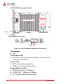
cPCI-3920 Series
3U CompactPCI Blade with Intel® Core™2 Duo,
Core™ Duo, Celeron® M Processor
User’s Manual
Manual Rev.
2.20
Revision Date:
August 30, 2010
Part No:
50-15064-1020
Advance Technologies; Automate the World.
Revision History
Revision
Release Date
Description of Change(s)
2.00
2008/07/07
Initial Release
2.10
2008/09/04
Update BIOS chapter
2.20
2010/08/30
Correct pin definitions (SATA0, J2, COM2, rJ2);
update BIOS
cPCI-3920
Preface
Copyright 2010 ADLINK Technology Inc.
This document contains proprietary information protected by copyright. All rights are reserved. No part of this manual may be reproduced by any mechanical, electronic, or other means in any form
without prior written permission of the manufacturer.
Disclaimer
The information in this document is subject to change without prior
notice in order to improve reliability, design, and function and does
not represent a commitment on the part of the manufacturer.
In no event will the manufacturer be liable for direct, indirect, special, incidental, or consequential damages arising out of the use or
inability to use the product or documentation, even if advised of
the possibility of such damages.
Environmental Responsibility
ADLINK is committed to fulfill its social responsibility to global
environmental preservation through compliance with the European Union's Restriction of Hazardous Substances (RoHS) directive and Waste Electrical and Electronic Equipment (WEEE)
directive. Environmental protection is a top priority for ADLINK.
We have enforced measures to ensure that our products, manufacturing processes, components, and raw materials have as little
impact on the environment as possible. When products are at their
end of life, our customers are encouraged to dispose of them in
accordance with the product disposal and/or recovery programs
prescribed by their nation or company.
Trademarks
Product names mentioned herein are used for identification purposes only and may be trademarks and/or registered trademarks
of their respective companies.
Preface
iii
Using this Manual
Audience and Scope
The cPCI-3920 User’s Manual is intended for hardware
technicians and systems operators with knowledge of installing,
configuring and operating industrial grade CompactPCI modules.
Manual Organization
This manual is organized as follows:
Chapter 1, Overview: Introduces the cPCI-3920 and package
contents.
Chapter 2, Specifications: Presents detailed specification
information, power consumption, and mechanical layout.
Chapter 3, Functional Description: Describes the cPCI-3920
main functions and board interfaces.
Chapter 4, Getting Started:
instructions of the cPCI-3920.
Describes the installation
Chapter 5, Driver Installation:
installation procedures.
Describes the driver
Chapter 6, Watchdog Timer: Describes the Watchdog Timer
functionality.
Chapter 7, BIOS Setup Utility: Describes the AMIBIOS®8
BIOS setup utility.
Important Safety Instructions: Presents safety instructions
all users must follow for the proper setup, installation and
usage of equipment and/or software.
Getting Service: Contact information for ADLINK’s worldwide
offices.
iv
Preface
cPCI-3920
Conventions
Take note of the following conventions used throughout this
manual to make sure that users perform certain tasks and
instructions properly.
Additional information, aids, and tips that help users perform
tasks.
NOTE:
CAUTION:
WARNING:
Preface
Information to prevent minor physical injury, component damage, data loss, and/or program corruption when trying to complete a task.
Information to prevent serious physical injury, component
damage, data loss, and/or program corruption when trying to
complete a specific task.
v
This page intentionally left blank.
vi
Preface
cPCI-3920
Table of Contents
Revision History...................................................................... ii
Preface .................................................................................... iii
List of Tables.......................................................................... ix
List of Figures ........................................................................ xi
1 Overview ............................................................................. 1
1.1
1.2
1.3
1.4
1.5
Introduction ..........................................................................
Features...............................................................................
Block Diagram .....................................................................
Product List..........................................................................
Package Contents ...............................................................
1
2
3
4
5
2 Specifications ..................................................................... 7
2.1
2.2
2.3
2.4
2.5
2.6
2.7
2.8
2.9
CPU, memory, and chipset.................................................. 7
Interfaces ............................................................................. 7
Software .............................................................................. 9
Mechanical........................................................................... 9
Environmental...................................................................... 9
I/O Connectivity Table ....................................................... 10
Power Requirements ......................................................... 11
Mechanical Dimensions..................................................... 15
Board Layout ..................................................................... 17
3 Functional Description .................................................... 23
3.1
3.2
3.3
3.4
CPU, Memory and Chipset ................................................
Peripherals.........................................................................
Board Interfaces ................................................................
Board Interfaces on RTM...................................................
23
30
34
51
4 Getting Started ................................................................. 57
4.1
4.2
4.3
4.4
4.5
4.6
Safety Requirements .........................................................
Installing the USB Flash Disk ............................................
Installing the Hard Disk Drive (cPCI-3290B only) ..............
Installing the cPCI-3920 to the Chassis.............................
RTM (cPCI-R3920) Installation..........................................
Hot Swap Procedures........................................................
Table of Contents
57
58
59
60
61
61
vii
5 Driver Installation.............................................................. 63
6 Watchdog Timer................................................................ 65
6.1
6.2
WDT Overview................................................................... 65
Using the Watchdog Timer in an Application ..................... 66
7 BIOS Setup Utility ............................................................. 71
7.1
7.2
7.3
7.4
7.5
7.6
7.7
7.8
Starting the BIOS ...............................................................
Main Setup.........................................................................
Advanced BIOS Setup .......................................................
PCI/PnP Setup...................................................................
Boot Setup .........................................................................
Security Setup....................................................................
Chipset Setup ....................................................................
Exit Menu ...........................................................................
71
75
77
89
90
94
97
99
Important Safety Instructions............................................. 101
Getting Service .................................................................... 103
viii
Table of Contents
cPCI-3920
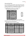
List of Tables
Table
Table
Table
Table
Table
Table
Table
Table
Table
Table
Table
Table
Table
Table
Table
Table
Table
Table
Table
Table
Table
Table
Table
Table
Table
Table
Table
2-1:
2-2:
2-3:
2-4:
2-5:
3-1:
3-2:
3-3:
3-4:
3-5:
3-6:
3-7:
3-8:
3-9:
3-10:
3-11:
3-12:
3-13:
3-14:
3-15:
3-16:
3-17:
3-18:
3-19:
3-20:
3-21:
3-22:
List of Tables
I/O Connectivity ......................................................
CompactPCI input voltage characteristics ..............
Power consumption of Core™ 2 Duo LV (L7400) ..
Power consumption of Core™ 2 Duo LV (U2500) ..
Power consumption of Celeron M LV(423) .............
Supported Processors, Power Dissipation .............
SMBus Devices and Addresses .............................
LED Function Descriptions .....................................
Front Panel USB Connector Pin Definition .............
Onboard USB Connector Pin Definition .................
VGA Connector CN3 Pin Definition ........................
Gigabit Connector CN7/CN8 Pin Definitions ..........
Ethernet LED Status Definitions .............................
Board-to-Board Connector Pin Definition ...............
PS/2 Keyboard/Mouse Connector Pin Definition ....
COM3 Serial Port Connector Pin Definition ............
COM4 Serial Port Connector Pin Definition ............
COM4 Mode Switch Settings ..................................
SATA0 Connector Pin Definition ............................
CompactPCI J1 Pin Assignment ............................
CompactPCI J2 Pin Assignment ............................
RTM USB Connector Pin Definitions ......................
RTM Gigabit Connector Pin Definitions ..................
COM1 Serial Port Connector Pin Definition ............
COM2 Serial Port Connector Pin Definition ............
SATA1-3 Connectors Pin Definition .......................
CompactPCI rJ2 Pin Assignment ...........................
10
11
12
13
14
25
32
33
34
35
38
39
40
41
42
43
43
44
46
48
50
51
52
53
53
54
56
ix
This page intentionally left blank.
x
List of Tables
cPCI-3920
List of Figures
Figure 1-1:
Figure 2-1:
Figure 2-2:
Figure 2-3:
Figure 2-4:
Figure 2-5:
Figure 2-6:
Figure 2-7:
Figure 3-1:
Figure 3-2:
Figure 6-1:
List of Figures
cPCI-3920 Block Diagram ......................................... 3
cPCI-3920 Mechanical Dimensions......................... 15
cPCI-R3920 Mechanical Dimensions ...................... 16
cPCI-3920 Board Layout ......................................... 17
cPCI-3920A Assembly and Front Panel .................. 18
DB-3920L2 Daughter Board Layout ........................ 19
cPCI-3920B Assembly and Front Panel .................. 20
cPCI-R3920(T) Board Layout and Front Panel ....... 21
Intel® 3100 Chipset Block Diagram......................... 26
USB Flash Disk Mechanical Layout ........................ 36
cPCI-3920 Watchdog Timer Architecture ................ 65
xi
This page intentionally left blank.
xii
List of Figures
cPCI-3920
1
Overview
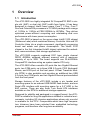
1.1 Introduction
The cPCI-3920 is a highly integrated 3U CompactPCI SBC in single slot (4HP) or dual slot (8HP) width form factor. It has been
designed to support Intel® lower power Core™ 2 Duo, Core™
Duo and Celeron® M processors in FC-BGA package with a range
of 1.0GHz to 1.5GHz at FSB 533MHz to 667MHz. They deliver
optimized power-efficient computing and outstanding dual core
performance with lower power consumption.
The cPCI-3920 is based on the server-class Intel® 3100 chipset
(Whitmore Lake) which combines Memory Controller Hub and I/O
Controller Hubs into a single component, significantly conserving
board real estate and power consumption. The Intel® 3100
chipset is the first Integrated Intel® chipset optimized for embedded, communications, and storage applications.
The cPCI-3920 supports registered ECC type, single channel
DDR2 400MHz soldered onboard memory with a maximum
capacity of up to 2GB. The board supports one 32-bit/33MHz
CompactPCI interface acting as system master CPU only.
The cPCI-3920 offers versatile I/O ports like two Gigabit Ethernet
ports, two COM ports, up to three USB 2.0 ports, PS/2 Keyboard/
Mouse, and VGA port on the front panel. A Rear Transition Module (RTM) is also available and provides an additional two USB
2.0 ports, two COM ports, and two Gigabit Ethernet ports switched
from the front panel.
Storage features of the cPCI-3920 include a pin header and
mounting space for an onboard USB NAND flash module, and one
Serial ATA interface with mounting space for a 2.5” HDD in the
8HP version. There are also three 7-pin Serial ATA interfaces
available on the RTM for additional storage expansion.
Designed for stability and packaged in a rugged format, the cPCI3920 is suitable for long life applications situated in industrial environments, including I/O intensive applications where only one slot
is available for the CPU. Components which have high temperature tolerance have been selected from embedded technology
programs, and therefore offer long-term availability.
Overview
1
1.2 Features
2
X
3U CompactPCI SBC in 4HP or 8HP width form factor
X
Low power Intel Core 2 Duo 1.5GHz, Core™ Duo 1.2GHz,
Celeron® M 1.0GHz processors
X
Intel® 3100 chipset (Memory and I/O Hub integrated chip)
X
Single channel DDR2 registered and ECC memory at
400MHz
X
Two PCI-Express Gigabit Ethernet ports in the front or RTM
X
Support USB 2.0 NAND flash module, up to 8GB
X
Supports one 2.5” Serial ATA hard drive onboard and three
Serial ATA interfaces on RTM
X
Up to five USB ports and four serial ports
Overview
cPCI-3920
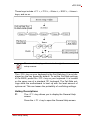
1.3 Block Diagram
FSB
533/677
Intel® Core 2 Duo
(Merom)
USB
GbE 1/2
HUB
USB 3
GbE 1/2
82571EB
PCI-E x4
USB x2
PCI-E x4 (1x) or x1 (4x)
J2
COM 1/2
USB
USB 2
USB
USB 1
SATA (3x)
SMbus
Intel® 3100
Chipset
(Whitmore Lake)
F8126
COM 3/4
FWH
KB/MS
W83792AG
F71858D
USB 0
pin header
LPC
DDR2-400 REG/ECC
VGA
Volari
Z11
Soldered
PCI-E x1
PCI 32-bit/33MHz
SATA
I/O for 8HP
J1
I/O for 4HP
Figure 1-1: cPCI-3920 Block Diagram
Overview
3
1.4 Product List
Products included in the cPCI-3920 Series include:
SBC
X
cPCI-3920A: single-slot (4HP) width 3U CompactPCI featuring Intel LV Core 2 Duo 1.5GHz, Core Duo 1.2GHz or
ULV Celeron 1.0GHz processors; 512MB, 1GB or 2GB
onboard memory; optional USB flash disk module
X
cPCI-3920B: dual-slot(8HP) width 3U CompactPCI featuring Intel LV Core 2 Duo 1.5GHz, Core Duo 1.2GHz or ULV
Celeron 1.0GHz processors; 512MB, 1GB or 2GB onboard
memory; optional USB flash disk module and 2.5” SATA
hard drive
Rear Transition Module
X
cPCI-R3920: Rear Transition Module for cPCI-3920 SBCs
with 50mm width
X
cPCI-R3920T: Rear Transition Module for cPCI-3920 SBCs
with 80mm width
Accessories
X
USB flash disk module, optional 2GB, 4GB or 8GB
X
2.5” Serial ATA hard drive
Contact your ADLINK representative to purchase accessories.
4
Overview
cPCI-3920
1.5 Package Contents
The cPCI-3920 is packaged with the following components. If any
of the items on the contents list are missing or damaged, retain the
shipping carton and packing material and contact the dealer for
inspection. Please obtain authorization before returning any product to ADLINK. The packing contents of the cPCI-3920 Series are
non-standard configurations and may vary depending on customer
requests.
CPU module
X
The cPCI-3920 Series CPU Module
Z
CPU, RAM, and HDD specifications will differ depending
on options selected
Z
Thermal module is assembled on the board
Z
Battery daughter board is assembled on the board
Z
HDD bracket is assembled on the 8HP version
X
Four screws for hard drive
X
Y-cable for PS/2 combo port (8HP version only)
X
ADLINK All-in-One CD
X
User’s manual
Rear Transition Module
X
cPCI-R3920 or cPCI-R3920T
The contents of non-standard cPCI-3920 configurations may
vary depending on the customer’s requirements.
NOTE:
CAUTION: This product must be protected from static discharge
and physical shock. Never remove any of the components except
at a static-free workstation. Use the anti-static bag shipped with
the product when putting the board on a surface. Wear an antistatic wrist strap properly grounded on one of the system's ESD
ground jacks when installing or servicing system components.
Overview
5
This page intentionally left blank.
6
Overview
cPCI-3920
2
Specifications
2.1 CPU, memory, and chipset
uFC-BGA Intel® Core™ 2 Duo LV (L7400) 1.5 GHz,
FSB 667MHz, 4 MB L2 cache
Processor
uFC-BGA Intel Intel® Core™ Duo ULV (U2500) 1.2 GHz,
FSB 533MHz, 2 MB L2 cache
uFC-BGA Intel Intel® Celeron® M ULV (423) 1.06 GHz,
FSB 533MHz, 1 MB L2 cache
Chipset
Intel® 3100 chipset
Memory
Single channel soldered onboard registered ECC DDR2
SDRAM at 400MHz up to 2GB
2.2 Interfaces
CompactPCI
Standard
PICMG® 2.0 R3.0
PICMG® 2.1 R2.0
CompactPCI Bus 32-bit/33MHz PCI bus
Display
XGI Volari Z11 PCI-Express x1 Graphics Controller
32MB DDR2-400 SDRAM memory
Up to 1600x1200@70Hz 24bit color
Ethernet
PCI-Express x4 Intel® 82571EB dual port Ethernet
controller
Two GbE egress ports on the front panel or on the rear
panel by BIOS selection
4x USB channels from 3100 chipset
Channel 0 is for 9 pin header, space reserved for horizontal
USB flash disk module
USB
Channel 1 is connected to the front panel
Channel 2 is connected to the front panel (8HP only)
Channel 3 is connected to 4-port hub controller with one
channel routed to the 8HP front panel and two channels
routed to the RTM
Specifications
7
4x serial ports
Serial Port
Two DB-9 ports on the front panel, one RS-232 and one
RS-232/422/485/485+ (8HP only)
Two ports are routed to RTM with one DB-9 port on rear
panel and one pin header onboard
4x Serial ATA channels:
Serial ATA
One SATA connector onboard, 2.5” HDD space reserved
(8HP only)
Three channels are routed to RTM with pin headers
onboard
cPCI-3920 main board
1x USB 2.0 port
1x VGA port
2x GbE port
1x system reset button
Front panel I/O
Power, WDT, CPU over-temperature LED
DB-3920L2 daughter board (8HP only)
1x RS-232 port
1x RS-232/422/485/485+ selectable port
1x PS/2 combo port for keyboard and mouse
2x USB 2.0 port
cPCI-3920 main board
1x pin header for USB flash disk module
DB-3920L2 daughter board (8HP only)
Board I/O
Interfaces
1x SATA port (signal and power for onboard HDD)
cPCI-R3920 rear transition module
3x SATA ports (7-pin)
10-pin RS232 port
2x USB 2.0 port
Rear panel I/O
2x GbE port (share the same channels with front panel GbE
ports, selected by BIOS setting)
1x RS-232 port
8
Specifications
cPCI-3920
2.3 Software
BIOS
AMI 16Mbit FWH
Microsoft® Windows® XP Professional
Microsoft® Windows® Server 2003
Supported OS
Microsoft® Windows® Vista Enterprise, 32-bit version
RedHat Fedora Core 8
Contact ADLINK for other OS availability
2.4 Mechanical
Form factor
cPCI-3920: 3U 4HP/8HP CompactPCI
cPCI-R3920(T): 3U 4HP CompactPCI
cPCI-3920: 100mmx 160mm (LxW)
Dimensions
cPCI-R3920: 100mm x 50mm (LxW)
cPCI-R3920T: 100mmx 80mm (LxW)
2.5 Environmental
Operating
temperature
Standard: 0 to 60°C
Storage
temperature
-40°C to 85°C
Humidity
Shock
Extended temperature: -20 to 70°C
5% to 95% non-condensing
15G peak-to-peak, 11ms duration, non-operation
Non-operating: 1.88G rms, 5 to 500 Hz, each axis
Vibration
Compliance
Specifications
Operating: 1.88G rms. 5 to 500Hz, each axis, with USB
flash disk (without HDD)
CE, FCC Class A
9
2.6 I/O Connectivity Table
cPCI-3920A
Faceplate
cPCI-3920B
Board
Faceplate
Board
cPCI-R3920(T)
Faceplate
GbE
Y x2
--
Y x2
--
Yx2
--
USB
Y
Y (9-pin)
Y x3
Y (9-pin)
Yx2
--
VGA
Y
--
Y
--
--
--
--
Y (DB-9)
Y
(10-pin)
COM
--
--
Y
(DB-9) x2
SATA
--
--
--
Y
--
Y x3
(7-pin)
PS/2
KB/MS
--
--
Y
--
--
--
LED
Y x3
--
Y x3
--
--
--
Reset
Button
Y
--
Y
--
--
--
Table 2-1: I/O Connectivity
10
Specifications
cPCI-3920
2.7 Power Requirements
In order to guarantee a stable functionality of the system, it is recommended to provide more power than the system requires. An
industrial power supply unit should be able to provide at least
twice as much power as the entire system requires. An ATX power
supply unit should be able to provide at least three times as much
power as the entire system requires.
The tolerance of the voltage lines described in the CompactPCI
specification (PICMG 2.0 R3.0) is +5%/ -3% for 5, 3.3 V and ±5%
for ±12V. This specification is for power delivered to each slot and
it includes both the power supply and the backplane tolerance.
Voltage
5V
3.3V
+12V
-12V
V I/O (PCI I/O
Buffer Voltage)
GND
Nominal
Value
+5.0 VDC
+3.3 VDC
+12 VDC
-12 VDC
+3.3 VDC or
+5 VDC
Tolerance
+5% / -3%
+5% / -3%
+5% / -5%
+5% / -5%
Max. Ripple
(P - P)
50 mV
50 mV
240 mV
240 mV
+5% / -3%
50 mV
Table 2-2: CompactPCI input voltage characteristics
Specifications
11
Power Consumption
The following tables provide information on the power consumption of cPCI-3920.
Processor: Intel® Core™ 2 Duo LV (L7400) 1.5GHz,
FSB 667MHz, 4MB L2 cache
Function
Memory
SATA Hard Drive
Backplane
Power Supply
DOS
Power requirement
Current (A)
Watts (W)
Configuration
DDR2 400 1GB
External 3.5”HDD
ADLINK cBP-3208R Rev.B2
ZIPPY HG2-6350P 350W
+3.3V
1.53
5.05
+5V
4.41
22.05
Total
Linux, Idle
Power requirement
Current (A)
Watts (W)
+3.3V
1.63
5.38
+5V
3.53
17.65
Total
Windows® XP, Idle
Power requirement +3.3V
Current (A)
1.62
Watts (W)
5.35
+5V
4.63
23.15
Total
Windows® XP, CPU 100% Usage
Power requirement +3.3V
+5V
Current (A)
1.61
6.02
Watts (W)
5.31
30.10
27.10
23.03
28.50
Total
35.41
Table 2-3: Power consumption of Core™ 2 Duo LV (L7400)
12
Specifications
cPCI-3920
Processor: Intel® Core™ Duo (U2500) 1.2GHz, FSB 533MHz,
2MB L2 cache
Function
Memory
SATA Hard Drive
Backplane
Power Supply
DOS
Power requirement
Current (A)
Watts (W)
Configuration
DDR2 400 1GB
External 3.5”HDD
ADLINK cBP-3208R Rev.B2
ZIPPY HG2-6350P 350W
+3.3V
1.54
5.08
+5V
3.50
17.50
Total
Linux, Idle
Power requirement
Current (A)
Watts (W)
+3.3V
1.64
5.41
+5V
3.30
16.50
Total
Windows® XP, Idle
Power requirement +3.3V
Current (A)
1.68
Watts (W)
5.38
+5V
3.71
18.55
Total
Windows® XP, CPU 100% Usage
Power requirement +3.3V
+5V
Current (A)
1.63
4.30
Watts (W)
5.38
21.50
22.58
21.91
23.93
Total
26.88
Table 2-4: Power consumption of Core™ 2 Duo LV (U2500)
Specifications
13
Processor: Intel® Celeron M LV(423) 1.07GHz, FSB 533MHz,
1MB L2 cache
Function
Memory
SATA Hard Drive
Backplane
Power Supply
DOS
Power requirement
Current (A)
Watts (W)
Configuration
DDR2 400 1GB
External 3.5”HDD
ADLINK cBP-3208R Rev.B2
ZIPPY HG2-6350P 350W
+3.3V
1.51
4.98
+5V
3.27
16.35
Total
Linux, Idle
Power requirement
Current (A)
Watts (W)
+3.3V
1.60
5.28
+5V
3.12
15.60
Total
Windows® XP, Idle
Power requirement +3.3V
Current (A)
1.59
Watts (W)
5.25
+5V
3.36
16.80
Total
Windows® XP, CPU 100% Usage
Power requirement +3.3V
+5V
Current (A)
1.59
3.64
Watts (W)
5.25
18.20
21.33
20.88
22.05
Total
23.45
Table 2-5: Power consumption of Celeron M LV(423)
14
Specifications
cPCI-3920
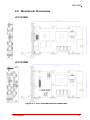
2.8 Mechanical Dimensions
cPCI-3920A
cPCI-3920B
Figure 2-1: cPCI-3920 Mechanical Dimensions
Specifications
15
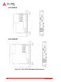
cPCI-R3920
cPCI-R3920T
Figure 2-2: cPCI-R3920 Mechanical Dimensions
16
Specifications
cPCI-3920
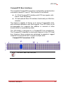
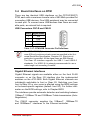
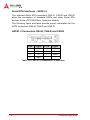
2.9 Board Layout
cPCI-3920 Board Layout
CN2
U6
CN3
U7
CN4
CN7
U19
U5
CN5
U15
CN8
U25
U6
Processor
CN2 USB port
U7
Chipset
CN3 VGA port
U5
Transformer
CN7 Ethernet port
U15 Graphics controller
CN8 Ethernet port
U19 Ethernet controller
CN4
U25 SDRAM
CN5 USB pin header
J1
CompactPCI J1
connector
J2
J2
J1
DB-3920L2 daughter
board connector
CompactPCI J2
connector
Figure 2-3: cPCI-3920 Board Layout
Specifications
17
cPCI-3920A Assembly Outline
Thermal Module
USB flash
disk (optional)
Battery
cPCI-3920A Front Panel
Speed ACT
Figure 2-4: cPCI-3920A Assembly and Front Panel
Reset Button
X
RST
Temperature LED
X
Hot (red): CPU Overtemperature Status, connected to the
CPU signal PROCHOT
Status LEDs
X
WDT (yellow): Watchdog Status
X
PWR (green): Power Supply Status
Gigabit Ethernet LEDs
18
X
SPEED ON (green): 1000Mbps
X
SPEED OFF: 10Mbps or 100Mbps
X
ACT (yellow): Ethernet Link Activity
Specifications
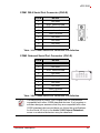
cPCI-3920
DB-3920L2 Daughter Board Components Layout
The DB-3920L2 Daughter Board extends the cPCI-3920 from
4HP (cPCI-3920A) to 8HP (cPCI-3920B) version. This additional capability opens up the broadest range of expansion possibilities. The DB-3920L2 module has been designed to include
two COM ports, a PS/2 keyboard and mouse port, two USB 2.0
interfaces and a 2.5” SATA hard disk interface.
CN1-2
CN2-2
CN3-2
CN4-2
CN5-2
SW
CN6-2
CN1-2 Serial port
CN5-2 USB port
CN2-2 PS/2 Keyboard/ Mouse CN6-2 Serial port
CN3-2 Serial ATA connector
SW
COM4 mode switches
CN4-2 USB port
Figure 2-5: DB-3920L2 Daughter Board Layout
Specifications
19
cPCI-3920B Assembly Outline
2.5” SATA
hard drive
cPCI-3920B Front Panel
Figure 2-6: cPCI-3920B Assembly and Front Panel
20
Specifications
cPCI-3920
cPCI-R3920(T) Board Layout
The cPCI-3920 Series offer two version rear transition modules
with the same functionality but different dimensions. The cPCIR3920 is designed with a 50mm width and the cPCI-R3920T is
designed with a 80mm width
CN1-R
rJ2
CN2-R
CN4-R
CN1-R
CN3-R
rJ2
CN2-R
CN4-R
CN5-R
CN3-R
CN5-R
CN6-R
CN6-R
CN8-R
CN7-R
cPCI-R3920T
CN8-R
CN7-R
cPCI-R3920
CN1-R 10 pin RS-232 port
CN5-R SATA port
CN2-R SATA port
CN6-R Dual Ethernet ports
CN3-R RS232 port
CN7-R USB port
CN4-R SATA port
CN8-R USB port
cPCI-R3920(T) Front Panel
Figure 2-7: cPCI-R3920(T) Board Layout and Front Panel
Specifications
21
This page intentionally left blank.
22
Specifications
cPCI-3920
3
Functional Description
The following sections describe the cPCI-3920 main functions and
board interfaces.
3.1 CPU, Memory and Chipset
CPU: Intel® Core™ Duo and Intel® Core™2 Duo
The cPCI-3920 supports the latest Intel® Core™ Duo and Intel®
Core™2 Duo processor family up to speeds of 1.5 GHz with up to
667 MHz FSB. The Intel® Core™ Duo consists of two cores and
up to 2 MB L2 cache shared by both cores. The Intel® Core™2
Duo consists of two cores, up to 4 MB L2 cache shared by both
cores, Intel Extended Memory 64 Technology (Intel EM64T), and
enhanced address range for up to 64 GB memory. The Intel®
Core™ Duo and the Intel® Core™2 Duo processors deliver optimized power-efficient computing and outstanding dual-core performance with low power consumption.
The Intel® Core™ Duo and the Intel® Core™2 Duo support the
latest Intel’s Virtualization Technology (VT), which allows a platform to run multiple operating systems and applications in independent partitions, such as performing system upgrades and
maintenance without interrupting the system or the application,
keeping software loads and virus attacks separate, combining
multiple servers in one system, etc. With processor and I/O
enhancements to Intel’s various platforms, Intel Virtualization
Technology improves the performance and robustness of today’s
software-only virtual machine solutions.
Furthermore, the Intel® Core™ Duo and the Intel® Core™2 Duo
also support the Intel SpeedStep technology which enables realtime dynamic switching of the voltage and frequency between several modes. This is achieved by switching the bus ratios, core
operating voltage, and core processor speeds without resetting
the system.
Functional Description
23
The following list sets out some of the key features of the Intel®
Core™ Duo and the Intel® Core™2 Duo processors:
X
Two mobile execution cores in one single processor
X
Support of Intel’s Virtualization Technology (Vanderpool)
X
Support of Intel Architecture with Dynamic Execution
X
Outstanding dual-core performance with low power consumption
X
On die, primary 32 KB instruction cache and 32KB writeback data cache
X
On die, L1 and L2 cache with Advanced Transfer Cache
Architecture
Z
Intel® Core™ Duo processor (ULV), 1.2 GHz, 533 MHz
FSB, 2 MB L2 cache
Z
Intel® Core™2 Duo processor (LV), 1.5 GHz, 667 MHz
FSB, 4 MB L2 cache
X
Advanced Branch Prediction and Data Prefetch Logic
X
Streaming SIMD Extensions 3 (SSE3)
X
Up to 667 MHz, Source-Synchronous Front Side Bus (FSB)
X
Advanced Power Management features including
Enhanced Intel SpeedStep technology
X
Intel Extended Memory 64 Technology for 64-bit computing
(only with the Intel® Core™2 Duo)
X
Enhanced address range for up to 64 GB memory (only with
the Intel® Core™ Duo )
Intel® Celeron® M
The cPCI-3920 supports the low power 1.07 GHz Intel® Celeron®
M processor with 533 MHz FSB. The Intel® Celeron® M consists
of one core and 1 MB L2 cache.
The following list sets out some of the key features of the Intel®
Celeron® M processor:
24
X
Supports Intel architecture with dynamic execution
X
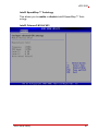
High-performance, low-power core featuring architectural
innovations like micro-ops fusion and advanced stack man-
Functional Description
cPCI-3920
agement that reduce the number of micro-ops handled by
the processor.
X
On-die, primary 32-kB instruction cache and 32-kB, writeback, data cache
X
On-die, 1 MB second level cache with Advanced Transfer
Cache architecture
X
Advanced branch prediction and data prefetch logic
X
Streaming SIMD extensions 2 (SSE2) that enables breakthrough levels of performance in multimedia applications
including 3D graphics, video decoding/encoding, and
speech recognition.
X
533-MHz, source-synchronous front side bus (FSB)
X
Advanced power management features
X
Maintained support for MMX_ technology (technology
designed to accelerate multimedia and communications
software)
X
Compatible with IA-32 software
Supported Processors, Maximum Power Dissipation
The following tables indicate the processors supported on the
cPCI-3920 and their maximum power dissipation.
Intel® Celeron® M
1.07 GHz (ULV(2))
μFCBGA
1MB
533 MHz
Speed
Package
L2 Cache
FSB
Intel® Core Duo
1.2GHz (ULV(2))
μFCBGA
2MB
533 MHz
Intel® Core 2 Duo
1.5GHz (LV(1))
μFCBGA
4MB
667 MHz
Intel® Core Duo
1.2GHz (ULV)
2MB L2 Cache
Intel® Core 2 Duo
1.5GHz (LV)
4MB L2 Cache
(1) LV: Low Voltage
(2) ULV: Ultra low Voltage
Intel® Celeron® M
1.07 GHz (ULV)
1MB L2 Cache
Frequency
Mode
Maximum
Power HFM(3)
5.5W
9W
17W
(3) HFM: High Frequency Mode (maximum frequency of the CPU)
Table 3-1: Supported Processors, Power Dissipation
Functional Description
25
Memory
The cPCI-3920 supports a single soldered channel DDR2 memory
with Error Checking and Correcting (ECC) running at 400 MHz
The available memory module configuration is 1 GB. 2 GB available on request, please contact your ADLINK representative.
NOTE:
Memory configuration changes can only be performed at the
factory. Failure to comply with the above may result in damage
to your board or improper operation.
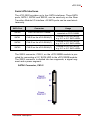
Intel® 3100 Chipset Overview
The Intel® 3100 Chipset is a single integrated chip that contains
the functionality of a Memory Controller Hub and an I/O Controller
Hub. In this document the Memory Controller Hub unit and I/O
Controller Hub unit in the Intel® 3100 Chipset are referenced as
IMCH (Integrated Memory Controller Hub) and IICH (Integrated
I/O Controller Hub) respectively.
P roc essor
W DT
FSB
R egistere d ECC
D DR 2 400
Serial ATA
6 Drives
Intel® 31 00 Chipset
SM Bus x2
EC C
PCI 32/33
IICH
2 UAR T
IMCH
4 USB-2
38 GPIOs
ED M A
LPC
Port B
PCI Express
1x4 or 4x1
Port A
PCI Express
1x8 configurable as 2x4 or 2x1
Figure 3-1: Intel® 3100 Chipset Block Diagram
26
Functional Description
cPCI-3920
PCI Express
The Intel 3100 Chipset provides one configurable x8 PCI
Express interface with a maximum theoretical bandwidth of 4
GByte/s. The x8 PCI Express interface may alternatively be
configured as two independent x4 PCI Express interfaces with
a maximum theoretical bandwidth of 2 GBytes/s each. The
Intel® 3100 Chipset also supports an additional x4 PCI
Express interface with a maximum theoretical bandwidth of 2
GBytes/s which may alternatively be configured as four independent x1 PCI Express interfaces.
IICH
I/O Controller Hub (IICH) functions are integrated into the
Intel® 3100 Chipset, eliminating the requirement for a legacy
I/O bridge.
I/O Controller Hub Feature set comprises:
X
PCI Express Interface
X
Low Pin Count (LPC) Interface
X
Firmware Hub (FWH) Interface
X
Integrated Serial ATA (SATA) Host Controllers:
X
Z
Independent DMA operation on six ports
- Four ports in SATA 1.0a and AHCI mode
- Six ports in AHCI mode only
Z
Data transfer rates up to 150 Mbyte/s
Two controllers with up to four USB 2.0 ports:
Z
One EHCI USB 2.0 Host Controller to support a total of
four ports (shared with the UHCI ports)
Z
Two UHCI Host Controllers to support a total of four
ports (shared with the EHCI ports)
X
Interrupt Controller
X
Power Management Logic
X
DMA Controller
X
Timers Based on 82C54
X
High Precision Event Timers (HPET)
X
Real Time Clock with 256-byte Battery-backed CMOS RAM
Functional Description
27
X
System TCO Reduction Circuits
X
SMBus
X
Watchdog Timers
X
PCI 2.3 Interface
X
Two fully functional serial ports
X
38 General Purpose I/Os (GPIO)
IMCH
The Intel® 3100 Chipset provides an integrated memory controller for direct-connection to one channel of DDR2-400
(unstacked) registered memory devices with ECC. Peak theoretical memory data bandwidth using DDR2-400 is 3.2 GByte/s
Volari™ Z11 Graphics Controller
Volari™ Z11 GPU is the extreme programmable GPU of the XGI
2D GPU family. The Volari™ Z11 integrates a PCI-Express 1x controller and a 64-bit 2D graphics engine. It offers a flexible 16-bit
DDR-II memory interface. The Z11 also incorporates a configurable 3.3V DVO digital interface to support a third party
LVDS/TMDS transmitter. It can achieve high 2D performance with
a memory interface supporting a bandwidth of up to 1 GB/s (DDRII @250MHz).
Volari™ Z11 GPU main features:
X
PCI-Express 1x Bus Interface
Z
X
X
28
Supports PCI-E local bus standard Revision 1.1 compliant
High Performance 2D Accelerator
Z
Built-in hardware command queue
Z
Built-in Direct Draw Accelerator
Z
Built-in GDI 2000 Accelerator
Z
Built-in an 1T pipelined 64-bit BITBLT graphics engine
Z
Supports memory-mapped, zero wait-state, burst engine
write
Z
Built-in 64x64x2 bit-mapped mono hardware cursor
High Efficient BroadBahn™ Memory Architecture
Functional Description
cPCI-3920
X
Z
Supports DDR-II SDRAM memory
Z
32 MB memory configuration
Z
Supports VGA BIOS auto memory size detection
High Performance Flat Panel Display Interface
Z
X
X
X
High Integration
Z
Built-in CRT FIFO to support ultra high resolution graphics modes and reduce CPU wait-state
Z
Built-in programmable 24-bit true-color RAMDAC with
230 MHz pixel clock
Resolution, Color & Frame Rate
Z
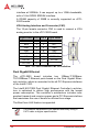
Supports 230 MHz pixel clock
Z
Supports VESA standard super high resolution graphics
modes
4:3 resolution up to 1600x1200 256/32K/64K/16M colors 70Hz
Wide Screen resolution modes
Low resolution modes
Z
Supports virtual screen up to 4096x4096
Power Management
Z
X
X
NOTE:
Supports graphics mode up to 1600x1200@70Hz 16M
colors
Supports power management for VGA monitor
Multimedia Application
Z
Supports DDC1, DDC2B and DDC 3.0 specifications
Z
Supports RAMDAC snoop fir multimedai applications
Miscellaneous
Z
Lead-free package
Z
RoHS compliance
The Z11 doesn't support the Linux X11 performance bench
test, which changes display mode frequently during every
screen page. The display flickers when performing the X11
performance bench test under Linux.
Functional Description
29
3.2 Peripherals
The following standard peripherals are available on the cPCI-3920
board:
Timer
The cPCI-3920 is equipped with the following timers:
Real-Time Clock
The IICH contains real-time clock with 256-byte of batterybacked RAM.
The real-time clock performs timekeeping functions and
includes 256 bytes of general purpose battery-backed CMOS
RAM. Features include an alarm function, programmable periodic interrupt and a 100-year calendar. All battery-backed
CMOS RAM data remains stored in an additional EEPROM.
This prevents data loss in case the cPCI-3920 is operated without battery.
Counter/Timer
Three 8254-style counter/timers are included on the cPCI-3920
as defined for the PC/AT (System Timer, Refresh Request,
Speaker Tone Output).
In addition to the three 8254-style counters, the IICH includes
three High Precision Event Timers (HPET) that may be used by
the operating system. They are implemented as a single
counter each with its own comparator and value register.
They support One-shot and periodic interrupts.
Watchdog Timer
The cPCI-3920 provides a Watchdog Timer that is programmable
for a timeout period ranging from 1 ms to 1050 sec. Failure to trigger the Watchdog Timer in time results in a system reset, an interrupt, or NMI. In the dual-stage mode, a combination of both NMI,
and reset if the Watchdog is not serviced. A hardware status flag
will be provided to determine if the Watchdog Timer generated the
reset.
30
Functional Description
cPCI-3920
Battery
The cPCI-3920 is provided with a 3.0 V “coin cell” lithium battery
for the RTC. To replace the battery, proceed as follows:
X
Turn off power
X
Remove the battery
X
Place the new battery in the socket.
X
Make sure that you insert the battery the right way round.
The plus pole must be on the top!
The lithium battery must be replaced with an identical battery
or a battery type recommended by the manufacturer. Suitable
batteries include the Varta CR2025 and Panasonic BR2020.
NOTE:
NOTE:
The user must be aware that the battery’s operational temperature range is less than that of the cPCI-3920’s storage temperature range. For exact range information, refer to the battery
manufacturer’s specifications.
Care must be taken to ensure that the battery is correctly
replaced.The battery should be replaced only with an identical or equivalent type recommended by the manufacturer.Dispose of used batteries according to the manufacturer’s
instructions.The typical life expectancy of a 225 mAh battery
(Varta CR2032) is 4-5 years with an average on-time of 8
hours per working day at an operating temperature of 30°C.
However, this typical value varies considerably because the life
expectancy is dependent on the operating temperature and the
standby time (shutdown time) of the system in which it operates.To ensure that the lifetime of the battery has not been
exceeded, it is recommended to exchange the battery after 3-4
years.
Functional Description
31
Reset
A reset will be generated by the following conditions:
X
Pressing the front panel reset button
X
Watchdog overflow
X
CompactPCI backplane PRST# input (CompactPCI connector J2, pin C17)
SMBus Devices
The cPCI-3920 provides a System Management Bus (SMBus)
for access to several system monitoring and configuration
functions. The SMBus consists of a two-wire I2C bus interface.
The following table describes the function and address of every
onboard SMBus device.
Device
SMBus Address
Clock Buffer
DCh
Clock Generator
D2h
SPD
A0h
EEPROM (Board VPD)
AEh
Table 3-2: SMBus Devices and Addresses
Thermal Management / System Monitoring
The W83792AG can be used to monitor several critical hardware
parameters of the system, including power supply voltages and
temperatures, all of which are very important for the proper operation and stability of a high-end computer system.
The voltages +12 V, +5 V, +3.3 V, and Vcore are supervised. The
temperature sensors monitor the CPU temperature and the ambient temperature to ensure that the system is operating at a safe
temperature level. If the CPU temperature is too high, the sensor
automatically reduces the CPU clock frequency, depending on the
mode chosen in the BIOS settings.
32
Functional Description
cPCI-3920
FWH Flash Memory
For simple BIOS updating a standard onboard 16 Mbit Firmware
Hub device is used. The FWH stores both the system BIOS and
graphics BIOS. It can be updated as new versions of the BIOS
become available.
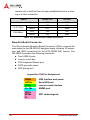
LED Functions
There are three LEDs on the front panel, below table shows the
function of LEDs.
Name
HOT
Color
Status
Function description
BLINK
CPU reaches or exceeds max.
operating temperature
OFF
CPU below max. operating
temperature
Red
WDT
Yellow
PWR
Green
ON
WDT function enable
OFF
WDT function disable
ON
Power on
OFF
Power off
Table 3-3: LED Function Descriptions
Functional Description
33
3.3 Board Interfaces
USB Interfaces
The cPCI-3920 supports six USB 2.0 ports:
X
one front I/O
X
two front I/O on DB-3920L2 module
X
one onboard to connect a Flash disk
X
two on the Rear I/O module.
On the USB 2.0 front panel port, USB cable with up to 5 meters in
length can be used.
On the USB 2.0 Rear I/O ports, it is strongly recommended to use
a cable below 3 meters in length for USB 2.0 devices.
The USB 2.0 ports are high-speed, full-speed, and low-speed
capable. Hi-speed USB 2.0 allows data transfers of up to 480 Mb/s
- 40 times faster than a full-speed USB (USB 1.1). One USB
peripheral may be connected to each port.
To connect more USB devices than there are available ports, an
external hub is required.
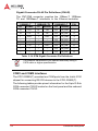
Front Panel USB Connectors (CN2, CN4 -2, CN5-2)
Pin # Signal Name
1
Vcc
2
UV0-
3
UV0+
4
GND
Table 3-4: Front Panel USB Connector Pin Definition
NOTE:
34
The cPCI-3920 host interfaces can be used with maximum 500
mA continuous load current as specified in the Universal Serial
Bus Specification, Revision 2.0. Short-circuit protection is provided. All the signal lines are EMI-filtered.
Functional Description
cPCI-3920
Onboard USB Pin Header (CN5)
The onboard USB device (CN5 pin header, 2.54mm pitch) is
used to connect a USB Flash Disk.
The following figure and table provide pinout information for the
onboard USB pin header CN5:
Pin
Signal
Function
I/O
1
Vcc
VCC
--
2
Uv0-
Differential USB-
I/O
3
Uv0+
Differential USB+
I/O
4
GND
GND
--
5
--
Not connected
--
6
--
Not used
--
7
GND
GND
--
8
--
Not used
--
9
--
Not used
--
10
--
Not used
--
Table 3-5: Onboard USB Connector Pin Definition
Functional Description
35
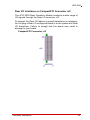
USB Flash Disk Mechanical Layout
X
Maximum space reserved for USB flash disk is 50mm x
30mm (LxW)
X
The distance between the centers of connector and screw
hole is 27.3mm~27.9mm
X
Maximum allowable connector height is 9.78mm (under
4HP)
Figure 3-2: USB Flash Disk Mechanical Layout
36
Functional Description
cPCI-3920
Graphics Controller
The Volari™ Z11 graphics controller incorporates a powerful 64-bit
graphics engine to enhance the performance of 2D operations.
The capabilities of the graphics engine include, but are not limited
to BitBlt, Color Expansion, Enhanced Color Expansion, Line Drawing, Transparent BitBlt, and Rectangle Fill.
For all enhanced 256 color (8 bpp), 32k & 64k hi-color (16 bpp),
and 16M true color (32 bpp) graphics modes, the 2D engine supports the following functions:
X
256 raster operations
X
Rectangle fill
X
Color expansion
X
Enhanced Color expansion
X
Line drawing with styled pattern
X
Built-in bytes pattern registers
X
Built-in 8x8 mask registers
X
Rectangle Clipping Transparent BitBlt with source and destination keys
X
Source data in command queue Bitblt
The engine also supports new GDI 2000 functions
PCI Bus Interface
The Volari™ Z11 GPU is a native PCI-E device which
connects directly to the PCI-E bus onboard the motherboard. The Z11 decodes 32-bit addresses and configures the
device based on the applicable control lines between the target
and initiator. The GPU can execute both I/O and memory
access instructions as a 32-bit device.
BroadBahn™ Memory Architecture
The internal memory controller of the Z11 generates the timing
parameters for display memory. It supports the DDRII SDRAM
timing specifications
The frequency of the Volari™ Z11 memory controller interface
is synchronous with the 2D engine at 125MHz with the I/O
Functional Description
37
interface at 250MHz. It can support up to a 1GB/s bandwidth,
with a 16-bit DDRII SDRAM interface.
A DRAM capacity of 32MB is currently supported on cPCI3920 boards.
VGA Analog Interface and Connector (CN3)
The 15-pin female connector CN3 is used to connect a VGA
analog monitor to the cPCI-3920 board.
Signal Name Pin # Pin # Signal Name
Red
1
2
Green
Blue
3
4
N.C.
GND
5
6
GND
GND
7
8
GND
+5V.
9
10
GND
N.C.
11
12
CRTDATA
HSYNC
13
14
VSYNC
CRTCLK
15
Table 3-6: VGA Connector CN3 Pin Definition
Dual Gigabit Ethernet
The cPCI-3920 board includes two 10Base-T/100BaseTX/1000Base-T Ethernet ports based on the Dual Gigabit Ethernet controller, which is connected to the x4 PCI Express interfaces
of the Intel® 3100.
The Intel® 82571EB Dual Gigabit Ethernet Controller’s architecture is optimized to deliver high performance with the lowest
power consumption. The controller’s architecture includes independent transmit and receive queues and a PCI Express interface
that maximizes the use of bursts for efficient bus usage.
The Boot from LAN feature is supported.
The Ethernet transmission can operate effectively using a
CAT5 cable or higher specifications.
NOTE:
38
Functional Description
cPCI-3920
Gigabit Connector RJ-45 Pin Definitions (CN7/CN8)
The CN7/CN8 connector supplies the 10Base-T, 100BaseTX and 1000Base-T interfaces to the Ethernet controller.
10BASE--T
100BASE--TX
1000BASE--T
PIN
I/O
SIGNAL
I/O
SIGNAL
I/O
SIGNAL
O
TX+
O
TX+
I/O
BI_DA+
O
TX-
O
TX-
I/O
BI_DA-
2
I
RX+
I
RX+
I/O
BI_DB+
3
--
--
--
--
I/O
BI_DC+
4
-I
-TX--
-I
-RX--
I/O
I/O
BI_DCBI_DB-
5
6
--
--
--
--
I/O
BI_DD+
7
--
--
--
--
I/O
BI_DD-
8
1
Table 3-7: Gigabit Connector CN7/CN8 Pin Definitions
Ethernet LED Status
SPEED (green):
When green it indicates a 1000BASE-TX connection. When not
lit and the ACT-LED is active, the connection is operating at
100BASE-T.
ACT (yellow):
This LED monitors network connection and activity. The LED
lights up when a valid link (cable connection) has been established. The LED goes temporarily off if network packets are
being sent or received through the RJ-45 port. When this LED
Functional Description
39
remains off, a valid link has not been established due to a missing or a fault connection.
Status
Speed LED
Act LED
Network link is not established
OFF
OFF
10/100 Mbps
1000 Mbps
Link
OFF
ON
Active
OFF
Blink
Link
ON
ON
Active
ON
Blink
Table 3-8: Ethernet LED Status Definitions
Board-to-Board Connector
The 60-pin female Board-to-Board Connector (CN4) connects the
main board to the DB-3920L2 daughter board, allowing I/O expansion and HDD connectivity for the cPCI-3920B 8HP version. The
DB-3920L2 provides the following interfaces:
X
Two USB2.0 ports
X
Low pin count bus
X
PS/2 Keyboard Mouse port
X
SATA port with power
X
XDP debug port
Legend for CN4 Pin Assignment
USBx
SATAx
LPCx
Kx, Mx
XDPx
BPMx
Tx
40
USB Interface and power
Serial ATA port
Low pin count interface
KB/MS port
XDP related signals
Functional Description
cPCI-3920
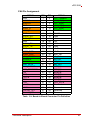
CN4 Pin Assignment
SIGNAL
GND
USB3-DUSB3-D+
GND
USB2_DUSB2_D+
GND
SATA0_RXSATA0_RX+
GND
SATA0_TX+
SATA0_TXGND
USB3_PWR
USB2_PWR
LPC_LDRQ0#
A20GATE
SERIRQ#
KBD_RST#
CPU_PWRGD
XDP_DBRESET#
TDI
TMS
TRST#
TCK
TDO
+1.05V
+1.5V
CLK100_ITP+
CLK100_ITP-
PIN
1
3
5
7
9
11
13
15
17
19
21
23
25
27
29
31
33
35
37
39
41
43
45
47
49
51
53
55
57
59
PIN
2
4
6
8
10
12
14
16
18
20
22
24
26
28
30
32
34
36
38
40
42
44
46
48
50
52
54
56
58
60
SIGNAL
LPC_FRAME#
LPC_AD[3]
LPC_AD[2]
LPC_AD[1]
LPC_AD[0]
PCIRST
CLK33
GND
+5V
+5V
+5V
GND
+3.3V
+3.3V
B2B_IN#
KB_CLK
KB_DAT
MS_CLK
MS_DAT
BPM[0]#
BPM[1]#
BPM[2]#
BPM[3]#
BPM[4]#
BPM[5]#
CPU_RST#
Reserved
Reserved
Reserved
Reserved
Table 3-9: Board-to-Board Connector Pin Definition
Functional Description
41
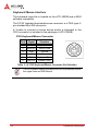
Keyboard/ Mouse Interface
The keyboard controller is located on the cPCI-3920B and is 8042
software compatible.
The PC/AT standard keyboard/mouse connector is a PS/2-type 6pin shielded Mini-DIN connector.
A Y-cable to connect a mouse device and/or a keyboard to the
PS/2 connector is included in the package of cPCI-3920B.
PS/2 Keyboard/Mouse Connector
Pin #
Signal
Function
1
KBDATA
Keyboard Data
2
MSDATA
Mouse Data
3
GND
Ground
4
+5V
Power
5
KBCLK
Keyboard Clock
6
MSCLK
Mouse Clock
Table 3-10: PS/2 Keyboard/Mouse Connector Pin Definition
The PS/2 power supply provides short-circuit protection and all
the signal lines are EMI-filtered.
NOTE:
42
Functional Description
cPCI-3920
Universal Serial Ports
Two PC-compatible serial RS-232, 9-pin D-Sub ports are available and fully compatible with the 16C550 controller. These port
includes a complete set of handshaking and modem control signals. Data transfer rates up to 115.2 kB/s are supported.
The COM3 interface is routed to the connector CN1.
COM3 DB-9 Serial Port Connector (CN1)
Pin #
RS-232
1
DCD, Data carrier detect
2
RXD, Receive data
3
TXD, Transmit data
4
DTR, Data terminal ready
5
GND, Ground
6
DSR, Data set ready
7
RTS, Request to send
8
CTS, Clear to send
9
RI, Ring indicator
Table 3-11: COM3 Serial Port Connector Pin Definition
The COM4 interface is routed to the connector CN6-2. The COM4
interface supports RS-232/422/485/485+.
COM4 DB-9 Serial Port Connector (CN6-2)
Pin #
RS-232
RS422/485+
RS485
1
DCD, Data carrier detect
TXD-
Data-
2
RXD, Receive data
TXD+
Data+
3
TXD, Transmit data
RXD+
--
4
DTR, Data terminal ready
RXD
--
5
IsoGND, Isolated ground
GND
GND
6
DSR, Data set ready
--
--
7
RTS, Request to send
--
--
8
CTS, Clear to send
--
--
9
RI, Ring indicator
--
--
Table 3-12: COM4 Serial Port Connector Pin Definition
Functional Description
43
COM4 Mode Switch Settings
RS232
Full Modem
RS422
Half Duplex
RS485
Half Duplex
RS485+
Half Duplex
Location
SW1
SW2
SW3
SW4
1
ON
ON
OFF
ON
2
OFF
OFF
OFF
OFF
3
ON
ON
OFF
OFF
4
OFF
OFF
OFF
OFF
1
OFF
OFF
ON
OFF
2
ON
ON
ON
ON
3
OFF
OFF
OFF
OFF
4
ON
ON
OFF
OFF
1
OFF
OFF
ON
OFF
2
ON
ON
ON
OFF
3
OFF
OFF
OFF
ON
4
ON
ON
OFF
OFF
1
OFF
OFF
OFF
OFF
2
ON
ON
OFF
OFF
3
OFF
OFF
ON
OFF
4
ON
ON
ON
ON
Table 3-13: COM4 Mode Switch Settings
44
Functional Description
cPCI-3920
Serial ATA Interfaces
The cPCI-3920 provides up to four SATA interfaces. Three SATA
ports, SATA1, SATA2 and SATA3, can be used only on the Rear
Transition Module I/O interface. All SATA ports can be used simultaneously.
SATA Port
Connector
Usage
SATA0
CN3-2 on the cPCI-3920B
Onboard 2.5” DATA HDD drive
mounted on CPCI-3920B
SATA1
CN5-R on the cPCI-R3920(T)
External SATA HDD drives,
e.g. 2.5” or 3.5” SATA HDDs
SATA2
CN4-R on the cPCI-R3920(T)
External SATA HDD drives,
e.g. 2.5” or 3.5” SATA HDDs
SATA3
CN2-R on the cPCI-R3920(T)
External SATA HDD drives,
e.g. 2.5” or 3.5” SATA HDDs
The SATA connector, CN3-2, on the cPCI-3920B module is provided for connecting a 2.5˜ SATA HDD to the cPCI-3920B module.
The SATA connector is divided into two segments, a signal segment and a power segment.
SATA0 Connector, CN3-2
Functional Description
45
SATA0 Connector, CN3-2
PIN
SIGNAL
FUNCTION
Signal Segment Key
I/O
S1
GND
Ground signal
--
S2
SATA_TX2+
Differential Transmit+
O
S3
SATA_TX2-
Differential Transmit-
O
S4
GND
Ground signal
--
S5
SATA_RX2-
Differential Receive-
I
S6
SATA_RX2+
Differential Receive+
I
S7
GND
Ground signal
--
Signal Segment "L"
Central Connector Polarizer
Power Segment "L"
P1
NC (3.3V)
Not connected
--
P2
NC (3.3V)
Not connected
--
P3
NC (3.3V)
Not connected
--
P4
GND
Ground signal
--
P5
GND
Ground signal
--
P6
GND
Ground signal
--
P7
5V
5V power
--
P8
5V
5V power
--
P9
5V
5V power
--
P10
GND
Ground signal
--
P11
RES
Reserved
--
P12
GND
Ground signal
--
P13
12V
12V power
--
P14
12V
12V power
--
P15
12V
12V power
--
Power Segment Key
Table 3-14: SATA0 Connector Pin Definition
46
Functional Description
cPCI-3920
CompactPCI Bus Interfaces
The complete CompactPCI connector configuration comprises two
connectors named J1 and J2. Their function is as follows:
X
J1: 32-bit CompactPCI interface with PCI bus signals, arbitration, clock and power
X
J2: has optional Rear I/O interface functionality or 64-bit termination
The board is capable of driving up to seven CompactPCI slots,
with individual arbitration and clock signals. The cPCI-3920 is not
hot-swappable but supports the addition or removal of other
boards whilst in a powered-up state.
The cPCI-3920 is designed for a CompactPCI bus architecture.
The CompactPCI standard is electrically identical to the PCI local
bus. However, these systems are enhanced to operate in rugged
industrial environments and to support multiple slots.
CompactPCI Connectors J1/J2
Pin rows F and Z are GND pins.
NOTE:
Functional Description
47
CompactPCI J1 Pin Assignment
Pin
Z
A
B
C
D
E
F
25
GND
+5V
REQ64#
ENUM#
+3.3V
+5V
GND
24
GND
AD[1]
+5V
V(I/O)
AD[0]
ACK64#
GND
23
GND
+3.3V
AD[4]
AD[3]
+5V
AD[2]
GND
22
GND
AD[7]
GND
+3.3V
AD[6]
AD[5]
GND
21
GND
+3.3V
AD[9]
AD[8]
M66EN(2)
C/ BE[0]#
GND
20
GND
AD[12]
GND
V(I/O)
AD[11]
AD[10]
GND
19
GND
+3.3V
AD[15]
AD[14]
GND
AD[13]
GND
18
GND
SERR#
GND
+3.3V
PAR
C/ BE[1]#
GND
17
GND
+3.3V
N.C.
N.C.
GND
PERR#
GND
16
GND
DEVSEL#
GND
V(I/O)
STOP#
LOCK#
GND
15
GND
+3.3V
FRAME#
IRDY#
GND
TRDY#
12-14
GND
11
GND
10
9
Key
AD[18]
AD[17]
GND
AD[21]
GND
C/BE[3]#
8
GND
AD[26]
7
GND
AD[30]
6
GND
REQ0#
5
GND
N.C.
4
GND
3
GND
GND
AD[16]
GND
C/ BE[2]#
GND
GND
+3.3V
AD[20]
AD[19]
GND
GND
AD[23]
GND
AD[22]
GND
GND
V(I/O)
AD[25]
AD[24]
GND
AD[29]
AD[28]
GND
AD[27]
GND
GND
+3.3V
CLK0
AD[31]
GND
N.C.
PCIRST#
GND
GNT[0]#
GND
IPMB_PWR
GND
V(I/O)
INTP(1)
INTS
GND
GND
INTA#
INTB#
INTC#
+5V
INTD#
GND
2
GND
TCK
+5V
TMS
TDO
TDI
GND
1
GND
+5V
-12V
TRST#(3)
+12V
+5V
GND
Z
A
B
C
D
E
F
Table 3-15: CompactPCI J1 Pin Assignment
48
Functional Description
cPCI-3920
CompactPCI J2 Pin Assignment
The cPCI-3920 board provides Rear I/O connectivity for special
compact systems. Some standard PC interfaces are implemented and assigned to the front panel and to the rear connector J2.
When the Rear I/O module is used, the signals of some of the
main board/front panel connectors are routed to the Rear I/O
module interface. Thus the Rear I/O module makes it much
easier to remove the CPU in the rack as there is practically no
cabling on the CPU board.
For the system Rear I/O feature a special backplane is necessary. The cPCI-3920 with Rear I/O is compatible with all standard CompactPCI passive backplanes with Rear I/O support
on the system slot.
The cPCI-3920 Rear I/O provides the following interfaces:
X
32-bit/33 MHz CompactPCI (J1) and Rear I/O (J2)
X
Two USB 2.0 ports
X
Two Gigabit Ethernet ports without LED signals
X
Three SATA ports
X
Two COM ports
X
Seven GPIOs
NOTE:
To support the Rear I/O feature a special backplane is necessary. Do not plug a Rear I/O configured board in a non-system
slot Rear I/O backplane. Failure to comply with the above will
result in damage to your board.
Functional Description
49
Legend for J2 Pin Assignment
USBx
USB interface and power
ETHx
Gigabit Ethernet port
SATAx
Serial ATA port
COMx
COM port
GPIO x
GPIO
PEX_RX0Lx
PEX_TX0Lx
Pin
Z
A
B
1 x4 or 4 x1 PCI-Express
C
D
E
F
22
N.C
GA[4]
GA[3]
GA[2]
GA[1]
GA[0]
GND
21
N.C
CLK[6]
GND
COM1_RXD
COM2_RXD
GPIO7
GND
20
N.C
CLK[5]
GND
COM1_TXD
COM2_TXD
GPIO6
GND
19
N.C
GND/CLK100+
GND/CLK100+
SMB_SDA
SMB_SCL
SMB_ALERT
GND
18
N.C
SATA3_TX+
SATA3_TX-
GND
SATA3_RX+
SATA3_RX-
GND
17
N.C
USB4_D+
USB4_D
RST_BP#
N.C.
GNT[6]#pull
GND
16
N.C
USB4_PWR
USB5_PWR
DEGXB
GND
GPIO5
GND
15
N.C
USB5_D+
USB5_D
FALXB
N.C.
GNT[5]#pull
GND
14
N.C
SATA2_TX+
SATA2_TX-
GND
SATA2_RX+
SATA2_RX-
GND
13
N.C
SATA1_TX+
SATA1_TX-
GND
SATA1_RX+
SATA1_RX-
GND
12
N.C
PEX_RX0L0+
PEX_RX0L0-
GND
PEX_TX0L0
PEX_TX0L0-
GND
11
N.C
PEX_RX0L1+
PEX_RX0L1-
GND
PEX_TX0L1
PEX_TX0L1-
GND
10
N.C
PEX_RX0L2+
PEX_RX0L2-
GND
PEX_TX0L2
PEX_TX0L2-
GND
9
N.C
PEX_RX0L3+
PEX_RX0L3-
GND
PEX_TX0L3
PEX_TX0L3-
GND
8
N.C
ETH0_DA+
ETH0_DA-
GND
ETH0_DC+
ETH0_DC-
GND
7
N.C
ETH0_DB+
ETH0_DB-
GND
ETH0_DD+
ETH0_DD-
GND
6
N.C
ETH1_DA+
ETH1_DA-
GND
ETH1_DC+
ETH1_DC-
GND
5
N.C
ETH1_DB+
ETH1_DB-
GND
ETH1_DD+
ETH1_DD-
GND
4
N.C
V(I/O)
GPIO1
GPIO2
GPIO3
GPIO4
GND
3
N.C
CLK[4]
GND
GNT[3]#
N.C.
GNT[4]#pull
GND
2
N.C
CLK[2]
CLK[3]
SYSEN#
GNT[2]#
REQ[3]#
GND
1
N.C
CLK[1]
GND
REQ[1]#
GNT[1]#
REQ[2]#
GND
Table 3-16: CompactPCI J2 Pin Assignment
50
Functional Description
cPCI-3920
3.4 Board Interfaces on RTM
There are two identical USB interfaces on the CPCI-R3920(T)
RTM, each with a maximum transfer rate of 480 Mb!s provided for
connecting USB devices. One USB peripheral may be connected
to each port. To connect more USB devices than there are available ports, an external hub is required.
USB Connectors CN7-R and CN8-R
Pin #
Signal Name
1
Vcc
2
UV0-
3
UV0+
4
GND
Table 3-17: RTM USB Connector Pin Definitions
NOTE:
The CPCI-R3920(T) host interfaces can be used with maximum 500 mA continuous load current as specified in the Universal Serial Bus Specification, Revision 2.0. Short-circuit
protection is provided. All the signal lines are EMI-filtered.
The Rear I/O interface supports the USB 1.1 and USB 2.0
standards. For USB 2.0 it is strongly recommended to use a
cable length not exceeding 3 meters.
Gigabit Ethernet Interfaces
Gigabit Ethernet signals are available either on the front R-J45
connector or on the Rear I/O interface due the implemented
switches on the cPCI-3920. Both Gigabit Ethernet channels are
individually switchable to front or Rear I/O. Switching over from
front to Rear I/O or vice versa is effected using the BIOS settings
or the board-specific registers (default: front I/O). For further information on the BIOS settings, refer to Chapter BIOS.
The interfaces provide automatic detection and switching between
10Base-T, 100Base-TX and 1000Base-T data transmission (AutoNegotiation).
The CN6-R connector supplies the 10Base-T, 100Base-TX
and 1000Base-T interfaces to the Ethernet controller.
Functional Description
51
Gigabit Connector RJ-45 Pin Definitions (CN6-R)
The CN7/CN8 connector supplies the 10Base-T, 100BaseTX and 1000Base-T interfaces to the Ethernet controller.
10BASE--T
100BASE--TX
1000BASE--T
PIN
I/O
SIGNAL
I/O
SIGNAL
I/O
SIGNAL
O
TX+
O
TX+
I/O
BI_DA+
O
TX-
O
TX-
I/O
BI_DA-
2
I
RX+
I
RX+
I/O
BI_DB+
3
---
---
---
---
I/O
I/O
BI_DC+
BI_DC-
4
5
I
TX--
I
RX--
I/O
BI_DB-
6
--
--
--
--
I/O
BI_DD+
7
--
--
--
--
I/O
BI_DD-
8
1
Table 3-18: RTM Gigabit Connector Pin Definitions
The Ethernet transmission can operate effectively using a
CAT5 cable or higher specifications.
NOTE:
COM1 and COM2 Interfaces
The CPCI-R3920(T) provides two COM ports from the Intel® 3100
chipset for connecting RS-232 devices to the CPCI-R3920(T).
The following tables provide pinout information for the 9-pin D-Sub
COM connector CN3-R located on the front panel and the onboard
COM connector CN1-R.
52
Functional Description
cPCI-3920
COM1 DB-9 Serial Port Connector (CN3-R)
Pin #
RS-232
1
not used
2
RXD, Receive data
3
TXD, Transmit data
4
not used
5
GND, Ground
6
not used
7
not used
8
not used
9
not used
Table 3-19: COM1 Serial Port Connector Pin Definition
COM2 Onboard Serial Port Connector (CN1-R)
Pin #
RS-232
1
not used
2
not used
3
RXD, Receive data
4
not used
5
TXD, Transmit data
6
not used
7
not used
8
not used
9
GND, Ground
10
NC
Table 3-20: COM2 Serial Port Connector Pin Definition
NOTE:
The serial ports of Intel® 3100 Chipset are not 100 percent
compatible with other 16550 standard devices. If any system or
software designer assumes that they are compatible with other
16550 standard devices and does not follow the specifications
for the Serial I/O Unit in the Intel® 3100 Chipset Datasheet,
errors or undesired behaviors may be observed.
Functional Description
53
Serial ATA Interfaces - SATA1-3
The onboard Serial ATA connectors CN2-R, CN4-R and CN5-R
allow the connection of standard HDDs and other Serial ATA
devices to the cPCI-3920 Rear Transition Module.
The following figure and table provide pinout information for the
SATA connectors CN2-R, CN4-R and CN5-R.
SATA1-3 Connectors CN2-R, CN4-R and CN5-R
Pin #
Signal
Pin #
Signal
1
GND
5
RX-
2
TX+
6
RX+
3
TX-
7
GND
4
GND
Table 3-21: SATA1-3 Connectors Pin Definition
54
Functional Description
cPCI-3920
Rear I/O Interfaces on CompactPCI Connector rJ2
The cPCI-3920 Rear Transition Module conducts a wide range of
I/O signals through the Rear I/O connector rJ2.
To support the Rear I/O feature a special backplane is necessary.
Do not plug a Rear I/O configured board in a non-system slot Rear
I/O backplane. Failure to comply with the above may result in
damage to your board.
CompactPCI Connector rJ2
Functional Description
55
CompactPCI rJ2 Pin Assignment
Legend for rJ2 Pin Assignment
Pin
Z
USBx
USB interface and power
ETHx
Gigabit Ethernet port
SATAx
Serial ATA port
COMx
COM port
A
B
C
D
E
F
22
N.C.
GA[4]
GA[3]
GA[2]
GA[1]
GA[0]
GND
21
N.C.
CLK[6]
GND
COM1_RXD
COM2_RXD
N.C.
GND
20
N.C.
CLK[5]
GND
COM1_TXD
COM2_TXD
N.C.
GND
19
N.C.
GND/CLK100
GND/CLK100
SMB_SDA
SMB_SCL
SMB_ALERT
GND
18
N.C.
SATA3_TX+
SATA3_TX-
GND
SATA3_RX+
SATA3_RX-
GND
17
N.C.
USB4_D+
USB4_D
RST_BP#
N.C.
GNT[6]#pull
GND
16
N.C.
USB4_PWR
USB5_PWR
DEGXB
GND
GPIO5
GND
15
N.C.
USB5_D+
USB5_D
FALXB
N.C.
GNT[5]#pull
GND
14
N.C.
SATA2_TX+
SATA2_TX-
GND
SATA2_RX+
SATA2_RX-
GND
13
N.C.
SATA1_TX+
SATA1_TX-
GND
SATA1_RX+
SATA1_RX-
GND
12
N.C.
N.C.
N.C.
GND
N.C.
N.C.
GND
11
N.C.
N.C.
N.C.
GND
N.C.
N.C.
GND
10
N.C.
N.C.
N.C.
GND
N.C.
N.C.
GND
9
N.C.
N.C.
N.C.
GND
N.C.
N.C.
GND
8
N.C.
ETH0_DA+
ETH0_DA-
GND
ETH0_DC+
ETH0_DC-
GND
7
N.C.
ETH0_DB+
ETH0_DB-
GND
ETH0_DD+
ETH0_DD-
GND
6
N.C.
ETH1_DA+
ETH1_DA-
GND
ETH1_DC+
ETH1_DC-
GND
5
N.C.
ETH1_DB+
ETH1_DB-
GND
ETH1_DD+
ETH1_DD-
GND
4
N.C.
V(I/O)
N.C.
N.C.
N.C.
N.C.
GND
3
N.C.
CLK[4]
GND
GNT[3]#
N.C.
GNT[4]#pull
GND
2
N.C.
CLK[2]
CLK[3]
SYSEN#
GNT[2]#
REQ[3]#
GND
1
N.C.
CLK[1]
GND
REQ[1]#
GNT[1]#
REQ[2]#
GND
Table 3-22: CompactPCI rJ2 Pin Assignment
56
Functional Description
cPCI-3920
4
Getting Started
The cPCI-3920 has been designed for easy installation. However,
the following standard precautions, installation procedures, and
general information must be observed to ensure proper installation
and to preclude damage to the board, other system components,
or injury to personnel.
4.1 Safety Requirements
The following safety precautions must be observed when installing
or operating the cPCI-3920. ADLINK assumes no responsibility for
any damage resulting from failure to comply with these requirements.
Exercised due care when handling the board as the heat sink can
get very hot. Do not touch the heat sink when installing or removing the board. The board should not be placed on any surface or in
any form of storage container until the board and heat sink have
cooled down to room temperature.
If your board type is not specifically qualified as being hot swap
capable, switch off the CompactPCI system power before installing the board in a free CompactPCI slot. Failure to do so could
endanger your life or health and may damage your board or system.
Certain CompactPCI boards require bus master and/or Rear I/O
capability. If you are in doubt whether such features are required
for the board you intend to install, please check your specific
board and/or system documentation to make sure that your system is provided with an appropriate free slot in which to insert the
board.
This CompactPCI board contains electrostatically sensitive
devices. Please observe the necessary precautions to avoid damage to your board:
X
Discharge your clothing before touching the assembly.
Tools must be discharged before use.
X
Do not touch components, connector-pins or traces.
X
If working at an anti-static workbench with professional discharging equipment, please do not omit to use it.
Getting Started
57
4.2 Installing the USB Flash Disk
The cPCI-3920 supports an onboard USB Flash Disk module via
the CN5 pin header. To install a USB Flash Disk, follow the procedure below.
1. Secure the standoff to the underside of the module with
the screw provided.
2. Align the module with the CN5 pin header and mounting
hole as shown.
3. Insert the module onto the pin header and secure with
the screw provided from the back side of the cPCI-3290.
58
Getting Started
cPCI-3920
4.3 Installing the Hard Disk Drive (cPCI-3290B only)
The cPCI-3920B supports a slim-type 2.5” SATA HDD. If the cPCI3920 comes with a pre-installed HDD, proceed to the next section.
To install the hard disk drive:
1. Place the HDD into the bracket as shown.
2. Insert the the HDD into the CN3-2 SATA signal/power connector.
CN3-2
3. Tighten all four bracket screws to secure the HDD in place.
Getting Started
59
4.4 Installing the cPCI-3920 to the Chassis
To install the cPCI-3920 module to a CompactPCI chassis:
1. Refer to the chassis documentation before installing the
cPCI-3920.
2. Turn off the power in both chassis front and rear.
3. Assign a system slot for the board. Make sure you
assign the correct slot.
4. Remove the panel cover of the slot you have selected.
5. Remove the black plastic caps securing the mounting
screws to the front panel.
6. Align the top and bottom edges of the board with the
card guides on the chassis, then push the board until it is
completely flushed on the chassis.
7. Move the locking handle inward until it is fully-latched. A
slight resistance may be felt when inserting the board. If
the resistance is too strong, check if there are bent pins
on the backplane or if the board’s connector pins are
properly aligned with the connectors on the backplane.
8. Check if the board is seated properly on the slot. Secure
the board with mounting screws (behind the upper and
lower ejector)
9. Connect the cables and peripherals to the board, then
turn the chassis on.
60
Getting Started
cPCI-3920
4.5 RTM (cPCI-R3920) Installation
Follow the typical cPCI board installation and removal procedures
for the RTM. However, be careful when when inserting or removing RTMs to the chassis as these are shorter than front boards.
Refer to previous sections when connecting or installing peripherals to the RTM. Make sure that the RTMs you are installing are
compatible with the cPCI-3920 Series.
NOTE:
You must install the correct RTM to enable some functionalities
(I/O interfaces) on the rear panel. Installation of non-compatible RTMs may damage the system board and/or other RTMs.
4.6 Hot Swap Procedures
The cPCI-3920 is not designed for hot swap operation. Do not
attempt to hot swap this board. However, the cPCI-3920 supports
the addition or removal of other boards whilst in a powered-up
state.
Getting Started
61
This page intentionally left blank.
62
Getting Started
cPCI-3920
5
Driver Installation
The cPCI-3920 drivers are available from the ADLINK All-In-One
CD at X:\cPCI\cPCI-3920\, or from the ADLINK website
(http://www.adlinktech.com). The following describes the driver
installation procedures for Windows® 2000, Windows® XP or
Windows® Server 2003:
1. Install the Windows operating system before installing
any driver. Most standard I/O device drivers are installed
during Windows installation.
2. Install the chipset driver by running the program
...\Chipset\InfInst_AUTOL.exe.
3. Install the VGA driver and utilities by running the program ...\VGA\R1.09.05_WHQL_Windows\XGIRun.exe.
4. Install the LAN drivers by running the program
...\LAN\PRO2KXP.exe.
We recommend using the chipset, VGA, and LAN drivers provided
on the ADLINK All-in-One CD or downloaded from the ADLINK
website to ensure compatibility. Contact ADLINK to get support for
Linux and VxWorks BSP drivers.
Driver Installation
63
This page intentionally left blank.
64
Driver Installation
cPCI-3920
6
Watchdog Timer
6.1 WDT Overview
This section explains the operation of the cPCI-3920’s Watchdog
Timer (WDT). The primary function of the WDT is to monitor the
cPCI-3920 operation and to reset the system if a software application fails to function as programmed. The following WDT functions
may be controlled using a software application:
X
enabled and disabled
X
reloading timeout value
LPC Interface
Preload Value 1
Preload Value 2
Down-Counter
Timeout/ Interrupt Control Logic
WDT_TOUT#
(External)
WDT_INT
(Internal)
Figure 6-1: cPCI-3920 Watchdog Timer Architecture
The cPCI-3920 implements the internal WDT unit of the Intel 3100
chipset and its LPC interface. It contains registers of device6 at
Watchdog Timer
65
the internal IO to control the WDT and retrieve its status. The basic
functions of the WDT include:
X
Setting the watchdog timeout interval
X
Starting the timer countdown
X
Selecting 1 step or 2 step WDT
X
Enabling or disabling WDT
X
Reloading the timeout value to keep the watchdog from timing out
X
Setting the range of the timeout period from 1 µs to 1 second, or from 1 ms to 1050 seconds
When the watchdog times out, it will send a RESET signal to the
system.
6.2 Using the Watchdog Timer in an Application
The following section describes the WDT functions in an application. The WDT reset function is explained in the previous section.
This can be controlled through the registers in the WDT unit of the
Intel 3100 chipset .
An application using the reset feature enables the watchdog function, sets the count-down period, and reloads the timeout value
periodically to keep it from resetting the system. If the timer countdown value is not reloaded, the watchdog resets the system hardware after its counter registers zero.
A detailed programming sample is provided below:
#include<dos.h>
#include<conio.h>
#include<stdio.h>
#include<stdlib.h>
#defineconfig_port_index0x4E
#defineconfig_port_data0x4F
/* Pre-declaration */
/* access configuration registers routines */
void enter_config_mode();
void exit_config_mode();
66
Watchdog Timer
cPCI-3920
void write_config_data_byte(unsigned
char,unsigned char);
unsigned char read_config_data_byte(unsigned
char);
unsigned int read_wdt_io_base();
/* access wdt I/O registers routines */
void write_preload_val2_reg(unsigned long int);
void clear_preload_val1_reg();
void unlocking_reg();
/* Global parameter */
unsigned int wdt_io_base;
void main(void)
{
//
unsigned int wdt_io_base;
unsigned long int time_out_val=0;
wdt_io_base=read_wdt_io_base();
printf("Intel 3100 Chipset Watch-Dog Timer
test utility.\n");
printf("Intel 3100 WDT IO Base Address ==
0x%x\n",wdt_io_base);
while(1)//
(time_out_val==0)||(time_out_val>1050))
{
//3sec
printf("Please input the time to count
down (1-1050 sec): ");
//3sec
scanf("%d",&time_out_val);
}
//3sectime_out_val=time_out_val*1000;//transfer
to msec unit.
time_out_val=time_out_val+3000;
//3sec
clear_preload_val1_reg();//we don't need
preload_val1 caused internal interrupt.
write_preload_val2_reg(time_out_val);//
write preload_val2 ,it will cause external
interrupt.(WDT_TOUT#)
Watchdog Timer
67
outportb(wdt_io_base+0x18,2);//watchdog
timer enable!!
printf("\nPlease waiting for Watch-Dog Timer
time-out!!");
}
/************************************/
unsigned int read_wdt_io_base()
{
unsigned char_wdt_io_base[2];
int *p_wdt_io_base;
p_wdt_io_base=&_wdt_io_base;
enter_config_mode();
write_config_data_byte(0x07,6);//select
logic 6 - WDT
_wdt_io_base[1]=read_config_data_byte(0x60)
;
_wdt_io_base[0]=read_config_data_byte(0x61)
;
exit_config_mode();
return (*p_wdt_io_base);
}
/************************************/
void enter_config_mode()
{
outportb(config_port_index,0x80);
outportb(0xeb,00); //io delay
outportb(config_port_index,0x86);
}
/************************************/
void exit_config_mode()
{
outportb(config_port_index,0x68);
68
Watchdog Timer
cPCI-3920
outportb(0xeb,00); //io delay
outportb(config_port_index,0x08);
}
/************************************/
unsigned char read_config_data_byte(unsigned char
_index)
{
unsigned char r_data;
outportb(config_port_index,_index);
outportb(0xeb,00); //io delay
r_data=inportb(config_port_data);
return(r_data);
}
/************************************/
void write_config_data_byte(unsigned char
_index,unsigned char _data)
{
outportb(config_port_index,_index);
outportb(0xeb,00); //io delay
outportb(config_port_data,_data);
}
/************************************/
void write_preload_val2_reg(unsigned long int
_time_out_val)
{
unsigned char *p_data;
//
"unsigned char" declaration --> p_data++ =
addr. BYTE increased.
p_data=&_time_out_val;
//
printf("%x\n",*p_data);
//
Watchdog Timer
unlocking_reg();
outportb(wdt_io_base+4,*p_data);
p_data++;
printf("%x\n",*p_data);
69
//
unlocking_reg();
outportb(wdt_io_base+5,*p_data);
p_data++;
printf("%x\n",*p_data);
unlocking_reg();
outportb(wdt_io_base+6,*p_data);
}
/************************************/
void clear_preload_val1_reg()
{
unlocking_reg();
outportb(wdt_io_base,0x00);
unlocking_reg();
outportb(wdt_io_base+1,0x00);
unlocking_reg();
outportb(wdt_io_base+2,0x00);
}
/************************************/
void unlocking_reg()
{
outportb(wdt_io_base+12,0x80);
outportb(0xeb,00); //io delay
outportb(wdt_io_base+12,0x86);
70
Watchdog Timer
cPCI-3920
7
BIOS Setup Utility
The following chapter describes basic navigation for the
AMIBIOS®8 BIOS setup utility.
7.1 Starting the BIOS
To enter the setup screen, follow these steps:
1. Power on the motherboard
2. Press the < Delete > key on your keyboard when you
see the following text prompt:
< Press DEL to run Setup >
3. After you press the < Delete > key, the main BIOS setup
menu displays. You can access the other setup screens
from the main BIOS setup menu, such as Chipset and
Power menus.
NOTE:
In most cases, the < Delete > key is used to invoke the setup
screen. There are several cases that use other keys, such as <
F1 >, < F2 >, and so on.
BIOS Setup Utility
71
Setup Menu
The main BIOS setup menu is the first screen that you can navigate. Each main BIOS setup menu option is described in this
user’s guide.
The Main BIOS setup menu screen has two main frames. The left
frame displays all the options that can be configured. “Grayed”
options cannot be configured, “Blue” options can be.
The right frame displays the key legend. Above the key legend is
an area reserved for a text message. When an option is selected
in the left frame, it is highlighted in white. Often a text message will
accompany it.
Navigation
The BIOS setup/utility uses a key-based navigation system called
hot keys. Most of the BIOS setup utility hot keys can be used at
any time during the setup navigation process.
72
BIOS Setup Utility
cPCI-3920
These keys include < F1 >, < F10 >, < Enter >, < ESC >, < Arrow >
keys, and so on. .
There is a hot key legend located in the right frame on most
setup screens.
NOTE:
The < F8 > key on your keyboard is the Fail-Safe key. It is not displayed on the key legend by default. To set the Fail-Safe settings
of the BIOS, press the < F8 > key on your keyboard. It is located
on the upper row of a standard 101 keyboard. The Fail-Safe settings allow the motherboard to boot up with the least amount of
options set. This can lessen the probability of conflicting settings.
Hotkey Descriptions
F1
The < F1 > key allows you to display the General Help
screen.
Press the < F1 > key to open the General Help screen.
BIOS Setup Utility
73
F10
The < F10 > key allows you to save any changes you have
made and exit Setup. Press the < F10 > key to save your
changes. The following screen will appear:
Press the < Enter > key to save the configuration and exit.
You can also use the < Arrow > key to select Cancel and
then press the < Enter > key to abort this function and return
to the previous screen.
ESC
The < Esc > key allows you to discard any changes you have
made and exit the Setup. Press the < Esc > key to exit the
setup without saving your changes. The following screen will
appear:
Press the < Enter > key to discard changes and exit. You can
also use the < Arrow > key to select Cancel and then press
the < Enter > key to abort this function and return to the previous screen.
Enter
74
The < Enter > key allows you to display or change the setup
option listed for a particular setup item. The < Enter > key
can also allow you to display the setup sub-screens.
BIOS Setup Utility
cPCI-3920
7.2 Main Setup
When you first enter the Setup Utility, you will enter the Main setup
screen. You can always return to the Main setup screen by selecting
the Main tab. The Main BIOS Setup screen is shown below.
System Time/System Date
Use this option to change the system time and date. Highlight System Time or System Date using the < Arrow > keys. Enter new values using the keyboard. Press the < Tab > key or the < Arrow >
keys to move between fields. The date must be entered in MM/
DD/YY format. The time is entered in HH:MM:SS format.
The time is in 24-hour format. For example, 5:30 A.M. appears
as 05:30:00, and 5:30 P.M. as 17:30:00.
NOTE:
BIOS Setup Utility
75
Input UUID
Use this function to set a unique Universally Unique Identifier
(UUID) for the system.
UUID Byte 0-7
This field sets bytes 0-7 of the UUID.
UUID Byte 8-F
This field sets bytes 8-F of the UUID.
76
BIOS Setup Utility
cPCI-3920
7.3 Advanced BIOS Setup
Select the Advanced tab from the setup screen to enter the
Advanced BIOS Setup screen. You can select any of the items in
the left frame of the screen to go to the sub menu for that item.
You can display an Advanced BIOS Setup option by highlighting it
using the < Arrow > keys. The Advanced BIOS Setup screen is
shown below.
The sub menus are described on the following pages.
CPU Configuration
You can use this screen to select options for the CPU Configuration Settings. Use the up and down < Arrow > keys to select an
item. Use the < + > and < - > keys to change the value of the
selected option. A description of the selected item appears on the
right side of the screen. The settings are described on the following pages. CPU Configuration screens for the available CPUs are
shown below.
BIOS Setup Utility
77
Intel® Core™2 Duo L7400
Hardware Prefetcher
The processor has a hardware prefetcher that automatically
analyzes its requirements and prefetches data and instructions
from the memory into the Level 2 cache that are likely to be
required in the near future. This reduces the latency associated
with memory reads.
When Enabled, the processor's hardware prefetcher will be
enabled and allowed to automatically prefetch data and code
for the processor. When Disabled, the processor's hardware
prefetcher will be disabled.
Adjacent Cache Line Prefetch
The processor has a hardware adjacent cache line prefetch
mechanism that automatically fetches an extra 64-byte cache
line whenever the processor requests for a 64-byte cache line.
78
BIOS Setup Utility
cPCI-3920
This reduces cache latency by making the next cache line
immediately available if the processor requires it as well.
When Enabled, the processor will retrieve the currently
requested cache line, as well as the subsequent cache line.
When Disabled, the processor will only retrieve the currently
requested cache line.
Intel® Virtualization Technology
This option is used to enable or disable the Intel® Virtualization
Technology (IVT) extension, which is also known by the development code name of Vanderpool. It allows multiple operating
systems to run simultaneously on the same system. It does this
by creating virtual machines, each running its own x86 operating system. When Enabled, the IVT extensions will be
enabled, allowing for hardware-assisted virtual machine management. When Disabled, the IVT extensions will be disabled.
However, software virtual machine managers like VMware can
still be used if virtualization is required.
Intel® SpeedStep™ Techology
Allows you to Enable or Disable Intel® SpeedStep™ Technology. If SpeedStep is disabled, the CPU Frequency on XP/
Linux option will become visible.
ACPI T-State Tech
This option allows you to Enable or Disable ACPI throttling.
BIOS Setup Utility
79
CPU Frequency on XP/Linux
This option is used to manually set the CPU frequency on XP
and Linux operating systems. The following options are available: 1500MHz, 1333MHz, 1166MHz, and 1000MHz.
Intel® Core™ Duo U2500
Intel® Virtualization Technology
This is used to enable or disable the Intel® Virtualization Technology (IVT) extension, which is also known by the development code name of Vanderpool. It allows multiple operating
systems to run simultaneously on the same system. It does this
by creating virtual machines, each running its own x86 operating system. When enabled, the IVT extensions will be enabled,
allowing for hardware-assisted virtual machine management.
When disabled, the IVT extensions will be disabled. However,
software virtual machine managers like VMware can still be
used if virtualization is required.
80
BIOS Setup Utility
cPCI-3920
Intel® SpeedStep™ Techology
This allows you to enable or disable Intel® SpeedStep™ Technology.
Intel® Celeron® M ULV 423
BIOS Setup Utility
81
IDE Configuration
You can use this screen to select options for the IDE Configuration
Settings. Use the up and down < Arrow > keys to select an item.
Use the < + > and < - > keys to change the value of the selected
option. A description of the selected item appears on the right side
of the screen. The settings are described on the following pages.
An example of the IDE Configuration screen is shown below.
ATA/IDE Configuration
This item specifies whether the IDE channels should be initialized in Compatible or Enhanced mode of operation. The settings are Disabled, Compatible and Enhanced.
Configure SATA as
This item specifies SATA channels transport to what kind of
channels. The settings are IDE mode and AHCI mode.
82
BIOS Setup Utility
cPCI-3920
Primary IDE Master, Primary IDE Slave, Secondary IDE
Master, Secondary IDE Slave
Select one of the hard disk drives to configure it. Press
< Enter > to access its sub menu.
Hard Disk Write Protect
This will be affective only if device is accessed through BIOS.
The settings are Enabled and Disabled.
IDE Detect Time Out (Sec)
Select the time out value for detecting ATA/ATAPI devices. The
settings are 0 sec, 5 sec, 10 sec, 15 sec, 20 sec, 25sec, 30
sec, and 35 sec.
AHCI Configuration
While entering setup BIOS auto detects the presence of IDE
devices.
BIOS Setup Utility
83
Hardware Health Configuration
This option displays the current status of all of the monitored hardware devices / components such as voltages and temperatures.
84
BIOS Setup Utility
cPCI-3920
Remote Access Configuration
Remote Access Configuration provides the settings to allow
remote access by another computer to get POST messages and
send commands through serial port access.
Remote Access
Select this option to Enabled or Disabled the BIOS remote
access feature.
Serial Port Number
Select the serial port you want to use for the remote access
interface. You can set the value for this option to either COM1
or COM2. The Base Address and IRQ of the selected serial
port is displayed.
BIOS Setup Utility
85
Serial Port Mode
Select the baud rate you want the serial port to use for console
redirection. The options are 115200 8,n,1; 57600 8,n,1; 19200
8,n,1; and 09600 8,n,1.
Flow Control
Set this option to select Flow Control for console redirection.
The settings for this value are None, Hardware, or Software.
Terminal Type
This option is used to select either VT100/VT-UTF8 or ANSI
terminal type. The settings for this value are ANSI, VT100, or
VT-UTF8.
VT-UTF8 Combo Key Support
This option enables VT-UTF8 Combination Key Support for
ANSI/VT100 terminals. The settings for this value are Enabled
or Disabled.
Sredir Memory Display Delay
This option gives the delay in seconds to display memory information. The options for this value are No Delay, Delay 1 Sec,
Delay 2 Sec, or Delay 4 Sec.
86
BIOS Setup Utility
cPCI-3920
USB Configuration
You can use this screen to select options for the USB Configuration. Use the up and down < Arrow > keys to select an item. Use
the < + > and < - > keys to change the value of the selected
option. The settings are described on the following pages. The
screen is shown below.
Legacy USB Support
Legacy USB Support refers to USB mouse and keyboard support. Normally if this option is not enabled, any attached USB
mouse or USB keyboard will not become available until a USB
compatible operating system is fully booted with all USB drivers loaded. When this option is enabled, any attached USB
mouse or USB keyboard can control the system even when
there are no USB drivers loaded on the system. Set this value
to enable or disable Legacy USB Support.
BIOS Setup Utility
87
Disabled Set this value to prevent the use of any USB device
in DOS or during system boot.
Enabled Set this value to allow the use of USB devices during
boot and while using DOS.
Auto
This option auto detects USB Keyboards or Mice
and if found, allows them to be utilized during boot
and while using DOS.
Port 64/60 Emulation
It uses USB to receive the IO port 64/60 trap to emulate the
legacy keyboard controller.
USB 2.0 Controller Mode
The USB 2.0 Controller Mode configures the data rate of the
USB port. The options are FullSpeed (12 Mbps) and HiSpeed
(480 Mbps).
88
BIOS Setup Utility
cPCI-3920
7.4 PCI/PnP Setup
Select the PCI/PnP tab from the setup screen to enter the Plug
and Play BIOS Setup screen. You can display a Plug and Play
BIOS Setup option by highlighting it using the < Arrow > keys. The
Plug and Play BIOS Setup screen is shown below.
IRQ
Set this value to allow the IRQ settings to be modified. Available –
This setting allows the specified IRQ to be used by a PCI/PnP
device. Reserved – This setting allows the specified IRQ to be
used by a legacy ISA device.
DMA Channel
Set this value to allow the MDA settings to be modified. Available
– This setting allows the specified DMA to be used by a PCI/PnP
BIOS Setup Utility
89
device. Reserved – This setting allows the specified DMA to be
used by a legacy ISA device.
7.5 Boot Setup
Select the Boot tab from the setup screen to enter the Boot BIOS
Setup screen. You can select any of the items in the left frame of
the screen, such as Boot Device Priority, to go to the sub menu for
that item. You can display a Boot BIOS Setup option by highlighting it using the < Arrow > keys. Select an item on the Boot Setup
screen to access the sub menu for:
X
Boot Settings Configuration
X
Boot Device Priority
X
Removable Devices
The Boot Settings screen is shown below:
90
BIOS Setup Utility
cPCI-3920
Boot Setting Configuration
Use this screen to select options for the Boot Settings Configuration. Use the up and down <Arrow> keys to select an item. Use the
<Plus> and <Minus> keys to change the value of the selected
option. The settings are described on the following pages. The
screen is shown below.
Quick Boot
Disabled – Set this value to allow the BIOS to perform all
POST tests. Enabled – Set this value to allow the BIOS to skip
certain POST tests to boot faster.
BIOS Setup Utility
91
Boot Device Priority
Boot Devices Priority
This specifies the boot sequence from the available devices.
The 1st Boot Device is primary device.
92
BIOS Setup Utility
cPCI-3920
Removable Drives
Removable Drives
This specifies the Boot Device Priority sequence from available
Removable Drives. Disabled – Set this menu to allow the BIOS
to remove device on Boot Device Priority. Device name – Set
this menu to allow the BIOS to stay device on Boot Device Priority
BIOS Setup Utility
93
7.6 Security Setup
Password Support
Two Levels of Password Protection
Provides both a Supervisor and a User password. If you use
both passwords, the Supervisor password must be set first.
The system can be configured so that all users must enter a
password every time the system boots or when Setup is executed, using either or either the Supervisor password or User
password.
The Supervisor and User passwords activate two different levels of password security. If you select password support, you
are prompted for a one to six character password. Type the
password on the keyboard. The password does not appear on
the screen when typed. Make sure you write it down. If you forget it, you must drain NVRAM and re-configure.
94
BIOS Setup Utility
cPCI-3920
Remember the Password
Keep a record of the new password when the password is
changed. If you forget the password, you must erase the system configuration information in NVRAM.
To access the sub menu for the following items, select the item
and press < Enter >:
X
Change Supervisor Password
X
Change User Password
X
Clear User Password
Supervisor Password
Indicates whether a supervisor password has been set.
User Password
Indicates whether a user password has been set.
Change Supervisor Password
Select this option and press < Enter > to access the sub menu.
You can use the sub menu to change the supervisor password.
Change User Password
Select this option and press < Enter > to access the sub menu.
You can use the sub menu to change the user password.
Clear User Password
Select this option and press < Enter > to access the sub menu.
You can use the sub menu to clear the user password.
Change Supervisor Password
Select Change Supervisor Password from the Security Setup
menu and press < Enter >.
Enter New Password:
Type the password and press < Enter >. The screen does not display the characters entered. Retype the password as prompted
and press < Enter >. If the password confirmation is incorrect, an
error message appears. The password is stored in NVRAM after
completes.
BIOS Setup Utility
95
Change User Password
Select Change User Password from the Security Setup menu and
press < Enter >.
Enter New Password:
Type the password and press < Enter >. The screen does not display the characters entered. Retype the password as prompted
and press < Enter >. If the password confirmation is incorrect, an
error message appears. The password is stored in NVRAM after
completes.
96
BIOS Setup Utility
cPCI-3920
7.7 Chipset Setup
Select the Chipset tab from the setup screen to enter the Chipset
BIOS Setup screen. You can select any of the items in the left
frame of the screen, such as CPU Configuration, to go to the sub
menu for that item. You can display a Chipset BIOS Setup option
by highlighting it using the < Arrow > keys. The Chipset BIOS
Setup screen is shown below.
South Bridge Configuration
You can use this screen to select options for the South Bridge
Configuration. South Bridge is a chipset on the motherboard that
controls the basic I/O functions, USB ports, audio functions,
modem functions, IDE channels, and PCI slots. Use the up and
down < Arrow > keys to select an item. Use the < Plus > and <
Minus > keys to change the value of the selected option.
BIOS Setup Utility
97
82571EB PCIE connect to
Set the onboard LAN to connect to either J2/RTM or Front I/O.
The settings are RTM (J2) and GigaLAN (Front I/O).
Onboard LAN Boot ROM control
Set this value to enable/disable the LAN Controller PXE function.
The PXE function allows system boot from a network environment.
Onboard VGA
You can use this option to control the onboard VGA. The settings are Enabled and Disabled.
98
BIOS Setup Utility
cPCI-3920
7.8 Exit Menu
Select the Exit tab from the setup screen to enter the Exit BIOS
Setup screen. You can display an Exit BIOS Setup option by highlighting it using the < Arrow > keys. The Exit BIOS Setup screen is
shown below.
Save Changes and Exit
When you have completed the system configuration changes,
select this option to leave Setup and reboot the computer so the
new system configuration parameters can take effect.
Save Configuration Changes and Exit Now?
[Ok] [Cancel]
appears in the window. Select Ok to save changes and exit.
BIOS Setup Utility
99
Discard Changes and Exit
Select this option to quit Setup without making any permanent
changes to the system configuration.
Discard Changes and Exit Setup Now?
[Ok] [Cancel]
appears in the window. Select Ok to discard changes and exit.
Discard Changes
Select Discard Changes from the Exit menu and press < Enter >.
Select Ok to discard changes.
Load Optimal Defaults
Automatically sets all Setup options to a complete set of default
settings when you select this option. The Optimal settings are
designed for maximum system performance, but may not work
best for all computer applications. In particular, do not use the
Optimal Setup options if your computer is experiencing system
configuration problems.
This page intentionally left blank.
Select Load Optimal Defaults from the Exit menu and press
< Enter >.
Select Ok to load optimal defaults.
Load Failsafe Defaults
Automatically sets all Setup options to a complete set of default
settings when you select this option. The Failsafe settings are
designed for maximum system stability, but not maximum performance. Select the FailSafe Setup options if your computer is
experiencing system configuration problems.
Select Load Fail-Safe Defaults from the Exit menu and press
< Enter >.
Load FailSafe Defaults?
[Ok] [Cancel]
appears in the window. Select Ok to load FailSafe defaults.
100
BIOS Setup Utility
cPCI-3920
Important Safety Instructions
Please read and follow all instructions marked on the product and
in the documentation before operating the system. Retain all
safety and operating instructions for future use.
X
Please read these safety instructions carefully.
X
Please keep this User’s Manual for future reference.
X
The equipment should be operated within the recommended operating temperature.
X
The equipment should be operated only from the type of
power source indicated on the rating label. Make sure the
voltage of the power source is correct when connecting the
equipment to the power outlet.
X
If the user’s equipment has a voltage selector switch, make
sure that the switch is set to the proper position for the area.
The voltage selector switch is set at the factory to the correct voltage.
X
For pluggable equipment, ensure they are installed near a
socket-outlet that is easily accessible.
X
Secure the power cord to prevent unnecessary accidents.
Do not place anything over the power cord.
X
If the equipment will not be in use for long periods of time,
disconnect the equipment from mains to avoid being damaged by transient overvoltage.
X
All cautions and warnings on the equipment should be
noted.
X
Please keep this equipment away from humidity.
X
Do not use this equipment near water or a heat source.
X
Place this equipment on a reliable surface when installing.
A drop or fall could cause injury.
X
Never pour any liquid into the opening, this could cause fire
or electrical shock.
Important Safety Instructions
101
X
Openings in the case are provided for ventilation. Do not
block or cover these openings. Make sure there is adequate
space around the system for ventilation when setting up the
work area. Never insert objects of any kind into the ventilation openings.
X
To avoid electrical shock, always unplug all power and
modem cables from the wall outlets before removing covers.
X
Lithium Battery provided (real time clock battery)
“CAUTION - Risk of explosion if battery is replaced by
an incorrect type. Dispose used batteries as instructed
in the instructions”
X
X
102
The equipment should be checked by service personnel if
one of the following situation arises:
Z
The power cord or plug is damaged.
Z
Liquid has penetrated the equipment.
Z
The equipment has been exposed to moisture.
Z
The equipment is not functioning or does not function
according to the user’s manual.
Z
The equipment has been dropped and damaged.
Z
If the equipment has obvious sign of breakage.
Never open the equipment. For safety reasons, the equipment should only be opened by qualified service personnel.
Important Safety Instructions
cPCI-3920
Getting Service
Contact us should you require any service or assistance.
ADLINK Technology, Inc.
Address: 9F, No.166 Jian Yi Road, Chungho City,
Taipei County 235, Taiwan
קᗼխࡉؑ৬ԫሁ 166 ᇆ 9 ᑔ
Tel:
+886-2-8226-5877
Fax:
+886-2-8226-5717
Email:
[email protected]
Ampro ADLINK Technology, Inc.
Address: 5215 Hellyer Avenue, #110, San Jose, CA 95138, USA
Tel:
+1-408-360-0200
Toll Free: +1-800-966-5200 (USA only)
Fax:
+1-408-360-0222
Email:
[email protected]
ADLINK Technology (China) Co., Ltd.
Address: Ϟ⍋Ꮦ⌺ϰᮄऎᓴ∳催⾥ᡔುऎ㢇䏃 300 ো(201203)
300 Fang Chun Rd., Zhangjiang Hi-Tech Park,
Pudong New Area, Shanghai, 201203 China
Tel:
+86-21-5132-8988
Fax:
+86-21-5132-3588
Email:
[email protected]
ADLINK Technology Beijing
Address: ࣫ҀᏖ⍋⎔ऎϞഄϰ䏃 1 োⲜ߯ࡼॺ E ᑻ 801 ᅸ(100085)
Rm. 801, Power Creative E, No. 1, B/D
Shang Di East Rd., Beijing, 100085 China
Tel:
+86-10-5885-8666
Fax:
+86-10-5885-8625
Email:
[email protected]
ADLINK Technology Shenzhen
Address: ⏅ഇᏖफቅऎ⾥ᡔುफऎ催ᮄफϗ䘧᭄ᄫᡔᴃು
A1 ᷟ 2 ὐ C ऎ (518057)
2F, C Block, Bldg. A1, Cyber-Tech Zone, Gao Xin Ave. Sec. 7,
High-Tech Industrial Park S., Shenzhen, 518054 China
Tel:
+86-755-2643-4858
Fax:
+86-755-2664-6353
Email:
[email protected]
Getting Service
103
ADLINK Technology (Europe) GmbH
Address: Nord Carree 3, 40477 Duesseldorf, Germany
Tel:
+49-211-495-5552
Fax:
+49-211-495-5557
Email:
[email protected]
ADLINK Technology, Inc. (French Liaison Office)
Address: 15 rue Emile Baudot, 91300 Massy CEDEX, France
Tel:
+33 (0) 1 60 12 35 66
Fax:
+33 (0) 1 60 12 35 66
Email:
[email protected]
ADLINK Technology Japan Corporation
Address: 151-0072 ᧲੩ㇺᷦ⼱ᐈ䊱⼱㩷
1-1-2 ᦺᣣ↢ᐈ䊱⼱䊎䊦 8F
Asahiseimei Hatagaya Bldg. 8F
1-1-2 Hatagaya, Shibuya-ku, Tokyo 151-0072, Japan
Tel:
+81-3-4455-3722
Fax:
+81-3-5333-6040
Email:
[email protected]
ADLINK Technology, Inc. (Korean Liaison Office)
Address: 昢殾柢 昢爎割 昢爎壟 1506-25 穢壊 B/D 2 猻
2F, Hando B/D, 1506-25, Seocho-Dong, Seocho-Gu,
Seoul 137-070, Korea
Tel:
+82-2-2057-0565
Fax:
+82-2-2057-0563
Email:
[email protected]
ADLINK Technology Singapore Pte. Ltd.
Address: 84 Genting Lane #07-02A, Cityneon Design Centre,
Singapore 349584
Tel:
+65-6844-2261
Fax:
+65-6844-2263
Email:
[email protected]
ADLINK Technology Singapore Pte. Ltd. (Indian Liaison Office)
Address: No. 1357, "Anupama", Sri Aurobindo Marg, 9th Cross,
JP Nagar Phase I, Bangalore - 560078, India
Tel:
+91-80-65605817
Fax:
+91-80-22443548
Email:
[email protected]
104
Getting Service