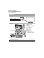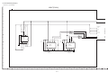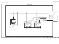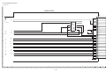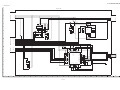
1
TopPage LC-32LE240M/340M(1stEdition) SERVICE MANUAL No. SY1V132LE340M LCD COLOUR TELEVISION MODELS LC-32LE240M LC-32LE340M In the interests of user-safety (Required by safety regulations in some countries) the set should be restored to its original condition and only parts identical to those specified should be used. CONTENTS SAFETY PRECAUTION IMPORTANT SERVICE SAFETY PRECAUTION ............................................................i PRECAUTIONS FOR USING LEAD-FREE SOLDER ............................................................ii OUTLINE MAJOR SERVICE PARTS ................................ iii CHAPTER 1. SPECIFICATIONS [1] SPECIFICATIONS ......................................... 1-1 CHAPTER 2. OPERATION MANUAL [1] OPERATION MANUAL .................................. 2-1 CHAPTER 3. REMOVING OF MAJOR PARTS [1] REMOVING OF MAJOR PARTS ................... 3-1 CHAPTER 5. TROUBLESHOOTING TABLE [1] TROUBLESHOOTING TABLE ......................5-1 CHAPTER 6. OVERALL WIRING/BLOCK DIAGRAM [1] OVERALL WIRING DIAGRAM......................6-1 [2] SYSTEM BLOCK DIAGRAM .........................6-2 CHAPTER 7. PRINTED WIRING BOARD ASSEMBLIES [1] MAIN Unit ......................................................7-1 CHAPTER 8. SCHEMATIC DIAGRAM [1] DESCRIPTION OF SCHEMATIC DIAGRAM............................................................8-1 [2] MAIN Unit ......................................................8-2 Parts Guide CHAPTER 4. ADJUSTMENT [1] ADJUSTMENT PROCEDURE ....................... 4-1 [2] USB Clone (Smart Loader) ............................ 4-7 [3] PUBLIC MODE SETTING PROCEDURE ........ 4-8 Parts marked with " " are important for maintaining the safety of the set. Be sure to replace these parts with specified ones for maintaining the safety and performance of the set. This document has been published to be used for after sales service only. The contents are subject to change without notice. LC-32LE240M/340M(1stEdition) Service Manual LC32LE240M SAFETY PRECAUTION IMPORTANT SERVICE SAFETY PRECAUTION Service work should be performed only by qualified service technicians who are thoroughly familiar with all safety checks and the servicing guidelines which follow: WARNING All checks must be repeated with the AC cord plug connection reversed. (If necessary, a nonpolarized adaptor plug must be used only for the purpose of completing these checks.) 1. For continued safety, no modification of any circuit should be attempted. Any reading of 0.74 Vrms (this corresponds to 0.5 mA rms AC.) or more is excessive and indicates a potential shock hazard which must be corrected before returning the monitor to the owner. 2. Disconnect AC power before servicing. BEFORE RETURNING THE RECEIVER (Fire & Shock Hazard) Before returning the receiver to the user, perform the following safety checks: DVM AC SCALE 3. Inspect all lead dress to make certain that leads are not pinched, and check that hardware is not lodged between the chassis and other metal parts in the receiver. 1.5k ohm 10W 4. Inspect all protective devices such as non-metallic control knobs, insulation materials, cabinet backs, adjustment and compartment covers or shields, isolation resistor-capacitor networks, mechanical insulators, etc. 5. To be sure that no shock hazard exists, check for leakage current in the following manner. • Plug the AC cord directly into a 110-240 volt AC outlet. • Using two clip leads, connect a 1.5k ohm, 10 watt resistor paralleled by a 0.15µF capacitor in series with all exposed metal cabinet parts and a known earth ground, such as electrical conduit or electrical ground connected to an earth ground. • Use an AC voltmeter having with 5000 ohm per volt, or higher, sensitivity or measure the AC voltage drop across the resistor. • Connect the resistor connection to all exposed metal parts having a return to the chassis (antenna, metal cabinet, screw heads, knobs and control shafts, escutcheon, etc.) and measure the AC voltage drop across the resistor. 0.15 µF TEST PROBE TO EXPOSED METAL PARTS CONNECT TO KNOWN EARTH GROUND /////////////////////////////////////////////////////////////////////////////////////////////////////////////////////////////////////////////////////////////////////////////////////////////////////////////////////////////////////////// SAFETY NOTICE Many electrical and mechanical parts in LCD colour television have special safety-related characteristics. For continued protection, replacement parts must be identical to those used in the original circuit. These characteristics are often not evident from visual inspection, nor can protection afforded by them be necessarily increased by using replacement components rated for higher voltage, wattage, etc. The use of a substitute replacement parts which do not have the same safety characteristics as the factory recommended replacement parts shown in this service manual, may create shock, fire or other hazards. Replacement parts which have these special safety characteristics are identified in this manual; electrical components having such features are identified by " " and shaded areas in the Replacement Parts List and Schematic Diagrams. /////////////////////////////////////////////////////////////////////////////////////////////////////////////////////////////////////////////////////////////////////////////////////////////////////////////////////////////////////////// i LC-32LE240M/340M(1stEdition) PRECAUTIONS FOR USING LEAD-FREE SOLDER Employing lead-free solder • “PWBs” of this model employs lead-free solder. The LF symbol indicates lead-free solder, and is attached on the PWBs and service manuals. The alphabetical character following LF shows the type of lead-free solder. Example: Indicates lead-free solder of tin, silver and copper. Indicates lead-free solder of tin, silver and copper. Using lead-free wire solder • When fixing the PWB soldered with the lead-free solder, apply lead-free wire solder. Repairing with conventional lead wire solder may cause damage or accident due to cracks. As the melting point of lead-free solder (Sn-Ag-Cu) is higher than the lead wire solder by 40 °C, we recommend you to use a dedicated soldering bit, if you are not familiar with how to obtain lead-free wire solder or soldering bit, contact our service station or service branch in your area. Soldering • As the melting point of lead-free solder (Sn-Ag-Cu) is about 220 °C which is higher than the conventional lead solder by 40 °C, and as it has poor solder wettability, you may be apt to keep the soldering bit in contact with the PWB for extended period of time. However, Since the land may be peeled off or the maximum heat-resistance temperature of parts may be exceeded, remove the bit from the PWB as soon as you confirm the steady soldering condition. Lead-free solder contains more tin, and the end of the soldering bit may be easily corroded. Make sure to turn on and off the power of the bit as required. If a different type of solder stays on the tip of the soldering bit, it is alloyed with lead-free solder. Clean the bit after every use of it. When the tip of the soldering bit is blackened during use, file it with steel wool or fine sandpaper. • Be careful when replacing parts with polarity indication on the PWB silk. Lead-free wire solder for servicing PARTS CODE ZHNDAi123250E ZHNDAi126500E ZHNDAi12801KE PRICE RANK BL BK BM PART DELIVERY J J J DESCRIPTION φ0.3mm 250g (1roll) φ0.6mm 500g (1roll) φ1.0mm 1kg (1roll) ii LC-32LE240M/340M(1stEdition) Service Manual LC32LE240M OUTLINE MAJOR SERVICE PARTS PWB UNIT Ref No. N N N N N Part No. DUNTKF998FMG4 DKEYMF998FMG5 RUNTKA929WJQZ RUNTKA927WJZZ RUNTKA928WJZZ Description MAIN Unit (LC-32LE340M) MAIN Unit (LC-32LE240M) POWER Unit LED PWB A LED PWB B OTHER UNIT Ref No. N Part No. R1LK315T3HB00W Description LCD Panel Unit iii LC-32LE240M/340M(1stEdition) Service Manual LC32LE240M CHAPTER 1. SPECIFICATIONS [1] SPECIFICATIONS Model Item LC-32LE240M LC-32LE340M Screen size 80 cm Resolution 1,049,088 pixels (1366 x 768) Video Color System PAL/SECAM/NTSC 3.58/NTSC 4.43/PAL 60 TV TV-Standard Function Receiving VHF/UHF Channel CATV NTSC: M TV-Tuning System STEREO/BILINGUAL 48.00 — 863.25 MHz S1 — S41ch (including Hyperband) Auto Preset 99 ch MTS: M Viewing angles H : 176º V : 176º Audio amplifier/Speakers 5 W x 2 / 3.14 x 14.4 cm 2pcs Terminals Antenna input UHF/VHF 75 INPUT 1 HDMI (HDMI input), AUDIO in ( 3.5 mm jack) INPUT 2 VIDEO in, AUDIO in INPUT 3 VIDEO in, AUDIO in, COMPONENT in DIN type INPUT 4 (PC input) 15 pin mini D-sub, AUDIO in (common use with INPUT 1) ( AUDIO OUT AUDIO out USB USB Headphone 3.5 mm jack) 3.5 mm stereo OSD language English/Simplified Chinese/Arabic/French/Portuguese/Russian/Persian/Thai/ Vietnamese/Indonesian Power Requirement AC 110 — 240 V, 50/60 Hz Power Consumption 55 W (0.8 W Standby) Dimensions without stand 750 (W) x 478 (H) x 55 (D) mm with stand 750 (W) x 508 (H) x 222 (D) mm Weight 7.6 kg (without stand) / 8.5 kg (with stand) Operating Temperature 0°C — 40°C • As a part of policy of continuous improvement, SHARP reserves the right to make design and specification changes for product improvement without prior notice. The performance specification figures indicated are nominal values of production units. There may be some deviations from these values in individual units. 1–1 LC-32LE240M/340M(1stEdition) Service Manual LC32LE240M CHAPTER 2. OPERATION MANUAL [1] OPERATION MANUAL Part names TV (Front) Remote control sensor POWER indicator Light off Lighted (Red) Lighted (Green) Power off. The TV is in standby mode. The TV is on. TV (Rear) 11 6 1 2 3 7 1 2 12 3 4 5 13 6 7 8 9 10 11 12 13 POWER (On/Off) button MENU button INPUT button Channel up ( )/down ( ) buttons Volume up (+ ) /down (- ) buttons INPUT 1 (HDMI) terminal* INPUT 4 terminal* INPUT 3 terminals AUDIO OUT terminals INPUT 2 terminals Antenna input terminal USB terminal Headphone jack ( 3.5 mm) • The speakers do not output volume when headphones are plugged in. 4 8 5 9 10 9 10 * The INPUT 1 and INPUT 4 terminals can both use the same audio input terminal. However, the proper item must be selected in the "PC audio select" menu. • The illustrations in this operation manual are for explanation purposes and may vary slightly from the actual operations. • The illustrations used throughout this manual are based on LC-32LE340M. 2–1 LC-32LE240M/340M(1stEdition) Remote control unit 12 1 2 3 13 7 VOL+ /VOL Set the volume. (VOL + ) Increasethe volume. (VOL - ) Decreasethe volume. 8 (Mute) Press Mutes sound. Press again Restores sound. Mute will be canceled after 30 minutes. However, the TV will not suddenly output loud sound as the volume level will be set to 0 automatically. Increase the volume level by pressing VOL + . 9 / / / (Cursor) Select a desired item on the setting screen. ENTER Execute a command. 4 5 6 7 14 15 16 17 8 9 18 10 11 10 COLOUR ADJ. (FREEZE) Freeze a motion picture on the screen and adjust the color tone of the still image. 11 Color (Red/Green/Yellow/Blue) The colored buttons are correspondingly used to select the colored items on the screen. 1 POWER (STANDBY/ON) To switch the power on and off. 2 DISPLAY Display the channel or input information. 3 SLEEP Set the Sleep timer. 0 hr. 30 min. Off 1 hr. 00 min. 2 hr. 30 min. 1 hr. 30 min. 2 hr. 00 min. 4 0…9 Set the channel. 5 (Flashback) Press to return to the previous selected channel or external input mode. 6 AV MODE Select an audio and video setting. 12 ECO Reduce overall power consumption based on user preferences. 13 PHOTO Display your pictures directly on the TV screen. 14 INPUT (INPUT SOURCE) Select an input source. 15 CH /CH TV input mode: Select the channel. (CH ) Increase the channel number. (CH ) Decrease the channel number. 16 MPX Select the sound multiplex mode. 17 MENU Display the menu screen. 18 RETURN MENU mode: Return to the previous menu screen. 2–2 LC-32LE240M/340M(1stEdition) Attaching the stand • • Before attaching (or detaching) the stand, unplug the AC cord from the AC outlet. Before performing work spread cushioning over the base area to lay the TV on. This will prevent it from being damaged. 1 Confrm the screws supplied with the TV. Screws (x 4) (used in step 3) Soft cushion 2 Insert the stand base to the stand post on the bottom of the TV. ( ) 3 Insert and tighten the 4 screws into the 4 holes on the bottom of the stand base. ( ) Stand NOTE Screw • To detach the stand, perform the steps in reverse order. • CAUTION Do not attach or detach the stand without holding it. Doing so can cause the stand to fall, resulting in serious personal injuries as well as damage to the stand. 2–3 Screw driver LC-32LE240M/340M(1stEdition) Service CHAPTER 3. REMOVING OF MAJOR PARTS LC32LE240M Manual [1] REMOVING OF MAJOR PARTS 1. Removing of the Rear Cabinet Ass’y and Stand Base 1. Remove the 4 screws 2. Remove the 1 screw and detach the Stand Base , 3 screws 3. Detach the Rear Cabinet Ass’y and 8 screws . . . Rear Cabinet Ass'y 6 5 4 3 Stand Base 2 1 3–1 LC-32LE240M/340M(1stEdition) 2. Removing of Connectors 1. Disconnect the following connectors from MAIN Unit. (SP, PD, LW) 2. Disconnect the following connectors from POWER Unit. (PD, LA) 3. Disconnect the following connectors from Panel Ass’y. (LW, LA1, LA2) Panel Ass'y [LW] [LW] [PD] [SP] [PD] [LA] [LA1] [LA2] POWER Unit MAIN Unit 3–2 LC-32LE240M/340M(1stEdition) 3. Removing of the Bottom Bracket, MAIN Unit, POWER Unit and Speaker-L/R 1. Remove the 1 screw , 2 screws and detach the Bottom Bracket 2. Remove the 5 screws and detach the MAIN Unit 3. Remove the 3 screws and detach the POWER Unit 4. Detach the Speaker-L/R . , Side Cover . . . 5 MAIN Unit 6 7 8 POWER Unit 4 Side Cover 3 Bottom Bracket 2 [SP] Speaker-R 9 1 Speaker-L 9 3–3 LC-32LE240M/340M(1stEdition) 4. Removing of the Chassis Ass’y and LCD Panel Unit 1. Remove the 5 screws and detach the Chassis Ass’y 2. Detach the LCD Panel Unit . . Chassis Ass'y 2 1 LCD Panel Unit 3 CAB-A Ass'y 3–4 LC-32LE240M/340M(1stEdition) 5. Removing LCD Panel Unit 1. Detach the LED PWB-A , LED PWB-B 2. Detach the Reflection , LGP 3. Remove the 4 screws , Lens sheet V , 4 screws 4. Detach the bottom Sheet and Heat Spreader , Lens sheet H and Diffusion Sheet . and detach the bezel Ass’y (Top) (Bottom) (Left) (Right) , Left Sheet 5. Detach the LCD Panel Unit . and Right Sheet from CAB-A , , , . . . 9 10 11 Bezel Ass'y (Top) Bezel Ass'y (Left) 13 9 9 Left Sheet 16 18 LCD Panel Unit 14 Bezel Ass'y (Right) Bezel Ass'y (Bottom) 12 19 CAB-A Ass'y 9 17 Right Sheet 15 Bottom Sheet Reflection 4 2 Lens Sheet V Diffusion Sheet LED PWB-B 6 8 1 3 5 7 Lens Sheet H 3–5 LGP LED PWB-A Heat Spreader LC-32LE240M/340M(1stEdition) Service Manual LC32LE240M CHAPTER 4. ADJUSTMENT [1] ADJUSTMENT PROCEDURE 1. Entering and cancel the adjustment process mode 1) While holding down the TV/VIDEO and Volume DOWN keys at the same time, plug in the AC cord to turn on the power. (“K” standing for inspection process mode is displayed on the upper left position of the screen.) 2) Press the Channel DOWN and Volume DOWN keys at the same time. (The adjustment process mode screen appears.) 3) To cancel it, turn off the power using the Power switch or remote control. 2. Remote controller key operation and description of display in adjustment process mode. 1. key operation Remote controller key CH ( / ) VOL (+ / –) Cursor ( / ) Cursor ( / ) TV/VIDEO button on remote controller ENTER * Main unit key CH ( / ) VOL (+ / –) —————— —————— Function Changing channel (UP/DOWN) Changing volume (UP/DOWN) Turning a page (PREVIOUS/NEXT) Changing a selected line setting (+10/-10) TV/VIDEO button Input source switching (toggle switching) (TV-DAV-1/SAV-1 → AV-2 → COMPONENT → HDMI → PC) —————— —————— Input mode is switched automatically when relevant adjustment is started so far as the necessary input signal is available. 3. Software upgrading. 1) Plug off the LCD TV. 2) Insert the USB device to the USB terminal at the LCD TV. (Make sure that the latest software is installed in the USB device). 3) Hold the LCD TV power key and plug on the LCD TV. 4) LCD TV is on and detecting the USB device. USB device found 5) A few seconds later, the software upgrading will start automatically. Do not power off Chip Programming 4–1 LC-32LE240M/340M(1stEdition) 6) Let the process running & entering verification. Verifying Verified 7) Software is successfully installed when the following appears at the end of the process. Please re-boot the system Update Finished 8) Plug off the LCD TV and plug ON again as usual. 9) LCD TV is running with the latest software. 4. EDID DATA INPUT 4.1. HDMI EDID 1 Adjustment item EDID Input (HDMI) Adjustment conditions Inspection mode Confirrm the file name/version. Adjustment procedure 1) EDID data is input to IC1501 (HDMI INPUT1). *1 2) EDID data is input before HDMI operation checking.(Without EDID data, HDMI will not function correctry) Adjustment conditions Inspection mode Confirrm the file name/version. Adjustment procedure 1) EDID data is input to IC508 (PC INPUT) at checker line. *2 2) EDID data is input before Analog PC operation checking. 4.2. ANALOG PC EDID 1 Adjustment item EDID Input (ANALOG PC) NOTE: *1 HDMI EDID file name : edid_32LE340_HDMI1_111019.bin NOTE: *2 PC EDID file name : 32LE340 PC EDID111019.bin Main Software Package Model 32LE340M 32LE240M Software Package ORCD_MM_Asia_Pack03_vXXX.bin ORCD_MM_Asia_Pack04_vXXX.bin Main Software File name : XXX is Software version If any changes of software, will be informed by MARUHEN. 4–2 LC-32LE240M/340M(1stEdition) 5. Signal adjustment 5.1. Picture Adjustment Confirmation of signal from generator (setting to spec level) • PAL Composite signal : • 15K Component signal (50Hz) : • 33K Component signal : Y level: Pb, Pr level: Y level: Pb, Pr level: 0.7Vp-p ± 0.02Vp-p (Pedestal to white level) 0.7Vp-p ± 0.02Vp-p (Pedestal to white level) 0.7Vp-p ± 0.02Vp-p 0.7Vp-p ± 0.02Vp-p (Pedestal to white level) 0.7Vp-p ± 0.02Vp-Com 5.1.1 ADJUSTMENT MODE 1 Adjustment item Adjustment mode Adjustment conditions Adjustment procedure 1) Press the test key at the test remote control. *On double screen models, the tuner, composite signal and component signal sdjustment are made for their single screen mode and double screen mode as well. 5.1.2 Component 15K 50Hz signal adjustment (COMP-SD) 1 Adjustment item Adjustment Adjustment conditions [Signal] COMP 15K 50Hz (576i) 100% Full-field Colour Bar Adjustment procedure Feed the COMPONENT 15K 50Hz (576i) 100% Full-field Colour Bar signal (100% colour saturation) to INPUT 3 COMPONENT terminal. [Terminal] INPUT 3 COMPONENT 100% white 2 Auto adjustment performance Process Mode page 4 (COMP SD) Black 1) At the related page, move cursor to [COMP SD ADJ], press ENTER. 2) [OK] appears when finished. 5.1.3 Component 33K 60Hz signal adjustment (COMP-HD) 1 Adjustment item Adjustment Adjustment conditions [Signal] COMP 33K 60Hz (1080i) 100% Full-field Colour Bar Adjustment procedure Feed the COMPONENT 33K 60Hz (1080i) 100% Full-field Colour Bar signal (100% colour saturation) to INPUT 3 COMPONENT terminal. [Terminal] INPUT 3 COMPONENT 100% white 2 Auto adjustment performance Process Mode page 5 (COMP HD) Black 1) At the related page, move cursor to [COMP HD ADJ], press ENTER. 2) [OK] appears when finished. 4–3 LC-32LE240M/340M(1stEdition) 5.1.4 PC (ANALOG RGB) signal adjustment (PC-RGB) 1 Adjustment item Adjustment Adjustment conditions [Signal] XGA 60Hz 100% Checkered Pattern Adjustment procedure Feed the XGA 60Hz 100% Checkered pattern signal (100% colour saturation) to PC INPUT 4. *Please make sure SYNC is OFF. [Terminal] PC INPUT 4 2 Auto adjustment performance Process Mode page 6 (PC-RGB) 1) At the related page, move cursor to [RGB ADJ], press ENTER. 2) [OK] appears when finished. 4–4 LC-32LE240M/340M(1stEdition) 5.2. White balance adjustment 1 Adjustment item Adjustment Adjustment conditions Brightness : MAX AV Mode: DYNAMIC Active Backlight : OFF Set the luminance meter on the center of the screen Adjustment procedure For the details of white balance adjustment procedure, please refer to white balance adjustment spec for Kameyama model. 1) Confirm the set condition. 2) Connect the white balance jig. 3) Through RS-232C command, adjustment mode screen is displayed. 2 Auto Adjustment performance [command] Adjustment Mode KRSW0001 KKT10037 [Adjustment Procedure] 1) Using the remote control, set the LCD TV to adjustment mode. FACT0001 Setting KYOF0001 OSDS0001 SBSL16_ _ 3) Calculate min. brightness (Lmin)=Lmax/1000. Multi point adj. Mode MSET0000 WBI20255 Point 2 WBI20229 MG2G**** MG2B**** MG2R**** Point 1 WBI10038 MG1G**** MG1B**** MG1R**** Write MSET0003 2) Measure Max brightness (Lmax). 4) Measure Point 2 brightness (Lhigh). 5) Set the reference value R,G,B of Point 2 (R2)=3664 x (229/P2) where P2=255 x [(Lhigh-Lmin)/(Lmax-Lmin)]1/2.2 6) Set the specified gradation for point 2, fix the most faint colour to get reference value, adjust others 2 colour to minus adjustment for reference value of point 2. 7) Measure Point 1 brightness (Llow). 8) Set the reference value R,G,B of Point 1 (Ref.1)=608 x (38/P1) where P1=255 x [(Llow-Lmin)/(Lmax-Lmin)]1/2.2 9) Set the specified gradation for point 1. Set G of point 1 to the default value [(Ref.1 x G value of point 2/Ref.2), with fractions rounded] and adjust RB to the reference value of point 1. 10)Set the G of point Max. to the default value (4080 x G value of point 2/Ref.2). Set the R,B Max. value [Gmax-G value of point 2 + (R,B value of pint 2)]. 11)Adjusted value is writing at [command] MSET0003. 12)Shut down the AC power. Set Max.Level MGMG**** MGMB**** MGMR**** *Initial value at RGB 2 point : 3664 *Initial value at RGB 1 point : 608 [Adjustment Value] ✩Teaching set send by engineering dept is set as reference. [Reference value for adjustment reference] Equipment: Luminance meter [Minolta CA-210] Point 2 ref. values Point 1 ref. values Level Spec Data Adjustment Spec. Inspection Spec. 229 x=0.281 y=0.288 r0.0010 r0.0020 38 x=0.272 y=0.277 r0.0045 r0.0090 Ref. : For inspection, set the LCD TV as below. AV MODE: [DYNAMIC] (Reset) Aging Time: Minimum 30 minutes 4–5 LC-32LE240M/340M(1stEdition) 6. Factory setting AC power is plug off after shipment setting is done. CAUTION: Do not plug on again after shipment setting is done. If do, please re-do the shipment setting. Do not off with remote control. Adjustment item Factory setting Adjustment condition AC power off to exit the factory setting. Model Name LC-32LE240M/340M (For Asia, Indonesia,, Vietnam, Thailand, Middle East) LC-32LE240M/340M (For Philippines) Adjustment procedure 1) Setting is done with test remote control. 2) Press the “Factory Setting” key on the remote control continuously. 3) When Green background appears on screen and “K” mark disappears, setting is completed. The followings are initialized to factory setting 1) User setting 2) Channel data (e. g. broadcast frequencies) 3) Manufacturer’s option settings 4) Password data 5) Setting values are set based on model destination Factory Setting Key Name Remote Control Code S-System Setting OSD Language Setting M-Setting 100000001010110 B/G ENGLISH P-Setting 100000001011110 M ENGLISH **Please do inspection for LC-32LE240M/340M (for Philippines) using NTSC signal. 4–6 LC-32LE240M/340M(1stEdition) [2] USB Clone (Smart Loader) 1. Description The Smart Loader is a function implemented in the service software to easily replicate the user settings of one TV into another. These settings include (but not restricted to): picture and audio, turning set-up, language and country selection, PIN, child locked programs etc. Factory adjustments are not copied as they are different for every TV. The Smart Loader makes possible the user data to be stored in a memory device connected to the USB terminal of the TV that is used as reference and later load those data into other TVs by using their respective USB terminal. 2. How it works 1. Enter USB clone menu (Smart Loader) i) Press panel key [TV/VIDEO] and [VOL+] and AC on, it will go to password entry OSD --- ii) Enter digit “369” then it will go to Smart Loader Menu Smart Loader SMLD Store SMLD Restore [ [ ] ] 2. Smart Loader function SMLD Store 1st AQUOS TV i) SMLD Restore USB 2nd AQUOS TV SMLD Store • To copy all related data from TV -> USB and put under a fixed filename “SHP_SMLD.bin” (8kB). ii) SMLD Restore • To restore the related data from USB -> TV. iii) SMLD Store and Restore execution • To execute SMLD Store or SMLD Restore, highlight at selected item and press Enter. • When copying is in process, “WAIT” is displayed. • After cloning process is done, “OK” is displayed. If cloning process is not finished due to error (e.g. no pendrive detected), “NG” is displayed. 3. Exit USB Clone menu (Smart Loader) i) To exit Smart Loader menu, plug off AC Cord. 4–7 LC-32LE240M/340M(1stEdition) [3] PUBLIC MODE SETTING PROCEDURE 1. How to start Public Mode • There are the following two ways to get the public mode setup screen displayed. 1) Press the “INPUT” and “VOL (+)” keys on the set at once and turn on the power. 2) Get the password input screen displayed. Procedure • The input starts with the leftmost digit. • Use the numeric keys [1] thru [9] and [10/0] keys on the remote controller. The other keys are not acceptable. • With a numeric-key input, “–” will change to “ “. The input position will move one digit to the right. • With all the 3 digits entered, the password will be verified. 3) The 3-digit password is now verified. The password [0] [2] [7] provides for the public mode screen. (This screen comes on with whatever adjustment process settings.) With any other passwords, the screen changes to the normal mode. In the adjustment process mode, turn on “PUBLIC MODE”. Also press the “CH ( )” and “VOL (+)” keys on the set at once and turn on the power. 2. How to exit Public Mode There are the following ways to quit the public mode setup screen. • Turn off “PUBLIC MODE” in the adjustment process mode. ( itself. • Turn off the power with the “POWER” key. ( • Select “EXECUTE”.( ) ← This way alone is not for quitting the setup screen, but for quitting the mode by ) ) ••• “PUBLIC MODE” stays on in the adjustment process mode. ••• The settings will be back to the factory ones. 3. Public Mode Setting Values • With the factory settings made, the public mode settings get initialized. (The adjustment process remains intact.) 4–8 LC-32LE240M/340M(1stEdition) 4. Public Mode Menu The guidance is not displayed onscreen. Setup procedure • To move the cursor up and down, use the “cursor UP/DOWN” key (remote controller) and “CH ( • To change the settings, use the “cursor RIGHT/LEFT” key (remote controller) and “VOL (+)/(–)” key (remote controller and set). )/( )” key (remote controller and set). • To save new settings, keep the cursor at “Execute” and use the “cursor RIGHT/LEFT” key (remote controller) and “VOL (+)/(–)” key (remote controller and set). PUBLIC MODE POWER ON FIXED MAXIMUM VOLUME VOLUME FIXED VOLUME FIXED LEVEL RC BUTTON PANEL BUTTON MENU BUTTON ON SCREEN DISPLAY BLUE SCREEN INPUT MODE START INPUT MODE FIXED 232C POWON START UP SCREEN PICTURE IMPORT RC PATH THROGH RESET EXECUTE [ [ [ [ [ [ [ [ [ [ [ [ [ [ [ VARIABLE 60 VARIABLE 20 RESPOND RESPOND RESPOND YES NO NORMAL VARIABLE DISABLE OFF OFF OFF ] ] ] ] ] ] ] ] ] ] ] ] ] ] ] <Example of image> 5. On Setting Items 1. POWER ON FIXED Selection Default Explanation Limit in setting Exception Remarks Variable/Fixed Variable When set to “Fixed”, the power cannot be turned off with the power key on the remote control or main unit, and the image reception state is kept (it does not enter the standby state). The power can be turned off by shutting off power supply from AC. • Power key on the main unit/remote control power supply key • OFF timer/ON timer None • Selection of “FIXED” assumes use of STB, etc. • When set to “Variable”, if the main power switch is set to off, the power is turned off after a wait of 1 second. (Push-push switch only) • Display ON/OFF in the hotel menu is controlled by the adjustment process “HOTEL POWERFIX”. • When the power button is operated, a caution is displayed (it times out in 5 seconds). (For the caution, refer to the power on fixed message sheet.) * The caution is not displayed when in the adjustment process, hotel menu, default setting, MCL operation and auto preset (Ch search operation). The OSD display including the menu and this caution have priority over all others. When “OSD display” (described below) is set to “Variable”, this caution is displayed as a special case. 2. MAXIMUM VOLUME Selection Default Explanation Limit in setting Exception Remarks Adjustment from 1 to 60 (no loop) 60 Sound volume can not be adjusted higher than the preset value. • When the sound volume is set lower than 59, only figures are displayed and the sound volume bar is not displayed. • The maximum sound volume for ON-timer (Wake up timer) is limited also to the preset value. • In the item “VOLUME” of adjustment process, the sound volume can be set freely irrespective of this setting. • Setting is valid only for the speakers of the unit. (As for the headphone, the sound volume can be set up to 60 irrespective of the limit.) • In line output (sound volume variable), the sound volume can be adjusted from -60 to 0 irrespective of pre-adjusted value. • When the sound volume is set higher than the MAX setting by the adjusting process or headphone, the sound volume control operation is prohibited for turn-up and the sound volume should be turned down to MAX in this state. 4–9 LC-32LE240M/340M(1stEdition) 3. VOLUME FIXED Selection Default Explanation Limit in setting Exception Remarks Selection between “Variable” and “Fixed” (loop provided) Variable Sound volume is fixed and made invariable. • The sound volume for the ON-timer (Wake up timer) is fixed also without display of menu. Besides, the setting is made impossible. (Basically, the menu is not displayed.) • The following keys become invalid: 1) Sound volume Up/Down (VOL +/-) [for both remote control and the unit] 2) Mute (MUTE) • In the item “VOLUME” of adjustment process, the sound volume can be set freely irrespective of this setting. • In “Variable” setting, the sound volume had been conventionally set at 1 but this operation has been abolished (and follows the last memory). • The sound volume for the ON-time is not set at 1 either and the sound volume set value of the ON-timer before the hotel mode is executed. • Setting is valid only for the speakers of the unit. (As for the headphone, the sound volume can be set up to 60 irrespective of the limit.) • In line output (sound volume variable), the sound volume can be adjusted from -60 to 0 irrespective of pre-adjusted value. • As for sound volume fixing and sound volume MAX level, the sound volume fixing has priority. • Once the sound volume has been changed by adjustment process or headphone, it should be set back to the sound volume preset by sound volume fixing level when the adjustment process ends or when the headphone is removed. 4. VOLUME FIXED LEVEL Selection Default Explanation Limit in setting Exception Remarks Adjustment from 1 to 60 (no loop) 20 The sound volume to be fixed by “Volume fixed” is determined. None None Setting is valid only when “Volume fixed” is selected for “fixed”. This must be confirmed actually by changing also the sound volume in accordance with setting. 5. R/C BUTTON Selection Default Explanation Limit in setting Exception Selection between “Respond”, “Limited” and “No respond” (loop provide) Respond Acceptability of keys by remote control is limited or reception of keys can be prohibited. 1) In “limited” setting, only power ON/OFF, sound volume , tuning and BACKLIGHT (brightness sensor) are accepted. 2) In “No respond” setting, all the keys (including the power key) are not accepted. • Adjustment process, factory setting, inspection process and hotel only keys are valid irrespective of setting. • All the keys can be used in adjustment process, inspection mode and hotel menu irrespective of setting. Remarks 6. PANEL BUTTON Selection Default Explanation Limit in setting Exception Selection between “Respond” and “No respond” (loop provide) Respond All the operations by keys (except the power key) of the unit can be invalidated. • • Inspection mode and hotel menu mode can be started irrespective of setting. All the keys can be used in adjustment process, inspection mode and hotel menu irrespective of setting. Remarks 7. MENU BUTTON Selection Default Explanation Limit in setting Exception Selection between “Respond” and “No respond” (loop provide) Respond In “No respond” setting, the menu operation by the menu key of the remote control and the menu key of the unit is invalidated. • ON-timer (Wakeup Timer) is turned OFF. • The following keys become invalid. Wake-up timer and clock setting keys and all of the direct change keys to menu display • Inspection mode and hotel menu mode can be started irrespective of setting. • All the keys can be used in adjustment process, inspection mode and hotel menu irrespective of setting. Remarks 4 – 10 LC-32LE240M/340M(1stEdition) 8. ON SCREEN DISPLAY Selection Default Explanation Limit in setting Others Exception Selection between “Yes”, “No” (loop provide) Yes The following OSD displays are made ineffective. Displays of menu group, channel call, sound volume bar and direct key call • Set time of the OFF-timer (SLEEP TIMER) is cleared. • Setting of the no-signal power-OFF (AUTO POWER OFF) is cleared to “OFF”. • Setting of the no-operation power-OFF is cleared to “OFF”. • Keys falling under any of the following items become invalid. 1) Appearance of screen changes and the sound changes. 2) Personal functions which are hard to restore. Ex.) Screen display, menu, OFF-timer, ON-timer, AV MODE, screen size switching, clock setting, treble emphasis, AUDIO ONLY, sound changeover, LANGUAGE, CLOSED CAPTION • Simple input switching is generated. Those which are restored soon after leaving as they are and may be requested for change by customer are not prohibited. Ex.) Brightness sensor (BACKLIGHT) and PIC. FLIP • Such a caution which is displayed independently is displayed as it is. Non-responding signal caution, TELE TEXT caution and power-ON fixing caution 9. BLUE SCREEN Selection Default Explanation Selection between “Yes”, “No” No When no signal inputs, selecting the background color. Selected to “Yes”---Blue screen Selected to “No”---No Blue screen 10.INPUT MODE START Selection Default Explanation About options Limit in setting Exception Remarks Selection between “Normal”, “TV (CH~)” “INPUT1~8” (loop provide) Normal In power-ON, the input source to be started or channel can be set. (In standard mode, the operation follows the last memory.) • All the input sources in the model are made selectable. • When the input/output switchable input source is selected and the input source is set to output, the setting of input/output switching is changed to input at the execution of hotel menu. In addition, the input/output switching by menu is prohibited. • In TV mode, the display of all channels is stopped and it is treated as an input source. At this time, the channel to be set follows the last memory and the content of the last memory is included in the notation by options. Ex.) TV (CH2), TV (CH4) etc. • The order of appearance of options in the hotel menu should agree with the order of toggles by input switching key. • The display of channel setting menu and the channel setting operation are prohibited (except for MCL). None • In setting at “Normal”, the setting of “Input mode fixed” is changed to “Variable” and selection should be prohibited. 11.INPUT MODE FIXED Selection Default Explanation Limit in setting Selection between “Variable” and “Fixed” (loop provide) – (Variable) The input mode is fixed at the input source or the channel set at the “Input mode start” in 9 and other input sources and channels can be made non-selectable. • With the execution of hotel mode, the input source is forced to change to that set by “Input mode start” and the channel switching and input switching are prohibited thereafter. • The following keys are invalidated. CH Exception Remarks , direct tuning button, FLASHBACK, input *However, the keys (input switching and CH , keys) of the unit for menu operation remain valid. None • In the following case, setting is cancelled and mode is changed to “Variable”. When the setting of “Input mode start” is set to “Standard (Normal)” 12.232C POWON Selection Default Explanation Limit in setting Exception Remarks “Enable” and “Disable” Disable When in the standby state, power ON by the RS-232C command is enabled or disabled. None None RS-232C power ON command “POWR1_ _ _ ” 4 – 11 LC-32LE240M/340M(1stEdition) 13.RC PATH THROUGH Selection Default Explanation Limit in setting Exception Remarks “Off”, “On: TV RCE”, “On: TV RCD” Off Remote control signal output from the pin 9 of the RS-232C terminal and signal reception is enabled or disabled. When set to “ON: TV RCE”, TV also receives signals. With “ON: TV RCD”, the remote control signal is output from the pin 9, but TV does not respond to the remote control. When set to “ON: TV RCD”, TV does not accept the remote control. None 4 – 12 LC-32LE240M/340M(1stEdition) Service CHAPTER 5. TROUBLESHOOTING TABLE LC32LE240M Manual [1] TROUBLESHOOTING TABLE No power (front LED failure to light up) or no startup (front LED failure to turn from red to green) Are the wire harnesses and other cables properly connected in the set? NO Reconnect the wire harnesses and other cables properly in the set. YES Is there the AC_CTRL and PNL_POWER signal input at pins (126) and (127) of IC3301? NO Check the AC_CTRL signal line PNL_POWER signal line. YES Are the DC/DC converter outputs and the output voltages along the control lines as specified? NO Check the DC/DC converters and the control lines. Replace defective parts as required. 1) 2) 3) 4) 5) 6) 7) M+5.6V (IC9603) D+1.26V (IC9605) D+5V (IC9610) T+5V (IC9612) D+3.3V (IC9608) D+1.8V (IC9609) D+2.5V (IC9611) 5–1 LC-32LE240M/340M(1stEdition) With [RF] signal input No video onscreen (1) No video in the UHF/VHF reception Is there IF output from the tuner pin(10) of TU1101 as specified? NO Check TU1101 and its peripheral circuits. YES Is there VIF input at pin 74 & 75 of IC3301? NO Check the circuit between TU1101 & IC3301. YES Are there the signal outputs (pin 100-107, 109,110) of IC3301? NO Check IC3301 and its peripheral circuit. YES Check LVDS cable, LCD controller (incl. panel) and their peripheral circuits. With <Video> signal input No video onscreen (2) No external input video onscreen <INPUT 2> Is INPUT 2 selected on the input select menu screen? NO Select INPUT 2 on the input select menu screen to pick up the right input signal. YES Is there the video signal input at pin (43) of IC3301? NO Check the line between pin (9) of J502 and pin (43) of IC3301. YES Are there the signal outputs (pin 100-107, 109,110) of IC3301? NO Check IC3301 and its peripheral circuits. YES Check LVDS cable, LCD controller (incl. panel) and their peripheral circuits. 5–2 LC-32LE240M/340M(1stEdition) With <Component> signal input No video onscreen (3) No external input video onscreen <INPUT 3> Is INPUT 3 selected on the input select menu screen? NO Select INPUT 3 on the input select menu screen to pick up the right input signal. YES Are there the Y, Pb and Pr signal inputs at pins (34), (36) and (38) of IC3301 respectively? NO Check the line between pins (19)/(17)/(15) of J502 and pins (34)/ (36)/(38) of IC3301. NO Check IC3301 and its peripheral circuits. YES Are there the signal outputs (pin 100-107, 109,110) of IC3301? YES Check LVDS cable, LCD controller (incl. panel) and their peripheral circuits. With <HDMI> signal input No video onscreen (4) No external input video onscreen <INPUT 1>. Is INPUT 1 selected on the menu screen? NO Select INPUT 1 on the input select menu screen to pick up the right signal input. YES Are there signal outputs from SC1501 to IC3301? NO Check peripheral circuits between SC1501 and IC3301. YES Are there the signal outputs (pin 100-107, 109,110) of IC3301? NO Check IC3301 and its peripheral circuits. YES Check LVDS cable, LCD controller (incl. panel) and their peripheral circuits. 5–3 LC-32LE240M/340M(1stEdition) No audio heard (1) No sound in the UHF/VHF reception. Is the IF output from the tuner pin (10) of TU1101 as specified? NO Check TU1101 and its peripheral circuits. YES Is there the SIF signal input at pins (77), (78) of IC3301? NO Check IC3301 and its peripheral circuits. YES Is there audio signal intput at pin(6) of IC1701? NO Check connection between IC3301 and IC1701 and its peripheral circuits. YES Is the L-ch audio signal output at pin((28), (30) of IC1701 normal? Is the R-ch audio signal output at pin(12), (14) of IC1701 normal? NO Check IC1701 and its peripheral circuits. YES Are the audio signal L-ch and R-ch output at (3)/(4) and (1)/(2) of P1701 normal? NO Check circuit between IC1701 & P1701. YES Check speakers and their peripheral circuits. 5–4 LC-32LE240M/340M(1stEdition) No audio heard (2) No external audio heard <INPUT 2> Is there the L-ch audio signal input from pin (7) of input terminal J502 to pin (47) of IC3301? Is there the R-ch audio signal input from pin (5) of input terminal J502 to pin (48) of IC3301? <INPUT 3> Is there the L-ch audio signal input from pin (13) of input terminal J502 to pin (49) of IC3301? Is there the R-ch audio signal input from pin (11) of input terminal J502 to pin (50) of IC3301? YES Is there the I2S signal output at pin (80), (81) of IC3301? NO Check IC3301 and its peripheral circuits. YES Is there audio signal input at pin(6) of IC1701? NO Check connection between IC3301 and IC1701 and its peripheral circuits. YES Is the L-ch audio signal output at pin(28), (30) of IC1701 normal? Is the R-ch audio signal output at pin(12), (14) of IC1701 normal? NO Check IC1701 and its peripheral circuits. YES Are the audio signal L-ch and R-ch output at (3)/(4) and (1)/(2) of P1701 normal? NO Check circuit between IC1701 & P1701. YES Check speakers and their peripheral circuits. 5–5 LC-32LE240M/340M(1stEdition) No audio heard (3) No HDMI sound heard. <INPUT 1> (*INPUT 1 is digital audio.) Does the HDMI image appear onscreen? NO Refer to “<INPUT 1> in No external input video onscreen (HDMI)”. No audio output from <INPUT 1> NO Check it if EDID is written or not. YES Are waveforms input in to the pin(3)-(6), (8), (9), (11), (12) of IC3301 normally? NO Check peripheral circuits IC3301. NO Check connection between IC3301 and IC1701 and its peripheral circuits. YES Is the L-ch audio signal output at pin(28), (30) of IC1701 normal? Is the R-ch audio signal output at pin(12), (14) of IC1701 normal? NO Check IC1701 and its peripheral circuits. YES Are the audio signal L-ch and R-ch output at (3)/(4) and (1)/(2) of P1701 normal? NO Check circuit between IC1701 & P1701. YES YES Is there audio signal input at pin(6) of IC1701? YES Check speakers and their peripheral circuits. 5–6 LC-32LE240M/340M(1stEdition) No audio heard (4) No sound from the HDMI sound input terminal. (INPUT 1 analog audio) YES Is there the L-ch audio signal input from pin (2) of external input terminal J506 (HDMI AUDIO IN) to pin (55) of IC3301? Is there the R-ch audio signal input from pin (3) of external input terminal J506 (HDMI AUDIO IN) to pin (56) of IC3301? YES Are I2S signal output from the pins (80), (81) of IC3301 normally? NO Check peripheral circuits of IC3301. YES Is there audio signal input at pin(6) of IC1701? NO Check connection between IC3301 and IC1701 and its peripheral circuits. YES Is the L-ch audio signal output at pin(28), (30) of IC1701 normal? Is the R-ch audio signal output at pin(12), (14) of IC1701 normal? NO Check IC1701 and its peripheral circuits. YES Are the audio signal L-ch and R-ch output at (3)/(4) and (1)/(2) of P1701 normal? NO Check circuit between IC1701 & P1701. YES Check speakers and their peripheral circuits. 5–7 LC-32LE240M/340M(1stEdition) No audio heard (5) No PC audio output YES Pin (2) of J506: Is L-ch input into the pin (55) of IC3301? Pin (3) of J506: Is R-ch input into the pin (56) of IC3301? YES Are I2S signal output from the pins (80), (81) of IC3301 normally? NO Check peripheral circuits of IC3301. YES Is there audio signal input at pin(6) of IC1701? NO Check connection between IC3301 and IC1701 and its peripheral circuits. YES Is the L-ch audio signal output at pin(28), (30) of IC1701 normal? Is the R-ch audio signal output at pin(12), (14) of IC1701 normal? NO Check IC1701 and its peripheral circuits. YES Are the audio signal L-ch and R-ch output at (3)/(4) and (1)/(2) of P1701 normal? NO Check circuit between IC1701 & P1701. YES Check speakers and their peripheral circuits. 5–8 LC-32LE240M/340M(1stEdition) 5–9 LC-32LE240M/340M(1stEdition) Service Manual LC32LE240M CHAPTER 6. OVERALL WIRING/BLOCK DIAGRAM [1] OVERALL WIRING DIAGRAM I Hiraki-Panel R1LK315T3HB00W 1 32 H G MAIN 32LE340M --> DUNTKF998FMG4 32LE240M --> DUNTKF998FMG5 F QCNW-M466WJQZ [LW] Power Unit RUNTKA929WJQZ E USB [PD] 10 D [SP] 1 4 QCNW-M465WJQZ 1 NL [AC] [L1] PC audio in HP HDMI D-Sub Tuner [PD] 1 1-4 QCNW-M467WJQZ 10 QCNW-M468WJQZ 12 32 - 1 12 C SP - R SP - L SP-L RSP-ZA570WJZZ SP-R RSP-ZA571WJZZ B LED PWB A RUNTKA927WJZZ LED PWB B RUNTKA928WJZZ A 1 2 3 4 5 6 7 8 9 10 11 12 6–1 13 14 15 16 17 18 19 20 21 22 LC-32LE240M/340M(1stEdition) [2] SYSTEM BLOCK DIAGRAM I MAIN UNIT TUNER HDMI1 TUNER TU1101 RTUNQA067WJQZ HDMI1 HDMII SC1501 QSOCZA271WJQZ Y IF I2C IF AMP clk I2C EDID IC1501 HPD0 IN D5V data H VIF SAW Filter KEY/RC/LED SIF AMP Filter IR Receiver KEY/SW IF_SW VIF+ VIF- LED RC TEMP SENSOR TH3301 SIF+ SIF- LED_G,R KEY1/2 PSW_IN POWER UNIT GPIO6 GPIO37 IR IN CEC SAR(0) SAR(1) GPIO10 HDMI1 HDMI SDA SCL SAR(2) EEPROM IC508 VHIBR24T02J SIF IN G VIF IN Terminal PC RGB PC D-sub 15pin SC502 HD VD L/R PC Audio J506 CVBS/COMP IN J502 PC DDC Y/Pb/Pr CVBS & Audio L/R COMP Audio IN J502 CVBS COMP AUDIO PD L/R F USB IN J501(side) DP/DN ERROR Mon L/R OUT J502 Mon Amp circuit Monitor Audio OFL INV_POW HP Amp circuit HP J504(side) PD UR+12.2V GND PS_ON ERROR OFL STB USB IF LED UNIT UR+12.2V GND PS_ON ERROR OFL STB L1 LED1_A LED1_K LED2_A LED2_K 4pin L1 LED1_A LED1_K 2pin HPAudio out HP Det PANEL_12V E LED UNIT Data A 8 MST6100VS RH-IXD454WJQZQ (340M) MST6003VS RH-IXD459WJQZQ (240M) MSTAR LVDS 8bit P2601 30 pin Clk A 2 TCON_WP Panel Hiraki 32" WXGA Data A 8 L1 LED1_A LED1_K 2pin Clk A 2 I2C IC3801 I2C SW XIN/XOUT I2C Xtal (24.0MHz) X3301 I2C Address A8 I2C EEPROM(HDCP) IC3103 RH-IXD110WJQZY I2C I2C Address A4 D EEPROM(DRAM) IC3102 VHIBR24T28F-1Y AUDIO OUT DDR2 (128Mb) IC3501 RH-IXD361WJQZQ SP_L AUDIO AMP IC1701 VHIYDA164DZ-1Y B SPI_WP SPI SP MUTE H/W RESET RESET IC3302 SPI IF I2S DRAM IF SP_R C SPI FLASH IC3101 RH-IXD464WJQZQ (LE340M) RH-IXD463WJQZQ (LE240M) SP_L A 8 1 2 3 4 5 6 7 8 9 10 5W SP_R SP_L SP P1701 QPLGNA961WJZZY 4 LCH(+) 3 LCH(-) 2 RCH(-) 1 RCH(+) SP_R 8 5W 11 12 6–2 13 14 15 16 17 18 19 20 21 22 LC-32LE240M/340M(1stEdition) Service Manual LC32LE240M CHAPTER 7. PRINTED WIRING BOARD ASSEMBLIES [1] MAIN Unit I MAIN Unit (Side-A) H G F E D C B A 1 2 3 4 5 6 7 8 9 10 11 12 7–1 13 14 15 16 17 18 19 20 21 22 LC-32LE240M/340M(1stEdition) I MAIN Unit (Side-A Chip) H G F E D C B A 1 2 3 4 5 6 7 8 9 10 11 12 7–2 13 14 15 16 17 18 19 20 21 22 LC-32LE240M/340M(1stEdition) I MAIN Unit (Side-B) H G F E D C B A 1 2 3 4 5 6 7 8 9 10 11 12 7–3 13 14 15 16 17 18 19 20 21 22 LC-32LE240M/340M(1stEdition) I MAIN Unit (Side-B Chip) H G F E D C B A 1 2 3 4 5 6 7 8 9 10 11 12 7–4 13 14 15 16 17 18 19 20 21 22 LC-32LE240M/340M(1stEdition) Service Manual LC32LE240M CHAPTER 8. SCHEMATIC DIAGRAM [1] DESCRIPTION OF SCHEMATIC DIAGRAM 1. VOLTAGE MEASUREMENT CONDITION: 1) The voltages at test points are measured on exclusive AC adaptor and the stable supply voltage of AC 110-240V. Signals are fed by a colour bar signal generator for servicing purpose and the above voltages are measured with a 20k ohm/V tester. 2. INDICATION OF RESISTOR & CAPACITOR: RESISTOR 1) The unit of resistance "Ω" is omitted. (K=kΩ=1000Ω, M=MΩ). 2) All resistors are ± 5%, unless otherwise noted. (K= ± 10%, F= ± 1%, D= ± 0.5%) 3) All resistors are 1/16W, unless otherwise noted. CAPACITOR 1) All capacitors are µF, unless otherwise noted. (P=pF=µµF). 2) All capacitors are 50V, unless otherwise noted. CAUTION: This circuit diagram is original one, therefore there may be a slight difference from yours. SAFETY NOTES: 1) DISCONNECT THE AC PLUG FROM THE AC OUTLET BEFORE REPLACING PARTS. 2) SEMICONDUCTOR HEAT SINKS SHOULD BE REGARDED AS POTENTIAL SHOCK HAZARDS WHEN THE CHASSIS IS OPERATING. IMPORTANT SAFETY NOTICE: PARTS MARKED WITH " "( ) ARE IMPORTANT FOR MAINTAINING THE SAFETY OF THE SET. BE SURE TO REPLACE THESE PARTS WITH SPECIFIED ONES FOR MAINTAINING THE SAFETY AND PERFORMANCE OF THE SET. 8–1 LC-32LE240M/340M(1stEdition) [2] MAIN Unit • MAIN Unit-1/11 MAIN1 (TUNER) I TU1101 QA067WJQZ GND GND H GND NC NC NC 1 2 3 RF AGC +5V SDA SCL NC NC AIF NC 4 5 6 7 8 9 10 11 GND R1132 4.7K R1133 4.7K TO MAIN10(POWER) D+3.3V T+5V C1118 0.01u R1143 100 G C1103 0.1u 10V C1123 47P C1106 10u C1105 10u 16V 16V C1107 10u 16V L1103 0.82uH SBN R1115 1.5K R1144 100 C1108 0.01u R1118 680 CZ FB1102 A191WJ R1116 270 C1122 47P R1105 100 C1114 0.01u R1113 56 R1111 12K C1110 0.01u C1121 10u 16V KZA837WJQZ R1119 Q1101 C1113 0.01u 0 DSC2G03 R1138 22K R1114 820 F C1115 0.01u R1117 68 FB1101 A191WJ FL1101 CA072WJQZ 1 4 C1116 0.01u E 2 5 3 R1125 0 R1131 22K D C1120 0.01u TO MAIN5(CPU) R1102 6.8K SIFP SIFM 1 VIFP 4 C1117 0.01u D1101 VHD KDS114E R1103 6.8K C FL1102 CA058WJ 2 R1127 3.3K VIFM 5 3 VS IF_SW B Q1105 LTC044EEB I2C_CLK I2C_DAT TAGC A DUNTKF998WE 1 2 3 4 5 6 7 8 9 10 11 12 8–2 13 14 15 16 17 18 19 20 21 22 LC-32LE240M/340M(1stEdition) • MAIN Unit-2/11 MAIN2 (HDMI-TERM) I H G TO MAIN10(POWER) D+5V D+5V BU+3.3V TOP INPUT1 F Q1503 SC1501 ZA271WJQZ D1510 DB2S310L 20 2 1 4 3 6 5 22 D1516 DB2S310L LTC044EEB Q1501 LTC044EEB 25 24 21 8 7 10 12 14 16 R1511 47K CZ 18 BU+3.3V R1510 10K CZ Q1502 TO MAIN5(CPU) LTC044EEB 9 11 13 15 17 19 23 HPD_+5V_IN R1505 1K 1 3 HPD_CTRL 2 E 4 R1516 WP_CTRL 47K HDMI_DAT HDMI_CLK 3 1 HDMI0_CLKN HDMI0_CLKP 2 4 R1504 R1503 47K CZ HDMI0_D0N HDMI0_CLKN 10 HDMI0_CLKP HDMI0_D0P D HDMI0_D0N HDMI0_D1N HDMI0_D0P HDMI0_D1P 8 C1501 10u 16V KZA837WJQZ HDMI0_D2N HDMI0_D2P VCC 7 6 5 SCL SDA EEPROM A1 A2 GND VCLK HDMI0_D1N HDMI0_D1P IC1501 HDMI0_D2N BR24T02J C1502 0.01u 25V CZB A0 1 2 3 HDMI0_D2P 4 C B R1547 200 HDMI_CEC HDMI_ARC DUNTKF998WE A 1 2 3 4 5 6 7 8 9 10 11 12 8–3 13 14 15 16 17 18 19 20 21 22 LC-32LE240M/340M(1stEdition) • MAIN Unit-3/11 1PVJKUOQFGNVJG/CKP%KTEWKV$CUKE&KCITCOKUPQVCRRNKGF MAIN3(TERMINAL) I LA047WJQZ J502 AV1_L AV1_V AV1_R AV_OUT_L AV_OUT_R HP SIDE J504 J0101SE COMP_CR 10 9 20 19 COMP_CB 8 18 7 17 6 5 16 15 COMP_R COMP_L COMP_Y 4 3 14 13 2 12 1 11 7 H 6 2 3 4 5 1 C501 0.01u R510 100K R506 100K R503 C530 56P G R533 75 TQ R549 75 TQ R548 75 TQ R528 100 1/4W R547 75 TQ TO MAIN5(CPU) R526 100 1/4W (PWB) C518 1000P R527 100K USB:500mA max C504 10P C514 56P R516 10K C509 0.01u (PWB) C533 1000P C502 10P C526 1000P C517 56P R536 10K (PWB) C531 1000P R522 0 C527 1000P C532 56P R534 10K R501 0 R523 0 R512 0 R517 0 R514 0 R519 0 R518 0 R521 0 R520 0 1K COMP1_Y COMP1_Pb R513 10K COMP1_Pr CVBS1 (PWB) C515 1000P C508 0.01u R525 100K J501 ZA284WJQZ R532 12K USB Atype Right Angle R515 12K R509 1/4W 100 TW COMP_AUD_L R511 12K R507 100 1/4W TW COMP_AUD_R R508 33 R505 33 R502 10K 4 FB503 A206WJ GND R535 12K L501 FA154WJ CVBS_AUD_L CVBS_AUD_R FB507 A206WJ HP_R_OUT HP_L_OUT HP_PLUG COMP_AUD_R MON_R_OUT COMP_AUD_L MON_L_OUT COMP1_Y VA506 VXA074WJ 39V 1.1pF VA505 VXA074WJ 39V 1.1pF 1 +5V CVBS1 USB_D0N CVBS_AUD_R 3 COMP1_Pb 1 CVBS_AUD_L 4 COMP1_Pr USB_DN 3 F 2 2 USB_D0P USB_DP WP_CTRL 5 4 Vout C503 10u 16V KZA837WJQZ ON 1 Vin R631 10 IC510 C581 10u 16V S172B50U KZA837WJQZ GND 2 UART_DEBUG_RX R632 10 PC_R UART_DEBUG_TX PC_G N.C. PC_B 3 PC_HSYNC_IN PC_R E FB521 0093GE BAV70 PC_AUD_L 1 1 16 6 2 3 FB522 0093GE R608 47K R625 47K R607 47K UART_232C_TX R616 100 R583 75 TQ UART_232C_RX UART_DEBUG_RX R615 100 PC_B FB523 0093GE UART_DEBUG_TX R626 0 CZ R584 75 TQ 8 FB517 A369WJ R524 0 2 R577 10K J VCC 6 USB_D0P 5 VCLK SCL SDA IC508 C566 0.01u 25V FB518 A369WJ PC_AUD_L 7 USB_D0N C565 10u 16V KZA837WJQZ D J 11 7 8 12 4 9 14 13 5 17 10 PC_AUD_R 3 2 PC_G 15 PC_VSYNC_IN D510 R582 75 TQ SC502 NB037WJQZ R601 1K HP_PLUG BR24T02J A0 1 EEPROM A1 A2 2 3 GND 4 3 C544 56P CH 1 J506 R590 12K C553 1000P CH TO MAIN9(AUDIO_AMP) JA024WJ WP_CTRL R529 R578 10K 0 J R613 100 PC_AUD_R FB520 A369WJ C543 56P CH R581 12K HP_R_OUT R620 100 FB519 A369WJ C548 1000P CH R610 2.2K HP_L_OUT MON_R_OUT R614 100 R621 100 R611 2.2K C561 47P CH 47P CH MON_L_OUT PC_VSYNC_IN C C560 PC_HSYNC_IN PC AUDIO TO MAIN10(POWER) D+5V M+5.6V BU+3.3V B TL504 TL505 UART_232C_TX TL506 UART_232C_RX TL507 A 1 2 3 4 5 6 7 8 9 10 11 12 8–4 13 14 15 16 17 18 19 20 21 22 LC-32LE240M/340M(1stEdition) • MAIN Unit-5/11 (LC-32LE240M) MAIN5 (CPU) I TO MAIN10(POWER) R3337 CPU BU3.3V : 5.6mA(Max) 33K 2 4 3 D+2.5V 1 BU+3.3V R3321 2.7K D+3.3V D+1.8V CPU BU1.26V : 23.9mA(Max) D+1.26V D+5V TO MAIN11(KEY) PANEL_POW H R3339 RC AC_CTRL 100 R/C TO MAIN6(DDR) C3350 0.047u C3308 0.047u A_DDR_D13 A_DDR_D14 C3376 1000P COMP1_SOGIN R3355 33 C3356 0.047u COMP1_PbINP R3356 33 C3359 0.047u COMP1_PrINP R3359 33 C3368 0.047u PC_BINP R3358 33 C3367 0.047u PC_RINP R3373 68 C3375 0.047u A_DDR_A6 A_DDR_A7 A_DDR_A8 PC_GINM PC_AUD_R S_RESET 0.1u C3337 148 147 146 145 144 143 142 141 140 139 138 137 136 135 134 133 132 131 130 129 128 127 126 125 124 123 121 120 119 118 117 116 115 114 113 112 111 110 109 10V KZA115WJ AUD_R0 C3315 2.2u 10V KZA115WJ AUD_L1 COMP_AUD_R C3316 2.2u 10V KZA115WJ AUD_R1 PC_AUD_L C3372 2.2u 10V KZA115WJ AUD_L2 PC_AUD_R C3373 2.2u 10V KZA115WJ AUD_R2 A_DDR_CAS#_HSS LVB4P LVA1M DQSU R3305 1K R3303 F 1K C3307 F 0.1u CZB C3354 1000P CZB C3313 0.1u A_DDR_A2 A_DDR_D5 A_DDR_A3 A_DDR_CLKP_400MHz RXE_D2P A_DDR_A5 A_DDR_CLKN_400MHz A_DDR_A6 A_DDR_ODT_HSS A_DDR_A7 A_DDR_RAS#_HSS A_DDR_A8 A_DDR_CAS#_HSS A_DDR_A9 A_DDR_A0 A_DDR_A2 C3314 0.1u A_DDR_A4 A_DDR_A6 A_DDR_A8 A_DDR_CAS#_HSS A_DDR_A11 LVACKP C3309 0.1u DDCR_DAT C3310 0.1u FB3301 A192WJ VS C3319 1u R3369 10K WP_CTRL UART_DEBUG_TX C3317 0.1u SPI_SCLK C3379 0.1u 10V UART_DEBUG_RX SPI_SDI_DAT POW_CHK VCC 1 UART_232C_TX SPI_SDO_DAT 8 SPI_CS0N UART_232C_RX 2 7 3 6 R3343 2.7K KEY1 HP_PLUG KEY2 TEMP 4 TO MAIN9(AUDIO_AMP) GND C3344 0.01u 5 PSW_IN TH3301 M1103J15 DDCA_CLK IC3303 MDATA[13] LVA3M 101 171 MDATA[7] LVA3P 100 172 MDATA[0] LVA4M 99 173 MVREF LVA4P 98 174 MDATA[2] 175 AVDD_DDR 176 MDATA[5] LED_G HP_OUT_0L USB_PLUG R3319 1K EEP_WP AD_SEL HPD_+5V_IN Pure NC Pin NC 97 PWM2 96 USB1_DP R3320 1K MCLK USB1_DM 94 AVDD_DDR GPIO38 93 179 MCLKZ GPIO37 92 GPIO36 180 ODT 181 RASZ 182 CASZ 183 MADR[0] 184 MADR[2] TO MAIN9(AMP) AD_SEL L_MUTE L_MUTE USB_D0N 185 AVDD_DDR 186 MADR[4] 88 VDDP 87 VDDC 86 LINE_OUT_R MST6003VS 188 MADR[8] 189 MADR[11] 85 GPIO26 84 GPIO25 83 GPIO24 82 RC R3368 220K I2S_OUT_MCLK HP_L_MUTE C3342 0.1u C3343 0.1u R3376 0 I2S_OUT_MCLK R3340 100 I2S_OUT_SCLK R3341 100 I2S_OUT_LRCLK R3342 100 I2S_OUT_DAT R3344 100 TCON_WP S_STBY_ I2S_MCLK I2S_SCLK I2S_LRCLK I2S_DAT L_MUTE 190 MADR[13] 191 VDDC I2S_OUT_WS 192 DDCR_DA 193 VDDP 194 DDCR_CK 81 80 TAGC 79 SIFM 78 SIFP 77 S_STBY_ GND 196 USB0_DM T_AGC 197 USB0_DP 198 AVDD_ALIVE 199 BYPASS 200 GND 75 VIFM 74 PGA_COM 73 AVDD_REF 72 AVDD_DMPLL R3322 0 SIFP TO MAIN10(POWER) LAMP_ERR FB3314 A192WJ LAMP-ERR VIFP VIFM INV_POW C3346 0.1u FB3315 A192WJ INV_POW PWM0_OFL PWM0_OFL 71 XOUT 70 XIN 69 201 SCK 202 SDI 203 SDO 204 SCZ 205 SAR0 206 SAR1 AUOUTR0 65 207 SAR2 AUOUTL0 64 208 GPIO10 AUOUTR1 63 Pure NC Pins NC 68 NC 67 NC 66 AUOUTL1 DDCA_CK SIFM C3348 0.1u 76 VIFP S_STBY I2S_OUT_LRCLK FB3312 A192WJ AVDD_PGA R3431 1K HP_PLUG I2S_OUT_DAT AVDD_AU33 FB3316 A192WJ C3347 0.1u R3347 470 GPIO6 AUR4 60 212 GPIO7 AUL4 59 213 GPIO8 AUR3 58 GPIO9 AUL3 57 1 X3301 C3357 10P I2C_CLK HP_OUT_0L 3 I2C_DAT 4 1 LINE_OUT_R DDCR_CLK 3 4 1 2 LINE_OUT_L DDCR_DAT FB3317 A192WJ 61 DDCA_DA 211 4 2 24MHz SCA239WJQZ HP_OUT_0R 62 210 C3358 10P 3 2 R3350 2.2K R3326 10 C3345 0.1u 3 4 1 215 IRIN AUR2 56 216 CEC AUL2 55 2 R3351 4.7K UART_DEBUG_RX C3303 220P C3380 220P S_RESET I2S_OUT_SD 214 R3364 220K C3378 220P I2S_OUT_SCLK TP3001 SPDIFO MONITOR_R R3362 1K LED_R RH-IXD459WJQZQ MADR[6] R3361 1K IF_SW 89 GPIO28 MONITOR_L SPI_WP 90 I2S_OUT_MCK *IC3301 AUD_R2 27 30 C3334 0.1u 41 42 43 45 46 48 49 50 R3332 0 GND 47 AUR1 VCOM CVBS0 44 CVBSOUT0 CVBS1 CVBS2 AVDD_33 CVBS3 CVBS4 40 C3338 0.1u 51 52 53 54 DDCA_CLK IC CONFIGURATION DDCA_DAT C3365 10u 16V C3364 10u C3371 0.1u C3370 0.1u 3 4 1 2 R3329 10 R3308 4.7K R3310 4.7K C3339 0.1u R3312 4.7K R3315 4.7K FB3311 A192WJ FB3309 A192WJ FB3306 A192WJ 4 FB3305 A192WJ NC 5 3 CT OUT 2 39 VDD GND HDMI0_D2P 1 38 FB3310 A192WJ C3332 0.1u C3328 0.1u HDMI0_D2N HPD_CTRL 37 AUD_L2 R3306 56 C3330 0.01u CZB HDMI_CLK 36 TP3304 C3323 0.1u HDMI0_D1N C3329 0.1u 10V 35 C3325 0.047u R3333 0 R3331 0 R3335 0 R3330 0 R3325 1K HDMI0_D0P R3334 0 HDMI0_D0N HDMI_DAT 34 RIN1P 33 GIN1M 32 GIN1P 31 SOGIN1 29 BIN1P 28 RIN0P SOGIN0 BIN0P 26 AVDD_AU25 25 AUVAG 24 HSYNC0 VDDC NC 23 AUVRP 22 AUL1 21 AUR0 20 NC NC NC 19 NC NC 18 AUL0 17 AVDD_126 16 AVDD_25 15 NC Pure NC Pins 14 VSYNC0 13 GIN0M 12 GIN0P 11 TL3302 HW_RESET HDMI0_D1P 10 NC 9 NC 8 ARC 7 DDCDA_CK 6 RXA2P 5 RXA2N 4 DDCDA_DA 3 RXA1P 2 AVDD_33 1 RXA1N R3324 22K R3328 0 HDMI0_CLKP Q3302 LTC014EEB VS R3327 0 R3323 4.7K RXA0P GND HDMI0_CLKN RXA0N TO MAIN2(HDMI-TERM) RXACKP UART_DEBUG_TX HDMI_CEC RXACKN R3313 220K SPI_DO_DAT USB_D0P 91 I2S_OUT_BCK HOTPLUGA C3301 220P SPI_DI_DAT TCON_WP RXE_D3P 95 178 HWRESET R3301 220K SPI_CLK RXE_D3N HP_OUT_0R HP_R R3353 10K SPI_DO_DAT SPI_WP 177 209 DDCA_DAT HC2G66DP HP_L_MUTE SPI_SDO_DAT R3366 100 SPI_CLK I2C_CLK A_DDR_CLKN_400MHz Q3304 RT1N141C SPI_DI_DAT RXE_CLKP 102 MDATA[10] 170 187 A_DDR_CLKP_400MHz A_DDR_CLKN_400MHz R3365 100 I2C_DAT RXE_CLKN A_DDR_WE#_HSS A_DDR_WE#_HSS SPI_CZ SPI_SDI_DAT RXE_D3N RXE_D2N TO MAIN7(FLASH) SPI_CZ R3363 100 I2C_DAT USB_D0N B RXE_D1P 106 D3301 DA1010 SPI_SCLK RXE_D3P I2C_CLK USB_D0P C 107 169 195 HP_L SPI_CS0N RXE_CLKN RXE_D1N LINE_OUT_L DDCR_CLK D 108 A_DDR_CLKEN A_DDR_CLKP_400MHz C3353 100P CCZ DDR_VREF A_DDR_D2 A_DDR_RAS#_HSS A_DDR_CLKEN C3352 100P CCZ R3430 10K RXE_CLKP AVDD_MOD 103 C3312 0.1u C3351 100P CCZ RXE_D2N LVA0P LVB4M LVA0M LVB3P LVB3M LVBCKP LVBCKM LVB2P LVB2M LVB1P LVB1M VDDC LVB0P LVB0M AVDD_MOD GPIO74 AVDD_LPLL GPIO75 GPIO76 GPIO77 VDDP PWM0 PWM1 VDDC MADR[12] MADR[9] MADR[7] MADR[5] MADR[3] MADR[1] MADR[10] BADR[2] BADR[0] BADR[1] AVDD_DDR WEZ MCLKE MDATA[4] AVDD_DDR MDATA[3] MDATA[1] MDATA[6] MDATA[11] AVDD_DDR MDATA[12] MDATA[9] MDATA[14] DQMU DQML DQSL DQSLZ AVDD_DDR AVDD_ MEMPLL 104 A_DDR_ODT_HSS A_DDR_RAS#_HSS C3363 2.2u PSWIN C3349 0.1u 10V RXE_D2P C3340 0.1u LVA2P A_DDR_A12 AUD_L0 CVBS_AUD_R KEY_2 R3345 1K RXE_D1N 122 LVACKM A_DDR_A11 A_DDR_A11 A_DDR_ODT_HSS COMP_AUD_L R3336 10K AC_CTRL INV_POW LAMP_ERR IR_PASS PWM0_OFL A_DDR_A9 A_DDR_A7 A_DDR_A12 A_DDR_A5 A_DDR_A3 A_DDR_A1 A_DDR_A10 A_DDR_BA2_HSS A_DDR_BA0_HSS A_DDR_BA1_HSS A_DDR_D4 A_DDR_CLKEN A_DDR_D1 A_DDR_D6 A_DDR_D11 A_DDR_D9 A_DDR_D12 A_DDR_D14 A_DDR_DQM1 A_DDR_DQM0 A_DDR_D3 149 AVDD_DDR A_DDR_A10 A_DDR_A10 A_DDR_A12 PC_AUD_L 150 MDATA[8] AUDIO input COMP_AUD_R 151 A_DDR_A4 A_DDR_A4 A_DDR_A5 PC_SOGIN PC_VSYNC_IN COMP_AUD_L 152 A_DDR_A1 A_DDR_A9 CVBS_AUD_R 153 168 A_DDR_A0 A_DDR_A1 PC_GINP C3369 0.047u 10V KZA115WJ 154 167 A_DDR_BA2_HSS A_DDR_A3 C3377 1000P C3360 2.2u 155 A_DDR_D13 A_DDR_D15 A_DDR_A0 COMP1_YINM R3372 0 PC_VSYNC_IN 156 A_DDR_D14 A_DDR_BA1_HSS A_DDR_BA2_HSS R3360 33 CVBS_AUD_L 157 A_DDR_D7 PC_HSYNC_IN CVBS_AUD_L 158 105 A_DDR_D0 PC_HSYNC_IN E 159 MDATA[15] A_DDR_BA0_HSS A_DDR_BA1_HSS PC input PC_R 160 A_DDR_D13 COMP1_YINP A_DDR_A2 PC_B 161 166 A_DDR_D10 A_DDR_D15 C3355 0.047u R3367 0 KEY_1 RXE_D1P A_DDR_D8 RCA_CVBS1_IN 1 RXE_D0N 0.1u LVA2M A_DDR_D12 A_DDR_BA0_HSS PC_G C3335 C3333 0.1u LVA1P VCOM0 C3374 0.047u C3331 0.1u C3327 0.1u A_DDR_D15 R3354 33 R3371 68 C3326 0.1u QDSUZ 165 A_DDR_D11 Component input COMP1_Pr C3324 0.1u A_DDR_DQS1N C3366 0.047u 68 164 A_DDR_D10 A_DDR_D10 RCA_CVBS2_IN A_DDR_D12 R3304 33 COMP1_Pb C3322 0.1u A_DDR_DQS1P A_DDR_D11 F 163 DVDD_DDR TP3307 A_DDR_D9 CVBS input COMP1_Y C3311 0.1u A_DDR_D9 TO MAIN3(TERMINAL) R3357 162 A_DDR_D8 A_DDR_D8 R3316 33 TO MAIN8(PANEL) A_DDR_D7 A_DDR_D7 CVBS1 C3321 2.2u A_DDR_D6 A_DDR_D6 USB_PLUG C3320 0.1u A_DDR_D5 C3362 0.1u C3336 0.1u A_DDR_D4 A_DDR_D5 C3361 0.022u 3 2 A_DDR_D3 A_DDR_D4 R3349 0 4 PSW_IN RXE_D0P A_DDR_D3 T_AGC TAGC TP3305 A_DDR_D2 A_DDR_D2 R3302 5.6K G 1K KEY2 A_DDR_D1 A_DDR_D1 IF_SW R3338 KEY1 A_DDR_D0 A_DDR_D0 I2C_DAT C3341 10u 16V KZA837WJQZ TP3308 C3318 10u 16V KZA837WJQZ A_DDR_DQS1P A_DDR_DQS1P R3377 0 R3385 0 R3346 10K SIFM FB3307 A192WJ C3306 0.1u A_DDR_DQS1N A_DDR_DQS1N LED_R FB3313 A192WJ RXE_D0P A_DDR_DQS0P A_DDR_DQS0P SIFP LED_G FB3308 A192WJ RXE_D0N A_DDR_DQS0N A_DDR_DQS0N VIFM C3304 0.1u %35739 VIFP C3302 10u 16V KZA837WJQZ A_DDR_WE#_HSS A_DDR_DQM1 A_DDR_DQM1 I2C_CLK FB3304 A192WJ FB3303 A192WJ A_DDR_DQM0 A_DDR_DQM0 TO MAIN1(TUNER) FB3302 A192WJ A_DDR_DQS0P DDR_VREF DDR_VREF A_DDR_DQS0N POW_CHK EEP_WP HPD_+5V_IN IC3306 WP_CTRL BU4229G WP_CTRL 6 5 4 1 2 3 Q3301 RN4983 HDMI_CEC AUD_R1 AUD_L1 AUD_R0 AUD_L0 VCOM0 RCA_CVBS2_IN RCA_CVBS1_IN COMP1_PrINP COMP1_YINM COMP1_YINP COMP1_SOGIN COMP1_PbINP PC_VSYNC_IN PC_RINP PC_GINM PC_GINP PC_SOGIN PC_BINP PC_HSYNC_IN HDMI_ARC HDMI_CLK HDMI0_D2P HDMI0_D2N HDMI_DAT HDMI0_D1P HDMI0_D1N HDMI0_D0P HDMI0_D0N HDMI0_CLKP HDMI0_CLKN HPD_CTRL HDMI_ARC A 1 2 3 4 5 6 7 8 9 10 11 12 8–5 13 14 15 16 17 18 19 20 21 22 LC-32LE240M/340M(1stEdition) • MAIN Unit-5/11 (LC-32LE340M) MAIN5 (CPU) I TO MAIN10(POWER) R3337 CPU BU3.3V : 5.6mA(Max) 33K 2 4 3 D+2.5V 1 BU+3.3V R3321 2.7K D+3.3V D+1.8V CPU BU1.26V : 23.9mA(Max) D+1.26V D+5V H TO MAIN11(KEY) PANEL_POW R3339 RC AC_CTRL 100 R/C TO MAIN6(DDR) C3308 0.047u A_DDR_D12 RCA_CVBS1_IN A_DDR_D14 A_DDR_D14 C3376 1000P COMP1_SOGIN R3355 33 C3356 0.047u COMP1_PbINP R3356 33 C3359 0.047u COMP1_PrINP A_DDR_D15 A_DDR_BA0_HSS PC_R C3377 1000P A_DDR_A0 A_DDR_A0 A_DDR_A3 C3369 0.047u PC_BINP R3358 33 C3367 0.047u PC_RINP R3373 68 C3375 0.047u PC_HSYNC_IN PC_VSYNC_IN A_DDR_A6 A_DDR_A7 A_DDR_A8 PC_GINM PC_HSYNC_IN A_DDR_A10 PC_VSYNC_IN A_DDR_A11 A_DDR_D2 C3354 1000P CZB C3313 0.1u A_DDR_A2 A_DDR_D5 A_DDR_A3 A_DDR_CLKP_400MHz CVBS_AUD_R COMP_AUD_L COMP_AUD_R PC_AUD_L PC_AUD_R C3360 2.2u S_RESET A_DDR_ODT_HSS A_DDR_A7 A_DDR_RAS#_HSS A_DDR_A8 A_DDR_CAS#_HSS A_DDR_A9 A_DDR_A0 A_DDR_A10 A_DDR_A2 C3314 0.1u A_DDR_A11 A_DDR_A12 A_DDR_A4 A_DDR_ODT_HSS A_DDR_ODT_HSS 10V KZA115WJ AUD_L0 AUD_R0 A_DDR_RAS#_HSS CVBS_AUD_R C3363 2.2u 10V KZA115WJ COMP_AUD_L C3315 2.2u 10V KZA115WJ AUD_L1 COMP_AUD_R C3316 2.2u 10V KZA115WJ AUD_R1 PC_AUD_L C3372 2.2u 10V KZA115WJ AUD_L2 PC_AUD_R C3373 2.2u 10V KZA115WJ AUD_R2 157 156 155 154 153 152 151 150 149 148 147 146 145 144 143 142 141 140 139 138 137 136 135 134 133 132 131 130 129 128 127 126 125 124 123 122 121 120 119 118 117 116 115 114 113 112 111 RXE_D0P 110 109 QDSUZ 168 MDATA[10] MDATA[13] MDATA[7] 172 MDATA[0] 173 MVREF 174 MDATA[2] 175 AVDD_DDR 176 MDATA[5] A_DDR_CAS#_HSS A_DDR_A6 A_DDR_RAS#_HSS A_DDR_A8 A_DDR_CAS#_HSS A_DDR_A11 A_DDR_CLKEN 106 LVA2M 105 RXE_D2P 104 A_DDR_CLKP_400MHz DDCR_DAT C3309 0.1u DDCR_CLK C3310 0.1u FB3301 A192WJ VS C3319 1u R3369 10K UART_DEBUG_TX SPI_SCLK C3379 0.1u 10V UART_DEBUG_RX SPI_SDI_DAT POW_CHK VCC 1 UART_232C_TX SPI_SDO_DAT 8 SPI_CS0N UART_232C_RX 2 7 3 6 R3343 2.7K KEY1 HP_PLUG KEY2 TEMP 4 TO MAIN9(AUDIO_AMP) GND C3344 0.01u 5 PSW_IN TH3301 M1103J15 DDCA_CLK IC3303 LED_G HP_OUT_0L USB_PLUG R3319 1K SPI_DI_DAT SPI_SDO_DAT R3366 100 SPI_DO_DAT SPI_CLK RXE_CLKN 103 EEP_WP AD_SEL HPD_+5V_IN R3320 1K 102 LVA3M 101 LVA3P 100 LVA4M 99 LVA4P 98 LVB4P Pure NC Pin NC 97 PWM2 96 USB1_DP MCLK USB1_DM 94 AVDD_DDR GPIO38 93 179 MCLKZ GPIO37 92 GPIO36 91 180 ODT 181 RASZ 182 CASZ 183 MADR[0] I2S_OUT_BCK RXE_D3N TCON_WP RXE_D3P TO MAIN9(AMP) AD_SEL L_MUTE L_MUTE USB_D0P USB_D0N 184 MADR[2] 185 AVDD_DDR 186 MADR[4] 88 VDDP 87 VDDC 86 C3317 0.1u MST6100VS GPIO26 84 MADR[8] GPIO25 83 MADR[11] GPIO24 82 MADR[6] 188 189 190 MADR[13] I2S_OUT_SD 81 191 VDDC I2S_OUT_WS 80 DDCR_DA TAGC 79 193 VDDP SIFM 78 194 DDCR_CK SIFP 77 195 GND 196 USB0_DM 197 USB0_DP HP_L_MUTE C3343 0.1u R3376 0 AVDD_ALIVE 199 BYPASS 200 GND SDI 203 SDO 204 SCZ 205 SAR0 206 SAR1 VIFP 75 VIFM 74 PGA_COM 73 AVDD_REF 72 XOUT 70 XIN 69 NC 68 NC 67 NC 66 AUOUTR0 SAR2 GPIO10 DDCA_DA 211 GPIO6 212 GPIO7 213 GPIO8 214 GPIO9 R3342 100 I2S_OUT_DAT R3344 100 I2S_MCLK I2S_SCLK I2S_LRCLK I2S_DAT L_MUTE R3431 1K S_STBY_ T_AGC SIFM R3322 0 SIFP C3348 0.1u LAMP_ERR FB3314 A192WJ 215 64 AUOUTR1 63 AVDD_AU33 LAMP-ERR VIFM C3346 0.1u INV_POW FB3315 A192WJ INV_POW PWM0_OFL PWM0_OFL FB3316 A192WJ C3347 0.1u R3347 470 60 59 AUR3 58 AUL3 57 1 X3301 C3357 10P I2C_CLK HP_OUT_0L 3 I2C_DAT DDCR_CLK DDCR_DAT 2 R3350 3 4 1 2 LINE_OUT_L FB3317 A192WJ 4 1 LINE_OUT_R 61 AUL4 4 2 24MHz SCA239WJQZ HP_OUT_0R 62 AUR4 C3358 10P 3 2.2K R3326 10 C3345 0.1u 3 4 1 AUR2 IRIN TO MAIN10(POWER) VIFP AUD_R2 56 2 R3351 4.7K UART_DEBUG_RX RC C3303 220P S_STBY I2S_OUT_DAT I2S_OUT_LRCLK 65 AUOUTL0 AUOUTL1 DDCA_CK 210 R3341 100 I2S_OUT_LRCLK 71 Pure NC Pins 208 R3340 100 I2S_OUT_SCLK HP_PLUG 76 AVDD_DMPLL 207 I2S_OUT_MCLK TCON_WP S_STBY_ FB3312 A192WJ AVDD_PGA 198 202 R3368 220K S_RESET 192 SCK C3380 220P I2S_OUT_MCLK C3342 0.1u 85 187 R3364 220K C3378 220P SPI_WP TP3001 SPDIFO MONITOR_R R3362 1K I2S_OUT_SCLK RH-IXD454WJQZQ 201 R3361 1K LINE_OUT_R LED_R 89 GPIO28 MONITOR_L IF_SW 90 I2S_OUT_MCK *IC3301 UART_DEBUG_TX 25 27 30 C3334 0.1u 41 42 43 44 45 46 48 49 AUR1 47 50 R3332 0 GND CVBSOUT0 VCOM CVBS0 CVBS1 CVBS2 CVBS3 CVBS4 40 C3338 0.1u 51 52 53 54 DDCA_CLK IC CONFIGURATION DDCA_DAT C3365 10u 16V C3364 10u C3371 0.1u C3370 0.1u 3 4 1 2 R3329 10 R3308 4.7K R3310 4.7K C3339 0.1u R3312 4.7K R3315 4.7K FB3311 A192WJ FB3309 A192WJ FB3306 A192WJ 4 FB3305 A192WJ NC 5 3 CT OUT 2 39 VDD GND HDMI0_D2P 1 38 FB3310 A192WJ C3332 0.1u C3328 0.1u HDMI0_D2N HPD_CTRL 37 AUD_L2 55 R3306 56 C3330 0.01u CZB HDMI_CLK 36 TP3304 C3323 0.1u HDMI0_D1N C3329 0.1u 10V 35 C3325 0.047u R3333 0 R3331 0 R3330 0 R3325 1K HDMI0_D0P R3335 0 HDMI0_D0N HDMI_DAT 34 AVDD_33 33 RIN1P 32 GIN1M 31 GIN1P 29 BIN1P 28 RIN0P SOGIN0 BIN0P 26 AVDD_AU25 24 HSYNC0 VDDC NC 23 AUVAG 22 AUVRP 21 NC NC NC 20 AUL1 19 AUR0 18 NC NC NC 17 AUL0 16 AVDD_126 15 AVDD_25 14 VSYNC0 13 GIN0M 12 GIN0P 11 TL3302 HW_RESET HDMI0_D1P 10 NC 9 NC 8 Pure NC Pins ARC 7 DDCDA_CK 6 DDCDA_DA 5 RXA2P 4 RXA2N 3 RXA1P 2 RXA1N 1 RXA0N R3324 22K R3334 0 HDMI0_CLKP Q3302 LTC014EEB VS R3328 0 R3323 4.7K R3327 0 HDMI0_CLKN RXA0P GND SOGIN1 AUL2 CEC AVDD_33 216 RXACKP HDMI_CEC TO MAIN2(HDMI-TERM) RXACKN R3313 220K SPI_DO_DAT I2C_CLK 95 178 HOTPLUGA C3301 220P SPI_DI_DAT SPI_WP HWRESET R3301 220K SPI_CLK RXE_CLKP HP_OUT_0R HP_R R3353 10K R3365 100 I2C_DAT LVACKP 177 209 DDCA_DAT HC2G66DP HP_L_MUTE SPI_CZ SPI_SDI_DAT I2C_DAT A_DDR_CLKN_400MHz A_DDR_CLKN_400MHz SPI_CZ SPI_SCLK RXE_D3N RXE_D2N TO MAIN7(FLASH) D3301 DA1010 R3363 100 RXE_D3P RXE_D1P A_DDR_WE#_HSS A_DDR_WE#_HSS A_DDR_CLKP_400MHz Q3304 RT1N141C B 107 LVA1P SPI_CS0N RXE_CLKN RXE_D1N A_DDR_CLKEN WP_CTRL C LVA1M LVACKM USB_D0N HP_L 108 I2C_CLK AVDD_DDR 171 R3430 10K RXE_CLKP LVA2P MDATA[8] 170 RXE_D2N LVA0P LVB4M LVA0M LVB3P LVB3M LVB2P LVBCKP LVBCKM LVB2M LVB1P LVB1M VDDC LVB0P LVB0M GPIO74 AVDD_MOD AVDD_LPLL GPIO75 VDDP GPIO77 GPIO76 PWM0 PWM1 VDDC MADR[9] MADR[12] MADR[7] MADR[5] MADR[3] MADR[1] MADR[10] BADR[2] AVDD_DDR MCLKE BADR[0] BADR[1] WEZ MDATA[4] AVDD_DDR MDATA[3] MDATA[1] MDATA[6] AVDD_DDR MDATA[11] MDATA[12] MDATA[9] DQMU DQML MDATA[14] DQSL DQSLZ AVDD_DDR MDATA[15] 169 C3353 100P CCZ RXE_D2P C3340 0.1u AVDD_MOD USB_D0P D R3336 10K AC_CTRL INV_POW LAMP_ERR IR_PASS PWM0_OFL A_DDR_A9 A_DDR_A7 A_DDR_A12 A_DDR_A5 A_DDR_A3 A_DDR_A1 A_DDR_A10 A_DDR_BA2_HSS A_DDR_BA0_HSS A_DDR_BA1_HSS A_DDR_D4 A_DDR_CLKEN A_DDR_D3 A_DDR_D1 A_DDR_D6 A_DDR_D11 A_DDR_D9 A_DDR_D14 A_DDR_D12 A_DDR_DQM1 A_DDR_DQM0 158 A_DDR_CLKN_400MHz A_DDR_A6 AUDIO input CVBS_AUD_L 159 C3352 100P CCZ LINE_OUT_L A_DDR_A5 A_DDR_A5 A_DDR_A12 CVBS_AUD_L 160 A_DDR_A4 A_DDR_A4 PC_GINP A_DDR_A9 E 161 C3351 100P CCZ RXE_D1N A_DDR_A1 A_DDR_A1 PC_SOGIN R3305 1K R3303 F 1K C3307 F 0.1u CZB A_DDR_BA2_HSS A_DDR_BA2_HSS PC input C3368 0.047u R3372 0 PSWIN C3349 0.1u 10V DDR_VREF A_DDR_D0 R3360 33 KEY_2 R3345 1K RXE_D1P A_DDR_D7 A_DDR_BA1_HSS A_DDR_BA1_HSS COMP1_YINM KEY_1 RXE_D0N 0.1u A_DDR_D13 COMP1_YINP A_DDR_A2 PC_B C3312 0.1u A_DDR_D10 A_DDR_D15 C3355 0.047u R3367 0 R3359 33 DQSU 165 167 A_DDR_D13 A_DDR_D13 A_DDR_BA0_HSS PC_G AVDD_ MEMPLL 164 166 VCOM0 C3374 0.047u C3335 C3333 0.1u A_DDR_D8 R3354 33 R3371 68 C3331 0.1u C3327 0.1u A_DDR_D15 C3366 0.047u 68 C3326 0.1u A_DDR_DQS1N A_DDR_D11 Component input COMP1_Pb C3324 0.1u C3337 A_DDR_D10 A_DDR_D10 RCA_CVBS2_IN 1 R3346 10K C3350 0.047u R3304 33 COMP1_Pr C3322 0.1u A_DDR_DQS1P A_DDR_D12 F 163 DVDD_DDR TP3307 A_DDR_D9 A_DDR_D11 COMP1_Y 162 C3311 0.1u A_DDR_D9 CVBS input R3357 C3321 2.2u A_DDR_D7 A_DDR_D8 TO MAIN3(TERMINAL) CVBS1 C3320 0.1u A_DDR_D6 A_DDR_D7 A_DDR_D8 R3316 33 TO MAIN8(PANEL) 0.1u A_DDR_D4 A_DDR_D6 USB_PLUG 3 2 PSW_IN C3336 0.1u A_DDR_D5 C3362 0.1u 4 A_DDR_D3 A_DDR_D4 A_DDR_D5 C3361 0.022u TP3305 RXE_D0P A_DDR_D3 T_AGC 1K KEY2 A_DDR_D2 A_DDR_D2 R3349 0 R3338 KEY1 A_DDR_D1 A_DDR_D1 TAGC C3341 10u 16V KZA837WJQZ A_DDR_D0 A_DDR_D0 R3302 5.6K G R3377 0 TP3308 C3318 10u 16V KZA837WJQZ A_DDR_DQS1P A_DDR_DQS1P FB3307 A192WJ RXE_D0N SIFM LED_R FB3313 A192WJ C3306 0.1u A_DDR_DQS1N A_DDR_DQS1N IF_SW C3304 0.1u A_DDR_DQS0P A_DDR_DQS0P I2C_DAT C3302 10u 16V KZA837WJQZ A_DDR_DQS0N A_DDR_DQS0N SIFP LED_G FB3308 A192WJ R3385 0 %35739 VIFP VIFM A_DDR_WE#_HSS A_DDR_DQM1 A_DDR_DQM1 I2C_CLK FB3304 A192WJ FB3303 A192WJ A_DDR_DQM0 A_DDR_DQM0 TO MAIN1(TUNER) FB3302 A192WJ A_DDR_DQS0P DDR_VREF DDR_VREF A_DDR_DQS0N POW_CHK EEP_WP HPD_+5V_IN IC3306 WP_CTRL BU4229G WP_CTRL 6 5 4 1 2 3 Q3301 RN4983 HDMI_CEC 1 2 3 4 5 6 7 8 9 10 11 12 8–6 13 AUD_R1 AUD_L1 AUD_R0 AUD_L0 VCOM0 RCA_CVBS2_IN RCA_CVBS1_IN COMP1_PrINP COMP1_YINM COMP1_YINP COMP1_SOGIN COMP1_PbINP PC_VSYNC_IN PC_RINP PC_GINM PC_GINP PC_SOGIN PC_BINP PC_HSYNC_IN HDMI_ARC HDMI_CLK HDMI0_D2P HDMI0_D2N HDMI_DAT HDMI0_D1P HDMI0_D1N HDMI0_D0P HDMI0_D0N HDMI0_CLKP A HDMI0_CLKN HPD_CTRL HDMI_ARC 14 15 16 17 18 19 20 21 22 LC-32LE240M/340M(1stEdition) • MAIN Unit-6/11 MAIN6(DDR) I TO MAIN10(POWER) D+1.8V FL3501 NA119WJ 010 C3508 10u 16V KZA837WJQZ C3505 0.1u 10V K H R3526 1K F TO MAIN5(CPU) R3525 1K F VREF_DDR_0.9V A_DDR_DQM0 A_DDR_DQM1 R3501 56 A_DDR_DQS0N G A_DDR_DQS0P A_DDR_D7 A_DDR_DQS1N A_DDR_D0 A_DDR_DQS1P 7 8 5 6 3 4 1 2 A_DDR_D2 A_DDR_D0 1 R3514 56 A_DDR_D5 DDRA_D7 A_DDR_D11 DDRA_D0 A_DDR_D12 DDRA_D2 A_DDR_D9 DDRA_D5 A_DDR_D14 C3502 0.1u 10V DDRA_D11 7 8 5 6 3 4 1 2 DDRA_D12 DDRA_DQM1 DDRA_D4 7 8 5 6 3 4 A_DDR_D3 A_DDR_DQM0 B1 B2 B3 DQ14 VSSQ UDM A A7 A8 A9 VSSQ /UDQS VDDQ B B7 B8 B9 UDQS VSSQ DQ15 C1 C2 C3 VDDQ DQ9 VDDQ D1 D2 D3 DQ12 VSSQ DQ11 C C7 C8 C9 VDDQ DQ8 VDDQ D7 D8 D9 DDRA_D6 2 1 DDRA_DQM0 D DQ10 VSSQ DQ13 A_DDR_DQS1N C3511 A_DDR_D15 DDRA_DQS1N DDRA_D15 8 7 A_DDR_D9 DDRA_DQM0 A_DDR_D8 R3508 56 A_DDR_D10 A_DDR_DQS1P 5 6 3 4 A_DDR_DQM1 E3 VSS F1 F2 F3 DQ6 VSSQ LDM E7 E8 E9 VSSQ /LDQS VDDQ F7 F8 F9 LDQS VSSQ DQ7 1 2 DDRA_D7 DDRA_D13 DDRA_D1 F DDRA_D0 DDRA_DQM1 A_DDR_D13 C3503 0.1u 10V A_DDR_D14 C3512 K G1 G2 G3 VDDQ DQ1 VDDQ DQ4 VSSQ DQ3 H1 H2 H3 G IC3501 A_DDR_D15 IXD361WJQZ H G7 G8 G9 VDDQ DQ0 VDDQ DQ2 VSSQ DQ5 H7 H8 H9 DDRA_D3 R3502 56 A_DDR_BA1_HSS A_DDR_WE#_HSS A_DDR_BA2_HSS 1 A_DDR_CLKEN DDRA_WE#_HSS 2 3 4 5 6 R3519 56 A_DDR_CLKP_400MHz DDRA_CLKEN A_DDR_BA1_HSS A_DDR_A1 A_DDR_BA0_HSS 7 8 1 A_DDR_CAS#_HSS A_DDR_RAS#_HSS R3511 56 A_DDR_ODT_HSS 3 4 5 6 A_DDR_A3 A_DDR_A8 DDRA_A3 R3503 56 A_DDR_A11 A_DDR_A5 1 CK VDD J7 J8 J9 /CK ODT K8 K9 R3527 100 K CKE /WE K2 K3 /RAS K7 K DDRA_CLKP_400MHz DDRA_ODT_HSS DDRA_CLKN_400MHz NC(BA2) BA0 BA1 L1 L2 L3 A10 A1 M2 M3 VSS A3 A5 N1 N2 N3 L /CAS /CS L7 L8 A2 A0 VDD M7 M8 M9 A6 A4 N7 N8 DDRA_BA2_HSS DDRA_BA0_HSS DDRA_CAS#_HSS DDRA_CAS#_HSS DDRA_BA1_HSS DDRA_RAS#_HSS M DDRA_ODT_HSS 8 DDRA_A10 A_DDR_A4 A_DDR_A2 DDRA_A5 2 1 2 3 4 5 6 7 8 N DDRA_A8 DDRA_A6 DDRA_A3 DDRA_A4 DDRA_A5 DDRA_A6 A7 A9 P2 P3 VDD A12 NC R1 R2 R3 DDRA_A4 DDRA_A2 P A11 A8 VSS P7 P8 P9 NC NC R7 R8 DDRA_A7 DDRA_A8 DDRA_A11 DDRA_A9 A_DDR_A12 A_DDR_A7 A_DDR_A9 3 4 5 6 DDRA_A7 7 R3521 56 DDRA_A9 A_DDR_A11 A_DDR_ODT_HSS A_DDR_A12 C3517 0.1u 10V DDRA_A0 DDRA_A2 DDRA_A1 A_DDR_A6 A_DDR_A10 VSSDL DDRA_RAS#_HSS R3518 56 A_DDR_A9 B 7 DDRA_A10 R3513 56 A_DDR_A8 J R3528 100 DDRA_A1 R3512 56 A_DDR_A10 C3509 0.1u 10V DDRA_A0 2 A_DDR_A4 A_DDR_A7 J3 DDRA_WE#_HSS R3517 56 A_DDR_A0 A_DDR_A6 VSS J2 DDRA_CLKEN A_DDR_A2 A_DDR_A1 VREF J1 DDRA_CLKN_400MHz A_DDR_A3 A_DDR_A5 VDDL DDRA_BA1_HSS DDRA_BA0_HSS K DDRA_D2 K DDRA_CLKP_400MHz R3520 56 A_DDR_CLKN_400MHz A_DDR_A0 C3506 0.1u 10V 0.1u 10V DDRA_D5 DDRA_D4 A_DDR_BA0_HSS K DDRA_DQS0P DDRA_D10 A_DDR_D13 R3509 56 A_DDR_D12 E2 NC 0.1u 10V DDRA_D6 A_DDR_D10 DDRA_DQS1P E1 VDD E DDRA_D8 A_DDR_D11 C 0.1u K 10V DDRA_D10 DDRA_DQS0N R3516 56 R3507 56 A_DDR_D8 D DDRA_D8 DDRA_D1 A_DDR_D6 A_DDR_D7 E K DDRA_DQS1P DDRA_D13 DDRA_D12 A_DDR_D1 R3506 56 DDRA_D11 DDRA_D3 DDRA_DQS0P A_DDR_D5 A_DDR_D6 A3 VSS C3510 A_DDR_D4 R3505 56 A_DDR_DQS0P A2 NC DDRA_DQS0N A_DDR_D3 F A1 VDD DDRA_DQS1N C3507 0.1u 10V DDRA_D15 DDRA_D9 A_DDR_D4 9 R3515 56 R3504 56 A_DDR_DQS0N 8 DDRA_D14 DDRA_D9 DDRA_D14 A_DDR_D1 A_DDR_D2 7 3 2 K C3504 0.1u 10V DDRA_A11 K R DDRA_A12 8 DDRA_A12 A_DDR_RAS#_HSS A_DDR_CAS#_HSS A_DDR_CLKEN A_DDR_WE#_HSS A_DDR_CLKP_400MHz A_DDR_CLKN_400MHz A 1 2 3 4 5 6 7 8 9 10 11 12 8–7 13 14 15 16 17 18 19 20 21 22 LC-32LE240M/340M(1stEdition) • MAIN Unit-7/11 (LC-32LE240M) MAIN7 (FLASH) I H TO MAIN10(POWER) BU+3.3V SPI_CZ SPI_DO_DAT SPI_WP G TO MAIN5(CPU) SPI_WP SPI_CLK R3101 4.7K SPI_CZ SPI_WP F 3 4 1 2 SPI_DI_DAT SPI_DO_DAT R3104 10 4 GND 3 WP 2 1 SO/SIO1 CS R3103 4.7K *IC3101 E RH-IXD463WJQZQ 1 2 I2C_CLK 3 4 I2C_DAT R3105 10 SCLK SI/SIO0 5 HOLD VCC 7 8 6 3.3 C3102 0.1u 10V 8 0 7 3.3 6 3.3 3.3 C3103 0.1u 10V 5 8 VCC C3101 0.1u 10V CZB D IC3102 SPI_CLK SPI_DI_DAT A0 A1 A2 1 2 3 0 C 0 3.3 5 SCL SDA IXD110WJQZ 4 0 WP 3.3 6 IC3103 R3102 0 BR24T28F 0 7 0 A0 A1 A2 1 2 3 0 For DATA I2C Address at A4 0 GND 4 0 0 For HDCP Key I2C Address at A8 B A 1 2 3 4 5 6 7 8 9 10 11 12 8–8 13 14 15 16 17 18 19 20 21 22 LC-32LE240M/340M(1stEdition) • MAIN Unit-7/11 (LC-32LE340M) MAIN7 (FLASH) I H TO MAIN10(POWER) BU+3.3V SPI_CZ SPI_DO_DAT SPI_WP G TO MAIN5(CPU) SPI_WP SPI_CLK R3101 4.7K F SPI_WP SPI_CZ 3 4 1 2 SPI_DI_DAT SPI_DO_DAT R3104 10 4 GND 3 2 1 SO/SIO1 WP CS R3103 4.7K *IC3101 E RH-IXD464WJQZQ 1 2 I2C_CLK 3 4 I2C_DAT R3105 10 SCLK SI/SIO0 5 6 HOLD VCC 7 8 3.3 C3102 0.1u 10V 0 8 7 3.3 6 3.3 3.3 C3103 0.1u 10V 5 8 VCC C3101 0.1u 10V CZB D IC3102 SPI_CLK SPI_DI_DAT A0 A1 A2 1 2 3 0 C 0 3.3 5 SCL SDA IXD110WJQZ 4 0 WP 3.3 6 IC3103 R3102 0 BR24T28F 0 7 0 A0 A1 A2 1 2 3 0 For DATA I2C Address at A4 0 GND 4 0 0 For HDCP Key I2C Address at A8 B A 1 2 3 4 5 6 7 8 9 10 11 12 8–9 13 14 15 16 17 18 19 20 21 22 LC-32LE240M/340M(1stEdition) • MAIN Unit-8/11 I MAIN8 (PANEL) P3801 NA915WJ H @pinCo TO MAIN10(POWER) TL3806 TO MAIN5(CPU) G VCC 1 2 VCC 3 VCC CZB 4 VCC 5 VCC 6 GND 7 GND 8 GND 9 GND F 8 2 7 3 6 4 GND 5 10 SELLVDS 11 NC(OS_EN) 12 NC/TCON_WP 13 NC/BIST 14 NC/SDA 15 NC/SCL 16 GND RXE_D3P 17 RIN3+ RXE_D3N 18 RIN3- TL3804 R3802 10K I2C_CLK *IC3801 TCON_WP HC2G66DP I2C_DAT TL3805 E D GND C3801 0.1u PNL+12V D+3.3V 1 19 GND RXE_CLKP 20 CLKN+ RXE_CLKN 21 CLKN- 22 GND RXE_D2P 23 RIN2+ RXE_D2N 24 RIN2- 25 GND 26 RIN1+ 27 RIN1- 28 GND RXE_D0P 29 RIN0+ RXE_D0N 30 RIN0- 31 GND 32 GND RXE_D1P C RXE_D1N B @pinCo A 1 2 3 4 5 6 7 8 9 10 11 12 8 – 10 13 14 15 16 17 18 19 20 21 22 LC-32LE240M/340M(1stEdition) • MAIN Unit-9/11 MAIN9(AUDIO_AMP) I TO MAIN10(POWER) UR+12.2V TO MAIN3(TERMINAL) D+3.3V D+5V MON_L_OUT 13V_DET MON_R_OUT BU+5V H HP_L_OUT HP_R_OUT CZ R1910 100K TL1909 VS Q1902 LTC044EEB R1905 12K 1 2 10V 1u C1913 R1908 10K TL1904 13 2.2u 10V C1912 2 VDD 3 GND C1920 12 10V 11 1u 10 PST8429U C1902 16V 10u 1 C1922 1000P 50V CZB HPVDD 3 CD IC1905 10 INL- 9 1u 10V INL+ 8 IC1903 TPA6132A INR+ 7 CPP 4 OUT C1911 6 PGND C1910 0.1u CZF 10u 16V 14 C1909 NJU72011 EN IC1902 G 0.1u CZF 15 1 16 2 SGND 3 GND 4 10u 16V OUTL 5 C1916 C1915 AVDD C1905 1u 10V C1919 F R1907 C1907 820P C1908 820P HPVSS 8 R1918 2.2K G1 R1917 6.8K 7 CD G0 OUT IC1904 1K 6 3 9 1u 10V C1921 1000P 50V CZB PST8429U C1904 1u CYB R1901 15K 4 OUTR R1906 1K C1903 1u CYB 10V 5 1u INR- VS Q1901 LTC044EEB CPN 4 C1914 GND VDD 1 2 C1917 2.2u 10V CZ R1914 10K CZ R1912 10K TO MAIN5(CPU) L_MUTE MONITOR_R R1915 6.8K R1916 2.2K MONITOR_L HP_L_MUTE E HP_L HP_R S_RESET S_STBY C1702 10u 25V KZA838WJQZ L1703 22uH L1701 22uH PB301WJQZ KZA838WJQZ C1715 0.1u CYB PB301WJQZ C1708 25V 1u KZA621WJQZ I2S_DAT D 25V CKZ CYB C1704 10u 25V KZA838WJQZ C1701 10u 25V I2S_MCLK C1716 0.22u C1710 0.1u 25V 25V C1712 1u 25V KZA621WJQZ I2S_SCLK 1.66 3 C1707 1u 10V 25 R1710 0 TP1702 R1715 47K 0 3 Lch- 2 Rch- 1 Rch+ R1719 47K SDATA SCLK SLEEPN LRCLK PLIMIT MUTEN PROTN 21 MCK TP1703 2.4 R1716 47K C1732 1000P CYB 20 1.66 1.66 3.3 19 R1711 560K R1717 10K R1720 0 5.4 5.4 0 5.4 22K 18 0 17 3.3 (PWB) *R1718 10K R1712 10K 16 5.4 13.3 C1713 1u 25V KZA621WJQZ C1709 1u 25V KZA621WJQZ C1711 0.1u 25V CYB C1718 1000P PVSSR PVDDMR 15 OUTMR 14 13 PVSSR OUTPR 12 11 PVSSR PVDDPR 9 HOPP DVSS 13.3 R1904 8.2K Lch+ 0 0.92 B R1903 3.3K 26 27 PVSSR 28 CKMOD 10 2 DVDD 4 22 4 C1901 1000P 50V CZB 1 P1701 NA961WJ R1709 0 TP1701 PST8429U VDD CYB 3.3 0 1.66 R1708 0 IC1901 GND GAIN0 5 3 PVDDML IC1701 REFA 6 R1707 0 CD 29 GAIN1 7 R1706 0 4 OUTML 31 30 32 PVSSR PVDDPL VREF 8 R1705 0 OUT 1000P MONO VHIYDA164DZ-1Y 1.66 TL1901 C1731 0 AVSS C1705 0.1u C 13.3 5.4 24 3.3 2 C1706 0.1u 10V 5.4 0 23 1 13.3 5.4 5.4 PVSSL 13.3 OUTPL I2S_LRCLK L1702 22uH PB301WJQZ L1704 22uH PB301WJQZ C1714 0.1u 25V CYB C1717 0.22u 25V CKZ A 1 2 3 4 5 6 7 8 9 10 11 12 8 – 11 13 14 15 16 17 18 19 20 21 22 LC-32LE240M/340M(1stEdition) • MAIN Unit-10/11 MAIN10 (POWER) I R9626 4.7K SC9601 NA911WJ 1 UR12.2V 2 UR12.2V 3 VS Q9604 RT1N141C TL9601 @pinCo UR12.2V C9601 TL9613 H Q9605 RT1N141C VS TO MAIN9(AUDIO_AMP) 10u 25V R9632 4.7K TL9602 GND 4 GND 5 GND 6 TL9603 UR+12.2V R9625 4.7K D+3.3V TO MAIN3(TERNIMAL) GND On D+5V 5 1 2 On Vout KZA520WJQZ M+5.6V NC 4 NC M+5.6V 5 C9626 4.7u 10V KZA761WJQZ VOUT KZA761WJQZ C9630 4.7u 10V GND ON D9605 CRS02 VHD R9634 1K S172B33U TL9607 Vout KZA761WJQZ C9632 4.7u 10V IC9608 3 1/2W TWF NC 2 R9628 1 1/2W TWF 4 R9627 1 1/2W TWF 3 R9635 1 5 TL9605 C9624 10u 16V KZA837WJQZ C9614 10u 25V KZA838WJQZ BU+3.3V S170B50U Vin 1 C9623 10u 16V KZA837WJQZ C9610 0.1u F GND D+5V 80mAmax C9633 1u 10V Vin IC9612 L9603 10uH PB014WJQZ 2.45A 48m 25V CZB Vout Vin RP130N50 KZA520WJQZ C9631 1u 10V NC 4 C9636 10u 16V KZA837WJQZ TL9610 IC9610 3416C33N 3 BD9329EF IC9607 KZA520WJQZ C9629 1u 10V 2 GND 3 VHIRP130N50-5Y F VSS SW 2 R9624 51K 1 BS 1 R9620 1.6K F 5 IC9603 4 5 Vin R9609 27 6 ON 7 SS 8 BU+5V D9606 DB2J317L 16V 1 G R9607 12K 2 R9606 47K R9637 3.3K CZ @pinCo 3 10 D+5V VHD 4 0.033u C9616 2200P STB C9611 R9612 0 VIN TL9612 F 9 R9636 12K CZ R9616 10K PWM(OFL) R9602 0 R9603 0 R9613 12K TL9611 FB TL9604 8 EN 7 COMP PS_ON LAMP_ERR TO MAIN1(TUNER) T+5V D+3.3V TL9609 D+3.3V 600mA TO MAIN7(FLASH) 8 7 6 5 SW GND 1 2 3 4 IC9605 D BD9328EF 5 1 2 3 On BU+3.3V NC 3 Vout NC D+5V GND 2 Vin C9628 4.7u 10V KZA067WJ FB BS R9610 0 Vin R9601 10K COMP EN SS PANEL_POW GND Vout TO MAIN2(HDMI-TERM) S170B18U 4 F R9623 3.9K F 5 R9619 680 R9614 1K LAMP-ERR 1 KZA761WJQZ 1/2W C9627 4.7u 10V TWF R9615 10K F C9617 0.022u C9612 0.033u 16V PWM0_OFL Vin IC9609 R9631 INV_POW KZA520WJQZ C9634 1u 10V 3416C25N ON 1 TO MAIN5(CPU) E IC9611 R9630 1 1/2W TWF 4 R9618 4.7K BU+3.3V TL9608 1.8V 280mA L9602 10uH PB014WJQZ 2.45A 48m TO MAIN6(DDR) C9622 10u 16V KZA837WJQZ C9621 10u 16V KZA837WJQZ C9613 0.01u K 16V D+1.26V 600mA TL9606 D+1.8V TO MAIN5(CPU) C9615 10u 25V KZA838WJQZ D+5V D+3.3V D+1.8V D+2.5V D+1.26V C BU+3.3V AC_CTRL POW_CHK C9602 1u 25V KZA621WJQZ R9605 47K Q9602 TPC6110 R9611 PNL+12V 3 5 B TO MAIN8(PANEL) 0 D+3.3V C9635 10u 25V 2 4 R9608 4.7K 1 6 KZA838WJQZ TO MAIN11(KEY) Q9601 RT1N141U BU+5V BU+3.3V A DUNTKF998WE 1 2 3 4 5 6 7 8 9 10 11 12 8 – 12 13 14 15 16 17 18 19 20 21 22 LC-32LE240M/340M(1stEdition) • MAIN Unit-11/11 MAIN11(KEY/RC) 3 2 4 3 4 1 1 2 2 3 4 1 2 1 3 4 H 2 S107 KA037WJ 3 MENU S106 KA037WJ 4 VOL-DOWN S104 KA037WJ 1 VOL-UP S103 KA037WJ 2 INPUT S102 KA037WJ KA037WJ 3 CH-DOWN S101 4 CH-UP 1 I G R101 8.2K 1/16W R103 12K 1/16W R113 R117 8.2K 1/16W 12K 1/16W POW S105 KA037WJ 3 TO MAIN5(CPU) RMC101 UA108WJQZ 4 1 F 5 GND GND 2 4 TL101 KEY_1 TL102 KEY_2 E TL103 VCC PSWIN 3 GND 2 VOUT 1 TO MAIN10(POWER) BU+3.3V R116 100 R111 10K BU+5V D TO MAIN5(CPU) TL104 Q102 2SC3928AR LED CONT D102 C102 10u CKZ 0.7 PXA227WJQZ R/C TL105 R110 470 Green LED_G 0.2 C103 10u CKZ 0 TL106 LED_R D103 PXA226WJQZ RED 0 2.3 C R108 1K 0 Q103 2SC3928AR LED CONT R105 10K B DUNTKF998WE (QPWBFFWJZZ) A 1 2 3 4 5 6 7 8 9 10 11 12 8 – 13 13 14 15 16 17 18 19 20 21 22 LC-32LE240M/340M(1stEdition) 8 – 14 LC-32LE240M/340M(1stEdition) PartsGuide PARTS GUIDE No. SY1V132LE340M LCD COLOR TELEVISION LC-32LE240M LC-32LE340M MODELS Note: The reference numbers on the PWB are arranged in alphabetical order. CONTENTS [1] [2] PRINTED WIRING BOARD ASSEMBLIES [5] LCD PANEL [6] SUPPLIED ACCESSORIES [7] PACKING PARTS (NOT REPLACEMENT ITEM) LCD PANEL [3] DKEYMF998FMG4/5 (MAIN Unit) [4] CABINET AND MECHANICAL PARTS Parts marked with " " are important for maintaining the safety of the set. Be sure to replace these parts with specified ones for maintaining the safety and performance of the set. This document has been published to be used for after sales service only. The contents are subject to change without notice. LC-32LE240M/340M(1stEdition) NO. PARTS CODE PRICE NEW PART RANK MARK DELIVERY DESCRIPTION [1] PRINTED WIRING BOARD ASSEMBLIES N N N N N DUNTKF998FMG4 DKEYMF998FMG5 RUNTKA929WJQZ RUNTKA927WJZZ RUNTKA928WJZZ N N N N N V V V V V MAIN Unit (LC-32LE340M) MAIN Unit (LC-32LE240M) POWER Unit LED PWB-A LED PWB-B N V LCD Panel Unit J J J J J J J J J J J J J J J J J J J J J J J J J J J J J J J J J J J J J J J J J J J J J J J J J J J J J J J J J J J J J J J J J J J J J J J J J J J Capacitor Capacitor Capacitor Capacitor Capacitor Capacitor Capacitor Capacitor Capacitor Capacitor Capacitor Capacitor Capacitor Capacitor Capacitor Capacitor Capacitor Capacitor Capacitor Capacitor Capacitor Capacitor Capacitor Capacitor Capacitor Capacitor Capacitor Capacitor Capacitor Capacitor Capacitor Capacitor Capacitor Capacitor Capacitor Capacitor Capacitor Capacitor Capacitor Capacitor Capacitor Capacitor Capacitor Capacitor Capacitor Capacitor Capacitor Capacitor Capacitor Capacitor Capacitor Capacitor Capacitor Capacitor Capacitor Capacitor Capacitor Capacitor Capacitor Capacitor Capacitor Capacitor Capacitor Capacitor Capacitor Capacitor Capacitor Capacitor Capacitor Capacitor Capacitor Capacitor Capacitor Capacitor Capacitor [2] LCD PANEL N R1LK315T3HB00W [3] DKEYMF998FMG4/5 (MAIN Unit) C102 C103 C501 C502 C503 C504 C508 C509 C514 C515 C517 C518 C526 C527 C530 C531 C532 C533 C543 C544 C548 C553 C560 C561 C565 C566 C581 C1103 C1105 C1106 C1107 C1108 C1110 C1113 C1114 C1115 C1116 C1117 C1118 C1120 C1121 C1122 C1123 C1501 C1502 C1701 C1702 C1704 C1705 C1706 C1707 C1708 C1709 C1710 C1711 C1712 C1713 C1714 C1715 C1716 C1717 C1718 C1731 C1732 C1901 C1902 C1903 C1904 C1905 C1907 C1908 C1909 C1910 C1911 C1912 RC-KZA837WJQZY RC-KZA837WJQZY VCKYCZ1EB103KY VCCCCZ1HH100DY RC-KZA837WJQZY VCCCCZ1HH100DY VCKYCZ1EB103KY VCKYCZ1EB103KY VCCCCZ1HH560JY VCCCCZ1HH102JY VCCCCZ1HH560JY VCCCCZ1HH102JY VCKYCZ1HB102KY VCKYCZ1HB102KY VCCCCZ1HH560JY VCCCCZ1HH102JY VCCCCZ1HH560JY VCCCCZ1HH102JY VCCCCZ1HH560JY VCCCCZ1HH560JY VCCCCZ1HH102JY VCCCCZ1HH102JY VCCCCZ1HH470JY VCCCCZ1HH470JY RC-KZA837WJQZY VCKYCZ1EB103KY RC-KZA837WJQZY VCKYCZ1AB104KY RC-KZA837WJQZY RC-KZA837WJQZY RC-KZA837WJQZY VCKYCZ1EB103KY VCKYCZ1EB103KY VCKYCZ1EB103KY VCKYCZ1EB103KY VCKYCZ1EB103KY VCKYCZ1EB103KY VCKYCZ1EB103KY VCKYCZ1EB103KY VCKYCZ1EB103KY RC-KZA837WJQZY VCCCCZ1HH470JY VCCCCZ1HH470JY RC-KZA837WJQZY VCKYCZ1EB103KY RC-KZA838WJQZY RC-KZA838WJQZY RC-KZA838WJQZY VCKYCZ1AB104KY VCKYCZ1AB104KY VCKYCY1AB105KY RC-KZA621WJQZY RC-KZA621WJQZY VCKYCY1EB104KY VCKYCY1EB104KY RC-KZA621WJQZY RC-KZA621WJQZY VCKYCY1EB104KY VCKYCY1EB104KY RC-KZA709WJQZY RC-KZA709WJQZY VCKYCZ1HB102KY VCKYCY1HB102KY VCKYCY1HB102KY VCKYCZ1HB102KY RC-KZA837WJQZY VCKYCY1AB105KY VCKYCY1AB105KY VCKYCY1AB105KY VCCCCZ1HH821JY VCCCCZ1HH821JY RC-KZA837WJQZY VCKYCZ1EF104ZY VCKYCY1AB105KY VCKYCY1AB105KY AB AB AA AB AB AB AA AA AB AA AB AA AB AB AB AA AB AA AB AB AA AA AB AB AB AA AB AB AB AB AB AA AA AA AA AA AA AA AA AA AB AB AB AB AA AB AB AB AB AB AB AA AA AB AB AA AA AB AB AA AA AB AA AA AB AB AB AB AB AA AA AB AA AB AB 2 10 10V Ceramic 10 10V Ceramic 0.01 25V Ceramic 10p 50V Ceramic 10 10V Ceramic 10p 50V Ceramic 0.01 25V Ceramic 0.01 25V Ceramic 56p 50V Ceramic 1000p 50V Ceramic 56p 50V Ceramic 1000p 50V Ceramic 1000p 50V Ceramic 1000p 50V Ceramic 56p 50V Ceramic 1000p 50V Ceramic 56p 50V Ceramic 1000p 50V Ceramic 56p 50V Ceramic 56p 50V Ceramic 1000p 50V Ceramic 1000p 50V Ceramic 47p 50V Ceramic 47p 50V Ceramic 10 10V Ceramic 0.01 25V Ceramic 10 10V Ceramic 0.1 10V Ceramic 10 10V Ceramic 10 10V Ceramic 10 10V Ceramic 0.01 25V Ceramic 0.01 25V Ceramic 0.01 25V Ceramic 0.01 25V Ceramic 0.01 25V Ceramic 0.01 25V Ceramic 0.01 25V Ceramic 0.01 25V Ceramic 0.01 25V Ceramic 10 10V Ceramic 47p 50V Ceramic 47p 50V Ceramic 10 10V Ceramic 0.01 25V Ceramic 10 25V Ceramic 10 25V Ceramic 10 25V Ceramic 0.1 10V Ceramic 0.1 10V Ceramic 1 10V Ceramic 1 25V Ceramic 1 25V Ceramic 0.1 25V Ceramic 0.1 25V Ceramic 1 25V Ceramic 1 25V Ceramic 0.1 25V Ceramic 0.1 25V Ceramic 0.22 25V Ceramic 0.22 25V Ceramic 1000p 50V Ceramic 1000p 50V Ceramic 1000p 50V Ceramic 1000p 50V Ceramic 10 10V Ceramic 1 10V Ceramic 1 10V Ceramic 1 10V Ceramic 820p 50V Ceramic 820p 50V Ceramic 10 10V Ceramic 0.1 25V Ceramic 1 10V Ceramic 1 10V Ceramic LC-32LE240M/340M(1stEdition) NO. PARTS CODE PRICE NEW PART RANK MARK DELIVERY DESCRIPTION [3] DKEYMF998FMG4/5 (MAIN Unit) C1913 C1914 C1915 C1916 C1917 C1919 C1920 C1921 C1922 C3101 C3102 C3103 C3301 C3302 C3303 C3304 C3306 C3307 C3308 C3309 C3310 C3311 C3312 C3313 C3314 C3315 C3316 C3317 C3318 C3319 C3320 C3321 C3322 C3323 C3324 C3325 C3326 C3327 C3328 C3329 C3330 C3331 C3332 C3333 C3334 C3335 C3336 C3337 C3338 C3339 C3340 C3341 C3342 C3343 C3344 C3345 C3346 C3347 C3348 C3349 C3350 C3351 C3352 C3353 C3354 C3355 C3356 C3357 C3358 C3359 C3360 C3361 C3362 C3363 C3364 C3365 C3366 C3367 C3368 C3369 C3370 C3371 C3372 C3373 C3374 VCKYCY1AB105KY VCKYCY1AB105KY RC-KZA837WJQZY VCKYCZ1EF104ZY RC-KZA115WJZZY VCKYCY1AB105KY RC-KZA115WJZZY VCKYCZ1HB102KY VCKYCZ1HB102KY VCKYCZ1AB104KY VCKYCZ1AB104KY VCKYCZ1AB104KY VCKYCZ1HB221KY RC-KZA837WJQZY VCKYCZ1HB221KY VCKYCZ1AB104KY VCKYCZ1AB104KY VCKYCZ1AB104KY VCKYCZ1AB473KY VCKYCZ1AB104KY VCKYCZ1AB104KY VCKYCZ1AB104KY VCKYCZ1AB104KY VCKYCZ1AB104KY VCKYCZ1AB104KY RC-KZA115WJZZY RC-KZA115WJZZY VCKYCZ1AB104KY RC-KZA837WJQZY RC-KZA520WJQZY VCKYCZ1AB104KY RC-KZA115WJZZY VCKYCZ1AB104KY VCKYCZ1AB104KY VCKYCZ1AB104KY VCKYCZ1AB473KY VCKYCZ1AB104KY VCKYCZ1AB104KY VCKYCZ1AB104KY VCKYCZ1AB104KY VCKYCZ1EB103KY VCKYCZ1AB104KY VCKYCZ1AB104KY VCKYCZ1AB104KY VCKYCZ1AB104KY VCKYCZ1AB104KY VCKYCZ1AB104KY VCKYCZ1AB104KY VCKYCZ1AB104KY VCKYCZ1AB104KY VCKYCZ1AB104KY RC-KZA837WJQZY VCKYCZ1AB104KY VCKYCZ1AB104KY VCKYCZ1EB103KY VCKYCZ1AB104KY VCKYCZ1AB104KY VCKYCZ1AB104KY VCKYCZ1AB104KY VCKYCZ1AB104KY VCKYCZ1AB473KY VCCCCZ1HH101JY VCCCCZ1HH101JY VCCCCZ1HH101JY VCKYCZ1HB102KY VCKYCZ1AB473KY VCKYCZ1AB473KY VCCCCZ1HH100DY VCCCCZ1HH100DY VCKYCZ1AB473KY RC-KZA115WJZZY VCKYCZ1CB223KY VCKYCZ1AB104KY RC-KZA115WJZZY RC-KZA837WJQZY RC-KZA837WJQZY VCKYCZ1AB473KY VCKYCZ1AB473KY VCKYCZ1AB473KY VCKYCZ1AB473KY VCKYCZ1AB104KY VCKYCZ1AB104KY RC-KZA115WJZZY RC-KZA115WJZZY VCKYCZ1AB473KY AB AB AB AA AB AB AB AB AB AB AB AB AA AB AA AB AB AB AB AB AB AB AB AB AB AB AB AB AB AA AB AB AB AB AB AB AB AB AB AB AA AB AB AB AB AB AB AB AB AB AB AB AB AB AA AB AB AB AB AB AB AB AB AB AB AB AB AB AB AB AB AC AB AB AB AB AB AB AB AB AB AB AB AB AB J J J J J J J J J J J J J J J J J J J J J J J J J J J J J J J J J J J J J J J J J J J J J J J J J J J J J J J J J J J J J J J J J J J J J J J J J J J J J J J J J J J J J Capacitor Capacitor Capacitor Capacitor Capacitor Capacitor Capacitor Capacitor Capacitor Capacitor Capacitor Capacitor Capacitor Capacitor Capacitor Capacitor Capacitor Capacitor Capacitor Capacitor Capacitor Capacitor Capacitor Capacitor Capacitor Capacitor Capacitor Capacitor Capacitor Capacitor Capacitor Capacitor Capacitor Capacitor Capacitor Capacitor Capacitor Capacitor Capacitor Capacitor Capacitor Capacitor Capacitor Capacitor Capacitor Capacitor Capacitor Capacitor Capacitor Capacitor Capacitor Capacitor Capacitor Capacitor Capacitor Capacitor Capacitor Capacitor Capacitor Capacitor Capacitor Capacitor Capacitor Capacitor Capacitor Capacitor Capacitor Capacitor Capacitor Capacitor Capacitor Capacitor Capacitor Capacitor Capacitor Capacitor Capacitor Capacitor Capacitor Capacitor Capacitor Capacitor Capacitor Capacitor Capacitor 3 1 10V Ceramic 1 10V Ceramic 10 10V Ceramic 0.1 25V Ceramic 2.2 10V Ceramic 1 10V Ceramic 2.2 10V Ceramic 1000p 50V Ceramic 1000p 50V Ceramic 0.1 10V Ceramic 0.1 10V Ceramic 0.1 10V Ceramic 220p 50V Ceramic 10 10V Ceramic 220p 50V Ceramic 0.1 10V Ceramic 0.1 10V Ceramic 0.1 10V Ceramic 0.047 10V Ceramic 0.1 10V Ceramic 0.1 10V Ceramic 0.1 10V Ceramic 0.1 10V Ceramic 0.1 10V Ceramic 0.1 10V Ceramic 2.2 10V Ceramic 2.2 10V Ceramic 0.1 10V Ceramic 10 10V Ceramic 1 Ceramic 0.1 10V Ceramic 2.2 10V Ceramic 0.1 10V Ceramic 0.1 10V Ceramic 0.1 10V Ceramic 0.047 10V Ceramic 0.1 10V Ceramic 0.1 10V Ceramic 0.1 10V Ceramic 0.1 10V Ceramic 0.01 25V Ceramic 0.1 10V Ceramic 0.1 10V Ceramic 0.1 10V Ceramic 0.1 10V Ceramic 0.1 10V Ceramic 0.1 10V Ceramic 0.1 10V Ceramic 0.1 10V Ceramic 0.1 10V Ceramic 0.1 10V Ceramic 10 10V Ceramic 0.1 10V Ceramic 0.1 10V Ceramic 0.01 25V Ceramic 0.1 10V Ceramic 0.1 10V Ceramic 0.1 10V Ceramic 0.1 10V Ceramic 0.1 10V Ceramic 0.047 10V Ceramic 100p 50V Ceramic 100p 50V Ceramic 100p 50V Ceramic 1000p 50V Ceramic 0.047 10V Ceramic 0.047 10V Ceramic 10p 50V Ceramic 10p 50V Ceramic 0.047 10V Ceramic 2.2 10V Ceramic 0.022 16V Ceramic 0.1 10V Ceramic 2.2 10V Ceramic 10 10V Ceramic 10 10V Ceramic 0.047 10V Ceramic 0.047 10V Ceramic 0.047 10V Ceramic 0.047 10V Ceramic 0.1 10V Ceramic 0.1 10V Ceramic 2.2 10V Ceramic 2.2 10V Ceramic 0.047 10V Ceramic LC-32LE240M/340M(1stEdition) NO. PARTS CODE PRICE NEW PART RANK MARK DELIVERY DESCRIPTION [3] DKEYMF998FMG4/5 (MAIN Unit) C3375 C3376 C3377 C3378 C3379 C3380 C3502 C3503 C3504 C3505 C3506 C3507 C3508 C3509 C3510 C3511 C3512 C3517 C3801 C9601 C9602 C9610 C9611 C9612 C9613 C9614 C9615 C9616 C9617 C9621 C9622 C9623 C9624 C9626 C9627 C9628 C9629 C9630 C9631 C9632 C9633 C9634 C9635 C9636 D102 D103 D510 D1101 D1510 D1516 D3301 D9605 D9606 FB503 FB507 FB517 FB518 FB519 FB520 FB521 FB522 FB523 FB1101 FB1102 FB3301 FB3302 FB3303 FB3304 FB3305 FB3306 FB3307 FB3308 FB3309 FB3310 FB3311 FB3312 FB3313 FB3314 FB3315 FB3316 FB3317 FL1101 FL1102 FL3501 IC508 VCKYCZ1AB473KY VCKYCZ1HB102KY VCKYCZ1HB102KY VCKYCZ1HB221KY VCKYCZ1AB104KY VCKYCZ1HB221KY VCKYCZ1AB104KY VCKYCZ1AB104KY VCKYCZ1AB104KY VCKYCZ1AB104KY VCKYCZ1AB104KY VCKYCZ1AB104KY RC-KZA837WJQZY VCKYCZ1AB104KY VCKYCZ1AB104KY VCKYCZ1AB104KY VCKYCZ1AB104KY VCKYCZ1AB104KY VCKYCZ1AB104KY RC-KZA838WJQZY RC-KZA621WJQZY VCKYCZ1EB104KY VCKYCZ1CB333KY VCKYCZ1CB333KY VCKYCZ1CB103KY RC-KZA838WJQZY RC-KZA838WJQZY VCKYCZ1HB222KY VCKYCZ1CB223KY RC-KZA837WJQZY RC-KZA837WJQZY RC-KZA837WJQZY RC-KZA837WJQZY RC-KZA761WJQZY RC-KZA761WJQZY RC-KZA067WJZZY RC-KZA520WJQZY RC-KZA761WJQZY RC-KZA520WJQZY RC-KZA761WJQZY RC-KZA520WJQZY RC-KZA520WJQZY RC-KZA838WJQZY RC-KZA837WJQZY RH-PXA227WJQZY RH-PXA226WJQZY VHDBAV70+++-1Y VHDKDS114E+-1Y VHDDB2S310L-1Y VHDDB2S310L-1Y VHDDA1010++-1Y VHDCRS02+++-1Y VHDDB2J317L-1Y RBLN-A206WJZZY RBLN-A206WJZZY RBLN-A369WJZZY RBLN-A369WJZZY RBLN-A369WJZZY RBLN-A369WJZZY RBLN-0093GEZZY RBLN-0093GEZZY RBLN-0093GEZZY RBLN-A191WJZZY RBLN-A191WJZZY RBLN-A192WJZZY RBLN-A192WJZZY RBLN-A192WJZZY RBLN-A192WJZZY RBLN-A192WJZZY RBLN-A192WJZZY RBLN-A192WJZZY RBLN-A192WJZZY RBLN-A192WJZZY RBLN-A192WJZZY RBLN-A192WJZZY RBLN-A192WJZZY RBLN-A192WJZZY RBLN-A192WJZZY RBLN-A192WJZZY RBLN-A192WJZZY RBLN-A192WJZZY RFiLCA072WJQZ RFiLCA058WJZZ RFiLNA119WJZZY VHiBR24T02J-1Y AB AB AB AA AB AA AB AB AB AB AB AB AB AB AB AB AB AB AB AB AA AA AA AA AB AB AB AB AC AB AB AB AB AB AB AB AA AB AA AB AA AA AB AB N N AB AB AB AB AA AC AA AA AB AB AB AB AB AB AB AB AB AA AA AA AA AA AA AA AA AA AA AA AA AA AA AA AA AA AG AC J J J J J J J J J J J J J J J J J J J J J J J J J J J J J J J J J J J J J J J J J J J J V V J J J J J J V J J J J J J J J J J J J J J J J J J J J J J J J J J J J V J J V Capacitor 0.047 10V Ceramic Capacitor 1000p 50V Ceramic Capacitor 1000p 50V Ceramic Capacitor 220p 50V Ceramic Capacitor 0.1 10V Ceramic Capacitor 220p 50V Ceramic Capacitor 0.1 10V Ceramic Capacitor 0.1 10V Ceramic Capacitor 0.1 10V Ceramic Capacitor 0.1 10V Ceramic Capacitor 0.1 10V Ceramic Capacitor 0.1 10V Ceramic Capacitor 10 10V Ceramic Capacitor 0.1 10V Ceramic Capacitor 0.1 10V Ceramic Capacitor 0.1 10V Ceramic Capacitor 0.1 10V Ceramic Capacitor 0.1 10V Ceramic Capacitor 0.1 10V Ceramic Capacitor 10 25V Ceramic Capacitor 1 25V Ceramic Capacitor 0.1 25V Ceramic Capacitor 0.033 16V Ceramic Capacitor 0.033 16V Ceramic Capacitor 0.01 16V Ceramic Capacitor 10 25V Ceramic Capacitor 10 25V Ceramic Capacitor 2200p 50V Ceramic Capacitor 0.022 16V Ceramic Capacitor 10 10V Ceramic Capacitor 10 10V Ceramic Capacitor 10 10V Ceramic Capacitor 10 10V Ceramic Capacitor 4.7 10V Ceramic Capacitor 4.7 10V Ceramic Capacitor 1000p 50V Ceramic Capacitor 1 Ceramic Capacitor 4.7 10V Ceramic Capacitor 1 Ceramic Capacitor 4.7 10V Ceramic Capacitor 1 Ceramic Capacitor 1 Ceramic Capacitor 10 25V Ceramic Capacitor 10 10V Ceramic Diode PY1111R-TR Diode BR1111R-TR Diode BAV70,215 Diode KDS114E-RTK/P Diode DB2S31000L Diode DB2S31000L Diode DA2J10100L Diode CRS02(TE85L,Q,M) Diode DB2J31700L Ferrite Bead Ferrite Bead Ferrite Bead Ferrite Bead Ferrite Bead Ferrite Bead Ferrite Bead Ferrite Bead Ferrite Bead Ferrite Bead Ferrite Bead Ferrite Bead Ferrite Bead Ferrite Bead Ferrite Bead Ferrite Bead Ferrite Bead Ferrite Bead Ferrite Bead Ferrite Bead Ferrite Bead Ferrite Bead Ferrite Bead Ferrite Bead Ferrite Bead Ferrite Bead Ferrite Bead Ferrite Bead Filter Filter Filter IC BR24T02FJ-WE2 4 LC-32LE240M/340M(1stEdition) NO. PARTS CODE PRICE NEW PART RANK MARK DELIVERY DESCRIPTION [3] DKEYMF998FMG4/5 (MAIN Unit) IC510 IC1501 IC1701 IC1901 IC1902 IC1903 IC1904 IC1905 IC3101 IC3101 IC3102 IC3103 IC3301 IC3301 IC3303 IC3306 IC3501 IC3801 IC9603 IC9605 IC9607 IC9608 IC9609 IC9610 IC9611 IC9612 J501 J502 J504 J506 L501 L1103 L1701 L1702 L1703 L1704 L9602 L9603 P501 P1701 P3801 Q102 Q103 Q1101 Q1105 Q1501 Q1502 Q1503 Q1901 Q1902 Q3301 Q3302 Q3304 Q9601 Q9602 Q9604 Q9605 R101 R103 R105 R108 R110 R111 R113 R116 R117 R501 R502 R503 R505 R506 R507 R508 R509 R510 R511 R512 R513 R514 R515 R516 R517 R518 R519 R520 VHiS172B50U-1Y VHiBR24T02J-1Y VHiYDA164DZ-1Y VHiPST8429U-1Y VHiNJU72011-1Y VHiTPA6132A-1Y VHiPST8429U-1Y VHiPST8429U-1Y RH-iXD463WJQZQ RH-iXD464WJQZQ VHiBR24T28F-1Y RH-iXD110WJQZY RH-iXD459WJQZQ RH-iXD454WJQZQ VHiHC2G66DP-1Y VHiBU4229G+-1Y RH-iXD361WJQZQ VHiHC2G66DP-1Y VHiBD9329EF-1Y VHiBD9328EF-1Y VHi3416C33N-1Y VHiS172B33U-1Y VHiS170B18U-1Y VHiRP130N50-5Y VHi3416C25N-1Y VHiS170B50U-1Y QSOCZA284WJQZ QJAKLA047WJQZ QJAKJ0101SEZZ QJAKJA024WJZZ RCiLFA154WJZZY VPSBNR82JR34NY RCiLPB301WJQZY RCiLPB301WJQZY RCiLPB301WJQZY RCiLPB301WJQZY RCiLPB014WJQZY RCiLPB014WJQZY QPLGNA338WJZZY QPLGNA961WJZZY QPLGNA915WJZZY VS2SC3928AR-1Y VS2SC3928AR-1Y VSDSC2G03//1EY VSLTC044EEB-1Y VSLTC044EEB-1Y VSLTC044EEB-1Y VSLTC044EEB-1Y VSLTC044EEB-1Y VSLTC044EEB-1Y VSRN4983///-1Y VSLTC014EEB-1Y VSRT1N141C/-1Y VSRT1N141U/-1Y VSTPC6110++-1Y VSRT1N141C/-1Y VSRT1N141C/-1Y VRS-CZ1JF822JY VRS-CZ1JF123JY VRS-CZ1JF103JY VRS-CZ1JF102JY VRS-CZ1JF471JY VRS-CZ1JF103JY VRS-CZ1JF822JY VRS-CZ1JF101JY VRS-CZ1JF123JY VRS-CZ1JF000JY VRS-CZ1JF103JY VRS-CZ1JF102JY VRS-CZ1JF330JY VRS-CZ1JF104JY VRS-TW2ED101JY VRS-CZ1JF330JY VRS-TW2ED101JY VRS-CZ1JF104JY VRS-CZ1JF123JY VRS-CZ1JF000JY VRS-CZ1JF103JY VRS-CZ1JF000JY VRS-CZ1JF123JY VRS-CZ1JF103JY VRS-CZ1JF000JY VRS-CZ1JF000JY VRS-CZ1JF000JY VRS-CZ1JF000JY AC AG AE AC AC N N AE AG N AD AD AF AF AC AD AE AB AD AC AE AD AC AB AC AC AC AC AC AC AD AD AG AB AB AB AB AB AB AB AB AC AB AB AB AC AB AB AA AA AA AA AA AA AA AA AA AA AA AA AA AA AA AA AA AA AA AA AA AA AA AA AA AA AA AA V V V J J J J J V V J J V V J V V J J J J J J V J J J V J J J J J J J J J J J J J J J V J J J J J J J J J J J J J J J J J J J J J J J J J J J J J J J J J J J J J J J J J IC S-1172B50-U5T1G IC BR24T02FJ-WE2 IC YDA164B-QZE2 IC IC-PST8429UR IC NJU72011RB2(TE2) IC TPA6132A2RTER IC IC-PST8429UR IC IC-PST8429UR IC iXD463WJ (LC-32LE240M) IC W25Q64CVSSIG (LC-32LE340M) IC BR24T128F-WE2 IC CAT24C08 IC MST6003VS-LF-Z1 (LC-32LE240M) IC MST6100VS-LF-Z1-SJ (LC-32LE340M) IC 74HC2G66DP,125 IC BU4229G-TR IC H5PS5162GFR-S5C IC 74HC2G66DP,125 IC BD9329EFJ-E2 IC BD9328EFJ-E2 IC MM3416C33NRE IC S-1172B33-U5T1G IC S-1170B18UC-OTDTFG IC RP130N501B-TR-FE IC MM3416C25NRE IC S-1170B50UC-OUJTFG Socket Jack Jack Jack Coil Peaking 0.82µH Coil Coil Coil Coil Coil Coil Plug Plug Plug Transistor 2SC3928A-T112V-1R Transistor 2SC3928A-T112V-1R Transistor DSC2G0300L Transistor LTC044EEBFS8TL Transistor LTC044EEBFS8TL Transistor LTC044EEBFS8TL Transistor LTC044EEBFS8TL Transistor LTC044EEBFS8TL Transistor LTC044EEBFS8TL Transistor RN4983(TE85L,F) Transistor LTC014EEBFS8TL Transistor RT1N141U-T112-1 Transistor RT1N141U-T111-1 Transistor TPC6110(TE85L,F,M) Transistor RT1N141U-T112-1 Transistor RT1N141U-T112-1 Resistor 8.2k 1/16W Metal Oxide Resistor 12k 1/16W Metal Oxide Resistor 10k 1/16W Metal Oxide Resistor 1k 1/16W Metal Oxide Resistor 470 1/16W Metal Oxide Resistor 10k 1/16W Metal Oxide Resistor 8.2k 1/16W Metal Oxide Resistor 100 1/16W Metal Oxide Resistor 12k 1/16W Metal Oxide Resistor 0 1/16W Metal Oxide Resistor 10k 1/16W Metal Oxide Resistor 1k 1/16W Metal Oxide Resistor 33 1/16W Metal Oxide Resistor 100k 1/16W Metal Oxide Resistor 100 1/4W Metal Oxide Resistor 33 1/16W Metal Oxide Resistor 100 1/4W Metal Oxide Resistor 100k 1/16W Metal Oxide Resistor 12k 1/16W Metal Oxide Resistor 0 1/16W Metal Oxide Resistor 10k 1/16W Metal Oxide Resistor 0 1/16W Metal Oxide Resistor 12k 1/16W Metal Oxide Resistor 10k 1/16W Metal Oxide Resistor 0 1/16W Metal Oxide Resistor 0 1/16W Metal Oxide Resistor 0 1/16W Metal Oxide Resistor 0 1/16W Metal Oxide 5 LC-32LE240M/340M(1stEdition) NO. PARTS CODE PRICE NEW PART RANK MARK DELIVERY DESCRIPTION [3] DKEYMF998FMG4/5 (MAIN Unit) R521 R522 R523 R524 R525 R526 R527 R528 R529 R532 R533 R534 R535 R536 R547 R548 R549 R577 R578 R581 R582 R583 R584 R590 R601 R607 R608 R610 R611 R613 R614 R615 R616 R620 R621 R625 R626 R631 R632 R1102 R1103 R1105 R1111 R1113 R1114 R1115 R1116 R1117 R1118 R1119 R1125 R1127 R1131 R1132 R1133 R1138 R1143 R1144 R1503 R1504 R1505 R1510 R1511 R1516 R1547 R1705 R1706 R1707 R1708 R1709 R1710 R1711 R1712 R1715 R1716 R1717 R1718 R1719 R1720 R1901 R1903 R1904 R1905 R1906 R1907 VRS-CZ1JF000JY VRS-CZ1JF000JY VRS-CZ1JF000JY VRS-CZ1JF000JY VRS-CZ1JF104JY VRS-TW2ED101JY VRS-CZ1JF104JY VRS-TW2ED101JY VRS-CZ1JF000JY VRS-CZ1JF123JY VRS-TQ2EF750JY VRS-CZ1JF103JY VRS-CZ1JF123JY VRS-CZ1JF103JY VRS-TQ2EF750JY VRS-TQ2EF750JY VRS-TQ2EF750JY VRS-CZ1JF103JY VRS-CZ1JF103JY VRS-CZ1JF123JY VRS-TQ2EF750JY VRS-TQ2EF750JY VRS-TQ2EF750JY VRS-CZ1JF123JY VRS-CZ1JF102JY VRS-CZ1JF473JY VRS-CZ1JF473JY VRS-CZ1JF222JY VRS-CZ1JF222JY VRS-CZ1JF101JY VRS-CZ1JF101JY VRS-CZ1JF101JY VRS-CZ1JF101JY VRS-CZ1JF101JY VRS-CZ1JF101JY VRS-CZ1JF473JY VRS-CZ1JF000JY VRS-CZ1JF100JY VRS-CZ1JF100JY VRS-CZ1JF682JY VRS-CZ1JF682JY VRS-CZ1JF101JY VRS-CZ1JF123JY VRS-CZ1JF560JY VRS-CZ1JF821JY VRS-CZ1JF152JY VRS-CZ1JF271JY VRS-CZ1JF680JY VRS-CZ1JF681JY VRS-CZ1JF000JY VRS-CZ1JF000JY VRS-CZ1JF332JY VRS-CZ1JF223JY VRS-CZ1JF472JY VRS-CZ1JF472JY VRS-CZ1JF223JY VRS-CZ1JF101JY VRS-CZ1JF101JY VRS-CZ1JF473JY VRK-SA1JF100JY VRS-CZ1JF102JY VRS-CZ1JF103JY VRS-CZ1JF473JY VRK-SA1JF473JY VRS-CZ1JF201JY VRS-CZ1JF000JY VRS-CZ1JF000JY VRS-CZ1JF000JY VRS-CZ1JF000JY VRS-CZ1JF000JY VRS-CZ1JF000JY VRS-CZ1JF564JY VRS-CZ1JF103JY VRS-CZ1JF473JY VRS-CZ1JF473JY VRS-CZ1JF103JY VRS-CZ1JF103JY VRS-CZ1JF473JY VRS-CZ1JF223JY VRS-CZ1JF153JY VRS-CZ1JF332JY VRS-CZ1JF822JY VRS-CZ1JF123JY VRS-CZ1JF102JY VRS-CZ1JF102JY AA AA AA AA AA AA AA AA AA AA AA AA AA AA AA AA AA AA AA AA AA AA AA AA AA AA AA AA AA AA AA AA AA AA AA AA AA AA AA AA AA AA AA AA AA AA AA AB AA AA AA AA AA AA AA AA AA AA AA AB AA AA AA AC AA AA AA AA AA AA AA AB AA AA AA AA AA AA AA AA AA AA AA AA AA J J J J J J J J J J J J J J J J J J J J J J J J J J J J J J J J J J J J J J J J J J J J J J J J J J J J J J J J J J J J J J J J J J J J J J J J J J J J J J J J J J J J J Resistor Resistor Resistor Resistor Resistor Resistor Resistor Resistor Resistor Resistor Resistor Resistor Resistor Resistor Resistor Resistor Resistor Resistor Resistor Resistor Resistor Resistor Resistor Resistor Resistor Resistor Resistor Resistor Resistor Resistor Resistor Resistor Resistor Resistor Resistor Resistor Resistor Resistor Resistor Resistor Resistor Resistor Resistor Resistor Resistor Resistor Resistor Resistor Resistor Resistor Resistor Resistor Resistor Resistor Resistor Resistor Resistor Resistor Resistor Resistor Resistor Resistor Resistor Resistor Resistor Resistor Resistor Resistor Resistor Resistor Resistor Resistor Resistor Resistor Resistor Resistor Resistor Resistor Resistor Resistor Resistor Resistor Resistor Resistor Resistor 6 0 1/16W Metal Oxide 0 1/16W Metal Oxide 0 1/16W Metal Oxide 0 1/16W Metal Oxide 100k 1/16W Metal Oxide 100 1/4W Metal Oxide 100k 1/16W Metal Oxide 100 1/4W Metal Oxide 0 1/16W Metal Oxide 12k 1/16W Metal Oxide 75 1/4W Metal Oxide 10k 1/16W Metal Oxide 12k 1/16W Metal Oxide 10k 1/16W Metal Oxide 75 1/4W Metal Oxide 75 1/4W Metal Oxide 75 1/4W Metal Oxide 10k 1/16W Metal Oxide 10k 1/16W Metal Oxide 12k 1/16W Metal Oxide 75 1/4W Metal Oxide 75 1/4W Metal Oxide 75 1/4W Metal Oxide 12k 1/16W Metal Oxide 1k 1/16W Metal Oxide 47k 1/16W Metal Oxide 47k 1/16W Metal Oxide 2.2k 1/16W Metal Oxide 2.2k 1/16W Metal Oxide 100 1/16W Metal Oxide 100 1/16W Metal Oxide 100 1/16W Metal Oxide 100 1/16W Metal Oxide 100 1/16W Metal Oxide 100 1/16W Metal Oxide 47k 1/16W Metal Oxide 0 1/16W Metal Oxide 10 1/16W Metal Oxide 10 1/16W Metal Oxide 6.8k 1/16W Metal Oxide 6.8k 1/16W Metal Oxide 100 1/16W Metal Oxide 12k 1/16W Metal Oxide 56 1/16W Metal Oxide 820 1/16W Metal Oxide 1.5k 1/16W Metal Oxide 270 1/16W Metal Oxide 68 1/16W Metal Oxide 680 1/16W Metal Oxide 0 1/16W Metal Oxide 0 1/16W Metal Oxide 3.3k 1/16W Metal Oxide 22k 1/16W Metal Oxide 4.7k 1/16W Metal Oxide 4.7k 1/16W Metal Oxide 22k 1/16W Metal Oxide 100 1/16W Metal Oxide 100 1/16W Metal Oxide 47k 1/16W Metal Oxide 10 1/16W Metal Composition 1k 1/16W Metal Oxide 10k 1/16W Metal Oxide 47k 1/16W Metal Oxide 47k 1/16W Metal Composition 200 1/16W Metal Oxide 0 1/16W Metal Oxide 0 1/16W Metal Oxide 0 1/16W Metal Oxide 0 1/16W Metal Oxide 0 1/16W Metal Oxide 0 1/16W Metal Oxide 560k 1/16W Metal Oxide 10k 1/16W Metal Oxide 47k 1/16W Metal Oxide 47k 1/16W Metal Oxide 10k 1/16W Metal Oxide 10k 1/16W Metal Oxide 47k 1/16W Metal Oxide 22k 1/16W Metal Oxide 15k 1/16W Metal Oxide 3.3k 1/16W Metal Oxide 8.2k 1/16W Metal Oxide 12k 1/16W Metal Oxide 1k 1/16W Metal Oxide 1k 1/16W Metal Oxide LC-32LE240M/340M(1stEdition) NO. PARTS CODE PRICE NEW PART RANK MARK DELIVERY DESCRIPTION [3] DKEYMF998FMG4/5 (MAIN Unit) R1908 R1910 R1912 R1914 R1915 R1916 R1917 R1918 R3101 R3102 R3103 R3104 R3105 R3301 R3302 R3303 R3304 R3305 R3306 R3308 R3310 R3312 R3313 R3315 R3316 R3319 R3320 R3321 R3322 R3323 R3324 R3325 R3326 R3327 R3328 R3329 R3330 R3331 R3332 R3333 R3334 R3335 R3336 R3337 R3338 R3339 R3340 R3341 R3342 R3343 R3344 R3345 R3346 R3347 R3349 R3350 R3351 R3353 R3354 R3355 R3356 R3357 R3358 R3359 R3360 R3361 R3362 R3363 R3364 R3365 R3366 R3367 R3368 R3369 R3370 R3371 R3372 R3373 R3376 R3377 R3385 R3430 R3431 R3501 R3502 VRS-CZ1JF103JY VRS-CZ1JF104JY VRS-CZ1JF103JY VRS-CZ1JF103JY VRS-CZ1JF682JY VRS-CZ1JF222JY VRS-CZ1JF682JY VRS-CZ1JF222JY VRS-CZ1JF472JY VRS-CZ1JF000JY VRS-CZ1JF472JY VRK-SA1JF100JY VRK-SA1JF100JY VRS-CZ1JF224JY VRS-CZ1JF562JY VRS-CZ1JF102FY VRS-CZ1JF330JY VRS-CZ1JF102FY VRS-CZ1JF560JY VRS-CZ1JF472JY VRS-CZ1JF472JY VRS-CZ1JF472JY VRS-CZ1JF224JY VRS-CZ1JF472JY VRS-CZ1JF330JY VRS-CZ1JF102JY VRS-CZ1JF102JY VRS-CZ1JF272JY VRS-CZ1JF000JY VRS-CZ1JF472JY VRS-CZ1JF223JY VRS-CZ1JF102JY VRK-SA1JF100JY VRS-CZ1JF000JY VRS-CZ1JF000JY VRK-SA1JF100JY VRS-CZ1JF000JY VRS-CZ1JF000JY VRS-CZ1JF000JY VRS-CZ1JF000JY VRS-CZ1JF000JY VRS-CZ1JF000JY VRS-CZ1JF103JY VRK-SA1JF333JY VRK-SA1JF102JY VRS-CZ1JF101JY VRS-CZ1JF101JY VRS-CZ1JF101JY VRS-CZ1JF101JY VRS-CZ1JF272FY VRS-CZ1JF101JY VRS-CZ1JF102JY VRS-CZ1JF103JY VRS-CZ1JF471JY VRS-CZ1JF000JY VRK-SA1JF222JY VRK-SA1JF472JY VRS-CZ1JF103JY VRS-CZ1JF330JY VRS-CZ1JF330JY VRS-CZ1JF330JY VRS-CZ1JF680JY VRS-CZ1JF330JY VRS-CZ1JF330JY VRS-CZ1JF330JY VRS-CZ1JF102JY VRS-CZ1JF102JY VRS-CZ1JF101JY VRS-CZ1JF224JY VRS-CZ1JF101JY VRS-CZ1JF101JY VRS-CZ1JF000JY VRS-CZ1JF224JY VRS-CZ1JF103JY VRK-SA1JF000JY VRS-CZ1JF680JY VRS-CZ1JF000JY VRS-CZ1JF680JY VRS-CZ1JF000JY VRS-CZ1JF000JY VRS-CZ1JF000JY VRS-CZ1JF103JY VRS-CZ1JF000JY VRK-SB1FF560JY VRK-SB1FF560JY AA AA AA AA AA AA AA AA AA AA AA AB AB AA AA AA AA AA AA AA AA AA AA AA AA AA AA AA AA AA AA AA AB AA AA AB AA AA AA AA AA AA AA AB AB AA AA AA AA AA AA AA AA AA AA AB AA AA AA AA AA AB AA AA AA AA AA AA AA AA AA AA AA AA AB AB AA AB AA AA AA AA AA J J J J J J J J J J J J J J J J J J J J J J J J J J J J J J J J J J J J J J J J J J J J J J J J J J J J J J J J J J J J J J J J J J J J J J J J J J J J J J J J J J J V V Resistor Resistor Resistor Resistor Resistor Resistor Resistor Resistor Resistor Resistor Resistor Resistor Resistor Resistor Resistor Resistor Resistor Resistor Resistor Resistor Resistor Resistor Resistor Resistor Resistor Resistor Resistor Resistor Resistor Resistor Resistor Resistor Resistor Resistor Resistor Resistor Resistor Resistor Resistor Resistor Resistor Resistor Resistor Resistor Resistor Resistor Resistor Resistor Resistor Resistor Resistor Resistor Resistor Resistor Resistor Resistor Resistor Resistor Resistor Resistor Resistor Resistor Resistor Resistor Resistor Resistor Resistor Resistor Resistor Resistor Resistor Resistor Resistor Resistor Resistor Resistor Resistor Resistor Resistor Resistor Resistor Resistor Resistor Resistor Resistor 7 10k 1/16W Metal Oxide 100k 1/16W Metal Oxide 10k 1/16W Metal Oxide 10k 1/16W Metal Oxide 6.8k 1/16W Metal Oxide 2.2k 1/16W Metal Oxide 6.8k 1/16W Metal Oxide 2.2k 1/16W Metal Oxide 4.7k 1/16W Metal Oxide 0 1/16W Metal Oxide 4.7k 1/16W Metal Oxide 10 1/16W Metal Composition 10 1/16W Metal Composition 220k 1/16W Metal Oxide 5.6k 1/16W Metal Oxide 1k 1/16W Metal Oxide 33 1/16W Metal Oxide 1k 1/16W Metal Oxide 56 1/16W Metal Oxide 4.7k 1/16W Metal Oxide 4.7k 1/16W Metal Oxide 4.7k 1/16W Metal Oxide 220k 1/16W Metal Oxide 4.7k 1/16W Metal Oxide 33 1/16W Metal Oxide 1k 1/16W Metal Oxide 1k 1/16W Metal Oxide 2.7k 1/16W Metal Oxide 0 1/16W Metal Oxide 4.7k 1/16W Metal Oxide 22k 1/16W Metal Oxide 1k 1/16W Metal Oxide 10 1/16W Metal Composition 0 1/16W Metal Oxide 0 1/16W Metal Oxide 10 1/16W Metal Composition 0 1/16W Metal Oxide 0 1/16W Metal Oxide 0 1/16W Metal Oxide 0 1/16W Metal Oxide 0 1/16W Metal Oxide 0 1/16W Metal Oxide 10k 1/16W Metal Oxide 33k 1/16W Metal Composition 1k 1/16W Metal Composition 100 1/16W Metal Oxide 100 1/16W Metal Oxide 100 1/16W Metal Oxide 100 1/16W Metal Oxide 2.7k 1/16W Metal Oxide 100 1/16W Metal Oxide 1k 1/16W Metal Oxide 10k 1/16W Metal Oxide 470 1/16W Metal Oxide 0 1/16W Metal Oxide 2.2k 1/16W Metal Composition 4.7k 1/16W Metal Composition 10k 1/16W Metal Oxide 33 1/16W Metal Oxide 33 1/16W Metal Oxide 33 1/16W Metal Oxide 68 1/16W Metal Oxide 33 1/16W Metal Oxide 33 1/16W Metal Oxide 33 1/16W Metal Oxide 1k 1/16W Metal Oxide 1k 1/16W Metal Oxide 100 1/16W Metal Oxide 220k 1/16W Metal Oxide 100 1/16W Metal Oxide 100 1/16W Metal Oxide 0 1/16W Metal Oxide 220k 1/16W Metal Oxide 10k 1/16W Metal Oxide 0 1/16W Metal Composition 68 1/16W Metal Oxide 0 1/16W Metal Oxide 68 1/16W Metal Oxide 0 1/16W Metal Oxide 0 1/16W Metal Oxide 0 1/16W Metal Oxide 10k 1/16W Metal Oxide 0 1/16W Metal Oxide 56 1/32W Metal Composition 56 1/32W Metal Composition LC-32LE240M/340M(1stEdition) NO. PARTS CODE PRICE NEW PART RANK MARK DELIVERY DESCRIPTION [3] DKEYMF998FMG4/5 (MAIN Unit) R3503 R3504 R3505 R3506 R3507 R3508 R3509 R3511 R3512 R3513 R3514 R3515 R3516 R3517 R3518 R3519 R3520 R3521 R3525 R3526 R3527 R3528 R3802 R9601 R9602 R9603 R9605 R9606 R9607 R9608 R9609 R9610 R9611 R9612 R9613 R9614 R9615 R9616 R9618 R9619 R9620 R9623 R9624 R9625 R9626 R9627 R9628 R9630 R9631 R9632 R9634 R9635 R9636 R9637 RMC101 S101 S102 S103 S104 S105 S106 S107 SC502 SC1501 SC9601 TH3301 TU1101 VA505 VA506 X3301 VRK-SB1FF560JY VRS-CZ1JF560JY VRS-CZ1JF560JY VRS-CZ1JF560JY VRS-CZ1JF560JY VRS-CZ1JF560JY VRS-CZ1JF560JY VRS-CZ1JF560JY VRS-CZ1JF560JY VRS-CZ1JF560JY VRK-SB1FF560JY VRK-SB1FF560JY VRK-SB1FF560JY VRK-SB1FF560JY VRK-SB1FF560JY VRS-CZ1JF560JY VRS-CZ1JF560JY VRS-CZ1JF560JY VRS-CZ1JF102FY VRS-CZ1JF102FY VRS-CZ1JF101JY VRS-CZ1JF101JY VRS-CZ1JF103JY VRS-CZ1JF103JY VRS-CZ1JF000JY VRS-CZ1JF000JY VRS-CZ1JF473JY VRS-CZ1JF473JY VRS-CZ1JF123JY VRS-CZ1JF472JY VRS-CZ1JF270JY VRS-CZ1JF000JY VRS-CY1JF000JY VRS-CZ1JF000JY VRS-CZ1JF123JY VRS-CZ1JF102JY VRS-CZ1JF103FY VRS-CZ1JF103FY VRS-CZ1JF472JY VRS-CZ1JF681FY VRS-CZ1JF162FY VRS-CZ1JF392FY VRS-CZ1JF513FY VRS-CZ1JF472JY VRS-CZ1JF472JY VRS-TW2HF1R0JY VRS-TW2HF1R0JY VRS-TW2HF1R0JY VRS-TW2HF1R0JY VRS-CZ1JF472JY VRS-CZ1JF102JY VRS-TW2HF1R0JY VRS-CZ1JF123FY VRS-CZ1JF332FY RRMCUA108WJQZY QSW-KA037WJZZY QSW-KA037WJZZY QSW-KA037WJZZY QSW-KA037WJZZY QSW-KA037WJZZY QSW-KA037WJZZY QSW-KA037WJZZY QSOCNB037WJQZ QSOCZA271WJQZY QPLGNA911WJZZY VHHM1103J15-1Y RTUNQA067WJQZ RH-VXA074WJZZY RH-VXA074WJZZY RCRSCA239WJQZY AA AA AA AA AA AA AA AA AA AA AA AA AA AA AA AA AA AA AA AA AA AA AA AA AA AA AA AA AA AA AB AB AA AA AA AA AA AA AA AA AA AA AA AA AA AA AA AA N AC AC AC AC AC AC AC AF AG AB AU AB AB AD V J J J J J J J J J V V V V V J J J J J J J J J J J J J J J J J J J J J J J J J J J J J J J J J J J J J J J V J J J J J J J J J V J J J J J Resistor 56 1/32W Metal Composition Resistor 56 1/16W Metal Oxide Resistor 56 1/16W Metal Oxide Resistor 56 1/16W Metal Oxide Resistor 56 1/16W Metal Oxide Resistor 56 1/16W Metal Oxide Resistor 56 1/16W Metal Oxide Resistor 56 1/16W Metal Oxide Resistor 56 1/16W Metal Oxide Resistor 56 1/16W Metal Oxide Resistor 56 1/32W Metal Composition Resistor 56 1/32W Metal Composition Resistor 56 1/32W Metal Composition Resistor 56 1/32W Metal Composition Resistor 56 1/32W Metal Composition Resistor 56 1/16W Metal Oxide Resistor 56 1/16W Metal Oxide Resistor 56 1/16W Metal Oxide Resistor 1k 1/16W Metal Oxide Resistor 1k 1/16W Metal Oxide Resistor 100 1/16W Metal Oxide Resistor 100 1/16W Metal Oxide Resistor 10k 1/16W Metal Oxide Resistor 10k 1/16W Metal Oxide Resistor 0 1/16W Metal Oxide Resistor 0 1/16W Metal Oxide Resistor 47k 1/16W Metal Oxide Resistor 47k 1/16W Metal Oxide Resistor 12k 1/16W Metal Oxide Resistor 4.7k 1/16W Metal Oxide Resistor 27 1/16W Metal Oxide Resistor 0 1/16W Metal Oxide Resistor 0 1/16W Metal Oxide Resistor 0 1/16W Metal Oxide Resistor 12k 1/16W Metal Oxide Resistor 1k 1/16W Metal Oxide Resistor 10k 1/16W Metal Oxide Resistor 10k 1/16W Metal Oxide Resistor 4.7k 1/16W Metal Oxide Resistor 680 1/16W Metal Oxide Resistor 1.6k 1/16W Metal Oxide Resistor 3.9k 1/16W Metal Oxide Resistor 51k 1/16W Metal Oxide Resistor 4.7k 1/16W Metal Oxide Resistor 4.7k 1/16W Metal Oxide Resistor 1 1/2W Metal Oxide Resistor 1 1/2W Metal Oxide Resistor 1 1/2W Metal Oxide Resistor 1 1/2W Metal Oxide Resistor 4.7k 1/16W Metal Oxide Resistor 1k 1/16W Metal Oxide Resistor 1 1/2W Metal Oxide Resistor 12k 1/16W Metal Oxide Resistor 3.3k 1/16W Metal Oxide Remote Receiver Switch Switch Switch Switch Switch Switch Switch Socket Socket Socket Thermistor Tuner AVRL101A1R1NTB AVRL101A1R1NTB Crystal 8 LC-32LE240M/340M(1stEdition) [4] CABINET AND MECHANICAL PARTS Panel Ass'Y SP 10 8 E LW LA2 11 E 16 LA1 LW Power Unit 7 2 PD 12 12 MAIN Unit 3 B 12 LA2 SP D 15 C 5 9 6 PD LA1 14 A 1-5 1-6 14 13 1 4 1-5 17 1-6 1-5 1-2 1-7 1-6 1-3 1-4 9 1-1 1-5 18 LC-32LE240M/340M(1stEdition) NO. PARTS CODE PRICE NEW PART RANK MARK DELIVERY DESCRIPTION [4] CABINET AND MECHANICAL PARTS 1 1-1 1-2 1-3 1-4 1-5 1-6 1-7 2 3 4 5 5 5 5 6 7 8 9 10 11 12 13 14 15 16 17 17 17 17 18 CCABBC052WJ01 Not Available JBTN-A960WJ4A LANGKD438WJ4W PSPAHA978WJ4Z PSPAHB354WJ4Z PSPAHC407WJ00 XEBS930P08000 GCOVAE325WJ4A LANGKD478WJ4W LHLDWA101WJKZ QACCBA051WJN2 QACCZA048WJN2 QACCZA077WJN2 QACCZA188WJN22 QCNW-M465WJQZ QCNW-M466WJQZ QCNW-M467WJQZ QCNW-M468WJQZ RSP-ZA570WJZZ RSP-ZA571WJZZ XBPS730P06WS0 XBPS830P06WS0 XEBS830P08000 XEBS830P12000 TLABZD156WJZZ TLABME206WJZZ TLABME207WJZZ TLABME208WJZZ TLABME209WJZZ TLABSA206WJZZ - N N N AB AA N N AD AL N N N N N N AA AA AA AA N N N V V V J V V J V V J V J V V V V V V V V J J J J V V V V V V Rear Cabinet Ass'y Rear Cabinet Control Button VESA Angle, x2 Spacer, x4 (80 X 12 X t0.5) Spacer, x4 (200 X 14 X t0.5) Spacer, x8 (16 X 10 X t0.55) For VESA Holder, x2 Side Cover Bottom Bracket AC Cord Hook AC Cord (for Middle East) AC Cord (except for Philippines/Thailand) AC Cord (for Philippines) AC Cord (for Thailand) Connecting Cord (PD) Connecting Cord (LW) Connecting Cord (SP) Connecting Cord (L1) Speaker-L Speaker-R Spacer PWB, x8 Screw for CAB, x3 Screw, x9 (M3x8) (LC-32LE240M) Screw for Bottom Bracket, x2 (LC-32LE340M) POP Label Model Label (except for Thailand) Model Label (LC-32LE240M for Middle East) Model Label (LC-32LE240M for Thailand) Model Label (LC-32LE340M) Regulation Label (for Indonesia) 10 LC-32LE240M/340M(1stEdition) [5] LCD PANEL 2-5 2-5 2 2-1 2-4 1 2-5 2-5 LCD Panel Unit 12 2-3 F 2-2 3-1 2-5 13 3 3-3 11 3-2 4-2 4-1 4-3 A 4 4-5 4-4 6 5 D LED PWB-B B C 4-5 10 9 14 8 F 7 11 LED PWB-A LC-32LE240M/340M(1stEdition) NO. PARTS CODE PRICE NEW PART RANK MARK DELIVERY DESCRIPTION [5] LCD PANEL 1 2 2-1 2-2 2-3 2-4 2-5 3 3 3-1 3-2 3-2 3-3 4 4-1 4-2 4-3 4-4 4-5 5 6 7 8 9 10 11 12 13 14 Not Available CANGKD508WE01 Not Available CANGKD509WJ01 CANGKD510WJ01 CANGKD511WJ01 LX-BZ2312TPZZ CCABAC850WJ02 CCABAC850WJ01 Not Available HDECPA100WJ4A HDECPA099WJ4A HDECQB690WJ4A CCHSMA655WJ01 Not Available LHLDWA175WJUZ LHLDWA176WJUZ LHLDWA181WJKZ PSPAZC831WJZZ PGiDMA049WJZZ PMiR-A315WJZZ PRDARB028WJ4W PSHEPB178WJZZ PSHEPB179WJZZ PSHEPB180WJZZ PSHEPB206WJZZ PSHEPB207WJZZ PSHEPB208WJZZ XEBS830P08000 - N N N N N N AB - AC AC AC N N N N N N N N N N N N N N N N N N AA V V V V J V V V V V V J J J V V V V V V V V V V J Panel Ass'y Bezel Ass'y Bezel Ass'y (Top) Bezel Ass'y (Bottom) Bezel Ass'y (Left) Bezel Ass'y (Right) Screw, x8 CAB-A Ass'y (LC-32LE240M) CAB-A Ass'y (LC-32LE340M) CAB-A DECO Sheet (LC-32LE240M) DECO Sheet (LC-32LE340M) LED DEC Chassis Ass'y PWB Chassis WH, x2 WH, x2 AC Cord WH, x2 Spacer for SPK, x2 LGP Reflection Heat Spreader Diffusion Sheet Lens Sheet H Lens Sheet V Bottom Sheet Lens Sheet Right Sheet Screw, x5 (M3x8) 12 LC-32LE240M/340M(1stEdition) [6] SUPPLIED ACCESSORIES X1 X2 Operation manual Remote control unit X4 Stand base NO. PARTS CODE X5 Screws (x 4) PRICE NEW PART RANK MARK DELIVERY X3 "AAA" size battery (x 2) X6 Antenna adaptor DESCRIPTION [6] SUPPLIED ACCESSORIES X1 X2 X2 X2 X2 X2 X2 X2 X2 X2 X2 X3 X4 X5 X6 X7 X7 X7 X7 RRMCGB016WJSA TiNS-F404WJZZ TiNS-F405WJZZ TiNS-F406WJZZ TiNS-F407WJZZ TiNS-F408WJZZ TiNS-F409WJZZ TiNS-F415WJZZ TiNS-F416WJZZ TiNS-F417WJZZ TiNS-F418WJZZ Not Available CDAi-A814WJ01 XBBS740P40JS0 QCNCWA969WJZZ TGAN-B249WJZZ TGAN-B383WJN1 TGAN-B636WJZZ TGAN-B728WJZZ N N N N N AD AD V V V V V V V V V V V V J V V V J V Remote Control Unit Operation Manual (for Indonesia/Vietnam/Thailand) Operation Manual (for Asia) Operation Manual (for Asia/Middle East) Operation Manual (for Thailand) Operation Manual (for Vietnam) Operation Manual (for Middle East) Operation Manual (for Asia/Middle East) Operation Manual (for Indonesia) Operation Manual (for Middle East) Operation Manual (for Philippines) "AAA" Size Battery, x2 Stand Base Screw for Stand, x4 Antenna Adaptor (for Philippines) Warranty Card (LC-32LE240M for Philippines) Warranty Card (LC-32LE240M for Vietnam) Warranty Card (for Asia) Warranty Card (for Indonesia) 13 LC-32LE240M/340M(1stEdition) [7] PACKING PARTS (NOT REPLACEMENT ITEM) ڎS4 ڎS2 ڎS3 X1 X4 X2 X3 X5 X6 X7 ڎS5 ڎS6 ڎS8 ڎS1 ڎS7 ڎNot Replacement Item NO. PARTS CODE PRICE NEW PART RANK MARK DELIVERY DESCRIPTION [7] PACKING PARTS (NOT REPLACEMENT ITEM) S1 S1 S1 S1 S2 S3 S4 S5 S6 S7 S8 SPAKCG642WJZZ SPAKCG643WJZZ SPAKCG644WJZZ SPAKCG645WJZZ SSAKHA050WJZZ SSAKA0001PEZZ SPAKPB846WJZZ SPAKXD570WJZZ SPAKXD571WJZZ TLABV0182AJZZ TLABZD107WJZZ - N N N N N - Packing Case (except LC-32LE240M for Indonesia, LC-32LE340M) Packing Case (LC-32LE240M for Indonesia) Packing Case (LC-32LE340M for Asia) Packing Case (LC-32LE340M for Indonesia) Pack for Screw Polyethylene Bag Hoso PP Top Pad Bottom Pad No. Card Carton Label (for Vietnam) 14 LC-32LE240M/340M(1stEdition) LC-32LE240M/340M(1stEdition) COPYRIGHT © 2011 BY SHARP CORPORATION ALL RIGHTS RESERVED. No Part of this publication may be reproduced, stored in a retrieval system, or transmitted in any from or by any means, electronic, mechanical, photocopying, recording, or otherwise, without prior written permission of the publisher. Dec. 2011 SH. DS SHARP CORPORATION AV Systems Group CS Promotion Center Yaita,Tochigi 329-2193, Japan