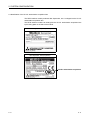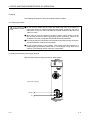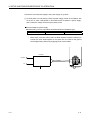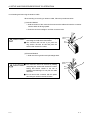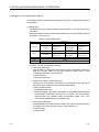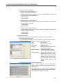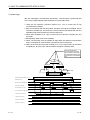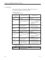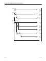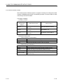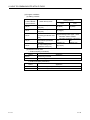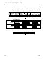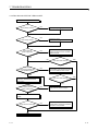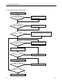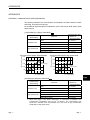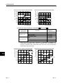
1
RFID Intreface Module EQ V-680D1 EQ V-680D2 User,s Manual
HEAD OFFICE:Hulic KUDAN BLDG.1-13-5, KUDANKITA CHIYODA-KU, TOKYO 102-0073, JAPAN
NAGOYA ENGINEERING OFFICE:139 SHIMOYASHIKICHO-SHIMOYASHIKI, KASUGAI, AICHI 486-0906, JAPAN
Model
EQ-V680D-MAN-E
50CM-D180057-C(1211)MEE
New publication,effective Nov. 2012
Specifications subject to change without notice.
Printed in Japan on recycled paper.
Q SAFETY PRECAUTIONS Q
(Always read these precautions prior to use.)
Before using this product, please read this manual and the relevant manuals introduced in this manual
carefully and pay full attention to safety to ensure that the product is used correctly.
The precautions presented in this manual are concerned with this product only. For programmable
controller system safety precautions, refer to the user’s manual of the CPU module used.
In this manual, the safety precautions are ranked as “WARNING” and “CAUTION.”
WARNING
CAUTION
Indicates that incorrect handling may cause hazardous
conditions, resulting in death or severe injury.
Indicates that incorrect handling may cause hazardous
conditions, resulting in medium or minor injury and/or property
damage.
Note that failure to observe the
CAUTION level instructions may lead to a serious consequence
according to the circumstances. Always follow the precautions of both levels because they are important
to personal safety.
Please keep this manual in an easy-to-access location for future reference, and be sure to deliver the
manual to the end user.
[DESIGN PRECAUTIONS]
CAUTION
Q
Provide a safety circuit outside the programmable controller to ensure that the overall system
operates safely in the event of an error in the external power supply or failure of the
programmable controller itself. Failure to do so results in the risk of erroneous output and
malfunction, resulting in module failure.
Q
Configure the circuitry so that the external power supply is activated after the power supply of the
programmable controller itself. Activating the external power supply first results in the risk of
erroneous output and malfunction, resulting in module failure.
Q
When installing the RFID interface module and amplifier/antenna cables, do not bundle the
cables with or install the cables close to the main circuit, power lines, or the like. Be sure to
separate the cables and lines by about 100mm or more. Failure to do so will cause noise,
resulting in malfunction.
A-1
A-1
[DESIGN PRECAUTIONS]
CAUTION
Q
When storing the product, be sure to observe the defined storage ambient temperature and
humidity. Failure to do so will lead to module malfunction and failure.
Q
Look the control panel so that only those who are trained and have acquired enough knowledge
of electric facilities can open control panel.
Q
Install the emergency stop switch outside the control panel so that workers can operate it easily.
[INSTALLATION PRECAUTIONS]
CAUTION
Q
Use the programmable controller in an environment that reflects the general specifications stated
in the user’s manual of the CPU module used. Using the programmable controller in an
environment out of the general specification range results in the risk of electric shock, fire,
malfunction, and product damage or deterioration.
Q
During installation, fully insert the tabs used to secure the module into the holes of the base unit
while pressing down the module mounting lever located at the bottom of the module, using the unit
holes as support points. An incorrectly mounted module results in the risk of malfunction, failure,
and dropping. When used in an environment of high oscillation, secure the module with screws.
Q
Tighten the screws within the specified torque range. If a screw is too loose, a dropped module,
short circuit, or malfunction may result. If a screw is too tight, screw and/or module damage may
occur, resulting in a dropped module, short circuit, or malfunction.
Q
Be sure to shut off all phases of the external power supply used by the system before module
installation or removal.
Failure to do so results in the risk of product damage.
Q
Do not directly touch a powered section or electronic component of the module. Doing so results
in the risk of module malfunction and failure.
[WIRING PRECAUTIONS]
CAUTION
Q
After the installation and wiring work, be sure to install the provided terminal cover on the product when
you want to activate and operate the module. Failure to do so results in the risk of electric shock.
Q
Fully mount the antenna cable to the module connector. After mounting, check for separation.
Insufficient contact results in the risk of erroneous input and output.
Q
Be sure to place the communication cables and power cables connected to the module in a duct,
or secure them with clamps. Failure to do so results in the risk of cable movement and drift,
module or cable damage caused by careless pulling, and malfunction caused by insufficient
cable contact.
A-2
A-2
[WIRING PRECAUTIONS]
CAUTION
Q
When connecting a cable, first verify the connection interface type and then connect the cable
properly. Connecting a cable to a wrong interface or miswiring a cable results in the risk of
module and external device malfunction.
Q
Tighten the screws within the specified torque range. If a screw is too loose, a short circuit or
malfunction may result. If a screw is too tight, screw and/or module damage may occur, resulting
in a short circuit or malfunction.
Q
When removing a communication cable or power cable connected to the module, do not pull the
cable section. For cables with connectors, hold the connector of the section connected to the
module during removal. For terminal block cables, loosen the screws of the terminal block and
then remove the cable. Pulling a cable while it is connected to the module results in the risk of
malfunction and module and cable damage.
Q
Be careful to prevent foreign matter such as dust or wiring chips from entering the module
interior. Failure to do so results in the risk of fire, failure, and malfunction.
Q
A protective film is attached to the top of the module to prevent foreign matter, such as wire
chips, from entering the module during wiring.
Do not remove the film during wiring.
Remove it for heat dissipation before system operation.
Q
Do not connect the power supply in reverse. Doing so results in risk of failure.
Q
Use the module after confirming that the external input DC power supply is within the rated
power supply voltage.
Failure to do so results in the risk of failure and malfunction.
Q
Do not bundle the control or communication cables with or install the cables close to the main
circuit, power lines, or the like. Be sure to separate the cables and lines by about 100mm or more.
[STARTUP AND MAINTENANCE PRECAUTIONS]
CAUTION
Q
Do not disassemble or modify the module. Doing so results in the risk of failure, malfunction,
injury, and fire.
Q
Be sure to shut off all phases of the external power supply used by the system before module
installation or removal. Failure to do so results in the risk of module failure and malfunction.
Q
After product use begins, be sure the number of times the module, base, and terminal block are
installed and removed does not exceed 50 (JIS B 3502 compliant). Exceeding 50 results in the
risk of malfunction.
Q
Do not touch the terminals while the module is powered. Doing so results in the risk of
malfunction.
A-3
A-3
[STARTUP AND MAINTENANCE PRECAUTIONS]
CAUTION
Q
Be sure to shut off all phases of the external power supply used in the system before cleaning or
tightening terminal screws or module screws. Failure to do so results in the risk of module failure
and malfunction. If a screw is too loose, a dropped module, short circuit, or malfunction may
result. If a screw is too tight, screw and/or module damage may occur, resulting in a dropped
module, short circuit, or malfunction.
Q
The module case is made of plastic. Do not drop the case or expose the case to strong impact.
Doing so results in the risk of module damage.
Q
Before touching the module, be sure to touch grounded metal or the like to release the static
electricity from your body. Failure to do so results in the risk of module failure or malfunction.
Q
When cleaning, do not use thinner, benzene, acetone, or kerosene. Doing so results in the risk of
module damage.
Q
Do not insert water or wire through the gaps in the case. Doing so results in the risk of fire or
electric shock.
Q
This product cannot be used as a detector for physical protection. Erroneous output or
malfunction may result in an accident.
Q
When installing or removing the antenna from the amplifier, first turn OFF the module power
supply. Failure to do so results in the risk of module failure and malfunction.
Q
Installation of multiple antennas may result in a decrease in communication performance due to
mutual interference. Refer to the description of mutual interference between antennas in the
antenna user’s manual.
Q
In the unlikely event that you feel something is wrong with the product, stop using the product
immediately, turn OFF the power supply, and consult with your local Mitsubishi service center or
representative. Continued use as is results in the risk of module failure and malfunction.
Q
Do not use the product in locations where chemical products and oil are scattered. Doing so
results in the risk of module failure and malfunction.
Q
When using the product, be sure to observe the defined ambient temperature and humidity.
Failure to do so results in the risk of module failure and malfunction.
Q
Do not touch any connectors when the module is powered. Doing so results in the risk of module
malfunction caused by the static electricity in your body.
[DISPOSAL PRECAUTIONS]
CAUTION
Q
A-4
At the time of disposal, treat the product as industrial waste.
A-4
REVISIONS
*The manual number is given on the bottom left of the back cover.
Print Date
*Manual Number
Revision
Oct. 2011
50CM-D180057-B First edition
Nov. 2012
50CM-D180057-C Partial correction
Section 6.5 changed to Section 6.6
Addition
Section 6.5
This manual confers no industrial property rights or any rights of any other kind, nor does it confer any
patent licenses. Mitsubishi Electric Engineering cannot be held responsible for any problems involving
industrial property rights which may occur as a result of using the contents noted in this manual.
© 2011 MITSUBISHI ELECTRIC ENGINEERING COMPANY LIMITED
A-5
A-5
INTRODUCTION
Thank you for purchasing the RFID interface module manufactured by Mitsubishi Electric Engineering
Company, Ltd.
Prior to use, please read this manual carefully to develop full familiarity with the functions and performance of
the MELSEC-Q series programmable controller to ensure correct use.
CONTENTS
SAFETY PRECAUTIONS·······························································································································A- 1
REVISIONS ·····················································································································································A- 5
INTRODUCTION·············································································································································A- 6
CONTENTS·····················································································································································A- 6
EMC Directive and Low Voltage Directive Compliance·················································································A- 9
Manuals ··························································································································································A-10
Generic Terms and Abbreviations ·················································································································A-10
Product Portfolio·············································································································································A-10
Chapter 1 OVERVIEW
1- 1 to 1- 2
1.1 RFID Interface Module Overview ············································································································· 1- 1
1.2 RFID Interface Module Features ·············································································································· 1- 2
Chapter 2 SYSTEM CONFIGURATION
2- 1 to 2- 8
2.1 Application System···································································································································· 2- 1
2.2 Verifying the Function Version·················································································································· 2- 4
2.3 Identification of the UL/cUL authorization acquisition item ······································································ 2- 5
2.4 Overall Configuration ································································································································ 2- 6
2.4.1 System that uses a separate amplifier type antenna········································································ 2- 6
2.4.2 System that uses a built-in amplifier type antenna ··········································································· 2- 7
2.5 Component List ········································································································································· 2- 8
Chapter 3 SPECIFICATIONS
3- 1 to 3-13
3.1 Performance Specifications ······················································································································ 3- 1
3.2 Functions ··················································································································································· 3- 2
3.2.1 RUN mode·········································································································································· 3- 2
3.2.2 TEST mode ········································································································································ 3- 3
3.3 Programmable Controller CPU IO Signals······························································································· 3- 4
3.3.1 IO signal list ········································································································································ 3- 4
3.3.2 IO signal details ·································································································································· 3- 5
3.4 Buffer Memory··········································································································································· 3- 8
3.4.1 Buffer memory list ······························································································································ 3- 8
3.4.2 Buffer memory details ························································································································ 3- 8
A-6
A-6
Chapter 4 SETUP AND PROCEDURES PRIOR TO OPERATION
4- 1 to 4- 9
4.1 Usage Precautions···································································································································· 4- 1
4.2 Installation Environment···························································································································· 4- 2
4.3 Cable Installation······································································································································· 4- 2
4.4 Setup and Procedures Prior to Operation ································································································ 4- 3
4.5 Names of Parts·········································································································································· 4- 4
4.6 Wiring························································································································································· 4- 5
4.6.1 Wiring precautions······························································································································ 4- 5
4.6.2 Wiring the external power supply terminal ························································································ 4- 5
4.6.3 Inserting and removing the antenna cable ························································································ 4- 7
4.7 Intelligent Function Module Switch Settings····························································································· 4- 8
Chapter 5 THINGS YOU NEED TO KNOW BEFORE PROGRAMMING
5- 1 to 5-24
5.1 Operation Mode ········································································································································ 5- 1
5.1.1 Switching the operation mode ··········································································································· 5- 1
5.1.2 RUN mode·········································································································································· 5- 1
5.1.3 TEST mode ········································································································································ 5- 1
5.2 ID Tag Memory ········································································································································· 5- 8
5.3 Write Protect Function ····························································································································· 5-10
5.3.1 How to set write protect····················································································································· 5-10
5.3.2 How to cancel write protect··············································································································· 5-15
5.4 ID Tag Number of Writes Management Function (EEPROM Type Only)·············································· 5-16
5.4.1 Manage Number of Writes 1 (Write life = Preset number of writes)················································5-16
5.4.2 Manage Number of Writes 2 (Write life = Arbitrary number of writes) ············································ 5-19
5.5 ID Tag Data Check Function ··················································································································· 5-21
5.6 ID Tag Memory Error Correction Function······························································································ 5-24
Chapter 6 HOW TO COMMUNICATE WITH ID TAGS
6- 1~6-84
6.1 Programming Precautions ························································································································ 6- 1
6.2 Instruction/Specification List ····················································································································· 6- 2
6.2.1 Read ··················································································································································· 6- 2
6.2.2 Write···················································································································································· 6- 2
6.2.3 Set bit·················································································································································· 6- 3
6.2.4 Clear bit ·············································································································································· 6- 4
6.2.5 Write mask bit····································································································································· 6- 5
6.2.6 Write calculation ································································································································· 6- 7
6.2.7 Fill data ··············································································································································· 6- 8
6.2.8 Check data ········································································································································· 6- 9
6.2.9 Control number of writes··················································································································· 6-10
6.2.10 Copy················································································································································· 6-11
6.2.11 Read with error correction··············································································································· 6-12
6.2.12 Write with error correction··············································································································· 6-13
6.2.13 Read UID········································································································································· 6-13
6.2.14 Measure noise································································································································· 6-13
6.3 Control Methods According to Communication Specification ································································ 6-14
6.3.1 Trigger················································································································································ 6-14
A-7
A-7
6.3.2 Auto···················································································································································· 6-15
6.3.3 Repeat auto ······································································································································· 6-16
6.3.4 FIFO trigger ······································································································································· 6-17
6.3.5 FIFO repeat ······································································································································· 6-18
6.3.6 Multi-trigger········································································································································ 6-19
6.3.7 Multi-repeat········································································································································ 6-20
6.4 Sample Programs ···································································································································· 6-21
6.4.1 Set parameters·································································································································· 6-23
6.4.2 Read ·················································································································································· 6-25
6.4.3 Write··················································································································································· 6-28
6.4.4 Set bit················································································································································· 6-31
6.4.5 Clear bit ············································································································································· 6-34
6.4.6 Write mask bit···································································································································· 6-37
6.4.7 Write calculation ································································································································ 6-40
6.4.8 Fill data ·············································································································································· 6-44
6.4.9 Check data ········································································································································ 6-47
6.4.10 Control number of writes················································································································· 6-50
6.4.11 Copy················································································································································· 6-53
6.4.12 Read with error correction··············································································································· 6-56
6.4.13 Write with error correction··············································································································· 6-59
6.4.14 Read UID········································································································································· 6-62
6.4.15 Measure noise································································································································· 6-65
6.4.16 Read module status ························································································································ 6-68
6.5 Specialized Sample Program for Read/Write of ID Tags with the Trigger Communication·················· 6-70
6.5.1 Sample program································································································································ 6-70
6.6 For Use in Remote I/O Network ·············································································································· 6-76
6.6.1 Sample program for use in remote I/O Network ·············································································· 6-76
6.6.2. Attention and limitation using the RFID module at MELSECNET/H remote I/O station················ 6-84
Chapter 7. TROUBLESHOOTING
7- 1~7- 5
7.1 Error Details List········································································································································ 7- 1
7.2 Troubleshooting········································································································································· 7- 2
7.2.1 Troubleshooting flow ·························································································································· 7- 2
7.2.2 Flow when “RUN” LED turns OFF ····································································································· 7- 3
7.2.3 Flow when the “EXT.PW” LED turns OFF························································································· 7- 4
7.2.4 Flow when the “ERR.” LED turns ON································································································ 7- 5
APPENDICES
App- 1~App- 7
APPENDIX 1 COMMUNICATION TIME (Reference) ·············································································· App- 1
APPENDIX 2 PROCESSING TIME (Reference)······················································································ App- 3
APPENDIX 3 EXTERNAL DIMENSIONS ································································································· App- 6
INDEX
A-8
Ind- 1~Ind- 2
A-8
EMC Directive and Low Voltage Directive Compliance
(1) Programmable controller system
When you want to incorporate an EMC Directive and Low Voltage Directive compliant
programmable controller into your product to ensure directive compliance, refer to
Chapter 9, “EMC Directive and Low Voltage Directive”, of the QCPU User’s Manual
(Hardware Design, Maintenance, and Inspection). A programmable controller that is
compliant with the EMC Directive and Low Voltage Directive has a CE mark printed on
the rating plate of the main unit.
Authorized representative in Europe
Authorized representative in Europe si shown below
Name:
Mitsubishi Electric Europe B.V.
(EMC C.C. Division)
Address: Gothaer strasse 8, 40880 Ratingen, Gemany
(2) This product
To make this product compliant with the EMC Directive and Low Voltage Directive,
the following countermeasure is required.
To suppress radiation noise, use a ferrite core. The method of use is as follows:
Bring together the power supply cable of the programmable controller power supply
module and the grounding wire and route them through the ferrite core. The target
position of the ferrite core is within 10cm from the power supply module.
Programmable controller
Grounding
wire
Power supply
cable
Power
supply
CPU
module
FG
LG
INPUT
100-240VAC
Ferrite core
(within 10cm from the power supply contact)
A-9
A-9
Manuals
The manuals related to this product include the following.
Direct any inquiries to your local sales store, Mitsubishi Electric Engineering service
office, or any Mitsubishi Electric product dealer, as necessary.
Detailed manuals
Included manual
Manual Title
Manual Number
RFID Interface Module User's Manual (Hardware)
50CM-D180056
Manufactured by
Mitsubishi Electric Corporation Mitsubishi general-purpose programmable controller MELSEC-Q series manual
Manual Title
Manual Number
QCPU User's Manual (Hardware Design, Maintenance and Inspection)
SH-080483ENG
Generic Terms and Abbreviations
This manual uses the following generic terms and abbreviations in product
explanations, unless otherwise specified.
Generic Term / Abbreviation
RFID interface module
Description
A generic term for an EQ-V680D1/EQ-V680D2 RFID interface module.
A generic product name for product models SWnD5C-GPPW-E, SWnD5C-GPPW-EA,
GX Developer
SWnD5C-GPPW-EV, and SWnD5C-GPPW-EVA (where n indicates version 4 or later).
-A indicates a multiple license product, and -V indicates a version upgrade product.
A generic term for Q00JCPU, Q00CPU, Q01CPU, Q02CPU, Q02HCPU, Q06HCPU, Q12HCPU,
QCPU (Q mode)
Q25HCPU, Q02PHCPU, Q06PHCPU, Q12PHCPU, Q25PHCPU, Q12PRHCPU, Q25PRHCPU,
Q02UCPU, Q03UDCPU, Q04UDHCPU, Q06UDHCPU, Q13UDHCPU, Q26UDHCPU,
Q03UDECPU, Q04UDEHCPU, Q06UDEHCPU, Q13UDEHCPU, and Q26UDEHCPU.
Product Portfolio
The following indicates the product portfolio of this product.
Model
EQ-V680D1
EQ-V680D2
A - 10
Product Name
Quantity
EQ-V680D1 RFID interface module (for one channel)
1
User’s Manual (Hardware) (Included with module)
1
Ferrite core (Included with module)
1
EQ-V680D2 RFID interface module (for two channels)
1
User’s Manual (Hardware) (Included with module)
1
Ferrite core (Included with module)
1
A - 10
1. OVERVIEW
Chapter 1 OVERVIEW
This user’s manual describes the specifications, use, ID tag communication method,
and other information related to the EQ-V680D1/EQ-V680D2 RFID interface module
(hereinafter “RFID interface module”).
The RFID interface module is mounted on a base unit of the Mitsubishi
general-purpose programmable controller MELSEC-Q series, enabling reading and
writing with Omron RFID system V680 series ID tags.
When utilizing the program examples introduced in this manual in an actual system, be
sure to fully verify that use will not be problematic in the control of the target system.
1.1 RFID Interface Module Overview
The RFID interface module has one or two channels that connect to a V680 series
antenna, and fulfills the role as an interface for V680 series ID tag reading and writing
and the programmable controller CPU.
RFID interface
module
ID tag
Antenna
Programmable
controller CPU
Data reading and
writing with ID tag
by electromagnetic
induction (non-contact)
Amplifier
1-1
1-1
1
1. OVERVIEW
1.2 RFID Interface Module Features
1
The following describes the features of the RFID interface module.
(1) The RFID interface module uses a rich group of Mitsubishi Electric MELSEC-Q series
products, and is capable of controlling Omron RFID system V680 series products.
(2) The two-channel RFID interface module enables independent antenna operation per
channel.
CH1
(Setup)
CH2
(Finishing and inspection)
(3) The two-channel RFID interface module allows you to the module allows you to copy
data between ID tags using the Copy Data command.
Data
Copy
(4) The one-channel RFID interface module enables use of an amplifier built-in type
antenna.
(5) The module is provided with various test functions as standard.
The communication test function allows you to check whether or not
communication with an ID tag is possible without operating the sequence program.
The distance level measurement function measures the distance between the
antenna and ID tag with respect to the communication area, dividing the margin
into six stages.
The communication success rate measurement function executes
communication with a static ID tag 100 times, and measures the repeated
communication success rate.
The speed level measurement function measures the number of times
communication can be performed continuously according to the speed of an ID
tag that moves within the antenna communication area.
The noise level measurement function measures the noise level in the area
surrounding the antenna installation location.
(6) The module allows you to simply develop programs by downloading an FB (function
block) library that can be used with Mitsubishi Electric MELSOFT GX Works 2 from
the Mitsubishi Electric Corporation FA device information site MELFANSweb.
1-2
1-2
2. SYSTEM CONFIGURATION
Chapter 2 SYSTEM CONFIGURATION
The following describes the system configuration of the RFID interface module.
2.1 Application System
2
The following describes the application system.
(1) Mountable modules, mountable quantities, and mountable base units
(a) When mounted with a CPU module
The table below indicates the mountable CPU modules, mountable quantities,
and mountable base units for the RFID interface module.
Note that, depending on the combination with other mounted modules and the
number of modules mounted, the power supply capacity may be insufficient.
When mounting the modules, be sure to take the power supply capacity into
consideration.
In the event the power supply capacity is insufficient, investigate the combination
of the mounted modules.
Table 2.1 Application system
Mountable CPU Module
CPU Type
Basic model
QCPU
1
CPU Model
Q00JCPU
Q00CPU
Q01CPU
Mountable Quantity*
Mountable Base Unit*2
Main Base Unit
Extension Base Unit
○
○
64, maximum
○
○
64, maximum
○
○
53, maximum
×
○
○
○
8, maximum
24, maximum
Q02CPU
High
performance
model QCPU
Q02HCPU
Q06HCPU
Q12HCPU
Q25HCPU
Q02PHCPU
Process CPU
Programmable
controller CPU
Q06PHCPU
Q12PHCPU
Q25PHCPU
Dual CPU
Q12PRHCPU
Q25PRHCPU
Q00UJCPU
Q00UCPU
Q01UCPU
Q02UCPU
Universal
model CPU
8, maximum
24, maximum
36, maximum
Q03UDCPU
Q04UDHCPU
Q06UDHCPU
Q10UDHCPU
64, maximum
Q13UDHCPU
Q20UDHCPU
Q26UDHCPU
2-1
2-1
2. SYSTEM CONFIGURATION
Table 2.1 Application system (Continued)
Mountable CPU Module
CPU Type
Mountable Base Unit*2
1
Mountable Quantity*
CPU Model
Main Base Unit
Extension Base Unit
64, maximum
○
○
Not mountable
×
×*3
Not mountable
×
×
Q03UDECPU
Q04UDEHCPU
2
Programmable
controller CPU
Universal
model CPU
Q06UDEHCPU
Q10UDEHCPU
Q13UDEHCPU
Q20UDEHCPU
Q26UDEHCPU
Safety CPU
QS001CPU
Q06CCPU-V-H01
C-language controller module
Q06CCPU-V
Q06CCPU-V-B
Q12DCCPU-V
○:Mountable, ×:Not mountable
*1. Limited to within the range of the number of IO points of the CPU module.
*2. Mountable in any IO slot of a mountable base unit.
*3. An extension base unit cannot be connected to a safety CPU.
(b) Mounting to a MELSECNET/H remote I/O station
The table below shows the network modules and base units applicable to the
RFID interface module and quantities for each network module model.
Depending on the combination with other modules or the number of mounted
modules, power supply capacity may be insufficient.
Pay attention to the power supply capacity before mounting modules, and if the
power supply capacity is insufficient, change the combination of the modules.
Applicable network
module
Base unit*2
1
No. of modules*
Main base unit of
remote I/O station
Extension base unit of
remote I/O station
Up to 64
○
○
QJ72LP25-25
QJ72LP25G
QJ72LP25GE
QJ72BR15
○:Applicable, ×:N/A
*1. Limited within the range of I/O points for network module.
*2. Can be installed to any I/O slot of a base unit.
2-2
2-2
2. SYSTEM CONFIGURATION
(2) Compatibility with multiple CPU systems
When you want to use the RFID interface module in a multiple CPU system, be
sure to first refer to the manual below:
QCPU User’s Manual (Multiple CPU System)
(a) Compatible RFID interface modules
The RFID interface module has supported a multiple CPU system from the
beginning with function version B.
(b) Intelligent function module parameters
Execute programmable controller writing of intelligent function module
parameters to the control CPU of the RFID interface module only.
(3) Omron RFID system V680 series dedicated use
The RFID interface module connects with amplifiers and antennas of the Omron
RFID system V680 series, enabling reading and writing with V680 series ID tags.
(4) Compatible software packages
The following table indicates the compatibility between systems that use the RFID
interface module and software packages.
When using an RFID interface module, GX Developer is required.
Table 2.2 Compatible software packages list
Q00J/Q00/Q01CPU
Q02/Q02H/Q06H/Q12H/
Q25HCPU
Q02PH/Q06PHCPU
Q12PH/Q25PHCPU
Q12PRH/Q25PRHCPU
Q00UJ/Q00U/Q01UCPU
Q02U/Q03UD/Q04UDH/
Q06UDHCPU
Q10UDH/Q20UDHCPU
Q13UDH/Q26UDHCPU
Q03UDE/Q04UDEH/Q06UDEH/
Q13UDEH/Q26UDEHCPU
Q10UDEH/Q20UDEHCPU
2-3
Single CPU system
Multiple CPU system
Single CPU system
Multiple CPU system
Single CPU system
Multiple CPU system
Single CPU system
Multiple CPU system
Dual system
Single CPU system
Multiple CPU system
Single CPU system
Multiple CPU system
Single CPU system
Multiple CPU system
Single CPU system
Multiple CPU system
Single CPU system
Multiple CPU system
Single CPU system
Multiple CPU system
Software Version
GX Developer
Version 7 or later
Version 8 or later
Version 4 or later
Version 6 or later
Version 8.68W or later
Version 7.10L or later
Version 8.45X or later
Version 8.76E or later
Version 8.48A or later
Version 8.76E or later
Version 8.62Q or later
Version 8.68W or later
Version 8.76E or later
2-3
2. SYSTEM CONFIGURATION
2.2 Verifying the Function Version
The following describes the method used to verify the function version of the RFID
interface module.
(1) Verifying the function version of the RFID interface module
(a) When verifying the version by viewing the “SERIAL” area of the rating plate on
the side of the module
・EQ-V680D1
1109BA-B
Function version
・EQ-V680D2
1109BA-B
Function version
(b) When verifying the version by viewing the system monitor (product information
list)
To view the system monitor, select “Diagnostics” -> “System Monitor” in GX
Developer, and click the Product Information List button.
Function version
2-4
2-4
2. SYSTEM CONFIGURATION
2.3 Identification of the UL/cUL authorization acquisition item
The RFID interface module produced after September, 2011 is shipped as the UL/cUL
authorization acquisition item.
The RFID interface module can distinguish the UL/cUL authorization acquisition item
by the rating plate on the side of the module.
Before August, 2011(Not acquisition)
After September, 2011(Acquisition)
1109BA-B
2-5
UL/cUL authorization acquisition
2-5
2. SYSTEM CONFIGURATION
2.4 Overall Configuration
The following indicates the overall configuration of the RFID system.
2.4.1 System that uses a separate amplifier type antenna
The following illustrates a system that uses a separate amplifier type antenna.
The antennas, amplifier and ID tags can be used in certain combinations. Refer to the
Omron RFID system V680 series catalog.
24V external power supply
power supply
1CH type
Programmable
controller CPU
2CH type
RFID interface module
Amplifier
Extension cable
Main base
Extension cable
Antennas
ID tags
2-6
Extension base
2-6
2. SYSTEM CONFIGURATION
2.4.2 System that uses a built-in amplifier type antenna
The following illustrates a system that uses a built-in amplifier type antenna.
The antennas and ID tags can be used in certain combinations. Refer to the Omron
RFID system V680 series user’s catalog.
24V external power supply
power supply
1CH type*1
Programmable
controller CPU
RFID interface module
Extension cable
Main base
Built-in amplifier type antenna
Extension cable
ID tags
*1. A 2CH type cannot be used.
2-7
Extension base
2-7
2. SYSTEM CONFIGURATION
2.5 Component List
The component lists the required equipment for using the RFID interface module.
Table 2.3 Component List
Product Name
RFID interface
module
Amplifier
Antenna
(separate
amplifier type)
Antenna
(built-in
amplifier type)
EEPROM-type
ID tag
Model
EQ-V680D1
EQ-V680D2
V680-HA63A
V680-HA63B
V680-HS51
V680-HS52
V680-HS63
V680-HS65
Remarks
V680 series RFID interface module; one antenna connected
V680 series RFID interface module; two antennas connected
For EEPROM-type ID tags (V680-D1KP)
For FRAM-type ID tags (V680-D2KF/V680-D8KF/V680-D32KF)
For ID tag communication; Ф18mm type
Cable length: 2m/12.5m
For ID tag communication; Ф22mm type
Cable length: 2m/12.5m
For ID tag communication; 40x53mm type
Cable length: 2m/12.5m
For ID tag communication; 100x100mm type
Cable length: 2m/12.5m
V680-H01-V2
For ID tag communication; 250x200mm type
V680-D1KP52MT
V680-D1KP53M
Memory capacity: 1kbytes (1,000 bytes); Ф8mm type; metal embedding permitted
Memory capacity: 1kbytes (1,000 bytes); Ф10mm type; metal embedding permitted
Memory capacity: 1kbytes (1,000 bytes); 34x34mm type; metal installation
permitted
Memory capacity: 1kbytes (1,000 bytes); 34x34mm type
Memory capacity: 1kbytes (1,000 bytes);
oil-proof and chemical resistant specifications
Memory capacity: 1kbytes (1,000 bytes); Ф80mm type; heat resistant specifications
Memory capacity: 2kbytes (2,000 bytes); Ф8mm type; metal embedding permitted
Memory capacity: 2kbytes (2,000 bytes); 40x40mm type; metal installation
permitted
Memory capacity: 2kbytes (2,000 bytes); 40x40mm type
Memory capacity: 8kbytes (8,192 bytes); 40x40mm type; metal installation possible
Memory capacity: 8kbytes (8,192 bytes); 40x40mm type
Memory capacity: 8kbytes (8,192 bytes); 86x54mm type
Memory capacity: 32kbytes (32,744 bytes); 86x54mm type
For V680-HA63A/63B amplifier connection
Cable length: 10m
For V680-HA63A/63B amplifier connection
Cable length: 20m
For V680-H01-V2 built-in amplifier type antenna connection
V680-D1KP66MT
V680-D1KP66T
V680-D1KP66T-SP
V680-D1KP58HT
V680-D2KF52M
V680-D2KF67M
FRAM-type ID
tag
Extension
cable
V680-D2KF67
V680-D8KF67M
V680-D8KF67
V680-D8KF68
V680-D32KF68
V700-A43
V700-A44
V700-A40-W
Cable length: 0.5m
Cable length: 2m/5m/10m/20m/30m
* For amplifier, antenna, and ID tag combinations, refer to the Omron RFID system
V680 series catalog.
2-8
2-8
3. SPECIFICATIONS
Chapter 3 SPECIFICATIONS
The following describes the RFID interface module performance specifications,
programmable controller CPU input/output signals, and buffer memory specifications.
The following table shows the general specifications of the RFID interface module.
Item
Operating temperature
Operating humidity
Pollution degree
Operating ambience
Operating altitude
Overvoltage category
Enclosure
3-1
Specifications
0 to 55℃(Maximum surrounding air temperature 55℃)
5 to 95%RH
3
2
No corrosive gases
0 to 2000m
Ⅱ
open type equipment (Must be mounted within an enclosure.)
3-1
3. SPECIFICATIONS
3.1 Performance Specifications
The following describes the performance specifications of the RFID interface module.
Table 3.1 Performance specifications
Item
Model
EQ-V680D1
Manufactured by Omron Corporation
Connectable antenna
3
Specifications
No. of connectable antennas
No. of occupied IO points
EQ-V680D2
V680-HA63A+V680-HS□□
V680-HA63B+V680-HS□□
V680-H01-V2
V680-HA63A+V680-HS□□
V680-HA63B+V680-HS□□
1 antenna
2 antennas
32 points (IO assignments: 32 intelligent module points)
Data transfer volume
2,048 bytes, maximum
Internal power supply
Current consumption
5VDC (supplied from inside
0.42A
0.52A
0.25A
0.37A
the programmable controller) *1
External power supply*2
24VDC (20.4 to 26.4VDC)
External power supply connection
2-point terminal block
terminal
Heat Resistant PVC Insulated Wire
Wiring
recommendations
Power supply
Current consumption
Wire standard
JIS C 3316 HKIV,JIS C 3317 HIV,
UL 758 Style No.1007or1015
Temperature rating
Minimum 75℃
Voltage rating
300V to 600V
Conductors wire size
AWG18(0.75mm2, 0.9mm2)
Conductors metal
Stranded copper
Compatible crimp Contact lugs
Outer dimensions
Weight
1.25-3, R1.25-3
98(H)
0.2kg
27.4(W)
106.5(D) [mm]
0.2kg
*1. “The Power Supply shall comply with the requirements in the standard for an
isolated secondary limited voltage, limited current (LVLC) circuit, defined by
UL508.” or equivalent.
*2. For external power supply details, refer to Section 4.6.2.
3-2
3-2
3. SPECIFICATIONS
3.2 Functions
The RFID interface module has two operation modes: RUN mode and TEST mode.
The following describes the functions of each mode.
3.2.1 RUN mode
RUN mode is used during programmable controller operation.
To set the mode to RUN mode, set the test switch located on the front of the RFID
interface module to “RUN”.
Table 3.2 RUN mode functions list
Function
Command
Read
Read
Reads data from an ID tag.
Read with Error
Correction
Reference
Section 6.2.1
Reads the data and check code written by the Write with Error
Correction function from the ID tag, inspects data reliability, and Section 6.2.11
corrects any 1-bit errors.
Read UID
Reads the UID (unit identification number) of an ID tag.
Section 6.2.13
Write
Writes data to an ID tag.
Section 6.2.2
Set Bit
Sets the bit specified in the data of an ID tag to “1”.
Section 6.2.3
Clears the bit specified in the data of an ID tag to “0”.
Section 6.2.4
Clear Bit
Write
Description
Write Mask Bit
Write Calculation
Protects the data area within the ID tag data that you do not want
overwritten, and writes data.
Writes an addition or subtraction calculation result (data) to ID tag
data.
Section 6.2.5
Section 6.2.6
Write with Error
Writes data and check codes for inspecting data reliability to an ID
Correction
tag.
Duplicate
Copy*1
Copies data of an ID tag between channel 1 and channel 2.
Section 6.2.10
Initialize
Fill Data
Initializes data of an ID tag with specified data.
Section 6.2.7
Check Data
Management
Manage Number
of Writes
Measure Noise
Checks whether or not an error occurred in data of an ID tag.
Writes data and code for checking data to an ID tag.
Section 6.2.12
Section 6.2.8
Writes the number of EEPROM-type ID tag writes to an ID tag, and
assesses whether or not the ID tag number of writes has been Section 6.2.9
exceeded.
Measures the noise environment around an antenna.
Section 6.2.14
*1. Available with EQ-V680D2.
3-3
3-3
3. SPECIFICATIONS
3.2.2 TEST mode
TEST mode is used when starting the RFID system or when performing maintenance.
To set the mode to TEST mode, either set the test switch located on the front of the
RFID interface module to “TEST,” or set the test mode execution request (Y15) to ON
in the sequence program.
Table 3.3 TEST mode functions list
Function
Description
Reference
Has the RFID interface module read ID tag data without operating the sequence
Communication test
program.
Checks whether a sequence program, antenna, or ID tag caused a read error
Section 5.1.3(2)
when a data read error occurs with an ID tag.
Distance level
measurement
Checks the potential maximum communication distance of the installation distance
of the ID tag.
Use this function to adjust the installation location.
Communication
Checks the data reading potential in terms of the repeated execution success rate,
success rate
in the installation state with the ID tag in a stationary state.
measurement
Use this function to adjust the installation location.
Speed level
Checks the data reading potential in terms of the number of times read can be
measurement
repeatedly executed while moving an ID tag.
(read)
Use this function to adjust the ID tag movement speed.
Speed level
Checks the data writing potential in terms of the number of times write can be
measurement
repeatedly executed while moving an ID tag.
(write)
Use this function to adjust the ID tag movement speed.
Noise level
Checks whether noise that adversely affects communication with an ID tag is
measurement
occurring in the area surrounding the antenna installation location.
3-4
Section 5.1.3(3)
Section 5.1.3(4)
Section 5.1.3(5)
Section 5.1.3(5)
Section 5.1.3(6)
3-4
3. SPECIFICATIONS
3.3 Programmable Controller CPU IO Signals
3.3.1 IO signal list
The following provides a list of the IO signals of the RFID interface module.
Note that the IO numbers (X/Y) shown hereafter indicate the number when the first IO
number of the RFID interface module is set to 0.
Table 3.4 IO signal list
Signal Direction: CPU Module <- RFID Interface Module
Device No. (Input)
X0
X1
X2
X3
X4
X5
X6
X7
X8
X9
XA
XB
XC
XD
XE
XF
X10
X11
X12
X13
X14
X15
X16
X17
X18
X19
X1A
X1B
X1C
X1D
X1E
X1F
Signal Name
Module READY
Use prohibited
ID communication complete
ID-BUSY
ID command complete
Error detection
CH1
Use prohibited
1
CH2*
ID communication complete
ID-BUSY
ID command complete
Error detection
Use prohibited
Signal Direction: CPU Module -> RFID Interface Module
Device No. (Output)
Signal Name
Y0
Y1
Y2
Y3
Y4
Y5
Y6
Y7
Y8
Y9
YA
YB
YC
YD
YE
YF
Y10
Y11
Y12
Y13
Y14
Y15
Y16
Y17
Y18
Y19
Y1A
Y1B
Y1C
Y1D
Y1E
Y1F
Use prohibited
CH1 ID command execution request
2
TEST mode execution request*
CH1
Result reception
Use prohibited
1
CH2*
1
CH2*
ID command execution request
Use prohibited
Result reception
Use prohibited
*1. Effective only with EQ-V680D2 use.
*2. Available for use only when both the “test mode enable” bit and “Y contact test
request enable” bit are set to “0” (enable) on switch 2 of the intelligent function
module switch. (Refer to Section 4.7)
Point
Use-prohibited IO signals are used by the system and cannot be used by users. In
the unlikely event that a use-prohibited IO signal is turned ON/OFF by a sequence
program, the functions of the RFID interface module cannot be guaranteed.
3-5
3-5
3. SPECIFICATIONS
3.3.2 IO signal details
The following describes in detail the input/output signals of the RFID interface module.
(1) Input signals
Device
No.
Signal Name
Description
(1) Turns ON when the RFID interface module is ready after programmable controller
X0
Module READY
CPU power ON or reset.
(2) Turns OFF when an RFID interface module hardware error occurs.
(1) Turns ON when the communication processing with all ID tags is completed when
the communication specification is multi-trigger.
(2) Turns ON when RFID interface module communication is suspended due to the
elapse of the auto command wait time when the communication specification is
repeat auto, FIFO repeat, or multi-repeat.
Turns ON when communication is suspended due to antenna disconnection when
the communication specification is repeat auto, FIFO repeat, multi-trigger, or
multi-repeat.
(3) Turns OFF when the ID command execution request (Y14, Y1C) is turned OFF.
(4) The timing chart is as follows:
1) ID communication complete (X2, XA) turns ON when the communication
specification is Multi-trigger and the last communication is completed.
Turns ON when communication is suspended due to the elapse of the auto
command wait time when the communication specification is repeat auto, FIFO
repeat, or multi-repeat.
Turns ON when communication is suspended due to antenna disconnection
when the communication specification is repeat auto, FIFO repeat, multi-trigger,
or multi-repeat.
X2, XA
ID communication
complete
2) The ID command execution request (Y14, Y1C) turns OFF when ID
communication complete (X2, XA) turns ON.
3) ID communication complete (X2, XA) and ID-BUSY (X3, XB) turn OFF
when the ID command execution request (Y14, Y1C) turns OFF.
Implemented by RFID interface module
Implemented by sequence program
ID command execution
request (Y14, Y1C)
ID communication complete
(X2, XA)
ID-BUSY(X3,XB)
1)
3-6
2)
3)
3-6
3. SPECIFICATIONS
Device
No.
Signal Name
Description
(1) Turns ON when the ID command execution request (Y14, Y1C) is turned ON and
received by the RFID interface module.
X3, XB
ID-BUSY
(2) Turns OFF when the ID command execution request (Y14, Y1C) is turned OFF and
received by the RFID interface module.
(3) Always ON in TEST mode.
(4) For the timing chart, refer to ID command complete (X4, XC).
(1) Turns ON when the ID command execution request (Y14, Y1C) is turned ON and
the status is normal upon ID command execution completion. Error detection (X5,
XD) turns ON when the status is abnormal upon ID command execution
completion.
(2) Turns OFF when the ID command execution request (Y14, Y1C) is turned OFF and
received by the RFID interface module.
(3) The timing chart is as follows:
1) The ID command execution contents are set in the buffer memory (Un\G0 to
Un\G5, Un\G10 to Un\G11/Un\G4000 to Un\G4005, Un\G4010 to Un\G4011).
2) ID-BUSY (X3, XB) turns ON when the ID command execution request (Y14,
Y1C) turns ON, and the ID command is executed in accordance with the setting
contents of Step 1 above.
3) ID command complete (X4, XC) turns ON when the status is normal upon ID
command execution completion. Error detection (X5, XD) turns ON when the
status is abnormal upon ID command execution completion.
X4, XC
ID command
complete
4) ID-BUSY (X3, XB), ID command complete (X4, XC), and error detection (X5,
XD) turn OFF when the ID command execution request (Y14, Y1C) turns OFF.
Implemented by RFID interface module
Buffer memory
(Un\G0 to Un\G5, Un\G10 to Un\G11
/Un\G4000 to Un\G4005,
Un\G4010 to Un\G4011).
Implemented by sequence program
Execution contents
ID command execution
request (Y14, Y1C)
ID-BUSY (X3, XB)
ID command
execution
ID command complete (X4, XC)
/ Error detection (X5, XD)
1)
2)
3) 4)
(1) Turns ON when the ID command execution request (Y14, Y1C) is turned ON and
the ID command ends abnormally.
X5, XD
Error detection
(2) Turns OFF when the ID command execution request (Y14, Y1C) is turned OFF and
received by the RFID interface module.
(3) For the timing chart, refer to ID command complete (X4, XC).
3-7
3-7
3. SPECIFICATIONS
(2) Output signals
Device
No.
Signal Name
Description
(1) Executes the ID command of the contents set in the buffer memory (Un\G0 to
Un\G5, Un\G10 to Un\G11/Un\G4000 to Un\G4005, Un\G4010 to Un\G4011).
when the sequence program turns ON.
(2) Processing is executed from channel 1 first when the ID command execution
Y14, Y1C
ID command
execution request
request (Y14, Y1C) turns ON simultaneously on channel 1 and channel 2. The read
of channel 2 is ignored when channel 1 is copy and channel 2 is read. A channel 2
copy command error occurs when channel 1 is read and channel 2 is copy.
The ID command error (bit 0) of the error details storage area (Un\G4041) turns
ON, and error detection (XD) turns ON.
(3) For the timing chart, refer to ID command complete (X4, XC).
(1) Executed when turned ON by the sequence program.
Y15
TEST mode
execution request
(2) Available for use only when both the “test mode enable” bit and “Y contact test
request enable” bit are set to “0” (enable) on switch 2 of the intelligent function
module switch.
(1) Used as a timing signal for communication with the next ID tag when the
communication specification is repeat auto, FIFO repeat, multi-trigger, or
multi-repeat.
(2) The timing chart is as follows:
1) The result information is acquired and result reception (Y16, Y1E) is turned ON
when ID command complete (X4, XC) turns ON.
2) ID command complete (X4, XC) turns OFF when result reception (Y16, Y1E) is
turned ON.
3) Result reception (Y16, Y1E) is turned OFF when ID command complete (X4,
XC) turns OFF.
Y16, Y1E
Result reception
Implemented by the RFID interface module
Implemented by the sequence program
ID command complete
(X4, XC)
Result reception
(Y16, Y1E)
1)
3-8
2)
3)
3-8
3. SPECIFICATIONS
3.4 Buffer Memory
Buffer memory refers to an area that stores read/write data and control information for
exchanging data between ID tags and the programmable controller CPU.
The buffer memory can be accessed by the MOV command from the sequence program.
Note that the contents of buffer memory return to default values at power OFF and
programmable controller CPU reset.
3.4.1 Buffer memory list
The following table lists the buffer memory of the RFID interface module.
Table 3.5 Buffer memory list
Address
Intelligent Function Module Device
CH.1
Buffer Memory Address Name
CH.2
Un\G0
Un\G4000
Un\G1
Un\G4001
Un\G2
Un\G4002
Un\G3
Un\G4003
Un\G4
Un\G4004
Un\G5
Un\G4005
Un\G6 to Un\G9
Un\G4006 to Un\G4009
Un\G10
Un\G4010
Un\G11
Un\G4011
Un\G12 to Un\G39
Un\G4012 to Un\G4039
Un\G40
Un\G4040
Un\G41
Un\G4041
Un\G42
Un\G4042
Un\G43 to Un\G89
Un\G4043 to Un\G4089
Un\G90 to Un\G93
Un\G4090 to Un\G4093
Un\G94 to Un\G99
Un\G4094 to Un\G4099
Un\G100 to Un\G1123 Un\G4100 to Un\G5123
Un\G8000
Un\G8001
Un\G8002
Command code specification area
Communication specification area
Processing specification area
Head address specification area
No. of processing points specification area
Command option specification area
Use prohibited
Auto command wait time setting area
Processing result monitor switch setting area
Use prohibited
Module status storage area
Error details storage area
Processing result monitor storage area
Use prohibited
2
ID tag UID storage area (8 bytes)*
Use prohibited
Data storage area (2,048 bytes)
Test operation mode specification area
Test operation antenna specification area
No. of processing points during testing
specification area
Initial
1
R/W*
Reference
0
0
0
0
0
0
─
0
0
─
0
0
0
─
0
─
0
0
0
R/W
R/W
R/W
R/W
R/W
R/W
─
R/W
R/W
─
R
R
R
─
R
─
R/W
R/W
R/W
Section 3.4.2 (1)
Section 3.4.2(2)
Section 3.4.2(3)
Section 3.4.2(4)
Section 3.4.2(5)
Section 3.4.2(6)
──
Section 3.4.2(7)
Section 3.4.2(8)
──
Section 3.4.2(9)
Section 3.4.2(10)
Section 3.4.2(11)
──
Section 3.4.2(12)
──
Section 3.4.2(13)
Section 3.4.2(14)
Section 3.4.2(15)
0
R/W
Section 3.4.2(16)
Value
*1. Read and write are enabled/disabled from the sequence program. R: Read enabled,
W: Write enabled.
*2. Does not change according to the setting contents of the data storage order of the
processing specification area (Un\G2, Un\G4002).
Point
Use-prohibited buffer memory is used by the system and cannot be used by users.
If you execute read or write with this buffer memory in the sequence program,
normal operation cannot be guaranteed.
3.4.2 Buffer memory details
(1) Command code specification area (Un\G0, Un\G4000)
This area is used to specify the processing contents for ID tags using command codes.
For command code details, refer to Section 6.2, “Command Specification List.”
3-9
3-9
3. SPECIFICATIONS
(2) Communication specification area (Un\G1, Un\G4001)
The communication specification method is selected according to the ID tag status
(stationary, moving, number of ID tags in antenna communication area, etc.).
For details of the control method for each communication specification, refer to
Section 6.3, “Control Method by Communication Specification”.
Table 3.6 Communication specification list
Name
Specification
Details
Trigger
0000H
Auto
0001H
Repeat
auto
0002H
FIFO
1
trigger *
0003H
FIFO
repeat*1
0004H
Multi-trigger
1, 2
* *
0005H
Multi-repeat
1, 2
* *
0006H
Description
(1) Communicates with a static ID tag located within the antenna communication area
when the ID command execution request (Y14, Y1C) turns ON.
(2) Be sure that there is only one ID tag in the antenna communication area.
(1) Waits for detection of an ID tag moving within the antenna communication area after the ID
command execution request (Y14, Y1C) turns ON, and then executes communication.
(2) Be sure that there is only one ID tag in the antenna communication area.
(1) Waits for detection of an ID tag moving within the antenna communication area after the ID
command execution request (Y14, Y1C) turns ON, and then executes communication.
(2) Does not execute communication with ID tags that stay in the communication area.
(3) Waits again for the approach of a moving ID tag after response transmission is
completed, continually executes communication with subsequent ID tags, and stops
communication when the ID command execution request (Y14, Y1C) turns OFF.
(4) Be sure that there is only one ID tag in the antenna communication area.
(1) Communicates with an operable ID tag within the antenna communication area after
the ID command execution request (Y14, Y1C) turns ON.
(2) Sets the ID tag to an operation disabled state after communication completion.
(3) Does not communicate with an ID tag with which communication was once already
performed when that same ID tag is within the communication range.
(4) Be sure that only one operable ID tag is within the antenna communication area during
ID tag communication.
(1) Waits for detection of an operable ID tag within the antenna communication area after the
ID command execution request (Y14, Y1C) turns ON, and then performs communication.
(2) Sets the ID tag to an operation disabled state after communication completion.
(3) Does not communicate with the same ID tag again when an ID tag with which
communication was once already performed is within the communication range.
(4) Be sure that only one operable ID tag is within the antenna communication area during
ID tag communication.
(5) Waits again for the approach of a moving ID tag after response transmission
completion, continuously executes communication with subsequent ID tags, and stops
communication when the ID command execution request (Y14, Y1C) turns OFF.
(1) Communicates with all static ID tags within the antenna communication area after the
ID command execution request (Y14, Y1C) turns ON.
(2) Sets the ID tag to an operation disabled state after communication completion.
(3) Turns ON ID communication complete (X2, XA) upon completion of communication
with all ID tags within the antenna communication area.
(4) Sends a tag not present error when there is no ID tag within the antenna communication area.
(1) Waits for detection of an ID tag moving within the antenna communication area after
the ID command execution request (Y14, Y1C) turns ON, and then communicates with
all ID tags within the antenna communication area.
(2) Sets the ID tag to an operation disabled state after communication completion.
(3) Waits again for the approach of a moving ID tag after response transmission
completion, continuously executes communication with subsequent ID tags, and stops
communication when the ID command execution request (Y14, Y1C) turns OFF.
*1. Cannot be used with communication with V680-D1KP.
*2. It may not be possible to execute read/write with all ID tags due to the ID tag
installation location and surrounding environment. Be sure to identify the
quantity of ID tags to be subject to reading and writing prior to use.
3 - 10
3 - 10
3. SPECIFICATIONS
(3) Processing specification area (Un\G2, Un\G4002)
This area is used to select the processing specification contents according to the
commands used.
Table 3.7 Processing specification list
Specification
Contents
Processing
Contents
0000H
Upper ->
Lower
0001H
Lower ->
Upper
Calculation
method
0000H
Addition
0001H
Subtraction
Calculation/Verifi
cation
0000H
Calculation
0001H
Verification
Name
Data storage
order
Applicable Commands
Read, Write, Set Bit, Clear Bit, Write Mask Bit, Fill Data,
Read with Error Correction, Write with Error Correction,
Read System
Write Calculation, Control No. of Writes
Check Data
(a) Data storage order setting example
Within ID tag memory, data are processed in units of bytes (8 bytes). Since data
are processed in units of words in the RFID interface module, one of the
following two data storage orders is selected and specified.
1. Upper -> Lower
Buffer memory
ID tag
Buffer memory
4241H
42H
4241H
41H
4443H
44H
4443H
43H
2. Lower -> Upper
Buffer memory
ID tag
Buffer memory
4241H
41H
4241H
42H
4443H
43H
4443H
44H
3 - 11
3 - 11
3. SPECIFICATIONS
(4) Head address specification area (Un\G3, Un\G4003)
This area is used to specify the ID tag head address when ID tag reading and
writing are to be executed.
(5) No. of processing points specification area (Un\G4, Un\G4004)
This area is used to specify the number of processed bytes when ID tag reading
and writing are to be executed.
(6) Command option specification area (Un\G5, Un\G4005)
This area is used to specify the details of the command processing method when
Write Calculation, Control Number of Writes, and Copy commands are executed.
(Refer to Section 6.2.6, 6.2.9, 6.2.10)
(7) Auto command wait time setting area (Un\G10, Un\G4010)
This area is used to set the wait time in BCD for an ID tag response after the ID
command execution request (Y14, Y1C) is turned ON by an auto command (Auto,
Auto Repeat, FIFO Repeat, Multi-repeat).
Table 3.8 Auto command wait time setting list
Setting Value
Description
0000, value other than BCD
Continually executes the ID command until there is a response from the ID tag.
Stops the ID command with a tag not present error when an ID tag is not detected within a
0001 to 9999
period of the set value[BCD] x 0.1 seconds, causing error detection to turn ON.
(8) Processing result monitor switch setting area (Un\G11, Un\G4011)
This area is used to set the contents to be stored in the processing result monitor
storage area (Un\G42, Un\G4042).
Table 3.9 Processing result monitor switch setting list
Setting Value
Description
0001
Stores the noise level in the processing result monitor storage area (Un\G42, Un\G4042).
Stores the communication time in the processing result monitor storage area
(Un\G42, Un\G4042).
Other than 0001
(9) Module status storage area (Un\G40, Un\G4040)
This area stores the operation status of the RFID interface module.
Table 3.10 Module status list
Bit
Name
Description
0
Antenna error*1
1
24VDC power supply error
2
TEST mode
3 to 15
Not used
0: Normal or antenna not connected
1: An antenna other than the set antenna is connected.
0: 24VDC power is normally supplied.
1: 24VDC power is not normally supplied.
0: RUN mode in operation
1: TEST mode in operation
0: Fixed
*1. The antenna error bit is changed to 0 or 1 when 24V DC current is not normally
supplied.
3 - 12
3 - 12
3. SPECIFICATIONS
(10) Error details storage area (Un\G41, Un\G4041)
When an error occurs, the bit corresponding to the error contents turns ON.
The bit in the error details storage area (Un\G41, Un\G4041) either turns OFF the
ID command execution request (Y14, Y1C) or clears when result reception (Y16,
Y1E) turns ON/OFF.
Table 3.11 Error details list
Bit
Name
Description
0
ID command error
1
Not used
--
2
Not used
--
3
Data correction flag
Turns ON when there is an error in the specified ID command.
Turns ON when data become normal by data correction as a result of read with
error correction.
Turns ON under in the following cases:
When the number of rewrites is exceeded by the Control Number of Writes
command.
When the verification results indicate an error as a result of a memory data
check (verification).
4
When a data error occurs as a result of Read with Error Correction.
Status flag*1
When overflow occurs as a result of an addition operation of Write
Calculation.
When underflow occurs as a result of a subtraction operation of Write
Calculation.
When an error occurs as a result of data writing after reading during the
1
Copy command. *
5
Not used
--
6
Not used
--
7
ID system error 3
ID system error
8
ID system error 2
ID system error
9
ID system error 1
ID system error
10
Tag not present error
11
Protect error
12
Tag communication error
13
Address error
14
Verify error
15
Antenna error
Turns ON when there is no communicable ID tag in the antenna communication
area.
Turns ON when data are written in an area set as write protected.
Turns ON when communication with an ID tag does not end normally.
Turns ON when the ID tag address range has been exceeded and an attempt is
made to read or write data.
Turns ON when data writing cannot be performed normally with an ID tag.
Turns ON when failure occurs possibly because the antenna is not connected.
*1. When a Copy command error occurs causing an error on the copy destination
side, the bit on the copy source side also turns ON.
(11) Processing result monitor storage area (Un\G42, Un\G4042)
This area stores the processing result of each test.
For processing result details, refer to Section 5.1.3.
3 - 13
3 - 13
3. SPECIFICATIONS
(12) ID tag UID storage area (Un\G90 to Un\G93, Un\G4090 to Un\G4093)
This area stores the UID (individual identification number) of the ID tag with which
communication was performed.
(13) Data storage area (Un\G100 to Un\G1123, Un\G4100 to Un\G5123)
This area stores read data when reading is performed.
The area stores write data when writing is performed.
(14) Test operation mode specification area (Un\G8000)
This area sets the test contents to be executed.
Table 3.12 Test operation mode specification list
Setting Value
Description
0000H, value other below
Communication test
00A0H
Distance level
00B0H
Speed level (read)
00B1H
Speed level (write)
00C0H
Noise level
00C1H
Communication success rate
1
H*
00C2
Use prohibited
*1. Use prohibited. Do not set this value. Normal operation cannot be guaranteed if
the value is set.
(15) Test operation antenna specification area (Un\G8001)
This area is used to specify an antenna when tests other than the communication
test are executed.
Table 3.13 Test operation antenna specification list
Setting Value
Description
0001H
Specifies antenna 1.
0002H
Specifies antenna 2.
Value other than the above*1
Executes the communication test.
*1. The communication test is executed when the setting value is not properly
specified.
(16) No. of processing points during testing specification area (Un\G8002)
This area is used to specify the number of bytes to be executed during testing other
than the noise level test.
Table 3.14 No. of processing points during testing specification list
Setting Value
0001H to 0800H
Value other than the above*1
Description
Specifies the number of bytes to be executed.
Executes the communication test.
*1. The communication test is executed when the setting value is not properly
specified.
3 - 14
3 - 14
4. SETUP AND PROCEDURES PRIOR TO OPERATION
Chapter 4 SETUP AND PROCEDURES PRIOR TO OPERATION
The following describes the setup and procedures to be executed prior to operation,
names of parts, wiring, and the like for a system that uses the RFID interface module.
Point
(1) When using the RFID interface module, be sure to review the Q Safety
Precautions Q provided in the beginning of this manual.
(2) The mounting and installation of the RFID interface module are the same as
those for the CPU module.
(3) For module mounting and installation, refer to the user’s manual of the CPU
module used.
4.1 Usage Precautions
4
The following describes the usage precautions for the RFID interface module unit.
(1) The module case is made of plastic. Do not drop the case or expose the case to
strong impact.
(2) Before touching the module, be sure to touch grounded metal or the like to release
the static electricity from your body.
(3) Tighten the module screws, etc., within the ranges described below. A loose screw
results in the risk of a short circuit, module failure, and malfunction.
Screw Location
Module screw (M3 screw)*1
Power supply terminal block screw (M3 screws)
Tightening Torque Range
0.36 to 0.48N m (3.2 to 4.3lbf in)
0.52 to 0.57N m (4.6 to 5.1lbf in)
*1. The module can be simply secured to the base unit using the hooks located on
top of the module. Note, however, that we recommend securing the module
using the module screws in locations of high oscillation.
the programmable controller in an environment that complies with the
CAUTION Q Use
general specifications described in the user’s manual of the CPU module
used. Failure to do so results in the risk of electric shock, fire, malfunction,
and product damage or deterioration.
Q During installation, fully insert the tabs used to secure the module into the holes
of the base unit while pressing down the module mounting lever located at the
bottom of the module, using the unit holes as support points. An incorrectly
mounted module results in the risk of malfunction, failure, and dropping. When
used in an environment of high oscillation, secure the module with screws.
Q Tighten the screws within the specified torque range. If a screw is too loose, a
dropped module, short circuit, or malfunction may result. If a screw is too
tight, screw and/or module damage may occur, resulting in a dropped
module, short circuit, or malfunction.
Q Fully mount the antenna cable to the module connector. After mounting, check
for separation. Insufficient contact results in the risk of erroneous input and
output.
Q Do not directly touch a powered section or electronic component of the
module. Doing so results in the risk of module malfunction and failure.
4-1
4-1
4. SETUP AND PROCEDURES PRIOR TO OPERATION
4.2 Installation Environment
Refer to the user’s manual of the CPU module used.
4.3 Cable Installation
When installing the antenna cable to the RFID interface module, be sure that excessive
external force is not applied to the connector connecting area of the module.
RFID interface module
Connector connecting area
Antenna cable
4
Installation curvature
radius: 40mm or greater
Secure the antenna cable without applying external force to
the connector connecting area.
4-2
4-2
4. SETUP AND PROCEDURES PRIOR TO OPERATION
4.4 Setup and Procedures Prior to Operation
4-3
4-3
4. SETUP AND PROCEDURES PRIOR TO OPERATION
4.5 Names of Parts
The following describes the names of the parts of the RFID interface module.
1)
1)
2)
2)
3)
3)
4)
4)
No.
Name
Description
1)
LED display
Indicates the operating status of the RFID interface module.
[For display details, refer to Section (1).]
2)
Test switch
Used to switch between RUN mode and TEST mode.
3)
Antenna connector
A connector for antenna connection.
Power supply terminal
A terminal for 24VDC power supply connection.
4)
(1) LED list
LED Name
RUN
BSY.
NOM.
ERR.
EXT.PW
4-4
Display Details
Indicates normal operation.
Indicates the operating status of
each channel.
Indicates the communication
completion status of each channel.
Indicates whether or not an error
exists on each channel.
Indicates the status of the power
supply to the antenna.
:On
:Off
Normal
Abnormal
Running
Waiting
Normal completion
Waiting or abnormal
completion
Error
Normal
Normal
Abnormal
4-4
4. SETUP AND PROCEDURES PRIOR TO OPERATION
4.6 Wiring
The following describes the wiring of the RFID interface module.
4.6.1 Wiring precautions
not wire the cables near or bundle the cables with main circuit cables, or
CAUTION Q Do
power lines. Doing so causes noise and surge impact, resulting in the risk of
malfunction. At the very least, separate the module cables from the above by
100mm or more.
Q When using a group of equipment, such as inverters, server motors, and the
like, be sure to execute class D grounding (type 3 grounding). Failure to do
so results in the risk of magnetic field interference and malfunction.
Q Do not invert the EXT.PW polarity of an external power supply during connection.
The RFID interface module will not operate.
Q Do not connect directly to line voltage. Line voltage must be supplied by a
suitable,approved isolating transformer or power supply having short circuit
capacity not exceeding 100VA maximum or equivalent.
4.6.2 Wiring the external power supply terminal
Wire the external power supply terminal as shown below.
(Connection example)
+24VDC
0V
4-5
4-5
4. SETUP AND PROCEDURES PRIOR TO OPERATION
Connect the 24V DC power supply to the power supply of (1) below.
(1) A circuit (class 2 circuit) having a class 2 power supply module in accordance with
UL1310 or a class 2 transformer in accordance with UL1585 as a power supply,
and a maximum voltage of 30Vrms (42.4 peak) or less
Recommended DC power supply
Manufactured by Omron Corporation (small-sized DIN rail installation type)
Model
S8VS-03024
Input Voltage
100 to 240VAC
Output Capacity
24VDC, 1.3A
• While simply corrective action within the RFID interface module is sufficient to
counter the noise superimposed on the power line, the noise to the ground
can be significantly reduced by supplying power via a line filter.
Line filter
+24VDC
0V
4-6
4-6
4. SETUP AND PROCEDURES PRIOR TO OPERATION
4.6.3 Inserting and removing the antenna cable
When inserting or removing an antenna cable, follow the procedures below.
(1) Insertion Method
1. Hold the section of the connector that secures the cable and insert the connector
with the white dot facing upward.
2. Push the connector straight in until the connector locks.
CAUTION
Q Do not insert the connector with the power supply
ON. Doing so results in the risk of failure.
Q The connector will not lock if you push the
ring section. Be sure to hold and push the
section that secures the cable.
Cable securing
section
Ring
section
(2) Removal Method
1. Hold onto the ring section and pull straight back.
CAUTION
Q The connector cannot be removed by holding
and pulling the section that secures the cable.
Pulling that section results in the risk of
breakage and damage. Do not pull the cable
with force.
Cable securing
section
Ring
section
Q Do not remove the connector with the power
ON. Doing so results in the risk of failure.
4-7
4-7
4. SETUP AND PROCEDURES PRIOR TO OPERATION
4.7 Intelligent Function Module Switch Settings
The intelligent function module switch settings are set by the IO assignment settings of
GX Developer.
(1) Setting items
The intelligent function module switches include switches 1 to 5, and are set using
16-bit data.
When the intelligent function module switch settings are not set, the default value of
each switch 1 to 5 is set to 0.
Table 4.1 Switch Setting Items
Setting Items
b15 to b3
Switch 1
0: Fixed
b15 to b3
Switch 2
0: Fixed
b2
b1
ID tag
Write protect
communication
setting
speed setting
b0
Write verify
setting
b2
b1
Enable channel 2
Enable channel 1
Enable Y contact
TEST mode
TEST mode
TEST request
Switch 3
0: Fixed
Switch 4
0: Fixed
Switch 5
0: Fixed
b0
(a) Switch 1 (ID tag communication setting)
1. Write verify setting (b0)
Sets whether or not the write verify function, which automatically verifies that
data are normally written by the RFID interface module when a write
command is executed, is to be executed.
0 (OFF): Execute
1 (ON): Do not execute
2. ID tag communication speed setting (b1)
Shortens the communication time when the communication time with the ID
tag is long with the standard communication speed setting.
0 (OFF): Standard mode
1 (ON): High-speed mode
* When FIFO trigger, FIFO repeat, multi-trigger, or multi-repeat is specified in the
communication specification area (Un\G1, Un\G4001), the communication
speed becomes the standard mode communication speed, even if the
communication speed setting is high-speed mode.
3. Write protect setting (b2)
Enables/Disables the write protection function (ID tag write prohibit function).
For details of the write protection function, refer to Section 5.3.
0 (OFF): Enable
1 (ON): Disable
4-8
4-8
4. SETUP AND PROCEDURES PRIOR TO OPERATION
(b) Switch 2 (TEST mode setting)
For TEST mode, refer to Section 5.1.3.
1. Enable Y contact test request (b0)
Enables/Disables testing using the Y contact (Programmable controller CPU
output signal Y15: ON) in RUN mode.
0 (OFF): Enable
1 (ON): Disable
2. Enable channel 1 TEST mode (b1)
Enables/Disables the test switch “TEST” setting and “Enable Y contact TEST
request” setting for channel 1.
0 (OFF): Enable
1 (ON): Disable
3. Enable channel 2 TEST mode (b2)
Enables/Disables the test switch “TEST” setting and “Enable Y contact TEST
request” setting for channel 2.
0 (OFF): Enable
1 (ON): Disable
(2) Operation procedure
The switches are set from the GX Developer IO assignment setting screen.
(a) IO assignment setting screen
Set the following settings in the slot where the RFID interface module is
mounted. While “Type” is required, set all other items as necessary.
Type
: Select “Intelli”.
Model
: Enter the module model.
No. of points
: Select 32 points.
Head XY
: Enter the head IO number of the
RFID interface module.
Selected settings : Invalid with the RFID interface
module. Setting is not required.
Detailed settings : Specify the control CPU of the
RFID interface module. “Output
mode at time of error” and “CPU
operation mode at time of H/W
error” are invalid with the RFID
interface module. Setting is not
required.
(b) Intelligent function module switch setting screen
Click on “Switch settings” on the IO assignment
setting screen to display the screen below, and set
switches 1 to 5.
The settings can be simply set by entering the
settings in hexadecimal format. Change the input form
to hexadecimal and enter the settings.
4-9
4-9
5. THINGS YOU NEED TO KNOW BEFORE PROGRAMMING
Chapter 5 THINGS YOU NEED TO KNOW BEFORE PROGRAMMING
5.1 Operation Mode
The RFID interface module has two operation modes: RUN mode and TEST mode.
5.1.1 Switching the operation mode
The operation mode is switched using one of the following two switches:
1. Test switch located on the front of the RFID interface module
2. Intelligent function module switch
5.1.2 RUN mode
RUN mode allows you to use all commands.
5.1.3 TEST mode
5
TEST mode is used during ID system installation, maintenance, and troubleshooting.
Table 5.1 TEST mode functions list
Mode
Description
Reference
Has the RFID interface module read ID tag data without operating the sequence
Communication test
program.
Checks whether a sequence program, antenna, or ID tag caused a read error when a
Section 5.1.3(2)
data read error occurs with an ID tag.
Distance level
measurement
Checks the potential maximum communication distance of the installation distance of
the ID tag.
Use this function to adjust the installation location.
Communication
Checks the data reading potential in terms of the repeated execution success rate,
success rate
in the installation state with the ID tag in a stationary state.
measurement
Use this function to adjust the installation location.
Speed level
measurement (read)
Section 5.1.3(4)
Checks the data reading potential in terms of the number of times read can be
repeatedly executed while moving an ID tag.
Section 5.1.3(5)
Use this function to adjust the ID tag movement speed.
Speed level
Checks the data writing potential in terms of the number of times write can be
measurement
repeatedly executed while moving an ID tag.
(write)
Use this function to adjust the ID tag movement speed.
Noise level
Checks whether noise that adversely affects communication with an ID tag is
measurement
occurring in the area surrounding the antenna installation location.
5-1
Section 5.1.3(3)
Section 5.1.3(5)
Section 5.1.3(6)
5-1
5. THINGS YOU NEED TO KNOW BEFORE PROGRAMMING
(1) Using TEST mode
1. Set the operation mode to TEST mode.
Set the test contents to be executed in buffer memory (Un\G8000 to Un\G8002).
For TEST mode operation setting details, refer to Sections 3.4.2 (14) to (16).
Point
(1) The TEST execution contents cannot be changed after the mode has
transitioned to TEST mode, even if you change buffer memory (Un\G8000 to
Un\G8002). Set the execution contents in buffer memory (Un\G8000 to
Un\G8002) before transitioning to TEST mode.
2. Execute TEST mode.
TEST mode operation is started using the method below based on the buffer
memory (Un\G8000 to Un\G8002) setting conditions.
• When bit 0 of intelligent function module switch 2 is set to “1,” start TEST mode
by switching the test switch to “TEST”.
• When bit 0 of intelligent function module switch 2 is set to “0,” start TEST mode
by the above method or by turning the test mode execution request (Y15) ON
in RUN mode.
Point
(1) For antennas in which TEST mode is not set to Enable (0) in bits 1 and 2 of the
intelligent function module switch, TEST mode will not start even if the test
switch is turned ON.
5-2
5-2
5
5. THINGS YOU NEED TO KNOW BEFORE PROGRAMMING
(2) Communication test
The communication test executes communication with the ID tag and stores the
communication results in the processing result monitor storage area (Un\G42,
Un\G4042).
The results can also be verified using the amplifier operation indicator lamps.
With the 2CH type RFID interface module, CH1 and CH2 alternately repeat this
communication.
Point
(1) The communication test checks Read only. It does not check Write.
(2) The communication test is performed using the contents set in advance in buffer
memory (Un\G8000 to Un\G8002) (Refer to Section 3.4.2(14) to (16)).
The CH1 and CH2 communication tests are alternately repeated, regardless of
the setting in the test operation antenna specification area (Un\G8001).
1. Set the RUN/TEST mode switching method.
• When you want TEST mode to be started using the test switch only, set bit 0 of
intelligent function module switch 2 to “1”.
• When you want to start TEST mode using the test mode execution request
(Y15), set bit 0 of intelligent function module switch 2 to “0”.
2. Set TEST mode operation.
Set “0000H” in the test operation mode specification area (Un\G8000), and the
number of test operation bytes in the number of processed points during testing
specification area (Un\G8002).
3. Execute TEST mode.
The communication test is started based on the buffer memory (Un\G8000 to
Un\G8002) setting conditions.
• When bit 0 of intelligent function module switch 2 is set to “1”, start TEST mode
by switching the test switch to “TEST”.
• When bit 0 of intelligent function module switch 2 is set to “0”, start TEST mode
by the above method or by turning the test mode execution request (Y15) ON
in RUN mode.
4.Start communication with the ID tag.
Communication is executed with the ID tag, and the communication results are
stored in the processing result monitor storage area (Un\G42, Un\G4042).
Table 5.2 Communication Test Result
Address
CH1
Data Format
CH2
When normal
“Processing time”
Processing Time / Error Code
0000 to 9999 [BCD] (Unit: 10ms)
70: Tag communication error
Un\G42
72: Tag not present error
Un\G4042
When abnormal
“E0” + “Error code”
79: ID system error 1
7A: Address error
7C: Antenna error
5-3
5-3
5. THINGS YOU NEED TO KNOW BEFORE PROGRAMMING
(3) Distance level measurement
Distance level measurement allows you to easily verify the installation positions of
the antenna and ID tag.
The test measures the installation distance between the antenna and the ID tag with
respect to the communication area.
The measurement results are stored in the processing result monitor storage area
(Un\G42, Un\G4042). The measurement results can also be verified using the
amplifier operation indicator lamps.
Point
(1) The distance level significantly varies according to the effects of the surrounding
environment. Be sure to establish installation location targets, and fully
implement tests in RUN mode in the actual installation environment as well.
(2) Numerical values of distance levels 4 and above are sometimes not shown. This
does not impact RUN mode performance and does not indicate an abnormality.
(3) The distance level is measured using the contents set in advance in buffer
memory (Un\G8000 to Un\G8002) (Refer to Section 3.4.2(14) to (16)).
1. Set the RUN/TEST mode switching method.
• When you want TEST mode to be started using the test switch only, set bit 0 of
intelligent function module switch 2 to “1”.
• When you want to start TEST mode using the test mode execution request
(Y15), set bit 0 of intelligent function module switch 2 to “0”.
2. Set TEST mode operation.
Set “00A0H” in the test operation mode specification area (Un\G8000), the test
operation antenna number in the test operation antenna specification area
(Un\G8001), and the number of test operation bytes in the number of processed
points during testing specification area (Un\G8002).
3. Execute TEST mode.
The communication test is started based on the buffer memory (Un\G8000 to
Un\G8002) setting conditions.
• When bit 0 of intelligent function module switch 2 is set to “1”, start TEST mode
by switching the test switch to “TEST”.
• When bit 0 of intelligent function module switch 2 is set to “0”, start TEST mode
by the above method or by turning the test mode execution request (Y15) ON
in RUN mode.
4. Start distance level measurement.
The distance level is measured, and the measurement result is stored in the
processing result monitor storage area (Un\G42, Un\G4042).
The measurement result can also be verified using the amplifier operation
indicator lamps.
Table 5.3 Distance Level Measurement Results
Address
CH1
CH2
Un\G42
Un\G4042
5-4
Data Format
Measurement Result / Error Code
During operation
“A0” + “Measurement result”
00 to 06[BCD]
When abnormal
“E0” + “Error code”
7C: Antenna error
5-4
5. THINGS YOU NEED TO KNOW BEFORE PROGRAMMING
(4) Communication success rate measurement
Communication success rate measurement measures the communication success
rate.
The test executes communication with the ID tag 100 times, and measures the
communication success rate.
The measurement result is stored in the processing result monitor storage area
(Un\G42, Un\G4042).
Point
(1) The communication success rate is measured by Read. The rate is measured
using the contents set in advance in buffer memory (Un\G8000 to Un\G8002)
(Refer to Section 3.4.2(14) to (16)).
1. Set the RUN/TEST mode switching method.
• When you want TEST mode to be started using the test switch only, set bit 0 of
intelligent function module switch 2 to “1”.
• When you want to start TEST mode using the test mode execution request
(Y15), set bit 0 of intelligent function module switch 2 to “0”.
2. Set TEST mode operation.
Set “00C1H” in the test operation mode specification area (Un\G8000), the test
operation antenna number in the test operation antenna specification area
(Un\G8001), and the number of test operation bytes in the number of processed
points during testing specification area (Un\G8002).
3. Execute TEST mode.
The communication success rate is measured based on the buffer memory
(Un\G8000 to Un\G8002) setting conditions.
• When bit 0 of intelligent function module switch 2 is set to “1”, start TEST mode
by switching the test switch to “TEST”.
• When bit 0 of intelligent function module switch 2 is set to “0”, start TEST mode
by the above method or by turning the test mode execution request (Y15) ON
in RUN mode.
4. Start communication success rate measurement.
The communication success rate is measured, and the measurement result is
stored in the processing result monitor storage area (Un\G42, Un\G4042).
Table 5.4 Communication Success Rate Measurement Result
Address
CH1
Data Format
CH2
Measurement Result / Error Code
01 to 99 [BCD] (%)
EE: When the measurement
Un\G42
Un\G4042
During operation
“C1” + “Measurement result”
result is 0%
FF: When the measurement
result is 100%
When abnormal
5-5
“E0” + “Error code”
7C: Antenna error
5-5
5. THINGS YOU NEED TO KNOW BEFORE PROGRAMMING
(5) Speed level measurement (read/write)
Speed level measurement allows you to easily verify the ID tag movement speed
and the applicable number of bytes.
The test measures the number of times communication can be continuously
executed in response to the speed at which the tag passes through the antenna
communication area.
The measurement result is stored in the processing result monitor storage area
(Un\G42, Un\G4042). The measurement result can also be verified using the
amplifier operation indicator lamps.
Point
(1) Speed level measurement (write) is performed in a pseudo manner. Data are not
written to the ID tag. The speed level is measured using the contents set in
advance in buffer memory (Un\G8000 to Un\G8002) (Refer to Section 3.4.2(14) to
(16)).
1. Set the RUN/TEST mode switching method.
• When you want TEST mode to be started using the test switch only, set bit 0 of
intelligent function module switch 2 to “1”.
• When you want to start TEST mode using the test mode execution request
(Y15), set bit 0 of intelligent function module switch 2 to “0”.
2. Set TEST mode operation.
Set “00B0H” (read) or “00B1H” (write) in the test operation mode specification
area (Un\G8000). Set the test operation antenna number in the test operation
antenna specification area (Un\G8001), and the number of test operation bytes
in the number of processed points during testing specification area (Un\G8002).
3. Execute TEST mode.
The speed level is measured based on the buffer memory (Un\G8000 to
Un\G8002) setting conditions.
• When bit 0 of intelligent function module switch 2 is set to “1”, start TEST mode
by switching the test switch to “TEST”.
• When bit 0 of intelligent function module switch 2 is set to “0”, start TEST mode
by the above method or by turning the test mode execution request (Y15) ON
in RUN mode.
4. Start speed level measurement.
The speed level is measured, and the measurement result is stored in the
processing result monitor storage area (Un\G42, Un\G4042).
The measurement result can also be verified using the amplifier operation
indicator lamps.
Table 5.5 Speed Level Measurement Result
Address
CH1
Data Format
CH2
Read:
Un\G42
Un\G4042
During operation
“B0” + “Measurement result”
Write:
“B1” + “Measurement result”
When abnormal
5-6
“E0” + “Error code”
Measurement Result / Error Code
01 to 99 [BCD] (times)
EE: When the measurement
result is 0
7C: Antenna error
5-6
5. THINGS YOU NEED TO KNOW BEFORE PROGRAMMING
(6) Noise level measurement
Noise level measurement allows you to verify the effects of noise countermeasures
on the noise source. The test measures the noise level of the set surrounding
environment. The measurement result is stored in the processing result monitor
storage area (Un\G42, Un\G4042).
Point
(1) The noise level is measured using the contents set in advance in buffer memory
(Un\G8000, Un\G8001) (Refer to Section 3.4.2(14) to (16)).
1. Set the RUN/TEST mode switching method.
• When you want TEST mode to be started using the test switch only, set bit 0 of
intelligent function module switch 2 to “1”.
• When you want to start TEST mode using the test mode execution request
(Y15), set bit 0 of intelligent function module switch 2 to “0”.
2. Set TEST mode operation.
Set “00C0H” in the test operation mode specification area (Un\G8000), and the
test operation antenna number in the test operation antenna specification area
(Un\G8001).
3. Execute TEST mode.
The noise level is measured based on the buffer memory (Un\G8000,
Un\G8001) setting conditions.
• When bit 0 of intelligent function module switch 2 is set to “1”, start TEST mode
by switching the test switch to “TEST”.
• When bit 0 of intelligent function module switch 2 is set to “0”, start TEST mode
by the above method or by turning the test mode execution request (Y15) ON
in RUN mode.
4. Start noise level measurement.
The noise level is measured, and the measurement result is stored in the
processing result monitor storage area (Un\G42, Un\G4042).
Table 5.6 Noise Level Measurement Result
Address
CH1
CH2
Un\G42
Un\G4042
5-7
Data Format
Measurement Result / Error Code
During operation
“C0” + “Measurement result”
00 to 99 [BCD] (maximum value)
When abnormal
“E0” + “Error code”
7C: Antenna error
5-7
5. THINGS YOU NEED TO KNOW BEFORE PROGRAMMING
5.2 ID Tag Memory
The following describes the memory of ID tags capable of communicating with the
RFID interface module.
Communication between V680 series ID tags and antennas is performed in units of
blocks (units of 8 bytes).
When a write error occurs, the possibility exists that a data error exists in a block.
(1) EEPROM type (1K byte): V680-D1KP
Address Bit 7
0000H
Bit 0
Write protect setting area
Block
(8 bytes)
0003H
User area
0006H
0007H
0008H
0009H
Block
(8 bytes)
000FH
0010H
03E6H
03E7H
1 byte
(2) FRAM type (2K bytes): V680-D2KF
Address Bit 7
0000H
Bit 0
Write protect setting area
Block
(8 bytes)
0003H
User area
0006H
0007H
0008H
0009H
Block
(8 bytes)
000FH
0010H
07CEH
07CFH
1 byte
5-8
5-8
5. THINGS YOU NEED TO KNOW BEFORE PROGRAMMING
(3) FRAM type (8K bytes): V680-D8KF
Address Bit 7
0000H
Bit 0
Write protect setting area
Block
(8 bytes)
0003H
User area
0006H
0007H
0008H
0009H
Block
(8 bytes)
000FH
0010H
1FFEH
1FFFH
1 byte
(4) FRAM type (32K bytes): V680-D32KF
Address Bit 7
0000H
Bit 0
Write protect setting area
Block
(8 bytes)
0003H
User area
0006H
0007H
0008H
0009H
Block
(8 bytes)
000FH
0010H
7FE6H
7FE7H
1 byte
5-9
5-9
5. THINGS YOU NEED TO KNOW BEFORE PROGRAMMING
5.3 Write Protect Function
The write protect function is provided to ensure that important data, such as the
product models and types stored in an ID tag, do not get lost by careless writing.
After important data are written, it is recommended that you write-protect the data using
the method described below.
The RFID interface module is provided with a write protect function for enabling/
disabling ID tag write protection.
5.3.1 How to set write protect
Set the write-protect range in the four bytes of addresses 0000H to 0003H of the ID tag.
Specify the enable/disable setting for using the write protect function using the most
significant bit of the ID tag address 0000H.
Table 5.7 Write-Protect Setting Method
Address
0000H
Bit
7
Enable
/Disable
6
5
4
3
2
1
0
Upper two digits of start address (00 to 7F)
0001H
Lower two digits of start address (00 to FF)
0002H
Upper two digits of end address (00 to FF)
0003H
Lower two digits of end address (00 to FF)
(1) Write protect function enable/disable setting (bit 7 of address 0000H)
0 (OFF): Disable (Do not write protect)
1 (ON): Enable (Write protect)
(2) Write protect range setting (address 0000H to address 0003H)
Start address: 0000H to 7FFFH
End address: 0000H to FFFFH
5 - 10
5 - 10
5. THINGS YOU NEED TO KNOW BEFORE PROGRAMMING
(3) Write protect setting example
(a) When write-protecting data from address 0015H to 0120H (start address < end
address)
Table 5.8 Write Protect Setting Example (Start Address < End Address)
Bit
Address
0000H
Upper
1
0
Lower
0
0
0
0
8
0001H
0
0
0
1
0
1
1
0002H
0
0
0
0
0
0
0
1
0
1
0
0
5
0
0
0
0
0003H
0
0
1
1
0
0
0
2
0
Address
0000H
0015H
Write protect area
0120H
03E7H
5 - 11
5 - 11
5. THINGS YOU NEED TO KNOW BEFORE PROGRAMMING
(b) When write-protecting 1 byte only (start address = end address)
Table 5.9 Write Protect Setting Example (Start Address = End Address)
Bit
Address
0000H
Upper
1
0
0
0
Lower
0
0
0
0
1
0
0
0
8
0001H
0
0
0
0
0
0
0
0
1
0
0
0
0
0
0
0
0003H
1
1
2
0002H
0
1
1
0
0
0
2
0
Address
0000H
0120H
Write protect area
03E7H
5 - 12
5 - 12
5. THINGS YOU NEED TO KNOW BEFORE PROGRAMMING
(c) When the end address exceeds the last ID tag address (last ID tag address <
end address)
The following is a setting example of a case where the ID tag is V680-D1KP.
The addresses up to the last ID tag address 03E7H are write protected.
Table 5.10 Write Protect Setting Example (Last ID Tag Address < End Address)
Bit
Address
0000H
Upper
1
0
Lower
0
0
0
0
8
0001H
0
0
0
0
1
1
1
0
0
0
0
0
1
1
1
1
0
0
0
0
1
0
0
1
1
0
0003H
1
1
2
0002H
0
7
C
F
Address
0000H
0120H
Start Address
Write protect area
03E7H
Last ID Tag Address
07CFH
5 - 13
End Address
5 - 13
5. THINGS YOU NEED TO KNOW BEFORE PROGRAMMING
(d) When the start address exceeds the end address (start address > end address)
The following is a setting example of a case where the ID tag is V680-D1KP.
The addresses from the start address to the last ID tag address 03E7H and from
0004H to the end address are write protected.
Table 5.11 Write Protect Setting Example (Start Address > End Address)
Bit
Address
0000H
Upper
1
0
Lower
0
0
0
0
8
0001H
0
0
0
0
0
0
0
0
0
0
0
0
0
1
0
0
0
0
0
0
0
1
0
0
0
0
0003H
1
3
0
0002H
1
1
2
0
Address
0000H
0004H
0120H
End Address
0300H
Start Address
03E7H
5 - 14
5 - 14
5. THINGS YOU NEED TO KNOW BEFORE PROGRAMMING
5.3.2 How to cancel write protect
When you want to cancel a write protect setting, set the most significant bit of the
address 0000H to “0”.
The write protect setting is canceled, and the start and end address settings set in
addresses 0000H to 0003H are made invalid.
Table 5.12 Write Protect Cancellation Method
Bit
Address
0000H
Upper
0
0
Lower
0
0
0
0
0
0001H
0
0
0
0
0
0
0
0
0
0
0
5 - 15
0
0
0
0
0
0
0
0
0
0
0
0
0
0
0
0
0003H
0
0
0
0002H
0
0
0
5 - 15
5. THINGS YOU NEED TO KNOW BEFORE PROGRAMMING
5.4 ID Tag Number of Writes Management Function (EEPROM Type Only)
Whether or not the ID tag number of writes has been exceeded can be assessed using
the Manage Number of Writes command.
The write life is detected by assessing whether or not the ID tag number of writes (100,000
or an arbitrary number) has been exceeded using the Manage Number of Writes
command.
There are two methods for managing the number of writes: adding the number of
writes and assessing whether or not the number exceeds the preset write life of
100,000, or subtracting the number of writes from the write life specified by the user
and assessing whether the number of writes has been exceeded.
5.4.1 Manage Number of Writes 1 (Write life = Preset number of writes)
The three bytes from the ID tag head address serve as the number of writes
management area.
When the sum of the number of writes is written in this area and the value is greater
than or equal to 100,000 (0186A0H), the number of writes is exceeded, the status flag
(bit 4) of the error details storage area (Un\G41, Un\G4041) turns ON, and error
detection (X5, XD) turns ON.
When the data of the management area already exceeds 100,000, the value of the
management area is not updated.
ID tag
Area head
address
Upper digit
Middle digit
3 bytes
Lower digit
(1) Method of use
The write life of an EEPROM-type ID tag is 100,000 for every block (8 bytes),
requiring the number of writes of the address within the block in which data are
most frequently written to be counted.
When data are written in the address in which data are most frequently written, the
number of writes is updated, enabling verification of the write life.
The number of writes can also be verified without updating the number of writes.
Write stage
Write data
Update number
of writes
Life verification
stage
5 - 16
Verify life
5 - 16
5. THINGS YOU NEED TO KNOW BEFORE PROGRAMMING
(2) Example of use
The following describes an example of a case where the three bytes from the
address 0010H serve as the number of writes management area.
1. The Write command is executed, clearing the management area.
(Upper) Bit 7
Bit 0 (Lower)
Address
000FH
0010H
0 0
0011H
0 0
0012H
0 0
0013H
2. With four as the number of writes [specified using command options (Un\G5,
Un\G4005)], the Manage Number of Writes command is executed with addition
specified.
(Upper) Bit 7
Bit 0 (Lower)
Address
000FH
0010H
0 0
0011H
0 0
0012H
0 4
0013H
3. Next, with five as the number of writes [specified using command options (Un\G5,
Un\G4005)], the Manage Number of Writes command is executed with addition
specified.
(Upper) Bit 7
Bit 0 (Lower)
Address
000FH
0010H
0 0
0011H
0 0
0012H
0 9
0013H
5 - 17
5 - 17
5. THINGS YOU NEED TO KNOW BEFORE PROGRAMMING
4. The number of accumulated writes is 100,000.
When the Manage Number of Writes command is executed with addition
specified and five as the number of writes [specified using command options
(Un\G5, Un\G4005)] in this state, for example, the error details storage area
(Un\G41, Un\G4041) status flag (bit 4) turns ON, and error detection (X5, XD)
turns ON.
(Upper) Bit 7
Bit 0 (Lower)
Address
000FH
0010H
0 1
0011H
8 6
0012H
A 0
0013H
5 - 18
5 - 18
5. THINGS YOU NEED TO KNOW BEFORE PROGRAMMING
5.4.2 Manage Number of Writes 2 (Write life = Arbitrary number of writes)
The three bytes from the ID tag head address serve as the number of writes
management area.
When the difference that results from subtraction of the number of writes is written in
this area and the value is smaller than 0, the number of writes is exceeded, the status
flag (bit 4) of the error details storage area (Un\G41, Un\G4041) turns ON, and error
detection (X5, XD) turns ON.
Accordingly, to manage the number of writes, the write life needs to be entered in
advance in the management area.
The EEPROM-type ID tag write life is 100,000 (0186A0H). Be sure to set the write life
to a number less than or equal to that value.
When the data of the management area have already reached 0, the value of the
management area is not updated.
ID tag
Area head
address
Upper digit
Middle digit
3 bytes
Lower digit
(1) Method of use
An arbitrary write life is written in advance in the ID tag number of writes
management area using the Write command.
Since the ID tag write life is determined for each block (8 byte) unit, the number of
writes of the address within the block in which data are most frequently written
needs to be counted.
When data are written in the address in which data are most frequently written, the
number of writes is updated, enabling verification of the write life.
The number of writes can also be verified without updating the number of writes.
Write stage
Write data
Update number
of writes
Life verification
stage
5 - 19
Verify life
5 - 19
5. THINGS YOU NEED TO KNOW BEFORE PROGRAMMING
(2) Example of use
The following describes an example of a case where the three bytes from the
address 0010H serve as the number of writes management area.
1. The Write command is executed to write a write life of 100,000 in the
management area.
Bit 7
Bit 0
Address
000FH
0010H
0 1
0011H
8 6
0012H
A 0
0013H
2. With five as the number of writes [specified by command options (Un\G5,
Un\G4005), the Manage Number of Writes command is executed with
subtraction specified.
Bit 7
Bit 0
Address
000FH
0010H
0 1
0011H
8 6
0012H
9 B
0013H
3. When the Manage Number of Writes command is executed with subtraction
specified and five as the number of writes [specified using command options
(Un\G5, Un\G4005)], the error details storage area (Un\G41, Un\G4041)
status flag (bit 4) turns ON, and error detection (X5, XD) turns ON.
Bit 7
Bit 0
Address
000FH
0010H
0 0
0011H
0 0
0012H
0 0
0013H
5 - 20
5 - 20
5. THINGS YOU NEED TO KNOW BEFORE PROGRAMMING
5.5 ID Tag Data Check Function
The ID tag data can be checked using the Check Data command.
This function calculates, writes, and verifies CRC (Cyclic Redundancy Check) code in
the check block units specified by the user.
CRC code is calculated by the generating polynomial X16 + X12 + X5 + 1.
The data check function is used by separating the processing into a process that
calculates and writes check code and a process that verifies check code using the
processing specification (Un\G2, Un\G4002) of the Check Data command.
In the check block specified by a head address and number of bytes, the area
excluding the last two bytes of the block serves as the calculation target area, and the
last two bytes of the block serve as the check code area.
When the Check Data command is executed using the specification for writing the
check code, the CRC code of the data of the calculation target area is calculated, and
the result is written in the check code area.
Address
00
01
Area head
address
Number of check
block bytes
Check code calculation
target area
(Number of check block
bytes - 2)
CRC (upper digit) Check code
CRC (lower digit) area (2 bytes)
When data check is executed using the specification for data verification, the CRC
code of the data of the calculation target area is calculated and compared with the data
stored in the check code area.
When the two match, ID command complete (X4, XC) turns ON.
When the two do not match, the status flag (bit 4) of the error details storage area
(Un\G41, Un\G4041) turns ON and error detection (X5, XD) turns ON.
5 - 21
5 - 21
5. THINGS YOU NEED TO KNOW BEFORE PROGRAMMING
(1) Method of use
After data are written, calculate and write the check code using the Check Data
command and specifying the calculation process, and verify the check code prior to
reading using the Check Data command and specifying the verification process.
With the above, data damage within an ID tag can be detected before the data are
read.
Write stage
Write data
Calculate check code
Read stage
Verify check code
Read data
(2) Example of use
The following describes an example of a case where a data check is performed for
addresses 0010H to 0012H.
1. First, assume that the following data have been entered.
Bit 7
Bit 0
Address
000FH
0010H
1 2
0011H
3 4
0012H
5 6
0013H
0014H
0015H
5 - 22
5 - 22
5. THINGS YOU NEED TO KNOW BEFORE PROGRAMMING
2. With the five bytes specified from address 0010H, a data check (calculation) is
executed.
The CRC code “5CD6H” calculated from data “123456” is written in addresses
0013H to 0014H.
Bit 7
Bit 0
Address
000FH
0010H
1 2
0011H
3 4
0012H
5 6
0013H
5 C
0014H
D 6
0015H
3. With the five bytes specified from address 0010H, a data check (verification) is
executed.
When the data are normal, ID command complete (X4, XC) turns ON.
Bit 7
Bit 0
Address
000FH
0010H
1 2
0011H
3 4
0012H
5 6
0013H
5 C
0014H
D 6
0015H
When the data are abnormal, the status flag (bit 4) of the error details storage
area (Un\G41, Un\G4041) turns ON and error detection (X5, XD) turns ON.
Bit 7
Bit 0
Address
000FH
0010H
0 0
0011H
3 4
0012H
5 6
0013H
5 C
0014H
D 6
Data abnormal
0015H
5 - 23
5 - 23
5. THINGS YOU NEED TO KNOW BEFORE PROGRAMMING
5.6 ID Tag Memory Error Correction Function
The ID tag memory error correction function allows you to execute an ID tag data
check and then write five error correction code bytes after the write data using Write
with Error Correction.
The function also allows you to execute a data check and correct a one-bit error using
Read with Error Correction.
Address
0000H
0001H
Area head
address
Memory check
code calculation
Error correction
range
code calculation range
Area final
address
Memory check code (upper)
Write with Error
Correction is
executed
Memory check code (lower)
Error correction code (upper)
Error correction code (middle)
Error correction code (lower)
When a one-bit memory error is corrected with Read with Error Correction, the error
details storage area (Un\G41, Un\G4041) data correction flag (bit 3) turns ON, error
detection (X5, XD) turns ON, a one-bit memory error notification is sent, the data are
corrected, and normal data are stored in the data storage area (Un\G100 to
Un\G1123, Un\G4100 to Un\G5123).
When a memory error of two or more bits is detected, the error details storage area
(Un\G41, Un\G4041) status flag (bit 4) turns ON, error detection (X5, XD) turns ON, a
notification indicating there was a non-correctable memory error is sent, and the read
data are not returned.
5 - 24
5 - 24
6. HOW TO COMMUNICATE WITH ID TAGS
Chapter 6 HOW TO COMMUNICATE WITH ID TAGS
The following describes the programming method for communicating with ID tags using
instructions.
When utilizing the program examples introduced in this chapter into an actual system,
be sure to fully verify that control in the target system will be unproblematic.
6.1 Programming Precautions
The following describes the precautions and the like that you need to know before
using the RFID interface module to create a program for communicating with ID tags.
(1) Executing instructions on each channel
Multiple instructions cannot be executed simultaneously on a single channel.
Be sure to create an interlock in the program to ensure that multiple instructions are
not executed on one channel.
Simultaneous execution on different channels (channel 1 and channel 2) is possible
with EQ-V680D2.
(2) Initial value of buffer memory
When the initial value of buffer memory needs to be changed to communicate with
ID tags, a sequence program for changing the value needs to be incorporated.
6
6-1
6-1
6. HOW TO COMMUNICATE WITH ID TAGS
6.2 Instruction/Specification List
The following describes the instruction types and specification contents that can be
used with the RFID interface module.
Table 6.1 Instruction/Specification List
Command
Processing
Communication
Code
Specification
Specification
Command
(Un\G0,
(Un\G2,
(Un\G1,
Name
Un\G4000
Un\G4002)
Un\G4001)
)
0000H: Trigger Data storage order
Read
0000H
0000H:
0001H: Auto
0002H:
Upper -> Lower
Write
0001H
Repeat auto 0001H:
0003H:
Lower -> Upper
Set bit
0002H
FIFO trigger
0004H:
Clear bit
0003H
FIFO repeat
0005H:
Write
Multi-trigger
0004H
mask bit
0006H:
Multi-repeat
0000H: Addition
Write
0005H
0001H:
calculation
Subtraction
Data storage order
0000H:
Upper -> Lower
Fill data
0006H
0001H:
Lower -> Upper
0000H: Trigger 0000H: Calculation
Check
0007H
data
0001H: Auto
0001H: Verification
Control
0000H: Addition
number of
0008H
0001H:
writes
Subtraction
Copy
Read with
error
correction
Write with
error
correction
0009H
000AH
000BH
Read UID
000CH
Measure
noise
0010H
Head Address
Specification
Range
(Un\G3,
Un\G4003)
0000H to FFFFH
Stored Data
UID Range
Command
Range of No. of
(Un\G100 to
(Un\G90 to
Option
Processed Bytes
Un\G1123, Reference
Un\G93,
(Un\G5,
(Un\G4,
Un\G4100 to
Un\G4090 to
Un\G4005)
Un\G4004)
Un\G5123)
Un\G4093)
UID
0001H to 0800H
Section
Read data
6.2.1
Section
Write data
6.2.2
0001H to 0004H
Set bit specification
Section
data
6.2.3
Clear bit
Section
specification data
6.2.4
Mask data
Section
(0000H to FFFFFFFEH)
6.2.5
+ write data
Calculation data
0000H to FFFFH
0001H to 0800H
0000H:
All data specified
0000H to
FFFDH
-
0003H to 0800H
No. of additions/
subtractions
(Fixed to 0003H)
0000H to 00FFH
0001H to 0800H Copy destination
Copy source
address (write)
address (read)
0000H to FFFFH
0000H to FFFFH
0000H: Trigger Data storage order 0000H to
UID
0001H to 01FEH
0001H: Auto
FFFAH
0000H:
0002H:
Upper -> Lower
Repeat auto 0001H:
0003H:
Lower -> Upper
FIFO trigger
0004H:
FIFO repeat
0005H:
Multi-trigger
0006H:
Multi-repeat
-
-
Calculation result
Section
6.2.6
Fill data
0000H to FFFFH
Section
6.2.7
-
Section
6.2.8
No. of times
calculation result
Section
6.2.9
-
Section
6.2.10
Read data
Section
6.2.11
Write data
Section
6.2.12
-
Section
6.2.13
Measurement result
Section
6.2.14
6.2.1 Read
The Read command reads data from the ID tag starting from the address specified in
the head address specification area (Un\G3, Un\G4003), in an amount equivalent to
the number of bytes specified in the number of processed points specification area
(Un\G4, Un\G4004).
The read data are stored in the data storage area (Un\G100 to Un\G1123, Un\G4100
to Un\G5123).
6.2.2 Write
The Write command writes data to the ID tag starting from the address specified in the
head address specification area (Un\G3, Un\G4003), in an amount equivalent to the
number of bytes specified in the number of processed points specification area (Un\G4,
Un\G4004).
The data to be written are stored in the data storage area (Un\G100 to Un\G1123,
Un\G4100 to Un\G5123).
6-2
6-2
6
6. HOW TO COMMUNICATE WITH ID TAGS
6.2.3 Set bit
The Set Bit command sets the bits of the data of the number of bytes specified in the
number of processed points specification area (Un\G4, Un\G4004) from the address
specified in the head address specification area (Un\G3, Un\G4003), and writes the
result in the same address of the ID tag.
The data for which the bits are to be set are stored in the data storage area (Un\G100
to Un\G101, Un\G4100 to Un\G4101).
(1) Example of use
(a) When executing the Set Bit command in the data storage order 0000H (upper ->
lower) of the processing specification, for the four bytes from address 0010H
Address Buffer memory
b15
Stored data
ID tag
b0
Before
execution
b7
ID tag
b0
b7
After
execution
Un\G100
24 68H
0010H
12H
0010H
36H
Un\G101
13 57H
0011H
34H
0011H
7CH
0012H
56H
0012H
57H
0013H
78H
0013H
7FH
b7
b0 b7
b0 b7
b0 b7
b0
b0
Data before execution0 0 0 1 0 0 1 0
0 0 11 0 1 0 0
0 1 01 01 1 0
0 1 11 1 0 0 0
1234H 5678H
Write data
0 0 10 0 10 0
0 1 10 1 0 0 0
0 0 01 00 1 1
0 1 01 0 1 1 1
2468H 1357H
Data after execution 0 0 1 1 0 1 1 0
0 1 11 1 1 0 0
0 1 01 01 1 1
0 1 11 1 1 1 1
367CH 577FH
*Shaded area: Holds the data before execution.
*Area outlined in bold: Writes the write data.
(b) When executing the Set Bit command in the data storage order 0001H (lower ->
upper) of the processing specification, for the four bytes from address 0010H
Address Buffer memory
b15
Stored data
ID tag
b0
Before
execution
b7
ID tag
b0
b7
After
execution
Un\G100
24 68H
0010H
12H
0010H
7AH
Un\G101
13 57H
0011H
34H
0011H
34H
0012H
56H
0012H
57H
0013H
78H
0013H
7BH
b7
b0 b7
b0 b7
b0 b7
b0
b0
Data before execution0 0 0 1 0 0 1 0
0 0 11 0 1 0 0
0 1 01 01 1 0
0 1 11 1 0 0 0
1234H 5678H
Write data
0 1 10 1 00 0
0 0 10 0 1 0 0
0 1 01 01 1 1
0 0 01 0 0 1 1
6824H 5713H
Data after execution 0 1 1 1 1 0 1 0
0 0 11 0 1 0 0
0 1 01 01 1 1
0 1 11 1 0 1 1
7A34H 577BH
*Shaded area: Holds the data before execution.
*Area outlined in bold: Writes the write data.
6-3
6-3
6. HOW TO COMMUNICATE WITH ID TAGS
6.2.4 Clear bit
The Clear Bit command clears the bits of the data of the number of bytes specified in
the number of processed points specification area (Un\G4, Un\G4004) from the
address specified in the head address specification area (Un\G3, Un\G4003), and
writes the result in the same address of the ID tag.
The data for which bits are to be cleared are stored in the data storage area (Un\G100
to Un\G101, Un\G4100 to Un\G4101).
(1) Example of use
(a) When executing the Clear Bit command in the data storage order 0000H (upper
-> lower) of the processing specification, for the three bytes from address 0010H
Address Buffer memory
b15
Stored data
ID tag
b0
Before
execution
b7
ID tag
b0
b7
After
execution
Un\G100
24 68H
0010H
12H
0010H
12H
Un\G101
13 57H
0011H
34H
0011H
14H
0012H
56H
0012H
44H
0013H
78H
0013H
78H
b7
b0 b7
b0 b7
b0
b0
Data before execution0 0 0 1 0 0 1 0
0 0 11 0 1 0 0
0 1 01 0 1 1 0
1234H 56H
Write data
0 0 10 0 1 0 0
0 1 10 1 0 0 0
0 0 01 0 0 1 1
2468H 13H
Data after execution 0 0 0 1 0 0 1 0
0 0 01 0 1 0 0
0 1 00 0 1 0 0
1214H 44H
*Shaded area: Holds the data before execution.
*Area outlined in bold: Writes the write data.
(b) When executing the Clear Bit command in the data storage order 0001H (lower
-> upper) of the processing specification, for the three bytes from address 0010H
Address Buffer memory
b15
Stored data
Un\G100
24 68H
Un\G101
13 57H
b7
ID tag
b0
Before
execution
b7
ID tag
b0
b7
After
execution
0010H
12H
0010H
12H
0011H
34H
0011H
10H
0012H
56H
0012H
00H
0013H
78H
0013H
78H
b0 b7
b0 b7
b0
b0
Data before execution0 0 0 1 0 0 1 0
0 0 11 0 1 0 0
0 1 01 0 1 1 0
1234H 56H
Write data
0 1 10 1 0 0 0
0 0 10 0 1 0 0
0 1 01 0 1 1 1
6824H 57H
Data after execution 0 0 0 1 0 0 1 0
0 0 01 0 0 0 0
0 0 00 0 0 0 0
1210H 00H
*Shaded area: Holds the data before execution.
*Area outlined in bold: Writes the write data.
6-4
6-4
6. HOW TO COMMUNICATE WITH ID TAGS
6.2.5 Write mask bit
The Write Mask Bit command sets the mask bit of the data of the number of bytes
specified in the number of processed points specification area (Un\G4, Un\G4004)
from the address specified in the head address specification area (Un\G3, Un\G4003),
and writes the result in the same address of the ID tag.
When “1” is specified in the mask bit, the ID tag data prior to execution are held and the
buffer memory write data are ignored.
When “0” is specified in the mask bit, the ID tag data prior to execution are replaced
with the write data.
The data subject to mask bit and the data to be written are stored in the data storage
area (Un\G100 to Un\G103, Un\G4100 to Un\G4103).
The following indicates the area that stores the mask bit data and write data for each
number of processed bytes.
Table 6.2 Number of Processed Bytes and Data Storage Area
Number of
Address
Channel
Processed Bytes
Mask Bit Data
Write Data
Un\G100
Un\G101
CH1
1 to 2
3 to 4
CH2
Un\G4100
Un\G4101
CH1
Un\G100 to Un\G101
Un\G102 to Un\G103
CH2
Un\G4100 to Un\G4101
Un\G4102 to Un\G4103
(1) Example of use
(a) When executing the Write Mask Bit command in the data storage order 0000H
(upper -> lower) of the processing specification, for the four bytes from address
0010H
Address Buffer memory
b15
Stored data
ID tag
b0
b7
ID tag
Before
execution
b0
After
execution
b7
Un\G100
Mask
bit data Un\G101
0F F0H
0010H
11H
0010H
11H
55 AAH
0011H
22H
0011H
24H
Un\G102
12 34H
0012H
33H
0012H
13H
Un\G103
56 78H
0013H
44H
0013H
50H
Write
data
b7
Mask bit data
b0 b7
b0 b7
b0 b7
b0
b0
0 0 00 1 1 1 1
1 1 11 0 0 0 0
0 1 01 0 1 0 1
1 0 10 1 0 1 0
0FF0H 55AAH
Data before execution0 0 0 1 0 0 0 1
0 0 10 0 0 1 0
0 0 11 0 0 1 1
0 1 00 0 1 0 0
1122H 3344H
Write data
0 0 01 0 0 1 0
0 0 11 0 1 0 0
0 1 01 0 1 1 0
0 1 11 1 0 0 0
1234H 5678H
Data after execution 0 0 0 1 0 0 0 1
0 0 10 0 1 0 0
0 0 01 0 0 1 1
0 1 01 0 0 0 0
1124H 1350H
*Shaded area: Holds the data before execution.
*Area outlined in bold: Writes the write data.
6-5
6-5
6. HOW TO COMMUNICATE WITH ID TAGS
(b) When executing the Set Bit command in the data storage order 0001H (lower ->
upper) for the four bytes from address 0010H
Address Buffer memory
b15
Stored data
Mask
bit data
Write
data
Before
execution
b7
ID tag
b0
b7
After
execution
0100H
0F F0H
0010H
11H
0010H
14H
0101H
55 AAH
0011H
22H
0011H
12H
0102H
12 34H
0012H
33H
0012H
72H
0103H
56 78H
0013H
44H
0013H
46H
b7
Mask bit data
ID tag
b0
b0 b7
b0 b7
b0 b7
b0
b0
1 1 11 0 0 0 0
0 0 00 1 1 1 1
1 0 10 1 0 1 0
0 1 01 0 1 0 1
F00FH AA55H
Data before execution0 0 0 1 0 0 0 1
0 0 10 0 0 1 0
0 0 11 0 0 1 1
0 1 00 0 1 0 0
1122H 3344H
Write data
0 0 11 0 1 0 0
0 0 01 0 0 1 0
0 1 11 1 0 0 0
0 1 01 0 1 1 0
3412H 7856H
Data after execution 0 0 0 1 0 1 0 0
0 0 01 0 0 1 0
0 1 11 0 0 1 0
0 1 00 0 1 1 0
1412H 7246H
*Shaded area: Holds the data before execution.
*Area outlined in bold: Writes the write data.
6-6
6-6
6. HOW TO COMMUNICATE WITH ID TAGS
6.2.6 Write calculation
The Write Calculation command performs an addition (subtraction) operation on the
data of the number of bytes specified in the number of processed points specification
area (Un\G4, Un\G4004) from the address specified in the head address specification
area (Un\G3, Un\G4003), and then writes the result to the same address of the ID tag.
The data subject to the addition (subtraction) operation are stored in the command
option specification area (Un\G5, Un\G4005).
The calculation result data are also stored in the data storage area (Un\G100 to
Un\G101, Un\G4100 to Un\G4101).
When an addition calculation result indicates overflow, the calculation result is not
written to the ID tag, the status flag (bit 4) of the error details storage area (Un\G41,
Un\G4041) turns ON, error detection (X5, XD) turns ON, and the operation ends in
error.
Similarly, when a subtraction calculation result indicates underflow, the calculation
result is not written to the ID tag, the status flag (bit 4) of the error details storage area
(Un\G41, Un\G4041) turns ON, error detection (X5, XD) turns ON, and the operation
ends in error.
(1) Example of use
(a) When F012H is added to the four bytes from address 0010H
Address Buffer memory
b15
Option
Un\G5
ID tag
b0
F0 12H
b7
Before
execution
ID tag
b0
b7
After
execution
0010H
EFH
0010H
F0H
0011H
FFH
0011H
00H
0012H
56H
0012H
46H
0013H
78H
0013H
8AH
b0
Addition data
b7
b0 b7
b0 b7
b0 b7
b0
11101111 11111111 01010110 01111000
00000000 00000000 11110000 00010010
EFFFH 5678H
0000H F012H
Data after execution
11110000 00000000 01000110 10001010
F000H 468AH
Data before execution
(b) When F012H is subtracted to the four bytes from address 0010H
Address Buffer memory
b15
Option
Un\G5
6-7
F0 12H
ID tag
b0
b7
Before
execution
ID tag
b0
b7
After
execution
0010H
F0H
0010H
EFH
0011H
00H
0011H
FFH
0012H
46H
0012H
56H
0013H
8AH
0013H
78H
b0
Data before execution
Subtraction data
b7
b0 b7
b0 b7
b0 b7
b0
11110000 00000000 01010110 10001010
00000000 00000000 11110000 00010010
F000H 468A H
0000H F012H
Data after execution
11101111 11111111 01010110 01111000
EFFFH 5678H
6-7
6. HOW TO COMMUNICATE WITH ID TAGS
6.2.7 Fill data
The Fill Data command writes the same data to the ID tag in an amount equivalent to the
number of byte sets specified in the number of processed points specification area (Un\G4,
Un\G4004) from the address specified in the head address specification area (Un\G3,
Un\G4003).
The data for executing Fill Data are stored in the data storage area (Un\G100,
Un\G4100).
(1) Example of use
(a) When executing the Fill Data command in the data storage order 0000H (upper
-> lower) for the five bytes from address 0011H
Address Buffer memory
b15
Stored data
Un\G100
ID tag
b0
01 02H
b7
Before
execution
ID tag
b0
b7
After
execution
0011H
10H
0011H
01H
0012H
20H
0012H
02H
0013H
30H
0013H
01H
0014H
40H
0014H
02H
0015H
50H
0015H
01H
0016H
60H
0016H
60H
b0
(b) When executing the Fill Data command in the data storage order 0001H (lower
-> upper) for the five bytes from address 0011H
Address Buffer memory
b15
Stored data
Un\G100
01 02H
ID tag
b0
b7
Before
execution
ID tag
b0
b7
After
execution
0011H
10H
0011H
02H
0012H
20H
0012H
01H
0013H
30H
0013H
02H
0014H
40H
0014H
01H
0015H
50H
0015H
02H
0016H
60H
0016H
60H
b0
Point
(1) The Fill Data command ignores the write protect function in order to initialize all
data of the ID tag.
(2) When 0000H is specified in the number of processed points specification area
(Un\G4, Un\G4004), all data are specified.
6-8
6-8
6. HOW TO COMMUNICATE WITH ID TAGS
6.2.8 Check data
The Check Data command checks if an error occurred in the data of the ID tag.
The command performs the calculation or verification process indicated below according
to the setting contents of the processing specification area (Un\G2, Un\G4002).
For data check function details, refer to Section 5.5, “ID Tag Data Check Function”.
(1) Calculation
Performs a CRC calculation of the “No. of data sets – 2” specified in the number of
processed points specification area (Un\G4, Un\G4004) from the address specified
in the head address specification area (Un\G3, Un\G4003), and writes the
calculation result in the last two bytes of the specified area.
(2) Verification
Performs a CRC calculation of the “No. of data sets – 2” specified in the number of
processed points specification area (Un\G4, Un\G4004) from the address specified
in the head address specification area (Un\G3, Un\G4003), compares the result with
the data of the last two bytes in the specified area, and outputs the comparison
result.
(3) Example of use
(a) When executing calculation for the eight bytes from address 0010H
ID tag
ID tag
Before
execution
After
execution
0010H
10H
10H
0011H
11H
11H
0012H
12H
0013H
13H
0014H
14H
0015H
15H
0016H
16H
0017H
17H
B
A
12H
13H
14H
15H
C
4FH
CRC(upper)
D8H
CRC(lower)
A
: Command specification length (0008H bytes)
B
: Check code calculation range (command specification length – 2: 0006H
bytes)
C
6-9
: Check code (2 bytes)
6-9
6. HOW TO COMMUNICATE WITH ID TAGS
6.2.9 Control number of writes
The Control Number of Writes command adds (subtracts) specified data targeting the
three bytes from the address specified in the head address specification area (Un\G3,
Un\G4003), and writes the calculation result to the ID tag.
The data for the addition (subtraction) operation are stored in the command option
specification area (Un\G5, Un\G4005).
For details of the number of writes control function, refer to Section 5.4, “ID Tag Number
of Writes Control Function (EEPROM Type Only)”.
(1) Addition (write life = Fixed to 100,000)
When the processing specification area (Un\G2, Un\G4002) is 0000H, the data of
the check start address are added in an amount equivalent to the number of updates.
When the addition result reaches 100,000 or greater, the number of writes is
regarded as 100,000, the status flag (bit 4) of the error details storage area
(Un\G41, Un\G4041) turns ON, and error detection (X5, XD) turns ON.
(2) Subtraction (write life = arbitrary number)
When the processing specification area (Un\G2, Un\G4002) is 0001H, the data of
the check start address are subtracted in an amount equivalent to the number of
updates.
When the subtraction result reaches 0 or less, the number of writes is regarded as 0,
the status flag (bit 4) of the error details storage area (Un\G41, Un\G4041) turns
ON, and error detection (X5, XD) turns ON.
(3) Example of use
(a) When 0012H is added to the three bytes from the address 0010H using Control
Number of Writes (Addition)
Address Buffer memory
b15
Option
Un\G5
6 - 10
00 12H
ID tag
b0
b7
Before
execution
ID tag
b0
b7
After
execution
0010H
01H
0010H
01H
0011H
23H
0011H
23H
0012H
45H
0012H
57H
b0
6 - 10
6. HOW TO COMMUNICATE WITH ID TAGS
6.2.10 Copy
When the Copy command is specified using the ID instruction execution request (Y14)
of antenna 1, the command reads the data of the ID tag of antenna 1 (copy source)
and writes the data to the ID tag of antenna 2 (copy destination).
When the Copy command is specified using the ID instruction execution request (Y1C)
of antenna 2, the command reads the data of the ID tag of antenna 2 (copy source)
and writes the data to the ID tag of antenna 1 (copy destination).
When the Copy command ends normally, ID instruction complete (X4, XC) of the copy
source turns ON.
(1) Copy source antenna
The copy source antenna reads from the ID tag the number of byte sets specified in
the number of processed points specification area (Un\G4, Un\G4004) from the
address specified in the head address specification area (Un\G3, Un\G4003).
The communication specifications available are trigger and auto only.
(2) Copy destination antenna
The copy destination antenna writes data to the ID tag in an amount equivalent to the
number of byte sets specified in the number of processed points specification area
(Un\G4, Un\G4004) from the address specified in the command option specification
area (Un\G5, Un\G4005).
The communication specification is not available for selection. Communication is
executed by a trigger.
6 - 11
6 - 11
6. HOW TO COMMUNICATE WITH ID TAGS
6.2.11 Read with error correction
The Read with Error Correction command reads from the ID tag the number of byte sets
specified in the number of processed points specification area (Un\G4, Un\G4004) +
the check code (five bytes) from the address specified in the head address specification
area (Un\G3, Un\G4003), and checks the correctness of the data from the check code.
When a 1-bit memory error is corrected, the data correction flag (bit 3) of the error
details storage area (Un\G41, Un\G4041) turns ON and error detection (X5, XD) turns
ON. The normal data after error correction are stored in the data storage area
(Un\G100 to UN\G1123, UN\G4100 to Un\G5123).
For details of the error correction function, refer Section 5.6, “ID Tag Memory Error
Correction Function”.
(1) Example of use
(a) When executing the Read with Error Correction command in the data storage
order 0000H (upper -> lower), for the four bytes from address 0010H.
Address
b7
Buffer memory
ID tag
Before
execution
0010H
12H
0011H
34H
0012H
56H
0013H
78H
0014H
F0H
0015H
67H
0016H
00H
0017H
0CH
0018H
0FH
b15
A
After
execution
Un\G100
12 34H
Un\G101
56 78H
b0
B
C
A : No. of read bytes (4 bytes)
B : Memory check code (2 bytes)
C : Error correction code (3 bytes)
(b) When executing the Read with Error Correction command in the data storage
order 0000H (upper -> lower) for the four bytes from address 0010H and a 1-bit
memory error is corrected
Address
b7
6 - 12
Buffer memory
ID tag
Before
execution
0010H
02H
0011H
34H
0012H
56H
0013H
78H
0014H
F0H
0015H
67H
0016H
00H
0017H
0CH
0018H
0FH
b15
1-bit memory
error
After
execution
Un\G100
12 34H
Un\G101
56 78H
b0
Executing the
Read with Error
6 - 12
6. HOW TO COMMUNICATE WITH ID TAGS
6.2.12 Write with error correction
The Write with Error Correction command writes to the ID tag the number of byte sets
specified in the number of processed points specification area (Un\G4, Un\G4004) +
the check code (five bytes) from the address specified in the head address specification
area (Un\G3, Un\G4003).
For details of the error correction function, refer Section 5.6, “ID Tag Memory Error
Correction Function”.
(1) Example of use
(a) When executing the Write with Error Correction command in the data storage
order 0000H (upper -> lower), for the four bytes from address 0010H.
Address
b15
Buffer memory
Un\G100
12 34 H
0010H
12H
Un\G101
56 78 H
0011H
34H
0012H
56H
0013H
78H
0014H
F0H
0015H
67H
0016H
00H
0017H
0CH
0018H
0FH
Before
execution
ID tag
b0
b7
After
execution
A
B
C
A : No. of read bytes (4 bytes)
B : Memory check code (2 bytes)
C : Error correction code (3 bytes)
6.2.13 Read UID
The Read UID command reads the UID (unit identification number) (8bytes) of the ID
tag, and stores the value in the ID tag UID storage area (Un\G90 to Un\G93,
Un\G4090 to Un\G4093).
6.2.14 Measure noise
The Measure Noise function measures the noise environment surrounding the antenna,
and stores the average value, maximum value, and minimum value of the measured
data in the data storage area (Un\G100 to Un\G102, Un\G4100 to Un\G4102).
Address
Buffer memory
Antenna 1 Antenna 2 Measured data
Un\G100,Un\G4100 Average value "C0" + "00" to "99" [BCD]
Un\G101,Un\G4101 Maximum value "C0" + "00" to "99" [BCD]
Un\G102,Un\G4102 Minimum value "C0" + "00" to "99" [BCD]
6 - 13
6 - 13
6. HOW TO COMMUNICATE WITH ID TAGS
6.3 Control Methods According to Communication Specification
6.3.1 Trigger
With the trigger communication specification, communication is performed with the ID
tag stopped within the antenna communication area.
1. When the ID instruction execution request (Y14, Y1C) turns ON, communication with
the ID tag is started.
2. After communication with the ID tag ends, ID instruction complete (X4, XC) turns
ON.
3. When the ID instruction execution request (Y14, Y1C) is turned OFF, ID instruction
complete (X4, XC) turns OFF and the module changes to a standby state.
4. If an ID tag does not exist within the communication area of the antenna the moment
the ID instruction execution request (Y14, Y1C) is turned ON, error detection (X5,
XD) turns ON.
With the trigger communication specification, communication cannot be performed
normally and error detection (X5, XD) turns ON when multiple ID tags are within the
antenna communication area. Thus, make sure there is only one ID tag within the
antenna communication area.
ID tag A
Communication area
ID instruction execution request (Y14, Y1C)
ID-BUSY(X3,XB)
ID instruction complete (X4, XC)
Error detection (X5, XD)
Tag not present error
Result reception (Y16, Y1E)
ID communication complete (X2, XA)
Communication with ID tag
(Movement of ID tag A)
(Movement of ID tag B)
6 - 14
Communication
No detection
Within communication area
Outside communication area
6 - 14
6. HOW TO COMMUNICATE WITH ID TAGS
6.3.2 Auto
With the auto communication specification, communication is performed while the ID
tag is being moved.
1. When the ID instruction execution request (Y14, Y1C) is turned ON, ID tag detection
is started.
2. When an ID tag enters within the antenna communication area, communication with
the ID tag is started.
3. After communication with the ID tag ends, ID instruction complete (X4, XC) turns
ON.
4. When the ID instruction execution request (Y14, Y1C) is turned OFF, ID instruction
complete (X4, XC) turns OFF and the module changes to a standby state.
5. With the auto communication specification, communication cannot be performed
normally and error detection (X5, XD) turns ON when multiple ID tags are within the
antenna communication area at once. Thus, make sure there is only one ID tag
within the antenna communication area.
ID tag B
Communication is started by
the ID tag entering within the
communication area.
ID tag A
Communication area
ID instruction execution request (Y14, Y1C)
ID-BUSY(X3, XB)
ID instruction complete (X4, XC)
Error detection (X5, XD)
Result reception (Y16, Y1E)
ID communication complete (X2, XA)
Waiting for ID
tag
Communication with ID tag
(Movement of ID tag A)
(Movement of ID tag B)
6 - 15
Communication
Communication
ID tag within communication area
No ID tag
ID tag within communication area
6 - 15
6. HOW TO COMMUNICATE WITH ID TAGS
6.3.3 Repeat auto
With the repeat auto communication specification, communication is performed while
the ID tag is being moved.
Communication is performed with the ID tags that enter the antenna communication
area one after the other, until the ID instruction execution request (Y14, Y1C) is turned
OFF.
1. When the ID instruction execution request (Y14, Y1C) is turned ON, ID tag detection
is started.
2. When an ID tag enters within the antenna communication area, communication with
the ID tag is started.
3. After communication with the ID tag ends, ID instruction complete (X4, XC) turns
ON.
4. When result reception (Y16, Y1E) is turned ON, ID instruction complete (X4, XC)
turns OFF and detection of the next ID tag within the antenna communication area is
started.
5. Subsequently, Steps 2 to 4 are repeated.
6. When the ID instruction execution request (Y14, Y1C) is turned OFF, ID tag
detection is ended.
7. With the repeat auto communication specification, communication cannot be
performed normally and error detection (X5, XD) turns ON when multiple ID tags are
within the antenna communication area at once. Thus, make sure there is only one
ID tag within the antenna communication area.
Communication is started by the
ID tag entering within the
communication area.
ID tag C
ID tag A
ID tag B
Communication area
ID instruction execution request (Y14, Y1C)
ID-BUSY(X3, XB)
ID instruction complete (X4, XC)
Error detection (X5, XD)
Result reception (Y16, Y1E)
ID communication complete (X2, XA)
Communication with ID tag
(Movement of ID tag A)
(Movement of ID tag B)
(Movement of ID tag C)
6 - 16
Waiting for
ID tag
Waiting for ID tag
Communication
Waiting for ID tag
Communication
Communication
Within
communication area
Within
communication area
Within
communication area
6 - 16
6. HOW TO COMMUNICATE WITH ID TAGS
6.3.4 FIFO trigger
With the FIFO trigger communication specification, communication is performed while
the ID tag is stopped within the antenna communication area.
1. When the ID instruction execution request (Y14, Y1C) is turned ON, communication
with the operable ID tag is started.
2. After communication with the ID tag ends, operation of the ID tag is disabled, and ID
instruction complete (X4, XC) turns ON.
3. When the ID instruction execution request (Y14, Y1C) is turned OFF, ID instruction
complete (X4, XC) turns OFF, and the module changes to a standby state.
4. When an operable ID tag does not exist within the antenna communication area the
moment the ID instruction execution request (Y14, Y1C) is turned ON, error
detection (X5, XD) turns ON.
5. With the FIFO trigger communication specification, communication is possible if
there is one operable ID tag among the ID tags within the antenna communication
area. When two or more operable ID tags exist, communication cannot be
performed normally and error detection (X5, XD) turns ON.
When the ID instruction execution request is
turned ON, communication is performed with
an operable ID tag that exists within the
communication area. When an operable ID
tag is not present, a tag not present error
occurs.
The operation of an ID tag that
completed communication is disabled.
When the ID tag moves outside the
communication area, the operation
disabled status is cleared.
ID tag C
ID tag B
ID tag A
Communication area
ID instruction execution request (Y14, Y1C)
ID-BUSY(X3, XB)
ID instruction complete (X4, XC)
Error detection (X5, XD)
Tag not present error
Result reception (Y16, Y1E)
ID communication complete (X2, XA)
Communication with ID tag
(Movement of ID tag A)
(Movement of ID tag B)
Communication
Within
communication area
Communication
No
detection
Operation disabled
Within
communication area
Operation disabled
(Movement of ID tag C)
6 - 17
6 - 17
6. HOW TO COMMUNICATE WITH ID TAGS
6.3.5 FIFO repeat
With the FIFO repeat communication specification, communication is performed while
the ID tag is being moved.
Communication is performed with the ID tags that enter the antenna communication area
one after the other, until the ID instruction execution request (Y14, Y1C) is turned OFF.
1. When the ID instruction execution request (Y14, Y1C) is turned ON, detection of
operable ID tags is started.
2. When the ID tag enters within the antenna communication area, communication with
the ID tag is started.
3. After communication with the ID tag ends, operation of the ID tag is disabled, and ID
instruction complete (X4, XC) turns ON.
4. When result reception (Y16, Y1E) is turned ON, ID instruction complete (X4, XC)
turns OFF, and detection of the next ID tag that enters the antenna communication
area is started.
5. Subsequently, Steps 2 to 4 are repeated.
6. When the ID instruction execution request (Y14, Y1C) is turned OFF, ID tag
detection is ended.
7. Communication is possible if there is one operable tag among the ID tags within the
antenna communication area.
Communication is started by
When two or more operable ID tags
the ID tag entering within the
communication area.
exist, communication cannot be
performed normally and error
The operation of an ID tag that completed
detection (X5, XD) turns ON.
communication is disabled.
When the ID tag moves outside the
communication area or the ID instruction
execution request (Y14, Y1C) is turned OFF,
the operation disabled status is cleared.
ID tag C
ID tag B
ID tag A
Communication area
ID instruction execution request (Y14, Y1C)
ID-BUSY(X3, XB)
ID instruction complete (X4, XC)
Error detection (X5, XD)
Result reception (Y16, Y1E)
ID communication complete (X2, XA)
Waiting for ID tag
Communication with ID tag
(Movement of ID tag A)
(Movement of ID tag B)
(Movement of ID tag C)
6 - 18
Waiting for ID tag
Communication
Within
communicationarea
Waiting for ID tag
Communication
Communication
Operation disabled
Within
communication area
Operation disabled
Within
communication area
Operation disabled
6 - 18
6. HOW TO COMMUNICATE WITH ID TAGS
6.3.6 Multi-trigger
With the multi-trigger communication specification, communication is performed with
one or more ID tags stopped within the antenna communication area.
1. When the ID instruction execution request (Y14, Y1C) is turned ON, ID tag
communication is started.
2. After communication with the ID tag ends, operation of the ID tag is disabled, and ID
instruction complete (X4, XC) turns ON. Communication is then started with the next
operable ID tag within the antenna communication area.
3. When result reception (Y16, Y1E) is turned ON, ID instruction complete (X4, XC)
turns OFF.
4. Subsequently, Steps 2 and 3 are repeated.
5. When communication with all operable ID tags within the antenna communication
area is completed, ID communication complete (X2, XA) is turned ON.
6. When the ID instruction execution request (Y14, Y1C) is turned OFF, ID instruction
complete (X4, XC) turns OFF and the module changes to a standby state.
When the ID instruction
execution request turns ON,
communication is performed
with the operable ID tags that
exist within the communication
area.
ID tag C
ID tag B
ID tag A
Communication area
ID instruction execution request (Y14, Y1C)
ID-BUSY(X3, XB)
ID instruction complete (X4, XC)
Error detection (X5, XD)
Result reception (Y16, Y1E)
ID communication complete (X2, XA)
Communication with ID tag
(Movement of ID tag A)
(Movement of ID tag B)
(Movement of ID tag C)
6 - 19
A
communication
B
communication
Within
communication area
C
communication
Operation disabled
Within communication area
Within communication area
Operation disabled
Operation disabled
6 - 19
6. HOW TO COMMUNICATE WITH ID TAGS
6.3.7 Multi-repeat
With the multi-repeat communication specification, communication is performed while
one or more ID tags are being moved.
1. When the ID instruction execution request (Y14, Y1C) is turned ON, detection of ID
tags that enter the antenna communication area is started.
2. When an ID tag enters within the antenna communication area, communication with
the ID tag is started.
3. After communication with the ID tag ends, operation of the ID tag is disabled, and ID
instruction complete (X4, XC) turns ON. Detection of the next operable ID tag within
the antenna communication area is then started.
4. When result reception (Y16, Y1E) is turned ON, ID instruction complete (X4, XC)
turns OFF.
5. Subsequently, Steps 2 to 4 are repeated.
6. When the ID instruction execution request (Y14, Y1C) is turned OFF, detection of
operable ID tags is ended.
Communication is performed
with all operable ID tags that
enter the communication area.
ID tag C
ID tag B
ID tag A
Communication area
ID instruction execution request (Y14, Y1C)
ID-BUSY(X3, XB)
ID instruction complete (X4, XC)
Error detection (X5, XD)
Result reception (Y16, Y1E)
ID communication complete (X2, XA)
Communication with ID tag
(Movement of ID tag A)
(Movement of ID tag B)
(Movement of ID tag C)
6 - 20
A
communication
B
communication
Within
communication area
Within communication area
C
communication
Operation disabled
Operation disabled
Within communication area
Operation disabled
6 - 20
6. HOW TO COMMUNICATE WITH ID TAGS
6.4 Sample Programs
The following describes sample programs of the RFID interface module.
(1) System configuration
EQ-V680D2
QnCPU
Power supply module
X/Y0
to
X/Y1F
The following intelligent function module switch settings are set in GX Developer I/O
assignment settings as shown below.
Switch 1 ·······························0000H (Write verify setting: Execute
ID tag communication speed setting: Standard
mode
Write protect setting: Enable)
Switch 2 ·······························0000H (Y contact test request enable: Enable
Channel 1 test mode enable: Enable
Channel 2 test mode enable: Enable)
Switch 3 ·······························0000H (0: Fixed)
Switch 4 ·······························0000H (0: Fixed)
Switch 5 ·······························0000H (0: Fixed)
6 - 21
6 - 21
6. HOW TO COMMUNICATE WITH ID TAGS
(2) Sample program list
The sample programs provided include the sixteen programs indicated in Table 6.3.
Table 6.3 Sample Program List
Program Name
Set parameters
Description
A program for setting parameters such as the communication
specification and processing specification.
Reference
Section 6.4.1
Read
A program for reading data from an ID tag.
Section 6.4.2
Write
A program for writing data to an ID tag.
Section 6.4.3
Set bit
Clear bit
Write mask bit
Write
calculation
Fill data
A program for setting the specified bits of the data of an ID
tag to “1”.
A program for clearing the specified bits of the data of the
ID tag to “0”.
A program for writing data to an ID tag while protecting the
data that you do not want replaced.
Section 6.4.4
Section 6.4.5
Section 6.4.6
A program for writing the calculation result (data) of an
addition or subtraction operation performed with ID tag
Section 6.4.7
data.
A program for initializing the data of an ID tag with specified
data.
Section 6.4.8
A program for checking if an error occurred in the data of an
Check data
ID tag. The program performs CRC calculation/writing and
Section 6.4.9
verification of the set address data of the ID tag.
Control number
of writes
Copy
Read with error
correction
EEPROM-type ID tags and assessing if the number of
A program for copying data of an ID tag between channel 1
and channel 2.
Section 6.4.11
A program for reading data and check code from an ID tag,
inspecting the reliability of the data, and correcting any
Section 6.4.12
one-bit errors.
A program for writing data and data reliability inspection
correction
check code to an ID tag.
Measure noise
Section 6.4.10
writes has been exceeded.
Write with error
Read UID
6 - 22
A program for writing to an ID tag the number of writes to
A program for reading the UID (unit identification code) of
an ID tag.
A program for measuring the noise environment surrounding
an antenna.
Read module
A program for reading the module status, processing result
status
monitor, etc.
Section 6.4.13
Section 6.4.14
Section 6.4.15
Section 6.4.16
6 - 22
6. HOW TO COMMUNICATE WITH ID TAGS
6.4.1 Set parameters
The Set Parameters program is a program for setting parameters such as the
communication specification or processing specification.
(1) Program conditions
(a) Parameter setting contents
Intelligent Function
Module Device
Buffer Memory Name
Setting Contents
Address
U0\G1
Communication specification
area (CH1)
K0 (Trigger)
K0 (Data storage order:
U0\G2
Processing specification area
(CH1)
Upper –> Lower
Calculation method: Addition
Calculation/Verification:
Calculation)
U0\G10
U0\G11
U0\G4001
Auto command wait time
setting area (CH1)
Processing result monitor
switch setting area (CH1)
Communication specification
area (CH2)
K0 (Continuously executes the ID
instruction until there is a
response from the ID tag)
K0 [Stores the communication time
in the processing result monitor
storage area (U0\G42)]
K0 (Trigger)
K0 (Data storage order:
U0\G4002
Processing specification area
(CH2)
Upper –> Lower
Calculation method: Addition
Calculation/Verification:
Calculation)
U0\G4010
U0\G4011
Auto command wait time
setting area (CH2)
Processing result monitor
switch setting area (CH2)
K0 (Continuously executes the ID
instruction until there is a
response from the ID tag)
K0 [Stores the communication time
in the processing result monitor
storage area (U0\G4042)]
(b) Devices used by user
1. External inputs (commands)
Device
M1000
6 - 23
Application
Set parameters command
6 - 23
6. HOW TO COMMUNICATE WITH ID TAGS
(2) Program example
Set parameters
M1000
<CH1 communication specification
U0\
MOV
K0
G1
>
<CH1 processing specification
U0\
MOV
K0
G2
>
Set
parameters
<CH1 auto command wait time setting >
U0\
MOV
K0
G10
<CH1 processing result monitor switch setting>
U0\
MOV
K0
G11
<CH2 communication specification
U0\
MOV
K0
G4001
>
<CH2 processing specification
U0\
MOV
K0
G4002
>
<CH2 auto command wait time setting >
U0\
MOV
K0
G4010
<CH2 processing result monitor switch setting>
U0\
MOV
K0
G4011
RST
M1000
Set
parameters
END
6 - 24
6 - 24
6. HOW TO COMMUNICATE WITH ID TAGS
6.4.2 Read
The Read program is a program for reading data from an ID tag.
(1) Program conditions
(a) Setting contents
Intelligent Function
Module Device
Buffer Memory Name
Setting Contents
Address
U0\G0
U0\G3
U0\G4
Command code specification
H0 (Read)
area (CH1)
Head address specification
K10 (Address: 10)
area (CH1)
Number of processed points
K8 (8 bytes)
specification area (CH1)
(b) Devices used by user
1. External inputs (commands)
Device
M1010
Application
Read ID Tag command
M1011
Read ID Tag result reception
M1012
Cancel Read ID Tag command
2. External outputs (verification)
Device
6 - 25
Application
M1013
Normal completion during Read ID Tag
M1014
Module error during Read ID Tag
M1015
ID communication complete during Read ID Tag
D1010
Error details storage during Read ID Tag
D1200 to D1203
Read data storage during Read ID Tag
6 - 25
6. HOW TO COMMUNICATE WITH ID TAGS
(2) Program example
Initialize output devices
M1010
RST
M1013
Normal
completion
during Read
ID Tag
RST
M1014
Module
error during
Read ID Tag
RST
M1015
ID communi
cation
complete
during Read
ID Tag
Read ID Tag
command
MOV
ID instruction execution
M1010
X0
X2
X3
X4
X5
K0
D1010
Error details
storage
during Read
ID Tag
<Command code specification
>
U0\
MOV
H0
G0
Read ID Module CH1 ID
CH.1 ID CH1 ID
CH1 error
ready communication-BUSY communicationdetection
Tag
command
complete
complete
<Head address specification
MOV
K10
>
U0\
G3
<Number of processed points specification>
U0\
MOV
K8
G4
SET
RST
Y14
CH1 ID
instruction
execution
request
M1010
Read ID Tag
command
End processing / Cancel processing
M1012
X0
X3
Module
Cancel
ready
Read
ID Tag
command
RST
Y14
CH1 ID
instruction
execution
request
RST
M1012
Cancel
Read ID Tag
command
RST
Y14
CH1 ID
instruction
execution
request
SET
M1015
ID
communication
complete
during Read
ID Tag
CH.1 ID
-BUSY
X2
CH1 ID
communication
complete
X4
=
CH1 ID
communi
-cation
complete
U0\
G1
K0
=
U0\
G1
K1
=
U0\
G1
X5
CH1 error
detection
X2
X0
CH1 ID
Module
communicationready
complete
6 - 26
K3
X3
CH.1 ID
-BUSY
6 - 26
6. HOW TO COMMUNICATE WITH ID TAGS
Normal completion
<Read data storage area
U0\
G100
D1200
K4
Read data
stored
X4
>
BMOV
CH1 ID
instruction
complete
SET
M1013
Normal
completion
during Read
ID Tag
Abnormal completion
<Read error details storage area
>
U0\
MOV
G41
D1010
Error details
storage
during Read
ID Tag
X5
CH1 error
detection
SET
M1014
Module
error during
Read ID Tag
SET
Y16
CH1 result
reception
RST
M1013
Normal
completion
during Read
ID Tag
RST
M1014
Module
error during
Read ID Tag
RST
Y16
CH1 result
reception
RST
M1011
Read ID
Tag result
reception
Result reception processing
M1011
X4
Read ID CH1 ID
Tag result instruction
reception complete
X5
CH1 error
detection
X4
X5
CH1 ID
CH1 error
instruction detection
complete
6 - 27
6 - 27
6. HOW TO COMMUNICATE WITH ID TAGS
6.4.3 Write
The Write program is a program for writing data to an ID tag.
(1) Program conditions
(a) Setting contents
Intelligent Function
Module Device
Buffer Memory Name
Setting Contents
Address
U0\G0
U0\G3
U0\G4
Command code specification
H1 (Write)
area (CH1)
Head address specification
K10 (Address: 10)
area (CH1)
Number of processed points
K8 (8 bytes)
specification area (CH1)
(b) Devices used by user
1. External inputs (commands/data)
Device
Application
M1020
Write to ID Tag command
M1021
Write to ID Tag result reception
M1022
Cancel Write to ID Tag command
D2300 to D2303
Specifies the data to be written to the ID tag during Write to ID Tag
2. External outputs (verification)
Device
6 - 28
Application
M1023
Normal completion during Write to ID Tag
M1024
Module error during Write to ID Tag
M1025
ID communication complete during Write to ID Tag
D1020
Error details storage during Write to ID Tag
6 - 28
6. HOW TO COMMUNICATE WITH ID TAGS
(2) Program example
Initialize output devices
M1020
RST
M1023
Normal
completion
during Write
RST
M1024
Module
error during
Write
RST
M1025
ID
communication
complete
during Write
Write
command
MOV
K0
D1020
Error details
during Write
ID instruction execution
M1020
X0
X2
X3
X4
X5
CH1 error
Module CH1 ID
Write
CH.1 ID CH1 ID
command ready communication-BUSY instruction detection
complete
complete
<Command code specification
U0\
MOV
H1
G0
>
<Head address specification
U0\
MOV
K10
G3
>
<Number of processed points specification
U0\
MOV
K8
G4
>
<Write to data storage area
U0\
BMOV D2300
G100
K4
Write
data
SET
RST
End processing / Cancel processing
M1022
X0
X3
Cancel
Module
Write
ready
command
>
Y14
CH1 ID
instruction
execution
request
M1020
Write
command
RST
Y14
CH1 ID
instruction
execution
request
RST
M1022
Cancel Write
command
RST
Y14
CH1 ID
instruction
execution
request
CH.1 ID
-BUSY
X2
CH1 ID
communication
complete
X4
=
CH1 ID
communi
-cation
complete
U0\
G1
K0
=
U0\
G1
K1
=
U0\
G1
X5
CH1 error
detection
X2
X0
K3
X3
SET
CH1 ID
Module
communicationready
complete
6 - 29
CH.1 ID
-BUSY
M1025
ID communication
complete
during Write
6 - 29
6. HOW TO COMMUNICATE WITH ID TAGS
Normal completion
X4
SET
CH1 ID
instruction
complete
M1023
Normal
completion
during Write
Abnormal completion
<Read error details storage area
>
U0\
MOV
G41
D1020
Error details
storage
during Write
X5
CH1 error
detection
SET
M1024
Module error
during Write
SET
Y16
CH1 result
reception
RST
M1023
Normal
completion
during Write
RST
M1024
Module error
during Write
RST
Y16
CH1 result
reception
RST
M1021
Write result
reception
Result reception processing
M1021
X4
Write
CH1 ID
result
instruction
reception complete
X5
CH1 error
detection
X4
X5
CH1 ID
CH1 error
instruction detection
complete
END
6 - 30
6 - 30
6. HOW TO COMMUNICATE WITH ID TAGS
6.4.4 Set bit
The Set Bit program is a program for setting the specified bits of the data of an ID tag
to “1”.
(1) Program conditions
(a) Setting contents
Intelligent Function
Module Device
Buffer Memory Name
Setting Contents
Address
U0\G0
U0\G3
U0\G4
Command code specification
H2 (Set bit)
area (CH1)
Head address specification
K10 (Address: 10)
area (CH1)
Number of processed points
K4 (4 bytes)
specification area (CH1)
(b) Devices used by user
1. External inputs (commands/data)
Device
Application
M1030
Set Bit of ID Tag command
M1031
Set Bit of ID Tag result reception
M1032
Cancel Set Bit of ID Tag command
D3400 to D3401
Specifies the data of the ID Tag for which bits are to be set.
2. External outputs (verification)
Device
6 - 31
Application
M1033
Normal completion during Set Bit of ID Tag
M1034
Module error during Set Bit of ID Tag
M1035
ID communication complete during Set Bit of ID Tag
D1030
Error details storage during Set Bit of ID Tag
6 - 31
6. HOW TO COMMUNICATE WITH ID TAGS
(2) Program example
Initialize output devices
M1030
RST
M1033
Normal
completion
during
Set Bit
RST
M1034
Module
error during
Set Bit
Set Bit
command
RST
MOV
ID instruction execution
M1030
X0
X2
X3
X4
X5
Module CH1 ID
CH.1 ID CH1 ID
CH1 error
Set Bit
command ready communication-BUSY instruction detection
complete
complete
M1035
ID
communication
complete
during
Set Bit
K0
D1030
Error details
during
Set Bit
<Command code specification
>
U0\
MOV
H2
G0
<Head address specification
U0\
MOV
K10
G3
>
<Number of processed points specification >
U0\
MOV
K4
G4
<Write to data storage area
U0\
D3400
G100
K2
Set Bit
data
>
BMOV
SET
RST
Y14
CH1 ID
instruction
execution
request
M1030
Set Bit
command
End processing / Cancel processing
M1032
X0
X3
Module
Cancel
ready
Set Bit
command
RST
Y14
CH1 ID
instruction
execution
request
RST
M1032
Cancel
Set Bit
command
RST
Y14
CH1 ID
instruction
execution
request
SET
M1035
ID
communication
complete
during Set Bit
CH.1 ID
-BUSY
X2
CH1 ID
communication
complete
X4
=
CH1 ID
communi
-cation
complete
U0\
G1
K0
=
U0\
G1
K1
=
U0\
G1
K3
X5
CH1 error
detection
X2
X0
X3
CH1 ID
Module CH.1 ID
communicationready
-BUSY
complete
6 - 32
6 - 32
6. HOW TO COMMUNICATE WITH ID TAGS
Normal completion
X4
SET
CH1 ID
instruction
complete
M1033
Normal
completion
during
Set Bit
Abnormal completion
<Read error details storage area
>
U0\
MOV
G41
D1030
Error details
during
Set Bit
X5
CH1 error
detection
SET
M1034
Module error
during
Set Bit
SET
Y16
CH1 result
reception
RST
M1033
Normal
completion
during
Set Bit
RST
M1034
Module error
during
Set Bit
RST
Y16
CH1 result
reception
RST
M1031
Set Bit
result
reception
Result reception processing
M1031
X4
CH1 ID
Set Bit
instruction
result
reception complete
X5
CH1 error
detection
X4
X5
CH1 ID
CH1 error
instruction detection
complete
END
6 - 33
6 - 33
6. HOW TO COMMUNICATE WITH ID TAGS
6.4.5 Clear bit
The Clear Bit program is a program for clearing the specified bits of the data of an ID
tag to “0”.
(1) Program conditions
(a) Setting contents
Intelligent Function
Module Device
Buffer Memory Name
Setting Contents
Address
U0\G0
U0\G3
U0\G4
Command code specification
area (CH1)
Head address specification
area (CH1)
Number of processed points
specification area (CH1)
H3 (Clear bit)
K10 (Address: 10)
K4 (4 bytes)
(b) Devices used by user
1. External inputs (commands/data)
Device
Application
M1040
Clear Bit of ID Tag command
M1041
Clear Bit of ID Tag result reception
M1042
Cancel Clear Bit of ID Tag command
D3410 to D3411
Specifies the data of the ID Tag for which bits are to be cleared.
2. External outputs (verification)
Device
6 - 34
Application
M1043
Normal completion during Clear Bit of ID Tag
M1044
Module error during Clear Bit of ID Tag
M1045
ID communication complete during Clear Bit of ID Tag
D1040
Error details storage during Clear Bit of ID Tag
6 - 34
6. HOW TO COMMUNICATE WITH ID TAGS
(2) Program example
Initialize output devices
M1040
RST
M1043
Normal
completion
during
Clear Bit
RST
M1044
Module error
during
Clear Bit
RST
M1045
ID
communication
complete
during
Clear Bit
Clear Bit
command
MOV
K0
ID instruction execution
M1040
X0
X2
X3
X4
X5
Clear Bit Module CH1 ID
CH.1 ID CH1 ID
CH1 error
command ready communication-BUSY instruction detection
complete
complete
D1040
Error details
during
Clear Bit
<Command code specification
U0\
MOV
H3
G0
>
<Head address specification
U0\
MOV
K10
G3
>
<Number of processed points specification >
U0\
MOV
K4
G4
<Write to data storage area
U0\
D3410
G100
K2
Clear Bit
data
>
BMOV
SET
RST
End processing / Cancel processing
M1042
X0
X3
RST
Cancel
Clear Bit
command
Module
ready
Y14
CH1 ID
instruction
execution
request
M1040
Clear Bit
command
Y14
CH1 ID
instruction
execution
request
CH.1 ID
-BUSY
X2
CH1 ID
communication
complete
X4
=
CH1 ID
communi
-cation
complete
U0\
G1
K0
=
U0\
G1
K1
=
U0\
G1
X5
RST
M1042
Cancel
Clear Bit
command
RST
Y14
CH1 ID
instruction
execution
request
CH1 error
detection
X2
X0
K3
X3
SET
CH1 ID
Module CH.1 ID
communicationready
-BUSY
complete
6 - 35
M1045
ID communication
complete
during
Clear Bit
6 - 35
6. HOW TO COMMUNICATE WITH ID TAGS
Normal completion
X4
SET
CH1 ID
instruction
complete
M1043
Normal
completion
during
Clear Bit
Abnormal completion
<Read error details storage area
>
U0\
MOV
G41
D1040
Error details
during
Clear Bit
X5
CH1 error
detection
SET
M1044
Module error
during
Clear Bit
SET
Y16
CH1 result
reception
RST
M1043
Normal
completion
during
Clear Bit
RST
M1044
Module error
during
Clear Bit
RST
Y16
CH1 result
reception
RST
M1041
Clear Bit
result
reception
Result reception processing
M1041
X4
Clear Bit CH1 ID
result
instruction
reception complete
X5
CH1 error
detection
X4
X5
CH1 ID
CH1 error
instruction detection
complete
END
6 - 36
6 - 36
6. HOW TO COMMUNICATE WITH ID TAGS
6.4.6 Write mask bit
The Write Mask Bit program is a program for writing data to an ID tag while protecting
the data that you do not want replaced.
(1) Program conditions
(a) Setting contents
Intelligent Function
Module Device
Buffer Memory Name
Setting Contents
Address
U0\G0
U0\G3
U0\G4
Command code specification
area (CH1)
Head address specification
area (CH1)
Number of processed points
specification area (CH1)
H4 (Write Mask Bit)
K10 (Address: 10)
K4 (4 bytes)
(b) Devices used by user
1. External inputs (commands/data)
Device
Application
M1050
Write Mask Bit of ID Tag command
M1051
Write Mask Bit of ID Tag result reception
M1052
Cancel Write Mask Bit of ID Tag command
D3420 to D3421
Specifies the data to be masked with Write Mask Bit of ID Tag.
D3422 to D3423
Specifies the data to be written with Write Mask Bit of ID Tag.
2. External outputs (verification)
Device
6 - 37
Application
M1053
Normal completion during Write Mask Bit of ID Tag
M1054
Module error during Write Mask Bit of ID Tag
M1055
ID communication complete during Write Mask Bit of ID Tag
D1050
Error details storage during Write Mask Bit of ID Tag
6 - 37
6. HOW TO COMMUNICATE WITH ID TAGS
(2) Program example
Initialize output devices
M1050
RST
M1053
Write
Mask Bit
normal
completion
RST
M1054
Module error
during Write
Mask Bit
RST
M1055
Write
Mask Bit ID
communication
complete
Write
Mask Bit
command
MOV
K0
D1050
Error details
during Write
Mask Bit
ID instruction execution
M1050
X0
X2
X3
X4
X5
Write
CH.1 ID CH1 ID
CH1 error
Module CH1 ID
Mask Bit ready communication-BUSY instruction detection
command
complete
complete
<Command code specification
U0\
MOV
H4
G0
>
<Head address specification
U0\
MOV
K10
G3
>
<Number of processed points specification >
U0\
MOV
K4
G4
<テWrite to data storage area
U0\
D3420
G100
K2
Mask data
during Write
Mask Bit
>
BMOV
BMOV
6 - 38
U0\
D3422
G102
Write data
during Write
Mask Bit
K2
SET
Y14
CH1 ID
instruction
execution
request
RST
M1050
Write
Mask Bit
command
6 - 38
6. HOW TO COMMUNICATE WITH ID TAGS
End processing / Cancel processing
M1052
X0
X3
Cancel
Module
Write
ready
Mask Bit
command
RST
Y14
CH1 ID
instruction
execution
request
RST
M1052
Cancel Write
Mask Bit
command
RST
Y14
CH1 ID
instruction
execution
request
CH.1 ID
-BUSY
X2
CH1 ID
communication
complete
X4
=
CH1 ID
communi
-cation
complete
U0\
G1
K0
=
U0\
G1
K1
=
U0\
G1
X5
CH1 error
detection
X2
X0
CH1 ID
Module
communicationready
complete
K3
X3
CH.1 ID
-BUSY
SET
M1055
Write
Mask Bit ID
communication
complete
SET
M1053
Write
Mask Bit
normal
completion
Normal completion
X4
CH1 ID
instruction
complete
Abnormal completion
<Read error details storage area
>
U0\
MOV
G41
D1050
Error details
during Write
Mask Bit
X5
CH1 error
detection
SET
M1054
Module error
during Write
Mask Bit
SET
Y16
CH1 result
reception
RST
M1053
Write
Mask Bit
normal
completion
RST
M1054
Module error
during Write
Mask Bit
RST
Y16
CH1 result
reception
RST
M1051
Write
Mask Bit
result
reception
Result reception processing
M1051
X4
Write
CH1 ID
Mask Bit instruction
result
complete
reception
X5
CH1 error
detection
X4
X5
CH1 ID
CH1 error
instruction detection
complete
END
6 - 39
6 - 39
6. HOW TO COMMUNICATE WITH ID TAGS
6.4.7 Write calculation
The Write Calculation program is a program for writing the calculation result (data) of
an addition or subtraction operation performed with ID tag data.
(1) Program conditions
(a) Setting contents
Intelligent Function
Module Device
Buffer Memory Name
Setting Contents
Address
U0\G0
U0\G3
U0\G4
U0\G5
Command code specification
area (CH1)
Head address specification
area (CH1)
Number of processed points
specification area (CH1)
Command option specification
area (CH1)
H5 (Write Calculation)
K10 (Address: 10)
K4 (4 bytes)
K1 (Addition data 1)
(b) Devices used by user
1. External inputs (commands/data)
Device
Application
M1060
Write Calculation of ID Tag command
M1061
Write Calculation of ID Tag result reception
M1062
Cancel Write Calculation of ID Tag command
2. External outputs (verification)
Device
6 - 40
Application
M1063
Normal completion during Write Calculation of ID Tag
M1064
Module error during Write Calculation of ID Tag
M1065
ID communication complete during Write Calculation of ID Tag
D1060
Error details storage during Write Calculation of ID Tag
D1061 to D1062
Calculation result storage during Write Calculation of ID Tag
6 - 40
6. HOW TO COMMUNICATE WITH ID TAGS
(2) Program example
Initialize output devices
M1060
Write
Calculation
command
MOV
RST
M1063
Write
Calculation
normal
completion
RST
M1064
Module error
during Write
Calculation
RST
M1065
Write
Calculation ID
communication
complete
K0
D1060
Error details
during Write
Calculation
ID instruction execution
M1060
X0
X2
X3
X4
X5
<Command code specification
U0\
MOV
H5
G0
>
<Head address specification
U0\
MOV
K10
G3
>
Write
CH.1 ID CH1 ID
CH1 error
Module CH1 ID
Calculation ready communication-BUSY instruction detection
command
complete
complete
<Number of processed points specification >
U0\
MOV
K4
G4
<Command option specification
U0\
MOV
K1
G5
6 - 41
>
SET
Y14
CH1 ID
instruction
execution
request
RST
M1060
Write
Calculation
command
6 - 41
6. HOW TO COMMUNICATE WITH ID TAGS
End processing / Cancel processing
M1062
X0
X3
Module
Cancel
ready
Write
Calculation
command
RST
Y14
CH1 ID
instruction
execution
request
RST
M1062
Cancel
Write
Calculation
command
Y14
CH1 ID
instruction
execution
request
CH.1 ID
-BUSY
X2
CH1 ID
communication
complete
X4
=
CH1 ID
communi
-cation
complete
U0\
G1
K0
=
U0\
G1
K1
=
U0\
G1
K3
X5
RST
CH1 error
detection
X2
X0
X3
SET
Module CH.1 ID
CH1 ID
communicationready -BUSY
complete
M1065
Write
Calculation ID
communication
complete
Normal completion
<Read stored data
X4
BMOV
U0\
G100
CH1 ID
instruction
complete
>
D1061
K2
Calculation
result during
Write Calculation
<Sort data
=
U0\
G4
K1
>
SWAP
MOV
K0
D1062
D1062
=
U0\
G4
K2
MOV
K0
=
U0\
G4
K3
DROL
D1061
K8
Calculation
result during
Write Calculation
=
U0\
G4
K4
XCH
D1061
D1062
Calculation
result during
Write Calculation
SET
6 - 42
D1061
Calculation
result during
Write
Calculation
M1063
Write
Calculation
normal
completion
6 - 42
6. HOW TO COMMUNICATE WITH ID TAGS
Abnormal completion
<Read error details storage area
>
U0\
MOV
G41
D1060
Error details
during Write
Calculation
X5
CH1 error
detection
SET
M1064
Module error
during Write
Calculation
SET
Y16
CH1 result
reception
RST
M1063
Write
Calculation
normal
completion
RST
M1064
Module error
during Write
Calculation
RST
Y16
CH1 result
reception
RST
M1061
Write
Calculation
result
reception
Result reception processing
M1061
X4
Write
CH1 ID
Calculationinstruction
result
complete
reception
X5
CH1 error
detection
X4
X5
CH1 error
CH1 ID
instruction detection
complete
END
6 - 43
6 - 43
6. HOW TO COMMUNICATE WITH ID TAGS
6.4.8 Fill data
The Fill Data program is a program for initializing the data of an ID tag with specified
data.
(1) Program conditions
(a) Setting contents
Intelligent Function
Module Device
Buffer Memory Name
Setting Contents
Address
U0\G0
U0\G3
U0\G4
U0\G100
Command code specification
area (CH1)
Head
address
specification
area (CH1)
Number of processed points
specification area (CH1)
Data storage area (CH1)
H6 (Fill Data)
K0 (Address: 0)
K0 (All data specified)
K0 (Fill data: 0)
(b) Devices used by user
1. External inputs (commands/data)
Device
Application
M1070
Fill Data of ID Tag command
M1071
Fill Data of ID Tag result reception
M1072
Cancel Fill Data of ID Tag command
2. External outputs (verification)
Device
6 - 44
Application
M1073
Normal completion during Fill Data of ID Tag
M1074
Module error during Fill Data of ID Tag
M1075
ID communication complete during Fill Data of ID Tag
D1070
Error details storage during Fill Data of ID Tag
6 - 44
6. HOW TO COMMUNICATE WITH ID TAGS
(2) Program example
Initialize output devices
M1070
RST
M1073
Fill Data
normal
completion
RST
M1074
Module error
during
Fill Data
RST
M1075
Fill Data ID
communication
complete
Fill Data
command
MOV
K0
D1070
Error details
during
Fill Data
ID instruction execution
M1070
X0
X2
X3
X4
X5
<Command code specification
U0\
MOV
H6
G0
>
<Head address specification
U0\
MOV
K0
G3
>
Fill Data Module CH1 ID
CH.1 ID CH1 ID
CH1 error
command ready communication-BUSY instruction detection
complete
complete
<Number of processed points specification >
U0\
MOV
K0
G4
<Fill Data specification
MOV
6 - 45
K0
>
U0\
G100
SET
Y14
CH1 ID
instruction
execution
request
RST
M1070
Fill Data
command
6 - 45
6. HOW TO COMMUNICATE WITH ID TAGS
End processing / Cancel processing
M1072
X0
X3
Cancel
Module
Fill Data
ready
command
RST
Y14
CH1 ID
instruction
execution
request
RST
M1072
Cancel
Fill Data
command
RST
Y14
CH1 ID
instruction
execution
request
SET
M1075
Fill Data ID
communication
complete
SET
M1073
Fill Data
normal
completion
CH.1 ID
-BUSY
X2
CH1 ID
communication
complete
X4
=
U0\
G1
K0
=
U0\
G1
K1
=
U0\
G1
K3
CH1 ID
communi
-cation
complete
X5
CH1 error
detection
X2
X0
X3
CH1 ID
Module CH.1 ID
communicationready -BUSY
complete
Normal completion
X4
CH1 ID
instruction
complete
Abnormal completion
<Read error details storage area
>
U0\
MOV
G41
D1070
Error details
during
Fill Data
X5
CH1 error
detection
SET
M1074
Module error
during
Fill Data
SET
Y16
CH1 result
reception
RST
M1073
Fill Data
normal
completion
RST
M1074
Module error
during
Fill Data
RST
Y16
CH1 result
reception
RST
M1071
Fill Data
result
reception
Result reception processing
M1071
X4
Fill Data CH1 ID
result
instruction
reception complete
X5
CH1 error
detection
X4
X5
CH1 ID
CH1 error
instruction detection
complete
END
6 - 46
6 - 46
6. HOW TO COMMUNICATE WITH ID TAGS
6.4.9 Check data
The Check Data program is a program for checking if an error occurred in the data of
an ID tag. The program writes data and data check code to the ID tag.
(1) Program conditions
(a) Setting contents
Intelligent Function
Module Device
Buffer Memory Name
Setting Contents
Address
U0\G0
U0\G3
U0\G4
Command code specification
H7 (Check Data)
area (CH1)
Head address specification
K10 (Address: 0)
area (CH1)
Number of processed points
K10 (10 bytes)
specification area (CH1)
(b) Devices used by user
1. External inputs (commands/data)
Device
Application
M1080
Check Data of ID Tag command
M1081
Cancel Check Data of ID Tag command
2. External outputs (verification)
Device
6 - 47
Application
M1082
Normal completion during Check Data of ID Tag
M1083
Module error during Check Data of ID Tag
D1080
Error details storage during Check Data of ID Tag
6 - 47
6. HOW TO COMMUNICATE WITH ID TAGS
(2) Program example
Initialize output devices
M1080
RST
M1082
Check Data
normal
completion
RST
M1083
Module error
during
Check Data
Check
Data
command
MOV
K0
D1080
Error details
during
Check Data
ID instruction execution
M1080
X0
X2
X3
X4
X5
<Command code specification
U0\
MOV
H7
G0
>
<Head address specification
U0\
MOV
K10
G3
>
Check Data Module CH1 ID
CH.1 ID CH1 ID CH1 error
command ready communication-BUSY instruction detection
complete
complete
<Number of processed points specification >
U0\
MOV
K10
G4
SET
Y14
CH1 ID
instruction
execution
request
RST
M1080
Check Data
command
RST
Y14
CH1 ID
instruction
execution
request
RST
M1081
Cancel
Check Data
command
RST
Y14
CH1 ID
instruction
execution
request
End processing / Cancel processing
M1081
X0
X3
Module
Cancel
Check Data ready
command
CH.1 ID
-BUSY
X4
CH1 ID
communi
-cation
complete
X5
CH1 error
detection
6 - 48
6 - 48
6. HOW TO COMMUNICATE WITH ID TAGS
Normal completion
X4
SET
CH1 ID
instruction
complete
M1082
Check Data
normal
completion
Abnormal completion
X5
CH1 error
detection
<Read error details storage area
>
U0\
MOV
G41
D1080
Error details
during
Check Data
SET
M1083
Module error
during
Check Data
END
6 - 49
6 - 49
6. HOW TO COMMUNICATE WITH ID TAGS
6.4.10 Control number of writes
The Control Number of Writes program is a program for writing to an ID tag the number
of writes to EEPROM-type ID tags, and assessing whether or not the number of writes
of the ID tag has been exceeded.
(1) Program conditions
(a) Setting contents
Intelligent Function
Module Device
Buffer Memory Name
Setting Contents
Address
U0\G0
U0\G3
U0\G5
Command code specification
area (CH1)
Head address specification
area (CH1)
Command option specification
area (CH1)
H8 (Control Number of Writes)
K10 (Address: 10)
K5 (Number of times added: 5)
(b) Devices used by user
1. External inputs (commands/data)
Device
Application
M1090
Control Number of Writes of ID Tag command
M1091
Cancel Control Number of Writes of ID Tag command
2. External outputs (verification)
Device
M1092
Normal completion during Control Number of Writes of ID Tag
M1093
Module error during Control Number of Writes of ID Tag
D1090
Error details storage during Control Number of Writes of ID Tag
D1091 to D1092
6 - 50
Application
Number of writes calculation result storage during Control Number of
Writes of ID Tag
6 - 50
6. HOW TO COMMUNICATE WITH ID TAGS
(2) Program example
Initialize output devices
M1090
Control
Number of
Writes
command
MOV
RST
M1092
Control
Number of
Writes normal
completion
RST
M1093
Module error
during Contro
Number of
Writes
K0
D1090
Error details
during Contro
Number of
Writes
ID instruction execution
M1090
X0
X2
X3
X4
X5
<Command code specification
U0\
MOV
H8
G0
>
<Head address specification
U0\
MOV
K10
G3
>
<Command option specification
U0\
MOV
K5
G5
>
Module CH1 ID
CH.1 ID CH1 ID
Control
CH1 error
Number of ready communication-BUSY instruction detection
complete
complete
Writes
command
SET
Y14
CH1 ID
instruction
execution
request
RST
M1090
Control
Number of
Writes
command
RST
Y14
CH1 ID
instruction
execution
request
RST
M1091
Cancel
Control
Number of
Writes
command
RST
Y14
CH1 ID
instruction
execution
request
End processing / Cancel processing
M1091
X0
X3
Cancel
Module
Control
ready
Number of
Writes
command
CH.1 ID
-BUSY
X4
CH1 ID
communi
-cation
complete
X5
CH1 error
detection
6 - 51
6 - 51
6. HOW TO COMMUNICATE WITH ID TAGS
Normal completion
X4
<Read stored data
U0\
G100
D1091
K2
Number of writes
calculation result
during Control
Number of Writes
>
BMOV
CH1 ID
instruction
complete
<Sort upper, middle, and lower bytes >
DROL
D1091
K8
Number of writes
calculation result
during Control
number of Writes
SET
M1092
Control
Number of
Writes
normal
completion
Abnormal completion
X5
CH1 error
detection
<Read error details storage area
>
U0\
MOV
G41
D1090
Error details
during Contro
Number of
Writes
SET
M1093
Module error
during Contro
Number of
Writes
END
6 - 52
6 - 52
6. HOW TO COMMUNICATE WITH ID TAGS
6.4.11 Copy
The Copy program is a program for copying data of an ID tag between Channel 1 and
Channel 2.
(1) Program conditions
(a) Setting contents
Intelligent Function
Module Device
Buffer Memory Name
Setting Contents
Address
U0\G0
U0\G3
U0\G4
U0\G5
Command code specification
H9 (Copy)
area (CH1)
Head address specification
K10 (Copy source head address: 10)
area (CH1)
Number of processed points
K100 (100 bytes)
specification area (CH1)
Command option specification
K110 (Copy destination head address:
area (CH1)
110)
(b) Devices used by user
1. External inputs (commands/data)
Device
Application
M1100
Copy Between ID Tags command
M1101
Cancel Copy Between ID Tags command
2. External outputs (verification)
Device
6 - 53
Application
M1102
Normal completion during Copy Between ID Tags
M1103
Module error during Copy Between ID Tags
D1100
Error details storage during Copy Between ID Tags
6 - 53
6. HOW TO COMMUNICATE WITH ID TAGS
(2) Program example
Initialize output devices
M1100
RST
M1102
Copy norma
completion
RST
M1103
Module error
during Copy
Copy
command
MOV
K0
D1100
Error details
during Copy
ID instruction execution
M1100
X0
X2
X3
Module CH1 ID
Copy
CH.1 ID
command ready communication-BUSY
complete
X4
X5
<Command code specification
U0\
MOV
H9
G0
>
<Head address specification
U0\
MOV
K10
G3
>
CH1 ID CH1 error
instruction detection
complete
<Number of processed bytes specification >
U0\
MOV
K100
G4
<Command option specification
U0\
G5
MOV
K110
SET
Y14
CH1 ID
instruction
execution
request
RST
M1100
Copy
command
RST
Y14
CH1 ID
instruction
execution
request
RST
M1101
Cancel
Copy
command
RST
Y14
CH1 ID
instruction
execution
request
>
End processing / Cancel processing
M1101
X0
X3
Cancel
Module
Copy
ready
command
CH.1 ID
-BUSY
X4
CH1 ID
communi
-cation
complete
X5
CH1 error
detection
6 - 54
6 - 54
6. HOW TO COMMUNICATE WITH ID TAGS
Normal completion
X4
SET
CH1 ID
instruction
complete
M1102
Copy
normal
completion
Abnormal completion
X5
CH1 error
detection
<Read error details storage area
>
U0\
MOV
G41
D1100
Error details
during Copy
SET
M1103
Module error
during Copy
END
6 - 55
6 - 55
6. HOW TO COMMUNICATE WITH ID TAGS
6.4.12 Read with error correction
The Read with Error Correction program is a program for reading data and check code
from an ID tag, inspecting data reliability, and correcting one bit errors.
(1) Program conditions
(a) Setting contents
Intelligent Function
Module Device
Buffer Memory Name
Setting Contents
Address
U0\G0
U0\G3
U0\G4
Command code specification
area (CH1)
Head address specification
area (CH1)
Number of processed points
specification area (CH1)
HA (Read with Error Correction)
K10 (Address: 10)
K8 (8 bytes)
(b) Devices used by user
1. External inputs (commands/data)
Device
Application
M1110
Read with Error Correction of ID Tag command
M1111
Read with Error Correction of ID Tag result reception
M1112
Cancel Read with Error Correction of ID Tag command
2. External outputs (verification)
Device
M1113
6 - 56
Application
Normal completion during Read with Error Correction of ID Tag
M1114
Module error during Read with Error Correction of ID Tag
M1115
ID communication complete during Read with Error Correction of ID Tag
D1110
Error details storage during Read with Error Correction of ID Tag
D1200 to D1203
Read data storage during Read with Error Correction of ID Tag
6 - 56
6. HOW TO COMMUNICATE WITH ID TAGS
(2) Program example
Initialize output devices
M1110
RST
M1113
Normal
completion
during Read
with Error
Correction
RST
M1114
Module error
during Read
with Error
Correction
RST
M1115
ID communication
complete
during Read
with Error
Correction
Read with
Error
Correction
command
MOV
ID instruction execution
M1110
X0
X2
X3
X4
X5
CH1 error
Read with Module CH1 ID
CH.1 ID CH1 ID
Error
ready communication-BUSY instruction detection
complete
Correction
complete
command
K0
D1110
Error detailsstorage
during Readwith Error
Correction
<Command code specification
>
U0\
MOV
H0A
G0
<Head address specification
U0\
MOV
K10
G3
>
<Number of processed points specification >
U0\
MOV
K8
G4
SET
Y14
CH1 ID
instruction
execution
request
RST
M1110
Read with
Error
Correction
command
RST
Y14
CH1 ID
instruction
execution
request
RST
M1112
Cancel Read
with Error
Correction
command
RST
Y14
CH1 ID
instruction
execution
request
SET
M1115
ID
communication
complete
during Read
with Error
Correction
End processing / Cancel processing
M1112
X0
X3
Cancel
Read with
Error
Correction
command
X2
Module
ready
CH.1 ID
-BUSY
CH1 ID
communication
complete
X4
=
U0\
G1
K0
=
U0\
G1
K1
=
U0\
G1
K3
CH1 ID
communi
-cation
complete
X5
CH1 error
detection
X2
X0
X3
Module CH.1 ID
CH1 ID
communicationready
-BUSY
complete
6 - 57
6 - 57
6. HOW TO COMMUNICATE WITH ID TAGS
Normal completion
<Read data storage area
U0\
G100
D1200
Store
read
data
X4
BMOV
CH1 ID
instruction
complete
SET
>
K4
M1113
Normal
completion
during Read
with Error
Correction
Abnormal completion
<Read error details storage area
>
U0\
MOV
G41
D1110
Error details
storage during
Read with Erro
Correction
<Error during
>
X5
CH1 error
detection
U0\G41.3
BMOV
U0\
G100
D1200
Store
read
data
K4
SET
M1114
Module error
during Read
with Error
Correction
SET
Y16
CH1 result
reception
RST
M1113
Normal
completion
during Read
with Error
Correction
RST
M1114
Module error
during Read
with Error
Correction
RST
Y16
CH1 result
reception
RST
M1111
Read with
Error
Correction
result
reception
Result reception processing
M1111
X4
Read with CH1 ID
Error
instruction
Correction complete
result
reception
X5
CH1 error
detection
X4
X5
CH1 ID
CH1 error
instruction detection
complete
END
6 - 58
6 - 58
6. HOW TO COMMUNICATE WITH ID TAGS
6.4.13 Write with error correction
The Write with Error Correction program is a program for writing data and data
reliability inspection check code to an ID tag.
(1) Program conditions
(a) Setting contents
Intelligent Function
Module Device
Buffer Memory Name
Setting Contents
Address
U0\G0
U0\G3
U0\G4
Command code specification
area (CH1)
Head address specification
area (CH1)
Number of processed points
specification area (CH1)
HB (Write with Error Correction)
K10 (Address: 10)
K8 (8 bytes)
(b) Devices used by user
1. External inputs (commands/data)
Device
Application
M1120
Write with Error Correction of ID Tag command
M1121
Write with Error Correction of ID Tag result reception
M1122
D2300 to D2303
Cancel Write with Error Correction of ID Tag command
Specifies data to be written to ID tag during Write with Error Correction
of ID Tag
2. External outputs (verification)
Device
6 - 59
Application
M1123
Normal completion during Write with Error Correction of ID Tag
M1124
Module error during Write with Error Correction of ID Tag
M1125
ID communication complete during Write with Error Correction of ID Tag
D1120
Error details storage during Write with Error Correction of ID Tag
6 - 59
6. HOW TO COMMUNICATE WITH ID TAGS
(2) Program example
Initialize output devices
M1120
RST
M1123
Normal
completion
during Write
with Error
Correction
RST
M1124
Module error
during Write
with Error
Correction
RST
M1125
ID
communication
complete
during Write
with Error
Correction
D1120
Error details
storage
during Write
with Error
Correction
Write with
Error
Correction
command
MOV
K0
ID instruction execution
M1120
X0
X2
X3
X4
X5
<Command code specification
U0\
MOV
H0B
G0
>
<Head address specification
U0\
MOV
K10
G3
>
Write with Module CH1 ID
CH1 error
CH.1 ID CH1 ID
Error
ready communication-BUSY instruction detection
Correction
complete
complete
command
<Number of processed points specification >
U0\
MOV
K8
G4
<Write to data storage area
U0\
BMOV D2300
G100
K4
Write
data
6 - 60
SET
Y14
CH1 ID
instruction
execution
request
RST
M1120
Write with
Error
Correction
command
>
6 - 60
6. HOW TO COMMUNICATE WITH ID TAGS
End processing / Cancel processing
M1122
X0
X3
Cancel
Module
Write with ready
Error
Correction
command
X2
CH1 ID
communication
complete
X4
=
U0\
G1
K0
=
U0\
G1
K1
=
U0\
G1
K3
CH1 ID
communi
-cation
complete
X5
RST
Y14
CH1 ID
instruction
execution
request
RST
M1122
Cancel Write
with Error
Correction
command
RST
Y14
CH1 ID
instruction
execution
request
CH.1 ID
-BUSY
CH1 error
detection
X2
X0
X3
SET
M1125
ID communication
complete during Writ
with Error Correction
Module CH.1 ID
CH1 ID
communicationready -BUSY
complete
Normal completion
X4
SET
M1123
Normal completion
during Writewith Error
Correction
<Read error details storage area
>
CH1 ID
instruction
complete
Abnormal completion
X5
MOV
U0\
G41
CH1 error
detection
SET
M1124
Module error
during Write
with Error
Correction
SET
Y16
CH1 result
reception
RST
M1123
Normal
completion
during Write
with Error
Correction
RST
M1124
Module error
during Write
with Error
Correction
RST
Y16
CH1 result
reception
RST
M1121
Write with
Error
Correction
result
reception
Result reception processing
M1121
D1120
Error details
during Write
with Error
Correction
X4
Write with CH1 ID
instruction
Error
Correction complete
result
reception
X5
CH1 error
detection
X4
X5
CH1 ID
CH1 error
instruction detection
complete
END
6 - 61
6 - 61
6. HOW TO COMMUNICATE WITH ID TAGS
6.4.14 Read UID
The Read UID program is a program for reading the UID (unit identification number) of
an ID tag.
(1) Program conditions
(a) Setting contents
Intelligent Function
Module Device
Buffer Memory Name
Setting Contents
Address
U0\G0
Command code specification
HC (Read UID)
area (CH1)
(b) Devices used by user
1. External inputs (commands)
Device
Application
M1130
Read UID of ID Tag command
M1131
Read UID of ID Tag result reception
M1132
Cancel Read UID of ID Tag command
2. External outputs (verification)
Device
6 - 62
Application
M1133
Normal completion during Read UID of ID Tag
M1134
Module error during Read UID of ID Tag
M1135
ID communication complete during Read UID of ID Tag
D1130
Error details storage during Read UID of ID Tag
D1131 to D1134
ID tag UID storage during Read UID of ID Tag
6 - 62
6. HOW TO COMMUNICATE WITH ID TAGS
(2) Program example
Initialize output devices
M1130
RST
M1133
Normal
completion
during Read
UID
RST
M1134
Module error
during Read
UID
RST
M1135
ID
communication
complete
during Read
UID
Read UID
command
MOV
ID instruction execution
M1130
X0
X2
X3
X4
X5
K0
D1130
Error details
storage
during Read
UID
<Command code specification
>
U0\
MOV
H0C
G0
Read UID Module CH1 ID
CH.1 ID CH1 ID
CH1 error
command ready communication-BUSY instruction detection
complete
complete
SET
Y14
CH1 ID
instruction
execution
request
RST
M1130
Read UID
command
RST
Y14
CH1 ID
instruction
execution
request
RST
M1132
Cancel
Read UID
command
RST
Y14
CH1 ID
instruction
execution
request
SET
M1135
ID
communication
complete
during Read
UID
End processing / Cancel processing
M1132
X0
Module
Cancel
Read UID ready
command
X3
CH.1 ID
-BUSY
X2
CH1 ID
communication
complete
X4
=
U0\
G1
K0
=
U0\
G1
K1
=
U0\
G1
K3
CH1 ID
communi
-cation
complete
X5
CH1 error
detection
X2
X0
X3
CH1 ID
Module CH.1 ID
communicationready -BUSY
complete
6 - 63
6 - 63
6. HOW TO COMMUNICATE WITH ID TAGS
Normal completion
<Read UID of ID Tag
U0\
G90
D1131
K4
ID tag UID
during Read
UID
X4
>
BMOV
CH1 ID
instruction
complete
SET
M1133
Normal
completion
during
Read UID
Abnormal completion
<Read error details storage area
>
U0\
MOV
G41
D1130
Error details
storage
during Read
UID
X5
CH1 error
detection
SET
M1134
Module error
during Read
UID
SET
Y16
CH1 result
reception
RST
M1133
Normal
completion
during
Read UID
RST
M1134
Module error
during
Read UID
RST
Y16
CH1 result
reception
RST
M1131
Read UID
result
reception
Result reception processing
M1131
X4
Read UID CH1 ID
result
instruction
reception complete
X5
CH1 error
detection
X4
X5
CH1 ID
CH1 error
instruction detection
complete
END
6 - 64
6 - 64
6. HOW TO COMMUNICATE WITH ID TAGS
6.4.15 Measure noise
The Measure Noise program is a program for measuring the noise environment
surrounding an antenna.
(1) Program conditions
(a) Setting contents
Intelligent Function
Module Device
Buffer Memory Name
Setting Contents
Address
U0\G0
Command code specification
area (CH1)
H10 (Measure Noise)
(b) Devices used by user
1. External inputs (commands)
Device
M1140
Application
Measure Noise command
2. External outputs (verification)
Device
6 - 65
Application
M1141
Normal completion during Measure Noise
M1142
Module error during Measure Noise
D1140
Error details storage during Measure Noise
D1141 to D1143
Measurement result storage during Measure Noise
6 - 65
6. HOW TO COMMUNICATE WITH ID TAGS
(2) Program example
Initialize output devices
M1140
RST
M1141
Normal
completion
during
Measure
Noise
RST
M1142
Module error
during
Measure
Noise
Measure
Noise
command
MOV
K0
D1140
Error details
storage
during
Measure
Noise
ID instruction execution
M1140
X0
X2
X3
X4
X5
<Command code specification
U0\
MOV
H10
G0
>
Measure Module CH1 ID
CH.1 ID CH1 ID
CH1 error
Noise
ready communication-BUSY instruction detection
command
complete
complete
SET
Y14
CH1 ID
instruction
execution
request
RST
M1140
Measure
Noise
command
Normal completion
X4
<Read stored data
U0\
MOV
G100
CH1 ID
instruction
complete
6 - 66
>
D1141
Measurement
result during
Measure
Noise
RST
Y14
CH1 ID
instruction
execution
request
SET
M1141
Normal
completion
during
Measure
Noise
6 - 66
6. HOW TO COMMUNICATE WITH ID TAGS
Abnormal completion
X5
<Read error details storage area
U0\
K3
G41
D1140
Error details
storage during
Measure Noise
>
BMOV
CH1 error
detection
RST
Y14
CH1
instruction
execution
request
SET
M1142
Module error
during
Measure
Noise
END
6 - 67
6 - 67
6. HOW TO COMMUNICATE WITH ID TAGS
6.4.16 Read module status
The Read Module Status program is a program for reading the module status,
monitoring result monitor, and the like.
(1) Program conditions
(a) Read contents
Intelligent Function
Buffer Memory Name
Module Device Address
U0\G40
Module status storage area (CH1)
U0\G42
Processing result monitor storage area (CH1)
U0\G90 to U0\G93
ID tag UID storage area (CH1)
U0\G4040
Module status storage area (CH2)
U0\G4042
Processing result monitor storage area (CH2)
U0\G4090 to U0\G4093
ID tag UID storage area (CH2)
(b) Devices used by user
1. External inputs (commands)
Device
M1150
Application
Read Module Status command
2. External outputs (verification)
Device
6 - 68
Application
D1150
CH1 module status storage during Read Module Status
D1151
Ch1 processing result monitor storage during Read Module Status
D1152 to D1155
CH1 ID tag UID storage during Read Module Status
D1156
CH2 module status storage during Read Module Status
D1157
Ch2 processing result monitor storage during Read Module Status
D1158 to D1161
CH2 ID tag UID storage during Read Module Status
6 - 68
6. HOW TO COMMUNICATE WITH ID TAGS
(2) Program example
Module status
M1150
Read
Module
Status
command
<CH1 communication specification
>
U0\
MOV
G40
D1150
CH1 module
status
<CH1 communication specification
>
U0\
MOV
G42
D1151
CH1
processing
result
monitor
<CH1 ID tag UID
U0\
BMOV G90
D1152
CH1 ID
tag UID
>
K4
<CH2 communication specification
>
U0\
MOV
G4040
D1156
CH2 module
status
<CH2 communication specification
>
U0\
MOV
G4042
D1157
CH2
processing
result
monitor
<CH2 ID tag UID
U0\
BMOV G4090
D1158
CH2 ID
tag UID
RST
>
K4
M1150
Read
Module
Status
command
END
6 - 69
6 - 69
6. HOW TO COMMUNICATE WITH ID TAGS
6.5 Specialized Sample Program for Read/Write of ID Tags with the Trigger Communication
The following describes a simple and versatile sample program specialized for reading
data from and writing data to an ID tag with the trigger communication.
6.5.1 Sample program
(1) System configuration
MSLSEC-Q series programmable controller
Slot 0
RFID Module
CPU Module
Power Module
24VDC
power
supply
Antenna
ID tag
CH1
Amplifier
(2) Operating conditions
Mounting and connection of
the RFID module
Communication method
Reading data from an ID tag
Writing data to an ID tag
6 - 70
Mount the RFID module to slot 0 of the MELSEC-Q programmable controller
and connect the amplifier and the antenna to channel 1 for communication with
ID tags.
Trigger
By turning on the Read command signal (M1010), the 8 bytes of data from
address 10 to address 17 of the ID tag are read and stored in the CPU
module's data register D1200 to D1203.
By turning on the Write command signal (M1020), the 8 bytes of data stored in
the CPU module's data register D2300 to D2303 are written to address 20 to
address 27 of the ID tag.
6 - 70
6. HOW TO COMMUNICATE WITH ID TAGS
(3) Explanation of the operation
(a) Reading from ID tags
RFID module
CPU module
Sequence program
M1010
[MOV H0 U0\G0]
Read
ID Tag
command
1)
[MOV H0 U0\G1]
2)
Read
setting
[MOV H0 U0\G2]
[MOV K10 U0\G3]
[MOV K8 U0\G4]
[SET Y14]
3) ID
instruction
execution
request
[BMOV U0\G100 D1200 K4]
4)
CPU internal data register
D1200 : 3330H '03'
D1201 : 3135H '51'
D1202 : 3630H '06'
D1203 : 3934H '49'
[RST Y14]
[RST M1010]
Memory
0 (Command code): H0 (Read)
0: 00H
1 (Communication specification): H0 (Trigger)
1: 00H
2 (Processing specification): H0 (Upper -> lower)
2: 00H
4 (No. of processing points): K8 (8 bytes)
ID
instruction
execution
complete
Read
request
10: 33H '3'
Data storage
order
Upper -> lower
11: 30H '0'
12: 31H '1'
5)
Buffer memory
Read data
storage
100
: 3330H '03'
101
: 3135H '51'
15: 30H '0'
: 3630H '06'
16: 39H '9'
: 3934H '49'
17: 34H '4'
6)
7)
Data
storage
102
area
103
Write protect
area setting
3: 00H
3 (Head address): K10 (Address: 10)
X4
ID
instruction
complete
ID tag
Buffer memory
Reading
the data
13: 35H '5'
14: 36H '6'
Read data
(8 bytes)
1) By turning on the Read ID Tag command signal (M1010), the subsequent Read
program is executed.
2) The Read command and the data required for reading are set in the buffer memory
(Un\G0 to G4) of the RFID module.
3) The ID instruction execution request (Y14) turns on.
4) The data is read from the ID tag and the ID instruction complete signal (X4) turns on
when reading ends normally.
5) The data read from the data storage area (starting from U0\G100) in the buffer
memory are transferred to the CPU module's data register D1200 to D1203.
6) The ID instruction execution request (Y14) turns off.
7) The Read ID Tag command signal (M1010) turns off.
6 - 71
6 - 71
6. HOW TO COMMUNICATE WITH ID TAGS
(b) Writing to ID tags
RFID module
CPU module
Sequence program
M1020
0: 00H
1 (Communication specification): H0 (Trigger)
1: 00H
[MOV H0 U0\G2]
2 (Processing specification): H0 (Upper -> lower)
2: 00H
[MOV K20 U0\G3]
3 (Head address): K20 (Address: 20)
3: 00H
[MOV K8 U0\G4]
4 (No. of processing points): K8 (8 bytes)
[MOV H0 U0\G1]
1)
[BMOV D2300 U0\G100 K4]
CPU internal data register
D2300 : 3638H '86'
D2301 : 3336H '63'
D2302 : 3230H '02'
D2303 : 3435H '54'
[SET Y14]
X4
5)
Write
setting
3)
Write data
storage
4) ID
instruction
execution
request
ID
instruction
execution
complete
6)
[RST M1020]
7)
20: 36H '6'
Buffer memory
100
Data
storage
102
area
103
101
Y14]
[RST
ID
instruction
complete
Memory
0 (Command code): H1 (Write)
[MOV H1 U0\G0]
Write to
ID Tag
command
2)
ID tag
Buffer memory
: 3638H '86'
: 3336H '63'
: 3230H '02'
Write
request
21: 38H '8'
Writing
the data
23: 36H '6'
: 3435H '54'
Write protect
area setting
Data storage
order
Upper -> lower
22: 33H '3'
24: 32H '2'
Write data
(8 bytes)
25: 30H '0'
Write verify
26: 34H '4'
27: 35H '5'
1) By turning on the Write to ID Tag command signal (M1020), the subsequent Write
program is executed.
2) The Write command and the data required for writing are set in the buffer memory
(U0\G0 to G4) of the RFID module.
3) The data to be written to the ID tag are transferred to the buffer memory (starting
from U0\G100) of the RFID module.
4) The ID instruction execution request (Y14) turns on.
5) When writing to the ID tag ends normally, the ID instruction complete signal (X4)
turns on.
6) The ID instruction execution request (Y14) turns off.
7) The Write to ID Tag command signal (M1020) turns off.
6 - 72
6 - 72
6. HOW TO COMMUNICATE WITH ID TAGS
(4) Program conditions
(a) Setting contents
Intelligent
Function Module
Setting Contents
Buffer Memory Name
Read
Device Address
U0\G0
U0\G1
U0\G2
U0\G3
U0\G4
Command code specification
area (CH1)
Communication specification
area (CH1)
Processing specification area
H0 (Read)
Write
H1 (Write)
K0 (Trigger)
K0 (Data storage order: Upper -> lower
Calculation method: Addition
(CH1)
Calculation/Verification: Calculation)
Head address specification
K10
K20
area (CH1)
(Address: 10)
(Address: 20)
No. of processing points
specification area (CH1)
K8 (8 bytes)
(b) Devices used by user
1. External inputs (commands)
Device
Application
M1010
Read ID Tag command
M1020
Write to ID Tag command
2. External outputs (verification)
Device
6 - 73
Application
D1200 to D1203
Read data storage during Read ID tag
D1020
Error details storage
6 - 73
6. HOW TO COMMUNICATE WITH ID TAGS
(5) Program example
ID tag read processing
M1010
Read ID Tag
command
X0
Module
ready
X2
X3
CH1 ID
communication
complete
CH1
ID-BUSY
X4
CH1 ID
instruction
complete
X5
MOVP
H0
MOVP
H0
MOVP
H0
U0\
G0
Set CH1 command code
specification in "read"
CH1 command
(setting value = 0).
code specification
CH1 error
detection
U0\
G1
CH1
communication
specification
U0\
G2
CH1 processing
specification
MOVP
K10
MOVP
K8
Set "10" in the head address
specification for the ID tag to
CH1 head address
read CH1 data.
specification
U0\
G4
CH1 number of
processed points
specification
Y14
CH1 ID instruction
execution request
M1020
X0
X2
X3
X4
X5
MOVP
Write to
ID Tag
command
Module
ready
CH1 ID
CH1
communication ID-BUSY
complete
CH1 ID
instruction
complete
U0\
G0
H1
CH1 command
code specification
CH1 error
detection
MOVP
H0
MOVP
H0
U0\
G1
CH1
communication
specification
U0\
G2
CH1 processing
specification
MOVP
U0\
G3
K20
CH1 head address
specification
MOVP
BMOVP
D2300
U0\
G4
K8
U0\
G100
CH1 number of
processed points
specification
K4
CH1 data
Write data
storage
SET
Y14
CH1 ID instruction
execution request
ID instruction complete processing
X4
X0
M1010
BMOV
CH1 ID
instruction
complete
Module
ready
Read ID Tag
command
U0\
G100
CH1 data
storage
Set CH1 processing
specification (data storage
order) in "upper -> lower"
(setting value = 0).
U0\
G3
SET
ID tag write processing
Set CH1 communication
specification in "trigger"
(setting value = 0).
D1200
K4
Read data
Add the processing when reading ends normally.
Set the CH1 data reading size
to "8 bytes" in the number of
processing points specification.
Execute CH1 ID instruction
(Read command).
Set CH1 command code
specification in "write"
(setting value = 1).
Set CH1 communication
specification in "trigger"
(setting value = 0).
Set CH1 processing
specification (data storage
order) in "upper -> lower"
(setting value = 0).
Set "20" in the head address
specification for the ID tag to
write CH1 data.
Set the CH1 data writing size
to "8 bytes" in the number of
processing points
specification.
Transfer the data written in the
data register D2300 to D2303
to CH1 data storage area.
Execute CH1 ID instruction
(Read command).
Specify the number of
points to transfer in words
(8 bytes -> 4 words).
Transfer the data read from
CH1 data storage area to the
data register D1200 to D1203.
Specify the number of
points to transfer in words
(8 bytes -> 4 words).
M1020
Write to ID
Tag command
Add the processing when writing ends normally.
ID instruction error processing
X5
X0
MOV
CH1 error
detection
Module
ready
U0\
G41
D1020
CH1 error
details storage
ID instruction
error code
When an error occurs with CH1,
transfer the number of error
details from the storage area to
the data register D1020.
Add the processing when the status is abnormal upon ID instruction execution.
End processing
X4
RST
CH1 ID
instruction
complete
X5
M1010
CH1 error
detection
Read ID Tag
command
RST
RST
6 - 74
M1010
Read ID Tag
command
M1020
Write to ID
Tag command
Y14
CH1 ID instruction
execution request
M1020
Write to ID
Tag command
Turn off CH1 ID instruction
request when the ID instruction
execution is completed.
Turn off the Read ID Tag
command signal.
Turn off the Write to ID
Tag command signal.
6 - 74
6. HOW TO COMMUNICATE WITH ID TAGS
(6) Applications of the sample program
1) Application 1: Change of the channel to connect the antenna and the amplifier
When connecting the antenna and the amplifier for communication with ID
tags to channel 2, change the I/O signal and intelligent function module device
settings as shown below.
CH1
CH2
X2
XA
X3
XB
ID instruction complete
X4
XC
Error detection
ID instruction execution
request
X5
XD
Y14
Y1C
Channel
CH1
Name
Command code
U0\G0
specification area
Communication
U0\G1
specification area
Processing
U0\G2
specification area
Head address
U0\G3
specification area
No. of processing points U0\G4
specification area
Error details storage
U0\G41
area
Data storage area
U0\G100
Intelligent function
module device
I/O signal
Channel
Name
ID communication
complete
ID-BUSY
CH2
U0\G4000
U0\G4001
U0\G4002
U0\G4003
U0\G4004
U0\G4041
U0\G4100
2) Application 2: Change of the slot to mount the RFID module
When mounting the RFID module to the slot other than slot 0 of the
programmable controller, change the I/O signal and intelligent function module
device settings as shown below.
MELSEC-Q series programmable controller
0
1
2
CPU Module
Input 32 points
Output 32 points
RFID Module
Power Module
Slot
Head address for I/O
assignment: 40
Head address for the
intelligent function module
device: 4
ID tag
Antenna
X/Y
X/Y
X/Y
00 to 1F 20 to 3F 40 to 5F
24VDC
power
supply
Amplifier
CH2
X42
X4A
X43
X4B
ID instruction complete
X44
X4C
Error detection
ID instruction execution
request
X45
X4D
Y54
Y5C
Channel
Name
Command code
specification area
Communication
specification area
Processing
specification area
Head address
specification area
No. of processing points
specification area
Error details storage
area
Data storage area
Intelligent function
module device
CH1
I/O signal
Channel
Name
ID communication
complete
ID-BUSY
CH1
CH2
U4\G0
U4\G4000
U4\G1
U4\G4001
U4\G2
U4\G4002
U4\G3
U4\G4003
U4\G4
U4\G4004
U4\G41
U4\G4041
U4\G100
U4\G4100
Changes are shown in bold fonts.
6 - 75
6 - 75
6. HOW TO COMMUNICATE WITH ID TAGS
6.6 For Use in Remote I/O Network
6.6.1 Sample program for use in remote I/O Network
This sentence is explanation of the usage of the RFID module on the MELSECNET/H
remote I/O network.
Point
The dedicated instructions used for reading/writing the buffer memory of the
intelligent function module on a remote I/O station (REMTO and REMFR) are the
execution type for which several scans are needed. Therefore, transmissions of the
execution results are not synchronized with the I/O signal operations.
When control the output device after reading/writing the buffer memory of the
intelligent function module, put an interlock circuit which controls an output device
after the completion device of the dedicated instructions turn on by all means.
ZP.REMTO "J1"
Read
ID tag
command
M1
K1
K1
H0
K10
D0
K8
M1
completion
device
M2
SET Y1014
CH1 ID
instruction
execution
request
completion abnormal
device
device
For details on the MELSECNET/H remote I/O network, please refer to the following
manual published from Mitsubishi Electric Corporation about these.
Manual Name
Document Number
Q Corresponding MELSECNET/H Network System
Reference Manual (Remote I/O Network)
SH-080124
(1) System configuration
Remote master station (Network No.1)
Remote I/O station (Station No.1)
RFID Module
(Y40~Y5F)
QY41P
QX41
(X20~X3F)
QJ71LP21 (X00~X1F)
Remote I/O
Module
Power Module
Remote Master
Module
CPU Module
Power Module
QCPU
QY41P
(Y1040~Y105F)
QX41
(X1020~X103F)
EQ-V680D1
(X1000~X101F)
QJ71LP25
MELSECNET/H
Remote I/O Network
GX Developer
6 - 76
【CPU settings for Master Station】
1.PC parameters
2.Network parameters
・・・ refer to (2)
・Network range assignment ・・・ refer to (3)
・Refresh parameters
・・・ refer to (4)
3.Sequence Program
・・・ refer to (8)
Set device comments, initial device value as
needed.
GX Developer
Amplifier
【Remote I/O module settings】
1.PC parameter (I/O assignment)
・Switch setting for intelligent
function module ・・・ refer to (5)
・Detailed setting (Output mode
at the time of the CPU error)
・・・ refer to (6)
antenna
ID tag
6 - 76
6. HOW TO COMMUNICATE WITH ID TAGS
(2) Network parameters
The network parameters to set to a CPU module of the remote I/O master station
are as follows.
Unit 1
Network type
Starting I/O No.
Network No.
Total stations
Mode
MNET/H(Remote master)
0000H
1
1
Online
Items
are set in GX Developer.
(3) Network range assignment
The network range assignment of the network parameter to set to a CPU module of
the remote I/O master station, are as follows.
Station
No.
1
M station -> R station
Y
Y
Points Start End Points Start
96
1000 105F
96
M station <- R station
X
X
End Points Start End Points Start
0000 005F
96
Items
1000 105F
96
End
0000 005F
are set in GX Developer.
(4) Refresh parameters
The refresh parameters of the network parameter to set to a CPU module of the
remote I/O master station are as follows.
Link side
Dev. name Points Start End
Transfer SB
SB
512 0000 01FF
Transfer SW
SW
512 0000 01FF
Random cyclic LB
Random cyclic LW
Transfer 1
LB
8192 0000 1FFF
Transfer 2
LW
8192 0000 1FFF
Transfer 3
Transfer 4
LX
LY
96
96
1000
1000
105F ⇔ X
105F ⇔ Y
Items
6 - 77
PLC side
Dev. name Points Start End
512 0000 01FF
⇔ SB
512 0000 01FF
⇔ SW
⇔
⇔
8192 0000 1FFF
⇔ B
8192 0000 1FFF
⇔ W
96
96
1000
1000
105F
105F
are set in GX Developer.
6 - 77
6. HOW TO COMMUNICATE WITH ID TAGS
(5) Intelligent function module switch setting
The Intelligent function module switch setting of the remote I/O module at remote
I/O station is as follows.
When use intelligent function module switch setting in the default state, the
parameter setting is not necessary.
Slot
Type
Module name Switch1 Switch 2 Switch 3 Switch 4 Switch 5
0 Remote I/O Remote I/O QJ72LP25
1 0(*-0)
INTERI
EQ-V680D1
2 1(*-1)
3 2(*-2)
INPUT
OUTPUT
QX41
QY41P
0004
Items
0000
0000
0000
0000
are set in GX Developer.
Switch Setting Items
b15~b3
Switch1
Switch2
0:Fixed
b2
Write protect setting
0(OFF):Enable
1(ON) :Disable
b15~b3
b2
0:Fixed
b1
B0
ID tag communication speed setting
0(OFF):Standard mode
1(ON) :High-speed mode
b1
Write verify setting
0(OFF):Execute
1(ON) :Do not execute
b0
Enable ch.2 Test mode Enable ch.1 Test mode
0(OFF):Enable
0(OFF):Enable
1(ON) :Disable
1(ON) :Disable
Enable Y contact test request
0(OFF):Enable
1(ON) :Disable
(6) Output mode at the time of the CPU error
The output mode at the time of the CPU error of the remote I/O module at remote
I/O station is as follows.
Output mode at the time of the CPU error
Items
6 - 78
Clear
are set in GX Developer.
6 - 78
6. HOW TO COMMUNICATE WITH ID TAGS
(7) Programming
(1) Program conditions
(a) Setting contents
Buffer
Buffer Memory Name
Memory
Address
0
Command code specification area (CH1)
1
Communication specification area (CH1)
2
3
4
100
Setting Contents
Reading
Writing
H0 (Read) H1 (Write)
K0 (Trigger)
K0 (Data storage order:
Upper –> Lower
Processing specification area (CH1)
Calculation method: Addition
Calculation/Verification : Calculation)
Head address specification area (CH1)
K10 (Address: 10)
Number of processed points specification area (CH1) K8 (8 bytes)
Specifies the data to
Data storage area (CH1)
―
be written to the ID tag
(b) Devices used by user
1. External inputs (commands)
Device
M1160
M1161
M1170
M1171
D0
D1
D2
D3
D4
D1170~D1173
Application
Read ID Tag command
Cancel Read ID Tag command
Write ID Tag command
Cancel Write ID Tag command
Command code
Communication specification
Processing specification
Head address
Number of processed points
Specifies the data to be written to the ID tag during Write to ID Tag
2. External outputs (verification)
Device
D1178
D1160~D1163
Application
Error details storage during Read ID Tag
Read data storage during Read ID Tag
(8) Sample Program
(a) The operation of the program
Action
Read data
from an ID tag
Write in data
at an ID tag
Error Processing
Cancel Operation
6 - 79
Explanation of the operation
The data from address 10 of the ID tag to 8 bytes are retrieved by turning
on a device (M1160).
And, those data are stored by a storage device (D1160 to D1163).
By turning on a device (M1170), read the data of the device (D1170 to
D1173) and write in data for 8 bytes from address 10 of the ID tag..
When an operation error occurs to the RFID module, an error code is
stored by device (D1178).
In the case of communications specification method is either of repeat
auto, FIFO repeat, multi-repeat, the reading or writing to ID tag is
continued till turning on a device (M1171).
6 - 79
6. HOW TO COMMUNICATE WITH ID TAGS
(b) Remote I/O station operating status checking(Common)
【Caution】
This program is the same as a sample program listed
in a MELSECNET/H network system reference
manual (a remote I/O network version).
Please adjust it at each filter time.
SB47
H
K4
T0
Baton pass
status
Abnormal detection filter
timer of Baton pass
SB49
H
K3
T1
Host data
link status
Abnormal detection filter
timer of Host data link
SW70.0
H
Abnormal detection filter
timer of Baton pass of St.1
SW74.0
H
Abnormal detection filter timer of
cyclic transmission of St.1
SW78.0
H
Abnormal detection filter timer of
parameter communication of St.1
SB20
T0
T1
Module
status
Abnormal
detection
filter
timer of
Baton pass
Abnormal
detection
filter
timer of
Host data
link
T2
T3
M2000
Remote I/O parameter communication
status checking
T4
MC
Abnormal
Abnormal
detection detection
filter
filter
timer of
timer of
Baton pass
cyclic
of St.1 transmissio
n of St.1
Remote I/O station data link
status checking
K3
T4
Parameter communication
status of station 1
Remote I/O station baton pass
status checking
K3
T3
Cyclic transmission
status of station 1
Master station data link status
checking
K4
T2
Baton pass status
of station 1
Master station baton pass status
checking
N0
Abnormal
detection
filter
timer of
parameter
communicati
on of St.1
M2000
Master module status checking
Remote I/O
station
normal
operation
Remote I/O access program
MCR
N0
END
(c) Read ID Tag
M1160
X1000
X1002
X1003
X1004
X1005
MOVP
H0
D0
Set command code
specification in read.
MOVP
H0
D1
Set communication
specification in trigger.
MOVP
H0
D2
Set data storage order in
a higher → lower.
MOVP
K10
D3
Set top address to retrieve
from an ID tag in K10.
MOVP
K8
D4
Set the reading size from
an ID tag to 8 bytes.
Read
Setting
M3000
K0
M1162
K0
6 - 80
ZP.REMTO
"J1"
K1
K1
H0
SET
M3000
Set the device during the
ch1 use of the dedicated
instructions.
SET
Y1014
Set an ID command execution
request switch.
K5
M1162
Write the setting data to
write to the buffer memory
of the RFID module of
remote I/O station.
M1163
K0
D0
6 - 80
6. HOW TO COMMUNICATE WITH ID TAGS
X1000
M3000
X1004
K0
SET
M3000
Set the device during the
ch1 use of the dedicated
instructions.
X1005
K1
SET
M3000
Set the device during the
ch1 use of the dedicated
instructions.
K0
ZP.REMFR
"J1"
K1
K1
H0
K100
D1000
K4
M1164
Read the reading data
from the buffer memory
of the RFID module of
remote I/O station.
K1
ZP.REMFR
"J1"
K1
K1
H0
K41
D1200
K1
M1166
Read the error code from
the buffer memory of the
RFID module of remote
I/O station.
RST
M3000
Reset the device during
the ch1 use of the
dedicated instructions.
RST
Y1014
Reset an ID command
execution request
switch.
RST
M1160
X1162
X1164
X1166
* In the case of communication specification which are trigger, auto, FIFO trigger.
X1004
M1164
X1005
M1166
Reset the read
ID Tag command
* In the case of communication specification which are repeat auto, FIFO repeat, multi-trigger and multi-repeat.
X1004
Require communication
Y1016
with the next ID tag.
Add the processing of the read data at here.
* In the case of communication specification which are repeat auto, FIFO repeat and multi-repeat, turn on M1161.
X1002
X1005
M1161
6 - 81
RST
Y1014
Reset an ID command
execution request
switch.
RST
M1160
Reset the read
ID tag command.
M1166
X1004
6 - 81
6. HOW TO COMMUNICATE WITH ID TAGS
(d) Write ID Tag
M1170
X1000
X1002
X1003
X1004
X1005
MOVP
H1
D0
Set command code
specification in Write.
MOVP
H0
D1
Set communication
specification in trigger.
MOVP
H0
D2
Set data storage order in
a higher → lower.
MOVP
K10
D3
Set top address to retrieve
from an ID tag in K10.
MOVP
K8
D4
Set the reading size from
an ID tag to 8 bytes.
Write
Setting
M3000
K0
SET
M1172
M1173
M3000
Set the device during the
ch1 use of the dedicated
instructions.
M3000
K1
M1174
SET
M3000
Set the device during the
ch1 use of the dedicated
instructions.
SET
Y1014
Set an ID command execution
request switch.
M1175
K0
ZP.REMTO
"J1"
K1
K1
H0
K0
D0
K5
M1172
Write the setting data to
write to the buffer memory
of the RFID module of
remote I/O station.
K1
ZP.REMTO
"J1"
K1
K1
H0
K100
D1100
K4
M1174
Write the ID tag data to
write to the buffer memory
of the RFID module of
remote I/O station.
X1000
X1005
M3000
K0
K0
ZP.REMFR
"J1"
K1
K1
H0
K41
D1200
SET
M3000
Set the device during the
ch1 use of the dedicated
instructions.
K1
M1176
Read the error code from
the buffer memory of the
RFID module of remote
I/O station.
RST
M3000
Reset the device during
the ch1 use of the
dedicated instructions.
X1172
X1174
X1176
6 - 82
6 - 82
6. HOW TO COMMUNICATE WITH ID TAGS
* In the case of communication specification which are trigger , auto, FIFO trigger.
X1004
X1005
RST
Y1014
RST
M1170
Reset an ID command
execution request
switch.
M1176
Reset the write
ID Tag command
* In the case of communication specification which are repeat auto , FIFO repeat, multi-trigger and multi-repeat.
X1004
Require communication
Y1016
with the next ID tag.
* In the case of communication specification which are repeat auto, FIFO repeat and multi-repeat, turn on M1161.
X1002
RST
Y1014
X1005
M1176
RST
M1171
6 - 83
Reset an ID command
execution request
switch.
M1170
Reset the write
ID tag command.
X1004
6 - 83
6. HOW TO COMMUNICATE WITH ID TAGS
6.6.2. Attention and limitation using the RFID module at MELSECNET/H remote I/O station
(1) Attention in the sequence programming
The interlock circuit which operates the RFID module only when a MELSECNET/H
remote I/O network system works normally is necessary as show in section 6.6.1 (8)
(b).
(2) The limitation on executing reading or writing of the buffer memory of the RFID
module
GX Configurator for RFID modules is not prepared for. Therefore, the update of
periodical data by the automatic refreshment setting of the intelligent functional unit
parameter is not possible.
When read/write of the buffer memory of the RFID module, please use the buffer
memory read/write command (an REMFR command / REMTO command) of the
intelligent function module of remote I/O station that is a command for exclusive use
of the link.
(3) The limitation of the data storage device
Can not use the local device of the CPU module for a device used in the buffer
memory read/write (an REMFR command / REMTO command) of the intelligent
function module of remote I/O station those are a command for exclusive use of the
link.
In addition, please do not choose the parameter to "Use a file name same as a
program name" for when use a file register device.
(4) The limitation of the data size that read/write is possible at the same time
The read/write size when execute the read/write (an REMFR command and an
REMTO command) of the buffer memory of the intelligent function module of
remote I/O station that is a command for exclusive use of the link is 960 words.
(The read/write size when attached an RFID module to a base same as a CPU
module is 1024 words.)
Besides the above, some instructions and restrictions are applied to use a
MELSECNET/H remote I/O network system. Please refer to the following manual
published from Mitsubishi Electric Corporation about these.
6 - 84
Manual Name
Document Number
Q Corresponding MELSECNET/H Network System Reference Manual (Remote I/O Network)
SH-080124
6 - 84
7. TROUBLESHOOTING
Chapter 7. TROUBLESHOOTING
The following describes the details of the errors that may occur when using the RFID
interface module, and the corresponding troubleshooting methods.
7.1 Error Details List
When an error occurs, the RFID interface module turns ON the bit corresponding to the
error details in the error details storage area (Un\G41, Un\G4041).
The bits of the error details storage area (Un\G41, Un\G4041) are cleared by either
turning OFF the ID command execution request (Y14, Y1C) or turning ON and then
OFF result reception (Y16, Y1E).
Table 7.1 Error Details List
Bit
Name*1
0
ID command error
1
Not used
-
2
Not used
-
3
Data correction flag
Description
Turns ON when there is an error in the specified ID command.
Turns ON when data become normal by data correction as a result of Read with
Error Correction.
Turns ON in the following cases:
When the number of rewrites is exceeded by the Control Number of Writes
command.
When the verification results indicate an error as a result of a memory data check
(verification).
4
Status flag*1
When a data error occurs as a result of Read with Error Correction.
When overflow occurs as a result of an addition operation of Write Calculation.
7
When underflow occurred as a result of a subtraction operation of Write
Calculation.
When an error occurs as a result of data writing after reading during the Copy
command. *1
5
Not used
-
6
Not used
-
7
ID system error 3
ID system error
8
ID system error 2
ID system error
9
ID system error 1
ID system error
10
Tag not present error
11
Protect error
12
Tag communication error
13
Address error
14
Verify error
15
Antenna error
Turns ON when there is no communicable ID in the antenna communication area.
Turns ON when data are written to an area set as write-protected.
Turns ON when communication with an ID tag does not end normally.
Turns ON when the ID tag address range has been exceeded and an attempt is
made to read or write data.
Turns ON when data writing cannot be performed normally with an ID tag.
Turns ON when failure occurs possibly because the antenna is not connected.
*1. When a Copy command error occurs causing an error on the copy destination
side, the bit on the copy source side also turns ON.
7-1
7-1
7. TROUBLESHOOTING
7.2 Troubleshooting
The following describes simple troubleshooting methods to be employed when using
the RFID interface module.
For programmable controller CPU related troubleshooting, refer to the user’s manual of
the CPU module used.
7.2.1 Troubleshooting flow
In this section, error details are described by first dividing the errors into groups
according to the events that occur as described below.
Error occurs
"RUN" LED of
RFID interface module
turns OFF
YES
Section 7.2.2
Flow when "RUN" LED turns OFF
YES
Section 7.2.3
Flow when "EXT.PW" LED turns OFF
YES
Section 7.2.4
Flow when "ERR" LED turns ON
NO
"EXT.PW" LED of
RFID interface module
turns OFF
NO
"ERR" LED of
RFID interface module
turns ON
NO
7
Please consult your local
representative, explaining a detailed
description of the problem.
7-2
7-2
7. TROUBLESHOOTING
7.2.2 Flow when “RUN” LED turns OFF
Error occurs
Is the
programmable controller
CPU normal?
NO
Eliminate the error cause and reset
the CPU.
YES
Is the power ON?
NO
Turn the power ON.
YES
Is "RUN" LED OFF?
NO
YES
Is the power
supply voltage within the
specified range?
NO
Adjust the power supply voltage to
within the specified range.
YES
NO
The power supply capacity may be
insufficient.
Calculate the current consumption.
Is the "RUN" LED OFF?
YES
Is the power
supply capacity of the power
supply module OK?
NO
Investigate selection of the power
supply module used once again.
NO
Please consult your local
representative, explaining a detailed
description of the problem.
YES
RFID interface module runaway may
have occurred due to external noise.
Turn the power OFF and then ON again.
Is the "RUN" LED ON?
YES
End
7-3
7-3
7. TROUBLESHOOTING
7.2.3 Flow when the “EXT.PW” LED turns OFF
Flow when the "EXT.PW" LED turns OFF
Is the polarity correct?
NO
Set the polarity correctly.
YES
NO
Correct the wiring.
Is the wiring correct?
YES
Is the external
power supply ON?
Turn ON the external power supply,
and then reset the CPU or the RFID
interface module.
NO
YES
NO
Is the external
power supply voltage within
the specified range?
NO
Is the "EXT.PW" LED ON?
YES
Adjust the power supply voltage to within
the specified range, and then reset the
CPU or the RFID interface module.
YES
The power supply capacity may be
insufficient. Calculate the current
consumption.
Is the "EXT.PW" LED ON?
YES
NO
Is the power
supply capacity of the power
supply module OK?
NO
Investigate selection of the power
supply module used once again.
NO
Please consult your local
representative, explaining a detailed
description of the problem.
YES
Reset the CPU or the RFID interface
module.
Is the "EXT.PW" LED ON?
YES
End
7-4
7-4
7. TROUBLESHOOTING
7.2.4 Flow when the “ERR.” LED turns ON
Flow when the "ERR." LED turns ON
Is the "RUN"
LED of the antenna or
amplifier on?
NO
Correctly wire the antenna and amplifier
following the antenna and amplifier
connection methods.
NO
Place the ID tag at the recommended
communication distance.
YES
Is the ID tag within the
communicable range?
YES
NO
Is the "BSY." LED OFF?
The antenna or amplifier may have malfunctioned
due to external noise. Check the antenna, amplifier,
and cable installation methods, and install the units
correctly.
YES
Are all detailed error
outputs OFF?
NO
Review the sequence program
following the actions in the detailed
error output list.
YES
Turn OFF ID command execution
output or result reception output.
Is the "ERR." LED OFF?
NO
Review the sequence program.
YES
Turn ID command execution output ON.
Are the "BSY." and
"NOM." LEDs ON?
NO
Review the sequence program.
YES
NO
Is the "Err." LED OFF?
YES
End
7-5
7-5
APPENDICES
APPENDICES
APPENDIX 1 COMMUNICATION TIME (REFERENCE)
The following describes the communication time between the RFID interface module
and ID tag, according to ID tag type.
For suitable ID tag and antenna combinations, refer to the Omron RFID system V680
series manual.
(1) EEPROM type (1Kbyte): V680-D1KP
Communication
Speed Setting
Standard mode
High-speed mode
Read
T=1.3×N+31
Write (with verify)
T=2.2×N+58
Write (without verify)
T=1.9×N+56
Read
T=1.0×N+29
Write (with verify)
T=1.8×N+51
Write (without verify)
T=1.5×N+47
●Communication Speed: Standard Mode
●Communication Speed: High-speed Mode
2,000
Write (with verify)
Write
(without verify)
ms 1,000
2,500
2,000
Write (with verify)
1,500
Write
(without verify)
ms 1,000
During read
500
0
Communication Time ( )
Communication Time ( )
2,500
1,500
Communication Time
N: Number of
Processed Bytes
Command
200
400
600
500
800 1,000 1,200
No. of Bytes (bytes)
0
During read
200
400
600
800 1,000 1,200
No. of Bytes (bytes)
App
(2) FRAM type (2Kbytes): V680-D2KF
Communication
Command
Speed Setting
Standard mode
Communication Time
N: Number of
Processed Bytes
Read
T=1.2×N+30
Write (with verify)
T=2.6×N+49
Write (without verify)
T=1.3×N+49
Read
T=0.9×N+27
High-speed mode *1 Write (with verify)
Write (without verify)
T=1.9×N+49
T=0.9×N+49
*1. When FIFO trigger, FIFO repeat, multi-trigger, or multi-repeat is specified in the
communication specification area (Un\G1, Un\G4001), the communication time
becomes the standard mode communication time, even if the ID tag communication
speed setting is high-speed mode.
App - 1
App - 1
APPENDICES
●Communication Speed: Standard Mode
●Communication Speed: High-speed Mode
Communication Time
Communication Time
5,500
5,000
4,500
4,000
3,500 Write (with verify)
Write
(without verify)
3,000
5,000
4,500
4,000
3,500
3,000
2,500
Write
(without verify)
2,500
( )
( )
ms 2,000
ms 2,000
During read
1,500
1,500
1,000
1,000
500
500
0
Write (with verify)
500
1,000 1,500 2,000 2,500
No. of Bytes (bytes)
0
(3) FRAM type (8Kbytes/32Kbytes): V680-D8KF
Communication
500
1,000 1,500 2,000 2,500
No. of Bytes (bytes)
/V680-D32KF
Communication Time
N: Number of
Processed Bytes
Command
Speed Setting
Standard mode
During read
Read
T=1.3×N+30
Write (with verify)
T=1.6×N+59
Write (without verify)
T=1.3×N+59
Read
T=0.8×N+25
High-speed mode *1 Write (with verify)
T=1.1×N+41
Write (without verify)
T=0.9×N+40
*1. When FIFO trigger, FIFO repeat, multi-trigger, or multi-repeat is specified in the
communication specification area (Un\G1, Un\G4001), the communication time
becomes the standard mode communication time, even if the ID tag communication
speed setting is high-speed mode.
●Communication Speed: Standard Mode
Write
(without verify)
3,000
2,500
Write (with verify)
During read
2,000
ms
3,500
3,000
2,500
Write (with verify)
2,000
Write
(without verify)
ms
1,500
1,500
1,000
1,000
500
500
0
App - 2
●Communication Speed: High-speed Mode
Communication Time ( )
Communication Time ( )
App
3,500
500
1,000
1,500 2,000 2,500
No. of Bytes (bytes)
0
During read
500
1,000
1,500 2,000 2,500
No. of Bytes (bytes)
App - 2
APPENDICES
APPENDIX 2 PROCESSING TIME (REFERENCE)
The processing time is the time from the moment the ID instruction execution request
(Y14, Y1C) is turned ON to the time ID instruction complete (X4, XC) turns OFF.
Processing Time
0 step
END
Sequence program
ID command execution
request (Y14, Y1C)
Y signal output
ID instruction complete
(X4, XC)
X signal input
Execution request
(1) EEPROM type (1kbytes): V680-D1KP
Communication
Speed Setting
Command
Read
Standard mode
Write (with verify)
Write (without verify)
Read
High-speed
mode *1
Write (with verify)
Write (without verify)
Number of
Processed Bytes
(byte)
100
256
512
1,000
100
256
512
1,000
100
256
512
1,000
100
256
512
1,000
100
256
512
1,000
100
256
512
1,000
Processing Time (ms)
S: Scan Time (ms)
169 + 2 × S
372 + 2 × S
705 + 2 × S
1339 + 2 × S
289 + 2 × S
637 + 2 × S
1208 + 2 × S
2296 + 2 × S
257 + 2 × S
559 + 2 × S
1053 + 2 × S
1994 + 2 × S
137 + 2 × S
293 + 2 × S
549 + 2 × S
1037 + 2 × S
241 + 2 × S
525 + 2 × S
991 + 2 × S
1879 + 2 × S
206 + 2 × S
442 + 2 × S
829 + 2 × S
1565 + 2 × S
*1. When FIFO trigger, FIFO repeat, multi-trigger, or multi-repeat is specified in the
communication specification area, the processing time becomes the standard mode
processing time, even if the communication speed setting is high-speed mode.
App - 3
App - 3
APPENDICES
(2) FRAM type (2kbytes): V680-D2KF
Communication
Speed Setting
Command
Read
Standard mode
Write (with verify)
Write (without verify)
Read
High-speed
mode *1
Write (with verify)
Write (without verify)
Number of
Processed Bytes
(byte)
100
256
512
1,000
2,000
100
256
512
1,000
2,000
100
256
512
1,000
2,000
100
256
512
1,000
2,000
100
256
512
1,000
2,000
100
256
512
1,000
2,000
Processing Time (ms)
S: Scan Time (ms)
158 + 2 × S
346 + 2 × S
653 + 2 × S
1238 + 2 × S
2438 + 2 × S
320 + 2 × S
731 + 2 × S
1404 + 2 × S
2687 + 2 × S
5317 + 2 × S
190 + 2 × S
398 + 2 × S
738 + 2 × S
1387 + 2 × S
2717 + 2 × S
125 + 2 × S
266 + 2 × S
496 + 2 × S
935 + 2 × S
1835 + 2 × S
249 + 2 × S
549 + 2 × S
1041 + 2 × S
1977 + 2 × S
3897 + 2 × S
148 + 2 × S
290 + 2 × S
523 + 2 × S
967 + 2 × S
1877 + 2 × S
*1. When FIFO trigger, FIFO repeat, multi-trigger, or multi-repeat is specified in the
communication specification area, the processing time becomes the standard mode
processing time, even if the communication speed setting is high-speed mode.
App - 4
App - 4
APPENDICES
(3) FRAM type (8kbytes / 32kbytes): V680-D8KF
Communication
Speed Setting
Command
Read
Standard mode
Write (with verify)
Write (without verify)
Read
High-speed
mode *1
Write (with verify)
Write (without verify)
/ V680-D32KF
Number of
Processed Bytes
(byte)
100
256
512
1,000
2,000
100
256
512
1,000
2,000
100
256
512
1,000
2,000
100
256
512
1,000
2,000
100
256
512
1,000
2,000
100
256
512
1,000
2,000
Processing Time (ms)
S: Scan Time (ms)
168 + 2 × S
371 + 2 × S
704 + 2 × S
1338 + 2 × S
2638 + 2 × S
230 + 2 × S
485 + 2 × S
902 + 2 × S
1697 + 2 × S
3327 + 2 × S
200 + 2 × S
408 + 2 × S
747 + 2 × S
1397 + 2 × S
2727 + 2 × S
113 + 2 × S
238 + 2 × S
443 + 2 × S
833 + 2 × S
1633 + 2 × S
161 + 2 × S
336 + 2 × S
623 + 2 × S
1169 + 2 × S
2289 + 2 × S
139 + 2 × S
281 + 2 × S
514 + 2 × S
958 + 2 × S
1868 + 2 × S
*1. When FIFO trigger, FIFO repeat, multi-trigger, or multi-repeat is specified in the
communication specification area, the processing time becomes the standard mode
processing time, even if the communication speed setting is high-speed mode.
App - 5
App - 5
APPENDICES
APPENDIX 3 EXTERNAL DIMENSIONS
(1) EQ-V680D1
(50)
R
90.5
(106.5)
40
or
g
a
re
r
te
(16)
27.4
Unit: mm
(2) EQ-V680D2
(50)
40
R
90.5
(106.5)
(16)
er
at
e
gr
or
27.4
Unit: mm
App - 6
App - 6
APPENDICES
Product Warranty Details
Please confirm the following product warranty details prior to product use.
Gratis Warranty Terms and Gratis Warranty Range
If any fault or defect (hereinafter referred to as "Failure") attributable to Mitsubishi Electric Engineering
Company Limited (hereinafter referred to as "MEE") should occur within the gratis warranty period, MEE shall
repair the product free of charge via the distributor from whom you made your purchase.
■Gratis Warranty Period
The gratis warranty period of this product shall be one (1) year from the date of purchase or delivery to the
designated place. Note that after manufacture and shipment from MEE, the maximum distribution period shall
be six (6) months, and the gratis warranty period after manufacturing shall be limited to eighteen (18) months.
In addition, the gratis warranty period for repaired products shall not exceed the gratis warranty period
established prior to repair.
■Gratis Warranty Range
The gratis warranty range shall be limited to normal use based on the usage conditions, methods and
environment, etc., defined by the terms and precautions, etc., given in the instruction manual, user's manual
and caution labels on the product.
Warranty Period after Discontinuation of Production
(1) MEE shall offer product repair services (fee applied) for seven (7) years after production of the product has
been discontinued. Discontinuation of production shall be reported via distributors.
(2) Product supply (including spare parts) is not possible after production has been discontinued.
Exclusion of Opportunity Loss and Secondary Loss from Warranty Liability
Regardless of the gratis warranty period, MEE shall not be liable for compensation for damages arising from
causes not attributable to MEE, opportunity losses or lost profits incurred by the user due to Failures of MEE
products, damages or secondary damages arising from special circumstances, whether foreseen or unforeseen
by MEE, compensation for accidents, compensation for damages to products other than MEE products, or
compensation for other work carried out by the user.
Changes in Product Specifications
The specifications given in the catalogs, manuals and technical documents are subject to change without
notice.
App - 7
App - 7
INDEX
[A]
Ind
Amplifier·························································· 2- 7
Antenna ·························································· 2- 7
Application system ········································· 2- 1
Auto································································ 6-15
Abbreviations················································· A-10
[G]
Generic terms················································ A-10
[H]
How to communicate with ID tags ··················6- 1
[I]
[B]
Buffer memory················································ 3- 8
Built-in amplifier type antenna························ 2- 6
[C]
Cable Installation············································ 4- 2
Cable securing section··································· 4- 7
Check data ····················································· 6- 9
Check function··············································· 5-21
Clear bit ·························································· 6- 4
Communication success rate measurement· 5- 5
Communication test ······································· 5- 3
Communication time ··································App- 1
Component list ··············································· 2- 7
Connectable antenna····································· 3- 1
Connected antenna selection ························ 4- 8
Control methods according to
communication specification························· 6-14
Control number of writes······························· 6-10
Copy ······················································· 3-2, 6-11
[D]
ID tag ·······························································2- 7
ID tag communication setting ·························4- 8
ID tag communication speed setting ··············4- 8
ID tag memory·················································5- 8
Initialize····························································3- 2
Input signals ····················································3- 5
Installation Environment ·································4- 2
Intelligent function module switch settings ·····4- 8
Inserting and removing the antenna cable·····4- 7
Instruction························································6- 2
IO signal list·····················································3- 4
[L]
LED··································································4- 4
Low voltage directive compliance················· A-10
[M]
Management ···················································3- 2
Measure noise················································6-13
Memory error correction function ··················5-24
Multi-repeat ····················································6-20
Multi-trigger ····················································6-19
Distance level measurement ························· 5- 4
[N]
[E]
EMC directive ················································ A-10
Error details list··············································· 7- 1
External dimensions···································App- 6
[F]
Features ························································· 1- 2
FIFO repeat ··················································· 6-18
FIFO trigger ··················································· 6-17
Fill data ··························································· 6- 8
Functions ························································ 3- 2
Function version ············································· 2- 4
Ind - 1
Names of parts················································4- 4
Noise level measurement ·······························5- 7
[P]
Performance specifications ····························3- 1
Power supply·········································· 3- 1, 4- 6
Processing time·········································· App- 3
Product portfolio ············································ A-10
Programming Precautions ······························6- 1
Ind - 1
[O]
Output signals················································· 3- 8
Overall configuration ······································ 2- 5
Overview························································· 1- 1
Ind
[R]
Read ······························································· 3- 2
Read UID······················································· 6-13
Read with error correction····························· 6-12
Repeat auto ··················································· 6-16
Ring section···················································· 4- 7
RUN mode·············································· 3- 2, 5- 1
[S]
Safety precautions·········································· A- 1
Sample programs·········································· 6-21
Separate amplifier type antenna···················· 2- 5
Set bit······························································ 6- 3
Setup and procedures prior to operation······· 4- 3
Specifications ················································· 3- 1
Speed level measurement ····························· 5- 6
System configuration······································ 2- 1
[T]
TEST mode ············································ 3- 3, 5- 1
TEST mode enable: ······································· 4- 9
TEST mode setting ········································ 4- 9
Tightening torque range································· 4- 1
Trigger ··························································· 6-14
Troubleshooting·············································· 7- 1
Troubleshooting flow ······································ 7- 2
[U]
Usage precautions ········································· 4- 1
[W]
Wiring······························································ 4- 5
Wiring precautions·········································· 4- 5
Wiring the external power supply terminal ···· 4- 5
Write································································ 3- 2
Write calculation ············································· 6- 7
Writes management function ························ 5-16
Write mask bit················································· 6- 5
Write protect function ···································· 5-10
Write protect setting ······································· 4- 8
Write with error correction····························· 6-13
Ind - 2
Ind - 2
Ind - 3
Ind - 3
RFID Intreface Module EQ V-680D1 EQ V-680D2 User,s Manual
HEAD OFFICE:Hulic KUDAN BLDG.1-13-5, KUDANKITA CHIYODA-KU, TOKYO 102-0073, JAPAN
NAGOYA ENGINEERING OFFICE:139 SHIMOYASHIKICHO-SHIMOYASHIKI, KASUGAI, AICHI 486-0906, JAPAN
Model
EQ-V680D-MAN-E
50CM-D180057-C(1211)MEE
New publication,effective Nov. 2012
Specifications subject to change without notice.
Printed in Japan on recycled paper.