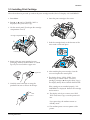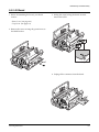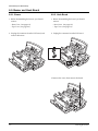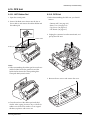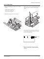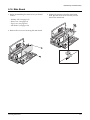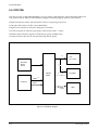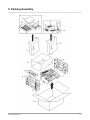
1
SAMSUNG FACSIMILE
SF3000/SF3000T
SERVICE
Manual
FACSIMILE
CONTENTS
1. Precautions
2. Specifications
3. Installation
4. Service Mode
5. Circuit Description
6. Disassembly and Reassembly
7. Troubleshooting
8. Packing Assembly
9. Electrical Parts List
10. Block Diagram,
11. Connection Diagram
12. Schematic Diagrams
1. Precautions
Follow these safety, ESD, and servicing precautions to prevent personal injury and equipment damage.
1-1. Safety Precautions
1. Be sure that all built-in protective devices are in
place. Restore any missing protective shields.
2. Make sure there are no cabinet openings through
which people- particularly children- might insert
fingers or objects and contact dangerous voltages.
3. When re-installing chassis and assemblies, be
sure to restore all protective devices, including
control knobs and compartment covers.
4. Design Alteration Warning:
Never alter or add to the mechanical or electrical
design of this equipment, such as auxiliary
connectors, etc. Such alterations and
modifications will void the manufacturerÕs
warranty.
7. Product Safety Notice:
Some electrical and mechanical parts have special
safety-related characteristics which might not be
obvious from visual inspection. These safety
features and the protection they provide could be
lost if a replacement component differs from the
original. This holds true, even though the
replacement may be rated for higher voltage,
wattage, etc.
Components critical for safety are indicated in
the parts list with symbols
. Use only
replacement components that have the same
ratings, especially for flame resistance and
dielectric specifications. A replacement part that
does not have the same safety characteristics as
the original may create shock, fire, or other safety
hazards.
5. Components, parts, and wiring that appear to
have overheated or are otherwise damaged
should be replaced with parts which meet the
original specifications. Always determine the
cause of damage or overheating, and correct any
potential hazards.
6. Observe the original lead dress, especially near
sharp edges, AC, and high voltage power
supplies. Always inspect for pinched, out-ofplace, or frayed wiring. Do not change the
spacing between components and the printed
circuit board.
Samsung Electronics
1-1
Precautions
1-2. ESD Precautions
Certain semiconductor devices can be easily
damaged by static electricity. Such components are
commonly called ÒElectrostatically Sensitive (ES)
DevicesÓ, or ESDs. Examples of typical ESDs are:
integrated circuits, some field effect transistors, and
semiconductor ÒchipÓ components.
The techniques outlined below should be followed
to help reduce the incidence of component damage
caused by static electricity.
CAUTION: Be sure no power is applied to the
chassis or circuit, and observe all other safety
precautions.
1. Immediately before handling a semiconductor
component or semiconductor-equipped assembly,
drain off any electrostatic charge on your body
by touching a known earth ground. Alternatively,
employ a commercially available wrist strap
device, which should be removed for your personal
safety reasons prior to applying power to the unit
under test.
2. After removing an electrical assembly equipped
with ESDs, place the assembly on a conductive
surface, such as aluminum or copper foil, or
conductive foam, to prevent electrostatic charge
buildup in the vicinity of the assembly.
3. Use only a grounded tip soldering iron to solder
or desolder ESDs.
4. Use only an Òanti-staticÓ solder removal device.
Some solder removal devices not classified as
Òanti-staticÓ can generate electrical charges
sufficient to damage ESDs.
5. Do not use Freon-propelled chemicals. When
sprayed, these can generate electrical charges
sufficient to damage ESDs.
6. Do not remove a replacement ESD from its
protective packaging until immediately before
installing it. Most replacement ESDs are
packaged with all leads shorted together by
conductive foam, aluminum foil, or a comparable
conductive material.
7. Immediately before removing the protective
shorting material from the leads of a replacement
ESD, touch the protective material to the chassis
or circuit assembly into which the device will be
installed.
8. Maintain continuous electrical contact between
the ESD and the assembly into which it will be
installed, until completely plugged or soldered
into the circuit.
9. Minimize bodily motions when handling
unpackaged replacement ESDs. Normal motions,
such as the brushing together of clothing fabric
and lifting oneÕs foot from a carpeted floor, can
generate static electricity sufficient to damage an
ESD.
1-3. Lithium Battery Precautions
1. Exercise caution when replacing a Lithium
battery. There could be a danger of explosion and
subsequent operator injury and/or equipment
damage if incorrectly installed.
3. Lithium batteries contain toxic substances and
should not be opened, crushed, or burned for
disposal.
2. Be sure to replace the battery with the same or
equivalent type recommended by the
manufacturer.
1-2
Samsung Electronics
2. Specification
GENERAL
Application Circuit :
PSTN or behind PABX
Mode of Operation :
Half-Duplex
Communication Mode :
ITU Group 3
Effective Scanning Width :
A4 (210 mm)
Scanning Method :
CIS
Recording Paper Size :
A4, Letter, Legal
Effective Recording Width :
8 inch (203.2 mm)
Recording Method :
Thermal Ink-Jet
ADF :
15 sheets (based on A4 /20 lbs)
Paper Capacity :
100 sheets (based on A4, 10mm)
Resolution :
Standard/Fine/Super Fine/Photo
Gray Scale :
64 levels
Contrast :
Light/Auto/Dark
Memory :
512 kbyte for EPROM, 32 kbyte for SRAM
Modem Speed :
Max. 14,400 bps
Coding Method :
MH/MR/MMR
Transmission Speed :
10 seconds (Phase C by ITU 4% Chart/Memory TX)
Back Up Battery :
3 V Lithum / non-rechargeable
Power Supply :
Check power label attached near the power cord connection.
Insulation Resistance :
50 Mohm or more (typ. 3 G at 500 V)
Dimension (W x D x H mm) :
384 x 330 x 183 mm (including ASF)
Samsung Electronics
2-1
Specification
LIU
Out Band Signal Level :
0 - 4 kHz
4 - 12 kHz
2 kHz or more
P-20 dBm or less
P-40 dBm or less
P-60 dBm or less
Input Level Range :
-5 ~ -48 dBm
Coding Format
L
H
697 Hz
770 Hz
852 Hz
941 Hz
1209 Hz
1336 Hz
1477 Hz
1
4
7
*
2
5
8
0
3
6
9
#
Frequency Tolerance : ± 1.5%
2-2
Samsung Electronics
3. Installation
3-1. Connections
3-1-1. Connection Diagram
3-1-3. Document Tray
1. Insert the two tabs on the document tray into the
slot on top of your machine.
00000000000000000
00000000
0000000
000000
AC power
cord
0000
00000000 0
Phone line cord
Extension phone (option)
(for SF3000 only)
2. Fold out the extender on the document tray, if
necessary.
3-1-2. Handset
Plug one end of the coiled cord into the jack on the
handset, the other end into the modular jack on the
left side of the machine.
Extender
Handset
Samsung Electronics
3-1
Installation
3-1-4 Document Exit Tray
3-1-6. Extension Phone (Optional)
(SF3000 only)
1. Insert the two tabs on the document exit tray into
the slots on the front of your machine.
Plug one end of the cord of your extension phone
into the TAM lead and the plug of the TAM lead
into the socket marked EXT. LINE on the back of the
machine.
00000000000000000
00000000
0000000
000000
0000
00000000 0
Document exit tray
2. Fold out the extender, if necessary.
3-1-7. AC Power Cord
Plug one end of the cord into the back of the
machine, and the other into a standard, grounded 3pin AC socket (220 - 240 V, 50 - 60 Hz).
The machine turns on and the LCD displays
ÔSYSTEM INITIAL..Õ. If there is no cartrige installed,
or no paper, the display shows ÔNO CARTRIDGEÕ
or ÔPAPER EMPTYÕ.
Extender
To turn the machine off, unplug the power cord.
3-1-5. Telephone Line
Plug one end of the telephone line cord into the
TEL. LINE jack,the other end into a standard phone
wall jack.
Note: If documents are deleted from memory due to
a power failure, the machine automatically prints
out a Power Failure report when power is reapplied.
00000000000000000
00000000
0000000
000000
0000
00000000 0
3-2
Samsung Electronics
Installation
3-1-8. Backup Battery
(SF3000T only)
1. Lift the control panel ➀ and open the cartridge
compartment cover ➁.
➁
➀
3. Insert the battery into the battery slot.
The battery maintains setup configuration and
messages when a power failure occurs or when
power is accidentally disconnected.
We recommend you use an alkaline battery
because it lasts longer than a conventional
battery.
2. Remove the old battery, if necessary.
Connect the new battery to the clips.
4. Close the cartridge compartment cover, and close
the control panel.
The battery can maintain the internal memory for
about 20 hours. If the backup battery is weak or
missing, the LCD displays a warning message.
Samsung Electronics
3-3
Installation
3-2. Loading Paper
The display shows ÔPAPER EMPTYÕ when paper is not loaded. You can load approximately 100 sheets of paper.
1. Pull the paper support on the paper bin all the
way up.
3. Squeeze the left paper guide and move it to the
right to match the width of the paper.
Paper support
Paper Guide
2. Fan and insert the paper, with the printing side
facing you.
3-4
Note: The machine is preset to load A4-size paper.
To load letter or legal-size paper, you have to
set ÔPAPER SIZEÕ option to the desired size.
Samsung Electronics
Installation
3-3. Installing Print Cartridge
When the machine is powered up without the print cartridge installed, the LCD displays ÔNO CARTRIDGE Õ.
1. Press Menu.
6. Insert the print cartridge in the carrier.
2. Press ¹ or
until Ô1.CHANGE CART.Õ is
displayed, then press Start/Copy.
3. Lift the control panel ➀, and open the cartridge
compartment cover ➁.
Cartridge compartment cover
➁
➀
7. Push the cartridge firmly in the direction of the
arrow until it clicks into place.
Control panel
4. Remove the new print cartridge from its
packaging. Hold by the black areas or colored
top only. Do not touch the copper area.
copper area
5. Carefully remove the tape covering the
printhead. Be sure to remove all the tape.
8. After installing the print cartridge, close the
cover and replace the control panel.
9. The display shows Ô:NEW :USED.Õ Press
Start/Copy to confirm ÔNEWÕ. (For used
cartridge, press ¹ or
then press Start/Copy.)
The display briefly shows ÔMONO INSTALLED.Õ
If the cartridge is not installed properly, ÔNO
CARTRIDGEÕ is displayed. Remove the cartridge
and re-insert it.
10. The display asks if you want to run a SELF
TEST. Press Start/Copy to run the printer self
test.
If you press Stop, the machine returns to
Standby mode.
11. The machine prints out a test pattern of the
printer.
Samsung Electronics
3-5
Installation
Memo
3-6
Samsung Electronics
6. Disassembly and Reassembly
6-1. General Precautions on Disassembly
When disassemble and reassembling components, use extreme caution. The close proximity of cables to moving
parts makes proper routing a must. If components are removed or replaced, any cables
disturbed by the procedure must be replaced as close as possible to their original positions. Before removing
any component from the machine, note the cable routing that will be affected.
Whenever servicing the machine, you must perform the following:
1. Check that documents are not stored in memory.
2. Remove the print cartridge.
3. Unplug the power cord.
4. Work on a flat and clean surface.
5. Replace only with authorized components.
6. Do not force plastic components.
7. Make sure all components are in their proper position.
6-2. White Roller
1. Lift the control panel.
2. Push the white clip on each end of the roller
slightly inward, then rotate it until it reaches the
slot, as shown below. Then lift the roller out.
B
Note : Check the roller for dirt. If dirty, wipe it off
with soft cloth dampened with water. If the
roller is heavily worn, replace it with a new
one.
A
white clip
White roller
Control panel
Samsung Electronics
6-1
Disassembly and Reassembly
6-3. Rear Cover
1. Holding the paper guide, move it in the direction
of arrow.
3. Holding the rear cover assÕy, take it out by
rotating it to release properly.
Paper guide
2. Remove the six screws, as shown below.
6-2
Samsung Electronics
Disassembly and Reassembly
6-4. Top Cover and Speaker
1. Before you disassemble the top cover, you should
remove:
4. Remove the four screws securing the cover.
Ð Rear Cover (see page 6-2)
2. Remove the handset, and unplug the connector
from the main board.
3. Release the tie stopper supporting the control
panel.
5. If you want to remove the speaker, turn the top
cover over, and remove the two screws securing
it.
Tie stopper
Samsung Electronics
6-3
Disassembly and Reassembly
6-5. Scan Motor
1. Before disassembling the scan motor, you should
remove:
4. Remove the ground plate.
Ð Rear Cover (see page 6-2)
Ð Top Cover (see page 6-3)
2. Unplug the motor connector from the main
board. Make sure the harness is released from the
two hooks, as shown below.
Ground plate
5. Remove the ground screw securing the motor to
the motor bracket.
3. Remove the two screws as shown below.
6-4
Samsung Electronics
Disassembly and Reassembly
6-6. ADF Roller and Contact Image Sensor (CIS)
1. Before disassembling the roller and CIS, you
should remove:
3. Unplug the CIS harness, then remove the CIS
assÕy. To remove the CIS assÕy, turn it up and
slide the two legs far left, and pull it up.
Ð Rear Cover (see page 6-2)
Ð Top Cover (see page 6-3)
2. Remove the ADF roller. When you assemble the
roller, make sure it is properly hooked.
4. Remove the CIS from the bracket.
CIS
Note : Clean the surface of the roller with ethyl
alcohol. After wiping it, you must dry it
completely.
Note: Check the glassy surface of the CIS for stains
or scratches. If stained, wipe off with ethyl
alcohol. If it is heavily scratched, replace it
with a new one.
Samsung Electronics
6-5
Disassembly and Reassembly
6-7. SMPS
1. Before disassembling the SMPS, you should
remove:
3. Remove the two ground screws from the bracket,
as shown.
Ð Rear Cover (see page 6-2)
2. Unplug the SMPS connector from the main
board. Make sure the harness is released from the
hook.
4. Pushing down the hook, as shown in the inset,
remove the SMPS.
6-6
Samsung Electronics
Disassembly and Reassembly
6-8. LIU Board
1. Before disassembling the board, you should
remove:
3. Pulling the snaps locking the board outward,
remove the board.
Ð Rear Cover (see page 6-2)
Ð Top Cover (see page 6-3)
2. Remove the screw securing the ground wires to
the SMPS bracket.
Snap fit
4. Unplug all the connectors from the board.
Samsung Electronics
6-7
Disassembly and Reassembly
6-9. Buzzer and Hook Board
6-9-1. Buzzer
6-9-2. Hook Board
1. Before disassembling the buzzer, you should
remove:
1. Before disassembling the board, you should
remove:
Ð Rear Cover (see page 6-2)
Ð Top Cover (see page 6-3)
2. Unplug the connector from the LIU board, and
remove the buzzer.
Ð Rear Cover (see page 6-2)
Ð Top Cover (see page 6-3)
2. Unplug the connector from the LIU board.
3. Remove the screw, then remove the board.
6-8
Samsung Electronics
Disassembly and Reassembly
6-10. OPE Unit
6-10-1. ADF Rubber Pad
6-10-2. OPE Unit
1. Open the control panel.
1. Before disassembling the OPE unit, you should
remove:
2. Insert a flat blade screw driver into the slot as
shown below, and remove the rubber holder and
the rubber pad.
Ð Dummy ASF (see page 6-2)
Ð Rear Cover (see page 6-2)
Ð Top Cover (see page 6-3)
Ð LIU Board (see page 6-7)
2. Unplug the connector from the main board, and
pull up the OPE unit.
Rubber holder
Rubber pad
Notes:
¥ When reassembling the rubber pad, be sure that it
and the holder fit into the guide boss and the
holder latches fit into the corresponding hole.
Then push firmly until it clicks.
3. Remove the two screws and remove the cover.
¥ Clean the surface of the rubber pad with ethyl
alcohol. After wiping, be sure to dry it. Check for
rubber wear. If the wear reaches 1/2 its original
thickness, replace it with a new one.
Samsung Electronics
6-9
Disassembly and Reassembly
4. Remove the microphone (SF3000T only) and the
seven screws.
Notes:
¥ Do not turn the OPE unit upside down after you
remove the screws securing the board. Keys and
rubber contacts may be separated and easily lost.
¥ When reassembling the OPE unit, make sure the
keys are in correct position.
¥ When reassembling the board, secure the screws
according to the order printed on the PBA.
¥ After reassembling, operate the machine to make
sure it works properly.
¥ After reassembling, make sure the LCD is not
blocked.
Microphone
(SF3000T only)
5. Remove the OPE board. Then remove the two
screws from the LCD and remove the LCD.
LCD
6-10
Samsung Electronics
Disassembly and Reassembly
6-11. Printer Unit
1. Before disassembling the printer unit, you should
remove:
3. Remove the two screws securing the printer unit,
and unplug the six connectors from the main
board.
Ð Dummy ASF (see page 6-2)
Ð Rear Cover (see page 6-2)
Ð Top Cover (see page 6-3)
2. Slide the cartridge carrier, as shown below.
The connectors are located as shown below. It is
not necessary to unplug the LF motor connector
to remove the printer unit.
LF motor
4. Remove the printer unit. When you pull up
printer unit, be careful to properly release the
harnesses.
Samsung Electronics
6-11
Disassembly and Reassembly
6-12. ASF Feeder
1. Before disassembling the ASF feeder assÕy, you
should remove:
4. Remove the screw securing the pickup shaft. To
remove the pickup shaft, pull it to the far right
and take it out.
Ð Dummy ASF (see page 6-2)
Ð Rear Cover (see page 6-2)
2. Remove the two screws securing the ASF feeder.
Pickup shaft
3. Unlock the ASF feeder assembly, and remove it.
Note : When reassembling the ASF feeder assÕy,
insure the harness for the line feed motor is
not pinched or shorted.
6-12
Samsung Electronics
Disassembly and Reassembly
6-13. Printer Unit Miscellaneous
6-13-1. Cartridge Carrier Home Assembly
6-13-2. Cartridge Carrier Assembly
1. Before disassembling the cartridge carrier home,
you should remove:
1. Before disassembling the cartridge carrier
assembly, you should remove:
Ð Dummy ASF (see page 6-2)
Ð Rear Cover (see page 6-2)
Ð Top Cover (see page 6-3)
Ð Printer Unit (see page 6-11)
2. Remove the screw securing the cartridge carrier
home, and take it out.
Ð Dummy ASF (see page 6-2)
Ð Rear Cover (see page 6-2)
Ð Top Cover (see page 6-3)
Ð Printer Unit (see page 6-11)
Ð Cartridge Carrier Home Assembly
(see page left)
Ð ASF Feeder (see page 6-12)
Ð Main Board (see page 6-15)
2. Remove the cable holder, and remove the screw
on the right side of the frame.
Carrier shaft
Carrier
Holder
Samsung Electronics
6-13
Disassembly and Reassembly
6-13-3. Base Frame Assembly
6-13-4. Feed Roller Assembly and Line
Feeder Bracket Assembly
1. Before disassembling the base frame assembly,
you should remove:
Ð Dummy ASF (see page 6-2)
Ð Rear Cover (see page 6-2)
Ð Top Cover (see page 6-3)
Ð Printer Unit (see page 6-11)
Ð Cartridge Carrier Home Assembly
(see page 6-13)
Ð Cartridge Carrier Assembly (see page 6-13)
Ð ASF Feeder (see page 6-12)
Ð Main Board (see page 6-15)
2. Remove the roller friction assemblies, then the
actuator feed.
3. Remove the base frame assembly.
1. Before disassembling the feeder roller assÕy,
and/or the line feed bracket assÕy, you should
remove:
Ð Dummy ASF (see page 6-2)
Ð Rear Cover (see page 6-2)
Ð Top Cover (see page 6-3)
Ð Printer Unit (see page 6-11)
Ð Cartridge Carrier Home Assembly
(see page 6-13)
Ð Cartridge Carrier Assembly (see page 6-13)
Ð Base Frame Assembly (see page left)
2. Remove the feed bearing from the main frame.
Pull the feeder roller in the direction of arrow,
and take it out.
Holdr Roller
Roller friction assÕy
3. Remove the two screws, then remove the feeder
bracket assembly.
Base frame assÕy
6-14
Samsung Electronics
Disassembly and Reassembly
6-14. Main Board
1. Before disassembling the main board, you should
remove:
3. Unplug all connectors from the main board.
Then, pull the sensor lever towards you and
remove the main board.
Ð Dummy ASF (see page 6-2)
Ð Rear Cover (see page 6-2)
Ð Top Cover (see page 6-3)
Ð ASF Feeder (see page 6-12)
2. Remove the two screws securing the main board.
Sensor lever
Samsung Electronics
6-15
Disassembly and Reassembly
Memo
6-16
Samsung Electronics
5. Circuit Description
5-1. General
The main circuit board consists of a Jupiter-2 Chip (KS32C6500), memory, TX- and RX-related circuitry, and
some portions of the Line interface Unit, and controls the system.
5-2. System Control Part
This circuit consists of the EP-ROM and SRAM, External Real Time Clock crystal, RTC and memory back-up,
and the Jupiter-2 Chip (KS32C6500). The Jupiter-2 Chip is an integrated 14400bps modem, image processor, 16bit MPU, peripheral control, and analog front end circuit on a single-chip.
The modem is 14400 bps half duplex. It is a monolithic device incorporating an over sampling Σ∆ AFE, digital
filters, a digital signal processor (SDIP4) and CPU-Interface logic.
5-2-1. Memory Map
The external memory of the CPU is divided into 32kB RAM (0000H through 7FFFH), 512kB ROM (FC0000H
through FFFFFFH) and 1024kB DRAM (010000H through 07FFFFH).
Reserved
CPU (Logical) Address Space
Setup
Registers
FFFFFF
ROMCSn
FC0000
MCSn
C00000
Internal
Registers
CS2n CS4n
CAS0
CS1n
800000
00FFFF
00FF00
00FE00
00FE00
00FD00
CS4n
00FC00
CS3n
00FDFF
00FDC0
00FD80
CS2n
Internal
Memory
00FD00
CAS2
00FBFF
00E000
000000
00FE80
Operational
Registers
CAS1
400000
00FEFF
00FEE0
Reserved
00FBE0
Shading Inversion 00FBD0
DBCMC Buffer 00FBC0
Dither Table
00FB80
Reserved
00E000
Figure 5-1 KS32C6500 External Memory Map
Samsung Electronics
5-1
Circuit Description
5-2-2. Jupiter-2 Chip
5-2-3. System Clock
KS32C6500 internal logic generates chip select
signals for both memory chips and peripherals. To
support external access, from one to three wait
cycles can be inserted under program control during
external accesses. A chip select signal line goes
active (low) whenever its corresponding device is
accessed over the external interface. The peripheral
addresses are located in data memory.
The 30 MHz internal system clock frequency is
supplied by an external clock generator.
/SRAMCS : SRAM chip select active (low)
/ ROMCS : EP-ROM chip select active (low)
D0ÐD15 : 16 bit data bus
A0ÐA17 : address bus
SDIP4
TAD PART
CONTROL
A0~A5
D0~D15
D0~D7
ONLY SF3000T
XIN
XOUT
OPERATING
PANEL
SERIAL
COMMUNICATION
TXD
RTC
CRYSTAL
(32, 768KHZ)
/DMS
RXD
/RD/WR
D0~D7
A0~A14
DATA
MEMORY
(SRAM)
KS32C6500
/RASO~
/UCAS
/LCAS
HEAD
DRIVER
PHINA~D
DRAM.
(USER MEMORY)
/RD
D0~D15
A0~A17
/A16
PROGRAM
MEMORY
(EPROM)
/PMS
/RD/WR
MOTOR
CONTROL
D0~D7
+24
MODEM
A0~A4
DRIVER
(CR, LF
MOTOR)
/RESET
/RESTO
GENERAL
PURPOSE I/ 0
Figure 5-2 Hardware Interface Signals
5-2
Samsung Electronics
Circuit Description
5-2-4. Real Time Clock (RTC)
The circuit receives clock pulses from an external 32.768 kHz crystal, which it divides into hours, minutes,
seconds, year, month, and day. A battery maintains operation when power is off. KS32C6500 can up-track 100
years, begining with 1998.
32.768 KHz
1HZ
15 BIT
PRESCALER
BUSY FLAG CLEAR
CO=60
6 BIT
6 BIT
SECONDS
MINUTES
BUSY
DETECT
5 BIT
DAYS
CO=28,29,
30,or 31
CO=60
5 BIT
HOURS
CO=24
BUSY FLAG
4 BIT
MONTHS
CO=12
5 BIT
YEARS
MONTH
DECODER
LEAP YEAR
DECODER
3 STATE
DRIVER
Figure 5-3 RTC Block Diagram
5-2-5. Operation Panel Control
A Synchronous/Asynchronous Receiver/Transmitter (SART) controls serial data transmission between the
main circuit and the operator panel.
JUPITER - 2
CPU Bus
SclkCtrlLo
SclkCtrlHi
Baud Gen (8x)
Tx/Rx Control
IRQ control
SARTCmd
SartlRQ
SCLK
RxShift Reg
RXD
(SARTData)
RxBuffer
(SARTData)
TxShiftReg
TXD
Internal Register
Figure 5-4 SART Block Diagram
5-2-6. Serial Communication Signals
The KS32C6500 has two full-duplex serial communication ports. One port is used for I-LIU communication,
and the other for OPE communication.
Samsung Electronics
5-3
Circuit Description
5-2-7. Reset
5-2-9. Line Feed Motor Driver
To initialize the chipÕs internal logic, the reset input
(/RESET) must be held to 0 Volt for at least 22 CPU
clocks. During this time, Vdd must be greater than 3
volt. The watchdog timer can also invoke a system
reset.
The LF motor feeds paper in and out.
Motor type : Step Unipolar
Operation Voltage : +24V DC
Holding Voltage : +5V DC
Resistance : 50 ohm ±10%
IC : STA471A
[+5V Power Monitoring]
If 5 Volt power to KIA7045P drops to between 4.65V
and 4.35V (typically 4.5V), power failure will be
indicated and the output of KIA7045P will go ÔlowÕ
(GND5). This causes the KS16118 to become active
(ÔlowÕ=reset).
5-2-10. Head Nozzle Driver
The KS32C6500 reset causes the /RESET terminal to
be reset. The output terminal of KIA7045P is an
open-drain configuration, and is connected to
KS32C6500 through a 10 kohm pull-up resistor.
The nozzle control circuit is composed as follows:
Number of nozzle : 56 nozzles for mono
Driving Voltage : +24V DC +/-2%
Driving Pulse Width : 3.6 us for mono
Operation Frequency : 5 kHz
Resistance : 30 ohm for mono
IC : SGS Thomson L6451 or Allegro A5817
5-2-8. Carriage Return Motor Driver
The IC decodes four input signals (PHINA, PHINB,
PHINC, PHIND) and enables the selected using
OEA and OEB signal input.
The CR motor drives the head in two directions to
print data on the recording paper.
Motor type : Step Bipolar
Operation Voltage : +24V DC
Resistance : 5 ohm +/-10%
IC : PBL3717 x2EA
STEP MOTOR DRIVER OUTPUT SIGNAL
Standby
Full Step
CRIAO
CRIA 1
PHA
INPUT
PHB
CRIBO
CRIB 1
500mA
IND
INC
INB
INA
N
0
0
0
0
0
0
0
0
1
1
1
1
1
1
1
1
0
0
0
0
1
1
1
1
0
0
0
0
1
1
1
1
0
0
1
1
0
0
1
1
0
0
1
1
0
0
1
1
0
1
0
1
0
1
0
1
0
1
0
1
0
1
0
1
0
1
2
3
4
5
6
7
8
9
10
11
12
13
ALL OFF
ALL OFF
IMA
Table 5-1 Nozzle Driver Signal
-500mA
OUTPUT
500mA
IMB
-500mA
Figure 5-5 Step Motor Drive
5-4
Samsung Electronics
Circuit Description
5-2-11. Jupiter-2 (KS32C6500) Pin Layout Diagram
P
H
A
D
R
1
2
P
H
V
A
D
D
D
R R R R
1 X X T
3 O I C
160
PHADR11
PHADR10
PHADR9
PHADR8
PHADR7
PHADR6
PHADR5
PHADR4/ PHIND
PHADR3/ PHINC
PHADR2/ PHINB
PHADR1/ PHINA
GND1
HOE16/HOED?
HOE15/HOEC?
HOE14/HOEB?
HOE13/HOEA?
HOE12
HOE11
HOE10
HOE9
VDD1
HOE8
HOE7
HOE6
HOE5
HOE4
HOE3
HOE2
HOE1
GND2
GOP12/nHSM
DC_CRIA0
??????????
DC_CRIA1
CRIB0
??????????
CRIB1
PORT0
PORT1
PORT2
G
O
P
7
/
n
I
O
R
D
1
G
O
P
6
/
n
I
O
W
R
2
G
O
P
1
1
/
n
H
S
C
G
O
P
1
0
/
F
I
R
E
P
U
L
S
E
G
O
P
9
/
C
L
K
O
U
T
155
G
O
P
8
/
n
I
O
R
D
2
G
O
P
4
/
n
R
S
T
O
G
O
P
3
/
T
O
N
E
G
N
D
9
P
H
E B
E E Z
E D
C A I
L T B
K A 0
150
L
F
P
H
A
S
E
B
P
P H
H A
B Z
I I
B A
0 1
145
G G
O O
L
P P
F
2 4
C P / /
O H n n
N A E E
D D
P I A R
H A C E
A 1 K Q
G
O
P
3
/
n
E
I
N
T
2
140
G
O
P
2
/
n
E
I
N
T
1
V
D
D
5
G
O
P
5
/
n
I
O
W
R
1
G
N
D
8
M
C
L
K
135
G
N
D
7
n
R
E
S
E
T
C
L
K
S
E
L
G
I
P
5
/
U
C
L
K
T
E
S
T
2
130
T
E
S
T
1
G
I
P
1
/
R
X
D
2
G
I
P
1
/
R
X
D
2
G
I
P
0
/
R
X
D
1
G
I
P
0
/
R
X
D
1
125
120
1
5
115
10
110
15
105
KS32C6500
20
25
100
160 QFP
95
(Top View)
30
90
35
85
40
50
45
P
O
R
T
3
P
O
R
T
4
n
F
A
U
L
T
P
E
R
R
O
R
B
U
S
Y
n
A
C
K
S
E
L
E
C
T
n
I
N
I
T
n
S
L
C
T
I
N
n
A
U
T
O
F
D
55
n
S
T
R
O
B
E
G
N
D
3
P
P
D
7
P
P
D
6
P
P
D
5
60
P
P
D
4
P
P
D
3
P
P
D
2
P
P
D
1
P
P
D
0
65
2
4
5
C
L
K
V
D
D
2
D
A
T
A
0
D
A
T
A
1
D
A
T
A
2
70
D
A
T
A
3
D
A
T
A
4
D
A
T
A
5
D
A
T
A
6
D
A
T
A
7
75
G
N
D
4
D
A
T
A
8
D
A
T
A
9
D
A
T
A
1
0
D
A
T
A
1
1
nECS3
nECS2
nECS1
nECS0
nWBE1
nWBE0
GND6
nWE
nOE
nCAS1
nCAS0
nRAS1
nRAS0
nRCS2
nRCS1
nRCS0
VDD4
VDDR21
VDDR20
VDDR19
VDDR18
VDDR17
VDDR16
VDDR15
VDDR14
VDDR13
VDDR12
VDDR11
GND5
VDDR10
VDDR9
VDDR8
VDDR7
VDDR6
VDDR5
VDDR4
VDDR3
VDDR2
VDDR1
VDDR0
80
D
A
T
A
1
2
D
A
T
A
1
3
D
A
T
A
1
4
D
A
T
A
1
5
V
D
D
3
Figure 5-6 Pin Layout Diagram
Samsung Electronics
5-5
Circuit Description
5-2-12. Jupiter-2 ASIC(KS32C6500) Pin Description
Pin No.
KS32C6500
ATLAS used pin
1
2
3
4
5
6
7
8
9
10
11
12
13
14
15
16
17
18
19
20
21
22
23
24
25
26
27
28
29
30
31
32
33
34
35
36
37
38
39
40
41
42
43
_PHGA11
_PHGA10
_PHGA9
_PHGA8
_PHGA7
_PHGA6
_PHGA5
_PHGA4
_PHGA3
_PHGA2
_PHGA1
GND1
PHOE16
PHOE15
PHOE14
PHOE13
PHOE12
PHOE11
PHOE10
PHOE9
VDD1
PHOE8
PHOE7
PHOE6
PHOE5
PHOE4
PHOE3
PHOE2
PHOE1
GND2
GOP12
DC_CRIA0
CRPHA/CHX
DC_CRI41
CRIB0
CRPHB/CHY
CRIB1
GPIO0
GPIO1
GPIO2
GPIO3
GPIO4
_FAULT
NOT-USED
NOT-USED
NOT-USED
NOT-USED
NOT-USED
NOT-USED
NOT-USED
PHIND
PHINC
PHINB
PHINA
GND1
_HOED
_HOEC
_HOEB
_HOEA
NOT-USED
NOT-USED
NOT-USED
NOT-USED
VDD1
NOT-USED
NOT-USED
NOT-USED
NOT-USED
NOT-USED
NOT-USED
NOT-USED
NOT-USED
GND2
GOP12
CRIA0
CRPHA
CRIA1
CRIB0
CRPHB
CRIB1
GPIO0
GPIO1
GPIO2
GPIO3
GPIO4
NOT-USED
5-6
Pin Description
INK NOZZLE ENABLE CONTROL SIGINAL
INK NOZZLE ENABLE CONTROL SIGINAL
INK NOZZLE ENABLE CONTROL SIGINAL
INK NOZZLE ENABLE CONTROL SIGINAL
INK NOZZLE DECODING SIGNAL
INK NOZZLE DECODING SIGNAL
INK NOZZLE DECODING SIGNAL
INK NOZZLE DECODING SIGNAL
TX CONTROL
CRPHA, CRPAB: PHASE A, B DIRECTION
CONTROL SIGNAL
CRIA, CRIB: PHASE A, B CURRENT CONTROL
SIGNAL
L L : HIGH
H L : MEDIUM
L H : LOW
H H : NO
Samsung Electronics
Circuit Description
Pin No.
44
45
46
47
48
49
50
51
52
53
54
55
56
57
58
59
60
61
62
63
64
65
66
67
69
69
70
71
72
73
74
75
76
77
78
79
80
81
82
83
84
85
86
87
89
89
KS32C6500
PERROR
BUSY
_ACK
SELECT
_INT
_SLCTIN
_AUTOFD
_STROBE
GND3
PPD7
PPD6
PPD5
PPD4
PPD3
PPD2
PPD1
PPD0
245DIR
VDD2
D0
D1
D2
D3
D4
D5
D6
D7
GND4
D8
D9
D10
D11
D12
D13
D14
D15
VDD3
A0
A1
A2
A3
A4
A5
A6
A7
A8
Samsung Electronics
ATLAS used pin
Pin Description
NOT-USED
NOT-USED
NOT-USED
NOT-USED
NOT-USED
NOT-USED
NOT-USED
NOT-USED
GND3
NOT-USED
NOT-USED
NOT-USED
NOT-USED
NOT-USED
NOT-USED
NOT-USED
NOT-USED
NOT-USED
VDD2
D0
D1
D2
D3
D4
D5
D6
D7
GND4
D8
D9
D10
D11
D12
D13
D14
D15
VDD3
A0
A1
A2
A3
A4
A5
A6
A7
A8
5-7
Circuit Description
Pin No.
90
91
92
93
94
95
96
97
98
99
100
101
102
103
104
105
106
107
108
109
110
111
112
113
114
115
116
117
118
119
120
121
122
123
124
125
126
127
128
129
130
131
132
133
134
135
5-8
KS32C6500
A9
A10
GND5
A11
A12
A13
A14
A15
A16
A17
A18
A19
A20
A21
VDD4
_RCS0
_RCS1
_RCS2
_RAS0
_RAS1
_CAS0
_CAS1
_OE
_WE
GND6
_WBE0
_WBE1
_ECS0
_ECS1
_ECS2
_ECS3
GOP0
GIP0
GOP1
GIP1
TEST1
TEST2
CHIP5
CLKSEL
_RESET
GND7
MCLK
GND8
GOP5
VDD5
GIP2
ATLAS used pin
A9
A10
GND5
A11
A12
A13
A14
A15
A16
A17
A18
A19
A20
A21
VDD4
_RCS0
NOT-USED
_RCS2
_RAS0
NOT-USED
_CAS0
_CAS1
_OE
_WE
GND6
_WBE0
NOT-USED
_ECS0
_ECS1
_ECS2
NOT-USED
GOP0
GIP0
GOP1
GIP1
TEST1
TEST2
CHIP5
CLKSEL
_RESET
GND7
MCLK
GND8
GOP5
VDD5
GIP2
Pin Description
PROGRAM ROM CHIP SELECT
FONT ROM CHIP SELECT
SRAM CHIP SELECT
DRAM ROW ADDRESS STROBE (DEFAULT)
DRAM ROW ADDRESS STROBE (OPTION)
DRAM LOWER COLUMN ADDRESS STROBE
DRAM UPPER COLUMN ADDRESS STROBE
MEMORY OUTPUT ENABLE
MEMORY WRITE ENABLE
WRITE BYTE ENABLE
WRITE BYTE ENABLE
MODEM CHIP SELECT
DSP CHIP SELECT
SDIP4 CHIP SELECT
LIU TXD
LIU RXD
OPE TXD
OPE RXD
NORMAL MODE: GND
DEBUG MODE: VCC
HEAD CHECK
MASTER CLK SELECT: H
SYSTEM RESET
MASTER CLK (30MHZ)
RX CONTROL
_MODEM INTERRUPT REQUEST
Samsung Electronics
Circuit Description
Pin No.
136
137
138
139
140
141
142
143
144
145
146
147
148
149
150
151
152
153
154
155
156
157
158
159
160
KS32C6500
GIP3
GIP4
GOP2
LFIA0
LFPHA
LFIA1
LFIB0
LFPHB
LFIB1
EEDATA
EECLK
GND9
GOP3
GOP4
GOP8
GOP9
GOP10
GOP11
GOP6
GOP7
VDDRTC
RXI
RXO
_PHGA13
_PHGA12
ATLAS used pin
GIP3
GIP4
GOP2
LFIA0
LFEN
LFIA1
LFIB0
NOT-USED
LFIB1
NOT-USED
NOT-USED
GND9
GOP3
GOP4
NOT-USED
GOP9
GOP10
NOT-USED
NOT-USED
NOT-USED
VDDRTC
RXI
RXO
NOT-USED
NOT-USED
Pin Description
TX INT
_XDREQ (SDIP4)
_XDACK (SDIP4)
LF MOTOR PHASE CONTROL
LF MOTOR ENABLE
LF MOTOR PHASE CONTROL
LF MOTOR PHASE CONTROL
LF MOTOR PHASE CONTROL
KEY CLICK
POR CONTROL
SDIP4 CLK (30MHZ)
_RESET OUT
RTC BACK-UP
RTC CLK IN
RTC CLK OUT
5-3. Memory
System memory consists of 512 kB ROM, 32 kB SRAM and 1024 kB DRAM. All of SRAM is backed up. ROM
and SRAM are selected by chip select lines, and data is accessed by the units position of the byte.
5V power is applied to SRAM through VSB. This facsimile machine uses a Lithium battery for memory backup.
A, 820 ohm resistor in series with the positive battery terminal is for battery protection.
5-4. Modem and TX- and RX- Related Circuits
These circuits control transmission between the internal MODEM and the LIU or a remote MODEM.
The KS16117 is a single-chip fax-MODEM having features to detect and generate DTMF tones. TX OUT is the
MODEM output port, and RX IN is the input port. /PORI is the Jupiter-2 signal which enables MODEM
initialization at system power on. D0 - D7 are data buses. RS0 - RS4 are internal register select signals which
determine the mode. /CS is the chip select signal, and /RD /WR are the read and write control signals. RLSD
is used for v.24 interface-related signals and /IRQ is the MODEM interrupt.
Samsung Electronics
5-9
Circuit Description
5-4-1. Transmit Circuit
5-4-2. Receive Circuit
This circuitry controls transmission of analog signals
from the MODEM. Output voltage from the
MODEM is buffered through the LIU board and OP
amp after signal smoothing and filtering, and finally
output to the line.
In receive mode, analog signals from the LIU board
are transferred to RX IN through the BPF and
smoothing filter.
5-5. Image Processor / Motor Driver (SDIP4)
¥Scan driver generates the control signals to acquire the document data from the scanner and to operate the
Image Processor.
¥Motor driver generates the control signals to drive the Tx-Motor according to programmed motor speed.
ADDR-BUS
DATA MEMORY
DMA Controller
DATA-BUS
CLK_NINE
CLK_PIX
LINE_PERIOD
AGC_PERIOD
ADDR-BUS
CPU
SCAN/ MOTOR
DRIVER
DATA-BUS
ADSAMPLE
T
R
D
M
A
T
R
D
M
A
A
C
K
E
Q
R
IMAGE
PROCESSOR
B-BIT
HALF FLASH ADC
VIDEO SIGNAL
(analog)
SI
CLKI
CLKI_
ΦR
SCANNER
Tx_A_Tx_B_Tx_A_Tx_B_
[SDIP4]
DOCUMENT IMAGE
Figure 5-7 Block Diagram of Scanner Control Function
5-10
Samsung Electronics
Circuit Description
HARDWARE BLOCK DIAGRAM
A/D data[7:0]
CPU - Data Bus[15:0]
CPU - Addr Bus[26:0]
CPU - read
CPU - write
IP_CS_
Initial Data[7.0]
Half-Tone enable
Edge-Strength
ERM-Mode
CPU
I/F
MODULE
(Register Files)
Vpeak_IN[7:0]
Vpeak_OUT[7:0]
AGC MODULE
(A/D, D/A I/F)
Gamma Corrected Value[7:0]
[IMAGE - PROCESSOR]
Shading Factor[7:0]
SHADING
CORRECTION
MODULE
Shade Corrected Value[7:0]
GAMMA
CORRECTION
MODULE
Gamma Corrected Value[7:0]
ERM_Data[7:0]
DECIMATION/
INTERPOLATION
MODULE
EDGEENHANCEMENT
/EMPHASIS
MODULE
Edge_Data[7:0]
Error-Diffused Data[7:0]
Image Data
Memory
I/F
MODULE
BINARY Decision &
Output
MODULE
RAM - Data Bus[7:0]
RAM - Addr Bus[14:0]
RAM _read_
RAM _write_
Tr_DMA_request
Tr_DMA_acknowledge
pclk
pdata
5-11
Samsung Electronics
ERRORDIFFUSION
MODULE
Figure 5-8 Hardware Block Diagram of Image Processor
Circuit Description
5-5-2. Image Sensor
This shading wave is formed by scanning the white roller prior to a document. The slice level is determined by
the shading wave, and compensates for shading distortion according to the CIS characteristics. The wave
format from the CIS is converted into a 6 bit digital value in the SDIP4 image processor, and then processed in
B/W or intermediate mode.
5-5-3. CIS Driver
500 KHZ (L:DUTY 75%)
CLOCK
The CIS driver clock (CLK) frequency is 500
kHz. A low duty cycle of 75% is used to
lengthen the charging time. A start signal (SI) is
provided every 5 ms to match the line scanning
time. Actual image signal (VIN) is provided in
less than 3.4 ms, using the 500 kHz clock,
taking A4 paper size into consideration.
SI
SIG
1 LINE
Figure 5-9 CIS Diver Clock Timing
5-5-4. Sensor Detection Circuit
PE SENSOR 1,2
This sensor detects whether paper is loaded in the automatic sheet feeder. If no paper is detected, the output
signal turns high. While paper is feeding to print, the output turns low.
HOME DETECTION CIRCUIT
This circuit detects whether the head is in home position. When power turns on and head is capped, the circuit
is activated. If the head is in the home position, the output turns high.
5-5-5. Scan Motor Controller
The SF3000/SF3000T model facsimile machines perform their send function utilising a single 24 volt motor.
This motor has a winding resistance of 120 ohms. Three drive strobe pulses are used to operate the motor.
5-12
Motor Function
Drive Strobe Pulse
Phase
Document Feed In/Out
400 pps
1-2 phase
Fine Copy/Tx
400 pps
1-2 phase
Super Fine Tx
400 pps
1-2 phase
Samsung Electronics
Circuit Description
5-5-6. SDIP4 Pin Layout Diagram
109
110
111
112
113
114
115
116
117
118
119
120
121
122
123
124
125
126
127
128
129
130
131
132
133
134
135
136
137
138
139
140
141
142
143
144
VDD
VSS
GPI6
GPIO10
GPIO11
GPO6
Tx_A
Tx_B
VSS
Tx_A
Tx_B
VSS
Tx_en1
Tx_en2
Tx_int
VSS
/RESET
D15
D14
CLKI
GPIO14
/CLK
GPIO15
/SH
GPO7
ADCCLK
VSS
/WR
/RD
VDD
VSS
A5
A4
A3
A2
VSS
A1
A0
IPCS_
VSS
GPO5
GPI5
VSS
VSSA
VDDA
VREFDAC
VREFADC
ADCIN
D13
D12
VDD
VSS
D11
D10
D9
D8
VDD
VSS
D7
D6
D5
D4
VSS
GPO4
GPIO9
GPIO8
GPI4
VDD
VSS
AA14
AA13
AA12
SDIP4
144-QFP
VSS
D3
D2
VSS
D1
D0
VDD
VSS
GPI0
GPIO0
GPIO1
GPO0
VSS
AA11
AA10
AA9
AA8
VDD
VSS
AA7
AA6
AA5
AA4
VDD
VSS
GPI1
GPIO2
GPIO3
GPO1
VSS
VDD
VSS
AA3
AA2
AA1
AA0
108
107
106
105
104
103
102
101
100
99
98
97
96
95
94
93
92
91
90
89
88
87
86
85
84
83
82
81
80
79
78
77
76
75
74
73
VSS
DD0
DD1
DD2
VSS
VDD
GPI7
GPIO12
VSS
GPIO13
VSS
VDD
GPO2
GPIO5
GPIO4
GPI2
VSS
XCLK
VSS
VDD
VDD
VSS
DD3
DD4
DD5
DD6
DD7
VSS
VDD
/RAMWR
VSS
/RAMRD
GPO3
GPIO7
GPIO6
GPI3
1
2
3
4
5
6
7
8
9
10
11
12
13
14
15
16
17
18
19
20
21
22
23
24
25
26
27
28
29
30
31
32
33
34
35
36
72
71
70
69
68
67
66
65
64
63
62
61
60
59
58
57
56
55
54
53
52
51
50
49
48
47
46
45
44
43
42
41
40
39
38
37
Figure 5-10 Pin Lay out Diagram
Samsung Electronics
5-13
Circuit Description
5-5-7. SDIP4 ASIC Pin Description
Name
Type
RESET
I
Power on reset pin.
A[5:0]
I
CPU interface address bus.
D[15:0}
B
CPU interface data bus.
WR
I
CPU interface write signal pin.
RD
I
CPU interface read signal pin.
IPCS
I
CPU interface chip select signal pin.
XP
I
System clock input pin.
AIN
I
Sensor image signal input pin.
Ør
O
CCD charge clear signal pin.
SI
O
CCD/CIS line clear signal pin.
CLK1
O
Sensor Drive signal output pin.
CLK2
O
DREQ
O
DMA data request signal output pin.
active : H
DACK
I
DMA data acknowiedge output pin.
active : L
RAM_RD
O
IP-SRAM read signal pin.
RAM_WR
O
IP-SRAM write signal pin.
RAM_addr[14:0]
O
IP-SRAM address bus.
RAM_data[7:0]
O
IP-SRAM data bus.
Tx_A
O
Tx_B
O
Tx_A
O
Tx_B
O
Tx_en1
O
Tx_en2
O
Tx_int
O
Motor drive interrupt pin.
GPI[7:0]
I
General purpose input pins.
GPO[7:0]
O
General purpose output pins.
GPIO[7:0]
B
General purpose input/output pins.
5-14
Description
active : L
Motor drive signal pins.
Samsung Electronics
Circuit Description
5-6. TAD (SF3000T Only)
TAD circuit consists of a voice coprocessor to record and play voice messages in voice memory.
5-6-1. Recording path
5-6-3. Line input and play path
R62 provides power to the condenser microphone.
Voice signal from the microphone is passed through
active filter U22, R60 and C51, R58, C48 to clear
aliasing noise occuring while sampling and
amplifying the signal. Q5 and Q4 compose ALC
(Automatic Level Control) circuit. CODEC (U29)
converts the voice signal to digital and converts the
digital signal from voice coprocessor into analog for
line output.
Incoming signals from line are stored in the voice
memory (4Mb DRAM) through CODEC and DSPG
DRAM controller. When played, DSPG processes
the data stored in voice memory and sends it out to
LIU through CODEC and R93. To playback through
the speaker, DSPG sends the signal to speaker
through R93, MUX (U25, U26), and op amp.
5-6-4. DSPG
5-6-2. Mic input path
Transmit path functions as MIC input path.
Outgoing messages and memo messages from
CODEC are stored in the voice memory (4Mb
DRAM) through the DSPG DRAM controller.
This circuit consists of Host Interface, Memory
Interface, CODEC Interface, and DSP core. Host
Interface sends and receives data to and from IFC.
Memory Interface sends and receives the
compressed voice data to and from DRAM to play
back and record voice data. DSP core communicates
with host IFC through Host Interface.
5-6-5. Voice backup
+5V is supplied for voice memory through VBT
when power is on. When power is off, +5V is
supplied from the 9V backup battery.
Samsung Electronics
5-15
Circuit Description
5-7. LIU PBA
The LIU (Line Interface Unit) interfaces the MODEM and telephone to the telephone line. The FAX and
telephone portions of the LIU are active with machine power on. When machine power is off, only the
telephone circuity operates, powered by telephone line voltage. The FAX portion of LIU consists of the interface
between MODEM and telephone line, and the circuits for DC loop feeding, DP signal, loop current and ring
detect. The telephone portion is divided into ringer, dialling and speech circuits. Refer to the schematic and
connection diagram sections of this manual.
5-7-1. FAX section
MODEM/LINE INTERFACE
RING DETECT
Following is the path for data and remote control
signals:
¥ U1 pin 28 (MO) is ring melody output port and
this signal drives FET3 which drive Photo coupler
U4 for artificial ring.
¥ CML1 relay: Switches telephone line between FAX
and telephone circuits.
¥ U1 pin 3TIT: Single ended input for transformer
(T2)
TIT: Transformer Input from Transformer
¥ U1 pin 40 ROT: Output for driving transformer
(T3) with an AC impedance greater than 10 Kohm.
ROT: Receive Output Transformer
¥ C57: DTMF and CNG detect path to T1 20Kohm
winding under idle conditions, and DC blocking
for 20Kohm winding.
¥ AC impedance: The AC impedance of U1 (I-LIU)
is set to 1000 ohm by external capacitor (C32) at
U1 pin 8 CI (Complex Impedance Input) port.
With the external resistor (R38) at U1 pin 34 ACI
port, it can be programmed to 600ohm. U1 pin 35
CS (Current Shunt control output) port is an
N-channel open drain output to control the
external high power shunt transistor for
synthesizing AC and DC impedance.
¥ DC conditions: The normal operating mode is
from 15mA to 100mA. An operating mode with
reduced performance is from 5mA to 15mA. In the
line hold range from 0mA to 5mA, the device is in
a power down mode and the voltage at U1 pin 37
LI (Line Input) port is reduced to a maximum of
3.5V. The DC characteristic is determined by the
voltage at U1 pin 37 LI port and R45 resistor
between U1 pin 37 LI and pin 39 LS port. It can be
calculated by the following equation: VLS = VLI +
ILINE X 45.
5-16
MF DIAL (Same as telephone section)
¥ U1 pin 2 DMS (Dial Mode Selection) port is set to
VDD by R46. It has M/B ratio of 33:66, and in no
power operation mode operates only DP.
¥ MF signal appears (tone level of low group:
typical - 14 dBm) at U1 pin 4 MFO (DTMF
Generator Output). This signal is leveled by R32,
R28 and C29, then to amplier U1 pin 9 MFI
(DTMF Amplier Input).
¥ Line dial signals appear at U1 pin 39 LS (Line
Current Sense Input).
DP DIAL (Same as telephone section)
¥ U1 pin 2 (DMS) is set to Vdd (33/66) or VSS
(40/60) by R46 or R52 resistor.
¥ Dial pulses originate at U1 pin 27 (DPN), which
toggles Q5, which drives Q2. The resulting
intermittent voltage interrupts the telephone line.
¥ Pulse M/B ratio is set by U1 pin 2 DMS port.
Vdd = 33/66, and Vss = 40/60.
¥ U1 pin 35 CS port: Modulation of line voltage and
shorting the line during make period of pulse
dialling.
Samsung Electronics
Circuit Description
LLC (Line Loss Compensation) LOOP
CURRENT DETECT
¥ The LLC is a pin option. When it is activated, the
transmit and receive gains for both I/O are
decreased by 6dB at line currents from 20mA
when the U1 pin 31 LLC is connected to AGND,
from 75mA when this pin is connected to VDD.
The LLC is deactivated when LLC pin is
connected VSS.
¥ When the CML1 relay or Hook Switch switches to
telephone line, the U1 in the LIU board and CPU
(U1) in the Main board srart communication. The
U1 send <Ack> message contains the line current
information. Using this line current information
Main CPU can recognize a parallel phone.
SERIAL INTERFACE
¥ U1 pin 11 RXD: Schmitt trigger input (treshold =
2.5V) to serial interface.
¥ U1 pin 29 TXD: Open drain output from serial
interface.
¥ The communication principle is derived from a
standard UART:
Baud Rate 9600
Start Bit 1
Stop Bit 1
Data Bits 8
Parity Bit None
LSB is transferred prior to MSB.
¥ Line ring voltage passes through bridge diode
BD1, CML relay and Hook Switch to FET3 (BS170)
pin 3, C21, R19.
¥ The ring frequency discriminator of U1 assures
that only signals with a frequency between 13Hz
and 70Hz are regarded as valid ring signals.
¥ When a valid ring signal is present for 73ms
continuously, the ring melody generator (pin 28,
MO) is activated and remains active as long as a
valid ring signal is present.
¥ U1 filters the ring signals and output is pin 28
(MO).
¥ The 3 basic melody frequencies are : F1 = 880 Hz,
F2 = 1067 Hz and F3 = 1333 Hz. The repetition
rate is set to 4 which means that the sequence of
F1, F2, F3, F1, F2, F3 is repeated 4 times within a
second.
SPEECH CIRCUIT
¥ U1 (STI9510) and associated components.
¥ Handset transmitting circuit. Condensor MIC of
handset is filtered by R25, C28, C27, C20, C19,
C24, C22 and C30, and then amplified by U1 pin
32 and 33 (M1, M2)
¥ Handset receiving circuit. Receiving (Dynamic
unit) of handset is filtered by R49, C45, C40, C44
and C23, and then applied by U1 pin 1 (ROH) and
VSS.
¥ U1 pin 39 (LS) is audio output to telephone line.
5-7-2. Telephone Section
RINGER CIRCUIT
¥ When a ringing signal is applied to the line, Vdd
of U1 (I-LIU) is charged up via an external path.
After Vdd has reached the operating voltage the
oscillator starts and U1 discriminates the ring
frequency.
After a valid ring frequency is applied to the U1
pin 25 RFD (Ring Frequency Discrimination) port,
the ring melody generator of U1 sends out a 3tone melody via the U1 pin 28 MO (Ring Melody
Output)port.
¥ U1: I-LIU and associated components.
¥ Ring frequency passes through DC blocking
capacitor C3 or C4 (for Switzerland or Austria)
and Zener-diode ZD2 or ZD3 (for Switzerland or
Austria) to U1 pin 25 RED port.
Samsung Electronics
SIDETONE CIRCUIT
¥ Sidetone audio characteristics are controlled by
R37, R51, R5, R26, and C41 connected to U1 pin 7
STB.
5-17
Circuit Description
5-8. OPE PBA
OPE PBA consists of U300 (MICOM Z8601), LCD, key matrix, LED indicators, and the document detect and
scan position sensors. Refer to OPE Schematic Diagram and Wiring Diagram sections of this manual.
¥Signals from the key matrix and delivered to U300 X/Y input pin group (P1-X).
¥U300 pin 4 (RX DATA) is UART code to MAIN PBA.
¥Display from controller is received at U300 pin 5 (TX DATA).
¥LCD drive signals are U300 P2-X pin group, connector pin P303-1 ~ P303-3.
¥Machine status LED drive signals are U300 P01 pin group. (SF3000T only)
¥Connector P302 is NPO (No Power Operation) key matrix output.
11
Document
Detect
Sensor
LCD
16 x 1 lines
7
X
MICOM
Z-8601
Y
8
Key Matrix
UART 2
Connector
Reset
1 (SF3000T
Only)
LEDs
Figure 5-11 OPE Block Diagram
5-18
Samsung Electronics
7. Troubleshooting
7-1. Overall Troubleshooting Flow
START
Power Supply
OK?
Plug the power cord
Y
System
initialized?
N
N
See 7-3
See 7-2
Load document
in Feeder
Document fed?
Y
CIS on?
Press START Key
N
Y
Call machine from
another phone
N
RX OK ?
N
See 7-9
See 7-5
Auto Answer
OK ?
Y
N
See 7-6
Lift Handset off
hook
Dial tone OK ?
N
See 7-10
Y
RX OK?
N
See 7-7
Y
Y
N
See 7-4
Copy OK?
Y
See 7-8
Y
TX OK ?
Y
N
See 7-11
END
Samsung Electronics
7-1
Troubleshooting
7-2. Check Power Supply
Power cord
connected?
START
Y
Check AC
socketvoltage
220 ~ 240 VAC?
N
N
Connect as required
Check
Power Cord
Continuity
N
Replace Cord
Y
Y
Fuse OK?
N
Replace Fuse
Notify customer
END
Y
Q1 OK ?
N
Replace Q1
Y
Y
R8 Short ?
N
END
Remove short
7-2
Samsung Electronics
Troubleshooting
7-2-1. No +5 V
START
N
Output Shorted ?
Y
Y
Check U2 Input
voltage
Replace D4
Y
Check U2 ?
N
N
Y
Remove short
DC 6 V
D2 Open or
Shorted ?
Check CON1
END
N
Replace U2
Check PCB Pattern
7-2-2. No -12 V
output shorted ?
START
N
D3 Open or
Shorted ?
Y
N
Check PCB Pattern
Samsung Electronics
Y
Check U3 Input
voltage
Y
Replace D3
Remove short
-15 VDC
N
U1 Output ?
Y
Check CON1
END
N
Replace U4
7-3
Troubleshooting
7-2-3. No +24 V
output shorted ?
START
N
D4 Open or
Shorted ?
Y
N
Check PCB Pattern
7-4
Y
Check L1 Input
voltage
Y
Replace D4
Remove short
DC 24V
N
Check ED3 ?
Y
Check CON1
END
N
Replace ED3
Samsung Electronics
Troubleshooting
7-3. System Not Initialized
START
Check Vcc ≥ 4.75V
P9-1 (+5)
P9-2 (GND5)
Y
Check U33Pin 3
= “High”
N
See Section 7-2-2
N
Replace U33
Voltage detector IC
Y
Check
P4 Harness or
OPE PBA
Y
Step motor
driving
N
NG
Replace P4 Harness
or OPE PBA
OK
Replace U1
Jupiter-2
Check
30 MHz
Clock U1-151
NG
Y
Check
30 MHz
Clock U1-131
NG
Replace X1 XTAL
OK
Replace U28 ROM
OK ?
Y
END
N
Replace U1
Jupiter-2 IC
OK ?
Y
END
N
A
Samsung Electronics
7-5
Troubleshooting
A
Replace U30 RAM
OK ?
Y
END
N
Replace MAIN PBA
END
7-6
Samsung Electronics
Troubleshooting
7-4. Document Not Loading
START
Insert Document
U301-2 “H” ?
N
Replace D-DET
SENSOR
P7-1, 2, 3, 4
Motor Strobe
OK
Y
Check 24V
P7-5, 6 ?
Y
N
See Section 7-2
Replace Motor
N
NG
U2-105,106,
107,108 Motor
Strobe
OK
END
NG
Replace U2
Samsung Electronics
7-7
Troubleshooting
7-5. CIS LED Not Lit
START
Load document in
feeder
Document fed ?
Y
Press the copy
button
N
See 7-4
CIS LED lights
Works properly ?
N
Check +5, -12V
from P5
Y
Normal?
Y
N
Check LED +5 in
P5
Replace the
power supply
Replace CIS
Y
+5V ?
N
Replace the main
b’d
END
7-8
Samsung Electronics
Troubleshooting
7-6. Malfunction on Copy
Load document in
feeder
START
Press the
COPY button
Y
Document fed ?
N
See chart 7-4
5V
CIS LED on ?
Y
Copy works
properly ?
N
See chart 7-5
N
0V
Check
CIS clock (P5-8)
the main board
Y
A
Y
Normal ?
Replace CIS
N
Check cartridge
Good ?
Y
Replace the
main b’d
N
Replace cartridge
N
Good ?
Y
Check U11, U12
in the main
boaard
Y
Measure voltage
on the main
board
+5V and
+24v ?
N
N
Copy produced ?
Y
Check harness
A
Replace the
main b’d
N
Good ?
Replace harness
END
Y
Replace the
power supply
Samsung Electronics
7-9
Troubleshooting
A
Good copy
quality ?
N
Good printer
quality ?
Run the selt test
Y
N
Replace the
printer b’d
N
Replace
N
the main b’d
Y
Run the CIS test
Normal ?
Y
N
Replace the CIS
Good copy
quality ?
Y
END
7-10
Samsung Electronics
Troubleshooting
7-7. Malfunction in Auto Answer
START
Call the machine
from another phone
Auto answer?
Y
N
Check Signal P1-6
+5V
0V
?
Y
Replace main
board
N
Replace LIU board
END
Samsung Electronics
7-11
Troubleshooting
7-8. Malfunction in Manual Receiving
START
Lift the handset from
fax then press START
Machine goes
on-line ?
Y
N
Check P3-12
OK ?
Y
Check LIU board
N
OK ?
N
Replace LIU
board
Y
Replace main board
Replace main board
END
7-12
Samsung Electronics
Troubleshooting
7-9. Malfunction in Automatic Receiving
START
Call the machine
from another phone
Auto answer ?
Y
N
Y
Normal ?
N
Y
END
See chart 7-7
Check the
telephone line
Receive data ?
Check Tx/Rx signal
from P1-7 to P1-9 in
the main b’d
N
Notify to customer
Normal ?
N
Replace the
LIU b’d
Y
Replace the
main b’d
END
Samsung Electronics
7-13
Troubleshooting
7-10. No Dial Tone
START
Y
Test Telephone
Cord
Press OHD/V.REQ.
NG
Replace Telephone
Cord
OK
Dial tone ?
NG
Use a phone to check
service at wall jack
OK
Service OK ?
Lift Handset
N
Request Telephone
Service
Y
Dial tone ?
OK
Main PCB U2-45
CML1
L
NG
Check/ Replace:
Speaker
Main Board U16
Main board
H
Check/ Replace:
Handset cord
Handset, Hook
Switch, LIU U1,
LIU Board
Main PCB U293 SPK_CTRL
H
L
Replace LIU PBA
N
Return machine to
Custmer
7-14
Check logic
U26-9, 10, 11
Good ?
Y
Replace main PBA
Samsung Electronics
Troubleshooting
7-11. Transmit Failure
START
Dial Receiving
Machine
Load document
Feed OK ?
N
Chart 7-4 Document
Not Loading
Y
Transmit Begin ?
Y
N
Replace: LIU board,
Main Board
Return Machine
to Customer
Samsung Electronics
7-15
Troubleshooting
Memo
7-16
Samsung Electronics
CONTENTS
1. Exploded Views and Parts Lists . . . . . 1-2
1-1.
1-2.
1-3.
1-4.
1-5.
Main Assembly
OPE Unit Assembly
Handset Unit Assembly
Engine Unit Assembly
Base Unit Assembly
2. ELECTRICAL PARTS . . . . . . . . . . . . . . . . . . 2-1
3. CIRCUIT DIAGRAM . . . . . . . . . . . . . . . . . . . . 3-1
Samsung Electronics
1-1
Exploded Views and Parts Lists
1. Exploded Views and Parts Lists
1-1. Main Assembly
0
7
1
S2
6
24
26
3
25
20
19
S2
22
21
23
14
12
13
11
27
2
S2
15
10
16
4
17
18
1-2
8
9
5
S1
Samsung Electronics
Exploded Views and Parts Lists
Main Assembly Parts Lists
Location No.
Description
0
SEC. Code
Q'ty
Remark
SF-3000I/ATG
1
PRINT HEAD INK-MONO
JB47-30506A
1
2
ELA UNIT-BASE
*
1
3
ELA UNIT-ENGINE
*
1
4
ELA HOU-HANDSET
JB96-00946A
1
5
CBF CURL CORD
JF39-60001A
1
6
PMO-COVER REAR
JB72-41240A
1
7
PMO-DUMMY ASF
JB72-41267A
1
8
MEC-STACKER TX
JG75-10009A
1
9
PMO-STACKER TX(1)
*
1
10
PMO-STACKER TX(2)
*
1
11
ELA UNIT-COVER TOP
JB96-00948A
1
12
PMO-COVER DOC
*
1
13
GEAR-PINION
*
1
14
PMO-GUIDE DOC R
*
1
15
PMO-GUIDE DOC L
*
1
16
PMO-COVER TOP
*
1
17
SPEAKER
3001-001044
1
18
IPR-UNIT FIXING BRAC
*
1
19
MEA ETC-ROLLER WHITE
JB97-01096A
1
20
PMO-BUSHING WHITE
*
2
21
MEC-ROLLER WHITE
*
1
22
PMO-GEAR DRIVE(B4)
*
1
23
RING-C
*
2
24
MEC-CHUTE
JB75-11087A
1
25
PMO-CHUTE(1)
*
1
26
PMO-CHUTE(2)
*
1
27
ELA UNIT-OPE
JB96-00971H
1
S1
SCREW-TAPTITE, PWH, +, M2.5, L6
6003-000193
2
S2
SCREW-TAPTITE, BH, +, M3, L8
6003-000015
12
*: service not Available
Samsung Electronics
1-3
Exploded Views and Parts Lists
1-2. OPE Unit Assembly
01
3
4
5
2
6
7
8
9
11
10
S1
23
19
12
15
14
22
13
16
20
21
S2
1-4
17
18
Samsung Electronics
Exploded Views and Parts Lists
OPE Unit Assembly Parts Lists
Location No.
Description
SEC. Code
Q'ty
0
ELA UNIT-OPE
JB96-00971H
1
1
MEA LCD WINDOW
JB75-11090A
1
2
ELA HOU-COVER OPE
JB96-00945K
1
3
PMO-COVER OPE
JB72-41261J
1
4
PMO-KEY STOP
JB72-41253A
1
5
PMO-KEY START
JB72-41252A
1
6
PMO-KEY OHD
JB72-41251A
1
7
PMO-KEY TEL
JB72-41249A
1
8
PMO-KEY FUNCTION
JB72-41250A
1
9
RMO-CONTACT RUBBER
JB73-40906A
1
10
DISPLAY LCD
JF07-20061A
1
11
PBA SUB I/F-OPE
JG92-01036A
1
12
MEA UNIT-SCAN UPPER
JB97-01094A
1
13
ICT-SPRING COIL
JG70-40514A
1
14
PMO-LEVER SENSOR SCN
JB72-41257A
1
15
PMO-LEVER SENSOR DOC
JB72-41247A
1
16
PMO-FRAME SCAN UPPER
JB72-41248A
1
17
PMO-HOLDER RUBBER
JG72-40044A
1
18
MEC-ANTISTATIC BRUSH
JB75-11098A
1
19
PMO-SUPPORT ADF
JG72-40043A
1
20
PMO-TIE STOPPER
JG72-40717A
1
21
RPR-RUBBER ADF
JG73-10003A
1
22
CBF HARNESS-OPE(OPE-FRAME)
JB39-40532A
1
23
CBF HARNESS(LCD FLAT CABLE)
JG39-41019A
1
S1
SCREW-TAPTITE, PWH, +, B, M2.5, L6
6003-000193
9
S2
SCREW-TAPTITE, BH, +, B, M3, L8
6003-000015
4
Samsung Electronics
Remark
1-5
Exploded Views and Parts Lists
1-3. Handset Unit Assembly
0
1
2
3
6
7
8
4
5
1-6
S1
9
Samsung Electronics
Exploded Views and Parts Lists
Handset Unit Assembly Parts Lists
Location No.
Description
SEC. Code
Q'ty
0
ELA HOU-HANDSET
JB96-00946A
1
1
PMO-HANDSET UPPER
*
1
2
AUDIO-RECEIVER
*
1
3
RING-OP, ID17, OD35, T2
*
1
4
PMO-HANDSET LOWER
*
1
5
RMO-HOLE DUMMY
*
1
6
PBA SUB ETC-MIC
*
1
7
IPR-WEIGHT BALANCE
*
1
8
RMO-RUBBER MIC
*
1
9
CBF HARNESS-JACK
*
1
SCREW-TAPTITE, PH, +, B, M3, L8
*
1
S1
Remark
*: service not Available
Samsung Electronics
1-7
1-8
S4
78
S1
82
80 83
81
79
77
76
97
96
93
84
94
98
95
99
71
70
69
85
100
86
75
S2 37
38
36
39
40
35
92 30
91
90
89
31
S2
87 88
72
S4
74
73
1
29
S2
S3
S4
13
26
43
41 42
45
32
33
34
54
53
49
68
15
14
S5
23
16
46
19
20
66
63
S1 57
60
59
62
52
21
44
18
24
55
47
17
25
S2
28
67
22
27
S2
51
50
48
65
64
58
61
56
8
9
2
10
4
5
12
3
7
6
11
Exploded Views and Parts Lists
1-4. Engine Unit Assembly
0
Samsung Electronics
Exploded Views and Parts Lists
Engine Unit Assembly Parts Lists
Location No.
Description
SEC. Code
Q'ty
0
ELA UNIT-ENGIN(AT)
*
1
1
PBA MAIN-MAIN
JG92-01035A
1
2
ELA HOU-CR
JB96-00943A
1
3
PMO-FRAME CR
*
1
4
PMO-LATCH HEAD
*
1
5
SPRING-CS
*
1
6
BELT-TIMING
JB66-20901A
1
7
PMO-HOLDER FPC
*
1
8
RMO-CONTACT
*
1
9
IPR-DEFLECTOR GUIDE
*
1
10
PCB-FPC CABLE
JB41-10100B
1
11
PMO-CRADDLE HEAD B
JB72-40243A
1
12
PMO-DAMPER CR
*
1
13
MEC-FRAME BASE
JB97-01092A
1
14
PMO-FRAME BASE
*
1
15
SPRING-RING
*
2
16
PMO-PULLEY EXIT
*
2
17
RMO-RUBBER PULLEY
*
2
18
PMO-ROLLER EXIT
*
1
19
REX-FEED EXIT
JB73-20901A
2
20
IPR-WHEEL STAR(T)
*
6
21
PMO-HOLDER WHEEL
*
6
22
PMO-LEVER EXIT
*
4
23
PMO-HOLDER EXIT
*
1
24
SPRING-CS(EXIT)
*
6
25
PMO-LEVER EXIT(2)
*
2
26
MEA-ROLLER FEED
JB97-00939A
1
27
GEAR-FEED
*
1
28
MEC-ROLLER FEED
*
1
29
SPRING-ES
6107-000003
1
30
MEA UNIT-BRKT LF
JB97-01091A
1
31
GEAR-LF IDLE4
*
1
32
GEAR-LF IDLE3
*
1
33
GEAR-LF IDLE2
*
1
34
GEAR-LF IDLE1
*
1
35
BEARING-FEED L,
*
1
36
IPR-BRACKET LF MOTOR
*
1
37
MOTOR-STEP, DC24V,LF MOTOR
JB31-10102F
1
Samsung Electronics
Remark
1-9
Exploded Views and Parts Lists
Location No.
1-10
Description
SEC. Code
Q'ty
38
MEA UNIT-PULLEY IDLE
JB97-01089A
1
39
PMO-PULLEY IDLE
*
1
40
PMO-HOLDER PULLEY
*
1
41
SPRING-CS
*
1
42
SPRING-CR SHAFT
JB61-70007A
1
43
ICT-SHAFT CR
JB70-40901A
1
44
MEC-FRAME MAIN
JB75-11097A
1
45
CABLE CLAMP
*
2
46
IPR-FRAME MAIN
*
1
47
MOTOR-STEP,CR MOTOR
JB31-10102C
1
48
MEA ETC-ROLLER, SUB
JB97-00240A
1
49
PMO-HOLDER ROLLER
*
1
50
PMO-ACTUATOR FEED
*
1
51
SPRING-ACTUATOR
*
1
52
MEA-FRICTION ROLLER
JB97-00938A
1
53
SPRING-FRICTION
*
1
54
PMO-HOLDER FRICTION
*
1
55
ICT-ROLLER FRICTION
*
1
56
MEA UNIT-FRAME HOME
JB97-01090A
1
57
RMO-CAP, HEAD
*
1
58
PMO-HOLDER CAP
*
1
59
SPRING-CS
*
1
60
RMO-WIPER, HEAD
*
1
61
PMO-GUIDE CAP
*
1
62
PMO-GUIDE WIPPER
*
1
63
SPRING-LEVER
*
1
64
PMO-LEVER WIPER
*
1
65
PMO-FRAME HOME
*
1
66
BEARING GEED(R)
JB66-10002A
1
67
ELA HOU-HOME
JB96-00930A
1
68
MEA-ASF ASSY
JB97-01093A
1
69
PMO-GUIDE PAPER SIDE
JB72-40918A
1
70
PMO-PLATE KNOCK UP
*
1
71
IPR-GUIDE LATCH
*
1
72
PMO-LEVER DAMPER
*
1
73
PMO-ACTUATOR PE
*
1
74
PMO-GUIDE ENVELOPE
JB72-40951A
1
75
MMP-PAD
*
2
76
PMO-GUIDE EXTENSION
JB72-40218A
1
Remark
CR MOTOR
Samsung Electronics
Exploded Views and Parts Lists
Location No.
Description
SEC. Code
Q'ty
77
PMO-FRAME ASF
*
1
78
MEC-CLUTCH
JB75-10931A
1
79
PMO-HUB CLUTCH
*
1
80
SPRING-CLUTCH
*
1
81
PMO-RATCHET CLUTCH
*
1
82
SPRING-RATCHET
*
1
83
GEAR-CLUTCH
*
1
84
PMO-STOPPER CLUTCH
JB72-40929A
1
85
PPR-SHEET ASF
*
1
86
SPRING-ES, PI0.2, D13.3, L13
*
1
87
PMO-CAM PICK UP
*
1
88
PMO-FINGER ASF
*
1
89
SPRING-ES, PI0.2, D3.4, L13
*
1
90
SPRING-FINGER LEVER
*
1
91
PMO-LEVER FINGER
*
1
92
IPR-BRACKET FINGER
*
1
93
RMO-RUBBER PICK UP
*
2
94
PMO-ROLLER IDLE
*
6
95
PMO-SHAFT PICK UP
*
1
96
SPRING-RETURN LEVER
*
1
97
PMO-LEVER RETURN
*
1
98
PMO-BUSHING LEVER
*
2
99
PHOTO-INTERRUPTER,PAPER EMPTY
*
1
100
CBF HARNESS-PES
*
1
S1
SCREW-TAPTITE, BH, +, M3, L5.5
6003-001016
3
S2
SCREW-TAPTITE, BH, +, S, M3. L5
6003-000126
8
S3
SCREW-TAPTITE, BH, +, M3, L4
6003-000008
1
S4
SCREW-TAPPING, WPH, +, 2, M3, L8
6002-000175
3
S5
SCREW-TAPPING, BH, +, M3, L10
6002-000101
2
Remark
MAIN-PEMPTY
*: service not Available
Samsung Electronics
1-11
Exploded Views and Parts Lists
1-5. Base Unit Assembly
0
4
3
2
1
5
6
8
9
7
S2
12
21 S2
17
S1
10
28
S1
32
S2
26
24
S3
14
11 18
19
15
16
20
13
27
22
25
29
23
S2
30
31
1-12
Samsung Electronics
Exploded Views and Parts Lists
Base Unit Assembly Parts Lists
Location No.
Description
SEC. Code
Q'ty
0
ELA UNIT-BASE
*
1
1
MEA ETC-ROLLER ADF
JB97-01088A
1
2
RING-C, ID3, OD7, T0.6
*
1
3
GEAR-GEAR ADF(AT)
*
1
4
ICT-SPRING CLUTCH
*
1
5
PMO-SHAFT ADF
*
1
6
MEC-ROLLER ADF
*
1
7
RING-C, ID5, OD11, T0.6
*
1
8
ELA UNIT-CIS
JB96-00939A
1
9
CONTACT IMAGE SENSOR
0609-001066
1
10
IPR-GUIDE CIS
JB70-10945A
1
11
SPRING-CIS
JB61-70938A
2
12
IPR-PLATE GROUND
JB70-10944A
1
13
ELA UNIT-SCAN MOTOR
JB96-00947A
1
14
MOTOR-STEP, 7.5 deg, 24 V
3101-001150
1
15
RING-C, ID2.5, OD6, T0.4
*
2
16
IPR-BRACKET MOTOR
*
1
17
PMO-GEAR CLUTCH
*
1
18
PMO-GEAR IDLE(B)
*
1
19
PMO-GEAR IDLER
*
1
20
PMO-GEAR TRANS(B4)
*
1
21
CBF-HARNESS:EARTH
*
1
22
MEC-BASE
JB75-11088A
1
23
FOOT
*
2
24
PMO-BUSHING
*
1
25
PMO-BASE
*
1
26
LOCKER-TX
JG64-30001A
2
27
PBA SUB I/F-LIU
JB92-00993A
1
28
SMPS-V2:8F3000,AC/DC
JG44-10057A
1
29
CBF HARNESS-HANDSET
JB39-40527A
1
30
PBA ETC-HOOK
JG92-01037A
1
31
PMO-HOOK
JB72-41241A
1
32
MPR-FELT INK
JG74-10505A
1
S1
SCREW-TAPTITE, BH, +, M3, L5
6003-000126
2
S2
SCREW-TAPTITE, BH, +, M3, L8
6003-000015
5
S3
SCREW-TAPTITE, BH, +, B, M3, L6
6003-000261
1
Remark
*: service not Available
Samsung Electronics
1-11
Exploded Views and Parts Lists
MEMO
1-12
Samsung Electronics
8. Packing Assembly
Samsung Electronics
8-1
Packing Assembly
Packing Assembly Parts Lists
Location No.
Description
SEC. Code
Q'ty
1
SET
*
1
2
BOX-MASTER
*
1
3
CUSHION-EPS(R,L)
*
1
4
BAG-SET
*
1
5
ELA HOU-HANDSET
*
1
6
BAG-PE(ACCESSORY)
*
1
7
BAG-MANUAL
*
1
8
CBF POWER CORD
*
1
9
CBF CURL CORD
*
1
10
CBF LINE CORD(LINE CORD)
*
1
11
MANUAL
*
1
12
MEC-STACKER TX
*
1
13
MEC-CHUTE
*
1
14
PRINT HEAD INK-MONO
*
1
Remark
*: service not Available
8-2
Samsung Electronics
9. Electrical Parts Lists
9-1. MAIN PBA
9-1-1. SF3000 MAIN PBA
Ref. No.
Description
ASSEMBLY, MAIN PBA, SF3000
SEC. Code
Remark
JG92-01035A
- Capacitors C1
C-CERMIC, CHIP, 100 nF, 79.8, 50 V
2003-000192
C2
C-CERMIC, CHIP, 100 nF, 79.8, 50 V
2003-000192
C3
C-CERMIC, CHIP, 100 nF, 79.8, 50 V
2003-000192
C4
C-CERMIC, CHIP, 100 nF, 79.8, 50 V
2003-000192
C5
C-CERMIC, CHIP, 100 nF, 79.8, 50 V
2003-000192
C6
C-CERMIC, CHIP, 100 nF, 79.8, 50 V
2003-000192
C7
C-CERMIC, CHIP, 68 pF, 5 %, 50 V
2003-001158
C8
C-CERMIC, CHIP, 15 pF, 5 %, 50 V
2003-001517
C9
C-CERMIC, CHIP, 100 nF, 79.8, 50 V
2003-000192
C10
C-CERMIC, CHIP, 100 nF, 79.8, 50 V
2003-000192
C11
C-CERMIC, CHIP, 1 nF, 10 %, 50 V
2003-000444
C12
C-CERMIC, CHIP, 120 pF, 5 %, 50 V
2003-000316
C13
C-CERMIC, CHIP, 100 nF, 79.8, 50 V
2003-000192
C14
C-CERMIC, CHIP, 100 nF, 79.8, 50 V
2003-000192
C16
C-CERMIC, CHIP, 100 nF, 79.8, 50 V
2003-000192
C17
C-CERMIC, CHIP, 100 nF, 79.8, 50 V
2003-000192
C18
C-CERMIC, CHIP, 100 nF, 79.8, 50 V
2003-000192
C19
C-CERMIC, CHIP, 100 nF, 79.8, 50 V
2003-000192
C20
C-CERMIC, CHIP, 100 nF, 79.8, 50 V
2003-000192
C21
R-CHIP, 0 ohm, 5 %, 1/10 W
2007-000029
C22
C-CERMIC, CHIP, 100 nF, 79.8, 50 V
2003-000192
C23
C-CERMIC, CHIP, 100 pF, 5 %, 50 V
2003-000239
C25
C-CERMIC, CHIP, 100 nF, 79.8, 50 V
2003-000192
C26
C-CERMIC, CHIP, 100 nF, 79.8, 50 V
2003-000192
C27
C-CERMIC, CHIP, 100 nF, 79.8, 50 V
2003-000192
C28
C-CERMIC, CHIP, 100 nF, 79.8, 50 V
2003-000192
C29
C-CERMIC, CHIP, 1 nF, 10 %, 50 V
2003-000444
C30
C-CERMIC, CHIP, 100 nF, 79.8, 50 V
2003-000192
C31
C-CERMIC, CHIP, 1 nF, 10 %, 50 V
2003-000444
C32
C-CERMIC, CHIP, 100 nF, 79.8, 50 V
2003-000192
C33
C-CERMIC, CHIP, 100 nF, 79.8, 50 V
2003-000192
C34
C-CERMIC, CHIP, 1 nF, 10 %, 50 V
2003-000444
Samsung Electronics
9-1
Electrical Parts Lists
Ref. No.
9-2
Description
SEC. Code
C35
C-CERMIC, CHIP, 68 nF, 10 %, 25 V
2003-001142
C37
C-CERMIC, CHIP, 100 nF, 79.8, 50 V
2003-000192
C38
C-CERMIC, CHIP, 100 nF, 79.8, 50 V
2003-000192
C39
C-CERMIC, CHIP, 100 nF, 79.8, 50 V
2003-000192
C40
C-CERMIC, CHIP, 1 nF, 10 %, 50 V
2003-000444
C41
C-CERMIC, CHIP, 100 nF, 79.8, 50 V
2003-000192
C42
C-CERMIC, CHIP, 100 nF, 79.8, 50 V
2003-000192
C43
C-CERMIC, CHIP, 100 nF, 79.8, 50 V
2003-000192
C44
C-CERMIC, CHIP, 100 nF, 79.8, 50 V
2003-000192
C45
C-CERMIC, CHIP, 100 nF, 79.8, 50 V
2003-000192
C46
C-CERMIC, CHIP, 100 nF, 79.8, 50 V
2003-000192
C47
C-CERMIC, CHIP, 100 nF, 79.8, 50 V
2003-000192
C49
C-CERMIC, CHIP, 4.7 nF, 10 %, 50 V
2003-000891
C50
C-CERMIC, CHIP, 47 nF, 10 %, 50 V
2003-000979
C54
C-CERMIC, CHIP, 100 nF, 79.8, 50 V
2003-000192
C55
C-CERMIC, CHIP, 100 nF, 79.8, 50 V
2003-000192
C56
C-CERMIC, CHIP, 100 nF, 79.8, 50 V
2003-000192
C57
C-CERMIC, CHIP, 100 nF, 79.8, 50 V
2003-000192
C58
C-CERMIC, CHIP, 100 nF, 79.8, 50 V
2003-000192
C59
C-CERMIC, CHIP, 22 pF, 5 %, 50 V
2003-000634
C60
C-CERMIC, CHIP, 18 pF, 5 %, 50 V
2003-000429
C61
C-CERMIC, CHIP, 100 nF, 79.8, 50 V
2003-000192
C63
C-CERMIC, CHIP, 820 pF, 10 %, 50 V
2003-000009
C64
C-CERMIC, CHIP, 100 nF, 79.8, 50 V
2003-000192
C65
C-CERMIC, CHIP, 100 nF, 79.8, 50 V
2003-000192
C67
C-CERMIC, CHIP, 100 nF, 79.8, 50 V
2003-000192
C68
C-CERMIC, CHIP, 10 nF, 10 %, 50 V
2003-000260
C73
C-CERMIC, CHIP, 22 pF, 5 %, 50 V
2003-000634
C74
C-CERMIC, CHIP, 22 pF, 5 %, 50 V
2003-000634
C75
C-CERMIC, CHIP, 560 pF, 5 %, 50 V
2003-001058
C76
C-CERMIC, CHIP, 560 pF, 5 %, 50 V
2003-001058
C77
C-CERMIC, CHIP, 560 pF, 5 %, 50 V
2003-001058
C78
C-CERMIC, CHIP, 560 pF, 5 %, 50 V
2003-001058
C79
C-CERMIC, CHIP, 100 nF, 79.8, 50 V
2003-000192
C80
C-CERMIC, CHIP, 820 pF, 10 %, 50 V
2003-000009
C81
C-CERMIC, CHIP, 820 pF, 10 %, 50 V
2003-000009
C82
C-CERMIC, CHIP, 100 nF, 79.8, 50 V
2003-000192
C83
C-CERMIC, CHIP, 820 pF, 10 %, 50 V
2003-000009
C85
C-CERMIC, CHIP, 100 nF, 79.8, 50 V
2003-000192
Remark
Samsung Electronics
Electrical Parts Lists
Ref. No.
Description
SEC. Code
C86
C-CERMIC, CHIP, 27 pF, 5 %, 50 V
2003-000683
C87
C-CERMIC, CHIP, 27 pF, 5 %, 50 V
2003-000683
C96
C-CERMIC, CHIP, 100 nF, 79.8, 50 V
2003-000192
C97
C-CERMIC, CHIP, 100 nF, 79.8, 50 V
2003-000192
C99
C-CERMIC, CHIP, 100 nF, 79.8, 50 V
2003-000192
C98
C-CERMIC, CHIP, 100 pF, 5 %, 50 V
2003-000239
C100
C-CERMIC, CHIP, 22 pF, 5 %, 50 V
2003-000634
C102
C-AL, 47 µF, 20 %, 16 V
2401-000031
C103
C-TA, CHIP, 1 µF, 20 %, 10 V
2404-000291
C104
C-AL, 100 µF, 20 %, 16 V
2401-000042
C105
C-AL, 22 µF, 20 %, 16 V
2401-000913
C106
C-TA, CHIP, 10 µF, 20 %, 6.3 V
2404-000141
C107
C-AL, 47 µF, 20 %, 16 V
2401-000031
C108
C-AL, 47 µF, 20 %, 16 V
2401-000031
C109
C-AL, 1000 µF, 20 %, 35 V
2401-000172
C110
C-AL, 10 µF, 20 %, 16 V
2401-000414
C111
C-AL, 22 µF, 20 %, 16 V
2401-000913
C113
C-TA, CHIP, 470 nF, 20 %, 16 V
2404-000312
C116
C-CERMIC, CHIP, 100 nF, 79.8, 50 V
2003-000192
C117
C-CERMIC, CHIP, 100 nF, 79.8, 50 V
2003-000192
C118
C-AL, 100 µF, 20 %, 16 V
2401-000042
C119
C-CERMIC, CHIP, 100 nF, 79.8, 50 V
2003-000192
C120
C-CERMIC, CHIP, 15 pF, 5 %, 50 V
2003-001517
C122
C-CERMIC, CHIP, 100 nF, 79.8, 50 V
2003-000192
C123
C-CERMIC, CHIP, 100 nF, 79.8, 50 V
2003-000192
C124
C-CERMIC, CHIP, 100 nF, 79.8, 50 V
2003-000192
C125
C-CERMIC, CHIP, 100 nF, 79.8, 50 V
2003-000192
C126
C-CERMIC, CHIP, 100 pF, 5 %, 50 V
2003-000239
C127
C-CERMIC, CHIP, 100 pF, 5 %, 50 V
2003-000239
C128
C-CERMIC, CHIP, 100 pF, 5 %, 50 V
2003-000239
C129
C-CERMIC, CHIP, 100 pF, 5 %, 50 V
2003-000239
C130
C-CERMIC, CHIP, 220 nF, +80-20 %, 25 V
2003-000563
C131
C-CERMIC, CHIP, 100 pF, 5 %, 50 V
2003-000239
C133
C-CERMIC, CHIP, 100 pF, 5 %, 50 V
2003-000239
C134
C-CERMIC, CHIP, 100 pF, 5 %, 50 V
2003-000239
Remark
- Diodes D1
DIODE-SWITCHING, MMSD914T1, 100 V, 200 mA
0401-000116
D3
DIODE-RECTIFIER, 1N4002, 100 V, 1 A
0402-000371
D4
DIODE-SCHOTTKY, RB420D, 25 V, 100 mA
0404-000112
Samsung Electronics
9-3
Electrical Parts Lists
Ref. No.
Description
SEC. Code
D5
DIODE-SCHOTTKY, RB420D, 25 V, 100 mA
0404-000112
D6
DIODE-SCHOTTKY, RB420D, 25 V, 100 mA
0404-000112
D8
DIODE-ARRAY, DAP202K, 80 V, 100mA
0407-000116
D9
DIODE-ARRAY, DAP202K, 80 V, 100mA
0407-000116
ZD4
DIODE-ZENER, PTZ5.1B, 5.1B, 5.1 V
0403-000464
ZD5
DIODE-ZENER, MMBZ5249BL, 5 %, 225 mW
0403-000286
Remark
- ICs U1
IC ASIC-JUPITER 2, MJ-715S, KS32C6500, 160 P
JB13-10503B
U2
IC-ASIC-IMAGE CHIP, STOA7110, QFP, 238 P
JG13-10062A
U3
IC-MODEM, KS16117Q, QFP, 100 P
1205-001134
U4
IC-OP AMP, 82, SOP, 8 P
1201-000178
U5
IC-DRAM, 416C256, 256K x 16BIT, 40 P
1105-001029
U6
IC-DRAM, 416C256, 256K x 16BIT, 40 P
1105-001029
U9
IC-SRAM, 68257, 32K x 8BIT, 28 P
1106-001012
U11
IC-DECODER, A5817SEP, QFP, 44 P
1204-000359
U12
IC-DECODER, A5817SEP, QFP, 44 P
1204-000359
U13
IC-OP AMP, 358, SOP, 8 P
1201-000167
U14
IC-MOTOR DRIVER, PBL3717A, DIP, 16 P
1003-000243
U15
IC-MOTOR DRIVER, PBL3717A, DIP, 16 P
1003-000243
U19
FREQ-ATTENUATOR, 5-8 MHz, 15dB, 0.03 W
4701-001020
U20
IC-OP AMP, 4558, SOP, 8 P
1201-000189
U21
IC-OP AMP, 4558, SOP, 8 P
1201-000189
U22
IC-OP AMP, 4558, SOP, 8 P
1201-000189
U23
IC-AUDIO AMP, 386, SOP, 8 P
1201-000114
U24
IC-ANALOG SWITCH, MC14053BD, 16 P
1001-000171
U26
IC-ANALOG SWITCH, MC14051BD, 16 P
1001-000170
U27
TR-ARRAY, ULN2003L, NPN, 1 W
0506-000182
U28
IC-EPROM. 27C240, 256K x 16 BIT, DIP, 40 P
1102-001051
U28
SOCKET-IC, 40 P, DIP
3704-000275
U30
IC-SRAM, 62256B, 32K x 8BIT, 28 P
1106-000197
U31
PHOTO-INTERRUPTER, TR, 150 mW
0604-001033
U32
IC-CMOS LOGIC, 74HC00, NAND GATE, 14 P
0801-000379
U33
IC-RESET, 7045, T0-92, 3 P
1203-000495
U128
TR-ARRA, STA471A, NPN, 4 W
0506-001019
SOCKET
- Resistors -
9-4
R2
R-CHIP, 1.5 Kohm, 5 %, 1/10 W
2007-000241
R4
R-CHIP, 150 ohm, 5 %, 1/10 W
2007-000401
R5
R-CHIP, 10 Kohm, 5 %, 1/10 W
2007-000300
R6
R-CHIP, 86.6 Kohm, 1 %, 1/10 W
2007-001220
Samsung Electronics
Electrical Parts Lists
Ref. No.
Description
SEC. Code
R7
R-CHIP, 150 Kohm, 5 %, 1/10 W
2007-000395
R8
R-CHIP, 118 Kohm, 1 %, 1/10 W
2007-000325
R10
R-CHIP, 620 ohm, 5 %, 1/10 W
2007-001092
R11
R-CHIP, 82 Kohm, 5 %, 1/10 W
2007-001208
R12
R-CHIP, 150 Kohm, 5 %, 1/10 W
2007-000395
R13
R-CHIP, 47 Kohm, 5 %, 1/10 W
2007-000941
R14
R-CHIP, 3 Kohm, 5 %, 1/10 W
2007-000844
R15
R-CHIP, 47 Kohm, 5 %, 1/10 W
2007-000941
R16
R-CHIP, 300 ohm, 5 %, 1/10 W
2007-000728
R20
R-CHIP, 200 ohm, 5 %, 1/10 W
2007-000026
R21
R-CHIP, 200 ohm, 5 %, 1/10 W
2007-000026
R22
R-CHIP, 3 Kohm, 5 %, 1/10 W
2007-000844
R23
R-CHIP, 0 ohm, 5 %, 1/10 W
2007-000029
R24
R-CHIP, 10 Kohm, 5 %, 1/10 W
2007-000300
R25
R-CHIP, 330 ohm, 5 %, 1/10 W
2007-000766
R26
R-CHIP, 10 Kohm, 5 %, 1/10 W
2007-000300
R27
R-CHIP, 47.5 Kohm, 1 %, 1/10 W
2007-000920
R28
R-CHIP, 10 Kohm, 5 %, 1/10 W
2007-000300
R29
R-CHIP, 3 Kohm, 5 %, 1/10 W
2007-000844
R30
R-CHIP, 17.4 Kohm, 1 %, 1/10 W
2007-000435
R31
R-CHIP, 86.6 Kohm, 1 %, 1/10 W
2007-001220
R32
R-CHIP, 51 Kohm, 5 %, 1/10 W
2007-001009
R33
R-CHIP, 22 Kohm, 5 %, 1/10 W
2007-000586
R34
R-CHIP, 24 Kohm, 5 %, 1/10 W
2007-000615
R35
R-CHIP, 1 Kohm, 5 %, 1/10 W
2007-000468
R36
R-CHIP, 1 Kohm, 5 %, 1/10 W
2007-000468
R40
R-CHIP, 47 Kohm, 5 %, 1/10 W
2007-000941
R41
R-CHIP, 4.7 Kohm, 5 %, 1/10 W
2007-000872
R42
R-CHIP, 150 ohm, 5 %, 1/10 W
2007-000401
R43
R-CHIP, 150 ohm, 5 %, 1/10 W
2007-000401
R45
R-CHIP, 300 ohm, 5 %, 1/10 W
2007-000728
R46
R-CHIP, 47 Kohm, 5 %, 1/10 W
2007-000941
R47
R-CHIP, 2 Kohm, 5 %, 1/10 W
2007-000671
R48
R-CHIP, 3 Kohm, 5 %, 1/10 W
2007-000844
R50
R-CHIP, 10 Kohm, 5 %, 1/10 W
2007-000300
R51
R-CHIP, 10 Kohm, 5 %, 1/10 W
2007-000300
R52
R-CHIP, 22 Kohm, 5 %, 1/10 W
2007-000586
R53
R-CHIP, 7.5 Kohm, 5 %, 1/10 W
2007-001141
R54
R-CHIP, 3 Kohm, 5 %, 1/10 W
2007-000844
Samsung Electronics
Remark
9-5
Electrical Parts Lists
Ref. No.
9-6
Description
SEC. Code
R55
R-CHIP, 4.7 Kohm, 5 %, 1/10 W
2007-000872
R56
R-CHIP, 1 Mohm, 5 %, 1/10 W
2007-000477
R59
R-CHIP, 10 ohm, 5 %, 1/10 W
2007-000308
R68
R-CHIP, 820 ohm, 5 %, 1/10 W
2007-001201
R69
R-CHIP, 47 Kohm, 5 %, 1/10 W
2007-000941
R70
R-CHIP, 15 Kohm, 5 %, 1/10 W
2007-000409
R71
R-CHIP, 24 Kohm, 5 %, 1/10 W
2007-000615
R72
R-CHIP, 1 Mohm, 5 %, 1/10 W
2007-000477
R73
R-CHIP, 300 ohm, 5 %, 1/10 W
2007-000728
R74
R-CHIP, 10 Mohm, 5 %, 1/10 W
2007-000304
R78
R-CHIP, 3.6 Kohm, 5 %, 1/10 W
2007-000703
R79
R-CHIP, 3.6 Kohm, 5 %, 1/10 W
2007-000703
R83
R-CHIP, 1 Kohm, 5 %, 1/10 W
2007-000468
R84
R-CHIP, 10 Kohm, 5 %, 1/10 W
2007-000300
R85
R-CHIP, 10 Kohm, 5 %, 1/10 W
2007-000300
R86
R-CHIP, 10 Kohm, 5 %, 1/10 W
2007-000300
R87
R-CHIP, 10 Kohm, 5 %, 1/10 W
2007-000300
R88
R-CHIP, 100 ohm, 5 %, 1/10 W
2007-000290
R89
R-CHIP, 150 ohm, 5 %, 1/10 W
2007-000401
R90
R-CHIP, 100 ohm, 5 %, 1/10 W
2007-000290
R91
R-CHIP, 10 Mohm, 5 %, 1/10 W
2007-000304
R92
R-CHIP, 10 Kohm, 5 %, 1/10 W
2007-000300
R94
R-CHIP, 1 Kohm, 5 %, 1/10 W
2007-000468
R95
R-CHIP, 1 Kohm, 5 %, 1/10 W
2007-000468
R96
R-CHIP, 1 Kohm, 5 %, 1/10 W
2007-000468
R97
R-CHIP, 1 Kohm, 5 %, 1/10 W
2007-000468
R98
R-CHIP, 5.1 Kohm, 5 %, 1/10 W
2007-000964
R99
R-CHIP, 56 Kohm, 5 %, 1/10 W
2007-001039
R100
R-CHIP, 47 Kohm, 5 %, 1/10 W
2007-000941
R101
R-CHIP, 300 ohm, 5 %, 1/10 W
2007-000728
R105
R-CHIP, 150 ohm, 5 %, 1/10 W
2007-000401
R106
R-CHIP, 150 ohm, 5 %, 1/10 W
2007-000401
R107
R-CHIP, 100 ohm, 5 %, 1/10 W
2007-000290
R108
R-CHIP, 100 ohm, 5 %, 1/10 W
2007-000290
R109
R-CHIP, 150 ohm, 5 %, 1/10 W
2007-000401
R110
R-CHIP, 150 ohm, 5 %, 1/10 W
2007-000401
R111
R-CHIP, 150 ohm, 5 %, 1/10 W
2007-000401
R112
R-CHIP, 150 ohm, 5 %, 1/10 W
2007-000401
R114
R-CHIP, 1 Kohm, 5 %, 1/10 W
2007-000468
Remark
Samsung Electronics
Electrical Parts Lists
Ref. No.
Description
SEC. Code
R121
R-CHIP, 1 Kohm, 5 %, 1/10 W
2007-000468
R122
R-CHIP, 5.1 Kohm, 5 %, 1/10 W
2007-000964
R123
R-CHIP, 1.2 Kohm, 5 %, 1/10 W
2007-000221
R124
R-CHIP, 56 Kohm, 5 %, 1/10 W
2007-001039
R125
R-CHIP, 1 Kohm, 5 %, 1/10 W
2007-000468
R126
R-CHIP, 1 Kohm, 5 %, 1/10 W
2007-000468
R127
R-CHIP, 1 Kohm, 5 %, 1/10 W
2007-000468
R128
R-CHIP, 1 Kohm, 5 %, 1/10 W
2007-000468
R129
R-CHIP, 1 Kohm, 5 %, 1/10 W
2007-000468
R131
R-CHIP, 1 Kohm, 5 %, 1/10 W
2007-000468
R132
R-CHIP, 47 Kohm, 5 %, 1/10 W
2007-000941
R135
R-CHIP, 0 ohm, 5 %, 1/10 W
2007-000029
R136
R-CHIP, 1 Kohm, 5 %, 1/10 W
2007-000468
R138
R-CHIP, 47 Kohm, 5 %, 1/10 W
2007-000941
R145
R-CHIP, 5.1 Kohm, 5 %, 1/10 W
2007-000964
R146
R-CHIP, 39 ohm, 5 %, 1/10 W
2007-000028
R147
R-CHIP, 39 ohm, 5 %, 1/10 W
2007-000028
R148
R-CHIP, 10 Kohm, 5 %, 1/10 W
2007-000300
R149
R-CHIP, 1 Kohm, 5 %, 1/10 W
2007-000468
R152
R-CHIP, 150 ohm, 5 %, 1/10 W
2007-000401
R153
R-CHIP, 2 Kohm, 5 %, 1/10 W
2007-000671
R155
R-CHIP, 22.1 ohm, 1 %, 1/2 W
2008-000177
R156
R-CHIP, 22.1 ohm, 1 %, 1/2 W
2008-000177
R157
R-CHIP, 22.1 ohm, 1 %, 1/2 W
2008-000177
R158
R-CHIP, 22.1 ohm, 1 %, 1/2 W
2008-000177
R159
R-CHIP, 20 ohm, 5 %, 1/4 W
2007-001289
R160
R-CARBON, 0.5 ohm, 5 %, 1/2 W
2001-000202
R161
R-CHIP, 100 Kohm, 5 %, 1/10 W
2007-000282
R162
R-CHIP, 10 Kohm, 5 %, 1/10 W
2007-000300
R163
R-CHIP, 10 Kohm, 5 %, 1/10 W
2007-000300
R166
R-CHIP, 1 Kohm, 5 %, 1/10 W
2007-000468
R167
R-CHIP, 1 Kohm, 5 %, 1/10 W
2007-000468
R168
R-CHIP, 1 Kohm, 5 %, 1/10 W
2007-000468
R169
R-CHIP, 4.7 Kohm, 5 %, 1/10 W
2007-000872
R172
R-CHIP, 0 ohm, 5 %, 1/10 W
2007-000029
Remark
- Transistors Q2
TR-SMALL SIGNAL, KSC5019-MTA, NPN, 750 mW
0501-000342
Q3
TR-SMALL SIGNAL, KSC1623-Y, NPN, 200 mW
0501-000342
Q6
TR-SMALL SIGNAL, MMTB2222A, NPN, 225 mW
0501-000457
Samsung Electronics
9-7
Electrical Parts Lists
Ref. No.
Description
SEC. Code
Q7
TR-DARLINGTON, TIP127, PNP, 2 W
0503-000134
Q8
TR-SMALL SIGNAL, MMTB2222A, NPN, 225 mW
0501-000457
Q9
TR-SMALL SIGNAL, MMTB2222A, NPN, 225 mW
0501-000457
Remark
- Micellanceous -
9-8
BT1
BATTERY-LI, 3 V, 220 mAH
4301-000108
L1
CORE-FERRITE BEAD, AB, 3.2 x 2.5 x 1.3 mm
3301-000325
L3
CORE-FERRITE BEAD, AB, 3.2 x 2.5 x 1.3 mm
3301-000325
L5
CORE-FERRITE BEAD, AB, 3.2 x 2.5 x 1.3 mm
3301-000325
L6
CORE-FERRITE BEAD, AB, 3.2 x 2.5 x 1.3 mm
3301-000325
L7
CORE-FERRITE BEAD, AB, 3.2 x 2.5 x 1.3 mm
3301-000325
L8
INDUCTOR-SMD, 10 µH, 10 %, 1.25 x 2 x 1.25 mm
2703-000125
L9
CORE-FERRITE BEAD, AB, 3.2 x 2.5 x 1.3 mm
3301-000325
P1
CONNECTOR-HEADER, 3 WALL, 13 P
3711-000417
P2
CONNECTOR-HEADER, 3 WALL, 3 P
3711-000452
P3
CONNECTOR-HEADER, 1 WALL, 6 P
3711-000280
P4
CONNECTOR-HEADER, 3 WALL, 5 P
3711-000484
P5
CONNECTOR-HEADER, 3 WALL, 10 P
3711-000398
P6
CONNECTOR-FPC/FC/PIC, 30 P, 1.0 mm
3708-001058
P7
CONNECTOR-HEADER, 3 WALL, 6 P
3711-000496
P8
CONNECTOR-HEADER, BOX, 3 P
3711-000907
WHITE
P9
CONNECTOR-HEADER, BOX, 6 P
3711-001062
WHITE
P10
CONNECTOR-HEADER, 3 WALL, 2 P
3711-000443
P11
CONNECTOR-FPC/FC/PIC, 30 P, 1.0 mm
3708-001058
P12
CONNECTOR-HEADER, 1 WALL, 4 P
3711-000225
PCB
PCB-MAIN
JG41-10124A
RA1
R-NETWORK, 39 ohm, +-5 %, 1/16 W
2011-001094
RA2
R-NETWORK, 39 ohm, +-5 %, 1/16 W
2011-001094
RA3
R-NETWORK, 39 ohm, +-5 %, 1/16 W
2011-001094
RA4
R-NETWORK, 39 ohm, +-5 %, 1/16 W
2011-001094
RA5
R-NETWORK, 39 ohm, +-5 %, 1/16 W
2011-001094
RA6
R-NETWORK, 39 ohm, +-5 %, 1/16 W
2011-001094
RA7
R-NETWORK, 39 ohm, +-5 %, 1/16 W
2011-001094
RA8
R-NETWORK, 39 ohm, +-5 %, 1/16 W
2011-001094
RA9
R-NETWORK, 39 ohm, +-5 %, 1/16 W
2011-001094
RA10
R-NETWORK, 39 ohm, +-5 %, 1/16 W
2011-001094
RA11
R-NETWORK, 39 ohm, +-5 %, 1/16 W
2011-001094
RA12
R-NETWORK, 39 ohm, +-5 %, 1/16 W
2011-001094
X1
CRYSTAL-UNIT, 30 MHz, 50 ppm
2801-003582
X2
CRYSTAL-UNIT, 38.00053 MHz, 15 ppm
2801-003330
Samsung Electronics
Electrical Parts Lists
Ref. No.
X4
Description
CRYSTAL-UNIT, 32.768 KHz, 5 ppm
SEC. Code
Remark
2801-001498
9-1-2. SF3000T MAIN PBA
Ref. No.
Description
ASSEMBLY, MAIN PBA, SF3000T
SEC. Code
Remark
JG92-01035B
- Capacitors C1
C-CERMIC, CHIP, 100 nF, 79.8, 50 V
2003-000192
C2
C-CERMIC, CHIP, 100 nF, 79.8, 50 V
2003-000192
C3
C-CERMIC, CHIP, 100 nF, 79.8, 50 V
2003-000192
C4
C-CERMIC, CHIP, 100 nF, 79.8, 50 V
2003-000192
C5
C-CERMIC, CHIP, 100 nF, 79.8, 50 V
2003-000192
C6
C-CERMIC, CHIP, 100 nF, 79.8, 50 V
2003-000192
C7
C-CERMIC, CHIP, 68 pF, 5 %, 50 V
2003-001158
C8
C-CERMIC, CHIP, 15 pF, 5 %, 50 V
2003-001517
C9
C-CERMIC, CHIP, 100 nF, 79.8, 50 V
2003-000192
C10
C-CERMIC, CHIP, 100 nF, 79.8, 50 V
2003-000192
C11
C-CERMIC, CHIP, 1 nF, 10 %, 50 V
2003-000444
C12
C-CERMIC, CHIP, 120 pF, 5 %, 50 V
2003-000316
C13
C-CERMIC, CHIP, 100 nF, 79.8, 50 V
2003-000192
C14
C-CERMIC, CHIP, 100 nF, 79.8, 50 V
2003-000192
C15
C-CERMIC, CHIP, 47 nF, 10 %, 50 V
2003-000979
C16
C-CERMIC, CHIP, 100 nF, 79.8, 50 V
2003-000192
C17
C-CERMIC, CHIP, 100 nF, 79.8, 50 V
2003-000192
C18
C-CERMIC, CHIP, 100 nF, 79.8, 50 V
2003-000192
C19
C-CERMIC, CHIP, 100 nF, 79.8, 50 V
2003-000192
C20
C-CERMIC, CHIP, 100 nF, 79.8, 50 V
2003-000192
C21
R-CHIP, 0 ohm, 5 %, 1/10 W
2007-000029
C22
C-CERMIC, CHIP, 100 nF, 79.8, 50 V
2003-000192
C23
C-CERMIC, CHIP, 100 pF, 5 %, 50 V
2003-000239
C24
C-CERMIC, CHIP, 1 nF, 10 %, 50 V
2003-000444
C25
C-CERMIC, CHIP, 100 nF, 79.8, 50 V
2003-000192
C26
C-CERMIC, CHIP, 100 nF, 79.8, 50 V
2003-000192
C27
C-CERMIC, CHIP, 100 nF, 79.8, 50 V
2003-000192
C28
C-CERMIC, CHIP, 100 nF, 79.8, 50 V
2003-000192
C29
C-CERMIC, CHIP, 1 nF, 10 %, 50 V
2003-000444
C30
C-CERMIC, CHIP, 100 nF, 79.8, 50 V
2003-000192
C31
C-CERMIC, CHIP, 1 nF, 10 %, 50 V
2003-000444
C32
C-CERMIC, CHIP, 100 nF, 79.8, 50 V
2003-000192
Samsung Electronics
9-9
Electrical Parts Lists
Ref. No.
9-10
Description
SEC. Code
C33
C-CERMIC, CHIP, 100 nF, 79.8, 50 V
2003-000192
C34
C-CERMIC, CHIP, 1 nF, 10 %, 50 V
2003-000444
C35
C-CERMIC, CHIP, 68 nF, 10 %, 25 V
2003-001142
C36
C-CERMIC, CHIP, 100 nF, 79.8, 50 V
2003-000192
C37
C-CERMIC, CHIP, 100 nF, 79.8, 50 V
2003-000192
C38
C-CERMIC, CHIP, 100 nF, 79.8, 50 V
2003-000192
C39
C-CERMIC, CHIP, 100 nF, 79.8, 50 V
2003-000192
C40
C-CERMIC, CHIP, 1 nF, 10 %, 50 V
2003-000444
C41
C-CERMIC, CHIP, 100 nF, 79.8, 50 V
2003-000192
C42
C-CERMIC, CHIP, 100 nF, 79.8, 50 V
2003-000192
C43
C-CERMIC, CHIP, 100 nF, 79.8, 50 V
2003-000192
C44
C-CERMIC, CHIP, 100 nF, 79.8, 50 V
2003-000192
C45
C-CERMIC, CHIP, 100 nF, 79.8, 50 V
2003-000192
C46
C-CERMIC, CHIP, 100 nF, 79.8, 50 V
2003-000192
C47
C-CERMIC, CHIP, 100 nF, 79.8, 50 V
2003-000192
C48
C-CERMIC, CHIP, 470 pF, 5 %, 50 V
2003-000953
C49
C-CERMIC, CHIP, 1 nF, 10 %, 50 V
2003-000444
C50
C-CERMIC, CHIP, 47 nF, 10 %, 50 V
2003-000979
C51
C-CERMIC, CHIP, 47 nF, 10 %, 50 V
2003-000979
C52
C-CERMIC, CHIP, 10 nF, 10 %, 50 V
2003-000260
C53
C-CERMIC, CHIP, 47 nF, 10 %, 50 V
2003-000979
C54
C-CERMIC, CHIP, 100 nF, 79.8, 50 V
2003-000192
C55
C-CERMIC, CHIP, 100 nF, 79.8, 50 V
2003-000192
C56
C-CERMIC, CHIP, 100 nF, 79.8, 50 V
2003-000192
C57
C-CERMIC, CHIP, 100 nF, 79.8, 50 V
2003-000192
C58
C-CERMIC, CHIP, 100 nF, 79.8, 50 V
2003-000192
C59
C-CERMIC, CHIP, 22 pF, 5 %, 50 V
2003-000634
C60
C-CERMIC, CHIP, 18 pF, 5 %, 50 V
2003-000429
C61
C-CERMIC, CHIP, 100 nF, 79.8, 50 V
2003-000192
C62
C-CERMIC, CHIP, 100 nF, 79.8, 50 V
2003-000192
C63
C-CERMIC, CHIP, 820 pF, 10 %, 50 V
2003-000009
C64
C-CERMIC, CHIP, 100 nF, 79.8, 50 V
2003-000192
C65
C-CERMIC, CHIP, 100 nF, 79.8, 50 V
2003-000192
C66
C-CERMIC, CHIP, 100 nF, 79.8, 50 V
2003-000192
C67
C-CERMIC, CHIP, 100 nF, 79.8, 50 V
2003-000192
C68
C-CERMIC, CHIP, 10 nF, 10 %, 50 V
2003-000260
C69
C-CERMIC, CHIP, 100 nF, 79.8, 50 V
2003-000192
C70
C-CERMIC, CHIP, 100 nF, 79.8, 50 V
2003-000192
C71
C-CERMIC, CHIP, 100 pF, 5 %, 50 V
2003-000239
Remark
Samsung Electronics
Electrical Parts Lists
Ref. No.
Description
SEC. Code
C72
C-CERMIC, CHIP, 100 nF, 79.8, 50 V
2003-000192
C73
C-CERMIC, CHIP, 22 pF, 5 %, 50 V
2003-000634
C74
C-CERMIC, CHIP, 22 pF, 5 %, 50 V
2003-000634
C75
C-CERMIC, CHIP, 560 pF, 5 %, 50 V
2003-001058
C76
C-CERMIC, CHIP, 560 pF, 5 %, 50 V
2003-001058
C77
C-CERMIC, CHIP, 560 pF, 5 %, 50 V
2003-001058
C78
C-CERMIC, CHIP, 560 pF, 5 %, 50 V
2003-001058
C79
C-CERMIC, CHIP, 100 nF, 79.8, 50 V
2003-000192
C80
C-CERMIC, CHIP, 820 pF, 10 %, 50 V
2003-000009
C81
C-CERMIC, CHIP, 820 pF, 10 %, 50 V
2003-000009
C82
C-CERMIC, CHIP, 100 nF, 79.8, 50 V
2003-000192
C83
C-CERMIC, CHIP, 820 pF, 10 %, 50 V
2003-000009
C84
C-CERMIC, CHIP, 100 nF, 79.8, 50 V
2003-000192
C85
C-CERMIC, CHIP, 100 nF, 79.8, 50 V
2003-000192
C86
C-CERMIC, CHIP, 27 pF, 5 %, 50 V
2003-000683
C87
C-CERMIC, CHIP, 27 pF, 5 %, 50 V
2003-000683
C88
C-CERMIC, CHIP, 100 nF, 79.8, 50 V
2003-000192
C89
C-CERMIC, CHIP, 100 nF, 79.8, 50 V
2003-000192
C90
C-CERMIC, CHIP, 47 nF, 10 %, 50 V
2003-000979
C91
C-CERMIC, CHIP, 100 nF, 79.8, 50 V
2003-000192
C92
C-CERMIC, CHIP, 100 nF, 79.8, 50 V
2003-000192
C93
C-CERMIC, CHIP, 10 pF, 5 %, 50 V
2003-000295
C94
C-CERMIC, CHIP, 1 nF, 10 %, 50 V
2003-000444
C95
C-CERMIC, CHIP, 10 pF, 5 %, 50 V
2003-000295
C96
C-CERMIC, CHIP, 100 nF, 79.8, 50 V
2003-000192
C97
C-CERMIC, CHIP, 100 nF, 79.8, 50 V
2003-000192
C98
C-CERMIC, CHIP, 100 pF, 5 %, 50 V
2003-000239
C99
C-CERMIC, CHIP, 100 nF, 79.8, 50 V
2003-000192
C100
C-CERMIC, CHIP, 22 pF, 5 %, 50 V
2003-000634
C102
C-AL, 47 µF, 20 %, 16 V
2401-000031
C103
C-TA, CHIP, 1 µF, 20 %, 10 V
2404-000291
C104
C-AL, 100 µF, 20 %, 16 V
2401-000042
C105
C-AL, 22 µF, 20 %, 16 V
2401-000913
C106
C-TA, CHIP, 10 µF, 20 %, 6.3 V
2404-000141
C107
C-AL, 47 µF, 20 %, 16 V
2401-000031
C108
C-AL, 47 µF, 20 %, 16 V
2401-000031
C109
C-AL, 1000 µF, 20 %, 35 V
2401-000172
C110
C-AL, 10 µF, 20 %, 16 V
2401-000414
C111
C-AL, 22 µF, 20 %, 16 V
2401-000913
Samsung Electronics
Remark
9-11
Electrical Parts Lists
Ref. No.
Description
SEC. Code
C112
C-TA, CHIP, 1 µF, 20 %, 10 V
2404-000291
C113
C-TA, CHIP, 470 nF, 20 %, 16 V
2404-000312
C114
C-TA, CHIP, 10 µF, 20 %, 6.3 V
2404-000141
C115
C-TA, CHIP, 10 µF, 20 %, 6.3 V
2404-000141
C116
C-CERMIC, CHIP, 100 nF, 79.8, 50 V
2003-000192
C117
C-CERMIC, CHIP, 100 nF, 79.8, 50 V
2003-000192
C118
C-AL, 100 µF, 20 %, 16 V
2401-000042
C119
C-CERMIC, CHIP, 100 nF, 79.8, 50 V
2003-000192
C120
C-CERMIC, CHIP, 15 pF, 5 %, 50 V
2003-001517
C122
C-CERMIC, CHIP, 100 nF, 79.8, 50 V
2003-000192
C123
C-CERMIC, CHIP, 100 nF, 79.8, 50 V
2003-000192
C124
C-CERMIC, CHIP, 100 nF, 79.8, 50 V
2003-000192
C125
C-CERMIC, CHIP, 100 nF, 79.8, 50 V
2003-000192
C126
C-CERMIC, CHIP, 100 pF, 5 %, 50 V
2003-000239
C127
C-CERMIC, CHIP, 100 pF, 5 %, 50 V
2003-000239
C128
C-CERMIC, CHIP, 100 pF, 5 %, 50 V
2003-000239
C129
C-CERMIC, CHIP, 100 pF, 5 %, 50 V
2003-000239
C130
C-CERMIC, CHIP, 220 nF, +80-20 %, 25 V
2003-000563
C131
C-CERMIC, CHIP, 100 pF, 5 %, 50 V
2003-000239
C133
C-CERMIC, CHIP, 100 pF, 5 %, 50 V
2003-000239
C134
C-CERMIC, CHIP, 100 pF, 5 %, 50 V
2003-000239
Remark
- Diodes D1
DIODE-SWITCHING, MMSD914T1, 100 V, 200 mA
0401-000116
D2
DIODE-SWITCHING, MMSD914T1, 100 V, 200 mA
0401-000116
D3
DIODE-RECTIFIER, 1N4002, 100 V, 1 A
0402-000371
D4
DIODE-SCHOTTKY, RB420D, 25 V, 100 mA
0404-000112
D5
DIODE-SCHOTTKY, RB420D, 25 V, 100 mA
0404-000112
D6
DIODE-SCHOTTKY, RB420D, 25 V, 100 mA
0404-000112
D7
DIODE-SWITCHING, MMSD914T1, 100 V, 200 mA
0401-000116
D8
DIODE-ARRAY, DAP202K, 80 V, 100mA
0407-000116
D9
DIODE-ARRAY, DAP202K, 80 V, 100mA
0407-000116
D10
DIODE-SWITCHING, MMSD914T1, 100 V, 200 mA
0401-000116
ZD1
DIODE-ZENER, PTZ5.1B, 5.1B, 5.1 V
0403-000464
ZD2
DIODE-ZENER, PTZ12B, 120-135 V
0403-001142
ZD3
DIODE-ZENER, PTZ12B, 120-135 V
0403-001142
ZD4
DIODE-ZENER, PTZ5.1B, 5.1B, 5.1 V
0403-000464
ZD5
DIODE-ZENER, MMBZ5249BL, 5 %, 225 mW
0403-000286
- ICs U2
9-12
IC-ASIC-IMAGE CHIP, STOA7110, QFP, 238 P
JG13-10062A
Samsung Electronics
Electrical Parts Lists
Ref. No.
Description
SEC. Code
U3
IC-MODEM, KS16117Q, QFP, 100 P
1205-001134
U4
IC-OP AMP, 82, SOP, 8 P
1201-000178
U5
IC-DRAM, 416C256, 256K x 16BIT, 40 P
1105-001029
U6
IC-DRAM, 416C256, 256K x 16BIT, 40 P
1105-001029
U7
IC-DSP, 6305, 16BIT, 80 P
0904-001068
U8
IC-CMOS LOGIC, 74HC245, 20 P
0801-000696
U9
IC-SRAM, 68257, 32K x 8BIT, 28 P
1106-001012
U10
IC-DRAM, 44C1000, 1M x 4BIT, 20 P
1105-000133
U11
IC-DECODER, A5817SEP, QFP, 44 P
1204-000359
U12
IC-DECODER, A5817SEP, QFP, 44 P
1204-000359
U13
IC-OP AMP, 358, SOP, 8 P
1201-000167
U14
IC-MOTOR DRIVER, PBL3717A, DIP, 16 P
1003-000243
U15
IC-MOTOR DRIVER, PBL3717A, DIP, 16 P
1003-000243
U16
IC-VOLTAGE COMP, 393, 8 P
1202-000164
U17
IC-CMOS LOGIC, 7S32, 5 P
0801-000795
U18
IC-VOLTAGE REGULATOR, 78L05, 3 P
1203-001037
U19
FREQ-ATTENUATOR, 5-8 MHz, 15dB, 0.03 W
4701-001020
U20
IC-OP AMP, 4558, SOP, 8 P
1201-000189
U21
IC-OP AMP, 4558, SOP, 8 P
1201-000189
U22
IC-OP AMP, 4558, SOP, 8 P
1201-000189
U23
IC-AUDIO AMP, 386, SOP, 8 P
1201-000114
U24
IC-ANALOG SWITCH, MC14053BD, 16 P
1001-000171
U25
IC-ANALOG SWITCH, MC14053BD, 16 P
1001-000171
U26
IC-ANALOG SWITCH, MC14051BD, 16 P
1001-000170
U27
TR-ARRAY, ULN2003L, NPN, 1 W
0506-000182
U28
IC-EPROM. 27C240, 256K x 16 BIT, DIP, 40 P
1102-001051
U28
SOCKET-IC, 40 P, DIP
3704-000275
U29
IC-CODEC, TP3054J, 16 P
1205-000120
U30
IC-SRAM, 62256B, 32K x 8BIT, 28 P
1106-000197
U31
PHOTO-INTERRUPTER, TR, 150 mW
0604-001033
U32
IC-CMOS LOGIC, 74HC00, NAND GATE, 14 P
0801-000379
U33
IC-RESET, 7045, T0-92, 3 P
1203-000495
U34
IC-CMOS LOGIC, 7S32, 5 P
0801-000795
U128
TR-ARRA, STA471A, NPN, 4 W
0506-001019
Remark
SOCKET
- Resistors R2
R-CHIP, 1.5 Kohm, 5 %, 1/10 W
2007-000241
R3
R-CHIP, 22 Kohm, 5 %, 1/10 W
2007-000586
R4
R-CHIP, 150 ohm, 5 %, 1/10 W
2007-000401
R5
R-CHIP, 10 Kohm, 5 %, 1/10 W
2007-000300
Samsung Electronics
9-13
Electrical Parts Lists
Ref. No.
9-14
Description
SEC. Code
R6
R-CHIP, 86.6 Kohm, 1 %, 1/10 W
2007-001220
R7
R-CHIP, 150 Kohm, 5 %, 1/10 W
2007-000395
R8
R-CHIP, 118 Kohm, 1 %, 1/10 W
2007-000325
R9
R-CHIP, 22 Kohm, 5 %, 1/10 W
2007-000586
R10
R-CHIP, 620 ohm, 5 %, 1/10 W
2007-001092
R11
R-CHIP, 82 Kohm, 5 %, 1/10 W
2007-001208
R12
R-CHIP, 150 Kohm, 5 %, 1/10 W
2007-000395
R13
R-CHIP, 47 Kohm, 5 %, 1/10 W
2007-000941
R14
R-CHIP, 3 Kohm, 5 %, 1/10 W
2007-000844
R15
R-CHIP, 47 Kohm, 5 %, 1/10 W
2007-000941
R16
R-CHIP, 300 ohm, 5 %, 1/10 W
2007-000728
R20
R-CHIP, 200 ohm, 5 %, 1/10 W
2007-000026
R21
R-CHIP, 200 ohm, 5 %, 1/10 W
2007-000026
R22
R-CHIP, 3 Kohm, 5 %, 1/10 W
2007-000844
R23
R-CHIP, 0 ohm, 5 %, 1/10 W
2007-000029
R24
R-CHIP, 10 Kohm, 5 %, 1/10 W
2007-000300
R25
R-CHIP, 330 ohm, 5 %, 1/10 W
2007-000766
R26
R-CHIP, 10 Kohm, 5 %, 1/10 W
2007-000300
R27
R-CHIP, 47.5 Kohm, 1 %, 1/10 W
2007-000920
R28
R-CHIP, 10 Kohm, 5 %, 1/10 W
2007-000300
R29
R-CHIP, 3 Kohm, 5 %, 1/10 W
2007-000844
R30
R-CHIP, 17.4 Kohm, 1 %, 1/10 W
2007-000435
R31
R-CHIP, 86.6 Kohm, 1 %, 1/10 W
2007-001220
R32
R-CHIP, 51 Kohm, 5 %, 1/10 W
2007-001009
R33
R-CHIP, 22 Kohm, 5 %, 1/10 W
2007-000586
R34
R-CHIP, 24 Kohm, 5 %, 1/10 W
2007-000615
R35
R-CHIP, 1 Kohm, 5 %, 1/10 W
2007-000468
R36
R-CHIP, 1 Kohm, 5 %, 1/10 W
2007-000468
R40
R-CHIP, 47 Kohm, 5 %, 1/10 W
2007-000941
R41
R-CHIP, 4.7 Kohm, 5 %, 1/10 W
2007-000872
R42
R-CHIP, 150 ohm, 5 %, 1/10 W
2007-000401
R43
R-CHIP, 150 ohm, 5 %, 1/10 W
2007-000401
R45
R-CHIP, 300 ohm, 5 %, 1/10 W
2007-000728
R46
R-CHIP, 47 Kohm, 5 %, 1/10 W
2007-000941
R47
R-CHIP, 2 Kohm, 5 %, 1/10 W
2007-000671
R48
R-CHIP, 3 Kohm, 5 %, 1/10 W
2007-000844
R50
R-CHIP, 10 Kohm, 5 %, 1/10 W
2007-000300
R51
R-CHIP, 10 Kohm, 5 %, 1/10 W
2007-000300
R52
R-CHIP, 22 Kohm, 5 %, 1/10 W
2007-000586
Remark
Samsung Electronics
Electrical Parts Lists
Ref. No.
Description
SEC. Code
R53
R-CHIP, 7.5 Kohm, 5 %, 1/10 W
2007-001141
R54
R-CHIP, 3 Kohm, 5 %, 1/10 W
2007-000844
R55
R-CHIP, 4.7 Kohm, 5 %, 1/10 W
2007-000872
R56
R-CHIP, 1 Mohm, 5 %, 1/10 W
2007-000477
R57
R-CHIP, 68 Kohm, 5 %, 1/10 W
2007-000001
R58
R-CHIP, 100 Kohm, 5 %, 1/10 W
2007-000282
R59
R-CHIP, 10 ohm, 5 %, 1/10 W
2007-000308
R60
R-CHIP, 3.9 Kohm, 5 %, 1/10 W
2007-000710
R61
R-CHIP, 33 Kohm, 5 %, 1/10 W
2007-000774
R62
R-CHIP, 2.2 Kohm, 5 %, 1/10 W
2007-000493
R63
R-CHIP, 470 ohm, 5 %, 1/10 W
2007-000931
R64
R-CHIP, 100 ohm, 5 %, 1/10 W
2007-000290
R65
R-CHIP, 15 Kohm, 5 %, 1/10 W
2007-000409
R66
R-CHIP, 1 Kohm, 5 %, 1/10 W
2007-000468
R67
R-CHIP, 1 Kohm, 5 %, 1/10 W
2007-000468
R68
R-CHIP, 820 ohm, 5 %, 1/10 W
2007-001201
R69
R-CHIP, 47 Kohm, 5 %, 1/10 W
2007-000941
R70
R-CHIP, 15 Kohm, 5 %, 1/10 W
2007-000409
R71
R-CHIP, 30 Kohm, 5 %, 1/10 W
2007-000738
R72
R-CHIP, 1 Mohm, 5 %, 1/10 W
2007-000477
R73
R-CHIP, 300 ohm, 5 %, 1/10 W
2007-000728
R74
R-CHIP, 10 Mohm, 5 %, 1/10 W
2007-000304
R75
R-CHIP, 12 Kohm, 5 %, 1/10 W
2007-000355
R76
R-CHIP, 12 Kohm, 5 %, 1/10 W
2007-000355
R77
R-CHIP, 2.2 Kohm, 5 %, 1/10 W
2007-000493
R78
R-CHIP, 3.6 Kohm, 5 %, 1/10 W
2007-000703
R79
R-CHIP, 3.6 Kohm, 5 %, 1/10 W
2007-000703
R80
R-CHIP, 1 Mohm, 5 %, 1/10 W
2007-000477
R81
R-CHIP, 100 Kohm, 5 %, 1/10 W
2007-000282
R82
R-CHIP, 100 Kohm, 5 %, 1/10 W
2007-000282
R83
R-CHIP, 1 Kohm, 5 %, 1/10 W
2007-000468
R84
R-CHIP, 10 Kohm, 5 %, 1/10 W
2007-000300
R85
R-CHIP, 10 Kohm, 5 %, 1/10 W
2007-000300
R86
R-CHIP, 10 Kohm, 5 %, 1/10 W
2007-000300
R87
R-CHIP, 10 Kohm, 5 %, 1/10 W
2007-000300
R88
R-CHIP, 100 ohm, 5 %, 1/10 W
2007-000290
R89
R-CHIP, 150 ohm, 5 %, 1/10 W
2007-000401
R90
R-CHIP, 100 ohm, 5 %, 1/10 W
2007-000290
R91
R-CHIP, 10 Mohm, 5 %, 1/10 W
2007-000304
Samsung Electronics
Remark
9-15
Electrical Parts Lists
Ref. No.
9-16
Description
SEC. Code
R92
R-CHIP, 10 Kohm, 5 %, 1/10 W
2007-000300
R93
R-CHIP, 1 Kohm, 5 %, 1/10 W
2007-000468
R94
R-CHIP, 1 Kohm, 5 %, 1/10 W
2007-000468
R95
R-CHIP, 1 Kohm, 5 %, 1/10 W
2007-000468
R96
R-CHIP, 1 Kohm, 5 %, 1/10 W
2007-000468
R97
R-CHIP, 1 Kohm, 5 %, 1/10 W
2007-000468
R98
R-CHIP, 5.1 Kohm, 5 %, 1/10 W
2007-000964
R99
R-CHIP, 56 Kohm, 5 %, 1/10 W
2007-001039
R100
R-CHIP, 47 Kohm, 5 %, 1/10 W
2007-000941
R101
R-CHIP, 300 ohm, 5 %, 1/10 W
2007-000728
R102
R-CHIP, 470 ohm, 5 %, 1/10 W
2007-000931
R103
R-CHIP, 3.3 Kohm, 5 %, 1/10 W
2007-000686
R104
R-CHIP, 1.5 Kohm, 5 %, 1/10 W
2007-000241
R105
R-CHIP, 150 ohm, 5 %, 1/10 W
2007-000401
R106
R-CHIP, 150 ohm, 5 %, 1/10 W
2007-000401
R107
R-CHIP, 100 ohm, 5 %, 1/10 W
2007-000290
R108
R-CHIP, 100 ohm, 5 %, 1/10 W
2007-000290
R109
R-CHIP, 150 ohm, 5 %, 1/10 W
2007-000401
R110
R-CHIP, 150 ohm, 5 %, 1/10 W
2007-000401
R111
R-CHIP, 150 ohm, 5 %, 1/10 W
2007-000401
R112
R-CHIP, 150 ohm, 5 %, 1/10 W
2007-000401
R114
R-CHIP, 1 Kohm, 5 %, 1/10 W
2007-000468
R115
R-CHIP, 10 Kohm, 5 %, 1/10 W
2007-000300
R116
R-CHIP, 10 Kohm, 5 %, 1/10 W
2007-000300
R117
R-CHIP, 10 Kohm, 5 %, 1/10 W
2007-000300
R118
R-CHIP, 100 ohm, 5 %, 1/10 W
2007-000290
R119
R-CHIP, 100 ohm, 5 %, 1/10 W
2007-000290
R120
R-CHIP, 100 ohm, 5 %, 1/10 W
2007-000290
R121
R-CHIP, 1 Kohm, 5 %, 1/10 W
2007-000468
R122
R-CHIP, 5.1 Kohm, 5 %, 1/10 W
2007-000964
R123
R-CHIP, 1.2 Kohm, 5 %, 1/10 W
2007-000221
R124
R-CHIP, 56 Kohm, 5 %, 1/10 W
2007-001039
R125
R-CHIP, 1 Kohm, 5 %, 1/10 W
2007-000468
R126
R-CHIP, 1 Kohm, 5 %, 1/10 W
2007-000468
R127
R-CHIP, 1 Kohm, 5 %, 1/10 W
2007-000468
R128
R-CHIP, 1 Kohm, 5 %, 1/10 W
2007-000468
R129
R-CHIP, 1 Kohm, 5 %, 1/10 W
2007-000468
R131
R-CHIP, 1 Kohm, 5 %, 1/10 W
2007-000468
R132
R-CHIP, 47 Kohm, 5 %, 1/10 W
2007-000941
Remark
Samsung Electronics
Electrical Parts Lists
Ref. No.
Description
SEC. Code
R135
R-CHIP, 0 ohm, 5 %, 1/10 W
2007-000029
R136
R-CHIP, 1 Kohm, 5 %, 1/10 W
2007-000468
R138
R-CHIP, 47 Kohm, 5 %, 1/10 W
2007-000941
R139
R-CHIP, 680 Kohm, 5 %, 1/10 W
2007-001113
R140
R-CHIP, 680 Kohm, 5 %, 1/10 W
2007-001113
R141
R-CHIP, 10 Kohm, 5 %, 1/10 W
2007-000300
R142
R-CHIP, 82 Kohm, 5 %, 1/10 W
2007-001208
R143
R-CHIP, 1 Mohm, 5 %, 1/10 W
2007-000477
R144
R-CHIP, 150 ohm, 5 %, 1/10 W
2007-000401
R145
R-CHIP, 5.1 Kohm, 5 %, 1/10 W
2007-000964
R146
R-CHIP, 39 ohm, 5 %, 1/10 W
2007-000028
R147
R-CHIP, 39 ohm, 5 %, 1/10 W
2007-000028
R148
R-CHIP, 10 Kohm, 5 %, 1/10 W
2007-000300
R149
R-CHIP, 1 Kohm, 5 %, 1/10 W
2007-000468
R150
R-CHIP, 100 ohm, 5 %, 1/10 W
2007-000290
R152
R-CHIP, 150 ohm, 5 %, 1/10 W
2007-000401
R153
R-CHIP, 2 Kohm, 5 %, 1/10 W
2007-000671
R154
R-CARBON, 0.5 ohm, 5 %, 1/2 W
2001-000202
R155
R-CHIP, 22.1 ohm, 1 %, 1/2 W
2008-000177
R156
R-CHIP, 22.1 ohm, 1 %, 1/2 W
2008-000177
R157
R-CHIP, 22.1 ohm, 1 %, 1/2 W
2008-000177
R158
R-CHIP, 22.1 ohm, 1 %, 1/2 W
2008-000177
R159
R-CHIP, 20 ohm, 5 %, 1/4 W
2007-001289
R160
R-CARBON, 0.5 ohm, 5 %, 1/2 W
2001-000202
R161
R-CHIP, 100 Kohm, 5 %, 1/10 W
2007-000282
R162
R-CHIP, 10 Kohm, 5 %, 1/10 W
2007-000300
R163
R-CHIP, 10 Kohm, 5 %, 1/10 W
2007-000300
R164
R-CHIP, 300 Kohm, 5 %, 1/10 W
2007-000027
R165
R-CHIP, 300 Kohm, 5 %, 1/10 W
2007-000027
R166
R-CHIP, 1 Kohm, 5 %, 1/10 W
2007-000468
R167
R-CHIP, 1 Kohm, 5 %, 1/10 W
2007-000468
R168
R-CHIP, 1 Kohm, 5 %, 1/10 W
2007-000468
R169
R-CHIP, 4.7 Kohm, 5 %, 1/10 W
2007-000872
R170
R-CHIP, 12 Kohm, 5 %, 1/10 W
2007-000355
R171
R-CHIP, 12 Kohm, 5 %, 1/10 W
2007-000355
Remark
- Transistors Q1
TR-SMALL SIGNAL, KSA1182-Y, PNP, 150 mW
0501-000279
Q2
TR-SMALL SIGNAL, KSC5019-MTA, NPN, 750 mW
0501-000385
Q3
TR-SMALL SIGNAL, KSC1623-Y, NPN, 200 mW
0501-000342
Samsung Electronics
9-17
Electrical Parts Lists
Ref. No.
Description
SEC. Code
Q4
TR-SMALL SIGNAL, KSC1623-Y, NPN, 200 mW
0501-000342
Q5
TR-SMALL SIGNAL, KSA1182-Y, PNP, 150 mW
0501-000279
Q6
TR-SMALL SIGNAL, MMTB2222A, NPN, 225 mW
0501-000457
Q7
TR-DARLINGTON, TIP127, PNP, 2 W
0503-000134
Q8
TR-SMALL SIGNAL, MMTB2222A, NPN, 225 mW
0501-000457
Q9
TR-SMALL SIGNAL, MMTB2222A, NPN, 225 mW
0501-000457
Remark
- Micellanceous -
9-18
BT1
BATTERY-LI, 3 V, 220 mAH
4301-000108
L1
CORE-FERRITE BEAD, AB, 3.2 x 2.5 x 1.3 mm
3301-000325
L2
INDUCTOR-SMD, 3.3 µH, 10 %, 1.25 x 2 x 1.25 mm
2703-000185
L3
CORE-FERRITE BEAD, AB, 3.2 x 2.5 x 1.3 mm
3301-000325
L5
CORE-FERRITE BEAD, AB, 3.2 x 2.5 x 1.3 mm
3301-000325
L6
CORE-FERRITE BEAD, AB, 3.2 x 2.5 x 1.3 mm
3301-000325
L7
CORE-FERRITE BEAD, AB, 3.2 x 2.5 x 1.3 mm
3301-000325
L8
INDUCTOR-SMD, 10 µH, 10 %, 1.25 x 2 x 1.25 mm
2703-000125
L9
CORE-FERRITE BEAD, AB, 3.2 x 2.5 x 1.3 mm
3301-000325
P1
CONNECTOR-HEADER, 3 WALL, 13 P
3711-000417
P2
CONNECTOR-HEADER, 3 WALL, 3 P
3711-000452
P3
CONNECTOR-HEADER, 1 WALL, 6 P
3711-000280
P4
CONNECTOR-HEADER, 3 WALL, 7 P
3711-000502
P5
CONNECTOR-HEADER, 3 WALL, 10 P
3711-000398
P6
CONNECTOR-FPC/FC/PIC, 30 P, 1.0 mm
3708-001058
P7
CONNECTOR-HEADER, 3 WALL, 6 P
3711-000496
P8
CONNECTOR-HEADER, BOX, 3 P
3711-000907
WHITE
P9
CONNECTOR-HEADER, BOX, 6 P
3711-001062
WHITE
P10
CONNECTOR-HEADER, 3 WALL, 2 P
3711-000443
P11
CONNECTOR-FPC/FC/PIC, 30 P, 1.0 mm
3708-001058
P12
CONNECTOR-HEADER, 1 WALL, 4 P
3711-000225
P13
CONNECTOR-HEADER, 3 WALL, 2 P
3711-000443
PCB
PCB-MAIN
JG41-10124A
RA1
R-NETWORK, 39 ohm, +-5 %, 1/16 W
2011-001094
RA2
R-NETWORK, 39 ohm, +-5 %, 1/16 W
2011-001094
RA3
R-NETWORK, 39 ohm, +-5 %, 1/16 W
2011-001094
RA4
R-NETWORK, 39 ohm, +-5 %, 1/16 W
2011-001094
RA5
R-NETWORK, 39 ohm, +-5 %, 1/16 W
2011-001094
RA6
R-NETWORK, 39 ohm, +-5 %, 1/16 W
2011-001094
RA7
R-NETWORK, 39 ohm, +-5 %, 1/16 W
2011-001094
RA8
R-NETWORK, 39 ohm, +-5 %, 1/16 W
2011-001094
RA9
R-NETWORK, 39 ohm, +-5 %, 1/16 W
2011-001094
Samsung Electronics
Electrical Parts Lists
Ref. No.
Description
SEC. Code
RA10
R-NETWORK, 39 ohm, +-5 %, 1/16 W
2011-001094
RA11
R-NETWORK, 39 ohm, +-5 %, 1/16 W
2011-001094
RA12
R-NETWORK, 39 ohm, +-5 %, 1/16 W
2011-001094
X1
CRYSTAL-UNIT, 30 MHz, 50 ppm
2801-003582
X2
CRYSTAL-UNIT, 38.00053 MHz, 15 ppm
2801-003330
X3
CRYSTAL-UNIT, 29.4912 KHz, 50 ppm
2801-001530
X4
CRYSTAL-UNIT, 32.768 KHz, 5 ppm
2801-001498
Samsung Electronics
Remark
9-19
Electrical Parts Lists
9-2. OPE PBA
Ref. No.
Description
ASSEMBLY, OPE PBA
SEC. Code
Remark
JG92-01036A
- Capacitors C301
C-AL, 10 µF, 20 %, 16 V
2401-000414
C302
C-CERAMIC, CHIP, 100 nF, 79.8, 50 V
2203-000192
C303
C-CERAMIC, CHIP, 47 pF, 5 %, 50 V
2203-001002
C304
C-CERAMIC, CHIP, 47 pF, 5 %, 50 V
2203-001002
C305
C-CERAMIC, CHIP, 100 nF, 79.8, 50 V
2203-000192
C306
C-CERAMIC, CHIP, 100 pF, 5 %, 50 V
2203-000239
C307
C-CERAMIC, CHIP, 22 pF, 5 %, 50 V
2203-000634
C308
C-CERAMIC, CHIP, 22 pF, 5 %, 50 V
2203-000634
C309
C-CERAMIC, CHIP, 22 pF, 5 %, 50 V
2203-000634
C311
C-CERAMIC, CHIP, 100 nF, 79.8, 50 V
2203-000192
C312
C-CERAMIC, CHIP, 100 nF, 79.8, 50 V
2203-000192
C313
C-CERAMIC, CHIP, 100 nF, 79.8, 50 V
2203-000192
C314
C-CERAMIC, CHIP, 100 nF, 79.8, 50 V
2203-000192
C315
C-CERAMIC, CHIP, 100 nF, 79.8, 50 V
2203-000192
C310
C-CERAMIC, CHIP, 100 pF, 5 %, 50 V
2203-000239
- Diodes D301
DIODE-ARRAY, KDS226, 80 V, 300 mA
0407-000122
D302
DIODE-ARRAY, KDS226, 80 V, 300 mA
0407-000122
D303
DIODE-ARRAY, KDS226, 80 V, 300 mA
0407-000122
D304
DIODE-SWITCHING, MMSD914T1, 100 V, 200 mA
0401-000116
D305
DIODE-SWITCHING, MMSD914T1, 100 V, 200 mA
0401-000116
D306
DIODE-SWITCHING, MMSD914T1, 100 V, 200 mA
0401-000116
D307
DIODE-SWITCHING, MMSD914T1, 100 V, 200 mA
0401-000116
D308
DIODE-SWITCHING, MMSD914T1, 100 V, 200 mA
0401-000116
- ICs U300
IC MICRO COMPUTER
JF09-10052A
U301
PHOTO-INTERRUPTER, TR
0604-000231
U302
PHOTO-INTERRUPTER, TR, 150 mW
0604-001033
- Resistors -
9-20
R301
R-CHIP, 200 ohm, 5 %, 1/10 W
2007-000026
R302
R-CHIP, 22 Kohm, 5 %, 1/10 W
2007-000586
R303
R-CHIP, 200 ohm, 5 %, 1/10 W
2007-000026
R304
R-CHIP, 22 Kohm, 5 %, 1/10 W
2007-000586
R305
R-CHIP, 0 ohm, 5 %, 1/10 W
2007-000029
R306
R-CHIP, 10 Kohm, 5 %, 1/10 W
2007-000300
Samsung Electronics
Electrical Parts Lists
Ref. No.
Description
SEC. Code
R307
R-CHIP, 680 ohm, 5 %, 1/10 W
2007-001118
R308
R-CHIP, 22 Kohm, 5 %, 1/10 W
2007-000586
R311
R-CHIP, 470 ohm, 5 %, 1/10 W
2007-000931
R312
R-CHIP, 470 ohm, 5 %, 1/10 W
2007-000931
R313
R-CHIP, 10 Kohm, 5 %, 1/10 W
2007-000300
R314
R-CHIP, 470 ohm, 5 %, 1/10 W
2007-000931
R315
R-CHIP, 470 ohm, 5 %, 1/10 W
2007-000931
R316
R-CHIP, 10 Kohm, 5 %, 1/10 W
2007-000300
R317
R-CHIP, 22 Kohm, 5 %, 1/10 W
2007-000586
R318
R-CHIP, 22 Kohm, 5 %, 1/10 W
2007-000586
R319
R-CHIP, 22 Kohm, 5 %, 1/10 W
2007-000586
R320
R-CHIP, 22 Kohm, 5 %, 1/10 W
2007-000586
R321
R-CHIP, 22 Kohm, 5 %, 1/10 W
2007-000586
R322
R-CHIP, 22 Kohm, 5 %, 1/10 W
2007-000586
R323
R-CHIP, 22 Kohm, 5 %, 1/10 W
2007-000586
R324
R-CHIP, 22 Kohm, 5 %, 1/10 W
2007-000586
R326
R-CHIP, 4.7 Kohm, 5 %, 1/10 W
2007-000872
R327
R-CHIP, 4.7 Kohm, 5 %, 1/10 W
2007-000872
Remark
- Micellanceous J300
R-CHIP, 0 ohm, 5 %, 1/10 W
2007-000029
J301
R-CHIP, 0 ohm, 5 %, 1/10 W
2007-000029
J302
R-CHIP, 0 ohm, 5 %, 1/10 W
2007-000029
J303
R-CHIP, 0 ohm, 5 %, 1/10 W
2007-000029
J304
R-CHIP, 0 ohm, 5 %, 1/10 W
2007-000029
J305
R-CHIP, 0 ohm, 5 %, 1/10 W
2007-000029
J306
R-CHIP, 0 ohm, 5 %, 1/10 W
2007-000029
J307
R-CHIP, 0 ohm, 5 %, 1/10 W
2007-000029
J308
R-CHIP, 0 ohm, 5 %, 1/10 W
2007-000029
J309
R-CHIP, 0 ohm, 5 %, 1/10 W
2007-000029
J310
R-CHIP, 0 ohm, 5 %, 1/10 W
2007-000029
J311
R-CHIP, 0 ohm, 5 %, 1/10 W
2007-000029
J312
R-CHIP, 0 ohm, 5 %, 1/10 W
2007-000029
P301
CBF HARNESS-OPE
JB39-40521A
OPE-MAIN
P302
CBF HARNESS-OPE
JB39-40525A
OPE-LIU
PCB
PCB-OPE
JG41-10121A
X300
RESONATOR-CERAMIC, 7.37 MHz, 0.5 %
2802-000185
Samsung Electronics
9-21
Electrical Parts Lists
9-3. HOOK PBA
Ref. No.
Description
SEC. Code
ASSEMBLY, HOOK PBA
JG92-01037A
SWITCH
SWITCH-HOOK, 48 V, 200mA
3409-000118
LIU
CBF HARNESS-HOOK
JB39-40526A
PCB
PCB-HOOK
JF41-10692A
Remark
9-4. MIC PBA
Ref. No.
Description
SEC. Code
ASSEMBLY, HOOK PBA
JF92-00625A
MIC
MIC-CONDENSOR, 1.5 V, 0.3 mA
3003-000103
PCB
PCB-H/S MIC
JF41-10589A
ZD1
DIODE-ZENER, IN4736A, 6.8 A, 5 %, 1 W
0403-000142
Remark
9-5. HOME SENSOR
Ref. No.
SEC. Code
ASSEMBLY, HOME SENSOR
JB96-00930A
CBF HARNESS, HOME
JB39-40524A
PCB
PCB-SUB
JB41-10050G
SENSOR
PHOTO-INTERRUPTER
0604-000156
HARNESS
9-22
Description
Remark
MAIN-HOME
Samsung Electronics
10. Block Diagram
M IC
L CD
MAI N
MII C _ A
A MP
MP
O PP E
MEE MO
MO RR Y
* II MA G E _ RRO C E S S O RR
UP
( 63 0 5 B )
CI S
S DI P 4
PI CK
DSSPP G
MEE MO
MO RR Y
* T x _ MO
MO T O R C T L
S E N SS O RR
I MA G E
* G P II , G P O , G P II O
P E MP T Y S E N S O RR
O P E _T x D /R x D
MP U
( Z8 601 )
O P E _R S T
TX
MOT O RR
CPU
KS3
32 C 6 5 0 0
ME MO RR Y
D
DD
DEE T
T
SS EE N
N SS O
O RR
D
D SS CC A
AN
N
SS EE N
N SS O
O RR
* EP R OM
M
* DR A M
M
* S RR A M
M
C
O
L
1
4
L I N EE
R
O
W
G PO
PO ,, G PPI , G P II O
R E A LL T II ME C L K
C R MO TTO RR C T
T LL
S A RT
RT ( L II U ))
L F MO TTO RR C T
T LL
LF
S A RT
RT ( O PPE ))
H EEA D C O N
NTTR O L
MOT O RR
1
CR
4
MOT OR
LI U
M OD E M
T x /R x
T x D /R x D
E _P H O
ON
NEE
WA
AT C HD
HDO
OG
I
A FFE
MOD E M
( KS 1 6 1 1 7 )
MOT O RR
H EEA D
D
D RII V EE R
D RRII V E R
( TX , C R , L F )
( A5 8 1 7 S E P )
HE AD
LI U
( S TT I 9 5 0 1 )
G
N
D
2
4
H OO K
K
S/ W
S P E A KKE R
+
2
4
V
G
N
D
1
2
1
2
V
G
N
D
5
P OWE R S UP P L Y
+
5
V
AC
P OW E R
H AN D
DS E T
Samsung Electronics
10-1
12. Schematic Diagrams
12-1. Main Circuit Diagram
CPU
Samsung Electronics
12-1
Schematic Diagrams
SCAN, I/O
12-2
Samsung Electronics
Schematic Diagrams
Memory, Motor
Samsung Electronics
12-3
Schematic Diagrams
Modem
12-4
Samsung Electronics
Schematic Diagrams
DSPG
Samsung Electronics
12-5
Schematic Diagrams
Head Driver
12-6
Samsung Electronics
Schematic Diagrams
Connector
Samsung Electronics
12-7
Schematic Diagrams
12-2. OPE Circuit Diagram
ANSWER
D_SCAN
D_DET
D4
D3
D2
D1
D0
Only used for SF3000T
D0
D4
D3
D2
D1
D0
D1
D2
D3
D4
D5
D6
D7
D_SCAN
D_DET
R_W
RS
E
12-8
Samsung Electronics
Schematic Diagrams
12-3. Hook Circuit Diagram
OFF_HOOK_STATE
MHS_IN
P1-7
(*)SERIAL_ON
P1-8
MHS_OUT
P1-6
LINE_IN
P1-5
P1-3
P1-4
EXT
LINE_OUT
(*)SERIAL_OFF
P1-9
RING_OUT
P1-2
P1-1
RING_IN
(*) IS FOR ITALY
Samsung Electronics
12-9
Schematic Diagrams
12-4. Home Circuit Diagram
+5V
HOME
1
2
CN1-1
CN1-2
3
4
GND5
CN1-3
12-10
Samsung Electronics
Schematic Diagrams
12-5. AFPS-V2 (1)
Samsung Electronics
12-11
3. CIRCUIT DIAGRAM - SF3000 LIU PBA
4.7NF
(*) C57
T1
100-2019
C42
R62
15K
1/4W
(*)C33
15NF
ZD9
Z02W4.7
(*)C4
22NF
(*)C3
470NF
JMP3(OTHERS)
ARR6
*
ARR5
J27
0
ARR4
C2
R2
10M
(*)
RECALL
1/4W
1/4W
Q2
2SA1156-M
4.2mH
6
ZD4
1N4740A
R45 27
(*)
(*)
R34
56K
JMP6 (OTHERS)
(*)C34
(*)
V82ZA2
U5
PC814
1
*
P5-5
3
VAR1
V82ZA2
GND5
5V
(*) R60
100
(*) R56
100
MMSD914T1
3
(OTHERS)
JMP11
C39
10UF
50V
(*)
C36
1UF
50V
C35
33NF
REMOTE
DGND
J8
13
(*) CML2-3
FLT3 60uH
R42
2.2M
R40
2.2M
9
13
27
J4
12
TIT
DPN
C2
EHS
C3
47NF
C25
P5-6
C4 21
ZD5
1N4749A
J15
(45~75mA)
(80:80)
R21 0
R11 0
R4 17
14 DTS
TXD 29
(*)R13
0
4
1
C56
10UF
50V
(*)R8
0
DGND
GND12
(*)
5
(80:150)
AGND
OSC
R10 0
(20~50mA)
(NONE)
R27 0
R30 0
(20PPS)
R15
6.8K
P5-11
P1-5
R1
P1-1
R2
P1-2
R3
P1-3
R4
P1-4
9
4
3
DGND
MFI
C29
5.6NF DGND
9
R28
18K
36 16 6
P5-9
I_RXD
R59 5V
470
GND5
5V
R54
470
R17
1K
4
U2
PC817C
C54
100NF
1
AGND
R55
330K
C59
10PF
ZD1
1N4734A
11
C3
VCC
VSS
MO
P1-7
P1-6
2
R32
27K
C1
470UF
16V
C51
100NF
24V
24V
1
1
DGND
C5 (*)
30PF
D3
1N4148
R31
0
2
J18
C15
100UF
16V
X1
KBR-3.58MS
3
AGND DGND
R23
180
Q6
KSA1182-Y
GND5
7
R58 0
P5-7
I_TXD
GND5
DGND
DGND
NOTE: (*) is unused.
16
(*)
CML2-1
CML1-1
4
P5-4
28
C1
C2
R50
300
MFO 4
34 ACI
470K
J23
J24
10
RXD 11
P5-1
GND5
GND5
GND5
DGND AGND
24V
C49
0.01uF
50V
C53
100NF
GND12
U3
1 PC817C
AGND
R18
DGND
R22
100K
P5-3
DGND
31 LLC
VCC
GND5
Samsung Electronics
15 DRS
VDD
DGND
DGND
MODEM_RX 1
DGND
C7
100PF
C9
100PF
C11
100PF
C13
100PF
Q1
VCC
BC327-16
R2 19
30 DFS
R38 0
R12
100K
R9
0
300
J2
C55
10UF
50V
P5-10
FET3
BS170
C18
1UF
50V
6 _RING_DET
8
22
R3 18
J14
FET2
BS170
3
P5-8
(*)R29
BUZZER1
VCC
D1
1N4148
PC817C
U4
1
23
26 GL
(*)
(*)
C21
10UF
50V
2 BUZZER2
P2-1
(33:66)
J26
R19
330K
P2-2
(*)
J9
1 RING_IN
2 RING_OUT
(40:60)
(*)
R7 0
6 MHS_OUT
100-1016
T3
J11
R52 0
P4-7
P4-6
C48
1UF
10V
DGND
DGND
C12
100PF
C10
100PF
C8
100PF
C6
100PF
(*)
7 MHS_IN
P4-2
R14 0
4 LINE_OUT
(10PPS)
P4-4
P4-1
R46 0
P4-5
5 LINE_IN
P3-2
C46
68NF
2
ON-HOOK
STATES
J25
P3-3
RX2
DGND
R1 20
11
EXT
RX1
100-1016
T2
C1 24
2 DMS
3
C23
100NF
MODEM_TX 3
9
P4-3
C44
0.47uF
50V
U1
STI9510
VCC
CML1-3
DGND
FLT7
60uH
3
ROT 40
13 MHS
(*)J6
RECALL
(*) R53
0
STB
15NF
8 CI
R33
12K
DGND
R47
470K
11
(*)
P3-4
DGND
C45
1NF
10 TEST
DGND
Q5
MPSA45
DGND
R3
1M
C24
1NF
35 CS
DGND
TX2
FLT2
60uH
C47
1NF
C26
1NF
P3-1
DGND
7
C38
2.2NF
R49
220
TX1
R5
5.1K
C40
DGND 22UF
50V
38 RI
(*)C32
DGND
5
3
R24
3K
FLT6 C28
60uH 100NF
C19
100NF
M2 33
ROH 1
Q4
BC327-16
GND5
MJ2-4
37 LI
(*) C16
2.2NF
(*)C50
1NF
MJ2-2
R48
6.8K
C37
15NF
(*)D7
4
7
HFS113F017A1
(*) HIB1
6
2
MJ2-1
D8 (*)
MMSD914T1
5
(OTHERS)
1/4W
R44
3.6K
100K
J10
FLT5 60uH
2
JMP12
1
4
39 LS
Q3 (*)
2SA1156-M
R20
0
R16
*
MJ2-3
R39
270
4.2mH
BD1
W06F
DGND
2
R61
10
1/4W
C30
1NF
M1 32
(*)L2
5
4
VAR2
R41 75 1/4W
(*)
C31 22UF 50V
JMP9
JMP10
(*)
DGND
25 RFO
JMP7
FLT4
60uH
*
DGND
(GERMANY)
1/4W
C17
10NF
22NF
R26 DGND
1K
J5
C22
10NF
1/2W
(*)JMP8 (Only U.K)
C20
10NF
C27
3.9K 1NF
(*) L1
ARR7
FGND
DGND
MJ1-5
(*)
(*)R25
DGND
FGND
5
R51
1K
ZD6
1N4736A
R6
1.2K
4
CML1-2
MJ1-3
R4
200K
C14
10NF
1UF
C41
100UF
16V
R37
3.3K
R1
330K
1/4W
ZD2
1N4746A
8
(*)FET1
VN2410L
3
J1
1N4746A
D5 KDS226
1
GND12
(*) ZD3
FLT1
60uH
(*)FUS1
(*)JMP2(Only U.K)
J20
J21
MJ1-1
J19
JMP1
R43
470K
2
4
P5-2
R57
30K
630V
3.3UF
50V
MJ1-2
REMOTE 2
220
JMP5 (*)
(Only U.K)
MJ1-4
C52
1NF
ZD10
Z02W4.7
(*)R35
D2 KDS226
ZD8
1N4730A
D6 KDS226
JMP13
D4 KDS226
ZD7
1N4730A
400V
(*)
(*)
(*)
16
_CML2 13
_CML1 12
P5-13
P5-12
3-1
Circuit Diagram
SF3000T LIU PBA
4.7NF
(*) C57
T1
100-2019
C42
R62
15K
1/4W
15NF
ZD9
Z02W4.7
1
(*)C4
22NF
(*)C3
470NF
JMP3(OTHERS)
ARR6
*
ARR5
J27
0
ARR4
C2
R2
10M
(*)
RECALL
1/4W
(*)R25
1/4W
3.9K
Q2
2SA1156-M
(*) L1
4.2mH
6
ZD4
1N4740A
JMP6 (OTHERS)
(*)C34
22NF
(*)
V82ZA2
(*)
U5
PC814
1
P5-5
R61
10
1/4W
VAR1
V82ZA2
GND5
5V
(*) R60
100
(*) R56
100
3
R48
6.8K
C37
15NF
R24
3K
C39
10UF
50V
(*)
C36
1UF
50V
C35
33NF
C38
2.2NF
REMOTE
DGND
J8
C26
1NF
27
11
13
(*)MJ2-4
(OTHERS)
(*)JMP11
3
(*)MJ2-2
(*)FLT3
R47
470K
DGND
5
(*) CML2-3
60uH
R43
470K
1NF
GND5
R42
2.2M
R40
2.2M
9
0
13
J4
12
DPN
C2
EHS
C3
R3 18
R4 17
15 DRS
47NF
C25
TXD 29
(*)R13
P5-10
C56
10UF
50V
(*)R8
0
4
J24
10
4
DGND
GND12
3-2
24V
24V
1
1
AGND
OSC
VSS
VDD
R38 0
(20~50mA)
(NONE)
R27 0
(20PPS)
(80:150)
R10 0
P5-11
P1-5
R1
P1-1
R2
P1-2
R3
P1-3
R4
P1-4
R50
300
R15
6.8K
9
4
3
P5-9
I_RXD
R59 5V
470
DGND
MFI
C29
5.6NF DGND
9
R28
18K
36 16 6
GND5
5V
R54
470
R17
1K
4
U2
PC817C
C54
100NF
1
AGND
R55
330K
C59
10PF
DGND
C5 (*)
30PF
D3
1N4148
R31
0
X1
KBR-3.58MS
3
2
J18
C15
100UF
16V
AGND DGND
R23
180
Q6
KSA1182-Y
GND5
7
R58 0
P5-7
I_TXD
GND5
DGND
DGND
NOTE: (*) is unused.
16
(*)
CML2-1
CML1-1
GND5
P5-4
5
ZD1
1N4734A
11
C3
VCC
C1
470UF
16V
C51
100NF
P1-7
P1-6
GND5
GND5
GND5
(*)
MO
C1
C2
2
R32
27K
34 ACI
470K
J23
0
C49
0.01uF
50V
C53
100NF
DGND AGND
24V
300
J2
C55
10UF
50V
GND12
MFO 4
28
P5-1
DGND
U3
1 PC817C
AGND
R18
DGND
RXD 11
30 DFS
VCC
R9
0
3
P5-8
ZD5
1N4749A
DGND
FET2
BS170
C18
1UF
50V
6 _RING_DET
8
R12
100K
R22
100K
P5-3
2
P5-6
(*)R29
BUZZER1
FET3
BS170
PC817C
U4
1
P2-1
VCC
D1
1N4148
DGND
MODEM_RX 1
31 LLC
(*)
C21
10UF
50V
2 BUZZER2
J14
(*)
R30 0
J26
R19
330K
P2-2
(*)
J9
1
P4-2
(*)
1 RING_IN
2 RING_OUT
(40:60)
6 MHS_OUT
R7 0
P4-6
100-1016
T3
J11
R52 0
P4-7
C48
1UF
10V
DGND
DGND
DGND
C7
100PF
C9
100PF
C11
100PF
C13
100PF
Q1
VCC
BC327-16
(*)
7 MHS_IN
P4-1
22
R2 19
14 DTS
ON-HOOK
STATES
23
26 GL
J15
(45~75mA)
(80:80)
R21 0
R11 0
4 LINE_OUT
(33:66)
P4-4
R14 0
P4-5
5 LINE_IN
(10PPS)
R46 0
J25
3
P3-3
P3-2
C46
68NF
C12
100PF
C10
100PF
C8
100PF
C6
100PF
C4 21
2 DMS
P4-3
RX1
RX2
DGND
R1 20
11
C23
100NF
100-1016
T2
C1 24
9
EXT
C44
0.47uF
50V
MODEM_TX 3
VCC
CML1-3
DGND
FLT7
60uH
U1
STI9510
13 MHS
(*)J6
RECALL
(*) R53
DGND
3
ROT 40
15NF
8 CI
R33
12K
DGND
P3-4
DGND
TIT
STB
10 TEST
(*)
TX2
C24
1NF
35 CS
DGND
Q5
MPSA45
P3-1
FLT2
60uH
C47
1NF
DGND
DGND
R3
1M
R49
220
TX1
R5
5.1K
C45
1NF
(*)C32
(*)C50
FLT6 C28
60uH 100NF
J5
C40
DGND 22UF
50V
38 RI
7
(*) C16
2.2NF
R26 DGND
1K
C19
100NF
M2 33
ROH 1
Q4
BC327-16
(*)D7
MMSD914T1
4
7
HFS113F017A1
(*) HIB1
6
2
D8 (*)
MMSD914T1
5
(OTHERS)
(*)MJ2-1
37 LI
R44
3.6K
100K
J10
60uH
2
(*)FLT5
1
(*)JMP12
1/4W
Q3 (*)
2SA1156-M
R20
0
R16
2
*
4
39 LS
4.2mH
BD1
W06F
DGND
3
(*)
C30
1NF
M1 32
(*)L2
5
*
(*)
(*)MJ2-3
R39
270
(*)
4
VAR2
JMP10
(*)
R41 75 1/4W
JMP9
(*)
C31 22UF 50V
DGND
(GERMANY)
DGND
25 RFO
JMP7
FLT4
60uH
*
C27
1NF
C22
10NF
1/4W
C17
10NF
1/2W
(*)JMP8 (Only U.K)
C20
10NF
R45 27
(*)
(*)
R34
56K
ARR7
FGND
DGND
5
(*)
DGND
FGND
MJ1-5
R51
1K
ZD6
1N4736A
R6
1.2K
4
CML1-2
3
R4
200K
C14
10NF
1UF
C41
100UF
16V
R37
3.3K
R1
330K
1/4W
ZD2
1N4746A
8
(*)FET1
VN2410L
MJ1-3
J1
1N4746A
D2 KDS226
MJ1-1
GND12
(*) ZD3
FLT1
60uH
(*)FUS1
(*)JMP2(Only U.K)
J20
D5 KDS226
4
J19
JMP1
J21
MJ1-4
P5-2
R57
30K
630V
3.3UF
50V
(*)
(Only U.K)
JMP5
2
REMOTE 2
220
(*)C33
MJ1-2
C52
1NF
ZD10
Z02W4.7
(*)R35
D6 KDS226
JMP13
ZD8
1N4730A
D4 KDS226
ZD7
1N4730A
400V
(*)
(*)
(*)
16
_CML2 13
_CML1 12
P5-13
P5-12
Samsung Electronics
ELECTRONICS
©Samsung Electronics Co., Ltd. Jul. 1998
Printed in Korea
P/N. JB68-60988A