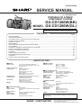
1
GX-CD1200W
SERVICE MANUAL
No. S5039GXCD1200
PORTABLE CD STEREO
COMPONENT SYSTEM
GX-CD1200W(BK)
MODEL GX-CD1200W(GL)
• In the interests of user-safety the set should be restored to its original
condition and only parts identical to those specified should be used.
CONTENTS
Page
SPECIFICATIONS ............................................................................................................................................................... 1
VOLTAGE SELECTION ....................................................................................................................................................... 2
AC POWER SUPPLY CORD AND AC PLUG ADAPTOR ................................................................................................... 2
FITTING OF DIAL POINTER ............................................................................................................................................... 2
NAMES OF PARTS ............................................................................................................................................................. 3
DISASSEMBLY .................................................................................................................................................................... 4
REMOVING AND REINSTALLING THE MAIN PARTS ....................................................................................................... 5
ADJUSTMENT ..................................................................................................................................................................... 6
SCHEMATIC DIAGRAM / WIRING SIDE OF P.W.BOARD ............................................................................................... 10
NOTES ON SCHEMATIC DIAGRAM ................................................................................................................................ 18
TYPES OF TRANSISTOR AND LED ................................................................................................................................. 18
VOLTAGE .......................................................................................................................................................................... 18
WAVEFORMS OF CD CIRCUIT ........................................................................................................................................ 19
TROUBLESHOOTING (CD SECTION) ............................................................................................................................. 20
FUNCTION......................................................................................................................................................................... 24
PARTS GUIDE / EXPLODED VIEW
SPECIFICATIONS
General
Power source:
Power consumption:
Output power:
Input terminal:
Output terminal:
Dimensions:
Weight:
Radio section
AC 110-127 V/220-240 V, 50/60 Hz
DC 15 V [“D” size (UM/SUM-1, R20 or HP2) battery x 10]
31 W
PMPO; 200 W (Total)
(AC operation)
MPO; 50 W (25 W + 25 W)
(AC operation)
RMS; 25 W (12.5 W + 12.5 W)
(DC operation, 10 % T.H.D.)
Mixing microphone(monaural); 600 ohms
Headphones; 16-50 ohms
(recommended; 32 ohms)
Width; 300 mm (11-13/16")
Height; 262 mm (9-1/2")
Depth; 220 mm (8-11/16")
4.1 kg (9.1 lbs.) without batteries
Frequency range:
Tape recorder section
Frequency response:
Signal/noise ratio:
Wow and flutter:
Motor:
Bias system:
Erase system:
Audio channels:
Filter:
D/A converter:
Wow and flutter:
60 - 12,000 Hz (Normal tape)
40 dB (TAPE 1, recording/playback)
55 dB (TAPE 2, playback)
0.15 % (WRMS)
DC 9 V electric governor
AC bias
Magnet erase
Speaker section
Type:
Speakers:
2-way type
12 cm (4-3/4") free-edge speaker x 2
Tweeter x 2
Maximum input power: 25 W
Rated input power:
12.5 W
Impedance:
8 ohms
Dimensions:
Width; 235 mm (9-1/4")
Height; 262 mm (10-5/16")
Depth; 220 mm (8-11/16")
Weight:
1.8 kg (4.0 lbs.)/each
Compact disc player
Type:
Signal readout:
FM; 88 - 108 MHz
SW1; 2.3 - 7.3 MHz
SW2; 7.3 - 22 MHz
MW; 526.5 - 1,606.5 kHz
Compact disc
Non-contact, 3-beam semi-conductor laser
pickup
2
8-times oversampling digital filter
1-bit D/A converter
Unmeasurable
(less than 0.001 % W. peak)
Specifications for this model are subject to change without
prior notice.
SHARP CORPORATION
–1–
This document has been published to be used
for after sales service only.
The contents are subject to change without notice.
GX-CD1200W
FOR A COMPLETE DESCRIPTION OF THE OPERATION OF THIS UNIT, PLEASE REFER
TO THE OPERATION MANUAL.
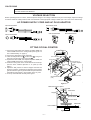
VOLTAGE SELECTION
Before operating the unit on mains, check the preset voltage. If the voltage is different from your local voltage, adjust the voltage
as follows: Slide the voltage selector with a screwdriver to the appropriate voltage number (AC 110V-127V or AC 220V-240V).
AC POWER SUPPLY CORD AND AC PLUG ADAPTOR
QACCE0007AW00
QACCA0001SJ00
QPLGA0250AFZZ
QACCL0002AW00
QPLGA0253AFZZ
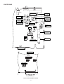
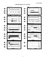
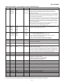
FITTING OF DIAL POINTER
1. Remove the Main PWB, the Graphic Equalizer PWB, the
Volume PWB and the Fine Tuning PWB. (See Figure 4-2
in the "Disassembly" on page 4.)
2. Remove the dial pointer guide and PWB.
3. Insert the dial pointer from A , lead it under B , hang it on
the tuner gear and then pass it through C .
4. Replace the Main PWB, the Graphic Equalizer PWB, the
Volume PWB and the Fine Tuning PWB.
5. Rotate the tuning knob in the arrow direction until it stops.
(Set the tuner variable capacitor to "0" point (F-LOW
state).)
6. Adjust the dial pointer so that its stopper becomes the
Figure 2-2 position. (Adjust the engagement of the pointer
gear and the tuner gear to get the minimum space between
the PWB and the stopper.) This position is the "0" point.
7. Screw up the PWB and the dial pointer guide.
"0" Point
Dial Pointer(211)
A
Front Cabinet
Tuning Knob
B
Dial Pointer(211)
Graphic Equalizer
PWB
Fine Tuning
PWB
Screw(601)
ø3x10mm
C
PWB
Tuner
Gear
Volume PWB
Dial Pointer Guide
(218)
Main PWB
Figure 2-1
Make the minimum space.
PWB
Dial Pointer
Stopper
Pointer Gear
Tuner Gear
Main PWB
Front Cabinet
Variable Capacitor
Figure 2-2
–2–
GX-CD1200W
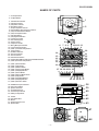
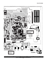
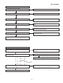
NAMES OF PARTS
1. CD Compartment
2. CD Eject Button
3.
4.
5.
6.
7.
8.
9.
10.
11.
12.
13.
14.
15.
16.
17.
18.
19.
20.
21.
22.
23.
24.
25.
26.
Track Number Indicator
(CD) Play Indicator
(CD) Pause Indicator
Extra Bass Control
Graphic Equalizer Controls
Power/(TAPE 2) Play Direction Indicators
(CD) Track Down/Review Button
(CD) Track Up/Cue Button
(CD) Stop Button
(CD) Play/Pause Button
Fine Tuning Control
Built-in Microphone
Volume Control
Headphone Socket
Mixing Microphone Socket
Function Selector Switch
(TAPE 1) Cassette Compartment
Tuning Control
FM Stereo Indicator
Surround Indicator
Surround Switch
Band Selector Switch
Dubbing Speed/Built-in Microphone/FM Mode Switch
(TAPE 2) Cassette Compartment
27.
28.
29.
30.
31.
32.
33.
34.
35.
36.
37.
(TAPE 1) Record Button
(TAPE 1) Play Button
(TAPE 1) Rewind Button
(TAPE 1) Fast Forward Button
(TAPE 1) Stop/Eject Button
(TAPE 1) Pause Button
(TAPE 2) Reverse Mode Switch
(TAPE 2) Play Button
(TAPE 2) Fast Wind Buttons
(TAPE 2) Stop/Eject Button
(TAPE 2) Direction Switch
38.
39.
40.
41.
42.
43.
FM/SW Telescopic Rod Aerial
Beat Cancel Switch
Speaker Terminals
AC Voltage Selector
AC Power Input Socket
Battery Compartment
44.
45.
46.
47.
48.
Tweeter
Bass Reflex Duct
Woofer
Speaker Release Lever
Speaker Wire
(Continued)
1
2
3
4
5
6
7 8 9
10 11 12 13
20
14
15
16
17
18
21
22
23
24
25
19
26
27 28 29 30 31 32
33 34 35 36 37
38
39
40
41
42
43
44
47
45
46
–3–
48
GX-CD1200W
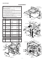
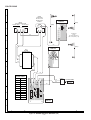
DISASSEMBLY
Caution on Disassembly
Follow the below-mentioned notes when disassembling
the unit and reassembling it, to keep it safe and ensure
excellent performance:
1. Take cassette tape out of the unit.
2. Be sure to remove the power supply plug from the wall
outlet before starting to disassemble the unit and remove
the batteries from the unit.
3. Take off nylon bands or wire holders where they need
to be removed when disassembling the unit. After
servicing the unit, be sure to rearrange the leads where
they were before disassembling.
4. Take sufficient care on static electricity of integrated
circuits and other circuits when servicing.
CD Player Unit
Front Cabinet
(B1)x2
ø3x10mm
CD SERVO PWB
(B2)x1
MAIN UNIT
STEP
1
REMOVAL
Front Cabinet/
Rear Cabinet
PROCEDURE
FIGURE
1. Battery Compartment Lid.
................................. (A1)x1
2. Screw ................... (A2)x5
3. Screw ................... (A3)x3
4. Socket .................. (A4)x1
4-1
Fine Tuning
PWB
2
CD Player Unit
1. Screw ................... (B1)x2
2.Socket ................... (B2)x1
4-2
3
Main PWB/
Graphic Equalizer
PWB/
Volume PWB/
Fine Tuning PWB
1. Knob ..................... (C1)x1
2. Socket .................. (C2)x3
3. Screw ................... (C3)x5
4. Screw ................... (C4)x2
5. Mic ....................... (C5)x1
4-3
Tape mechanism 1. Open the cassette holder.
2. Screw ................... (D1)x6
4-3
Power PWB/
1. Screw ................... (E1)x3
Terminal A PWB/ 2. Screw ................... (E2)x2
Terminal B PWB 3. Bracket ................. (E3)x1
4. Screw ................... (E4)x2
5. Hook ..................... (E5)x2
CD Servo PWB/ 1. Screw ................... (F1)x7
CD Control PWB/ 2. Socket .................. (F2)x3
CD Mechanism
1. Screw ................... (G1)x1
4-4
4
5
6
7
Figure 4-2
Front Cabinet
1
REMOVAL
Speaker
(C1)x1
Washer
Main PWB
Open
(C4)x2
ø3x10mm
(C5)x1
(D1)x4
ø3x10mm
5-1
(C3)x5
ø3x10mm
5-1
(C2)x3
SPEAKER UNIT
STEP
Volume Graphic
PWB
Equalizer
PWB
Nat
Cassette
Holder
(D1)x2
Tape (Left/Right)
ø3x10mm Mechanism
Figure 4-3
PROCEDURE
FIGURE
1. Screw ................... (H1)x5
2. Front Panel .......... (H2)x1
3. Screw ................... (H3)x4
5-2
Power
Transeformer
Voltage Selector
Rear Cabinet
Main PWB
AC Socket
Power
PWB
(A2)x1
ø3x6mm
(A4)x1
Front
Cabinet
(A3)x3
ø3x20mm
(E5)x2
(E1)x3
ø3x10mm
(E2)x2
ø4x16mm
(A2)x3
ø3x6mm
(E3)x1
(A1)x1
Rear
Cabinet
(E4)x2
ø3x10mm
(A2)x1
ø3x6mm
Figure 4-1
Terminal B
PWB
Terminal A
PWB
Figure 4-4
–4–
GX-CD1200W
CD Servo
PWB
(F1)x3
ø3x10mm
(G1)x3
ø3x10mm
Front Panel
Tweeter
(H2)x1
Speaker Cord
Speaker
Holder
Cord
Woofer
(F2)x2
Driver
(F2)x1
CD Mechanism
(F1)x1
ø3x10mm
(H3)x4
ø3x10mm
Switch PWB
Main Unit
CD Player Unit
(F1)x3
ø3x10mm
Speaker
Release
Lever Speaker Box
CD Control PWB
Figure 5-2
Figure 5-1
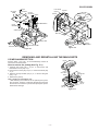
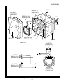
REMOVING AND REINSTALLING THE MAIN PARTS
CD MECHANISM SECTION
(A1)x2
Perform steps 1,2,6 and 7 of the disassembly method to
remove the CD mechanism.
How to remove the pickup (See Fig. 5-3.)
(A2)x1
1. Remove the hooks (A1) x 2 pcs., to remove the CD
Mechanism Cover (A2) x1 pc.
2. Remove the screws (A3) x 2 pcs., to remove the shaft (A4)
x1 pc.
3. Remove the stop washer (A5) x1 pc., to remove the gear
(A6) x 1 pc.
4. Remove the pickup.
(A3) x2
ø2.6 x6mm
CD
Mechanism
Pickup
Note : (Figure 5-1 and Figure 5-3)
After removing the connector for the optical pick-up from
the connector, wrap the conductive aluminium foil around
the front end of connector to protect the optical pick-up from
electrostatic damage.
Shaft
(A4) x1
Gear
(A6) x1
Figure 5-3
–5–
Stop
Washer
(A5) x1
(H1)x5
ø4x16mm
GX-CD1200W
TAPE MECHANISM SECTION
Perform steps 1, 2, 3 and 4 of the disassembly method to
remove the mechanism block.
(A1) x1
ø2x7mm
(A1) x1
ø2x3mm
Hook
(A2) x2
How to remove the record / playback, playback
and erase heads (See Figs. 6-1 and 6-2.)
1. Remove the screws (A1) x 2 pcs., to remove the record/
playback head.
2. Remove the hooks (A2) x 2 pcs., toward the center position
as shown in Fig. 6-1. and then extract the erase head
upward.
3. Remove the screws (B1) x 2 pcs., to remove the playback
head.
Note:
After replacing the heads and performing the azimuth adjustment, be sure to apply screw lock.
TAPE 1
Record/Playback
Head
Erase
Head
Figure 6-1
(B1) x1
ø2x7mm
How to remove the pinch roller (See Fig. 6-3.)
(B1) x1
ø2x3mm
TAPE 2
Playback
Head
1. Carefully bend the pinch roller pawl in the direction of the
arrow <A> , and remove the pinch roller (C1) upwards.
How to remove the motor (See Fig. 6-4.)
1. Remove the belt.
2. Remove the screws (D1) x 4 pcs., to remove the motor
bracket.
3. Remove the screws (D2) x 3 pcs., to remove the motor.
Note:
When mounting the motor, pay attention to the motor mounting angle.
How to remove the belts (See Fig. 6-5.)
Figure 6-2
1. Remove the main belt (E1) x 1 pc., at the tape 1 side from
the motor pulley.
2. Remove the main belt (E2) x 1 pc., at the tape 2 side from
the motor pulley.
3. Remove the REW/FF belt (E3) x 2 pcs., from the REW/FF
roller.
4. Put on the belts in the reverse order of removal.
Note:
When putting on the belt, ascertain that the belt is not twisted,
and clean it.
Pinch Roller
(C1)
Pinch Roller
Pawl
<A>
Figure 6-3
Motor
TAPE 2
REW / FF
Belt
(E3) x1
( D1 ) x2
ø2 x 4mm
( D1 ) x2
ø2 x 4mm
Motor
TAPE 2
TAPE 1
Main Belt Main Belt
Motor
Bracket
( D2 ) x3
Special Screw
Motor
Main
Belt
(E1) x1
TAPE 1
Main
Belt
(E2) x1
Motor
Bracket
REW / FF
Belt
(E3) x1
Motor
Figure 6-5
Figure 6-4
–6–
GX-CD1200W
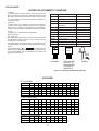
ADJUSTMENT
MECHANISM SECTION
TUNER SECTION
• Driving Force Check
fL: Low-range frequency
fH: High-range frequency
Torque Meter
Specified Value
Play: TW-2412
• FM IF/RF
Tape 1: Over 60 g
Tape 2: Over 50 g
Specified Value/
Adjusting
Point
Test Stage
• Torque Check
Torque Meter
Specified Value
Tape 1
Tape 2
Play: TW-2111
30 to 70 g.cm
27 to 60 g.cm
Fast Forward: TW-2231
Over 55 g.cm
55 to 120 g.cm
Rewind: TW-2231
Over 55 g.cm
55 to 120 g.cm
Test Tape
Instrument Connection
MTT-114
Headphones Socket
(Load resistance: 32 ohms)
Adjustment
Point
Specified
Value
Instrument
Connection
DECK SECTION
• Bias Oscillation
• Beat Cancel Switch: C
L301
Specified value
100 kHz + 4 kHz
Instrument
Connection
2.5 V ± 3 dB
Instrument
Connection
AM IF
L11
Input: Antenna
Output: Pin 9 of IC2
MW Band
Coverage
fL: L6
fH: TC3
Input: Antenna
Output: Headphone Socket
SW1 Band
Coverage
fL(2.3 MHz): L7
fH(7.3 MHz): TC5
SW1
Tracking
fL(2.6 MHz): L4
fH(6 MHz): TC6
SW2 Band
Coverage
fL(7.3 MHz): L8
fH(22 MHz): TC7
SW2
Tracking
fL(8.5 MHz): L5
fH(19 MHz): TC8
(Load resistance:
32 ohms)
Specified value
76 kHz ± 200 Hz
VR1
Instrument Connection
Pin 13, Pin 21 and ground
of IC2
Note:
After preparing the test circuit shown in Fig. 7, connect the Pin
13, Pin 21 and ground of the IC2 with the test circuit, and
measure the value.
• Playback Amplifier Sensitivity Check
Specified value
Specified Value/
Adjusting
Point
Adjustment
Point
Specified Value
MTT-118
Input: Antenna
Output: Headphone Socket
(Load resistance:
32 ohms)
fL: L1
fH: TC1
fL(88.0 MHz): L2
fH(108 MHz): TC2
• VCO Frequency
Pin 1 of CNS102
A: 104 ± 4 kHz
B: 94 ± 4 kHz
C: 100 ± 4 kHz
Beat Cancel
Test tape
FM Band
Coverage
FM Tracking
MW Tracking fL(600 kHz): L3
fH(1,400 kHz):TC4
Tape 1,2:VR102 3,000 ± 60 Hz Headphones
Socket
(Load resistance:
32 ohms)
Adjustment Point
Input: FM Antenna
Output:Pin 9 of IC2
Test Stage
• Tape Speed (Normal only)
MTT-111
FM IF
L9
FM Detection L10
• AM IF/RF
• Head Azimuth
Test Tape
Instrument
Connection
Instrument Connection
Pin 21 of IC2
Pin 13 of IC2
Speaker terminal
(Load resistance: 8 ohms)
D
FET: 2SK212
(or Other 2SK Type FET.)
G
10 pF
S
1M ohm
0.1 µF
10K ohm
TO FREQUENCY
COUNTER
Figure 7 VCO FREQUENCY TEST CIRCUIT
–7–
GX-CD1200W
SW103
SW1
SW401
TC6
L7
TC5
SW1
TRACKING fH
FM TRACKING
fH
MW
TRACKING fH
SW1 BAND fH
COVERAGE fL
L8
TC7
SW2 BAND fH
COVERAGE fL
L2
MW BAND
COVERAGE fL
TC4
TC3
TC2
TC1
FM
TRACKING fL
L6
MW BAND
COVERAGE fH
fH FM BAND
fL COVERAGE
TC8
L1
IC1
fH SW2
fL TRACKING
CF1
FM IF
AM IF
L5
L9
L11
12
CF3
9
1
CF2
L4
SW1
TRACKING fL
L3
MW
TRACKING fL
IC2
21 24
13
VCO
L10
FM DETECTION
VR1
MAIN PWB
MAIN PWB
CNP103
IC502
Q603
TAPE SPEED
VR102
CNP501
SPEAKER TERMINALS
Figure 8 ADJUSTMENT POINTS
–8–
GX-CD1200W
CD SECTION
Since this CD system incorporates the following automatic adjustment function, when the pickup is replaced, it is not necessary
to reajust it.
Since this CD unit does not need adjustment, the combination of PWB and laser pickup unit is not restricted.
TEST MODE
Start
While holding down the "PLAY" button, move the FUNCTION/POWER switch to "CD".
(To serial No.006XXXXX)
While holding down the "STOP" button, move the FUNCTION/POWER switch to "CD".
(From serial No.007XXXXX)
Note
1. When the CD LID switch is in the OFF position, (CD LID is open) the unit will be able to enter the test mode.
However, can use the "UP/CUE" and "DOWN/REVIEW" button only.
2. You can only move the pickup.
3. The LCD display should be the same as it is for normal CD operations.
Operation The use of the "UP/CUE" button will move the pickup to the outermost position.
The use of the "DOWN/REVIEW" button will move the pickup to the innermost position.
LCD MODE
After connecting of the 10kΩ resistor between IC802 27 pin and GND and holding down the "PLAY" button, move
the FUNCTION/POWER switch to "CD".
Start
Display
LASER LIGHTING CONFIRMATION
1. Remove the front cabinet according to the disassembly method.
2. Short the TP of the Figure 9 to turn on the CD LID SW 810.
3. While holding down the "PLAY" button, move the FUNCTION/POWER switch to "CD".
4. Open the CD LID and press the PLAY button. The laser lights up for a few seconds. (At this time, the pickup lens moves up
and down and adjusts the focus to check if there is a disc or not.)
CD CONTROL PWB-C2
R847
R848
SW801
PLAY/
PAUSE
SW804
REVIEW/
TRACK DOWN
R849
SW802
STOP
FW801
SW803
CUE/
TRACK UP
LCD801
10
1
8 7 6 5 4 3 2 1
SWITCH PWB-C3
FW801
1
FW1
1
R846
12
100
1
C824
5
10
R844
R839
90
15
85
75
C823
1
C825
2
25
30
31 35
40
IC802
45 55
R835
R865
60
L801
C840
C843
R832
C837
Figure 9
–9–
11
1
R840
X801
C842
Q803
R858
3 2 1 Q804
C852
C845 R836
81
80
70
65
C850
C858
C844
95
20
R863
C848
2
C847
10
R861
1 2 3
P804
R822
C851
C853
C849
R857
L803
C846
C855
L802
SW810
OPEN/CLOSE
R821
TP
CD SERVO PWB-C1
17 4 14 15
16
13
6
5
4
3
CNS804
GX-CD1200W
BI804
L-CH
2
0V(9V)
0V
1
0V
7
IC151
TA2011S
MIC AMP.
3
1.3V
2
0V
4
1.9V
5
C33
3.3/50
C32
0.0082(ML)
AM/FM
VCO
MO/ST
R-CH
MPX IN
L-CH
AM IN
GND
SW2
FM
MW
SW1
SW2
C41
1/50
R182
1K R184
330K
R20
10
2.7V
0.9V
0.3V
Q182
KTC3199
GRAPHIC
EQUALIZ
R127
22K
R129
150K
R130
150K
+B
CD
TUNER
R128
22K
SW501-A
FUNCTION
SELECTOR
CD
TUNER
TAPE
C42
0.022
R-CH
SW501-B
FUNCTION
SELECTOR
D154
DS1SS133
R172
10K
MIC
R170
33K
R177
1K
C159
47/25
R171
33K
D162
DS1SS133
C160
22/16
0V
R111
22K
NF
MATAL
OUT
2
C104
470P
C102
470P
PRE
OUT
R115
680
R113
120K
A/B
VCC
MIX
OUT
GND1
C112
0.015
(ML)
R110
6.8K
REC
OUT
REC
NF
REC
IN
M/N
REC
OUT
REC
NF
REC
IN
8
9
10
11
12
C122
330P
R124
10K
R114
120K
R116
680
C305
0.0015
(ML)
C306
390P
C304
0.022
C303
0.0056
(ML) C302
0.0022
(ML)
(0.1V)
R304
10
0V
R131
1.2K
ALC
GND
R132
1.2K
C126
4.7/50
C124
0.01
R134
82K
C120
R118 0.033
330K (ML)
Q5
KT
SW
+B
( ):RECORD
(3V)
R302 R
100
R306 R305
47
27K (0.7V)
L301
BIAS OSC.
1
R112
22K
Q301
KTC3203 Y
BIAS OSC.
R301
330
R511
10K
P
SW101-E
RECORD/
PLAYBACK
C301 100/10
SW102
BEAT CANCEL
A
C138
0.0015(ML)
Q601
KRC102M
R133
82K
13
R120
100
C132 120P R136 10K
L104
22mH
0V
2
9V
3
C125
4.7/50
C121
330P
14
R123
10K
C114
4.7/50
R102
100
R119
100
15
6
7
3
4
5
C108
R106
330P
180K R122
R108
10K
10K
+B
C119
0.033
(ML)
C123
0.01
R117
330K
C117
10/16
C115
4.7/50
CH1/A CH1/B
16
C118
10/16
MATAL PRE
OUT
OUT
C128
2.2/50
NF
17
C129
22/16
CH2/B
18
C116
4.7/50
CH2/A
C127
330/10
C109
47/10
R101
100
C103
470P
22
1
21
R105
180K
20
19
23
C106
330P
C134
150P
R107
10K
24
R
P R
P
SW101-D SW101-C
SW101-B
SW101-A
R
P R
P
C133
150P
R100
150
C113
4.7/50
C111
0.015 R109
(ML) 6.8K
C107
330P
R174
22K
+B
(0V)
(0.7V)
Q156
KTC3199 GR
LINE AMP.
IC101 TA8189N
RECORD/PLAY AMP.
SW101-A~D
RECORD/
PLAYBACK
B
SW501-C
FUNCTION
SELECTOR
CD
TUNER
TAPE
D158
DS1SS133
D152
DS1SS133
R135 10K
CNP101
CNS101
Q153
KTC3199 GR
MIC AMP.
R173
10K
C137
0.0015(ML)
1
2
3
CNP102
C158
47/25
D163
HIGH
DS1SS133
NORMAL
+B
C105
330P
C307
150P
R169
10K
R161
1M
C101
470P
C
+B
( ):RECORD
L103
22mH
1
2
3
4
SW103-A
DUBBING
SPEED/MIC
R168
10K
0V(0.7V)
C155
10/16
R154
560
D165
DS1SS133
D164
DS1SS133
( ):HIGH
R151
2.2K
SW504-B
TAPE2 DIRECTION
+B
R303
100
MAIN PWB-A1/VOLUME PWB-A3/FINE TUNING PWB-A4
H
• NOTES ON SCHEMATIC DIAGRAM can be found on page 18.
1
C184
220P
TAPE
C43
220P
SW101-F
BAND SELECTOR
R
P
R166
560
0V(0V)
0V(0V)
C154
47/10
B
CNS102
R17
2.7K
C157
1/50
C110
47/10
C151
0.33/50
R152
4.7K
A
ERASE HEAD
TAPE1
RECORD/PLAYBACK HEAD
TC7
+B
6V
6 C156
100/10
TAPE2
PLAYBACK HEAD
SW504-A
TAPE2 DIRECTION
R-CH
47
R11
47
R165
10K
C131
120P
G
MW
SW1
D156
DS1SS133
0V(0V)
3
MIC151
BUILT-IN
MICROPHONE
1
2
3
4
R18
2.7K
( ):CD FUNCTION
0V(9V)
C152
10/16
L-CH
C40
1/50
R16
10K
+8V(SERVO)
E
SIDE-A
R-CH
SIDE-B
11
C38
0.012
(ML)
+B
FM
TC5
C26
0.022
0.9V
1
2
3
C182
1/50
R1
220
R1
220
D-GND
R153
2.2K
B
10
TP1
VCO
76KHZ
C183
220P
R351
47K
A-GND
Q154
KRA102M
MIC AMP.
SIDE-A
L-CH
SIDE-B
0.3V
R181
1K
13 12
GND(A)
J151
MIC JACK
F
9
R13
100
C30
0.022
R352
47K
R-CH
14
SW1-F
BAND
SELECTOR
FM
MW
SW1
SW2
R10
C15
0.022
15
L7 SW1 OSC.
C27
0.0047
R19
15K
N.C.
C37
0.012
(ML)
C39
1/50
R15
10K
R12
1K
2
C29
22/16
TC3
C21
5P
(UJ)
R353
27K
1
A
FM DET
1
L8 SW2 OSC.
R354
27K
16
8
CF3
3 455KHz
AM IF
AM IF
TC8
FINE
TNNING
17
7
VCO
C36
0.0015
L-CH
L3,4 MW/SW1
BAR ANTENNA
C34 R14
470P 100K
C35
3.3/50
DET OUT
IF AD
7V
SW1-E
C19
BAND
SELECTOR 330P
FM
C14
MW
5P(CH)
SW1
SW2
C20
0.0022
TC9
18
Q181
KTC3199 G
GRAPHIC
R183 EQUALIZE
330K
C181
2.7V
1/50
0.9V
FM MONO
VR1
10KB
+B
C25
0.022
R121 10K
D
6
L6 MW OSC.
L4 SW1
L5 SW2
ANTENNA
CNP804
TO CD
SERVO
PWB
P13 11-G
5
L11
VC3
6
5
4
3
2
1
4
+B
3
SW1
CNS804
6
5
4
3
2
1
AGC
IC2
LA1805
FM/AM IF MPX.
2
TC6
SW2
19
21
C24
0.022
CF2
FM IF
SW1-D
BAND
SELECTOR
20
AM IF AM OUT
IF AD
STB
22
2
SW1
SW2
MW
L10
AM RF
23
C9
0.022
TC4
SW1-C
BAND
SELECTOR
FM
C
24
1
C6
0.0047
SW2
C31
0.0047(ML)
R8
3.9K R9
12K
1 3
FM IF
FM
MW
FM
DETECTION
C17
0.022
R5
100
R3
47
L3 MW
FM STEREO
SW1-H
BAND
SELECTOR
C7
0.0047
C18
10/16
L9
C8
0.022
SW1-B
BAND
SELECTOR
FM
MW
SW1
VC4
L1
FM
OSC.
C23
220/10
C22
0.022
SW1-G
BAND
SELECTOR
OSC
R1
10
0V
TC1
D2
DS1SS133
D1
DS1SS133
5
C10
15P(CH)
R2
33
VC2
B
8
6
VC1
C4
24P
(CH)
L2
9
C2
5P(CH)
FM
TRACKING TC2
SW2
C12
3P(CH)
C11
22P(CH)
MW
SW1
4
1.6V
3
7.2V
2
C5
0.001
7.2V
1.6V
FM
7.1V
SW1-A
BAND
SELECTOR
MIX
1
SW1
COV
SW103-B
FM MODE
R7
820K
C13
0.022
RF AMP
0.9V
ROD ANTENNA(253)
R4
330K
7
6.4V
AM MIX
IC1
TA7358AP
FM FRONT END
CF1
FM BAND PASS
FILTER
1 2 3
A
fH TC6
fL L4
SW1
TRACKING
RECORD SIGNAL
PLAYBACK SIGNAL
MW/SW1 SIGNAL
AM OSC
FM IF IN
FM SIGNAL
2
3
4
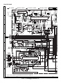
Figure 10 SCHEMATIC DIAGRAM (1/4)
– 10 –
5
6
GX-CD1200W
GRAPHIC EQUALIZER PWB-A2
C185
1/50
2.7V
C203
1/50
R203
2.2K
R187
3.9K
R255
120
GRAPHIC
EQUALIZER
VR203 VR204 VR205
100K(A) 100K(A) 100K(A)
(500Hz) (2KHz) (10KHz)
X-BASS
VR202
50K(A)
(100Hz)
7
C253
0.022
C259
0.0039
(ML)
5
4
3
2
1
LED257
C257
47/25
39K
+B
9 8
R253
R183
330K
C181
1/50
0.9V
IC202 LB1403N
LEVER METER DRIVER
R251 C251
6.8K 1/50
Q181
KTC3199 GR
GRAPHIC
EQUALIZER
fH TC1
FM BAND
COVERAGE fL L1
fH TC3
MW BAND
COVERAGE fL L6
SW2 BAND fH TC7
COVERAGE fL L8
fH TC8
fL L5
SW2
TRACKING
LED259
fH TC2
fL L2
FM
TRACKING
LED255
fH TC4
fL L3
MW
TRACKING
LED253
SW1 BAND fH TC5
COVERAGE fL L7
6
R257 10K
fH TC6
fL L4
C255
10/16
R259
120
0.3V
R207
4.7K
18
R202
1K
R127
22K
C202
4.7/50
16
14
12
C206
0.01
(ML)
C222
4.7/50
10
8
C210
0.082
(ML)
C256
10/16
LED1
STEREO
VR205 VR204 VR203 VR202
100K(B) 100K(B) 100K(B) 50K(B)
(10KHz) (2KHz) (500Hz) (100Hz)
GRAPHIC
X-BASS
EQUALIZER
R206
3.3K
1K
+B
LED501
R520
10K
A : 0.8V
B : 0.2V
A : 0V
B : 0.7V
R521
10K
R260
120
LED501,502
POWER DIRECTION
LED502
R519
1K
R204 C204
2.2K 1/50
R128
22K
C254
0.022
R518
R208
3.3K
R212
1K
+B
C260
0.0039
(ML)
C218
0.47/50
C214
0.33/50
1
LED260
2
2
LED258
4
6
R252
6.8K
1
LED254
3
3
LED256
5
4
6
R258 10K
7
R254 39K
C211
0.0015
9
11
C207
5.9V
470P
IC201
BA3822LS
GRAPHIC
EQUALIZER
13
6.5V
5.9V
20
15
5
C252
1/50
LED401 SURRUND
R180
560
22
17
7
9 8
C220
0.039
(ML)
0V
24
19
5.9V
6.5V
Q182
KTC3199 GR
GRAPHIC
EQUALIZER
21
(ML)
23
(ML)
R200
330
C200
100/10
R256
120
C205
0.01
(ML)
C209
0.082
(ML)
C213
0.33/50
(ML)
+B
C186
1/50
0.3V
C217
0.47/50
C215
0.0056
C180
100/10
0.9V
IC203 LB1403N
LEVER METER DRIVER
(ML)
C216
0.0056
R188
3.9K
R211
1K
C212
0.0015
2.7V
C201
4.7/50
R201
1K
C221 4.7/50
R186
220
C219
0.039
(ML)
C184
220P
2.6V
2.6V
4.4V
6.5V
6.5V
5.9V
5.9V
6.5V
6.5V
5.9V
5.9V
6.5V
6.5V
5.9V
Q505
KTC3199 GR
LED CONTROL
0V
+B
R440
470
+B
SW401
SURROUND
+B
5
R404
10K
3.8V
3.8V
3
0V
+B
9V
OUT
IC501
3 KA7809AP 1
C506
2 IN
0.022
0V
C505
47/16
Q602
KRA102 M 0V
SWITCHING3
8.1V 100
C508
100/16
0V(0.7V)
R511
10K
R512
10K
0V(0V)
L501
47µH
0V(7.9V)
C511
0.022
13
L-CH
6
-OUT1
0V
3
C420
4.7/50
14.3V
C424 1
47/25
0V
R-CH
-OUT2
5
9
+
–
–
+
R435
C427 2.2
0.1(ML)
C426
0.1(ML) R434
2.2
L-CH
SP401
WOOFER
8 Ohm
L-CH
R-CH
SP402
WOOFER
8 Ohm
0V
6.9V
11
8
7
6.4V 15V
VOLUME
6.9V
10
4
Q404
KTC3199 GR
POWER MUTE
6.9V
12
R-CH
R436
C428 2.2
0.1(ML)
SP404
TWEETER
8 Ohm
15V
R431
27K
C429
10/16
C433
0.022
R437
120
C513
1/50
C510
3300/25
C601
0.022
8.5V
(6.3V)
R516
3.6K
R515
120
+
–
B
1
2
3
4
5
6
7
8
9
CNS103
A
J401
HEADPHONES JACK
AC110V-127V
AC220V-240V
D651
TS4B03GM
1
2
3
4
5
6
7
8
9
Q504
KTA1271 Y
SWITCHING
(7.9V)
1
2
SW501-D
FUNCTION
SELECTOR
IN
R438
120
SW601
VOLTAGE SELECTOR
POWER PWB-A7
1
2
8.5V(8.5V)
VR102
470
TAPE SPEED
R441
15K
C423
10/16
C430
10/16
15V
IC502
3 KA7809P 1
C514
2
1/50
C509
0.022 0V
Q503
R514
KTC3199 GR 100K
SWITCHING
7.9V
0.7V
(0V)
R416
3.3K
0V
R433
2.2
SP403
TWEETER
8 Ohm
+B
OUT
9V
Q502
KTC3199 GR
SWITCHING
R426
1K
C425
0.1(ML)
0V
15V
DZ601
DZ8.2BSB
C602
100/10
R513
10K
C414
0.001
(ML)
R428
4.7K
14
+OUT2
R601
270
R602
( ):HIGH SPEED
0.7V(0V)
C416
0.15 VR401
(ML) 50K(B)
6.9V
+OUT1
2
0V
+B
7.5V
0V
0.6V
15V
Q603
KTD2058 Y
VOLTAGE
REGULATOR
C603
0.022
4
0V
R429
100K
R420
3.3K
15V
2
1
C604
220/10
C410
1/50
1
IC401
KIA4558P
OPE AMP.
2
3.8V
C404
10/16
C418
22/16
R418
22K
R410
12K
0V
R427
4.7K
0.6V
R419
3.3K
C412
47/10
C408
4.7/50
C415
0.15
(ML)
IC402
LA4663
POWER AMP.
C419
4.7/50
R425
1K
CNS601
C402
0.0068(ML)
+B
R413
10K
C407
4.7/50
R406
2.7K R408
12K
R417
22K
CNP103
R402
100K
R409
12K
R412
10K
R407
12K
C406
0.0033 C405
0.0033
(ML)
(ML)
R401
100K
R405
2.7K
VOLUME
C413
0.001
(ML)
CNP601
R403
10K
6
R415
3.3K
C411
47/10
C401
0.0068(ML)
3.8V
IC401
KIA4558P
8 OPE AMP.
C409
3.8V
1/50
7
R442
15K
7.5V
Q403
KTC3199 GR
POWER MUTE
3.8V
VR401
50K(B)
R411
330
C403
10/16
CNP501
SPEAKER
TERMINALS
R182
K R184
330K
R185
220
R205
4.7K
C208
470P
C182
1/50
C183
220P
6.9V
3.2V
3.2V
4.4V
1
C652
0.022
M501
MOTOR
T601
POWER
TRANSFORMER
C651
0.022
SO601
AC SOCKET
AC110V-127V/
AC220V-240V,
50/60Hz
C654
0.022
C653
0.022
M
F601
T4A L 250V
SW901
TAPE1 MAIN
SW902
TAPE2 MAIN
SW903
TAPE2 PLAY
TERMINAL B
PWB-A6
SW904
TAPE2
DIRECTION
TERMINAL A
PWB-A5
BATTERYS DC 15V
["D" SIZE (UM/SUM-1,
R20 or HP2) battery x 10]
0V(0V)
IC501,502:VOLTAGE REGULATOR
7
8
9
10
Figure 11 SCHEMATIC DIAGRAM (2/4)
– 11 –
11
12
GX-CD1200W
A
FW802
( ):STOP
SW810
OPEN/CLOSE
4
3
3
F
2
2
2
C
1
1
1
B
F
C
GND 23
0V
IC801
R895
68K
R893
68K
R892
56K
R891
68K
2.1V
FG
FOPD
VR
LD
2
3
3
4
4
4
5
5
5
6
6
7
7
7
8
8
8
FC-
7
LDO
2.5V
(0.3V)
8
SEL
2.8V
9
TEB
4.3V
10
2VRO
11
TEN
2.1V
PU-IN
GND
6
5
4
3
2
1
6
5
4
3
2
1
21
RFGC
20
RFGO
19
0V
0.1(ML)
C818
56P
2.1V
18
RFRP
17
VRO
16
FEN
15
2.1V
FEO
14
12
SBAD
13
10
2.1V
C801
0.1
C863
47/10
2.0V
(1.1V)
LD
R
+B
C822
0.047
C841
0.047
C843
47/10
C814
0.047
BI803
6
5
4
3
2
1
DM+
C834
470P
2
DM-
3
FM+
C835
470P
C836
0.047
(ML)
FOO
FMSLT+
TRO
+B
C807
0.047
N.C.
G
RES
5V
2.1V
2.1V
3.3V
6.7V
C89
220
+B
5V(5V)
2.2K
R852
3.4V
0V
0V
0V
3V
3.6V
R851
2.2K
2.1V
C805
0.022
2.2V
1 2 3 4 5 6 7 8 9 10 11 12 13 14 15
+B
5V
REG IN
CD
VIN3
VIN2
VG2
VO2+
VO2-
GND
GND
GND
VO1-
VO1+
VG1
VIN1
N.C.
REG OUT
VG3
VO3+
VO3-
GND
GND
GND
VO4-
VO4+
VG4
VIN4
VCC
VREF
MT
VCC
92LHPC1LXASY
QCNWN0032BGZZ
NOT USED
NOT USED
VRD-ST2CD683J
VRD-ST2CD563J
VRD-ST2CD683J
VRD-ST2CD683J
VRD-ST2CD683J
VRD-ST2CD563J
7.4V
92LHPC1LASY
QCNWN0027BGZZ
VCQYKA1HM103K
VRD-ST2CD222J
NOT USED
JUMPER
JUMPER
NOT USED
JUMPER
JUMPER
0.9V
PICK-UP UNIT
BI802/CNS802
C801
R802
R891
R892
R893
R894
R895
R896
IC803 LA6541D
FOCUS/TRACKING/SPIN/SLED
C806
220/10
F
From serial
No.00504991
6.8V
(6.8V)
Q802
KTA1271 Y
VOLTAGE
REGULATOR
FMO
DMO
+B
+B
CD SERVO PWB-C1
H
• NOTES ON SCHEMATIC DIAGRAM can be found on page 18.
1
2
3
4
Figure 12 SCHEMATIC DIAGRAM (3/4)
– 12 –
C837
0.047 (M
C838
0.047(M
C839
0.047(M
N.C. N.C.
30 29 28 27 26 25 24 23 22 21 20 19 18 17 16
To serial
No.00404990
C854 R
0.0068
VR
CD MOTOR PWB-B
SERIAL NO.
+B
3.2V
(1.1)
2.1V
TEO
9
2.2V C819
RFIS
2.1V
PD
SLT-
SW702
PICKUP IN
AGCI
0V
R853
2.2K
SL+
SL-
–
3.6V
(4.4V)
2.1V
+
MDI
C820
0.1
(ML) R807
1K
8
GND
7.4V
M
6
FC+
2.1V
SP-
M801
SLED
MOTOR
CNS803
CNP803
–
SP+
E
TNI
C813
47/10
+
M
5
0.18V
(0V)
TR-
PICK-UP UNIT
M802
SPINDLE
MOTOR
2.1V
(2.1V)
3.3V
D
2
3
6
TRVR1A
2
TPI
7.4V(7.5V)
F+
1
FPI
4
3.3V
FO+
TR+
1
3
2.1V
(2.1V)
2.1V
1
R+
RFO 22
4.8V
RTR+
R806
2.7K
1.6V
(0.3V)
FNI
2.1V
R811
22K
C4A
R894
68K
BI801
C
CNS801
2/1VCC
2
R805
39K
C832
47/10
4
3
VCC
C842
0.047
4
A
2.1V
RFN 24
1
C804
2P(CH)
5
5V
2.1V
5
R896
56K
3.3V
5
E
C825
47/10
C8
47
82K
C821
47/10
6
R803
7
6
3.6V
(4.4V)
0V
3.3V
B
7
6
C817
100/10
C802
0.022
C816
0.022 R804
68K
0V
E
A
7
+B
C815
47/10
0V
C2A
R801
22
2.1V
B
C3A
MON
SERVO PRE AMP.
4.3V(5V)
0.2V(1.5V)
BI802
LD
CNS802
+5V
VCC
R802 IC801
2.2K TA2109F
Q801
KTA1266 GR
SWITCHING
SWITCH PWB-C3
5
6
GX-CD1200W
C825
47/10
+B
+B
0V
0V
0V
0V
0V
0V
0V
0V
5V
TEST0
ADIN2
27
0V
55
AVSS
5V
ADIN1
26
2.1V
56
SLCO
0V
P3-0
25
2.1V
57
RFI
5V
P1-3
24
5V
58
AVDD
0V
P1-2
23
2.1V
59
RFCT
0V
P1-1
22 N.C.
2.1V
60
RFZI
0V
P1-0
21 N.C.
2.7V
61
RFRP
0V
MVSS1
20
2.3V
62
FEI
2.9V
63
SBAD
TEI
65
TEZI
2.1V
66
FOO
2.1V
67
TRO
2.1V
68
VREF
6
19
P8-3
18
0V
CD LID
SW
17
0V
CDSEL1
16
0V
CDSEL0
15
14 N.C.
2.5V SEG13
13 N.C.
RFGC
2.5V SEG12
12 N.C.
TEBC
2.5V SEG11
11 N.C.
2.5V SEG10
10 N.C.
69
70
71
FMO
2.1V
72
DMO
4.1V
73
2VREF
2.5V
74
SEL
5V
75
VDD2
0V
76
0V
77
2.1V
2.6V
5V
15
9
N.C.
2.5V SEG8
8
N.C.
2.5V SEG7
7
N.C.
2.5V SEG6
6
N.C.
VSS2
2.5V SEG5
5
XVSS
2.5V SEG4
4
78
XI
2.5V SEG3
3
79
XO
2.5V SEG2
2
80
XVDD
2.5V SEG1
1
COM2
COM1
MVDD
MVSS
MXI
MXO
INTR
HOLD
N.C. N.C.
RESET
DVSL
RO
LO
16
17
SW801
PLAY/ R847 R848
PAUSE 1K
2.2K
R822
22K
R849
6.8K
LCD801
L802
10µH
8 7 6 5 4 3 2 1
N.C.
COM4
4
COM3
2.5V SEG9
14
C824
0.1(ML)
R861
3.3K
2.5V SEG14
11
2.1V
R865
1K
IC802
TC9457F0
SERVO/SIGNAL
CONTROL
1
2.1V
C845
0.047
C860
0.0015
7
R844
3.3K
SW804
CUE/
TRACK UP
64
2.1V
MVDD1
0V
5V
5
R863
3.3K
SW803
REVIEW/
TRACK
DOWN
TEST1
TEST2
TEST3
TEST4
TEST5
/HSO
SPCK
SPDA
COFS
28
5V
3.3K
3.3K
3.3K
2.3V
2.3V
2.3V
2.3V
5V
0V
0.3V
N.C. N.C.
5V
5V
0V
5V
0V
0V
0V
+B
C847 2.5V
22/16 0V
81 82 83 84 85 86 87 88 89 90 91 92 93 94 95 96 97 98 99 100
2.4V
XL801 3
16.93 MHz
DOUT
0V(5V) MUTE
VCOF
R832
R833
R834
1
SBSY
PVREF
54
SW802
STOP
2.5V
0.4V
0V
5V
5V
53
1.5V
2.1V
2
SBOK
2.1V
3.3K
R840
10
VDD1
29
R831
C834
470P
VSS1
PDO
30
PU IN
13
12
DVRL
3.3K
10K
C840
0.047
C837
0.047 (ML)
C838
0.047(ML)
C839
0.047(ML)
PUSEL2
5V
2.1V
+B
835
70P
836
047
L)
0V
LPFO
DVSR
C842
0.047
C841
.047
LPFN
52
DVDD
R829
R830
1K
R821
22K
51
4.7V
C854 R812
0.0068
10µH
2.1V
DVRR
C833
0.033 (ML)
P2VREF
TMAX
C829
0.0047
R828 10K
C863
7/10
N.C. N.C. L803
2.1V
C848 2.5V
22/16 2.3V
C832
47/10
C830
0.01(ML)
+B
N.C. N.C. N.C. N.C. N.C. N.C. N.C.
2.1V 50 49 48 47 46 45 44 43 42 41 40 39 38 37 36 35 34 33 32 31
C827
R827 0.015
15K (ML)
C828
0.0027
0V
R826
220K
4.2V
2.1V
R820
47K
1.7V
+B
C823
0.022
R824
10K
2.5V
+B
R846
330
C826
47P
C844
100/10
C894
0.022
R836
15K
+B
C893
220/10
L801
0.82µH
C850 C849
120P 120P
C853
0.022
C852
3.3/50
FW801
R835
15K
C855
0.022
C846
2.2/50
R839
47K
C851
3.3/50
CD CONTROL PWB-C2
Q804 +B
KRC102M
MUTING
3
0V(5V)
0V
2
1 0V
C858
0.022
R858 R857
5.6K 5.6K
3
0V
2
1
0V
0V(5V)
Q803
KRC102M
MUTING
CNP804
R-CH
GND(A)
C859
0.0027
L-CH
A-GND
D-GND
+B
B+
6
5
4
3
2
CNS804
FROM MAIN PWB
P10 1-D
1
• The numbers 1 to 17 are waveform numbers shown in page 19.
7
8
9
10
Figure 13 SCHEMATIC DIAGRAM (4/4)
– 13 –
11
12
GX-CD1200W
TO CD SERVO PWB
P17 12-D
CNP804
SW102
BEAT CANCEL
C B A
C301
R113
C115
C160
R121
R115
C121
R117
R131
R119
C123
C125
L103
C113
R122
IC101
F
R412
C409
R173
C405 R411
C412
R417
R413
C407
R407
C403
R406
C404
R416
C411
5
C401
R401
BK
C151
E
R405
R409
8 R403
1
C402
SW501
FUNCTION SELECTOR
A
B
IC401
R402
R154
C406
R418
R153
R151
C305
R306 C304
R302
C303
C302
C136
C408
C410
C154
R415
WH
D
C
VOLUME
PWB-A3
CD/LINE
SW40
SURRO
VR401
VOLUME
B
RADIO
TAPE
MIC 151
BUILT-IN
MICROPHONE
3
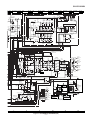
Figure 14 WIRING SIDE OF P.W.BOARD (1/4)
– 14 –
5
6
C252
R252
R256
R419
C257
R255
C253
R251
C260
A
R518
C259
R519
4
FW1
1
R253
C251
R201
R202
C255 R257
4
1 2
C254
R521
R520
C221
R200
LED257
C207
H
IC202
1 2 3 4 5 6 7 8 9
LED259 R259
VR205
C222
C211
C201
R211
2
C204
C205
C202
C213
C209
C217
R207
24
C200
LED501
C206
C214
20
C416
R204
LED253
C413
C415
R420
C203
C215
15
C219
VR202
IC201
R212
10
LED502
R206
VR204
1
5
VR203
C218
C220
G
R205
C208
R208
E
C
B
LED255
C210
C212
C216
R203
Q505
C414
1
C124
C126
C129
C120
R123
R120
R112
C118
C138
R116
R136
R118
C116
C122
R114
4
R410
J151
MIC JACK
GL
D
R
C1
R1
C109
4 3 2 1
BK
R408
C159
R165
C602
R181
R127
D154
BK
C
CNP102
WH
R129
R152
WH
C105
R101
C103
C101
3 2 1
B
D152
24
CNP101
C133
7 6 5 4 3 2 1
C152
R105
C107
SW101
C134
R
C
R107
20
5
R106
D163
D164
R166
R161
10 15
C132
Q181
D165
C156
J401
HEADPHONES JACK
F
L104
A
R170
R168
C157
C158
Q154
R438
Q153
C429
R511
R183
C181
B
C
E
12 13
C108
1
C106
R102
C104
C102
C110
R110
C112
R104
R124
C184
Q182
C180
R185
C185
R187
C183
R180
R184
R186
R188
R182
D162
C426
R434
R133
C186
B
C
E
C128
R128
C155
R437
C114
R134
4
C127
R108
3 2 1
R431
IC151
IC501
R425
R426
R130
C430
R132
C513
R404
C420
1
2
3
R111
C506
R177
E
R352
R100
C514
C428
B
C
E
Q602
C603
E C B
1
R169
C604
Q601
C607
3 2 1
C509
Q603
C505
L301
R351
IC502
C512
FW1
C425
R602
R174
R171
D156
C427
2
R601
D158 1 2 3 4 5 6 7 8 9
R442
C423
IC402
1
2
3
4
5
6
7
8
9
10
11
12
13
14
DZ601
3
2
1
CNP103
C418
1
CNS601
FROM
POWER
PWB
P16 5-F
R436
D
B
C
E
C182
CNP601
R428
R427
R429
C419
R435
R433
C433
R441
C424
C
L501
C508
Q404 Q403
B
C
E
1
2
3
E
C
B
C135
Q502
C510
R516
R515
C608
B
C
E
R514
VR102
C601
E
C
B
E
C
B
R513
Q504
CK129
R512
B
Q503
C511
BI804
Q301
6
R305
1
C307
R304
C306
CNS804 1 2 3 4 5 6
R301
MAIN PWB-A1
C131
CNP501
SPEAKER
TERMINALS
LED260
A
LED258
GX-CD1200W
W102
AT CANCEL
C B A
ROD ANTENNA
SPRING (249)
COLOR TABLE
BR
BROWN
RD(R)
RED
L301
C305
ROD
ANTENNA (253)
R7
WH
C34
C22
C23
C119
C32
R9
C31
R8
24
13
C36
15
20
IC2
R17
R3
C10
TC8
C12
C6
L1
VC1
C4
TC1
VC2
VC1
R11
WH
TC5
TC3
C14
GY
FW2
TC6
C19
C20
C27
C42
E
F
C
D
H
G
B
A
TC9
B
CNS102
C30
ON
R10
A
SW401
SURROUND OFF
SW1
BAND
SELECTOR
SW103
DUBBING SPEED/
MIC/FM MODE
MIC
NORMAL
FM MONO
HIGH
FM MW SW1 SW2
CNS103
FM STEREO
BR
RD
OR
YL
GR
BL
VL
GR
WH
R254
R258
1 2 3 4 5 6 7 8 9
C256
LED1
YL
YL
1
2
3
4
5
6
7
8
9
A
TAPE 2
SW504
HEAD
FLEXIBLE
TAPE1
PWB
DIRECTION
B
+-
R260
A B
LED254
LED256
LED401
C260
C252
R252
C254
R419
R256
IC203
LED260
BK
FINE TUNING
PWB-A4
VC3
C16
L7
RD
C28
TC7
TC2
SW503
TAPE2
PLAY
SW501A
TAPE2
MAIN
GRAPHIC
EQUALIZER
PWB-A2
BK
4
WH
3
RD
2
BK
1
R13
R440
R2
R1
TC4
R415
7
RECORD/PLAYBACK
HEAD
ERASE
HERAD
R4
L8
R173
R301
C13
C9
VC4
LED258
PINK
1 2 3 4 5 6 7 8 9
C21
L103
IC1
C7
C26
C415
BLACK
PK
L3,4
MW/SW1
BAR ANTENNA
D1
C8
C5
C413
BK
TAPE 1
D2
C405 R411
C412
R417
R413
R412
409
GRAY
L5
L2
2
VIOLET
R5
C15
CF1
1 2 3
L6
F
BLUE
VL
WHITE
L4
SW1
L9
C2
R303
101
L11
R172
C131
1
CF3
1 2 3
D152
R109
C111
C105
R103
R101
C109
3
C24
CF2
3 2 1
C37
C25
R20
R14
R135
C137
R107
R105
C107
C41
R15
R12
GREEN
BL
GY
C43
1
C38
E
C
B
C39
GR
WH(W)
C29
5
12
C40
R18
Q156
C117
R121
R115
C160
R113
C115
C121
R117
10
R16
YELLOW
C11
27
R131
R119
C123
C125
TP1
L3
MW
C18
R353
C35
R351
C33
R354
R19
R352
ORANGE
YL
L10
VR1
C17
BK
OR
C
M501
TAPE
MOTOR
SW502
TAPE1
MAIN
PLAYBACK
HEAD
B
A
GR
BK RD
WH
CNS101
RD
GY
WH
8
9
10
Figure 15 WIRING SIDE OF P.W.BOARD (2/4)
– 15 –
11
3
2
1
12
GX-CD1200W
A
SO601
AC SOCKET
AC110V-127V/
AC220V-240V,
50/60Hz
TERMINAL A
PWB-A5
SW601
VOLTAGE SELECTOR
AC220V-240V
AC110V-127V
(251)
(250)
B
BATTERYS
DC15V
["D" SIZE (UM / SUM-1,
R20 or HP2) battery x 10]
OR
C
RD
(251)
TERMINAL B
PWB-A6
T601
POWER
TRANSFORMER
D
BK
WH
BL
(237)
RD
E
WH
OR
COLOR TABLE
F
BR
BROWN
RD(R)
RED
OR
ORANGE
YL
YELLOW
GR
GREEN
CNS601
RD
GY
GRAY
WH(W)
WHITE
BK
BLACK
PK
PINK
C652
C651
VIOLET
P14 1-D
C653
BLUE
VL
CNP601
2
BK
C654
G
BL
F601
T4A L 250V
BK
TO MAIN PWB
1
D651
POWER
PWB-A7
H
1
2
3
4
Figure 16 WIRING SIDE OF P.W.BOARD (3/4)
– 16 –
5
6
GX-CD1200W
CD CONTROL PWB-C2
R847
R848
SW804
REVIEW/
TRACK DOWN
R849
SW802
STOP
SW801
PLAY/
PAUSE
FW801
SW803
CUE/
TRACK UP
LCD801
10
1
8 7 6 5 4 3 2 1
SWITCH PWB-C3
R839
90
C823
R821
1
25
30
31 35
40
45 55
L801
70
65
C843
R832
C837
IC803
20
16
Q802
E
C
B
R801
R853
25
Q801
R807
R805
C820
R806
24
C804
12
8
5
7
6
BR
BK
BK
BK
BK
BK
BK
BK
C805
C813
1
WH
WH
WH
WH
WH
WH
BK
7
6
5
4
3
2
1
10
BI801
C807
C806
7
C822
R894
R893
R895
3 2
1 2 3 4 5 6 7 8
CNS801
8
COLOR TABLE
BR
BROWN
RD(R)
RED
OR
ORANGE
YL
YELLOW
GR
GREEN
CD MOTOR PWB-B
+
M801
SLED MOTOR
BL
BLUE
VL
VIOLET
GY
GRAY
WH(W)
WHITE
BK
BLACK
PK
PINK
F0027AW
SW702
PICKUP IN
SERIAL NO.
+
-
CNP803
1
2
3
4
5
6
R802
R891 R896 R892
1
CNS803
BR 1
GY 2
GY 3
GY 4
GY 5
GY 6
CNS804
FROM
MAIN PWB
P14 5-A
C821
20 15
IC801
10
5
1
6
5
4
3
2
1
9
C818
R803
13
C815
R804
B
C
E
C802
15
10
C893
5
C894
1
C833
C819
C839
C836
C834
C835
C838
C854
C842
C829
R829
C827
C830
R852
R833
R834
R831
51
C828
R826
C863
C840
X801
60
50
11
1
R840
R830
R824
R827
R820
C826
C841
R851
30
IC802
81
80
C832
BI803
2
FW1
C825
R863
C845 R836
R865
85
75
CNP804
15
20
3 2 1 Q804
C852
R828
R844
C844
95
10
C850
C858
Q803
R858
C801
5
R835
R811
C814
C824
R846
12
100
1
C816
FW1
1
C848
10
R861
1
C817
2
C847
1 2 3
BI802
FW801
R812
R822
C851
C853
C849
R857
L803
C846
C855
L802
SW810
OPEN/CLOSE
CD SERVO PWB-C1
17 4 14 15
16
13
M802
SPINDLE MOTOR
PICK-UP UNIT
BI802/CNS802
C801
R802
R891
R892
R893
R894
R895
R896
PICK UP UNIT
7 6 5 4 3 2 1
8 7 6 5 4 3 2 1
To serial
No.00404990
From serial
No.00504991
92LHPC1LASY
QCNWN0027BGZZ
VCQYKA1HM103K
VRD-ST2CD222J
NOT USED
JUMPER
JUMPER
NOT USED
JUMPER
JUMPER
92LHPC1LXASY
QCNWN0032BGZZ
NOT USED
NOT USED
VRD-ST2CD683J
VRD-ST2CD563J
VRD-ST2CD683J
VRD-ST2CD683J
VRD-ST2CD683J
VRD-ST2CD563J
• The numbers 1 to 17 are waveform numbers shown in page 19.
7
8
9
10
Figure 17 WIRING SIDE OF P.W.BOARD (4/4)
– 17 –
11
12
GX-CD1200W
NOTES ON SCHEMATIC DIAGRAM
•
•
•
•
•
Resistor:
To differentiate the units of resistors, The symbol as K and
M are used: the symbol K means 1000 ohm and the symbol
M means 1000 kohm and the resistor without any symbol
is an ohm resistor. The resistor designated “Fusible” is a
fuse type resistor.
Capacitor:
To indicate the unit of capacitor, a symbol P is used: this
symbol P means pico-farad and the unit of the capacitor
without such a symbol is microfarad. As to electrolytic
capacitor, the expression “capacitance/withstand voltage”
is used.
(CH),(RH),(UJ): Temperature compensation
(ML): Mylar type
(S): Styrol type
The indicated voltage in each section is the one measured
by Digital Multimeter between such a section and the
chassis with no signal given.
Schematic diagram and Wiring Side of P.W. Board for this
model are subject to change for improvement without prior
notice.
Parts marked with “ ” (
) are important for
maintaining the safety of the set. Be sure to replace these
parts with specified ones for maintaining the safety and
performance of the set.
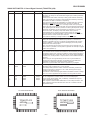
REF. NO.
DESCRIPTION
POSITION
SW1
BAND SELECTOR
FM
SW101
RECORD/PLAYBACK
PLAYBACK
SW102
BEAT CANCEL
A
SW103
DUBBING SPEED/MIC/
FM MODE
MIC/FM MONO
SW401
SURROUND
ON
SW501
FUNCTION SELECTOR
CD/LINE
SW601
VOLTAGE SELECTOR
AC220-240V
SW702
PICKUP IN
OFF
SW902
TAPE 2 MAIN
OFF
SW901
TAPE 1 MAIN
OFF
SW903
TAPE 2 PLAY
OFF
SW904
TAPE 2 DIRECTION
A
FRONT
VIEW
FRONT
VIEW
E C B
E C B
KTA1266 GR
KTA1271 Y
KTC3199 GR
KTC3203 Y
KRA102 M
KTD2058 Y
333ID213
Figure 18 TYPES OF TRANSISTOR AND LED
VOLTAGE
IC2 (LA1805)
PIN
FM
MW/SW
PIN
FM
MW/SW
1
2
3
4
5
6
7
8
9
10
11
12
1.6V
1.6V
7.2V
0.5V
1.6V
0V
7.6V
0V
2.3V
2.3V
6.5V
0.9V
1.6V
1.6V
8V
0.8V
1.6V
0V
7.6V
0V
2.4V
2.4V
8V
0.9V
13
14
15
16
17
18
19
20
21
22
23
24
1V
2.2V
1V
1.7V
1.6V
1.6V
0.4V
7.2V
7.2V
0.5V
1.6V
1.4V
0V
1.8V
1.5V
1.7V
1.7V
1.6V
0.7V
8V
8V
1.6V
1.6V
1.6V
IC101 (TA8189N)
PIN
PLAY
REC
PIN
PLAY
REC
1
2
3
4
5
6
7
8
9
10
11
12
0V
0V
1.3V
1.4V
1.4V
1.3V
0V
0V
1.8V
1.3V
0V
0V
0V
0V
1.3V
1.4V
1.4V
1.3V
0V
0V
1.8V
1.3V
0V
0V
13
14
15
16
17
18
19
20
21
22
23
24
0.9V
0V
1.3V
1.8V
1.4V
7.4V
1.4V
1.4V
1.4V
1.3V
0V
0V
0.9V
0V
1.3V
1.8V
1.4V
7.4V
0V
1.4V
1.4V
1.3V
0V
0V
IC202/203 (LB1403N)
PIN
LED OFF
LED ON
1
2
3
4
5
6
7
8
9
7.7V
7.7V
7.7V
7.7V
0V
7.7V
0V
0V
8.6V
1V
1V
1V
1V
0V
1V
2.4V
0V
8.6V
– 18 –
GX-CD1200W
WAVEFORMS OF CD CIRCUIT
NO DISC FOCUS SEARCH
1
STOP
FO+
FO-
SEL
TRO
2
FMO
3
PLAY
CUE
6
1
TEI
1
TRO
2
FMO
3
IC802 64pin
SBAD
11
2
IC802 67pin
RFO
15
3
IC802 71pin
IC801 22pin
STOP
PLAY
REVIEW
6
1
FEI
TEI
1
TRO
2
FMO
3
IC802 64pin
IC802 62pin
RFGO
11
2
IC801 19pin
IC802 67pin
RFRP
15
3
IC801 17pin
IC802 71pin
STOP
TEI
PLAY
TCD-782 TNO-02 PLAYBACK
16
1
IC802 64pin
LO
1
RO
2
IC802 86pin
TRO
2
SBAD
3
IC802 67pin
7
1
IC802 71pin
IC802 63pin
11
15
3
FEI
6
TEI
IC802 67pin
IC802 62pin
10
11
2
STOP
9
PLAY
IC802 64pin
TEI
5
6
1
FEI
8
3
STOP
IC802 64pin
7
DMO
TOC IL
IC802 62pin
5
2
IC802 72pin
IC802 74pin
6
SBOK
14
3
FOCUS SEARCH
5
1
IC802 45pin
IC803 21pin
4
13
2
IC803 20pin
3
TMAX
IC802 50pin
IC802 66pin
2
12
1
FOO
PLAY
17
IC802 82pin
IC802 63pin
– 19 –
GX-CD1200W
TROUBLESHOOTING (CD SECTION)
When the CD does not function
When the CD section does not operate when the objective lens of the optical pickup is dirty, this section may not operate. Clean
the objective lens, and check the playback operation. When this section does not operate even after the above step is taken, check
the following items.
Remove the cabinet and follow the troubleshooting instructions.
"Track skipping and/or no TOC (Table Of Contents) may be caused by build up of dust other foreign matter on the laser pickup
lens. Before attempting any adjustment make certain that the lens is clean. If not, clean it as mentioned below."
Turn the power off.
Gently clean the lens with a lens cleaning tissue and a small amount of isopropyl alcohol.
Do not touch the lens with the bare hand.
Dust gradually accumulates on the objective lens during use, and it may degrade performance.
To avoid this problem, use a cleaning disc designed for CD optical pickup lenses.
HOW TO USE
1. Using the brush in the cleaner cap, apply 1 or 2 drops of the cleaning fluid to the brush on the CD cleaner disc which has
the mark next to it.
2. Place the CD cleaner disc onto the CD disc tray with the brush side down, then press the play button.
3. You will hear music for about 20 seconds and the CD player will automatically stop. If it continues to turn, press the stop button.
CAUTION
The CD lens cleaner should be effective for 30 - 50 operations, however if the brushes become worn out earlier then please
replace the cleaner disc.
If the CD cleaner brushes become very wet then wipe off any excess fluid with a soft cloth.
Do not drink the cleaner fluid or allow it to come in contact with the eyes. In the event of this happening then drink and / or
rinse with clean water and seek medical advice.
The CD cleaner disc must not be used on car CD player or on computer CD-ROM drives.
All rights reserved. Unauthorized duplicating, broadcasting and renting product is prohibited by law.
Cleaning Disc
PARTS CODE:
UDSKA0004AFZZ
Cleaning Liquid
• The CD function will not work.
The CD operating keys don't work.
Check the power supply, 16.93 MHz clock, and reset terminal.
Check the pickup-in switch (SW702) position.
Check the Focus system.
– 20 –
GX-CD1200W
• Laser failure.
Is +7.5V applied to the emiter of Q802 ?
Check the PWB pattern of Q603.
No
Yes
Is +5V applied to the collector of Q802 ?
Check the peripheral parts of IC803 and Q802.
No
Yes
No
Check the PWB pattern between collector of Q204 and pin 75 of
IC802.
No
Check the PWB pattern between collector of Q204 and pin 1 of
IC801.
No
Check the laser come on when pattern cut between pin 8 (SEL) of
IC801 and pin 74 (SEL) of IC802.
No
Check the peripheral parts of IC801 and Q801. If it is normal, the
optical pickup is faulty.
No
Check as stated in item "FOCUS SERVO SAWTOOTH WAVE
FAILURE".
Is +5V applied to the pin 75 (VDD) of IC802 ?
Yes
Is +5V applied to the pin 1 (VCC) of IC801 ?
Yes
Is +0V applied to the pin 74 (SEL) of IC802 ?
Yes
Is approx. 1.8V applied to the collector of Q801.
Yes
Check BI801/CNS801. If it is normal, the optical pickup is
faulty.
• Focus failure.
Does the optical pickup move up and down when the disc is
removed?
Yes
Is the following waveform ouput at the pin 62 (FEI) of IC802
when the disc is set?
Check the periphery of IC801 and BI801/CNS801. Is it normal?
No
Yes
Yes
pin 62
The optical pickup is faulty.
(FEI)
pin 86
(FOO)
pin 63
(SBAD)
Is the waveform shown above input at the pin 63 (SBAD) of
IC802?
No
Yes
IC801 is faulty.
– 21 –
Check the pattern between pin 13 of IC801 and pin 63 of IC802.
Check the periphery of IC801 and BI801/CNS801.
GX-CD1200W
• Focus servo sawtooth wave failure.
Is sawtooh wave output to the pin 66 (FOO) of IC802 ?
No
IC802 is faulty.
Yes
1.5~2.5sec
Check the PWB pattern of IC803.
Is +8.1V applied to the pins 1 and 30 (VCC) of IC803 ?
No
Yes
Check the PWB pattern of IC803.
Is sawtooth wave obtained between pins 20 and 21 of IC803 ?
No
Yes
1.5~2.5sec
Is sawtooth wave obtained between pins 3 and 4 of BI801/
CNS801 ? (as shown above)
Check the PWB pattern between BI801/CNS801 and IC803.
No
Yes
BI801/CNS801 connection failure or optical pickup failure.
• Spindle motor clv servo failure.
Is following wave output to the pin 55 (AVSS) of IC802 when
the Function is changed to "PLAY" from "STOP" ?
No
Check the procedure in "HF ERROR".
If OK. IC802 is faulty.
No
Check the PWB pattern between pin 72 (DMO) of IC802 and pins
5 and 6 of IC803. If OK. IC803 is faulty.
Yes
DMO
Is above wave obtained between pins 5 and 6 of IC803 ?
Yes
Is above wave obtained between pins 5 and 6 of BI803/
CNS803 ?
Check the PWB pattern between BI803/CNS803 and IC803.
No
Yes
BI803/CNS803 connection failure or optical pickup failure.
– 22 –
GX-CD1200W
• Track search failure
Does the sled motor run in FF/REW state when the CD
TEST MODE is set?
No
Check as stated in item "SLED MOTOR OPERATION FAILURE".
Yes
Is the following wave output to the pin 67 (TRO) of IC802
during track search in normal playback?
No
IC802 failure.
Yes
TRO
Is the following wave output to the pins 12 (TEO) of IC801
during track search in normal playback?
No
Yes
TEO
TEI
Check the PWB pattern between pin 67 (TRO) of IC802 and pin
28 of IC803.
Check the PWB pattern between pins 25 and 26 of IC803 and
Optical pickup.
If OK. Optical pickup failure.
TEZI
Is the above wave output to the pins 64 (TEI) and 65 (TEZI)
of IC802 during track serch in normal playback?
No
Check the PWB pattern between pin 12 (TEO) of IC801 and pins 64
(TEI) and 65 (TEZI) of IC802. If OK. IC801 failure.
No
Check the PWB pattern between pin 22 (RFO) and 18 (RFIS), 17
(RFRP) of IC801 and pins 60 and 61 of IC802. If OK. IC801 failure.
Yes
Is the following wave output to the pin 60 (RFZI) and 61
(RFRP) of IC802 during track search in normal playback?
Yes
RFRP
RFZI
Normal.
• Sled motor operation failure.
Is following sled feed signal output the pin 71 (FMO) of IC802
when FF/REW key is pressed after the CD TEST MODE is
sated?
Yes
FF
IC802 is faulty.
No
REW
FMO
Is following sled feed signal input the pins 12 and 13 of IC803
when FF/REW key is pressed after the CD TEST MODE is
seted?
FF
Yes
No
Check the PWB pattern between pin 71 of IC802 and pins 12 and
13 of IC803.
REW
SL ±
Is sled feed signal output the pins 10 and 11 of IC803?
No
Check the peripheral parts of IC803. If OK, IC803 is faulty.
Yes
Is sled feed voltage applied between both terminals of sled
motor?
Yes
No
Check the BI803/CNS803.
Check the CD mechanism (periphery of sled motor).
If the sled motor does not run when DC2.0V is applied to
both terminals of sled motor, the sled motor is faulty.
• Sled servo failure.
Is following sled signal output the pin 71 (FMO) of IC802
during playback?
IC802 is faulty.
No
Yes
FMO
Normal.
– 23 –
GX-CD1200W
FUNCTION TABLE OF IC
IC802 VHiTC9457F0-1: Servo/Signal Control (TC9457F0) (1/4)
Pin No.
Port Name
1*
2
3
4
5
6*
7*
8*
9*
10*
11*
(OT5)S1
(OT6)S2
(OT7)S3
(OT8)S4
(OT9)S5
(OT10)S6
(OT11)S7
(OT12)S8
(OT13)S9
(OT14)S10
(CLCK/OT15)
S11
(DATA/OT16)
S12
(SFSY/OT17)
S13
(LRCK/OT18)
S14
(BCK/S15)
P8-0
(AOUT/S16)
P8-1
(MBOV/S17)
P8-2
(IPF/S18)
P8-3
12*
13*
14*
15
16
17
18
Terminal Name
Input/Output
Function
SEG1
SEG2
SEG3
SEG4
SEG5
SEG6
SEG7
SEG8
SEG9
SEG10
SEG11
Output
Output
Output
Output
Output
Output
Output
Output
Output
Output
Output
SEG12
Output
SEG13
Output
SEG14
Output
CDSEL0
Output
Segment signal output to the LCD panel.
Up to 72 segments in a matrix with COM1 to COM4 can be displayed.
All of the S1 to S18 pins can be switched for output ports by a program.
Also, the S15 to S18 pins each can be switched for I/O ports individually.
When set for I/O ports, these pins become Nch open-drain output.
Furthermore, the S11 to S14 and the P8-0 to P8-3 pins can be switched for
use as CD signal (CLCK to IPF) input/output pins by a program.
• CLCK: Subcodes P thru W data readout clock input/output.
Selected between input and output by a command.
• DATA: Subcodes P thru W data output.
• SFSY: Playback system frame sync signal output.
• LRCK: Channel clock (44.1kHz) output.
It outputs a low for L channel and a high for R channel.
Polarity can be inverted by a command.
• BCK : Bit clock (1.4122MHz) output.
• AOUT: Audio data output.
• MBOV: Buffer memory-over signal output.
It outputs a high when buffer overflows.
• IPF : Correction flag output. When AOUT is C2 correction output, it
outputs a high indicating that correction is impossible.
CDSEL1
Output
CD LID SW
Output
DOOR OUT
Output
19
20
MVDD
MVSS
MVDD1
MVSS1
—
—
Power supply pins.
Normally, apply a voltage of 4.5 to 5.5V to VDD.
In a backup state (when the CKSTP instruction executed), the device's
current consumption is reduced to 1µA or less, allowing for the supply
voltage to be lowered to 2.0V.
The device is reset and the program starts from address 0 when a voltage
of 2.7V or more is applied to this pin when it is at 0V (power-on reset).
21*
22*
23
24
(K0)P1-0
(K1)P1-1
(K2)P1-2
(K3)P1-3
TRAY CLOSE
TRAY OPEN
PUSEL0
PUSEL1
Input
Input
Input
Input
4-bit CMOS I/O ports.
These ports can be set for input or output bit for bit by a program.
These pins can be pulled up to VDD or down to GND by program.
Therefore, they can be used as key input pins. Also, when they are set for
I/O port, a change of state in this input can be used to clear the clock stop
or wait mode.
25
26
27
28
29
(DCREF)P3-0
(ADin1)P3-1
(ADin2)P3-2
(ADin3)P3-3
(BUZR/
ADin4)P4-0
DISPLAY
ADIN1
ADIN2
MUTE
PU IN
Input
Input
Input
Input
Input
5-bit CMOS I/O ports.
These ports can be set for input or output bit for bit by a program.
The P3-0 to P4-0 pins serve dual purposes as analog inputs for the internal
6-bit 4-channel A/D converters.
The internal A/D converters can complete conversion in 6 instruction cycles
using a successive approximation method. The required pins can be set for
A/D analog input bit for bit by a program. P3-0 can be set for reference
voltage input, and the internal power supply (MVDD) can be used for this
reference voltage.
The P4-0 pin serves dual purposes as a buzzer output pin.
The buzzer output can be selected from 8 frequencies, 0.625 to 3kHz.
Each selected frequency can be output in one of four modes: continuous,
single, 10Hz intermittent, and 10Hz intermittent at 1Hz interval.
Whether or not to use and how to control the A/D converter and buzzer all
can be set by a program.
In this unit, the terminal with asterisk mark (*) is open terminal which is not connected to the outside.
– 24 –
GX-CD1200W
IC802 VHiTC9457F0-1: Servo/Signal Control (TC9457F0) (2/4)
Pin No.
Port Name
30
31*
(S12)P4-1
(SO/S11/
SDA)P4-2
(SCK/SCL)
P4-3
32*
Terminal Name
Input/Output
PUSEL2
NC
Input
Input/Output
NC
Input/Output
Function
3-bit CMOS I/O ports.
These ports can be set for input or output bit for bit by a program.
These pins serve dual purposes as input or output pins for the serial
interface circuit (SIO).
The SIO is a 2-wire/3-wire compatible serial interface. 4 or 8 bits of serial
data, beginning with the MSB or LSB, are serially output from the SO/SDA,
pin at each clock edge on the SCK/SCL pin, and the data on S11 or S12
pin is serially input to the device.
The serial clock (SCK/SCL) allows selection between the internal (450/225/
150/75 kHz) and external sources and a selection of the active edge, rise or
fall. Moreover, since the clock and data can be output via Nch open-drain
outputs, various, device controls and communication between controllers
can be greatly facilitated.
When an SIO interrupt is enabled, an interrupt is generated at completion
of SIO execution and the program jumps to address 4.
All inputs to SIO contain a Schmitt trigger circuit.
33
34
35
36
37
38
TEST0
TEST1
TEST2
TEST3
TEST4
TEST5
TEST0
TEST1
TEST2
TEST3
TEST4
TEST5
Input
Input
Input
Input
Input
Input
Test mode control input pins.
The test mode is selected when these pins are set high and normal
operation is selected when they are low.
39*
40*
41*
42*
(OT19)/HSO
(OT20)SPCK
(OT21)SPDA
(OT22)COFS
/HSO
SPCK
SPDA
COFS
Output
Output
Output
Output
43*
DOUT
DOUT
Input/Output
Digital output pin.
44*
SBSY
SBSY
Input/Output
Subcode block sync output pin. It outputs a high at the S1 position when
subcode sync is detected.
45*
SBOK
SBOK
Input/Output
Subcode Q data CRCC determination result output pin. It outputs a high
when CRCC check is found OK.
46
47
VDD
VSS
VDD1
VSS1
Input/Output
Input/Output
CD unit's digital block power supply pins.
Normally, apply 5V to VDD.
When not using a CD (CD off), this power supply can be turned off, with
only the controller power supply kept active, so that the controller alone is
operating. In this case, the CD off bit must be set to 1. When this bit is set
to 1, pins 11 through 18 and pins 39 through 42 all are changed for output
ports if they have been set for CD control signal input/output pins.
48
P2VREF
P2VREF
Input/Output
PLL block-2 VREF pin.
49
PDO
PDO
Input/Output
This pin outputs a phase error between EFM and PLCK signals.
50
TMAX
TMAX
Input/Output
TMAX detection result output pin.
Selected by command bit TMPS.
Longer than preset period: Outputs P2VREF.
Shorter than preset period: Low level (Vss).
Within preset period: High impedance.
51
LPFN
LPFN
Input/Output
Inverted input of low-pass filter amp.
52
LPFO
LPFO
Input/Output
Output of low-pass filter amp.
53
PVREF
PVREF
Input/Output
PLL block VREF pin.
54
VCOF
VCOF
Input/Output
VCO filter pin.
55
AVSS
AVSS
Input/Output
Analog block ground pin.
56
SLCO
SLCO
Input/Output
DAC output pin for data slice level generation.
57
RFI
RFI
Input/Output
RF signal input pin.
58
AVDD
AVDD
Input/Output
Analog block power supply pin.
59
RFCT
RFCT
Input/Output
RFRP signal center level input pin.
60
RFZI
RFZI
Input/Output
RFRP zero-cross input pin.
61
RFRP
RFRP
Input/Output
RF ripple signal input pin.
62
FEI
FEI
Input/Output
Focus error signal input pin.
CD control output pins.
• /HSO: Playback speed mode output.
High = normal speed; Low = double speed.
• SPCK: Processor status signal readout clock output (176.4kHz)
• SPDA: Processor status signal output.
• COFS: Correction system frame clock output (7.35kHz)
These pins can be switched for output ports by a program.
In this unit, the terminal with asterisk mark (*) is open terminal which is not connected to the outside.
– 25 –
GX-CD1200W
IC802 VHiTC9457F0-1: Servo/Signal Control (TC9457F0) (3/4)
Pin No.
Port Name
63
SBAD
SBAD
Terminal Name
Input/Output
Input/Output
Subbeam add signal input pin.
64
TEI
TEI
Input/Output
Tracking error input pin.
This input is read when tracking servo is on.
65
TEZI
TEZI
Input/Output
Tracking error zero-cross input pin.
66
FOO
FOO
Input/Output
Focus equalizer output pin.
67
TRO
TRO
Input/Output
Tracking equalizer output pin.
68
VREF
VREF
Input/Output
Analog reference power supply pin.
69
RFGC
RFGC
Input/Output
RF amplitude adjusting control signal output pin. It outputs 3-level PWM
signals. (PWM carrier = 88.2kHz)
70
TEBC
TEBC
Input/Output
Tracking balance control signal output pin. It outputs 3-level PWM signals.
(PWM carrier = 88.2kHz)
71
FMO
FMO
Input/Output
Focus equalizer output pin. It outputs 3-level PWM signals.
(PWM carrier = 88.2kHz)
72
DMO
DMO
Input/Output
Disc equalizer output pin. It outputs 3-level PWM signals.
(PWM carrier = DSP block 88.2kHz, synchronized to PXO)
73
2VREF
2VREF
Input/Output
Analog reference power supply pin. (2 x VREF)
74
SEL
SEL
Input/Output
APC circuit on/off signal output pin.
When laser is on, this pin goes to a high-impedance state when UHS = low
and outputs a high when UHS = high
75
76
VDD
VDD
VDD2
VSS2
Input/Output
Input/Output
CD unit's digital block power supply pins.
Normally, apply 5V to VDD.
When not using a CD (CD off), this power supply can be turned off, with
only the controller power supply kept active, so that the controller alone is
operating. In this case, the CD off bit must be set to 1. When this bit is set
to 1, pins 11 through 18 and pins 39 through 42 all are changed for output
ports if they have been set for CD control signal input/output pins.
77
XVSS
XVSS
Input/Output
CD's crystal oscillator power supply pins.
Normally, connect these pins to the power supply lines that are used in
common for the VDD and VSS pins.
78
79
XI
XO
XI
XO
Input/Output
Input/Output
CD's crystal oscillator input/output pins.
Normally, connect 16.934MHz here. This clock is used as the system clock
for the CD. After a system reset, it also is used as the system clock on the
controller side.
80
XVDD
XVDD
Input/Output
CD's crystal oscillator input/output pins.
Normally, connect these pins to the power supply lines that are used in
common for the VDD and VSS pins.
81
DVSR
DVSR
Input/Output
R-channel D/A converter unit ground pin.
82
RO
RO
Input/Output
R-channel data forward output pin.
83
DVRR
DVRR
Input/Output
R-channel reference voltage pin.
84
DVDD
DVDD
Input/Output
D/A converter unit power supply pin.
85
DVRL
DVRL
Input/Output
L-channel reference voltage pin.
86
LO
LO
Input/Output
L-channel data forward output pin.
87
DVSL
DVSL
Input/Output
L-channel D/A converter unit ground pin.
88
89*
NC
NC/VPP
NC
NC
Input/Output
Input/Output
NC pins. Normally, connect these pins to ground or leave them open.
90
/RST
RESET
Input
Function
Device's system reset signal input pin.
The device remains reset while RESET is held low and when RESET is
released back high, the CD unit becomes operational and the program
starts from address 0. Normally, a system reset is asserted when a voltage
of 2.7V or more is applied to VDD when it is at 0V (power-on reset).
Therefore, this pin must be pulled high when used for this purpose.
In this unit, the terminal with asterisk mark (*) is open terminal which is not connected to the outside.
– 26 –
GX-CD1200W
IC802 VHiTC9457F0-1: Servo/Signal Control (TC9457F0) (4/4)
Pin No.
Port Name
91
/HOLD
92
Terminal Name
Input/Output
Function
HOLD
Input
This pin is used to input a signal that requests or clears the hold mode.
Normally, use this pin for CD mode select signal input or battery detection
signal input.
There are two hold modes: clock stop mode (crystal oscillator turned off)
and a wait mode (CPU stopped). These modes are entered by executing
the CKSTP and WAIT instructions, respectively.
The clock stop mode can be requested by a programmed input: low level
detection on HOLD pin or forced execution, and can be cleared by
detecting a high on the HOLD pin or a change of state in its input signal.
When the CKSTP instruction is executed, the clock generator and the CPU
stop operating and the device is placed in a memory backup state. During
this state, the device's current consumption is reduced to 1µA or less.
At the same time, the display output and CMOS output ports are
automatically set low, and the Nch open-drain outputs are turned off.
The wait mode is executed regardles of the input state on the HOLD pin,
with the device's current consumption reduced.
This mode is cleared by a change of state in the HOLD input.
INTR
REMO-IN
Input
External interrupt input pin.
When the interrupt facility is enabled and a pulse of 1.11 to 2.22µs in
duration is applied to this pin, an interrupt is generated and the program
jumps to address 1. Input logic and the active edge (rise or fall) can be
selected for each interrupt input.
Also, the internal 8-bit time clock can be chosen for this interrupt input, in
which case it is possible to count pulses or generate an interrupt at a given
pulse count (address 3).
93*
94*
MXO
MXI
MXO
MXI
—
—
Crystal oscillator pins for the controller.
The oscillator clock is used as the timebase for the clock facility or as the
controller's system clock. Connect a 4.5MHz or 75kHz crystal resonator to
the MXO and MXI pins. Since these pins do not contain internal feedback
resistors, etc, an amp resistor or output resistor must be added external to
the chip.
When using the clock generated by the CD unit's crystal oscillator for
clocking the entire device operation, fix the MXI pin to the GND level.
Oscillation is stopped by executing a CKSTP instruction.
Select the crystal oscillator and control its operation by a program.
95
96
MVSS
MVDD
MVSS
MVDD
—
—
Power supply pins.
Normally, apply a voltage of 4.5 to 5.5V to VDD.
In a backup state (when the CKSTP instruction executed), the device's
current consumption is reduced to 1µA or less, allowing for the supply
voltage to be lowered to 2.0V.
The device is reset and the program starts from address 0 when a voltage
of 2.7V or more is applied to this pin when it is at 0V (power-on reset).
97
98
99
100
OT1
OT2
OT3
OT4
COM1
COM2
COM3
COM4
Output
Output
Output
Output
Common signal outputs to the LCD panel.
Up to 72 segments in a matrix with S1 to S18 can be displayed.
Three voltage levels MVDD, VEE (1/2 MVDD), and GND are output for
83Hz period at 2ms intervals.
After a system reset and after deassertion of a clock stop instruction, the
VEE voltage is output and the DISP OFF bit is set to 0 before common
signals are output.
In this unit, the terminal with asterisk mark (*) is open terminal which is not connected to the outside.
To serial No.006XXXXX
From serial No.007XXXXX
TC9457F-013
JAPAN
TC7457F-022
JAPAN
– 27 –
GX-CD1200W
—MEMO—
– 28 –
GX-CD1200W
PARTS GUIDE
PORTABLE CD STEREO
COMPONENT SYSTEM
GX-CD1200W(BK)
MODEL GX-CD1200W(GL)
“HOW TO ORDER REPLACEMENT PARTS”
To have your order filled promptly and correctly, please furnish the
following information.
1. MODEL NUMBER
2. REF. No.
3. PART NO.
4. DESCRIPTION
For U.S.A. only
Contact your nearest SHARP Parts Distributor to order.
For location of SHARP Parts Distributor,
Please call Toll-Free;
1-800-BE-SHARP
MARK: SPARE PARTS-DELIVERY SECTION
Explanation of capacitors/resistors parts codes
Capacitors
Resistors
VCC ....................... Ceramic type
VCK ........................ Ceramic type
VCT ........................ Semiconductor type
VC • • MF ............... Cylindrical type (without lead wire)
VC • • MN ............... Cylindrical type (without lead wire)
VC • • TV ................ Square type (without lead wire)
VC • • TQ ............... Square type (without lead wire)
VC • • CY ............... Square type (without lead wire)
VC • • CZ ............... Square type (without lead wire)
VC • • • • • • • • • J .. The 13th character represents capacity difference.
("J" ±5%, "K" ±10%, "M" ±20%, "N" ±30%,
"C" ±0.25 pF, "D" ±0.5 pF, "Z" +80-20%.)
VRD ....................... Carbon-film type
VRS ........................ Carbon-film type
VRN ....................... Metal-film type
VR • • MF ............... Cylindrical type (without lead wire)
VR • • MN ............... Cylindrical type (without lead wire)
VR • • TV ................ Square type (without lead wire)
VR • • TQ ............... Square type (without lead wire)
VR • • CY ............... Square type (without lead wire)
VR • • CZ ............... Square type (without lead wire)
VR • • • • • • • • • J .. The 13th character represents error.
("J" ±5%, "F" ±1%, "D" ±0.5%.)
If there are no indications for the electrolytic capacitors, error is ±20%.
If there are no indications for other parts, the resistors are ±5%
carbon-film type.
NOTE:
Parts marked with “
” are important for maintaining the safety of the set.
Be sure to replace parts with specified ones for maintaining the safety and performance of the set.
– 29 –
GX-CD1200W
NO.
PRICE
RANK
PARTS CODE
DESCRIPTION
INTEGRATED CIRCUITS
IC1
IC2
IC101
IC151
IC201
IC202,203
IC401
IC402
IC501,502
IC801
IC802
IC803
VHITA7358AP-1
VHILA1805//-1
VHITA8189N/-1
VHITA2011S/-1
VHIBA3822LS-1
VHILB1403N/-1
VHIKIA4558P-1
VHILA4663//-1
VHIKA7809AP-1
VHITA2109F/-1
VHITC9457F0-1
VHILA6541D/-1
J
J
J
J
J
J
J
J
J
J
J
J
AG
AM
AM
AM
AL
AG
AC
AQ
FM Front End,TA7358AP
FM/AM IF MPX.,LA1805
Record/Playback Amp.,TA8189N
Mic Amp.,TA2011S
Graphic Equalizer,BA3822LS
Level Meter Driver,LB1403N
Ope Amp.,KIA4558P
Power Amp.,LA4663
Voltage Regulator,KA7809AP
AL Servo Pre Amp.,TA2109F
AZ Servo/Signal Control,TC9457F0
AW Focus/Tracking/Spin/Sled Driver,
LA6541D
!
J
J
J
J
J
J
J
J
J
J
J
J
J
J
J
AB
AC
AB
AB
AC
AB
AB
AC
AB
AC
AC
AF
AB
AC
AC
Silicon,NPN,KTC3199 GR
Digital,PNP,KRA102 M
Silicon,NPN,KTC3199 GR
Silicon,NPN,KTC3199 GR
Silicon,NPN,KTC3203 Y
Silicon,NPN,KTC3199 GR
Silicon,NPN,KTC3199 GR
Silicon,PNP,KTA1271 Y
Silicon,NPN,KTC3199 GR
Digital,NPN,KRC102 M
Digital,PNP,KRA102 M
Silicon,NPN,KTD2058 Y
Silicon,PNP,KTA1266 GR
Silicon,PNP,KTA1271 Y
Digital,NPN,KRC102 M
VHDDS1SS133-1
VHDDS1SS133-1
VHDDS1SS133-1
VHDDS1SS133-1
VHDDS1SS133-1
VHDDS1SS133-1
VHDTS4B03GM-1
VHEDZ8R2BSB-1
VHP333ID213-1
VHP333ID213-1
VHP333ID213-1
VHP333ID213-1
J
J
J
J
J
J
J
J
J
J
J
J
AB
AB
AB
AB
AB
AB
AK
AB
Silicon,DS1SS133
Silicon,DS1SS133
Silicon,DS1SS133
Silicon,DS1SS133
Silicon,DS1SS133
Silicon,DS1SS133
Silicon,TS4B03GM
Zener,8.2V,DZ8.2BSB
LED,RED,333ID213
LED,RED,333ID213
LED,RED,333ID213
LED,RED,333ID213
RFILR0008AWZZ
92LFILTF1342A
RFILA0001BGZZ
J
J
J
AE FM Band Pass Filter
AD FM IF,10.7 MHz
AC AM IF,455 kHz
RTRNP0001BGZZ
J
AX Power
RCILB0001BGZZ
RCILR0001BGZZ
RCILA0001BGZZ
RCILA0003BGZZ
RCILB0002BGZZ
RCILB0003BGZZ
RCILB0004BGZZ
RCILI0002BGZZ
RCILI0003BGZZ
RCILI0001BGZZ
VP-MK223K0000
RCILB0005BGZZ
VP-MK470K0000
VP-DHR82K0000
VP-DH100K0000
J
J
J
J
J
J
J
J
J
J
J
J
J
J
J
AD
AA
AH
AC
AC
AC
AC
AD
AD
AD
AC
AD
AB
AE
AB
J
J
AC 10 kohm (B),Semi-VR [VCO]
AC 470 ohms (B),Semi-VR
[Tape Speed]
FILTERS
CF1
CF2
CF3
TRANSFORMER
!
T601
COILS
L1
L2
L3,4
L5
L6
L7
L8
L9
L10
L11
L103,104
L301
L501
L801
L802,803
FM Oscillation
FM Tracking
MW/SW1 Bar Antenna
SW2 Antenna
MW Oscillation
SW1 Oscillation
SW2 Oscillation
FM IF
FM Detection
AM IF
22 mH,Choke
Bias Oscillation
47 µH,Choke
0.82 µH,Choke
10 µH,Choke
VARIABLE RESISTORS
VR1
VR102
RVR-M0026AWZZ
RVR-M0018AWZZ
RVR-Q0002BGZZ
RVR-Q0001BGZZ
J
J
VR401
RVR-B0002BGZZ
J
DESCRIPTION
AE 50 kohms (B)×2 [X-BASS]
AC 100 kohm (B)×2
[Graphic Equalizer]
50 kohms (B)×2 [VOLUME]
VARIABLE CAPACITORS
TC5,6
TC7,8
TC9
VC1~4
RTO-H1003SJZZ
RTO-H1001BGZZ
RVC-Z0001BGZZ
RVC-R0001BGZZ
J
J
J
J
AG
AD
AF
AK
Trimmer,5 pF
Trimmer,10 pF
Fine Tuning
Variable Capacitance with
Trimmer (TC1~4)
J
AF
Ceramic,16.93 MHz
J
J
J
J
J
J
J
J
J
J
J
J
J
J
J
J
J
J
J
J
J
J
J
J
J
J
J
J
J
J
J
J
J
J
J
J
J
J
J
J
J
J
J
J
J
J
J
J
J
J
J
J
J
J
J
J
J
J
J
J
J
J
J
AA
AA
AA
AB
AA
AA
AA
AA
AA
AA
AA
AA
AB
AA
AA
AA
AA
AB
AA
AB
AB
AA
AB
AA
AB
AA
AB
AC
AA
AB
AA
AA
AA
AA
AA
AB
AB
AB
AB
AB
AA
AA
AB
AB
AB
AB
AA
AA
AB
AA
AB
AB
AB
AB
AB
AB
AB
AB
AB
AA
AB
AB
AB
5 pF (CH),50V
24 pF (CH),50V
0.001 µF,50V
0.0047 µF,50V
0.022 µF,50V
15 pF (CH),50V
22 pF (CH),50V
3 pF (CH),50V
0.022 µF,50V
5 pF (CH),50V
0.022 µF,50V
0.022 µF,50V
10 µF,16V,Electrolytic
330 pF,50V
0.0022 µF,50V
5 pF (UJ),50V
0.022 µF,50V
220 µF,10V,Electrolytic
0.022 µF,50V
0.0047 µF,50V
22 µF,16V,Electrolytic
0.022 µF,50V
0.0047 µF,50V,Mylar
0.0082 µF,50V,Mylar
3.3 µF,50V,Electrolytic
470 pF,50V
3.3 µF,50V,Electrolytic
0.0015 µF,100V
0.012 µF,50V,Mylar
1 µF,50V,Electrolytic
0.022 µF,50V
220 pF,50V
470 pF,50V
470 pF,50V
330 pF,50V
47 µF,10V,Electrolytic
0.015 µF,50V,Mylar
4.7 µF,50V,Electrolytic
10 µF,16V,Electrolytic
0.033 µF,50V,Mylar
330 pF,50V
0.01 µF,50V
4.7 µF,50V,Electrolytic
330 µF,10V,Electrolytic
2.2 µF,50V,Electrolytic
22 µF,16V,Electrolytic
120 pF,50V
150 pF,50V
0.0015 µF,50V,Mylar
0.33 µF,50V,Electrolytic
10 µF,16V,Electrolytic
47 µF,10V,Electrolytic
10 µF,16V,Electrolytic
100 µF,10V,Electrolytic
1 µF,50V,Electrolytic
47 µF,25V,Electrolytic
22 µF,16V,Electrolytic
100 µF,10V,Electrolytic
1 µF,50V,Electrolytic
220 pF,50V
1 µF,50V,Electrolytic
100 µF,10V,Electrolytic
4.7 µF,50V,Electrolytic
VIBRATOR
RCRM-0008AWZZ
CAPACITORS
VSKTC3199GR-1
VSKRA102M//-1
VSKTC3199GR-1
VSKTC3199GR-1
VSKTC3203Y/-1
VSKTC3199GR-1
VSKTC3199GR-1
VSKTA1271Y/-1
VSKTC3199GR-1
VSKRC102M//-1
VSKRA102M//-1
VSKTD2058Y/-1
VSKTA1266GR-1
VSKTA1271Y/-1
VSKRC102M//-1
DIODES
D1,2
D152
D154
D156
D158
D162~165
D651
DZ601
LED1
LED253~260
LED401
LED501,502
PRICE
RANK
PARTS CODE
VR202
VR203~205
XL801
TRANSISTORS
Q153
Q154
Q156
Q181,182
Q301
Q403,404
Q502,503
Q504
Q505
Q601
Q602
Q603
Q801
Q802
Q803,804
NO.
C2
C4
C5
C6,7
C8,9
C10
C11
C12
C13
C14
C15
C17
C18
C19
C20
C21
C22
C23
C24~26
C27
C29
C30
C31
C32
C33
C34
C35
C36
C37,38
C39~41
C42
C43
C101,102
C103,104
C105~108
C109,110
C111,112
C113~116
C117,118
C119,120
C121,122
C123,124
C125,126
C127
C128
C129
C131,132
C133,134
C137,138
C151
C152
C154
C155
C156
C157
C158,159
C160
C180
C181,182
C183,184
C185,186
C200
C201,202
–1–
VCCCPU1HH5R0J
VCCCPU1HH240J
VCKYPA1HB102K
VCKYPA1HB472K
VCKZPA1HF223Z
VCCCPU1HH150J
VCCCPU1HH220J
VCCCPU1HH3R0J
VCKZPA1HF223Z
VCCCPU1HH5R0J
VCKZPA1HF223Z
VCKZPA1HF223Z
RC-GZA106AF1C
VCKYPA1HB331K
VCKYPA1HB222K
VCCUPA1HJ5R0C
VCKZPA1HF223Z
RC-GZA227AF1A
VCKZPA1HF223Z
VCKYPA1HB472K
RC-GZA226AF1C
VCKZPA1HF223Z
VCQYKA1HM472K
VCQYKA1HM822K
RC-GZA335AF1H
VCKYPA1HB471K
RC-GZA335AF1H
92LCPU100V1500
VCQYKA1HM123K
RC-GZA105AF1H
VCKZPA1HF223Z
VCKYPA1HB221K
VCKYPA1HB471K
VCKYPA1HB471K
VCKYPA1HB331K
RC-GZA476AF1A
VCQYKA1HM153K
RC-GZA475AF1H
RC-GZA106AF1C
VCQYKA1HM333K
VCKYPA1HB331K
VCKYPA1HB103K
RC-GZA475AF1H
RC-GZA337AF1A
RC-GZA225AF1H
RC-GZA226AF1C
VCKYPA1HB121K
VCKYPA1HB151K
VCQYKA1HM152K
RC-GZA334AF1H
RC-GZA106AF1C
RC-GZA476AF1A
RC-GZA106AF1C
RC-GZA107AF1A
RC-GZA105AF1H
RC-GZA476AF1E
RC-GZA226AF1C
RC-GZA107AF1A
RC-GZA105AF1H
VCKYPA1HB221K
RC-GZA105AF1H
RC-GZA107AF1A
RC-GZA475AF1H
GX-CD1200W
NO.
PRICE
RANK
PARTS CODE
C203,204
C205,206
C207,208
C209,210
C211,212
C213,214
C215,216
C217,218
C219,220
C221,222
C251,252
C253,254
C255,256
C257
C259,260
C301
C302
C303
C304
C305
C306
C307
C401,402
C403,404
C405,406
C407,408
C409,410
C411
C412
C413,414
C415,416
C418
C419,420
C423
C424
C425~428
C429,430
C433
C505
C506
C508
C509
C510
C511
C513,514
C601
C602
C603
C604
C651~654
C801
RC-GZA105AF1H
VCQYKA1HM103K
VCKYPA1HB471K
VCQYKA1HM823K
VCQYKA1HM152K
RC-GZA334AF1H
VCQYKA1HM562K
RC-GZA474AF1H
VCQYKA1HM393K
RC-GZA475AF1H
RC-GZA105AF1H
VCKZPA1HF223Z
RC-GZA106AF1C
RC-GZA476AF1E
VCQYKA1HM392K
RC-GZA107AF1A
VCQYKA1HM222K
VCQYKA1HM562K
VCKZPA1HF223Z
VCQYKA1HM152K
VCKYPA1HB391K
VCKYPA1HB151K
VCQYKA1HM682K
RC-GZA106AF1C
VCQYKA1HM332K
RC-GZA475AF1H
RC-GZA105AF1H
RC-GZA476AF1A
RC-GZA476AF1A
VCQYKA1HM102K
VCQYKA1HM154K
RC-GZA226AF1C
RC-GZA475AF1H
RC-GZA106AF1C
RC-GZA476AF1E
VCQYKA1HM104K
RC-GZA106AF1C
VCKZPA1HF223Z
RC-GZA476AF1C
VCKZPA1HF223Z
RC-GZA107AF1C
VCKZPA1HF223Z
RC-GZG338AF1E
VCKZPA1HF223Z
RC-GZA105AF1H
VCKZPA1HF223Z
RC-GZA107AF1A
VCKZPA1HF223Z
RC-GZA227AF1A
VCKZPA1HF223Z
VCQYKA1HM103K
J
J
J
J
J
J
J
J
J
J
J
J
J
J
J
J
J
J
J
J
J
J
J
J
J
J
J
J
J
J
J
J
J
J
J
J
J
J
J
J
J
J
J
J
J
J
J
J
J
J
J
AB
AA
AA
AC
AB
AA
AA
AA
AB
AB
AB
AA
AB
AB
AA
AB
AA
AA
AA
AB
AA
AA
AA
AB
AA
AB
AB
AB
AB
AA
AB
AB
AB
AB
AB
AB
AB
AA
AB
AA
AB
AA
C802
C804
C805
C806
C807
C813
C814
C815
C816
C817
C818
C819,820
C821
C822
C823
C824
C825
C826
C827
C828
C829
C830
C832
C833
C834,835
C836~839
C840~842
C843
C844
C845
VCKZPA1HF223Z
VCCCPA1HH2R0C
VCKZPA1HF223Z
RC-GZA227AF1A
VCKZPA1HF473Z
RC-GZA476AF1A
VCKZPA1HF473Z
RC-GZA476AF1A
VCKZPA1HF223Z
RC-GZA107AF1A
VCCSPA1HL560J
VCQYKA1HM104K
RC-GZA476AF1A
VCKZPA1HF473Z
VCKZPA1HF223Z
VCQYKA1HM104K
RC-GZA476AF1A
VCCSPA1HL470J
VCQYKA1HM153K
VCKYPA1HB272K
VCKYPA1HB472K
VCQYKA1HM103K
RC-GZA476AF1A
VCQYKA1HM333K
VCKYPA1HB471K
VCQYKA1HM473K
VCKZPA1HF473K
RC-GZA476AF1A
RC-GZA107AF1A
VCKZPA1HF473Z
J
J
J
J
J
J
J
J
J
J
J
J
J
J
J
J
J
J
J
J
J
J
J
J
J
J
J
J
J
J
AA
AA
AA
AB
AA
AB
AA
AB
AA
AB
AA
AB
AB
AA
AA
AB
AB
AA
AB
AA
AB
AA
AB
AB
AA
AB
AA
AB
AB
AA
AA
AB
AA
AB
AA
AB
AA
AA
DESCRIPTION
NO.
1 µF,50V,Electrolytic
0.01 µF,50V,Mylar
470 pF,50V
0.082 µF,50V,Mylar
0.0015 µF,50V,Mylar
0.33 µF,50V,Electrolytic
0.0056 µF,50V,Mylar
0.47 µF,50V,Electrolytic
0.039 µF,50V,Mylar
4.7 µF,50V,Electrolytic
1 µF,50V,Electrolytic
0.022 µF,50V
10 µF,16V,Electrolytic
47 µF,25V,Electrolytic
0.0039 µF,50V,Mylar
100 µF,10V,Electrolytic
0.0022 µF,50V,Mylar
0.0056 µF,50V,Mylar
0.022 µF,50V
0.0015 µF,50V,Mylar
390 pF,50V
150 pF,50V
0.0068 µF,50V,Mylar
10 µF,16V,Electrolytic
0.0033 µF,50V,Mylar
4.7 µF,50V,Electrolytic
1 µF,50V,Electrolytic
47 µF,10V,Electrolytic
47 µF,10V,Electrolytic
0.001 µF,50V,Mylar
0.15 µF,50V,Mylar
22 µF,16V,Electrolytic
4.7 µF,50V,Electrolytic
10 µF,16V,Electrolytic
47 µF,25V,Electrolytic
0.1 µF,50V,Mylar
10 µF,16V,Electrolytic
0.022 µF,50V
47 µF,16V,Electrolytic
0.022 µF,50V
100 µF,16V,Electrolytic
0.022 µF,50V
3300 µF,25V,Electrolytic
0.022 µF,50V
1 µF,50V,Electrolytic
0.022 µF,50V
100 µF,10V,Electrolytic
0.022 µF,50V
220 µF,10V,Electrolytic
0.022 µF,50V
0.01 µF,50V,Mylar
[To Serial No.00404990 Only]
0.022 µF,50V
2 pF (CH),50V
0.022 µF,50V
220 µF,10V,Electrolytic
0.047 µF,50V
47 µF,10V,Electrolytic
0.047 µF,50V
47 µF,10V,Electrolytic
0.022 µF,50V
100 µF,10V,Electrolytic
56 pF,50V
0.1 µF,50V,Mylar
47 µF,10V,Electrolytic
0.047 µF,50V
0.022 µF,50V
0.1 µF,50V,Mylar
47 µF,10V,Electrolytic
47 pF,50V
0.015 µF,50V,Mylar
0.0027 µF,50V
0.0047 µF,50V
0.01 µF,50V,Mylar
47 µF,10V,Electrolytic
0.033 µF,50V,Mylar
470 pF,50V
0.047 µF,50V,Mylar
0.047 µF,50V
47 µF,10V,Electrolytic
100 µF,10V,Electrolytic
0.047 µF,50V
–2–
C846
C847
C848
C849,850
C851,852
C853
C854
C855
C858
C859
C860
C863
C893
C894
PRICE
RANK
PARTS CODE
RC-GZA225AF1H
RC-GZA226AF1C
RC-GZA226AF1C
VCKYPA1HB121K
RC-GZA335AF1H
VCKZPA1HF223Z
VCKYPA1HB682K
VCKZPA1HF223Z
VCKZPA1HF223J
VCKYPA1HB272K
VCKYPA1HB152K
RC-GZA476AF1A
RC-GZA227AF1A
VCKZPA1HF223Z
DESCRIPTION
J
J
J
J
J
J
J
J
J
J
J
J
J
J
AB
AB
AB
AA
AB
AA
AB
AA
AA
AA
AB
AB
AA
2.2 µF,50V,Electrolytic
22 µF,16V,Electrolytic
22 µF,16V,Electrolytic
120 pF,50V
3.3 µF,50V,Electrolytic
0.022 µF,50V
0.0068 µF,50V
0.022 µF,50V
0.022 µF,50V
0.0027 µF,50V
0.0015 µF,50V
47 µF,10V,Electrolytic
220 µF,10V,Electrolytic
0.022 µF,50V
J
J
J
J
J
J
J
J
J
J
J
J
J
J
J
J
J
J
J
J
J
J
J
J
J
J
J
J
J
J
J
J
J
J
J
J
J
J
J
J
J
J
J
J
J
J
J
J
J
J
J
J
J
J
J
J
J
J
J
J
J
J
J
J
J
AA
AA
AA
AA
AA
AA
AA
AA
AA
AA
AA
AA
AA
AA
AA
AA
AA
AA
AA
AA
AA
AA
AA
AA
AA
AA
AA
AA
AA
AA
AA
AA
AA
AA
AA
AA
AA
AA
AA
AA
AA
AA
AA
AA
AA
AA
AA
AA
AA
AA
AA
AA
AA
AA
AA
AA
AA
AA
AA
AA
AA
AA
AA
AA
AA
10 ohm,1/4W
33 ohms,1/6W
47 ohms,1/6W
330 kohms,1/6W
100 ohm,1/6W
820 kohms,1/6W
3.9 kohms,1/6W
12 kohms,1/6W
47 ohms,1/4W
1 kohm,1/6W
100 ohm,1/4W
100 kohm,1/6W
10 kohm,1/6W
2.7 kohms,1/6W
15 kohms,1/6W
10 ohm,1/4W
150 ohms,1/4W
100 ohm,1/6W
180 kohms,1/6W
10 kohm,1/6W
6.8 kohms,1/6W
22 kohms,1/6W
120 kohms,1/6W
680 ohms,1/6W
330 kohms,1/6W
100 ohm,1/6W
10 kohm,1/6W
22 kohms,1/6W
150 kohms,1/6W
1.2 kohms,1/6W
82 kohms,1/6W
10 kohm,1/6W
2.2 kohms,1/6W
4.7 kohms,1/6W
2.2 kohms,1/6W
560 ohms,1/6W
1 Mohm,1/6W
10 kohm,1/6W
560 ohms,1/4W
10 kohm,1/6W
33 kohms,1/6W
10 kohm,1/6W
22 kohms,1/6W
1 kohm,1/6W
560 ohms,1/4W
1 kohm,1/6W
330 kohms,1/6W
220 ohms,1/6W
3.9 kohms,1/6W
330 ohms,1/4W
1 kohm,1/6W
2.2 kohms,1/6W
4.7 kohms,1/6W
3.3 kohms,1/6W
4.7 kohms,1/6W
3.3 kohms,1/6W
1 kohm,1/6W
6.8 kohms,1/6W
39 kohms,1/6W
120 ohms,1/4W
10 kohm,1/6W
120 ohms,1/4W
330 ohms,1/4W
100 ohm,1/4W
10 ohm,1/4W
RESISTORS
R1
R2
R3
R4
R5
R7
R8
R9
R10,11
R12
R13
R14
R15,16
R17,18
R19
R20
R100
R101,102
R105,106
R107,108
R109,110
R111,112
R113,114
R115,116
R117,118
R119,120
R121~124
R127,128
R129,130
R131,132
R133,134
R135,136
R151
R152
R153
R154
R161
R165
R166
R168,169
R170,171
R172,173
R174
R177
R180
R181,182
R183,184
R185,186
R187,188
R200
R201,202
R203,204
R205
R206
R207
R208
R211,212
R251,252
R253,254
R255,256
R257,258
R259,260
R301
R302,303
R304
VRD-ST2EE100J
VRD-ST2CD330J
VRD-ST2CD470J
VRD-ST2CD334J
VRD-ST2CD101J
VRD-ST2CD824J
VRD-ST2CD392J
VRD-ST2CD123J
VRD-ST2EE470J
VRD-ST2CD102J
VRD-ST2EE101J
VRD-ST2CD104J
VRD-ST2CD103J
VRD-ST2CD272J
VRD-ST2CD153J
VRD-ST2EE100J
VRD-ST2EE151J
VRD-ST2CD101J
VRD-ST2CD184J
VRD-ST2CD103J
VRD-ST2CD682J
VRD-ST2CD223J
VRD-ST2CD124J
VRD-ST2CD681J
VRD-ST2CD334J
VRD-ST2CD101J
VRD-ST2CD103J
VRD-ST2CD223J
VRD-ST2CD154J
VRD-ST2CD122J
VRD-ST2CD823J
VRD-ST2CD103J
VRD-ST2CD222J
VRD-ST2CD472J
VRD-ST2CD222J
VRD-ST2CD561J
VRD-ST2CD105J
VRD-ST2CD103J
VRD-ST2EE561J
VRD-ST2CD103J
VRD-ST2CD333J
VRD-ST2CD103J
VRD-ST2CD223J
VRD-ST2CD102J
VRD-ST2EE561J
VRD-ST2CD102J
VRD-ST2CD334J
VRD-ST2CD221J
VRD-ST2CD392J
VRD-ST2EE331J
VRD-ST2CD102J
VRD-ST2CD222J
VRD-ST2CD472J
VRD-ST2CD332J
VRD-ST2CD472J
VRD-ST2CD332J
VRD-ST2CD102J
VRD-ST2CD682J
VRD-ST2CD393J
VRD-ST2EE121J
VRD-ST2CD103J
VRD-ST2EE121J
VRD-ST2EE331J
VRD-ST2EE101J
VRD-ST2EE100J
GX-CD1200W
NO.
PRICE
RANK
PARTS CODE
R305
R306
R351,352
R353,354
R401,402
R403,404
R405,406
R407~410
R411
R412,413
R415,416
R417,418
R419,420
R425,426
R427,428
R429
R431
R433~436
R437,438
R440
R441,442
R511~513
R514
R515
R516
R518,519
R520,521
R601
R602
R801
R802
VRD-ST2EE273J
VRD-ST2EE470J
VRD-ST2CD473J
VRD-ST2CD273J
VRD-ST2CD104J
VRD-ST2CD103J
VRD-ST2CD272J
VRD-ST2CD123J
VRD-ST2EE331J
VRD-ST2CD103J
VRD-ST2CD332J
VRD-ST2CD223J
VRD-ST2CD332J
VRD-ST2CD102J
VRD-ST2CD472J
VRD-ST2CD104J
VRD-ST2CD273J
VRD-ST2CD2R2J
VRD-ST2EE121J
VRD-ST2EE471J
VRD-ST2CD153J
VRD-ST2CD103J
VRD-ST2CD104J
VRD-ST2CD121J
VRD-ST2CD302J
VRD-ST2CD102J
VRD-ST2CD103J
VRD-ST2EE271J
VRD-ST2EE101J
VRD-ST2EE220J
VRD-ST2CD222J
J
J
J
J
J
J
J
J
J
J
J
J
J
J
J
J
J
J
J
J
J
J
J
J
J
J
J
J
J
J
J
AA
AA
AA
AA
AA
AA
AA
AA
AA
AA
AA
AA
AA
AA
AA
AA
AA
AA
AA
AA
AA
AA
AA
AA
AA
AA
AA
AA
AA
AA
AA
R803
R804
R805
R806
R807
R811
R812
R820
R821,822
R824
R826
R827
R828
R829
R830
R831~834
R835,836
R839
R840
R844
R846
R847
R848
R849
R851~853
R857,858
R861
R863
R865
R891
VRD-ST2CD823J
VRD-ST2CD683J
VRD-ST2CD393J
VRD-ST2CD272J
VRD-ST2CD102J
VRD-ST2CD223J
VRD-ST2CD102J
VRD-ST2CD473J
VRD-ST2CD223J
VRD-ST2CD103J
VRD-ST2CD224J
VRD-ST2CD153J
VRD-ST2CD103J
VRD-ST2CD332J
VRD-ST2CD103J
VRD-ST2CD332J
VRD-ST2CD153J
VRD-ST2CD473J
VRD-ST2EE100J
VRD-ST2CD332J
VRD-ST2CD331J
VRD-ST2CD102J
VRD-ST2CD222J
VRD-ST2CD682J
VRD-ST2CD222J
VRD-ST2CD562J
VRD-ST2CD332J
VRD-ST2CD332J
VRD-ST2CD102J
VRD-ST2CD683J
J
J
J
J
J
J
J
J
J
J
J
J
J
J
J
J
J
J
J
J
J
J
J
J
J
J
J
J
J
J
AA
AA
AA
AA
AA
AA
AA
AA
AA
AA
AA
AA
AA
AA
AA
AA
AA
AA
AA
AA
AA
AA
AA
AA
AA
AA
AA
AA
AA
AA
R892
VRD-ST2CD563J
J
AA
R893~895
VRD-ST2CD683J
J
AA
R896
VRD-ST2CD563J
J
AA
NO.
27 kohms,1/4W
47 ohms,1/4W
47 kohms,1/6W
27 kohms,1/6W
100 kohm,1/6W
10 kohm,1/6W
2.7 kohms,1/6W
12 kohms,1/6W
330 ohms,1/4W
10 kohm,1/6W
3.3 kohms,1/6W
22 kohms,1/6W
3.3 kohms,1/6W
1 kohm,1/6W
4.7 kohms,1/6W
100 kohm,1/6W
27 kohms,1/6W
2.2 ohms,1/6W
120 ohms,1/4W
470 ohms,1/4W
15 kohms,1/6W
10 kohm,1/6W
100 kohm,1/6W
120 ohms,1/6W
3.6 kohms,1/6W
1 kohm,1/6W
10 kohm,1/6W
270 ohms,1/4W
100 ohm,1/4W
22 ohms,1/4W
2.2 kohms,1/6W
[To Serial No.00404990 Only]
82 kohms,1/6W
68 kohms,1/6W
39 kohms,1/6W
2.7 kohms,1/6W
1 kohm,1/6W
22 kohms,1/6W
1 kohm,1/6W
47 kohms,1/6W
22 kohms,1/6W
10 kohm,1/6W
220 kohms,1/6W
15 kohms,1/6W
10 kohm,1/6W
3.3 kohms,1/6W
10 kohm,1/6W
3.3 kohms,1/6W
15 kohms,1/6W
47 kohms,1/6W
10 ohm,1/4W
3.3 kohms,1/6W
330 ohms,1/6W
1 kohm,1/6W
2.2 kohms,1/6W
6.8 kohms,1/6W
2.2 kohms,1/6W
5.6 kohms,1/6W
3.3 kohms,1/6W
3.3 kohms,1/6W
1 kohm,1/6W
68 kohms,1/6W
[From Serial No.00504991]
56 kohms,1/6W
[From Serial No.00504991]
68 kohms,1/6W
[From Serial No.00504991]
56 kohms,1/6W
[From Serial No.00504991]
CNP501
CNP601
CNP803
CNP804
CNS101
CNS102
CNS103
CNS601
F601
FW1
FW2
FW801
FW802
J151
J401
LCD801
M501(300-10)
M801
M802
MIC151
SO601
SP401,402
SP403,404
SW1
QTANA0001BGZZ
QCNCM035BAWZZ
92LCONE6P53254
QCNCM705FAFZZ
QCNWN0001BGZZ
QCNWN0002BGZZ
QCNWN0003BGZZ
QCNWN0006BGZZ
QFS-D402ABGNI
QCNWN0038BGZZ
QCNWN0014BGZZ
QCNWN0030AFZZ
QCNWN0029AFZZ
QJAKA0004BGZZ
QJAKM0001BGZZ
RV-LX0001BGZZ
92L1959123012
92LMMTR1651B
92LMMTR1854A
RMICC0001BGZZ
QSOCA0006SJZZ
VSP0012PBG28A
RALMB0001BGZZ
QSW-S9001BGZZ
J
J
J
J
J
J
J
J
J
J
J
J
J
J
J
J
J
J
J
J
J
J
J
J
SW101
QSW-S9002BGZZ
J
AD
SW102
SW103
QSW-S9003BGZZ
QSW-S9004BGZZ
J
J
AC
AC
SW401
SW501
QSW-P9001BGZZ
QSW-S9005BGZZ
J
J
AE
AD
SW601
QSW-S0004SJZZ
J
AK
SW702
SW801
SW801
SW802
SW803
SW804
QSWF9001AW01
QSW-K0008AWZZ
92LSWICHT1663
QSW-K0008AWZZ
QSW-K0008AWZZ
QSW-K0008AWZZ
J
J
J
J
J
J
AC
AC
AC
AC
AC
SW810
QSW-P0004AWZZ
SW901(300-12) 92L640101149
SW902(300-11) 92L640101149
SW903(300-13) 92L640101149
SW904(300-14) 92L64030204
J
J
J
J
J
AE
OTHER CIRCUITRY PARTS
BI801/CNS801 QCNWN0026BGZZ J
BI802/CNS802 QCNWN0027BGZZ J
BI802/CNS802 QCNWN0032BGZZ J
BI803/CNS803
BI804/CNS804
CNP101
CNP102
CNP103
QCNWN0028BGZZ
QCNWN0031BGZZ
QCNCM705CAFZZ
QCNCM705DAFZZ
QCNCM698JAFZZ
J
J
J
J
J
PRICE
RANK
DESCRIPTION
Connector Ass’y,8/8Pin
Connector Ass’y,5/5Pin
[To Serial No.00404990]
Connector Ass’y,7/7Pin
[From Serial No.00504991]
Connector Ass’y,6/6Pin
Connector Ass’y,6/6Pin
AA Plug,3Pin
AB Plug,4Pin
AC Plug,9Pin
!
!
!
PARTS CODE
AD
AB
AC
AB
AD
AE
AF
AD
AC
AA
AG
AE
AL
AP
AF
AB
AC
AE
DESCRIPTION
Terminal,Speaker
Plug,2Pin
Plug,6Pin
Plug,6Pin
Connector Ass’y,3Pin
Connector Ass’y,4Pin
Connector Ass’y,9Pin
Connector Ass’y,2Pin
T4A L 250V
Flat Wire,4Pin
Flat Wire,2Pin
Flat Wire,10Pin
Flat Wire,2Pin
Jack,Mic
Jack,Headphones
LCD Display
Motor with Pulley [Tape]
Motor with Chassis [Sled]
Motor with Gear [Spindle]
Built-in Microphone
AC Socket
Speaker,Woofer
Speaker,Tweeter
Switch,Slide Type
[Band Selector]
Switch,Slide Type
[Record/Playback]
Switch,Slide Type [Beat Cancel]
Switch,Slide Type [Dubbing
Speed/Mic/FM Mode]
Switch,Push Type [Surround]
Switch,Slide Type
[Function Selector]
Switch,Slide Type
[Voltage Selector]
Switch,Push Type [Pickup In]
Switch,Key Type [Play/Pause]
Switch,Key Type [Play/Pause]
Switch,Key Type [Stop]
Switch,Key Type [Cue/Track Up]
Switch,Key Type
[Review/Track Down]
Switch,Push Type [Open/Close]
Switch,Leaf Type [Tape 1 Main]
Switch,Leaf Type [Tape 2 Main]
Switch,Leaf Type [Tape 2 Play]
Switch,Slide Type
[Tape 2 Direction]
CD MECHANISM PARTS
NGERH0011AWZZ
NGERH0012AWZZ
MLEVP0080AWZZ
NSFTM0020AWFW
92LMCUSN1524A
92LHPC1LASY
J
J
J
J
J
J
AC
AC
AC
AD
AD
!
301
302
303
304
305
306
!
306
92LHPC1LXASY
J
BD
307
701
702
703
704
M801
M802
SW702
PCOVP1001AWSA
XBSSD26P06000
XHBSD20P05000
XBBSD20P03000
LX-WZ1070AFZZ
92LMMTR1651B
92LMMTR1854A
QSWF9001AW01
J
J
J
J
J
J
J
J
AE
AA
AA
AA
AA
AL
AP
Gear,Middle
Gear,Drive
Rail,Guide
Shaft,Guide
Cushion
Pickup Unit Ass’y
[To Serial No.00404990]
Pickup Unit Ass’y
[From Serial No.00504991]
Cover,CD Mechanism
Screw,ø2.6×6mm
Screw,ø2×5mm
Screw,ø2×3mm
Washer,ø1.5×ø3.8×0.25mm
Motor with Chassis [Sled]
Motor with Gear [Spindle]
Switch,Push Type [Pickup In]
CABINET PARTS
201
201
202
202
203
203
204
205
206
207
208
–3–
GCABA1003BGSA
GCABA1003BGSB
GFTAC0001BGSB
GFTAC0001BGSC
GFTAC0002BGSB
GFTAC0002BGSC
HBDGA1003BGSA
HBDGS1001BGSA
HDECQ0001BGSA
HDECQ0004BGSA
HDECQ0017BGSA
J
J
J
J
J
J
J
J
J
J
J
AK
AK
AF
AH
AD
Front Cabinet [GL]
Front Cabinet [BK]
Cassette Holder [Tape 1] [BK]
Cassette Holder [Tape 1] [GL]
Cassette Holder [Tape 2] [BK]
Cassette Holder [Tape 2] [GL]
Badge,SHARP
Sheet,Surround Sound System
Panel,Display
Ring,Volume Knob
Panel,Cassette Holder [Tape 1]
GX-CD1200W
NO.
PRICE
RANK
PARTS CODE
209
210
211
212
213
214
215
216
218
219
220
221
222
222
223
223
224
224
225
HDECQ0008BGSA
HDECZ0001BGSA
HSSND0001BGSA
JKNBQ0001BGSC
LANGT0001BGFW
MLIFP0001BGZZ
MSPRD0001BGFW
NGERH0002BGZZ
LANGG0001BGFW
HDECQ0005BGSA
JKNBK0001BGSB
LHLDW1033CE00
JBTN-0001BGSB
JBTN-0001BGSC
JBTN-0002BGSB
JBTN-0002BGSC
JBTN-0003BGSB
JBTN-0003BGSC
JBTN-0004BGSB
J
J
J
J
J
J
J
J
J
J
J
J
J
J
J
J
J
J
J
225
JBTN-0004BGSC
J
226
226
227
227
228
JBTN-0005BGSB
JBTN-0005BGSC
JBTN-0006BGSB
JBTN-0006BGSC
JBTN-0007BGSB
J
J
J
J
J
228
JBTN-0007BGSC
J
229
229
230
230
231
JBTN-0008BGSB
JBTN-0008BGSC
JBTN-0009BGSB
JBTN-0009BGSC
JBTN-0010BGSB
J
J
J
J
J
231
JBTN-0010BGSC
J
232
232
233
233
234
235
236
237
238
239
240
241
242
243
244
245
245
246
247
247
248
JBTN-0011BGSB
JBTN-0011BGSC
JBTN-0012BGSB
JBTN-0012BGSC
LANGF0001BGZW
LHLDZ8001BG00
LHLDZ1002BGZZ
MSPRC0001BGFJ
PRDAR0001BGFW
NGERK0001BGZZ
PSHEP0001BGSA
PSHEP0002BGSA
JKNBZ0001BGSA
PCOVZ9001BGZZ
MSPRP0001BGFW
GCABB1003BGSA
GCABB1003BGSB
GLEGG0001BG00
JHNDP1002BGSA
JHNDP1002BGSB
LHLDQ1001BGZZ
J
J
J
J
J
J
J
J
J
J
J
J
J
J
J
J
J
J
J
J
J
249
250
251
253
254
255
256
257
258
259
260
261
262
263
263
264
MSPRB0002BGFW
MSPRC0002BGFJ
MSPRC0003BGFJ
QANTR0002BGZZ
LHLDR1001BGZZ
NGERK0002BGZZ
NGERK0003BGZZ
JKNBM0001BGSA
JKNBP0001BGSA
JKNBP0001BGSA
JKNBP0002BGSA
LHLDS1002BGZZ
MLEVP0002BGZZ
GFTAB1001BGSB
GFTAB1001BGSC
TSPC-0017BGZZ
J
J
J
J
J
J
J
J
J
J
J
J
J
J
J
J
264
TSPC-0018BGZZ
J
264
TSPC-0020BGZZ
J
DESCRIPTION
NO.
AD Panel,Cassette Holder [Tape 2]
AC Panel,Dial Pointer
AC Dial Pointer
Knob,Tuning
AD Bracket,Front Cabinet
AD Gear,Cassette Holder
AB Spring,Cassette Holder Up
AC Gear,Tuning Knob
AB Guide,Dial Pointer
AC Cap,Volume Knob
Knob,Volume
Nylon Band
AC Button,Record [Tape 1] [BK]
Button,Record [Tape 1] [GL]
AC Button,Play [Tape 1] [BK]
Button,Play [Tape 1] [GL]
AC Button,Rewind [Tape 1] [BK]
Button,Rewind [Tape 1] [GL]
AC Button,Fast Forward [Tape 1]
[BK]
Button,Fast Forward [Tape 1]
[GL]
AC Button,Stop/Eject [Tape 1] [BK]
Button,Stop/Eject [Tape 1] [GL]
AC Button,Pause [Tape 1] [BK]
Button,Pause [Tape 1] [GL]
AC Button,Reverse Mode [Tape 2]
[BK]
Button,Reverse Mode [Tape 2]
[GL]
AC Button,Play [Tape 2] [BK]
Button,Play [Tape 2] [GL]
AC Button,Rewind [Tape 2] [BK]
Button,Rewind [Tape 2] [GL]
AC Button,Fast Forward [Tape 2]
[BK]
Button,Fast Forward [Tape 2]
[GL]
AC Button,Stop/Eject [Tape 2] [BK]
Button,Stop/Eject [Tape 2] [GL]
AC Button,Direction [Tape 2] [BK]
Button,Direction [Tape 2] [GL]
Support,Mechanism Button Shaft
AC Holder,Mic
AC Holder,LED A
AC Spring,Battery,AL Heat Sink,Main
AD Dial Drum
AD Sheet,LED,Left
AD Sheet,LED,Right
AC Knob,Fine Tuning
AB Cover,Dial Pointer
AC Plate,Record
Rear Cabinet [GL]
Rear Cabinet [BK]
AB Cushion,Leg
Handle [GL]
Handle [BK]
AE Holder,AC Socket/Voltage
Selector
AB Spring,Rod Antenna
AC Spring,Battery,+/AC Spring,Battery,+/AK Rod Antenna
AD Holder,Tuning
AB Gear,Tuning A
AB Gear,Tuning B
AD Button,Surround
AA Knob,Function
AA Knob,Dubbing Speed
AB Knob,Band Selector
AC Holder,Record Lever
AB Lever,Record
AE Battery Compartment Lid [BK]
Battery Compartment Lid [GL]
Label,Specifications [GL]
[For Malaysia/Asia Middle East/
Africa]
Label,Specifications [GL]
[For Jordan/Egypt]
Label,Specifications [GL]
[For Thailand]
–4–
!
!
PRICE
RANK
PARTS CODE
264
TSPC-0026BGZZ
J
264
TSPC-0027BGZZ
J
264
TSPC-0028BGZZ
J
264
TSPC-0029BGZZ
J
264
TSPC-0030BGZZ
J
266
267
267
268
268
269
270
271
271
272
273
274
275
276
277
278
279
280
300
300- 1
300- 2
300- 3
PRDAR0002BGFW
GCABC1003BGSA
GCABC1003BGSB
GFTAT1001BGSA
GFTAT1001BGSB
HPNLZ1001BGSA
HPNLZ1002BGSA
JBTN-0024BGSA
JBTN-0024BGSB
MLEVP0003BGZZ
JKNBK0002BGSA
LHLDM1001BGZZ
PMAGF0001BGZZ
LHLDZ1003BGZZ
MSPRD0002BGFJ
QFSHD0017CEZZ
QFSHD0018CEZZ
MSPRB0003BGFW
CMECB0001BG01
92L192104309
92L195904302
92L195904301
J
J
J
J
J
J
J
J
J
J
J
J
J
J
J
J
J
J
J
J
J
J
300- 4
92L6201-01-111
300- 5
92L6209-10-10
300- 6
92L6216-07-01
300- 7
92L19210703
300- 8
92L182112173
300- 9
92L182112142
300-10(M501) 92L1959123012
300-11(SW902) 92L640101149
300-12(SW901) 92L640101149
300-13(SW903) 92L640101149
300-14(SW904) 92L64030204
J
J
J
J
J
J
J
J
J
J
J
601
602
603
604
605
606
607
608
609
610
611
612
613
J
J
J
J
J
J
J
J
J
J
J
J
J
XEBSD30P10000
XJBSD30P08000
XBPSD26P04JS0
XHBSD20P04000
XJSSD30P10000
XBBSF30P10000
XJBSD40P16000
XEBSD30P20000
XHSSF30P06000
XEBSD30P10000
LX-JZ0002AWFD
XESSD30P10000
LX-EZ0005AWFD
BL
AA
AA
AA
AA
AA
AB
AA
AA
AA
AA
AA
DESCRIPTION
Label,Specifications [BK]
[For Malaysia/Asia Middle East/
Africa]
Label,Specifications [BK]
[For Jordan/Egypt]
Label,Specifications [BK]
[For Thailand]
Label,Specifications [GL]
[For Australia]
Label,Specifications [BK]
[For Australia]
Heat Sink,Sub
Top Cabinet [GL]
Top Cabinet [BK]
CD Lid [GL]
CD Lid [BK]
Panel,Decoration
Panel,LCD
Button,CD Lid Open [GL]
Button,CD Lid Open [BK]
Lock Lever,CD Lid
Button,Function
Stabilizer
Magnet
Holder,LCD
Spring,CD Lid
Holder,Fuse
Holder,Fuse
Spring,CD LID Open Button
Tape Mechanism Ass’y
Pinch Roller Arm Ass’y
Pinch Roller Arm Ass’y,Rewind
Pinch Roller Arm Ass’y,Fast
Forward
Head,Record/Playback,Tape 1
Head,Erase,Tape 1
Head,Playback,Tape 2
FF/REW Belt
Main Belt,Tape 1
Main Belt,Tape 2
Motor with Pulley [Tape]
Switch,Leaf Type [Tape 2 Main]
Switch,Leaf Type [Tape 1 Main]
Switch,Leaf Type [Tape 2 Play]
Switch,Slide Type
[Tape 2 Direction]
Screw,ø3×10mm
Screw,ø3×8mm
Screw,ø2.6×4mm
Screw,ø2×4mm
Screw,ø3×10mm
Screw,ø3×10mm
Screw,ø4×16mm
Screw,ø3×20mm
Screw,ø3×6mm
Screw,ø3×10mm
Screw,ø3×10mm
Screw,ø3×10mm
Screw,ø2.6×10mm
SPEAKER BOX PARTS
301
301
302
302
303
303
304
304
305
306
306
307
308
309
701
702
SP401,402
SP403,404
CCAB-120LBG01G
CCAB-120LBG01K
CCAB-120RBG01G
CCAB-120RBG01K
GCABD1001BGSB
GCABD1001BGSC
GCABF1001BGSB
GCABF1001BGSC
GLEGG0001BG00
LHLDW1001BGSB
LHLDW1001BGSC
QCNWG0001BGZZ
LPLTW0001BGZZ
LPLTW0002BGZZ
XEBSD30P10000
XJBSD40P16000
VSP0012PBG28A
RALMB0001BGZZ
J
J
J
J
J
J
J
J
J
J
J
J
J
J
J
J
J
J
AQ
AQ
AB
AB
AE
AC
AC
AA
AB
AC
Front Panel,Ass’y,Left [GL]
Front Panel,Ass’y,Left [BK]
Front Panel,Ass’y,Right [GL]
Front Panel,Ass’y,Right [BK]
Speaker Box,Left [BK]
Speaker Box,Left [GL]
Speaker Box,Right [BK]
Speaker Box,Right [GL]
Cushion,Leg,Speaker
Holder,Speaker Cord [BK]
Holder,Speaker Cord [GL]
Cord,Speaker
Support H,Speaker Box
Support V,Speaker Box
Screw,ø3×10mm
Screw,ø4×16mm
Speaker,Woofer
Speaker,Tweeter
GX-CD1200W
NO.
PRICE
RANK
PARTS CODE
DESCRIPTION
NO.
ACCESSORIES/PACKING PARTS
!
!
!
!
!
QACCA0001SJ00
QACCE0007AW00
QACCL0002AW00
QPLGA0250AFZZ
QPLGA0253AFZZ
SPAKA0003BGZZ
SPAKC0023BGZZ
J
J
J
J
J
J
J
AS
AH
AN
AF
AE
SPAKC0024BGZZ
J
SPAKC0033BGZZ
J
SPAKC0034BGZZ
J
SSAKA0002BGZZ
J
AB
SSAKH0002BGZZ
SSAKH0004BGZZ
SSAKH0005BGZZ
TGANE0002BG03
TGANE0003BGZZ
TINSZ0008BGZZ
TLABB0001BGZZ
TLABB0002BGZZ
TLABE0005BGZZ
TLABE0008BGZZ
TLABR1137BGZZ
TLABR1138BGZZ
TLABS0002BGZZ
TLABS0003BGZZ
TLABZ0001BGZZ
TLABZ0002BGZZ
TLABZ0009BGZZ
TLABZ0010BGZZ
J
J
J
J
J
J
J
J
J
J
J
J
J
J
J
J
J
J
AB
AB
AB
TLABZ0011BGZZ
J
TLABZ0012BGZZ
J
AB
AC
AC Power Supply Cord
AC Power Supply Cord
AC Power Supply Cord
Adaptor,AC Plug
Adaptor,AC Plug
Packing Add.,Unit
Packing Case [GL]
[For Malaysia]
Packing Case [GL]
[Except for Malaysia]
Packing Case [BK]
[For Malaysia]
Packing Case [BK]
[Except for Malaysia]
Polyethylene Bag,AC Plug
Adaptor
Polyethylene Bag,Accessories
Polyethylene Bag,Unit
Polyethylene Bag,Speaker
Warranty Card [For Philippines]
Warranty Card [For Australia]
Operation Manual
Label,Japan
Label,Japan
Label,Ean Bar Code [GL]
Label,Ean Bar Code [BK]
Label,Bar Code [GL]
Label,Bar Code [BK]
Label,Laser
Label,Class 3
Label,Contru origin for Set
Label,Contru origin for P-case
Label,Feature,Left [For Malaysia]
Label,Feature,Right
[For Malaysia]
Label,Feature,Left
[Except for Malaysia]
Label,Feature,Right
[Except for Malaysia]
P.W.B. ASSEMBLY (Not Replacement Item)
PWB-A1~8
DUNTK0003BG01
J
PWB-B
PWB-C1~3
QPWBF0027AWZZ J
DUNTK0004BG01 J
—
Main/Graphic Equalizer/Volume/
Fine Tuning/Terminal A/
Terminal B/Power/Holder
(Combined Ass’y)
AD CD Motor (PWB Only)
— CD Servo/CD Control/Switch
(Combined Ass’y)
OTHER SERVICE PART
UDSKA0004AFZZ
J
AZ
Pickup Lens Cleaner
–5–
PARTS CODE
PRICE
RANK
DESCRIPTION
GX-CD1200W
307
A
306
B
701
304
701
704
C
302
702
301
D
303
703x2
E
M802
F
305
M801
305x2
G
SW702
PWB-B
H
1
2
3
4
Figure 6 CD MECHANISM EXPLODED VIEW
–6–
5
6
GX-CD1200W
269
247
271
CD
MECHANISM
A
610x2
268
278
277
263
275
267
274
608x3
253
245
PWB-C2
613x3
B
264
273
612x3
276
LCD801
601x3
606
PWB-C3
272
214
607
SW601
PWB-C1
609
248
601x3
C
SO601
250
607x3
T601
PWB-A6
607x2
246
246x2
251
249
609
279
280
601x2
D
237
PWB-A7
246
PWB-A5
601
603
601x2
236
213
605x5
270
255
239
256 Silicon
Grease
254
MIC151 240
602
601x2
211
266
601
235
PWB-A8
218
204
E
601
PWB-A2
241
201
251
611
601
Silicon
Grease
258
238
VR401
PWB-A3
PWB-A1
601
259
260
243
IC502
602x2
257
205
601x2
IC402
Q601
214x2
F
602x2
261
601
605x6
244
213
242
216
222
223
224
PWB-A4
225
226 227
202
228
229
203
230
231
232
210
206
With VR401
234x2
233
207
300(300-1, 300-2, 300-3,
300-4, 300-5, 300-6, 300-7,
300-8,300-9,300-10(M501),
300-11(SW902),
300-12(SW901),
300-13(SW903),
300-14(SW904)
220
219
208
215
221
215
604
TAPE
MECHANISM
601
212
G
262
209
H
Note: Only the unit and consumale parts are supplied as parts supply for the Tape mechanism.
1
2
3
4
Figure 7 CABINET EXPLODED VIEW
–7–
5
6
GX-CD1200W
A
702x5
303(LEFT)
304(RIGHT)
301(LEFT)
302(RIGHT)
SP403(L-CH)
SP404(R-CH)
307
B
701x4
306
C
308
D
SP401(L-CH)
SP402(R-CH)
305
305
309
305
305
TWEETER
SP403(L-CH)
SP404(R-CH)
E
BLACK
RED
BLACK
F
TWEETER
SP403(L-CH)
SP404(R-CH)
G
WOOFER
SP401(L-CH)
SP402(R-CH)
RED
WOOFER
SP401(L-CH)
SP402(R-CH)
H
1
2
3
4
Figure 8 SPEAKER EXPLODED VIEW
–8–
5
6
GX-CD1200W
—MEMO—
–9–
GX-CD1200W
—MEMO—
– 10
GX-CD1200W
COPYRIGHT
©
2000 BY SHARP CORPORATION
ALL RIGHTS RESERVED.
No part of this publication may be reproduced,
stored in a retrieval system, or transmitted in
any from or by any means, electronic, mechanical,
photocopying, recording, or otherwise, without
prior written permission of the publisher.
SHARP CORPORATION
Communication Systems Group
Quality & Reliability Control Center
Higashihiroshima, Hiroshima 739-0192, Japan
Printed in Japan
A0006-1408DS•HA•I
SCA • SCNZ • EX