1
Virtex-5 FPGA
Integrated Endpoint Block
for PCI Express Designs
User Guide
UG197 (v1.5) July 22, 2009
R
R
Xilinx is disclosing this user guide, manual, release note, and/or specification (the "Documentation") to you solely for use in the development
of designs to operate with Xilinx hardware devices. You may not reproduce, distribute, republish, download, display, post, or transmit the
Documentation in any form or by any means including, but not limited to, electronic, mechanical, photocopying, recording, or otherwise,
without the prior written consent of Xilinx. Xilinx expressly disclaims any liability arising out of your use of the Documentation. Xilinx reserves
the right, at its sole discretion, to change the Documentation without notice at any time. Xilinx assumes no obligation to correct any errors
contained in the Documentation, or to advise you of any corrections or updates. Xilinx expressly disclaims any liability in connection with
technical support or assistance that may be provided to you in connection with the Information.
THE DOCUMENTATION IS DISCLOSED TO YOU “AS-IS” WITH NO WARRANTY OF ANY KIND. XILINX MAKES NO OTHER
WARRANTIES, WHETHER EXPRESS, IMPLIED, OR STATUTORY, REGARDING THE DOCUMENTATION, INCLUDING ANY
WARRANTIES OF MERCHANTABILITY, FITNESS FOR A PARTICULAR PURPOSE, OR NONINFRINGEMENT OF THIRD-PARTY
RIGHTS. IN NO EVENT WILL XILINX BE LIABLE FOR ANY CONSEQUENTIAL, INDIRECT, EXEMPLARY, SPECIAL, OR INCIDENTAL
DAMAGES, INCLUDING ANY LOSS OF DATA OR LOST PROFITS, ARISING FROM YOUR USE OF THE DOCUMENTATION.
© 2006-2009 Xilinx, Inc. XILINX, the Xilinx logo, Virtex, Spartan, ISE, and other designated brands included herein are trademarks of Xilinx
in the United States and other countries. PCI, PCI Express, PCIe, and PCI-X are trademarks of PCI-SIG. All other trademarks are the
property of their respective owners.
Virtex-5 FPGA Integrated Endpoint Block
www.xilinx.com
UG197 (v1.5) July 22, 2009
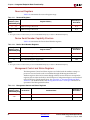
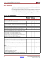
Revision History
The following table shows the revision history for this document.
Date
Version
Revision
09/06/06
1.0
Initial Xilinx release on CD.
03/20/07
1.1
Moved “TX and RX Buffer Layout” and “Buffer Latency” from Chapter 2 to Appendix
A. Renamed Chapter 3 to “Designing with the Endpoint Block Plus Wrapper”and
replaced content. Split Error Reporting table into Table 4-3 (PCIe Block action) and
Table 4-4 (User action). Added VHDL code examples to “Simulating in VHDL” in
Chapter 5.
12/13/07
1.2
Revised L0PWRTURNOFFREQ description in Table 2-15, page 45 and added a footnote
tied to power state D3. Clarified request types when crossing a 4 KB boundary in
Table 4-2, page 70.
Replaced Chapter 3, “Designing with the Endpoint Block Plus Wrapper.”
Addition of “Known Restrictions,” page 78.
06/02/08
1.3
Updated “TX Transmission Issues Due to Lack of Data Credits,” page 78 including
workaround.
Added “Lane Reversal,” page 77.
Fixed LLKRXDSTREQN in “Invalid Cycles in LLKRXPREFERREDTYPE Signal,” page 81.
Updated “Credit Leak When Transmitting Completion TLPs,” page 86.
Added “Receipt of Back-to-Back ACK DLLPs,” page 87.
UG197 (v1.5) July 22, 2009
www.xilinx.com
Virtex-5 FPGA Integrated Endpoint Block
Date
Version
Revision
09/23/08
1.4
• Removed references to Virtual Channel 1 (VC1) and multiple VCs throughout the
document.
• Changed references to RocketIO GTP transceiver to RocketIO transceiver to include GTX
transceivers as well.
• Changed references to CORE Generator Wrapper to Endpoint Block Plus Wrapper.
• Rewrote introduction to “About This Guide,” page 9.
• Added “Additional Documentation,” page 10.
• Added introductory paragraph to “Virtex-5 FPGA Integrated Endpoint Block
Interface Descriptions,” page 21.
• Removed “PCI Express Virtual Channel Capability Structure” and added its
corresponding range as reserved to Table 2-21, page 56.
• Changed locations 0x40B through 0x412 to reserved in Table 2-23, page 56.
• Renamed Chapter 3, “Designing with the Endpoint Block Plus Wrapper,” and revised
introductory paragraphs.
• Renamed Chapter 4, “Integrated Endpoint Block Operation,” and revised the
introductory paragraph.
• Removed “Expansion ROM”, “Handling Inbound Completion Packets”, “Traffic
Class to Virtual Channel Mapping”, “Operation as a Transaction Requester”,
“Operation as a Transaction Completer”, “Virtual Channel Arbitration”, “Message
Signaled Interrupts”, and “Legacy Interrupts” from Chapter 4, “Integrated Endpoint
Block Operation.” Some of these sections were moved to UG341, LogiCORE IP
Endpoint Block Plus for PCI Express User Guide.
• Replaced content of Chapter 5, “Simulating with the Integrated Endpoint Block,”
with paragraph referring to UG343, LogiCORE IP Endpoint Block Plus for PCI Express
Getting Started Guide.
• Removed VC Enabled scenario from Table A-6, page 95.
• Updated the VC1*, LOWPRIORITYVCCOUNT,
PORTVCCAPABILITYEXTENDEDVCCOUNT, PORTVCCAPABILITYVCARBCAP,
PORTVCCAPABILITYVCARBTABLEOFFSET, AERBASEPTR, DSNBASEPTR,
MSIBASEPTR, PBBASEPTR, PMBASEPTR, VCBASEPTR, and XPBASEPTR attributes
in Table A-7, page 96.
07/22/09
1.5
Changed instances of 64 packets to 48 packets in “48-Packet Threshold on Posted Packets
Passing Non-posted and Completion Packets in the TX Direction,” page 82.
Virtex-5 FPGA Integrated Endpoint Block
www.xilinx.com
UG197 (v1.5) July 22, 2009
Table of Contents
Revision History . . . . . . . . . . . . . . . . . . . . . . . . . . . . . . . . . . . . . . . . . . . . . . . . . . . . . . . . . . . . . 3
Preface: About This Guide
Guide Contents . . . . . . . . . . . . . . . . . . . . . . . . . . . . . . . . . . . . . . . . . . . . . . . . . . . . . . . . . . . . . . 9
Additional Documentation . . . . . . . . . . . . . . . . . . . . . . . . . . . . . . . . . . . . . . . . . . . . . . . . . . 10
Additional Support Resources . . . . . . . . . . . . . . . . . . . . . . . . . . . . . . . . . . . . . . . . . . . . . . . 11
Typographical Conventions . . . . . . . . . . . . . . . . . . . . . . . . . . . . . . . . . . . . . . . . . . . . . . . . . 11
Online Document . . . . . . . . . . . . . . . . . . . . . . . . . . . . . . . . . . . . . . . . . . . . . . . . . . . . . . . . . 11
Chapter 1: Virtex-5 FPGA Integrated Endpoint Block Overview
Summary . . . . . . . . . . . . . . . . . . . . . . . . . . . . . . . . . . . . . . . . . . . . . . . . . . . . . . . . . . . . . . . . . . .
The PCI Express Standard . . . . . . . . . . . . . . . . . . . . . . . . . . . . . . . . . . . . . . . . . . . . . . . . . . .
Virtex-5 FPGA Integrated Endpoint Block for PCI Express Designs . . . . . . . . . .
Memory Requirements . . . . . . . . . . . . . . . . . . . . . . . . . . . . . . . . . . . . . . . . . . . . . . . . . . . . . .
Use Models . . . . . . . . . . . . . . . . . . . . . . . . . . . . . . . . . . . . . . . . . . . . . . . . . . . . . . . . . . . . . . . . .
13
13
14
15
15
Chapter 2: Integrated Endpoint Block Functionality
Summary . . . . . . . . . . . . . . . . . . . . . . . . . . . . . . . . . . . . . . . . . . . . . . . . . . . . . . . . . . . . . . . . . . . 17
Architecture Overview . . . . . . . . . . . . . . . . . . . . . . . . . . . . . . . . . . . . . . . . . . . . . . . . . . . . . . 17
Transaction Layer. . . . . . . . . . . . . . . . . . . . . . . . . . . . . . . . . . . . . . . . . . . . . . . . . . . . . . . . .
Data Link Layer . . . . . . . . . . . . . . . . . . . . . . . . . . . . . . . . . . . . . . . . . . . . . . . . . . . . . . . . . .
Physical Layer . . . . . . . . . . . . . . . . . . . . . . . . . . . . . . . . . . . . . . . . . . . . . . . . . . . . . . . . . . . .
Physical Layer Lane Module . . . . . . . . . . . . . . . . . . . . . . . . . . . . . . . . . . . . . . . . . . . . . .
Configuration and Capabilities Module . . . . . . . . . . . . . . . . . . . . . . . . . . . . . . . . . . . . . .
18
19
19
20
20
Virtex-5 FPGA Integrated Endpoint Block Interface Descriptions . . . . . . . . . . . . 21
Clock and Reset Interface . . . . . . . . . . . . . . . . . . . . . . . . . . . . . . . . . . . . . . . . . . . . . . . . . .
Clocks . . . . . . . . . . . . . . . . . . . . . . . . . . . . . . . . . . . . . . . . . . . . . . . . . . . . . . . . . . . . . . .
Clock Frequency . . . . . . . . . . . . . . . . . . . . . . . . . . . . . . . . . . . . . . . . . . . . . . . . . . . . . . .
Resets . . . . . . . . . . . . . . . . . . . . . . . . . . . . . . . . . . . . . . . . . . . . . . . . . . . . . . . . . . . . . . .
Ports . . . . . . . . . . . . . . . . . . . . . . . . . . . . . . . . . . . . . . . . . . . . . . . . . . . . . . . . . . . . . . . .
Transaction Layer Interface . . . . . . . . . . . . . . . . . . . . . . . . . . . . . . . . . . . . . . . . . . . . . . . .
Transmit . . . . . . . . . . . . . . . . . . . . . . . . . . . . . . . . . . . . . . . . . . . . . . . . . . . . . . . . . . . . .
Receive . . . . . . . . . . . . . . . . . . . . . . . . . . . . . . . . . . . . . . . . . . . . . . . . . . . . . . . . . . . . . .
Ports . . . . . . . . . . . . . . . . . . . . . . . . . . . . . . . . . . . . . . . . . . . . . . . . . . . . . . . . . . . . . . . .
Management Interface . . . . . . . . . . . . . . . . . . . . . . . . . . . . . . . . . . . . . . . . . . . . . . . . . . . . .
Reset . . . . . . . . . . . . . . . . . . . . . . . . . . . . . . . . . . . . . . . . . . . . . . . . . . . . . . . . . . . . . . . .
Ports . . . . . . . . . . . . . . . . . . . . . . . . . . . . . . . . . . . . . . . . . . . . . . . . . . . . . . . . . . . . . . . .
Block RAM Interface . . . . . . . . . . . . . . . . . . . . . . . . . . . . . . . . . . . . . . . . . . . . . . . . . . . . . .
RX and TX Buffer Capacity . . . . . . . . . . . . . . . . . . . . . . . . . . . . . . . . . . . . . . . . . . . . . . .
Retry Buffer Size . . . . . . . . . . . . . . . . . . . . . . . . . . . . . . . . . . . . . . . . . . . . . . . . . . . . . . .
Ports . . . . . . . . . . . . . . . . . . . . . . . . . . . . . . . . . . . . . . . . . . . . . . . . . . . . . . . . . . . . . . . .
Transceiver Interface . . . . . . . . . . . . . . . . . . . . . . . . . . . . . . . . . . . . . . . . . . . . . . . . . . . . . .
Power Management Interface . . . . . . . . . . . . . . . . . . . . . . . . . . . . . . . . . . . . . . . . . . . . . .
Virtex-5 FPGA Integrated Endpoint Block
UG197 (v1.5) July 22, 2009
www.xilinx.com
21
21
21
23
25
28
28
31
34
37
38
38
40
41
41
42
42
45
5
R
Configuration and Status Interface . . . . . . . . . . . . . . . . . . . . . . . . . . . . . . . . . . . . . . . . . . 46
Registers . . . . . . . . . . . . . . . . . . . . . . . . . . . . . . . . . . . . . . . . . . . . . . . . . . . . . . . . . . . . . . . . . . . . 53
Legacy Configuration Registers (Type 0) . . . . . . . . . . . . . . . . . . . . . . . . . . . . . . . . . . . . .
Power Management Capability Registers . . . . . . . . . . . . . . . . . . . . . . . . . . . . . . . . . . . .
Message Signaled Interrupt (MSI) Capability Structure . . . . . . . . . . . . . . . . . . . . . . . .
PCI Express Capability Structure . . . . . . . . . . . . . . . . . . . . . . . . . . . . . . . . . . . . . . . . . . .
Reserved Registers . . . . . . . . . . . . . . . . . . . . . . . . . . . . . . . . . . . . . . . . . . . . . . . . . . . . . . . .
Device Serial Number Capability Structure . . . . . . . . . . . . . . . . . . . . . . . . . . . . . . . . . . .
Management Control and Status Registers . . . . . . . . . . . . . . . . . . . . . . . . . . . . . . . . . . .
53
54
55
55
56
56
56
Chapter 3: Designing with the Endpoint Block Plus Wrapper
Chapter 4: Integrated Endpoint Block Operation
Summary . . . . . . . . . . . . . . . . . . . . . . . . . . . . . . . . . . . . . . . . . . . . . . . . . . . . . . . . . . . . . . . . . . .
Flow Control . . . . . . . . . . . . . . . . . . . . . . . . . . . . . . . . . . . . . . . . . . . . . . . . . . . . . . . . . . . . . . . .
Configuration Requests . . . . . . . . . . . . . . . . . . . . . . . . . . . . . . . . . . . . . . . . . . . . . . . . . . . . .
Transaction Ordering . . . . . . . . . . . . . . . . . . . . . . . . . . . . . . . . . . . . . . . . . . . . . . . . . . . . . . .
65
65
66
67
Ordering at Transmission . . . . . . . . . . . . . . . . . . . . . . . . . . . . . . . . . . . . . . . . . . . . . . . . . . 67
Ordering at Reception . . . . . . . . . . . . . . . . . . . . . . . . . . . . . . . . . . . . . . . . . . . . . . . . . . . . . 67
Performance Considerations . . . . . . . . . . . . . . . . . . . . . . . . . . . . . . . . . . . . . . . . . . . . . . . 68
Interrupt Handling . . . . . . . . . . . . . . . . . . . . . . . . . . . . . . . . . . . . . . . . . . . . . . . . . . . . . . . . . .
Error Detection . . . . . . . . . . . . . . . . . . . . . . . . . . . . . . . . . . . . . . . . . . . . . . . . . . . . . . . . . . . . . .
Error Reporting . . . . . . . . . . . . . . . . . . . . . . . . . . . . . . . . . . . . . . . . . . . . . . . . . . . . . . . . . . . . .
Message Tags . . . . . . . . . . . . . . . . . . . . . . . . . . . . . . . . . . . . . . . . . . . . . . . . . . . . . . . . . . . . . . .
Phantom Function Support . . . . . . . . . . . . . . . . . . . . . . . . . . . . . . . . . . . . . . . . . . . . . . . . . .
Lane Width . . . . . . . . . . . . . . . . . . . . . . . . . . . . . . . . . . . . . . . . . . . . . . . . . . . . . . . . . . . . . . . . .
Lane Reversal . . . . . . . . . . . . . . . . . . . . . . . . . . . . . . . . . . . . . . . . . . . . . . . . . . . . . . . . . . . . . . .
Known Restrictions . . . . . . . . . . . . . . . . . . . . . . . . . . . . . . . . . . . . . . . . . . . . . . . . . . . . . . . . .
TX Transmission Issues Due to Lack of Data Credits . . . . . . . . . . . . . . . . . . . . . . . . . . .
Workaround . . . . . . . . . . . . . . . . . . . . . . . . . . . . . . . . . . . . . . . . . . . . . . . . . . . . . . . . . .
64-Packet Threshold for Completion Streaming on RX Interface . . . . . . . . . . . . . . . . .
Workaround . . . . . . . . . . . . . . . . . . . . . . . . . . . . . . . . . . . . . . . . . . . . . . . . . . . . . . . . . .
Reset Considerations in LTSSM Polling State . . . . . . . . . . . . . . . . . . . . . . . . . . . . . . . . .
Workaround . . . . . . . . . . . . . . . . . . . . . . . . . . . . . . . . . . . . . . . . . . . . . . . . . . . . . . . . . .
Invalid Cycles in LLKRXPREFERREDTYPE Signal . . . . . . . . . . . . . . . . . . . . . . . . . . . .
Workaround . . . . . . . . . . . . . . . . . . . . . . . . . . . . . . . . . . . . . . . . . . . . . . . . . . . . . . . . . .
Continuous Deassertion of LLKTXCONFIGREADYN Signal . . . . . . . . . . . . . . . . . . .
Workaround . . . . . . . . . . . . . . . . . . . . . . . . . . . . . . . . . . . . . . . . . . . . . . . . . . . . . . . . . .
Transmitting Completion TLP with Completer Abort Status . . . . . . . . . . . . . . . . . . . .
Workaround . . . . . . . . . . . . . . . . . . . . . . . . . . . . . . . . . . . . . . . . . . . . . . . . . . . . . . . . . .
Link Retrain Due to an Absence of UpdateFC DLLPs . . . . . . . . . . . . . . . . . . . . . . . . . .
Workaround . . . . . . . . . . . . . . . . . . . . . . . . . . . . . . . . . . . . . . . . . . . . . . . . . . . . . . . . . .
Automatic Transmission of PME_TO_Ack Message . . . . . . . . . . . . . . . . . . . . . . . . . . .
Workaround . . . . . . . . . . . . . . . . . . . . . . . . . . . . . . . . . . . . . . . . . . . . . . . . . . . . . . . . . .
48-Packet Threshold on Posted Packets Passing Non-posted and Completion
Packets in the TX Direction . . . . . . . . . . . . . . . . . . . . . . . . . . . . . . . . . . . . . . . . . . . . . .
Workaround . . . . . . . . . . . . . . . . . . . . . . . . . . . . . . . . . . . . . . . . . . . . . . . . . . . . . . . . . .
REPLAY_NUM Rollover in LTSSM State TX.L0s . . . . . . . . . . . . . . . . . . . . . . . . . . . . . .
Workaround . . . . . . . . . . . . . . . . . . . . . . . . . . . . . . . . . . . . . . . . . . . . . . . . . . . . . . . . . .
6
www.xilinx.com
68
70
74
76
76
77
77
78
78
78
79
79
80
80
81
81
81
81
81
81
82
82
82
82
82
83
83
83
Virtex-5 FPGA Integrated Endpoint Block
UG197 (v1.5) July 22, 2009
R
ACK Ignored When Followed by IDLE Ordered Set . . . . . . . . . . . . . . . . . . . . . . . . . . .
Workaround . . . . . . . . . . . . . . . . . . . . . . . . . . . . . . . . . . . . . . . . . . . . . . . . . . . . . . . . . .
Access to Unimplemented Configuration Space . . . . . . . . . . . . . . . . . . . . . . . . . . . . . . .
Workaround . . . . . . . . . . . . . . . . . . . . . . . . . . . . . . . . . . . . . . . . . . . . . . . . . . . . . . . . . .
Receive TLPs with Illegal Payload Length . . . . . . . . . . . . . . . . . . . . . . . . . . . . . . . . . . . .
Workaround . . . . . . . . . . . . . . . . . . . . . . . . . . . . . . . . . . . . . . . . . . . . . . . . . . . . . . . . . .
Receiving PM_PME or PME_TO_Ack Messages . . . . . . . . . . . . . . . . . . . . . . . . . . . . . .
Workaround . . . . . . . . . . . . . . . . . . . . . . . . . . . . . . . . . . . . . . . . . . . . . . . . . . . . . . . . . .
Loopback Slave Mode Considerations . . . . . . . . . . . . . . . . . . . . . . . . . . . . . . . . . . . . . . .
Workaround . . . . . . . . . . . . . . . . . . . . . . . . . . . . . . . . . . . . . . . . . . . . . . . . . . . . . . . . . .
Link Upconfigure Bit on TS2 Training Sequence . . . . . . . . . . . . . . . . . . . . . . . . . . . . . .
Workaround . . . . . . . . . . . . . . . . . . . . . . . . . . . . . . . . . . . . . . . . . . . . . . . . . . . . . . . . . .
Returning to L1 from L0 in D3hot State . . . . . . . . . . . . . . . . . . . . . . . . . . . . . . . . . . . . . .
Workaround . . . . . . . . . . . . . . . . . . . . . . . . . . . . . . . . . . . . . . . . . . . . . . . . . . . . . . . . . .
Credit Leak When Transmitting Completion TLPs . . . . . . . . . . . . . . . . . . . . . . . . . . . .
Workaround . . . . . . . . . . . . . . . . . . . . . . . . . . . . . . . . . . . . . . . . . . . . . . . . . . . . . . . . . .
Receipt of Ignored Messages . . . . . . . . . . . . . . . . . . . . . . . . . . . . . . . . . . . . . . . . . . . . . . .
Workaround . . . . . . . . . . . . . . . . . . . . . . . . . . . . . . . . . . . . . . . . . . . . . . . . . . . . . . . . . .
Receipt of Unsupported Configuration Requests and Poisoned Configuration
Writes . . . . . . . . . . . . . . . . . . . . . . . . . . . . . . . . . . . . . . . . . . . . . . . . . . . . . . . . . . . . . . . .
Workaround . . . . . . . . . . . . . . . . . . . . . . . . . . . . . . . . . . . . . . . . . . . . . . . . . . . . . . . . . .
Receipt of Back-to-Back ACK DLLPs . . . . . . . . . . . . . . . . . . . . . . . . . . . . . . . . . . . . . . . .
Workaround . . . . . . . . . . . . . . . . . . . . . . . . . . . . . . . . . . . . . . . . . . . . . . . . . . . . . . . . . .
83
83
84
84
84
84
84
84
84
85
85
85
85
85
86
86
86
86
86
86
87
87
Chapter 5: Simulating with the Integrated Endpoint Block
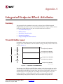
Appendix A: Integrated Endpoint Block Attributes
Summary . . . . . . . . . . . . . . . . . . . . . . . . . . . . . . . . . . . . . . . . . . . . . . . . . . . . . . . . . . . . . . . . . . .
TX and RX Buffer Layout . . . . . . . . . . . . . . . . . . . . . . . . . . . . . . . . . . . . . . . . . . . . . . . . . . . .
Buffer Latency . . . . . . . . . . . . . . . . . . . . . . . . . . . . . . . . . . . . . . . . . . . . . . . . . . . . . . . . . . . . . .
Initial Flow Control Credits . . . . . . . . . . . . . . . . . . . . . . . . . . . . . . . . . . . . . . . . . . . . . . . . .
Extended Capabilities . . . . . . . . . . . . . . . . . . . . . . . . . . . . . . . . . . . . . . . . . . . . . . . . . . . . . . .
Integrated Endpoint Block Attributes . . . . . . . . . . . . . . . . . . . . . . . . . . . . . . . . . . . . . . . .
91
91
92
93
94
96
Glossary. . . . . . . . . . . . . . . . . . . . . . . . . . . . . . . . . . . . . . . . . . . . . . . . . . . . . . . . . . . . . . . . . . . . . . .
109
Index . . . . . . . . . . . . . . . . . . . . . . . . . . . . . . . . . . . . . . . . . . . . . . . . . . . . . . . . . . . . . . . . . . . . . . . . . . .
117
Virtex-5 FPGA Integrated Endpoint Block
UG197 (v1.5) July 22, 2009
www.xilinx.com
7
R
8
www.xilinx.com
Virtex-5 FPGA Integrated Endpoint Block
UG197 (v1.5) July 22, 2009
R
Preface
About This Guide
This guide serves as a technical reference describing the Virtex®-5 FPGA Integrated
Endpoint Block for PCI Express® designs (integrated Endpoint block). Users intending to
implement the integrated Endpoint block should use the CORE Generator™ tool to create
the LogiCORE™ IP Endpoint Block Plus for PCI Express (Endpoint Block Plus wrapper).
The Endpoint Block Plus wrapper contains all the settings and interface logic needed to
create a compliant PCI Express design. See Chapter 3, “Designing with the Endpoint Block
Plus Wrapper,” for more information.
UG341, LogiCORE IP Endpoint Block Plus for PCI Express User Guide describes how to use the
Endpoint Block Plus wrapper to create an Endpoint design for PCI Express operation. The
LogiCORE IP Endpoint Block Plus for PCI Express User Guide should primarily be used when
creating a design with the integrated Endpoint block.
The Virtex-5 FPGA Integrated Endpoint Block for PCI Express Designs User Guide (this guide)
provides an in-depth description of the integrated Endpoint block's behavior. Even though
the Endpoint Block Plus wrapper extracts much of this behavior from the user, this guide
is useful as a companion document to the LogiCORE IP Endpoint Block Plus for PCI Express
User Guide to provide a better understanding of the integrated Endpoint block. Because
this user guide describes the integrated Endpoint block’s ports and attributes, it is
extremely helpful when debugging user designs. It also provides a list of known
restrictions to be referenced when encountering design problems.
Guide Contents
This guide contains the following chapters:
•
Chapter 1, “Virtex-5 FPGA Integrated Endpoint Block Overview,”provides a brief
introduction to the integrated Endpoint block embedded in the Virtex-5 devices.
•
Chapter 2, “Integrated Endpoint Block Functionality,” gives an architectural overview
of the block and detailed descriptions of each block interface.
•
Chapter 3, “Designing with the Endpoint Block Plus Wrapper,” provides more
information on using the CORE Generator GUI to generate the appropriate
LogiCORE IP to implement the Virtex-5 FPGA Integrated Endpoint block in a PCI
Express design.
•
Chapter 4, “Integrated Endpoint Block Operation,” provides in-depth information on
various design considerations.
•
Chapter 5, “Simulating with the Integrated Endpoint Block,” introduces simulating
with the Virtex-5 FPGA Integrated Endpoint block.
•
Appendix A, “Integrated Endpoint Block Attributes,” provides detailed information
on the attributes that can be set on the integrated Endpoint block. Because these
Virtex-5 FPGA Integrated Endpoint Block
UG197 (v1.5) July 22, 2009
www.xilinx.com
9
R
Preface: About This Guide
attributes are all set through the CORE Generator GUI, this appendix is provided as a
reference.
•
“Glossary,” defines various terms used in this document.
Additional Documentation
The following documents are also available for download at
http://www.xilinx.com/virtex5.
•
Virtex-5 Family Overview
The features and product selection of the Virtex-5 family are outlined in this overview.
•
Virtex-5 FPGA Data Sheet: DC and Switching Characteristics
This data sheet contains the DC and Switching Characteristic specifications for the
Virtex-5 family.
•
Virtex-5 FPGA User Guide
Chapters in this guide cover the following topics:
•
-
Clocking Resources
-
Clock Management Technology (CMT)
-
Phase-Locked Loops (PLLs)
-
Block RAM
-
Configurable Logic Blocks (CLBs)
-
SelectIO™ Resources
-
SelectIO Logic Resources
-
Advanced SelectIO Logic Resources
Virtex-5 FPGA RocketIO GTP Transceiver User Guide
This guide describes the RocketIO™ GTP transceivers available in the Virtex-5 LXT
and SXT devices.
•
Virtex-5 FPGA RocketIO GTX Transceiver User Guide
This guide describes the RocketIO GTX transceivers available in the TXT and FXT
devices.
•
Virtex-5 FPGA Embedded Processor Block in Virtex-5 FPGAs
This reference guide is a description of the embedded processor block available in the
Virtex-5 FXT device.
•
Virtex-5 FPGA Embedded Tri-Mode Ethernet MAC User Guide
This guide describes the dedicated Tri-Mode Ethernet Media Access Controller
available in the Virtex-5 LXT, SXT, TXT, and FXT devices.
•
Virtex-5 FPGA XtremeDSP Design Considerations User Guide
This guide describes the XtremeDSP™ slice and includes reference designs for using
the DSP48E.
•
Virtex-5 FPGA Configuration Guide
This all-encompassing configuration guide includes chapters on configuration
interfaces (serial and SelectMAP), bitstream encryption, Boundary-Scan and JTAG
configuration, reconfiguration techniques, and readback through the SelectMAP and
JTAG interfaces.
10
www.xilinx.com
Virtex-5 FPGA Integrated Endpoint Block
UG197 (v1.5) July 22, 2009
R
Additional Support Resources
•
Virtex-5 FPGA System Monitor User Guide
The System Monitor functionality available in all the Virtex-5 devices is outlined in
this guide.
•
Virtex-5 FPGA Packaging and Pinout Specifications
This specification includes the tables for device/package combinations and maximum
I/Os, pin definitions, pinout tables, pinout diagrams, mechanical drawings, and
thermal specifications.
•
Virtex-5 FPGA PCB Designer’s Guide
This guide provides information on PCB design for Virtex-5 devices, with a focus on
strategies for making design decisions at the PCB and interface level.
Additional Support Resources
To search the database of silicon and software questions and answers or to create a
technical support case in WebCase, see the Xilinx website at:
http://www.xilinx.com/support.
Typographical Conventions
This document uses the following typographical conventions. An example illustrates each
convention.
Convention
Meaning or Use
References to other documents
See the Virtex-5 FPGA Configuration
Guide for more information.
Emphasis in text
The address (F) is asserted after
clock event 2.
Indicates a link to a web page.
http://www.xilinx.com/virtex5
Italic font
Underlined Text
Example
Online Document
The following conventions are used in this document:
Convention
Meaning or Use
Example
See the section “Additional
Support Resources” for details.
Blue text
Cross-reference link to a location
in the current document
Red text
Cross-reference link to a location
in another document
See Figure 2-5 in the Virtex-5
FPGA Data Sheet.
Blue, underlined text
Hyperlink to a website (URL)
Go to http://www.xilinx.com
for the latest documentation.
Virtex-5 FPGA Integrated Endpoint Block
UG197 (v1.5) July 22, 2009
www.xilinx.com
Refer to “The PCI Express
Standard” in Chapter 1 for
details.
11
R
Preface: About This Guide
12
www.xilinx.com
Virtex-5 FPGA Integrated Endpoint Block
UG197 (v1.5) July 22, 2009
R
Chapter 1
Virtex-5 FPGA Integrated Endpoint
Block Overview
Summary
This chapter introduces the integrated Endpoint block embedded in Virtex-5 devices. The
sections include:
•
“The PCI Express Standard”
•
“Virtex-5 FPGA Integrated Endpoint Block for PCI Express Designs”
•
“Memory Requirements”
•
“Use Models”
The PCI Express Standard
The PCI Express (PCIe®) standard is a next-generation evolution of the older PCI™ and
PCI-X™ parallel bus standards. It is a high-performance, general-purpose interconnect
architecture, designed for a wide range of computing and communications platforms. It is
a packet-based, point-to-point serial interface that is backward compatible with PCI and
PCI-X configurations, device drivers, and application software. Its faster, serial-bus
architecture with dedicated, bidirectional I/O represents a fresh architectural approach.
Table 1-1 shows the bandwidth for various lane configurations. The effective bandwidth is
lower than the raw bandwidth due to the overhead of the 8B/10B encoding and decoding
used by the protocol.
Table 1-1:
PCIe Standard Bandwidth
Link
Raw Bandwidth per Direction
Effective Bandwidth per Direction
x1
2.5 Gb/s
2 Gb/s
x2
5 Gb/s
4 Gb/s
x4
10 Gb/s
8 Gb/s
x8
20 Gb/s
16 Gb/s
Virtex-5 FPGA Integrated Endpoint Block
UG197 (v1.5) July 22, 2009
www.xilinx.com
13
R
Chapter 1: Virtex-5 FPGA Integrated Endpoint Block Overview
Virtex-5 FPGA Integrated Endpoint Block for PCI Express Designs
The Virtex-5 FPGA Integrated Endpoint block contains the functionality defined in the
specifications maintained by the PCI-SIG (www.pcisig.com):
•
Compliant with the PCI Express Base 1.1 Specification
•
Endpoint block or Legacy Endpoint block for PCI Express designs
•
x8, x4, x2, or x1 lane width
•
RocketIO™ GTP and GTX transceivers implement a fully compliant PHY
•
Block RAMs used for buffering
•
Fully buffered Transmit and Receive
•
Management interface to access configuration space and internal configuration
•
Full range of maximum payload size (128 to 4096 bytes) supported
•
Up to 6 x 32 bit or 3 x 64 bit base address registers (BARs), or a combination of 32 bit
and 64 bit
•
BARs configurable for memory or I/O
•
One function
•
Signals to the fabric for statistics and monitoring
•
Up to two virtual channels (VCs)
•
Round robin, weighted round robin, or strict priority VC arbitration
Note: The recommended and supported design flow for utilizing the integrated Endpoint block (via
the CORE Generator™ tool to create the Endpoint Block Plus wrapper) only supports a single virtual
channel.
The integrated Endpoint block is configurable by using a combination of attributes and
port tie-offs, as part of the standard FPGA configuration. Configuration uses the
LogiCORE™ GUI briefly described in Chapter 3, “Designing with the Endpoint Block Plus
Wrapper.” Descriptions of the block pins can be found in “Virtex-5 FPGA Integrated
Endpoint Block Interface Descriptions” in Chapter 2, and descriptions of the attributes are
in Appendix A, “Integrated Endpoint Block Attributes.”
There are several interfaces to the integrated Endpoint block, including:
•
Clock and Reset interface, as described in “Clock and Reset Interface,” page 21.
•
Transaction Layer interface, as described in “Transaction Layer Interface,” page 28.
•
Management interface, as described in “Management Interface,” page 37.
•
Memory interface, as described in “Block RAM Interface,” page 40.
•
Transceiver interface, as described in “Transceiver Interface,” page 42.
•
Configuration and Status interface, as described in “Configuration and Status
Interface,” page 46.
The Transceiver interface, the Memory interface, and the Clock and Reset interface are
automatically connected in the CORE Generator wrappers. These interfaces are not visible
outside of the wrappers. The Transaction Layer interface must interface with the user
design in fabric. The rest of the interfaces are optional; the user can choose whether to
access them, and which pins to access.
14
www.xilinx.com
Virtex-5 FPGA Integrated Endpoint Block
UG197 (v1.5) July 22, 2009
R
Memory Requirements
Memory Requirements
There are three buffers that require block RAM: the Retry buffer, the Receive (RX) buffer,
and the Transmit (TX) buffer. Each buffer has its own interface for independent access. The
amount of block RAM needed can vary greatly, depending on the user requirements. For
example, more block RAM is needed for the TX and RX buffers when there is a larger
maximum payload size. The amount of block RAM needed for the Retry buffer can
increase with multilane designs because the bandwidth is larger.
Table 1-2 shows the number of 36-kbit block RAM buffers required for several different
representative usages. The number varies from 3 to 40, depending on user requirements.
The typical column assumes a 128- or 256-byte maximum payload size. More information
on buffer sizing can be found in “Block RAM Interface,” page 40.
Table 1-2:
Number of 36-kbit Block RAMs Required
Number of 36-kbit Block RAMs
Minimum
Typical
Maximum
Receive Buffer
1
1
16
Transmit Buffer
1
1
16
Retry Buffer
1
1
8
Total
3
3
40
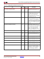
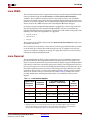
Use Models
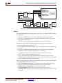
The example topology shown in Figure 1-1 illustrates the major components in a PCIe
system. Endpoint blocks and Legacy Endpoint blocks, both upstream-facing ports, are
supported by the integrated Endpoint block.
CPU
PCIe to
PCI
Bridge
Root Complex
Virtex-5 FPGA
Legacy
Endpoint
Switch
Memory
Virtex-5 FPGA
Endpoint
Legend:
Virtex-5 FPGA
Endpoint
Virtex-5 FPGA
Endpoint
Upstream port
Downstream port
UG197_c1_01_082008
Figure 1-1:
Virtex-5 FPGA Integrated Endpoint Block
UG197 (v1.5) July 22, 2009
Topology of a PCIe System
www.xilinx.com
15
Chapter 1: Virtex-5 FPGA Integrated Endpoint Block Overview
16
www.xilinx.com
R
Virtex-5 FPGA Integrated Endpoint Block
UG197 (v1.5) July 22, 2009
R
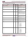
Chapter 2
Integrated Endpoint Block Functionality
Summary
This chapter presents information on the architecture and functionality of the Virtex-5
FPGA Integrated Endpoint block. The sections include:
•
“Architecture Overview”
•
“Virtex-5 FPGA Integrated Endpoint Block Interface Descriptions”
•
“Registers”
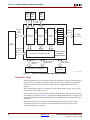
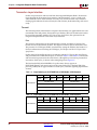
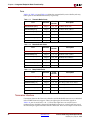
Architecture Overview
The PCI Express protocol is divided into three layers: the Transaction Layer, the Data Link
Layer, and the Physical Layer. These three layers interact with the Configuration Space.
The Virtex-5 FPGA Integrated Endpoint block (Figure 2-1) provides the full functionality
of the Transaction Layer, the Data Link Layer, the Physical Layer, and the Configuration
Space as per the PCI Express Base 1.1 Specification.
Virtex-5 FPGA Integrated Endpoint Block
UG197 (v1.5) July 22, 2009
www.xilinx.com
17
R
Chapter 2: Integrated Endpoint Block Functionality
Block
RAM
(TX)
Block
RAM
(RX)
Block
RAM
(Retry)
Block
RAM
Interface
PL Lane
Transaction
Layer
Interface
PL Lane
PL Lane
Transaction
Layer
Data Link
Layer
Physical
Layer
Transceiver
Interface
PL Lane
PL Lane
RocketIO
Transceiver(s)
PL Lane
PL Lane
PL Lane
User
Application
Management
Interface
Configuration and Capabilities Module
Power
Management
Interface
Configuration and
Status Interface
Miscellaneous Logic (Optional)
Virtex-5 FPGA
Integrated
Endpoint Block
Clock and
Reset Interface
Clock and
Reset Block
UG197_c2_01_081908
Figure 2-1:
Virtex-5 FPGA Integrated Endpoint Block Diagram
Transaction Layer
The Transaction Layer (TL) is the upper layer in the architecture. It takes Transaction Layer
Packets (TLPs) presented by user logic at the Transaction Layer interface and schedules
them for transmission. The module also advises the user application when TLPs are
received.
TLPs can both make requests and complete requests from another device. They can also
communicate certain types of events.
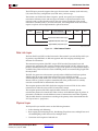
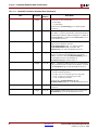
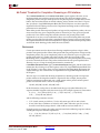
A TLP is composed of a header, data payload (for most packets), and optional end-to-end
CRC (ECRC), as shown in Figure 2-2. The integrated Endpoint block does not support the
optional ECRC generation and checking; however, the block does pass through the ECRC
untouched.
The Transaction Layer also manages the credit-based flow control. The flow control
mechanism ensures that a packet is not transmitted unless the receiving device has
sufficient buffer space to accept it.
18
www.xilinx.com
Virtex-5 FPGA Integrated Endpoint Block
UG197 (v1.5) July 22, 2009
R
Architecture Overview
The PCI Express protocol supports four types of transactions: memory (read and write),
I/O (read and write), configuration (read and write), and message.
Transactions are divided into three categories: posted, non-posted, and completion
transactions. Memory writes and message transactions are posted transactions. The
requester sends a packet, but the receiver does not return a completion. Non-posted
transactions (memory reads, I/O reads and writes, and configuration reads and writes)
require a response and are implemented as split transactions.
Start
Sequence
Number
Header
Data Payload
ECRC
LCRC
End
Presented to Transaction Layer
Appended by Data Link Layer
Appended by Physical Layer
UG197_c2_02_071306
Figure 2-2:
PCIe Protocol Packet
Data Link Layer
The Data Link Layer (DLL) resides between the Transaction Layer and the Physical Layer.
Its primary responsibilities are link management and data integrity, including error
detection and correction.
The transmission portion of the DLL accepts TLPs from the Transaction Layer and
generates the appropriate TLP sequence number and Link CRC (LCRC), then passes the
packet to the Physical Layer. It also places a copy of the packet in a retry buffer, making it
available if the packet needs to be resent. Nullified packets are automatically purged from
the retry buffer.
The DLL also generates and consumes special packets called Data Link Layer packets
(DLLPs) that do not pass to the Transaction Layer. Types of DLLPs include
acknowledgment (ACK/NAK), flow control, and power management. When the DLL
detects errors in a packet, it requests retransmission of the packet until it is correctly
received or until the link is determined to have failed.
The reception portion of the DLL checks the integrity of received TLPs. It also orders
retransmission when the received TLP is found to be corrupt.
The reception portion of the DLL simply handles whatever is received, but the
transmission portion also controls the order of release of the different types of packets. A
prioritizer is included to sort the different sources of transmission into order of priority
and schedule them for transmission according to the priority order recommended in the
PCI Express Base 1.1 Specification.
Physical Layer
The Physical Layer module carries out the following functions:
•
Packet framing and deframing
•
Byte striping and unstriping; that is, distributing TX packets across multiple lanes and
reassembling RX packets received over multiple lanes
•
Generation and reception of ordered sets
Virtex-5 FPGA Integrated Endpoint Block
UG197 (v1.5) July 22, 2009
www.xilinx.com
19
R
Chapter 2: Integrated Endpoint Block Functionality
•
Link initialization and training, including the Link Training and Status State Machine
(LTSSM)
•
Generating scramble and descramble codes
Physical Layer Lane Module
There are eight Physical Layer lane modules, one for each lane that the integrated
Endpoint block supports.
On the transmission side of its operation, the PL lane module applies the scramble codes
generated by the Physical Layer module to the transmit data, multiplexes this with
ordered set data received from the Physical Layer module, and then passes the packet to
the transceiver interface for transmission.
On the receive side, the Physical Layer lane module receives TLP bytes from the
Transceiver interface, decodes ordered sets from this data, and descrambles DLLP and TLP
data from the resulting datastream.
This module also detects the receipt of electrical idle characters. The remaining Physical
Layer functionality, including lane-to-lane deskew and 8B/10B encoding and decoding, is
included in the RocketIO transceivers.
Configuration and Capabilities Module
The Configuration and Capabilities module principally provides the repository for the
different registers within the Configuration Space, including:
•
Legacy PCI V3.0 Type 0 Configuration Space Header
•
Legacy Capabilities
•
♦
PCI Express
♦
Power Management
♦
Message Signaled Interrupts (MSIs)
PCI Express Extended Capabilities
♦
Device Serial Number
The integrated Endpoint block does not support the Advanced Error Reporting Capability.
The module also includes a packet decoder and a packet generator for handling
configuration and message packets.
20
www.xilinx.com
Virtex-5 FPGA Integrated Endpoint Block
UG197 (v1.5) July 22, 2009
R
Virtex-5 FPGA Integrated Endpoint Block Interface Descriptions
Virtex-5 FPGA Integrated Endpoint Block Interface Descriptions
The following subsections describe the physical interfaces on the integrated Endpoint
block. Connections and control of these interfaces are contained within the Endpoint Block
Plus Wrapper for PCI Express available from the CORE Generator GUI. The Endpoint
Block Plus Wrapper for PCI Express uses the integrated Endpoint block to create a PCI
Express Endpoint in the Virtex-5 FPGA. All users of the integrated Endpoint block should
use the Endpoint Block Plus Wrapper in their designs.
Clock and Reset Interface
Clocks
The integrated Endpoint block has two synchronous clock domains: core_clk and user_clk.
The user_clk domain allows user logic in the fabric to run at a slower speed than the
integrated Endpoint block in x1, x2, or x4 modes. Each clock domain has several clock
ports to improve timing. All clock ports on the same clock domain must be tied to the same
BUFG.
The user_clk domain is controlled by the CRMUSERCLK, CRMUSERCLKRXO, and
CRMUSERCLKTXO ports (see Table 2-3). The user_clk domain clocks the following:
•
The Management interface
•
The Transaction Layer interface
•
The write port of the TX buffer
•
The read port of the RX buffer
•
User logic in the fabric connected to the above interfaces
The core_clk domain is controlled by the CRMCORECLK, CRMCORECLKRXO,
CRMCORECLKTXO, and CRMCORECLKDLO signals (see Table 2-3). The core_clk domain
clocks the following:
•
The rest of the integrated Endpoint block
•
The read port of the TX buffer
•
The write port of the RX buffer
•
The Retry buffer
•
The Transceiver interface
•
Portions of the RocketIO transceiver (TXUSRCLK2, RXUSRCLK2)
Clock Frequency
The core_clk always runs at 250 MHz. The user_clk must also run at 250 MHz for x8
configurations to maintain full bandwidth. The user_clk can be run at lower frequencies
for x1, x2, or x4, while still maintaining full bandwidth, lowering power, and simplifying
timing closure. Table 2-1 shows the allowed clock frequencies.
Table 2-1:
Clock Frequency Versus Lane Width
Configured Lane Width
core_clk Frequency (MHz)
user_clk Frequency (MHz)(1)
x1
250
62.5, 125, or 250
x2
250
62.5, 125, or 250
Virtex-5 FPGA Integrated Endpoint Block
UG197 (v1.5) July 22, 2009
www.xilinx.com
21
R
Chapter 2: Integrated Endpoint Block Functionality
Table 2-1:
Clock Frequency Versus Lane Width (Continued)
Configured Lane Width
core_clk Frequency (MHz)
user_clk Frequency (MHz)(1)
x4
250
125 or 250
x8
250
250
Notes:
1. The user_clk frequency is based on the configured lane width. It cannot be reduced, even when the
negotiated lane width is smaller.
When the frequency of the user_clk domain is 250 MHz, there is no need to provide two
separate clocks to the integrated Endpoint block. In this case, the 250 MHz clock is tied to
all the core_clk ports and the user_clk ports must be tied High. This gives a very simple
timing model for the system: all signals on the integrated Endpoint block and all signals on
other blocks on the FPGA that directly interface with the integrated Endpoint block are
clocked by the same clock. These clock connections are included in the CORE Generator
wrappers.
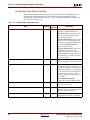
The core_clk and user_clk are obtained by using a Clock Management Tile (CMT). The
reference clock is brought on the device through the CLKP and CLKN differential reference
clock pins to the RocketIO transceiver. The reference clock should be forwarded from the
RocketIO transceiver to the CMT. The CMT PLL must be used to derive the 250 MHz
core_clk from the reference clock (unless a 250 MHz reference clock is used). See Figure 2-3
and Figure 2-4. The CMT PLL, BUFGs, and clocking connections are included in the CORE
Generator wrappers.
BUFG
PLLLKDET
CMT
PLL
BUFG
CRMCORECLK
CRMCORECLKRXO
CRMCORECLKTXO Virtex-5 FPGA
CRMCORECLKDLO
Integrated
Endpoint Block
CRMUSERCLK
CRMUSERCLKRXO
CRMUSERCLKTXO
BUFG
REFCLK Frequency
REFCLK
(100, 125, or 250 MHz)
GTP_DUAL
or
GTX_DUAL
Tile
core_clk (250 MHz)
TX/RX
Block
RAMs
Retry
Block
RAMs
User
Logic
user_clk
(62.5 or 125 MHz)
UG197_c2_09_081808
Figure 2-3:
22
Clocking for Applications with CLKDIVIDED = TRUE
www.xilinx.com
Virtex-5 FPGA Integrated Endpoint Block
UG197 (v1.5) July 22, 2009
R
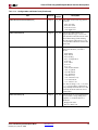
Virtex-5 FPGA Integrated Endpoint Block Interface Descriptions
CRMCORECLK
CRMCORECLKRXO
CRMCORECLKTXO
CRMCORECLKDLO
BUFG
PLLLKDET
CMT
PLL
BUFG
CRMUSERCLK
CRMUSERCLKRXO
CRMUSERCLKTXO
Virtex-5 FPGA
Integrated
Endpoint Block
REFCLK Frequency
REFCLK
(100, 125, or 250 MHz)
GTP_DUAL
or
GTX_DUAL
Tile
TX/RX
Block
RAMs
Retry
Block
RAMs
User
Logic
core_clk (250 MHz)
UG197_c2_10_081808
Figure 2-4:
Clocking for Applications with CLKDIVIDED = FALSE
Resets
The integrated Endpoint block supports three types of resets, as defined by the PCI Express
Base Specification:
•
Cold reset, a fundamental reset that occurs following the application of power.
•
Warm reset, a fundamental reset that is triggered by hardware without the removal
and reapplication of power.
•
Hot reset, an in-band mechanism for propagating reset across a PCIe link.
The registers in the integrated Endpoint block are divided into six reset domains:
•
mgmt_rst: Management interface reset.
•
nv_rst: Sticky (or non-volatile) registers reset. A sticky register retains its state through
a hot reset.
•
user_cfg_rst: Endpoint Configuration Space reset. All registers in the Endpoint
Configuration Space, except the sticky registers, are affected.
•
u_rst: Backend interface to the Transaction Layer (user_clk domain) reset.
•
mac_rst: Physical Layer, including PL Lane reset.
•
link_rst: Transaction Layer (core_clk domain), Data Link Layer, and part of the
Configuration and Capabilities module reset. This affects all registers in the block that
are not included in the other five reset domains.
There are six reset ports (see Table 2-3). The domain(s) that are reset by each port depend
on the RESETMODE attribute (see Table 2-2).
•
When RESETMODE = FALSE, most of the ports reset more than one domain; thus,
only one of these signals should be asserted at a time. Two of the signals,
CRMMACRSTN and CRMLINKRSTN, are not used in this mode.
•
When RESETMODE = TRUE, each port resets just one domain (except for
CRMMGMTRSTN, which resets the entire block); multiple reset signals can be asserted
as needed.
Virtex-5 FPGA Integrated Endpoint Block
UG197 (v1.5) July 22, 2009
www.xilinx.com
23
R
Chapter 2: Integrated Endpoint Block Functionality
Table 2-2:
The Effect of the RESETMODE Attribute on Reset Signal Functionality
Reset Domain
Port
RESETMODE
user_cfg_rst
mac_rst
link_rst
u_rst
nv_rst
CRMUSERCFGRSTN
FALSE
CRMMACRSTN(1)
FALSE
CRMLINKRSTN(1)
FALSE
CRMURSTN
FALSE
•
•
•
•
CRMNVRSTN
FALSE
•
•
•
•
•
CRMMGMTRSTN
FALSE
•
•
•
•
•
CRMUSERCFGRSTN
TRUE
•
CRMMACRSTN
TRUE
CRMLINKRSTN
TRUE
CRMURSTN
TRUE
CRMNVRSTN
TRUE
CRMMGMTRSTN
TRUE
mgmt_rst
•
•
•
•
•
•
•
•
•
•
•
•
Notes:
1. These ports are not used in this mode.
During FPGA configuration, the entire integrated Endpoint block is reset, including the
sticky register block, the PCI Configuration Space, and the Management Interface
registers. All other resets of the block are controlled by the user through the six reset ports.
These signals are asynchronous, but there is logic in the integrated Endpoint block to
guarantee synchronous deassertion with respect to the core_clk. The integrated Endpoint
block must be clocked while its reset port(s) are asserted in order for the appropriate
portion(s) of the block to be reset.
The integrated Endpoint block asserts the PIPERESETLn signals to all lanes when the
MAC_RST domain is reset. PIPERESETLn is only deasserted for the active lanes (based on
the ACTIVELANESIN attribute setting) and remains asserted for the unused lanes. The
PIPERESETLn ports are connected to the RXCDRRESET port on the RocketIO transceivers.
See Table 2-14, page 43 for details.
The user reset design in fabric for the PCIe system must assert the appropriate reset signals
for warm reset, hot reset, DL_Down, etc. The user should also ensure that the integrated
Endpoint block is held in reset until the PLL is locked. This reset design is included in the
CORE Generator wrapper.
The falling edge of the L0DLUPDOWN[0] output of the integrated Endpoint block indicates
when the link goes down (DL_Down status). The CRMDOHOTRESETN output is asserted
when a hot reset is received from upstream. An Endpoint user design must use these
outputs to reset a portion of the integrated Endpoint block. This is done in the CORE
Generator wrappers. The sticky registers and management interface registers should not
be reset on DL_Down status or hot reset. The LTSSM does not need to be reset, but it can be
reset after it transitions from Disabled (1011), Loopback (1001), Hot Reset (1010),
Recovery (1100), or Configuration (0011) to Detect (0001). This transition can be seen by
decoding the L0LTSSMSTATE outputs of the integrated Endpoint block.
24
www.xilinx.com
Virtex-5 FPGA Integrated Endpoint Block
UG197 (v1.5) July 22, 2009
R
Virtex-5 FPGA Integrated Endpoint Block Interface Descriptions
The CRMPWRSOFTRESETN output indicates when the integrated Endpoint block
transitions from the D3hot power state to the D0uninitialized state. This transition must be
used to trigger the assertion of the CRMUSERCFGRSTN port on the integrated Endpoint
block. This is done in the CORE Generator wrappers.
Ports
Table 2-3 shows the Clock and Reset interface ports.
Table 2-3:
Clock and Reset Ports
Direction
Clock
Domain
CRMCORECLK
Input
core_clk
250 MHz clock from the FPGA, also drives TX buffer read clock
port, RX buffer write clock ports, both Retry buffer clock ports,
and the transceiver RX/TXUSRCLK2 ports. Should be tied Low if
the integrated Endpoint block is not used. CRMCORECLK,
CRMCORECLKRXO, CRMCORECLKTXO, and
CRMCORECLKDLO must be tied to the output of the same BUFG.
CRMCORECLKDLO
Input
core_clk
250 MHz clock from the FPGA. Clocks the outputs of both Retry
buffer ports. Should be tied Low if the integrated Endpoint block
is not used. CRMCORECLK, CRMCORECLKRXO,
CRMCORECLKTXO, and CRMCORECLKDLO must be tied to the
output of the same BUFG.
CRMCORECLKTXO
Input
core_clk
250 MHz clock from the FPGA. Clocks the TX buffer read port
outputs. Should be tied Low if the integrated Endpoint block is
not used. CRMCORECLK, CRMCORECLKRXO,
CRMCORECLKTXO, and CRMCORECLKDLO must be tied to the
output of the same BUFG.
CRMCORECLKRXO
Input
core_clk
250 MHz clock from the FPGA. Clocks the RX buffer write port
outputs. Should be tied Low if the integrated Endpoint block is
not used. CRMCORECLK, CRMCORECLKRXO,
CRMCORECLKTXO, and CRMCORECLKDLO must be tied to the
output of the same BUFG.
CRMUSERCLK
Input
user_clk
User clock. Should be tied Low if the integrated Endpoint block
is not used. CRMUSERCLK, CRMUSERCLKRXO, and
CRMUSERCLKTXO must be tied to the output of the same BUFG
when they are at a lower frequency than CRMCORECLK. Must be
tied High when frequency is the same as CRMCORECLK
(250 MHz).
CRMUSERCLKTXO
Input
user_clk
User clock. Clocks TX buffer write port outputs. Should be tied
Low if the integrated Endpoint block is not used. CRMUSERCLK,
CRMUSERCLKRXO, and CRMUSERCLKTXO must be tied to the
output of the same BUFG when they are at a lower frequency
than CRMCORECLK. Must be tied High when frequency is the
same as CRMCORECLK (250 MHz).
CRMUSERCLKRXO
Input
user_clk
User clock. Clocks RX buffer read ports outputs. Should be tied
Low if the integrated Endpoint block is not used. CRMUSERCLK,
CRMUSERCLKRXO, and CRMUSERCLKTXO must be tied to the
output of the same BUFG when they are at a lower frequency
than CRMCORECLK. Must be tied High when frequency is the
same as CRMCORECLK (250 MHz).
Port
Virtex-5 FPGA Integrated Endpoint Block
UG197 (v1.5) July 22, 2009
Description
www.xilinx.com
25
R
Chapter 2: Integrated Endpoint Block Functionality
Table 2-3:
Clock and Reset Ports (Continued)
Direction
Clock
Domain
CRMURSTN
Input
core_clk
User reset (active Low). When the RESETMODE attribute is set to
FALSE, resets all the registers in the integrated Endpoint block,
except the sticky registers and the Management Interface
registers. When the RESETMODE attribute is set to TRUE, resets
the backend interface to the Transaction Layer (user_clk
domain). Asynchronous, but the integrated Endpoint block
ensures internal synchronous deassertion with respect to
core_clk. Should be tied High if not used in the user design or if
the block is not used.
CRMNVRSTN
Input
core_clk
Non-volatile reset (active Low). When the RESETMODE attribute
is set to FALSE, resets the sticky registers, and everything else in
the block except for the Management Interface registers. When
the RESETMODE attribute is set to TRUE, resets the sticky
registers only. Asynchronous, but the integrated Endpoint block
ensures internal synchronous deassertion with respect to
core_clk. Should be tied High if not used in the user design or if
the block is not used.
CRMMGMTRSTN
Input
core_clk
Management interface reset (active Low). Resets the registers in
the block, including the management interface registers. The
function of this signal does not depend on the RESETMODE
attribute setting. Asynchronous, but the integrated Endpoint
block ensures internal synchronous deassertion with respect to
core_clk. Should be tied High if not used in the user design or if
the block is not used.
CRMUSERCFGRSTN
Input
core_clk
User configuration reset (active Low). Resets all the registers in
the PCI Express Configuration Space except the sticky registers.
The function of this signal does not depend on the RESETMODE
attribute setting. Asynchronous, but the integrated Endpoint
block ensures internal synchronous deassertion with respect to
core_clk. Should be tied High if not used in the user design or if
the block is not used.
CRMMACRSTN
Input
core_clk
MAC reset (active Low). When the RESETMODE attribute is set
to FALSE, CRMMACRSTN is not used and should be tied High.
When the RESETMODE attribute is set to TRUE, CRMMACRSTN
resets the MAC link and MAC lane logic (Physical Layer).
Asynchronous, but the integrated Endpoint block ensures
internal synchronous deassertion with respect to core_clk.
Should be tied High if not used in the user design or if the block
is not used.
CRMLINKRSTN
Input
core_clk
Link reset (active Low). When the RESETMODE attribute is set to
FALSE, CRMLINKRSTN is not used and should be tied High.
When the RESETMODE attribute is set to TRUE, CRMLINKRSTN
resets the core_clk domain of the Transaction Layer, part of the
Configuration module, and the Data Link Layer. Asynchronous,
but the integrated Endpoint block ensures internal synchronous
deassertion with respect to core_clk. Should be tied High if not
used in the user design or if the block is not used.
Port
26
Description
www.xilinx.com
Virtex-5 FPGA Integrated Endpoint Block
UG197 (v1.5) July 22, 2009
R
Table 2-3:
Virtex-5 FPGA Integrated Endpoint Block Interface Descriptions
Clock and Reset Ports (Continued)
Direction
Clock
Domain
CRMDOHOTRESETN
Output
core_clk
Hot reset (active Low). Asserted on completion of hot reset
handshake as a prompt for user logic to be reset. See “Resets,”
page 23.
CRMPWRSOFTRESETN
Output
core_clk
Soft reset (active Low). Asserted when the block makes the
transition from D3hot to D0uninitialized, as a prompt for user logic
to be reset (with CRMUSERCFGRSTN).
Port
Virtex-5 FPGA Integrated Endpoint Block
UG197 (v1.5) July 22, 2009
Description
www.xilinx.com
27
R
Chapter 2: Integrated Endpoint Block Functionality
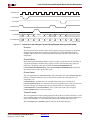
Transaction Layer Interface
Packets are presented to and received from the integrated Endpoint block’s Transaction
Layer through the Transaction Layer interface. On this interface, a beat is a clock cycle
where both the source and destination are ready. The main Transaction Layer interface
framing signals indicate the start of frame, the end of frame, destination ready, and source
ready.
Transmit
The transmit portion of the interface accepts the data from the user application that is to be
transmitted to the link partner. Transaction Layer Packets (TLPs) for transmission need to
be created in accordance with the PCI Express Base Specification, then presented to the
integrated Endpoint block’s Transaction Layer interface.
Data
The data bus contains data for the packet header, payload, and digest, if present. The
header must be written before the data. The digest is treated as the last word of the data.
The presence of a TLP digest (ECRC) is indicated by setting the TD bit in the header to '1'.
For more information on creating the TLP digest, see Chapter 2 of the PCI Express Base
Specification.
Packets must be formed by the user in accordance with the PCI Express Base Specification,
and presented on the LLKTXDATA ports as shown in Table 2-4 and Table 2-5. The header
and data must be presented in the order shown, although they need not be presented on
consecutive clock cycles, as shown in the timing diagram in Figure 2-5.
The first header DW (32-bit DWORD) of a packet must always appear on
LLKTXDATA[63:32], and cannot appear in the same clock cycle as the final DW of the
previous packet (but can appear in the next clock cycle, if all other signaling requirements
are met).
Table 2-4:
Byte Ordering on LLKTXDATA for 3 DW Header, 4 DW Payload
63 56
55 48
47 40
39 32
31 24
23 16
15
byte0
byte1
byte2
byte3
byte4
byte5
byte6
LLKTXDATA
Table 2-5:
Header DW0
Header DW1
Header DW2
Payload DW0
Payload DW1
Payload DW2
Payload DW3
don’t care
7
0
byte7
Byte Ordering on LLKTXDATA for 4 DW Header, 4 DW Payload
LLKTXDATA
28
8
63 56
55 48
47 40
39 32
31 24
23 16
15
8
byte0
byte1
byte2
byte3
byte4
byte5
byte6
Header DW0
Header DW1
Header DW2
Header DW3
Payload DW0
Payload DW1
Payload DW2
Payload DW3
www.xilinx.com
7
0
byte7
Virtex-5 FPGA Integrated Endpoint Block
UG197 (v1.5) July 22, 2009
R
Virtex-5 FPGA Integrated Endpoint Block Interface Descriptions
CRMUSERCLK
LLKTXSOFN
LLKTXEOFN
LLKTXSRCRDYN
LLKTXDSTRDYN
LLKTXDATA
LLKTXENABLEN
H0 H1
H2 H3
00
00
P0 P1
00
P2 P3
00
00
11
P4 P5
P6 P7
00
00
11
11
UG197_c2_03_111906
Figure 2-5:
Transaction Layer Interface Transmit Timing Diagram Showing a 4 DW Header
Channels
The Transaction Layer interface allows for the generic concept of channels to deal with
multiple logical channels for one physical interface. The integrated Endpoint block
supports eight traffic classes each having three traffic types: posted, non-posted, and
completion.
Channel Ready
When the integrated Endpoint block is ready to accept a packet into one of the buffers, it
asserts the appropriate channel ready signal(s). There is one channel ready signal per
traffic class, according to the type of packet (LLKTXCHPOSTEDREADYN[7:0],
LLKTXCHNONPOSTEDREADYN[7:0], and LLKTXCHCOMPLETIONREADYN[7:0]). More than
one channel can be ready on any clock cycle.
Channel Select
The user application sets LLKTXCHTC[2:0] to select the traffic class and LLKTXCHFIFO[1:0] to
indicate in which TX FIFO the data is to be placed: posted (00), non-posted (01), or
completion (10).
LLKTXDSTRDYN is asserted when the selected channel has space available, and
LLKTXCHANSPACE reports the amount of free space. Pipelining causes a delay of one cycle
between a change in a channel select and an output based on a selected channel
(LLKTXDSTRDYN or LLKTXCHANSPACE). Also, it takes four clock cycles to update
LLKTXCHANSPACE after a write transaction.
Transmit Framing
The user application uses the framing signals to indicate the start and end of frames as well
as the position of the header and digest (if present). The framing signals also indicate how
many 32-bit DWORDs are valid at the end of the header and the end of the frame.
The LLKTXSOFN and LLKTXEOFN signals delineate the frame boundaries.
Virtex-5 FPGA Integrated Endpoint Block
UG197 (v1.5) July 22, 2009
www.xilinx.com
29
R
Chapter 2: Integrated Endpoint Block Functionality
Framing Errors
The following conditions are framing errors and are not allowed:
•
Two SOFs without an intervening EOF
•
Two EOFs without an intervening SOF
•
An SOF and EOF in the same cycle
DWORD Enables
The Transaction Layer interface data bus, LLKTXDATA, is 64 bits wide, allowing the user to
transfer one QWORD of data into the integrated Endpoint block per clock cycle. Because
the PCIe protocol allows DWORD (32-bit) alignment of header and data, certain QWORDs
contain only one valid DWORD. The LLKTXENABLEN[1:0] bus indicates which DWORD(s)
contain valid header or data information. Bit 1 of LLKTXENABLEN[1:0] refers to
LLKTXDATA[63:32], and bit 0 refers to LLKTXDATA[31:0]. A value of 0 indicates that the
corresponding DWORD is valid.
All 64 bits of LLKTXDATA must be enabled, except on the last cycle of a TLP transfer, when
LLKTXEOFN = 0. For the last QWORD of a packet, it is possible that only LLKTXDATA[63:32]
is valid because of DWORD alignment. This is denoted by LLKTXENABLEN[1:0] = 01 during
LLKTXEOFN. Otherwise, LLKTXENABLEN[1:0] = 00 is used for all other cycles of a TLP
transfer.
Transmit Handshake
The handshake signals control the flow of data between the user application and the
integrated Endpoint block.
When the user application has a packet ready for transmission, it asserts LLKTXCHTC and
LLKTXCHFIFO to select the channel, and asserts LLKTXSRCRDYN to indicate that the data
bus and framing signals are set to transfer data. The user application does not need to wait
for the integrated Endpoint block to assert LLKTXDSTRDYN. Either ready signal can be
asserted first. See Figure 2-6, page 31.
30
www.xilinx.com
Virtex-5 FPGA Integrated Endpoint Block
UG197 (v1.5) July 22, 2009
R
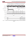
Virtex-5 FPGA Integrated Endpoint Block Interface Descriptions
Note: Need to wait an additional two cycles of
LLKTXDSTRDYN assertion after LLKTXEOFN
before switching LLKTXCHFIFO or LLKTXCHTC.
CRMUSERCLK
LLKTXCHFIFO
0
2 (CPL)
0 (P)
LLKTXCHTC
0
4
6
LLKTXSOFN
LLKTXEOFN
LLKTXSRCRDYN
LLKTXDSTRDYN
LLKTXDATA
H0 H1 H2 D0 D1 D2 D3 D4 D5 D6
LLKTXENABLEN
00
11
00
nP
LLKTXCHANSPACE[7:0]
00
00
nC
H0 H1 H2 D0 D1 D2 D3 XX H0 H1 H2 D1
00
11
nC-1
00
nC-2
00
00
01
nP
00
11
00
nP-1
nP-2
UG197_c2_04_030607
Figure 2-6:
Transaction Layer Interface Transmit Channel Switching Timing Diagram
After transmission of a packet, a subsequent packet on the same channel (FIFO and TC)
can be sent immediately. For packets on a different channel (FIFO or TC), the user logic
must pause until LLKTXDSTRDYN is asserted for two cycles after LLKTXEOFN before
changing the LLKTXCHFIFO or LLKTXCHTC signal.
If the transmit buffer becomes full during packet transfer, it deasserts LLKTXDSTRDYN and
stalls data transfers on the Transaction Layer interface until space becomes available again
as the packet is sent over the serial interface. The user can optionally check the amount of
space in a channel using LLKTXCHANSPACE and decide to not begin sending the packet
over the Transaction Layer interface if insufficient space is available to send the packet
without stalling. The requirement on channel switching timing as shown in Figure 2-6
must also be observed.
LLKTXENABLEN is ignored unless LLKTXSRCRDYN and LLKTXDSTRDYN are asserted.
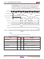
Receive
The receive portion of the interface passes the data received from the link partner to the
user application in fabric.
Virtex-5 FPGA Integrated Endpoint Block
UG197 (v1.5) July 22, 2009
www.xilinx.com
31
R
Chapter 2: Integrated Endpoint Block Functionality
Receive Framing
The receive framing signals are similar to the transmit framing signals. In receive packets,
the header is always before the data. LLKRXVALIDN = 00 on all valid cycles except the last
one. If the total number of 32-bit DWORDs (header plus payload) is odd, LLKRXVALIDN is
01 on the last beat.
Receive Handshake
When a packet has been received into the RX buffer and confirmed as valid, the integrated
Endpoint block asserts the appropriate LLKRXCHPOSTEDAVAILABLEN,
LLKRXCHNONPOSTEDAVAILABLEN, or LLKRXCHCOMPLETIONAVAILABLEN signal to
indicate the type of packet that has been received. In some cases, requesting a packet that
has been received can violate PCIe transaction ordering rules. The user application must
monitor the LLKRXPREFERREDTYPE signal and follow the rules specified in “Ordering at
Reception,” page 67 before requesting a packet from the integrated Endpoint block.
The user application selects the traffic class and the traffic type to read by setting
LLKRXCHTC to select the traffic class, and LLKRXCHFIFO to select posted, non-posted, or
completion.
The user asserts the LLKRXDSTREQN signal to request data from the integrated Endpoint
block. For each clock where LLKRXDSTREQN is asserted, the integrated Endpoint block
asserts LLKRXSRCRDYN for one clock after a minimum delay of 3 + TLRAMREADLATENCY.
The value of the TLRAMREADLATENCY attribute is in the range [2 .. 6].
The receive interfaces provides a LLKRXSRCRDYN signal when data is valid on
LLKRXDATA.
The integrated Endpoint block asserts LLKRXSRCLASTREQN three user_clk cycles after it
has received the second-to-last (penultimate) request for the current RX packet via
LLKRXDSTREQN. A single assertion of LLKRXDSTREQN during the three user_clk cycles is
sufficient for the block to receive its final request for the current RX packet. Other
assertions of LLKRXDSTREQN are ignored, provided LLKRXDSTCONTREQN is deasserted. If
the block has received the final request when LLKRXSRCLASTREQN is asserted, no further
requests should be issued on subsequent cycles (via LLKRXDSTREQN) unless there are
further packets available on the selected channel as indicated by the corresponding
LLKRX*AVAILABLEN signal (where * is POSTED, NONPOSTED, or COMPLETION). When
configuration packets are being processed, the LLKRX*AVAILABLEN signals are deasserted
until processing of the configuration packet is complete.
32
www.xilinx.com
Virtex-5 FPGA Integrated Endpoint Block
UG197 (v1.5) July 22, 2009
R
Virtex-5 FPGA Integrated Endpoint Block Interface Descriptions
When there is no more data to receive, LLKRXDSTREQN must be deasserted in the cycle
after LLKRXSRCLASTREQN is first asserted. See Figure 2-7. Failure to do this causes the
block to enter an undefined state; as a result, subsequent packets can be corrupted.
CRMUSERCLK
REQN deasserted after
LASTREQN when asserted in one
or all of the three previous cycles
LLKRXDSTREQN
LLKRXSRCLASTREQN
3+TL_RAM_READ_LATENCY
LLKRXSRCRDYN
LLKRXVALIDN
11
LLKRXDATA
00
11
H0 H1
00
H2 H3 P0 P1
11
00
11
P2 P3 P4 P5
LLKRXSOFN
LLKRXEOFN
LLKRXCHFIFO
LLKRXCHTC
UG197_c2_05_121306
Figure 2-7: Transaction Layer Interface Receive Timing Diagram Showing a 4 DW Header and 6 DW Data
Payload
Virtex-5 FPGA Integrated Endpoint Block
UG197 (v1.5) July 22, 2009
www.xilinx.com
33
R
Chapter 2: Integrated Endpoint Block Functionality
If LLKRXDSTREQN is deasserted in each of the three cycles, including initial assertion of
LLKRXSRCLASTREQN, then one more request is required to complete reception of the
current packet. To complete reception, the user must assert LLKRXDSTREQN for one
subsequent cycle. See Figure 2-8. LLKRXSRCLASTREQN remains asserted until three cycles
after the integrated Endpoint block has received the final request for the current RX packet.
CRMUSERCLK
LLKRXDSTREQN
LLKRXSRCLASTREQN
3+TL_RAM_READ_LATENCY
LLKRXSRCRDYN
LLKRXVALIDN
11
00
LLKRXDATA
11
H0 H1
11
00
H2 P0 P1 P2
00
11
01
P5 XX
P3 P4
LLKRXSOFN
LLKRXEOFN
UG197_c2_06_111906
Figure 2-8: Transaction Layer Interface Receive Timing Diagram Showing a 3 DW Header and 6 DW Data
Payload
Ports
Table 2-6 shows the ports of the Transaction Layer interface.
Table 2-6:
Transaction Layer Interface Ports
Direction
Clock
Domain
Output
user_clk
Report the status of the eight traffic classes: 1 implies
initialized; 0 implies uninitialized.
LLKTXDATA[63:0]
Input
user_clk
Transaction Layer interface transmit data.
LLKTXSRCRDYN
Input
user_clk
Asserted (active Low) if the transmit source has data
available.
LLKTXDSTRDYN
Output
user_clk
Asserted (active Low) if the transmit destination has
space available on the selected channel.
LLKTXSRCDSCN
Input
user_clk
Port
LLKTCSTATUS[7:0]
Description
Transmit source Frame Discard (active Low).
Not supported. Must be tied High.
34
www.xilinx.com
Virtex-5 FPGA Integrated Endpoint Block
UG197 (v1.5) July 22, 2009
R
Table 2-6:
Virtex-5 FPGA Integrated Endpoint Block Interface Descriptions
Transaction Layer Interface Ports (Continued)
Port
LLKTXCHANSPACE[9:0]
Direction
Clock
Domain
Output
user_clk
Description
Amount of free space in the TX FIFO as selected by
LLKTXCHTC and LLKTXCHFIFO.
Bit [9] indicates if space is available for header:
1: Space for one header
0: No space for header
Bit [8] indicates if space is available for data:
1: Space for data
0: No space for data
Bits [7:0] indicate the number of data credits
available:
1 .. 255: Number of credits available
0: Meaning depends on bit [8] setting:
– If bit [8] = 0, no credits are available.
– If bit [8] = 1, at least 256 credits are available.
LLKTXSOFN
Input
user_clk
Transaction Layer interface TX Start of Frame (active
Low).
LLKTXEOFN
Input
user_clk
Transaction Layer interface TX End of Frame (active
Low).
LLKTXSOPN
Input
user_clk
Not supported. Must be tied High.
LLKTXEOPN
Input
user_clk
Not supported. Must be tied High.
LLKTXENABLEN[1:0]
Input
user_clk
Word enable for Transaction Layer interface
Transmit bus (active Low).
LLKTXCHTC[2:0]
Input
user_clk
Traffic class portion of Channel Select.
LLKTXCHFIFO[1:0]
Input
user_clk
FIFO portion of Channel Select.
00: Posted
01: Non-posted
10: Completion
11: Reserved
LLKTXCHPOSTEDREADYN[7:0]
Output
user_clk
Channel ready for posted packets TC7 – TC0 (active
Low).
LLKTXCHNONPOSTEDREADYN[7:0]
Output
user_clk
Channel ready for non-posted packets TC7 – TC0
(active Low).
LLKTXCHCOMPLETIONREADYN[7:0]
Output
user_clk
Channel ready for completion packets TC7 – TC0
(active Low).
LLKRXDATA[63:0]
Output
user_clk
Transaction Layer interface receive data.
Virtex-5 FPGA Integrated Endpoint Block
UG197 (v1.5) July 22, 2009
www.xilinx.com
35
R
Chapter 2: Integrated Endpoint Block Functionality
Table 2-6:
Transaction Layer Interface Ports (Continued)
Direction
Clock
Domain
LLKRXSRCRDYN
Output
user_clk
LLKRXDSTREQN
Input
user_clk
Port
Description
Asserted (active Low) for one cycle if the receive
source has data available on LLKRXDATA in response
to an earlier LLKRXDSTREQN. Data must be
captured by the user design during the cycle
LLKRXSRCRDYN is asserted. LLKRXSRCRDYN
reflects the value of LLKRXVALID[1:0].
LLKRXSRCRDYN = 1 when LLKRXVALIDN = 11.
LLKRXSRCRDYN = 0 when either bit of
LLKRXVALIDN = 0.
Receive data destination request (active Low).
See LLKRXSRCLASTREQN.
LLKRXSRCLASTREQN
Output
user_clk
LLKRXDSTCONTREQN
Input
user_clk
Asserted three cycles after the block has received the
penultimate request for the current RX packet. If
LLKRXDSTREQN was asserted in one of the three
cycles, then the block has received the final request
for the current RX packet. No further requests should
be issued (with assertion of LLKRXDSTREQN) unless
there are further packets available on the selected
channel as indicated by the corresponding
LLKRXCH*AVAILABLEN signal, where * is POSTED,
NONPOSTED, or COMPLETION (active Low).
When this signal is asserted, every assertion of
LLKRXDSTREQN requests data from the selected
channel, which allows continuous requests while
receiving back-to-back packets. Should only be
asserted in cases where there is a further packet(s) of
the same type to be received after the current one.
LLKRXSOFN
Output
user_clk
Transaction Layer interface RX Start of Frame (active
Low).
LLKRXEOFN
Output
user_clk
Transaction Layer interface RX End of Frame (active
Low).
LLKRXSOPN
Output
user_clk
Not supported. Must be tied High.
LLKRXEOPN
Output
user_clk
Not supported. Must be tied High.
LLKRXVALIDN[1:0]
Output
user_clk
Word enable for Transaction Layer interface receive
bus (active Low).
LLKRXCHTC[2:0]
Input
user_clk
Traffic class portion of Channel Select.
LLKRXCHFIFO[1:0]
Input
user_clk
FIFO portion of Channel Select.
00: Posted
01: Non-posted
10: Completion
11: Reserved
LLKRXCHPOSTEDAVAILABLEN[7:0]
36
Output
user_clk
Traffic classes with complete posted packets
available (active Low).
www.xilinx.com
Virtex-5 FPGA Integrated Endpoint Block
UG197 (v1.5) July 22, 2009
R
Table 2-6:
Virtex-5 FPGA Integrated Endpoint Block Interface Descriptions
Transaction Layer Interface Ports (Continued)
Port
Direction
Clock
Domain
LLKRXCHNONPOSTEDAVAILABLEN[7:0]
Output
user_clk
Traffic classes with complete non-posted packets
available (active Low).
LLKRXCHCOMPLETIONAVAILABLEN[7:0]
Output
user_clk
Traffic classes with complete completion packets
available (active Low).
LLKRXPREFERREDTYPE[15:0]
Output
user_clk
Used with LLKRXCH*AVAILABLEN to determine
which queues have packets that can be read from the
associated FIFO in accordance with PCIe transaction
ordering rules. The bits are interpreted in pairs with
bits [1:0] allocated to TC0, bits [3:2] to TC1, and so on.
Within those two bits:
Description
00: Posted
01: Non-posted
10: Completion
11: Reserved
Management Interface
The Management interface is used to access various registers and signals in the integrated
Endpoint block, including the PCI Express Configuration Space, and various control and
status registers. The Management Interface also contains output signals for statistics and
monitoring and an interface to read flow control credit outputs.
The interface has separate 32-bit data read and write buses. Separate read and write
enables control the type of access on the interface. For writes, byte-write enables determine
which byte of the 32-bit data (DWORD) is written. Figure 2-9 shows the read timing for the
Management interface.
CRMUSERCLK
A0
MGMTADDR[10:0]
MGMTRDATA[31:0]
D0
MGMTRDEN
D0 Can Be Read By User
UG197_c2_07_082406
Figure 2-9:
Management Interface Read Timing
The Management Interface address bus has DWORD addressing. A typical processor bus
has byte addressing, where the lower two bits of the address bus indicate which byte in a
DWORD is accessed. To connect the Management Interface to a processor bus, the lower
two bits of the processor address are decoded with user logic to generate the byte write
enables for the Management Interface.
To use the Management interface to override attributes (for example, DEVICEID), the
integrated Endpoint block must be held in reset during and for at least four cycles after
Virtex-5 FPGA Integrated Endpoint Block
UG197 (v1.5) July 22, 2009
www.xilinx.com
37
R
Chapter 2: Integrated Endpoint Block Functionality
performing the final Management write to the attribute address. This must be done to
allow the new values to propagate within the integrated Endpoint block. The reset port(s)
should be asserted for an additional four CRMUSERCLK cycles after the final assertion of
MGMTWREN (see Figure 2-10). The exact port(s) that must be asserted to reset the block
(indicated by “reset” in the timing diagram) depends on the reset mode. When
RESETMODE = FALSE, the CRMNVRSTN port should be asserted as shown in the timing
diagram (Figure 2-10). When RESETMODE = TRUE, all reset ports other than
CRMMGMTRSTN should be asserted.
CRMUSERCLK
MGMTADDR[10:0]
A0
MGMTWDATA[31:0]
D0
MGMTWREN
MGMTBWREN[3:0]
BWR0
Active-Low Reset
(see above)
UG197_c2_08_082406
Figure 2-10:
Management Interface Write Timing
Reset
All the flip-flops in the Management Interface have their asynchronous reset input driven
by the CRMMGMTRSTN port. Integrated Endpoint block logic ensures that this reset is
synchronously deasserted with respect to core_clk. Separating the management reset
allows the user to reset the rest of the block without resetting the management interface.
Attribute values such as DEVICEID or VENDORID that were previously written through the
management interface are retained, even when other parts of the integrated Endpoint
block are reset (because of link down, soft reset, etc.). If the user desires to override the
attribute definitions for attributes such as DEVICEID and VENDORID, they only need to be
written once at power-on.
Ports
Table 2-7 shows the ports of the Management interface.
Table 2-7:
Management Interface Ports
Direction
Clock
Domain
MGMTRDATA[31:0]
Output
user_clk
Management Interface read data.
MGMTWDATA[31:0]
Input
user_clk
Management Interface write data.
MGMTBWREN[3:0]
Input
user_clk
Management Interface byte write enables.
MGMTWREN
Input
user_clk
Management Interface write enable.
MGMTADDR[10:0]
Input
user_clk
Management Interface address.
MGMTRDEN
Input
user_clk
Management Interface read enable.
Port
38
Description
www.xilinx.com
Virtex-5 FPGA Integrated Endpoint Block
UG197 (v1.5) July 22, 2009
R
Table 2-7:
Virtex-5 FPGA Integrated Endpoint Block Interface Descriptions
Management Interface Ports (Continued)
Port
MGMTSTATSCREDIT[11:0]
Direction
Clock
Domain
Output
user_clk
Description
Credit information as selected by
MGMTSTATSCREDITSEL[6:0]. MGMTSTATSCREDIT[11:0] is
updated two cycles after MGMTSTATSCREDITSEL[6:0] is
switched.
MGMTSTATSCREDITSEL[6:0]
Input
user_clk
Channel select for credit information output to
MGMTSTATSCREDIT[11:0].
Bits [1:0] select VC0:
00: VC0
01: Reserved
10: Reserved
11: Reserved
Bits [4:2] select the channel.
000: Posted header (PH)
001: Non-posted header (NPH)
010: Completion header (CH)
011: Posted data (PD)
100: Non-posted data (NPD)
101: Completion data (CD)
110: Reserved
111: Reserved
Bits [6:5] select the type of credit information.
00: credits consumed - TX credits used by transmitted
packets
01: credit limit - TX credits received from link partner
10: credits allocated - RX credits issued to link partner
11: credits received - RX credits consumed by received
packets
MGMTPSO[16]
Output
user_clk
Master Data parity error. Bit 8 of the Status register.
MGMTPSO[15]
Output
user_clk
Signaled Target abort. Bit 11 of the Status register.
MGMTPSO[14]
Output
user_clk
Received Target abort. Bit 12 of the Status register.
MGMTPSO[13]
Output
user_clk
Received Master abort. Bit 13 of the Status register.
MGMTPSO[12]
Output
user_clk
Signaled system error. Bit 14 of the Status register.
MGMTPSO[11]
Output
user_clk
Detected parity error (poisoned TLP). Bit 15 of the Status
register.
MGMTPSO[10]
Output
user_clk
Correctable error detected. Bit 0 of the Device Status register.
MGMTPSO[9]
Output
user_clk
Nonfatal error detected. Bit 1 of the Device Status register.
MGMTPSO[8]
Output
user_clk
Fatal error detected. Bit 2 of the Device Status register.
MGMTPSO[7]
Output
user_clk
Unsupported request detected. Bit 3 of the Device Status
register.
MGMTPSO[6]
Output
user_clk
Transactions Pending. Bit 5 of the Device Status register.
MGMTPSO[5:0]
Output
user_clk
Reserved.
Virtex-5 FPGA Integrated Endpoint Block
UG197 (v1.5) July 22, 2009
www.xilinx.com
39
R
Chapter 2: Integrated Endpoint Block Functionality
Block RAM Interface
The Transmit (TX), Receive (RX), and Retry buffers are implemented with block RAM.
Each buffer has separate read and write interfaces. The sizes of the buffers can vary based
on the application’s needs.
•
Transmit buffer. Buffers transmitted packets. It is divided into separate FIFOs for
posted, non-posted, and completion transactions (see Figure A-1, page 91 and
Table A-7, page 96).
•
Receive buffer. Buffers received packets. It is divided into separate FIFOs for posted,
non-posted, and completion transactions (see Figure A-1, page 91 and Table A-7,
page 96).
•
Retry buffer. Holds a copy of each TLP that is currently in the process of being
transmitted until the information has been received correctly (or it becomes clear that
the link has failed).
These three buffers are instantiated and configured by the Endpoint Block Plus Wrapper,
based on selections made in the CORE Generator GUI. Users implementing their design
with the Endpoint Block Plus Wrapper do not need to explicitly set any of the attributes or
connect any pins described in this section. The block RAM datapaths are 64 bits wide.
All three block RAM interfaces operate synchronously to the rest of the integrated
Endpoint block. Each interface has separate read and write addresses, data, and control
signals.
Table 2-8 shows the recommended aspect ratio for both ports of each dual-port block
RAM. The block RAM can be connected directly to the integrated Endpoint block using
fabric interconnect, without additional fabric logic.
Table 2-8:
Block RAM Sizing
RAM
Number of
Requirement
36K Block RAMs
(KB) per Buffer
Address Bits
Used
Aspect Ratio of
Each Block RAM Block RAM Mode
(no ECC(1))
4
1
[8:0]
512 x 64
Simple Dual Port
8
2
[9:0]
1k x 32
True Dual Port
16
4
[10:0]
2k x 16
True Dual Port
32
8
[11:0]
4k x 8
True Dual Port
64(2)
16
[12:0]
8k x 4
True Dual Port
Notes:
1. If ECC is required, each block RAM must be 512 x 64. This block RAM requirement uses additional
fabric logic for all cases except when one 36K block RAM is used for a buffer. Fabric logic is always
required if the user wants ECC error counting or logging.
2. Not available for the Retry buffer.
Since the total amount of RAM used for the Retry buffer must always be a power of two,
the next size up is chosen when necessary. This restriction does not apply to the TX and RX
buffers, but choosing a size that is not a power of two might require additional fabric logic.
The CORE Generator tool always instantiates the TX and RX buffers as a power of two.
Block RAM output registers should generally be used but are not necessary if the design
can meet timing without them. The CORE Generator tool always uses the block RAM
output registers.
40
www.xilinx.com
Virtex-5 FPGA Integrated Endpoint Block
UG197 (v1.5) July 22, 2009
R
Virtex-5 FPGA Integrated Endpoint Block Interface Descriptions
A pipeline stage can be added in the fabric between the integrated Endpoint and block
RAM blocks, if necessary, to meet timing. A pipeline stage can be added for either read or
write, or both. It is possible to pipeline address/control or data or both. See “Buffer
Latency” in Appendix A for more information. These additional pipeline stages are not
automatically added in the CORE Generator wrapper because whether or not they are
needed depends on the placement of the rest of the user's design.
RX and TX Buffer Capacity
Although the TX, RX, and Retry buffers are implemented using fully configurable block
RAM, there are hard limits on how many packets can be buffered in the TX and RX buffers.
Table 2-9 shows the maximum number of packets that can be buffered for each of the RX
and TX buffers. The number of packets that can be buffered can be further limited by the
various FIFO sizes and the negotiated maximum payload size set when the link is
initialized.
The size of posted or completion packets is the size of the payload plus the size of the
header. The posted header size should be 24 bytes, due to rounding up because of the
64-bit buffer width; 16 bytes should be used for the completion header size. Non-posted
packets should be allocated 24 bytes each, due to rounding up.
Table 2-9:
Maximum RX and TX Buffer Capacity
Maximum Number
of Packets (VC0)
Maximum Size
(VC0)
Posted Packets
8
32 Kbytes
Non-Posted Packets
8
512 bytes
Completion Packets
8
32 Kbytes
Retry Buffer Size
The optimal size of the Retry buffer depends on the level of traffic that is expected, because
the buffer needs to be large enough not to throttle the traffic flow. At a minimum, the buffer
should be able to hold at least two TLPs of the size exchanged between the integrated
Endpoint block and the device to which it is attached (the negotiated maximum payload
size set when the link is initialized). See Table 2-10.
The minimum size can be calculated by using the XPMAXPAYLOAD attribute (128, 256, 512,
1024, 2048, or 4096 bytes), and adding overhead for sequence number, redundancy checks,
and header information. The overhead is 16 bytes for PCIe packets without ECRC. For
example, if XPMAXPAYLOAD is 2048 bytes and ECRC is not used, the minimum Retry buffer
size is 2 × (2048 + 16) = 4128 bytes. The calculated value is then rounded up to the next
available Retry buffer size, which is 8192 bytes in this example.
Table 2-10:
Recommended Minimum Retry Buffer Sizes
XPMAXPAYLOAD
Minimum Retry Buffer Size
128
4096 bytes
256
4096 bytes
512
4096 bytes
1024
4096 bytes
2048
8192 bytes
4096
16384 bytes
Virtex-5 FPGA Integrated Endpoint Block
UG197 (v1.5) July 22, 2009
www.xilinx.com
41
R
Chapter 2: Integrated Endpoint Block Functionality
Ports
Table 2-11, Table 2-12, and Table 2-13 define the transmit buffer, receive buffer, and retry
buffer ports for the Block RAM interface, respectively.
Table 2-11:
Transmit Buffer Ports
Direction
Clock
Domain
MIMTXBWDATA[63:0]
Output
user_clk
TX Buffer Write data
MIMTXBWADD[12:0]
Output
user_clk
TX Buffer Write address
MIMTXBRADD[12:0]
Output
core_clk
TX Buffer Read address
MIMTXBWEN
Output
user_clk
TX Buffer Write enable
Input
core_clk
TX Buffer Read data
Output
core_clk
TX Buffer Read enable
Port
MIMTXBRDATA[63:0]
MIMTXBREN
Table 2-12:
Description
Receive Buffer Ports
Direction
Clock
Domain
MIMRXBWDATA[63:0]
Output
core_clk
RX Buffer Write data
MIMRXBWADD[12:0]
Output
core_clk
RX Buffer Write address
MIMRXBRADD[12:0]
Output
user_clk
RX Buffer Read address
MIMRXBWEN
Output
core_clk
RX Buffer Write enable
Input
user_clk
RX Buffer Read data
Output
user_clk
RX Buffer Read enable
Port
MIMRXBRDATA[63:0]
MIMRXBREN
Table 2-13:
Description
Retry Buffer Ports
Direction
Clock
Domain
MIMDLLBWDATA[63:0]
Output
core_clk
DLL Retry buffer Write data
MIMDLLBWADD[11:0]
Output
core_clk
DLL Retry buffer Write address
MIMDLLBRADD[11:0]
Output
core_clk
DLL Retry buffer Read address
MIMDLLBWEN
Output
core_clk
DLL Retry buffer Write enable
Input
core_clk
DLL Retry buffer Read data
Output
core_clk
DLL Retry buffer Read enable
Port
MIMDLLBRDATA[63:0]
MIMDLLBREN
Description
Transceiver Interface
Connections between the Transceiver Interface and the RocketIO transceivers are included
in the CORE Generator wrappers. There are eight copies of each of the signals in
Table 2-14, one for each lane (n = 0 .. 7). If less than eight lanes are used, the lower
numbered lanes should be connected to RocketIO transceivers, starting with lane 0, and
the unused input signals should be tied off as indicated. There are two copies of each of the
42
www.xilinx.com
Virtex-5 FPGA Integrated Endpoint Block
UG197 (v1.5) July 22, 2009
R
Virtex-5 FPGA Integrated Endpoint Block Interface Descriptions
RocketIO transceiver ports in each GTP_DUAL or GTX_DUAL tile. The 0/1 designation is
omitted from Table 2-14 for simplicity.
For multilane designs, lane 0 should be connected to the RocketIO transceiver channel
bonding master.
Table 2-14:
RocketIO Transceiver Interface Ports
Direction
Clock
Domain
PIPERXELECIDLELn
Input
core_clk
Electrical idle detected on receive channel of selected
lane. Connect to the RXELECIDLE port on the RocketIO
transceiver or tie High for unused lanes.
PIPERXSTATUSLn[2:0]
Input
core_clk
Encodes receiver status and error codes for the received
data stream and receiver detection on selected lane.
Port
Description
000: Data received OK
001: One skip symbol (SKP) added
010: One SKP removed
011: Receiver detected
100: 8B/10B decode error
101: Elastic Buffer overflow
110: Elastic Buffer underflow
111: Receive disparity error
Connect to the RXSTATUS[2:0] ports on the RocketIO
transceiver or tie Low for unused lanes.
PIPERXDATALn[7:0]
Input
core_clk
Receive data. Connect to the RXDATA[7:0] ports on the
RocketIO transceiver or tie Low for unused lanes.
PIPERXDATAKLn
Input
core_clk
Control bit(s) for receive data.
0: Data byte
1: Control byte
Connect to the RXCHARISK[0] port on the RocketIO
transceiver or tie Low for unused lanes.
PIPEPHYSTATUSLn
Input
core_clk
Communicates completion of RocketIO transceiver
functions like power management, state transitions, and
receiver detection on lane. For state transitions between
P0, P0s, and P1, the RocketIO transceiver indicates a
successful transition by a single cycle assertion of
PIPEPHYSTATUSLn. Connect to the PHYSTATUS port on
the RocketIO transceiver or tie Low for unused lanes.
PIPERXVALIDLn
Input
core_clk
Symbol lock and valid data on PIPERXDATALn and
PIPERXDATAKLn. Connect to the RXVALID port on the
RocketIO transceiver or tie Low for unused lanes.
PIPERXCHANISALIGNEDLn
Input
core_clk
Signal from the RocketIO transceiver elastic buffer. Stays
High to denote that the channel is properly aligned with
the master transceiver according to observed channel
bonding sequences in the data stream. Connect to the
RXCHANISALIGNED port on the RocketIO transceiver or
tie Low for unused lanes.
Output
core_clk
Transmit data for selected lane. Connect to the
TXDATA[7:0] ports on the RocketIO transceiver.
PIPETXDATALn[7:0]
Virtex-5 FPGA Integrated Endpoint Block
UG197 (v1.5) July 22, 2009
www.xilinx.com
43
R
Chapter 2: Integrated Endpoint Block Functionality
Table 2-14:
RocketIO Transceiver Interface Ports (Continued)
Port
PIPETXDATAKLn
Direction
Clock
Domain
Output
core_clk
Description
Control bits for the transmit data.
0: Data byte
1: Control byte
Connect to the TXCHARISK[0] port on the RocketIO
transceiver.
PIPETXELECIDLELn
Output
core_clk
Electrical idle requested on transmit channel of selected
lane. When 1, selects electrical idle on Transmit channel
of selected lane. When 0, indicates that there is valid data
on PIPETXDATALn. Connect to the TXELECIDLE port on
the RocketIO transceiver.
PIPETXDETECTRXLOOPBACKLn
Output
core_clk
Causes the RocketIO transceiver on the selected lane to
begin receiver detection operation
(PIPEPOWERDOWNLn=P1) or to begin loopback
(PIPEPOWERDOWNLn=P0). Connect to the
TXDETECTRX port on the RocketIO transceiver.
PIPETXCOMPLIANCELn
Output
core_clk
When 1, sets the running disparity for the selected lane to
negative. (Used when transmitting the compliance
pattern). Connect to the TXCHARDISPMODE[0] port on
the RocketIO transceiver. RocketIO port
TXCHARDISPVAL[0] should be tied to 0.
PIPERXPOLARITYLn
Output
core_clk
When 1, tells the RocketIO transceiver on selected lane
to do a polarity inversion (on the received data). Connect
to the RXPOLARITY port on the RocketIO transceiver.
PIPEPOWERDOWNLn[1:0]
Output
core_clk
Power up/down signal for the transmitter for lane.
00:P0 - Normal Operation
01:P0s - Low recovery time power saving state
10:P1 - Longer recovery time power state
11:P2 - Lowest Power State
Connect to the TXPOWERDOWN[1:0] and
RXPOWERDOWN[1:0] ports on the RocketIO transceiver.
PIPEDESKEWLANESLn
Output
core_clk
PIPERESETLn
Output
core_clk
Enable Channel bonding. Not connected to the RocketIO
transceiver.
Active-High RocketIO transceiver reset. Connect to the
RXCDRRESET port on the RocketIO transceiver.
44
www.xilinx.com
Virtex-5 FPGA Integrated Endpoint Block
UG197 (v1.5) July 22, 2009
R
Virtex-5 FPGA Integrated Endpoint Block Interface Descriptions
Power Management Interface
This interface includes ports related to Power Management. Most ports in this interface are
tied off by the CORE Generator wrapper.
Table 2-15:
Power Management Ports
Port
L0PWRSTATE0[1:0]
Direction
Clock
Domain
Output
user_clk
Description
Indicates the current device power state as follows:
00: D0
01: D1
10: D2
11: D3(1)
Can be used to inhibit transfers while the block is in the D1
or D2 state.
L0PWRL1STATE
Output
user_clk
Asserted when the link is in the L1 power state.
L0PWRL23READYSTATE
Output
user_clk
Asserted when the link is in the L2/L3 power state.
L0PWRTXL0SSTATE
Output
user_clk
Asserted when TX Link is in the L0s power state.
L0PWRTURNOFFREQ
Output
user_clk
Asserted when port has received a PMETURNOFF
message. The integrated Endpoint block immediately
sends a PME_TO_Ack message in response. After this
signal is asserted, the user application is guaranteed power
for a minimum of 250 ns to prepare and do maintenance
tasks before the power is turned off. Afterwards, the power
can be turned off by the Root at any time.
L0MACNEWSTATEACK
Output
core_clk
Acknowledgment that the link has transitioned to the
requested new link power state.
L0MACRXL0SSTATE
Output
core_clk
Asserted when receiver has gone into the RxL0s state.
L0MACENTEREDL0
Output
core_clk
Pulsed when the MAC transitions back into the L0 link
power state.
Input
core_clk
Not supported. Must be tied Low.
L0PMEACK
Output
user_clk
Not supported.
L0PMEREQOUT
Output
user_clk
Not supported.
L0PMEEN
Output
user_clk
Not supported.
L0RXDLLPM
Output
core_clk
Not used. Driven to 0.
L0RXDLLPMTYPE[2:0]
Output
core_clk
Not used. Driven to 0.
L0DLLRXACKOUTSTANDING
Output
core_clk
Not used. Driven to 0.
L0DLLTXOUTSTANDING
Output
core_clk
Not used. Driven to 0.
L0DLLTXNONFCOUTSTANDING
Output
core_clk
Not used. Driven to 0.
L0PMEREQIN
Notes:
1. When an upstream component programs the integrated Endpoint block to the D3hot power state, the integrated Endpoint block
transitions into an L1 state. While the integrated Endpoint block is in the D3hot state, if the upstream component sends a TLP, then
the block initiates entry into the L0 state in order to process the incoming TLP and send completions, if necessary. After processing
the TLP and sending any relevant completions, the integrated Endpoint block does not return to the L1 state and remains in the L0
state, which is not compliant. To avoid this scenario, the upstream component needs to initiate a D0 transition before sending a TLP
and initiate a D3hot transition after receiving any expected completions to send the integrated Endpoint block back into the D3hot
power state.
Virtex-5 FPGA Integrated Endpoint Block
UG197 (v1.5) July 22, 2009
www.xilinx.com
45
R
Chapter 2: Integrated Endpoint Block Functionality
Configuration and Status Interface
This interface includes control and status, error, backend interface configuration, and
interrupt ports. More information on error reporting and user application design
considerations can be found in Chapter 4, “Integrated Endpoint Block Operation.” The
ports are listed in Table 2-16.
Table 2-16:
Configuration and Status Ports
Port
COMPLIANCEAVOID
Direction
Clock
Domain
Input
core_clk
Description
Modifies the rules for entering
POLLING. COMPLIANCE from
POLLING.ACTIVE (see Section 4.2.6.2.1
of the PCI Express Base Specification).
When 0, the block enters
POLLING.COMPLIANCE if any lane that
detected a receiver during Detect has
not detected an exit from Electrical Idle
since entering POLLING.ACTIVE.
When 1, the block enters
POLLING.COMPLIANCE if all the lanes
that detected receivers have not
detected exit from Electrical Idle since
entering POLLING.ACTIVE. This option
is provided to cope with broken lanes
in the receive path.
Output
user_clk
Asserted following the completion of
the first configuration write after reset.
Input
core_clk
Remote device loopback control, used
to check the physical connectivity of a
link. When asserted, causes the MAC to
send training sequences, which put the
device at the other end of the link into
loopback mode. The remote device
then loops back all packets sent by this
device until
L0CFGLOOPBACKMASTER is
deasserted, causing the link to retrain.
L0CFGLOOPBACKACK
Output
core_clk
Asserted after the block has entered the
Loopback master state.
L0RXMACLINKERROR[1:0]
Output
core_clk
Used to report link errors. Bit 1 asserted
indicates a receiver error. Bit 0 asserted
indicates a link training error.
L0MACLINKUP
Output
core_clk
Driven High when link training has
completed and the link is operational.
L0FIRSTCFGWRITEOCCURRED
L0CFGLOOPBACKMASTER
46
www.xilinx.com
Virtex-5 FPGA Integrated Endpoint Block
UG197 (v1.5) July 22, 2009
R
Table 2-16:
Virtex-5 FPGA Integrated Endpoint Block Interface Descriptions
Configuration and Status Ports (Continued)
Port
L0MACNEGOTIATEDLINKWIDTH[3:0]
Direction
Clock
Domain
Output
core_clk
Description
Link width selected after negotiation,
as follows:
0001: One lane
0010: Two lanes
0100: Four lanes
1000: Eight lanes
L0MACLINKTRAINING
Output
core_clk
Indicates that link training is in
progress. Reset to logic 1. Goes Low
when the link reaches the L0 state at the
end of link training. If link training
fails, the signal is pulsed Low for one
clock cycle before the block reenters the
detect state.
L0LTSSMSTATE[3:0]
Output
core_clk
The state of the Link Training and
Status State Machine, encoded as
follows:
0000: Initial
0001: Detect
0010: Polling
0011: Configuration
0100: L0
0101: L0sTx
0110: L1
0111: L2
1000: Testmode Wait
1001: Loopback
1010: Hot Reset
1011: Disabled
1100: Recovery
1101: L0 to Recovery
1110: L0 to L0sTx
1111: L0 to L1/L2
Note: The encodings 1101, 1110, and
1111, corresponding to L0 transition
states, identify where the device is still
nominally in the L0 state but cannot
transmit data.
L0DLLVCSTATUS[7:0]
Output
core_clk
Indicates the flow control initialization
process for the corresponding VC is
complete. A 1 indicates the VC is
initialized.
Bit [0]: VC0 status
Bits [7:1]: Reserved
Virtex-5 FPGA Integrated Endpoint Block
UG197 (v1.5) July 22, 2009
www.xilinx.com
47
R
Chapter 2: Integrated Endpoint Block Functionality
Table 2-16:
Configuration and Status Ports (Continued)
Direction
Clock
Domain
Output
core_clk
When operating as an Endpoint in a
PCIe design, a rising edge on this signal
flags the transition from the InitFC1
phase of the initialization procedure to
the InitFC2 phase. A falling edge
indicates that the link has been broken
and is used as a trigger for the link to be
reset. There is a bit for each
implemented VC.
Bits [7:1] are never used.
L0CFGDISABLESCRAMBLE
Input
core_clk
When asserted at power-up, disables
the MAC scrambler. Provided for use in
debugging communication issues
between linked devices after physical
connectivity has been confirmed using
loopback (see
L0CFGLOOPBACKMASTER).
L0DLLERRORVECTOR[6:0]
Output
core_clk
Error signals relating to DLL data.
Errors detected within the DLL result
in the relevant bit in the vector being
asserted for one clock period:
Port
L0DLUPDOWN[7:0]
Description
bit 0: DLLBADTLP
bit 1: DLLBADDLLP
bit 2: DLLREPLAYTIMEOUT
bit 3: DLLREPLAYROLLOVER
bit 4: Reserved
bit 5: RXTLPMISSING
bit 6: DLLPROTOCOLERROR
A missing TLP triggers both bit 5 and
bit 0.
The same error in consecutive DLLPs
results in the associated bit being
asserted for more than one clock period
where the DLLPs are presented backto-back to the Data Link Layer by the
MAC.
L0COMPLETERID[12:0]
L0TRANSACTIONSPENDING
48
Output
user_clk
Bus number and device number
components of the Completer ID.
Append the 3-bit Function number, 0,
to form the full 16-bit Completer ID.
Also used as the Requester ID for
Request TLPs.
Input
user_clk
Assert when there are outstanding
transactions pending. Setting reflected
in setting of the Transaction Pending
bit in the Device Status register.
www.xilinx.com
Virtex-5 FPGA Integrated Endpoint Block
UG197 (v1.5) July 22, 2009
R
Table 2-16:
Virtex-5 FPGA Integrated Endpoint Block Interface Descriptions
Configuration and Status Ports (Continued)
Direction
Clock
Domain
L0SETCOMPLETERABORTERROR
Input
user_clk
When asserted, causes the relevant
Completer Abort status bit(s) to be set
to 1.
L0SETDETECTEDCORRERROR
Input
user_clk
When asserted, causes the relevant
Correctable Error status bit(s) to be set
to 1. If bit 0 of the Device Control
Register is set (Correctable Error
Reporting Enable), then a Correctable
Error Message is also sent.
L0SETDETECTEDFATALERROR
Input
user_clk
When asserted, causes the relevant
Fatal Error status bit(s) to be set to 1. If
bit 2 of the Device Control Register is
set (Fatal Error Reporting Enable) or bit
8 of the Command Register is set (SERR
Enable), then a Fatal Error Message is
also sent.
L0SETDETECTEDNONFATALERROR
Input
user_clk
When asserted, causes the relevant
Nonfatal Error status bit(s) to be set to
1. If bit 1 of the Device Control Register
is set (Non-Fatal Error Reporting
Enable) or bit 8 of the Command
Register is set (SERR Enable), then a
Non-Fatal Error Message is also sent.
L0SETUSERDETECTEDPARITYERROR
Input
user_clk
When asserted, causes the relevant
Parity Error status bit(s) to be set to 1.
L0SETUSERMASTERDATAPARITY
Input
user_clk
When asserted, causes the relevant
Master Data Parity status bit(s) to be set
to 1.
L0SETUSERRECEIVEDMASTERABORT
Input
user_clk
When asserted, causes the relevant
Master Abort status bit(s) to be set to 1.
L0SETUSERRECEIVEDTARGETABORT
Input
user_clk
When asserted, causes the relevant
Target Abort status bit(s) to be set to 1.
L0SETUSERSYSTEMERROR
Input
user_clk
When asserted, causes the relevant
System Error status bit(s) to be set to 1.
L0SETUSERSIGNALLEDTARGETABORT
Input
user_clk
When asserted, causes the relevant
Target Abort status bit(s) to be set to 1.
L0SETCOMPLETIONTIMEOUTUNCORRERROR
Input
user_clk
Asserted to indicate that a requester
has not seen a completion and has
handled this as an Uncorrectable Error.
Causes the relevant “Completion
Timeout” status bit(s) to be set to 1.
Port
Virtex-5 FPGA Integrated Endpoint Block
UG197 (v1.5) July 22, 2009
www.xilinx.com
Description
49
R
Chapter 2: Integrated Endpoint Block Functionality
Table 2-16:
Configuration and Status Ports (Continued)
Direction
Clock
Domain
L0SETCOMPLETIONTIMEOUTCORRERROR
Input
user_clk
Asserted to indicate that a requester
has not seen a completion and has
handled this as a Correctable Error.
Causes the relevant “Completion
Timeout” status bit(s) to be set to 1.
L0SETUNEXPECTEDCOMPLETIONUNCORRERROR
Input
user_clk
Asserted to indicate that a receiver has
received an unexpected completion
and has handled this as an
Uncorrectable Error. Causes the
relevant Unexpected Completion
status bit(s) to be set to 1.
L0SETUNEXPECTEDCOMPLETIONCORRERROR
Input
user_clk
Asserted to indicate that a receiver has
received an unexpected completion
and has handled this as a Correctable
Error. Causes the relevant Unexpected
Completion status bit(s) to be set to 1.
L0SETUNSUPPORTEDREQUESTNONPOSTEDERROR
Input
user_clk
Asserted to indicate that a completer
has received an unsupported nonposted request. Causes the relevant
unsupported request status bit(s) to be
set to 1.
L0SETUNSUPPORTEDREQUESTOTHERERROR
Input
user_clk
Asserted to indicate that a completer
has received some other kind of
unsupported request (other than a nonposted request). Causes the relevant
unsupported request status bit(s) to be
set to 1.
L0LEGACYINTFUNCT0
Input
user_clk
Drive High to request Legacy Interrupt
on Function 0.
L0MSIREQUEST0[3:0]
Input
user_clk
Not supported. Must be tied Low.
L0MSIENABLE0
Output
user_clk
Asserted when MSI is enabled for
Function 0.
L0MULTIMSGEN0[2:0]
Output
user_clk
Asserted when MSI multiple messages
are enabled for Function 0.
L0STATSDLLPRECEIVED
Output
core_clk
Asserted for a single clock cycle when a
DLLP is received.
L0STATSDLLPTRANSMITTED
Output
core_clk
Asserted for a single clock cycle when a
DLLP is transmitted.
L0STATSOSRECEIVED
Output
core_clk
Asserted for a single clock cycle when
an ordered set is received.
L0STATSOSTRANSMITTED
Output
core_clk
Asserted for a single clock cycle when
an ordered set is transmitted.
L0STATSTLPRECEIVED
Output
core_clk
Asserted for a single clock cycle when a
TLP is received.
Port
50
www.xilinx.com
Description
Virtex-5 FPGA Integrated Endpoint Block
UG197 (v1.5) July 22, 2009
R
Table 2-16:
Virtex-5 FPGA Integrated Endpoint Block Interface Descriptions
Configuration and Status Ports (Continued)
Direction
Clock
Domain
L0STATSTLPTRANSMITTED
Output
core_clk
L0STATSCFGRECEIVED
Output
user_clk
Port
Description
Asserted for a single clock cycle when a
TLP is transmitted.
Asserted for a single cycle of
CRMUSERCLK when a configuration
packet is received by the configuration
block.
L0STATSCFGTRANSMITTED
Output
user_clk
Asserted for a single cycle of
CRMUSERCLK when a configuration
packet is transmitted by the
configuration block.
L0STATSCFGOTHERRECEIVED
Output
user_clk
Asserted for a single cycle of
CRMUSERCLK when a packet of any
other type (e.g., a message packet or a
posted memory write packet relating to
MSI) is received by the configuration
block.
L0STATSCFGOTHERTRANSMITTED
Output
user_clk
Asserted for a single cycle of
CRMUSERCLK when one of these other
types of packet is transmitted by the
configuration block.
IOSPACEENABLE
Output
user_clk
I/O space enable. When 1, shows that
response to I/O request packets has
been enabled.
MEMSPACEENABLE
Output
user_clk
Memory space enable. When 1,
response to memory request packets
has been enabled.
MAXPAYLOADSIZE[2:0]
Output
user_clk
Negotiated Max Payload size, as
follows:
000:
001:
010:
011:
100:
101:
110:
111:
MAXREADREQUESTSIZE[2:0]
Output
user_clk
Negotiated Read request size, as
follows:
000:
001:
010:
011:
100:
101:
110:
111:
Virtex-5 FPGA Integrated Endpoint Block
UG197 (v1.5) July 22, 2009
www.xilinx.com
128 bytes
256 bytes
512 bytes
1024 bytes
2048 bytes
4096 bytes
Reserved
Reserved
128 bytes
256 bytes
512 bytes
1024 bytes
2048 bytes
4096 bytes
Reserved
Reserved
51
R
Chapter 2: Integrated Endpoint Block Functionality
Table 2-16:
Configuration and Status Ports (Continued)
Direction
Clock
Domain
BUSMASTERENABLE
Output
user_clk
Bus Master Enable. When 0, the
Endpoint is prevented from issuing
any memory or I/O requests.
PARITYERRORRESPONSE
Output
user_clk
Parity Error Response. When 1,
response to Master Data parity errors
has been enabled.
SERRENABLE
Output
user_clk
SERR Enable. When 1, reporting of
fatal and nonfatal errors has been
enabled.
INTERRUPTDISABLE
Output
user_clk
Interrupt Disable. When 1, device is
prevented from generating INTx
interrupt messages.
URREPORTINGENABLE
Output
user_clk
Unsupported request reporting enable.
When 1, reporting of unsupported
requests has been enabled.
Input
user_clk
Not supported. Must be tied Low.
DLLTXPMDLLPOUTSTANDING
Output
core_clk
Not used. Driven to 0.
L0UNLOCKRECEIVED
Output
user_clk
Not supported.
Input
user_clk
Not supported. Must be tied Low.
Port
AUXPOWER
L0PACKETHEADERFROMUSER[127:0]
52
www.xilinx.com
Description
Virtex-5 FPGA Integrated Endpoint Block
UG197 (v1.5) July 22, 2009
R
Registers
Registers
The tables in this section describe the registers in the integrated Endpoint block. All
registers can be read through the Management interface, and those designated read/write
(RW) can also be written. Note that the addresses given in the following tables refer to the
Management interface address (MGMTADDR[10:0]). The addresses used when accessing the
configuration registers through configuration read and write packets are different, and can
be found in the PCI-SIG specifications.
Legacy Configuration Registers (Type 0)
Further documentation on each of the registers in the following tables can be found in the
appropriate specifications on the PCI-SIG website (www.pcisig.com). The registers are
read on MGMTRDATA[31:0] or written to MGMTWDATA[31:0].
Table 2-17:
Legacy Configuration Registers
Management
Address (Hex)
MGMTADDR[10:0]
Register Name(1)
Read Only or
Read Write
0
Device ID; Vendor ID
RW; RW
1
Status; Command
RO; RO
2
Class Code; Revision ID
RW; RW
3
Header Type; Cache Line Size
RO; RO
4
Base Address Registers (BAR0)
RO
5
Base Address Registers (BAR1)
RO
6
Base Address Registers (BAR2)
RO
7
Base Address Registers (BAR3)
RO
8
Base Address Registers (BAR4)
RO
9
Base Address Registers (BAR5)
RO
A
Cardbus CIS Pointer
RW
B
Subsystem ID; Subsystem Vendor ID
C
Expansion ROM Base Address
D
Interrupt Pin; Interrupt Line; Capabilities Pointer
E
base_addr0_mask(2)
RO
F
base_addr1_mask(2)
RO
10
rom_base_addr_mask
RO
11
base_addr2_mask(2)
RO
12
base_addr3_mask(2)
RO
13
base_addr4_mask(2)
RO
14
base_addr5_mask(2)
RO
15
Reserved
RO
Virtex-5 FPGA Integrated Endpoint Block
UG197 (v1.5) July 22, 2009
RW; RW
RO
www.xilinx.com
RW; RO; RW
53
R
Chapter 2: Integrated Endpoint Block Functionality
Table 2-17:
Legacy Configuration Registers (Continued)
Management
Address (Hex)
MGMTADDR[10:0]
Read Only or
Read Write
Register Name(1)
16
Reserved
RO
17
Reserved
RO
18
Reserved
RO
19
Reserved
RO
1A
Reserved
RO
1B
Reserved
RO
1C
Reserved
RO
Notes:
1. The register names are listed as they are read on MGMTRDATA[31:0] or written to MGMTWDATA[31:0].
2. The number of Base Address registers implemented depends on the BARnEXIST attribute settings, while the width of the Address
range allocated by the host depends on the Base Address Register Mask, set from the BARnMASKWIDTH attributes.
Power Management Capability Registers
Table 2-18 summarizes the Power Management Capability Structure registers.
Table 2-18:
Power Management Capability Structure
Management
Address (Hex)
MGMTADDR[10:0]
Register Name(1)
Read Only or
Read Write
1D
Power Management Capabilities (PMC)(2); Next Capability Pointer; Capability
ID
RW; RW; RO
1E
Reserved (8 bits); Reserved (8 bits); Power Management Control/Status
(PMCSR)
1F
Reserved
N/A
20
Reserved
N/A
21
Reserved
N/A
N/A; N/A; RO
Notes:
1. The register names are listed as they are read on MGMTRDATA[31:0] or written to MGMTWDATA[31:0].
2. The PM version correctly has a value of 3 when read through the PCI Express link, but returns a value of 2 when read through the
Management interface.
54
www.xilinx.com
Virtex-5 FPGA Integrated Endpoint Block
UG197 (v1.5) July 22, 2009
R
Registers
Message Signaled Interrupt (MSI) Capability Structure
Table 2-19 summarizes the MSI registers.
Table 2-19:
MSI Registers
Management
Address (Hex)
MGMTADDR[10:0]
Register Name(1)
Read Only or
Read Write
22
Message Control; Next Pointer; Capability ID
RW; RW; RO
23
Message Address
RO
24
Message Upper Address
RO
25
Reserved (16 bits); Message Data (16 bits)
26
Mask Bits
RO
27
Pending Bits
RO
RO; RO
Notes:
1. The register names are listed as they are read on MGMTRDATA[31:0] or written to MGMTWDATA[31:0].
PCI Express Capability Structure
Table 2-20 summarizes the PCI Express Capability registers.
Table 2-20:
PCI Express Capability Registers
Management
Address (Hex)
MGMTADDR[10:0]
Register Name(1)
Read Only or
Read Write
28
PCIe Capabilities Register; Next Cap Pointer; PCIe Cap ID
RW; RW; RO
29
Device Capabilities
2A
Device Status; Device Control
2B
Link Capabilities(2)
2C
Link Status(2); Link Control
2D
Reserved
N/A
2E
Reserved
N/A
2F
Reserved
N/A
30
Reserved
N/A
RW
RO; RO
RW
RW; RO
Notes:
1. The register names are listed as they are read on MGMTRDATA[31:0] or written to MGMTWDATA[31:0].
2. Bit 20 of the Link Capabilities register (Data Link Layer Active Reporting Capable) and bit 13 of the Link Status register (Data Link
Layer Link Active) both have a correct value of 0 when read through the PCI Express serial link, but return a value of 1 when read
from the Management interface.
Virtex-5 FPGA Integrated Endpoint Block
UG197 (v1.5) July 22, 2009
www.xilinx.com
55
R
Chapter 2: Integrated Endpoint Block Functionality
Reserved Registers
Table 2-21 summarizes the reserved register range.
Table 2-21:
Reserved Registers
Management
Address (Hex)
MGMTADDR[10:0]
Read Only or
Read Write
Register Name(1)
31 - 45
Address Range is Reserved
N/A
49 - 3FF
Address Range is Reserved
N/A
Notes:
1. The register names are listed as they are read on MGMTRDATA[31:0] or written to MGMTWDATA[31:0].
Device Serial Number Capability Structure
Table 2-22 summarizes the Device Serial Number registers.
Table 2-22:
Device Serial Number Registers
Management
Address (Hex)
MGMTADDR[10:0]
Read Only or
Read Write
Register Name(1)
46
PCIe Enhanced Capability Header
RW
47
Serial Number Register (Lower DW)
RW
48
Serial Number Register (Upper DW)
RW
Notes:
1. The register names are listed as they are read on MGMTRDATA[31:0] or written to MGMTWDATA[31:0].
Management Control and Status Registers
The Management Control and Status registers are loaded with the attribute settings at
power-on reset and can be read or overridden through the Management Interface.
Attribute registers that can be written through address 0x400 and above correspond to
registers that are either read only in the PCI Express Configuration Space or are unrelated
to the PCI Express Configuration Space. See Appendix A, “Integrated Endpoint Block
Attributes” for attribute details and “Management Interface” in Chapter 2 for details of
operation of the Management Interface.
Table 2-23:
”
Management Control and Status Registers
Management
Address (Hex)
MGMTADDR[10:0]
Bit Position
Attribute Name
10:0
Reserved
11
Reserved
Read Only or
Read Write
400
56
www.xilinx.com
Virtex-5 FPGA Integrated Endpoint Block
UG197 (v1.5) July 22, 2009
R
Table 2-23:
Registers
Management Control and Status Registers (Continued)
Management
Address (Hex)
MGMTADDR[10:0]
401
Bit Position
Attribute Name
Read Only or
Read Write
2:0
RETRYRAMWRITELATENCY
RW
5:3
RETRYRAMREADLATENCY
RW
17:6
RETRYRAMSIZE
RW
18
Reserved
19
Reserved
20
Reserved
21
Reserved
24:22
TLRAMWRITELATENCY
RW
27:25
TLRAMREADLATENCY
RW
0
Reserved
8:1
TXTSNFTSCOMCLK
RW
16:9
TXTSNFTS
RW
17
Reserved
402
403
20:18
L1EXITLATENCYCOMCLK
RW
23:21
L1EXITLATENCY
RW
26:24
L0SEXITLATENCYCOMCLK
RW
29:27
L0SEXITLATENCY
RW
11:0
Reserved
19:12
Reserved
22:20
Reserved
23
Reserved
26:24
LOWPRIORITYVCCOUNT
Virtex-5 FPGA Integrated Endpoint Block
UG197 (v1.5) July 22, 2009
www.xilinx.com
RW
57
R
Chapter 2: Integrated Endpoint Block Functionality
Table 2-23:
Management Control and Status Registers (Continued)
Management
Address (Hex)
MGMTADDR[10:0]
Bit Position
0
405
406
Read Only or
Read Write
Reserved
3:1
XPMAXPAYLOAD
RW
11:4
ACTIVELANESIN
RW
INFINITECOMPLETIONS
RW
12
404
Attribute Name
20:13
Reserved
24:21
XPDEVICEPORTTYPE
RW
25
Reserved
26
Reserved
27
Reserved
28
Reserved
29
Reserved
5:0
BAR0MASKWIDTH
RW
11:6
BAR1MASKWIDTH
RW
17:12
BAR2MASKWIDTH
RW
5:0
BAR3MASKWIDTH
RW
11:6
BAR4MASKWIDTH
RW
17:12
BAR5MASKWIDTH
RW
0
BAR0IOMEMN
RW
1
BAR1IOMEMN
RW
2
BAR2IOMEMN
RW
3
BAR3IOMEMN
RW
4
BAR4IOMEMN
RW
5
BAR5IOMEMN
RW
0
BAR0PREFETCHABLE
RW
1
BAR1PREFETCHABLE
RW
2
BAR2PREFETCHABLE
RW
3
BAR3PREFETCHABLE
RW
4
BAR4PREFETCHABLE
RW
5
BAR5PREFETCHABLE
RW
407
408
58
www.xilinx.com
Virtex-5 FPGA Integrated Endpoint Block
UG197 (v1.5) July 22, 2009
R
Table 2-23:
Registers
Management Control and Status Registers (Continued)
Management
Address (Hex)
MGMTADDR[10:0]
Bit Position
Attribute Name
Read Only or
Read Write
0
BAR0ADDRWIDTH
RW
1
BAR1ADDRWIDTH
RW
2
BAR2ADDRWIDTH
RW
3
BAR3ADDRWIDTH
RW
4
BAR4ADDRWIDTH
RW
5
Reserved
0
BAR0EXIST
RW
1
BAR1EXIST
RW
2
BAR2EXIST
RW
3
BAR3EXIST
RW
4
BAR4EXIST
RW
5
BAR5EXIST
RW
409
40A
12:0
Reserved
13
Reserved
26:14
Reserved
27
Reserved
12:0
Reserved
13
Reserved
26:14
Reserved
27
Reserved
12:0
Reserved
13
Reserved
26:14
Reserved
27
Reserved
10:0
Reserved
21:11
Reserved
6:0
Reserved
13:7
Reserved
20:14
Reserved
40B
40C
40D
40E
40F
Virtex-5 FPGA Integrated Endpoint Block
UG197 (v1.5) July 22, 2009
www.xilinx.com
59
R
Chapter 2: Integrated Endpoint Block Functionality
Table 2-23:
Management Control and Status Registers (Continued)
Management
Address (Hex)
MGMTADDR[10:0]
Bit Position
Attribute Name
12:0
Reserved
13
Reserved
26:14
Reserved
27
Reserved
12:0
Reserved
13
Reserved
26:14
Reserved
27
Reserved
12:0
Reserved
13
Reserved
26:14
Reserved
27
Reserved
Read Only or
Read Write
410
411
412
12:0
13
VC0RXFIFOLIMITC
RW
Reserved
413
26:14
27
12:0
13
VC0RXFIFOLIMITNP
RW
Reserved
VC0RXFIFOLIMITP
RW
Reserved
414
26:14
27
12:0
13
VC0RXFIFOBASEC
RW
Reserved
VC0RXFIFOBASENP
RW
Reserved
415
26:14
27
VC0RXFIFOBASEP
RW
Reserved
10:0
VC0TOTALCREDITSCD
RW
21:11
VC0TOTALCREDITSPD
RW
6:0
VC0TOTALCREDITSCH
RW
13:7
VC0TOTALCREDITSNPH
RW
20:14
VC0TOTALCREDITSPH
RW
416
417
60
www.xilinx.com
Virtex-5 FPGA Integrated Endpoint Block
UG197 (v1.5) July 22, 2009
R
Table 2-23:
Registers
Management Control and Status Registers (Continued)
Management
Address (Hex)
MGMTADDR[10:0]
Bit Position
12:0
13
Attribute Name
VC0TXFIFOLIMITC
Read Only or
Read Write
RW
Reserved
418
26:14
27
12:0
13
VC0TXFIFOLIMITNP
RW
Reserved
VC0TXFIFOLIMITP
RW
Reserved
419
26:14
27
12:0
13
VC0TXFIFOBASEC
RW
Reserved
VC0TXFIFOBASENP
RW
Reserved
41A
26:14
41B
VC0TXFIFOBASEP
RW
27
Reserved
7:0
XPBASEPTR
RW
19:8
VCBASEPTR
RW
31:20
PMBASEPTR
RW
11:0
PBBASEPTR
RW
23:12
MSIBASEPTR
RW
11:0
DSNBASEPTR
RW
23:12
AERBASEPTR
RW
41C
41D
41E .. 7FF
Reserved
Virtex-5 FPGA Integrated Endpoint Block
UG197 (v1.5) July 22, 2009
www.xilinx.com
61
Chapter 2: Integrated Endpoint Block Functionality
62
www.xilinx.com
R
Virtex-5 FPGA Integrated Endpoint Block
UG197 (v1.5) July 22, 2009
R
Chapter 3
Designing with the Endpoint Block Plus
Wrapper
Users who are designing with the Virtex-5 FPGA Integrated Endpoint Block for PCI
Express designs must use the LogiCORE™ Endpoint Block Plus Wrapper for PCI Express®
designs available in the CORE Generator™ tool. This tool provides a wrapper around the
integrated Endpoint block and automatically connects the block RAMs, RocketIO
transceivers, and reset and clock modules. The wrapper provides an easy-to-use interface
that simplifies system design. In addition, certain features related to compliance and
performance are included in the wrapper. More information including data sheets and
user guides is available at http://www.xilinx.com/pciexpress.
Virtex-5 FPGA Integrated Endpoint Block
UG197 (v1.5) July 22, 2009
www.xilinx.com
63
Chapter 3: Designing with the Endpoint Block Plus Wrapper
64
www.xilinx.com
R
Virtex-5 FPGA Integrated Endpoint Block
UG197 (v1.5) July 22, 2009
R
Chapter 4
Integrated Endpoint Block Operation
Summary
This chapter presents information related to designing with the Virtex-5 FPGA Integrated
Endpoint Block. This information assist in understanding the behavior of the block. The
Endpoint Block Plus Wrapper uses this information to interface to the Endpoint Block to
provide a simple LocalLink interface for user designs. The sections include:
•
“Flow Control”
•
“Configuration Requests”
•
“Transaction Ordering”
•
“Interrupt Handling”
•
“Error Detection”
•
“Error Reporting”
•
“Message Tags”
•
“Phantom Function Support”
•
“Lane Width”
•
“Lane Reversal”
•
“Known Restrictions”
Flow Control
The integrated Endpoint block fully implements the rules given in the PCI Express Base
Specification. Flow control information is passed from the receiving device to the
transmitting device as further credits become available as a result of sent data being read at
the receiver. This involves the receiver side of the Transaction Layer block instructing the
Data Link Layer to send Update Flow Control (UpdateFC) credit value packets to the
device at the other end of the link, normally after each packet is received. The flow control
process is automatically handled by the integrated Endpoint block.
Following the training sequences sent when the integrated Endpoint port is first connected
to another device, the Data Link Layer automatically initializes the process by sending the
requisite flow control initialization packets across the link. The Data Link Layer also
receives flow control initialization packets advertising the number of credits available in
the receive side of the device at the other end of the link.
For the system to work, the devices at each end of the link must behave correctly and never
transmit more data to the Receiver’s RX buffers than it has been told can be accepted. To
ensure this does not happen in the integrated Endpoint block, the Transaction Layer (TL)
keeps a count of the header and data credits consumed by the packets of each type that it
Virtex-5 FPGA Integrated Endpoint Block
UG197 (v1.5) July 22, 2009
www.xilinx.com
65
R
Chapter 4: Integrated Endpoint Block Operation
has transmitted. Every time the TL transmits a packet, it increments the count of credits
consumed so far. When the transmitted data has exhausted the current credit limit held by
the transmitter (the last credit value to be received from the device at the other end of the
link), it halts transmission of new data of that type until it receives an UpdateFC packet.
The number of flow control credits that the integrated Endpoint block initially advertises
for each of the receive FIFOs must be set through various attributes, depending on how
much buffer space is allocated to the receiver. These attributes need to be set to record the
number of packets of the selected type that can be handled by the corresponding FIFO,
considering both the size of the FIFO and the overriding maximum of eight packets that
can be buffered by any FIFO. The initial flow control attribute values are automatically
calculated and set in the Endpoint Block Plus Wrapper. See Appendix A for more
information.
When working as the receiver, the integrated Endpoint block counts the number of credits
of each type consumed as it routes each incoming packet to the appropriate RX buffer. The
credit count is used for error checking since an overflow error will occur if the number of
credits consumed ever exceeds the number of credits advertised to the device at the other
end of the link. If this happens, the integrated Endpoint block flags the error to the
configuration block, which then sends an error message packet to the host.
Note: The transmission of UpdateFC packets is monitored via a timer that is reset each time an
UpdateFC packet is sent. If this timer expires, transmission of new Transaction Layer packets is
halted in the Data Link Layer while the UpdateFC packet can be sent.
The four flow control registers detailed in the PCI Express Base Specification
(CREDITS_CONSUMED, CREDIT_LIMIT, CREDITS_ALLOCATED, and the optional
CREDITS_RECEIVED) are all implemented by the integrated Endpoint block. The values of
these registers can be read using the MGMTSTATSCREDITSEL and MGMTSTATSCREDIT
buses in the Management Interface.
Note: The optional timeout mechanism detailed in Section 2.6.1.2 of the PCI Express Base
Specification is implemented inside the Transaction Layer.
Configuration Requests
Endpoints receive configuration request packets addressing their internal configuration
registers from the PCIe link.
Configuration read and write request packets are included in the traffic received by the
Transaction Layer from the Data Link Layer. Type 0 configuration requests are
automatically filtered out and passed to the integrated Endpoint block’s Configuration
and Capabilities module without any need for intervention from the user logic.
Responses from the Configuration and Capabilities module are automatically constructed
into Transaction Layer completion packets and placed in the TX completion buffer for
transmission back to the configuration requester over the PCIe link.
Completions for Configuration requests compete with User Application generated TLPs in
the Transmit direction. Configuration completions can be stalled if there is a continuous
stream of three to four DW TLPs being transmitted by the User Application. In such a
scenario, the user should ensure there are frequent gaps in transmission to allow
Configuration completions to be transmitted.
66
www.xilinx.com
Virtex-5 FPGA Integrated Endpoint Block
UG197 (v1.5) July 22, 2009
R
Transaction Ordering
Transaction Ordering
The PCI Express Base Specification has rules about the type of traffic that can overtake other
types of traffic to avoid blockages.
The PCI Express ordering rules apply at transmission of Transaction Layer packets, and
also at reception and transfer through the Transaction Layer interface to the user
application. The details are given in “Ordering at Transmission,” page 67 and “Ordering at
Reception,” page 67.
Ordering at Transmission
The Transaction Layer arbitrates between each Transmit buffer to give each buffer access to
the Data Link Layer transmit logic, based upon the PCI Express ordering rules, which are
outlined in Table 4-1.
Table 4-1:
Summary of Ordering Rules Applied: Can “Row” pass “Column?”
Posted Request
Non-Posted Request
Completion
Posted Request
No
Yes
Yes
Non-Posted Request
No
No
Yes
Completion
No
Yes
No
The integrated Endpoint block primarily chooses between the three transmit streams
based on how long the packets have been waiting. The general rule is that the oldest is sent
first. However, should there be a delay in processing a particular type of traffic (e.g., due to
a lack of flow control credits), then the block could allow packets of other traffic types to be
sent instead – based on the above ordering rules.
The integrated Endpoint block never allows two transactions of the same type to be
transmitted out of order, because both transactions are placed into the same FIFO pipeline
and it is impossible for one transaction to leapfrog another inside the same buffer.
Ordering at Reception
The LLKRXPREFERREDTYPE signals indicate a recommended packet type that could be
received in compliance with ordering rules, although there could be other packet types
that qualify to be received in compliance. The LLKRXCH*AVAILABLEN signals indicate when
a packet is available in the RX buffer, but in some cases receiving the packet could violate
ordering rules.
The incoming stream of transactions is placed into the RX buffers, and each transaction
header is given an order code by the integrated Endpoint block as it is placed into the RX
posted, RX non-posted, or RX completion buffer.
The outputs provided to the user logic then become active in accordance with the ordering
rules. For example, if a posted request is waiting for processing and its order code is earlier
than a non-posted request also waiting in the receive buffers, LLKRXPREFERREDTYPE
indicates the posted queue, while the LLKRXCH*AVAILABLE signals indicate that packets are
available in both the posted and non-posted queues.
The LLKRXPREFERREDTYPE and LLKRXCH*AVAILABLEN signals together indicate when
incoming packets are available and legal to receive according to the PCIe transaction
ordering rules. These signals have separate bits to indicate the preferred type and packet
availability for each traffic class. Within a given traffic class, the following rules must be
Virtex-5 FPGA Integrated Endpoint Block
UG197 (v1.5) July 22, 2009
www.xilinx.com
67
R
Chapter 4: Integrated Endpoint Block Operation
applied to determine which packet(s) can be legally read in accordance with the PCI
strongly ordered model:
•
A posted packet can be read when LLKRXCHPOSTEDAVAILABLEN is asserted, which
allows a posted packet to pass a non-posted or completion packet.
•
A non-posted packet can be read when LLKRXCHNONPOSTEDAVAILABLEN is asserted
and LLKRXPREFERREDTYPE indicates the non-posted channel, which prevents a nonposted packet from passing a posted or completion packet.
•
A completion packet can be read when LLKRXCHCOMPLETIONAVAILABLEN is asserted
and LLKRXPREFERREDTYPE indicates completion.
•
A completion packet can be read when LLKRXCHCOMPLETIONAVAILABLEN is asserted
and LLKRXCHPOSTEDAVAILABLEN is not asserted, which allows a completion packet
to pass a non-posted packet, but not a posted packet.
The user logic can choose to modify the completion rule when the relaxed ordering bit is
set on the packet. (If a request is made with the relaxed ordering bit set, the received
completion should have the relaxed ordering bit set.) In this case:
•
A completion packet can be read when LLKRXCHCOMPLETIONAVAILABLEN is asserted,
regardless of LLKRXPREFERREDTYPE, which allows a completion packet to pass
either a non-posted packet or a posted packet.
When packets are available in more than one traffic class, the user can choose to service the
traffic classes in any order. For more information on PCI Express transaction ordering
rules, see section 2.4.1 of the PCI Express Base 1.1 Specification.
In certain cases, the ordering rules allows transactions of different types to be made known
to the user logic simultaneously. The PCI Express Base Specification states that in such cases,
it is up to the user logic to arbitrate between the different transaction type streams (though
it does recommend certain strategies).
As with transmission, transactions with the same type cannot be passed to the user out of
sequence because they are placed into the same received FIFO pipeline and therefore
cannot pass each other.
Performance Considerations
The user application should avoid situations where non-posted or completion packets are
stalled in the transmit buffers due to lack of flow control credits. Many systems advertise
infinite completions, so this is primarily an issue for non-posted packets. This can be
accomplished by monitoring the CREDIT_LIMIT and CREDIT_CONSUMED values in the
Management interface to ensure that there are sufficient credits before pushing a packet
through the Transaction Layer interface.
On the receive side, the user application should make sure packets are received through
the Transaction Layer interface as quickly as possible and that forward progress is always
made.
Interrupt Handling
The integrated Endpoint block supports sending interrupt requests as either Legacy
interrupts or Message Signaled Interrupts (MSI). The mode is programmed using the MSI
Enable bit in the Message Control register of the MSI Capability structure. If the MSI
Enable bit is set to 1, then the user application can generate MSI requests by creating and
sending memory write TLPs on the transmit Transaction Layer interface. If the MSI Enable
bit is reset to 0, the block generates Legacy interrupt messages as long as the Interrupt
68
www.xilinx.com
Virtex-5 FPGA Integrated Endpoint Block
UG197 (v1.5) July 22, 2009
R
Interrupt Handling
Disable bit in the PCI Command register is set to 0. This is reflected on the
INTERRUPTDISABLE output:
•
INTERRUPTDISABLE = 0: interrupts enabled
•
INTERRUPTDISABLE = 1: interrupts disabled (requests are blocked)
The MSI Enable bits in the MSI Control register and the Interrupt Disable bit in the PCI
Command register are programmed by the Root Complex. The user application has no
direct control over these bits.
Interrupts are generated using the Endpoint Block Plus wrapper’s configuration and
interrupt interface. The Endpoint Block Plus wrapper contains logic that polls the
integrated Endpoint block’s management interface to read the MSI Enable bit. The
wrapper provides a signal output to the user informing what type of interrupt is being
used. See the LogiCORE Endpoint Block Plus Wrapper User Guide for more information.
Virtex-5 FPGA Integrated Endpoint Block
UG197 (v1.5) July 22, 2009
www.xilinx.com
69
R
Chapter 4: Integrated Endpoint Block Operation
Error Detection
The PCI Express Base Specification identifies a number of errors a PCIe port should check for,
together with a number of additional optional checks.
Most of the required checks (including several of the optional checks) are carried out by the
integrated Endpoint block. Some, however, need to be implemented by the user. The
integrated Endpoint block performs checks on received TLPs only. The user must perform
all checks on transmit TLPs. Details of checks made by the integrated Endpoint block or
the user are shown in Table 4-2. This table is organized broadly in line with the sections of
the PCI Express Base Specification describing how these checks should be made.
Table 4-2:
Error Checking Summary
PCI Express Check is
Where Check is
Specification Required
Implemented
Section
or Optional
Checks Made Regarding TLPs with Data Payloads
That the data payload of a TLP does not exceed Max_Payload_Size. Any
TLP that violates this rule is a Malformed TLP.
2.2.2
Required
Endpoint block
That where a TLP includes data, the actual amount of data matches the
value in the length field. Any TLP that violates this rule is a Malformed
TLP.
2.2.2
Required
Endpoint block
2.2.3
Required
Endpoint block
2.2.5
Optional
Endpoint block
That the tag field is the correct length for the current configuration. The
tag field for received and transmitted memory and I/O requests must be
checked by the user.
2.2.6.2
Optional
Endpoint block
That MWr requests do not specify an Address/Length combination that
causes a Memory Space access to cross a 4 kB boundary. Any MWr
request that violates this rule is treated as a Malformed TLP. For MRd
requests, this optional check should be implemented in the fabric, if
desired.
2.2.7
Optional
Endpoint block
That I/O requests obey the following restrictions:
2.2.7
Optional
Endpoint block
Checks Made Regarding TLP Digests
That the presence (or absence) of a digest correctly reflects the setting of
the TD field. Any TLP that violates this rule is a Malformed TLP.
Checks Made Regarding First/Last DW Byte Enable (1DW = 32 bits)
•
•
•
•
That if length > 1DW, then the first DW BE is not 0000
That if length = 1DW, then the last DW BE is 0000
That if length > 1DW, then the last DW BE is not 0000
That the BEs are not non-contiguous for packets ≥ 3DW in length or
2DW packets that are not QWORD aligned
Any TLP that violates these rules is a Malformed TLP.
Checks Made Regarding Memory, I/O, and Configuration Requests
•
•
•
•
TC[2:0] must be 000b
Attr[1:0] must be 00b
Length[9:0] must be 00 0000 0001b
The last DW BE[3:0] must be 000b
Any I/O request that violates this rule is treated as a Malformed TLP.
70
www.xilinx.com
Virtex-5 FPGA Integrated Endpoint Block
UG197 (v1.5) July 22, 2009
R
Table 4-2:
Error Detection
Error Checking Summary (Continued)
PCI Express Check is
Where Check is
Specification Required
Implemented
Section
or Optional
2.2.7
Optional
Endpoint block
7.3.2
Required
Endpoint block
That Assert_INTx/Deassert_INTx Messages are only issued by
upstream Ports. Any Assert_INTx/Deassert_INTx Message that violates
this rule is treated as a Malformed TLP.
2.2.8.1
Optional
Endpoint block
That Assert_INTx/Deassert_INTx Messages use TC0. Any
Assert_INTx/Deassert_INTx Message that violates this rule is treated as
a Malformed TLP.
2.2.8.1
Required
Endpoint block
That Power Management Messages use TC0. Any PM Message that
violates this rule is treated as a Malformed TLP.
2.2.8.2
Required
Endpoint block
That Error Signaling Messages use TC0. Any Error Signaling Message
that violates this rule is treated as a Malformed TLP.
2.2.8.3
Required
Endpoint block
That Unlock Messages use TC0. Any Unlock Message that violates this
rule is treated as a Malformed TLP.
2.2.8.4
Required
Endpoint block
That Set_Slot_Power_Limit Messages use TC0. Any
Set_Slot_Power_Limit message that violates this rule is treated as a
Malformed TLP.
2.2.8.5
Required
Endpoint block
Unsupported Type 0 Vendor-Defined Messages. Reported as
unsupported requests.
2.2.8.6
Required
User
2.2.8.6, 2.2.8.7
Required
User
2.3
Required
Endpoint block
That configuration requests obey the following restrictions:
•
•
•
•
TC[2:0] must be 000b
Attr[1:0] must be 00b
Length[9:0] must be 00 0000 0001b
The last DW BE[3:0] must be 000b
Any configuration request that violates this rule is treated as a
Malformed TLP.
That configuration requests address a valid function number field.
Checks Made Regarding Message Requests
Note: Type 1 Vendor-Defined Messages should be ignored.
Unsupported messages, i.e., all messages other than:
• Supported Type 0 Vendor-Defined Messages (message code
01111110)
• Type 1 Vendor-Defined Messages (message code 01111111)
• Ignored Messages (messages codes 01000000, 01000001,
01000011, 01000100, 01000101, 01000111, 01001000)
Reported as unsupported requests.
Checks Made Regarding Handling of TLPs
That any received TLP passes the required and implemented optional
checks on TLP formation. Any TLP that violates this rule is a malformed
TLP. The user must generate the appropriate completion TLP.
Virtex-5 FPGA Integrated Endpoint Block
UG197 (v1.5) July 22, 2009
www.xilinx.com
71
R
Chapter 4: Integrated Endpoint Block Operation
Table 4-2:
Error Checking Summary (Continued)
PCI Express Check is
Where Check is
Specification Required
Implemented
Section
or Optional
That Memory Read Request-Locked (MRdLk) requests do not include a
payload. Any MRdLk requests with payload must be discarded by the
user and a malformed TLP must be signaled.
2.3
Required
User
That a Completion with Data (CplD) has a 3DW header. Any CplD with
a 4 DW header must be discarded by the user and a malformed TLP must
be signaled.
2.3
Required
User
That an I/O request has a 3DW header. Any I/O request with a 4DW
header must be discarded by the user and a malformed TLP must be
signaled.
2.2.7
Required
User
That the byte enable rules for received memory reads are followed. If not,
TLP must be discarded by the user and a malformed TLP must be
signaled.
2.2.5
Required
User
2.3.1
Required
User
Requests that violate the programming model of the device. Reported as
a completer abort. The user must generate the appropriate completion
TLP.
2.3.1
Optional
User
Requests that cannot be processed due to a device-specific error
condition. Reported as a completer abort. The user must generate the
appropriate completion TLP.
2.3.1
Required
User
That completions do not include more data than permitted by the
MAX_PAYLOAD_SIZE. Any completion that violates this rule is treated
as a Malformed TLP.
2.3.1.1
Required
Endpoint block
Violations of RCB. Any completion that violates the RCB rules is treated
as a Malformed TLP.
2.3.1.1
Optional
User
Unexpected completions.
2.3.2
Required
User
Completions with a status of request retry for requests other than
configuration requests. Treated as a malformed TLP.
2.3.2
Optional
User
Completions with a completion status of unsupported request or
completer abort. Reported via conventional PCI reporting mechanisms.
2.3.2
Required
User
2.5
Optional
User
Checks Made Regarding Request Handling
Unsupported request types. Reported as an unsupported request. The
user must generate the appropriate completion TLP.
Note: While type 0 configuration requests are routed to the integrated
Endpoint block’s configuration completer, type 1 configuration requests
are routed to the receive Transaction Layer interface and should be
handled by the user as an unsupported request.
Checks Made Regarding Completion Handling
Checks Made Regarding Virtual Channel Mechanism
That requesters that do not support the VC capability structure only
operate on TC0. Received requests on TC1-TC7 must be handled
normally (without error) and completions must be returned on the same
TC in which the request was received.
72
www.xilinx.com
Virtex-5 FPGA Integrated Endpoint Block
UG197 (v1.5) July 22, 2009
R
Table 4-2:
Error Detection
Error Checking Summary (Continued)
PCI Express Check is
Where Check is
Specification Required
Implemented
Section
or Optional
That the TC associated with each TLP is mapped to an enabled VC at an
Ingress Port. Any TLP that violates this rule is treated as a Malformed
TLP.
2.5.3
Required
Endpoint block
That the initial FC value is greater than or equal to the minimum
advertisement. Reported as a flow control protocol error. Requires
knowledge of the device and the Max Payload Size setting at the far end
of the link.
2.6.1
Optional
User
That no receiver ever cumulatively issues more than 2047 outstanding
unused data credits or 127 outstanding unused header credits. Reported
as a flow control protocol error.
2.6.1
Optional
Endpoint block
That if infinite credits are advertised during initialization, all updates
must also be infinite. Reported as a flow control protocol error. This also
applies where just a header or just the data has been advertised as
infinite.
2.6.1
Optional
Endpoint block
That the VC used by a TLP has been enabled. Any TLP that violates this
rule is treated as a Malformed TLP.
2.6.1
Required
Endpoint block
Receiver Overflow. The PCI Express Base Specification defines this as
happening where the number of TLPs exceeds CREDITS_ALLOCATED.
However, the integrated Endpoint block reports where FIFO actually
overflows.
2.6.1.2
Optional
Endpoint block
That Update FCPs are scheduled for transmission at the specified
interval. The integrated Endpoint block takes the option of employing a
200 µs watchdog timer.
2.6.1.2
Optional
Endpoint block
2.7.1
Required
Endpoint block
2.7.2.2
Required
User
2.8
Required
User
REPLAY_NUM rolling over from 11b to 00b. Causes the Transmitter to:
(a) report an error; (b) signal the Physical Layer to retrain the Link.
3.5.2.1
Required
Endpoint block
Retry buffer containing TLPs for which no Ack or Nak DLLP has been
received for a period exceeding specified maximum time. Causes the
Transmitter to: (a) report an error; (b) initiate a replay.
3.5.2.1
Required
Endpoint block
Value in the CRC field of all received DLLPs compared with calculated
result. If not equal: (a) the DLLP is discarded as corrupt; (b) an error is
reported.
3.5.2.1
Required
Endpoint block
Checks Made Regarding Flow Control
Checks Made Regarding Data Integrity
Integrity of TD bit in messages received and forwarded by switches. Any
failed ECRC checks are reported.
Receipt of a Poisoned TLP.
Checks Made Regarding Completion Timeout
That the completion timeout timer does not expire in less than 50 µs but
must expire if a request is not completed in 50 ms.
Checks Made Regarding LCRC and Sequence Number (TLP Transmitter)
Virtex-5 FPGA Integrated Endpoint Block
UG197 (v1.5) July 22, 2009
www.xilinx.com
73
R
Chapter 4: Integrated Endpoint Block Operation
Table 4-2:
Error Checking Summary (Continued)
PCI Express Check is
Where Check is
Specification Required
Implemented
Section
or Optional
Sequence Number specified by the AckNak_Seq_Num compared with
that of unacknowledged TLPs and value in ACKD_SEQ. If no match
found: (a) the DLLP is discarded; (b) a DLLP error is reported.
3.5.2.1
Required
Endpoint block
LCRC field of the received TLP compared with calculated result. If not
equal: (a) the TLP is discarded as corrupt; (b) an error is reported.
3.5.3.1
Required
Endpoint block
LCRC field of the received TLP compared with logical NOT of calculated
result if TLP end framing symbol is EDB. LCRC does not match logical
NOT of the calculated value: (a) the TLP is discarded as corrupt; (b) an
error is reported.
3.5.3.1
Required
Endpoint block
TLP Sequence Number compared with expected value stored in
NEXT_RCV_SEQ. If not equal, an error is reported.
3.5.3.1
Required
Endpoint block
Validity of received 8B/10B symbols bearing in mind the running
disparity. Errors reported as Receiver Errors.
4.2.1.3
Required
Endpoint block
Framing Errors, Loss of Symbol Lock, Lane Deskew Errors, and
Elasticity Buffer Overflow/Underflow. Errors reported as Receiver
Errors.
4.2.2.1
Optional
User
Checks Made Regarding LCRC and Sequence Number (TLP Receiver)
Checks Resulting in Receiver Errors
Error Reporting
While failed requests are reported through the completion status field of the completion
packet sent in response to the request, the occurrence of other error conditions is required
by the PCI Express Base Specification to be recorded in the appropriate configuration
registers. In addition, a message advising that an error condition has occurred can
optionally be sent upstream towards the Root Complex. Details of the error condition are
available by reading the relevant fields of the device configuration registers.
As shown in Table 4-3, the integrated Endpoint block performs the error reporting for the
errors shown as being checked. For error checking done by the user, the integrated
Endpoint block offers a range of inputs that can update relevant registers in the event of an
error condition occurring. The error bit(s) set as a result of asserting these signals depends
on both the type of error and the range of extended capabilities configured for the
integrated Endpoint block.
As well as setting the appropriate registers, the assertion of these error signals can also
cause the appropriate in-band ERR_CORR, ERR_NONFATAL, or ERR_FATAL message to be
sent upstream towards the Root Complex.
The integrated Endpoint block must be reset by the Root Complex after a fatal error is
detected in order to return to normal operation.
Table 4-3 summarizes how different types of errors are reported and handled by the
integrated Endpoint block.
74
www.xilinx.com
Virtex-5 FPGA Integrated Endpoint Block
UG197 (v1.5) July 22, 2009
R
Table 4-3:
Error Reporting
Error Reporting with Integrated Endpoint Block Action
Error Detected
Action by Integrated Endpoint Block
Errors Flagged by Transaction Layer
Message generated
Flow Control
Protocol Error
Standard PCIe Error
Reporting
Legacy Error Reporting
ERR_FATAL
Action when
Receiver
Message generated
Malformed TLP
Standard PCIe Error
Reporting
Legacy Error Reporting
Receiver Overflow
Standard PCIe Error
Reporting
Signaled System Error bit of Status register
set (but only if an ERR_FATAL message is
sent).
ERR_FATAL
Action when
Receiver
Message generated
Poisoned TLP
Fatal Error Detected bit of the Device Status
register is set.
Fatal Error Detected bit of Device Status
Register set.
Signaled System Error bit of Status register
set (but only if an ERR_FATAL message is
sent).
(None)
Action when
Transmitter
(None)
Legacy Error Reporting
Master Data Parity Error bit of Status register
set (but only if PERR_EN is logic 1)
Message generated
ERR_FATAL
Standard PCIe Error
Reporting
Legacy Error Reporting
Action when
Receiver
Fatal Error Detected bit of Device Status
Register set.
Signaled System Error bit of Status register
set (but only if an ERR_FATAL message is
sent).
Errors Flagged by Data Link Layer
Message generated
Data Link Protocol
Error
Standard PCIe Error
Reporting
Legacy Error Reporting
ERR_FATAL
Action when
Transmitter or
Receiver
Fatal Error Detected bit of Device Status
register set.
Signaled System Error bit (but only if an
ERR_FATAL message is sent).
Virtex-5 FPGA Integrated Endpoint Block
UG197 (v1.5) July 22, 2009
www.xilinx.com
75
R
Chapter 4: Integrated Endpoint Block Operation
Table 4-4 summarizes how different types of errors are reported and the actions taken by
the user.
Table 4-4:
Error Reporting with User Action
Error Detected
Action by User
Errors Flagged by Transaction Layer
Assert L0SETUSERSIGNALLEDTARGETABORT
Action when
Transmitter
port.
(i.e., the Completer)
Completer Abort
Malformed TLP
Action when
Receiver (i.e.,
receiver of the
completion)
Assert L0SETUSERRECEIVEDTARGETABORT
port.
Action when
Receiver
Assert L0SETDETECTEDFATALERROR port.
Poisoned TLP
Action when
Receiver
Completion with
Unsupported
Request
Action when
Receiver
Assert L0SETUSERMASTERDATAPARITY port
only if it is a completion TLP. If it is not an
advisory non-fatal error, assert
L0SETDETECTEDNONFATALERROR port,
otherwise do not assert it.
Assert L0SETUSERRECEIVEDMASTERABORT
port.
Message Tags
The integrated Endpoint block supports the use of either 5-bit or 8-bit (extended) Message
Tags. The Extended Tag Field Supported bit is permanently enabled in the Device
Capabilities register and the choice of tag-length depends on the Extended Tag Field
Enable bit in the Device Control register. If 5-bit tags are used, the remaining three bits of
the tag field should be set to zero. Any nonzero bits within the remaining three bits of the
tag field can cause the integrated Endpoint block to report an unsupported request.
Phantom Function Support
The integrated Endpoint block supports the use of Phantom Functions. The Phantom
Functions Supported bits of the Device Capabilities register are set to 01, indicating single
bit support. Functions 0, 1, 2, and 3 can claim functions 4, 5, 6, and 7 as Phantom Functions,
respectively. If the Phantom Function Number Enable bit is set, the maximum possible
number of outstanding requests requiring completion can be increased beyond 256 by
using Function Numbers not assigned to implemented functions to logically extend the tag
identifier.
76
www.xilinx.com
Virtex-5 FPGA Integrated Endpoint Block
UG197 (v1.5) July 22, 2009
R
Lane Width
Lane Width
The maximum number of lanes supported by a design using the integrated Endpoint block
can be specified through the ACTIVELANESIN and LINKCAPABILITYMAXLINKWIDTH
attributes. These attributes should specify the same number of lanes, and a RocketIO
transceiver should be connected to the integrated Endpoint block through the Transceiver
interface for each lane specified. This is automatically configured and connected based on
choices made in the CORE Generator GUI of the Endpoint Block Plus Wrapper.
If a design using the integrated Endpoint block is plugged into a slot having fewer lanes
than the configuration of the integrated Endpoint block, or if lane(s) are broken, the
integrated Endpoint block auto-negotiates a smaller lane width with the link partner. The
following lane width auto-negotiations are supported:
•
x8 to x4, x2 or x1
•
x4 to x2 or x1
•
x2 to x1
The negotiated lane width is indicated by the L0MACNEGOTIATEDLINKWIDTH output once
the link has entered L0.
Once a link has been retrained to a lower than maximum supported link width, it is unable
to retrain back up to a higher link width through recovery. A complete receiver detect
sequence is required to configure the design to a higher link width. This can be done by
resetting the integrated Endpoint block.
Lane Reversal
The integrated Endpoint block supports limited lane reversal capabilities and therefore
provides flexibility in the design of the board for the link partner. The link partner can
choose to layout the board with reversed lane numbers and the integrated Endpoint block
will continue to link train successfully and operate normally. The configurations that have
lane reversal support are x8 and x4 (excluding downshift modes). Downshift refers to the
link width negotiation process that occurs when link partners have different lane width
capabilities advertised. As a result of lane width negotiation, the link partners negotiate
down to the smaller of the two advertised lane widths. Table 4-5 describes the several
possible combinations including downshift modes and availability of lane reversal
support.
Table 4-5:
Lane Reversal Support
Endpoint Block
Advertised
Lane Width
Negotiated
Lane Width
x8
Lane Number Mapping
(Endpoint →Link Partner)
Endpoint
Link Partner
Lane
Reversal
Supported
x8
Lane 0 …Lane 7
Lane 7 …Lane 0
Yes
x8
x4
Lane 0 …Lane 3
Lane 7 …Lane 4
No(1)
x8
x2
Lane 0 …Lane 3
Lane 7…Lane 6
No(1)
x4
x4
Lane 0 …Lane 3
Lane 3 …Lane 0
Yes
x4
x2
Lane 0 …Lane 1
Lane 3 …Lane 2
No(1)
Notes:
1. When the lanes are reversed in the board layout and a downshift adapter card is inserted
between the Endpoint and link partner, Lane 0 of the link partner remains unconnected (as
shown by the lane mapping in Table 4-5) and therefore does not link train.
Virtex-5 FPGA Integrated Endpoint Block
UG197 (v1.5) July 22, 2009
www.xilinx.com
77
R
Chapter 4: Integrated Endpoint Block Operation
Known Restrictions
This section describes several restrictions and anomalies in the functionality of the
integrated Endpoint block for PCI Express® designs. Designers must understand each
restriction and the potential impact on their application. This chapter also clearly describes
the user action required to work around the restrictions and anomalies. In some cases there
are no workarounds available. Wherever applicable, the availability of the workaround in
the LogiCORE™ IP Endpoint Block Plus Wrapper is indicated. Designers must read the
descriptions and workarounds carefully before proceeding to design.
TX Transmission Issues Due to Lack of Data Credits
Whenever the transmission of a minimum size packet (1DW posted or completion, nonposted) causes the transmit buffers to run out of data credits (while header credits are still
available), then one of the following symptoms can result in x8 designs:
•
A nullified TLP is transmitted. This occurs when the transmit path incorrectly starts
transmission of a TLP when the buffer is empty and subsequently nullifies it.
•
TLPs could be sent out of order. This will result in non-posted packets potentially
passing posted packets.
•
A valid TLP is transmitted when there are no credits available. This could result in the
TLP being dropped by the partner device due to lack of buffer space to accept the TLP.
In addition, if the partner device is configured so that the advertised flow control credits
follow the guidelines shown in Table 4-6, the symptoms described in this section will not
occur. Completion packets need to satisfy one of the two guidelines (row 3 OR row 4 in
Table 4-6).
For Table 4-6, all credits are in units of four DWORDs = 16 bytes and
n = MPS/16 or MTU/16 (where the maximum payload size (MPS) and maximum
transfer unit (MTU) are expressed in bytes).
Table 4-6:
Advertised Flow Control Credits Guidelines (from Partner Device)
Packet Type
Header Credits
Data Credits
Non Posted
x
0 or ≥ x
Posted
x
≥ x∗n
Completions
0
0
Completions
x
≥ x∗n
Workaround
The user can perform flow control in the FPGA and prevent a minimum size packet from
being presented to the integrated Endpoint block if it is in danger of running out of data
credits. This requires monitoring the advertised credit information, the consumed credit
information from the integrated Endpoint block, and the occupancy levels of the transmit
buffers. This workaround is implemented in LogiCORE Endpoint Block Plus for PCI
Express Designs v1.6.1 or later. This workaround has a potential performance impact of up
to 12% (worst case scenario). Actual numbers will vary across applications and systems,
and could be much lower. No workaround is implemented in LogiCORE Endpoint Block
for PCI Express Designs.
78
www.xilinx.com
Virtex-5 FPGA Integrated Endpoint Block
UG197 (v1.5) July 22, 2009
R
Known Restrictions
64-Packet Threshold for Completion Streaming on RX Interface
The LLKPREFERREDTYPE and LLKRXCH*AVAILABLE signals together allow the user to
implement both strict-ordering and relaxed-ordering rules. Relaxed ordering allows
completion packets to bypass older posted or non-posted packets available in the receive
buffers. For more information on relaxed ordering, refer to Section 2.4 of the PCI Express
Base Specification. LogiCORE Endpoint Block Plus for PCI Express uses these signals to
implement relaxed ordering when used in Completion Streaming mode to achieve high
performance on completions.
When older posted and non-posted packets are bypassed by completion packets, the user
must ensure that any given completion packet is allowed to pass any given non-posted
packet only if it is within a 64-packet window from the non-posted packet. If this
requirement is not met, several undesirable effects can result including older non-posted
packets, passing older posted packets, complete blocking of posted, or non-posted packets.
This requirement must be met when completions to bypass posted and non-posted packets
are allowed while draining packets from the receive buffers.
Workaround
Certain precautions must be taken when allowing completion packets to bypass older
posted or non-posted packets. When older posted and non-posted packets are bypassed by
completion packets, any given completion packet is only allowed to pass any given nonposted packet when it is within a 64-packet window from the non-posted packet.
Monitoring when a completion packet arrives relative to a non-posted packet and waiting
for it to be drained will ensure a 64-packet window from the non-posted packet before
allowing it to pass. Using the management interface, monitor the
LLKRXNONPOSTEDAVAILABLE signal, LLKRXPREFERREDTYPE signal, and the credit status
information. By selecting one of three options in the GUI, LogiCORE Endpoint Block Plus
for PCI Express v1.4 or later, when used in Completion Streaming Mode implements the
workaround logic. No workarounds are implemented in LogiCORE Endpoint Block for
PCI Express.
The next step is to switch from draining completions to draining posted or non-posted
packets whenever the 64-packet window is required. In this example, the 64-packet
window requirement workaround uses a traffic pattern where posted and non-posted
packets are scattered inside a stream of completions:
1P, 10C, 2NP, 50C, 1P, 10C, 1NP, 90C, 2NP …
In this illustration, each packet is described with the type of packet followed by the
sequence number assigned to it by the receive logic. The example sequence is converted to:
P-1, C-2, ..., C-11, NP-12, NP-13, C-14, ..., C-63, P-64, C-65, ..., C-74, NP-75,
C-76, ..., C-165, NP-166, NP-167
and the following statements are true:
•
C-77 (12+65) cannot pass NP-12, C-78 (13+65) cannot pass NP-13 and so forth.
•
If one of the above conditions is violated, and C-130 is allowed to pass P-1(1+129),
then NP-12 will look younger than P-1 and could be read out ahead of P-1.
Using the previous example, the packets can be drained in the following sequence without
violating the 64-packet window requirement:
C-1,…, C-76, P-1, NP-12, C-77, NP-13, C-78,…, C-139, P-64, NP-75, C-140,…, C-165,
NP-166, NP-167 ...
Virtex-5 FPGA Integrated Endpoint Block
UG197 (v1.5) July 22, 2009
www.xilinx.com
79
R
Chapter 4: Integrated Endpoint Block Operation
However, if the posted packets are large and completions are very short, the completion
buffer is at risk of overflow when draining the posted packet. The risk is higher if multiple
posted or non-posted packets must be drained before switching back to draining
completions. Since the risk of completion buffer overflow depends on the traffic pattern,
there are three potential workarounds:
1.
When a predictable traffic pattern with uniform packet sizes is used with Completion
Streaming mode, the user should switch from draining completions to draining
posted/non-posted packets whenever there is danger of build up of posted/nonposted packets (to avoid completion buffer overflow while draining posted/nonposted packets) or when there is a danger of completion passing a non-posted packet
outside the 64-packet window
2.
In all other cases which use Completion Streaming mode, the flow control credits for
posted packets and non-posted packets should be restricted to one header each. In
addition, preference should be given to draining posted and non-posted packets
whenever there is a packet of that type available in the receive buffer. This preference
controls the transmission of posted and non-posted packets from the partner device
and will always guarantee safe operation independent of traffic pattern.
3.
This solution is an alternative to solution #2 and can be used with and without
Completion Streaming mode. The user should turn off infinite completion credits by
setting the attribute INFINITECOMPLETIONS in the integrated Endpoint block to
FALSE. The user should then switch to draining posted/non-posted packets whenever
there is danger of a completion passing a non-posted packet outside the 64-packet
window. However, turning off infinite completion credits will result in a noncompliant solution.
Users should choose the option that best suits their applications. LogiCORE Endpoint
Block Plus for PCI Express implements all three solutions and provides them as a user
selectable option.
Reset Considerations in LTSSM Polling State
When the integrated Endpoint block‘s LTSSM is in the polling state and Lane 0 breaks
electrical idle (transitions from 1 to 0), the block is not reset.
Workaround
The user must monitor the PIPERXELECIDLE0 and L0LTSSMSTATE signals and generate an
additional reset to the block when this LTSSM condition occurs. The additional reset must
be applied to all registers except the sticky and management registers. Sample pseudocode
is provided:
additional reset = (PIPERXLECIDLE0 == 1 → 0)
& (L0LTSSMSTATE == 4’b0010)
This workaround is implemented in LogiCORE Endpoint Block Plus for PCI Express
designs v1.3 or later and LogiCORE Endpoint Block for PCI Express Designs v1.4 or later.
80
www.xilinx.com
Virtex-5 FPGA Integrated Endpoint Block
UG197 (v1.5) July 22, 2009
R
Known Restrictions
Invalid Cycles in LLKRXPREFERREDTYPE Signal
Due to the way the integrated Endpoint block updates LLKRXPREFERREDTYPE and the
LLKRXCH*AVAILABLE signals, there will be some cycles in which LLKRXPREFERREDTYPE is
invalid. Sampling the signal during the invalid cycles can result in incorrect operation.
Workaround
These invalid cycles can be detected in a deterministic fashion and depend on whether the
arbiter in the receive path has granted the request to the TLI or the internal configuration
completion. Whenever the user asserts LLKRXDSTREQN, the grant of the arbiter to the user
and subsequently the determination of the invalid cycles of LLKRXPREFERREDTYPE can
be implemented in a state machine and additional logic.
This workaround is implemented in LogiCORE Endpoint Block Plus for PCI Express
Designs v1.3 or later and LogiCORE Endpoint Block for PCI Express v1.4 or later.
Continuous Deassertion of LLKTXCONFIGREADYN Signal
Receiving an undefined MsgD with a payload greater than two or receiving a malformed
configuration request with format 2’b11 causes the internal configuration block to hang,
resulting in continuous deassertion of LLKTXCONFIGREADYN.
Workaround
The user should monitor the LLKTXCONFIGREADYN signal to detect any fatal failures in the
internal configuration block. If the LLKTXCONFIGREADYN signal is deasserted for more
than several thousands of user clock cycles, the user should transmit a fatal error message
by toggling L0SETDETECTEDFATALERROR. The user should wait a minimum of 2500 user
clock cycles of continuous deassertion before transmitting a fatal error message.
No workarounds are implemented in LogiCORE Endpoint Block Plus or LogiCORE
Endpoint Block for PCI Express Designs.
Transmitting Completion TLP with Completer Abort Status
Whenever the user application sends a completion packet with the Completer Abort status
bit set, the integrated Endpoint block transmits a non-fatal error message that could result
in a blue screen on the host.
Workaround
The user can alternatively send a completion packet with the unsupported request status
bit set to prevent an error message from being transmitted. This solution, however, is noncompliant.
No workarounds are implemented in LogiCORE Endpoint Block Plus or LogiCORE
Endpoint Block for PCI Express Designs.
Virtex-5 FPGA Integrated Endpoint Block
UG197 (v1.5) July 22, 2009
www.xilinx.com
81
R
Chapter 4: Integrated Endpoint Block Operation
Link Retrain Due to an Absence of UpdateFC DLLPs
When the partner device advertises infinite header and data credits for all packet types for
a given virtual channel, the integrated Endpoint block might not receive any UpdateFC
DLLPs. When the integrated Endpoint block does not receive any UpdateFC DLLPs, it
initiates a link retrain because an internal timer used to track the receipt of UpdateFC
DLLPs has expired. This behavior is non-compliant.
Workaround
The partner device should be configured to have at least one packet type per virtual
channel advertising the finite header and data credits.
No workarounds are implemented in LogiCORE Endpoint Block Plus or LogiCORE
Endpoint Block for PCI Express Designs.
Automatic Transmission of PME_TO_Ack Message
The integrated Endpoint block automatically sends a PME_TO_Ack message in response
to a received PME_Turn_Off message instead of allowing the user to control the
transmission of the PME_Turn_Off message.
Workaround
There are no workarounds to prevent the transmission of the PME_Turn_Off. Any
required housekeeping must be completed within 250 ns from the receipt of
PME_Turn_Off message in preparation for power removal. The receipt of PME_Turn_Off
message is indicated by a transition to 1 on the L0PWRTURNOFFREQ port. This is described
in Table 2-15, page 45.
No workarounds are implemented in LogiCORE Endpoint Block Plus or LogiCORE
Endpoint Block for PCI Express Designs.
48-Packet Threshold on Posted Packets Passing Non-posted and
Completion Packets in the TX Direction
If non-posted packets and completion packets are stalled inside the integrated Endpoint
block’s transmit buffer and more than 48 packets pass a given stalled packet, then the
following scenarios can occur:
82
•
Subsequent posted packets might get stalled until the stalled non-posted or
completion packet is transmitted.
•
Older non-posted and completion packets could become younger and will be
incorrectly blocked by a posted packet that arrives later. These non-posted and
completion packets are transmitted if all posted packets that were in the transmit
buffer when the blocking occurred are eventually transmitted.
•
A nullified TLP can be transmitted.
www.xilinx.com
Virtex-5 FPGA Integrated Endpoint Block
UG197 (v1.5) July 22, 2009
R
Known Restrictions
Workaround
To avoid the issues listed, the user needs to prevent non-posted packets and completion
packets from being stalled inside the transmit buffer of the integrated Endpoint block. The
user needs to monitor the credit status through the management interface and send nonposted and completion packets on the TLI only if sufficient credits are available for
transmission. The user determines if sufficient credits are available by monitoring “credits
consumed” and “credit limit” for non-posted and completion packets in the transmit
direction. The usage of the Management Interface ports for monitoring credit information
is described in Table 2-7, page 38.
No workarounds are implemented in LogiCORE Endpoint Block Plus or LogiCORE
Endpoint Block for PCI Express Designs.
REPLAY_NUM Rollover in LTSSM State TX.L0s
If a given packet is replayed several times, it causes REPLAY_NUM to rollover. According
to the PCI Express Base Specification 1.1, this should always trigger link training.
However, the integrated Endpoint block will not initiate link training due to
REPLAY_NUM rollover if the LTSSM state is TX.L0s. As a result, the block returns to the L0
state instead of the Recovery state, and will not replay any packets. The block will continue
to remain in this state until link training is initiated.
Workaround
To avoid this scenario, the user can inject TS1 training sets into the receive path of the block
when the LTSSM returns to the L0 state. Insert training sets by adding FPGA logic at the
Transceiver interface. Monitor signals L0DLLERRVECTOR[3] and L0LTSSMSTATE to detect
when a rollover occurs and the state of the LTSSM.
No workarounds are implemented in LogiCORE Endpoint Block Plus or LogiCORE
Endpoint Block for PCI Express Designs.
ACK Ignored When Followed by IDLE Ordered Set
When the host sends an ACK followed by an IDLE ordered set to initiate L0s.Entry, the
integrated Endpoint block never sees the ACK and instead replays the packet. If this
scenario repeats multiple times, REPLAY_NUM rolls over, causing the block to initiate link
training.
Workaround
To avoid this scenario, the user can intercept the IDLE ordered set and delay it in the FPGA
logic by adding logic at the Transceiver interface.
No workarounds are implemented in LogiCORE Endpoint Block Plus or LogiCORE
Endpoint Block for PCI Express Designs.
Virtex-5 FPGA Integrated Endpoint Block
UG197 (v1.5) July 22, 2009
www.xilinx.com
83
R
Chapter 4: Integrated Endpoint Block Operation
Access to Unimplemented Configuration Space
According to PCI Express Specification 1.1, an Endpoint should treat access to an
unimplemented configuration space as an unsupported request. The integrated Endpoint
block responds with a successful completion that is non-compliant.
Workaround
There are no workarounds for this issue. However, as an upstream component is not
expected to access an unimplemented configuration space, this has no impact on safe
operation.
No workarounds are implemented in LogiCORE Endpoint Block Plus or LogiCORE
Endpoint Block for PCI Express Designs.
Receive TLPs with Illegal Payload Length
According to PCI Express Specification 1.1, any TLP with a payload length that is not a
multiple of 1DW is illegal. The integrated Endpoint block does not send an ERR_FATAL
message when it receives a TLP with an illegal payload length. Instead, the block detects
this TLP as a bad LCRC and sends back a NAK.
Workaround
There are no workarounds for this issue. However, such an occurrence is very rare.
No workarounds are implemented in LogiCORE Endpoint Block Plus or LogiCORE
Endpoint Block for PCI Express Designs.
Receiving PM_PME or PME_TO_Ack Messages
According to PCI Express Specification 1.1, an Endpoint should not receive a PM_PME or
a PME_TO_Ack message. If it receives such a message, it should respond by sending an
ERR_NON_FATAL message. The integrated Endpoint block does not respond with any
error message and silently drops the received messages.
Workaround
There are no workarounds for this issue. However, this issue is expected to have minimal
or no impact on safe operation.
No workarounds are implemented in LogiCORE Endpoint Block Plus or LogiCORE
Endpoint Block for PCI Express Designs.
Loopback Slave Mode Considerations
The integrated Endpoint block supports Loopback Slave mode operation as described in
the PCI Express Base Specification 1.1. When the integrated Endpoint block is operating as
a Loopback slave, all data received is looped back to the upstream component. The
upstream component can initiate an exit from Loopback by transmitting an Electrical Idle
ordered set followed by transitioning the serial lines to Electrical Idle. The integrated
Endpoint block is expected to loopback all data including the Electrical Idle ordered set
before transitioning its TX serial line to Electrical Idle. The block does not loopback all data.
84
www.xilinx.com
Virtex-5 FPGA Integrated Endpoint Block
UG197 (v1.5) July 22, 2009
R
Known Restrictions
Workaround
The user can work around this issue by introducing a delay of 160 ns (equal to
40 CRMCORECLK cycles) in the FPGA logic on the RXELECIDLE 0/1 signals in the interface
between the RocketIO transceiver and the integrated Endpoint block. The user can build a
single FPGA logic design that turns on the delay whenever L0LTSSMSTATE = Loopback,
thus preventing delay during normal operation.
No workarounds are implemented in LogiCORE Endpoint Block Plus or LogiCORE
Endpoint Block for PCI Express Designs.
Link Upconfigure Bit on TS2 Training Sequence
The integrated Endpoint block is designed for forward compatibility with PCI Express
Base Specification 2.0 and successful interoperability. However, there is one exception.
According to the PCI Express Specification 2.0, a bit in the TS2 sequence is used as a Link
Upconfigure bit. This bit is reserved in the PCI Express Specification 1.1. The integrated
Endpoint block is expected to transmit a 1 on this bit and ignore the value on the RX side.
The integrated Endpoint block does not ignore this bit and fails to link train if it is set to 1.
Workaround
The user should force this bit to 0 in each lane by inserting FPGA logic in the interface
between the RocketIO transceiver and the integrated Endpoint block.
This workaround is implemented in LogiCORE Endpoint Block Plus for PCI Express
Designs v1.5 or later. No workarounds are implemented in LogiCORE Endpoint Block for
PCI Express Designs.
Returning to L1 from L0 in D3hot State
When an upstream component programs the integrated Endpoint block to the D3hot
power state, the integrated Endpoint block transitions into an L1 state. While the
integrated Endpoint block is in the D3hot state, if the upstream component sends a TLP,
then the block initiates entry into the L0 state in order to process the incoming TLP and
send completions, if necessary. After processing the TLP and sending any relevant
completions, the integrated Endpoint block does not return to the L1 state and remains in
the L0 state, which is not compliant.
Workaround
To avoid this scenario, the upstream component needs to initiate a D0 transition before
sending a TLP and initiate a D3hot transition after receiving any expected completions to
send the integrated Endpoint block back into the D3hot power state.
No workarounds are implemented in LogiCORE Endpoint Block Plus or LogiCORE
Endpoint Block for PCI Express Designs.
Virtex-5 FPGA Integrated Endpoint Block
UG197 (v1.5) July 22, 2009
www.xilinx.com
85
R
Chapter 4: Integrated Endpoint Block Operation
Credit Leak When Transmitting Completion TLPs
Whenever a minimum size completion TLP (1DW) entering the TX completion buffer
causes it to become full and there is a pending configuration completion at the same time,
then the configuration completion is incorrectly entered into the TX posted buffer. This
results in a reduction of advertised posted credits and no reduction in advertised
completion credits, which are both incorrect. This could potentially lead to two symptoms:
•
A completion will be transmitted when the partner device does not have credits to
accept it causing flow control protocol error.
•
Posted packets will be stalled even though the partner device has enough credits to
accept the packet.
Workaround
Users can perform flow control in the FPGA and prevent a minimum size completion from
being presented to the integrated Endpoint block, if it is in danger of causing the transmit
completion buffer to become full. This requires monitoring several statistics signals to
accurately measure the occupancy level of the transmit completion buffer. This
workaround is implemented in LogiCORE Endpoint Block Plus for PCI Express Designs
v1.6.1 or later. No workaround is implemented in LogiCORE Endpoint Block for PCI
Express Designs.
Receipt of Ignored Messages
Whenever an ignored message is received, the integrated Endpoint block does not perform
any action on it and the message is passed to the user logic.
Workaround
The user should monitor the user interface for receipt of an ignored message and perform
appropriate user action as per the PCI Express Base Specification 1.1, section 2.2.8.7.
No workarounds are implemented in LogiCORE Endpoint Block Plus or LogiCORE
Endpoint Block for PCI Express Designs.
Receipt of Unsupported Configuration Requests and Poisoned
Configuration Writes
Whenever an unsupported configuration request is received (for example, a configuration
request to functions 1 to 7) OR a poisoned configuration request is received, the integrated
Endpoint block incorrectly sets the correctable error detected and unsupported request
detected bits.
Workaround
The user should implement a separate version (set correctly) of the correctable error
detected and unsupported request detected bits in user logic. These registers should be
used to overwrite the internal bits when host reads the Device Control register and Status
register.
This workaround is implemented in LogiCORE Endpoint Block Plus for PCI Express
Designs v1.3 or later. No workarounds are implemented in LogiCORE Endpoint Block for
PCI Express Designs.
86
www.xilinx.com
Virtex-5 FPGA Integrated Endpoint Block
UG197 (v1.5) July 22, 2009
R
Known Restrictions
Receipt of Back-to-Back ACK DLLPs
Whenever ACKs are received in consecutive cycles for x8 designs, the TX path of the block
can lock up.
Workaround
Users can work around this issue by monitoring the interface between the integrated
Endpoint block and the RocketIO transceivers and nullify the second ACK by zeroing out
all the bits in the ACK DLLP.
This workaound is implemented in LogiCORE Endpoint Block Plus for PCI Express
Designs v1.8 or later. No workarounds are implemented in LogiCORE Endpoint Block for
PCI Express Designs.
Virtex-5 FPGA Integrated Endpoint Block
UG197 (v1.5) July 22, 2009
www.xilinx.com
87
Chapter 4: Integrated Endpoint Block Operation
88
www.xilinx.com
R
Virtex-5 FPGA Integrated Endpoint Block
UG197 (v1.5) July 22, 2009
R
Chapter 5
Simulating with the Integrated
Endpoint Block
For simulation information, refer to UG343, LogiCORE IP Endpoint Block Plus for PCI
Express Getting Started Guide. The Getting Started Guide discusses how to set up and
simulate the Endpoint Block Plus Wrapper using the integrated Endpoint block for PCI
Express designs.
Virtex-5 FPGA Integrated Endpoint Block
UG197 (v1.5) July 22, 2009
www.xilinx.com
89
Chapter 5: Simulating with the Integrated Endpoint Block
90
www.xilinx.com
R
Virtex-5 FPGA Integrated Endpoint Block
UG197 (v1.5) July 22, 2009
R
Appendix A
Integrated Endpoint Block Attributes
Summary
This appendix lists the attributes that must be set for the Virtex-5 FPGA Integrated
Endpoint block. All attributes are set in the Endpoint Block Plus wrapper, based on choices
made in the CORE Generator GUI, and are documented here for reference.
•
“TX and RX Buffer Layout”
•
“Buffer Latency”
•
“Initial Flow Control Credits”
•
“Extended Capabilities”
•
“Integrated Endpoint Block Attributes”
TX and RX Buffer Layout
Each buffer is divided into separate areas for posted, non-posted, and completion packets.
No gaps can be in the FIFO base and limit attribute settings, and they must be in the order
shown in Figure A-1.
{
}
VC0{RX/TX}FIFOLIMITC
Completion
VC0{RX/TX}FIFOBASEC
VC0{RX/TX}FIFOLIMITNP
VC0
Non-Posted
VC0{RX/TX}FIFOBASENP
VC0{RX/TX}FIFOLIMITP
Posted
VC0{RX/TX}FIFOBASEP
UG197_a_01_112106
Figure A-1:
Layout for TX and RX Buffers
The selection of the FIFO base and FIFO limit attribute values for any packet type can be
determined by the amount of RAM available to allocate, the number of packets to be to
accommodated in the FIFO at any given time, and the size of those packets. One way of
determining the necessary FIFO size is to multiply the maximum packet size by the
number of packets. A smaller FIFO could be used, or a larger number of packets
accommodated, if the pattern of traffic is such that maximum-sized packets are
Virtex-5 FPGA Integrated Endpoint Block
UG197 (v1.5) July 22, 2009
www.xilinx.com
91
R
Appendix A: Integrated Endpoint Block Attributes
interspersed with smaller packets. Care should be taken in opting to specify a larger
number of packets than the FIFO technically has room for, to ensure that allowance has
been made for effects that ordering rules can have on the packets needing to be handled.
The other factor that needs to be considered is the absolute limit of eight packets that can
be handled by any FIFO.
Note: The number of packets that the FIFO can handle determines the maximum number of flow
control credits that can be offered for any particular type of packet. The TOTALCREDITS attributes are
used to initialize the flow control credits. More information on the setting of these attributes is given in
Table A-7, page 96.
Because the block RAM interface is 64 bits wide, the VC0FIFOBASE* and VC0FIFOLIMIT*
pointers should be defined accordingly. For example, VC0TXFIFOBASEP will be set to 0, so
VC0TXFIFOLIMITP = [Posted TX FIFO size (in bytes)] / 8 - 1. More information on the buffer
sizing is given in “Block RAM Interface,” page 40.
Buffer Latency
Allowable buffer latency is established by setting the appropriate attributes, shown in
Table A-1.
•
The TLRAMREADLATENCY attribute applies to both TX and RX buffer READs.
•
The TLRAMWRITELATENCY attribute applies to both the TX and RX buffer WRITEs.
•
The Retry buffer latencies (RETRYRAMREADLATENCY and RETRYRAMWRITELATENCY)
can be controlled independently.
Table A-1:
Allowed RAM Latency Settings
Attribute
Applicable Buffer(s)
Allowed Latencies
TLRAMREADLATENCY
TX, RX
2–6
TLRAMWRITELATENCY
TX, RX
1–2
RETRYRAMREADLATENCY
Retry
2–6
RETRYRAMWRITELATENCY
Retry
1–2
The read latency attribute settings are calculated as:
# block RAM output registers (0 or 1)
+ # of fabric read pipeline stages (data)
+ # of fabric read pipeline stages (address/control)
+2
Read Latency Setting
Typical settings are given Table A-2. Other cases are possible, but probably not very useful.
For the purposes of this calculation, TRUE = 1 and FALSE = 0.
Note: The difference between the TLRAMREADLATENCY and RETRYRAMREADLATENCY
settings must be no more than two.
92
www.xilinx.com
Virtex-5 FPGA Integrated Endpoint Block
UG197 (v1.5) July 22, 2009
R
Table A-2:
Initial Flow Control Credits
Memory Interface Read Latency Settings
Block RAM
Number of
Number of Fabric TLRAMREADLATENCY or
Output
Fabric Pipeline Pipeline Stages RETRYRAMREADLATENCY
Setting
Registers Used Stages (Data) (Address/Control)
Notes
1
0
0
011b
Typical setting
1
1
1
101b
For very large buffer sizes
implemented in slow speed
grade parts
The write latency attribute settings are calculated as:
# of fabric write pipeline stages (address and data)
+1
Write Latency Setting
The allowed settings are given Table A-3.
Table A-3:
Memory Interface Write Latency Settings
Number of Fabric TLRAMWRITELATENCY or
RETRYRAMWRITELATENCY
Pipeline Stages
Setting
(Address and Data)
Notes
0
001b
Typical setting.
1
010b
For very large buffer sizes implemented
in slower speed grade devices.
Initial Flow Control Credits
Initial flow control credits attributes should be set according to Table A-4.
Table A-4:
Flow Control Attribute Settings
Attribute
Value
VC0TOTALCREDITSPH
Maximum of 8
VC0TOTALCREDITSNPH
Maximum of 8
VC0TOTALCREDITSCH
0 if INFINITECOMPLETIONS = TRUE. Maximum of 8 if INFINITECOMPLETIONS = FALSE.
VC0TOTALCREDITSPD
(((VC0RXFIFOLIMITP – VC0RXFIFOBASEP + 1) × 8) – (VC0TOTALCREDITSPH × 24))/16
VC0TOTALCREDITSCD
0 if INFINITECOMPLETIONS = TRUE, otherwise (((VC0RXFIFOLIMITC –
VC0RXFIFOBASEC + 1) × 8) – (VC0TOTALCREDITSCH × 16))/16
INFINITECOMPLETIONS
TRUE or FALSE
Note:
•
Endpoints are required to advertise infinite completions. The integrated Endpoint
block can use completion flow control, but this choice should only be made if the user
knows that the link partner can receive completion flow control updates from an
Endpoint. See the section entitled “Performance Considerations on Receive
Transaction Interface” in UG341, LogiCORE IP Endpoint Block Plus for PCI Express User
Guide.
Virtex-5 FPGA Integrated Endpoint Block
UG197 (v1.5) July 22, 2009
www.xilinx.com
93
R
Appendix A: Integrated Endpoint Block Attributes
•
Infinite Completions are indicated by setting the flow control credit attribute to 0, and
setting the INFINITECOMPLETIONS attribute to TRUE.
•
Each posted data credit is 16 bytes.
•
The maximum number of packets that can be buffered by each FIFO is eight. Thus, the
maximum number of posted data or completion data credits that should be
advertised is 8 × XPMAXPAYLOAD/16.
Extended Capabilities
The integrated Endpoint block supports several Extended Capabilities:
•
Power Management (PM)
•
Message Signaled Interrupt (MSI)
•
PCI Express (XP or PCIe)
•
Device Serial Number (DSN)
Attributes are defined for pointers to these capability structures. In addition, there are
attributes for pointers to capabilities that are included in the PCI Express specification but
not supported by the Virtex-5 FPGA Integrated Endpoint Block:
•
Advanced Error Reporting (AER)
•
Power Budgeting (PB)
•
Virtual Channel (VC)
Note: The Virtex-5 FPGA Integrated Endpoint Block supports the VC Capability Structure; however,
the recommended and supported design flow for utilizing the integrated Endpoint block (via the
CORE Generator tool to create the Endpoint Block Plus wrapper) disables the VC Extended
Capability structure. The default attribute settings listed in this appendix reflect the capabilities of the
Endpoint Block Plus wrapper.
The PCI Express and Power Management capabilities should be enabled in PCI Express
compliant implementations. The MSI and DSN capabilities can be enabled or disabled,
depending on the application.
A base pointer and a next pointer must be set for each extended capability, depending on
which capabilities are chosen. Each pointer has a default value, which is used if all
available capabilities are enabled. If one or more capabilities are disabled, then the
appropriate pointers must be changed.
Table A-5:
Default Pointer Attribute Settings
Attribute
Notes
PMBASEPTR
40h
Cannot be changed.
MSIBASEPTR
48h
Cannot be changed.
XPBASEPTR
60h
Cannot be changed.
AERBASEPTR
110h
See Table A-6 for other legal values.
PBBASEPTR
138h
See Table A-6 for other legal values.
DSNBASEPTR
148h
See Table A-6 for other legal values.
VCBASEPTR
154h
See Table A-6 for other legal values.
CAPABILITIESPOINTER
94
Value
PMBASEPTR
www.xilinx.com
Should not be changed for PCIe
compliant systems.
Virtex-5 FPGA Integrated Endpoint Block
UG197 (v1.5) July 22, 2009
R
Extended Capabilities
Table A-5:
Default Pointer Attribute Settings (Continued)
Attribute
Value
Notes
PMCAPABILITYNEXTPTR
MSIBASEPTR
MSICAPABILITYNEXTPTR
XPBASEPTR
PCIECAPABILITYNEXTPTR
0
Cannot be changed.
AERCAPABILITYNEXTPTR
PBBASEPTR
Cannot be changed.
DSNBASEPTR
Cannot be changed.
PBCAPABILITYNEXTPTR
DSNCAPABILITYNEXTPTR
Should not be changed for PCIe
compliant systems.
VCBASEPTR
VCCAPABILITYNEXTPTR
0
Cannot be changed.
Two linked lists are defined. The method used to disable capabilities depends on which list
includes the capability. The capabilities in the first list are defined in the following order:
PM, MSI, XP (PCIE).
The start of the first linked list is defined by CAPABILITIESPOINTER, which should be set to
the base pointer of the first enabled capability in the above list. The next pointer for the first
enabled capability is set to the base pointer of the second enabled capability (if there is
one), and so on. The next pointer for the last enabled capability is set to 0, as is done with
PCIECAPABILITYNEXTPTR in the default settings. The default values of the base pointers
for the capabilities in this first list are always used.
The second list includes the following capabilities in order: AER, PB, DSN, VC.
Only the DSN extended capability is supported by the integrated Endpoint block. This
leaves only the option of having the DSN enabled or none enabled as shown in Table A-6.
The base pointer for the first enabled capability in the second list is set to 100h. If the first
enabled capability is DSN, then all the capabilities will use the default base pointers shown
in Table A-5.
Table A-6 lists the possible base pointer settings based on the first enabled capability.
Table A-6:
Possible Combinations of Base Pointer Settings
DSN Enabled
None Enabled(1)
DSNBASEPTR = 100h(2)
AERBASEPTR = 110h
AERBASEPTR = 10Ch
PBBASEPTR = 138h
PBBASEPTR = 144h
DSNBASEPTR = 148h
VCBASEPTR = 154h
VCBASEPTR = 154h
Notes:
1. Because there are no extended capability base pointers mapped to address 100h, all extended
capabilities are disabled.
2. Set DSNCAPABILITYNEXTPTR to 0 to disable the remaining base pointers in the linked list.
The next pointer for each enabled capability is set to the base pointer of the next enabled
capability. The next pointer for the last enabled capability is set to 0.
The next pointer for an unused capability (in either list) should be left at its default value,
since the next pointer is not used.
Virtex-5 FPGA Integrated Endpoint Block
UG197 (v1.5) July 22, 2009
www.xilinx.com
95
R
Appendix A: Integrated Endpoint Block Attributes
Integrated Endpoint Block Attributes
Table A-7 summarizes the integrated Endpoint block attributes.
Table A-7:
Integrated Endpoint Block Attributes
Attribute Name
Type
Description
VC0TXFIFOBASEP
13-bit Hex
Base of address area used for header and data of
transmitted posted packets associated with VC0.
Must be set to 0.
VC0TXFIFOBASENP
13-bit Hex
Base of address area used for header and data of
transmitted non-posted packets associated with
VC0.
VC0TXFIFOBASEC
13-bit Hex
Base of address area used for header and data of
transmitted completion packets associated with
VC0.
VC0TXFIFOLIMITP
13-bit Hex
Top of address area used for header and data of
transmitted posted packets associated with VC0.
The maximum allowed FIFO size is 32,768 bytes.
VC0TXFIFOLIMITNP
13-bit Hex
Top of address area used for header and data of
transmitted non-posted packets associated with
VC0. The maximum allowed FIFO size is 512 bytes.
VC0TXFIFOLIMITC
13-bit Hex
Top of address area used for header and data of
transmitted completion packets associated with
VC0. The maximum allowed FIFO size is 32,768
bytes.
VC0TOTALCREDITSPH
7-bit Hex
Number of credits that should be advertised for
posted headers received on VC0. Can be limited by
the FIFO size. The maximum supported value is 8.
VC0TOTALCREDITSNPH
7-bit Hex
Number of credits that should be advertised for
non-posted headers received on VC0. Can be
limited by the FIFO size. The maximum supported
value is 8. There is no corresponding
VC0TOTALCREDITSNPD attribute as this is always
advertised as infinite.
VC0TOTALCREDITSCH
7-bit Hex
Number of credits that should be advertised for
completion headers received on VC0. Can be
limited by the FIFO size. The maximum supported
value is 8. Must be set to 0 when
INFINITECOMPLETIONS = TRUE.
VC0TOTALCREDITSPD
11-bit Hex
Number of credits that should be advertised for
posted data received on VC0. Limited by the FIFO
size and/or the overriding maximum of 8 posted
data packets that can be buffered on VC0.
VC0TOTALCREDITSCD
11-bit Hex
Number of credits that should be advertised for
Completion data received on VC0. Limited by the
FIFO size and/or the overriding maximum of 8
completion data packets that can be buffered on
VC0. Must be set to 0 when INFINITECOMPLETIONS
= TRUE.
96
www.xilinx.com
Virtex-5 FPGA Integrated Endpoint Block
UG197 (v1.5) July 22, 2009
R
Table A-7:
Integrated Endpoint Block Attributes
Integrated Endpoint Block Attributes (Continued)
Attribute Name
Type
Description
VC0RXFIFOBASEP
13-bit Hex
Base of address area used for header and data of
received posted packets associated with VC0. Must
be set to 0.
VC0RXFIFOBASENP
13-bit Hex
Base of address area used for header and data of
received non-posted packets associated with VC0.
VC0RXFIFOBASEC
13-bit Hex
Base of address area used for header and data of
received completion packets associated with VC0.
VC0RXFIFOLIMITP
13-bit Hex
Top of address area used for header and data of
received posted packets associated with VC0. The
maximum allowed FIFO size is 32,768 bytes.
VC0RXFIFOLIMITNP
13-bit Hex
Top of address area used for header and data of
received non-posted packets associated with VC0.
The maximum allowed FIFO size is 512 bytes.
VC0RXFIFOLIMITC
13-bit Hex
Top of address area used for header and data of
received completion packets associated with VC0.
Must be set to VC0RXFIFOLIMITNP + (216 + (9 *
XPMAXPAYLOAD)) / 8 -1 when the
INFINITECOMPLETIONS attribute is set to TRUE.
The maximum allowed FIFO size is 32,768 bytes.
VC1TXFIFOBASEP
13-bit Hex
Reserved. Should be set to VC0TXFIFOLIMITC + 1.
VC1TXFIFOBASENP
13-bit Hex
Reserved. Should be set to VC0TXFIFOLIMITC + 1.
VC1TXFIFOBASEC
13-bit Hex
Reserved. Should be set to VC0TXFIFOLIMITC + 1.
VC1TXFIFOLIMITP
13-bit Hex
Reserved. Should be set to VC0TXFIFOLIMITC.
VC1TXFIFOLIMITNP
13-bit Hex
Reserved. Should be set to VC0TXFIFOLIMITC.
VC1TXFIFOLIMITC
13-bit Hex
Reserved. Should be set to VC0TXFIFOLIMITC.
VC1TOTALCREDITSPH
7-bit Hex
Reserved. Should be set to 00h.
VC1TOTALCREDITSNPH
7-bit Hex
Reserved. Should be set to 00h.
VC1TOTALCREDITSCH
7-bit Hex
Reserved. Should be set to 00h.
VC1TOTALCREDITSPD
11-bit Hex
Reserved. Should be set to 000h.
VC1TOTALCREDITSCD
11-bit Hex
Reserved. Should be set to 000h.
VC1RXFIFOBASEP
13-bit Hex
Reserved. Should be set to VC0RXFIFOLIMITC + 1.
VC1RXFIFOBASENP
13-bit Hex
Reserved. Should be set to VC0RXFIFOLIMITC + 1.
VC1RXFIFOBASEC
13-bit Hex
Reserved. Should be set to VC0RXFIFOLIMITC + 1.
VC1RXFIFOLIMITP
13-bit Hex
Reserved. Should be set to VC0RXFIFOLIMITC.
VC1RXFIFOLIMITNP
13-bit Hex
Reserved. Should be set to VC0RXFIFOLIMITC.
VC1RXFIFOLIMITC
13-bit Hex
Reserved. Should be set to VC0RXFIFOLIMITC.
Virtex-5 FPGA Integrated Endpoint Block
UG197 (v1.5) July 22, 2009
www.xilinx.com
97
R
Appendix A: Integrated Endpoint Block Attributes
Table A-7:
Integrated Endpoint Block Attributes (Continued)
Attribute Name
ACTIVELANESIN
Type
8-bit Hex
Description
Bit mask of available active lanes. Valid settings are:
01h: x1
03h: x2
0Fh: x4
FFh: x8
TXTSNFTS
Integer
Sets the number of FTS sequences generally
advertised in the TS1 Ordered Sets (used for all
lanes).
TXTSNFTSCOMCLK
Integer
Sets the number of FTS sequences advertised in the
TS1 Ordered Sets when the Link Configuration
register shows that a common clock source is
selected (used for all lanes).
RETRYRAMREADLATENCY
Integer
Specifies the Retry buffer read latency. Valid range is
2 .. 6.
RETRYRAMWRITELATENCY
Integer
Specifies the Retry buffer write latency. Valid
settings are 1 or 2.
RETRYRAMSIZE
12-bit Hex
Specifies width of Retry buffer address.
INFINITECOMPLETIONS
Boolean
FALSE specifies the block does not advertise infinite
completion credits. TRUE specifies the block does
advertise infinite completion flow control credits.
Must be set to TRUE.
TLRAMREADLATENCY
Integer
Specifies the read latency for the TX and RX buffers
in terms of cycles of core_clk for TX or user_clk for
RX. Valid range is 2 .. 6.
TLRAMWRITELATENCY
Integer
Specifies the write latency for TX and RX buffers in
terms of cycles of user_clk for TX or core_clk for RX.
Valid settings are 1 or 2.
L0SEXITLATENCY
Integer
Sets the exit latency from the L0s state to be applied
where separate clocks are used. Transferred to the
Link Capabilities register. Possible values are:
0: less than 64 ns
1: 64 ns to less than 128 ns
2: 128 ns to less than 256 ns
3: 256 ns to less than 512 ns
4: 512 ns to less than 1 µs
5: 1 µs to less than 2 µs
6: 2 µs to 4 µs
7: more than 4 µs
98
www.xilinx.com
Virtex-5 FPGA Integrated Endpoint Block
UG197 (v1.5) July 22, 2009
R
Table A-7:
Integrated Endpoint Block Attributes
Integrated Endpoint Block Attributes (Continued)
Attribute Name
L0SEXITLATENCYCOMCLK
Type
Integer
Description
Sets the exit latency from the L0s state to be applied
where a common clock is used. Transferred to the
Link Capabilities register. Possible values are:
0: less than 64 ns
1: 64 ns to less than 128 ns
2: 128 ns to less than 256 ns
3: 256 ns to less than 512 ns
4: 512 ns to less than 1 µs
5: 1 µs to less than 2 µs
6: 2 µs to 4 µs
7: more than 4 µs
L1EXITLATENCY
Integer
Sets the exit latency from the L1 state to be applied
where separate clocks are used. Transferred to the
Link Capabilities register. Possible values are:
0: less than 1 µs
1: 1 µs to less than 2 µs
2: 2 µs to less than 4 µs
3: 4 µs to less than 8 µs
4: 8 µs to less than 16 µs
5: 16 µs to less than 32 µs
6: 32 µs to 64 µs
7: more than 64 µs
L1EXITLATENCYCOMCLK
Integer
Sets the exit latency from the L1 state to be applied
where a common clock is used. Transferred to the
Link Capabilities register. Possible values are:
0: less than 1 µs
1: 1 µs to less than 2 µs
2: 2 µs to less than 4 µs
3: 4 µs to less than 8 µs
4: 8 µs to less than 16 µs
5: 16 µs to less than 32 µs
6: 32 µs to 64 µs
7: more than 64 µs
BAR0EXIST
Boolean
TRUE specifies that Base Address Register 0 exists.
BAR1EXIST
Boolean
TRUE specifies that Base Address Register 1 exists.
BAR2EXIST
Boolean
TRUE specifies that Base Address Register 2 exists.
BAR3EXIST
Boolean
TRUE specifies that Base Address Register 3 exists.
BAR4EXIST
Boolean
TRUE specifies that Base Address Register 4 exists.
BAR5EXIST
Boolean
TRUE specifies that Base Address Register 5 exists.
BAR0ADDRWIDTH
Integer
Specifies BAR 0 address width. Valid settings are:
0: 32 bits wide
1: 64 bits wide
When 64-bit addressing is selected, the BAR
occupies both the BAR0 and the BAR1 registers.
Virtex-5 FPGA Integrated Endpoint Block
UG197 (v1.5) July 22, 2009
www.xilinx.com
99
R
Appendix A: Integrated Endpoint Block Attributes
Table A-7:
Integrated Endpoint Block Attributes (Continued)
Attribute Name
BAR1ADDRWIDTH
Type
Integer
Description
Specifies BAR 1 address width. Valid settings are:
0: 32 bits wide
1: 64 bits wide
When 64-bit addressing is selected, the BAR
occupies both the BAR1 and BAR2 registers.
BAR2ADDRWIDTH
Integer
Specifies BAR 2 address width. Valid settings are:
0: 32 bits wide
1: 64 bits wide
When 64-bit addressing is selected, the BAR
occupies both the BAR2 and BAR3 registers.
BAR3ADDRWIDTH
Integer
Specifies BAR 3 address width. Valid settings are:
0: 32 bits wide
1: 64 bits wide
When 64-bit addressing is selected, the BAR
occupies both the BAR3 and BAR4 registers.
BAR4ADDRWIDTH
Integer
Specifies BAR 4 address width. Valid settings are:
0: 32 bits wide
1: 64 bits wide
When 64-bit addressing is selected, the BAR
occupies both the BAR4 and BAR5 registers.
Because BAR5 must always be 32-bits wide, there is
no BAR5ADDRWIDTH attribute.
BAR0PREFETCHABLE
Boolean
Specifies BAR 0 memory region is prefetchable.
Valid settings are:
TRUE: prefetchable
FALSE: not prefetchable
BAR1PREFETCHABLE
Boolean
Specifies BAR 1 memory region is prefetchable.
Valid settings are:
TRUE: prefetchable
FALSE: not prefetchable
BAR2PREFETCHABLE
Boolean
Specifies BAR 2 memory region is prefetchable.
Valid settings are:
TRUE: prefetchable
FALSE: not prefetchable
BAR3PREFETCHABLE
Boolean
Specifies BAR 3 memory region is prefetchable.
Valid settings are:
TRUE: prefetchable
FALSE: not prefetchable
BAR4PREFETCHABLE
Boolean
Specifies BAR 4 memory region is prefetchable.
Valid settings are:
TRUE: prefetchable
FALSE: not prefetchable
100
www.xilinx.com
Virtex-5 FPGA Integrated Endpoint Block
UG197 (v1.5) July 22, 2009
R
Table A-7:
Integrated Endpoint Block Attributes
Integrated Endpoint Block Attributes (Continued)
Attribute Name
BAR5PREFETCHABLE
Type
Boolean
Description
Specifies BAR 5 memory region is prefetchable.
Valid settings are:
TRUE: prefetchable
FALSE: not prefetchable
BAR0IOMEMN
Integer
Selects Memory or I/O Space for BAR 0. Valid
settings are:
0: Memory Space
1: I/O Space
BAR1IOMEMN
Integer
Selects Memory or I/O Space for BAR 1. Valid
settings are:
0: Memory Space
1: I/O Space
BAR2IOMEMN
Integer
Selects Memory or I/O Space for BAR 2. Valid
settings are:
0: Memory Space
1: I/O Space
BAR3IOMEMN
Integer
Selects Memory or I/O Space for BAR 3. Valid
settings are:
0: Memory Space
1: I/O Space
BAR4IOMEMN
Integer
Selects Memory or I/O Space for BAR 4. Valid
settings are:
0: Memory Space
1: I/O Space
BAR5IOMEMN
Integer
Selects Memory or I/O Space for BAR 5. Valid
settings are:
0: Memory Space
1: I/O Space
BAR0MASKWIDTH
6-bit Hex
Specifies top bit of address range for BAR 0. Valid
settings are in the range 04h to 3Fh.
BAR1MASKWIDTH
6-bit Hex
Specifies top bit of address range for BAR 1. Valid
settings are in the range 04h to 3Fh.
BAR2MASKWIDTH
6-bit Hex
Specifies top bit of address range for BAR 2. Valid
settings are in the range 04h to 3Fh.
BAR3MASKWIDTH
6-bit Hex
Specifies top bit of address range for BAR 3. Valid
settings are in the range 04h to 3Fh.
BAR4MASKWIDTH
6-bit Hex
Specifies top bit of address range for BAR 4. Valid
settings are in the range 04h to 3Fh.
BAR5MASKWIDTH
6-bit Hex
Specifies top bit of address range for BAR 5. Valid
settings are in the range 04h to 3Fh.
Virtex-5 FPGA Integrated Endpoint Block
UG197 (v1.5) July 22, 2009
www.xilinx.com
101
R
Appendix A: Integrated Endpoint Block Attributes
Table A-7:
Integrated Endpoint Block Attributes (Continued)
Attribute Name
XPDEVICEPORTTYPE
Type
4-bit Hex
Description
Identifies the type of device/port as follows:
0h: Endpoint device for PCI Express designs
1h: Legacy Endpoint device for PCI Express
designs
Transferred to PCI Express Capabilities register (see
Table 2-20, page 55).
XPMAXPAYLOAD
Integer
Specifies maximum payload supported. Valid
settings are:
0: 128 bytes
1: 256 bytes
2: 512 bytes
3: 1024 bytes
4: 2048 bytes
5: 4096 bytes
Transferred to the Device Capabilities register.
LOWPRIORITYVCCOUNT
Integer
Sets the number of VCs in addition to VC0 that are
to be included in the Low Priority VC group.
Should be set to 0.
VENDORID
16-bit Hex
Unique Manufacturer ID. Transferred to the Vendor
ID register.
DEVICEID
16-bit Hex
Unique Device ID. Transferred to the Device ID
register.
REVISIONID
8-bit Hex
ID identifying revision of device. Transferred to the
Revision ID register.
CLASSCODE
24-bit Hex
Code identifying basic function, subclass and
applicable programming interface. Transferred to
the Class Code register.
CARDBUSCISPOINTER
32-bit Hex
Pointer to Cardbus data structure. Transferred to the
Cardbus CIS Pointer register.
SUBSYSTEMVENDORID
16-bit Hex
ID that can be used to provide additional vendor
information to that provided by Vendor ID.
Transferred to the Subsystem Vendor ID register.
SUBSYSTEMID
16-bit Hex
ID that can be used to provide additional device
information to that provided by Device ID.
Transferred to the Subsystem ID register.
CAPABILITIESPOINTER
8-bit Hex
Points to the first capabilities structure
INTERRUPTPIN
8-bit Hex
Indicates mapping for legacy interrupt messages.
Valid values are:
0h: No legacy interrupt messages used.
1h: INTA
PMCAPABILITYNEXTPTR
102
8-bit Hex
www.xilinx.com
The offset to the next PCI Capability Structure or
00h if no further capability structures are available
at higher addresses.
Virtex-5 FPGA Integrated Endpoint Block
UG197 (v1.5) July 22, 2009
R
Table A-7:
Integrated Endpoint Block Attributes
Integrated Endpoint Block Attributes (Continued)
Attribute Name
PMCAPABILITYDSI
Type
Boolean
Description
Device Specific Initialization (DSI).
TRUE: 1
FALSE: 0
Transferred to the PM Capabilities register.
PMCAPABILITYAUXCURRENT
3-bit Hex
Reserved. Must be set to 0h.
PMCAPABILITYD1SUPPORT
Boolean
D1 Support. Transferred to the PM Capabilities
register.
Must be set to FALSE.
PMCAPABILITYD2SUPPORT
Boolean
D2 Support. Transferred to the PM Capabilities
register.
Must be set to FALSE.
PMCAPABILITYPMESUPPORT
5-bit Hex
PME Support. These five bits indicate support for
PME generation within D3COLD, D3HOT, D2, D1,
and D0, respectively. Transferred to the PM
Capabilities register.
Must be set to 0h.
PMDATA0
8-bit Hex
Reserved. Must be set to 0h.
PMDATA1
8-bit Hex
Reserved. Must be set to 0h.
PMDATA2
8-bit Hex
Reserved. Must be set to 0h.
PMDATA3
8-bit Hex
Reserved. Must be set to 0h.
PMDATA4
8-bit Hex
Reserved. Must be set to 0h.
PMDATA5
8-bit Hex
Reserved. Must be set to 0h.
PMDATA6
8-bit Hex
Reserved. Must be set to 0h.
PMDATA7
8-bit Hex
Reserved. Must be set to 0h.
PMDATASCALE0
Integer
Reserved. Must be set to 0.
PMDATASCALE1
Integer
Reserved. Must be set to 0.
PMDATASCALE2
Integer
Reserved. Must be set to 0.
PMDATASCALE3
Integer
Reserved. Must be set to 0.
PMDATASCALE4
Integer
Reserved. Must be set to 0.
PMDATASCALE5
Integer
Reserved. Must be set to 0.
PMDATASCALE6
Integer
Reserved. Must be set to 0.
PMDATASCALE7
Integer
Reserved. Must be set to 0.
PMDATASCALE8
Integer
Reserved. Must be set to 0.
MSICAPABILITYNEXTPTR
8-bit Hex
Pointer to the next item in the capabilities list or 00h
if no further capability structures are available at
higher addresses.
Virtex-5 FPGA Integrated Endpoint Block
UG197 (v1.5) July 22, 2009
www.xilinx.com
103
R
Appendix A: Integrated Endpoint Block Attributes
Table A-7:
Integrated Endpoint Block Attributes (Continued)
Attribute Name
MSICAPABILITYMULTIMSGCAP
Type
3-bit Hex
Description
Multiple Message Capable. Each MSI function can
request up to four unique messages. System
software can read this field to determine the number
of messages requested. Number of messages
requested are encoded as follows:
0h: 1
1h: 2
2h: 4
PCIECAPABILITYNEXTPTR
8-bit Hex
The offset to the next PCI Capability Structure or
00h if no further capability structures are available
at higher addresses.
Must be set to 0h.
DEVICECAPABILITYENDPOINTL0SLATENCY
3-bit Hex
Endpoint L0s Acceptable Latency. Records the
latency the Endpoint can withstand on transitions
from the L0s state to L0. Valid settings are:
0h: Maximum of 64 ns
1h: Maximum of 128 ns
2h: Maximum of 256 ns
3h: Maximum of 512 ns
4h: Maximum of 1 µs
5h: Maximum of 2 µs
6h: Maximum of 4 µs
7h: No limit
DEVICECAPABILITYENDPOINTL1LATENCY
3-bit Hex
Endpoint L1 Acceptable Latency. Records the
latency that the Endpoint can withstand on
transitions from the L1 state to L0 (if the L1 state is
supported). Valid settings are:
0h: Maximum of 1 µs
1h: Maximum of 2 µs
2h: Maximum of 4 µs
3h: Maximum of 8 µs
4h: Maximum of 16 µs
5h: Maximum of 32 µs
6h: Maximum of 64 µs
7h: No limit
LINKCAPABILITYMAXLINKWIDTH
6-bit Hex
Maximum Link Width. Valid settings are:
1h: x1
2h: x2
4h: x4
8h: x8
LINKCAPABILITYASPMSUPPORT
2-bit Hex
Active State PM Support. Indicates the level of
active state power management supported by the
selected PCI Express Link, encoded as follows:
0h: Reserved
1h: L0s entry supported
2h: Reserved
3h: L0s and L1 entry supported
Must be set to 1h.
104
www.xilinx.com
Virtex-5 FPGA Integrated Endpoint Block
UG197 (v1.5) July 22, 2009
R
Table A-7:
Integrated Endpoint Block Attributes
Integrated Endpoint Block Attributes (Continued)
Attribute Name
Type
LINKSTATUSSLOTCLOCKCONFIG
Boolean
Description
Slot Clock Configuration. Indicates where the
component uses the same physical reference clock
that the platform provides on the connector. For a
port that connects to the slot, indicates that it uses a
clock with a common source to that used by the slot.
For an adaptor inserted in the slot, indicates that it
uses the same clock source as the slot, not a locallyderived clock source.
Transferred to the Link Status register (see
Table 2-20, page 55).
AERCAPABILITYNEXTPTR
12-bit Hex
Next Capability Offset. The offset to the next PCI
Express capability structure or 000h if no further
capability structures are available at higher
addresses.
Should be set to PBBASEPTR.
VCCAPABILITYNEXTPTR
12-bit Hex
Next Capability Offset. The offset to the next PCI
Express capability structure or 000h if no further
capability structures are available at higher
addresses.
Must be set to 000h.
PORTVCCAPABILITYEXTENDEDVCCOUNT
3-bit Hex
Extended VC Count. Indicates the number of
(extended) VCs in addition to the default VC
supported by the device. Should be set to 0.
PORTVCCAPABILITYVCARBCAP
8-bit Hex
VC Arbitration Capability. Indicates the types of VC
Arbitration supported for VCs in the LPVC group.
Should be set to 0h.
PORTVCCAPABILITYVCARBTABLEOFFSET
8-bit Hex
VC Arbitration Table Offset. Contains the offset of
the base of the VC Arbitration Table from the base
address of the VC Capability structure, expressed in
DQWords (16 bytes). Should be set to 0h.
DSNCAPABILITYNEXTPTR
12-bit Hex
Next Capability Offset. The offset to the next PCI
Express capability structure above DSN (Device
Serial Number) or 000h if no further capability
structures are available at higher addresses.
DEVICESERIALNUMBER
64-bit Hex
PCI Express Device Serial Number. IEEE-defined
EUI-64 64-bit extended unique identifier. This
identifier includes a 24-bit company ID value
assigned by IEEE registration authority and a 40-bit
extension assigned by the manufacturer to identify
the particular device.
PBCAPABILITYNEXTPTR
12-bit Hex
Next Capability Offset. The offset to the next PCI
Express capability structure above power budgeting
or 000h if no further capability structures are
available at higher addresses.
Should be set to DSNBASEPTR.
PBCAPABILITYDW0BASEPOWER
Virtex-5 FPGA Integrated Endpoint Block
UG197 (v1.5) July 22, 2009
8-bit Hex
www.xilinx.com
Reserved. Must be set to 0h.
105
R
Appendix A: Integrated Endpoint Block Attributes
Table A-7:
Integrated Endpoint Block Attributes (Continued)
Attribute Name
Type
Description
PBCAPABILITYDW0DATASCALE
2-bit Hex
Reserved. Must be set to 0h.
PBCAPABILITYDW0PMSUBSTATE
3-bit Hex
Reserved. Must be set to 0h.
PBCAPABILITYDW0PMSTATE
2-bit Hex
Reserved. Must be set to 0h.
PBCAPABILITYDW0TYPE
3-bit Hex
Reserved. Must be set to 0h.
PBCAPABILITYDW0POWERRAIL
3-bit Hex
Reserved. Must be set to 0h.
PBCAPABILITYDW1BASEPOWER
8-bit Hex
Reserved. Must be set to 0h.
PBCAPABILITYDW1DATASCALE
2-bit Hex
Reserved. Must be set to 0h.
PBCAPABILITYDW1PMSUBSTATE
3-bit Hex
Reserved. Must be set to 0h.
PBCAPABILITYDW1PMSTATE
2-bit Hex
Reserved. Must be set to 0h.
PBCAPABILITYDW1TYPE
3-bit Hex
Reserved. Must be set to 0h.
PBCAPABILITYDW1POWERRAIL
3-bit Hex
Reserved. Must be set to 0h.
PBCAPABILITYDW2BASEPOWER
8-bit Hex
Reserved. Must be set to 0h.
PBCAPABILITYDW2DATASCALE
2-bit Hex
Reserved. Must be set to 0h.
PBCAPABILITYDW2PMSUBSTATE
3-bit Hex
Reserved. Must be set to 0h.
PBCAPABILITYDW2PMSTATE
2-bit Hex
Reserved. Must be set to 0h.
PBCAPABILITYDW2TYPE
3-bit Hex
Reserved. Must be set to 0h.
PBCAPABILITYDW2POWERRAIL
3-bit Hex
Reserved. Must be set to 0h.
PBCAPABILITYDW3BASEPOWER
8-bit Hex
Reserved. Must be set to 0h.
PBCAPABILITYDW3DATASCALE
2-bit Hex
Reserved. Must be set to 0h.
PBCAPABILITYDW3PMSUBSTATE
3-bit Hex
Reserved. Must be set to 0h.
PBCAPABILITYDW3PMSTATE
2-bit Hex
Reserved. Must be set to 0h.
PBCAPABILITYDW3TYPE
3-bit Hex
Reserved. Must be set to 0h.
PBCAPABILITYDW3POWERRAIL
3-bit Hex
Reserved. Must be set to 0h.
PBCAPABILITYSYSTEMALLOCATED
Boolean
Reserved. Must be set to FALSE.
RESETMODE
Boolean
A value of FALSE selects a hierarchical reset scheme
that uses four reset domains. A value of TRUE
selects a 6-domain reset scheme where each signal
resets a separate domain, except for
CRMMGMTRSTN, which resets the entire block for
either RESETMODE setting. See Table 2-3, page 25
for more information.
CLKDIVIDED
Boolean
Specifies whether the user_clk domain frequency is
a divided version of the core_clk domain frequency.
Set to FALSE when user_clk frequency is the same as
core_clk.
Set to TRUE when the user_clk frequency is one half
or one quarter the frequency of the core_clk.
106
www.xilinx.com
Virtex-5 FPGA Integrated Endpoint Block
UG197 (v1.5) July 22, 2009
R
Table A-7:
Integrated Endpoint Block Attributes
Integrated Endpoint Block Attributes (Continued)
Attribute Name
AERBASEPTR
Type
12-bit Hex
Description
Location of the base of the Advanced Error
Reporting Capability Structure. See Table A-6,
page 95 for more information.
Not supported.
DSNBASEPTR
12-bit Hex
Location of the base of the Device Serial Number
Capability Structure (Table 2-22, page 56). See
Table A-6, page 95 for more information.
MSIBASEPTR
12-bit Hex
Location of the base of the Message Signaled
Interrupt Capability Structure (Table 2-19, page 55).
See Table A-5, page 94 for more information.
PBBASEPTR
12-bit Hex
Location of the base of the Power Budgeting
Capability Structure. See Table A-6, page 95 for
more information.
Not supported.
PMBASEPTR
12-bit Hex
Location of the base of the Power Management
Capability Structure (Table 2-18, page 54). See
Table A-5, page 94 for more information.
VCBASEPTR
12-bit Hex
Location of the base of the Virtual Channel
Capability Structure. See Table A-6, page 95 for
more information.
XPBASEPTR
8-bit Hex
Location of the base of the PCI Express Capability
Structure (Table 2-20, page 55). See Table A-5,
page 94 for more information.
Virtex-5 FPGA Integrated Endpoint Block
UG197 (v1.5) July 22, 2009
www.xilinx.com
107
Appendix A: Integrated Endpoint Block Attributes
108
www.xilinx.com
R
Virtex-5 FPGA Integrated Endpoint Block
UG197 (v1.5) July 22, 2009
R
Glossary
Click on a letter, or scroll down to view the entire glossary. The PCI Express Base 1.1
Specification also includes a Terms and Acronyms section.
8ABCDEFGHIJKLMNOPQRSTUVWXYZ
8
8B/10B Encoding
An encoding method used for encoding 8-bit data bytes as 10-bit
Transmission Characters to acheive the following: bit synchronization,
DC balance, a simplified design for receivers and transmitters,
improved error detection, and easy identification of control
characters. An example is shown below. For illustration purposes, the
10-bit code is shown only for RD+ (positive running disparity).
Data Byte
8B/10B
00
0000 0000
011000 1011
01
0000 0001
100010 1011
02
0000 0010
010010 1011
04
0000 0101
001010 1011
07
0000 0111
000111 0100
08
0000 1000
000110 1011
0F
0000 1111
101000 1011
F0
1111 0000
100100 1110
FF
1111 1111
010100 1110
A
AER
Advanced Error Reporting.
Virtex-5 FPGA Integrated Endpoint Block
UG197 (v1.5) July 22, 2009
www.xilinx.com
109
R
B
BAR
Base Address Register.
Beat
A clock cycle where both the source and destination are ready.
C
Completer
The device addressed by a request. It executes the completer
transaction.
Completion
A Packet used to terminate or partially terminate a transaction
sequence.
Configuration Space
One of the four address spaces within the PCI Express architecture
(the others are I/O, memory and message). Packets with a
Configuration Space address are used to configure a device.
CplD
Completion with Data. Used for memory, I/O, and configuration read
completions.
CRC
Cyclic redundancy check. A method of error detection. A number is
calculated from the data being transmitted, and is sent along with the
data. The number is re-calculated at the destination and compared to
the transmitted value.
110
www.xilinx.com
Virtex-5 FPGA Integrated Endpoint Block
UG197 (v1.5) July 22, 2009
R
D
Data Link Layer
The middle layer of the PCI Express architecture, that is between the
Transaction Layer and the Physical Layer. See “Data Link Layer” on
page 19.
Digest
A single 32-bit DW at the end of a TLP, containing an ECRC value.
DL_Down
DL_Down status indicates that there is no connection with another
component on the Link, or that the connection with the other
component has been lost and is not recoverable by the Physical or
Data Link Layer.
DLLP
Data Link Layer Packet. A packet generated in the Data Link Layer to
support Link management functions.
DSN
Device Serial Number.
DWORD, DW
Four bytes.
E
ECRC
End-to-end CRC. The ECRC is generated by the source component on
the header and data of the TLP and checked by the ultimate
destination component. A switch forwards the ECRC untouched,
unless the packet is destined for the switch itself. ECRC is optional,
and requires Advanced Error Reporting support.
F
Flow control
The protocol that determines how transactions flow between the
various ports in a PCI Express fabric. It is a method for communicating
receive buffer status from a receiver to a transmitter to prevent receive
buffer overflow and allow transmitter compliance with ordering rules.
Virtex-5 FPGA Integrated Endpoint Block
UG197 (v1.5) July 22, 2009
www.xilinx.com
111
R
Function
A logical function corresponding to a PCI function configuration
space. Can be used to refer to one function of a multi-function device,
or to the only function in a single-function device.
G
H
Hot plug
The ability to swap cards in a powered up system using software
control.
Hot swap
The ability to swap cards in a powered up system without software
control.
I
In-band
Communications that use the differential wire pairs of the PCI Express
lanes for signaling.
Isochronous data transfer
A time sensitive data transfer, such as video. It relies on a guaranteed
latency and bandwidth.
J
K
112
www.xilinx.com
Virtex-5 FPGA Integrated Endpoint Block
UG197 (v1.5) July 22, 2009
R
L
Lane
A set of differentially driven signal lines, one for each direction of data
flow. A 1-lane PCI Express implementation is sometimes referred to as
“x1” (by-1), a 4-lane implementation “x4” (by-4), and so on.
LCRC
Link CRC. A CRC added by the Data Link Layer, that covers the entire
TLP and the sequence number. It is checked by the neighboring
receiver device.
Legacy Interrupt
PCI interrupt delivery using active Low INTA signal.
Link
A communication path between two PCI Express components. A link
consists of one or more lanes.
M
MRd32
Memory Read Request (32-bit).
MRd64
Memory Read Request (64-bit).
MWr32
Memory Write Request (32-bit).
MWr64
Memory Write Request (64-bit).
MSI
Message Signaled Interrupt.
N
Virtex-5 FPGA Integrated Endpoint Block
UG197 (v1.5) July 22, 2009
www.xilinx.com
113
R
O
Ordered set
The sequences of multiples of four characters starting with a comma
(COM) character. These special sequences of characters are used
during link training, clock compensation, electrical idle, and L0s exit.
P
Packet
A unit of data transferred across a PCI Express Link. The three types
of packets are TLPs, DLLPs, and PLPs.
PB
Power Budgeting.
Physical Layer
The lowest of the three layers in the PCI Express architecture. See
“Physical Layer” on page 19.
PM
Power Management.
Port
The interface between a PCI Express component and the Link,
consisting of the transmitters and receivers on a chip associated with
the Link.
Q
QWORD, QW
Eight bytes.
R
Requester
The device that first initiates a PCI Express transaction sequence by
executing a requester transaction.
114
www.xilinx.com
Virtex-5 FPGA Integrated Endpoint Block
UG197 (v1.5) July 22, 2009
R
S
Sideband
A signal that is implemented with its own wire. Communication using
a sideband signal is not “in-band”. Required by certain PCI Express
form factors.
Sticky register
A register that retains its state through a hot reset.
Switching fabric
The combination of hardware and software that moves data coming in
to a network node out the correct port to the next node in the network.
The switching fabric includes data buffers and the use of shared
memory, the switching units in a node, the integrated circuits that they
contain, and the programming that allows switching paths to be
controlled. The switching fabric is independent of the bus technology
and infrastructure used to move data between nodes and also separate
from the router. The term is sometimes used to mean collectively all
switching hardware and software in a network.
T
TL
Transaction Layer.
TLP
Transaction Layer Packet. A Packet generated in the Transaction Layer
to convey a Request or Completion.
Transaction Layer
The uppermost of the three layers of the PCI Express architecture. See
“Physical Layer” on page 19.
U
V
VC
Virtual channel.
Virtual channel
Virtual connections between two PCI Express devices based on
priority-based servicing. A PCI Express Link can support one or
Virtex-5 FPGA Integrated Endpoint Block
UG197 (v1.5) July 22, 2009
www.xilinx.com
115
R
multiple virtual channels. There is no correspondence between the
number of virtual channels and the number of Lanes.
W
X
x1, x2, x4, x8, etc.
A notation for designating how many lanes are included in the PCI
Express link (1, 2, 4, 8 in this example). Pronounced by 1, by 2, by 4,
by 8, etc.
Y
Z
116
www.xilinx.com
Virtex-5 FPGA Integrated Endpoint Block
UG197 (v1.5) July 22, 2009
Index
A
base_addr3_mask register 53
DLLTXPMDLLPOUTSTANDING port 52
base_addr4_mask register 53
DSNBASEPTR attribute 94, 95, 107
ACTIVELANESIN attribute 24, 58, 77, 98
base_addr5_mask register 53
DSNCAPABILITYNEXTPTR attribute 95,
AERBASEPTR attribute 94, 95
buffer capacity 41
buffer latency 92
buffer layout 91
AERCAPABILITYNEXTPTR attribute 95,
105
AUXPOWER port 52
BUSMASTERENABLE port 52
105
E
Endpoint Cap ID register 55
B
BAR0 register 53
BAR0ADDRWIDTH attribute 59, 99
BAR0EXIST attribute 59, 99
Endpoint Capabilities register 55
C
Endpoint Enhanced Capability Header
Cache Line Size register 53
CAPABILITIESPOINTER attribute 94, 95,
register 56
Expansion ROM Base Address register
53
102
BAR0IOMEMN attribute 58, 101
Capability ID register 54, 55
BAR0MASKWIDTH attribute 58, 101
Cardbus CIS Pointer register 53
BAR0PREFETCHABLE attribute 58, 100
CARDBUSCISPOINTER attribute 102
BAR1 register 53
Class Code register 53
BAR1ADDRWIDTH attribute 59, 100
CLASSCODE attribute 102
BAR1EXIST attribute 59, 99
CLKDIVIDED attribute 106
BAR1IOMEMN attribute 58, 101
command register 53
BAR1MASKWIDTH attribute 58, 101
COMPLIANCEAVOID port 46
BAR1PREFETCHABLE attribute 58, 100
CRMCORECLK port 21, 25
BAR2 register 53
CRMCORECLKDLLO port 21
BAR2ADDRWIDTH attribute 59, 100
CRMCORECLKDLO port 25
BAR2EXIST attribute 59, 99
CRMCORECLKRXO port 21, 25
BAR2IOMEMN attribute 58, 101
CRMCORECLKTXO port 21, 25
BAR2MASKWIDTH attribute 58, 101
CRMDOHOTRESETN port 27
BAR2PREFETCHABLE attribute 58, 100
CRMLINKRSTN port 24
BAR3 register 53
CRMMACRSTN port 24
BAR3ADDRWIDTH attribute 59, 100
CRMMGMTRSTN port 24, 38
BAR3EXIST attribute 59, 99
CRMNVRSTN port 24, 26, 38
BAR3IOMEMN attribute 58, 101
CRMPWRSOFTRESETN port 27
BAR3MASKWIDTH attribute 58, 101
CRMURSTN port 24, 38
BAR3PREFETCHABLE attribute 58, 100
CRMUSERCFGRSTN port 24, 26
BAR4 register 53
CRMUSERCLK port 25, 37, 38, 51
BAR4ADDRWIDTH attribute 59, 100
CRMUSERCLKRXO port 21, 25
H
Header Type register 53
I
INFINITECOMPLETIONS attribute 58, 93,
94, 98
Interrupt Line register 53
Interrupt Pin register 53
INTERRUPTDISABLE port 52, 69
INTERRUPTPIN attribute 102
IOSPACEENABLE port 51
L
L0CFGDISABLESCRAMBLE port 48
L0CFGLOOPBACKACK port 46
L0CFGLOOPBACKMASTER port 46, 48
L0COMPLETERID bus 48
L0DLLERRORVECTOR bus 48
L0DLLRXACKOUTSTANDING port 45
BAR4EXIST attribute 59, 99
L0DLLTXNONFCOUTSTANDING port 45
BAR4IOMEMN attribute 58, 101
L0DLLTXOUTSTANDING port 45
BAR4MASKWIDTH attribute 58, 101
D
BAR4PREFETCHABLE attribute 58, 100
Device Capabilities register 55
BAR5 register 53
BAR5EXIST attribute 59, 99
BAR5IOMEMN attribute 58, 101
BAR5MASKWIDTH attribute 58, 101
BAR5PREFETCHABLE attribute 58, 101
base_addr0_mask register 53
L0DLLVCSTATUS bus 47
Device Control register 55
Device ID register 53
Device Status register 55
DEVICECAPABILITYENDPOINTL0SLATE
NCY attribute 104
base_addr1_mask register 53
DEVICECAPABILITYENDPOINTL1LATEN
CY attribute 104
base_addr2_mask register 53
DEVICEID attribute 37, 38, 102
DEVICESERIALNUMBER attribute 105
Virtex-5 FPGA Integrated Endpoint Block
UG197 (v1.5) July 22, 2009
www.xilinx.com
L0DLUPDOWN bus 48
L0FIRSTCFGWRITEOCCURRED port 46
L0LEGACYINTFUNCT0 port 50
L0LTSSMSTATE bus 47
L0MACENTEREDL0 port 45
L0MACLINKTRAINING port 47
L0MACLINKUP port 46
L0MACNEGOTIATEDLINKWIDTH bus 47,
77
L0MACNEWSTATEACK port 45
117
R
L0MACRXL0SSTATE port 45
L0STATSDLLPTRANSMITTED port 50
LLKTXSOFN port 29, 35
L0MSIENABLE0 port 50
L0STATSOSRECEIVED port 50
LLKTXSRCDSCN port 34
L0MSIREQUEST0 bus 50
L0STATSOSTRANSMITTED port 50
LOWPRIORITYVCCOUNT attribute 57,
L0MULTIMSGEN0 bus 50
L0STATSTLPRECEIVED port 50
L0PACKETHEADERFROMUSER bus 52
L0STATSTLPTRANSMITTED port 51
L0PMEACK port 45
L0TRANSACTIONSPENDING port 48
L0PMEEN port 45
L0UNLOCKRECEIVED port 52
L0PMEREQIN port 45
L1EXITLATENCY attribute 57, 99
Mask Bits register 55
L0PMEREQOUT port 45
L1EXITLATENCYCOMCLK attribute 57,
MAXPAYLOADSIZE bus 51
L0PWRL1STATE port 45
102
M
99
MAXREADREQUESTSIZE bus 51
L0PWRL23READYSTATE port 45
Link Capabilities register 55
MEMSPACEENABLE port 51
L0PWRSTATE0 bus 45
Link Control register 55
Message Address register 55
L0PWRTURNOFFREQ port 45
LINKCAPABILITYASPMSUPPORT at-
Message Control register 55, 68
L0PWRTXL0SSTATE port 45
L0RXDLLPM port 45
L0RXDLLPMTYPE bus 45
L0RXMACLINKERROR bus 46
tribute 104
Message Data register 55
LINKCAPABILITYMAXLINKWIDTH attribute 77, 104
Message Upper Address register 55
MGMTADDR bus 37, 38
LINKSTATUSSLOTCLOCKCONFIG at-
MGMTBWREN bus 38
tribute 105
LLKRXCHCOMPLETIONAVAILABLEN
bus 32, 37, 68
MGMTPSO port 39
LLKRXCHFIFO bus 32, 36
MGMTRDEN port 37, 38
LLKRXCHNONPOSTEDAVAILABLEN bus
32, 37, 68
MGMTSTATSCREDIT bus 39
L0SETDETECTEDCORRERROR port 49
LLKRXCHPOSTEDAVAILABLEN bus 32,
36, 68
MGMTWDATA bus 38
L0SETDETECTEDFATALERROR port 49
LLKRXCHTC bus 32, 36
L0SETDETECTEDNONFATALERROR
LLKRXCOMPLETIONAVAILABLEN bus
L0SETCOMPLETERABORTERROR port
49
L0SETCOMPLETIONTIMEOUTCORRERR
OR port 50
L0SETCOMPLETIONTIMEOUTUNCORRE
RROR port 49
port 49
MGMTRDATA bus 37, 38
MGMTSTATSCREDITSEL bus 39
MGMTWREN port 38
MIMDLLBRADD bus 42
MIMDLLBRDATA bus 42
32
L0SETUNEXPECTEDCOMPLETIONCOR
RERROR port 50
LLKRXDATA bus 32, 35
MIMDLLBREN port 42
LLKRXDSTCONTREQN port 36
MIMDLLBWADD bus 42
L0SETUNEXPECTEDCOMPLETIONUNC
ORRERROR port 50
LLKRXDSTREQN port 32, 33, 36
MIMDLLBWDATA bus 42
LLKRXEOFN port 36
MIMDLLBWEN port 42
L0SETUNSUPPORTEDREQUESTNONPO
STEDERROR port 50
LLKRXNONPOSTEDAVAILABLEN bus 32
MIMRXBRADD bus 42
L0SETUNSUPPORTEDREQUESTOTHER
ERROR port 50
LLKRXPOSTEDAVAILABLEN bus 32
MIMRXBRDATA bus 42
LLKRXPREFERREDTYPE bus 37, 67
MIMRXBREN port 42
L0SETUSERDETECTEDPARITYERROR
LLKRXSOFN port 36
MIMRXBWADD bus 42
LLKRXSRCLASTREQN port 32, 33, 36
MIMRXBWDATA bus 42
LLKRXSRCRDYN port 32, 36
MIMRXBWEN port 42
LLKRXVALIDN bus 36
MIMTXBRADD bus 42
LLKTCSTATUS bus 34
MIMTXBRDATA bus 42
LLKTXCHANSPACE bus 29, 35
MIMTXBREN port 42
LLKTXCHCOMPLETIONREADYN bus 29,
MIMTXBWADD bus 42
port 49
L0SETUSERMASTERDATAPARITY port
49
L0SETUSERRECEIVEDMASTERABORT
port 49
L0SETUSERRECEIVEDTARGETABORT
port 49
L0SETUSERSIGNALLEDTARGETABORT
port 49
L0SETUSERSYSTEMERROR port 49
L0SEXITLATENCY attribute 57, 98
L0SEXITLATENCYCOMCLK attribute 57,
99
35
MIMTXBWDATA bus 42
LLKTXCHFIFO bus 35
MIMTXBWEB port 42
LLKTXCHNONPOSTEDREADYN bus 29,
MSIBASEPTR attribute 94, 95, 107
35
MSICAPABILITYMULTIMSGCAP at-
LLKTXCHPOSTEDREADYN bus 29, 35
LLKTXCHTC bus 35
L0STATSCFGOTHERRECEIVED port 51
LLKTXCOMPLETIONREADYN bus 29, 35
L0STATSCFGOTHERTRANSMITTED port
LLKTXDATA bus 30, 34
51
LLKTXENABLEN bus 30, 35
tribute 104
MSICAPABILITYNEXTPTR attribute 95,
103
N
L0STATSCFGRECEIVED port 51
LLKTXEOFN port 29, 30, 35
L0STATSCFGTRANSMITTED port 51
LLKTXNONPOSTEDREADYN bus 35
Next Cap Pointer register 55
L0STATSDLLPRECEIVED port 50
LLKTXPOSTEDREADYN bus 35
Next Capability Pointer register 54
118
www.xilinx.com
Virtex-5 FPGA Integrated Endpoint Block
UG197 (v1.5) July 22, 2009
R
Next Pointer register 55
PCIECAPABILITYNEXTPTR attribute 95,
104
P
PARITYERRORRESPONSE port 52
PBBASEPTR attribute 94, 95, 105
PBCAPABILITYDW0BASEPOWER at-
tribute 105
PBCAPABILITYDW0DATASCALE at-
tribute 106
PBCAPABILITYDW0PMSTATE attribute
106
PBCAPABILITYDW0PMSUBSTATE at-
tribute 106
Pending Bits register 55
PIPEDESKEWLANESLN port 44
PIPEPHYSTATUSLN port 43
PIPEPOWERDOWNLN bus 44
PORTVCCAPABILITYVCARBTABLEOFFSET attribute 105
Power Management Capabilities register
54
Power Management Control / Status
(PMCSR) register 54
PIPERESETLN port 44
PIPERXCHANISALIGNEDLN port 43
PIPERXDATAKLN port 43
PIPERXDATALN bus 43
PIPERXELECIDLE port 43
PIPERXPOLARITYLN port 44
PIPERXSTATUSLN bus 43
R
RESETMODE attribute 23, 24, 26, 38, 106
Retry buffer 15, 19, 21, 25, 40, 41, 42, 91,
92, 98
RETRYRAMREADLATENCY attribute 57,
98
PIPERXVALIDLN port 43
RETRYRAMSIZE attribute 57, 98
PIPETXCOMPLIANCELN port 44
PBCAPABILITYDW0TYPE attribute 106
PIPETXDATAKLN port 44
RETRYRAMWRITELATENCY attribute
57, 98
PBCAPABILITYDW1BASEPOWER at-
PIPETXDATALN bus 43
Revision ID register 53
PIPETXDETECTRXLOOPBACKLN port
REVISIONID attribute 102
PBCAPABILITYDW0POWERRAIL at-
tribute 106
tribute 106
44
PBCAPABILITYDW1DATASCALE at-
tribute 106
PBCAPABILITYDW1PMSTATE attribute
106
PBCAPABILITYDW1PMSUBSTATE at-
tribute 106
PBCAPABILITYDW1POWERRAIL at-
tribute 106
PBCAPABILITYDW1TYPE attribute 106
PBCAPABILITYDW2BASEPOWER at-
tribute 106
PBCAPABILITYDW2DATASCALE at-
tribute 106
PBCAPABILITYDW2PMSTATE attribute
106
PBCAPABILITYDW2PMSUBSTATE at-
tribute 106
PBCAPABILITYDW2POWERRAIL at-
tribute 106
PIPETXELECIDLELN port 44
PMBASEPTR attribute 94, 107
PMCAPABILITYAUXCURRENT attribute
103
PMCAPABILITYD1SUPPORT attribute
103
PMCAPABILITYD2SUPPORT attribute
103
PMCAPABILITYDSI attribute 103
PMCAPABILITYNEXTPTR attribute 95,
102
PMCAPABILITYPMESUPPORT attribute
103
PMDATA0 attribute 103
PMDATA1 attribute 103
PMDATA2 attribute 103
PMDATA3 attribute 103
PBCAPABILITYDW2TYPE attribute 106
PMDATA4 attribute 103
PBCAPABILITYDW3BASEPOWER at-
PMDATA5 attribute 103
tribute 106
PBCAPABILITYDW3DATASCALE at-
tribute 106
PBCAPABILITYDW3PMSTATE attribute
106
PBCAPABILITYDW3PMSUBSTATE at-
tribute 106
PBCAPABILITYDW3POWERRAIL at-
tribute 106
PMDATA6 attribute 103
PMDATA7 attribute 103
PMDATASCALE0 attribute 103
PMDATASCALE1 attribute 103
PMDATASCALE2 attribute 103
PMDATASCALE3 attribute 103
PMDATASCALE4 attribute 103
PMDATASCALE5 attribute 103
RocketIO transceiver
PHYSTATUS port 43
RXCDRRESET port 44
RXCHANISALIGNED port 43
RXCHARISK port 43
RXDATA bus 43
RXELECIDLE port 43
RXPOLARITY port 44
RXPOWERDOWN port 44
RXSTATUS bus 43
RXVALID port 43
TXCHARDISPMODE port 44
TXCHARDISPVAL port 44
TXCHARISK port 44
TXDATA bus 43
TXDETECTRX port 44
TXELECIDLE port 44
TXPOWERDOWN port 44
rom_base_addr_mask register 53
RX buffer 15, 21, 25, 40, 41, 42, 91, 92, 98
S
Serial Number Register (Lower DW) regis-
ter 56
Serial Number Register (Upper DW) regis-
ter 56
PBCAPABILITYDW3TYPE attribute 106
PMDATASCALE6 attribute 103
SERRENABLE port 52
PBCAPABILITYNEXTPTR attribute 95,
PMDATASCALE7 attribute 103
status register 53
PMDATASCALE8 attribute 103
Subsystem ID register 53
PORTVCCAPABILITYEXTENDEDVCCOUNT attribute 105
Subsystem Vendor ID register 53
PORTVCCAPABILITYVCARBCAP at-
SUBSYSTEMVENDORID attribute 102
105
PBCAPABILITYSYSTEMALLOCATED at-
tribute 106
PCI COMMAND register 69
pci_xp_link_status register 55
Virtex-5 FPGA Integrated Endpoint Block
UG197 (v1.5) July 22, 2009
tribute 105
www.xilinx.com
SUBSYSTEMID attribute 102
119
R
T
TLRAMREADLATENCY attribute 57, 98
TLRAMREADLATENCY port 32
TLRAMWRITELATENCY attribute 57, 98
TX buffer 15, 21, 25, 29, 35, 40, 41, 42, 91,
92, 98
TX Link 45
TXTSNFTS attribute 57, 98
TXTSNFTSCOMCLK attribute 57, 98
U
URREPORTINGENABLE port 52
V
VC0RXFIFOBASEC attribute 60, 91, 97
VC0RXFIFOBASENP attribute 60, 91, 97
VC0RXFIFOBASEP attribute 60, 91, 93,
97
VC0RXFIFOLIMITC attribute 60, 91, 93,
97
VC0RXFIFOLIMITNP attribute 60, 91, 97
VC0RXFIFOLIMITP attribute 60, 91, 93
VC0TOTALCREDITSCD attribute 60, 93,
96
VC0TOTALCREDITSCH attribute 60, 93,
96
VC0TOTALCREDITSNPH attribute 60, 93,
96
VC0TOTALCREDITSPD attribute 60, 93,
96
VC0TOTALCREDITSPH attribute 60, 93,
96
VC0TXFIFOBASEC attribute 61, 91, 96
VC0TXFIFOBASENP attribute 91, 96
VC0TXFIFOBASEP attribute 91, 92, 96
VC0TXFIFOLIMITC attribute 61, 91, 96
VC0TXFIFOLIMITNP attribute 61, 91, 96
VC0TXFIFOLIMITP attribute 61, 91, 92, 96
VCBASEPTR attribute 94, 95
VCCAPABILITYNEXTPTR attribute 95,
105
Vendor ID register 53
VENDORID attribute 38, 102
X
XPBASEPTR attribute 94, 95, 107
XPDEVICEPORTTYPE attribute 58, 102
XPMAXPAYLOAD attribute 41, 58, 94, 102
120
www.xilinx.com
Virtex-5 FPGA Integrated Endpoint Block
UG197 (v1.5) July 22, 2009