1
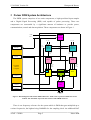
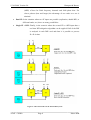
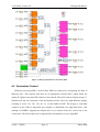
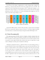
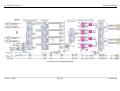
A 1GHz Pulsar Digital Filter Bank
and RFI Mitigation System
Grant Hampson and Andrew Brown
Australia Telescope National Facilty - CSIRO
Corner Vimiera and Pembroke Roads
Marsfield, NSW, 2122
Phone +61 2 9372 4647, Fax +61 2 9372 4298
[email protected], [email protected]
October 9, 2008
15/10/2008, Version 2.0
Hampson & Brown
Contents
1
Introduction ___________________________________________________________ 4
2
Pulsar DFB System Architecture___________________________________________ 5
3
4
5
6
2.1
PDFB Control PC __________________________________________________ 6
2.2
Pulsar Timing Unit _________________________________________________ 7
2.3
Modes of Operation_________________________________________________ 7
Hardware Module Descriptions____________________________________________ 9
3.1
PDFB Chassis and Backplane ________________________________________ 9
3.2
48Volt Power Supply Module________________________________________ 13
3.3
Sampler and Synthesizer Module ____________________________________ 14
3.4
RTM Module _____________________________________________________ 16
3.5
Digital Filter Bank Module__________________________________________ 18
3.6
Communications Module ___________________________________________ 19
3.7
PDFB Cost Summary ______________________________________________ 21
Firmware Descriptions__________________________________________________ 22
4.1
Sampler Histogram ________________________________________________ 22
4.2
Decimation Control ________________________________________________ 23
4.3
Polyphase Filter Bank______________________________________________ 24
4.4
Pulsar Processing Unit _____________________________________________ 26
4.5
10Gb Ethernet ____________________________________________________ 28
4.6
Inverse Filter Bank ________________________________________________ 29
4.7
RFI Processor ____________________________________________________ 31
PDFB Debug Software__________________________________________________ 34
5.1
Digitiser Debug Software ___________________________________________ 34
5.2
DSP Board Debug Software _________________________________________ 36
5.3
Xilinx Download Software __________________________________________ 38
PDFB Correlator Software ______________________________________________ 41
6.1
Overview ________________________________________________________ 41
6.2
Operation ________________________________________________________ 47
6.2.1
Pulsar Folding _________________________________________________ 47
6.2.2
Search Mode __________________________________________________ 48
6.2.3
Spectrometer Mode _____________________________________________ 49
6.3
7
File Locations_____________________________________________________ 50
ATDC Operation_______________________________________________________ 51
7.1
Overview ________________________________________________________ 51
7.2
Configuration_____________________________________________________ 52
___________________________________________________________________
ATNF - CSIRO
Page 2
Pulsar DFB
15/10/2008, Version 2.0
7.3
Hampson & Brown
Operation ________________________________________________________ 52
___________________________________________________________________
ATNF - CSIRO
Page 3
Pulsar DFB
15/10/2008, Version 2.0
Hampson & Brown
1 Introduction
This report presents a description of the Pulsar Digital Filter Bank (PDFB) and RFI
Mitigation (RFIM) projects. The PDFB is a system capable of processing up to 1GHz of BW
in four primary modes of operation; folding, search, spectrometer and base band outputs.
These PDFB modes can be used in conjunction with the RFI inputs when interference is
sufficiently strong as to require the real time mitigation.
Pulsar observing systems require a method of dividing the observed bandwidth into
narrow channels to counter the effects of interstellar dispersion. To provide the very wide
bandwidths (1GHz) and high time-resolution required for precision timing and polarization
observations, ATNF has developed a Pulsar Digital Filterbank (PDFB) system based on
implementation of a polyphase filter in FPGA processors. The Pulsar Digital Filter Bank
hardware will consist of three main parts; a high speed Analog-Digital-Converter (ADC), a
Digital Filter Bank (DFB), and a Pulsar Processing Unit (PPU). The PPU contains a full
correlator to preserve polarisation information and then folds data at the pulsar period.
Astronomy observations are becoming increasingly difficult due to the growing number of
strong transmitters (TV stations, etc.), otherwise known as interference, or RFI, to
astronomers. The objective is to implement real-time mitigation of the effects of RFI with
particular application to pulsar observations. Because of its high time resolution and the very
wide bandwidths used to obtain sufficient sensitivity, pulsar astronomy is especially
susceptible to the effects of RFI. The system has been developed to incorporate a second RFI
input, which can be appropriately subtracted in real-time from the measured astronomical
signal (alternatively this can be used as a second IF input).
This document represents a summary of the hardware, firmware and software in the PDFB
system. Each of these components will be discussed in a suitable depth such that it can be
appreciated by a wide audience. Further details can be obtained from the authors.
___________________________________________________________________
ATNF - CSIRO
Page 4
Pulsar DFB
15/10/2008, Version 2.0
Hampson & Brown
2 Pulsar DFB System Architecture
The PDFB system comprises of two main components, a high-speed dual input sampler
and a Digital Signal Processing (DSP) card capable of pulsar processing. These two
components are surrounded by a significant amount of hardware to provide power,
communication, control and data acquisition. These components are shown in Figure 1.
5MHz
32MHz
Synthesiser
BAT
A1 B1
Event
Generator
PTU
Timing
A2 B2
Dual
Sampler/
Synthesiser
PTU Timing
Clocks
Data
Dual
Sampler/
Synthesiser
Clocks
Data
10/100MB
Ethernet
RTM
RTM
Clocks
Data
Events
Correlator
Control
Computer
Clocks
Data
Events
PTU
DSP
Backplane
DSP
SCSI
Card/Drives
10GbE
Ethernet
COMMS
Card
10GbE
Ethernet
Switch
Figure 1: Block Diagram of the Pulsar DFB architecture. Each colour represents a different card or
module. The dotted line represents the contents of the PDFB enclosure
There is one frequency reference for the system which is 5MHz that gets multiplied up to
various frequencies, the highest being 2048MHz for the sampling clock. An additional BAT
___________________________________________________________________
ATNF - CSIRO
Page 5
Pulsar DFB
15/10/2008, Version 2.0
Hampson & Brown
(Binary Atomic Time) signal generated from an ATDC (Australian Telescope Distributed
Clock) is required to synchronise the system and provide absolute time. The sampler module
contains two 10-bit ADCs, of which only 9-bits is output in a serial fashion. The serialiser
requires a 640MHz reference - which is also sent to the RTM module that contains a deserialiser. The sampler module contains a synthesizer, which generates 2048MHz, 640MHz
and 256MHz (used for the DSP module.) Data is transmitted serially at a rate of 10.24Gbps.
A Pulsar Timing Unit (PTU), included on the DSP cards, generates three signals; bin,
period and bank, which control the pulsar folding engine on the DSP module. The PTU is
directly controlled from the DSP card computer with its time reference generated from the
ATDC’s BAT.
The Rear Transition Module (RTM) is an acronym used for describing a board located in
an AdvancedTCA rack. The RTM is based on this standard, as well as the board called DSP.
The RTM accepts the serial data from the sampler and converts them to a parallel format.
Other signals input into the RTM include several clocks, as well as the physical
10/100/1000M Ethernet connections (although in the diagram they are shown connected to
the DSP card). All these signals are connected to the DSP board.
The DSP board contains many large high speed FPGAs and DDR2 memory to perform
the pulsar operations required. Here two digital filter banks are implemented as well as the
PPU. Data processing is shared between two DSP cards across a backplane using serial data
communications at 3.125Gbps. By sharing data between the two DSP cards it is possible to
implement many different configurations; these will be discussed later. Data out the DSP
board can vary tremendously in bandwidth and as such there are three possible methods of
data transport: a 10/100M Ethernet link, a 1Gb Ethernet link and three 10Gb Ethernet links. In
general the 10/100/1000 network is suitable for folding, however for search mode or base
band processors the 10Gb links provide the higher bandwidths required.
2.1 PDFB Control PC
The PDFB control PC which is known as the CCC is a specialised PC containing the
necessary hardware for the system. Table 1 lists the hardware contained in the CCC - note
that not all this hardware will be required for certain applications. The approximate cost for a
fully loaded system is AU$? Some time is required to assemble the PC due to that large
___________________________________________________________________
ATNF - CSIRO
Page 6
Pulsar DFB
15/10/2008, Version 2.0
Hampson & Brown
number of components. The PC is also loaded with SUSE 10.3 Linux and all drivers need to
be installed.
Table 1: Bill of Materials for the Correlator Control Computer (CCC)
Component
Part Number
19” Chassis
Motherboard
Processor
1GB Memory
10Gb Ethernet
SCSI320 card
SCSI Drives
SCSI Cable
IDE Drive
DVD R/W drive
Power Supply
Event Generator
RCK404M
Tyan Tomcat i7230W S5162
Pentium D LGA775 3.2GHz
240-pin DDR2 1GB 667MHz
Intel CX4 PXLA8591CX4
Adaptec MIO-39320AR/P
Seagate 300GB 10000RPM
SCSI320 Cable
300GB ATA133 7200RPM
Sony DRU800A
500W Antex Neo HE
Event Generator V3.3
Quantity
1
1
1
4
2
1
2
1
1
1
1
16
Supplier
Unit Cost
Total Cost
AICSYS-Australia
PC Nation
Jess World
Jess World
DigitalCarte
DigitalYes
Alpha Online
PC Pitstop
TechBuy
Auspac
Jess World
ATNF-CSIRO
$?
$?
$?
$?
$?
$?
$?
$?
$?
$?
$?
$?
$?
$?
$?
$?
$?
$?
$?
$?
$?
$?
$?
$?
$?
2.2 Pulsar Timing Unit
The Pulsar Timing Unit (PTU) is a piece of equipment that can accurately generate timing
signals required for the pulsar folding mode. These signals are Bin, Period and Bank. Each
pulsar period is defined by the Period signal for there are given number of Bins, for example
each period may be divided into 2048 bins. Since the system is fully double buffered there is a
bank signal, which indicates which bank should be currently integrated into. The PTU module
has been integrated with an event generator and incorporated onto the pulsar DSP cards. All
of the PTU timing signals are injected into the digitiser modules allowing the signals to travel
with the data and eliminating processing timing compensation that would be otherwise
necessary.
2.3 Modes of Operation
There are many modes of operation of the PDFB & and RFI systems. This section
describes the main configurations possible with a dual card system (obviously a single card
system is limited.) Figure 2 shows three basic configurations possible with a dual card system.
•
Single IF: To achieve maximum performance with a single IF system the data can be
distributed across two cards. This achieves the Minimum Pulsar Period
___________________________________________________________________
ATNF - CSIRO
Page 7
Pulsar DFB
15/10/2008, Version 2.0
Hampson & Brown
(MPP) of 4ms for 2048 frequency channels and 2048 phase bins. For
slower pulsars (8ms and longer) the advantage of two cards over one is
minimal.
•
Dual IF: In the situation where two IF inputs are possible (replication, double BW, or
different bands, etc.) there are many possibilities.
•
Single IF + RFI: Finally, in the scenario where the second IF is a RFI input then a
real time RFI mitigation algorithm can be applied. Half of the BW
is analysed in each DSP card and then it is possible to process
2k×2k in 4ms.
Figure 2: Three base modes of the Pulsar DFB system
___________________________________________________________________
ATNF - CSIRO
Page 8
Pulsar DFB
15/10/2008, Version 2.0
Hampson & Brown
3 Hardware Module Descriptions
The following sections describe the six major hardware modules in the PDFB rack (the
CCC is considered previously.) A significant amount of assembly is required for these
modules - however this document only deals with the top-level assembly. For example the
DSP card contains over 4000 components, and only top-level assembly is shown here.
3.1 PDFB Chassis and Backplane
The PDFB chassis is constructed from standard Rittal rack hardware (with some
modification) and a fully custom backplane. The Rittal parts required for the construction of
the rack are shown in Table 3. Some additional M4 holes are required in the side plates of the
rack to accommodate horizontal rails.
Table 2: Rittal bill of materials for the PDFB 19” 9U rack (ex-GST prices)
Rittal #
3684.550
3684.619
3684.638
3684.702
3684.234
3684.233
3688.770
3688.771
3684.562
3687.724
3687.567
3684.572
3684.582
3684.610
3654.370
3654.340
3654.300
3684.886
3687.527
3687.528
Part Description
9U x 525mm side plate
9U front flange
9U rear trim
Vented cover plate
Cover mounting blocks
Assembly screws
Black handle top
Black handle bottom
84TE A front horizontal
84TE B1 cross rail
84TE B cross rail
84TE C1 rear cross rail
84TE D1 centre rail
84TE tapped strip
M2.5 nut pack 100
M2.5 screw pack 100
M4 screw pack 100
Front panel 1U 84TE
Aluminium guide 220mm
Aluminium guide 280mm
Quantity
2
2
2
2
3
1
6
6
2
2
2
5
1
8
1
1
1
2
6
10
65
Unit Cost
$?
$?
$?
$?
$?
$?
$?
$?
$?
$?
$?
$?
$?
$?
$?
$?
$?
$?
$?
$?
Total
Total Cost
$?
$?
$?
$?
$?
$?
$?
$?
$?
$?
$?
$?
$?
$?
$?
$?
$?
$?
$?
$
$?
In addition to the Rittal parts there are a set of laser cut and etched 3mm stainless steel
front and rear faceplates for each of the modules. These cost $20 for the laser cutting and $?
each for the laser etching, for a total cost of $?
___________________________________________________________________
ATNF - CSIRO
Page 9
Pulsar DFB
15/10/2008, Version 2.0
Hampson & Brown
For cooling, the PDFB rack has fans placed above the modules (still inside the rack) and
are powered from the 48V supply. There are six fans in total and they are mounted on two
stainless steel plates spanning the depth of the rack, each plate mounts 3 fans. The drawing of
fan mount holes is shown in Figure 3. The fan part number is Papst-4318 and they cost $?
each for a total cost of $? These are mounted to the fan rails using twenty-four M4x16 screws
and nuts.
Figure 3: Found mounting plate (2 required)
There are seven extra 4.5mm holes required in PDFB rack side plates. These holes are
illustrated in Figure 4 where this should only be used for illustration purposes only (the side
plate shown is for a shallower rack.) The exact location of the holes can be determined by
placing another plate over the top to get exact placement. In addition the 9U front flange and
rear trim also require these holes.
___________________________________________________________________
ATNF - CSIRO
Page 10
Pulsar DFB
15/10/2008, Version 2.0
Hampson & Brown
Figure 4: Extra holes required in the 9U side plates for the Pulsar DFB
The backplane is mounted inside the Rittal rack using 36-M2.5x8 screws. Figure 5 shows
the Protel layout of backplane - which is reasonably straightforward. There are six large
AdvancedTCA power connectors (power supply, 2xDSP, 2xADC and a COMS card. The
ADC modules are located at the outer edges of the backplane, with the DSP modules sitting
adjacent to them. A cut out is visible where the DSP module connects to the RTM module.
The COMS module is located in-between the DSP modules (i.e., the centre.) Although the
backplane appears rather simple, it requires a significant number of layers to route the serial
data links between the DSP and COMS modules. As such it is 5mm thick and contains 18layers. Fan power connections are available top and bottom. The DFB-backplane-IF
connection on the backplane connects to the ADC modules so that they can be programmed.
___________________________________________________________________
ATNF - CSIRO
Page 11
Pulsar DFB
15/10/2008, Version 2.0
Hampson & Brown
Figure 5: Backplane PCB for the Pulsar DFB
The ADC and COMS modules transfer analogue signals through a set of OSP connectors.
These OSP connects are connected to semi-rigid cable to various modules that sit on the rear
side of the backplane. A mini-circuits splitter module (ZX10-2-12-S) is mounted on the rear
of the backplane to split the 32MHz to both DSP cards for synchronisation. Table 3 lists the
required cables for the OSPs.
The total cost for the mechanics of the DFB rack is then Rittal + F/R plates + Fans +
Connectors + Backplane = $?
___________________________________________________________________
ATNF - CSIRO
Page 12
Pulsar DFB
15/10/2008, Version 2.0
Hampson & Brown
Table 3: Semi-rigid 0.085 cable required for the Pulsar DFB backplane
OSP Connector
1059456-1
1059456-1
1059456-1
1059456-1
1059456-1
Description
10Gbps data
32MHz clock
640MHz clock
256MHz clock
32MHz clock
Quantity
8
2
2
2
1
Length
28cm
25cm
16cm
16cm
4cm
End Connector
SMA straight
1059456-1
MCX straight
MCX straight
SMA straight
SMA straight
32MHz clock
2
16cm
MCX right angled
Comments
J5,6,7,8 on RTM
Solder in place!
J12 on RTM
J4 on RTM
Sum input of
rear mounted
splitter
J25 on RTM
3.2 48Volt Power Supply Module
The power supply board for the Pulsar DFB is a fully custom design so that it could be
mounted within the chassis and plug into the rack easily. A photo of the power supply module
is shown in Figure 6, which contains relatively few components, as shown in Table 5. A
power cable to the supply is required using crimp connections. These cables are 11 and 19cm
long. Solid core wire is also required from the supply output to the PCB.
Figure 6: Power Supply module for the Pulsar DFB
___________________________________________________________________
ATNF - CSIRO
Page 13
Pulsar DFB
15/10/2008, Version 2.0
Hampson & Brown
Table 4: Components on the 48V power supply module
Part #
PBB20C-48X
Description
48V-600W
supply
VPB30W8M6200C1 R/A connector
Power PCB
PCB
Farnell 1190673
12A fuse
Farnell 9997113
AC inlet 6A
Quantity
1
Unit Cost
$?
Total Cost
$?
2
1
2
1
$?
$?
$?
$?
Total Cost
$?
$?
$?
$?
$?
3.3 Sampler and Synthesizer Module
The analogue IF inputs into the Pulsar DFB are converted to a digital format in the
Sampler/Synthesizer module, as shown in Figure 7. These IF inputs are not filtered in any
way and should be AC coupled into the module. The maximum voltage of the input should
not exceed ±500mV as damage will occur to the ADCs. It is expected that the input is
appropriately band limited to match the DFB bandwidth setting.
Figure 7: Sampler/Synthesiser module for the Pulsar DFB
___________________________________________________________________
ATNF - CSIRO
Page 14
Pulsar DFB
15/10/2008, Version 2.0
Hampson & Brown
The synthesizer accepts a 32MHz reference from the backplane (via an OSP) and
multiplies this up to 2048MHz (the sampling clock) and 640MHz (the serialiser reference.)
The long skinny box contains the synthesizer and the squarer enclosure the sampler. The
2048MHz clock is divided down on the module to 256MHz (divide by 8.) The 640MHz and
256MHz outputs are required in the RTM and DSP modules and hence they are connected via
OSPs to the backplane.
There are two ATMEL digitizers inside the ADC box, as well as a de-multiplexer (to
reduce data rates) and a Xilinx FPGA. The FPGA controls the function of the samplers as
well as outputting data to the Intel serialisers. The output rate of serialiser is 10.24Gbps.
These outputs are connected through the backplane to the RTM via OSPs.
The sampler module is powered from a single 48V supply and hence to provide the
necessary voltages there are several DC-DC converters. There is one large isolated DC-DC
regulator which converts 48 volts to 12 volts, additional regulators and inverters generate –6,
+5.5, +1.2, +2.5, -3.3, -2. A single led (visible on the front panel) indicates if power is applied
to the module. The sampler PCB is 6-layers.
The BCCIF controls the sampler module via the Zd-connector next to the power
connector. Alternatively the BCCIF cable can be connected via the front panel. The JTAG
chain (FPGA and PROM) can be accessed via the backplane (with appropriate jumper
settings) or via the front panel.
Several cables are required for the construction of the sampler module, which are listed in
Table 5. Also the total cost of each sampler/synthesizer module is shown in Table 6.
Table 5: Semi-rigid 0.085 cable required for the Sampler/Synthesizer Module
OSP Connector
1059404-1
1059404-1
1059404-1
1059404-1
SMA
SMA
Description
10Gbps data
32MHz clock
640MHz clock
256MHz clock
2048MHz clock
IF Inputs
Quantity
8
2
2
2
2
4
Length
25.4cm
12cm
35cm
38cm
5.5cm
14cm
End Connector
SMA straight
SMA straight
SMA R/A
SMA R/A
SMA R/A
Panel SMA
___________________________________________________________________
ATNF - CSIRO
Page 15
Pulsar DFB
15/10/2008, Version 2.0
Hampson & Brown
Figure 8: 12mm right angle aluminium strip 8cm long with hole centres of 1cm
Table 6: Components on the Sampler/Synthesiser module (single module shown)
Description
Dual Sampler with enclosure
Synthesiser with enclosure
Sampler/Synthesiser PCB
DC-DC supplies and divider
Total Cost
$?
$?
$?
$?
$?
3.4 RTM Module
The serial data from the Sampler module passes through the backplane and enters a card
known as an RTM, or Rear Transition Module. This comes from the AdvancedTCA standard,
although we have modified it so that is double the depth of the standard. The RTM handles all
the data interfacing to the external world for the front board, or DSP card.
A photo of the RTM is shown in Figure 9 where there are a number of connectors visible.
There are four possible clock inputs into the RTM via MCX connectors. In a typical
configuration these clocks may be DSP clock, deserialiser reference, rocket clock and a
synchronisation clock. The RTM is capable of receiving fibre inputs as well as coax inputs for
the serial data.
___________________________________________________________________
ATNF - CSIRO
Page 16
Pulsar DFB
15/10/2008, Version 2.0
Hampson & Brown
Figure 9: Photo of the RTM and AdvancedTCA rack
The BAT reference and event inputs enter on the 2mm connector at the bottom of the
RTM – which can be used for pulsar timing, etc.. There are also four 10Gb Ethernet ports on
the RTM one of which (J29) is used for search mode data output.
The four 10Gbps serial data is de-serialised and passes through the RTM FPGA and then
through the connector to the DSP card. The total cost of the RTM board is $?
___________________________________________________________________
ATNF - CSIRO
Page 17
Pulsar DFB
15/10/2008, Version 2.0
Hampson & Brown
3.5 Digital Filter Bank Module
The heart of the Pulsar DFB system is the DSP board, as shown in Figure 10. A brief
overview of the card follows, as to talk about it in detail would take up considerable room.
The DSP PCB is a 26-layer board measuring 322x280x3mm containing 4188 components.
There are approximately 20,000 nets and 23,000 holes. Given that there are ten large signal
processing FPGAs on the board means that it can be applied to a multitude of projects.
Figure 10: Photo of the DSP board inside an AdvancedTCA rack (not the PDFB rack)
The DSP card is powered from a single 48V supply, which is converted to 12V and then
distributed, to many DC-DC converters and linear supplies. Each card is nominally rated to
200W of power. A large heat sink covers all the FPGA to distribute heat evenly over the
entire surface area. (This is not shown in the photo). There is a small computer on each card
controlling/monitoring everything on the board. Power supplies are switchable, there are a
___________________________________________________________________
ATNF - CSIRO
Page 18
Pulsar DFB
15/10/2008, Version 2.0
Hampson & Brown
multitude of temperature sensors, power and voltage monitory. The computer can program the
FPGAs and then communicate over a 16-bit 66MHz bus (for control and data-acquisition.)
The sampler data enters a LX80 FPGA first where the data statistics are analysed and any
RFI transients are removed (if RFI rejection is selected). Data is then passed to two SX55
FPGAs which each contain a filter bank varying in size from 512 channel to 8192 channels.
The data is then passed to two Pro50 FPGAs, which can transfer data serially to a second DSP
card to share the processing. Data then travels to a further two SX55 FPGAs which contain
the Pulsar Processing Unit (PPU.) These FPGAs are each connected to 1GBytes of DDR2
memory, which is required for all pulsar modes of the PPU. There are many possible modes
for all of these FPGAs and hence will not be described in any more detail here.
There are three methods of getting data from the card, firstly a 10/100/1000M Ethernet
link connected to the computer on each card. Secondly, there are two 10Gb Ethernet streams
coming from the communications card from two of the Pro50 FPGAs. Finally, it is also
possible to have a 10Gb Ethernet link coming off the RTM. Each of these links connects to
different FPGAs.
The DSP board is the most expensive part of the design and in summary costs
approximately $?
3.6 Communications Module
The last module in the design is the communications module. This module buffers the
10Gb Ethernet signals coming from the DSP cards, as well as providing a location for the
system clock reference to be. A photo of the board is shown in Figure 11 where the 32MHz
synthesizer box can be seen. This box accepts a 5MHz station reference and multiplies this up
to a clean 32MHz. This is distributed to the Sampler and DSP module via OSP connectors. A
list of cables required for the communications module is shown in Table 7. In addition to
these cables there will be 10Gb Ethernet cables required for the connection to the base band
processor. The 10Gb Ethernet signals travel from the DSP module across the backplane. On
the communications module the signals are buffered to boost signal integrity. An approximate
costing for the communications module is shown in Table 8.
___________________________________________________________________
ATNF - CSIRO
Page 19
Pulsar DFB
15/10/2008, Version 2.0
Hampson & Brown
Table 7: Semi-rigid 0.085 cable required for the Communications module
OSP Connector
SMA R/A
1059404-1
1059404-1
BNC
Description
32MHz clock
32MHz clock
BAT Reference
5MHz clock
Quantity
1
3
1
1
Length
10cm
5cm
20cm
6in
End Connector
SMA R/A
SMA R/A
SMA R/A
SMA (Digikey J3606)
Table 8: Components on the Communications module
Description
32MHz module with enclosure
10GbE Ethernet buffers
Communications PCB
DC-DC supplies and splitters
Total Cost
$?
$?
$?
$?
$?
Figure 11: Communications module for the Pulsar DFB
___________________________________________________________________
ATNF - CSIRO
Page 20
Pulsar DFB
15/10/2008, Version 2.0
Hampson & Brown
3.7 PDFB Cost Summary
A summary of the PDFB costs is shown in Table 9 for the major modules and systems. A
majority of the cost falls into the Sampler and DSP modules, as expected for a high
bandwidth/resolution system.
Table 9: Cost summary for a single/dual card PDFB system
Description
Correlator Control Computer (no SCSI)
PDFB 19” 9U Chassis Complete
48V 600W Power Supply Module
Sampler Synthesiser Module
RTM Board
DSP Board
Communications Module
Total Cost
Single
$?
$?
$?
$?
$?
$?
$?
$?
Dual
$?
$?
$?
$?
$?
$?
$?
$?
___________________________________________________________________
ATNF - CSIRO
Page 21
Pulsar DFB
15/10/2008, Version 2.0
Hampson & Brown
4 Firmware Descriptions
Firmware is the programming of the digital gates in the FPGAs - and makes the hardware
have a desired function. The following sections describe the firmware associated with each
part of the design. The firmware is developed in Matlab/Simulink as models and then
exported as VHDL. This VHDL is then incorporated into low-level wrappers which interface
to the external world. As such only the high level models will be shown here to give the
reader an understanding of the signal processing occurring in the system.
4.1 Sampler Histogram
The sampler histogram is the first part of the signal processing chain – although it doesn’t
alter the data. The Simulink top-level model is shown in Figure 12 and calculates the
minimum, maximum and mean sampler value. In addition it calculates the mean square value
(the square root is calculated in software.) The histogram is also calculated so that the
distribution of sampler data can be seen. These statistics and values are read from the
hardware every integration cycle and stored in the output file.
___________________________________________________________________
ATNF - CSIRO
Page 22
Pulsar DFB
15/10/2008, Version 2.0
Hampson & Brown
Figure 12: Histogram module for the Pulsar DFB
4.2 Decimation Control
Different processing BW’s in the Pulsar DFB are achieved by decimating the data at
different rates. This requires that there be an appropriate external filter, which limits the
analog IF signal to the same BW, failure to insert this IF filter will result in aliasing. Figure 13
illustrates the top-level structure of the decimation network. There are eight different settings
resulting in 1024, 512, 256, 128, 64, 32, 16 and 8MHz of BW. The design is somewhat
complex as the 1GHz of input data (per sampler) is distributed over eight data buses, each
running at 256MHz. Appropriate samples have to be chosen from the correct bus at the
correct time. The filter bank clock is appropriately decimated for a given input BW.
___________________________________________________________________
ATNF - CSIRO
Page 23
Pulsar DFB
15/10/2008, Version 2.0
Hampson & Brown
Figure 13: decimation module for the Pulsar DFB
4.3 Polyphase Filter Bank
The polyphase filter bank converts the time series data into a number of frequency sub
bands using a polyphase filtering technique. This technique involves the use of filters and the
FFT to shift each band to base band. The top-level design of the DFB is shown in Figure 14
where these two parts can clearly be seen. As said earlier the input data are distributed over
___________________________________________________________________
ATNF - CSIRO
Page 24
Pulsar DFB
15/10/2008, Version 2.0
Hampson & Brown
eight real input buses since it is not possible to have a single data bus clocking over at 2GSPS.
The output of the DFB is also distributed over four complex data buses.
Figure 14: Top level of the Digital Filter Bank Module
The filter part of the design is implemented using the DSP48 modules (multiply
accumulate) inside the Virtex-4 FPGAs. Delays and filter-coefficients are implemented using
BRAMs. One section of the filter is shown in Figure 15 where the length of the polyphase
filter is 8. The overall filter length is determined by twice the number of filter bank channels.
Input data is 9-bits wide, filter coefficients are 12-bits wide and the filter output 16-bits.
Figure 15: Polyphase filter with 8-taps (one/eight of the overall filter)
___________________________________________________________________
ATNF - CSIRO
Page 25
Pulsar DFB
15/10/2008, Version 2.0
Hampson & Brown
The FFT part of the design is implemented as a radix-4 design using a complex FFT
followed by a post-processing stage that converts the complex FFT into a real FFT. The
complex FFT can be divided into processing stages of DFT, Twiddle and Commutate. A 64channel FFT is shown in Figure 16. Given that the design is based on radix-4 the filter lengths
achievable are 64, 256, 1024, 4096, etc. To achieve intermediate filter lengths (e.g., 128, 512,
2048) a mixed radix design technique is used.
Figure 16: A Radix 4 64 Channel FFT
In general the DFB consumes a fraction of the processing (∝ log N) resources in the SX55
FPGAs, but as expected the memory resources are linear (∝ N) with the length of the DFB.
Given that memory is consumed faster that processing the maximum DFB length is 8192.
4.4 Pulsar Processing Unit
The pulsar-processing unit (PPU) takes the frequency channels outputted from the
polyphase filter bank correlates and integrates according to the signals generated from the
PTU. All possible correlation products are formed, the two auto correlation products and the
cross product. As the output bit width of the correlator is the same as its inputs there is a gain
control, enabling the correlator gain to be adjusted in 6dB steps.
Although the integration memory is within the FPGA, the pulsar binning memory is
located off the FPGA in the 4 sticks of DDR2 memory on the lower half of the DSP card. The
memory is double buffered to allow simultaneous download of data and pulsar processing.
The filter bank frames are integrated into internal FPGA memory until a Bin signal is
received from the PTU at which time the current integration results are placed into the
external DDR2 memory and the next time bin results are retrieved from the DDR2 memory.
The PPU is pipelined to allow the maximum timing resolution permitted by the size of the
___________________________________________________________________
ATNF - CSIRO
Page 26
Pulsar DFB
15/10/2008, Version 2.0
Hampson & Brown
filter bank frames. Table 10 specifies the minimum pulsar folding periods permitted with each
filter bank configuration using 1GHz of bandwidth (using a dual system), as the BW is
decreased the minimum folding time increase. Folding mode is not supported beyond 4096
frequency channels and beyond 2048 time bins, also the minimum number of frequency
channels is 512. It is important to note that the quantity of data being downloaded increases
with respect to the product of the time bins and frequency channels, and as such the correlator
cycle time must also increase to allow more time for the data to be downloaded.
FFT
Channels
Table 10: Minimum pulsar folding periods
512
1024
2048
4096
16
8us
16us
32us
64us
Time Bins
32
64
128
256
512
1024
16us 32us 64us
128us
256us
512us
32us 64us 128us 256us
512us 1.024ms
64us 128us 256us 512us 1.024ms 2.048ms
128us 256us 512us 1.024ms 2.048ms 4.096ms
2048
1.024ms
2.048ms
4.096ms
8.192ms
___________________________________________________________________
ATNF - CSIRO
Page 27
Pulsar DFB
15/10/2008, Version 2.0
Hampson & Brown
Figure 17: Pulsar Processing Unit
4.5 10Gb Ethernet
10Gb Ethernet is utilised in the PDFB system to allow the high speed transfer of search
and base band data to computer networks. The 10Gb Ethernet is realised through the CX4
standard, allowing a direct copper connection between the PDFB system and either a
___________________________________________________________________
ATNF - CSIRO
Page 28
Pulsar DFB
15/10/2008, Version 2.0
Hampson & Brown
computer or a network switch. Data is transmitted using UDP packets sent to a particular
MAC and IP combination. No ARP (address resolution protocol) infrastructure is
implemented meaning that all network MAC addresses must be set configured prior to use.
The 10Gb Ethernet FPGA code used is a customised freeware core from Xilinx.
The PDFB rack contains 6 10Gb Ethernet ports, 4 on the front of the unit for base band
data, and 2 on the rear of the unit for search data. For the search mode data all packets are sent
to a single IP/MAC combination, however for the base band data each band is sent to a
different IP/MAC combination.
4.6 Inverse Filter Bank
The PDFB has the capability to output base band data divided into 16 equal bands across
the processed bandwidth, i.e. processing at 1GHz gives 16 bands of 64MHz. Base band data
is reconstructed from the filter bank data using an inverse or synthesis polyphase filter bank.
The inverse filter bank uses a standard Xilinx FFT module with a custom FIR configuration
as shown in Figure 18.
The output of the inverse filter bank is 16 band limited complex time series that represent
the full bandwidth of the PDFB. The inverse filter bank can be operated with 512, 1024 and
2048 channel filter bank configurations and in parallel with folding operations. The inverse
filter bank is located after the RFI mitigation processing allowing real time RFI filtering to the
base band outputs.
___________________________________________________________________
ATNF - CSIRO
Page 29
Pulsar DFB
15/10/2008, Version 2.0
Hampson & Brown
Figure 18: Inverse Polyphase Filterbank
______________________________________________________________________________________________________________
ATNF - CSIRO
Page 30
Pulsar DFB
15/10/2008, Version 2.0
Hampson & Brown
4.7 RFI Processor
Two level of RFI mitigation processing exist within the PDFB hardware, firstly large
transients in the time series data can be removed and secondly the frequency channels can be
filtered. Either one or both of these mechanisms can be employed during folding and
spectrometer modes.
Removal of large transients from the time series data (clipping) is implemented prior to
the polyphase filter bank. To detect an RFI spike the average variance of the input data is
calculated over an adjustable time period and compared to the instantaneous variance of the
data. Any data that exceeds a preset threshold is removed from the time series and replaced
with the running mean of the data. The RFI clipping mechanism accepts two inputs, firstly the
time constant and secondly a beta2 value (maximum allowable deviation from variance). The
time constant is selectable between 128us and 2us in powers of 2, and the beta2 value, or
deviation from variance is between 1 and 65535, with 0 being disabled. The value of beta2 is
determined from the amplitude of the input data and the level of rejection required. The RFI
clipper is shown in Figure 19.
___________________________________________________________________
ATNF - CSIRO
Page 31
Pulsar DFB
15/10/2008, Version 2.0
Hampson & Brown
Figure 19: RFI Clipping mechanism
RFI filtering is achieved through the use of the second set of inputs (RFI reference) on a
PDFB system and an adaptive filter. The RFI reference input is average over an adjustable
time threshold and the proportion of it present in the astronomy signal is subtracted. The
subtraction is a complex operation allowing for phase differences between the RFI reference
and astronomy signal. This means that path matching is not necessary for the RFI signal,
however a good signal to noise ratio on the RFI input is necessary to provide optimum
filtering. The adaptive filter has two input parameters, a time constant over which the RFI
average is calculated, and a gain coefficient to prevent filter overshoot. A time constant of 1
ms and a gain coefficient of 0.1 is sufficient for most situations. The RFI adaptive filter is
shown in Figure 20.
___________________________________________________________________
ATNF - CSIRO
Page 32
Pulsar DFB
15/10/2008, Version 2.0
Hampson & Brown
Figure 20: Adaptive RFI Filter
___________________________________________________________________
ATNF - CSIRO
Page 33
Pulsar DFB
15/10/2008, Version 2.0
Hampson & Brown
5 PDFB Debug Software
Debug software is an integral part of commissioning and testing any complex hardware
system. The PDFB system like any other has a range of engineering debug programs designed
to examine various aspects of the system to determine the location of faults and detect
hardware problems. The following sections describe the most commonly used features of the
debug programs.
It should be noted that misuse of these programs can cause hardware instability and device
malfunctions.
5.1 Digitiser Debug Software
The digitiser test program adcv is used to analyse the functionality of the digitiser
modules without the aid of the DSP cards. The primary purpose of adcv is to examine the
input into the digitiser module without running the correlator software. The adcv program
cannot be run in conjunction with the correlator software, as the same communications paths
are required.
The digitiser test program can be started from the corr user account on the correlator
control computer. On starting the application the user is asked to specify a target name, Table
11 identifies the correct target name based on the system configuration. A port number is also
required which in all cases is port 4001, and a communications timeout, which should be set
to 10 seconds. Once the program is started 4 new PGPlot windows will open, and once data is
downloaded they will display the ADC data, ADC histogram and the frequency spectrum. A
screen shot of the adcv program is shown in Figure 21. There are two commands in adcv:
•
i – Issues an initialisation command. If the correlator software hasn’t been configured
since a system power cycle then the initialisation command is required. This command
starts the samplers and resets the data download machinery.
•
g <x> <y> – Issues a data get command, where <x> is the digitiser number and <y> is
the number of download iterations. The get data command will retrieve a number of
2048 sample downloads from the digitiser hardware. If the iterations count is greater
___________________________________________________________________
ATNF - CSIRO
Page 34
Pulsar DFB
15/10/2008, Version 2.0
Hampson & Brown
than 1 then the integrated spectrum and histogram plots will be calculated. The
mapping of the digitiser number is shown in Table 11.
•
quit – Exits the program.
Table 11: Possible adcv targets
Target Name
l-bcc11
l-bcc11
l-bcc11
l-bcc11
l-bcc11
l-bcc11
Digitiser Number Description
Single System
0
Pol A Input
1
Pol B Input
Dual System
0
Astronomy Pol A Input
1
Astronomy Pol B Input
2
RFI Pol A Input
3
RFI Pol B Input
___________________________________________________________________
ATNF - CSIRO
Page 35
Pulsar DFB
15/10/2008, Version 2.0
Hampson & Brown
Figure 21: adcv program screenshot
5.2 DSP Board Debug Software
The DSP board test program is used to review the power dissipation and system
temperatures of the DSP board in real time. There are many additional features of this
software however they are outside the scope of this document. The DSP board test program
___________________________________________________________________
ATNF - CSIRO
Page 36
Pulsar DFB
15/10/2008, Version 2.0
Hampson & Brown
can be run while the correlator software is active however not while it is integrating. The DSP
board test program is executed on the DPS card which is to be examined. On a single system
there is only 1 DSP card, however on a dual system there is 2 DSP cards. In order to execute
the test program root access is required to the DSP cards, which requires an ssh session form
the correlator control computer. From the terminal on the correlator control computer:
1. ssh root@<target> where <target> is l-bcc11 for the master DSP card on a dual
PDFB system or on a single PDFB system.
2. cd /som_bin/TEST
3. ./test
When asked for the device name use cabb0.
The option to execute start-up will turn all the switchable power supplies on,
and is only necessary if the card has not been configured.
4. Option 3 will display the temperatures of the DSP card, and option 4 will display the
power dissipation of the DSP card.
___________________________________________________________________
ATNF - CSIRO
Page 37
Pulsar DFB
15/10/2008, Version 2.0
Hampson & Brown
Figure 22: DSP test program
5.3 Xilinx Download Software
The Xilinx download software is used to program the two non-signal processing FPGA’s
on the DSP card. These FPGA’s control the general function of the DSP card and the overall
system timing. The FPGAs are configured on start up by a PROM located on the DSP card, in
order to change the FPGA code the PROM must be reprogrammed.
To reprogram the PROM a Xilinx download cable and the Xilinx download software is
required, of which the software can be downloaded from the Xilinx website. The following
list outlines the major tasks required to perform an upgrade.
___________________________________________________________________
ATNF - CSIRO
Page 38
Pulsar DFB
15/10/2008, Version 2.0
Hampson & Brown
1. The first step is to connect the download cable to the DSP, the cable must be
connected while the DSP card is installed in the rack, as power is required. Start
with the rack turned off and the 10Gbe Ethernet card removed. Connect the 2mm
pitch ribbon connector from the Xilinx download cable to the DSP card’s H8
connector with the cable guide facing up, as shown in Figure 23.
2. Connect the Xilinx download cable to a computer with the Xilinx Impact software
installed, the light on the cable should turn orange. Start the Impact software, but
do not initialise the JTAG cable.
3. Now power on the rack, the orange light on the Xilinx cable should turn green.
Once the VFD screen has turned on initialise the JTAG cable. The list of devices
should appear as in Figure 24.
4. Select the correct device and set it to program with the new MCS file.
5. Power cycle the rack to install the new FPGA code.
Notch Here
Programming
Cable
Figure 23: The Xilinx Programming Cable connected to the DSP card
___________________________________________________________________
ATNF - CSIRO
Page 39
Pulsar DFB
15/10/2008, Version 2.0
Hampson & Brown
PTU
PROM
BCC
PROM
Figure 24: Xilinx Impact Software screenshot
___________________________________________________________________
ATNF - CSIRO
Page 40
Pulsar DFB
15/10/2008, Version 2.0
Hampson & Brown
6 PDFB Correlator Software
The PDFB system is controlled through the correlator control computer using the
correlator software either under telescope control or using a dummy control program. In
addition to the control software there are several real time monitoring programs that can be
used to review the PDFB data as it is processed. The correlator software functionality is based
around the cycle or integration time period, where the data is download from the PDFB
hardware at the end of every cycle and written to the output file.
The following sections provide a brief overview of the operation of the correlator control
software, the dummy control program, and the real-time monitoring programs.
6.1 Overview
The correlator software sdfb3/pdfb3 (dual systems), sdfb4/pdfb4 (single systems) is
responsible for the connection to the PDFB hardware and the control of the timing logic. The
control software is actually a collection of individual programs interacting with each other
through the use of TCP socket connections and using a GLISH user interface for input and
display. There are two different versions of the correlator software sdfb and pdfb. The sdfb
software is used for running the correlator in spectrometer mode and the pdfb software is used
for running the correlator in folding mode. The interface of both pieces of software is the
same, however the output file type is different. In spectrometer mode the output file is a
RPFITS format, and in folding mode the output file is a CFITS format.
The executables for the correlator control software and its support programs are located in
/usr/local/bin/cor. The executable for the correlator software is actually a script that
configures an environment variable setting the output location of the files written as well as
starting the correlator software. The default directory for the spectrometer data files is
/DATA1/SDFB3_1 (for a dual system, /DATA1/SDFB4_1 for a single system) and
/DATA1/PDFB3_1 (for a dual system, /DATA1/PDFB4_1 for a single system) for the folding
and search files. To modify the output directories the environment variable inside of these
scripts must be altered.
___________________________________________________________________
ATNF - CSIRO
Page 41
Pulsar DFB
15/10/2008, Version 2.0
Hampson & Brown
The correlator software can be started from the corr user account on the correlator control
computer by typing pdfb3 on a dual PDFB system or pdfb4 on a single PDFB system. An
example of the pdfb3 program is shown in Figure 25. The control software GUI is divided
into 3 scrolling frames. The lower window displays errors, warning and critical information,
while the middle screen displays messages received from the Dummsy software each cycle,
such as the telescope position. The top window has multiple, purposes depending on what
radio button is selected.
•
Tsys – Display information from the telescope regarding the noise levels, it is only
applicable if the control software is connected directly to the telescope.
•
Samplers – Displays statistics on the IF inputs currently being observed. Statistics
include the min count, max count, RMS and average. The values represent the
digitiser voltage levels and as such have an 8-bit range of –128 to 127. In normal
folding or spectrometer 2 lines are displayed representing polarisation A and B, in
dual beam spectrometer mode or RFI mitigation modes 4 lines are displayed.
•
Data Links – Displays information regarding the 10Gb links from the digitisers to
each DSP card.
•
DSP Brd’s – Displays the temperatures of each of the measurement point on a DSP
card.
At the top of the GUI the current state of the correlator is displayed, along with the current
cycle time, the selected correlator configuration, and the name of the output file.
___________________________________________________________________
ATNF - CSIRO
Page 42
Pulsar DFB
15/10/2008, Version 2.0
Hampson & Brown
Figure 25: pdfb3 example screen shot
The dummy control program is called Dummsy and connects to the correlator software
allowing testing of the correlator and also providing a simple interface for connection to nonstandard telescope control systems. Dummsy is started by typing tkds while logged on as user
corr on the correlator control computer. An example screen shot of Dummsy is in Figure 26.
The Dummsy program’s GUI has a number of buttons and text fields which are editable
and specify information that is either used to determine the operating mode of the correlator
___________________________________________________________________
ATNF - CSIRO
Page 43
Pulsar DFB
15/10/2008, Version 2.0
Hampson & Brown
or inserted to the output file in the header information. The following list explains the critical
test fields and buttons:
•
Go button – Starts the correlator
•
Stop button – Stops the correlator. Pressing the stop button will cause the correlator
software to initiate a staged shutdown that takes two cycle periods.
•
Config button – Configures the correlator using the configuration file selected in the
adjacent scroll box.
•
Obs Type drop down box – Selects the type of observation being conducted, the
only valid selections are NORMAL, and WB_PSR.
•
Source text box – The source text box specifies a polyco file to use when starting
the correlator.
•
Command text box – The command text box allows the entry of commands to
configure the correlator. A complete list of commands accepted is available at
www.atnf.csiro.au/people/wwilson/dummsy.html.
Figure 26: Dummsy screenshot
___________________________________________________________________
ATNF - CSIRO
Page 44
Pulsar DFB
15/10/2008, Version 2.0
Hampson & Brown
Validating what the correlator is processing while it is processing is a necessary step to
verify input levels and ensure that the processed data is free from problems. Real time
monitoring of the correlator output is possible using a program called spd. The spd program
graphs the output data for the correlator using the free PGPlot software, and it allows the full
input spectrum to be monitored, as well as the pulsar bin profile to be observed. It can be
started from the corr user account by typing spd, multiple spd programs can be connected to a
single correlator. The data displayed on the spd plots is updated on the correlator cycle time,
with different data sets and display options selectable through specific commands. A full list
of commands can be found at www.atnf.csiro.au/people/wwilson/spd.html. A screenshot of
spd is located in Figure 27.
Figure 27: Screenshot of spd
___________________________________________________________________
ATNF - CSIRO
Page 45
Pulsar DFB
15/10/2008, Version 2.0
Hampson & Brown
A similar program to spd is adc (different from adcv in section 5.1), which allows the
sampler histogram and sampler statistics to be reviewed, however they are only updated while
the correlator is cycling. The adc program is started by typing adc from the corr user account
on the correlator control computer. A screen shot of the program is shown in Figure 28. Upon
starting adc the program asks for the DATA RAMDISK directory, which is selected as
follows:
•
/data_dump_ram/l-bcc11 – single system or astronomy input of a dual system
•
/data_dump_ram/l-bcc06 – RFI input of a dual system
The adc program has only two commands, which selects the range of the x and y axis. The
applicable commands are:
•
x <min value> <max value> - Sets the display range of the x-axis. If no minimum
and maximum value is supplied the axis will auto scale to the data. The maximum
range of the x-axis is –128 to 127.
•
y <min value> <max value> - Sets the display range of the y-axis. If no minimum
and maximum value is supplied the axis will auto scale to the data.
___________________________________________________________________
ATNF - CSIRO
Page 46
Pulsar DFB
15/10/2008, Version 2.0
Hampson & Brown
Figure 28: Screenshot of adc
6.2 Operation
6.2.1 Pulsar Folding
The following series of commands will place the PDFB hardware into the standard folding
mode operation.
1. Start the pdfb3/4 software and the tkds software.
2. Select a source polyco on the tkds window. The polyco file must exist in the
/home/corr/cor/pulsar directory on the correlator control computer.
___________________________________________________________________
ATNF - CSIRO
Page 47
Pulsar DFB
15/10/2008, Version 2.0
Hampson & Brown
3. Set the obs type to WB_PSR on tkds.
4. Select a valid configuration from the scroll box on the tkds GUI and press the
configure button. Valid configurations for fold mode are defined as:
pdfb3_<X>_<Y>_<Z> (dual system)
or
pdfb4_<X>_<Y>_<Z> (single system)
where:
•
<X> is the number of pulsar time bins
•
<Y> is the bandwidth of the input to be processed
•
<Z> is the number of frequency channels
5. If the configuration chosen has greater than or equal to 2048 frequency channels and
2048 time bins then change the cycle time to 20 seconds by typing “cycle 20” in the
tkds command test box.
6. Optionally a file can be opened by typing “fo” and a filename in the tkds command
text box.
7. Press the go button.
8. Press the stop button to halt the correlator.
9. If a file was opened then the file must be closed with the “fc” command.
6.2.2 Search Mode
The following series of commands will place the PDFB hardware into the standard search
mode operation.
1. Start the pdfb3/4 software and the tkds software.
2. Set the obs type to WB_PSR on tkds.
3. Type the “sset” command into the tkds command text box to enable search mode.
4. Set the search sampling time by typing “ssamt” and the sample time in seconds into
the tkds command text box to enable search mode.
5. Set the number of search product to produce by typing “snprod” and the number of
products 1,2 or 4 into the tkds command text box.
6. Select a valid configuration from the scroll box on the tkds GUI and press the
configure button. Valid configurations for search mode are defined as:
srch_<Y>_<Z>
where:
___________________________________________________________________
ATNF - CSIRO
Page 48
Pulsar DFB
15/10/2008, Version 2.0
Hampson & Brown
•
<Y> is the bandwidth of the input to be processed
•
<Z> is the number of frequency channels
7. Optionally a file can be opened by typing “fo” and a filename in the tkds command
text box.
8. Press the go button.
9. Press the stop button to halt the correlator.
10. If a file was opened then the file must be closed with the “fc” command.
6.2.3 Spectrometer Mode
The following series of commands will place the PDFB hardware into the standard
spectrometer mode operation.
1. Start the sdfb3/4 software and the tkds software.
2. Set the spectrometer cycle time with the cycle keyword in tkds.
3. Set the obs type to NORMAL on tkds.
4. Select a valid configuration from the scroll box on the tkds GUI and press the
configure button. The standard configurations for spectrometer mode are defined as
(non-standard time binning configurations exist for spectrometer mode):
sdfb3_<X>_<Y>_<Z> (dual system)
or
sdfb4_<X>_<Y>_<Z> (single system)
where:
•
<X> is either “2bm” for two beam same frequency spectrometer, “2f” for
two beam two frequency spectrometer, or not present for single beam
configurations.
•
<Y> is the bandwidth of the input to be processed
•
<Z> is the number of frequency channels
5. Optionally a file can be opened by typing “fo” and a filename in the tkds command
text box.
6. Press the go button.
7. Press the stop button to halt the correlator.
8. If a file was opened then the file must be closed with the “fc” command.
___________________________________________________________________
ATNF - CSIRO
Page 49
Pulsar DFB
15/10/2008, Version 2.0
Hampson & Brown
6.3 File Locations
There is a specific location for every part of the correlator source and executable files, and
although under normal conditions these files do not need to be accessed for upgrading
purposes the locations must be known.
All correlator source code is located in /usr/local/src/ccc in various subdirectories, any
new code will need to be placed inside the appropriate directory before the build process.
Once the correlator sources are compiled the executables are placed in /usr/local/bin/ and
/usr/local/bin/cor. The working directory for the correlator code is in /home/corr/cor, and
contains many subdirectories, they include:
•
etd: Contains timing code
•
menu: Contains the textual configuration information files
•
cordb: Contains FPGA firmware files
•
log: Contains various log files on the operation of the correlator
___________________________________________________________________
ATNF - CSIRO
Page 50
Pulsar DFB
15/10/2008, Version 2.0
Hampson & Brown
7 ATDC Operation
This section describes the operation and configuration of the PCI based Australia
Telescope Distributed Clock (ATDC) included in the correlator control computers for the
international PDFB orders. The time reference for both the correlator control computer and
the DSP cards is configured to synchronise with the ATDC, and thus its accuracy is extremely
important to correlator functionality.
7.1 Overview
The ATDC provides absolute timing to the PDFB for the purposes of pulsar timing and
calibration signal generation. The ATDC is distributed by means of a twisted pair differential
TTL signal on a DB9 connector, pin 5 is common ground, pin 1 is positive and pin 6 is
negative. The ATDC distribution is designed as a bus network so that each capable device is
inserted in series with a liner terminator at the final device. The ATDC signal is a falling edge
pulse width modulated 1MHz signal that encodes the UTC, local time, LMST, the binary
atomic time (BAT), 1PPS and other timing parameters. The ATDC hardware will remember
the exact time regardless of correlator control computer reboots, however after a complete
power cycle the time must be re-adjusted using the procedure described in section 7.3.
The ATDC accepts two inputs, a 5MHz maser signal and an optional 1PPS signal. The
5MHz signal should have an amplitude of 0dBm (although between –6dBm and 6dBm is
acceptable) and the 1PPS signal should be TTL levels. The 5MHz input has an integrated 50Ω
terminator, as does the 1PPS signal. Preferably the 5MHz input is a sinusoid while the 1PPS
is a square wave. The 5MHz signal provides the base frequency reference for all of the PDFB
timing and the 1PPS signal is used to determine the absolute time and the drift of the 5MHz
reference.
The ATDC has the ability to monitor the drift or phase between the 1PPS signal generated
from the 5MHz input and the external 1PPS input and can “slide” the clock if necessary to
correct for instabilities in the 5MHz input. This sliding operation slowly adjusts the internal
1PPS signal back to alignment with the external 1PPS without disturbing the overall timing.
___________________________________________________________________
ATNF - CSIRO
Page 51
Pulsar DFB
15/10/2008, Version 2.0
Hampson & Brown
7.2 Configuration
There is a single file that is used to configure the ATDC on a system reboot with the
location information allowing the local time to be calculated. Modification of this file requires
root privileges on the correlator control computer. The configuration file is /etc/atdcd.conf
and contains the following:
•
.site 35583243 Parkes 10.0
•
.quit
The configuration file is actually a script that executes specific functions on the ATDC. The
site command sets the time zone the longitude and the location name, and the quit command
terminates the script file. The definition of the site command is
.site <X> <Y> <Z>
where:
•
<X> is the longitude in milliseconds.
•
<Y> is the site name.
•
<Z> is the time zone used to calculate the local time from the UTC.
7.3 Operation
Operation and monitoring of the ATDC hardware is achieved through the use of the atdc
program, which can be started by typing atdc from the user corr account. An example screen
shot is shown in Figure 29. Once started the application will ask for a number of parameters,
they should be set to:
•
Communications Mode: TCP/IP socket
•
Node to Connect to: localhost
•
Function: Clock Control
•
Port Number: 4010
•
SU Password: atdc
The clock display option (9) will display the current local time, LMST, UTC, 1PPS phase,
current BAT and date, with all values updated on the 1 sec tick. In order for the atdc to
correctly display the time the program must either be run on the local terminal of the
correlator control computer or run from a telnet session, this is due to the way in which the
characters are drawn on the screen. The print status option (10) will display the locked status
___________________________________________________________________
ATNF - CSIRO
Page 52
Pulsar DFB
15/10/2008, Version 2.0
Hampson & Brown
of the internal PLL in addition to the running time of the hardware and other useful
information.
To set the time on the atdc the current UTC must be accurately known, usually from a
GPS receiver. From the main menu of atdc select option 2, the first parameters required is the
DUTC of the current location and the time zone. Once these parameters are entered there are
two possible options for setting the system time, either using the PC time rounded to a future
point, or by entering the UTC directly. Once enter is pressed the software will wait until enter
is pressed again before adjusting the time on the ATDC. The second time enter is pressed
should be after the 1PPS tick from the GPS receiver the time is valid for but before the next
1PPS tick. By connecting the GPS receiver 1PPS signal to the ATDC and using the same GPS
receiver to determine the UTC the exact time of that particular GPS receiver can be
transferred to the ATDC hardware.
To compensate for the drift in the 5MHz maser relative to the 1PPS signal either an
automatic (option 5) or manual (option 4) method is possible. The automatic method will
interrogate the ATDC hardware a configurable number of times to determine the average
phase difference between the internal 1PPS and the external 1PPS. Once determined the
ATDC’s clock will be moved in the appropriate number of 200ns increments to align the
1PPS signal with ±100ns. The manual method allows the phase of the ATDC’s clock to be
manually adjusted in increments of 200ns.
___________________________________________________________________
ATNF - CSIRO
Page 53
Pulsar DFB
15/10/2008, Version 2.0
Hampson & Brown
Figure 29: Example screen shot of the atdc program
___________________________________________________________________
ATNF - CSIRO
Page 54
Pulsar DFB