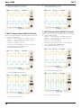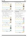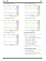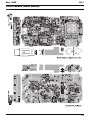
1
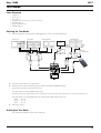
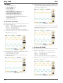
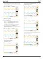
May. 2008
DD-7
SERVICE NOTES
Issued by RJA
Table of Contents
Cautionary Notes ..............................................................2
Main Specifications ...........................................................3
Location of Controls .........................................................4
Location of Controls Parts List........................................4
Exploded View ..................................................................5
Exploded View Parts List.................................................5
Parts List .............................................................................6
Verifying the Version Number........................................8
Performing a Factory Reset..............................................8
Updating the System ........................................................8
Test Mode ...........................................................................9
Circuit Board (Main Board) ...........................................17
Circuit Diagram (Main Board: Analog) .......................18
Circuit Diagram (Main Board: Digital) ........................20
Copyright © 2008 Roland Corporation
All rights reserved. No part of this publication may be reproduced in any form without the written permission
of Roland Cororation.
17058564E0
Printed in Japan (0290) (CC-KWS)
May. 2008
Cautionary Notes
Before beginning the procedure, please read
through this document. The matters described may
differ according to the model.
No User Data
This product cannot save user data. Backing up user data during servicing is
not required.
Parts List
A component whose part code is ******** cannot be supplied as a service part
because one of the following reasons applies.
•
Because it is supplied as an assembled part (under a different part code).
•
Because a number of circuit boards are grouped together and supplied as
a single circuit board (under a different part code).
•
Because supply is prohibited due to copyright restrictions.
•
Because reissuance is restricted.
•
Because the part is made to order (at current market price).
Circuit Diagram
In the circuit diagram, “NIU” is an abbreviation for “Not in Use,” and
“UnPop” is an abbreviation for “Unpopulated.” They both mean non-mounted
components. The circuit board and circuit board diagram show silk-screened
indications, but no components are mounted.
2
DD-7
May. 2008
DD-7
Main Specifications
DD-7: Digital Delay
Nominal Input Level
Dimensions
-20 dBu
73 (W) x 129 (D) x 59 (H) mm
2-7/8 (W) x 5-1/8 (D) x 2-3/8 (H) inches
Input Impedance
1 MΩ
Weight
440 g / 1 lb (including battery)
Nominal Output Level
- 20 dBu
Accessories
Owner’s Manual English (#G2507366R0)
Output Impedance
Mode Sticker (#G2547154R0)
1 kΩ
Leaflet (“USING THE UNIT SAFELY,” “IMPORTANT NOTES,” and
“Information”) (#********)
Recommended Load Impedance
Dry battery/9 V type (6LR61) (#********)
Application Sticker (#G2547160R0)
* The battery that was supplied with the unit is for temporary use-intended
primarily for testing the unit’s operation.
10 kΩ or greater
We suggest replacing this with an alkaline dry cell.
Delay Time
Options
1 ms to 6400 ms
* Values may vary according to the mode and connections.
AC adaptor (PSA-series)
Maximum Recording Time
40 seconds (in HOLD mode)
Controls
* 0 dBu = 0.775 Vrms
Pedal switch
E.LEVEL knob, F.BACK knob, D.TIME knob, MODE knob
* In the interest of product improvement, the specifications and/or appearance of
this unit are subject to change without prior notice.
Indicator
CHECK indicator
(Used for indication of TEMPO, HOLD, and to check battery)
Connectors
INPUT-A (MONO) jack, INPUT-B jack
OUTPUT-A (MONO) jack, OUTPUT-B jack
TEMPO/EXP jack, AC adaptor jack (DC 9 V)
Power Supply
DC 9 V:
Dry battery 6F22 (9 V) type (carbon)
Dry battery 6LR61 (9 V) type (alkaline)
AC Adaptor (PSA-series: optional)
Current Draw
55 mA (DC 9 V)
Expected battery life under continuous use:
Carbon:
1.5 hours
Alkaline:
6 hours
* These figures will vary depending on the actual conditions of use.
3
May. 2008
DD-7
Location of Controls
fig.panel.eps
Location of Controls Parts List
No.
1
2
3
4
5
6
7
8
9
10
11
12
13
4
Part Code
75E593C0R0
G2537516R0
13449717
F5029423R0
G2477127R0
F3279852R0
G2477127R0
F3229206R0
F3449150R0
03344701
13449140R0
75E592T0R0
22357304R0
G2217798R0
40125101
Part Name
CASE
PSA CAUTION
ADAPTOR JACK
LED
ROUND KNOB
POTENTIOMETER
ROUND KNOB
POTENTIOMETER
JACK (STEREO+SW)
6.5MM JACK
JACK(STEREO)
PEDAL
PEDAL PLATE
PANEL PLATE
THUMB SCREW
Description
CE 9V N225
HEC2392-01-150
L-3VEGW
D-CUT (BLUE/BLACK)
RD901-20-15FW-B54-006
D-CUT (BLUE/BLACK)
RD901-20-15FW-B50K-08Q7 8CLIC
2LJ-650NHW00
HTJ-064-12DS
HTJ-064-14D
M3X10 FE ZC
Q’ty
1
1
1
1
3
3
1
1
2
1
2
1
1
1
1
May. 2008
DD-7
Exploded View
fig.bunkai.eps
10
b
11
a
7
a
b
d
6
2
12
1
9
5
3
4
c
8
Exploded View Parts List
No.
1
2
3
4
5
6
7
8
9
10
11
12
Part Code
13129710R0
22267333R0
F3419102R0
G2537516R0
22357305R0
22027851R0
G2167301R0
22157702R0
22177109R0
22357304R0
75E592T0R0
75E593C0R0
Part Name
SWITCH(PUSH)
CUSHION
BATTERY CONNECTOR
PSA CAUTION
BOTTOM BASE
BOTTOM COVER
INSULATING SHEET
PEDAL GUIDE BUSH
COIL SPRING
PEDAL PLATE
PEDAL
CASE
a
b
c
d
40125134
H5019413R0
H5029325R0
40125101
NYLON WASHER 3X6X0.5
SCREW M3X10
SCREW 3X6
THUMB SCREW
Description
JM-0404
006P BATTERY SNAP
CE 9V N225
BINDING MACHINE FEBC
B1FEBC
M3X10 FE ZC
Q’ty
1
1
1
1
1
1
1
1
1
1
1
1
2
2
4
1
5
May. 2008
DD-7
Parts List
fig.-part1-e.eps
SAFETY PRECAUTIONS:
The parts marked
have
safety-related characteristics. Use
only listed parts for replacement.
Due to one or more of the following reasons,
parts with parts code ******** cannot be supplied as service parts.
• Part supplied only as a component in a complete assembly
• Copyright does not permit the part to be supplied
• Part is sold commercially
NOTE: The parts marked # are new. (initial parts)
The description "Q'TY" means a necessary number of the parts per one product.
CASING
#
#
#
22357305R0
22027851R0
75E593C0R0
G2217798R0
75E592T0R0
22357304R0
BOTTOM BASE
BOTTOM COVER
CASE
PANEL PLATE
PEDAL
PEDAL PLATE
1
1
1
1
1
1
KNOB, BUTTON
#
G2477127R0
ROUND KNOB
D-CUT (BLUE/BLACK)
4
JACK, EXT TERMINAL
03344701
#
F3449150R0
13449140R0
13449717
6.5MM JACK
JACK (STEREO+SW)
JACK (STEREO)
ADAPTOR JACK
HTJ-064-12DS
2LJ-650NHW00
HTJ-064-14D
HEC2392-01-150
1
2
2
1
SWITCH(PUSH)
JM-0404
1
SWITCH
13129710R0
PWB ASSY
#
75E593P0R1
MAIN SHEET ASSY
* This unit includes the following parts.
********
MAIN BOARD
********
VR BOARD
********
INPUT BOARD
********
CTL BOARD
********
LED BOARD
1
DIODE
F5029423R0
LED
L-3VEGW
1
F5399101R0
F5429516R0
MTL.FILM RESISTOR
MTL.FILM RESISTOR
0J (1608TYPE)
1R0 J(1608TYPE)
12
12
POTENTIOMETER
POTENTIOMETER
RD901-20-15FW-B54-006
RD901-20-15FW-B50K-08Q7
8CLIC
3
1
BATTERY CONNECTOR
006P BATTERY SNAP
1
WIRING
WIRING 1007
WIRING
WIRING 1P
WIRING
WIRING 1007-26X3P
WIRING
WIRING 1P
WIRING 1007
WIRING
INPUT WIRING
YELLOW 110X6EX6E (EXP)
WHITE 85X6X3
RIBBON CABLE 6P X80MM
VIOLET L=160MM
ORANGE 100X3X6 (OUTPUT)
L=65MM CONNECT X 1
GREY 100X3X6 (OUTPUT)
GREEN L=160MM
BROWN 105X6X3
BLACK 45X6X6 (INPUT)
BOARD IN CONNECTOR
1
1
1
1
1
1
1
1
1
1
1
RESISTOR
#
POTENTIOMETER
F3279852R0
#
F3229206R0
CONNECTOR
F3419102R0
WIRING, CABLE
#
F3487015R0
H4009408R0
#
F3477063R0
H4009498R1
#
H4009305R0
F3467053R0
#
H4009610R0
H4009499R1
H4009597R0
#
H4009458R0
#
F3467058R1
6
May. 2008
DD-7
SCREWS
#
H5039158R0
40125101
40125134
22137709R0
G2137403R0
H5019413R0
H5029325R0
H5039205R0
H5039510R0
H5039521R0
WASHER M9X14X0.5T
THUMB SCREW
NYLON WASHER 3X6X0.5
WASHER 9.6X14X1.0
WASHER
SCREW M3X10
SCREW 3X6
TOOTH WASHER
NUT M9X12X2T NI
NUT M7
G2627738R0
G2627793R0
INNER BOX
PACKING CASE
NI
M3X10 FE ZC
HALF MOON SHAPE
BINDING MACHINE FEBC
B1FEBC
9.1X13
5
1
2
1
1
2
5
5
5
4
PACKING
#
1
1
MISCELLANEOUS
H2369451R0
G2537516R0
22177109R0
22267333R0
G2167301R0
22157702R0
22257257R0
LED SPACER
PSA CAUTION
COIL SPRING
CUSHION
INSULATING SHEET
PEDAL GUIDE BUSH
EARTH TERMINAL
LEDH-5 5MM 3P
CE 9V N225
1
1
1
1
1
1
2
ACCESSORIES (Standard)
#
G6017474R0
#
G2507366R0
#
G2547154R0
#
G2547160R0
OWNER’S MANUAL
OWNER’S MANUAL
MODE LABEL
APPLICATION LABEL
JAPANESE
ENGLISH
1
1
1
1
7
May. 2008
Verifying the Version
Number
1.
Connect an AC adaptor.
2.
Turn down all controls all the way counterclockwise.
3.
Holding down the foot pedal and inserting a plug into the INPUT jack
makes the CHECK LED light up.
* Continue holding down the pedal until the LED goes dark.
After approximately 2 seconds, the CHECK LED goes dark.
* The CPU and DSP checks are performed before the LED goes dark as just
described. If a problem is found in the CPU, DSP, or the like, the LED may not
go out.
After approximately 1 second the CHECK LED flashes, and the number
of flashes indicates the version.
4.
1 flash:
Ver. 1.00
2 flashes:
Ver. 1.01
3 flashes:
Ver. 1.02
After the version display, execution shifts to the Test Mode.
Performing a Factory Reset
This product has no factory-reset feature.
Updating the System
A system update cannot be performed for this product. If an update is
required, replace with an updated circuit board.
8
DD-7
May. 2008
DD-7
Test Mode
Items Required
•
Oscillator x 2
•
Oscilloscope x 1
•
Noise meter x 2
•
AC adaptor (PSA series device or 9 V DC power source) x 1
•
Powered monitor x 2
•
Expression pedal (EV-5) x 1
•
47-kΩ short plug x 2
Entering the Test Mode
1.
Refer to the figure below and connect the measuring equipment to a connector other than the INPUT jack.
fig.DD-7-connection.eps
Oscilloscope
Noise Meter
MonitorSpeaker
Signal Genelator
Power
Supply
400Hz
4.0V
Sine
400Hz
800mV
Square
9V
47kΩ
Dummy Plug
6.5V
EV-5
2.
3.
Turn down all controls all the way counterclockwise.
Holding down the foot pedal and inserting a plug into the INPUT jack makes the CHECK LED light up.
* Continue holding down the foot pedal until the LED goes dark.
After approximately 2 seconds, the CHECK LED goes dark.
* The CPU and DSP checks are performed before the LED goes dark as just described. If a problem is found in the CPU, DSP, or the like, the LED may not go out.
After approximately 1 second the CHECK LED flashes, and the number of flashes indicates the version.
4.
1 flash:
Ver. 1.00
2 flashes:
Ver. 1.01
flashes:
Ver. 1.02
Release the foot pedal.
Quitting the Test Mode
Pull out the plug from the INPUT jack and switch off the power.
9
May. 2008
DD-7
4.
Test Items
1. VR Check (E.LEVEL) (p. 10)
2. VR Check (F.BACK) (p. 10)
Adjust the E.LEVEL control to the 12 o’clock position. With the control
turned down counterclockwise all the way, turn it clockwise to the 12
o’clock position, and verify that the CHECK LED goes dark. At the 12
o’clock position, the LED lights up red.
fig.DD-7-wave-3.eps_75
3. VR Check (D.TIME) (p. 11)
4. VR Check (MODE) (p. 12)
5. DA Check (EXP [Expression Pedal] Check) (p. 13)
6. DSP Through Check (INPUT B Check) (p. 14)
7. DSP Through Check (INPUT A Check) (p. 14)
8. DSP Through Check (OUTPUT A Check) (p. 15)
9. DSP Through Check (OUTPUT B Check) & CLIP Check (p. 15)
10. Residual Noise Check (p. 16)
11. Battery Operation Check (p. 16)
1. VR Check (E.LEVEL)
Make the connections shown below to the INPUT and OUTPUT jacks on the
DD-7, using the settings indicated.
INPUT A:
Input a rectangular wave at 400 Hz, 800 mVp-p.
INPUT B:
Input a rectangular wave at 400 Hz, 800 mVp-p.
OUTPUT A:
Connect the oscilloscope.
OUTPUT B:
Connect the oscilloscope.
Set the oscilloscope to 500 mV/DIV, 1 ms/DIV, and coupling: DC.
1.
5.
Turn the E.LEVEL control clockwise all the way. Verify that while the
control is being turned all the way clockwise from the 12 o’clock position,
the CHECK LED stays dark. When the control has been turned clockwise
all the way, the LED lights up red.
fig.DD-7-wave-1.eps_75
Verify that the E.LEVEL control is turned down counterclockwise all the
way.
The CHECK LED lights up orange.
fig.DD-7-wave-1.eps_75
2. VR Check (F.BACK)
Make the connections shown below to the INPUT and OUTPUT jacks on the
DD-7, using the settings indicated.
2.
3.
With the E.LEVEL control turned down counterclockwise all the way,
turn it clockwise to the 9 o’clock position.
INPUT A:
Input a rectangular wave at 400 Hz, 800 mVp-p.
INPUT B:
Input a rectangular wave at 400 Hz, 800 mVp-p.
Verify that the CHECK LED goes dark.
OUTPUT A:
Connect the oscilloscope.
Turning the control all the way counterclockwise again makes the
CHECK LED light up red.
OUTPUT B:
Connect the oscilloscope.
fig.DD-7-wave-2.eps_75
Set the oscilloscope to 500 mV/DIV, 1 ms/DIV, and coupling: DC.
1.
Verify that the F.BACK control is turned down counterclockwise all the
way.
The CHECK LED lights up orange.
fig.DD-7-wave-1.eps_75
10
May. 2008
2.
3.
DD-7
With the F.BACK control turned down counterclockwise all the way, turn
it clockwise to the 9 o’clock position.
3. VR Check (D.TIME)
Verify that the CHECK LED goes dark.
Make the connections shown below to the INPUT and OUTPUT jacks on the
DD-7, using the settings indicated.
Turning the control all the way counterclockwise again makes the
CHECK LED light up red.
fig.DD-7-wave-2.eps_75
INPUT A:
Input a rectangular wave at 400 Hz, 800 mVp-p.
INPUT B:
Input a rectangular wave at 400 Hz, 800 mVp-p.
OUTPUT A:
Connect the oscilloscope.
OUTPUT B:
Connect the oscilloscope.
Set the oscilloscope to 500 mV/DIV, 1 ms/DIV, and coupling: DC.
1.
Verify that the D.TIME control is turned down counterclockwise all the
way.
The CHECK LED lights up orange.
fig.DD-7-wave-1.eps_75
4.
Adjust the F.BACK control to the 12 o’clock position. With the control
turned down counterclockwise all the way, turn it clockwise to the 12
o’clock position, and verify that the CHECK LED goes dark. At the 12
o’clock position, the LED lights up red.
fig.DD-7-wave-3.eps_75
2.
With the D.TIME control turned down counterclockwise all the way, turn
it clockwise to the 9 o’clock position. Verify that the CHECK LED goes
dark.
3.
Turning the control all the way counterclockwise again makes the
CHECK LED light up red.
fig.DD-7-wave-2.eps_75
5.
Turn the F.BACK control clockwise all the way. Verify that while the
control is being turned all the way clockwise from the 12 o’clock position,
the CHECK LED stays dark. When the control has been turned clockwise
all the way, the LED lights up red.
fig.DD-7-wave-1.eps_75
4.
Adjust the D.TIME control to the 12 o’clock position. With the control
turned down counterclockwise all the way, turn it clockwise to the 12
o’clock position, and verify that the CHECK LED goes dark. At the 12
o’clock position, the LED lights up red.
fig.DD-7-wave-3.eps_75
11
May. 2008
5.
Turn the D.TIME control clockwise all the way. Verify that while the
control is being turned all the way clockwise from the 12 o’clock position,
the CHECK LED stays dark. When the control has been turned clockwise
all the way, the LED lights up red.
DD-7
3.
Adjust the MODE knob to the MODULATE position.
Verify that waveforms like those shown in the figure below are output.
The CHECK LED lights up orange.
fig.DD-7-wave-1.eps_75
fig.DD-7-wave-1.eps_75
4.
Verify that waveform output stops.
4. VR Check (MODE)
Make the connections shown below to the INPUT and OUTPUT jacks on the
DD-7, using the settings indicated.
INPUT A:
Input a rectangular wave at 400 Hz, 800 mVp-p.
INPUT B:
Input a rectangular wave at 400 Hz, 800 mVp-p.
OUTPUT A:
Connect the oscilloscope.
OUTPUT B:
Connect the oscilloscope.
Adjust the MODE control to the HOLD position.
The CHECK LED goes dark.
fig.DD-7-wave-2.eps_75
Set the oscilloscope to 500 mV/DIV, 1 ms/DIV, and coupling: DC.
1.
Verify that the MODE control is at the REVERSE position.
Verify that waveforms like those shown in the figure below are output.
The CHECK LED lights up orange.
fig.DD-7-wave-1.eps_75
5.
Adjust the MODE control to the 50 ms position.
Verify that waveforms like those shown in the figure below are output.
The CHECK LED lights up orange.
fig.DD-7-wave-1.eps_75
2.
Adjust the MODE knob to the ANALOG position.
Verify that waveform output stops.
The CHECK LED goes dark.
fig.DD-7-wave-2.eps_75
12
May. 2008
6.
Adjust the MODE control to the 200 ms position.
Verify that waveform output stops.
The CHECK LED goes dark.
fig.DD-7-wave-2.eps_75
DD-7
5. DA Check (EXP [Expression Pedal]
Check)
Make the connections shown below to the INPUT and OUTPUT jacks on the
DD-7, using the settings indicated.
INPUT A:
Input a rectangular wave at 400 Hz, 800 mVp-p.
INPUT B:
Input a rectangular wave at 400 Hz, 800 mVp-p.
OUTPUT A:
Connect the oscilloscope.
OUTPUT B:
Connect the oscilloscope.
Set the oscilloscope to 500 mV/DIV, 1 ms/DIV, and coupling: DC.
1.
Adjust the MODE control to the 800 ms position.
Verify that the CHECK LED is lighted up orange.
2.
Connect the EV-5 to the TEMPO/EXP jack.
Verify that the CHECK LED is lighted up red.
fig.DD-7-wave-1.eps_75
7.
Adjust the MODE control to the 800 ms position.
Verify that waveforms like those shown in the figure below are output.
The CHECK LED lights up orange.
fig.DD-7-wave-1.eps_75
3.
Depress the heel of the EV-5 pedal all the way.
fig.DD-7-wave-2.eps_75
8.
Adjust the MODE control to the 3,200 ms position.
Verify that waveform output stops.
The CHECK LED goes dark.
fig.DD-7-wave-2.eps_75
4.
Depress the toe of the EV-5 pedal, and stop when the intermediate
position is reached.
Verify that the CHECK LED is lighted up green.
fig.DD-7-wave-3.eps_75
13
May. 2008
5.
Depress the toe of the EV-5 pedal all the way.
DD-7
3.
fig.DD-7-wave-1.eps_75
6.
Insert the plug into the INPUT B jack.
Verify that the CHECK LED goes dark.
Verify that the CHECK LED is lighted up red.
fig.DD-7-wave-1.eps_75
Unplug the EV-5 from the jack.
7. DSP Through Check (INPUT A Check)
6. DSP Through Check (INPUT B Check)
Make the connections shown below to the INPUT and OUTPUT jacks on the
DD-7, using the settings indicated.
INPUT A:
Input a rectangular wave at 400 Hz, 800 mVp-p.
INPUT A:
Input a rectangular wave at 400 Hz, 800 mVp-p.
INPUT B:
Input a rectangular wave at 400 Hz, 800 mVp-p.
INPUT B:
Input a rectangular wave at 400 Hz, 800 mVp-p.
OUTPUT A:
Connect the oscilloscope.
OUTPUT A:
Connect the oscilloscope.
OUTPUT B:
Connect the oscilloscope.
OUTPUT B:
Connect the oscilloscope.
Set the oscilloscope to 500 mV/DIV, 1 ms/DIV, and coupling: DC.
1.
Make the connections shown below to the INPUT and OUTPUT jacks on the
DD-7, using the settings indicated.
Set the oscilloscope to 500 mV/DIV, 1 ms/DIV, and coupling: DC.
1.
Verify that the CHECK LED lights up orange.
Adjust the MODE control to the 200 ms position.
Verify that the CHECK LED goes dark.
Adjust the MODE control to the 50 ms position.
fig.DD-7-wave-1.eps_75
fig.DD-7-wave-1.eps_75
2.
2.
Disconnect the plug from the INPUT B jack.
Verify that the CHECK LED lights up green.
Disconnect the plug from the INPUT A jack.
Verify that the CHECK LED lights up red.
fig.DD-7-wave-5.eps_75
fig.DD-7-wave-4.eps_75
If the waveforms grow larger, operation is correct. If the waveforms
show no change, operation is faulty.
14
If the waveforms grow larger, operation is correct. If the waveforms
show no change, operation is faulty.
May. 2008
3.
Insert the plug into the INPUT A jack.
DD-7
3.
Verify that the CHECK LED lights up orange.
Insert the plug into the OUTPUT A jack.
Verify that the CHECK LED goes dark.
fig.DD-7-wave-1.eps_75
fig.DD-7-wave-1.eps_75
8. DSP Through Check (OUTPUT A Check)
9. DSP Through Check (OUTPUT B Check)
& CLIP Check
Make the connections shown below to the INPUT and OUTPUT jacks on the
DD-7, using the settings indicated.
1.
Make the connections shown below to the INPUT and OUTPUT jacks on the
DD-7, using the settings indicated.
INPUT A:
Input a rectangular wave at 400 Hz, 800 mVp-p.
INPUT B:
Input a rectangular wave at 400 Hz, 800 mVp-p.
INPUT A:
Input a sine wave at 400 Hz, 4.0 V p-p.
OUTPUT A:
Connect the oscilloscope.
INPUT B:
Input a sine wave at 400 Hz, 4.0 V p-p.
OUTPUT B:
Connect the oscilloscope.
OUTPUT A:
Connect the oscilloscope.
Set the oscilloscope to 500 mV/DIV, 1 ms/DIV, and coupling: DC.
OUTPUT B:
Connect the oscilloscope.
Adjust the MODE control to the HOLD position.
Set the oscilloscope to 2.0 V/DIV, 1 ms/DIV, and coupling: DC.
Verify that the CHECK LED has gone dark.
1.
fig.DD-7-wave-1.eps_75
Adjust the MODE knob to the MODULATE position.
Verify that the CHECK LED lights up orange.
Verify that the waveforms are not clipped.
fig.DD-7-wave-7.eps_75
2.
Disconnect the plug from the OUTPUT A jack.
Verify that the CHECK LED lights up green.
fig.DD-7-wave-6.eps_75
2.
Disconnect the plug from the OUTPUT B jack.
Verify that the CHECK LED lights up red.
fig.DD-7-wave-8.eps_75
15
May. 2008
3.
Insert the plug into the OUTPUT B jack.
DD-7
6.
Verify that the CHECK LED lights up orange.
Insert the plug into the OUTPUT B jack.
Verify that the CHECK LED lights up orange.
fig.DD-7-wave-7.eps_75
fig.DD-7-wave-7.eps_75
4.
7.
Adjust the MODE knob to the ANALOG position.
Verify that the CHECK LED lights up orange.
Verify that the CHECK LED lights up orange.
Verify that the waveforms are not clipped.
fig.DD-7-wave-7.eps_75
5.
Adjust the MODE control to the REVERSE position.
Verify that the waveforms are not clipped.
fig.DD-7-wave-7.eps_75
Disconnect the plug from the OUTPUT B jack.
Verify that the CHECK LED lights up red.
10. Residual Noise Check
fig.DD-7-wave-8.eps_75
Make the connections shown below to the INPUT and OUTPUT jacks on the
DD-7.
1.
INPUT A:
Connect a 47-kΩ dummy plug.
INPUT B:
Connect a 47-kΩ dummy plug.
OUTPUT A:
Connect a noise meter (JIS-A) and monitor speaker.
OUTPUT B:
Connect a noise meter (JIS-A) and monitor speaker.
Adjust the MODE knob to the ANALOG position.
Verify that the CHECK LED goes dark.
Verify that residual noise is -93.0 dB or less.
Verify that no audible noise or shock noise is present.
2.
Adjust the MODE control to the REVERSE position.
Verify that the CHECK LED lights up orange.
Verify that residual noise is -99.0 dB or less.
Verify that no audible noise or shock noise is present.
3.
Detach the plugs from the INPUT A and INPUT B jacks and switch off
the power.
11. Battery Operation Check
1.
Insert batteries into the battery compartment, connect the AC adaptor (to
INPUT A), and switch on the power.
Make sure the CHECK LED lights up.
2.
Rapidly disconnect the AC adaptor and verify battery operation.
* Failing to disconnect rapidly triggers a reset. If reset occurs repeatedly, a
problem such as faulty contact in the AC adaptor jack may be present. If the
CHECK LED is dark, check the battery voltage.
16
May. 2008
DD-7
Circuit Board (Main Board)
fig.b-main.eps
17
May. 2008
DD-7
Circuit Diagram (Main Board: Analog)
fig.d-main-analog.eps@L
MAIN BOARD
TP26
R70
39k
2
3
_BYPASS_A
AVREF
1
IC4
NJM4558M(TE1)
TP8
R62
39k
AGND
<2C7>
<2C7>
AVCC
TP20
2
3
R86; 100
-> 180
2
R3; 47K
R86; 180
R87; 220
-> 39K
-> 100
-> 270
TP9
TP40
DGND
<2C7>
<2C7>
DA_A
AVREF
R101
R23
10k
12k
D (0.5%)D (0.5%)
C27 0.1uF
4
8
VEE VDD
<G10>
<G10>
3.28->3.13
(D) -> 0
R18
10k D (0 5%)
TP1
C51 1000pF
R83
27k D (0.5%)
R75
47k
0
D (0.5%)
R95
R44
TP54
R72
47k
R96
DGND
R94
1
C73
10uF 10V
C54
47uF 10V
LED_CHK_RED
LED_CHK_GRN
R8
22k
Q19
2SA1586-GR(TE85R,F)
RIBBONCABLE 3P
18
R17
22k
AGND
TP35
C50
470pF
R93
3
R97
UnPop
CN1
TP7
Q20
2 2SA1586-GR(TE85R,F)
3
3
R86
180
TP48
DGND
AGND
4 Digital
R75 ; 3.3k
AGND
2
D15
UDZS TE-17 9.1B
Q17
2SC4116-GR(TE85R,F)
TP59
R98
UnPop
CN2
2
R31
560
C40 0.1uF
3
R3
39k
2
1
2
3
1
2
3
R91
39k
L_GRN
2
LED1
L-3VEGW
R87
270
3
1
1
3
1
1
L_RED
5
4
FB_1.5
FB_3.3
22k
D (0.5%)
C74
10uF 10V
C55
47uF 10V
Q16
2SC4117-GR(TE85L,F)
2
R53
1M
1
1
DGND
BYPASS_A_MUTE
DA_A_MUTE
BYPS_A_TO_B_MUTE
BYPASS_B_MUTE
DA_B_MUTE
TP45
TP3
R58
1M
2
<2E5>
<2D7>
<2F5>
<2E5>
<2C7>
TER1
EARTHTERMINAL
1
2
1
2
D14
UDZS TE-17 9.1B
TER2
EARTHTERMINAL
R7
56k
1
TP52
TP24
TP23
TP43
TP64
Q18
2SC4116-GR(TE85R,F)
Q6 ; Unpop -> DTC114TUAT106
R7 ; Unpop -> 56k
1
R58; Unpop -> 1M
C67; Unpop -> 0.047uF
1
1
R76
2.2k
3
1
DGND
2.2k
18k
D (0.5%)D (0.5%)
Connect to SHASSIS
1
C49 0.1uF
TP61
R38
0
D13
GS1G
VBAT
100uF
16V
0.1uF
C30
C42
0.1uF
TP6
L3
JK3
D12
WQT-0460
HEC2392-0101509
SS14
1
3
2
2
4
3
1
5
TP74 4
C57
Adaptor PSA-***S
TP58
TP4
C66 0.047uF
3
R13
22k
IN_A_DET
IN_B_DET
AGND
AVCC
AVCC
C128
0.1uF
AGND
DGND
C3
10uF 10V
TP4
DGND
AGND
C129
0.1uF
TP19
PWB F2927058R0 3/6
ASSY 75E593P0R0
IC6
AK4552VTP
A
AVREF
2
C38
0.1uF
C130
0.1uF
R15
1k
18
VCOM
47k
D (0.5%)
R16
22k
3
TP49
R11
1k
LED BOARD
<2F5>
3
D1
1SS362FV(TPL3)
2
1
D2
1SS362FV(TPL3)
1
2
BLU 70mm
TP80
SD_AD
AGND
D+3.3
Battery 006P
RIN
SDTI
LRCK
MCLK
BCLK
DEM1
DEM0
PDN
CKS3
CKS2
CKS1
CKS0
2
IC1
NJM2115V(TE1)
LIN
R50 C22
22k 2200
D (0.5%)
TP33
19
R79
LOUT
R47
56k
D (0.5%)
22k
D
(0.5%)
20 DA_B
6
ROUT
7
8
5
2
IC5
SDTO
C14
R92
NJM4
10uF
10V
100
C45
0.1uF AGND
C32 0.1uF
<2C7> CODEC_PDN
1
13
14
15
16
7
6
17
12
11
10
9
C127
68pF
C37 0.1uF
C4
10uF 10V AGND
R43
0
R1
10
2
VD
VA
C31
AGND 0.1uF
TP12
Q6
DTC114TUAT106
3
C29
0.1uF
8
VDD
10k
10k
D (0.5%) D (0.5%)
R24
R22
C11
10uF 10V
TP11
C7
100uF 4V
C9
10uF 10V
2
C13
10uF 10V
_AD_B
R80
56k
D (0.5%) IC1
<2F5> SD_DA
NJM2115V(TE1)
LRCK
<2E5> MCK
A+3.3 <2E5>
<2E5> BCK
A+3.3
R39
0
A+3.3
VSS
10V
10uF
C10
D+3.3
C58
47pF
R46
22k
D (0.5%)
6
7
5
4
VEE
R20
C43
0.1uF
R100
UnPop
R51
C21
2200pF D 22k
(0.5%)
C41 0.1uF
R59
1M
IN_REFV
TP37
C2
10uF 10V
AGND
C59
47pF
TP27
R52
R45
2
C23
22k
22k
C15
2200pF D (0.5%) D (0.5%)
10uF 10V
2
1
R82
3
56k
D (0.5%) IC1
NJM2115V(TE1)
10V
10uF
C8
AGND
12k
D (0.5%)
C1
10uF 10V
R21
10k
D (0.5%)
TP39
IN_REFV
AVCC
Q8
DTC114TUAT106
3
R5
56k
TP51
R49 C24
22k
220
D (0.5%)
R81
TP60
56k
R48
D (0.5%)
22k
D (0.5%)
2
2
3
AVREF
C18
10uF 10V
IC5
NJM4558M
C67 0.047uF
C78
1uF
10/10
10/10
10/10
10/10
C53 1000pF
R84
27k D (0.5%)
R25
10k
ORG 70mm
TP66
2
IC4
NJM4558M(TE1)
10(3216) ->
10(3216) ->
10(3216) ->
10(3216) ->
1u -> 10/10
C64 10uF 10V
3
C133
68pF
C13;
C14;
C15;
C18;
C64;
R74
C52
470pF 47k
AGND
_BYPASS_B
7
IC4
NJM4558M(TE1)
AVCC
8
VDD
TP28
GRN 60mm
TP73
6
5
R60
39k
AVREF
TP79
C5
10uF 10V
4
VEE
D4 AVCC
1SS362FV(TPL3)
UnPop
2
1
AGND
C34
0.1uF
BG608 INPUT WIRING
BLK 45mm
R42
R57
1M
AGND
BLK 70mm
TP77
R28
10k
D (0.5%)
JK2
2LJ-650NHW00
SHASSIS
TP68
TP67
TP70
TP83
TP75
TP71
TP78
1
1
YEL 70mm
TP76
JK1
2LJ-650NHW00
SHASSIS
6
7
8
4
3
2
-> 10/10
-> 39k
-> 39k
3
2
BRN 60mm
TP65
3
1
2
Q2
2SK880-GR(TE85R,F)
INPUT B
INPUT A
PWB F2927058R0 4/6
ASSY 75E593P0R0
6
7
8
4
3
2
PWB F2927058R0 1/6
ASSY 75E593P0R0
D6
1SS362FV(TPL3)
C6 ; Unpop
UnPop AVCC
Unpop
1
2
1 R61;
R70; 0
Q1
AGND
2SK880-GR(TE85R,F)
3
TP2
R30
C77
10k
1uF
TP30
R61 1
TP31
1 C6
10uF 10V 39k
IN_REFV
R19
10k
D (0.5%)
UnPop
INPUT BOARD
May. 2008
DD-7
10u(3216)
1SS387
2SK879-Y
39k
470k
TP21
1
470k
AVREF
R35
1
2
R68
39k
1
3
C17
10uF
1
R64
1 39k
TP44
C61
68pF
1
D9
1SS387(TPH3,F)
TP22
C76
10uF 16V
1
IC3
NJM4558M(TE1)
2
3
TP32
OUTPUT A
R90
100k
->
->
->
->
->
AVREF
Unpop
Unpop
Unpop
Unpop
Unpop
C62 22pF
1
C17;
D9 ;
Q12;
R64;
R35;
Q12
2SK879-Y(TE85L,F)
fig.d-main-analog.eps@R
TP55
R85
1k
TP81
GRY 100mm
TP69
BRN 105mm
JK5
2 HTJ-064-14D
3
1
SHASSIS
AGND
_DA_A
3
2
470k
AVREF
R33
C16
10uF
TP36
R63
39k
1
Q9
2SK879-Y(TE85L,F)
D10
1SS387(TPH3,F)
4
00pF
TP14
C75
10uF 16V
Q11
UnPop
1
3
2
R66
UnPop
D8
UnPop
TP25
TP10
_DA_B
C19
10uF
R69
39k
3
2
R34
470k
5
558M(TE1)
AVREF
JK6
2 HTJ-064-14D
3
1
TP72
ORG 100mm
SHASSIS
1k
AGND
6
5
22pF
Q13
2SK879-Y(TE85L,F)
R65
2
1
39k
7
IC3
NJM4558M(TE1)
C63
3
D11
1SS387(TPH3,F)
TP53
R32
470k
C20
10uF
AVREF
WHT 85mm
R67
39k
TP46
0pF
TP82
C60
68pF
AVREF
TP5
1
Q10
2SK879-Y(TE85L,F)
AVCC
C35 0.1uF
8
4
VEE VDD
(TE1)
OUTPUT B
R88
R89
100k
1
D7
1SS387(TPH3,F)
VEE VDD
IC5
NJM4558M(TE1)
AVCC
IC3
NJM4558M(TE1)
AGND
D
D5
1SS362FV(TPL3)
2
1
DGND
AGND
DGND
3
R10
1k
D3
1SS362FV(TPL3)
1
2
0.047uF
DGND
R12
22k
R55
1M
1
R9
22k
TP29
AVCC
C68
R56
1M
TP15
C65 0.047uF
Q5
DTC114TUAT106
2
3
R6
56k
1
AGND
DGND
TP16
AVCC
R4
56k
R2
UnPop
Q7
UnPop
3
R54
UnPop
2
1
C69 UnPop
Q4
DTC114TUAT106
2
3
TP13
AVCC
D+3.3
3
1
OUT_A_DET
OUT_B_DET
<2C7>
AGND <2C7>
R14
1k
TP34
PVCC
IC2
BD9851EFV-E2
DGND
R40
0
FB_1.5
1
4
L1
ELL6SH151M
TP56
Q15
QS5U27TR(PB FREE)
Q15
QS5U27TR(PB FREE)
TP42
<F6>
D+3.3
R41
0
3
TP38
C47
0.1uF
4
5
L2
ELL6SH820M
C25
100uF 4V
2
3
TP62
R78
56
DGND
TP47
FB_3.3
<F6>
DGND
2
3
R27
C28
0.1uF 10k D (0.5%)
10
C36
0.1uF
C26
100uF 4V
TP63
C72
470pF
PGND
8
9
D+1.5
1
C39
0.1uF
C48
0.1uF
PVCC2
OUT2
C44
0.1uF
5
R29
10k
D (0.5%)
TP57
12
PVCC1 11
OUT1
R77
56
TP50
2
TP17
FB1
INV1
DTC1
FB2
INV2
DTC2
NON2
STB
SEL1
RT
CT
SCP
VREF
VCC
18
47k
15
16
13
6
5
7
4
19
1
2
3
14
17
Q14
QS5U27TR(PB FREE)
Q14
QS5U27TR(PB FREE)
C56
47uF 10V
GND
R71
R99
15k
D (0.5%)
R26
10k D (0.5%)
10k D (0.5%)
C70
0.01uF
20
C71
R73
1000pF 47k
3
1
RST_DCDC <2B4>
Q3
DTC114TUAT106
19
May. 2008
DD-7
Circuit Diagram (Main Board: Digital)
fig.d-main-digital.eps@L
3
GRY 110mm
IC10
TC7W04FK(TE85L/F)
D+3.3
SHASSIS
VR BOARD
PWB F2927058R0 2/6
ASSY 75E593P0R0
C116
0.1uF
5 RST_DCDC
<1H7>
C122
0.1uF
A2
A1
A0
SDA
4
VSS
SCL
WP
IC12
HN58X2402SFPIBEZ
8
IC10
TC7W04FK(TE85L/F)
NC
A1
A0
SDA
SCL
WP
IC8
HN58X24512FPIE
8
VCC
C105
0.1uF
4
VSS
DGND
_DVREF
VCC
3
2
1
5
6
7
WP_USER
<E5>
3
2
1
5
6
7
SDA
SCL
WP_PROG
<C8>
<C8>
<C8>
TP106
3
DGND
79
80 SCL
SDA
102
TP117
103 DCK
TP119
D16
104 DMS
TP121
1SS362FV(TPL3)
105 DDI
TP122
2
1
106 DDO
TP118
_DRST
ESC+3.3
R103 DVREF TP87
R133
R134
10
84
DGND
4.7k
4.7k
85 AVDD3
TP110 L7 FBMA-10-160808-601T
AVREF
C90
C115
TP94 100uF
4V
0.1uF 95 AGND3
TP113 L8 FBMA-10-160808-601T
94
AVREF
R132
R135
R107
DVREF C85
93
0
4.7k
92 AIN7
10uF 10V 4.7k
DGREF
DGND
1
91 AIN6
2
90 AIN5
3
89 AIN4
88 AIN3
4
87 AIN2
5
86 AIN1
6
AIN0
TP100
R102
RIBBON CABLE 6P CN3
10
134
0
R110
DGREF
AVDD1
R106 0
C89
C111
100uF 4V
0.1uF
R111 0
133
R108 0
AGND1
TP97
139
XIN
D+3.3
C125
DGREF
PVCC
22pF
140
X1
XOUT
DGND
C126 ESB16.9344F16D35F
98
22pF
R131
TMODE
99
1
IC11
135 TMODE
0
R109
BD45431G-TR
R131; 18K
(MF) -> 15K
(MF)
136 TMC1
0
4
137 TMC2
5
VDD VOUT
142 _TRST
1
143 SMC
3
C123
2
R124
ER
AMC
GND
UnPop
UnPop
R131; 15K
(MF) -> 0
81
DGND
R124; 33K
(MF) -> UnPop
_RESE
IC11; BD45301G-TR -> BD45431G-TR
70
SW_PDL
TP85 DGND
RESET
<C9>
71 TXD1/
<B3>
74 RXD1/
TP123
DGND
75 TXD0/
TP120
RXD0/
76
WP_USER
<B5>
77 TI/P7
TCLR/
BYPASS_A_MUTE 119
<1E5>
PWM/S
BYPASS_B_MUTE 118
_SYNC
1
8 <1F5>
2
7
110
<1D5> MCK
3
6
111 MCK/T
<1D5> BCK
4
5
107 BCK/T
LRCK
<1D5>
LRCK/
RA8
112
SD_DA
<1D5> SD_AD
113 SD7/T
100
<1D6>
116 SD6/T
117 SD5/T
<1F5> BYPS_A_TO_B_MUTE
SD4/T
D+3.3
D17
1SS362FV(TPL3)
2
1
SUB
TP108
TP90
TP92
TP105
TP107
2
C12
20
56k
TP84
0.1uF
R104
1
2
DGND ESC+1.5
TP98
TP101
TP89
TP88
3
TP103
CN4
0.01uF
0.01uF
0.01uF
0.01uF
_DGREF
C82
C80
C83
C81
1
VR4
RD901F-20-15FW-B50K-08Q7
2 MODE(8click)
1
2
3
4
5
6
C124 1000pF
C93
0.1uF
3
1
C88
10uF
TP104
R105
470k
1
3
_DVREF
VR3
RD901F-20-15FW-B50K-006
2 D.TIME
R136
4.7k
3
3
1
DVREF
VR2
RD901F-20-15FW-B50K-006
2 F.BACK
_DGREF
0.1uF
0.1uF
0.1uF
0.1uF
0.1uF
0.1uF
0.1uF
0.1uF
0.1uF
0.1uF
0.1uF
0.1uF
DGND
ADRESS->USER;1010001/PROG;1010X00
VR1
RD901F-20-15FW-B50K-006
2 E.LEVEL
C121
C91
C109
C101
C112
C119
C104
C103
C107
C114
C110
C98
9
YEL 110mm
TP99
TP96
TP109
TP116
TP
C87
100uF 4V
TP102
<E5>
4
8
GND VCC
JK4
HTJ-064-12DS
2
3
1
IC10
TC7W04FK(TE85L/F)
IC10
TC7W04FK(TE85L/F)
7 6
2
RESET 1
10k
10k
10k
10k
PWB F2927058R0 5/6
ASSY 75E593P0R0
R114
R120
R115
R119
EXP BOARD
PWB F2927058R0 1/6
ASSY 75E593P0R0
TP95
MAIN BOARD
May. 2008
DD-7
fig.d-main-digital.eps@R
D+3.3
L5
FBMA-10-160808-601T
ESC+1.5
TP91 C86
100uF 4V
0.1uF
0.1uF
0.1uF
0.1uF
0.1uF
0.1uF
0.1uF
1
10
18
27
35
50
62
83
97
115
123
EGND
EGND
EGND
EGND
EGND
EGND
EGND
EGND
EGND
EGND
EGND
1
2
RA5 3
47 4
R126
100k
0.01uF
C79
R118 10k
R112 10k
TP115
VIO 160mm
SW1
JM-0404#01
GRN 160mm
TP114
TP112
1
S_ED(0:7)
8
7
6
5
IC7
UPD800402GJ-211-UEN-A(ESC)
DGND
Connect to SHASSIS
S_ED(7)
S_ED(6)
S_ED(5)
S_ED(4)
S_ED(3)
S_ED(2)
S_ED(1)
S_ED(0)
S_ED(0)
S_ED(1)
S_ED(2)
S_ED(3)
S_ED(4)
S_ED(5)
S_ED(6)
S_ED(7)
D+3.3
L4
FBMA-10-160808-601T
27
_CS
VDD 14
_RAS
VDD 1
_CAS
VDD 49
_WE
VDDQ 43
UDQM VDDQ 9
LDQM VDDQ 3
CLK
VDDQ
CKE
NC/RFU
52
VSSQ 46
VSSQ 12
VSSQ 6
VSSQ 54
VSS 41
VSS 28
VSS
IC9
K4S641632K-UC75000
1
C132
TER3
UnPop
UnPop
1
C131
TER4
UnPop
UnPop
DGND
SD+3.3
53
51
50
48
47
45
44
42
13
11
10
8
7
5
4
2
C95 0.1uF
19
18
17
16
39
15
38
37
40
DQ15
BA0
DQ14
DQ13
BA1
DQ12
NC
DQ11
A11
A10/AP DQ10
DQ9
A9
DQ8
A8
DQ7
A7
DQ6
A6
A5
DQ5
DQ4
A4
DQ3
A3
DQ2
A2
DQ1
A1
DQ0
A0
C102 0.1uF
S_EA(13)
S_EA(11)
20
21
36
35
22
34
33
32
31
30
29
26
25
24
23
C97 0.1uF
5
6 RA4
7 47
8
5
6 RA6
47
7
8
S_ED(7)
5
S_ED(6)
6
S_ED(5)
7
S_ED(4)
8
S_ED(3)
5
S_ED(2)
6
S_ED(1)
7
S_ED(0)
88
7
6
5
R138 47
S_EA(9)
S_EA(12)
S_EA(8)
S_EA(10) S_EA(12)
S_EA(13)
S_EA(7) S_EA(11)
S_EA(0) S_EA(10)
S_EA(6) S_EA(9)
S_EA(1) S_EA(8)
S_EA(7)
S_EA(5) S_EA(6)
S_EA(2) S_EA(5)
S_EA(4) S_EA(4)
S_EA(3) S_EA(3)
S_EA(2)
S_EA(1)
S_EA(0)
C99 0.1uF
5
6 RA3
7 47
8
C106 0.1uF
/SD3/TRR3/P83
RCKI/P71
RCKO/P70
_SYNC/P72
RR7/P87
RR6/P86
RR5/P85
RR4/P84
R125
1k
DGND
DGND
4
3
2
1
4
3
2
1
4
RA1 3
47
2
1
4
RA2 3
47 2
11
2
RA7 3
47 4
TP111
SW_PDL
C92 0.1uF
4
BUDO0/P73
D2/TRR2/P82
EA(7)
EA(6)
EA(5)
EA(4)
EA(3)
EA(2)
EA(1)
EA(0)
<E5>
TP111,TP114
DA_A_MUTE
<1E5>
4
3
2
1
PWB F2927058R0 6/6
ASSY 75E593P0R0
C120 0.1uF
P61
P60
P76
P75
EA(7)
EA(6)
EA(5)
EA(4)
EA(3)
EA(2)
EA(1)
EA(0)
SW BOARD
ESC+3.3
SD+3.3
T
<B5> SDA
<B5> SCL
<1E4>
<1E4> <B5> WP_PROG
<1E8>
<1E8>
DGND
<1H5>
<1D5>
<1H5>
ESC+3.3
S_EA(0:13)
1
0
CN5
1 UnPop
2
3
4
5
6
10k
10k
10k
10k
5
IN_B_DET
IN_A_DET
OUT_B_DET
OUT_A_DET
LED_CHK_GRN
CODEC_PDN
LED_CHK_RED
ESC+3.3
<1F5>
R116
R121
R122
R113
5
37
42
73
100
109
138
3
P
3
M
For UPDATE
DA_B_MUTE
IGND
IGND
IGND
IGND
IGND
IGND
121
_CS4/SD0/TRR0/P80 68
_CS3/P63 69
_CS1/SPICS/P62
124
A23/_SYNC/TRS7/P97 125
A22/TRS6/P96 126
A21/TRS5/P95 127
A20/TRS4/P94 128
A19/TRS3/P93 129
A18/TRS2/P92 130
A17/TRS1/P91 131
A16/TRS0/P90
53
AD15/PWM/P57 54
AD14/SPICK/P56 56
AD13/SPIDI/P55 57
AD12/SPIDO/P54 58
AD11/BUCK/P53 59
AD10/BULCK/P52 60
AD9/BUDO1/P51 63
AD8/P50
43
AD7/P47 44
AD6/P46 45
AD5/P45 46
AD4/P44 47
AD3/P43 48
AD2/P42 51
AD1/P41 52
AD0/P40
64
ALE/P67 65
_CRD/P66 66
_CWR/P65 67
_WAIT/P64
120
INT2/SD1/TRR1/P81 78
INT1
22
EA13/_CRD/P10 24
EA12/_WAIT/P22 21
EA11/ALE/P11 28
EA10/_CS1/P20 23
EA9/_CWR/P23 25
EA8/_CS3/P21 29
EA7/AD15/P37 31
EA6/AD13/P35 33
EA5/AD11/P33 39
EA4/AD9/P31 40
EA3/AD8/P30 38
EA2/AD10/P32 32
EA1/AD12/P34 30
EA0/AD14/P36
2
ED7/P07 3
ED6/P06 4
ED5/P05 5
ED4/INT2/P04 6
ED3/_CS6/P03 7
ED2/_CS4/P02 8
ED1/A23/P01 11
ED0/A22/P00
20
_ECS/A16/P12 19
_ERAS/A17/P13 16
_ECAS/A18/P14 14
_EWE/A19/P15 13
EUDQM/A20/P16 12
ELDQM/A21/P17
15
ECK
DGND
R117 10k
R123 10k
C113
C117
C118
C94
C100
C108
C96
IVDD
IVDD
IVDD
IVDD
IVDD
IVDD
IVDD
EVDD
EVDD
EVDD
EVDD
EVDD
EVDD
EVDD
EVDD
EVDD
EVDD
EVDD
EVDD
36
41
55
72
101
108
141
9
17
26
34
49
61
82
96
114
122
132
144
L6
FBMA-10-160808-601T
ESC+3.3
86
D+1.5
TP93
C84
100uF 4V
DGND
21
May. 2008
22
DD-7
May. 2008
DD-7
23
May. 2008
DD-7
MEMO