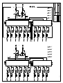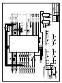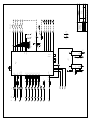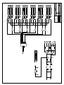
1
I R T Electronics Pty Ltd A.B.N. 35 000 832 575
26 Hotham Parade, ARTARMON N.S.W. 2064 AUSTRALIA
National: Phone: (02) 9439 3744
Fax: (02) 9439 7439
International:
+61 2 9439 3744
+61 2 9439 7439
Email: [email protected]
Web: www.irtelectronics.com
IRT Eurocard 3000 Series
Switchers & Controllers
Including Switcher Types
AVS-3010 & 3011 5 x 1 Video switchers
AAS-3020 & 3021 5 x 1 Stereo audio switchers
DDS-3030 & 3031 5 x 1 RS-422 switcher
DVS-3040 & 3041 5 x 1 Serial digital switchers
& Controllers
CP-700 5 x 1 Remote control panel
CPS-3050 5 x 1 Local control panel
CDC-3060 Logic control module
CPS-9000 & 9001 5 x 1 Remote control panels
& Tally Panel
TPS-3010
5 x LED tally panel
Designed and manufactured in Australia
IRT can be found on the Internet at:
http://www.irtelectronics.com
3000 series eurocard switchers.ib.rev21.doc
Page 1 of 36
16/10/2007
IRT Eurocard 3000 Series
Switchers & Controllers
Instruction Book
Table of Contents
Section
Page
General description
Technical specifications
Circuit description
Power supplies
Switching logic
Sync path
Signal path
Internal adjustments
Operational safety
Configuration
Interconnecting modules
Switch pulses - internal & external sync.
Power on reset
DDS-3030 & DDS-3031 Input impedance
CDC-3060 Logic control module
RS232 Control codes & connector
Link settings
Wire per crosspoint operation
Location of links & user settings
Pre-installation
Installation
CPS-3050 Local control
TPS-3010 Local tally panel
Front panel layouts
Rear connection diagrams
Operation
CDC-3060 Cyclic control
Maintenance & storage
Warranty & service
Equipment return
Drawing index
3
6
10
10
12
12
13
15
16
16
16
16
17
17
20
22
23
24
27
29
30
30
30
31
32
34
34
35
35
35
36
This instruction book applies to units later than S/N 9500000.
3000 series eurocard switchers.ib.rev21.doc
Page 2 of 36
16/10/2007
General description
The 3000 series switchers are a family of “smart” switchers in Eurocard format, which may be linked and
configured by the user to cover a wide range of switching and monitoring functions.
By combining modules, the user is able to easily assemble switchers ranging from a basic 5 x 1 to the equivalent of
a small router, encompassing analogue and digital signals in multiple levels. These may be controlled with multiple
local or remote control panels or under computer control.
The devices in the range may be classified into two groups, one being the Switcher Group and the other the Control
Group.
The Switcher Group comprises:
AVS-3010 5 x 1 Video switcher
AVS-3011 5 x 1 Video switcher
AAS-3020 5 x 1 Stereo audio switcher
AAS-3021 5 x 1 Stereo audio switcher
DDS-3030 5 x 1 RS-422/RS-485 switcher
DDS-3031 5 x 1 RS-422/RS-485 switcher
DVS-3040 5 x 1 Serial digital switcher
DVS-3041 5 x 1 Serial digital switcher
The Control Group comprises:
CP-700
5 x 1 Remote control panel
CPS-3050
5 x 1 Local control panel
CDC-3060 Logic control module
CDC-3061 Priority control module
CDC-3062 Priority control module
CPS-9000
5 x 1 Remote control panel
CPS-9001
5 x 1 Remote control panel
CPS-1050
10 x 1 Remote control panel
CPS-1052
20 button remote control panel
The AVS-3011, AAS-3021, DDS-3031, DVS-3041 and CPS-9001 supersede the AVS-3010, AAS-3020, DDS3030, DVS-3040 and CPS-9000 respectively. Details of both types are shown for those combining the new versions
with the older types in existing systems.
Modules in the switcher group are normally supplied in slave format, but may optionally be fitted with, a CPS-3050
local control panel.
Alternatively, a tally panel (TPS-3010) may be fitted to the front of any switcher to give visual switcher status
information where the switcher is remotely controlled.
On board links allow several switchers to be joined for 10 x1, 15 x 1 or 20 x 1 operation. Additionally, the
switchers may be slaved to operate in conjunction with other 3000 series switchers for multilevel analogue video,
stereo audio, digital video and RS422 or similar control signals.
This makes the switchers ideally suited to situations where a mixture of analogue and digital signals is present.
Control options include local or remote pushbuttons or RS232 serial control. Multiple control panels are permissible
and each panel reflects the current switcher tally status. The control panel types CPS-1050 and CPS-1052 and the
priority controller types CDC-3061 & CDC-3062 are described in separate manuals.
The modules may be mounted in standard IRT Eurocard frames alongside other IRT Eurocard modules for
distribution and signal conditioning.
Frame and PSU combinations are available in both 1 RU and 3 RU sizes for two to twelve modules.
Power supply options include AC and DC inputs over a wide range of voltages. Redundant power supplies on board
are supported by dual redundant supplies in the 3 RU frame and PSU combinations.
Features:
•
•
•
•
•
•
May be cascaded to 20 x 1.
Multiple levels available through combining modules in series under common control.
Internal or external sync.
Local and / or remote control options with multiple control panels.
RS232 & sequential control options.
May be mounted in same frame as other IRT Eurocards including VDA’s, ADA’s, detectors and
processors.
3000 series eurocard switchers.ib.rev21.doc
Page 3 of 36
16/10/2007
Features of individual modules:
TPS-3010:
Local tally panel. Fits any switcher in the series. Equipped with 5 tally LED’s. Provides visual
indication of switcher status when switcher is remotely controlled.
AVS-3010:
AVS-3011:
Analogue video switch with looping inputs. Internal vertical interval switching or external
synchronisation for use in RGB, YUV & YC applications.
As for AVS-3010, but with wire per crosspoint input patching and improved static immunity.
AAS-3020:
AAS-3021:
Stereo analogue audio switch with looping inputs.
As for AAS-3021, but with wire per crosspoint input patching and improved static immunity.
DDS-3030:
RS422 / RS485 Serial bi-directional data switch. Only the selected bi-directional path is active at any
time with unselected data outputs reverting to tri-state. This allows switchers to be used in multiple
combinations (subject to logical conflicts).
As for DDS-3031, but with wire per crosspoint input patching and improved static immunity.
DDS-3031:
DVS-3040:
DVS-3041:
CPS-3050:
Serial digital switch. Primarily designed for 270 Mbit serial digital video with input equalisation to 50
metres. As no re-clocking is provided on this model, it may also be used for a variety of serial digital
signals over a wide range of data rates.
As for DVS-3040, but with automatic input equalisation to over 200 metres, automatic muting of
unused inputs, wire per crosspoint input patching and improved static immunity.
Local control switch panel. Fits any of the switchers in the series. Equipped with 5 push buttons with
tally LED’s and inserts for labels. In addition to providing local control and tally for the switcher to
which it is fitted this panel allows the switcher to act as a master for controlling other switchers.
CDC-3061: Priority logic control module. Integrates the functions of video detectors, priority encoder, local
control and remote interface for controlling 3000 series switchers in PIE and other path switching
applications. May be used with either video or audio or both types of signals. Allows control of a
traditional Main - Standby - Local arrangement.
CDC-3062: Priority logic control module. Similar to the CDC-3061, but with three levels of detection and
encoding for Main - Reserve - Standby - Local operation and greater remote control tally and
interfacing flexibility.
CPS-9000:
CPS-9001:
Remote control panel. Controls one or more switchers in the series. Equipped with 5 push buttons
with tally LED’s and inserts for labels. Equipped with on board addressing to designate which bank
of 5 is controlled thus allowing formation of 10 x 1 and larger switchers. Multiple panels may be used
with tally to each panel.
May also be used as a switch data encoder for use with the CDC-3060 for remote control over serial
data links or for interfacing to external control systems.
As for CPS-9000, but with improved static immunity. Wire per crosspoint connector provided for
external interfacing.
CPS-1050:
Remote control panel - 1 RU. Controls one or more switchers in the series. Equipped with 10 push
buttons with tally LED’s and inserts for labels. Controls two 3000 series switchers for 10 x 1
operation. Multiple panels may be used with tally to each panel. Wire per crosspoint and tally
connectors are provided for external interfacing.
CPS-1052:
Remote control panel - 1 RU. Controls one or more switchers in the series. Equipped with two banks
of 10 push buttons with tally LED’s and inserts for labels. Controls four 3000 series switchers for
20 x 1 operation or for 10 x 1 audio breakaway or as two separate 10 x 1 switchers. Multiple panels
may be used with tally to each panel. Wire per crosspoint and tally connectors are provided for
external interfacing.
3000 series eurocard switchers.ib.rev21.doc
Page 4 of 36
16/10/2007
CDC-3060: Logic control module. Performs a variety of functions according to the users (link selectable) choice.
May be used directly or in conjunction with local or remote control switch panels.
RS232 control address bits allow one computer serial port to control up to four CDC-3060’s with
different addresses. Current output status is indicated on the return RS232 line for tally purposes.
Sequential (cyclic) control. Switches between selected range of inputs with manual interrupt and user
selectable timing.
The RS232 and sequential functions are non-exclusive allowing sequential control via RS232 if
required.
For serial remote control without a computer, the CDC-3060 is set up with a remote panel to encode
pushbutton data to RS232 for reception by another CDC-3060, which decodes the data and returns
tally to the originating remote panel.
Applications:
•
•
•
•
•
•
•
•
•
Path switching in transmission systems.
Input switching in edit suites.
Master control switching in small systems.
PIE path and monitoring switching with automatic / manual control.
YUV & RGB synchronised switching.
Simultaneous digital path and analogue monitoring switching.
Computer controlled switching.
Remote site switching and monitoring via modem.
Automatic sequential switching with override for path monitoring.
3000 series eurocard switchers.ib.rev21.doc
Page 5 of 36
16/10/2007
Technical specifications
AVS-3010 & 3011: 5 x 1 analogue video switchers.
Video inputs:
Number
Type
Impedance
Connectors
5.
DC coupled.
Loop through.
BNC.
Video outputs:
Type
Number
Impedance
Connectors
DC coupled.
1.
75 Ω.
BNC.
Performance:
Switching
Gain
Frequency response
Differential gain
Differential phase
Crosstalk between inputs
Power consumption
During vertical interval. Timing may be derived from either the current
output signal or synchronised to another switcher.
Unity (adjustable by internal pre-set).
±0.1 dB to 20 MHz.
±0.5 dB to 30 MHz.
<0.1% at 4.43 MHz.
<0.1° at 4.43 MHz.
>65 dB at 4.43 MHz.
>60 dB at 10 MHz.
<100 mA.
AAS-3020 & 3021: 5 x 1 analogue stereo audio switchers.
Audio inputs:
Number
Type
Impedance
Connectors
Max. input level
Input CMR
5 x 2 (5 stereo).
Tranformerless, bridging DC coupled.
> 10 KΩ.
Plugable screw block connectors.
+24 dBu.
> 40 dB @ 55 Hz.
Audio outputs:
Type
Number
Impedance
Connectors
Max. output level
DC on output
Transformerless, balanced DC coupled.
1 x 2 (left and right).
< 44 Ω.
Plugable screw block connectors.
+24 dBu into 600 Ω.
< ±20 mV.
Performance:
Switching
Gain
Frequency response
Harmonic distortion
Noise
Crosstalk left/right
Phase left/right
Within 25 ms. Timing may be synchronised to another switcher.
±3 dB (adjustable by internal pre-set).
±0.5 dB for 20 Hz to 20 KHz.
< 0.01% 20 Hz to 20 KHz at +20 dBu output.
-90 dB, Ref. +20 dBu 20 Hz to 20 KHz.
-70 dB @ 15 KHz with measured input terminated.
±0.2° to 20 KHz.
Power consumption
<200 mA (+ 24 dBu, outputs loaded in 600 Ω).
3000 series eurocard switchers.ib.rev21.doc
Page 6 of 36
16/10/2007
DDS-3030 & 3031: 5 x 1 RS422 / RS485 bi-directional serial data switcher.
Data inputs:
Number
Type
Impedance
Connectors
Threshold level
Data outputs:
Type
Number
Connectors
Level
6. (One selected path active - other 4 ‘don’t care’.)
RS422 / RS485.
>10 KΩ. Terminated with optional 330 Ω resistor.
Plug in 5 pin screw terminal block.
200 mV differential for a common mode of -7 to +12 V.
RS422 / RS485.
6. (One selected path active - other 4 tri-state.)
Plug in 5 pin screw terminal block.
5 V unloaded (differential).
>2 V (50 Ω load) (differential).
Performance:
Switching
Maximum data rate
Within 25 ms. Timing may be synchronised to another switcher.
>2 Mbps.
Power consumption
<80 mA.
DVS-3040 & 3041: 5 x 1 serial digital video switchers.
Video inputs:
Number
Type
DVS-3040
DVS-3041
Impedance
Connectors
Video outputs:
Type
Connectors
Performance:
Switching
5.
Automatic equalisation to 50 metres on each input.
Automatic equalisation to >200 metres on each input. Automatic muting
of inputs with no signal.
75 Ω.
BNC.
1 x 800 mV ±10% into 75 Ω.
1 x ECL monitoring output.
BNC.
Return loss
DC offset
Rise time
Timing is either free running at ≈25 ms or may be synchronised to
another switcher.
>15 dB 5 MHz to 270 MHz.
0 V ±0.5 V.
between 0.75 and 1.5 ns.
Power consumption
<180 mA.
3000 series eurocard switchers.ib.rev21.doc
Page 7 of 36
16/10/2007
CDC-3060: programmed data controller for 3000 series switchers.
RS232 input / output:
Number
Type
Connectors
Format
1.
9600 baud. (8 bit word, no parity, 1 stop)
9 pin ‘D’.
8 bit data word comprising:
1 command bit
2 address bits
5 crosspoint number bits - BCD encoded.
Switcher control input/output:
Type
Number
Connector
5 bit BCD coded parallel TTL level.
1.
Plug in 10 pin HE14 dual IDC.
Performance:
Switching
Power consumption
Determined by type of switchers connected.
<50 mA.
CP-700: 5 x 1 remote pushbutton panel for wire per crosspoint switchers.
Type
Number
Control connector
Momentary action with removable clear cap for legend insert. Red LED
indicator in one corner.
5
9 pin 'D'.
Switching
Dumb contact to ground only. Performance is entirely dependent on
connected switchers.
Power consumption
Approximately 10 mA per active LED derived from connected switcher if
tally enabled.
128 mm x 30 mm front panel
30 mm clearance including connectors.
May be mounted in a standard IRT Eurocard frame if required, but does
not connect to motherboard.
114 mm x 28 mm.
81 mm x 17 mm.
Dimensions
Depth
Mechanical
Mounting hole - with front panel
Mounting hole - switches only
CPS-9000 & 9001: 5 x 1 remote pushbutton panel for 3000 series switchers.
Type
Number
Momentary action with removable clear cap for legend insert. Red LED
indicator in one corner.
5
Control inputs/outputs:
Type
Number
Connectors
5 bit BCD coded parallel TTL level.
1 “input” & 1 “output”.
Plug in 10 pin HE14 dual IDC.
Switching
Determined by type of switchers connected; but not more than 25 ms.
Timing of connected switchers may be synchronised to a master switcher.
Power consumption
Derived from connected switcher.
Up to 4 x CP-9000 or 9001’s may be connected to one switcher (or
CDC-3060) without exceeding power rating specified for switcher.
128 mm x 30 mm front panel.
60 mm front panel to end of PCB.
80 mm clearance including connectors.
May be mounted in a standard IRT Eurocard frame if required, but does
not connect to motherboard.
114 mm x 28 mm.
81 mm x 17 mm.
Dimensions
Depth
Mechanical
Mounting hole - with front panel
Mounting hole - switches only
3000 series eurocard switchers.ib.rev21.doc
Page 8 of 36
16/10/2007
Common specifications
(Common to all modules in series except control panels.)
Control inputs/outputs:
Type
Number
Connectors
5 bit BCD coded parallel TTL level (or individual grounding contacts –
AVS-3011, AAS-3021, DDS-3031 and DVS-3041 only).
1 “input” & 1 “output”.
Plug in 10 pin HE14 dual IDC.
Power requirements:
28 Vac CT (14-0-14) or ± 16 Vdc.
General:
Temperature range
Mechanical
Finish:
Front panel
Rear assembly
Dimensions
Supplied accessories
0 - 50° C ambient
Suitable for mounting in IRT 19" rack chassis types FRU-3000, FRU3001 & FRU-1030 with input output and power connections on the rear
panel
Grey enamel, silk-screened black lettering & red IRT logo
Detachable silk-screened PCB with direct mount connectors to Eurocard
and external signals
6 HP x 3 U x 220 mm IRT Eurocard
Rear connector assembly including matching connectors for control
inputs & outputs.
Due to our policy of continuing development, these specifications are subject to change without notice.
Accessories available:FRU-3000 Eurocard module mounting frame
Provides mounting for up to 12 IRT Eurocards and
one PSU-3000 Dual AC power supply side by side
in 134 mm of standard rack space (3 Rack Units).
FRU-3001 Eurocard module mounting frame
Provides mounting for up to 10 IRT Eurocards and
two PSU-3001 Dual AC power supply side by side
in 134 mm of standard rack space (3 Rack Units).
FRU-1030 1 RU chassis / PSU
The FRU-1030 can be fitted with either one or two
Eurocards in a horizontal side by side format. A
single AC power supply with switched multi-voltage
input selector is included to power the cards.
Fitted with Eurocard guide rails for easy
maintenance.
TME-6 Eurocard extender board.
Control connector assembly tool
3000 series eurocard switchers.ib.rev21.doc
For ease of making interconnecting leads between
modules or to remote control panels.
A range of tools is available from Farnell
Components and RS Components for connecting
ribbon cable to the HE14 IDC type remote control
connectors.
Page 9 of 36
16/10/2007
Circuit description
The 3000 series of switchers and controllers share a common logic control system. This system is therefore
described separately and applies to all modules in the group unless otherwise indicated.
The power supply system is similar in each module and is therefore described separately.
Power supplies:
CPS-9000 & CPS-9001:
The CPS-9000 / 9001 does not have its own power supply, but uses either
+10 Vdc or +12 Vdc power from the first connected switcher through the remote control logic connectors PL 4 and
PL 5.
Pins 1A on both connectors are joined and are the power supply pins for the panel. This is to allow the power
supply to continue to the next control panel where more than one panel is required.
The +12 Vdc input (the only supply required) is reduced to +5 Vdc by a three terminal regulator.
A number of 10 µF and 100 nF tantalum tag capacitors are located at key points in the circuit to suppress
interference on the DC rails. Should any of these fail they should be replaced by high quality tantalum tag
capacitors of at least 16 Vdc rating.
Other modules: Input power to other modules may be fed by a number of means.
1. One or two 14 - 0 - 14 Vac supplies via connections on the 64 pin DIN rear connector of the module. (Used
when module is mounted in FRU-3000 chassis fitted with on PSU-3000 or FRU-3001 chassis fitted with two
PSU-3001’s.)
2. Two ±16 Vdc supplies via connections on the 64 pin DIN rear connector of the module. (Used when module
is mounted in FRU-3001 chassis fitted with one or two PT-748A PSU’s.)
3. One 14 - 0 - 14 Vac supply and one ±16 Vdc supply via connections on the 64 pin DIN rear connector of the
module. (Used when module is mounted in a FRU-3001 chassis fitted with 1 x PSU-3001 PSU and 1 x
PT-748A PSU.)
4. A single 14 - 0 - 14 Vac supply connected to the 3 pin male connector on the module side of the rear
assembly. (Used when module is mounted in FRU-1030 chassis.)
The input power is isolated by fusible resistors F 1 to F 4. Should these fail, they should be only replaced by a
similar type of the same value or protection of the common power supply will be compromised.
If an AC supply is provided, the isolated AC is full wave rectified by diodes D 1 to D4 and D5 to D 8 to provide a
raw DC voltage of approximately 20 V at filter capacitors C 17 and C 18. The actual voltage will vary depending on
the type of frame, loading of PSU by other modules and the local mains supply voltage.
If a DC supply is provided, the isolated DC passes through the diodes D 1 to D4 and D5 to D 8, which provide
protection against accidental reverse polarity connection of the DC supply. Where a DC supply is used, the input
voltage must be at least ±15 Vdc under all conditions to ensure sufficient margin for the proper operation of the
following voltage regulators and losses in the input fusible resistors and diodes.
AVS-3010 & AVS-3011: (See diagrams 803614 & 804070 sheet 1.)
The raw DC power is fed to three terminal regulator IC’s which provide ±10 Vdc rails for the video circuits. The
+10 Vdc is also supplied to the remote logic connector PL 4 pin 1 via a current limiting resistor R 25 for use by
control panels.
The +10 Vdc rail is further connected to another three terminal regulator to provide the +5 Vdc required by the
logic control circuits.
A number of 10 µF tantalum tag capacitors are located at key points in the circuit to suppress interference on the
DC rails. Should any of these fail they should be replaced by high quality tantalum tag capacitors of at least 16 Vdc
rating.
3000 series eurocard switchers.ib.rev21.doc
Page 10 of 36
16/10/2007
AAS-3020 & AAS-3021: (See diagrams 803754 & 804115 sheet 2.)
The raw DC power is fed to three terminal regulator IC’s which provide ±12 Vdc rails for the audio circuits. The
+12 Vdc is also supplied to the remote logic connector PL 4 pin 1 via a current limiting resistor R 34 for use by
control panels.
The 12 Vdc rails are further connected to two more three terminal regulator to provide the ±5 Vdc. The +5 Vdc is
required by the logic control circuits and ±5 Vdc for the audio matrix switching IC’s.
A number of 10 µF tantalum tag capacitors are located at key points in the circuit to suppress interference on the
DC rails. Should any of these fail they should be replaced by high quality tantalum tag capacitors of at least 16 Vdc
rating.
DDS-3030 & DDS-3031: (See diagrams 803763 & 804200 sheet 1.)
The raw DC power is fed to a three terminal regulator IC, which provides a +12 Vdc rail the remote logic connector
PL 4 pin 1 via a current limiting resistor R 23 for use by control panels.
The remainder of the circuit requires a +5 Vdc rail and to decrease power consumption a switch mode power supply
is used. This is fed from the raw ± DC power via series ballast resistors R 7 & R 8 and a filter network comprising
inductors L 1 & L 2 and capacitors B 8, 9, 10 & 11.
This prevents any interference generated by the action of the switch mode regulator from passing back to the power
input rails and thus to other modules. Power is drawn equally from the two DC rails in order to ensure that a
balanced current is drawn from the main supply.
A Zener diode ZD 1 is connected between the +ve and -ve supplies following R 7 & R 8 to ensure that the
maximum input voltage of the switch mode regulator is not exceeded when a higher than normal raw DC voltage is
presented at the output of the rectifiers.
A number of 10 µF tantalum tag capacitors are located at key points in the circuit to suppress interference on the
DC rails. Should any of these fail they should be replaced by high quality tantalum tag capacitors of at least 16 Vdc
rating.
DVS-3040 & DVS 3041: (See diagrams 803662 & 804110 sheet 1.)
The same configuration is used as for the DDS-3030. Some component designations may differ -- see circuit
diagram for details.
CDC-3060: (See diagram 803798 sheet 1.)
This module requires only a low current +5 Vdc supply for the logic circuit and +12 Vdc for supplying remote
control panels. The description as given in Other modules applies except that the components for generating the -ve
DC are omitted. Diodes D 17, 18, 19 & 20 provide full wave rectified DC to filter capacitor C 9 and thence to a +12
V three terminal regulator U 4 and also, via a ballast resistor R 2, to a +5 V three terminal regulator U 3.
Power indicator LED’s:
Modules have a green LED on the front panel to indicate presence of DC power in the module. This LED is
supplied from the +5 Vdc regulated supply rail.
Modules with local control buttons (CPS-3050) or local tally panel (TPS-3010) are not fitted with LD 1 -- DC
power indicator LED.
3000 series eurocard switchers.ib.rev21.doc
Page 11 of 36
16/10/2007
Switching Logic:
Control logic for each switcher module is performed by a Programmable Logic Array (PLA) which has been
programmed for the required operations. This component will only function correctly when loaded with the correct
program and is therefore only available through IRT.
Each module of the switcher group has two control connectors on its rear assembly.
They are labelled PL 4 and PL 5. For descriptive purposes, PL 4 is called the “input” connector and PL 5 the
“output” connector.
The pins on these connectors have the following functions:
1A
1B
2A
2B
3A
3B
4A
4B
5A
5B
PL 4
+12 Vdc
Ground
Data 4
Data 3
Data 2
Data 1
Data 0
Switch pulse in
Busy out
Unlatch in
PL 5
NC
Ground
Data 4
Data 3
Data 2
Data 1
Data 0
Switch pulse out
Busy in
Unlatch out
1B
2B
3B
4B
5B
1A
2A
3A
4A
5A
The CPS-9000 / 9001 remote control panel also has PL 4 and PL 5 but Pins 1A on both connectors are joined and
are the power supply pins for the panel. This is to allow the power supply to continue to the next control panel
where more than one panel is required. This is necessary, as the CPS-9000 / 9001 does not have its own power
supply, but derives its power from the first connected switcher.
The CDC-3060 logic control module only has a PL 4.
The 5 bit codes on Pins 2A to 4A represent the input selected. This code is in BCD (Binary Coded Decimal) where
the Data 0 to 3 represent the binary numbers 0 to 9 (Inputs 1 to 10 if Data 4 is 0 or Inputs 11 to 20 if Data 4 is 1).
The unlatch out signal is asserted by a switcher if any of its front panel switches is operated or if its unlatch in
signal is asserted. The presence of an unlatch in signal causes any switcher to release control of the data lines (if it
had control of them).
A switcher signals that it has control of the data lines by asserting busy out. Busy out also ripples busy in.
The operation of a push-button ripples unlatch to modules farther down the chain, causing any of them with control
of the bus to release it, and in so doing clear the busy line.
As soon as the requesting module sees its busy in line clear, it takes control of the bus and asserts its busy out. The
busy out signal then ripples up the chain causing any other modules release control (if they had it).
Sync path:
The switchers may be operated in either a local or remote sync mode in order to allow simultaneous switching of
different signals in multilevel applications.
This implies that the matrix will not switch until a sync pulse is received. When this is not provided externally, a
local sync needs to be provided.
The AVS-3010 / 3011 provides this sync from the video’s vertical pulse (see AVS-3010 sync path for details).
All other modules generate a local sync by means of a free running oscillator followed by a monostable (AAS-3020,
AAS-3021, DDS-3030 & DDS-3031 -- U 10, DVS-3040 & DVS-3041 -- U 8). This provides pulses approximately
every 25 ms.
The “localsync” signal is passed to the PLA via link LK 4, which allows a choice of internal or external sync to the
switcher logic. The chosen sync is echoed to “vertout” which is available on the PL 5 remote connector for slaving
other switchers. See Configuration section for details.
3000 series eurocard switchers.ib.rev21.doc
Page 12 of 36
16/10/2007
Signal path:
AVS-3010 & AVS-3011: Analogue video.
Video path: (See diagrams 803614 & 804070 sheet 2)
The incoming video signal on each of inputs 1 - 5 is connected to two BNC connectors on the rear assembly to
provide a loop through capability. One of these terminals must be terminated in 75 Ω either via a termination plug
or via other equipment.
Inputs 1 - 5 are terminated in 10 KΩ in order to reduce noise from unused inputs.
Cascade input PL3 (SMA connector) is terminated in 75Ω.
The inputs are then supplied to a pair of 4 x 1 video switch matrix IC’s U 1 & U 2 which are configured to operate
as a single 8 x 1 matrix. The two unused inputs are terminated in 75Ω to reduce noise.
The matrix is addressed by data lines a 0, a 1, a 2 & /a 2 produced by the PLA logic controller. This allows selection
of either no output or output from one only of the four inputs to each of U 1 & U 2. Thus when U 2 is active no
output is selected from U 1 and vice versa.
The outputs of the two halves of the matrix are mixed and then proceed to the output via U 3 which acts as a buffer
amplifier with gain (RV 1) and frequency compensation (C 8).
The output BNC connector is fed via a series resistor R 10, which provides the correct 75 Ω output source
impedance.
It should be noted that the video signal is DC coupled throughout.
Sync path: (See diagrams 803614 & 804070 sheets 1 & 2.)
The video output signal of U 3 buffer amplifier is AC coupled to an integrated sync detector IC U4 which provides
a vertical output sync pulse from the video signal.
If no vertical pulse is detected within approximately 25 ms U 4 will generate a pseudo vertical pulse. Thus, a sync
pulse will be provided even when an input is selected which has no sync. As this default period is longer than the
normal interval between vertical pulses the true vertical sync will prevail whenever it is present.
The output of the sync detector is passed through two monostable s which provide an adjustable delay (RV 2) such
that the output sync, “localvert”, is positioned to initiate switching on line 9 of the video signal.
The “localvert” signal is passed to the PLA via link LK 4, which allows a choice of internal or external sync to the
switcher logic. The chosen sync is echoed to “vertout” which is available on the PL 5 remote connector for slaving
other switchers. See Configuration section for details.
AAS-3020 & AAS-3021: Analogue audio. (See diagrams 803754 & 804115 sheet 1.)
The audio signals for Left & Right channels are processed by identical circuits; the Left on the main PCB and the
Right on a sub-board mounted over the Left channel section of the main PCB.
Balanced inputs 1 - 5 are terminated with resistors R 1 to R 20 resulting in an input impedance greater than 10 KΩ.
The signal is then buffered by amplifiers U 1 to U 5 and switched by analogue switch matrix IC’s U 6 & U7.
The matrix is addressed by data lines A & B, and enable lines CE 1 & CE 2 produced by the PLA logic controller.
This allows selection of either no output or output from one only of the input pairs to each of U 6 & U 7. Thus when
U 6 is active no output is selected from U 7 and vice versa.
The outputs of U 6 & U 7 are coupled in a low impedance mixing bus, which is available via J 4 for expanded
operation. See configuration section for details.
The mixing bus for the +ve and -ve signals is then buffered by U 8 with gain adjustment set by RV 1.
The balanced output connector is fed via series resistors R 26 & R 27, which provide an approximate 22 Ω output
source impedance.
Note that the audio signal is DC coupled throughout.
3000 series eurocard switchers.ib.rev21.doc
Page 13 of 36
16/10/2007
DDS-3030 & DDS-3031: RS422/RS485 data. (See diagrams 803763 & 804200 sheet 1)
The RS422/RS485 data lines are bi-directional, consisting of a send and receive pair. Thus, it is not strictly correct
to speak of inputs and outputs for this switcher. The switcher in essence connects a common transmit / receive pair
to one of five other receive / transmit pairs. For simplicity and commonality with other switchers in the series the
common transmit / receive pair (SK 6 on the rear assembly) will be referred to as the output and the remaining five
transmit / receive pairs as inputs 1 - 5.
The best termination impedance for RS422/RS485 signals depends on many factors including data rate, cable type
and length. The DDS-3030 & DDS-3031 have 300 Ω termination resistors on all receive lines which are connected
via a wire link to allow users to change the impedance if required.
The transmit and receive pairs for each input and the output connect to a line amplifier / receiver (U 1 to U 6) which
has an enable facility for each pair.
All “input” receive lines are connected in common to the “output” transmit amplifier.
The “output” receive line is connected to all “input”: transmit amplifiers.
The data signal lines A, B & C from the PLA controller are decoded by U 8 and hex inverter U 7 provides the
correct enable signals to each amplifier / receiver.
When an amplifier or receiver is not enabled it reverts to a “tri-state” output and so outputs can be connected in
common. This capability is used internally for the receive lines from the “inputs” and externally on the transmit
lines when configuring switchers larger than 5 x 1. See configuration section for details.
DVS-3040 & DVS-3041: Digital video. (See diagrams 803662 & 804110 sheet 1.)
Each incoming video line is terminated in 75 Ω and is AC coupled to an automatic cable equaliser IC (U 1 to U 5).
The DVS-3041 equaliser is capable of recognising a complete loss of input signal and will mute its output when this
occurs. This overcomes the problem of the equaliser output providing maximum gain to noise only signals, which
would otherwise cause crosstalk in the adjacent channels and produce "sparkles" in the picture.
The inputs are then switched using U 6 under control of three data lines (A, B & C) from the control PLA.
Output IC U 7 provides amplification with the 75 Ω output impedance being set by the combination of the IC’s
output source impedance R 18 & R20.
A second 75 Ω output is provided by U 7 for monitoring or expansion purposes.
When a DVS-3040 / 3041* is to be used for inputs greater than 1-5 two optional connectors PL 1 and PL 2 are
installed on its motherboard. In addition, R 21 is moved to its alternative position so that expansion output PL 1
provides a DC coupled output.
When a DVS-3041 (post serial number 0203001) is to be used for inputs greater than 1-5, see circuit diagram for
modification instructions. Maximum expansion to 10x1 only recommended.
The expansion input PL 2 is taken direct to the switching matrix as it does not require equalisation due to the short
distance between modules.
Note that this is a re-entrant form of switching and consequently there will be a slight increase jitter and delay.
CDC-3060: Controller.
All operation is under the direction of a microprocessor, which is loaded with a control program during
manufacture. This part can only be obtained through IRT. For more information on this module, see configuration
section.
*
denotes serial numbers pre 0203001.
3000 series eurocard switchers.ib.rev21.doc
Page 14 of 36
16/10/2007
Internal adjustments
The following adjustable circuit elements are factory set and should not be adjusted unless a component has been
changed. They are not 'operational' controls. Before adjusting any of these controls allow time for the module to
reach temperature stability.
AVS-3010 & AVS-3011:
C8
RV 1
RV 2
Frequency response.
Video gain.
Vertical interval switching point delay adjust. Set to line 9.
AAS-3020 & AAS-3021:
RV 1
RV 1
Main board
Sub-board
Audio gain -- Right channel.
Audio gain -- Left channel.
DDS-3030 & DDS-3031:
No adjustments.
DVS-3040 & DVS-3041:
RV 1
Output gain.
CP-700:
No adjustments.
CPS-3050:
No adjustments.
CPS-9000 & CPS-9001:
No adjustments.
TPS-3010:
No adjustments.
3000 series eurocard switchers.ib.rev21.doc
Page 15 of 36
16/10/2007
Operational Safety:
WARNING
Operation of electronic equipment involves the use of voltages and currents that
may be dangerous to human life. Note that under certain conditions dangerous
potentials may exist in some circuits when power controls are in the OFF position.
Maintenance personnel should observe all safety regulations.
Do not make any adjustments inside equipment with power ON unless proper
precautions are observed. All internal adjustments should only be made by suitably
qualified personnel. All operational adjustments are available externally without the
need for removing covers or use of extender cards.
Configuration
Interconnecting modules:
From the description given under circuit description -- control circuit the following rules for daisy chaining the
modules can be deduced:
I.
Modules are looped by joining PL 5 (data out) on one module to PL 4 (data in) on the next.
II.
A CPS-9000 or CPS-9001 remote control panel must be powered by either:
(a) Connecting its PL 5 to PL 4 on a powered module (i.e. one of the switcher group or a CDC-3060
logic control module).
or
(b) Connecting its PL 5 to PL 4 on another CPS-9000 that is configured as in (a).
III.
If a CDC-3060 logic control module is used it must be the last link in the chain. I.e.. PL 4 of the CDC-3060
connects to PL 5 of the last switcher.
Switch pulses - internal & external sync.:
Each of the switcher group has a free running switch pulse generator for executing a crosspoint change. The period
is approximately 25 ms. Uniquely, the AVS-3010/3011 5 x 1 video switcher can synchronise its switch pulse
generator so that transitions will occur in the vertical interval of the video signal that is currently selected.
When a switcher group module is configured as Inputs 1-5 (using LK’s 1 & 2), it uses its own switch pulses. If
configured for any other input range (e.g. Inputs 6-10), it defaults to using the switch pulses incoming on its PL 4
connector -- switch pulse in, and also passes these on to switch pulse out on its PL 5.
When multiple AVS-3010/3011's are used as YUV switchers, you have a case where all are configured as Inputs
1-5 but only the switcher for Y can be synchronised. (The others have no recognisable syncs.) By changing LK 4 on
the U and V switchers they can be forced to use the incoming switch pulses from the Y switcher.
As the switch pulse signal is sent from the AVS-3010/3011 1 - 5 switcher only on its PL 5 connector, this must be
the first switcher connected to the chain.
Therefore, for YUV and YC signals the switchers may be connected in that order, but for RGB the connection order
should be GBR if synchronised switching is to occur.
3000 series eurocard switchers.ib.rev21.doc
Page 16 of 36
16/10/2007
Power on reset:
Power on reset is needed so that at power on only one switcher or control panel drives the buss. LK 3 on each of the
Switcher Group or the CPS-9000 / 9001 remote control panel is used to select which unit is in control at power on.
If LK 3B is not installed and the switcher/control panel is configured to be for Inputs 1-5 then at power on that unit
will take control of the buss and select input 1.
In the case of a multi-level set up, such as a 5 x 1 video with a 5 x 1 audio as a slave, all the slaves should have
LK 3B installed.
LK 3 has another function. If LK 3A is not installed then any CPS-3050 switcher panel installed on the front of the
module will act as tally only -- the operation of any of its buttons will have no effect. This also applies to the
CPS-9000 / 9001 remote control panel.
DDS-3030 & DDS-3031 5 x 1 RS-422 switcher: -- input impedance.
The rear assembly for this module provides input termination resistors on each input line. Note that this includes the
“output” as this switcher is bi-directional. These 300 Ω resistors (R 1 to R 6) are connected via a wire link (TL 1 to
TL 6 respectively) which may be cut if a different input impedance is required.
To obtain the input impedance required a resistor should be fitted across the input terminals (marked “R”) of the
plug-in screw connector block and the wire link cut.
It is recommended that this method be used in preference to replacing the surface mount resistors on the rear
assembly PCB as doing so is likely to cause damage to the PCB.
3000 series eurocard switchers.ib.rev21.doc
Page 17 of 36
16/10/2007
Switcher set ups larger than 5 x 1
10 x 1, 15 x 1 and 20 x 1 switchers can be made up of multiple switchers.
In order to achieve this connections have to be made between modules for both control and signal purposes. In
addition, links on each module need to be configured to set the address range for the module.
These three operations are dealt with separately below.
Control side:
LK 1 and LK 2 on the switchers are used to assign the group of inputs that a module will switch.
NOTE: Always have one at least one switcher configured as ‘Inputs 1-5’ otherwise there will be no switch pulses
and consequently no switching action at all.
Connector PL 5 (data out) on switcher 1 - 5 connects to PL 4 (data in) on switcher 6 - 10 and so on.
Cables may be wired using the connectors provided or may be ordered from IRT using the following part numbers:
GDW-3010 150 mm cable for joining adjacent modules in 3 RU frame.
GDW-3011 300 mm cable for joining modules in 1 RU frames.
Signal side:
AVS-3010 & AVS-3011 5 x 1 Analogue video switchers:
When the data buss value is outside the range of inputs for which the module is configured the module selects PL 3
(SMA connector) on its rear assembly as its input. Therefore, the module with the highest input range should have
its output connector linked to PL 3 of the module with the next lower input range.
This is accomplished using a short BNC to SMA linking cable. A 150 mm cable of this type may be ordered from
IRT; this is of sufficient length to join together two adjacent modules fitted to a 3 RU frame. Please use part number
GVW-3010.
Thus, the output from the 1 - 5 switcher will be the only output left unconnected to another switcher and is the
switched output for the complete switcher.
Note that this is a re-entrant form of switching. For example inputs in the range 16 - 20 on a 20 x 1 configuration
actually pass through four active modules, consequently being subjected to a slight increase in distortion and (being
DC coupled switchers) DC offset.
Positions PL 1 and PL 2 on the main board are not used.
3000 series eurocard switchers.ib.rev21.doc
Page 18 of 36
16/10/2007
AAS-3020 & AAS-3021 5 x 1 Stereo analogue audio switcher
When the data buss value is outside the range of inputs for which the module is configured the module places its
signal busses in a high impedance state. J 4L (on the motherboard) and J 4R (on the sub-board) are signal buss
extender connectors. Therefore, by paralleling all the J 4L connectors on a group of switchers, and all the J 4R
connectors, size expansion is achieved.
Note that the J 4 connectors and matching plugs are not normally supplied with the switchers.
To order please use the following part numbers:
J4 connector
1100-12-103-02
Matching plug
1300-103-426
Figure 8 shielded cable or two shielded cables of small diameter should be used for the link.
For a 15 x 1 or 20 x 1 configuration it will be necessary to connect two wires into each connector on modules 2 and
3 respectively to extend the link as only one connector is provided on each module for each channel.
For consistency with other switchers in the series, it is recommended that the output from the 1 - 5 switcher be taken
as the output for the complete switcher.
3 RU frames installation: As these connections are made between the main module boards extreme care should be
taken when inserting or removing these boards to ensure that they move in and out of the frame as a group.
To assist in this regard a small linking plate is available which loops over the front panel retaining screws as an
indicator of the modules in the group. These are available in 2, 3 and 4 module widths. To order please use part
number PC803845 and indicate the number of modules to be linked.
For example:
3 only PC803845/ 4 would be an order for links for 3 only 20 x 1 (4 modules) switchers
In order to be able to slide the modules in and out of the frame it is necessary to route the inter-board wiring through
the small gap between the boards rear connector and the top slider rail.
3000 series eurocard switchers.ib.rev21.doc
Page 19 of 36
16/10/2007
DVS-3040 & DVS-3011 5x 1 Serial digital switcher:
When a DVS-3040/3041* is to be used for inputs greater than 1-5 two optional connectors PL 1 and PL 2 are
installed on its motherboard. In addition, R 21 is moved to its alternative position.
When the data buss value is outside the range of inputs for which the module is configured the module selects PL 2
(Expn In) on its motherboard as its input. Therefore, the module with the highest input range should have its PL 1
(Expn Out) connector linked to PL 2 of the module with the next lower input range.
Thus, the output from the 1 - 5 switcher will be output for the complete switcher. Outputs from the 6 - 10, 11 - 15 or
16 - 20 switchers will only provide outputs of 6 - 20, 11 - 20 and 16 - 20 respectively. When an input outside this
range is selected, no output will result. It is therefore recommended that these outputs not be used.
Note that this is a re-entrant form of switching. For example, inputs in the range 16 - 20 on a 20 x 1 configuration
actually pass through four active modules, consequently being subjected to a slight increase in jitter and delay.
When a DVS-3041 (post serial number 0203001) is to be used for inputs greater than 1-5, see circuit diagram for
modification instructions. Maximum expansion to 10x1 only recommended.
*
denotes serial numbers pre 0203001.
3 RU frames installation: See note above under AAS-3020/3021.
DDS-3030 & DDS-3031 5 x 1 RS-422 switcher:
When the data buss value is outside the range of inputs for which the module is configured all its 6 outputs are
placed in the high impedance state. Therefore, signal expansion is achieved by paralleling SK 6 on every module.
Note that TL 6 on every module but one should be cut to prevent double termination of the receive line.
CDC-3060 Logic control module:
The CDC-3060 may be used either as a stand-alone controller for a switcher (comprising one or more modules) or
as an interface between the switcher and RS232 serial data control signals.
RS232 link control: A CDC-3060 Logic control module is used to enable remote control of a switcher or group
of switchers over an RS232 link.
One CDC-3060 logic control module is required to be connected to the switcher(s) via its PL 4 control connector.
This CDC-3060 should be configured to switcher program.
The remote end of the RS232 link can be implemented with another CDC-3060 logic control module in conjunction
with one or more CPS-9000 remote control panels. This CDC-3060 should be configured to control panel program.
Alternately a computer or other intelligent logic can be use to generate the necessary RS232 control codes. See
RS232 control codes & connector.
General setup:
Operation of the CDC-3060 is determined by a number of on board links. Before installing the board, these should
be carefully checked according to the following operating configuration guidelines.
Summary of links:
LK 1
LK 2
LK 3
LK 4
LK 5
LK 6
LK 7
LK 8
Reserved
Reserved
Reserved
Program type b 0
Program type b 1
Address b 0
Address b 1
Loop LED enable
3000 series eurocard switchers.ib.rev21.doc
Page 20 of 36
16/10/2007
Program:
The CDC-3060 has a microprocessor on board which can have four different operating programs loaded. Program
selection is by links LK 4 (b 0) and LK 5 (b 1) as follows:
Program
Switcher
Control Panel
PR 3
PR 4
LK 5 -- b 1
OUT
OUT
IN
IN
LK 4 -- b 0
OUT
IN
OUT
IN
PR 3 & PR 4 are currently reserved for future use.
Switcher program: The switcher program is used where the controller is to be connected to a switcher or group of
switchers to actuate their function. In this mode the CDC-3060 may receive RS232 information and decode this to
operate the switcher or it may itself generate a sequence of switcher control codes for cyclic operation.
In this case PL 4 (data in/out) on the CDC-3060 rear assembly is connected to PL 5 (data out) on the last switcher to
be controlled.
Control panel program: This program is used when the CDC-3060 is required to generate RS232 incoming data
from remote control panels or switchers.
In this case PL 4 (data in/out) on the CDC-3060 rear assembly is connected to PL 5 (data out) on the last switcher or
control panel in the chain.
Addressing: The CDC-3060 may be set to one of four addresses, thus allowing up to four CDC-3060’s to be
controlled by one RS232 signal.
To use this facility the RS232 signal is looped from the DB 9 connector on one controller to the DB 9 connector on
the next.
The connectors should be wired so that:
The TXD line of the first CDC-3060 connects to the RXD line of the second CDC-3060 and so on.
The RXD line of the first CDC-3060 connects to the TXD line of the computer.
The TXD line of the last CDC-3060 connects to the RXD line of the computer.
The DTR line is not connected between any CDC-3060’s.
The Gnd line is not connected between any CDC-3060’s.
From computer
CDC-3060
1
2 -- TXD
3 -- RXD
5 -- Gnd
8 -- DTR
CDC-3060
2
2 -- TXD
3 -- RXD
5 -- Gnd
8 -- DTR
CDC-3060
3
2 -- TXD
3 -- RXD
5 -- Gnd
8 -- DTR
CDC-3060
4
2 -- TXD
3 -- RXD
5 -- Gnd
8 -- DTR
Address
0
Address
1
Address
2
Address
3
To computer
Note that the TXD & RXD references apply to the device itself NOT the connected equipment.
Addressing is accomplished using links LK 6 and LK 7 as follows:
Address
3
2
1
0
3000 series eurocard switchers.ib.rev21.doc
LK 7 -- b 1
OUT
OUT
IN
IN
LK 6 -- b 0
OUT
IN
OUT
IN
Page 21 of 36
16/10/2007
Cyclic control: In addition to the remote control capability, the local CDC-3060 logic control module also
provides a “cycle inputs” function.. This may be activated locally or via the RS232 interface.
In either case the controller must be pre-set with the start and end switcher crosspoint numbers and the time required
to hold each input before stepping to the next in sequence.
For example, the settings required may be:
Start at input 2
End at input 7
Step every 5 seconds.
These settings are made using DIP switches SW 2, SW 1 and SW 3 respectively.
Logically the Start setting should be less than the End setting. If Start is greater than or equal to End then the
switcher will switch to Start and hold that input without cycling.
In the following tables 0 represents closed and 1 represents open as marked on the switch assemblies.
Switches SW 2 -- Start and SW 1 -- End:
Switch number
1
2 3 4 5 6
6-8
5 (b 4)
0
0 0 0 0 0
4 (b 3)
0
0 0 0 0 0
3 (b 2)
0
0 0 0 1 1
2 (b 1)
0
0 1 1 0 0
1 (b 0)
0
1 0 1 0 1
Switch SW 3 -- Step time:
Switch number
1
2
6-8
5 (b 4)
0
0
4 (b 3)
0
0
3 (b 2)
0
0
2 (b 1)
0
0
1 (b 0)
0
1
7
8
9
10
0
0
1
1
0
0
0
1
1
1
0
1
0
0
0
0
1
0
0
1
3
4
5
6
7
0
0
0
1
0
0
0
0
1
1
0
0
1
0
0
0
0
1
0
1
0
0
1
1
0
Input number
11 12 13
Not used
1
1
1
0
0
0
0
0
0
0
0
1
0
1
0
14
15
16
17
18
19
20
1
0
0
1
1
1
0
1
0
0
1
0
1
0
1
1
0
1
1
0
1
0
1
1
1
1
1
0
0
0
1
1
0
0
1
16
17
18
19
20
1
0
1
0
1
1
0
1
1
0
1
0
1
1
1
1
1
0
0
0
1
1
0
0
1
Step duration. (Each unit ≈ 1.31 seconds)
8 9 10 11 12 13 14 15
Not used
0 0 0
1
1
1
1
1
0 1 1
0
0
0
0
0
1 0 0
0
0
0
0
1
1 0 0
0
0
1
1
0
1 0 1
0
1
0
1
0
Data LED enable: An LED (LD 2) is provided on the front panel which when enabled by inserting link LK 8 will
indicate that the RS232 control loop is connected and running.
RS232 Control codes & connector: When control of the CDC-3060 is via a computer or other RS232
source the following protocol must be used.
Protocol
RS232 -- 2 wire format.
Type
9600 baud. (8 bit data word, no parity, 1 stop.)
Format
8 bit data word comprising:
1 command bit (MSB)
2 address bits
5 crosspoint number bits - BCD encoded.
Command bit:
0 = Poll switcher for tally status.
1 = Activate crosspoint. Switchers will switch to indicated input.
Note that only one crosspoint can be active at any time. Activating a crosspoint will cancel all
other crosspoints.
3000 series eurocard switchers.ib.rev21.doc
Page 22 of 36
16/10/2007
Address bits:
If the RS232 address bits are an exact match for those on the CDC-3060 then the CDC-3060
will execute the command to activate the crosspoint or respond with the switcher tally status
depending on the state of the command bit.
If the RS232 address bits do not match those on the CDC-3060 then the CDC-3060 will ignore
the instruction as far as any attached switcher is concerned and will repeat the instruction on its
TXD line for forwarding to any other CDC-3060’s connected. See Addressing for connection
details.
Crosspoint number bits: These are binary coded decimal (BCD) format and correspond to the switcher input
number minus one. I.e.. Crosspoint 0 = Input 1.
Bits 0 to 3 encode decimal 0 to 9 as standard binary numbers.
Bit 4 encodes the decade. I.e. 0 to 9 or 10 to 19.
Thus, the maximum allowable size for a switcher is 20 inputs (crosspoints 0 to 19).
Bit Number
4
3
2
1
0 (LSB)
1
0
0
0
0
0
2
0
0
0
0
1
3
0
0
0
1
0
4
0
0
0
1
1
5
0
0
1
0
0
6
0
0
1
0
1
7
0
0
1
1
0
8
0
0
1
1
1
9
0
1
0
0
0
10
0
1
0
0
1
Input number
11 12 13
1
1
1
0
0
0
0
0
0
0
0
1
0
1
0
14
1
0
0
1
1
15
1
0
1
0
0
16
1
0
1
0
1
17
1
0
1
1
0
18
1
0
1
1
1
19
1
1
0
0
0
20
1
1
0
0
1
Special codes:
Hex
1F
Decimal
31
Binary
11111
Action
Initiate cyclic program
RS232 Connector: The DB 9 connector on the rear assembly of the CDC-3060 is wired as follows:
Pin s1, 4, 6 & 9
Internal loop
Pin 2
TXD I.e. output of CDC-3060.
Pin 3
RXD I.e.. input to CDC-3060.
Pin 5
GND
Pin 8
DTR I.e. out from CDC-3060.
Link Settings:
The following link settings apply to all switchers and controllers except as noted.
See separate section for links CDC-3060.
Links LK 1 & LK 2:
These set the crosspoint range of the switcher or control panel as follows:
Inputs
1- 5
6 - 10
11 - 15
16 - 20
LK 1
LK 2
IN
IN
IN
IN
Link LK 3: Local / remote control selection. If the switchers on the front of this unit are to be active, then install
LK 3A, otherwise install LK 3B.
Link LK 4: AVS-3010/3011 only. Internal / external sync select.
LK 4A: Always use incoming switch pulses.
LK 4B: Normal selection of switch pulses.
3000 series eurocard switchers.ib.rev21.doc
Page 23 of 36
16/10/2007
Wire per crosspoint operation
In most cases, the BCD encoded remote control system offers the most satisfactory way of controlling one or more
switchers. There are however, situations where it is necessary to provide a wire per crosspoint access for control and
/ or a line per crosspoint tally system.
Both of these facilities may be made available on the 3000 series in a number of ways.
3011 Series:
The AVS-3011, AAS-3021, DDS-3031 and DVS-3041 supersede the earlier models and provide an on board
patching area for changing the switcher from BCD to WPX input using the PL 4 & PL 5 connectors.
To change to WPX mode the WPX links should be installed on the PCB where indicated on the PCB overlay and all
of the "Universal" links should be removed or cut.
A momentary contact closure to ground on the relevant control input will now cause the switcher to operate in the
same way as it would had the switch on the local control panel type CPS-3050 been depressed.
Pin connections are as follows:
PL 4
1A
+12 Vdc out.
1B
Ground.
2A
Switch 5 contact.
2B
Switch 4 contact.
3A
Switch 3 contact.
3B
Switch 2 contact.
4A
Switch 1 contact.
4B
N/C.
5A
N/C.
5B
N/C.
PL 5
N/C.
Ground.
Switch 5 contact.
Switch 4 contact.
Switch 3 contact.
Switch 2 contact.
Switch 1 contact.
Vert. out
N/C.
N/C.
1B
2B
3B
4B
5B
1A
2A
3A
4A
5A
No complicated logic is required of a remote control to the switcher in this configuration and the CP-700 fivebutton remote control connector may be used to operate the switcher or a custom switch panel may be fabricated.
If the CP-700 is used to operate the switcher the LED's for tally will be inoperative and the + Volts connection on
the CP-700 should not be connected.
The primary disadvantage of this method is that no tally is available on the switch lines.
3010 series:
The 3000 series switchers initially provided WPX control by:
1. Direct connection to the switch contact and LED connections provided for use with a local
control panel.
2. Connection by external BCD encoding.
These are described below.
Each switcher and the remote control panel is equipped with a 12 way in line connector at the front of the board for
connecting to the switch panel. This connector carries signals for each switch contact and the LED tally indication
from the switch control logic.
Switch control lines are normally held high by 10 KΩ resistors in a resistor array. The switch action momentarily
grounds this control line and this is the action that should be mimicked by an external control. Link LK 3 which
determines the start-up defaults should be set to the ‘A’ position as the remote panel takes the place of the local
switches. This will also connect the local earth reference to pin one of the multi-way connector for access by the
remote switches.
It is recommended that the 12-way connector be connected to a 15 pin ‘D’ connector (either normal or high density)
and wired pin for pin leaving 3 pins unconnected. The ‘D’ connector may be mounted directly on the rear of the
frame (in the case of the FR-722 or FR-722A) or on a blank rear plate covering an empty module space (in the case
of the FR-700 or FR-748A).
The matching 12-pin connector for the switcher is a Harwin part number M20-9821206 (top entry) or M209891206 (side entry). These should be available through your local Harwin stockist. If the 12-pin version is
unavailable, a 20-pin type may be cut down to size. These are available through Farnell Components.
3000 series eurocard switchers.ib.rev21.doc
Page 24 of 36
16/10/2007
Pin numbering is as follows:
Pin Signal
1. GND reference (LK 3A connected)
2. Switch 1 contact
3. Tally out 1
4. Switch 2 contact
5. Tally out 2
6. Switch 3 contact
7. Tally out 3
8. Switch 4 contact
9. Tally out 4
10. Switch 5 contact
11. Tally out 5
12. +5 Vdc 560 Ω sourced feed for tally LED’s.
Tally lines are pulled low when active and an indicating LED may be directly connected between the pin 12 current
source and the tally line for each crosspoint.
Where it is not convenient to connect directly to a switcher in the above manner, the same procedure may be
followed using a CPS-9000 remote control panel connected to the switchers using the standard encoded remote
control cables. In this case, the switch panel for the CPS-9000 should be removed and the wire per crosspoint
control connected in its place. Hence, the CPS-9000 will act as a wire per crosspoint to BCD encoder for the
connected switches. The CPS-9000 may be built into other equipment or fitted with a blank front panel and
mounted in a standard Eurocard frame.
The CPS-9001 remote control panel may be used in a similar fashion to the CPS-9000. However, if remote wireper-crosspoint control is required without tally, this may be accomplished without accessing the front panel
connector. A special connector is provided on the CPS-9001 for remote wire-per-crosspoint input. This is connected
directly to the switch panel wiring.
Connections are as follows:
1A
1B
2A
2B
3A
3B
4A
4B
5A
5B
PL 6
N/C.
Ground.
Switch 5 contact.
Switch 4 contact.
Switch 3 contact.
Switch 2 contact.
Switch 1 contact.
N/C.
N/C.
N/C.
3000 series eurocard switchers.ib.rev21.doc
Page 25 of 36
1B
2B
3B
4B
5B
1A
2A
3A
4A
5A
16/10/2007
External BCD encoding:
The switching logic for the 3000 series is a binary sequence as explained under Switching Logic. Where wire per
crosspoint style operation is required, the following simple method may be used to externally encode wire per
crosspoint signals into the BCD format required by the switcher input.
PL 4
Pin
Regulator IC
Type
78L05
Crosspoint 1
+12 Vdc
1A
Unlatch in
+5 Vdc
5B
Gnd
1B
Data 0
4A
Data 1
3B
Data 2
3A
No connection
required.
Crosspoint 2
Crosspoint 3
Crosspoint 4
Crosspoint 5
All diodes type 1N4148 or equivalent.
Note that with this method, the Unlatch In signal is always present and therefore the switcher will not latch to
momentary contact closures. The switches or relays must hold the contact as long as that crosspoint is required.
When no input is crosspoint is selected crosspoint 1 will be active and so any delay between releasing one
crosspoint and activating another will result in the switcher attempting to switch to input 1.
This will have varying effects according to the type of switcher and so caution is advised.
Analogue video.
Because switching normally takes place only in sync with the vertical interval, the last
crosspoint activated before the switching point will be the one chosen. Thus for example; a delay of 1 ms between
selections will result in a 95% probability of correct switching and a 5% probability of one field of input 1 being
switched between the two selections.
Other types.
Switching is under the control of an oscillator with pulses approximately every 25 ms. Thus
the probability for a 1 ms delay would be 96% for correct switching and 4% for a 25 ms “bite” of the signal on input
1 being inserted.
For audio signals, this would be heard as a “click”.
For digital video signals the result would be a “flash” and
For RS422 signals the result will be determined by the type of equipment connected and could result in almost any
effect ranging from none to catastrophic. Particular care should therefore be exercised with these signals.
3000 series eurocard switchers.ib.rev21.doc
Page 26 of 36
16/10/2007
Location of links & user settings
The following location diagrams are not to scale and are intended only to assist in finding the location of links and
other settings, which may need to be changed by the user during Configuration.
Note: AVS-3010 PL 1 & PL 2 positions on board are deliberately unfilled and are not required by users.
PL 2
F
R
O
N
T
P
A
N
E
L
C8
A
B
L
K
2
L
K
1
L
K
4
RV 2
Rear
Assembly
RV 1
AVS-3010
J
4
A
B
L
K
3
L
K
2
L
K
1
J
4
L
K
4
RV 1
RV 1
L
D
1
F
R
O
N
T
P
A
N
E
L
L
K
3
L
D
1
F
R
O
N
T
P
A
N
E
L
PL 1
Channel 2
Sub-board
Rear
Assembly
AAS-3020
A
B
L
K
3
L
K
2
L
K
1
L
K
4
L
D
5
3000 series eurocard switchers.ib.rev21.doc
Rear
Assembly
DDS-3030
Page 27 of 36
16/10/2007
F
R
O
N
T
P
A
N
E
L
F
R
O
N
T
P
A
N
E
L
A
B
L
K
3
L
K
2
L
K
1
L
K
4
PL 2
IN
Rear
Assembly
PL 2
OUT
L
D
1
DVS-3040
L
D
2
LK 8
LK 7
LK 6
LK 5
LK 4
LK 3
LK 2
LK 1
8
7
6
5
4
3
2
1
8
7
6
5
4
3
2
1
8
7
6
5
4
3
2
1
SW 1
SW 2
SW 3
L
D
1
Rear
Assembly
CDC-3060
F
R
O
N
T
P
A
N
E
L
3000 series eurocard switchers.ib.rev21.doc
SW
1
SW
2
SW
3
SW
4
SW
5
PL 6
WPX input on CPS-9001 only
PL 6
WPX
A
B
L
K
3
L
K
2
L
K
1
PL 5
OUT
CPS-9000
Page 28 of 36
PL 4
IN
16/10/2007
Pre-installation:
Handling:
This equipment may contain or be connected to static sensitive devices and proper static free handling precautions
should be observed.
Where individual circuit cards are stored, they should be placed in antistatic bags. Proper antistatic procedures
should be followed when inserting or removing cards from these bags.
Power:
AC mains supply:
Ensure that operating voltage of unit and local supply voltage match and that correct rating
fuse is installed for local supply.
DC supply:
Ensure that the correct polarity is observed and that DC supply voltage is maintained within
the operating range specified.
Earthing:
The earth path is dependent on the type of frame selected. In every case particular care should be taken to ensure
that the frame is connected to earth for safety reasons. See frame manual for details.
Signal earth: For safety reasons a connection is made between signal earth and chassis earth. No attempt should be
made to break this connection.
3000 series eurocard switchers.ib.rev21.doc
Page 29 of 36
16/10/2007
Installation
Installation in frame or chassis:
See details in separate manual for selected frame type.
Before installing in frame, make any required link changes as detailed in the Configuration section.
AVS-3010 & AVS-3011:
Analogue Video Connections:
If input termination is required then 75 Ω termination BNC plugs should be fitted to the loop through input sockets.
AAS-3020 & AAS-3021: Audio Connections:
If input termination is required then termination resistors should be fitted to the input sockets.
Follow the polarity markings on the rear assembly or incorrect phasing will result.
DDS-3030 & DDS-3031: RS422 / RS485 Data Connections:
If a change in the input termination is required, consult the configuration section for details.
Follow the connection markings on the rear assembly carefully or incorrect operation will result.
As this switcher is bi-directional, extreme care must be taken in its application for configurations greater than 5 x 1
or conflicts will result.
DVS-3040 & DVS-3041: Digital Video Connections:
Input termination is fitted and should not be altered. No loop through facility is available. For applications requiring
multiple destinations, a distribution amplifier such as the DVA-3002 should be used.
CPS-3050 -- Local control:
All switchers are sold with a plain front panel with DC power LED and printed with the switcher type number and
IRT logo. The CPS-3050 provides the necessary components to add control buttons and tally to the front panel.
Before fitting the CPS-3050, the original front panel and LD 1, LED DC indicator, must be removed.
The CPS-3050 PCB should then be pressed carefully into place making sure that the pins on the CPS-3050 plug
mate correctly with the socket on the main module PCB.
The front plate is then fitted using the screws and spacers provided.
For local switching, to take effect link LK 3 must be placed in the “A” position. See Configuration for details.
TPS-3010 -- Local tally panel:
All switchers are sold with a plain front panel with DC power LED and printed with the switcher type number and
IRT logo.
The TPS-3010 provides the necessary components to add tally LED indicators to the front panel. This is desirable
when switchers are controlled only by remote connections that are distant from the switcher. This panel is especially
useful when switchers are controlled via the CDC-3060 controller from a remote location using RS232 connections.
The TPS-3010 provides confidence that a slave switcher has responded to the master command and can therefore
greatly assist in finding faults in inter-module wiring.
Before fitting the TPS-3010, the original front panel and LD 1, LED DC indicator, must be removed.
The TPS-3010 PCB should then be pressed carefully into place making sure that the pins on the TPS-3010 plug
mate correctly with the socket on the main module PCB.
The front plate is then fitted using the screws and spacers provided.
3000 series eurocard switchers.ib.rev21.doc
Page 30 of 36
16/10/2007
Front panel layouts
The following, front panel drawings are not to scale. They are intended to show approximate relative positions of
controls only.
Front panel layouts:
AVS-3010 & 3011
AAS-3020 & 3021
DDS-3030 & 3031
DVS-3040 & 3041
AVS - 3 0 1 1
Front panel layouts:
CP-700
CPS-3050
CPS-9000
C P S -3 0 5 0
Front panel layout:
CDC-3060
Front panel layout:
TPS-3010
C DC - 3 0 6 0
TP S - 3 0 1 0
1
2
3
DATA
4
5
DC
DC
N140
3000 series eurocard switchers.ib.rev21.doc
N140
N140
Page 31 of 36
N140
16/10/2007
Rear connection diagrams
The following rear assembly drawings are not to scale and are intended to show connection order only.
DDS-3030:
Input to switcher = “R” -- Output = “T”.
AVS-3010 & 3011
AAS-3020 & 3021
3010
DDS-3030 & 3031
3030
3020
PL 3
L I/P’s
R I/P’s
+
+
INPUT
5
INPUT
4
1
TL 1
+
Gnd
+
+
1
+
Gnd
+
+
INPUT
2
INPUT
1
OUTPUT
3
Gnd
+
+
+
+
PL 5
OUT
PL 4
IN
3000 series eurocard switchers.ib.rev21.doc
PL 5
TL 5
Gnd
R4
3
T
4 T
+
Gnd
Gnd
R5
-
+
R O/P TL-O/P
R
R
+
5 O/P
+
+
+
-
Gnd
Gnd
Gnd
+
TL 4
-
Gnd
OUT
+
R
Gnd
LEFT
O/P
T
R
+
+
Gnd
5
R3
-
Gnd
+
2
-
Gnd
4
R
T
Gnd
Gnd
TL 2
R
-
TL 3
INPUT
3
R2
-
Gnd
2
R1
T
T
+
Gnd
RIGHT
O/P
PL 4
IN
Page 32 of 36
PL 5
OUT
PL 4
IN
16/10/2007
DVS-3040 & 3041
CDC-3060
PL4 & PL5 Pin Positions
3040
3060
1B
2B
3B
4B
5B
1A
2A
3A
4A
5A
J2
INPUTS
1
2
3
4
5
OUTPUT
MONITOR
PL 5
OUT
PL 4
IN
3000 series eurocard switchers.ib.rev21.doc
PL 4
IN
Page 33 of 36
16/10/2007
Operation
CDC-3060: Cyclic control.
The CDC-3060 will perform automatic cycling of inputs of selected switchers on demand. This can be performed at
any time and will continue until a stop command is given by local, remote or RS232 control.
The first and last inputs between which the switcher will cycle are set by switches on the CDC-3060. See
Configuration section for details.
To Start cycling:
Press any button on a local or remote control panel for more than 2 seconds.
or
Send code 1F via RS232 link.
If the button pressed is outside the range set for cycling then the switcher will switch to that
input when the button is pressed and when released after two seconds will progress to Start
input and continue cycling from that point.
To Stop cycling:
Press any button on a local or remote control panel for less than 2 seconds.
or
Send any valid switch code via RS232 link.
If two CDC-3060’s are connected to form an RS232 link, the CDC-3060 configured for the switcher program will
be the unit, which sets the Start, End and Step for cycling operation.
3000 series eurocard switchers.ib.rev21.doc
Page 34 of 36
16/10/2007
Maintenance & storage
Maintenance:
No regular maintenance is required.
Care however should be taken to ensure that all connectors are kept clean and free from contamination of any kind.
This is especially important in fibre optic equipment where cleanliness of optical connections is critical to
performance.
Storage:
If the equipment is not to be used for an extended period, it is recommended the whole unit be placed in a sealed
plastic bag to prevent dust contamination. In areas of high humidity a suitably sized bag of silica gel should be
included to deter corrosion.
Where individual circuit cards are stored, they should be placed in antistatic bags. Proper antistatic procedures
should be followed when inserting or removing cards from these bags.
Warranty & Service
Equipment is covered by a limited warranty period of three years from date of first delivery unless contrary
conditions apply under a particular contract of supply. For situations when “No Fault Found” for repairs, a
minimum charge of 1 hour’s labour, at IRT’s current labour charge rate, will apply, whether the equipment is within
the warranty period or not.
Equipment warranty is limited to faults attributable to defects in original design or manufacture. Warranty on
components shall be extended by IRT only to the extent obtainable from the component supplier.
Equipment return:
Before arranging service, ensure that the fault is in the unit to be serviced and not in associated equipment. If
possible, confirm this by substitution.
Before returning equipment contact should be made with IRT or your local agent to determine whether the
equipment can be serviced in the field or should be returned for repair.
The equipment should be properly packed for return observing antistatic procedures.
The following information should accompany the unit to be returned:
1.
2.
3.
4.
5.
6.
7.
A fault report should be included indicating the nature of the fault
The operating conditions under which the fault initially occurred.
Any additional information, which may be of assistance in fault location and remedy.
A contact name and telephone and fax numbers.
Details of payment method for items not covered by warranty.
Full return address.
For situations when “No Fault Found” for repairs, a minimum charge of 1 hour’s labour will apply,
whether the equipment is within the warranty period or not. Contact IRT for current hourly rate.
Please note that all freight charges are the responsibility of the customer.
The equipment should be returned to the agent who originally supplied the equipment or, where this is not
possible, to IRT direct as follows.
Equipment Service
IRT Electronics Pty Ltd
26 Hotham Parade
ARTARMON
N.S.W.
2064
AUSTRALIA
Phone:
Email:
3000 series eurocard switchers.ib.rev21.doc
61 2 9439 3744
[email protected]
Page 35 of 36
Fax:
61 2 9439 7439
16/10/2007
Drawing index
Drawing #
Sheet #
Description
803614
803614
804070
804070
803754
803754
804115
804115
803763
803763
804200
804200
803662
803662
804110
804110
803618
803798
803771
803740
803286
804194
1
2
1
2
1
2
1
2
1
2
1
2
1
2
1
2
AVS-3010 video circuit schematic.
AVS-3010 control circuit schematic.
AVS-3011 video circuit schematic.
AVS-3011 control circuit schematic.
AAS-3020 audio circuit schematic.
AAS-3020 control circuit schematic.
AAS-3021 audio circuit schematic.
AAS-3021 control circuit schematic.
DDS-3030 data circuit schematic.
DDS-3030 control circuit schematic.
DDS-3031 data circuit schematic.
DDS-3031 control circuit schematic.
DVS-3040 digital signal circuit schematic.
DVS-3040 control circuit schematic.
DVS-3041 digital signal circuit schematic.
DVS-3041 control circuit schematic.
CPS-3050 local control panel schematic.
CDC-3060 circuit schematic.
CPS-9000 circuit schematic.
CP-700 circuit schematic.
CP-600 dimensional drawing front panel for CPS-9000 & CPS-9001.
CPS-9001 circuit schematic.
1
1
1
1
1
3000 series eurocard switchers.ib.rev21.doc
Page 36 of 36
16/10/2007
PC803615R
PL3
V2
V1
V6
V5
V10
V7
V4
V3
V8
26a/b
24a/b
25a/b
22a/b
23a/b
21a/b
S1/P1
1a
1b
2a/b
3a/b
4a/b
5a/b
12a/b
13a/b
15a/b
16a/b
18a/b
19a/b
S1/P1
J1
10K
10K
10K
R5
4R7
FS4
4R7
4R7
FS3
FS2
4R7
FS1
10K
R4 10K
R3
R2
R1
R6
75
7
6
5
4
3
2
1
7
6
5
4
3
2
1
U2
GX4314
8
+10
14
8
14
-10
-10
11
12
13
1N4004
D5-8
D1-4
1N4004
10
11
12
13
10
ao
a1
a2
/a2
CD2
1500u
CD1
1500u
R39
33
R37
33
PL2
PL1
LM337T
U8
2
I
LM317T
U7
3
I
R38
10K
C8
3-20p
R7
220
R36
1K8
O
R34
1K8
O
R8
180
3
2
2
3
+10
7
8
CD4
10u
R35
270
CD3
10u
R33
270
RV1
100
R9
220
-10
4
V9
U1
GX4314
Adj
1
Adj
1
CD6
10u
CD5
10u
6
UA
EL2120
R11
220
R10
75
CD8
10u
CD9
10u
C1
22n
CD11
10u
CD10
10u
R12
680K
4
2
U9
LM1881
8a/b
9a/b
S1/P1
6
_10
+10
VER
8
+5
3
+5
C2
0.1u
SK11
78L05
U4
C3
0.1u
R14
1K5
R13
390K
C4
10u
+5
+10
6
2
1
4
R15
47K
1
7
THR
TRG
DIS
RST
14
+5
O
5
G
2
+10
I
U5
+5
3
CD7
10u
12
13
8
11
DIS
THR
TRG
10
CONTRACT No.
ENG. APP.
CHECKED
DRAWN
COPYRIGHT
DO NOT COPY NOR
DISCLOSE TO ANY
THIRD PARTY
WITHOUT WRITTEN
CONSENT
R16
1K
C5
0.1u
RV2
5K
NE556
2 30/01/95
ECN 515
3 10/04/95
ECN 574
4 18/10/95
9
CD12
o.1u
C6
0.1u
RBB
+5
AVS-3010
DRAWING No.
803614
5X1 VIDEO SWITCHER
TITLE
IRT Electronics Pty. Ltd.
ARTARMON NSW AUSTRALIA 2064
SCALE
SIZE
CD13
0.1u
+5
localvert
SHEET
1 OF 2
4B
1A
1B
2A
2B
3A
3B
4A
5A
5B
PL5
OUT
4B
5A
5B
30a
20a
27a
27b
28a
28b
29a
29b
30b
31a
31b
32a
32b
S1/P1
RP1
R25
RP1
RP1
RP1
RP1
RP1
RP1
RP1
4
10
10
9
8
7
6
3
2
R19
+10
R24
R23
R22
R21
R20
R18
R17
10K
10K
10K
10K
10K
10K
10K
10K
20
34
33
31
29
32
28
27
26
25
24
21
19
18
17
16
A0
A1
A2
/A2
VERTIN
DOT4
DI4
DOT3
DI3
DOT2
DI2
DOT1
DI1
DOT0
DI0
VERTOUT
ST2
UL2
UL1
ST1
23
LK4
35
38
3
3
39
40
15
22
U6
1
EPM7032
30
42
41
LOCALVERT
10
T4
T3
T2
T1
T0
POR
ONETO10
ONETO5
SW4
SW3
SW2
SW1
SW0
14
12
9
7
5
2
1
43
13
11
8
6
4
D9
1N4148
RP2
10K
+5
1
PL4
IN
MINEOUT
37
36
2
+5
R27
10K
C7
22u
1
2
3
4
5
6
7
8
9
10
2
+5
+5
B
560
R28
LK3
LK2
A
LK1
P2
2 30/01/94
ECN555
4 18.08-95
ECN 515
3 10/04/95
MINEIN
44
2
1
CONTRACT No.
ENG. APP.
CHECKED
DRAWN
COPYRIGHT
DO NOT COPY NOR
DISCLOSE TO ANY
THIRD PARTY
WITHOUT WRITTEN
CONSENT
GN
LD1
SW5
SW4
SW3
SW2
SW1
1
1
1
1
1
RBB
LD5
LD4
LD3
LD2
LD1
AVS-3010
DRAWING No.
803614
5X1 VIDEO SWITCHER
TITLE
IRT Electronics Pty. Ltd.
ARTARMON NSW AUSTRALIA 2064
SCALE
SIZE
2
2
2
2
2
SHEET
2 OF 2
PC804071
PL3
V2
V1
V6
V5
V10
V4
V3
V8
V7
26a/b
24a/b
25a/b
22a/b
23a/b
21a/b
S1/P1
1a
1b
2a/b
3a/b
4a/b
5a/b
12a/b
13a/b
15a/b
16a/b
18a/b
19a/b
S1/P1
J1
10K
10K
10K
R5
4R7
FS4
4R7
4R7
FS3
FS2
4R7
FS1
10K
R4 10K
R3
R2
R1
R6
75
7
6
5
4
3
2
1
7
6
5
4
3
2
1
14
U2
GX4314
8
+10
14
8
+10
-10
-10
11
12
13
1N4004
D5-8
D1-4
1N4004
10
11
12
13
10
ao
a1
a2
/a2
CD2
1500u
CD1
1500u
R32
33
R30
33
LM337T
U8
2
I
LM317T
U7
3
I
R31
10K
R7
220
3-20p
C8
CD13
100n
R26
1K8
O
3
2
R17
68K
RV3
1M
R8
180
R24
1K8
O
-10
2
3
+10
7
8
CD4
10u
R25
270
CD3
10u
R23
270
RV1
100
R9
220
-10
4
V9
Adj
1
Adj
1
CD6
10u
CD5
10u
6
UA
EL2120
R11
220
R10
75
CD8
10u
CD9
10u
C1
22n
CD11
10u
CD10
10u
R12
680K
4
2
U4
LM1881
8a/b
9a/b
S1/P1
6
-10
+10
VER
8
+5
3
+5
C2
0.1u
SK11
C3
0.1u
R14
1K5
R13
390K
C4
10u
+5
+10
6
2
1
4
R15
47K
78L05
U9
3
7
THR
TRG
DIS
RST
14
+5
I
5
G
2
U1
GX4314
O
U5
+5
1
CD7
10u
12
13
8
11
DIS
THR
TRG
10
CONTRACT No.
ENG. APP.
CHECKED
DRAWN
COPYRIGHT
DO NOT COPY NOR
DISCLOSE TO ANY
THIRD PARTY
WITHOUT WRITTEN
CONSENT
R16
1K
C5
0.1u
RV2
5K
NE556
1 13/02/97
9
CD12
o.1u
C6
0.1u
RBB
+5
AVS-3011
DRAWING No.
804070
5X1 VIDEO SWITCHER
TITLE
IRT Electronics Pty. Ltd.
ARTARMON NSW AUSTRALIA 2064
SCALE
SIZE
+5
localvert
SHEET
1 OF 2
4B
1A
1B
2A
2B
3A
3B
4A
5A
5B
PL5
OUT
4B
5A
5B
30a
20a
27a
27b
28a
28b
29a
29b
30b
31a
31b
32a
32b
S1/P1
10
RP1 = 10x22K
RP3 = 5x470R
RP4 = 5x470R
R29
+10
UNIVERSAL
1
1
1
1
1
1
1
1
4
10
9
8
7
6
3
2
*
3
9
9
7
7
5
5
2
3
1
4
SA5.0A
4
4
3
4
3
4
3
3
3
4
10
10
8
8
6
6
1
4
2
*
*
*
*
*
*
*
*
*
*
20
33
29
28
26
24
21
19
18
17
16
A0
A1
A2
/A2
VERTIN
DI4
DI3
DI2
DI1
DI0
VERTOUT
ST2
UL2
UL1
ST1
23
38
B
22
U6
EPM7032
LK3
35
30
42
41
LOCALVERT
10
MINEOUT
A
3
39
40
15
T4
T3
T2
T1
T0
POR
ONETO10
ONETO5
SW4
SW3
SW2
SW1
SW0
14
12
9
7
5
2
1
43
13
11
8
6
4
D9
1N4148
R22
R21
R20
R19
R18
RP2
10K
+5
10K
10K
10K
10K
10K
1
2
PL4
IN
+5
R27
10K
C7
22u
+5
1
2
3
4
5
6
7
8
9
10
+5
B
560
WPX
2
LK1
P2
MINEIN
44
37
36
CONTRACT No.
ENG. APP.
CHECKED
DRAWN
COPYRIGHT
DO NOT COPY NOR
DISCLOSE TO ANY
THIRD PARTY
WITHOUT WRITTEN
CONSENT
A
LK2
R28
LK3
1 13/02/97
GN
LD1
RBB
1
1
1
1
1
1
2
2
2
2
2
AVS-3011
DRAWING No.
804070
5X1 VIDEO SWITCHER
TITLE
LD5
LD4
LD3
LD2
LD1
IRT Electronics Pty. Ltd.
ARTARMON NSW AUSTRALIA 2064
SCALE
SIZE
SW5
SW4
SW3
SW2
SW1
SHEET
2 OF 2
2
SK5L
3
2
SK4L
3
2
SK3L
3
2
SK2L
3
2
SK1L
3
R20
R19
R17
R18
R16
R15
R13
R14
R12
R11
R9
R10
R8
R7
R5
R6
R4
R3
R1
R2
PCB 803755R
15b
14b
12b
11b
9b
8b
6b
5b
3b
2b
12K
12K
12K
12K
12K
12K
12K
12K
12K
12K
12K
12K
12K
12K
12K
12K
12K
12K
12K
12K
3
2
5
6
3
2
5
6
3
2
5
6
3
2
5
6
3
2
5
6
U1B
U2B
U3B
U4B
U5B
7
7
7
CE1
CE2
A
B
7
U5A
1
NE5532
U4A
1
NE5532
U3A
1
NE5532
U2A
1
NE5532
U1A
1
NE5532
7
12
11
15
14
12
1
4
2
5
1
16
Y0
X0
Y3
X3
Y2
X2
Y1
X1
Y0
X0
+5
16
8
7
7
-5
U7
9 10
B
A
6
Y
X
Y
X
EN
A EN
B
9 10
6
U6
8
-5
3
13
3
13
3
1
J4
C1
10u
-12
R21
1M
R25
12K
RV1
50K
R22
1M
2
C2
10u
-5
C3
10u
U8B
NE5532
7
1
U8A
NE5532
12K
22p
R24
12K
R23
C22
+12
6
5
3
2
8
4
8
4
8
4
8
4
8
4
8
4
C4
10u
+5
R27
22
R26
22
C23
10u
-12
18b
17b
SK6L
2
3
2
SK5R
3
2
SK4R
3
CE1
CE2
A
B
2
SK3R
3
2
SK2R
3
2
SK1R
3
15a
14a
12a
11a
9a
8a
6a
5a
3a
2a
5
6
4
3
14
13
11
10
8
7
5
4
2
1
J2
R20
R19
R17
R18
R16
R15
R13
R14
R12
R11
R9
R10
R8
R7
R5
R6
R4
R3
R1
R2
12K
12K
12K
12K
12K
12K
12K
12K
12K
12K
12K
12K
12K
12K
12K
12K
12K
12K
12K
12K
3
2
5
6
3
2
5
6
3
2
5
6
3
2
5
6
3
2
5
6
U1B
U2B
U3B
U4B
U5B
7
7
7
7
1
U5A
1
NE5532
U4A
NE5532
U3A
1
NE5532
U2A
1
NE5532
U1A
1
NE5532
7
12
11
15
14
12
X3
Y2
X2
Y1
X1
Y0
1
16
Y0
X0
4 Y3
2
5
1
X0
+5
16
8
U6
8
7
-5
7
-5
U7
9 10
B
A
6
Y
X
3
13
3
13
3
1
+12
C2
10u
C1
10u
R21
1M
RV1
50K
R25
12K
-12
CONTRACT No.
ENG. APP.
CHECKED
DRAWN
J4
R22
1M
2
COPYRIGHT
DO NOT COPY NOR
DISCLOSE TO ANY
THIRD PARTY
WITHOUT WRITTEN
CONSENT
Y
X
EN
A EN
B
9 10
6
+5
SIZE
C22
C3
10u
-5
+5
IRT Electronics Pty. Ltd.
ARTARMON NSW AUSTRALIA 2064
803754
5x1 STEREO
AUDIO SWITCHER
AAS-3020
C23
10u
-12
C4
10u
+12
9
2
3
SHEET
1 OF 2
SK6R
8
7
-5
18a
17a
2
J3
17
16
J2
1
-12
R27
22
R26
22
+5
7
TITLE
12K
1
U8A
NE5532
DRAWING No.
U8B
NE5532
R23
22p
R24
12K
SCALE
6
5
3
2
8
4
8
4
8
4
8
4
8
4
8
4
+5
ECN 495
4 15-02-95
3 10/10/94
26a,b
25a,b
24a,b
23a,b
22a,b
21a,b
J6
4R7
F4
4R7
F3
4R7
F2
4R7
F1
D5-8
D1-4
PL4
IN
4B
1A
1B
2A
2B
3A
3B
4A
5A
1N4004
1N4004
4B
5A
5B
C12
1500u
C13
1500u
C14
10u
C16
10u
30a
20a
27a
27b
28a
28b
29a
29b
30b
31a
31b
32a
32b
S1/P1
A
B
/CE1
/CE2
7912
U12
2
7812
U11
1
+12
RP1
R34
RP1
RP1
RP1
RP1
RP1
RP1
RP1
I
I
4
10
10
9
8
7
6
5
3
2
1
10K
10K
10K
R41
R42
R43
O
O
R38
3
3
10K
10K
R40
+12
10K
10K
R37
R39
10K
R36
UL2
UL1
ST1
C15
10u
VERTIN
DOT4
DI4
DOT3
DI3
DOT2
DI2
DOT1
DI1
DOT0
DI0
VERTOUT
ST2
C17
10u
20
34
33
31
29
32
28
27
26
25
24
21
19
18
17
16
-12
+12
23
15
35
LK4
A
-12
+12
B
3
C20
10u
C18
10u
U9
22
EPM7032
79L05
U14
2
78L05
U13
3
30
I
I
10
42
O
O
41
3
1
C21
10u
C19
10u
44
T4
T3
T2
T1
T0
POR
ONETO10
ONETO5
SW4
SW3
SW2
SW1
SW0
C8
10u
14
12
9
7
5
2
1
43
13
11
8
6
4
-5
C8
100n
D9
1N4148
RP2
10K
+5
1
+5
G
C11
100n
+5
+5
R33
10K
C9
22u
1
2
3
4
5
6
7
8
9
10
2
5B
PL5
OUT
G
2
G
1
40
2
39
G
MINEIN
1
MINEOUT
+5
+5
LK3
C5
0.1u
R46
1K5
R45
330K
R28
B
LK2
+5
560
A
6
2
1
4
R44
47K
LK1
7
THR
TRG
DIS
RST
14
J1
2 10/11/94
38
37
36
+5
2
U10
1
C7
0.1u
R47
3k3
+5
CONTRACT No.
ENG. APP.
CHECKED
DRAWN
COPYRIGHT
DO NOT COPY NOR
DISCLOSE TO ANY
THIRD PARTY
WITHOUT WRITTEN
CONSENT
5
NE556
LD1
SW5
SW4
SW3
SW2
SW1
OPTIONAL SW-75X
12
13
11
DIS
THR
TRG
10
LD5
LD4
LD3
LD2
LD1
RBB
8
1
1
1
1
1
9
C6
0.1u
AAS-3020
5X1 STEREO
803754
AUDIO SWITCHER
DRAWING No.
TITLE
IRT Electronics Pty. Ltd.
ARTARMON NSW AUSTRALIA 2064
SCALE
SIZE
+5
2
2
2
2
2
SHEET
2 OF 2
2
SK5L
3
2
SK4L
3
2
SK3L
3
2
SK2L
3
2
SK1L
3
R20
R19
R17
R18
R16
R15
R13
R14
R12
R11
R9
R10
R8
R7
R5
R6
R4
R3
R1
R2
PCB 803755R
15b
14b
12b
11b
9b
8b
6b
5b
3b
2b
12K
12K
12K
12K
12K
12K
12K
12K
12K
12K
12K
12K
12K
12K
12K
12K
12K
12K
12K
12K
3
2
5
6
3
2
5
6
3
2
5
6
3
2
5
6
3
2
5
6
U1B
U2B
U3B
U4B
U5B
7
7
7
CE1
CE2
A
B
7
U5A
1
NE5532
U4A
1
NE5532
U3A
1
NE5532
U2A
1
NE5532
U1A
1
NE5532
7
12
11
15
14
12
1
4
2
5
1
16
Y0
X0
Y3
X3
Y2
X2
Y1
X1
Y0
X0
+5
16
8
7
7
-5
U7
9 10
B
A
6
Y
X
Y
X
EN
A EN
B
9 10
6
U6
8
-5
3
13
3
13
3
1
J4
C1
10u
-12
R21
1M
R25
12K
RV1
50K
R22
1M
2
C2
10u
-5
C3
10u
U8B
NE5532
7
1
U8A
NE5532
12K
22p
R24
12K
R23
C22
+12
6
5
3
2
8
4
8
4
8
4
8
4
8
4
8
4
C4
10u
+5
R27
22
R26
22
C23
10u
-12
18b
17b
SK6L
2
3
2
SK5R
3
2
SK4R
3
CE1
CE2
A
B
2
SK3R
3
2
SK2R
3
2
SK1R
3
15a
14a
12a
11a
9a
8a
6a
5a
3a
2a
5
6
4
3
14
13
11
10
8
7
5
4
2
1
J2
R20
R19
R17
R18
R16
R15
R13
R14
R12
R11
R9
R10
R8
R7
R5
R6
R4
R3
R1
R2
12K
12K
12K
12K
12K
12K
12K
12K
12K
12K
12K
12K
12K
12K
12K
12K
12K
12K
12K
12K
3
2
5
6
3
2
5
6
3
2
5
6
3
2
5
6
3
2
5
6
U1B
U2B
U3B
U4B
U5B
7
7
7
7
1
U5A
1
NE5532
U4A
NE5532
U3A
1
NE5532
U2A
1
NE5532
U1A
1
NE5532
7
12
11
15
14
12
X3
Y2
X2
Y1
X1
Y0
1
16
Y0
X0
4 Y3
2
5
1
X0
+5
16
8
U6
8
7
-5
7
-5
U7
9 10
B
A
6
Y
X
3
13
3
13
3
1
+12
C2
10u
C1
10u
R21
1M
RV1
50K
R25
12K
-12
CONTRACT No.
ENG. APP.
CHECKED
DRAWN
J4
R22
1M
2
COPYRIGHT
DO NOT COPY NOR
DISCLOSE TO ANY
THIRD PARTY
WITHOUT WRITTEN
CONSENT
Y
X
EN
A EN
B
9 10
6
+5
SIZE
C22
C3
10u
-5
+5
IRT Electronics Pty. Ltd.
ARTARMON NSW AUSTRALIA 2064
804115
5x1 STEREO
AUDIO SWITCHER
AAS-3021
C23
10u
-12
C4
10u
+12
9
2
3
SHEET
1 OF 2
SK6R
8
7
-5
18a
17a
2
J3
17
16
J2
1
-12
R27
22
R26
22
+5
7
TITLE
12K
1
U8A
NE5532
DRAWING No.
U8B
NE5532
R23
22p
R24
12K
SCALE
6
5
3
2
8
4
8
4
8
4
8
4
8
4
8
4
+5
1 18/07/97
26a,b
25a,b
24a,b
23a,b
22a,b
21a,b
J6
PL4
IN
4R7
F4
4R7
F3
4R7
F2
4R7
F1
4B
1A
1B
2A
2B
3A
3B
4A
5A
D5-8
D1-4
4B
5A
5B
1N4004
1N4004
30a
20a
27a
27b
28a
28b
29a
29b
30b
31a
31b
32a
32b
S1/P1
C12
1500u
C13
1500u
A
B
/CE1
/CE2
C14
10u
C16
10u
RP1
R34
RP1
RP1
RP1
RP1
RP1
UNIVERSAL
RP1
RP1
10
7912
U12
2
I
I
RP4
+12
*=
RP4
RP3
RP4
RP3
RP4
RP3
RP3
RP3
RP4
7812
U11
1
4
10
9
8
7
6
3
2
1
560
560
560
560
560
560
560
560
560
560
*
1
O
O
2
3
3
Z
SA0.5
*
*
*
*
*
*
*
*
*
UL2
UL1
ST1
C15
10u
VERTIN
DI4
DI3
DI2
DI1
DI0
VERTOUT
ST2
C17
10u
20
33
29
28
26
24
21
19
18
17
16
-12
+12
23
15
35
LK4
A
-12
+12
B
3
C20
10u
C18
10u
U9
22
EPM7032
79L05
U14
2
78L05
U13
3
30
I
I
10
42
O
O
41
3
1
C21
10u
C19
10u
44
T4
T3
T2
T1
T0
POR
ONETO10
ONETO5
SW4
SW3
SW2
SW1
SW0
C8
10u
14
12
9
7
5
2
1
43
13
11
8
6
4
-5
C8
100n
D9
1N4148
R39
R38
R37
R36
R35
RP2
10K
+5
4K7
4K7
4K7
4K7
4K7
1
C11
100n
2
+5
G
WPX
+5
+5
R33
10K
C9
22u
+5
+5
+5
1
2
3
4
5
6
7
8
9
10
5B
PL5
OUT
G
2
G
1
40
2
39
G
MINEIN
1
MINEOUT
LK3
C5
0.1u
R46
1K5
R45
330K
R44
47K
R28
B
560
A
LK2
6
2
1
4
7
THR
TRG
DIS
RST
14
LK1
J1
1 18/07/97
38
37
36
+5
2
5
C7
0.1u
R47
3k3
U10
NE556
1
+5
CONTRACT No.
ENG. APP.
CHECKED
DRAWN
COPYRIGHT
DO NOT COPY NOR
DISCLOSE TO ANY
THIRD PARTY
WITHOUT WRITTEN
CONSENT
LD1
SW5
SW4
SW3
SW2
SW1
12
11
DIS
THR
TRG
10
LD5
LD4
LD3
LD2
LD1
RBB
8
1
1
1
1
1
13
OPTIONAL CPS-3050
9
C6
0.1u
AAS-3021
5X1 STEREO
804115
AUDIO SWITCHER
DRAWING No.
TITLE
IRT Electronics Pty. Ltd.
ARTARMON NSW AUSTRALIA 2064
SCALE
SIZE
+5
2
2
2
2
2
SHEET
2 OF 2
+5
3
4
ZS3
C5
10u
-
+
I
G
2
1
2
78L12
U11
3
O
1
B11
100n
L1
B9
100n
L2
C6
10u
+12
B10
100n
B8
100n
+5
1
2
R8
33
ZD1
1N5364B
R7
33
B1
B2
C2
1500u
C1
1500u
B3
B4
1N4004
D1-4
B6
D5-8
1N4004
B5
A
B
C
B7
F4
4R7
F3
4R7
F2
4R7
F1
4R7
+5
15
14
13
12
C4
10u
J1
16=+5
8=GND
74HC42
A
B
C
D
U8
1
3
2
0
1
2
3
4
5
6
7
8
9
26a/b
24a/b
25a/b
22a/b
23a/b
21a/b
1
2
3
4
5
6
7
9
10
11
14=+5
7=GND
U7D
9
74HC04
74HC04
U7C
5
74HC04
74HC04
74HC04
74HC04
U7E
11
U7B
3
U7F
13
U7A
8
6
10
4
12
2
5
2
5
2
5
2
5
2
5
2
5
2
D
R
D
R
D
R
D
R
D
R
D
R
ECN 518
3 10/04/95
4 30/08/95
CONTRACT No.
ENG. APP.
CHECKED
DRAWN
9
10
11
12
9
10
11
12
U6
9
10
11
12
U5
9
10
11
12
U4
9
10
11
12
U3
9
10
11
12
U2
COPYRIGHT
DO NOT COPY NOR
DISCLOSE TO ANY
THIRD PARTY
WITHOUT WRITTEN
CONSENT
LTC491
14=+5
6&7=GND
4
4
3
3
3
3
3
3
4
4
4
4
1
U1
2 10/11/94
300
TL3
R3
300
TL4
R4
300
TL5
R5
300
TL6
R6
300
TITLE
DDS-3030
5x1 RS-422
DRAWING No.
803763
IRT Electronics Pty. Ltd.
ARTARMON NSW AUSTRALIA 2064
SCALE
SWITCHER
SK6/1
SIZE
SK6/2
19ab
SK6/3
SK6/5
18a
18b
17a
17b
SK6/4
SK5/1
LTC491
SK5/2
16ab
SK5/3
SK5/5
15a
15b
14a
14b
SK5/4
SK4/1
LTC491
SK4/2
13ab
SK4/3
SK4/5
12a
12b
11a
11b
SK4/4
SK3/1
LTC491
SK3/2
10ab
SK3/3
SK3/5
9a
9b
8a
8b
SK3/4
SK2/1
LTC491
SK2/2
7ab
SK2/3
SK2/5
SK2/4
6a
6b
5a
5b
LTC491
SK1/1
SK1/3
SK1/5
SK1/4
SK1/2
R2
300
4ab
TL2
TL1
R1
3a
3b
2a
2b
P1/S1
SHEET
1 OF 2
4B
1A
1B
2A
2B
3A
3B
4A
5A
5B
PL5
OUT
4B
5A
5B
C
B
RP1
R23
RP1
RP1
RP1
RP1
RP1
RP1
RP1
10
4
10
9
8
7
6
3
2
R17
+12
R22
R21
R20
R19
R18
R16
R15
10K
10K
10K
10K
10K
10K
10K
10K
20
34
33
31
29
32
28
27
26
25
24
21
19
18
17
16
+5
6
2
1
4
R9
47K
7
THR
TRG
DIS
RST
14
+5
LK4
5
1
22
U9
EPM7032
10
B16
0.1u
R12
3k3
U10
NE556
30
42
+5
41
B14
0.1u
37
+5
3
3
35
15
12
13
8
ONETO5
SW4
SW3
SW2
SW1
SW0
11
DIS
THR
TRG
10
+5
T4
T3
T2
T1
T0
POR
ONETO10
44
R11
1K5
R10
330K
VERTIN
DOT4
DI4
DOT3
DI3
DOT2
DI2
DOT1
DI1
DOT0
DI0
VERTOUT
ST2
UL2
UL1
ST1
23
38
A
30a
20a
27a
27b
28a
28b
29a
29b
30b
31a
31b
32a
32b
S1/P1
B15
0.1u
9
14
12
9
7
5
2
1
43
13
11
8
6
4
D9
1N4148
RP2
10K
+5
1
PL4
IN
+5
R13
10K
C3
22u
1
2
3
4
5
6
7
8
9
10
2
+5
39
40
2
MINEOUT
B12
100n
+5
+5
LK3
R14
B
LK2
560
A
+5
LK1
B13
100n
P2
2 10/11/94
MINEIN
36
LD5
1
CONTRACT No.
ENG. APP.
CHECKED
DRAWN
COPYRIGHT
DO NOT COPY NOR
DISCLOSE TO ANY
THIRD PARTY
WITHOUT WRITTEN
CONSENT
2
SW5
SW4
SW3
SW2
SW1
OPTIONAL SW-75X
1
1
1
1
1
RBB
LD5
LD4
LD3
LD2
LD1
DDS-3030
803763
SWITCHER
5X1 RS-422
DRAWING No.
TITLE
IRT Electronics Pty. Ltd.
ARTARMON NSW AUSTRALIA 2064
SCALE
SIZE
2
2
2
2
2
SHEET
2 OF 2
+5
3
4
ZS3
C3
10u
-
+
I
G
2
1
2
78L12
U10
3
O
1
B9
100n
L2
B11
100n
L1
C4
10u
+12
B8
100n
B10
100n
+5
1
2
R7
33
ZD11
1N5364B
R8
33
B1
B2
C2
1500u
C1
1500u
B3
B4
B5
B6
D5-8
1N4004
D1-4
1N4004
A
B
C
B7
F4
4R7
F3
4R7
F2
4R7
F1
4R7
15
14
13
12
J1
16=+5
8=GND
74HC42
A
B
C
D
U8
1
3
2
0
1
2
3
4
5
6
7
8
9
26a/b
24a/b
25a/b
22a/b
23a/b
21a/b
1
2
3
4
5
6
7
9
10
11
14=+5
7=GND
U7D
9
74HC04
74HC04
U7C
5
74HC04
74HC04
74HC04
74HC04
U7E
11
U7B
3
U7F
13
U7A
8
6
10
4
12
2
5
2
5
2
5
2
5
2
5
2
5
2
D
R
D
R
D
R
D
R
D
R
D
R
CONTRACT No.
ENG. APP.
CHECKED
DRAWN
9
10
11
12
9
10
11
12
U6
9
10
11
12
U5
9
10
11
12
U4
9
10
11
12
U3
9
10
11
12
U2
COPYRIGHT
DO NOT COPY NOR
DISCLOSE TO ANY
THIRD PARTY
WITHOUT WRITTEN
CONSENT
LTC491
14=+5
6&7=GND
4
4
3
3
3
3
3
3
4
4
4
4
1
U1
1 11/06/98
300
TL3
R3
300
TL4
R4
300
TL5
R5
300
TL6
R6
300
TITLE
DDS-3031
5x1 RS-422
DRAWING No.
804200
IRT Electronics Pty. Ltd.
ARTARMON NSW AUSTRALIA 2064
SCALE
SWITCHER
SK6/1
SIZE
SK6/2
19ab
SK6/3
SK6/5
18a
18b
17a
17b
SK6/4
SK5/1
LTC491
SK5/2
16ab
SK5/3
SK5/5
15a
15b
14a
14b
SK5/4
SK4/1
LTC491
SK4/2
13ab
SK4/3
SK4/5
12a
12b
11a
11b
SK4/4
SK3/1
LTC491
SK3/2
10ab
SK3/3
SK3/5
9a
9b
8a
8b
SK3/4
SK2/1
LTC491
SK2/2
7ab
SK2/3
SK2/5
SK2/4
6a
6b
5a
5b
LTC491
SK1/1
SK1/3
SK1/5
SK1/4
SK1/2
R2
300
4ab
TL2
TL1
R1
3a
3b
2a
2b
P1/S1
SHEET
1 OF 2
4B
1A
1B
2A
2B
3A
3B
4A
5A
5B
PL5
OUT
4B
5A
5B
30a
20a
27a
27b
28a
28b
29a
29b
30b
31a
31b
32a
32b
S1/P1
RP1
R20
RP1
RP1
RP1
RP1
RP1
UNIVERSAL
RP1
RP1
10
5
10
C
B
A
9
8
7
6
3
2
1
R34
+12
*=
R39
R38
R37
R36
R35
R33
R30
R32
R31
270
270
270
270
270
270
270
270
270
270
*
*
R44
270
R49
R48
R47
270
270
270
270
270
R45
R46
270
270
270
270
R43
R40
R42
R41
Z
SA0.5
*
*
*
*
*
*
*
*
*
20
33
29
28
26
24
21
19
18
17
16
VERTIN
DI4
DI3
DI2
DI1
DI0
VERTOUT
ST2
UL2
UL1
ST1
23
15
35
3
39
40
38
37
36
32
LK4
A
B
U9
22
EPM7032
30
10
42
41
44
T4
T3
T2
T1
T0
POR
ONETO10
ONETO5
SW4
SW3
SW2
SW1
SW0
14
12
9
7
5
2
1
43
13
11
8
6
4
D9
1N4148
R18
R17
R16
R15
R14
RP2
10K
+5
4K7
4K7
4K7
4K7
4K7
1
2
PL4
IN
1
2
WPX
+5
R13
10K
C9
22u
+5
+5
+5
1
2
3
4
5
6
7
8
9
10
+5
MINEOUT
MINEIN
LK3
C5
0.1u
R11
1K5
R10
330K
R9
47K
R19
B
560
A
LK2
6
2
1
4
7
THR
TRG
DIS
RST
14
LK1
P2
1 11/06/98
+5
2
5
C7
0.1u
R12
3k3
U11
NE556
1
+5
CONTRACT No.
ENG. APP.
CHECKED
DRAWN
COPYRIGHT
DO NOT COPY NOR
DISCLOSE TO ANY
THIRD PARTY
WITHOUT WRITTEN
CONSENT
LD1
SW5
SW4
SW3
SW2
SW1
12
11
DIS
THR
TRG
10
LD5
LD4
LD3
LD2
LD1
RBB
8
1
1
1
1
1
13
OPTIONAL CPS-3050
9
C6
0.1u
DDS-3031
804200
5X1 RS422 SWITCHER
DRAWING No.
TITLE
IRT Electronics Pty. Ltd.
ARTARMON NSW AUSTRALIA 2064
SCALE
SIZE
+5
2
2
2
2
2
SHEET
2 OF 2
PC803663R
BNC
J5
BNC
J4
BNC
J3
BNC
J2
BNC
J1
14a,b
15a,b
11a,b
12a,b
8a,b
9a,b
4a,b
5a,b
1a,b
2a,b
15
12
9
5
2
B15
100n
+5
B14
100n
+5
B13
100n
+5
B12
100n
+5
B11
100n
+5
R5
75
R4
75
R3
75
R2
75
R1
75
B5
100n
C5
47p
B4
100n
C4
47p
B3
100n
C3
47p
B2
100n
C2
47p
B1
100n
C1
47p
9
8
4
2
1
9
8
4
2
1
9
8
4
2
1
9
8
4
2
1
9
8
4
2
-
+
-
+
-
+
-
+
-
+
U5
GS9004B
U4
GS9004B
U3
GS9004B
GS9004B
U2
GS9004B
U1
-
+
AGC
-
+
AGC
-
+
AGC
-
+
AGC
-
+
AGC
11
10
14
13
7
11
10
14
13
7
11
10
14
13
7
11
10
14
13
7
11
10
14
13
7
R15
390
B10
100n
R13
390
B9
100n
R11
390
B8
100n
R9
390
B7
100n
R7
390
R50
33K
R16
390
33K
R14
390
C10
10u
R49
33K
R12
390
C9
10u
R48
33K
R10
390
C8
10u
R47
33K
R8
390
C7
10u
R46
C6
10u
+5
+5
+5
+5
+5
+5
+5
+5
+5
+5
18
17
15
4
5
7
8
14
9
U6
12
13
C
20
10
Z
!E
MC10H164
X7
A
B
X6
X5
X3
X2
X1
X0
X4
2
+5
+5
3
4
3
19
A
B
C
+5
ZS3
R17
390
C12
10u
-
+
2
1
LEVEL
RV1
10K
6
7
4
B26
100n
L1
B24
100n
L2
3
GS9008
U7
B17
100n
B16
100n
5
8
+5
B25
100n
B23
100n
2
1
1
R19
150
R18
150
2
B6
100n
R44
22
+5
R21
68
C11
1u
R23
470
R22
88.7
R45
22
ZD1
1N5364B
X
C13
R21
68
C19
1u
1p8
R20
68
C16
1500u
C15
1500u
EXPN
IN
EXPN
OUT
19a,b
20 ,b
17a,b
18a,b
CONTRACT No.
ENG. APP.
CHECKED
DRAWN
COPYRIGHT
DO NOT COPY NOR
DISCLOSE TO ANY
THIRD PARTY
WITHOUT WRITTEN
CONSENT
SMB
PL2
SMB
PL1
D5-8
1N4004
1N4004
D1-4
BNC
J7
BNC
J6
F4
4R7
F3
4R7
F2
4R7
F1
4R7
DVS-3040
26a/b
24a/b
803662
SWITCHER
5x1 SERIAL
DRAWING No.
TITLE
2
25a/b
22a/b
23a/b
21a/b
IRT Electronics Pty. Ltd.
ARTARMON NSW AUSTRALIA 2064
SCALE
SIZE
MON
O/P
J1
1
3
1
2 30/01/95
ECN 523
3 01/05/95
4 30/08/95
ECN669
5 21/05/96
SHEET
1 OF 2
C17
10u
78L12
U10
3
I
+5
+5
+5
O
R34
560
R35
560
R31
390
R32
390
C18
10u
560
390
1
R33
R30
20a
30a
27a
27b
28a
28b
29a
29b
30b
+5
RP1
RP1
RP1
RP1
RP1
RP1
RP1
RP1
10
4
9
8
7
6
5
3
2
R38
10K
R43
R42
R41
R40
R39
R37
R36
10K
10K
10K
10K
10K
10K
10K
20
34
33
31
29
32
28
27
26
25
24
21
19
18
17
16
+5
B18
0.1u
R26
1K5
R25
330K
DOT4
DI4
DOT3
DI3
DOT2
DI2
DOT1
DI1
DOT0
DI0
VERTIN
VERTOUT
ST2
UL2
UL1
ST1
23
+5
37
X
C
B
4B
31a
31b
32a
32b
1
6
2
1
4
R24
47K
7
THR
TRG
DIS
RST
14
3
+5
LK4
3
35
15
38
A
1A
4B
1B
2A
2B
3A
3B
4A
5A
5A
5B
S1/P1
5
U9
1
22
EPM7032
2
5B
PL5
OUT
10
B20
0.1u
R27
3k3
U8
NE556
30
+5
42
12
13
8
41
11
DIS
THR
TRG
10
44
+5
T4
T3
T2
T1
T0
POR
ONETO10
ONETO5
SW4
SW3
SW2
SW1
SW0
B19
0.1u
9
14
12
9
7
5
2
1
43
13
11
8
6
4
D9
1N4148
RP2
10K
+5
1
PL4
IN
39
40
G
+5
R29
10K
C14
22u
1
2
3
4
5
6
7
8
9
10
2
+5
MINEOUT
2
MINEIN
B21
100n
+5
B
+5
R28
LK3
LK2
560
A
+5
LK1
B22
100n
2
P2
2 30/01/95
3 30/08/95
36
1
CONTRACT No.
ENG. APP.
CHECKED
DRAWN
COPYRIGHT
DO NOT COPY NOR
DISCLOSE TO ANY
THIRD PARTY
WITHOUT WRITTEN
CONSENT
LD1
SW5
SW4
SW3
SW2
SW1
1
1
1
1
1
RBB
LD5
LD4
LD3
LD2
LD1
SWITCHER
DRAWING No.
803662
DVS-3040
5X1 SERIAL
TITLE
IRT Electronics Pty. Ltd.
ARTARMON NSW AUSTRALIA 2064
SCALE
SIZE
2
2
2
2
2
SHEET
2 OF 2
SK5
SK4
SK3
SK2
SK1
9a,b
8a,b
6a,b
5a,b
4a,b
3a,b
2a,b
1a,b
16a,b
15a,b
14a,b
13a,b
12a,b
11a,b
10a,b
PCB 804123 ISS.6
68R
R5RA
L5RA
68R
R4RA
L4RA
68R
R3RA
L3RA
68R
R2RA
L2RA
68R
R1RA
L1RA
15nH
L5
R9
75R
15nH
L4
R7
75R
15nH
L3
R5
75R
15nH
L2
R3
75R
15nH
L1
R1
75R
C11
100n
C21
100n
C16
R65
C22
R67
100
U5
CLC014
100pF
100n
R64
100
100pF
100n
R62
100
100n
R68
100
100n
C4
100n
C9
100n
C14
100n
C19
100n
100pF
100n
R66
100
C23
C17
100
100pF
100n
100pF
C18
C12
100
R63
U4
CLC014
100n
C8
C13
C7
100
R61
U3
CLC014
100n
C6
C2
100 R60
100
R59
U2
CLC014
100n
C1
U1
CLC014
7
AEC-
DI
8
7
AEC-
DI
8
C24
100n
3
C3
7
AEC-
DI
8
DI
AEC-
7
6
6
8
7
AEC-
DI
8
5
5
0R0
JP4
1
Vcc
5
CD
Vee
10
AEC+
DI
9
6
AEC+
DI
9
CD
Vee
10
5
CD
Vee
10
AEC+
DI
9
6
AEC+
DI
9
CD
Vee
10
5
CD
6
AEC+
DI
9
Vee
10
0R0
JP5
0R0
JP6
0R0
JP7
JP8
0R0
4u7
R10
75
C37
100n
C25
U4/1
R8
75
100n
C20
U3/1
R6
75
100n
C15
U2/1
R4
75
100n
C10
U1/1
R2
75
C28
4u7
+5
R15
100
C33
100n
R14
100
D12
LS4148
R13
100
C32
100n
R12
100
D11
LS4148
C31
10nF
D10
LS4148
100nH
C27
10nF
L8
2
1
4
Vcc
Vee
11
4
Vcc
Vee
11
4
Vcc
Vee
11
4
Vcc
Vee
11
4
Vcc
Vee
11
OEM
MUTE
12
3
OEM
MUTE
12
3
2
Vcc
DO
13
2
DO
14
1
Vcc
DO
14
2
1
Vcc
DO
13
2
Vcc
1
Vcc
DO
OEM
MUTE
12
3
OEM
MUTE
12
3
OEM
MUTE
12
R11
120
4u7
10nF
C29
C26
C30
10nF
3
5
4
5
7
8
18
17
15
14
+5
-V
X7
X6
X5
X4
X3
X2
X1
+5
10nF
U6
C35
10nF
C34
VIN-
VIN+
+5
JP1
R16
560
R17
82R
0R0
JP3
0R0
JP2
Z
EN
MC10H164FN
4u7
L6
100nH
C36
X0
+V
CONV
PBBA-2405B
B
12
DO
13
2
7
A
9
2
VCC1
6
20
VCC2
C
13
14
1
Vcc
DO
14
Vcc
DO
13
2
Vcc
1
Vcc
DO
13
DO
14
2
1
VEE
10
0R0
2
3
19
10nF
C62
1
C38
A
B
C
100n
C55
10nF
C58
10nF
C42
R21100n
180
R20
100
RV1
500R
R18
820
5
6
7
8
CLC007
VEE
IN-
IN+
VCC
U7
100pF
10nF
R19
270
C39
+5
C54
1500uF
22R
R45
C53
1500uF
22R
R44
ZD1
1N5365B
X
C40
C57
10nF
RFC2
C56
10nF
RFC1
1
2
Q1
Q1
Q0
Q0
4u7
4
68
R26
68
R27
F1
4R7
F4
4R7
F3
4R7
F2
4R7
C41
1p5
3
3
3
3
FIL1
FIL2
17a,b
18a,b
19a,b
20,b
FIL4
FIL3
1
1
1
1
68R
R6/R
L6/R
68R
R7/R
L7/R
26a,b
24a,b
25a,b
22a,b
23a,b
21a,b
J2/R
Date:
4
8-Jul-2002
Revision:
ENG. APP.
CHECKED
DRAWN RBB
DO NOT COPY NOR
DISCLOSE TO ANY
THIRD PARTY
WITHOUT WRITTEN
CONSENT
COPYRIGHT
DVS-3041
5x1 SERIAL SWITCHER
Drawing No. 804110
Title
Sheet
1 of 2
IRT Electronics Pty. Ltd.
ARTARMON NSW AUSTRALIA 2064
SCALE
N.T.S.
A3
SIZE
FOR EXPANSION INPUT REMOVE C44, REPLACE R27 WITH 0R0 AND WIRE COAX
FROM R27 TO R17. USE SK7 AS EXPANSION INPUT.
SK6
O/P 1
SK7
O/P 2
EXPN
IN/ OUT
3
2
1
FOR EXPANSION OUTPUT REPLACE C44 BY SHORT CIRCUIT AND USE
SK7 AS EXPANSION OUTPUT.
4u7
C45
3
2
1
C44
1N4004
D5-8
1N4004
D1-4
2
2
2
2
C5
CLC CHIPSET
1 5/08/97
2 16-06-98 ECR921
3 23-10-00 ECR1138
4 23-04-01 ECR1202
1A
4B
1B
2A
2B
3A
3B
4A
5A
5B
X
C
B
A
4B
5A
C59
1uF
20a
30a
27a
27b
28a
28b
29a
29b
30b
31a
31b
32a
32b
3
+5
+5
+5
I
U10
390
R32
390
R31
390
R30
O
78L12
UNIVERSAL
1
560
R35
560
R34
560
R33
C60
1uF
RP1
RP1
RP1
RP1
RP1
RP1
3
RP1
22K
4
10
9
8
7
6
2
RP1
270
R40
R42
R36
R37
R38
R50
10R
270
270
270
270
270
270
R39
270
270
R43
R41
270
R52
R51
270
R53
*
*
*
*
*
*
*
*
*
*
*
*
270
270
270
270
270
270
270
270
270
R76
R77
R74
R73
R72
R71
R70
R69
R75
SA5.0A
C48
100nF
R46
1K5
R47
330K
270
R78
D13-D23
270
R79
+5
20
33
29
28
26
24
21
19
18
17
16
2
1
DI4
DI3
DI2
DI1
DI0
VERTOUT
ST2
UL2
UL1
ST1
THD
DIS
36
+5
C46
1
38
A
3
U9
B
+5
10
THD
DIS
30
C49
100nF
12
3
+5
3
22
13
R49
3k3
LK4
39
EPM7032
5
C43
100nF
TLC556
CV
O/P
40
35
22uF
U8A
37
+5
15
42
44
TLC556
CV
O/P
U8B
41
11
9
T4
T3
T2
T1
T0
POR
ONETO10
ONETO5
SW4
SW3
SW2
SW1
SW0
C50
100nF
14
12
9
7
5
2
1
43
13
11
8
6
4
D9
BAS32
10K
10K
R54
10K
R55
10K
R56
10K
R57
R58
+5
RP2
1
2
5B
1
2
WPX
+5
10K
R29
10K
C47
22uF
+5
B
A
C52
100nF
LK1
COPYRIGHT
+5
3
LK2
CLC CHIPSET
1 5-08-97
2 16-06-98 ECR921
3 23-10-00 ECR1138
4 23-04-01 ECR1202
Date:
4
RBB
8-Jul-2002
Revision:
ENG. APP.
CHECKED
DRAWN
DO NOT COPY NOR
DISCLOSE TO ANY
THIRD PARTY
WITHOUT WRITTEN
CONSENT
560
R28
LK3
C51
100nF
+5
1
1
2
3
4
5
6
7
8
9
10
S1/P1
23
2
PL5
OUT
G
2
PL4
IN
6
2
4
RST
TR
14
V+
GND
7
10
RST
TR
MINEIN
8
MINEOUT
I/O PROTECT.
+5
2
LD1
1
2
2
2
2
2
DVS-3041
5x1 SERIAL SWITCHER
CONTROL CIRCUIT
LD5
LD4
LD3
LD2
LD1
Drawing No. 804110
Title
1
1
1
1
1
SW5
SW4
SW3
SW2
SW1
Sheet
2 of 2
IRT Electronics Pty. Ltd.
ARTARMON NSW AUSTRALIA 2064
SCALE
N.T.S.
A3
SIZE
C61
100nF
P2
PC 803799
5
9
6
4
26a,b
24a,b
25a,b
22a,b
23a,b
3b
1a,b
8
21a,b
2b
2
1
2a
3
J2
F4
F3
F2
F1
4x4R7
DTR
TXD
RXD
D20
D19
D18
D17
4x1N4004
2
2
2
2
1
1
1
1
VCC
13
8
VCC
14
7
C7 1u
1
3
4
5
C13
10u
C9
470u
LT1081
R2
R1
T1
T2
C1+
C1C2+
C2Q2
Q1
D1
D2
VCC
GND
V+
V12
9
11
10
C10
10u
R2
150
78L05
U3
3
I
I
LD2
LED
78L12
U4
3
VCC
LK1-8
R4
560
16
VCC
15
2
6
O
O
1u
C5
1
1
VCC
VCC
VCC
1u
C4
1N4148
D1
C11
10u
+5
C12
10u
2
1
22K
R3
RP3
9x22K
VCC
+12
*
LK2
C3
22u
2
1
IRQ
RST
PC0
PC1
PC2
PC3
PC4
PC5
PC6
PC7
PD2
PD3
PD4
PD5
RDI
TDO
PD7
R1
LK3
68HC705C8
U1
X1
PROG
TYPE
LK4
VCC
*
LK5
TCAP
TCMP
PB0
PB1
PB2
PB3
PB4
PB5
PB6
PB7
PA0
PA1
PA2
PA3
PA4
PA5
PA6
PA7
+5
R5
560
LD1
PWR
LK5 OUT, LK4 IN = RESERVED
LK5 OUT, LK4 OUT = RESERVED
LK7
VCC
VCC
RP2
37
VCC
35
12
13
14
15
16
17
18
19
11
10
9
8
7
6
5
4
ADDRESS
LK6
40
CRYSTAL
C2
10p
LK5 OUT, LK4 OUT = SWITCHER PROGRAM
LK5 OUT, LK4 IN = CONTROL PANEL PROGRAM
LK1
VCC
28
27
26
25
24
23
22
21
20
31
32
33
34
29
30
36
39
OSC1
10M
38
OSC2
U2
1
1u
2
1
2
3
C6
G
2
G
2
VPP
C1
10p
LOOP
LAMP
LK8
C8
100n
VCC
VCC
SW1
+12
7
ADDRESS
6
2
2
2
2
1
1
1
1
D7-11
1N4148
2
D11
1
5
4
SK1
CONTRACT No.
ENG. APP.
CHECKED
DRAWN
COPYRIGHT
DO NOT COPY NOR
DISCLOSE TO ANY
THIRD PARTY
WITHOUT WRITTEN
CONSENT
2
SW3
1
1
1
1
1
ST2
UL1
A
B
C
D
E
D16
2
1
2
0
DRAWING No.
TITLE
D12-16
1N4148
2
2
2
4A
3B
3A
2B
2A
4B
5A
5B
CDC-3060
803798
SERIAL CONTROL
IRT Electronics Pty. Ltd.
ARTARMON NSW AUSTRALIA 2064
SCALE
SIZE
XPOINT NUMBER
3
DATA WORD ASSIGNMENT
SW2
29b
29a
28b
28a
27b
30a
31a
32a
1A
1B
27a
PL4
20a
DATA = 9600 BAUD, 8 BITS, NO PARITY, 1 STOP
CMND
2
1
D2-6
1N4148
2
1
2
2
1
1
2
1
D6
RP1
9x22K
10
R6
1 17/02/95
2 04/04/95
ECN 548
3 24/07/95
4 28/08/95
SHEET
1 OF 1
+5
C3
100n
C1
10u
78L05
U2
3
I
+5
C4
100n
O
1
R11
R10
C2
10u
10K
10K
10K
R1
470
470
470
470
R4
R5
R6
R7
+5
470
R3
R2 10K
470
R12
44
41
34
33
31
29
32
28
27
26
25
24
19
18
17
16
MINEIN
MINEOUT
DOT4
DI4
DOT3
DI3
DOT2
DI2
DOT1
DI1
DOT0
DI0
ST2
UL2
UL1
ST1
3
35
15
38
& PCB 803773
4B
5A
5B
23
39
40
PCB 803772
1A
1B
2A
2B
3A
3B
4A
4B
5A
5B
PL5
OUT
U1
22
EPM7032
30
10
42
T4
T3
T2
T1
T0
POR
ONETO10
ONETO5
SW4
SW3
SW2
SW1
SW0
14
12
9
7
5
2
1
43
13
11
8
6
4
D1
1N4148
RP1
10K
+5
1
PL4
IN
G
2
+5
R8
10K
C7
22u
1
2
3
4
5
6
7
8
9
10
2
+5
+5
LK3
R9
B
LK2
560
A
LK1
P2
2 16/5/1994
3 30/08/95
ECR777
4 02/12/96
37
36
CONTRACT No.
ENG. APP.
CHECKED
DRAWN
COPYRIGHT
DO NOT COPY NOR
DISCLOSE TO ANY
THIRD PARTY
WITHOUT WRITTEN
CONSENT
SW5
SW4
SW3
SW2
SW1
1
1
1
1
1
RBB
LD5
LD4
LD3
LD2
LD1
CPS-9000
DRAWING No.
803771
REMOTE CONTROL PANEL
TITLE
IRT Electronics Pty. Ltd.
ARTARMON NSW AUSTRALIA 2064
SCALE
SIZE
2
2
2
2
2
SHEET
1 OF 1
SW5
2
1
SW4
2
1
SW3
2
1
SW2
2
1
CONTROL
PANEL
CP-700
SW1
R1A
470
LD1
2
1
R5A
470
LD5
2
3
4
5
6
7
8
(J2)
GND
SW5
SW4
SW3
SW2
SW1
+VOLTS
5
9
4
8
3
7
2
6
1
DB9
J1
1 3/8/1994
C.N.
K.N.
CONTRACT No.
ENG. APP.
CHECKED
DRAWN
COPYRIGHT
DO NOT COPY NOR
DISCLOSE TO ANY
THIRD PARTY
WITHOUT WRITTEN
CONSENT
803740
CP-700
5x1 SWITCHER
DRAWING No.
TITLE
IRT Electronics Pty. Ltd.
ARTARMON NSW AUSTRALIA 2064
SCALE
SIZE
SHEET
1 OF 1
+5
C3
100n
C1
10u
78L05
U2
3
I
R27
R26
22K
22K
O
270
270
270
270
270
270
270
R18
R17
R19
R20
R21
R22
R23
1
270
R16
C2
10u
*=
*
*
*
*
*
*
*
*
*
R12
R11
R10
R8
R14
R13
+5
270
270
SA0.5
270
270
270
270
270
270
R9 270
R7
R6
44
41
33
29
28
26
24
19
18
17
16
MINEIN
MINEOUT
DI4
DI3
DI2
DI1
DI0
ST2
UL2
UL1
ST1
23
3
35
15
38
& PCB 803773
4B
5A
5B
270
R15
+5
39
40
PCB 803772
1A
1B
2A
2B
3A
3B
4A
4B
5A
5B
PL5
OUT
G
2
1
2
U1
22
EPM7032
30
10
42
T4
T3
T2
T1
T0
POR
ONETO10
ONETO5
SW4
SW3
SW2
SW1
SW0
14
12
9
7
5
2
1
43
13
11
8
6
4
D1
1N4148
R1
R2
R3
R4
R5
4K7
4K7
4K7
4K7
4K7
1
2
PL4
IN
+5
R24
10K
C4
22u
+5
LK3
R25
B
1
2
3
4
5
6
7
8
9
10
RP1
10K
+5
560
A
LK2
LK1
1 03/06/98
37
36
1B
2A
2B
3A
3B
4A
P2
CONTRACT No.
ENG. APP.
CHECKED
DRAWN
COPYRIGHT
DO NOT COPY NOR
DISCLOSE TO ANY
THIRD PARTY
WITHOUT WRITTEN
CONSENT
P6
RBB
1
1
1
1
1
2
2
2
2
2
CPS-9001
DRAWING No.
804194
REMOTE CONTROL PANEL
TITLE
LD5
LD4
LD3
LD2
LD1
IRT Electronics Pty. Ltd.
ARTARMON NSW AUSTRALIA 2064
SCALE
SIZE
SW5
SW4
SW3
SW2
SW1
SHEET
1 OF 1