1
SIMATIC NET
SPC3 Siemens PROFIBUS Controller
User Description
Date 09/25/02
SIM ATIC - NET
SPC3 and DPS2
User Description
(Siem ens PRO FIBUS Controller
according to IEC 61158)
Version: 2.0
D ate: 09/02
SPC3
PROFIBUS Interface Center
Liability Exclusion
We have tested the contents of this document regarding
the hardware and software described. Nevertheless,
deviations, and we don’t guarantee complete agreement.
document is tested periodically, however. Required
included in subsequent versions. We gratefully accept
improvement
agreement with
there may be
The data in the
corrections are
suggestions for
Copyright
Copyright © Siemens AG 1995. All Rights Reserved.
Unless permission has been expressly granted, passing on this document
or copying it, or using and sharing its content are not allowed. Offenders
will be held liable. All rights reserved, in the event a patent is granted or a
utility model or design is registered.
Subject to technical changes.
Page 2
09/02
V2.0
SPC3 User Description
Copyright (C) Siemens AG 2002. All rights reserved.
SPC3
PROFIBUS Interface Center
Versions
Release
V 1.7
Date
12/23/99
V 1.8
V1.9
02/09/00
08/09/00
V 2.0
09/25/02
Changes
Chapter 8.2 Current consumption without bus accesses
Chapter 15.1 Contact persons
Chapter 8.6.9 Humidity class
Chapter 6.2.2.1 Publisher_Enable bit
Chapter 6.2.10 DXB
Chapter 15.1 Addresses
Included the specification of the different manufacturers in
Chap. 8.1, 8.3, 8.5 and 10.3 Order numbers
chap 10.1 contact persons
SPC3 User Description
Copyright (C) Siemens AG 2002. All rights reserved.
V2.0
Page 3
09/02
SPC3
PROFIBUS Interface Center
Table of Contents
1
INTRODUCTION
8
2
FUNCTION OVERVIEW
9
3
PIN DESCRIPTION
10
4
MEMORY ALLOCATION
12
5
4.1
Memory Area Distribution in the SPC3
12
4.2
Processor Parameters (Latches/Register)
14
4.3
Organizational Parameters (RAM)
16
ASIC INTERFACE
17
5.1
Mode Register
5.1.1
Mode Register 0
5.1.2
Mode Register 1 (Mode-REG1, writable):
17
17
19
5.2
Status Register
20
5.3
Interrupt Controller
22
5.4
Watchdog Timer
5.4.1
Automatic Baud Rate Identification
5.4.2
Baud Rate Monitoring
5.4.3
Response Time Monitoring
6
PROFIBUS-DP INTERFACE
6.1
26
DP_Buffer Structure
26
6.2
Description of the DP Services
6.2.1
Set_Slave_Address (SAP55)
6.2.2
Set_Param (SAP61)
6.2.3
Check_Config (SAP62)
6.2.4
Slave_Diagnosis (SAP60)
6.2.5
Write_Read_Data / Data_Exchange (Default_SAP)
6.2.6
Global_Control (SAP58)
6.2.7
Read_Inputs (SAP56)
6.2.8
Read_Outputs (SAP57)
6.2.9
Get_Config (SAP59)
6.2.10 DXB (Data Exchange Broadcast)
7
HARDWARE INTERFACE
09/02
29
29
30
31
32
34
36
37
37
37
37
38
7.1
Universal Processor Bus Interface
7.1.1
General Description
7.1.2
Bus Interface Unit (BIU)
7.1.3
Switching Diagram Principles
7.1.4
Application with the 80 C 32
7.1.5
Application with th 80 C 165
Page 4
25
25
25
25
38
38
38
40
42
43
V2.0
SPC3 User Description
Copyright (C) Siemens AG 2002. All rights reserved.
SPC3
7.1.6
PROFIBUS Interface Center
Interface Signals
44
7.2
UART
44
7.3
ASIC Test
44
8
TECHNICAL DATA
45
8.1
Maximum Limit Values
8.1.1
SPC3 (AMI)
8.1.2
SPC3 (ST)
45
45
45
8.2
45
Typical Values
8.3
Permitted Operating Values
8.3.1
SPC3 (AMI)
8.3.2
SPC3 (ST)
45
45
46
8.4
46
Ratings for the Output Drivers
8.5
DC Specification for the I/O Drivers
8.5.1
SPC3 (AMI)
8.5.2
SPC3 (ST)
47
47
47
8.6
Timing Characteristics
8.6.1
SYS Bus Interface
8.6.2
Timing in the Synchronous C32-Mode:
8.6.3
Timing in the Asynchronous Intel Mode (X86 Mode) :
8.6.4
Timing in the Synchronous Motorola Mode (E_Clock-Mode, for example, 68HC11) :
8.6.5
Timing in the Asynchronous Motorola-Mode (for example, 68HC16) :
8.6.6
Serial Bus Interface
8.6.7
Housing
8.6.8
Processing Instructions
8.6.9
Humidity class
49
49
50
52
54
56
58
59
60
60
9
PROFIBUS INTERFACE
61
9.1
Pin Assignment
61
9.2
Example for the RS 485 Interface
62
10
OVERVIEW DPS 2
63
10.1 State Machine of a PROFIBUS DP Slave
10.1.1 State Machine
10.1.2 Power On
10.1.3 Wait_Prm
10.1.4 Wait_Cfg
10.1.5 Data_Exchange
10.1.6 Diagnostics
10.1.7 Read_Inputs, Read_Outputs
10.1.8 Watchdog
11
11.1
64
64
64
65
65
65
65
65
65
DPS2
66
Introduction
SPC3 User Description
Copyright (C) Siemens AG 2002. All rights reserved.
66
V2.0
Page 5
09/02
SPC3
PROFIBUS Interface Center
11.2 Initialization
11.2.1 Hardware
11.2.2 Compiler Settings
11.2.3 Locating the SPC 3
11.2.4 Hardware Mode
11.2.5 Activating the Indication Function
11.2.6 User Watchdog
11.2.7 Station Address
11.2.8 Ident Number
11.2.9 Response Time
11.2.10
Buffer Initialization
11.2.11
Entry of Setpoint Configuration
11.2.12
Fetching the First Buffer Pointers
11.2.13
Baudrate Control
11.2.14
Start of the SPC3
68
68
68
68
69
70
71
71
72
72
72
73
74
74
75
11.3 DPS2 Interface Functions
11.3.1 DPS2 Indication Function (dps2_ind())
11.3.2 Read Out Reason for Indication
11.3.3 Acknowledging the Indication
11.3.4 Ending the Indication
11.3.5 Polling the Indication
11.3.6 Checking Parametrization
11.3.7 Checking Configuration Data
11.3.8 Transfer of Output Data
11.3.9 Transfer of Input Data
11.3.10
Transferring Diagnostics Data
11.3.11
Checking Diagnostics Data Buffers
11.3.12
Changing the Slave Address
11.3.13
Signaling Control Commands
11.3.14
Leaving the Data Exchange State
11.3.15
DPS2_Reset (Go_Offline)
11.3.16
Response Monitoring Expired
11.3.17
Requesting Reparameterization
11.3.18
Reading Out the Baudrate
11.3.19
Determining Addressing Errors
11.3.20
Determining the Free Memory Space in the SPC3
75
75
75
77
77
77
78
79
80
81
81
82
83
83
84
84
85
85
85
86
86
12
SAMPLE PROGRAM
87
12.1
Overview
87
12.2
Main Program
88
12.3
Interrupt Program
93
13
MICROCONTROLLER IMPLEMENTATION
96
13.1
Developmental Environment
96
13.2
Diskette Contents
96
13.3
Generation
96
14
IM182 IMPLEMENTATION
97
14.1
Developmental Environment
97
14.2
Diskette Contents
97
Page 6
09/02
V2.0
SPC3 User Description
Copyright (C) Siemens AG 2002. All rights reserved.
SPC3
14.3
PROFIBUS Interface Center
Generation
97
APPENDIX
98
15.1
Addresses
98
15.2
General Definition of Terms
99
15
15.3 Ordering of ASICs
15.3.1 SPC3 (AMI)
15.3.2 SPC3 (ST)
16
16.1
99
99
99
APPENDIX A: DIAGNOSTICS PROCESSING IN PROFIBUS DP
Introduction
100
100
16.2 Diagnostics Bits and Expanded Diagnostics
16.2.1 STAT_DIAG
16.2.2 EXT_DIAG
16.2.3 EXT_DIAG_OVERFLOW
100
100
100
102
16.3
102
17
Diagnostics Processing from the System View
APPENDIX B: USEFUL INFORMATION
103
17.1
Data format in the Siemens PLC SIMATIC
103
17.2
Actual application hints for the DPS2 Software / SPC3
103
SPC3 User Description
Copyright (C) Siemens AG 2002. All rights reserved.
V2.0
Page 7
09/02
SPC3
PROFIBUS Interface Center
1 Introduction
For simple and fast digital exchange between programmable logic controllers, Siemens offers its users
several ASICs. These ASICs are based on and are completely handled on the principles of the EN 50170
Vol. 2, of data traffic between individual programmable logic controller stations.
The following ASICs are available to support intelligent slave solutions, that is, implementations with a
microprocessor.
The ASPC2 already has integrated many parts of Layer 2, but the ASPC2 also requires a processor’s
support. This ASIC supports baud rates up to 12 Mbaud. In its complexity, this ASIC is conceived primarily
for master applications.
Due to the integration of the complete PROFIBUS-DP protocol, the SPC3 decisively relieves the processor of
an intelligent PROFIBUS slave. The SPC3 can be operated on the bus with a baud rate of up to 12 MBaud.
However, there are also simple devices in the automation engineering area, such as switches and
thermoelements, that do not require a microprocessor to record their states.
There are two additional ASICs available with the designations SPM2 (Siemens Profibus Multiplexer, Version
2 ) and LSPM2 (Lean Siemens PROFIBUS Multiplexer) for an economical adaptation of these devices.
These blocks work as a DP slave in the bus system (according to DIN E 19245 T3) and work with baud rates
up to 12 Mbaud. A master addresses these blocks by means of Layer 2 of the 7 layer model. After these
blocks have received an error-free telegram, they independently generate the required response telegrams.
The LSPM2 has the same functions as the SPM2, but the LSPM2 has a decreased number of I/O ports and
diagnostics ports.
Page 8
09/02
V2.0
SPC3 User Description
Copyright (C) Siemens AG 2002. All rights reserved.
SPC3
PROFIBUS Interface Center
2 Function Overview
The SPC3 makes it possible to have a price-optimized configuration of intelligent PROFIBUS-DP slave
applications.
The processor interface supports the following processors:
Intel:
Siemens:
Motorola:
80C31, 80X86
80C166/165/167
HC11-,HC16-,HC916 types
In SPC3, the transfer technology is integrated (Layer 1), except for analog functions (RS485 drivers), the FDL
transfer protocol (Fieldbus Data Link) for slave nodes (Layer 2a), a support of the interface utilities (Layer 2b),
some Layer 2 FMA utilities, and the complete DP slave protocol (USIF: User Interface, which makes it
possible for the user to have access to Layer 2). The remaining functions of Layer 2 (software utilities and
management) must be handled via software.
The integrated 1.5k Dual-Port-RAM serves as an interface between the SPC3 and the software/application.
The entire memory is subdivided into 192 segments, with 8 bytes each. Addressing from the user takes
place directly and from the internal microsequencer (MS) by means of the so-alled base pointer. The basepointer can be positioned at any segment in the memory. Therefore, all buffers must always be located at the
beginning of a segment.
If the SPC3 carries out a DP communication the SPC3 automatically sets up all DP-SAPs. The various
telegram information is made available to the user in separate data buffers (for example, parameter setting
data and configuration data). Three change buffers are provided for data communication, both for the output
data and for the input data. A change buffer is always available for communication. Therefore, no resource
problems can occur. For optimal diagnostics support, SPC3 has two diagnostics change buffers into which
the user inputs the updated diagnostics data. One diagnostics buffer is always assigned to SPC3 in this
process.
The bus interface is a parameterizable synchronous/asynchronous 8-bit interface for various Intel and
Motorola microcontrollers/processors. The user can directly access the internal 1.5k RAM or the parameter
latches via the 11-bit address bus.
After the processor has been switched on, procedural-specific parameters (station address, control bits, etc.)
must be transferred to the Parameter Register File and to the mode registers.
The MAC status can be scanned at any time in the status register.
Various events (various indications, error events, etc.) are entered in the interrupt controller. These events
can be individually enabled via a mask register. Acknowledgement takes place by means of the
acknowledge register. The SPC3 has a common interrupt output.
The integrated Watchdog Timer is operated in three different states: ‘Baud_Search’, ‘Baud_Control,’ and
‘DP_Control’.
The Micro Sequencer (MS) controls the entire process.
Procedure-specific parameters (buffer pointer, buffer lengths, station address, etc.) and the data buffer are
contained in the integrated 1.5kByte RAM that a controller operates as Dual-Port-RAM.
In UART, the parallel data flow is converted into the serial data flow, or vice-versa. The SPC3 is capable of
automatically identifying the baud rates (9.6 kBd - 12 MBd).
The Idle Timer directly controls the bus times on the serial bus cable.
SPC3 User Description
Copyright (C) Siemens AG 2002. All rights reserved.
V2.0
Page 9
09/02
SPC3
PROFIBUS Interface Center
3 Pin Description
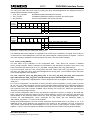
The SPC3 has a 44-pin PQFP housing with the following signals:
Pin
1
Signal Name
XCS
In/Out
I©
2
3
XWR/E_Clock
DIVIDER
4
5
6
7
8
XRD/R_W
CLK
VSS
CLKOUT2/4
XINT/MOT
9
10
X/INT
AB10
O
I(CPD)
11
DB0
I©/O
12
DB1
I©/O
13
14
15
XDATAEXCH
XREADY/XDTACK
DB2
O
O
I©/O
16
DB3
I©/O
17
18
19
VSS
VDD
DB4
I©/O
20
DB5
I©/O
21
22
23
DB6
DB7
MODE
I©/O
I©/O
I
I©
I©
I©
I(TS)
O
I©
Description
Chip-Select
Source / Destination
C32 Mode: place on VDD.
C165 Mode: CS-Signal
Write signal /EI_Clock for Motorola
Setting the scaler factor for CLK2OUT2/4.
low potential means divided through 4
Read signal / Read_Write for Motorola
Clock pulse input
Clock pulse divided by 2 or 4
<log> 0 = Intel interface
<log> 1 = Motorola interface
Interrupt
Address bus
24
ALE/AS
25
AB9
I
26
27
28
29
TXD
RTS
VSS
AB8
O
O
Serial send port
Request to Send
I©
Address bus
30
31
32
33
34
35
36
37
38
39
40
41
42
43
44
RXD
AB7
AB6
XCTS
XTEST0
XTEST1
RESET
AB4
VSS
VDD
AB3
AB2
AB5
AB1
AB0
I©
I©
I©
I©
I©
I©
I(CS)
I©
I©
I©
I©
I©
I©
CPU, Interrupt-Contr.
CPU, memory
LED
System, CPU
CPU, memory
C32 mode: data bus/address
bus multiplexed
C165 mode: data bus/address CPU, memory
bus separate
<log> 0 = 80C166
signal
<log> 1 = 80C32
timing
Address
latch
enable
Address bus
I©
CPU
System
System, CPU
System
C32 mode: <log> 0
C165 mode: address bus
Data bus
C32
Mode:
Data/address
bus
multiplexed
C165 Mode:
Data/address bus
separated
Data_Exchange state for PROFIBUS-DP
Ready for external CPU
Data bus
C32 mode: data bus/address
bus multiplexed
C165 mode: data/address bus
separate
Data bus
CPU (80C165)
CPU
Data bus/address bus separated; ready System
data bus/address bus multiplexed, fixed
C32 mode: ALE
C165 mode: <log> 0
C32 mode: <log> 0
C165 mode: address bus
CPU (80C32)
CPU (C165), memory
RS 485 sender
RS 485 sender
C32 Mode : <log> 0
C165 Mode: address bus
Serial receive port
Address bus
Address bus
Clear to send <log> 0 = send enable
Pin must be placed fixed at VDD.
Pin must be placed fixed at VDD.
Connect reset input with CPU’s port pin.
Address bus
RS 485 receiver
System, CPU
System, CPU
FSK modem
Address bus
System, CPU
Address bus
System, CPU
System, CPU
Figure 3.1: SPC3 Pin Assignment
Note: • All signals that begin with X.. are LOW active
• VDD = +5V, VSS = GND
Page 10
09/02
V2.0
SPC3 User Description
Copyright (C) Siemens AG 2002. All rights reserved.
SPC3
Input levels:
I ©:
I (CS):
I (CPD):
I (TS):
PROFIBUS Interface Center
CMOS
CMOS Schmitt trigger
CMOS with pull down
TTLt Schmitt trigger
SPC3 User Description
Copyright (C) Siemens AG 2002. All rights reserved.
V2.0
Page 11
09/02
SPC3
PROFIBUS Interface Center
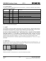
4 Memory Allocation
4.1 Memory Area Distribution in the SPC3
The figure displays the division of the SPC3 1.5k internal address area.
The internal latches/register are located in the first 21 addresses. The internal latches/register either come
from the controller or influence the controller. Certain cells can be only read or written. The internal work
cells to which the user has no access are located in RAM at the same addresses.
The organizational parameters are located in RAM beginning with address 16H. The entire buffer structure
(for the DP-SAPS) is written based on these parameters. In addition, general parameter setting data (station
address, Ident no., etc.) are transferred in these cells and the status displays are stored in these cells (global
control command, etc.).
Corresponding to the parameter setting of the organizational parameters, the user-generated buffers are
located beginning with address 40H. All buffers or lists must begin at segment addresses (48 bytes
segmentation).
Address
000H
016H
040H
5FFH
Function
Processor parameters
internal work cells
Latches/register
(22 bytes)
Organizational
parameters
(42 bytes)
DP- buffer:
Data In (3) *
Data Out (3) *
Diagnostics (2)
Parameter setting data (1)
Configuration data (2)
Auxiliary buffer (2)
SSA-buffer(1)
Figure 4.1: SPC3 Memory Area Distribution
Caution:
The HW prohibits overranging the address area. That is, if a user writes or reads past the memory
end, 400H is subtracted from this address and the user therefore accesses a new address. This
prohibits overwriting a process parameter. In this case, the SPC3 generates the RAM access
violation interrupt. If the MS overranges the memory end due to a faulty buffer initialization, the same
procedure is executed.
* Data In is the input data from PROFIBUS slave to master
Data out is the output data from PROFIBUS master to slave
Page 12
09/02
V2.0
SPC3 User Description
Copyright (C) Siemens AG 2002. All rights reserved.
SPC3
PROFIBUS Interface Center
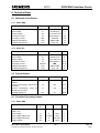
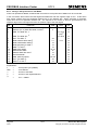
The complete internal RAM of the SPC 3 is divided logically into 192 segments. Each segment consists of 8
bytes. For more informations about the contents of the 3 memory areas see previous chapter.The physical
address is build by multiplikation with 8.
internal SPC 3 RAM (1.5 kByte)
Segment 0
Segment 1
Segment 2
8 Bit Segmentaddresses
(Pointer to the buffers
7
0
+
10
0
Segment 190
Segment 191
SPC3 User Description
Copyright (C) Siemens AG 2002. All rights reserved.
V2.0
Page 13
09/02
SPC3
PROFIBUS Interface Center
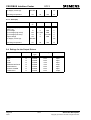
4.2 Processor Parameters (Latches/Register)
These cells can be either read only or written only. SPC3 carries out “address swapping” for an access to the
address area 00H - 07H (word register) in the Motorola mode. That is, the SPC3 exchanges
address bit 0 (generated from an even address, one uneven, and vice-versa). The following sections more
clearly explain the significance of the individual registers.
Address
Intel / Motorla
00H
01H
01H
00H
02H
03H
03H
02H
04H
05H
05H
04H
06H
07H
07H
06H
08H
09H
0AH
0BH
0CH
0DH
0EH
0FH
10H
11H
12H
13H
14H
15H
Name
Int-Req-Reg
Int-Req-Reg
Int—Reg
Int—Reg
Status-Reg
Status-Reg
Reserved
Bit No. Significance (Read Access!)
7..0 Interrupt Controller Register
15..8
7..0
15..8
7..0 Status Register
15..8
DIN_Buffer_SM
7..0 Buffer assignment of the
DP_Din_Buffer_State_Machine
New_DIN_Buffer_Cmd
1..0 The user makes a new DP Din buffer available in the
N state.
DOUT_Buffer_SM
7..0 Buffer assignment of the
DP_Dout_Puffer_State_Machine
Next_DOUT_Buffer_Cmd 1..0 The user fetches the last DP Dout-Buffer from the N
state.
DIAG_Buffer_SM
3..0 Buffer assignment for the
DP_Diag_Puffer_State_Machine
New_DIAG_Puffer_Cmd
1..0 The user makes a new DP Diag Buffer available to
the SPC3.
User_Prm_Data_OK
1..0 The user positively acknowledges the user
parameter setting data of a Set_Param-Telegram.
UserPrmDataNOK
1..0 The user negatively acknowledges the user
parameter setting data of a Set_Param-Telegram.
User_Cfg_Data_OK
1..0 The user positively acknowledges the configuration
data of a Check_Config-Telegram.
User_Cfg_Data_NOK
1..0 The user negatively acknowledges the configuration
data of a Check_Config-Telegram.
Reserved
SSA_Bufferfreecmd
The user has fetched the data from the SSA buffer
and enables the buffer again.
Reserved
Figure 4.2: Assignment of the Internal Parameter Latches for READ
Page 14
09/02
V2.0
SPC3 User Description
Copyright (C) Siemens AG 2002. All rights reserved.
SPC3
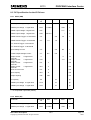
Address
Intel
/Motorola
00H
01H
01H
00H
02H
03H
03H
02H
04H
05H
05H
04H
06H
07H
07H
06H
08H
09H
0AH
0BH
OCH
0DH
0EH
0FH
10H
11H
12H
13H
14H
15H
Name
PROFIBUS Interface Center
Bit No. Significance (Write Access !)
Int-Req-Reg
Int-Req_Reg
Int-Ack-Reg
Int-Ack-Reg
Int—Mask-Reg
Int—Mask-Reg
Mode-Reg0
Mode-Reg0-S
Mode-Reg1-S
Mode-Reg1-R
WD Baud Ctrl -Val
MinTsdr_Val
7..0 Interrupt- Controller - Register
15..8
7..0
15..8
7..0
15..8
7..0 Setting parameters for individual bits
15..8
7..0
7..0
7..0 Root value for baud rate monitoring
7..0
MinTsdr time
Reserved
Figure 4.3: Assignment of the Internal Parameter Latches for WRITE
SPC3 User Description
Copyright (C) Siemens AG 2002. All rights reserved.
V2.0
Page 15
09/02
SPC3
PROFIBUS Interface Center
4.3 Organizational Parameters (RAM)
The user stores the organizational parameters in RAM under the specified addresses. These parameters
can be written and read.
Address
Intel
/Motorola
16H
17H
18H
19H
19H
18H
1AH
1BH
1CH
1DH
1EH
1FH
20H
21H
22H
23H
24H
25H
26H
27H
28H
29H
2AH
2BH
2CH
2DH
2EH
2FH
30H
31H
32H
33H
34H
35H
36H
37H
38H
39H
3AH
3BH
3CH
3DH
Name
Bit No.
Significance
R_TS_Adr
reserved
R_User_Wd_Value
7..0 Set up station address of the relevant SPC3
Pointer to a RAM address which is presetted with 0FFH
7..0 Based on an internal 16-bit wachdog timer, the user is
monitored in the DP_Mode.
R_User_Wd_Value
15 ..8
R_Len_Dout_Puf
Length of the 3 Dout buffers
R_Dout_buf_Ptr1
Segment base address of Dout buffer 1
R_Dout_buf_Ptr2
Segment base address of Dout buffer 2
R_Dout_buf_Ptr3
Segment base address of Dout buffer 3
R_Len_Din_buf
Length of the 3 Din buffers
R_Din_buf_Ptr1
Segment base address of Din buffer 1
R_Din_buf_Ptr2
Segment base address of Din buffer 2
R_Din_buf_Ptr3
Segment base address of Din buffer 3
reserved
Preset with 00H.
reserved
Preset with 00H.
R Len Diag buf1
Length of Diag buffer 1
R Len Diag buf2
Length of Diag buffer 2
R_Diag_Puf_Ptr1
Segment base address of Diag buffer 1
R_Diag_Puf_Ptr2
Segment base address of Diag buffer 2
R Len Cntrl Pbuf1
Length of Aux buffer 1 and the control buffer belonging to it,
for example, SSA-Buf, Prm-Buf, Cfg-Buf, Read-Cfg-Buf
R Len Cntrl Puf2
Length of Aux-Buffer 2 and the control buffer belonging to it,
for example, SSA-Buf, Prm-Buf, Cfg-Buf, Read-Cfg-Buf
R Aux Puf Sel
Bit array, in which the assignments of the Aux-buffers ½ are
defined to the control buffers, SSA-Buf, Prm-Buf, Cfg-Buf
R_Aux_buf_Ptr1
Segment base address of auxiliary buffer 1
R_Aux_buf_Ptr2
Segment base address of auxiliary buffer 2
R_Len_SSA_Data
Length of the input data in the Set_Slave_Address-buffer
R SSA buf Ptr
Segment base address of the Set_Slave_Address-buffer
R_Len_Prm_Data
Length of the input data in the Set_Param-buffer
R_Prm_buf_Ptr
Segment base address of the Set_Param-buffer
R_Len_Cfg_Data
Length of the input data in the Check_Config-buffer
R Cfg Buf Ptr
Segment base address of the Check_Config-buffer
R_Len_Read_Cfg_Data
Length of the input data in the Get_Config-buffer
R_Read_Cfg_buf_Ptr
Segment base address of the Get_Config-buffer
reserved
Preset with 00H.
reserved
Preset with 00H
reserved
Preset with 00H.
reserved
Preset with 00H.
R_Real_No_Add_Change
This parameter specifies whether the DP slave address may
again be changed at a later time point.
R_Ident_Low
The user sets the parameters for the Ident_Low value.
R_Ident_High
The user sets the parameters for the Ident_High value.
R_GC_Command
The Global_Control_Command last received
R_Len_Spec_Prm_buf
If parameters are set for the Spec_Prm_Buffer_Mode (see
mode register 0), this cell defines the length of the param
buffer.
Figure 4.4: Assignment of the Organizational Parameters
Page 16
09/02
V2.0
SPC3 User Description
Copyright (C) Siemens AG 2002. All rights reserved.
SPC3
PROFIBUS Interface Center
5 ASIC Interface
The registers that determine both the hardware function of the ASIC as well as telegram processing are
described in the following.
5.1 Mode Register
Parameter bits that access the controller directly or which the controller directly sets are combined in two
mode registers (0 and 1) in the SPC3.
5.1.1 Mode Register 0
Setting parameters for Mode Register 0 takes place in the offline state only (for example, after switching
on). The SPC3 may not exit offline until Mode Register 0, all processor parameters, and organizational
parameters are loaded (START_SPC3 = 1, Mode-Register 1).
Address
Control
Register
06H
(Intel)
Address
Control
Register
07H
(Intel)
7
6
5
Freeze_
Supported
Sync_
Supported
EARLY_
RDY
15
14
13
Bit Position
4
3
INT_
POL
12
MinTSDR
Bit Position
11
Spec_Cle Spec_Prm_
ar_Mode
Puf_Mode
*)
**)
Designation
2
WD
Test
1
0
DIS_
STOP_
CON
TROL
DIS_
START_
CON
TROL
Mode Reg0
7..0
Designation
10
9
8
User
Time
base
EOI
Time
base
DP
Mode
Mode-Reg0
13 .. 8
*) When Spec_Clear_Mode (Fail Safe Mode ) = 1 the SPC3 will accept data telegramm with a data unit=0 in
the state Data Exchange. The reaction to the outputs can be parameterized f.e. in the parameterization
telegram ( only available from version Step C).
**) When using a big number of parameters to be transmitted from the PROFIBUS-Master to the slave the
Auxiliary buffer ½ has to have the same size like the Parameterization buffer. Sometimes this could reach the
limit of the available memory space in the SPC3. When Spec_Prm_Puf_Mode = 1 the parameterization data
are processed directly in this special buffer and the Auxiliary buffers can be held compact.
SPC3 User Description
Copyright (C) Siemens AG 2002. All rights reserved.
V2.0
Page 17
09/02
SPC3
PROFIBUS Interface Center
Bit 0
Bit 1
Bit 2
Bit 3
Bit 4
Bit 5
Bit 6
Bit 7
Bit 8
Bit 9
Bit 10
Bit 11
Bit 12
Bit 13
DIS_START_CONTROL
Monitoring the following start bit in UART. Set-Param Telegram overwrites this memory cell in
the DP mode. (Refer to the user-specific data.)
0=
Monitoring the following start bit is enabled.
1=
Monitoring the following start bit is switched off.
DIS_STOP_CONTROL
Stop bit monitoring in UART. Set-Param telegram overwrites this memory cell in the DP mode.
(Refer to the user-specific data.)
0=
Stop bit monitoring is enabled.
1=
Stop bit monitoring is switched off.
EN_FDL_DDB
Reserved
0=
The FDL_DDB receive is disabled.
MinTSDR
Default setting for the MinTSDR after reset for DP operation or combi operation
0=
Pure DP operation (default configuration!)
1=
Combi operation
INT_POL
Polarity of the interrupt output
0=
The interrupt output is low-active.
1=
The interrupt output is high-active.
EARLY_RDY
Moved up ready signal
0=
Ready is generated when the data are valid (read) or when the data are accepted
(write).
1=
Ready is moved up by one clock pulse.
Sync_Supported
Sync_Mode support
0=
Sync_Mode is not supported.
1=
Sync_Mode is supported.
Freeze_Supported
Freeze_Mode support
0=
Freeze_Mode is not supported.
1=
Freeze_Mode is supported.
DP_MODE
DP_Mode enable
0=
DP_Mode is disabled.
1=
DP_Mode is enabled. SPC3 sets up all DP_SAPs.
EOI_Time base
Time base for the end of interrupt pulse
0=
The interrupt inactive time is at least 1 usec long.
1=
The interrupt inactive time is at least 1 ms long.
User_Time base
Time base for the cyclical User_Time_Clock-Interrupt
0=
The User_Time_Clock-Interrupt occurs every 1 ms.
1=
The User_Time_Clock-Interrupt occurs every 10 ms.
WD_Test
Test mode for the Watchdog-Timer, no function mode
0=
The WD runs in the function mode.
1=
Not permitted
Spec_Prm_Puf_Mode
Special parameter buffer
0=
No special parameter buffer.
1=
Special parameter buffer mode .Parameterization data will be stored directly in the
special parameter buffer.
Spec_Clear_Mode
Special Clear Mode (Fail Safe Mode)
0=
1=
No special clear mode.
Special clear mode. SPC3 will accept datea telegramms with data unit = 0.
Figure 5.1: Mode-Register 0 Bit 12 .. 0.(can be written to, can be changed in offline only)
Page 18
09/02
V2.0
SPC3 User Description
Copyright (C) Siemens AG 2002. All rights reserved.
SPC3
PROFIBUS Interface Center
5.1.2 Mode Register 1 (Mode-REG1, writable):
Some control bits must be changed during operation. These control bits are combined in Mode-Register 1
and can be set independently of each other (Mode_Reg_S) or can be deleted independently of each other
(Mode_Reg_R). Various addresses are used for setting and deleting. Log ‘1’ must be written to the bit
position to be set or deleted.
Address
Control
Register
08H
7
6
Bit 1
Bit 2
Bit 3
Bit 4
Bit 5
Bit Position
4
3
Res_
EN_
User_WD Change_
Cfg_
Puffer
Res_
EN_
User_WD Change_
Cfg_
Puffer
09H
Bit 0
5
Designation
2
1
0
User_
Leave_
Master
Go_
Offline
EOI
START_
SPC3
Mode-Reg_S
7..0
User_
Leave_
Master
Go_
Offline
EOI
START_
SPC3
Mode-Reg_R
7..0
START_SPC3
Exiting the Offline state
1 = SPC3 exits offline and goes to passive-idle. In addition, the idle timer and
Wd timer are started and ‘Go_Offline = 0’ is set.
EOI
End of Interrupt
1 = End of Interrupt: SPC3 switches the interrupt outputs to inactive and again
sets EOI to log.’0.’
Go_Offline
Going into the offline state
1 = After the current requests ends, SPC3 goes to the offline state and again
sets Go_Offline to log.’0.’
User_Leave_Master
Request to the DP_SM to go to ‘Wait_Prm.’
1 = The user causes the DP_SM to go to ‘Wait_Prm.’ After this action, SPC3
sets User_Leave_Master to log.’0.’
En_Change_Cfg_Puffer
Enabling buffer exchange (Cfg buffer for Read_Cfg buffer)
0 = With ‘User_Cfg_Data_Okay_Cmd,’ the Cfg buffer may not be exchanged for
the Read_Cfg buffer.
1 = With ‘User_Cfg_Data_Okay_Cmd,’ the Cfg buffer must be exchanged for the
Read_Cfg buffer.
Res_User_Wd
Resetting the User_WD_Timers
1 = SPC3 again sets the User_Wd_Timer to the parameterized value
‘User_Wd_Value15..0.’ After this action, SPC3 sets Res_User_Wd to log.’0.’
Figure 5..2: Mode Register1 S and Mode Register1 R Bit7..0.(writable)
SPC3 User Description
Copyright (C) Siemens AG 2002. All rights reserved.
V2.0
Page 19
09/02
SPC3
PROFIBUS Interface Center
5.2 Status Register
The status register mirrors the current SPC3 status and can be read only.
Address
Control
Register
04H
(Intel)
Address
Control
Register
05H
(Intel)
7
09/02
5
Bit Position
4
3
RAM
access
violation
WD_State
DP_State
1
0
1
0
15
14
13
Bit Position
12
11
SPC3 Release
3
Page 20
6
2
1
Designation
2
1
0
Diag_
Flag
FDL_
IND_ST
Offline/
PassiveIdle
10
9
8
Designation
Baud Rate
0
3
V2.0
Status-Reg
7..0
2
1
Status-Reg
15 .. 8
0
SPC3 User Description
Copyright (C) Siemens AG 2002. All rights reserved.
SPC3
Bit 0
Bit 1
Bit 2
Bit 3
Bits
4,5
Bits
6,7
Bits
8,9
10,11
Bit 12
13,14,
15
PROFIBUS Interface Center
Offline/Passive-Idle
Offline-/Passive-Idle state
0 = SPC3 is in offline.
1 = SPC3 is in passive idle.
FDL_IND_ST
FDL indication is temporarily buffered.
0 = No FDL indication is temporarily buffered.
1 = No FDL indication is temporarily buffered.
Diag_Flag
Status diagnostics buffer
0 = The DP master fetches the diagnostics buffer.
1 = The DP master has not yet fetched the diagnostics buffer.
RAM Access Violation
Memory access > 1.5kByte
0 = No address violation
1 = For addresses > 1536 bytes, 1024 is subtracted from the current address,
and there is access to this new address.
DP-State1..0
DP-State Machine state
00 = ’Wait_Prm’ state
01= ’Wait_Cfg’ state
10 = ’DATA_EX’ state
11= Not possible
WD-State1..0
Watchdog-State-Machine state
00 = ’Baud_Search’ state
01= ’Baud_Control’ state
10 = ’DP_Control’ state
11= Not possible
Baud rate3..0:
The baud rates SPC3 found
0000 = 12 MBaud
0001 = 6 MBaud
0010 = 3 MBaud
0011 = 1.5 MBaud
0100 = 500 kBaud
0101 = 187.5 kBaud
0110 = 93.75 kBaud
0111 = 45.45 kBaud
1000 = 19.2 kBaud
1001 = 9.6 kBaud
Rest = Not possible
SPC3-Release3..0:
Release no. for SPC3
0000 = Release 0
Rest = Not possible
Figure 5.3: Status Register Bit15 .. 0.(readable)
SPC3 User Description
Copyright (C) Siemens AG 2002. All rights reserved.
V2.0
Page 21
09/02
SPC3
PROFIBUS Interface Center
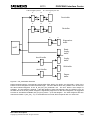
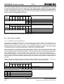
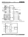
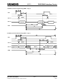
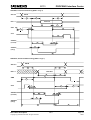
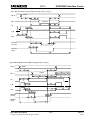
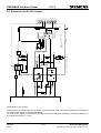
5.3 Interrupt Controller
The processor is informed about indication messages and various error events via the interrupt controller. Up
to a total of 16 events are stored in the interrupt controller. The events are carried out on an interrupt output.
The controller does not have a prioritization level and does not provide an interrupt vector (not 8259A
compatible!).
The controller consists of an Interrupt Request Register (IRR), an Interrupt Mask Register (IMR), an Interrupt
Register (IR), and an Interrupt Acknowledge Register (IAR).
uP
SPC3
uP
uP SEP_INT
uP
IR
S
IRR
S
IMR
X/INT
uP
FF
R
R
INT_Pol
IAR
uP
Each event is stored in the IRR. Individual events can be suppressed via the IMR. The input in the IRR is
independent of the interrupt masks. Event signals not masked out in the IMR generate the X/INT interrupt via
a sum network. The user can set each event in the IRR for debugging.
Each interrupt event the processor processed must be deleted via the IAR (except for New_Prm_Data,
New_DDB_Prm_Data, and New_Cfg_Data). Log ‘1’ must be written on the relevant bit position. If a new
event and an acknowledge from the previous event are present at the IRR at the same time, the event
remains stored. If the processor subsequently enables a mask, it must be ensured that no prior input is
present in the IRR. For safety purposes, the position in the IRR must be deleted prior to the mask enable.
Prior to exiting the interrupt routine, the processor must set the “end of interrupt signal (E01) = 1” in the mode
register. The interrupt cable is switched to inactive with this edge change. If another event must be stored,
the interrupt output is not activated again until after an interrupt inactive time of at least 1 usec or 1-2 ms.
This interrupt inactive time can be set via ‘EOI_Timebase.’ This makes it possible to again come into the
interrupt routine when an edge-triggered interrupt input is used.
The polarity for the interrupt output is parameterized via the INT_Pol mode bit. After the hardware reset, the
output is low-active.
Address
Control
Register
00H
(Intel)
Address
Control
Register
01H
(Intel)
Page 22
09/02
7
6
5
Res
Res
Res
15
14
13
Res
Res
DX_OUT
Bit Position
4
3
User_
Timer_
Clock
WD_DP_
Mode_
Timeout
Bit Position
12
11
Diag_
Puffer_
Changed
New_
Prm_
Data
V2.0
Designation
2
1
0
Baud_
rate_
Detect
Go/Leave
Data_
EX
MAC_
Reset
10
9
8
New_
Cfg_
Data
New_
SSA_
Data
New_GC
Com
mand
Int-Req-Reg
7..0
Designation
Int-Req-Reg 7
15..8
SPC3 User Description
Copyright (C) Siemens AG 2002. All rights reserved.
SPC3
Bit 0
Bit 1
Bit 2
Bit 3
Bit 4
Bit 5
Bit 6
Bit 7
Bit 8
Bit 9
Bit 10
Bit 11
Bit 12
Bit 13
Bit 14
Bit 15
PROFIBUS Interface Center
MAC_Reset
After it processes the current request, the SPC3 has arrived at the offline state (through
setting the ‘Go_Offline bit’ or through a RAM access violation).
Go/Leave_DATA_EX
The DP_SM has entered or exited the ‘DATA_EX’ state.
Baudrate_Detect
The SPC3 has exited the ‘Baud_Search state’ and found a baud rate.
WD_DP_Control_Timeout
The watchdog timer has run out in the ‘DP_Control’ WD state.
User_Timer_Clock
The time base for the User_Timer_Clocks has run out (1/10ms).
Res
For additional functions
Res
For additional functions
Res
For additional functions
New_GC_Command
The SPC3 has received a ‘Global_Control telegram’ with a changed ‘GC_CommandByte,’ and this byte is stored in the ‘R_GC_Command’ RAM cell.
New_SSA_Data
The SPC3 has received a ‘Set_Slave_Address telegram’ and made the data available in
the SSA buffer.
New_Cfg_Data
The SPC3 has received a ‘Check_Cfg telegram’ and made the data available in the Cfg
buffer.
New_Prm_Data
The SPC3 has received a ‘Set_Param telegram’ and made the data available in the Prm
buffer.
Diag_Puffer_Changed
Due to the request made by ‘New_Diag_Cmd,’ SPC3 exchanged the diagnostics buffer
and again made the old buffer available to the user.
DX_OUT
The SPC3 has received a ‘Write_Read_Data telegram’ and made the new output data
available in the N buffer. For a ‘Power_On’ or for a ‘Leave_Master,’ the SPC3 deletes
the N buffer and also generates this interrupt.
Res
For additional functions
Res
For additional functions
Figure 5.4: Interrupt Request Register, IRR Bit 15..0 (writable and readable)
SPC3 User Description
Copyright (C) Siemens AG 2002. All rights reserved.
V2.0
Page 23
09/02
SPC3
PROFIBUS Interface Center
The other interrupt controller registers are assigned in the bit positions, like the IRR.
Address
02H /
03H
04H /
05H
Register
Interrupt Register
(IR)
Interrupt Mask
Register
(IMR)
02H /
03H
Interrupt
Acknowledge
Register
(IAR)
Reset State
Readable only All bits deleted
Assignment
Writable, can
be changed
during
operation
Writable, can
be changed
during
operation
Bit = 1 Mask is set and the interrupt
is disabled.
Bit = 0 Mask is deleted and the
interrupt is enabled.
Bit = 1 The IRR bit is deleted.
Bit = 0 The IRR bit remains
unchanged.
All bits set
All bits deleted
Figure 5.5: Additional Interrupt Registers
The ‘New_Prm_Data’, ‘New_Cfg_Data’ inputs may not be deleted via the Interrupt Acknowledge Register.
The relevant state machines delete these inputs through the user acknowledgements (for example,
‘User_Prm_Data_Okay’ etc.).
Page 24
09/02
V2.0
SPC3 User Description
Copyright (C) Siemens AG 2002. All rights reserved.
SPC3
PROFIBUS Interface Center
5.4 Watchdog Timer
5.4.1 Automatic Baud Rate Identification
The SPC3 is able to identify the baud rate automatically. The „baud search“ state is located after each
RESET and also after the watchdog (WD) timer has run out in the ‘Baud_Control_state.’
As a rule, SPC3 begins the search for the set rate with the highest baud rate. If no SD1 telegram, SD2
telegram, or SD3 telegram was received completely and without errors during the monitoring time, the search
continues with the next lowest baud rate.
After identifying the correct baud rate, SPC3 switches to the “Baud_Control” state and monitors the baud
rate. The monitoring time can be parameterized (WD_Baud_Control_Val). The watchdog works with a clock
of 100 Hz (10 msec). The watchdog resets each telegram received with no errors to its own station address.
If the timer runs out, SPC3 again switches to the baud search state.
5.4.2 Baud Rate Monitoring
The located baud rate is constantly monitored in ‘Baud_Control.’ The watchdog is reset for each error-free
telegram to its own station address.
The monitoring time results from multiplying both
‘WD_Baud_Control_Val’ (user sets the parameters) by the time base (10 ms). If the monitoring time runs
out, WD_SM again goes to ‘Baud_Search’. If the user carries out the DP protocol (DP_Mode = 1, see Mode
register 0) with SPC3, the watchdog is used for the “DP_Control’ state, after a ‘Set_Param telegram’ was
received with an enabled response time monitoring ‘WD_On = 1.’ The watchdog timer remains in the baud
rate monitoring state when there is a switched off ‘WD_On = 0’ master monitoring. The PROFIBUS DP state
machine is also not reset when the timer runs out. That is, the slave remains in the DATA_EXchange state,
for example.
5.4.3 Response Time Monitoring
The ‘DP_Control’ state serves response time monitoring of the DP master (Master_Add). The set monitoring
times results from multiplying both watchdog factors and multiplying the result with the momentarily valid time
base (1 ms or 10 ms):
TWD = (1 ms or 10 ms) * WD_Fact_1 * WD_Fact_2 (See byte 7 of the parameter setting telegram.)
The user can load the two watchdog factors (WD_Fact_1, and WD_Fact_2) and the time base that
represents a measurement for the monitoring time via the ‘Set_Param telegram’ with any value between 1
and 255.
EXCEPTION: The WD_Fact_1=WD_Fact_2=1 setting is not permissible. The circuit does not check
this setting.
Monitoring times between 2 ms and 650 s - independent of the baud rate - can be implemented with the
permisible watchdog factors.
If the monitoring time runs out, the SPC3 goes again to ‘Baud_Control,’ and the SPC3 generates the
‘WD_DP_Control_Timeout-Interrupt’. In addition, the DP_State machine is reset, that is, generates the reset
states of the buffer management.
If another master accepts SPC3, then there is either a switch to ‘Baud_Control” (WD_On = 0), or there is a
delay in ‘DP_Control’ (WD_On = 1), depending on the enabled response time monitoring (WD_On = 0).
SPC3 User Description
Copyright (C) Siemens AG 2002. All rights reserved.
V2.0
Page 25
09/02
SPC3
PROFIBUS Interface Center
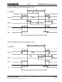
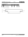
6 PROFIBUS-DP Interface
6.1 DP_Buffer Structure
The DP mode is enabled in the SPC3 with ‘DP_Mode = 1’ (see mode Register0). In this process, the
following SAPS are fixed reserved for the DP mode:
`
`
`
`
`
`
`
`
`
`
Default SAP:
SAP53:
SAP55:
SAP56:
SAP57:
SAP58:
SAP59:
SAP60:
SAP61:
SAP62:
Data exchange (Write_Read_Data)
reserved
Changing the station address (Set_Slave_Address)
Reading the inputs (Read_Inputs)
Reading the outputs (Read_Outputs)
Control commands to the DP-Slave (Global_Control)
Reading configuration data (Get_Config)
Reading diagnostics information (Slave_Diagnosis)
Sending parameter setting data (Set_Param)
Checking configuration data (Check_Config)
The DP Slave protocol is completely integrated in the SPC3 and is handled independently. The user must
correspondingly parameterize the ASIC and process and acknowledge transferred messages. Except for the
default SAP, SAP56, SAP57, and SAP58, all SAPS are always enabled. The remaining SAPS are not
enabled until the the DP Slave Machine (DP_SM) goes into the ‘DATA_EX’ state. The user has the
possibility of disabling SAP55. The relevant buffer pointer R_SSA_Puf_Ptr must be set to ‘00H’ for this
purpose. The DDB utility is disabled by the already described initialization of the RAM cells.
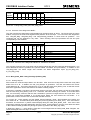
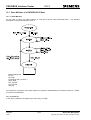
The DP_SAP buffer structure is displayed in Figure 6.1. The user configures all buffers (length and buffer
beginning) in the ‘offline state.’ During operation, the buffer configuration must not be changed, except for
the length of the Dout-/Din buffers.
The user may still adapt these buffers in the ‘Wait_Cfg’ state after the configuration telegram (Check_Config).
Only the same configuration may be accepted in the ‘DATA_EX’ state.
The buffer structure is divided into the data buffer, diagnostics buffer, and the control buffer.
Both the output data and the input data have three buffers each available with the same length. These
buffers function as change buffers. One buffer is assigned to the ‘D’ data transfer, and one buffer is assigned
to the ‘U’ user. The third buffer is either in a Next ‘N’ state or Free ‘F’ state, whereby one of the two states is
always unoccupied.
Two diagnostics buffers that can have varying lengths are available for diagnostics. One diagnostics buffer is
always the ‘D’ assigned to SPC3 for sending. The other diagnostics buffer belongs to the user for preparing
new diagnostics data, ‘U.’
The SPC3 first reads the different parameter setting telegrams (Set_Slave_Address, and Set_Param) and
the configuring telegram (Check_Config) into Aux-Puffer1 or Aux-Puffer 2.....
Page 26
09/02
V2.0
SPC3 User Description
Copyright (C) Siemens AG 2002. All rights reserved.
SPC3
D-Nis changed by SPC 3
D
PROFIBUS Interface Center
N- U is changed by the user
N
U
Dout-buffer
D
N
U
Din-buffer
D
U
Diagnosticsbuffer
UART
ReadConfigbuffer
User
Aux1/2-buffer
Configbuffer
SSA-buffer
Aux1/2-buffer
Parambuffer
Figure 6.1: DP_SAP Buffer Structure
Data exchanged with the corresponding target buffer (SSA buffer, Prm buffer, and Cfg buffer). Each of the
buffers to be exchanged must have the same length. The user defines which Aux_buffers are to be used for
the above-named telegrams in the ‘R_Aux_Puf_Sel’ parameter cell. The Aux- buffer1 must always be
available. The Aux-buffer2 is optional. If the data profiles of these DP telegrams are very different, such as
the data amount in the Set_Param telegram is significantly larger than for the other telegrams, it is suggested
to make an Aux-Buffer2 available (Aux_Sel_Set_Param = 1) for this telegram. The other telegrams are then
read via Aux-Buffer 1 (Aux_Sel_..=0). If the buffers are too small, SPC3 responds with “no resources”!
SPC3 User Description
Copyright (C) Siemens AG 2002. All rights reserved.
V2.0
Page 27
09/02
SPC3
PROFIBUS Interface Center
Address
RAM
Register
2AH
X1
0
1
7
6
5
Bit Position
4
3
2
0
0
0
0
0
Designation
0
Set_
Slave_
Adr
Check_
Cfg
Set_
Prm
R_Aux_Puf_Sel
X1
X1
X1
See below for coding.
Coding
Aux_Buffer1
Aux_Buffer2
Figure 6.2: Aux-Buffer Management
The user makes the configuration data (Get_Config) available in the Read_Cfg buffer for reading. The
Read_Cfg buffer must have the same length as the Cfg_buffer.
The Read_Input_Data telegram is operated from the Din buffer in the ‘D state’, and the Read_Output_Data
telegram is operated from the Dout buffer in the ‘U state.’
All buffer pointers are 8-bit segment addresses, because the SPC3 internally has only 8-bit address registers.
For a RAM access, SPC3 adds an 8-bit offset address to the segment address shifted by 3 bits (result: 11-bit
physical address). As regards the buffer start addresses, this results in an 8-byte graunularity from this
specification.
Page 28
09/02
V2.0
SPC3 User Description
Copyright (C) Siemens AG 2002. All rights reserved.
SPC3
PROFIBUS Interface Center
6.2 Description of the DP Services
6.2.1 Set_Slave_Address (SAP55)
6.2.1.1 Sequence for the Set_Slave_Address Utility
The user can disable this utility by setting the ‘R_SSA_Puf_Ptr = 00H’ buffer pointer. The slave address must
then be determined, for example, by reading a switch, and written in the R_TS_Adr. RAM register.
The user must make a retentive memory possibility available (for example, EEPROM) to support this utility. It
must be possible to store the ‘station address’ and the ‘Real_No_Add_Change’ (‘True’ = FFH) parameter in
this external EEPROM. After each restart caused by a power failure, the user must again make these values
available to SPC3 in the R_TS_Adr und R_Real_No_Add_Change RAM register.
If SAP55 is enabled and the Set_Slave_Address telegram is correctly accepted, SPC3 enters all net data in
the Aux-Puffer1/2, exchanges the Aux buffer1/2 for the SSA buffer, stores the entered data length in
‘R_Len_SSA_Data’, generates the ‘New_SSA_Data’ interrupt and internally stores the new ‘station address’
and the new ‘Real_No_Add_Change’ parameter. The user does not need to transfer this changed parameter
to SPC3 again. After the user has read the buffer, the user generates the ‘SSA_Puffer_Free_Cmd’ (read
operation on address 14H). This makes SPC3 again ready to receive an additional Set Slave Address
telegram (such as from another master).
SPC3 reacts independently when there are errors.
Address
Control
Register
14H
7
6
5
0
0
0
Bit Position
4
3
0
0
don´t care
Designation
2
1
0
0
0
0
SSA_Puffer_Free_Cmd
Figure 6.3: Coding SSA_Buffer_Free_Cmd
6.2.1.2 Structure of the Set_Slave_Address Telegram
The net data are stored as follows in the SSA buffer:
Byte
7
6
5
Bit Position
4
3
Designation
2
0
1
2
3
4-243
1
0
New_Slave_Address
Ident_Number_High
Ident_Number_Low
No_Add_Chg
Rem_Slave_Data additional applicationspecific data
Figure 6.4: Data Format for the Set_Slave_Address Telegram
SPC3 User Description
Copyright (C) Siemens AG 2002. All rights reserved.
V2.0
Page 29
09/02
SPC3
PROFIBUS Interface Center
6.2.2 Set_Param (SAP61)
6.2.2.1 Parameter Data Structure
SPC3 evaluates the first seven data bytes (without user prm data), or the first eight data bytes (with user prm
data). The first seven bytes are specified according to the standard. The eighth byte is used for SPC3specific characteristics. The additional bytes are available to the application.
Byte
0
1
2
3
4
5
6
7
7
6
5
Lock
Req
Unlo.
Req
Sync
Req
0
0
0
Bit Position
4
3
Free
Req
0
WD
on
0
Designation
2
1
0
Res
Res
Res
WD_
Base
Dis
Stop
Dis
Start
8-243
Station status
WD_Fact_1
WD_Fact_2
MinTSDR
Ident_Number_High
Ident_Number_Low
Group_Ident
Spec_User_Prm_Byte
User_Prm_Data
Byte 7
Bit
0
Spec_User_Prm_Byte
Name
Significance
Dis_Startbit
The start bit monitoring in the
receiver is switched off with this bit.
1
Dis_Stopbit
Stop bit monitoring in the receiver is
switched off with this bit.
2
WD_Base
3-4
5
res
Publisher_En
able
This bit specifies the time base used
to clock the watchdog.
WD_Base = 0: time base 10 ms
WD_Base = 1: time base 1 ms
to be parameterized with 0
DXB-publisher-functionality of the
SPC3 is activated with this bit
6-7
res
to be parameterized with 0
Default State
Dis_Startbit= 1 ,
that is, start bit monitoring is
switched off.
Dis_Stopbit= 0,
that is, stop bit monitoring is not
switched off.
WD_Base= 0,
that is, the time base is 10 ms
0
Publisher_Enable=0, DXB-requesttelegrams are ignored;
Publisher_Enable=1, DXB-requesttelegramme are processed
0
Figure 6.5: Data Format for the Set_Param_Telegram
6.2.2.2 Parameter Data Processing Sequence
In the case of a positive validatation for more than seven data bytes, SPC3 carries out the following reaction,
among others:
SPC3 exchanges Aux-Puffer1/2 (all data bytes are input here) for the Prm buffer, stores the input data length
in ‘R_Len_Prm_Data’, and triggers the ‘New_Prm_Data Interrupt’. The user must then check the
‘User_Prm_Data’
and
either
reply
with
the
‘User_Prm_Data_Okay_Cmd’
or
with
‘User_Prm_Data_Not_Okay_Cmd.’ The entire telegram is input in the buffer, that is, application-specific
parameter data are stored beginning with data byte 8 only.
The user response (User_Prm_Data_Okay_Cmd or User_Prm_Data_Not_Okay_Cmd) again takes back
the ‘New_Prm_Data’ interrupt. The user may not acknowledge the ‘New_Prm_Data’ interrupt in the
IAR register.
The relevant diagnostics bits are set with the ‘User_Prm_Data_Not_Okay_Cmd’ message and are branched
to ‘Wait_Prm.’
Page 30
09/02
V2.0
SPC3 User Description
Copyright (C) Siemens AG 2002. All rights reserved.
SPC3
PROFIBUS Interface Center
The ‘User_Prm_Data_Okay’ and ‘User_Prm_Data_Not_Okay’ acknowledgements are reading accesses to
defined registers with the relevant signals:
• ‘User_Prm_Finished’:
• ‘Prm_Conflict’ :
• ‘Not_Allowed’,
Address
Control
Register
0EH
Address
Control
Register
0FH
7
6
5
0
0
0
7
6
5
0
0
0
No additional parameter telegram is present.
An additional parameter telegram is present, processing again
Access not permitted in the current bus state
Bit Position
4
3
0
0
Bit Position
4
3
0
0
Designation
2
1
0
0
⇓
0
0
1
⇓
0
1
1
2
1
0
0
⇓
0
0
1
⇓
0
1
1
User_Prm_Data_Okay
User_Prm_Finished
PRM_Conflict
Not_Allowed
Designation
User_Prm_Data_Not_Okay
User_Prm_Finished
PRM_Conflict
Not_Allowed
Figure 6.6: Coding User_Prm_Data_Not/_Okay_Cmd
If an additional Set-Param telegram is supposed to be received in the meantime, the signal ‘Prm_Conflict’ is
is returned for the acknowledgement of the first Set_Param telegram, whether positive or negative. Then the
user must repeat the validation because the SPC3 has made a new Prm buffer available.
6.2.3 Check_Config (SAP62)
The user takes on the evaluation of the configuration data. After SPC3 has received a validated
Check_Config-Telegram, SPC3 exchanges the Aux-Puffer1/2 (all data bytes are entered here) for the Cfg
buffer, stores the input data length in ‘R_Len_Cfg-Data,’ and generates ‘New_Cfg_Data-Interrupt’.
The user must then check the ‘User_Config_Data’ and either respond with ‘User_Cfg_Data_Okay_Cmd’ or
with ‘User_Cfg_Data_Not_Okay_Cmd’ (acknowledgement to the Cfg_SM). The net data is input in the buffer
in the format regulation of the standard.
The user response (User_Cfg_Data_Okay_Cmd or the User_Cfg_Data_Not_Okay_Cmd response)
again takes back the ‘New_Cfg_Data’ interrupt and may not be acknowledged in the IAR.
If an incorrect configuration is signalled back, various diagnostics bits are changed, and there is branching to
‘Wait_Prm.“
For a correct configuration, the transition to ‘DATA_EX’ takes place immediately, if no Din_buffer is present
(R_Len_Din_Puf = 00H) and trigger counters for the parameter setting telegrams and configuration telegrams
are at 0. Otherwise, the transition does not take place until the first ‘New_DIN_Puffer_Cmd’ with which the
user makes the first valid ‘N buffer” available. When entering into ‘DATA_EX,’ SPC3 also generates the
‘Go/Leave_Data_Exchange-Interrupt.
If the received configuration data from the Cfg buffer are supposed to result in a change of the Read-Cfgbuffer ( the change contains the data for the Get_Config telegram), the user must make the new Read_Cfg
data available in the Read-Cfg buffer before the ‘User_Cfg_Data_Okay_Cmd” acknowledgement. After
receiving the acknowledgement, SPC3 exchanges the Cfg buffer with the Read-Cfg buffer, if
‘EN_Change_Cfg_buffer = 1’ is set in mode register1.
During the acknowledgement, the user receives information about whether there is a conflict or not. If an
additional Check_Config telegram was supposed to be received in the meantime, the user receives the
‘Cfg_Conflict” signal during the acknowledgement of the first Check_Config telegram, whether positive or
negative. Then the user must repeat the validation, because SPC3 has made a new Cfg buffer available.
SPC3 User Description
Copyright (C) Siemens AG 2002. All rights reserved.
V2.0
Page 31
09/02
SPC3
PROFIBUS Interface Center
The ‘User_Cfg_Data_Okay_Cmd’ and ‘User_Cfg_Data_Not_Okay_Cmd’ acknowledgements are read
accesses to defined memory cells (see Section 2.2.1) with the relevant ‘Not_Allowed’, ‘User_Cfg_Finished,’
or ‘Cfg_Conflict’ signals (see Figure 3.7). If the ‘New_Prm_Data’and ‘New_Cfg_Data’ are supposed to be
present simultaneously during power up, the user must maintain the Set_Param and then the
Check_Config. acknowledgement sequence.
Address
Control
Register
10H
Address
Control
Register
11H
7
6
5
0
0
0
7
6
5
0
0
0
Bit Position
4
3
0
0
Bit Position
4
3
0
0
Designation
2
1
0
0
⇓
0
0
1
⇓
0
1
1
2
1
0
0
⇓
0
0
1
⇓
0
1
1
User_Cfg_Data_Okay
User_Cfg_Finished
Cfg_Conflict
Not_Allowed
Designation
User_Cfg_Data_Not_Okay
User_Cfg_Finished
Cfg_Conflict
Not_Allowed
Figure 6.7: Coding of the User_Cfg_Data_Not/_Okay_Cmd
6.2.4 Slave_Diagnosis (SAP60)
6.2.4.1 Diagnostics Processing Sequence
Two buffers are available for diagnostics. The two buffers can have varying lengths. SPC3 always has one
diagnostics buffer assigned to it, which is sent for a diagnostics call-up. The user can pre-process new
diagnostics data in parallel in the other buffer. If the new diagnostics data are to be sent now, the user uses
the ‘New_Diag_Cmd’ to make the request to exchange the diagnostics buffers. The user receives
confirmation of the exchange of the buffers with the ‘Diag_Puffer_Changed Interrupt.’
When the buffers are exchanged, the internal ‘Diag_Flag’ is also set. For an activated ‘Diag_Flag,’ SPC3
responds during the next Write_Read_Data with high-priority response data that signal the relevant master
that new diagnostics data are present at the slave. Then this master fetches the new diagnostics data with a
Slave_Diagnosis telegram. Then the ‘Diag_Flag” is reset again. If the user signals ‘Diag.Stat_Diag = 1,’
however (static diagnosis, see the structure of the diagnostics buffer), then ‘Diag_Flag’ still remains activated
after the relevant master has fetched the diagnosis. The user can poll the ‘Diag_Flag’ in the status register to
find out whether the master has already fetched the diagnostics data before the old data is exchanged for the
new data.
Status coding for the diagnostics buffers is stored in the‘Diag_bufferSM’ processor parameter. The user can
read this cell with the possible codings for both buffers: ‘User,’ ‘SPC3,’ or ‘SPC3_Send_Mode.’
Address
Control
Register
0CH
X1
0
0
1
1
X2
0
1
0
1
Page 32
09/02
7
6
5
0
0
0
Bit Position
4
3
0
Designation
2
D_Puf2
X1 X2
0
D_Puf1
X1 X2
Diag_Puffer_SM
See below for coding.
Coding
Each for the D_Buf2 or D_Buf1
User
SPC3
SPC3_Send_Mode
V2.0
SPC3 User Description
Copyright (C) Siemens AG 2002. All rights reserved.
SPC3
PROFIBUS Interface Center
Figure 6.8: Diag_Buffer Assignment
The ‘New_Diag_Cmd’ is also a read access to a defined processor parameter with the signal as to which
diagnostics buffer belongs to the user after the exchange, or whether both buffers are currently assigned to
SPC3 (‘no Puffer’, ‘Diag_Puf1’, ‘Diag_Puf2’).
SPC3 User Description
Copyright (C) Siemens AG 2002. All rights reserved.
V2.0
Page 33
09/02
SPC3
PROFIBUS Interface Center
Address
Control
Register
0DH
7
6
5
0
0
0
Bit Position
4
3
0
0
Designation
2
1
0
0
⇓
0
0
1
⇓
0
1
0
New_Diag_Cmd
no Puffer
Diag_Puf1
Diag_Puf2
Figure 6.9: Coding Diag_Puffer_SM, New_Diag_Cmd
6.2.4.2 Structure of the Diagnostics Buffer:
The user transfers the diagnostics buffer displayed in the figure below to SPC3. The first 6 bytes are space
holders, except for the three least significant bit positions in the first byte. The user stores the diagnostics
bits, ‘Diag.Ext_Diag’ ‘Diag.Stat_Diag,” and Diag.Ext.Diag_Overflow’ in these three bit positions. The
remaining bits can be assigned in any order. When sending, SPC3 pre-processes the first six bytes
corresponding to the standard.
Byte
7
6
Bit Position
4
3
5
0
1
2
3
4
5
6-n
Designation
2
1
0
Ext_
Diag
Over
f
Stat
Diag
Ext_
Diag
Spaceholder
Spaceholder
Spaceholder
Spaceholder
Spaceholder
Spaceholder
Ext_Diag_Data (n = max 243)
The user must input
Figure 6.10: Structure of the Diagnostics Buffer for Transfer to the SPC3
The ‘Ext-Diag_Data’ the user must enter into the buffers follow after the SPC3-internal diagnostics data. The
three different formats are possible here (device-related, ID-related, and port-related). In addition to the
‘Ext_Diag_Data,’ the buffer length also includes the SPC3 diagnostics bytes (R_Len_Diag_Puf1,
R_Len_Diag_Puf2).
6.2.5 Write_Read_Data / Data_Exchange (Default_SAP)
6.2.5.1 Writing Outputs
SPC3 reads the received output data in the D buffer. After error-free receipt, SPC3 shifts the newly filled
buffer from ‘D’ to ‘N.’ In addition, the ‘DX_Out_Interrupt’ is generated. The user now fetches the current
output data from ‘N.’ The buffer changes from ‘N’ to ‘U’ with the ‘Next_Dout_Buffer_Cmd,’ so that the current
data of the application can be sent back for the master’s Read_Outputs.
If the user’s evaluation cycle time is shorter than the bus cycle time, the user does not find any new buffers
with the next ‘Next_Dout_Buffer_Cmd’ in ‘N.’ Therefore, the buffer exchange is omitted, At a 12 Mbd baud
rate, it is more likely, however, that the user’s evaluation cycle time is larger than the bus cycle time. This
makes new output data available in ‘N’ several times before the user fetches the next buffer. It is
guaranteed, however, that the user receives the data last received.
For ‘Power_On’, ‘Leave_Master’ and the Global_Control-Telegram ‘Clear,’ SPC3 deletes the D buffer and
then shifts it to ‘N.’ This also takes place during the power up (entering into ‘Wait_Prm’). If the user fetches
this buffer, he receives the ‘U_buffer cleared’ display during the ‘Next_Dout_Buffer_Cmd.’ If the user is still
supposed to enlarge the output data buffer after the Check_Config telegram, the user must delete this delta
in the N buffer himself (possible only during the power-up phase in the ‘Wait_Cfg’ state).
If ‘Diag.Sync_Mode = 1’, the D buffer is filled but not exchanged with the Write_Read_Data-Telegram, but
rather exchanged at the next Sync or Unsync.
Page 34
09/02
V2.0
SPC3 User Description
Copyright (C) Siemens AG 2002. All rights reserved.
SPC3
PROFIBUS Interface Center
The user can read the buffer management state with the following codes for the four states:
‘Dout_Puf_Ptr1-3’. The pointer for the current data is in the “N” state.
Address
Control
Register
0AH
7
X2
0
1
0
1
5
X2
X1
F
X1
X1
0
0
1
1
6
Bit Position
4
3
U
Designation
2
0
N
X2
X1
‘Nil’,
D
X2
X1
X2
Dout_Puffer_SM
See below for coding.
Coding
Nil
Dout_Puf_Ptr1
Dout_Puf_Ptr2
Dout_Puf_Ptr3
Figure 6.11: Dout_Buffer Management
When reading the ‘Next_Dout_Buffer_Cmd’ the user gets the information which buffer (U-buffer) belongs to
the user after the change, or whether a change has taken place at all.
Address
Control
Register
0BH
7
6
5
Bit Position
4
3
0
0
0
0
U_
Buffer
Cleared
Designation
2
State_
U_
Buffer
0
1
0
1
1
0
Ind_U_
Buffer
Next_Dout_Buf_Cmd
0
1
1
Dout_Buf_Ptr1
Dout_Buf_Ptr2
Dout_Buf_Ptr3
No new U buffer
New U buffer
U buffer contains data
U buffer was deleted
1
0
1
Figure 6.12: Next_Dout_Puffer_Cmd
The user must delete the U buffer during initialization so that defined (deleted) data can be sent for a
Read_Output Telegram before the first data cycle.
6.2.5.2 Reading Inputs
SPC3 sends the input data from the D buffer. Prior to sending, SPC3 fetches the Din buffer from ‘N’ to ‘D.’ If
no new buffer is present in ‘N,’ there is no change.
The user makes the new data available in ‘U’. With the ‘New_Din_buffer_Cmd,’ the buffer changes from ‘U’
to ‘N’. If the user’s preparation cycle time is shorter than the bus cycle time, not all new input data are sent,
but just the most current. At a 12 Mbd baud rate, it is more probable, however, that the user’s preparation
cycle time is larger than the bus cycle time. Then SPC3 sends the same data several times in succession.
During start-up, SPC3 first goes to ‘DATA_EX’ after all parameter telegrams and configuration telegrams are
acknowledged, and the user then makes the first valid Din buffer available in ‘N’ with the
‘New_Din_Buffer_Cmd.
If ‘Diag.Freeze_Mode = 1’, there is no buffer change prior to sending.
The user can read the status of the state machine cell with the following codings for the four states: ‘Nil’,
‘Dout_Puf_Ptr1-3.’ (See Figure 3.13.) The pointer for the current data is in the “N” state.
SPC3 User Description
Copyright (C) Siemens AG 2002. All rights reserved.
V2.0
Page 35
09/02
SPC3
PROFIBUS Interface Center
Address
Control
Register
08H
7
6
F
X1
X1
0
0
1
1
X2
0
1
0
1
5
Bit Position
4
3
U
X2
X1
Designation
2
0
N
X2
X1
D
X2
X1
X2
Din_Buffer_SM
See below for coding.
Coding
Nil
Din_Buf_Ptr1
Din_Buf_Ptr2
Din_Buf_Ptr3
Figure 6.13: Din_Buffer Management
When reading the ‘New_Din_Buffer_Cmd’ the user gets the information which buffer (U-buffer) belongs to the
user after the change (Din_Buf_Ptr 1-3).
Address
Control
Register
09H
7
6
5
0
0
0
Bit Position
4
3
0
0
Designation
2
1
0
0
⇓
0
1
1
⇓
1
0
1
New_Din_Buf_Cmd
Din_Buf_Ptr1
Din_Buf_Ptr2
Din_Buf_Ptr3
Figure 6.14: Next_Din_Buffer_Cmd
6.2.5.3 User_Watchdog_Timer
After power-up (‘DATA_EX’ state), it is possible that SPC3 continually answers Write_Read_Data-telegrams
without the user fetching the received Din buffers or making new Dout buffers available. If the user processor
‘hangs up,’ the master would not receive this information. Therefore, a ‘User_Watchdog_Timer’ is
implemented in SPC3.
This User_Wd_Timer is an internal 16-bit RAM cell that is started from a ‘R_User_Wd_Value15..0’ value the
user parameterizes and is decremented with each received Write_Read_Data telegram from SPC3. If the
timer attains the ‘0000hex’ value, SPC3 transitions to the ‘Wait_Prm’ state, and the DP_SM carries out a
‘Leave_Master.’ The user must cyclically set this timer to its start value. Therefore, ‘Res_User_Wd = 1’ must
be set in mode register 1. Upon receipt of the next Write_Read_Data telegram, SPC3 again loads the
User_Wd_Timer to the parameterized value ‘R_User_Wd_Value15..0’ and sets ‘Res_User_Wd = 0’ (Mode
Register 1). During power-up, the user must also set ‘Res_User_Wd = 1’, so that the User_Wd_Timer is
even set at its parameterized value.
6.2.6 Global_Control (SAP58)
SPC3 itself processes the Global_Control-Telegrams in the manner already described. In addition, this
information is available to the user.
The first byte of a valid Global_Control command is stored in the R_GC_Comand RAM cell. The second
telegram byte (Group_Select) is processed internally.
Address
RAM
Cell
3CH
Page 36
09/02
7
6
5
Res
Res
Sync
Bit Position
4
3
Un
sync
Freeze
V2.0
Designation
2
1
0
Un
freeze
Clear_
Data
Res
R_GC_Command
SPC3 User Description
Copyright (C) Siemens AG 2002. All rights reserved.
SPC3
Bit
0
1
Designation
Reserved
Clear_Data
2
3
Unfreeze
Freeze
4
5
Unsync
Sync
6,7
Reserved
PROFIBUS Interface Center
Significance
With this command, the output data is deleted in ‘D’ and is changed
to ‘N.’
With „Unfreeze,“ freezing input data is cancelled.
The input data is fetched from ‘N’ to ‘D’ and „frozen“. New input data
is not fetched again until the master sends the next ‘Freeze’
command.
The „Unsync“ command cancels the „Sync“ command.
The output data transferred with a WRITE_READ_DATA telegram is
changed from ‘D’ to ‘N.’ The following transferred output data is kept
in ‘D’ until the next ‘Sync’ command is given.
The „Reserved“ designation specifies that these bits are reserved for
future function expansions.
Figure 6.15: Data Format for the Global_Control Telegram
If the Control_Comand byte changed at the last received Global_Control telegram, SPC3 additionally
generates the ‘New_GC_Command’ interrupt. During initialization, SPC3 presets the ‘R_GC_Command’
RAM cell with 00H. The user can read and evaluate this cell.
So that Sync and Freeze can be carried out, these functions must be enabled in the mode register.
6.2.7 Read_Inputs (SAP56)
SPC3 fetches the input data like it does for the Write_Read_Data Telegram. Prior to sending, ‘N’ is shifted to
‘D,’ if new input data are available in ‘N.’ For ‘Diag.Freeze_Mode = 1,’ there is no buffer change.
6.2.8 Read_Outputs (SAP57)
SPC3 fetches the output data from the Dout buffer in ‘U’. The user must preset the output data with ‘0’ during
start-up so that no invalid data can be sent here. If there is a buffer change from ‘N’ to ‘U’ (through the
Next_Dout_Buffer_Cmd) between the first call-up and the repetition, the new output data is sent during the
repetition.
6.2.9 Get_Config (SAP59)
The user makes the configuration data available in the Read_Cfg buffer. For a change in the configuration
after the Check_Config telegram, the user writes the changed data in the Cfg buffer, sets
‘EN_Change_Cfg_buffer = 1’ (see Mode-Register1), and SPC3 then exchanges the Cfg buffer for the
Read_Cfg buffer. (See Section 3.2.3.) If there is a change in the configuration data (for example, for the
modular DP systems) during operation, the user must return with ‘Go Offline’ (see Mode Register1) to
‘Wait_Prm’ to SPC3.
6.2.10 DXB (Data Exchange Broadcast)
The DXB-functionality as publisher is supported by the SPC3 automatically and whithout user interaction.
Precondition for that is that the length of the parameter-telegram is >=8 (Spec_User_Prm_Byte of the SPC3)
The response-data on a special DataEx request is sent as bradcast then.
The subscriber-functionality is not supported by the SPC3.
SPC3 User Description
Copyright (C) Siemens AG 2002. All rights reserved.
V2.0
Page 37
09/02
SPC3
PROFIBUS Interface Center
7 Hardware Interface
7.1 Universal Processor Bus Interface
7.1.1 General Description
SPC3 has a parallel 8-bit interface with an 11-bit address bus. SPC3 supports all 8-bit processors and
microcontrollers based on the 80C51/52 (80C32) from Intel, the Motorola HC11 family, as well as 8-/16-bit
processors or microcontrollers from the Siemens 80C166 family, X86 from Intel, and the HC16 and HC916
family from Motorola. Because the data formats from Intel and Motorola are not compatible, SPC3
automatically carries out ‘byte swapping’ for accesses to the following 16-bit registers (interrupt register,
status register, and mode register0) and the 16-bit RAM cell (R-User_Wd_Value). This makes it possible for
a Motorola processor to read the 16-bit value correctly. Reading or writing takes place, as usual, through two
accesses (8-bit data bus).
Due to the 11-bit address bus, SPC3 is no longer fully compatible to SPC2 (10-bit address bus). However,
AB(10) is located on the XINTCI output of the SPC2 that was not used until now. For SPC3, the AB(10) input
is provided with an internal pull-down resistor. If SPC3 is to be connected into existing SPC2 hardware, the
user can use only 1 kByte of the internal RAM. Otherwise, the AB(10) cable on the modules must be moved
to the same place.
The Bus Interface Unit (BIU) and the Dual Port RAM Controller (DPC) that controls accesses to the internal
RAM belong to the processor interface of the SPC3.
In addition, a clock rate divider is integrated that the clock pulse of an external clock pulse generator divided
by 2 (Pin: DIVIDER = High-Potential) or 4 (Pin: DIVIDER = Low-Potential) makes available on the pin
CLKOUT2/4 as the system clock pulse so that a slower controller can be connected without additional
expenditures in a low-cost application. SPC3 is supplied with a clock pulse rate of 48MHz.
7.1.2 Bus Interface Unit (BIU)
The BIU forms the interface to the connected processor/microcontroller. This is a synchronous or
asynchronous 8-bit interface with an 11-bit address bus. The interface is configurable via 2 pins (XINT/MOT,
MODE). The connected processor family (bus control signals such as XWR, XRD, or R_W, and the data
format) is specified with the XINT/MOT pin. Synchronous (rigid) or asynchronous bus timing is specified with
the MODE pin.
Various Intel system configurations are displayed in the figures in Section 7.1.3. The internal address latch
and the integrated decoder must be used in the C32 mode. One figure displays the minimum configuration of
a system with SPC3, whereby the block is connected to an EPROM version of the controller. Only a pulse
generator is necessary as an additional block in this configuration. If a controller is to be used without an
integrated program memory, the addresses must once again be latched off for the external memory. The
connection schematic in the next figure is applicable for all Intel/Siemens processors that offer asynchronous
bus timing and evaluate the ready signal.
Notes:
If the SPC3 is connected to an 80286 processor, or others, it must be taken into consideration that the
processor carries out word accesses. That is, either a “swapper” is necessary that switches the characters
out of the SPC3 at the relevant byte position of the 16-bit data bus during reading, or the least significant
address bit is not connected, and the 80286 must read word accesses and evaluate only the lower byte, as
displayed in the figure.
Page 38
09/02
V2.0
SPC3 User Description
Copyright (C) Siemens AG 2002. All rights reserved.
SPC3
XINT/MO MODE
1
1
synchron-ous
Motorola
1
0
asynchron-ous
Motorola
0
1
synchron-ous
Intel
0
asynchron.
Intel
1
PROFIBUS Interface Center
The SPC3 interface supports the following processors/microcontrollers.
Motorola microcontroller with the following characteristics:
• Synchronous (rigid) bus timing without evaluation of the XREADY signal
• 8-bit non-multiplexed bus: DB7..0, AB10..0
The following can be connected:
• HC11 types: K, N, M, F1
• HC16- und HC916 types with programmable E clock timing
• All other HC11 types with a multiplexed bus must select addresses AB7..0 externally
from DB7..0 data.
The address decoder is switched off in the SPC3. The CS signal is fed to SPC3.
• For microcontrollers with chip select logic (K, F1, HC16, and HC916), the chip select
signals are programmable as regards the address range, the priority, the polarity, and
the window width in the write cycle or read cycle.
• For microcontrollers without chip select logic (N and M), and others, an external chip
select logic is required. This means additional hardware and a fixed assignment.
Condition:
• The SPC3 output clock (CLKOUT2/4) must be four times larger than the E_CLOCK.
The SPC3 input clock (CLK) must be at least 10 times larger than the desired system
clock (E_Clock). The divider pin must be placed at „low“ (divider 4), and it results in an
E_CLOCK of 3 MHz
Motorola microcontroller with the following characteristics:
• Asychronous bus timing with evaluation of the XREADY signal
• 8-bit non-multiplexed bus: DB7..0, AB10..0
The following can be connected:
• HC16 and HC916 types
• All other HC11 types with a multiplexed bus must externally select addresses AB7..0
from data DB7..0.
The address decoder is switched off in SPC3. The CS signal is fed into SPC3.
• Chip select logic is available and programmable in all microcontrollers.
Intel microcontroller CPU basis is 80C51/52/32, microcontrollers from various
manufacturers:
• Sychronous (rigid) bus timing without evaluation of the XREADY signal
• 8-bit multiplexed bus: ADB7..0
The following can be connected:
• Microcontroller families from Intel, Siemens, and Philips, for example
The address decoder is switched on in SPC3. The CS signal is generated for SPC3
internally.
• The lower address bits AB7..0 are stored with the ALE signal in an internal address
latch. The internal CS decoder is activated in SPC3 that generates its own CS signal
from the AB10..0 addresses.
• The internal address decoder is fixed wired, so that SPC3 must always be addressed
under the fixed addresses AB7..0 = 00000xxxb. SPC3 selects relevant address window
from the AB2..0 signals. In this mode, the CS-Pin (XCS) must be located at VDD (high
potential).
Intel- and Siemens 16-/8-bit microcontroller families
• Asychronous bus timing with evaluation of the XREADY signal
• 8 bit non-multiplexed bus: DB7..0, AB10..0
The following can be connected:
• Microcontroller families from Intel x86 and Siemens 80C16x, for example
Address decoder is switched off in SPC3. The CS signal is fed in to the SPC3.
• External address decoding is always necessary.
• External chip select logic if the microcontroller is not present
Figure 7.1: Bus Interface
SPC3 User Description
Copyright (C) Siemens AG 2002. All rights reserved.
V2.0
Page 39
09/02
SPC3
PROFIBUS Interface Center
7.1.3 Switching Diagram Principles
Low Cost System with 80C32
Pulse Generator
48MHz
DIVIDER
12/24 MHz
CLK
WR
RD
INT 0
Port 0
80C32/
C501
XW R
XRD
X/INT
A / D 7...0
ALE
Port 2
AB 15...8
Divider :2/4
RT S
DB 7..0
Data
T xD
DB 7..0
Address Latch
RxD
SPC3
AB 7..0
Address
decoder
(0000 00XX BIN)
XCT S
1K
GND
AB8
AB9
AB10
SPC3
Reset
Mode
Reset
1K 1K 1K
3K3
GND
80C32 System with Ext. Memory (C32-Mode)
VDD
Pulse Generator
48 MHz
12/24 MHz
CLK
XW R
XRD
X/INT
WR
RD
INT 0
DIVIDER
Scaler:2/4
RT S
T xD
80C32
20/16M Hz
DB 7..0
Data
ALE
Port 0
Port 2
RxD
DB 7..0
Address Latch
A / D 7...0
Address
Latch
XCT S
SPC3
AB 7....0
Addressdecoder
(0000 00XX BIN)
AB 15...8
1K
GND
PSEN
AB 15...0
AB8
AB9
AB10
Reset
Mode
EPROM
RAM
64kB
32kB
RD W R
Page 40
09/02
V2.0
SPC3
Reset
Address
Decoder
1K 1K 1K
3K3
GND
VDD
SPC3 User Description
Copyright (C) Siemens AG 2002. All rights reserved.
SPC3
PROFIBUS Interface Center
80286-System (X86-Mode)
Clock -Generator
48 MHz
DIVIDER
12/24 MHz
CLK
XWR
XRD
X/INT
WR
RD
INTR
RTS
TxD
XREADY
READYLogic
80286
+
Buscontr.
(82288) +
82244
Teiler
RxD
DB
DB
(7..0)
DB 7...0
DB 15...0
XCTS
SPC3
RD
AB
(10..0
AB 12...1
AB 23...0
AB
1K
GND
WR
Reset
Driver, Control-logic
XCS
CSRAM
EPROM
RAM
64kB
32kB
CSEPROM
Address
Decoder
Mode
SPC3
Reset
CS
3K3
GND
SPC3 User Description
Copyright (C) Siemens AG 2002. All rights reserved.
V2.0
Page 41
09/02
SPC3
PROFIBUS Interface Center
7.1.4 Application with the 80 C 32
5
CLK
8
XINT/MOT
SPC3
48 MHz
M
1K
Px.x
uC
36
P5
1
3k3
P5
23
3k3
ALE
uC
uC
uC
24
XCS
XREADY
14
AB 10
10
MODE
ALE
XRD
4
XRD
3k3
5V or
GND
uC
XHOLDT.
XWR
P5
ADB(8:15)
RESET
2
3k3
7
13
XWR
P5
CLK2
34
XTEST0
35
XTEST1
3
DIVIDER
1K
M
INT0/1
9
X/INT
uC
XCTS
33
RXD
30
RXD
RTS
27
RTS
TXD
26
TXD
1K
AB8
44
0
AB9
43
1
AB10
41
2
0
11
ADB0
AB11
40
3
1
12
ADB1
AB12
37
4
2
15
ADB2
AB13
42
5
3
16
ADB3
AB14
32
6
4
19
ADB4
AB15
31
7
5
20
ADB5
8
6
21
ADB6
7
22
ADB7
1
M
1K
M
1K
29
25
AB
DB
9
RS485
RS485
RS485
DB(0:7)
uC
The pull up / pull down resistances in the drawing above are only relevant for a in circuit tester.The internal
chip select logic is activated when the address pins A 11 .. A 15 are set to „0“ . In the example above the
starting address of the SPC3 is set to 0x1000 .
Processor
SPC 3
ALE
AD 0 ..7
AddreßAD 0 ..7
latch
A 0..10
1,5 kByte RAM
in the SPC 3
A8 .. 10
A 11..15
Page 42
09/02
alle 0
CS
V2.0
SPC3 User Description
Copyright (C) Siemens AG 2002. All rights reserved.
SPC3
PROFIBUS Interface Center
7.1.5 Application with th 80 C 165
5
CLK
8
XINT/MOT
SPC3
48 MHz
M
1K
36
uC
XSPC3CS
uC
uC
M
1K
M
1K
XWRL
uC
XRD
uC
P5
3k3
P5
AB(0:10)
3k3
1
RESET
XCS
23
MODE
24
ALE
2
XWR
4
XRD
34
XTEST0
35
XTEST1
3
DIVIDER
CLK2
7
XDATAEX.
13
XREADY
14
XREADY
9
XEXxIN
XINT
XCTS
33
RXD
30
RXD
RTS
27
RTS
TXD
26
TXD
44
0
AB1
43
1
AB2
41
2
0
11
DB0
AB3
40
3
1
12
DB1
AB4
37
4
2
15
DB2
AB5
42
5
3
16
DB3
AB6
32
6
4
19
DB4
AB7
31
7
5
20
DB5
AB8
29
8
6
21
DB6
7
22
DB7
AB9
25
AB10
10
uC
9
10
DB
uC
1K
5V or
ground
AB0
AB
uC
RS485
RS485
RS485
DB(0:7)
uC
The pull up / pull down resistances in the drawing above are only relevant for a in circuit tester.
Dual Port RAM Controller
The internal 1.5k RAM of the SPC3 is a Single Port RAM. Due to an integrated Dual Port RAM controller, the
controller, however, permits an almost simultaneous access of both ports (bus interface and microsequencer
interface). When there is a simultaneous access of both ports, the bus interface has priority. This provides
for the shortest possible access time. If SPC3 is connected to a microcontroller with an asynchronous
interface, SPC3 can evaluate the Ready signal.
SPC3 User Description
Copyright (C) Siemens AG 2002. All rights reserved.
V2.0
Page 43
09/02
SPC3
PROFIBUS Interface Center
7.1.6 Interface Signals
The data bus outputs are high-resistance during the reset phase. All outputs are switched to high-resistance
in the test mode. (See block test.)
Name
Input/
Output
DB(7..0)
I/O
AB(10..0)
I
MODE
I
XWR/E_CLOCK I
XRD/R_W
I
XCS
I
ALE/AS
I
DIVIDER
I
X/INT
O
XRDY/XDTACK O
CLK
I
XINT/MOT
I
CLKOUT2/4
O
RESET
I
Type
Comments
Tristate
High-resistance for RESET
AB(10) has a pull down resistor.
Setting: syn/async interface
Intel: Write /Motorola: E-Clk
Intel: Read /Motorola: Read/Write
Chip Select
Intel/Motorola: Address Latch Enable
Scaling factor 2/4 for CLKOUT 2/4
Tristate
Polarity programmable
Tristate
Intel/Motorola: Ready-Signal
48 MHz
Setting: Intel/Motorola
Tristate
24/12 MHz
Schmitt-Trigger Minimum of 4 clock pulse cycles
Figure 7.2: Microprocessor Bus Signals
7.2 UART
The transmitter converts the parallel data structure into a serial data flow. Request-to-Send (RTS) is
generated before the first character. The XCTS input is available for connecting a modem. After RTS active,
the transmitter must hold back the first telegram character until the XCTS modem activates.
The receiver converts the serial data flow into the parallel data structure. The receiver scans the serial data
flow with the four-fold transmission speed. Stop bit testing can be switched off for test purposes
(„DIS_STOP_CONTROL = 1“, in mode register 0 or ‘Set_Param-Telegram’ for DP). One requirement of the
PROFIBUS protocol is that no rest states are permitted between the telegram characters. The SPC3
transmitter ensures that this specification is maintained. This following start bit test is switched off with the
parameter setting „DIS_START_CONTROL = 1“ (in mode register 0 or ‘Set_Param telegram’ for DP).
Specified by the four-fold scan, a maximum distortion of the serial input signal of X = -47% to y = +22% is
permissible.
7.3 ASIC Test
All output pins and I/O pins can be switched in the high-resistance state via the XTESTO test pin. An
additional XTEST1 input is provided (more information upon request) to test the block internally with test
automatic devices (not in the target hardware environment!).
Pin No.
34
Name
XTEST0
35
XTEST1
Function
VSS (GND)
VDD (+5V)
VSS (GND)
VDD (+5V)
All outputs high-resistance
Normal SPC3 function
Various test modes
Normal SPC3 function
Figure 7.3: Test Support
XTEST0 and XTEST1 must be placed on VDD (+5V) via external pull-up resistors.
Page 44
09/02
V2.0
SPC3 User Description
Copyright (C) Siemens AG 2002. All rights reserved.
SPC3
PROFIBUS Interface Center
8 Technical Data
8.1 Maximum Limit Values
8.1.1 SPC3 (AMI)
Parameter
DC supply voltage
Input voltage
Output voltage
DC output current
DC supply current
Storage temperature
Ambient temperature
Designation
limits
unit
VDD
VI
VO
IO
IDD
Tstg
Topt
-0.3 to +6.0
-0.3 to +6,3
-0.5 to VDD +0.5
siehe Kap.5.4
-10 to 10
-55 to +150
-40 to +85
V
V
V
mA
mA
°C
°C
Bez.
Grenzen
Einh
VDD
VI
VO
IO
IDD,ISS
Tstg
Topt
-0.5 to +7
-0.5 to +7,5
-0.5 to VDD +0.5
siehe Kap.5.4
TBD
-40 to +125
-40 to +85
V
V
V
mA
mA
°C
°C
Designation
Limits
Unit
Ia
58
mA
Ia
102
mA
Ia
110
mA
Rw
65
K/W
8.1.2 SPC3 (ST)
Parameters
DC supply voltage
Input voltage
Output voltage
DC output current
DC supply current
Storage temperature
Ambient temperature
8.2 Typical Values
Parameters
Current
consumption
during
RESET
Current consumption without bus
accesses
Current consumption using 12
Mbaud bus accesses
Thermal resistance
8.3 Permitted Operating Values
8.3.1 SPC3 (AMI)
Parameters
Supply Voltage (5V)
(VSS = 0V)
Input voltage
Input voltage (high-level)
Input voltage (low-level)
Output voltage
Designati
on
MIN
MAX
unit
VDD
4.5
5.5
V
VI
VIH
VIL
VO
0
0.7 VDD
0
0
VDD
VDD
0.3 VDD
VDD
V
V
V
V
SPC3 User Description
Copyright (C) Siemens AG 2002. All rights reserved.
V2.0
Page 45
09/02
SPC3
PROFIBUS Interface Center
DC Supply current typ.
IDD,ISS
mA
Operating temperature
TA
-40
+85
°C
Designati
on
MIN
MAX
unit
VDD
4.75
5.25
V
VI
VIH
VIL
VO
IDD,ISS
0
0.7 VDD
0
0
VDD
VDD
0.3 VDD
VDD
V
V
V
V
mA
TA
-40
+85
°C
8.3.2 SPC3 (ST)
Parameters
Supply Voltage (5V)
(VSS = 0V)
Input voltage
Input voltage (high-level)
Input voltage (low-level)
Output voltage
DC Supply current typ.
Operating temperature
8.4 Ratings for the Output Drivers
Signal Cable
DB 0-7
RTS
TxD
X/INT
XREADY/XDTACK
XDATAEXCH
XHOLD-TOKEN
CLKOUT2/4
Page 46
09/02
Direction
Driver
Type
Driver Strength
Capacitive Load
I/O
O
O
O
O
O
O
O
Tristate
Tristate
Tristate
Tristate
Tristate
Tristate
Tristate
Tristate
8mA
8mA
8mA
4mA
4mA
8mA
8mA
8mA
100pF
50pF
50pF
50pF
50pF
50pF
50pF
100pF
V2.0
SPC3 User Description
Copyright (C) Siemens AG 2002. All rights reserved.
SPC3
PROFIBUS Interface Center
8.5 DC Specification for the I/O Drivers
8.5.1 SPC3 (AMI)
Parameter
Designat
ion
MIN
CMOS input voltage 0 signal level
VILC
CMOS input voltage 1 signal level
VIHC
CMOS output voltage 0 signal level
VOL
CMOS output voltage 1 signal level
VOH
CMOS Schmitt Trigger +ve threshold
VT+
CMOS Schmitt Trigger -ve threshold
VT-
TYP
MAX
Unit.
0
0.3 VDD
V
0.7 VDD
VDD
V
0.4 *
V
*
V
VDD-0.5
3.0
1.0
4.0
1.5
V
V
TTL Schmitt Trigger +ve threshold
TTL Schmitt Trigger -ve threshold
Input leakage current
VT+
Tristate output leakage current
VT-
Output current
0 signal level
4mA cell
Output current
1 signal level
4mA cell
Output current
0 signal level
8mA cell
Output current
1 signal level
8mA cell
Short-circuit current
2.0
0.7
2.1
0.8
V
V
II
±1
µA
IOZ
±10
µA
IOL
4
mA
IOH
-4
mA
IOL
8
mA
Input capacity
IOH
-8
mA
Output capacity
IOS
300
mA
I/O capacity
Cin
10
pF
CMOS input voltage 0 signal level
Cout
10
pF
CMOS input voltage 1 signal level
CI/O
10
pF
• for a specified output load (4/8mA)
8.5.2 SPC3 (ST)
Parameter
Designat
ion
MIN
CMOS input voltage 0 signal level
VILC
CMOS input voltage 1 signal level
VIHC
SPC3 User Description
Copyright (C) Siemens AG 2002. All rights reserved.
MAX
Unit.
0
0.3 VDD
V
0.7 VDD
VDD
V
V2.0
TYP
Page 47
09/02
SPC3
PROFIBUS Interface Center
CMOS output voltage 0 signal level
VOL
CMOS output voltage 1 signal level
VOH
CMOS Schmitt Trigger +ve threshold
VT+
CMOS Schmitt Trigger -ve threshold
VT-
0.4 *
V
*
V
VDD-0.5
3.0
1.0
4.0
1.5
V
V
TTL Schmitt Trigger +ve threshold
TTL Schmitt Trigger -ve threshold
Input leakage current
VT+
Tristate output leakage current
VT-
Output current
0 signal level
4mA cell
Output current
1 signal level
4mA cell
Output current
0 signal level
8mA cell
Output current
1 signal level
8mA cell
Short-circuit current
2.0
0.6
2.4
0.8
V
V
II
±1
µA
IOZ
±10
µA
IOL
4
mA
IOH
-4
mA
IOL
8
mA
Input capacity
IOH
-8
mA
Output capacity
IOS
300
mA
I/O capacity
Cin
10
pF
CMOS input voltage 0 signal level
Cout
10
pF
CMOS input voltage 1 signal level
CI/O
10
pF
• for a specified output load (4/8mA)
Page 48
09/02
V2.0
SPC3 User Description
Copyright (C) Siemens AG 2002. All rights reserved.
SPC3
PROFIBUS Interface Center
8.6 Timing Characteristics
The following is generally applicable: All signals beginning with ‘X’ are ‘low active’.
All signal runtimes are based on the capacitive loads specified in the table above.
8.6.1 SYS Bus Interface
Clock Pulse:
No.
Parameter
1
2
3
4
Clock pulse 48 Mhz :
Clock High Time
Clock Low Time
Rise Time
Fall Time
MIN
MAX
Unit
6.25
6.25
14.6
14.6
4
4
ns
ns
ns
ns
Clock Pulse Timing:
Verzerrungen des Taktsignals sind bis zu einem Verhältnis von 40:60 zugelassen. Bei einer Schwelle
von 1,5 bzw. 3,5V:
TCL H
TCL L
1
2
CLK
Distortions in the clock pulse signal are permitted up to a ratio of 40:60. At a threshold of 1.5 or 3.5 V:
Interrupts:
No.
Parameter
MIN
MAX
Unit
1
Interrupt Inactive Time (for EOI_Timebase = 0)
1
1
µs
Interrupt Inactive Time
1
1
ms
X/INT
1
EOI
After acknowledging an interrupt with EO1, a min. of 1 us or 1 ms is expected in SPC3 before a new interrupt
is output.
Reset:
SPC3 requires a minimum of 400 clock pulse cycles during the reset phase so that it can be reset correctly.
Reset
SPC3 User Description
Copyright (C) Siemens AG 2002. All rights reserved.
V2.0
Page 49
09/02
SPC3
PROFIBUS Interface Center
8.6.2 Timing in the Synchronous C32-Mode:
If SPC3 is operated at 48MHz, an 80C32 with a maximum clock pulse rate of 20MHz can be connected.
In the C32 mode, SPC3 saves the least significant addresses with the negative edge of ALE. At the same
time, SPC3 expects the more significant address bits on the address bus. SPC3 generates a chipselect
signal from the more significant address bits. The request for an access to SPC3 is generated from the
negative edge of the read signal and from the positive edge of the write signal.
No.
Parameter
MIN
1
2
3
Address to ALE ↓ Setup Time
Address (A7..0) Hold after XRD or XWR !
(1
XRD " to Data Out
4
5
6
7
8
10
11
12
13
14
15
16
XRD " to Data Out
ALE " to XRD "
Data Holdtime after XRD !
Data Holdtimeafter XWR !
Data Setuptime to XWR !
XRD ! to ALE !
XRD-Pulse-Width
XWR-Pulse-Width
Address Hold after ALE ↓
ALE-Pulsewidth
XRD, XWR Cycletime
ALE " to XWR "
XWR ! to ALE !
MAX
10
5
3T+42.5
(3
(105)
4T+20.2
(2
20
3.1
10
10
10
6T-10
3T
10
10
6T+30
20
10
10.2
Unit
ns
ns
ns
ns
ns
ns
ns
ns
ns
ns
ns
ns
ns
ns
ns
ns
Explanations:
T
TBD
(1
(2
(3)
=
=
=
=
=
Page 50
09/02
Clock pulse cycle (48MHz)
to be defined
Access to the RAM
Access to the registers/latches
for T = 48MHz
V2.0
SPC3 User Description
Copyright (C) Siemens AG 2002. All rights reserved.
SPC3
PROFIBUS Interface Center
C32-Mode, Prozessor-Read-Timing (XWR = <log> 1)
13
ALE
12
1
2
VALID
AB 7..0
DB 7..0
Adressen
Adressen
Data Out
5
3
XRD
10
14
C32-Mode, Prozessor-Write-Timing (XRD = <log> 1)
13
14
ALE
12
1
AB 7..0
DB 7..0
2
VALID
VALID
Adressen
Adressen
Data In
7
XWR
6
11
14
SPC3 User Description
Copyright (C) Siemens AG 2002. All rights reserved.
V2.0
Page 51
09/02
SPC3
PROFIBUS Interface Center
8.6.3 Timing in the Asynchronous Intel Mode (X86 Mode) :
In 80X86 operation, SPC3 acts like memory with ready logic. The access times depend on the type of
accesses.
The request for an access to SPC3 is generated from the negative edge of the read signal or the positive
edge of the write signal.
SPC3 generates the Ready signal synchronously to the fed in pulse. The Ready signal is reset when the
read signal or write signal is deactivated. The data bus is switched to the Tristate with XRD = 1.
Nr.
Parameter
MIN
20
21
Address-Setuptime to XRD or XWR "
(1
XRD " to Data valid
22
23
24
25
26
27
28
29
30
31
32
33
34
35
36
37
XRD " to Data valid
Address (A10..0) Hold after XRD or XWR !
XCS " Setuptime to XRD " or WR "
XRD Pulse-Width
Data Holdtime after XRD !
Read/Write-Inactive-Time
XCS Holdtime after XRD or XWR !
XRD " to XRDY " (Normal Ready)
XRD " to XRDY " (Early Ready)
XREADY-Holdtime after XRD or XWR
Data Setuptime to XWR !
Data Holdtime after XWR !
XWR-Pulse-Width
XRD, XWR Cycletime
last XRD " to XCS "
XCS ! to next XWR !
XWR ! to next XWR ! (XCS don’t care)
MAX
0
3T+42,5
(3
(105)
3T+18
(2
0
-5
6T-10
3.1
10
0
6
10
10
4T
6T
4T+10
2T+10
6T
10.2
5T+16
4T+12
22
Einh.
ns
ns
ns
ns
ns
ns
ns
ns
ns
ns
ns
ns
ns
ns
ns
ns
ns
ns
ns
Explanations:
T
TBD
(1
(2
(3
=
=
=
=
=
Page 52
09/02
Clock pulse cycle (48MHz)
to be defined
Access to the RAM
Access to the registers/latches
For T = 48 MHz
V2.0
SPC3 User Description
Copyright (C) Siemens AG 2002. All rights reserved.
SPC3
PROFIBUS Interface Center
X86-Mode, Prozessor-Read-Timing (XWR = <log> 1)
VALID
AB 10..0
21
20
22
Data Out
DB 7..0
25
24
XRD
23
35
26
XCS
27
XREADY
(normal)
28
30
29
XREADY
(early)
34
X86-Mode, Prozessor-Write-Timing (XRD = <log> 1)
AB 10..0
VALID
22
20
Data Out
DB 7..0
31
XWR
32
33
26
XCS
27
23
XREADY
(normal)
28
36
30
29
XREADY
(early)
34
SPC3 User Description
Copyright (C) Siemens AG 2002. All rights reserved.
37
V2.0
Page 53
09/02
SPC3
PROFIBUS Interface Center
8.6.4 Timing in the Synchronous Motorola Mode (E_Clock-Mode, for example, 68HC11) :
For a CPU clockline through the SPC3, the output clock pulse (CLKOUT2/4) must be 4 times larger than the
E_CLOCK. That is, a clock pulse signal must be present at the CLK input that is at least 10 times larger
than the desired system clock pulse (E_CLOCK). The Divider-Pin must be placed on <log. 0> (divider 4).
This results in an E_CLOCK of 3MHz.
The request for a read access to SPC3 is derived from the positive edge of the E clock (in addition: XCS = 0,
R W = 1). The request for a write access is derived from the negative edge of the E clock (in addition: XCS =
0, R W = 0).
No.
Parameter
MIN
40
41
42
43
44
E_CLOCK-Pulse_Width
Address (A10..0) Setuptime to E_CLOCK ↑
Address (A10..0) Holdtime to E_CLOCK ↓
E_CLOCK ↑ to Data Active Delay
(1
E_CLOCK ↑ to Data valid
45
46
47
48
49
50
51
E_CLOCK ↑ to Data valid
Data Holdtime after E_CLOCK ↓
R_W Setuptime to E_CLOCK ↑
R_W Holdtime to E_CLOCK ↓
XCS Setuptime to E_CLOCK ↑
XCS Holdtime to E_CLOCK ↓
Data Setuptime to E_CLOCK ↓
Data Holdtime after E_CLOCK ↓
MAX
3T+74.2
10
5
2
(2
4
10
5
0
0
10
10
3+44.2
(3
(107)
4T+21.9
12
Unit
ns
ns
ns
ns
ns
ns
ns
ns
ns
ns
ns
ns
ns
Explanations:
T
TBD
(1
(2
(3
=
=
=
=
=
Page 54
09/02
Clock pulse cycle (48MHz)
to be defined
Access to the RAM
Access to the registers/latches
For T = 48 MHz
V2.0
SPC3 User Description
Copyright (C) Siemens AG 2002. All rights reserved.
SPC3
PROFIBUS Interface Center
sync. Motorola-Mode, Prozessor-Read-Timing (AS = <log> 1)
40
E_CLOCK
44
41
42
AB 10..0
VALID
45
43
DB 7..0
Data Invalid
Data Valid
46
47
R_W
48
49
XCS
sync. Motorola-Mode, Prozessor-Read-Timing (AS = <log> 1)
40
E_CLOCK
41
AB 10..0
42
VALID
50
DB 7..0
51
Data Valid
46
47
R_W
48
49
XCS
SPC3 User Description
Copyright (C) Siemens AG 2002. All rights reserved.
V2.0
Page 55
09/02
SPC3
PROFIBUS Interface Center
8.6.5 Timing in the Asynchronous Motorola-Mode (for example, 68HC16) :
In the asynchronous Motorola mode, the SPC3 acts like memory with Ready logic, whereby the access times
depend on the type of accesses.
The request for an access of SPC3 is generated from the positive edge of the AS signal (in addition:
XCS=´0´, R_W=´1´). The request for a write access is generated from the positive edge of the AS signal (in
addition: XCS=´0´, R_W=´0´).
Nr.
Parameter
MIN
60
61
Address-Setuptime to AS "
(1
AS " to Data valid
62
63
64
65
66
67
68
69
70
71
72
73
74
75
76
77
78
79
AS " to Data valid
Address (A10..0) Holdtime after AS!
R_W " Setuptime to AS "
AS-Pulse-Width (Read)
Data Holdtime after AS !
AS-Inactive-Time
R_W Holdtime after AS !
XCS " Setuptime to AS "
XCS Holdtime after AS !
AS " to XDTACK " (Read, Normal Ready)
AS " to XDTACK " (Read, Early Ready)
XDTACH-Holdtime after AS !
AS Cycletime
Data Setuptime to AS !
Data Holdtime after AS !
AS-Pulse-Width (Write)
last AS " (Read) to XCS "
XCS ! to next AS ! (Write)
AS ! to next AS ! (Write, XCS don’t care)
MAX
0
3+45.2
(3
(108)
4T+22.9
(2
10
10
6T-10
4
10
10
-5
0
12
6
6T
10
10
4T
4T + 10
2T + 10
6T
5T+16
4T+16
22
Einh.
ns
ns
ns
ns
ns
ns
ns
ns
ns
ns
ns
ns
ns
ns
ns
ns
ns
ns
ns
ns
ns
Explanations:
T
TBD
(1
(2
(3
=
=
=
=
=
Page 56
09/02
Pulse cycle (48MHz)
To Be Defined
Access to the RAM
Access to the register/latches
For T = 48MHz
V2.0
SPC3 User Description
Copyright (C) Siemens AG 2002. All rights reserved.
SPC3
PROFIBUS Interface Center
async. Motorola-Mode, Prozessor-Read-Timing (E_CLOCK = <log> 0)
VALID
AB 10..0
61
60
62
Data Out
DB 7..0
65
64
AS
63
66
67
R_W
77
69
68
XCS
70
XDSA CK
(normal))
72
71
XDSA CK
(early)
73
async. Motorola-Mode, Prozessor-Write-Timing (E_CLOCK = <log> 0)
AB 10..0
VALID
62
60
Data In
DB 7..0
74
75
79
76
AS
66
67
63
R_W
69
68
78
XCS
70
XDSACK
(normal)
XDSACK
(early)
72
71
73
SPC3 User Description
Copyright (C) Siemens AG 2002. All rights reserved.
V2.0
Page 57
09/02
SPC3
PROFIBUS Interface Center
8.6.6 Serial Bus Interface
No.
Parameter
MIN
1
2
Pulse 48 MHz:
RTS ↑ to TxD Setup Time
RTS ↓ to TxD Hold Token
T =
Clock pulse cycle (48MHz)
MAX
Unit
4T
4T
RTS
1
2
TxD
Page 58
09/02
V2.0
SPC3 User Description
Copyright (C) Siemens AG 2002. All rights reserved.
SPC3
PROFIBUS Interface Center
8.6.7 Housing
PQFP-44 Gehäuse
A
B
33
23
22
34
C
44
D
12
1
11
H
G
E
M
F
A
B
A
C
B
C
D
D
E
E
F
FG
G
H
H
L
LM
M
13,90 +-0,25
10,00+ +-0,10
14,2
0,3 mm
10,00+-0,10
9,88
+ 0,15 mm
14,2
0,3 mm
13,90+ +-0,25
9,88
0,15 mm
02,00+ +-0,10
2,03
0,1 mm
00,88+ +0,15
-0,10
8,81
00,80+ 0,03 mm
0,8
mm
00,35
+-0,05
0,36
0,01 mm
00,25+ min
0,15
0,30 mm
00,17bis
max
0,15 + 0.05 - 0.02 mm (Pindicke)
L
SPC3 User Description
Copyright (C) Siemens AG 2002. All rights reserved.
V2.0
Page 59
09/02
SPC3
PROFIBUS Interface Center
8.6.8 Processing Instructions
ESD protective measures must be maintained for all electronic components.
SPC3 is a cracking-endangered component that must be handled as such.
A drying process must be carried out before SPC3 is processed. The component must be dried at 125o C
for 24 hours and then be processed within 48 hours. This drying process may be carried out once only
because the component is soldered.
It must also be ensured that the SPC3’s connections are not bent. Flawless processing can be guaranteed
only if a planity of less than 0.1 mm is ensured. SPC3 is released for infrared soldering with a soldering
profile according to CECC00802.
8.6.9 Humidity class
TQFP44 is a JEDEC 3 level (JSTD 020)
Units have a shelf life of one week at 30 0 C/60% RH after removal from dry pack.
Page 60
09/02
V2.0
SPC3 User Description
Copyright (C) Siemens AG 2002. All rights reserved.
SPC3
PROFIBUS Interface Center
9 PROFIBUS Interface
9.1 Pin Assignment
The data transmission is performed in RS 485 operating mode (i.e., physical RS 485).
The SPC3 is connected via the following signals to the galvanically isolated interface drivers.
Signal Name
RTS
TXD
RXD
Input/
Output
Output
Output
Input
Function
Request to send
Sending data
Receiving data
The PROFIBUS interface is a 9-way, sub D, plug connector with the following pin assignment.
Pin 1 - Free
Pin 2 - Free
Pin 3 - B line
Pin 4 - Request to send (RTS)
Pin 5 - Ground 5V (M5)
Pin 6 - Potential 5V (floating P5)
Pin 7 - Free
Pin 8 - A line
Pin 9 - Free
The cable shield must be connected to the plug connector housing.
The free pins are described as optional in EN 50170 Vol. 2. If used, they should conform to the specifications
in DIN192453.
CAUTION:
The designations A and B of the lines on the plug connector refer to the designations in the RS 485 standard,
and not the pin designation of driver ICs.
Keep the cable from driver to connector as short as possible.
Use of higher baud rates )i.e., 3 to 12 Mbaud) requires the use of new plug connectors. These connectors
compensate for line interferences on all possible combinations of cables.
6ES7 972-0BB10-0XA0 with PG socket
6ES7 972-0BA10-0XA0 without PG socket
SPC3 User Description
Copyright (C) Siemens AG 2002. All rights reserved.
V2.0
Page 61
09/02
SPC3
PROFIBUS Interface Center
9
7
Shield
Important : electrical isolation
P5 and 2P5
2.2 .. 22nF
500 V
Layout : lines must be kept as short as possible .
2M
U-
OUT
IN
U-
68n
M
68n
300R
M
RXD
TXD
P5
20K
P5
CTS
EN
680R
U+
U+
HCPL7101 / 7721 / 0721
U+
U-
U-
EN
IN
OUT
M
M
HCPL7101 / 7721 / 0721
U+
EN
HCPL0601
680R
680R
68n
68n
1K2
680R
300R
to bus
Driver select :
Differential voltage > 2V
2
1
2P5
2M
2M
1M
300R
RTS
2M
A - line
8
5
6
2P5
4
680R
U+
EN1
GND
EN2
1K2
68n
2P5
2P5
&
RTS
1
100K
2
74HC132
2M
2
3
100K
SN65ALS1176
300R
2P5
B - line
1
9.2 Example for the RS 485 Interface
Explanations of the circuitry:
The bus driver input EN2 has to be connected to low potential to ensure that after transmission of a telegram
the ASIC is able to listen to the transmitted data.
To minimize the capacity of the bus lines the user should avoid additional capacities. The typical capacity of a
bus station should be 15 ... 25 pF.
Page 62
09/02
V2.0
SPC3 User Description
Copyright (C) Siemens AG 2002. All rights reserved.
SPC3
PROFIBUS Interface Center
10 Overview DPS 2
With the purchase of this development package, Siemens grants you the right to use the included firmware of
modules IM 183-1 and IM 180 for test purposes within the scope of the development package. This license
does not grant you the right to modify the software, reproduce it, pass it on to third parties either in
unchanged or changed form, and/or to use the software for any purposes other than those described in the
development package. It is pointed out that use of the firmware in violation of the license constitutes an
infringement of copyright law which will lead to damage claims against you by Siemens and criminal
prosecution.
The license for unrestricted use of the firmware can be obtained from your local Siemens contact partner.
This gives you the advantage of having parts of the firmware in source code, and being able to copy the
modules or ASICs procured from Siemens. In addition, we will keep you posted on modifications and
updates.
SPC3 User Description
Copyright (C) Siemens AG 2002. All rights reserved.
V2.0
Page 63
09/02
SPC3
PROFIBUS Interface Center
10.1 State Machine of a PROFIBUS DP Slave
10.1.1 State Machine
For the sake of clarity, the state machine of a DP slave will be briefly described below.
description is found in the EN 50170 Vol. 2.
The detailed
DataExchange,OK
Rd_inp,
Rd_Outp,
Commands (Sync, Freeze...)
Slave_Diag,
Chk_Cfg,OK,
Set_Prm,OK,
Get_Cfg
The sequence in principle of this state machine is helpful in understanding the firmware sequence. Details
are found in the Standard.
10.1.2 Power On
A Set_Slave_Address is accepted only in the Power_On state.
Page 64
09/02
V2.0
SPC3 User Description
Copyright (C) Siemens AG 2002. All rights reserved.
SPC3
PROFIBUS Interface Center
10.1.3 Wait_Prm
After start-up, the slave expects a parameter assignment message. All other types of messages are rejected
or not processed. Data exchange is not yet possible.
At least the information specified by the Standard, such as PNO Ident Number, Sync-Freeze capability etc. is
stored in the parameter message. In addition, user-specific parameter data is possible. Only the application
specifies the meaning of this data. For example, certain bits are set to indicate a desired measuring range in
the master interface configuration. The firmware makes this user-specific data available to the application
program. The application program evaluates and accepts the data, but can also reject it (for example, the
desired measuring range can’t be set, and therefore meaningful operation isn’t possible).
10.1.4 Wait_Cfg
The configuration message specifies the number of input bytes and output bytes. The master tells the slave
how many bytes I/O are transferred. The application is notified of the requested configuration for verification.
This verification either results in a correct, an incorrect, or an adaptable configuration. If the slave wants to
adapt to the desired configuration, a new user data length has to be calculated from the configuration bytes
(for example, 4 bytes I pre-defined and only 3 bytes utilized). The application has to decide whether this
adaptability makes sense.
In addition, it is possible to query each master for the configuration of any slave.
10.1.5 Data_Exchange
If the firmware as well as the application have accepted the parameter assignment and the configuration as
correct, the slave will enter the Data_Exchange state; that is, the slave exchanges user data with the master.
10.1.6 Diagnostics
The slave notifies the master of its current state by means of diagnostics. This state consists at least of the
information specified in the Standard in the first six octets, as, for example, the status of the state machine.
The user can supplement this information with process-specific information (user diagnostics, such as wire
break).
On the slave’s initiative, the diagnostics can be transmitted as an error message and as a status message.
In addition to the three defined bits, the user also influences the application-specific diagnostics data.
However, any master (not only the assigned master) can query the current diagnostics information.
• > Please note the detailed diagnostics description in the Appendix !
10.1.7 Read_Inputs, Read_Outputs
Any slave (in the Data_Exchange state) can query any master about the current states of the inputs and
outputs. The ASIC and the firmware process this function autonomously.
10.1.8 Watchdog
Along with the parameter message, the slave also receives a watchdog value. If the bus traffic does not
retrigger this watchdog, the state machine will enter the „safe“ state Wait_Prm.
SPC3 User Description
Copyright (C) Siemens AG 2002. All rights reserved.
V2.0
Page 65
09/02
SPC3
PROFIBUS Interface Center
11 DPS2
11.1 Introduction
The PROFIBUS DP ASIC SPC3 almost completely relieves a connected microprocessor of processing the
PROFIBUS DP state machine. The PROFIBUS DP ASIC SPC3 has functions permanently integrated in the
internal microprogram, which in the case of earlier ASICs had to be carried out by the associated firmware.
The interface to the user is the register or RAM interface, which is to be located in the hardware description.
The DPS2 program package for the SPC3 relieves the SPC3 user of hardware register manipulations and
memory calculations. DPS2 provides a convenient „C“-interface, and particularly provides support when the
buffer organization is set up. For the SPC2, a transition from DPS2 to DPS2/SPC3 is simple, since the callups and the organization are the same.
The entire project package consists of:
Module
Function
userspc3.c
Main Program
The following functions are serviced here: start-up,
input/output, and diagnostics
intspc3.c
Interrupt Module
This module handles the following functions: parameter
assignment and configuration
dps2spc3.c Help Functions
These functions calculate the buffer organization from
the desired configuration.
dps2user.h
These macros make it simple for the user to access the
ASIC register structure.
Macros and Definitions
As an interface to the user, DPS2 needs an interrupt for the SPC3 that the user must set up. The functions
which have to be carried out when the ASIC interrupt occurs are included in the intspc3.c program.
The user program can block this interrupt temporarily. It is also possible to block the interrupt entirely and
process the corresponding functions with the polling process.
The interface between the user and the DPS2 firmware is divided into sequences and functions:
• Which the application makes available and which DPS2 calls up,
and functions
• Which DPS2 makes available and which the DPS2 application calls up.
Page 66
09/02
V2.0
SPC3 User Description
Copyright (C) Siemens AG 2002. All rights reserved.
SPC3
PROFIBUS Interface Center
Initialization
--------------------------------------------------->
Input Data
--------------------------------------------------->
USER
Diagnostics
--------------------------------------------------->
DPS2/
SPC3
State Change
--------------------------------------------------->
State Display
--------------------------------------------------->
Control Commands
--------------------------------------------------->
Slave Address
--------------------------------------------------->
DPS2/
SPC3
Configuration
--------------------------------------------------->
User
Parameter Assignment
--------------------------------------------------->
Watchdog
--------------------------------------------------->
Output Data
--------------------------------------------------->
SPC3 User Description
Copyright (C) Siemens AG 2002. All rights reserved.
V2.0
Page 67
09/02
SPC3
PROFIBUS Interface Center
11.2 Initialization
11.2.1 Hardware
During the first start-up step, the application program resets the ASIC SPC3 via the RESET pin, initializes the
internal RAM and the resets connections of the connected processor.
11.2.2 Compiler Settings
The SPC3_INTEL_MODE literal sets the representation of the word registers in the SPC3.
The _INTEL_COMP literalsets the swap mechanism of the macros; that is, swapping bytes in a word.
SPC3_INTEL_MODE/_INTEL_COMP
Transfer
#define
not defined
Return
------
Processor Compiler
SAB 165
Intel Interface of the SPC3 selected
Motorola Interface of the SPC3 selected
Settings
Comment
Boston Tasking SPC3_INTEL_MODE
_INTEL_COMP
80C32
Keil Compiler
SPC3_INTEL_MODE
Compiler represents word sizes in Motorola
format => the swap mechanism of the
macros has to be activated.
With the declaration #define DPS2_SPC3 the DPS2 interface is activated.
To support the different memory allocation models the accesses to the SPC3 are distinguished with a
seperate attribute.
For C166-Compiler the addressing range of the SPC3 is as follows
#define SPC3_NEAR /* SPC3 is addressed in the NEAR-range*/
#define SPC3_FAR
/* the SPC3 is addressed in the FAR range */
For 80C32-Compiler the addressing of the user data is as follows
#define SPC3_DATA_XDATA /* user data is located to the external RAM*/
#define SPC3_DATA_IDATA /* user data is located to the internal RAM*/
With the definition #define SPC3_NO_BASE_TYPES the declaration of the basic types ( UBYTE, BYTE,
UWORD, WORD ) can be suppressed.
11.2.3 Locating the SPC 3
To have an easy access at the SPC3 it is possible to define a structure with the type SPC3. It has to be
located at the address range defined by the hardware.
Page 68
09/02
V2.0
SPC3 User Description
Copyright (C) Siemens AG 2002. All rights reserved.
SPC3
PROFIBUS Interface Center
11.2.4 Hardware Mode
The macro DPS2_SET_HW_MODE (|) makes various SPC3 settings possible.
DPS2_SET_HW_MODE(x)
Hardware Settings
Transfer
Return
INT_POL_LOW
The interrupt output is low active.
INT_POL_HIGH
The interrupt output is high active.
EARLY_RDY
Ready is moved ahead by one pulse.
SYNC_SUPPORTED
Sync_Mode is supported.
FREEZE_SUPPORTED
Freeze_Mode is supported.
DP_MODE
DP_Mode is enabled; the SPC3 sets up all DP_SAPs.
EOI_TIMEBASE_1u
The interrupt inactive time is at least 1 usec.
EOI_TIMEBASE_1m
The interrupt inactive time is at least 1 ms
USER_TIMEBASE_1m
The User_Time_Clock interrupt occurs every 1 ms.
USER_TIMEBASE_10m
The User_Time_Clock interrupt occurs every 10 ms.
Describe again in more detail!
SPEC_CLEAR
The SPC3 has to accept failsave-telegramms
------
The User_Time_Clock is a timer freely available for the application. This timer generates a 1 ms and a 10
ms timer tick. Through a relevant enable, this timer tick leads to an interrupt. (Refer to the following
paragraph.)
SPC3 User Description
Copyright (C) Siemens AG 2002. All rights reserved.
V2.0
Page 69
09/02
SPC3
PROFIBUS Interface Center
11.2.5 Activating the Indication Function
The DPS2_SET_IND ( | ) macro activates the indication functions and interrupt triggers.
parameters can be represented as UWORD, as BYTE (ending _B) and as BIT (ending: _NR).
DPS2_SET_IND(x|x..)
The transfer
Activate Indication Field
Transfer
MAC_RESET
After processing the current job, the SPC3 has entered the Offline
State by setting the ‘Go_Offline’ bit.
here
GO_LEAVE_DATA_EX
The DP_SM has entered the ‘DATA_EX’ state or has exited it.
UWORD
BAUDRATE_DETECT
The SPC3 has exited the ‘Baud_Search State’ and has found a
baud rate.
Representa WD_DP_MODE_TIMEOUT
-tion
The watchdog timer has expired in the ‘DP_Control’ WD state.
USER_TIMER_CLOCK
The time base of the User_Timer_Clock has expired (1/10ms)
timer tick.
Reserved
for additional functions
Reserved
for additional functions
Reserved
for additional functions
NEW_GC_COMMAND
The SPC3 has received a ‘Global_Control Message’ with a
changed ‘GC_Command-Byte’ and has stored this byte in the
‘R_GC_Command’ RAM cell.
NEW_SSA_DATA
The SPC3 has received a ‘Set_Slave_Address Message’ and has
made the data available in the SSA buffer.
NEW_CFG_DATA
The SPC3 has received a ‘Check_Cfg Message’ and has made
the data available in the Cfg buffer.
NEW_PRM_DATA
The SPC3 has received a ‘Set_Param Message’ and has made
the data available in the Prm buffer.
DIAG_BUFFER_CHANGED On request by ‘New_Diag_Cmd’, the SPC3 has exchanged the
diagnostics buffers and has made the old buffer available again to
the user.
Return
DX_OUT
The SPC3 has received a ‘Write_Read_Data Message’ and has
made the new output data available in the N buffer. For
‘Power_On’ or for ‘Leave_Master’, the SPC3 clears the N buffer
contents and also generates this interrupt.
Reserved
For additional functions
Reserved
For additional functions
------
Example:
DPS2_SET_IND(GO_LEAVE_DATA_EX | WD_DP_MODE_TIMEOUT);
*/ The user is informed when the DATA_Exchange state is entered or exited, or when the watchdog timer has
run out. */
An interrupt activation with byte variables could look like this:
DPS2_SET_IND(NEW_CFG_DATA_B | NEW_PRM_DATA_B | USER_TIMER_CLOCK_B);
Page 70
09/02
V2.0
SPC3 User Description
Copyright (C) Siemens AG 2002. All rights reserved.
SPC3
PROFIBUS Interface Center
11.2.6 User Watchdog
The user watchdog ensures that if the connected microprocessor fails, the SPC3 leaves the data cycle after a
defined number (DPS2_SET_USER_WD_VALUE) of data messages. As long as the microprocessor
doesn’t „crash“, it has to retrigger this watchdog (DPS2_RESET_USER_WD).
DPS2_SET_USER_WD_VALUE (x)
Transfer
UWORD
Return
------
Number of data messages
DPS2_RESET_USER_WD()
Transfer
------
Return
------
Set User Watchdog Time
Complete restart / retriggering of user watchdog
In the worst case scenario, the data telegrams can be sent in the time interval of the Min_Slave interval. By
means of this time specification and the run length of its own program component, the application can specify
the number of data messages.
Sample calculation: (T application runtime / min_slave interval) x 2 = number of data telegrams
Refer to DIN E 19245 Part 3 (maximum master polling time of telegrams to the slave).
2 = safety factor
11.2.7 Station Address
During startup, the application program reads in the station address (DIL switch, EEPROM, etc.), and
transfers the station address to the ASIC. The user must also specify whether this station address can be
changed via the PROFIBUS DP; that is, a memory medium (for example, serial EEPROM) is available.
DPS2_SET_STATION_ADRESS (x)
Transfer
UBYTE
Return
------
Address
DPS2_SET_ADD_CHG_DISABLE()
Transfer
------
Return
------
DPS2_SET_ADD_CHG_ENABLE()
Transfer
------
Return
------
Set Station Address
SPC3 User Description
Copyright (C) Siemens AG 2002. All rights reserved.
Station Address Change Disabled
Station Address Change Permitted
Attention: The user must set up buffers for this utility!
V2.0
Page 71
09/02
SPC3
PROFIBUS Interface Center
11.2.8 Ident Number
During startup, the application program reads in the ident number (EPROM, host system) and transfers it to
the ASIC.
DPS2_SET_IDENT_NUMBER_HIGH(x)
Transfer
UBYTE
Return
------
High byte of PNO ident number
DPS2_SET_IDENT_NUMBER_LOW(x)
Transfer
UBYTE
Return
------
Ident Number
Ident Number
Low byte of PNO ident number
11.2.9 Response Time
If special circumstances require it, the user can set the response time for the SPC3 during set-up. In
operation with PROFIBUS DP, the parameter message of the PROFIBUS DP master specifies the response
time.
DPS2_SET_MINTSDR(x)
Transfer
UBYTE
Return
------
MinTsdr
Response time in bit timing (11-255)
11.2.10 Buffer Initialization
The user must enter the lengths of the exchange buffers for the different messages in the dps2_buf structure
of the DPS2_BUFINIT type. These lengths determine the data buffers set up in the ASIC, and therefore are
dependent in total sum on the ASIC memory. DPS2_INIT checks the maximum lengths of the buffers
entered, and returns the test result. Please specify the overall calculation. Is the in/out buffer mutually
specified?
typedef struct {
UBYTE din_dout_buf_len;
UBYTE diag_buf_len;
UBYTE prm_buf_len;
UBYTE cfg_buf_len;
UBYTE ssa_buf_len;
} DPS2_BUFINIT;
/*overall length of the input/output buffer, 0-488*/
/*length of the diagnostics buffer, 6-244*/
/*length of the parameter buffer, 7-244*/
/*length of the config data buffer, 1-244*/
/*length of the Set-Slave-Add buffer, 0 and 4-244*/
Specifying the length 0 for the Set-Slave-Address buffer disables this utility.
For this type of buffer initialization, an additional macro is needed for adapting the lengths of the Din/Dout
buffers, since these are the only ones that are allowed to be changed during operation (but not beyond the
preset size).
Page 72
09/02
V2.0
SPC3 User Description
Copyright (C) Siemens AG 2002. All rights reserved.
SPC3
DPS2_INIT (x)
PROFIBUS Interface Center
Buffer Initialization
Transfer
Pointer to values with
DPS2_BUFINIT structure
the Desired/required buffer lengths
Return
DPS2_INITF_DIN_DOUT_LEN
Error with Din/Dout length
DPS2_INITF_DIAG_LEN
Error with diagnostics length
DPS2_INITF_PRM_LEN
Error with parameter assignment data length
DPS2_INITF_SSA_LEN
Error with address data length
DPS2_INITF_LESS_LEN
Overall, too much memory used
DPS2_INITF_OK
Buffer length OK
11.2.11 Entry of Setpoint Configuration
With the macro, the function first fetches a pointer to a data block for the configuration.
DPS2_GET_READ_CFG_BUF_PTR()
Transfer
----
Return
UBYTE *
Fetch Pointer to Configuration Buffer
Pointer to RAM area in the SPC3
In this data block, the user enters his configuration (identifier bytes). The individual identifier bytes are to be
generated according to the following specification (refer also to EN 50170 Vol. 2):
Bit
7
6
5
4
3
2
1
0
Data Length 00
=
Byte/Word
15
=
16Byte/Words
In- /Output 00 = Special Identifier Format
01 = Input
02 = Output
11 = Input - Output
Lengt 0 = Byte, Byte
h Structure
1 = Word
Consistency 0 = Byte or Word
across
1 = Total Length
For example, the identifiers correspond to
17 hex = 8 bytes input without consistency
27 hex = 8 bytes output without consistency
The special identifier formats are to be found in EN 50170 Vol. 2.
With the DPS2_SET_READ_CFG_LEN (CFG_LEN) macro, the user sets the length of the configuration data
entered.
DPS2_SET_READ_CFG_LEN (x)
Transfer
UBYTE
Return
----
Set Length of Configuration Data
Length of entries in the configuration buffer
SPC3 User Description
Copyright (C) Siemens AG 2002. All rights reserved.
V2.0
Page 73
09/02
SPC3
PROFIBUS Interface Center
Then the user uses the dps2_calculate_inp_outp_len() function made available in the dps2spc3.c file to
determine the length of the input and output data from the identifier bytes. This function returns a pointer to a
structure of the DPS2_IO_DATA_LEN type. A zero pointer indicates a faulty buffer configuration (for
example, real_cfg_data_len = 0).
dps2_calculate_inp_outp_len(x,y)
Transfer
Return
Calculation of Inputs/Outputs
UBYTE *
Pointer to configuration buffer
UWORD
Length of configuration data
DPS2_IO_DATA_LEN * Pointer to structure with the calculated input- output lengths
typedef struct {
UBYTE inp_data_len;
UBYTE outp_data_len;
} DPS2_IO_DATA_LEN;
With the DPS2_SET_IO_DATA_LEN(ptr) macro, the user initiates the DPS2 variables inp_data_len and
outp_data_len.
DPS2_SET_IO_DATA_LEN(x)
Set Input-/Output Data Lengths
Transfer
DPS2_IO_DATA_LEN * Pointer to structure with the calculated input-/output lengths
Return
UBYTE
TRUE: sufficient memory available
FALSE: memory insufficient
11.2.12 Fetching the First Buffer Pointers
Before the first entry of its input data, the application has to fetch a buffer for the input data with the
DPS2_GET_DIN_BUF_PTR() macro. With the DPS2_INPUT_UPDATE() macro, the user can transfer the
input data to DPS2. The length of the inputs is not transferred with every input; the length must agree with
the length transferred by DPS2_SET_IO_DATA_LEN().
Macro DPS2_GET_DIN_BUF_PTR()
Transfer
-----
Return
UBYTE *
Fetch First Input Data Buffer
Pointer to input buffer
Before the first entry of external diagnostics, the user must get a pointer to the available diagnostics buffer
with the DPS2_GET_DIAG_BUF_PTR() macro. The user can then enter his diagnostics messages or status
messages (starting with Byte 6) in this buffer.
DPS2_GET_DIAG_BUF_PTR()
Transfer
-----
Return
UBYTE *
Fetch first diagnostics buffer.
Pointer to diagnostics buffer; NIL if no diagnostics buffer available anymore
11.2.13 Baudrate Control
With the DPS2_SET_BAUD_CNTRL () macro, the root value of baudrate monitoring can be set. After the set
time (Value x Value x 10ms), the SPC3 autonomously starts the baudrate search, if no valid message was
received during this time. If the master system uses the watchdog, the value the master specified for baud
rate monitoring is used for watchdog monitoring. If the slave is operated without a watchdog, ASIC SPC3
interprets the entry of the root value for the baud rate monitoring. This makes a time value in the range of 10
ms - 650 s possible (entry 2-255).
Page 74
09/02
V2.0
SPC3 User Description
Copyright (C) Siemens AG 2002. All rights reserved.
SPC3
DPS2_SET_BAUD_CNTRL (x)
Transfer
UBYTE
Return
------
PROFIBUS Interface Center
Baudrate Monitoring
Root value of baudrate monitoring
11.2.14 Start of the SPC3
With DPS2_START, the SPC3 switches itself on-line.
DPS2_START ()
Transfer
------
Return
------
Start SPC3
11.3 DPS2 Interface Functions
11.3.1 DPS2 Indication Function (dps2_ind())
The user has to set up and make the dps2_ind() interrupt function ready. DPS2 will carry out this function as
soon as a corresponding event has occurred which was enabled in the interrupt bit field with the
DPS2_SET_IND() macro. (See above.)
dps2_ind
Interrupt Function
Transfer
-------
Return
-------
In a 16-bit field, the DPS2 indicates the reason for the indication to the user with bits, on which literals have
been entered.
11.3.2 Read Out Reason for Indication
With the DPS2_GET_INDICATION macro, the user receives the event which has caused the indication, the
interrupt trigger.
DPS2_GET_INDICATION()
Transfer
--------
Return
UWORD
Read Out Reason for Indication
Refer to the field described under DPS2_SET_IND
In order to increase the performance, primarily the 803x and 805x (byte-oriented), you can also query each
indication with its own macro (DPS2_GET_IND_...) instead. A runtime-optimized interface can be created
with these macros.
SPC3 User Description
Copyright (C) Siemens AG 2002. All rights reserved.
V2.0
Page 75
09/02
SPC3
PROFIBUS Interface Center
DPS2_GET_IND_GO_LEAVE_DATA_EX()
The DP_SM has entered the ‘DATA_EX’ state
or has exited it.
DPS2_GET_IND_MAC_RESET()
After processing the current request, the SPC3
has entered the offline state (by setting the
‘Go_Offline’ bit).
DPS2_GET_IND_BAUDRATE_DETECT()
The SPC3 has left the ‘Baud_Search state’ and
has found a baud rate.
DPS2_GET_IND_WD_DP_MODE_TIMEOUT
In the ‘DP_Control’ WD state , the watchdog
timer has expired.
DPS2_GET_IND_USER_TIMER_CLOCK
The time base of the User_Timer_Clock has
expired (1/10ms).
DPS2_GET_IND_NEW_GC_COMMAND()
The SPC3 has received a ‘Global_Control
Message’ with a changed ‘GC_Command Byte’
and
has
stored
this
byte
in
the
‘R_GC_Command’ RAM cell.
DPS2_GET_IND_NEW_SSA_DATA()
The SPC3 has received ‘Set_Slave_Address
Message’ and has made the data available in
the SSA buffer.
DPS2_GET_IND_NEW_CFG_DATA()
The SPC3 has received Check_Cfg Message’
and has made the data available in the Cfg
buffer.
DPS2_GET_IND_NEW_PRM_DATA()
The SPC3 has received ‘Set_Param Message’
and has made the data available in the Prm
buffer.
DPS2_GET_IND_DIAG_BUFFER_CHANGED()
Requested by ‘New_Diag_Cmd’ , the SPC3 has
exchanged the diagnostics buffer and has made
the old buffer available again to the user.
DPS2_GET_IND_ DX_OUT()
The SPC3 has received a ‘Write_Read_Data
Message’ and has made the new output data
available in the N buffer. For ‘Power_On’ and
for ‘Leave_Master’, the SPC3 clears the N buffer
contents and also generates this interrupt.
Transfer
--------
Return
UBYTE
0/FALSE: no interrupt
1/TRUE: This indication/interrupt has occurred.
Page 76
09/02
V2.0
SPC3 User Description
Copyright (C) Siemens AG 2002. All rights reserved.
SPC3
PROFIBUS Interface Center
11.3.3 Acknowledging the Indication
The DPS2_IND_CONFIRM() macro acknowledges the indication received through dps2_ind().
DPS2_IND_CONFIRM(x)
Transfer
UWORD
Return
--------
Acknowledge the Indication
Refer to the field described under DPS2_SET_IND.
Performance can also be increased by here defining a macro each for each indication (see „Read Out the
Reason for indication“).
DPS2_CON_IND_GO_LEAVE_DATA_EX()
See above
DPS2_CON_IND_MAC_RESET()
DPS2_CON_IND_BAUDRATE_DETECT()
DPS2_CON_IND_WD_DP_MODE_TIMEOUT
DPS2_CON_IND_USER_TIMER_CLOCK
DPS2_CON_IND_NEW_GC_COMMAND()
DPS2_CON_IND_NEW_SSA_DATA()
DPS2_CON_IND_NEW_CFG_DATA()
DPS2_CON_IND_NEW_PRM_DATA()
DPS2_CON_IND_DIAG_BUFFER_CHANGED()
DPS2_CON_IND_ DX_OUT()
Transfer
--------
Return
--------
11.3.4 Ending the Indication
The DPS2_SET_EOI() macro ends the indication sequence / interrupt function.
DPS2_SET_EOI()
Transfer
------
Return
------
Close Interrupt
11.3.5 Polling the Indication
The user can also poll indications instead of having them signaled with dps2_ind().
The
DPS2_POLL_IND_xx macro is available for a single read-out, or DPS2_POLL_INDICATION() for global
read-out. Polled indications can likewise be acknowledged with the DPS2_IND_CONFIRM macro.
DPS2_POLL_INDICATION()
Transfer
--------
Return
UWORD
Reason for Indication
Refer to the field described under DPS2_SET_IND.
SPC3 User Description
Copyright (C) Siemens AG 2002. All rights reserved.
V2.0
Page 77
09/02
SPC3
PROFIBUS Interface Center
DPS2_POLL_IND_GO_LEAVE_DATA_EX()
The DP_SM has entered the ‘DATA_EX’ state or
has exited it.
DPS2_POLL_IND_MAC_RESET()
After processing the current request, the SPC3 has
entered the offline state (by setting the ‘Go_Offline’
bit
DPS2_POLL_IND_BAUDRATE_DETECT()
The SPC3 has left the ‘Baud_Search State’ and
found a baud rate.
DPS2_POLL_IND_WD_DP_MODE_TIMEOUT In the WD state ‘DP_Control’, the watchdog timer
()
has expired.
DPS2_POLL_IND_USER_TIMER_CLOCK()
The time base of the User_Timer_Clock has
expired (1/10ms).
DPS2_POLL_IND_NEW_GC_COMMAND()
The SPC3 has received a ‘Global_Control
Message’ with a changed ‘GC_Command-Byte’
and has filed this byte in the ‘R_GC_Command’
RAM cell .
DPS2_POLL_IND_NEW_SSA_DATA()
The SPC3 has received a ‘Set_Slave_Address
Message’ and has made the data available in the
SSA buffer.
DPS2_POLL_IND_NEW_CFG_DATA()
The SPC3 has received a ‘Check_Cfg Message’
and has made the data available in the Cfg buffer.
DPS2_POLL_IND_NEW_PRM_DATA()
The SPC3 has received a ‘Set_Param Message’
and has made the data available in the Prm buffer.
DPS2_POLL_IND_DIAG_BUFFER_CHANGE
D()
Requested by ‘New_Diag_Cmd’, the SPC3 has
exchanged the diagnostics buffers and made the
old buffer available again to the user.
DPS2_POLL_IND_ DX_OUT()
The SPC3 has received a ‘Write_Read_Data
Message’ and has made the new output data
available in the N buffer. For ‘Power_On’ and for
‘Leave_Master’, the SPC3 clears the N buffer and
also generates this interrupt.
Transfer
--------
Return
UBYTE
0/FALSE: No interrupt
1/TRUE: This indication/interrupt has occurred.
11.3.6 Checking Parametrization
The user has to program the function for checking the received parameter assignment data. DPS2 calls up
the dps2_ind function in which NEW_PRM_DATA can determine whether the checking function has to be
carried out. Macro call-ups from DPS2 can fetch the required pointer to the corresponding buffer and the
length of this buffer.
The DPS2_GET_PRM_LEN() macro determines the length of the received data.
DPS2_GET_PRM_LEN ()
Transfer
--------
Return
UBYTE
Fetch parameter buffer length.
Length of the parameter data buffer
DPS2_GET_PRM_BUF_PTR() supplies a pointer to the current parameter buffer.
Page 78
09/02
V2.0
SPC3 User Description
Copyright (C) Siemens AG 2002. All rights reserved.
SPC3
DPS2_GET_PRM_ BUF_PTR()
Transfer
--------
Return
UBYTE *
PROFIBUS Interface Center
Fetch pointer to parameter buffer.
Address of the parameter buffer
Within this verification function, the user has the task of checking the received User_Prm_Data for validity.
The user acknowledges the checked parameters as positive by calling the DPS2_SET_PRM_DATA_OK
macro, and as negative by calling DPS2_SET_PRM_DATA_NOT_OK(). By acknowledging with these
macros, the interrupt request is canceled; that is, this interrupt may no longer be acknowledged with
DPS2_IND_CONFIRM(). The return value of the macros has to be evaluated as described below.
DPS2_SET_PRM_DATA_OK()
The received parameter assignment is OK.
DPS2_SET_PRM_DATA_NOT_OK() This macro notifies DPS2 the parameter assignment isn’t
OK. The transferred parameters can’t be used in the
device.
Transfer
--------
Return
DPS2_PRM_FINISHED
No further parameter assignment message is
present => end of sequence.
DPS2_PRM_CONFLICT
Another parameter assignment message is
present! => repeat check of requested parameter
assignment.
DPS2_PRM_NOT_ALLOWED
Access in present bus mode is not permitted. For
example, it is possible the watchdog has run out
during verification. Verifying the parameter setting
data (and possibly series-connected functions in
the application) are to be cancelled.
Caution:
When configuration settings and parameter settings are received, first there must be verification of the
parameter setting data and their confirmation. Then the configuration settings must be verified. The
sequence is absolutely mandatory.
11.3.7 Checking Configuration Data
The user has to program the function for verifying received configuration data. DPS2 calls up the dps2_ind
function in which NEW_CFG_DATA can determine whether the verification function has to be carried out.
Macro calls from DPS2 supply the needed pointer as well as the buffer length.
The DPS2_GET_CFG_LEN() macro determines the length of the received data.
DPS2_GET_CFG_LEN ()
Transfer
--------
Return
UBYTE
Fetch configuration buffer length.
Length of the received configuration byte
DPS2_GET_CFG_BUF_PTR() supplies a pointer to the current configuration buffer.
DPS2_GET_CFG_ BUF_PTR()
Transfer
--------
Return
UBYTE *
Fetch pointer to configuration buffer.
Configuration buffer address
SPC3 User Description
Copyright (C) Siemens AG 2002. All rights reserved.
V2.0
Page 79
09/02
SPC3
PROFIBUS Interface Center
Within the verification function, the user has the task of comparing the received Cfg_Data with the
Real_Cfg_Data; that is, its possible configuration. The user acknowledges the verified configuration data as
positive by calling up the macro DPS2_SET_CFG_DATA_OK() or DPS2_SET_CFG_DATA_UPDATE().
The usre acknowledges the verified configuration data as negative by calling up
DPS2_SET_CFG_DATA_NOT_OK() negative. By acknowledging with these macros, the interrupt request is
removed; that is, this interrupt may no longer be acknowledged through DPS2_IND_CONFIRM(). The return
value of the macros has to be evaluated as described below.
DPS2_SET_CFG_DATA_OK()
The transferred configuration is OK.
DPS2_SET_CFG_DATA_UPDATE()
If the user desires the verified configuration be exchanged
with the one already in DPS2, this can be done with the
DPS2_SET_CFG_DATA_UPDATE() macro.
DPS2_SET_CFG_DATA_NOT_OK()
This macro notifies the DPS2 that the configuration is not
OK.
Transfer
--------
Return
DPS2_CFG_FINISHED
No further configuration message is present => end
of sequence.
DPS2_CFG_CONFLICT
An additional configuration message is present! =>
Repeat verification of the requested configuration.
DPS2_CFG_NOT_ALLOWED Access is not permitted in the present bus mode.
For example, it is possible the watchdog has run out
during verification.
The verification of the
configuration data (and possibly subsequent
functions in the application) are to be cancelled.
11.3.8 Transfer of Output Data
DX_OUT in dps2_ind() displays received output data. The macro DPS2_OUTPUT_UPDATE() changes the
output buffers.
The DPS2_OUTPUT_UPDATE_STATE() buffer supplies the buffer pointer, and also the state of the Dout
buffer.
The lengths of the outputs are not transferred with every update. The length agrees with the length
transferred with DPS2_SET_IO_DATA_LEN(). If this were not the case, DPS2 would return to the WAITPRM state.
DPS2_OUTPUT_UPDATE_STATE ()
Fetch buffer pointer and state of the output buffer.
Transfer
UBYTE *
Pointer to variable into which the state of the output buffer is to be
written
Return
UBYTE *
Pointer to output data buffer
The following states (bits) are encoded into the status (pointer to this variable was transferred):
NEW_DOUT_BUF
Received new output data
DOUT_BUF_CLEARED
Output data was deleted.
Page 80
09/02
V2.0
SPC3 User Description
Copyright (C) Siemens AG 2002. All rights reserved.
SPC3
DPS2_OUTPUT_UPDATE ()
Transfer
------
Return
UBYTE *
PROFIBUS Interface Center
Fetch buffer pointer to output buffer.
Pointer to output buffer or NIL, if no buffer
11.3.9 Transfer of Input Data
As described, the application has to fetch a buffer for the input data with the DPS2_GET_DIN_BUF_PTR()
macro before the first entry of its input data.
With the DPS2_INPUT_UPDATE() macro, the user can repeatedly transfer the current input data from the
user to DPS2. The length of the inputs is not transferred with every update.. The length must agree with the
length transferred by DPS2_SET_IO_DATA_LEN().
DPS2_INPUT_UPDATE ()
Transfer
------
Return
UBYTE *
Fetch buffer pointer to input buffer.
Pointer to input data buffer
The input-/output data length can be reconfigured with the functions and macros described in the
“Initialization” section (dps2_calculate_inp_outp_len(), DPS2_SET_IO_DATA_LEN(), ...).
11.3.10 Transferring Diagnostics Data
With this utility, the user can transfer diagnostics data to DPS2. Prior to the first entry of external diagnostics
data, the user has to get a pointer to the free diagnostics buffer with the DPS2_GET_DIAG_BUF_PTR()
macro. The user can then write his diagnostics messages or status messages (starting with Byte 6) into this
buffer.
DPS2_GET_DIAG_BUF_PTR()
Transfer
------
Return
UBYTE *
Fetch pointer to diagnostics data buffer.
Pointer to diagnostics buffer
NIL if no diagnostics data buffer in the ‘U’ state
The user specifies the length of the diagnostics data by calling up the DPS2_SET_DIAG_LEN() macro. The
length is only to be set after a buffer was successfully received with DPS2_GET_DIAG_BUF_PTR().
The length always has to be transferred for the entire buffer, including the bytes specified by the standard
(+6). This means that, if no user diagnostics is supposed to be transferred, the length 6 is to be transferred.
DPS2_SET_DIAG_LEN()
Set length of diagnostics data.
Transfer
UBYTE
Length of diagnostics data
Return
UBYTE
Diagnostics
length
0xff, if no buffer is assigned to the user
actually
set
The transferred pointer of DPS2 points to Byte 0 of the transferred diagnostics buffer. The user may enter
his diagnostics in this buffer starting with Byte 6. DPS2 enters the fixed diagnostics bytes (bytes 0 to 5).
SPC3 User Description
Copyright (C) Siemens AG 2002. All rights reserved.
V2.0
Page 81
09/02
SPC3
PROFIBUS Interface Center
Structure of the data block to be transferred for expanded diagnostics:
Byte
Diagnostics Data
Comment
0
Station Status_1
Byte 0 to 5 permanent diagnostics header
1
Station Status_2
2
Station Status_3
3
Diag.Master_Add
4
Ident_Number_High
5
Ident_Number_Low
6 to 241 max.
Ext_Diag_Data
Start of user diagnostics in the DP
Standard format
With the DPS2_S ET_DIAG_STATE() macro, the user transfers the new diagnostics state to DPS2. The
new diagnostics state has to be transferred before the diagnostics data is updated.
DPS2_SET_DIAG_STATE()
Transfer
Return
Setting the Diagnostics Bits
Bit
Designation
Meaning
0
EXT_DIAG
If this bit is 1, the diagnostics bit Diag.Ext_Diag will be set;
otherwise, the bit will be reset.
1
STAT_DIAG
If this bit is 1, the diagnostics bit Diag.Stat_Diag will be set;
otherwise, the bit will be reset.
2
EXT_DIAG_OVF If this bit is 1, the bit Diag.Ext_Diag_Overflow is set;
otherwise, Diag.Ext_Diag_Overflow is reset.
------
With the DPS2_DIAG_UPDATE() macro, the user transfers the new, external diagnostics data to DPS2. As
a return value, the user receives a pointer to the new diagnostics data buffer.
DPS2_DIAG_UPDATE()
Transfer
------
Return
UBYTE *
Transfer diagnostics data and fetch new pointer.
Pointer to the diagnostics buffer; NIL if no diagnostics data buffer
present
If no diagnostics data is to be transferred with the DPS2_DIAG_UPDATE() macro, or if the diagnostics data
transferred previously is to be deleted, the diagnostics length has to be set to 6 with the
DPS2_SET_DIAG_LEN() macro. The SPC3 responds to a diagnostics request from the PROFIBUS DP
master with the 6 bytes of station diagnostics data.
11.3.11 Checking Diagnostics Data Buffers
The other exchange buffer is not automatically available after the diagnostics data has been transferred. The
user has two possibilities to find out when the diagnostics buffer was transmitted:
• DPS2 signals via the dps2_ind() indication function and indicates the event
with DIAG_BUFFER_CHANGED. This indication function has to be
enabled during initialization for this purpose.
Page 82
09/02
V2.0
SPC3 User Description
Copyright (C) Siemens AG 2002. All rights reserved.
SPC3
PROFIBUS Interface Center
With the DPS2_GET_DIAG_FLAG() macro, the user polls the state of the diagnostics buffer. The macro
indicates whether the buffer has already been transmitted. If, however, „static diagnostics“ has been set, the
„buffer not
transmitted“ state is always returned.
DPS2_GET_DIAG_FLAG()
Transfer
------
Return
UBYTE
Fetch state of diagnostics buffer.
TRUE: Diagnostics buffer has not yet been transmitted (or static
diagnostics).
FALSE: Diagnostics buffer has already been transmitted.
11.3.12 Changing the Slave Address
NEW_SSA_DATA indicates a request to change in the slave address.
With the
DPS2_GET_SSA_BUF_PTR() macro, a pointer to the buffer with the new slave address can be determined,
and with DPS2_GET_SSA_LEN() macro, the length of the received SSA buffer can be determined.
DPS2_GET_SSA_LEN()
Transfer
------
Return
UBYTE
Length of the Set_Slave_Address Buffer
Length of the SSA buffer
DPS2_GET_SSA_BUF_PTR()
Transfer
------
Return
UBYTE *
Fetch Pointer of Set_Slave_Address Buffer.
SSA buffer address
The user has to acknowledge the transfer of the data by calling the DPS2_SET_SSA_BUF_FREE() macro.
DPS2_SET_SSA_BUF_FREE()
Transfer
------
Return
------
Acknowledging the Set_Slave_Address utility
11.3.13 Signaling Control Commands
This message signals the arrival of a Global_Control message. The message is only made if group
association and a change of the control command was recognized as compared to the previous command.
The DPS2_GET_GC_COMMAND() macro supplies the Control_Command byte. This makes it possible for
the user to additionally react to these commands. The DPS2 internally processes these commands
regarding buffer management. That is, in the case of „Clear“, the output data is deleted.
SPC3 User Description
Copyright (C) Siemens AG 2002. All rights reserved.
V2.0
Page 83
09/02
SPC3
PROFIBUS Interface Center
DPS2_ GET_GC_COMMAND ()
Transfer
----
Return
Bit Designation
Fetch Global Control Command
Meaning
0
Reserved
1
Clear_Data
This command deletes the output data and makes the data
available to the user. A switch to ‘U’ is made.
2
Unfreeze
With „Unfreeze“, the freeze of input data is canceled.
3
Freeze
The input data is „frozen.“ The application does not fetch new
input data until the master sends the next „freeze“ command.
4
Unsync
The „Unsync“ command cancels the „Sync“ command.
5
Sync
The output data last received is made available to the
application. The following transferred output data is not passed
on to the application until the next ‘Sync’ command is given.
6,7 Reserved
The „Reserved“ designation indicates that these bits are
reserved for future function expansions.
11.3.14 Leaving the Data Exchange State
The GO_LEAVE_DATA_EX message indicates that DPS2 has carried out a state change of the internal state
machine.
With the DPS2_GET_DP_STATE() macro, the application is informed whether the DPS2 has entered the
data exchange state or left it. The cause for this can be a faulty parameter assignment message in the data
transfer phase, for example.
DPS2_GET_DP_STATE():
Fetching the status of the PROFIBUS DP state
machine
Transfer
------
Return
DPS2_DP_STATE_WAIT_PRM
Wait for parameter assignment
DPS2_DP_STATE_WAIT_CFG
Wait for configuration
DPS2_DP_STATE_DATA_EX
Data exchange
DPS2_DP_STATE_ERROR
Error
11.3.15 DPS2_Reset (Go_Offline)
With this macro, the SPC3 enters the offline state. The offline state can only be exited with the DPS2_INIT
function. This provides the possibility to transfer and start new configuration data.
DPS2_RESET()
Transfer
-------
Return
-------
Page 84
09/02
Go to the offline state.
V2.0
SPC3 User Description
Copyright (C) Siemens AG 2002. All rights reserved.
SPC3
PROFIBUS Interface Center
The DPS2_GET_OFF_PASS() macro can help to determine whether the transition to offline was made.
DPS2_GET_OFF_PASS()
Transfer
-------
Return
UBYTE/Bit
Check the offline state.
1 = Passive idle
0 = Offline
11.3.16 Response Monitoring Expired
WD_DP_MODE_TIMEOUT indicates the sequence of response monitoring. The SPC3_GET_WD_STATE()
macro queries the status of the watchdog state machine.
SPC3_GET_WD_STATE()
State of the watchdog state machine
Transfer
------
Return
SPC3_WD_STATE_BAUD_SEARCH
Baudr ate search
SPC3_WD_STATE_BAUD_CONTROL
Checking the baudrate
SPC3_WD_STATE_DP_MODE
DP_Mode; that is, bus watchdog activated
11.3.17 Requesting Reparameterization
The DPS2_USER_LEAVE_MASTER() macro causes the DPS2/SPC3 to change into the „Wait_Prm“ state.
DPS2_USER_LEAVE_MASTER()
Transfer
------
Return
------
Enter the State Wait_Prm
11.3.18 Reading Out the Baudrate
The DPS2_GET_BAUD() macro supplies the recognized baud rate in coded form.
DPS2_GET_BAUD()
Read baud rate.
Transfer
--------
Return
BD_12M
12 MBaud
BD_6M
6 MBaud
BD_3M
3 MBaud
BD_1_5M
1.5 MBaud
BD_500k
500 KBaud
BD_187_5k
187.5 KBaud
BD_93_75k
93.75 KBaud
BD_19_2k
19.2 KBaud
BD_9_6k
9.6 KBaud
SPC3 User Description
Copyright (C) Siemens AG 2002. All rights reserved.
V2.0
Page 85
09/02
SPC3
PROFIBUS Interface Center
11.3.19 Determining Addressing Errors
The SPC3 indicates MAC_RESET and ACCESS_VIOLATION when an addressing error occurs during an
access above 1.5 KB of the internal RAM. The macros SPC3_GET_OFF_PASS() and
SPC3_GET_ACCESS_VIOLATION() are provided to distinguish between the transition between "offline" and
"passive" when an addressing error occurs.
SPC3_GET_ACCESS_VIOLATION()
Transfer
------
Return
UBYTES
Addressing error has occurred
≠ 0: Addressing error occurred
= 0: No addressing error
Caution:
In C32 mode, an erroneous access of the processor does not trigger an interrupt. An erroneous access of the
SPC3's internal microsequencer does generate a message, however.
11.3.20 Determining the Free Memory Space in the SPC3
During initialization, the SPC3_INI() macro sets up buffer space in the internal RAM of the SPC3. You can
use this macro to provide yourself with a pointer to the beginning of the free memory space in the SPC3, and
the number of bytes still available. This functions returns a ZERO pointer when the SPC3 has not been
initialized.
SPC3_GET_FREE_MEM()
Determine free memory space
Transfer
UBYTE *
Pointer to the location containing the memory space available
Return
UBYTE *
Pointer to the free memory space in the SPC3
0 when SPC3 was not initialized correctly
Page 86
09/02
V2.0
SPC3 User Description
Copyright (C) Siemens AG 2002. All rights reserved.
SPC3
PROFIBUS Interface Center
12 Sample Program
12.1 Overview
The sample program shows the utilization of the DPS2 software with the following examples:
•
•
•
•
The received output data is filed in a defined memory area (io_byte_ptr).
As input data, this memory area is read back or mirrored.
The first byte of this input data influences the diagnostics bits in the manner already described.
The sample slave has a switched on configuration of 0x13 / 0x23 (that is, 4 bytes I/Q) and can
adapt
itself to a configuration of 0x11/0x21 that is, 2 bytes I/Q). Based on your
application, you must decide
the extent to which a configuration change is a good idea
• If 0xAA and 0xAA is in the user-specific parameter data, the sample program will signal
a faulty parameter assignment. The user-specific parameter data is copied to the
diagnostics
data
field.
You can insert your application to the interfaces described. The program modules to be processed are
summarized in the user directory. You particularly have to determine and enter the station address via your
mechanism (for example, rotary switch, keys, etc.). You can obtain your own device-/manufacturer-specific
PNO ident number from the PNO (refer to address list). You can include your own interrupt programs,
dependent on the application, in the interrupt routines provided in the source code.
Sample batch files, command files etc. are included in the diskette directory for generating operational
EPROMs.
The current state is stored on the delivery diskette. Please heed the current implementation instructions in
the interface center’s mailbox (++49 911 73 79 72).
SPC3 User Description
Copyright (C) Siemens AG 2002. All rights reserved.
V2.0
Page 87
09/02
SPC3
PROFIBUS Interface Center
12.2 Main Program
The following sample program shows the principal sequence of DPS2 in an application.
Das folgende Beispielprogramm zeigt den prinzipiellen Ablauf von DPS2 in einer Anwendung.
/************************************************************************/
/* D e s c r i p t i o n :
*/
/*
*/
/* USER-TASK
*/
/************************************************************************/
void
main ()
{
/* Reset sequenz for the SPC3 and the microprocessor
/*
depending of the used hardware application
/* - force the Reset Pin
/* - Set the interrupt parameters of the microprocessor
/* - Delete the SPC3 internal RAM */
*/
*/
*/
*/
/* activate the indication functions */
SPC3_SET_IND(GO_LEAVE_DATA_EX | WD_DP_MODE_TIMEOUT | NEW_GC_COMMAND |\
NEW_SSA_DATA | NEW_CFG_DATA | NEW_PRM_DATA | BAUDRATE_DETECT);
/* set the watchdog value in the SPC3, which supervice the microprozessor */
DPS2_SET_USER_WD_VALUE(20000);
/* In this example the input and output bytes are transfered to the
IO area, which is addressed by the io_byte_ptr. In the case of the IM183
there is RAM. */
#ifdef _IM182
io_byte_ptr = achIO;
//set memory adr.
#else
io_byte_ptr = ((UBYTE*) 0x2E000L);
#endif
for (i=0; i<2; i++)
{
(*(io_byte_ptr + i)) = 0;
}
/* fetch the station address, in this case the station address
is fixed in EPROM*/
this_station = OWN_ADDRESS;
/* get the Identnumber
*/
ident_numb_high = IDENT_HIGH;
ident_numb_low = IDENT_LOW;
/* Allow the change of the slave address by the PROFIBUS DP */
real_no_add_chg = FALSE;
/* Allow not the change of the slave address by the PROFIBUS DP
*/
/* Attention: The set_slave_address service is with it not blockaded */
real_no_add_chg = TRUE;
/* Reset the User und DPS */
user_dps_reset();
for (;;)
{
/*=== Begin
#ifdef _IM182
if(kbhit())
{
Page 88
09/02
of the endless loop ===*/
V2.0
SPC3 User Description
Copyright (C) Siemens AG 2002. All rights reserved.
SPC3
break;
}
#ifndef PC_USE_INTERRUPT
dps2_ind();
#endif
#endif
zyk_wd_state = SPC3_GET_WD_STATE();
zyk_dps_state = DPS2_GET_DP_STATE();
DPS2_RESET_USER_WD();
#ifdef __C51__
HW_WATCHDOG_TRIGGER = 1;
HW_WATCHDOG_TRIGGER = 0;
#endif
PROFIBUS Interface Center
/*for info.: the actuall WD State*/
/*for info.: the actuall PROFIBUS DP State*/
/* Trigger the user watchdog of the SPC3 */
/* Retrigger the HW Watchdog of the IM183*/
/*============ Handling of the output data =================*/
if (DPS2_POLL_IND_DX_OUT()) /* are new output date available? */
{
/* Confirm the taking over of the output data */
DPS2_CON_IND_DX_OUT();
/* Get the pointer to the actual output data */
user_output_buffer_ptr = DPS2_OUTPUT_UPDATE();
/* Example: Copy the output data to the IO */
for (i=0; i<user_io_data_len_ptr->outp_data_len; i++)
{
(*((io_byte_ptr) + i)) = (*(((UBYTE SPC3_PTR_ATTR*) user_output_buffer_ptr) + i));
}
}
/*============ Handling of the input data =================*/
/* Write the input data from the periphery to the ASIC */
for (i=0; i<user_io_data_len_ptr->inp_data_len; i++)
{
*(((UBYTE SPC3_PTR_ATTR*) user_input_buffer_ptr) + i) = *((io_byte_ptr) + i);
}
/* Give the actual pointer / data to the SPC3/DPS2 an get a new pointer,
where the next input data can be written */
user_input_buffer_ptr = DPS2_INPUT_UPDATE();
/*== Handling of the external diagnosis and other user defined actions =====*/
/* ATTENTION:
this is only an example
*/
/* Take the first Byte of the Input data as a service byte */
/* for the change diag function
*/
dps_chg_diag_srvc_byte_new = *((UBYTE*)(io_byte_ptr));
if (user_diag_flag) /* is a diagnosis buffer available? */
{
/* Is there a change in the service byte (1.input byte) */
if (dps_chg_diag_srvc_byte_new == dps_chg_diag_srvc_byte_old)
{
/* no action */
}
else
{
/*== Handling of the external diagnosis =====*/
/* only the least significant 3 byte are used */
if ((dps_chg_diag_srvc_byte_new & 0x07) !=
SPC3 User Description
Copyright (C) Siemens AG 2002. All rights reserved.
V2.0
Page 89
09/02
SPC3
PROFIBUS Interface Center
(dps_chg_diag_srvc_byte_old & 0x07))
{
/* Mask the 3 bits */
diag_service_code = dps_chg_diag_srvc_byte_new & 0x07;
/* Write the length of the diagnosis data to the SPC3 */
if (dps_chg_diag_srvc_byte_new & 0x01)
diag_len = 16;
//max. value of the IM308B
else
diag_len = 6;
diag_len = DPS2_SET_DIAG_LEN(diag_len);
/* Write the external diagnosis data to the SPC3 */
build_diag_data_blk ((struct diag_data_blk *)user_diag_buffer_ptr);
/* Set the service code
*/
/* 0x01 External diagnosis
*/
/* 0x02 Static
diagnosis
*/
/* 0x04 External diagnosis Overflow */
DPS2_SET_DIAG_STATE(diag_service_code);
/* Trigger the diagnosis update in the SPC3*/
DPS2_DIAG_UPDATE();
/* Store "no diagnosis buffer available"
user_diag_flag = FALSE;
*/
}
dps_chg_diag_srvc_byte_old = dps_chg_diag_srvc_byte_new;
}
}
/*================ Check the buffers and the state =================*/
/* Is a new diagnosis buffer available */
if (DPS2_POLL_IND_DIAG_BUFFER_CHANGED())
{
DPS2_CON_IND_DIAG_BUFFER_CHANGED(); /* Confirm the indication */
user_diag_buffer_ptr = DPS2_GET_DIAG_BUF_PTR(); /* Fetch the pointer */
user_diag_flag = TRUE; /* Set the Notice "Diag. buffer availble
*/
}
}
/*=== endless loop
===*/
#ifdef _IM182
#ifdef PC_USE_INTERRUPT
if(uwPCIrq<8)
{
outp(PIC_MASTER + PIC_IMR, ubOldMask);
}
else
{
outp(PIC_SLAVE + PIC_IMR, ubOldMask);
}
_dos_setvect(uwPCInt, oldhandler);
#endif
// force SPC3 to leave master
outp(SPC3_RESET,0x21);
outp(SPC3_RESET,0x00);
#endif
return;
}
Page 90
09/02
V2.0
SPC3 User Description
Copyright (C) Siemens AG 2002. All rights reserved.
SPC3
PROFIBUS Interface Center
/************************************************************************/
/* D e s c r i p t i o n :
*/
/*
*/
/* Reset the USER and DPS
*/
/************************************************************************/
void user_dps_reset (void)
{
enum SPC3_INIT_RET dps2_init_result;
/* result of the initial. */
DPS2_SET_IDENT_NUMBER_HIGH(ident_numb_high);
DPS2_SET_IDENT_NUMBER_LOW(ident_numb_low);
/* Set the Identnumber
SPC3_SET_STATION_ADDRESS(this_station);
/* Set the station address*/
SPC3_SET_HW_MODE(SYNC_SUPPORTED | FREEZE_SUPPORTED
/*
/*
if (!real_no_add_chg)
{
DPS2_SET_ADD_CHG_ENABLE();
/*
}
/*
else
{
DPS2_SET_ADD_CHG_DISABLE();
}
*/
| INT_POL_LOW | USER_TIMEBASE_10m);
Set div. modes of the */
SPC3
*/
Allow or allow not the */
address change
*/
/* initialize the length of the buffers for DPS2_INIT() */
dps2_buf.din_dout_buf_len = 244;
dps2_buf.diag_buf_len = sizeof(struct diag_data_blk);
dps2_buf.prm_buf_len = 20;
dps2_buf.cfg_buf_len = 10;
/* dps2_buf.ssa_buf_len = 5;
dps2_buf.ssa_buf_len = 0;
reserve buffer if address change is possible */
/* Suspend the address change service */
/* No storage in the IM183 is possible */
/* initialize the buffers in the SPC3
dps2_init_result = SPC3_INIT(&dps2_buf);
if(dps2_init_result != SPC3_INIT_OK)
{
/* Failure */
for(;;)
{
error_code = INIT_ERROR;
user_error_function(error_code);
}
}
*/
/* Get a buffer for the first configuration */
real_config_data_ptr = (UBYTE SPC3_PTR_ATTR*) DPS2_GET_READ_CFG_BUF_PTR();
/* Set the length of the configuration data */
DPS2_SET_READ_CFG_LEN(CFG_LEN);
/* Write the configuration bytes in the buffer */
*(real_config_data_ptr) = CONFIG_DATA_INP;
/* Example 0x13 */
*(real_config_data_ptr + 1) = CONFIG_DATA_OUTP; /* Example 0x23 */
/* Store the actuall configuration in RAM for the check in the
check_configuration sequence (see the modul intspc3.c)
cfg_akt[0] = CONFIG_DATA_INP;
cfg_akt[1] = CONFIG_DATA_OUTP;
cfg_len_akt = 2;
SPC3 User Description
Copyright (C) Siemens AG 2002. All rights reserved.
V2.0
*/
Page 91
09/02
SPC3
PROFIBUS Interface Center
/* Calculate the length of the input and output using the configuration bytes*/
user_io_data_len_ptr = dps2_calculate_inp_outp_len (real_config_data_ptr,(UWORD)CFG_LEN);
if (user_io_data_len_ptr != (DPS2_IO_DATA_LEN *)0)
{
/* Write the IO data length in the init block */
DPS2_SET_IO_DATA_LEN(user_io_data_len_ptr);
}
else
{
for(;;)
{
error_code =IO_LENGTH_ERROR;
user_error_function(error_code);
}
}
/* Fetch the first input buffer */
user_input_buffer_ptr = DPS2_GET_DIN_BUF_PTR();
/* Fetch the first diagnosis buffer, initialize service bytes */
dps_chg_diag_srvc_byte_new = dps_chg_diag_srvc_byte_old = 0;
user_diag_buffer_ptr = DPS2_GET_DIAG_BUF_PTR();
user_diag_flag = TRUE;
/* for info: get the baudrate
user_baud_value = SPC3_GET_BAUD();
*/
/* Set the Watchdog for the baudrate control */
SPC3_SET_BAUD_CNTRL(0x1E);
/* and finally, at last, los geht's start the SPC3 */
SPC3_START();
}
Page 92
09/02
V2.0
SPC3 User Description
Copyright (C) Siemens AG 2002. All rights reserved.
SPC3
PROFIBUS Interface Center
12.3 Interrupt Program
The following interrupt program shows the sequence in principle of the DPS2 interrupt program in an
application.
/************************************************************************/
/* D e s c r i p t i o n :
*/
/*
*/
/* dps2_ind
*/
/*
*/
/* This function is called by the hardware interrupt
*/
/************************************************************************/
#if defined __C51__
void dps2_ind(void)
interrupt 0
#elif
_C166
interrupt (0x1b) void dps2_ind(void)
#else
void dps2_ind(void)
#endif
{
UBYTE
/* CC11 = EX3IN */
i;
if(DPS2_GET_IND_GO_LEAVE_DATA_EX())
{
/*=== Start or the end of the Data-Exchange-State ===*/
go_leave_data_ex_function();
DPS2_CON_IND_GO_LEAVE_DATA_EX();
/* confirm this indication */
}
if(DPS2_GET_IND_NEW_GC_COMMAND())
{
/*=== New Global Control Command ===*/
global_ctrl_command_function();
DPS2_CON_IND_NEW_GC_COMMAND(); /* confirm this indication */
}
if(DPS2_GET_IND_NEW_PRM_DATA())
{
/*=== New parameter data ===*/
UBYTE
SPC3_PTR_ATTR * prm_ptr;
UBYTE
param_data_len, prm_result;
UBYTE
ii;
prm_result = DPS2_PRM_FINISHED;
do
{ /* Check parameter until no conflict behavior */
prm_ptr = DPS2_GET_PRM_BUF_PTR();
param_data_len = DPS2_GET_PRM_LEN();
/* data_length_netto of parametration_telegram > 7 */
if (param_data_len > 7)
{
if (( *(prm_ptr+8) == 0xAA) && ( *(prm_ptr+9) == 0xAA))
prm_result = DPS2_SET_PRM_DATA_NOT_OK(); /* as example !!! */
else
{
for (ii= 0; ii<param_data_len && ii <10; ii++) // store in the interim buffer
prm_tst_buf[ii] = *(prm_ptr+ii+7);
// for the diagnostic
//!!!!!! as example !!!!
prm_result = DPS2_SET_PRM_DATA_OK();
}
}
else
prm_result = DPS2_SET_PRM_DATA_OK();
} while(prm_result == DPS2_PRM_CONFLICT);
store_mintsdr =
*(prm_ptr+3);
// store the mintsdr for restart after
SPC3 User Description
Copyright (C) Siemens AG 2002. All rights reserved.
V2.0
Page 93
09/02
SPC3
PROFIBUS Interface Center
// baudrate search
}
if(DPS2_GET_IND_NEW_CFG_DATA())
{
/*=== New Configuration data ===*/
UBYTE SPC3_PTR_ATTR * cfg_ptr;
UBYTE i, config_data_len, cfg_result, result;
cfg_result = DPS2_CFG_FINISHED;
result = DPS_CFG_OK;
do
{
/* check configuration data until no conflict behavior m*/
cfg_ptr = DPS2_GET_CFG_BUF_PTR();
/* pointer to the config_data_block */
config_data_len = DPS2_GET_CFG_LEN();
/* In this example the only possible configurations are 0x13 and 0x23
(4 Byte I/O) or 0x11 and 0x21 (2 Byte I/O) are possible */
if ( config_data_len != 2)
cfg_result = DPS2_SET_CFG_DATA_NOT_OK();
else
{
/* Length of the configuration data o.k. */
/* check the configuratin bytes
*/
if ((cfg_akt[0] == cfg_ptr[0]) && (cfg_akt[1] == cfg_ptr[1]))
result = DPS_CFG_OK;
/* the desired conf. is equal the actuall configuration */
else
{
if (((cfg_ptr[0] == 0x13) && (cfg_ptr[1]) ==0x23)
|| ((cfg_ptr[0] == 0x11) && (cfg_ptr[1]) ==0x21))
{
cfg_akt[0] = cfg_ptr[0];
cfg_akt[1] = cfg_ptr[1];
result = DPS_CFG_UPDATE;
}
else
result = DPS_CFG_FAULT;
/* as example !!!!! */
if (result == DPS_CFG_UPDATE)
{
user_io_data_len_ptr = dps2_calculate_inp_outp_len(
cfg_ptr,(UWORD)config_data_len);
if (user_io_data_len_ptr != (DPS2_IO_DATA_LEN *)0)
{
DPS2_SET_IO_DATA_LEN(user_io_data_len_ptr);
}
else
result = DPS_CFG_FAULT;
}
}
switch (result)
{
case DPS_CFG_OK: cfg_result = DPS2_SET_CFG_DATA_OK();
break;
case DPS_CFG_FAULT: cfg_result = DPS2_SET_CFG_DATA_NOT_OK();
break;
case DPS_CFG_UPDATE: cfg_result = DPS2_SET_CFG_DATA_UPDATE();
break;
}
}
} while(cfg_result == DPS2_CFG_CONFLICT);
}
Page 94
09/02
V2.0
SPC3 User Description
Copyright (C) Siemens AG 2002. All rights reserved.
SPC3
PROFIBUS Interface Center
if(DPS2_GET_IND_NEW_SSA_DATA())
{
/*=== New Slave address received ===*/
address_data_function(DPS2_GET_SSA_BUF_PTR(), DPS2_GET_SSA_LEN());
DPS2_CON_IND_NEW_SSA_DATA();
/* confirm this indication */
}
if(DPS2_GET_IND_WD_DP_MODE_TIMEOUT())
{
/*=== Watchdog is run out ===*/
wd_dp_mode_timeout_function();
DPS2_CON_IND_WD_DP_MODE_TIMEOUT(); /* confirm this indication */
}
if(SPC3_GET_IND_USER_TIMER_CLOCK())
{
/*==== Timer tick received ====*/
SPC3_CON_IND_USER_TIMER_CLOCK();
}
if(SPC3_GET_IND_BAUDRATE_DETECT())
{
/*==== Baudrate found ====*/
/* If the baudrate has lost and again found in the state WAIT_CFG,
/* DATA_EX the SPC3 would answer to the next telegramms
/* with his default mintsdr.
/* But he should answer in the meantime parametrized mindstr
*/
*/
*/
*/
if ((DPS2_GET_DP_STATE() == DPS2_DP_STATE_WAIT_CFG )
|| (DPS2_GET_DP_STATE() == DPS2_DP_STATE_DATA_EX))
SPC3_SET_MINTSDR(store_mintsdr);
SPC3_CON_IND_BAUDRATE_DETECT();
}
SPC3_SET_EOI(); /* */
}
/* End dps2_ind() */
SPC3 User Description
Copyright (C) Siemens AG 2002. All rights reserved.
V2.0
Page 95
09/02
SPC3
PROFIBUS Interface Center
13 Microcontroller Implementation
13.1 Developmental Environment
Keil C51-Compiler Version 4.01 or higher
Boston Tasking C165-Compiler
13.2 Diskette Contents
The hardware-dependent parts are shown as subfunctions in the sample program or in the other functions of
the user directory.
Path
user
lst
obj
prj
File
userspc3.c
intspc3.c
dps2spc3.c
dps2user.h
*.obj
*.hex
us.bat
it.bat
d2.bat
link.bat
spc3.l51
spc3.log
hex.bat
Description
User program with main()
SPC3 interrupt (not in MINISPC3)
DPS2 help functions (not in MINISPC3)
Header file
Directory for listings
Translate modules
Hex-file for EPROM
Compiler call-up for userspc3.c
Compiler call-up for intspc3.c (not in MINISPC3)
Compiler call-up for dps2spc3.c (not in MINISPC3)
Linker/locator call
Linker command file
Result file for linker-/locator run
Call-up of the Object Hex Converter
13.3 Generation
You can translate and link the individual files in the user directory with the help of batches. Special note
should be taken that the SPC3 will be located on the 0x1000 hardware address. If, through corresponding
wiring, the SPC3 is placed on another address, the address instruction has to be adjusted, of course.
You can make adaptations to your hardware or your application in the respective files. The interrupt call-up
interface and the operation of the pertinent control bits is available to you in the source code, so that you can
insert your own procedures.
Page 96
09/02
V2.0
SPC3 User Description
Copyright (C) Siemens AG 2002. All rights reserved.
SPC3
PROFIBUS Interface Center
14 IM182 Implementation
14.1 Developmental Environment
The software was tested with following compilers:
• MSVC++ V 1.5
• Borland C/C++ V 4.0
• Watcom C/C++ V 10.0
The usage of other compilers should be possible without any problems.
14.2 Diskette Contents
The hardware-dependent parts are shown as subfunctions in the sample program or in the other functions of
the user directory.
Path
IM182
File
userspc3.c
dps2spc3.c
spc3dps2.h
spc3.ide
spc3msvc.mak
spc3wc.mak
spc3wc3.mak
Description
User program with main()
DPS2 help functions (not in MINISPC3)
Header file
Projektfile für Borland Compiler
Projektfile für Microsoft Compiler
Makefile for Watcom Compiler (16 bit DOS-Program)
Makefile for Watcom Compiler (32 bit DOS4GW Program)
14.3 Generation
For Borland and Microsoft Compiler you can load the projectfile in the appropriate IDE and build the program.
!!! ATTENTION !!!
For the 32-bit DOS4GW variant you must define the macro SPC3_FLAT in the file SPC3DPS2.H (remove the
comment).
SPC3 User Description
Copyright (C) Siemens AG 2002. All rights reserved.
V2.0
Page 97
09/02
SPC3
PROFIBUS Interface Center
15 Appendix
15.1 Addresses
PROFIBUS User Organisation
PNO
Office
Mr. Dr. Wenzel
Haid- und Neu- Straße 7
76131 Karlsruhe
Tel.: (0721) 9658-590
Technical contact person at ComDeC in Germany
Siemens AG
A&D SE RD73
Mr. Putschky
Address:
Postfach 2355
90713 Fürth
Tel.: (0911) 750 - 2078
Fax: (0911) 750 - 2100
email: [email protected]
Technical contact person at the PROFIBUS Interface Center in the United States
PROFIBUS Interface Center
One Internet Plaza
PO Box 4991
Johnson City, TN 37602-4991
Fax : (423) - 262 - 2103
Your Partner: Ron Mitchell
Tel.: (423) - 262 - 2687
email: [email protected]
Page 98
09/02
V2.0
SPC3 User Description
Copyright (C) Siemens AG 2002. All rights reserved.
SPC3
PROFIBUS Interface Center
15.2 General Definition of Terms
ASPC2
SPC2
SPC3
SPM2
LSPM2
DP
FMS
MS
SM
nd
Advanced Siemens PROFIBUS Controller, 2 generation
nd
Siemens PROFIBUS Controller, 2 generation
rd
Siemens PROFIBUS Controller, 3 generation
nd
Siemens PROFIBUS Multiplexer, 2 generation
nd
Lean Siemens PROFIBUS Multiplexer, 2 generation
Distributed I/Os
Fieldbus Message Specification
MicroSequenzer
State Machine
15.3 Ordering of ASICs
For Ordering SPC3 ASICs please refer to your contact person in the Siemens local branch office and use
one of the ordering numbers depending on the amount you want to order.
15.3.1 SPC3 (AMI)
ASIC SPC 3
(STEP C)
6ES7 195-0BD02-0XA0
6ES7 195-0BD12-0XA0
6ES7 195-0BD22-0XA0
6ES7 195-0BD32-0XA0
6ES7 195-0BD42-0XA0
Small amount
Single-Tray
Tray-Box
8 Tray-Box
17 Tray-Box
5
96
576
4608
9792
6ES7 195-0BD01-0XA0
6ES7 195-0BD11-0XA0
6ES7 195-0BD21-0XA0
6ES7 195-0BD31-0XA0
6ES7 195-0BD41-0XA0
Kleinverpack.
Einzel-Tray
Tray-Box
8 Tray-Box
17 Tray-Box
5
96
576
4608
9792
15.3.2 SPC3 (ST)
ASIC SPC 3
(STEP C)
SPC3 User Description
Copyright (C) Siemens AG 2002. All rights reserved.
V2.0
Page 99
09/02
SPC3
PROFIBUS Interface Center
16 Appendix A: Diagnostics Processing in PROFIBUS DP
16.1 Introduction
PROFIBUS DP offers a convenient and multi-layer possibility for processing diagnostics messages on the
basis of error states.
As soon as a diagnostics request is required, the slave will respond in the current data exchange with a high
priority reply message. In the next bus cycle, the master then requests a diagnostics from this slave, instead
of executing normal data exchange.
Likewise, any master (not only the assigned master!) can request a diagnostics from the slave. The
diagnostics information of the DP slave consists of standard diagnostics information (6 bytes), and can be
supplemented by user-specific diagnostics information.
In the case of the ASICs, SPM2, and LSPM2, extensive diagnostics is possible through corresponding wiring.
In the case of the intelligent SPCx solution, adapted and convenient diagnostics processing can be carried
out through programming.
16.2 Diagnostics Bits and Expanded Diagnostics
Parts of the standard diagnostics information are permanently specified in the firmware and in the microprogram of the ASICs through the state machine.
Request diagnostics only once („update_diag(..)“) if an error is present or changes. By no means should
diagnostics be requested cyclically in the data exchange state; otherwise, the system will be burdened by
redundant data.
Three information bits can be influenced by the application:
16.2.1 STAT_DIAG
Because of a state in the application, the slave can’t make valid data available. Consequently, the master
only requests diagnostics information until this bit is removed again. The PROFIBUS DP state is, however,
Data_Exchange, so that immediately after the cancellation of the static diagnostics, data exchange can start.
Example: failure of supply voltage for the output drivers
16.2.2 EXT_DIAG
If this bit is set, a diagnostics entry must be present in the user-specific diagnostics area. If this bit is not
set, a status message can be present in the user-specific diagnostics area.
User-Specific Diagnostics
The user-specific diagnostics can be filed in three different formats:
Device-Specific Diagnostics:
The diagnostics information can be coded as required.
Header Byte
Diagnostics Field
.....
Page 100
09/02
Bit 7 Bit 6 Bit 5-0
Block length in bytes, including header
0
0
Coding of diagnostics is device-specific
Can be specified as required
V2.0
SPC3 User Description
Copyright (C) Siemens AG 2002. All rights reserved.
SPC3
PROFIBUS Interface Center
Identifier-Related Diagnostics:
For each identifier byte assigned during configuration (for example, 0 x 10 for 1 byte input), a bit is reserved.
In the case of a modular system with an identifier byte each per module, module-specific diagnostics can be
indicated. One bit respectively will then indicate diagnostics per module.
Bit 7
0
1
Header Byte
Bit Structure
Bit 6
1
Bit 5-0
Block length in bytes including header
1
⇑ Identifier Byte 7 has
etc.
diagnostics
⇑ Identifier Byte 0 has
diagnostics
Channel-Related Diagnostics:
In this block, the diagnosed channels and the diagnostics cause are entered in sequence. Three bits are
required per entry.
Bit 7
Bit 6
Bit 5
Bit 4 - 0
Identification Number
1
0
Coding
Channel Number
Input/Output
Coding
Coding
Channel Type
Error Type
Header Byte
Channel Number
Type of Diagnostics
Coding of the error type is in part manufacturer-specific; other codings are specified in the Standard.
Example:
0 0 0 0 0 1 0 0
Device-specific
diagnostics field of
length 3
0 1 0 0 0 1 0 1
1
1
1
1
0
0
1
0
1
0
0
0
0
0
0
0
0
0
0
0
1
0
0
1
0
0
0
0
0
0
1
0
0
0
0
1
1
1
1
0
1
0
0
1
1
0
0
0
0
0
1
Device-related diagnostics.
Meaning of the bits
is specified
manufacturer-specific.
Identifier-related diagnostics.
Identification number 0 has diagnostics.
Identification number 18 has diagnostics.
Channel-related diagnostics, identification number 0.
Channel 2.
Overload, channel organized bit by bit.
Channel-related diagnostics identification number 12.
Channel 6.
Upper limit evalue xceeded, channel organized word by word.
Status
If the Bit EXT_DIAG is set to 0 , data is viewed as status info from the system view. f.e. cancellation of the
error triggering the diagnostics.
SPC3 User Description
Copyright (C) Siemens AG 2002. All rights reserved.
V2.0
Page 101
09/02
SPC3
PROFIBUS Interface Center
16.2.3 EXT_DIAG_OVERFLOW
This bit is set if more diagnostics data is present than will fit in the available diagnostics data area. For
example, more channel diagnostics could be present than the send buffer or the receive buffer makes
possible.
16.3 Diagnostics Processing from the System View
Inasmuch as it is bus-specific, the diagnostics information of the slaves is managed solely by the master
interface (for example, IM308B).
All diagnostics from the application are made available to the S6 program via corresponding data bytes. If
the External Diagnostics bit is set, the slaves to be diagnosed can already be evaluated in the diagnostics
overview. Then, a special error routine can be called up, whereby the standard diagnostics information and
the user-specific information can be evaluated.
After eliminating the current diagnostics situation, this can be signalled as a status message from the slave
without setting the external diagnostics bit.
With the COM ET200, a comfortable diagnostics tool is available on-line. At the present time, identificationrelated diagnostics information can be displayed with it in plain text. In later phases, channel-related
diagnostics will also be supported. User-specific diagnostics are only displayed if the EXT_DIAG bit is set.
The figure below shows a screen during data processing, for example:
Set Program File
SINGLE DIAGNOSTICS
Station Number: 30
C:PNO4..ET.200
SIMATIC S5 / COM ET 200
Station Designation:
Station Status:
Station4
Slave not ready
exchange
External diagnostics
Configuration error
Station Type:
COMBI
for
ET
200U-
data
Device-Related Diagnostics
KH = 01
Identification-Related
Diagnostics
Slot
3
Active
F1
F2
F3
F4
F5
F6
F7
F8
EXIT
In the type file for the COM ET200 and in the GSD [device master data] file, fields are already provided for
referencing device-specific bits and pertinent plain text messages (for example, Bit 7: „I have had it; good
night!“).
Page 102
09/02
V2.0
SPC3 User Description
Copyright (C) Siemens AG 2002. All rights reserved.
SPC3
PROFIBUS Interface Center
17 Appendix B: Useful Information
17.1 Data format in the Siemens PLC SIMATIC
The SPC3 always sends data from the beginning of the buffer till the end. 16Bit values are shown in the
Motorola format. For example:
Buffer pointer
high byte
Buffer pointer +1
low byte
17.2 Actual application hints for the DPS2 Software / SPC3
Please notice actual hints in our mailbox (++49 911-737972)
___________________________General _________________________________________
Static diagnosis
Problem:
A time-out of the DP-Buswatchdog forces the state-machine of the SPC 3 to fall
back in state Wait_PRM with an appropriate influence of the diagnosis.
When the diagnosis is reconstructed, the "static diagnosis-bit" is set,
which the Master recognizes during a restart of the bus-system.
Remedy:
After the sequence of the DP-Watchdog, a diagnosis update has to be performed.
This diagnosis update is already integrated in the standard software DPS 2
for the SPC 3.
Baudrate Search at 12 Mbaud
Problem:
When the SPC 3 is powered on, it is not able to find the baudrate sporadically,
if the min.-slave-intervals are bigger than 2 ms. The master-modules send
only one diag_req- and one gap-message for every min.-slave-interval.
Otherwise there are just bus-messages received, which can't be used for the
identification of the baudrate.
Remedy:
The min.-slave-interval has to be set less than 1.3 ms in the type-/GSD
file, which is always possible at the SPC 3.
State Data_Exchange
Problem:
The SPC3 does'nt change to the DATA_EXCHANGE state until he gets the first
inputs (Parameter and Configuration are ackknowledged positiv), like
mentioned in the description.
Workaround:
The input data has to be updated during startup once.
SPC3 User Description
Copyright (C) Siemens AG 2002. All rights reserved.
V2.0
Page 103
09/02
SPC3
PROFIBUS Interface Center
Timing in the Asynchronous Mode
Problem:
At a certain constellation (for example: SAB 165 has a program-code in RAM
with 0 wait-state access) access errors appear at the asynchronous interface
(Motorola / Intel).
Necessary rest periods of the read / write signals have to be kept between
the read / write cycles of the external memory and the following access to
the SPC 3.
Workaround:
The SPC 3 specification has been updated with the appropriate data.
With a suitable programming of the bus-cycles, the rates can be maintained
at the processors.
please refer the mailbox
_____________________________Version V1.2__________________________________
23.08.96
The version 1.2 of DPS2 for SPC3 contains the following improvements
/ supplements:
IM 182:
The IM 182 (PC-card with SPC3) is handled by the software package DPS2
with the compilers Microsoft C and Watcom C: The IM 182 can be addressed
by adjustable interrupts or by polling. The MS compiler expands the
standard makros faulty. Therefore certain makros had to be replaced with
inline-functions.
IM 183:
The latest version of the KEIL-compiler (V5.x) works more exactly at
the invertion of the bit-rates. Therefore "~" was replaced with "!" at
certain locations.
______________________________Version V1.1__________________________________
23.11.95
module dps2spc3.c
- In the function dps2_buf_init() the calculation of an list pointer
is wrong. This may cause problems if a FDL data exchange is on the bus.
______________________________Version V1.0__________________________________
14.11.95
module intspc3.c (example for a interupt module)
- Addition of the attribute SPC3_PTR_ATTR
(= xdata) at *user_io_data_len_ptr
=> extern DPS2_IO_DATA_LEN SPC3_PTR_ATTR *user_io_data_len_ptr
09.11.95
module userspc3.c (example for a main module)
- delete RAM from 0x16H, not from 16d
- no initialization of the interrupt 1 level/egde
Page 104
09/02
V2.0
SPC3 User Description
Copyright (C) Siemens AG 2002. All rights reserved.
SPC3
PROFIBUS Interface Center
02.11.95
all modules
- the structure SPC3 can not be declared external in the headerfile
spc3dps2.h. The locate instruction "_at_ address" in the main module
would not operate.
SPC3 User Description
Copyright (C) Siemens AG 2002. All rights reserved.
V2.0
Page 105
09/02
Siemens AG
Division Automation Engineering
Combination Engineering
PO Box 23 55, D-90713 Fuerth/Germany
SIEMENS Aktiengesellschaft
Siemens AG
Subject to change without prior notice
Printed in the Fed. Rep. of Germany