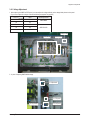
1
PDP-TELEVISION
Chassis : D74A(P_Europe_42SD)_Audi
Model : PS42E7SX/XEC
SERVICE
PDP-TELEVISION
Manual
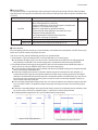
FEATURES
■ DTV Ready PDP TV
■ Supreme Picture Quality
Supreme Convenience Quality
■ RF, HDMI, PC(Analog),
2 Component, 2 Video, S-Video
■ Slim line design
■ Energy Saving
PS-42E7S
This Service Manual is a property of Samsung Electronics Co.,Ltd.
Any unauthorized use of Manual can be punished under applicable
International and/or domestic law.
© Samsung Electronics Co., Ltd. Apr. 2006
Printed in Korea
AA82-03734A
Table of Contents
Chapter 1 Precaution
■ 1-1 Safety Precautions . . . . . . . . . . . . . . . . . . . . . . . . . . . . . . . . . . . . . . . . . . . . . . . . . . . . . . . . . . . 1-1
■ 1-2 Servicing Precautions . . . . . . . . . . . . . . . . . . . . . . . . . . . . . . . . . . . . . . . . . . . . . . . . . . . . . . . . 1-3
■ 1-3 Static Electricity Precautions . . . . . . . . . . . . . . . . . . . . . . . . . . . . . . . . . . . . . . . . . . . . . . . . . . . 1-4
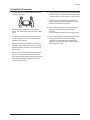
■ 1-4 Installation Precautions . . . . . . . . . . . . . . . . . . . . . . . . . . . . . . . . . . . . . . . . . . . . . . . . . . . . . . . 1-5
Chapter 2 Product Specification
■ 2-1 Product Features . . . . . . . . . . . . . . . . . . . . . . . . . . . . . . . . . . . . . . . . . . . . . . . . . . . . . . . . . . . . 2-1
■ 2-2 Key Features . . . . . . . . . . . . . . . . . . . . . . . . . . . . . . . . . . . . . . . . . . . . . . . . . . . . . . . . . . . . . . . 2-2
■ 2-3 Specifications Analysis . . . . . . . . . . . . . . . . . . . . . . . . . . . . . . . . . . . . . . . . . . . . . . . . . . . . . . . . 2-4
■ 2-4 Accessories . . . . . . . . . . . . . . . . . . . . . . . . . . . . . . . . . . . . . . . . . . . . . . . . . . . . . . . . . . . . . . . . 2-5
Chapter 3 Alignment & Adjustment
■ 3-1 Service Instruction . . . . . . . . . . . . . . . . . . . . . . . . . . . . . . . . . . . . . . . . . . . . . . . . . . . . . . . . . . . 3-1
■ 3-2 How to Access Service Mode . . . . . . . . . . . . . . . . . . . . . . . . . . . . . . . . . . . . . . . . . . . . . . . . . . . 3-2
■ 3-3 Factory Data . . . . . . . . . . . . . . . . . . . . . . . . . . . . . . . . . . . . . . . . . . . . . . . . . . . . . . . . . . . . . . . . 3-3
■ 3-4 Service Adjustment . . . . . . . . . . . . . . . . . . . . . . . . . . . . . . . . . . . . . . . . . . . . . . . . . . . . . . . . . . 3-8
■ 3-5 Software Upgrade . . . . . . . . . . . . . . . . . . . . . . . . . . . . . . . . . . . . . . . . . . . . . . . . . . . . . . . . . . . 3-11
■ 3-6 Replacements & Calibration . . . . . . . . . . . . . . . . . . . . . . . . . . . . . . . . . . . . . . . . . . . . . . . . . . . . 3-12
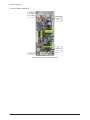
Chapter 4 Exploded View & Part List
■ 4-1 PS42E7SX/XEC . . . . . . . . . . . . . . . . . . . . . . . . . . . . . . . . . . . . . . . . . . . . . . . . . . . . . . . . . . . . . 4-1
Chapter 5 Electrical Part List
■ 5-1 PS42E7SX/XEC Service Item . . . . . . . . . . . . . . . . . . . . . . . . . . . . . . . . . . . . . . . . . . . . . . . . . . 5-1
Chapter 6 Troubleshooting
■ 6-1 First Checklist for Troubleshooting . . . . . . . . . . . . . . . . . . . . . . . . . . . . . . . . . . . . . . . . . . . . . . . 6-1
■ 6-2 Checkpoints by Error Mode . . . . . . . . . . . . . . . . . . . . . . . . . . . . . . . . . . . . . . . . . . . . . . . . . . . . 6-2
■ 6-3 Troubleshooting Procedures by ASS'Y . . . . . . . . . . . . . . . . . . . . . . . . . . . . . . . . . . . . . . . . . . . 6-13
Chapter 7 Block Diagram
■ 7-1 Overall Block Diagram . . . . . . . . . . . . . . . . . . . . . . . . . . . . . . . . . . . . . . . . . . . . . . . . . . . . . . . . 7-1
■ 7-2 Partial Block Diagram . . . . . . . . . . . . . . . . . . . . . . . . . . . . . . . . . . . . . . . . . . . . . . . . . . . . . . . . . 7-3
Chapter 8 Wiring Diagram
■ 8-1 Overall Wiring . . . . . . . . . . . . . . . . . . . . . . . . . . . . . . . . . . . . . . . . . . . . . . . . . . . . . . . . . . . . . . . 8-1
■ 8-2 Partial Wiring . . . . . . . . . . . . . . . . . . . . . . . . . . . . . . . . . . . . . . . . . . . . . . . . . . . . . . . . . . . . . . . 8-2
Chapter 9 PCB Diagram
■ 9-1 Main Board . . . . . . . . . . . . . . . . . . . . . . . . . . . . . . . . . . . . . . . . . . . . . . . . . . . . . . . . . . . . . . . . . 9-1
■ 9-2 Power & IR Board . . . . . . . . . . . . . . . . . . . . . . . . . . . . . . . . . . . . . . . . . . . . . . . . . . . . . . . . . . . . 9-4
■ 9-3 Function Board . . . . . . . . . . . . . . . . . . . . . . . . . . . . . . . . . . . . . . . . . . . . . . . . . . . . . . . . . . . . . . 9-4
■ 9-4 Side AV Board . . . . . . . . . . . . . . . . . . . . . . . . . . . . . . . . . . . . . . . . . . . . . . . . . . . . . . . . . . . . . . 9-4
■ 9-5 Main SMPS Board . . . . . . . . . . . . . . . . . . . . . . . . . . . . . . . . . . . . . . . . . . . . . . . . . . . . . . . . . . . 9-5
■ 9-6 DC-DC SMPS Board . . . . . . . . . . . . . . . . . . . . . . . . . . . . . . . . . . . . . . . . . . . . . . . . . . . . . . . . . 9-6
■ 9-7 PDP Module . . . . . . . . . . . . . . . . . . . . . . . . . . . . . . . . . . . . . . . . . . . . . . . . . . . . . . . . . . . . . . . . 9-7
Chapter 10 Schematic Diagram
■ 10-1 Analog . . . . . . . . . . . . . . . . . . . . . . . . . . . . . . . . . . . . . . . . . . . . . . . . . . . . . . . . . . . . . . . . . . . 10-1
Chapter 11 Operation Instruction & Installation
■ 11-1 Product Features and Functions . . . . . . . . . . . . . . . . . . . . . . . . . . . . . . . . . . . . . . . . . . . . . . . 11-1
■ 11-2 Installation Notes and Precautions . . . . . . . . . . . . . . . . . . . . . . . . . . . . . . . . . . . . . . . . . . . . . . 11-4
Chapter 12 Disassembly & Reassembly
■ 12-1 Overhaul Disassembly & Reassembly . . . . . . . . . . . . . . . . . . . . . . . . . . . . . . . . . . . . . . . . . . . 12-1
Chapter 13 Circuit Description
■ 13-1 Power ON/OFF Signal Timing Sequence . . . . . . . . . . . . . . . . . . . . . . . . . . . . . . . . . . . . . . . . . 13-1
■ 13-2 Partial Block Description . . . . . . . . . . . . . . . . . . . . . . . . . . . . . . . . . . . . . . . . . . . . . . . . . . . . . 13-2
Chapter 14 Reference Information
■ 14-1 Other issues related to other products . . . . . . . . . . . . . . . . . . . . . . . . . . . . . . . . . . . . . . . . . . . 14-1
■ 14-2 Technical Terms . . . . . . . . . . . . . . . . . . . . . . . . . . . . . . . . . . . . . . . . . . . . . . . . . . . . . . . . . . . . 14-3
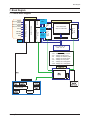
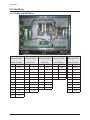
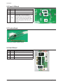
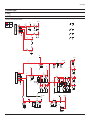
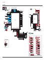
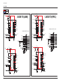
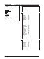
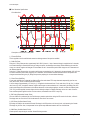
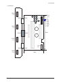
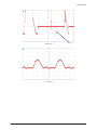
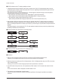
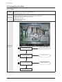
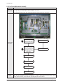
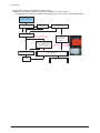
Block Diagram
7. Block Diagram
7-1 Overall Block Diagram
LOGIC CONTROL
DRIVER CIRCUIT & PANEL
Scan
Timing
X Pulse
Generator
852 x 480 Pixels
852 x 3 x 480 Cells
Driver
Timing
Y Pulse
Generator
LVDS
Interface
Display
Data
Row
Driver
DEN
Driver
Timing Controller
HSYNC
DRAM
HSYNC
Data Controller
DCLK
Input Data Processor
R-Data
8,10,12 or 13Bits
G-Data
8,10.12 or 13Bits
B-Data
8,10,12 or 13Bits
Column Driver
Vcc 3V3 Va Vs
Vset Vsc Ve
- 3V3
- Vcc
- Va
- Vs
- Vsc
- Ve
- Vset
Reference
: Voltage for Logic Control
: Voltage for FET driver
: Voltage for address pulse
: Voltage for sustain pulse
: Voltage for scan pulse
: Voltage for X ramp pulse
: Voltage for Y ramp pulse
Image Scaler +
Video Decoder
Micom
Samsung Electronics
7-1
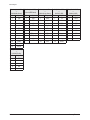
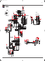
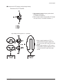
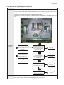
Block Diagram
CN804-1(Main SMPS)
↔
CN102(Main Board)
CN803(Main SMPS)
↔
CN101(Main Board)
CN810(Main SMPS)
↔
CN2013(Logic Board)
CN2(DC-DC SMPS)
↔
CN5007(Y B'D)
CN4(DC-DC SMPS)
↔
CN4001(X B'D)
Pin No.
Signal
Pin No.
Signal
Pin No.
Signal
Pin No.
Signal
Pin No.
Signal
1
5.3V
1
6.5V
1
STBY
1
Vs
1
D5.3V
2
RTN
2
RTN
2
VS_ON
2
Vs
2
Vg
3
N/C
3
12V
3
N/C
3
RTN
3
RTN
4
N/C
4
RTN
4
PS_ON
4
RTN
4
RTN
5
RTN
5
18Vamp
5
RTN
5
Vset
5
Ve
6
RTN
6
18Vamp
6
5.3V
6
RTN
6
RTN
7
12V
7
RTN_amp
7
RTN
7
Vscan
7
RTN
8
PS_ON
8
RTN_amp
8
RTN
8
RTN
8
Vs
9
RTN
9
Vt
9
5.3V
9
Vg
9
Vs
10
STBY
10
RTN
10
5.3V
10
D5.3V
11
FAN_ON
12
FAN_D
CN6(DC-DC SMPS)
↔
CN2509(E-Buffer)
Pin No.
Signal
1
RTN
2
N.C
3
D5.3V
4
N/C
5
Va
7-2
Samsung Electronics
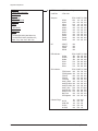
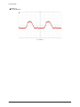
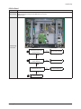
Block Diagram
7-2 Partial Block Diagram
7-2-1 Audio/Video Signal Block Diagram
DDR (16MB )
K 4D263238D
RF Tu n er
SIF
A N A Tu n er
Ren es as
M30620
Flash Memory
144Pin
16K RAM
Vi d eo 1/2
SVP PX
(256-FPGA)
Si d e S.Vi d eo
PC
HDMI
H.P
Au d i o
SW
HC4052
Ser v i c e
EEPROM
3D Comb
Multi Decoder
De-interlacer
Scaler
LVDS Out
WXGA Output
DNIe (Demo)
Caption/TTX2.5
HDMI
10b it p ro c ess
Co m p o n en t 1/2
L VDS
Tx
12b i t
LBE
( SD)
Au d i o Pr o c es s
STV8257
Lip Sync(120ms)
H.P Am p
TDA7050
Au d i o A m p
STA313W
10W
UA RT
MA X3223
7-2-2 DC-DC SMPS Block Diagram
Vs Input Part
Transformer
Control
and
Switching Block
Feedback
Block
Samsung Electronics
Rectification
Block
Vset Output
Auxiliary
Power
Feedback
Block
Transformer
Control
and
Switching Block
Vscan Output
Auxiliary
Power
Transformer
Control
and
Switching Block
Rectification
Block
Rectification
Block
Ve Output
Auxiliary
Power
Feedback
Block
7-3
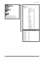
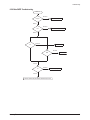
Block Diagram
7-2-3 Module Driver Board Block Diagram
1. Y Drive Board
2. X Drive Board
7-4
Samsung Electronics
Block Diagram
7-2-4 Logic Board Block Diagram
30 Pin Connector
Y-MAIN
CONTROL
SIGNAL
31 Pin LVDS
LVDS SIGNAL
(8~12bit)
10 Pin (Power)
RELAY_EINT
Vs-ON
20 Pin Connector
X-MAIN
CONTROL
SIGNAL
TX, RX
SCL, SDA
5 Pin (uart)
DRIVE
RESET
DDR
(FA)
ASIC
DATA : 32bit
ADDR : 12bit
DQS, CLK, nCLK
DRIVE
nRESET
R,G,B : 24bit
CLK 1, 2
BLK, POC, STB
60 Pin Connector
DDR
(MA)
R,G,B : 24bit
CLK 1, 2
BLK, POC, STB
FM75
60 Pin Connector
7-2-5 Power Block Diagram
Samsung Electronics
7-5
MEMO
7-6
Samsung Electronics
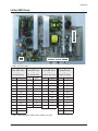
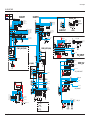
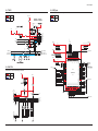
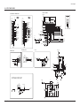
Wiring Diagram
8. Wiring Diagram
8-1 Overall Wiring
※ The ASS'Y code can be changed, see "5 Chapter. Electrical Part List."
Y-BUFFER
CN5401
CN5005
SMPS
-DC
2
CN5000
1
CN5402
CN5003
X-DRIVE
CN809
CN3
Y-DRIVE
CN804-1
CN800
CN803
CN4001
3
CN2
SMPS-MAIN
4
5
CN4004
CN810
CN4
CN5
CN4002
CN4003
CN2008 CN2004
CN5403
CN5004
CN5001
6
CN2009
CN2085
LOGIC BOARD
14
CN5404
CN2010
CN2011
AC-INLET
E-BUFFER
7
CN2508
CN1
MAIN BOARD
12
SIDE AV
No
Assy
8
9
CN741
CN101
F-BUFFER
CN2612
CN611 CN102 CN101
FUNCTION
13
CN2609
CN2608
CN2509
CN330
CN501
CN740
CN001
10
POWER SW
11
SPEAKER
Code No.
Description
-
ASSY PDP MODULE P
BN96-03073A M1,SPD-42D5SD,D71C,V5.0,1000?588,852?480,NTSC/PAL,42"SD
①
ASSY PCB P-SMPS
BN96-03052A PS42E7H,100~240V,245*370mm
②
ASSY PCB P-SMPS
BN96-01856A SPD-50P5HD(DC_DC),200Vin(DC_DC)
③
ASSY PDP MODULE P-X MAIN BOARD
BN96-03101A M1,PL42SD011A,V5.0,852*480,NTSC/PAL,42",SD,LJ92-01340A
④
ASSY PDP MODULE P-Y MAIN BOARD
BN96-03102A M1,PL42SD011A,Y-Main board,V5.0,852*480,NTSC/PAL,42 ",SD
⑤
ASSY PDP MODULE P-Y MAIN SCAN BUFFER
BN96-03103A M1,PL42SD011A,Y-scan buffer,V5.0,852*480,NTSC/PAL,42 ",SD
⑥
ASSY PDP MODULE P-LOGIC MAIN BOARD
BN96-03106A M1,PL42SD011A,logic main,V5.0,852*480,NTSC/PAL,42 ",SD
⑦
ASSY PDP P-ADDRESS E BUFFER
BN96-03104A M1,PL42SD011A,address e-buffer,V5.0,852*480,NTSC/PAL,42 ",SD
⑧
ASSY PDP P-ADDRESS F BUFFER
BN96-03105A M1,PL42SD011A,address f-buffer,V5.0,852*480,NTSC/PAL,42 ",SD
⑨
ASSY PCB MISC-MAIN
BN94-00933B PS-42E7S,EU,D74A,AUDI
⑩
ASSY BOARD P-POWER&IR
BN96-02050D Twister,CT5000-3530A,POWER & IR,Core,No LED Holder
⑪
ASSY SPEAKER P
BN96-02785A 8ohm,Twister,42inch,10W
⑫
ASSY BOARD P-SIDE AV
BN96-03075A AUDI,SJ05-01-430,Side A/V,42E7, With Bracket Shield
⑬
ASSY BOARD P-FUNCTION
BN96-02784A TWISTER,CT5000-3850A,FUNCTION,42V6,With Knob
⑭
FILTER-EMI AC LINE
2901-001374
Samsung Electronics
250V,6A,UL/SA/VDE,0.15uF/1000pF,50x22.5x37.2mm,BK,AE
8-1
Wiring Diagram
8-2 Partial Wiring
8-2-1 PDP Module ↔ SMPS Wiring
①
CN809(Main SMPS)
↔
CN3(DC-DC SMPS)
②
CN2(DC-DC SMPS)
↔
CN5007(Y B'D)
③
CN4(DC-DC SMPS)
↔
CN4001(X B'D)
④
CN6(DC-DC SMPS)
↔
CN2509(E-Buffer)
⑤
CN810(Main SMPS)
↔
CN2013(Logic B'D)
Pin No.
Signal
Pin No.
Signal
Pin No.
Signal
Pin No.
Signal
Pin No.
Signal
1
D5.3V
1
Vs
1
D5.3V
1
RTN
1
STD_5V
2
Vg
2
Vs
2
Vg
2
N.C
2
VS_ON
3
RTN
3
RTN
3
RTN
3
D5.3V
3
N/C
4
RTN
4
RTN
4
RTN
4
N/C
4
PS_ON
5
RTN
5
Vset
5
Ve
5
Va
5
RTN
6
RTN
6
RTN
6
RTN
6
D5.3V
7
RTN
7
Vscan
7
RTN
7
RTN
8
Va
8
RTN
8
Vs
8
RTN
9
Va
9
Vg
9
Vs
9
D5.3V
10
N/C
10
D5.3V
10
D5.3V
11
Vs
12
Vs
8-2
Samsung Electronics
Wiring Diagram
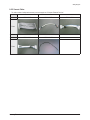
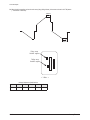
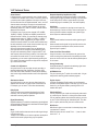
8-2-2 Connect Cables
※ The code number of cable(Lead-connector) can be changed, see "5 Chapter. Electrical Part List."
Use
SMPS 12P
LVDS 31P
POWER 10P
Code
BN39-00632B
BN39-00667D
BN39-00675A
Use
POWER 12P
EMI ONEPOINT WIRE
Code
BN39-00676A
BN39-00164E
Photo
Photo
Samsung Electronics
8-3
MEMO
8-4
Samsung Electronics
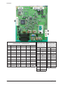
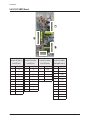
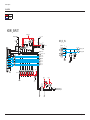
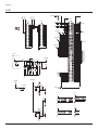
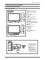
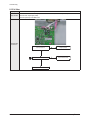
PCB Diagram
9. PCB Diagram
9-1 Main Board
No
Name
Function
Description
① SVP-PX
Scaler IC Controller
SVPTMPX contains dual-purposed triple 10-bit high-precision and
high speed video ADCs for both PC and video inputs, the high
speed HDMI could support all HDMI inputs up to 135MHz with
HDCP format, the highperformance multi-format 3D digital comb
video decoder that supports NTSC, PAL, and SECAM*, a HDTV
sync separator, motion adaptive de-interlacing engine, and the video
format conversion engine, supporting multi-window display in many
different output modes.
② M30840SGP
IC MICOM
With a 16-Mbyte address space, this microcomputer combines
advanced instruction manipulation capabilities to process complex
instructions by less bytes and execute instructions at higher speed.
③ FBE
IC DNIe
Image enhancement IC
④ TCPS3001PD32S(H) TUNER
Tuner CH Tuning
⑤ STA323W
Audio power amplifiers
Samsung Electronics
IC AUDIO-AMP
9-1
PCB Diagram
①
CN2013(Logic B'D) ↔ CN902(Main Board)
Pin No.
Signal
Pin No.
Signal
Pin No.
Signal
1
GND
12
TXOUT2+
23
TXOUT0B-
2
GND
13
GND
24
TXOUT0B+
3
TXOUT-
14
GND
25
4
TXOUT+
15
TXOUTCLK-
26
GND
5
GND
16
TXCLKOUT+
27
SCL_G
6
GND
17
28
GND
7
TXOUT-
18
29
SDA_G
8
TXOUT+
19
TXOUT3-
30
GND
9
20
TXOUT3+
31
10
21
32
GND
22
33
GND
11
9-2
TXOUT2-
②
CN804-1(Main SMPS)
↔
CN102(Main Board)
③
CN803(Main SMPS)
↔
CN108(Main Board)
Pin No.
Signal
Pin No.
Signal
1
5.3V
1
6.5V
2
RTN
2
RTN
3
N/C
3
12V
4
N/C
4
RTN
5
RTN
5
18Vamp
6
RTN
6
18Vamp
7
12V
7
RTN_amp
8
PS_ON
8
RTN_amp
9
RTN
9
Vt
10
STBY
10
RTN
11
FAN_ON
12
FAN_D
Samsung Electronics
PCB Diagram
④
CN740(Main Board)
↔
CN001(Power Button)
⑤
CN501(Main Board)
↔
Speaker Out
⑥
CN741(Main Board)
↔
CN1(Function Board)
Pin No.
Signal
Pin No.
Signal
Pin No.
Signal
1
GND
1
SPK_R+
1
KEY_INPUT1
2
LED
2
SPK_R-
2
KEY_INPUT2
3
ST5V
3
SPK_L+
3
GND
4
GND
4
SPK_L-
5
KEY_INPUT2
6
7
8
IR_7414
Samsung Electronics
9-3
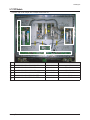
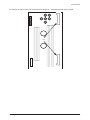
PCB Diagram
9-2 Power & IR Board
No
Loc. No.
①
RM1
Remote Control Sensor
②
SW1
Power Button
OP1
The Illumination sensor that senses the
quantity of light. It senses the illumination and
automatically adjusts the screen brightness
according to the surrounding brightness when
the Power Saving Mode of the User menu is
set to Auto.
③
Description
9-3 Function Board
Function Key. Located on the side of the unit.
9-4 Side AV Board
No
Loc. No.
①
CN102
S-VIDEO2 Input Jack
②
CN103
AV2 Input Jack
③
CN104
Earphone Jack
④
CN105
Side AV Connector
9-4
Description
Samsung Electronics
PCB Diagram
9-5 Main SMPS Board
① CN800 : AC IN (90 ~ 264V)
②
CN804-1(Main SMPS)
↔
CN102(Main Board)
③
CN803(Main SMPS)
↔
CN101(Main Board)
④
CN810(Main SMPS)
↔
CN2013(Logic Board)
⑤
CN809(Main SMPS)
↔
CN3(DC-DC SMPS)
Pin No.
Signal
Pin No.
Signal
Pin No.
Signal
Pin No.
Signal
1
5.3V
1
6.5V
1
STBY
1
5.3V
2
RTN
2
RTN
2
VS_ON
2
Vg
3
N/C
3
12V
3
N/C
3
RTN
4
N/C
4
RTN
4
PS_ON
4
RTN
5
RTN
5
18Vamp
5
RTN
5
RTN
6
RTN
6
18Vamp
6
5.3V
6
RTN
7
12V
7
RTN_amp
7
RTN
7
RTN
8
PS_ON
8
RTN_amp
8
RTN
8
Va
9
RTN
9
Vt
9
5.3V
9
Va
10
STBY
10
RTN
10
5.3V
10
N/C
11
FAN_ON
11
Vs
12
FAN_D
12
Vs
※ CN811, CN804-2 and CN805, CN806, CN807, CN808 are not used.
Samsung Electronics
9-5
PCB Diagram
9-6 DC-DC SMPS Board
①
CN2(DC-DC SMPS)
↔
CN5010(Y B'D)
②
CN4(DC-DC SMPS)
↔
CN4004(X B'D)
③
CN5(DC-DC SMPS)
↔
CN2710(F-Buffer)
④
CN3(DC-DC SMPS)
↔
CN809(Main SMPS)
Pin No.
Signal
Pin No.
Signal
Pin No.
Signal
Pin No.
Signal
1
Vs
1
Vs
1
RTN
1
D5.3V
2
Vs
2
Vs
2
N.C
2
Vg
3
RTN
3
RTN
3
D5.3V
3
RTN
4
RTN
4
RTN
4
N.C
4
RTN
5
Vset
5
Ve
5
Va
5
RTN
6
RTN
6
RTN
6
RTN
7
Vscan
7
RTN
7
RTN
8
RTN
8
Vg
8
Va
9
Vg
9
D5.3V
9
Va
10
D5.3V
10
N.C
11
Vs
12
Vs
9-6
Samsung Electronics
PCB Diagram
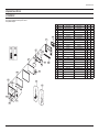
9-7 PDP Module
※ The ASS'Y code can be changed, see "5 Chapter. Electrical Part List."
No
Assy
Code No.
Description
①
ASSY PDP MODULE P-LOGIC MAIN BOARD
BN96-03106A
Logic Main Board
②
ASSY PDP MODULE P-X MAIN BOARD
BN96-03101A
X Drive Board
③
ASSY PDP MODULE P-Y MAIN BOARD
BN96-03102A
Y Drive Board
④
ASSY PDP MODULE P-Y MAIN SCAN BUFFER
BN96-03103A
Y Buffer Board
⑤
ASSY PDP MODULE P-ADDRESS E BUFFER
BN96-03104A
Address Buffer Board
⑥
ASSY PDP MODULE P-ADDRESS F BUFFER
BN96-03105A
Address Buffer Board
Samsung Electronics
9-7
MEMO
9-8
Samsung Electronics
Schematic Diagram
10. Schematic Diagram
10-1 Analog
10-1-1 POWER
This Document can not be used without Samsung’s authorization.
Power
Signal
B5V_VCC
+6V
BD101
IC101
TP102
KIA78D05F
HH-1H4532-121JT
A6.5V
GND
A12V
GND
18Vamp
18Vamp
GND
GND
+33V
GND
1
TP101
TP103
TP104
10
9
8
7
6
5
4
3
2
1
TP105
TP106
TP107
TP108
TP109
I
O
3
SOUND_AMP
SGND
G
C101
100uF
16V
C102
C103
100uF
2
100nF
25V
C104
100nF
D12V
SGND
BD108
SOUND_AMP
SMW250-10 WHT
C132
HH-1H4532-121JT
CN101
SILK
C133
DGND
100nF
25V
100uF
25V
+18V
BD104
HH-1H4532-121JT
PGND
C114
100nF
50V
+33V
BD105
C120
10uF
50V
C121
100nF
50V
B5V
B1.8VD
ACB2012L-015-T
B2.5V_VDD
IC104
BD114
BD106
C122
10uF
AP1117D-25A
HH-1H4532-121JT
3
C129
C125
VIN
ADJ
B12V
1
10uF
16V
470uF
16V
C130
100nF
B8V
C126 C124
VOUT
TP114
2
C127
100uF
16V
C128
100nF
C123
100nF
16V
PX_VD1.8
PGND PGND
100nF 10nF
PGND PGND
PGND
BD107
ACB2012L-015-T
PGND
C131
100nF
25V
CN102
BD109
C166
100nF
100nF
470uF
16V
100nF
25V
200ohm
120uF 1/10W
6.3V
C135
PX_VL1.8
BD110
ACB2012L-015-T
100nF
25V
C138
10uF
16V
100nF
25V
C145
C167
C165
C139
2
10uF
16V
FB
D101
C162
C140
GND
C168
GND
3
C137
8
7
6
5
100nF
25V
OUT
EN
100uF
16V
100uF
16V
C142
IN
MGND1
SW COMP
C161
C136
PGND
SS
BS
IN
100nF
25V
1
1
2
3
4
ACB2012L-015-T
1/10W
-
IC105
MP1583DN
R103
BD113
B9V
IC108
BA178M09FP
R150
C108
100nF
PGND
SILK
TP119
22uH
15Kohm
1/10W 6.8Kohm
C112
22uF
16V
C106 C107
100nF 10nF
L101
1uF
10V
C111
PX_VA1.8
R101
1/10W
10Kohm
R105
2
C141
100uF
25V
TP111
3
100Kohm
OUT
GND
R104
IN
C109
100uF
16V
100uF
16V
BA178M08FP
1
3.3nF
50V
TP121
1
C146
TP118
TP120
100nF 10nF
C160
IC102
TP110
C110 C105
HH-1H4532-121JT
18pF
50V
TP117
BD102
12
11
10
9
8
7
6
5
4
3
2
1
10nF
50V
GND
GND
D12V
PS_ON
GND
STD_5V
TP115
TP116
C134
D5.3V
GND
25V
PGND
PGND
R102
BD115
HH-1H4532-121JT
22ohm
1/10W
XREF
B3.3VD
SW_POWER
IC106
IC107
AP1117D-33A
3
VOUT
VIN
1
ADJ
C147 C148 C143
100uF 100nF 10nF
16V
C149
22uF
16V
C150
100nF
16V
PGND
PGND
Samsung Electronics
B3.3VD_M
A3.3V
A5V
AP1084K33A
2
C144
100uF
16V
TP122
1
OUT
IN
3
BD111
TP123
HH-1H4532-121JT
GND
C151
100nF
2
A3.3V
C152 C153
100uF 100nF
16V 16V
PGND
C154
100uF
16V
C155
100nF
16V
BD112
HH-1H4532-121JT
10-1
Schematic Diagram
10-1-2 MICOM
This Document can not be used without Samsung’s authorization.
A5V
MICOM
HDMI_5V
PC_5V
D201
Signal
1N4148WS-F
Power
DDC_VCC
D202
KDS184
R201
1Kohm
MAIN_KEY_INPUT1
MAIN_KEY_INPUT2
XREF
SC1_D4_CONT1_ID
SC2_D4_CONT3_ID
XREF
MCAD(0:7)
XREF
DDC_WP
XREF
XREF
100ohm
1/10W
100ohm
10uH
50V
1nF
DGND
XREF
IIC_DTV_SEL
COMP_DTV_SEL
XREF
C206
R0200
100ohm
1/10W
R0201
100ohm
1/10W
XREF
R240
0ohm
0ohm
X201
10.0MHz
M30840SGP
50V
22pF
50V
22pF
100nF
IC204
R253
R258
R259
100ohm
B
E
R267
C216
1uF
1
10Kohm
1
MAIN_SCL_EEPROM
SCL_EEPROM
MAIN_SDA_EEPROM
SDA_EEPROM
R276
R279
R281
1
R262100ohm
XREF
XREF
R263
TP_201
100ohm
TP_SCL
TP_SDA
FST3125MX
10ohm
10ohm
10ohm
R283
DGND
IC205
XREF
LVDS_EN
8257_RESET
SCL_STV8257
R261 10Kohm
C
14
13
12
11
10
9
8
10ohm
VCC
/OE1
/OE4
1A
4A
1B
4B
/OE2
/OE3
3A
3B
2A
2B
GND
1
2
3
4
5
6
7
REEFF
XXR
MAIN_KEY_INPUT1
KEY_INPUT1
DOWNLOAD_SCLK
DOWNLOAD_BUSY
DOWNLOAD_EPM
DOWNLOAD_CE
REEFF
XXR
MAIN_KEY_INPUT2
KEY_INPUT2
DOWNLOAD_TXD
DOWNLOAD_RXD
1
R274
R277
10ohm
10ohm
R280
10ohm
R282
TP_GND
10ohm
XREF
B
E
10ohm
10ohm
2
4
6
8
2
4
6
8
MCA(0:21)
R232
MCA(0)
MCA(1)
MCA(2)
MCA(3)
MCA(4)
MCA(5)
MCA(6)
MCA(7)
OE
MCA(0:21)
10ohm
10ohm
10ohm
10ohm
10ohm
0ohm
10ohm
R271
R273
R275
R278
1
1
1
0ohm
DIR
/OE
A1
B1
B2
A2
A3
B3
A4
B4
A5
B5
A6
B6
A7
B7
B8
A8
GND
B3.3VD_M
MCAD(5)
BD201
MCAD(4)
2.2uH
XREF
XREF
MCAD(3)
DELETE OPTION
74LCX245MTCX
VCC
MCAD(0:7)
MCAD(7)
MCAD(6)
XREF
DOWNLOAD_CE
RESETN
BUSY
IC203
XREF
20
19
18
17
16
15
14
13
12
11
MCA(9)
MCA(10)
MCA(11)
MCA(12)
MCA(13)
MCA(14)
MCA(15)
MCA(16)
MCA(17)
MCA(18)
MCA(19)
MCA(20)
MCA(21)
10ohm
0ohm
XREF
R239
CSN
MCA(8)
10ohm
10uF
16V
MCA(19)
MCA(18)
1
2
3
4
5
6
7
8
9
10
MCAD(2)
MCAD(1)
C210
100nF
C211
22uF
MCAD(0)
CE
XREF
OE
SVPD(0:7)
XREF
DELETE OPTION
R250
R251
1M
R252
R256
R260
10ohm
1/10W
XREF
10ohm
10ohm
R265
R266
XREF
10ohm
R270
CS1
CE
CSN
XREF
OE
XREF
MICOM_RXD
MICOM_TXD
XREF
10ohm
10ohm
10ohm
10ohm
47ohm
ALE
XREF
R272
DELETE OPTION
XREF
1
1
B5V_VCC
B3.3VD_M
R286
R292
4.7Kohm
R290
4.7Kohm
C
XREF
SCL_EEPROM
SDA_EEPROM
XREF
100ohm
Q203
C215
XREF
XREF
KSC1623-Y
100nF
XREF
10ohm
R247
R252
EEPROM_WP
R257
100ohm
RESET_IN
SDA0
SCL0
SDA1
XREF
SCL1
R248
R249
R250
R251
R256
1 TP202
1
SDA
XREF
XREF
4.7Kohm
8
7
6
5
2
4
6
8
2
4
6
8
DELETE OPTION
XREF
100nF
R264
VSS
XREF
SDA_STV8257
MAIN_SDA_EEPROM
MAIN_SCL_EEPROM
2
4 RA212
6 100ohm
8 1/16W
TP210
SCL
1
3
5
7
3
5
7
RA211 1
3
5
7
100ohm
E2
XREF
RA209 1
2
4 RA210
6 100ohm
8 1/16W
R268
R269
VCC
/WC
L203
10uH
E0
E1
XREF
3.3Kohm 3.3Kohm
M24C32-W MN6T
1
2
3
4
XREF
100ohm
100ohm
A5V
1
3
5
7
XREF
7
5
3
1
C214
R226
R227
R228
R229
R231
R205
XREF
PC_V_SYNC
INT#
SOUND_SEL1
SOUND_SEL2
IDENT_HP
R255
DELETE OPTION
C209
R244
100ohm
R254
4.7Kohm
XREF
RESETN
A3.3V
IC202
R241
C213
XREF
C212
MICOM_RESET
R222
4.7Kohm
1
RA2073
5
7
1
RA2083
5
7
MAIN_MICOM
100ohm
100ohm
HC-49/SM5H(10MHz,30ppm)
R0212
4.7Kohm
MCA(0:21)
IC201
MCA(0:21)
C208
1/16W 8
100ohm 6
RA213 4
2
IR_CNTR
XREF
3.3Kohm
47ohm
0ohm
0ohm
0ohm
0ohm
R234
R236
R238
XREF
SOUND_SEL3
CONTROL2
B3.3VD_M
R223
R218
DGND
R230
100ohm
3.3Kohm
4.7Kohm
22uF
16V
2
4 RA206
6 100ohm
8 1/16W
1Kohm
R219
R220
DGND
2N7002L
1
3
5
7
DELETE -> R225(ONLY 4M FLASH)
DELETE -> R242
L202
1nF
5n
0V
1
F
50V
C207
XREF
IR
C202
C203
R225
R221
Q202
10Kohm
1/10W
10Kohm
IR_CNTR
FLASH
R224
0ohm
XREF
RA203
DNI_RESET
BUSY
B3.3VD_M A3.3V
B3.3VD_M
25V
100nF
R208
R209
R215
R216
100ohm
R217 4.7Kohm
10Kohm
10Kohm
C201
100nF
R245
XREF
IR_DTV
3.6Kohm
4.7Kohm
22uF
3.6Kohm
B3.3VD_M
1
3
5
7
C204
R214
1
3
5
7
1
3
5
7
1
3
5
7
1
3
5
7
DGND
R0210
C205
RA20510ohm
R0211
R213
10ohm RA204
100ohm
100ohm
1/16W
XREF
XREF
R207
10Kohm
R206
22Kohm
DGND
XREF
100ohm
1/16W
L201
10uH
Q201
XREF
RA202
XREF
DTV_AGC
R210
XREF
TXD_MICOM
RXD_MICOM
B3.3VD_M
SDA0
SCL0
MICOM_RESET
SW_POWER
2
4
6
8
2
4
6
8
2
4
6
8
2
4
6
8
XREF
XREF
2
4 RA201
6 100ohm
8 1/16W
1
2
3
4
5
1
1
1
1
1
E
KSC1623-Y
XREF
DOWNLOAD_SDA
DOWNLOAD_SCL
RESET
U201
GND
B
10Kohm
TUNER_AFT
C
4.7Kohm
MICOM__TUNER_RST
*
4.7Kohm
1/10W
R242
XREF
TEST202
MCAD(0)
MCAD(1)
MCAD(2)
MCAD(3)
MCAD(4)
MCAD(5)
MCAD(6)
MCAD(7)
XREF
R202
10Kohm
R287
R293
4.7Kohm
IR_CNTR
10Kohm
R284
47Kohm
Q204
R291
4.7Kohm
KSC1623-Y
Q205
XREF
SCL2
2N7002L
Q207
XREF
2N7002L
B3.3VD_M
RA215
4.7Kohm
1/16W
XREF
SCL2_3.3V
XREF
SDA2_3.3V
B5V_VCC
100nF
7
5
3
1
RA214
4.7Kohm
1/16W
7
5
3
1
P2.4
P2.3
XOUT
P2.2
XIN
P2.1
TEST
P2.0
P1.3/AD3
100ohm
MICOM_RXD
XREF
RA220
XREF
100ohm
1/16W
XREF
R312
R313
R314 1/10W
R317
XREF
XREF
SVP_RESET
MICOM_RESET
HDMI_HOT_PLUG_A
MUTE_AMP
33ohm
XREF
R285
4D1
/1Q
/4Q
2D0
3D0
2D1
3D1
/3Q
/2Q
GND
1
2
3
4
5
6
7
8
XREF
XREF
R2 33
R235
0ohm
0ohm
XREF
R237
0ohm
XREF
UART_SEL
LOGIC_TXD
MICOM_TXD
R297
10Kohm
Q212
R298
0ohm
2N7002L
LOGIC_RXD
R299
Q211
VCC
GND
T1OUT
C2+
R1IN
C2-
R1OUT
V-
T1IN
T2OUT
T2IN
R2IN
R2OUT
16
15
14
13
12
11
10
9
DGND
R288
R289
100ohm
100ohm
XREF
XREF
C223
UART_SEL
1D1
5
6
7
8
10Kohm
V+
C1-
50V
1nF
XREF
100ohm
1/16W
SEL
1D0
R2 03
R295
4.7Kohm
C1+
C222
RA218
SERVICE_ANY_TX
SERVICE_ANY_RX
0ohm
2N7002L
DGND
SW_POWER
DGND
DGND
VSS2
VDD2
2
4
6
8
2
4
6
8
VCC
/OE
4D0
2
3
R319
C233
D204
KDS184
S_MUTE
1
3
5
7
1
3
5
7
100ohm
100ohm
0ohm
100ohm
16
15
14
13
12
11
10
9
R296
4.7Kohm
100nF 4
12
13
14
15
16
17
18
19
20
21
22
P1.2/AD2
P0.2/TM2CAP
33
32
31
30
29
28
27
26
25
24
23
74LCX157MX
C221
50V
1nF
P3.4/PWM4(2)
P3.2/PWM2/SCL1(2)
P3.3/PWM3/SDA1(2)
NC
P3.6/PWM6(2)
P1.4/VSYNC-O
P1.5/HSYNC-O
HSYNC-I(2)
P3.5/PWM5(2)
P2.6
P2.5
VDD1
50V
22pF
50V
22pF
1/10W
4.7Kohm
P1.6/CLAMP-O
SDAT(1)/SDA0(2)
SCLK(1)/SCL0(2)
VSS1
P0.3(2)
C231
C230
R316
24.0MHz
P3.0/PWM0
P2.7
P1.1/AD1
X202
4C-49/SM5H,24MHZ,16PF
P3.1/PWM1
IC207
S3F866B
P1.0/AD0
XREF
XREF
P0.1/INT1
NC
SDA0
SCL0
P0.0/INT0
P0.6(2)
XREF
2
4 RA219
6 100ohm
8 1/16W
VSYNC-I(2)
P0.5(2)
1
3
5
7
1
2
3
4
5
6
7
8
9
10
11
P1.7/CSYNC-I(SOG)
1Kohm
1/10W
P0.4(2)
A3.3V
XREF
IDENT_SIDE_SVHS
NRESET
R311
IR
44
43
42
41
40
39
38
37
36
35
34
1nF
50V
2
3
XREF
22uF
16V
IDENT_PC
IDENT_COMP2
IDENT_COMP1
IC210
100nF 1
C226
XREF
100ohm
1/16W
XREF
C229
C239
22uF
16V
100nF
RA217
C241
100nF
25V
C220
B5V_VCC
C238
C240
B3.3VD_M
R294
4.7Kohm
4.7Kohm
HDMI1_DET
IDENT_SIDE_AV
50V
100pF
XREF
XREF
R20 4
C237
RA216
100ohm
1/16W
IC206
MAX232ECWE
MUTE_HP
50V
100pF
0ohm
XREF
R246
R307
R308
2
4
6
8
2
4
6
8
4.7Kohm
0ohm
C218
B3.3VD_M
DGND
1
3
5
7
1
3
5
7
D210 C2 17
BZX84C5V6LT1 100nF
8
6
4
2
10Kohm
2.7Kohm
2.7Kohm
22uF
16V
10Kohm
10Kohm
C228
16V
100nF
8
6
4
2
C227
1
R303
R304
R300
R301
SUB_MICOM
R302
A3.3V
SDA2
RLZ5.6B-TE-11
16V
100nF
XREF
D205
KDS184
B3.3VD_M
A3.3V
1
3
5
7
2
4 RA221
6 100ohm
8 1/16W
XREF
XREF
REEFF
XXR
IDENT_AV1
KEY_INPUT1
KEY_INPUT2
LED_RED
R322
R323
IC209
10Kohm
4.7Kohm
D208
R321
R324
C235
1001n0FKohm
1/10W
C234
1uF
DELETE OPTION
470ohm
A5V
XREF
SUBMICOM_RESET
DS1834AS/T.R
1
2
3
4
5VIN
3.3VIN
/5V_RST
/3.3V_RST
5V_TOL
3.3V_TOL
GND /PBRST
8
7
6
5
1
U202
C236
1
R325
0ohm
1/10W
Samsung Electronics
50V
10nF
TP203
10-2
Schematic Diagram
10-1-3 IN_OUT_JACK
This Document can not be used without Samsung’s authorization.
Power
Signal
R343
1
R342
0ohm
XREF
18Kohm
R344
75ohm
R347
75ohm
R349
75ohm
XREF
XREF
R358
6.8Kohm
D353
D354
3
D352
3
D351
3
R355 R356 R357
75ohm 75ohm 75ohm
XREF
3
1.6Kohm
3
R328
XREF
D355
D320
A5V
D321
XREF
C341
47pF
D335
R361
100ohm
C337
100pF
D337
D336
C334
100pF
R345
18Kohm
R346
100ohm
R350
100ohm
XREF
$V
D348 D394
D349
C339
47pF
CDS3C30GTH
R352
6.8Kohm
XREF
R353
75ohm
D360
100ohm
XREF
PC_IN
SC2_AV1_C
MMBD4148SE
B5V
C342
47pF
R363
75ohm
D338
D339
CDS3C30GTH
CDS3C30GTH
XREF
R367
75ohm
XREF
1
1
D367
XRE F
R370
TP320
10Kohm
75ohm 75ohm
TP3241
TP356
1 TP357
TP314
R377
22ohm
1
TP323
R374
R376
C346
100nF
DDC_WP
VC C
1
2
3
4
E0
E1
TP315
MODE,/WC
SCL
E2
SDA
VSS
C343
C344
330pF
BD300
CIM10J121NC
R326
10Kohm
XREF
PC_H_SYNC
C370
100pF
3
3
3
D364
PC_SR_IN
PC_SL_IN
22ohm
R380
TP317
RE0
Fohm
4X7
CDS3C30GTC
HDS3C303
G3
T0
HpF
XR EF
75ohm
100ohm
RE0
Fohm
4X7
R368
D363
PC_5V
R378
R379
R366
1
TP353
XREF
TP358
1
3722-001061
IDENT_PC
1
TP352
1 TP321
AT24C02N-10SC
75ohm
1
IC330
8
7
47oh6m
47oh5m
1
10Kohm TP322
TP390
4
9
10
5
6
8
7
DDC_VCC
C345
10uF
R373
75ohm
R369
2
1
2
1
2
1
D366
R375
1
PC_RED
PC_GREEN
PC_BLUE
3
3
3
1
D365
TP316
1
TP380
1 TP381
TP378
XREF
75ohm
MMBD4148SM
EMBD4148SM
EMBD4148SE
TP355
3
1
1
TP354
3
JA342
1
SUPLVAL
75ohm
R365
U1018
1
MGND2
COMP2_INPUT(ASIA)
6
1
11
7
2
12
8
3
13
9
4
14
10
5
15
PC_S_IN
JA334
R364
R372
R371
1
COMP1_INPUT(ASIA)
U1019
BD301
D374
D373
1
C347
100pF
2
1
2
D372
1
2
1
2
D371
TP382
C 348
100pF
0ohm
RED
DDC_VCC
1
U1015
PC_V_SYNC
PC_SDA
MMBD414
M8M
SB
ED414M8M
SE
BD414
M8M
SB
ED4148SE MMBD4148SE
TP379
XREF
PC_SCL
1
WHT
D370
1
1
2
1
CIM10J121NC
PC_INPUT
C371
100pF
R327
10Kohm
1 TP383
1 U1016
GRN
XREF
IDENT_COMP2
100ohm
1
TP384
1 TP385
1
U1017
470ohm
R383
R305
ACB2012L-015D
-TELETE
BD310
GRN
1
1
R382
U330
BLUE
1
R397
RED
BLUE
1
XREF
DDC_VCC
R360
SC1_AV1_CVBS_IN
MGND1
WHT
1
SERVICE_ANY_RX
SERVICE_ANY_TX
100ohm
1
SC2_CVBS_AV1_Y
JA335
U1014
100ohm
X REF
R340
1
C 338
100pF
SC1_CVBS_OUT
RED
RED
1
1
R337
1
TP334
5
105-15202N330
TP377
RX_DTV_SVC
TX_DTV_SVC
TP332
AUDIO OUT
SC2_D4_CONT3_ID
SC2_AV_CVBS_OUT
CDS3C30CGDTSH3C30GTH
JA336
TP389
DELETE OPTION
C336
100pF
X REF
C340
100pF
D359
C335
100pF
75ohm
R348
1
D395
RLZ16C
R362
75ohm
D358
D334
1
4
6
0ohm
XREF
4
9
10
5
6
8
7
2
0ohm
R446
CDS3C30GTC
HDS3C30GTC
HDS3C30GTC
HDS3C30GTH
CDS3C30GTH
XREF
470ohm
XREF
D322
R351
75ohm
1/10W
TP346
TP347
470ohm
330oh m
R341
XREF
CDS3C30GTC
HDS3C30GTC
HDS3C30GTH
75ohm
R359
TP343
SC1_D4_CONT1_ID
SC1_B_COMP2_Pb
SC1_G_COMP2_Y
SC1_R_COMP2_Pr
SC1_FB
R336
R 339
XREF
2
1
2
1
2
1
2
1
2
R354
2.2Kohm
1
1 1 1
1 1 1
1
1
TP350
TP351
1 1
TP348
TP349
C332
100pF
C331
100pF
100pF
TP310
TP311
1
2
3
4
5
6
7
8
9
10
11
12
13
14
15
16
17
18
19
20
21
D333
D332
CDS3C30GTC
HDS3C30GTC
HDS3C30GTC
HDS3C30CG3T3H0
1 1
TP345
D331
TP335
TP336
3
D330
TP340
TP341
TP342
TP344
TP330
TP331
TP333
U1020
1 TP387
1
3
R445
XRE F
SUPLVAL
JA341
ANY_SC2_SR_OUT
SC2_AV1_SR_IN
ANY_SC2_SL_OUT
SC2_AV1_SL_IN
1
XREF
XREF
WHITE
470ohm
C333
100pF
330ohm
RED
XREF
R338
JA333
R334
2
XREF
JA331
RLZ16C
330ohm
1 1 1
470ohm
1 1
R333
R335
JA332
SC1_SR_OUT
SC1_COMP2_SR_IN
SC1_SL_OUT
SC1_COMP2_SL_IN
1
330ohm
XREF
1
2
3
4
5
6
7
8
9
10
11
12
13
14
15
16
17
18
19
20
21
Service_ANY
47Kohm
1/10W
R332
TP337
TP338
TP339
SCART2
SCART1
R331
1
47Kohm
1/10W
1 1
R330
TP386 0ohm
OPTION
XREF
AV2_SIDE_Y
A5V
D329
3
TP312
2
1
DELETE OPTION
BD311
ACB2012L-015-T
XREF
AV2_SIDE_C
XREF
IDENT_SIDE_SVHS
R309
R310
R381
1 U332
R396
R395
3
SIDE_AV
470ohm
R384
0ohm
0ohm
0ohm
AV (ASIA)
A5V
2
1
D375
0ohm
0ohm
1 U331
JA338
R385
WHITE
1 TP326
5
1
C349
330pF
R389
75ohm
D376
U1006
A5V
6
4
D377
R390
75ohm
C350
330pF
SIDE_SVIDEO INPUT
D378
XREF
A5V
D328
3
3
1
2
1
1 U1021
IDENT_AV1
1
0ohm
1 U1005
2
2
CDS3C30GTC
HDS3C30GTH
R306
YELLOW
100ohm
TP359
U1008
1
3
RED
1
8
9
7
TP360
1
R391 470ohm
XREF
R392 470ohm
XREF
TP361
1
JA339
COMP1_INPUT(EU)
R393
DELETE OPTION
TP362
BD312
RED
1
READY DELETE
6
4
TP370
1
TP371 1
WHITE
FT330
SGM32F1E104-2A
3
C355
100uF
16V
100nF
25V
470
XRo
Eh
Fm
C351
330pF
TP373
R329
R405 47ohXm
REF
0ohm
R407
1
R410
R409
XREF
XREF
XREF
HD1IN
HDSYNC
G1IN
HD2IN
HDOUT
GND
ROUT
B1IN
GND
VCC
GOUT
R2IN
VIDEOIN
GND
SYNCOUT
G2OUT
CTL
BOUT
GND
B2IN
VD1IN
VDOUT
VD2IN
4.7Kohm
1/10W
24
23
22
21
20
19
18
17
16
15
14
13
XREF
100
XRo
Eh
Fm
C411
R415
75ohm
R414
75ohm
33pF
50V
D390
C412
D391
CDS3C30GTH
33pF
50V
C362
100pF
CDS3C30GTH
C363
100pF
75ohm
COMP1_Pr
COMP1_Pb
IDENT_COMP1
COMP1_Y
1
2
3
4
5
6
7
8
9
10
11
12
13
14
XREF
D381
A5V
D382
D383
C353
330pF
CDS3C30GTC
HDS3C30GTC
HDS3C30GTH
SIDE_AV INPUT
75ohm
C352
330pF
D398
XREF
XREF
1/10W
100ohm
DTV_COMP1_Pr
DTV_COMP1_Y
R398
XREF
D393
A5V
CDS3C30GTH
D399
CDS3C30GTH
D400
CDS3C30GTH
R411
TP364
R 406
1
DTV_COMP1_Pb
100ohm
XREF
TP365
R408 47ohm
1
TP366
XREF
XREF
C
B
E
R0302
10Kohm
1/10W
XREF
COMP_DTV_SEL
D392
AGND_IN
A5V
D388
D389
TUNERGND
R416
1Kohm
2
1
CDS3C30GTC
HDS3C30GTH
C364
330pF
AGND_IN
SIDE_HP
HP_OUT_R
3
Q301
KSC1623-Y
IDENT_HP
HP_OUT_L
47oh m
1
READY DELETE
IDENT_SIDE_AV
D384 R399
EU_OPTION
3
R1IN
R413
75ohm
33pF
50V
2
XREF
XREF
C356 1
10uF 2
C357 3
10uF 4
C358 5
10uF 6
C359 7
10uF 8
C360 9
10uF10
C36111
10uF12
C410
1
XREF
1TP327
TP375
1
1TP376
75ohm
XREF
R0301
IC331
BA7657F
DTV_Pr_R
DTV_Y_G
DTV_Pb_B
COMP1_Pr
COMP1_Y
COMP1_Pb
0ohm
R412
R403
AV2_CVBS
R394 100ohm
1
CN330
SMW250-14
0ohm
1/10W
0ohm
1/10W
0ohm
1/10W
R402
COMP1_SL_IN
1
TP374
R400
XREF
TP363
TP372
1
DTV DELETE
ACB2012L-015-T
COMP1_SR_IN
3
C354
R404
2
3
1
2
470
XRo
Eh
Fm
2
1
R401
1 TP325
1
B5V_VCC
5
SIDE_AV_SR_IN
SIDE_AV_SL_IN
75ohm
DGND_IN
C365
330pF
R417
1Kohm
C366
330pF
AGND_IN
Samsung Electronics
10-3
Schematic Diagram
10-1-4 HDMI
This Document can not be used without Samsung’s authorization.
Power
Signal
HDMI_INPUT
DDC_VCC
XREF
XREF
R430
10Kohm
D430
D431
C431
100nF
TP440
TP443
R432
R433
1
1
DGND_IN
DGND_IN
DGND_IN
2
3
KSC1623-Y
B
3
C
3
1/10W
1 Kohm
R 43 4
10Kohm
DELETE OPTION
TP432
1
3
DGND_IN
47Kohm
2
1
TP430
1
R441
47X0RoEFhm
R444
47X0RoEFhm
4
6
5
DVI_SL_IN
TP431
1
HDMI1_DET
D434
D435
C432
0TpHF
CDS3C30GTC
HDS3C3
303G
DVI_SR_IN
C433
330pF
3
3
D444
A5V
D445
2
1
D443
2
3
D442
1
D441
2
D440
1
1
D439
2
1
3
D438
2
MMBD4148SE
1
DGND_IN
JA430
HDMI_RX2HDMI_RX2+
2
10ohm
10ohm
VSS
1
HDMI_RX1HDMI_RX1+
3
R466
R467
SDA
IC430
AT24C02N-10SC
HDMI_RX0HDMI_RX0+
1
10ohm
10ohm
E2
1
HDMI_HOT_PLUG_A
3
R464
R465
E1
SCL
1
2
3
4
HDMI_RXCLKHDMI_RXCLK+
2
10ohm
10ohm
E0
MODE,/WC
56ohm
5/61o0hW
m
1
1/10W
1Kohm
1/10W
R439
1
R462
R463
DGND_IN
3
10ohm
10ohm
R437
R438
2
R460
R461
DVI_S_IN
TP442
VCC
E
3
R440 0ohm
47ohm
47ohm
8
7
6
5
TP444
R435
R436
TP441
1
1
1
2
D432
2
DGND_IN
C430
10uF
16V
R431
10Kohm
WHITE
D433
RD8.2MB
1
RLZ6.2B
DDC_WP
RED
HDMI_5V
C402
1uF
10V
D421
RLZ5.6B-TE-11
A5V
B3.3VD
DGND_IN
DGND_IN
C401
IC401
D420
NC7WBD3125K8X
U1022
TP1433
1
10-4
1
2
3
4
/OE1
VCC
1A
/OE2
2A
1B
GND
2B
8
7
6
5
16V
100nF
R451
R452
4.7Kohm
1/10W
4.7Kohm
1/10W
R453
R454
22ohm
22ohm
XREF
XREF
HDMI_DDC_SCL
HDMI_DDC_SDA
Samsung Electronics
Schematic Diagram
10-1-5 SOUND
This Document can not be used without Samsung’s authorization.
Power
Signal
B5V_VCC
SOUND
R501
10Kohm
1/10W
10Kohm
Q501
KSC1623-Y
C
R595
SOUND_SEL3
B
E
B8V
READY DELETE
L513 10uH
C504
100nF
C501
22uF
16V
C502
100nF
R513
68Kohm
R517
100ohm
XREF
DTV_LtO
XREF
R518
100ohm
COMP1_SR_IN
XREF
R520
100ohm
DTV_RtO
XREF
R522
100ohm
C506
C50910uF 16V
0ohm
R515
0ohm
1
2
3
4
5
6
7
8
C51110uF 16V
10uF 16V
READY DELETE
R514
PC_SL_IN
R516
READY DELETE
R529
R531
R528
68Kohm
0Y
VDD
2Y
2X
Y-COM 1X
3Y X-COM
1Y
0X
/EN
3X
VEE
A
VSS
B
16
15
14
13
12
11
10
9
10uF 16V
R519
100ohm
C508
100ohm
C51010uF 16V
R523
100ohm
XREF
DVI_SL_IN
XREF
100ohm
R527
100ohm
DVI_SR_IN
XREF
1
2
3
4
5
6
7
8
10uF 16V
R526
XREF
B5V_VCC
C51210uF 16V
XREF
HDMI_SR_IN
IC501
C505
R521
HDMI_SL_IN
PC_SR_IN
100ohm
XREF
C50710uF 16V
R509
R508 68Kohm
68Kohm
R506
R504 68Kohm
68Kohm
R502
68Kohm
DTV DELETE
R511
68Kohm
READY DELETE
COMP1_SL_IN
R507
68Kohm
R503
R505
68Kohm 68Kohm
R512
68Kohm
R510
68Kohm
C513
C51410uF 16V
10uF 16V
0Y
2Y
16
15
14
13
12
11
10
9
VDD
2X
Y-COM 1X
3Y X-COM
1Y
0X
/EN
VEE
3X
A
VSS
B
R525
10Kohm
R524
10Kohm
R593
B
IC502
68Kohm
R530
68Kohm
Q502
KSC1623-Y
C
MM74HC4052M
68Kohm
R535
R537
68Kohm 68Kohm
R533
68Kohm
READY DELETE
R532
68Kohm
Q503 E
KSC1623-Y
R539
68Kohm
R534
68Kohm
B1.8VD
L502
B8V
C516 C517
C522
R542
C518
16V
10uF
R541
B
XREF
TUNER_SIF
I2S_DATA_AMP
I2S_LRCLK_AMP
I2S_SCLK_AMP
XREF
XREF
C529
220nF
100nF
100nF
SGNDC525 C527
Q504
KSC1623-Y
E
50V
100pF
100uF
16V
C528
560ohm
1/10W
SGND
C523
C524
C526
100nF
R540
SGND
SGND
C521
B3.3VD
C520
100uF
16V
10nF
50V
10uH
16V
10uF
4.7Kohm
1/10W
22uF
16V
L503 10uH
10uH
C519
L501 10uH
1.5nF 470pF
C515
C
SOUND_SEL2
10Kohm
R538
68Kohm
B5V_VCC
SC1_SL_OUT
SOUND_SEL1
10Kohm
R594
C
B
R536
68Kohm
POP NOISE SOLUTION
E
MM74HC4052M
XREF
SGND
B3.3VD
C531 C532
C534
470pF 1.5nF
47nF
10Lu5H05
100nF 100nF
C530
47Kohm
1/10W
SC1_SL_OUT
XREF
XREF
10uF
16V
C535
R543
R544
10uF
SC1_SR_OU
T
16V
C536
100ohm
100ohm
XREF
100uF
16V
I2S_CLK_AMP
B1.8VD
SGND
B
R546
E
SC1_COMP2_SL_IN
SC1_COMP2_SR_IN
47Kohm
1/10W
R545
R547
10uF 16V
10uF 16V
XREF
100ohm
100ohm
27.0MHz
C545
C547 16V
C548
10uF
Q506
KSC1623-Y
R553
E
C555
ANY_SC2_SL_OUT
ANY_SC2_SR_OUT
C
B
C556
R560
R554
100ohm
100ohm
1Kohm
R555
C557
C559
B5V_VCC
0ohm
BD510
SGND
BD511
C561
33nF
16V
C562
33nF
16V
SDA_STV8257 SGND
SGND
47ohm
R561
XREF
47ohm
R562
XREF
HP_L
SGND
HP_R
B1.8VD
B3.3VD
C565
330uF
16V
10Kohm
D506
R563
SCL_STV8257
C564
100nF
SGND
R564
R565
C569
470nF R566
20Kohm
C571
470nF R569
20Kohm
LM4810MM
10Kohm
1/10W
C573
B
E
10Kohm
1/10W
MUTE_AMP
10Kohm
1/10W
MUTE_HP
C568
C570
1
XREF
HP_OUT_L
TP502
1
XREF
HP_OUT_R
R574170Kohm
C574
4.7nF
R572
C
100uF
16V
100uF
16V
R570 100Kohm
4.7uF
S_MUTE
C567
SGND
C572
10Kohm
1/10W
MUTE_HP
R597
TP501
100uF
16V
Q509
KSC1623-Y
R567
POP_MUTE
10Kohm
1/10W
Q508
KSA1182
IC504
100Kohm
SGND
POP_MUTE
KDS184
100Kohm
C563
100nF
L508
10uH
SGND
B
100nF
SGND
4.7Kohm
R559
E
C551
100nF
R558
10uF 16V
XREF
R557 100ohm
C
C0500
1uF
10V
100nF
R556 100ohm
10uF 16V
16V
10uF
SPDIF_OUT
DTV_SPDIF
8257_RESET
XREF
C554
47Kohm
1/10W
XREF
XREF
XREF
100ohm
100ohm
10uF
16V
C560
XREF
R591
R592
R551
100ohm
100ohm
R552
XREF
C558
E
R549
10uF 16V
10uF 16V
XREF
SIDE_AV_SL_IN
SIDE_AV_SR_IN
Q507
KSC1623-Y
10uF
100nF
10uF16V
C553
XREF
XREF
SGND
ANY_SC2_SR_OUT
C550
SGND
C552
SC2_AV1_SL_IN
SC2_AV1_SR_IN
47Kohm
1/10W
MPZ2012S300A
B
10uF
16V
SGND
C549 16V
MPZ2012S300A
C
C546
10uH L507
22pF
100nF
SGND
B1.8VD
X501
IC503
XREF
C544
ANY_SC2_SL_OUT
22pF
B
C
C537
C543
E
SC1_SR_OUT
C538C539 C540 C541C542
100n1
F00nF
100nF 100nF 100nF 10uH L506
Q505
KSC1623-Y
C
SGND
4.7nF
SGND
SGND
R573
Q511
KSC1623-Y
R596
SGND
+18V
B3.3VD
SOUND AMP
BD501
C577
C578
100nF
25V
100nF
25V
C575
470uF
25V
SOUND_AMP
C584
C583
100nF
10uF
100nF
36
22uF
B3.3VD
35
VCCSIGN
34
VSS
33
0ohm
0ohm
0ohm
I2S_SCLK_AMP
I2S_LRCLK_AMP
I2S_DATA_AMP
SOUND_AMP
R578
R579
R580
32
30
LRCKI
29
SDI
27
XREF
I2S_CLK_AMP
26
R586
25
10Kohm
R585
SDA1
SCL1
R583
R584
1/10W
1/10W
100ohm
100ohm
24
23
22
1/10W
21
100ohm
20
R589
C599
3.9Kohm
1/10W
1uF
10V
D505
19
3
4
N.C.
5
GND
VICKI
28
XREF
7
GND2A
L521
22ohm
1/10W
SOUND_AMP
9
1
10
12
C610
13
220pF
50V
100nF
50V
14
15
100nF
50V
L522
C596
SOUND_AMP
C594
R588
SOUND_AMP
100nF
50V
L523
C601
22ohm
1/10W
L512
(22uH)
1
+18V
SGND
R576
4.7ohm
1/4W
C590
100nF
50V
R581
470nF
100nF
50V
C588
SOUND_AMP
SOUND_AMP
CN501
C592
4.7ohm
1/4W
100nF
50V
BD502
BD503
BD504
BD505
-
1
TP510 1
TP511 1
TP512 1
TP513
4
3
2
1
2
330pF
50V
16
100nF
25V
SOUND_AMP
C591
C593
100nF
50V
R587
4.7ohm
1/4W
C600
100nF
50V
R590
4.7ohm
1/4W
18
SOUND_AMP
100pF
50V
1nF
50V
C589
2
1
C603
1.2nF
50V
100nF
50V
100nF
50V
L511
(22uH)
11
17
C581
C582
L510
(22uH)
8
VCC2A
VDDA MGND1
OUT2A
GNDA
OUT1B
XTI
VCC1B
PLLFILTER
GND1B
RES
GND1A
SDA
N.C.
SCL
VCC1A
RESET
OUT1A
CONFIG
GNDCLEAN
VD
VSUBS
VDDREG
XREF
C602 C607 C608
8257_RESET
C576 R577
100nF
50V
6
GND2B
1N4148WS-F
SUBMICOM_RESET
2
N.C.
OUT2B
VCC2B
VDD
31
330pF
50V
1
C580
L520
C587
N.C.
1nF
50V
2
1
STA323W
C586
C579
L509
(22uH)
SOUND_AMP
IC505
C585
2
100nF
50V
C598
470nF
100nF
50V
C597
SOUND_AMP
SOUND_AMP
C604
100nF
50V
C605
1nF
50V
C606
1nF
50V
SGND
SOUND_AMP
C609
470uF
25V
SOUND_AMP
Samsung Electronics
10-5
Schematic Diagram
10-1-6 SVP-PX
DDR_RAS#
DDR_CS0#
K4
J8
K9
A3
J7
VSS
VSS
VSS
VSS
VSSQ
VSSQ
C8
C9
C3
C4
C5
C10
D5
D8
A10
VSSQ
VSSQ
VSSQ
VSSQ
VSSQ
VSSQ
VSSQ
VSSQ
VSSQ
G4
E9
F4
F9
G9
H4
H9
E4
VSSQ
VSSQ
VSSQ
VSSQ
VSSQ
VSSQ
VSSQ
VSSQ
G10
G3
B3
J9
J4
L2
K12
B10
NC
NC
NC
VSSQ
NC
L3
K11
K8
NC
NC
L12
L9
H3
VDDQ
VDDQ
DQ17
VDDQ
F10
E10
E3
D11
DQ18
VDDQ
DQ19
VDDQ
DQ20
VDDQ
DQ21
VDDQ
D2
B11
B9
B7
DQ22
VDDQ
DQ23
VDDQ
B4
VDD
VDDQ
VDD
VDD
VDDQ
VDD
K3
K6
K7
B2
K10
VDD
VDD
D10
C7
D3
VDD
VDD
C6
CAS#
CS#
WE#
VREF
CKE
RAS#
L1
K1
K2
M1
M12
L11
M11
CK#
DM2
DM1
BA0
DM3
CK
L10
L4
DQ24
BA1
B6
DDR_MD(9)
DDR_MD(8)
DDR_MD(7)
DDR_MD(6)
DDR_MD(5)
DDR_MD(4)
DDR_DQS(0)
C766
DDR_DQM(0)
0.1UF
50V
DDR_MD(1)
DDR_MD(0)
MVREF
C767
0.1UF
50V
R752
1Kohm
1/10W
DDR_MCLK0#
51ohm
DDR_DQM(2)
VSSR
4.7Kohm
DDR_DQM(0)
R753
PX_LVDS_VSS
C768
10nF 50V
R758
XREF
1
MGND2
2
LV_E(0)
3
4
5
R660
R661
0ohm
0ohm
100ohm
1/10W
R659
LV_E(1)
LV_E(2)
6
7
R662
8
100ohm
1/10W
9
R663
R66 4
0ohm
0ohm
10
11
R665
12
R667
R668
C671
1 00nF
25V
R671
R672
0ohm
0ohm
0ohm
0ohm
0ohm
0ohm
14
SDA1
100ohm
1/10W
LV_E(3)
LV_E(4)
PX_Power
LV_E(5)
LV_E(6)
15
LOGIC_TXD
LOGIC_RXD
R698
R699
100ohm 1/10W
100ohm 1/10W
R670
16
17
18
19
R673
R674
20
21
22
0ohm
1/10W
23
LV_E(7)
LV_E(8)
LV_E(9)
LV_E(10)
B3.3VD
PX_VA1.8
L611
L612
2.2uH
XREF
10uF
16V
0ohm
1/10W
27
28
R679
0ohm
1/10W
29
LV_E(11)
30
TP618
31
L614
100uF
16V
100nF
2.2uH
XREF
PX_AVDD3_ADC1
XREF
PX_AVSS_ADC1
XREF
PX_AVDD_ADC2
XREF
PX_AVDD3_ADC2
XREF
PX_AVDD3_OUTBUF
C674
10uF
16V
C0605
C675
26
R678
2.2uH
PX_AVDD_ADC1
C672
C673
R677
25
SCL1
LV_E(0:11)
DDR_MCLK0
DDR_CLKE
DDR_CS0#
DDR_RAS#
DDR_CAS#
DDR_WE#
TP616
0ohm
0ohm
24
L615
100nF
2.2uH
MGND1
C679
10uF
16V
GT121-31P-TD-E1000
C680
C681
C682
100nF
100nF
100nF
CN612
L617
B5V_VCC
2.2uH
C686
10uF
16V
CN611
L618
XREF
PX_AVSS_ADC2
XREF
PX_AVDD_ADC3
XREF
PX_AVSS_ADC3
XREF
10uF
16V
SDA1
SCL1
ACB2012L-015-T
C687
2.2uH
C690
BD611
C688
100nF
C689
10uF
16V
100nF
BD612
C692
ACB2012L-015-T
C691
XREF
BD620
C705
BD614
C713
BD616
C668
C717
PX_PAVDD1
PX_AVSS_BG_ASS
ACB2012L-015-T
100nF
PX_MLF1
XREF
XREF
PX_PAVSS1
XREF
PX_PAVDD2
C698
C699
100nF
100nF
XREF
PX_LVDS_VDD
XREF
PX_LVDS_VSS
XREF
VDDH_B3.3V
C700
100nF
C708
100nF
50V
2.7nF
C667
C706
PX_PLF2
XREF
10uF
16V
XREF
PX_PAVSS2
XREF
PX_AVDDLLPLL
XREF
PX_AVSSLLPLL
XREF
PX_AVDDAPLL
BD615
C715
C710
100nF
C711
100nF
C712
100nF
XREF
PX_REGVCC
XREF
PX_DGND
XREF
PX_PVCC
XREF
PX_PGND
C716
10uF
16V
BD617
C709
100nF
ACB2012L-015-T
C714
100nF
ACB2012L-015-T
10uF
16V
XREF
100nF
C697
50V
2.7nF
ACB2012L-015-T
10uF
16V
BD613
C696
100nF
BD621
10uF
16V
PX_AVDD3_BG_ASS
C693
10uF
16V
PX_AVSS_ADC4
XREF
C694
PX_AVSS_OUTBUF
XREF
100nF
PX_VL1.8
10uF
16V
XREF
PX_AVDD_ADC4
*
BUS_STOP
R751
1Kohm
1/10W
DDR_MD(3)
DDR_MD(2)
R675
R676
1
2
3
4
5
NC
NC
H10
F3
DQ15
DQ16
G2
J2
J3
VDDQ
VDDQ
M3
J1
F1
H2
D4
VDDQ
DQ14
A11
H1
VDDQ
DQ13
G11
RA744
22ohm
1/16W
VDDQ
DQ11
DQ12
DQS2
DDR_MD(0)
F2
D6
DQ10
DQS1
DDR_MD(1)
E1
22ohm
1/16W
D7
VS S
J10
DM0
DDR_MD(11)
DDR_MD(10)
RA743
D9
VS S
VSS
VS S
DQS3
DDR_MD(3)
E2
DQ6
DQ7
DQ8
E5
VS S
DQ9
A2
DDR_MD(5)
DDR_MD(4)
DDR_MD(2)
F11
E12
E11
4M X 32 DDR
1105-001538
DQ5
G1
DDR_DQS(1)
DDR_DQM(1)
F12
1/16W
22ohm
E7
E6
A12
DDR_MD(6)
H11
RA742
RA747
VS S
G12
DDR_MD(12)
J11
H12
DQ4
DQS0
DDR_MD(7)
D1
J12
1/16W
22ohm
F5
E8
VS S
A7
DDR_MD(13)
C1
VSS
VS S
DQ3
A1
DDR_MD(25)
C2
22ohm
1/16W
F6
VSS
IC740
K4D263238E-GC36
DQ2
DQ31
DDR_MD(26)
RA741
F7
VS S
DQ0
DQ1
DQ29
DDR_MD(27)
DDR_MD(24)
B1
VSS
A10
A11
DQ30
DDR_MD(28)
DDR_MD(14)
7
5
3
1
7
5
3
2
1
4
6
8
2
4
6
8
A5
B8
DDR_MD(29)
DDR_MD(17)
DDR_MD(16)
DDR_MD(15)
8
6
4
2
8
6
4
1
2
3
5
7
1
3
5
7
A4
A8
DDR_MD(31)
DDR_MD(30)
NC
NC
M2
DDR_MD(8)
DDR_MD(19)
DDR_MD(18)
NC
NC
DDR_MD(9)
DDR_DQM(2)
B5
DQ26
DDR_MD(10)
A6
RA740
2 2oh m
1/16W
G5
F8
DQ25
DDR_MD(11)
2
4
6
8
2
4
6
8
G6
VSS
VS S
DQ28
DDR_DQS(2)
1
3
5
7
1
3
5
7
G8
G7
VSS
A7
A8/AP
A9
DQ27
DDR_MD(12)
H5
VS S
A6
R656
4.7Kohm
R655
1/10W
0ohm
1/10W
0ohm
1/10W
R654
R652
DDR_MD(14)
DDR_MD(13)
DDR_MD(20)
TP617
I2C Chip Debug
L6
DDR_MA(11)
R657
R658
CSN
SVPD(0:7)
OE
DOWNLOAD_CE
ALE
100ohm 1/10W
DDR_MA(10)
DDR_MD(15)
DDR_MD(22)
DDR_MD(21)
VS S
H6
51ohm
INT#
SVP_RESET
R651
0ohm
SVPD(7)
SVPD(6)
SVPD(5)
SVPD(3)
SVPD(4)
SVPD(2)
SVPD(1)
SVPD(0)
MCA(7)
MCA(5)
MCA(6)
MCA(4)
MCA(3)
MCA(1)
R653
1Kohm
1/10W
SVP_VS
MCA(0:7)
100ohm 1/10W
R669
K5
A5
H7
DDR_DQM(3)
3
1
2
1
2
R666
L7
DDR_MA(9)
DDR_MD(23)
13
SCL1
M10
DDR_MA(8)
DDR_MD[0:31]
J5
H8
VS S
PX_LVDS_VDD
A5V
SDA1
M9
DDR_MA(7)
DDR_MD[0:31]
DDR_MD(25)
B5V_VCC
D601
MMBD4148SE
D600
MMBD4148SE
DDR_MA(6)
DDR_MD(26)
J6
VSS
VS S
V SS
A9
DDR_MD(27)
M8
C751 C753
100nF 10nF
16V
VSS
A2
A3
A4
B12
DDR_MA(9)
DDR_MA(8)
DDR_MA(7)
DDR_MA(10)
DDR_MA(6)
DDR_MA(5)
DDR_MA(4)
DDR_MA(3)
DDR_MA(2)
DDR_MA(1)
DDR_MA(0)
TP611
0ohm
0ohm
0ohm
0ohm
DDR_MA(11)
LVDS_VSSO
VDDM
C750
100nF
16V
A0
C11
DDR_BA1
DDR_BA0
DDR_CLKE
DDR_WE#
DDR_CAS#
R620
R621
PX_PVCC
PX_PGND
HDMI_RXCLK+
HDMI_RXCLK-
HDMI_RX0+
HDMI_RX0-
HDMI_RX1+
HDMI_RX1-
R618
R619
HDMI_RX2+
HDMI_RX2-
R616
R617
MLF1
PAVSS1
XTALO
XTALI
AVSSAPLL
AVDDAPLL
AVSSLLPLL
AVDDLLPLL
REGVCC
DGND
VSSC
VDDC
AGND
RX2+
RX2AVCC
AGND
RX1+
RX1AVCC
AGND
RX0+
RX0AVCC
AGND
RXC+
RXCAVCC
ANTSTO
PVCC
PGND
BA1
BA0
CLKE
WE#
CAS#
VSSM
VDDM
RAS#
CS1#
CS0#
MA0
MA1
VSSC
VDDC
MA2
MA3
MA4
MA5
MA6
VSSM
VDDM
MA7
MA8
MA9
MA10
MA11
VDDR
MVREF
PLF2
PAVSS2
PAVDD2
DPA_9
DDR_MA(5)
DDR_MD(24)
65
66
67
68
69
70
71
72
73
74
75
76
77
78
79
80
81
82
83
84
85
86
87
88
89
90
91
92
93
94
95
96
97
98
99
100
101
102
103
104
105
106
107
108
109
110
111
112
113
114
115
116
117
118
119
120
121
122
123
124
125
126
127
128
R650
100uF
16V
A1
DDR_BA0
DDR_BA1
R648
1Kohm
R649
DPA_8
DPA_7
470ohm
470ohm
3
HDMI_SR_IN
HDMI_SL_IN
33ohm
33ohm
33ohm
33ohm
L8
DDR_DQM(1)
R646
10uF
16V
PCM1754DBQR
TP602
R641
R642
R643
R644
M7
R754
R755
R756
R757
10uF
16V
VDDH_B3.3V
L5
M6
DDR_DQS(1)
DDR_DQS(3)
DDR_DQS(0)
DDR_DQS(2)
DDR_DQM[0:3]
R647
C637 1Kohm
C669
1Kohm
C670
100nF
1Kohm
B3.3VD
R645
IC613
M5
DDR_MA(2)
DDR_MA(3)
DDR_MA(4)
C12
HDMI_DDC_SCL
HDMI_DDC_SDA
1
R696
R697
PC_H_SYNC
B5V_VCC PC_V_SYNC
0ohm
0ohm
DDR_DQS(3)
DDR_DQM[0:3]
D12
10Kohm
4.7nF
10nF
7
5
3
1
7
5
3
1
R610
C663
C664
C665
C666
10nF
M4
DDR_MA(0)
DDR_MA(1)
DDR_MD(28)
DDR_DQM(3)
C742
10nF
2
DDR_MD(18) 1/16W 8
22ohm 6
DDR_MD(17)
DDR_MD(16) RA746 4
2
22ohm 1/10W
22ohm 1/10W
22ohm 1/10W
22ohm 1/10W
25V
10Kohm 100nF
100nF
100nF
100nF
100nF
IC611
SVP-PX56-7256
DDR_MA[0:11]
DDR_MD(30)
DDR_MD(29)
1/16W 8
22ohm 6
DTV_COMP1_Pb
SC1_B_COMP2_Pb
SC1_AV1_CVBS_IN
PC_BLUE
C655
C656
C657
C658
C662
DDR_MA[0:11]
DDR_MD[0:31]
DDR_MD(31)
RA745 4
B3.3VD
PX_AVDD_ADC3
PX_AVSS_ADC3
PX_AVDD3_ADC2
100nF
100nF
100nF
100nF
100nF
PX_VD1.8_LOCAL
DDR_MCLK0#
DDR_MCLK0
VDDMQ
4.7nF
C747 C749
DDR_MD(19)
PX_AVDD_ADC2
PX_AVSS_ADC2
DTV_COMP1_Pr
SC1_R_COMP2_Pr
SC2_CVBS_AV1_Y
PC_RED
AV2_SIDE_C
PAVDD1
256
255
254
253
252
251
250
249
248
247
246
245
244
243
242
241
240
239
238
237
236
235
234
233
232
231
230
229
228
227
226
225
224
223
222
221
220
219
218
217
216
215
214
213
212
211
210
209
208
207
206
205
204
203
202
201
200
199
198
197
196
195
194
193
C648
C649
C650
C652
100nF
C654
R609 C780
100nF
100nF
100nF
100nF
192
191
190
189
188
187
186
185
184
1 83
182
181
180
179
178
177
176
175
174
173
1 72
171
170
169
168
167
166
165
1 64
163
162
161
160
159
158
157
156
155
154
153
152
151
1 50
149
148
147
146
145
144
143
142
141
140
139
138
137
136
135
134
133
132
131
130
129
10nF
C745
C752
C613
4.7nF
DDR_MD(20)
DTV_COMP1_Y
SC1_G_COMP2_Y
AV2_SIDE_Y
PC_GREEN
100nF
MCA(2)
PX_AVSS_ADC2
100nF
C653
VSSC
VDDC
MCLKO#
MCLK0
MD31
MD30
MD29
MD28
DQS3
VSSM
VDDM
DQM3
MD27
MD26
MD25
MD24
VSSC
VDDC
MD23
MD22
MD21
MD20
DQS2
VSSM
VDDM
DQM2
MD19
MD18
MD17
MD16
VSSC
VDDC
MD15
MD14
MD13
MD12
DQS1
VSSM
VDDM
DQM1
MD11
MD10
MD9
MD8
VSSC
VDDC
MD7
MD6
MD5
MD4
DQS0
VSSM
VDDM
DQM0
MD3
MD2
MD1
MD0
LVDS_VDDD
LVDS_VSSD
LVDS_VSSA
LVDS_VDDA
LVDS_VDDO
C748
10nF
Near to DDR
DDR_MD(22)
C651
15
16
17
18
19
20
21
22
23
24
25
26
27
28
29
30
31
32
33
34
35
36
37
38
39
40
41
42
43
44
45
46
47
48
49
50
51
52
53
54
55
56
57
58
59
60
61
62
63
64
AVSS_OUTBUF
AVDD3_OUTBUF
AVDD3_BG_ASS
AVSS_BG_ASS
AVDD3_ADC1
CVBS1
FS2
FS1
FB2
FB1
VREFP_1
VREFN_1
AVSS_ADC1
AVDD_ADC1
AVDD_ADC4
AVSS_ADC4
Y_G1
Y_G2
Y_G3
PC_G
VREFP_2
VREFN_2
AVDD_ADC2
AVSS_ADC2
PR_R1
PR_R2
PR_R3
PC_4
C
AVDD_ADC3
AVSS_ADC3
AVDD3_ADC2
PB_B1
PB_B2
PB_B3
PC_B
VDDC
VSSC
AIN_HS
AIN_VS
PWR5V
DSCL
DSDA
SCDT
AUDIOCLK
SCK
WS
SD0
VDDH
VSSH
VDDH
VSSH
VDDC
VSSC
DPA_15
DPA_14
DPA_13
DPA_12
DPA_CLK
DPA_11
DPA_10
C746
10uF
BD741
VDDMQ
DDR_MD(21)
PX_AVSS_ADC1
PX_AVDD_ADC1
PX_AVDD_ADC4
PX_AVSS_ADC4
C620
22uF
16V
DDR_MD(23)
C639
100nF
100nF
100nF
100nF
100ohm
CVBS_OUT2
CVBS_OUT1
C617 C619
10nF 10nF
100ohm
C638
100nF
1
2
3
4
5
6
7
8
9
10
11
12
13
14
MCA(0)
PX_AVSS_ADC1
C615
10nF
TB1P
TB1M
TA1P
TA1M
100nF
C636
470uF
16V
10uF
16V
C612
C741
C743
C744
VDDMQ
C614
C618
10nF
100nF
16V
C0604
C632
C633
C634
C635
R695
TUNER_CVBS
DTV_CVBS
AV2_CVBS
SC2_AV1_C
SC1_FB
100nF
10nF
1
C0603
470uF
16V
MVREF C616
100ohm
20pF
C621
R622
0ohm
C740
BD740
100uF
16V
100ohm
X611
DELETE
100pF
50V
0ohm
0ohm
0ohm
0ohm
C611
B2.5V_VDD
DDR
DDR_MA[0:11]
C0602
10uF
16V
20pF
C0607
SC2_AV_CVBS_OUT
SC1_CVBS_OUT
PX_AVSS_OUTBUF
PX_AVDD3_OUTBUF
PX_AVDD3_BG_ASS
PX_AVSS_BG_ASS
PX_AVDD3_ADC1
R614
R615
10uF
16V
DPA_6
DPA_5
DPA_4
DPA_3
DPA_2
DPA_1
DPA_0
DPA_HS
DPA_VS
VDDH
VSSH
VDDC
VSSC
VDDC
VSSC
HS
ADDR0
ADDR1
ADDR2
ADDR3
ADDR4
ADDR5
ADDR6
ADDR7
VDDH
VSSH
AD0
AD1
AD2
AD3
AD4
AD5
AD6
AD7
RD#
WR#
ALE
CPU_CS
SDA
SCL
VDDC
VSSC
INTN
RESET
TESTMODE
V5SF
LVDS_VSSP
LVDS_VDDP
LVDS_VSSO
LVDS_VDDO
TE1P
TE1M
TD1P
TD1M
TCLK1P
TCLK1M
TC1P
TC1M
SVP-PX
C0601
28.322MHz
Signal
PX_PAVDD2
PX_PLF2
PX_PAVSS2
PX_PAVDD1
PX_MLF1
PX_PAVSS1
E228322557
Power
PX_AVSSAPLL
PX_AVDDAPLL
PX_AVSSLLPLL
PX_AVDDLLPLL
PX_REGVCC
PX_DGND
PX_AGND
PX_AVCC
This Document can not be used without Samsung’s authorization.
100nF
ACB2012L-015-T
C719
C718
100nF
XREF
C720
10uF
16V
PX_AVSSAPLL
100nF
PX_VD1.8
BD618
BD619
ACB2012L-015-T
XREF
C730
C731
C732
C733
C734
C735
C736
C737
PX_VD1.8_LOCAL
ACB2012L-015-T
C726
100nF
C727
C728
100nF
100nF
XREF
PX_AVCC
XREF
PX_AGND
C729
100nF
C725
10uF
16V
100nF
10-6
100nF
100nF
100nF
100nF
100nF
100nF
100nF
Samsung Electronics
Schematic Diagram
10-1-7 TUNER
10-1-9 FBE_Option
This Document can not be used without Samsung’s authorization.
This Document can not be used without Samsung’s authorization.
Power
Power
B5V_VCC
Signal
10uH-K
L740
Signal
B9V
B9V_LNA
BD742
10uH
C754
22uF
16V
VT
C755
C758
TU740
100nF
TP730
MGND1
C757
1
CVBS1
100pF
100pF
B3.3VD
1
1
1
1
1
TP731
C624
FT611
1/10W
1Kohm
2
C641
C643
C645
C647
16V
100nF
50V
1nF
16V
100nF
50V
1nF
100ohm
100ohm 1/10W
0ohm 1/10W
0ohm
VDDE
BLU_OUT00
VSSE
VDDI
BLU_OUT01
BLU_OUT02
BLU_OUT04
VSSI
BLU_OUT03
BLU_OUT05
VSSI
VDDI
BLU_OUT06
BLU_OUT08
BLU_OUT09
VSSE
VDDE
BLU_OUT10
BLU_OUT11
I2C_SDA
BLU_OUT07
TBP
AVSS33DRV
AVDD33DRV
TCN
VDDLVDS
TCP
S4LD158X01
RIN3N
TCLKN
TCLKP
RIN3P
RINCLKN
RINCLKP
AVSS33DRV
AVDD33DRV
FBE
VSSLVDS
TDN
RIN4N
TDP
RIN4P
TEN
RIN5N
TEP
RIN5P
AVSS33A
AVSS33A
AVDD33A
AVDD33A
ANA_DIMMING
VDDI
PWM_DIMMING
VSSI
GRN_OUT11
TESTIN4
GRN_OUT10
TESTIN5
TESTIN6
GRN_OUT09
GRN_OUT08
2
LBE_B(0:11)
VSSE
96
95
94
93
92
91
90
89
88
87
86
85
84
83
82
81
80
79
78
77
76
75
74
73
72
71
70
69
68
67
66
65
1
TP612
R632
TP613
1
R634
TP614
R636
1
TP615
1 R638
0ohm
0ohm
0ohm
0ohm
XREF
XREF
XREF
XREF
XREF
LBE_VSOUT
LBE_HSOUT
LBE_DEOUT
LBE_CLKOUT
LBE_OUT(0:11)
LBE_OUT(0)
LBE_OUT(1)
LBE_OUT(2)
LBE_OUT(3)
LBE_OUT(4)
LBE_OUT(5)
LBE_OUT(6)
LBE_OUT(7)
LBE_OUT(8)
LBE_OUT(9)
LBE_OUT(10)
LBE_OUT(11)
XREF
LBE_G(0:11)
33
34
35
36
37
38
39
40
41
42
43
44
45
46
47
48
49
50
51
52
53
54
55
56
57
58
59
60
61
62
63
64
VDDE
TESTIN7
GRN_OUT06
GRN_OUT07
LV_E(11)
1Kohm
100nF 10nF
TBN
IC612
RIN1P
GRN_OUT05
LV_E(10)
R759
AVDD33D
RIN1N
RIN2N
RIN2P
GRN_OUT04
LV_E(9)
C771 C769
TAP
VSSI
LV_E(8)
AVSS33D
VDDI
LV_E(7)
C770
100uF
16V
AVSS33D
TAN
GRN_OUT02
GRN_OUT03
L741
10uH
AVDD33D
GRN_OUT01
LV_E(6)
VSSE
TESTIN3
GRN_OUT00
Signal
LV_E(5)
TESTIN2
VDDI
VSSI
VSSE
LV_E(4)
A5V
CLKOUT
RED_OUT11
VDDE
A5V
LV_E(3)
SCANEN
RED_OUT10
LV_E(2)
V_SYNC_OUT
H_SYNC_OUT
DEN_OUT
RED_OUT09
This Document can not be used without Samsung’s authorization.
LV_E(1)
TESTIN0
TESTIN1
TESTCLK
RED_OUT08
LV_E(0)
1
2
3
4
5
6
7
8
9
10
11
12
13
14
15
16
17
18
19
20
21
22
23
24
25
26
27
28
29
30
31
32
VSSI
XREF
XREF
RED_OUT07
VDDI
10-1-8 FUNCTION
LV_E(0:11)
0ohm
0ohm
0ohm
0ohm
0ohm
0ohm
TESTIN8
R631
R633
R635
R637
R639
R640
I2C_ADDR01
1
VSSE
-
2
C659
10uF
Power
1
C661
16V 50V
100nF 10nF
FT614
TUNERGND TUNERGND
I2C_ADDR00
C660
TUNERGND
RED_OUT06
B3.3VD
RED_OUT05
C765
100nF
TUNERGND
FT612
R627
R628
R629
R630
C640
10uF
R749
220Kohm
RED_OUT04
DELETE
C646
50V
10nF
VSSI
1/10W
220Kohm
C644
1uF
50V
10nF
1
nRESET
100ohm
XREF
FT613
2
VDDI
I2C_SCL
1nF
50V
DTV_TUNER_SIF
DTV_TUNER_AFT
DTV_TUNER_CVBS
VDDI
VSSI
R748
C785
C764
16V
100nF
RED_OUT03
R750
R767
TP747
C627
50V
1nF
RED_OUT02
50V
47pF
1
XREF
C625
C642
0ohm
0ohm
0ohm
0ohm
75ohm
XREF
R766
TP746
1
C623
16V
100nF
R623
R624
R625
R626
R747
XREF
TMODE2
100Kohm
1/10W
C631
10uF
128
127
126
125
124
123
122
121
120
119
118
117
116
115
114
113
112
111
110
109
108
107
106
105
104
103
102
101
100
99
98
97
R746
0ohm
1/10W
0ohm
1/10W
0ohm
1/10W
-
R765
TP745
RED_OUT01
B1.8VD
XREF
XREF
C630
50V 16V
10nF 100nF
C622
10uF
220Kohm
100ohm
TUNER_SIF
TUNER_AFT
TUNER_CVBS
C629
TUNERGND
TUNERGND
1
50V
1nF
1
R744
TUNERGND
R745
B3.3VD
C628
C626
1uF
50V
10nF
1
-
C763
MGND4
TMODE1
T P74 4
C762
1
R743
VDDE
TMODE0
C761
CVBS
MGND3
TP743
-
TP742
1
RED_OUT00
47ohm
XREF
VDDE
VSSE
47ohm
R742
1
R741
1
1
XREF
XREF
1
1
1
1
AGC
SDA2
SCL2
SCL1
SDA1
TU_VT1
TU_AS1
TU_SCL1
TU_SDA1
TU_11
SIF1
AGC1
AFT1
DNI_RESET
1
TU_NC1
TU_VT
TU_AS
TU_SCL
TU_SDA
TU_740
SIF
AGC
AFT
1
TU_NC
1
10Kohm
1Kohm
1/10W
1
R740
R777
1
MGND2
TUNERGND
C760
100nF
C759
3.3uF
1
C756
TP741
1
1
-
1
BD745
1
+33V
FT741
LFA30-2A1E223MT
1
3
CN740
2
SMAW250-08 WHT
TP748
1
TP749
TP750
Q740
KTC3875S-GR
1
1
C
TP752
1
R760
10Kohm
XREF
DELETE OPTION
0ohm
R762
0ohm
R763
1
1TP780
1TP781
LED_RED
B
E
TP751
1
1
2
3
4
5
6
7
8
U740
R761
BD743
BD744 A
A
3
2
1
3
D742
MMBD4148SE
2
1
3
1
D741
MMBD4148SE
2
D740
MMBD4148SE
1Kohm
B
B
LBE_R(0:11)
SDA2_3.3V
SCL2_3.3V
IR
KEY_INPUT1
KEY_INPUT2
C773
10nF
C774 C772
10nF 1nF
A5V
CN741
SMW250-03
1
2
3
Samsung Electronics
TP753
1
TP754 1
1 TP755
10-7
Schematic Diagram
10-1-10 FRC
This Document can not be used without Samsung’s authorization.
DNI_RESET
A1.2V_PLL
D3.3V_FRCPLUS
D1.2V_FRCPLUS
XREF
R801
100ohm
1/10W
D1.2V_PLL
DNIE_CLKOUT
C801
100nF
16V
IC801-1
IC801-3
IC801-2
SDA1
SCL1
XREF
XREF
0ohm
0ohm
R802
R803
0ohm
0ohm
X REF
HSOUT_EX
VSOUT_EX
R807
R806
DNIE_BOUT(0:11)
R804
R805
0ohm
0ohm
R808
R809
R810
R811
R812
R813
C802
FRC
XREF
50V
1.5nF
DNIE_RIN(0:9)
XREF
0ohm
1
0/o1h0m
W
0
1o
/1h0m
W
0/o1h0m
1
W
1
0/o1h0m
W
1
0/o1h0m
W
1/10W
X REF
CLKOUT_EX
DNIE_GOUT(0:11)
1/10W
0ohm
R814
DNIE_GIN(0:9)
XREF
DNIE_ROUT(0:11)
DNIE_BIN(0:9)
XRE F
DNIE_VSOUT
DNIE_HSOUT
DNIE_DEOUT
SDRAM_ADDR(0)
SDRAM_ADDR(1)
SDRAM_ADDR(2)
SDRAM_ADDR(3)
SDRAM_ADDR(4)
SDRAM_ADDR(5)
SDRAM_ADDR(6)
SDRAM_ADDR(7)
SDRAM_ADDR(8)
SDRAM_ADDR(9)
SDRAM_ADDR(10)
SDRAM_BANK0
SDRAM_BANK1
INSERT FOR READY
B5V
C803
+3.3V_FRC
100nF
16V
TP801
L801
1
A
B
L802
1
C805
470uF
IC804
MP1583DN
-
C804
100nF
2
C806
10nF
1
2
3
4
C809
220uF
16V
C810
100nF
16V
BS
SS
MGND1
IN
SW
GND
EN
COMP
FB
8
7
6
5
R816
10Kohm
1
2
R815
6.2Kohm
1/10W
C808
100nF
16V
C807
220uF
16V
+3.3V
R818
3.6Kohm
1/10W
D801
SS24
R817
C811
180pF 100Kohm
SDRAM_CLK
SDRAM_DQM
SDRAM_nWE
SDRAM_nRAS
SDRAM_nCAS
C812
3.3nF
+3.3V_FRC
+3.3V_FRC
C813
D3.3V_FRCPLUS
L809
-
R819
B
B
C834
100uF
16V
C840
10nF
50V
IC805
100nF
16V MIC39102BM
L805
MPZ2012S300A
C814
100uF
16V
C841
1Kohm
1/10W
1nF
50V
C866
100nF
16V
1
2
3
4
EN
GND
IN
GND
OUT
GND
ADJ
GND
8
7
6
5
A1.2V_PLL
SDRAM_DQ(0:31)
C818
R820
0ohm
1/10W
100uF
16V
R821
A1.2V_PLL
10Kohm
1/10W
D1.2V_FRCPLUS
D1.2V_PLL
L808
MPZ2012S300A
C824
C870
10uF
16V
10uF
16V
C825
25V
100nF
C826
25V
100nF
C827
25V
100nF
C828
25V
100nF
C829
25V
100nF
10nF
50V
10nF
50V
C836
C837
10nF
50V
C838
10nF
50V
C832
C873
10uF
16V
10uF
16V
C874
25V
100nF
C875
25V
100nF
10nF
50V
C876
25V
100nF
C877
10nF
50V
C878
10nF
50V
C879
10nF
50V
C880
C839
B
C833
DELETE OPTION
DELETE OPTION
25V
100nF
C835
100uF
16V
D3.3V_FRCPLUS
C842
IC807
100nF
16V MIC39102BM
L810
MPZ2012S300A
R825
B
D1.2V_PLL
1Kohm
1/10W
C843
100uF
16V
C867
100nF
16V
1
2
3
4
EN
GND
IN
GND
OUT
GND
ADJ
GND
8
7
6
5
D1.2V_FRCPLUS
L811
MPZ2012S300A
C844
C871
10uF
16V
10uF
16V
C845
25V
100nF
DELETE OPTION
R826
0ohm
1/10W
B
C854
C846
25V
100nF
C847
25V
100nF
C848
25V
100nF
C850
C851
50V
10nF
50V
10nF
C852
50V
10nF
C830
C872
10uF
16V
10uF
16V
C831
25V
100nF
DELETE OPTION
100uF
16V
R827
10Kohm
1/10W
10-8
Samsung Electronics
Schematic Diagram
10-1-11 FRC Memory
This Document can not be used without Samsung’s authorization.
LVDS RX ( FOR FRC )
FRC Memory
+3.3V_FRC
D3.3V_SDRAM
D3.3V_SDRAM
LV_E(0:11)
L807
B
LV_E(0)
LV_E(1)
LV_E(2)
LV_E(3)
LV_E(4)
LV_E(5)
LV_E(6)
LV_E(7)
LV_E(8)
LV_E(9)
LV_E(10)
LV_E(11)
+3.3V
C676
1nF
C677
100nF
C678
10uF
16V
C820
C819
+3.3V
10nF
50V
100uF
16V
C821
1nF
50V
DELETE OPTION
L613
1.5uH
C860 C861 C862 C863 C864
10uF 100nF 100nF 100nF 100nF
16V
L616
1.5uH
RA611
47
100Kohm
1/10W
C701
10uF
16V
C702
100nF
C703
100nF
C704
1nF
8
6
4
2
8
6
4
2
RA-
RB-
RA+
RC-
RB+
RC+
LVCC
LGND
RCLK-
RCLK+
RE-
RD-
RE+
TEST
RA0
RA1
PD
OE
RA2
R/F
GND
IC614
RE6
RE5
RA3
RA4
THC63LVD104A
RE4
RA5
VCC
RA6
RE3
RB0
RE2
RB1
R682
R684
47ohm
47ohm
RA613
47
8
6
4
2
8
RA6146
47 4
2
7
5
3
1
7
5
3
1
R685
R686
47ohm
47ohm
RB6
CLKOUT
GND
RC0
RC1
RC2
RB5
RC3
RB4
RC4
RB3
GND
RC5
RB2
RD5
VCC
VCC
RD6
RC6
RE1
RE0
48
47
46
45
44
43
42
41
40
39
38
37
36
35
34
33
7
5
3
1
7
5
3 RA612
1
47
DNIE_RIN(2)
DNIE_RIN(3)
DNIE_RIN(4)
DNIE_RIN(5)
DNIE_RIN(6)
DNIE_RIN(7)
DNIE_RIN(8)
DNIE_RIN(9)
DNIE_RIN(0)
DNIE_RIN(1)
DNIE_GIN(2)
DNIE_GIN(3)
DNIE_GIN(4)
DNIE_GIN(5)
DNIE_GIN(6)
DNIE_GIN(7)
DNIE_GIN(8)
DNIE_GIN(9)
DNIE_GIN(0)
DNIE_GIN(1)
DNIE_RIN(0:9)
SDRAM_DQ(0:31)
DNIE_GIN(0:9)
SDRAM_BANK0
SDRAM_BANK1
DELETE OPTION
R691
R692
R693
R694
C721
15pF
Samsung Electronics
C722
15pF
C723
15pF
8
6
4
2
RA616 8
47 6
4
2
7
5
3
1
7
5
3
1
R689
R690
47ohm
47ohm
47ohm
47ohm
47ohm
47ohm
DNIE_BIN(2)
DNIE_BIN(3)
DNIE_BIN(4)
DNIE_BIN(5)
DNIE_BIN(6)
DNIE_BIN(7)
DNIE_BIN(8)
DNIE_BIN(9)
DNIE_BIN(0)
DNIE_BIN(1)
CLKOUT_EX
HSOUT_EX
VSOUT_EX
DPEN
1
1
1
1
TP619
TP620
TP621
TP622
SDRAM_ADDR(0:11)
K4S643232E-TC60
SDRAM_DQM
SDRAM_nWE
SDRAM_nCAS
SDRAM_nRAS
RA615
47
XREF
IC802
17
18
19
20
21
22
23
24
25
26
27
28
29
30
31
32
L619
1.5uH
RD+
VCC
RD4
+3.3V
10Kohm
GND
RD0
R683
10Kohm
1
2
3
4
5
6
7
8
9
10
11
12
13
14
15
16
RD1
R681
PVCC
C0608
100nF
+3.3V
RD2
R680
64
63
62
61
60
59
58
57
56
55
54
53
52
51
50
49
C685
1nF
PGND
C684
100nF
RD3
C66V
1
83
10uF
DNIE_BIN(0:9)
XREF
XREF
XREF
XREF
XREF
XREF
1
2
3
4
5
6
7
8
9
10
11
12
13
14
15
16
17
18
19
20
21
22
23
24
25
26
27
28
29
30
31
32
33
34
35
36
37
38
39
40
41
42
43
VDD1
DQ0
VDDQ1
DQ1
DQ2
VSSQ1
DQ3
DQ4
VDDQ2
DQ5
DQ6
VSSQ2
DQ7
N_C1
VDD2
DQMO
WE_
CAS_
RAS_
CS_
N_C2
BA0
BA1
A10
A0
A1
A2
DQM2
VDD3
N_C3
DQ16
VSSQ3
DQ17
DQ18
VDDQ3
DQ19
DQ20
VSSQ4
DQ21
DQ22
VDDQ4
DQ23
VDD4
VSS4
DQ15
VSSQ8
DQ14
DQ13
VDDQ8
DQ12
DQ11
VSSQ7
DQ10
DQ9
VDDQ7
DQ8
N_C7
VSS3
DQM1
N_C6
N_C5
CLK
CKE
A9
A8
A7
A6
A5
A4
A3
DQM3
VSS2
N_C4
DQ31
VDDQ6
DQ30
DQ29
VSSQ6
DQ28
DQ27
VDDQ5
DQ26
DQ25
VSSQ5
DQ24
VSS1
86
85
84
83
82
81
80
79
78
77
76
75
74
73
72
71
70
69
68
67
66
65
64
63
62
61
60
59
58
57
56
55
54
53
52
51
50
49
48
47
46
45
44
XREF
SDRAM_DQM
XREF
SDRAM_CLK
R860 22ohm
C865
15pF
50V
C724
15pF
10-9
Schematic Diagram
10-1-12 LVDS
This Document can not be used without Samsung’s authorization.
Power
Signal
FT901
C901 SGM32F1E104-2A
100uF
1
3
FT902
SGM32F1E104-2A
B3.3VD
LBE_R(0:11)
C903
C904
10uF
16V
10uF
16V
3
+3.3V
LVDS TX (LBE)
2
XREF
LVDS TX (FRC)
2
XREF
DNIE_ROUT(0:11)
IC901
DTC34LM85A
IC902
DTC34LM85A
1
2
3
4
5
6
7
8
9
10
11
12
13
14
15
16
17
18
19
20
21
22
23
24
25
26
27
28
LBE_R(11)
LBE_R(9)
LBE_G(4)
LBE_G(5)
LBE_G(6)
LBE_G(10)
LBE_G(11)
LBE_G(7)
LBE_G(8)
LBE_G(9)
LBE_B(0:11)
XREF
LBE_B(4)
LBE_B(10)
LBE_B(11)
LBE_B(5)
LBE_B(6)
LBE_B(7)
LBE_B(8)
LBE_B(9)
LBE_HSOUT
LBE_VSOUT
LBE_DEOUT
LBE_CLKOUT
XREF R906
XREF R908
XREF R911
XREF R912
22ohm
22ohm
D3
D2
D7
GND
GND
D1
D8
D0
D27
D9
LVDSGND
D10
TXIN0M
VCC
D11
TXIN0P
D12
TXIN1M
D13
TXIN1P
GND
LVDSVCC
D14
LVDSGND
D15
TXIN2M
D16
TXIN2P
R/F
TXCLKM
D17
TXCLKP
D18
TXIN3M
TXIN3P
D19
GND
LVDSGND
D20
PLLGND
PLLVCC
D21
PLLGND
D22
D23
PDN
VCC
CLKIN
D24
D26
D25
GND
LBE_R(7)
DNIE_ROUT(11)
LBE_R(6)
DNIE_ROUT(9)
DNIE_GOUT(5)
DNIE_GOUT(6)
DNIE_GOUT(10)
LBE12BIT_Tx_0LBE12BIT_Tx_0+
LBE12BIT_Tx_1LBE12BIT_Tx_1+
DNIE_GOUT(11)
DNIE_GOUT(7)
DNIE_GOUT(8)
DNIE_GOUT(9)
LBE12BIT_Tx_2LBE12BIT_Tx_2+
LBE12BIT_Tx_CLKLBE12BIT_Tx_CLK+
LBE12BIT_Tx_3LBE12BIT_Tx_3+
C910
15pF
50V
15pF
50V
FROM LBE (12BIT) TO LOGIC
DNIE_BOUT(7)
DNIE_BOUT(8)
4.7Kohm
1/10W
DNIE_BOUT(9)
CN902
R907
LVDS_EN
XREF
DNIE_HSOUT
MGND2
0ohm
1/10W
1
XREF R905
D2
D7
GND
GND
D1
D8
D0
D9
D27
D10
LVDSGND
VCC
TXIN0M
D11
TXIN0P
D12
TXIN1M
D13
TXIN1P
GND
LVDSVCC
D14
LVDSGND
D15
TXIN2M
D16
TXIN2P
R/F
TXCLKM
D17
TXCLKP
D18
TXIN3M
D19
GND
TXIN3P
LVDSGND
D20
PLLGND
D21
PLLVCC
D22
PLLGND
D23
PDN
VCC
CLKIN
D24
D26
D25
GND
56
55
54
53
52
51
50
49
48
47
46
45
44
43
42
41
40
39
38
37
36
35
34
33
32
31
30
29
DNIE_ROUT(8)
DNIE_ROUT(7)
DNIE_ROUT(6)
DNIE_ROUT(5)
DNIE_ROUT(4)
DNIE_ROUT(10)
12BIT_Tx_012BIT_Tx_0+
12BIT_Tx_112BIT_Tx_1+
12BIT_Tx_212BIT_Tx_2+
12BIT_Tx_CLK12BIT_Tx_CLK+
12BIT_Tx_312BIT_Tx_3+
4
DNIE_DEOUT
DNIE_CLKOUT
6
0ohm
1/10W
CN901
4.7Kohm
1/10W
1
R904
XREF
12BIT_Tx_012BIT_Tx_0+
LVDS_EN
XREF R910
7
C905
C906
C907
8
15pF
50V
15pF
50V
15pF
50V
9
TXOUT3BTXOUT3B+
12
16
17
18
19
20
R918
100ohm
0ohm
+3.3V
26
1
0ohm
8
9
XREF
XREF
10
XREF
11
12
13
14
XREF
12BIT_Tx_CLK12BIT_Tx_CLK+
LOGIC_TXD
LOGIC_RXD
12BIT_Tx_312BIT_Tx_3+
15
XREF
XREFR942
XREFR943
0ohm
0ohm
16
17
18
XREF
19
XREF
20
R915
100ohm
12BIT_Tx_0b12BIT_Tx_0b+
21
22
XREF
23
XREF
24
3
R919
0ohm
26
XREF
27
R920
0ohm
28
XREF
29
30
27
R922
MGND2
25
C911
100uF
24
R921
7
XREF
XREF
SCL1
SDA1
FT903
SGM32F1E104-2A
23
XREF
6
XREF
21
22
LBE12BIT_Tx_0bLBE12BIT_Tx_0b+
XREF
XREF
14
15
0ohm
0ohm
3
5
11
R940
R941
2
XREF
4
12BIT_Tx_112BIT_Tx_1+
12BIT_Tx_1b12BIT_Tx_1b+
12BIT_Tx_212BIT_Tx_2+
22ohm
47ohm
XREF R909
XREF
0ohm
1/10W
10
LBE12BIT_Tx_CLKLBE12BIT_Tx_CLK+
LOGIC_TXD
LOGIC_RXD
LBE12BIT_Tx_3LBE12BIT_Tx_3+
SCL1
SDA1
FROM FRC (12BIT) TO LOGIC
R901
13
0ohm
1/10W R917
R916
22ohm
22ohm
D3
D6
3
XREF
3
DNIE_VSOUT
XREF R903
D4
D5
2
LBE12BIT_Tx_1LBE12BIT_Tx_1+
LBE12BIT_Tx_1bLBE12BIT_Tx_1b+
LBE12BIT_Tx_2LBE12BIT_Tx_2+
XREF
FT904
SGM32F1E104-2A
1
DNIE_BOUT(6)
R902
25
B3.3VD
DNIE_BOUT(10)
DNIE_BOUT(5)
LBE_TXOUT3BLBE_TXOUT3B+
C913
100uF
DNIE_BOUT(4)
DNIE_BOUT(11)
5
C909
XREF
DNIE_BOUT(0:11)
22ohm
47ohm
15pF
50V
DNIE_GOUT(4)
LBE_R(4)
LBE12BIT_Tx_0LBE12BIT_Tx_0+
C908
XREF
DNIE_GOUT(0:11)
LBE_R(5)
LBE_R(10)
RS
0ohm
1/10W
XREF
D4
D6
1
2
3
4
5
6
7
8
9
10
11
12
13
14
15
16
17
18
19
20
21
22
23
24
25
26
27
28
LBE_R(8)
R913
LBE_G(0:11)
RS
D5
56
55
54
53
52
51
50
49
48
47
46
45
44
43
42
41
40
39
38
37
36
35
34
33
32
31
30
29
0ohm
1/10W R914
1
MGND1
31
2
28
XREF
29
C915
22pF
30
2
31
MGND1
C916
22pF
DELETE
C917
22pF
C918
22pF
IC903
DTC34LM85A
delete
IC904
DTC34LM85A
LBE_B(3)
LBE_R(0:11)
LBE_G(0:11)
LBE_B(0:11)
LBE_HSOUT
LBE_VSOUT
LBE_DEOUT
XREF
LBE_R(0)
LBE_R(1)
XREF
LBE_G(0)
LBE_G(1)
XREF
LBE_B(0)
LBE_B(1)
XREF R926
22ohm
XREF R929
22ohm
22ohm
XREF R930
1
2
3
4
5
6
7
8
9
10
11
12
13
14
15
16
17
18
19
20
21
22
23
24
25
26
27
28
DNIE_BOUT(3)
D4
RS
D5
D3
D6
D2
D7
GND
GND
D1
D8
D9
D0
D27
D10
LVDSGND
VCC
TXIN0M
D11
TXIN0P
D12
TXIN1M
D13
TXIN1P
GND
LVDSVCC
D14
LVDSGND
D15
TXIN2M
D16
TXIN2P
R/F
TXCLKM
D17
TXCLKP
D18
TXIN3M
D19
GND
D20
TXIN3P
LVDSGND
PLLGND
D21
PLLVCC
D22
PLLGND
D23
PDN
VCC
CLKIN
D24
D26
D25
GND
56
55
54
53
52
51
50
49
48
47
46
45
44
43
42
41
40
39
38
37
36
35
34
33
32
31
30
29
LBE_B(2)
XREF
LBE_G(3)
LBE_G(2)
XREF
LBE_R(3)
XREF
LBE_R(2)
LBE_B(0:11)
LBE_G(0:11)
LBE_CLKOUT
10-10
47ohm
LBE12BIT_Tx_0bLBE12BIT_Tx_0b+
LBE12BIT_Tx_1bLBE12BIT_Tx_1b+
LBE12BIT_Tx_CLKbLBE12BIT_Tx_CLKb+
C923
C924
15pF
50V
15pF
50V
15pF
50V
DNIE_GOUT(0:11)
DNIE_BOUT(0:11)
DNIE_HSOUT
DNIE_VSOUT
DNIE_DEOUT
DNIE_ROUT(0)
DNIE_ROUT(1)
XREF
DNIE_GOUT(0)
DNIE_GOUT(1)
XREF
DNIE_BOUT(0)
DNIE_BOUT(1)
XREF R923
22ohm
XREF R925
22ohm
22ohm
XREF R927
R928
4.7Kohm
1/10W
RS
D4
D5
D3
D6
D2
D7
GND
D1
GND
D8
D0
D9
D27
D10
VCC
LVDSGND
TXIN0M
D11
TXIN0P
D12
TXIN1M
D13
TXIN1P
GND
LVDSVCC
D14
LVDSGND
D15
TXIN2M
D16
TXIN2P
R/F
TXCLKM
D17
TXCLKP
D18
TXIN3M
D19
GND
D20
TXIN3P
LVDSGND
PLLGND
D21
PLLVCC
D22
PLLGND
D23
PDN
VCC
CLKIN
D24
D26
D25
GND
R932
XREF
56
55
54
53
52
51
50
49
48
47
46
45
44
43
42
41
40
39
38
37
36
35
34
33
32
31
30
29
DNIE_BOUT(2)
XREF
DNIE_GOUT(3)
DNIE_GOUT(2)
XREF
DNIE_ROUT(3)
XREF
DNIE_ROUT(2)
DNIE_BOUT(0:11)
DNIE_GOUT(0:11)
DNIE_ROUT(0:11)
12BIT_Tx_0b12BIT_Tx_0b+
12BIT_Tx_1b12BIT_Tx_1b+
12BIT_Tx_CLKb12BIT_Tx_CLKb+
R924
4.7Kohm
1/10W
R931
XREF
LVDS_EN
0ohm
1/10W
FT905
ACM2012-900-2P-T
LVDS_EN
0ohm
1/10W
XREF R933
47ohm
TXOUT3B-
DNIE_CLKOUT
LBE_TXOUT3BC922
XREF
LBE_R(0:11)
FT906
ACM2012-900-2P-T
XREF R934
DNIE_ROUT(0:11)
1
2
3
4
5
6
7
8
9
10
11
12
13
14
15
16
17
18
19
20
21
22
23
24
25
26
27
28
C919
C920
C921
15pF
50V
15pF
50V
15pF
50V
TXOUT3B+
LBE_TXOUT3B+
Samsung Electronics
Schematic Diagram
10-1-13 DTV / TUNER / POWER
This Document can not be used without Samsung’s authorization.
DIGITAL TUNER
DTV MODULE CONNECTION
B9V_LNA
1
1
CN1001
1 1 1 1 1 1 1 1 1
1
R1059
TxD_MICOM
DTV_SPDIF
RxD_MICOM
RESET_IN
0ohm
MGND4
MGND3
MGND2
MGND1
1 1 1
1 1 1 1 1 1 1 1 1 1 1 1 1
1/10W
47ohm
R1083
1/10W 0ohm
1/10W
1/10W
1/10W
1/10W
1/10W
R1098
1/10W 0ohm
0ohm
0ohm
0ohm
0ohm
0ohm
1/10W
47ohm
XREF
R1084
XREF
CH_DATA(1)
TXD
CH_DATA(2)
RXD
CH_DATA(3)
0ohm
XREF
CH_DATA(5)
CH_DATA(4)
XREF
DTV_TUNER_AFT
DTV_TUNER_CVBS
DTV_TUNER_SIF
XREF
CH_DATA(3)
CH_DATA(2)
XREF
CH_DATA(4)
BD1003
B3.3VD
1/10W 0ohm
C1031
470uF
B
C1005
470uF
CH_DATA(6)
R1050
R1051
1/10W 0ohm
CH_DATA(7)
C1006
100nF
RF5V
CH_DATA(1)
CH_DATA(0)
CH_DATA(0:7)
XREF
B5V_VCC
1/10W 0ohm
FT1002
CH_SCL
CH_ERROR
1
3
CH_RST
XREF
CH_SDA
CH_RST
1
CH_DATA(7)
CH_DATA(6)
RXR1E0F17
DTV_AGC
AGC
CH_DATA(5)
R1099
TU_SCL
TU_SDA
C770
CH_DATA(0)
R1092
4
1
1 1
1 1 1
TX_DTV_SVC
RX_DTV_SVC
R1093
R1094
R1095
R1096
R1097
3
2
1 1
RF5V
22Kohm
1/10W
DTV_LtO
DTV_RtO
0ohm
0ohm
R1088
1 1
1
IR_DTV
DTV_Pb_B
DTV_CVBS
DTV_Pr_R
DTV_CVBS
USBBP
CH_CLK
R1030
R1031
0ohm
1 1 1 1
DTV_Y_G
1 1 1 1 1 1
1
B
USBBN
CH_VALID
U1030
1 1
2
1 1 1
1
A
1 1 1 1 1 1 1 1 1 1 1 1 1 1 1 1
1
D12V
BD1007
TU1001
USB_VCC_CHECK
CH_START
1
17
1
18
2
19
3
20
4
21
5
22
6
23
7
24
8
25
9
26
10
27
11
28
12
29
13
30
14
31
15
32
16
1
B
MGND2
MGND2
17
1
18
2
19
3
20
4
21
5
22
6
23
7
24
8
25
9
26
10
27
11
28
12
29
13
30
14
31
15
32
16
2
MGND1
MGND1
A
VT
PCN10EA-32S-2.54DS
BD1002
1
1 1 1 1
PCN10EA-32S-2.54DS
MGND6
CN1003
CN1002
MGND5
D5V
1
470uF
16V
XREF
1/10W
0ohm
XREF
R1081
10Kohm
R1048
B3.3VD
C1030
0ohm
1/10W
10uF
16V
2
C1011
100nF
R1080
C1035
R1049
1/10W
0ohm
0ohm
CH_CLK
CH_VALID
XREF
XREF
R1082
CH_START
CH_ERROR
C1012
470uF
R1087
MICOM_TUNER_RST
100ohm
XREF
DELETE OPTION
B5V_VCC
10uH-K
USB
L1001
MODEM JACK
PHONE JACK
CN1005
JA1001
DEK623PCB-T
SUPLVAL
R1060
4.7Kohm
MGND1
1
IC1003
TP1064
FST3125MX
XREF
TU_SCL
TU_SDA
XREF
XREF
VCC
1A
/OE4
1B
4A
4B
/OE2
2A
/OE3
2B
3A
GND
3B
14
13
12
11
10
9
8
R1091
10ohm
1/10W
XREF
IIC_DTV_SEL
CONTROL2
XREF
R1089
33pF
50V
C1305
C1304
33pF
50V
DELETE OPTION
OPTICAL SPDIF OUT
B
A
C1010
TP1077
BD1006
10nF
1
-
1
2
IC1002
22uH
1
2
3
4
5
6
7
MP1410ES
1
AGND_IN
1
C1007
100nF
1
2
3
4
TP1075
SPDIF_OUT
TP1076
3
1
C1008
10uF
16V
2
FT1001
SGM32F1E104-2A
C1015
220uF
16V
C1016
BS
NC
EN
IN
SW
COMP
GND
AGND_IN
FB
R1052
R1053
8
7
6
5
11.5Kohm
1/10W
10Kohm
100nF
25V
2A Current
D1003
SS24
C1017
AGND_IN
KSC1623-Y
2
BD1004
1
E
Q1001
D5V
100nF
16V
TP1074
AGND_IN
B
C1009
1
B5V_VCC
CH_SDA
DELETE OPTION
C
R1090
10Kohm
1/10W
OP1001
CT5000-2870
XREF
CH_SCL
10ohm
1/10W
DELETE OPTION
D12V
XREF
33pF
50V
SCL2
SDA2
/OE1
C1303
CN1006
UB0112C-V1
1
2
3
4
5
6
7
XREF
33pF
50V
D1002
CDS3C30GTH
R1061
4.7Kohm
DELETE OPTION
MGND2
SMAW250-02 WHT
C1020
100nF
C1021
100uF
3722-001147
4
CN1004
D1001
CDS3C30GTH
TP1061 1 1
TP1062 1 2
TP1063 1 3
0ohm
0ohm
0ohm
C1302
2
1
R1070
R1071
R1072
D1007
XREF
TP1081
USB_VCC_CHECK
USBBN
USBBP
CDS3C30GTH
TP1073
1
1
D1006
1
TP1080
D1005
XREF
TXD
6
5
4
3
2
1
CDS3C30GTH
4
9
10
5
6
8
7
TP1072
CDS3C30GTH
1
1
RXD
TP1060
R1054
C1013
C1014
220uF
16V
100nF
25V
R1055
3.6Kohm
1/10W
180pF 100Kohm
C1018
3.3nF
Samsung Electronics
10-11
Operation Instruction & Installation
11. Operation Instruction & Installation
11-1 Product Features and Functions
11-1-1 Front (or Side) Panel
Front (or Side) Panel
1
SOURCE
Displays a menu of all of the available
input sources (TV, Ext.1, Ext.2, AV,
S-Video, Component, PC, HDMI).
2
MENU
Press to see the on-screen menu of
your TV’s features.
3
+
Press to decrease or increase the
volume.
In the on-screen menu, use the
+ buttons as you use the
œ and √ buttons on the remote control.
4
C/P.
Press to change channels. In the
on-screen menu, use the
C/P.
buttons as you use the and buttons
on the remote control.
5
(ENTER)
Press to confirm a selection.
6
(Power) button
Press to turn the TV on and off.
PS-42E7H/PS-42E7S
Speaker
PS-42E71H
Power Indicator
- Power Off: Red
- Power On: Off
Remote Control Sensor
Aim the remote control towards this
spot on the TV.
Speaker
Side Panel
1
1
S-Video or Video / Audio L/R
- Video (S-Video or Video) and
audio inputs for external devices,
such as a camcorder or VCR.
2
headphones jack
- You can connect a set of
headphones to your television if
you wish to watch a television
programme without disturbing the
other people in the room.
or
2
Samsung Electronics
Prolonged use of headphones
at a high volume may damage
your hearing.
11-1
Operation Instruction & Installation
11-1-2 Rear Panel
Rear Panel
7
1
8
or
Cable Television
Network
or
6
5
2
3
4
Whenever you connect an audio or video system to your set, ensure that all elements are switched off.
When connecting an external device, match the colour of the connection terminal to the cable.
1
ANT IN VHF/UHF (75Ω)
- 75Ω Coaxial connector for Aerial/Cable Network.
2 Connecting external Audio Devices
- Connect RCA audio signals from the TV to an external
source, such as Audio equipment.
3 COMPONENT IN
- Audio (AUDIO R/L) and video (PR/PB/Y) inputs for Component.
4 PC IN / AUDIO
- Connect to the video and audio output jack on your PC.
5 EXT 1, EXT 2
- Inputs or outputs for external devices, such as VCR,
DVD, video game device or video disc players.
Input/Output Specification
Connector
EXT 1
EXT 2
6
11-2
Input
Video Audio (L/R) S-Video RGB
Output
Video + Audio (L/R)
Only TV or DTV output is available.
Output you can choose.
HDMI/DVI IN
- Connect to the HDMI jack of a device with HDMI output.
These inputs can also be used as a DVI connection with
separate analog audio inputs. An optional HDMI/DVI cable
will be necessary to make this connection. When using the
optional HDMI/DVI adapter, the DVI analog audio inputs on
7
8
your TV allow you to receive left and right audio from your
DVI device. (Not compatible with PC)
- When connecting this product via HDMI or DVI to a
Set Top Box, DVD Player or Games Console etc,
make sure that it has been set to a compatible video
output mode as shown in the table below.
Failure to observe this may result in picture distortion,
image breakup or no picture.
- Do not attempt to connect the HDMI/DVI connector to
a PC or Laptop Graphics Card.
(This will result in a blank screen being displayed)
DVI AUDIO IN L/R
- DVI audio outputs for external devices.
POWER IN
- Connect the supplied power cord.
SERVICE
- Connector for service only.
Supported modes for HDMI/DVI and Component
HDMI/DVI 50Hz
HDMI/DVI 60Hz
Component
480i
X
X
O
480p
O
O
O
576i
X
X
O
576p
O
X
O
720p
O
O
O
1080i
O
O
O
Samsung Electronics
Operation Instruction & Installation
11-1-3 Remote Control
1
POWER button
(turns the TV on and off)
2
Number buttons for direct
channel access
3
One/Two-digit channel
selection
4
Channel control button
(Refer to page 13)
5
Selects the TV mode directly
6
Volume increase
Volume decrease
7
Temporary sound switch-off
8
Displays the main on-screen
menu
9
Picture-In-Picture On/Off
10 Sound effect selection
11 Picture effect selection
12 Adjust screen brightness to
surrounding environment
14 Sound mode selection
15 TruSurround XT mode button
16 Available source selection
21 Exit the on-screen menu
22 Control the cursor in the menu
23 Use to see information on the
current broadcast
25 Picture freeze
26 Picture size selection
27 Select the channel of sub
picture (PIP)
Teletext Functions
5
Exit from the teletext display
(depending on the model)
8
Teletext index
9
Teletext hold
13 Teletext store
16 Teletext mode selection
(LIST/FLOF)
17 Teletext sub page
20 P
P
: Teletext next page
: Teletext previous page
21 Teletext cancel
23 Teletext reveal
18 Automatic Power-off
24 Teletext display/mix both
teletext information and
the normal broadcast
19 Selects the PC mode directly
28 Teletext size selection
20
10 11 25 26
Fastext topic selection
17 Previous channel
Next channel
Previous channel
The performance of the remote control may be affected by bright light.
This is a special remote control for the visually impaired, and has Braille points on the Power, Channel and
Volume buttons.
Samsung Electronics
11-3
Operation Instruction & Installation
11-2 Installation Notes and Precautions
11-2-1 Installation Notes
1. Contact a technician for installing the wall bracket.
2. Samsung Electronics is not responsible for any damages to the product or harm to customers when the installation is done by
the customer.
3. This product is for installing on cement walls. The product may not stay in place when installed on plaster or wood.
4. The package contents and parts supplied for the wall mount are subject to change without prior notice.
11-2-2 Mounting Kits
Wall Mount Bracket
Screws
ASSY-HINGE
Plastic Hanger : 4 EA
1EA
LEFT :1EA RIGHT :1EA
SCREW : 4 EA
11-2-3 How to assemble the Wall Mount Bracket
Captive Screws
1
The wall mount bracket is delivered separately.
Please tighten the captive screw in the direction
of the arrow after assembling the bracket.
Install the Wall Mount Bracket after the screws
are securely inserted into the wall.
ASSY-HINGE
(LEFT)
Separate ASSY-HINGE
into Left and Right.
11-4
Wall Mount Bracket
ASSY-HINGE
(RIGHT)
Samsung Electronics
Operation Instruction & Installation
11-2-4 Instructions on Securing the SET to the Wall Mount Bracket
1
Remove the screws from the back of the PDP.
2
Use the screw and assemble the plastic hanger.
(Please refer to the following picture.)
1 Please ask the installers to install the wall
mount bracket.
2 Please be sure to check if the plastic hanger is
completely secured on both the left and right
side after hanging the SET on the wall mount
bracket.
3 Please avoid catching your fingers while
installing and adjusting the angle.
4 Please tightly secure the wall mount bracket to
the wall to avoid injury from a falling SET.
3
Tighten the screws of the plastic hanger (shown
in picture 2) to the back side of the PDP.
4
Remove the Safety Pins. Fasten the 4 plastic
latches assembled at step ( ) on the back side of
the PDP using the guide holes of the wall mount,
push ( ) and hook ( ) down to secure the PDP on
the wall mount as illustrated. Secure the PDP by
inserting the Safety Pins, not to fall from the wall
mount.
PDP panel
Wall attachment
panel bracket
Samsung Electronics
Wall
11-5
Operation Instruction & Installation
11-2-5 How to Adjust Mounting Angle
1
2
3
Secure the SET to the wall mount bracket.(Please refer to the
follow ing instructions.)
Set the angle by pulling the upper end of the SET attached to
bracket in the direction of the arrow. (Refer to the illustration
on the right.)
The angle can be adjusted from 0° to 15° by ±2°.
Hold onto the middle of the PDP to
adjust the angle (not the sides of
the PDP).
11-2-6 Connecting External Devices to the PDP
1
2
11-6
Be sure to remove the safety pins underneath the PDP.
If the safety pins are not removed, the angle cannot be
adjusted. Any attempt to do so may cause damage to
the PDP.
Hold onto the bottom of the PDP and pull forward fully as
directed by the arrow as illustrated) to adjust the angle.
(0°~20° by 2°) Insert the Safety Pins to the front guide
holes on both sides as illustrated in figure .
Viewing the PDP after connecting the external devices
Remove the Safety Pins to adjust the angle to 0°, and
then secure the Safety Pins again.
For safety, be sure to secure the PDP using the safety
pins. If the safety pins are not used, the PDP may fall,
causing serious injury.
Samsung Electronics
Alignment & Adjustment
3. Alignment & Adjustment
3-1 Service Instruction
■ Before Performing After Sales Services
1. Check if the measurement and test equipment is working properly.
2. Secure sufficient work space for disassembling the product.
3. Prepare a soft pad for disassembling the product.
Samsung Electronics
3-1
Alignment & Adjustment
3-2 How to Access Service Mode
1. General Remote
To Enter : Power Off → INFO → MENU → MUTE → Power On
(Interval between key strokes : less than 3 sec)
To Exit : Power Off → On
2. Factory Remote
To Enter : Power On → INFO → FACTORY Key (Interval between key strokes : less than 3 sec)
To Exit : Power Off → On
Press the Factory key twice with a key stroke interval of more than 1 second (Pressing once enters Aging Mode)
3. Settings when entering Factory mode
- Sharp Screen (Dynamic), Color Tone (Cool1), Factory (Dynamic CE Off)
4. Adjustment Procedures
- Channel ▲ ▼ Key : Select an item.
- Volume ◀▶ Key : Adjust the value up or down.
- MENU Key
: Save the changes to the EEPROM and return to the higher-level mode.
- Using the Numeric (0~9) keys, you can select a channel.
- Using the SOURCE key, you can switch AV modes.
5. Initial SERVICE MODE DISPLAY State
1. Calibration
2. Option Table XXXX XXXX
3. White Balance
4. SVP-PX
5. Option Block
6. STV8257/STA323W
7. YC Delay
8. Adjust
9. ----10. W/B MOVIE
11. Checksum
12. Reset
13. ----T-AUD42PEAS-XXXX (Main Micom Ver)
T-AUD42PEUHS-XXXX (Sub Micom Ver)
Month / Day / Year / Hour / Min. / Sec.
※ The version of the firmware displayed at the bottom of the screen may differ and the firmware is subject to change for the
improvement of product functions.
※ If you have adjusted the settings in Service Mode, you have to reset the product.
3-2
Samsung Electronics
Alignment & Adjustment
3-3 Factory Data
★ The underlined are items applied during the service adjustment. None of the others should be adjusted.
1. Calibration
2. Option Table XXXX XXXX
3. White Balance
4. SVP-PX
5. Option Block
6. STV8257/STA323W
7. YC Delay
8. Adjust
9. ----10. W/B MOVIE
11. Checksum
12. Reset
13. ----T-AUD42PEAS-XXXX (Main Micom Ver)
T-AUD42PEUHS-XXXX (Sub Micom Ver)
Month / Day / Year / Hour / Min. / Sec.
1. Calibration
AV Calibration
DTV Calibration
PC Calibration
HDMI Calibration
2. Option Table
: Setting option
Blue Eye
: ON
Gamma
: OFF
Logic D/L
: OFF
Auto Power
: ON
Dynamic CE
: OFF
EnergySave
: OFF
LBE/FBE
: ON
FRC-Micronas : OFF
FRC-Samsung : OFF
LNA
: OFF
Carrier Mute
: ON
Language
: English
Auto FM
: ON
High Deviation : OFF
TTX
: ON
TTX List
: Flof
Dynamic AslGain : OFF
Tuner TOP
:8
TTX Group
: Auto
TTX Level
: L1.5
PS Test
: MIN
LED OnTime
: 10
LED OffTime
:0
Debug
: Smart
Ch. Table
: SUWON
iDTV Country : UK
ACR
: OFF
3. White Balance
Sub Bright
R off set
G off set
B off set
Sub contrast
R gain
G gain
B gain
Samsung Electronics
: W/B Calibration
: Adjustment White Balance
( Range 0~255 )
: 128
: 128
: 128
: 128
: 128
: 128
: 128
: 128
3-3
Alignment & Adjustment
1. Calibration
2. Option Table XXXX XXXX
3. White Balance
4. SVP-PX
5. Option Block
6. STV8257/STA323W
7. YC Delay
8. Adjust
9. ----10. W/B MOVIE
11. Checksum
12. Reset
13. ----T-AUD42PEAS-XXXX (Main Micom Ver)
T-AUD42PEUHS-XXXX (Sub Micom Ver)
Month / Day / Year / Hour / Min. / Sec.
4. SVP-PX
: SVP-PX Correct Register
ComB Filter
: Y-Filter - 80H
Sharpness
:
NR
H2Gain
H4Gain
V2Gain
V4Gain
Sr2Gain
Sr4Gain
SI2Gain
SI4Gain
Peakth1
Peakth2
Peakth3
RF/AV
0DH
04H
0CH
04H
00H
00H
00H
00H
00H
80H
00H
: YNROFF
CNROFF
YNRON
CNRON
80H
80H
80H
80H
RGB Calibration :
HDMI
08H
00H
08H
04H
00H
00H
00H
00H
00H
80H
00H
HDMI
3BH
3BH
3BH
9DH
9DH
9DH
R-Offset
G-Offset
B-Offset
R-Gain
G-Gain
B-Gain
RF/AV
4EH
4EH
4EH
7CH
7CH
7CH
COMP PC
4BH 48H
4BH 48H
4BH 48H
7BH 80H
7BH 80H
7BH 80H
TCD3 Contrast
TCD3 Brightness
TCD3 CR
TCD3 CB
TCD3 Delay
Analog Y Offset
Analog PB Offset
Analog PR Offset
Analog Y Gain
Analog PB Gain
Analog PR Gain
Black Level
SVP Brightness
RF/AV
84H
23H
80H
80H
00H
40H
80H
80H
D6H
FEH
FEH
00H
00H
COMP PC HDMI
78H 78H 78H
20H 20H 20H
80H 80H 80H
80H 80H 80H
00H 00H 00H
40H 42H 40H
80H 39H 80H
80H 39H 80H
CBH CFH D6H
9AH 80H FEH
9AH 80H FEH
00H 00H 00H
00H 00H 00H
AV ADC
COMP ADC
PC ADC
ALL RGB
low
10H
10H
04H
04H
ADC Calibration :
Calibration Target :
3-4
COMP PC
10H 10H
04H 04H
10H 10H
04H 04H
00H 00H
00H 00H
00H 00H
00H 00H
00H 00H
80H 80H
00H 00H
high
F8H
F8H
F8H
F8H
delta
04H
04H
04H
10H
Samsung Electronics
Alignment & Adjustment
1. Calibration
2. Option Table XXXX XXXX
3. White Balance
4. SVP-PX
5. Option Block
6. STV8257/STA323W
7. YC Delay
8. Adjust
9. ----10. W/B MOVIE
11. Checksum
12. Reset
13. ----T-AUD42PEAS-XXXX (Main Micom Ver)
T-AUD42PEUHS-XXXX (Sub Micom Ver)
Month / Day / Year / Hour / Min. / Sec.
5. Option Block
FRC-Micronas
FRC-Samsung
LBE/FBE
: Test Pattern
Black Stretch Tilt
Black Stretch Gain
Black Stretch Ratio
Skin En
Skin Gain
Skin T X
Skin T Y
White En
MCM Gain
White T X
White T Y
CHY Gain1
CHY Gain2
CHC Gain1
CHC Gain2
CHM Gain1
CHM Gain2
ColorGain TY
ColorGain TC
ColorGain TM
Color Gain
Input RGB Gain
Input RGB Offset
00H
50H
55H
33H
01H
80H
70H
64H
00H
80H
4FH
54H
3EH
42H
40H
40H
3DH
45H
00H
00H
00H
80H
80H
00H
6. STV8257/STA323W : Sound IC Correct Register
Ch1 Volume
Ch2 Volume
AGC Gain
AM Prescale
ZWT TH
AV Delay
Comp Delay
HDMI Delay
PC Delay
L1 Att/Rel Th
Samsung Electronics
: 55H
: 55H
: 07H
: 00H
: 0AH
: 55H
: 32H
: 32H
: 32H
: EFH
3-5
Alignment & Adjustment
1. Calibration
2. Option Table XXXX XXXX
3. White Balance
4. SVP-PX
5. Option Block
6. STV8257/STA323W
7. YC Delay
8. Adjust
9. ----10. W/B MOVIE
11. Checksum
12. Reset
13. ----T-AUD42PEAS-XXXX (Main Micom Ver)
T-AUD42PEUHS-XXXX (Sub Micom Ver)
Month / Day / Year / Hour / Min. / Sec.
7. YC Delay
PAL B/G
PAK D/K
PAL I
SECAM B/G
SECAM D/K
SECAM L/L'
NTSC 3.58
NTSC 4.43
AV PAL
AV SECAM
AV NT3.58
AV NT4.43
AV PAL60
: 99H
: 88H
: 88H
: 88H
: 77H
: 66H
: 96H
: CCH
: A9H
: 66H
: 98H
: CCH
: 77H
8. Adjust
V Mute Time
Melody Volume
Ana_Dimm_Max
TTX Contrast
TTX Brightness
TTX Color
Dynamic Contrast
Dynamic Sharpness
Standard Contrast
Standard Brightness
Standard Color
Standard Sharpness
Movie Contrast
Movie Brightness
Movie Color
Movie Sharpness
: 10
:9
: FEH
: 50
: 50
: 50
: 100
: 60
: 90
: 80
: 70
: 70
: 60
: 50
: 50
: 40
LNA PLUS
: RFDB-1 Level
RFDB-2 Level
RFDB-3 Level
RFDB-4 Level
2
5
9
24
Hotel Option
: Hotel Mode
PWR On CH
PWR On Vol.
Max Volume
L.Key Lock
PWR On Src
OFF
1
10
100
OFF
RF
9. -----
3-6
Samsung Electronics
Alignment & Adjustment
1. Calibration
2. Option Table XXXX XXXX
3. White Balance
4. SVP-PX
5. Option Block
6. STV8257/STA323W
7. YC Delay
8. Adjust
9. ----10. W/B MOVIE
11. Checksum
12. Reset
13. ----T-AUD42PEAS-XXXX (Main Micom Ver)
T-AUD42PEUHS-XXXX (Sub Micom Ver)
Month / Day / Year / Hour / Min. / Sec.
10. W/B MOVIE
RF/AV
WB Movie
OFF
Color Mode
Movie
Color Tone
Warm2
W1 R Gain
130
W1 B Gain
117
W1 R Offset
138
W1 B Offset
119
W2 R Gain
132
W2 B Gain
115
W2 R Offset
141
W2 B Offset
115
Movie Contrast
70
Movie Brightness 50
Movie Color
45
Movie Sharpness 25
COMP
PC
HDMI
OFF OFF
OFF
Movie Movie Movie
Warm2 Warm2 Warm2
129
130
134
118
119
120
137
138
138
114
115
122
133
134
136
114
115
116
140
141
141
112
113
116
70
70
70
50
50
50
45
45
45
25
25
25
11. Checksum
12. Reset
13. -----
Samsung Electronics
3-7
Alignment & Adjustment
3-4 Service Adjustment
3-4-1 White Balance - Calibration
If picture color is wrong, do calibration first.
Execute calibration in Factory Mode
1. Source
: VIDEO
2. Setting Mode : PAL Video (MODE : #2)
3. Pattern
: Pattern #24 (Chess Pattern)
4. Use Equipment : K-7256 or Equipment of equality level
5. Work order
1) Enter by Factory Mode select "1.CALIBRATION".
2) Select "AV CALIBRATION" again in CALIBRAION MENU.
3) After Completing Calibration, come out "Av success". OSD on the screen (bottom-side) for about 3 seconds.
Source AV : PAL composite, Component : 1280*720/60Hz
PC : 1024*768/60Hz
( Chess Pattern )
3-8
Samsung Electronics
Alignment & Adjustment
3-4-2 White Balance - Adjustment
If picture color is wrong, check White Balance condition.
Equipment : CA210, Patten : Toshiba
Adjust W/B in Factory Mode
Sub brightness and R/G/B Offset controls low light region
Sub contrast and R/G/B Gain controls high light region
Source AV : PAL composite, Component : 1280*720/60Hz,
HDMI[DVI] : 1280*720/60Hz
[ Test Pattern : MSPG-945 Series Pattern #16 ]
* Color temperature
1500K +/-500, -6 ~-20 MPCD
* Color coordinate
H/L : 270/280 +/- 2
L/L : 270/280 +/- 3, 2.1 Ft +/-0.05 Ft
( SAMSUNG WHITE BALANCE Adjustment PATTERN with FPD )
3-4-3 Conditions for Measurement
1. On the basis of toshiba ABL pattern : High Light level (57 IRE)
- INPUT SIGNAL GENERATOR : MSPG-925LTH
* Mode No 2 : 744X484@60 Hz
No 6 : 1280X720@60 Hz
No 21 : 1024X768@60 Hz
* Pattern No 36 : 16 Color Pattern
No 16 : Toshiba ABL Pattern
2. Optical measuring device : CA210 (FL)
Please use the MSPG-925 LTH generator for model PS-42E7S / PS-42E7SS / PS-42C7S.
Samsung Electronics
3-9
Alignment & Adjustment
3-4-4 Method of Adjustment
1. Adjust the white balance of AV, Component and DVI Modes.
(AV → Component)
a) Set the input to the mode in which the adjustment will be made (RF → DTV → PC → DVI).
* Input signal - VIDEO Mode : Model #2 (744*484 Mode), Pattern #16
- DTV, DVI Mode : Model #6 (1280*720 Mode), Pattern #16
- HDMI Mode : Model #6 (1280*720 Mode), Pattern #16
b) Enter factory color control, confirm the data.
c) Adjust the low light. (Refer to table 1, 2 in adjustment position by mode)
- Adjust sub - Brightness to set the 'Y' value.
- Adjust red offset ('x') and blue offset ('y') to the color coordinates.
Low light
Measurement point
( SAMSUNG WHITE BALANCE Adjustment PATTERN with FPD )
* Do not adjust green offset data.
d) Adjust the high light. (Refer to table 1, 2 in adjustment position by mode)
- Adjust red gain ('x') and blue gain ('y') to the color coordinates.
Hight light
Measurement point
( SAMSUNG WHITE BALANCE Adjustment PATTERN with FPD )
* Do not adjust the green gain and sub-contrast (Y) data.
3-10
Samsung Electronics
Alignment & Adjustment
3-5 Software Upgrade
3-5-1 How to Update Flash ROM
1. Installthe Flash Downloader
Connect Set (Service Jack) and Jig Cable to execute Program Update.
2. Flash Downloader program update
- Before Turning on the set, Click "connect" which is under of OSD Screen.
- Turn on the Set.
Samsung Electronics
3-11
Alignment & Adjustment
3-6 Replacements & Calibration
※ The ASS'Y code can be changed, see "5 Chapter. Electrical Part List."
* Check items listed after changing each
Replaced Items
Code No.
Check Items
1) Auto Program
2) White Balance Adjust
ASSY PCB MISC-MAIN
BN94-00933B
ASSY PCB P-SMPS(MAIN)
BN96-03052A Vs, Va voltage check and adjust
ASSY PCB P-SMPS(DC DC)
BN96-01856A Vscan, Vset, Ve voltage check and adjust
ASSY PDP P-LOGIC BOARD
BN96-03106A
ASSY PDP P-X MAIN BOARD
BN96-03101A
ASSY PDP P-Y MAIN BOARD
BN96-03102A
ASSY PDP P-Y MAIN SCAN BOARD
BN96-03103A
ASSY PDP P-ADDRESS E BUFF BOARD
BN96-03104A
ASSY PDP P-ADDRESS F BUFF BOARD
BN96-03105A
Not adjustment
※ When replacing the SMPS (DC DC) or PDP panel, you have to check the voltage printed on the panel sticker and adjust it.
3-12
Samsung Electronics
Alignment & Adjustment
3-6-1 Voltage Adjustment
1. After replacing the SMPS or PDP panel, you must adjust the voltage referring to the voltage label printed on the panel.
(If you do not adjust the voltage, an abnormal discharge symptom may appear.)
Value
Vs
200
Va
65
Vset
195
Ve
120
Vscan
-190
Board Adjustment
SMPS-MAIN
SMPS-DC/DC
Voltage Label
SMPS-MAIN
SMPS-DC/DC
2. A point of adjusting SMPS-MAIN voltage.
Vs Adjustment
Vs Test point
Va Adjustment
Samsung Electronics
Va Test point
3-13
Alignment & Adjustment
3. A point of adjusting SMPS-DC/DC.
Test Point
Vset (Middle)
Vscan (Right)
Vscan/Vset
Adjustment
Point
VE
Adjustment
Point
Ve Test Point
* Use base chassis of PDP panel as GND point.
3-14
Samsung Electronics
Precaution
1. Precaution
To avoid possible damages or electric shocks or exposure to radiation, follow the instructions below with regard to safety,
installation, service and ESD.
1-1 Safety Precautions
1.
Make sure all protective devices are properly installed
including non-metallic handles and compartment covers
when installing or re-installing the chassis or chassis
assemblies.
2.
Make sure that no gaps exist between the cabinets for
children to insert their fingers in to prevent children from
receiving electric shocks. Gaps mentioned above include
ventilation holes of a too great magnitude between the
PDP module and the cabinet mask, and the improper
installation of the rear cabinet.
5.
Warning for Engineering Changes:
Never make any changes or additions to the circuit
design or the internal part for this product.
Ex: Do not add any audio or video accessory
connectors. This might cause physical damage.
Furthermore, any changes or additions to the original
design/engineering will invalidate the warranty.
6.
Warning - Hot Chassis:
Some TV chassis are directly connected to one end of
the AC power cord for electrical reasons.
Without insulated transformers, the product can only be
repaired safely when the chassis is connected to the
earthed end of the AC power source.
Errors may occur when the resistance is below 1.0 ㏁ or
over 5.2 ㏁.
In these cases, make sure that the device is repaired
before sending it back to the customer.
3.
Check for Electricity Leakage (Figure 1-1)
Warning: Do not use an insulated transformer for checking the leakage. Use only those current leakage testers
or mirroring systems that comply with ANSIC 101.1 and
the Underwriter Laboratory's specifications (UL1410,
59.7).
LEAKAGE
CURRENT
TESTER
DEVICE
UNDER
TEST
2-WIRE CORD
EARTH
GROUND
Fig. 1-1 AC Leakage Test
4.
A high voltage is maintained within the specified limits
using safety parts, calibration and tolerances. When
voltage exceeds the specified limits, check each special
part.
Samsung Electronics
7.
Some TV chassis are shipped with an additional
secondary grounding system. The secondary system is
adjacent to the AC power line. These two grounding
systems are separated in the circuit using an
unbreakable/unchangeable insulation material.
8.
When any parts, material or wiring appear overheated or
damaged, replace them with new regular ones
immediately. When any damage or overheating is
detected, correct this immediately and make a regular
check of possible errors.
(READING SHOULD
NOT BE ABOVE
0.5mA)
TEST ALL
EXPOSED METAL
SURFACES
ALSO TEST WITH
PLUG REVERSED
(USING AC ADAPTER
PLUG AS REQUIRED)
To make sure the AC power cord is properly connected,
follow the instructions below. Use the voltmeter to
measure the voltage between the chassis and the
earthed ground. If the measurement is over 1.0V, unplug
the AC power cord and change the polarity before reinserting it. Measure the voltage between the chassis
and the ground again.
9. Check for the original shape of the lead, especially that
of the antenna wiring, any sharp edges, the AC power
and the high voltage power. Carefully check if the wiring
is too tight, incorrectly placed or loose. Never change the
space between the part and the printed circuit board.
Check the AC power cord for possible damages. Keep
the part or the lead away from any heat-emitting
materials.
1-1
Precaution
10. Safety Indication:
Some electrical circuits or device related materials
require special attention to their safety features, which
cannot be viewed by the naked eye. If an original part is
replaced with another irregular one, the safety or
protective features will be lost even if the new one has a
higher voltage or more watts.
Critical safety parts should be bracketed with (
! ).
Use only regular parts for replacements (in particular,
flame resistance and dielectric strength specifications).
Irregular parts or materials may cause electric shock or
fire.
1-2
Samsung Electronics
Precaution
1-2 Servicing Precautions
Warning 1: First carefully read the "Safety Instruction" in this service manual.
When there is a conflict between the service and the safety instructions, follow the safety instruction at all times.
Warning 2: Any electrolytic capacitor with the wrong polarity will explode.
1.
The service instructions are printed on the cabinet, and
should be followed by any service personnel.
2.
Make sure to unplug the AC power cord from the power
source before starting any repairs.
(a) Remove or re-install parts or assemblies.
(b) Disconnect the electric plug or connector, if any.
(c) Connect the test part in parallel with the electrolytic
capacitor.
3.
Some parts are placed at a higher position than the
printed board. Insulated tubes or tapes are used for this
purpose. The internal wiring is clamped using buckles to
avoid contact with heat emitting parts. These parts are
installed back to their original position.
4.
After the repair, make sure to check if the screws, parts
or cables are properly installed. Make sure no damage is
caused to the repaired part and its surroundings.
5.
Check for insulation between the blade of the AC plug
and that of any conductive materials (i.e. the metal
panel, input terminal, earphone jack, etc).
6.
Insulation Check Process: Unplug the power cord from
the AC source and turn the switch on. Connect the insulating resistance meter (500v) to the AC plug blade.
7.
Any B+ interlock should not be damaged.
If the metal heat sink is not properly installed, no
connection to the AC power should be made.
8.
Make sure the grounding lead of the tester is connected
to the chassis ground before connecting to the positive
lead. The ground lead of the tester should be removed
last.
9.
Beware of risks of any current leakage coming into
contact with the high-capacity capacitor.
10. The sharp edges of the metal material may cause
physical damage, so ensure wearing protective gloves
during the repair.
11. Due to the nature of plasma display panels, partial afterimages may appear if a still picture is displayed on the
screen for a long period of time.
This is caused by brightness deterioration due to the
storage effect of the panel, and to prevent this from
happening, we recommend that the brightness and contrast are reduced.
(e.g.) Contrast: 25, Brightness: 50
The insulating resistance between the blade of the AC
plug and that of the conductive material should be more
than 1 ㏁.
Samsung Electronics
1-3
Precaution
1-3 Static Electricity Precautions
1.
Some semi-conductive ("solid state") devices are
vulnerable to static electricity. These devices are known
as ESD. ESD includes the integrated circuit and the field
effect transistor. To avoid any materials damage from
electrostatic shock, follow the instructions described
below.
2.
Remove any static electricity from your body by
connecting the earth ground before handling any
semi-conductive parts or ass'ys. Alternatively, wear a
dischargeable wrist-belt.
(Make sure to remove any static electricity before
connecting the power source - this is a safety instruction
for avoiding electric shock)
3.
Remove the ESD ass'y and place it on a conductive
surface such as aluminum foil to prevent accumulating
static electricity.
4.
Do not use any Freon-based chemicals.
Such chemicals will generate static electricity that
causes damage to the ESD.
5.
Use only grounded-tip irons for soldering purposes.
6.
Use only anti-static solder removal devices.
Most solder removal devices do not support an
anti-static feature. A solder removal device without an
anti-static feature can store enough static electricity to
cause damage to the ESD.
7.
Do not remove the ESD from the protective box until the
replacement is ready. Most ESD replacements are
covered with lead, which will cause a short to the entire
unit due to the conductive foam, aluminum foil or other
conductive materials.
8.
Remove the protective material from the ESD
replacement lead immediately after connecting it to the
chassis or circuit ass'y.
9.
Take extreme caution in handling any uncovered ESD
replacements. Actions such as brushing clothes or lifting
your leg from the carpet floor can generate enough static
electricity to damage the ESD.
CAUTION
These servicing instructions are for use by
qualified service personnel only.
To reduce the risk of electric shock do not
perform any servicing other than that contained in the
operating instructions unless you are qualified to do so.
1-4
Samsung Electronics
Precaution
1-4 Installation Precautions
1.
For safety reasons, more than two people are required
for carrying the product.
2.
Keep the power cord away from any heat emitting
devices, as a melted covering may cause fire or electric
shock.
3.
Do not place the product in areas with poor ventilation
such as a bookshelf or closet. The increased internal
temperature may cause fire.
4.
Bend the external antenna cable when connecting it to
the product. This is a measure to protect it from being
exposed to moisture. Otherwise, it may cause a fire or
electric shock.
5.
Make sure to turn the power off and unplug the power
cord from the outlet before repositioning the product.
Also check the antenna cable or the external connectors
if they are fully unplugged. Damage to the cord may
cause fire or electric shock.
Samsung Electronics
6.
Keep the antenna far away from any high-voltage cables
and install it firmly. Contact with the high-voltage cable or
the antenna falling over may cause fire or electric shock.
7.
When connecting the RF antenna, check for a DTV
receiving system and install a separate DTV reception
antenna for areas with no DTV signal.
8.
When installing the product, leave enough space (4")
between the product and the wall for ventilation
purposes.
A rise in temperature within the product may cause fire.
9.
When moving a PDP with removable speakers, detach
the speakers first before moving the main body.
Moving the PDP main body without separating the
speakers may cause the speakers to detach, possibly
causing damage or injury.
1-5
MEMO
1-6
Samsung Electronics
Circuit Description
13. Circuit Description
13-1 Power ON/OFF Signal Timing Sequence
70 m Sec.
Standby step turn-off
reset
for µ-processor
µ
AC POWER OFF
AC POWER ON/OFF
5V
3.4 V
Stand-By, (POP Option outputs)
PS_ON (Active Low)
from PS External
(Remote controller ON/OFF)
Remote
RemoteController
ControllerON
ON
OFF
RemoteController
ControllerON
ON
Remote
PFC output
DC OUTPUTS
Va
Vca
Vg vs. 3.4V
turn-off sequence
DC OUTPUTS
D5.3V,A6.5V,12V,Vamp,Vt
OUTPUTS
Vg
VS_ON (Active high)
from P/S External
DC OUTPUT
Vs
DISPLAY ON / OFF
VS_ON
VS_ON
Vcs
DISPLAY ON
DISPLAY ON
Keep Display ‘ON’w/o
display flicker while
3cycle full-dip condition
1. When connecting the AC power cord, Stand-By 5V from the Main SMPS is supplied to the Main Board (Pin 3 of CN1002 of Main
Board).
2. When pressing the Power button on the remote control or on the main body, PS_ON (Pin 5 of CN1002 of Main Board)
changes from High to Low.
3. If the PS_ON signal changes to Low, the Main SMPS supplies power to the Main Board and Logic Board, and Va and Vg power
is supplied to the DC-DC SMPS.
4. If the VS_ON signal from the Logic Board changes from Low to High, the Main SMPS supplies VS power to the X and Y Main
Board through the DC-DC SMPS, and the screen displays a picture on it.
Samsung Electronics
13-1
Circuit Description
13-2 Partial Block Description
13-2-1 Main SMPS
1. Outline (PDP 42inch/50inch SMPS)
Considering various related conditions, the switching regulator with good efficiency and allowing for its small size and light weight
was used as the power supply for PDP 42inch/50inch, VS requiring high power consumption Asymmetrical Half Bridge converter
and flyback converter. To comply with the international harmonics standards and improve the power factor, active PFC(Power
Factor Correction) was used to rectify AC input into +400V DC output, which in turns used as input to the switching regulator.
2. Input
The power supply shall be capable of supplying full rated output power over free voltage ranges that are rated 100 VAC - 240 VAC
RMS nominal. Operating voltage : 90 VAC - 264 VAC
The power supply must be able to start up under peak loading at 90V AC. The power supply shall automatically recover from AC
power loss. (Note that nominal voltages for test purposes are considered to be with +/- 1.0V of nominal).
STD_5V & Vpr2(3.3V) is a SELV standby voltage that is always present when AC mains voltage present.
3. Output
Output Name
Output Voltage
Output Current(Max.)
Using in PDP Driving
VS
+190V ~ 220V (210V)
2.0A
Sustain Voltage of Drive Board
VA
+60V ~ 80V (70V)
3.0A
Address Voltage of Drive Board
D5.3V
+5.3V
5.0A
A6.5V
+6.5V
3.0A
FAN_9V
+9V
0.2A
VG
+15V
1.0A
D12V
+12V
1.5A
A12V
+5.3V
0.5A
18VAMP
+18V
2.5A
VT
+33V
0.006A
STD_5V
+5V
1.0A
Amp Voltage of Audio Board
Standby for Remote Control
① Over Voltage Protection
The over voltage sense circuitry and reference shall reside in package that are separate and distinct from the regulator control
circuitry and reference. No single point fault shall be able to cause a sustained over voltage condition on any of all outputs.
The supply shall provide latch-mode Over Voltage Protection as defined below.
13-2
Parameter
Min
Unit
VS(210V)
250 ~
V
VA(70V)
100 ~
V
VCC(+5.3V)
6.8 ~
V
Samsung Electronics
Circuit Description
② Short Circuit and Over current Protection
An output short circuit is defined as output impedance of less than 300mohms. The power supply shall shutdown and latch off for
shorting VS DC rails to return. Shorts between main output rails and STD_5V shall not cause any damages to the power supply.
The power supply shall either shutdown and latch off for shorting is removed, the P/S shall recover. The power supply shall be
capable of withstanding a continuous short-circuit to the output without damage or over stress to the unit (components, PCB
traces,connectors,etc.) under the input conditions specified in Section 3 above. Current Protection as defined below.
Output
Over Current Limit
Unit
VS(210V)
20A, Constant Current.(TBD)
A
VA(70V)
10A, Constant Current.(TBD)
A
Output except Vs,Va
No damage (Auto Recovery or Shut down.)
A
Samsung Electronics
13-3
Circuit Description
13-2-2 PDP Module
1. Logic Board
■ A name of main part of Logic Board and vocabulary.
Item
Name
Explanation
① Y Connector
The connector to output the control signal for the Y drive board.
② LVDS Connector
The connector to receive the RGB, H, V, DATAEN and DCLK signals that have been LVDS
encoded through the video board.
③ Power Connector
The connector to receive power (5V, 3.3V) for the Logic board.
④ X Connector
The connector to output the control signal for the X drive board.
⑤ ASIC CHIP
The main processor that generates and outputs the logic drive signal and the address data.
⑥ DDR MEMORY (MENCON)
The Memory to restore Address output data.
⑦ DDR MEMORY (Frame Delay)
The Memory to restore FCR data.
⑧ JTAG PORT
The port to communicate uCOM.
⑨ Initial image option PIN
Initial image select F/W or BLACK :
Jumper Yes : 4 3 or 4 3 Full White, Jumper No :
2 1
2 1
4 3
2 1
Black
Micom Loading 5Pin Connector The connector to load the Micom drive program. The program is loaded by connecting to
the GA-WRITER.
⑩ or
Uart Connector
Connector that loads and controls 512K data, and connects kiss can Board
⑪ ARM-PROCESSOR
IC block Control-signal to drive logic main.
⑫ Buffer Connector
The connector to output the address data and the control signal to the E-buffer board.
⑬ Operating Status LED
The LED that shows whether the Sync and Clock signal is properly supplied to the logic
board. (Normal Status: Blinks at 0.5 second intervals)
⑭ Buffer Connector
The connector to output the address data and the control signal to the F-buffer board.
⑮ V-TOGG
V-SYNC output pin.
13-4
Samsung Electronics
Circuit Description
■ About Logic Board
The Logic Board consists of a Logic Main board, which processes the video signal input through LVDS and creates the address
driver output and XY drive signals, and a Buffer board, which buffers the output signal and outputs the signal to the Address Driver
IC (TCP IC).
Logic Board
Logic Main
Buffer Board
Function
Remark
- Video Signal Processing (W/L, error diffusion, APC, FCR)
Built-in LVDS Application and 1 ASIC Chip
- Outputs the Address Driver Control and Data Signals to the Buffer board
- Outputs the XY Drive Board Control Signal
- Major Drive Voltage Monitoring (MICOM Circuit Block)
: Detects abnormal voltage applications and protects drive circuits
- Temperature Induced Operating Mode
(Low Temperature/Room Temperature/High Temperature)
: Optimization of discharge by temperature
E Buffer Board Outputs data and control signals to the bottom left TCP IC.
F Buffer Board Outputs data and control signals to the bottom right TCP IC.
Single Scan
■ Normal Waveform
When the Operating LED blinks normally (at 0.5 second intervals), which indicates the normal operation of the PDP Set and Logic
Board, and the V-SYNC and data output signals are normal.
If the set is out of order, perform troubleshooting according to the procedures below.
1) Visual Inspection : Check if the Operating LED on the Logic Main blinks at a 0.5 second interval.
▶ If the Operating LED blinks too fast or too slow, you have to reload the data onto the MICOM, as this indicates abnormal
data processing in the MICOM. To load the data, supply power to the module and load the data using GA-WRITER.
2) If no problem has been found through the visual inspection, check if the drive waveforms and the address data output are
normal. (Check Point: Check the DAMPING R-NET output of each data output terminal.)
▶ If no drive waveform or address output signal is detected, load data onto the MICOM according to the procedures described
above, as this indicates a MICOM data error.
▶ If data output is detected but is abnormal, it indicates a hardware short-circuit if measured for the drive waveform, or it
indicates abnormal data output due to the abnormal operation of the DDR memory caused by the abnormal Vref voltage if
measured in the address data. Abnormal data output due to the abnormal operation of the DDR memory or a short circuit on
the board, which may be caused during the ass'y process, causes the screen to be abnormally displayed. Therefore, you
have to conduct a short test for each part.
▶ If the Vref voltage (Voltage Divider Voltage) is lower than 1.25V, check the resistance of the resistance output part and check
if the circuit status is normal. This applies the voltage and the proper Vref voltage and results in the screen being properly
displayed.
▶ If the screen is abnormally displayed, even though the Vref voltage is normal, find any abnormal points by conducting a short
test. If a short circuit is found and it is repairable, repair it. If a short circuit is internal, replace the board.
▶ The following waveform appears when the V-sync and address data are output properly.
< Normal V-SYNC Output Waveform >
Samsung Electronics
< Normal Address Data Output Waveform >
13-5
Circuit Description
2. X, Y Control Block
■ Drive Circuit Definition
The Drive Circuit is a circuit that generates a waveform (high-voltage pulse) for the X and Y electrode group of the panel's external
port so as to control the panel. The high-voltage switching pulse is generated through the combination of the IC HYBRID (Drive
block + IGBT) and FET.
■ Drive Circuit Mechanism
A picture is displayed on the PDP by applying voltage to the X, Y and ADDRESS electrodes of each pixel according to the appropriate condition. The drive waveform applied to 42HD V4 is of the ISSS (ISSS: Interweaving Scan and Selective Sustain with Scan
IC) type and has IDS (InDependent Sustain) in the Scan section unlike the existing ADS. Discharges within a PDP pixel can be
classified into 3 types:
① Address Discharge: To form a wall voltage within the pixel by giving information (applying DATA voltage) to the pixel to be lit.
② Sustain Discharge: Sustain Discharge is a display section that voluntarily maintains the discharge of the pixels whose wall
voltage has been formed by the Address Discharge. (Optical output for displaying a picture is generated).
③ Erase Discharge: To selectively perform Address Discharge for each pixel, all pixels on the panel should be in the same status
(the wall electric charge status and space electric charge status must be the same). Therefore, the Erase
Discharge section is an important component for guaranteeing the drive margin, and is implemented by
various methods such as applying a log waveform. However, the current 42HD V4 has adopted a wall voltage
control through an RA (Repeated Auto-quenching) reset that separates the discharge area and performs
switching to perform an efficient erase operation, while the gradient was the same in the RAMP section in the
existing approach.
1) Address Discharge
A discharge that is caused by the difference between the plus electric potential (Va apply voltage of 65~70V + Positive Wall
Charge) of the electrode and the negative electric potential (Applied GND Level + Negative Wall Charge) of the Y electrode. The
Address discharge forms a wall voltage within the pixel to display color (to be discharged) before the Sustain Discharge period.
That is, the pixel whose wall charge has been formed by the Address Discharge forms a Sustain Discharge vis the following
Sustain pulse.
2) Sustain Discharge
A Sustain Discharge is a Self-Sustaining Discharge formed by the accumulation of the electric potential of the Sustain pulse (generally 200 ~ 210 Volt) alternating over the X and Y electrodes during the sustain period, and the wall charge depending on whether
the pixel has previously been discharged or not. That is, it is controlled by the memory characteristics, one of the basic characteristics of the AC PDP (in that the past operating conditions determine the current status). That is, if a wall voltage exists on the pixel
(if the pixel is on), a discharge is formed again because the applied voltage, which is the sum of the following applied Sustain voltage and the wall voltage, is higher than the discharge threshold voltage. If no wall voltage exists on the pixel (if the pixel is off), a
discharge will not occur because the Sustain voltage is not higher than the discharge threshold voltage. The Sustain Discharge
period is the period for generating actual optical output so as to display a picture on the PDP screen.
3) Erase Discharge
The purpose of a Reset (Erase) Discharge is to create uniformity of the wall voltage within all panel pixels. It evens the wall voltages regardless of the Sustain Discharge in the previous stage. The Erase Discharge has to remove the wall voltage introduced by
the Sustain Discharge by supplying ions or electrons by a discharge. When the wall voltage is removed through a discharge, the
time when the reverse polarity is applied to the wall voltage (fine width erasing) is to be limited or ions or electrons are to be supplied by a weak discharge (low voltage erasing) so as to prevent a wall charge in reverse polarity.
There are 2 known weak discharge (low-voltage) erase methods. 1) A log waveform adopted by F company and 2) a weak erase
discharge via a ramp waveform adopted by Matsushita and other companies. Both methods control the externally applied voltage
by the difference of the wall voltage of the pixel by applying the rising gradient of the erasing waveform slowly, because the discharge begins when the sum of the existing remaining wall voltage and the rising waveform voltage exceeds the drive threshold
voltage. In addition, a weak discharge is introduced, because the applied voltage is low.
13-6
Samsung Electronics
Circuit Description
■ Requisite Components Necessary for Drive Board Operation
1) Power
- Supplied from the power board. The optimal value may differ from the following:
a) Vs
: 200V - Sustain
b) Vset : 190V - Y Rising Ramp
c) Ve
: 110V - Ve bias
d) Vscan : -190V - Scan low bias
e) Vsc_h : -70V - Scan high bias (Created by the DC-DC power block of the Y Drive board)
f) Vdd : 5V
- Logic signal buffer IC
g) Vcc : 15V - Gate drive IC
2) Logic Signal
- Supplied by the Logic board
- Gate signal of each switch
■ Drive Circuit Architecture and Function Description
- Description of the function of each board
Power B'd
Y-Buffer
Y Drive B'd
- Sustain Pulse
(Energy Recovery)
- Rising Ramp Pulse
- Falling Ramp Pulse
- Vscan Pulse
Y Pole Terminal
(4 Block)
X Drive B'd
- Sustain Pulse
(Energy Recovery)
- Ve Bias
Logic F-Buffer
Logic E-Buffer
Logic B'd
X Pole Terminal
(2 Block)
1) X Drive Board
This is connected to the X port part of the panel. 1) Sustain voltage waveform (including ERC) is output, and 2) Ve bias in the Scan
section is maintained.
2) Y Drive Board
This is connected to the Y port part of the panel. It outputs 1) Sustain voltage wave form (including ERC), and 2) Y Rising, Falling
Ramp waveform, and maintains 3) Vscan bias.
3) Y Buffer Board
A board, which applies the Scan waveform to the Y terminal block, consists of 12 Scan Driver ICs (TI SN755870: 64 Outputs).
Samsung Electronics
13-7
Circuit Description
■ Drive Waveform Specifications
- Drive Waveform
- Description of the function of each pulse
1) Y Preset RA Pulse
This is supplied to the first sub-field and erases the discharge status of the previous subfield.
2) Y Main RA Pulse
During the Y Rising Ramp section, approximately 300V~350V (Vscan-h + Vset) of external voltage is supplied to the Y electrode,
and a weak discharge is started when each gap voltage is equal to the discharge start voltage. While maintaining the weak discharge, as a whole, negative wall charges are accumulated on the Y electrode and positive wall charges on the X electrode and
the address electrode.
During the Y Falling Ramp section, the negative wall charges accumulated on the Y electrode by the approximately 105V of X bias
are used to erase the positive wall charges on the X electrode, and the address electrode maintains most of the positive wall
charges accumulated during the (0V) Rising Ramp section preparing for the next address discharge.
3) Y Scan Pulse (Odd/Even)
A scan pulse classifies the Y electrode into Odd and Even lines and selects FPC output electrodes sequentially (one line-at-atime). At this time, Vscan is called the Scan Bias Voltage.
A Vscan voltage of approximately -175 Volt (Vsc_1) is supplied to the electrode lines. For the other lines, -56 volt (Vsc_h is higher
than Vscan-l by 120V) is supplied. However, negative wall charges are accumulated on the Y electrode by the Ramp pulse, and
positive wall charges are accumulated on the address electrode, and the voltage applied to the cells, to which the Address pulse
(70V~75V) has been applied, becomes higher than the discharge voltage. An address Discharge occurs as a result. Since the
Scan and Data pulse is applied one line at a time as above, the address time of PDP is very long.
4) IDS Pulse (InDependent Sustain Pulse)
Since an Odd Scan is performed first, the Odd line output sustains optical twice during the IDS section. At this time, a Sustain
Discharge does not occur for the Even line because the Even line is not scanned.
5) CPS Pulse (ComPare Sustain Pulse)
By floating the Odd line that caused the Sustain Discharge in the IDS section to the Vscan-h level, and introducing the Sustain
Discharge only for Even lines, it compensates for the optical output difference between the Even and Odd lines.
6) CMS Pulse (ComMon Sustain Pulse)
Actual optical is output during the common Sustain Discharge section.
13-8
Samsung Electronics
Circuit Description
■ Mechanism of the FET Operation and High-Voltage Switching
Mechanism of the FET Operation
1) When the signal is output to the gate, (positive electric
potential) FET short circuits
(i.e. Conductor of resistance 0)
2) When no signal is output to the gate (GND), FET changes
to an open circuit (i.e. an insulator of resistance ∞).
High-Voltage Switching of the FET Operation
1) When no signal is applied to G1, FET1 is
opened and when the signal is applied to G2,
FET2 short circuits, GND is output via the output
terminal.
2) When a signal is applied to G1, FET1 short cir
cuits and when no signal is applied to G2, FET2
is opened, and 180V is output via the output
terminal.
Samsung Electronics
13-9
Circuit Description
■ Drive Board Connector Layout
1) X-Main Board
1.Vs
2.Vs
3.DGND
4.DGND
5.Ve
6.DGND
7.DGND
8.Vcc
1
CN4001
CN4004
- Power
8
X-FPC
Connector
240mm
CN4000
CN4003
- Signal
15 Pin
Connector
140mm
13-10
Samsung Electronics
Circuit Description
2) Y-Main Board
CN5401
- Panel
9
CN5403
CN5005
CN5010
1
CN5402
- Panel
CN5400
CN5000
- Panel
9.
8.
7.
6.
5.
4.
3.
2.
1.
Vs
Vs
GND
GND
Vset
GND
Vscan
GND
Vcc
280mm
CN5003
CN5503
- Panel
CN5001signal
CN5404
CN5502
- Panel
Samsung Electronics
CN5004
174mm
13-11
Circuit Description
▶ Adjust the drive waveform so that the main reset (rising, falling:40usec) is the same as those in the F/W pattern.
(※ Attachment 1 reference)
120usec
70usec
Rising ramp
Variable register
Falling ramp
Variable register
< Y-Main >
<Voltage Adjustment Specifications>
Vset
Vs
Vsc_l
Vsc_h
Ve
Va
201V
207V
-190V
-120V
110V
65V
13-12
Samsung Electronics
Circuit Description
▶ Check that the output of X-Out of the X board follows the waveform of ※Attachment 2 when the power is supplied.
X-OUT
Samsung Electronics
13-13
Circuit Description
※ Attachment 1
■ Y Output Waveform
Rising Ramp
< Rising Ramp >
Falling Ramp
13-14
< Falling Ramp >
Samsung Electronics
Circuit Description
< Even_Scan >
Scan_l
< Y Sustain >
Samsung Electronics
13-15
Circuit Description
※ Attachment 2
■ X Output Waveform
< X Sustain >
13-16
Samsung Electronics
Product Specification
2. Product Specification
2-1 Product Features
Block
Specfication
Major IC
Remark
RF
Tuner
TCPS3001PD32S(H)
SEMCO
Power
Input Voltage : AC 220 - 240V~, 50Hz
SVP-PX
TRIDENT
Sound Processor
STV8257DSX
ST Microelectronics
Sound AMP
STA323W
ST Microelectronics
Audio S/W
MM74HC4052
Samsung SDI V5
42" SD
Video
Sound
PDP Module
Scaler
Video Decoder
Remocon
TM86
Cabinet
E7
SAMSUNG SDI
■ Chip Description
- SVP-PX (IC611) : SVPTMPX contains dual-purposed triple 10-bit high-precision and high speed video ADCs for both PC and
video inputs, the high speed HDMI could support all HDMI inputs up to 135MHz with HDCP format, the highperformance multi-format 3D digital comb video decoder that supports NTSC, PAL, and SECAM*, a HDTV
sync separator, motion adaptive de-interlacing engine, and the video format conversion engine, supporting
multi-window display in many different output modes.
- STV8257DSX (IC503) : Digital Audio Decoder/Processor
- STA323W (IC505) : Audio power amplifiers
Samsung Electronics
2-1
Product Specification
2-2 Key Features
Model
PS-42E7S
Screen Size
107 Cm / 42 Inches (16:9)
Dimensions
1059.5(W) x 363(D) x 749.5(H) mm
Weight
35.0 Kg
Voltage
EU : AC 220-240V~, 50Hz
CIS : AC 100-240V~, 50/60Hz
Colour System
PAL, SECAM, NT3.58, NT4.43
Sound System
BG, DK, I, L
Number of Pixels
852(H) X 480(V)
ANTENNA input
VHF, UHF (75Ω unbalanced)
VIDEO input
SCART1, SCART2
AV (Side), S-VIDEO (Side)
2 COMPONENT IN (480i/P, 576i/P, 720P, 1080i)
PC IN (MINI D-SUB 15P)
HDMI/DVI IN
AUDIO input
SCART1, SCART2
AV (Side), S-VIDEO (Side)
2 Component
PC
DVI
Audio Output
AUDIO OUT
Headphone (Side)
Speaker Output
10W + 10W ( 8Ω )
■ H/W Configuration
- Video : SVP-PX
- Sound : STA8257DSX, STA323W
- Tuner : TCLW3001PD32S (H)
■ S/W Configuration
- Main Micom : M30840SGP (IC202)
- Sub Micom : 3F866BXZZ (IC207)
■ Picture
- System : Video → PAL/SECAM/NTSC4.43, Sound → Analog
- Progressive
- Output resolution : 852*480
- OSD : Smart user Interface
- Picture Enhancement : FBE
- Still picture, Noise reduction
- Comb Filter : 3D comb filter
- PIP : Large
- Panorama : Wide
■ Sound
- System : Stereo
- Output : 10W + 10W
- Speaker : built-in
2-2
Samsung Electronics
Product Specification
■ Feature
- Component Interface (480i/480p/576i/576p/720p/1080i, Y/Pb/Pr)
- Digital Interface : HDMI
- Picture Size : Auto Wide/16:9/Wide4:3/Zoom/4:3
- Auto Store
- Sleep Timer : 180 minute
- Clock
- Zoom, Previous channel, Blue Screen, Color Tone, Screen Burn Protection
■ Remocon
- TM86
■ Power Supply
- EU : AC 220-240V, 50Hz
- CIS : AC 100-240V~, 50/60Hz
■ Power Consumption
- Max Power : 310 W
■ Both screen position and size will vary depending on the type of PC monitor and its resolution.
The table below shows all of the display modes that are supported. (N : Negative, P : Positive)
Video Signal
Resolution
(Dot X Line)
Vertical frequency
(Hz)
Horizontal frequency
(kHz)
Vertical
polarity
Horizontal
polarity
640 X 350
70.086
31.469
P
N
720 X 400
70.087
31.469
N
P
59.940
31.469
N
N
70.000
35.000
N/P
N/P
72.809
37.861
N
N
75.000
37.500
N
N
56.250
35.156
N/P
N/P
60.317
37.879
P
P
70.000
43.750
N/P
N/P
72.188
48.077
P
P
75.000
46.875
P
P
60.000
31.020
P
P
74.769
37.684
P
N
60.004
48.363
N
N
70.069
56.476
N
N
72.000
57.672
N/P
N/P
75.029
60.023
P
P
640 X 480
IBM PC / AT
Compatible
800 X 600
848 X 480
1024 X 768
▶ The interlace mode is not supported.
▶ The television might operate abnormally if a non-standard video format is selected.
▶ 480i/p, 576i/p, 720p, or 1080i is not available in PC mode.
▶ The PC text quality is optimum in WVGA mode (848 x 480@60Hz).
Samsung Electronics
2-3
Product Specification
2-3 Specifications Analysis
Model
PS-42E7S (Audi-42SD)
Puccini(V4)
PDP TV
Design
Basic
Picture
Audio
Features
Connections
2-4
Display Type
PDP TV
Built-In Tuner
O
O
Resolution
852 x 480
1024 x 768
PDP Module
V5
V4
Screen Size
42 inches
42 inches
Aspect Ratio
16 : 9
16 : 9
Power Consumption
310 W
380 W
Dimensions
1059.5(W) x 363(D) x 749.5(H) mm
1050(W) x 86(D) x 755(H) mm
Weight
35.0 Kg
59.2 Kg
Brightness
1,100 Cd/m2
1,300 Cd/m2
Contrast Ratio
5000:1
10,000 : 1
Image Enhacer
FBE
DNIe-L
Equalizer
O
O
Auto Volume
O
O
Surround Sound
SRS TruSurround
SRS TruSurround
Speaker Output
10 W + 10 W
15 W + 15 W
Speaker
Included
Included
PIP
O
O
Double Screen
X
O
TTX
O
O
Still Image
O
O
My Color Control
X
O
Color Weakness
X
O
Energy Saving
O
O
Screen Burn Protection
O
O
Antenna
1 Input
1Input
CVBS
2 AV
1AV
S-Video
1 Input
1 Input
Component(Y/PB/PR)
2 Input
1 Input
PC(D-SUB)
1 Input
1 Input
DVI
X
X
HDMI
1 Input
1 Input
Sub Woofer
X
X
Optical
X
X
Coaxial
X
X
Samsung Electronics
Product Specification
2-4 Accessories
Accessories that can be purchased
additionally
Supplied Accessories
Accessories
Samsung Electronics
Item
Item code
User Manual
BN68-00989T
Remote Control
AAA Batteries
BN59-00531A
4301-000103
Remark
Samsung Service center
Power Cord
3903-000145
Core Ferrite
3301-001110
S-VIDEO Cable
-
HDMI Cable
-
HDMI/DVI cable
-
Component Cables (RCA)
Internal shopping mall
PC Cable
-
PC Audio Cable
-
Antenna Cable
-
Scart Cable
-
2-5
MEMO
2-6
Samsung Electronics
Reference Information
14. Reference Information
14-1 Other issues related to other products
Problem
Descriptions
A fixed screen can cause
permanent damage to the TV
Braun tube.
Braun, PDP and LCD TVs can all be damaged. When a still image is displayed in a sequence,
this can leave stains or after-images due to the characteristics of the panel.
However, the DLP TV has the advantage that no stains or after-images are left on the screen.
The DLP TV has mirror pixels on the DMD panel that project the beam onto the screen, in
which the mirror is a digital representation of 0s and 1s, leaving no trace of light.
The mirror returns to a blank state so that no stains or after-images are left.
Length of DVI Cable / PC RGB
Cable
- A too long DVI cable may cause a malfunction or degradation of the visual quality due to an
attenuation of the signal. There is no recommendation for the cable length at present.
In general, although a cable length of up to 5 meters should work, please check if video is
properly displayed on the screen after connecting. If you think the length of the cable is longer
than for normal use, check the visual quality of the video on the screen and shorten the
length, if necessary.
- This also applies to the PC RGB (D-Sub) cable. When the length of the cable is longer than
for normal use, video may not be displayed on the screen. In this case, shorten the cable
length.
When a digitally distributed TV
user receives HD-rated
broadcasts:
The digital distributed TV (Ready Technique) can render HD sources as HD-rated.
However, you need to install a set-top box for this purpose. The digital TV alone cannot render
HD broadcasting as HD-rated. Install the formal set-top box for HD broadcasts.
When a digital distributed TV
The digitally distributed TV (Ready Technique) renders any broadcasting service as SD-rated.
user selects normal size (4:3) to
However, when connected to a set-top box, the digital TV renders HD broadcasts as HD-rated
receive SD-rated digita
and renders SD as SD-rated. The screen size is scaled to 4:3.
broadcasts:
The digitally integrated TV ("built-in" type) renders SD broadcasting as SD-rated.
This can be understood easily.
When a digitally built-in TV user
Even a high-resolution TV cannot improve a low resolution picture into high quality.
receives SD (air) broadcasting:
In contrast, an SD-rated TV cannot represent HD broadcasting as HD because the resolution of
the TV is lower than the original.
The representation capability of SD or HD-rated depend entirely on the TV set. The HD TV can
render HD broadcasting as HD-rated only when it receives HD sources.
When selecting a picture size of
In the meantime, the HD TV renders SD as SD-rated when it receives SD sources.
4:3 in connection with a
The picture size has nothing to do with the resolution; TV models like SVP-XXL3HD or
computer or a multimedia
SVP-XXL6HD have a size adjustment feature to 16:9, 4:3, Panorama, Zoom1, Zoom2 and Auto
device:
Wide. This is about the aspect ratio of the top and bottom boundaries to the overall screen and
users can select their preference.
Samsung Electronics
14-1
Reference Information
■ SD/HD broadcasts and the TV's display capability are related
1. A digital broadcast should be transmitted in wide screen (an aspect ratio of 16:9) HD. If the broadcasting station converts a
conventional program created in normal screen (aspect ratio of 4:3) into a digital signal and broadcasts the signal, the left and
right of the picture will not be displayed.
This symptom also appears in other manufacturer's TV's. The three appliance companies are trying to resolve the problem
through the Ministry of Information and Communication.
* When watching an SD (normal) broadcast through a Digital (Wide) TV (480P normal broadcast)
* When watching an SD (normal) broadcast through a Digital Ready (Wide) TV (Using a set-top-box)
* When watching an analog (normal) broadcast through a wide TV
(When watching a broadcast after changing the aspect ratio of the TV from 16:9 (wide screen) to 4:3)
2. When watching a DVD title or video tape in wide screen (21:9) through a wide (16:9) TV, watching video from a computer or
game console by selecting the aspect ratio to 4:3, or watching video from a DVD, VCR, computer or game console through a
wide TV by selecting the aspect ratio to normal (4:3) or wide (21:9), the left and right, or top and bottom of the picture will not be
displayed.
This symptom appears in other manufacturer's TV's. The three appliance companies are trying to resolve the problem through
the Ministry of Information and Communication.
■ Changing the Order of the Picture Size for 16:9 Display Devices
Wide 4:3
Wide 4:3
■ Changing the Order of the Picture Size for DTV 1080i/720p Sources
■ Restrictions
1. When you want to change the picture size in PIP 'ON', you must turn the PIP off before changing the size.
However, you can change the main picture size even in PIP ON for products with no restrictions.
2. When the picture size is not Normal (4:3 for 4:3 display devices, 16:9 for 16:9 display devices) and you turn PIP on, the picture
size is changed to Normal.
However, you can turn PIP on without changing the picture size for products with no restrictions.
3. In the OSD notation for the picture size, 16:9 is represented as "Wide" instead of "16:9" for devices other than with 16:9 dis
plays.
Ex: For LCD 15:9 devices, "Wide" is displayed on the OSD instead of "16:9".
4. The picture size can be changed even in the blue screen.
However, the picture size should be controlled by the product specifications if the change is impossible due to hardware
restrictions.
14-2
Samsung Electronics
Reference Information
14-2 Technical Terms
Virtual Channel
In digital channels, a virtual channel is used. A virtual channel
is a function that enables users to watch a channel by selecting
a virtual channel number regardless of the region of the user.
Run Auto Channel Scan for digital broadcasts, tune in to a UHF
channel number according to the region for terrestrial broadcasts, or tune into a channel number allocated by the cable
broadcasting station for a cable TV network, and then select a
displayed virtual channel.
For example, even if you tune into channels UHF 14(MBC),
15(KBS1), 16(SBS), 17(KBS2) and 18(EBS) broadcast from
Kwanak mountain in Seoul, you can watch the channels using
virtual channels such as 11-1(MBC), 9-1(KBS1), 6-1(SBS), 71(KBS2) and 10-1(EBS) regardless of your region and the
actual local channel number. The virtual channel numbers may
be used nationwide, but the virtual channel numbers may vary
depending on the local broadcasting stations.
(Since the digital channel numbers may vary depending on
your region and can be changed by the broadcasting policy,
ask your local broadcasting station or regional cable TV network company about the channel numbers.) If the virtual channel numbers are saved and the TV set can receive digital
broadcasting, you can watch a digital channel by pressing the
DTV+ button and pressing the first two digits of the corresponding virtual channel number.
Custom Color Adjustment
Using this function, a user can adjust the color according to
personal preferences (Red, Grass-Color, Sky-Color, GoldColor, Skin-Color, White, Standard, Custom) without affecting
other colors using automatic selection mode or fine adjustment
mode.
Simultaneous Screen
Using this function, a user can view two video signals from
separate video sources on a single screen at the same time.
For example, you can watch TV and video simultaneously.
Dolby Digital
This is the digital sound standard developed by the Dolby
Laboratory. You can select your preferred digital surround
mode after connecting external speakers.
Digital Broadcasting
Digital Broadcasting is a television broadcasting signal digitized
and transmitted according to the United States' terrestrial digital
broadcast standard, or ATSC.
Mono
A type of audio interface that transmits the audio signal through
a single channel only.
Through a mono interface, it is hard to experience stereophonic
sound and the sound is played using only one speaker.
Samsung Electronics
Reception Sensitivity Amplification (LNA)
A signal amplification technique that amplifies a weak broadcasting signal by applying satellite technology to provide better
visual quality even for users in regions where only a weak
broadcasting signal is available. (LNA: Low Noise Amplifier)
Sub Woofer
A Sub Woofer is a speaker for ultra bass sound output only
whose frequency is as low as 150Hz. There are two types: an
active type which includes an amplifier, and a passive type,
which requires an additional amplifier.
Stereo
A type of audio interface that transmits audio signal through 2
channels.
Stereo transmits audio signals for right and left sound so that
you can experience stereophonic sound, and the sound is
played through 2 speakers.
Partial Color Blind Person Mode
Using this function, a user can adjust the red, green or blue
colors according to the preferences of the partially color-blind
person so that he or she can view the clearest possible picture
on the screen.
Analog Broadcasting
Analog Broadcasting is a television broadcasting signal transmitted according to the NTSC standard.
ANTENNA IN Port
The port connecting the TV aerial via a coaxial cable. It is generally used for watching public broadcast programs.
English Caption
A function that displays English captions or text information
included in the broadcast signal or video tape. You can use this
function for your English studies by watching AFKN or CC
marked video tapes.
Video/Audio Ports
You may experience poor visual and audio quality when watching a video tape on channel 3 or 4 through the antenna cable.
You can experience better visual and audio quality by connecting the TV and VCR through the Video/Audio ports. The video
port is in yellow, and the audio ports are in white and red.
Wide Screen
Wide Screen refers to a screen that is horizontally longer than
a conventional TV screen.
While the aspect ratio of a normal TV is 4:3, that of a wide
screen is 16:9.
14-3
Reference Information
External Input
External Input is a connected video device such as a VCR,
camcorder, DTV receiver, DVD, etc. as a video source.
Satellite Broadcasting
Satellite Broadcasting transmits programs via satellite so that a
program can be viable in all areas at a high visual and sound
quality. Approximately 100 channels including public broadcast
channels are provided. To view a satellite broadcast, you have
to install an additional receiver.
Wire Broadcasting
Wire Broadcasting refers to movie, entertainment and educational programs transmitted by a broadcasting station within a
hotel or school.
Audio Multimix
Audio Multimix provides 2 audio languages when foreign
movie, drama, news, etc. are broadcast. You can select and listen to one of the supported languages or you can select and
listen to both languages simultaneously.
After-Image Protection
Using this function, a user can configure the options necessary
for protecting the PDP TV screen.
Power Saving Mode
This function adjusts the screen brightness according to the
ambient brightness so as to conserve power.
Component Port
The Component Port transmits a separate luminance signal as
well as the green, blue, and red color signal and provides the
best quality of all video connection types.
Cable Broadcasting
Cable Broadcasting transmits programs via cable instead of via
the air. To view cable broadcasting, you have to subscribe to
your local cable broadcast service provider and install an additional receiver.
Tuner
A device that enables the selecting of specific channel frequencies for TV or radio.
Panorama Screen
This refers to a screen that corrects the picture distortion due
to a screen size mismatch on the TV.
DVD (Digital Versatile Disc)
DVD is a large capacity storage media that can store multimedia content such as video, games, audio applications, etc.
using MPEG-2 video compression technology on a CD sized
disc
DRC
This is a sound quality enhancement function that automatically
controls audio output so as to prevent sound quality distortion
even at loud volumes and correct the sound to the speakers so
that you can listen to the sound at the original sound quality.
DVI (Digital Visual Interface) Port
A DVI interface is a standard for high definition television connectivity. It provides a clear picture on the screen using TMDS
which minimizes video signal loss.
DVI-D Cable
A type of DVI connector. Using this cable you can only transmit
digital signals.
DVI-I Cable
A type of DVI connector. Using this cable you can transmit
either digital or analog signals.
HDMI
HDMI (High-Definition Multimedia Interface) is the first industrysupported, uncompressed, all-digital audio/video interface.
HDMI provides an interface between any audio/video source,
such as a set-top box, DVD player, and A/V receiver and an
audio and/or video monitor, such as a digital television (DTV).
HDMI supports standard, enhanced, or high-definition video,
plus multi-channel digital audio on a single cable. It transmits
all ATSC HDTV standards and supports 8-channel digital audio,
with bandwidth to spare to accommodate future enhancements
and requirements.
PCM
PCM (Pulse Coded Modulation): This refers to an uncompressed digital signal. Use this for an AV amplifier that does not
support 5.1 channels when connecting the audio output via
optical or coaxial cable.
SRS TruSurround XT
This function provides 5.1 channel surround sound using 2
channel speakers when inputting a stereo audio signal.
Progressive Scan
Progressive scan displays the entire frame in a single sweep
so as to provide clearer and sharper visual quality.
14-4
Samsung Electronics
Reference Information
VESA Plug & Play
This function enables the automatic recognition of devices
when connecting the TV to the computer without additional settings.
VHF/UHF
VHF refers to TV channels 2 to 13, and UHF refers to TV channels 14 to 69.
S-VIDEO IN Port
This is called super video. S-Video is a type of video signal
which has the video luminance and the color signal separated
in order to provide better visual quality.
Pixels, Resolution
The pixels are the number of small dots that make up the TV screen. The resolution represents the number of pixels on a screen.
For example, if the resolution of a TV is 852x480, it means the width of the screen consists of 852 pixel columns and the height of
the screen consists of 480 pixel rows. In this case, the total number of pixels on the screen is 408,960. The more pixels there are,
the higher the visual quality that can be achieved because the picture on the screen is displayed with more pixels and therefore
with more detail.
852
480
42SD = 409K Pixels
Gradation, Color Depth
Gradation describes the number of gradual brightness levels. Since all information is represented by binary numbers in a digital
system, the Gradation is determined by the number of bits used to represent the brightness levels of a pixel on the TV screen. For
example, if a pixel is represented by 8 bits, the Gradation is 28 or 256. Since a TV uses the three primary colors of light, R, G and
B, the number of possible colors for a pixel is 256 x 256 x 256, 16,777,216, or 16.7 million colors. If 12 bits are used for a pixel, the
gradation is 212 or 4096 for a color. Since three colors R, G and B are used, 4096 x 4096 x 4096 or 68.7 billion colors are supported per pixel. Since 68.7 billion colors are far more than 16.7 million colors, the picture will be displayed by far more abundant and
natural colors using a 12 bit pixel. That is, since Gradation means the number of brightness levels, color represented by 4096 levels appears more natural than color represented by 256 levels.
Contrast
The contrast is the ratio of brightness of the brightest color to the darkest color. The contrast is calculated by dividing the brightness of the brightest color by the brightness of the darkest color. For example, if the brightness of the darkest color is 1 and the
brightness of the brightest color is 3000, then the Contrast is 3000/1 or 3000. A higher contrast means that a dark color is displayed darker and bright color is displayed brighter so that the screen contrast can be easily distinguished. The contrast differs
from the Gradient which means the number of brightness levels.
Therefore, if someone says that a 5000:1 contrast displays a color by 5000 levels, he is confusing Contrast with Gradation.
Brightness
Brightness is the brightness per unit screen area, the unit for brightness is candela (cd). For example, 1000cd/m2 means the
brightness that is measured when 1000 candles are lit within 1 square meters area.
Samsung Electronics
14-5
Reference Information
Color Reproductivity
Each color displayed on the TV screen is implemented by a pixel on color coordinates which have an X and Y axis.
For example, when a pixel on the X coordinate 0.65 and the Y coordinate 0.74 is displayed as a
color and it becomes visible on the TV screen. While the possible color coordinate area is very
wide, the color coordinate area of the signal broadcast from a broadcast station is smaller than
that of possible color coordinates. Moreover, a TV provides a smaller color coordinate area than
that of the signal from the broadcasting station even though the size of the color coordinate area
varies depending on the TV model. In general, Color Reproductivity is used as follows:
The Color reproductivity of a TV is a certain % of NTSC. This means the TV displays that
particular % of the color coordinate area of the NTSC signal broadcast by the broadcasting
station. In general, a CRT TV provides the highest functional color reproductivity.
14-6
Samsung Electronics
Electrical Part List
5. Electrical Part List
5-1 PS42E7SX/XEC Service Item
You can search for the updated part code through ITSELF web site.
URL:http://itself.sec.samsung.co.kr
Loc. No.
Code No.
Description
Specification
Q'ty
SA/SNA
M0003
BN96-02746B
ASSY STAND P-SET RIGHT
42E7,HIPS HB,GRAY
1
S.A
M0013
BN96-03069A
ASSY COVER P-REAR
42E7,PCM T0.5
1
S.A
M0013
BN96-03070B
ASSY COVER P-REAR BOTTOM
42E7,HIPS HB,BK
1
S.A
M0018
BN97-00857A
ASSY MICOM
T-AUDMPEU-S-1001,PS42E7,D74A,
1
S.A
M0216
BN96-02747B
ASSY STAND P-SET LEFT
42E7,HIPS HB,GRAY,
1
S.A
M2893
BN39-00164E
LEAD CONNECTOR
Twister,UL1015#18,1P,300m
1
S.A
M2893
BN39-00632B
LEAD CONNECTOR
PS-42E7HX/XEC,UL1617#22,U
1
S.A
M2893
BN39-00667D
LEAD CONNECTOR-LVDS
AUDI,UL20276#30,31PI
1
S.A
M2893
BN39-00675A
LEAD CONNECTOR
PUCCINI,UL1007#26,10PIN,1
1
S.A
M2893
BN39-00676A
LEAD CONNECTOR
PUCCINI,UL1007#26,12PIN,1
1
S.A
T0003
BN96-03625D
ASSY COVER P-FRONT
42E7S(HQ),XEC,HIPS HB
1
S.A
T0044
BN96-03073A
ASSY PDP MODULE P
M1,SPD-42D5SD,D71C,V5.
1
S.A
T0074
BN59-00531A
REMOCON
AUDI,TM86,SAMSUNG,45Key,31mArms,
1
S.A
T0079
BN94-00933B
ASSY PCB MISC-MAIN
PS-42E7S,EU,D74A,AUDI
1
S.A
T0159
BN96-01856A
ASSY PCB P-SMPS
SPD-50P5HD(DC_DC),200Vin
1
S.A
T0159
BN96-03052A
ASSY PCB P-SMPS
PS42E7H,100~240V,245*370
1
S.A
T0175
BN96-02785A
ASSY SPEAKER P
8ohm,Twister,42inch,10W
1
S.A
T1910
BN96-03101A ASSY PDP MODULE P-X-MAIN BOARD
M1,PL42SD
1
S.A
T1911
BN96-03102A ASSY PDP MODULE P-Y-MAIN BOARD
M1,PL42SD
1
S.A
T1912
BN96-03103A ASSY PDP MODULE P-Y-SCAN BUFFE
M1,PL42SD
1
S.A
T1914
BN96-03104A ASSY PDP MODULE P-ADDRESS E-BU
M1,PL42SD
1
S.A
T1915
BN96-03105A ASSY PDP MODULE P-ADDRESS F-BU
M1,PL42SD
1
S.A
T1917
BN96-03106A
M1,PL42SD
1
S.A
Samsung Electronics
ASSY PDP MODULE P-LOGIC MAIN B
Remark
5-1
MEMO
5-2
Samsung Electronics
Troubleshooting
6. Troubleshooting
6-1 First Checklist for Troubleshooting
1. Check the various cable connections first.
- Check to see if there is a burnt or damaged cable.
- Check to see if there is a disconnected cable connection or a connection is too loose.
- Check to see if the cables are connected according to the connection diagram.
2. Check the power input to the Main Board.
3. Check the voltage in and out between the SMPS ↔ Main Board, between the SMPS ↔ X, Y Main Board, and between the
Logic Boards.
Samsung Electronics
6-1
Troubleshooting
6-2 Checkpoints by Error Mode
6-2-1 No Power
Symptom
- The LEDs on the front panel do not work when connecting the power cord.
- The SMPS relay does not work when connecting the power cord.
- The power of the unit seems to be out of order.
The SMPS relay or the LEDs on the front panel do not work when connecting the power cord if the cables are improperly
connected or the Main Board or SMPS is out of order. In this case, check the following:
- Check the internal cable connection status inside the unit.
Major Checklist
- Check the fuses of each part.
- Check the output voltage of SMPS.
- Replace the Main Board.
Troubleshooting
Procedures
Are the AC IN socket connector and
the Main SMPS CN800 connected?
No
The AC IN socket connector and
the Main SMPS CN800 connected
Yes
Is the Fuse (F801S) of the Main SMPS
Power Input Part blown?
No
Replace Fuse (F801S)
Yes
Main SMPS CN804-1
Pin 3 : STB 5V
Pin 8 PS-ON : Check to see if it is 0V
No
Replace the Main SMPS
Yes
Replace the Main Board
6-2
Samsung Electronics
Troubleshooting
6-2-2 When the unit is repeatedly turned on and off
Symptom
- The SMPS relay is repeatedly turned on and off.
In general, the SMPS relay repeatedly turns on and off by the protection function due to a defect on a board connected to the
SMPS.
- Disconnect all cables from the SMPS, operate the SMPS alone and check if the SMPS works properly and if each voltage
Major Checklist output is correct.
- If the symptom continues even when SMPS is operated alone, replace the SMPS.
- If the symptom is not observed when operating the SMPS alone, find any defective ASSYs by connecting the cables one by
one.
Troubleshooting
Procedures
Does the symptom continue after
connecting the power and
removing the CN809 cable from
the Main SMPS?
No
Does the symptom continue when
connecting the power after connecting
the CN809 cable and removing the
CN1, CN2, CN4 and CN6 cables
from the DC-DC SMPS?
Replace the
DC-DC SMPS
Does the symptom continue when
connecting the power after
removing the CN4 cable from the
DC-DC SMPS?
Replace the
X Main Board
Does the symptom continue when
connecting the power after removing
CN2 from the DC-DC SMPS?
Replace the
Y Main Board
Does the symptom continue when
connecting the power after removing
CN810 from the Main SMPS?
Replace the
Logic Board
Yes
Does the symptom continue
after connecting the power and
removing the CN804-2 cable
from the Main SMPS?
Yes
Replace the Main SMPS
Caution
When separating and connecting the cables such as CN809 of the Main SMPS, CN1, CN2, CN3, CN4 and CN5 of DC-DC
SMPS, CN of the X Main Board, and CN of the Y Main Board, a spark may be generated by the electric charge of the high
capacity capacitor. Therefore, wait some time after separating the power cord from the unit.
Samsung Electronics
6-3
Troubleshooting
6-2-3 No Picture (When audio is normal)
Symptom
- Audio is normal but no picture is displayed on the screen.
- This may happen when the Main Board is normal but the X, Y Main Board, Logic Board, or Y Buffer Board is out of order.
Major Checklist - The output voltage of the Main SMPS or the DC-DC SMPS is out of order.
- This may happen when the LVDS cable connecting the Main Board and the Logic Board is disconnected.
Troubleshooting
Procedures
Are the Vs and Va voltages
No
normal after removing the CN809
cable from the Main SMPS?
Replace the Main SMPS
Yes
Is the output voltage of the
DC-DC SMPS normal when
reconnecting the CN809 cable
and removing the CN1, CN2,
CN4 and CN6 cables from the
DC-DC SMPS?
No
Replace the DC-DC SMPS
Yes
Replace the Y Main Board
Replace the X Main Board
Replace the Logic Board
Replace the Y Scan Board
Caution
6-4
When separating and connecting the cables such as CN809 of the Main SMPS, CN1, CN2, CN3, CN4 and CN5 of the DC-DC
SMPS, CN of the X Main Board, and CN of the Y Main Board, a spark may be generated by the electric charge of the high
capacity capacitor. Therefore, wait some time after separ ating the power cord from the unit.
Samsung Electronics
Troubleshooting
6-2-4 No Sound
Symptom
- Video is normal but there is no sound.
- When the speaker connectors are disconnected or damaged.
Major Checklist - When the sound processing part of the Main Board is out of order.
- Speaker defect.
Troubleshooting
Procedures
Is the cable connection between
the Main Board and the speaker
properly connected?
Connect the cable properly or
replace the cable, if necessary.
Is the output voltage of SMPS
normal? (CN803 #5)
Replace the Main SMPS
Is the speaker output terminal
of the Main Board normal?
Replace the Main Board
Replace the Speaker
Samsung Electronics
6-5
Troubleshooting
6-2-5 No Video
Symptom
- A normal/cable network analog broadcast screen is blank or abnormal.
- Check the antenna connection settings (Antenna 1 - Normal/Cable/DTV, Antenna 2 - Only for DTV)
Major Checklist - Check the tuner output signal (CVBS).
- Check the power input of the Main board.
Troubleshooting
Procedures
Is the antenna connection setting
properly configured?
Configure properly
Check CN101 pin2 for +33V
Replace the Main SMPS
Replace the Main Board
6-6
Samsung Electronics
Troubleshooting
6-2-6 Main SMPS Troubleshooting
Power On
Abnormal
Check the U101, D108
STD_5V
Normal
Abnormal
Check the U201, Q203, Q204
PFC
Normal
Abnormal
Check the U501
VA
Abnormal
Check the U601
Multi
Normal
Abnormal
VS
Check the Q401, Q402
Normal
Check the Other board (Main Board or Driver Board) or Cable.
Samsung Electronics
6-7
Troubleshooting
6-2-7 Drive Board Troubleshooting
1) Troubleshooting Summary
Condition Name
Description
Related Board
No Voltage Output
Operating Voltage don't exist
PSU
No Display
Operating Voltage exist, but an Image doesn't exist on screen
Y-MAIN, X-MAIN, Logic Main, Cable
Abnormal Display
Abnormal Image (not open or short) is no screen
Y-MAIN, X-MAIN, Logic Main
Sustain Open
Some horizontal lines don't exist on screen
Scan Buffer, FPC of X/Y
Sustain Short
Some horizontal lines appear to be linked on screen
Scan Buffer, FPC of X/Y
Address Open
Some vertical lines don't exist on screen
Logic Main, Logic Buffer, TCP
Address Short
Some vertical lines appear to be linked on screen
Logic Main, Logic Buffer, TCP
6-8
Samsung Electronics
Troubleshooting
2) Troubleshooting Procedure in Abnormal Conditions
① No Display (Operating Voltage exist, but an doesn't exist on Screen)
▶ No Display is related with Y-MAIN, X-MAIN, Logic Main and so on.
This page shows you how to check the boards, and the following pages show you how to find the defective board.
No Display
[ Logic Main ]
LED Blinks
[ Y-MAIN ]
Check necessary points
[ X-MAIN ]
Check necessary points
[ Logic Main ]
Check if power is supplied
( 5V, 3.3V )
YES
NO
Check the
power connectivity
Check the LED
operation
YES
NO
Check if internal is
Default Black
Check the
MICOM operation
Check if any address
data output is detected
Check the ASIC
Control Signal output
Check if the data
and control signals
between DDR & ASIC
are normal
OPEN
FUSE
Replace the Board
F4000 for VCC
F4003 for Vs
FET/
DIODE
OK
Y-MAIN
Normal State
Samsung Electronics
If the input voltage is
abnormal, replace the
PSU and check it
again as this indicates
a PSU output error
OPEN
FUSE
Replace the Board
OK
OK
Q5008
Q5009
Q5010
Q5013
Check the
input voltage
[ X-MAIN ]
Check several points
[ Y-MAIN ]
Check several points
F5001 for VDD
F5002 for Vs
Check the FUSE
SHORT
Replace the Board
Q4010
Q4011
Q4012
Q4015
FET/
DIODE
SHORT
Replace the Board
OK
X-MAIN
Normal State
6-9
Troubleshooting
② Abnormal Display(Abnormal Image is on Screen.(except abnormality in Sustain or Address)
▶ Abnormal Display is related with Y-MAIN, X-MAIN, Logic Main and so on.
This page shows you how to check the boards, and the following pages show you how to find the defective board.
Abnormal
Display
[ Logic Main ]
Observation of
abnormal display
[ Y-MAIN ]
Check necessary points
[ X-MAIN ]
Check necessary points
[ Logic Main ]
LED Blinks
( action of Vsync )
Regular
abnormal
pattern
NO
Logic Main
Normal State
YES
Replace the Board
Replace the PDP
[ Y-MAIN ]
Check several points
F5001 for VDD
F5002 for Vs
[ X-MAIN ]
Check several points
OPEN
FUSE
Replace the Board
F4000 for VCC
F4003 for Vs
OPEN
FUSE
OK
Q5008
Q5009
Q5010
Q5013
Replace the Board
OK
Y-MAIN
Normal State
6-10
OK
SHORT
FET
Replace the Board
Q4010
Q4011
Q4012
Q4015
SHORT
FET
Replace the Board
OK
X-MAIN
Normal State
Samsung Electronics
Troubleshooting
③ Sustain Open (some horizontal lines don't exist on screen)
[ Y-FPC ]
Sustain Open
After Changing Y-buffer,
recheck the status
NG
Replace the Panel
There a defect on FPC
OK
Done
(Defect is from Y-buffer)
④ Sustain Short (some horizontal lines appear to be linked on Video)
[ Y-FPC ]
Sustain Short
(Discharging in unwanted Scan line)
After Changing Y-buffer,
recheck the status
NG
Replace the Panel
There a defect on FPC
OK
Done
(Defect is from Y-buffer)
Samsung Electronics
6-11
Troubleshooting
⑤ Address Open, Short(some vertical lines don't exist on screen)
▶ Address Open and Short is related with Logic Main, Logic Buffer, FFC, TCP film and so on.
This page shows you how to check the boards, and the following pages show you how to find the defective board.
[ Logic Main ]
Address Open/Short
Check the LED operation
Check if the internal mode
screen is normal
NG
NG
Check the
Main Board
OK
Check the DDR
input voltage (Vref)
OK
OK
NG
Reload the data onto the
MICOM and recheck it
Check if a specific TCP Block
screen is displayed abnormally
OK
Check the DDR Vref
input power and the
Voltage Divider
resistance
Check if there is an open or
short circuit on the Buffer Board
and the Logic Main address
data output section.
Check the FFC connection status
NG
NG
Check the detailed waveform
and control the signal waveform
Replace Logic Main /
Address Buffer (E or F) /
FFC
OK
NG
DONE
Replace the Panel
6-12
Samsung Electronics
Troubleshooting
6-3 Troubleshooting Procedures by ASS'Y
※ The ASS'Y code can be changed, see "5 Chapter. Electrical Part List."
No
Code No.
Description
1
ASSY PCB P-SMPS
Assy
BN96-03052A
Main SMPS
2
ASSY PCB P-SMPS
BN96-01856A
DC-DC SMPS
Blank screen, the Relay repeats On and Off.
3
ASSY PDP P-X MAIN BOARD
BN96-03101A
X Main Board
Blank screen
4
ASSY PDP P-Y MAIN BOARD
BN96-03102A
Y Main Board
Blank screen
5
ASSY PDP MODUEL P-LOGIC MAIN BOARD
BN96-03106A
Logic Board
6
ASSY PDP P-Y SCAN BOARD
BN96-03103A
Y Scan Board
7
ASSY PDP P-ADDRESS E-BUFF BOARD
BN96-03104A
Address E Buffer Board Corresponding Buffer Board block screen is blank.
8
ASSY PDP P-ADDRESS F-BUFF BOARD
BN96-03105A
Address F Buffer Board Corresponding Buffer Board block screen is blank.
9
ASSY PCB MISC-MAIN
BN94-00933B
Main Board
10 ASSY BOARD P-FUNCTION
BN96-02784A
Function Key Board
The side function key does not work properly
11 ASSY BOARD P-POWER&IR
BN96-02050D
Power Button Board
The remote control does not work properly, the LED does not work properly.
12 ASSY BOARD P-SIDE AV
BN96-03075A
Side AV Board
Samsung Electronics
Major Symptoms
No power, Blank screen, the Relay repeats On and Off.
Blank screen, Screen noise
Row Bar screen is blank
No Power, Abnormal screen for each input source, PIP screen trouble, Sound trouble
The AV2 and S-VIDEO2 modes do not work properly
6-13
MEMO
6-14
Samsung Electronics
Exploded View & Part List
4. Exploded View & Part List
4-1 PS42E7SX/XEC
You can search for the updated part code through ITSELF web site.
URL:http://itself.sec.samsung.co.kr
T0448
M0013
T0074
T0268
T0152
T0079
FT532
T0312
T0159
T0044
T0448
M0020
T0456
M0013
Loc. No.
Code No.
Description
Specification
Q'ty
SA/SNA
FT532
2901-001374
FILTER-EMI AC LINE
250V,6A,UL/SA/VDE,0.1
1
S.A
M0003
BN96-02746B
ASSY STAND P-SET RIGHT
42E7,HIPS HB,GRAY
1
S.A
M0013
BN96-03069A
ASSY COVER P-REAR
42E7,PCM T0.5
1
S.A
M0013
BN96-03070B
ASSY COVER P-REAR BOTTOM
42E7,HIPS HB,BK
1
S.A
M0020
BN96-03075A
ASSY BOARD P-SIDE A/V
AUDI,SJ05-01-430,S
1
S.A
M0112
BN63-02367D
COVER-FRONT
42E7S,HIPS,HB,GRAY,BKP-1526+
1
S.N.A
M0145
BN96-02784A
ASSY BOARD P-FUNCTION
TWISTER,CT5000-385
1
S.A
M0146
BN96-02050D
ASSY BOARD P-POWER & IR
Twister,CT5000-3
1
S.A
M0216
BN96-02747B
ASSY STAND P-SET LEFT
42E7,HIPS HB,GRAY,
1
S.A
T0003
BN96-03625D
ASSY COVER P-FRONT
42E7S(HQ),XEC,HIPS HB
1
S.A
T0023
BN64-00419A
KNOB-POWER
42V6,PC,VIOLET
1
S.N.A
T0023
BN64-00421A
KNOB POWER
42V6,DECO,ABS,HB,BLK(BK500),C
1
S.N.A
T0044
BN96-03073A
ASSY PDP MODULE P
M1,SPD-42D5SD,D71C,V5.
1
S.A
T0057
BP64-00177A
BADGE-BRAND
ALL,AL,T1.5,70,11.3,BLK,SILI
1
S.N.A
T0059
BN64-00366A
INDICATOR LED
ROME-I,PC,CLEAR,ALL MODEL
1
S.N.A
T0060
BN61-02184A
SPRING ETC
SUS304,OD11.2,L30,N7
1
S.N.A
T0074
BN59-00531A
REMOCON
AUDI,TM86,SAMSUNG,45Key,31mArms,
1
S.A
T0079
BN94-00933B
ASSY PCB MISC-MAIN
PS-42E7S,EU,D74A,AUDI
1
S.A
T0152
BN96-01774A
ASSY BRACKET P-WALL RIGHT
SPD-42P5HD,SEC
1
S.N.A
T0159
BN96-03052A
ASSY PCB P-SMPS
PS42E7H,100~240V,245*370
1
S.A
T0175
BN96-02785A
ASSY SPEAKER P
8ohm,Twister,42inch,10W
1
S.A
T0268
3903-000145
CBF-POWER CORD
DT,EU,FP3/YES,U(IEC C13-R
1
S.A
T0312
BN96-03067A
ASSY COVER P-REAR SUB
42E7,SECC,T1.0,AUD
1
S.N.A
T0448
BN96-01775A
ASSY BRACKET P-WALL LEFT
SPD-42P5HD,SECC
1
S.N.A
T0448
BN96-03068A
ASSY BRACKET P-TERMINAL
42E7,XEC,PCM T0.
1
S.N.A
T0456
BN67-00160A
GLASS-FILTER EMI
42V4,Sputter,NTR,T=49%,
1
S.N.A
Remark
T0003
M0216
M0112
M0003
T0175
T0059
M0146
T0057
T0060
T0023
M0145
T0023
Samsung Electronics
4-1