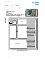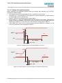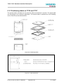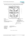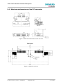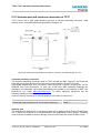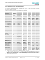
1
TC35
TC37
Siemens Cellular Engines
Hardware
Interface
Description
Version: 03.10
DocID: TC35_37_HD_02_V03.10
TC35 / TC37 Hardware Interface Description
Document Name:
TC35 / TC37 Hardware Interface Description
Version:
Date:
03.10
21.12.2001
Technical Support:
[email protected]
DocId:
Status:
TC35_37_HD_02_V03.10
Released
General notes
With respect to any damages arising in connection with the described product or this document,
Siemens shall be liable according to the General Conditions on which the delivery of the described
product and this document are based.
This product is not intended for use in life support appliances, devices or systems where a malfunction
of the product can reasonably be expected to result in personal injury. Siemens AG customers using or
selling this product for use in such applications do so at their own risk and agree to fully indemnify
Siemens for any damages resulting from illegal use or resale.
Applications incorporating the described product must be designed to be in accordance with the
technical specifications provided in these guidelines. Failure to comply with any of the required
procedures can result in malfunctions or serious discrepancies in results.
Furthermore, all safety instructions regarding the use of mobile technical systems, including GSM
products, which also apply to cellular phones must be followed.
Handheld applications such as mobile phones or PDAs incorporating the described product must be in
accordance with the guidelines for human exposure to radio frequency energy. The Specific Absorption
Rate (SAR) of the application must be evaluated and approved to be compliant with national and
international safety standards or directives.
Subject to change without notice at any time.
Copyright notice
Copying of this document and giving it to others and the use or communication of the contents thereof,
are forbidden without express authority. Offenders are liable to the payment of damages. All rights
reserved in the event of grant of a patent or the registration of a utility model or design.
Copyright © Siemens AG 2001
Trademark notice
MS Windowsâ is a registered trademark of Microsoft Corporation.
TC35_37_HD_02_V03.10 - Released
Page 2 of 92
21.12.2001
TC35 / TC37 Hardware Interface Description
Contents
0
Version History........................................................................................................... 7
1
Introduction ................................................................................................................ 8
1.1 Scope of the document and related documents .................................................. 8
1.2 Terms and abbreviations ..................................................................................... 9
1.3 Standards.......................................................................................................... 12
1.4 Safety Precautions ............................................................................................ 13
2
Functions overview .................................................................................................. 15
2.1 TC35 / TC37 key features at a glance ............................................................... 16
2.2 Block diagram of TC35...................................................................................... 18
2.3 Block diagram of TC37...................................................................................... 19
2.4 GSM baseband processor ................................................................................. 20
2.4.1
Features of the GSM baseband processor .......................................... 20
3
Application Interface ................................................................................................ 21
3.1 Operating modes............................................................................................... 22
3.2 Power supply..................................................................................................... 23
3.2.1
Minimizing power losses ...................................................................... 24
3.2.2
Battery pack......................................................................................... 25
3.2.2.1 Recommended battery pack ................................................................ 26
3.2.2.2 Supported charging technique ............................................................. 27
3.2.2.3 Operating modes during charging........................................................ 28
3.2.2.4 Charger requirements.......................................................................... 29
3.3 Power up / down scenarios................................................................................ 30
3.3.1
Turn on the GSM engine...................................................................... 30
3.3.1.1 Turn on GSM engine using the ignition line IGT (Power on) ................ 30
3.3.1.2 Timing of the ignition process .............................................................. 31
3.3.1.3 Turn on GSM engine using the POWER lines ..................................... 32
3.3.1.4 Turn on GSM engine using the RTC (Alarm mode) ............................. 32
3.3.2
Power saving ....................................................................................... 33
3.3.3
Wake up GSM engine.......................................................................... 33
3.3.4
Turn off GSM engine ........................................................................... 34
3.3.4.1 Turn off GSM engine using AT command............................................ 34
3.3.4.2 Emergency shutdown using /PD pin .................................................... 34
3.3.4.3 Automatic shutdown ............................................................................ 35
3.3.5
Summary of state transitions ............................................................... 37
3.4 RTC backup ...................................................................................................... 38
3.5 Serial interface .................................................................................................. 40
3.6 Audio interface .................................................................................................. 42
3.6.1
Speech processing .............................................................................. 43
3.7 SIM interface ..................................................................................................... 44
3.7.1
Approval considerations....................................................................... 44
3.7.2
Design considerations for SIM card holder .......................................... 45
3.7.3
Grounding the SIM interface ................................................................ 46
3.8 Control signals................................................................................................... 47
3.8.1
Inputs................................................................................................... 47
3.8.2
Outputs................................................................................................ 48
3.8.2.1 Synchronization signal ......................................................................... 48
3.8.2.2 Using the SYNC pin to control a status LED ........................................ 49
TC35_37_HD_02_V03.10 - Released
Page 3 of 92
21.12.2001
TC35 / TC37 Hardware Interface Description
3.9
3.8.2.3 Behaviour of the RING0 line ................................................................ 50
Pin assignment.................................................................................................. 51
4
Radio interface ......................................................................................................... 56
4.1 Receiver ............................................................................................................ 56
4.2 Transmitter ........................................................................................................ 56
4.3 Antenna interface (antenna reference point – ARP) .......................................... 57
4.3.1
Options of connecting the antenna ...................................................... 57
4.3.2
Description of antenna ports and connectors....................................... 58
5
Physical characteristics........................................................................................... 59
5.1 Exploded diagram and PCBs............................................................................. 59
5.2 Mechanical dimensions of TC35 and TC37 ....................................................... 60
5.3 Mounting TC35/TC37 onto the application platform........................................... 63
5.3.1
Mounting TC35 .................................................................................... 63
5.3.2
Mounting TC37 .................................................................................... 64
5.3.3
Positioning labels on TC35 and TC37.................................................. 65
5.4 ZIF connector .................................................................................................... 67
5.4.1
Mechanical dimensions of the ZIF connector ....................................... 68
5.5 Antenna design ................................................................................................. 69
5.5.1
GSC antenna connector on TC35........................................................ 69
5.5.2
Using antenna eqipment from other manufacturers ............................. 72
5.5.3
Antenna pad and coaxicon connector on TC37 ................................... 73
6
Electrical, temperature and radio characteristics.................................................. 74
6.1 Absolute maximum ratings ................................................................................ 74
6.2 Operating conditions ......................................................................................... 74
6.3 Temperature conditions..................................................................................... 74
6.4 Power supply ratings ......................................................................................... 75
6.4.1
Drop definition ..................................................................................... 75
6.4.2
Current consumption during transmit burst .......................................... 76
6.5 Electrical characteristics of the voiceband part .................................................. 80
6.5.1
Setting audio parameters by AT commands ........................................ 80
6.5.2
Characteristics of audio modes............................................................ 81
6.5.3
Voiceband receive path ....................................................................... 82
6.5.4
Voiceband transmit path ...................................................................... 83
6.6 Air interface ....................................................................................................... 84
6.7 Electrostatic discharge ...................................................................................... 85
7
Updating Firmware................................................................................................... 86
8
Reference Approval.................................................................................................. 87
8.1 Reference Equipment........................................................................................ 87
8.2 CE Conformity................................................................................................... 88
8.3 G.C.F. Conformity ............................................................................................. 88
9
APPENDIX: List of parts and accessories .............................................................. 89
9.1 Specifications of AMP switching connector ....................................................... 90
TC35_37_HD_02_V03.10 - Released
Page 4 of 92
21.12.2001
TC35 / TC37 Hardware Interface Description
Figures
Figure 1: Block diagram of TC35 ......................................................................................... 18
Figure 2: Block diagram of TC37 ......................................................................................... 19
Figure 3: Block diagram of a cellular application.................................................................. 21
Figure 4: Power supply limits during transmit burst.............................................................. 24
Figure 5: Battery pack circuit diagram ................................................................................. 25
Figure 6: Charging process ................................................................................................. 27
Figure 7: Power-on by ignition signal ................................................................................... 30
Figure 8: Timing of power-on process if VDDLP is not used................................................ 31
Figure 9: Timing of power-on process if VDDLP is fed from external source ....................... 31
Figure 10: Deactivating GSM engine by Power Down signal ............................................... 34
Figure 11: RTC supply from capacitor ................................................................................. 38
Figure 12: RTC supply from rechargeable battery (accumulator) ........................................ 38
Figure 13: RTC supply from non-chargeable battery ........................................................... 39
Figure 14: RS-232 interface................................................................................................. 40
Figure 15: Audio block diagram ........................................................................................... 42
Figure 16: SIM card holder of DSB35 Support Box.............................................................. 45
Figure 17: Connecting a separate ground for SIM interface ................................................ 46
Figure 18: TC35 output control signals ................................................................................ 48
Figure 19: LED Circuit (Example) ........................................................................................ 49
Figure 20: Incoming voice call ............................................................................................. 50
Figure 21: Incoming data call............................................................................................... 50
Figure 22: Antenna connector circuit on TC35..................................................................... 57
Figure 23: Antenna connector circuit on TC37..................................................................... 57
Figure 24: Exploded diagram and PCBs of TC35/TC37 ...................................................... 59
Figure 25: TC35 / TC37 – view of RF part ........................................................................... 60
Figure 26: Mechanical dimensions of TC35......................................................................... 61
Figure 27: Mechanical dimensions of TC37......................................................................... 62
Figure 28: Mounting TC35 (example) .................................................................................. 63
Figure 29: Mounting TC37 (example) .................................................................................. 64
Figure 30: Positioning labels................................................................................................ 65
Figure 31: Label dimensions................................................................................................ 65
Figure 32: Content of TC35 label......................................................................................... 66
Figure 33: Mechanical dimensions of ZIF connector............................................................ 68
Figure 34: PCB ZIF connector ............................................................................................. 68
Figure 35: Mechanical dimensions of MuRata GSC connector (in mm) ............................... 70
Figure 36: Maximum mechanical stress to the connector .................................................... 71
Figure 37: How to use MuRata tool ..................................................................................... 71
Figure 38: Dimensions and position of coaxicon connector and antenna pad on TC37 ....... 73
Figure 39: Typical current (peak) vs power control level ...................................................... 76
Figure 40: Typical current (average) vs power control level ................................................. 76
Figure 41: Typical current consumption for GSM 900, power level = 5 ................................ 78
Figure 42: Typical current consumption for DCS1800, power level = 0................................ 78
Figure 43: AT audio programming model ............................................................................ 80
Figure 44: Structure of audio inputs..................................................................................... 83
Figure 45: Reference equipment for approval...................................................................... 87
TC35_37_HD_02_V03.10 - Released
Page 5 of 92
21.12.2001
TC35 / TC37 Hardware Interface Description
Tables
Table 1: TC35 / TC37 key features...................................................................................... 16
Table 2: Overview of operating modes ................................................................................ 22
Table 3: Power supply pins of ZIF connector ....................................................................... 23
Table 4: Specifications of CGP34506 Panasonic battery pack ............................................ 26
Table 5: AT commands available in Charge-only mode....................................................... 29
Table 6: AT commands available in Alarm mode................................................................. 32
Table 7: Wake-up events..................................................................................................... 33
Table 8: Temperature dependent behaviour........................................................................ 35
Table 9: Dependency on ambient temperature .................................................................... 36
Table 10: State transitions of TC35 / TC37.......................................................................... 37
Table 11: DCE-DTE wiring .................................................................................................. 40
Table 12: Signal of the SIM interface (ZIF connector).......................................................... 44
Table 13 : Pin assignment of Molex SIM card holder on DSB35 Support Box ..................... 45
Table 14: Input control signals of the TC35/TC37 module ................................................... 47
Table 15: TC35 synchronization signal (if SYNC pin is set to mode 0 via AT^SSYNC)........ 48
Table 16: Modes of the LED and associated functions ........................................................ 49
Table 17: Ring signal........................................................................................................... 50
Table 18: Pin assignment .................................................................................................... 51
Table 19: Return loss .......................................................................................................... 57
Table 20: Signals available on GSC jack ............................................................................. 58
Table 21: Signals available on antenna pad / coaxicon connector ....................................... 58
Table 22: Electrical and mechanical characteristics of the ZIF connector ............................ 67
Table 23: Ratings and characteristics of the GSC antenna connector ................................. 69
Table 24: Stress characteristics of the GSC antenna connector.......................................... 71
Table 25: Ordering information for antenna equipment from AMP Tyco Electronics............ 73
Table 26: Absolute maximum ratings................................................................................... 74
Table 27: Operating conditions............................................................................................ 74
Table 28: Temperature conditions ....................................................................................... 74
Table 29: Power supply ratings............................................................................................ 75
Table 30: Power control levels GSM 900, power class 4 ..................................................... 77
Table 31: Power control levels DCS 1800, power class 1 .................................................... 77
Table 32: GSM 900, power level 5....................................................................................... 79
Table 33: GSM 1800, power level 0..................................................................................... 79
Table 34: Audio parameters adjustable by AT command..................................................... 80
Table 35: Voiceband characteristics (typical), all values preliminary.................................... 81
Table 36: Voiceband receive path ....................................................................................... 82
Table 37: Voiceband transmit path ...................................................................................... 83
Table 38: Air Interface ......................................................................................................... 84
Table 39: Measured electrostatic values.............................................................................. 85
Table 40: List of accessories ............................................................................................... 89
TC35_37_HD_02_V03.10 - Released
Page 6 of 92
21.12.2001
TC35 / TC37 Hardware Interface Description
0 Version History
This chapter reports modifications and improvements over previous versions of the
document.
Preceding document: "TC35 Hardware Interface Description" Version V0300
New document: "TC35_TC37 Hardware Interface Description" Version 03.10
Chapter
Page
What is new
2.1
16
Data transmission rate 14.4kbps now implemented
3.2.2
Chapter revised, technical specification of recommended battery pack added
3.3.1.1 /
3.3.1.2
30
31
Timing of ignition line described in greater detail
3.3.2
33
Brief description of powersave mode
3.3.4.3
35f
Automatic undervoltage shutdown: notes added
3.3.5
37
Summary of state transitions: transition from Charge-only mode to Alarm
mode
3.5
40
Serial interface described in greater detail
3.7
44
SIM interface described in greater detail. Recommendations for SIM card
holder and SIM interface grounding added
3.8.1
47
Table revised
3.8.2.3
50
Behaviour of /RING0 line described in more detail
3.9
51
RS-232: If unused keep output pins open and connect input pins to VDD via
10kΩ.
6.4
75
Table 29: Power supply ratings: minimum value of Icharge removed
6.4.2
76
Chapter revised. Figure 39 to Figure 42 and Table 30 to Table 33 moved into
one chapter. No values modified over preceding document version.
6.5.1
80
Note added: inCalibrate, outCalibrate and sideTone internally truncated to
32767.
6.5.2
81
Table 35 revised
7
86
Overview on firmware update added
9
89
List of parts and accessories enhanced
TC35_37_HD_02_V03.10 - Released
Page 7 of 92
21.12.2001
TC35 / TC37 Hardware Interface Description
1 Introduction
This document presents the hardware interface description of the Siemens GSM engines
•
•
TC35
TC37
As TC35 and TC37 are intended to integrate with a wide range of cellular application
platforms, all functional components are described in detail. So this guide covers all
information you need to design and set up host devices incorporating TC35 or TC37. It helps
you quickly retrieve interface specifications, electrical and mechanical details and, last but
not least, information on the requirements to be considered for integrating further
components.
TC35 and TC37 are full-featured GSM engines which are identical in terms of functionality,
physical dimensions and performance characteristics including minimum or maximum
ratings. They differ only in the design and location of antenna connectors. TC35 features a
coaxial GSC connector, while TC37 provides a coaxial switching connector plus an antenna
pad. Each connector type is described in a separate section.
1.1 Scope of the document and related documents
Please note that this hardware interface description is intended for the following TC35 and
TC37 release:
• Hardware:
PCB number Q8100-B1-7
• Software:
Version 03.10
Related documents
/1/ AT Command Set for TC35, TC37 and TC35 Terminal, Version 03.10
/2/ Release Notes: TC35 Version 03.10
/3/ Application Note 16: Updating TC35 Firmware, Version 03.10
/4/ DSB35 Support Box - Evaluation Kit for Siemens Cellular Engines
/5/ TC3x Multiplexer User's Guide, Version 03.10
/6/ Application Note 02: Audio Interface, Version 03.10
Prior to using the GSM engines or upgrading to a new firmware release, be sure to carefully
read and understand the latest product information provided in the Release Notes.
To visit the Siemens Website you can use the following link:
http://siemens.com/wm
TC35_37_HD_02_V03.10 - Released
Page 8 of 92
21.12.2001
TC35 / TC37 Hardware Interface Description
1.2 Terms and abbreviations
Abbreviation
Description
ADC
Analog-to-Digital Converter
AFC
Automatic Frequency Control
AGC
Automatic Gain Control
ARFCN
Absolute Radio Frequency Channel Number
ARP
Antenna Reference Point
ASIC
Application Specific Integrated Circuit
BER
Bit Error Rate
BTS
Base Transceiver Station
CB or CBM
Cell Broadcast Message
CS
Coding Scheme
CSD
Circuit Switched Data
CPU
Central Processing Unit
CE
Conformité Européene (European Conformity)
DAC
Digital-to-Analog Converter
dBm0
Digital level, 3.14dBm0 corresponds to full scale, see ITU G.711, A-law
DCE
Data Communication Equipment (typically modems, e.g. Siemens GSM engine)
DCS 1800
Digital Cellular System, also referred to as PCN
DSB
Development Support Box
DSP
Digital Signal Processor
DSR
Data Set Ready
DTE
Data Terminal Equipment (typically computer, terminal, printer or, for example, GSM
application)
DTR
Data Terminal Ready
DTX
Discontinuous Transmission
EFR
Enhanced Full Rate
EGSM
Enhanced GSM
EMC
Electromagnetic Compatibility
ESD
Electrostatic Discharge
ETS
European Telecommunication Standard
FDMA
Frequency Division Multiple Access
FFC
Flat Flexible Cable
FR
Full Rate
GMSK
Gaussian Minimum Shift Keying
GPRS
General Packet Radio Service
GSM
Global Standard for Mobile Communications
TC35_37_HD_02_V03.10 - Released
Page 9 of 92
21.12.2001
TC35 / TC37 Hardware Interface Description
Abbreviation
Description
HiZ
High Impedance
HR
Half Rate
IC
Integrated Circuit
IMEI
International Mobile Equipment Identity
I/O
Input/Output
ISO
International Standards Organization
ITU
International Telecommunications Union
kbps
kbits per second
LED
Light Emitting Diode
Li-Ion
Lithium-Ion
Mbps
Mbits per second
MMI
Man Machine Interface
MO
Mobile Originated
MS
Mobile Station (GSM engine), also referred to as TE
MSISDN
Mobile Station International ISDN number
MT
Mobile Terminated
NTC
Negative Temperature Coefficient
PCB
Printed Circuit Board
PCL
Power Control Level
PCN
Personal Communications Network, also referred to as DCS 1800
PCS
Personal Communication System
PDU
Protocol Data Unit
PLL
Phase Locked Loop
PPP
Point-to-point protocol
PSU
Power Supply Unit
R&TTE
Radio and Telecommunication Terminal Equipment
RAM
Random Access Memory
RF
Radio Frequency
ROM
Read-only Memory
RMS
Root Mean Square (value)
RTC
Real Time Clock
Rx
Receive Direction
SAR
Specific Absorption Rate
SELV
Safety Extra Low Voltage
SIM
Subscriber Identification Module
SMS
Short Message Service
SRAM
Static Random Access Memory
TC35_37_HD_02_V03.10 - Released
Page 10 of 92
21.12.2001
TC35 / TC37 Hardware Interface Description
Abbreviation
Description
TA
Terminal adapter (e.g. GSM engine)
TDMA
Time Division Multiple Access
TE
Terminal Equipment, also referred to as DTE
Tx
Transmit Direction
UART
Universal asynchronous receiver-transmitter
URC
Unsolicited Result Code
USSD
Unstructured Supplementary Service Data
VSWR
Voltage Standing Wave Ratio
ZIF
Zero Insertion Force
Phonebook abbreviations
FD
SIM fixdialling phonebook
LD
SIM last dialling phonebook (list of numbers most recently dialled)
MC
Mobile Equipment list of unanswered MT calls (missed calls)
ME
Mobile Equipment phonebook
ON
Own numbers (MSISDNs) stored on SIM or ME
RC
Mobile Equipment list of received calls
SM
SIM phonebook
TC35_37_HD_02_V03.10 - Released
Page 11 of 92
21.12.2001
TC35 / TC37 Hardware Interface Description
1.3 Standards
The Siemens GSM engines described in this document have been approved to comply with
the following directives and standards.
Directives
99/05/EC
Directive of the European Parliament and of the council of 9 March
1999 on radio equipment and telecommunications terminal
equipment and the mutual recognition of their conformity
89/336/EC
Directive on electromagnetic compatibility
73/23/EC
Directive on electrical equipment designed for use within certain
voltage limits (Low Voltage Directive)
Standards of type approval
ETS 300 607-1
Digital cellular telecommunications system (Phase 2);
Mobile Station (MS) conformance specification;
(equal GSM 11.10-1=>equal 3GPP51.010-1)
EN 301 419-1
v.4.1.1 (4-2000) Global System for Mobile communications
(GSM); Harmonized standard for mobile stations in the GSM 900
and 1800 Bands covering essential requirements under article 3.2
of the R&TTE Directive (1999/5EC) (GSM 13.11)
ETS 300 342-1
Radio Equipment and Systems(RES);
Electro Magnetic Compatibility (EMC) for European digital cellular
telecommunications system (GSM 900 MHz and DCS 1800 MHz)
Part 1: Mobile and portable radio and ancillary equipment
(for equipment for fixed and vehicular use)
EN 60 950
Safety of information technology equipment
ES 59005/ANSI C95.1 Considerations for evaluation of human exposure to
Electromagnetic Fields (EMFs) from Mobile Telecommunication
Equipment (MTE) in the frequency range 30MHz-6GHz (relevant for
applications)
Requirements of quality
IEC 60068
Environmental testing
DIN EN 60529
IP - codes
TC35_37_HD_02_V03.10 - Released
Page 12 of 92
21.12.2001
TC35 / TC37 Hardware Interface Description
1.4 Safety Precautions
The following safety precautions must be observed during all phases of the operation,
usage, service or repair of any cellular terminal or mobile incorporating TC35 or TC37.
Manufacturers of the cellular terminal are advised to convey the following safety information
to users and operating personnel and to incorporate these guidelines into all manuals
supplied with the product. Failure to comply with these precautions violates safety standards
of design, manufacture and intended use of the product. Siemens AG assumes no liability
for customer failure to comply with these precautions.
When in a hospital or other health care facility, observe the restrictions on the
use of mobiles. Switch the cellular terminal or mobile off, if instructed to do so
by the guidelines posted in sensitive areas. Medical equipment may be
sensitive to RF energy.
The operation of cardiac pacemakers, other implanted medical equipment
and hearing aids can be affected by interference from cellular terminals or
mobiles placed close to the device. If in doubt about potential danger, contact
the physician or the manufacturer of the device to verify that the equipment is
properly shielded. Pacemaker patients are advised to keep their hand-held
mobile away from the pacemaker, while it is on.
Switch off the cellular terminal or mobile before boarding an aircraft. Make
sure it cannot be switched on inadvertently. The operation of wireless
appliances in an aircraft is forbidden to prevent interference with
communications systems. Failure to observe these instructions may lead to
the suspension or denial of cellular services to the offender, legal action, or
both.
Do not operate the cellular terminal or mobile in the presence of flammable
gases or fumes. Switch off the cellular terminal when you are near petrol
stations, fuel depots, chemical plants or where blasting operations are in
progress. Operation of any electrical equipment in potentially explosive
atmospheres can constitute a safety hazard.
Your cellular terminal or mobile receives and transmits radio frequency
energy while switched on. Remember that interference can occur if it is used
close to TV sets, radios, computers or inadequately shielded equipment.
Follow any special regulations and always switch off the cellular terminal or
mobile wherever forbidden, or when you suspect that it may cause
interference or danger.
Road safety comes first! Do not use a hand-held cellular terminal or mobile
when driving a vehicle, unless it is securely mounted in a holder for handsfree
operation. Before making a call with a hand-held terminal or mobile, park the
vehicle.
Handsfree devices must be installed by qualified personnel. Faulty installation
or operation can constitute a safety hazard.
TC35_37_HD_02_V03.10 - Released
Page 13 of 92
21.12.2001
TC35 / TC37 Hardware Interface Description
SOS
IMPORTANT!
Cellular terminals or mobiles operate using radio signals and cellular
networks cannot be guaranteed to connect in all conditions. Therefore, you
should never rely solely upon any wireless device for essential
communications, for example emergency calls.
Remember, in order to make or receive calls, the cellular terminal or mobile
must be switched on and in a service area with adequate cellular signal
strength.
Some networks do not allow for emergency calls if certain network services
or phone features are in use (e.g. lock functions, fixed dialling etc.). You may
need to deactivate those features before you can make an emergency call.
Some networks require that a valid SIM card be properly inserted in the
cellular terminal or mobile.
TC35_37_HD_02_V03.10 - Released
Page 14 of 92
21.12.2001
TC35 / TC37 Hardware Interface Description
2 Functions overview
TC35 and TC37 GSM engines operate in the GSM 900 MHz and GSM 1800 MHz frequency
bands. Designed to easily provide radio connection for voice and data transmission both
modules integrate seamlessly with a wide range of GSM application platforms and are
ideally suited to design and set up innovative cellular solutions with minimum effort.
The complete RF part is incorporated and the GSM protocol runs autonomously on a GSM
baseband processor. The GSM engine uses a single 40-pin ZIF connector that connects to
the cellular device application. The ZIF connector establishes the application interface for
control data, audio signals and power supply lines.
The cellular device application forms the Man-Machine Interface (MMI). Access to the GSM
engine is enabled by a serial interface (RS232).
TC35_37_HD_02_V03.10 - Released
Page 15 of 92
21.12.2001
TC35 / TC37 Hardware Interface Description
2.1 TC35 / TC37 key features at a glance
Table 1: TC35 / TC37 key features
Feature
Implementation
Transmission
Voice, Data, SMS, Fax
Power supply
Single supply voltage 3.3V – 5.5V
Please refer to Chapter 6.4 for more detailed information
Frequency bands
Dual Band EGSM 900 and GSM 1800 (GSM Phase 2+)
GSM class
Small MS
Transmit power
Class 4 (2W) for EGSM 900
Class 1 (1W) for GSM 1800
SIM card reader
External – connected via interface connector
Note: The SIM card reader is not part of the GSM engine
Antenna design
50 Ohm antenna interface. Connectors vary with type of GSM engine:
• TC35: GSC coaxial connector
• TC37: Coaxial switching connector from AMP and antenna pad
Temperature range
Normal operation:
Restricted operation:
-20°C to +55°C
–25° to –20°C and +55°C to +70°C
Storage:
Current consumption
(typical)
Speech codec
-40°C to +85°C
Depending on operating mode
• TALK mode (peak) at EGSM 900 / GSM 1800:
1.8A
• TALK mode at EGSM 900 / GSM 1800:
300mA / 270mA
• IDLE mode at EGSM 900 / GSM 1800:
10mA / 10mA
• SLEEP mode:
3mA
• Power Down mode:
50µA
Triple rate codec:
• Half Rate (ETS 06.20)
• Full Rate (ETS 06.10)
• Enhanced Full Rate (ETS 06.50 / 06.60 / 06.80)
SMS
MT, MO, CB, Text and PDU mode
DATA
Transmission rates: 2.4, 4.8, 9.6, 14.4 kbps, non-transparent, USSD
FAX
Group 3: Class 1, Class 2
Audio interface
Analog voice:
• Microphone
• Earpiece
• Handsfree (supports echo cancellation and noise reduction)
TC35_37_HD_02_V03.10 - Released
Page 16 of 92
21.12.2001
TC35 / TC37 Hardware Interface Description
Feature
Implementation
Serial interface
RS232 (2.65V CMOS level) bi-directional bus for commands / data using AT
commands
TC35/TC37 modules support Multiplex mode according to the GSM 07.10
Multiplexer Protocol and enable one physical serial interface to be
partitioned into three virtual channels. This allows you to take advantage of
up to 3 simultaneous sessions on the serial interface. For example, you can
transfer data over one channel while two further channels are free to control
the GSM engine with AT commands.
Supported SIM card
3V
Phonebook
management
Supported phonebook types: SM, FD, LD, MC, RC, ON, ME
Selectable baud rate
300bps ... 115kbps (AT interface)
Autobauding range
Supported baud rates: 1200, 2400, 4800, 9600, 19200, 38400, 57600,
115200
Firmware download
Optionally via RS232 interface or SIM interface
Real time clock
Implemented
Timer function
Programmable via AT command
Physical characteristics
Size:
54.5 x 36 x 6.75mm
Weight:
approx. 18g
TC35_37_HD_02_V03.10 - Released
Page 17 of 92
21.12.2001
TC35 / TC37 Hardware Interface Description
2.2 Block diagram of TC35
Figure 1 shows a block diagram of the TC35 module and illustrates the major functional
components:
• GSM baseband processor
• GSM radio
• Power supply (ASIC)
• Flash
• ZIF connector
• Antenna interface: Coaxial GSC type connector
SIEMENS GSM Engine TC35
Antenna
Connector
Flash
Radio
GSM Baseband Processor
Power Supply ASIC
Earpiece 1
MIC 1
Earpiece 2 (handsfree)
HF Microphone
2
2
2
2
SIM
RS-232
Synchronization
6
8
1
ACCU_TEMP
1
VBATT+
5
POWER (Charger)
2
Ground
5
Ignition
1
Power Down
1
RTC backup
VDD = 2.9 V
1
1
ZIF Connector 40 Pins
Antenna
Additional ground pad
Figure 1: Block diagram of TC35
TC35_37_HD_02_V03.10 - Released
Page 18 of 92
21.12.2001
TC35 / TC37 Hardware Interface Description
2.3 Block diagram of TC37
Figure 2 shows a block diagram of the TC37 module and illustrates the major functional
components:
• GSM baseband processor
• GSM radio
• Power supply (ASIC)
• Flash
• ZIF connector
• Antenna interface: Coaxial switching connector
and antenna pad (to be used alternatively)
SIEMENS GSM Engine TC37
Antenna
pad
Flash
Earpiece 1
MIC 1
Earpiece 2 (handsfree)
MIC 2 (handsfree)
Radio
GSM Baseband Processor
Power Supply ASIC
2
2
2
2
SIM
RS-232
Synchronization
6
8
1
ACCU_TEMP
1
VBATT+
5
POWER (charger)
2
Ground
5
Ignition
1
Power Down
1
RTC backup
VDD = 2.9 V
1
1
ZIF Connector 40 Pins
Antenna
Antenna jack
(alternative
to pad)
Additional ground pad
Figure 2: Block diagram of TC37
TC35_37_HD_02_V03.10 - Released
Page 19 of 92
21.12.2001
TC35 / TC37 Hardware Interface Description
2.4 GSM baseband processor
The GSM baseband processor handles all the processing for audio, signaling and data
transfer within a GSM cellular device. Internal software runs the application interface and the
whole GSM protocol stack. A UART forms the interface to the cellular device application.
The GSM baseband processor is a single chip mixed signal baseband IC, containing all
analog and digital functionality of a cellular radio. Designed to meet the increasing demands
of the GSM/PCS cellular subscriber market, it supports FR, HR and EFR speech and
channel coding without the need for external hardware.
Its high level of integration reduces system complexity, board dimensions and the number of
components. In combination with the RF solution a complete two-chip GSM system solution
is achieved, which results in extremely compact implementation, very low power
consumption and cost effective system performance. Due to its very flexible interfaces the
baseband controller can easily be set up to control a wide variety of RF architectures. The
baseband processor is powered by a C166 CPU and a DSP processor core. Integrating
these high performance processor cores with on-chip memory, a TDMA timer module and
GSM specific peripherals provides a compelling single chip cellular baseband processor.
2.4.1 Features of the GSM baseband processor
The baseband processor includes the following major features:
•
•
•
•
•
•
•
•
•
•
•
•
•
•
•
•
•
•
C166 MCU processor core
Digital Signal Processing core
On-chip MCU Program ROM / SRAM flexibly configurable as program or data RAM
DSP Program ROM / RAM
DSP Data ROM / RAM
Programmable PLL for system clock generation
GSM Timer Module that off-loads the MCU from radio channel timing
MCU and DSP Timers
Pulse Carry Modulation output for Automatic Frequency Correction (AFC)
Serial RF Control Interface
ISO 7816 compatible SIM card interface
Digital and analog voiceband and baseband filters including digital-to-analog and
analog-to-digital converters
RF power ramping functions
Measurement of battery voltage, battery and environment temperature
GMSK Modulator
Viterbi Hardware Accelerator
A51/A52 Cipher Unit
Comprehensive static and dynamic power management
TC35_37_HD_02_V03.10 - Released
Page 20 of 92
21.12.2001
TC35 / TC37 Hardware Interface Description
3 Application Interface
The GSM engine connects to the application platform over the host interface, which takes
the form of a 40-pin 0.5mm pitch ZIF connector.
The host interface incorporates several sub-interfaces described in the following chapters:
• Power supply and charging (see Chapters 3.2 and 3.3)
• Serial interface (see Chapter 3.5)
• Two audio interfaces (see Chapter 3.6)
• SIM interface (see Chapter 3.7)
User application
GSM Engine
(TC35 or TC37)
SIM
Host interface via
ZIF connector and FFC
Figure 3: Block diagram of a cellular application
Electrical and mechanical characteristics of the ZIF connector are specified in Chapter 5.4.
Ordering information for the ZIF connector and the required cables are listed in Chapter 6.
TC35_37_HD_02_V03.10 - Released
Page 21 of 92
21.12.2001
TC35 / TC37 Hardware Interface Description
3.1 Operating modes
The table below briefly summarizes the various operating modes referred to in the following
chapters.
Table 2: Overview of operating modes
Mode
Function
Power Down
Operating voltage applied. Only a voltage regulator in the Power Supply ASIC
is active for powering the RTC. Software is not active. The RS-232 interface
is not accessible.
Normal operation
SLEEP
Power saving mode set with AT+CFUN command.
Software is active to minimum extent. If the GSM
engine was registered to the GSM network in IDLE
mode, it is registered and paging in SLEEP mode,
too. AT interface is not responding.
IDLE
Software is active. Once registered to the GSM
network, paging with BTS is carried out. The engine
is ready to send and receive.
TALK
Connection between two subscribers is in progress.
Power consumption depends on network coverage
individual settings, such as DTX off/on, FR/EFR/HR,
hopping sequences, antenna.
Alarm mode
Restricted operation launched by RTC alert function while GSM engine is in
Power Down mode. GSM engine will not be registered to GSM network.
Limited number of AT commands is accessible.
If application is battery powered: No charging functionality in Alarm mode.
Charge-only mode
Limited operation for battery powered applications. Enables charging while
engine is detached from GSM network. Limited number of AT commands is
accessible. There are several ways to launch Charge-only mode:
• From Power Down mode: Connect charger to POWER lines when engine
was powered down by AT^SMSO.
• From Normal mode: Connect charger to POWER lines, then enter
AT^SMSO.
Charge mode during Normal operation (SLEEP, IDLE, TALK, DATA) and charging running in
normal operation
parallel. Charge mode changes to Charge-only mode when GSM engine is
powered down before charging has been completed.
See also Table 7 and Table 10 for the various options of waking up the GSM engine and
proceeding from one mode to another.
TC35_37_HD_02_V03.10 - Released
Page 22 of 92
21.12.2001
TC35 / TC37 Hardware Interface Description
3.2 Power supply
The power supply of the GSM Engine has to be a single voltage source in the range of
VBATT+ = 3.3V...5.5V. It must be able to provide a peak current of about 2A for uplink
transmission and account for drops on the VBATT+ line that may be caused in transmit
bursts.
All the key functions for supplying power to the GSM engine are handled by an ASIC power
supply. The ASIC provides the following features:
• Stabilizes the supply voltages for the GSM baseband processor and for the RF part
using linear voltage regulators.
• Controls the module's power up and power down procedures.
A watchdog logic implemented in the baseband processor periodically sends signals to
the ASIC, allowing it to maintain the supply voltage for all TC35/TC37 components.
Whenever the watchdog pulses fail to arrive constantly, the module is turned off.
• Delivers, across the VDD pin, a regulated voltage of 2.9V/70mA for the external
application.
• Monitors overvoltage and undervoltage.
The RF power amplifier is driven directly from VBATT+.
10 pins of the ZIF connector are dedicated to connect the supply voltage (VBATT+) and
ground (GND).
Table 3: Power supply pins of ZIF connector
Signal name
Pin
I/O
Description
Parameter
VBATT+
1-5
I/O
Positive operating voltage
3.3 V...5.5 V, Ityp ≤ 2 A during transmit
burst
The minimum operating voltage must
not fall below 3.3 V, not even in case of
voltage drop.
GND
6-10
X
Ground
0V
POWER
11-12
I
Positive charging voltage
Imax = 500 mA (provided by external
source, e.g. charger)
U = 5.5...8 V
internal Pull Down R=100kΩ
VDDLP
30
I/O
Buffering of RTC (see
Chapter 3.3.1.4)
UOUT,max = VBATT+
UIN = 2.0 V...4.8 V
Ri = 1kΩ
Iin,max = 30µA
TC35_37_HD_02_V03.10 - Released
Page 23 of 92
21.12.2001
TC35 / TC37 Hardware Interface Description
3.2.1 Minimizing power losses
When designing the power supply for your application please pay specific attention to power
losses. Ensure that the input voltage VBATT+ never drops below 3.3 V on the TC35/TC37
board, not even during transmit bursts. Also, make sure that any voltage drops that may
occur during transmit bursts never exceed 400mV. It should be noted that TC35/TC37 will be
switched off in the event of exceeding these limits. For further details see Chapter 6.4.
Note:
In order to minimize power losses, use a FFC cable as short as possible. The
resistance of the power supply lines on the host board and a battery pack should
also be considered.
Example: The ZIF-FFC-ZIF connection causes a resistance of 50mΩ in the VBATT+ line
and 50mΩ in the GND line, if the FFC reaches the maximum length of 200mm.
As a result, a 2A transmit burst would add up to a total voltage drop of 200mV.
Plus, if a battery pack is involved, further losses may occur due to the resistance
across the battery lines.
Transmit
burst 2A
Transmit
burst 2A
VBATT+
max. 400mV
min. 3.3V
Figure 4: Power supply limits during transmit burst
TC35_37_HD_02_V03.10 - Released
Page 24 of 92
21.12.2001
TC35 / TC37 Hardware Interface Description
3.2.2 Battery pack
For some applications the use of a battery pack may be required. TC35 and TC37 can be
powered from a Li-Ion battery pack which must be specified for 3.8V, 0.85Ah and a final
charge voltage of 4.2V.
The charging algorithm has been optimized for a battery pack that meets the characteristics
listed below. It is strongly recommended that the battery pack you want to integrate into your
TC35/TC37 application is compliant with these specifications. This ensures reliable
operation, proper charging and, particularly, allows you to monitor the battery capacity using
the AT^SBC command (see /1/ for details). A battery pack especially designed to operate
with TC35/TC37 modules is specified in Chapter 3.2.2.1.
Battery pack characteristics
•
•
•
•
•
•
Ensure that the battery pack incorporates a protection circuit. Since charging and
discharging largely depend on the battery temperature, the battery pack should include
an NTC resistor. If the NTC is not inside the battery pack it must be placed nearby. The
NTC resistor must be connected between ACCU_TEMP and GND. Required NTC
characteristics are: 10 kΩ +5% @ 25°C, B25/50 = 3435K +3% (alternatively acceptable:
10 kΩ +2% @ 25°C, B25/50 = 3370K +3%). Please note that the NTC is indispensable for
proper charging, i.e. the charging process will not start if no NTC is present.
Furthermore, the protection circuit must be capable of detecting overvoltage (against
overcharging), undervoltage (against deep discharging) and overcurrent. The circuit
must be insensitive to pulse loading (see Chapter 3.2.2.1).
On the TC35/TC37 module, a built-in measuring circuit constantly monitors the charging
voltage. In the event of undervoltage, it causes the module to power down and
automatically starts up trickle charging to protect the cell from damage. Undervoltage
thresholds are specific to the battery pack and must be evaluated for the intended model.
When you evaluate undervoltage thresholds, consider both the current consumption of
TC35/TC37 and of the application circuit.
The battery cell must be insensitive to rupture, fire and gasing under extreme conditions
of temperature and charging (voltage, current).
The battery pack must be protected from reverse pole connection. For example, the
casing should be designed to prevent the user from mounting the battery in reverse
orientation.
The battery pack must be approved to satisfy the requirements of CE conformity.
Figure 5 shows the circuit diagram of a typical BATT+
battery pack design that includes the protection
elements described above.
ACCU_TEMP
GND
ϑ
NTC
Protection Circuit
+ Battery cell
Polyfuse
Figure 5: Battery pack circuit diagram
TC35_37_HD_02_V03.10 - Released
Page 25 of 92
21.12.2001
TC35 / TC37 Hardware Interface Description
3.2.2.1 Recommended battery pack
The following battery pack has been especially designed to operate with TC35 and TC37
modules.
Table 4: Specifications of CGP34506 Panasonic battery pack
Product name
Battery cell P/N "CGP34506 Panasonic"
Vendor
Shenzhen XWODA electronic Co., Ltd
To place orders or obtain more information please contact:
Mr. Wang Ming Wang
Phone:
+86 755 7619731
Fax:
+86 755 7608078
Email:
[email protected]
Nominal voltage
3.6V
Capacity
800mAh
NTC
10kΩ ± 5% @ 25°C B(25/85)=3435K ± 3%
Overcharge detection voltage
4.325 ± 0.025V
Overcharge release voltage
4.075 ± 0.025V
Overdischarge detection voltage
2.5 ± 0.05V
Overdischarge release voltage
2.9 ± 0.5V
Overcurrent detection
3 ± 0.5V
Nominal working current
<5µA
Current of low voltage detection
0.5µA
Overcurrent detection delay time
8~16ms
Short detection delay time
50µs
Overdischarge detection delay time
31~125ms
Overcharge detection delay time
1s
Internal resistance
<130mΩ
TC35_37_HD_02_V03.10 - Released
Page 26 of 92
21.12.2001
TC35 / TC37 Hardware Interface Description
3.2.2.2 Supported charging technique
Charging can be accomplished only in a temperature range from 0°C to +45°C. The
charging process supports trickle charging and processor controlled fast charging. In trickle
mode, the battery is charged at a rate of less than 10mA. The fast charging rate provided by
the charger or any other external source must be limited to 500mA. See also Table 29.
The charge cycle begins once the charger is tied to the two POWER pins of the ZIF
connector. First, the charging process goes into trickle charge mode, no matter whether the
battery was deeply or partially discharged. When the battery voltage reaches 3.2V within
60 minutes +10%, the Power ASIC turns on and wakes up the baseband processor.
Once activated, the baseband processor enables fast charging, in parallel to trickle charging.
Fast charging delivers a constant current until the battery voltage reaches 4.2V and then
proceeds with varying charge pulses. As shown in Figure 6, the pulse duty cycle is reduced
to adjust the charging procedure and prevent the voltage from overshooting beyond 4.2V.
Once the pulse width reaches the minimum of 100ms and the duty cycle does not change for
2 minutes, fast charging is completed.
Voltage
4.3
4.2
3.8
3.4
100ms 2 ... 0.1s
100ms 0.1 ... 2s
3.0
Constant current
tOFF = 100 ms
tON = 100 ms
Time
Figure 6: Charging process
Note:
Do not connect the charger to the VBATT+ lines. Only the POWER lines are
intended as input for charging!
The battery manufacturer must guarantee that the battery complies with the
described charging technique. Please refer to the application notes "Battery Pack"
and "Charging the Battery Pack" for a detailed description of the charging
characteristics.
TC35_37_HD_02_V03.10 - Released
Page 27 of 92
21.12.2001
TC35 / TC37 Hardware Interface Description
What to do if software controlled charging does not start up?
If the battery voltage fails to pass the 3.2V level when the 60 minutes timer expires,
processor controlled charging does not begin. To solve the problem you can do one of the
following:
• Once the voltage has reached its minimum of 3V, you can try to start software controlled
charging by pulling the IGT line to ground.
• If the voltage is still below 3V, driving the IGT line to ground switches the timer off and,
thus, prevents the system from proceeding to software controlled charging. Instead, you
are required to shortly disconnect and reconnect the charger. This turns on the timer and
starts anew the entire process.
Apart from this, trickle charging continues whenever the charger connects to the POWER
lines.
3.2.2.3 Operating modes during charging
Of course, the battery can be charged regardless of the engine's operating mode. When the
GSM engine is in Normal mode (SLEEP, IDLE or TALK mode), it remains operational while
charging is in progress (provided that sufficient voltage is applied). The charging process
during the Normal mode is referred to as Charge mode.
If the charger is connected to the POWER lines while the engine is in Power Down mode
(caused by AT^SMSO), the GSM engine goes into Charge-only mode.
Charge-only mode
Charge mode
How to activate mode
Advantages
Connecting charger to the POWER lines • Battery can be charged while GSM engine
while GSM engine is
remains operational and registered to the
GSM network.
• operating, e.g. in IDLE or TALK mode
•
In IDLE and TALK mode, the RS-232 interface
• in SLEEP mode
is accessible. AT command set can be used
to full extent.
• In SLEEP mode, the RS-232 interface is not
accessible at all.
Connecting charger to the POWER lines • Battery can be charged while GSM engine is
while GSM engine is
deregistered from GSM network.
• in Power Down mode (powered down • Charging runs smoothly due to constant
current consumption.
by AT^SMSO)
• in Normal mode: Connect charger to • The AT interface is accessible and allows to
use the commands listed below.
POWER lines, then enter AT^SMSO.
IMPORTANT: While trickle charging is in
progress, be sure that the application is
switched off. If the application is fed from
the trickle charge current the module
might be prevented from proceeding to
software controlled charging since the
current would no be sufficient.
Features of the Charge-only mode
Once the GSM engine enters the Charge-only mode, the AT command interface presents an
Unsolicited Result Code which reads:
^SYSSTART CHARGE-ONLY MODE
Note that this URC will not appear when autobauding was activated (due to the missing
TC35_37_HD_02_V03.10 - Released
Page 28 of 92
21.12.2001
TC35 / TC37 Hardware Interface Description
synchronization between DTE and DCE upon start-up). Therefore, it is recommended to
select a fixed baudrate before using the Charge-only mode.
While the Charge-only mode is in progress, you can take advantage of the AT commands
listed in Table 5. For further instructions refer to the AT Command Set.
Table 5: AT commands available in Charge-only mode
AT command
Use
AT+CALA
Set alarm time
AT+CCLK
Set date and time of RTC
AT^SBC
Monitor charging process
Note: While charging is in progress, no battery parameters are available. To
query the battery capacity disconnect the charger.
If the charger connects externally to the host device no charging parameters
are transferred to the module. In this case, the command cannot be used.
AT^SCTM
Query temperature of GSM engine
AT^SMSO
Power down GSM engine
To proceed from Charge-only mode to normal operation, it is necessary to drive the ignition
line to ground. This must be implemented in your host application as described in Chapter
3.3.1.1. When the engine is in Alarm mode there is no direct way to start charging, i.e.
charging will not begin even though the charger connects to the POWER lines. See also
Chapter 3.3.5 which summarizes the various options of changing the mode of operation.
If your host application uses the SYNC pin to control a status LED as described in Chapter
3.8.2.2, please note that the LED is off while the GSM engine is in Charge-only mode.
3.2.2.4 Charger requirements
The charger must be designed to meet the following requirements:
a) Simple transformer power plug
- Output voltage: 5.5V...8V (under load)
- The charge current must be limited to 500mA
- At an output voltage of 2.8V the current must never exceed 1A
- Voltage spikes that may occur while you connect or disconnect the charger must be
limited to a maximum of 25V and must not exceed 1ms
- There must not be any capacitor on the secondary side of the power plug (avoidance of
current spikes at the beginning of charging)
b) Supplementary requirements for a) to ensure a regulated power supply
- Output voltage: 5.5V...8V
- Current limit: 500mA
- When current is switched off a voltage peak of 10V is allowed for a maximum 1ms
- When current is switched on a spike of 1.6A for 1ms is allowed
Note:
To detect extreme thermal conditions while charging is in progress, connect an NTC
(10kΩ+5% @ 25°C, B=3435 Kelvin ±3%) from ACCU_TEMP to GND.
TC35_37_HD_02_V03.10 - Released
Page 29 of 92
21.12.2001
TC35 / TC37 Hardware Interface Description
3.3 Power up / down scenarios
3.3.1 Turn on the GSM engine
TC35 and TC37 modules can be activated in a variety of ways which are described in the
following chapters:
• via ignition line IGT: starts normal operating state (see Chapters 3.3.1.1 and 3.3.1.2)
• via POWER lines: starts charging algorithm (see Chapters 3.2.2.3 and 3.3.1.3)
• via RTC interrupt: starts Alarm mode (see Chapter 3.3.1.4)
3.3.1.1 Turn on GSM engine using the ignition line IGT (Power on)
To switch on TC35/TC37 the IGT (Ignition) signal needs to be driven to ground level for at
least 100ms. This can be accomplished using an open drain/collector driver in order to avoid
current flowing into this pin.
VBATT+
min. 10ms
HiZ
min.
100ms
HiZ
/IGT
50 to
100ms
VDD
/TXD0
ca. 180ms
Internal reset
max. 900ms
/PD
generated by GSM engine
RS-232
interface
undefined
For details please see Chapter 3.3.1.2
defined
Figure 7: Power-on by ignition signal
In a battery operated TC35 or TC37 application, the duration of the /IGT signal must be 1s
minimum when the charger is connected and you may want to go from charging to Normal
mode.
TC35_37_HD_02_V03.10 - Released
Page 30 of 92
21.12.2001
TC35 / TC37 Hardware Interface Description
3.3.1.2 Timing of the ignition process
When designing your application platform take into account that powering up TC35/TC37
requires the following steps.
• The ignition line cannot be operated until VBATT+ passes the level of 3.0V.
• 10ms after VBATT+ has reached 3.0V the ignition line can be switched low. The duration of
the falling edge must not exceed 1ms.
• Another 100ms are required to power up the module.
• Ensure that VBATT+ does not fall below 3.0V while the ignition line is driven. Otherwise the
module cannot be activated. If the VDDLP line is fed from an external power supply as
explained in Chapter 3.3.4, the /IGT line is HiZ before the rising edge of VBATT+.
• If the VDDLP line is fed from an external power supply as explained in Chapter 3.4, the
/IGT line is HiZ before the rising edge of VBATT+.
3.0V
VBATT+
0V
HiZ
HiZ
/IGT
10ms
min. 100ms
max. 1ms
Figure 8: Timing of power-on process if VDDLP is not used
3.0V
VBATT+
0V
HiZ
HiZ
/IGT
10ms
min. 100ms
max. 1ms
Figure 9: Timing of power-on process if VDDLP is fed from external source
TC35_37_HD_02_V03.10 - Released
Page 31 of 92
21.12.2001
TC35 / TC37 Hardware Interface Description
3.3.1.3 Turn on GSM engine using the POWER lines
As detailed in Chapter 3.2.2.3, the charging adapter can be connected regardless of the
GSM engine's operating mode (except for Alarm mode).
If the charger is connected to the POWER lines while the GSM engine is off, only the
charging algorithm will be launched. The GSM engine runs in a restricted mode, referred to
as Charge-only mode.
During the Charge-only mode the GSM engine is neither logged on to the GSM network nor
is the RS-232 interface fully accessible. When the minimum voltage of 3.2V is achieved
within 60 minutes the charging process proceeds to software controlled charging. To switch
to normal operation and log on to the GSM network, the IGT line needs to be activated.
3.3.1.4 Turn on GSM engine using the RTC (Alarm mode)
Another power-on approach is to use the RTC, which is constantly supplied with power from
a separate voltage regulator in the power supply ASIC. The RTC provides an alert function
which allows to wake up the GSM engine while power is off. To prevent the engine from
unintentionally logging into the GSM network, this procedure only enables restricted
operation, referred to as Alarm mode. It must not be confused with a wake-up or alarm call
that can be activated by using the same AT command, but without switching off power.
Use the AT+CALA command to set the alarm time. The RTC retains the alarm time if the
GSM engine was powered down by AT^SMSO. Once the alarm is timed out and executed,
the GSM engine enters into the Alarm mode. This is indicated by an Unsolicited Result Code
which reads:
^SYSSTART ALARM MODE
In Alarm mode only a limited number of AT commands is available. For further instructions
refer to the AT Command Set.
Table 6: AT commands available in Alarm mode
AT command
Use
AT+CALA
Set alarm time
AT+CCLK
Set date and time of RTC
AT^SBC
In Alarm mode, you can only query the present current consumption and
check whether or not a charger is connected. The battery capacity is
returned as 0, regardless of the actual voltage (since the values measured
directly on the cell are not delivered to the module).
AT^SCTM
Query temperature of GSM engine
AT^SMSO
Power down GSM engine
For the GSM engine to change from the Alarm mode to full operation (normal operating
mode) it is necessary to drive the ignition line to ground. This must be implemented in your
host application as described in Chapter 3.3.1.1. If your application is battery powered note
that charging cannot be started while the engine is in Alarm mode, i.e. charging will not
begin even though the charger connects to the POWER lines. See also Chapter 3.3.5 which
summarizes the various options of changing the mode of operation.
If your host application uses the SYNC pin to control a status LED as described in Chapter
3.8.2.2, please note that the LED is off while the GSM engine is in Alarm mode.
TC35_37_HD_02_V03.10 - Released
Page 32 of 92
21.12.2001
TC35 / TC37 Hardware Interface Description
3.3.2 Power saving
Intended for power saving, the SLEEP mode reduces the functionality of the module to a
minimum and, thus, minimizes the current consumption to the lowest level. To activate
SLEEP mode use the AT command
AT+CFUN=0.
While SLEEP mode is effective, the serial interface is not responding. The module shortly
wakes up to respond to a paging request from the base station and immediately returns to
the power saving mode.
The first wake-up event fully activates the module, enables the serial interface and
terminates power saving. See following chapter for wake-ups.
3.3.3 Wake up GSM engine
The following table summarizes the options of waking up the GSM engine from SLEEP or
Power Down mode. See also Table 10 for further information.
Table 7: Wake-up events
GSM engine is registered to GSM network
How to wake up
From SLEEP mode
Ignition line
No
RTS (falling edge)
Yes
Unsolicited Result Code (URC)
Yes
Incoming call
Yes
Incoming SMS depending on mode selected by AT+CNMI:
AT+CNMI=0,0 (= default, no indication upon receipt of SMS)
No
AT+CNMI=1,1 (= displays URC upon receipt of SMS)
Yes
RTC alarm
Yes
GSM engine is detached from GSM network
How to wake up
From Power Down mode
Ignition line
Yes (see Chapter 3.3.1.1)
RTS (falling edge)
No
Unsolicited Result Code
No
Incoming call
No
RTC alarm
Yes, but only wake-up into Alarm
mode (see Chapter 3.3.1.4)
Connecting charger to POWER lines
Yes, but only wake-up into Chargeonly mode (see Chapter 3.2.2.3)
TC35_37_HD_02_V03.10 - Released
Page 33 of 92
21.12.2001
TC35 / TC37 Hardware Interface Description
3.3.4 Turn off GSM engine
To switch the module off the following procedures may be used:
•
•
•
Normal procedure: Software controlled by sending an AT command over the RS232
application interface. See Chapter 3.3.4.1.
Emergency shutdown: Hardware driven by switching the /PD (Power Down) line of the
ZIF connector to ground = immediate shutdown of supply voltages, only applicable if the
software controlled procedure fails! See Chapter 3.3.4.2.
Automatic shutdown: Takes effect if undervoltage / overvoltage is detected or if battery
or board (engine) temperature exceeds critical limit. See Chapter 3.3.4.3.
3.3.4.1 Turn off GSM engine using AT command
The best and safest approach to powering down the engine is to issue the AT^SMSO
command. This procedure lets the engine log off from the network and allows the software to
enter into a secure state and to save data before disconnecting the power supply.
If the module is in Charge Only mode (not logged into the GSM network), it switches off
when the voltage is disconnected from the POWER inputs.
3.3.4.2 Emergency shutdown using /PD pin
Caution:
Use the /PD pin only when, due to serious problems, the software is not
responding for more than 5 seconds. Pulling the /PD pin causes the loss of all
information stored in the volatile memory since power is cut off immediately.
Therefore, this procedure is intended only for use in case of emergency, e.g. if
TC35 fails to shut down properly.
The /PD signal is available on the ZIF connector. To control the /PD line it is recommended
to use an open drain / collector driver. To actually turn the GSM engine off, the /PD line has
to be driven to ground for ≥ 3.5 s.
How does it work:
• Voltage
VBATT+
is
permanently applied to
the module.
• The module is active
while the internal reset
signal is kept at high
potential.
• The module turns off
once the PD signal is
grounded, the baseband
processor stops sending
watchdog pulses to the
ASIC and the VDD line
goes low.
VBATT+
/IGT
VDD
Internal reset
max. 3.5s
/PD
generated by GSM engine
generated by external application
Figure 10: Deactivating GSM engine by Power Down signal
TC35_37_HD_02_V03.10 - Released
Page 34 of 92
21.12.2001
TC35 / TC37 Hardware Interface Description
3.3.4.3 Automatic shutdown
To ensure proper operation of all assemblies under varying conditions, such as temperature,
input voltage, transmission power etc., the GSM engine features protection elements for
automatic shutdown.
Automatic shutdown takes effect if
• the PCB is exceeding the critical limits of overtemperature or undertemperature
• the battery is exceeding the critical limits of overtemperature or undertemperature.
• in a battery application, undervoltage is detected
• overvoltage is detected.
The automatic shutdown procedure is equivalent to the power-down initiated with the
AT^SMSO command, i.e. the GSM engine logs off from the network and the software enters
a secure state avoiding loss of data (except for overvoltage shutdown).
Alert messages transmitted before the device switches off are implemented as Unsolicited
Result codes (URCs). Please note that these URCs will be generated only if the function was
enabled before. To do this, use the AT^SBC and AT^SCTM commands. For detailed
instructions refer to the "TC3x AT Command Set". If disabled (factory setting), no URCs will
be sent, though the device turns off as necessary.
Temperature dependent shutdown
The board temperature is constantly monitored by an internal NTC resistor located on the
PCB. The NTC that detects the battery temperature must be part of the battery pack circuit
as described in Chapter 3.2.2. The values detected by either NTC resistor are measured
directly on the board and the battery and therefore, are not identical with the ambient
temperature. Use the AT^SCTM write command to enable or disable the URCs.
Proceeding from the measured temperature, TC35/TC37 sends an alert (if enabled) and
switches off when exceeding the critical limits. Please refer to Chapters 3.2.2.1 and 6 for
maximum ratings and excessive temperature. Environmental conditions are summarized in
Table 9.
• URCs indicating the alert level "1" or "-1" allow you to take appropriate precautions, such
as protect the module or battery from exposure to extreme conditions, or save or back up
data etc.
• URCs indicating the alert level "2" or "-2" are followed by immediate shutdown. If
AT^SCTM=0 (URCs disabled) you will not be informed before the module shuts down.
Table 8: Temperature dependent behaviour
Sending temperature alert
^SCTM_A: 1
Caution: Battery close to overtemperature limit.
^SCTM_B: 1
Caution: TC35/TC37 board close to overtemperature limit.
^SCTM_A: -1
Caution: Battery close to undertemperature limit.
^SCTM_B: -1
Caution: TC35/TC37 board close to undertemperature limit.
Automatic shutdown
^SCTM_A: 2
Alert: Battery beyond overtemperature limit. Module switches off.
^SCTM_B: 2
Alert: TC35/TC37 board beyond overtemperature limit. Module switches off.
^SCTM_A: -2
Alert: Battery below undertemperature limit. Module switches off.
^SCTM_B: -2
Alert: TC35/TC37 below undertemperature limit. Module switches off.
TC35_37_HD_02_V03.10 - Released
Page 35 of 92
21.12.2001
TC35 / TC37 Hardware Interface Description
Table 9: Dependency on ambient temperature
Reason of shutdown
Ambient Temperature
High temperature
Tamb > 70°C
Low temperature
Tamb<-25°C
High temperature with battery pack
Tamb,Akku> 60°C
Low temperature with battery pack
Tamb,Akku <-15°C
Shutdown in the event of undervoltage
The software constantly monitors the applied voltage to check that the voltage is sufficient to
set up a call. When the supply decreases to Vbatt+< 3.3V, the following URC will be
presented:
^SBC: Undervoltage
The message will be reported, for example, when you attempt to set up a call while the
voltage is close to the critical limit and further power loss is caused during the transmit burst.
To remind you that the battery needs to be charged soon the URC appears, in SLEEP or
IDLE mode, several times before the module switches off. In this case, the battery capacity
is still sufficient to set up a short call. If undervoltage occurs during a call (transmit burst), the
module turns off immediately after the URC has been presented.
To enable or disable the URC use the AT^SBC command. The URC will be enabled only
when you enter the write command and specify the power consumption of your GSM
application. Step by step instructions are provided in the "TC3x35 AT Command Set".
Note: The undervoltage protection is only efficient in battery operated applications where an
NTC is present. If no NTC is detected (no NTC connected to the ACCU_TEMP)
undervoltage URCs will be not be generated. In this case, the module turns off without
prior alert.
Shutdown in the event of overvoltage
Overvoltage protection is implemented in the PSU-ASIC. If the supply voltage raises to
Vbatt+ > 5.8V TC35 or TC37 switches off automatically. In contrast to undervoltage shutdown
• there is no URC function available
• and the module turns off immediately, i.e. loss of data cannot be avoided.
TC35_37_HD_02_V03.10 - Released
Page 36 of 92
21.12.2001
TC35 / TC37 Hardware Interface Description
3.3.5 Summary of state transitions
Table 10: State transitions of TC35 / TC37
The table shows how to proceed from one mode to another (gray column = present mode, white columns = intended modes)
Further mode èèè
**)
*)
Power Down
Normal mode
Charge-only mode
Charging in normal
*)**)
mode
---
/IGT >100 ms at low
level
Connect charger to
POWER (high level at
POWER)
No direct transition, but
Wake-up from Power
via “Charge-only mode” or Down mode (if activated
“Normal mode”
with AT+CALA)
Present mode
Power Down mode
without charger
Power Down mode
--with charger (high
level at POWER pins)
**)
Normal mode
/IGT (if supply voltage is 100ms < /IGT < 500ms
above 3.0V). No autoat low level
matic transition, but via
Power Down mode
without charger
/IGT >1 s at low level
Alarm mode
Wake-up from Power
Down mode (if activated
with AT+CALA)
AT^SMSO
or
exceptionally /PD pin
> 3.5 s at low level
---
Disconnect charger
(POWER at low level)
or AT^SMSO or
exceptionally /PD pin
>3.5 s at low level
No automatic transition, --but via “Charge in
Normal mode”
/IGT >1 s at low level
AT+CALA followed by
AT^SMSO. Module
enters Alarm mode when
specified time is reached
and VBATT+<3.3V
Charging in normal
*) **)
mode
Via “Charge-only mode”
or exceptionally /PD
pin > 3.5 s at low level
Disconnect charger
from POWER
AT^SMSO
---
No direct transition
Alarm mode
AT^SMSO or
exceptionally /PD pin
> 3.5 s at low level
/IGT >100 ms at low
level
No transition
/IGT >100 ms at low level
---
Charge-only mode
*)
*)
See Chapter 3.2.2.1 for details on the charging mode
TC35_37_HD_02_V03.10 - Released
No automatic transition, Connect charger to
but via “Power Down”
POWER (high level at
POWER)
**)
AT+CALA followed by
AT^SMSO. Module
enters Alarm mode when
specified time is reached.
Normal mode covers TALK, IDLE and SLEEP modes
Page 37/92
21.12.2001
TC35 / TC37 Hardware Interface Description
3.4 RTC backup
The internal Real Time Clock of TC35/TC37 is supplied from a dedicated voltage regulator
which is part of the power supply ASIC and remains active while the module is powered
down. An alarm function is included that allows to wake up the GSM engine without logging
on to the GSM network.
In addition, you can use the VDDLP pin on the ZIF connector (pin no. 30) to backup the RTC
from an external capacitor, a battery or an accumulator. The capacitor is charged by the
VBATT+ line of TC35/TC37. If the voltage supply at VBATT+ is disconnected the RTC can
be powered by the capacitor. The size of the capacitor determines the duration of buffering
when no voltage is applied to the module, i.e. the greater capacitor the longer TC35/TC37
will save the date and time. For example, a capacitor C=100µF typically buffers the date and
time for 30 seconds, i.e. you have 30 seconds to change the battery or accumulator without
losing the information.
If you need to adjust the date and time use the AT+CCLK command. To set the alarm time
enter AT+CALA. For further instructions please refer to Chapter 3.3.1.4 and to the AT
Command Set.
When designing the GSM application it is recommended to add a serial resistor to the
VDDLP line in order to limit the input current of an empty capacitor.
The following figures show various sample configurations. The voltage applied at VDDLP
can be in the range from 2 to 5.5V. Please refer to Table 18 for the parameters required.
VBatt+
Baseband
processor
PSU
RTC
ZIF
R
VDDLP
+
Figure 11: RTC supply from capacitor
VBatt+
Baseband
processor
PSU
RTC
ZIF
VDDLP
R
+
Figure 12: RTC supply from rechargeable battery (accumulator)
TC35_37_HD_02_V03.10 - Released
Page 38 of 92
21.12.2001
TC35 / TC37 Hardware Interface Description
VBATT+
Baseband
processor
PSU
RTC
ZIF
VDDLP
+
+
Figure 13: RTC supply from non-chargeable battery
Note:
In battery powered applications (Figure 12 and Figure 13), ensure that the voltage
supplied from the batteries is VBATTERY ≤ VBATT+.
The VDDLP voltage should be kept below the minimum VBATT+. voltage. This is
significant to prevent the GSM engine from being powered over the RTC backup
battery. Please refer to chapter 3.9, Table 18 for more information.
TC35_37_HD_02_V03.10 - Released
Page 39 of 92
21.12.2001
TC35 / TC37 Hardware Interface Description
3.5 Serial interface
The data interface is implemented as a serial asynchronous transmitter and receiver
conforming to ITU-T RS-232 Interchange Circuits DCE. It operates at CMOS level (2.65V).
All RS-232 signals on the ZIF connector are low active.
The GSM engine is designed for use as a DCE. Based on the conventions for DCE-DTE
connections it communicates with the customer application (DTE) using the following
signals:
• Port TxD @ application sends data to /TxD0 of the GSM engine
• Port RxD @ application receives data from /RXD0 of the GSM
Siemens GSM engine
(DCE)
APPLICATION
(DTE)
/TXD0
/TXD0
/RXD0
/RXD0
/RTS0
Serial interface
(UART)
/RTS0
/CTS0
/CTS0
/DTR0
Serial interface
(UART)
/DTR0
/DSR0
/DSR0
/DCD0
/DCD0
/RING0
/RING0
Figure 14: RS-232 interface
Table 11: DCE-DTE wiring
DCE
DTE
Pin no*).
Pin function
Signal direction
Pin function
Signal direction
19
TxD0
Input
TxD0
Output
18
RxD0
Output
RxD0
Input
21
RTS0
Input
RTS0
Output
20
CTS0
Output
CTS0
Input
22
DTR0
Input
DTR0
Output
16
DSR0
Output
DSR0
Input
23
DCD0
Output
DCD0
Input
17
RING0
Output
RING0
Input
*)
pin numbers on ZIF connector of GSM engine
TC35_37_HD_02_V03.10 - Released
Page 40 of 92
21.12.2001
TC35 / TC37 Hardware Interface Description
The data interface is configured for 8 data bits, no parity and 1 stop bit, and can be operated
at bitrates from 300bps to 115kbps. Autobauding supports bit rates from 4.8kbps to 115kbps
(except for 14.4kbps and 28.8kbps). Hardware handshake using the RTS0 / CTS0 signals
and XON/XOFF software flow control are supported.
*)
In addition, the modem control signals DTR0 , DSR0, DCD0 and RING0 are available. The
modem control signal RING0 (Ring Indication) can be used to indicate, to the cellular device
application, that a call or Unsolicited Result Code (URC) is received. There are different
modes of operation, which can be set with AT commands.
*)
The DTR0 signal will only be polled once per second from the internal firmware of
TC35/TC37.
TC35_37_HD_02_V03.10 - Released
Page 41 of 92
21.12.2001
TC35 / TC37 Hardware Interface Description
3.6 Audio interface
Each GSM engine comprises two audio interfaces, each with an analog microphone input
and an analog earpiece output (see block diagram below).
To suit several types of equipment, there are six audio modes available which can be
selected with the AT^SNFS command. The electrical characteristics of the voiceband part
vary with the audio mode. For example, sending and receiving amplification, sidetone paths,
noise suppression etc. depend on the selected mode and can be set with AT commands
(except for mode 1).
Please refer to Chapter 6.5 for specifications of the audio interface and an overview of the
audio parameters. Detailed instructions on using AT commands are presented in the "TC3x
AT Command Set". Table 35 summarizes the characteristics of the various audio modes and
shows what parameters are supported in each mode.
The first audio interface can be set to the audio modes 1 (default), 4 and 5. The default
configuration is optimized for the Votronic HH-SI-30.3/V1.1/0 handset and used for type
approving the Siemens reference configuration. Audio mode 1 has fix parameters which
cannot be modified. In audio mode 4, you can avail of AT commands to adjust the Votronic
handset as well as any individual handset.
The second audio interface is especially intended for headsets and can be configured to the
audio modes 2, 3 or 6. In order to integrate a handsfree application you can take advantage
of the Siemens Car Kit Portable and connect it to the second interface.
All microphone inputs and the earpiece / headset outputs are balanced. A power supply for
electret microphones is implemented and can be used with in audio modes 1 to 4. If not
needed, it has to be decoupled with capacitors.
MICP1
MICN1
Σ
ADC
Voiceband
Filters
RX and TX
MUX
2
MICP2
MICN2
2
Σ
DAC
EPP1
EPN1
2
2
EPP2
EPN2
Figure 15: Audio block diagram
TC35_37_HD_02_V03.10 - Released
Page 42 of 92
21.12.2001
TC35 / TC37 Hardware Interface Description
3.6.1 Speech processing
The voiceband filter includes a digital interpolation low-pass filter for received voiceband
signals with digital noise shaping and a digital decimation low-pass filter for voiceband
signals to be transmitted.
After voiceband (interpolation) filtering the resulting 2Mbit/s data stream is digital-to-analog
converted and amplified by a programmable gain stage in the voiceband processing part.
The output signal can directly be connected to the earpiece of the GSM cellular device or to
an external handset earpiece (via I/O connector). In the opposite direction the input signal
from the microphone is first amplified by a programmable amplifier. After analog-to-digital
conversion a 2Mbit/s data stream is generated and voiceband (decimation) filtering is
performed.
The resulting speech samples from the voiceband filters are handled by the DSP of the
baseband controller to calculate e.g. amplifications, sidetone, echo cancellation or noise
suppression.
Full rate, half rate and enhanced full rate, speech and channel encoding including voice
activity detection (VAD) and discontinuous transmission (DTX) and digital GMSK modulation
are also performed on the GSM baseband processor.
TC35_37_HD_02_V03.10 - Released
Page 43 of 92
21.12.2001
TC35 / TC37 Hardware Interface Description
3.7 SIM interface
The baseband processor has an integrated SIM interface compatible with the ISO 7816-3 IC
Card standard. This is wired to the host interface (ZIF connector) in order to be adapted to
an external SIM card holder.
Six pins on the ZIF connector are reserved for the SIM interface. Further to the five wire SIM
interface according to GSM 11.11, the CCIN pin has been added. The CCIN pin serves to
detect mechanically whether or not a card is inserted into the card holder. The default level
of CCIN is low (internal pull down resistor, no card inserted). It must go high when the card is
inserted.
To take advantage of this feature, an appropriate contact is required on the card holder. For
example, this is true for the model supplied by Molex Deutschland GmbH, which has been
tested to operate with TC35/TC37 and is part of the Siemens reference setup for type
approval (Molex ordering number 91228-0001). When designing the host application, ensure
that the card holder on the host application provides a high signal when the SIM card is
present.
It is recommended that the total cable length between the ZIF connector pins on TC35/TC37
and the pins of the card holder does not exceed 200 mm in order to meet the specifications
of GSM Recommendations 11.10 and to satisfy the requirements of EMC compliance.
Note: Before removing the SIM card or inserting a new one be sure that the GSM engine
has been powered down as described in Chapter 3.3.
Table 12: Signal of the SIM interface (ZIF connector)
Signal
Description
CCRST
Chipcard reset, provided by baseband processor
CCCLK
Chipcard clock, various clock rates can be set in the baseband processor
CCIO
Serial data line, input and output.
CCIN
Input on the baseband processor for detecting the SIM in the holder; if the SIM is removed
during operation the interface is shut down immediately to prevent destruction of the SIM.
CCVCC
SIM supply voltage.
CCGND
Separate ground connection for SIM card to improve EMC
3.7.1 Approval considerations
European countries: For Europe (R&TTE) it is not mandatory to provide an extra approval
for the SIM card holder used in an TC35/TC37 application. However,
should your application be enhanced beyond the certified Siemens
reference setup, it is recommended that you apply for an additional
approval.
Other countries:
You may be required to obtain an extra approval when your SIM card
holder differs from the SIM interface schematics detailed in this
chapter.
TC35_37_HD_02_V03.10 - Released
Page 44 of 92
21.12.2001
TC35 / TC37 Hardware Interface Description
3.7.2 Design considerations for SIM card holder
The schematic below is a sample configuration that illustrates the Molex SIM card holder
located on the DSB35 Support Box (evaluation kit used for type approval of the Siemens
TC35/TC37 reference setup, see /4/ for technical details). X1201 is the designation used for
the SIM card holder in /4/.
GSM
engine
Molex card
holder
Figure 16: SIM card holder of DSB35 Support Box
Table 13 : Pin assignment of Molex SIM card holder on DSB35 Support Box
Pin no. Signal name
I/O
Function
1
CCVCC
I
Supply voltage for SIM card, generated by the GSM engine
2
CCRST
I
Chip card reset, prompted by the GSM engine
3
CCCLK
I
Chip card clock
4
CCGND
-
Individual ground line for the SIM card to improve EMC
5
CCVPP
-
Not connected
6
CCIO
I/O
Serial data line, bi-directional
7
CCDET1
-
Connect to CCVCC
8
CCDET2
Connects to the CCIN input of the GSM engine. Serves to
recognize whether a SIM card is in the holder. Removing the SIM
card during operation will immediately stop further transmission of
signals to the card to protect the card from damage.
Pins 1 through 6 are the minimum requirement according to the GSM Recommendations,
while 7 and 8 are needed for the CCIN pin.
The X1202 switch is not mandatory, but may be added to help the system integrator control
the CCIN signal, e.g. for designing and testing purposes. When the switch is pushed open (3
is switched to 2), the line simulates an empty SIM card holder as if no SIM card was
inserted. When closed (3 switched to 1), the line simulates that the SIM card is present.
TC35_37_HD_02_V03.10 - Released
Page 45 of 92
21.12.2001
TC35 / TC37 Hardware Interface Description
3.7.3 Grounding the SIM interface
To ground the SIM interface you can proceed from several approaches, depending on your
individual application design. The following information is just one of several options you can
apply:
Potential equalization can best be achieved by applying a separate ground for the SIM
interface. For example, the PCB of your application platform may be designed to include an
extra ground plane for the SIM card reader, rather than connecting the CCGND pin of the
ZIF connector to the central ground on your application platform. For the SIM card ground
plane, you can choose a capacitive or inductive coupling or a zero Ohm bridge. Often, a
combination of capacitive and inductive coupling will yield best results. It depends on your
actual layout where to place these lines. For ease of planning and designing, you can simply
place the required footprints at each side of the ground plane and then decide which of them
to use when you test your equipment for ESD and EMC protection.
An example can be gathered from the figure below.
Customer
application
ZIF
TC35
GND
CCGND
CCGND
SIM card
reader
CCGND
GND
GND
GND
Insulation
Ground plane
Figure 17: Connecting a separate ground for SIM interface
TC35_37_HD_02_V03.10 - Released
Page 46 of 92
21.12.2001
TC35 / TC37 Hardware Interface Description
3.8 Control signals
The following control signals are available (2.65V CMOS level).
3.8.1 Inputs
Table 14: Input control signals of the TC35/TC37 module
Signal
Pin
Pin status
Function
Remarks
Ignition
/IGT
falling edge
Power up GSM engine
left open or HiZ
No operation
Active low ≥ 100ms (open
drain/collector driver required
in cellular device application)
Note: In a battery operated
TC35 or TC37 application, the
duration of the /IGT signal
must be 1s minimum when
the charger is connected and
you may want to go from
charging to Normal mode.
Power Down /PD
0
left open or HiZ
Power down GSM engine Active low ≥ 3.5s (Open
drain/collector driver required
No operation
in cellular device application).
At the /PD signal the
watchdog signal of the GSM
engine can be traced (see
description in Table 18).
(HiZ = high impedance)
TC35_37_HD_02_V03.10 - Released
Page 47 of 92
21.12.2001
TC35 / TC37 Hardware Interface Description
3.8.2 Outputs
3.8.2.1 Synchronization signal
The synchronization signal serves to indicate growing power consumption during the
transmit burst. The signal is generated by the SYNC pin (pin number 32). Please note that
this pin can adopt two different operating modes which you can select by using the
AT^SSYNC command (mode 0 and 1). For details refer to the "AT Command Set".
To generate the synchronization signal the pin needs to be configured to mode 0 (= default).
This setting is recommended if you want your application to use the synchronization signal
for better power supply control. Your platform design must be such that the incoming signal
accomodates sufficient power supply to the TC35 module if required. This can be achieved
by lowering the current drawn from other components installed in your application. The
characteristics of the synchronization signal are explained below.
Table 15: TC35 synchronization signal (if SYNC pin is set to mode 0 via AT^SSYNC)
Function
Pin
Status
Description
Synchronization
SYNC
=0
No operation
=1
Indicates increased power consumption
during transmission.
576.9 µs
Transmit burst
*)
SYNC signal
18 µs (approx.)
350 - 400 µs
Figure 18: TC35 output control signals
*)
The duration of the SYNC signal is always equal, no matter whether the traffic or the
access burst are active.
TC35_37_HD_02_V03.10 - Released
Page 48 of 92
21.12.2001
TC35 / TC37 Hardware Interface Description
3.8.2.2 Using the SYNC pin to control a status LED
As an alternative to generating the synchronization signal, the SYNC pin can be used to
control a status LED on your application platform.
To avail of this feature you need to set the SYNC pin to mode 1 by using the AT^SSYNC
command. For details see the "AT Command Set".
When controlled from the SYNC pin the LED can display the following functions:
Table 16: Modes of the LED and associated functions
LED mode
Off
Function
*)
TC35/TC37 is off, in SLEEP, Alarm or Charge-only mode.
600 ms On / 600ms Off
75ms On / 3s Off
On
*)
*)
*)
No SIM card inserted or no PIN entered, or network search in progress,
or ongoing user authentication, or network login in progress.
Logged to network (monitoring control channels and user interactions).
No call in progress.
Depending on type of call:
Voice call: Connected to remote party.
Data call: Connected to remote party or exchange of parameters while
setting up or disconnecting a call.
LED Off = SYNC pin low. LED On = SYNC pin high (if LED is connected as illustrated in Figure 19)
To operate the LED a buffer, e.g. a transistor or gate, must be included in your application. A
sample configuration can be gathered from Figure 19. Power consumption in the LED mode
is the same as for the synchronization signal mode. For details see Table 18, pin number 32.
Figure 19: LED Circuit (Example)
TC35_37_HD_02_V03.10 - Released
Page 49 of 92
21.12.2001
TC35 / TC37 Hardware Interface Description
3.8.2.3 Behaviour of the RING0 line
The behaviour of the /RING0 line depends on the type of the call received.
• When a voice call comes in the /RING0 line goes low for 1s and high for another 4s.
Every 5 seconds the ring string is generated and sent over the RXD0 line.
If there is a call in progress and call waiting is activated for a connected handset or
handsfree device, the /RING0 line switches to ground in order to generate acoustic
signals that indicate the waiting call.
4s
4s
/RING0
1s
Ring
string
1s
Ring
string
1s
Ring
string
Figure 20: Incoming voice call
•
Likewise, when a Fax or data call is received, /RING0 goes low. However, in contrast to
voice calls, the line remains low. Every 5 seconds the ring string is generated and sent
over the RXD0 line.
5s
5s
/RING0
Ring
string
Ring
string
Ring
string
Figure 21: Incoming data call
•
All types of unsolicited result codes (URCs) also cause the
/RING0 line to go low, however for 1 second only.
For example, the GSM engine may be configured to output
a URC upon the receipt of an SMS. As a result, if this URC
type was activated with AT+CNMI=1,1, each incoming
SMS causes the /RING0 line to go low.
For more detailed information on URCs please refer the
"TC3x AT Command Set".
/RING0
1s
URC
Table 17: Ring signal
Function
Pin
Status
Description
Ring indication
/RING0
=0
Indicates an incoming call or URC. If in
SLEEP mode, the cellular device
application is caused to wake up.
=1
No operation
TC35_37_HD_02_V03.10 - Released
Page 50 of 92
21.12.2001
TC35 / TC37 Hardware Interface Description
3.9 Pin assignment
Please note that the reference voltages listed below are the values measured directly on the
TC35 or TC37 module. They do not apply to the accessories connected.
Table 18: Pin assignment
Function
Signal
Name
Pin
No.
I/O
Signal Level
Power
supply
VBATT+
1
I/(O) Input:
Usage is mandatory
2
Vin = 3.3V...5.5V
3
Imax ≤ 2.0A at a return loss better than
≥ 6dB (see Figure 41 and Figure 42)
4
Imax is valid only during uplink transmission timeslot (e.g. TALK mode: Imax for
577µs every 4.616ms)
5
Output: only valid when charging
GND
6
Comment
-
Ground (0V)
I
Vin = 5.5V...8V transformer plug
7
Five power supply
pins have to be connected in parallel due
to peak current up to
2A
Voltage must stay
within the min/max
values, including voltage
drop,
ripple,
spikes.
See
also
Table 29.
8
9
10
Charger
POWER
11
Vin = 5.5V...8V regulated plug
12
If unused keep pin
open
Imax = 550mA
internal Pull Down (100kΩ)
Supply
VDD
voltage for
external
application
13
O
IDLE / TALK mode:
Vout = 2.9V ±3% @ 70mA, VBatt = 4.2V
and Tamb typ = 25°C
Vout = 2.9V ±3% @ 20mA, VBatt = 4.8V
and Tamb typ = 25°C
Imax = 70mA
Power Down mode: Vout = 0V
Cload max,extern = 1µF
Battery
temperature
AKKU_
TEMP
14
I/O
TC35_37_HD_02_V03.10 - Released
Can be used, for
example, to connect a
level converter or a
pull-up resistor. Not
recommended for
components operated
by pulse current.
If unused keep pin
open.
Voltage is applied
60ms – 100ms after
IGT was driven low.
External NTC: RNTC = 10kΩ @ 25°C
If unused keep pin
B = 3370 Kelvin ±3% connected to GND open. If used: external
NTC should be inIDLE/ TALK mode:
stalled inside or near
Vout,MEAS(RNTC=10kΩ)=1.15V
battery pack enables
the charging algorithm
Power Down mode:
and delivers temVout = 0V (internal Pull Down)
perature values
Page 51 of 92
21.12.2001
TC35 / TC37 Hardware Interface Description
Function
Signal
Name
Pin
No.
I/O
Signal Level
Comment
Ignition
/IGT
15
I
IDLE/ TALK/ Power-Down mode:
Usage is mandatory
Vout = 2.3V
Rout ≈ 220kΩ
Vlow,max = 0.45V @ Iout = 10µA
tlow ≥ 100ms (see Chapter 3.3!)
Open drain/collector
driver is required to
pull down this pin to
power on the GSM
Engine
Signal: falling edge and hold for tlow
RS232
DSR0
16
O
IDLE/ TALK mode:
/RING0
17
O
Output:
RxD0
18
O
TxD0
19
I
Rout ≈ 1kΩ
Vout,low,max = 0.2V @ I = 0.1mA
Vout,high,min = 2.25V @ I = -0.1mA
Vout,high,max = 2.76V
CTS0
20
O
RTS0
21
I
DTR0
22
I
DCD0
23
O
Input:
Ri ≥ 1MΩ (1kΩ serial resistor)
Vin,low,min = -0.3V, Vi,l,max = 0.5V
Vin,high,min = 1.95V, Vi,h,max=3.3V
Power Down mode:
Signals are not defined.
Be aware of backward supply effects at
the inputs and outputs.
TC35_37_HD_02_V03.10 - Released
Page 52 of 92
Signal is low active.
Application interface
to control GSM engine
using AT commands
If unused keep output
pins open and connect input pins to VDD
via 10kΩ.
When a voice call
comes in RING0 goes
active low for 1s and
inactive high for another 4s (alternating).
An incoming data call
also causes RING0 to
go active low, but
without changing to
inactive high. See
Chapter 3.8.2.3 for
more details.
DCD0 and DTR0 lines
are connected via
internal clamp diodes
to 2.65V and GND
21.12.2001
TC35 / TC37 Hardware Interface Description
Function
Signal
Name
Pin
No.
I/O
Signal Level
Comment
SIM
CCIN
24
I
IDLE / TALK mode:
SIM contact (active high)
RPD = 100kΩ (internal Pull Down resistor to GND)
Ri ≈ 10kΩ
Vin,low,max = 0.4V
Vin,high,min = 2.15V, Vi,h,max = 3.3V
All signals of the SIM
interface are protected from electrostatic discharge by
using spark gaps to
GND
and
clamp
diodes to 2.9V and
GND
Power Down mode:
Be aware of backward supply
If a card is inserted
CCIN has to be at
high level
If not used connect to
CCVCC
CCRST
CCIO
25
26
O
I/O
Ri ≈ 47 Ω
Usage is mandatory
External C = 1nF to CCGND required.
This capacitor must be located close to
the SIM card reader.
Signal levels according to GSM Rec. (2)
Output:
Ro ≈ 220 Ω (serial resistor)
VOLmax = 0.2 V at I = 0.1 mA
VOHmin = 2.25 V at I = -0.1 mA
VOH = 2.76 V
FFC must not exceed
200mm to meet the
timing requirements of
GSM Rec. 11.10
Input:
Ri ≈ 10 kΩ
VILmin=-0.3 V, VILmax = 0.5 V
VIHmin = 1.95 V, VIHmax=3.3 V
CCCLK
27
O
Output:
Ro ≈ 220 Ω (serial resistor)
VOLmax = 0.2 V at I = 0.1 mA
VOHmin = 2.25 V at I = -0.1 mA
VOH = 2.76 V
CCVCC
28
O
CCVCCmin = 2.84V
CCVCCmax = 2.96V
Imax = 20mA
Usage is mandatory
External C ≥ 200nF to CCGND is
required. This capacitor must be
located close to the SIM card reader.
CCGND
29
O
TC35_37_HD_02_V03.10 - Released
Ground (0V)
Page 53 of 92
Usage is mandatory.
See Application note
SIM Interface for details on grounding.
21.12.2001
TC35 / TC37 Hardware Interface Description
Function
Signal
Name
Pin
No.
I/O
Signal Level
Comment
RTC
backup
VDDLP
30
O
IDLE/TALK/Power Down mode if
VBATT+ connected:
Vout = VBATT+ - 0.6V
Iout,max = 100mA
If unused keep pin
open. See also chapter 3.3.4.
I
PD mode if VBATT+ disconnected:
Vin = 2.0V...5.5V
Iin,max = 30µA
tRTC,on ≈ 30s @ 100µF (typically)
I/O
IDLE/ TALK mode:
Power
down
/PD
31
If unused keep pin
open
Input:
For
emergency
only!
Ri = 1kΩ;
Vin,low,max = 0.45V @ I = 0.1mA
input signal
low ≥ 3.5s
~~~
~~~
|______|
active
Watchdog Output:
Ri = 22kΩ
Vout,low = 0.35V @ 0.01mA
Vout,high = 2.30V @ -0.01mA
fout = 0.5...2.0Hz
Synchroni- SYNC
zation
32
O
IDLE/ TALK mode:
Ro = 1kΩ
Vout,low,max = 0.2V @ 0.1mA
Vout,high,min = 2.25V @ -0.1mA
Vout,high,max = 2.76V
Open drain/collector
driver
to
GND
required.
/PD switches off the
GSM engine. A low
pulse at pin IGT
resets
the
GSM
Engine and restarts
the system.
The /PD pin also indicates the watchdog
function.
If unused keep pin
open
Indication
of
increased current consumption
during
uplink
transmission
burst
Power Down mode:
be aware of backward supply
TC35_37_HD_02_V03.10 - Released
Page 54 of 92
21.12.2001
TC35 / TC37 Hardware Interface Description
Function
Signal
Name
Pin
No.
I/O
Signal Level
Comment
Audio
Interface
EPP2
33
O
EPN2
34
O
Ri = 15Ω, (30kΩ if not active)
Vomax = 3.7Vpp, no load,
@ 3.14 dBm0:
f = 1024Hz,
audio mode = 6,
outBbcGain = 0,
outCalibrate = 16384
If unused keep pin
open
EPP1
35
O
EPN1
36
O
Ri = 15Ω, (30kΩ if not active)
Vomax = 3.7Vpp, no load,
@ 3.14 dBm0:
f = 1024Hz,
audio mode = 5,
outBbcGain = 0,
outCalibrate = 16384
If unused keep pin
open
MICP1
37
I
MICN1
38
I
Zi = 2kΩ
Vimax = 1.03Vpp
Vsupply = 2.65V ( 0V if off ), RDC = 4kΩ
Keep unused
face open
MICP2
39
I
MICN2
40
I
Zi = 2kΩ
Vimax = 1.03Vpp
Vsupply = 2.65V ( 0V if off ), RDC = 4kΩ
Keep unused
face open
Differential
output,
e.g. for external loudspeaker amplifier for
handsfree operation
Differential
output,
e.g. for internal earpiece
inter-
Balanced input with
switchable
microphone supply source,
e.g. for internal microphone
inter-
Balanced input with
switchable
microphone supply source,
e.g.
for
external
microphone
for
handsfree operation
Explanation of signal names:
P = positive
N = negative
TC35_37_HD_02_V03.10 - Released
Page 55 of 92
21.12.2001
TC35 / TC37 Hardware Interface Description
4 Radio interface
The RF part of TC35 and TC37 is based on the Transceiver Chip SMARTi. The transceiver
consists of a heterodyne receiver part, an upconversion modulation loop transmitter, a RF
PLL and fully integrated IF synthesizer.
4.1 Receiver
The receiver section of RF part provides the following features:
• Two low noise RF mixers for optimal dual band architectures
• Programmable Gain IF/Baseband amplifier strip by steps of 2dB
• Quadrature IF demodulator
• Differential I and Q outputs
• Programmable output DC level
• Automatic DC offset compensation
The signal received from the antenna first passes a gain programmable discrete low noise
amplifier (LNA) in the receiver chain. After external filtering the double balanced RF signal is
down converted to an intermediate frequency (IF) by a first mixer. The IF signal is passed
through an external Surface Acoustic Wave (SAW) filter, which performs a rough channel
selection. After that the signal is fed again into the receiver circuit to pass a digitally
programmable gain-controlled amplifier (PGC). Finally the amplified IF signal is demodulated
to baseband by a IQ demodulator. A differential offset introduced by the IQ demodulator is
compensated by a sample-and-hold circuit. The resulting differential I and Q baseband
signals are converted independently from analog to digital forming two 6.5Mbit/s data
streams.
4.2 Transmitter
The transmitter section of the RF part provides the following features:
• Differential I and Q inputs
• IF quadrature modulator
• Integrated IF filters and down conversion mixer
• Digital 250MHz Phase Frequency Detector
• Programmable Charge pump current and phase detector polarity
The digital 10-bit I and Q baseband components (GMSK modulated and 8-times
oversampled) provided by GSM baseband processor are converted in parallel from digital to
analog. The resulting analog differential baseband signal is fed to the input of a quadrature
amplitude modulator followed by the up-conversion loop. This up-conversion loop
configuration converts the IF-band signal to the desired radio frequency in the 900MHz or
1.8GHz band. Finally a RF power module (Dual band) amplifies the RF signal to the required
power. Ramping of the power amplifier is performed software controlled by 10-bit control
values.
TC35_37_HD_02_V03.10 - Released
Page 56 of 92
21.12.2001
TC35 / TC37 Hardware Interface Description
4.3 Antenna interface (antenna reference point – ARP)
There are no special antenna systems specified for TC35 and TC37. All RF interfaces
(connectors or pad) have an impedance of 50Ω with an SWR ≤2. TC35 and TC37 are
capable of sustaining a total mismatch at the antenna connector or pad when transmitting
with power control level for maximum RF Power.
Table 19: Return loss
State of module
Return loss of module
Recommended return loss of application
Receive
8dB min
higher than 12dB min
Transmit
not applicable
higher than 12dB min
Idle
5dB max
not applicable
4.3.1 Options of connecting the antenna
In order to suit the physical design of individual applications SIEMENS cellular engines
provide various RF interfaces to connect an external or internal antenna:
•
On TC35, a GSC connector is assembled on the PCB. The GSC connector is made by
Murata. Though present on the board, the antenna pad is not connected.
G S C conn ector (fro m M ura ta)
L (27n H )
TR X O utp ut
Figure 22: Antenna connector circuit on TC35
•
TC37 comes with a gold plated antenna pad and a switching coax connector. Both
options can be applied alternatively: Whenever an antenna is plugged into the coax
connector the switch opens, thus disconnecting the pad. Vice versa, removing the
antenna from the switch connector closes the switch and thus, activates the pad.
C oaxicon connector (from A M P )
A ntenna pad
M atch ing circuit
TR X output
Figure 23: Antenna connector circuit on TC37
TC35_37_HD_02_V03.10 - Released
Page 57 of 92
21.12.2001
TC35 / TC37 Hardware Interface Description
4.3.2 Description of antenna ports and connectors
Table 20: Signals available on GSC jack
Signal name
Pin
I/O
Description
Parameter
RF
Internal
I/O
RF input and output
Z = 50 Ω
GND
External
X
Ground connection
Table 21: Signals available on antenna pad / coaxicon connector
Signal name
Pin
I/O
Description
RF
Pad
I/O
RF input and output, can be deactivated
when the jack is connected
RF
Internal
I/O
RF input and output
GND
External
X
Ground connection
TC35_37_HD_02_V03.10 - Released
Page 58 of 92
Parameter
Z = 50 Ω
21.12.2001
TC35 / TC37 Hardware Interface Description
5 Physical characteristics
5.1 Exploded diagram and PCBs
Figure 24 shows the PCBs of TC35 and TC37. The exploded assembly drawing applies to
both modules.
Shielding cover
baseband
Shielding frame
baseband
PCB including
ZIF connector
and antenna
connector
TC35 baseband side
TC35 RF side
Shielding
frame RF
Shielding
cover RF
TC37 baseband side
TC37 RF side
Figure 24: Exploded diagram and PCBs of TC35/TC37
TC35_37_HD_02_V03.10 - Released
Page 59 of 92
21.12.2001
TC35 / TC37 Hardware Interface Description
5.2 Mechanical dimensions of TC35 and TC37
Figure 25 shows the RF part of TC35 and TC37 and provides an overview of the board's
mechanical dimensions. For further details see Figure 26.
Size:
Weight:
54.5+0.2 x 36+0.2 x 6.85+0.35 mm (height of antenna connector not considered)
approx. 18g
Figure 25: TC35 / TC37 – view of RF part
TC35_37_HD_02_V03.10 - Released
Page 60 of 92
21.12.2001
TC35 / TC37 Hardware Interface Description
0,00 = Reference point
All dimensions stated in millimeter
Figure 26: Mechanical dimensions of TC35
TC35_37_HD_02_V03.10 - Released
Page 61 of 92
21.12.2001
TC35 / TC37 Hardware Interface Description
0,00 = Reference point
All dimensions stated in millimeter
Figure 27: Mechanical dimensions of TC37
TC35_37_HD_02_V03.10 - Released
Page 62 of 92
21.12.2001
TC35 / TC37 Hardware Interface Description
5.3 Mounting TC35/TC37 onto the application platform
For the cellular application to operate reliably it is essential that the GSM engine is securely
attached to the host housing.
The TC35/TC37 board provides three mounting holes. To properly mount it to the host
device you can use M1.6 or M1.8 screws plus suitable washers. The maximum diameter of
the screw head incl. the washer must not exceed 4 mm.
To prevent mechanical damage, be careful not to force, bend or twist the GSM engine. Be
sure it is positioned flat against the host device.
Avoid placing the TC35 or TC37 board tightly to the host device. Instead, it is recommended
to set spacers between the module and the host device. If your design approach does not
allow for spacers make sure the host device provides an opening for the RF part.
5.3.1 Mounting TC35
Mounting hole
Do not use
this pad
GSC connector
Shielding cover
baseband part
Mounting hole
Shielding cover
RF part
Long mounting hole
ZIF connector
Figure 28: Mounting TC35 (example)
TC35_37_HD_02_V03.10 - Released
Page 63 of 92
21.12.2001
TC35 / TC37 Hardware Interface Description
5.3.2 Mounting TC37
Caution:
The antenna pad of TC37 is located close to the mounting hole. If you
connect your antenna to the pad only insert an insulated (nylon) screw, or
rather leave the hole open while using a clamp or clip to secure TC37 onto the
host device.
Antenna pad
Mounting hole (avoid using this
hole if antenna connects to pad)
Switching connector
Shielding cover
baseband part
Mounting hole
Shielding cover
RF part
Long mounting hole
ZIF connector
Figure 29: Mounting TC37 (example)
TC35_37_HD_02_V03.10 - Released
Page 64 of 92
21.12.2001
TC35 / TC37 Hardware Interface Description
5.3.3 Positioning labels on TC35 and TC37
The product label is divided into two sections which are identical in content. The upper label
can be placed on the customer application. The second label is positioned on the shielding
cover of the RF part as shown below.
Figure 30: Positioning labels
Figure 31: Label dimensions
TC35_37_HD_02_V03.10 - Released
Page 65 of 92
21.12.2001
TC35 / TC37 Hardware Interface Description
Figure 32: Content of TC35 label
TC35_37_HD_02_V03.10 - Released
Page 66 of 92
21.12.2001
TC35 / TC37 Hardware Interface Description
5.4 ZIF connector
This chapter provides specifications and handling instructions for the 40-pin ZIF connector
and the Flat Flexible Cable (FFC) used to connect the GSM engine to the host application.
The ZIF (zero insertion force) design allows to easily fasten or remove the cable without the
need for special tools. Simply insert the FFC cable into the open socket without using any
pressure. Then carefully close the socket lid until the contacts of the socket grip the cable
contacts.
Table 22: Electrical and mechanical characteristics of the ZIF connector
Parameter
Specification (40 pin ZIF connector)
Number of Contacts
40
Quantity delivered
2000 connectors per tape & reel
Voltage
50V
Current Rating
0.4A max per contact
Resistance
0.05 Ohm per contact
Dielectric Withstanding Voltage
200V RMS min
Operating Temperature
-40°C...+85°C
Contact Material
Phosphor bronze (tin-lead plated)
Insulator Material
PPS, natural color
Slider Material
PPS, natural color
FFC/FPC Thickness
0.3mm ±0.05mm (0.012" ±0.002")
Profile Height
2.00mm
Dimension A
24
Dimension B
19.5
Dimension C
26.2
Maximum connection cycles
50
Cable
FFC (Flat Flexible Cable), max. length 200mm from SIM interface
TC35_37_HD_02_V03.10 - Released
Page 67 of 92
21.12.2001
TC35 / TC37 Hardware Interface Description
5.4.1 Mechanical dimensions of the ZIF connector
Figure 33: Mechanical dimensions of ZIF connector
Figure 34: PCB ZIF connector
TC35_37_HD_02_V03.10 - Released
Page 68 of 92
21.12.2001
TC35 / TC37 Hardware Interface Description
5.5 Antenna design
As stated earlier, TC35 and TC37 are distinguished by the various options of connecting the
antenna. This chapter provides technical specifications and ordering information for each
solution.
Note:
Be sure that all peripherals are applied according to the manufacturer's antenna
specifications. For internal antenna equipment you are advised to use the services
of a consultant or full-service house.
A 27nH inductor to ground provides additional ESD protection for the antenna
connector. To protect the inductor from damage no DC voltage must be applied to
the antenna circuit.
5.5.1 GSC antenna connector on TC35
TC35 uses a GSC connector to establish the RF connection to the host application. Below
please find brief ordering information to help you retrieve further details from the
manufacturer MuRata, e.g. under http://www.murata.com.
Description
MuRata part number
Male connector mounted on TC35
MM9329-2700
Matching female connectors suited for individual cable assembly
• Right-angle flexible cable
• Right-angle flexible cable
• Right-angle semirigid cable
MXTK88xxxx
MXTK92xxxx
MXTK91xxxx
Engagement/disengagement tool type P/N M22001
Please use product name for
your order: P/N M22001
The physical dimensions and maximum mechanical stress limits can be gathered from the
table and the figures below. To securely fasten or remove the antenna cable MuRata
recommends to use the P/N M22001 engagement/disengagement tool.
Table 23: Ratings and characteristics of the GSC antenna connector
Item
Specification
Frequency range
DC to 6GHz
VSWR
1.2 max. (DC to 3 GHz), 1.3 max. 3GHz to 6GHz)
Nominal impedance
50Ω
Temperature range
-40°C to +90°C
Contact resistance
15mΩ max.
Withstanding voltage
AC300V
Insulation resistance
500MΩ min.
TC35_37_HD_02_V03.10 - Released
Page 69 of 92
21.12.2001
TC35 / TC37 Hardware Interface Description
Item
Specification
Material and finish
Material:
Copper alloy
Copper alloy
Engineering plastic
• Center contact:
• Outer contact:
• Insulator:
Finish:
Gold plated
Silver plated
None
Figure 35: Mechanical dimensions of MuRata GSC connector (in mm)
TC35_37_HD_02_V03.10 - Released
Page 70 of 92
21.12.2001
TC35 / TC37 Hardware Interface Description
Table 24: Stress characteristics of the GSC antenna connector
Parameter
Specification
Connector durability
100 cycles of mating and withdrawal with a jig at 12 cycles/minute
maximum
Engage force
30N max
Disengage force
3N min, 30N max
Angle of engagement
15 degree max
Mechanical stress to connector
See Figure 36 for details
A and B: 4.9N max.
C: 2.94N max and D: 1.96N max
E: 4.9N max
• Stress to the housing:
• Stress to outer sleeve:
• Cable pull strength:
Figure 36: Maximum mechanical stress to the connector
The following figure illustrates the engagement/disengagement tool type P/N M22001
recommended by MuRata and provides instructions for proper use.
Figure 37: How to use MuRata tool
TC35_37_HD_02_V03.10 - Released
Page 71 of 92
21.12.2001
TC35 / TC37 Hardware Interface Description
5.5.2 Using antenna eqipment from other manufacturers
For your product to meet individual design or technical requirements, you may decide to
choose antenna equipment from suppliers other than MuRata.
When selecting a suitable antenna your considerations should also include the requirements
of electromechanical valence. To achieve best performance it is essential to minimize the
valence potential delta levels of dissimilar metal mating surfaces. Therefore the material of
the antenna cable plug must be compatible with the material of the GSC receptacle on the
GSM engine, i.e. it should belong to the same group in the electromechanical series. The
material of the GSC connector on TC35 in specified in Table 23.
TC35_37_HD_02_V03.10 - Released
Page 72 of 92
21.12.2001
TC35 / TC37 Hardware Interface Description
5.5.3 Antenna pad and coaxicon connector on TC37
TC37 comes with a gold plate antenna pad and a coaxicon switching connector. Both
options can be used alternatively as described in Chapter 4.3.
Figure 38: Dimensions and position of coaxicon connector and antenna pad on TC37
Coaxicon switching connector
The coaxicon switching connector used on TC37 is made by AMP. Figure 27 and Figure 38
show the physical dimensions of the connector and its position on the TC37 board.
Appropriate accessories, such as cables, cable plugs and a special crimping tool can be
obtained from Tyco Electronics. To give you a first idea, AMP assembly drawings are
included in the Appendix. Up-to-date specifications are posted on the website of AMP Tyco
Electronics, e.g. under http://www.amp.com/. To select matching equipment use the
following ordering information:
Table 25: Ordering information for antenna equipment from AMP Tyco Electronics
AMP Tyco product name
AMP Tyco part number
COAXICON* Series Mobile Phone, Front Contact Cable Plug
619028-1
Antenna pad
The position and dimensions of the antenna pad can be gathered from Figure 27and Figure
38. To fasten the antenna it is recommended to use gold plated contact springs. Soldering
must be strictly avoided to prevent damage from the pad. Keep the contact surface clean.
TC35_37_HD_02_V03.10 - Released
Page 73 of 92
21.12.2001
TC35 / TC37 Hardware Interface Description
6 Electrical, temperature and radio characteristics
6.1 Absolute maximum ratings
Absolute maximum ratings for supply voltage and voltages on digital and analog pins of
TC35 and TC37 are listed in Table 26. Exceeding these values will cause permanent
damage to the GSM Engine. The supply current must be limited accordingly. The safety
status of the power supply is subject to SELV (as defined by EN60950)
Table 26: Absolute maximum ratings
Parameter
Min
Max
Unit
Peak current of power supply
0
4.0
A
RMS current of power supply (during one TDMA-frame)
0
0.5
A
Voltage on digital pins *)
-0.3
3.3
V
Voltage on analog pins *)
-0.3
3.0
V
*)Valid only in IDLE and TALK mode, if in Power Down mode absolute maximum ratings are ± 0.25 V.
6.2 Operating conditions
Table 27: Operating conditions
Parameter
Min
Typ
Max
Unit
Ambient temperature
-20
25
55
°C
Supply voltage VBATT+
3.3
4.2
5.5
V
6.3 Temperature conditions
Test conditions were specified in accordance with IEC 60068-2 (still air).
Table 28: Temperature conditions
Parameter
Min
Typ
Max
Unit
-20
25
55
°C
-25 to -20
55 to 70
°C
-25
-15
>70
**)
>60
°C
°C
Storage temperature
-40
+85
°C
Charging temperature (software controlled fast charging)
0
+45
°C
Ambient temperature (regarding GSM 11.10)
Restricted operation
*)
Automatic shutdown:
*)
**)
if application is not battery powered
if application is battery powered
**)
GSM engine is operational, but deviations from the GSM specification may occur.
Limited performance if VBATT+ max <4.0V and PCL5 is required at Tamb max = 70°
TC35_37_HD_02_V03.10 - Released
Page 74 of 92
21.12.2001
TC35 / TC37 Hardware Interface Description
6.4 Power supply ratings
Table 29: Power supply ratings
Parameter Description
Conditions
Min
Typ
Max
Unit
VBATT+
Reference point on VBATT+
contact pad
3.3
4.2
5.5
V
400
mV
Supply voltage
Voltage must stay within the
min/max values, including
voltage drop, ripple, spikes.
IBATT+
Voltage drop during
transmit burst
Normal condition, power control
level for Pout max
Voltage ripple
Normal condition, power control
level for Pout max
@ f<200kHz
@ f>200kHz
Average supply
current
50
2
Power Down mode
50
100
µA
SLEEP mode
3
3.5
mA
IDLE mode GSM
10
20
mA
TALK mode GSM
300
400
mA
Peak supply current Power control level for Pout max
(during 577µs trans- Imax
mission slot every
4.6ms)
ICHARGE
mV
See Table 32
and Table 33
A
Charging current
Li-Ion battery pack
500
mA
Trickle charging
Ubattery 0...3.6V
9.0
mA
6.4.1 Drop definition
Due to peak currents of I = 2 A, a GSM transmission burst may cause considerable voltage
drop. Further losses may result from the internal resistance of the external power supply
lines. As specified above, the supply voltage VBATT+ must not fall below 3.3 V at any time,
while the voltage drop must not exceed 400 mV.
In order to minimize voltage drop during transmission bursts, use an FFC cable as short as
possible and apply a low-impedance power supply.
TC35_37_HD_02_V03.10 - Released
Page 75 of 92
21.12.2001
TC35 / TC37 Hardware Interface Description
6.4.2 Current consumption during transmit burst
The diagrams in Figure 39 through Figure 40 illustrate the peak current consumption of the
application caused during a transmit burst. The peak current is shown vs. the power level for
GSM900/1800 and vs. the return loss of the antenna. All measurements have been
performed at 25°C and 4.2V (reference points used on module: test points on ZIF
connector). Changing the conditions, e.g. in terms of temperature or voltage, will cause
different results. The current will be maximized when the maximum supply voltage is used
together with a total reflection at the RF interface. Using a supply voltage higher than 4.3V at
PCL5 GSM 900 lets the peak current rise by about 150mA, due to higher RF output power.
Typical Current Consumption Burst
2,00
1,80
1,60
peak current / A
1,40
1,20
GSM900
1,00
GSM1800
0,80
0,60
0,40
0,20
0,00
0
1
2
3
4
5
6
7
8
9 10 11 12 13 14 15 16 17 18 19 20
Pow er control level
Figure 39: Typical current (peak) vs power control level
Typical Current Consumption Average
0,30
0,28
0,25
Current / A
0,23
0,20
0,18
GSM 900
0,15
DCS 1800
0,13
0,10
0,08
0,05
0 1 2 3 4 5 6 7 8 9 10 11 12 13 14 15 16 17 18 19 20
Pow er control level
Figure 40: Typical current (average) vs power control level
TC35_37_HD_02_V03.10 - Released
Page 76 of 92
21.12.2001
TC35 / TC37 Hardware Interface Description
Table 30: Power control levels GSM 900, power class 4
Power control level Transmitter output power
Tolerances according to GSM 05.05
dBm
normal
extreme
5
33
+/- 2dB
+/-2,5dB
6
31
+/- 3dB
+/-4dB
7
29
+/- 3dB
+/-4dB
8
27
+/- 3dB
+/-4dB
9
25
+/- 3dB
+/-4dB
10
23
+/- 3dB
+/-4dB
11
21
+/- 3dB
+/-4dB
12
29
+/- 3dB
+/-4dB
13
17
+/- 3dB
+/-4dB
14
15
+/- 3dB
+/-4dB
15
13
+/- 3dB
+/-4dB
16
11
+/- 5dB
+/- 6dB
17
9
+/- 5dB
+/- 6dB
18
7
+/- 5dB
+/- 6dB
19
5
+/- 5dB
+/- 6dB
Table 31: Power control levels DCS 1800, power class 1
Power control level Transmitter output power
Tolerances according to GSM 05.05
dBm
normal
extreme
0
30
+/- 2dB
+/-2,5dB
1
28
+/- 3dB
+/-4dB
2
26
+/- 3dB
+/-4dB
3
24
+/- 3dB
+/-4dB
4
22
+/- 3dB
+/-4dB
5
20
+/- 3dB
+/-4dB
6
18
+/- 3dB
+/-4dB
7
16
+/- 3dB
+/-4dB
8
14
+/- 3dB
+/-4dB
9
12
+/- 4dB
+/-5dB
10
10
+/- 4dB
+/-5dB
11
8
+/- 4dB
+/- 5dB
12
6
+/- 4dB
+/- 5dB
13
4
+/- 4dB
+/- 5dB
14
2
+/- 5dB
+/- 6dB
15
0
+/- 5dB
+/- 6dB
TC35_37_HD_02_V03.10 - Released
Page 77 of 92
21.12.2001
TC35 / TC37 Hardware Interface Description
The figures below show the typical peak current in dependency of load mismatch during a
transmit burst with the power control level for maximum RF power. To achieve optimum
performance the return loss of the customer application should be better than 10dB.
peak current / A
Typical current consumption GSM900 vs. load impedance
power level = 5
2,8
2,7
2,6
2,5
2,4
2,3
2,2
2,1
2,0
1,9
1,8
1,7
1,6
1,5
0
2
4
6
8
10
12
14
16
18
20
return loss of the load (application) / dB
Figure 41: Typical current consumption for GSM 900, power level = 5
Typical current consumption DCS 1800 vs. load impedance
power level = 0
2,0
1,9
1,8
peak current / A
1,7
1,6
1,5
1,4
1,3
1,2
1,1
1,0
0
2
4
6
8
10
12
14
16
18
20
return loss of the load (application) / dB
Figure 42: Typical current consumption for DCS1800, power level = 0
TC35_37_HD_02_V03.10 - Released
Page 78 of 92
21.12.2001
TC35 / TC37 Hardware Interface Description
The values for current and return loss listed below refer to Figure 41 and Figure 42.
Table 32: GSM 900, power level 5
Typ
Return loss
VSWR (approx.)
1600 mA
20 dB
1.20
1800 mA
11 dB
1.75
2000 mA
*)
3.00
2300 mA
6 dB
2.5 dB
**)
9.00
Table 33: GSM 1800, power level 0
Typ
Return loss
VSWR (approx.)
1200 mA
20 dB
1.20
1300 mA
11 dB
1.75
1400 mA
6 dB
*)
3.00
1500 mA
2.5 dB
**)
9.00
The typical value of a dual band antenna is in the range of VSWR < 2.
*)
mismatched antenna e.g. caused by bad dielectric or a mistuned antenna
**)
for example due to short circuit at the GSC connector or broken (destroyed) antenna
TC35_37_HD_02_V03.10 - Released
Page 79 of 92
21.12.2001
TC35 / TC37 Hardware Interface Description
6.5 Electrical characteristics of the voiceband part
6.5.1 Setting audio parameters by AT commands
Each audio mode is assigned a separate set of parameters. The audio modes 2 to 6 can be
adjusted according to the parameters listed below. Audio mode 1 is the default configuration
which cannot be modified.
Table 34: Audio parameters adjustable by AT command
Parameter
Influence to
Range
Gain range
Calculation
inBbcGain
MICP/MICN analogue amplifier gain 0...7
of baseband controller before ADC
0...42dB
6dB steps
inCalibrate
digital attenuation of input signal 0...32767 -∞...0dB
after ADC
20
*
(inCalibrate/
32768)
outBbcGain
EPP/EPN analogue output gain of 0...3
baseband controller after DAC
6dB steps
outCalibrate[n]
n = 0...4
digital attenuation of output signal 0...32767 -∞...+6dB
after speech decoder, before
summation of sidetone and DAC
0...-18dB
20 * log (2
outCalibrate[n]/
32768)
log
*
present for each volume step[n]
sideTone
digital attenuation of sidetone
0...32767 -∞...0dB
is corrected internally by outBbcGain
to obtain a constant sidetone
independent of output volume
20
*
(sideTone/
32768)
log
Note: The inCalibrate, outCalibrate and sideTone accept also values from 32768 to 65535.
These values are internally truncated to 32767.
The following figure illustrates how the signal path can be influenced by varying the AT
command parameters.
2,65V
1k
inCalibrate
1k
-∞...0dB
A
10uF
1k
+0..42dB in
6dB-steps
1k
inBbcGain
D
speechcoder
sideTone
6,8R
6,8R
D
A
speechdecoder
+
(0dB; -6db,
-12dB; -18dB)
outCalibrate[n]
n = 0...4
outBbcGain
AT - parameter
Figure 43: AT audio programming model
TC35_37_HD_02_V03.10 - Released
Page 80 of 92
21.12.2001
TC35 / TC37 Hardware Interface Description
6.5.2 Characteristics of audio modes
The electrical characteristics of the voiceband part depend on the current audio mode set
with the AT^SNFS command.
Table 35: Voiceband characteristics (typical), all values preliminary
Audio mode no.
AT^SNFS=
1 (Default
settings, not
adjustable)
2
3
4
5
6
Name
Default
Handset
Basic
Handsfree
Headset
User
Handset
Plain
Codec 1
Plain
Codec 2
Purpose
DSB with
M20T
handset
Siemens Car
Kit Portable
Siemens
Headset
DSB with
individual
handset
Direct
access to
speech
coder
Direct
access to
speech
coder
Gain settting via AT
command. Defaults:
Fix
Adjustable
Adjustable
Adjustable
Adjustable
Adjustable
5 (30dB)
1 (-6dB)
1 (6dB)
1 (-6dB)
4 (24dB)
2 (-12dB)
5 (30dB)
1 (-6dB)
0 (0dB)
0 (0dB)
0 (0dB)
0 (0dB)
MICPn/MICNn
EPPn/EPNn
n=1
n=2
n=2
n=1
n=1
n=2
Power supply
ON
ON
ON
ON
OFF
OFF
Sidetone
ON
---
Adjustable
Adjustable
Adjustable
Adjustable
Volume control
OFF
Adjustable
Adjustable
Adjustable
Adjustable
Adjustable
Limiter (receive)
ON
ON
ON
ON
---
---
---
---
---
---
ON
---
---
---
inBbcGain
outBbcGain
1)
Compressor
(receive)
---
ON
AGC (send)
OFF
---
Echo control (send)
Suppression Cancellation + NO
suppression
Suppression
---
---
---
up to 10dB
10dB
---
---
---
MIC input signal for
0dBm0 @ 1024 Hz
(default gain)
12.5mV
98mV
11mV @
12.5mV
-3dBm0 due
to AGC
315mV
315mV
EP output signal in
mV rms. @ 0dBm0,
1024 Hz, no load
(default gain);
@ 3.14 dBm0
275mV
120 mV
default @
max volume
270mV
275 mV
default @
default @
max volume max
volume
880mV
880mV
3.7 Vpp
3.7 Vpp
Sidetone gain at
default settings
27.7dB
-2.7dB
@
sideTone
3)
= 8192
-2.7dB
@
sideTone
3)
= 8192
Noise suppression
1)
2)
3)
2)
-∞ dB
Affected by
AGC, 9.3dB
@ 11mV
(MIC)
27.7 dB
Adaptive, receive volume increases with higher ambient noise level.
In audio modes with noise reduction, the microphone input signal for 0dBm0 shall be measured
with a sine burst signal for a tone duration of 5 seconds and a pause of 2 sec. The sine signal
appears as noise and, after approx. 12 sec, is attenuated by the noise reduction by up to 10dB.
See AT^SNFO command in /1/.
TC35_37_HD_02_V03.10 - Released
Page 81 of 92
21.12.2001
TC35 / TC37 Hardware Interface Description
Note: With regard to acoustic shock, the cellular application must be designed to avoid
sending false AT commands that might increase amplification, e.g. for a high
sensitive earpiece. A protection circuit should be implemented in the cellular
application.
6.5.3 Voiceband receive path
The values specified below were tested to 1kHz and 0dB gain stage, unless otherwise
stated.
gs = 0dB means audio mode = 5 for EPP1 to EPN1 and 6 for EPP2 to EPN2, inBbcGain= 0,
inCalibrate = 32767, outBbcGain = 0, OutCalibrate = 16384, sideTone = 0.
Table 36: Voiceband receive path
Parameter
Min
Typ
Max
Unit
Test condition / remark
Differential output
voltage (peak to peak)
3.33
3.7
4.07
V
from EPPx to EPNx
gs = 0dB @ 3.14 dBm0
Differential output gain
settings (gs) at 6dB
stages (outBbcGain)
-18
0
dB
fine scaling by DSP
(outCalibrate)
-∞
0
dB
100
mV
gs = 0dB, outBbcGain = 0 and -6dB
Ω
from EPPx to EPNx
Output differential
DC offset
Differential output
resistance
13
15
Absolute gain accuracy
0.8
dB
Variation due to change in VDD,
temperature and life time
Attenuation distortion
1
dB
for 300...3900Hz,
@ EPPx/EPNx (333Hz) /
@ EPPx/EPNx (3.66kHz)
Out-of-band
discrimination
60
dB
for f > 4kHz with in-band test signal
@ 1kHz and 1kHz RBW
gs = gain setting
TC35_37_HD_02_V03.10 - Released
Page 82 of 92
21.12.2001
TC35 / TC37 Hardware Interface Description
6.5.4 Voiceband transmit path
The values specified below were tested to 1kHz and 0dB gain stage, unless otherwise
stated.
Audio mode = 5 for MICP1 to MICN1 and 6 for MICP2 to MICN2, inBbcGain= 0, inCalibrate
= 32767, outBbcGain = 0, OutCalibrate = 16384, sideTone = 0
Table 37: Voiceband transmit path
Parameter
Min
Typ
Input voltage (peak to peak)
Max
Unit
1.03
V
Test condition/Remark
MICP1 to MICN1, MICP2 to
MICN2
Input amplifier gain in 6dB steps
(inBbcGain)
0
42
dB
fine scaling by DSP (inCalibrate)
-∞
0
dB
Input impedance
2.0
Microphone supply voltage ON
2.57
2.17
1.77
Ri = 4kΩ
Microphone supply voltage OFF ;
Ri = 4kΩ
2.65
2.25
1.85
kΩ
2.73
2.33
1.93
0
V
V
V
V
Microphone supply in power down
mode
1 kΩ
no supply current
@ 100µA
@ 200µA
see Figure 44
2.65 V
1 kΩ
Power down
MICP1
10 µF
MICN1
1 kΩ
1 kΩ
to ADC
1 kΩ
1 kΩ
MICP2
10 µF
MICN2
1 kΩ
1 kΩ
Figure 44: Structure of audio inputs
TC35_37_HD_02_V03.10 - Released
Page 83 of 92
21.12.2001
TC35 / TC37 Hardware Interface Description
6.6 Air interface
Table 38: Air Interface
Parameter
Min
Typ
Max
Unit
Frequency range
E-GSM 900
880
915
MHz
Uplink (MS → BTS)
GSM 1800
1710
1785
MHz
Frequency range
E-GSM 900
925
960
MHz
Downlink (BTS → MS)
GSM 1800
1805
1880
MHz
RF power @ ARP with 50Ω load
E-GSM 900
31
33
dBm
GSM 1800
28
30
dBm
Number of carriers
Duplex spacing
E-GSM 900
174
GSM 1800
374
E-GSM 900
45
MHz
GSM 1800
95
MHz
200
kHz
Carrier spacing
Multiplex, Duplex
TDMA / FDMA, FDD
Time slots per TDMA frame
8
Frame duration
4.615
ms
Time slot duration
577
µs
Modulation
GMSK
Receiver input sensitivity @ ARP
E-GSM 900
- 104
-105
dBm
BER Class II < 2.4%
GSM 1800
- 102
-105
dBm
TC35_37_HD_02_V03.10 - Released
Page 84 of 92
21.12.2001
TC35 / TC37 Hardware Interface Description
6.7 Electrostatic discharge
The GSM engine is not protected against Electrostatic Discharge (ESD) in general.
Consequently, it is subject to ESD handling precautions that typically apply to ESD sensitive
components. Proper ESD handling and packaging procedures must be applied throughout
the processing, handling and operation of any application that incorporates a TC35 or TC37
module.
Despite of this, the antenna port, the SIM interface, the ACCU_TEMP port, the POWER port
and the Battery lines are equipped with spark gaps and clamp diodes to protect these lines
from overvoltage. For all the other ports, ESD protection must be implemented on the
application platform that incorporates the GSM engine.
TC35 and TC37 have been tested and found to comply with the EN 61000-4-2 directive. The
measured values verified for the Siemens reference configuration can be gathered from the
following table.
Table 39: Measured electrostatic values
Pin No.
Signal name
Indirect discharge
(environment)
Direct discharge
(air discharge to TC35/TC37)
1-5
VBATT+
>4kV
8kV
6 - 10
GND
>4kV
8kV
11 - 12
POWER
>4kV
8kV
13
VDD
>4kV
1kV
14
ACCU_TEMP
>4kV
8kV
15
/IGT
>4kV
1kV
16 - 23
RS-232 signals
>4kV
1kV
24 - 29
SIM signals
>4kV
8kV
30
VDDLP
>4kV
1kV
31
/PD
>4kV
1kV
32
SYNC
>4kV
1kV
33 - 40
Audio
>4kV
1kV
Antenna
RF GND
>4kV
8kV
Please note that the values may vary with the individual application design. For example, it
matters whether or not the application platform is grounded over external devices like a
computer or other equipment, such as the Siemens reference application described in
Chapter 8.
TC35_37_HD_02_V03.10 - Released
Page 85 of 92
21.12.2001
TC35 / TC37 Hardware Interface Description
7 Updating Firmware
The TC35 firmware is stored in a Flash memory. This gives you the flexibility to easily
upgrade to the latest firmware releases. The firmware is supplied as a Windows executable
that can be downloaded onto the GSM engine using the serial interface of its ZIF connector
or the SIM interface.
To meet the requirements of various application platforms there are a number of ways to
perform the update. This chapter summarizes the options currently available. For detailed
information, step-by-step instructions and possibly implied modifications to the hardware
design please refer to the "Firmware Updating User's Guide", /3/.
Updating the firmware over the serial interface
• The download procedure uses the TXD0, RXD0 and IGT lines of the ZIF connector and
the TXD, RXD and DTR lines of the host application (MMI) or the PC's serial port. The
approach to set up the serial link depends very much on the individual design of the host
application. The "Firmware Updating User's Guide" recommends the following methods:
1. Download over DSB35 Support Box (evaluation kit).
2. Download over service interface and service connector with the download being
supported by firmware executable.
3. Download controlled by the processor of the host application (MMI processor).
Updating the firmware over the SIM interface
• This solution is recommended when your GSM application has no direct access to a
serial interface. To transfer the software to the device you will need the BB35 Bootbox. It
comes with a specific adapter that connects the SIM card reader of your TC35
application to your computer's serial port.
In either case, the firmware executable runs on any computer under Windows 98, Windows
NT 4.0, Windows 2000, Windows ME, Windows XP (except for Windows 95 which supports
only the serial interface option).
TC35_37_HD_02_V03.10 - Released
Page 86 of 92
21.12.2001
TC35 / TC37 Hardware Interface Description
8 Reference Approval
8.1 Reference Equipment
The Siemens TC35 and TC37 GSM engines have been approved for reference
configurations that satisfy all the requirements of GSM Phase 2/2+ (CTR 31, CTR 32).
Antenna or 50
Ohm cable to
system simulator
GSC
PC
RS232
GSM engine
DSB35
FFC
DAI cable for
acoustic measuring
SIM
DAI Box
Power supply
Handset
Acoustic tester
Figure 45: Reference equipment for approval
Referred to as "GSM terminal equipment" the reference configuration consists of the
following components:
- Siemens TC35 or TC37 cellular engine
- Development Support Box (DSB)
- SIM card reader integrated on the DSB
- Handset type Votronic HH-SI-30.3/V1.1/0
- PC as MMI
For the Siemens TC35 and TC37, an IMEI number contingent has been reserved for the
basic approval of the reference configuration. It will also apply to later approvals of customer
configurations incorporating TC35 or TC37.
Approved Siemens TC35 and TC37 configurations are recorded in the approval
documentation. Later enhancements and modifications beyond the certified configuration
require extra approvals. Each supplementary approval process includes submittal of the
technical documentation as well as testing of the changes made. The relevant test
applications for supplementary approvals should be agreed upon with Siemens.
TC35_37_HD_02_V03.10 - Released
Page 87 of 92
21.12.2001
TC35 / TC37 Hardware Interface Description
8.2 CE Conformity
TC35 and TC37 meet the requirements of EU directives listed below and is labeled with the
CE conformity mark.
- R&TTE Directive 1999/5/EG
- LVD 73/23/EEC
- EMC conformity in accordance with Directive 89/336/EEC
8.3 G.C.F. Conformity
TC35 and TC37 have been approved to comply with the quality assurance requirements
according to GCF-CCV and CCR, v. 3.4.1
TC35_37_HD_02_V03.10 - Released
Page 88 of 92
21.12.2001
TC35 / TC37 Hardware Interface Description
9 APPENDIX: List of parts and accessories
Table 40: List of accessories
Description
Supplier
Ordering information
TC35 engine
Siemens
Siemens ordering number
L36880-N8100-A100
TC37 engine
Siemens
Siemens ordering number
L36880-N8150-A200
SIM card holder incl. push button
ejector and slide-in tray
Molex
Ordering numbers:
91228
91236
Molex Deutschland GmbH
Felix-Wankel-Str. 11
D-74078 Heilbronn-Biberach
Phone:
+49(7066)9555 0
Fax:
+49(7066)9555 29
Email:
[email protected]
Web site:
http://www.molex.com/
American Headquarters
Lisle, Illinois 60532 U.S.A.
Phone:
1-800-78MOLEX
Fax:
630-969-1352
Far East Headquarters
Yamato, Kanagawa, Japan
Phone:
81-462-65-2324
Fax:
81-462
Far East Headquarters
Jurong, Singapore
Phone:
65-268-6868
Fax:
65-265-6044
ZIF connector
AVX
Ordering number: 04 6240 040 003 800
Flat cable for ZIF connector
cable 160 mm
cable 80 mm
Axon
Ordering numbers:
FFC 0.50 A 40 / 0160 K4.0-4.0-08.0-08.0SABB
FFC 0.50 A 40 / 0080 K4.0-4.0-08.0-08.0SABB
RF cable GSC-GSC
cable 50 mm
cable 100 mm
MuRata
Ordering numbers:
MXTK 88 TK 0500
MXTK 88 TK 1000
GSC connector
MuRata
MM9329-2700 TB2
P/N M22001 tool (recommended
for GSC antenna installation)
MuRata
Please use product name:
P/N M22001
TC35_37_HD_02_V03.10 - Released
Page 89 of 92
21.12.2001
TC35 / TC37 Hardware Interface Description
Description
Coaxicon switching
(TC37 only)
Supplier
Ordering information
connector AMP
/ 619028-1
Tyco
Electronics
Battery cell P/N
"CGP34506 Panasonic"
Shenzhen
XWODA
electronic
Co., Ltd
To place orders or obtain more information please
contact:
Mr. Wang Ming Wang
Phone:
+86 755 7619731
Fax:
+86 755 7608078
Email:
[email protected]
Handset
Votronic
HH-SI-30.3/V1.1/0
Siemens Car Kit Portable
Siemens
Siemens ordering number
L36880-N3015-A117
DSB35 Support Box
Siemens
Siemens ordering number
L36880-N8101-A100-3
BB35 Bootbox
Siemens
Siemens ordering number
L36880-N8102-A100-1
9.1 Specifications of AMP switching connector
The following drawings are provided to help you select matching accessories for use with the
AMP switching connector on TC37. For more details please visit the AMP Tyco homepage
http://www.amp.com/ or contact your local dealer.
TC35_37_HD_02_V03.10 - Released
Page 90 of 92
21.12.2001
Ordering information for special accessories
TC35 / TC37 Hardware Interface Description
TC35_37_HD_02_V03.10 - Released
Page 91 of 92
21.12.2001
Ordering information for special accessories
TC35 / TC37 Hardware Interface Description
TC35_37_HD_02_V03.10 - Released
Page 92 of 92
21.12.2001