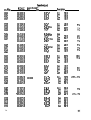
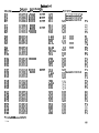
1
TM 9-6625-2467-15
DEPARTMENT
OF
THE
ARMY
TECHNICAL
MANUAL
OPERATOR’S, ORGANIZATIONAL, DIRECT SUPPORT, GENERAL SUPPORT,
AND DEPOT MAINTENANCE MANUAL
(INCLUDING REPAIR PARTS)
SPECTRUM ANALYZER
(TEKTRONIX, INC. MODEL 491)
(6625-494-2937)
HEADQUARTERS,
DEPARTMENT
DECEMBER 1969
OF
THE
ARMY
WARNING
HIGH VOLTAGE
is used in the operation of this equipment.
DEATH ON CONTACT
may result if personnel fail to observe safety precautions.
Learn the areas containing high voltage
in each piece of equipment.
Be careful not to contact high-voltage or 115-volt ac input connections
when installing or operating this equipment.
Before working inside the equipment, turn power off and ground points of
high potential before touching them.
This manual contains copyright material
reproduced by permission of TEKTRONIX, Inc.
TM 9-6625-2467-15
TECHNICAL MANUAL
HEADQUARTERS
DEPARTMENT OF THE ARMY
Washington, D.C., 15 December 1969
)
)
No. 9-6625-2467-15 )
SPECTRUM ANALYZER (TEKTRONIX, INC. MODEL 491)
(6625-494-2937)
CONTENTS
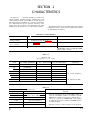
Section 1
Characteristics
Section 2
Operating Instructions
Section 3
Circuit Description
Section 4
Maintenance
Section 5
Performance Check
Section 6
Calibration
Abbreviations and Symbols
Section 7
Electrical Parts List
Mechanical Parts List Information
Section 8
Mechanical Parts List
Section 9
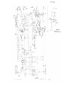
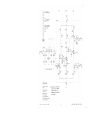
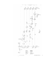
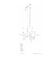
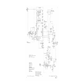
Diagrams
Mechanical Parts List Illustrations
Accessories
APPENDIX A.
B.
C.
BASIC ISSUE ITEMS LIST
MAINTENANCE ALLOCATION CHART
REPAIR PARTS LIST
Abbreviations and symbols used in this manual
are based on or taken directly from IEEE Standard 260 “Standard Symbols for Units”, MILSTD-12B and other standards of the electronics
industry.
i
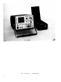
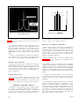
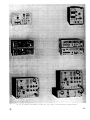
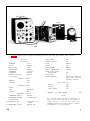
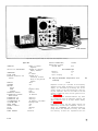
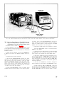
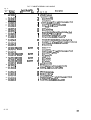
Fig. 1-1. The Type 491
i i
Spectrum Analyzer.
SECTION 1
CHARACTERISTICS
The Type 491
Spectrum Analyzer is a wide band,
general purpose portable spectrum analyzer with an RF
center frequency range from 10 MHz to 40 GHz. The analyzer displays signal amplitude as a function of frequency
for a selected portion of the spectrum, Frequency iS displayed along the horizontal axis (dispersion) and signal
amplitude on the vertical axis of a self-contained system.
The following electrical characteristics apply at an ambient
temperature of 25° C (±5°C) after an initial warmup period
of approximately 20 minutes.
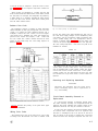
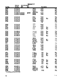
ELECTRICAL CHARACTERISTICS
Performance
Characteristic
RF Center
Frequency Range
Supplemental Information
10 MHz to 40 GHz—See Table 1-1
CW Sensitivity
(S + N=2N)
Dial Accuracy
Requirement
I
See Table 1-1
Within ± (2 MHz +1% of dial reading)
I
IF CENTER FREQ central at 000, FINE IF
CENTER FREQ control and FINE RF CENTER
FREQ controls centered.
TABLE 1-1
Minimum CW
Sensitivity (S + N = 2N)
Band and
Scale
RF CENTER FREQUENCY
1 kHz
RESOLUTION
–100 dBm
A-1
10-275 MHz
B-2
275-900 MHz
–110 dBm
–90 dBm
800-2000 MHz
–105 dBm
–85 dBm
3
–80 dBm
C-4
1.5-4.0 GHz
–110 dBm
–90 dBm
5
3.8-8.2 GHz
–100 dBm
-80 dBm
6
8.0-2.4 Ghz
–95 dBm
–75 dBm
7
12.4-18.0 GHz
–90 dBm
–70 dBm
18.0 -26,5 GHz
–80 dBm
-60 dBm
26.5-40.0 GHz
–70 dBm
-50
8
!
Supplemental
Information
100 kHz RESOLUTION
50 Ω source impedance.
All voltages are RMS.
dBm
TABLE 1-2
Setting
10MHz
DISPERSION/DIV
Accuracy
±3%
(±0.3
—
MHz/Div)
Remarks
5 MHz
±3%
2 MHz
±5% (±0.1 MHz/Div)
1 MHz
±7% (±70 kHz/Div)
.5 MHz
±10% (±50 kHz/Div)
Over the ±25 MHz of the IF Center FREQ control except the 10 MHz/DIV position (± 10 MHz). The DISPERSION CAL adjust can be reset to improve the accuracy at a specific IF CENTER FREQ control setting
by using the front panel 1 MHz CAL MARKERS OUT as
a calibrated signal.
.2 MHz
±15% (±30 kHz/Div)
Measured over the center 8 divisions of the graticule.
(±0.15
MHz/Div)
1-1
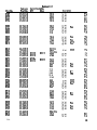
ELECTRICAL CHARACTERISTICS
Performance
Characteristic
Dispersion
MHz/DIV
Range
(cont)
Requirement
Linearity
kHz/DIV RANGE
Range
.2 MHz/Div to 10 MHz/Div
In a 1-2-5 seauence
See Table 1-2
±3%
(over an 8 division display)
1 kHz/Div to 500 kHz/Div in a 1-2-5 sequence and zero dispersion.
Accuracy
±3% of each setting
Linearity
±3% (over an 8 divisions display)
Resolution
IF Center Frequency
Control Range”
1 kHz/DIV to 500 kHz/DIV
Dispersion
Over the ±2.5 MHz range of the IF
CENTER FREQ control. Measured over the
center 8 divisions of the graticule.
≤1 kHz to ≥ 1 0 0 k H z ; i n 1 1 u n c a l i b r a t e d
steps.
IF CENTER FREQ
≥ ( + and – 2.5 MHz)
≥ ( + and – 50 kHz)
≥ ( + and – 25 MHz)
≥ ( + and – 1 MHz)
10 MHz/DIV
≥ ( + and – 10 MHz)
≥ ( + and – 1 MHz)
IF Attenuation
Range
Accuracy
IF GAIN Control
Range
Display Flatness with IF CENTER
FREQ at 000
Incidental FM
IF
LO
Phase Lock
Internal Markers
INT REF FREQ Range
May be coupled with the DISPERSION control or switched separately.
FINE
0.2 MHz/DIV to 5 MHz/DIV
+
In combinations of 1, 2, 4, 8, 16 and 20 dB.
0 to 51 dB
±0.1 dB/dB
≥50 d B
3 dB maximum
10 MHz to 12.4
6 dB maximum
12.4 GHz to 40
amplitude variations from
GHz.
amplitude variations from
GHz
≤200 H z
Band 1 (10 MHz to 275 MHz) 50 MHz dispersion.
Bands 2 through 8 (275 MHz to 40 GHz]
100 MHz dispersion.
Typically 100 Hz. Up to 400 Hz if power
line frequency drops to 48 Hz.
≤300 Hz (at LO fundamental and with
phase lock operation)
1 MHz ±0.1% (Control next to OFF position.)
At least 1 kHz but not more than 1.3 kHz
above measured frequency with the INT
REF FREQ control counterclockwise (next to
Instrument must be inside the dust cover.
OFF position.)
Stability; Ref. Osc.
(Short term FM)
External Phase Lock
Reference Input
Frequency
Voltage
Display Functions
Dynamic Range
LOG
≤ 1 p o r t i n 1 07 .
1 MHz to 5 MHz
1 to 5 volts peak to peak.
≥40 dB with 8 division display
≥26 dB with 8 division display
LIN
SQ
LAW
Maximum Input Power
≥13 db with 8 division display
-30 dBm for linear operation
+15 dBm diode mixer, power limit
1-2
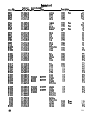
Information
RANGE
Accuracy
IF
Supplemental
See Fig. 2-8
TIME BASE
Performance
Characteristic
Requirement
Supplemental
,
Information
RECORDER Output
≥4 mV per displayed division amplitude of
signal in LIN made.
Sweep Range
10
Sweep Accuracy
± 3 %
Measured within the center 8 divisions
VARIABLE Time/Div
≥2.5:1
An uncalibrated control provides continuously variable sweep rates from 10 µs/div
to approximately 1.25 s/div.
µs/div to 0.5
s/div
Sweep Length
10.5 divisions ±0.2 div.
Sawtooth
70 mV to 90 mV (P-P)
Output
Rear panel connector
In a 1, 2, 5 sequence
Rear panel connector
TRIGGERING
Trigger Sensitivity
Internal
≤ 0 . 2 division, 20 Hz to 100 kHz
≤ 0 . 2 volt, 20 Hz to 100 kHz
External
Maximum Input Voltage
100 volts (DC + peak AC)
POWER REQUIREMENTS
Input Voltage
115-volt range
230-volt range
Line
Frequency
Input Power
LOW- 90 to 110 VAC
MED- 104 to 126 VAC
H I G H - 1 1 2 to 1 3 6 V A C
LOW- 180 to 220 VAC
MED- 208 to 252 VAC
HIGH- 224 to 272 VAC
Line voltage ranges provide regulated DC
voltages, when line contains less than 2%
total harmonic distortion.
48 to 440 Hz
55 watts maximum
CATHODE RAY TUBE
Information
Characteristic
Tube Type
T4910-7-1
Phosphor
P7
Accelerating Potential
Approximately 3.75 kV
Graticule
Type
internal
Area
8 divisions vertical by 10 divisions horizontal
Each division equals 0.8 cm.
Illumination
Variable edge lighting
Unblinking
Deflection type, DC coupled
MECHANICAL CHARACTERISTICS
Construction
Alluminum-alloy chassis, panel and cabinet
Glass laminate etched-circuit boards
Finish
Anodized panel, blue vinyl-coated cabinet
Overall Dimensions [measured
at maximum points]
7 ¼ ” h i g h , 1 2 ½ " w i d e , 2 3 ½ ” l o n g ( i n c l u d e s panel cover and carrying handle)
ENVIRONMENTAL CHARACTERISTICS
The following environmental test limits apply when tested
in accordance with the recommended test procedure. This
instrument will meet the electrical performance requirements
given in this section, following an environmental test.
1-3
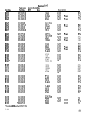
Characteristic
Temperature
Operating
Performance
Requirement
Altitude
Operating
–55° C to +75° C
15,000 feet maximum
Altitude referred to sea level. Operating
temperature capabilities decline 10 C per
1000 feet altitude above sea level.
May be tested during non-operating temperature test.
Non-operating
Humidity
Non-operating
Electromagnetic Interference (EMI)
Radiated Interference
Conducted
Interference
Vibration
Operating
Shock
Operating and non-operating
Transportation
Package vibration
Package drop
1-4
Information
Automatic resetting thermal cutout protects
instrument from overheating.
–15° C to +55° C
Non-operating
Supplemental
Five cycles (120 hours) of
Method 106B
Mil-Std-202C,
Exclude freezing and vibration.
150 kHz to 1000 MHz
Tested within an electrically shielded enclosure with the CRT mesh filter installed.
Within the limits described in MIL-I-6181D,
Figs. 7, 8, 14 and 16.
150 kHz to 25 MHz
Conducted interference through the power
cord.
Resonant searches along all 3 axes at 0.025
inches, frequency varied fram 10-55 c/s. All
major resonances must be above 55 c/s.
Instrument secured to vibration platform
during test. Total vibration time, about 55
minutes.
One shock of 30 G, one-half sine, 11 millisecond duration each direction along each
major axis.
Guillotine-type shocks. Total of 12 shocks.
Meets National Safe Transient type of test
when correctly packaged. One hour vibration slightly in excess of 1 G.
Package should just leave vibration surface
30 inch (18-inches for R491) drop on any
corner, edge or flat surface.
SECTION 2
OPERATING INSTRUCTIONS
Introduction
A Spectrum Analyzer is an instrument that graphically
presents a plot of signal amplitude as a function of frequency
for a selected portion of the spectrum. The Type 491 is
designed to provide a spectral display of the frequency
distribution of electromagnetic energy within the frequency
range of 10 MHz to 40 GHz. Signals are displayed as a
spectrum on a CRT screen with signal energy plotted on the
vertical axis against frequency on the horizontal axis.
fuses which are positioned correctly when the correct selection is made for either 115 or 230-volt nominal operation.
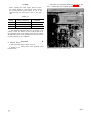
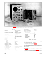
Fig. 2-3 shows the power input panel on the rear of the
instrument and the voltage range and nominal line voltage
selectors.
This type of display provides the following information;
The presence or absence of signals, their frequencies, frequency drift, relative amplitude of the signals and the nature
of modulation if any, plus many other characteristics.
This section of the manual describes the function of the
front and rear panel controls and connectors, power supply
connection, and a procedure for first time operation, to introduce the operator to the operational functions of the controls.
The remainder af the section then describes operation technique with some measurement applications and signal
interpretations.
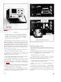
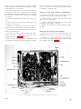
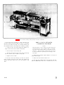
Front Cover and Handle
The front cover furnished with the Type 491 provides a
dust tight seal around the front panel. Use the cover to
protect the front panel when storing or transporting the
instrument, The cover also provides storage for the external
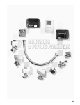
waveguide mixers and other accessories. See Fig. 2-1.
CAUTION
Removing or replacing the dust cover on the instrument may be hazardous, if the” instrument is lifted
out of, or slid into, the dust cover. To remove or
replace the dust cover, set the instrument on a
bench or table, then slide the cover off or on the
instrument. The instrument may also be set on the
front panel cover and the dust cover slipped on or
off the instrument. Do not set the instrument on
the front panel controls.
The handle of the Type 491 can be positioned to carry
the instrument or it can be positioned at several angles to
serve as a tilt-stand. To position the handle, press in at both
pivot points (see Fig. 2-2) and adjust the handle to the
desired position. The instrument may also be set upright
on the rear panel feet for operation or storage.
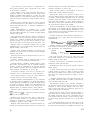
Voltage Considerations
The Type 491 can be operated from either 115 or 230-volt
nominal line voltage with a range from 90 to 136 VAC or
180 to 272 VAC. Two selector-type connectors on the power
input panel may be positioned to accommodate these voltage ranges. The selection assembly also includes two line
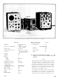
Fig. 2-1. Accessory storage provided in the front cover of the Type
491
2-1
Fig. 2-2. Handle positioned to provide a stand for the instrument.
CAUTION
The Type 491 should not be operated with these
voltage selector switches in improper positions.
Operation of the instrument with incorrect voltages
will either blow the protective fuses or the instrument will not operate properly.
The Voltage Range Selector located on the rear panel
permits the instrument to operate on line voltages above and
below the nominal 115 or 230 volts. Each selection provides
correct regulation through an overlap voltage range into the
next higher or lower range. It is best to select a range with
its center voltage near your nominal line voltage, thus providing adequate regulation over a plus and minus deviation of the input line voltage.
The following procedure will prepare the instrument for
operation at your average input line voltage:
1. Remove the cover assembly over the selectors by
unscrewing the two cap screws, then pull the cover with the
attached fuses away from the panel.
2. Pull the Line Voltage Selector out and turn the connector
around to plug it back into the correct position.
3. To change the regulating range, pull out the Range
Selector bar, slide it to the desired range and plug it into
the correct position. Select a range which is centered about
the average line voltage to be applied to the instrument.
See Fig. 2-3.
4. Re-install the cover. Make certain the cover fits firmly
against the rear panel, so the line fuses are seated in their
sockets, and tighten the two cap screws.
5. Before applying power to the instrument, check that the
indicating tabs on the switch bars are protruding through
the correct holes for the desired voltage setup.
2-2
Fig. 2-3. Power panel and selectors.
Spectrum Analyzer Terms
The following glossary of spectrum analyzer terms is presented as an aid to understanding the terms as they are used
in this manual.
Spectrum Analyzer-A device that displays a graph of the
relative power distribution as a function of frequency, typically on a cathode-ray tube or chart recorder.
Types: Real-time and non real-time.
A real-time spectrum analyzer performs a continuous
analysis of the incoming signal, with the time sequence of
events preserved between input and output.
A non-real-time spectrum analyzer performs an analysis
of repetitive events by a sampling process.
Methods: Swept front end and swept intermediate frequency.
A swept front end spectrum analyzer is a superheterodyne
spectrum analyzer in which the first local oscillator is swept.
A swept IF spectrum analyzer is a superheterodyne spectrum analyzer in which a local oscillator other than the first
is swept.
Center frequency (radio frequency or intermediate frequency)-That frequency which corresponds to the center
of the reference coordinate.
Center frequency range (radio frequency)-That range of
frequencies which can be displayed at the center of the
reference coordinate. When referred to a control (e.g., Intermediate Frequency Center Frequency Range) the term indicates the amount of frequency change available with the
control.
Dispersion (sweep width)-The frequency sweep excursion
over the frequency axis of the display can be expressed as
frequency/full frequency axis, or frequency (Hz)/division in
a linear display,
Display
flatness-Uniformity
of
amplitude
over
a
rated
dispersion, The maximum variation in amplitude response
over the maximum dispersion is a measure of display flatness
(usually in units of dB).
Drift (frequency drift)-Long term frequency changes or
or instabilities caused by a frequency change in the spectrum
analyzer local oscillators. Drift limits the time interval that a
spectrum analyzer can be used without retuning or resetting the front panel controls (units maybe Hz/s, Hz/°C, etc).
Dynamic range (on screen)-The maximum ratio of signal
amplitudes that can be simultaneously observed within the
graticule (usually in units of dB).
Dynamic range (maximum useful)-The ratio between the
maximum input power and the spectrum analyzer sensitivity
(usually in units of dB).
Frequency band-A range of frequencies that can be covered without switching.
Frequency scale-The range of frequencies that can be
read on one line of the frequency indicating dial.
Incidental frequency modulation (residual frequency modulation)—Short term frequency jitter ar undesired frequency
deviation caused by instabilities in the spectrum analyzer
local oscillators. Incidental frequency modulation limits the
usable resolution ond dispersion (in units of Hz).
Incremental linearity-A term used to describe local
aberrations seen as non-linearities for narrow dispersions.
Linear display-A display in which the vertical deflection
is a linear function of the input signal voltage.
Linearity (dispersion linearity)-Measure of the comparison
of frequency across the dispersion to a straight line frequency
change. Measured by displaying a quantity of equally spaced
(in frequency) frequency markers across the dispersion and
observing the positional deviation of the markers from an
idealized sweep as measured against a linear graticule.
Linearity accuracy, expressed as a percentage, is within
X 100% where
is maximum positional deviation
and W is the full graticule width.
Maximum input power-The upper level of input power
that the spectrum analyzer can accommodate without degradation in performance (spurious responses and signal
compression). [Usually in units of dBm).
Minimum usable dispersion-The narrowest dispersion obtainable for meaningful analysis. Defined as ten times the
incidental frequency modulation when limited by “incidental
frequency modulation” (in units of Hz).
Phase Lock-The frequency synchronization of the local
oscillator with a stable reference frequency.
Resolution-The ability of the spectrum analyzer to resolve and display adjacent signal frequencies. The measure
of resolution is the frequency separation (in Hz) of two equal
amplitude signals, the displays of which merge at the 3 dB
down point. The resolution of a given display depends on
three factors; sweep speed, dispersion and the bandwidth of
the most selective (usually last IF) amplifier.
Resolution bandwidth-The -6 dB bandwidth (with
sian response) of the analyzer, with the dispersion and
time adjusted for the minimum displayed bandwidth of
signal. Resolution and resolution bandwidth become
nymous at very long sweep times,
Gaussweep
a CW
syno-
Optimum resolution-The best resolution obtainable for a
given dispersion and a given sweep time, Theoretically or
mathematically:
Optimum resolution bandwidth—The bandwidth at which
best resolution is obtained for a given dispersion and sweep
time. Theoretically and mathematically:
Optimum
resolution
bandwidth
dispersion (in Hz)
sweep time [in seconds)
Safe power level-The upper level of input power that
the spectrum analyzer can accommodate without physical
damage (usually in units of dBm).
Scanning velocity-Product of dispersion and sweep repetition rate (units of Hz/unit time).
Sensitivity-Rating factor of spectrum analyzer’s ability to
display signals.
1. Signal equals noise: That input signal level (usually
in dBm) required to produce a display in which the signal
level above the residual noise is equal to the residual noise
level above the baseline. Expressed as: Signal + noise =
twice noise.
2. Minimum discernible signal: That input signal level (usually in dBm) required to produce a display in which the signal is just visible within the noise.
Skirt selectivity-A measure of the resolution capability of
the spectrum analyzer when displaying signals of unequal
amplitude. A unit of measure (usually in Hz) is the bandwidth at some level below the 6 dB down points. For example: 10 dB, 20 dB or 40 dB down.
Spurious response (spurii, spur)-An erroneous display or
signal which does not conform to the indicated frequency or
dial reading. Spurii and spur are the colloquialisms used to
mean spurious response (plural) or spurious response (singular) respectively. Spurious responses are of the following
types :
1. IF feedthrough-Signal frequencies within the IF passband of the spectrum analyzer that are not converted in the
first mixer but pass through the IF amplifier and produce dis-
2-3
plays on the CRT that are not tunable with the RF center frequency controls.
INTENSIFIER-Controls the relative brightness between the
displayed signal and the trace baseline.
2. Image response-The superheterodyne process results
in two major IF responses, separated from each other by
twice the IF. The spectrum analyzer is usually calibrated to
only one of these two responses. The other is called the
image.
POSITION-TWO (2) controls that position the CRT beam
in the vertical and horizontal plane.
3. Harmonic conversion-The spectrum analyzer will respond to signals that mix with harmonics of the local oscillator and produce the intermediate frequency. Most spectrum analyzers have dials calibrated for some of these higher
order conversions. The uncalibrated conversions are spurious
responses.
4. Intermodulation-in the case of more than one input
signal, the myriad of combinations of the sums and differences of these signals between themselves and their multiples
creates extraneous response known as intermodulation. The
most harmful intermodulation is third order, caused by the
second harmonic of one signal combining with the fundamental of another.
5. Video detection-The first mixer will act as a video detector if sufficient input signal is applied, A narrow pulse
may have sufficient energy at the intermediate frequency
to show up as an intermediate frequency feedthrough.
6. Internal-A spurious response on the display caused
by a signal generated within the spectrum analyzer that is
in no way connected with an external signal.
7. Anomalous IF responses-The filter characteristic of the
resolutian-dete rmining amplifier may exhibit extraneous passbands. This results in extraneous spectrum analyzer responses
when a signal is being analyzed.
8. Zero frequency feedthrough-(zero pip)-The response
produced when the first local oscillator frequency is within
the IF passband. This corresponds to zero input frequency
and is sometimes not suppressed so as to act as a zero frequency marker.
Sweep repetition rate-The number of sweep excursions
per unit of time. Approximately the inverse of sweep time
for a free-running sweep.
Sweep time-The time required for the spot on the reference coordinate (frequency in spectrum analyzer) to move
across the graticule, (In a linear spectrum system, sweep
time is Time/Division multiplied by total divisions.)
CONTROLS AND CONNECTORS
The following is a brief description of the operation or
function of the controls and connectors on the front (see Fig.
2-4) and rear panel, A more detailed description is given
later in this section under operating information.
Time Base Controls
TIME/DIV-Selects calibrated sweep rates from 0.5 s/div to
10 µs/div in a 1-2-5 sequence.
VARIABLE-Permits an uncalibrated overlapping adjustment of the sweep rate so the sweep rate may be varied
continuously from 10 µs/div to approximately 1.25 s/div.
Trigger Controls
SLOPE-Selects the positive or negative portion of
input signal to trigger the time base,
the
LEVEL-Selects the amplitude point on the triggering signal where sweep triggering occurs. In the fully clockwise
position, the sweep circuit free runs.
SOURCE-Selects signal source for triggering the time
base. Selections are: INT (from vertical amplifier); LINE
(line voltage frequency); EXT (external signal applied to the
rear panel BNC connector labeled TRIG IN).
Spectrum Analyzer Section (IF)
DISPERSION RANGE-Selects the range of the DISPER
SION selector.
DISPERSION—Selects the dispersion (frequency width) of
the display in conjunction with the DISPERSION RANGE
switch. Dispersion selections are 10 MHz/div to 1 kHz/div
in a 1-2-5 sequence plus 0 dispersion position.
When the DISPERSION selector is in the 0 position, the
analyzer functions as a fixed tuned receiver, permitting
displays of the time domain characteristics of modulation
within the resolution bandwidth capabilities of the analyzer.
COUPLED RESOLUTION-Selects the analyzer resolution
bandwidth. Eleven selectable ranges from approximately
100 kHz to less than 1 kHz are provided. Optimum resolution for a given dispersion is generally obtained with the
RESOLUTION control coupled to the DISPERSION selector.
DISPERSION CAL—A screwdriver adjustment to calibrate
the MHz/div dispersion.
DISPERSION BAL-Adjusted to balance the dispersion center (center freqeuncy point) of the MHz/DIV and kHz/
DIV positions of the DISPERSION RANGE switch.
IF ATTENUATOR dB-Series of six toggle switches to pro
vide a range of IF attenuation from 1 dB to 51 dB.
CRT Controls
GAIN-A variable control of the analyzer IF gain.
lNTENSITY-Controls brightness of the CRT trace
SCALE ILLUM-Controls graticule light level.
FOCUS-Adjusts spot size for optimum display definition.
ASTIGMATISM-Used in conjunction with the FOCUS control to adjust spot shape and obtain optimum display definition.
2-4
IF CENTER FREQ-A 10 turn control that adjusts the IF
center frequency of the display. Provides a + and - 10
MHz adjustment in 10 MHz/DIV dispersion position, a +
and - 25 MHz adjustment of the center frequency through
the 5 MHz/div to 0.2 MHz/div positions and a + and 2.5 MHz adjustments through the 500 kHz/div to 1 kHz/div
DISPERSION positions.
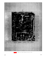
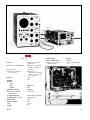
Fig. 2-4. Front panel controls and connectors.
FINE-A one turn control that operates in conjunction with
the IF control to provide a fine adjustment of the IF center
frequency.
CAL-With the IF CENTER FREQ control centered, it calibrates the IF center frequency to 200 MHz.
VIDEO FILTER-With the switch in the up position, the
video bandwidth is restricted, to reduce high frequency
video components such as noise, and reduce zero beats
when viewing signals near minimum resolution.
VERTICAL DISPLAY-Selects logarithmic, linear or squarelaw display. In the LOG position, signal display amplitude
is a logarithmic function with a ³40-dB dynamic range.
In the LIN position, signal display amplitude is a linear
function with a ³26-dB range. In the SQ LAW position
signal display amplitude is a square law function and the
display is a function of signal power, The SQ LAW position has a ≥13 d B d y n a m i c r a n g e .
POWER-Turns power off and on to the Type 491.
INDICATOR LIGHT-indicates when POWER is applied to
the Type 491.
RF CENTER FREQUENCY-Tunes RF center frequency from
10 MHz to 40 GHz. With the IF CENTER FREQ control in
the 0 position, the RF CENTER FREQUENCY dial indicates
the center frequency of the display.
BAND SELECTOR-Switch selects RF Inputs and bands;
A (10-275 MHz), B (270-2000 MHz) and C (1.5-40 GHz).
FINE RF CENTER FREQ-A 10 turn control to provide a
fine adjustment of the RF local oscillator frequency.
Especially useful in tuning the oscillator to a phase lock
condition with the reference frequency.
MIXER PEAKING-A two position control that optimizes
the conversion of the first local oscillator for bands B and
C. Does not affect band A. In the SEARCH position the
mixer current is swept through a range by the sweep voltage. This insures an optimum mixer conversion or sensitivity point within the dispersion range of the analyzer, so
all signals within a given dispersion pass through this optimum sensitivity point as the signals are tuned across the
screen. The manual (0 to 10) position of the control provides an adjustment to optimize mixer conversion for any
fixed center frequency setting.
LOCK CHECK-A push button switch that applies the
phase lock output beat signal (between the local oscillator
and reference frequency) to the vertical display system.
Provides a visual indication to the operator of phase lock
operation.
INT REF FREQ-A switch and control. The control varies
the internal 1 MHz Reference Frequency over a range of
approximately 1 kHz. With the control in the OFF position, the Internal Reference Frequency is turned off, and
an externally applied signal to the EXT REF FREQ IN
(1 MHz MARKERS OUT) connector becomes the reference
frequency.
2-5
1 MHz MARKERS OUT-EXT REF FREQ IN-A BNC connector that provides 1 MHz marker output signals to calibrate the dispersion. With the INT REF FREQ control in
the OFF position, an external signal between 1 MHz and
5 MHz (1 to 5 V peak to peak) applied to the connector
becomes the reference frequency for phase lock operation.
RF INPUTS-Coaxial connectors which connect through
either a coaxial cable, or (if above 12.4 GHz) a waveguide mixer, to the signal source. Band A frequency range
is 10 to 275 MHz. Band B frequency range is 275 MHz to
2 GHz. Band C consists of a coaxial mixer (green label) for
the frequency range 1.5 GHz to 12.4 GHz; or a Waveguide Mixer Adapter (black label) which connects through
a two foot cable to one of three external Waveguide
Mixers for the frequency range 12.4 GHz to 40 GHz.
Rear Panel
TRIG IN-A BNC connector to apply external triggering
signals. Frequency range: 20 Hz to 100 kHz, signal amplitude equal to or greater than 0.2 V.
Analyzer Controls
DISPERSION
RANGE
MHz/DIV
DISPERSION—COUPLED
RESOLUTION
Controls coupled together
and in the 10 MHz/div
position
IF ATTENUATOR dB
All switches OFF position
I F CENTER FREQ
Centered (000)
FINE
Midrange
VIDEO FILTER
OFF
VERTICAL DISPLAY
LIN
GAIN
CCW
RF CENTER FREQUENCY
Band B
FINE RF CENTER FREQ
Centered (approximately
5 full turns from either
extreme position)
INT REF FREQ
Out of the OFF switch
detent in the VARIABLE
position
MIXER PEAKING
Fully CCW in the
switched SEARCH position
SAW OUT-A 70 to 90 mV sawtooth signal output that
is coincident with the analyzer sweep.
RECORDER-Signals on the display may be recorded by
connecting to the RECORDER output. A linear output, equal
to or greater than 4 mV per displayed division amplitude
of signal, in the LIN mode, inta a load impedance of
600 ohms.
3. Connect the Type 491 to a suitable power source and
turn the POWER switch to ON. Allow a few minutes for
the instrument to stabilize.
4. Adjust the INTENSITY control clockwise until a trace
is visible, then adjust the FOCUS and ASTIGMATISM controls
for optimum trace definition.
FIRST TIME OPERATION
5. Position the trace to the horizontal center and to the
bottom graticule line of the graticule with the POSITION
controls.
The following procedure demonstrates the basic functions
of the controls and connectors for the Type 491. We recommend this procedure for first time familiarization. Careless
or incorrect operation may damage the instrument.
6. Adjust SCALE ILLUM control for the desired graticule
illumination.
1. Check input power selector positions at the rear panel.
Correct selector positions for the different input line voltages
are given under Voltage Considerations in this section.
2. Preset the front panel controls as follows:
OFF
POWER
CRT Controls
INTENSITY
Ccw
SCALE ILLUM
Midrange
FOCUS
Midrange
ASTIGMATISM
Midrange
Ccw
INTENSIFIER
POSITION
(Both centrals)
Midrange
Time Base Controls
2-6
TIME/DIV
10ms
VARIABLE
CAL
SLOPE
+
LEVEL
FREE RUN
SOURCE
INT
7. Apply a signal with an amplitude between -60 and
-30 dBm, from a Signal Generator or other source that is,
within the frequency range of band B, through a coaxial
cable to band B, RF INPUT connector.
NOTE
If a signal source within the frequency range af
band B is not available, apply the signal to band
A or C and set the band selector to the appropriate band.
8. Adjust the GAIN control for a moderate noise level
(1 division) on the display, then tune the RF CENTER FREQUENCY control through the frequency range. Note that
some of the signals move across the screen at different rates,
and the direction of movement (left to right or right to left)
of the signals is not the same. (See Spurious and Image
Frequency displays later in this section.)
9. Tune the dial with the RF CENTER FREQUENCY control
to the frequency of the applied input RF signal.
10. Switch the MIXER PEAKING control from SEARCH
position to manual, then adjust for optimum signal amplitudes.
11. Adjust the GAIN and/or the IF ATTENUATOR dB
switches for a signal amplitude of approximately 6 divisions.
12. Tune the signal to the extreme left graticule line with
the RF CENTER FREQUENCY control. Note the dial reading.
Tune the signal to the extreme right graticule line and note
the dial reading. The difference between dial readings is
the total dispersion window for this 10 division display. Tune
the signal to the center of the screen and switch the DISPERSION-COUPLED RESOLUTION selector to the 5 MHz/
div position. Tune the signal across the screen and note
the total dispersion. It should decrease to approximately
½ the dispersion noted with the DISPERSION selector in
the 10 MHz/div position. Tune the signal to the center of
the screen.
13. Tune the IF CENTER FREQ coarse control through its
range. Note that all signals move across the screen in the
same direction and the same amount. This control shifts
the IF center frequency approximately + and - 25 MHz
with the DISPERSION controls in this position. Tune the IF
CENTER FREQ control to center the signal on the screen.
GENERAL OPERATING INFORMATION
Light Filters
The instrument is shipped with a mesh filter installed.
Two (2) colored filters, plus a clear CRT faceplate protector
and an ornamental ring are provided with the accessories.
The mesh filter improves the contrast when viewing the
display under high ambient light conditions. The blue and
yellow filters can be used to take advantage of the dual
phosphor characteristics of the P7 CRT.
The mesh filter is removed by pressing down at the bottom of the frame and pulling the top of the holder away
from the CRT faceplate. See Fig. 2-5. To install the colored
filters, press them into the ornamental mounting ring until
they snap behind the retainer lips. To remove the filters
from their holder, press them out to the rear.
14. Change the DISPERSION selector to .5 MHz/div.
Adjust the FINE (1 turn) IF CENTER FREQ control. Note the
frequency range of this control. This control shifts the IF
center frequency approximately + and - 1 MHz with the
DISPERSION RANGE in this position.
15. Change the TIME/DIV switch between .1 s and .1 ms
positions. Note the change in signal amplitude and the
resolution. Return the TIME/DIV selector to the 10 ms position.
16. Push the LOCK CHECK button and tune the RF CENTER
FREQUENCY control very carefully through the signal frequency. Note the phase lock beat signals between the tunable local oscillator and the Internal Reference Frequency
oscillator as the display blooms, then snaps into phase lock
operation (Fig. 2-13).
17. With the LOCK CHECK button depressed, adjust the
FINE RF CENTER FREQ control. Note the beat frequency displays as the control is varied, and note also the vertical shift
of the baseline. This baseline shift is the change in the output DC level of the phase amplifier. Note the zero beat signal compression at the extreme positions of this control compared to their amplitude near the center. Phase lock should
be set with the output DC level within the center 4 divisions
of the graticule. Adjust for phase lock operation and release the LOCK CHECK button.
18. Switch the DISPERSION RANGE switch to kHz/DIV,
then decrease the DISPERSION TO 20 kHz/div, keeping the
signal centered on screen with the IF CENTER FREQ control. Slowly rotate the FINE RF CENTER FREQ control. Note
the positive action of the phase lock circuit before lock is
lost. Return the signal to its locked mode by adjusting the
FINE RF CENTER FREQ control.
19. Uncouple the RESOLUTION and turn the control
clockwise. Note that the signal broadens as the resolution bandwidth is increased. The resolution may be varied
from approximately 1 kHz to 100 kHz, Return the RESOLUTION control to the coupled position.
20. Adjust the INTENSIFIER control through its range. This
control suppresses the base of the display, and can be
utilized when photographing displays at slow sweep rates.
See Operation of the INTENSIFIER control. It should be left
in the OFF position for most aperating situations.
Fig. 2-5. Removing the light filter or faceplate.
One of the filters or protector should be used at all times
to protect the faceplate of the CRT from scratches.
Intensity Level, Astigmatism and Focus
Operate the instrument with the intensity level no higher
than the level required to clearly observe the display.
Changing the INTENSITY setting may require refocusing the
display.
The ASTIGMATISM and FOCUS controls both affect display definition and are normally adjusted together. If the
ASTIGMATISM control is correctly set, the vertical and horizontal segments of the display will focus at the same position of the FOCUS control, The controls are adjusted as
follows:
1. Obtain a display on the analyzer with both horizontal
and vertical information.
2. Adjust the ASTIGMATISM control for equally focused
vertical and horizontal portions in the display.
2-7
3. Adjust the FOCUS control for
vertical sections of the display.
optimum focus of the
4. Repeat the two adjustments for best overall focus and
display definition.
Trace Alignment
If a free running trace is not parallel to the horizontal
graticule lines, the trace may be aligned by means of an
internal Trace Rotation adjustment. Refer to the Calibration
section.
Operation of the INTENSIFIER and CONTRAST
Controls
These controls are used to suppress the brightness of the
display baseline when large variations in display brightness
are not desirable; for example, when photographing or viewing displays at very slow sweep rates. T h e I N T E N S I F I E R
adjusts the height of the suppressed baseline. The CONTRAST adjusts the degree of contrast between the suppressed
portion and the intensified portion of the display.
The adjustment of the CONTRAST is optional; however,
it is normally set to produce a suppressed portion that is
still visible, so the intensity level of the vertical and horizontal portions of the display are equalized at slow sweep
rates.
The INTENSIFIER control is normally operated in the OFF
position, so the display and baseline are intensified. It is
turned on to suppress the baseline at slow sweep rates, in
preparation for display photography. See Fig. 2-6.
Signal Application
The application of any RF signal to the Type 491 is determined by its frequency and level. Signals between 10 MHz
and 275 MHz are applied to the Band A, BNC connector.
Frequencies from 275 MHz to 2 GHz are applied to the band
B, N-type connector, and band C covers the remaining frequency range from 1.5 GHz to 40 GHz. Signals should be
applied through the standard cables supplied with the accessories. Cables such as RG 9B/U will give satisfactory performance to approximately 12.4 GHz. Signals in the 12.4
GHz to 40 GHz range are applied to external Waveguide
Mixers which connect through a two-foot coaxial cable and
a Waveguide Mixer Adapter to the input receptacle. The
Waveguide Mixer Adapter replaces the Coaxial Mixer Assembly in the input receptacle.
The selection of mixers and adapters for the frequency
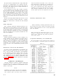
coverage is as follows:
1.5 GHz to 12.4 GHz-Plug-in Coaxial Mixer, Tektronix
Part No. 119-0096-00.
12.4 GHz to 40 GHz-Waveguide Mixer Adapter, Tektronix Part No. 119-01 04-00; Coaxial Cable, Tektronix Part
No. 012-0115-00 and one of the following Waveguide Mixers.
Flange
Type
Tektronix
Part
Number
Frequency
Range
Band
Waveguide
( EIA
designation)
Ku
WR62
12.4 GHz to
18.0 GHz
UG-419/U 119-0097-00
K
WR42
18.0 GHz to
26.5 GHz
UG-595/U
Ka
WR28
18.0 GHz to
40.0 GHz
UG-599/U 119-0099-00
119-0098-00
—
Fig. 2-6. INTENSIFIER operation.
2-8
Signal input power to the analyzer should not exceed -30
dBm. Signal above this level will overload the 1st mixer and/
or the 1st IF stage and generate spurious signals on the display. Add at least 10 dB of attenuation to the input when
the signal begins to compress (no increase of signal amplitude
with an increase of signal level). A conversion chart (Fig.
2-8) may be used to calculate input signal level.
CAUTION
Signals stronger than +15 dBm applied to the
input or mixer will damage or burn out the mixer
diodes.
Mismatches between the signal source and the RF INPUT
connectors may be caused by signal source output impedance, long coaxial cables, etc. These mismatches will adversely affect display flatness. When optimum flatness is
desired and signal strength is adequate, a 50 Ω attenuator
pad of approximately 6 to 10 dB should be added between
the signal source and the input to the mixer. The addition
of the attenuator will minimize reflections and optimize display flatness.
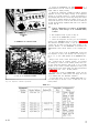
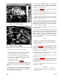
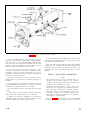
Fig. 2-7. Changing band C Coaxial Mixer to Wave Guide Adapter,
The Mixer Adapter or Coaxial Mixer may be removed from
the input receptacle by turning the retainer ring in either
direction. See Fig. 2-7. To replace either assembly, push the
adapter or coaxial mixer against the spring until the flange
bottoms, then turn until the latch snaps to hold the unit in
place.
Three attenuator pads, 10 dB, 20 dB and 40 dB are supplied with the accessories kit, These three attenuators may
be stacked on the N type connector to provide up to 70 dB
attenuation. A support should be provided however, if
more than 2 attenuators and an N to BNC adapter are
stacked on the band A connector. The attenuators are rated
at 2 watts (average).
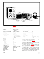
Fig. 2-8. Volts-dBm-Watts conversion chart for 50
Ω
impedance.
2-9
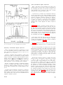
Mixer Peaking
As the analyzer sweep rate is increased, the amplitude
of the CW signal will decrease and the bandwidth becomes
The MIXER PEAKING control has a switch and variable
control position and is used to optimize mixer conversion in
the harmonic bands of Band C. The switched position (fully
C C W) is referred to as the SEARCH mode. In this position, an
optimum mixer conversion or sensitivity point is provided
within the dispersion window so signals that are tuned across
the screen will pass through this optimum sensitivity point.
This insures thot most signals within a given dispersion window will be observed as the RF CENTER FREQUENCY control is tuned.
wider; which signifies that both the sensitivity and resolution
have been degraded by the analyzer sweep rate,
Mixer conversion becomes a manual adjustment with the
control in the VARIABLE position and should be optimized at
each RF CENTER FREQUENCY setting. It has no affect on
band A and is usually broad through the B and C band frequency range.
The loss of the analyzer sensitivity due to sweep rate
and dispersion can be expressed mathematically as:
w h e r e S / SO is the ratio of the effective sensitivity to the
analyzer measured sensitivity, at very slow sweep rates or
zero dispersion.
D is the dispersion in hertz
B is the -3 dB bandwidth of the analyzer in hertz
T is the sweep time in seconds, or
Relative amplitude and sensitivity measurements must be
made after the MIXER PEAKING is adjusted because the display response is not flat when the central is in the SEACH
position.
is the sweep rate.
These same variables also determine the resolution of
the analyzer. The loss in resolution can be expressed as
follows:
Dispersion
Dispersion is the swept frequency range, or screen window.
The dispersion is adjustable from 10 MHz/div to 1 kHz/div in
a 1, 2, 5 sequence with an added zero dispersion position
for fixed frequency operation. Band A is limited to a maximum usable dispersion of 5 MHz/div (±25 MHz), because
of the added 235 MHz low pass filter.
Dispersion accuracy is a function of the IF CENTER FREQ
control position
and the DISPERSION RANGE switch setting. See Characteristics section. The dispersion accuracy
far the kHz/div selections is greater than the MHz/div
selections, because the range of the IF CENTER FREQ is ten
times greater for the MHz/div ranges (±25 MHz in the MHz/
DIV range).
The front panel DISPERSION-CAL adjustment may be used
to recalibrate dispersion for specific IF CENTER FREQ control settings if a high degree of accuracy is desired. The procedure is described in step 4 for front panel calibration.
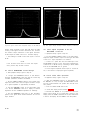
Resolution
Resolution is the ability of the spectrum analyzer to display adjacent signal frequencies discretely. The measure of
resolution is the frequency separation (in Hz) of two equal
amplitude signals when the notch or dip between these signals is 3 dB down. The resolution for a given display is a
function of sweep speed, dispersion and bandwidth of the
most selective (usually the last IF) amplifier in the signal path.
Resolution bandwidth is approximately the -6 dB bandwidth (with Gaussian response) of the analyzer, with the dispersion and sweep time adjusted for the minimum displayed
bandwidth to a CW signal. Resolution and resolution bandwidth become synonymous at very long sweep times.
As the analyzer sweep rate is increased, the amplitude of
the CW signal will decrease and the bandwidth becomes
wider; which signifies that both the sensitivity and resolution
have been degraded by the analyzer sweep rate.
2-10
W h e r e R / R O is the ratio of the effective resolution of the
analyzer to the analyzer measured resolution bandwidth
at very slow sweep speeds. R O is somewhat arbitrary and
is taken as the displayed width of the CW signal at the
-6 dB point.
The resolution of the Type 491 Spectrum Analyzer is
optimized for most settings of the DISPERSION selector
when the RESOLUTION control is in the coupled position.
Resolution however, can be varied from approximately 100
kHz to less than 1 kHz by uncoupling the RESOLUTION
control and changing it as an independent function of the
DISPERSION selector.
The sweep rate, as previously mentioned, should be set
below the sweep rate at which there is no noticeable amplitude loss in the signal.
As previously shown in the above formula the effective
resolution of the analyzer is a function af the IF bandwidth.
To adequately resolve pulsed spectrum information, the resolution bandwidth of the analyzer should be on the order of
1/10 of the sidelobe frequency width or the reciprocal of
the pulse width. The RESOLUTION control is usually set,
after the sweep rate has been adjusted, for optimum main
lobe detail. See Fig. 2-9.
Front Panel Calibration Adjustments
Three front panel screwdriver adjustments are provided,
to enable the operator to calibrate the dispersion and IF CENTER FREQ controls, and balance the MHz and kHz positions
of the DISPERSION RANGE selector.
1. Balance and Calibration Check
a. Turn the INT REF FREQ control to OFF position, then
tune a signal on screen with the RF CENTER FREQUENCY
control.
d.
tion,
shift
MHz
With the DISPERSION RANGE in the MHz/DIV posiadjust the IF CENTER FREQ-CAL for minimum signal
as the DISPERSION is switched through the MHz (10
- .2 MHz) positions.
e. Return the DISPERSION to the 5 MHz/div position.
Position the signal to the graticule center with the Horizontal
POSITION control. If the signal is more than 1 division
from the sweep center, it will be necessary to adjust the
internal Sweep Center adjustment R203. See Calibration
section.
3. DISPERSION-BAL Adjustment
a. Preset the front panel controls as follows:
Fig. 2-9. Frequency spectrum of a pulsed cw signal.
b. Tune for minimum signal shift as the DISPERSION
RANGE is switched from MHz/DIV to kHz/DIV positions.
c. With the DISPERSION RANGE selector at MHz/DIV
position, adjust the IF CENTER FREQ control for minimum
signal shift as the DISPERSION control is switched through
the 10 to .2 MHz positions.
d. Center the signal with the Horizontal POSITION control and check the position of the signal on the sweep. The
signal should locate near the center of the sweep with the
sweep extending over the 10 division width of the graticule.
If calibration is required, proceed with the following
adjustments.
IF CENTER FREQ and
FINE
000 (centered)
DISPERSION RANGE
MHz/DIV
DISPERSION
5 MHz/div
b. Tune the RF signal to the screen center.
c. Adjust the DISPERSION BAL for minimum signal shift
as the DISPERSION RANGE switch is switched between the
MHz/DIV and kHz/DIV positions. (Start the balance adjustment with the DISPERSION selector in the 5 MHz position,
then decrease the dispersion to the .2 MHz-20 kHz position
for the final adjustment.)
NOTE
If the dispersion balance can not be achieved
with the above procedure, the instrument requires
i n t e r n a l a d j u s t m e n t . Refer to the Calibration section of the manual.
NOTE
These adjustments interact, and must be performed
in sequence.
4. DISPERSION-CAL Adjustment
a. Preset the front panel controls as follows:
2. IF CENTER FREQ-CAL Adjustment
a. Center the IF CENTER FREQ controls, the DISPERSION
BAL and the IF CENTER FREQ-CAL adjustments. Set the
DISPERSION RANGE to MHz/DIV and the DISPERSION
selector to 5 MHz/div position.
b. Apply a stable RF signal to the appropriate RF INPUT
connector; then tune to the signal frequency with the RF
CENTER FREQUENCY control. Adjust the GAIN control for
a signal amplitude of approximately 6 divisions.
c. Adjust the RF CENTER FREQUENCY and the FINE RF
CENTER FREQ controls for minimum signal shift as the DISPERSION RANGE is switched between the MHz/DIV and the
kHz/DIV position.
IF CENTER FREQ
000 (centered)
DISPERSION RANGE
MHz/DIV
DISPERSION
1 MHz/div
VERTICAL DISPLAY
SQ LAW
RF Input Selector
Band B
INT REF FREQ
Just out of the OFF
detent
b. Connect the 1 MHz MARKERS OUT signal through a
coaxial cable to the band B RF INPUT connector.
c. Tune the RF CENTER FREQUENCY control to align the
tunable markers to the fixed marker signals.
2-11
Fig. 2-10. 1 MHz MARKERS OUT (Phase lock reference) connector.
DISPERSION 1 MHz/div.
d. Adjust the DISPERSION-CAL for 1 marker/division.
Use the Horizontal POSITION control or the IF CENTER FREQ
control to align the markers to the graticule lines. Dispersion
is calibrated over the center 8 divisions of the display. See
Fig. 2-10.
Video Filter Operation
The video filter restricts the video bandwidth so that noise
or beat signals are reduced. This application is very useful
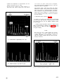
when analyzing signals close to minimum resolution bandwidth. Fig. 2-11 shows the apparent increased resolution
when the VIDEO FILTER is turned on. It does restrict the useable sweep rate, because of the filter time constant, to about
50 ms/div or slower.
Fig. 2-11. Integrating the display with the video filter.
Vertical Display Modes
The appearance of the displayed signal depends to a
great extent on the setting of the VERTICAL DISPLAY switch.
For example; to accentuate the side lobes of a signal, the
LOG (40 dB full screen) position should be used, as compared to the SQ LAW (13 dB full screen) position. Fig, 2-12
illustrates the effect of each display mode or each position
of the VERTICAL DISPLAY switch.
The LOG position increases the dynamic range of the display by attenuating large amplitude signals more than small
amplitude signals. This produces a display which approximates a logarithmic response curve. The circuit is basically
a compression circuit, and is most effective when there are
large signal amplitude differences.
2-12
The SQ LAW (power) position provides a display that is
approximately
nal amplitude.
signal power.
centuate small
proportional to the square of the input sigThe display, therefore, approximates the input
This is basically an expansion circuit to acamplitude differences.
Selecting the Sweep Rate
The sweep rate for wide dispersion coupled resolution settings is usually set just above the visual flicker setting; however, as the DISPERSION is decreased the sweep rate will
begin to affect the resolution and sensitivity of the analyzer,
as described under Obtaining Optimum Resolution. Therefore, as the DISPERSION settings are reduced the sweep
rate should also be reduced to maintain sensitivity and resolution.
Fig. 2-13. Measuring timing between pulses.
With the DISPERSION control set to 0, the analyzer functions as a fixed tuned receiver. The analyzer therefore displays time domain characteristics of the signal modulation
within the bandwidth capabilities of the analyzer.
Timing information such as pulse repetition rate may be
obtained by triggering the sweep on the INT signal source
and switching the TIME/DIV control to a calibrated sweep
rate that will permit measurement in time between the modulation pulses. See Fig. 2-13.
Triggering the Sweep
For most applications the trigger LEVEL control is switched
to the FREE RUN position and the sweep repetition rate is
a function of the TIME/DIV selector settings.
In some applications, particularly at 0 dispersion, or when
slaving the Type 491 to a recorder, it may be desirable or
necessary to trigger the display. The Type 491 may be triggered from the following three sources: INT, LINE and EXT.
When the SOURCE switch is in the INT position, the display is triggered on the video display. The Type 491 re-
Fig. 2-12. VERTICAL DISPLAY Modes showing a 100 MHz carrier
signal modulated by 20 kHz.
quires approximately 0.2 division of signal amplitude for
internal triggering. If the sweep will not trigger on INT when
the LEVEL control is adjusted, it may be necessary to tune
2-13
Fig. 2-15. Adjusting
operation.
Fig. 2-14. To trigger the analyzer from the display requires 0.2
divisions of signal. Tune the spectrum null point away from the
sweep starting point, with the RF CENTER FREQUENCY control.
the FINE RF or IF CENTER FREQ control to move the sweep
start off a spectrum null point. See Fig. 2-14.
When the SOURCE switch is in the LINE position, the display is triggered from a sample of the power input line
frequency. This feature provides a stable display when the
signal is time-related to the line frequency.
External triggering requires a signal equal to or greater
then 0,2 V, within the frequency range of 20 Hz to 100 kHz,
to trigger the sweep. The signal is applied to the TRIG IN
connector on the rear panel. External triggering will provide a stable display when the internal signal triggering is
unstable. It may also be used to slave the analyzer to a
recording device.
The SLOPE switch selects the positive or negative-going
portion of the triggering signal. The LEVEL control selects
the required signal amplitude to trigger the sweep for single
sweep operation.
RF Center Frequency Tuning
The dial and the analyzer are tuned through the frequency range of each band by the RF CENTER FREQUENCY
control. The dial frequency calibration is accurate to within
± (2 MHz + 1% of the dial reading) when the FINE RF CENTER FREQ and the IF CENTER FREQ controls are centered.
The RF CENTER FREQUENCY control is supplemented by
a FINE RF CENTER FREQ, ten turn control, that provides a
fine tuning adjustment through a limited frequency range
on either side of the dial frequency, or the RF center frequency. This allows fine tuning when operating on the high
frequency scales with narrow dispersion, or fine adjustment
to establish a phase lock condition.
2-14
FINE
RF
CENTER
FREQ
control
for
phase
lock
When searching a frequency band, set the MIXER PEAKING control to SEARCH position and tune slowly through
the band with the RF CENTER FREQUENCY control. This
ensures that signals of sufficient power within a tunable range
will be observed. See Mixer Peaking. After the signal has
been located adjust the MIXER PEAKING to optimize signal
amplitude.
NOTE
MIXER PEAKING control must not be in the SEARCH
position when making relative amplitude measurements and should be adjusted for maximum signal
amplitude.
Phase Lock Operation
The 1st local oscillator can be phase locked to either an
internal 1 MHz reference oscillator or an external freguency
source when it is applied to the EXT REF FREQ IN connector.
Locking the local oscillator to a stable frequency, such as the
internal 1 MHz crystal controlled oscillator, reduces the local
oscillator incidental frequency modulation and frequency
drift. This allows narrow dispersion and high resolution settings for signal analysis.
The frequency range of an external reference frequency
is 1 MHz to 5 MHz, and amplitude limitations are 1 to 5
volts peak to peak. The external signal for phase lock
operation is applied to the phase lock circuit when the INT
REF FREQ control is turned ccw to the OFF OR EXT REF FREQ
IN position.
The LOCK CHECK pushbutton applies the output of the
phase lock amplifier to the vertical display system. The output of the phase lock amplifier contains the following: (1)
Beat frequency signals between the local oscillator and the
reference frequency when the oscillator frequency is very
close to a lock with the reference frequency. (2) A DC ref-
erence level of the output amplifier. This DC level changes
as the FINE RF CENTER FREQ control is rotated and shifts
the local oscillator frequency a slight amount. It also affects
the vertical position of the display baseline. Thus, by depressing the LOCK CHECK button and slowly turning the
FINE RF CENTER FREQ control (Fig. 2-15), the operator will
observe the baseline of the display shift until a lock mode is
reached. The baseline will then remain stationary over a
portion of the control range as the circuit holds the local
oscillator locked to the reference frequency. Turning the control further causes the circuit to lose its lock and the baseline
jumps from the locked position.
Beat frequency signals are usually displayed just before a
lock point is reached. See Fig. 2-16. However, through part
of the frequency range, the phase lock operation may be
very positive and the local oscillator will jump from one lock
mode to another without displaying the beat signals or the
smooth shift of the display baseline between lock points.
When the DC operating level of the phase lock amplifier
reaches either extreme (top or bottom of the graticule area)
the operation of the amplifier becomes non-linear and compression of the beat signals will be noted. Phase lock operation becomes difficult to achieve. The displayed DC level
thus aids in setting a phase lock condition within the linear
operating range of the phase lock amplifier.
Part of the input signal is coupled through and displayed
when the LOCK CHECK button is pushed. This permits the
operator to re-establish a particular lock point that may
be lost because of oscillator drift or other reasons. The operator adjusts the FINE RF CENTER FREQ control while observing the display until the signal is again at a particular lock
point (the point where the baseline or the signal position
locks).
The local oscillator fundamental frequency locks in 1 MHz
steps, (from one lock mode to the next) then the internal
1 MHz reference frequency is used for phase lock operation.
This produces gaps of as much as 5 MHz in the upper frequency scale, where the upper harmonic of the local oscillator is used. Continuous tuning through these gaps is provided
by the INT REF FREQ control. Rotating the control through
its range pulls the crystal controlled reference frequency approximately 1 kHz. This is sufficient to shift the local oscillator frequency through these gaps and maintain phase lock
operation.
I
Phase lock operation is established as follows:
1. Tune the desired signal to the center of the display with
the RF CENTER FREQUENCY control.
Fig. 2-16. Typical LOCK CHECK displays
2. Depress the LOCK CHECK button and adjust the FINE RF
CENTER FREQ control for a lock indication within the center
(4 div) of the graticule. if the lock indication or beat signal
is outside the linear operating range of the amplifier (baseline of display at the top or bottom of the graticule), center
the display with the FINE RF CENTER FREQ control, then
adjust the RF CENTER FREQUENCY control to shift the signal
towards a beat mode. Adjust the FINE RF CENTER FREQ control while observing the desired signal for phase lock operation, then release the LOCK CHECK button.
2-15
2-16
Fig. 2-17. Control set-up chart.
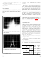
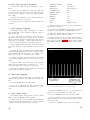
Fig. 2-18. Spectrum of an amplitude modulated signal. Sideband
amplitude is ½ the percentage of modulation. This spectrum shows
100% modulation.
3. Decrease the dispersion to open the screen. Keep the
signal centered on screen with the IF CENTER FREQ controls.
If the local oscillator should lose its lock condition when the
dispersion settings are 100 kHz or less, the signal will disappear from the screen. A slight adjustment of the FINE RF
CENTER FREQ control will usually return the signal to the
display.
4. If two or more high frequency (upper scale) signals are
to be resolved, they can be moved on the display without
losing phase lock by adjusting the INT REF FREQ control.
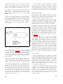
Fig. 2-19. Formation of a spectrum. F is the fundamental or carrier
f r e q u e n c y , F 1 and F 2 are the modulating frequencies.
Spectrum of Amplitude Modulation
When a single frequency (CW) signal is amplitude-modulated by a single frequency, two additional frequencies will
be generated; the carrier plus the two side bands. See Fig.
2-18. The amplitude of either sideband with respect to the
carrier voltage is ½ the percentage of modulation. The
frequency difference between the carrier and either sideband
equals the modulating frequency.
Figure 2-19 illustrates how a spectrum is generated when
a fundamental carrier frequency F is modulated by two
frequencies F 1 and F 2.
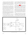
Recorder Out Connector
Signals on the display may be recorded by connecting to
the RECORDER output connector on the rear panel. A linear
output is provided when the VERTICAL DISPLAY switch is in
the LOG and LIN positions. With the DISPLAY switch in
the SQ LAW position, the output to the RECORDER connector is square law.
Control Setup Chart
Fig. 2-17 is
Type 491. This
setup record
also serve as
a control setup chart for the front panel of the
figure may be reproduced and used as a test
for special applications or procedures. It may
a training aid to facilitate control operation.
SPECTRUM ANALYZER DISPLAYS
The Spectrum Analyzer displays a plot of signal amplitude
as a function of frequency. With this type of display, in
the frequency domain, individual frequency. components in
the signal can be displayed and readily analyzed. This
section describes some basic spectrum analyzer displays.
The sideband spectrum af multiple frequency amplitudemodulated signal spectrum is determined by the modulating
frequencies. To resolve this complex spectrum, the analyzer
resolution bandwidth must be less than the lowest modulating
frequency, or the bandwidth must be less than the difference
between any two modulating frequencies, whichever is the
smaller.
In wideband amplitude-modulation such as television picture information, the spectrum analyzer may be used to
measure the sideband energy distribution and modulation
bandwidth.
The amplitude modulated signal spectrum will therefore
furnish the following information: 1) Fundamental or carrier
frequency, 2) modulation frequency or frequencies, 3) modulation percentage, 4) sideband energy distribution and 5)
modulation bandwidth. Other characteristics which may
be evaluated are; degree of incidental FM (evidenced by
signal jitter), nonlinear modulation, and over-modulation.
These characteristics will be described in more detail with
other types of spectrum display patterns.
2-17
Pulse Modulated Signal Spectrum
When a CW signal is pulse modulated, the carrier is periodically turned on and off. The on period is determined by
the modulating pulse width, the off periods is related to the
pulse repetition rate or frequency. The carrier is usually
modulated with rectangular shaped pulses.
A square wave is composed of its fundamental frequency
plus the odd harmonics. If the relative amplitudes and phase
of the harmonics are changed, a number of waves hapes are
produced; rectangular, trapezoidal, sawtooth, etc. The spectrum of the square wave or any pulse shape is displayed
according to its frequency components and their amplitudes.
Common pulse forms and their spectrum are described in
Reference Data for Radio Engineers, 4th edition, Chapter 35,
ITT 1956.
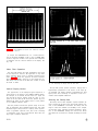
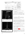
Fig. 2-20A illustrates a theoretical voltage spectrum of a
square-pulse, pulse-modulated oscillator. The main lobe and
the side lobes are shown as groups of spectral lines extending above and below the baseline, The number of these side
lobes for a truly rectangular pulse, approaches infinity, since
the number of harmonics in a square pulse approaches an
infinite quantity. Any two adjacent side lobes are separated
an the frequency scale by a distance equal to the inverse of
the modulating pulse width. See Fig. 2-20A.
Fourier theory shows that adjacent lobes are “180° out of
phase; however, since the spectrum analyzer is insensitive
to phase, only the absolute value of the spectrum is displayed
and appears as illustrated in Fig. 2-20B.
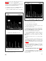
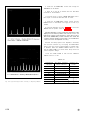
Fig. 2-21 illustrates the relative effects the pulse width
Fig. 2-20. Formation of a pulse modulated signal spectrum.
Frequency Modulated Signal Spectrum
When a CW signal F C is frequency modulated at a rate
( Fm ), it will theoretically produce an infinite number of sideband frequencies. These frequencies are equal to (F C ±
nF
m
where
n
=
1,
2,
3,
etc.
Frequency modulated signal bandwidth is usually determined by the width of the sidebands containing sufficient
energy to dominate the display. Signal bandwidth is approximately equal to
+ Fm ) where
is t h e f r e q u e n c y
deviation of the carrier and F m is the frequency of the modulating signal. Frequency deviation of the carrier is primarily dependent on the modulating signal amplitude.
This ratio of frequency deviation to modulating frequency
is known as modulation index. Bessel function and frequency
spectrum for different modulation indices may be found in
the 4th edition of Reference Data for Radio Engineers, Chapter 19.
To resolve adjacent sideband components in a frequency
modulated display, the spectrum analyzer resolution bandwidth should be less than the lowest modulating frequency
in the spectrum which is the same as the requirements for an
amplitude modulated spectrum.
2-18
and pulse repetition frequency have on a pulsed RF spectrum.
Since the spacing between the spectral lines of the pulsed
RF spectrum is a function of the PRF, the spectrum analyzer
resolution bandwidth should be less than the PRF to respond
to one frequency component at a time. In mast instances this
is impractical; for example, a short pulse at a PRF of 100 hertz,
would require an effective r e s o l u t i o n o f 1 0 0 h e r t z . T h i s
would produce an extremely fine grain display, and would
be impractical for analysis.
The spectrum envelope, however, is plotted with pulses
instead of lines. If the analyzer is swept slowly, it will plot
a series of pips or lines, the focus of which represents the relative energy distribution of the swept spectrum. The number or density of these pips for a given PRF
will depend on the sweep speed, or TIME/DIV selection, on
the analyzer. It is possible, by sweeping very slowly, to obtain
the spectrum of a very low PRF signal. This display closely
simulates a pulsed spectrum and contains the same information for analysis. This spectrum may now be resolved, since
the resolution bandwidth of the analyzer need only be less
than the side lobe frequency width, or the reciprocal of the
modulating pulse width. Fig. 2-22 illustrates the effects the
pulse shape will have an the RF spectrum. Notice the reduction of side lobes when the pulse is no longer rectangular;
Fig. 2-22C.
Fig. 2-21. Pulse width and PRF effects on pulse modulated spectrum.
Identification and Frequency Measurement of
Displayed Signals
the second harmonic of 900 MHz (1800 MHz] will mix with
1600 MHz and 2000 MHz.
These response are identified and read as follows:
Bandpass and dispersion characteristics of spectrum analyzers require very limited preelection ahead of the first
mixer. Signals with frequencies different than that indicated
by the dial will therefore appear on the display. These
signals are called spurious responses. See spurious responses
under Spectrum Analyzer Terms at the beginning of this section.
The dial scales for the Type 491 indicate frequencies that
are below the local oscillator frequency by the IF (200 MHz).
For example: a dial reading of 700 MHz means the local
oscillator frequency of 900 MHz (700 MHz + 200 MHz). This
1. Tune the RF Center Frequency across a dispersion window and observe the signal movement.
2. True responses move across the dispersion window from
left to right, on the Type 491, as the RF CENTER FREQUENCY
is increased, or in the same direction as the tuning knob
is turned.
3. Images move across the dispersion window opposite to
the direction of the true response.
4. IF feedthrough signals are not tunable and remain fixed
in position as the RF CENTER FREQUENCY is tuned.
local oscillator frequency will mix with 700 MHz and 1100
MHz to produce the IF of 200 MHz. The 1100 MHz response
is called the image. Note that the image response is twice
the IF away from the true, or dial calibrated response. Harmonics of the local oscillator fundamental frequency also
convert incoming signals to the IF response. For example,
5. Signal frequency shifts across the dispersion window that
are not coincident with the RF CENTER FREQUENCY change
are spurious. Some of these spurii are mixing with higher
harmonics of the local oscillator. The upper dial scales of
the Type 491 are calibrated to harmonics of the local os-
2-19
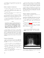
Fig. 2-23. Frequency difference measurement between two signals.
cillator fundamental. If an incorrect dial scale is used to
measure the frequency movement of the signal, as the RF
CENTER FREQUENCY is tuned, an erroneous reading will
be obtained, This erroneous reading however can be used
to identify which scale to use to obtain the corect frequency
reading. For example: With a dispersion of 5 MHz/div
(50 MHz total) a given signal moves 50 MHz for a RF CENTER FREQUENCY change of 25 MHz. This indicates the
signal is mixing with the next higher harmonic of the oscillator, and the next higher scale should be used to read
the signal frequency. If the signal only moves 25 MHz for
an RF CENTER FREQUENCY change of 50 MHz, the next
lower scale should be used.
6. The rate at which the signal moves across the dispersion window as the RF CENTER FREQUENCY is tuned also
aids in identifying which scale to use, and with practice,
the correlation of the signal rate of movement and the dial
scale becomes fairly easy.
Spurious responses due to intermodulation are the most
difficult to identify. Signal characteristics, such as type and
amount of modulation, irregular spacing between signals,
etc., are the main character identities.
APPLICATIONS
Fig. 2-22. Pulse shaping effects on the pulse spectrum.
2-20
The spectrum analyzer is a very versatile device in the field
of radiation measurements. It can be used for example, as
an aid in the design and adjustment of transmitters, to check
and calibrate oscillators, check and calibrate attenuators, or
as a sensitive detector device to study all types of modulated signals, plus many more special applications.
The following are basic applications for the Type 491
and are presented to illustrate some of these uses in the
electronics field.
Relative Amplitude Measurements
The relative amplitudes of signals are measured as follows:
1. Center the IF CENTER FREQ controls. Switch out any
IF ATEN. Tune the signal with the lowest amplitude to the
center of the screen.
2. Adjust the GAIN control so the low amplitude signals
establish a reference amplitude.
3. Tune the stronger signal to the center of the display.
Add IF attenuation by switching combinations of IF ATTENUATION until the stronger signal amplitude decreases
to the same reference amplitude established in step 2.
4. Add the total attenuation that was switched in. This
is the relative amplitude difference, in dB, between the two
compared signals.
NOTE
For maximum accuracy, the signals should be referenced and compared near the same location on
the display. Tune each signal to the reference
location with the RF CENTER FREQUENCY control.
The IF CENTER FREQ, the DISPERSION-COUPLED
RESOLUTION, the FINE RF CENTER FREQ, and the
TIME/DIV controls should not be changed when
measuring relative signal amplitude.
The peak amplitude of the main lobe of a pulse modulated
RF spectrum represents only a portion of the total energy
contained in the lobe. The main lobe is less than the amplitude of an equal peak value CW signal, by an amount
5. Read the frequency indicated on the RF CENTER FREQUENCY dial. The signal frequency is the dial reading
± (2 MHz +1% of the dial reading). For example: A dial
reading of 1000 MHz indicates the signal is 1000 MHz
± (2 MHz + 10 MHz) or, between 988 MHz and 1012 MHz
Accurate frequency measurements can be performed by
applying a calibrated or crystal-controlled frequency to the
RF INPUT and calibrating the dial near the frequency range
of the input signal; then tune the input signal to the same
screen position and note the dial reading plus or minus the
measured dial accuracy.
Frequency Difference Measurements
Frequency separation measurements to 100 MHz can be
made between signals as follows:
1. Switch the DISPERSION RANGE switch and the DISPERSION selector so the signals to be measured are the maximum number of graticule divisions apart on the display.
2. Set the TIME/DIV selector and the RESOLUTION control
for optimum signal definition. [Sharp and clean signal display.)
3. Measure the distance, in graticule divisions, between
the two signals (see Fig. 2-23.)
4. Multiply the measured distance in step 3 by the Dispersion/Div setting. This is the frequency separation or frequency
difference between the two signals.
NOTE
Accuracy of this measurement depends on the DISPERSION RANGE settings.
See Characteristics
Section.
which is approximately 3/2†B; where t is the measured
pulse width in seconds, and B is the selected resolution
bandwidth of the analyzer in hertz. Spectrum Analyzer
sensitivity measurements should therefore be made with a
CW signal.
Frequency Measurements
Frequency measurements taken from the RF CENTER FREQUENCY dial are accurate to within ± (2 MHz +1% of the
dial reading). The frequency of an applied signal is measured
as follows:
1. Check the calibration of the IF CENTER FREQ CAL
adjustment as described under Front Panel adjustments.
2. Set both IF CENTER FREQ controls and the FINE RF
CENTER FREQ control to their midrange (000) position.
3. Set the DISPERSION RANGE switch to kHz/DIV and the
DISPERSION selector to 500 kHz/div.
4. Tune the RF CENTER FREQUENCY so the signal to be
measured is in the graticule center.
Fig. 2-24. Short term stability measurement. Random FM characDISPERSION is 2 kHz/Div and RESOLUTION
teristic of a klystron.
is 1 kHz. Oscillator FM is about 6 kHz.
2-21
Fig, 2-25 Frequency modulated displays.
Fig. 2-26. Amplitude modulated displays.
Frequency Stability
The Type 491 con be used to measure long and short
term frequency stability, when the local oscillator is phase
locked to a stable crystal-controlled reference frequency.
See Stability in Characteristics Section.
Short term stability measurements apply to fast frequency
changes such as those caused by power supply noise and
ripple, vibration or other random factors. Fig. 2-24 shows
the random frequency modulation characteristics of a klystron.
2-22
Long term stability measurements require a recorder or a
series of photographs to show the frequency drift as a
function of time. Temperature compensation can be recomputed
by this process, since the amount and direction of the drift
may be graphically indicated by photographs.
Amplitude Modulation
Modulating frequency or frequencies and modulation percentage are the figures most often required from an AM
signal measurement. Fig. 2-25 shows two illustrations of
amplitude modulated signals, the methods to measure the
modulating frequency and modulation percentage.
Over modulation will produce extra sideband frequencies.
The spectrum is very similar to multi-frequency modulation.
Over modulation, however, is usually distinguished from the
multi-frequency modulation by: 1) The spacing between overmodulated sidebands is equal, while, multi-frequency sidebands may be arbitrarily spaced, unless the modulating frequencies are harmonically related; 2) The amplitude of the
sidebands decreases progressively out from the carrier, but.
the amplitude multifrequency modulated signals is determined
by the modulation percentage of each frequency and can be
arbitrary.
Frequency Modulated Spectrum
FM measurements are generally measurements that determine; the modulating frequency, amplitude of the modulating
signal or frequency deviation, and index of modulation.
A typical FM spectrum is shown in Fig. 2-26. The exterior
modulation envelope resembles a cOS2 curve, and identifies
the signal as frequency modulation.
Frequency Deviation Measurement
There is no clear relationship between spectral width and
deviation, because in theory the FM spectrum approaches
infinity. In practice however the spectral level falls quite
rapidly as shown in Fig. 2-26B.
Accurate deviation measurements can be made if the
modulating frequency and the modulation index (where the
carrier goes to zero) are known.
Modulation Index =
Carrier deviation
Modulating frequency
Values of modulation index corresponding to zero carrier
amplitude are listed in Table 2-1.
TABLE 2-1
Accurate carrier null is essential for accurate measurement.
Pulse Modulated RF Spectral Measurements
A visual examination of the pulse modulated spectrum can
check a number of the characteristics about a transmitting
and modulating device. Some of these characteristics are:
1, The transmitting oscillator stability can be checked by
noting the degree of frequency shift as described previously.
Fig. 2-27. Pulse modulation display,
PRF measurements.
illustrating pulse width and
2-23
2. A visual means is provided to tune the transmitting
system and obtain most of the output power within the frequency range of the receiver bandwidth.
3. The frequency difference between the first two minima
of any spectrum is a measure of the modulating pulse width.
See Fig. 2-27.
4. A spectrum without deep minima points adjacent to
the main Iobe indicates the presence of frequency modulation. See Fig. 2-22.
5. If the spectrum has two peaks, the oscillator is operating
in two modes or it is pulled in frequency by some external
factor, such as mismatched transmission lines or fluctuating
voltages (providing the resolution of the analyzer is sufficient).
Measurements of Pulse Modulated RF Signals
Pulse Width: Since the theoretical pulse width for a square
pulse is the reciprocal of the spectral side lobe frequency
width, the main frequency lobe or its side lobes can be used
to measure the pulse width of the pulse modulated spectrum.
This is accomplished with the Type 491 as follows:
1. Adiust the DISPERSION control and tune the RF CENTER
FREQUENCY control so the main lobe of the spectrum is
displayed in the center of the graticule, and the side lobes
are visible on each side.
2. Adjust the GAIN control and switch in the necessary
IF ATTENUATION dB switches, so the main lobe and its side
lobes are within the graticule height.
3. Adjust the TIME/DIV selector for optimum spectrum
definition,
4. Adjust the RESOLUTION control so the nulls are easily
discernible without excessive loss of sensitivity. Change the
mode selection of the VERTICAL DISPLAY switch to accentuate these minima points. (Usually LOG position.)
5. Calculate the dispersion of either the main lobe or a
side lobe as directed under measuring frequency difference.
2-24
The pulse width is equal to the reciprocal of ½ the main lobe
frequency width, or the reciprocal of the side lobe frequency
width. See Fig. 2-27.
Repetition Rate: The pulse repetition rate is measured
when the spectrum analyzer is switched to zero dispersion
and the analyzer becomes a fixed tuned receiver. The sweep
is then triggered on the signal and becomes a time domain
display. The procedure is as follows:
1. Tune the signal to the display center with the RF CENTER FREQUENCY and the IF CENTER FREQ controls.
2. Change the DISPERSION RANGE switch to kHz, then
decrease the DISPERSION to 0. Uncouple the RESOLUTION
control and turn to the fully clockwise position. The analyzer
is now a fixed frequency device with no dispersion.
3. Set the Trigger SOURCE switch to INT, the SLOPE switch
to + position, then adjust the LEVEL control for a stable
display. The IF CENTER FREQ-FINE control may require
slight adjustment to displace the spectrum null point from the
sweep start. See Fig. 2-14. The Type 491 requires a 0.2
divisions of signal to trigger internally.
4. Set the VARIABLE control to the CAL detent then adjust
the TIME/DIV selector so several pulses of the received signal
are displayed. See Fig. 2-27C. The number of pulses displayed is now a function of the sweep rate and the signal
PRF.
5. Measure the number of divisions between 2 or more
pulses on the graticule.
6. The pulse repetition frequency is the reciprocal of the
period between pulses.
In the example of Fig. 2-27C, the repetition time is
The pulse repetition frequency
1000 Hz.
SECTION 3
CIRCUIT DESCRIPTION
Introduction
The Type 491 Spectrum Analyzer is a swept IF type analyzer covering the frequency range from 10 MHz to 40 GHz.
This section first presents a block diagram analysis, then a
more detailed circuit description of each major section.
Basic Description
A block diagram of the Type 491 is shown in Fig. 3-1 and
the Diagrams section.
Signals within the frequency range of the Type 491 that
are applied to the RF INPUT are converted by the heterodyne
process to the first intermediate frequency. This is a wide
band IF of 150 MHz to 250 MHz. Three selectable local
oscillators, in combination with selected mixers, provide the
10 MHz to 40 GHz frequency coverage for the instrument. A
phase lock circuit locks the local oscillator to a stable (internal
or external) reference frequency. This provides the required
stability necessary for narrow dispersion displays.
One or two [depending on the selected bond) low pass
filters (265 MHz and 235 MHz] plus the 150 MHz to 250 MHz
bandpass filter between the first mixer and the wide band
IF amplifier, attenuate and isolate local oscillator frequencies
which would generate spurious signals when mixed with the
second local oscillator frequency.
The wide band (150 MHz to 250 MHz) IF response is then
swept, in the second mixer, by a swept frequency to generate
a second IF of 75 MHz. The swept frequency rate of the oscillator is synchronized to the sweep rate so the CRT display
becomes frequency based with a dispersion window that
depends on how much the oscillator is swept.
Center frequency of the swept oscillator is 275 MHz. The
amount the oscillator sweeps depends on the selected dispersion. At maximum dispersion the oscillator sweeps 225
MHz to 325 MHz, which converts all signals within the wide
band IF to the second 75 MHz IF.
Calibrated attenuation is steps of 1 to 51 dB is provided
by the IF attenuator, The signal is then amplified and applied
to the 3rd mixer stage r where it is mixed with 70 MHz to
produce a 3rd IF frequency of 5 MHz, The bandwidth of this
5 MHz IF is varied by means of the variable resolution circuit
which provides resolution control from approximately 100
kHz to less than 1 kHz.
Video signals from the detector are amplified by the
vertical amplifier, then applied to the CRT vertical deflection
plates and to the trigger circuit for the sweep generator,
provided the Trigger SOURCE selector is in the INT position.
The sweep generator will free run, or it can be triggered
from any one of three selectable sources; line, external and
internal.
The signal from the sweep generator is applied to both
the sweeper oscillator through the variable dispersion circuit
and to the horizontal amplifier circuit for the horizontal
sweep on the CRT. The horizontal CRT beam movement and
the frequency scan in the 2nd mixer are therefore synchronized. This provides the calibrated dispersion and a linear
display of the frequency spectrum on either side of the dial
center frequency.
The 1st or tunable local oscillator is phase-locked to a
stable crystal-controlled reference frequency by the phase
locking circuit. This stabilizes the local oscillator frequency
and permits narrow 1 kHz/div dispersion settings.
RF Section
The RF section contains three local oscillator assemblies,
for each band, and their respective mixers. Two low-pass
filters (235 and 265 MHz) are switched in series with the
signal path between the band A mixer and the IF band-pass
filter. Only the 265 MHz low-pass filter is used for bands B
and C, The band selector switch SW70 selects the filters and
connects only one oscillator circuit to the +150 volt supply,
Only one oscillator is operating for a given band switch
position. The 235 MHz low pass filter attenuates the low
frequency end of the band A oscillator.
Heater voltage for the oscillators is supplied by the +10
volt regulated supply. Thus, oscillator frequency drift due
to heater voltage variation is minimized. The heater supply
line to V40 and V41 includes a series dropping resistor, R45
and R46, to reduce the voltage far these tubes to 6 volts.
Lossy cables (such as W10-W34, etc.) are used to reduce
SWR caused by slight impedance mismatch between circuits.
Impedance mismatches may be due to coaxial connectors or
other discontinuities.
NOTE
Lossy cables use steel wire for the center conductor. These cables are factory-installed and used
to optimize response flatness and sensitivity. The
Iossy cable is identified by the white insulation
coating; the standard 50 W coaxial cable has the
clear insulation. Do not interchange these cables.
Band A: The oscillator frequency for band A is 200 MHz
above the RF input dial reading and has a tunable range of
210 to 475 MHz. The oscillator uses a ceramic planer triode.
The tuned circuits are ganged together and tuned by the
RF CENTER FREQUENCY control. Frequency tracking of the
RF dial is adjusted by variable L and C trimmers, if required.
The band A local oscillator output is applied through a
transmission line transformer T14, to the diodes or balanced
section of the mixer. Adjustment of R13, C14 and C16 for balance greatly reduces local oscillator feed-through. The desired
difference frequency is coupled to the IF amplifier through
the 235 MHz filter.
3-1
3-2
Fig. 3-1. Function block diagram of the Type 491.
Band B: The oscillator for band B is similar to band A
oscillator. The fundamental frequency range 470 MHz to 1100
MHz and the 2nd harmonic of the oscillator is used for the
frequency range 270 MHz to 2000 MHz for scales 2 and 3.
The mixer for this band is a crystal diode. Input RF is
applied through a 1 dB isolation pad to the diode. C68, in
series with R68, is tuned for response flatness. An RF choke
L67, isolates the IF and provides a DC path for the MIXER
PEAKING circuit.
Band C: The oscillator for band C is a triode oscillator
connected to tunable transmission lines which are tuned by
the RF CENTER FREQUENCY control. The oscillator fundamental frequency range is 1.7 GHz to 4.2 GHz. Harmonics
through the 10th and the fundamental are used to heteradyne
with the input RF to provide the input frequency range from
1.5 to 40 GHz.
If the local oscillator is slowly tuned through a frequency
range, signals above the specified sensitivity level will appear
above the noise when they reach this optimum point. This
ensures optimum search capability, and when a signal is
intercepted, the operator then switches to manual tuning
and optimizes the mixer for the given RF center frequency.
Phase Lock Circuit
The phase lack circuit synchronizes the local oscillator
frequency with a stable reference frequency. This reduces
oscillator drift and incidental frequency modulation, permitting narrow dispersion settings for signal analysis.
The phase detector samples the instantaneous RF voltage
generated by the tunable local oscillator at a rate determined
by the reference frequency. The sample voltages are then
intergrated and applied to a comparator which generates a
corrective voltage to feed back to the local oscillator.
When the local oscillator frequency is an exact multiple
of the reference frequency, the phase detector output is a DC
voltage that is proportional to the instantaneous potential
of the sampled oscillator voltage. If the local oscillator
phase drifts, the phase detector output changes. This change
is amplified through Q1170-Q1180 and applied as a corrective voltage to a voltage-controlled capacitance diode in
the oscillator tuned circuit. This shifts the phase of the oscillator so it remains lacked with the reference frequency.
See Fig. 3-3.
Fig. 3-2. Simplified equivalent of the hybrid directional coupler.
The oscillator output is applied to a hyrid directional
coupler or diplexer; see Fig. 3-2. The diplexer couples the
LO signal to the mixer port (OUT] and the mixer output to
the IF port. The mixer action is therefore in an externally
connected mixer, which may be either coaxial or waveguide,
and the 200 MHz IF is then coupled through the diplexer to
the IF connector.
The C band frequency range requires the following four
mixers: One coaxial mixer for the frequency range 1.5 to
12.4 GHz, and three wave guide mixers with frequency ranges
of 12.4 to 18 GHz, 18.0 to 26.5 GHz and 26.5 to 40 GHz.
The IF output is applied through a 1 dB attenuator pad
and the 265 MHz law-pass filter. DC return for the mixer is
through the 1 dB attenuator to the mixer peaking circuit.
The mixer peaking circuit has two modes of operation, a
search mode and a manual mode. In the search mode, the
sweep voltage from the sweep generator circuit is applied
to the base of Q65 and Q51. This varies the collector-toemitter resistance and establishes a variable mixer diode
current so that optimum mixer peaking is provided at some
point through the sweep scan.
The corrective signal from the comparator and amplifier
is also applied to the vertical circuit when the LOCK CHECK
button SW889 is depressed. This provides a beat frequency
signal indication on the CRT so the operator can locate a
lock point. Beat frequency displays appear on the CRT screen
as the local oscillator is tuned (see Operating section). A
reference voltage related to the position of the FINE RF
CENTER FREQ control is also applied to the vertical deflection circuit and is used to center the error signal within
the dynamic operating range of the comparator amplifier
Q1170-Q1180. Phase lock operation should be set within
the dynamic range of the amplifier, preferably in the center
of the dynamic range. This dynamic range is visually displayed on the CRT as a vertical displacement of the display.
Circuit Analysis
Turning the INT REF FREQ control clockwise closes SW1106
so collector voltage is applied to Q1100. The crystal controlled 1 MHz oscillator will now operate. The output 1 MHz
signal from the emitter of Q1110 is applied to the trigger
generator circuit. Diodes D1122 and D1123 set the quiescent
current through the tunnel diode D1124 and couple the
signal to the 1 MHz MARKER OUT connector J1120; or, if an
external reference signal is applied, they couple the signal
to the trigger generator circuit.
Frequency of the reference oscillator Q1100 is primarily
controlled by the crystal Y1104, inductor L1104, and the
capacitance of diodes D1116 and D1117. Diode D1116 is back
biased to act as a voltage-controlled capacitance diode;
however, when signal amplitude across crystal Y1104 becomes excessive, D1116 will conduct on the peak signal
swing. D1117 then becomes back biased and acts as the
capacitance diode.
3-3
The back bias across D1116 is controlled by INT REF FREQ
charge of diodes D1134 and D1139. When the charge has
control R1106. This change in back bias increases or decreases the diode capacity and shifts the resonant frequency
of crystal Y1104. The pulling range on the crystal frequency
by the INT REF FREQ control is about 1 kHz. This is sufficient
to maintain phase lock condition through frequency gaps
that occur above 1 GHz when the oscillator shifts phase lock
mode,
dissipated, the diodes generate a fast recovery step. This
recovery step is differentiated and coupled through transmission line transformer T1140, T1150 and T1160 to the phase
detector as a series of equal amplitude positive and negative
strobe pulses.
When the local oscillator shifts to a different lock mode,
the fundamental frequency of the oscillator shifts 1 MHz.
This produces frequency gaps in the upper scales which will
shift the signal off screen with dispersions of 100 kHz/div
or less. The INT REF FREQ control shifts the reference
oscillator frequency about 0.1% (1 kHz). This shifts the local
oscillator by the same percentage, so the frequency gaps
between lock modes are filled. If the observed signal should
shift off screen, it can be returned on screen or slid along
the display by the INT REF FREQ control.
The pulse generator consists of tunnel diode D1124, driving
amplifier Q1120. The quiescent current of tunnel diode
D1124 is approximately 2.5 mA. The positive-going portion
of the input reference signal switches the tunnel diode to its
high state and a fast rise positive pulse is generated. The
pulse is amplified and differentiated by Q1120 and the short
RC time constant in the emitter circuit.
The output pulse of Q1120 is transformer coupled through
T1128 to Q1121. The positive portion of the coupled pulse
is of sufficient amplitude to trigger Q1121 into avalanche,
and the resulting collector current sweeps out the stored
The phase detector (Fig. 3-4) consists of a two diode
gate and a low pass filter network. The diode gate is turned
on by the combined application of the local oscillator signal
and the very narrow strobe pulses, During the on time, the
phase detector samples the amplitude and phase of the local
oscillator signal and develops a voltage at the output of
the filter (C, and the junction of R 1, R2) that approximately
equals the instantaneous value of the local oscillator signal.
The sample of the local oscillator signal has a finite width
determined by the duration of the strobe pulse. The phase
detector operates on either the positive or negative slope
of the local oscillator signal, depending on the total difference between the detector output voltage and the phase
of the local oscillator signal. The strobe pulse width, therefore, must not exceed one-half period of the highest local
oscillator input frequency, which is 4.2 GHz. This period is
0.21 ns.
If the input local oscillator frequency is not a harmonic
of the reference frequency, the output of the phase detector
is approximately zero. H o w e v e r , a s t h e l o c a l o s c i l l a t o r
frequency approaches a harmonic of the reference frequency,
an AC or beat frequency signal is developed at the detector
output. This is amplified and applied through the LOCK
Fig. 3-3. Phase lock block diagram.
3-4
CHECK switch to the vertical deflection system. At zero beat,
the output signal amplitude snaps to a minimum and the circuit locks the local oscillator to the reference frequency by
feeding a corrective voltage to a Varactor diode in the
oscillator circuit.
FINE RF CENTER FREQ control R1182 tunes the local oscillator over a limited range by changing the DC output level
of Q1180. When the circuit is in a lock condition, any small
shift of the FINE RF CENTER FREQ control is counteracted
by the phase lock circuit. If the control is further moved
the circuit will lose the lock and the oscillator will jump
to a different frequency lock point. This jump in frequency
is easily seen as a shift in signal position at dispersion settings of 500kHz/div or less,
An isolation switch is used to minimize the loading affect
of the lower band (A & B) phase detectors on the band C
phase detector. The junction at diodes D1170 and D1174
is returned, through a filter network and the Band selector
switch SW70, to +150V. The diodes are forward biased
when the Band selector switch is in the A or B position. When
the switch is changed to the C position, the diode switch is
open.
Band C Bal and Bands A & B Bal adjustments correct any
imbalance between the phase detectors so the DC output
level of the amplifier remains balanced as the Band selector
is switched between bands. The FINE RF CENTER FREQ
control must be centered for this adjustment.
Sweeper Circuit
This circuit (see Fig. 3-5)
centered at 275 MHz, to the
swept frequency amplitude
can be varied from about O
provides a swept frequency,
wide band mixer amplifier. The
is constant and the dispersion
Hz to 100 MHz.
A positive-going sawtooth voltage from the sweep generator circuit is applied through pin AE to the emitter of Q200.
Q200 is configured as a long-tail amplifier. It converts the
sawtooth voltage input signal to a linear current ramp, which
is applied through the DISPERSION attenuator to one side
of comparator amplifier Q220-Q230.
The output DC level of the current ramp from Q200 is
set by Sweep Center adjustment R203. Dispersion CAL adjustment R208, shunts the dispersion attenuator. It calibrates
the dispersion for the 10 MHz/div position of the DISPERSION
selector by adjusting the output amplitude of the current
ramp from Q200. The remaining positions the selector are
then within instrument specifications.
Two
vided
selects
of the
dispersion ranges (MHz/DIV and kHz/DIV) are proby the DISPERSION RANGE selector R210, which
a different range of resistance values for each position
DISPERSOIN selector.
Sweep Comparator. The sweep comparator containing
Q220 and Q230 compares the current ramp from the dispersion attenuator against a current ramp applied to the
base of Q230. The signal applied to the base of Q230 is the
Fig. 3-4. Simplified phase detector circuit.
3-5
resultant feedback signal from a frequency to voltage converter and ramp generator. Any differential between the
two signals is a voltage output that controls the bias on
frequency-determining capacitance diode D314. D314 is part
of the swept oscillator circuit which shifts the swept oscillator frequency by an amount proportional to the signal
output from the comparator.
Q240 is the constant current source for the sweep comparator. About 3.4 mA of current through the comparator
is set by the bias of Q240. Output DC level at the collector
of Q230 is set by the IF Center Freq Range adjustments in
the collector circuit of Q260.
S w e e p O s c i l l a t o r . The oscillator frequency is primarily
a function of the L (L314) and C (diode D314 in series with
blocking capacitor C314) in the collector circuit of Q310.
Capacitance of diode D314 is varied by the signal from
comparator Q230-Q220. An increase in back bias decreases
the capacitance of the diode and increases the frequency of
the swept oscillator. Capacitance change of the diode is
not proportional to the voltage ramp, but high gain in the
discriminator feedback loop to the comparator reduce this
non-linearity. At maximum dispersion, the oscillator sweeps
from 225 MHz to 325 MHz.
Output signal from the oscillator is tapped across the
partial winding of L314 and capacitively coupled to transformers T330 and T331. The transformers step the voltage
up about 2:1 and converts the single-ended signal to a balanced push-pull drive signal for the output amplifier Q340
and Q350.
Fig. 3-6 is a simplified drawing of the transformer circuit.
The oscillator is the signal source or generator which supplies
the signal voltage (e). The input windings of T330 and T331
are connected in series; therefore, the voltage across each
winding equals e/2 (assuming an ideal transformer). The
polarity of the signal at a particular instant of time is shown
in Fig. 3-6. This voltage, across the input windings, produces
an equal voltage (e/2) across the output windings with the
polarity as indicated in Fig. 3-6.
The generator, or source, is in series with the output winding for T331, therefore, the voltage ot the output with reference to point A equals 3e/2. This voltage adds to the voltage output of T330 to provide a total output signal of 4e/2
or 2e.
If the reference point is changed to the common side of
the input windings of T330 and T331 (shown os a phantom
ground on the simplified drawing) the impedance looking
into the output terminals of the transformers is balanced,
Fig. 3-5. Block diagram of sweeper circuits.
3-6
transmission line input impedance increases, the open ended
line input impedance decreases. This produces proportionate
changes to the output signal from the diodes. Signal output
from diode D376 becomes more negative, and signal output
from D373 becomes less negative. This push-pull drive is
applied to the comparator Q260 and converted to a single
ended output signal for the sweep comparator.
Thermal balance is achieved by balancing the current
differential through both sections of the transistor. The common emitters are connected to a constant current source
Q270. Current (approximately 3 mA) is established by the
voltage drop across the emitter resistance R274.
The IF CENTER FREQ (R256) and the FINE (R259) controls
sum in a DC voltage with the differential signal from the
comparator to allow positioning of the IF center frequency
(200 MHz or a frequency close to 200 MHz) to the center of
the horizontal sweep.
The amplitude of the ramp signal to the sweep comparator
is a function of the DISPERSION RANGE switch SW210 and
the DISPERSION selector SW365 setting. This amplitude
determines the frequency deviation swing of the sweep
oscillator band.
Fig. 3-6. Simplified diagram of the transformer (T330-T331) circuit from the swept oscillator to the push-pull amplifier Q340-Q350.
so the dirve signal to the amplifiers is a balanced pushpull signal.
Transformers T343 and T354 in the collector circuit of
Q340 ond Q350 provide a 4:1 impedance transformation
from the collectors of the transistors to the output transformer
T347.
Transformer T347 converts the push-pull signal to a singleended output signal. Push-pull amplification, plus filtering
through the low pass filter circuit of L358-C358 and L348C348 reduces the harmonic content in the swept frequency
output signal.
Diode D334 in the base voltage divider circuit provides
the temperature compensation for transistors Q340-Q350.
The single-ended output signal is coupled through a 2:1
impedance transformer T363, to the mixer in the Wide Band
IF. The output signal is also applied, through two feedback
loops, to frequency ond amplitude control circuits.
Frequency Discriminator. Two frequency discriminators
for each position of the DISPERSION RANGE selector SW365
provide an output voltage signal to the frequency discriminator comparator Q260. The output voltage from the comparator is a ramp voltage that is proportional to the sweep
oscillator frequency. It is applied to one side of the comparator Q230-Q220.
The MHz/Div discriminator consists of two matched diodes,
D373 and D376, at the input ends of two transmission lines.
The transmission lines are 1/ 8 wavelength long at the center
frequency (275 MHz). One line is open ended and appears
capacitive, the other line is shorted and appears inductive,
at the center frequency. As the input frequency to the discriminator increases, the transmission line input impedance
nears the characteristics of a ¼ wavelength line. The shorted
Fig. 3-7. Frequency vs Voltage curves for kHz/DIV discriminator circuit.
3-7
The discriminator for the kHz/DIV position of the DISPERSION RANGE switch consists of tuned circuits which operate
much like the tuned transmission lines for the MHz/div discriminator. The parallel circuit L384-C384 is tuned slightly
below the center frequency, and the circuit L385-C385 is
tuned above the center of the sweep oscillator frequency.
The output of the detectors is shown in Fig. 3-7. When the
detector output is applied to the comparator, a voltage versus
frequency curve similar to Fig. 3-7C is the resultant output.
The circuit operates over the linear portion of the curve.
The kHz/div Cal adjustment R368 calibrates this range.
Diodes D277 and D279 isolate the narrow band discriminator tuned circuit when the Type 491 is operating in the
MHz/DIV dispersion range. They prevent parasitic oscillation
due to circuit coupling between the wide band and narrow
band discriminators. The diodes are forward biased when
the DISPERSION RANGE switch is in the MHz/DIV position
and the current through the diodes lowers or spoils the Q
of the tuned discriminator circuit. When the DISPERSION
RANGE switch is in the kHz/DIV position, the diodes are
backbiased and disconnected from the low dispersion discriminator circuit.
Ampliude Comparator. Uniform sensitivity and linearity
over the dispersion range is maintained by controlling or
regulating the oscillator output amplitude. This is accomplished by the RF amplitude comparator circuit, Q290 and
Q280. The RF output signal is detected by diode D361 and
applied through diode D362 to the base of Q280. This
rectified RF signal on the base of Q280 is compared against
a reference voltage set by the RF Ampl adjustment R290.
The differential output signal is fed back as a voltage to
control the forward bias of Q320. Q320 is the current source
for the oscillator circuit. Amplitude changes in the oscillator
output are fed back as correction signals to the current
regulator to regulate oscillator current or output power.
To summarize the sequence of operation for the sweeper
circuit, assume the output from the sweep comparator Q220Q230 is a positive-going ramp. This voltage ramp increases
the bias on the capacitance diode and decreases the circuit
capacitance so the socillator output frequency will increase.
This increase in output frequency is fed back to the discriminator, and detected as an increasing negative voltage output
from D376 (assuming the DISPERSION RANGE switch is in
the position shown in the schematic diagram) and a decreasing
negative voltage from D373. The differential output from
comparator Q260 is a positive-going ramp to the base of
Q230, where it is compared against the input ramp on the
base of Q220. The differential signal output from the sweep
comparator, s y n c h r o n i z e s t h e s w e e p o s c i l l a t o r w i t h t h e
horizontal sweep generator sawtooth signal and the dispersion is a function of the DISPERSION RANGE and DISPERSION selector positions.
DISPERSION RANGE BAL adjustment R234 provides IF
center frequency balance adjustment between the MHz/Div
and kHz/Div dispersion positions. Center Freq Range adjustment (R251) and CAL (R250) calibrate the frequency range
of the IF CENTER FREQ control over the IF center frequency.
Wide Band (1 50-250 MHz) Amplifier and Second
Mixer
The wide band amplifier contains an input 150-250 MHz
band-pass filter, two amplification s t a g e s a n d a m i x e r
3-8
ampilifer with its output tuned to 75 MHz, Gain through the
amplifier is approximately 20 dB.
The wide band response from the RF section is applied
through a 150-250 MHz band-pass filter to the input amplifier
Q120. The band-pass filter is a combination constant-k
type filter, modified with m-derived input and output sections
to provide a constant 500 input and output impedance
through the pass band. Series-tuned circuits L101-C101 and
L107-C107, are tuned to the low end of the band; L102-C102
and L108-C108 primarily control the high frequency response
characteristic of the filter. All of the adjustments interact and
are adjusted for optimum response flatness over the pass
band.
Toroid transformers T120, T125 and T134 provide the
wide band characteristics for the input and output coupling.
L124-C124 form a 75 MHz trap to provide additional attenuation (approximately 60 dB) to any 75 MHz signal that
may push through the filters.
C137 in the emitter and L134 in the collector of Q130
are peaking adjustments and adjusted for optimum flatness
of the IF response. C137 compensates for the transistor
rolloff toward the high end of the band; however, because
of the low Q in the collector circuit; due to R134 and circuit
loading, the overall effect of both adjustments (L134 and
C137) is seen as a bandpass response adjustment.
The output from Q130 is applied through transformer
T134 to the base of mixer amplifier Q140. The swept oscillator output is coupled to the emitter of Q140. The collector
output load (L144 and C143) is tuned to 75 MHz so the difference frequency of 75 MHz is coupled through the 65 MHz
trap to the attenuator circuit as the 2nd IF frequency, The
65 MHz trap (L147-C147) attenuates or rejects 65 MHz signal
component from feeding through to mix with the 70 MHz
oscillator. Any 65 MHz signal would mix with 70 MHz to
generate a 5 MHz signal for the narrow band IF amplifier
and would appear as an undesirable spurious response on
the output display.
IF Attenuator
The IF attenuator is a six section network that provides
a total signal attenuation of 51 dB. The input and output
impedances to the attenuator are maintained at a constant
50 regardless of the IF ATTENUATOR switch setting, Input
and output filter sections (C151-L151-C152 and C187-L188C188) at the input and output of the attenuator form a low
pass filter to prevent high frequency signals from feeding
into the 75 MHz amplifier.
Narrow Band IF Amplifier
This circuit contains two stages of 75 MHz IF amplification,
a stable 70 MHz oscillator, a mixer amplifier with its output
tuned to 5 MHz and a stage of amplification for the 5 MHz
IF frequency,
Input to the amplifier is AC coupled from the IF attenuator
to the base of Q420, The 75 MHz IF amplifiers are Q420 and
Q430. The IF transformers are tuned to the IF frequency by
adjusting the capacitance of C425 and C435. Gain of the
amplifier is varied by changing the forward bias of Q420,
which then sets the bias of Q430 through the DC return of
its base to emitter Q420. A feedback winding on T424, to
the hose of Q420, provides the neutralization far the collector-to-base capacitance.
The 75 MHz IF and the output from o crystal controlled
70 MHz oscillator Q440, are applied to the mixer amplifier
Q450. The collector output circuit of Q450 is T454, which
Fig. 3-8. Crystal variable resolution filter.
is tuned to 5 MHz and couples the signal to the 5 MHz IF
amplifier Q460. Diode D454 in the collector load of Q450
improves the overload characteristics of the amplifier. Output of the 5 MHz IF signal is applied through an insulated
connector J470 to the input of the variable resolution amplifier.
Fig. 3-9. Crystal filter, equivalent circuit and impedance response
curves.
3-9
Fig. 3-10. Block diagram of the video detector and vertical amplifier.
3-10
Variable Resolution Amplifier
Video Detector and Vertical Amplifier (Fig. 3-10)
The variable resolution amplifier is designed to vary
the bandwidth of the 5 MHz IF from approximately 100 kHz
to less than 1 kHz, Bandwidth of the circuit is a function of
the output load for a crystal filter network. By varying
The 5 MHz IF response from the variable resolution amplifier is applied to a band-pass filter circuit to shape the
response and attenuate spurious signals. VERTICAL DISPLAY
switch SW600 selects one of three possible displays; LOG,
LIN and SQ LAW.
the output load a variable resolution bandwidth is obtained.
The signal input to the variable filter circuit is insulated
from chassis ground and connects across R501-R502. Crystal
Y501 is a 5 MHz crystal, connected in series between the input and the parallel resonant circuit L508-C508. Bandwidth
or resolution of the circuit is dependent on the characteristic
response of the crystal at its series resonant frequency and
the Q of the parallel resonant circuit L508-C508.
The LOG position applies the signal directly to the base
of the amplifier Q620. This direct coupling, with no signal
attenuation, provides the full dynamic range required for
the LOG diode circuit at the output of the video amplifier
and a logarithmic display.
Fig. 3-8 illustrates the impedance response versus frequency curve of a quartz crystal. Capacitor C504 neutralizes
the stray shunt capacitance around the crystal so the response
of the crystal is equivalent to a series tuned circuit with a
very narrow band-pass 1; see Fig. 3-9.
The bandwidth of the filter network is a function of the
crystal output load, which is primarily the parallel resonant
circuit; therefore, bandwidth becomes a function of the Q
for the resonant circuit. The Q of the output load circuit for
the crystal is varied by changing the bias of diodes D506,
which changes the shunt loading across the parallel-tuned
circuit.
As the forward bias of D506 is
parallel resonant circuit decreases
acteristic of the crystal becomes
determining the bandwidth of the
response is very narrow, so the
increased, the Q of the
and the response charthe dominant factor in
filter network. The crystal
display resolution is in-
creased as the diode forward bias increases.
SW550, the RESOLUTION selector, is coupled to the
DISPERSION selector and when coupled, provides normal
resolution for each position of the DISPERSION selector.
However, by pulling the control knob, the RESOLUTION
selector is uncoupled and any desired resolution within the
range of the control can be obtained for a given DISPERSION
selector setting.
The 100 MHz Resol Cal adjustment R543, adjusts the resolution bandwidth to approximately 100 kHz with the RESOLUTION control at the fully clockwise position, and to
60 kHz at the —6dB point in the next position. The other
RESOLUTION control positions are not calibrated. However, the bandwidth at each step provides adequate resolution for most displays.
Emitter followers Q510-Q520 isolate the high impedance
of the filter network from the relatively low output impedance, thus minimizing circuit loading on the filter network.
Q530 is a grounded-emitter operational amplifier with a
relatively low output impedance to provide the signal amplitude required to drive the Log and Sq Law circuits.
1
(Ref:
F.
edition.)
Langford-Smith
RAC
Radiotron
Designer’s
Handbook;
4th
Fig. 3-11. Characteristic curves for 1N64 diodes; (A) voltage vs
current; (B) voltage vs dynamic resistance.
3-11
The input signal is attenuated through R617 and the input
impedance to Q620, so that an approximate 5 division display in the LIN position will provide approximately the
same signal amplitude when the switch is changed to either
of the other two positions.
In the SQ LAW position the signal is applied through two
germanium diodes, D612-D613, to the base of Q620. The
diodes are connected back to back to form a square-law
voltage divider. Signal voltage to the amplifier Q260 in the
SQ LAW mode becomes a function of the diode’s dynomic
resistance as shown in Fig. 3-11.
Note that diode resistance exceeds 100 k - for very low
(mV) input signals. The divider ratio is approximately 200:1
so 0.5% of the signal will be applied to Q620. With a 150
mV signal the dynamic resistance of the diode decreases to
approximately 5 k , so approximately 10% of the signal
will be applied to Q620. The circuit will normally have about
70 mV signal for full screen display so the diodes operate
along the steep portion of the dynamic resistance curve.
This no-linear dynamic resistance of the divider produces
a display which emphasizes small signal level differences
between signals. The vertical response for the SQ LAW
display is approximately proportional to the signal power.
Q620 is a high gain amplifier driving the complementary
amplifier Q630-Q631. The complementary amplifier provides
the drive for the step-up transformer T640. This provides
the voltage gain required to drive the LIN detector, the log
circuit, the recorder and the intensifier circuit. The signal
to the RECORDER output connector is a linear signal in the
LIN and LOG positions of the VERTICAL DISPLAY switch,
and square law in the SQ LAW position.
The video detector diodes D640 and D641 are connected
as a voltage doubler for maximum efficiency The output
video signal is then amplified through the emitter followers
Q640 and Q641 and applied through the VERTICAL DISPLAY switch SW600 to the vertical amplifier. Q641 is longtailed through R657 to the -10 V supply to provide a constant
DC output level to drive the vertical amplifier, the baseline
suppress circuit and the RECORDER output connector. This
provides minimum baseline shift when the VERTICAL DISPLAY selector is switched between positions.
The logarithmic circuit consisting of R650, R651, R653, D650
and D652 provides a logarithmic display when the VERTICAL
DISPLAY switch is in the LOG position.
Low amplitude video signal voltages appear across D650
with little or no attenuation. As the amplitude increases,
the current through the diode becomes an exponential
function of the voltage across the diode, R650 becomes the
current source for the diode, so the voltage out becomes a
logarithmic function. As the signal amplitude incrases the
diode current approaches the linear region of the voltagecurrent characteristic curve; however, this current through
R653 develops sufficient voltage across D652 to turn this
diode on and the two diodes operate in series to extend the
logarithmic range of the circuit.
Vertical Amplifier.
The vertical amplifier consists of
an operational amplifier driving a paraphase output amplifier. The operational amplifier consists of the grounded
base amplifier Q660, driving the emitter follower Q670 and
the inverter amplifier Q680. Output signal from the collector
of Q680 is fed back to the input of the amplifier, through
3-12
R672 (Vert Gain adjustment) in series with R671, to the
emitter of Q660. Gain of the amplifier is a function of the
ratio R f / Ri n . Rf is controlled by the Vert Gain adjustment.
POSITION control R665, sets the input DC level to the
operational amplifier which is reflected as a DC shift in
the output level to the vertical output amplifiers. Diodes
D670 and D671 do not normally conduct They limit the
overdrive and speed up the recovery of the amplifier.
The low impedance signal output from the operational
amplifier drives the vertical amplifier output stage. The
output amplifier is connected as a paraphase amplifier to
convert the single-ended input signal to a push-pull drive
for the vertical deflection plates of the CRT, The common
emitters of the output amplifer are connected to a constant
current source Q690, which supplies approximately 2.5 mA
to each output side of the amplifier (or 5 MA total).
Trigger Generator, Sweep Generator and
Horizontal Amplifier
The sweep generator will free run or it may be triggered
by the internal video signal, the line frequency or an externally applied triggering signal.
Sweep rates in a 1-2-5 sequence may be selected for
0.5 s/div to 10 µs/div. The sweep voltage generated by the
sweep generator is amplified by the horizontal amplifier and
applied as a push-pull sawtooth to the horizontal deflection
plates of the CRT.
If the sweep generator IS triggered, the selected trigger
signal is amplified and shaped by a trigger amplifier then
applied to the trigger generator. Trigger signal level and
slope can be adjusted and selected.
The trigger pulse from the trigger generator switches
a sweep gating multivibrator to generate the unblinking gate
for the CRT during sweep time and initiates the operation of
the sweep generating circuit.
The sweep generator supplies a linear and timed ramp
signal to the horizontal amplifier plus a feed-back signal
to the trigger generator. This feed-back signal locks out
or holds off the trigger signals to the sweep gating multivibrator until the sweep has run and the circuit is ready
again to be triggered.
Trigger Generator. The selected trigger signals from the
SOURCE siwtch are AC coupled through C701 to an operational amplifier Q700, Q710 and Q720. The output of this
operational amplifier is a low impedance signal that drives
one side of a comparator amplifier Q730-Q731.
The input DC level to the operational amplifier is set
by the trigger LEVEL control R702, and the Trig Level Center
adjustment R724. This input DC level to the operational
amplifier also governs the output DC level of the amplifier
which is the input level to the comparator Q730-Q731,
One side of the comparator is referenced through the
SLOPE switch SW720 to ground, while the other side is
connected through the SLOPE switch to the output of the
operational amplifier. The Trigger LEVEL control adjust the
DC level, on the signal side of the comparator, to a voltage
potential above or below ground. The input trigger signal
must overcome this unbalance to trigger the trigger generator
circuit.
Triggering becomes a funtion of the trigger signal
amplitude and the slope of the trigger signal.
The Trig Level Centering R724 is adjusted with the Trigger
LEVEL control set to zero volts. It is adjusted so a low amplitude input signal will trigger the trigger generator with the
SLOPE switch in either the + or - position.
The trigger generator consists of the comparator Q730Q731, the tunnel diode D737 and the amplifier Q740. In
the quiescent state, with the trigger generator ready to be
triggered, the comparator is unbalanced so Q730 is conducting most of the current. The current of Q731 sets the tunnel
diode between its low operating and threshold state.
If the current through Q731 is increased by the application
of a trigger signal (negative-going signal on the base of
C2730 or positive-going signal on the base of Q731) the tunnel
diode will shift to its high state. When the TD shifts to its
high state, a fast-rise pulse is generated at the base of the
amplifier Q740, This generated trigger pulse is amplified,
inverted and applied us a positive-going pulse to the sweep
gating multivibrator Q750-Q751. The output waveform of
the multi vibrator is the sweep gate to the sweep circuits
and the CRT unblanking signal.
Sweep Gating Multivibrator. The positive-going input
pulse from the collector of Q740 turns Q750 on and flips
the multivibrator. This applies a negative-going gate to
the emitter follower Q752 which provides the unblinking
pulse for the CRT blanking plates and the sweep gate signal
to the emitters of the gated comparator Q770-Q771. The
sweep gating multivibrator is a bistable oscillator so it
will remain in this state until a signal is applied to the circuit
to switch the multivibrator back to its pretriggered state.
The sweep gate signal steps the emitter potential of
the gated compartor Q770-Q771 from approximately 1 volt
to 0 volt. The DC level on the base of Q771 is approximately
300 mV (set by the voltage divider R779 and R778). The base
voltage of Q770 is approximately 1.3 volts (set by the 10:1
voltage divider R770 and R771). Both sides of the comparator
are therefore back biased when the negative-going gate is
applied to the emitters. The collector of Q771 steps down
abruptly, gate diode D781 disconnects and the Miller runup
circuit action is initiated.
Sweep Generator. When diode D781 disconnects, collector current from Q771 is interrupted so the base of Q790
starts toward the -10 volt supply.
The Miller runup circuit is essentially a high gain amplifier
employing negative feedback, The positive-going voltage at
the collector of Q791 is fed back through runup emitter follower Q800 and coupled through the timing capacitor C785
to the base of Q790. This feedback voltage opposes the
tendency for the base to swing negative. Because the gain of
the amplifier Q790-Q791 is high, a very linear rate of charge
is maintained on the timing capacitor C785. Timing current
through R785 almost equals the charging current of C785 so
the base of Q790 moves only a very small amount during runup.
The linear voltage rise at the emitter of Q800 rises to
approximately 7.5 volts (set by the Sweep Length adjustment R759) and pulls up the base of Q751 to its forward bias
state. At this point the gating multivibrator is flipped to its
pretriggered state. The emitter of Q752 now steps up to
approximately
+9
volts.
When the emitter voltage of Q752 steps up, Q771 is turned
on hard. This applies forward bias to the disconnect diode,
and timing current plus extra base current is now supplied
by Q771. The Miller circuit now starts to run down and will
continue to run down until diode D770 is forward biased.
This occurs when the emitter potential is approximately 0.6
volts more negative than the 1.3 volt potential on the base of
Q770. This turns Q770 on. It now shares part of the available
current. The rundown of the Miller circuit levels off and a
condition of equilibrium is maintained. The output voltage
level of the Miller circuit remains near O V until the next gate
is applied to the gate comparator, when it again runs up to
generate another sweep ramp.
Diode D782 conducts if the positive voltage excursion
on the base of Q790 should be excessive. This prevents the
Miller circuit from hanging up.
Holdoff Circuit. When the sweep gate is applied to the
emitters of the gated comparator, the collector of Q770 steps
down from approximately 0 volts to -1.4 volts (drop across
D767 and D768). The negative-going gate to the base of
Q761 is amplified and applied to Q760 as a positive-going
gate. This turns Q706 on hard. The resultant current demand
of Q760 through R741 pulls the emitter of the trigger amplifier
Q740 down far enough to cut Q740 off. No trigger signal
can now get through from the trigger generator to the sweep
gating multivibrator.
When the sweep gating multivibrator is flipped to its
pretriggered state by the sweep ramp on the base of Q751,
the positive-going gate at the emitter of Q752 is not sufficient to turn Q770 on. The sweep ramp must run down
to approximately 0.6 volts to turn D770 on. After a time
delay period, established by the RC feedback network (C761
and R762 between the collector and base of Q760), the
collector current of Q760 will decrease. This increases the
forward bias of Q740 to the point where it again conducts
and an applied trigger signal to the amplifier will now go
through the amplifier to trigger the sweep gate multivibrator
and initiate another sweep.
Sweep rate is a function of the timing resistors R785 and
timing capacitors C785. R786 is the VARIABLE control which
provides an approximate 2.5 times sweep rate change between the TIME/DIV selector (SW785) positions.
Horizontal Amplifier. The sawtooth voltage at the emitter
of Q800 drives the paraphase amplifier Q810-Q820 which
converts the single-ended sweep from the sweep generator
to a push-pull drive signal for the horizontal deflection plates.
The paraphase output amplifier is long-tailed to the constant
current source Q830 and Q831. Horizontal gain is provided
by the GAIN adjustment R813. Horizontal trace positioning is
provided by the POSITION control R823 which shifts the DC
output level to the horizontal deflection plates.
CRT and Blanking Circuit
This circuit contains the high voltage generating and
regulating circuits for the accelerating potentials on the
CRT, plus an unblinking circuit, and a baseline suppressed or
intensifier circuit.
High Voltage Circuit. The high voltage oscillator Q1003
drives the primary windings of the high voltage transformer
T1010. The high voltage rectifier circuit, containing D1014
3-13
and D1016, is configured as a voltage doubler. The circuit
When the voltage difference between the plates is significant,
provides approximately -3700 volts for the cathode of
the CRT and is the reference voltage for the half-wave rectifier
D1020, which develops an additional -150 volts (approximately) for the CRT grid to cathode bias.
few electrons strike the phosphor and the CRT is blanked,
A sample of the high voltage is taken from the voltage
divider circuit and applied to an error sensing and amplifier
circuit, Q1000, Q1001 and Q1002. This circuit controls the
current through the high voltage oscillator to regulate the
high voltage output.
Q1003, with the primary windings of T1010 plus the distributed circuit capacitance, comprise the high voltage oscillator. Q1002, in shunt with the emitter-base winding of the
oscillator, regulates the oscillator current.
Q1000 compares a sample of the high voltage with the
-10 volt regulated supply. The error voltage is amplified
through the complementary amplifier and regulator Q1001
and Q1002.
The emitter of Q1002 or output of the regulator is connected through R1009 to the +10 volt supply, This provides
the initial forward bias to the base of Q1003. Positive feedback from the collector winding to the base-emitter winding causes the circuit to oscillate. Frequency of oscillation
is dependent on transformer winding capacitance, including
reflected reactance of the secondary windings, Frequency
of oscillation is approximately 50 kHz.
The voltages supplied by the secondary windings of T1010
are: +175 V for the +150 volt regulator circuit in the low
voltage power supply; -3700 V for the CRT cathode; 6.3
VAC for the CRT heater, and grid bias voltage for the
CRT. All of these voltages are regulated by the regulator
circuit. The amplitude of the oscillator output signal, or
the transformer primary voltage, is dependent on drive
voltage to the base of Q1003. The DC base voltage of
The voltage on one defection blanking plate (pin 9) is
fixed at approximately +80 volts by the voltage divider
R1040-R1042. The voltage on the other plate (pin 7) is dependent on the output level of the operational amplifier
Q1080 and Q1081.
The quiescent level (no-trace period) of Q1080 collector
is about +10 V and the electron stream from the cathode of
the CRT is deflected to the side because of the voltage difference between the plates, No beam or trace is visible on
the screen. During sweep time, a negative unblinking pulse
is applied to the base of Q1081 This raises the operational
amplifier DC output level to the voltage level on the other
blanking plate so the electron stream can now poss through
to the CRT screen, The beam or trace is now visible.
Intensifier Circuit. Signal intensification or hose line
suppression provides increased contrast between spectrum
signals and the baseline of the display.
The video signal is applied through diodes D1050 and
D1051 to one side of a comparator amplifier Q1050 and
Q1051. The input video signal is compared against a DC
level set by the INTENSIFIER control R1013 and the resultant
differential output is applied across the base-emitter junction
of Q1070.
The positive-going input video from the detector circuit
produces an output voltage from the comparator amplifier
which will decrease the forward bias of Q1070. This produces
a negative-going voltage at the collector of Q1070. This
voltage is applied through the CONTRAST control R1075 to
the input of the operational amplifier Q1081 ond Q1080. A
negative-going signal from the intensifier circuit adds to the
unblinking voltage signal and modulates the CRT blanking
plates so that the CRT beam is intensity modulated (Z axis
modulation),
Q1003 is set by the base voltage of Q1002.
The HV Adjust R1001 sets the forward bias for the amplifier Q1000. This sets the current through Q1001 and
Q1002. Far example: A decrease in the high voltage load
(current demand decreases) will decrease the forward bias
of Q1000 and a positive-going signal is applied to the base
of Q1001. This decreases the DC voltage at the base of
Q1003. The feedback therefore decreases the oscillator output and the output high voltage will remain constant, Ripple
reduction is a factor of the amplifier gain.
R1032 (Intensity Range) and R1033 (INTENSITY level control) provide a range from 0 to approximately 100 volts
bias for the CRT to vary the CRT beam current. FOCUS
R1028 and ASTIGMATISM R1038 controls provide a variable
positive (with respect to the cathode) control voltage to the
focusing anode and astigmatism grid. These two controls
are normally adjusted in sequence for optimum beam focus
over the CRT graticule area.
Trace Rotation. The Trace Rotation control provides
means to align the horizontal trace on the CRT with the
graticule lines. The Trace Rotation adjustment R1035 varies
the magnetic field about the coil around the CRT. It will
rotate the horizontal beam approximately +3°.
Blanking Circuit. Blanking in this CRT is dependent on
the voltage difference between the deflection blanking plates.
3-14
Diode D1073 provides a reference voltage to ground for
the collector of Q1070. With no signal input, the collector
potential of Q1070 is approximately +10 volts, The INTENSIFIER control sets the quiescent current through the
intensifier circuit, which sets the DC level at which intensification begins, CONTRAST control R1075 adjusts the amplitude
of the moduating signal to the unblinking circuit. This determines the contrast between the suppressed baseline and the
video signal.
Low Voltage Power Supply
The low voltage power supply in the Type 491 (see Power
Supply schematic diagram) consists of three inter-related supplies that operate together as a system. This system delivers
regulated and filtered voltages of -10, +10 and +150
volts, A common power transformer T900 supplies the input
power to each of the supplies. The input circuit to the power
transformer primary can be altered so the Type 491 will
operate through a voltage range from 90 VAC to 136 VAC.
A second plug-in connector switches the transformer primary
winding from 115 V nominal to 230 V nominal line voltage
by connecting the windings in series for 230 VAC operation
or in parallel for 115 VAC operation, The Operating section
of the manual describes connector switch positions for each
voltage range. Unless otherwise specified, the Type 491 is
shipped with T900 connected for 115 VAC input.
Overload protection is provided by fuse F900 ond F902.
Thermal cutout TK902 in the primary circuit of T900 opens
the transformer primary circuit if the temperature inside the
analyzer rises above a safe level. TK902 resets automatically
when the temperature returns to normal.
-10 Volt Supply. This is the reference voltage for the
other voltage supplies and the comparator circuits in the
Type 491. Reference voltage for the -10 volt supply is
set by zener diode D964, to approximately -0.9 V on one
side of a comparator Q960-Q961. The voltage to the other
half of the comparator is obtained from the voltage divider
R967, R968 (-10 volts), R969 and diodes D967-D968. When
R968 is properly adjusted the output voltage from the regulator is exactly -10 volts.
Error voltage signal is sensed by the comparator Q960Q961 and applied as a correction signal through the complementary amplifier Q952-Q951 to the base of the regulator Q960. For example, an increased current demand by
the -10 volt supply load would tend to develop a negativegoing error signal on the error side of the comparator. This
produces a positive-going correction signal to the base of
Q950 and the extra current demand of the load is supplied.
The regulator circuit can never completely compensate
for changes in output voltage, because there must be an
error input for the circuit to operate. However, any error
in the output is reduced by a factor equal to the loop gain
of the regulator circuit.
+10 Volt Supply and Regulator. Error sensing far the
+10 volt supply is accomplished by the amplifier Q930.
A sample of the +10volt supply is applied from the voltage
divider, R934-R935 in series with the regulator Q920, to the
base of Q930. This voltage sample is compared with the
-10 volt emitter reference voltage. D932 provides thermal
compensation for Q930.
The amplified error signal from Q930 is emitter-coupled
through Q922 to the base of the regulator Q920. Q921 is
connected in cascade with Q922 and isolates the collector
of Q922 from the rectifier output. This reduces the amount
of the power supply ripple couple into the regulator circuit.
The +10 volt supply provides power for the POWER
indicating light B948. Current is also supplied from the
+10 V unregulated supply, through transistor Q940 to the
scale illumination lights. T h e S C A L E I L L U M c o n t r o l R 9 4 0
sets the current through the illumination circuit and controls
lamp brightness.
Line signal for the LINE position of the SOURCE switch
is provided from pin 17 of the secondary winding of T900.
+150 Volt Regulated Supply. Error sensing for the +150
volt supply is provided by Q911. Error signal voltage in
the +150 volt supply is amplified by the cascode amplifier
Q911-Q910 and applied through the emitter follower Q900
to the base of the regulator Q901 as a corrective signal.
Diodes D904 and D905 protect Q900 from excessive voltage transients between the collector and emitter of Q900.
3-15
SECTION 4
MAINTENANCE
Introduction
tion (such as Kelite or Spray White). Abrasive cleaners
should not be used.
This section of the manual pertains to the maintenance
and troubleshooting of the Type 491. The first portion of
the section describes some general preventive measures to
help minimize major problems. This is followed with some
corrective maintenance information and information on ordering parts or components. The last and major portion of the
section describes the removal and replacement of the subassemblies and their components, and some general troubleshooting information pertinent to the Type 491. Trouble
symptoms and possible causes are not listed for this instrument because all circuits are interrelated. Listed causes for
various troubles could cause confusion. However one mis-
CAUTION
Do not permit water to get inside controls or shaft
bushings.
Avoid the use of chemical cleaning
agents which might damage the plastics used in
this instrument. Some chemicals to avoid are benzene, toluene, xylene, acetone or similar compounds.
The CRT faceplate, protector plate and filters are as
follows:
leading trouble symptom may occur when one of the three
varactor diodes short. This will clamp the DC output voltage
from the phase lock circuit and prevent vertical trace shift
as the FINE RF CENTER FREQ control is adjusted which
indicates trouble in the phase lock circuit.
Clean the plastic light filters, faceplate protector and the
CRT face with a soft, lint-free cloth dampened with denatured alcohol. The CRT mesh filter is easily scratched or
damaged. It should be cleaned as follows:
CAUTION
1. Hold the filter in a vertical position and brush lightly
with a soft water-color brush to remove light coatings of
dust or lint.
Removing or replacing the dust cover for the
instrument may be hazardous, if the instrument
is lifted out of, or slid into the dust cover. Remove
or replace the cover as follows: Place the accessory cover on the instrument, Set the instrument
on the front-panel cover (do not set the instrument on the front-panel controls). The dust cover
may now be removed or replaced with safety and
ease.
PREVENTIVE
MAINTENANCE
General
Preventive maintenance consists of cleaning, visual inspection, lubrication, and if needed, recalibration. Preventive
maintenance is generally more economical than corrective
maintenance, since it can usually be done at a time convenient to the user. The preventive maintenance schedule
established for the instrument should be based on the amount
of use and the environment in which the instrument is used.
2. Greasy residues or dried-on dirt are removed with a
solution of warm water and a neutral liquid detergent. Use
the water-color brush to scrub the filter.
3. Rinse the filter thoroughly in clean water and allow
to air dry.
4. If any lint or dirt remains, use clean low-pressure air
to remove. Do not use tweezers or other sharp cleaning
tools on the filter as the special finish may be damaged.
5. Store the mesh filter in a lint-free, dust-proof container
such as a plastic bag.
CAUTION
Do not write on the CRT face—use the clean
plastic protector plate mounted in the ornamental
ring.
Lubrication
Cleaning
Clean the instrument often enough to prevent accumulation of dirt, Dirt on the components acts as a thermal insulating blanket (preventing efficient heat dissipation) and may
provide electrical conducting paths.
Clean the instrument by loosening the accumulated dust
with a dry, soft paint brush. Remove the loosened dirt by
vacuum and/or dry low pressure compressed air (high velocity air can damage certain components. ) Hardened dirt and
grease may be removed with a cotton-tipped swab or a
soft cloth dampened with water and a mild detergent solu-
The life of potentiometers and selector switches is increased
if these devices are kept properly lubricated. Use a cleaning type lubricant (such as Cramoline) on shaft bushings
and switch contacts. Lubricate the switch detents with a
heavier grease (Beacon grease No. 325 or equivalent). Do
not over-lubricate. The necessary materials and instructions
for proper lubrication of Tektronix instruments are contained
in a component lubrication kit which may be ordered from
Tektronix. Order Tektronix Part No. 003-0342-00.
The dial and tuning assembly should be lubricated periodically. This is normally every 500 hrs., however if the tuning
tends to bind or drag it may be due to improper lubrication.
4-1
The gears should be lubricated with a high quality lubri-
replaced provided reasonable care is used, and
cant such as COSMOLUBE No. 102, (Tektronix Part No.
006-1229-00). The bearing surfaces and drive shaft should be
oiled with a light weight oil such as Hoppes lubricating oil
or Pfaff sewing machine oil.
their replacement is performed by competent personnel. (See replacement instructions in this section.) Circuit components have been selected and
positioned at the factory using special test equipment. Tracking adjustments for the local oscillator
section require special test equipment and tools.
Lay the instrument on its side. Using a syringe or hypodermic oiler (Tektronix Part No. 003-0280-00) and apply no more
than one drop to each point. The gear shafts that are below
the RF CENTER FREQUENCY and oscillator tuning shafts
can be reached with the hypodermic oiler, or a small wire
which will wick the oil to the out-of-the-way points. Do not
apply oil to the tuning shaft from the front panel of the
instrument.
The lead screw (long threaded shaft) that tunes the C band
oscillator cavity should not require lubrication. It should,
however, be cleaned with a soft brush and mild detergent
solution.
Visual Inspection
After a thorough cleaning, the instrument should be carefully inspected for such defects as poor connections, damaged ports and improperly seated transistors. The remedy
for most visible defects is obvious; however, if heat-damaged
parts are discovered, determine the cause of over-heating
before the damaged parts are replaced, otherwise the damage may be repeated.
Transistor Checks
Obtaining Replacement Parts
Before purchasing or ordering replacement parts, consult the Parts List for value, tolerance and rating. The Parts
sections contain instructions on how to order replacement
parts from Tektronix.
NOTE
When selecting the replacement parts, it is important to remember that the physical size and
shape of the component may affect its performance in the circuit.
Periodic preventive maintenance checks consisting of removing transistors from the instrument and testing them in
a tester, are not recommended. The circuits within the instrument provide the only satisfactory check on transistor performance. Defective transistors are usually detected during
recalibration of the instrument. Details of in-circuit transistor
checks are given in the troubleshooting procedure in this
section.
Performance Checks and Recalibration
To insure accurate measurements, the instrument performance should be checked after each 500 hours of operation or every six months if the instrument is used intermittently. The calibration procedure is helpful, both in the isolation of major troubles in the instument, and in locating
minor troubles which are not apparent during regular operation. Instruction on how to conduct a performance check
are given in Section 5, Calibration instructions are described
in Section 6.
CORRECTIVE
MAINTENANCE
Corrective maintenance consists of component replacement
and instrument repair. Special techniques or procedures
required to replace components in this instrument are described in this section.
NOTE
Maintenance and repair of the RF Local Oscillator,
Mixer and Filter sections should not be attempted.
The oscillator tubes and mixer diodes can be
4-2
Component Numbering and Identification
The circuit number of each electrical part is shown on
the circuit diagrams. A functional group of circuits (such
TABLE 4-1
as the RF Section) is assigned a particular series of numbers. Table 4-1 lists the assigned component numbers for
the various circuits,
Switch wafers are identified by counting from the first
wafer, located behind the detent section of the switch, towards
the last wafer. For example, the designation 2R printed by
a switch section on a schematic, identifies the switch section
as the rear side of the second wafer when counting back
from the switch detent section.
Resistor Color Code
The instrument contains a number of stable metal-film
resistors identified by their gray background color and color
coding. If a resistor has three significant figures and a
multiplier, it will be EIA color coded. If it has four significant figures and a multiplier, the value will normally be
printed on the resistor. For example, a 332
resistor will
be color coded, but a 332.5 k resistor will have its value
printed on the resistor body. The color-coding sequence is
shown in Fig. 4-1.
Fig. 4-2. Diode polarity for glass diodes.
tracing. The widest color stripe identifies the first color of
the code. Power supply voltages can be identified by three
color stripes and the background. White background indicates a positive supply, and a tan background is used to
indicate a negative supply. Table 4-2 shows the wiring color
code for the power supply voltages used in the Type 491.
The color coding helps trace a wire from one point in the
instrument to another.
TABLE
4-2
RF cables for the RF and IF sections are miniature coaxial
cables. Some of these cables have a lossy characteristic
and are identified with a white outside coating, The standard 50 ohm low-loss coaxial cables have a clear plastic
outside coating. Do not interchange the lossy type with
the standard 50 Ω t y p e w h e n t h e s e c o a x i a l c a b l e s a r e
replaced.
Removing and Replacing Assemblies
WARNING
Disconnect the instrument from the power source
before attempting repair and/or replacement of
any sub-assembly.
Circuit Board Assembly Removal or
Replacement
Fig. 4-1. Standard EIA color code for metal-film resistors,
Fig. 4-2 identifies the polarity of the glass diode types
used in this instrument.
Wiring Color Code
The insulated wire used in the Type 491 is color-coded
according to the EIA standard color code to facilitate circuit
If a circuit board
the entire assembly
replaced. The board
Mechanical Parts List
assembly
including
assembly
and may
is damaged beyond repair,
all components should be
part number is listed in the
be ordered as directed.
In most cases the complete circuit board assembly should
be removed when components are to be replaced. This
will allow a soldering-iron tip to be placed at the back
side ar bottom of the board to unsolder the component
leads and remove the damaged component. The new com-
4-3
ponent can then be correctly soldered in its place, Observe
soldering precautions and techniques as described in Soldering Techniques later in this section.
The interconnecting wires to the boards are sufficiently
long that the boards may be loosened and re-positioned
for troubleshooting without disconnecting the pin connectors.
The procedure for removing these circuit board assemblies
is as follows:
1. Remove the mounting screws holding the board in position.
2. Slip the cable out of the delrin cable clamps if the
IF board is to be removed.
3. Disconnect the necessary pin connectors to allow the
board to be lifted and turned as required for maintenance.
4. If complete removal is desired, remove all the pin connectors and soldered leads.
5. To replace the board, reverse the removal procedure.
Correct wire and pin connections for each circuit board
assembly are shown in Figs. 4-3 through 4-9.
Make certain the pin connectors are perpendicular with
the pins when connecting to prevent bending or spreading
Fig. 4-3.
4-4
the pin connectors. If the connectors are grasped near the
wire end by a pair of needle nose pliers, their removal
or installation is relatively easy.
Removal of the High Voltage Compartment
Components in the high voltage compartment can be
removed far maintenance or replacement as follows:
1. Remove the two mounting screws and high voltage
shield over the compartment.
2. Slide the high voltage components out of the plastic
compartment and replace as necessary.
3. Reverse the procedure for replacing the high voltage
assembly.
Removing the Honeycomb Assembly
1. Remove the six (6) nuts and washers that hold the IF
ATTENUATOR dB switches at the front panel assembly.
2. Remove the chassis mounting screw and grounding
lug located at the outside rear end and loosen the inside
rear mounting screw. See Fig. 4-10.
Vertical Amplifier circuit board with wiring color code to pin connectors.
Fig. 4-4. Power Supply Circuit board assembly with wiring color code.
4-5
Fig. 4-5. Horizontal Display circuit board assembly showing color code to pin connectors.
4-6
Fig. 4-6. IF Control board assembly. Wiring color code to pin connector.
4-7
Fig. 4-7. Honeycomb assembly and wire color code to the pin
connector.
3. Turn the Type 491 on its side (see Fig. 4-11). Remove
the nylon rocker arm from the DISPERSION RANGE switch
SW365.
4. Unlock the IF control assembly and swing the circuit
board assembly up to its fully extended position. Now
gently remove the honeycomb assembly by slipping the
assembly towards the rear to free the mounting screw head
and pulling the assembly out and to the rear.
5. Turn the honeycomb assembly over and place it upside
down on a block or box as shown in Fig. 4-11. CAUTIONDo not bend or damage the pin connectors.
6. Remove the screws that fasten the bottom plate to
the assembly and remove the bottom plate.
Fig. 4-8. Connector assembly board for the RF oscillator assembly
and wiring color code to the pin connector.
2. Disconnect the deflection plate pin connectors, Pull
out on the connectors so the pins will not be bent.
3. Remove the CRT base socket,
7. If power is to be applied, make certain all connections
are correct to the square pin connector and the connectors
are free of short circuit conditions. The DISPERSION RANGE
switch must be manually switched on the honeycomb assembly when changing DISPERSION RANGE positions. Fig.
4-11 shows the circuit sections in each cell of the honeycomb assembly.
Cathode-Ray Tube Replacement
Protective clothing and safety glasses should be worn when
handling the CRT. Avoid striking the tube on any object which
might cause the tube to crack or implode. The CRT may be
stored by placing the tube face down on a smooth surface
with a protective cover or soft mat under the faceplace to
prevent scratches.
The removal and replacement procedure for the CRT tube
and shield assembly is as follows:
1. Unsolder the trace rotation leads.
4-8
4. Remove the two (2) nuts and graticule light holders
which secure the front of the CRT shield to the subpanel.
Remove the graticule lights from the studs and position them
out of the way.
5. Remove the two phillips-head screws that hold the two
right angle mounting brackets at the base of the CRT shield.
See Fig. 4-12.
6. Slide the CRT assembly to
until the faceplate clears the
assembly clockwise to clear the
lift the assembly up and out of
the rear of the instrument
mounting studs; twist the
right angle brackets, then
the instrument.
7. Loosen the slot screw at the base of the CRT clamp
inside the CRT shield.
8. Place the left hand on the CRT faceplate and push
forward on the tube base with the right hand to slip it out
of the base clamp. As the CRT starts out of the shield, grasp
it firmly with the left hand. When the tube is free of the
clamp, slide the shield completely off the CRT.
Fig. 4-9. Phase lock assembly and wiring color code to the pin connector.
To replace the CRT, reverse the removal procedure. Make
certain the faceplate of the CRT seats properly against the
front panel. It may be necessary to loosen the two side
screws at the side of the tube clamp and realign the tube
base. Tighten the bottom clamp screw approximately 4
to 7 inch-pounds.
After the tube and assembly have been replaced, adjust
the high voltage, high voltage current and trace rotation.
The procedure is given in the Calibration section.
Removing the TIME/DIV Switch Assembly
The horizontal display board may either be removed before
removing the switch assembly, or it can remain mounted. If
the board is not removed, disconnect the necessary pin
connectors to the board so the assembly can be removed.
1. Remove the VARIABLE and TIME/DIV control knobs,
plus the mounting nuts and washers.
2. Disconnect the lead from capacitor C701, at pin C of
the pin connector. Snap the nylon mounting bracket for
the capacitor C701 off the switch struts. See Fig. 4-13A.
Fig. 4-10. Mounting screws for the honeycomb assembly,
3. Loosen the two screws (Fig. 4-13B) through the two
nylon supports that hold the switch strut to the main frame.
These nylon supports are just forward of the switch wafer
section. Twist the nylon support studs off the switch struts.
4-9
Fig. 4-11. Honeycomb assembly open and ready for voltage and waveform measurements.
4. Loosen the two nuts that secure the back of the switch
assembly to the rear mounting bracket.
5. Lift the switch assembly up so the studs clear the mounting bracket, then slide the assembly back and out of the
instrument.
Reverse the removal procedure to remount the switch
assembly.
Removal of the DISPERSION RANGE Switch
1. Loosen the shaft coupling set screws. See Fig. 4-14A.
2. Grasp the nylon rocker arm linkage at the switch
(SW365) end and lift the linkage off the switch lever.
3. Remove the two mounting screws that hold the switch
assembly mounting bracket to the side frame.
4. Slide the switch assembly back and lift the assembly
out.
5. Loosen the set screws for the drive gears on bath the
switch shaft and the drive shaft. Loosen the set screw through
the mounting bracket casting (Fig. 4-14).
6. Pull the switch shaft to separate the two gears, then
unscrew the mounting bracket casting off the switch.
Fig. 4-12. Removing the CRT assembly,
4-10
7. To replace, reverse the removal procedure, however,
make certain the new switch is in the same switched position
as the removed switch before tightening the drive gear set
screws.
Fig. 4-14. Dispersion range switch removal.
Replacement of these switches or the control is the reverse
of the removal procedure.
Replacing the Pilot Light
Unscrew the colored pilot light cover. Pull out the bulb
and replace.
Removing the Cover to the Phase Lock Assembly
(Fig. 4-15)
1. Remove the B band Mixer assembly by removing the
front panel mounting nut and washer for the assembly. Slide
the assembly to the rear, then lift out and position the assembly so that it is clear of the cover.
Fig. 4-13. Removing the TIME/DIV switch. Local oscillator assembly
removed to show the location of the mounting hardware.
After the assembly is remounted, it may be necessary to
reposition the rocker arm linkage on the drive “shaft. This
can be done as follows: Loosen the set screws, slip the racker
arm cup over the switch SW365, then retighten the set screws.
Removing the SOURCE, SLOPE switch and LEVEL
control
1. Remove the CRT assembly.
2. Remove the knobs and the LEVEL control mounting nut
and washer.
3. Use a flexshaft-drive socket wrench to loosen the switch
mounting nuts.
4. Lift the switches and/or the LEVEL control out of the
2. Loosen the large barrel nut on the C band receptacle,
then disconnect the right angle Sealectro connector from the
diplexer. Remove the receptacle assembly. (A number of
turns are required to unscrew the barrel nut before the receptacle can be removed.)
3. Remove the knob and hardware for the MIXER PEAKING control. Slip the control free.
4. Unlatch the IF control board assembly and lift the
assembly board up out of the way.
5. Remove the 5 cover screws. Disconnect the cables to
J34 and J80 of the filter assemblies. Disconnect the subminiature connector to J10 of the band A Mixer assembly.
6. Slide the Phase Lock assembly cover to the rear and
lift up and out until it clears, then turn the cover to the side
to gain access to the inside of the box. Voltage measurements may now be taken after insuring that there are no
electrical shorts at the pin connector to the Honeycomb
assembly.
4-11
Removing the Circuit Board Assembly for the
Phase Lock (See Fig. 4-16)
1. Remove the retainer nuts on the connectors J1140,
J1150 and J1160.
2. Remove the two screws that secure the pin connector
to the chassis,
3. Unsolder the wires to the INT FREQ control and remove
the potentiometer.
4. Unsolder the wire to the 1 MHz MARKERS OUT
connector.
5. Remove the hardware to the RF CENTER FREQ potentiometer and the LOCK CHECK switch button. Push the controls into the box,
6. Remove the five mounting screws.
7. Pull the cable into the box to provide cable slack, then
lift the board up and slide clear of the chassis lip.
When reassembling the board into the box, be sure to
install the wires on the pin connector before replacing
the box assembly.
8. Remount the assembly using the reverse of the removal
procedure. Do not force the assembly into place, Check the
wiring and connectors to avoid wire pinching or strain on
the connectors.
Removing the Line Voltage Selector
Use a pin extractor, Model 107 R-1001; manufactured by
Winchester Electronics Div. of Litton Industries, or equivalent
to remove the wire and pins from the connector. The pins
are re-inserted into the selector with a pair of needle nose
pliers.
Removing the Oscillator Assembly (Fig. 4-17)
1. Remove the tuning knob and the band switch knob,
then remove the flat head screw under the tuning shaft.
Fig. 4-15. Removing the Phase Lock assembly.
2. Disconnect the sub-miniature right angle coaxial connectors and the pin connectors to the oscillator assembly.
Removing the Phase Lock Assembly
3. Remove the two mounting bracket screws under the
coaxial band switch. See Fig. 4-17A.
1. Repeat steps 1 through 3 of the above procedure, then
remove the knob and hardware for the FINE RF CENTER
FREQ, the INT REF FREQ controls and the LOCK CHECK
button switch.
2. Remove the mounting screws through the side frame to
the assembly box.
3. Disconnect the three right angle sub-miniature connectors
at the back of the phase lock assembly (J1140, J1150 and
J1160).
4. Slide the phase lock assembly back and lift up and
out of the unit. Set the assembly on a block or the table
top. Power can now be applied to the unit for voltage or
waveform measurements,
If the assembly is to be removed and replaced, disconnect
the pin connectors.
4-12
4. Remove the two nuts securing the drive gear assembly
to the front panel assembly. See Fig. 4-178.
5. Pull the oscillator assembly back and up to remove.
To replace the assembly, reverse the removal procedure.
The two drive gear assembly mounting nuts and the flat
head screw should be installed before the mounting bracket
screws are replaced. To align the assembly, loosen the two
mounting nuts for the bracket assembly and slip the mounting bracket in the slots provided; then tighten the nuts,
Replacing Mixer Diodes
Mixer diodes are sensitive to RF electrical fields and
static charges. Exposure to these fields may damage the
replacement diode.
Fig. 4-16. Removing the phase-lock assembly board.
3. Band C Mixer Diodes
1. Band A Mixer Diodes
a. Disconnect the sub-miniature connectors, remove the
two mounting screws and the mixer assembly.
CAUTION
Do not tip or bend the connectors in removing
them. Grasp the body of the connector with the
fingers or needle nose pliers at the base of the
connector, and pull straight out.
b. Remove the four screws and spacers that hold the
cover and circuit plate to the shell.
c. Unsolder and replace the diodes with a matched pair.
See Fig. 4-18A. USE A HEAT SINK WHEN SOLDERING
THE NEW DIODES INTO PLACE, SEE SOLDERING TECHNIQUE.
e. Replace the cover and the mixer assembly. Reconnect
the connectors to the mixer assembly.
a. Coaxial Mixer. Unscrew the base of the coaxial mixer.
Fig. 4-18C. Replace the diode and re-assemble the mixer.
b. Waveguide Mixers. Unscrew the cap over diode and
replace the-diode. See Fig. 4-18D.
Oscillator Tube Replacement
NOTE
A c o m p l e t e o s c i l l a t o r a s s e m b l y a nd i ts s ub parts
are listed in the Mechanical Parts section. Replacing components such as the oscillator tubes requires
a complete recalibration with special test equipment and technique. We therefore recommend
replacing the complete assembly and returning the
defective assembly to your Tektronix Field office
or representative. A calibration procedure is provided in the Calibration section, if it is impractical
to return the assembly for repair.
a. Remove the front panel mounting nut and washer.
The oscillator tube should only be replace after all tests
indicate the tube is faulty. Check supply voltages, etc., as
illustrated in Fig. 4-19A.
b. Slip the mixer assembly back and out of the unit.
1. Band A and B oscillator tube replacement (V40 and V41)
2. Band B Mixer Diode
c. Unscrew the front barrel (1 dB pad) and replace the
mixer diode. See Fig. 4-18B.
a. Unscrew and remove the screws that hold the tap plate
to the oscillator chamber. Remove the top plate.
4-13
Fig. 4-17. Preparation to remove the oscillator and tuner assembly.
b. Slide the oscillator tube out of the mounting flanges by
gently pushing the tube with a plastic or fiber dowel. See Fig.
4-19B.
c. Insert the new tube and slide into place. Do not bend
the two contact fingers for the filament buttons.
d. Replace the cover and secure all mounting screws.
Tighten the screws uniformly.
e. Refer to the Calibration section to calibrate the oscillator and check its operation.
2. Band C oscillator tube replacement (V42)
The procedure to replace this tube is described and
illustrated in Fig. 4-20A and 4-20B.
Component Replacement
The physical size and shape of the replaced component
may affect the performance of the circuit, therefore it is best
to duplicate the original component as much as possible.
Parts orientation and lead dress should also duplicate those
of the original part since many of the components are
mounted in such a way as to reduce or control circuit capacitance and inductance. After repair, the circuits of the instrument may need recalibration.
4-14
Fig. 4-18. Replacing the mixer diodes.
Fig. 4-19. Band A and B local oscillator assemblies.
Replacing Components on the Circuit Boards
It is best to remove the circuit board assembly to replace
components, because melted solder at the connections will
wick through the plated eyelets and can produce electrical
shorts. If the component is replaced without removing the
board make certain an electrical short does not exist.
3. When the lead comes out of the board it should leave
a clean hole. If not, the hole should be cleaned by reheating
the solder and placing a sharp object such as a wooden
toothpick or enameled wire into the hole to remove the old
solder.
4. Clean the leads on the new component and bend them
to the correct shape to fit into the holes. Insert the leads,
making certain the component seats the same as the original,
Use electronic grade 60/40 solder and a 15-watt pencil
soldering iron with a 1 / 8 inch or smaller, chisel tip. The
soldering iron tip should be clean and properly tinned for
maximum heat transfer. Higher wattage irons may damage
the bond between the etched wiring and the base material.
5. Apply the iron to the connection at the back of the
board and apply only the amount of solder required to form
a good electrical connection.
The following technique is suggested in the replacement
of a component on the circuit board assembly:
6. Check the front or component side of the board to
insure that the solder has filled the plated eyelet.
1. Remove the component by cutting the leads near the
body. This frees the leads for individual unsoldering,
NOTE
2. Grip the lead with needle-nose pliers. Apply the tip
of the soldering iron to the connection at the back of the
board, then pull gently to remove the lead.
Some components can be damaged by heat. A
hemostat or forceps, between the component and
the connection will protect the component from
excessive heat.
4-15
Fig. 4-20A. Tube subassembly removal procedure.
4-16
Fig. 4-20B. Tube subassembly installation procedure.
4-17
7. Clip off any excess leads that protrude through the
hole in the board.
8. If necessary, clean the area around the soldered connection with a flux-remover solvent to maintain good environmental characteristics,
Replacing Components on Metal Terminals
When soldering metal terminals (e.g., switch terminals,
potentiometers, etc.) ordinary 60/40 solder is satisfactory. The
soldering iron should have a 40- to 75-watt rating and a 1/ 8
inch chisel tip.
1. Apply only enough heat to make the solder flow freely
and form a good electrical connection. Excess solder may
impair the operation of the circuit or cover a cold solder
joint.
2. Clip off excess wire that may extend past the soldered
connection and clean with flux-remover solvent,
Removing and Replacing Switches
Single wafers on the VOLTS/DIV or DISPERSION-COUPLED
RESOLUTION switches are not normally replaced. If any of
these wafers are defective, the entire switch should be
replaced. It can be ordered through your Tektronix Field
office, either unwired or wired, as desired. Refer to the
Electrical Parts List to find the unwired or wired switch part
numbers.
CAUTION
When disconnecting or connecting leads to a
wafer-type switch, do not let solder flow around
and beyond the rivet on the switch terminal. Excessive solder can destroy the spring tension of the
contact.
TROUBLESHOOTING
Attempt to isolate trouble to one circuit through operational and visual checks. Verify that the apparent trouble
is actually a malfunction within the Type 491 and not
improper controls setting or malfunctioning associated equipment. Note the effect the controls have on the trouble symptoms. Normal and abnormal operation of each control helps
establish the location and nature of the trouble, Control
functions are described in the Operations section.
Check the instrument calibration or the calibration of the
affected circuit. The trouble may be corrected after calibration, The calibration procedure is given in Section 6. Before
changing any adjustment settings during this check, note the
position of the adjustment, so it can be returned to its original
position after the check. This will facilitate recalibration after
the trouble has been found and corrected.
Check circuit voltages and waveforms against
in section 9 of the manual. Fig. 4-22 through
board wiring drawings and component layout
It is usually best, if the trouble is not isolated
4-18
those shown
4-26 provide
information.
to a circuit,
Fig. 4-21. Electrode configuration for socket-mounted transistors and
field effect transistors.
to start with the power supply circuit, then proceed consecutively from one circuit to the next.
Once the circuit has been isolated, refer to the Circuit
Description in section 3 for a description of the normal
circuit operation.
CAUTION
Use care when measuring voltages or waveforms.
The small size and high density of components
in this instrument establishes a condition such that
an inadvertent movement of the test probe or the
use of oversized probes may short-circuit between
components.
The pin connectors to the circuit boards provide a method
to isolate circuit resistance and voltages. Check circuit conditions before disconnecting voltages to make certain bias
voltages are not removed, which may cause excessive overloads.
venient way to detect defective transistors.
Before substituting a transistor, it is recommended that circuit conditions
be checked to be certain that an exact replacement will not
be damaged. If a transistor is removed from its socket,
make certain it is replaced in the same socket in the same
position. Some transistors can be inserted incorrectly into
their socket. Fig. 4-21 shows the correct connections and
positions for the different types of transistors used in the Type
491.
In-Circuit Diode Checks
In-circuit diode checks may be performed with a voltmeter.
A comparison check of the voltages on each side of the
diode with the typical voltages listed on the diagram will
help isolate faulty diodes. Forward-to-back resistance ratios
on some diodes can be checked by referring to the schematic
and pulling appropriate transistors and square pin connectors
to remove low resistance loops around the diode.
CAUTION
Transistor Substitution and Replacement
Transistors should not be replaced unless they are actually
defective. However, temporary substitution is often a con-
Do not use an o h m m e t e r s c a l e t h a t h a s a h i g h
internal current. Do not check the forward-to-back
resistance ratios of tunnel diodes or mixer diodes.
4-19
Fig. 4-22. Power supply board assembly with component call out.
4-20
Fig. 4-23 Vertical Amplifier and Blanking board assembly with component call out.
4-21
Fig. 4-24. IF control board assembly with component call out.
4-22
Fig. 4-24. IF control board assembly with component call out.
4-23
Fig. 4-25. Horizontal display board with component call out.
4-24
Fig. 4-25. Horizontal display board with component call out.
4-25
Fig. 4-26. Phase lock board with component call out.
4-26
SECTION 5
PERFORMANCE CHECK
This section of the manual provides a means of checking
the performance of the Type 491. It is intended to check
the calibration of the instrument without performing the complete Calibration Procedure. The Performance Check does
not include the adjustment of any internal controls. Failure
to meet the requirements given in this procedure indicates the
need for internal checks or adjustments, details of which will
be found in the Calibration Procedure.
Recommended Equipment
The following equipment is recommended for a complete
performance check. Specifications given are the minimum
necessary to perform this procedure. All equipment must
be calibrated and operating within the original specifications.
If equipment is substituted, it must meet or exceed the specifications of the recommended equipment.
For accuracy and convenience, special calibration fixtures
may be used in this procedure. These fixtures are available
from Tektronix, Inc. Order by part number through your
local Tektronix Field Office or representative.
1. Test Oscilloscope: Minimum deflection factor, .01 volts/
division. Frequency response DC to 10 MHz. Any Tektronix
oscilloscope and plug-in unit with the above requirements and
a 1× and a 10× probe such as P6010 (10×) and P6011
(1×).
2. Time-Mark Generator. Marker outputs, .5s to .1 µs
and frequency outputs of 20 MHz, 50 MHz, 100 MHz and
200 MHz; accuracy 0.001%. Tektronix Type 184 Time-Mark
Generator,
3. Audio Signal Generator: Frequency range 10 Hz to
1 MHz, variable output amplitude at least 10 volts peak to
peak, accuracy ±3%. General Radio Model 1310A or
Hewlett-Packard Model 241A.
4. VHF Signal Generator: Frequency range 10 MHz to 400
MHz, accuracy ±1%, calibrated variable output 0 to –120
dBm. Hewlett-Packard Model 608D.
5. Constant Amplitude Signal Generator: 1 MHz to 10
MHz, output amplitude 1 V to 5 V peak to peak. Tektronix
Type 191 Constant Amplitude Signal Generator.
12. BNC T connector. Tektronix Part No. 103-0030-00.
13. Two (2) BNC coaxial cables, 50 W. Tektronix Part
No. 012-0057-00.
14. 10 dB attenuator pad,1 Type N fitting. Tektronix Part
No. 011-0085-00.
15. 20 dB attenuator pad,1 Type N fittings. Tektronix Part
No. 011-0086-00.
16. 40 dB attenuator pad,1 Type N fittings. Tektronix Part
No. 011-0087-00.
17. Two (2) adapters, BNC male of N female.1 Tektronix
Part No. 103-0058-00,
18. Two (2) adapters, BNC female to N male.1 Tektronix
Part No. 103-0045-00.
The following additional equipment is required to check
the instrument sensitivity, flatness and dial calibration.
Group II (optional)
Swept-Frequency Generator, with a frequency range 130
MHz to 280 MHz and an amplitude variation which is less
than 0.25 dB, Suggested equipment-Kay Type 121 C MultiSweep Generator.
Group III
RF Signal Generatars with calibrated frequency and output power: Frequency range 10 MHz to 40 GHz, accuracy1
±1%; output power -100 dBm to -30 dBm, accuracy ±
dB/dB; output impedance 50 Ω. Suggested equipment:
Hewlett-Packard 612A UHF Signal Generator, 450 MHz
to 1230 MHz.
Hewlett-Packard 8614A UHF Signal Generator, 800 MHz
to 2400 MHz.
Hewlett-Packard 8616A UHF Signal Generator, 1800 MHz
to 4500 MHz.
Polarad 1107 Microwave Signal Generator, 3.8 GHz to
8.2 GHz.
Polarad 1108 Microwave Signal Generator, 6.95 GHz to
11.0 GHz.
6. Step Attenuators: 1 dB and 10 dB steps, accuracy ±1.5
dB to 90 dB (below 1 GHz). Hewlett-Packard Type 355C and
355D Step Attenuators.
Hewlett-Packard 626A SH F Signal Generator, 10.0 GHz
to 15.5 GHz.
7. Harmonic Generator: Tektronix Calibration Fixture
067-0594-00.
Hewlett-Packard 628A SHF Signal Generator, 15.0 GHz
to 21.0 GHz.
8. 200 MHz Trap: Tektronix Calibration Fixture 067-0595-00.
Hewlett-Packard 938 Frequency Doubler set, 18.0 GHz to
26.5 GHz.
9. Two (2) GR to BNC male adapters: Tektronix Part No.
017-0064-00.
10. Clip lead adapter, BNC. Tektronix Part No. 0130076-00.
Hewlett-Packard 940 Frequency Doubler set, 26.5 GHz to
40.0 GHz.
Hewlett-Packard X281 Wave-guide to coaxial adapter.
11. Termination, 50 Ω, BNC. Tektronix Part No. 017-0049-
01.
Hewlett-Packard NP292A Wave-guide to coaxial adapter.
1
Supplied with accessories kit.
5-1
Hewlett-Packard MX292B Wave-guide to coaxial adapter.
RF Band Selector
A
Hewlett-Packard MP 292B Wave-guide to coaxial adapter.
FINE RF CENTER FREQ
Centered (5 turns from
either extreme)
MIXER PEAKING
Search
Hewlett-Packard NK292A Wave-guide to coaxial adapter.
Hewlett-Packard 11503A flexible wave-guide.
Phase Lock Controls
Hewlett-Packard 11504A flexible wave-guide,
INT REF FREQ
OFF
PERFORMANCE CHECK PROCEDURE
1. Trace Alignment
General
In the following procedure, test equipment connections or
control settings should not be changed except as noted. If
only a partial check is desired, refer to the preceding step(s)
for setup information.
The following procedure uses the equipment listed under
Recommended Equipment. If substitute equipment is used,
control settings or setup must be altered to the requirements of the equipment used.
Several checks use a 200 MHz signal applied to the RF
INPUT connector. This IF feedthrough signal is not tunable
with the RF center frequency. To avoid interference from
other signals it is recommended that the tunable signals be
positioned off the screen with the RF CENTER FREQUENCY
control.
Preliminary Procedure
a. Requirement—Horizontal trace alignment is not critical and is usually set to the operator’s requirement, If misalignment is excessive (approximately 2°) refer to the Calibration Section.
2. Astigmatism
a. Requirement—Well defined display with equally focused vertical and horizontal segments in the display.
b. Adjust the GAIN control for a display with approximately 1 division of noise.
c. Adjust the FOCUS control for optimum focus, then
adjust the ASTIGMATISM control for optimum vertical definition. Display should be well defined with optimum setting
of the FOCUS control.
3. Scale Illumination
Connect the instrument to a power source within the regulating range of the Type 491. Turn the POWER switch to
ON and allow at least 20 minutes warm up time at 25° C
±5° C before checking the instrument to given accuracy.
Set the front panel controls as follows:
a.
Requirement-Graticule
scale
illumination
must
vary
smoothly from no illumination with the SCALE ILLUM control
fully counterclockwise to maximum illumination with the control fully clockwise.
b. Rotate the SCALE ILLUM control from a fully counterclockwise position to full clockwise.
INTENSITY
Nominal
FOCUS and
ASTIGMATISM
Adjusted for a sharply
focused display
c. Illumination must increase smoothly as the control is
rotated,
POSITION
Position the trace to the
bottom graticule line and
center horizontally
4. Position Controls
TIME/DIV
1 ms
VARIABLE
CAL
SLOPE
+
LEVEL
FREE RUN
SOURCE
INT
brightness
Dispersion Controls
DISPERSION
RANGE
D I S P ER S I O N - C O UPLE D
RESOLUTION
IF ATTENUATOR dB
a. Requirement—Vertical POSI TI ON c o n tro l mus t pos ition the sweep beyond the upper and lower graticule limits,
Horizontal POSITION control must position either end of the
sweep into the graticule area.
b. Rotate the Vertical POSITION control to both extremes.
Note that the range of the control equals or exceeds the
requirements in step a.
MHz/DIV
10 (MHz/div)
c. Rotate the Horizontal POSITION control to both extremes. Note that the range of the control equals or exceeds
the above requirements.
All switches OFF
IF CENTER FREQ Controls
I F C EN TER F R E Q
Midrange (000)
FINE
Midrange
VIDEO FILTER
OFF
VERTICAL DISPLAY
LIN
5-2
5. Check Sweep Length
a. Requirement—Sweep Length must equal 10.5 divisions
±0.2 divisions.
b. Check the above requirements for the sweep length.
6. Check Saw Out Signal Amplitude
a. Requirement—SAW OUT signal amplitude is 70 to
90 mV.
b. Connect the test oscilloscope probe to the SAW OUT
connector on the rear panel of the Type 491. Adjust the
test oscilloscope triggering controls for a triggered sweep
ramp display.
DISPERSION RANGE
kHz/DIV
DISPERSION
100 kHz/div
RESOLUTION
100 kHz (fully cw)
IF ATTENUATOR
OFF
VERTICAL DISPLAY
LIN
Band Selector
A
TIME/DIV
1 ms
c. Measure the amplitude of the sawtooth waveform.
Must measure between 70 and 90 mV.
VARIABLE
CAL
SOURCE
LINE
d. Disconnect the test oscilloscope from the SAW OUT
connector.
LEVEL
Triggered
sweep
c. Adjust the GAIN control far a signal amplitude of
approximately 6 divisions.
7. Check External Triggering
a. Requirement—Sweep circuit must trigger on an externally applied signal of 0.2 V within the frequency range of
20 Hz to 100 kHz.
b. Apply the output of the Audio Signal Generator
through a coaxial cable and T connector to the rear panel
TRIG IN connector. Monitor the applied signal with the test
oscilloscope by connecting a coaxial cable between the T
connector and the oscilloscope vertical Input connector.
d. Decrease the DISPERSION to 0, keeping the signal
centered on screen with the IF CENTER FREQ controls.
e. Switch the SOURCE switch to INT position and adjust
the LEVEL control for a triggered display.
f. Adjust the position control to position the 1st marker to
the 1st graticule line (see Fig. 5-1), then check the sweep
timing for each position of the TIME/DIV selector. Marker
input, TIME/DIV selector and type of display is listed in Table
5-1.
c. Set the Signal Generator frequency to 20 Hz and adjust
the output control for a signal amplitude of 0.2 V peak to
peak.
d. Change the Type 491 SOURCE switch to EXT position.
Adjust the LEVEL control and check for a triggered sweep
with the SLOPE switch in either the + or - positions. Must
trigger with a 20 Hz, 0.2 V externally applied signal.
e. Change the Signal Generator frequency to 100 kHz
and adjust the output control for a 0.2 volt peak to peak
signal.
f. Adjust the LEVEL control and check for a triggered
sweep with the SLOPE switch in either the + or - positions. Must trigger with a 100 kHz, 0.2 volt signal.
g. Remove the externally applied signal and T connector
from the Type 491 TRIG IN connector.
8. Check Line Triggering
a. Requirement-Sweep will trigger on LINE with the
LEVEL control centered and the SLOPE switch in either position.
b. Set the SOURCE switch to LINE position.
c. Check for a triggered sweep with the LEVEL control
centered and the SLOPE switch in either the + or - positions.
9. Check Sweep Timing
Fig. 5-1. Time markers aligned to check sweep timing.
g. Return the TIME/DIV selector to 1 ms position, then
apply 10 ns and 5 ms markers to the Type 491.
h. Turn the VARIABLE control fully counterclockwise.
a. Requirement-Sweep timing accuracy must be within
±3% of indicated TIME/DIV selector Position.
b. Apply 10 ns and 1 ms time markers from the Time-Mark
Generator through 40 dB attenuator to band A, RF INPUT
connector. Set the front panel controls as follows:
i. Check-A minimum of five (5 ms) markers should be
displayed within the 10 division graticule width. Variable
control range 2.5:1.
j. Return the VARIABLE control to the CAL position.
5-3
TABLE 5-1
d. Adjust the GAIN control for a signal amplitude of
6 divisions.
e. Adjust the IF CENTER FREQ CAL for minimum signal
shift as the DISPERSION control is rotated between 10 MHz/
div and .2 MHz /div.
f. Position the IF feedthrough signal to the center of the
graticule with the Horizontal POSITION control.
g. Set the DISPERSION control to the .2 MHz/div position.
h. Adjust the DISPERSION BAL for minimum signal shift
as the DISPERSION RANGE is switched between MHz and
kHz positions. Set the DISPERSION RANGE to kHz.
i. Adjust the IF CENTER FREQ CAL for minimum signal
shift as the DISPERSION control is switched between 100 kHz/
div and 1 kHz/div positions.
j. Check-There should be less than ±2 major division
signal shift as the DISPERSION control is rotated down to
the 1 kHz/div position. The IF CENTER FREQ CAL adjustment should not be against the stop.
10. Check Internal Triggering
a. Requirement-Sweep must trigger on 0.2 division signal
amplitude.
b. With 1 ms and 10 ns markers applied as in step 8,
adjust the Trigger LEVEL control for a triggered display on
the INT position.
c. Decrease the amplitude of the displayed markers by
switching in 20 dB attenuation and adjusting the GAIN control until sweep triggering can no longer be maintained
with optimum adjustment of the LEVEL control.
d. Check-Amplitude of the markers must be equal to
or less than 0.2 divisions (1 minor division).
11. Check IF Center Frequency
a. Requirement-The center frequency of the IF bandpass with the IF CENTER FREQ controls centered must be
adjustable to 200 MHz with the IF CENTER FREQ CAL
adjustment.
k. Return the DISPERSION RANGE to MHz position and
the DISPERSION-COUPLED RESOLUTION control to 10 MHz/
div position.
12. Check the Dispersion Accuracy of the MHz/
DIV Ranges and the Range of the IF Center
Frequency Control
a. Requirement-Dispersion accuracy for the MHz/DIV
ranges is listed in Table 5-2. IF CENTER FREQ coarse control range should equal or exceed + and - 25 MHz from
its centered (000) position. Dispersion accuracy and display
linearity must remain within the listed specifications of Table
5-2 to the + and – 25 MHz positions of the control.
b. Apply .1µs and 10 ns time markers from the Time-Mark
Generator (Type 184) through a 20 dB attenuator to band
A RF INPUT connector.
c. Set the VERTICAL DISPLAY switch to LOG position.
Adjust the GAIN control for a display amplitude of approximately 6 divisions. Set the SOURCE switch to LINE and
adjust the LEVEL control for a triggered display.
d. Center the IF CENTER FREQ controls.
b. Apply a calibrated 200 MHz signal from the TimeMark Generator (Type 184) to band B RF INPUT connector
through a 20 dB attenuator pad. (Signal input to the Type
491 should be less than -30 dBm to reduce the number
of spurious signals.)
c. Set the Type 491 front panel controls as follows:
POSITION
5-4
Position the trace to the
bottom graticule line
IF CENTER FREQ
Centered (000)
FINE IF CENTER FREQ
Centered
DISPERSION RANGE
MHz/DIV
DISPERSION-COUPLED
RESOLUTION
10 MHz/div
RF INPUT Selector
B
e. Check the dispersion accuracy and linearity for each
MHz/DIV setting of the DISPERSION selector as listed in
Table 5-2. (See Figs. 5-2 and 5-3.) The Horizontal POSITION control or the IF CENTER FREQ control may be used
to align the prime markers to the graticule divisions. As
the DISPERSION is decreased, the RESOLUTION control
should remain in the coupled position,
f. Check the range, dispersion accuracy and linearity of
the IF CENTER FREQ control in the 2, 1, .5 and .2 MHz
positions of the DISPERSION selector.
Range of the coarse control should equal or exceed +
and - 25 MHz from its centered position. It is checked
by rotating the control to both extreme positions from center
and noting the frequency shift of the .1µs or 10 MHz markers as the control is rotated. Dispersion accuracy and dis-
play linearity must remain within listed specifications of
Table 5-2 to the + and - 25 MHz positions.
g. Center the coarse IF CENTER FREQ control. Set the
DISPERSION control to 1 MHz position and apply 10 ns and
1 µs markers from the Time-Mark Generator.
h. Check-The range of the IF CENTER FREQ-FINE control. Must equal or exceed + and - 1 MHz.
i. Return the VERTICAL DISPLAY switch to LIN position.
Fig.
5-3.
Measuring
dispersion
linearity.
13. Check Resolution Bandwidth
a. Requirement-Resolution bandwidth is equal to or less
than 1 kHz, to 100 kHz or more.
b. Apply 200 MHz (5 ns) signal from the Time-Mark Generator to band B RF INPUT connector through 20 dB attenuator. Tune CENTER FREQUENCY control to minimize interference of the converted signals (tunable signals).
c. Set the DISPERSION RANGE to kHz/DIV position and
the DISPERSION to 50 kHz/div. Uncouple the RESOLUTION and turn the control fully clockwise. Set the TIME/
DW to .1 s.
d. Adjust the GAIN control for an 8 division display
amplitude.
e. Check the bandwidth of the 200 MHz signal at the
-6 dB amplitude point by switching in -6 dB attenuation
with the IF ATTENUATOR switches and noting the -6 dB
amplitude point. Bandwidth must equal or exceed 100 kHz.
See Fig. 5-4A.
f. Change the RESOLUTION control to 1 kHz position
(fully counterclockwise) and the DISPERSION to 1 kHz/div
keeping the 200 MHz signal centered on screen with the
IF CENTER FREQ controls.
g. Check the resolution bandwidth at the -6 dB amplitude point, Bandwidth must not exceed 1 kHz. See Fig. 5-4B.
Fig. 5-2. Measuring dispersion accuracy.
h. Return the RESOLUTION to the coupled position and
set the DISPERSION-COUPLED RESOLUTION controls to
500 kHz/div position.
5-5
TABLE 5-2
14. Check Dispersion Accuracy of kHz/div
Selections
Requirement: Dispersion accuracy. within 3% over + and
- 2.5 MHz range of the IF CENTER FREQUENCY.
a. Apply 10 ns and 1 µs markers from the Time-Mark
Generator through a 20 dB attenuator to band A, RF INPUT,
Set the band selector to A, and the DISPERSION to 500 kHz/
div.
NOTE
The marker signals may also be aplied through a
20 dB attenuator, a BNC to TNC adapter and the
Wavequide Mixer Adapter to band C RF INPUT.
(This bypasses the 1st mixer.)
b. Check-the range of the IF CENTER FREQ control by
rotating the control to the limit each side of center. Count
the number of 1 MHz (1 µs) markers from the IF feedthrough
signal. Must equal or exceed 2.5 MHz, Note the dial reading when the control is 2.5 MHz from center. This reading
will be referred to later in the procedure.
c. Center the IF CENTER FREQ controls and change the
DISPERSION to 50 kHz/div. Apply 10 ns and 10 µs (100 kHz
markers) to the Type 491 RF INPUT.
d. Check-the range of the IF CENTER FREQ-FINE control.
Must equal or exceed 50 kHz either side of center.
e. Center the IF CENTER FREQ controls, change the DISPERSION to 50 kHz/div and again apply 10 ns and 1 µs
markers to the RF INPUT.
f. Check-the dispersion accuracy at each DISPERSION
selector position listed in Table 5-3.
Measure dispersion within the center 8 div of the display
for each selector position and over the + and – 2.5 MHz
range of the IF center frequency. Check accuracy with the
IF CENTER FREQ control centered then rotate the control
t O the dial reading noted in step b at 2.5 MHz and recheck
Fig. 5-4. Display pattern when resolution is correctly adjusted.
5-6
dispersion accuracy.
Fig. 5-5 Equipment block diagram showing setup to check attenuator accuracy.
TABLE
5-3
f. Switch the band selector to A, adjust the GAIN control if required for a satisfactory 1 MHz marker amplitude
and turn the RF CENTER FREQUENCY control to align the
tunable markers with the fixed markers.
g. Check the frequency of the Internal Reference oscillator
by aligning the 1st marker with the 1st graticule line and
noting the displacement of the 9th marker from the 9th
graticule line. (The INT REF FREQ control must be turned
to the initial on position to make this frequency check.)
There should be no noticeable difference in the postion of
the marker with the position noted in step e.
h. Set the DISPERSION RANGE to kHz/DIV and the DISPERSION to 100 kHz/div.
i. Position a 1 MHz marker to the screen center with the
IF CENTER FREQ control.
Decrease the sweep rate as the dispersion is decreased
and increase resolution by uncoupling the RESOLUTION
control and turning it counterclockwise to optimize marker
definition. Switch the VERTICAL DISPLAY to LOG and the
VIDEO FILTER on, at these slower sweep rates and narrow
dispersion selections.
g. Turn the VIDEO FILTER to OFF position and the VERTICAL DISPLAY selector to LIN.
j. Adjust the INT REF FREQ-VARIABLE control through its
range and note the frequency shift af the Internal Reference
oscillator. The display is the 200th harmonic of the 1 MHz
marker signal. The range of the VARIABLE control will also
be related to the 200th harmonic, so the marker signal should
shift 2 to 2.6 divisions (1 kHz to less than 1.3 kHz).
k. Remove the cable between the 1 MHz MARKERS OUT
connector and the RF INPUT connector. Remove the TimeMark Generator. Set the band selector to C.
15. Check Internal Reference Frequency
a. Requirement-Frequency is 1 MHz ±0.1%, variable
frequency range is equal to or greater than 1 kHz, but not
over 1.3 kHz, above the measured frequency when the control is in the initial on position.
16. Check Phase Lock Balance Between Band
A or B and Band C
a. Requirement-Band A or B, DC output level, with the
FINE RF CENTER FREQ control centered, should measure
within ±2 divisions of band C, DC output level.
b. Apply 10 ns and 1 µs markers from the Time-Mark
Generator to the band B RF INPUT connector through a
20 dB attenuator.
c. Apply the 1 MHz MARKERS OUT signal to band A
RF INPUT connector,
b. With the band selector in position C, push the LOCK
CHECK button and position the sweep to the center of the
graticule with the FINE RF CENTER FREQ control.
c. Switch the band selector to band A or B and check
the position of the trace. Trace position must be within ±2
divisions of the graticule center.
d. Set the DISPERSION to 1 MHz/div, the TIME/DIV to
5 ms and the band selector to B.
e. Align the 1 µs markers to the graticule lines with the
IF CENTER FREQ control. If necessary, adjust the DISPERSION-CAL to calibrate the display. Note the displacement
of the 9th time marker at the 9th graticule line.
17. Check Dynamic Range of Vertical Display
Modes
a. Requirement-The dynamic range of the screen for the
three display modes is as follows:
5-7
LIN; ≥ 2 6 δ Β .
TABLE
LOG; ≥40 d B .
Spectrum
Analyer
SQ LAW; ≥ 1 3 δ Β
b. Apply 200 MHz signal that has an amplitude less than
-40 dBm, from a VHF Signal Generator that has a calibrated variable output attenuator, to band B RF INPUT connector.
c. Adjust the GAIN control and the variable attenuator
of the Signal Generator for a display amplitude of 8 divisions (full screen).
d. Increase the output attenuation of the VHF Signal Generator until the signal is just visible (about 0.5 minor division) on the display. Note the difference in the attenuator
readings.
e. Check the dynamic range of each VERTICAL DISPLAY
switch position. Must equal or exceed the range listed in
step a.
5-4a
Si g na l Amp l i tude
Limits (.1 dB/dB)
Step
Attenuators
Units
Tens
1 dB
11
20
2 dB
10
20
5.86 to 6.14 div
4 dB
8
20
5.6 to 6.3 div
8 dB-
5.93 to 6.07 div
4
20
5.5 to 6.6 div
16 dB
6
10
5.0 to 7.2 div
20 dB
2
10
4.7 to 7.6 div
The 1 and 2 dB measurements are very difficult, because
of signal stability and the noise level. For these small signal
levels, the square law mode may be used to expand the
screen changes, for the some level change by the square
power as listed in Table 5-4b.
TABLE
5-4b
f. Return the VERTICAL DISPLAY switch to the LIN position.
An alternate method which is not as accurate but is sufficient for most applications is as follows:
18. Check Accuracy of IF ATTENUATOR
dB Selectors
Accuracy of the IF ATTENUATOR dB selectors is checked
at the factory to insure that they are within 0.1 dB/dB specification. Any change in this tolerance should be a large one and
due to component failure. Step attenuators with rigid
specifications are, therefore, not recommended. However, if
the user desires a precise check of the attenuator error, he
must either accurately calibrate the recommended equipment
or use step attenuators with more rigid specification.
a. Requirement-IF
within 0.1dB/dB.
ATTENUATOR
selections
must
remain
b. Apply a 200 MHz signal from the signal generator that
is 10 dB below 1 mW, through a 2X attenuator (6 dB), a Tens
and Units step attenuator and a 10X attenuator (20 dB) to the
Type 491 RF INPUT connector. (Fig. 5-5).
1. Apply a 200 MHz signal (at 60 dB below 1 mW, as
shown an the Attenuator dial) from the signal generatar
to the RF INPUT connector. Adjust the Spectrum Analyzer
GAIN control for a signal amplitude of 5 divisions.
2. Switch the 1 dB IF ATTENUATOR switch on and adjust
the signal generator output attenuator control to return the
signal amplitude to 5 divisions.
3. Check the new reading of the attenuator dial. Should
read -59 dBm.
4. Turn the 1 dB IF ATTENUATOR switch to OFF. Check
the remainder of the IF ATTENUATOR selector steps as
directed in Table 5-4c.
TABLE 5-4c
c. Set the Tens attenuator far 20 dB attenuation and the
Units attenuator for 12 dB attenuation.
d. Adjust the GAIN control far a signal amplitude of 6
divisions on the analyzer screen.
e. Check the accuracy of the IF ATTENUTOR dB selectors
as follows:
1. Switch the Type 491 1 dB attenuator siwtch to ON and
switch out 1 dB of attenuation through the units step attenuator.
2. Check the display amplitude. Must equal 6 div. ±0.7
minor division (.1 dB/dB).
3. Switch the IF ATTENUATOR switch to OFF position,
then check the remaining IF ATTENUATOR switch steps
as directed in Table 5-4a.
5-8
19. Check Attenuation Range of IF GAIN
Control
a. Requirement-The IF GAIN control range should equal
or exceed 50 dB.
b. Turn the GAIN control fully counterclockwise. Adjust
the VHF Signal Generator output for an 8 division signal
amplitude. Note the variable attenuator dial reading.
c. Increase the output attenuation 50 dB from the noted
position.
d. Adjust the GAIN control clockwise until the signal
amplitude is again 8 divisions. This checks that the range
of the control equals or exceeds 50 dB.
20. Check INTENSIFIER Control Range
a. Requirement-With the control in the OFF position
(fully counterclockwise) the display, plus the baseline, must
be intensified. With the control fully on, the baseline plus
approximately 30% of the signal should be suppressed.
b. Change the DISPERSION to 100 kHz/div. Uncouple
the RESOLUTION control and turn the control fully clockwise.
c. Set the VERTICAL DISPLAY switch to LOG position,
then adjust the GAIN control and/or the Signal Generator
output for a signal display amplitude of 8 divisions.
d. Turn the INTENSIFIER control to the OFF position,
adjust the INTENSITY control for a display of nominal brightness. Set the CONTRAST to midrange. Note that the entire
display is intensified.
e. Turn the INTENSIFIER control full on or clockwise.
b. Set the VERTICAL DISPLAY switch to LIN, adjust the
Signal Generator output and the Type 491 GAIN control
for a signal amplitude of 6 divisions.
c. Connect the TO RECORDER connector on the back
panel to the Vertical Input of a test oscilloscope through
a 1× probe. Terminate the connector into a 600 Ω load by
connecting a 600 Ω resistor from the TO RECORDER jack
to chassis ground.
d. Check-Signal amplitude at the TO RECORDER connector should equal or exceed 24 mV (≥4 mV/div).
22. Check Incidental Frequency Modulation
a. Requirement-With the DISPERSION RANGE at kHz/
DIV the IF incidental FM should not exceed 200 Hz. The
incidental FM of the local oscillator plus the IF with phase
lock must not exceed 300 Hz.
NOTE
Signal source must supply a very stable signal
to accurately measure this performance and the
Type 491 must be on a stable, vibration-free platform.
Incidental FM measurements for bands B
and C must be performed with the MIXER PEAKING
adjusted to maximize signal amplitude for each
display window.
b. Set the DISPERSION RANGE switch to kHz/DIV and
the DISPERSION to 500 kHz/div. Set the TIME/DIV to .1 s.
c. Apply a 200 MHz signal from the Time-Mark Generator through a 20 dB attenuator to band A RF INPUT
connector and center the IF feed-through signal on screen.
d. Change the DISPERSION-COUPLED RESOLUTION to
1 kHz/div, adjusting the IF CENTER FREQ control to keep
the signal centered on screen.
e. Adjust the GAIN control for an 8 division signal amplitude,
f. Check the amount of signal frequency modulation (see
Fig. 5-6). Must not exceed 1 minor division. ( ≤ 2 0 0 H z ) .
g. Change the DISPERSION to 100 kHz/div and move
the IF feedthrough signal off screen with the IF CENTER
FREQUENCY control. Center a tunable 200 MHz signal an
screen with the RF CENTER FREQUENCY controls. Adjust the
MIXER PEAKING control for maximum signal amplitude.
Fig. 5-6. Typical display showing incidental frequency modulation.
Measure the horizontal displacement of the signal at the most
vertical slope of the signal.
f. Check-The remaining intensified portion of the signal
should measure between 3 and 5 divisions.
21. Check Signal Amplitude at the TO
RECORDER Connector
a. Requirement-Signal amplitude at the TO RECORDER
output connector should equal or exceed 4 mV per division
of displayed signal amplitude when terminated into a 600
ohm load.
h. Turn the INT REF FREQ on and phase lock the display. See operating instructions.
i. Decrease the DISPERSION to 1 kHz/div, keeping the
phase locked signal on screen with the IF CENTER FREQ
controls.
j. Check the amount of frequency modulation in the display. Must not exceed 1.5 minor divisions (300 Hz).
k. Return the DISPERSION-COUPLED RESOLUTION controls to 500 kHz/div.
23. Check Display Flatness
a. Requirement-Display flatness with the IF CENTER FREQ
controls centered, is 3 dB maximum amplitude variation
5-9
from 10 MHz to 12.4 GHz over 50 MHz dispersion on band A
and over 100 MHz dispersion for bands B and C to 12.4
GHz. 6 dB maximum amplitude variation from 12.4 GHz
to 40 GHz, over 100 MHz dispersion.
g. Check display
Maximum amplitude
MHz from RF center
just MIXER PEAKING
measuring flatness.
flatness for band B as per Table 5-6.
variation over 100 MHz window (± 50
frequency) must not exceed 3 dB. Adfor maximum signal amplitude before
NOTE
Display Flatness check for bands B and C must
be made with the MIXER PEAKING control adjusted
to maximize signal amplitude for each display
window.
i. Check response flatness through the frequency range
of the Coaxial Mixer. Maximum amplitude variation over
100 MHx dispersion window must not exceed 3 dB. Adjust
MIXER PEAKING for maximum signal amplitude before
measuring flatness.
b. Set the front panel controls as follows:
DISPERSION RANGE
MHz/DIV
DISPERSION
5 MHz/div
VERTICAL DISPLAY
LIN
IF
20 dB
ATTENUATOR
Band Selector
A
TIME/DIV
5 ms
j. Replace the Coaxial Mixer with the Waveguide Mixer
Adapter.
c. Apply the output signal from a signal generator within the frequency range of band A through a 20 dB attenuator, (Part No. 011-0086-00) to the band A RF INPUT connector.
d. Set the generator frequency and
quency to the frequencies that are listed
the signal generator output attenuator
GAIN control for a signal amplitude of
the RF center frein Table 5-5. Adjust
and the Type 491
6 divisions.
e. Check band A display flatness by tuning the signal
from the left edge to the right edge of the display screen
with the RF CENTER FREQUENCY control. (Frequency range
+ and - 25 MHz from the RF center frequency.) Signal
amplitude should not change more than ±1.5 dB from its
average amplitude or 3 dB (2.4 div) total.
TABLE 5-5
RF Center
Frequency
A pplied S ignal
Gener at or Fr eq.
10 MHz- 60 MHz
35 MHz
50 MHz-100 MHz
75 MHz
100 MHz-150 MHz
125 MHz
150 MHz-200 MHz
175 MHZ
200 MHz-250 MHz
225 MHz
250 MHz-275 MHz
275 MHz
f. Remove the signal to band A, RF INPUT and apply
a signal within the frequency range of band B to RF INPUT
B. Set the band selector to B and set the DISPERSION to
10 MHz/div.
TABLE 5-6
5-10
h. Remove the signal from band B INPUT and apply the
output from signal generators, that cover scales 4 through
6 frequency range, to band B Coaxial Mixer.
A pplied
S ignal
RF Center
Frequency
Gener at or Fr eq.
275 MHz-375 MHz
325 MHz
375 MHz-475 MHz
425 MHz
475 MHz-575 MHz
525 MHz
575 MHz-675 MHz
625 MHz
675 MHz-775 MHz
725 MHz
775 MHz-875 MHz
825 MHz
875 MHz-900 MHz
850 MHz
k. Apply the output from a signal generator, within the
frequency range of scale 8 and 9, through one of the Waveguide Mixers and the 2 foot cable (with TNC connectors)
to band C Waveguide Adapter.
l. Check response flatness for the frequency range above
12.4 GHz. Maximum amplitude variation over 100 MHz dispersion window must not exceed 6 dB (+2.4 div, -1.3 div).
Adjust MIXER PEAKING for maximum signal amplitude
before checking flatness.
m. Remove the Waveguide Adapter and replace the
Coaxial Mixer in the band C receptacle.
24A. Check RF Center Frequency Calibration,
System Sensitivity and Phase Lock Operation
NOTE
Since signal generators with calibrated attenuators
are required to check sensitivity, dial accuracy can
be checked by the same instruments provided the
signal source has an accuracy within 0.1% at the
dial check points. The signal generators listed in
Table 5-7 may be used if accuracy is checked near
each dial check point, by a frequency counter or
the beat frequency indicator against some accurate
reference frequency.
A secondary or alternate source of accurate frequency markers is the combination of two calibration
fixtures
(Harmonic
Generator
067-0594-00
and a 200 MHz Trap 067-0595-00) and a relatively low frequency, accurate (at least 0.1%),
signal source such as a Time-Mark Generator
(Type 184).
The harmonic generatar will produce sufficient
harmonic signal power from the Type 184 to produce frequency markers into the GHz range. The
200 MHz trap attenuates the IF feedthrough spurious response.
This procedure is divided into two steps, with step
24B describing the dial check procedure using the
harmonic generator.
a. Requirement-Dial accuracy within ± (2 MHz + 1%
of dial reading), sensitivity within the specified limits listed in
Table 5-7. Phase lock must operate through all frequency
ranges.
b. Apply a frequency and amplitude calibrated signal between -60 dBm and -30 dBm, to the RF INPUT connector
listed in the Table 5-7. Switch the Type 491 Band Selector
to the appropriate band.
c. Set the DISPERSION to 500 kHz/div and the RESOLUTION control for a resolution bandwidth of 100 kHz
(fully clockwise).
d. Adjust the GAIN control for an average noise amplitude
of one division. Center the IF CENTER FREQ and FINE RF
CENTER FREQ controls.
e. Tune the signal on screen with the RF CENTER FREQUENCY control. Reduce the signal amplitude with the
signal generator output attenuator control for an on-screen
display, then adjust the MIXER PEAKING control and sweep
rate for optimum amplitude. (Sweep rate approximately
5 ms/div,)
NOTE
Cable losses for frequencies of 10 GHz and higher
became significant and must be added for correct
sensitivity measurements. Refer to Fig. 6-45 for
insertion loss of a 6 foot cable.
h. Center the IF CENTER FREQ controls and the FINE
RF CENTER FREQ control, then tune the signal to the center
of the screen with the RF CENTER FREQUENCY control.
(Horizontal sweep must be centered.)
i. Check the dial accuracy as listed in Table 5-7, Must
equal or exceed ± (2 MHz + 1% of the dial reading).
j. As the dial accuracy is checked, depress the LOCK
CHECK button and check for phase lock beats. Check for
a phase lock operation at the center and extreme frequency
position for each scale. Dial accuracy need only be checked
for scales 1, 2 and 4. The remaining scales are harmonic
settings of these fundamental frequency ranges,
k. Check phase lock operation with an external reference
frequency as follows:
1) Apply a 1 V peak to peak, 1 MHz signal, from the
Constant Amplitude Signal Generatar (Type 191)” to the REF
FREQ IN connector, Use a BNC T connector to apply the
input signal to the Type 491 to provide a convenient monitoring point for the test oscilloscope. The input signal voltage
level must be measured at the REF FREQ IN connector.
Turn the INT REF FREQ control to the OFF or EXT REF FREQ
IN position,
2) Center the FINE RF CENTER FREQ control. Depress the
LOCK CHECK button and adjust the RF CENTER FREQ control
until a beat frequency is displayed.
3) Adjust the FINE RF CENTER FREQ control for a LO
lock or until the beat reduces to zero (zero beat).
4) Repeat the above procedure with a 5 MHz signal from
the signal generator.
(5) Increase the input signal amplitude to 5 V peak to peak
and repeat the check with the increased signal amplitude
at 5 MHz and 1 MHz.
24B. Alternate Procedure to Check Dial Accuracy, Oscillator and Mixer Operation, and
Effectiveness of Local Oscillator Phase Lock
Fig. 5-7. Signal to noise ratio for measuring sensitivity.
f. Calibrate the signal generator output then adjust the
variable output attenuator control on the signal generator,
until the signal amplitude is two divisions (twice the noise
amplitude). See Fig. 5-7.
g. Check the total signal attenuation (in dB) below 0 dBm
as indicated on the signal generator attenuator dial. This
is the sensitivity of the analyzer for the RF center frequency
indicated. Check as listed in Table 5-7 under 100 kHz resolution. Sensitivity can also be checked for 1 kHz resolution;
however, a very stable signal source is required at higher
frequencies.
a. Apply 100 MHz (10 ns) markers from the Time-Mark
Generator through a coaxial cable, BNC to GR adapter,
Harmonic Generator [calibration fixture 067-0594-00), 200
MHz Trap (calibration fixture 067-0595-00), GR to N type
adapter, and the 20 dB RF attenuator (011-0086-00), to the
band B RF INPUT.
b, Switch the band selector to B. Set the DISPERSION
RANGE to MHz/DIV, and the DISPERSION to 2 MHz/div.
Switch the VERTICAL DISPLAY selector to LOG.
c. Check dial accuracy for band B as follows:
1) Tune the RF CENTER FREQUENCY through the band.
Observe the 100 MHz harmonics and their image spurii travel
5-11
towards the center of the display, merge over the IF feedthrough response than separate and move off the screen,
as the center frequency is tuned through 100 MHz check points
on the dial. See Fig. 5-8. Error between the dial readings
and the frequency check points must not exceed ± (2 MHz
+ 1% of the dial reading).
2) Adjust the MIXER PEAKING control to optimize signal
amplitude. Note the spectral display of the harmonic generator signals. Tune the RF CENTER FREQUENCY through
the band, checking for dead spots which could be caused
by either the local oscillator failure or mixer malfunction.
The MIXER PEAKING must be peaked at all check points.
d. Check-Local oscillator phase lock operation as follows:
1) Turn the INT REF FREQ control on, Decrease the DISPERSION to 500 kHz/div.
2) Depress the LOCK CHECK button and adjust the FINE
RF CENTER FREQ control to position the display to the center
of the graticule area. Release the LOCK CHECK button.
3) Shift the IF feedthrough response approximately 2
graticule divisions off center with the IF CENTER FREQ
control, then tune the RF CENTER FREQ to any harmonic signal. Depress the LOCK CHECK button and adjust the FINE
RF CENTER FREQ control to establish a lock made on the
harmonic signal. See Operating instructions.
4) Decrease the DISPERSION to 50 kHz/div, keeping the
signal centered on the screen with the IF CENTER FREQ
control.
5) Slowly adjust the FINE RF CENTER FREQ control until
the LO loses the lock. The signal may shift off screen. Reestablish phase lock by adjusting the FINE RF CENTER FREQ
control to return the signal on screen.
6) Slowly adjust the INT REF FREQ, VARIABLE control. Note
the signal shift across the dispersion window as the reference
oscillator frequency is changed. Range of the control is
approximately 0.1% of the dial frequency. See step 15.
e. Remove the signal and harmonic source from band B
RF INPUT connector and apply the signals to band C, coaxial
mixer. Switch the band selector to C and set the DISPERSION
to 2 MHz/d iv.
f. Check dial accuracy over scale 4, band C. Check
oscillator and mixer operation and local oscillator phase lock
as the dial accuracy is checked. Check these parameters by
repeating the procedure described in steps (d) for band B.
NOTE
There is no need to check dial calibration of the
upper scales of band C because they are multiples
of scale 4.
g. Apply 10 MHz (.1 µs) marker signals and harmonics
to the band A RF INPUT. Switch the band selector to A.
Set the DISPERSION to 1 MHz/div.
h. Check the dial accuracy, oscillator and mixer performance, and LO phase lock operation through band A. Check
by using the some procedure used to check bands B and C.
Note that range of INT REF FREQ control is less because of
lower ratio between reference oscillator and LO.
i. Check-Phase lock operation with an external reference
frequency. Use the procedure rescribed in step 24A (k).
5-12
Fig. 5-8. Harmonic frequency markers used to check dial accuracy.
TABLE 5-7
Suggested Signal
Generator
(Refer to equipment list)
Hewlett-Packard
Model 608D
Sensitivity (50 W source)
Equal to or better than
Hewlett-Packard
Model 8614A
1 kHz
Dial Accuracy
Check Frequency
-80 dBm
-100 dBm
Every 10 MHz
2
-90 dBm
-110 dBm
Every 100 MHz
3
-85 dBm
-105 dBm
Every 500 MHz
Every 1.0 GHz
Band
10 MHz
140
275
1
275
400
Hewlett-Packard
Model 612A
100 kHz
Frequency
900
850
1.5 GHz
2.0
1.5
Hewlett-Packard
Model 8616A
2.5
4.0
4.0
41
-90 dBm
-110 dBm
Polarad
Type 1107
6.0
8.0
52
-80 dBm
-100 dBm
Polarad
Type 1108
8.0
10.0
12.0
61
–75 dBm
–95 dBm
12.4
15.0
72
–70 dBm
-90 dBm
25.0
82
-60 dBm
-80 dBm
26.5
40.0
82
–50 dBm
–70 dBm
Hewlett-Packard
Model 626A
Hewlett-Packard
Model 628A
Hewlett-Packard
Model 938
Hewlett-Packard
Model 940
18.0
18.0
1
Sensitivity is specified at the mixer input. Insertion loss through the cable, at the higher (GHz) frequency range, will become significant. Fig.
6-45 is a graph that shows the approximate loss in dB for a 6 foot coaxial cable.
2
When checking the sensitivity of scales 7 and 8, apply the source signal to the Waveguide Mixer, then connect the Waveguide Mixer to the
Mixer Adapter through the 2 foot cable with TNC connections.
25. Check Amplitude of Spurious Signals from
Internal Sources
Requirement-With the DISPERSION RANGE at kHz/DIV
for band A, spurious signals must not exceed 2 times noise
amplitude. With DISPERSION RANGE at MHz/DIV for
bands B and C, spurious signals should be down more than
-40 dB with 100 kHz resolution.
b. Connect a 50 W termination on band A RF INPUT
connector and switch the band selector to band A.
c. Set the DISPERSION RANGE to kHz/DIV, the DISPERSION to 500 kHz/div and the RESOLUTION control fully
clockwise.
d. Adjust the GAIN control for an average noise amplitude of 1 division then tune the RF CENTER FREQUENCY
control across the entire band checking that spurious signals
do not exceed 2 divisions in amplitude. (2× average noise
level.)
e. Move the 50 Ω termination to band B RF INPUT connector and switch the band selector to band B. Change the
DISPERSION RANGE to MHz/DIV and the DISPERSION to
10 MHz/div.
f. Adjust the GAIN control for an average noise level of
1 division, then tune across the entire band, checking for
spurious signals greater than 2 divisions in amplitude.
g. Move the 50 Ω termination to band C RF INPUT connector. Change the band selector to band C.
h. Measure band C for spurious signals as above.
This concludes the performance check for the Type 491.
If the instrument has met all checks it is ready to operate and
will perform to specifications listed in Section 1.
5-13
SECTION 6
CALIBRATION
Introduction
to peak, accuracy ±3%. General Radio Model 1310A or
Hewlett-Packard Model 241A.
This spectrum analyzer is a stable laboratory instrument
which should not require frequent recalibration. Performance however, should be checked os directed in Section
5, approximately every 1000 hours of operation or every six
months if used intermittently. This assures proper aperation or indicates the section of the instrument that needs
calibration.
4. VHF Signal Generator. Frequency range 10 MHz to
400 MHz, accuracy ±1%, calibrated 0 to -120 dBm, variable output. Hewlett-Packard Model 608D.
5. Constant Amplitude Signal Generator. 1 MHz to 10
MHz amplitude 1 V to 5 V peak to peak. Tektronix Type
191 Constant Amplitude Signal Generator.
This calibration procedure is arranged so the instrument
6. Variable Autotransformer. Voltage range 96 to 137
(192 to 274) volts nominal line. Monitor output voltage with
an AC (RMS) voltmeter. General Radio Model W10-MT3W
Metered Variac.
can be checked and calibrated with the least interaction of
adjustments and reconnecting of test equipment. A single step
can usually be performed, provided interaction between
steps and adjustments is considered.
7. Multimeter. Minimum sensitivity 20,000 Ω /volt, accuracy
within 1% at 10V, 12V, 125V and 3750V; ammeter range
to 1 ampere, Simpson Model 262 or Triplet Model 630-PL.
CAUTION
Removing or replacing the dust cover for the
instrument may be hazardous. Remove or replace
the cover as follows: Place the accessory cover
8, Step Attenuators. 1 dB and 10 dB steps, accuracy ±1.5
db to 90 dB (below 1 GHz) 1. H e w l e t t - P a c k a r d T y p e 3 5 5 C
and 355D Step Attenuators.
(front) on the instrument. Set the instrument on
the front-panel cover (do not set the instrument
on the front-panel controls). The dust cover may
now be removed or replaced with safety and ease.
9. Harmonic Generator. Tektronix Calibration Fixture 067-
0594-00.
Recommended Equipment
10. 200 MHz Trap. Tektronix Calibration Fixture 067-059500.
The equipment required to calibrate the Type 491 is listed
in three groups: 1. Basic equipment: Check and calibrates
the Type 491 except for the following; sensitivity, system
flatness, front-end calibration, and the honeycomb assemblies.
2. Equipment required for checking the honeycomb assembly.
3. Equipment required to check the system sensitivity and
calibrate the local oscillator and mixer sections.
11. Adapter Cable. BNC female to subminiature female,
4½ inches. Tektronix Part No. 175-0321-00. Subminiature
to BNC male, P6041 probe cable, Part No. 010-0164-00.
12. Two (2) GR to BNC male adapters. Tektranix Part No.
017-0064-00.
13. Clip lead adapter, BNC. Tektronix Part No. 013-0076-
The calibration of the honeycomb, local oscillator and
mixer sections is complex and requires special skills and
equipment. We recommend returning these assemblies to
Tektronix for recalibration. See the Maintenance section
for instructions concerning removal of these assemblies.
00.
14. Termination, 50 Ω, BNC. Tektronix Part No. 017-0083-
01.
15. B N C T c o n n e c t o r . T e k t r o n i x P a r t N o . 1 0 3 - 0 0 3 0 - 0 0 .
Minimum test equipment specifications are listed. If substitute equipment is used, it must meet or exceed specifications of the recommended equipment. Proper dial and equipment setups of the substitute equipment must be determined
by the user. Signal generators should be relatively free of
harmonic content to provide a clean display.
16. Two (2) BNC coaxial cables, 50 Ω. Tektronix Part No.
012-0057-00.
17. 10 dB attenuator pad 2, type N fitting. Tektronix Part
No. 011-0085-00.
18. 20 dB attenuator pad 2, type N fitting. Tektronix Part
No. 011-0086-00.
Group 1
1. Test Oscilloscope and Vertical Plug-In Unit with 1 ×
and 10× probes. Minimum sensitivity .005 V/cm, frequency
response DC to 30 MHz. Tektronix Type 540 Series oscilloscope with Type 1A1 Plug-In Unit and Tektronix P6010 ( 1 0 × )
and P6011 (1×) test
19. 40 dB attenuator pad 2, type N fitting. Tektronix Part
No. 011-0087-00.
1
Accuracy of the IF ATTEN dB selectors is checked at the factory to
insure they are within the 0.1 dB/dB specification. Change in this
tolerance should be large and due to component failure. Step attenuators with rigid specifications are therefore not recommended,
however, if the user desires to precisely check the attenuator error,
he must either accurately calibrate the recommended equipment or
use attenuators with more rigid specifications.
probes.
2. Time-Mark Generator. Marker outputs, .5 s to .1 µs and
frequency outputs of 20 MHz { 50 MHz, 100 MHz and 200 MHz;
accuracy 0.001%. Tektronix Type 184 Time-Mark Generator.
3. Audio Signal Generator. Frequency range 10 Hz to
1 MHz, variable output amplitude to at least 10 volts peak
Note.
Calibration
will
be
performed
in
2
the
Supplied with accessories kit.
AN/TSM-35V5
maintenance
shelter.
6-1
Fig. 6-1. Test equipment recommended for calibration of the Type 491.
6-2
Fig. 6-2. Test equipment recommended to measure the
dial accuracy, receiver sensitivity and response flatness.
6-3
Fig. 6-3. Recommended adjustment tools.
20. Two (2) adapters, BNC male to N female 2. Tektronix
Part No. 103-0058-00.
Hewlett-Packard 8614A UHF signal generator, 800 MHz to
2400 MHz.
21. Two (2) adapters, BNC female to N male 2. Tektronix
Part No. 103-0045-00.
Hewlett-Packard 8616A UHF signal generator, 1800 MHz to
4500 MHz.
22. 10× attenuator,
011-0059-00.
Polarad 1107 Microwave signal generator, 3.8 GHz to
8.2 GHz.
BNC
connector.
Tektronix
Part
No.
A d j u s t i n g T o o l s . See Fig. 6-3.
3
a. Screwdriver, / 32 blade, 3 inch shaft
003-0192-00
Hewlett-Packard 626A SHF signal generator, 10.0 GHz to
15.5 GHz.
b. Tuning tool
003-0307-00
Handle
5
Insert for / 64 (D) hex cores
Polarad 1108 Microwave signal generator, 6.95 GHz to
11.0 GHz.
003-0310-00
Group II (optional)
Swept-Frequency Generator, with a frequency range 130
MHz to 280 MHz and amplitude variation less than 0.25 dB.
Suggested equipment—Kay Type 121C Multi-Sweep Generator.
Hewlett-Packard 628A SHF signal generator, 15.0 GHz t o
21.0 GHz.
Hewlett-Packard 938 Frequency doubler set, 18.0 GHz t o
26.5 GHz.
Hewlett-Packard 940 Frequency doubler set, 26.5 GHz to
40.0 GHz.
Hewlett-Packard X281 Wave-guide to coaxial adapter.
Hewlett-Packard NP292A Wave-guide to coaxial adapter.
Group III
Hewlett-Packard MX292B Wave-guide to coaxial adapter.
RF Signal Generators, with calibrated frequency and output
power: Frequency range 10 MHz to 40 GHz, accuracy ±1%;
output power -100 dBm to -30 dBm, accuracy ±1 dB; output impedance 50 Ω. Suggested equipment:
Hewlett-Packard 612A UHF signal generator, 450 MHz t o
1230 MHz.
6-4
Hewlett-Packard MP292B Wave-guide to coaxial adapter.
Hewlett-Packard NK292A Wave-guide to coaxial adapter.
Hewlett-Packard 11503A Flexible wave-guide.
Hewlett-Packard 11504A Flexible wave-guide.
CALIBRATION RECORD AND INDEX
This Abridged Calibration Procedure is provided to aid in
checking the operation of the Type 491/R491. It may be used
as a calibration guide by the experienced calibrator, or as a
calibration record. Since the step number and titles used
here correspond to those in the complete Calibration Procedure, the following procedure serves as an index to locate a
step in the complete Calibration Procedure. Characteristics
are those listed in the Characteristics section of the instruction
manual.
❑ 12.
❑ 13.
❑ 14.
❑ 15.
Page 6-8
2. Check the +10 Volt and +150 Volt Supplies. Page 6-9
3. Adjust the High Voltage Power Supply.
❑ 16.
4. Adjust Intensity Range.
❑ 17.
❑ 18.
❑ 19.
Page 6-11
Adjust R1035 to align trace with horizontal graticule
line.
❑
7. Adjust Vertical Amplifier Gain.
❑
9. Adjust Trigger Level Centering.
❑ 21.
❑ 10.
Check External Triggering.
Page 6-15
Check triggering with an externally applied signal
with an amplitude ≥0.2 V and a frequency between
20 Hz and 100 kHz.
❑ 11.
Check Line Triggering.
Page 6-16
Apply the line signal from pin 17 of the power transformer through a 10× attenuator probe, to pin H on
the Vertical Amplifier board. Check operation of
LINE trigger on + and - SLOPE positions.
Page 6-19
Adjust RF Amplitude.
Page 6-19
Adjust Center Frequency Range.
Page 6-19
Adjust Sweep Center.
Page 6-19
Adjust MHz/Div Dispersion and Linearity. Page 6-20
Apply 10 MHz (.1 /µs) and 10 ns markers to RF INPUT
from the Time-Mark Generator. Adjust DISPERSION
CAL R208 and C358 for dispersion accuracy and
linearity,
❑ 22.
Page 6-14
Adjust LEVEL control for zero volts at pin C of Horizontal Display board, then adjust Trig Level Center
R724, far stable sweep triggering with + and SLOPE on an internal signal with an amplitude of
0.2 divisions.
Check Unblinking Waveform.
Apply a 200 MHz signal to the band B RF INPUT
connector. Adjust Sweep Center R203, to center the
200 MHz signal on the sweep.
8. Check Range of Vertical POSITION control. Page 6-13
A 0.5 volt signal applied to pin H of the Vertical
Amplifier should position out of the graticule area
when the Vertical Position control is in either extreme
position.
❑
❑ 20.
Page 6-13
With 0.5 volt signal applied to pin H of Vertical Amp.
board, adjust R873 for 5 division display.
Page 6-18
Apply 200 MHz to the RF INPUT connector. Adjust
Center Freq Range R251, for minimum IF signal shift
as the DISPERSION selector is switched through the
MH/div range.
5. Check Power Supply Voltage Regulation. Page 6-10
6. Adjust Trace Alignment.
Check SAW OUT Signal Amplitude.
Adjust the RF Ampl R290, for -0.85 volt ±0.1 V at
pin, P of square pin connector on the honeycomb
assembly.
Refer to Table 6-2.
❑
Page 6-18
Check unblinking waveform at pin K of Horizontal
Display board. Should measure between 0.8 and 1.0
volt, typically 0.9 V.
Page 6-10
Remove F1008 and connect ammeter across the fuse
holder. Adjust R1032 for 750 mA. Be careful not to
exceed 800 mA.
❑
Check VARIABLE Control Range.
Check amplitude of sawtooth signal at SAW OUT
connector. Should measure between 70 and 90 mV.
Page 6-9
Measure high voltage between pin 14 of CRT and
chassis ground.
Adjust R1000 for 3670 volts.
❑
Page 6-18
VARIABLE control range ³2.5:1.
If voltage is not within tolerance (±1%]adjust R968
for –10 volts.
❑
❑
Check Sweep Timing Accuracy.
Check sweep timing accuracy (±3%), for all positions of the TIME/DIV selector.
Date
1. Adjust the –10 Volt Supply.
Adjust Sweep Calibration and Sweep Gain. Page 6-17
Adjust Sweep Gain R813, for 10,5 division sweep
length. Adjust Sweep Cal R787, for calibrated sweep.
Use 1 ms timing markers applied to pin H of Vertical
Amplifier board to calibrate sweep timing.
Calibrator
❑
Page 6-17
Adjust Sweep Length R759, for 7.5 volt peak to peak
sawtooth, at pin S of the Horizontal Display board.
Type 491, Serial No.
Calibration
Adjust Sweep Length,
Check Dispersion Accuracy of the MHz/ Page 6-22
DIV Ranges and the IF CENTER FREQ Controls.
Check the dispersion accuracy for each MHz/div
position of the DISPERSION selector as listed in Table
6-3.
❑ 23.
Adjust IF Amplifier Response and
Resolution Bandwidth.
Page 6-23
Adjust L144, T464, T454, C435, C425 for maximum
response to an IF feedthrough signal with the GAIN
control fully clockwise. Adjust L444 for stable 70
MHz oscillator operation.
Set the DISPERSION to 50 kHz/div, RESOLUTION
fully clockwise, Connect a 10× probe from the
test oscilloscope to pin B of the honeycomb assembly.
Adjust C504, C508, C601, C604, C607 and C610 for
optimum display symmetry and maximum amplitude with no more than 3 dB dip in the center. Set
6-5
amplitude with no more than 3 dB dip in the center,
Set the RESOLUTION control fully clockwise. Adjust
the 100 kHz Resolution Cal R543, for a resolution
bandwidth between 100 kHz and 120 kHz at the –6
dB point. Check that the bandpass decreases to less
than 1 kHz with the RESOLUTION control in the fully
counterclockwise position.
❑
able attenuator output, to an RF INPUT connector
of the Type 491. Check the accuracy of each IF
ATTENUATOR dB selector against the calibrated
attenuator on the Signal Generator. Accuracy must
equal or exceed ±0.1 dB/dB of attenuation.
❑
Check the range of the IF GAIN control. Must equa
exceed 50 dB.
24. Adjust the kHz/DIV DISPERSION Calibration.
Page 6-25
Apply 10 ns and 1 µs markers to the RF INPUT. Set
the DISPERSION to 500 kHz/div. Preset the DISPER-
❑
25. Check Dispersion Accuracy of the kHz/DIV Ranges.
Page 6-26
Apply time markers from the Time-Mark Generator
to the RF INPUT as listed in Table 6-4 and check the
kHz/div dispersion accuracy through + and – 2.5
MHz change in the IF center frequency. Dispersion
accuracy must not exceed ±3% over the center
8 divisions of the graticule sweep length.
❑
26. Adjust Avalanche Voltage.
Page 6-28
Connect the test oscilloscope to the 1 MHz MARKERS
OUT, turn on the tNT REF FREQ control. Adjust the
Avalanche Volts R1131, from a counterclockwise position, clockwise until the avalanche transistor is just
below the point of free running avalanche. Set the
band selector to C. Push the LOCK CHECK button
and tune the RF CENTER FREQUENCY control. Check
for beat signals through band C.
❑
❑
❑
28. Adjust Band C Balance then Band A and B Balance.
Page 6-30
Center the FINE RF CENTER FREQ control. Set the
band selector to C. Push the LOCK CHECK button
and adjust Band C Bal R1140, for a centered trace.
Switch the band selector to B or A. Push the LOCK
CHECK button and adjust band A and B Bal R1150
for a centered trace.
❑
29. Check Dynamic Range of Vertical Display Modes,
Page 6-31
Dynamic range of the 8 division screen is as follows:
LIN ≥26 dB, LOG ≥40 dB and SQ LAW ≥13 d B .
❑
6-6
Page 6-32
33. Check Signal Amplitude to RECORDER Connector.
Page 6-32
With VERTICAL DISPLAY in LIN position, the signal
output to the RECORDER connector when terminated
into 600 Ω load should equal or exceed 4 mV/ division of displayed signal.
❑
❑
34. Check Video Filter Operation.
Page 6-32
35. Check Incidental Frequency Modulation. Page 6-32
Incidental FM for a 200 MHz IF signal should not
exceed 200 Hz. Incidental FM for a tunable signal
(IF + Local Oscillator) in phase lock condition should
not exceed 300 Hz.
❑
36. Adjust the Narrow Band IF Amplifier Peaking.
Page 6-35
Apply a 200 MHz signal to J100 on the honeycomb
assembly. Adjust T464, T454, C435 and C425, in the
order listed, for optimum signal amplitude and symmetry. Adjust L444 for optimum amplitude and stable
70 MHz oscillator operation.
27. Adjust 1 MHz Reference Frequency Range. Page 6-29
Apply the output from the 1 MHz MARKERS OUT
connector, through a 20 dB attenuator, to J100 on the
honeycomb assembly. Adjust L1108 for positive oscillator start as the INT REF FREQ control is turned from
OFF to on position. Adjust L1104 for a frequency shift
of 1.2 kHz in the 1 MHz oscillator, as the INT REF
FREQ control is rotated through its range.
32. Check INTENSIFIER Control Range.
Set the DISPERSION to 100 kHz/div, and the RESOLUTION control to maximum. Set the VERTICAL DISPLAY switch to LOG position and adjust the GAIN
control for an 8 division display. Intensified portion of
the display with the INTENSIFIER control fully clockwise should measure between 3.5 and 4.5 divisions.
SION BAL to midrange position. Adjust C384 and
C385 for 1 marker per two divisions. Adjust these
capacitors simultaneously in opposite directions to
keep the 200 MHz signal centered on screen. Adjust
kHz/Div Cal R368, for optimum dispersion linearity.
❑
31. Check Attenuation Range of IF Gain Control.
Page 6-32
❑
37. Adjust Wide Band Amplifier Response and Check
System Flatness.
Page 6-36
Apply a calibrated 75 MHz signal to J120. Connect a
test oscilloscope to J188. Turn the 20 dB ATTENUATOR switch on.
Adjust L144 for maximum response to 75 MHz signal.
Apply 65 MHz and adjust L147 for minimum response
to 65 MHz. Remove the Signal Generator signal and
test oscilloscope; reconnect honeycomb cables to J120
and J188.
Apply a frequency and amplitude calibrated signal
to an RF INPUT connector and check the response
flatness of the Type 491. Response flatness should
vary over ±1.5 dB over 50 MHz dispersion for
band A, ±1.5 dB over 100 MHz dispersion for bands
B and C.
30. Check Accuracy of IF ATTENUATOR selectors.
Page 6-31
Adjust C137 and L134 for optimum sensitivity and response flatness. Adjust C68 on band B RF Mixer, for
optimum sensitivity and bandpass flatness at the high
frequency end (800 MHz) of band B.
Apply a signal within the frequency range of one
band, from a Signal Generator with a calibrated vari-
Check system flatness as per Table 6-4, 6-5, and instructions to check band C. System flatness within ± 1.5
CALIBRATION PROCEDURE
set to the exact setting, even if the Check is within t h e a l l o w a b l e t o l e r a n c e . T h e f o l l o w i n g p r o cedure uses the equipment listed under Equipment
Required.
General
In the following procedure, a test equipment setup is shown
for each major setup change. Complete control settings are
listed following the illustration. To aid in locating individual
controls which have been changed during the complete calibration, the control names are printed in bold type. If only
a partial calibration is performed, start with the setup preceding the desired portion of the procedure.
NOTE
When performing a complete recalibration, best
performance will be obtained if each adjustment is
Preliminary Procedure
Remove the instrument from the container, connect the
autotransformer (if used) to a suitable power source, then
connect the Type 491 power cord to the autotransformer
output (or directly to the power source). Set the autotransformer output voltage to 115 (230) volts, check the rear panel
power selector and set to the same nominal voltage. Turn
the Type 491 power switch to on and allow at least 20
minutes warmup at 25° C, ±5° C before checking the instrument to the given accuracy.
6-7
Fig. 6-4. Equipment setup for adjusting and checking the low and high voltage power supplies.
Type 491
CRT Controls
VIDEO FILTER
OFF
VERTICAL DISPLAY
LIN
Midrange
INTENSITY
CCW
GAIN
FOCUS
Midrange
POWER
ON
SCALE ILLUM
CCW
MIXER PEAKING
SEARCH
ASTIGMATISM
Midrange
FINE RF CENTER FREQ
Centered
INTENSIFIER
CCW-OFF
PHASE LOCK Controls
CONTRAST
Midrange
POSITION [Horizontal
and Vertical)
Midranae
.
TIME/DIV
2 mS
VARIABLE
CAL
Controls
SLOPE
+
LEVEL
FREE RUN
SOURCE
INT
DISPERSION
DISPERSION
RANGE
DISPERSION-COUPLED
RESOLUTION
INT REF FREQ
ON
Band Selector
B
POWER
Proper voltage settings for
power source used. See
Operating Instructions.
SELECTOR
Controls
TIME/DIV
TRIGGER
Controls
MHz/DIV
2 (Outside Ring)
IF ATTENUATOR dB
All switches in off
position
IF CENTER FREQ Controls
Midrange (000)
6-8
Steps 1 through 6.
Test Oscilloscope
Time/Cm
1 ms
Volts/Cm
.005
Input Coupling
AC
1. Adjust - 1 0 v o l t s u p p l y
NOTE
The - 10 volt supply affects the calibration of
most circuits in the Type 491. If the voltage is
within tolerance ( -9.9 to -10.1 volts), this
adjustment should not be altered unless a complete
recalibration is to be performed.
o
a. Equipment setup is shown in Fig. 6-4.
b. Turn the POWER switch to ON position, then connect
a calibrated voltmeter between pin K on the Vertical Amplifier ond Blanking circuit board, and chassis ground (see Fig.
6-5).
3. Adjust High Voltage Power Supply
0
a. Test equipment setup is given in step 2.
b. Turn the POWER switch to OFF position. Remove the
CRT base socket, then remove the plastic CRT base socket
cover. Replace the base socket on the CRT.
c. If the voltage is not within tolerance, adjust the -10
Volts adjustment R968, for a meter reading of -10 volts.
2. Check +10 Volt and + 150 Volt Power
Supplies
NOTE
The high voltage supply must be operating before
the + 150 volt supply will regulate. If the high
voltage supply is not operating, a substitution
may be made by connecting a 30 volt battery
between the + 150 volt supply and the high voltage 175 V supply as follows:
Connect the + lead of the battery to pin AQ
on the power supply board. Connect the - lead
of the battery to pin Al.
a. Equipment setup is given in step 1.
b. Connect the voltmeter between pin L of the Vertical
Amplifier and Blanking circuit board and chassis ground
[see Fig. 6-5). Check the +10 volt supply. Must read
between +9.7 and +10.3 volts (10 V ±3%).
c. Connect the voltmeter between pin M, of the Vertical
Amplifier and Blanking circuit board, and ground. Check
the +150 volt supply. Must read between +145.5 and
+154.4 volts (+150V ±3%).
Fig. 6-5. Location of the low voltage check points.
Fig. 6-6. Adjusting the — 3670 V supply.
6-9
c. Connect the voltmeter between pin 14 of the CRT base
socket and chassis ground. (See Fig. 6-6). Set the voltmeter
range to measure approximately 4000 volts.
d. Turn the POWER switch to ON and adjust the High
Voltage Adj R1000 (Fig. 6-6) for a meter reading of –3670
volts.
e. Turn the POWER switch to OFF, remove the meter lead
probes and replace the plastic protective cover over the
CRT base. (Align the two holes in the cover to the holes
inthe socket),
o
4. Adjust Intensity Range
a. Test equipment setup is given in step 3.
b. Turn the POWER switch to the OFF position, then
remove the high voltage fuse F1008.
c. Connect an ammeter across the fuse holder (Fig. 6-7)
Set the ammeter range to 1A.
d. Turn the vertical POSITION control fully counterclockwise to position the beam off the CRT screen, turn the
POWER switch to ON and the INTENSITY control fully
clockwise.
NOTE
Be careful not to exceed 800 mA meter reading.
If the Intensity Range is misadjusted, the current
may exceed 800 mA and blow the high voltage
fuse.
e. Adjust the Intensity Range R1032 for a current reading of 750 mA.
f. Turn the POWER switch to OFF, remove the meter
leads and replace the high voltage fuse. Check that the
fuse is a 1A fast blow. Turn the POWER switch to ON, then
readjust the INTENSITY and POSITION controls for a centered trace of nominal brightness.
5. Check Power Supply Voltage Regulation and
Ripple Amplitude
a. Test equipment setup is given in step 4.
b. Connect the VOM to the voltage check paints (Fig. 6-5),
and check the voltage regulation of each regulated supply
as the input line voltage is varied through the input line
voltage range as shown in Table 6-1.
Connect the 1× probe from the test oscilloscope to the
voltage check points and note the ripple amplitude. Voltage regulation and typical ripple amplitudes are listed
in Table 6-2.
The input line voltage to the Type 491 is adjusted by
means of the autotransformer which is connected between
the source and the Type 491 input power connector.
TABLE 6-1
Line Voltage
Selector
L O W
6-10
Input Voltage Range
90-110 VAC
MED
104-126 VAC
HIGH
112-136 VAC
c. Adjust the Trace Alignment R1035 (see Fig. 6-8) so the
trace is aligned with the horizontal graticule centerline.
CAUTION
When changing the input power selector range,
the power should be removed by either turning
the autotransformer power switch to off, or by
disconnecting the input power cord to the Type
491.
TABLE 6-2
Voltage Regulation
Typical Ripple
Amplitude
-10V
–9.9 to —1 0.1 V
≤1 m V
+10V
9.7 to 10.3 V
≤2 m V
145.5 to 154.5 V
≤5 m V
Supply
+150 V
c. The following calibration steps do not require a line
voltage control unit. Return the Line Voltage Selector to
the operating range for the existing power source voltage.
The Type 491 may be connected directly to the power source
for the remainder of the calibration.
6. Adjust Trace Alignment
o
a. Test equipment setup is given in step 5.
b. Position a free running trace to the graticule center
horizontal line.
Fig.
6-8.
Location
of
Trace
Rotation
R1035.
6-11
Fig. 6-9. Test equipment setup for adjusting Vertical Amplifier Gain.
Type 491
INTENSITY
FOCUS and ASTIGMATISM
Display of nominal
brightness
Adjusted for optimum
display definition
SCALE ILLUM
As desired
POSITION (Horizontal
and Vertical)
Adjusted for a
horizontally centered
sweep on the graticule baseline
TIME/DIV
VARIABLE
TRIGGER
SLOPE
LEVEL
SOURCE
DISPERSION RANGE
2 mS
DISPERSION-COUPLED
RESOLUTION
5 MHz/div
IF ATTENUATOR dB
IF CENTER FREQ Controls
VIDEO FILTER
VERTICAL DISPLAY
All switches in off position
Midrange (000)
OFF
LIN
SEARCH
Centered
PHASE LOCK Controls
INT REF FREQ
OFF or EXT REF FREQ
IN
CAL
+
FREE RUN
INT
MHz/DIV
GAIN
CCW
POWER
ON
6-12
MIXER PEAKING
FINE RF CENTER FREQ
Fig. 6-10. Location of Vertical Amplifier Gain adjustment R672.
Test Oscilloscope
Time/Cm
1 mS
Volts/Cm
.2
Input
DC
Trigger
Coupling
c. Apply the output from Amplitude Calibrator through
a 1× test probe to pin H of the Vertical Amplifier circuit
board.
d. Adjust the Vertical Amplifier Gain R672 (Fig. 6-10)
for a signal amplitude on the Type 491 of 5 major divisions.
Adjusted for free running
sweep
8. Check Range of Vertical Position Control
a. Test equipment setup is given in step 7.
7.
Adjust Vertical Amplifier Gain
o
b. With a 0.5 volt signal applied to pin H of the Vertical
Amplifier board, adjust the Vertical POSITION control
through its range.
a. Test equipment setup is shown in Fig. 6-9.
b. Set the Amplitude Calibrator of the test oscilloscope
for a signal output of 0.5 volts.
c. Check-The display should move out of the graticule
area in each extreme position of the Vertical POSITION
control.
6-13
Fig. 6-11. Equipment setup for adjusting and checking triggering,
Type 491
INTENSITY
FOCUS and ASTIGMATISM
Display of nominal
brightness
Adjusted for optimum
display definition
POWER
ON
MIXER PEAKING
SEARCH
FINE RF CENTER FREQ
Centered
PHASE LOCK Controls
INT REF FREQ
O N
Test Oscilloscope
INTENSIFIER
OFF
SCALE ILLUM
As desired
Time/Cm
1 ms
POSITION (Horizontal
Adjusted for a
horizontally centered
sweep on the graticule
baseline
Volts/Cm
.2
Input Coupling
DC
Trigger
Adjust for free running
sweep
and Vertical)
TIME/DIV
2 ms
VARIABLE
CAL
9. Adjust Trigger Level Centering
TRIGGER
SLOPE
+
LEVEL
FREE RUN
SOURCE
INT
DISPERSION RANGE
MHz/DIV
DISPERSION-COUPLED
RESOLUTION
5 MHz/DIV
IF ATTENUATOR dB
All switches in off position
IF CENTER FREQ
Midrange (000)
VIDEO FILTER
OFF
VERTICAL DISPLAY
LIN
GAIN
Midrange
6-14
o
a. Equipment setup is shown in Fig. 6-11.
b. Apply the output signal of the Audio Signal Generator
to pin H of the Vertical Amplifier circuit board. Set the Audio
Signal Generator frequency to 20 kHz.
c. Adjust the Trigger LEVEL control for a voltmeter reading of 0 volts between pin C (see Fig. 6-12) of the Horizontal Display board and chassis ground.
d. Adjust the output of the Audio Generator for 0.2 division (1 minor division) display amplitude on the Type 491.
e. Adjust the Trig Lev Center R724, for stable sweep
triggering on both + and - SLOPE switch positions.
10. Check External Triggering
a. Equipment setup is given in step 9.
b. Remove the audia signal connection from pin H of the
Vertical Amplifier circuit board and apply the signal to both
the TRIG IN connector on the rear panel of the Type 491
and to a test oscilloscope so the signal amplitude may be
monitored.
c. Set the Audio Signal Generator frequency to 20 Hz and
adjust the output for 0.2 volts. (Monitor the output amplitude with the test oscilloscope.)
d. Change the Type 491 Triggering SOURCE switch to
EXT position and the TIME/DIV switch to .1 s position.
e. Check external triggering. Must trigger with a 20 Hz,
0.2 volt signal applied, with the SLOPE switch in either the
+ or - positions.
f. Increase the Audio Signal Generator frequency to 100
kHz. Readjust the output amplitude to 0.2 volts peak to
peak.
g. Check triggering-Must trigger with a 100 kHz, 0.2 V
signal in the + and - SLOPE positions.
Fig. 6-12. Adjustments for trigger circuit on the horizontal display
circuit board assembly.
h. Remove the audio signal from the TRIG IN connector.
6-15
Fig. 6-13. Setup to check LINE triggering operation.
11. Check line Triggering
a. Equipment setup is shown in Fig. 6-13.
b. Switch the Triggering SOURCE selector to LINE position.
c. Turn the POWER switch OFF, then connect a 10× t e s t
probe and a BNC to clip lead adapter between pin H of
the Vertical Amplifier circuit board and pin 17 of the power
transformer. See Fig. 6-13.
6-16
CAUTION
Use special care to avoid shorting the transformer
terminal to ground or other transformer terminal.
d. Set the TIME/DIV selector to 10 ms and turn the POWER
switch to the ON position.
e. Check line triggering with the SLOPE switch in both
the + and - positions. Display must trigger on the correct slope.
f. Remove the 10× probe and clip lead adapter. Return
the TIME/DIV switch to 2 ms position and the Triggering
SOURCE switch to INT position.
Fig. 6-14. Equipment setup to check and adjust sweep circuits, Steps 12 through 20.
MIXER PEAKING
FINE RF CENTER FREQ
SEARCH
Centered
Display of nominal
brightness
Adjusted for optimum
display definition
OFF
As desired
Adjusted for a
horizontally centered
sweep on the graticule
baseline
2 ms
CAL
PHASE LOCK Controls
INT REF FREQ
OFF
+
b. Connect the probe from the test oscilloscope to pin S
of the Horizontal Amplifier circuit board.
Type 491
INTENSITY
FOCUS
and
ASTIGMATISM
INTENSIFIER
SCALE ILLUM
POSITION (Horizontal
Vertical)
TIME/DIV
VARIABLE
TRIGGER
SLOPE
LEVEL
SOURCE
DISPERSION RANGE
DISPERSION-COUPLED
RESOLUTION
DISPERSION BAL
IF ATTENUATOR dB
IF CENTER FREQ
VIDEO FILTER
VERTICAL DISPLAY
GAIN
POWER
and
FREE RUN
INT
MHz/DIV
5 MHz/div
Centered
All switches in off
position
Midrange (000)
OFF
LIN
Midrange
ON
Time/Cm
Volts/Cm
Test Oscilloscope
1 ms
2
Input Coupling
DC
Trigger
lnt.-Triggered
display
o
12. Adjust Sweep Length
a. Equiment setup is given in Fig. 6-14,
c. Adjust the Sweep Length R759 (see Fig. 6-15) for a 7.5 V
peak to peak sawtooth waveform on the test oscilloscope
13. Adjust Sweep Calibration and Sweep
Gain
o
a. Equipment setup is given in step 12.
b. Apply 0.1 ms markers from the Time-Marker Generator
to pin H of the Vertical Amplifier circuit board. Set the Type
491 TIME/DIV selector to .1 ms. Adjust the LEVEL control for
a triggered display.
6-17
Position the zero timing mark and the start of the trace on
the left graticule line.
c. Check timing accuracy (±3%) at each position of the
TIME/DIV selector. Marker input and Type 491 display for
each position is listed in Table 6-3.
15. Check VARIABLE Control Range
a. Equipment setup is given in step 14
b. Apply 5
circuit board
to 1 ms and
display. One
ms markers to pin H of the Vertical Amplifier
assembly. Set the Type 491 TIME/DIV selector
adjust the Triggering LEVEL control for a stable
5 ms marker/5 divisions.)
c. Turn the VARIABLE control fully counterclockwise.
d. Check-A minimum of five markers should be displayed
within the 10 division graticule width. Variable control range
2.5:1.
Fig.
6-15.
Location
of
trigger
and
sweep
adjustments.
16. Check SAW OUT Signal Amplitude
a. Equipment setup is given in step 12.
c. Preset the Sweep Cal R787 to midrange. Adjust the
Sweep Gain R813 (see Fig. 6-15) for 10.5 divisions of sweep
length. Adjust Sweep Cal R787 for 1 marker per division.
Sweep timing must be within ±3% (1.2 minor divisions)
over the center 8 graticule divisions.
TABLE
b. Connect the 1× probe from the test oscilloscope to
the SAW OUT connector on the rear panel of the Type 491.
6-3
14. Check Sweep Timing Accuracy
a. Equipment setup is given in step 13.
b. With the Marker Output signal from the Time-Mark
Generator applied to pin H of the Vertical Amplifier circuit
board, adjust the LEVEL control for a stable triggered trace.
6-18
Fig. 6-16. Sawtooth waveform and blanking waveform.
c. Check—The amplitude of the SAW OUT signal, should
measure between 70 and 90 mV.
17. Check Unblinking Waveform
o. Equipment setup is given in step 16.
b. Connect the 1× probe from the test oscilloscope to
pin K of the Horizontal Display circuit board.
c. Check unblinking waveform. Amplitude should measure between 8.0 V and 9.0 V, typically 9.0 V (see Fig. 6-16).
d. Remove the 1× p r o b e .
voltage is too high it will produce a display similar to an
amplitude modulated signal, with sidebands 100 kHz to 180
kHz from the IF feedthrough signal. If this type of display is
present reduce the RF amplitude voltage to eliminate the
side bands.
g. Return the DISPERSION RANGE and DISPERSION selectors to the 10 MHz/div positions. Switch the VERTICAL DISPLAY selector to LIN. Remove the probe from pin P of the
honeycomb connector.
o
19. Adjust Center Frequency Range
a. Test equipment setup is given in step 18.
Sweep Circuit
18. Adjust RF Amplitude
o
a. Test equipment setup is given in Fig. 6-14.
b. Set the TIME/DIV selector to 20 ms. Apply a calibrated
200 MHz signal from the Time-Mark Generator (2nd harmonic
of 10 ns sine wave) through a 20 dB attenuator to band B
RF INPUT connector. Switch the RF INPUT selector to band
B. Set the TIME/DIV to 20 ms.
c. Adjust the GAIN control for a displayed IF signal amplitude of 6 divisions. Tune the RF CENTER FREQUENCY control
for minimum converted signal interference.
d. Establish zero volt reference level on the test oscilloscope by connecting the probe to chassis ground on the Type
491, then connect the probe to pin P of the square pin connector for the honeycomb assembly. See Fig. 6-17.
Fig. 6-18. Sweeper circuit adjustments.
NOTE
The IF CENTER FREQ controls and the IF CENTER
FREQ-CAL adjustment must be centered (000).
b. Adjust the Center Freq Range R251 (Fig. 6-18) for minimum IF signal shift as the DISPERSION selector is rotated
through the 10 MHz to the .2 MHz positions. The DISPERSION RANGE switch must be in the MHz/DIV position for
this adjustment.
c. Return the DISPERSION selector to the 10 MHz position.
20. Adjust Sweep Center
Fig. 6-17. Location of pin P on the honeycomb square pin connector.
o
a. Equipment setup is given in step 19.
e. Adjust the RF Ampl R290 (see Fig. 6-18) for —0.85 volts
±0.1 volt of trace deflection on the test oscilloscope.
b. Adjust the Horizontal POSITION control to center the
sweep. (¼ of a division sweep extension from either end
of the graticule.)
f. Switch the VERTICAL DISPLAY switch to LOG position
and check the display with 100 kHz dispersion. If the RF Ampl
c. Adjust the Sweep Center R203 (Fig. 6-18) to position
the 200 MHz signal at the graticule center horizontal line.
6-19
Fig. 6-19. Test equipment setup to adjust and check dispersion accuracy.
Type 491
INTENSITY
FOCUS
and
ASTIGMATISM
INTENSIFIER
SCALE ILLUM
POSITION (Horizontal
Vertical)
and
TIME/DIV
VARIABLE
TRIGGER
SLOPE
LEVEL
SOURCE
DISPERSION RANGE
DISPERSION-COUPLED
RESOLUTION
DISPERSION CAL
DISPERSION BAL
IF ATTENUATOR dB
IF C EN TER F R EQ
VIDEO FILTER
VERTICAL DISPLAY
GAIN
POWER
MIXER PEAKING
6-20
Display of nominal
brightness
Adjusted for optimum
display definition
OFF
As desired
Adjusted for a
horizontally centered
sweep on the graticule
baseline
20 ms
CAL
+
Triggered sweep
LINE
MHz/DIV
10 MHz/div
Midrange
Midrange
All switches in off position
Midrange (000)
OFF
LIN
Midrange
ON
SEARCH
FINE RF CENTER FREQ
PHASE LOCK Controls
INT REF FREQ
Centered
OFF
Test Oscilloscope
Time/Cm
Volts/Cm
Input Coupling
1 ms
.5
AC
21. Adjust MHz/DIV Dispersion and
Linearity
NOTE
Dispersion accuracy is a measure of the frequency
dispersion error within 8 divisions of a 10 division
display. It is measured by positioning the 1st frequency marker on the 1st graticule line, then noting the dispersion error as the distance the 9th
marker is displaced from the 9th graticule line.
See Fig. 6-20.
Linearity error is the measured distance any marker is displaced from its respective graticule line
when compared over an 8 major division display.
See Fig. 6-21.
Dispersion accuracy and the display linearity are
affected by the RF output amplitude, circuit constants, etc. DISPERSION CAL adjustment R208 primarily affects the dispersion accuracy and C358
the linearity. If these two adjustments will not
o
calibrate the dispersion to specifications, the following techniques may be tried.
Shift the sweep oscillator RF output voltage to a
new level. (The output voltage level must remain
0.75 to 1.0 volt). If the level is changed,
the Center Freq Range adjustment and a check for
sidebands must be repeated.
within
Interchange Q310, Q340 and Q350. The slight
differences between the transistor parameters will
have some effect on display linearity. Changing
these transistors is only recommended if new transistors have been installed or components have
been changed and linearity cannot be obtained
by other means,
a. Equipment setup is given in Fig. 6-19.
b. Apply .1 µs and 10 ns markers from the Time-Mark
Generator (Type 184) through a 20 dB attenuator to band
B RF INPUT connector, Set the VERTICAL DISPLAY switch
to LOG position.
c. Adjust the Type 491 GAIN control for a display amplitude of approximately 6 divisions. See Fig. 6-20. Set the
SOURCE switch to LINE and adjust the LEVEL control for
a triggered display.
NOTE
More than one set of 1 MHz markers may appear
on the display. To avoid confusion, tune the RF
CENTER FREQUENCY and FINE FREQ controls to
align the tunable markers with the fixed (IF feedthrough markers).
Fig. 6-20, Measuring dispersion accuracy.
Fig.
6-21.
Measuring
dispersion
linearity.
6-21
d. Adjust the DISPERSION CAL R208 (Fig. 6-22) for 1
marker/division over the center 8 graticule divisions, then
adjust C358 for display linearity.
e. Repeat the adjustment of R208 and C358 for optimum
dispersion accuracy and display linearity. If the dispersion
linearity is not within tolerance, a slight re-adjustment of
the RF Ampl R290 and the Center Freq Range R251 adjustments may be required. Monitor the voltage at pin P of the
honeycomb square pin connector with the test oscilloscope
to keep the RF voltage amplitude within 0.75 to 1.0 volts and
recheck step 18.
22. Check Dispersion Accuracy of MHz/DIV
Ranges and Range of IF CENTER FREQ
Control
a. Test equipment setup is given in step 21.
b. Center the IF CENTER FREQ controls.
c. C h e c k t h e d i s p e r s i o n a c c u r a c y f o r e a c h M H z / D I V
setting of the DISPERSION selector as listed in Table 6-4.
The Horizontal POSITION central, or the IF CENTER FREQ
control may be used to align the prime markers to the
graticule divisions. As the DISPERSION is decreased, the
RESOLUTION control should remain in the coupled position.
d. Check the range of the IF CENTER FREQ control plus
the dispersion accuracy and linearity over this range, in
the 5, 2, 1, .5 and .2 MHz positions of the DISPERSION selector.
Range of the coarse control should equal or exceed +
and - 25 MHz from its centered position. It is checked
by rotating the control to both extreme positions from center and noting the frequency shift of the .1 µs or 10 MHz
markers as the control is rotated. Dispersion accuracy and
display linearity must remain within the listed specifications
of Table 6-4 to the + and - 25 MHz positions.
e. Center the coarse IF CENTER FREQ control. Set the
DISPERSION control to 1 MHz position and apply 10 ns and
1 µs markers from the Time-Mark Generator.
Fig. 6-22. Dispersion calibration adjustments.
f. Check-The range of the IF CENTER FREQ-FINE control. Must equal or exceed + and - 1 MHz from its centered position.
TABLE 6-4
6-22
Fig. 6-23. Test equipment setup to adjust IF amplifier and the resolution bandwidth.
Type 491
Display of nominal
brightness
INTENSITY
FOCUS
and
ASTIGMATISM
(Horizontal
and
O N
PEAKING
SEARCH
FINE RF CENTER FREQ
Centered
MIXER
PHASE LOCK Controls
INT REF FREQ
horizontally centered
sweep on the graticule
baseline.
TIME/DIV
2 ms
VARIABLE
CAL
TRIGGER
SLOPE
sweep
LINE
SOURCE
RANGE
Time/Cm
1 ms
Volts/Cm
.05
Input Coupling
AC
Trigger
LINE
o
23. Adjust IF Amplifier Response and
Resolution Bandwidth
+
Triggered
LEVEL
OFF
Test Oscilloscope
Adjusted for a
Vertical)
DISPERSION
POWER
As desired
SCALE ILLUM
POSITION
Adjusted for optimum
display definition.
OFF
INTENSIFIER
Midrange
GAIN
kHz/DIV
DISPERSION-COUPLED
RESOLUTION
Set the DISPERSION to
50, uncouple the RESOLUTION control and
turn fully clockwise.
IF ATTENUATOR dB
All switches in off position
IF CENTER FREQ Controls
Midrange (000)
VIDEO FILTER
OFF
VERTICAL DISPLAY
LIN
a. Equipment setup is shown in Fig. 6-23.
NOTE
Resolution bandwidth should be pre-adjusted before calibrating the kHz/div dispersion. Repeat
this step after adjusting kHz/div dispersion if
kHz/div dispersion error is greater than 6%.
b. Apply 200 MHz signal (2nd harmonic of 10 ns) from the
Time-Mork Generator (Type 184) through a 20 dB attenuator
ond proper adapter to the RF INPUT connector.
Two alternate methods of 200 MHz signal application are
as follows:
6-23
Fig. 6-24. Location of narrow band IF amplifier adjustments.
Fig. 6-26. Display pattern when resolution is correctly adjusted.
1. Install the Waveguide Mixer Adapter into band C, RF
INPUT receptacle. Apply the 200 MHz signal from the TimeMark Generator through a 20 dB attenuator and adapter
to the Waveguide Mixer adapter. Switch the band selector
to c.
2. Apply 200 MHz signal below - 50 dBm from an accurate signal generator through a 50 Ω termination or attenuator and a P6041 or P6040 probe cable adapter to subminiature connector J100 on the wide band-pass filter of the
honeycomb assembly.
Fig. 6-25. Typical test oscilloscope display when C504 and C508
are adjusted correctly. Dispersion 50 kHz/div, RESOLUTION selector
fully clockwise.
6-24
c. Turn the GAIN central fully clockwise and switch in
the required IF ATTENTION to reduce the signal amplitude
to approximately 4 divisions.
Fig. 6-27. Location of C504 and C508.
d. Adjust L444 (wide band amplifier), T464, T454, C435 and
C425 (Fig. 6-24) in the order listed for optimum signal amplitude.
e. Adjust L444 for stable 60 MHz oscillator operation.
The stable point is midway between the oscillator dropout
points when the core of L444 is turned in and out through
the operating range. (Remove the P6041 or P6040 cable if
connected and reconnect the cable to J100.)
f. With 200 MHz signal applied to the RF INPUT as described in step b, set the DISPERSION to 50 kHz/div, the
RESOLUTION fully clockwise, IF ATTENUTOR for 20 dB, and
adjust the GAIN control for a signal amplitude of 8 divisions.
Center the display with the IF CENTER FREQ controls. Tune
the RF CENTER FREQUENCY if necessary to minimize interference from converted signals.
g. Connect a test oscilloscope through a 10× probe to
pin B of the honeycomb square pin connector. Adjust the
test oscilloscope sensitivity for a display amplitude of approximately 6 divisions then adjust the triggering controls for
a stable display. See Fig. 6-25. (Test oscilloscope sweep rate
should be the same as the analyzer sweep rate.)
h. Adjust 100 kHz Resol Cal R543 (Fig. 6-28) so the display
begins to show evidence of over coupling (slight dip in the
center]. Bandpass response on the analyzer display should
decrease to approximately 60 kHz at the -6 dB point when
the RESOLUTION selector is turned counterclockwise one
step from the fully clockwise position.
i. Set, the RESOLUTION selector fully clockwise. Adjust
C504 and C508 (Fig. 6-27) for optimum display symmetry
on the test oscilloscope See Fig. 6-25. Adjust C504 for
the slope of the response and C508 for symmetry. Turn
the RESOLUTION selector counterclockwise one step from
fully clockwise position. Adjust C601, C604, C607 and C610
for optimum display symmetry and amplitude.
Fig. 6-28. location of resolution filter adjustments and 100 kHz
Resolution Cal R543.
j. Check display symmetry through each position of the
RESOLUTION selector. When these adjustments are correct,
display will remain fairly symmetrical through the range of
the selector. Remove the 10× probe and return the RESOLUTION selector to the fully clockwise position.
k. Check the Type 491 resolution bandwidth at the -6 dB
point. (This point can be located by switching in the 2
and 4 dB IF ATTENUATOR dB switches and noting the display amplitude.) Bandwidth must equal or exceed 100 kHz
at the -6 dB point.
1. If the bandpass is less than 100 kHz in step k, adjust
the 100 kHz Resolution Cal R543 (Fig 2-28) to obtain a
bandpass between 100 kHz and 120 kHz at the -6 dB point.
m. Turn the RESOLUTION control one position counterclockwise from the fully clockwise position (DISPERSION is
50 kHz.) Readjust the GAIN control for a full 8 division
display and check the bandpass at the -6 dB point. Bandpass should decrease to approximately 60 kHz.
n. These adjustments interact. When properly set, the
resolution bandwidth should vary from approximately 100
kHz, with the control in the full clockwise position, to 1 kHz
or less with the RESOLUTION control in the fully counterclockwise position As the DISPERSION is reduced to the 1
kHz/div position, the sweep rate must also be decreased
to approximately .2 s/div to maintain a symmetrical response.
6-25
Fig. 6-29. Test equipment setup to adjust and check kHz/DIV dispersion accuracy.
Type 491
Display of nominal
brightness
INTENSITY
FOCUS
and
OFF
ASTIGMATISM
Adjusted for optimum
display definition.
As desired
POSITION (Horizontal
Vertical)
Adjusted for a
horizontally centered
sweep on the graticule
baseline.
TIME/DIV
.1 s
VARIABLE
CAL
POWER
ON
MIXER
+
LEVEL
Triggered
SOURCE
LINE
sweep
DISPERSION RANGE
kHz/DIV
DISPERSION-COUPLED
500 kHz/div
RESOLUTION
dB
SEARCH
PEAKING
FINE RF CENTER FREQ
Centered
INT REF FREQ
a.
SLOPE
All switches in off postion
IF CENTER FREQ
Midrange (000)
VIDEO FILTER
OFF
VERTICAL DISPLAY
LIN
6-26
Midrange
OFF
24. Adjust kHz/DIV Dispersion
TRIGGER
IF ATTENUATOR
GAIN
PHASE LOCK Controls
SCALE ILLUM
and
VIDEO FILTER
Equipment setup is shown in Fig. 6-29.
NOTE
An alternate setup to check kHz/div dispersion is
as follows: Replace the Coaxial Mixer for band C
with ‘the Waveguide Adapter. Apply the output of
the Time-Mark Generator (Type 184) through a
20 dB attenuator and a BNC to TNC adapter to
the band C RF INPUT. Switch the band selector to
band C. This permits the direct application of an
IF feedthrough signal. Markers down to 1 kHz/
div can now be readily observed over the range of
the IF CENTER FREQ control.
b, Apply 10 ns and 1 µs markers from the Time-Mark
Generator through the 20 dB attenuator to the band A RF INPUT. Set the DISPERSION to 500 kHz/div. Preset the DISPERSION BAL R234, to its midrange position and the kHz/div
Cal R368 (Fig. 6-30) approximately 90° counterclockwise
from its fully clockwise position.
c. Adjust C384 and C385 simultaneously for 1 marker/2
div. Keep the IF feedthrough signal centered on the graticule
as this adjustment is made.
d. Adjust the kHz/div Cal R368, for optimum dispersion
linearity. These adjustments interact, so repeat the adjustments until optimum dispersion linearity and accuracy is
obtained.
NOTE
An alternate source of frequency markers may be
obtained by using the Harmonic Modulator (See
equipment list) with a 100 MHz or 200 MHz source
and an accurate audio signal source. Apply the RF
signal to the RF Input and the audio frequency to
the Mod Freq 1 Input of the Harmonic Modulator.
Connect the Modu Harm Out connector through
a 20 dB attenuator to the RF INPUT connector of
the Type 491. This will provide an IF feedthrough
signal modulated by the audio frequency for frequency markers.
25. Check Dispersion of the kHz/div Selector
Positions
a. Test equipment setup is described in step 24.
b. Apply 10 ns and 1 µs m a r k e r s f r o m t h e T i m e - M a r k
Generator through the 20 dB attenuator and proper adapter
to band A RF INPUT or through the proper adapter to the
Waveguide Adapter for band C. Set the band selector to
the appropriate band and the DISPERSION selector to 500
kHz/div.
c. Check-The range of the IF CENTER FREQ control by
rotating the control to the limits each side of center. Count
the number of 1 MHz (1 µs) markers from the 200 MHz (20
ns) feedthrough signal. Must equal or exceed 2.5 MHz.
Fig. 6-30. Adjustments for the kHz/DIV discriminator.
Note the dial reading when the control is 2.5 MHz from
center. This reading will be used later in the procedure.
6-27
d. Center the IF CENTER FREQ controls and change the
DISPERSION to 50 kHz/div.
e. Apply 10 ns and 10 µs markers from the Time-Mark
Generatar to the RF INPUT.
f. Check-the range of the IF CENTER FREQ-FINE control.
Must equal or exceed 50 kHz either side af center.
g. Center the IF CENTER FREQ controls, change the DISPERSION bock to 500 kHz/div and apply 10 ns and 1 µs
markers,
h. Check-the dispersion accuracy (Fig. 6-31) at each DISPERSION selector position noted in Table 6-5.
Measure dispersion accuracy within the center 8 div of the
display for each selector position and over the + and – 2.5
MHz range of the IF center frequency. Check the accuracy
with the IF CENTER FREQ control centered, then rotate the
control to the dial reading noted in step c for 2.5 MHz from
center, and check the dispersion accuracy.
Decrease the sweep speed as the dispersion is decreased,
and increase resolution by uncoupling the RESOLUTION
selector. Turn the control counterclockwise to optimize marker definition. Switch the VERTICAL DISPLAY selector to LOG
and the VIDEO FILTER on at these slower sweep rates and
narrow dispersion settings.
i. T u r n t h e V I D E O F I L T E R t o O F F a n d t h e V E R T I C A L
DISPLAY selector to LIN.
TABLE 6-5
Fig. 6-31. Typical displays when checking or adjusting kHz/DIV
6-28
DISPERSION
kHz/DIV
Time-Mark Generator
Marker Selector
Divisions per
marker
500
10 ns and 1 µs
2
200
10 ns and 5 µs
100
10 ns and 10 µs
1
1
50
10 ns and 10 µS
2
20
10 ns and 50 µs
10
10 ns and .1 ms
1
1
5
2
10 ns and .1 ms
10 ns and .5 ms
1
10 ns and .5 ms
Fig. 4-32. Test equipment setup to check or adjust the phase lock circuit.
Type 491
INTENSITY
Display of nominal
brightness
FOCUS AND ASTIGMATISM
Adjusted for optimum
display definition
SCALE ILLUM
As desired
POSITION (Horizontal and
Vertical)
Adjusted for a horizontally centered sweep on
the graticule baseline.
TIME/DIV
2 ms
VARIABLE
CAL
SEARCH
FINE RF CENTER FREQ
Centered
PHASE LOCK Controls
INT REF FREQ
ON
Test Oscilloscope
Time/Cm
.5 µs
Volts/Cm
.05
Input Coupling
AC
Triggering
Int.
Phase Lock Circuit
TRIGGER
SLOPE
MIXER PEAKING
LEVEL
+
Triggered
SOURCE
LINE
DISPERSION RANGE
kHz/DIV
DISPERSION-COUPLED
RESOLUTION
50 kHz/div
IF ATTENUATOR dB
All switches in off position
IF CENTER FREQ
Midrange (000)
VIDEO FILTER
OFF
VERTICAL DISPLAY
LIN
GAIN
Midrange
POWER
ON
26. Adjust Avalanche Voltage
o
a. Equipment setup is given in Fig. 6-32.
b. Connect the Vertical Input of the test oscilloscope to
the 1 MHz MARKERS OUT connector ond turn the INT REF
FREQ control on.
c. Adjust the test oscilloscope for a triggered display.
See Fig. 6-33B.
d. Adjust the Avalanche Volts R1131. (Fig. 6-33), from a
fully ccw position, clockwise until the avalanche transistor is
6-29
Fig. 6-34. Location of L1104 and 11108, R1150 and R1140.
e. Switch the band selector to band C. Turn the INT REF
FREQ control on.
f. Push the LOCK CHECK button. Check for beat signal
displays as the FINE RF CENTER FREQ control is rotated
through its range.
27. Adjust 1 MHz REF FREQ Range
o
a. Equipment set up is given in step 26.
b. Apply the output from the 1 MHz MARKERS OUT
signal through a 10× attenuator to J120 on the honeycomb
assembly as follows: Connect a GR to Sealectro adapter
(such as a P6040 probe cable), a GR to BNC adapter and a
20 dB attenuator, (see Fig. 6-32) between the 1 MHz MARKERS OUT connector and J120. Disconnect the Sealectro
connector from J120.
c. Set the DISPERSION to 100 kHz/Div and position a
1 MHz marker to the screen center with the IF CENTER
FREQ control.
Fig. 6-33. Adjusting avalanche voltage.
just below the state of free running avalanche. Free running
avalanche, appears as an RF burst signal between the 1 MHz
pulses as shown in Fig. 6-33C; or with the INT REF FREQ
control in the OFF position, the free running avalanche
transistor signal will feed through to the 1 MHz MARKERS
OUT connector, and appear on the test oscilloscope as a
2 MHz burst. If free running avalanche does not occur, turn
the adjustment fully clockwise.
6-30
d. Adjust L1108 (Fig. 6-34) for a positive oscillator start
when the INT REF FREQ control is turned from its OFF to
ON position. The signal position on the screen should be
consistent as the INT REF FREQ control is switched from
OFF to the initial ON position. (The control must not be
turned past the initial ON position or the oscillator frequency
will be changed.]
e. Rotate the INT REF FREQ control through its range
Check the total frequency shift of the internal reference
1 MHz marker.
f. Adjust L1104 (Fig. 6-34) until the oscillator shift range,
as the INT REF FREQ is rotated, is 1.2 kHz. The display is
the 200th harmonic of the 1 MHz signal. The range of the
INT REF FREQ control will also be related to the 200th
harmonic, so 1.2 kHz X 200 = 240 kHz. With 100 kHz/Div
dispersion this will equal 2.4 divisions.
g. Remove the P6040 Probe, attenuator and adapters, then
reconnect the coaxial cable between J120 and J109.
28. Adjust Band C Balance then Band A
and B Balance
a. Equipment setup is as given for step 26.
o
b. Turn the INT REF FREQ control ON and the band
selector to band C.
c. Set the FINE RF CENTER FREQ control to its midrange
position.
d. Push the LOCK CHECK button and adjust the Band C
Bal R1140 for a centered trace.
e. Switch the band selector to B or A.
f. Push the LOCK CHECK button and adjust the A and
B Bal R1150 for a centered trace,
g. Check the DC balance between the level for band A
or B to band C by switching the band selector between B
and C. Adjust A and B, DC level to set level for band C.
6-31
Fig. 6-35. Test equipment setup to check dynamic range, IF GAIN control range, IF ATTENUATOR dB accuracy RECORDER signal out amplitude and incidental FM.
Type 491
INTENSITY
FOCUS
Display of nominal
brightness
and
ASTIGMATISM
INTENSIFIER
SCALE ILLUM
POSITION
(Horizontal
and
Adjusted for optimum
display definition
LEVEL
FREE
SOURCE
INT
DISPERSION RANGE
kHz/DIV
DISPERSION-COUPLED
500 kHz/div
RESOLUTION
OFF
IF ATTENUATOR dB
All switches in off position
As desired
IF CENTER FREQ
Midrange (000)
Adjusted for a horizon
VIDEO FILTER
OFF
Vertical)
tally centered sweep
on the graticule
baseline.
VERTICAL DISPLAY
LIN
GAIN
Midrange
POWER
ON
TIME/DIV
10 ms
MIXER
VARIABLE
CAL
FINE RF CENTER FREQ
TRIGGER
SLOPE
6-32
RUN
PHASE
+
PEAKING
LOCK
SEARCH
Centered
Controls
INT REF FREQ
OFF
29. Check Dynamic Range of Vertical Display
Modes
a. Equipment setup is shown in Fig. 6-35.
TABLE
Sp e c trum An a l yze r
IF ATTENUATOR
Switch on
d. Increase the output attenuation of the Signal Generator
until the signal is just visible (about 0.5 minor divisions).
Note the difference in attenuator reading between the full
screen display and the 0.5 minor division display.
e. Check the dynamic range af each VERTICAL DISPLAY
switch mode to the following specifications:
SQ LAW; ≥13 d B
30. Check Accuracy of IF ATTENUATOR dB
Selectors
Accuracy of the IF ATTENUATOR dB selectors is checked
at the factory to insure they are within the 0.1 dB/dB specification. Any change in this tolerance should be a large
one and due to component failure. Step attenuators with
rigid specifications are, therefore, not recommended. However, if the user desires to precisely measure the error of
the dB selectors, he must accurately calibrate the recommended equipment or use an attenuator with more rigid
specification.
a. Equipment setup is shown in Fig. 6-35.
b. Apply a 200 MHz signal, that is 10 dB below 1 mW,
from the signal generator through a 2× Attenuator (6 dB), a
Tens and Units Step Attenuator and a 10× Attenuator (20 dB)
to the Type 491 RF INPUT connector.
Amplitude
Limit (.1 dB/dB)
Units
Tens
11
20
5.93 to 6.07 div
2 dB
10
20
5.86 to 6.14 div
4 dB
8
20
5.7 to 6.3 div
8 dB
4
20
5.5 to 6.6 div
16 dB
6
10
5.0 to 7.2 div
20 dB
2
10
4.8 to 7.5 div
The 1 and 2 dB measurements are very difficult because of
signal stability and the noise level. Over these small levels
the square law mode may be used. This expands the screen
changes for the same level change by the square power as
listed in Table 6-6b. Use reference signal amplitude of 5 divisions to avoid going outside the graticule area.
TABLE
LIN; ≥ 2 6 d B
LOG; ≥40 d B
Si g nal
1 dB
b. Apply a 200 MHz signal from an RF Signal Generator
with a calibrated variable output attenuator to band A RF
INPUT connector. Signal amplitude should be less than
-40 dBm
c. Adjust the GAIN control and the Variable Output
Attenuator for a display amplitude on the Type 491 of 8
divisions.
6-6a
1
dB
Signal
4.96
2
4.75
6-6b
4
8
16
20
4,5
4.0
2.8
2.0
Amplitude
to
to
to
to
to
to
limits
5.06
5.25
5.5
6.0
7.3
8.0
An alternate method which is not as accurate but is sufficient for most applications is as follows:
1. Apply a -60 dBm, 200 MHz signal from the signal
generator to the RF INPUT connector. Adjust the Spectrum
Analyzer GAIN control for a signal amplitude of 5 divisions.
2. Switch the 1 dB ATTENUATOR switch on and adjust the
signal generator Attenuator control to return the signal amplitude to 5 divisions.
3. Check the new reading of the Attenuator dial. Should
read -50 dBm ±0.1 dBm.
4. Turn the 1 dB ATTENUATOR switch to OFF. Check the
remainder of the IF ATTENUATOR selector steps as directed
in Table 6-6c.
TABLE 6-6c
c. Set the Tens Step Attenuator for 20 dB and the Units
Step Attenuator for 12 dB attenuation.
Sp e c trum Ana l yze r
IF ATTEN switch ON
RF Generator Attenuator
Control Setting
d. Adjust the GAIN control for a signal amplitude of 6
divisions on the analyzer.
2 dB
-58 dBm ± .2 dBm
4 dB
-56 dBm ± .4 dBm
8dB
-52 dBm ± .8 dBm
16 dB
-44 dBm ± 1.6 dBm
20 dB
-40 dBm ± 2.0 dBm
e. Check the accuracy of the IF ATTENUATOR dB selectors as follows:
1. Switch the 1 dB ATTENUATOR switch to on and switch
out 1 dB attenuation through the Units Step Attenuator.
2. Check the display amplitude. Must equal 6 divisions
± 0 . 7 m i n or d iv isions.
31. Check Attenuation Range of IF GAIN
Control
a. Equipment setup is given in step 30.
3. Switch the 1 dB ATTENUATOR switch to the OFF position, then check the remaining IF ATTENUATOR dB steps as
directed in Table 6-6a.
b. Turn the GAIN control fully counterclockwise. Adjust
the Signal Generator variable output attenuator for an 8
6-33
Fig. 6-36. Typical Video Filter integrated display of 200 MHz RF
Fig. 6-37. Typical display showing incidental frequency modulation,
division signal amplitude on the Type 491. Note the dBm
reading of the Signal Generator attenuator dial, Increase
the variable output attenuation of the Signal Generator
50 dB. Adjust the GAIN control for a 8 division display.
3 3 . Check Signal Amplitude at the TO
RECORDER Connector
c. Check-Range of GAIN control must equal or exceed
50 dB.
b. Set the VERTICAL DISPLAY switch to the LIN position,
adjust the Signal Generator output and the Type 491 GAIN
control for a signal amplitude of 6 divisions.
NOTE
c. Connect a 1× probe from the test oscilloscope to the
TO RECORDER connector on the back panel. Terminate the
connector into a 600 W Ioad by connecting a 600 W resistor
from the TO RECORDER lack to ground.
If the IF GAIN control does not meet this requirement, perform step 36 then recheck.
32. Check INTENSIFIER Control Range
a. Equipment setup is given in step 29.
d. Check—Signal amplitude should equal or exceed 24
mV (≥4 mV division of displayed signal amplitude).
a. Test equipment setup is given in step 29.
b. Change the DISPERSION selector to 100 kHz/div.
Uncouple the RESOLUTION control and turn the control fully
clockwise (maximum resolution bandwidth).
c. Set the VERTICAL DISPLAY switch to LOG position than
adjust the GAIN control and the Signal Generator output
for a signal amplitude of approximately 8 divisions.
d. Turn the INTENSIFIER control to the OFF position (fully
Set the INTENSIFIER control for a display of nominal
brightness. Set the CONTRAST adjustment to midrange.
C C W ).
e. Turn the INTENSIFIER control fully C W. The intensified
portion of the signal should measure between 3.5 and 4.5
major divisions.
6-34
34. Check Video Filter Operation
a.
Equipment setup is given in step 33.
b. With the DISPERSION selector at 100 kHz/DIV and
the TIME/DIV at 5 ms, uncouple the RESOLUTION control
and turn counterclockwise one position from the full clockwise position.
c. Turn the VIDEO FILTER switch ON.
d. Check—The display should resemble Fig. 6-36.
e. Decrease the TIME/DIV to .5 s position and check the
display. There should be no appreciable change in the
display, when the FILTER is switched ON or OFF, unless there
is noise in the display. Set the FILTER to the OFF position.
35. Check Incidental Frequency Modulation
NOTE
Signal source must supply a very stable 200 MHz
signal to accurately measure incidental FM and
the Type 491 must be on a vibration-free platform.
a. Equipment setup is given in step 34.
b. Set the DISPERSION RANGE switch to kHz/DIV and
the DISPERSION to 500 kHz/div. Set the TIME/DIV to .1 s.
c. Apply a 200 MHz signal from the Time-Mark Generator
through a 20 dB attenuator to band A RF INPUT connector
and center the IF feedthrough signal on screen.
d. Change the DISPERSION-COUPLED RESOLUTION to
1 kHz/div, adjusting the IF CENTER FREQ control to keep
the signal centered on screen.
e. Adjust the GAIN control for an 8 division signal
amplitude.
f. Check the display frequency modulation (see Fig. 6-37).
Must not exceed 1 minor division ( ≤ 2 0 0 H z ) .
g. Change the DISPERSION to 100 kHz/div and move the
IF feedthrough signal off screen with the IF CENTER FREQUENCY control. Center the tunable 200 MHz signal on
screen with the RF CENTER FREQUENCY controls.
h. Turn the INT REF FREQ on and phase lock the display.
See Operating Instructions.
i. Decrease the DISPERSION to 1 kHz/div, keeping the
phase locked signal on screen with the IF CENTER FREQ
controls.
j. Check the frequency modulation of the display. Must
not exceed 1.5 minor divisions (300 Hz).
k. Return the DISPERSION-COUPLED RESOLUTION controls to 500 kHz/div.
6-35
Fig. 6-38. Equipment setup to adjust wide band IF amplifier and check flatness.
Type 491
FINE RF CENTER FREQ
Centered
PHASE LOCK Controls
Display of nominal
brightness
INTENSITY
FOCUS
and
ASTIGMATISM
SCALE ILLUM
POSITION
(Horizontal
and
1 ms
As desired
Volts/Cm
.005
Input Coupling
AC
Trigger
Int
Adjusted for a horizon-
TIME/DIV
20 ms
VARIABLE
CAL
TRIGGER
SLOPE
+
LEVEL
FREE RUN
SOURCE
INT
DISPERSION-COUPLED
MHz/DIV
5 MHz/DIV
RESOLUTION
IF ATTENUATOR dB
20 dB switch on
IF CENTER FREQ Controls
Midrange (000)
VIDEO FILTER
OFF
VERTICAL DISPLAY
LIN
GAIN
Midrange
POWER
O N
MIXER PEAKING
Manual
6-36
Test Oscilloscope
Time/Cm
tally centered sweep on
the graticule baseline
RANGE
ON
Adjusted for optimum
display definition.
Vertical]
DISPERSION
INT REF FREQ
o
36. Adjust the Wide Band Amplifier
Response and Check the System Response
Flatness
NOTE
The Type 491 response flatness and sensitivity
is dependent on the combined response of the
wide band amplifier, the bandpass filter, the low
pass filters and the RF mixer. Each circuit assembly must be adjusted as part of the complete
system, since the circuit response for each unit is
dependent on the impedance presented by the
preceding and following circuit.
The low-pass and bandpass filters should require
recalibration only after circuit components have
been replaced.
If recalibration is required, the
analyzer should be returned to Tektronix for cali-
d. Turn the 20 dB ATTENUATOR switch for the Type 491
to the ON position. Adjust the variable output attenuator
on the signal generator for an approximate 3 mV display
amplitude on the test oscilloscope.
e. Adjust L147 (Fig. 6-39), the 65 MHz trap, for minimum
response to the 65 MHz signal.
f. Remove the signal generator signal and the test oscilloscope connection. Reconnect the Sealectro connectors
and cables to J120 and J188.
9. Apply a calibrated signal within the frequency range of
band B through a 20 dB attenuator (Part No. 011-0086-00)
to band B RF INPUT connector.
h. Set the Dispersion to 10 MHz/div. Tune the RF center
frequency to the applied signal frequency. Adjust the
MIXER PEAKING for maximum signal amplitude. Adjust the
GAIN plus the variable attenuator of the signal generator
for a signal amplitude of 6 divisions.
i. Calibrate the output amplitude of the RF signal from
the signal generator.
j. Tune the signal generator frequency through a 100 MHz
band and check the response flatness of the Type 491. Signal
amplitude should not vary over ±1.5 dB, or a total of 3 dB
from the maximum to minimum amplitude point, with a
constant amplitude input signal to the RF INPUT connectors.
Adjust the MIXER PEAKING for maximum signal amplitude
for each display window.
NOTE
This is not a conclusive check because the local
oscillator power may vary over this frequency
range. Try other input frequencies and oscillator
frequency ranges.
Fig. 6-39. Wide band IF and Mixer tuning adjustments.
bration. These filters require special test equipment and technique to calibrate. Contact your
local Tektronix Field Office or representative.
This procedure does not require a Sweep Generator, however, a Sweep Generator such as the
Kay Model 121 C Multi-Sweep Generator may be
used to check flatness.
a. Equipment setup is given in Fig. 6-38.
b. Disconnect the cable connector from J120 on the honeycomb assembly and apply a calibrated 65 MHz signal (—30
dBm) from the signal generator to J120 as described in
step 23.
c. Disconnect the cable connector from J188 (output of
the IF Attenuator). Connect the output of J188 through a
subminiature to BNC adapter and coaxial cable to the Vertical connector of the test oscilloscope.
k. If the response flatness is not within tolerance, adjust
C137 and L134 (Fig. 6-39) for optimum sensitivity and flatness.
Adjusting C137 will produce a noticeable affect on the
response slope. Adjust L134 for optimum sensitivity at the
high frequency end of the response.
l. Increase the signal generator frequency to 800 MHz
and tune the Type 491 to this frequency.
m. Adjust the MIXER PEAKING control for maximum
signal amplitude.
n. Adjust C68 (Fig. 6-39) on the band B RF mixer for
optimum sensitivity and bandpass flatness. Tune the signal
across the screen with the RF CENTER FREQUENCY control
to check flatness.
o. Check the display flatness over the frequency range of
the instrument as follows:
NOTE
Each time the signal generator frequency is
changed it will be necessary to recalibrate the
output amplitude.
6-37
1) Set the front panel controls as follows:
10 MHz/div.
RF CENTER FREQUENCY
10 MHz
DISPERSION RANGE
MHz/DIV
DISPERSION
5 MHz/div
IF
20 dB
ATTENUATOR
VERTICAL DISPLAY
LIN
TIME/DIV
5 ms
Band Selector
A
B. Set the band selector to B and set the DISPERSION to
TABLE
6-8
2) Apply the output signal from a signal generator
within the frequency range of band A, to the band A
RF INPUT connector.
3) Set the generator frequency and the RF center frequency to the frequencies that are listed in Table 6-7.
Adjust the signal generator output attenuator and the
Type 491 GAIN control for a signal amplitude of 6 divisions.
4) Check band A display flatness by tuning the signal
from the display screen left edge to the right edge with
the RF CENTER FREQUENCY control. (Frequency range +
and -25 MHz of the RF center frequency.) Signal amplitude should not change more than ±1.5 dB from its
average amplitude or 3 dB total.
TABLE 6-7
RF Center
Frequency
A pplied S ignal
Gener at or Fr eq.
10 MHz-60 MHz
35 MHz
50 MHz-100 MHz
75 MHz
100 MHz-150 MHz
125 MHz
150 MHz-200 MHz
175 MHz
200 MHz-250 MHz
225 MHz
250 MHz-275 MHz
275 MHz
5) Remove the signal to band A, RF INPUT and apply
a signal within the frequency range of band B to RF INPUT
6 - 3 8
6) Check display flatness as per Table 6-8. 3 dB maximum amplitude variation over 100 MHz window (±50 MHz
from RF center frequency). Maximum signal amplitude
with the MIXER PEAKING control before measuring flatness.
7) Remove the signal from band B INPUT and apply
the output from signal generators, that cover scales 4
through 6 frequency range, to band C Coaxial Mixer.
8) Check response flatness through the frequency range
of the Coaxial Mixer. Maximum amplitude variation over
100 MHz dispersion window must not exceed 3 dB. Adjust
MIXER PEAKING for maximum signal amplitude before
measuring flatness.
9) Replace the Coaxial Mixer with the Waveguide Mixer
Adapter.
10) Apply the output from o signal generator, within
the frequency range of scale 8 and 9 through one of the
Waveguide Mixers and the 2 foot cable (with the BNC
connectors) to band C Waveguide Adapter.
11) Check response flatness for the frequency range
above 12.4 GHz. Maximum amplitude variation over 100
MHz dispersion window must not exceed 6 dB. Adjust
Mixer PEAKING for maximum signal amplitude before
measuring flatness.
Fig. 6-40. Equipment setup to check internal spurious responses.
Type 491
INTENSITY
Display of nominal brightness
FOCUS & ASTIGMATISM
SCALE ILLUM
Adjusted for optimum display definition
As desired
POSITION (Horizontal
and Vertical)
Adjusted for a horizontally centered sweep on
the graticule baseline
TIME/DIV
5 ms
VARIABLE
CAL
TRIGGER
SLOPE
LEVEL
+
FREE RUN
SOURCE
DISPERSION RANGE
MHz/DIV
DISPERSION
2
RESOLUTION
Fully CW
IF ATTENUATOR dB
20
IF CENTER FREQ
Midrange (000)
VIDEO FILTER
OFF
VERTICAL DISPLAY
LIN
GAIN
Midrange
POWER
ON
MIXER
INT
PEAKING
SEARCH
FINE RF CENTER FREQ
Centered
PHASE LOCK Controls
INT REF FREQ
OFF
6-39
Fig. 6-41. Typical equipment setup to check response flatness, sensitivity, frequency calibration and phase lock operation.
37. Adjust Band A Mixer Balance—Check
Amplitude of Spurious Signals from Internal
Sources
a. Equipment setup is shown in Fig. 6-40.
b. Connect a 50 Ω termination to band A RF INPUT connector. Switch the band selector to A.
c. Adjust the GAIN control so noise amplitude is about
1 division.
d. Tune the RF CENTER FREQUENCY to the low end of
the dial against the stop. At this center frequency setting
with a dispersion of 2 MHz/div, a local oscillator feedthrough
spur should be visible on the display.
e. Tune the RF CENTER FREQUENCY to center the feedthrough spur, then decrease the dispersion to 1 MHz/div.
f. Adjust C14, C16 and R13 (band A mixer, see Fig. 6-39)
to minimize the amplitude of this feedthrough spur over the
5 MHz dispersion window.
g. Check through band A frequency range for spurious
signals. Amplitude of any spur with the exception of the local
oscillator feedthrough signal must not exceed 2× n o i s e
amplitude. If a spur appears at approximately 37.5 MHz,
readjust the mixer balance.
6-40
h. Move the 50 Ω termination to band B RF INPUT connector, switch the band selector to B and set the DISPERSION to 10 MHz/div.
i. Adjust the GAIN control for 1 division of noise, then
tune through the band B frequency range checking for spurious signals whose amplitude exceeds 2× noise level.
j. Move the 50 Ω termination to band C RF INPUT connector. Set the band selector to C.
k. Check through the frequency range of band C for
spurious signals with amplitudes that should exceed 2 ×
noise level.
38A. Check Dial Accuracy, Analyzer Sensitivity
and Local Oscillator Phase Lock Operation
NOTE
Since signal generators with calibrated attenuators
are required to check sensitivity, dial accuracy
can be checked by the same instruments, provided
the signal source has an accuracy within 0.1%
at the dial check points. The signal generatars
listed in Table 6-9 may be used if their accuracy is
checked near each dial check point, by a frequency
counter or by the beat frequency indicator against
some accurate reference frequency.
Fig. 6-42. Typical equipment setup to check response flatness, sensitivity, frequency calibration and phase lock operation for band C.
A secondary or alternate source of accurate frequency markers is the combination of two calibration fixtures (Harmonic Generator 067-0594-00
and a 200 MHz Trap 067-0595-00) and a relatively low frequency, accurate (at least 0.1%)
signal source such as a Time-Mark Generator (Type
184).
c. Set the DISPERSION to 500 kHz/div and the RESOLUTION control for a resolution bandwidth of 100 kHz (fully
clockwise).
d. Adjust the GAIN control for an average noise amplitude of one division. Center the IF CENTER FREQ and FINE
RF CENTER FREQ controls.
The harmonic generator will produce sufficient
harmonic signal power, from the Type 184, to produce frequency markers into the GHz range. The
200 MHz trap attenuates the IF feedthrough spurious response.
e. Tune the signal on screen with the RF CENTER FREQUENCY control. Reduce the signal amplitude with the
signal generator output attenuator control for an on-screen
display, then adjust the MIXER PEAKING control and sweep
rate for optimum signal amplitude. (Sweep rate 5 ms/div
or slower.)
This procedure is divided into two steps, with step
38B describing the dial check procedure using the
harmonic generator.
f. Calibrate the signal generator output, then adjust the
variable output attenuator control on the signal generator
until the signal amplitude is two divisions (twice the noise
amplitude). See Fig. 6-44.
a. Equipment setups are shown in Fig. 6-41 through 6-43.
Fig. 6-45 shows the setup for the alternate procedure to check
dial accuracy (step 38 B),
g. Check the total signal attenuation (in dB) below 0 dBm
as indicated on the signal generator attenuator dial. This
is the sensitivity of the analyzer for the RF center frequency
indicated. Check as listed in Table 6-9 under 100 kHz resolution. Sensitivity can also be checked for 1 kHz resolution, however, a very stable signal source is required at the
higher frequencies. Sweep speed must be rduced to 50 ms/
div or slower to check sensitivity at 1 kHz resolution.
b. Apply a frequency and amplitude calibrated signal,
between -60 dBm and -30 dBm, to the appropriate RF
INPUT connector. Switch the Type 491 band selector switch
to the appropriate band.
6-41
Fig. 6-43. Typical equipment setup to check response flatness, sensitivity, frequency calibration and phase lock operation for band C, scales 7
through 8.
h. Center the IF CENTER FREQ controls ond the FINE RF
CENTER FREQ control then tune the signal to the center of
the screen with the RF CENTER FREQUENCY control (Horizontal sweep must be centered.)
i. Check the dial accuracy as listed in Table 6-9. Must
equal or exceed ± (2 MHz + 1% of the dial reading).
j. As the dial accuracy is checked, depress the LOCK
CHECK button and check for phase lock beats. Check for a
phase lock display at the center and extreme frequency positions for each scale. Dial accuracy need only be checked for
scales 1, 2 and 4. The other scales are harmonic settings of
these fundamental ranges.
k. CHECK-Phase lock operation with an external reference frequency as follows:
Fig. 6-44. Signal to noise ratio for measuring sensitivity.
6-42
1) Apply a 1 V peak to peak, 1 MHz signal, from the Constant Amplitude Signal Generator (Type 191) to the REF
FREQ IN connector. Use a BNC T connector to apply the input signal to the Type 491 to provide a convenient monitoring point for the test oscilloscope. The input signal voltage
must be measured at the REF FREQ IN connector. Turn the
INT REF FREQ control to the OFF or EXT REF FREQ IN position.
TABLE 6-9
Suggested
Signal Generator
(Refer to equipment list)
Frequency
Hewlett-Packard
Model 608D
10 MHz
140
275
275
400
Hewlett-Packard
Model 612A
Band
1
Sensitivity
(Equal to or better than)
100 kHz
1 kHz
Dial Accuracy
Check Frequency
-80 dBm
-100 dBm
Every 10 MHz
-90 dBm
-110 dBm
Every 100 MHz
3
-85 dBm
-105 dBm
Every 500 MHz
41
-90 dBm
-110 dBm
Every 1.0 GHz
51
-80 dBm
-100 dBm
61
-75 dBm
-95 dBm
72
-70 dBm
-90 dBm
2
900
Hewlett-Packard
Model 8614A
850
1.5 GHz
2.0
Hewlett-Packard
Model 8616A
2.5
4.0
Polarad
Type 1107
6.0
8.0
Polarad
Type 1108
8.0
10.0
Hewlett-Packard
Model 626A
12.0
1.5
4.0
Hewlett-Packard
Model 628A
12.4
15.0
18.0
18.0
Hewlett-Packard
Model 938
25.0
82
-60 dBm
-80 dBm
Hewlett-Packard
Model 940
26.5
40.0
82
-50 dBm
-70 dBm
1
Sensitivity is specified at the mixer input. Insertion loss through the cable, at the higher (GHz) frequency range, will become significant. Fig.
645 is a graph that shows the approximate loss in dB for a 6 foot coaxial cable.
2
When checking the sensitivity of scales 7 and 8, apply the source signal to the Waveguide Mixer, then connect the Waveguide Mixer to the
Mixer Adapter-through the 2 foot cable with TNC connectors.
2) Center the FINE RF CENTER FREQ control. Depress the
LOCK CHECK button and adjust the RF CENTER FREQ control until a beat frequency is displayed.
3) Adjust the FINE RF CENTER FREQ control for a lock
condition or until the beat reduces to zero (zero beat).
4) Repeat the above procedure with a 5 MHz signal from
the signal generator.
5) Increase the input signal amplitude to 5 V peak to
peak and repeat the check with the increased signal amplitude at 5 MHz and 1 MHz.
38B. Alternate Procedure to Check Dial Accuracy, Oscillator Mixer ‘Operation and Effectiveness of Local Oscillator Phase Lock
a. Equipment setup is shown in Fig. 6-46.
b. Apply 100 MHz (10 ns) markers from the marker output
of the time-mark generator through the harmonic generator,
the 200 MHz trap, and the 20 dB attenuator to the band B
RF INPUT connector.
c. Switch the band selector to B. Set the DISPERSION to
2 MHz/div and switch the VERTICAL DISPLAY selector to
LOG.
d. Check the dial accuracy as follows:
1) Tune the RF CENTER FREQUENCY through the band.
Observe the 100 MHz harmonics and their image spurii as
they travel across the screen towards the center and merge
with the IF feedthrough response, as the dial crosses a frequency check point. The harmonics then separate and move
off the screen. See Fig. 6-47. Maximum error between the
dial readings and frequency check points must not exceed
± (2 MHz + 1% of the dial reading).
2) Adjust the MIXER PEAKING control to optimize signal
amplitude. Note the spectral display of the harmonic generator signals. Tune the RF CENTER FREQUENCY through the
band, checking for dead spots which could be caused by
either local oscillator failure or mixer malfunction. The MIXER
PEAKING must be peaked at all check points.
e. Check-Local oscillator phase lock operation as follows:
1) Turn the INT REF FREQ control on. Decrease the DISPERSION to 500 kHz/div.
2) Depress the LOCK CHECK button and adjust the FINE
RF CENTER FREQ control to position the display to the center
of the graticule area. Release the LOCK CHECK button.
3) Shift the IF feedthrough response approximately 2
divisions off center with the IF CENTER FREQ control, then
6-43
Fig. 6- 45. Alternate equipment setup that will check dial accuracy, mixer and oscillator operation, and LO phase lock effectiveness.
38B. Alternate Procedure to Check Dial Accuracy, Oscillator Mixer Operation and Effectiveness of Local Oscillator Phase Lock
a. Equipment setup is shown in Fig. 6-45.
b. Apply 100 MHz (10 ns) markers from the marker output
of the time-mark generator through the harmonic generator,
the 200 MHz trap, and the 20 dB attenuator to the band B
RF INPUT connector.
c. Switch the band selector to B. Set the DISPERSION to
2 MHz/div and switch the VERTICAL DISPLAY selector to
LOG.
d. Check the dial accuracy as follows:
1) Tune the RF CENTER FREQUENCY through the band.
Observe the 100 MHz harmonics and their image spurii as
they travel across the screen towards the center and merge
with the IF feedthrough response, as the dial crosses a frequency check paint. The harmonics then separate and move
off the screen. See Fig. 6-46. Maximum error between the
dial readings and frequency check points must not exceed
± (2 MHz + 1% of the dial reading).
2) Adjust the MIXER PEAKING control to optimize signal
amplitude. Note the spectral display of the harmonic genera-
6-44
tor signals. Tune the RF CENTER FREQUENCY through the
band, checking for dead spots which could be caused by
either local oscillator failure or mixer malfunction. The MIXER
PEAKING must be peaked at all check points.
e. Check-Local oscillator phase lock operation as follows:
1) Turn the INT REF FREQ control on. Decrease the DISPERSION to 500 kHz/div.
2) Depress the LOCK CHECK button and adjust the FINE
RF CENTER FREQ control to position the display to the center
of the graticule area. Release the LOCK CHECK button.
3) Shift the IF feedthrough rsponse approximately 2 divisions off center with the IF CENTER FREQ control, then tune
the RF CENTER FREQ to any harmonic signal. Depress the
LOCK CHECK button and adjust the FINE RF CENTER FREQ
control to establish a lock mode on the harmonic signal. See
Operating instructions.
4) Decrease the DISPERSION to 50 kHz/div, keeping the
signal centered an screen with the IF CENTER FREQ control.
5) Slowly adjust the FINE RF CENTER FREQ control until
the LO loses its lock. The signal may shift screen when the
LO loses phase lock. Re-establish phase lock by adjusting the
FINE RF CENTER FREQ control to return the signal an screen.
tune the RF CENTER FREQ to any harmonic signal. Depress
the LOCK CHECK button and adjust the FINE RF CENTER
FREQ control to establish a lock mode on the harmonic
signal. See Operating instructions.
4) Decrease the DISPERSION to 50 kHz/div, keeping the
signal centered on screen with the IF CENTER FREQ control,
5) Slowly adjust the FINE RF CENTER FREQ control until
the LO loses its lock. The signal may shift screen when the
LO loses phase lock. Re-establish phase lock by adjusting the
FINE RF CENTER FREQ control to return the signal on screen,
6) Slowly adjust the INT REF FREQ VARIABLE control.
Note the signal shift across the dispersion window as the
reference oscillator frequency is changed. Range of the
control is approximately 0.1% of the dial frequency. See
step 27.
f. Remove the signal and harmonic source from band B
RF INPUT connector and apply the signals to band C Coaxial Mixer. Switch the band selector to C and set the DISPERSION to 2 MHz/div.
g. Check dial accuracy over scale 4, band C. Check oscillator and mixer operation and local oscillator phase lock
as the dial accuracy is checked. Check these parameters by
repeating the procedure described in step d for band B.
NOTE
There is no need to check dial calibration for the
upper scales of band C because they are multiples
of scale 4.
h. Apply 10 MHz (.1 µs) marker signals and harmonics to
the band A RF INPUT. Switch the band selector to A. Set the
DISPERSION to 1 MHz/div.
i. Check the dial accuracy, oscillator and mixer performance, and LO phase lock operation through band A. Check
by using the same procedure that was used to check bands
B and C.
j. Check phase lock operation with an external reference
frequency. Use the procedure described in step 38A (k).
RF AND LOCAL OSCILLATOR CALIBRATION
NOTE
The following procedures are NOT part of the
routine calibration. They only provide a means
of calibrating the RF section after minor repair,
such as oscillator tube replacement. If possible we
recommend the complete RF assembly or the complete unit be returned to Tektronix for repair,
See your local Tektranix Field Office or representative.
Dial Tracking
1. Apply power to the oscillator and allow 20 minutes
warmup time for the oscillator to stabilize.
2. Push the LOCK CHECK button and adjust the RF FINE
FREQ control for a centered (vertical) trace. This should
provide a varactor bias reading of +7.0 volts. See Fig. 6-48.
Fig. 6-47. Harmonic frequency markers used to check dial accuracy.
3. Use an accurate frequency meter or counter to tune
the A band oscillator to exactly 375.5 MHz (200 MHz above
a dial reading of 175.5).
6-45
Fig. 6-47. Local oscillator assembly showing Voltage and signal connections.
6. Tune the band B oscillator to exactly 835 MHz. The
dial tape should read 635 ±8 MHz on scale 2. If the tape
does not read within this range, the coupling between the
two oscillators must be reset. Adjust the coupling as follows:
a. Loosen the two set screws through the flexible coupling to the band B (rear) oscillator drive shaft.
b. Set the tape to read exactly 635.
c. Hold the front shaft at 635 on the dial and manually
tune the band B (rear) oscillator to 835 MHz.
d. Tighten the set screws.
7. Check the dial tape tracking on band B at several
points, including each end of the band. The oscillator frequency must track within ±1% of the dial frequency +200
MHz.
6-46
BAND A LOCAL OSCILLATOR
CALIBRATION PROCEDURE
NOTE
This procedure is to be used only after replacing
V40 (the Band A local oscillator tube) or performing some other internal repair on the Band A local
oscillator. T h i s p r o c e d u r e r e q u i r e s t h a t t h e b a n d
B local oscillator be operating and tracking to the
dial tape.
1. Perform the necessary repairs. Replace all covers. All
screws must be tight.
2. Switch the band selector switch to B.
3. Push the LOCK CHECK button and adjust the Type 491
FINE RF CENTER FREQ control for a centered trace or +7.0
Fig. 6-49. Local oscillator assembly showing drive shaft coupling and tuning adjustments.
volts at the varactor biers terminal for the band B oscillator.
See Fig. 6-48.
4. Use an accurate frequency meter to check the oscillator
frequency and tune the band B local oscillator to 835 MHz.
(Oscillator frequency can be checked by disconnecting the
Sealectro Connector J69 at the mixer output and connecting
the oscillator output through an adapter cable to the frequency meter.)
5. Check the dial reading for 635 MHz on scale 2. If
dial is incorrect, loosen the set screws holding the coupling
between the drive shaft and the tuning shaft (see Fig. 6-48).
Tune the dial to read 635. This sets the dial tape to a known
frequency point on the tuning curve for both oscillators.
6. Check the dial tape tracking of the B band at several
points, including each end of the band. The oscillator frequency must be within ± (1% of the dial tape frequency
plus 200 MHz).
7. Switch the band selector to A.
10. Set the frequency meter to 475 MHz. Tune the dial
tape to 275 and adjust the A band capacitance adjustment
(Fig. 6-49) to tune the oscillator frequency to 475 MHz.
11. Repeat steps 9 and 10 until both frequency check
points match the dial tape reading.
12. Set the frequency meter to indicate 375.5 MHz. Tune
the oscillator to 375.5 MHz. The frequency dial tape must
read between 174 and 177. If the tape does not read within
this range, both oscillators require special equipment to
calibrate and should be returned to Tektronix for repair and
calibration.
BAND B LOCAL OSCILLATOR
Calibration Procedure
This procedure requires that the band A local oscillator be operating and tracking correctly. Both
band A and B covers must be in place and all
screws must be tight.
8. Push the LOCK CHECK button and adjust the FINE
RF CENTER FREQ control for a centered trace or +7.0 V at
the varactor bias terminal on band A local oscillator. See
Fig. 6-48.
1. Set the band selector to band B. Push the LOCK CHECK
button and adjust the RF FINE FREQ control for a centered
display, or a varactor bias reading of 7.0 volts for band B
oscillator.
9. Set the frequency meter to 210 MHz. Tune the dial to
10 MHz and adjust the A band inductance adjustment (Fig.
6-49] to tune the oscillator freuency to 210 MHz.
2. By means of a frequency meter or frequency counter,
set band B oscillator to 470 MHz. Note which side of 270
on scale 2 the dial indicates.
6-47
Fig. 6-49. Band C Assembly Alignment Diagram.
3. Turn the POWER switch to OFF. Loosen the inductor
lock screw on the left side of the oscillator chamber (see Fig.
6-48). This screws is on the left side slightly forward of the
center point. Do not confuse this adjustment with the high
frequency capacitor adjustment located between the two
spring-like wires protruding from the side wall.
4. If the dial reading in step 2 was above 270, more
inductance is required. Turn the inductor adjustment counterclockwise. If the dial reading was below 270, turn the
adjustment clockwise. Turn the adjustment approximately
one turn at a time then recheck.
5. Remove the screwdriver from the access hole, turn the
POWER switch ON and return the oscillator frequency to
470 MHz.
6. Again check the dial reading. If necessary again turn
off the POWER switch and repeat step 4 until the dial reads
270 when the oscillator frequency is 470 MHz.
7. Set the frequency meter to 1100 MHz and tune the dial
to 900.
8. Adjust the band B capacitance adjustment (see Fig.
6-48) to tune the oscillator frequency to 1100 MHz.
9. Repeat the inductance adjustment and capacitance
adjustment until the dial tracks at the low and high end of the
scale, then tighten the inductor lacking screw.
6-48
10. Set the frequency meter to 835 MHz and tune the local
oscillator to this frequency. Check the dial reading. Must
read between 630 and 640 MHz.
If the dial does not read within this range, bath oscillators
require repair and adjustment using special equipment, The
assembly should be returned to Tektronix for repair and
calibration. See your local Tektronix Field Office or representative.
BAND C OSCILLATOR CALIBRATION
NOTE
This procedure should only be required after the
oscillator tube has been replaced. The oscillator
assembly must be removed from the instrument for
calibration. See Maintenance section.
Calibration of this oscillator is very critical and
should only be attempted by qualified personnel
with adequate facilities. The complete oscillator
assembly is listed in the Mechanical Parts list. We
recommend replacing the complete assembly and
returning the defective assembly to yaur Tektronix
Field office or representative.
Refer to Fig. 6-49 for the location of the sub-assemblies
and parts. The oscillator assembly must be removed for
The probe assemblies
field of the oscillator
positioning the probe
the probe within the
100 mW, decrease the coupling by pulling the probe assembly out. Tighten the set screws.
Usually the probes are rotated for maximum power output
and inserted in or out of the chamber for the specified power
output. It is important to keep the output power below the
maximum specification listed in steps 1 (m) and 1 (o) of the
following procedure. All adjustments interact; therefore, as
each adjustment is made, its effect on the frequency tracking
and output power over the frequency range of the oscillator
must be checked. Adjust to obtain as flat an output as possible with frequency tracking within ± 1%.
Force the lead screw against the bearing and tighten the
set screws.
calibration. See Maintenance Section.
can be oriented within the magnetic
chamber by loosening set screws and
in or out of the chamber or rotating
field.
i. Loosen the set screws (1) in Fig. 6-50, and position the
plate choke for a frequency of 4.2 GHz.
j. Loosen the set screws (2) in Fig. 6-50, and position the
cathode choke for maximum power output. Decrease probe
coupling if power output exceeds 100 mW.
Force the lead screws against the bearing and tighten the
set screws.
ALIGNMENT PROCEDURE FOR BAND C OSCILLATOR
ASSEMBLY
k. Connect the Varactor terminal to a +1.5 V to +14 V
bias supply. The instrument bias supply is preferred. Set the
Varactor bias voltage to +7 V and tune the oscillator to its
mid-frequency position.
This procedure should be used only after replacing the
oscillator tube. Refer to Fig, 6-50 for the locatian of sub-assemblies and parts. The oscillator assembly must be removed
for calibration.
1. Vary the position of the Varactor assembly, until a bias
swing from +1.5 V to +14 V provides a frequency shift
equal to or greater than 1.5 MHz. Return the bias voltage
to +7 V, by adjusting the FINE RF CENTER FREQ control.
1. Alignment and Installation of the Probe and Varactor
Assemblies.
m. Tune the oscillator through its frequency range checking
the output power. Power output aver the range should not
exceed 100 mW or decrease below 5 mW.
a. Install probe assembly (Part No. 119-0107-01 into the
No. 2 port Fig, 6-50). Position the probe assembly approximately 1/16 inch out from full penetration with the notch or
keyway (DC return of the probe towards the plate end of the
oscillator assembly, and secure by tightening one of the two
set screws.
CAUTION
Do not over-tighten set screws. They may warp
the shaft if tightened too much.
b. Install probe assembly (Part No. 119-0107-00) into the
No. 1 port (Fig. 6-50]. Position the probe assembly approxi
mately 1/16 inch out from full penetration with the notch or
keyway towards the plate end of the oscillator assembly,
and secure by tightening one of the two set screws.
c. Install the Varactor assembly (Part No. 119-01 05-00) into
the control port. Position the assembly approximately 1/16
inch out from full penetration and secure by tightening one
of the two set screws.
d. Position the cathode and plate chokes to the high frequency end of the band (towards the center of the assembly)
but not against the stop.
e. Connect an RF power meter through a 50 Ω, 10 dB attenuator and a 9 inch coaxial cable (clear cable covering) to
the No. 2 port.
f. Connect a frequency counter or accurate frequency
measuring device through a 50 Ω termination and a 9 inch
lossy coaxial cable (white cable covering) to the No, 1 port.
n. Remove the RF power meter from the No. 2 port and
connect the meter through a 50 Ω 10 dB attenuator and 9
inch lossy cable to the No. 1 port. Connect the 9 inch (not
lossy) coaxial cable from the instrument-phase lock circuit to
the No, 2 port.
o. Tune the oscillator through its frequency range checking
the output power from the No. 1 part. Power output should
not exceed 16 mW or decrease below 2 mW.
Balancing the output of ports No. 1 and No. 2 may be
necessary to provide the desired output from both ports. This
is done by loosening the 2-56 set screw in the probe assembly ond varying the coupling. Each adjustment interacts
with the other adjustments, therefore, both outputs must be
checked after each adjustment.
2. Tracking the oscillator to the dial assembly.
a. Tune the oscillator to 4.2 GHz. Set the indicated dial
assembly to 4.0 GHz and lock the dial assembly to the oscillator tuning shaft.
b. Tune the dial to indicate 1.5 GHz. Adjust the trimmer
screw (3) in Fig. 6-50, for an oscillator frequency of 1.7 GHz.
c. Repeat these steps until the oscillator frequency corresponds to the dial reading at both ends of the frequency
band.
g. Apply power (B+ and filament supply) to the oscillator.
Allow approximately 10 minutes for the oscillator to stabilize.
d. Check oscillator tracking through the frequency range.
Must track within ± (1% of the indicated dial reading
+200 MHz). It may be necessary to introduce some error at
the upper or lower frequency limits to bring the tracking
within the ± 1% specification.
h. Loosen the set screw to No. 2 port and rotate probe
assembly for maximum power input. Do not rotate the probe
180° from the preset position. If power output exceed
e. Check the phase lock operation over the frequency
range. Check for the presence of beat frequency signals and
stable locking operation.
6-49
PARTS LIST ABBREVIATIONS
BHB
BHS
binding head brass
int
internal
binding head steel
lg
length or long
cap.
capacitor
met.
metal
ceramic
mtg hdw
mounting hardware
comp
composition
OD
outside diameter
corm
connector
oval head brass
CRT
cathode-ray tube
cer
csk
countersunk
DE
double end
OHB
OHS
PHB
PHS
dia
diameter
plstc
plastic
div
elect.
division
PMC
paper, metal cased
electrolytic
poly
polystyrene
EMC
EMT
electrolytic, metal cased
prec
precision
electrolytic, metal tubular
paper, tubular
ext
external
F & I
focus and intensity
FHB
flat head brass
FHS
flat head steel
Fil H B
fillister head brass
Fil HS
fillister head steel
oval head steel
pan head brass
pan head steel
h
height or high
hex.
hexagonal
PT
PTM
RHB
RHS
SE
SN or S/N
Sw
TC
THB
HHB
HHS
HSB
HSS
hex head brass
thk
thick
hex head steel
THS
truss head steel
hex socket brass
tub.
tubular
hex socket steel
var
variable
ID
inside diameter
w
wide or width
incd
incandescent
WW
wire-wound
paper or plastic, tubular, molded
round head brass
round head steel
single end
serial number
switch
temperature compensated
truss head brass
6 -A
SPECIAL NOTES AND SYMBOLS
× 000
Part first added at this serial number
00 ×
Part removed after this serial number
*000-0000-00
Use 000-0000-00
o
Asterisk preceding Tektronix Part Number indicates manufactured by
or for Tektronix, Inc., or reworked or checked components.
Part number indicated is direct replacement
Screwdriver
adjustment.
Control, adjustment or connector.
6-B
SECTION 7
ELECTRICAL PARTS LIST
Values are fixed unless marked Variable.
Tektronix
Serial/Model No.
Ckt. No.
Part No.
Eff
Disc
Description
Bulbs
B901
150-0045-00
B942
B943
150-0059-00
150-0059-00
Incandescent #685
Incandescent #386
h-tcandescent #386
Capacitors
Tolerance &20~~ unless otherwise indicated.
Clo
Clo
cl 4
0.001 ~F
0.001 UF
0.8-8.5 pF, Var
0.8-8.5 pF, Var
47 pF
47 pF
Cer
Cer
Cer
Cer
Cer
Cer
200 v
200 v
281-0613-00
281-0105-00
281-0613-00
281-0105-00
281-0613-00
281-0105-00
10pF
0.8-8.5 pF, Var
10pF
0. B-8.5 pF, Var
10pF
0,8-8.5 PF, Var
Cer
Cer
Cer
Cer
Cer
Cer
200 v
10%
200 v
10%
200 v
10%
281-0613-00
281-0105-00
283-0067-00
10pF
0.8-8.5 pF, Var
0.001 KF
Cer
Cer
Cer
200 v
10%
200 v
10%
281-0616-00
281-0105-00
281-0616-00
281-0105-00
281-0616-00
6.8 pF
0.8-8.5 pF, Var
6.8 pF
0.8-8.5 pF, Var
6.8 pF
Cer
Cer
Cer
Cer
Cer
200 v
C90
C92
C94
cl 01
cl 02
C104
C105
281-0105-00
281-0616-00
281.0105-00
281-0101-00
281-0099-00
281-0101-00
0.8-8.5
6.8 pF
0.8-8,5
1.5-9.1
1.3-5.4
1.5-9.1
56 pF
Cer
Cer
Cer
Air
Air
Air
Cer
C106
C107
C108
C123
Cl 24
C124
‘Furnished as a unit
281-0101-00
C16
C17
c17
C23
C24
C26
C27
C29
C30
C32
C34
C51
@p
Czw
C68’
283-0067-00
283-0121-00
281-0105-00
281-0105-00
281-0518-00
281-0651-00
BO101 00
B120000
B1 19999
8010100
B1 20000
8119999
:6J
C84
C86
C87
C89
281-0648-00
281-0099-00
281-0101-00
281-0635-00
BO1O100
281-0523-00
B040000
283-0599-00
with Mixer *(119-0064-00)
B039999
pF, Var
pF,
pF,
pF,
pF,
Var
Vat
Var
Var
1.5-9.1 pF, Var
1.3-5.4 pF, Var
1.5-9.1 pF, Var
1000PF
100pF
98 pF
Air
Air
Air
Cer
Cer
Mica
10%
500 v
5%
200 v
200 v
200 v
w
500V
5%
7-1
Capacitors (contj
Ckt. No.
Tektronix
Part No.
Cl 28
cl 30
Cl 32
C133
Cl 36
cl 37
283-0065-01
283-0103-00
283-0039-00
281-0635-00
281-0616-00
281-0063-00
Cl 38
cl 39
cl 40
C143
cl 45
Serial/Model No.
Eff Disc
Description
180 pF
0.001 pF
1000 pF
6.8 pF
9-35 pF, Var
Cer
Cer
Cer
Cer
Cer
Cer
100V
500 v
500 v
500 v
200 v
281-0635-00
283-0039-00
283-0103-00
281-0635-00
281-0558-00
1000 pF
0.001 pF
180 pF
1000 pF
18pF
Cer
C43r
Cer
Cer
Cer
500 v
500 v
500 v
500 v
500 v
C146
cl 47
Cl 48
cl 49
cl 51
281-0549-00
281-0523-00
283-0065-01
281-0635-00
281-0549-00
68 pF
100 pF
0.001 KF
1000 pF
68 pF
Cer
Cer
Cer
Cer
Cer
500 v
350 v
100V
500 v
500 v
Cl 52
Cl 87
cl 88
C225
C229
281-0549-00
281-0549-00
281-0549-00
283-0003-00
285-0703-00
68 pF
68 pF
68 pF
0.01 /.LF
0.1 pF
Cer
Cer
Cer
Cer
PTM
500 v
500 v
500 v
150V
100V
C233
C236
C237
C250
C254
283-0003-00
283-0003-00
283-0003-00
283-0067-00
283-0003-00
0.01 pF
0.01 pF
0.01 /.LF
0.001 pF
0.01 pF
Cer
Cer
Cer
Cer
Cer
150V
150V
150V
200 v
150V
C258
C270
C293
C300
C31 o
283-0003-00
290-0167-00
283-0010-00
283-0039-00
283-0065-00
0.01 pF
10/LF
0.05 pF
0.001 pF
0.001 pF
Cer
Elect.
Cer
Cer
Cer
150V
15V
50 v
500 v
100V
C311
C314
C315
C320
C330
281-0613-00
283-0563-00
281-0610-00
283-0039-00
283-0003-00
10pF
1000 pF
2.2 pF
0.001 /.LF
0.01 /.LF
Cer
Mica
Cer
Cer
Cer
200 v
500 v
200 v
500 v
150V
C331
C346
C347
C349
C357
283-0003-00
283-0050-00
283-0050-00
281-0503-00
283-0050-00
0.01 /.LF
0.008 pF
0.008 /.LF
8 PF
0.008 pF
Cer
Cer
Cer
Cer
Cer
150V
200 v
200 v
500 v
200 v
C358
C361
C362
C363
281-0105-00
283-0039-00
281-0635-00
283-0039-00
0.8-8.5 pF, Var
0.001 pF
1000 pF
0.001 /LF
Cer
Cer
Cer
Cer
500 v
500 v
500 v
7-2
0.001 pF
XB040000
5=)”
570
5’70
loy’
10%
lo’y!
5%
5%
10%
10%
Capacitors (corrtj
Ckt. No.
Tektronix
Part
No.
Serial/Model No.
Eff
Disc
Description
C365
C367
C368
C373
C376
283-0025-00
283-0039-00
283-0003-00
283-0039-00
283-0039-00
0.0005 pF
0.001 /LF
0.01 /.LF
0.001 pF
0.001 pF
Cer
Cer
Cer
Cer
Cer
500 v
500 v
150V
500 v
500 v
C383
C384
C385
C386
C401
283-0039-00
281-0105-00
281-0105-00
283-0039-00
283-0065-01
0.001 pF
0.8-8.5 pF, Var
0.8-8.5 pF, Var
0.001 /.LF
0.001 pF
Cer
Cer
Cer
Cer
Cer
500 v
C412
C413
C416
C422
C423
283-0003-00
283-0039-00
283-0001-00
281-0599-00
283-0065-01
0.01 pF
0.001 pF
0.005 pF
1 pF
0.001 pF
Cer
Cer
Cer
Cer
Cer
C424
C425
C426
C427
C433
281-0564-00
281-0105-00
283-0065-01
283-0065-01
283-0065-01
24 pF
0.8-8.5 pF, Var
0.001 /.LF
0.001 /.LF
0.001 pF
G$34
C435
C436
281-0645-00
281-0105-00
283-0065-01
283-0001-00
283-0001-00
C445
C446
C447
C450
5%
500 v
100V
5%
100V
500 v
500 v
200 v
100V
5%
Cer
Cer
Cer
Cer
Cer
500 v
5%
8.2 pF
0.8-8.5 pF, Var
0.001 pF
0.005 pF
0.005 /JF
Cer
Cer
Cer
Cer
Cer
500
281-0564-00
281-0579-00
281-0550-00
281-0511-00
283-0001-00
24 pF
21 pF
120 pF
22 pF
0.005 /AF
Cer
Cer
Cer
Cer
Cer
500 v
500V
500 v
500 v
C454
C456
C457
C462
C463
283-0566-00
283-0001-00
283-0001-00
283-0039-00
283-0001 -K!
100pF
0.005 /LF
0.005 pF
0.001 pF
0.005 KF
Mica
Cer
Cer
Cer
Cer
500 v
500 v
500 v
500 v
500 v
:E
C469
C501
283-0566-00
283-0001-00
283-0001-00
283-0039-0)
281-0523-00
100 pF
0.005 /LF
0.005 pF
0.001 /AF
100pF
Mica
Cer
Cer
Cer
Cer
500
500
500
500
350
281-0523-00
281-0105-00
281-0105-00
283-0065-01
283-0039-00
100pF
0.8-8.5 pF, Var
0.8-8.5 pF, Var
0.001 pF
0.001 pF
&lw7
EE
&?
C524
Cer
Cer
Cer
Cer
Cer
100V
100V
100V
v
&O.25 pF
100V
500 v
500 v
5%
500V
5%
5%
lo=y’
10%
5%
v
v
v
v
v
350 v
100V
500V
7-3
Capacitors (contj
Ckt. No.
Tektronix
Part No.
Serial/Model No.
Eff
Disc
Description
500V
C537
283-0039-00
283-0003-00
283-0003-00
283-0003-00
283-0003-00
0.001 /bF
0.01 ILF
0.01 pF
0.01 /.LF
0.01 /LF
Cer
Cer
Cer
Cer
Cer
C539
C600
C601
C602
C603
283-0003-00
281-0629-00
281-0118-00
283-0605-00
281-0628-00
0.01 pF
33 pF
8-90 pF, Vor
678 pF
15pF
Cer
Cer
C604
C605
C606
C607
281-0118-00
283-0605-00
281-0628-00
281-0118-00
283-0605-00
&90 pF, Var
678 PF
15pF
8-90 pF, Var
678 pF
Mica
Mica
Cer
Mica
Mica
C609
C61 O
C611
C612
C622
281-0628-00
281-0118-00
283-0605-00
281-0629-00
283-0003-00
15pF
8-90 pF, Var
678 pF
33 pF
0.01 /LF
Cer
Mica
Mica
Cer
Cer
C625
C627
C632
C633
283-0067-00
283-0067-00
283-0003-00
283-0003-00
283-0003-00
0.001 pF
0.001 pF
0.01 pF
0.01 /AF
0.01 pF
Cer
Cer
Cer
Cer
Cer
200 v
200V
150V
150V
150V
C635
C641
C642
C647
C651
283-0003-00
281-0629-00
281-0629-00
283-0003-00
281-0518-00
0.01 /AF
33 pF
33 pF
0.01 #
47 pF
Cer
Cer
Cer
Cer
Cer
150V
600V
600V
150V
500V
C655
C664
C670
C680
283-0081-00
283-0003-00
283-0079-00
281-0627-00
283-0027-00
0.1 IAF
0.01 /.LF
0.01 pF
1 pF
0.02 pF
Cer
Cer
Cer
Cer
Cer
25 V
150V
250 v
600V
50V
C681
C684
C692
C696
C701
283-0027-00
281-0541-00
283-007940
283-0079-00
*285JJ736.00
0.02 JbF
Cer
Cer
Cer
Cer
MT
50V
C703
C7w
C712
C717
C722
C732
283-0079-00
283-0027-00
283-0027-00
283-0027-00
283-0027-00
283-0027-00
0.01 /LF
0.02 pF
0.02 @
0.02 #
0.02 /hF
0.02 pF
C525
C527
C530
C534
C630
C666
7-4
XB130000
6.8 pF
0.01 pF
0.01 pF
0.1 pF
Mica
Mica
Cer
Cer
Cer
Cer
Cer
Cer
Cir
150V
150V
150V
150V
150V
600V
5%
300 v
600V
300V
1%
600V
300V
5%
600V
5%
300V
1%
5%
600 V
150V
R?!
250 v
60V
250 v
50V
50V
50V
50V
50V
1%
loy!
10%
5%
5%
+80%-20%
10%
+5%-15%
Capdta9 (cent)
Ckt, No.
SoriaVModei No.
Part
Eff
No.
Disc
283-0079-00
281-0536-00
C741
053
C755
C761
c705A
C7858
C785C
C78SD
C785E
Tdrtronix
I
2834027-00
0.01 AF
1000pF
O.)$:F#
281-0575-00
283-0078-00
O.(B1 /AF
Cer
Cer
Cer
Cer
Cer
250 v
500V
g;
500V
:.?@
0.01 @
0.001 pF
%?9s-01034)
0.01 #
4.7 pF
0.01 #
0.001 /.LF
0.01 pF
283-oo78-m
283-oo79-@
1%
Cer
Cer
Cer
Cer
Cer
250 v
*1 pF
z:
WV
250V
w
0.1 pF
loox20x20pF
0.001 pF
0.001 /&
Cer
Cer
Elect.
Cer
Cer
100pF
1000PF
0.02 pF
4500 pF
10/LF
22 pF
Cer
Cer
Cer
Elect.
Elect.
Cer
350 v
500V
15(IV
25 V
15V
500V
0.02 pF
%%%%
liming Series
+8W–20%
250 V/200 V125 V
C906
C910
283-0078-00
2834X178-00
C913
C913
C922
C924
025
cm
281-0523-00
281-0536-00
283~
29041740
290-0167-00
281-0511-00
C9S2
C954
C958
C964
C968
283-0004-00
290-0279-00
283-0079-00
290-olo7-iM
290-0248-01
0.02 /LF
1000/AF
0.01 pF
25 /.LF
150/.LF
Cer
Elect:
Cer
Elect.
Elect.
150V
25 V
250 v
25 v
15V
C972
C974
283-0092430
283-00590
283-oo59a)
283-0079-00
2moo27-oo
0.03 @
1 /.LF
1 jLF
0.01 pF
0.02 ~F
Cer
Cer
Cer
Cer
Cer
200 v
25 V
25 v
250 v
50V
cm
C998
Clool
C1OO9
283-0079-00
283-0027-00
283-0059-00
283-0081-00
283-0081-00
0.01 /.LF
0.02 pF
1 pF
0.1 pF
0.1 ILF
Cer
Cer
Cer
Cer
Cer
250 v
50V
25 V
25 V
25 V
Clol o
Cloll
cl 012
C1014
c1 016
285-07034XI
283-0008-00
285-0572-00
283-0120-00
28$(N20-00
0.1 pF
0.1 pF
0.1 IAF
0.015 /AF
0.015 ~F
PTM
Cer
FTM
Cer
Cer
100V
500V
200 v
2500 V
2500 v
w?
10%
10PF
283-00794X)
281-05014M
283#79ai
c904A#8,c
Description
801 O1(I3
8059999
10%
+100%-10%
10%
+80%-20%
+80%-20%
+80%-20%
+80%—20%
+8074—20%
+80%-20%
5%
+80%-30%
+80%-30%
7-5
Capacitors (cent)
Ckt. No.
Tektronix
Part No.
Serial/Model No.
Eff
Disc
Description
cl 020
cl 021
Cl 025
cl 032
cl 033
283-0092-00
283-0082-00
283-0021-00
283-0004-00
283-0004-00
0.03 pF
0.01 pF
0.001 pF
0.02 pF
0.02 /LF
Cer
Cer
Cer
Cer
Cer
200 v
4000 v
5000 v
150V
150V
Cl 042
cl 054
cl 059
cl 070
Cl 080
283-0079-00
283-0059-00
283-0079-00
283-0079-00
283-0079-00
0.01 pF
1 pF
0.01 pF
0.01 pF
0.01 ,ILF
Cer
Cer
Cer
Cer
Cer
250 V
25 V
250 V
250 V
250 V
cl 082
cl 086
c1 101
cl102
C1103
281-0529-00
283-0027-00
283-0003-00
281-0523-00
283-0003-00
1.5 pF
0.02 /LF
0.01 pF
100 pF
0.01 /.LF
Cer
Cer
Cer
Cer
Cer
500 v
50 v
150V
350 v
150V
C1104
Cl 108
cl109
C1112
C1121
283-0003-00
281-0638-00
283-0065-00
281-0549-00
283-0003-00
0.01 /.LF
240 pF
0.001 /.LF
68 pF
0.01 /AF
Cer
Cer
Cer
Cer
Cer
150V
500 v
100V
500 v
150V
5%
5’)’0
10%
Cl 126
Cl 128
C1131
C1134
C1135
281-0528-00
283-0081-00
283-0065-00
283-0146-00
283-0146-00
82 pF
0.1 pF
0.001 pF
4.7 pF
4.7 pF
Cer
Cer
Cer
Cer
Cer
500 v
25 V
100V
50 v
50 v
+80%–20%
5y.
&o.5 pF
C1136
C1137
Cl 138
cl139
C1140
283-0127-00
283-0065-00
283-0146-00
283-0127-00
283-0127-00
2.5 pF
0.001 pF
4.7 pF
2.5 pF
2.5 pF
Cer
Cer
Cer
Cer
Cer
100V
100V
50 v
100V
100V
C1144
cl150
C1154
Cl 160
C1164
cl 170
283-0127-00
283-0127-00
283-0127-00
283-0127-00
283-0127-00
283-0065-00
2.5 pF
2.5 pF
2.5 pF
2.5 pF
2.5 pF
0.001 pF
Cer
Cer
Cer
Cer
Cer
Cer
100V
100V
100V
100V
100V
100V
Cl 172
C1172
C1174
cl174
Cl 178
Cl 180
283-0065-00
283-0078-00
283-0065-00
283-0078-00
283-0003-00
283-0065-00
0.001 /.LF
0.001 pF
0.001 pF
0.001 pF
0.01 pF
0.001 pF
Cer
Cer
Cer
Cer
Cer
Cer
100V
500 v
100V
500 v
150V
100V
5%
Cl 187
Cl 192
cl 193
283-0059-00
283-0065-00
283-0003-00
1 pF
0.001 ,1.LF
0.01 pF
Cer
Cer
Cer
25 V
100V
150V
+80%–20%
5%
7-6
BO101 00
B050000
BO101 00
B050000
B049999
B049999
+80~o—20%
+807!0 –20%
+80% —207”
*0.25 pF
10%
&().5 pF
5=70
&tJ.5 pF
5%
5 ye
5%
Diodes
Ckt. No,
Tektronix
Part No.
Serial/Model No.
Eff
Disc
Description
Germanium
1 N82A (matched pair)
152-0272-00
152-0194-00
152-0197-00
Silicon
Silicon
Silicon
Varicap 6.8 pF
1N416D
1N415D Microwave Mixer
D82
084
D86
0203
D224
152-0363-00
152-0364-00
152-0362-00
*1 52-0185-00
*1 52-0061-00
Silicon
Silicon
Silicon
Silicon
Silicon
Microwave mixer
Microwave mixer
Microwave Mixer
Replaceable by 1N4152
Tek Spec
D252
D252
D270
0272
D277
152-0034-00
152-0280-00
*1 52.0185.~
*1 52-0185-00
152-0246-00
Zener
Zener
Silicon
Silicon
Silicon
1 N753
1 N753
1N4152
1N4152
Low leakage
0279
D314
0334
0361
0362
152-0246-00
152-0231-00
*1 52-0107-00
*1 52-0153-00
*1 52-0185-00
Silicon
Silicon
Silicon
Silicon
Silicon
0.25 W, 40 V
Low leakage
60 V, 22 pF
Varicap MV1 872
Replaceable by 1 N647
Replaceable by 1 N4244
1N4152
D365
D373
D376
D383
D386
*1 52-0153-00
Silicon
Replaceable by 1 N4244
*1 53-0025-00
Silicon
Selected 1 N4244 [1 pair)
*1 53-0025-00
Silicon
Selected 1 N4244 (1 pair)
D412
*? 52.0107-00
Silicon
Replaceable by 1 N647
D454
152-0141-02
Silicon
1N4152
D506
0550
152-0141-02
*1 52.0107.00
Silicon
Silicon
1 N41i~
Replaceable by 1 N647
0612
D612
D613
0613
D640
D641
0644
D647
D647
152-0188-00
152-0079-00
152-0188-00
152-0079-00
152-0186-00
152-0186-00
*1 52-0075-00
152-0142-00
152-0282-00
Germanium
Germanium
Germanium
Germanium
Germanium
Germanium
Germanium
Zener
Zener
HD 1841
1 N64
HD 1841
1N198
1N198
Tek Spec
1 N972A
1 N972B
D650
152-0141 -f32
Silicon
1N4152
D652
D660
0670
0671
152-0141-02
*1 52-0185-00
*1 52-0185.130
Silicon
Silicon
Silicon
Silicon
1N4152
Replaceable by 1N4152
Replaceable by 1 N4152
Replaceable by 1N4152
0693
0703
D704
● 1 52-0185-00
*1 52-0185.00
*1 52-0185-00
Silicon
Silicon
Silicon
Replaceable by 1N4152
Replaceable by 1 N4152
Replaceable by 1N4152
0705
152-0141-02
Silir-.rl
1N4152
0737
152-0402-00
Tunnel
(Note diode polarity) 2.2 mA
:z>”p~
*1 53-0024-00
I
*1 52-0185-00
BO101 00
B090000
B089999
BO101 00
Bl 90000
B1 89999
BO1O1OO
B1 90000
B1 89999
BO101 00
B090000
B089999
0.4 W, 6.2 V, 10%
0.4 W, 6.2 V, 5%
0.25 W, 40 V
1 N64
0.4 w, 30 v, 10%
8.4 W, 30 V, 5%
7-7
Diodee (Contj
D742
D744
D767
D76B
D770
Tektronix
Part
No.
● 152.oo75~
*1 52-0075-00
*1 52-0185-00
*1 52-0185-00
*1 52-0075-(X)
D781
D782
D784
D798
D799
D830
Ckt. No.
Serial/Model No.
Eff
Disc
Description
Germanium
Germanium
Silicon
Silicon
Germanium
Tek Spec
Tek SDOC
Replo&able by 1 N4152
Replaceable by 1 N4152
Tek Spec
152-0246-00
152-0246-00
*152.01 85.00
*152.01 85.00
*1 52-0185-00
Silicon
Silicon
Silicon
Silicon
Silicon
Low leakage
0.25 W, 40V
Low leakage
0.25 W, 40V
Replaceable by 1N4152
Replaceable by 1 N4152
Replaceable by 1 N4152
D831
D902A,B,C,D(4)
D904
D905
*152.ol 85-00
● 1 52-0185-00
*1 52-0107-00
*152.ol 85.00
*1 52-0185-00
Silicon
Silicon
Silicon
Silican
Silicon
Replaceable
Replaceable
Replaceable
Replaceable
Replaceable
by 1N4152
by 1 N4152
by 1 N647
by 1N4152
by 1N4152
D912
D922
D923
D932
D940
*1 52-0185-00
152-0198-00
152-0198-00
*1 52-0185-00
152-0195-00
Silicon
Rectifier Bridge
Rectifier Bridge
Silicon
Zoner
Replaceable
MDA 962-3
MDA 962-3
Replaceable
1 N751 A
by 1N4152
(Motorola)
(Motorola)
by 1 N4152
D952
D953
D964
D967
152-0066-00
152-0066-00
152-0123-00
*1 52-0185-00
*1 52-0185-00
Silicon
Silicon
Zoner
Silicon
SiIican
1 N3194
1N3194
1 N935A
0.4 W, 9.1 V, 57’0 TC
Replaceable by 1 N4152
Replaceable by 1N4152
D101 O
D1014
D1016
D102O
D105O
D1051
● 1 52.0107.00
152-0192-00
152-0192-00
● 1 52.0107.00
● 1 52.0185.00
*1 52.0185.00
silicon
Silicon
Silicon
Silicon
Silicon
Silicon
Replaceable by
7701 -5X Varo
7701 -5X Varo
Replaceable by
Replaceable by
Replaceable by
D1 054
D1073
*1 52-0075-00
*1 52-0075-00
Germanium
Germanium
Tek Spec
Tek Spec
D1116
152-0271-00
Silicon
Voricap 2.2 pF --26 PF
D1117
152-0271-00
Silicon
Varicap 2.2 pF --26 pF
D1122
152-0141-02
Silicon
1N4152
D1123
D1124
152-0141-02
152-0125-00
Silicon
Tunnel
1 N4152
Selected TD3A 4.7 mA
Snap off
Snap off
GOAS
GOAS
GOAS
Tek made
Tek made
(1 pair) Tek made
(1 pair) Tek made
(1 pair) Tek made
Silicon
silicon
Silicon
Silicon
Replaceable
Replaceable
Replaceable
Replaceable
D1134
D1 139
D1142A,B
D1152A,B
D1162A,B
D1 170
D1174
D1196
D1198
7-8
*152-0325.00
*152.0325-00
*15241 52.00
*15241 52.W
● 1 52-0152-00
● 1 52.0185.00
*152.01 85.00
*152.01 8$~
*1 52-0185-00
0.4 w, 5.1 v, 5%
by
by
by
by
1 N647
1 N647
1 N4152
1 N4152
1N4152
1 N4152
1N4152
1N4152
Ckt. No.
F902
F1 008
Tektronix
Port
No.
Serial/Model No.
Eff
Disc
Description
0.5 A 3AG Fast-Blo
1 A 3AG Fast-Blo
1 A 3AG Fast-Blo
159-0025-00
159-0022-00
1594022-00
Piltor
FL900
FL900
119-0095-00
119-0095-03
8010100
8059999
Low Pass 275 V AC
Low Pass 275 V AC
Connoctars
::0
J14
J18
J20
J34
J40AS
MOE’
J41A’
J41 B’
131-0390-00
131-0372-00
131-0372-00
131-0372-00
131-0372-00
BNC, female
Coaxial
Coaxial
Coaxial
Coaxial
131-0372-00
J42A’
J42BS
J45’
J&q
Adapter, Snap-On
J72’
J73’
J75’
J80
J94
131-0372-00
131 4H72-00
Coaxial
Coaxial
JltM
J1 W
J120
J147
J1 #
131.03724)
131-037240
131-0372”00
131.0372-00
131-0372-00
Cosxial
Coaxial
Coaxial
Coaxial
Coaxial
‘Furnished as a unit with Oscillator *[119-O1O6OOI
‘Furnished as a unit w’th Diplexer (1 19.01~
‘Furnished os a unit with Resktive ‘T Network 119-oo91.001
‘Furnished as a unit with Mixer *(119-W4-001
7-9
Connectors (corst)
Ckt. No.
Tektronix
Part No.
Serial/Model No.
Eff
Disc
Description
J151
J188
J363
J370
J373
131-0372-00
131-0372-00
131-0372-00
131-0372-00
131-0372-00
Coaxial
Coaxial
Coaxial
Coaxial
Coaxial
J376
J379
J401
J470
J501
131-0372-00
131-0372-00
131-0372-00
131-0372-00
131-0372-00
Coaxial
Coaxial
Coaxial
Coaxial
Coaxial
J650
J700
J790
J1120
J1142
131-0106-01
131-0106-01
131-0106-01
131-0352-01
131-0391-00
Coaxial,
Coaxial,
Coaxial,
8NC
Coaxial,
J1152
J1162
131-0391-00
131-0391-00
Coaxial, male
Coaxial, male
1 contact, female
1 contact, female
1 contact, female
male
Inductors
I.1 O
L1 O
Lx
L23
L24
L26
L27
L29
L30
L51
L65’
L66
*1 08-0220-00
*1 08-0283-00
*1 08-0388-00
*1 08-0385-00
*1 08-0390-00
*1 08-0387-00
8010100
8120000
8119999
0.15pH
0.13 pH
35 nH
8 nH
45 nH
24 nH
*1 08-0389-00
*1 08-0386-00
*1 08-0389-00
*1 08-0437-00
40 nH
15nH
40 nH
Choke R.F.
*1 08-0394-00
30 /.LH
L67e
L68’
181
L83
L84
L86
*1 08-0380-00
*1 08-0377-00
*1 08-0382-00
*1 08-0379-00
32 nH
7 nH
41 nH
22 nH
L87
L89
L90
L101
L102
*1 08-0381-00
*1 08-0378-00
*1 08-0381-00
*1 08-0371-00
*1 08-0370-00
36 nH
14nH
36 nH
0.23 pH
0.14 pH
L104
L105
L106
L107
L108
*1 08-0369-00
*1 08-0401-00
*1 0843369.00
*1 08-0370-00
*1 o&0371 .oo
0.12 pH
14nH
0.12pH
0.14 pH
0.23 /,H
‘Furnished as a unit with Mixer *(1 19-0064-00)
7-10
Inductors
Ckt. No.
Tektronix
Part No.
(contj
Seriul/Model No.
Eff
Disc
Description
L124
L124
L134
L144
L147
L151
*1 08-0373-00
* 108-0374-00
*1 14-0205-00
*1 14-0206-00
*1 14-0205-00
*1 08-0310-00
LI 88
L222
L313
L314’
L320
*1 08-0310-00
276-0507-00
*1 08-0215-00
*1 08-0215-00
1.1 NH
L325
L333
L343
L348
L35B
276-0507-00
*1 08-0215.00
*1 08-0215-00
*1 08-0304-00
*1 08-0372-00
Core, Ferramic Suppressor
1.1 pH
1.1 pH
45 nH
27 nH
l%
M44
*1 08-0374-00
*1 08-0374-00
*11 4-0207-00
L446
L450(3)
*1 08-0215-00
276-0507-00
55 nH
55 nH
180-220 nH, Var
Core 276-0506-00
1.1 pH
Core, Ferramic Supressor
L4%
276-0507-00
276-0507-00
108-0363-00
108.0226-00
*1 08-0415-00
Core, Ferramic Suppressor
Core, Ferramic Suppressor
67 pi-l
100 pH
1.5 /.LH
*1 08-0415-00
*1 08-0415-00
*1 08-0415-00
*1 08-0317-00
*1 08-0321-00
1.5 pH
1.5 gH
1.5 /LH
15pH
Beam Rotator
LT 104
L1108
L1124
L11 %
. 108-0324-00
114-0178-00
*1 14-0218-00
*1 08-0215-00
276-0554-00
iOmH
1.3-3 mH, Var
Core not replaceable
70-120 pH, Var
Core 276-0506-00
1.1 pH
Core, Toroid Ferrite
LR413
LR423
LR427
LR433
LR437
*1 08-0368-00
* 108-0367-00
* 108-0367-00
*1 08-0367-00
*108-O36B-OO
10 ~H [wound on a 1 kQ 1/2 W resistor)
1 ~H (wound on a 1 k~, 1/4 W resistor)
1 pH (wound on a 1 k~, 1/4 W resistor)
1 IAH (wound on a 1 kfl, ‘/4 W resistor]
10 pH [wound on a 1 ktl 1/2 W resistor)
LR443
LR453
LR457
LR463
LR467
*1 fj8-fj3&-oo
* 108-0368-00
*I 08-0368-00
*1 08-0368-00
*108-0368-OQ
10
10
10
10
10
L508
L534
L602
L605
L608
L611
L998
L1 035
L1 054
BO101 00
B040000
XBO101 12
B039999
56 nH
55 nH
54-66 nH, Var
234-286 nH, Var
54-66 nH, Var
0.09 #l
Care 276-0506-00
Core 276-0506-00
Core 276-0506-00
0.09 YH
Core, Ferramic Suppressor
1.1 pH
pH
pH
pH
pH
p,H
(wound
(wound
(wound
.(wound
[wound
on a 1 kQ,
on a 1 kQ,
on a 1 k~,
on a 1 k~,
on a 1 kfl,
~z
l/n
1/2
l/z
%
W
W
W
W
W
resistor)
resistor)
resistor)
resistor)
resistor)
‘Part of Sweeper Circuit Board.
7-11
Transistors
Ckt. No.
Tektronix
Part No.
Serial/Model No.
Eff
Disc
Description
Q120
Q120
Q130
Q130
151-0207-00
151-0207-00
151-0180-00
* 151-0230-00
151-0180-00
*151 -0230-00
Q140
Q200
Q220
Q230
Q240
Q260
151-0181-00
151-0188-00
*151-0192-00
151-0150-00
151-0157-00
*151 -0104-00
Silicon
Silicon
Silicon
Silicon
Silicon
Silicon
40242 (RCA)
2N3906
Replaceable by MPS 6521
2N3440
40232 (RCA)
Replaceable by 2N2919
Q270
Q280
Q31O
Q320
151-0157-00
*151-0192-00
*151-0192-00
151-0173-00
*151 -0153-00
Silicon
Silicon
Silicon
Silicon
Silicon
40232 (RCA)
Replaceable by MPS 6521
Replaceable by MPS 6521
2N3478
Replaceable by 2N2923
Q340
Q350
Q420
Q430
Q440
151-0173-00
151-0173-00
151-0181-00
151-0181-00
151-0175-00
Silicon
Silicon
Silicon
Silicon
Silicon
2N3478
2N3478
40242 (RCA)
40242 (RCA)
2N3662
Q450
Q460
Q51 O
Q520
Q530
151-0175-00
151-0175-00
151-0181-00
151-0175-00
151-0175-00
Silicon
Silicon
Silicon
Silicon
Silicon
2N3662
2N3662
40242 (RCA)
2N3662
2N3662
Q620
Q630
Q631
Q640
Q641
151-0175-00
151-0175-00
*151 .0199.00
Silicon
Silicon
Silicon
Silicon
Silicon
2N3662
2N3662
Replaceable by MPS 3640
2N3906
2N3904
Q660
*151 -0192-00
*151 -0192.00
151-0188-00
151-0150-00
151-0150-00
Silicon
Silicon
Silicon
Silicon
Silicon
Replaceable by MPS 6521
Replaceable by MPS 6521
2N3906
2N3440
2N3440
Q690
Q700
Q71 O
Q720
Q730
*151 -0192-00
*151 -0192-00
151-0188-00
*151 .0192.00
*151 -0192.00
5ilicon
Silicon
Silicon
Silicon
Silicon
Replaceable
Replaceable
2N3906
Replaceable
Replaceable
by MPS 6521
by MPS 6521
Q731
Q740
Q750
Q751
Q752
*151 .0192.00
Silicon
Silicon
Silicon
Silicon
Silicon
Replaceable
2N3906
Replaceable
Replaceable
Replaceable
by MPS 6521
Q54
Q64
Q290
Q670
Q680
Q681
Q682
7-12
151-0188-00
151-0190-00
151-0188-00
*151 -0192-00
*151 -0192-00
*151 .o~ 92-oo
BO1O1OO
B040000
BO101 00
8040000
B039999
B039999
Silicon
Silicon
Silicon
Silicon
Silicon
Silicon
2N3415
2N3415
40235 (RCA)
Replaceable by 40235 (RCA)
40235 (RCA)
Replaceable by 40235 (RCA)
by MPS 6521
by MPS 6521
by MPS 6521
by MPS 6521
by MPS 6521
Traneietom (cent)
Ckt. No.
Tektronix
Part
No.
Q760
Q761
*] 51.019.2.00
Q770
151-0188-00
151-0188-00
*151 .0192-00
Q771
Q790
Q791
Q800
Q81O
Q820
QB30
Description
5ilicon
Silicon
Silicon
Silicon
Silicon
Replaceable by MPS 6521
Replaceable by MPS 6521
2N3906
2N3906
Replaceable by MPS 6521
Silicon
Silicon
Silicon
Silicon
Silicon
Replaceable by MPS 6521
Replaceable by MPS 6521
2N3440
2N3440
Replaceable by MPS 6521
Silicon
Silicon
Silicon
Silicon
Silicon
Replaceable by MPS 6521
Replaceable by MPS 6521
Selected from 2N3441
2N3440
Replaceable by MPS 6521
Silicon
Silicon
Silicon
Silicon
Silicon
Selected 40250 (RCA)
2N3415
2N3415
Replaceable by MPS 6521
Selected 40250 (RCA)
Silicon
Silican
Silicon
Silicon
Silicon
Selected 40250 (RCA)
Replaceable by MPS 6521
2N3906
Replaceable by MPS 6521
Replaceable by MPS 6521
Silicon
Silicon
Silicon
Silicon
Silicon
Replaceable by MPS 6521
2N3906
Replaceable by 2N3053
Selected from 2N3055
Replaceable by MPS 6521
Silicon
Silicon
Silicon
Silicon
Silicon
Replaceable by MPS 6521
2N3906
2N3440
2N3906
Replaceable by 2N2501
*151 .0192.00
Silicon
Silicon
Silicon
Silicon
Silicon
Replaceable by MPS 6521
40242 (RCA)
Selected from 2N2501
2N3440
Replaceable by MPS 6521
*151 .0192.00
● 151 .01 $?2.00
Silicon
Silicon
Replaceable by MPS 6521
Replaceable by MPS 6521
● 151 -0192-00
*151~192~
*151 -0192-00
151-0150-00
151-0150-00
*151-01 92~
Q831
Q900
Q901
Q91O
Q911
*151 .0192.00
Q920
*151
Q921
Q922
Q930
Q940
151-0207-00
*151 -01 92-OIJ
*151 .01 @.oo
*151 -0192-00
*151 -0149-00
151-0150-00
*151 .0192.00
-0148-00
151-0207-00
Q950
Q951
Q952
Q960
Q961
*151 .014B0
*151 .o192~
Q1OOO
Q1OO1
Q1OO2
Q1OO3
Q105O
*151 -0192-00
151-0188-00
*151 -0136-00
*151 -0140.00
Q1051
Q107O
Q1OBO
Q1 081
*151 .0192.00
151-0188-00
*1514192~
● 151 -0192-00
*151 -0192-00
151-0188-00
151-0150-00
151-0188-00
Q11OO
*151 .010840
Q111O
Q1 120
Q1121
Q1130
Q1 170
*151 .0192.00
Q1180
Q1190
Serial/Model No.
Eff
Disc
151-0181-00
*153.0545~
151-0150-00
Resistore
Resistors are fixed, composition, ~lOYe unless otherwise indicated.
R1 O
R1O
R1 1
R12
R13
315-0510-00
317-0510-00
317-0510-00
317-0510-00
311-0643-00
BO101 00
B1 20000
XB120000
XB120000
XB120000
B1 19999
51 n
51 Q
51 a
51 !2
50 Q Var
5%
5%
7- 13
Resistore (contJ
Ckt. No.
Tektronix
Part No.
Serial/Model No.
Disc
Eff
R16
R16
RI 7
317-0151-00
315-0330-00
317-0151-00
315-0200-00
8010100
8120000
8010100
B1 20000
8010100
R17
R18
R18
R20
R21
317-0200-00
315-0101-00
317-0101-00
317-0240-00
317-0510-00
B1 20000
BO101 00
B1 20000
XB1 20000
XB1 20000
R40
R41
R42
R43
R45
8119999
Description
47 Q
1500
33 Ct
150Q
200
y4 w
20a
100!2
100!2
24 Q
51 Cl
ye w
1/4 w
y* w
ye w
y~ w
308-0319-00
308-0319-00
301-0821-00
317-0201-00
308-0297-00
4.5 k~
4.5 kCt
820 Q
200 K?
24.7 Q
3W
R46
R51
R55’
R66
R123
308-0297-00
315-0563-00
311-0662-00
315-0563-00
315-0101-00
24.7 Q
56 k~
10 k~, Var
R124
R128
R130
R133
R134
315-0471-00
315-0332-00
315-0221-00
315-0101-00
315-0131-00
XB040000
R137
R137
R138
R140
R143
315-0101-00
315-0330-00
315-0182-00
315-0221-00
315-0101-00
8010100
B040000
R148
R149
R158
R159
R160
315-0101-00
315-0472-00
315-0620-00
315-0241-00
315-0620-00
loo Ct
4.7 k~
62 Q
240 Q
62 C?
R163
R164
R165
R168
R169
R170
315-0680-00
315-0151-00
315-0680-00
315-0121-00
315-0510-00
315-0121-00
68 Cl
1500
68 n
1200
51 Cl
120Q
y4 w
‘/4 w
1/4 w
RI 73
R174
R175
R178
R179
R180
315-0221-00
315-0240-00
315-0221-00
315-0431-00
315-0120-00
315-0431-00
2200
24 n
220 Q
430 a
12Ct
430 f-l
1/4 w
%w
1/4 w
y4 w
y4 w
1/4 w
R14
R14
315-0470-00
‘Furnshed as a unit with SW55.
7-14
B1 19999
B119999
B119999
(nominal
(nominal
(nominal
(nominal
value)
value)
value)
value)
5%
5 =j!.
Ww
Ww
5%
57’
1%
‘; G
y!j w
3W
3W
1/4 w
1 y.
1%
Ww
1 y’
570
1000
y4 w
y4 w
5%
5%
470 Q
3.3 kQ
220 Q
loo Ct
130f2
%w
~~ w
1/4 w
1/4 w
y4 w
5%
5%
57.
5%
570
100Q
33 Q
1.8 k~
220 a
100Q
y4 w
56 kf2
B039999
Selected
Selected
Selected
Selected
y4 w
1/4 w
‘h w
5%
Selected (nominal value)
5 ‘y.
5%
5%
5%
5%
5%
5=)4
5%
yj w
~/j w
%w
5%
5%
5=jo
5%
5%
5%
5%
5%
570
Resistors (contj
Ckt. No.
Tektronix
Part No.
Serial/Model No.
Eff
Disc
Description
R183
R184
RI 85
R200
R201
315-0911-00
307-0107-00
315-0911-00
321-0256-00
323-0369-00
91OQ
5.6 Q
910!2
4.53 k~
68.1 kct
R203
R204
R206
R208
R209
311-0633-00
315-0752-00
321-0296-00
311-0614-00
321-0238-00
5 k~, Var
7.5 k~
11.8kQ
30 kQ, Var
2.94 kt)
R21OA
R21 OB
R21 OC
R21OD
R21 OE
321-0231-00
321-0164-00
321-0193-00
321-0164-00
321-0135-00
RX OF
R21 OG
RX OH
R2101
R21OJ
R21OK
~h w
)j w
1/4 w
ys w
yz w
Prec
Prec
5%
5%
5%
1%
1%
‘/4 w
1/8 W
Prec
5%
1%
%W
Prec
1%
2.49 k~
499 c!
1 k!2
499 c?
249 C?
%W
%W
%W
ye w
1/8 W
Prec
Prec
Prec
Prec
Prec
1%
1%
1%
1%
1%
321-0068-00
321-0097-00
321-0068-00
321-0047-00
321-0001-00
49.9 c?
100Q
49.9 a
30.1 c1
10Q
‘/8 w
ye w
ye w
1/8 W
%w
Prec
Prec
Prec
Prec
Prec
1%
1 y’
1%
1%
1%
301 a
100Q
1 k~
2.21 k~
w
ye w
%w
y.4 w
‘/8 w
Prec
Prec
R224
R225
R226
321-0001-00
321-0143-00
315-0101-00
315-0102-00
321-0226-00
1%
1%
5%
5%
1%
R227
R228
R229
R232
R233
321-0254-00
322-0382-00
315-0101-00
321-0278-00
321-0431-00
4.32 kf2
93.1 kf2
1000
7.68 k~
301 ki2
%w
~/4 w
y4 w
1/8 W
Prec
Prec
R234
R236
R237
R240
R242
311-0614-00
3214347-00
321-0368-00
321-0205-00
321-0233-00
30 k~, Var
40.2 kf)
66.5 k~
1.33 k~
2.61 k~
R250
R251
R252
R254
R255
311-0633-00
311-0644-00
323-0348-00
321-0385-00
321-0164-00
5 kfl, Var
20 kfl, Var
41.2 k~
100 k~
499 Q
R256
311-0590-00
322-0481-00
311-0580-00
321-0423-00
321-0143-00
2 k(l, Var
1-Ma
50 kfl, Var
249 kct
3010
R222
R258
R259
R260
R261
10C2
ye
Prec
%W
Prec
Prec
1 y.
1%
57.
1%
1%
l/s W
%W
l/s W
ye w
Prec
Prec
Prec
Prec
1%
1%
1%
1%
y2 w
1/8 W
ye w
Prec
Prec
Prec
1%
1 ‘yO
1%
~/’4 w
Prec
1%
l/s W
1/8 w
Prec
Prec
1%
1%
7-15
Resistors (cent)
Ckt. No.
Tektronix
Part No.
Serial/Model No.
Eff
Disc
Description
1/8 W
R263
R264
R266
R267
R272
321-0143-00
321-0423-00
321-0135-00
321-0135-00
321-0222-00
1/8
%
ys
ys
R274
321-0205-00
315-0272-00
315-0274-00
321-0423-00
315-0101-00
‘/4 w
JA w
yo w
yj w
R277
R279
R280
R282
w
w
w
w
Prec
Prec
Prec
Prec
Prec
1 y.
1%
1%
1%
1%
yo w
Prec
1 y.
5%
59.
1%
5%
Prec
R286
R290
R291
R293
321-0097-00
315-0512-00
311-0609-00
321-0280-00
315-0510-00
100Q
5.1 k~
2kf_t, Vor
8.06 kt’2
51 f-l
ye w
‘/4 w
‘/s w
y4 w
R294
R295
R296
R300
R31 O
315-0562-00
315-0202-00
315-0102-00
315-0102-00
315-0562-00
5.6 kcr
2 k~
1 k~
1 kf2
5.6 kQ
y4 w
%w
74 w
yf w
y4 w
57”
5%
57,
5%
5%
R311
R316
R333
R334
R346
315-0392-00
315-0221-00
321-0233-00
315-0431-00
315-0680-00
3.9 k~
220 Q
2.61 k~
430 i-l
68 Q
‘/4 w
%w
1/8 W
5%
5%
1%
5=72
5’%
R356
R361
R363
R365
R368
315-0680-00
321-0395-00
315-0221-00
315-0102-00
311-0633-00
68a
127 k~
220 Q
1 kQ
5kf2, Var
‘/4 w
%w
1/4 w
1A w
R373
R376
R383
R384
R385
315-0510-00
315-0510-00
315-0681-00
321-0097-00
321-0097-00
51 n
51 c?
680 Q
100!2
1000
74 w
y4 w
1/4 w
%w
yo w
R401
R41 O
R411 A
R414
R416
315-0680-00
315-0393-00
311-0310-00
315-0512-00
315-0102-00
‘/4 w
~h w
y4 w
5%
5%
R426
R436
R448
R454
R456
315-0102-00
315-0102-00
315-0472-00
315-0103-00
315-0472-00
‘/4 w
7/4 w
y4 w
1/4 w
%w
570
5%
5%
5%
5%
R283
7-16
Prec
1%
57”
Prec
Prec
‘/4 w
1/4 w
Prec
Prec
Prec
1%
5%
5%
1%
5%
5%
5%
5%
5%
1%
1%
5%
Selected (nominal volue)
Redstore (contj
Ckt. No.
Tektronix
Part No.
Serial/Model No.
Eff
Disc
Description
R464
R466
R501
R502
R514
315-0103-00
315-0472-00
317”0151-00
317-0151-00
315-0470-00
10kn
4.7 kn
150Q
15(IQ
47 Q
R516
R517
R524
R525
R530
315-0242-00
315-0242-00
315-0470-00
315-0202-00
315-0301-00
2.4 ka
2.4 k~
47 c?
2 k!a
300 Q
R531
R532
R534
R537
R539
315-0203-00
315-0562-CKI
315-0102-00
315-0101-00
315-0102-00
20 kt2
5.6 kQ
1 kn
100Q
1 kct
R540
R541
R543
R550
R551
323-0365-00
315-0204-00
311-0607-00
315-0221-00
315-0161-00
61.9 kf)
200 ka
10 kf2, Var
R552
R553
R554
R555
R556
315-0111-00
315-0151-00
315-0331-00
315-0511-00
315-0561-00
non
150!2
330 Q
51OQ
560 CJ
R557
R558
R559
R600
R612
315-0154-00
315-0624-00
315-0624-00
315-0471-00
315-0681-00
150
620
620
470
680
R617
R620
R622
R623
R625
315-0302-00
315-0471-00
315-0100-00
315-0182-00
315-0102-00
R626
fM27
R628
R630
R631
315-0103-00
315-0472-00
315-0103-00
315-0100-00
315-o1oo-Oo
10ks2
4.7 kn
10kfz
10$-2
10Q
R633
R635
R636
R642
R644
31 !HWl -00
315-( UOO-00
315-O1OO-OO
315-O1O4-OO
315-0105-00
470 Cl
100
10Q
100kSI
1AM
5%
5%
Prec
1%
5%
220$-1
1600
5%
5%.
5%
5%
5%
kci
kn
ko
Q
c?
5%
5%
57.
s%
5ya
7-17
Resistors (corst)
Ckt. No.
Tektronix
Part No.
Serial/Model No.
Eff “
Disc
Description
R646
R650
R651
R653
Q655
308-0413-00
315-0683-00
315-0273-00
315-0102-00
315-0104-00
16ki2
68 k~
27 kf)
1 k~
100 k~
‘/4 w
1/4 w
‘/4 w
R657
R658
R659
R660
R663
R663
315-0103-00
315-0622-00
315-0621-00
315-0103-00
321-0391-00
321-0387-00
10kf)
6.2 k~
620 Q
10kf)
l15kf2
105 k~
7/4 w
1/4 w
1/4 w
1/4 w
y~ w
ye w
R664
R665
R666
R667
2668
321-0369-00
311-0642-00
315-0334-00
315-0474-00
321-0385-00
68.1 k~
20kQ, Var
330 kf)
470 k~
100 k~
R669
R671
R672
R674
R675
323-0495-00
321-0444-00
311-0660-00
301-0623-00
315-0102-00
1.4 Mn
412 k~
200kQ, Var
62 k~
1 k~
R677
R680
R682
R684
R685
321-0289-00
315-0100-00
315-0332-00
315-0474-00
*31 0-0632-00
10kQ
10Q
3.3 kf)
470 k~
30 k~
yn w
‘/4 w
1/4 w
‘j y
R686
R687
R689
R692
R693
321-0193-00
321-0193-00
*31 0-0632-00
321-0247-00
321-0193-00
1 k~
1 k~
30 k~
3.65 k~
1 k~
y8 w
%w
R695
R696
R700
R701
R702’
321-0155-00
315-0100-00
315-0104-00
321-0385-00
311-0640-00
402 Q
10Q
100 ko
100 k~
20kQ, Var
R7’03
R704
R705
R707
R709
R709
315-0102-00
321-0385-00
321-0289-00
323-0399-00
321-0289-00
321-0288-00
1 kf2100 k~
10kO
140 k~
10kQ
9.76 kf)
%w
R712
R714
R715
R717
R718
315-0100-00
315-0103-00
315-0101-00
315-0101-00
315-0101-00
10Q
10kQ
100Q
100!-2
1000
1/4 w
1/4 w
y4 w
‘/4 w
7/4 w
‘Furnished as a unit with SW702.
7-18
BO101 00
B1 00000
BO101 00
El 00000
8099999
B099999
3W
1/4 w
Ww
1%
5 “/0
Prec
5%
5%
1%
1%
%w
Prec
1 y.
1/4 w
1/4 w
‘/8 w
Prec
‘/2 w
‘/8 w
Prec
Prec
Prec
‘/2 w
y4 w
570
5%
Prec
Ww
Prec
1%
5%
5’%
5=70
Prec
1%
1%
4W
‘/8 W
ye w
Ww
Prec
Prec
1%
1%
1 y.
y8 w
Prec
1 ‘)!O
Prec
570
5yo
1 ‘-x.
1/4 w
1/4 w
%w
‘/4 w
y8 w
‘/8 w
‘/2 w
1/8 W
Prec
Prec
Prec
Prec
Prec
5 y’
1%
1 y.
1%
1%
1 y.
5’yo
570
5%
5yo
5%
Resistors (cot-it)
Ckt. No.
Tektronix
Part No.
Serial/Model No.
Disc
Eff
Description
100Q
3.3 k~
100Q
100 kil, Var
300 k~
200 ks2
1/4 w
74 w
JA w
5%
5%
5%
1/4 w
1/4 w
5%
574
1OO(I
2.49 k~
%w
yfj w
1/4 w
1/4 w
1/4 w
R720
R721
R722
R724
R725
R725
315-0104-00
315-0332-00
315-0101-00
311-0613-00
315-0304-00
315-0204-00
R730
R732
R733
R735
R736
315-0101-00
321-0231-00
315-0101-00
315-0101-00
315-0154-00
R737
R739
R741
R?43
R744
315-0101-00
315-0100-00
315-0224-00
321-0222-00
321-0222-00
R745
R750
R752
R753
R755
321-0280-00
321-0209-00
321-0222-00
315-0100-00
321.0289.00
R756
R757
R758
R759
R761
315-0101-00
321-0280-00
321-0299-00
311-0633-00
315-0472-00
R762
R763
R765
R76B
315-0101-00
315-0102-00
315-0103-00
315-0332-00
315-0104-00
1000
1 kta
10kQ
3.3 ka
100 k~
y4 w
1/4 w
1/4 w
‘/4 w
yj w
R773
R775
R777
R778
315-0103-00
321-0213-00
321-0239-00
321-0210-00
315-0332-00
lokn
1.62 k~
3.01 kf)
1.5 k~
3.3 k~
1/4 w
ye w
y@ w
~/8 W
‘/4 w
R779
R781
R782
R784
R785A
315-0101-00
321-0207-00
321-0239-00
315-0103-00
323-0463-06
100C?
J/, w
1/8 W
R770
Rm
R785B
323-0425-06
323-0396-06
R785C
311-0182-00
R786il
R787
311-0607-00
315-0101-00
R788
llFurnish~ as a unit with SW786.
BO1O1O4
B1 00000
B099999
100C2
loon
150 k~
yi w
74 w
1/4 w
1/8 W
l/lJ W
w
‘/8 w
1/8 W
1/4 w
78 W
y.
100GI
8.06 k~
12.7 ka
5 k~, Var
4.7 k~
1.4 k~
3.01 k~
10k$3
649 kci
261 k~
130 k~
200 k~, Var
10 k~, Var
?Ooc!
74 w
ye w
%w
JL w
%W
1/4 w
y2 w
y2 w
‘/2 w
%w
5%
Prec
1 ‘yO
5%
5%
5%
Prec
Prec
Prec
Prec
Prec
1%
1%
1%
Prec
Prec
Prec
Prec
Prec
Prec
Prec
Prec
Prec
Prec
Prec
57’*
1%
1%
1%
5%
1%
1 y.
5%
‘/4
70
%70
‘/4 %
5%
7-19
Resistors (contj
Ckt. No.
Tektronix
Part No.
Serial/Model No.
Eff
Disc
Description
R789
R790
R791
R793
R794
315-0101-00
315-0623-00
315-0621-00
315-0101-00
315-0101-00
62 ko
620 Q
100(2
100Q
R795
R797
R799
R802
R803
315-0101-00
321-0452-00
315-0472-00
315-0100-00
315-0100-00
100Q
499 ka
4.7 kfz
10s2
10(2
R805
R807
R809
R811
R812
323-0402-00
315-0101-00
322-0210-00
*31 0-0632-00
321-0210-00
150kf’)
100C2
1.5 kf)
30 k~
1.5 k~
R813
R821
R823
R824
R824
311-0609-00
*31 0-0632-00
311-0642-00
315-0682-00
315-0472-00
2 k~, Var
30 k~
20 k~, Var
6.8 k~
4.7 k~
R825
R825
R826
R830
R831
315-0822-00
315-0682-00
315-0133-00
321-0222-00
321-0222-00
R833
R836
R838
R901
R903
315-0100-00
321-0222-00
321-0222-00
301-0910-00
315-0103-00
R904
R905
R906
R908
R91 O
308-0229-00
308-0275-00
321-0452-00
315-0224-00
315-0102-00
4 kc!
200 a
499 k~
220 k~
1 kt’2
R912
R914
R915
R924
R925
315-0103-00
321-0431-00
321-0318-00
315-0751-00
315-0122-00
10kf2
301 k~
20 k~
750 (2
1.2 ko
R928
R930
R932
R934
R935
315-0103-00
321-0402-00
315-0562-00
321-0289-00
321-0289-00
10ka
150kQ
5.6 kn
10kf)
10kO
R940
R941
R942
311-0642-00
315-0131-00
315-0432-00
20 k~, Var
130$2
4.3 k~
7-20
100Q
BOI0100
BO101 12
8010111
BO101 00
8010112
BO101 11
8.2 k~
6.8 kn
13kf2
2 k~
2 k~
5%
5%
5%
5%
5%
Prec
Prec
5%
1%
5%
5%
Prec
1 y.
5%
1%
1%
1%
Ww
1%
Prec
Prec
5%
5$4
5%
1%
1%
Prec
Ww
Prec
Prec
Prec
Prec
Prec
Prec
Prec
Prec
5%
1 ‘y’
1 y’
5%
5%
574
5%
1%
5’%
5%
5%
1%
‘1%
5%
5%
5%
1%
5%
1%
1%
5%
5%
Raiders (Conf)
Ckt. No.
Tektronix
Part
No.
Serial/Model No.
Eff
Disc
Description
321-0213-00
3150222-00
315-0332-00
315-0123-00
315-0101-00
1.62 ks)
2.2 k~
3.3 kc)
12kn
100Q
ys w
R956
R958
R960
!!962
R964
R966
R967
R96B
R969
321-0209-00
315-0302-00
321-0143-00
311-0609-00
321-028$00
1.47 kn
Prec
1%
:oYn
2 kfl, Var
8.66 kf3
yo w
y4 w
y, w
Prec
5%
1%
y. w
Prec
1%
315-0101-00
307-O1O3-OO
315-O1OO-(X)
315-0101-00
315-0100-00
loon
2.7 Q
10CA
100Q
100
1/4 w
1/4 w
1/4 w
~/’4 w
y4 w
574
5%
5%
5%
5%
315-0101-00
315-0100-00
3114M06-00
315-0105-00
315-0103-00
loon
lon
500 IQ Var
1AM)
10ksI
~h w
JL w
5%
5%
‘h w
1/4 w
5%
5%
RI Ml?
R1OO9
R101O
315-0102-00
315-0101-00
315-0104-00
315-0302-00
315-0103-00
1 kn
loon
100 kn
3 kn
lokn
y4 w
y4 w
J/’4 w
~~ w
y4 w
5%
5%
5%
5%
R1012
R1014
R1 021
R1022
RI023
R1 024
315-0102-00
301-0103-00
303-0305-00
303-0305-00
303-0305-00
303-0305-00
1 kfl
lokn
y4 w
y~ w
:2
3Mn
3Mn
:{
lW
lW
5%
R1025
R1026
R1 O%
R1027
RI Q27
R1028
3a3-0305-oo
303-0305-00
303-0275-00
3035305-00
303-0275-00
311-0647-00
3MQ
3Mn
2.7 Mn
3 Ma
2.7 I&2
5 MO, Var
lW
lW
lW
lW
lW
5%
5%
5%
5%
5%
R1029
R1 029
R103O
R103O
R1032
Rli)33
30WWW0
303-0106.00
303-0335-00
3035365-00
311-o&M-oo
311-064&oo
6.8 Mn
10MQ
3.3 Mn
3.6 MO
1 MO, Var
1 A@ Var
lW
lW
lW
lW
5%
5%
5%
5%
R1035
R1038
R104O
R1042
R105O
R1051
311-O31O-OO
3114)641-00
323-0342-00
3234X347-(X)
315-0154-00
315-O1O4-OO
R954
R974
R976
R984
R990
R1OOO
R1 001
R1OO2
R1OO4
R1OO6
8010100
B130000
BO101 00
B1 29999
B1
m
B1 30000
Bol0100
B129999
Blm
8010100
B130000
B129999
5 kfl, Var
200 kn, Var
35.7 kn
40.2 kn
150kn
100kQ
1/4 w
y4 w
~h w
1/4 w
y~ w
y~ w
JL w
yj w
Prec
1$’”
5%
5%
5%
5%
Prec
Prec
5%
5%
7-21
Resistors (contj
Ckt. No.
Tektronix
Part No.
Serial/Model No.
Eff
Disc
Description
R1 053
R1 055
RI 057
R1 059
RI 062
315-0102-00
315-0471-00
321-0239-00
315-0101-00
321-0320-00
1 k~
470 !Q
3.01 k~
100Q
21 k$d
R1 063
RI 065
R1 068
R1 070
R1 071
311-0310-00
321-0097-00
321-0250-00
315-0332-00
315-0100-00
5kQ, Var
100Q
3.92 kf)
3.3 k~
10CI
R1 073
R1 075
R1 080
RI 081
RI 082
321-0356-00
311-0614-00
315-0100-00
308-0429-00
321-0385-00
49.9 k~
30kQ, Var
10Q
22 k~
100 k~
R1 084
RI 086
R1 090
R1 094
R1 100
315-0103-00
315-0101-00
321-0318-00
321-0298-00
315-0562-00
10kQ
100Q
20 kf)
12.4 k~
5.6 kc?
R1 101
R1 103
R1 104
R1 105
R1 10611
w
w
‘/8 w
1/4
1/~
‘/4 w
%w
‘/8 w
‘la w
1/4 w
1/4 w
‘/8 w
Prec
5%
5%
J%
5%
1%
Prec
Prec
1 %
Prec
1 y.
590
57!0
Prec
1 %
‘/4 w
3W
l/e W
Ww
Prec
‘/4 w
‘/4 w
5%
570
1 =/.
1 y.
5%
315-0472-00
315-0102-00
315-0104-00
315-0913-00
311-0645-00
1/4 w
‘/4 w
1/4 w
1/4 w
5=70
570
57”
5%
RI 109
Rllll
R1112
R1114
R1116
315-0101-00
315-0103-00
315-0104-00
315-0100-00
315-0473-00
74 w
1/4 w
l/4 w
1/4 w
1/4 w
R1117
R1118
R1 121
R1 122
RI 123
315-0102-00
315-0122-00
315-0510-00
315-0101-00
315-0332-00
1 kf)
1.2 kf2
51 Q
100Q
3.3 k~
y4 w
1/4 w
1/4 w
1/4 w
y4 w
570
5%
57!0
5%
5%
R1 124
R1126
R1128
R1 129
R1 130
315-0162-00
315-0163-00
315-0101-00
317-0510-00
315-0473-00
1.6 kf)
16kQ
100CZ
51 n
47 k~
‘/4 w
‘/4 w
y4 w
‘/8 w
1/4 w
57.
570
5%
590
5 =/0
R1131
R1132
R1133
R1134
R1 135
311-0607-00
315-0333-00
308-0293-00
315-0510-00
*308-0277-00
Zlllrrnished as a unit with SW1106.
7-22
10kQ, Var
33 k~
4 k~
51 (2
500 !2
‘/4 w
y8 w
1/8 W
‘/4 w
3W
1/4 w
Prec
Prec
Ww
Ww
5%
5 y.
5%
5%
Resistors (conf)
Ckt. No.
Tektronix
Part No.
Serial/Model
Eff
No.
Disc
Description
500 f-l
10Q
51 K?
1 kn, Var
9.1 kn
Ww
321-0306-00
321-0251-00
321-0251-00
321-0308-00
317-0100-00
15kQ
4.02 k~
4.02 k~
15.8 kf)
10Q
Prec
Prec
Prec
Prec
R1148
R1 149
R1 150
R1 151
RI 152
317-0101-00
317-0101-00
311-0635-00
31 5-0912-(XI
321-0340-00
100(2
100Q
1 kfl, Var
9.1 ka
34 k~
R1 153
R1154
R1155
R1 159
R1162
321-0251-00
321-0251-00
321-0339-00
317-0510-00
321-0340-00
4.02 kQ
4.02 kfl
33.2 kc?
51 L?
34 kf2
Prec
Prec
Prec
R1163
R1164
R1165
RI 169
RI 170
321-0251-00
321-0251-00
321-0339-00
317-0510-00
321-0385-00
4.02 kfl
4.02 kn
33.2 ka
51 Q
100 ka
Prec
Prec
Prec
RI 172
R1173
R1 174
R1175
R1177
315-0125-00
317-0122-00
315-0155-00
317-0122-00
321-0277-00
1.2
1.2
1.5
1.2
7.5
R1178
R1 180
R1181
R1 182
R1 183
322-0402-00
315-0103-00
315-0101-00
311-0668-00
315-0101-00
150kQ
10kf2
100Q
2 kfl, Var
100Q
R1184
R1 186
R1 187
R1 189
RI 190
315-0103-00
322-0402-00
315-0471-00
315-0472-00
315-0203-00
10kf)
150 k~
4700
4.7 kfl
20 k~
R1 191
R1 192
R1 193
R1195
RI 196
315-0204-00
315-0104-00
315-0103-00
315-0682-00
315-0302-00
RI 136
iv137
R1 13t?
R1140
R1 141
*308-0277-00
315-0100-00
315-0510-00
311-0635-00
315-0912-00
R1142
R1143
R1144
RI 145
R1147
Ma
kf)
MQ
k~
k~
5%
5%
5%
574
1%
1%
1%
1 y,
5%
5%
5%
Prec
Prec
5%
1 ‘j’”
1 =)”
1 y“
1%
57.
1%
Prec
1 v.
1 y.
1’%
5%
1%
Prec
57.
5%
5%
5%
1%
Prec
1%
5%
5’%
5%
Prec
5%
1%
5%
5’%
5%
5%
5%
5%
57”
5%
7-23
Reeistors (corrtj
Ckt. No.
RI 197
RI 198
R1199
Tektronix
Part No.
Serial/Madel
Eff
No.
Disc
Description
120 kCt
3 k~
2 M$2
315-0124-00
315-0302-00
315-0205-00
1
R50
R60
y4 w
y4 w
y4 w
5%
5%
57”
a Pad
Resistive “T” Network (includes J50, J51, J52)
Attenuator Pad
119-009140
119-0066-00
Switches
Wired or Unwired
SW70
SW55’2
Swl 59
Swl 64
SW169
260-0821-00
311-0662-00
260-0642-00
260-0642-00
260-0642-00
Lever
BAND
Toggle
Toggle
Toggle
IF AITEN 20 dB
IF ATTEN 16 dB
IF ATTEN 8 dB
IF ATTEN 4 dB
IF AllEN 2 dB
IF ATTEN 1 dB
DISPERSION RANGE
DISPERSION
DISPERSION
SW174
SW179
Swl 84
SW21O
SW25W
SW25018
260-0642-00
260-0642-00
260-0642-00
260-0866-00
Wired *262-0788-00
260-0759-01
Toggle
Toggle
Toggle
Rotary
Rotary
Rotary
SW365
SW550’S
SW600
SW61 O
SW700
260-0643-00
Toggle
Rotary
Lever
Toggle
Lever
SW702’4
SW720
SW785
SW785
SW784S5
311-0640-00
260-0664-00
Wired *262-0787-00
2600819-00
311-0182-00
Lever
Rotary
Rotary
SLOPE
TIME/DIV
TIME/DIV
260-0834-00
Toggle
POWER
311-0645-00
260-0689-00
Push
LOCK CHECK
SW900
SW902°
SW903*6
SW1106”
Swl 190
260-0820-00
260-0643-00
260-0665-00
COUPLED RESOLUTION
VERTICAL DISPLAY
SOURCE
Thermal Cut-Out
TK902
260-0677-00
lZFurni~hed as a unit with R55.
lssw250 and sW550 furnished as a unit.
‘furnished as a unit with R702.
15 Furnished as a unit with R786.
“%ee Mechanical Parts List. Line Voltage Selector Body.
17 Furnished as a unit with R1 106.
7-24
Opens 158° *5”, closes 128” &lOO
Transformers
Ckt. No.
n4
T120
Tektronix
Part No.
Serial/Model No.
Eff
Disc
*1 20.&l ~@28.~
Description
5
4
5
5
5
turns,
turns,
turns,
turns,
turns,
bifilor
bifilar
bifilar
bifilar
bifilar
1347
T354
5
5
5
5
5
turns,
turns,
turns,
turns,
turns,
bifilar
bifilar
bifilar
bifilar
bifilar
T424
T434
1454
T464
5 turns, bifilar
4 turns, primary
2 windings
3.5 MHz LF.
3.5 MHz I.F.
T640
T900
T101O
T1128
T1128
8 turns, quintifilar
L.V. Power
H.V. Power
4 turns, trifilar
4 turns, trifrlar
T331
T1140
Tl150
Tl160 1
8010100
BOB9999
B090000
Part of C3rcuit Board (“670-0504-00)
Ektren Tubes
V40
1641
1641
V41
V42
V103O
Tek Spec
T491 O-7-1 CRT Standard Phosphar
Cable Aseomblies
wl
W40
8r/a inch
11 1/4 inch
61/A inch
5s/4 inch
91/2 inch
W41
W42
W45
W45
W50
5~Z inch
93/z inch
9 inch
9 inch
5Y3 inch
W14
W19
W50
W66
W66
z:
BO1 0100
B070000
8010100
8010112
BO1O1OO
B090000
BO1O1OO
B090000
8010100
B090000
W75
W94
Who
0049999
801011?
BOB9999
8089999
6~~ inch
12 inch
121/4 inch
101/4 inch
9 inch
7~~
71/4
4~~
81/4
3~A
inch
inch
inch
inch
inch
7-25
Cable Assemblies (contj
Ckt. No.
Tektronix
Part No.
W150
W200
W300
W300
W370’8
W375’8
*1 75-0313-00
*175-0358-00
*1 75-0358-00
*1 75-0413-00
W500
Wlloo
W1102
W1104
*1 75-0358-00
* 175-0418-00
*I 75-0418-00
* 75-0418-00
Serial/Model No.
Eff
Disc
BO101 00
B060000
Description
41/d inch
213/ld inch
213/,6 inch
81/4 inch
B059999
213/,6 inch
65/~ inch
65/8 inch
65/8 inch
Crysfals
Y440
Y501
Y1104
58-0024-00
58-0019-00
58-0025-00
70 MHz
5 MHz
1 MHz
Diplexer
Multiplexer, IF dual hybrid (includes J45, J46, J47)
119-0100-00
Mixers
*61 0-0169-00
*61 0-0169-02
*1 19-0064-00
*1 19-0096-00
*11 9-0097-00
*1 19-0098-00
*l 19-0099-00
8010100
8120000
8119999
10-275 MHz Mixer Band A (includes D14 and D16)
10-275 MHz Mixer Band A (includes D14 and D16)
275-4200 MHz Mixer Band B (includes D64 and J69)
Mixer, Coaxial (includes D74)
Mixer, Crystal Waveguide (includes D82)
Mixer, Crystal Waveguide (includes D84)
Mixer, Crystal Waveguide (includes D86)
Oscillator
*1 19-0106-00
Is Selected. See Mechanica I Parts List.
7-26
Oscillator, (includes V40, V41, V42, SW70, J40A, J40B,
J41 A, J41 B, J42A, J42B, J71 , J72, J73, J75\
FIGURE AND INDEX NUMBERS
Items in this section are referenced by figure and index numbers to the illustrations
which appear on the pullout pages immediately following the Diagrams section of this
instruction manual.
INDENTATION SYSTEM
This mechanical parts list is indented to indicate item relationships. Following is an
example of the indentation system used in the Description column.
Assembly and/or Component
Detail Part of Assembly and/or Component
mounting hardware for Detail Part
Parts of Detail Part
mounting hardware for Parts of Detail Part
mounting hardware for Assembly and/or Component
Mounting hardware always appears in the same indentation as the item it mounts,
while the detail parts are indented to the right. Indented items are part of, and included
with, the next higher indentation.
Mounting hardware must be purchased separately, unless otherwise specified.
ABBREVIATIONS AND SYMBOLS
For an explanation of the abbreviations and symbols used in this section, please refer
to the page immediately preceding the Electrical Parts List in this instruction manual.
7 -A
INDEX OR MECHANICAL PARTS LIST ILLUSTRATIONS
(Located behind diagrams)
FIG. 1 FRONT
FIG. 2 REAR
FIG. 3 IF CHASSIS & PHASE LOCK ASSEMBLIES
FIG. 4 POWER CHASSIS
FIG. 5 TIME/DIV SWITCH & OSCILLATOR ASSEMBLIES
FIG. 6 CRT SHIELD ASSEMBLY
FIG. 7 CABINET ASSEMBLY & HANDLE
FIG. 8 491 ACCESSORIES
7-B
SECTION 8
MECHANICAL PARTS LIST
FIG. 1 FRONT
Fig. &
Index Tektronix
Part No.
No.
Q
Serial/Model No.
Disc
Eff
~
3644392-00
1-1
KNOB, charcoal-lNTENSITY
knob includes:
SPRING
KNOB, charcaal-FC)CUS
knob includes:
SPRING
KNOB, charcoal-SCALE ILLUM
knob includes:
SPRING
KNOB, charcoal—ASTIGMATISM
knob include=
SPRING
KNOB, charcaal-iNTENSIFIER
knob includes:
SPRING
KNOB, charcaal-POSITION (horizontal)
knob includes:
SPRING
KNOB, charcool-POSITION (vertical)
knob includes
SPRING
KNOB, charcoal-DISPERSION RANGE
knob includes:
SCREW, set, 5-40 x 0.125 inch, HSS
KNOB, red—POWER OFF-ON
knob includes:
SCREW, set, 5-40 x 0.125 inch, HSS
KNOB, charcoal—lF CENTER FREQ (fine)
KNOB, charcoal—lF CENTER FREQ (fine)
knob includes
SCREW, set, 5-40 x 0.125 inch, HSS
RESISTOR, variable
mounting hardware for each: (not included w/resistor)
SPACER, ring
WASHER, flat, 1/4 ID x % inch OD
NUT, hex., 1A-32 x 5~6 inch
il&9i9&366-0392-00
-2
-4
il&&
366439240
. ..ilb949-oo
366-0392-00
-5
il&i9%
366-0392-00
-3
-7
ilG9i9L36&0392-oo
---ilb949-oo
%6.0392-00
-8
ill-&i9i
366-0379-00
Figure -6
iliil &$
361W373-00
---;1L0153-00
366-0393-00
-9
-10
366-0494-00
. ..;1;-01 53-00
--------“&i -0143-00
210-0940-00
210-0593-00
-11
-12
-13
-14
8010100
B140000
3664393-(X) 8010100
W94-00 B140W0
---iliol 53-00
Description
12345
- 1 6 ------
11
-17
-18
i
1
KNOB, charcoal—TRIGGER (LEVEL)
KNOB, charcaal—TRIGGER (LEVEL)
knob includes:
SCREW, set, 5-40 x 0.125 inch, HSS
RESISTOR, variable
mounting hardware (not included w/resistor)
SPACER, ring
NUT, hex., 1/,-32 x $~4 inch
1
1
.
2
KNOB, charcoal, lever—TRIGGER (SLOPEJ
SWITCH, lever—TRIGGER (SLOPEl
mounting hardware: (not included w/switch)
NUT, hex., 4-40 x0.562 inch long
- 1 5
-19
-20
---;6;-0143-00
21 O-O5B3-OO
366-0215-02
260-0664-00
----- .
- 2 1 220-0413-00
B139999
1
1
8-1
FIG. 1 FRONT (cont)
Fig. &
Index Tektronix
Part No.
No.
Q
Serial/Model
Eff
No.
Disc
t
Y
1
1-22 366-0215-02
- 2 3 260-0665-00
1
- 2 4 ;2~-&;3:W-
2
- 2 5 366-0393-00
366-0494-00
. . . . . .
213-0153-00
- 2 6 366-0393-00
366-0494-00
----- 213-0153-00
- 2 7 366-0413-00
366-0495-00
. . . .
;1 i-ol 53-00
- 2 8 366-0393-00
366-0494-00
----- .
213-0153-00
- 2 9 366-0407-00
366-0493-00
;1 i-ii i3:m- 3 0 366-0398-00
366-1001-00
. .
;1 i-ii i3-oo
- 3 1 366-0215-02
- 3 2 260-0820-00
. . . . . .
- 3 3 220-0413-00
BO101 00
B1 40000
B139999
1
1
BO101 00
B1 40000
B139999
BO101 00
B1 40000
B1 39999
BO101 00
B1 40000
B1 39999
11
1
.
8010100
B1 40000
B139999
1
1
1
BO101 00
B1 40000
B1 39999
11
1
i
1
1
.
1
1
1
11
1
i
- 3 4 260-0643-00
1
-35 ;1 O-ioio(i
- 3 6 210-0562-00
2
-37
331-0168-00 BO101 00
331-0168-01
8020000
- 3 8 366-0215-02
- 3 9 366-0405-00 BO101 00
366-1033-00 Bl 40000
;1 i-ii &:oi
- 4 0 366-0406-00
----- 213-0153-00
- 4 1 262-0788-00
-.
;60-07~9-01
----- - 4 2 210-0978-00
- 4 3 210-0590-00
8-2
;
BO1 9999
B139999
1
1
1
1
1
1
1
1
1
1
1
1
Description
12345
KNOB. charcoal lever—TRIGGER [SOURCEI
SWITCH, lever—TRIGGER
(SOURCE)
“
mounting hardware: (not included w/switch)
NUT, hex., 4-40 x 0.562 inch long
KNOB, charcoal—GAIN
KNOB, charcoal—GAIN
knob includes:
SCREW, set, 5-40 x 0.125 inch, HSS
KNOB, charcoal—MIXER PEAKING
KNOB, charcoaI—MIXER PEAKING
knob includes: “
SCREW, set, 5-40 x 0.125 inch, HSS
KNOB, charcoal—FINE RF CENTER FREQ
KNOB, charcoal—FINE RF CENTER FREQ
knob includes:
SCREW, set, 5-40 x 0.125 inch, HSS
KNOB, charcoal—PHASE LOCK ([NT REF FREQ)
KNOB, charcoal—PHASE LOCK (INT REF FREQ)
knob includes:
SCREW, set, 5-40 x 0.125 inch, HSS
KNOB, red—VARIABLE CAL
KNOB, red—VARIABLE CAL
knob includes:
SCREW, set, 5-40 x 0.125 inch, HSS
KNOB, charcoaI—TIME/DIV
KNOB, charcoal—TIME/DIV
knob includes:
SCREW, set, 5-40 x 0.125 inch, HSS
KNOB, charcoal, lever—VERTICAL DISPLAY
SWITCH, lever—VERTICAL DISPLAY
mounting hardware: [not included w/switch)
NUT, hex, 4-40 x 0.562 inch long
SWITCH, toggle—VIDEO FILTER
mounting hardware: (not included w/switch)
LOCKWASHER, internal, l/A ID x 0.400 inch OD
NUT, hex., ‘/d-40 x 5/16 inch
DIAL, w/o brake—lF CENTER FREQ
DIAL, w/brake-lF CENTER FREQ
KNOB, charcoal, lever—RF CENTER FREQ
KNOB, charcoal—COUPLED RESOLUTION
KNOB, charcoal—COUPLED RESOLUTION
knob includes:
SCREW, set, 5-40 x 0.125 inch, HSS
KNOB, charcoal—DISPERSION
knob includes:
SCREW, set, 5-40 x 0.125 inch, HSS
SWITCH, wired—COUPLED RESOLUTION-DISPERSION
switch includes:
SWITCH, unwired
mounting hardware: (not included w/switch)
WASHER, flat, 3/~ ID x I/z inch OD
NUT, hex., 3/8-32 x ~lt inch
FIG. 1 FRONT (cont)
Fig. &
I n d e x Tektronix
Part No.
No.
Q
Serial/Model No.
EH
Disc
t
Description
Y
12345
199-0066-00
1
ili-ioio:&
1
ATTENUATOR, pad
mounting hardware (not included w/attenuator)
WASHER, flat, 0.643 ID x 0.875 inch OD
-45
-46
119-0064-00
103-0057-00
1
1
MIXER, w/crystal
ADAPTER, connector
1
-47
-48
-49
-50
-51
-52
-53
-54
-55
-56
136-0246-00
. . . . . .
220-0467-00
210-0047-00
175-0420-00
3540303-00
354-0301-01
205-0077-00
214-0862-00
214-0861-00
166-0005-00
214-0505-00
-.. .
;1;-0022.00
ASSEMBLY, receptacle, locking, coaxial, mixer (BAND “C’)
assembly includes:
NUT, sleeve, 0.875-20 x 1 x 1 inch long
LOCKWASHER, internal, 0.880 ID x 1.110 inches OD
ASSEMBLY, cable, 4.375 inches (ASSEMBLY to J46)
RING, retaining
RING, locking
SHELL
SPRING, locking
SPRING, compression
TUBE, spacer
CAM, switch actuator
mounting hardware: (not included w/cam)
SCREW, set, 4-40 x 3/16 inch, HSS
1-44
-57
-58
-59
-60
-61
-62
-63
-64
-65
-66
-67
-68
-69
-70
1
1
1
1
1
1
2
1
1
1
;
358-0301-01
358-0210-00
376-0067-00
. . . . -.
213-0048-00
384-0419-00
3844658-00
136-0223-00
----- 210-0940-00
BUSHING, plastic
BUSHING, plastic, 1 l/8z diameter x %z inch Iang
COUPLING
coupling includes:
SCREW, set, 4-40 x % inch, HSS
SHAFT, extension
SHAFT, extension
SOCKET, light w/hardware
mounting hardware: (not included w/socket)
WASHER, flat, 1A ID x % inch, OD
380-0110-01
---;1; -0507-00
HOUSING, gear drive
mounting hardware: (not included w/housing)
SCREW, 6-32 x ‘/1* inch, PHS
2
214-0911-00
----- 213-0075-00
2
354-0251-00 BO101 00
---- .213-0048-00
BO1O1OO
B069999X
1
B069999X
i
214-0765-00 BO101 00
214-0765-01
8070000
----- .
166-0447-00
214-0775-00
354-0251-00
213-0048-00
B069999
1
1
i
1
;
GEAR
mounting hardware for each: [not included w/gear)
SCREW, set, 4-40 x 3/~2 inch, HSS
RING, coupling
mounting hardware: (not included w/ring)
SCREW, set, 4-40 x 1/4 inch, HSS
ACTUATOR, switch
ASSEMBLY, actuator, switch
assembly includes:
SLEEVE, 0.125 ID x 0.161 OD x 0.375 inch long
actuator, switch
RING, coupling
SCREW, set, 4-40 x 1/8 inch HSS
8-3
FIG. 1 FRONT (cont)
Fig. &
I n d e x Tektronix
Part No.
No.
Q
Serial/Model No.
Disc
Eff
t
Y
1
1 - 7 1 376-0068-00
. . . . . -72
-73
-74
-75
2
1
1
2
2
213-0048-00
384-0420-00
384-0658-00
200-0021-00
348-0031-00
- 7 6 407-0315-01
----- .
1
- 7 7 211-0507-00
2
- 7 8 407-0315-02
1
---- .- 7 9 211-0507-00
2
- 8 0 384-0631-00
----
2
- 8 1 ;1;-0068-00
i
- 8 2 426-0259-01
2
..-. . .
- 8 3 212-0506-00
-84
-85
-86
348-0117-00
348-0117-01
214-0654-00
BO1O1OO
348-0155-00 B1 50000
-87
-88
378-0571-00
366-0394-00 BO101 00
. ..;l~-01 53-00 BO10100
366-0402-00
B090000
4
B089999
2
2
1
1
1
1
B089999
1
B1 49999
1
2
21 ~-il ;3~O0 8090000
337-0925-01
175-0419-00
---- . .
131-0390-00
426-0318-01
-.. . .
213-0020-00
333-0960-01
7
1
213-oo55:oi
1
- 9 4 388-0817-00
-.
- 9 5 ;1; -01 ;6-00
1
- 9 6 388-0815-00
..-. . .
1
- 9 7 211-0116-00
2
-89
-90
-91
-92
-93
8-4
1
1
1
1
1
Description
12345
COUPLING
coupling includes:
SCREW, set, 4-40 x ‘/8 inch, HSS
SHAFT, extension
SHAFT, extension
COVER, plastic, black, 1 s/8 inches
GROMMET, plastic, 1/4 inch
BRACKET, protector bar, right
mounting hardware: (not included w/bracket)
SCREW, 6-32 x 5/1,s inch, PHS
BRACKET, protector bar, left
mounting hardware: (not included w/bracket)
SCREW, 6-32 x ‘/lA inch, PHS
ROD, spacer
mounting hardware for each: (not included w/rod)
SCREW, 8-32 x 5/lA inch, THS
FRAME, rail
mounting hardware for each: (not included w/frame)
SCREW, 10-32 x 3/8 inch, 100° csk, FHS
SHIELDING GASKET
SHIELDING GASKET
SPRING, grounding
SHIELDING GASKET
FILTER, mesh
KNOB, charcoal—RF CENTER FREQUENCY
knob includes:
SCREW, set, 5-40 x 0.125 inch, HSS
KNOB, charcoal, crank—RF CENTER FREQUENCY
knob includes:
SCREW, set, 5-40 x 0.125 inch, HSS
SHIELDING, GASKET
ASSEMBLY, cable, 8 inches (Jl to J1O)
assembly includes:
CONNECTOR, coaxial, 1 contact, BNC, w/hardware
FRAME, front subpanel
frame includes:
SCREW, set, 6-32 x 1/8 inch, HSS
PANEL, front
mounting hardware: (not included w/panel)
SCREW, thread forming, 2-32 x 3/,4 inch, PHS (not shown)
BOARD, circuit, 1 terminal
mounting hardware: (not included w/board)
SCREW, sems, 4-40x 5/,4 inch, PH8
80ARD, circuit, 3 terminal
mounting hardware: (not included w/board)
SCREW, sems, 4-40x ‘/lt inch, PHB
FIG. 2 REAR
Fig. &
I n d e x Tektronix
Part No.
No.
Serial/Model No.
Disc
Eff
2 - 9 8 175-0415-00 BO101 00
175-0312-00 B09041 O
- 9 9 175-0417-00 BO1O100
175-0364-00 B09041 O
-100 119-0096-00
-101 260-0866-00
B090409
B090409
Q
t
Y
1
1
1
1
;
i13-&i2:oo
1
- 1 352-W31 -00
---211-0504-00
-2
‘-
1
-3
-4
- 5
119-0095-00
119-0095-03
----- .
211-0507-00
210-0457-00
1
BO1O100
B060000
B059999
:
2
2
3
- 7
131-0106-01
---;1;-0255-00
-8
131-0373-00
2
- 9
;1 ;.kil :m210-0405-00
1
1
- 1 0 ---------- .
- 1 1 407-0297-00
- 1 2 210-0586-00
1
-6
1
1
2
129-0053-00
. . ..- 355-0507-00
200-0103-00
. ---- 210-0046-00
210-0455-00
1
- 1 7 -----. ---- .
- 1 8 210-0046-00
- 1 9 210-0583-00
1
-13
-14
-15
-16
1
1
1
1
1
1
Description
12345
ASSEMBLY, cable, 10 inches (J69 to J72)
ASSEMBLY, cable, 10 inches (J69 to J72)
ASSEMBLY, cable, 12 inches (J65 to J41 A)
ASSEMBLY, cable, 12 inches (J65 to J41 A)
MIXER
SWITCH, unwired—DISPERSION RANGE
mounting hardware: (not included w/switch)
SCREW, set, 4-40 x 3/,4 inch, HSS (not shown)
HOLDER, fuse, single, 3AG
mounting hardware: (not included w/holder)
SCREW, 6-32 x l/d inch, PHS
FILTER, RFI
FILTER; RFI
mounting hardware: (not included w/filter)
SCREW, 6-32 x 5/l& inch, PHS
NUT, keps, 6-32x 5/,4 inch
CONNECTOR, coaxial, 1 cantact, BNC, w/hardware
mounting hardware for each: (not included w/connector)
LUG, solder, 3/s inch
CONNECTOR, terminal standoff
mounting hardware for each: (not included w/cannector)
LOCKWASHER, internal, #2 (not shown)
NUT, hex., 2-56 x 3/1* inch
CAPACITOR
mounting hardware: (not included w/capacitar)
BRACKET
NUT, keps, 4-40x 1/4 inch
ASSEMBLY, binding post
assembly includes:
STEM
CAP
mounting hardware: (not included w/assembly)
LOCKWASHER, internal, l/A ID x ‘5/3z inch OD
NUT, hex., 1/4-28 x 3/8x 3/~2 inch
RESISTOR, variable
mounting hardware: (not included w/resistor)
LOCKWASHER, internal, 1/. ID x 0.400 inch OD
NUT, hex., 7/4-32 x 5/16 inch
8-5
FIG. 2 REAR (cont)
Fig. &
I n d e x Tektronix
Part No.
No.
Serial/Model No.
Disc
Eff
Q
t
Y
2 - 2 0 407-0272-00
---- . .
1
- 2 1 211-0512-00
- 2 2 210-045740
- 2 3 211-0507-00
1
- 2 4 670-0506-00
---;88-0800-00
- 2 5 214-0506-00
- 2 6 136-0183-00
- 2 7 136-0220-00
. . . . .-
1
2
1
1
26
3
8
- 2 8 211-0116-00
4
- 2 9 200-0021-00
- 3 0 204-0279-00
1
1
- 3 1 ;1 ~-00~6~O;
- 3 2 210-0407-00
2
2
- 3 3 200-0764-00
.-
1
- 3 4 ;5;-;1 ;2-00
------ 3 5 213-0088-00
2
- 3 6 337-0901-00
- 3 7 386-1115-00
- 3 8 337-0871-00
----- - 3 9 211-0512-00
- 4 0 210-0457-00
210-0586-00
1
1
1
2
2
2
4
621-0428-00
----- - 4 1 200-0607-00
- 4 2 202-0135-00
- 4 3 670-0508-00
1
;8;-;8;7~O;
- 4 4 214-0806-00
- 4 5 670-0509-00
----- .
388-0808-00
- 4 6 670-0510-00
. . . . . .
388-0809-00
1
1
1
8-6
;
1
1
1
1
1
Description
12345
BRACKET
mounting hardware: (not included w/bracket)
SCREW, 6-32 x ‘/z inch, 100° csk, FHS
NUT, keps, 6-32x 5/~4 inch
SCREW, 6-32 x s/id inch, PHS
ASSEMBLY, circuit board—VERTICAL AMPLIFIER & BLANKING
assembly includes:
BOARD, circuit
PIN, connector, male
SOCKET, transistor, 3 pin
SOCKET, transistor, 3 pin
mounting hardware: (not included w/assembly)
SCREW, sems, 4-40x 5/l,A inch, PHB
COVER, plastic, black, 1 % inches
ASSEMBLY, line voltage selector
mounting hardware: (not included w/body)
LOCKWASHER, internal, #6
NUT, hex., 6-32 x l/d inch
COVER, line voltage selector
cover includes:
HOLDER, fuse, plastic
mounting hardware for each: (not included w/holder)
SCREW, thread cutting, #4x 1/4 inch, PHS
SHIELDING GASKET
PLATE, rear
SHIELD
mounting hardware: (not included w/shield)
SCREW, 6-32 x l/z inch, 100” csk, FHS
NUT, keps, 6-32x 5/if inch
NUT, keps, 4-40x l/d inch, (not shown)
ASSEMBLY, high voltage
assembly includes:
COVER
BOX
ASSEMBLY, circuit board, 175 V supply
assembly includes:
BOARD, circuit
INSULATOR, plastic
ASSEMBLY, circuit board, CRT HV divider
assembly includes:
BOARD, circuit
ASSEMBLY, circuit board, CRT HV supply
assembly includes:
BOARD, circuit
FIG. 2 REAR (cont)
Fig. &
I n d e x Tektronix
Part No.
No.
Serial/Model No.
Disc
Eff
2 - 4 7 179-1097-00 BO101 00
179-1194-00
B020000
179-1194-01
B1 20000
. . . . . - 4 8 13?-0371 -00
- 4 9 136-0243-00 8010100
136-0243-01
B120000
----- .
136-0202-01
200-0616-00 BO101 00
8019999
BI 19999
Q
t
Y
1
1
1
2
2
2
CA8LE HARNESS, high voltage
CA8LE HARNESS, high voltage
CABLE HARNESS, high voltage
cable harness includes:
CONNECTOR, single contact
SOCKET, CRT, 14 pin
SOCKET, CRT, 14 pin
socket includes:
SOCKET, CRT, 14 pin
COVER, CRT socket
mounting hardware (not included
SCREW, 6-32 x 3/4 inch, THS
POST, 0.25 diameter x 1.59 inches
SCREW, 6-32 x s/16 inch, PHS
2
COVER, CRT socket
FRAME, rear, lower
FRAME, rear, upper
mounting hardware: (not included w/frame)
SCREW, 10-32 x s/8 inch, 100” csk, FHS
B1 19999
7
1
1
81 19999X
1
1
- 5 0 ;1; -65i4:m- 5 1 129-0104-00
- 5 2 211-0507-00
- 5 3 200-0616-00 XB1 20000
- 5 4 426-0319-01
- 5 5 426-0320-00
- 5 6 ili-&ii&
- 5 7
17+-1096-00 BO1O1OO
. ..-. .
- 5 8 2144768-00
- 5 9 214-0776-00
BO1 9999X
Description
12345
1
8
1
& CRT
& CRT
& CRT
w/assembly)
CABLE HARNESS, power #2
cable harness includes:
CONTACT
SHIELDING GASK~
8-7
FIG. 3 IF CHASSIS & PHASE LOCK ASSEMBLIES
Fig. &
I n d e x Tektronix
Part No.
No.
Q
Serial/Model No.
Eff
Disc
t
Y
610-0175-00
1
1
-1
-2
ilo-ol;3:oo
. . . . . 260-0642-00
337-0799-00
--
610-0174-00
1
-3
-4
- 5
131 -03;2-00
‘- ‘210-0206-00
-----. . . . . .
214-0456-00
4
2
6
124-0181-00
2
1
1
3--
-6
-7
- 8
-9
337-0802-00
441-0667-00
. . . . . - 1 0 211-0065-00
1
8
- 1 1 131-0182-00
2
;5~-;l ~5~W-
1
- 1 2 131-0372-00
- 1 3 ---------- .
- 1 4 210-0812-00
- 1 5 210-0813-00
9
1
- 1 6 ------ 1 7 131-0373-00
---- -.
- 1 8 210-0259-00
- 1 9 210-0405-00
6
21
- 2 0 136-0153-00
----- - 2 1 211-0022-00
- 2 2 210-0405-00
210-0001-00
1
- 2 3 131-0373-00
---- -.
- 2 4 210-0001-00
- 2 5 210-0405-00
9
8-8
1
1
1
1
1
1
1
1
1
Description
12345
ASSEMBLY, lF CHASSIS
assembly includes:
ASSEMBLY, IF ATTENUATOR dB
assembly includes:
SWITCH, toggle—lF ATTENUATOR dB
SHIELD, switch
ASSEMBLY, 8ANDPASS FILTER
assembly includes:
CONNECTOR, coaxial, 1 contact, w/hardware
LUG, solder, SE #1 O, long
CAPACITOR
mounting hardware for each: (not included w/capacitor]
FASTENER, plastic
STRIP, terminal
SHIELD, filter
CHASSIS
mounting, hardware: (not included w/assembly)
SCREW,-4-40 x 3/it inch, PHS
CONNECTOR, terminal feed thru
mounting hardware for each: (not included w/connector)
BUSHING, plastic
CONNECTOR, coaxial, 1 contact, w/hardware
CAPACITOR, w/hardware
mounting hardware for each: (not included w/capacitor)
WASHER, fiber, #1 O
WASHER, fiber, #10, shouldered
CAPACITOR, w/hardware
CONNECTOR, terminal standoff
mounting hardware for each: (not included w/cannectar)
LUG, solder, #2
NUT, hex., 4-40 x 3/lb inch
SOCKET, crystal, 2 pin, w/clamp
mounting hardware: (not included w/socket)
SCREW, 2-56 x 3/,4 inch, RHS
NUT, hex., 2-56 x 3/,~ inch
LOCKWASHER, inter-al, #2 (not shown)
CONNECTOR, terminal standoff
mounting hardware for each: (not included w/connector)
LOCKWASHER, internal, #2
NUT, hex., 4-40 x 3/IA inch
FIG. 3 IF CHASSIS & PHASE LOCK ASSEMBLIES (cont)
Fig. &
I n d e x Tektronix
Part No,
No.
Q
Serial/Model No.
Disc
EH
t
Y
Description
12345
3 - 2 6 136-0217-00
. . . . . - 2 7 354-0285-00
9
1
SOCKET, transistor, 4 pin
mounting hardware for each: (not included w/socket)
HOLDER, socket
- 2 8 136-0218-00
. . ..- .
6
- 2 9 354-0285-00
;
SOCKET, transistor, 3 pin
mounting hardware for each: (not included w/socket)
HOLDER, socket
- 3 0 260-0643-00
. . ..- .
1
214-0695-00
210-0562-00
;
1
- 3 1 426-0121-00
2
- 3 2 ;6~ -&;7~W-
i
- 3 3 -----. ---- -
1
- 3 4 385-0150-00
- 3 5 21 O-OOO4-OO
- 3 6 211-0008-00
‘i
1
1
337-0801-00
337-0803-01
388-0683-00
. . ..- .
- 4 0 214-0506-00
----- - 4 1 213-0141-00
1
1
1
-37
--38
-39
16
2
1
- 4 2 670-0100-00
. . . . . .
388-0634-00
- 4 3 179-1046-00
- 4 4 441-0666-00
-45
----- 211-0065-00
- 4 6 386-1032-00
----- - 4 7 211-0065-00
- 4 8 211-0105-00
136-0208-00 BO101 00
136-0325-00 B1 60000
352-0130-01 B1 60000
- 5 0 131-0372-00
- 4 9
- 5 1 ;l;-68~2:06
- 5 2 210-0206-00
- 5 3 210-0813-00
B1 59999
SWITCH, toggle-DISPERSION RANGE
mounting hardware: (not included w/swhch)
WASHER, key, 0.255 ID x 0.375 inch OD
NUT, hex., 1/4-40 x 5/1* inch
MOUNT, toroid, plastic
mounting hardware for each: (not included w/mount)
SPACER, plastic, 0.188 inch long
COIL
mounting hardware: (not included w/coil)
ROD, spacer, 3/8 x 5/8 inch
LOCKWASHER, internal, #4
SCREW, 4-40 x ‘/4 inch, PHS
SHIELD
SHIELD
BOARD, connector
board includes:
PIN, connector, male
mounting hardware: (not included w/board)
SCREW, thread forming, 4-40 x 1/4 inch, PHS
i
1
1
16
ASSEMBLY, circuit board
assembly includes:
BOARD, circuit
CABLE HARNESS, sweeper
CHASSIS
mounting hardware: (not included w/chassis)
SCREW, 4-40 x 3/]6 inch, PHS
1
.
16 ;
5“
PLATE, chassis cover
mounting hardware: (not included w/plate)
SCREW, 4-40 x 3/lA inch, PHS
SCREW, 4-40 x 3/It inch, FHS
1
1
1
2
.1
1
1
SOCKET, crystal
SOCKET, crystol
HOLDER, crystal
CONNECTOR, coaxial, 1 contact, w/hardware
mounting hardware for each: (not included w/connector)
WASHER, fiber, #10
LUG, solder, #1 O
WASHER, fiber, #1 O, shouldered
8-9
FIG. 3 IF CHASSIS & PHASE LOCK ASSEMBLIES
Fig. &
I n d e x Tektronix
Part No.
No.
(cont)
Q
Serial/Model No.
Disc
Eff
t
Y
Description
12345
3 - 5 4 210-0259-00
6
- 5 5 213-0055-00
1
LUG, solder, #2
mounting hardware for each: (not included w/lu9)
SCREW, 2-56 x s/It inch, PHS
- 5 6 175-0308-00
1
ASSEMBLY, cable, 2 inches (J120 to J109)
1
. . . . . -
175-0313-00
175-0384-00
175-0384-01
175-0384-02
175-0384-03
175-0384-04
175-0358-00
175-0358-00
175-0358-00 BO101 00
175-0413-00
B060000
;1 i -05i7:o(i
210-0562-00
210-0940-00
2
6
6
ASSEMBLY, cable, 3 inches (J147 to J151)
‘ASSEMBLY, cable, black band
lASSEMBLY, cable, brown band
1ASSEM8LY, cable, red band
lASSEMBLY, cable, orange band
lASSEMBLY, cable, yellow band
ASSEMBLY, cable, 171. inches (J363 to J148)
ASSEMBLY, cable, 19/]6 inches (J501 to J470)
ASSEMBLY, cable, 1 ‘/lA inches (Jl 88 to J401 )
ASSEMBLY, cable, 8.250 inches (J188 to J401)
mounting hardware: (not included w/assembly)
SCREW, 6-32 x 5/14 inch, PHS (not shown)
NUT, hex., 1/4-40 x 5/id inch (not shown)
WASHER, flat, 1/4 ID x 3/8 inch OD
- 5 7 175-0413-00
1
ASSEMBLY, cable 8 inches (J1OO to J94)
;
ASSEMBLY, PHASE LOCK
assembly includes:
ASSEMBLY, circuit board—PHASE LOCK
assembly includes:
BOARD, circuit
DISK, plastic (not shown)
SOCKET, transistor, 3 pin
SOCKET, transistor, 3 pin
CLIP, diode
HOLDER, diode
HOLDER, crystal
CONNECTOR, coaxial, 1 contact
mounting hardware: (not included w/assembly)
SCREW, sems, 4-40x s/TA inch, PHB
1
1
1
I
1
1
1
B059999
1
1
644-0415-00
-58
670-i5(i4:oo
-59
-60
-61
-62
-63
-64
;88-0798:00
132-0119-00
136-0183-00
136-0220-00
344-0064-00
352-0041-00
352-0096-00
131-0391-00
-.. .
ii -0116-00
-65
-66
-67
-68
-69
-70
-71
-72
-73
-74
131-0352-01
. ..- -..-.
;10-0011 -00
210-0905-00
210-0583-00
260-0689-00
---;10-0223-00
210-0905-00
210-0583-00
CONNECTOR, coaxial, 1 contact, BNC, w/hardware
RESISTOR, variable
mounting hardware: (not included w/resistor)
LOCKWASHER, internal, 1/, ID x 15/3z inch OD
WASHER, flat, 0.265 ID x ~16 inch OD
NUT, hex., ‘/4-32 x 5/14 inch
1
SWITCH, push button—LOCK CHECK
mounting hardware: (not included w/switch)
LUG, solder, l/d ID x ~14 inch OD, SE
WASHER, flat, 0.265 ID x ~ld inch OD
NUT, hex., 1A-32 x s/lA inch
‘This is a specially selected cable assembly connected from J370 to J373 and J376 to J379. Replace only with part bearing
the same color band as the originol part in your instrument.
8-10
FIG. 3 IF CHASSIS & PHASE LOCK ASSEMBLIES (cont)
Fig. &
Index Tektronix
Part No.
No.
3-75
-76
-77
-78
-79
Q
Serial/Model No.
Disc
Eff
t
Y
. . . . . .
-.. .
1
;1 i-l 042-00
210-0583-00
;
1
388-0688-00
----- .
214-0507-00
. ..;1;-01 16-00
1
10
2
348-0056-00
337-0870-00
;
179-1098-00
1
175-0418-00
----- .
131-0450-00
175-0418-00
. . . . . .
131-0450-00
175-0418-00
1
.
‘1
; 3; -i4io:oi
. ---- 210-0940-00
210-0583-00
211-0504-00
i
- 8 9 343-0081-00
1
- 9 0 Xl -05io:iXi
- 9 1 210-0803-00
210-0457-00
1
1
1
- 9 2 119-0100-00
1
-80
-81
-82
-83
-84
-85
-86
-87
-88
- 9 3 ;1;-;906;0; BO10100
- 9 4 210-1008-00
- 9 5 211-0001-00
‘1
i
1
.
1
3
1
210-0001-00
i
2
2
2
136-0218-00
2
- 9 7 ii4-0285:00
1-
-96
B1 OOOOOX
- 9 8 344-0002-00
Description
12345
RESISTOR, variable
mounting hordware (not included w/resistor]
LOSKWASHER, internal, 0,285 ID x 0.50 inch OD (not shown)
NUT, hex., 1/4~2 x S/l& inch
BOARD, circuit
board includes:
PIN, connector
mounting hardware: (not included w/board)
SCREW, sems, 4-40x 5/,6 inch, PHB
GROMM!3, plastic, 0.406 inch diameter
SHIELD
CABLE HARNESS, phase lock
ASSEMBLY, cable, 6’/4 inches (Jl 140)
assembly includes:
CONNECTOR, coaxial, 1 contact, w/hardware
ASSEMBLY, cable, 6’/j inches (Jl 150)
assembly includes:
CONNECTOR, coaxial, 1 contact, w/hardware
ASSEMBLY, cable, 61/4 inches [Jl 160)
assembly includes:
CONNECTOR. coaxial, 1 contact, w/hardware
mounting hardware (not included w/assembly)
WASHER, flat, 1A ID x % inch OD
NUT, hex., 1/4-32 x 5/lA inch
SCREW, 6-32 x 1A inch, PHS
CLAMP, cable, plastic, s/lJ inch
mounting hardware: (not included w/clamp]
SCREW, 6-32 x 3/8 inch, PHS
WASHER, flat, 0.1 50x s/e inch OD
NUT, keps, 6-32x ‘/,4 inch
MULTIPLEXER
mounting hardware: (not included w/multiplexer)
WASHER, fiber, % inch ID x 19L4 inch OD
WASHER, flat, 0.090 ID x 0.188 inch OD
SCREW, 2-56 x 1/4 inch, RHS
LOCKWASHER, internal, #2 (not shown)
SOCKET, transistor, 3 pin
mounting hardware for each: (not included w/socket)
HOLDER, socket
CLIP
mounting hardware for each: [not included w/clip)
SCREW, sheet metal, #4 3/T* inch, PHS
- 9 9 ;1;-01 38:0;
-100 210-0201-00
1
-101 il;-h38i(i
1-
LUG, solder, SE #4
mounting hardware (not included w/lug)
SCREW, sheet metal, #4x 3/1* inch, PHS
8-11
FIG. 3 IF CHASSIS & PHASE LOCK ASSEMBLIES (cont)
Fig. &
I n d e x Tektronix
Part No.
No.
Serial/Model No.
Disc
Eff
Q
t
Description
Y
12345
3-102 337-0879-00
..-. . .
1
-103 213-0138-00
5
SHIELD
mounting hardware: (not included w/shield)
SCREW, sheet metal, #4x 3/it inch, PHS
1
1
ASSEMBLY, 10-275 MHz MIXER “A’
ASSEMBLY, 10-275 MHz MIXER “A”
assembly includes:
CONNECTOR, coaxial, 1 contact, w/hardware
CONNECTOR, terminal standoff
mounting hardware for each: (not included w/connector)
LOCKWASHER, internal, #2 (not shown)
NUT, hex., 4-40 x 3/16 inch (not shown)
.-
610-0169-00
BO10100
610-0169-02 B1 20000
B1 19999
. . . . . -104 131-0372-00
-105 131-0373,00
. . . . .210-0001-00
210-0405-00
-106 ------ 1 0 7 441-0671-00 BO101 00
441-0671-03 B1 20000
----- .
-108 210-0599-00
-109 380-0097-00
-110 386-1037-00
----- .
-111 211-0106-00
----- -112 213-0138-00
--
610-0170-00
. . . . .-
124-0180-00
-113 ------114 131-0372-00
-115 337-0806-00
----- .
213-0138-00
-116 441-0669-01
----- .
-117 210-0586-00
--
610-0171-00
. . . . . .
-118 131-0372-00
-119 337-0806-00
-21_3-01i8-00
2
B1 19999
1
1
i
1
1
4
2
1
i
4
2
2
1
1
2
1
2
2
-120 441-0669-02
-121 ------
4
-122 210-0586~00
2
8-12
1
CAPACITOR, w/hardware
CHASSIS
CHASSIS
mounting hardware: (not included w/chassis)
NUT, sleeve, 4-40 x 0.391 inch long
HOUSING
PLATE, shield bottom
mounting hardware: (not included w/plate)
SCREW, 4-40 x 5/8 inch, 100” csk, FHS
mounting hardware: (not included w/assembly)
SCREW, sheet metal, #4x 3/16 inch, PHS
ASSEMBLY, LOW PASS FILTER
assembly includes:
STRIP, terminal (not shown)
CAPACITOR, w/hardware
CONNECTOR, coaxial, 1 contact, w/hardware
SHIELD
mounting hardwore for each: (not included w/shield)
SCREW, sheet metal, #4x 3/]6 inch, PHS
CHASSIS
mounting hardware: (not included w/assembly)
NUT, keps, 4-40x l/d inch
ASSEMBLY, LOW PASS FILTER 235 MHz
assembly includes:
CONNECTOR, coaxial, 1 contact, w/hardware
SHIELD
mounting hardware for each: [not included w/shield)
SCREW, sheet metal, #4x 3/id inch, PHS
CHASSIS
CAPACITOR, w/hardware
mounting hardware: (not included w/assembly)
NUT, keps, 4-40x l/d inch
FIG. 3 IF CHASSIS & PHASE LOCK ASSEMBLIES (cont)
Fig. &
Index Tektronix
Part No.
No.
Serial/Model No.
Eff
Disc
Q
t
Y
Description
12345
SHIELD, filter
mounting hardware for each: (not included w/shield)
SCREW, sheet metal, #4x 3/14 inch, PHS
3-123 337-0805-00
----- .
-124 213-0138-00
-135 ------136 175-0416-00
1
1
ASSEMBLY,
ASSEMBLY,
ASSEMBLY,
ASSEMBLY,
ASSEMBLY,
ASSEMBLY,
ASSEMBLY,
ASSEMBLY,
ASSEMBLY
ASSEMBLY,
ASSEMBLY,
ASSEMBLY,
ASSEMBLY,
FRONT)
ASSEMBLY,
ASSEMBLY,
-137 119-0091-00
1
DIVIDER, resistive
-125 175-0414-00
-126 174-0414-00
- 1 2 7 175-0409-00 BO101 00
175-0411-00
BO1O112
-128 175-0408-00
-129 175-0410-00
-130 175-0411-00
-131 175-0409-00
- 1 3 2 175-0412-00 BO1O1OO
175-0310-00 B09041 O
- 1 3 3 175-0312-00 BO101 00
175-0473-00
B070000
-134 ------
1
BO1O111
B090409
B069999
1
1
:
1
1
1
1
1
1
1
1
cable,
cable,
cable,
cable,
cable,
cable,
cable,
cable,
cable,
cable,
cable,
cable,
cable,
9 inches (Jl 140 to J42B)
9 inches (Jl 150 to J41 B)
6’~ inches (JI 160 to J40B)
6 inches (Jl 160 to J40B)
41/2 inches (J80 to J75)
5’/z inches (J34 to J71)
6 inches (J20 to J18)
51/, inches (J50 to J4~
7 inches (J52 to J73)
7 inches [J52 to J73)
9 inches (J45 to J42A)
9 inches (J45 to J42A)
(J46 to BAND “C’ ASSEMBL~ (see Fig. 1
cable, (J1O to J1 ) [see Fig. 1 FRONT)
cable, (J14 to J40A)
8-13
FIG. 4 POWER CHASSIS
Fig. &
Index Tektronix
No. Part No.
Q
Serial/Model No.
Disc
Eff
t
Description
Y
12345
4 - 1 ------
1
2
3
4
5
;12-0522:00
210-0812-00
354-0019-01
220-0410-00
4
4
1
4
TRANSFORMER
mounting hardware: (not included w/transformer)
SCREW, 10-32 x 21/2 inches, HHS
WASHER, fiber, #1 O
RING
NUT, keps, 10-32x 3/B inch
- 6
- 7
200-0533-00
------
1
2
-8
- 9
-10
-11
-12
-21-1 -05-L4:O0
386-0255-00
432-0048-00
384-0519-00
211-0514-00
2
1
1
2
2
- 1 3 ------
1
21-1-0507:00
386-0252-00
432-0047-00
384-0519-00
211-0514-00
2
1
1
- 1 9 ------
2
-20 ;l-l -05-a:oo
- 2 1 210-0478-00
- 2 2 211-0507-00
1
1
1
-
-14
-15
-16
-17
-18
- 2 3
260-0398-00 BO101 00
260-0834-00 B1 50000
2
2
B1 59999
1
1
- 2 4 210-046;00
- 2 5 210-0940-00
- 2 6 210-0562-00
1
- 2 7 ------
4
-28 21-1 -05; 0:00
- 2 9 386-0143-00
i
210-0811-00
210-0202-00
210-0802-00
210-0457-00
2
1
2
2
8-14
1
1
1
COVER, capacitor, plastic, 1 ID x 0.150 inch long
CAPACITOR
mounting hardware for each: (not included w/capacitor)
SCREW, 6-32 x 5/it inch, PHS
PLATE, metal, Iarg&
8ASE, plastic, large
ROD, hex., 1/4 x 9/Id inch
SCREW, 6-32 x 3/, inch, PHS
CAPACITOR
mounting hardware: (not included w/capacitor)
SCREW, 6-32 x 5/id inch, PHS
PLATE, fiber, small
BASE, plastic, small
ROD, hex., 1/4 x 9/]6 inch
SCREW, 6-32 x 3/, inch, PHS
RESISTOR
mounting hardware for each: (not included w/resistor]
SCREW, 6-32 x 3/4 inch, THS
NUT, hex., 5/16 x zl/3z inch long
SCREW, 6-32 x 5/,4 inch, PHS
SWITCH, toggle—POWER OFF-ON
SWITCH, toggle-POWER OFF-ON
mounting hardware: (not included w/switch)
LOCKWASHER, internal, l/d ID x 0.400 inch OD
WASHER, flat, l/d ID x 3/8 inch OD
NUT, hex., 1/4-40 x s/16 inch
TRANSISTOR
mounting hardware for each: (not included w/transistor)
SCREW, 6-32 x 3/8 inch, PHS
PLATE, mica, insulator
WASHER, fiber, #6, shouldered (not shown)
LUG, solder, SE #6 (not shown)
WASHER, flat, 0.150 ID x 5/1* inch OD (not shown)
NUT, keps, 6-32x 5/id inch (not shown)
FIG. 4 POWER CHASSIS (cont)
Fig. &
I n d e x Tektronix
Part No.
No.
4-30
. . . . . .
-31
-32
-33
-34
-35
-36
;l-1 -;5; 0:4
386-0978-00
210-0975-00
210-0802-00
210-0202-00
210-0457-00
-37
-----. . . . . .
-38
-39
211-0008-00
210-0586-00
-40
Serial/Model No.
Eff
Disc
Q
t
Description
Y
12345
2
1
2
TRANSISTOR
mounting hardware: (not included w/transistor)
SCREW, 6-32 x % inch, PHS
PLATE, mica, insulator
WASHER, fiber, shouldered, 0.140 ID x 0.375 inch OD
WASHER, flat, 0.150 ID x 5/16 inch OD
LUG, solder, SE #6
NUT, keps, 6-32x 5/1$ inch
1
THERMAL CUTOUT
mounting hardware: (not included w/thermal cutout)
SCREW, 4-40 x 1/4 inch, PHS
NUT, keps, 4-40x 1/4 inch
670-0507-00
1
;8;-kbl ~~
214-0506-00
i
1
136-0183-00
136-0220-00
2
11
-44
ii -ii 6:00
i
ASSEMBLY, circuit board—LOW VOLTAGE POWER SUPPLY
assembly includes:
BOARD, circuit
PIN, connector, male
SOCKET, transistor, 3 pin
SOCKET, transistor, 3 pin
mounting hardware: (not included w/ossembly)
SCREW, sems, 4-40x 5/i* inch, PHB
-45
-46
200-0709-00
210-0201-00
--
1
1
-47
ili-iob
-48
-49
348-0050-00
407-0307-00
-50
;10-;4i7&i
-51
1
-52
407-0275-00
----- 210-0586-00
BRACK~, ongle
mounting hardware: (not included w/bracket)
NUT, keps, 4-40x 1/4 inch
-53
131-0373-00
2
-54
-55
-21;-”41:00
210-0405-00
i
1
CONNECTOR, terminal standoff
mounting hardware for each: (not included w/connector)
LOCKWASHER, internal, #2
NUT, hex., 2-56 x 3/l,j inch
-56
441-0689-00
-41
-42
-43
ii -0507ii
11
1
COVER, transistor
LUG, solder, SE #4
mounting hardware: (not included w/lug)
SCREW, thread forming, 5-32 x 3/,4 inch, PHS
GROMMET, plastic, 3/4 inch diameter
BRACKH’, angle
mounting hardware: (not included w/bracket)
NUT, keps, 6-32x 5/14 inch
CHASSIS, power
mounting hardware: (not included w/chassis)
SCREW, 6-32 x s/14 inch, PHS
8-15
FIG. 4 POWER CHASSIS (cont)
Fig. &
I n d e x Tektronix
Part No.
No.
4-57
-58
-59
-60
-61
-62
-63
-64
358-0215-00
670-0505-00
---- -388-0799-00
214-0506-00
136-0183-00
136-0220-00
136-0235-00
426-0121-00
361-0007-00
---- . .
Serial/Model No.
Disc
Eff
Q
t
Y
1
1
A
1
11
1
4
4
211-0116-00
5
- 6 6 407-0273-00
---- .-
1
- 6 7 210-1016-00
- 6 8 214-0788-00
- 6 9 129-0107-00
---- .-
11
1
- 7 0 214-0793-00
- 7 1 344-0137-00
11
-65
-78
-79
343-0136-00
343-0089-00
348-0100-00
179-1094-00
. ..- -.
131-0371-00
179-1095-00
---- . .
131-0371-00
407-0276-00
Si
1
-80
-81
-82
211-0008-00
210-0201-00
211-0504-00
2
2
2
-72
-73
-74
-75
-76
-77
8-16
---- . .
Description
12345
BUSHING, plastic
ASSEM8LY, circuit board—lF CONTROL
assembly includes:
BOARD, circuit
PIN, connector, male
SOCKET, transistor, 3 pin
SOCKET, transistor, 3 pin
SOCKET, transitor, dual
MOUNT, toroid, plastic
SPACER, plastic, 0.188 inch long
mounting hardware: (not included w/assembly)
SCREW, sems, 4-40x 5/I,A inch, PHB
BRACKET, circuit board
bracket includes:
WASHER, spring, 0.228 ID x 0.375 inch OD
LATCH
POST, snapslide fastener
mounting hardware: (not included w/bracket)
PIN, hinge
CLIP, retaining
CLAMP, iOOp
CLAMP, cable, plastic, large
GROMMET, plastic, 78 inch diameter
CABLE HARNESS, IF control
cable harness includes:
CONNECTOR, single contact
CA8LE HARNESS, power #1
cable harness includes:
CONNECTOR, single contact, female
BRACKET
mounting hardware: (not included w/bracket)
SCREW, 4-40 x ‘/4 inch, PHS
LUG, solder, 3/s ID x 5/s inch OD, SE
SCREW, 6-32 x l/d inch, PHS
FIG. 5 TiME/DIV SWITCH & OSCILLATOR ASSEMBLIES
Fig. &
I n d e x Tektronix
Part No,
No.
5-1
Q
Serial/Model No.
Eff
Disc
t
Y
262-0787-00
. . . . . .
1
- 2
260-0819-00
------
i
1
- 3
-4
210-;0;2:4
210-0413-00
;
- 5
- 6
376-0014-00
37&OO07-00
1
1
-7
- 8
213-oc05-oo
i
1
-9
----- .
-----. . . . . .
352-0050-00
1
- 1 0 384-0651-00
- 1 1 384-0652-00
. ---- .
210-0978-00
210-0012-00
1
1
210-0590-00
-12
-13
-14
-15
-16
-17
1
1
1
670-0503-00
----- .
388-0797-00
214-0506-00
136-0183-00
136-0220-00
. . . . . .
352-0071-00
211-0116-00
- 1 8 ------
SWITCH, wired—TIME/DIV
switch includes:
SWITCH, unwired
RESISTOR, variable
mounting hardware: (not included w/resistor)
LOCKWASHER, internal, 3/8x 1/2 inch OD
NUT, hex., %-32 x I/z inch
COUPLING, wire
COUPLING
coupling includes:
SCREW, “set, 8-32 x 1/8 inch, HSS
CAPACITOR
mounting hardware: (not included w/capacitor)
HOLDER
SHAFT, extension
SHAFT, exteiwion
mounting hardware: [not included w/switch)
WASHER, flat, ~/8 ID x 1/1 inch OD
LOCKWASHER, internal, ~/8 ID x 1/2 inch OD
NUT, hex., s/8-32 x ~,6 inch
ASSEMBLY, circuit board—HORIZONTAL DISPLAY
assembly includes;
BOARD, circuit
PIN, connecting, male
SOCKET, transistor, 3 pin
SOCKET, transistor, 3 pin
mounting hardware: (not included w/assembly)
HOLDER
SCREW, sem:, 4-40x s/id inch, PHB
1
. . . . . .
- 1 9 210-0046-00
- 2 0 210-0940-00
- 2 1 210-0583-00
11
1
- 2 2 407-0274-00
1
-23
-24
-25
-26
i
2
4
4
21_l -OO08~k
352-0071-00
210-0586-00
210-0449-00
Description
12345
RESISTOR, variable
mounting hardware: (not included w/resistor)
LOCKWASHER, internal, l/~ ID x 0.400 inch OD
WASHER, flat, 1/4 ID x s/8 inch OD
NUT, hex., 1/4-32 x 5/14 inch
BRACKET
mounting hardware: (not included w/bracket)
SCREW, 4-40 x 1/4 inch, PHS
HOLDER
NUT, keps, 4-40x 1A inch
NUT, hex., 5-40 x 1/4 inch
8-17
FIG. 5 TIME/DIV SWITCH & OSCILLATOR ASSEMBLIES
Fig. &
I n d e x Tektronix
Part No.
No.
Serial/Model No.
Disc
Eff
Q
t
Y
Description
12345
CA8LE HARNESS, sweep
cable harness includes:
CONNECTOR, single contact
5 - 2 7 179-1093-00
- 2 8 ; 3; -;3;1 ~00
119-0106-00
. ..- -670-0523-00 XB1
(cont)
1
1
50740
i
1
1
;88-08;6:00
214-0506-00
179-1099-00
. . . . -131-0371-00
132-0014-00
. ..- -211-0116-00
2
1
2
ASSEMBLY, oscillator
assembly includes:
ASSEMBLY, circuit board—OSCILLATOR CONNECTOR
assembly includes:
BOARD, circuit
PIN, connector, male
CA8LE HARNESS
cable harness includes:
CONNECTOR, single contact, female
SLEEVE
mounting hardware: (not included w/assembly)
SCREW, sems, 4-40x 5/,6 inch, PHS
1
OSCILLATOR
mounting hardware: (not included w/oscillator)
LOCKWASHER, internal, #6
SCREW, 6-32 x 0.375 inch, Socket HS
- 3 1 119-0108-00
---- -.
119-0105-00
1
213-00;8~O0
119-0107-00
119-0107-01
---- .213-0048-00
2
1
1
OSCILLATOR ASSEMBLY, RF
oscillator includes:
VARACTOR ASSEMBLY
mounting hardware: [nat included w/varactor)
SCREW, set, 4-40 x 1/8 inch, HSS
PROBE, waveguide
PROBE, waveguide
mounting haardware for each: (not included w/prabe)
SCREW, set, 4-40 x l/* inch, HSS
mounting hardware: (not included w/oscillator assembly)
SCREW, 6-32 x 0.375 inch, 100° csk, FHS
LOCKWASHER, internal, #6
SCREW, 6-32 x 0.375 inch, PHS
- 2 9 119-0063-01
21 O-0006-_OO
- 3 0 211-0564-00
1
2
- 3 2 ;l ; -;559~O0
210-0006-00
- 3 3 211-0510-00
1
331-0176-00
1
- 3 4 ;80-01 ~ 1 ~01- 3 5 214-0758-00
---- -.
213-0075-00
6
- 3 6 210-1011-00
- 3 7 210-0839-00
- 3 8 214-0803-00
7
1
1
213-;0;5--00
2
- 3 9 214-0801-00
- 4 0 384-0424-00 BO101 00
384-0691-00 B1 30500
. . . . .213-0075-00
BO10100
220-0491-00
B1 30500
- 4 1 384-0421-00
8-18
1
DIAL ASSEMBLY, tape
dial assembly includes:
HOUSING, dial
GEAR, helical
mounting hardware for each: (not included w/gear)
SCREW, set, 4-40 x 0.094 inch, HSS (not shown)
WASHER, plastic, 0.130 ID x 0.375 inch OD
WASHER, end play, 1/4 ID x ~14 inch OD
LEVER
mounting hardware: (not included w/lever)
SCREW, set, 4-40 x 0.094 inch, HSS (not shown)
B1 30499
1
1
B1 30499
i
1
LEVER SHAFT
EXTENSION SHAFT
EXTENSION SHAFT
mounting hardware: (not included w/extensian shaft)
SCREW, set, 4-40 x 0.094 inch, HSS (not shown)
NUT, hex., %-32 x 0.438 inch
2
SHAFT
FIG. 5 TIME/DIV SWITCH & OSCILLATOR ASSEMBLIES (cont)
Fig. &
I n d e x Tektronix
Part No.
No.
Q
Serial/Model No.
Disc
Eff
t
Y
SHAFT
mounting hardware
CLIP, retaining
5 - 4 2 384-0423-00
- 4 3 &-ili7:&
- 4 4 384-0422-00
- 4 5 210-0906-00
- 4 6 376-0051-00
1
1
1
ili-&i5:m376-0049-00
354-0251-00
- 4 7 361-0136-00
- 4 8 214-0520-00 BO1O100
B130000
214-0520-01
i
1
:
B1 29999
214-0804-00 BO10100
214-0804-02 B1 30000
B129999
1
4
1
i 3-ii;5ii
- 5 0 214-0805-00
211-1011-00
213-0075-00
- 5 1 331-0179-00
- 5 2 386-1181-00
1
1
2
i13-&J;5:m- 4 9
XB120000
XB120000
4
3
3
1
1
- 5 3 21; -ioi9iMi
i
- 5 4 386-1131-00
1
- 5 5 ili-05&ii
4
.;1 iMili4-oi)
- 5 6 210-0012-00
for
each:
(not
included
w/shafi)
SHAR
WASHER, fiber, l/@ ID x 13/64 inch OD
COUPLING, flexible
coupling includes:
SCREW, set, 4-40 x 0.094 inch, HSS
COUPLING, plastic
RING, coupling
SPACER, sprocket
SPROCKEf, tape
SPROCKET, tape
mounting hardware: (not included w/sprocket)
SCREW, set, 4-40 x 0.W4 inch, HSS (not shown)
SPOOL EXTENSION
SPOOL EXTENSION
mounting hardware: (not included w/spoal extension)
SCREW, set, 4-40 x 0.094 inch, HSS (not shown)
SPOOL
WASHER, plastic (not shown)
SCREW, set, 4-40 x 3/sz inch, HSS (not shown)
DIAL TAPE
PLATE, dial window mounting
mounting hardware: (not included w/plate)
SCREW, 2-56 x l/* inch, PHS
PLATE, dial window
mounting hardware (not included w/plate)
FASTENER, press
mounting hardware: (not included w/dial assembly)
LOCKWASHER, internal, #4
SCREW, 4-40 x 0.375 inch, PHS
ROD, coupling
mounting hardware: (not included w/rod)
SCREW, set, 4-40 x 0.094 inch, HSS
- 5 7 384-0425-00
- 5 8 ii-io;5ii
- 5 9 260-0821-00
Description
12345
1
SWITCH, lever—BAND SWITCH
mounting hardware (not included w/switch)
LOCKWASHER, split, #2
NUT, hex., 2-56 x 3/14 inch
i o-&Lil - 6 0 210-0405-00
- 6 1 337-0880-00
1
- 6 2 ;1; -iii2ixi
i
210-0053-00
- 6 3 210-0405-00
1
1
SHIELD, switch
mounting hardware (not included w/shield)
SCREW, 2-56 x 5/T* inch, RHS
LOCKWASHER, split, #2
NUT, hex., 2-56 x ‘/TJ inch
8-19
FIG. 5 TIME/DIV SWITCH & OSCILLATOR ASSEMBLIES (cont)
Fig. &
Index Tektronix
N o . Part No.
Q
Serial/Model No.
Disc
Eff
t
Y
5 - 6 4 407-0294.00
- 6 5 407-0295-00
1
1
- 6 6 ;1 &io;4:o;
- 6 7 211-0504-00
- 6 8 210.0006-00
2
2
2
- 6 9 131-0391.00
- 7 0 386-1135-00
4
1
~3;-iO;5~O~ XB1 10000
211-0133-00
- 7 1 210-0586-00
211-0507-00
i
337.0910-00 BO1 0000
337-0910-01
B030000
- 7 3 670-0523-00 BO101 00
- 7 2
;
2
B029999
1
El 50739X
;
i88.i81-6:m”
- 7 4 214-0506-00
- 7 5 179-1099-00
:
1
- 7 6 i3~ -~3;l ~M-77 V 1324014-00
i
1
- 7 8 ;1; -01 i6~O;
i
-79
-80
-81
-82
-83
-84
-85
-86
-87
-88
8-20
. . . . .
. . . . .
. . . .
. . . . .
. . . . .
. . . . .
. . . . .
. . . . .
. . . . .
. . . . .
. ..-.
. . . . .
. . . . .
. . . . .
. . . . .
. . . . .
----. . . . .
. . . . .
-----
.
.
.
.
.
.
.
.
.
.
.
.
.
.
.
.
.
.
.
1
i
i
i
1
1
i
i
i
Description
12345
BRACKET, support
BRACKET, support
mounting hardware: (not included w/brocket)
SCREW, set, 6-32 x 3/14 inch, HSS
SCREW, 6-32 x 1/, inch, PHS
LOCKWASHER, internal, #6
CONNECTOR, coaxial, 1 contact
PLATE, mounting
mounting hardware: (no} included w/assembly)
SHIELD, oscillator wraparound (not shown)
SCREW, 4-40 x 0.25 inch, Socket HS (not shown}
NUT, keps, 4-40x l/A inch
SCREW, 6-32 x s/id inch, PHS (not shown)
SHIELDING GASKET
SHIELDING GASKET
ASSEMBLY, circuit board—OSCILLATOR CONNECTOR
assembly includes:
BOARD, circuit
PIN, connector, male
CABLE HARNESS
cable harness includes:
CONNECTOR, single contact, female
SLEEVE
mounting hardware: (not included w/assembly)
SCREW, sems, 4-40x s/,6 inch, PHS
ASSEMBLY, cable, 11 inches (J40A to J14) (see Fig. 3
IF CHASSIS & PHASE LOCK ASSEMBLY)
ASSEMBLY, cable, 51/z inches (J40B to J1 160) (see Fig. 3
IF CHASSIS & PHASE LOCK ASSEMBLY)
ASSEMBLY, cable, 12 inches (J51A to J65) (see Fig. 1
FRONT)
ASSEMBLY, cable, 9 inches (J41 B to J1 150) (see Fig. 3
IF CHASSIS & PHASE LOCK ASSEMBLY)
ASSEMBLY, cable, 9 inches (J42A to J45) (see Fig. 3
IF CHASSIS & PHASE LOCK ASSEMBLY)
ASSEMBLY, cable, 9 inches (J42B to J1 140) (see Fig. 3
IF CHASSIS & PHASE LOCK ASSEMBLY)
ASSEMBLY, cable, 51/z inches (J71 to J34) (see Fig. 3
IF CHASSIS & PHASE LOCK ASSEMBLY)
ASSEMBLY, cable, 10 inches (J72 to J69) (see Fig. 1
FRONTl
ASSEMBLY, cable, 7 inches (J73 ta J52) (see Fig. 3
IF CHASSIS & PHASE LOCK ASSEMBLY)
ASSEMBLY, cable, 41/z inches (J75 to J80) (see Fig. 3
IF CHASSIS & PHASE LOCK ASSEMBLY)
FIG. 6 CRT SHIELD ASSEMBLY
Fig. &
i n d e x Tektronix
Part No.
No.
6Figure -1
Figure -2
Q
Serial/Model No.
Disc
Eff
t
Y
626-0440-00
----- .
1
337-0754-00
.. ----
1
1
----
Description
12345
ASSEMBLY, CRT shield
assembly includes:
SHIELD, CRT
COIL
mounting hardware: (not included w/coil)
SCREW, 6-32 x 1/4 inch, PHS
SCREW, thread forming, #6x 0.375 inch PHS
-3
;1 i -0590-00 BO10100
213-0149-00
B050320
-4
-5
-6
-7
-8
348-0070-01
358-0281-00
343-0122-01
-----213-0049-00
210-0949-00
-9
343-0123-01
2
-10
;1; -0590-00
2
CLAMP
mounting hardware for each: (not included w/clamp)
SCREWj 6-32x 1/4 inch, PHS
343-0124-00
1
CLAMP, plastic
-12
-13
211-0599-00
220-0444-00
2
2
mounting hardware: (not included w/clamp)
SCREW, 6-32 x 3/4 inch, FIL HS
NUT, square, 6-32 x 1/, inch
-14
352-0091-01
-.
ii -i6i0-00
220-0444-00
----- 210-0586-00
2
HOLDER
i
1
SCREW, 6-32 x 2 inches FIL HS
NUT, square, 6-32 x 1/4 inch
-11
B050319
i
.,
CUSHION
BUSHING, plastic
CLAMP
mounting hardware for each: (not included w/clamp)
SCREW, 6-32 x ‘/14 inch, HHS
WASHER, flat, 9/6J ID x ~z inch OD
----
----- -
-15
-16
-17
-18
-19
-20
-21
-22
220-0413-00
212-0004-00
21 O-085B-00
136-0205-00
175-0691-00
175-0692-00
175-0693-00
175-0694-00
----- 131-0371-00
131-0049-00
mounting hardware for each: (not included w/holder)
mounting hardware: (not included w/assembly)
BO10100
B090440
B090439
i
2
2
2
1
1
1
1
1
.
1
1
NUT, keps, 4-40x ‘/4 inch
NUT, hex., 4-40 x s/lA x 0.562 inch long
SCREW, 8-32 x 5/16 inch, PHS
WASHER, flat, lT/d4 ID x 1/2 inch OD [not shown)
SOCKET, graticule lamp
WIRE, CRT lead, brown stripe
WIRE, CRT lead, red stripe
WIRE, CRT lead, green stripe
WIRE, CRT lead, blue stripe
each wire includes:
CONNECTOR, single contact, female
CONNECTOR, cable end, female
8-21
FIG. 7 CABINET ASSEMBLY AND HANDLE
Fig. &
I n d e x Tektronix
Part No.
No.
7-1
-2
-3
-4
-5
-6
Serial/Model No.
Eff
Disc
Q
t
Y
1
437-0088-01
----- 348-0079-00
348-0078-00
. . . . . 212-0022-00
210-1018-00
210-0458-00
2
2
1
1
1
-7
-8
348-0079-00
348-0078-00
----- .
2
2
-9
-10
-11
212-0022-00
210-1018-00
214-0808-00
1
1
1
-12
214-0766-00
. .
;l;-ioi7-oo
354-0299-00
2
-13
-14
-15
-16
-17
-18
-19
-20
-21
-22
-23
-24
-25
8-22
1
1
348-0025-00 BO101 00
B050000
348-0025-01
-;1; -;5;7-00
220-0479-00 BO101 00
210-0437-00
B050000
B049999
B049999
1
1
348-0025-00 BO101 00
B050000
348-0025-01
220-0479-00 BO101 00
210-0437-00
B050000
367-0069-00
----- 211-0512-00
B049999
2
2
2
2
1
214-0516-00
214-0513-00
214-0515-00
. .
ili-oli9-oo
210-0805-00
2
2
1
B049999
4
2
2
2
i
1
Description
12345
ASSEMBLY, cabinet
assembly includes:
FOOT, plastic cap
FOOT, plastic
mounting hardware for each: (not included w/foot)
SCREW, 8-32 x 1 ‘/z inches, RHS
WASHER, flat, 0.203 ID x 0.937 inch OD
NUT, keps, 8-32x 1 l/~z inch
FOOT, plastic cap
FOOT, plastic
mounting hardware for each: (not included w/foot)
SCREW, 8-32 x 1 ‘/z inches, RHS
WASHER, flat, 0.203 ID x 0.937 inch OD
NUT, guide, hex., 8-32 x 0.75 inch long
THUMBSCREW, 0.250-20 x 0.50x 1.125 inches long
mounting hardware for each: (not included w/thumbscrew)
WASHER, plastic, 0.281 ID x 0.875 inch OD
RING, retaining
FOOT, dastic
FOOT; ~lastic
mounting hardware for each: (not included w/foot)
SCREW, 6-32 x 5/,4 inch, PHS
NUT, plastic
NUT, speed, #6
FOOT, plastic
FOOT, plastic
NUT, plastic
NUT, speed, #6
HANDLE, carrying
mounting hardware: (not included w/handle)
SCREW, 6-32 x 1/2 inch, 100° csk, FHS
SPRING, handle index
INDEX, handle ring
INDEX, handle hub
mounting hardware for each: (not included w/index)
SCREW, 10-24 x ‘3/8 inch, HHS
WASHER, flat, 0.204 ID x 0.438 inch OD
APPENDIX A
BASIC ISSUE ITEMS LIST
Basic issue items list will be published at a later date.
A-1
APPENDIX B
MAINTENANCE ALLOCATION CHART
Section I.
INTRODUCTION
B-1. General
This Maintenance Allocation Chart designates overall responsibility
for the performance of maintenance functions on the identified end item or
component. The implemeatation of field maintenance tasks upon this end
item or component will be consistent with the assigned maintenance operations.
B-2. Maintenance Functions.
Maintenance functions will be limited to and defined as follows:
a. Inspect. To determine serviceability of an item by comparing its
physical, mechanical and electrical characteristics with established standards.
b. Test. To verify serviceability and to detect electrical or
mechanical failure by use of test equipment.
c. Service. To clean, to preserve, to charge and to add fuel, lubricants,
cooling agents, and air. If it is desired that elements , such as painting and lubricating, be defined separately, they may be so listed.
d. Adjust. To rectify to the extent necessary to bring into proper
operating range.
e. Align. To adjust specified variable elements of an item to bring
to optimum performance.
f. Calibrate. To determine the corrections to be made in the readings
of instruments or test equipment used in precise measurement. Consists of
the comparison of two instruments, one of which is a certified standard of
known accuracy, to detect and adjust any discrepancy in the accuracy of
the instrument being compared with the certified standard.
g. Install. To set up for use in an operational environment such as
an emplacenment, site, or vehicle.
h. Replace.
To replace unserviceable items with serviceable like items.
i. Repair. Those maintenance operations necessary to restore an item
to serviceable condition through correction of material damage or a specific
failure. Repair may be accomplished at each category of maintenance.
B-1
j. Overhaul. Normally, the highest degree of maintenance performed by
the Army in order to minimize tine work in process is consistent with quality
and economy of operation. It consists of that maintenance necessary to restore an item to completely serviceable condition as prescribed by maintenance standards in technical publications for each item of equipment. Overhaul normally does not return an item to like new, zero mileage, or zero
hour condition.
k Rebuild. The highest degree of materiel maintenance. It consists of
_.
restoring equipment as nearly as possible to new condition in accordance with
original manufacturing standards. Rebuild is performed only when required
by operational considerations or other paramount factors and then only at
the depot maintenance category. Rebuild reduces to zero the hours or miles
the equipment, or component thereof, has been in use.
l.
Symbols. The uppercase letter placed in the appropriate column indicates the lowest level at which that particular maintenance function is
to be performed.
B-3.
Explanation of Columns.
Listed below is an explanation of the columns shown in the maintenance
allocation chart:
a. Column 1, Group Number. Column 1 lists group numbers, the purpose
of which is to identify components, assemblies , subassemblies and modules
with the next higher assembly.
b.
Column 2, Functional Group. Column 2 lists the noun names of components, assemblies, subassemblies and modules on which maintenance is
authorized.
c. Column 3, Maintenance Functions. Column 3 lists the lowest level at
which that particular maintenance function is to be performed.
d. Column 4,Tools and Equipment. This column shall be used to specify,
by code, those tools and test equipment required to perform the designated
function.
e. Column 5, Remarks.
B-2
Self-explanatory.
SECTION II
B -3
APPENDIX C
REPAIR PARTS LIST
C-1. This appendix provides a list of repair parts for maintenance support
of the equipment. The parts along with their descriptions are listed in
table C-1 below.
C-2. Instructions for requisitioning parts not identified by Federal Stock
Numbers require the following information be furnished to the Supply Officer:
a. Manufacturer's Federal Supply Code Number
b. Manufacturer’s identification number
c. Manufacturer’s nomenclature
d. My other information as listed on parts list that will aid in
identification of the item being requisitioned.
C-3. If DD Form 1348 is used, fill in all blocks except 4, 5, 6 and Remarks
field in accordance with AR 725-50. Complete Form as follows:
a. In Blocks 4, 5 and 6 list Manufacturer’s Federal Supply Code Number
followed by a colon and the Manufacturer’s part number.
b. Complete Remarks Field as follows: Nomenclature of the repair part
and any other identification to assist Supply Officer in procurement.
C-4. Report of errors, omissions and recommendation for improving this
publication by the individual user is encouraged. Reports should be submitted on DA Form 2028 (Recommended Changes to DA Publications) and forwarded
direct to Commanding Officer, Frankford Arsenal, ATTN: AMSWE-SMF-W3100,
Philadelphia, Pa. 19137.
C-1
Table C-1.
Repair Parts List
Nomenclature.
————
150--0045-00
BULB INCAND
150-0059-00
BULB INCAND
XSTR SP8481
151-0104-00
XSTR SIL 4!YJ B
151-0108-00
XSTR 2N3053
151-0;36-00
XSTX SIL 2N.305S
151-0140-00
XSTR SIL NPN
151-0248-00
XSTR 2!N3:+41
151-0149-00
XSTR SIL 2N34~+g
151-0150-00
XSTR %N2923
151-0153-00
XSTR SIL NPN
151-0157-00
151-0173-00
XSTR SIL 2N3473
151-0175-00
XSTR SIL 2N3662
XSTR SILl14 2554
151-0;?31-00
XSTR SIL 2N3906
151-0188-00
XSTR 2N3904
151-0:30-00
s 2NTH
XSTR SIL MJ?S
151-0192-00
6521
XSTR S1 PNPTO-92 ~ 151-0199-00
XSTR S1 NPN
151-0207-00
2N3415
XSTR S1 RCA
151-0230-00
40235
XSTR S1 ‘IQ-i8
151-1007-00
D13DE GER 5075
152-0075-00
152-0152-00
DIODE GA-AS PAIR
152-0185-00
DIODE SIL 10MA
XSTR S1 SELECTEI)
153-05L+5-00
cR’~ ~-4910.7-l
154-0502-00
154-0506-00
TU3E SET. 1641
TUBE ELECTRON .4SSY 154-0510”00”
CRYSTAL 5 Mfj
158-0019-00
158-0024-00
CRYSTAL 7’0 MC
CRYSTAL 1.0 llfiz
158-0025-00
F“USE ~. A FAST
159”0022-00
159-0025-00
FUSE .5 A FAST
233-0093-00
CAP CER .91 UF
RES COMJ? l/4W 10 315-0100-00
REs COMP l/4w 1!30 ~ 315-0101-00
RES COMP 1/4W lK I 315-0192-00
RES COMP l/4W 10K ; 315”0103-00
RES COMP l/4W 1001<~ 3I5-CJ104-OO
321-0251-00
RES PREC l/8W
4.02K
3~1-03~5.f)(3
~S PR3C l/8w
100K
C-2
i,
[
j
~
1
i
C&
FSiV
——
1
1
1
6240-333-5821
6240-941-2683
59ijl.~23-977~
5961-759-9392
80009
!30909
80009
80009
80009
80009
30009
80009
80009
80009
80009
80009
80009
80009
80009
80009
1
1
1
1
1
3
1
1
1
2
2
4
2
80009
5
30009
80009
1
1
80009
1
!33009
80009
80009
80009
80009
80009
80009
80009
80009
80009
80009
80009
80009
80009
89009
80009
80009
80009
80009
80009
1
1
1
1
1
1
1
1
1
1
1
5
5
1
1
2
1
1
1
1
80009
1
5961-724-2J38
5’961-924-4173
5951-121-9224
5961-472-5667
5961-457-5187
5!?51-879-7461
5961-908-7.593
5961-787-3672
5:)~1-936-7604
5’120-933-5439
5910-801-1005
I
TM 9-6625-2467-15
By Order of the Secretary of the Army:
Official:
W. C. WESTMORELAND,
General, United States Army,
Chief of Staff.
KENNETH G. WICKHAM,
Major General, United States Army,
The Adjutant General.
Distribution:
To be distributed in accordance with DA Form 12-37 (qty rqr block
No. 201) operator maintenance requirements for Gun, 20-mm, XM163 and
DA Form 12-40 (qty rqr block No. 168) operator and crew maintenance
requirements for Gun, 20-mm, XM167.
SECTION 9. DIAGRAMS
MECHANICAL PARTS LIST ILLUSTRATIONS
ACCESSORIES
9-1
9-3
9-5
9-7
9-9
9-11
9-13
9-15
9-17
9-19
9-21
9-23
9-25
9-27
FIG. 1
9-29
FIG. 2 REAR
9-31
FIG. 3 IF CHASSIS & PHASE LOCK ASSEMBLIES
9-33
FIG. 4 POWER CHASSIS
9-35
FIG. 5 TIME/DIV SWITCH & OSCILLATOR ASSEMBLIES
9-37
FIG. 6 CRT SHIELD ASSEMBLY
9-39
FIG. 7 CABINET ASSEMBLY & HANDLE
9-41
FIG. 8 491 STANDARD ACCESSORIES
FIG. 8 491 STANDARD ACCESSORIES
9-43
PIN: 028017-000
This fine document...
Was brought to you by me:
Liberated Manuals -- free army and government manuals
Why do I do it? I am tired of sleazy CD-ROM sellers, who take publicly
available information, slap “watermarks” and other junk on it, and sell it.
Those masters of search engine manipulation make sure that their sites that
sell free information, come up first in search engines. They did not create it...
They did not even scan it... Why should they get your money? Why are not
letting you give those free manuals to your friends?
I am setting this document FREE. This document was made by the US
Government and is NOT protected by Copyright. Feel free to share,
republish, sell and so on.
I am not asking you for donations, fees or handouts. If you can, please
provide a link to liberatedmanuals.com, so that free manuals come up first in
search engines:
<A HREF=http://www.liberatedmanuals.com/>Free Military and Government Manuals</A>
– Sincerely
Igor Chudov
http://igor.chudov.com/