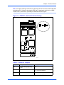
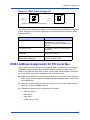
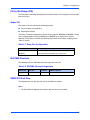
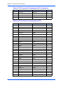
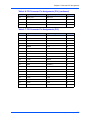
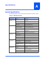
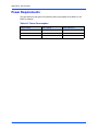
1
i
IPMC7126E/7616E I/O Module
Installation and Use
6806800A45B
September 2008 Edition
©
Copyright 2008 Emerson
All rights reserved.
Trademarks
Emerson, Business-Critical Continuity, Emerson Network Power and the Emerson Network Power logo are trademarks and service marks of
Emerson Electric Co. © 2008 Emerson Electric Co.
All other trademarks are the property of their respective owners.
PICMG®, CompactPCI®, AdvancedTCA™ and the PICMG, CompactPCI and AdvancedTCA logos are registered trademarks of the PCI Industrial
Computer Manufacturers Group.
Notice
While reasonable efforts have been made to assure the accuracy of this document, Emerson assumes no liability resulting from any omissions
in this document, or from the use of the information obtained therein. Emerson reserves the right to revise this document and to make changes
from time to time in the content hereof without obligation of Emerson to notify any person of such revision or changes.
Electronic versions of this material may be read online, downloaded for personal use, or referenced in another document as a URL to a Emerson
website. The text itself may not be published commercially in print or electronic form, edited, translated, or otherwise altered without the
permission of Emerson,
It is possible that this publication may contain reference to or information about Emerson products (machines and programs), programming, or
services that are not available in your country. Such references or information must not be construed to mean that Emerson intends to announce
such Emerson products, programming, or services in your country.
Limited and Restricted Rights Legend
If the documentation contained herein is supplied, directly or indirectly, to the U.S. Government, the following notice shall apply unless otherwise
agreed to in writing by Emerson.
Use, duplication, or disclosure by the Government is subject to restrictions as set forth in subparagraph (b)(3) of the Rights in Technical Data
clause at DFARS 252.227-7013 (Nov. 1995) and of the Rights in Noncommercial Computer Software and Documentation clause at DFARS
252.227-7014 (Jun. 1995).
Contact Address
Emerson Network Power - Embedded Computing
2900 South Diablo Way, Suite 190
Tempe, AZ 85282
USA
Safety Summary
The following general safety precautions must be observed during all phases of operation, service, and repair
of this equipment. Failure to comply with these precautions or with specific warnings elsewhere in this manual
could result in personal injury or damage to the equipment.
The safety precautions listed below represent warnings of certain dangers of which Emerson is aware. You,
as the user of the product, should follow these warnings and all other safety precautions necessary for the
safe operation of the equipment in your operating environment.
Ground the Instrument.
To minimize shock hazard, the equipment chassis and enclosure must be connected to an electrical ground.
If the equipment is supplied with a three-conductor AC power cable, the power cable must be plugged into
an approved three-contact electrical outlet, with the grounding wire (green/yellow) reliably connected to an
electrical ground (safety ground) at the power outlet. The power jack and mating plug of the power cable meet
International Electrotechnical Commission (IEC) safety standards and local electrical regulatory codes.
Do Not Operate in an Explosive Atmosphere.
Do not operate the equipment in any explosive atmosphere such as in the presence of flammable gases or
fumes. Operation of any electrical equipment in such an environment could result in an explosion and cause
injury or damage.
Keep Away From Live Circuits Inside the Equipment.
Operating personnel must not remove equipment covers. Only Factory Authorized Service Personnel or other
qualified service personnel may remove equipment covers for internal subassembly or component
replacement or any internal adjustment. Service personnel should not replace components with power cable
connected. Under certain conditions, dangerous voltages may exist even with the power cable removed. To
avoid injuries, such personnel should always disconnect power and discharge circuits before touching
components.
Use Caution When Exposing or Handling a CRT.
Breakage of a Cathode-Ray Tube (CRT) causes a high-velocity scattering of glass fragments (implosion). To
prevent CRT implosion, do not handle the CRT and avoid rough handling or jarring of the equipment.
Handling of a CRT should be done only by qualified service personnel using approved safety mask and
gloves.
Do Not Substitute Parts or Modify Equipment.
Do not install substitute parts or perform any unauthorized modification of the equipment. Contact your local
Emerson representative for service and repair to ensure that all safety features are maintained.
Observe Warnings in Manual.
Warnings, such as the example below, precede potentially dangerous procedures throughout this manual.
Instructions contained in the warnings must be followed. You should also employ all other safety precautions
which you deem necessary for the operation of the equipment in your operating environment.
Warning
Warning
To prevent serious injury or death from dangerous voltages, use
extreme caution when handling, testing, and adjusting this
equipment and its components.
Flammability
All Emerson PWBs (printed wiring boards) are manufactured with a flammability rating of 94V-0 by UL-recognized
manufacturers.
EMI Caution
Caution
!
Caution
This equipment generates, uses and can radiate electromagnetic energy. It may cause or be
susceptible to electromagnetic interference (EMI) if not installed and used with adequate EMI
protection.
CE Notice (European Community)
Warning
!
This is a Class A product. In a domestic environment, this product may cause radio
interference, in which case the user may be required to take adequate measures.
Warning
Emerson products with the CE marking comply with the EMC Directive (89/336/EEC). Compliance with this directive
implies conformity to the following European Norms:
EN55022 “Limits and Methods of Measurement of Radio Interference Characteristics of Information
Technology Equipment”; this product tested to Equipment Class A
EN 300 386 V.1.2.1 “Electromagnetic compatibility and radio spectrum matters (ERM);
Telecommunication network equipment; Electromagnetic compatibility (EMC) requirements”
Board products are tested in a representative system to show compliance with the above mentioned requirements.
A proper installation in a CE-marked system will maintain the required EMC/safety performance.
In accordance with European Community directives, a “Declaration of Conformity” has been made and is on file
within the European Union. The “Declaration of Conformity” is available on request. Please contact your sales
representative.
The product has been designed to meet the directive on the restriction of the use of certain hazardous substances
in electrical and electronic equipment (RoHS) Directive 2002/95/EC.
Industrie Canada
This product meets the requirements of the Canadian Interference-Causing Equipment Standard ICES-003.
Cet appareil numérique est conforme à la norme NMB-003 du Canada.
Contents
About This Manual . . . . . . . . . . . . . . . . . . . . . . . . . . . . . . . . . . . . . . . . . . . . . . . . . . . . . . . . . . . . . . . . . .xi
Summary of Changes . . . . . . . . . . . . . . . . . . . . . . . . . . . . . . . . . . . . . . . . . . . . . . . . . . . . . . . . . . . . . xi
Comments and Suggestions . . . . . . . . . . . . . . . . . . . . . . . . . . . . . . . . . . . . . . . . . . . . . . . . . . . . . . . xii
Terminology . . . . . . . . . . . . . . . . . . . . . . . . . . . . . . . . . . . . . . . . . . . . . . . . . . . . . . . . . . . . . . . . . . . . xii
Conventions Used in This Manual . . . . . . . . . . . . . . . . . . . . . . . . . . . . . . . . . . . . . . . . . . . . . . . . . . . xii
1
Product Features. . . . . . . . . . . . . . . . . . . . . . . . . . . . . . . . . . . . . . . . . . . . . . . . . . . . . . . . . . . . . . . . . 1
General Functionality . . . . . . . . . . . . . . . . . . . . . . . . . . . . . . . . . . . . . . . . . . . . . . . . . . . . . . . . . . . . . . 2
IPMC Mode . . . . . . . . . . . . . . . . . . . . . . . . . . . . . . . . . . . . . . . . . . . . . . . . . . . . . . . . . . . . . . . . . . . . . 2
Design Features . . . . . . . . . . . . . . . . . . . . . . . . . . . . . . . . . . . . . . . . . . . . . . . . . . . . . . . . . . . . . . . . . . 2
PCI Bus Interface . . . . . . . . . . . . . . . . . . . . . . . . . . . . . . . . . . . . . . . . . . . . . . . . . . . . . . . . . . . . . 2
Configurable Switches . . . . . . . . . . . . . . . . . . . . . . . . . . . . . . . . . . . . . . . . . . . . . . . . . . . . . . . . . . 3
PCI-to-ISA Bridge (PIB) . . . . . . . . . . . . . . . . . . . . . . . . . . . . . . . . . . . . . . . . . . . . . . . . . . . . . . . . . 3
SCSI . . . . . . . . . . . . . . . . . . . . . . . . . . . . . . . . . . . . . . . . . . . . . . . . . . . . . . . . . . . . . . . . . . . . . . . 3
ISA Local Resource Bus . . . . . . . . . . . . . . . . . . . . . . . . . . . . . . . . . . . . . . . . . . . . . . . . . . . . . . . . . . . 9
PCI-to-ISA Bridge (PIB) . . . . . . . . . . . . . . . . . . . . . . . . . . . . . . . . . . . . . . . . . . . . . . . . . . . . . . . . . 9
Super I/O . . . . . . . . . . . . . . . . . . . . . . . . . . . . . . . . . . . . . . . . . . . . . . . . . . . . . . . . . . . . . . . . . . . . 9
ESCC . . . . . . . . . . . . . . . . . . . . . . . . . . . . . . . . . . . . . . . . . . . . . . . . . . . . . . . . . . . . . . . . . . . . . . . 9
CIO . . . . . . . . . . . . . . . . . . . . . . . . . . . . . . . . . . . . . . . . . . . . . . . . . . . . . . . . . . . . . . . . . . . . . . . . 9
Static ROM (SROM) . . . . . . . . . . . . . . . . . . . . . . . . . . . . . . . . . . . . . . . . . . . . . . . . . . . . . . . . . . . . . . . 9
Input/Output Modes . . . . . . . . . . . . . . . . . . . . . . . . . . . . . . . . . . . . . . . . . . . . . . . . . . . . . . . . . . . . . . 10
LEDs . . . . . . . . . . . . . . . . . . . . . . . . . . . . . . . . . . . . . . . . . . . . . . . . . . . . . . . . . . . . . . . . . . . . . . . . . 10
PCI Signaling Voltage Level . . . . . . . . . . . . . . . . . . . . . . . . . . . . . . . . . . . . . . . . . . . . . . . . . . . . . . . . 10
RS232 Interface . . . . . . . . . . . . . . . . . . . . . . . . . . . . . . . . . . . . . . . . . . . . . . . . . . . . . . . . . . . . . . . . . 10
2
Installing the IPMC Module . . . . . . . . . . . . . . . . . . . . . . . . . . . . . . . . . . . . . . . . . . . . . . . . . . . . . . . 11
Packaging . . . . . . . . . . . . . . . . . . . . . . . . . . . . . . . . . . . . . . . . . . . . . . . . . . . . . . . . . . . . . . . . . . . . .
Configuring the IPMC Modules . . . . . . . . . . . . . . . . . . . . . . . . . . . . . . . . . . . . . . . . . . . . . . . . . . . . .
Installing IPMC Modules on Host Board . . . . . . . . . . . . . . . . . . . . . . . . . . . . . . . . . . . . . . . . . . . . . .
Before You Install or Remove a Board . . . . . . . . . . . . . . . . . . . . . . . . . . . . . . . . . . . . . . . . . . . . . . . .
Observe ESD Precautions . . . . . . . . . . . . . . . . . . . . . . . . . . . . . . . . . . . . . . . . . . . . . . . . . . . . . .
Watch for Bent Pins or Other Damage . . . . . . . . . . . . . . . . . . . . . . . . . . . . . . . . . . . . . . . . . . . .
Use Caution When Installing or Removing Boards . . . . . . . . . . . . . . . . . . . . . . . . . . . . . . . . . . .
Preserve EMI Compliance . . . . . . . . . . . . . . . . . . . . . . . . . . . . . . . . . . . . . . . . . . . . . . . . . . . . . .
Recognize Different Injector/Ejector Lever Types . . . . . . . . . . . . . . . . . . . . . . . . . . . . . . . . . . . .
Verify Slot Usage . . . . . . . . . . . . . . . . . . . . . . . . . . . . . . . . . . . . . . . . . . . . . . . . . . . . . . . . . . . . .
IPMC7126E/7616E I/O Module Installation and Use (6806800A45B)
11
11
11
12
12
13
13
13
14
14
v
Contents
3
Programming. . . . . . . . . . . . . . . . . . . . . . . . . . . . . . . . . . . . . . . . . . . . . . . . . . . . . . . . . . . . . . . . . . . 15
Programing Details . . . . . . . . . . . . . . . . . . . . . . . . . . . . . . . . . . . . . . . . . . . . . . . . . . . . . . . . . . . . . . .
PCI Local Bus . . . . . . . . . . . . . . . . . . . . . . . . . . . . . . . . . . . . . . . . . . . . . . . . . . . . . . . . . . . . . . . . . .
The PCI-to-ISA Bridge (PIB) . . . . . . . . . . . . . . . . . . . . . . . . . . . . . . . . . . . . . . . . . . . . . . . . . . . .
The SCSI Controller . . . . . . . . . . . . . . . . . . . . . . . . . . . . . . . . . . . . . . . . . . . . . . . . . . . . . . . . . .
IDSEL Address Assignments for PCI Local Bus . . . . . . . . . . . . . . . . . . . . . . . . . . . . . . . . . . . . . . . .
PCI Arbitration Assignments on Host Boards . . . . . . . . . . . . . . . . . . . . . . . . . . . . . . . . . . . . . . . . . .
MVME5100 . . . . . . . . . . . . . . . . . . . . . . . . . . . . . . . . . . . . . . . . . . . . . . . . . . . . . . . . . . . . . . . . .
MVME5500 . . . . . . . . . . . . . . . . . . . . . . . . . . . . . . . . . . . . . . . . . . . . . . . . . . . . . . . . . . . . . . . . .
MVME6100 . . . . . . . . . . . . . . . . . . . . . . . . . . . . . . . . . . . . . . . . . . . . . . . . . . . . . . . . . . . . . . . . .
Interrupt Assignments . . . . . . . . . . . . . . . . . . . . . . . . . . . . . . . . . . . . . . . . . . . . . . . . . . . . . . . . . . . .
MVME5100 IPMC Module Interrupt Assignments . . . . . . . . . . . . . . . . . . . . . . . . . . . . . . . . . . . .
MVME5500 IPMC Module Interrupt Assignments . . . . . . . . . . . . . . . . . . . . . . . . . . . . . . . . . . . .
MVME6100 IPMC Module Interrupt Assignments . . . . . . . . . . . . . . . . . . . . . . . . . . . . . . . . . . . .
ISA Local Resource Bus . . . . . . . . . . . . . . . . . . . . . . . . . . . . . . . . . . . . . . . . . . . . . . . . . . . . . . . . . .
PCI-to-ISA Bridge (PIB) . . . . . . . . . . . . . . . . . . . . . . . . . . . . . . . . . . . . . . . . . . . . . . . . . . . . . . . .
Super I/O . . . . . . . . . . . . . . . . . . . . . . . . . . . . . . . . . . . . . . . . . . . . . . . . . . . . . . . . . . . . . . . . . . .
ISA DMA Channels . . . . . . . . . . . . . . . . . . . . . . . . . . . . . . . . . . . . . . . . . . . . . . . . . . . . . . . . . . .
Z8536 CIO Port Pins . . . . . . . . . . . . . . . . . . . . . . . . . . . . . . . . . . . . . . . . . . . . . . . . . . . . . . . . . .
ISA DMA Connections/Assignments . . . . . . . . . . . . . . . . . . . . . . . . . . . . . . . . . . . . . . . . . . . . . .
Interrupt Routing to PIB . . . . . . . . . . . . . . . . . . . . . . . . . . . . . . . . . . . . . . . . . . . . . . . . . . . . . . . .
Vital Product Data (VPD) . . . . . . . . . . . . . . . . . . . . . . . . . . . . . . . . . . . . . . . . . . . . . . . . . . . . . . . . . .
4
15
15
15
15
17
18
18
18
19
19
19
20
20
20
21
21
21
21
22
23
24
Connector Pin Assignments . . . . . . . . . . . . . . . . . . . . . . . . . . . . . . . . . . . . . . . . . . . . . . . . . . . . . . 25
IPMC712 Connector . . . . . . . . . . . . . . . . . . . . . . . . . . . . . . . . . . . . . . . . . . . . . . . . . . . . . . . . . . . . . . 25
IPMC761 Connector . . . . . . . . . . . . . . . . . . . . . . . . . . . . . . . . . . . . . . . . . . . . . . . . . . . . . . . . . . . . . . 26
PCI Interface and I/O Connectors . . . . . . . . . . . . . . . . . . . . . . . . . . . . . . . . . . . . . . . . . . . . . . . . . . . 27
A
Specifications . . . . . . . . . . . . . . . . . . . . . . . . . . . . . . . . . . . . . . . . . . . . . . . . . . . . . . . . . . . . . . . . . . 33
General Specifications . . . . . . . . . . . . . . . . . . . . . . . . . . . . . . . . . . . . . . . . . . . . . . . . . . . . . . . . . . . . 33
Power Requirements . . . . . . . . . . . . . . . . . . . . . . . . . . . . . . . . . . . . . . . . . . . . . . . . . . . . . . . . . . . . . 34
B
Related Documentation . . . . . . . . . . . . . . . . . . . . . . . . . . . . . . . . . . . . . . . . . . . . . . . . . . . . . . . . . . 35
Emerson Network Power - Embedded Computing Documents . . . . . . . . . . . . . . . . . . . . . . . . . . . . . 35
Manufacturers’ Documents . . . . . . . . . . . . . . . . . . . . . . . . . . . . . . . . . . . . . . . . . . . . . . . . . . . . . . . . 36
Related Specifications . . . . . . . . . . . . . . . . . . . . . . . . . . . . . . . . . . . . . . . . . . . . . . . . . . . . . . . . . . . . 37
vi
IPMC7126E/7616E I/O Module Installation and Use (6806800A45B)
List of Figures
Figure 1-1.
Figure 1-2.
Figure 1-3.
Figure 1-4.
Figure 1-5.
Figure 2-1.
Figure 2-2.
Figure 3-1.
Figure 3-2.
IPMC761 with Default Switch Setting . . . . . . . . . . . . . . . . . . . . . . . . . . . . . . . . . . . . . . . . 4
IPMC761 Functional Block Diagram . . . . . . . . . . . . . . . . . . . . . . . . . . . . . . . . . . . . . . . . . 5
IPMC712 with Default Switch Settings . . . . . . . . . . . . . . . . . . . . . . . . . . . . . . . . . . . . . . . 6
IPMC712 Functional Block Layout . . . . . . . . . . . . . . . . . . . . . . . . . . . . . . . . . . . . . . . . . . 7
IPMC712 Serial Port 4 Clock Configuration . . . . . . . . . . . . . . . . . . . . . . . . . . . . . . . . . . . 8
IPMC Installation . . . . . . . . . . . . . . . . . . . . . . . . . . . . . . . . . . . . . . . . . . . . . . . . . . . . . . . 12
Injector/Ejector Lever Types . . . . . . . . . . . . . . . . . . . . . . . . . . . . . . . . . . . . . . . . . . . . . . 14
GPIO Switch Settings (S1) . . . . . . . . . . . . . . . . . . . . . . . . . . . . . . . . . . . . . . . . . . . . . . . 16
IDSEL Switch Settings (S2) . . . . . . . . . . . . . . . . . . . . . . . . . . . . . . . . . . . . . . . . . . . . . . 17
IPMC7126E/7616E I/O Module Installation and Use (6806800A45B)
vii
List of Figures
viii
IPMC7126E/7616E I/O Module Installation and Use (6806800A45B)
List of Tables
Table 1-1. IPMC761 Jumpers . . . . . . . . . . . . . . . . . . . . . . . . . . . . . . . . . . . . . . . . . . . . . . . . . . . . . . . 4
Table 1-2. IPMC712 Jumpers . . . . . . . . . . . . . . . . . . . . . . . . . . . . . . . . . . . . . . . . . . . . . . . . . . . . . . . 6
Table 3-1. GPIO Pin Assignments . . . . . . . . . . . . . . . . . . . . . . . . . . . . . . . . . . . . . . . . . . . . . . . . . . . 16
Table 3-2. SCSI Speed/Width Settings Using GPIO2:[1,2] . . . . . . . . . . . . . . . . . . . . . . . . . . . . . . . . 16
Table 3-3. IDSEL and IDSELB Mapping for PCI Devices . . . . . . . . . . . . . . . . . . . . . . . . . . . . . . . . . 18
Table 3-4. On-Board PCI Device Identification . . . . . . . . . . . . . . . . . . . . . . . . . . . . . . . . . . . . . . . . . 18
Table 3-5. PCI Arbitration Assignments . . . . . . . . . . . . . . . . . . . . . . . . . . . . . . . . . . . . . . . . . . . . . . . 18
Table 3-6. Hawk MPIC Interrupt Assignments . . . . . . . . . . . . . . . . . . . . . . . . . . . . . . . . . . . . . . . . . . 19
Table 3-7. Strap Pins Configuration . . . . . . . . . . . . . . . . . . . . . . . . . . . . . . . . . . . . . . . . . . . . . . . . . . 21
Table 3-8. PIB DMA Channel Assignments . . . . . . . . . . . . . . . . . . . . . . . . . . . . . . . . . . . . . . . . . . . . 21
Table 3-9. Z8536 CIO Port Pins Assignment . . . . . . . . . . . . . . . . . . . . . . . . . . . . . . . . . . . . . . . . . . . 22
Table 3-10. DMA Connection/Assignments . . . . . . . . . . . . . . . . . . . . . . . . . . . . . . . . . . . . . . . . . . . . 22
Table 3-11. PIB Interrupt Assignments . . . . . . . . . . . . . . . . . . . . . . . . . . . . . . . . . . . . . . . . . . . . . . . 23
Table 4-1. IPMC712 Connector . . . . . . . . . . . . . . . . . . . . . . . . . . . . . . . . . . . . . . . . . . . . . . . . . . . . . 25
Table 4-2. IPMC761 Connector . . . . . . . . . . . . . . . . . . . . . . . . . . . . . . . . . . . . . . . . . . . . . . . . . . . . . 26
Table 4-3. PCI Connector Pin Assignments (P11) . . . . . . . . . . . . . . . . . . . . . . . . . . . . . . . . . . . . . . 27
Table 4-4. PCI Connector Pin Assignments (P12) . . . . . . . . . . . . . . . . . . . . . . . . . . . . . . . . . . . . . . 28
Table 4-5. PCI Connector Pin Assignments (P13) . . . . . . . . . . . . . . . . . . . . . . . . . . . . . . . . . . . . . . 29
Table 4-6. PCI Connector Pin Assignments (P14) . . . . . . . . . . . . . . . . . . . . . . . . . . . . . . . . . . . . . . 30
Table 4-7. PCI Connector Pin Assignments (P15) . . . . . . . . . . . . . . . . . . . . . . . . . . . . . . . . . . . . . . 31
Table A-1. IPMC Specifications . . . . . . . . . . . . . . . . . . . . . . . . . . . . . . . . . . . . . . . . . . . . . . . . . . . . . 33
Table A-2. Power Consumption . . . . . . . . . . . . . . . . . . . . . . . . . . . . . . . . . . . . . . . . . . . . . . . . . . . . . 34
Table B-1. Emerson Network Power - Embedded Computing Publications . . . . . . . . . . . . . . . . . . . 35
Table B-2. Manufacturers’ Documents . . . . . . . . . . . . . . . . . . . . . . . . . . . . . . . . . . . . . . . . . . . . . . . 36
Table B-3. Related Specifications . . . . . . . . . . . . . . . . . . . . . . . . . . . . . . . . . . . . . . . . . . . . . . . . . . . 37
IPMC7126E/7616E I/O Module Installation and Use (6806800A45B)
ix
List of Tables
x
IPMC7126E/7616E I/O Module Installation and Use (6806800A45B)
About This Manual
The IPMC7126E/7616E I/O Module Installation and Use manual provides the information you
will need to install, use, and program your IPMC7126E or IPMC7616E module. These are
optional I/O modules installed on the variants of the MVME5100, MVME5500 and MVME6100
Single Board Computers (SBCs). Their design utilizes the PowerPlus II architecture. Hereafter,
the IPMC7126E and IPMC7616E modules will be referred to as the IPMC712 and IPMC761.
The IPMC712 is a variation of the IPMC761 The primary differences between the two modules
are in the physical interfaces of the Ethernet port and serial ports 3 and 4. These differences
along with others are discussed in the following chapters of this manual.
As of the printing date of this manual, these I/O module models are available:
Model Number
Product Description and I/O Features
IPMC7126E-002
Multifunction rear I/O PMC module; Ultra-Wide SCSI, one parallel port,
three asynchronous and one synchronous/asynchronous serial port
IPMC7616E-002
Multifunction rear I/O PMC module; Ultra-Wide SCSI, one parallel port,
two asynchronous and two synchronous/asynchronous serial ports
This manual is organized as follows:
■
Chapter 1, Product Features
■
Chapter 2, Installing the IPMC Module
■
Chapter 3, Programming
■
Chapter 4, Connector Pin Assignments
■
Appendix A, Specifications
■
Appendix B, Related Documentation
Summary of Changes
See the table below for manual revisions and changes.
Part Number
Date
Description
6806800A45B
September 2008
Update document to Emerson style (logo, copyright,
trademarks, etc.)
IPMC7126E/7616E I/O Module Installation and Use (6806800A45B)
xi
About This Manual
Comments and Suggestions
We welcome and appreciate your comments on our documentation. We want to know what you
think about our manuals and how we can make them better.
Mail comments to us by filling out the following online form:
http://www.emersonnetworkpowerembeddedcomputing.com/ > Contact Us > Online Form
In “Area of Interest” select “Technical Documentation”. Be sure to include the title, part number,
and revision of the manual and tell us how you used it.
Terminology
A character precedes a data or address parameter to specify the numeric format, as follows (if
not specified, the format is hexadecimal. An asterisk (#) following a signal name for signals that
are level significant denotes that the signal is true or valid when the signal is low.
An asterisk (#) following a signal name for signals that are edge significant denotes that the #
actions initiated by that signal occur on high to low transition.
In this manual, assertion and negation are used to specify forcing a signal to a particular state.
In particular, assertion and assert refer to a signal that is active or true; negation and negate
indicate a signal that is inactive or false. These terms are used independently of the voltage
level (high or low) that they represent.
Data and address sizes are defined as follows:
0x
Specifies a hexadecimal number
%
Specifies a binary number
&
Specifies a decimal number
Byte
8 bits, numbered 0 through 7, with bit 0 being the least significant.
Half word
16 bits, numbered 0 through 15, with bit 0 being the least significant.
Word
32 bits, numbered 0 through 31, with bit 0 being the least significant.
Double word
64 bits, numbered 0 through 63, with bit 0 being the least significant.
Conventions Used in This Manual
The following typographical conventions are used in this document:
bold
is used for user input that you type just as it appears; it is also used for commands, options
and arguments to commands, and names of programs, directories and files.
italic
is used for names of variables to which you assign values. Italic is also used for comments
in screen displays and examples, and to introduce new terms.
xii
IPMC7126E/7616E I/O Module Installation and Use (6806800A45B)
About This Manual
courier
is used for system output (for example, screen displays, reports), examples, and system
prompts.
<Enter>, <Return> or <CR>
represents the carriage return or Enter key.
Ctrl
represents the Control key. Execute control characters by pressing the Ctrl key and the
letter simultaneously, for example, Ctrl-d.
IPMC7126E/7616E I/O Module Installation and Use (6806800A45B)
xiii
About This Manual
xiv
IPMC7126E/7616E I/O Module Installation and Use (6806800A45B)
1
Product Features
1
The IPMC712 and IPMC761 are optional modules that provide backward compatibility with
earlier Emerson products using the MVME761 or MVME712M rear transition modules.
General Functionality
Both models are designed around a PMC form factor and both modules incorporate a PCI-toISA bridge, Ultra-wide SCSI adapter, and Super I/O functionality. Both modules are single wide,
standard length, standard height PMC boards. They attach to the host board PCI bus via the
PMC P11, P12, P13, P14, and P15 connectors.
■
One single-ended ultra-wide SCSI port
■
One parallel port
■
Four serial ports (2 or 3 asynchronous and 1 or 2 synchronous/asynchronous, depending
on the module)
With this PMC card configuration, the memory mezzanine, one PMC slot, and the PMCspan
are still available, providing support for additional product customization.
IPMC Mode
In IPMC mode, the MVME 6100, MVME5500, and MVME5100 support legacy MVME761 or
MVME712M rear transition modules (with limited PMC I/O) when an IPMC712 or IPMC761
module is installed in PMC slot 1. In this configuration, signals used by wide (16-bit SCSI
conflict with signals that are used by PMC slot 2 rear I/O.
Design Features
The following sections describe the basic features that are incorporated in the design of both
IPMC modules.
PCI Bus Interface
Both modules contain four EIA-E700 AAAB connectors, which provide a 32-bit PCI interface to
an IEEE P1386.1 PMC-compliant host board such as the MVME6100, MVME5500, or
MVME5100.
Connectors P11-P13 on each module provide the 32-bit PCI interface while P14 provides an
I/O path from the module to the host board.
IPMC7126E/7616E I/O Module Installation and Use (6806800A45B)
1
Chapter 1 Product Features
Signals routed to P14 include: narrow SCSI, parallel port, COM1 and COM2 synchronous serial
ports, COM3 and COM4 synchronous serial ports, power, and P2 mux signals. The remaining
SCSI data lines are routed to P15.
The on-board PCI devices on each module are as follows:
■
Winbond PCI-to-ISA Bridge (PIB)
■
LSI SCSI device (SYM53C895A)
Configurable Switches
S1 Switch
A 1x4 switch (S1) is provided on each module for configuring GPIO pins 2 and 3. The factory
default setting is for Ultra-Speed and Ultra-Wide SCSI. Refer to Table 3-1 on page 16 for the
GPIO pin assignments and to Figure 3-1 on page 16 for the default switch settings.
S2 Switch
There is a 1x2 switch (S2) on each module that is in line with the PCI-to-ISA bridge for selecting
either AD[11] IDSEL or IDSELB for connection to the Winbond chip, depending on the IPMC
module you are using.
Note The S2 is not dependent on either IPMC module. It is dependent on either the
MVME5100, MVME5500, or MVME6100 host board. The IPMC modules are shipped
configured for these boards.
Details on IDSEL mapping and PCI arbitration assignments for these SBCs can be found in
Chapter 3, Programming. An illustration showing the S2 switch settings can be found in Figure
3-2 on page 17.
PCI-to-ISA Bridge (PIB)
The PIB provides the bridging functions between PCI local bus and the ISA local resource bus.
The following are a few of the features of the PIB.
SCSI
The SCSI controller is an LSI Logic SYM53C895A device. The SCSI clock frequency is 40 MHz.
The SCSI controller features:
■
32-bit PCI Interface with 64-bit addressing
■
8KB internal SCRIPTS RAM
■
Improved PCI caching design (improves PCI bus efficiency)
The SCSI device maintains backward compatibility with the MVME761 rear transition module
and P2 adapter card. It is also Ultra-wide capable and has a performance of 40MB/s
synchronous transfer rate across a 16-bit bus.
2
IPMC7126E/7616E I/O Module Installation and Use (6806800A45B)
Chapter 1 Product Features
Note SCSI signals leading to connector P15 go through zero ohm resistors (R92-R100) before
terminating at P15. When the host board’s PMC slot 2 is populated, and there is an IPMC
module in slot 1, there exists a possibility for contention on these signals.
Figure 1-1. IPMC761 with Default Switch Setting
P15
P14
P12
P13
P11
S1
C7
C9
C10
C8
S2
C7
S1
C9
U12
U11
U7
J3
C5
U6
U5
J2
U4
U19
U3
Y2
U2
C2
Y1
C4
Y3
J1
DS2
DS1
IPMC761
PIB BUSY SCSI BUSY
2844 0905
Table 1-1. IPMC761 Jumpers
Jumper
Description
Setting
J1
Reserved 9PLD programming
header
N/A
J2
Port 3 Transmit Clock
1-2: driven by IPMC761
2-3: received by IPMC761
J3
Port 4 Transmit Clock
1-2: driven by IPMC761
2-3: received by IPMC761
IPMC7126E/7616E I/O Module Installation and Use (6806800A45B)
3
Chapter 1 Product Features
Figure 1-2. IPMC761 Functional Block Diagram
PMC PCI BUS CONNECTORS P11, P12
PIB
WINBOND
W83C554F_(H)
SCSI
LSILOGIC
SYM53C895A
IPMC761 Receptacle to Base Board
ISA bus
Super I/O
NATIONAL
PC97307
ESCC
85230
CIO
Z8536
SROM
(VPD)
2 Async Serial Ports
Parallel
P2 MUX
LOGIC
PMC I/O Connector P1
2863 0101
4
IPMC7126E/7616E I/O Module Installation and Use (6806800A45B)
Chapter 1 Product Features
Figure 1-3. IPMC712 with Default Switch Settings
P15
P14
P12
P13
P11
S1
C7
C9
C10
C8
S2
C7
S1
C9
U12
S2
U11
U7
J3
J2
U6
C5
J4
J5
U5
U15
U3
U19
Y2
Y1
C4
C2
Y3
J1
DS2
DS1
IPMC761
PIB BUSY SCSI BUSY
2843 0905
Table 1-2. IPMC712 Jumpers
Jumper
Description
Setting
J1
Reserved 9PLD programming
header
N/A
J2
Port 4 Receive Clock
1-2: driven by IPMC712
2-3: received by IPMC712
J3
Port 4 Transmit Clock
1-2: driven by IPMC712
2-3: received by IPMC712
J5
Clock Loopback
MAX207 14/15in connects to R1out
IPMC7126E/7616E I/O Module Installation and Use (6806800A45B)
5
Chapter 1 Product Features
Figure 1-4. IPMC712 Functional Block Layout
PMC P11 & P12
PCI bus
PIB
WB-554
JSA bus
CIO
8536
COM4 (sync)
ESCC
85230
COM3
Parallel
COM2
Super IO
National
COM1
Rear SCSI
SCSI
LSI
PMC P14 & P15
6
IPMC7126E/7616E I/O Module Installation and Use (6806800A45B)
Chapter 1 Product Features
Figure 1-5. IPMC712 Serial Port 4 Clock Configuration
P2
ADAPTER
Base Board + IPMC712
Z85230
64-PIN
CABLE
MVME712M
MODULE
TXD
TXDB
RTS
RTSB#
DCD
DCDB#
RXD
RXDB
CTS
CTSB#
J2
1
2
J5
3
J15
TXCI
RXCI
TXCO
J3
DTE
TRXCB
1
2
RTXCB
3
2
4
8
3
5
15
17
24
DB25
Connector
Z8536
DCD
DTR4#
LLB4#
NC
RLB4#
NC
DSR4#
NC
RI4#
NC
TM4#
NC
GND
20
7
2865 0101
IPMC7126E/7616E I/O Module Installation and Use (6806800A45B)
7
Chapter 1 Product Features
ISA Local Resource Bus
PCI-to-ISA Bridge (PIB)
The PIB (W83C554F) contains the ISA Bridge I/O Registers necessary for various functions.
These registers are also accessible from the PCI bus.
Super I/O
The Super I/O device (PC97307) provides the following functions on the IPMC:
■
Two synchronous serial ports (COM1 and COM2)
■
Parallel printer port
ESCC
Two DTE synchronous/asynchronous serial ports are provided by the ESCC device (Z85230).
Since the Z85230 device does not have all modem control lines, a Z8536 CIO device (described
below) is used to provide the missing lines.
A PAL device is used to perform decode for the Z85230 and the Z8536 for register accesses
and pseudo interrupt acknowledge cycles in the ISA I/O space. DMA supports for the Z85230
is provided by the PIB.
The clock input to the Z85230 PCLK pin is a 10 MHz clock. The Z85230 supplies an interrupt
vector during a pseudo interrupt acknowledge cycle. The vector is modified based upon the
interrupt source within the device.
All modem control lines from the ESCC are multiplexed/demultiplexed through connector P2 by
the P2MX function due to pin limitation of the connector.
CIO
The CIO device (Z8536) is used to provide the modem control lines not provided by the Z85230
ESCC. In addition, the device has three independent 16-bit counters/timers. The clock input to
the Z8536 PCLK pin is a 5 MHz clock.
Static ROM (SROM)
Both modules contains one +3.3V, 256 x 8 serial EEPROM device (AT24C02) onboard. This
device provides for Vital Product Data (VPD) storage of the module hardware configuration. The
serial EEPROM is located on the baseboard’s I2C bus at address $A4.
8
IPMC7126E/7616E I/O Module Installation and Use (6806800A45B)
Chapter 1 Product Features
Input/Output Modes
Both modules are designed to be plugged into PMC slot 1 of the base board. As stated earlier,
these SBCs have two P2 I/O modes (IPMC and PMC) that are user configurable. The user
should configure the baseboard for the IPMC module being used.
The jumpers route the on-board Ethernet port 2 to row C of connector P2. When used, both
modules are backwards compatible with the MVME761 rear transition module and P2 adapter
card (excluding PMC I/O routing) used on the MVME2600/2700. The rear panel Ethernet is not
available when using the IPMC712.
LEDs
Both modules use two LEDs to provide PMC status.
■
The module’s green SCSI LED is lit when the SCSI device is Master
■
The module’s green PIB LED is lit when the PCI bus grant to the PIB is asserted
PCI Signaling Voltage Level
Both modules will operate with only +5V signaling levels.
RS232 Interface
On the IPMC712 module, the four serial ports are used to communicate at RS232 voltage levels
(P14). The first three ports are fixed asynchronous ports, while the remaining port can be
configured as either a synchronous or an asynchronous port.
For additional handshaking signals, the IPMC712 module has the following features:
■
Port 1 has RTS and CTS
■
Ports 2, 3, and 4 have RTS, CTS, DTR, DCD
■
Port 4 has configurable serial clock signals RTxC and TRxC
Jumpers J2, J3 and J5 determine the sources for these two signals, refer to Figure 1-5 on
page 7.
IPMC7126E/7616E I/O Module Installation and Use (6806800A45B)
9
Chapter 1 Product Features
10
IPMC7126E/7616E I/O Module Installation and Use (6806800A45B)
2
Installing the IPMC Module
2
This chapter discusses the configuration and installation of IPMC modules on an MVME6100,
MVME5500, or MVME5100 SBCs.
For additional information pertaining to the MVME51005E, refer to the information contained in
the MVME51005E Single Board Computer Installation and Use manual before proceeding with
these instructions contained in this chapter.
Packaging
As a precautionary measure, IPMC modules are sealed in an anti-static package to protect
them from static discharge. Observe standard handling practices of static sensitive equipment.
Configuring the IPMC Modules
There are two user configurable switches on the IPMC712 and IPMC761 I/O modules. Switches
S1 and S2 are described in Chapter 3, Programming.
Installing IPMC Modules on Host Board
Both the IPMC712 and the IPMC761 modules are installed on PMC slot 1 of the host board. As
a general reminder, IPMC modules must be installed on the host board prior to installing it into
the VME chassis.
To install an IPMC module, refer to the following figure and proceed as follows:
1. Inspect the host board and the IPMC module for evidence of any damage to the PCB itself or
for evidence of any damage on the mating connectors.
2. If the host board is installed in a VMEbus card slot, carefully remove it and place it with
connectors P1and P2 facing you.
IPMC7126E/7616E I/O Module Installation and Use (6806800A45B)
11
Chapter 2 Installing the IPMC Module
3. Remove the filler plate from the host board’s front panel. Position the IPMC module over the
center area of the slot 1 connectors as follows:
Figure 2-1. IPMC Installation
4. Line up the IPMC module’s front panel into the IPMC filler cutout slot on the host board’s front
panel.
5. Align connectors P11, P12, P13, P14, and P15 on the IPMC module with the mating connectors
on the host board and press firmly into place.
6. Insert the appropriate number of Phillips screws (typically 4) from the bottom of the host board
into the standoffs on the IPMC module and tighten the screws.
The host board is now ready to be installed into a VME chassis.
Before You Install or Remove a Board
Boards may be damaged if improperly installed or handled. Please read and follow the
guidelines in this section to protect your equipment.
Observe ESD Precautions
ESD
Use ESD
Wrist Strap
Emerson strongly recommends that you use an antistatic wrist strap and a conductive
foam pad when installing or upgrading a system. Electronic components, such as disk
drives, computer boards, and memory modules, can be extremely sensitive to
electrostatic discharge (ESD). After removing the component from its protective
wrapper or from the system, place the component flat on a grounded, static-free
surface (and, in the case of a board, component side up). Do not slide the component
over any surface.
If an ESD station is not available, you can avoid damage resulting from ESD by wearing
an antistatic wrist strap (available at electronics stores) that is attached to an active
electrical ground. Note that a system chassis may not be grounded if it is unplugged.
12
IPMC7126E/7616E I/O Module Installation and Use (6806800A45B)
Chapter 2 Installing the IPMC Module
Watch for Bent Pins or Other Damage
Caution
!
Caution
Bent pins or loose components can cause damage to the board, the backplane, or
other system components. Carefully inspect your board and the backplane for both pin
and component integrity before installation.
ECC and our suppliers take significant steps to ensure there are no bent pins on the backplane
or connector damage to the boards prior to leaving our factory. Bent pins caused by improper
installation or by boards with damaged connectors could void the warranty for the backplane or
boards.
If a system contains one or more crushed pins, power off the system and contact your local
sales representative to schedule delivery of a replacement chassis assembly.
Use Caution When Installing or Removing Boards
When first installing boards in an empty chassis, we recommend that you start at the left of the
card cage and work to the right when cards are vertically aligned; in horizontally aligned cages,
work from bottom to top.
When inserting or removing a board in a slot adjacent to other boards, use extra caution to avoid
damage to the pins and components located on the primary or secondary sides of the boards.
Preserve EMI Compliance
Caution
!
Caution
To preserve compliance with applicable standards and regulations for electromagnetic
interference (EMI), during operation all front and rear openings on the chassis or board
faceplates must be filled with an appropriate card or covered with a filler panel. If the
EMI barrier is open, devices may cause or be susceptible to excessive interference.
IPMC7126E/7616E I/O Module Installation and Use (6806800A45B)
13
Chapter 2 Installing the IPMC Module
Recognize Different Injector/Ejector Lever Types
The modules you install may have different ejector handles and latching mechanisms. The
following illustration shows the typical board ejector handles used with ECC payload cards: (A)
Elma Latching, (B) Rittal Type II, (C) Rittal Type IV. All handles are compliant with the
CompactPCI specification and are designed to meet the IEEE1101.10 standards.
Figure 2-2. Injector/Ejector Lever Types
A
B
C
4243 1103
Each lever type has a latching mechanism to prevent the lever from being opened accidentally.
You must press the lever release before you can open the lever. Never force the lever. If the lever
does not open easily, you may not have pressed firmly enough on the release. If the lever does
not close easily, the board may not be properly seated in the chassis.
To open a lever, press the release and move the lever outward away from the faceplate.
To close a lever, move the lever inward toward the faceplate until the latch engages.
Verify Slot Usage
Prevent possible damage to module components by verifying the proper slot usage for
your configuration.
Caution
!
Caution
14
IPMC7126E/7616E I/O Module Installation and Use (6806800A45B)
3
Programming
3
Programing Details
The overall design of the IPMC712 and IPMC761 is based on the PowerPlus II architecture. The
programming characteristics for both modules conforms to the PowerPlusII Programming
Specification.
Note The PowerPlus II Programming Specification covers a large variety of programming
configurations, many of which are not applicable to either module. This chapter describes those
aspects of the specification that are unique to both modules.
PCI Local Bus
The on-board PCI devices on the IPMC712 and the IPMC761 are the PCI-to-ISA Bridge and
the SCSI controller.
The PCI-to-ISA Bridge (PIB)
The PCI-to-ISA Bridge (PIB) provides the bridging functions between PCI local bus and the ISA
local resource bus. Other features contained in the PIB are:
■
8259 Interrupt Controller
■
ISA DMA support
■
Timers and counters
The SCSI Controller
The SCSI controller’s clock speed is 40 MHz. The presence of the SCSI device can be positively
determined by reading the Device ID PCI Configuration Register 0x02 - 0x03. The Device ID is
0x0012.
IPMC7126E/7616E I/O Module Installation and Use (6806800A45B)
15
Chapter 3 Programming
The General Purpose I/O (GPIO) pin assignments for the SCSI Controller are shown in the
table below. A 1x4 switch (S1) is provided to configure GPIO pins 2 and 3. The factory default
setting shall be for Ultra-Speed and Ultra-Wide SCSI.
Table 3-1. GPIO Pin Assignments
GPIO Pin
Direction
Level
Usage
GPIO1_MASTER_l
output
1
SCSI LED; SCSI is not MASTER.
0
SCSI is MASTER.
1
SCSI speed; selectable by switch S1.
S1:1 OFF selects Ultra
0
S1:1 ON selects FAST (default).
1
SCSI bus width; selectable by switch S1.
S1:2 in OFF selects Wide-SCSI.
0
S1:2 in ON selects Narrow-SCSI.
-
Not used.
GPIO2
input
GPIO3
input
0, 4, 5, 6, 7, 8
-
Table 3-2. SCSI Speed/Width Settings Using GPIO2:[1,2]
SCSI Type
Width
Speed
FAST SCSI
Narrow (8 bit)
10MB/second
FAST SCSI
Wide (16 bit)
20MB/second
Ultra SCSI
Narrow (8 bit)
20MB/second
Ultra SCSI
Narrow (16 bit)
40MB/second
Figure 3-1. GPIO Switch Settings (S1)
1
ON
8
1
S1-P1=0
S1-P1=1
S1-P2=0
S1-P2=1
S1-P3=0
S1-P3=1
S1-P4=0
S1-P4=1
ON
8
SW1-P1 controls GPIO2 (Ultra/FAST SCSI) and SW1-P2 controls GPIO3 (Wide/Narrow SCSI
bus. SW1-P3 and SW1-P4 are No Connect. Select the SCSI characteristics of your
configuration according to the following table:
16
Width of Bus
Ultra (P1 OFF)
Fast (P1 ON)
Wide (16-bit) SCSI bus (P2 OFF)
40MB/second
20MB/second
Narrow (8-bit) SCSI bus (P2 ON)
20MB/second
10MB/second
IPMC7126E/7616E I/O Module Installation and Use (6806800A45B)
Chapter 3 Programming
Figure 3-2. IDSEL Switch Settings (S2)
ON
1
1
S2-P2 = 0
2
S2-P1=0
2
S2-P1 = 1
ON
S2-P2 =1
MVME5100 and MVME5500 S2 Default Setting
MVME6100 S2 Setting
The settings of SW2 determine the IDSEL used by the W83C553 PCI/ISA Bridge. It is important
that the settings of P1 and P2 are neither both on nor both off, otherwise the device will be
enumerated twice.
If
Then
The SW2-P1 is OFF
The W83C553’s IDSEL is connected to
IDSELB (P12:34). The IDSEL is then
determined by the carrier’s configuration of the
IPMC site.
The SW2-P2 is OFF
The W83C553’s IDSEL is connected to AD11
on the IPMC.
The IPMC761-002 is used on an
MVME6100
The SW2-P1 should be OFF and SW2-P2 set
ON for proper operation.
The IPMC761-002 is used on an
MVME5100 or MVME5500
The SW2-P1 should be ON and SW2-P2 OFF
to emulate the IPMC761-001.
IDSEL Address Assignments for PCI Local Bus
Legacy IDSEL assignment for the PCI-to-ISA Bridge (PIB) is maintained to ensure software
compatibility between MVME2700 and MVME5100 while functioning in IPMC mode. The
IPMC712 and IPMC761 boards have a switch (S2) that allows you to configure the board for
the correct IDSEL connection to the Winbond chip, as described below:
■
Connection to IDSEL, AD[11] on PMC connector pin P11-48 is selected when using the
IPMC 712/761 with ECC VME boards MVME5100 and MVME5500 (boards released prior
to the MVME6100)
■
Connection to IDSEL, AD[16] on PMC connector pin P12-34 is selected when using the
IPMC712/761 with the MVME6100 board
■
Connection to IDSELB varies according to the base board:
–
5100: No Connect
–
5500: AD[17]
–
6100: AD[21]
–
PrPMC Carrier: AD[17]
IPMC7126E/7616E I/O Module Installation and Use (6806800A45B)
17
Chapter 3 Programming
The IDSEL assignments for both modules are shown below:
Table 3-3. IDSEL and IDSELB Mapping for PCI Devices
Device Number
Field
PCI Address Line
IDSEL Connection
0b0_1011
AD11
PCI/ISA Bridge
0b1_0000
AD16
PMC Slot 1 SCSI Device
0b1_0001
AD17
PMC Slot 1 MVME5500
0b1_0101
AD21
PMC Slot 1 MVME6100
The following table shows the Vendor ID, the Device ID, and Revision ID for each of the planar
PCI devices on the IPMC712 and IPMC761:
Table 3-4. On-Board PCI Device Identification
Device
Device
Vendor ID
Device ID
Revision ID
SCSI Controller
LSI SYM53C895A
0x1000h
0x0012h
0x00h
PCI-ISA Bridge
W83C554F
0x10ADh
0x0565h
XXh
PCI Arbitration Assignments on Host Boards
The IPMC module PCI arbitration is provided by the host board.
MVME5100
The MVME5100 PCI arbitration is performed by the Hawk ASIC on the host board which
supports eight external PCI masters. Included is the Hawk itself and seven external PCI
masters. The arbitration assignments for the IPMC712 and IPMC761, when installed on the
MVME5100, are as follows:
Table 3-5. PCI Arbitration Assignments
PCI Bus Request
PCI Master(s)
Request 1 (PARBI1)
PMC Slot 1 (SCSI device on the module in PMC Slot 1)
Request 2 (PARBI2)
PIB device on the module in PMC Slot 1
MVME5500
The MVME5500 IPMC module PCI arbitration is performed using logic implemented in
Programmable Logic Devices (PLDs). These arbiters use a rotating priority scheme for fairness
and bus parking and will always be on the GT-64260B. There are no software programmable
modes to these arbiters.
18
IPMC7126E/7616E I/O Module Installation and Use (6806800A45B)
Chapter 3 Programming
MVME6100
The MVME6100 IPMC module PCI arbitration is performed by the MV64360 ASIC. The internal
PCI arbiter REQ#/GNT# signals are multiplexed on the MV64360 MPP[31:0] pins. The internal
PCI arbiter is disabled by default (the MPP pins function as general purpose inputs). Software
will configure the MPP pins to function as request/grant pairs for the internal PCI arbiter.
The IPMC module arbitration pairs for the MVME6100 are assigned to the MPP pins as follows;
■
MPP pin 8, PCI Bus Grant (PIB device on IPMC module)
■
MPP pin 9, PCI Bus Request (PIB device on IPMC module)
■
MPP pin 12, PCI Bus Grant (SCSI device on IPMC module)
■
MPP pin 13, PCI Bus Request (SCSI device on IPMC module)
Interrupt Assignments
The interrupt architecture for the IPMC712 and IPMC761 is fully compliant with the PowerPlusII
Programming Specification for a single processor board configuration.
MVME5100 IPMC Module Interrupt Assignments
Legacy interrupt assignment for the PCI-to-ISA Bridge (PIB) is maintained to ensure software
compatibility between MVME5100 and IPMC761 while in IPMC mode. This is accomplished by
using the on-board IPMC761 connector to route the PIB’s interrupt to external interrupt 0 of the
Hawk’s MPIC.
The MVME5100 Ethernet port 2 is routed to the PIB’s IRQ10 input. The SCSI interrupt on the
IPMC761 is also routed to the PIB at IRQ14. The SCSI device is connected to the INTA# pin
J11-04 of PMC Slot 1. Interrupts are routed to the Hawk from on-board resources as specified
by the module’s programming.
The Hawk interrupt assignments are shown below:
Table 3-6. Hawk MPIC Interrupt Assignments
MPICI
RQ
Edge/Leve
l
Polarity
Interrupt Source
Note
s
IRQ0
Level
High
PIB (8259) in PMC Slot 1
1
IRQ9
Level
Low
SCSI Controller interrupt shall be connected to
INTA# pin J11-04
2
Notes
1. This interrupt provided for software compatibility with MVME2700.
IPMC7126E/7616E I/O Module Installation and Use (6806800A45B)
19
Chapter 3 Programming
2. MVME5100 Hawk MPIC IRQ9 interrupt sources may be one of the following: PCI-PMC1
INTA#, PMC2 INTB#, or PCIX INTA#.
MVME5500 IPMC Module Interrupt Assignments
Legacy Interrupt assignments were not maintained on the MVME5500 due to the vastly
different host bridge device (GT-64260) used. The MVME5500 uses the GT-64260 interrupt
controller to handle interrupts internal to the GT-64260 as well as the external interrupt sources.
The GT-64260 us's general purpose pins that are configured by software to act as interrupt
inputs. The following are the IPMC module-related interrupt assignments.
GPP PIN
Edge/Level
Polarity
Interrupt Source
11
Level
Low
IPMC PIB (8259) Int in Slot 1
8
Level
Low
SCSI Controller Interrupt
Connected to INTA# pin J11-04
Note The MVME5500 does not have any Ethernet interrupts routed back to the IPMC PIB
device.
MVME6100 IPMC Module Interrupt Assignments
Legacy Interrupt assignments were not maintained on the MVME6100 because of the vastly
different host bridge device (MV64360).
The MVME6100 uses the interrupt controller integrated into MV64360 to manage the MV64360
internal interrupts as well as the external interrupt requests. The IPMC module interrupts are
routed to the MV64360 MPP pins as follows;
GPP PIN
Edge/Level
Polarity
Interrupt Source
5
Level
High
IPMC PIB (8259) Int in Slot 1
16
Level
Low
SCSI Controller Interrupt
Connected to INTA# pin J11-04
Note The MVME6100 does not have any Ethernet interrupts routed back to the IPMC PIB
device.
ISA Local Resource Bus
The ISA devices on the IPMC712 and IPMC761 are as follows:
20
■
PCI-to-ISA Bridge
■
Super I/O
IPMC7126E/7616E I/O Module Installation and Use (6806800A45B)
Chapter 3 Programming
PCI-to-ISA Bridge (PIB)
The PIB contains ISA Bridge I/O Registers for various functions. These registers are accessible
from the PCI bus.
Super I/O
The Super I/O device provides the following functions:
■
Two serial ports (asynchronous)
■
Parallel port interface
The device’s hardware configuration is based on two strap-pins: BADDR0 and BADDR1. During
reset, strapping options shown on BADDR0 and BADDR1 pins determine the device’s
operation. Clock speed is 48 MHz.The following table shows the hardware strapping for the
Super I/O device:
Table 3-7. Strap Pins Configuration
Pins
Reset Configuration
BADDR1
1,1 - Index Register 002Eh, Data Register 002Fh,
BADDR0
PnP motherboard mode,Wake up in Config state
ISA DMA Channels
The following table lists PIB DMA Channel Assignments not used.
Table 3-8. PIB DMA Channel Assignments
PIB Priority
PIB Label
Controller
DMA Assignment
Highest
Channel 2
DMA1
Not used on module
Z8536 CIO Port Pins
The following table lists port pins not used by the IPMC761 module.
Notes
1. The Hawk External Register Set interface now provides these functions.
IPMC7126E/7616E I/O Module Installation and Use (6806800A45B)
21
Chapter 3 Programming
2. On the IPMC712, pins PA0 through PA4, PA6, PA7, PB0 through PB4 are not used on the
Z8536 CIO.
Table 3-9. Z8536 CIO Port Pins Assignment
Port Pin
Signal Name
Direction
Descriptions
PA6
BRDFAIL
Output
Not used on module
PB6
FUSE
Input
Not used on module
PB7
ABORT_
Input
Not used on module
PC1
Reserved
I/O
Not used on module
PC2
BASETYP0
Input
Not used on module
PC3
BASETYP1
Input
ISA DMA Connections/Assignments
The following table shows the DMA connections/assignments between the PC97307 and the
PIB.
Table 3-10. DMA Connection/Assignments
22
Chann
el
Connection
Level
Usage
0
SCC W//REQA
high
Serial Port 3 RX
1
SCC
DTR//REQA
high
Serial Port 3 TX
2
SIO
DRQ2/DACK2
high
User SIO configurable, suggested use is parallel port
3
SIO
DRQ3/DACK3
high
User SIO configurable, suggested use is parallel port
4
None
5
SCC W//REQB
high
Serial Port 4 RX
6
SCC
DTR//REQB
high
Serial Port 4 TX
7
None
PIB Internal DMA cascade
IPMC7126E/7616E I/O Module Installation and Use (6806800A45B)
Chapter 3 Programming
Interrupt Routing to PIB
Module interrupts and MVME5100 Ethernet Port 2 interrupts go through the 8259 pair and into
the PIB. The output of the PIB then goes to the Hawk MPIC on the MVME5100. The table below
lists the ISA interrupts routed to the PIB.
1
IRQ0
3-10
IRQ2
4
IRQ9
INT1
INT2
Edge/Leve
l
Notes
IRQ
Polarity
ISA
PRI
Controller
Table 3-11. PIB Interrupt Assignments
Interrupt Source
Edge
High
Timer 1 / Counter 0
Edge
High
Cascade Interrupt from INT2
Level
High
Z8536 CIO
1
2,3
Z85230 ESCC
5
IRQ10
INT2
Level
Low
PCI-Ethernet Interrupt (from
MVME5100 Port 2)
2,4
9
IRQ14
INT2
Level
Low
PCI-SCSI Interrupt
2
11
IRQ3
INT1
Edge
High
COM2 (Async Serial Port 2)
12
IRQ4
Edge
High
COM1 (Async Serial Port 1)
15
IRQ7
Edge
High
Parallel Port Interrupt
Notes
1. Internally generated by the PIB.
2. After a reset, all ISA IRQ interrupt lines default to
edge-sensitive mode.
3. Interrupts from the Z8536 and Z85230 devices are externally wired. External logic will
determine which device to acknowledge during a pseudo IACK cycle. The Z8536 CIO has
higher priority than the Z85230 ESCC. This IRQ MUST be programmed for level-sensitive
mode.
4. This interrupt is routed from the MVME5100 through the IPMC connector to the module’s
PIB to allow backward compatibility to other products.
IPMC7126E/7616E I/O Module Installation and Use (6806800A45B)
23
Chapter 3 Programming
Vital Product Data (VPD)
To access VPD information for each SBC, access the registers through the I2C interface as
follows:
24
■
MVME5100 - via the Hawk ASIC; IPMC761’s VPD address is $A4.
■
MVME5500 - via the Discovery1 device GT64260
■
MVME6100 - via the Discovery2 device MV64360
IPMC7126E/7616E I/O Module Installation and Use (6806800A45B)
4
Connector Pin Assignments
4
This chapter provides connector pin assignments for the IPMC712 and IPMC761 modules.
IPMC712 Connector
This connector provides the on-board interface of the IPMC712 I/O signals. The pin
assignments for this connector are as follows:
Table 4-1. IPMC712 Connector
Pin
Signal Description
Signal Description
Pin
1
I2CSCL
I2CSDA
2
3
GND
GND
4
5
JDB8#
GND
6
7
GND
JDB9#
8
9
JDB10#
+3.3V
10
11
+3.3V
JDB11#
12
13
JDB12#
GND
14
15
GND
JDB13#
16
17
JDB14#
+3.3V
18
19
+3.3V
JDB15#
20
21
JDBP1#
GND
22
23
GND
LANINT2_L
24
25
PIB_INT
+3.3V
26
27
+3.3V
PIB_PMCREQ#
28
29
PIB_PMCGNT#
GND
30
31
GND
+3.3V
32
33
+5.0v
+5.0v
34
35
GND
GND
36
37
+5.0v
+5.0v
38
39
GND
GND
40
IPMC7126E/7616E I/O Module Installation and Use (6806800A45B)
25
Chapter 4 Connector Pin Assignments
IPMC761 Connector
connector provides the on-board interface of the IPMC761 I/O signals. The pin assignments
for this connector are as follows:
Table 4-2. IPMC761 Connector
26
Pin
Signal Description
Signal Description
Pin
1
I2CSCL
I2CSDA
2
3
GND
GND
4
5
DB8#
GND
6
7
GND
DB9#
8
9
DB10#
+3.3V
10
11
+3.3V
DB11#
12
13
DB12#
GND
14
15
GND
DB13#
16
17
DB14#
+3.3V
18
19
+3.3V
DB15#
20
21
DBP1#
GND
22
23
GND
LANINT2_L
24
25
PIB_INT
+3.3V
26
27
+3.3V
PIB_PMCREQ#
28
29
PIB_PMCGNT#
GND
30
31
GND
+3.3V
32
33
+5.0v
+5.0v
34
35
GND
GND
36
37
+5.0v
+5.0v
38
39
GND
GND
40
IPMC7126E/7616E I/O Module Installation and Use (6806800A45B)
Chapter 4 Connector Pin Assignments
PCI Interface and I/O Connectors
There are four 64-pin connectors on the IPMC761 (P11, P12, P13, and P14) which provide 32bit PCI interface and P2 Input/Output (I/O) for the host board. The pin assignments are as
follows:
Table 4-3. PCI Connector Pin Assignments (P11)
Pin
Signal Description
Signal Description
Pin
1
TCK
-12V
2
3
GND
INTA#
4
5
INTB#
INTC#
6
7
PMCPRSNT1#
+5V
8
9
INTD#
Not Used
10
11
GND
Not Used
12
13
CLK
GND
14
15
GND
PMCGNT1#
16
17
PMCREQ1#
+5V
18
19
+5V (Vio)
AD31
20
21
AD28
AD27
22
23
AD25
GND
24
25
GND
C/BE3#
26
27
AD22
AD21
28
29
AD19
+5V
30
31
+5V (Vio)
AD17
32
33
FRAME#
GND
34
35
GND
IRDY#
36
37
DEVSEL#
+5V
38
39
GND
LOCK#
40
41
SDONE#
SBO#
42
43
PAR
GND
44
45
+5V (Vio)
AD15
46
47
AD12
AD11
48
49
AD09
+5V
50
51
GND
C/BE0#
52
53
AD06
AD05
54
55
AD04
GND
56
IPMC7126E/7616E I/O Module Installation and Use (6806800A45B)
27
Chapter 4 Connector Pin Assignments
Table 4-3. PCI Connector Pin Assignments (P11) (continued)
Pin
Signal Description
Signal Description
Pin
57
+5V (Vio)
AD03
58
59
AD02
AD01
60
61
AD00
+5V
62
63
GND
REQ64#
64
Table 4-4. PCI Connector Pin Assignments (P12)
28
Pin
Signal Description
Signal Description
Pin
1
+12V
TRST#
2
3
TMS
TDO
4
5
TDI
GND
6
7
GND
Not Used
8
9
Not Used
Not Used
10
11
Not Used
+3.3V
12
13
RST#
Not Used
14
15
+3.3V
Not Used
16
17
Not Used
GND
18
19
AD30
AD29
20
21
GND
AD26
22
23
AD24
+3.3V
24
25
IDSEL1
AD23
26
27
+3.3V
AD20
28
29
AD18
GND
30
31
AD16
C/BE2#
32
33
GND
Not Used
34
35
TDRY#
+3.3V
36
37
GND
STOP#
38
39
PERR#
GND
40
41
+3.3V
SERR#
42
43
C/BE1#
GND
44
45
AD14
AD13
46
47
GND
AD10
48
49
AD08
+3.3V
50
51
AD07
Not Used
52
53
+3.3V
Not Used
54
55
Not Used
GND
56
IPMC7126E/7616E I/O Module Installation and Use (6806800A45B)
Chapter 4 Connector Pin Assignments
Table 4-4. PCI Connector Pin Assignments (P12) (continued)
Pin
Signal Description
Signal Description
Pin
57
Not Used
Not Used
58
59
GND
Not Used
60
61
ACK64#
+3.3V
62
63
GND
Not Used
64
Table 4-5. PCI Connector Pin Assignments (P13)
Pin
Signal Description
Signal Description
Pin
1
Reserved
GND
2
3
GND
Not Used
4
5
Not Used
Not Used
6
7
Not Used
GND
8
9
+5V (Vio)
Not Used
10
11
Not Used
Not Used
12
13
Not Used
GND
14
15
GND
Not Used
16
17
Not Used
Not Used
18
19
Not Used
GND
20
21
+5V (Vio)
Not Used
22
23
Not Used
Not Used
24
25
Not Used
GND
26
27
GND
Not Used
28
29
Not Used
Not Used
30
31
Not Used
GND
32
33
GND
Not Used
34
35
Not Used
Not Used
36
37
Not Used
GND
38
39
+5V (Vio)
Not Used
40
41
Not Used
Not Used
42
43
Not Used
GND
44
45
GND
Not Used
46
47
Not Used
Not Used
48
49
Not Used
GND
50
51
GND
Not Used
52
53
Not Used
Not Used
54
55
Not Used
GND
56
IPMC7126E/7616E I/O Module Installation and Use (6806800A45B)
29
Chapter 4 Connector Pin Assignments
Table 4-5. PCI Connector Pin Assignments (P13) (continued)
Pin
Signal Description
Signal Description
Pin
57
+5V (Vio)
Not Used
58
59
Reserved
Reserved
60
61
Reserved
GND
62
63
GND
Reserved
64
Table 4-6. PCI Connector Pin Assignments (P14)
30
Pin
Signal Description
Signal Description
Pin
1
Not Used
DB0#
2
3
Not Used
DB1#
4
5
Not Used
DB2#
6
7
Not Used
DB3#
8
9
Not Used
DB4#
10
11
Not Used
DB5#
12
13
Not Used
DB6#
14
15
PRSTB#
DB7#
16
17
PRD0
DBP#
18
19
PRD1
ATN#
20
21
PRD2
BSY#
22
23
PRD3
ACK#
24
25
PRD4
RST#
26
27
PRD5
MSG#
28
29
PRD6
SEL#
30
31
PRD7
D/C#
32
33
PRACK#
REQ#
34
35
PRBSY
O/I#
36
37
PRPE
AFD#
38
39
PRSEL
SLIN#
40
41
INIT#
TXD3
42
43
PRFLT#
RXD3
44
45
TXD1_232
RTXC3
46
47
RXD1_232
TRXC3
48
49
RTS1_232
TXD4
50
51
CTS1_232
RXD4
52
53
TXD2_232
RTXC4
54
55
RXD2_232
TRXC4
56
IPMC7126E/7616E I/O Module Installation and Use (6806800A45B)
Chapter 4 Connector Pin Assignments
Table 4-6. PCI Connector Pin Assignments (P14) (continued)
Pin
Signal Description
Signal Description
Pin
57
RTS2_232
Not Used
58
59
CTS2_232
Not Used
60
61
MDO
MSYNC#
62
63
MDI
MCLK
64
Table 4-7. PCI Connector Pin Assignments (P15)
Pin
Signal Description
Signal Description
Pin
1
I2CSCL
I2CSDA
2
3
GND
GND
4
5
DB8#
GND
6
7
GND
DB9#
8
9
DB10#
+3.3V
10
11
+3.3V
DB11#
12
13
DB12#
GND
14
15
GND
DB13#
16
17
DB14#
+3.3V
18
19
+3.3V
DB15#
20
21
DBP1#
GND
22
23
GND
LANINT2_L
24
25
PIB_INT
+3.3V
26
27
+3.3V
PIB_PMCREQ#
28
29
PIB_PMCGNT#
GND
30
31
GND
+3.3V
32
33
+5.0V
+5.0V
34
35
GND
GND
36
37
+5.0V
+5.0V
38
39
GND
GND
40
IPMC7126E/7616E I/O Module Installation and Use (6806800A45B)
31
Chapter 4 Connector Pin Assignments
32
IPMC7126E/7616E I/O Module Installation and Use (6806800A45B)
A
Specifications
A
General Specifications
The following table provides general specifications for the IPMC712 and IPMC761 module.
Table A-1. IPMC Specifications
Main
Characteristic
PMC
Interface
SCSI Bus
Function
Specification
Address/Data
A32/D32/D64, PMC PN1, PN2, PN3, PN4
Connectors
PCI Bus Clock
33 MHz
Signaling
5 Volts
Module Type
Basic, Single-Wide; P2 I/O
Controller
Symbios 53C895A
PCI Local Bus DMA
Yes, with PCI Local Bus Burst
Asynchronous Transfer Rate
5.0MB/s
Ultra-SCSI Transfer Rate
20.0MB/s (8-Bit Mode), 40.0MB/s
(16-Bit Mode)
Synchronous
Serial Ports
Asynchronous
Serial Ports
Parallel Ports
Connector
Routed to P2, 50 or 68 Pin on P2
Controller
85230/8536
Number of Ports
2
Configuration
TTL to P2 (Both Ports), SIM on MVME761
Baud Rate (BPS Max)
2.5M Synchronous, 38.4K Asynchronous
Connector
Routed to P2, HD-26 on MVME761
Controller
16C550 UART
Number of Ports
2 (16550 Compatible)
Configuration
EIA-574 DTE
Asynchronous Baud Rate
(BPS Max)
38.4 EIA-232, 115Kbps Raw Transfer Rate
Connector
Routed to P2, DB-9 on MVME761
Controller
PC97307
Configuration
8-Bit Bi-Directional, Full IEEE 1284 Support,
Centronics Compatible
Modes
Master Only
Connector
Routed to P2, HD-36 on MVME761
IPMC7126E/7616E I/O Module Installation and Use (6806800A45B)
33
Appendix A Specifications
Power Requirements
The table below lists the typical and maximum power consumption of the IPMC712 and
IPMC761 modules.
Table A-2. Power Consumption
34
Supply Voltage
Amps (Typical)
Amps (Maximum)
+5V (±5%)
0.5 A
N/A
+12V (±10%)
0.2 A
0.5 A
-12V (±10%)
0.1 A
0.3 A
IPMC7126E/7616E I/O Module Installation and Use (6806800A45B)
B
Related Documentation
B
Emerson Network Power - Embedded Computing
Documents
The Emerson Network Power - Embedded Computing publications listed below are referenced
in this manual. You can obtain electronic copies of Emerson Network Power - Embedded
Computing publications by contacting your local Emerson sales office. For documentation of
final released (GA) products, you can also visit the following website:
www.emersonnetworkpower.com/embeddedcomputing > Solution Services > Technical
Documentation Search. This site provides the most up-to-date copies of Emerson Network
Power - Embedded Computing product documentation.
Table B-1. Emerson Network Power - Embedded Computing Publications
Document Title
Publication
Number
MVME55006E Single Board Computer Installation and Use
6806800A37
MVME51005E Single Board Computer Installation and Use
6806800A38
MVME5500 Single Board Computer Programmer’s Reference Guide
6806800A37
MVME5100 Single Board Computer Programmer’s Reference Guide
V5100A/PG
MVME6100 Single Board Computer Installation and Use
6806800D58
MOTLoad Firmware Package User’s Manual
6806800C24
PPCBug Firmware Package User’s Manual, Part 1 of 2
PPCBUGA1/UM
PPCBug Firmware Package User’s Manual, Part 2 of 2
PPCBUGA2/UM
PPCBug Diagnostics User’s Manual
PPCDIAA/UM
IPMC7126E/7616E I/O Module Installation and Use (6806800A45B)
35
Appendix B Related Documentation
Manufacturers’ Documents
For additional information, refer to the following table for manufacturers’ data sheets or user’s
manuals. For your convenience, a source for the listed document is also provided.
Note In many cases, the information is preliminary and the revision levels of the documents are
subject to change without notice.
Table B-2. Manufacturers’ Documents
Document Title
Publication
Number
WebSite: Freescale Literature Distribution Center
E-mail: [email protected]
MPC750 RISC Microprocessor Users Manual
MPC750UM/AD
MPC7400 RISC Microprocessor Users Manual
MPC7400UM/D
PowerPlus II Vital Product Data Engineering Specification
Revision 0.1
Tundra Semiconductor Corporation
8091142_MD300_01.pdf
Universe II User Manual
MV64360 System Controller for PowerPC Processors Data Sheet
MV-S100414-00C
Marvell Technologies, Ltd.
Web Site: http://www.marvell.com/
Note In many cases, the information is preliminary and the revision levels of the documents are
subject to change without notice.
36
IPMC7126E/7616E I/O Module Installation and Use (6806800A45B)
Appendix B Related Documentation
Related Specifications
For additional information, refer to the following table for related specifications. For your
convenience, a source for the listed document is also provided.
Table B-3. Related Specifications
Document Title and Source
PCI Special Interest Group
Peripheral Component Interconnect (PCI) Local Bus Specification,
Publication
Number
PCI Specification
Revision 2.0, 2.1, 2.2
Institute of Electrical and Electronics Engineers, Inc. (IEEE)
IEEE - Common Mezzanine Card Specification (CMC)
P1386, Draft 2.0
IEEE - PCI Mezzanine Card Specification (PMC)
P1386.1, Draft 2.0
Bidirectional Parallel Port Interface Specification
IEEE Standard 1284
ANSI
X3.131.1990
ANSI Small Computer System Interface-2 (SCSI-2), Draft Document
Global Engineering Documents
VMEbus International Trade Association (VITA)
ANSI/VITA 1-1994
VME64 Specification
IPMC7126E/7616E I/O Module Installation and Use (6806800A45B)
37
Index
A
address assignments PCI local bus (IDSEL) 17
arbitration assignments (host boards) 18
arbitration pairs, MVME6100 19
architecture xi, 15
B
backward compatibility 3, 10
basic features 2
block diagram, IPMC712 7
block diagram, IPMC761 5
board ejector handles 14
bus grants 19
C
caching 3
CIO device 9
CIO port pins 21
clock configuration, IPMC712 8
clock input 9
clock speed, SCSI 15
clock speed, Super I/O 21
compliance, IEEE P1386.1 2
configuring the module 11
connectors
EIA-E700 2
IPMC761 25, 26
P1 and P2 25, 26, 27
controller, SCSI 3
conventions used in the manual xii
D
device ID, PCI device 18
device ID, SCSI 15
devices
CIO 9
ESCC 9
ISA 20
PCI 15
PIB 2, 21
SCSI 2, 15
Super I/O 9
DMA channel assignments 21
DMA connections 21
DMA support 9, 15
DTE 9
E
EEPROM device 9
EIA-E700 2
ejector levers 14
Emerson publications 35
ESCC 9
ESD precautions 12
Ethernet port interrupts 23
F
form factor 2
functionality 2
G
GPIO pin assignments 16
green PIB LED 10
green SCSI LED 10
H
handshaking signals 10
Hawk ASIC 18
headers, configurable 11
I
I/O
narrow SCSI 2
parallel 2
serial 2
I/O connector pin assignments 26
I/O modes 10
I/O ports 2
IDSEL mapping 18
IDSEL settings 3, 17
inspecting the module 11
installation
hardware 11
PMC module onto host board 11
installation precautions 12
installing the IPMC 11
interfaces
Hawk external register set 21
parallel 21
PCI bus 2, 26
SCSI 3
serial 21
interrupt assignments
for MVME5500 20
for MVME6100 20
Hawk MPIC for MVME5100 19
interrupt routing to PIB 23
IPMC mode 2, 10
IPMC specifications 33
IPMC712 pin assignments 25
IPMC761 pin assignments 26
ISA Bridge I/O Registers 9
IPMC7126E/7616E I/O Module Installation and Use (6806800A45B)
39
Index
ISA local resource bus 9, 20
J
jumpering, clock signals 10
L
LEDs 10
local buses 3
local resource bus 9
M
manual conventions xii
manufacturers’ manuals 36
mapping to IDSEL 18
max power consumption 34
mechanical layouts 6
memory support 2
model numbers xi
modem control lines 9
modes, I/O 10
modes, programmable 18
module interrupts 23
MPP pins 19
P
P1 and P2 connectors 25, 26, 27
packaging 11
parallel port 9
PCI arbitration, MVME5100, MVME5500,
MVME6100 18
PCI bus grant 10
PCI device identification 18
PCI interface 26
PCI Signaling Voltage Level 10
PCI-ISA Bridge 3
PCI-to-ISA bridge 3, 9, 15
PIB 3, 9
pin assignments 25
pin assignments, GPIO 16
PLDs 18
PMC mode 10
PMC support 2
power consumption 34
power requirements 34
product description xi
programmable modes 18
programming model 15
R
register access 9
registers, ISA bridge 21
40
related specifications 37
revision ID, PCI device 18
RS232 Interface 10
S
S1 switch 3, 16
S2 switch 17
SCRIPTS RAM 3
SCSI as master 10
SCSI controller 3
SCSI data lines 2
SCSI device 2
SCSI signals 4
selecting IDSEL settings 17
selecting SCSI bus width 16
selecting SCSI master 16
selecting SCSI speed 16
serial port 4, clock 8
serial port configuration 9
serial ports 9
settings for IDSEL 3
signaling levels 10
signals, mux 2
signals, SCSI 4
specification, related 37
specifications for IPMCs 33
static ROM 9
strap pin configuration 21
strapping options 21
Super I/O 9, 20
super I/O 21
switch settings 11
switches
S1 (GPIO) 3, 16
S2 (IDSEL) 17
synchronous transfer rate 3
T
termination of SCSI signals 4
terminology used in this manual xii
transition modules, compatibility 3
typeface, meaning of xii
V
variants xi
vendor ID, PCI device 18
Vital Product Data (VPD) 9
voltage levels 10
W
Winbond PCI-to-ISA Bridge 2
IPMC7126E/7616E I/O Module Installation and Use (6806800A45B)