1
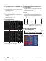
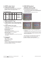
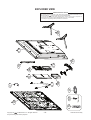
LED TV
SERVICE MANUAL
CHASSIS : LA46B
MODEL : 39LB5800
39LB5800-UG
CAUTION
BEFORE SERVICING THE CHASSIS,
READ THE SAFETY PRECAUTIONS IN THIS MANUAL.
P/NO : MFL68026206 (1402-REV00)
Printed in Korea
Recommended Troubleshooting & Repairing Guide:
V3.0 –LED & LCD TV
Repair Tips ebook
V2.0- LCD TV Repair
Tips & Case Histories
“More information on
T-con Board & Mainboard
Secret Repair Tips!”
V1.0- Collection of LCD
TV Repair Tips
LCD/LED & 3D TV
Repair Membership Site
Vol-3 LCD/LED
Monitor Repair Case
Histories by Jestine
Yong
Plasma & 3D TV
Repair Membership
Site
Projection TV &
DLP/LCD Projector
Repair Membership Site
Troubleshooting &
Repairing LCD TV
Guide
Plasma TV Repair GuideDisplay Fault
Troubleshooting Basic
LCD TV Repair
Secrets Revealed
LCD Monitor Repair Guide
SMPS-Switch Mode
Power Supply Repair
Guide
Vol .1- 10 Trus Repair
Case Histories of LCD
Monitor
Testing Electronic
Components like a ProFor Beginner
Please visit: http://lcd-television-repair.com/newsletter/Recommend.html
CONTENTS
CONTENTS . ............................................................................................. 2
PRODUCT SAFETY ................................................................................. 3
SPECIFICATION........................................................................................ 4
ADJUSTMENT INSTRUCTION................................................................. 9
BLOCK DIAGRAM................................................................................... 18
EXPLODED VIEW .................................................................................. 19
SCHEMATIC CIRCUIT DIAGRAM ..............................................................
Copyright ©
LG Electronics. Inc. All rights reserved.
Only for training and service purposes
-2-
LGE Internal Use Only
SAFETY PRECAUTIONS
IMPORTANT SAFETY NOTICE
Many electrical and mechanical parts in this chassis have special safety-related characteristics. These parts are identified by
in the
Schematic Diagram and Exploded View.
It is essential that these special safety parts should be replaced with the same components as recommended in this manual to prevent
Shock, Fire, or other Hazards.
Do not modify the original design without permission of manufacturer.
General Guidance
Leakage Current Hot Check (See below Figure)
Plug the AC cord directly into the AC outlet.
An isolation Transformer should always be used during the
servicing of a receiver whose chassis is not isolated from the AC
power line. Use a transformer of adequate power rating as this
protects the technician from accidents resulting in personal injury
from electrical shocks.
It will also protect the receiver and it's components from being
damaged by accidental shorts of the circuitry that may be
inadvertently introduced during the service operation.
If any fuse (or Fusible Resistor) in this TV receiver is blown,
replace it with the specified.
When replacing a high wattage resistor (Oxide Metal Film Resistor,
over 1 W), keep the resistor 10 mm away from PCB.
Keep wires away from high voltage or high temperature parts.
Do not use a line Isolation Transformer during this check.
Connect 1.5 K / 10 watt resistor in parallel with a 0.15 uF capacitor
between a known good earth ground (Water Pipe, Conduit, etc.)
and the exposed metallic parts.
Measure the AC voltage across the resistor using AC voltmeter
with 1000 ohms/volt or more sensitivity.
Reverse plug the AC cord into the AC outlet and repeat AC voltage
measurements for each exposed metallic part. Any voltage
measured must not exceed 0.75 volt RMS which is corresponds to
0.5 mA.
In case any measurement is out of the limits specified, there is
possibility of shock hazard and the set must be checked and
repaired before it is returned to the customer.
Leakage Current Hot Check circuit
Before returning the receiver to the customer,
always perform an AC leakage current check on the exposed
metallic parts of the cabinet, such as antennas, terminals, etc., to
be sure the set is safe to operate without damage of electrical
shock.
Leakage Current Cold Check(Antenna Cold Check)
With the instrument AC plug removed from AC source, connect an
electrical jumper across the two AC plug prongs. Place the AC
switch in the on position, connect one lead of ohm-meter to the AC
plug prongs tied together and touch other ohm-meter lead in turn to
each exposed metallic parts such as antenna terminals, phone
jacks, etc.
If the exposed metallic part has a return path to the chassis, the
measured resistance should be between 1 MΩ and 5.2 MΩ.
When the exposed metal has no return path to the chassis the
reading must be infinite.
An other abnormality exists that must be corrected before the
receiver is returned to the customer.
Copyright ©
LG Electronics. Inc. All rights reserved.
Only for training and service purposes
-3-
LGE Internal Use Only
SERVICING PRECAUTIONS
CAUTION: Before servicing receivers covered by this service
manual and its supplements and addenda, read and follow the
SAFETY PRECAUTIONS on page 3 of this publication.
NOTE: If unforeseen circumstances create conflict between the
following servicing precautions and any of the safety precautions
on page 3 of this publication, always follow the safety precautions.
Remember: Safety First.
General Servicing Precautions
1. Always unplug the receiver AC power cord from the AC power
source before;
a. Removing or reinstalling any component, circuit board module or any other receiver assembly.
b. Disconnecting or reconnecting any receiver electrical plug or
other electrical connection.
c. Connecting a test substitute in parallel with an electrolytic
capacitor in the receiver.
CAUTION: A wrong part substitution or incorrect polarity
installation of electrolytic capacitors may result in an explosion hazard.
2. Test high voltage only by measuring it with an appropriate
high voltage meter or other voltage measuring device (DVM,
FETVOM, etc) equipped with a suitable high voltage probe.
Do not test high voltage by "drawing an arc".
3. Do not spray chemicals on or near this receiver or any of its
assemblies.
4. Unless specified otherwise in this service manual, clean
electrical contacts only by applying the following mixture to the
contacts with a pipe cleaner, cotton-tipped stick or comparable
non-abrasive applicator; 10 % (by volume) Acetone and 90 %
(by volume) isopropyl alcohol (90 % - 99 % strength)
CAUTION: This is a flammable mixture.
Unless specified otherwise in this service manual, lubrication of
contacts in not required.
5. Do not defeat any plug/socket B+ voltage interlocks with which
receivers covered by this service manual might be equipped.
6. Do not apply AC power to this instrument and/or any of its
electrical assemblies unless all solid-state device heat sinks are
correctly installed.
7. Always connect the test receiver ground lead to the receiver
chassis ground before connecting the test receiver positive
lead.
Always remove the test receiver ground lead last.
8. Use with this receiver only the test fixtures specified in this
service manual.
CAUTION: Do not connect the test fixture ground strap to any
heat sink in this receiver.
Electrostatically Sensitive (ES) Devices
Some semiconductor (solid-state) devices can be damaged easily by static electricity. Such components commonly are called
Electrostatically Sensitive (ES) Devices. Examples of typical ES
devices are integrated circuits and some field-effect transistors
and semiconductor “chip” components. The following techniques
should be used to help reduce the incidence of component damage caused by static by static electricity.
1. Immediately before handling any semiconductor component or
semiconductor-equipped assembly, drain off any electrostatic
charge on your body by touching a known earth ground. Alternatively, obtain and wear a commercially available discharging
wrist strap device, which should be removed to prevent potential shock reasons prior to applying power to the unit under test.
Copyright ©
LG Electronics. Inc. All rights reserved.
Only for training and service purposes
2. After removing an electrical assembly equipped with ES
devices, place the assembly on a conductive surface such as
aluminum foil, to prevent electrostatic charge buildup or exposure of the assembly.
3. Use only a grounded-tip soldering iron to solder or unsolder ES
devices.
4. Use only an anti-static type solder removal device. Some solder
removal devices not classified as “anti-static” can generate
electrical charges sufficient to damage ES devices.
5. Do not use freon-propelled chemicals. These can generate
electrical charges sufficient to damage ES devices.
6. Do not remove a replacement ES device from its protective
package until immediately before you are ready to install it.
(Most replacement ES devices are packaged with leads electrically shorted together by conductive foam, aluminum foil or
comparable conductive material).
7. Immediately before removing the protective material from the
leads of a replacement ES device, touch the protective material
to the chassis or circuit assembly into which the device will be
installed.
CAUTION: Be sure no power is applied to the chassis or circuit,
and observe all other safety precautions.
8. Minimize bodily motions when handling unpackaged replacement ES devices. (Otherwise harmless motion such as the
brushing together of your clothes fabric or the lifting of your
foot from a carpeted floor can generate static electricity sufficient to damage an ES device.)
General Soldering Guidelines
1. Use a grounded-tip, low-wattage soldering iron and appropriate
tip size and shape that will maintain tip temperature within the
range or 500 °F to 600 °F.
2. Use an appropriate gauge of RMA resin-core solder composed
of 60 parts tin/40 parts lead.
3. Keep the soldering iron tip clean and well tinned.
4. Thoroughly clean the surfaces to be soldered. Use a mall wirebristle (0.5 inch, or 1.25 cm) brush with a metal handle.
Do not use freon-propelled spray-on cleaners.
5. Use the following unsoldering technique
a. Allow the soldering iron tip to reach normal temperature.
(500 °F to 600 °F)
b. Heat the component lead until the solder melts.
c. Quickly draw the melted solder with an anti-static, suctiontype solder removal device or with solder braid.
CAUTION: Work quickly to avoid overheating the circuit
board printed foil.
6. Use the following soldering technique.
a. Allow the soldering iron tip to reach a normal temperature
(500 °F to 600 °F)
b. First, hold the soldering iron tip and solder the strand against
the component lead until the solder melts.
c. Quickly move the soldering iron tip to the junction of the
component lead and the printed circuit foil, and hold it there
only until the solder flows onto and around both the component lead and the foil.
CAUTION: Work quickly to avoid overheating the circuit
board printed foil.
d. Closely inspect the solder area and remove any excess or
splashed solder with a small wire-bristle brush.
-4-
LGE Internal Use Only
IC Remove/Replacement
Some chassis circuit boards have slotted holes (oblong) through
which the IC leads are inserted and then bent flat against the circuit foil. When holes are the slotted type, the following technique
should be used to remove and replace the IC. When working with
boards using the familiar round hole, use the standard technique
as outlined in paragraphs 5 and 6 above.
3. Solder the connections.
CAUTION: Maintain original spacing between the replaced
component and adjacent components and the circuit board to
prevent excessive component temperatures.
Circuit Board Foil Repair
Excessive heat applied to the copper foil of any printed circuit
board will weaken the adhesive that bonds the foil to the circuit
board causing the foil to separate from or "lift-off" the board. The
following guidelines and procedures should be followed whenever
this condition is encountered.
Removal
1. Desolder and straighten each IC lead in one operation by
gently prying up on the lead with the soldering iron tip as the
solder melts.
2. Draw away the melted solder with an anti-static suction-type
solder removal device (or with solder braid) before removing
the IC.
Replacement
1. Carefully insert the replacement IC in the circuit board.
2. Carefully bend each IC lead against the circuit foil pad and
solder it.
3. Clean the soldered areas with a small wire-bristle brush.
(It is not necessary to reapply acrylic coating to the areas).
At IC Connections
To repair a defective copper pattern at IC connections use the
following procedure to install a jumper wire on the copper pattern
side of the circuit board. (Use this technique only on IC connections).
"Small-Signal" Discrete Transistor
Removal/Replacement
1. Remove the defective transistor by clipping its leads as close
as possible to the component body.
2. Bend into a "U" shape the end of each of three leads remaining
on the circuit board.
3. Bend into a "U" shape the replacement transistor leads.
4. Connect the replacement transistor leads to the corresponding
leads extending from the circuit board and crimp the "U" with
long nose pliers to insure metal to metal contact then solder
each connection.
Power Output, Transistor Device
Removal/Replacement
1. Heat and remove all solder from around the transistor leads.
2. Remove the heat sink mounting screw (if so equipped).
3. Carefully remove the transistor from the heat sink of the circuit
board.
4. Insert new transistor in the circuit board.
5. Solder each transistor lead, and clip off excess lead.
6. Replace heat sink.
Diode Removal/Replacement
1. Remove defective diode by clipping its leads as close as possible to diode body.
2. Bend the two remaining leads perpendicular y to the circuit
board.
3. Observing diode polarity, wrap each lead of the new diode
around the corresponding lead on the circuit board.
4. Securely crimp each connection and solder it.
5. Inspect (on the circuit board copper side) the solder joints of
the two "original" leads. If they are not shiny, reheat them and if
necessary, apply additional solder.
1. Carefully remove the damaged copper pattern with a sharp
knife. (Remove only as much copper as absolutely necessary).
2. carefully scratch away the solder resist and acrylic coating (if
used) from the end of the remaining copper pattern.
3. Bend a small "U" in one end of a small gauge jumper wire and
carefully crimp it around the IC pin. Solder the IC connection.
4. Route the jumper wire along the path of the out-away copper
pattern and let it overlap the previously scraped end of the
good copper pattern. Solder the overlapped area and clip off
any excess jumper wire.
At Other Connections
Use the following technique to repair the defective copper pattern
at connections other than IC Pins. This technique involves the
installation of a jumper wire on the component side of the circuit
board.
1. Remove the defective copper pattern with a sharp knife.
Remove at least 1/4 inch of copper, to ensure that a hazardous
condition will not exist if the jumper wire opens.
2. Trace along the copper pattern from both sides of the pattern
break and locate the nearest component that is directly connected to the affected copper pattern.
3. Connect insulated 20-gauge jumper wire from the lead of the
nearest component on one side of the pattern break to the lead
of the nearest component on the other side.
Carefully crimp and solder the connections.
CAUTION: Be sure the insulated jumper wire is dressed so the
it does not touch components or sharp edges.
Fuse and Conventional Resistor
Removal/Replacement
1. Clip each fuse or resistor lead at top of the circuit board hollow
stake.
2. Securely crimp the leads of replacement component around
notch at stake top.
Copyright ©
LG Electronics. Inc. All rights reserved.
Only for training and service purposes
-5-
LGE Internal Use Only
SPECIFICATION
NOTE : Specifications and others are subject to change without notice for improvement.
1. Application range
1.1. This spec sheet is applied all of the 32”, 39”, 42”, 47”, 50”,
55”, 60, 65” LED TV with LA46B chassis.
1.2. Not included spec and each product spec in this spec
sheet apply correspondingly to the following each country
standard and requirement of Buyer
2. Test condition
Each part is tested as below without special notice.
1) Temperature : 20 ºC ± 5 ºC
2) Relative Humidity: 65 % ± 10 %
3) Power Voltage
Market
Input voltage
Frequency
USA
110~240V
50/60Hz
Remark
Standard Voltage of each
product is marked by
models
4) Specification and performance of each parts are followed
each drawing and specification by part number in
accordance with BOM
5) The receiver must be operated for about 20 minutes prior to
the adjustment
3. Test method
1) Performance: LGE TV test method followed
2) Demanded other specification
- Safety : UL, CSA, IEC specification
- EMC: FCC, ICES, IEC specification
- Wireless : WirelessHD Specification (Option)
Copyright ©
LG Electronics. Inc. All rights reserved.
Only for training and service purposes
-6-
LGE Internal Use Only
4. General Specification
No
Item
Specification
Remark
1
Market
1) North America
2
Television System
NTSC-M, ATSC, 64 & 256 QAM
3
Input Voltage
AC 100 ~ 240V 50/60Hz
4
Available Channel
1) VHF : 02~13
2) UHF : 14~69
3) DTV : 02-69
4) CATV : 01~135
5) CADTV : 01~135
5
Aspect Ratio
16:9
6
Tuning System
FS
7
LCD Module
LC550DUE-FGA3
LGD
55LB5800-UA
T500HVF05.0
AUO
50LB5800-UA
LC550DUE-FGA4
LGD
55LB6100-UG
LC500DUE-FGA4
LGD
50LB5800-UG, 50LB6100-UG
LC470DUE-FGA4
LGD
47LB5800-UG, 47LB6100-UG
LC420DUE-FGA4
LGD
42LB5800-UG
LC650DUF-FGA1
LGD
65LB6190-UD
HC600DUF-VHHS2
Sharp
60LB6100-UG
T550HVF04.2
AUO
55LB6100-UG/55LB5800-UG
NC500DUN-VXBP2
INX
50LB6100-UG/50LB5800-UG
T420HVF07.0
AUO
42LB5800-UG
NC390DUN-VXBP2
INX
39LB5800-UG
LC320DUE-FGA4
LGD
32LB5800-UG
NC320DXN-VSBP2
Sharp
32LB580B-UG
LC320DXE-FGA4
LGD
32LB580B-UG
8
Operating Environment
1) Temp : 0 ~ 40 deg
2) Humidity : ~ 80 %
9
Storage Environment
1) Temp : -20 ~ 60 deg
2) Humidity : ~ 85 %
Copyright ©
LG Electronics. Inc. All rights reserved.
Only for training and service purposes
-7-
LGE Internal Use Only
5. Supported video resolutions
5.1. Component 2D input(Y, CB/PB, CR/PR)
No
Resolution
H-freq(kHz)
V-freq.(Hz)
Pixel clock(MHz)
Proposed
1.
720*480
15.73
60
13.5135
SDTV ,DVD 480I
2.
720*480
15.73
59.94
13.5
SDTV ,DVD 480I
3.
720*480
31.50
60
27.027
SDTV 480P
4.
720*480
31.47
59.94
27.0
SDTV 480P
5.
1280*720
45.00
60.00
74.25
HDTV 720P
6.
1280*720
44.96
59.94
74.176
HDTV 720P
7.
1920*1080
33.75
60.00
74.25
HDTV 1080I
8.
1920*1080
33.72
59.94
74.176
HDTV 1080I
9.
1920*1080
26.97
23.976
74.176
HDTV 1080P
10.
1920*1080
27.00
24.00
74.25
HDTV 1080P
11.
1920*1080
33.71
29.97
74.176
HDTV 1080P
12.
1920*1080
33.75
30.00
74.25
HDTV 1080P
13.
1920*1080
67.432
59.94
148.352
HDTV 1080P
14.
1920*1080
67.50
60
148.50
HDTV 1080P
5.2. HDMI Input (PC/DTV)
No.
Resolution
H-freq(kHz)
V-freq.(kHz)
Pixel clock(MHz)
PC
Proposed
DDC
1
640*350
31.468
70.09
25.17
EGA
X
2
720*400
31.469
70.08
28.32
DOS
O
3
640*480
31.469
59.94
25.17
VESA(VGA)
O
4
800*600
37.879
60.31
40.00
VESA(SVGA)
O
5
1024*768
48.363
60.00
65.00
VESA(XGA)
O
6
1152*864
54.348
60.053
80.002
VESA
O
7
1360*768
47.712
60.015
85.50
VESA (WXGA)
X
8
1280*1024
63.981
60.020
108.00
VESA (SXGA)
O
9
1920*1080
67.5
60
148.5
HDTV 1080P
O
DTV
1
720*480
31.50
60
27.027
SDTV 480P
2
720*480
31.469
59.94
27.00
SDTV 480P
3
1280*720
45.00
60.00
74.25
HDTV 720P
4
1280*720
44.96
59.94
74.176
HDTV 720P
5
1920*1080
33.75
60.00
74.25
HDTV 1080I
6
1920*1080
33.72
59.94
74.176
HDTV 1080I
7
1920*1080
67.500
60
148.50
HDTV 1080P
8
1920*1080
67.43
59.94
148.352
HDTV 1080P
9
1920*1080
27.000
24.000
74.25
HDTV 1080P
10
1920*1080
26.97
23.97
74.176
HDTV 1080P
11
1920*1080
33.75
30.000
74.25
HDTV 1080P
12
1920*1080
33.716
29.976
74.176
HDTV 1080P
Copyright ©
LG Electronics. Inc. All rights reserved.
Only for training and service purposes
-8-
LGE Internal Use Only
ADJUSTMENT INSTRUCTION
1. Application
This spec. sheet applies to LA46B Chassis applied LED TV all
models manufactured in TV factory
2. Specification
(1) Because this is not a hot chassis, it is not necessary to use
an isolation transformer. However, the use of isolation
transformer will help protect test instrument.
(2) Adjustment must be done in the correct order.
(3) The adjustment must be performed in the circumstance of
25 ±5 ºC of temperature and 65±10% of relative humidity if
there is no specific designation
(4) The input voltage of the receiver must keep 100~240V,
50/60Hz
(5) At first Worker must turn on the SET by using Power Only
key.
(6) The receiver must be operated for about 5 minutes prior to
the adjustment when module is in the circumstance of over
15 ºC
In case of keeping module is in the circumstance of 0°C, it
should be placed in the circumstance of above 15°C for 2
hours
In case of keeping module is in the circumstance of below
-20°C, it should be placed in the circumstance of above
15°C for 3 hours.
※ Caution
When still image is displayed for a period of 20 minutes or
longer (especially where W/B scale is strong.
Digital pattern 13ch and/or Cross hatch pattern 09ch), there
can some afterimage in the black level area
4. MAIN PCBA Adjustments
4.1. ADC Calibration
- A n ADC calibration is not necessary because MAIN SoC
(LGExxxx) is already calibrated from IC Maker
4.2. M AC Address, ESN Key and Widevine
Key, DTCP Key, HDCP1.4, HDCP2.0
download
4.2.1. Equipment & Condition
1) Play file: keydownload.exe
4.2.2. Communication Port connection
1) Key Write: Com 1,2,3,4 and 115200 (Baudrate)
2) Barcode: Com 1,2,3,4 and 9600 (Baudrate)
4.2.3. Download process
1) Select the download items.
2) Mode check: Online Only
3) Check the test process
- U S, Canada models: DETECT -> MAC_WRITE ->
WIDEVINE_WRITE
4) Play : START
5) Check of result: Ready, Test, OK or NG
6) Printer out (MAC Address Label)
4.2.4. Communication Port connection
1) Connect: PCBA Jig -> RS-232C Port == PC -> RS-232C
Port
3. Adjustment items
3.1. Final assembly adjustment
(1) White Balance adjustment
(2) RS-232C functionality check
(3) Factory Option setting per destination
(4) Shipment mode setting (In-Stop)
(5) GND and HI-POT test
4.2.5. Download
1) US, Canada models (14Y LED TV + MAC + Widevine +
ESN Key + DTCP Key + HDCP1.4 and HDCP2.0)
3.2. Appendix
(1) Tool option menu, USB Download (S/W Update, Option
and Service only)
(2) Manual adjustment for ADC calibration and White balance.
(3) Shipment conditions, Channel pre-set
4.2.6. Inspection
- In INSTART menu, check these keys.
Copyright ©
LG Electronics. Inc. All rights reserved.
Only for training and service purposes
-9-
LGE Internal Use Only
4.3. LAN port Inspection (Ping Test)
4.4.3. EDID DATA
4.4.3.1. . 2D_8bit_PCM(US) _ xvYCC : off (HD)
HDMI EDID 2D_8bit_PCM(US)_xvYCC : off (HD)
4.3.1. Equipment setting
1) Play the LAN Port Test PROGRAM.
2) Input IP set up for an inspection to Test Program.
- IP number: 12.12.2.2
4.3.2. LAN PORT inspection (PING TEST)
1) Play the LAN Port Test Program.
2) Connect each other LAN Port Jack.
3) Play Test (F9) button and confirm OK Message.
4) Remove LAN CABLE
▪Reference
- HDMI1 ~ HDMI3
- In the data of EDID, bellows may be different by S/W or Input
mode.
ⓐ Product ID
HEX
EDID Table
DDC Function
0001
0100
Analog
0001
0100
Digital
ⓑ Serial No: Controlled on production line.
ⓒ Month, Year: Controlled on production line:
ex) Monthly : ‘01’ -> ‘01’
Year : ‘2014’ -> ‘18’
ⓓ Model Name(Hex): LGTV
Chassis
MODEL NAME(HEX)
LA46B
00 00 00 FC 00 4C 47 20 54 56 0A 20 20 20 20 20 20 20
ⓔ Checksum(LG TV): Changeable by total EDID data.
ⓔ1
4.4. EDID Download
4.4.1 Overview
▪ I t is a VESA regulation. A PC or a MNT will display an
optimal resolution through information sharing without any
necessity of user input. It is a realization of “Plug and Play”.
4.4.2 Equipment
▪ Since embedded EDID data is used, EDID download JIG,
HDMI cable and D-sub cable are not need.
▪ Adjust remocon
Copyright ©
LG Electronics. Inc. All rights reserved.
Only for training and service purposes
- 10 -
ⓔ2
ⓔ3
HDMI1
A5
0C
X
HDMI2
A5
FC
X
HDMI3
A5
EC
X
ⓕ Vendor Specific(HDMI)
INPUT
MODEL NAME(HEX)
HDMI1
67 03 0C 00 10 00 80 1E
HDMI2
67 03 0C 00 20 00 80 1E
HDMI3
67 03 0C 00 30 00 80 1E
LGE Internal Use Only
4.4.3.2. 2D_8bit_PCM(US) _ xvYCC : off
HDMI EDID 2D_8bit_PCM(US)_xvYCC : off
4.4.3.3. 2D_10bit_PCM(US) _ xvYCC : off
HDMI EDID 2D_10bit_PCM(US)_xvYCC : off
▪Reference
- HDMI1 ~ HDMI3
- In the data of EDID, bellows may be different by S/W or Input
mode.
▪Reference
- HDMI1 ~ HDMI3
- In the data of EDID, bellows may be different by S/W or Input
mode.
ⓐ Product ID
ⓐ Product ID
HEX
EDID Table
DDC Function
HEX
EDID Table
DDC Function
0001
0100
Analog
0001
0100
Analog
0001
0100
Digital
0001
0100
Digital
ⓑ Serial No: Controlled on production line.
ⓒ Month, Year: Controlled on production line:
ex) Monthly : ‘01’ -> ‘01’
Year : ‘2014’ -> ‘18’
ⓓ Model Name(Hex): LGTV
ⓑ Serial No: Controlled on production line.
ⓒ Month, Year: Controlled on production line:
ex) Monthly : ‘01’ -> ‘01’
Year : ‘2014’ -> ‘18’
ⓓ Model Name(Hex): LGTV
Chassis
MODEL NAME(HEX)
Chassis
MODEL NAME(HEX)
LA46B
00 00 00 FC 00 4C 47 20 54 56 0A 20 20 20 20 20 20 20
LA46B
00 00 00 FC 00 4C 47 20 54 56 0A 20 20 20 20 20 20 20
ⓔ Checksum(LG TV): Changeable by total EDID data.
ⓔ1
ⓔ2
ⓔ3
HDMI1
E7
1C
X
HDMI2
E7
0C
HDMI3
E7
FC
ⓔ Checksum(LG TV): Changeable by total EDID data.
ⓔ1
ⓔ2
ⓔ3
HDMI1
E7
02
X
X
HDMI2
E7
F2
X
X
HDMI3
E7
E2
X
ⓕ Vendor Specific(HDMI)
ⓕ Vendor Specific(HDMI)
INPUT
MODEL NAME(HEX)
INPUT
MODEL NAME(HEX)
HDMI1
67 03 0C 00 10 00 80 1E
HDMI1
67 03 0C 00 10 00 B8 2D
HDMI2
67 03 0C 00 20 00 80 1E
HDMI2
67 03 0C 00 20 00 B8 2D
HDMI3
67 03 0C 00 30 00 80 1E
HDMI3
67 03 0C 00 30 00 B8 2D
Copyright ©
LG Electronics. Inc. All rights reserved.
Only for training and service purposes
- 11 -
LGE Internal Use Only
5. Final Assembly Adjustment
5.1.4. Adjustment Command (Protocol)
(1) RS-232C Command used during auto-adj.
5.1. White Balance Adjustment
RS-232C COMMAND
5.1.1. Overview
5.1.1.1. W/B adj. Objective & How-it-works
(1) Objective: To reduce each Panel’s W/B deviation
(2) How-it-works: When R/G/B gain in the OSD is at 192, it
means the panel is at its Full Dynamic Range. In order to
prevent saturation of Full Dynamic range and data, one of
R/G/B is fixed at 192, and the other two is lowered to find
the desired value.
(3) Adj. condition: normal temperature
- Surrounding Temperature: 25±5 °C
- Warm-up time: About 5 Min
- Surrounding Humidity: 20% ~ 80%
- Before White balance adjustment, Keep power on status,
don’t power off
5.1.1.2. Adj. condition and cautionary items
(1) Lighting condition in surrounding area surrounding lighting
should be lower 10 lux. Try to isolate adj. area into dark
surrounding.
(2) Probe location: Color Analyzer (CA-210) probe should be
within 10cm and perpendicular of the module surface
(80°~ 100°)
(3) Aging time
- A fter Aging Start, Keep the Power ON status during 5
Minutes.
- In case of LCD, Back-light on should be checked using no
signal or Full-white pattern.
5.1.2. Equipment
(1) Color Analyzer: CA-210 (NCG: CH 9 / WCG: CH12 / LED:
CH14)
(2) A dj. Computer (During auto adj., RS-232C protocol is
needed)
(3) Adjust Remocon
(4) V ideo Signal Generator MSPG-925F 720p/204-Gray
(Model: 217, Pattern: 49)
※ Color Analyzer Matrix should be calibrated using CS-1000
5.1.3. Equipment connection
Copyright ©
LG Electronics. Inc. All rights reserved.
Only for training and service purposes
Explanation
CMD
DATA
ID
Wb
00
00
Begin White Balance adj.
Wb
00
ff
End White Balance adj.
(internal pattern disappears )
(2) Adjustment Map
Adj. item
Cool
Medium
Warm
Command
(lower caseASCII)
Data Range
(Hex.)
CMD1
CMD2
MIN
MAX
R Gain
j
g
00
C0
G Gain
j
h
00
C0
B Gain
j
i
00
C0
R Gain
j
a
00
C0
G Gain
j
b
00
C0
B Gain
j
c
00
C0
R Gain
j
d
00
C0
G Gain
j
e
00
C0
B Gain
j
f
00
C0
5.1.5. Adjustment method
5.1.5.1. Auto WB calibration
(1) Set TV in ADJ mode using P-ONLY key (or POWER ON
key)
(2) Place optical probe on the center of the display
- It need to check probe condition of zero calibration before
adjustment.
(3) Connect RS-232C Cable
(4) Select mode in ADJ Program and begin a adjustment.
(5) When WB adjustment is completed with OK message,
check adjustment status of pre-set mode (Cool, Medium,
Warm)
(6) Remove probe and RS-232C cable.
▪ W/B Adj. must begin as start command “wb 00 00” , and
finish as end command “wb 00 ff”, and Adj. offset if need
- 12 -
LGE Internal Use Only
5.1.5.2. Manual adjustment
(1) Set TV in Adj. mode using POWER ON
(2) Z
ero Calibrate the probe of Color Analyzer, then place it on
the center of LCD module within 10cm of the surface..
(3) P
ress ADJ key -> EZ adjust using adj. R/C à 9. WhiteBalance then press the cursor to the right (KEY►). When
KEY(►) is pressed 206 Gray internal pattern will be
displayed.
(4) Adjust Cool modes
(i) F ix the one of R/G/B gain to 192 (default data) and
decrease the others.
(If G gain is adjusted over 172 and R and B gain less than
192 , Adjust is O.K.)
(ii) If G gain is less than 172,
Increase G gain by up to 172, and then increase R gain and
G gain same amount of increasing G gain.
(iii) If R gain or B gain is over 255,
R
eadjust G gain less than 172, Conform to R gain is 255 or
B gain is 255
(5) Adjust two modes (Medium / Warm) Fix the one of R/G/B
gain to 192 (default data) and decrease the others.
(6) Adj. is completed, Exit adjust mode using “EXIT” key on
Remote controller.
▪ If internal pattern is not available, use RF input. In EZ Adj.
menu. 6.White Balance, you can select one of 2 Test-pattern:
ON, OFF. Default is inner (ON). By selecting OFF, you can
adjust using RF signal in 206 Gray pattern.
5.1.7. Reference (White balance table)
▪ S tandard color coordinate and temperature using
CA-210(CH-14) – by aging time
(1) Normal line in Korea (From January to February) LGD
(LB5xxx, LB6xxx, LB7xxx, LB8xxx).
Aging time
(Min)
Mode
Coordinate
X
Temp
Y
△uv
Medium
Warm
Y
X
Y
X
Y
271
270
286
289
313
329
1
0-2
286
295
301
314
328
354
2
3-5
284
290
299
309
326
349
3
6-9
282
287
297
306
324
346
4
10-19
279
283
294
302
321
342
5
20-35
276
278
291
297
318
337
6
36-49
274
275
289
294
316
334
7
50-79
273
272
288
291
315
331
8
80-119
272
271
287
290
314
330
9
Over 120
271
270
286
289
313
329
▪ S tandard color coordinate and temperature using
CA-210(CH-14) – by aging time
(2) Normal line (From March to December) : LGD
(LB5xxx, LB6xxx, LB7xxx, LB8xxx)
Aging time
(Min)
5.1.6. Reference (White Balance Adj. coordinate and
color temperature)
▪ Luminance: 204 Gray, 80IRE
▪ Standard color coordinate and temperature using CS-1000
(over 26 inch)
Cool
X
Cool
Medium
Warm
X
Y
X
Y
X
Y
271
270
286
289
313
329
1
0-2
282
289
297
308
324
348
2
3-5
281
287
296
306
323
346
3
6-9
279
284
294
303
321
343
4
10-19
277
280
292
299
319
339
20-35
275
277
290
296
317
336
Cool
0.271
0.270
13,000K
0.0000
5
Medium
0.286
0.289
9,300K
0.0000
6
36-49
274
274
289
293
316
333
Warm
0.313
0.329
6,500K
0.0000
7
50-79
273
272
288
291
315
331
8
80-119
272
271
287
290
314
330
9
Over 120
271
270
286
289
313
329
▪ S tandard color coordinate and temperature using
CA-210(CH 18) – ALEF
Mode
Coordinate
X
Y
Temp
△uv
Cool
0.271±0.002
0.270±0.002
13,000K
0.0000
Medium
0.286±0.002
0.289±0.002
9,300K
0.0000
Warm
0.313±0.002
0.329±0.002
6,500K
0.0000
▪ S tandard color coordinate and temperature using
CA-210(CH 14)
O/S Module (AUO, INX, Sharp, CSOT, BOE)
cool
▪ S tandard color coordinate and temperature using
CA-210(CH-14)
Mode
Coordinate
X
Y
Temp
△uv
Cool
0.271±0.002
0.270±0.002
13,000K