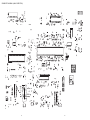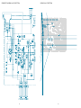
1
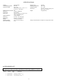
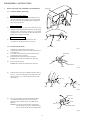
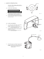
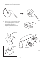
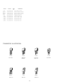
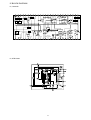
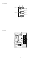
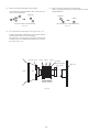
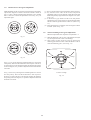
TV-CN202
NH1C3
SERVICE MANUAL
COLOR TELEVISION
S/M Code No. 09-995-333-9R1
DA
TA
RE
VI
SIO
N
This Service Manual is the "Revision Publishing" and replaces "Simple Manual"
(S/M Code No. 09-995-333-9T1).
SPECIFICATIONS
Category:
TV Broadcasting System:
Channel Coverage:
Color television
NTSC-M
TV: 2 – 69
Cable (CATV): 5A, 2 – 13,A-5 – A-1,
A–W, W+1 – W+84 (A-8)
Number of Preset Channels 181
Aerial Input
75 ohms, unbalanced
Picture Tube
20” (510 mm)
Screen Size
404 (W) x 303 (H) x mm (16 x 12 in.)
480 mm (diagonal) (19 in.)
Video Input/Output
1 Vp-p, 75 ohms
Audio Input
0.5 Vrms., 33 k ohms more
Audio Output
0.5 Vrms., 2.2 k ohms less
Speaker
76 mm (3 in.) round: 2
Operating Voltage
110 – 240 V AC, 50/60 Hz
Power Consumption
85 W
Earphone Jack
Operating Temperature
Operatin Humidity
Dimensions
Weight
•Design and specifications are subject to change without notice.
ACCESSORIES LIST
REF. NO
1
2
3
4
Mini jack
5°C – 40°C
35% – 80%
520 (W) x 479.5 (D) x 425 (H) mm
(20 1/2 x 19 x 16 3/4 in.)
18 kg (39.6 lbs.)
PART NO.
KANRI
DESCRIPTION
NO.
87-JBG-902-010
IB,NH (E) -CN202/142 -M
87-JBG-953-010
RC UNIT,RC-7VT02
87-B30-136-010
ANT ASSY,TV 5 SEC ( NTSC)
87-A90-786-010
PLUG,CONVERSION IR46
2
DISASSEMBLY INSTRUCTIONS
1.
HIGH-VOLTAGE CAP (ANODE CAP) REMOVAL
Anode cap
1-1. Cautions before Removing
CRT GND
Discharge the anode voltage
(1)
The anode voltage is not discharged completely from
the CRT of this unit even after the power is turned off.
Be sure to discharge the residual anode voltage before
removing the anode cap.
Do not use pliers
(2)
Do not use pliers, etc. to remove the anode cap. If you
used pliers and bent the hook to remove the cap, the spring
characteristics of the hook could be lost, and when
reinstalled, the cap would come off from the CRT anode
button easily, causing an accident.
Do not turn the anode cap
(3)
If the anode cap is turned in the direction of its
circumference, the hook is likely to come off.
Grip
1-2. Anode Cap Removal
(1)
(2)
(3)
(4)
CRT
Hook
CRT GND
Fig. 1
Discharge the anode voltage. (See Figure 1)
Connect a flat-bladed screwdriver to the CRT GND via
an alligator clip.
Use a tester to check the end of the screwdriver and
ground of the TV for continuity.
Touch the hook with the end of the screwdriver.
Caution : Be careful not to damage the anode cap.
Anode cap
Turn over the anode cap.
Caution : Be careful not to damage the anode cap.
CRT
Anode button
Hook
Fig. 2
(5)
Push the anode cap with your thumb in the direction of
arrow 1 as shown in the figure, then lift the cap in the
direction of arrow 2 to release the hook on one side.
(See Figure 3)
1
2
Anode cap
1
CRT
CRT
Hook
Hook
Fig. 3
Anode cap
(6)
Turn over the anode cap on the side where the hook
was released and pull out the cap in the direction
opposite to that on which the cap was pushed. (See
Figure 4)
Caution : Do not pull out the anode cap straight up.
: Do not pull the cap forcibly. After removing
the cap, check that the hook is not deformed.
Pull out
CRT
Anode button
Hook
Fig. 4
4
2. ANODE CAP REINSTALLTION
Anode cap
Observe the cautions carefully so that no accident
occurs due to a defect in installing the anode cap and
so it does not come off.
Left
Right
2-1. Caution before Reinstalling
Never turn the anode cap after installing it
Never re-use the hook when it has been deformed
(1)
(2)
If the anode cap is turned after it is installed, it may
come off. Therefore, arrange the high-voltage cable
before attaching the anode cap. (See Figure 1-1)
If you have attached the anode cap before arranging
the high-voltage cable, arrange the cable carefully so
the cap does not turn.
Fig. 1-1
Anode button
2-2. Anode cap reinstallation
(1)
(2)
Installation
section
Use a clean cloth moistened slightly with alcohol to
clean the installation section. (See Figure 2)
Caution : Check that the installation section is free
from dust, foreign matter, etc.
Coat the anode cap installation circumference with an
appropriate amount of the specified silicone grease
(KS-650N). (See Figure 2)
Caution : Be careful that silicone grease does not
enter the anode button.
Fig. 2
High-voltage cable
Anode cap
(3)
Eliminate twisting, etc. of the high-voltage cable and
arrange it so that no twisting occurs. (See Figure 3)
Caution : If the cable is not arranged correctly, the
anode cap could turn and cause an
installation defect.
Fig. 3
5
(4)
Turn over the rubber cap symmetrically on the left and
right. (See Figure 4)
Caution : Take great care not to damage the anode cap.
Fig. 4
(5)
(6)
(7)
Fit your forefinger over the projection at the center of
the cap and hold the cap between your thumb and
middle finger. (See Figure 5-1)
Apply the hook on one side to the anode button as
shown on the figure. (See Figure 5-2)
Caution : Check that the hook is held securely.
Apply the hook on the other side to the anode button
as shown in Figure 5-3.
Fig. 5
Anode button
Hook
Hook
30˚
Anode button
Anode button
Fig. 5-2
Hook
Fig. 5-3
6
(8)
(9)
(10)
(11)
Pull the anode cap slightly with the rubber cap turned
over and visually check that the hook is engaged
securely.
Release your hand from the rubber cap of the anode
cap.
Caution : Cover the anode cap so that it does not lift.
Hold the skirt of the andoe cap slightly to improve the
close contact between the cap and CRT.
Check that the anode cap is in close contact with the
CRT. (See Figure 6)
Anode cap
Skirt
Fig. 6
Front cabinet
3. CASE REMOVAL
3-1. Rear Cabinet Removal (See Figure 1)
1
(1)
Remove four screws 1 and three screws 2, then
remove the rear cabinet in the direction of the arrow.
1
1
2
2
2
1
Rear cabinet
Fig. 1
Front cabinet
3-2. Neck C.B. (PWB, NK) Removal
(See Figure 2)
(1)
(2)
Disconnect CN903 (CRT GND).
Remove the Neck C.B. in the diection of arrow 1.
CN801
(Degauss
cord)
3-3. Main C.B. (PWB, MAIN) Removal
(See Figure 2)
(1)
(2)
(3)
1
Remove connector (CN401).
Remove connector (CN801).
Pull out the Main C.B. in the direction of the direction
of arrow 2.
PWB, NK
7
CN903
PWB, MAIN
2
CN401
(Speakers)
ELECTRICAL MAIN PARTS LIST
REF. NO
PART NO.
KANRI
NO.
DESCRIPTION
REF. NO
IC
87-JBC-629-010
87-A90-297-010
87-A20-612-010
87-A20-611-080
87-A20-362-010
IC,M37272M8-131SP
RCR UNIT,SBX1981-52
IC,AT93C46-10PI
IC,M51943BSL-700A
IC,LA7676 D
87-A20-364-010
87-A20-734-010
87-002-577-010
87-001-647-080
87-002-524-010
IC,KIA7809PI
IC,TDA2007A
IC,LA7953N
IC,NJM78L 12A
IC,LA7837
87-017-956-010
87-A20-980-010
87-020-881-080
IC,BA7611AN
IC,STR-S6707N
IC,NJM78L05A
TRANSISTOR
87-A30-091-080
89-111-755-080
89-327-854-080
89-337-794-580
87-A30-090-080
FET,2SJ460
TR,2SA1175F
TR,2SC2785F
TR,2SC3779 D/E
FET,2SK2541
87-A30-095-010
89-334-674-580
87-A30-041-010
87-A30-005-010
TR,2SD2333LS/C202
TR,2SC3467 D/E
TR,SE115N
TR,2SC2688M/L
87-070-345-080
87-070-150-080
87-070-274-080
87-A40-286-080
87-A40-004-080
DIODE,IN4148
ZENER,MTZJ33D
DIODE,1N4003 SEM
DIODE,RGP10JE-5025
ZENER,MTZJ16A
87-017-654-060
87-A40-450-090
87-A40-354-090
87-A40-440-080
DIODE,GBU6J
DIODE,RU 1P
DIODE,UF3GL-6251
ZENER,MTZJ7.5A
BT301
BT403
BT601
C1
C2
87-JBC-625-010
87-JBC-624-010
87-JBC-626-010
87-016-624-080
87-018-119-080
CONN ASSY,5P V WHT TV-NK
CONN ASSY,9P V JK
CONN ASSY,4P V WHT TV-NK
CAP,E 10-16 SSL
CAP, CER 100P-50V
C3
C4
C5
C6
C9
87-018-134-080
87-016-633-080
87-016-583-080
87-018-134-080
87-018-128-080
CAPACITOR,TC-U 0.01-16
CAP,E 1-50 SSL
CAP,E 100-25 SSL
CAPACITOR,TC-U 0.01-16
CAP, CERA-SOL SS 560P
C10
C11
C12
C13
C14
87-018-131-080
87-016-633-080
87-018-209-080
87-018-109-080
87-018-109-080
CAP, CER 1000P-50V
CAP,E 1-50 SSL
CAP, CER 0.1-50V
CAP, CER 22P-50V
CAP, CER 22P-50V
C15
C16
C17
C18
C19
87-018-109-080
87-018-109-080
87-018-109-080
87-018-109-080
87-018-131-080
CAP,
CAP,
CAP,
CAP,
CAP,
C21
C22
C23
C25
C26
87-016-637-080
87-016-633-080
87-016-637-080
87-016-633-080
87-018-209-080
CAP,E 10-50 SSL
CAP,E 1-50 SSL
CAP,E 10-50 SSL
CAP,E 1-50 SSL
CAP, CER 0.1-50V
C29
C101
C102
C103
87-018-123-080
87-016-636-080
87-018-134-080
87-016-575-080
CAP, CER 220P-50V
CAP,E 4.7-50 SSL
CAPACITOR,TC-U 0.01-16
CAP,E 220-16 SSL
DIODE
PART NO.
KANRI
NO.
DESCRIPTION
C105
C106
C107
C203
C204
87-016-637-080
87-018-134-080
87-A10-207-080
87-018-134-080
87-018-134-080
CAP,E 10-50 SSL
CAPACITOR,TC-U 0.01-16
CAP,TCS 0.01-50KBUP050
CAPACITOR,TC-U 0.01-16
CAPACITOR,TC-U 0.01-16
C205
C207
C208
C210
C211
87-018-134-080
87-016-632-080
87-018-131-080
87-018-134-080
87-A10-585-080
CAPACITOR,TC-U 0.01-16
CAP,E 0.47-50 SSL
CAP, CER 1000P-50V
CAPACITOR,TC-U 0.01-16
CAP,CER 18P-50 J CH
C214
C215
C216
C218
C219
87-018-134-080
87-016-637-080
87-018-134-080
87-016-583-080
87-018-134-080
CAPACITOR,TC-U 0.01-16
CAP,E 10-50 SSL
CAPACITOR,TC-U 0.01-16
CAP,E 100-25 SSL
CAPACITOR,TC-U 0.01-16
C301
C302
C303
C305
C306
87-016-583-080
87-016-632-080
87-018-134-080
87-016-583-080
87-018-134-080
CAP,E 100-25 SSL
CAP,E 0.47-50 SSL
CAPACITOR,TC-U 0.01-16
CAP,E 100-25 SSL
CAPACITOR,TC-U 0.01-16
C309
C312
C314
C315
C316
87-016-634-080
87-016-637-080
87-018-125-080
87-016-632-080
87-016-633-080
CAP,E 2.2-50 SSL
CAP,E 10-50 SSL
CAP, CER 330P-50V
CAP,E 0.47-50 SSL
CAP,E 1-50 SSL
C319
C320
C321
C322
C323
87-018-130-080
87-016-627-080
87-016-634-080
87-016-633-080
87-016-636-080
CAP,TC-U 820P-50 B
CAP,E 47-16 SSL
CAP,E 2.2-50 SSL
CAP,E 1-50 SSL
CAP,E 4.7-50 SSL
C325
C326
C327
C328
C329
87-018-134-080
87-018-113-080
87-016-633-080
87-018-115-080
87-016-637-080
CAPACITOR,TC-U 0.01-16
CAP, CER 33P-50V
CAP,E 1-50 SSL
CAP, CER 47P-50V
CAP,E 10-50 SSL
C330
C331
C332
C333
C334
87-018-194-080
87-018-111-080
87-018-134-080
87-018-115-080
87-018-134-080
CAP,TC-U 91P-50 B
CAP,TC-U 27P-50 B
CAPACITOR,TC-U 0.01-16
CAP,TC-U 47P-50 B
CAPACITOR,TC-U 0.01-16
C336
C337
C401
C403
C405
87-018-134-080
87-018-134-080
87-016-586-080
87-016-586-080
87-A10-776-080
CAPACITOR,TC-U 0.01-16
CAPACITOR,TC-U 0.01-16
CAP,E 470-25 SSL
CAP,E 470-25 SSL
CAP,E 1000-25 M 105 KMG
C406
C407
C408
C412
C414
87-016-621-080
87-016-621-080
87-016-627-080
87-016-633-080
87-016-637-080
CAP,E
CAP,E
CAP,E
CAP,E
CAP,E
220-10 SSL
220-10 SSL
47-16 SSL
1-50 SSL
10-50 SSL
C418
C422
C423
C424
C425
87-016-583-080
87-016-636-080
87-A10-831-080
87-016-632-080
87-016-632-080
CAP,E
CAP,E
CAP,E
CAP,E
CAP,E
100-25 SSL
4.7-50 SSL
1000-25 M SMG
0.47-50 SSL
0.47-50 SSL
C426
C427
C501
C504
C505
87-016-637-080
87-016-586-080
87-016-583-080
87-016-591-080
87-016-641-080
CAP,E
CAP,E
CAP,E
CAP,E
CAP,E
10-50 SSL
470-25 SSL
100-25 SSL
100-35 SSL
100-50 SSL
C506
C507
C508
C509
C511
87-A10-367-080
87-A10-402-080
87-016-634-080
87-016-587-090
87-018-123-080
CAP,CER 10P-500 J SL
CAP,M 0.22-100 J TF TYPE1
CAP,E 2.2-50 SSL
CAP,E 1000-25 M SSL
CAP, CER 220P-50V
C601
C602
C603
C604
C605
87-016-596-080
87-016-635-080
87-A10-457-080
87-016-597-080
87-012-405-080
CAP,E 10-160 SSL
CAP,E 3.3-50 SSL
CAP,E 2.2-160 M SSL
CAP,E 22-160 SSL
CAP,CER 1800P-2K K BN DE
MAIN C.B
CER
CER
CER
CER
CER
22P-50V
22P-50V
22P-50V
22P-50V
1000P-50V
8
REF. NO
PART NO.
C606
C607
C609
C610
C611
KANRI
DESCRIPTION
NO.
87-A10-474-090
CAP,PP 0.01-1.25K J PHS
87-010-974-080
CAP,CER 220P-500 B
87-016-583-080
CAP,E 100-25 SSL
87-016-594-090
CAP,E 1000-35 M SSL
87-010-976-080
CAP,CER 1000P-500 B
REF. NO
C612
C616
C701
C702
C705
87-010-974-080
87-A10-674-090
87-016-633-080
87-016-637-080
87-016-637-080
CAP,CER 220P-500 B
CAP,M/P 0.P-50C0 J
CAP,E 1-50 SSL
CAP,E 10-50 SSL
CAP,E 10-50 SSL
L501
L603
L802
L803
!LF801
87-005-608-080
87-A50-040-010
87-A50-170-010
87-005-608-080
87-JB8-650-010
COIL,33UH J LAV35
COIL,2.2MH
COIL,390UH RCH106
COIL,33UH J LAV35
FLTR,LINE SS24H-K18055
C707
C708
C710
C712
C715
87-016-633-080
87-016-637-080
87-016-622-080
87-016-637-080
87-016-633-080
CAP,E
CAP,E
CAP,E
CAP,E
CAP,E
!P801
!P802
!PR601
!PR801
!PR802
87-A30-096-010
87-A30-096-010
87-A90-757-080
87-A90-090-080
87-026-681-080
P-TR,TLP721F
P-TR,TLP721F
PROTECTOR,0.75A 60V 491
PROTECTOR,1.5A 491SERIES 60V
PROTECTOR,5A 60V 491
C716
C801
C802
C803
C804
87-016-634-080
87-A10-688-090
87-A10-688-090
87-012-370-010
87-012-370-010
CAP,E 2.2-50 SSL
CAP,M/P 0.22-275 K (B81133)
CAP,M/P 0.22-275 K (B81133)
CAP,CER 3300P-0C0NS
CAP,CER 3300P-0C0NS
!PR803
R327
R401
R402
!R406
87-A90-247-080
87-A00-161-090
87-A00-150-090
87-A00-150-090
87-029-158-060
RPOTECTOR,0.315A 60V 491
RES,M/F 47-2W J RSF(S)
RES,M/F 220-1W J RSF(S)
RES,M/F 220-1W J RSF(S)
RES,FUSE 1-1W J
C808
C809
C810
C811
C812
87-A10-646-090
87-016-584-080
87-A10-728-080
87-018-131-080
87-A10-645-010
CAP,E 220-400 SMH (25.4*40)
CAP,E 220-25 SSL
CAP,E 680-10 M LXV
CAP, CER 1000P-50V
CAP,M/P 0.01-1K J MMH
!R407
R503
R507
R603
R605
87-029-158-060
87-025-429-080
87-A00-197-090
87-A00-247-090
87-A00-300-090
RES,FUSE 1-1W J
RES,M/F 47K-1/6W
RES,M/F 1.2-1W J
RES,M/F 100-3W J
RES,M/F 2.2-1W J
C813
C814
C815
C816
C817
87-012-372-010
87-A10-832-010
87-012-397-010
87-A10-731-090
87-A10-756-090
CAP,CER 1000P-2K
CAP,CER 1000P-1K K R LONG
CAP,CER 1000P-2K BN
CAP,E 220-160 M KMF
CAP,E 100-160 M KMF
R610
R611
R804
R805
87-A00-225-090
87-A00-196-090
87-A00-224-090
87-A00-333-090
RES,M/F 2.2K-5W J RSV5
RES,M/F 0.47-1/2W J RSF(S)
RES,SD 8.2M-1W J CE
RES,M/F 100K-3W J RSS
C819
C821
C822
C823
C824
87-016-576-080
87-016-588-090
87-016-587-090
87-016-627-080
87-016-583-080
CAP,E
CAP,E
CAP,E
CAP,E
CAP,E
C825
CF201
CF202
CN401
CN601
87-A10-469-080
84-LB3-627-010
84-LB3-626-010
87-049-469-010
87-099-675-010
CAP,CER 2200P-500 K B DD10
FLTR,SFSF 4.5MDB SIF
FLTR,TPS4.5MB2
CONN,4P V
CONN,5P V V
!CN801
!CN802
D1
!F801
FB801
87-099-454-010
87-099-674-010
87-070-110-010
87-035-458-010
87-003-320-080
CONN,2P TV-50 EYLET
CONN,2P VA V
LED,SLP-181B-51
FUSE,4A 250V T W/C
F-BEAD,FBR07HA121NB
FB802
FB803
FB804
FB805
!FC801
87-003-320-080
87-003-320-080
87-003-320-080
87-003-320-080
87-033-213-080
F-BEAD,FBR07HA121NB
F-BEAD,FBR07HA121NB
F-BEAD,FBR07HA121NB
F-BEAD,FBR07HA121NB
CLAMP, FUSE
!FC802
!FR601
!FR602
!FR604
!FR801
87-033-213-080
87-A00-063-060
87-A00-371-090
87-A00-051-060
87-A00-081-090
CLAMP, FUSE
RES,FUSE 2.2-1/2W J R-TYPE
RES,FUSE 5.6-1W J R-TYPE
RES,FUSE 2.7-1W J R-TYPE
RES,FUSE 1-1/2W
J401
J701
J702
L1
L2
87-A60-420-010
87-A60-321-010
87-A60-323-010
87-005-614-080
87-005-614-080
JACK,3.5 ST (MSC)
JACK,PIN 2P BLK-Y
JACK,PIN 4P Y-BLK
COIL 100UH LAV35 J
COIL 100UH LAV35 J
L101
L102
L201
L202
L203
87-005-614-080
87-005-608-080
84-LB2-684-010
87-003-140-080
84-LB2-681-010
COIL 100UH LAV35 J
COIL,33UH J LAV35
COIL,TRAP 47.25 SA
CH COIL 0.82
COIL,VCO 45.75 SA
L204
L205
L206
L207
L208
87-005-604-080
87-003-146-080
84-LB2-682-010
84-LB2-683-010
87-005-485-080
COIL,15UH J LAV35
COIL,15UH LAL02
COIL,AFT 45.75 SA
COIL,SIF 4.5M SA
COIL,100UH J FLR50
L301
L303
L304
L305
L306
1-50 SSL
10-50 SSL
470-10 SSL
10-50 SSL
1-50 SSL
330-16 SSL
2200-25 SSL
1000-25 M SSL
47-16 SSL
100-25 SSL
9
PART NO.
KANRI
DESCRIPTION
NO.
87-003-051-080
COIL,470UH
87-003-149-080
COIL,47UH
87-003-147-080
COIL, 22UH
87-003-295-080
COIL,10UH
87-003-147-080
COIL, 22UH
F
RSF
RSF
RSF(F)
REF. NO
L901
!R904
!R905
!R906
R907
PART NO.
KANRI
NO.
DESCRIPTION
87-005-615-080
87-A00-165-090
87-A00-165-090
87-A00-165-090
87-025-355-080
COIL,120UH J LAV35
RES,M/F 15K-2W J RSF(S)
RES,M/F 15K-2W J RSF(S)
RES,M/F 15K-2W J RSF(S)
RES,M/F 100-1/6W F
S901
SFR901
SFR902
SFR903
SFR904
84-LB3-610-010
87-024-519-080
87-024-519-080
87-024-520-080
87-024-520-080
SOCKET,CRT HPS1171
SFR,470 DIA6 V NTP
SFR,470 DIA6 V NTP
SFR,1K DIA6 V NTP
SFR,1K DIA6 V NTP
SFR905
87-024-520-080
SFR,1K DIA6 V NTP
TRANSISTOR ILLUSTRATION
ECB
SDG
ECB
ECB
2SC3467
2SK2541
2SJ460
2SC2785
2SA1175
2SC2688
BEC
123
BCE
2SC3779
SE115N
2SD2333
10
IC BLOCK DIAGRAM
IC, LA7676D
51
50
49
48
47
45
46
44
42
43
41
40
39
38
AFT
APC
DET
VCO
LOCK
DET
VIDEO
DET
VIDEO
AMP
36
37
GND
(V 1DEO
CHR (MA)
JUNGLE)
35
34
33
1ST-BPA
CONTRAST
LIM
AMP
APC
SOFT
TINT
CARRIER-F
VIF
AMP
VCO
AF
AMP
5
6
7
8
9
10
(VIF SIF)
VCC
11
-Y-OUT
FBP-DET
OSD SWITCH
OSD
RF-AGC
(VIF SIF)
GND
4
COLOR-DEMO
IF
AGC
ATT
3
30
29
28
27
VER
C/D
HOR
COIN
D.L.
VER
SYNC-SEP
CLAMP
BRIGHT
SYNC-SEP
AFC-2
HOR
C/D
ACC
KILLER
FM-DET
2
31
SHARP
2ND-BPA
11
32
HOR
VCC
BLACK
EXPAND
FBP-DET
BGP-OUT
52
13
14
IC, STR-S6707
11
15
HDP
DSC
HOR
DRIVER
(JUNGLE)
(VIDEO CHROMA)
VCC
12
AFC-1
PHASE
SHIFTER
16
17
18
19
20
21
22
23
24
25
26
IC, TDA2007A
5VR
+VS
8
3
INPUT+(2) 5
+
–
7 OUT(2)
4 INPUT-(2)
INPUT+(1) 1
+
–
9 OUT(1)
2 INPUT-(1)
6
GND
IC, LA7953
12
BLOCK DIAGRAM
13
14
SCHEMATIC DIAGRAM-1 (MAIN C.B SECTION)
15
16
WIRING-1 (MAIN C.B SECTION)
1
2
3
4
5
6
7
8
9
10
11
12
A
B
C
D
E
F
G
H
I
J
17
18
13
14
WIRING-2 (N.K C.B SECTION)
13
14
SCHEMATIC DIAGRAM-2 (N.K C.B SECTION)
19
20
WAVEFORM
Input condition : Tuner 11ch (199.25MHz), 80dBµ input : P = Full Field CB & S = 1kHz (Mono)
1
5
IC501 Pin 12
6
HOLDOFF MIN
NORM
IC301 Pin 18
IC301 Pin 19
TRG +0 . 0 d i v
SMSA
NORM
SMSA
20 µs/div
1 V/div
5
1
PlOx 10V
2
1 V/div
PlOx 1V
A=5ms
7
Between X301 & C304
8
HOLDOFF MIN
EQUIV
20 µs/div
6
5 ms/div
10 V/div
SMSA
PlOx 1V
A=20µs
IC301 Pin 20
IC301 Pin 21
TRG +0 . 0 d i v
NORM
SMSA
7
20 µs/div
1V/div
2
0.1µ/div
200 mV/div
PlOx 200mV
3
A=0.1µs
PlOx 1V
9
IC301 Pin 25
HOLDOFF MIN
EQUIV
20 µs/div
2 V/div
8
PlOx 2V
T601 Pin 1
HOLDOFF #
SMSA
3
A=20µs
NORM
SMSA
9
20 µs/div
50 V/div
0.5 µs/div
50 mV/div
PlOx 50mV
4
PlOx 50V
A=0.5µs
11 T601 Pin 8
IC1 Pin 20
HOLDOFF #
A=20µs
EQUIV
HOLDOFF #
SMSA
4
NORM
SMSA
11
20 µs/div
50 V/div
5 ns/div
1 V/div
PlOx 1V
PlOx 50V
A=50ns
21
A=20µs
19
12 Q901 Collector
20
HOLDOFF MIN
NORM
IC301 Pin 22
IC301 Pin 23
HOLDOFF MIN
SMSA
NORM
SMSA
19
20 µs/div
5 V/div
20
20 µs/div
0.5 V/div
12
20 µs/div
50 V/div
PlOx 50V
PlOx 5V
A=20µs
21
13 Q902 Collector
22
HOLDOFF MIN
NORM
PlOx 0.5V
IC301 Pin 20
IC301 Pin 21
HOLDOFF MIN
SMSA
A=20µs
NORM
SMSA
21
20 µs/div
0.2 V/div
13
20 µs/div
50 V/div
PlOx 50V
23
NORM
50 mV/div
PlOx 0.2V
A=20µs
14 Q903 Collector
HOLDOFF MIN
20 µs/div
22
PlOx 50mV
IC301 Pin 44
HOLDOFF MIN
SMSA
14
A=20µs
NORM
SMSA
23
20 µs/div
0.5 V/div
20 µs/div
50 V/div
PlOx 50V
PlOx 0.5V
A=20µs
15 Q601 Collector
17 Q602 Collector
HOLDOFF MIN
24
NORM
SMSA
A=20µs
IC301 Pin 1
HOLDOFF MIN
NORM
SMSA
20 µs/div
500 V/div
15
24
20 µs/div
50 V/div
17
PlOx 500V PlOx 50V
50 µs/div
0.5 V/div
A=20µs
PlOx 0.5V
22
A=50µs
25 IC1 Pin 17
HOLDOFF MIN
NORM
SMSA
25
20 µs/div
0.5 V/div
PlOx 0.5V
A=20µs
IC DESCRIPTION
IC, M37272M8-113SP
Pin No.
Pin Name
I/O
Description
1
HSYNC
I
OSD horizontal synchronised signal input terminal. "L"= active.
2
VSYNC
I
OSD vertical synchronised signal input terminal. "L"= active.
3
VOL
O
Volume control output. (Volume PWM 8 bit.)
4
CONT
O
Contrast control output. (Contrast PWM 8 bit.)
5
BRIGHT
O
Brightness control output. (Brightness PWM 8 bit.)
6
COLOR
O
Color control output. (Color PWM 8 bit.)
7
TINT
O
Tint control output. (Tint PWM 8 bit.)
8
SHARP
O
Sharpness control output. (Sharpness PWM 8 bit.)
9
STEREO / SAP
I
STEREO / SAP detect. (Not connected)
10
RMC
I
Remote control signal is led to this pin.
11
SD
I
12
DGC
–
13
PON
O
14
AVCC
–
15
HLF
–
Connected to filter.
16
VHOLD
–
Connected to condensor.
17
CVIN
I
Video signal input.
18
CNVSS
–
Connected to ground.
19
XIN
I
8 MHz clock input.
20
XOUT
O
8 MHz clock output.
21
VSS
–
Connected to ground.
22
VCC
–
5 V supply.
Horizontal sync. detected input. The level of this pin will be sampled by µ-P to
determine whether there is picture signal detected.
Not connected.
During standby mode, "H" level is inserted to switch off horizontal deflection and high
voltage.
5V supply.
TUNER SAP
TUNER STEREO
Pin 23 Pin 24 Pin 35
23, 24
ST1, ST2
O
Pin 23 Pin 24 Pin 35
MONO/SAP
L
L
L
STEREO
L
L
L
MONO
L
H
L
MONO
L
H
H
SAP
H
L
L
TUNER STEREO / SAP
(NC)
Pin 23 Pin 24 Pin 35
25
RST
I
26
SLDA
I/O
27
TONE
–
28
SLCK
O
MONO/SAP
L
L
L
STEREO
L
H
L
SAP
H
L
L
MONO
L
H
H
PIN 35 : MONO
Used to reset the µ-P when power up.
Data bus between µ-P and E2PROM / tuner.
Not connected.
Synchronizing clock between µ-P and E2PROM / tuner provided by µ-P through this
pin.
29
AFTV
I
AFT voltage from IC301 is received by µ-P during channel tuning.
30
KEY0
I
Input key is detected by monitor.
24
Pin No.
Pin Name
I/O
Description
31
EEP CS
O
EEP-ROM chip selection.
32
SUR
O
Surround ON "H", OFF "L".
33
ENABLE
O
Timing data bus between µ-P and tuner.
34
AMUTE
O
35
MONO
O
Used to mute line out sound and picture when no input signal is detected.
"H" to mute.
Compel the sound system to monaural. (Not connected)
Selecting tuner receiving band.
36, 37
SEL1, SEL2
O
Pin 36
Pin 37
TUNER
L
L
VIDEO 1
H
L
VIDEO 2
L
H
38
VMUTE
–
Not connected.
39
BLK
O
OSD blanking output.
40
B
O
OSD blue output.
41
G
O
OSD green output.
42
R
O
OSD red output.
25
Reset start : Both of Pin 36, Pin 37 are "H".
ADJUSTMENT
A MAIN C.B
IC402
IC1
SFR501
V-SIZE
SW501
V-POS
SFR302
SUB-BRIGHT
SFR301
H-POS
SFR303
SUB-TINT
L206
AFT
L203
VCO
TOP: FOCUS VR
BOTTOM: SCREEN VR
IC301
L207
SIF
SFR201
RF AGC
L201
TRAP
T601
(FBT)
TU101
MAIN Circuit board (Component side)
B NK C.B
SFR902
B-DRIVE
SFR904
SFR901 SFR905
SFR903
R-DRIVE B-CUT OFF G-CUT OFF R-CUT OFF
TP901
S901
TP902 SUB-TINT (B-Y)
TP903 GND
NK Circuit board (Solder side)
26
RF AGC
TP15
SET-UP FOR ADJUSTMENT
1. CRT ADJUSTMENT
Because the video signal output from a pattern generator is used as
the adjustment signal input during adjustment, the video signal output
from the pattern generator must conform with the specifications.
Measure the output waveform across 75 Ω load. Confirm that the
synchronizing signal has an amplitude of about 0.3 V, the video signal
portion has an amplitude of about 0.7 V and the burst signal has an
amplitude of about 0.3 V with flat envelope. Confirm that ratio of the
burst signal amplitude and the red signal amplitude is 0.30 : 0.66. If
the output signal does not conform with the specifications, calibrate
the pattern generator. (Refer to pattern generator operation manual.)
Use the LEADER: LCG 404 for the pattern generator.
1-1.
(1) Receive the white raster signal, and then perform edging for
at least 20 minutes.
(2) Demagnetize the area surronding the CRT with a degausser
before making adjustments.
(3) Set the picture quality for each mode to the factory setting.
(4) Position the front screen facing to the east as much as possible.
1-2.
Color bar signal of a pattern generator
Approx. 0.7V
1 Vp-p White (Approx.
75%)
Purpose
(1) Beam landing adjustment (purity magnet)
Burst signal
Approx.
0.3V
Approx. 0.3V
Precautions
Set the left/right balance of beam landing. If there is a
discrepancy in this adjustment, a color irregularity will occur.
After completion of the landing adjustment, it is necessary to
perform a convergence adjustment.
Before adjustment
After adjustment
Fig. 1-1
Black
Red
Blue
Magenta
Cyan
Green
75% white
Yellow
Color
irregularity
TV display
Precautions before starting adjustment
Satisfy the following setting conditions before starting adjustment.
• Allow warm-up of 20 minutes or longer. (Do not turn off during
warm-up.)
• Set all picture quality controls of users' setting to initial set-up,
unless otherwise specified.
• Picture quality reset
1. Select "Picture" on the screen menu and press enter button.
2. Select "Normal" and press enter button.
3. Select "Reset" and press enter button.
• Set the pattern generator’s output level at 1.0Vp-p (across 75Ω
load).
27
(3) Beam convergence adjustment (6-pole magnet)
With a 4-pole magnet align the G beam with the already
aligned R/B beam.
(2) Beam convergence adjustment (4-pole magnet)
Align the R beam with the B beam. The G beam does not
move with this adjustment.
(magenta)
B
(magenta)
R/B
R
G
(white)
R/B
G
G
RGB
Align the G beam with the R/B beam
Fig. 1-3
Align the R beam with the B beam
Fig. 1-2
(4) The composition of each magnet is as appears in Fig. 1-4.
In making adjustments, rotate the lock ring clockwise (looking
from the CRT’s back screen) and disengage.
Be careful not to loose the lock ring too much. If the magnet
assembly has become shifted during adjustments, secure it to
the position in Fig. 1-4.
DY lock screw
Purity 4-pole 6-pole
Lock ring
Magnet assembly
lock screw
CRT
CRT
DY
DY
Magnet assembly
Fig 1-4
28
NK C.B
1-3.
Beam Landing Adjustment
As there is occurrence of convergence distortion after
completing the landing adjustments, be certain to carry out
convergence adjustments.
(1) Receive the green raster signal through the pattern generator.
(2) Loosen the magnet lock screw, and shift the magnet assembly
backward (toward the neck).
(3) Loosen the DY lock screw, and shift the DY deflecting yoke
backward (toward the neck).
(4) After opening the two purity magnets to the same angle, adjust
the color width of the bands on both sides of the screen so
that they are of equal width. (refer to Fig. 1-5 (a)).
If the color irregularity in the screen’s corner section are not
improved, correct them with the landing magnet. After using
the landing magnet, be sure to demagnetize the CRT with
degausser and verify that there is no occurrence of color
irregularity. (refer to Fig. 1-6)
Landing magnet: 81-JTI-710-010
(two-sided adhesive tape) : 80-XVI-218-010 Cushion
R=B
R
G
B
Fig 1-5 (a)
As shown in Fig. 1-5 (b), the purity magnet functions in
relation to the electron beam.
Landing magnet
Cushion
S
N
S
S
N
N
N
S
NS
SN
Since the landing magnet is polarized,
check the screen’s improvement through
rotation, not only by position.
SS
NN
Fig 1-6
Fig 1-5 (b)
(5) Gradually shift the deflecting yoke toward the front (toward
the CRT funnel). Stop movement at the point when the screen
has become completely green.
(6) Also, verify the respective monochromatics of red and blue.
(7) While looking at the screen, adjust the tilt of the deflecting
yoke and tighten the DY lock screw.
(8) Shift the magnet assembly to the front (toward the CRT
funnel), stop movement before the adjustment position and
then tighten the magnet lock screw.
At this time, be careful not to shift the position of the purity
magnet.
29
1-4.
Beam Center Convergence Adjustment
(1) Receive the dot pattern signal through the pattern generator.
(2) Pay attention to the center of the screen, and perform
adjustments with two 4-pole magnets so that the R beam and
the B beam perfectly align and become a magenta color. (refer
to Fig. 1-2)
(3) In the same way, pay attention to the screen, and perform
adjustments with a 6-pole magnet so that the magenta beam
and the G beam align and become a white dot. (refer to Fig.
1-3)
(4) After adjustments are completed, secure all magnets with the
lock link. (Refer to Fig. 1-4)
Make adjustments on the convergence with 4-pole and 6-pole magnets.
Operate each magnet in relation to the electron beam as shown in
Figs. 1-7 and 1-8. When performing this adjustment, verify whether
there is distortion in the focus adjustment. If necessary, carry out
adjustments again.
S
S
B
N
G
N
B
N
R
G
R
N
S
S
1-5.
The Surrounding Convergence Adjustment
Make this adjustment after completion of adjustment 1-4.
Fig 1-7
N
S
S
(1) Shake the deflecting yoke up, down, right and left, and adjust
any discrepancies in the screen’s surroundings.
(2) Insert wedges in three locations in the gap between the
deflecting yoke and the surface of the CRT funnel in order to
secure the deflecting yoke. (refer to Fig. 1-9)
N
S
B
G
R
N
B
G
R
S
N
N
S
S
N
Wedge
Wedge
Fig 1-8
In Fig. 1-7, two 4-pole magnets are stacked together so as to be of the
same polarity. Move the B and R beams to their respective direction,
by rotating the two 4-pole magnets together. By adjusting the opening
of the two magnets, it is possible to adjust the amount of the beam’s
movement.
Wedge
Position of wedge
In Fig. 1-8, the two 6-pole magnets are stacked together so as to be of
the same polarity. Move the B and R beams to their respective
direction, by rotating the two 6-pole magnets together. By adjusting
the opening of the two magnets, it is possible to adjust the amount of
the beam’s movement.
Fig. 1-9
30
2. ELECTRICAL ADJUSTMENT
2-1.
2-3.
(1) Receive a NTSC stairstep signal (color bar with chroma off).
(2) Adjust SFR302 so the band next to the right end start to light.
(See Figure 2-2)
White Balance Adjustment (NK C.B.)
(1) Receive a NTSC raster signal (white).
(2) Set the customer picture controls “bright” and “contrast” to
minimum.
(3) Set the CUT OFF SFR (SFR903, SFR904, SFR905) and
DRIVE SFR (SFR901, SFR902) to their mechanical centers.
(4) Leaves the CUT OFF SFR of the color which is brightest on
the screen as it is and use other two CUT OFF SFR to adjust
the white balance.
(5) Set the customer picture controls “brightness” and “contrast”
to maximum.
(6) Turn SFR901 (R DRIVE) fully counterclockwise so the whole
screen becomes red.
(7) Turn SFR901 (R DRIVE) gradually clockwise and stop it
where red disappears from the screen.
(8) Turn SFR902 (B DRIVE) fully counterclockwise so the whole
screen becomes blue.
(9) TurnSFR902 (B DRIVE) gradually clockwise and stop it
where blue disappears from the screen.
(10) Repeat steps (2)-(4) and (5)-(9) until the white balance has
been adjusted completey.
(11) Return the customer picture controls to their original
positions.
(12) Receive a stairstep signal (color bar with chroma off) and
check that there is no unnatural color at any bands.
*
Perform 2-3 Sub-bright adjustment after completing the white
balance adjustment.
2-2.
Sub-bright Adjustment
Too dark
dark
Two bands on the right
Two
bands
thebe
right
are dark
andon
cannot
aredistinguished.
dark and cannot be
distinguished.
Tooexample
dark
Good
The band on the right
The
end isband
not lit on
andthe
the right
adjacent
bandlit
is and
very the
end
is
not
dim.
adjacent band is very
dim.
Screen Adjustment
(1) Short the IC501 Pin2 and Pin5 (or 11) and set the screen in
single horizontal line.
(2) Set the TV to the external input mode (no input).
(3) Connect an oscilloscope to TP901 (JW901) Pin9 of S901 (on
the NK C.B.).
(4) Adjust SFR302 (Sub-bright) so the voltage at TP901 (JW901)
Pin9 of S901 is 170 ± 5VDC. (See Figure 2-1)
(5) Adjust the SCREEN VR (FBT) so that a horizontal line begins
to appear at the center of the screen.
(6) Release the short-circuit point.
170V DC
150V DC
Too bright
Too
50V/Div50V/Div
20 µ sec/Div
20µ sec/Div
The band
on the
The
band
onright
the right
end is lit.
end is lit.
GND
Fig 2-2
Fig 2-1
*
2-4.
Be sure to perform the next sub-bright adjustment after
completing this adjustment.
Focus Adjustment
(1) Receive a NTSC dot pattern signal.
(2) Adjust the FOCUS SFR (FBT) so the focus of the dots is
optimum.
31
2-5.
Horizontal Position Adjustment
(Simple Adjustment Method)
(1) Input the following signals.
Monoscope signal of the test tape TTV-06T (connect video)
(2) As is shown in Fig. 2-3, make adjustments with SFR301 so
that the scales on both sides of the screen are the same.
(1) Using LEADER LCG-404, input the cross hatch signal.
(2) As is shown in Fig. 2-4 (b), make adjustments with SFR501
so that the number of vertical squares is 13.
Approximately 13 Blocks
Scale A
Scale B
Scale A = Scale B
Fig. 2-4 (b)
Fig 2-3
2-6.
Vertical Size Adjustment
2-7.
(1) Input the monoscopic signal of the test tape TTV-06T. (connect
video)
(2) Make adjustments with SFR501 so that the upper and lower
scales on the monoscope screen have the numerical values
that appear below. (refer to Fig. 2-4 (a))
*
SW501 is used only for initial setting in the factory. Make
sure that the selector of SW501 is positioned at B (center)
before adjusting.
Sub-tint Adjustment
(1) Receive an NTSC 3.58 MHz color bar signal.
(2) Connect an oscilloscope to Q903 Collector (on the NK C.B).
(3) Adjust SFR303 so the bottom edges of the waveform fall on
one line. (See figure 2-5)
1H
20V/Div
10µ20V/Div.
sec/Div
10µ sec/Div.
ACAc
range
range
Upper Scale (90% ± 3%)
STRAIGHT
STRAIGHT LINE
CRT Center
Mark
CRT Center
Mark
Lower Scale (90% ± 3%)
Fig 2-4 (a)
32
Fig. 2-5
3. TUNER ADJUSTMENT
3-1.
AGC Adjustment
(3) Using a DC power supply, add DC3.0V ± DC0.2V of voltage
to the IC301 Pin10 (TP14).
(4) Make adjustments with L203 so that the waveform’s center
section (a section in the figure below) of the ALIGNMENT
SCOPE becomes 45.75 MHz ± 50 kHz.
(1) Receive a NTSC signal of RF INPUT under the following
conditions.
Input level: 58 dBµ
Modulation percentage: 87.5%
Received channel : US TV 10ch (fp = 193.25MHz)
(2) Adjust SFR201 so the voltage at the TU101 Pin1 (TP15 or
JW101) is 6.8V ± 0.2VDC.
(Simple Adjustment Method)
45.15
(1) Using the LEADER LCG-401 (65dBµ), receive the color bar
signal on channel 2.
(2) With SFR201, make adjustments so that the voltage of TU101
pin1 becomes 3.6VDC.
(3) Receive a television broadcast, and verify that the screen is
clear.
3-2.
46.35
a
47.75MHz
VCO Adjustment
(5) Remove the capacitor.
( Rough Adjustment )
(1)
Make connections as they appear below.
3-3.
(1) Connect the resistance of 1 kΩ between the TU101 Pin11
and the GND.
AC POWER
SUPPLY
TU 101 Pin ! (TP2, IF)
10
AFT Adjustment
TP14
TU 101
11
IC301
1kΩ
44
TP12
ATT
LSW – 480
VIF
(2)
TP2
(2) Input the following signal conditions to the TU101 Pin11.
(AM/FM SSG)
CARRIER
45.75 MHz
LEVEL
100 dBµ
MOD
OFF
(3) Make adjustments with L206 so that the voltage of the
IC301 Pin47 (TP16) is DC4.5V ± DC0.2V.
(4) Remove resistance (1 kΩ).
ALIGNMENT
SCOPE
Connect between Pin52 and GND of IC301 with capacitor.
( Simple Adjustment Method )
IC301
(1) Using the pattern generator LCG-401, receive the signal for
channel 2.
(2) Adjust L206 so that the voltage at IC301 Pin47 (TP16)
becomes 4.5V ± 0.3VDC.
(3) Receive each television broadcasts and vertify that the picture
is clear.
52
+
CAP, 10/50 +
C207 0.47/50
33
3-4.
SIF Adjustment
(1) Input the following signal conditions to the IC301 Pin48
(TP1).
(FM/SG)
CARRIER
4.5MHz
LEVEL
90dBµ
MOD
OFF
(2) Adjust L207 so that the voltage at IC301 Pin1 (TP21) becomes
4.5V ± 0.3VDC.
(2) Adjust L201 so that center section (a section in the figure
below) of the ALIGNMENT SCOPE waveform becomes
60.25 MHz ± 50 kHz.
a
(Simple Adjustment Method)
60.25MHz
(1) Connect an oscilloscope to IC301 Pin1 (TP21), then receive
a television broadcast.
(2) Adjust L207 so that the center of audio signal level becomes
4.5V.
4.5V
5V
0V
3-5.
TRAP Adjustment
(1) Make connections as shown in figure below.
TU 101 Pin ! (TP2)
Q201
COLLECTOR
DC POWER
SUPPLY
ATT
LSW-480
VIF
ALIGNMENT
SCOPE
IF
DETECTOR
<IF DETECTOR>
TO ALIGNMENT
SCOPE
Ge DIODE
1000pF
FROM Q201
1000pF COLLECTOR
DO AS SHORT
Ge
DIODE AS IT CAN
IF DETECTOR
DC POWER
SUPPLY
4.6V
GERMANIUM DIODE: ISS-188 FM...etc.
34
1. How To Activate /Release Service Mode
Precautions to replace EEPROM
1 Release the function of Auto Power OFF.
It releases the function of Auto Power OFF when no input
occurs.
<JIG remote control unit>
JIG remote control unit to operate the service mode should be
used with the remote control unit for RC-6VT03 (86-LBR-951010) or 86-6VT07 (86-LBP-951-010).
It is used for warming up (Aging) of CRT Adjustment.
Test mode is activated by pressing TEST key (Hidden Key under
the label). (Refer to Fig.1).
2 Display of AFT S curb.
It displays OK, UP, DN in the status of AFT S curb.
(Observe the Voltage of IC301 Pin47)
When the Test Mode is activated, below menu (refer to Fig.2)
will be appeared and turn on and off at one second interval.
Jig Remote Controller
(1) Remove label of jig remote controller.
(2) Cut label of two hidden keys (Finish and Test) into
button size.
(3) Place two timer buttons on the two hidden keys.
(4) Place label back after above steps.
When replacing the EEPROM (IC3, AT93C46-10PI), be
certain to follow the sequence appearing below to carry out
initialization.
Jig Remote Controller
1. Press “ TEST ” key (hidden key) on the remote control unit to
activate the Service Mode. (Refer to Fig. 1)
2. Press “ DISPLAY ” key on the remote control unit and verify that
the screen is the same as in Fig. 2.
3. Press “ CHANNEL k i ” key and move the red cursor to S2
position.
4. Press “VOLUME + –” key, and display data appears as below.
UP ··· Higher than normal
OK ··· Normal
DN ··· Lower than normal
( S10
S2 M
1 0
1
1
2
1
3
1
4
1
5
0
6
1
7
0
8
1
FINISH KEY
(hidden key
under label)
)
2
3
4
5
6
7
8
9
10
11
12
TEST KEY
(hidden key
under label)
▼
AFT
S curb.
1
Red cursor
Fig. 4
FINISH KEY
(hidden key
under label)
1
2
3
4
5
6
7
8
9
10
11
12
3 Display the product hours of CRT ON.
It product hours of CRT ON at one hour interval count up by
(HEX).
5. With conditions as they are in step 4, press the “DISPLAY” key
and then press the “FINISH key (hidden key)”. (refer to Fig. 1)
6. Following the display of “INITIAL” on the screen for a few
seconds, the power will automatically go off.
Fig. 1
Display is 4 digits in HEX.
The product hours is connected to the decimal scale number
from the displayed number.
TEST KEY
(hidden key
under label)
(Example)
Display “1
2
3
DISPLAY
4”
DISPLAY KEY
S1 S2 M
0 0 1
▼
1 ✕ 163 + 2 ✕ 162 + 3 ✕ 161 + 4 ✕ 160
=
1
0
2
1
3
0
4
0
4660 Hours
Red
Fig. 2
When it exceeds 7FFF H (32768 hours), it will reflect to 0000
H again.
Fig. 1
AGING
AFT OK 0000H
Fig. 2
Test mode is released by pressing TEST KEY again.
2. Content of Service Mode.
Test mode have the following functions.
1 Function for releasing Auto Power OFF.
2 Display AFT S curb status.
3 Display the product Hours of CRT ON.
1 AGING
2 AFT OK
3 0000H
Fig. 3
35
36
5
0
6
0
7
1
8
1
MECHANICAL EXPLODED VIEW 1/1
MECHANICAL MAIN PARTS LIST
B
3
REF. NO
A
a
!
NK C.B
B
C
2
PART NO.
KANRI
NO.
DESCRIPTION
1
2
3
4
5
87-054-086-010
8Z-JBW-001-010
86-LB4-006-010
86-LB4-005-010
86-LB4-001-210
BADGE,AIWA 52.5
PANEL,FR CN202
LENS,LED
LENS,RC
CABI,FR
6
7
8
9
10
86-LBU-201-010
86-LB4-004-010
87-JBC-628-010
86-LB7-202-110
84-LB3-641-010
HLDR,AC CORD
BTN,POWER
AC CORD SET,NH BLK
HLDR,FBT
SP,F DIA 7.6
11
12
13
14
15
87-A90-332-010
87-JBD-605-010
84-LB3-205-010
84-LB2-633-110
87-JBD-625-010
HLDR,SF-2001 HV CABLE
CRT,A48JAN44X04(W)
SPR-E,EARTH
CONN ASSY,1P CRT GND
DGC,20 15 OHM
REF. NO
b
1
C
CONN ASSY,
1P CRT GND
11
6
a
10
5
E
MAIN C.B
b
E
8
D
D
4
PANEL FR
7
LENS,RC
aiw
a
9
LENS,LED
37
38
PART NO.
KANRI
NO.
DESCRIPTION
16
17
18
A
B
86-LB4-002-110
87-JBG-004-010
84-LB3-216-010
87-067-758-010
87-067-680-010
CABI,REAR
PLATE,JACK NH
HLDR,LED
BVT2+3-12 W/O SLOT
BVI T3+3-10
C
D
E
F
86-LBB-206-010
87-067-844-010
87-067-761-010
87-067-579-010
S-SCREW,ASSY TV5-40 W20
BVT2+4-16 BLK
TAPPING SCREW, BVT2+3-10
TAPPING SCREW, BVT2+3-8
2–11, IKENOHATA 1–CHOME, TAITO-KU, TOKYO 110-8710, JAPAN TEL:03 (3827) 3111
727105
Printed in Singapore