1
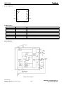
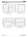
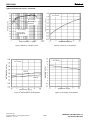
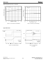
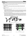
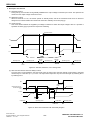
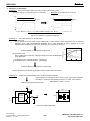
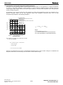
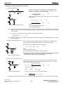
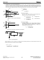
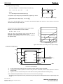
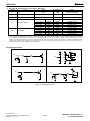
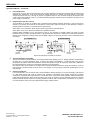
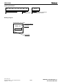
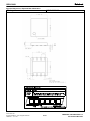
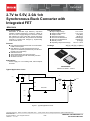
Datasheet 2.7V to 5.5V, 2.0A 1ch Synchronous Buck Converter with Integrated FET BD9130NV General Description Key Specifications BD9130NV is ROHM’s high efficiency step-down switching regulator designed to provide a voltage as low as 1V from a supply voltage of 5.5V/3.3V. It offers high efficiency by using pulse skip control technology and synchronous switches, and provides fast transient response to sudden load changes by implementing current mode control. Features Fast Transient Response because of Current Mode PWM Control System High Efficiency for All Load Ranges because of Synchronous Switches (Nch/Pch FET) and SLLMTM (Simple Light Load Mode) Soft-Start Function Thermal Shutdown and UVLO Functions Short-Circuit Protection with Time Delay Function Shutdown Function Input Voltage Range: Output Voltage Range: Output Current: Switching Frequency: Pch FET ON-Resistance: Nch FET ON-Resistance: Standby Current: Operating Temperature Range: Package 2.7V to 5.5V 1.0V to 2.5V 2.0A (Max) 1MHz(Typ) 200mΩ(Typ) 160mΩ(Typ) 0μA (Typ) -25°C to +105°C W(Typ) x D(Typ) x H(Max) Applications Power Supply for LSI including DSP, Microcomputer and ASIC SON008V5060 5.00mm x 6.00mm x 1.00mm Typical Application Circuit VCC CIN L EN VCC,PVCC SW ADJ ITH VOUT CO GND,PGND R2 R1 RITH CITH Figure 1. Typical Application Circuit ○Product structure:Silicon monolithic integrated circuit .www.rohm.com © 2012 ROHM Co., Ltd. All rights reserved. TSZ22111・14・001 ○This product has no designed protection against radioactive rays 1/21 TSZ02201-0J3J0AJ00130-1-2 02.Oct.2014 Rev.002 BD9130NV Pin Configuration (TOP VIEW) ADJ 1 8 EN VCC 2 7 PVCC ITH 3 6 SW GND 4 5 PGND Figure 2. Pin Configuration Pin Description Pin No. Pin name 1 2 3 4 5 6 7 8 ADJ VCC ITH GND PGND SW PVCC EN Pin function Output voltage detection pin Power supply input pin GmAmp output pin/connected to phase compensation capacitor Ground pin Power switch ground pin Power switch node Power switch supply pin Enable pin (Active high) Block Diagram VCC PVCC VCC RITH R1 CITH R2 Figure 3. Block Diagram www.rohm.com © 2012 ROHM Co., Ltd. All rights reserved. TSZ22111・15・001 2/21 TSZ02201-0J3J0AJ00130-1-2 02.Oct.2014 Rev.002 BD9130NV Absolute Maximum Ratings Parameter VCC Voltage Symbol Limit V PVCC -0.3 to +7 (Note 1) V VEN -0.3 to +7 V VCC PVCC Voltage EN Voltage SW,ITH Voltage Unit (Note 1) -0.3 to +7 VSW,VITH -0.3 to +7 V Power Dissipation 1 Pd1 0.90(Note 2) W Power Dissipation 2 Pd2 3.90(Note 3) W Operating Temperature Range Topr -25 to +105 °C Storage Temperature Range Tstg -55 to +150 °C Tjmax +150 °C Maximum Junction Temperature (Note 1) Pd should not be exceeded. (Note 2) Reduce by 7.2mW/°C for temperatures above Ta=25°C, Mounted on 70mmx70mmx1.6mm Glass Epoxy PCB. (Note 3) Reduce by 31.2mW/°C for temperatures above Ta=25°C, Mounted on JESD51-7. Caution: Operating the IC over the absolute maximum ratings may damage the IC. The damage can either be a short circuit between pins or an open circuit between pins. Therefore, it is important to consider circuit protection measures, such as adding a fuse, in case the IC is operated over the absolute maximum ratings. Recommended Operating Conditions (Ta=25°C) Parameter VCC voltage PVCC Voltage En Voltage SW Average Output Current Output Voltage Setting Range Limit Symbol Unit Min Typ Max VCC (Note 4) 2.7 (Note 5) 3.3 5.5 V PVCC (Note 4) 2.7 (Note 5) 3.3 5.5 V VEN 0 - VCC V ISW (Note 4) - - 2.0 A VOUT 1.0 - 2.5 V (Note 4) Pd should not be exceeded. (Note 5) In case the output voltage is set to 1.6V or more, VCCMin = VOUT + 1.3V. Electrical Characteristics(Ta=25°C, VCC=PVCC=3.3V, VEN=VCC, R1=10kΩ, R2=5kΩ, unless otherwise specified.) Symbol Min Typ Max Unit Standby Current Parameter ISTB - 0 10 μA Bias Current ICC - 250 400 μA Conditions EN=GND En Low Voltage VENL - GND 0.8 V Standby mode En High Voltage VENH 2.0 VCC - V Active mode EN Input Current IEN - 1 10 μA VEN=3.3V Oscillation Frequency fOSC 0.8 1 1.2 MHz Pch Fet ON-Resistance RONP - 200 400 mΩ PVCC=3.3V Nch Fet ON-Resistance RONN - 160 350 mΩ PVCC=3.3V ADJ Voltage VADJ 0.788 0.800 0.812 V Output Voltage VOUT - 1.200 - V ITH Sink Current ITHSI 10 20 - μA VADJ=1.0V ITH Source Current ITHSO 10 20 - μA VADJ=0.6V UVLO Threshold Voltage VUVLO1 2.400 2.500 2.600 V VCC=3V to 0V UVLO Release Voltage VUVLO2 2.425 2.550 2.700 V VCC=0V to 3V tSS 0.5 1 2 ms Timer Latch Time tLATCH 1 2 3 ms Scp/Tsd operated Output Short Circuit Threshold Voltage VSCP - VOUTx0.5 VOUTx0.7 V VOUT=1.2V to 0V Soft-Start Time www.rohm.com © 2012 ROHM Co., Ltd. All rights reserved. TSZ22111・15・001 3/21 TSZ02201-0J3J0AJ00130-1-2 02.Oct.2014 Rev.002 BD9130NV [VOUT=2.5V] Ta=25°C Ta=25°C IO=0A IO=0A [VOUT=1.8V] [VOUT=1.8V] Output Voltage: VOUT [V] Output Voltage: VOUT [V] Typical Performance Curves VCC=3.3V Ta=25°C IO=0A Ta=25°C IO=0A EN Voltage: VEN [V] Input Voltage: VCC [V] Figure 4. Output Voltage vs Input Voltage Figure 5. Output Voltage vs EN Voltage VCC=3.3V IO=0A [VOUT=2.5V] VCC=5V Ta=25°C [VOUT=1.8] VCC=3.3V Ta=25°C Output Voltage: VOUT [V] Output Voltage: VOUT [V] [VOUT=1.8V] Output Current: IOUT [A] Temperature: Ta [°C] Figure 6. Output Voltage vs Output Current www.rohm.com © 2012 ROHM Co., Ltd. All rights reserved. TSZ22111・15・001 Figure 7. Output Voltage vs Temperature 4/21 TSZ02201-0J3J0AJ00130-1-2 02.Oct.2014 Rev.002 BD9130NV Typical Performance Curves - continued Efficiency: η [%] [VOUT=1.8V] VCC=3.3V Ta=25°C [VOUT=2.5V] VCC=5V Ta=25°C Frequency: fOSC [MHz] VCC=3.3V Temperature: Ta [°C] Output Current: IOUT [mA] Figure 9. Frequency vs Temperature Figure 8. Efficiency vs Output Current VCC=3.3V EN Voltage: VEN [V] ON-Resistance: RON [Ω] VCC=3.3V Temperature: Ta [°C] Temperature: Ta [°C] Figure 11. EN Voltage vs Temperature Figure 10. ON-Resistance vs Temperature www.rohm.com © 2012 ROHM Co., Ltd. All rights reserved. TSZ22111・15・001 5/21 TSZ02201-0J3J0AJ00130-1-2 02.Oct.2014 Rev.002 BD9130NV Typical Performance Curves - continued VCC=3.3V Frequency: fOSC [MHz] Circuit Current: ICC [µA] Ta=25°C Temperature: Ta [°C] Input Voltage: VCC [V] Figure 12. Circuit Current vs Temperature Figure 13. Frequency vs Input Voltage Typical Waveforms [VOUT=1.8V] VCC=PVCC =EN [SLLMTM control VOUT=1.8V] SW VOUT VOUT VCC=3.3V Ta=25°C IO=0A VCC=3.3V Ta=25°C Figure 14. Soft Start Waveform www.rohm.com © 2012 ROHM Co., Ltd. All rights reserved. TSZ22111・15・001 Figure 15. SW Waveform (Io=10mA) 6/21 TSZ02201-0J3J0AJ00130-1-2 02.Oct.2014 Rev.002 BD9130NV Typical Waveforms - continued [PWM control [VOUT=1.8V] VOUT=1.8V] VOUT VCC=3.3V Ta=25°C IOUT VCC=3.3V Ta=25°C Figure 17. Transient Response (Io=1A to 2A, 10μs) Figure 16. SW Waveform (Io=200mA) [VOUT=1.8V] VOUT IOUT VCC=3.3V Ta=25°C Figure 18. Transient Response (Io=2A to 1A,10μs) www.rohm.com © 2012 ROHM Co., Ltd. All rights reserved. TSZ22111・15・001 7/21 TSZ02201-0J3J0AJ00130-1-2 02.Oct.2014 Rev.002 BD9130NV Application Information 1. Operation BD9130NV is a synchronous step-down switching regulator that achieves fast transient response by employing current mode PWM control system. It utilizes switching operation either in PWM (Pulse Width Modulation) mode for heavier load, or SLLMTM (Simple Light Load Mode) operation for lighter load to improve efficiency. (1) Synchronous Rectifier Integrated synchronous rectification using two MOSFETS reduces power dissipation and increases efficiency when compared to converters using external diodes. Internal shoot-through current limiting circuit further reduces power dissipation. (2) Current mode PWM Control The PWM control signal of this IC depends on two feedback loops, the voltage feedback and the inductor current feedback. (a) PWM (Pulse Width Modulation) Control The clock signal coming from OSC has a frequency of 1Mhz. When OSC sets the RS latch, the P-Channel MOSFET is turned ON and the N-Channel MOSFET is turned OFF. The opposite happens when the current comparator (Current Comp) resets the RS latch i.e. the P-Channel MOSFET is turned OFF and the N-Channel MOSFET is turned ON. Current Comp’s output is a comparison of two signals, the current feedback control signal “SENSE” which is a voltage proportional to the current IL, and the voltage feedback control signal, FB. (b) SLLMTM (Simple Light Load Mode) Control When the control mode is shifted by PWM from heavier load to lighter load or vice versa, the switching pulse is designed to turn OFF with the device held operating in normal PWM control loop. This allows linear operation without voltage drop or deterioration in transient response during the sudden load changes. Although the PWM control loop continues to operate with a SET signal from OSC and a RESET signal from Current Comp, it is so designed such that the RESET signal is continuously sent even if the load is changed to light mode where the switching is turned OFF and the switching pulses disappear. Activating the switching discontinuously reduces the switching dissipation and improves the efficiency. SENSE Current Comp RESET VOUT Level Shift R Q FB SET Gm Amp S IL Driver Logic VOUT SW Load OSC RITH Figure19. Diagram of Current Mode PWM Control PVCC Current Comp SENSE PVCC SENSE Current Comp FB FB SET GND SET GND RESET GND RESET GND SW GND SW IL GND IL(AVE) IL 0A VOUT VOUT VOUT(AVE) VOUT(AVE) Not switching Figure 20. PWM Switching Timing Diagram www.rohm.com © 2012 ROHM Co., Ltd. All rights reserved. TSZ22111・15・001 Figure 21. SLLMTM Switching Timing Diagram 8/21 TSZ02201-0J3J0AJ00130-1-2 02.Oct.2014 Rev.002 BD9130NV 2. Description of Functions (1) Soft-Start Function During start-up, the soft-start circuit gradually establishes the output voltage to limit the input current. This prevents the overshoot in the output voltage and inrush current. (2) Shutdown Function When EN terminal is “Low”, the device operate in Standby Mode, and all the functional blocks such as reference voltage circuit, internal oscillator and drivers are turned OFF. Standby current is 0μA (Typ). (3) UVLO Function This circuit detects whether the supplied input voltage is sufficient to obtain the output voltage of this IC. It provides a hysteresis of 50mV (Typ) to prevent the output from chattering. Hysteresis 50mV VCC EN VOUT tSS tSS tSS Soft start Standby mode Standby mode Operating mode Standby mode Operating mode UVLO UVLO Operating mode EN Standby mode UVLO Figure 22. Soft-Start, Shutdown, UVLO Timing Chart (4) Short-Circuit Protection with Time Delay Function To protect the IC from breakdown, the short-circuit turns the output OFF when the internal current limiter is activated continuously for a fixed time (tLATCH) or more. The output that is kept OFF may be turned ON again by restarting EN or by resetting UVLO. EN Output OFF Latch Output Short circuit Threshold Voltage VOUT IL Limit IL t1<tLATCH t2=tLATCH Operating mode Output OFF Operating mode Output OFF Timer Latch EN EN Figure 23. Short-Circuit Protection with Time Delay Diagram www.rohm.com © 2012 ROHM Co., Ltd. All rights reserved. TSZ22111・15・001 9/21 TSZ02201-0J3J0AJ00130-1-2 02.Oct.2014 Rev.002 BD9130NV 3. Information on Advantages Advantage 1:Offers fast transient response by using current mode control system Conventional product (Load response IO=0.1A to 0.6A) BD9139NV (Load response IO=1A to 2A) VOUT VOUT 29mV 110mV IOUT IOUT Voltage drop due to sudden change in load was reduced. Figure 24. Comparison of Transient Response Advantage 2: Offers high efficiency for all load ranges (a) For lighter load: This IC utilizes the current mode control called SLLMTM, which reduces various dissipations such as switching dissipation (PSW), gate charge/discharge dissipation (PGATE), ESR dissipation of output capacitor (PESR) and ON-Resistance dissipation (PRON) that may otherwise cause reduction in efficiency. 100 Achieves efficiency improvement for lighter load. (b) For heavier load: This IC utilizes the synchronous rectifying mode and uses low ON-Resistance power MOSFETs. Efficiency η[%] SLLMTM ON-Resistance of P-Channel MOSFET : 200mΩ(Typ) ON-Resistance of N-Channel MOSFET : 160mΩ(Typ) ② 50 ① PWM ①improvement by SLLMTM system ②improvement by synchronous rectifier 0 0.001 0.01 0.1 Output current IOUT[A] 1 Figure 25. Efficiency Achieves efficiency improvement for heavier load. Offers high efficiency for all load ranges with the improvements mentioned above. Advantage 3:・Supplied in smaller package due to small-sized power MOSFET. ・Output capacitor Co required for current mode control: 22μF ceramic capacitor ・Inductance L required for the operating frequency of 1 MHz: 2.2μH inductor (BD9130NV:CO=22μF, L=2.2μH) Reduces the required mounting area. VCC 15mm CIN CIN DC/DC Convertor Controller RITH RITH L VOUT L 10mm CITH CO CO CITH Figure 26. Example Application www.rohm.com © 2012 ROHM Co., Ltd. All rights reserved. TSZ22111・15・001 10/21 TSZ02201-0J3J0AJ00130-1-2 02.Oct.2014 Rev.002 BD9130NV 4. Switching Regulator Efficiency Efficiency η may be expressed by the equation shown below: VOUT IOUT VIN I IN 100 POUT POUT 100 100 PIN POUT Pd % Efficiency may be improved by reducing the switching regulator power dissipation factors Pdα as follows: Dissipation factors: (1) ON-Resistance Dissipation of Inductor and FET: Pd(I2R) Pd I 2 R I OUT 2 RCOIL RON where: RCOIL is the DC resistance of inductor. RON is the ON-Resistance of FET. IOUT is the output current. (2) Gate Charge/Discharge Dissipation: Pd(Gate) Pd Gate Cgs f V 2 where: Cgs is the gate capacitance of FET. f is the switching frequency. V is the gate driving voltage of FET. (3) Switching Dissipation: Pd(SW) Pd SW V IN 2 C RSS I OUT f I DRIVE where: CRSS is the reverse transfer capacitance of FET. IDRIVE is the peak current of gate. (4) ESR Dissipation of Capacitor: Pd(ESR) PdESR I RMS 2 ESR where: IRMS is the ripple current of capacitor. ESR is the equivalent series resistance. (5) Operating Current Dissipation of IC: Pd(IC) PdIC VIN I CC where: ICC is the circuit current. www.rohm.com © 2012 ROHM Co., Ltd. All rights reserved. TSZ22111・15・001 11/21 TSZ02201-0J3J0AJ00130-1-2 02.Oct.2014 Rev.002 BD9130NV 5. Consideration on Permissible Dissipation and Heat Generation Since this IC functions with high efficiency without significant heat generation in most applications, no special consideration is needed on permissible dissipation or heat generation. In case of extreme conditions, however, including lower input voltage, higher output voltage, heavier load, and/or higher temperature, the permissible dissipation and/or heat generation must be carefully considered. For dissipation, only conduction losses due to DC resistance of inductor and ON-Resistance of FET are considered. This is because conduction losses are the most significant among other dissipation mentioned above such as gate charge/discharge dissipation and switching dissipation. ①3.9W Power dissipation: Pd [W] 4.0 3.0 ①for SON008V5060 JEDEC 4 layer board 76.2x114.3x1.6mm θj-a=32.1°C/W ②for SON008V5060 ROHM standard 1 layer board 70x70x1.6mm θj-a=138.9°C/W ③ IC only θj-a=195.3°C/W P I OUT 2 RON RON D RONP 1 D RONN 2.0 ②0.90W 1.0 Where: D is the ON duty (=VOUT/VCC). RONP is the ON resistance of P-channel MOS FET. RONN is the ON resistance of N-channel MOS FET. ③0.64W 0 0 Ambient temperature: Ta [°C] 25 50 75 100105 125 150 Figure 27. Thermal Derating Curve (SON008V5060) If VCC=3.3V, VOUT=1.8V, RONP=0.2Ω, RONN=0.16Ω IOUT=2A, for example, D VOUT / VCC 1.8 / 3.3 0.545 RON 0.545 0.20 1 0.545 0.16 0.109 0.0728 0.1818 P 22 0.1818 0.7272 W Since RONP is greater than RONN in this IC, the dissipation increases as the on duty increases. Taking into consideration the dissipation stated above, thermal design must be carried out with sufficient margin. www.rohm.com © 2012 ROHM Co., Ltd. All rights reserved. TSZ22111・15・001 12/21 TSZ02201-0J3J0AJ00130-1-2 02.Oct.2014 Rev.002 BD9130NV 6. Selection of Components Externally Connected (1) Selection of Inductor (L) The inductance significantly depends on the output ripple current. As seen in equation (1), the ripple current decreases as the inductor and/or switching frequency increases. IL ΔIL IL VCC VCC VOUT VOUT A L VCC f ・・・(1) Appropriate output ripple current should be ±20% of the maximum output current. IL VOUT A I L 0.2 IOUT Max L CO L VCC VOUT VOUT ・・・(2) H I L VCC f ・・・(3) where: ΔIL is the Output ripple current, and f is the Switching frequency. Figure 28. Output Ripple Current Note: Current exceeding the current rating of the inductor results in magnetic saturation of the inductor, which decreases efficiency. The inductor must be selected allowing sufficient margin with which the peak current may not exceed its current rating. If VCC=3.3V, VOUT=1.8V, f=1MHz, ΔIL=0.2x2A=0.4A, for example, (BD9130NV) L 3.3 1.8 1.8 2.05 2.2 0.4 3.3 1M H Note: Select an inductor with low resistance component (such as DCR and ACR) to minimize dissipation in the inductor for better efficiency. (2) Selection of Output Capacitor (CO) Output capacitor should be selected with the consideration of the stability region and the equivalent series resistance required to minimize ripple voltage. VCC Output ripple voltage is determined by the equation (4) : V VOUT I L ESR ・・・(4) VOUT L where: ΔIL is the Output ripple current. ESR is the Equivalent series resistance of output capacitor. ESR CO Figure 29. Output Capacitor Note:Rating of the capacitor should be determined allowing sufficient margin against output voltage. A 22μF to 100μF ceramic capacitor is recommended. Less ESR allows reduction in output ripple voltage. (3) Selection of Input Capacitor (CIN) VCC Input capacitor must be a low ESR capacitor with a capacitance sufficient to cope with high ripple current to prevent high transient voltage. The ripple current IRMS is given by the equation (5): CIN VOUT L I RMS I OUT VOUT VCC VOUT Co VCC A ・・・(5) < Worst case > IRMSMax When VCC is twice VOUT , IRMS= Figure 30. Input Capacitor IOUT 2 If VCC=3.3V, VOUT=1.8V, and IOUTMax=2A, (BD9130NV) I RMS 2 1.83.3 1.8 0.99 3.3 ARMS A low ESR 22μF/10V ceramic capacitor is recommended to reduce ESR dissipation of input capacitor for better efficiency. www.rohm.com © 2012 ROHM Co., Ltd. All rights reserved. TSZ22111・15・001 13/21 TSZ02201-0J3J0AJ00130-1-2 02.Oct.2014 Rev.002 BD9130NV (4) Calculating RITH, CITH for Phase Compensation Since the Current Mode Control is designed to limit an inductor current, a pole (phase lag) appears in the low frequency area due to a CR filter consisting of an output capacitor and a load resistance, while a zero (phase lead) appears in the high frequency area due to the output capacitor and its ESR. Therefore, the phases are easily compensated by adding a zero to the power amplifier output with C and R as described below to cancel a pole at the power amplifier. fp fp(Min) A f Z ESR fp(Max) Gain [dB] 1 2 RO CO 0 1 2 ESR CO fZ(ESR) IOUTMin Phase [deg] IOUTMax Pole at power amplifier When the output current decreases, the load resistance Ro increases and the pole frequency decreases. 0 -90 Figure 31. Open loop gain characteristics A fpMin 1 2 ROMax CO Hz ← with lighter load fpMax 1 Hz ← with heavier load 2 ROMin CO fZ(Amp) Zero at power amplifier Increasing capacitance of the output capacitor lowers the pole frequency while the zero frequency does not change. (This is because when the capacitance is doubled, the capacitor ESR is reduced to half.) Gain [dB] 0 0 Phase [deg] -90 f Z Amp 1 2 RITH CITH Figure 32. Error amp phase compensation characteristics CIN VCC EN VOUT VCC,PVCC L SW VOUT ITH VOUT ESR GND,PGND RO CO RITH CITH Figure 33. Typical Application Stable feedback loop can be achieved by canceling the pole fp (Min) produced by the output capacitor and the load resistance with CR zero correction by the error amplifier. f Z Amp f P Min 1 1 2 R ITH C ITH 2 ROMax C o www.rohm.com © 2012 ROHM Co., Ltd. All rights reserved. TSZ22111・15・001 14/21 TSZ02201-0J3J0AJ00130-1-2 02.Oct.2014 Rev.002 BD9130NV (5) Setting the Output Voltage The output voltage VOUT is determined by the equation (6): VOUT ( R2 / R1 1) V ADJ L ・・・(6) 6 Output SW Where: VADJ is the Voltage at ADJ terminal (0.8V Typ) Co R2 1 ADJ R1 The required output voltage may be determined by adjusting R1 and R2. Figure 34. Setting the Output Voltage Adjustable output voltage range : 1.0V to 2.5V Use 1 kΩ to 100 kΩ resistor for R1. If a resistor with resistance higher than 100 kΩ is used, check the circuit and calculate carefully for ripple voltage etc. 3.9 The lower limit of input voltage depends on the output voltage. Basically, it is recommended to use the condition: Input Voltage: VCC [V] 3.7 CC[V] V CC IN PUT VOLTA GE :V [V] VCC Min VOUT 1.3V Figure 35. shows the necessary output current value at the lower limit of input voltage. (DCR of inductor: 0.1Ω) This data is the characteristic value, so it does not guarantee the operation range. 3.5 3.3 Vo=2.5V Vo=1.8V 3.1 Vo=2.0V 2.9 2.7 0 0.5 1 1.5 2 Output Current: :IIOUT [A] OUT PUT CURRENT IOUT [A] OUT[A] Figure 35. Minimum Input Voltage in each Output Voltage 7. Cautions on PCB Layout VCC R2 1 2 R1 3 RITH ③ CITH EN 8 ADJ VCC PVCC ITH SW 7 GND PGND ① L 6 5 4 EN VOUT CIN ② CO GND Figure 36. Layout Diagram ① ② ③ For the sections drawn with heavy line, use thick conductor pattern as short as possible. Layout the input ceramic capacitor CIN closer to the pins PVCC and PGND, and the output capacitor CO closer to the pin PGND. Layout CITH and RITH between the pins ITH and GND as near as possible with least necessary wiring. Note: SON008V5060 (BD9130NV) has thermal FIN on the reverse of the package. The package thermal performance may be enhanced by bonding the FIN to GND plane which occupies a large area of PCB. www.rohm.com © 2012 ROHM Co., Ltd. All rights reserved. TSZ22111・15・001 15/21 TSZ02201-0J3J0AJ00130-1-2 02.Oct.2014 Rev.002 BD9130NV 8. Recommended Components Lists on Above Application Symbol Part Value Manufacturer Series Coil 2.2µH TDK LTF5022-2R2N3R2 CIN Ceramic capacitor 22µF Kyocera CM32X5R226M10A CO Ceramic capacitor 22µF Kyocera CM316B226M06A Murata Murata Murata Murata Murata Rohm Rohm Rohm Rohm Rohm GRM18 Series GRM18 Series GRM18 Series GRM18 Series GRM18 Series MCR03 Series MCR03 Series MCR03 Series MCR03 Series MCR03 Series L CITH Ceramic capacitor RITH Resistance VOUT=1.0V VOUT=1.2V VOUT=1.5V VOUT=1.8V VOUT=2.5V VOUT=1.0V VOUT=1.2V VOUT=1.5V VOUT=1.8V VOUT=2.5V 680pF 560pF 470pF 330pF 330pF 10kΩ 12kΩ 15kΩ 18kΩ 18kΩ Note:The parts list presented above is an example of recommended parts. Although the parts are standard, actual circuit characteristics should be checked on your application carefully before use. Be sure to allow sufficient margins to accommodate variations between external devices and this IC when employing the depicted circuit with other circuit constants modified. Both static and transient characteristics should be considered in establishing these margins. When switching noise is significant and may affect the system, a low pass filter should be inserted between the VCC and PVCC pins, and a Schottky Barrier diode connected between the SW and PGND pins. I/O Equivalent Circuit ・EN pin PVCC ・SW pin PVCC PVCC EN SW ・ADJ pin ・ITH pin VCC ADJ ITH Figure 37. I/O Equivalent Circuit www.rohm.com © 2012 ROHM Co., Ltd. All rights reserved. TSZ22111・15・001 16/21 TSZ02201-0J3J0AJ00130-1-2 02.Oct.2014 Rev.002 BD9130NV Operational Notes 1. Reverse Connection of Power Supply Connecting the power supply in reverse polarity can damage the IC. Take precautions against reverse polarity when connecting the power supply, such as mounting an external diode between the power supply and the IC’s power supply pins. 2. Power Supply Lines Design the PCB layout pattern to provide low impedance supply lines. Separate the ground and supply lines of the digital and analog blocks to prevent noise in the ground and supply lines of the digital block from affecting the analog block. Furthermore, connect a capacitor to ground at all power supply pins. Consider the effect of temperature and aging on the capacitance value when using electrolytic capacitors. 3. Ground Voltage Ensure that no pins are at a voltage below that of the ground pin at any time, even during transient condition. 4. Ground Wiring Pattern When using both small-signal and large-current ground traces, the two ground traces should be routed separately but connected to a single ground at the reference point of the application board to avoid fluctuations in the small-signal ground caused by large currents. Also ensure that the ground traces of external components do not cause variations on the ground voltage. The ground lines must be as short and thick as possible to reduce line impedance. 5. Thermal Consideration Should by any chance the power dissipation rating be exceeded the rise in temperature of the chip may result in deterioration of the properties of the chip. In case of exceeding this absolute maximum rating, increase the board size and copper area to prevent exceeding the Pd rating. 6. Recommended Operating Conditions These conditions represent a range within which the expected characteristics of the IC can be approximately obtained. The electrical characteristics are guaranteed under the conditions of each parameter. 7. Inrush Current When power is first supplied to the IC, it is possible that the internal logic may be unstable and inrush current may flow instantaneously due to the internal powering sequence and delays, especially if the IC has more than one power supply. Therefore, give special consideration to power coupling capacitance, power wiring, width of ground wiring, and routing of connections. 8. Operation Under Strong Electromagnetic Field Operating the IC in the presence of a strong electromagnetic field may cause the IC to malfunction. 9. Testing on Application Boards When testing the IC on an application board, connecting a capacitor directly to a low-impedance output pin may subject the IC to stress. Always discharge capacitors completely after each process or step. The IC’s power supply should always be turned off completely before connecting or removing it from the test setup during the inspection process. To prevent damage from static discharge, ground the IC during assembly and use similar precautions during transport and storage. 10. Inter-pin Short and Mounting Errors Ensure that the direction and position are correct when mounting the IC on the PCB. Incorrect mounting may result in damaging the IC. Avoid nearby pins being shorted to each other especially to ground, power supply and output pin. Inter-pin shorts could be due to many reasons such as metal particles, water droplets (in very humid environment) and unintentional solder bridge deposited in between pins during assembly to name a few. www.rohm.com © 2012 ROHM Co., Ltd. All rights reserved. TSZ22111・15・001 17/21 TSZ02201-0J3J0AJ00130-1-2 02.Oct.2014 Rev.002 BD9130NV Operational Notes – continued 11. Unused Input Pins Input pins of an IC are often connected to the gate of a MOS transistor. The gate has extremely high impedance and extremely low capacitance. If left unconnected, the electric field from the outside can easily charge it. The small charge acquired in this way is enough to produce a significant effect on the conduction through the transistor and cause unexpected operation of the IC. So unless otherwise specified, unused input pins should be connected to the power supply or ground line. 12. Regarding the Input Pin of the IC This monolithic IC contains P+ isolation and P substrate layers between adjacent elements in order to keep them isolated. P-N junctions are formed at the intersection of the P layers with the N layers of other elements, creating a parasitic diode or transistor. For example (refer to figure below): When GND > Pin A and GND > Pin B, the P-N junction operates as a parasitic diode. When GND > Pin B, the P-N junction operates as a parasitic transistor. Parasitic diodes inevitably occur in the structure of the IC. The operation of parasitic diodes can result in mutual interference among circuits, operational faults, or physical damage. Therefore, conditions that cause these diodes to operate, such as applying a voltage lower than the GND voltage to an input pin (and thus to the P substrate) should be avoided. Resistor Transistor (NPN) Pin A Pin B C E Pin A N P+ P N N P+ N Pin B B Parasitic Elements N P+ N P N P+ B N C E Parasitic Elements P Substrate P Substrate GND GND Parasitic Elements GND Parasitic Elements GND N Region close-by Figure 38. Example of monolithic IC structure 13. Thermal Shutdown Circuit(TSD) This IC has a built-in thermal shutdown circuit that prevents heat damage to the IC. Normal operation should always be within the IC’s power dissipation rating. If however the rating is exceeded for a continued period, the junction temperature (Tj) will rise which will activate the TSD circuit that will turn OFF all output pins. When the Tj falls below the TSD threshold, the circuits are automatically restored to normal operation. Note that the TSD circuit operates in a situation that exceeds the absolute maximum ratings and therefore, under no circumstances, should the TSD circuit be used in a set design or for any purpose other than protecting the IC from heat damage. 14. Selection of Inductor It is recommended to use an inductor with a series resistance element (DCR) 0.1Ω or less. Especially, note that use of a high DCR inductor will cause an inductor loss, resulting in decreased output voltage. Should this condition continue for a specified period (soft start time + timer latch time), output short circuit protection will be activated and output will be latched OFF. When using an inductor over 0.1Ω, be careful to ensure adequate margins for variation between external devices and this IC, including transient as well as static characteristics. Furthermore, in any case, it is recommended to start up the output with EN after supply voltage is within. www.rohm.com © 2012 ROHM Co., Ltd. All rights reserved. TSZ22111・15・001 18/21 TSZ02201-0J3J0AJ00130-1-2 02.Oct.2014 Rev.002 BD9130NV Ordering Information B D 9 1 3 0 Part Number N V - Package NV:SON008V5060 E2 Packaging and forming specification E2: Embossed tape and reel Marking Diagram SON008V5060 (TOP VIEW) Part Number Marking BD9130 LOT Number 1PIN MARK www.rohm.com © 2012 ROHM Co., Ltd. All rights reserved. TSZ22111・15・001 19/21 TSZ02201-0J3J0AJ00130-1-2 02.Oct.2014 Rev.002 BD9130NV Physical Dimension, Tape and Reel Information Package Name www.rohm.com © 2012 ROHM Co., Ltd. All rights reserved. TSZ22111・15・001 SON008V5060 20/21 TSZ02201-0J3J0AJ00130-1-2 02.Oct.2014 Rev.002 BD9130NV Revision History Date Revision 02.Mar.2012 02.Oct.2014 001 002 Changes New Release Applied the ROHM Standard Style and improved understandability. www.rohm.com © 2012 ROHM Co., Ltd. All rights reserved. TSZ22111・15・001 21/21 TSZ02201-0J3J0AJ00130-1-2 02.Oct.2014 Rev.002 Notice Precaution on using ROHM Products 1. Our Products are designed and manufactured for application in ordinary electronic equipments (such as AV equipment, OA equipment, telecommunication equipment, home electronic appliances, amusement equipment, etc.). If you (Note 1) intend to use our Products in devices requiring extremely high reliability (such as medical equipment , transport equipment, traffic equipment, aircraft/spacecraft, nuclear power controllers, fuel controllers, car equipment including car accessories, safety devices, etc.) and whose malfunction or failure may cause loss of human life, bodily injury or serious damage to property (“Specific Applications”), please consult with the ROHM sales representative in advance. Unless otherwise agreed in writing by ROHM in advance, ROHM shall not be in any way responsible or liable for any damages, expenses or losses incurred by you or third parties arising from the use of any ROHM’s Products for Specific Applications. (Note1) Medical Equipment Classification of the Specific Applications JAPAN USA EU CHINA CLASSⅢ CLASSⅡb CLASSⅢ CLASSⅢ CLASSⅣ CLASSⅢ 2. ROHM designs and manufactures its Products subject to strict quality control system. However, semiconductor products can fail or malfunction at a certain rate. Please be sure to implement, at your own responsibilities, adequate safety measures including but not limited to fail-safe design against the physical injury, damage to any property, which a failure or malfunction of our Products may cause. The following are examples of safety measures: [a] Installation of protection circuits or other protective devices to improve system safety [b] Installation of redundant circuits to reduce the impact of single or multiple circuit failure 3. Our Products are designed and manufactured for use under standard conditions and not under any special or extraordinary environments or conditions, as exemplified below. Accordingly, ROHM shall not be in any way responsible or liable for any damages, expenses or losses arising from the use of any ROHM’s Products under any special or extraordinary environments or conditions. If you intend to use our Products under any special or extraordinary environments or conditions (as exemplified below), your independent verification and confirmation of product performance, reliability, etc, prior to use, must be necessary: [a] Use of our Products in any types of liquid, including water, oils, chemicals, and organic solvents [b] Use of our Products outdoors or in places where the Products are exposed to direct sunlight or dust [c] Use of our Products in places where the Products are exposed to sea wind or corrosive gases, including Cl2, H2S, NH3, SO2, and NO2 [d] Use of our Products in places where the Products are exposed to static electricity or electromagnetic waves [e] Use of our Products in proximity to heat-producing components, plastic cords, or other flammable items [f] Sealing or coating our Products with resin or other coating materials [g] Use of our Products without cleaning residue of flux (even if you use no-clean type fluxes, cleaning residue of flux is recommended); or Washing our Products by using water or water-soluble cleaning agents for cleaning residue after soldering [h] Use of the Products in places subject to dew condensation 4. The Products are not subject to radiation-proof design. 5. Please verify and confirm characteristics of the final or mounted products in using the Products. 6. In particular, if a transient load (a large amount of load applied in a short period of time, such as pulse. is applied, confirmation of performance characteristics after on-board mounting is strongly recommended. Avoid applying power exceeding normal rated power; exceeding the power rating under steady-state loading condition may negatively affect product performance and reliability. 7. De-rate Power Dissipation (Pd) depending on Ambient temperature (Ta). When used in sealed area, confirm the actual ambient temperature. 8. Confirm that operation temperature is within the specified range described in the product specification. 9. ROHM shall not be in any way responsible or liable for failure induced under deviant condition from what is defined in this document. Precaution for Mounting / Circuit board design 1. When a highly active halogenous (chlorine, bromine, etc.) flux is used, the residue of flux may negatively affect product performance and reliability. 2. In principle, the reflow soldering method must be used on a surface-mount products, the flow soldering method must be used on a through hole mount products. If the flow soldering method is preferred on a surface-mount products, please consult with the ROHM representative in advance. For details, please refer to ROHM Mounting specification Notice – GE © 2014 ROHM Co., Ltd. All rights reserved. Rev.003 Precautions Regarding Application Examples and External Circuits 1. If change is made to the constant of an external circuit, please allow a sufficient margin considering variations of the characteristics of the Products and external components, including transient characteristics, as well as static characteristics. 2. You agree that application notes, reference designs, and associated data and information contained in this document are presented only as guidance for Products use. Therefore, in case you use such information, you are solely responsible for it and you must exercise your own independent verification and judgment in the use of such information contained in this document. ROHM shall not be in any way responsible or liable for any damages, expenses or losses incurred by you or third parties arising from the use of such information. Precaution for Electrostatic This Product is electrostatic sensitive product, which may be damaged due to electrostatic discharge. Please take proper caution in your manufacturing process and storage so that voltage exceeding the Products maximum rating will not be applied to Products. Please take special care under dry condition (e.g. Grounding of human body / equipment / solder iron, isolation from charged objects, setting of Ionizer, friction prevention and temperature / humidity control). Precaution for Storage / Transportation 1. Product performance and soldered connections may deteriorate if the Products are stored in the places where: [a] the Products are exposed to sea winds or corrosive gases, including Cl2, H2S, NH3, SO2, and NO2 [b] the temperature or humidity exceeds those recommended by ROHM [c] the Products are exposed to direct sunshine or condensation [d] the Products are exposed to high Electrostatic 2. Even under ROHM recommended storage condition, solderability of products out of recommended storage time period may be degraded. It is strongly recommended to confirm solderability before using Products of which storage time is exceeding the recommended storage time period. 3. Store / transport cartons in the correct direction, which is indicated on a carton with a symbol. Otherwise bent leads may occur due to excessive stress applied when dropping of a carton. 4. Use Products within the specified time after opening a humidity barrier bag. Baking is required before using Products of which storage time is exceeding the recommended storage time period. Precaution for Product Label QR code printed on ROHM Products label is for ROHM’s internal use only. Precaution for Disposition When disposing Products please dispose them properly using an authorized industry waste company. Precaution for Foreign Exchange and Foreign Trade act Since our Products might fall under controlled goods prescribed by the applicable foreign exchange and foreign trade act, please consult with ROHM representative in case of export. Precaution Regarding Intellectual Property Rights 1. All information and data including but not limited to application example contained in this document is for reference only. ROHM does not warrant that foregoing information or data will not infringe any intellectual property rights or any other rights of any third party regarding such information or data. ROHM shall not be in any way responsible or liable for infringement of any intellectual property rights or other damages arising from use of such information or data.: 2. No license, expressly or implied, is granted hereby under any intellectual property rights or other rights of ROHM or any third parties with respect to the information contained in this document. Other Precaution 1. This document may not be reprinted or reproduced, in whole or in part, without prior written consent of ROHM. 2. The Products may not be disassembled, converted, modified, reproduced or otherwise changed without prior written consent of ROHM. 3. In no event shall you use in any way whatsoever the Products and the related technical information contained in the Products or this document for any military purposes, including but not limited to, the development of mass-destruction weapons. 4. The proper names of companies or products described in this document are trademarks or registered trademarks of ROHM, its affiliated companies or third parties. Notice – GE © 2014 ROHM Co., Ltd. All rights reserved. Rev.003 Datasheet General Precaution 1. Before you use our Pro ducts, you are requested to care fully read this document and fully understand its contents. ROHM shall n ot be in an y way responsible or liabl e for fa ilure, malfunction or acci dent arising from the use of a ny ROHM’s Products against warning, caution or note contained in this document. 2. All information contained in this docume nt is current as of the issuing date and subj ect to change without any prior notice. Before purchasing or using ROHM’s Products, please confirm the la test information with a ROHM sale s representative. 3. The information contained in this doc ument is provi ded on an “as is” basis and ROHM does not warrant that all information contained in this document is accurate an d/or error-free. ROHM shall not be in an y way responsible or liable for an y damages, expenses or losses incurred b y you or third parties resulting from inaccur acy or errors of or concerning such information. Notice – WE © 2014 ROHM Co., Ltd. All rights reserved. Rev.001