1
PPCBug
Firmware Package
User’s Manual
Parts 1 & 2
PPCBUGA1/UM4 PPCBUGA2/UM4
Notice
While reasonable efforts have been made to assure the accuracy of this document,
Motorola, Inc. assumes no liability resulting from any omissions in this document,
or from the use of the information obtained therein. Motorola reserves the right to
revise this document and to make changes from time to time in the content hereof
without obligation of Motorola to notify any person of such revision or changes.
No part of this material may be reproduced or copied in any tangible medium, or
stored in a retrieval system, or transmitted in any form, or by any means, radio,
electronic, mechanical, photocopying, recording or facsimile, or otherwise,
without the prior written permission of Motorola, Inc.
It is possible that this publication may contain reference to, or information about
Motorola products (machines and programs), programming, or services that are
not announced in your country. Such references or information must not be
construed to mean that Motorola intends to announce such Motorola products,
programming, or services in your country.
Restricted Rights Legend
If the documentation contained herein is supplied, directly or indirectly, to the U.S.
Government, the following notice shall apply unless otherwise agreed to in
writing by Motorola, Inc.
Use, duplication, or disclosure by the Government is subject to restrictions as set
forth in subparagraph (c)(1)(ii) of the Rights in Technical Data and Computer
Software clause at DFARS 252.227-7013.
Motorola, Inc.
Computer Group
2900 South Diablo Way
Tempe, Arizona 85282
Preface
The PPCBug Firmware Package UserÕs Manual provides information on the PPCBug
Þrmware, the start-up and boot routines, the debugger commands, the one-line
assembler/disassembler, and the debugger system calls. All information
contained herein is speciÞc to MotorolaÕs PowerPCª-based boards: MVME230x
VME Processor Modules, MVME260x Single Board Computers, MVME3604 VME
Processor Modules, MVME4604 VME Dual Processor Modules, MTX Embedded
ATX Motherboards, MCP750 CompactPCI, and PMCspan PCI expansion boards.
In this manual, they are collectively referred to as the PowerPC board or board.
This manual covers release 3.5, and earlier versions, of PPC1Bug.
This document is bound in two parts. Part 1 (PPCBUGA1/UM4) contains the Table
of Contents, List of Figures, List of Tables, and Chapters 1 through 3. Part 2
(PPCBUGA2/UM4) contains Chapters 4 and 5, Appendixes A through H, and the
Index.
The diagnostics are covered in the PPCBug Diagnostics Manual (PPCDIAA/UM2).
A basic knowledge of computers and digital logic is assumed. Refer to Appendix
A, Related Documentation, of this manual for a list of documents that may provide
helpful information.
This manual is intended for anyone who designs OEM systems, supplies
additional capability to an existing compatible system, or works in a lab
environment for experimental purposes.
Motorola¨ and the Motorola symbol are registered trademarks of Motorola, Inc.
PowerPCª is a trademark of IBM, and is used by Motorola with permission.
AIXTM is a trademark of IBM Corp.
All other products mentioned in this document are trademarks or registered
trademarks of their respective holders.
Conventions
The following conventions are used in this document:
bold
is used for user input that you type just as it appears. Bold is also used for
commands, options and arguments to commands, and names of programs,
directories, and files.
italic
is used for names of variables to which you assign values. Italic is also used
for comments in screen displays and examples.
courier
is used for system output (e.g., screen displays, reports), examples, and
system prompts.
Return or Ôthe Return keyÕ
represents the Enter, Return, or Carriage Return key.
CTRL
represents the Control key. Execute control characters by pressing the
CTRL key and the letter simultaneously, e.g., CTRL-d.
|
Separates two or more items that you can select from (one only).
[]
encloses an optional item that may occur zero or one time.
{}
encloses an optional item that may occur zero or more times.
A character precedes a data or address parameter to specify the numeric format,
as follows (if not specified, the format is hexadecimal):
$
dollar
0x
Zero-x
%
percent
&
ampersand a decimal number.
a hexadecimal character.
a binary number.
Safety Summary
Safety Depends On You
The following general safety precautions must be observed during all phases of operation, service, and
repair of this equipment. Failure to comply with these precautions or with speciÞc warnings elsewhere in
this manual violates safety standards of design, manufacture, and intended use of the equipment.
Motorola, Inc. assumes no liability for the customer's failure to comply with these requirements.
The safety precautions listed below represent warnings of certain dangers of which Motorola is aware. You,
as the user of the product, should follow these warnings and all other safety precautions necessary for the
safe operation of the equipment in your operating environment.
Ground the Instrument.
To minimize shock hazard, the equipment chassis and enclosure must be connected to an electrical ground.
The equipment is supplied with a three-conductor ac power cable. The power cable must be plugged into
an approved three-contact electrical outlet. The power jack and mating plug of the power cable meet
International Electrotechnical Commission (IEC) safety standards.
Do Not Operate in an Explosive Atmosphere.
Do not operate the equipment in the presence of ßammable gases or fumes. Operation of any electrical
equipment in such an environment constitutes a deÞnite safety hazard.
Keep Away From Live Circuits.
Operating personnel must not remove equipment covers. Only Factory Authorized Service Personnel or
other qualiÞed maintenance personnel may remove equipment covers for internal subassembly or
component replacement or any internal adjustment. Do not replace components with power cable
connected. Under certain conditions, dangerous voltages may exist even with the power cable removed. To
avoid injuries, always disconnect power and discharge circuits before touching them.
Do Not Service or Adjust Alone.
Do not attempt internal service or adjustment unless another person capable of rendering Þrst aid and
resuscitation is present.
Use Caution When Exposing or Handling the CRT.
Breakage of the Cathode-Ray Tube (CRT) causes a high-velocity scattering of glass fragments (implosion).
To prevent CRT implosion, avoid rough handling or jarring of the equipment. Handling of the CRT should
be done only by qualiÞed maintenance personnel using approved safety mask and gloves.
Do Not Substitute Parts or Modify Equipment.
Because of the danger of introducing additional hazards, do not install substitute parts or perform any
unauthorized modiÞcation of the equipment. Contact your local Motorola representative for service and
repair to ensure that safety features are maintained.
Dangerous Procedure Warnings.
Warnings, such as the example below, precede potentially dangerous procedures throughout this manual.
Instructions contained in the warnings must be followed. You should also employ all other safety
precautions which you deem necessary for the operation of the equipment in your operating environment.
!
WARNING
Dangerous voltages, capable of causing death, are present in this
equipment. Use extreme caution when handling, testing, and
adjusting.
The computer programs stored in the Read Only Memory of this device contain
material copyrighted by Motorola Inc., 1995, 1996, and 1997, and may be used only
under a license such as those contained in MotorolaÕs software licenses.
The software described herein and the documentation appearing herein are
furnished under a license agreement and may be used and/or disclosed only in
accordance with the terms of the agreement.
The software and documentation are copyrighted materials. Making unauthorized
copies is prohibited by law. No part of the software or documentation may be
reproduced, transmitted, transcribed, stored in a retrieval system, or translated
into any language or computer language, in any form or by any means without the
prior written permission of Motorola, Inc.
Disclaimer of Warranty
Unless otherwise provided by written agreement with Motorola, Inc., the software
and the documentation are provided on an Òas isÓ basis and without warranty.
This disclaimer of warranty is in lieu of all warranties whether express, implied, or
statutory, including implied warranties of merchantability or Þtness for any
particular purpose.
!
WARNING
This equipment generates, uses, and can radiate electromagnetic energy. It may cause or be susceptible to electromagnetic interference (EMI) if not installed and used in a
cabinet with adequate EMI protection.
© Copyright Motorola, Inc. 1996, 1997
All Rights Reserved
Printed in the United States of America
December 1997
Contents
CHAPTER 1
General Information
PPCBug Overview ..................................................................................................1-1
Comparison with other Motorola Bugs ...............................................................1-2
PPCBug Implementation .......................................................................................1-2
Memory Requirements...........................................................................................1-3
Size and Address Requirements for NVRAM .............................................1-3
Set-up ........................................................................................................................1-4
Start-up .....................................................................................................................1-4
MPU, Hardware, and Firmware Initialization ............................................1-5
LED/Serial Startup Diagnostic Codes...................................................1-7
Running the Diagnostics and Debugger............................................................1-12
Auto Boot ...............................................................................................................1-13
ROMboot ................................................................................................................1-14
Sample ROMboot Routine............................................................................1-16
Network Auto Boot...............................................................................................1-18
Restarting the System ...........................................................................................1-19
Reset .................................................................................................................1-19
Abort ................................................................................................................1-20
Break ................................................................................................................1-21
Board Failure ..................................................................................................1-21
SYSFAIL* Assertion and Negation (MVME230x, MVME260x,
MVME360x, and MVME460x) ..............................................................1-22
MPU Clock Speed Calculation.....................................................................1-22
Disk I/O Support ..................................................................................................1-23
Blocks and Sectors..........................................................................................1-23
Device Probe ...................................................................................................1-24
Disk I/O via Debugger Commands............................................................1-24
IOI (Input/Output Inquiry) ..................................................................1-24
IOP (Physical I/O to Disk) ....................................................................1-25
IOT (I/O Configure)...............................................................................1-25
IOC (I/O Control)...................................................................................1-25
PBOOT (Bootstrap Operating System) ................................................1-25
Disk I/O via Debugger System Calls..........................................................1-26
Default PPCBug Controller and Device Parameters ................................1-27
Disk I/O Error Codes ....................................................................................1-27
Network I/O Support ..........................................................................................1-28
vii
Physical Layer Manager Ethernet Driver................................................... 1-28
UDP and IP Modules .................................................................................... 1-28
RARP and ARP Modules.............................................................................. 1-30
BOOTP Module.............................................................................................. 1-30
TFTP Module.................................................................................................. 1-30
Network Boot Control Module.................................................................... 1-30
Network I/O Error Codes............................................................................ 1-31
Multiprocessor Support (Remote Start)............................................................. 1-31
Multiprocessor Control Register (MPCR) Method ................................... 1-31
Data and Address Sizes........................................................................................ 1-33
Byte Ordering ........................................................................................................ 1-34
CHAPTER 2
Using the Debugger
Entering Commands .............................................................................................. 2-1
Command Syntax ............................................................................................ 2-1
Command Arguments .................................................................................... 2-2
EXP ............................................................................................................. 2-2
ADDR......................................................................................................... 2-4
PORT .......................................................................................................... 2-6
Command Options .......................................................................................... 2-6
Control Characters........................................................................................... 2-7
Entering and Debugging Programs ..................................................................... 2-8
System Call Routines in User Programs.............................................................. 2-8
Preserving the Operating Environment .............................................................. 2-9
Memory Requirements ................................................................................... 2-9
Exception Vectors........................................................................................... 2-10
MPU Registers................................................................................................ 2-10
MPU Register SPR275............................................................................ 2-11
MPU Registers SPR272-SPR274............................................................ 2-11
Context Switching................................................................................................. 2-11
Floating Point Support......................................................................................... 2-13
Single Precision Real ..................................................................................... 2-14
Double Precision Real ................................................................................... 2-14
ScientiÞc Notation ......................................................................................... 2-15
CHAPTER 3
Debugger Commands
Introduction ............................................................................................................. 3-1
Debugger Commands ............................................................................................ 3-1
AS - One-Line Assembler ............................................................................... 3-4
viii
BC - Block of Memory Compare ....................................................................3-5
BF - Block of Memory Fill ...............................................................................3-7
BI - Block of Memory Initialize ....................................................................3-10
BM - Block of Memory Move .......................................................................3-12
BR - Breakpoint Insert
NOBR - Breakpoint Delete............................................................................3-15
BS - Block of Memory Search .......................................................................3-17
BV - Block of Memory Verify........................................................................3-22
CM - Concurrent Mode
NOCM - No Concurrent Mode ....................................................................3-25
CNFG - ConÞgure Board Information Block .............................................3-29
CS - Checksum ...............................................................................................3-33
CSAR - PCI ConÞguration Space READ Access .......................................3-35
CSAW - PCI ConÞguration Space WRITE Access.....................................3-36
DC - Data Conversion ...................................................................................3-37
DMA - Block of Memory Move....................................................................3-40
DS - One-Line Disassembler.........................................................................3-48
DU - Dump S-Records...................................................................................3-49
ECHO - Echo String .......................................................................................3-51
ENV - Set Environment.................................................................................3-53
FORK - Fork Idle MPU at Address..............................................................3-58
FORKWR - Fork Idle MPU with Registers.................................................3-59
GD - Go Direct (Ignore Breakpoints)...........................................................3-60
GEVBOOT - Global Environment Variable Boot.......................................3-62
GEVDEL - Global Environment Variable Delete .......................................3-68
GEVDUMP - Global Environment Variable(s) Dump ..............................3-69
GEVEDIT - Global Environment Variable Edit .........................................3-71
GEVINIT - Global Environment Variable Initialization ...........................3-72
GEVSHOW - Global Environment Variable(s) Display ...........................3-73
GN - Go to Next Instruction .........................................................................3-74
GO - Go Execute User Program ...................................................................3-76
GT - Go to Temporary Breakpoint...............................................................3-79
HE - Help.........................................................................................................3-82
IDLE - Idle Master MPU ...............................................................................3-86
IOC - I/O Control for Disk ...........................................................................3-87
IOI - I/O Inquiry ............................................................................................3-90
IOP - I/O Physical (Direct Disk Access) .....................................................3-93
IOT - I/O ConÞgure Disk Controller ..........................................................3-99
IRD, IRM, IRS - Idle MPU Register Display/Modify/Set .....................3-107
LO - Load S-Records from Host.................................................................3-108
MA - Macro DeÞne/Display
NOMA - Macro Delete ................................................................................3-114
ix
MAE - Macro Edit........................................................................................ 3-117
MAL - Enable Macro Listing
NOMAL - Disable Macro Listing .............................................................. 3-119
MAR - Load Macros .................................................................................... 3-120
MAW - Save Macros.................................................................................... 3-122
MD, MDS - Memory Display..................................................................... 3-124
MENU - System Menu................................................................................ 3-128
MM - Memory Modify................................................................................ 3-129
MMD - Memory Map Diagnostic.............................................................. 3-133
MS - Memory Set ......................................................................................... 3-135
MW - Memory Write ................................................................................... 3-136
NAB - Network Auto Boot ......................................................................... 3-138
NAP - NAP MPU......................................................................................... 3-139
NBH - Network Boot Operating System, Halt ........................................ 3-140
NBO - Network Boot Operating System .................................................. 3-142
NIOC - Network I/O Control.................................................................... 3-146
NIOP - Network I/O Physical ................................................................... 3-152
NIOT - Network I/O Teach (ConÞguration) ........................................... 3-156
NPING - Network Ping .............................................................................. 3-163
OF - Offset Registers Display/Modify ..................................................... 3-165
PA - Printer Attach
NOPA - Printer Detach................................................................................ 3-168
PBOOT - Bootstrap Operating System ..................................................... 3-170
PF - Port Format
NOPF - Port Detach..................................................................................... 3-178
PFLASH - Program FLASH Memory ....................................................... 3-183
PS - Put RTC into Power Save Mode ........................................................ 3-187
RB - ROMboot Enable
NORB - ROMboot Disable ......................................................................... 3-188
RD - Register Display.................................................................................. 3-190
REMOTE - Remote ...................................................................................... 3-196
RESET - Cold/Warm Reset ........................................................................ 3-197
RL - Read Loop ............................................................................................ 3-199
RM - Register Modify.................................................................................. 3-200
RS - Register Set ........................................................................................... 3-203
RUN - MPU Execution/Status .................................................................. 3-205
SD - Switch Directories ............................................................................... 3-207
SET - Set Time and Date ............................................................................. 3-208
SROM - SROM Examine/Modify ............................................................. 3-209
SYM - Symbol Table Attach
NOSYM - Symbol Table Detach ................................................................ 3-211
SYMS - Symbol Table Display/Search ..................................................... 3-214
x
T - Trace .........................................................................................................3-216
TA - Terminal Attach....................................................................................3-220
TIME - Display Time and Date ..................................................................3-221
TM - Transparent Mode ..............................................................................3-222
TT - Trace to Temporary Breakpoint .........................................................3-224
VE - Verify S-Records Against Memory....................................................3-227
VER - Revision/Version Display ...............................................................3-231
WL - Write Loop ...........................................................................................3-235
PART 2
CHAPTER 4
One-Line Assembler/ Disassembler
Introduction .............................................................................................................4-1
PowerPC Assembly Language ..............................................................................4-1
Machine-Instruction Operation Codes .........................................................4-2
Directives...........................................................................................................4-2
Comparison with the Standard Assembler .........................................................4-2
Source Program Coding .........................................................................................4-3
Source Line Format..........................................................................................4-3
Operation Field .........................................................................................4-4
Operand Field............................................................................................4-4
Disassembled Source Line.......................................................................4-4
Mnemonics and Delimiters .....................................................................4-5
Instructions ................................................................................................4-6
Character Set..............................................................................................4-7
Addressing Modes...........................................................................................4-8
WORD DeÞne Constant Directive.................................................................4-9
SYSCALL System Call Directive..................................................................4-10
Entering and Modifying Source Programs........................................................4-11
Invoking the Assembler/Disassembler ......................................................4-11
Entering a Source Line ..................................................................................4-12
Entering Branch Operands ...........................................................................4-13
Assembler Output/Program Listings.........................................................4-13
Assembler Error Messages ...........................................................................4-14
CHAPTER 5
System Calls
Introduction .............................................................................................................5-1
Invoking System Calls.....................................................................................5-1
String Formats for I/O ....................................................................................5-2
xi
System Call Routines.............................................................................................. 5-2
.INCHR ............................................................................................................. 5-7
.INSTAT ............................................................................................................ 5-8
.INLN ................................................................................................................ 5-9
.READSTR ...................................................................................................... 5-10
.READLN........................................................................................................ 5-12
.CHKBRK........................................................................................................ 5-13
.DSKRD
.DSKWR .......................................................................................................... 5-14
.DSKCFIG ....................................................................................................... 5-17
Configuration Area Block CFGA Fields.............................................. 5-22
.DSKFMT ........................................................................................................ 5-27
.DSKCTRL....................................................................................................... 5-30
.NETRD
.NETWR .......................................................................................................... 5-32
.NETCFIG....................................................................................................... 5-34
.NETFOPN ..................................................................................................... 5-40
.NETFRD ........................................................................................................ 5-42
.NETCTRL ...................................................................................................... 5-44
.OUTCHR ....................................................................................................... 5-47
.OUTSTR
.OUTLN........................................................................................................... 5-48
.WRITE
.WRITELN ...................................................................................................... 5-49
.PCRLF ............................................................................................................ 5-50
.ERASLN......................................................................................................... 5-51
.WRITD
.WRITDLN...................................................................................................... 5-52
.SNDBRK ........................................................................................................ 5-54
.DELAY ........................................................................................................... 5-55
.RTC_TM......................................................................................................... 5-56
.RTC_DT ......................................................................................................... 5-57
.RTC_DSP ....................................................................................................... 5-58
.RTC_RD ......................................................................................................... 5-59
.REDIR ............................................................................................................ 5-60
.REDIR_I
.REDIR_O........................................................................................................ 5-61
.RETURN ........................................................................................................ 5-62
.BINDEC ......................................................................................................... 5-63
.CHANGEV.................................................................................................... 5-64
.STRCMP ........................................................................................................ 5-65
.MULU32 ........................................................................................................ 5-66
xii
.DIVU32...........................................................................................................5-67
.CHK_SUM .....................................................................................................5-68
.BRD_ID ..........................................................................................................5-69
.ENVIRON ......................................................................................................5-72
.PFLASH Function ........................................................................................5-76
.DIAGFCN ......................................................................................................5-79
.SIOPEPS.........................................................................................................5-91
.FORKMPU Function ....................................................................................5-93
.FORKMPUR Function .................................................................................5-94
.IDLEMPU Function .....................................................................................5-99
.IOINQ ...........................................................................................................5-100
.IOINFORM ..................................................................................................5-106
.IOCONFIG...................................................................................................5-108
.IODELETE ...................................................................................................5-109
.SYMBOLTA.................................................................................................. 5-111
.SYMBOLTD .................................................................................................5-113
APPENDIX A
Related Documentation
Motorola Computer Group Documents ............................................................ A-1
Microprocessor and Controller Documents ...................................................... A-3
Related SpeciÞcations ........................................................................................... A-9
APPENDIX B
System Menu
Introduction ............................................................................................................ B-1
Menu Items ............................................................................................................. B-1
Continue System Start-up.............................................................................. B-1
Select Alternate Boot Device.......................................................................... B-1
Go to System Diagnostics .............................................................................. B-2
Initiate Service Call ......................................................................................... B-2
Display System Test Errors ............................................................................ B-2
Dump Memory to Tape.................................................................................. B-2
Using the Service Call Function ........................................................................... B-5
Operation ......................................................................................................... B-5
Sending Messages.................................................................................... B-7
Concurrent Mode..................................................................................... B-7
Terminating the Conversation and Concurrent Modes..................... B-8
Manual Connection ........................................................................................ B-9
Terminal Connection .................................................................................... B-11
xiii
APPENDIX C
PPCBug Messages
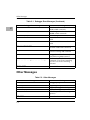
Introduction ............................................................................................................ C-1
Error Messages ....................................................................................................... C-1
Other Messages ...................................................................................................... C-2
APPENDIX D
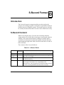
S-Record Format
Introduction ............................................................................................................D-1
S-Record Content ...................................................................................................D-1
S-Record Types .......................................................................................................D-2
Creating S-Records ................................................................................................D-4
Example...................................................................................................................D-4
APPENDIX E
Disk and Tape Controllers
Disk and Tape Support ..........................................................................................E-1
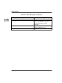
Floppy Drive ConÞguration Parameters.............................................................E-2
APPENDIX F
Disk Status Codes
Introduction .............................................................................................................F-1
SCSI....................................................................................................................F-1
ATA (Hard Disks/CD-ROM Drives) ............................................................F-2
ATAPI (CD-ROM Drives) ...............................................................................F-2
Controller-Independent Status Codes .................................................................F-3
SCSI Firmware Status Codes.................................................................................F-3
ATA/ATAPI Firmware Status Codes...................................................................F-6
APPENDIX G
Network Controller Devices
APPENDIX H
Network Communication Status Codes
Glossary
Abbreviations, Acronyms, and Terms to Know ............................................. GL-1
xiv
List of Tables
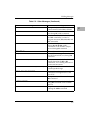
Table 1-1. LED/Serial Startup Diagnostic Codes ...............................................1-8
Table 3-1. Debugger Commands...........................................................................3-1
Table 5-1. System Call Routines -- Hex Code Order ..........................................5-2
Table 5-2. System Call Routines -- Alphabetical Order......................................5-4
Table 5-3. Disk Packet Parameters ......................................................................5-20
Table 5-4. IOSATM Fields (CFGA)......................................................................5-22
Table 5-5. IOSPRM Fields (CFGA) ......................................................................5-23
Table 5-6. IOSEPRM Fields (CFGA)....................................................................5-23
Table 5-7. IOSATW Fields (CFGA)......................................................................5-24
Table 5-8. CFGA Fields .........................................................................................5-25
Table A-1. Motorola Computer Group Documents ..................................................A-2
Table A-2. Microprocessor and Controller Documents............................................A-3
Table A-3. Related Specifications ............................................................................A-9
Table C-1. Debugger Error Messages.......................................................................C-1
Table C-2. Other Messages.......................................................................................C-2
Table D-1. S-Record Fields ......................................................................................D-1
Table E-1. Disk and Tape Controllers Supported ..................................................... E-1
Table E-2. Floppy Drive Configuration Parameters ................................................. E-2
Table F-1. Controller-Independent Status Codes...................................................... F-3
Table F-2. SCSI Firmware Status Codes .................................................................. F-4
Table F-3. ATA/ATAPI Controller-Dependent Errors............................................. F-7
Table H-1. Controller-Independent Status Codes .....................................................H-1
Table H-2. DEC21040/21140 Controller Status Codes ............................................H-2
xv
List of Figures
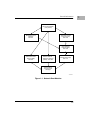
Figure 1-1. Network Boot Modules ....................................................................1-29
Figure 3-1. Boot Record ......................................................................................3-172
Figure 3-2. PowerPC Reference Platform Partition Table Entry...................3-173
Figure 3-3. Layout of the $41-Type Partition...................................................3-174
xvii
1General Information
1
PPCBug Overview
PPCBug is a powerful evaluation and debugging tool for systems
built around the Motorola PowerPC microprocessors. PPCBug
firmware consists of three parts:
❏
Command-driven user-interactive software debugger. It is
hereafter referred to as the debugger, which is described in this
manual. Debugging commands are available for loading and
executing user programs under complete operator control for
system evaluation.
❏
Command-driven diagnostic package for testing and
troubleshooting the PowerPC board, which is hereafter called
the diagnostics. Refer to the PPC1Bug Diagnostics Manual.for
information on the diagnostics and the diagnostics utilities
and self-tests.
❏
MPU, firmware, and hardware initialization routines, which
are described in this manual.
The PPCBug firmware is implemented on the following Motorola
PowerPC-based products:
❏
MVME230x VME Processor Modules
❏
MVME260x Single Board Computers
❏
MVME3604 VME Processor Modules
❏
MVME4604 VME Dual Processor Modules
❏
MTX Embedded ATX Motherboards
❏
MCP750 PowerPC Single Board Computers
A PMCspan board added to any of these also interfaces with PPCBug.
1-1
1
Comparison with other Motorola Bugs
They are collectively referred to in this manual as the PowerPC board
or board.
The debugger includes:
❏
Commands for display and modification of memory
❏
Breakpoint and tracing capabilities
❏
Assembler and disassembler useful for patching programs
Various PPCBug routines that handle I/O, data conversion, and
string functions are available to user programs through the System
Call handler.
Because PPCBug is command-driven, it performs its various
operations in response to user commands entered at the keyboard.
Comparison with other Motorola Bugs
The PPCBug is similar to previous Motorola firmware packages
(e.g., MVME147Bug, MVME167Bug, MVME187Bug), with
differences due to microprocessor architectures. These differences
are primarily reflected in the instruction mnemonics, register
displays, addressing modes of the assembler/disassembler, and
argument passing to the system calls.
PPCBug Implementation
PPCBug is written largely in the C programming language,
providing benefits of portability and maintainability. Where
necessary, the assembly language has been used in separately
compiled program modules that deal with processor-specific
issues. No mixed-language modules are used.
Physically, PPCBug is contained in two socketed 32-pin PLCC
Flash devices that together provide 1MB (256KB words) of storage.
PPCBug uses the entire memory contained in the two devices.
1-2
General Information
The executable code is checksummed at every power-on or reset
firmware entry. The result is checked with a pre-calculated
checksum contained in the last 16-bit word of the Flash image.
!
Caution
Although a command to allow the erasing and
reprogramming of this Flash memory is available to
you, keep in mind that reprogramming any portion of
Flash memory will erase everything currently contained
in Flash, including PPCBug.
Memory Requirements
The debugger requires approximately 768KB of read/write
memory (i.e., DRAM). The debugger will allocate this memory
from the top of memory. For example, on a system which contains
64MB ($04000000) of read/write memory, the debugger's memory
page will be located at $03F80000 to $03FFFFFF.
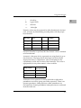
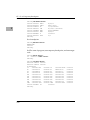
Size and Address Requirements for NVRAM
Currently, Motorola uses the SGS-Thompson Timekeeper SRAM
device (48T559), or equivalent. This is used on the PowerPlus
boards and is structured by the Debugger as follows:
NVRAM = 8192 bytes total size (with rtc)
Address ranges include:
Size/Area
5880 bytes user area
2048 bytes debugger area
256 bytes conÞguration area
8 bytes real time clock registers
Offset
0000 - 16f7
16f8 - 1ef7
1ef8 - 1ff7
1ff8 - 1fff
1-3
1
1
Set-up
Set-up
Refer to the board installation and use manual for information on
installing the hardware, configuring jumpers, and assigning the
console monitor.
Start-up
At either power-up or system reset, PPCBug performs the MPU,
hardware, and firmware initialization process (refer to MPU,
Hardware, and Firmware Initialization on page 1-5). This process
includes a checksum of the FLASH memory contents.
The following types of messages are displayed on the firmware
console during the initialization process:
Copyright Motorola Inc. 1988 - 1997, All Rights Reserved
PPC1 Debugger/Diagnostics Release Version 3.x - xx/xx/xx/RMxx
COLDStart
Local Memory Found =04000000 (&67108864)
MPU Clock Speed =167Mhz
BUS Clock Speed =67Mhz
Reset Vector Location : ROM Bank B
Mezzanine Configuration: Single-MPU
Current 60X-Bus Master : MPU0
Idle MPU(s)
: NONE
System Memory: 64MB, ECC Enabled (ECC-Memory Detected)
L2 Cache:
NONE
PPC1-Bug>
At this point, PPCBug is waiting for you to enter one of the
commands described in Chapter 3 of this manual.
PPCBug may alternatively be configured via the ENV command to
run selftest and/or autoboot automatically during startup. If so,
then PPCBug will instead behave as follows:
The system pauses five seconds, during which you may terminate
start-up, and exit to the diagnostics prompt, by pressing ESC or the
Break key.
1-4
General Information
The system performs the self test diagnostics if you do not
terminate system start-up. Upon successful completion of these
tests, the system pauses another five seconds. You may terminate
start-up, and exit to the diagnostics prompt, by pressing ESC or the
Break key.
If you do not terminate system start-up, the system begins the boot
routine that has been set up in the ENV command, either NVRAM
Boot List Boot, Auto Boot, ROMboot, or Network Auto Boot.
If the self-tests fail, various error messages appear, and the
diagnostics prompt appears.
Refer to Chapter 3 for information on setting the ENV command
parameters.
MPU, Hardware, and Firmware Initialization
The MPU, hardware, and firmware initialization process is
performed by the PPCBug power-up or system reset. The steps
below are a high-level outline; not all of the detailed steps are listed.
1. Set MPU.MSR to known value.
2. Invalidate the MPU's data/instruction caches.
3. Clear all segment registers of the MPU.
4. Clear all block address translation registers of the MPU.
5. For Òdual CPU onlyÓ boards (MVME460x or MTX), catch one
CPU of a dual CPU and place it in a waiting loop.
6. Initialize the MPU bus to PCI bus bridge device.
7. Initialize the PCI bus to ISA bus bridge device.
8. Calculate the external bus clock speed of the MPU.
9. Delay for 750 milliseconds.
10. Determine the CPU board type.
11. Size the local read/write memory (i.e., DRAM).
12. Initialize the read/write memory controller.
1-5
1
1
Start-up
13. Set base address of memory to $00000000.
14. Retrieve the speed of read/write memory from NVRAM.
15. Initialize read/write memory controller with the speed of
read/write memory.
16. Retrieve the speed of read only memory (i.e., FLASH) from
NVRAM.
17. Initialize read only memory controller with the speed of read
only memory.
18. Enable the MPU's instruction cache.
19. Copy the MPU's exception vector table from $FFF00000 to
$00000000.
20. Initialize the SIO (PC87303/PC87307/PC87308) resources'
base addresses for boards that have the SIO device.
21. Initialize the Z8536 device if the board has the device.
22. Verify MPU type.
23. Enable the super-scalar feature of the MPU (boards with
MPC604-type chips only).
24. Initialize the Keyboard Controller
(PC87303/PC87307/PC87308) for boards that have the
device.
25. Determine the debugger's Console/Host ports, and initialize
the appropriate UART and Graphic devices.
26. Display the debugger's copyright message.
27. Display any hardware initialization errors that may have
occurred.
28. Checksum the debugger object, and display a warning
message if the checksum failed to verify.
29. Display the amount of local read/write memory found.
1-6
General Information
30. Verify the configuration data that is resident in NVRAM,
and display a warning message if the verification failed.
31. Calculate and display the MPU clock speed. Verify that the
MPU clock speed matches the configuration data, and
display a warning message if the verification fails.
32. Display the BUS clock speed. Verify that the BUS clock speed
matches the configuration data, and display a warning
message if the verification fails.
33. For boards that have a Keyboard Controller display
initialization errors that have occurred.
34. Probe PCI bus for supported Network devices.
35. Probe PCI bus for supported Mass Storage devices.
36. Initialize the memory/IO addresses for the supported PCI
bus devices.
37. Execute self-test, if configured.
38. Extinguish the board fail LED, if there are no self-test failures
or initialization/configuration errors.
39. Execute the configured boot routine, either ROMboot,
Autoboot, or Network Autoboot. (PowerPlus architecture
boards do not execute a conÞgured boot routine.)
40. Execute the user interface (i.e., the PPC1-Bug> or
PPC1-Diag> prompt).
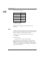
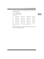
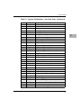
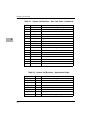
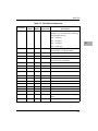
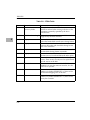
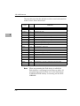
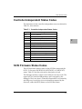
LED/Serial Startup Diagnostic Codes
These codes are displayed on seven-segment LEDs at key points in
the initialization of the hardware devices. Should the debugger fail
to come up to a prompt, the last code displayed will indicate how
far the initialization sequence had progressed before stalling. The
serial port version of the startup codes is enabled by an ENV
parameter:
Serial Startup Code Master Enable [Y/N]=N?
1-7
1
1
Start-up
Under normal conditions, the startup sequence begins at 0x1100
and continues to the PPC1-Bug> prompt just after 0x11D4. RAM
initialization problems may cause the startup sequence to terminate
at the : (RawBug) prompt just after 0x11D8 instead.
The operating system boot sequence begins at 0x11E0 with the
creation of residual data and continues to 0x11EC just before
execution is passed to the boot image. The OS may have its own
LED codes which are displayed after 0x11EC.
A line feed can be inserted after each serial code is displayed to
prevent it from being overwritten by the next code. This is also
enabled by an ENV parameter:
Serial Startup Code LF Enable [Y/N]=N?
The following firmware codes are always sent to 7-segment LEDs
located at ISA I/O address 0x8C0. These codes can also be sent to
the debugger serial port if the ENV parameter ÒSerial Startup Code
Master EnableÓ is set to ÔYÕ. The list of LED/serial codes follows.
Table 1-1. LED/Serial Startup Diagnostic Codes
Code (Hex)
1100
1102
1104
1106
1108
110A
110C
110E
1110
1112
1114
1116
1118
111A
1-8
Location in Startup
Setting up MSR (startup begins)
Invalidating caches
Determining ROM or RAM execution mode
Setting up machine state register
Setting up CPUÕs address translation registers
Setting up CPUÕs address translation table
Shutting down redundant processors
Initializing super I/O chip (CPU initialization completed)
Initializing raw I/O device
Getting PHB (PCI Host Bridge) Table Pointer
Initializing PCI bridge
Initializing the powerup ßag indicator
Calculating the speed of the processor bus
Waiting for hardware to initialize memory
General Information
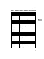
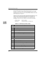
Table 1-1. LED/Serial Startup Diagnostic Codes (Continued)
Code (Hex)
111C
111E
1120
1122
1124
1126
1128
112A
112C
Location in Startup
Setting up the DRAM init parameters
Initializing DRAM in bridge/memory controller
Setting up debugger memory page area
Calculating and setting DRAM speed
Calculating and setting ROM speed
Enabling instruction cache
Setting up debugger memory page tables
Setting up debugger kernel pointers and saving registers
Setting up buginit section pointers and runtime variables
1130
1132
1134
1136
1138
113A
113C
113E
1140
1142
1144
1146
1148
Retrieving the processor board type
Initializing the Z8536
Initializing local board status
Retrieving the base board type
Checking the level of the ABORT push-button
Initializing the interrupt/timer controller
Retrieving MPU identiÞer
Enabling super-scalar modes
Adding processor-speciÞc work-arounds
Getting the bus clock speed
Initializing the keyboard controller
Initializing the PCI interrupt route control registers
Starting PCI hierarchy conÞguration process
12nn
Probing PCI conÞg space (nn = bbbddddd; bbb = bus#,
ddddd = dev#
Allocating PCI I/O & memory space and initializing PCI
devices.
1149
114A
114C
Initializing RAVEN PCI space
Initializing RAVEN time base registers
1-9
1
1
Start-up
Table 1-1. LED/Serial Startup Diagnostic Codes (Continued)
Code (Hex)
114E
1150
1152
1154
1160
1162
1164
1166
1168
116A
116C
116E
1170
1172
1174
1176
1178
117A
117C
117E
1180
1182
1184
1186
1188
118A
118C
118E
1190
1192
1-10
Location in Startup
Initializing FALCON ROM
Initializing VME bridge
Initializing ISA bridge
Sending speaker beep
Checking abort switch state
Initializing exception handling
Initializing board identiÞer structure
Initializing point break table
Initializing macro subsystem
Initializing conÞguration data area
Initializing board information data area
Initializing I/O (character) subsystem
Initializing register Þle
Getting bridge pointer
Setting up local memory pointers
Setting up local memory size variables
Displaying sign-on messages
displaying board initialization errors
Verifying the ROM checksum
Displaying memory size and misc errors
Displaying MPU clock speed
Verifying MPU clock speed
Displaying bus clock speed
Initializing network I/O subsystem
Initializing disk I/O subsystem
Initializing direction ßags
Initializing NVRAM (PReP) environment
Initializing residual data pointer
Initializing input/output pointers
Initializing diagnostic subsystem
General Information
Table 1-1. LED/Serial Startup Diagnostic Codes (Continued)
Code (Hex)
1194
1196
1198
Location in Startup
Setting up special init section pointers and runtime variables
Initializing abort switch
Setting up board sufÞx and return environment
11A0
11A2
11A4
11A6
11A8
11AA
11AC
11AE
11B0
11B2
11B4
11B6
11B8
11BA
11BC
11BE
Retrieving the processor board type
Displaying memory warning and MPU conÞguration
Clearing MPU idle semaphores
Waiting for MPU logins
Displaying MPU status information
Setting up DRAM and bridge pointers
Initializing DRAM ECC/parity
Displaying DRAM information
Setting up misc. L2 cache variables
Setting up L2 cache size variables
Initializing and ßushing L2 cache data parity
Displaying L2 cache parity state
Reading NVRAM contents
Verifying NVRAM header
Initializing NVRAM contents
Retrieving global environment variable pointers
11D0
11D2
11D4
11D8
Initializing processor timebase/decrementer registers
Enabling interrupts
Transferring control to monitor (initialization complete)
Error - dropping to RawBug
11E0
11E2
11E4
11E6
11E8
Initializing residual data structure
Adding vital product data
Adding processor information
Adding memory information
Adding PCI device information
1-11
1
1
Running the Diagnostics and Debugger
Table 1-1. LED/Serial Startup Diagnostic Codes (Continued)
Code (Hex)
11EA
11EC
Location in Startup
Adding ISA device information
Residual data completed
12nn
Probing PCI conÞg space (board speciÞc)
Running the Diagnostics and Debugger
In order to use the diagnostics, terminate the start-up process by
pressing ESC or the Break key during one of the four pauses
(PowerPlus architecture boards in their default configuration may
not pause at any of the four places.) The diagnostics prompt
(PPC1-Diag>) appears. You may switch to the debugger prompt
(PPC1-Bug>) by using the SD command.
Both the debugger and diagnostic commands are available from the
diagnostic prompt. Only the debugger commands are available
from the debugger prompt.
You may view a list of the diagnostics or debugger commands by
using the HE (Help) command.
Note
Some diagnostics depend on restart defaults that are
set up only in a particular restart mode. Refer to the
PPCBug Diagnostics Manual, PPCDIAA/UM, for the
correct mode.
Refer to the PPCBug Diagnostics Manual for complete descriptions
of the diagnostic routines available and instructions on how to
invoke them.
1-12
General Information
Auto Boot
Note
The PowerPlus architecture boards do not execute a
configured boot routine.
Auto Boot is the default boot routine. It provides an independent
mechanism for booting an operating system. No console is
required. Autoboot selects the boot device from either a scan list of
device types, a floppy diskette, a CD-ROM, tape, or a hard disk.
You may change the scan order, or configure Auto Boot to boot
from a specific Controller Logical Unit Number (CLUN) and
Device Logical Unit Number (DLUN) by changing the ENV
command parameters for enabling Auto Boot (refer to Chapter 3 for
information).
At power-up, Auto Boot is enabled. The following message is
displayed on the system console:
Autoboot in progress... To abort hit <BREAK>
Following this message there is a delay to allow you to abort the
Auto Boot process and gain control. Press either the BREAK key or
the software abort or reset switch to abort Autoboot.
If you do not abort Auto Boot, the actual I/O is begun. The program
pointed to within the boot-record of the media specified is loaded
into RAM, and control is passed to it.
Upon power-up or system reset, PPCBug examines the validity of
the configuration parameters in NVRAM. If there is a configuration
error (e.g., corrupted data or checksum error), the PPCBug will
initialize the configuration parameters with the default values, and
run AutoBoot. Following the auto-initialization of the
configuration parameters, the PPCBug will reset the system to
allow a start-up with the now default configuration parameters.
1-13
1
1
ROMboot
ROMboot
Note
The PowerPlus architecture boards do not execute a
configured boot routine.
ROMboot is a mechanism for booting an operating system from a
user-defined routine stored in ROM. ROMboot executes at powerup (or optionally at reset) if it is configured and enabled in
parameters set with the ENV command. It may also be executed
with the RB (ROMboot) command.
Refer to Chapter 3 for information on setting the ENV command
parameters for enabling ROMboot.
For ROMboot to work, a ROMboot routine must be stored in the
FLASH memory to support it. If ROMboot code is installed, a userwritten routine is given control (if the routine meets the format
requirements). One use of ROMboot might be resetting SYSFAIL*
on an unintelligent controller board.
The NORB command disables ROMboot.
For a user's ROMboot routine to gain control through the ROMboot
linkage, four requirements must be met:
❏
Power must have just been applied (or at reset, if configured
to do so with the ENV command).
❏
Your ROMboot routine must be stored within the PowerPC
board FLASH memory map (or elsewhere in onboard
memory, if configured to do so with the ENV command).
❏
The ASCII string ÒBOOTÓ must be located within the
specified memory range.
❏
Your ROMboot routine must pass a checksum test, which
ensures that this routine was really intended to receive
control at power-up.
When the module is ready it can be loaded into RAM. Use the CS
command to generate, install, and verify the checksum.
1-14
General Information
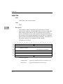
The format of the beginning of the routine is:
Offset
Length
Contents
Description
$00
4 bytes
BOOT
ASCII string indicating possible
routine; the checksum must be
valid
$04
4 bytes
Entry Address
Word offset from ÒBOOTÓ
$08
4 bytes
Routine Length
Word; includes length from
ÒBOOTÓ to and including a twobyte checksum
$0C
Length Routine name
of name
ASCII string containing routine
name
If you want to make use of ROMboot, you do not have to fill a
complete FLASH device. Any partial amount is acceptable, as long
as:
❏
The identifier string ÒBOOTÓ starts on a word (FLASH and
Direct spaces) or 8KB (local RAM and VMEbus spaces)
boundary.
❏
The ROMboot routine size (in bytes) is evenly divisible by 2.
❏
The length parameter (offset $8) reflects where the checksum
is, and the checksum is correct.
ROMboot searches predefined areas of the memory map for
possible routines and checks for the ÒBOOTÓ indicator. Two events
are of interest for any location being tested:
❏
The map is searched for the ASCII string ÒBOOTÓ.
❏
If the ASCII string ÒBOOTÓ is found, it is still undetermined
whether the routine is meant to gain control at power-up or
reset. To verify that this is the case, the bytes starting from
ÒBOOTÓ through the end of the routine, excluding the two
byte checksum, are run through the debugger checksum
algorithm. If the result of the checksum is equal to the final
two bytes of the ROMboot routine (the checksum), it is
1-15
1
1
ROMboot
established that the routine was meant to be used for
ROMboot.
Under control of the ENV command, the sequence of searches is as
follows:
1. Search direct address for ÒBOOTÓ. The direct address points
to an installed ROMboot routine. It is a variable that may be
set using the ENV command.
2. Search complete ROM map.
3. Search local RAM, at all 8KB boundaries starting at the
beginning of local RAM.
4. Search the VMEbus map (if so selected by the ENV
command) on all 8KB boundaries starting at the end of the
onboard RAM. VMEbus address space is searched both
below (if the start address of local RAM is not located at 0)
and above local RAM up to the beginning of FLASH Space.
Sample ROMboot Routine
The example ROMboot routine performs the following:
1-16
❏
Outputs a <CR> <LF> sequence to the default output port.
❏
Displays the date and time from the current cursor position.
❏
Outputs two more <CR> <LF> sequences to the default
output port.
❏
Returns control to PPCBug.
General Information
Do the following to prepare the ROMboot routine (includes
checksum calculation):
1. Assemble and link the code, leaving $00 in the even and odd
locations destined to contain the checksum.
2. Load the routine into RAM (with S-records via the LO
command, or from magnetic media using IOP).
3. Display entire ROMboot routine (checksum bytes are at
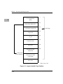
$00010038 and $00010039).
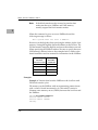
PPC1-Bug>MD 10000 :10 <Return>
00010000
00010010
00010020
00010030
424F4F54
39400026
39400026
39400063
00000010
44000002
44000002
44000002
0000003A
39400052
39400026
0000FFFF
54455354
44000002
44000002
FFFFFFFF
BOOT.......:TEST
9@.&[email protected]...
9@.&D...9@.&D...
[email protected]...........
4. Disassemble executable instructions.
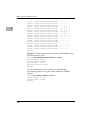
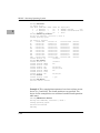
PPC1-Bug>MD 10010:5;DI <Return>
00010010 39400026 SYSCALL
.PCRLF
00010018 39400052 SYSCALL
.RTC_DSP
00010020 39400026 SYSCALL
.PCRLF
00010028 39400026 SYSCALL
.PCRLF
00010028 39400063 SYSCALL
.RETURN
5. Perform checksum on locations $10000 through $10037 (refer
to CS command in chapter 3).
PPC1-Bug>CS 10000:38/2;H <Return>
Effective address: 00010000
Effective count : &56
Checksum: ACFA
6. Insert checksum into bytes $10038, $10039.
PPC1-Bug>M 10038;H <Return>
00010038 0000? ACFA. <Return>
7. Display the entire ROMboot routine with checksums.
PPC1-Bug>MD 10000 :10 <Return>
00010000 424F4F54 00000010 0000003A
00010010 39400026 44000002 39400026
00010020 39400026 44000002 39400026
00010030 39400063 44000002 ACFAFFFF
54455354
44000002
44000002
FFFFFFFF
BOOT.......:TEST
9@.&[email protected]...
9@.&D...9@.&D...
[email protected]...........
1-17
1
1
Network Auto Boot
8. Verify the functionality of the user ROMboot routine with the
RB command.
PPC1-Bug>RB; V <Return>
ROMboot about to Begin... Press <ESC> to Bypass, <SPC> to Continue
Direct Add: FFC00000 FFFFFFFC: Searching for ROMboot Module at: 00010000
Executing ROMboot Module “TEST” at 00010000
MON MAR 27 10:39:08.00 1995
PPC1-Bug>
The sample ROMboot routine is now ready for use.
Network Auto Boot
Network Auto Boot (or Network Boot) is a software routine that
provides a mechanism for booting an operating system using an
Ethernet network as the boot device.
Network Auto Boot executes at power-up (or optionally at reset) if
it is configured and enabled in parameters set with the ENV
command.
This routine selects the boot device based on from the Controller
Logical Unit Number (CLUN) and Device Logical Unit Number
(DLUN) which have been set in the ENV command.
Refer to Chapter 3 for information on setting the ENV command
parameters for enabling Network Auto Boot.
If Network Boot is enabled, the following message is displayed on
the system console at power-up:
Network Boot in progress... To abort hit <BREAK>
Following this message there is approximately a five-second delay
before the actual I/O is begun. The program pointed to within the
volume ID of the media specified is loaded into RAM and control is
passed to it.
1-18
General Information
During the delay, you can gain control without Network Autoboot
by pressing either the BREAK key or the software abort or reset
switches.
Network Autoboot is controlled by parameters contained in the
NIOT and ENV commands. These parameters allow the selection
of specific boot devices, systems, and files and allow programming
of the boot delay. Refer to the NIOT and ENV commands in
Chapter 3 for more details.
Restarting the System
You can initialize the system to a known state in three different
ways: reset, abort, and break. Each has characteristics which make
it more appropriate than the others in certain situations.
Reset
Pressing and releasing the board front panel RESET switch initiates
a system reset. Cold and warm reset modes are available. By
default, PPCBug is in cold mode (refer to the RESET command
description in Chapter 3). During cold reset, a total system
initialization takes place, as if the PowerPC board had just been
powered up. All static variables are restored to their default states.
The breakpoint table and offset registers are cleared. The target
registers are invalidated. Input and output character queues are
cleared. Onboard devices are reset, and the first two serial ports are
reconfigured to their default state.
During warm reset, the PPCBug variables and tables are preserved,
as well as the target state registers and breakpoints.
Reset must be used if the processor ever halts, or if the PPCBug
environment is ever lost, such as if the vector table is destroyed, or
the stack is corrupted.
1-19
1
1
Restarting the System
Abort
Abort is invoked by pressing and releasing the ABORT switch.
Whenever abort is invoked while executing a user program
(running target code), a snapshot of the processor state is captured
and stored in the target registers. (When working in the debugger,
abort captures and stores only the Instruction Pointer, status
register, and format and vector information.) For this reason, abort
is most appropriate when terminating a user program that is being
debugged. Abort should be used to regain control if the program
gets caught in a loop. The target IP and register contents help to
pinpoint the malfunction.
Pressing and releasing the ABORT switch generates a local board
condition which interrupts the microprocessor. The target registers,
reflecting the machine state at the time the abort switch was
pressed, are displayed on the screen. Any breakpoints installed in
the user code are removed, and the breakpoint table remains intact.
Control is returned to the debugger.
Note
1-20
You may wish to perform Òdouble-button resetÓ by
pressing the RESET and ABORT switches at the same
time. Release RESET first, wait seven seconds, and then
release ABORT. This resets all onboard devices, as well
as sending a SYSRESET* signal if the board is the
VMEbus system controller. It also ignores the
parameters stored in NVRAM, and starts debugger
execution with the same ENV parameters as if you had
used the command ENV;D.
General Information
Break
A break is generated by pressing and releasing the BREAK key on
the current-console keyboard. Break does not generate an interrupt.
The only time break is recognized is when characters are sent or
received by the console port. Break removes any breakpoints in the
user code and keeps the breakpoint table intact. Break also takes a
snapshot of the machine state if the function was entered using
SYSCALL. This machine state is then accessible to you for
diagnostic purposes.
Many times it may be desirable to terminate a debugger command
prior to its completion; for example, the display of a large block of
memory. Break allows you to terminate the command.
Board Failure
The following conditions result in a board failure. These conditions
also give a WARNING message, if possible:
❏
Board initialization error/failure
❏
Debugger object checksum error
❏
Configuration data (NVRAM ENV parameters) failure (i.e.,
checksum)
❏
Configuration data (NVRAM CNFG parameters) failure (i.e.,
checksum)
❏
Calculated MPU clock speed does not match the associative
CNFG parameter
❏
Calculated BUS clock speed does not match the associative
CNFG parameter
❏
Selftest error/failure
If the board is equipped with a board fail LED, the LED will be
illuminated when a board failure occurs.
1-21
1
1
Restarting the System
SYSFAIL* Assertion and Negation (MVME230x, MVME260x, MVME360x, and
MVME460x)
On VMEbus boards, the board fail is the same as the SYSFAIL
indicator. At reset or power-up, the debugger asserts the VMEbus
SYSFAIL* line (refer to the VMEbus specification).
The SYSFAIL* line is negated if debugger initialization is done and
if none of the board failure conditions have occurred. However,
SYSFAIL* stays asserted if any of the board failure conditions have
occurred. In this way, the state of the debugger is indicated to the
user or VMEbus masters. In a multi-computer configuration, other
VMEbus masters could view the pertinent control and status
registers to determine which CPU is asserting SYSFAIL* in the
event of a board failure.
SYSFAIL* assertion and negation is also affected by the ENV
command (refer to the ENV command in Chapter 3).
Notes Assert indicates a signal is active or true. Negate
indicates a signal is inactive or false. These terms are
used independently of the voltage levels (high or low)
that they represent.
The asterisk (*) in the signal name SYSFAIL* denotes
that the signal is true or valid when the it is low
(SYSFAIL* is level sensitive).
MPU Clock Speed Calculation
The MPU clock speed is calculated and checked against the MPU
clock speed parameter located in NVRAM, which you may set in
the CNFG command. If the check fails, a warning message is
displayed. The calculated clock speed is also checked against
known clock speeds and tolerances.
Refer to Chapter 3 for information on setting the CNFG command
parameters.
1-22
General Information
Disk I/O Support
The debugger can initiate disk input and output by communicating
with intelligent disk controllers over the PCI bus. Disk support
facilities built into the debugger consist of command-level disk
operations, disk I/O system calls (only via one of the system call
instructions) for use by user programs, and defined data structures
for disk parameters (refer to Chapter 5 for information on system
calls).
Parameters such as the address where the module is mapped and
the type and number of devices attached to the controller module
are kept in tables by PPCBug. Default values for these parameters
are assigned at power-up and cold-start reset, but may be altered as
described in Default PPCBug Controller and Device Parameters on
page 1-27.
You can obtain a list of supported controllers with the IOI
command. Appendix E contains a list of the controllers presently
supported, as well as a list of the default configurations for each
controller.
Blocks and Sectors
The logical block defines the unit of information for disk devices. A
disk is viewed by PPCBug as a storage area divided into logical
blocks. By default, the logical block size is set to 256 bytes for every
block device in the system. The block size can be changed on a per
device basis with the IOT command.
The sector defines the unit of information for the media itself, as
viewed by the controller. The sector size varies for different
controllers, and the value for a specific device can be displayed and
changed with the IOT command.
When a disk transfer is requested, the start and size of the transfer
is specified in blocks. PPCBug translates this into an equivalent
sector specification, which is then passed on to the controller to
1-23
1
1
Disk I/O Support
initiate the transfer. If the conversion from blocks to sectors yields
a fractional sector count, an error is returned and no data is
transferred.
Device Probe
A device probe with entry into the device descriptor table is done
whenever a specified device is accessed. This happens when system
calls .DSKRD, .DSKWR, .DSKCFIG, .DSKFMT, and .DSKCTRL,
and commands IOC, IOP, IOT, MAR, MAW, and PBOOT are
used.
The device probe mechanism utilizes the SCSI commands Inquiry
and Mode Sense. If the specified controller is non-SCSI, the probe
simply returns a status of device present and unknown. The device
probe makes an entry into the device descriptor table with the
pertinent data. After an entry has been made, the next time a probe
is done it simply returns with device present status (pointer to
the device descriptor).
Disk I/O via Debugger Commands
The following debugger commands are provided for disk I/O.
Refer to Chapter 3 for instructions for their use. When a command
is issued to a particular controller LUN and device LUN, these
LUNs are remembered in the debugger so that the next disk
command uses the same controller and device.
IOI (Input/Output Inquiry)
The IOI command is used to probe the system for all possible
CLUN/DLUN combinations and display inquiry data for devices
which support it. The device descriptor table only has space for 16
device descriptors. With the IOI command, you can view the table
and clear it if necessary.
1-24
General Information
IOP (Physical I/O to Disk)
!
Caution
If you start the IOP format procedure, it must be
allowed to complete (PPC1Bug> prompt returns) or else
the disk drive may be totally disabled. This format
procedure may take as long as half an hour.
The IOP command allows you to read or write blocks of data, or to
format the specified device in a certain way. IOP creates a
command packet from the arguments you specify, and then
invokes the proper system call function to carry out the operation.
IOT (I/O Configure)
The IOT command allows you to change any configurable
parameters and attributes of the device. In addition, it allows you
to see the controllers available in the system.
IOC (I/O Control)
The IOC command allows you to send command packets as
defined by the particular controller directly. IOC can also be used
to look at the resultant device packet after using the IOP command.
PBOOT (Bootstrap Operating System)
The PBOOT command reads an operating system or control
program from the specified device into memory, and then transfers
control to it.
With the H option, PBOOT reads an operating system or control
program from a specified device into memory, and then returns
control to the debugger.
1-25
1
1
Disk I/O Support
Disk I/O via Debugger System Calls
All operations that actually access the disk are done directly or
indirectly by debugger system calls. (The command-level disk
operations provide a convenient way of using these system calls
without writing and executing a program.)
The following system calls are provided to allow user programs to
do disk I/O:
.DSKRD
.DSKWR
.DSKCFIG
.DSKFMT
.DSKCTRL
Disk read - system call to read blocks from a disk into
memory
Disk write - system call to write blocks from memory
onto a disk
Disk conÞgure - system call to change the
conÞguration of the speciÞed device
Disk format - system call to send a format command
to the speciÞed device
Disk control - system call to implement any special
device control functions that cannot be
accommodated easily with any of the other disk
functions
Refer to Chapter 5 for information on using these and other system
calls.
To perform a disk operation, the debugger must present a
particular disk controller module with a controller command
packet which has been prepared for the particular type of controller
module. (This is accomplished in the respective controller driver
module.) Typically, the command packets are different for each of
the controller modules. The system call facilities which do disk I/O
accept a generalized (controller-independent) packet format as an
argument, and translate it into a controller-specific packet, which is
then sent to the specified device. Refer to the system call
descriptions in Chapter 5 for details on the format and construction
of these standardized user packets.
1-26
General Information
The packets which a controller module expects to receive vary from
controller to controller. The disk driver module for the particular
board module must take the standardized packet given to a trap
function and create a new packet which is specifically tailored for
the disk drive controller it is sent to. Refer to documentation on the
particular controller module for the format of its packets. Refer to
the IOC command in Chapter 3 for sending command packets.
Default PPCBug Controller and Device Parameters
PPCBug initializes the parameter tables for a default configuration
of controllers (refer to Appendix E). If the system needs to be
configured differently than this default configuration (for example,
to use a different drive), then these tables must be changed.
Use the IOT command to reconfigure the parameter table manually
for any controller and/or device that is different from the default.
This is a temporary change and is overwritten if a cold-start reset
occurs.
Disk I/O Error Codes
PPCBug returns an error code if an attempted disk operation is
unsuccessful. Refer to Appendix F for an explanation of disk I/O
error codes.
1-27
1
1
Network I/O Support
Network I/O Support
The network autoboot firmware provides the capability to boot the
CPU through the ROM debugger using a network (local Ethernet
interface) as the boot device.
The booting process is executed in two distinct phases.
❏
The first phase allows the diskless remote node to discover its
network identify and the name of the file to be booted.
❏
The second phase has the diskless remote node reading the
boot file across the network into its memory.
Figure 1-1 depicts the various modules (capabilities) and the
dependencies of these modules that support the overall network
boot function. They are described in the following paragraphs.
Physical Layer Manager Ethernet Driver
This driver surrounds and manages the Ethernet controller chip or
module. Management includes the reception of packets, the
transmission of packets, flushing of the receive buffer, and interface
initialization.
This module ensures that the packaging and unpackaging of
Ethernet packets is done correctly in the Boot PROM.
UDP and IP Modules
The Internet Protocol (IP) is designed for use in interconnected
systems of packet-switched computer communication networks.
The Internet Protocol provides for transmitting blocks of data
called datagrams (hence User Datagram Protocol, or UDP) from
sources to destinations, where sources and destinations are hosts
identified by fixed length addresses.
The UDP and IP protocols are necessary for the TFTP and BOOTP
protocols; TFTP and BOOTP require a UDP/IP connection.
1-28
General Information
Boot Control Module
(Two phases)
Bootstrap Protocol
(BOOTP)
RFC 951
Trivial File Transfer
Protocol (TFTP)
RFC 783
User Datagram
Protocol (UDP)
RFC 768
Address Resolution
Protocol (ARP)
RFC 826
Reverse Address
Resolution Protocol
(RARP) - RFC 903
Internet Protocol (IP)
RFC 791
Ethernet Driver
Physical Layer
Manager
1273 9401
Figure 1-1. Network Boot Modules
1-29
1
1
Network I/O Support
RARP and ARP Modules
The Reverse Address Resolution Protocol (RARP) basically consists
of an identity-less node that broadcasts a ÒwhoamiÓ packet onto the
Ethernet and waits for an answer. The RARP server fills an Ethernet
reply packet up with the target's Internet Address and sends it.
The Address Resolution Protocol (ARP) basically provides a
method of converting protocol addresses (e.g., IP addresses) to
local area network addresses (e.g., Ethernet addresses). The RARP
protocol module supports systems which do not support the
BOOTP protocol (refer to BOOTP Module below).
BOOTP Module
The Bootstrap Protocol (BOOTP) basically allows a diskless client
machine to discover its own IP address, the address of a server host,
and the name of a file to be loaded into memory and executed.
TFTP Module
The Trivial File Transfer Protocol (TFTP) is a simple protocol to
transfer files. It is implemented on top of the Internet User
Datagram Protocol (UDP or Datagram) so it may be used to move
files between machines on different networks implementing UDP.
The only thing it can do is read and write files from/to a remote
server.
Network Boot Control Module
The control capability of the Network Boot Control Module is
needed to tie together all the necessary modules (capabilities) and
to sequence the booting process. The booting sequence consists of
two phases. The first is address determination and bootfile
selection, and the second is file transfer. The first phase utilizes the
RARP/BOOTP capability and the second phase utilizes the TFTP
capability.
1-30
General Information
Network I/O Error Codes
PPCBug returns an error code if an attempted network operation is
unsuccessful. Refer to Appendix H for an explanation of network
I/O error codes.
Multiprocessor Support (Remote Start)
The PowerPC board dual-port RAM feature makes the shared
RAM available to remote processors as well as to the local
processor. This can be done by the following method. This method
can be enabled/disabled by the ENV command as its Remote Start
Switch method.
Note
PPCBug runs in single processor operation only.
Refer to Chapter 3 for information on setting the ENV command
parameters.
Multiprocessor Control Register (MPCR) Method
A remote processor can initiate program execution in the local
PowerPC board dual-port RAM by issuing a remote GO command
using the Multiprocessor Control Register (MPCR). MPCR contains
one of two words used to control communication between
processors. The location of MPCR is calculated as local RAM size
minus $1C000. The MPCR contents are organized as follows:
*
N/A N/A N/A (MPCR)
The status codes stored in the MPCR are of two types:
❏
Status returned (from the monitor)
❏
Status set (by the bus master)
The status codes that may be returned from the monitor are:
NUL ($00) Wait; the initialization is not yet complete
E ($45)
Code pointed to by the MPAR address is executing
1-31
1
1
Multiprocessor Support (Remote Start)
P ($50)
Program FLASH Memory. The MPAR is set to the
address of the FLASH memory program control packet.
Ready; the Þrmware monitor is watching for a change
R ($52)
Code P is used only by the MVME260x, MVME360x, MVME460x, and
MVME230x boards. You can only program FLASH memory by the MPCR
method. See the .PFLASH system call for a description of the FLASH
memory program control packet structure.
The status codes that may be set by the bus master are:
G ($47)
Initiate code at the MPAR address in a manner similar
to the GD command.
Initiate code at the MPAR address, with breakpoints
enabled, in a manner similar to the GO command.
Query: Request for residual data, build it, and return its
address in the MPAR.
Start: Build residual data, then start code execution. The
execution address is expected in the MPAR, (as with the
GO command). Residual data is built and its address is
loaded into r3 before execution begins.
B ($42)
Q ($51)
S ($53)
The Multiprocessor Address Register (MPAR) contains the second
of two words used to control communication between processors.
The MPAR contents specify the address at which execution for the
remote processor is to begin if the MPCR contains a G or B. The
location of MPAR is calculated as MPCR plus 4. The MPAR is
organized as follows:
*
*
*
*
(MPAR)
At power-up, the PPCBug self-test routines initialize RAM,
including the memory locations used for multi-processor support
(MPCR and MPAR).
The MPCR contains $00 at power-up, indicating that initialization
is not yet complete. As the initialization proceeds, the execution
path comes to the routine that displays the prompt. Before sending
the prompt, this routine places an R in the MPCR to indicate that
initialization is complete. Then the prompt is sent.
1-32
General Information
If no terminal is connected to the port, the MPCR is still polled to
see whether an external processor requires control to be passed to
the dual-port RAM. If a terminal does respond, the MPCR is polled
for the same purpose while the serial port is being polled for user
input.
A G placed in the MPCR by a remote processor indicates that the Go
Direct type of transfer is requested (as with the GD command). A B
in the MPCR indicates that breakpoints are to be armed before
control is transferred (as with the GO command).
In either sequence, an E is placed in the MPCR to indicate that
execution is underway just before control is passed to RAM. (Any
remote processor could examine the MPCR contents.)
If the code being executed in dual-port RAM is to re-enter PPCBug,
a system call using function $0063 (SYSCALL .RETURN) returns
control to PPCBug with a new display prompt. Note that every time
PPCBug returns to the prompt, an R is moved into the MPCR to
indicate that control can be transferred once again to a specified
RAM location.
Data and Address Sizes
Data and address sizes are defined as follows:
A byte is eight bits, numbered 0 through 7, with bit 0 being the least
significant.
A half-word is 16 bits, numbered 0 through 15, with bit 0 being the
least significant.
A word is 32 bits, numbered 0 through 31, with bit 0 being the least
significant.
1-33
1
1
Byte Ordering
Byte Ordering
The MPU on the PowerPC board is programmed to big-endian byte
ordering. Any attempt to use little-endian byte ordering will
immediately render the debugger unusable.
1-34
2Using the Debugger
2
Entering Commands
The debugger is command-driven and performs its various
operations in response to commands that you enter at the
keyboard. When the PPC1-Bug> prompt appears on the screen, the
debugger is ready to accept commands.
What you enter is stored in an internal buffer. Execution begins
only after you press the Return key, allowing you to correct entry
errors, if necessary, using the control characters (refer to Control
Characters on page 2-7). After the debugger executes the command,
the prompt reappears.
However, if the command causes execution of target code (for
example GO) then control may or may not return to the debugger,
depending on what the program does. For example, if a breakpoint
has been specified, then control returns to the debugger when the
breakpoint is encountered during execution of the user program.
For more about this, refer to the GD, GO, and GT command
descriptions in Chapter 3.
Alternately, the user program could return to the debugger by
means of the System Call Handler routine .RETURN (refer to
Chapter 5).
Command Syntax
A debugger command is made up of the following parts:
❏
The command name
❏
Any required arguments, delineated with either a space or
comma (precede the first argument with a space)
2-1
Entering Commands
❏
2
Any required options. Precede an option or a string of
options with a semi-colon (;). If no option is selected, the
default options are used.
Command entry is either uppercase or lowercase.
Command Arguments
The following arguments are common to many of the commands.
Additional arguments are defined in the description of the
particular command in which they occur.
EXP
Expression (refer to EXP below)
ADDR
Address (refer to ADDR on page 2-4)
COUNT
Count; this is a numeric expression and has the same
syntax as EXP (refer to EXP below)
RANGE
A range of memory addresses speciÞed with a pair of
arguments, either ADDR ADDR or ADDR : COUNT
TEXT
An ASCII string of up to 255 characters, delimited at
each end by the single quote mark (')
PORT
Port Number (refer to PORT on page 2-6)
Use either a space or a comma as a delimiter between arguments.
You may select the default value for an argument by inserting a pair
of commas in place of the argument.
EXP
The EXP (expression) argument can be one or more numeric values
separated by the arithmetic operators:
2-2
+
plus
-
minus
*
multiply by
Using the Debugger
/
divide by
&
logical AND
<<
shift left
>>
shift right
2
Numeric values may be expressed in either hexadecimal, decimal,
octal, or binary by immediately preceding them with the proper
base identifier.
Data Type
IdentiÞe
r
Base
Example
Integer
Hexadecimal
$
$FFFFFFFF
Integer
Decimal
&
&1974, &10-&4
Integer
Octal
@
@456
Integer
Binary
%
%1000110
If no base identifier is specified, then the numeric value is assumed
to be hexadecimal.
A numeric value may also be expressed as a string literal of up to
four characters. The string literal must begin and end with the
single quote mark ('). The numeric value is interpreted as the
concatenation of the ASCII values of the characters. This value is
right-justified, as any other numeric value would be.
String Literal
Numeric Value
(Hexadecimal)
'A'
41
'ABC'
414243
'TEST'
54455354
Evaluation of an expression is always from left to right unless
parentheses are used to group part of the expression. There is no
operator precedence. Subexpressions within parentheses are
evaluated first. Nested parenthetical subexpressions are evaluated
from the inside out.
2-3
Entering Commands
Valid expression examples:
2
Expression
Result (Hex)
FF0011
FF0011
45+99
DE
&45+&99
90
@35+@67+@10
5C
%10011110+%1001
A7
88<<4
880
AA&F0
A0
<< represents shift-left
& represents logical AND
The total value of the expression must be between 0 and
$FFFFFFFF.
ADDR
The syntax for the ADDR argument is similar to the syntax accepted
by the PowerPC one-line assembler. All control addressing modes
are allowed. Refer to Addressing Modes in Chapter 4.
ADDR may also be specified in the address + offset form.
ADDR Formats
The ADDR format is:
HexadecimalNumber {[^S]|[^s]|[^U]|[^u]}|Rn
Enter ADDR as a hexadecimal number (e.g., 20000 for address
$00020000). The address, or starting address of a range, can be
qualified by a suffix, either ^S or ^s for supervisor address space,
or ^U or ^u for user address space. The default, when the suffix is
not specified, is supervisor.
2-4
Using the Debugger
Once a qualifier has been entered, it remains valid for all addresses
entered for that command sequence, until either the debugger is
reentered or another qualifier is provided.
In the alternate register number (Rn) form, the debugger uses the
address contained in MPU Register Rn, where n is 0 through 31 (i.e.,
0, 1, . . . 31).
If the address range specified as ADDR ADDR, with a size option
of either H (half-word) or W (word), data at the second (ending)
address is acted on only if the second address is a proper boundary
for a half-word or word. Otherwise, the range is truncated so that
the last byte acted upon is at an address that is a proper boundary.
Offset Registers
Eight pseudo-registers (Z0-Z7) called offset registers are used to
simplify the debugging of relocatable and position-independent
modules. The listing files in these types of programs usually start at
an address (normally 0) that is not the one at which they are loaded,
so it is harder to correlate addresses in the listing with addresses in
the loaded program. The offset registers solve this problem by
taking into account this difference and forcing the display of
addresses in a relative address+offset format. Offset registers have
adjustable ranges and may even have overlapping ranges. The
range for each offset register is set by two addresses, base and top,
both of which are standard in a given 64-bit offset register.
Specifying the base and top addresses for an offset register sets its
range. In the event that an address falls in two or more offset
registers' ranges, the one that yields the least offset is chosen.
Note
Relative addresses are limited to 1MB (5 digits),
regardless of the range of the closest offset register.
2-5
2
Entering Commands
2
PORT
The PORT argument is the logical number of the port to be used to
input or output. Valid port numbers which may be used for these
commands are as follows:
0 or 00
Terminal port 0 (console port) is used for interactive
user input and output (the default), or may also be
used for the graphics adapter device. This port is
labeled COM1 or SER1 or DEBUG on the PowerPC
board or transition module.
1 or 01
Terminal port 1 (host port) is the default for
downloading, uploading, concurrent mode, and
transparent modes. This port is labeled either COM2
or SER2 on the PowerPC board or transition module.
Command Options
Many commands have one or more options, represented in
boldface type in the command descriptions. Precede an option or a
string of options with a semi-colon (;). If no option is entered, the
commandÕs default options are used.
2-6
Using the Debugger
Control Characters
2
Some commands, such as CNFG, MM, or RM, allow you to edit
parameter fields or the contents of registers or memory. You may
use the following control characters to scroll through the listed
items:
V or v
Go to the next Þeld, register, or memory location. This is
the default, and remains in effect until changed by entering
one of the other special characters.
^
Back up to the previous Þeld register, or memory location.
This remains in effect until changed by entering one of the
other special characters.
=
Re-open the same Þeld register, or memory location.
.
Terminate the command, and return to PPC1-Bug>
prompt
You may use the following control characters for limited editing
while entering commands at the PPC1-Bug> prompt:
DEL
Delete: move the cursor back one position and erase the
character at the new cursor position. If a printer port is
conÞgured (hardcopy mode), a slash (/) character is typed
along with the deleted character.
CTRL-h
Performs the same function as DEL.
CTRL-x
Cancel line: move the cursor to the beginning of the line.
If a printer port is conÞgured (hardcopy mode), a
<CR><LF> sequence is issued along with another
PPC1-Bug> prompt.
CTRL-d
Redisplay the entire command line entered on the
following line
CTRL-a
Repeat the previous line.
This happens only at the command line. The last line
entered is redisplayed but not executed. The cursor is
positioned at the end of the line. You may enter the line as
is or you can add more characters to it. You can edit the line
by backspacing and typing over old characters.
2-7
Entering and Debugging Programs
The XON and XOFF characters in effect for the terminal port may
be entered to control the output from any debugger command, if
the XON/XOFF protocol is enabled (default). The characters
initialized by PPCBug are (you may change them with the PF
command):
2
CTRL-s
Wait: halt console output (XON)
CTRL-q
Resume console output (XOFF).
Entering and Debugging Programs
There are various ways to enter a user program into system
memory for execution. One way is to create the program using the
Assembler/Disassembler, entering the program one source line at
a time. After each source line is entered, it is assembled and the
object code is loaded to memory. Refer to Chapter 4 for information
on using the PPCBug Assembler/Disassembler.
Another way is to download an object file from a host system. The
program must be in S-record format (refer to Appendix D) and may
have been assembled or compiled on the host system. Alternately,
you may create a program using the Assembler/Disassembler, and
store the program to the host using the DU command. A
communication link must exist between the host system and
PowerPC board port 1 (Refer to the board installation and use
manual). Later, download the file from the host to PowerPC board
memory with the LO command.
Once the object code has been loaded into memory, you can set
breakpoints if desired and run the code or trace through it.
System Call Routines in User Programs
Access to various debugger routines is provided via the System
Call Handler. This gives a convenient way of doing character
input/output and many other useful operations so that you do not
have to write these routines into the target code.
2-8
Using the Debugger
The System Call handler is accessible through the SC (system call)
instruction, with exception vector $00C00 (System Call Exception).
Refer to Chapter 5 for details on the routines available and how to
invoke them from within a user program.
Preserving the Operating Environment
This section explains how to avoid contaminating the operating
environment of the debugger. PPCBug uses some of the PowerPC
board onboard resources to contain temporary variables and
exception vectors. If the resources that PPCBug relies upon are
disturbed, PPCBug may not function reliably.
If your application enables translation through the Memory
Management Unit (MMU), and utilizes resources of the debugger
(e.g., system calls), your application must create the necessary
translation tables for the debugger to have access to its various
resources. The debugger honors the enabling of the MMU; it does
not alter or disable translation.
Memory Requirements
The debugger requires approximately 768KB (maybe less) of
read/write memory. The debugger will allocate this memory from
the top of memory. For example, on a system which contains 64
megabytes ($04000000) of read/write memory (i.e., DRAM), the
debugger's memory page will be located at $03F80000 to
$03FFFFFF.
This memory space is used by the debugger for program stack, I/O
buffers, variables, and register files. If an user program is loaded
(e.g., booted, S-Records) into memory, and if this program is
utilizing the debugger's programmatic interface (i.e., system calls),
the program must not modify this allocated memory.
2-9
2
Preserving the Operating Environment
Whenever the host hardware is reset, the target IP is initialized to
$00004000 (i.e., just above the memory space of the exception vector
table), and the target pseudo stack pointer is initialized to the
starting location of the debugger's read/write memory space. The
target IP will be set to the appropriate address if a program load
operation (e.g., the PBOOT command) is initiated.
2
Note that user programs should handle the stack area properly in
that it should not write starting at the initialized location. Some
compilers and assemblers may write to the stack prior to
decrementing the stack.
This read/write memory space that is allocated for the debugger,
and by the debugger, may increase in future releases. To properly
compensate for the increased read/write memory requirements,
user programs may utilized the target register R1 as indicator for
the top (plus 1) of usable memory.
Exception Vectors
The following exception vectors are reserved for use by the
debugger:
00100 - System Reset
Used for the abort switch soft reset feature
00700 - Program
Used for instruction breakpoints
00C00 - System Call
Used for the System Call Handler
02000 - Run Mode
Used for instruction tracing
These vectors may be taken over under a userÕs application.
However, prior to returning control to the debugger these vectors
must be restored for proper operation of the affected features.
MPU Registers
Certain MPU registers must be preserved for their specific uses.
2-10
Using the Debugger
MPU Register SPR275
2
MPU register SPR275 is reserved for usage by the debugger. If
SPR275 is to be used by the user program, it must be restored prior
to utilizing debugger resources (system calls) and or returning
control to the debugger.
MPU Registers SPR272-SPR274
These MPU registers are utilized by debugger as scratch registers.
Context Switching
Context switching is the switching from the debugger state to the
user (target) state, or vice versa. This switching occurs upon the
invocation of either the GD, GN, GO, GT, T, or TT commands, or
the return from user state to the debugger state.
When the context switch transitions from the user state to the
debugger state, the following MPU registers are captured:
PPC603-based boards:
R0-R31
General Purpose Registers
FR0-FR31
Floating Point Unit Data Registers
SR0-SR15
Segment Registers
SPRn
Special Purpose Registers (n is 1, 8, 9, 18, 19, 22, 25, 26,
27 268, 269, 275, 282, 287, 528 - 543, 976 - 981, 1008,
1010)
IP
Instruction Pointer (copy of SPR26)
MSR
Machine State Register (copy of SPR27)
CR
Condition Register
FPSCR
Floating Point Status/Control Register
2-11
Context Switching
PPC604-based boards:
2
R0-R31
General Purpose Registers
FR0-FR31
Floating Point Unit Data Registers
SR0-SR15
Segment Registers
SPRn
Special Purpose Registers (n is 1, 8, 9, 18, 19, 22, 25, 26,
27 268, 269, 275, 282, 287, 528 - 543, 1008, 1010, 1013,
1023)
IP
Instruction Pointer (copy of SPR26)
MSR
Machine State Register (copy of SPR27)
CR
Condition Register
FPSCR
Floating Point Status/Control Register
When the context switch transitions from the debugger state to the
user state, the following MPU registers are restored:
PPC603-based boards:
R0-R31
General Purpose Registers
FR0-FR31
Floating Point Unit Data Registers
SPRn
Special Purpose Registers (n is 1, 8, 9, 275, 1010)
IP
Instruction Pointer, copied to SPR26
MSR
Machine State Register, copied to SPR27
CR
Condition Register
FPSCR
Floating Point Status/Control Register
PPC604-based boards:
2-12
0-R31
General Purpose Registers
FR0-FR31
Floating Point Unit Data Registers
SPRn
Special Purpose Registers (n is 1, 8, 9, 275, 1010,
1013, 1023)
IP
Instruction Pointer, copied to SPR26
MSR
Machine State Register, copied to SPR27
CR
Condition Register
FPSCR
Floating Point Status/Control Register
Using the Debugger
Note that on a restoration context switch, registers whose
perspectives feature MMU characteristics and operating modes of
the MPU are not restored. The debugger honors the user's MMU
configuration. If the user's program wishes to utilize the
programmatic interface (i.e., system calls) of the debugger, it must
maintain the address translation of 1 to 1, and the I/O resources
utilized by the debugger must be data cache inhibited.
Floating Point Support
The MD and MM commands allow display and modification of
floating point data in memory. Use either the MD command or the
MM command to assemble or disassemble floating point
instructions.
Valid data types that can be used when modifying a floating point
data register or a floating point memory location:
Integer Data Types
Byte
Half-Word
Word
12
1234
12345678
Floating Point Data Types
Single Precision Real
1_FF_7FFFFF
Double Precision Real 1_7FF_FFFFFFFFFFFFF
ScientiÞc Notation
-3.12345678901234501_E+123
(decimal)
When entering data in single or double precision format, observe
the following rules:
❏
The sign field is the first field and is a binary field.
❏
The exponent field is the second field and is a hexadecimal
field.
❏
The mantissa field is the last field and is a hexadecimal field.
2-13
2
Floating Point Support
2
❏
The sign field, the exponent field, and at least the first digit of
the mantissa field must be present (any unspecified digits in
the mantissa field are set to zero).
❏
Each field must be separated from adjacent fields by an
underscore.
❏
All the digit positions in the sign and exponent fields must be
present.
Single Precision Real
The single precision real format would appear in memory as:
1-bit sign Þeld
8-bit biased exponent Þeld
23-bit fraction Þeld
(1 binary digit)
(2 hex digits, Bias = $7F)
(6 hex digits)
A single precision number takes 4 bytes in memory.
Double Precision Real
The double precision real format would appear in memory as:
1-bit sign Þeld
11-bit biased exponent Þeld
52-bit fraction Þeld
(1 binary digit)
(3 hex digits, Bias = $3FF)
(13 hex digits)
A double precision number takes 8 bytes in memory.
Note
2-14
The single and double precision formats have an
implied integer bit (always 1).
Using the Debugger
Scientific Notation
2
The scientific notation format provides a convenient way to enter
and display a floating point decimal number. Internally, the
number is assembled into a packed decimal number and then
converted into a number of the specified data type.
Entering data in this format requires the following fields:
❏
An optional sign bit (+ or -).
❏
One decimal digit followed by a decimal point.
❏
Up to 17 decimal digits (at least one must be entered).
❏
An optional Exponent field that consists of:
Ð An optional underscore.
Ð The Exponent field identifier, letter E.
Ð An optional Exponent sign (+, -).
Ð From 1 to 3 decimal digits.
For more information about the floating point unit, refer to the
PowerPC 603 RISC Microprocessor User's Manual, the PowerPC 604
RISC Microprocessor UserÕs Manual, or the PowerPC 750 RISC
Microprocessor UserÕs Manual.
2-15
3Debugger Commands
3
Introduction
This chapter contains descriptions of each debugger command,
with one or more examples of each. The debugger commands are
listed in Table 3-1.
Debugger Commands
Each of the individual command is described in the following
pages. The command syntax is shown using the symbols explained
in Chapter 2.
Table 3-1. Debugger Commands
Command
Description
AS
BC
BF
BI
BM
BR
NOBR
BS
BV
CM
NOCM
CNFG
CS
CSAR
CSAW
DC
DMA
DS
DU
ECHO
ENV
One Line Assembler
Block of Memory Compare
Block of Memory Fill
Block of Memory Initialize
Block of Memory Move
Breakpoint Insert
Breakpoint Delete
Block of Memory Search
Block of Memory Verify
Concurrent Mode
No Concurrent Mode
ConÞgure Board Information Block
Checksum
PCI ConÞguration Space READ Access (NOTE 2)
PCI ConÞguration Space WRITE Access (NOTE 2)
Data Conversion
Move Block of Memory
One Line Disassembler
Dump S-Records
Echo String
Set Environment
3-1
Debugger Commands
Table 3-1. Debugger Commands (Continued)
3
3-2
Command
Description
FORK
FORKWR
GD
GEVBOOT
GEVDEL
GEVDUMP
GEVEDIT
GEVINIT
GEVSHOW
GN
GO
GT
HE
IDLE
IOC
IOI
IOP
IOT
IRD
IRM
IRS
LO
MA
NOMA
MAE
MAL
NOMAL
MAR
MAW
MD, MDS
MENU
MM
MMD
MS
MW
NAB
NAP
NBH
NBO
NIOC
NIOP
Fork Idle MPU at Address (NOTE 2)
Fork Idle MPU with Registers (NOTE 2)
Go Direct (Ignore Breakpoints)
Global Environment Variable Boot (NOTE 1)
Global Environment Variable Delete (NOTE 1)
Global Environment Variable(s) Dump (NOTE 1)
Global Environment Variable Edit (NOTE 1)
Global Environment Variable Initialization (NOTE 1)
Global Environment Variable(s) Display (NOTE 1)
Go to Next Instruction
Go Execute User Program
Go to Temporary Breakpoint
Help
Idle Master MPU (NOTE 2)
I/O Control for Disk
I/O Inquiry
I/O Physical (Direct Disk Access)
I/O Teach for ConÞguring Disk Controller
Idle MPU Register Display (NOTE 2)
Idle MPU Register Modify (NOTE 2)
Idle MPU Register Set (NOTE 2)
Load S-Records from Host
Macro DeÞne/Display
Macro Delete
Macro Edit
Enable Macro Listing
Disable Macro Listing
Load Macros
Save Macros
Memory Display
System Menu
Memory Modify
Memory Map Diagnostic
Memory Set
Memory Write
Automatic Network Boot
Nap MPU (NOTE 2)
Network Boot Operating System, Halt
Network Boot Operating System
Network I/O Control
Network I/O Physical
Debugger Commands
Table 3-1. Debugger Commands (Continued)
Command
Description
NIOT
NPING
OF
PA
NOPA
PBOOT
PF
NOPF
PFLASH
PS
RB
NORB
RD
REMOTE
RESET
RL
RM
RS
RUN
SD
SET
SROM
SYM
NOSYM
SYMS
T
TA
TIME
TM
TT
VE
VER
WL
Network I/O Teach (ConÞguration)
Network Ping
Offset Registers Display/Modify
Printer Attach
Printer Detach
Bootstrap Operating System
Port Format
Port Detach
Program FLASH Memory
Put RTC into Power Save Mode
ROMboot Enable
ROMboot Disable
Register Display
Remote
Cold/Warm Reset
Read Loop
Register Modify
Register Set
MPU Execution/Status (NOTE 2)
Switch Directories
Set Time and Date
SROM Examine/Modify (NOTE 2)
Symbol Table Attach
Symbol Table Detach
Symbol Table Display/Search
Trace
Terminal Attach
Display Time and Date
Transparent Mode
Trace to Temporary Breakpoint
Verify S-Records Against Memory
Revision/Version Display
Write Loop
3
Notes 1. This command was added at revision 1.8 of PPCBug,
dated 10/05/95.
2. This command was added at Revision 3.1 of PPCBug,
dated 2/26/97.
3-3
3Debugger Commands
AS - One-Line Assembler
AS - One-Line Assembler
Command Input
3
AS ADDR
Description
The AS command provides access to the one-line assembler. It is
synonymous with the Memory Modify (MM) command when used
with the DI option (MM ADDR ;DI). Refer to MM - Memory Modify
on page 3-129 for details on using the MM command. Refer to
Chapter 4 for information on using the one-line assembler.
3-4
BC - Block of Memory Compare
BC - Block of Memory Compare
Command Input
3
BC RANGE ADDR [;B|H|W]
Options
B
Byte
H
Half-word
W
Word
Description
The BC command compares the contents of memory defined by
RANGE with another place in memory, beginning at ADDR.
The option field is only allowed when RANGE is specified using a
COUNT. In this case, the B, H, or W defines the size of the data that
the COUNT is referring to. For example, a COUNT of 4 with an
option of W would mean to compare 4 words (16 bytes). The default
data type is word.
No confirmation is printed if the memory being compared matches.
If the memory does not match, each mismatch is displayed. If the
RANGE beginning address is greater than or equal to the end
address, an error message is displayed and no comparison takes
place.
For the following examples, assume that memory blocks 2000020020 and 21000-21020 contain identical data.
Examples
Example 1: Compare the memory, with nothing printed.
PPC1-Bug>BC 20000 2001F 21000 <Return>
Effective address: 00020000
Effective address: 0002001F
Effective address: 00021000
PPC1-Bug>
3-5
BC - Block of Memory Compare
Example 2: Compare the memory, with nothing printed.
PPC1-Bug>BC 20000:20 21000;B <Return>
Effective address: 00020000
Effective count : &32
Effective address: 00021000
PPC1-Bug>
3
Example 3: Create a mismatch (using the MM command), and
prints out the mismatches.
PPC1-Bug>MM 2100F;B <Return>
0002100F 21? 0. <Return>
PPC1-Bug>
PPC1-Bug>BC 20000:20 21000;B <Return>
Effective address: 00020000
Effective count : &32
Effective address: 00021000
0002000F|21 0002100F|00
PPC1-Bug>
3-6
BF - Block of Memory Fill
BF - Block of Memory Fill
Command Input
3
BF RANGE data [increment] [;B|H|W]
Arguments
data
Data pattern to be written to memory.
If data does not Þt into the selected data Þeld length, then
leading bits are truncated to make it Þt. If truncation
occurs, then a message is printed stating the data pattern
which was actually written (or initially written if you
speciÞed an increment).
increment
Value that data is incremented following each write.
If increment does not Þt into the data Þeld size, then leading
bits are truncated to make it Þt. If truncation occurs, then a
message is printed stating the increment which was
actually used.
Options
B
Byte
H
Half-word
W
Word
Description
The BF command fills the specified range of memory with a data
pattern (data). If an increment is specified, then data is incremented
by this value following each write, otherwise data remains a
constant value.
A decrementing pattern may be accomplished by entering a
negative increment. The data you enter is right-justified in either a
byte, half-word, or word field (as specified by the data field length
selected). The default field length is W (word).
3-7
BF - Block of Memory Fill
If the upper address of the range is not on the correct boundary for
an integer multiple of the data to be stored, then data is stored to the
last boundary before the upper address. No address outside of the
specified range is ever disturbed in any case. The Effective
address messages displayed by the command show exactly where
data was stored.
3
Examples
Example 1: For this example, assume that memory from $20000
through $2002F is clear.
Because no option is specified, the length of the data field defaults
to word.
PPC1-Bug>BF 20000,2001F 4E71 <Return>
Effective address: 00020000
Effective address: 0002001F
PPC1-Bug>
PPC1-Bug>MD 20000:18;H <Return>
00020000 0000 4E71 0000 4E71 0000 4E71 0000 4E71
00020010 0000 4E71 0000 4E71 0000 4E71 0000 4E71
00020020 0000 0000 0000 0000 0000 0000 0000 0000
..Nq..Nq..Nq..Nq
..Nq..Nq..Nq..Nq
................
Example 2: For this example, assume that memory from $20000
through $2002F is clear.
The specified data does not fit into the specified data field size, the
data is truncated, and the Data = message is output.
PPC1-Bug>BF 20000:10 4E71;B <Return>
Effective address: 00020000
Effective count : &16
Data = $71
PPC1-Bug>
PPC1-Bug>MD 20000:18;H <Return>
00020000 7171 7171 7171 7171 7171 7171 7171 7171
00020010 0000 0000 0000 0000 0000 0000 0000 0000
00020020 0000 0000 0000 0000 0000 0000 0000 0000
PPC1-Bug>
3-8
qqqqqqqqqqqqqqqq
................
................
BF - Block of Memory Fill
Example 3: For this example, assume that memory from $20000
through $2002F is clear.
The word pattern does not fit evenly in the given range. Only one
word is written and the Effective address messages reflect the
fact that data is not written all the way up to the specified address.
PPC1-Bug>BF 20000,20006 12345678;W <Return>
Effective address: 00020000
Effective address: 00020003
PPC1-Bug>
PPC1-Bug>MD 20000:18;H <Return>
00020000 1234 5678 0000 0000 0000 0000 0000 0000
00020010 0000 0000 0000 0000 0000 0000 0000 0000
00020020 0000 0000 0000 0000 0000 0000 0000 0000
.4Vx............
................
................
Example 4: For this example, assume memory from $20000 through
$2002F is clear.
PPC1-Bug>BF 20000:18 0 1;H <Return>
Effective address: 00020000
Effective count : &48
PPC1-Bug>
PPC1-Bug>MD 20000:18;H <Return>
00020000 0000 0001 0002 0003 0004 0005 0006 0007
00020010 0008 0009 000A 000B 000C 000D 000E 000F
00020020 0010 0011 0012 0013 0014 0015 0016 0017
PPC1-Bug>
................
................
................
3-9
3
BI - Block of Memory Initialize
BI - Block of Memory Initialize
Command Input
3
BI RANGE [;B|H|W]
Options
B
Byte
H
Half-word
W
Word
Description
The BI initializes parity for a block of memory. The BI command is
non-destructive; if the parity is correct for a memory location, then
the contents of that memory location are not altered.
The limits of the block of memory to be initialized may be specified
using a RANGE. The option field specifies the data size in which
memory is initialized if RANGE is specified using a COUNT. The
option also specifies the size of data element to which the COUNT
refers. The length option is valid only when a COUNT is used. The
default data type is word.
BI works through the memory block by reading from locations and
checking parity. If the parity is not correct, then the data read is
written back to the memory location in an attempt to correct the
parity. If the parity is not correct after the write, then the message
RAM FAIL is output and the address is given.
This command may take several seconds to initialize a large block
of memory.
Examples
Example 1:
PPC1-Bug>BI 0:10000;B <Return>
Effective address: 00000000
Effective count : &65536
PPC1-Bug>
3-10
BI - Block of Memory Initialize
Example 2: For this example, assume system memory from $0 to
$000FFFFF.
PPC1-Bug>BI 0,1FFFFF <Return>
Effective address: 00000000
Effective address: 001FFFFF
RAM FAIL AT $00100000
PPC1-Bug>
3
3-11
BM - Block of Memory Move
BM - Block of Memory Move
Command Input
3
BM RANGE ADDR [;B|H|W]
Options
B
Byte
H
Half-word
W
Word
Description
The BM command copies the contents of the memory addresses
defined by RANGE to another place in memory, beginning at
ADDR.
The option field is only allowed when RANGE is specified using a
COUNT. In this case, the B, H, or W defines the size of the data that
the COUNT is referring to. For example, a COUNT of 4 with an
option of W would mean to move 4 words (or 16 bytes) to the new
location. If an option field is specified without a COUNT in the
RANGE, an error results.
The BM command is useful for patching assembly code in memory
(refer to example 2).
The default data size is word.
Examples
Example 1: For this example, assume that memory from 20000 to
2000F is clear.
PPC1-Bug>MD 21000:10;H <Return>
00021000 5448 4953 2049 5320 4120 5445 5354 2121
00021010 0000 0000 0000 0000 0000 0000 0000 0000
PPC1-Bug>
3-12
THIS IS A TEST!!
................
BM - Block of Memory Move
PPC1-Bug>BM 21000 2100F 20000 <Return>
Effective address: 00021000
Effective address: 0002100F
Effective address: 00020000
PPC1-Bug>
PPC1-Bug>MD 20000:10;H <Return>
00020000 5448 4953 2049 5320 4120 5445 5354 2121
00020010 0000 0000 0000 0000 0000 0000 0000 0000
PPC1-Bug>
3
THIS IS A TEST!!
................
Example 2: Patch assembly code in memory
For this example, assume that you had a short program in memory
at address 20000 (displayed with the MD command).
PPC1-Bug>MD 20000 2000F;DI <Return>
00020000 3C401000 ADDIS
R2,R0,$1000
00020004 60420001 ORI
R2,R2,$1
00020008 7C631378 OR
R3,R3,R2
0002000C 7CA53214 ADD
R5,R5,R6
PPC1-Bug>
To insert an ANDC between the OR instruction and the ADD
instruction, Block Move the object code down four bytes to make
room for the ANDC.
PPC1-Bug>BM 20008 20010 2000C <Return>
Effective address: 00020008
Effective address: 0002000F
Effective address: 0002000C
PPC1-Bug>
PPC1-Bug>MD 20000 20014;DI <Return>
00020000 3C401000 ADDIS
R2,R0,$1000
00020004 60420001 ORI
R2,R2,$1
00020008 7C631378 OR
R3,R3,R2
0002000C 7C631378 OR
R3,R3,R2
00020010 7CA53214 ADD
R5,R5,R6
PPC1-Bug>
Enter the ANDC at address 20008 using the MM command.
PPC1-Bug>MM 20008;DI <Return>
00020008 7C631378 OR
R3,R3,R2? ANDC R3,R3,R2 <Return>
00020008 7C631078 ANDC
R3,R3,R2
0002000C 7C631378 OR
R3,R3,R2? . <Return>
PPC1-Bug>
3-13
BM - Block of Memory Move
PPC1-Bug>MD 20000 20014;DI <Return>
00020000 3C401000 ADDIS
R2,R0,$1000
00020004 60420001 ORI
R2,R2,$1
00020008 7C631078 ANDC
R3,R3,R2
0002000C 7C631378 OR
R3,R3,R2
00020010 7CA53214 ADD
R5,R5,R6
PPC1-Bug>
3
3-14
BR - Breakpoint Insert NOBR - Breakpoint Delete
BR - Breakpoint Insert
NOBR - Breakpoint Delete
Command Input
3
BR [ADDR[:COUNT]]
NOBR [ADDR]
Description
The BR command sets a target code instruction address as a
breakpoint address for debugging purposes. If, during target code
execution, a breakpoint with 0 count is found, the target code state
is saved in the target registers and control is returned back to the
debugger. This allows you to see the actual state of the processor at
selected instructions in the code.
Up to eight breakpoints can be defined. The breakpoints are kept in
a table which is displayed each time either BR or NOBR is used. If
an address is specified with the BR command, that address is
added to the breakpoint table.
The COUNT argument specifies how many times the instruction at
the breakpoint address must be fetched before a breakpoint is
taken. The COUNT, if greater than zero, is decremented with each
fetch. Every time a breakpoint with zero count is found, a
breakpoint handler routine prints the CPU state on the screen and
control is returned to the debugger.
NOBR is used for deleting breakpoints from the breakpoint table.
If an address is specified, then that address is removed from the
breakpoint table. If NOBR is entered with no address, then all
entries are deleted from the breakpoint table and the empty table is
displayed.
3-15
BR - Breakpoint Insert NOBR - Breakpoint Delete
Examples
Example 1: Set some breakpoints.
PPC1-Bug>BR 1E000,1E200 1E700:&12 <Return>
BREAKPOINTS
0001E000
0001E200
0001E700:C
PPC1-Bug>
3
Example 2: Delete specified breakpoint.
PPC1-Bug>NOBR 1E200 <Return>
BREAKPOINTS
0001E000
0001E700:C
PPC1-Bug>
Example 3: Delete all breakpoints.
PPC1-Bug>NOBR <Return>
BREAKPOINTS
PPC1-Bug>
3-16
BS - Block of Memory Search
BS - Block of Memory Search
Command Input
3
BS RANGE TEXT [;B|H|W]
or
BS RANGE data [mask] [;B|H|W [,N] [,V]]
Arguments
TEXT
An ASCII text string that is matched against a range of
memory
data
Data pattern that is matched against a range of memory
mask
A string that indicates which bit positions in data to compare
to memory (a one is compared, a zero is not). The default is
all ones.
Options
B
Byte
H
Half-word
W
Word
N
Non-aligned. The search is conducted on a byte-by-byte
basis, rather than by half-words or words, regardless of the
size of data.
V
Verify. Addresses and data are displayed only when the
memory contents do not match data.
Description
The BS command searches the specified range of memory for a
match with a an ASCII text string or a data pattern. This command
has three modes.
3-17
BS - Block of Memory Search
String Search
In the string search mode, a search is carried out for the TEXT
argument. The size option Þeld indicates whether the COUNT
Þeld of RANGE refers to bytes, half-words, or words. If RANGE
is not speciÞed using a COUNT, then no options are allowed. If
a match is found, then the address of the Þrst byte of the match
is output.
3
Data Search
In the Data Search mode, a data pattern (data) is matched
against a range of memory. The size option indicates whether
the COUNT Þeld in RANGE refers to bytes, half-words, or
words (the default is word).
The following actions occur during a data search:
1. data is right-justified and leading bits are truncated or leading
zeros are added as necessary to make the data pattern the
specified size.
2. A compare is made with successive bytes, half-words, or
words (depending on the size in effect) within the range for a
match with data.
Comparison is made only on those bits at bit positions
corresponding to a one in mask. If mask is not specified, the
default is all ones (all bits are compared). The size of the mask
is taken to be the same size as the data.
If the N (non-aligned) option is selected, data is searched for
on a byte-by-byte basis, rather than by half-words or words,
regardless of the size of data. This is useful if a half-word (or
word) pattern is being searched for, but is not expected to lie
on a half-word (or word) boundary.
3. If a match is found, then the address of the first byte of the
match is output along with the memory contents. If a mask
was in use, then the actual data at the memory location is
displayed, rather than the data with the mask applied.
3-18
BS - Block of Memory Search
Data VeriÞcation
If the V (verify) option has been selected, the addresses and data
are displayed only when the memory contents do not match
data. Otherwise this mode is identical to the Data Search mode.
For all three modes, information on matches is output to the screen
in a four-column format. If more than 24 lines of matches are found,
then output is inhibited to prevent the first match from rolling off
the screen. A message is printed at the bottom of the screen
indicating that there is more to display. To resume output, you
should simply press any character key. To cancel the output and
exit the command, you should press the BREAK key.
If a match is found (or, in the case of Mode 3, a mismatch) with a
series of bytes of memory whose beginning is within the range but
whose end is outside of the range, then that match is output and a
message is output stating that the last match does not lie entirely
within the range. You may search non-contiguous memory with
this command without causing a Bus Error.
For the examples below, assume the following data is in memory.
00030000 0000 0045 7272 6F72
00030010 3446 2F2F 436F 6E66
00030020 7461 7274 3A00 0000
2053 7461 7475 733D
6967 5461 626C 6553
0000 0000 0000 0000
...Error Status=
4F//ConfigTableS
tart:...........
Examples
Example 1: Mode 1: The string is not found, so a message is output.
PPC1-Bug>BS 30000 3002F 'Task Status' <Return>
Effective address: 00030000
Effective address: 0003002F
-not foundPPC1-Bug>
Example 2: Mode 1: The string is found, and the address of its first
byte is output.
PPC1-Bug>BS 30000 3002F 'Error Status' <Return>
Effective address: 00030000
Effective address: 0003002F
00030003
PPC1-Bug>
3-19
3
BS - Block of Memory Search
Example 3: Mode 1: The string is found, but it ends outside of the
range, so the address of its first byte and a message are output.
PPC1-Bug>BS 30000 3001F 'ConfigTableStart' <Return>
Effective address: 00030000
Effective address: 0003001F
00030014
-last match extends over range boundaryPPC1-Bug>
3
Example 4: Mode 1, using RANGE with COUNT and size option:
COUNT is displayed in decimal, and address of each occurrence of
the string is output.
PPC1-Bug>BS 30000:30 't';B <Return>
Effective address: 00030000
Effective count : &48
0003000A 0003000C 00030020 00030023
PPC1-Bug>
Example 5: Mode 2, using RANGE with COUNT: COUNT is
displayed in decimal bytes, and the data pattern is found and
displayed.
PPC1-Bug>BS 30000:18,2F2F;H <Return>
Effective address: 00030000
Effective count : &48
00030012|2F2F
PPC1-Bug>
Example 6: Mode 2, the default size is word and the data pattern is
not found, so a message is output.
PPC1-Bug>BS 30000,3002F 3D34 <Return>
Effective address: 00030000
Effective address: 0003002F
-not foundPPC1-Bug>
Example 7: Mode 2, the size is half-word and non-aligned option is
used, so the data pattern is found and displayed.
PPC1-Bug>BS 30000,3002F 3D34;HN <Return>
Effective address: 00030000
Effective Address: 0003002F
0003000F|3D34
PPC1-Bug>
3-20
BS - Block of Memory Search
Example 8: Mode 2, using RANGE with COUNT, mask option, and
size option: COUNT is displayed in decimal, and the actual
unmasked data patterns found are displayed.
PPC1-Bug>BS 30000:30 60,F0;B <Return>
Effective address: 00030000
Effective count : &48
00030006|6F 0003000B|61 00030015|6F
00030017|66 00030018|69 00030019|67
0003001C|62 0003001D|6C 0003001E|65
PPC1-Bug>
3
00030016|6E
0003001B|61
00030021|61
Example 9: Mode 3, on a different block of memory, mask option,
scan for words with low nibble nonzero: two locations failed to
verify.
PPC1-Bug>BS 3000 1FFFF 0000 000F;VH <Return>
Effective address: 00003000
Effective address: 0001FFFF
0000C000|E501 0001E224|A30E
PPC1-Bug>
3-21
BV - Block of Memory Verify
BV - Block of Memory Verify
Command Input
3
BV RANGE data [increment] [;B|H|W]
Arguments
data
Data pattern to be compared to memory.
If data does not Þt into the selected data Þeld length, then
leading bits are truncated to make it Þt. If truncation
occurs, then a message is printed stating the data pattern
which was actually written (or initially written if you
speciÞed an increment).
increment
Value that data is incremented following each write.
If increment does not Þt into the data Þeld size, then leading
bits are truncated to make it Þt. If truncation occurs, then a
message is printed stating the increment which was
actually used.
Options
B
Byte
H
Half-word
W
Word
Description
The BV command compares the specified range of memory against
a data pattern. If an increment is specified, then data is incremented
by this value following each comparison, otherwise data remains a
constant value. A decrementing pattern may be accomplished by
entering a negative increment. The data you entered is rightjustified in either a byte, half-word, or word field (as specified by
the option selected). The default field length is W (word).
If the range is specified using a COUNT, then the COUNT is
assumed to be in terms of the data size.
3-22
BV - Block of Memory Verify
If the upper address of the range is not on the correct boundary for
an integer multiple of the data to be verified, data is verified to the
last boundary before the upper address. No address outside of the
specified range is read from in any case. The Effective address
messages displayed by the command show exactly the extent of the
area read from.
Examples
Example 1: For this example, assume memory from $20000 to
$2002F is as indicated. In this example the default data element size
is word, and the block verify was successful (i.e., nothing printed).
PPC1-Bug>MD 20000:18;H <Return>
00020000 4E71 4E71 4E71 4E71 4E71 4E71 4E71 4E71
00020010 4E71 4E71 4E71 4E71 4E71 4E71 4E71 4E71
00020020 4E71 4E71 4E71 4E71 4E71 4E71 4E71 4E71
PPC1-Bug>
NqNqNqNqNqNqNqNq
NqNqNqNqNqNqNqNq
NqNqNqNqNqNqNqNq
PPC1-Bug>BV 20000 2001F 4E714E71 <Return>
Effective address: 00020000
Effective address: 0002001F
PPC1-Bug>
Example 2: For this example, assume memory from $20000 to
$2002F is as indicated. Mismatches are printed out.
PPC1-Bug>MD 20000:18;H <Return>
00020000 0000 0000 0000 0000 0000 0000 0000 0000
00020010 0000 0000 0000 0000 0000 0000 0000 0000
00020020 0000 0000 0000 0000 0000 4AFB 4AFB 4AFB
PPC1-Bug>
PPC1-Bug>BV 20000:30 0;B <Return>
Effective address: 00020000
Effective count : &48
0002002A|4A
0002002B|FB
0002002C|4A
0002002E|4A
0002002F|FB
PPC1-Bug>
................
................
..........J{J{J{
0002002D|FB
3-23
3
BV - Block of Memory Verify
Example 3: For this example, assume memory from $20000 to
$2002F is as indicated. Size is half-word, mismatches are printed
out.
3
PPC1-Bug>MD 20000:18;H <Return>
00020000 0000 0001 0002 0003 0004 0005 0006 0007
00020010 0008 FFFF 000A 000B 000C 000D 000E 000F
00020020 0010 0011 0012 0013 0014 0015 0016 0017
PPC1-Bug>
PPC1-Bug>BV 20000:18 0 1;H <Return>
Effective address: 00020000
Effective count : &48
00020012|FFFF
PPC1-Bug>
3-24
................
................
................
CM - Concurrent Mode NOCM - No Concurrent Mode
CM - Concurrent Mode
NOCM - No Concurrent Mode
Command Input
3
CM [[PORT] [ID-STRING] [BAUD] [PHONE-NUMBER]]|[;A]|[;H]
NOCM
Arguments
ID-STRING
Device (i.e. modem) with which communications
is established before the concurrent mode session
is activated.
If no identiÞer string is speciÞed, CM will use an
identiÞer string of ÒDUMBÓ by default.
The identiÞer string must be one that is supported.
If the identiÞer string is not found in the supported
list, CM displays an error message.
BAUD
Baud rate.
The baud rate must be supported by the device
and must be supported by the debugger (110, 300,
600, 1200, 2400, 4800, 9600, 19200).
If no baud rate is speciÞed, CM uses the default
baud rate for the device. This is also displayed
along with the supported devices. If the baud rate
is not supported, CM displays an error message.
PHONE-NUMBER
Phone number.
This may be a string of any alphanumeric
characters. This string is passed directly to the
device driver if needed. In the case of modems, this
string is added to the dial recognition string. If the
phone number Þeld is not speciÞed, a dial-in
condition is assumed (wait for call).
3-25
CM - Concurrent Mode NOCM - No Concurrent Mode
Options
3
A
List all supported devices.
H
Displays whether concurrent mode is active or not, and if it
is, what secondary port number is being used by it.
Description
The CM command activates a mode in which everything that
appears on the system console terminal is also echoed to the port
specified by the PORT argument.
PORT is checked for inbound characters. These are also echoed to
the system console terminal. If no port is specified, CM uses port 1
by default.
PORT must already be configured. The baud rate need not be
specified because the port is reconfigured prior to activation. The
preconfiguration of the port is done by using the PF (Port Format)
command. If PORT is not currently assigned, CM displays an error
message.
For any reason you may abort the concurrent mode setup by
pressing the BREAK key. This may be necessary if the modem is not
responding to commands from the debugger.
The NOCM command terminates concurrent mode which was
activated by the CM command. Depending on the device and the
port specified with the CM command, the communication link is
appropriately closed.
Examples
Example1: List all devices supported by the debugger:
PPC1-Bug>CM;A <Return>
Concurrent Devices Supported
Device Name (ID-STRING) Default Baud
DUMB
9600
UDS2662
1200
UDS2980
1200
UDS3382
1200
3-26
CM - Concurrent Mode NOCM - No Concurrent Mode
Example 2: Activate the concurrent mode.
PPC1-Bug>CM <Return>
Concurrent Mode Active
3
This results in the default settings remaining intact:
PORT
1
ID-STRING
DUMB
BAUD
9600 (default if ID-STRING is ÒDUMBÓ)
PHONE-NUMBER
null
Example 3: Activate the concurrent mode, with changes to the
modem and the phone number.
PPC1-Bug>CM,,UDS2662,,16024383020 <Return>
Concurrent Mode Active
This results in the following changes:
PORT
1
ID-STRING
UDS2662
BAUD
1200 (default if ID-STRING is ÒUDS2662Ó)
PHONE-NUMBER
16024383020
Example 4: Activate the concurrent mode, with changes to the
modem and the phone number.
PPC1-Bug>CM,,UDS2662,,16024383020 <Return>
Concurrent Mode Active
PPC1-Bug>CM,,UDS2662,,16024383020 <Return>
Concurrent Mode Already Active
PPC1-Bug>
An error occurs on the second entry because the concurrent mode
is already active.
Example 3: Activate the concurrent mode, with changes to the
modem, baud rate, and phone number.
PPC1-Bug>CM 2 UDS2980 1200 18007777777 <Return>
Concurrent Mode Active
PPC1-Bug>
3-27
CM - Concurrent Mode NOCM - No Concurrent Mode
This results in the following changes:
3
PORT
2
ID-STRING
UDS2980
BAUD
1200
PHONE-NUMBER
18007777777
Example 5: Activate the concurrent mode, with error.
PPC1-Bug>CM 2,,DUMB <Return>
Concurrent Mode Setup Failure
PPC1-Bug>
Example 6: Terminate the concurrent mode.
PPC1-Bug>NOCM <Return>
Concurrent Mode Terminated
PPC1-Bug>
Example 7: Attempt to terminate the previously terminated
concurrent mode.
PPC1-Bug>NOCM <Return>
Concurrent Mode Not Active
PPC1-Bug>
3-28
CNFG - Configure Board Information Block
CNFG - Configure Board Information Block
Command Input
3
CNFG [;[I] [M]]
Options
I
Initialize the board information block to zero.
M
Modify the board information block.
Description
The CNFG command displays the configure the board information
block, and allows you to change the contents. The board
information block, which is resident within the Non-Volatile RAM
(NVRAM), contains various elements detailing specific operation
parameters of the PowerPC board. which have been set up by the
factory. The CNFG command does not describe the elements and
their use.
The board information block contents are checksummed for
validation purposes. This checksum is the last element of the block.
Refer to the board installation and use manual for the location, and
contents of the board information block, and the size and logical
offset of each element.
The parameters that are quoted are left-justified ASCII strings
padded with space characters. The quotes are displayed to indicate
the size of the string. Parameters that are not quoted are considered
data strings, and data strings are right-justified. The data strings are
padded with zeroes if the length is not met.
The CNFG information is configured in the factory. There is no
need ever to modify these values unless the NVRAM gets
corrupted.
3-29
CNFG - Configure Board Information Block
Option M allows you to modify the board information block. When
invoked, this command prompts for entry into each field. You may
change the displayed value by typing a new value, followed by the
Return key. To leave the field unaltered, press the Return key
without typing a new value.
3
You may also enter a special character, either at the prompt or after
typing new data, for scrolling through the fields. The special
characters are:
V or v
Go to the next Þeld. This is the default, and remains in
effect until changed by entering one of the other special
characters.
^
Back up to the previous Þeld. This remains in effect until
changed by entering one of the other special characters.
=
Re-open the same Þeld
.
Terminate the CNFG command, and return control to the
debugger
At the end of the modification session, you are prompted whether
or not to update the NVRAM. Enter Y to cause the update to occur;
any other response terminates the update (disregards all changes).
The update also recalculates the checksum.
Note
Be careful when modifying parameters. Correct board
operation relies upon these parameters.
In the event of corruption of the board information block, the
command displays question marks for nondisplayable characters.
A warning message is also displayed in the event of a checksum
failure.
Note
3-30
When upgrading from an earlier version of the
firmware, prior to PPC1BUG 1.7, it may be necessary to
match the processor and bus clock frequencies to those
displayed by the firmware during sign on. This only
CNFG - Configure Board Information Block
needs to be done if the firmware complains that there is
a mismatch in values. To correct it, invoke CNFG;M
from the firmware command line to correct the
mismatched values.
3
Examples
Example 1: Shown below is a sample of a valid board information
block:
PPC1-Bug>CNFG <Return>
Board (PWA) Serial Number
Board Identifier
Artwork (PWA)
MPU Clock Speed
Bus Clock Speed
Ethernet Address
Primary SCSI Identifier
System Serial Number
System Identifier
License Identifier
PPC1-Bug>
=
=
=
=
=
=
=
=
=
=
“MOT000061050”
“MVME2603-001”
“01-W3015F01A”
“233”
“067”
08003E20C983
“07”
“163725”
“Motorola Series E603-166P”
“12345678”
Example 2: Shown below is a board information block with
corrupted data.
PPC1-Bug>CNFG <Return>
WARNING: Board Information Block Checksum Error
Board (PWA) Serial Number = "????????????"
Board Identifier
= "????????????????"
Artwork (PWA) Identifier = "????????????????"
MPU Clock Speed
= "????"
Bus Clock Speed
= "????"
Ethernet Address
= 000000000000
Primary SCSI Identifier = "??"
System Serial Number
= "?????????????"
System Identifier
= "?????????????????????????"
License Identifier
= "12345678 "
PPC1-Bug>
3-31
CNFG - Configure Board Information Block
Example 3: Modify the Board Information Block.
PPC1-Bug>CNFG;M <Return>
WARNING: Board Information Block Checksum Error
Board (PWA) Serial Number = "????????????"? MOT000061050
Board Identifier
= "????????????????"? MVME2603-001
Artwork (PWA) Identifier = "????????????????"? 01-W3015F01A
MPU Clock Speed
= "????"? 233
Bus Clock Speed
= "????”? 067
Ethernet Address
= 000000000000? 08003E20C983
Primary SCSI Identifier = "??"? 07
System Serial Number
= "163725
"
System Identifier
= "Motorola Series E603-166P "
License Identifier
= "12345678 "
Update Non-Volatile RAM (Y/N)? y
PPC1-Bug>
3
Example 4: View the Board Information Block and the updates.
PPC1-Bug>CNFG
Board (PWA) Serial Number
Board Identifier
Artwork (PWA) Identifier
MPU Clock Speed
Bus Clock Speed
Ethernet Address
Primary SCSI Identifier
System Serial Number
System Identifier
License Identifier
PPC1-Bug>
3-32
= "MOT000061050"
= "MVME2603-001 "
= "01-W3015F01A "
= “233”
= "067”
= 08003E20C983
= "07"
= "163725
"
= "Motorola Series E603-166P "
= "12345678 "
CS - Checksum
CS - Checksum
Command Input
3
CS RANGE [;B|H|W]
Options
B
Byte
H
Half-word
W
Word
Description
The CS command calculates a checksum to verify the contents of a
block of memory. It uses the same checksum routine that is run at
system start-up. The checksum algorithm works as follows:
1. The checksum variable is set to zero.
2. Each data element is added to the checksum. If a carry is
generated, a one is added to the checksum variable.
This process is repeated for each data element until the ending
address is reached.
The option field serves both as a data size identifier and scale factor
if a COUNT is specified as part of the RANGE. The size option is
byte, half-word, or word for the items checked. The default data
size is word.
The addresses used in the RANGE parameters can be provided in
two forms:
❏
An absolute address (32-bit maximum).
❏
An expression using a displacement + relative offset register.
3-33
CS - Checksum
Examples
Example 1: Default size is word.
PPC1-Bug>CS 1000 2000 <Return>
Effective address: 00001000
Effective address: 00001FFF
Checksum: FF8D3E87
PPC1-Bug>
3
Example 2: Size is set to half-word.
PPC1-Bug>CS 1000 2000;H <Return>
Effective address: 00001000
Effective address: 00001FFF
Checksum: 3E15
PPC1-Bug>
Example 3: Size is set to byte, COUNT is in hexadecimal.
PPC1-Bug>CS FF800000:400;B <Return>
Effective address: FF800000
Effective count : &1024
Checksum: 1C
PPC1-Bug>
Example 4: Default size is word, COUNT is in hexadecimal.
PPC1-Bug>CS FF800000:400 <Return>
Effective address: FF800000
Effective count : &4096
Checksum: 00B50D05
PPC1-Bug>
3-34
CSAR - PCI Configuration Space READ Access
CSAR - PCI Configuration Space READ Access
Command Input
3
CSAR busnum devnum function addr [;B|H|W]
Options
B
Byte
H
Half-word
W
Word (default)
Description
The CSAR command reads the location in PCI configuration space
of the device at the PCI bus number specified by:
busnum
= the PCI bus number to be read
devnum
= the device number to be read
function
= the device function number to be read
addr
= the offset into the device conÞguration registers.
addr must be between 0 and 255 decimal.
size (optional) = the size of the location to be read
CSAR displays the value read.
Example: To read the register at offset 8 of the PCI device on PCI bus 0,
which has a device ID of 12 (decimal), and function 0 of that device, do:
PPC1-Bug>csar 0 c 0 8<Return>
Read Data = 01000013
PPC1-Bug>
3-35
CSAW - PCI Configuration Space WRITE Access
CSAW - PCI Configuration Space WRITE Access
Command Input
3
CSAW busnum devnum function addr data [;B|H|W]
Options
B
Byte
H
Half-word
W
Word (default)
Description
The CSAW command writes data to the location of the device in
PCI configuration space at the PCI bus number specified by:
busnum
= the PCI bus number to be read
devnum
= the device number to be read
function
= the device function number to be read
addr
= the offset into the device conÞguration registers.
addr must be between 0 and 255 decimal.
data
= the data that should be written
size (optional) = the size of the location to be read
Example: To write the hexadecimal number a into the byte register at offset
3C of the PCI device on PCI bus 0, which has a device ID of 12 (decimal),
and function 0 of that device, do:
PPC1-Bug>csaw 0 c 0 3C a;b<Return>
PPC1-Bug>
3-36
DC - Data Conversion
DC - Data Conversion
Command Input
3
DC EXP | ADDR [;[B] [O] [A]]
Options
B
Display the output in binary
O
Display the output in octal
A
Display the ASCII character equal to the value. If the value is
greater than $7F, the A option displays NA.
Description
The DC command calculates an expression into a single numeric
value. This equivalent value is displayed in its hexadecimal and
decimal representation. If the numeric value could be interpreted as
a signed negative number (i.e., if the most significant bit of the 32bit internal representation of the number is set), then both the
signed and unsigned interpretations are displayed.
Examples
Example 1:
PPC1-Bug>DC 10 <Return>
00000010 = $10 = &16
PPC1-Bug>
Example 2:
PPC1-Bug>DC &10-&20 <Return>
SIGNED : FFFFFFF6 = -$A = -&10
UNSIGNED: FFFFFFF6 = $FFFFFFF6 = &4294967286
PPC1-Bug>
Example 3:
PPC1-Bug>DC 123+&345+@67+%1100001 <Return>
00000314 = $314 = &788
PPC1-Bug>
3-37
DC - Data Conversion
Example 4:
PPC1-Bug>DC (2*3*8)/4 <Return>
0000000C = $C = &12
PPC1-Bug>
3
Example 5:
PPC1-Bug>DC 55&F <Return>
00000005 = $5 = &5
PPC1-Bug>
Example 6:
PPC1-Bug>DC 55>>1 <Return>
0000002A = $2A = &42
PPC1-Bug>
Example 7:
PPC1-Bug>DC 1+2;B <Return>
DATA BIT: 33222222222211111111110000000000
NUMBER>>: 10987654321098765432109876543210
BINARY : 00000000000000000000000000000011
PPC1-Bug>
Example 8:
PPC1-Bug>DC 1+2;BO <Return>
DATA BIT: 33222222222211111111110000000000
NUMBER>>: 10987654321098765432109876543210
BINARY : 00000000000000000000000000000011
OCTAL : 00000000003
PPC1-Bug>
Example 9:
PPC1-Bug>DC 1+2;BOA <Return>
DATA BIT: 33222222222211111111110000000000
NUMBER>>: 10987654321098765432109876543210
BINARY : 00000000000000000000000000000011
OCTAL : 00000000003
ASCII : ETX
PPC1-Bug>
3-38
DC - Data Conversion
Example 10: For this example, assume R2=00030000 and the
following data resides in memory:
00030000 11111111 22222222 33333333 44444444
....""""3333DDDD
3
PPC1-Bug>DC R2 <Return>
00030000 = $30000 = &196608
PPC1-Bug>
3-39
DMA - Block of Memory Move
DMA - Block of Memory Move
Note
3
This command works for MVME160x series modules
only.
Command Input
DMA RANGE ADDR VDIR AM BLK [;B|H|W]
Arguments
VDIR
Direction of the transfer.
0 means the transfer occurs from the local bus to the VMEbus; 1
means the transfer occurs from the VMEbus to the local bus.
AM
VMEbus address modiÞer of the transfer.
Refer to the VMEbus speciÞcation for the complete list of address
modiÞers. The VMEbus transfer address must also support
transfers with the selected address modiÞer. Refer to the
applicable board installation and use manual.
BLK
Block transfer mode, which can be one of the following:
0
1
2
3
3-40
Block transfers disabled.
The DMA controller executes D32 block transfer cycles on
the VMEbus. In the block transfer mode, the DMA
controller may execute byte and two-byte cycles at the
beginning and ending of a transfer in non-block transfer
mode.
Block transfers disabled.
The DMA controller executes D64 block transfer cycles on
the VMEbus. In the block transfer mode, the DMA
controller may execute byte, two-byte, and four-byte
cycles at the beginning and ending of a transfer in nonblock transfer mode.
DMA - Block of Memory Move
Options
B
Byte
H
Half-word
W
Word
3
Description
The DMA command moves blocks of data from the local bus to the
VMEbus, or from the VMEbus to the local bus. This command.
utilizes the hardware capability of Direct Memory Access (DMA).
Refer to the board installation and use manual for a detailed
description of DMA. You can not perform a DMA from the local
bus to the local bus, or from the VMEbus to the VMEbus.
The DMA command copies (DMAs) the contents of the memory
addresses defined by RANGE to another place in memory,
beginning at ADDR.
The option field is only allowed when RANGE is specified using a
COUNT. In this case, the B, H, or W defines the size of the data to
which the COUNT is referring. For example, a COUNT of four with
an option of W means to move four words (or 16 bytes) to the new
location. If an option field is specified without a COUNT in the
RANGE, an error results. The default data type is word.
Refer to the VMEbus specification for the complete description of
block transfer mode. The VMEbus transfer address must also
support block transfers if enabled, refer to the applicable board
installation and use manuals.
At the end of the transfer, the DMA command displays the
completion status of the transfer. A completion status of $1 is a
successful transfer. Any other completion status means that the
transfer was not successful. This status comes directly from the
hardware status from the DMA controller.
3-41
DMA - Block of Memory Move
Note
If the block transfer modes are used to transfer data
make sure that your VMEbus and VME memory
actually support the block transfer modes.
3
When the command is given on a non-VMEbus board, the
following message is shown:
This system does not host a VMEbus.
Be sure to set the high bit when specifying the address for the local
memory. Setting the high bit directs the address to the PCI bus. The
PCI bus actually strips the high bit and passes the address onward.
When specifying the VMEbus address, be sure to specify the exact
VME memory address (refer to the examples below). Refer to the
board installation and use manual for information on the VMEbus.
Memory
Location
(Processor View)
As Used in
the DMA
Command
$0
$80000000
$4000
$80004000
$C1000000
$01000000
$C1002000
$01002000
Examples
Example 1: Transfer data from the VMEbus to the local bus with
D32 block transfer cycles.
Fill memory on the VMEbus with an incrementing pattern (starts
with a value of 0 and increments by 4). This makes it easier to
illustrate some memory moves (DMAs) between the local bus and
the VMEbus.
PPC1-Bug>BF C1000000 C2000000 0 4
Effective address: C1000000
Effective address: C1FFFFFF
PPC1-Bug>
3-42
DMA - Block of Memory Move
First a range is given for the source location of the data on the
VMEbus. Note that this is an exact address on the VMEbus. (From
the beginning of the VME memory ($01000000 to $01800000).
The destination for the memory transfer is back to local memory on
the board beginning at $0. Notice, that on the destination address
the high bit is set. This is due to the PCI bus, the PCI bus masks the
high bit and the actual data transfer maps to $0 (the beginning of
local memory).
The VDIR argument is specified as $1 here because the transfer in
this case should occur from the VMEbus to the local bus. The AM
parameter is specified as $D to indicate (Extended Supervisory
Data Access) for a simple data transfer. In this case, the block
transfer was set to $1 which means that the DMA controller
executes D32 block transfer cycles on the VMEbus.
PPC1-Bug>DMA 01000000 01800000 80000000 1 d 1 <Return>
Effective address: 01000000
Effective address: 017FFFFF
Effective address: 80000000
DMA Completion Status =00000001
PPC1-Bug>
By displaying the local memory which was the destination for the
transfer we can see that the data from the VMEbus was transferred
to local memory.
PPC1-Bug>MDS 0 <Return>
00000000 00000000 00000004
00000010 00000010 00000014
00000020 00000020 00000024
00000030 00000030 00000034
00000040 00000040 00000044
00000050 00000050 00000054
00000060 00000060 00000064
00000070 00000070 00000074
00000080 00000080 00000084
00000090 00000090 00000094
000000A0 000000A0 000000A4
000000B0 000000B0 000000B4
000000C0 000000C0 000000C4
000000D0 000000D0 000000D4
000000E0 000000E0 000000E4
00000008
00000018
00000028
00000038
00000048
00000058
00000068
00000078
00000088
00000098
000000A8
000000B8
000000C8
000000D8
000000E8
0000000C
0000001C
0000002C
0000003C
0000004C
0000005C
0000006C
0000007C
0000008C
0000009C
000000AC
000000BC
000000CC
000000DC
000000EC
................
................
... ...$...(...,
...0...4...8...<
[email protected]
...P...T...X...\
...‘...d...h...l
...p...t...x...|
................
................
................
................
................
................
................
3-43
3
DMA - Block of Memory Move
000000F0
00000100
00000110
00000120
00000130
00000140
00000150
00000160
00000170
00000180
00000190
000001A0
000001B0
000001C0
000001D0
000001E0
000001F0
PPC1-Bug>
3
000000F0
00000100
00000110
00000120
00000130
00000140
00000150
00000160
00000170
00000180
00000190
000001A0
000001B0
000001C0
000001D0
000001E0
000001F0
000000F4
00000104
00000114
00000124
00000134
00000144
00000154
00000164
00000174
00000184
00000194
000001A4
000001B4
000001C4
000001D4
000001E4
000001F4
000000F8
00000108
00000118
00000128
00000138
00000148
00000158
00000168
00000178
00000188
00000198
000001A8
000001B8
000001C8
000001D8
000001E8
000001F8
000000FC
0000010C
0000011C
0000012C
0000013C
0000014C
0000015C
0000016C
0000017C
0000018C
0000019C
000001AC
000001BC
000001CC
000001DC
000001EC
000001FC
................
................
................
... ...$...(...,
...0...4...8...<
[email protected]
...P...T...X...\
...‘...d...h...l
...p...t...x...|
................
................
................
................
................
................
................
................
Example 2: Transfer data from the local bus to the VMEbus using
D32 block transfer cycles.
PPC1-Bug>DMA 80000000 80800000 01000000 0 d 1 <Return>
Effective address: 80000000
Effective address: 807FFFFF
Effective address: 01000000
DMA Completion Status =00000001
PPC1-Bug>
We can use the block verify command to show that the
incrementing pattern was copied to the destination VMEbus
memory.
PPC1-Bug>BV C1000000 C1800000 0 4 <Return>
Effective address: C1000000
Effective address: C17FFFFF
PPC1-Bug>
3-44
DMA - Block of Memory Move
Example 3: Transfer data from the local bus to the VMEbus. First,
show the data at the destination so we can see it change.
PPC1-Bug>MD 100000:40 <Return>
00100000 7C3043AF 7CFFFBBF 7C3143A7 48FFFFDF |0C.|...|1C.H...
00100010 00000001 00FFFC0F 00000003 00FFFFFF ................
00100020 00048003 00FFFFFF 00000008 00FFFEEF ................
00100030 0000000F 00FFFFFF 0000000D 00FFFEEF ................
00100040 00000000 00FFF10F 0000000E 00FFFD5F ..............._
00100050 00000000 00FFF2EF 00000003 00FFFFBF ................
00100060 0000000E 00FFFFFF 0000000A 00FFFEAF ................
00100070 0000068E 00FFFFBF 00000001 00FFFEFF ................
00100080 00000002 00FFF39F 00000002 00FFF39F ................
00100090 00000001 00FFF91F 00000003 00FFFDDF ................
001000A0 0000800F A0FFFFFF 0000020F 00FFF6EF ................
001000B0 0000000D 00FFFFEF 0000200E 00FFF7FF .......... .....
001000C0 00000004 00FFF88F 00000005 00FFFF2F .............../
001000D0 00000009 00FFF84F 00000005 00FFFDDF .......O........
001000E0 0008050F 00FFFFFF 0000000F 00FFFFFF ................
001000F0 0000000D 00FFFF2F 00000008 00FFF7EF ......./........
PPC1-Bug>DMA 80100000:40 01000000 0 d 0;W <Return>
Effective address: 80100000
Effective count : &256
Effective address: 01000000
DMA Completion Status =00000001
PPC1-Bug>
3
In the above example, 256 bytes of data was moved from the local
bus to the VMEbus. At the end of the transfer, the DMA command
displays the completion status of the transfer.
3-45
DMA - Block of Memory Move
View the transferred data:
PPC1-Bug>MD C1000000:40 <Return>
C1000000 7C3043AF 7CFFFBBF 7C3143A7
C1000010 00000001 00FFFC0F 00000003
C1000020 00048003 00FFFFFF 00000008
C1000030 0000000F 00FFFFFF 0000000D
C1000040 00000000 00FFF10F 0000000E
C1000050 00000000 00FFF2EF 00000003
C1000060 0000000E 00FFFFFF 0000000A
C1000070 0000068E 00FFFFBF 00000001
C1000080 00000002 00FFF39F 00000002
C1000090 00000001 00FFF91F 00000003
C10000A0 0000800F A0FFFFFF 0000020F
C10000B0 0000000D 00FFFFEF 0000200E
C10000C0 00000004 00FFF88F 00000005
C10000D0 00000009 00FFF84F 00000005
C10000E0 0008050F 00FFFFFF 0000000F
C10000F0 0000000D 00FFFF2F 00000008
PPC1-Bug>
3
48FFFFDF
00FFFFFF
00FFFEEF
00FFFEEF
00FFFD5F
00FFFFBF
00FFFEAF
00FFFEFF
00FFF39F
00FFFDDF
00FFF6EF
00FFF7FF
00FFFF2F
00FFFDDF
00FFFFFF
00FFF7EF
|0C.|...|1C.H...
................
................
................
..............._
................
................
................
................
................
................
.......... .....
.............../
.......O........
................
......./........
Example 4: Transfer data from the VMEbus to the local bus.
Display the 64 bytes of data on the VMEbus which are to be
transferred.
PPC1-Bug>MD C1000000:10 <Return>
C1000000 5A5A5A5A 5A5A5A5A 5A5A5A5A
C1000010 5A5A5A5A 5A5A5A5A 5A5A5A5A
C1000020 5A5A5A5A 5A5A5A5A 5A5A5A5A
C1000030 5A5A5A5A 5A5A5A5A 5A5A5A5A
PPC1-Bug>
5A5A5A5A
5A5A5A5A
5A5A5A5A
5A5A5A5A
ZZZZZZZZZZZZZZZZ
ZZZZZZZZZZZZZZZZ
ZZZZZZZZZZZZZZZZ
ZZZZZZZZZZZZZZZZ
Transfer the 64 bytes from the beginning of VMEbus memory to
location $2000 in local memory. A display of the local memory
shows the newly transferred data.
3-46
DMA - Block of Memory Move
PPC1-Bug>DMA 01000000:10 80002000 1 D 0 <Return>
Effective address: 01000000
Effective count : &64
Effective address: 80002000
DMA Completion Status =00000001
PPC1-Bug>MD 00002000:10 <Return>
00002000 5A5A5A5A 5A5A5A5A 5A5A5A5A 5A5A5A5A ZZZZZZZZZZZZZZZZ
00002010 5A5A5A5A 5A5A5A5A 5A5A5A5A 5A5A5A5A ZZZZZZZZZZZZZZZZ
00002020 5A5A5A5A 5A5A5A5A 5A5A5A5A 5A5A5A5A ZZZZZZZZZZZZZZZZ
00002030 5A5A5A5A 5A5A5A5A 5A5A5A5A 5A5A5A5A ZZZZZZZZZZZZZZZZ
3
Example 5: Attempt to DMA to non-existent VMEbus memory. The
command displays the DMA controller status register and the
DMA controller counter registers.
PPC1-Bug>DMA 80000000:15 05000000 0 D 0;B <Return>
Effective address: 80000000
Effective count : &21
Effective address: 05000000
DMA Completion Status =00000002
DMA Byte Counter
=00000000
DMA Local Bus Address Counter =80000015
DMA VMEbus Address Counter
=05000004
PPC1-Bug>
3-47
DS - One-Line Disassembler
DS - One-Line Disassembler
Command Input
3
DS ADDR [:COUNT | ADDR]
Description
The DS command enables the one-line disassembler. This command
is synonymous with the Memory Display (MD) command when
used with the DI option (MD ADDR;DI). Refer to MD, MDS Memory Display on page 3-124 for details. Refer to Chapter 4 for
information on using the one-line assembler.
3-48
DU - Dump S-Records
DU - Dump S-Records
Command Input
3
DU [PORT] RANGE [TEXT] [ADDR] [OFFSET] [;B|H|W]
Description
The DU command outputs data from memory in the form of
Motorola S-records to a port you specified. If port is not specified,
the S-records are sent to the host port, and the missing port number
must be delimited by two commas.
A size option is allowed only if a COUNT was entered as part of the
RANGE, and defines the units of the COUNT. The default data type
is byte.
The optional TEXT argument is for text that will be incorporated
into the header (S0) record of the block of records that will be
dumped.
The optional ADDR argument is to allow you to enter an entry
address for code contained in the block of records. This address is
incorporated into the address field of the block termination record.
If no entry address is entered, then the address field of the
termination record will consist of zeros. The termination record will
be an S7, S8, or S9 record, depending on the address entered.
Appendix C has additional information on S-records.
You may also specify an optional offset in the OFFSET argument.
The offset value is added to the addresses of the memory locations
being dumped, to come up with the address which is written to the
address field of the S-records. This allows you to create an S-record
file which will load back into memory at a different location than
the location from which it was dumped. The default offset is zero.
Note
If an offset is to be specified but no entry address is to
be specified, then two commas (indicating a missing
field) must precede the offset to keep it from being
interpreted as an entry address.
3-49
DU - Dump S-Records
Examples
Example 1: Dump memory from $20000 to $2002F to port 1.
PPC1-Bug>DU ,,20000 2002F <Return>
Effective address: 00020000
Effective address: 0002002F
PPC1-Bug>
3
Example 2: Dump 10 bytes of memory beginning at $30000 to the
terminal screen (port 0).
PPC1-Bug>DU 0 30000:&10 <Return>
Effective address: 00030000
Effective count : &10
S0030000FC
S20E03000026025445535466084E4F7B
S9030000FC
PPC1-Bug>
Example 3: Dump memory from $20000 to $2002F to host (port 1).
Specify a file named TEST in the header record and specify an entry
point of $2000A.
PPC1-Bug>DU ,,20000 2002F 'TEST' 2000A <Return>
Effective address: 00020000
Effective address: 0002002F
PPC1-Bug>
3-50
ECHO - Echo String
ECHO - Echo String
Command Input
3
ECHO [PORT] {hexadecimal number} {'string'}
Description
The ECHO command displays strings to a configured port. ASCII
strings can be entered by enclosing them in single quotes ('). To
include a quote as part of a string, enter two consecutive quotes.
The hexadecimal number allows printing <NL>, <CR>, and other
control symbols. A hexadecimal number must have two digits
before it is displayed.
Note that one or more hexadecimal numbers and ASCII strings may
be entered in the same command.
If the port number is not specified (substituted by commas), ECHO
uses the current console port.
Examples
Example 1: Display the ASCII string to the current console port.
PPC1-Bug>ECHO ,,'quick brown fox jumps over the lazy dog' 0A <Return>
quick brown fox jumps over the lazy dog
PPC1-Bug>
Example 2: Send the ASCII string and a BELL character to port #1.
PPC1-Bug>ECHO 1 'this is a test' 07 <Return>
PPC1-Bug>
Example 3: In this example an error message results because the
selected port is not configured.
PPC1-Bug>ECHO 2 'this is a test' <Return>
Logical unit $02 unassigned
PPC1-Bug>
3-51
ECHO - Echo String
Example 4: This example handles a string with quotes.
PPC1-Bug>ECHO ,, 'This is "PPCBUG"' <Return>
This is “PPCBUG”
PPC1-Bug>
3
3-52
ENV - Set Environment
ENV - Set Environment
Command Input
3
ENV [;[D]]
Description
The ENV command allows you to view and configure all PPCBug
operational parameters that are kept in Non-Volatile RAM
(NVRAM). The operational parameters are saved in NVRAM and
used whenever power is lost. (The NVRAM is also known as the
Battery Backed Up RAM.)
Any time PPCBug uses a parameter from NVRAM, the NVRAM
contents are first tested by checksum to insure the integrity of the
NVRAM contents. In the instance of NVRAM checksum failure,
certain default values are assumed.
The debugger operational parameters (which are kept in NVRAM)
are not initialized automatically on power-up/warm reset. It is up
to you to invoke the ENV command. Once the ENV command is
invoked and executed without error, debugger default and/or user
parameters are loaded into NVRAM along with checksum data. If
any of the operational parameters have been modified, these new
parameters will not be in effect until a reset or power-up condition.
If the ENV command is invoked with the D option, ROM defaults
will be loaded into NVRAM. If the ENV command is invoked
without the D option, you are prompted to configure all
operational parameters. You may change the displayed value by
typing a new value, followed by the Return key. To leave the field
unaltered, press the Return key without typing a new value.
3-53
ENV - Set Environment
You may also enter a special character, either at the prompt or after
typing new data, for scrolling through the fields. The special
characters are:
3
V or v
Go to the next Þeld. This is the default, and remains in
effect until changed by entering one of the other special
characters.
^
Back up to the previous Þeld. This remains in effect until
changed by entering one of the other special characters.
=
Re-open the same Þeld
.
Terminate the ENV command, and return control to the
debugger
Programming The VMEbus Slave Image Map Decoders.
The VMEbus slave image map decoders allow a VMEbus master to
access the resources on the local primary PCI bus, and control the
type of access to those resources. These decoders are located in the
Universe VMEbus interface chip. The following general procedure
can be used with the ENV command to configure the VMEbus slave
image map decoders. This is not the only procedure that can be
used to program the map decoders. More complete information on
this subject can be found in the UserÕs Manual for the Universe chip,
the VMEbus specification, the PCI bus specification, and the
ProgrammerÕs Guide for the specific board being used.
1. Determine the desired VMEbus base address. This is the
starting, or lowest, address that any resource on the local PCI
bus can be accessed on the VMEbus. This address must not
allow an overlap of the UniverseÕs control and status registers
or any other VMEbus resourceÕs address space. The first
VMEbus slave decoder (for VME slave image 0) has a 4K-byte
resolution but VMEbus slave images 1, 2, and 3, have a 64Kbyte resolution.
2. Determine the desired VMEbus bound address. This is the
ending, or highest, address that any resource on the local PCI
bus can be accessed on the VMEbus. The address on the
VMEbus must lie within the window defined by the base and
bound addresses to gain a response.
3-54
ENV - Set Environment
3. Determine any necessary VMEbus translation offset. The
offset value is added to the VMEbus address to create the PCI
bus address.
4. Determine the necessary VMEbus slave image control. The
value used for slave image control is made up of several bit
fields which specify how reads and writes will be processed
by the Universe device. The desired value can be determined
by progressively ORing together the selected bit fields
described below.
To select the type of PCI address space that will respond in
the defined VMEbus window, use the following:
0x00000000 for PCI Memory space, zero no bits are set.
0x00000001 for PCI I/O space.
0x00000002 for PCI Configuration space.
To lock PCI transactions resulting from VMEbus ReadModify-Writes, OR the following value with that chosen
above: 0x00000040
To enable 64-bit PCI transactions, OR the following value
with those chosen above: 0x00000080
To select the VMEbus address space accesses to decode, OR
the value defined here with those chosen above:
0x00000000 for A16 space, zero no bits are set.
0x00010000 for A24 space.
0x00020000 for A32 space.
To select the mode of VMEbus accesses to decode, OR the
value defined here with those chosen above:
0x00100000 for non-privileged.
0x00200000 for supervisor.
0x00300000 for both non-privileged and supervisor, two bits
set.
To select the type of VMEbus accesses to decode, OR the
value defined here with those chosen above:
0x00400000 for data.
0x00800000 for program.
0x00C00000 for both data and program, two bits are set.
3-55
3
ENV - Set Environment
To enable prefetch reads for incoming VMEbus block read
cycles, OR the following value with those chosen above:
0x20000000
3
To enable posted writes of incoming data on the VMEbus, OR
the following value with those chosen above: 0x40000000
To enable the selected VME Slave Image Map Decoder, OR
the following value with those chosen above: 0x80000000
As an example, a control value of: 0xE0F20000
decodes A32, non-privileged and supervisor, data and
program VMEbus space, with prefetch reads, and posted
writes enabled.
It is the userÕs responsibility to ensure that the selected
control bits are not destructive, and that the resources present
on the VMEbus and PCI bus support the access and
transaction controls chosen.
ENV Command Parameters
The parameters that can be configured with ENV are listed and
described in your board-specific installation and use manual.
Systems with Wide SCSI Drives Running AIX
If AIX (or some other OS) is booted on a system with wide SCSI
drives, and then the system is reset, PPCBug will not be able to
access the wide SCSI drives. This problem may be corrected by
running ENV and enabling PPCBug to reset the SCSI bus on startup
as follows:
Local SCSI Bus Reset on Debugger Startup [Y/N] = N? y
This ENV change should be made to all PowerPlus architecture
systems running AIX.
Note
3-56
This problem is fixed in PPCBug release 3.2 and later.
ENV - Set Environment
LED/Serial Startup Diagnostic Codes
These codes can be displayed at key points in the initialization of
the hardware devices. Should the debugger fail to come up to a
prompt, the last code displayed will indicate how far the
initialization sequence had progressed before stalling. The codes
are enabled by an ENV parameter:
Serial Startup Code Master Enable [Y/N]=N?
A line feed can be inserted after each code is displayed to prevent it
from being overwritten by the next code. This is also enabled by an
ENV parameter:
Serial Startup Code LF Enable [Y/N]=N?
The list of LED/serial codes is included in the section on MPU,
Hardware, and Firmware Initialization in Chapter 1.
3-57
3
FORK - Fork Idle MPU at Address
FORK - Fork Idle MPU at Address
Note
3
This command is for multi-processor boards only.
Command Input
FORK MPU# ADDR
Description
The FORK command allows you to fork an idle processor to target
code that is pointed to by the ADDR argument. The MPU#
argument depends on your configuration and idle processors
present. It is the target code's responsibility to load the processor's
registers. Once a processor is forked, the only means back to the idle
state would be by execution of the system call .IDLEMPU. Refer to
the System Calls chapter in this manual for the description of the
system call.
To inquire of the BUG about idle processors, refer to the RUN
command.
Example
Fork processor #1 to address $10000.
PPC1-Bug>fork 1 10000
PPC1-Bug>
3-58
FORKWR - Fork Idle MPU with Registers
FORKWR - Fork Idle MPU with Registers
Note
This command is for multi-processor boards only.
3
Command Input
FORKWR MPU#
Description
The FORKWR command allows you to fork an idle processor to
target code. The associated register set is loaded before execution.
The MPU# argument depends on your configuration and idle
processors present.
The idle processor's registers can be examined/modified by the
commands IRD, IRM, and IRS. Once a processor is forked, the only
means back to the idle state would be by execution of the
system call .IDLEMPU. Refer to the System Calls chapter in this
manual for the description of the system call.
To inquire of the BUG about idle processors, refer to the RUN
command.
Example
Fork processor #1.
PPC1-Bug>forkwr 1
PPC1-Bug>
3-59
GD - Go Direct (Ignore Breakpoints)
GD - Go Direct (Ignore Breakpoints)
Command Input
3
GD [ADDR]
Description
The GD command starts target code execution. If an address is
specified, it is placed in the target IP. Execution starts at the target
IP address. Unlike GO, breakpoints are not inserted.
Once execution of the target code has begun, control may be
returned to the debugger by one of the following conditions:
❏
The abort or reset switch on the debugger host was pressed.
❏
An unexpected exception occurred.
Example
The following program resides at $20000.
PPC1-Bug>DS 20000:10 <Return>
00020000 3C600004 ADDIS
00020004 60631000 ORI
00020008 7C641B78 OR
0002000C 3CA00005 ADDIS
00020010 60A51000 ORI
00020014 3CC00000 ADDIS
00020018 90C40000 STW
0002001C 38840004 ADDI
00020020 7F042840 CMPL
00020024 409AFFF4 BC
00020028 38C60001 ADDI
0002002C 38E7FFFF ADDI
00020030 7C641B78 OR
00020034 2B070000 CMPLI
00020038 409AFFE0 BC
0002003C 00000000 WORD
PPC1-Bug>
Set breakpoint at $20028.
3-60
R3,R0,$4
R3,R3,$1000
R4,R3,R3
R5,R0,$5
R5,R5,$1000
R6,R0,$0
R6,$0(R4) ($00041000)
R4,R4,$4
CRF6,0,R4,R5
4,26,$00020018
R6,R6,$1
R7,R7,$FFFFFFFF
R4,R3,R3
CRF6,0,R7,$0
4,26,$00020018
$00000000
GD - Go Direct (Ignore Breakpoints)
PPC1-Bug>BR 20028 <Return>
BREAKPOINTS
00020028
PPC1-Bug>
3
Initialize R7 and start target the program.
PPC1-Bug>RM R7 <Return>
R7
=00000000 ? FFFFFFFF. <Return>
PPC1-Bug>
PPC1-Bug>GD 20000 <Return>
Effective address: 00020000
To exit target code, press the abort switch. Note that the breakpoint
was not taken.
Exception: System Reset (Soft)
SRR0 =00020020 SRR1 =00003030 Vector-Offset =00100
IP
=00020020 MSR
=00003030 CR
=00000080
R0
=00000000 R1
=00020000 R2
=10000001
R4
=000410F4 R5
=00051000 R6
=00009A46
R8
=00000000 R9
=00000000 R10
=00000000
R12
=00000000 R13
=00000000 R14
=00000000
R16
=00000000 R17
=00000000 R18
=00000000
R20
=00000000 R21
=00000000 R22
=00000000
R24
=00000000 R25
=00000000 R26
=00000000
R28
=00000000 R29
=00000000 R30
=00000000
SPR0 =00000000 SPR1 =00000000 SPR8 =00000000
00020020 7F042840 CMPL
CRF6,0,R4,R5
PPC1-Bug>
FPSCR
R3
R7
R11
R15
R19
R23
R27
R31
SPR9
=00000000
=00041000
=FFFF65B9
=00000000
=00000000
=00000000
=00000000
=00000000
=00000000
=00000000
3-61
GEVBOOT - Global Environment Variable Boot
GEVBOOT - Global Environment Variable Boot
Command Input
3
GEVBOOT Variable-Name
Description
The GEVBOOT command permits the user to boot the system
using a Global Environment Variable, Variable-Name, which is a
Òfw-boot-pathÓ.
Background: Residual Data and Boot List
Recent releases of IBM AIX requires that the PRP style of residual
data be provided by the system firmware. Previous releases of
IBM's AIX did not require that residual data be implemented.
Residual data, basically, informs the operating system of the system
attributes (i.e., what devices are present, how are they configured,
are they bootable?, etc.). To some degree, it is an abstraction of the
hardware that the system firmware provides.
IBM has further defined what residual data should look like now.
This latest version of IBM AIX also requires that the system
firmware must support a boot list. This boot list contains a list of
bootable devices that the firmware utilizes to boot the system. This
boot list is housed within a Global Environment Variable (GEV).
The GEVs are kept in the PRP partition of NVRAM, more
specifically, the global environment variable area. Through this
GEV, the OS/user can configure the system for its boot device
selection policy.
This latest version of IBM AIX also requires that the system
firmware support the PRP style of network booting. The PRP style
of network boot treats the network boot image the same as a mass
storage (e.g., hard disk, floppy) boot image. The network boot
feature facilitates AIX network install manager (NIM) feature.
3-62
GEVBOOT - Global Environment Variable Boot
Requirements
Some high-level requirements that this release meets are:
❏
Residual Data as specified above.
❏
Boot List Support via "fw-boot-path", "fw-boot-device", and
"boot-file" global environment variables
❏
Network Boot, PRP style
❏
OEM Banner support
❏
Initialization of the PIRQx (PCI Interrupts) route control
registers.
❏
System uniqueness (i.e., board serial number)
3
The "boot list" and "OEM banner support" requirements require
that the firmware be capable of reading and writing global
environment variables. These variables are housed within the
global environment area of NVRAM (i.e., the PRP partition).
Each mass storage device, and network interface supported from
the firmware must identify itself. This identification is per the
firmware device naming convention, as outlined in the IBM
document. The device naming convention follows the Open
Firmware device naming convention. The GE variables, "fw-bootpath" and "fw-boot-device", consist of device names.
Global Environment Variables (GEVs)
The product supports the following GEVs:
❏
MOT-OEM-BANNER
This variable is used by the firmware to display the OEM
banner (if initialized). The contents of this GEV are displayed
prior to the display of the firmware copyright message.
❏
MOT-OEM-ID
This variable is used by the firmware to apply any special
switches/product-variations/work-arounds as needed.
3-63
GEVBOOT - Global Environment Variable Boot
❏
fw-boot-path
This variable contains a list (four maximum) of boot devices
which can be booted from. The OS maintains this variable.
This is a read-only variable from the firmware's perspective.
(The firmware does not impose any limit upon the length of
this list.) However, this variable may be modified by utilizing
the GEVEDIT command.
❏
fw-boot-device
This variable contains the boot device path from the current
boot device (i.e., the device just booted from, mass storage or
network). This variable is updated on each successful boot
(i.e., IPL loaded).
❏
ClientIPAddr
This variable is updated on each successful network boot. It
contains the client's internet protocol address.
❏
ServerIPAddr
This variable is updated on each successful network boot. It
contains the server's internet protocol address.
❏
GatewayIPAddr
This variable is updated on each successful network boot.It
contains the gateway internet protocol address to the server.
❏
NetMask
This variable is updated on each successful network boot. It
contains the internet protocol address mask. The mask is
applied to both the server's and client's IP address to
determine if the gateway must be used.
❏
boot-file
This variable is updated on each successful network boot. It
contains the name of the boot file.
3
3-64
GEVBOOT - Global Environment Variable Boot
Styles of Booting
The older Motorola mode of mass storage device booting was also
preserved for backward compatibility. However, priority is given
to the new style of booting (i.e., NVRAM boot list).
The older product supports booting from the network. However, it
does not support it as per the PRP specification. The PRP
specification specifies the boot image from a mass storage device to
be the same when booting from a network interface. The older
support treats the network boot image as a raw binary, no format
understood. The new support understands the PRP boot image.
The PRP boot image does have a defined format. The network boot
image may be loaded any where in memory, as per the PRP
specification.
Support has been added to the product to enable the PRP style of
networking booting. The former style is also preserved for
backward compatibility. However, priority is given to the new style
of network booting. This enablement is in the form of a new ENV
parameter.
Both styles of network booting are supported. The new style of
networking booting (i.e., PRP) is controlled by an ENV
configuration parameter. The default state of the ENV
configuration parameter is set to enable the PRP style of network
booting. Disabling this parameter will effectively default the
network boot process to the past mode of network booting (i.e., no
file format understood). This support is identified by the following
ENV parameter:
Network PReP-Boot Mode Enable [Y/N], defaults to 'Y'
PPC1Bug revision 1.8 added a new global environment variable
(GEV) "fw-boot-path" boot to the global firmware boot process. The
boot priority, for both mass storage device boot and network
interface boot, is given first to the "fw-boot-path" GEV.
To support this, a new boot process has been added. This boot
process is labeled "NVRAM Boot List" boot.This new boot process
is identified by the ENV command parameters of:
3-65
3
GEVBOOT - Global Environment Variable Boot
NVRAM Boot List (GEV.fw-boot-path) Boot Enable [Y/N], defaults to 'Y'
NVRAM Boot List (GEV.fw-boot-path) Boot at power-up only [Y/N], defaults to 'N'
NVRAM Boot List (GEV.fw-boot-path) Boot Abort Delay, defaults to 5
The default state of the ENV configuration parameter is set to 'Y' for
yes/enabled. This gives boot priority to the devices listed within
the "fw-boot-path" GEV. Setting this ENV configuration parameter
to 'N' for no/disabled, effectively changes the behavior of boot
policy to the same behavior as prior products. If the "fw-boot-path"
GEV is not initialized, this also effectively has the same behavior as
prior products.
3
This new boot takes priority over all other boots (i.e., Auto Boot,
Network Boot). This boot may also be executed manually from the
firmware command line via the GEVBOOT command.
The following global environment variables are updated upon each
successful network boot: fw-boot-device, ClientIPAddr,
ServerIPAddr, GatewayIPAddr, NetMask, and boot-file.
The "fw-boot-device" GEV is updated upon each boot instance. This
is done regardless of the specified boot policy. Both the mass
storage device boot module, and the network interface boot module
are modified to set the GEV at every successful boot instance.
The "fw-boot-path" GEV is a list (a maximum of four) of "fw-bootdevice" GEVs. Boot priority is always given to the first device in the
list.
Example
Show storage devices via ioi
PPC1-Bug>ioi;d
I/O Inquiry Status:
CLUN DLUN CNTRL-TYPE DADDR DTYPE RM Inquiry-Data
1 0 PC8477 0 $00 Y <None>
Device-Name =/pci@80000000/pci8086,484@b,0/PNP0700@3f0/floppy@0
3-66
GEVBOOT - Global Environment Variable Boot
fw-boot-path needs to be defined as a device that was shown to be available
via ioi
PPC1-Bug>gevshow
fw-boot-device=/pci@80000000/pci1011,9@e,0:0,0
ClientIPAddr=144.191.24.121
ServerIPAddr=144.191.24.252
GatewayIPAddr=144.191.12.252
NetMask=255.255.255.0
boot-file=/usr/tmp/jdcham.ram
fw-boot-path=/pci@80000000/pci8086,484@b,0/PNP0700@3f0/floppy@0
Total Number of GE Variables =7, Bytes Utilized =313, Bytes Free =1999
gevboot automatically uses fw-boot-device -- in this example it fails
because there is no floppy in the drive with a bootable image
PPC1-Bug>gevboot
NVRAM Boot List about to Begin... Press <ESC> to Bypass, <SPC> to Continue
Scanning System for Attached Boot Devices
/pci@80000000/pci8086,484@b,0/PNP0700@3f0/floppy@0
/pci@80000000/pci1011,9@e,0:0,0
Attempting BOOT from Devices Specified by the GE Variable “fw-boot-path”
/pci@80000000/pci8086,484@b,0/PNP0700@3f0/floppy@0
PPC1-Bug>
3-67
3
GEVDEL - Global Environment Variable Delete
GEVDEL - Global Environment Variable Delete
Command Input
3
GEVDEL Variable-Name
Description
The GEVDEL command permits the user to selectively delete a
Global Environment Variable, Variable-Name.
Example
PPC1-Bug>gevdel testvar
testvar=12345
Update Global Environment Area of NVRAM (Y/N)? y
PPC1-Bug>
Show that the variable is deleted
PPC1-Bug>gevshow
fw-boot-device=/pci@80000000/pci1011,9@e,0:0,0
ClientIPAddr=144.191.24.121
ServerIPAddr=144.191.24.252
GatewayIPAddr=144.191.12.252
NetMask=255.255.255.0
boot-file=/usr/tmp/jdcham.ram
Total Number of GE Variables =6, Bytes Utilized =184, Bytes Free =2128
PPC1-Bug>
3-68
GEVDUMP - Global Environment Variable(s) Dump
GEVDUMP - Global Environment Variable(s) Dump
Command Input
3
GEVDUMP
Description
The GEVDUMP command permits the user to dump to the
console, in a hexadecimal/ASCII fashion, the contents of NVRAM
(i.e., the PRP partition). These contents include the NVRAM
Header + Data.
Example
PPC1-Bug>gevdump
01F8B000 00 04 01 02 07 E8 59 C3 02 00 01 00 00 00 00 00 ......Y.........
01F8B010 00 00 00 00 00 00 00 00 00 00 00 00 00 00 00 00 ................
01F8B020 00 00 00 00 00 00 00 00 00 00 00 00 00 00 00 00 ................
01F8B030 00 00 00 00 00 00 00 00 00 00 00 00 00 00 00 00 ................
01F8B040 00 00 00 00 00 00 00 00 00 00 00 00 00 00 00 00 ................
01F8B050 00 00 00 00 00 00 00 00 00 00 00 00 00 00 00 00 ................
01F8B060 00 00 00 00 00 00 00 00 00 00 00 00 00 00 00 00 ................
01F8B070 00 00 00 00 00 00 00 00 00 00 00 00 00 00 00 00 ................
01F8B080 00 00 00 00 00 00 00 00 00 00 00 00 00 00 00 00 ................
01F8B090 00 00 00 00 00 00 00 00 00 00 00 00 00 00 00 00 ................
01F8B0A0 00 00 00 00 00 00 00 00 00 00 00 00 00 00 00 00 ................
01F8B0B0 00 00 00 00 00 00 00 00 00 00 00 00 00 00 00 00 ................
01F8B0C0 00 00 00 00 00 00 00 F8 00 00 09 08 00 00 00 00 ................
01F8B0D0 00 00 00 00 00 00 0C 00 00 00 04 00 00 00 00 00 ................
01F8B0E0 00 00 00 00 00 00 00 00 00 00 0A 00 00 00 02 00 ................
01F8B0F0 19 94 01 04 21 27 48 00 66 77 2D 62 6F 6F 74 2D ....!'H.fw-boot-
3-69
GEVDUMP - Global Environment Variable(s) Dump
01F8B100 64 65 76 69 63 65 3D 2F 70 63 69 40 38 30 30 30 device=/pci@8000
01F8B110 30 30 30 30 2F 70 63 69 31 30 31 31 2C 39 40 65 0000/pci1011,9@e
01F8B120 2C 30 3A 30 2C 30 00 43 6C 69 65 6E 74 49 50 41 ,0:0,0.ClientIPA
01F8B130 64 64 72 3D 31 34 34 2E 31 39 31 2E 32 34 2E 31 ddr=144.191.24.1
01F8B140 32 31 00 53 65 72 76 65 72 49 50 41 64 64 72 3D 21.ServerIPAddr=
01F8B150 31 34 34 2E 31 39 31 2E 32 34 2E 32 35 32 00 47 144.191.24.252.G
01F8B160 61 74 65 77 61 79 49 50 41 64 64 72 3D 31 34 34 atewayIPAddr=144
01F8B170 2E 31 39 31 2E 31 32 2E 32 35 32 00 4E 65 74 4D .191.12.252.NetM
01F8B180 61 73 6B 3D 32 35 35 2E 32 35 35 2E 32 35 35 2E ask=255.255.255.
01F8B190 30 00 62 6F 6F 74 2D 66 69 6C 65 3D 2F 75 73 72 0.boot-file=/usr
01F8B1A0 2F 74 6D 70 2F 6A 64 63 68 61 6D 2E 72 61 6D 00 /tmp/jdcham.ram.
01F8B1B0 00 00 00 00 00 00 00 00 00 00 00 00 00 00 00 00 ................
01F8B1C0 00 00 00 00 00 00 00 00 00 00 00 00 00 00 00 00 ................
01F8B1D0 00 00 00 00 00 00 00 00 00 00 00 00 00 00 00 00 ................
01F8B1E0 00 00 00 00 00 00 00 00 00 00 00 00 00 00 00 00 ................
01F8B1F0 00 00 00 00 00 00 00 00 00 00 00 00 00 00 00 00 ................
3
:
More stuff in between
:
01F8BF00 00 00 00 00 00 00 00 00 00 00 00 00 00 00 00 00 ................
01F8BF10 00 00 00 00 00 00 00 00 00 00 00 00 00 00 00 00 ................
01F8BF20 00 00 00 00 00 00 00 00 00 00 00 00 00 00 00 00 ................
01F8BF30 00 00 00 00 00 00 00 00 00 00 00 00 00 00 00 00 ................
01F8BF40 00 00 00 00 00 00 00 00 00 00 00 00 00 00 00 00 ................
01F8BF50 00 00 00 00 00 00 00 00 00 00 00 00 00 00 00 00 ................
01F8BF60 00 00 00 00 00 00 00 00 00 00 00 00 00 00 00 00 ................
01F8BF70 00 00 00 00 00 00 00 00 00 00 00 00 00 00 00 00 ................
01F8BF80 00 00 00 00 00 00 00 00 00 00 00 00 00 00 00 00 ................
01F8BF90 00 00 00 00 00 00 00 00 00 00 00 00 00 00 00 00 ................
01F8BFA0 00 00 00 00 00 00 00 00 00 00 00 00 00 00 00 00 ................
01F8BFB0 00 00 00 00 00 00 00 00 00 00 00 00 00 00 00 00 ................
01F8BFC0 00 00 00 00 00 00 00 00 00 00 00 00 00 00 00 00 ................
01F8BFD0 00 00 00 00 00 00 00 00 00 00 00 00 00 00 00 00 ................
01F8BFE0 00 00 00 00 00 00 00 00 00 00 00 00 00 00 00 00 ................
01F8BFF0 00 00 00 00 00 00 00 00 00 00 00 00 00 00 00 00 ................
PPC1-Bug>
3-70
GEVEDIT - Global Environment Variable Edit
GEVEDIT - Global Environment Variable Edit
Command Input
3
GEVEDIT Variable-Name
Description
The GEVEDIT command permits the user to selectively edit a
Global Environment Variable, Variable-Name.
This writing of new, or modification of existing, global
environment variables, is available from the command line (i.e., on
demand), or at any time within the product (i.e., a function call).
Example
PPC1-Bug>gevedit testvar
testvar=12345
Update Global Environment Area of NVRAM (Y/N)? y
PPC1-Bug>
Show the new variable
PPC1-Bug>gevshow
fw-boot-device=/pci@80000000/pci1011,9@e,0:0,0
ClientIPAddr=144.191.24.121
ServerIPAddr=144.191.24.252
GatewayIPAddr=144.191.12.252
NetMask=255.255.255.0
boot-file=/usr/tmp/jdcham.ram
testvar=12345
Total Number of GE Variables =7, Bytes Utilized =196, Bytes Free =2116
PPC1-Bug>
3-71
GEVINIT - Global Environment Variable Initialization
GEVINIT - Global Environment Variable Initialization
Command Input
3
GEVINIT
Description
The GEVINIT command permits the user to initialize the NVRAM
Header (i.e., the PRP partition) information.
Initialization of the NVRAM PRP partition is available from the
command line (i.e., on demand), or at any time when the system's
firmware initializes itself (i.e., buginit()).
The auto initializing of the NVRAM (PRP partition) header, is
controlled by an ENV configuration parameter. The default state of
this parameter is set to enabled. The following is the ENV
parameter syntax:
Auto-Initialize of NVRAM Header Enable [Y/N], defaults to 'Y'
If you answer Y, it will initialize the header; if you answer N, it
wonÕt.
Examples
GEVINIT example with (yes) for update
PPC1-Bug>gevinit
Update Global Environment Area of NVRAM (Y/N)? y
PPC1-Bug>
GEVINIT example with (no) for update
PPC1-Bug>gevinit
Update Global Environment Area of NVRAM (Y/N)? n
PPC1-Bug>
3-72
GEVSHOW - Global Environment Variable(s) Display
GEVSHOW - Global Environment Variable(s) Display
Command Input
3
GEVSHOW [string]
Description
The GEVSHOW command permits the user to selectively display
the contents of a currently configured global environment variable
(by typing string, where string is the name of a variable), or to
display all currently configured global environment variables.
Reading of global environment variables (GEV read) is available
from the command line (i.e., on demand), or at any time within the
product (i.e., a function call).
Example
PPC1-Bug>gevshow
fw-boot-device=/pci@80000000/pci1011,9@e,0:0,0
ClientIPAddr=144.191.24.121
ServerIPAddr=144.191.24.252
GatewayIPAddr=144.191.12.252
NetMask=255.255.255.0
boot-file=/usr/tmp/jdcham.ram
Total Number of GE Variables =6, Bytes Utilized =184, Bytes Free =2128
PPC1-Bug>
3-73
GN - Go to Next Instruction
GN - Go to Next Instruction
Command Input
3
GN
Command Input
The GN command sets a temporary breakpoint at the address of the
next instruction (the instruction that follows the current
instruction), and starts target code execution. After setting the
temporary breakpoint, the sequence of events is similar to that of
the GO command.
GN is especially helpful when debugging modular code because it
allows you to trace through a subroutine call as if it were a single
instruction.
Example
The following section of code resides at address $20000.
PPC1-Bug>DS 20000:6 <Return>
00020000 3C600004 ADDIS
00020004 60631000 ORI
00020008 3C800000 ADDIS
0002000C 608400FE ORI
00020010 4800FFF1 BL
00020014 80620000 LWZ
PPC1-Bug>
R3,R0,$4
R3,R3,$1000
R4,R0,$0
R4,R4,$FE
$00030000
R3,$0(R2) ($FFF0178C)
The following simple routine resides at address $30000.
PPC1-Bug>DS 30000 <Return>
00030000 3CA00000 ADDIS
00030004 2B040000 CMPLI
00030008 419A0014 BC
0003000C 98A30000 STB
00030010 3884FFFF ADDI
00030014 38630001 ADDI
00030018 4BFFFFEC B
0003001C 4E800020 BCLR
PPC1-Bug>
3-74
R5,R0,$0
CRF6,0,R4,$0
12,26,$0003001C
R5,$0(R3) ($00000000)
R4,R4,$FFFFFFFF
R3,R3,$1
$00030004
20,0
GN - Go to Next Instruction
Execute up to the BL instruction.
PPC1-Bug>RM IP <Return>
IP
=00020020 ? 20000. <Return>
PPC1-Bug>
PPC1-Bug>GT 20010 <Return>
Effective address: 00020010
Effective address: 00020000
At Breakpoint
IP
=00020010 MSR
=00003030 CR
R0
=00000000 R1
=00020000 R2
R4
=000000FE R5
=00000000 R6
R8
=00000000 R9
=00000000 R10
R12
=00000000 R13
=00000000 R14
R16
=00000000 R17
=00000000 R18
R20
=00000000 R21
=00000000 R22
R24
=00000000 R25
=00000000 R26
R28
=00000000 R29
=00000000 R30
SPR0 =00000000 SPR1 =00000000 SPR8
00020010 4800FFF1 BL
$00030000
PPC1-Bug>
3
=00000020
=FFF0178C
=00000000
=00000000
=00000000
=00000000
=00000000
=00000000
=00000000
=00020014
FPSCR
R3
R7
R11
R15
R19
R23
R27
R31
SPR9
=00000000
=00041000
=00000000
=00000000
=00000000
=00000000
=00000000
=00000000
=00000000
=00000000
Use the GN command to trace through the subroutine call and
display the results.
PPC1-Bug>GN <Return>
Effective address: 00020014
Effective address: 00020010
At Breakpoint
IP
=00020014 MSR
=00003030 CR
R0
=00000000 R1
=00020000 R2
R4
=00000000 R5
=00000000 R6
R8
=00000000 R9
=00000000 R10
R12
=00000000 R13
=00000000 R14
R16
=00000000 R17
=00000000 R18
R20
=00000000 R21
=00000000 R22
R24
=00000000 R25
=00000000 R26
R28
=00000000 R29
=00000000 R30
SPR0 =00000000 SPR1 =00000000 SPR8
00020014 80620000 LWZ
R3,$0(R2)
PPC1-Bug>
=00000020 FPSCR
=FFF0178C R3
=00000000 R7
=00000000 R11
=00000000 R15
=00000000 R19
=00000000 R23
=00000000 R27
=00000000 R31
=00020014 SPR9
($FFF0178C)
=00000000
=000410FE
=00000000
=00000000
=00000000
=00000000
=00000000
=00000000
=00000000
=00000000
3-75
GO - Go Execute User Program
GO - Go Execute User Program
Command Input
3
GO [ADDR]
Description
The GO command initiates target code execution. All previously
set breakpoints are enabled. If an address is specified, it is placed in
the target IP. Execution starts at the target IP address. The sequence
of events is as follows:
1. If an address is specified, it is loaded in the target IP.
2. If a breakpoint is set at the target IP address, the instruction
at the target IP is traced (executed in trace mode).
3. All breakpoints are inserted in the target code.
4. Target code execution resumes at the target IP address.
At this point control may be returned to the debugger by one of the
following conditions:
❏
A breakpoint with a count of 0 was found.
❏
The abort or reset switch on the debugger host was pressed.
❏
An unexpected exception occurred.
When you invoke GO, control may or may not return to the
debugger, depending on the outcome of the user program.
You may use G as an alternate form to GO.
Example
The following program resides at $30000.
3-76
GO - Go Execute User Program
PPC1-Bug>DS 30000 <Return>
00030000 3CA00000 ADDIS
00030004 2B040000 CMPLI
00030008 419A0014 BC
0003000C 98A30000 STB
00030010 3884FFFF ADDI
00030014 38630001 ADDI
00030018 4BFFFFEC B
0003001C 4E800020 BCLR
PPC1-Bug>
R5,R0,$0
CRF6,0,R4,$0
12,26,$0003001C
R5,$0(R3) ($000410FE)
R4,R4,$FFFFFFFF
R3,R3,$1
$00030004
20,0
3
Initialize R3/R4, set some breakpoints, and start the target
program.
PPC1-Bug>RM R3 <Return>
R3
=000410FE? 68000 <Return>
R4
=00000000? 34. <Return>
PPC1-Bug>
PPC1-Bug>BR 30018 3001C <Return>
BREAKPOINTS
00030018
0003001C
PPC1-Bug>
PPC1-Bug>GO 30000 <Return>
Effective address: 00030000
At Breakpoint
IP
=00030018 MSR
=00003030 CR
R0
=00000000 R1
=00020000 R2
R4
=00000033 R5
=00000000 R6
R8
=00000000 R9
=00000000 R10
R12
=00000000 R13
=00000000 R14
R16
=00000000 R17
=00000000 R18
R20
=00000000 R21
=00000000 R22
R24
=00000000 R25
=00000000 R26
R28
=00000000 R29
=00000000 R30
SPR0 =00000000 SPR1 =00000000 SPR8
00030018 4BFFFFEC B
$00030004
PPC1-Bug>
=00000040
=FFF0178C
=00000000
=00000000
=00000000
=00000000
=00000000
=00000000
=00000000
=00020014
FPSCR
R3
R7
R11
R15
R19
R23
R27
R31
SPR9
=00000000
=00068001
=00000000
=00000000
=00000000
=00000000
=00000000
=00000000
=00000000
=00000000
Remove breakpoint at this location (* represents the current
instruction pointer).
PPC1-Bug>NOBR * <Return>
BREAKPOINTS
0003001C
PPC1-Bug>
3-77
GO - Go Execute User Program
Continue target program execution.
PPC1-Bug>G <Return>
Effective address: 00030018
At Breakpoint
IP
=0003001C MSR
=00003030 CR
R0
=00000000 R1
=00020000 R2
R4
=00000000 R5
=00000000 R6
R8
=00000000 R9
=00000000 R10
R12
=00000000 R13
=00000000 R14
R16
=00000000 R17
=00000000 R18
R20
=00000000 R21
=00000000 R22
R24
=00000000 R25
=00000000 R26
R28
=00000000 R29
=00000000 R30
SPR0 =00000000 SPR1 =00000000 SPR8
0003001C 4E800020 BCLR
20,0
PPC1-Bug>
3
=00000020
=FFF0178C
=00000000
=00000000
=00000000
=00000000
=00000000
=00000000
=00000000
=00020014
FPSCR
R3
R7
R11
R15
R19
R23
R27
R31
SPR9
Remove breakpoints and restart the target code.
PPC1-Bug>NOBR <Return>
BREAKPOINTS
PPC1-Bug>
PPC1-Bug>GO 30000 <Return>
Effective address: 00030000
The outcome is dependent on the loaded application.
3-78
=00000000
=00068034
=00000000
=00000000
=00000000
=00000000
=00000000
=00000000
=00000000
=00000000
GT - Go to Temporary Breakpoint
GT - Go to Temporary Breakpoint
Command Input
3
GT ADDR
Command Input
The GT command sets a temporary breakpoint and starts target
code execution. A count may be specified with the temporary
breakpoint. Control is given at the target IP address. All previously
set breakpoints are enabled. The temporary breakpoint is removed
when any breakpoint with a count of 0 is encountered.
After setting the temporary breakpoint, the sequence of events is
similar to that of the GO command. At this point control may be
returned to the debugger by one of the following conditions:
❏
A breakpoint with a count of 0 was found.
❏
The abort or reset switch on the debugger host was pressed.
❏
An unexpected exception occurred.
Example
The following program resides at $20000 and $30000.
PPC1-Bug>DS 20000:7 <Return>
00020000 3C600004 ADDIS
00020004 60631000 ORI
00020008 3C800000 ADDIS
0002000C 608400FE ORI
00020010 4800FFF1 BL
00020014 80620000 LWZ
00020018 4BFFFFE8 B
PPC1-Bug>
R3,R0,$4
R3,R3,$1000
R4,R0,$0
R4,R4,$FE
$00030000
R3,$0(R2) ($FFF0178C)
$00020000
3-79
GT - Go to Temporary Breakpoint
PPC1-Bug>DS 30000:8 <Return>
00030000 3CA00000 ADDIS
00030004 2B040000 CMPLI
00030008 419A0014 BC
0003000C 98A30000 STB
00030010 3884FFFF ADDI
00030014 38630001 ADDI
00030018 4BFFFFEC B
0003001C 4E800020 BCLR
PPC1-Bug>
3
R5,R0,$0
CRF6,0,R4,$0
12,26,$0003001C
R5,$0(R3) ($00041004)
R4,R4,$FFFFFFFF
R3,R3,$1
$00030004
20,0
Set a breakpoint.
PPC1-Bug>BR 20014 <Return>
BREAKPOINTS
00020014
PPC1-Bug>
Set IP to start of program, set temporary breakpoint, and start target
code.
PPC1-Bug>RM IP <Return>
IP =00020010 ? 20000. <Return>
PPC1-Bug>
PPC1-Bug>GT 20010 <Return>
Effective address: 00020010
Effective address: 00020000
At Breakpoint
IP
=00020010 MSR
=00003030 CR
R0
=00000000 R1
=00020000 R2
R4
=000000FE R5
=00000000 R6
R8
=00000000 R9
=00000000 R10
R12
=00000000 R13
=00000000 R14
R16
=00000000 R17
=00000000 R18
R20
=00000000 R21
=00000000 R22
R24
=00000000 R25
=00000000 R26
R28
=00000000 R29
=00000000 R30
SPR0 =00000000 SPR1 =00000000 SPR8
00020010 4800FFF1 BL
$00030000
PPC1-Bug>
3-80
=00000040
=FFF0178C
=00000000
=00000000
=00000000
=00000000
=00000000
=00000000
=00000000
=00020014
FPSCR
R3
R7
R11
R15
R19
R23
R27
R31
SPR9
=00000000
=00041000
=00000000
=00000000
=00000000
=00000000
=00000000
=00000000
=00000000
=00000000
GT - Go to Temporary Breakpoint
Set another temporary breakpoint at $20000 and continue the target
program execution.
PPC1-Bug>GT 20000 <Return>
Effective address: 00020000
Effective address: 00020010
At Breakpoint
IP
=00020014 MSR
=00003030 CR
R0
=00000000 R1
=00020000 R2
R4
=00000000 R5
=00000000 R6
R8
=00000000 R9
=00000000 R10
R12
=00000000 R13
=00000000 R14
R16
=00000000 R17
=00000000 R18
R20
=00000000 R21
=00000000 R22
R24
=00000000 R25
=00000000 R26
R28
=00000000 R29
=00000000 R30
SPR0 =00000000 SPR1 =00000000 SPR8
00020014 80620000 LWZ
R3,$0(R2)
PPC1-Bug>
3
=00000020 FPSCR
=FFF0178C R3
=00000000 R7
=00000000 R11
=00000000 R15
=00000000 R19
=00000000 R23
=00000000 R27
=00000000 R31
=00020014 SPR9
($FFF0178C)
=00000000
=000410FE
=00000000
=00000000
=00000000
=00000000
=00000000
=00000000
=00000000
=00000000
Note that a breakpoint from the breakpoint table was encountered
before the temporary breakpoint.
3-81
HE - Help
HE - Help
Command Input
3
HE [COMMAND]
Description
The HE command displays information about the debugger
commands.
HE displays the description and the syntax of the command
specified in the COMMAND argument.
Without the COMMAND argument, HE displays a list of the
debugger commands and their descriptions.
Examples
Example 1:
PPC1-Bug>HE MD <Return>
Memory Display:
MD[S] <ADDR>[:<COUNT>|<DEL><ADDR>][;[B|H|W|S|D][DI]]
PPC1-Bug>
Example 2:
PPC1-Bug>HE <Return>
AS
Assembler
BC
Block of Memory Compare
BF
Block of Memory Fill
BI
Block of Memory Initialize
BM
Block of Memory Move
BR
Breakpoint Insert
BS
Block of Memory Search
BV
Block of Memory Verify
CM
Concurrent Mode
CNFG
Configure Board Information Block
CS
Checksum a Block of Data
CSAR
PCI Configuration Space READ Access
CSAW
PCI Configuration Space WRITE Access
DC
Data Conversion and Expression Evaluation
DMA
Move Block of Memory
DS
Disassembler
DU
Dump S-Records
3-82
HE - Help
ECHO
Echo String
ENV
Set Environment to Bug/Operating System
FORK
Fork Idle MPU at Address
FORKWR Fork Idle MPU with Registers
G
"Alias" for "GO" Command
GD
Go Direct (Ignore Breakpoints)
GEVBOOT Global Environment Variable Boot
GEVDEL Global Environment Variable Delete
GEVDUMP Global Environment Variable(s) Dump
Press "RETURN" to continue
GEVEDIT Global Environment Variable Edit
GEVINIT Global Environment Variable Initialization
GEVSHOW Global Environment Variable(s) Display
GN
Go to Next Instruction
GO
Go Execute User Program
GT
Go to Temporary Breakpoint
HE
Help on Command(s)
IDLE
Idle Master MPU
IOC
I/O Control for Disk
IOI
I/O Inquiry
IOP
I/O Physical to Disk
IOT
I/O "Teach" for Configuring Disk Controller
IRD
Idle MPU Register Display
IRM
Idle MPU Register Modify
IRS
Idle MPU Register Set
LO
Load S-Records from Host
M
"Alias" for "MM" Command
MA
Macro Define/Display
MAE
Macro Edit
MAL
Enable Macro Expansion Listing
MAR
Macro Load
MAW
Macro Save
MD
Memory Display
MDS
Memory Display
MENU
System Menu
MM
Memory Modify
Press "RETURN" to continue
MMD
Memory Map Diagnostic
MS
Memory Set
MW
Memory Write
NAB
Network Automatic Bootstrap Operating System
NAP
Nap MPU
NBH
Network Bootstrap Operating System and Halt
NBO
Network Bootstrap Operating System
NIOC
Network I/O Control
3
3-83
HE - Help
NIOP
Network I/O Physical
NIOT
I/O "Teach" for Configuring Network Controller
NOBR
Breakpoint Delete
NOCM
No Concurrent Mode
NOMA
Macro Delete
NOMAL
Disable Macro Expansion Listing
NOPA
Printer Detach
NOPF
Port Detach
NORB
No ROM Boot
NOSYM
Detach Symbol Table
NPING
Network Ping
OF
Offset Registers Display/Modify
PA
Printer Attach
PBOOT
Bootstrap Operating System
PF
Port Format
Press "RETURN" to continue
PFLASH Program FLASH Memory
PS
Put RTC Into Power Save Mode for Storage
RB
ROM Bootstrap Operating System
RD
Register Display
REMOTE Connect the Remote Modem to CSO
RESET
Cold/Warm Reset
RL
Read Loop
RM
Register Modify
RS
Register Set
RUN
MPU Execution/Status
SD
Switch Directories
SET
Set Time and Date
SROM
SROM Examine/Modify
SYM
Attach Symbol Table
SYMS
Display Symbol Table
T
Trace
TA
Terminal Attach
TIME
Display Time and Date
TM
Transparent Mode
TT
Trace to Temporary Breakpoint
VE
Verify S-Records Against Memory
VER
Revision/Version Display
WL
Write Loop
PPC1-Bug>
3
3-84
HE - Help
3
3-85
3Debugger Commands
IDLE - Idle Master MPU
IDLE - Idle Master MPU
Note
3
This command is for multi-processor boards only.
Command Input
IDLE
Description
The IDLE command allows you to idle the current processor. Care
should be taken not to idle it when all other processors are idle. The
only way to correct this problem is by an MPU reset.
To inquire of the BUG about idle processors, refer to the RUN
command.
Example
Idle current processor.
PPC1-Bug>idle
PPC1-Bug>
3-86
IOC - I/O Control for Disk
IOC - I/O Control for Disk
Command Input
3
IOC
Description
The IOC command sends command packets directly to a disk
controller. The packet to be sent must already reside in memory
and must follow the packet protocol of the particular disk
controller. This packet protocol is outlined in the documentation for
the SCSI controller (refer to Appendix A, Related Documentation).
This command may be used as a debugging tool to issue commands
to the disk controller to locate problems with either drives, media,
or the controller itself.
When invoked, this command prompts for the controller and drive
required. The default controller LUN (CLUN) and device LUN
(DLUN) when IOC is invoked are those most recently specified for
IOP, IOT, or a previous invocation of IOC. The command also
prompts for an address where the controller command is located.
You may change the displayed value by typing a new value,
followed by the Return key. To leave the field unaltered, press the
Return key without typing a new value.
3-87
IOC - I/O Control for Disk
You may also enter a special character, either at the prompt or after
typing new data, for scrolling through the fields. The special
characters are:
3
V or v
Go to the next Þeld. This is the default, and remains
in effect until changed by entering one of the other
special characters.
^
Back up to the previous Þeld. This remains in effect
until changed by entering one of the other special
characters.
=
Re-open the same Þeld
.
Terminate the IOC command, and return control to
the debugger
The power-up default for the packet address is the area which is
also used by the PBOOT and IOP commands for building packets.
IOC displays the command packet, and if you so instruct it, sends
the packet to the disk controller, following the proper protocol
required by the particular controller.
A device probe with entry into the device descriptor table is done
whenever a specified device is accessed via IOC.
The device probe mechanism utilizes the SCSI commands Inquiry
and Mode Sense. If the specified controller is non-SCSI, the probe
simply returns a status of device present and unknown. The
device probe makes an entry into the device descriptor table with
the pertinent data. After an entry has been made, the next time a
probe is done it simply returns with device present status
(pointer to the device descriptor).
3-88
IOC - I/O Control for Disk
Example
Send the packet at $10000 to a controller device configured as
CLUN #0. Specify an operation to the hard disk which is at DLUN
#1.
PPC1-Bug>IOC <Return>
Controller LUN =00? <Return>
Device LUN
=00? 1 <Return>
Packet address =000012BC? 10000 <Return>
00700074 0000 0000 8004 000E 0000 0000
00700084 0000 0006 1200 0000 2400 0000
00700094 0000 0000 0000 0000 0000 0000
007000A4 0000 0000 0000 0000 0000 0000
007000B4 0000 0000 0000 0000 0000 0024
007000C4 0000 0000 0000 0000 0000 0000
007000D4 0000 0000 0000 0000 0000 0000
007000E4 0000 0000 0000 0000 0000 0000
Send Packet=Y (Y/N)? y
PPC1-Bug>
0000
0000
0000
0000
0040
0018
0000
0000
0000
0000
0000
0000
0000
AFC8
0000
0000
................
........$.......
................
................
...........$.@..
................
................
................
3-89
3
IOI - I/O Inquiry
IOI - I/O Inquiry
Command Input
3
IOI [;[C|D|L|N]]
Options
C
Clear the Device Descriptor Table.
D
List Devices while probing
L
List the Device Descriptor Table.
N
List the Devices currently conÞgured
Description
The IOI command inquires for all of the possible attached devices.
If no option is specified, this command probes the system for all
possible CLUN/DLUN combinations. Both the CLUN and DLUN
parameters have the range of 0 to 255 (decimal).
If the probed device supports an inquiry operation (SCSI devices),
the command will display the inquiry data along with the CLUN,
DLUN, controller type, device address, device type, and the
removable media attribute. If a device does not support inquiry
data, the message <None> will be displayed.
The probe ordering starts with a CLUN of zero and a DLUN of zero.
Once the probe is done, the DLUN is incremented by one and the
probe is executed again, the incrementing of the DLUN and the
probing continues until the DLUN reaches 256. At this point the
CLUN is incremented by one and the DLUN is set to zero, the
probing of DLUNs from zero to 255 is performed. The probing
continues until the CLUN reaches 256.
When the ENV option ÒSerial Startup Code Master EnableÓ is set to
ÔYÕ, the CLUN/DLUN numbers are displayed on the console as the
probe occurs.
The CLUN/DLUN numbers in this case are shown on the screen as:
[mmnn]
3-90
IOI - I/O Inquiry
where: mm = the CLUN number and
while: nn = the DLUN number
The CLUN/DLUN numbers are always sent to the 7-segment LEDs
regardless of the ENV setting.
With the variable number of devices that can now be attached to a
given system, the memory requirements to house the pertinent
device descriptors cannot be met. The debugger reserves space for
16 device descriptors. The device descriptor table (16 entries) can be
viewed or cleared by this command with the L and C options,
respectively.
Each mass storage boot device and network interface boot device is
identified by a device name. Each device type that the product
supports is contained/listed within device probe tables. These
tables are modified to contain the associative device name.
At probe time, the probed device's name is copied into the dynamic
device configuration tables housed within NVRAM. This will only
be done, of course, if the device is present. The user may view the
system's device names by performing the following operations.
For mass storage devices while probing, the D option allows users
to display the device names of the attached devices. These device
names are per the IBM firmware and the IBM AIX naming
conventions.
To view the device names of mass storage devices which are
currently configured (or have been accessed via a boot (PBOOT), or
via an I/O operation (IOP)), use the N option.
Examples
Example 1: Probe for all possible devices. As a device is found
(probe was successful) it is displayed to the console with the
associative inquiry data.
3-91
3
IOI - I/O Inquiry
PPC1-Bug>IOI <Return>
I/O Inquiry Status:
CLUN DLUN CNTRL-TYPE
0 0
NCR53C825
0 30
NCR53C825
1 0
PC8477
PPC1-Bug>
3
DADDR
0
3
0
DTYPE
$00
$05
$00
RM
N
Y
Y
Inquiry-Data
SEAGATE ST31200N
8630
TOSHIBA CD-ROM XM-3401TA 1094
<None>
Note that if the board has a secondary SCSI, and both primary and
secondary SCSI controllers are connected with the same SCSI cable,
all SCSI peripherals will be listed twice by IOI because they can be
accessed by either primary or secondary SCSI controller:
PPC1-Bug>IOI <Return>
I/O Inquiry Status:
CLUN DLUN CNTRL-TYPE
0 10
NCR53C825
0 30
NCR53C825
1 0
PC8477
12 10
NCR53C825
12 30
NCR53C825
PPC1-Bug>
DADDR
1
3
0
1
3
DTYPE
$00
$05
$00
$00
$05
RM
N
Y
Y
N
Y
Inquiry-Data
SEAGATE ST11200N ST31230
TOSHIBA CD-ROM XM-5301TA
<None>
SEAGATE ST11200N ST31230
TOSHIBA CD-ROM XM-5301TA
0660
0925
0660
0925
Example 2: List (view) the current device descriptors as found in
the device descriptor table.
PPC1-Bug>IOI;L <Return>
I/O Inquiry
CLUN DLUN
0
30
2
30
PPC1-Bug>
Device Descriptor Table Status:
CNTRL-TYPE CNTRL-Address
RM
VME???
$FFF47000
N
VME327
$FFFFA600
Y
Device-Type
$00/Direct-Access
$01/Sequential-Access
Example 3: Clear the device descriptor table.
PPC1-Bug>IOI;C <Return>
PPC1-Bug>
This option is useful in the event the table becomes full and a device
that has not been accessed is accessed.
3-92
IOP - I/O Physical (Direct Disk Access)
IOP - I/O Physical (Direct Disk Access)
Command Input
3
IOP
Description
The IOP command allows you to read, write, or format any of the
supported disk or tape devices.
When invoked, this command goes into an interactive mode,
prompting you for all the parameters necessary to carry out the
command. You may change the displayed value by typing a new
value, followed by the Return key. To leave the field unchanged,
press the Return key without typing a new value.
You may also enter a special character, either at the prompt or after
typing new data, for scrolling through the fields. The special
characters are:
V or v
Open the next Þeld. This is the default, and remains in
effect until changed by entering one of the other special
characters.
^
Back up and open the previous Þeld
=
Re-open the same Þeld
.
Terminate the IOP command, and return control to the
debugger
The disk SYSCALL functions (trap routines) are used by IOP to
access the specified disk or tape (refer to Chapter 5).
A device probe with entry into the device descriptor table is done
whenever a specified device is accessed via IOP.
The device probe mechanism utilizes the SCSI Inquiry and Mode
Sense commands (SCSI devices) or ATA Identify Data and Initialize
Device Parameters commands (ATA devices). ATAPI devices are
queried only for their inquiry data. If the specified controller is nonSCSI or non-ATA/ATAPI, the probe simply returns the message
device present and unknown. The device probe makes an
3-93
IOP - I/O Physical (Direct Disk Access)
entry into the device descriptor table with the pertinent data. After
an entry has been made, the next time a probe is done it simply
returns with the message device present (pointer to the device
descriptor).
3
Initially (after a cold reset), all the parameters used by IOP are set
to certain default values. However, any new values entered are
saved and are displayed the next time that the IOP command is
invoked.
The following prompts appear (some prompts are devicedependent):
Controller LUN
=00?
The Logical Unit Number (LUN) of the controller to access
Device LUN
=00?
The LUN of the device to access
Read/Write/Format =R?
The command function:
R
Read blocks of data from the selected device into memory
W
Writes blocks of data from memory to the selected device
F
Formats the selected device;
If you start the IOP format procedure, it must be allowed
to complete (PPC1Bug> prompt returns) or else the disk
drive may be totally disabled. This format procedure
Caution may take as long as half an hour.
!
For disk devices, either a track or the whole disk can be selected by
a subsequent Þeld. This option only applies to SCSI Direct Access
devices (type $00). When the format operation is selected, the Flag
Byte prompt is displayed. A flag byte of $08 specifies to ignore the
grown defect list when formatting. A ßag byte of $00 speciÞes not
to ignore the grown defect list when formatting.
3-94
IOP - I/O Physical (Direct Disk Access)
Memory Address
=00003000?
The starting address for the memory block to be accessed. For
disk read operations, data is written starting at this location. For
disk write operations, data is read starting at this location.
Starting Block
=00000000?
The starting disk block number to access. For disk read
operations, data is read starting at this block. For disk write
operations, data is written starting at this block. For disk track
format operations, the track that contains this block is
formatted.
Number of Blocks
=0002?
The number of data blocks to be transferred on a read or write
operation.
Address Modifier
Note
=00?
Changing this Address Modifier parameter works for
the MVME160x series modules only.
Track/Disk
=T (T/D)?
T
Format a disk track
D
Format the entire disk
File Number
=0000?
The starting Þle number to access (for streaming tape devices)
3-95
3
IOP - I/O Physical (Direct Disk Access)
Flag Byte
=00?
The ßag byte is used to specify variations of the same command,
and to receive special status information. Bits 0 through 3 are
used as command bits; bits 4 through 7 are used as status bits.
The following bits are deÞned for streaming tape read and write
operations.
3
Bit 7
Filemark ßag. If 1, a Þlemark was detected at the end of
the last operation.
Bit 3
Disk formatting. It is ignored on tape operations.
Bit 2
Reset Controller Flag. If 1, a controller reset will take
place if possible before the requested operation takes
place.
Bit 1
Ignore File Number (IFN) ßag. If 0, the Þle number Þeld
is used to position the tape before any reads or writes are
done. If 1, the Þle number Þeld is ignored, and reads or
writes start at the present tape position.
Bit 0
End of File ßag. If 0, reads or writes are done until the
speciÞed block count is exhausted. If 1, reads are done
until the count is exhausted or until a Þlemark is found.
If 1, writes are terminated with a Þlemark.
Retension/Erase
=R (R/E)?
R
Retension tape when a format operation is scheduled
E
Erase and retension tape when a format operation is
scheduled
After all the required parameters are entered, the disk access is
initiated. If an error occurs, an error status word is displayed. Refer
to Appendix F for an explanation of any error status codes that are
returned.
3-96
IOP - I/O Physical (Direct Disk Access)
Examples
Example 1: Read 25 blocks starting at block 370 from device 2 of
controller 0 into memory beginning at address $50000.
PPC1-Bug>IOP <Return>
Controller LUN =00? <Return>
Device LUN
=00? 2 <Return>
Read/Write/Format=R? <Return>
Memory Address =00003000? 50000 <Return>
Starting Block =00000000? &370 <Return>
Number of Blocks =0002? &25 <Return>
Address Modifier =00? <Return>
PPC1-Bug>
Example 2: Write 14 blocks starting at memory location $7000 to file
6 of device 0, controller 4. Append a filemark at the end of the file.
PPC1-Bug>IOP <Return>
Controller LUN =00? 4 <Return>
Device LUN
=02? 0 <Return>
Read/Write/Format=R? W <Return>
Memory Address =00050000? 7000 <Return>
File Number
=00000172? 6 <Return>
Number of Blocks =0019? E <Return>
Flag Byte
=00? %01 <Return>
Address Modifier =00? <Return>
PPC1-Bug>
Example 3: Format the specified device with the option not to
ignore the grown defect list.
PPC1-Bug>IOP
Controller LUN
Device LUN
Read/Write/Format
Starting Block
Track/Disk (T/D)
Flag Byte
Address Modifier
PPC1-Bug>
=00? <Return>
=00? <Return>
=R? F <Return>
=00000000? <Return>
=D? <Return>
=00? <Return>
=00? <Return>
3-97
3
IOP - I/O Physical (Direct Disk Access)
Example 4: Format the specified device with the option to ignore
the grown defect list.
PPC1-Bug>IOP
Controller LUN
Device LUN
Read/Write/Format
Starting Block
Track/Disk (T/D)
Flag Byte
Address Modifier
PPC1-Bug>
3
3-98
=00? <Return>
=00? <Return>
=R? F <Return>
=00000000? <Return>
=D? <Return>
=00? 8 <Return>
=00? <Return>
IOT - I/O Configure Disk Controller
IOT - I/O Configure Disk Controller
Command Input
3
IOT [;[A|F|H|T]]
Options
A
List all the disk controllers which are supported by PPCBug. SCSI
controllers are identiÞed with an asterisk (*). Each PCI controller
is only listed once.
F
Force a device descriptor into the Device Descriptor Table. This
option makes it easier to debug a particular device, in the event
the device probe for the speciÞed device fails.
H
List all the disk controllers which are available to the system.
SCSI controllers are identiÞed by an asterisk (*).
T
Probe the system for I/O controllers. This option basically
invokes the IOI command with no options.
Description
The IOT command allows you to set-up (ÒteachÓ) a new disk
configuration in the PPCBug for use by the system call disk
functions. IOT lets you modify the controller and device descriptor
tables used by the system call functions for disk access. Note that
because the PPCBug commands that access the disk use the system
call disk functions, changes in the descriptor tables affect all those
commands. These include the IOP and PBOOT commands, and
also any user program that uses the system call disk functions.
Refer to Table E-2 for information on formatting floppy disk drives.
Before attempting to access the disks with the IOP command, you
should verify the parameters and, if necessary, modify them for the
specific media and drives used in the system. (Refer to Appendix E
for details.)
3-99
IOT - I/O Configure Disk Controller
Note that during a boot, the configuration sector is normally read
from the disk, and the device descriptor table for the LUN used is
modified accordingly. If you wish to read/write using IOP from a
disk that has been booted, IOT will not be required, unless the
system is reset.
3
A device probe with entry into the device descriptor table is done
whenever a specified device is accessed via IOT.
The device probe mechanism utilizes the SCSI commands Inquiry
and Mode Sense. If the specified controller is non-SCSI, the probe
simply returns the status device present and unknown. The
device probe makes an entry into the device descriptor table with
the pertinent data. After an entry has been made, the next time a
probe is done it simply returns with the status device present
(pointer to the device descriptor).
Note that reconfiguration is only necessary when you wish to read
or write a disk which is different than the default set by the IOP
command. Reconfiguration is normally done automatically by the
PBOOT command when booting from a disk which is different
from the default.
When invoked without options, the IOT command enters an
interactive subcommand mode where the descriptor table values
currently in effect are displayed one-at-a-time. You may change the
displayed value by typing a new value, followed by the Return key.
To leave the field unaltered, press the Return key without typing a
new value.
You may also enter a special character, either at the prompt or after
typing new data, for scrolling through the fields. The special
characters are:
3-100
IOT - I/O Configure Disk Controller
V or v
Open the next Þeld. This is the default, and remains in
effect until changed by entering one of the other special
characters.
^
Back up and open the previous Þeld
=
Re-open the same Þeld
.
Terminate the IOT command, and return control to the
debugger
All numerical values are interpreted as hexadecimal numbers. You
may enter decimal values by preceding the number with an &.
The following information prompts appear with the default field
values (some of the prompts are device-dependent):
Controller LUN
=00?
The Controller LUN
Device LUN
=00?
The Device LUN
If the Controller LUN and Device LUN selected do not
correspond to a valid controller and device, then IOT outputs
the message Invalid LUN and you are prompted for the two
LUNs again.
Device Type [00-1F]
$00
$01
$02
$03
$04
$05
$06
$07
$08
=00?
Direct-access (e.g., magnetic disk)
Sequential-access (e.g., magnetic tape)
Printer
Processor
Write-once (e.g., some optical disks)
CD-ROM
Scanner
Optical Memory (e.g., some optical disks)
Medium Changer (e.g., jukeboxes)
3-101
3
IOT - I/O Configure Disk Controller
$09
$0A, $0B
$0C-$1E
$0F
3
Communications
Graphic Arts Pre-Press
Reserved
Unknown or no device type
Only the $00, $01, $05, and $07 are supported by the I/O
controller drivers.
Attribute Parameters
The parameters and attributes that are associated with a particular
device are determined by a parameter and an attribute mask that is
a part of the device definition. The device that has been selected
may have any combination of the following parameters and
attributes:
Sector Size:
0- 128 1- 256 2- 512
3-1024 4-2048 5-4096 =01 (0-5)?
The number of data bytes per sector.
Block Size:
0- 128 1- 256 2- 512
3-1024 4-2048 5-4096 =01 (0-5)?
The units in which a transfer count is speciÞed when doing a
disk/tape block transfer. The block size can be smaller, equal to,
or greater than the physical sector size, as long as (Block Size) *
(Number of Blocks) / (Physical Sector Size) is an integer.
Sectors/Track
=0020?
The number of data sectors per track, and is a function of the
device being accessed and the sector size speciÞed.
Starting Head
=10?
The starting head number for the device. It is normally zero for
Winchester and ßoppy drives. It is nonzero for dual volume
SMD drives.
3-102
IOT - I/O Configure Disk Controller
Number of Heads
=05?
The number of heads on the drive.
Number of Cylinders
3
=0337?
The number of cylinders on the device. For ßoppy disks, the
number of cylinders depends on the media size and the track
density.
Precomp. Cylinder
=0000?
The cylinder number at which precompensation should occur
for this drive. This parameter is normally speciÞed by the drive
manufacturer.
Reduced Write Current Cylinder =0000?
The cylinder number at which the write current should be
reduced when writing to the drive. This parameter is normally
speciÞed by the drive manufacturer.
Interleave Factor
=00?
The manner in which the sectors are formatted on a track.
Normally, consecutive sectors in a track are numbered
sequentially in increments of 1 (interleave factor of 1). The
interleave factor controls the physical separation of logically
sequential sectors. This physical separation gives the host time
to prepare to read the next logical sector without requiring the
loss of an entire disk revolution.
Spiral Offset
=00?
The number of sectors that the Þrst sector of each track is offset
from the index pulse. This is used to reduce latency when
crossing track boundaries.
ECC Data Burst Length =0000?
The number of bits to correct for an ECC error when supported
by the disk controller
Step Rate Code
=00?
3-103
IOT - I/O Configure Disk Controller
The rate at which the read/write heads can be moved when
seeking a track on the disk. The encoding is as follows:
Step Rate
Code
(Hex)
3
Winchester
Hard Disks
3-1/2 and
5-1/4 Inch
Floppy
00
0 msec
12 msec
6 msec
01
6 msec
6 msec
3 msec
02
10 msec
12 msec
6 msec
03
15 msec
20 msec
10 msec
04
20 msec
30 msec
15 msec
8-Inch
Floppy
Single/Double DATA Density =D (S/D)?
S
Single (FM) data density
D
Double (MFM) data density
Single/Double TRACK Density =D (S/D)?
The density (tracks per inch)
S
48 TPI = Single Track Density
D
96 TPI = Double Track Density
Single/Equal_in_all Track zero density =S (S/E)?
The data density of track 0, either a single density or equal to the
density of the remaining tracks. For Equal_in_all, the
Single/Double data density ßag indicates the density of track 0.
Slow/Fast Data Rate
=S (S/F)?
The data rate for ßoppy disk devices
3-104
S
250 kHz data rate
F
500 kHz data rate
IOT - I/O Configure Disk Controller
Gap 1
=07?
The number of words of zeros that are written before the header
Þeld in each sector during format.
Gap 2
=08?
The number of words of zeros that are written between the
header and data Þelds during format and write commands
Gap 3
=00?
The number of words of zeros that are written after the data
Þelds during format commands
Gap 4
=00?
The number of words of zeros that are written after the last
sector of a track and before the index pulse
Spare Sectors Count
=00?
The number of sectors per track allocated as spare sectors. These
sectors are only used as replacements for bad sectors on the
disk.
Examples
Example 1: Examine the default parameters of a 5-1/4 inch floppy
disk.
PPC1-Bug>IOT <Return>
Controller LUN
=00? <Return>
Device LUN
=00? 2 <Return>
Device Type [00-1F] =00? <Return>
Removable Media = Y (Y/N)? <Return>
Sector Size:
0- 128 1- 256 2- 512
3-1024 4-2048 5-4096 =01 (0-5)? <Return>
Block Size:
0- 128 1- 256 2- 512
3-1024 4-2048 5-4096 =01 (0-5)? <Return>
3-105
3
IOT - I/O Configure Disk Controller
Sectors/track
Number of heads
Number of cylinders
Precomp. Cylinder
Step Rate Code
Single/Double TRACK
Single/Double DATA
Single/Equal_in_all
Slow/Fast Data Rate
PPC1-Bug>
3
=0010? <Return>
=02? <Return>
=0050? <Return>
=0028? <Return>
=00? <Return>
density=D (S/D)? <Return>
density
=D (S/D)? <Return>
Track zero density =S (S/E)? <Return>
=S (S/F)? <Return>
Example 2:
PPC1-Bug>iot;a <Return>
I/O Controllers Supported:
CLUN CNTRL-TYPE CNTRL-Address N-Devices
1 PC8477
$800003F0
1
2 PC87303IDE $80000 1F0
2
X NCR53C810
Any PCI
*
X NCR53C825
Any PCI
*
X NCR53C875
Any PCI
*
X SL82C105
Any PCI
4
X PBC-EIDEF1
Any PCI
4
PPC1-Bug>
3-106
IRD, IRM, IRS - Idle MPU Register Display/Modify/Set
IRD, IRM, IRS - Idle MPU Register Display/Modify/Set
Note
These commands are for multi-processor boards only.
Command Inputs
IRD MPU# ARGS
IRM MPU# ARGS
IRS MPU# ARGS
Descriptions
The IRD command allows you to display the idle processor's
registers. The idle processor is specified by the argument MPU#.
This argument depends on your configuration. The ARGS
argument is equivalent to the argument string as required by the
command RD. Refer to the RD command for argument syntax.
The IRM command allows you to examine/modify the idle
processor's registers. The idle processor is specified by the
argument MPU#. This argument depends on your configuration.
The ARGS argument is equivalent to the argument string as
required by the command RM. Refer to the RM command for
argument syntax.
The IRS command allows you to display/set a particular register of
the idle processor's register set. The idle processor is specified by
the argument MPU#. This argument depends on your
configuration. The ARGS argument is equivalent to the argument
string as required by the command RS. Refer to the RS command
for argument syntax.
Refer to the individual commands (RD, RM, and RS) for examples.
3-107
3
LO - Load S-Records from Host
LO - Load S-Records from Host
Command Input
3
LO [PORT] [ADDR] [;[X] [C] [T]] [=text]
Arguments
PORT
Port to be used for the downloading.
The default is port 1.
ADDR
Offset address which is to be added to the address contained
in the address Þeld of each record. This causes the records to
be stored to memory at different locations than would
normally occur. The contents of the automatic offset register
are not added to the S-record addresses.
Options
More than one option may be used.
3-108
X
Echo the S-records to your terminal as they are read in at the
host port.
C
Ignore checksum. A checksum for the data contained within
an S-record is calculated as the S-record is read in at the port.
Normally, this calculated checksum is compared to the
checksum contained within the S-record and if the compare
fails, an error message is sent to the screen on completion of
the download. If this option is selected, then the comparison
is not made.
T
System Call code. This option causes LO to set the target
register R04 to ÔLO$01Õ ($4C4F2001).
The ASCII string LO indicates the LO command. The code
$01 indicates system call support with stack
parameter/result passing and system call disk support.
This code can be used by the downloaded program to select
the appropriate calling convention when invoking debugger
functions (necessary because some Motorola debuggers use
conventions different from PPCBug, and they set a different
code in R05).
LO - Load S-Records from Host
=text
The command that is sent to the host before the debugger
begins to look for S-records at the host port. The command is
sent to the host device to initiate the download. Do not
enclose text in quote marks.
Do not separate the = and text with a space. If the host is
operating full duplex, the string is also echoed back to the
host port by the host and appears on your terminal screen.
Description
The LO command downloads Motorola S-record files from a host
system to the debugger host. The LO command accepts serial data
from the host and loads it into memory.
Note
You can download S-records at any baud rate
supported by both the debugger and the host system. If
the X option is specified, make sure that the baud rate
of the host system is less than or equal to the baud rate
of the console. If there are any problems loading the
records, reduce the baud rate of the host.
In order to accommodate host systems that echo all received
characters, the above-mentioned text string is sent to the host one
character at a time and characters received from the host are read
one-at-a-time. After the entire command has been sent to the host,
LO keeps looking for a line feed (LF) character from the host,
signifying the end of the echoed command. No data records are
processed until this <LF> is received. If the host system does not
echo characters, LO still keeps looking for a <LF> character
before data records are processed. For this reason, it is required in
situations where the host system does not echo characters, that the
first record transferred by the host system be a header record. The
header record is not used but the <LF> after the header record
serves to break LO out of the loop so that data records are
processed.
3-109
3
LO - Load S-Records from Host
The S-record format (refer to Appendix D) allows for an entry point
to be specified in the address field of the termination record of an Srecord block. The contents of the address field of the termination
record (plus the offset address, if any) are put into the target IP.
Thus, after a download, you need only enter GO instead of GO
ADDR to execute the code that was downloaded.
3
If a non-hexadecimal character is encountered within the data field
of a data record, then the part of the record which had been received
up to that time is printed to the screen and the PPCBug error
handler is invoked to point to the faulty character.
If the embedded checksum of a record does not agree with the
checksum calculated by PPCBug and if the checksum comparison
has not been disabled via the C option, then an error condition
exists. A message is output stating the address of the record (as
obtained from the address field of the record), the calculated
checksum, and the checksum read with the record. A copy of the
record is also output. This is a fatal error and causes the command
to abort.
When a load is in progress, each data byte is written to memory and
then the contents of this memory location are compared to the data
to determine if the data stored properly. If for some reason the
compare fails, then a message is output stating the address where
the data was to be stored, the data written, and the data read back
during the compare. This is also a fatal error and causes the
command to abort.
Because processing of the S-records is done character-by-character,
any data that was deemed good will have already been stored to
memory if the command aborts due to an error.
3-110
LO - Load S-Records from Host
Example
For this example, assume that a host system was used to create the
following program:
.file
“test.s”
#
# retrieve contents of the RTC registers
#
.toc
T.FD: .tc
FD.4330000080000000[tc] ,1127219200,-2147483648
.toc
T..test:
.tc
..test[tc], test[ds]
T..LDATA:
.tc
..LDATA[tc], .LDATA
T..LRDATA:
.tc
..LRDATA[tc], .LRDATA
#
.align 2
.globl test[ds]
.csect test[ds]
.long .test[pr], TOC[tc0], 0
.globl .test[pr]
.csect .test[pr]
.test:
mfspr r4,4
# load RTC upper register
stw
r4,0(r3)
# write to caller’s buffer
mfspr r4,5
# load RTC lower register
stw
r4,4(r3)
# write to caller’s buffer
bclr
0x14,0x0
# return to the caller
FE_MOT_RESVD.test:
.csect [rw]
.align 2
.LDATA:
.csect [rw]
.align 2
.LRDATA:
Also assume program has been compiled and linked to start at
address 65040000, and the program was converted into an S-record
file named test.mx as follows:
S325650400007C8402A6908300007C8502A6908300044E80002000000000650400006504002412
S30D65040020000000000000000069
S7056504000091
3-111
3
LO - Load S-Records from Host
Load this file into memory for execution at address $40000 as
follows:
PPC1-Bug>TM <Return>
Escape character: $01=^A.
3
Go into transparent mode to establish host link, input the necessary
character sequences to gain access to the S-Record file test.mx.
.
.
.
Exit transparent mode by inputting the escape character sequence,
default is Ctrl-a. At this point control will return to the debugger
prompt.
.
PPC1-Bug>
PPC1-Bug>LO ,,-65000000 ;X=cat test.mx <Return>
cat test.mx
S325650400007C8402A6908300007C8502A6908300044E800020000000006504000065040
02412
S30D65040020000000000000000069
S7056504000091
PPC1-Bug>
The S-records are echoed to the terminal because of the X option.
The offset address of -65000000 was added to the addresses of the
records in TEST.MX and caused the program to be loaded to
memory starting at $40000. The text cat test.mx is an operating
system command line that caused the file to be copied by the
operating system to the port which is connected with the debugger
hostÕs host port.
PPC1-Bug>DS 40000,40014 <Return>
00040000 7C8402A6 MFSPR
R4,4
00040004 90830000 STW
R4,$0(R3) ($00041000)
00040008 7C8502A6 MFSPR
R4,5
0004000C 90830004 STW
R4,$4(R3) ($00041004)
00040010 4E800020 BCLR
20,0
PPC1-Bug>
The target IP now contains the entry point of the code in memory
($40000).
3-112
LO - Load S-Records from Host
PPC1-Bug>RD <Return>
IP
=00040000 MSR
=00003030 CR
R0
=00000000 R1
=00020000 R2
R4
=00000000 R5
=00000000 R6
R8
=00000000 R9
=00000000 R10
R12
=00000000 R13
=00000000 R14
R16
=00000000 R17
=00000000 R18
R20
=00000000 R21
=00000000 R22
R24
=00000000 R25
=00000000 R26
R28
=00000000 R29
=00000000 R30
SPR0 =00000000 SPR1 =00000000 SPR8
00040000 7C8402A6 MFSPR
R4,4
PPC1-Bug>
=00000020
=FFF0178C
=00000000
=00000000
=00000000
=00000000
=00000000
=00000000
=00000000
=00020014
FPSCR
R3
R7
R11
R15
R19
R23
R27
R31
SPR9
=00000000
=00041000
=00000000
=00000000
=00000000
=00000000
=00000000
=00000000
=00000000
=00000000
3-113
3
MA - Macro Define/Display NOMA - Macro Delete
MA - Macro Define/Display
NOMA - Macro Delete
3
Command Input
MA [NAME|;L]
NOMA [NAME]
Description
The MA command allows you to define a macro consisting of any
number of debugger commands with optional parameter
specifications.
NOMA command is used to delete either a single macro or all
macros.
The NAME argument is a macro name, which may be any
combination of one to eight alphanumeric characters.
Enter MA without a macro name to view a list of all currently
defined macros and their definitions.
When MA is invoked with the name of a currently defined macro,
the macro definition is displayed. Line numbers, which are
assigned in increments of 10, are shown to facilitate editing with the
MAE command.
If MA is invoked with a valid name that does not currently have a
definition, then the debugger enters the macro definition mode. In
response to each macro definition prompt M=, type a debugger
command followed by the return key. To exit the macro definition
mode, press the Return key (null line) at the prompt.
Commands are not checked for syntax until the macro is invoked.
A macro must contain primitive debugger commands (i.e., no
definition). If the macro contains errors, you may either edit it with
the MAE command or delete with the NOMA command and
redefine it.
3-114
MA - Macro Define/Display NOMA - Macro Delete
Macro definitions are stored in a string pool of fixed size. If the
string pool becomes full while in the definition mode, the offending
string is discarded, a message STRING POOL FULL, LAST LINE
DISCARDED is printed and the user is returned to the debugger
command prompt. This also happens if the string entered would
cause the string pool to overflow. The string pool has a capacity of
511 characters. The only way to add or expand macros when the
string pool is full is either to delete or edit macro(s).
Debugger commands contained in macros may reference
arguments supplied at invocation time. Arguments are denoted in
macro definitions by embedding a back slash (\) followed by a
numeral. Up to ten arguments are permitted, numbered 0 through
9. A definition containing a back slash followed by a zero would
cause the first argument to that macro to be inserted in place of the
string Ò\0Ó. Similarly, the second argument would be used in place
of the string Ò\1Ó.
For instance, you may create a macro named ARGUE, with three
arguments, \0, \1, and \2. Entering ARGUE 3000 1 ;B at the
debugger prompt invokes the macro, with the text strings 3000, 1,
and ;B replacing the \0, \1, and \2 respectively, within the body of
the macro.
The L option toggles the loop continuous macro mode. If the
current macro mode is loop continuous, once a macro is invoked, it
will automatically be re-invoked for continuous operation.
To delete a macro, invoke NOMA followed by the name of the
macro. Invoking NOMA without specifying a valid macro name
deletes all macros. If NOMA is invoked with a valid macro name
that does not have a definition, an error message is printed.
Examples
Example 1: Define the macro ABC.
PPC1-Bug>MA ABC <Return>
M=MD 3000 <Return>
M=GO \0 <Return>
M= <Return>
PPC1-Bug>
3-115
3
MA - Macro Define/Display NOMA - Macro Delete
Example 2: Define the macro DIS.
PPC1-Bug>MA DIS <Return>
M=MD \0:17;DI <Return>
M= <Return>
PPC1-Bug>
3
Example 3: List all currently defined macros.
PPC1-Bug>MA <Return>
MACRO ABC
010 MD 3000
020 GO \0
MACRO DIS
010 MD \0:17;DI
PPC1-Bug>
Example 4: List the definition of the macro ABC.
PPC1-Bug>MA ABC <Return>
MACRO ABC
010 MD 3000
020 GO \0
PPC1-Bug>
Example 5: Delete the macro DIS.
PPC1-Bug>NOMA DIS <Return>
PPC1-Bug>
Example 6: List all currently defined macros.
PPC1-Bug>MA <Return>
MACRO ABC
010 MD 3000
020 GO \0
PPC1-Bug>
Example 8: Delete all defined macros.
PPC1-Bug>NOMA <Return>
PPC1-Bug>
Example 9: List all currently defined macros.
PPC1-Bug>MA <Return>
NO MACROS DEFINED
PPC1-Bug>
3-116
MAE - Macro Edit
MAE - Macro Edit
Command Input
3
MAE NAME LINE # [STRING]
Arguments
NAME
Macro name, which may be any combination of one to
eight alphanumeric characters
LINE #
Line number (1-999) to be replaced or where a new line is
to be inserted
STRING
Line to be inserted or replaced
Description
The MAE command allows you to edit a macro. MAE is line
oriented and allows inserting, deleting, and replacing individual
lines.
Replace a line by specifying its line number and the replacement
text.
Insert a line between two existing lines by specifying a LINE # that
is between line numbers of the two existing lines. For instance,
assign LINE # 15 to a new line that you want to insert between lines
010 and 020. The text of the new line is the STRING.
Deleted if its line by specifying a line number but without any the
replacement text.
The MAE command displays the macro, as edited, with the lines
renumbered in increments of 10.
Attempting to delete a nonexistent line results in an error message
being displayed. MAE does not permit deletion of a line if the
macro consists only of that line; you must remove it using the
NOMA command.
MAE operates only on previously defined macros (use MA to
define new macros).
3-117
MAE - Macro Edit
Line numbers serve one purpose: specifying the location within a
macro definition to perform the editing function. After the editing
is complete, the macro definition is displayed with a new set of line
numbers.
3
Examples
Example 1: Add a line to macro ABC.
List definition of macro ABC.
PPC1-Bug>MA ABC <Return>
MACRO ABC
010 MD 3000
020 GO \0
PPC1-Bug>
Then add a line to macro ABC.
PPC1-Bug>MAE ABC 15 RD <Return>
MACRO ABC
010 MD 3000
020 RD
030 GO \0
PPC1-Bug>
Example 2: Replace line 010 from macro ABC.
PPC1-Bug>MAE ABC 10 MD 10+Z0 <Return>
MACRO ABC
010 MD 10+Z0
020 RD
030 GO \0
PPC1-Bug>
Example 3: Remove the specified line from the macro ABC.
PPC1-Bug>MAE ABC 30 <Return>
MACRO ABC
010 MD 10+Z0
020 RD
PPC1-Bug>
3-118
MAL - Enable Macro Listing NOMAL - Disable Macro Listing
MAL - Enable Macro Listing
NOMAL - Disable Macro Listing
Command Input
3
MAL
NOMAL
Description
The MAL command allows you to view expanded macro lines as
they are executed. This is especially useful when errors result, as
the line that caused the error appears on the display.
The NOMAL command is used to suppress the listing of the macro
lines during execution.
The use of MAL and NOMAL is a convenience for you and in no
way interacts with the function of the macros.
3-119
MAR - Load Macros
MAR - Load Macros
Command Input
3
MAR [controllerLUN] [[deviceLUN] [block#]]
Arguments
controllerLUN
deviceLUN
block#
Logical Unit Number (LUN) of the controller to
which the following device is attached. This initially
defaults to LUN 0.
LUN of the device to save/load macros to/from. This
initially defaults to LUN 0.
Number of the block on the above device that is the
Þrst block of the macro list. This initially defaults to
block 2.
Description
The MAR command loads macros that have previously been saved
by MAW. Care should be taken to avoid attempting to load macros
from a location on the disk or tape other than that written to by the
MAW command. While MAR checks for invalid macro names and
other anomalies, the results of such a mistake are unpredictable.
Note
MAR discards all currently defined macros before
loading from disk or tape.
Default are set each time either MAR or MAW is invoked. When
either command has been used, the default controller, device, and
block numbers are set to those used. If macros were loaded from
controller 0, device 2, block 8 with command MAR, the defaults for
a later invocation of MAW would be the same.
Errors encountered during I/O are reported along with the 16-bit
status word returned by the I/O routines.
3-120
MAR - Load Macros
Example
For the example, assume that controller 0, device 2 is accessible.
Load macros from block 3.
3
PPC1-Bug> MAR 0,2,3 <Return>
PPC1-Bug>
List macros.
PPC1-Bug> MA <Return>
MACRO ABC
010 MD 3000
020 GO \0
PPC1-Bug>
Define macro ASM.
PPC1-Bug> MA ASM <Return>
M=MM \0;DI
M= (CR)
PPC1-Bug>
List all macros.
PPC1-Bug> MA <Return>
MACRO ABC
010 MD 3000
020 GO \0
MACRO ASM
010 M=MM \0;DI
PPC1-Bug>
3-121
MAW - Save Macros
MAW - Save Macros
Command Input
3
MAW [controllerLUN] [[deviceLUN] [block#]]
Arguments
controllerLUN
deviceLUN
block#
Logical Unit Number (LUN) of the controller to
which the following device is attached. This initially
defaults to LUN 0.
LUN of the device to save/load macros to/from. This
initially defaults to LUN 0.
Number of the block on the above device that is the
Þrst block of the macro list. This initially defaults to
block 2.
Description
The MAW command saves the currently defined macros to disk or
tape.
The selected block number, controller LUN, and device LUN are
displayed, followed by a prompt to confirm the save (OK to
proceed (y/n)?).
The list is saved as a series of strings and may take up to three
blocks. If no macros are currently defined, no write is done. A NO
MACRO DEFINED message is displayed.
Default are set each time either MAR or MAW is invoked. When
either command has been used, the default controller, device, and
block numbers are set to those used. If macros were loaded from
controller 0, device 2, block 8 with command MAR, the defaults for
a later invocation of MAW would be the same.
Errors encountered during I/O are reported along with the 16-bit
status word returned by the I/O routines.
3-122
MAW - Save Macros
Example
For the example, assume that controller 0, device 2 is accessible.
Load macros from block 3.
3
PPC1-Bug> MAR 0,2,3 <Return>
PPC1-Bug>
List macros.
PPC1-Bug> MA
MACRO ABC
010 MD 3000
020 GO \0
PPC1-Bug>
Define macro ASM.
PPC1-Bug> MA ASM <Return>
M=MM \0;DI
M= (CR)
PPC1-Bug>
List all macros.
PPC1-Bug> MA <Return>
MACRO ABC
010 MD 3000
020 GO \0
MACRO ASM
010 M=MM \0;DI
PPC1-Bug>
Save macros to block 8, previous device.
PPC1-Bug> MAW ,,8 <Return>
Saving to: VME320, Controller 0, Drive 2, Block/File Number 8
Number of Logical Blocks = 2
OK to proceed (y/N)? Y <Return>
PPC1-Bug>
3-123
MD, MDS - Memory Display
MD, MDS - Memory Display
Command Input
3
MD ADDR[:COUNT | ADDR] [; [B|H|W|S|D|DI] ]
MDS ADDR[:COUNT | ADDR] [; [B|H|W|S|D|DI] ]
Options
Integer Data Types
B
Byte
H
Half-word
W
Word
Floating Point Data Types
S
Single Precision
D
Double Precision
DI
Enable the one-line disassembler. All other options are invalid if
DI is selected.
Description
The MD and MDS commands display the contents of multiple
memory locations all at once.
The default data type is word. Also, for the integer data types, the
data is always displayed in hexadecimal along with its ASCII
representation.
The optional COUNT argument specifies the number of data items
to be displayed (or the number of disassembled instructions to
display if the disassembly option is selected). The default is 8 for
MD. MDS displays 128 items (a sector) as the default.
To re-execute the command, press the Return key at the prompt
immediately after the command has executed. The command
displays an equal number of data items or lines beginning at the
next address.
3-124
MD, MDS - Memory Display
Examples
Example 1:
PPC1-Bug>MD 22000;H <Return>
00022000 2800 1942 2900 1942
PPC1-Bug> <Return>
00022010 FC20 0050 ED07 9F61
PPC1-Bug>
2800 1842 2900 2846
(..B)..B(..B).(F
FF00 000A E860 F060
| .Pm..a....h'p'
Example 2: For this example, assume the microprocessor register
state is R5=00023627.
PPC1-Bug>MD R5:&19;B <Return>
00023627 4F 82 00 C5 9B 10 33 7A DF 01 6C 3D 4B 50 0F 0F
00023637 31 AB 80
PPC1-Bug>
O..E..3z_.l=KP..
1+.
Example 3:
PPC1-Bug>MD 30000;DI <Return>
00030000 3CA00000 ADDIS
00030004 2B040000 CMPLI
00030008 419A0014 BC
0003000C 98A30000 STB
00030010 3884FFFF ADDI
00030014 38630001 ADDI
00030018 4BFFFFEC B
0003001C 4E800020 BCLR
PPC1-Bug>
R5,R0,$0
CRF6,0,R4,$0
12,26,$0003001C
R5,$0(R3) ($00041004)
R4,R4,$FFFFFFFF
R3,R3,$1
$00030004
20,0
Example 4:
PPC1-Bug>MD 20000;D <Return>
00020000 0_521_9415513BBFC7C= 3.1400000000000010_E+0087
00020008 1_740_05800C000D2A5=-5.8508426708663386_E+0250
00020010 0_2B3_BFF25B8031E80= 1.9999900000000014_E-0100
00020018 0_47C_97EC34022A8D5= 6.7777778899999985_E+0037
00020020 0_423_6FEB11A600001= 9.8762300000000015_E+0010
00020028 0_3F8_47B56E95931C5= 1.0000876423100000_E-0002
00020030 0_2B8_407C89A021ADB= 4.5789000000000044_E-0099
00020038 0_44C_52D0F4552863F= 2.0000179999999999_E+0023
PPC1-Bug>
3-125
3
MD, MDS - Memory Display
Example 5:
PPC1-Bug>MD 10000;S <Return>
00020000 0_A4_194155= 1.6455652147200000_E+0011
00020004 0_27_3BFC7C= 4.7454405384196168_E-0027
00020008 1_E8_005800=-4.0673757930760459_E+0031
0002000C 1_80_00D2A5=-2.0128567218780518_E+0000
00020010 0_56_3BFF25= 6.6789829960070541_E-0013
00020014 1_70_031E80=-3.1261239200830460_E-0005
00020018 0_8F_497EC3= 1.0316552343750000_E+0005
0002001C 0_80_22A8D5= 2.5415546894073486_E+0000
PPC1-Bug>
3
Example 6:
PPC1-Bug>MDS 30000 <Return>
00030000 3CA00000 2B040000
00030010 3884FFFF 38630001
00030020 FFFFFFFF FFFFFFFF
00030030 FFFFFFFF FFFFFFFF
00030040 00000000 00000000
00030050 00000000 00000000
00030060 FFFFFFFF FFFFFFFF
00030070 FFFFFFFF FFFFFFFF
00030080 00000000 00000000
00030090 00000000 00000000
000300A0 FFFFFFFF FFFFFFFF
000300B0 FFFFFFFF FFFFFFFF
000300C0 00000000 00000000
000300D0 00000000 00000000
000300E0 FFFFFFFF FFFFFFFF
000300F0 FFFFFFFF FFFFFFFF
00030100 00000000 00000000
00030110 00000000 00000000
00030120 FFFFFFFF FFFFFFFF
00030130 FFFFFFFF FFFFFFFF
00030140 00000000 00000000
00030150 00000000 00000000
00030160 FFFFFFFF FFFFFFFF
00030170 FFFFFFFF FFFFFFFF
00030180 00000000 00000000
00030190 00000000 00000000
000301A0 FFFFFFFF FFFFFFFF
000301B0 FFFFFFFF FFFFFFFF
000301C0 00000000 00000000
000301D0 00000000 00000000
000301E0 FFFFFFFF FFFFFFFF
000301F0 FFFFFFFF FFFFFFFF
PPC1-Bug>
3-126
419A0014
4BFFFFEC
FFFFFFFF
FFFFFFFF
00000000
00000000
FFFFFFFF
FFFFFFFF
00000000
00000000
FFFFFFFF
FFFFFFFF
00000000
00000000
FFFFFFFF
FFFFFFFF
00000000
00000000
FFFFFFFF
FFFFFFFF
00000000
00000000
FFFFFFFF
FFFFFFFF
00000000
00000000
FFFFFFFF
FFFFFFFF
00000000
00000000
FFFFFFFF
FFFFFFFF
98A30000
4E800020
FFFFFFFF
FFFFFFFF
00000000
00000000
FFFFFFFF
FFFFFFFF
00000000
00000000
FFFFFFFF
FFFFFFFF
00000000
00000000
FFFFFFFF
FFFFFFFF
00000000
00000000
FFFFFFFF
FFFFFFFF
00000000
00000000
FFFFFFFF
FFFFFFFF
00000000
00000000
FFFFFFFF
FFFFFFFF
00000000
00000000
FFFFFFFF
FFFFFFFF
<...+...A.......
8...8c..K...N..
................
................
................
................
................
................
................
................
................
................
................
................
................
................
................
................
................
................
................
................
................
................
................
................
................
................
................
................
................
................
MD, MDS - Memory Display
Example 7:
PPC1-Bug>MDS 30000;B <Return>
00030000 3C A0 00 00 2B 04 00
00030010 38 84 FF FF 38 63 00
00030020 FF FF FF FF FF FF FF
00030030 FF FF FF FF FF FF FF
00030040 00 00 00 00 00 00 00
00030050 00 00 00 00 00 00 00
00030060 FF FF FF FF FF FF FF
00030070 FF FF FF FF FF FF FF
PPC1-Bug>
00
01
FF
FF
00
00
FF
FF
41
4B
FF
FF
00
00
FF
FF
9A
FF
FF
FF
00
00
FF
FF
00
FF
FF
FF
00
00
FF
FF
14
EC
FF
FF
00
00
FF
FF
98
4E
FF
FF
00
00
FF
FF
A3
80
FF
FF
00
00
FF
FF
00
00
FF
FF
00
00
FF
FF
00
20
FF
FF
00
00
FF
FF
<...+...A.......
8...8c..K...N..
................
................
................
................
................
................
Example 8:
PPC1-Bug>MDS 30000;H <Return>
00030000 3CA0 0000 2B04 0000
00030010 3884 FFFF 3863 0001
00030020 FFFF FFFF FFFF FFFF
00030030 FFFF FFFF FFFF FFFF
00030040 0000 0000 0000 0000
00030050 0000 0000 0000 0000
00030060 FFFF FFFF FFFF FFFF
00030070 FFFF FFFF FFFF FFFF
00030080 0000 0000 0000 0000
00030090 0000 0000 0000 0000
000300A0 FFFF FFFF FFFF FFFF
000300B0 FFFF FFFF FFFF FFFF
000300C0 0000 0000 0000 0000
000300D0 0000 0000 0000 0000
000300E0 FFFF FFFF FFFF FFFF
000300F0 FFFF FFFF FFFF FFFF
PPC1-Bug>
419A
4BFF
FFFF
FFFF
0000
0000
FFFF
FFFF
0000
0000
FFFF
FFFF
0000
0000
FFFF
FFFF
0014
FFEC
FFFF
FFFF
0000
0000
FFFF
FFFF
0000
0000
FFFF
FFFF
0000
0000
FFFF
FFFF
98A3
4E80
FFFF
FFFF
0000
0000
FFFF
FFFF
0000
0000
FFFF
FFFF
0000
0000
FFFF
FFFF
0000
0020
FFFF
FFFF
0000
0000
FFFF
FFFF
0000
0000
FFFF
FFFF
0000
0000
FFFF
FFFF
<...+...A.......
8...8c..K...N..
................
................
................
................
................
................
................
................
................
................
................
................
................
................
3-127
3
MENU - System Menu
MENU - System Menu
Command Input
3
MENU
Description
The MENU command displays the System Menu, which is shown
below:
1 Continue System Start Up
2 Select Alternate Boot Device
3 Go to System Debugger
4 Initiate Service Call
5 Display System Test Errors
6 Dump Memory to Tape
Enter Menu #:
You can return to the debugger by entering 3 at the Enter Menu
# prompt. (If you execute the Menu command from the PPC1Diag> prompt, menu option 3 will return you to the PPCBug
diagnostics.)
Refer to Appendix B for information on using the System Menu.
3-128
MM - Memory Modify
MM - Memory Modify
Command Input
3
MM ADDR [;[[B|H|W|S|D] [A] [N]]|[DI] ]
Options
Integer Data Types
B
Byte
H
Half-word
W
Word
Floating Point Data Types
S
Single Precision
D
Double Precision
Other Options:
N
Disable the read portion of the command
A
Force alternate location accesses only
DI
Enable the one-line assembler/disassembler. All other options
are invalid if this option is selected.
Description
The MM command is used to view and change the contents of
memory. The command reads and displays the contents of memory
at the specified address and prompts you with a question mark (?).
M is an alternate form of MM.
You may change the displayed value by typing a new value
followed by the Return key. To leave the memory location
unchanged, press the Return key without typing a new value. That
memory location is closed and the next location is opened.
You may also enter a special character, either at the prompt or after
typing new data, for scrolling through the memory locations. The
special characters are:
3-129
MM - Memory Modify
3
V or v
Open the next memory location. This is the default, and
remains in effect until changed by entering one of the
other special characters.
^
Back up and open the previous memory location
=
Re-open the same memory location (this is useful for
examining I/O registers or memory locations that are
changing over time)
.
Terminate the MM command, and return control to the
debugger
The command reads the memory and verifies that the new contents
match what was written. An error message appears if the value
read back is not the same as the value written (i.e., if the write was
not allowed).
When the one-line assembler/disassembler is enabled, the contents
of the specified memory location are disassembled and displayed
and you are prompted with a question mark (?) for input. At this
point, you have three choices:
❏
Press the Return key. This closes the present location and
continues with disassembly of next instruction.
❏
Enter a new source instruction and press the Return key. This
invokes the assembler, which assembles the instruction and
generates a listing file of one instruction.
❏
Enter a period (.) and press the Return key. This closes the
present location and exits the MM command.
If a new source line is entered, the present line is erased and
replaced by the new source line entered. If a printer port is configured
(hard copy mode), a line feed is done instead of erasing the line.
If an error is found during assembly, an error message such as NONEXISTENT OPERAND or NON-EXISTENT MNEMONIC appears. The
location being accessed is redisplayed.
Refer to Chapter 4 for information on the PPCBug assembler.
3-130
MM - Memory Modify
Examples
Example 1: Access location $20000, modify memory, modify and
backup, and modify memory and exit.
PPC1-Bug>MM 20000;H <Return>
00020000 1234? <Return>
00020002 5678? 4321 <Return>
00020004 9ABC? 8765^ <Return>
00020002 4321? <Return>
00020000 1234? ABCD. <Return>
PPC1-Bug>
Example 2: Word access to location $20004 with alternate location
access option enabled, modify and reopen location, and exit
memory modify.
PPC1-Bug>MM 10004;WA <Return>
00020004 CD432187? <Return>
0002000C 00068010? 68010+10= <Return>
0002000C 00068020? <Return>
0002000C 00068020? . <Return>
PPC1-Bug>
Example 3: Assemble a new source line.
PPC1-Bug>MM 40000;DI <Return>
00040000 00000000 WORD
$00000000? ADDIS R10,R0,1000 <Return>
00040000 3D401000 ADDIS
R10,R0,$1000
00040004 00000000 WORD
$00000000? ORI R10,R10,FFFF <Return>
00040004 614AFFFF ORI
R10,R10,$FFFF
00040008 00000000 WORD
$00000000? . <Return>
PPC1-Bug>
Example 4: New source line with error.
PPC1-Bug>MM 40008;DI <Return>
00040008 00000000 WORD
$00000000? FOO R20,R0,10 <Return>
Assembler Error: Unknown Mnemonic
00040008 00000000 WORD
00040008 60140010 ORI
0004000C 00000000 WORD
PPC1-Bug>
$00000000? ORI R20,R0,10 <Return>
R20,R0,$10
$00000000? . <Return>
3-131
3
MM - Memory Modify
Example 5: Step to next location and exit MM.
PPC1-Bug>MM 40000;DI <Return>
00040000 3D401000 ADDIS
R10,R0,$1000? <Return>
00040004 614AFFFF ORI
R10,R10,$FFFF? . <Return>
PPC1-Bug>
3
Example 6: Double precision floating point numbers.
PPC1-Bug>MM 20000;D <Return>
00020000 3.140000000000001_E+87? 1.2 <Return>
00020008 -5.8508426708663386_E+250? 2 <Return>
00020010 1.9999900000000014_E-100? 4.357E+10 <Return>
00020018 6.7777778899999985_E+37? 2.765E-99 <Return>
00020020 9.8762300000000015_E+10? -4.876E-34 <Return>
00020028 1.00008764231_E-2? -1.023E101 <Return>
00020030 4.5789000000000044_E-99? 1_7FF_FFFFFFFFFFFFF. <Return>
PPC1-Bug>
PPC1-Bug>MD 20000:7;D <Return>
00020000 0_3FF_3333333333333= 1.2000000000000000_E+0000
00020008 0_400_0000000000000= 2.0000000000000000_E+0000
00020010 0_422_449F2E0FFFFFF= 4.3569999999999992_E+0010
00020018 0_2B7_830E4EB15EA1B= 2.7650000000000032_E-0099
00020020 1_390_4410D74F66DA5=-4.8760000000000030_E-0034
00020028 1_54E_762B1924BFDD5=-1.0230000000000001_E+0101
00020030 1_7FF_FFFFFFFFFFFFF=-0.FFFFFFFFFFFFF000_E-0FFF
PPC1-Bug>
Example 7: Attempt to write to a location that is not available.
PPC1-Bug>MM 80000080 <Return>
80000080 00000000 ? 1
** WARNING: NO MATCH **
80000080 00000000 ? .
PPC1-Bug>
3-132
MMD - Memory Map Diagnostic
MMD - Memory Map Diagnostic
Command Input
3
MMD RANGE INCREMENT [;B|H|W]
Options
B
Byte
H
Half-word
W
Word
Description
The MMD command is used to find and display ranges of
addresses that are readable. This is done by reading memory
locations within the RANGE. If a successful transaction to a location
is completed, that address is included in a found range, else in a
not-found range. The transaction (a read) is done with the data type
specified on the command line.
INCREMENT is the value that is added to the old transaction
address after the transaction is complete to form the next
transaction address. The INCREMENT will be scaled by the data
type, i.e., 1x for byte, 2x for half-word, and 4x for word.
The default data type is word.
Examples
Example 1: Look for any memory between $0 and $10000000 with
an increment of $10000 by bytes. MMD reports that only $800000
(8Mbytes) of memory was found.
PPC1-Bug>MMD 0 10000000 10000;B <Return>
Effective address: 00000000
Effective address: 10000000
$00000000-$007F0000 PRESENT
$00800000-$0FFF0000 NOT-PRESENT
PPC1-Bug>
3-133
MMD - Memory Map Diagnostic
Example 2: Look for any memory between $10000000 and
$FFFFFFFF with an increment of $40000 by bytes.
PPC1-Bug>MMD 10000000 FFFFFFFF 40000;B <Return>
Effective address: 10000000
Effective address: FFFFFFFF
$10000000-$7FFC0000 NOT-PRESENT
$80000000-$9FFC0000 PRESENT
$A0000000-$FFEC0000 NOT-PRESENT
$FFF00000-$FFFC0000 PRESENT
PPC1-Bug>
3
3-134
MS - Memory Set
MS - Memory Set
Command Input
3
MS ADDR {Hexadecimal number} {'string'}
Arguments
Hexadecimal number
Hexadecimal value to be written to memory.
It is not assumed to be of a particular size, so it
can contain any number of digits (as allowed
by command line buffer size). If an odd
number of digits are entered, the least
signiÞcant nibble of the last byte accessed will
be unchanged.
string
An ASCII string to be written to memory.
Enclose it in single quotes ('). To include a
quote as part of string, enter two consecutive
quotes.
Description
The MS command writes data to memory starting at the specified
address.
Note that one or more hexadecimal numbers and ASCII strings may
be entered in the same command.
Example
For this example, assume that memory is initially cleared:
PPC1-Bug>MS 25000 0123456789ABCDEF 'This is "PPC1Bug"' 23456 <Return>
PPC1-Bug>
PPC1-Bug>MD 25000:20;B <Return>
00025000 01 23 45 67 89 AB CD EF
00025010 22 45 56 4D 42 75 67 22
PPC1-Bug>
54 68 69 73 20 69 73 20
23 45 60 00 00 00 00 00
.#Eg....This is
“PPC1Bug”#E‘.....
3-135
MW - Memory Write
MW - Memory Write
Command Input
3
MW ADDR DATA [;B|H|W]
Options
B
Byte
H
Half-word
W
Word
The default data size is word.
Description
The MW command writes a data pattern (DATA) to a specific
location (ADDR). No verify (read) is performed.
Examples
Example 1:
PPC1-Bug>MW 1E000 55AA55AA <Return>
Effective address: 0001E000
Effective data : 55AA55AA
PPC1-Bug>
PPC1-Bug>MD 1E000 <Return>
0001E000 55AA55AA 00000000 00000000 00000000 U.U.............
0001E010 00000000 00000000 00000000 00000000 ................
PPC1-Bug>
Example 2:
PPC1-Bug>MW 1E000 77;B <Return>
Effective address: 0001E000
Effective data : 77
PPC1-Bug>
PPC1-Bug>MW 1E000 <Return>
0001E000 77AA55AA 00000000 00000000 00000000 w.U.............
0001E010 00000000 00000000 00000000 00000000 ................
PPC1-Bug>
3-136
MW - Memory Write
Example 3:
PPC1-Bug>MW 1E002 33CC;H <Return>
Effective address: 0001E002
Effective data : 33CC
PPC1-Bug>
3
PPC1-Bug>MD 1E000 <Return>
0001E000 77AA33CC 00000000 00000000 00000000 w.3.............
0001E010 00000000 00000000 00000000 00000000 ................
PPC1-Bug>
3-137
NAB - Network Auto Boot
NAB - Network Auto Boot
Command Input
3
NAB
Description
The NAB command re-invokes the network auto boot feature. This
command simply invokes the NBO command with the specified
parameters saved in NVRAM for the specified network interface.
This invocation occurs at system start-up and can be specified at
either power-up or at any reset condition.
Refer to NBO - Network Boot Operating System on page 3-142.
The clock must be running in order for this command to work
properly. Use TIME ;L to see if the clock is running. Use the SET
command to start and initialize the clock.
3-138
NAP - NAP MPU
NAP - NAP MPU
Note
This command is for multi-processor boards only.
3
Command Input
NAP MPU#
Options
None
Description
The NAP command puts an idling CPU into a tight cached loop
from which it will never exit. The napping CPU will not intrude
onto the bus. This command is useful during performance analysis
when it is desirable to allow one single CPU access to the bus
without having to share bus bandwidth with another CPU.
To cause a processor to leave the napping state, a board reset must
be issued.
This command will issue an error message if the system does not
contain two processors.
Example: To ÔnapÕ processor 1, do:
PPC1-Bug>NAP 1<Return>
PPC1-Bug>
3-139
NBH - Network Boot Operating System, Halt
NBH - Network Boot Operating System, Halt
Command Input
3
NBH [ControllerLUN] [DeviceLUN] [ClientIPAddress] [ServerIPAddress] [String]
Arguments
ControllerLUN
Logical Unit Number (LUN) of the controller to
which the following device is attached.
It defaults to LUN 0.
DeviceLUN
LUN of the device to boot from.
It defaults to LUN 0.
ClientIPAddress
Internet Protocol Address of the client, basically
my/source IP address. It defaults to an IP address of
0 (refer to the NIOT command).
ServerIPAddress
Internet Protocol Address of the server, basically the
destination IP address.
It defaults to an IP address of 0 (refer to the NIOT
command).
String
A character string.
Up to 2 strings may be speciÞed, usually the name of
the Þle to boot and an optional string (string 2).
String 2, if speciÞed, is passed to the booted Þle. To
specify string 2, a delimiter must be used to
differentiate from string 1 (boot Þlename). Both
character strings default to a null character string
(refer to the NIOT command).
Description
The NBH command loads an operating system or control program
from the server into memory, and halts. This command functions in
exactly the same way as the NBO command, except that control is
not given to the loaded program.
3-140
NBH - Network Boot Operating System, Halt
After the registers are initialized, control is returned to the
debugger monitor and the prompt reappears on the terminal
screen. Because control is retained by the debugger, all of the
debugger's facilities are available for debugging the loaded
program if necessary.
3
The device and controller configuration parameters used when
NBH is initiated can be examined via the NIOT command.
Note that certain arguments will be passed (through MPU
registers) to the loaded program.
Refer to NBO - Network Boot Operating System on page 3-142 for
examples and further explanation.
Note
The clock must be running in order for this command
to work properly. Use TIME ;L to see if the clock is
running. Use the SET command to start and initialize
the clock.
3-141
NBO - Network Boot Operating System
NBO - Network Boot Operating System
Command Input
3
NBO [ControllerLUN] [DeviceLUN] [ClientIPAddress] [ServerIPAddress] [String]
Arguments
ControllerLUN
Logical Unit Number (LUN) of the controller to
which the following device is attached.
It defaults to LUN 0.
DeviceLUN
Logical Unit Number (LUN) of the device from
which to boot.
It defaults to LUN 0.
ClientIPAddress
Internet Protocol Address of the client, basically
my/source IP address. It defaults to an IP address of
0 (refer to the NIOT command).
ServerIPAddress
Internet Protocol Address of the server, basically the
destination IP address.
It defaults to an IP address of 0 (refer to the NIOT
command).
String
String of characters.
Up to 2 strings may be speciÞed, usually the name of
the Þle to boot and a optional string (string 2). String
2, if speciÞed, is passed to the booted Þle. To specify
string 2 a delimiter must be used to differentiate
from string 1 (boot Þlename). Both character strings
default to a null character string (refer to the NIOT
command).
Description
The NBO command loads an operating system or control program
from the server into memory and gives control to it (execute). The
load and execution address of the file is specified via the
configuration parameters. The device and controller configuration
parameters used when NBO is initiated can be examined via the
Network I/O Teach (NIOT) command.
3-142
NBO - Network Boot Operating System
NBO uses primarily the BOOTP, RARP, and TFTP protocols to load
the boot file. Refer to the DARPA Internet Request for Comments
RFC-951, RFC-903, and RFC-783, respectively, for the description of
these protocols. You may skip the BOOTP phase (address
determination and bootfile selection) by specifying the IP addresses
(server and client) and the boot filename; the booting process
would then start with the TFTP phase (file transfer) of the boot
sequence.
When the IP addresses are 0 they always force a BOOTP/RARP
phase to occur first. If all (client and server) of the IP addresses are
known/specified, the TFTP phase occurs first. If this phase fails in
loading the boot file, the BOOTP/RARP phase is initiated prior to
subsequent TFTP phase. If the filename is not specified, this also
forces a BOOTP/RARP phase to occur first. Note that the defaults
specified by the command always initiates a BOOTP/RARP phase.
In any case the booting (server) IP address is displayed as well as
that of any failing IP address.
Once the IP addresses are obtained from the BOOTP server (or the
configuration parameters, if specified), the IP addresses are
checked to see if the server and the client are resident on the same
network. If they are not, the gateway IP address is used as the
intermediate server to perform the TFTP phase with.
If the server has only RARP capability, you need to specify the
name of the boot file, either by the command line or the
configuration parameters (refer to the NIOT command).
Prior to the TFTP phase an ARP request is transmitted for the
hardware (Ethernet) address of the server.
At selected times (when prompted or a time-out condition exists),
the booting process can be aborted by pressing the BREAK key on
the console keyboard or by pressing the abort switch on the front
panel.
3-143
3
NBO - Network Boot Operating System
Note that certain arguments are passed (through MPU registers) to
the loaded program. The following is a list of the MPU registers and
their contents:
3
R3
Controller Logical Unit Number (CLUN) of the boot
R4
Device Logical Unit Number (DLUN) of the boot
R5
System Call Support available
R6
Base address of Network Controller Device
R7
Execution Address of Load Program
R8
Address to IPAs (Client, Server, Gateway)
R9
Pointer to Filename String (i.e., string start)
R10
Pointer to Filename String (i.e., string end + 1)
R11
Pointer to Argument String (i.e., string start)
R12
Pointer to Argument String (i.e., string end + 1)
Invoke the NIOT command with the H option to see which LUNs
are available. Refer to Appendix G for a list of LUNs.
NBO uses primarily the BOOTP and TFTP protocols to load the
boot file. Refer to the DARPA Internet Request for Comments RFC951 and RFC-783, respectively, for the description of these
protocols. You may skip the BOOTP phase (address determination
and bootfile selection) by specifying the IP addresses (server and
client) and the boot filename; the booting process would then start
with the TFTP phase (file transfer) of the boot sequence.
You may invoke NBO without any arguments. Depending on the
interface's configuration parameters, the display of various IP
addresses and the boot file name signifies that the BOOTP phase
was successful. The booting process halts and waits about 5
seconds for you to abort (by pressing the BREAK key).
If you do not abort, a <CR><LF> sequence is printed to signify the
entrance into the TFTP phase of the boot process. Once this phase is
started, you cannot abort unless a time-out condition arises. When
3-144
NBO - Network Boot Operating System
the boot file is loaded into the user memory, the statistics of the
TFTP phase (file transfer) are displayed. The boot process continues
with loading of the MPU registers and execution of the loaded file.
Whenever an error occurs, the booting process is terminated and
the error code is displayed. The error codes are listed in Appendix
H.
The clock must be running in order for this command to work
properly. Use TIME ;L to see if the clock is running. Use the SET
command to start and initialize the clock.
Examples
Example 1: Boot from controller LUN 0, device LUN 0, with default
client address of 255.255.17.34, server IP address of 255.255.17.21,
and bootfile /tftpboot/load.
PPC1-Bug>NBO 0 0 255.255.17.34 255.255.17.21 /ot/load <Return>
...
Example 2: Boot from controller LUN 0, device LUN 0, with default
client IP address, server IP address 255.255.17.21, and the default
bootfile.
PPC1-Bug>NBO 0 0,,255.255.17.21 <Return>
...
Example 3: Invoke NBO with no arguments:
PPC1-Bug>NBO <Return>
Network Booting from: AM79c970, Controller 0, Device 0
Loading: Operating System
Client IP Address
= 255.255.24.10
Server IP Address
= 255.255.11.81
Gateway IP Address
= 255.255.24.254
Subnet IP Address Mask
= 255.255.24.254
Boot File Name
= /riscy/fwdb/NETLOADER/nbldexp/M88K/nbld.out
Argument File Name
=
Network Boot File load in progress... To abort hit <BREAK>
Bytes Received =&8912, Bytes Loaded =&8912
Bytes/Second =&2970, Elapsed Time =3 Second(s)
...
3-145
3
NIOC - Network I/O Control
NIOC - Network I/O Control
Command Input
3
NIOC
Description
The NIOC command sends command packets directly to the
Ethernet network interface driver. The packet to be sent must
already reside in memory and must follow the packet protocol of
the interface. This command facilitates in the transmission and
reception of raw packets (command identifiers 2 and 3, listed
below), as well as some control (command identifiers 0, 1, 4, and 5,
listed below).
The command packet specifies the network interface (CLUN/
DLUN), command type (identifier), the starting memory address
(data transfers), and the number of bytes to transfer (data transfers).
The command types are listed in this header file as well.
The command types (identifiers) are as follows:
0
Initialize device/channel/node
1
Get hardware (Ethernet) address (network node)
2
Transmit (put) data packet
3
Receive (get) data packet
4
Flush receiver and receive buffers
5
Reset device/channel/node
The initialization (type 0) of the device/channel/node must always
be performed first. If you have booted or initiated some other
network I/O command, the initialization would already have been
done.
The flush receiver and receive buffer (type 4) would be used if, for
example, the current receive data is no longer needed, or to provide
a known buffer state prior to initiating data transfers.
3-146
NIOC - Network I/O Control
The reset device/channel/node (type 5) would be used if another
operating system (node driver) needs to be control of the
device/channel/node. Basically, put the device/channel/ node to
a known state.
Whenever an error occurs, the initiated I/O control process is
terminated and the appropriate error code is displayed. The error
codes are listed in Appendix H.
When invoked, NIOC enters an interactive mode which prompts
for information required to perform the command. You may
change the displayed value by typing a new value, and the Return
key. To leave the field unaltered, press the Return key without
typing a new value.
You may also enter a special character, either at the prompt or after
typing new data, for scrolling through the registers. The special
characters are:
V or v
Open the next Þeld. This is the default, and remains in
effect until changed by entering one of the other special
characters.
^
Back up and open the previous Þeld
=
Re-open the same Þeld
.
Terminate the NIOC command, and return control to the
debugger
The clock must be running in order for this command to work
properly. Use TIME ;L to see if the clock is running. Use the SET
command to start and initialize the clock.
3-147
3
NIOC - Network I/O Control
Examples
Example 1: Initialize (type 0) the device/channel/node.
PPC1-Bug>NIOC <Return>
Controller LUN
=00? <Return>
Device LUN
=00? <Return>
Packet Address
=00006454? <Return>
00006454 0000 0000 0000 0000 0000 0000 0000 0000
00006464 0000 0000
Send Packet (Y/N)
=N? Y <Return>
PPC1-Bug>
3
................
....
Example 2: Retrieve the hardware address of the specified network
interface (type 1). Note that the transfer byte count is set to zero; this
specifies all possible data associated with the address retrieval. This
also holds true for the reception of data packets.
PPC1-Bug>NIOC <Return>
Controller LUN
=00? <Return>
Device LUN
=00? <Return>
Packet Address
=00006454? <Return>
00006454 0000 0000 0000 0001 0000 E000 0000 0000
00006464 0000 0000
....
Send Packet (Y/N)
=N? Y <Return>
PPC1-Bug>
................
View the address data retrieval.
PPC1-Bug>MD E000:6;B <Return>
0000E000 08 00 3E 21 0F CC
PPC1-Bug>
..>!..
Example 3: View the packet to transmit, ARP Request.
This example illustrates the transmission (type 2) of a packet (ARP
Request). The transfer byte count specifies how many bytes are to
be transmitted. If the transfer byte count is below the minimum
transmit byte count for the specified interface, the driver rounds to
the minimum and places it into your packet. However, the specified
network interface driver does not round down to the maximum if
the transfer byte count exceeds the maximum. You must ensure
packet integrity (e.g., source and destination addresses) for the
specified network interface; the driver does not insert any data.
3-148
NIOC - Network I/O Control
PPC1-Bug>MD E000:&21 <Return>
0000E000 FFFF FFFF FFFF 0800 3E21 0FCC 0806 0001
0000E010 0800 0604 0001 0800 3E21 0FCC ffff 0B2C
0000E020 FFFF FFFF FFFF 8610 1112
..........
PPC1-Bug>
PPC1-Bug>NIOC <Return>
Controller LUN
=00? <Return>
Device LUN
=00? <Return>
Packet Address
=00006454? <Return>
00006454 0000 0000 0000 0002 0000 E000 0000 002A
00006464 0000 0000
....
Send Packet (Y/N)
=N? Y <Return>
PPC1-Bug>
........>!......
........>!.....,
3
................
Example 4:
This example illustrates the reception of data (type 3). The driver
does not block (waits for incoming data). The control/status word
field signifies whether or not data has been received. Currently
only one status bit is specified, bit 16, the receipt of data. This bit is
cleared if no data is present. It is set if receive data is present. The
transfer byte count is also set to the number of bytes associated with
this receive data packet. This field is only valid when bit 16 is set.
PPC1-Bug>NIOC <Return>
Controller LUN
=00? <Return>
Device LUN
=00? <Return>
Packet Address
=00006454? <Return>
00006454 0000 0000 0000 0003 0000 E000 0000 0000
00006464 0000 0000
Send Packet (Y/N)
=N? Y <Return>
PPC1-Bug>
................
....
View the address data retrieval.
PPC1-Bug>NIOC <Return>
Controller LUN
=00? <Return>
Device LUN
=00? <Return>
Packet Address
=00006454? <Return>
00006454 0000 0000 0000 0003 0000 E000 0000 0222
00006464 0001 0000
Send Packet (Y/N)
=N? N <Return>
PPC1-Bug>
................
....
3-149
NIOC - Network I/O Control
View the address data retrieval.
PPC1-Bug>MD E000:222;B <Return>
0000E000 FF FF FF FF FF FF 08 00
0000E010 02 14 00 00 00 00 40 11
0000E020 18 FF 02 08 02 08 02 00
0000E030 00 00 C0 13 01 00 00 00
0000E040 00 03 00 02 00 00 90 BF
0000E050 00 00 00 00 00 03 00 02
0000E060 00 00 00 00 00 00 00 00
0000E070 63 00 00 00 00 00 00 00
0000E080 00 00 90 BF 83 00 00 00
0000E090 00 04 00 02 00 00 90 BF
0000E0A0 00 00 00 00 00 03 00 02
0000E0B0 00 00 00 00 00 00 00 00
0000E0C0 04 00 00 00 00 00 00 00
0000E0D0 00 00 90 BF 85 00 00 00
0000E0E0 00 04 00 02 00 00 90 BF
0000E0F0 00 00 00 00 00 03 00 02
0000E100 00 00 00 00 00 00 00 00
0000E110 E6 00 00 00 00 00 00 00
0000E120 00 00 90 BF 87 00 00 00
0000E130 00 04 00 02 00 00 90 BF
0000E140 00 00 00 00 00 02 00 02
0000E150 00 00 00 00 00 00 00 00
0000E160 28 00 00 00 00 00 00 00
0000E170 00 00 DE 01 08 00 00 00
0000E180 00 02 00 02 00 00 90 BF
0000E190 00 00 00 00 00 04 00 02
0000E1A0 00 00 00 00 00 00 00 00
0000E1B0 89 00 00 00 00 00 00 00
0000E1C0 00 00 90 BF 29 00 00 00
0000E1D0 00 04 00 02 00 00 90 BF
0000E1E0 00 00 00 00 00 04 00 02
0000E1F0 00 00 00 00 00 00 00 00
0000E200 0A 00 00 00 00 00 00 00
0000E210 00 00 90 BF AB 00 00 00
0000E220 00 04
3
3E
25
55
00
82
00
00
00
00
03
00
00
00
00
06
00
00
00
00
C7
00
00
00
00
08
00
00
00
00
AA
00
00
00
00
20
5E
34
00
00
00
04
00
00
00
00
04
00
00
00
00
04
00
00
00
00
04
00
00
00
00
02
00
00
00
00
04
00
00
C8
90
02
00
00
C0
00
00
00
00
90
00
00
00
00
90
00
00
00
00
90
00
00
00
00
90
00
00
00
00
90
00
00
00
0A
BF
01
00
00
13
02
00
00
00
BF
02
00
00
00
BF
02
00
00
00
BF
02
00
00
00
BF
02
00
00
00
BF
02
00
00
08
18
00
00
00
02
00
00
00
00
84
00
00
00
00
86
00
00
00
00
88
00
00
00
00
E8
00
00
00
00
8A
00
00
00
00
FE
00
00
00
00
00
02
00
00
00
00
03
00
00
00
00
02
00
00
00
00
02
00
00
00
00
04
00
00
00
00
03
00
45
90
00
00
00
00
90
00
00
00
00
90
00
00
00
00
90
00
00
00
00
90
00
00
00
00
90
00
00
00
00
90
00
00
00
BF
02
00
00
00
BF
02
00
00
00
BF
02
00
00
00
BF
02
00
00
00
BF
02
00
00
00
BF
02
00
00
00
BF
02
00
.......> ....E.
......@.%^......
........U4......
................
................
................
................
c...............
................
................
................
................
................
................
................
................
................
................
................
................
................
................
(...............
................
................
................
................
................
....)...........
................
................
................
................
................
..
Example 5: Flush the receiver and receive buffers (type 4).
PPC1-Bug>NIOC <Return>
Controller LUN
=00? <Return>
Device LUN
=00? <Return>
Packet Address
=00006454? <Return>
00006454 0000 0000 0000 0004 0000 0000 0000 0000
00006464 0000 0000
Send Packet (Y/N)
=N? Y <Return>
PPC1-Bug>
3-150
................
....
NIOC - Network I/O Control
This entry point is useful when the interface has not been accessed
for some time and you do not want receive data. The Network I/O
commands (i.e., NAB, NBH, NBO, NIOP, and NPING) use this
feature prior to any Network I/O transactions.
3-151
3
NIOP - Network I/O Physical
NIOP - Network I/O Physical
Command Input
3
NIOP
Description
The NIOP command allows you to get files from the supported
Ethernet network interfaces and put files to the supported Ethernet
network interfaces. When invoked, this command goes into an
interactive mode, prompting you for all parameters necessary to
carry out the command. This command basically uses the TFTP
protocol to perform the file transfer.
The IP addresses for the TFTP session are obtained from the
configuration parameters. The IP addresses are checked to see if the
server and the client are resident on the same network. If they are
not, the gateway IP address is used as the intermediate server to
perform the TFTP session with. The filename character string has a
maximum length of 64 bytes.
Whenever an error occurs, the TFTP session is terminated and the
error code is displayed. The error codes are listed in Appendix H.
Upon successful transfer of the specified file, the TFTP session
statistics are displayed.
When invoked, this command goes into an interactive mode, which
prompts for information required to perform the command. You
may change the displayed value by typing a new value, and the
Return key. To leave the field unaltered, press the Return key
without typing a new value.
3-152
NIOP - Network I/O Physical
You may also enter a special character, either at the prompt or after
typing new data, for scrolling through the fields. The special
characters are:
V or v
Open the next Þeld. This is the default, and remains in
effect until changed by entering one of the other special
characters.
^
Back up and open the previous Þeld
=
Re-open the same Þeld
.
Terminate the NIOP command, and return control to the
debugger
The NIOP command utilizes the necessary configuration
parameters to perform the TFTP file transfer. Prompts appear for
entering the parameters. Refer to NIOT - Network I/O Teach
(Configuration) on page 3-156 for a description of the parameters.
Note that winding (indexing) into a file is possible on a read (get),
there is a drawback in this feature due to the nature of TFTP, the
entire file is transferred across the network. But only the desired
section of the file is written to the user memory.
Refer to the DARPA Internet Request for Comments RFC-783 for
the description of the TFTP protocol. Prior to the TFTP session an
ARP request is transmitted for the hardware (Ethernet) address of
the server.
At time-out conditions the file transfer process can be aborted by
pressing the BREAK key on the console keyboard or by pressing the
abort switch on the front panel.
Note
The clock must be running in order for this command
to work properly. Use TIME ;L to see if the clock is
running. Use the SET command to start and initialize
the clock.
The field prompts are shown below.
3-153
3
NIOP - Network I/O Physical
Controller LUN
=00?
The Logical Unit Number (LUN) of the controller to access
3
Device LUN
=00?
The LUN of the device to access
Get/Put
=G?
G
Read/get from host
P
Write/put to host
File Name
=?
The name of the Þle to load/store. On a write the Þle must exist
on the host system and also be writable (write permission). The
Þlename string must be null terminated. The maximum length
of the string is 64 bytes inclusive of the null terminator.
Note
The path of the file name to load/store must point to a
tftp boot area on the host system. See your host system
administrator for details on configuring a tftp boot
area.
Memory Address =00004000?
Address of buffer in memory. On a read, data is read to (received to)
starting at this address. On a write, data is written (sent) starting at
this address.
Length
=00000001?
The number of bytes from the data transfer address to transfer.
A length of 0 speciÞes to transfer the entire Þle on a read. On a
write the length must be set to the number of bytes to transfer.
Byte Offset
=00000001?
The offset into the Þle on a read. This permits users to wind into
a Þle.
3-154
NIOP - Network I/O Physical
Example
Read a file into memory.
This example illustrates the reading (or getting) of the file
/tftboot/motorola.bin from the specified server (refer to the NIOT
command) into memory at address 00010000. The length field of 0
signifies to load the entire file. The load (get) of a file can be
truncated to a desired length by specifying the desired length (nonzero). The byte offset field can be used to wind (index) into a file
(only used on file reads, gets).
PPC1-Bug>NIOP <Return>
Controller LUN =00? <Return>
Device LUN
=00? <Return>
Get/Put
=G? <Return>
File Name
=? /tftboot/motorola.bin <Return>
Memory Address =0000E000? 10000 <Return>
Length
=00000000? <Return>
Byte Offset
=00000000? <Return>
Bytes Received =&8912, Bytes Loaded =&8912 <Return>
Bytes/Second =&8912, Elapsed Time =1 Second(s) <Return>
PPC1-Bug>
3-155
3
NIOT - Network I/O Teach (Configuration)
NIOT - Network I/O Teach (Configuration)
Command Input
3
NIOT [;[A|H|D]]
Options
A
Display the Network Controllers/Nodes that are
supported by this version of the firmware. Each PCI
controller is only listed once.
H
Display all Network Controllers/Nodes that are
present in the system. The display also includes the
Protocol (Internet) and Hardware (Ethernet)
addresses.
D
List Devices while probing
Description
The NIOT command allows you to set-up (ÒteachÓ) a new network
configuration on the debugger for use by the .NETxxx system calls.
NIOT lets you modify the controller and device descriptor tables
used by the .NETxxx system calls for network access. Note that
because the debugger commands that access the network use the
same interface as the system calls, changes in the descriptor tables
affect all those commands. These commands include NIOP, NBO,
NBH, and also any user program that uses the .NETxxx system
calls.
Each controller LUN and device LUN combination has its own
descriptor table which houses configuration and run-time
parameters. If the controller and device LUNs are used for Network
Automatic Boot, any changes made by this command are saved in
NVRAM.
3-156
NIOT - Network I/O Teach (Configuration)
Each mass storage boot device and network interface boot device is
identified by a device name. Each device type that the product
supports is contained/listed within device probe tables. These
tables are modified to contain the associative device name.
At probe time, the probed device's name is copied into the dynamic
device configuration tables housed within in NVRAM. This will
only be done, of course, if the device is present. The user may view
the system's device names by the performing the following
operations.
For network interface devices, the D option allows users to display
the device names of the attached devices. These device names are
per the IBM firmware and the IBM AIX naming conventions.
When invoked, this command goes into an interactive mode, which
prompts for information required to perform the command. You
may change the displayed value by typing a new value, and the
Return key. To leave the field unaltered, press the Return key
without typing a new value.
You may also enter a special character, either at the prompt or after
typing new data, for scrolling through the fields. The special
characters are:
V or v
Open the next Þeld. This is the default, and remains in
effect until changed by entering one of the other special
characters.
^
Back up and open the previous Þeld
=
Re-open the same Þeld
.
Terminate the NIOT command, and return control to the
debugger
You will be prompted to save changes.
The field prompts are shown below. A retry value of 0 is interpreted
as no maximum, always retry.
3-157
3
NIOT - Network I/O Teach (Configuration)
Node Control Memory Address=FFE10000?
The starting address of the necessary memory needed for the
transmit and receive buffers. 256KB are needed for the Ethernet
driver (transmit/receive buffers).
3
As of version 1.8 of PPC1Bug, the node control memory address
is dynamically calculated. The saved version(i.e., NVRAM) is
now ignored.
Client IP Address
=255.255.255.255?
The IP address of the client. The firmware is considered the
client.
Server IP Address
=255.255.255.255?
The IP address of the server. The server is the host system from
which the specified file is retrieved.
Subnet IP Address Mask
=255.255.255.0?
The subnet IP address mask. This mask is used to determine if
the server and client are resident on the same network. If they
are not, the gateway IP address is used as the intermediate
target (server).
Broadcast IP Address
=255.255.255.255?
The broadcast IP address that the firmware utilizes when a IP
broadcast needs to be performed.
Gateway IP Address
=255.255.255.255?
The gateway IP address. The gateway IP address would be
necessary if the server and the client do not reside on the same
network. The gateway IP address would be used as the
intermediate target (server).
3-158
NIOT - Network I/O Teach (Configuration)
Boot File Name (“NULL” for None)
=?
The name of the boot file to load. Once the file is loaded, control
is passed to the loaded file (program). To specify a null
filename, the string ÒNULLÓ must be used; this resets the
filename buffer to a null character string.
Argument File Name (“NULL” for None)
=?
The name of the argument file. This file may be used by the
booted file (program) for an additional file load. To specify a
null filename, the string ÒNULLÓ must be used; this resets the
filename buffer to a null character string.
Boot File Load Address
=001F0000?
Boot File Execution Address=001F0000
The load and execution addresses of the boot file.
Boot File Execution Delay
=00000000?
The delay, in seconds, before control is passed to the loaded file
(program).
Boot File Length
=00000000?
The number of bytes from the data transfer address to transfer.
A length of 0 speciÞes to transfer the entire Þle on a read. On a
write the length must be set to the number of bytes to transfer.
Boot File Byte Offset
=00000000?
The offset into the Þle on a read. This permits users to wind into
a Þle.
BOOTP/RARP Request Retry
TFTP/ARP Request Retry
=00?
=00?
The number of retries that should be attempted prior to giving
up. A retry value of zero specifies always to retry (not give up).
3-159
3
NIOT - Network I/O Teach (Configuration)
Trace Character Buffer Address=00000000?
The starting address of memory in which to place the trace
characters. The receive/transmit packet tracing are disabled by
default (value of 0). Any non-zero value enables tracing. Tracing
would only be used in a debug environment and normally
should be disabled. Care should be exercised when enabling
this feature; you need to ensure that adequate memory exists.
The following characters are deÞned for tracing:
3
?
&
*
%
$
[
]
+
(
)
{
}
^
\
/
<
>
|
,
:
;
3-160
Unknown
Unsupported Ethernet Type
Unsupported IP Type
Unsupported UDP Type
Unsupported BOOTP Type
BOOTP Request
BOOTP Reply
Unsupported ARP Type
ARP Request
ARP Reply
Unsupported RARP Type
RARP Request
RARP Reply
Unsupported TFTP Type
TFTP Read Request
TFTP Write Request
TFTP Acknowledgment
TFTP Data
TFTP Error
Unsupported ICMP Type
ICMP Echo Request
ICMP Echo Reply
NIOT - Network I/O Teach (Configuration)
BOOTP/RARP Request Control: Always/When-Needed (A/W)
=W
A
BOOTP/RARP request is always sent, and the accompanying
reply expected
W
BOOTP/RARP request is sent if needed (i.e., IP addresses of 0,
null boot Þle name)
BOOTP/RARP Reply Update Control: Yes/No (Y/N)
=Y
This parameter specifies the updating of the configuration
parameters following a BOOTP/RARP reply. Receipt of a
BOOTP/RARP reply would only be in lieu of a request being
sent.
Examples
Example 1: Invoke NIOT with no options. This shows the
interactive session for the various configuration parameters.
PPC1-Bug>NIOT <Return>
Controller LUN
=00? <Return>
Device LUN
=00? <Return>
Node Control Memory Address =FFE10000? <Return>
Client IP Address
=255.255.255.255? <Return>
Server IP Address
=255.255.255.255? <Return>
Subnet IP Address Mask
=255.255.255.0? <Return>
Broadcast IP Address
=255.255.255.255? <Return>
Gateway IP Address
=255.255.255.255? <Return>
Boot File Name (“NULL” for None)
=? <Return>
Argument File Name (“NULL” for None)
=? <Return>
Boot File Load Address
=001F0000? <Return>
Boot File Execution Address
=001F0000? <Return>
Boot File Execution Delay
=00000000? <Return>
Boot File Length
=00000000? <Return>
Boot File Byte Offset
=00000000? <Return>
BOOTP/RARP Request Retry
=00? <Return>
TFTP/ARP Request Retry
=00? <Return>
Trace Character Buffer Address =00000000? <Return>
BOOTP/RARP Request Control: Always/When-Needed (A/W) =W? <Return>
BOOTP/RARP Reply Update Control: Yes/No (Y/N)
=Y? <Return>
PPC1-Bug>
3-161
3
NIOT - Network I/O Teach (Configuration)
Example 2: Display the network controllers/nodes that are present
in the system.
PPC1-Bug>NIOT;H <Return>
Network Controllers/Nodes Available
CLUN DLUN Name
Address
IP-Address/H-Address
0
0
DEC21140 $80804000 255.255.24.10/08003E210FCC
PPC1-Bug>
3
Example 3: Display the Network Controllers/Nodes that are
supported by PPCBug.
PPC1-Bug>niot;a <Return>
Network Controllers/Nodes Supported
CLUN DLUN Name
Address
X
0 DEC21040 Any PCI
X
0 DEC21140 Any PCI
X
0 AM79C970 Any PCI
PPC1-Bug>
!
Caution
If you use the NIOT debugger command, the network interface
configuration parameters need to be saved/retained in the
NVRAM, somewhere in the offset range $00000000 through
$00000FFF. The NIOT parameters do not exceed 128 bytes in
size. The location for these parameters is determined by setting
the ENV pointer Network Auto Boot Configuration Parameters
Offset (NVRAM). If you have used the exact same space for your
own program information or commands, they will be
overwritten and lost.
You can relocate the network interface conÞguration
parameters in this space by using the ENV command to change
the Network Auto Boot Configuration Parameters Offset (NVRAM)
from its default of FFFFFFFF to the value you need so as to be
clear of your data within NVRAM.
3-162
3Debugger Commands
NPING - Network Ping
NPING - Network Ping
Command Input
NPING ControllerLUN DeviceLUN SourceIP DestinationIP [NPackets]
Arguments
ControllerLUN
Logical Unit Number (LUN) of the controller to which
the device is attached.
DeviceLUN
Logical Unit Number (LUN) of the device.
SourceIP
Internet Protocol Address of the Source (initiator,
ECHO_REQUEST).
DestinationIP
Internet Protocol Address of the Destination (target,
ECHO_RESPONSE).
NPackets
Number of packets to send. It defaults to inÞnity.
Description
The NPING command probes the network. This probing facilitates
the testing, measurement, and management of the network.
NPING utilizes the ICMP protocol's mandatory ECHO_REQUEST
datagram to elicit an ICMP ECHO_RESPONSE from a host or
gateway.
The packet size has a fixed length of 128 bytes.
At any time an error occurs, the NPING session is terminated and
the appropriate error code is displayed. The error codes are listed
in Appendix H. The receive packet is checked for checksum and
data integrity.
Prior to the NPING session an ARP request is transmitted for the
hardware (Ethernet) address of the destination. The source and
destination IP addresses must always be specified. No gateway IP
address is used.
Refer to the DARPA Internet Request for Comments RFC-792 for
the description of the ICMP protocol.
3-163
3
NPING - Network Ping
If the destination does not respond within 10 seconds, the
command continues on with the next transmission. Between each
successful transmit/receive packet there is a one second delay; this
is done so as not to inundate the network.
3
If the number of packets is not specified on the command line, the
command will indefinitely transmit/receive packets. You must
press the BREAK key to abort the session.
The clock must be running in order for this command to work
properly. Use TIME ;L to see if the clock is running. Use the SET
command to start and initialize the clock.
Examples
Example 1: Transmit/receive $10 (16) ping packets. Once the ping
session is complete, the command displays the statistics of the
session.
PPC1-Bug>NPING 0 0 255.255.24.10 255.255.24.254 10 <Return>
Source IP Address
= 255.255.24.10
Destination IP Address
= 255.255.24.254
Number of Packets Transmitted =16, Packets Lost =0, Packet Size =128
PPC1-Bug>
Example 2: This example illustrates the indefinite transmission/
reception of packets.
PPC1-Bug>NPING 0 0 255.255.24.10 255.255.24.254 <Return>
Source IP Address
= 255.255.24.10
Destination IP Address
= 255.255.24.254
(<BREAK> key pressed)
Number of Packets Transmitted =1955, Packets Lost =0, Packet Size =128
PPC1-Bug>
3-164
OF - Offset Registers Display/Modify
OF - Offset Registers Display/Modify
Command Input
3
OF [Zn[;A] ]
Description
The OF command allows you to access and change pseudoregisters called offset registers. These registers are used to simplify
the debugging of relocatable and position-independent modules.
There are eight offset registers Z0-Z7, but only Z0-Z6 can be
changed. Z7 always has both base and top addresses set to 0. This
allows the automatic register function to be effectively disabled by
setting Z7 as the automatic register.
Each offset register has two values: base and top. The base address
is the absolute least address that is used for the range declared by
the offset register. The top address is the absolute greatest address
that is used.
OF without the argument or option displays all offset registers. An
asterisk indicates which register is the automatic register.
The argument Zn is the register that is displayed or modified
register.
The option A sets register Zn as the automatic register. The automatic
register is one that is automatically added to each absolute address
argument of every command unless an offset register is explicitly
added. An asterisk indicates which register is the automatic
register.
When invoked with the Zn argument, this command goes into an
interactive mode, prompting you for information. You may change
the displayed register by typing a new value, followed by pressing
the Return key. To leave the register unaltered, press the Return key
without typing a new value.
3-165
OF - Offset Registers Display/Modify
Enter the following parameters:
[base_address [top_address] ]
or
3
[base_address [: byte_count] ]
The top_address must equal or exceed the base_address. Wrap-around
is not permitted. The default for byte_count is 1MB.
You may also enter a special character, either at the prompt or after
typing new data, for scrolling through register Zn. The special
characters are:
V or v
Open the next register. This is the default, and remains in
effect until changed by entering one of the other special
characters.
^
Back up and open the previous register
=
Re-open the same register
.
Terminate the OF command, and return control to the
debugger
Offset register rules:
3-166
❏
At power-up and cold start reset, Z7 is the automatic register.
❏
At power-up and cold start reset, all offset registers have both
base and top addresses preset to 0. This effectively disables
them.
❏
Z7 always has both base and top addresses set to 0; it cannot
be changed.
❏
Any offset register can be set as the automatic register.
❏
The automatic register is always added to every absolute
address argument of every debugger command where there
is not an offset register explicitly called out.
❏
There is always an automatic register. A convenient way to
disable the effect of the automatic register is by setting Z7 as
the automatic register. Note that this is the default condition.
OF - Offset Registers Display/Modify
Examples
Example 1: Display offset registers.
PPC1-Bug>OF <Return>
Z0 =00000000 00000000
Z2 =00000000 00000000
Z4 =00000000 00000000
Z6 =00000000 00000000
PPC1-Bug>
Z1 =
Z3 =
Z5 =
Z7*=
00000000
00000000
00000000
00000000
3
00000000
00000000
00000000
00000000
Example 2: Modify some offset registers.
PPC1-Bug>OF Z0 <Return>
Z0 =00000000 00000000? 20000 200FF <Return>
Z1 =00000000 00000000? 25000:200^ <Return>
Z0 =00020000 000200FF? . <Return>
PPC1-Bug>
Look at location $20000.
PPC1-Bug>M 20000;DI <Return>
00000+Z0 3C600004 ADDIS
PPC1-Bug>
R3,R0,$4? . <Return>
PPC1-Bug>M Z0;DI <Return>
00000+Z0 3C600004 ADDIS
PPC1-Bug>
R3,R0,$4? . <Return>
Example 3: Set Z0 as the automatic register.
PPC1-Bug>OF Z0;A <Return>
Z0*=00020000 000200FF? . <Return>
PPC1-Bug>
To look at location $20000
PPC1-Bug>M 0;DI <Return>
00000+Z0 3C600004 ADDIS
PPC1-Bug>
R3,R0,$4? . <Return>
To look at location 0, override the automatic offset.
PPC1-Bug>M 0+Z7;DI <Return>
00000000 7FB143A6 MTSPR
PPC1-Bug>
273,R29? . <Return>
3-167
PA - Printer Attach NOPA - Printer Detach
PA - Printer Attach
NOPA - Printer Detach
3
Command Input
PA [PORT]
NOPA [PORT]
Description
The PA command attaches a printer to the parallel or serial port that
you specify. Multiple printers may be attached. When the printer is
attached, everything that appears on the system console terminal is
also echoed to the attached port. If no port is specified, PA does not
attach a port.
The NOPA command detaches a port. If no port is specified, NOPA
detaches all attached ports.
The specified port (PORT) must be configured and functional.
When attaching to a parallel port, the printer must be on-line and
functioning. Due to the nature of a parallel port, a potential hang
condition could result if the printer device is not handshaking
correctly.
If the port is not currently assigned, PA displays a message. If
NOPA is attempted on a port that is not currently attached, a
message is displayed.
The port being attached must already be configured using the PF
command. Refer to PF - Port Format NOPF - Port Detach on page
3-178.
Examples
Example 1: Attach logical unit $02.
PPC1-Bug>PA 2 <Return>
PPC1-Bug>
3-168
PA - Printer Attach NOPA - Printer Detach
Example 2: Display current attached printers.
PPC1-Bug>PA <Return>
Printer $02 attached
PPC1-Bug>
3
Example 3: Detach device at logical unit $02.
PPC1-Bug>NOPA 2 <Return>
Printer $02 detached
PPC1-Bug>
Example 4: Detach all possible attached printers.
PPC1-Bug>NOPA <Return>
PPC1-Bug>
3-169
PBOOT - Bootstrap Operating System
PBOOT - Bootstrap Operating System
Command Input
3
PBOOT ; A|V
PBOOT CLUN DLUN PARTITION [String] [;H ]
Arguments
CLUN
Controller Logical Unit Number (CLUN).
The default is 00.
DLUN
Device Logical Unit Number (DLUN).
The default is 00.
The CLUN/DLUN argument pair is the set of
parameters that the IOI command reports as
attached/found/probed devices. Refer to IOI - I/O
Inquiry on page 3-90 for a complete description.
PARTITION
Partition Number
The default is 0, which speciÞes to boot from the Þrst
bootable partition, starting with 1 and stepping through
4. You may also select a partition (1 through 4).
String
A string of characters which is displayed as a comment at
boot time.
Options
3-170
A
Auto Boot. This option, with no other options, permit the user to
boot the system using the Auto Boot routine, as it would be
invoked from the system start-up. This permits users to autoboot
the system from an interrupted system boot scenario.
V
Verbose. This option is the same as A, with the addition of
displaying boot process messages to allow the user to examine the
autoboot process.
PBOOT - Bootstrap Operating System
H
Boot and halt. Control is not passed to the booted program, but
back to the debugger monitor.
This option is useful for examining and patching the booted
program, and or setting instruction breakpoints prior to execution.
Once the interim commands are invoked the user may simply use
the GO command to pass control to booted program.
PBOOT with the H option is analogous to the BH command in
other Motorola debuggers.
Description
The PBOOT command loads an operating system or control
program from a mass storage device (e.g., hard disk) into memory
and give control to it.
Dependent upon the boot device type, the bootable device contains
the length and offset-into parameters of the boot program. Floppy
diskette devices and sequential access (i.e., streaming tape) devices
do not contain a partition table, other devices do.
Devices that require a partition table must contain at least one boot
partition to be bootable. These devices contain a boot record block
(512 bytes in size) which contains the partition table. The format of
the boot record is an extension of the PC environment. The boot
record is composed of a PC compatibility block and a partition
table. To support media interchange, the PC compatibility block
may contain an x86-type program. The entries in the partition table
identify the PowerPC Reference Platform boot partition and its
location in the media.
3-171
3
PBOOT - Bootstrap Operating System
The layout of the boot record must be designed as shown in the
Figure 3-1. The first 446 bytes of the boot record contain a PC
compatibility block, the next four entries contain a partition table
totaling 64 bytes, and last two bytes contain a signature.
3
0
0
PC Compatibility Block
in the Boot Record
$1BE
446
Partition Entry 1
$1CE
462
Partition Entry 2
$1DE
478
Partition Entry 3
$1EE
494
Partition Entry 4
$1FE
510
$55
$AA
512
Figure 3-1. Boot Record
Figure 3-2 identifies the PowerPC Reference Platform partition
table entry by the $41 value in the system indicator field.
All other fields are ignored by the debugger except for the
beginning sector and number of sectors fields. Note that these are
really not sector entities, but logical block entities. The logical block
size is 512 bytes, the same size as the boot record.
3-172
PBOOT - Bootstrap Operating System
partition begin
boot ind
head
sector
cyl
partition end
sys ind
head
sector
cyl
beginning sector
32-bit start RBA (zero-based) (LE)
number of sectors
32-bit RBA count (one-based) (LE)
3
Figure 3-2. PowerPC Reference Platform Partition Table Entry
The 32-bit start RBA is zero-based. The 32-bit count RBA value is
one-based and indicates the number of 512-byte blocks. The count
is always specified in 512-byte blocks, even if the physical sectoring
of the target device is not 512-byte sectors.
The devices that are not required to contain a boot record (i.e.,
partition table) are treated as if they have a single partition.
Basically, the entire media contents is the data within the partition.
Figure 3-3 identifies the layout of the $41 type partition and the
process of loading the image. The PC Compatibility Block in the
boot partition may contain x86-type program. When executed on
an x86 machine, this program displays a message indicating that
this partition is not applicable to the current system environment.
The second relative block in the boot partition contains the Entry
Point Offset, Load Image Length, Flag Field, OS_ID field, ASCII
Partition Name field, and the Reserved1 area. The 32-bit value
Entry Point Offset (little endian byte ordering) is the offset (into the
image) of the entry point of the PowerPC Reference Platform boot
program. The Entry Point Offset is used to allocate the Reserved1
space. The Reserved1 area from offset 554 to Entry Point - 1 is
reserved for implementation specific data and future expansion.
The 32-bit value Load Image Length (little endian byte ordering) is
the length, in bytes, of the load image. The Load Image Length
specifies the size of the data physically copied into the system RAM
by the debugger. Note, that the debugger can load the boot
program image anywhere into system RAM, the boot program is
responsible for positioning.
3-173
PBOOT - Bootstrap Operating System
0
PC Compatibility
Block
3
512
Entry Point Offset (LE)
516
Load Image
Load Image Length (LE)
520
Flag Field
521
OS_ID
522
Partition Name
554
Reserved1
1024
OS-SpeciÞc Field
(Optional)
Entry Point
(Code Aligned)
Code Section of the
Load Image
Reserved2
RBA_Count * 512
Figure 3-3. Layout of the $41-Type Partition
3-174
PBOOT - Bootstrap Operating System
Once the boot partition is located by using the boot record, the
debugger will typically:
1. Read into memory the second 512-byte block of the load
image.
2. Determine the load image length, which runs to, but does not
include, the Reserved2 space.
3. Allocate a buffer in system RAM for the load image transfer
(no fixed location).
4. Transfer the remaining portion of the load image into system
RAM from the boot device (the Reserved2 space is not
loaded).
After the load image has been loaded, the debugger transfers
control to the entry point of the loaded code. The state of the
machine at this point is as follows:
❏
Interrupts are masked (i.e., MPU.MSR.EE bit is set a 0).
❏
System I/O addresses are in the contiguous mode.
❏
The system is Big-Endian mode.
❏
The instruction cache is enabled (L1 only).
❏
MPU.GPR3 is set to the starting address of the residual data.
❏
MPU.GPR4 is set to the starting address of the load image.
❏
MPU.GPR5 is set to a zero.
Examples
Example 1: This example demonstrates a boot and halt scenario.
The boot device is an CDROM device, as observed by the IOI
command output.
Note that in this example it was necessary to delimit the remaining
arguments to enable the H option. This delimiting of arguments
specifies to use the defaults for the corresponding argument.
3-175
3
PBOOT - Bootstrap Operating System
PPC1-Bug>IOI <Return>
I/O Inquiry Status:
CLUN DLUN CNTRL-TYPE DADDR DTYPE RM Inquiry-Data
0
0 NCR53C825
0
$00
N
SEAGATE ST31200N
8630
0
30 NCR53C825
3
$05
Y
TOSHIBA CD-ROM XM-3401TA 1094
1
0 PC8477
0
$00
Y
<None>
PPC1-Bug>PBOOT 0 30,,,;H <Return>
Booting from: NCR53C825, Controller 0, Drive 30
Loading: Operating System
3
IPL loaded at: $00080000
IP
=00080430 MSR
=00003040 CR
=00000000
R0
=00000000 R1
=03FA0000 R2
=00000000
R4
=00000000 R5
=00000000 R6
=00000000
R8
=00000000 R9
=00000000 R10
=00000000
R12
=00000000 R13
=00000000 R14
=00000000
R16
=00000000 R17
=00000000 R18
=00000000
R20
=00000000 R21
=00000000 R22
=00000000
R24
=00000000 R25
=00000000 R26
=00000000
R28
=00000000 R29
=00000000 R30
=00000000
SPR0
=00000000 SPR1
=00000000 SPR8
=00000000
00080430 48000005 BL
$00080434
PPC1-Bug>DS * <Return>
00080430 48000005 BL
$00080434
00080434 7E8000A6 MFMSR
R20
00080438 4C00012C ISYNC
0008043C 7E94A278 XOR
R20,R20,R20
00080440 3A941040 ADDI
R20,R20,$1040
00080444 7E800124 MTMSR
R20
00080448 4C00012C ISYNC
0008044C 7E94A278 XOR
R20,R20,R20
PPC1-Bug>AS 80438
00080438 4C00012C ISYNC
? sync
PPC1-Bug>GO <Return>
Effective address: 00080430
.
.
.
FPSCR
R3
R7
R11
R15
R19
R23
R27
R31
SPR9
=00000000
=00000000
=00000000
=00000000
=00000000
=00000000
=00000000
=00000000
=00000000
=00000000
Example 2: This example demonstrates a boot from a direct-access
device (i.e., hard disk). The fourth partition was specified. The
device in this example does not contain a bootable fourth partition
table entry.
PPC1-Bug>PBOOT 0 0 4 <Return>
Booting from: NCR53C825, Controller 0, Drive 0
Loading: Operating System
Partition Not Bootable
PPC1-Bug>
3-176
PBOOT - Bootstrap Operating System
Example 3: This example demonstrates a boot from a direct-access
device (i.e., hard disk). The default partition is used due to the lack
of the PARTITION argument.
3
PPC1-Bug>PBOOT 0 0 <Return>
Booting from: NCR53C825, Controller 0, Drive 0
Loading: Operating System
IPL loaded at: $00080000
.
.
.
The above example is equivalent of:
PPC1-Bug>PBOOT,,, <Return>
Booting from: NCR53C825, Controller 0, Drive 0
Loading: Operating System
IPL loaded at: $00080000
.
.
.
Example 4: This example demonstrates a boot and halt from the
PC8477 Disk Controller (i.e., floppy disk controller).
PPC1-Bug>PBOOT 1 0,,,;H <Return>
Booting from: PC8477, Controller 1, Drive 0
Loading: Operating System
IPL loaded at: $00080000
IP
=00080400 MSR
=00003040
R0
=00000000 R1
=03FA0000
R4
=00000000 R5
=00000000
R8
=00000000 R9
=00000000
R12
=00000000 R13
=00000000
R16
=00000000 R17
=00000000
R20
=00000000 R21
=00000000
R24
=00000000 R25
=00000000
R28
=00000000 R29
=00000000
SPR0 =00000000 SPR1 =00000000
00080400 7C0000A6 MFMSR
R0
PPC1-Bug>
CR
R2
R6
R10
R14
R18
R22
R26
R30
SPR8
=00000000
=00000000
=00000000
=00000000
=00000000
=00000000
=00000000
=00000000
=00000000
=00000000
FPSCR
R3
R7
R11
R15
R19
R23
R27
R31
SPR9
=00000000
=00000000
=00000000
=00000000
=00000000
=00000000
=00000000
=00000000
=00000000
=00000000
3-177
PF - Port Format NOPF - Port Detach
PF - Port Format
NOPF - Port Detach
3
Command Input
PF [PORT]
NOPF [PORT]
Description
The PF command allows you to examine and change the serial
input/output environment. PF may be used to configure a port that
is already assigned or assign and configure a new port. PF supports
PowerPC board drivers and the ports on each.
PORT is the port to be assigned or configured. Without PORT
specified, PF displays a list of the current port assignments.
The NOPF command removes a port assignment. Serial ports
ÒDEBUGÓ (LUN 0), ÒHOSTÓ (LUN 1), and ÒConsoleÓ (LUN
dependent, ÒDEBUGÓ LUN by default) are removable.
To assign or configure a port, invoke the command with the port
number (PORT). Assigning and configuring may be accomplished
consecutively. You are prompted to configure the port parameters.
You may change the displayed value by typing a new value,
followed by the Return key. To leave the field unaltered, press the
Return key without typing a new value.
3-178
PF - Port Format NOPF - Port Detach
You may also enter a special character, either at the prompt or after
typing new data, for scrolling through the fields. The special
characters are:
V or v
Go to the next Þeld. This is the default, and remains in
effect until changed by entering one of the other special
characters.
^
Back up to the previous Þeld. This remains in effect until
changed by entering one of the other special characters.
=
Re-open the same Þeld
.
Terminate the PF command, and return control to the
debugger
Any changes will remain in effect until a reset operation occurs, or
another PF execution. The reset operation, via the debugger, will set
serial ports ÒDEBUGÓ (LUN 0, port 0) and ÒHOSTÓ (LUN 1, port 1)
to the default parameters. (Refer to Auto Boot in Chapter 1 for
details on terminal setup.)
Note
Only nine ports may be assigned at any given time.
PORT must be in the range 0 to $1F.
Listing Current Port Assignments
PF lists the names of the PowerPC board and port for each assigned
port number (LUN) when the command is invoked with the port
number omitted.
Example
PPC1-Bug>PF <Return>
Current port assignments: (Port #: Board name, Port name)
[00: MPC603PPC1- “DEBUG”] [01: MPC603PPC1- “HOST”]
Console = [00: MPC603PPC1- “DEBUG”]
PPC1-Bug>
Current port assignments: (Port #: Board name, Port name)
[00: PC16550- "DEBUG"] [01: PC16550- "HOST"]
Console = [00: PC16550- "DEBUG"]
PPC1-Bug>
3-179
3
PF - Port Format NOPF - Port Detach
ConÞguring a Port
These are the configurable parameters (these may vary depending
on the driver):
3
Port base address:
The base address of the port. This is useful for supporting
PowerPC boards with adjustable base addressing.
Baud rate [110,300,600,1200,2400,4800,9600,19200]?
The baud rate
Note
If a number base is not specified, the default is decimal,
not hexadecimal.
Even, Odd, or No Parity [E,O,N] = N?
E
Even
O
Odd
N
Disabled
Character width [5,6,7,8] = 8?
Character width, in bits
Stop Bits [1,2] = 1?
The number of stop bits
Example
Change the number of stop bits to 2.
3-180
PF - Port Format NOPF - Port Detach
PPC1-Bug>PF 1 <Return>
Baud rate [110,300,600,1200,2400,4800,9600,19200] = 9600? <Return>
Even, Odd, or No Parity [E,O,N] = N? <Return>
Character width [5,6,7,8] = 8? <Return>
Stop Bits [1,2] = 1? 2 <Return>
Auto Xmit enable on CTS* [Y,N] = N? . <Return>
OK to proceed (y/n)? Y <Return>
PPC1-Bug>
Assigning a New Port
These are the configurable parameters (these may vary depending
on the driver):
Name of board?
The device driver. Press the Return key to see a list the currently
supported PowerPC drivers and ports. The controllers are:
VKIO
VGA Keyboard I/O
PC16550
Asynchronous Communications
Z85C230
Serial Communications
PC87303
Parallel Printer
Name of port?
The name of the port. The available boards are:
DEBUG
Serial Port 1
HOST
Serial Port 2
CPP
Parallel Printer Port
Port base address = $00000000?
The base address of the port
XON = $11=^Q?
XOFF = $13=^S?
Flow control (software handshake) characters (case sensitive).
ASCII control characters or hexadecimal values are accepted.
3-181
3
PF - Port Format NOPF - Port Detach
If the new port has not been configured, the interactive
configuration mode is entered (refer to Configuring a Port on page
3-180). If the new port has been configured, the OK to proceed
(y/n)? prompt appears.
3
PF does not initialize any hardware until you have responded with
a Y to prompt OK to proceed (y/n)?. Pressing the BREAK key
on the console any time prior to this step or responding with an N
at the prompt leaves the port unassigned.
Example
PPC1-Bug>PF 10 <Return>
Logical unit $10 unassigned
Name of board? <Return>
Boards and ports supported:
VKIO: DEBUG
PC16550: DEBUG, HOST
Z85C230: DEBUG, HOST
PC87303: CPP
Name of board? VKIO <Return>
Name of port? DEBUG <Return>
Port base address = $00000000? <Return>
XON = $11=^Q? <Return>
XOFF = $13=^S?. <Return>
OK to proceed (y/n)? Y <Return>
PPC1-Bug>
NOPF Port Detach
The NOPF command unassigns the port number (PORT
argument). Only one port may be unassigned at a time. Invoking
NOPF without a port number does not unassign any ports.
3-182
PFLASH - Program FLASH Memory
PFLASH - Program FLASH Memory
Command Input
PFLASH SSADDR SEADDR DSADDR [IEADDR] [;[A|R] [X]]
PFLASH SSADDR:COUNT DSADDR [IEADDR] [;[B|W|L] [A|R] [X]]
Arguments
SSADDR
Source starting address of the binary image to program the
FLASH memory with
SEADDR
Source ending address of the binary image to program the
FLASH memory with
DSADDR
Destination starting address of the FLASH memory to
program the binary image to
COUNT
Number of elements to program.
A colon (:) is required to indicate that the second argument
is COUNT instead of SEADDR.
IEADDR
Instruction execution address (i.e., PC/IP). This address
points to a reset vector for MPC60x architectures.
Options
B
Byte
H
Half-word
W
Word
R
Allow the automatic reset (local) of the hardware upon
completion of programming the FLASH Memory, only
when the programming is completed error free. Resetting
is done only if the board supports it.
A
Allow the automatic reset (local) of the hardware upon
completion of programming the FLASH Memory.
Resetting is done only if the board supports it.
X
Allow the FLASH Memory driver to always execute the
passed execution address, even on error. This option is
valid only when you specify the instruction execution
address.
3-183
3
PFLASH - Program FLASH Memory
Description
The PFLASH command loads an application or program into Flash
memory. The command line arguments are checked (e.g., does the
destination range lie completely within the Flash memory?, are
there overlapping address spaces?, are the address arguments
aligned?). If an argument does not pass, an appropriate error
message is displayed and control is passed back to the monitor with
the Flash memory contents undisturbed.
3
Physically, PPCBug is contained in two socketed 32-pin PLCC
Flash memory devices that together provide 1MB ($00100000) of
storage. PPCBug uses the entire memory contained in the two
devices. The executable code is checksummed at every power-on or
reset firmware entry. The result is checked with a pre-calculated
checksum contained in the last 16-bit word of the Flash image.
The element size is determined by the size (B, W, or L) option. The
default B.
If the programming agent is the debugger and it is resident in the
Flash memory, it may have to download the Flash memory driver.
The downloaded driver uses the board's system fail LED and
NVRAM to communicate programming errors. This hardware
notification of a Flash memory programming error is only
necessary if you are reprogramming the programming agent's text
and data space. Otherwise, errors are communicated by means of
the programming terminal (serial I/O).
Upon error free completion of the Flash memory programming,
control is passed back to the monitor. If the instruction execution
address argument is specified, control will be passed to this
address. If the programming agent is reprogrammed and the
instruction execution address argument is not specified, control
remains within the Flash memory driver (do nothing, wait for
reset).
If the Flash memory driver was downloaded, messages are not
displayed on the terminal. If return from the downloaded driver is
not possible, and the instruction execution or the local reset option
3-184
PFLASH - Program FLASH Memory
is not specified, upon successful completion, the driver blinks the
FAIL LED at the rate of once per 1/2 second. Upon any error the
driver illuminates the FAIL LED (no blinking).
If the Flash memory driver was not downloaded, one or more of the
following messages may be displayed on the terminal:
FLASH
FLASH
FLASH
FLASH
FLASH
FLASH
Memory
Memory
Memory
Memory
Memory
Memory
PreProgramming Error: Address-Alignment
PreProgramming Error: Address-Range
Programming Complete
Programming Error: Zero-Phase
Programming Error: Erase-Phase
Programming Error: Write-Phase
FLASH Memory Programming Error: Erase-Phase_Time-Out
FLASH Memory Programming Error: Write-Phase_Time-Out
FLASH Memory Programming Error: Verify-Phase
The Ò;rÓ option on the ÒpflashÓ command is most frequently used
because without this option the user does not know when the
ÒpflashÓ command function has completed. When the Ò;rÓ option is
used on the ÒpflashÓ command, it is important to remember that it
uses the current setting from the ÒRESETÓ command (i.e., the
Òwarm/coldÓ selection from the command.)
Note
A full board reset must be done in order for the
ÒpflashÓ command to work correctly (i.e., that the
ÒRESETÓ command specifies a ÒCOLDÓ reset.) If you
have recently reset your board with a warm reset please make sure that you reexecute the ÒRESETÓ
command with the cold option prior to reflashing your
board with the PFLASH command (refer to the RESET
command for further details).
Example
The following is an example of programming the Flash memory
with an updated version of the debugger. The example assumes
that the updated version has been loaded into memory.
3-185
3
PFLASH - Program FLASH Memory
PPC1-Bug>BM FFF00000:100000/4 100000 <Return>
Effective address: FFF00000
Effective count : &1048576
Effective address: 00100000
PPC1-Bug>PFLASH 100000:100000 FFF00000;R <Return>
Source Starting/Ending Addresses
=00100000/001FFFFF
Destination Starting/Ending Addresses =FFF00000/FFFFFFFF
Number of Effective Bytes
=00100000 (&1048576)
3
Program FLASH Memory (Y/N)? Y <Return>
The reset option R was utilized to restart the debugger. If it was not
used, the user would not know when the programming is complete.
3-186
PS - Put RTC into Power Save Mode
PS - Put RTC into Power Save Mode
Command Input
3
PS
Description
The PS command turns off the oscillator in the RTC chip. The
PowerPC board is shipped with the RTC oscillator stopped to
minimize current drain from the onchip battery. Normal cold start
of the board with the PPCBug FLASH devices installed gives the
RTC a Òkick startÓ to begin oscillation.
Use SET command to restart the clock.
Example
PPC1-Bug>PS <Return>
(Clock is in Battery Save Mode)
PPC1-Bug>
3-187
RB - ROMboot Enable NORB - ROMboot Disable
RB - ROMboot Enable
NORB - ROMboot Disable
3
Command Input
RB[;V]
NORB
Description
The RB command invokes the search for and booting from a
ROMboot routine encoded in FLASH memory on the board.
However, the routine can be stored in other memory locations, if
configured to do so with the ENV command. Refer also to ROMboot
in Chapter 1.
The V option enables verbose mode operation.
NORB disables the search for a ROMboot routine, but does not
change the options chosen.
The default condition is with the ROMboot function disabled.
Examples
Example 1: For this example, assume the existence of a valid
ROMboot routine at $10000.
PPC1-Bug>RB <Return>
ROMboot in progress... To abort hit <BREAK>
FRI SEP 15 11:50:21.00 1994
PPC1-Bug>
Example 2: For this example, assume the existence of a valid
ROMboot routine at $10000.
PPC1-Bug>RB;V <Return>
ROMboot in progress... To abort hit <BREAK>
Direct Adr: FFC00000 FFC00000: Searching for ROMboot Module at: FFC00000
ROM
: FFC00000 FFC7FFFC: Searching for ROMboot Module at: FFC7E000
Local RAM : 00000000 00FFFFFC: Searching for ROMboot Module at: 00010000
Executing ROMboot Module "TEST" at 00010000
FRI SEP 15 11:50:21.00 1989
PPC1-Bug>
3-188
RB - ROMboot Enable NORB - ROMboot Disable
Example 3:
PPC1-Bug> NORB <Return>
ROM boot disabled
PPC1-Bug>
3
3-189
RD - Register Display
RD - Register Display
Command Input
3
RD [{[+|-|=] [DNAME] [/]}{[+|-|=] [REG1[-REG2]] [/]}] [;E]
Arguments
DNAME
MPU for Microprocessor Unit,
DEF for default
REG1
First register in a range of registers
REG2
Last register in a range of registers
Description
The RD command displays the register state associated with the
target program (refer to the GO command). The instruction pointed
to by the target IP is disassembled and displayed also. Internally, a
register mask specifies which registers are displayed when RD is
executed.
At reset time, this mask is set to display the default (DEF) registers
only. This register mask can be changed with the RD command.
The optional arguments allow you to enable or disable the display
of any register or group of registers. This is useful for showing only
the registers of interest, minimizing unnecessary data on the screen;
and also in saving screen space.
The E option elects an internal bank of registers that is updated
upon every exception, regardless of whether the exception
occurred while executing target code or the debugger itself. This
option allows you to get a glimpse of what was happening when a
debugger command caused an exception. These registers are not
accessible using other debugger commands.
Use the following characters with the arguments:
3-190
+
The device or register range is to be added
-
The device or register range is to be removed, except when
used between two register names. In this case, it indicates a
register range.
RD - Register Display
=
The device or register range is to be set. This character
followed by DEF in the DNAME argument restores the
register mask to select those registers originally displayed.
/
A required delimiter between device names and register
ranges
Note the following when specifying any arguments in the
command line:
❏
The +, -, or = qualifier applies to the next register range only.
❏
If no qualifier is specified, a + is assumed, even for the
default.
❏
All device names should appear before any register names.
❏
The command line arguments are parsed from left to right,
with each argument being processed after parsing; thus the
sequence in which qualifiers and registers are organized has
an impact on the resultant register mask.
❏
When specifying a register range, REG1 and REG2 do not
have to be of the same class.
❏
The register mask used by RD is also used by all exception
handler routines, including the trace and breakpoint
exception handlers.
The MPU registers, in ordering sequence, are (total of 117 registers):
IP
Instruction Pointer
MSR
Machine State Register
CR
Condition Codes Register
FPSCR
Floating Point Status/Control Register
R0-R31
General Purpose (32)
SR0-SR15
Segment Registers (16)
SPR0-SPR1023
Special Purpose Registers (33)
FR0-FR31
Floating Point Data Registers (32)
3-191
3
RD - Register Display
Examples
Example 1: Default display - MPU subset (also called out by DEF):
PPC1-Bug>RD <Return>
IP
=00040010 MSR
R0
=00000000 R1
R4
=22EDB280 R5
R8
=00000000 R9
R12
=00000000 R13
R16
=00000000 R17
R20
=00000000 R21
R24
=00000000 R25
R28
=00000000 R29
SPR0 =00000000 SPR1
00040010 4E800020 BCLR
PPC1-Bug>
3
=00003030 CR
=00020000 R2
=00000000 R6
=00000000 R10
=00000000 R14
=00000000 R18
=00000000 R22
=00000000 R26
=00000000 R30
=00000000 SPR8
20,0
=00000020
=FFF0178C
=00000000
=00000000
=00000000
=00000000
=00000000
=00000000
=00000000
=00020014
FPSCR
R3
R7
R11
R15
R19
R23
R27
R31
SPR9
=00000000
=00041000
=00000000
=00000000
=00000000
=00000000
=00000000
=00000000
=00000000
=00000000
Example 2: Change the mask to display all MPU registers.
PPC1-Bug>RD +MPU <Return>
IP
=00040010 MSR
=00003030 CR
=00000020 FPSCR =00000000
R0
=00000000 R1
=00020000 R2
=FFF0178C R3
=00041000
R4
=22EDB280 R5
=00000000 R6
=00000000 R7
=00000000
R8
=00000000 R9
=00000000 R10
=00000000 R11
=00000000
R12
=00000000 R13
=00000000 R14
=00000000 R15
=00000000
R16
=00000000 R17
=00000000 R18
=00000000 R19
=00000000
R20
=00000000 R21
=00000000 R22
=00000000 R23
=00000000
R24
=00000000 R25
=00000000 R26
=00000000 R27
=00000000
R28
=00000000 R29
=00000000 R30
=00000000 R31
=00000000
SR0
=60000000 SR1
=00000000 SR2
=00000000 SR3
=00000000
SR4
=00000000 SR5
=00000000 SR6
=00000000 SR7
=00000000
SR8
=E7F00008 SR9
=E7F00009 SR10
=00000000 SR11
=00000000
SR12
=00000000 SR13
=00000000 SR14
=00000000 SR15
=60000000
SPR0
=00000000 SPR1
=00000000 SPR4
=00AD6BA7 SPR5
=22EE2A00
SPR8
=00020014 SPR9
=00000000 SPR18 =40000000 SPR19 =FFEC0000
SPR20 =FFEC0000 SPR21 =FFEC0000 SPR22 =16A30500 SPR25 =00000000
SPR26 =00040010 SPR27 =00083030 SPR272 =00004210 SPR273 =00000000
SPR274 =00000000 SPR275 =00000000 SPR282 =00083030 SPR286 =00083030
SPR528 =0000000E SPR529 =0000007F SPR530 =FFF0000F SPR531 =FFF00047
SPR532 =00000000 SPR533 =00000000 SPR534 =00000000 SPR535 =00000000
SPR1008=80810080 SPR1009=00000000 SPR1010=00000000 SPR1013=00000000
SPR1023=00000000
FR0
=0_3DE_70C6B50A527AC= 1.6770000000000003_E-0010
FR1
=0_407_0000000000000= 2.5600000000000000_E+0002
FR2
=0_40C_3880000000000= 1.0000000000000000_E+0004
FR3
=1_3FF_0000000000000=-1.0000000000000000_E+0000
FR4
=0_400_8000000000000= 3.0000000000000000_E+0000
FR5
=0_000_0000000000000= 0.0000000000000000_E+0000
3-192
RD - Register Display
FR6
=0_000_0000000000000=
FR7
=0_000_0000000000000=
FR8
=0_000_0000000000000=
FR9
=0_000_0000000000000=
FR10
=0_000_0000000000000=
FR11
=0_000_0000000000000=
FR12
=0_000_0000000000000=
FR13
=0_000_0000000000000=
FR14
=0_000_0000000000000=
FR15
=0_000_0000000000000=
FR16
=0_000_0000000000000=
FR17
=0_000_0000000000000=
FR18
=0_000_0000000000000=
FR19
=0_000_0000000000000=
FR20
=0_000_0000000000000=
FR21
=0_000_0000000000000=
FR22
=0_000_0000000000000=
FR23
=0_000_0000000000000=
FR24
=0_000_0000000000000=
FR25
=0_000_0000000000000=
FR26
=0_000_0000000000000=
FR27
=0_000_0000000000000=
FR28
=0_000_0000000000000=
FR29
=0_000_0000000000000=
FR30
=0_000_0000000000000=
FR31
=0_000_0000000000000=
00040010 4E800020 BCLR
PPC1-Bug>
0.0000000000000000_E+0000
0.0000000000000000_E+0000
0.0000000000000000_E+0000
0.0000000000000000_E+0000
0.0000000000000000_E+0000
0.0000000000000000_E+0000
0.0000000000000000_E+0000
0.0000000000000000_E+0000
0.0000000000000000_E+0000
0.0000000000000000_E+0000
0.0000000000000000_E+0000
0.0000000000000000_E+0000
0.0000000000000000_E+0000
0.0000000000000000_E+0000
0.0000000000000000_E+0000
0.0000000000000000_E+0000
0.0000000000000000_E+0000
0.0000000000000000_E+0000
0.0000000000000000_E+0000
0.0000000000000000_E+0000
0.0000000000000000_E+0000
0.0000000000000000_E+0000
0.0000000000000000_E+0000
0.0000000000000000_E+0000
0.0000000000000000_E+0000
0.0000000000000000_E+0000
20,0
3
Afterwards, every time RD is executed, all MPU registers are
displayed.
To change the mask and disable the display of MPU registers,
execute the following command:
PPC1-Bug>RD -MPU <Return>
00040010 4E800020 BCLR
PPC1-Bug>
20,0
3-193
RD - Register Display
Example 3: Add only FR0 and FR1 to the original default display.
PPC1-Bug>RD FR0/FR1 <Return>
IP
=00040010 MSR
=00003030 CR
=00000020 FPSCR
R0
=00000000 R1
=00020000 R2
=FFF0178C R3
R4
=22EDB280 R5
=00000000 R6
=00000000 R7
R8
=00000000 R9
=00000000 R10
=00000000 R11
R12
=00000000 R13
=00000000 R14
=00000000 R15
R16
=00000000 R17
=00000000 R18
=00000000 R19
R20
=00000000 R21
=00000000 R22
=00000000 R23
R24
=00000000 R25
=00000000 R26
=00000000 R27
R28
=00000000 R29
=00000000 R30
=00000000 R31
SPR0 =00000000 SPR1 =00000000 SPR8 =00020014 SPR9
FR0
=0_3DE_70C6B50A527AC= 1.6770000000000003_E-0010
FR1
=0_407_0000000000000= 2.5600000000000000_E+0002
00040010 4E800020 BCLR
20,0
PPC1-Bug>
3
=00000000
=00041000
=00000000
=00000000
=00000000
=00000000
=00000000
=00000000
=00000000
=00000000
Example 4: Remove R10-R21 and R29 from the previous display.
PPC1-Bug>RD -R10-R21/-R29 <Return>
IP
=00040010 MSR
=00003030 CR
=00000020 FPSCR
R0
=00000000 R1
=00020000 R2
=FFF0178C R3
R4
=22EDB280 R5
=00000000 R6
=00000000 R7
R8
=00000000 R9
=00000000 R22
=00000000 R23
R24
=00000000 R25
=00000000 R26
=00000000 R27
R28
=00000000 R30
=00000000 R31
=00000000
SPR0 =00000000 SPR1 =00000000 SPR8 =00020014 SPR9
FR0
=0_3DE_70C6B50A527AC= 1.6770000000000003_E-0010
FR1
=0_407_0000000000000= 2.5600000000000000_E+0002
00040010 4E800020 BCLR
20,0
PPC1-Bug>
=00000000
=00041000
=00000000
=00000000
=00000000
=00000000
Example 5: Set the display to R2 and R31 only. (Note that this
sequence sets the display to R2 only, then adds register R31 to the
display.)
PPC1-Bug>RD =R2/R31 <Return>
R2
=FFF0178C R31
=00000000
00040010 4E800020 BCLR
20,0
PPC1-Bug>
3-194
RD - Register Display
Example 6: Restore the display to the original set.
PPC1-Bug>RD =DEF <Return>
IP
=00040010 MSR
=00003030 CR
R0
=00000000 R1
=00020000 R2
R4
=22EDB280 R5
=00000000 R6
R8
=00000000 R9
=00000000 R10
R12
=00000000 R13
=00000000 R14
R16
=00000000 R17
=00000000 R18
R20
=00000000 R21
=00000000 R22
R24
=00000000 R25
=00000000 R26
R28
=00000000 R29
=00000000 R30
SPR0 =00000000 SPR1 =00000000 SPR8
00040010 4E800020 BCLR
20,0
PPC1-Bug>
=00000020
=FFF0178C
=00000000
=00000000
=00000000
=00000000
=00000000
=00000000
=00000000
=00020014
FPSCR
R3
R7
R11
R15
R19
R23
R27
R31
SPR9
=00000000
=00041000
=00000000
=00000000
=00000000
=00000000
=00000000
=00000000
=00000000
=00000000
3-195
3
REMOTE - Remote
REMOTE - Remote
Command Input
3
REMOTE
Description
The REMOTE command initiates a service call through a remote
modem. This command duplicates the Initiate Service Call option
of the System Menu, which is assessed through the MENU
command.
Refer to MENU - System Menu on page 3-128 and to Appendix B for
information on service calls.
3-196
RESET - Cold/Warm Reset
RESET - Cold/Warm Reset
Command Input
3
RESET
Description
The RESET command allows you to specify the level of reset
operation that will be in effect when a RESET exception is detected
by the processor. A reset exception can be generated by pressing the
RESET switch on the debugger host.
Two RESET levels are available:
Cold
This is the standard level of operation, and is the one
defaulted to on power-up. In this mode, all the static
variables are initialized every time a reset is done.
Warm
In this mode, all the static variables are preserved when a
reset exception occurs. This is convenient for keeping
breakpoints, offset register values, the target register state,
and any other static variables in the system.
Use the ÒwarmÓ RESET option with caution, since using this option
will prevent the execution of the full board initialization on *ALL*
RESETs until this option is modified to ÒcoldÓ.
Control may passed to the boot routine, System Menu, or the
diagnostics prompt, according to the ENV command parameters.
Example
Set to ÒcoldÓ start.
PPC1-Bug>RESET <Return>
Cold/Warm Reset [C,W] = C? c <Return>
Execute Local SCSI Bus Reset [Y,N] = N? <Return>
Execute Local (CPU) Reset [Y,N] = N? Y<Return>
Copyright Motorola Inc. 1988 - 1995, All Rights Reserved
PPC1Bug Debugger/Diagnostics Release Version x.x - mm/dd/yy
COLD Start
Local Memory Found =nnnnnnnn (&nnnnnnnn)
3-197
RESET - Cold/Warm Reset
MPU Clock Speed =xxMhz
BUS Clock Speed =xxMhz
PPC1-Bug>
3
3-198
RL - Read Loop
RL - Read Loop
Command Input
3
RL ADDR[;B|H|W]
Options
B
Byte
H
Half-word
W
Word
Description
The RL command establishes an infinite loop consisting of a
processor load instruction targeted to the given address and of the
given length (the default data size is word), followed by a branch
instruction back to the load. Hence the address is accessed
repeatedly in rapid succession.
The read loop can only be terminated by an external occurrence,
such as an interrupt (usually an abort), a reset from the RST switch,
or power cycle.
3-199
RM - Register Modify
RM - Register Modify
Command Input
3
RM [REG]
Description
The RM command allows you to display and change the target
registers.
REG is the target register. If REG is not specified, all the registers are
displayed in sequence.
When invoked without options, the RM command enters an
interactive mode where the register contents currently in effect are
displayed one-at-a-time on the console for the operator to examine.
You may change the displayed value by typing a new value,
followed by the Return key. To leave the register unaltered, press
the Return key without typing a new value.
You may also enter a special character, either at the prompt or after
typing new data, for scrolling through the registers. The special
characters are:
V or v
Open the next register. This is the default, and remains in
effect until changed by entering one of the other special
characters.
^
Back up and open the previous register
=
Re-open the same register
.
Terminate the RM command, and return control to the
debugger
Examples
Example 1: Modify register R5 and exit.
PPC1-Bug>RM R5 <Return>
R5
=12345678? ABCDEF. <Return>
PPC1-Bug>
3-200
RM - Register Modify
Example 2: Modify register FR0 and view the results.
PPC1-Bug>RM FR0 <Return>
FR0 =0_384_4ED67D467D9BF= 1.2300000000000004_E-0037?
FR1 =0_000_0000000000000= 0.0000000000000000_E+0000?
FR2 =0_000_0000000000000= 0.0000000000000000_E+0000?
FR3 =0_000_0000000000000= 0.0000000000000000_E+0000?
FR4 =0_000_0000000000000= 0.0000000000000000_E+0000?
PPC1-Bug>RM FR0 <Return>
FR0 =0_3DE_70C6B50A527AC= 1.6770000000000003_E-0010?
FR1 =0_407_0000000000000= 2.5600000000000000_E+0002?
FR2 =0_40C_3880000000000= 1.0000000000000000_E+0004?
FR3 =1_3FF_0000000000000=-1.0000000000000000_E+0000?
FR4 =0_400_8000000000000= 3.0000000000000000_E+0000?
PPC1-Bug>
1.677E-10 <Return>
&256 <Return>
10000 <Return>
-1 <Return>
&1+&2. <Return>
<Return>
<Return>
<Return>
<Return>
. <Return>
Example 3: List all registers.
PPC1-Bug>RM <Return>
IP
=00040010? <Return>
MSR
=00003030? <Return>
CR
=00000020? <Return>
FPSCR =00000000? <Return>
R0
=00000000? <Return>
R1
=00020000? <Return>
R2
=FFF0178C? <Return>
R3
=00041000? <Return>
...
R29
R30
R31
SR0
SR1
SR2
...
=00000000?
=00000000?
=00000000?
=60000000?
=00000000?
=00000000?
<Return>
<Return>
<Return>
<Return>
<Return>
<Return>
SR13
SR14
SR15
SPR0
SPR1
SPR4
SPR5
SPR8
SPR9
SPR18
SPR19
=00000000?
=00000000?
=60000000?
=00000000?
=00000000?
=00AD6BA7?
=22EE2A00?
=00020014?
=00000000?
=40000000?
=FFEC0000?
<Return>
<Return>
<Return>
<Return>
<Return>
<Return>
<Return>
<Return>
<Return>
<Return>
<Return>
3-201
3
RM - Register Modify
SPR20 =FFEC0000? <Return>
SPR21 =FFEC0000? <Return>
SPR22 =16A30500? <Return>
SPR25 =00000000? <Return>
SPR26 =00040010? <Return>
SPR27 =00083030? <Return>
SPR272 =00004210? <Return>
SPR273 =00000000? <Return>
SPR274 =00000000? <Return>
SPR275 =00000000? <Return>
SPR282 =00083030? <Return>
SPR286 =00083030? <Return>
SPR528 =0000000E? <Return>
SPR529 =0000007F? <Return>
SPR530 =FFF0000F? <Return>
SPR531 =FFF00047? <Return>
SPR532 =00000000? <Return>
SPR533 =00000000? <Return>
SPR534 =00000000? <Return>
SPR535 =00000000? <Return>
SPR1008=80810080? <Return>
SPR1009=00000000? <Return>
SPR1010=00000000? <Return>
SPR1013=00000000? <Return>
SPR1023=00000000? <Return>
FR0
=0_3DE_70C6B50A527AC= 1.6770000000000003_E-0010? <Return>
FR1
=0_407_0000000000000= 2.5600000000000000_E+0002? <Return>
FR2
=0_40C_3880000000000= 1.0000000000000000_E+0004? <Return>
...
3
FR29 =0_000_0000000000000= 0.0000000000000000_E+0000? <Return>
FR30 =0_000_0000000000000= 0.0000000000000000_E+0000? <Return>
FR31 =0_000_0000000000000= 0.0000000000000000_E+0000? <Return>
CPUIEN =0000FEFB? . <Return>
PPC1-Bug>
3-202
RS - Register Set
RS - Register Set
Command Input
3
RS REG [EXP|ADDR]
Description
The RS command allows you to change the data in the specified
target register. It works in essentially the same way as the RM
command.
REG is the target register.
When invoked without options, the RM command enters an
interactive mode where the register contents currently in effect are
displayed one-at-a-time. You may change the displayed value by
typing a new value followed by the Return key. To leave the
register unchanged, press the Return key without typing a new
value.
You may also enter a special character, either at the prompt or after
typing new data, for scrolling through the registers. The special
characters are:
V or v
Open the next register. This is the default, and remains in
effect until changed by entering one of the other special
characters.
^
Back up and open the previous register
=
Re-open the same register
.
Terminate the RS command, and return control to the
debugger
Examples
Example 1: Change register R5.
PPC1-Bug>RS R5 12345678 <Return>
R5
=12345678
PPC1-Bug>
3-203
RS - Register Set
Example 2: Examine register R5.
PPC1-Bug>RS R5 <Return>
R5
=12345678
PPC1-Bug>
3
Example 3: Examine register FR0.
PPC1-Bug>RS FR0 <Return>
FR0
=0_44D_09F7E57C92CC4= 3.1399999999999997_E+0023
PPC1-Bug>
Example 4: Set register FR0 contents.
PPC1-Bug>RS FR0 1.23E-37 <Return>
FR0
=0_384_4ED67D467D9BF= 1.2300000000000004_E-0037
PPC1-Bug>
3-204
RUN - MPU Execution/Status
RUN - MPU Execution/Status
Note
This command is for multi-processor boards only.
3
Command Input
RUN [MPU#]
Description
The RUN command allows you to inquire of the BUG the current
state of each of the processors. The command also allows you to
switch an idle processor to the current processor (processor
executing the debugger). The MPU# argument depends on your
configuration and idle processors present. If your configuration is
less than a two processor setup, an error message will be displayed
instead.
Examples
Example 1:
PPC1-Bug>run
MPU0 : MASTER
MPU1 : IDLE
PPC1-Bug>
(current state of all possible processors)
Example 2:
PPC1-Bug>run 1
PPC1-Bug>
(switch to processor #1 as master/current)
PPC1-Bug>run
MPU0 : IDLE
MPU1 : MASTER
PPC1-Bug>
(current state of all possible processors)
3-205
RUN - MPU Execution/Status
Descriptions of all possible states:
State
3
Description
IDLE
Processor is idle (can be forked).
UNKNOWN
Processor never became idle from start up
(power-up/reset).
EXECUTING TARGET
Processor has been forked to target code.
ERROR
Illegal state.
EXCEPTION PROCESSING PENDING
Processor is stalled at the exception handler
semaphore (see NOTE).
Note
3-206
The debugger only permits one processor to execute
the debugger monitor. This is achieve by placing a
semaphore prior to the exception handler access. The
stalled processor will wait indefinitely. The
current/master processor must be idled, forked, or
executed (GO, GT, GN, GD commands) before the
stalled processor is serviced.
SD - Switch Directories
SD - Switch Directories
Command Input
3
SD
Description
The SD command allows you to switch from the debugger
directory to the diagnostic directory or from the diagnostic
directory to the debugger directory. The prompt indicates the
current directory (PPC1-Bug> for the debugger, and PPC1-Diag>
for the diagnostics).
The commands in the current directory (the directory that you are
in at the particular time) may be listed using the HE command.
The debugger commands are available from either directory, but
the diagnostic commands are only available from the diagnostic
directory.
Examples
Example 1: Switch from the debugger directory to the diagnostic
directory.
PPC1-Bug>SD <Return>
PPC1-Diag>
Example 2: Switch from the diagnostic directory to the debugger
directory.
PPC1-Diag>SD <Return>
PPC1-Bug>
3-207
SET - Set Time and Date
SET - Set Time and Date
Command Input
3
SET mmddyyhhmm
Description
The SET command starts the RTC and sets the time and date. The
argument, mmddyyhhmm, represents two digits each of month, day,
year, hour, and minutes. Hours should be in Military (24-hour)
form.
mmddyyhhmm is validated to ensure that it corresponds to a legal
date and time, and if valid, the time-of-day clock is updated to
correspond, and a formatted date and time message is displayed as
a check. The SET command may be repeated to correct the date and
time.
The clock must be running in order for the network I/O commands
(i.e., NAB, NBH, NBO, NIOC, NIOP, and NPING) to work
properly. Use TIME ;L to see if the clock is running. Use the SET
command to start and initialize the clock.
Use the TIME command to display the current date and time of day
(refer to TIME - Display Time and Date on page 3-221).
Example
Set the date and time:
PPC1-Bug>SET 05151405 <Return>
MON MAY 15 14:05:00.00 1995
PPC1-Bug>
3-208
SROM - SROM Examine/Modify
SROM - SROM Examine/Modify
Command Input
3
SROM [offset]
Options:
None
Description:
The SROM command allows the user to examine and modify the
contents of the network SROM attached to the DEC21140 Ethernet
chip.
When the command is invoked, the user will be prompted with
choices of base addresses of DEC21140 chips which have attached
SROMs. Upon selection of the device, the SROM contents is read
into a buffer and the user allowed to view and edit the buffer. If
changes are made to the buffer contents, the user is prompted
whether to allow the SROM to be updated or not. The SROM
command also automatically calculates the required SROM
checksum and writes it to the SROM if allowed by the user.
The optional offset argument allows the user to specify what offset
within the buffer to begin viewing/editing at. If omitted, a default
value of 0 is used for offset.
When the command is entered at the BUG prompt, an opportunity
is given to edit the SROM for each device present on any attached
PMCspan board, as well as the base board.
!
Caution
In normal cases, the network SROM will have been
programmed at the factory to the correct contents.
Proper operation of the Ethernet interface under both
BUG and Operating Systems is dependent on the SROM
containing correct information. Users should not
modify the SROM contents unless there is a well
understood reason for doing so.
3-209
SROM - SROM Examine/Modify
Examples:
Example 1: To simply view the first 26 bytes of SROM contents and
not change any entry:
3
PPC1-Bug>srom
Device Address =$80804000 (N/Y)? y
Reading SROM into Local Buffer.....
$00 (&000) 5710?
$02 (&002) 0000?
$04 (&004) 0000?
$06 (&006) 0000?
$08 (&008) 0000?
$0A (&010) 0000?
$0C (&012) 0000?
$0E (&014) 0000?
$10 (&016) AF00?
$12 (&018) 0301?
$14 (&020) 0800?
$16 (&022) 3E25?
$18 (&024) 3157? .
PPC1-Bug>
Example 2: Assume the proper Ethernet address was 08003E263157
instead of 08003E253157. It could be modified as follows:
PPC1-Bug>srom
Device Address =$80804000 (N/Y)? y
Reading SROM into Local Buffer.....
$00 (&000) 5710?
$02 (&002) 0000?
$04 (&004) 0000?
$06 (&006) 0000?
$08 (&008) 0000?
$0A (&010) 0000?
$0C (&012) 0000?
$0E (&014) 0000?
$10 (&016) AF00?
$12 (&018) 0301?
$14 (&020) 0800?
$16 (&022) 3E25? 3e26.
Update SROM (Y/N)? y
Calculate CRC (Y/N)? y
Writing SROM from Local Buffer.....
Verifying SROM with Local Buffer...
PPC1-Bug>
3-210
SYM - Symbol Table Attach NOSYM - Symbol Table Detach
SYM - Symbol Table Attach
NOSYM - Symbol Table Detach
Command Input
3
SYM [ADDR]
NOSYM
Description
The SYM command attaches a symbol table to the debugger. Once
a symbol table has been attached, all displays of physical addresses
are first looked up in the symbol table to see if the address is in
range of any of the symbols (symbol data). If the address is in range,
it is displayed with the corresponding symbol name and offset (if
any) from the symbol's base address (symbol data). In addition to
the display, any command line input that supports an address as an
argument can now take a symbol name for the address argument.
The address argument is first looked up in the symbol table to see
if it matches any of the addresses (symbol data) before conversion
takes place.
It is your responsibility to load the symbol table into memory. This
command is analogous to the system call .SYMBOLTA. Refer to
Chapter 5 for the description of the system call.
ADDR is the location where the symbol table begins in memory.
The default address of the symbol table is your default instruction
pointer. The symbol table must be word-aligned.
The Number of Entries in Symbol Table field governs the size of the
symbol table. The Symbol Data field must be word-aligned and the
Symbol Name field must consist only of printable characters (ASCII
codes $21 through $7E). The symbol name may be terminated with
a null ($00) character. The symbol data fields must be ascending in
value (sorted numerically).
3-211
SYM - Symbol Table Attach NOSYM - Symbol Table Detach
The format of the symbol table is shown below:
3
Offset
Field Description
$00
Number of entries in symbol table (32 bit word).
$04
Symbol Data - Entry #0 (32 bit word)
$08
Symbol Name - Entry #0 (24 bytes)
$20
Symbol Data - Entry #1 (32 bit word)
$24
Symbol Name - Entry #1 (24 bytes)
$XX
Table End (dependent on the number of entries)
Upon execution of the command, the debugger performs a sanity
check on the symbol table with the above rules. The symbol table is
not attached if the check fails.
The NOSYM command allows you to detach a symbol table from
the debugger.
This command is analogous to the system call .SYMBOLTD. Refer
to Chapter 5 for the description of the system call.
Examples
Example 1: Attach symbol table at address $0001E000
PPC1-Bug>SYM 1E000 <Return>
PPC1-Bug>
Example 2:
PPC1-Bug>MD 0 <Return>
_ldchar+$0000 00010203 04050607 08090A0B 0C0D0E0F
_ldchar+$0010 10111213 14151617 18191A1B 1C1D1E1F
PPC1-Bug>
................
................
Example 3:
PPC1-Bug>MD _LDCHAR <RETUrn>
_ldchar+$0000 00010203 04050607 08090A0B 0C0D0E0F
_ldchar+$0010 10111213 14151617 18191A1B 1C1D1E1F
PPC1-Bug>
3-212
................
................
SYM - Symbol Table Attach NOSYM - Symbol Table Detach
Example 4:
PPC1-Bug>MD _LDCHAR+4 <Return>
_ldchar+$0004 04050607 08090A0B 0C0D0E0F 10111213
_ldchar+$0014 14151617 18191A1B 1C1D1E1F 20212223
PPC1-Bug>
................
............ !"#
Example 5:
PPC1-Bug>BF _LDCHAR:8 0 <Return>
Effective address: _ldchar+$0000
Effective count : &32
PPC1-Bug>MD _LDCHAR <Return>
_ldchar+$0000 00000000 00000000 00000000 00000000
_ldchar+$0010 00000000 00000000 00000000 00000000
PPC1-Bug>
................
................
Example 6: Detach symbol table.
PPC1-Bug>NOSYM <Return>
PPC1-Bug>
3-213
3
SYMS - Symbol Table Display/Search
SYMS - Symbol Table Display/Search
Command Input
3
SYMS [symbol-name]|[;S]
Description
The SYMS command displays the attached symbol table or search
the attached symbol table.
Specify a symbol-name to search the symbol table for a particular
symbol. Enter a character string in symbol-name to search the
symbol table for all of symbols that begin with the character string.
The S option displays the attached symbol table in ascending ASCII
order.
A symbol table must be attached for this command to execute. Refer
to SYM - Symbol Table Attach NOSYM - Symbol Table Detach on page
3-211.
Examples
Example 1: Display the attached symbol table.
PPC1-Bug>SYMS <Return>
_stchar
00001020
_ldchar
000028A0
_sizmemory
00004930
PPC1-Bug>
Example 2: Search the attached symbol table for symbol _ldchar.
PPC1-Bug>SYMS _LDCHAR <Return>
_ldchar
000028A0
PPC1-Bug>
Example 3: Search the attached symbol table for all symbols
starting with _s.
PPC1-Bug>SYMS _S <Return>
_stchar
00001020
_sizmemory
00004930
PPC1-Bug>
3-214
SYMS - Symbol Table Display/Search
Example 4: Display the attached symbol table in ascending ASCII
order.
PPC1-Bug>SYMS;S <Return>
_ldchar
000028A0
_sizmemory
00004930
_stchar
00001020
PPC1-Bug>
3
3-215
T - Trace
T - Trace
Command Input
3
T [COUNT]
Description
The T command executes one instruction at a time, displaying the
target state after execution. T starts tracing at the address in the
target IP.
The optional COUNT argument (which defaults to 1) specifies the
number of instructions to be traced before returning control to the
debugger.
Breakpoints are monitored (but not inserted) during tracing for all
trace commands. Instruction memory must be writable. In all cases,
if a breakpoint with 0 count is encountered, control is returned to
the debugger.
The trace functions are implemented by inserting traps in the code.
Therefore, the code must be writable and uncached for tracing to be
effective.
Example
The following program resides at location $30000, and breakpoint
is specified at location $30014.
PPC1-Bug>DS 30000 <Return>
00030000 3CA00000 ADDIS
00030004 2B040000 CMPLI
00030008 419A0014 BC
0003000C 98A30000 STB
00030010 3884FFFF ADDI
00030014 38630001 ADDI
00030018 4BFFFFEC B
0003001C 4E800020 BCLR
PPC1-Bug>
3-216
R5,R0,$0
CRF6,0,R4,$0
12,26,$0003001C
R5,$0(R3) ($00041000)
R4,R4,$FFFFFFFF
R3,R3,$1
$00030004
20,0
T - Trace
PPC1-Bug>BR <Return>
BREAKPOINTS
00030014
PPC1-Bug>
3
Initialize IP and R3, R4:
PPC1-Bug>RM IP <Return>
IP =0000E000 ? 30000.<Return>
PPC1-Bug>
PPC1-Bug>RM R3 <Return>
R3
=00000000 ? 41000 <Return>
R4
=00000000 ? 100. <Return>
PPC1-Bug>
Display target registers and trace one instruction:
PPC1-Bug>RD <Return>
IP
=00030000 MSR
=00003030 CR
R0
=00000000 R1
=00020000 R2
R4
=00000100 R5
=00000000 R6
R8
=00000000 R9
=00000000 R10
R12
=00000000 R13
=00000000 R14
R16
=00000000 R17
=00000000 R18
R20
=00000000 R21
=00000000 R22
R24
=00000000 R25
=00000000 R26
R28
=00000000 R29
=00000000 R30
SPR0 =00000000 SPR1 =00000000 SPR8
00030000 3CA00000 ADDIS
R5,R0,$0
PPC1-Bug>
=00000020
=FFF0178C
=00000000
=00000000
=00000000
=00000000
=00000000
=00000000
=00000000
=00020014
PPC1-Bug>T <Return>
R0
=00000000 R1
=00020000 R2
=FFF0178C
R4
=00000100 R5
=00000000 R6
=00000000
R8
=00000000 R9
=00000000 R10
=00000000
R12
=00000000 R13
=00000000 R14
=00000000
R16
=00000000 R17
=00000000 R18
=00000000
R20
=00000000 R21
=00000000 R22
=00000000
R24
=00000000 R25
=00000000 R26
=00000000
R28
=00000000 R29
=00000000 R30
=00000000
SPR0 =00000000 SPR1 =00000000 SPR8 =00020014
00030004 2B040000 CMPLI
CRF6,0,R4,$0
PPC1-Bug>
FPSCR
R3
R7
R11
R15
R19
R23
R27
R31
SPR9
=00000000
=00041000
=00000000
=00000000
=00000000
=00000000
=00000000
=00000000
=00000000
=00000000
R3
R7
R11
R15
R19
R23
R27
R31
SPR9
=00041000
=00000000
=00000000
=00000000
=00000000
=00000000
=00000000
=00000000
=00000000
3-217
T - Trace
Trace next instruction:
PPC1-Bug> <Return>
IP
=00030008 MSR
R0
=00000000 R1
R4
=00000100 R5
R8
=00000000 R9
R12
=00000000 R13
R16
=00000000 R17
R20
=00000000 R21
R24
=00000000 R25
R28
=00000000 R29
SPR0 =00000000 SPR1
00030008 419A0014 BC
PPC1-Bug>
3
=00003030 CR
=00000040
=00020000 R2
=FFF0178C
=00000000 R6
=00000000
=00000000 R10
=00000000
=00000000 R14
=00000000
=00000000 R18
=00000000
=00000000 R22
=00000000
=00000000 R26
=00000000
=00000000 R30
=00000000
=00000000 SPR8 =00020014
12,26,$0003001C
FPSCR
R3
R7
R11
R15
R19
R23
R27
R31
SPR9
=00000000
=00041000
=00000000
=00000000
=00000000
=00000000
=00000000
=00000000
=00000000
=00000000
=00003030 CR
=00000040 FPSCR
=00020000 R2
=FFF0178C R3
=00000000 R6
=00000000 R7
=00000000 R10
=00000000 R11
=00000000 R14
=00000000 R15
=00000000 R18
=00000000 R19
=00000000 R22
=00000000 R23
=00000000 R26
=00000000 R27
=00000000 R30
=00000000 R31
=00000000 SPR8 =00020014 SPR9
R5,$0(R3) ($00041000)
=00003030 CR
=00000040 FPSCR
=00020000 R2
=FFF0178C R3
=00000000 R6
=00000000 R7
=00000000 R10
=00000000 R11
=00000000 R14
=00000000 R15
=00000000 R18
=00000000 R19
=00000000 R22
=00000000 R23
=00000000 R26
=00000000 R27
=00000000 R30
=00000000 R31
=00000000 SPR8 =00020014 SPR9
R4,R4,$FFFFFFFF
=00000000
=00041000
=00000000
=00000000
=00000000
=00000000
=00000000
=00000000
=00000000
=00000000
Trace the next two instructions:
PPC1-Bug>T 2 <Return>
IP
=0003000C MSR
R0
=00000000 R1
R4
=00000100 R5
R8
=00000000 R9
R12
=00000000 R13
R16
=00000000 R17
R20
=00000000 R21
R24
=00000000 R25
R28
=00000000 R29
SPR0 =00000000 SPR1
0003000C 98A30000 STB
IP
=00030010 MSR
R0
=00000000 R1
R4
=00000100 R5
R8
=00000000 R9
R12
=00000000 R13
R16
=00000000 R17
R20
=00000000 R21
R24
=00000000 R25
R28
=00000000 R29
SPR0 =00000000 SPR1
00030010 3884FFFF ADDI
PPC1-Bug>
3-218
=00000000
=00041000
=00000000
=00000000
=00000000
=00000000
=00000000
=00000000
=00000000
=00000000
T - Trace
Trace the next instruction:
PPC1-Bug>T <Return>
At Breakpoint
IP
=00030014 MSR
R0
=00000000 R1
R4
=000000FF R5
R8
=00000000 R9
R12
=00000000 R13
R16
=00000000 R17
R20
=00000000 R21
R24
=00000000 R25
R28
=00000000 R29
SPR0 =00000000 SPR1
00030014 38630001 ADDI
PPC1-Bug>
=00003030 CR
=00020000 R2
=00000000 R6
=00000000 R10
=00000000 R14
=00000000 R18
=00000000 R22
=00000000 R26
=00000000 R30
=00000000 SPR8
R3,R3,$1
=00000040
=FFF0178C
=00000000
=00000000
=00000000
=00000000
=00000000
=00000000
=00000000
=00020014
FPSCR
R3
R7
R11
R15
R19
R23
R27
R31
SPR9
=00000000
=00041000
=00000000
=00000000
=00000000
=00000000
=00000000
=00000000
=00000000
=00000000
Note that in the breakpoint was reached (the message At
Breakpoint is displayed).
3-219
3
TA - Terminal Attach
TA - Terminal Attach
Command Input
3
TA [PORT]
Description
The TA command assigns a serial port to be the console. The port
specified must already be assigned (refer to PF - Port Format NOPF
- Port Detach on page 3-178).
No prompt appears unless the selected port is already the console.
All keyboard exchanges and displays are now made through port.
This remains in effect until either another TA command is issued or
the reset switch is depressed.
If no port is specified, TA restores the console to port selected at
power-up. The prompt will appear at the connected terminal (port
0).
Examples
Example 1: Select port 1 (logical unit #01) as console.
PPC1-Bug>TA 1 <Return>
Console = [01: PPC1- “HOST”]
Example 2: Restore console to port selected at power-up.
PPC1-Bug>TA <Return>
Console = [00: PPC1- "DEBUG"]
PPC1-Bug>
3-220
TIME - Display Time and Date
TIME - Display Time and Date
Command Input
3
TIME [;L]
Description
The TIME command displays the date and time to the console in
ASCII characters.
Use the SET command to initialize the time-of-day clock (refer to
SET - Set Time and Date on page 3-208).
Option L causes the date and time display to be updated
continuously. An abort or break returns you to the debugger
prompt. Use TIME ;L to see if the clock is running.
Example
Display the date and time:
PPC1-Bug>TIME <Return>
MON MAY 15 14:05:32.70 1995
PPC1-Bug>
3-221
TM - Transparent Mode
TM - Transparent Mode
Command Input
3
TM [PORT] [ESCAPE]
Description
The TM command connects the current console serial port to the an
other port, allowing you to communicate with a host computer. The
two ports remain connected until the escape character (the
character used to exit the transparent mode) is received by the
console port. The escape character is not transmitted to the host,
and at power-up or reset it is initialized to $01 (CTRL- a).
The optional PORT argument allows you to specify which port is
the host port. If omitted, port 1 is assumed.
The ports do not have to be at the same baud rate, but the console
port baud rate should be equal to or greater than the host port baud
rate for reliable operation. To change the baud rate use the PF (Port
Format) command.
The optional ESCAPE argument allows you to specify the character
to be used as the escape character. This character may be either a
Control character (e.g., CTRL-a), or an ASCII character. The
ESCAPE argument can be entered in one of three formats:
ESCAPE Format
Sets escape to . . .
Example
Hexadecimal
CTRL and the
equivalent ASCII
character
$63 sets escape to
CTRL-c.
^ and a character
CTRL and the
character
^c sets escape to
CTRL-c.
Ô and a character
the character
Ôc sets escape to c.
If the port number is omitted and the ESCAPE argument is entered
as a numeric value, precede the ESCAPE argument with a comma
to distinguish it from a port number.
3-222
TM - Transparent Mode
TM without any arguments displays the current escape character,
which you must enter in order to return to the debugger.
Examples
3
Example 1: Display the escape character.
PPC1-Bug>TM <Return>
Escape character: $01=^A
.
.
.
<Control-A>
PPC1-Bug>
Example 2: In this example, the default port of 1 is specified by the
NULL PORT argument, and the escape character is set to CTRL-g.
PPC1-Bug>TM,,^g <Return>
Escape character: $07=^G
.
.
.
<Ctrl-g>
PPC1-Bug>
Example 3: In this example, $03 is specified as the port logical unit
and the escape character is set to CTRL-b.
PPC1-Bug>TM 3 2 <Return>
Escape character: $02=^B
.
.
.
<Ctrl-b>
PPC1-Bug>
3-223
TT - Trace to Temporary Breakpoint
TT - Trace to Temporary Breakpoint
Command Input
3
TT ADDR
Description
The TT command sets a temporary breakpoint at the specified
address and traces until a breakpoint with 0 count is encountered.
The temporary breakpoint is then removed (TT is analogous to the
GT command) and control is returned to the debugger. Tracing
starts at the target IP address.
The message At Breakpoint is displayed when a breakpoint is
reached.
Breakpoints are monitored (but not inserted) during tracing for all
trace commands. Instruction memory must be writable. If a
breakpoint with 0 count is encountered, control is returned to the
debugger.
The trace functions are implemented by inserting traps in the code.
Therefore, the code must be writable and uncached for tracing to be
effective.
Example
The following program resides at location $30000, and breakpoint
is specified at location $30014.
PPC1-Bug>DS 30000 <Return>
00030000 3CA00000 ADDIS
00030004 2B040000 CMPLI
00030008 419A0014 BC
0003000C 98A30000 STB
00030010 3884FFFF ADDI
00030014 38630001 ADDI
00030018 4BFFFFEC B
0003001C 4E800020 BCLR
PPC1-Bug>
3-224
R5,R0,$0
CRF6,0,R4,$0
12,26,$0003001C
R5,$0(R3) ($00041000)
R4,R4,$FFFFFFFF
R3,R3,$1
$00030004
20,0
TT - Trace to Temporary Breakpoint
PPC1-Bug>BR <Return>
BREAKPOINTS
00030014
PPC1-Bug>
3
Initialize IP and R3, R4:
PPC1-Bug>RM IP <Return>
IP =0000E000 ? 30000.<Return>
PPC1-Bug>
PPC1-Bug>RM R3 <Return>
R3
=00000000 ? 41000 <Return>
R4
=00000000 ? 100. <Return>
PPC1-Bug>
Display target registers and trace to temporary breakpoint:
PPC1-Bug>RD <Return>
IP
=00030000 MSR
=00003030 CR
R0
=00000000 R1
=00020000 R2
R4
=00000100 R5
=00000000 R6
R8
=00000000 R9
=00000000 R10
R12
=00000000 R13
=00000000 R14
R16
=00000000 R17
=00000000 R18
R20
=00000000 R21
=00000000 R22
R24
=00000000 R25
=00000000 R26
R28
=00000000 R29
=00000000 R30
SPR0 =00000000 SPR1 =00000000 SPR8
00030000 3CA00000 ADDIS
R5,R0,$0
PPC1-Bug>
=00000020
=FFF0178C
=00000000
=00000000
=00000000
=00000000
=00000000
=00000000
=00000000
=00020014
PPC1-Bug>TT 30008 <Return>
IP
=00030004 MSR
=00003030 CR
=00000000
R0
=00000000 R1
=00020000 R2
=00000000
R4
=00000100 R5
=00000000 R6
=00000000
R8
=00000000 R9
=00000000 R10
=00000000
R12
=00000000 R13
=00000000 R14
=00000000
R16
=00000000 R17
=00000000 R18
=00000000
R20
=00000000 R21
=00000000 R22
=00000000
R24
=00000000 R25
=00000000 R26
=00000000
R28
=00000000 R29
=00000000 R30
=00000000
SPR0 =00000000 SPR1 =00000000 SPR8 =00000000
00030004 2B040000 CMPLI
CRF6,0,R4,$0
At Breakpoint
IP
=00030008 MSR
=00003030 CR
=00000040
R0
=00000000 R1
=00020000 R2
=00000000
FPSCR
R3
R7
R11
R15
R19
R23
R27
R31
SPR9
=00000000
=00041000
=00000000
=00000000
=00000000
=00000000
=00000000
=00000000
=00000000
=00000000
FPSCR
R3
R7
R11
R15
R19
R23
R27
R31
SPR9
=00000000
=00041000
=00000000
=00000000
=00000000
=00000000
=00000000
=00000000
=00000000
=00000000
FPSCR =00000000
R3
=00041000
3-225
TT - Trace to Temporary Breakpoint
R4
=00000100 R5
R8
=00000000 R9
R12
=00000000 R13
R16
=00000000 R17
R20
=00000000 R21
R24
=00000000 R25
R28
=00000000 R29
SPR0 =00000000 SPR1
00030008 419A0014 BC
PPC1-Bug>
3
3-226
=00000000 R6
=00000000
=00000000 R10
=00000000
=00000000 R14
=00000000
=00000000 R18
=00000000
=00000000 R22
=00000000
=00000000 R26
=00000000
=00000000 R30
=00000000
=00000000 SPR8 =00000000
12,26,$0003001C
R7
R11
R15
R19
R23
R27
R31
SPR9
=00000000
=00000000
=00000000
=00000000
=00000000
=00000000
=00000000
=00000000
VE - Verify S-Records Against Memory
VE - Verify S-Records Against Memory
Command Input
3
VE [PORT] [ADDR] [;[X] [C]] [=text]
Options
C
Ignore checksum. A checksum for the data contained within an SRecord is calculated as the S-Record is read in at the port.
Normally, this calculated checksum is compared to the checksum
contained within the S-Record and if the compare fails an error
message is sent to the screen on completion of the download. If
this option is selected, then the comparison is not made.
X
Echo the S-records to your terminal as they are read in at the host
port
Description
The VE command compares data to the an S-record that is in
memory. This command is similar to the LO command, except that
the data is compared to memory instead of being stored to memory.
The VE command accepts serial data from a host system in the form
of a file of Motorola S-records and compares it to data already in the
memory. If the data does not compare, then you are alerted via
information sent to the terminal screen.
If PORT is not specified but ADDR is specified, insert two commas
in front of ADDR. If this number is omitted, port 1 is assumed.
ADDR is an offset address which is to be added to the address
contained in the address field of each record. This causes the
records to be compared to memory at different locations than
would normally occur. The contents of the automatic offset register
are not added to the S-record addresses. (For information on Srecords, refer to Appendix D)
The optional text argument is a command that is sent to the host
before the debugger begins to look for S-records at the host port.
This allows you to send a command to the host device to initiate the
download. This text should not be delimited by any quote marks,
3-227
VE - Verify S-Records Against Memory
and should begin immediately following the equals sign, and
terminate with the carriage return. If the host is operating full
duplex, the string is also echoed back to the host port by the host
and appears on your terminal screen.
3
In order to accommodate host systems that echo all received
characters, the above-mentioned text string is sent to the host one
character at a time and characters received from the host are read
one at a time. After the entire command has been sent to the host,
VE keeps looking for an <LF> character from the host, signifying
the end of the echoed command. No data records are processed
until this <LF> is received. If the host system does not echo
characters, VE still keeps looking for an <LF> character before data
records are processed. For this reason, it is required in situations
where the host system does not echo characters, that the first record
transferred by the host system be a header record. The header
record is not used, but the <LF> after the header record serves to
break VE out of the loop so that data records are processed.
During a verify operation, data from an S-record is compared to
memory beginning with the address contained in the S-record
address field (plus the offset address, if it was specified). If the
verification fails, then the non-comparing record is set aside until
the verify is complete and then it is printed out to the screen. If three
non-comparing records are encountered in the course of a verify
operation, then the command is aborted.
If a non-hexadecimal character is encountered within the data field
of a data record, then the part of the record which had been received
up to that time is printed to the screen and the PPCBug error
handler is invoked to point to the faulty character.
As mentioned, if the embedded checksum of a record does not
agree with the checksum calculated by PPCBug and if the
checksum comparison has not been disabled via the C option, then
an error condition exists. A message is output stating the address of
the record (as obtained from the address field of the record), the
calculated checksum, and the checksum read with the record. A
copy of the record is also output. This is a fatal error and causes the
command to abort.
3-228
VE - Verify S-Records Against Memory
Example
For the example, assume that the program has been compiled and
linked to start at address 65040000.
.file
“test.s”
#
# retrieve contents of the RTC registers
#
.toc
T.FD: .tc
FD.4330000080000000[tc] ,1127219200,-2147483648
.toc
T..test:
.tc
..test[tc], test[ds]
T..LDATA:
.tc
..LDATA[tc], .LDATA
T..LRDATA:
.tc
..LRDATA[tc], .LRDATA
#
.align 2
.globl test[ds]
.csect test[ds]
.long .test[pr], TOC[tc0], 0
.globl .test[pr]
.csect .test[pr]
.test:
mfspr r4,4
# load RTC upper register
stw
r4,0(r3)
# write to caller’s buffer
mfspr r4,5
# load RTC lower register
stw
r4,4(r3)
# write to caller’s buffer
bclr
0x14,0x0
# return to the caller
FE_MOT_RESVD.test:
.csect [rw]
.align 2
.LDATA:
.csect [rw]
.align 2
.LRDATA:
Then the program is converted into an S-record file named test.mx
as follows:
S325650400007C8402A6908300007C8502A6908300044E80002000000000650400006504002412
S30D65040020000000000000000069
S7056504000091
3-229
3
VE - Verify S-Records Against Memory
This file is downloaded into memory at address $40000. The
program may be examined in memory using the MD command.
PPC1-Bug>MD 40000:5;DI <Return>
00040000 7C8402A6 MFSPR
R4,4
00040004 90830000 STW
R4,$0(R3) ($00041000)
00040008 7C8502A6 MFSPR
R4,5
0004000C 90830004 STW
R4,$4(R3) ($00041004)
00040010 4E800020 BCLR
20,0
PPC1-Bug>
3
Suppose you want to make sure that the program has not been
destroyed in memory. The VE command is used to perform a
verification.
PPC1-Bug>VE ,,-65000000;X=cat test.mx <Return>
cat test.mx
S325650400007C8402A6908300007C8502A6908300044E80002000000000650400006504002412
S30D65040020000000000000000069
S7056504000091
Verify passes.
PPC1-Bug>
The verification passes. The program stored in memory was the
same as that in the S-record file that had been downloaded.
Now change the program in memory and perform the verification
again.
PPC1-Bug>MM 40004;H <Return>
00040004 9083? 9082. <Return>
PPC1-Bug>
PPC1-Bug>VE ,,-65000000;X=cat test.mx <Return>
cat test.mx
S325650400007C8402A69083
S-RECORD Data Verification error:
Address
=00040005
Expected data =83
Actual data =82
S-RECORD=
S325650400007C8402A69083
PPC1-Bug>
The byte which was changed in memory does not compare with the
corresponding byte in the S-record.
3-230
VER - Revision/Version Display
VER - Revision/Version Display
Command Input
3
VER [;E]
Description
The VER command displays the various revisions and versions of
the host's hardware subsystems. The command displays the
revision and date of PPCBug that is running.
The E option displays more detail, such as PCI configuration
headers for each device, which can be used for
components/subsystems that may have lengthy data arrays
associated with their identification. Such a data array would be
displayed as a memory dump.
Refer to the appropriate device manual to translate the physical
revision/version to its logical revision/version.
Examples
Example 1:
PPC1-Bug>VER <Return>
Debugger/Diagnostics Type/Revision..................=PPC1/x.x
Debugger/Diagnostics Revision Date..................=XX/XX/XX RMXX
MicroProcessor Version/Revision.....................=0008/0201
MicroProcessor Internal Clock Speed (MHZ)...........=233
MicroProcessor External Clock Speed (MHZ)...........=67
CPU Type/System ID/CPU Subtype......................=E0/FC/00
PCI Bus Clock Speed (MHZ)...........................=33
Local Memory Size...................................=02000000 (32MB)
L2 Cache (External).................................=NONE
L2 Cache (P0-In-Line)...............................=1MB
L2 Cache (P1-In-Line)...............................=N/A
Super I/O Device Offset/ID Revision.................=02E/C0/7
PCI Bus Bridge Device ID/Revision...................=00011057/21
PCI Device (80800800) ID/Revision...................=05861106/33
PCI Function 00/0B/1 (00005900) ID/Revision.........=05711106/06
3-231
VER - Revision/Version Display
PCI Function
PCI Function
PCI Function
PCI Function
PCI Function
PCI Function
PCI Function
PCI Function
PCI Function
PPC1-Bug>
3
00/0B/2
00/0B/3
00/0E/0
00/10/0
00/14/0
01/0D/0
01/0F/0
02/08/0
02/0D/0
(00005A00)
(00005B00)
(00007000)
(00008000)
(0000A000)
(00016800)
(00017800)
(00024000)
(00026800)
ID/Revision.........=30381106/02
ID/Revision.........=30401106/02
ID/Revision.........=00091011/20
ID/Revision.........=00B81013/00
ID/Revision.........=00261011/01
ID/Revision.........=70789004/03
ID/Revision.........=00211011/02
ID/Revision.........=00031000/02
ID/Revision.........=0091011/22
Example 2:
PPC1-Bug>VER ;E <Return>
Debugger/Diagnostics Type/Revision..................=PPC1/X.X
Debugger/Diagnostics Revision Date..................=XX/XX/XX RMXX
MicroProcessor Version/Revision.....................=0008/0201
MicroProcessor Internal Clock Speed (MHZ)...........=233
MicroProcessor External Clock Speed (MHZ)...........=67
CPU Type/System ID/CPU Subtype......................=E0/FC/00
PCI Bus Clock Speed (MHZ)...........................=33
Local Memory Size...................................=02000000 (32MB)
L2 Cache (External).................................=NONE
L2 Cache (P0-In-Line)...............................=1MB
L2 Cache (P1-In-Line)...............................=N/A
Super I/O Device Offset/ID Revision.................=02E/C0/7
PCI Bus Bridge Device ID/Revision...................=48011057/01
PCI Bus Bridge Device Registers
Class: Built before Class definitions Subclass: Non VGA device
Base+$0000 48 01 10 57 22 80 00 06 06 00 00 01 00 00 00 00 H..W”..........
Base+$0010 00 00 00 01 3C 00 00 00 00 00 00 00 00 00 00 00 ..............
Base+$0020 00 00 00 00 00 00 00 00 00 00 00 00 00 00 00 00 ..............
Base+$0030 00 00 00 00 00 00 00 00 00 00 00 00 00 00 00 00 ..............
Base+$0040 00 00 00 00 00 00 00 00 00 00 00 00 00 00 00 00 ..............
Base+$0050 00 00 00 00 00 00 00 00 00 00 00 00 00 00 00 00 ..............
Base+$0060 00 00 00 00 00 00 00 00 00 00 00 00 00 00 00 00 ..............
Base+$0070 00 00 00 00 00 00 00 00 00 00 00 00 00 00 00 00 ..............
Base+$0080 80 00 81 FE 80 00 00 F3 81 FF 81 FF 80 00 00 E3 ..............
Base+$0090 00 00 00 00 00 00 00 00 00 00 00 00 00 00 00 00 ..............
Base+$00A0 00 00 00 00 00 00 00 00 00 00 00 00 00 00 00 00 ..............
Base+$00B0 00 00 00 00 00 00 00 00 00 00 00 00 00 00 00 00 ..............
Base+$00C0 00 00 00 00 00 00 00 00 00 00 00 00 00 00 00 00 ..............
Base+$00D0 00 00 00 00 00 00 00 00 00 00 00 00 00 00 00 00 ..............
Base+$00E0 00 00 00 00 00 00 00 00 00 00 00 00 00 00 00 00 ..............
Base+$00F0 00 00 00 00 00 00 00 00 00 00 00 00 00 00 00 00 ..............
Press "RETURN" to continue <Return>
3-232
VER - Revision/Version Display
PCI Function 00/0B/0 (0005800) ID/Revision..........=05861106/33
Class:Bridge Device Subclass: PCI/ISA Bridge
Base+$0000 05 86 11 06 02 00 00 07 06 01 00 33 00 80 00 00 ............3.
Base+$0010 01 00 00 00 00 00 00 00 00 00 00 00 00 00 00 00 ...............
Base+$0020 00 00 00 00 00 00 00 00 00 00 00 00 00 00 00 00 ...............
Base+$0030 00 00 00 00 00 00 00 00 00 00 00 00 00 00 00 00 ...............
Press "RETURN" to continue <Return>
PCI Function 00/0B/1 (00005900) ID/Revision..........=05711106/06
Class:Mass Storage Controller Subclass: IDE Controller
Base+$0000 05 71 11 06 02 80 00 85 01 01 8F 06 00 00 00 00 H..W...........
Base+$0010 00 00 FF F9 00 00 FF F5 00 00 FF E9 00 00 FF E5................
Base+$0020 00 00 FF D1 00 00 00 00 00 00 00 00 00 00 00 00 ................
Base+$0030 00 00 00 00 00 00 00 00 00 00 00 00 00 00 01 0E ................
Press "RETURN" to continue <Return>
PCI Function 00/0B/2 (00005A00) ID/Revision.........=30381106/02
Class: Serial Bus Controller Subclass: Universal Serial Bus
Base+$0000 30 38 11 06 02 00 00 05 0C 03 00 02 00 00 16 08 08.."..........
Base+$0010 00 00 00 00 00 00 00 00 00 00 00 00 00 00 00 00 ..@............
Base+$0020 00 00 FF A1 00 00 00 00 00 00 00 00 12 34 09 25 .............4%
Base+$0030 00 00 00 00 00 00 00 00 00 00 00 00 00 00 04 0B ...............
Press "RETURN" to continue <Return>
PCI Function 00/0B/3 (00005B00) ID/Revision..........=30401106/02
Class: Built before Class definitions Subclass: Non VGA device
Base+$0000
Base+$0010
Base+$0020
Base+$0030
30
00
00
00
40
00
00
00
11
00
00
00
06
00
00
00
02
00
00
00
80
00
00
00
00
00
00
00
00
00
00
00
00
00
00
00
00
00
00
00
00
00
00
00
02
00
00
00
00
00
00
00
00
00
00
00
00
00
00
00
00
00
00
00
0@.............
...............
...............
................
Press "RETURN" to continue <Return>
PCI Function 00/0E/0 (00007000) ID/Revision..........=00091011/20
Class: Network Controller Subclass: Ethernet Controller
Base+$0000
Base+$0010
Base+$0020
Base+$0030
00
3F
00
5D
09
7F
00
7C
10
FF
00
00
11
81
00
00
02
3B
00
00
80
FF
00
00
00
FF
00
00
07
80
00
00
02
00
00
00
00
00
00
00
00
00
00
00
20
00
00
00
00
00
00
28
00
00
00
14
00
00
00
01
00
00
00
0A
...............
.?.............
...............
]|..............
Press "RETURN" to continue <Return>
PCI Function 00/10/0 (00008000) ID/Revision..........=008B1013/00
Class: Display Controller Subclass:VGA-compatible Controller
Base+$0000
Base+$0010
Base+$0020
Base+$0030
00
FF
00
00
B8
00
00
00
10
00
00
00
13
08
00
00
02
FF
00
00
00
FF
00
00
00
FF
00
00
00
E1
00
00
03
00
00
00
00
00
00
00
00
00
00
00
00
00
00
00
00
00
00
00
00
00
00
00
00
00
00
00
00
00
00
05
...............
...............
...............
................
Press "RETURN" to continue <Return>
3-233
3
VER - Revision/Version Display
PCI Function 00/14/0 (0000A000) ID/Revision..........=00261011/01
Class: Bridge Device Subclass:PCI/PCI Bridge
Base+$0000
Base+$0010
Base+$0020
Base+$0030
3
00
00
3B
00
26
00
E0
00
10
00
3B
00
11
00
D0
00
02
00
00
00
80
00
01
00
00
00
FF
00
07
00
F1
00
06
80
FF
00
04
02
FF
00
00
01
FF
00
01
00
FF
00
00
22
00
00
01
80
00
00
80
E1
00
00
08
D1
00
00
.&.............
...............
...............
...............
Press "RETURN" to continue <Return>
PCI Function 00/0D/0 (00016800) ID/Revision..........=70789004/03
Class: Mass Storage Controller Subclass: SCSI Controller
Base+$0000
Base+$0010
Base+$0020
Base+$0030
70
00
00
00
78
00
00
00
90
EF
00
00
04
01
00
00
02
3B
00
00
80
EF
00
00
00
F0
00
00
07
00
00
00
01
00
00
00
00
00
00
00
00
00
00
00
03
00
00
00
00
00
00
08
00
00
00
08
00
00
00
01
08
00
00
FF
px.............
...............
...............
................
Press "RETURN" to continue <Return>
PCI Function 01/0F/0 (00017800) ID/Revision..........=00211011/02
Class: Bridge Device Subclass: PCI/PCI Bridge
Base+$0000
Base+$0010
Base+$0020
Base+$0030
00
00
3B
00
21
00
D0
00
10
00
3B
00
11
00
D0
00
02
00
00
00
80
00
00
00
00
00
FF
00
07
00
F0
00
06
80
00
00
04
02
00
00
00
02
00
00
02
01
00
00
00
02
00
00
01
80
00
00
80
D0
00
00
08
D0
00
00
.!.............
...............
...............
................
Press "RETURN" to continue <Return>
PCI Function 02/08/0 (00024000) ID/Revision..........=00031000/02
Class: Mass Storage Controller Subclass: SCSI Controller
Base+$0000
Base+$0010
Base+$0020
Base+$0030
00
00
00
00
03
00
00
00
10
DF
00
00
00
01
00
00
02
3B
00
00
00
DF
00
00
00
FF
00
00
07
00
00
00
01
00
00
00
00
00
00
00
00
00
00
00
02
00
00
00
00
00
00
00
00
00
00
00
80
00
00
01
00
00
00
FF
...............
...............
...............
................
Press "RETURN" to continue <Return>
PCI Function 02/0D/0 (00026800) ID/Revision..........=00091011/22
Class: Network Controller Subclass: Ethernet Controller
Base+$0000
Base+$0010
Base+$0020
Base+$0030
00
00
00
40
09
00
00
00
10
DE
00
00
11
81
00
00
02
3B
00
00
80
DF
00
00
00
FE
00
00
07
80
00
00
Press "RETURN" to continue <Return>
PPC1-Bug>
3-234
02
00
00
00
00
00
00
00
00
00
00
00
22
00
00
00
00
00
00
28
00
00
00
14
00
00
00
01
08
00
00
FF
...........”...
...............
...............
@...............
WL - Write Loop
WL - Write Loop
Command Input
3
WL ADDR:DATA[;B|H|W]
Options
B
Byte
H
Half-word
W
Word
Description
The WL command establishes an infinite loop consisting of a
processor store instruction, DATA, targeted to the given ADDR and
of the given length, followed by a branch instruction back to the
store. The defined DATA is therefore stored repeatedly into the
defined location in rapid succession.
The write loop can only be terminated by an external occurrence,
such as an interrupt (usually an abort), a reset from the RESET
switch, or power cycle.
3-235
PPCBug
Firmware Package
User’s Manual
Part 2 of 2
PPCBUGA2/UM4
Notice
While reasonable efforts have been made to assure the accuracy of this document,
Motorola, Inc. assumes no liability resulting from any omissions in this document,
or from the use of the information obtained therein. Motorola reserves the right to
revise this document and to make changes from time to time in the content hereof
without obligation of Motorola to notify any person of such revision or changes.
No part of this material may be reproduced or copied in any tangible medium, or
stored in a retrieval system, or transmitted in any form, or by any means, radio,
electronic, mechanical, photocopying, recording or facsimile, or otherwise,
without the prior written permission of Motorola, Inc.
It is possible that this publication may contain reference to, or information about
Motorola products (machines and programs), programming, or services that are
not announced in your country. Such references or information must not be
construed to mean that Motorola intends to announce such Motorola products,
programming, or services in your country.
Restricted Rights Legend
If the documentation contained herein is supplied, directly or indirectly, to the U.S.
Government, the following notice shall apply unless otherwise agreed to in
writing by Motorola, Inc.
Use, duplication, or disclosure by the Government is subject to restrictions as set
forth in subparagraph (c)(1)(ii) of the Rights in Technical Data and Computer
Software clause at DFARS 252.227-7013.
Motorola, Inc.
Computer Group
2900 South Diablo Way
Tempe, Arizona 85282
Preface
The PPCBug Firmware Package UserÕs Manual provides information on the PPCBug
Þrmware, the start-up and boot routines, the debugger commands, the one-line
assembler/disassembler, and the debugger system calls. All information
contained herein is speciÞc to MotorolaÕs PowerPCª-based boards: MVME230x
VME Processor Modules, MVME260x Single Board Computers, MVME360x VME
Processor Modules, MVME460x VME Dual Processor Modules, MTX Embedded
ATX Motherboards, MCP750 CompactPCI, and PMCspan PCI expansion boards.
In this manual, they are collectively referred to as the PowerPC board or board.
This manual covers release 3.4, and earlier versions, of PPC1Bug.
This document is bound in two parts. Part 1 (PPCBUGA1/UM4) contains the Table
of Contents, List of Figures, List of Tables, and Chapters 1 through 3. Part 2
(PPCBUGA2/UM4) contains Chapters 4 and 5, Appendixes A through H, and the
Index.
The diagnostics are covered in the PPCBug Diagnostics Manual (PPC1DIAA/UM2).
A basic knowledge of computers and digital logic is assumed. Refer to Appendix
A, Related Documentation, of this manual for a list of documents that may provide
helpful information.
This manual is intended for anyone who designs OEM systems, supplies
additional capability to an existing compatible system, or works in a lab
environment for experimental purposes.
Motorola¨ and the Motorola symbol are registered trademarks of Motorola, Inc.
PowerStack is a trademark of Motorola, Inc.
PowerPCª is a trademark of IBM, and is used by Motorola with permission.
AIXTM is a trademark of IBM Corp.
All other products mentioned in this document are trademarks or registered
trademarks of their respective holders.
Conventions
The following conventions are used in this document:
bold
is used for user input that you type just as it appears. Bold is also used for
commands, options and arguments to commands, and names of programs,
directories, and files.
italic
is used for names of variables to which you assign values. Italic is also used
for comments in screen displays and examples.
courier
is used for system output (e.g., screen displays, reports), examples, and
system prompts.
<Return> or Ôthe Return keyÕ
represents the Enter, Return, or Carriage Return key.
CTRL
represents the Control key. Execute control characters by pressing the
CTRL key and the letter simultaneously, e.g., CTRL-d.
|
Separates two or more items that you may select from (one only).
[]
encloses an optional item that may occur zero or one time.
{}
encloses an optional item that may occur zero or more times.
A character precedes a data or address parameter to specify the numeric format,
as follows (if not specified, the format is hexadecimal):
$
dollar
0x
Zero-x
%
percent
&
ampersand a decimal number.
a hexadecimal character.
a binary number.
Safety Summary
Safety Depends On You
The following general safety precautions must be observed during all phases of operation, service, and
repair of this equipment. Failure to comply with these precautions or with speciÞc warnings elsewhere in
this manual violates safety standards of design, manufacture, and intended use of the equipment.
Motorola, Inc. assumes no liability for the customer's failure to comply with these requirements.
The safety precautions listed below represent warnings of certain dangers of which Motorola is aware. You,
as the user of the product, should follow these warnings and all other safety precautions necessary for the
safe operation of the equipment in your operating environment.
Ground the Instrument.
To minimize shock hazard, the equipment chassis and enclosure must be connected to an electrical ground.
The equipment is supplied with a three-conductor ac power cable. The power cable must be plugged into
an approved three-contact electrical outlet. The power jack and mating plug of the power cable meet
International Electrotechnical Commission (IEC) safety standards.
Do Not Operate in an Explosive Atmosphere.
Do not operate the equipment in the presence of ßammable gases or fumes. Operation of any electrical
equipment in such an environment constitutes a deÞnite safety hazard.
Keep Away From Live Circuits.
Operating personnel must not remove equipment covers. Only Factory Authorized Service Personnel or
other qualiÞed maintenance personnel may remove equipment covers for internal subassembly or
component replacement or any internal adjustment. Do not replace components with power cable
connected. Under certain conditions, dangerous voltages may exist even with the power cable removed. To
avoid injuries, always disconnect power and discharge circuits before touching them.
Do Not Service or Adjust Alone.
Do not attempt internal service or adjustment unless another person capable of rendering Þrst aid and
resuscitation is present.
Use Caution When Exposing or Handling the CRT.
Breakage of the Cathode-Ray Tube (CRT) causes a high-velocity scattering of glass fragments (implosion).
To prevent CRT implosion, avoid rough handling or jarring of the equipment. Handling of the CRT should
be done only by qualiÞed maintenance personnel using approved safety mask and gloves.
Do Not Substitute Parts or Modify Equipment.
Because of the danger of introducing additional hazards, do not install substitute parts or perform any
unauthorized modiÞcation of the equipment. Contact your local Motorola representative for service and
repair to ensure that safety features are maintained.
Dangerous Procedure Warnings.
Warnings, such as the example below, precede potentially dangerous procedures throughout this manual.
Instructions contained in the warnings must be followed. You should also employ all other safety
precautions which you deem necessary for the operation of the equipment in your operating environment.
!
WARNING
Dangerous voltages, capable of causing death, are present in this
equipment. Use extreme caution when handling, testing, and
adjusting.
The computer programs stored in the Read Only Memory of this device contain
material copyrighted by Motorola Inc., 1995, 1996, and 1997, and may be used only
under a a license such as those contained in MotorolaÕs software licenses.
The software described herein and the documentation appearing herein are
furnished under a license agreement and may be used and/or disclosed only in
accordance with the terms of the agreement.
The software and documentation are copyrighted materials. Making unauthorized
copies is prohibited by law. No part of the software or documentation may be
reproduced, transmitted, transcribed, stored in a retrieval system, or translated
into any language or computer language, in any form or by any means without the
prior written permission of Motorola, Inc.
Disclaimer of Warranty
Unless otherwise provided by written agreement with Motorola, Inc., the software
and the documentation are provided on an Òas isÓ basis and without warranty.
This disclaimer of warranty is in lieu of all warranties whether express, implied, or
statutory, including implied warranties of merchantability or Þtness for any
particular purpose.
!
WARNING
This equipment generates, uses, and can radiate electromagnetic energy. It may cause or be susceptible to electromagnetic interference (EMI) if not installed and used in a
cabinet with adequate EMI protection.
© Copyright Motorola, Inc. 1996, 1997
All Rights Reserved
Printed in the United States of America
December 1997
4One-Line Assembler/
Disassembler
4
Introduction
The PPCBug one-line assembler is an interactive assembler/editor
in which the source program is not saved. Each source line is
translated into the proper PowerPC machine language code and is
stored in memory on a line-by-line basis at the time of entry. In
order to display an instruction, the machine code is disassembled,
and the instruction mnemonic and operands are displayed. All
valid PowerPC instructions are translated.
The assembler is effectively a subset of an operating system
assembler. It has some limitations as compared with the operating
system assembler, such as not allowing line numbers, pseudo ops,
instruction macros, and label. However, it is a powerful tool for
creating, modifying, and debugging code written in PowerPC
assembly language.
PowerPC Assembly Language
The symbolic language used to code source programs for
processing by the assembler is PowerPC assembly language. This
language is a collection of mnemonics representing:
❏
Operations
Ð (PowerPC machine-instruction operation codes,
Directives (pseudo-ops))
Ð Operators
❏
Special symbols
4-1
Comparison with the Standard Assembler
Machine-Instruction Operation Codes
Refer to PowerPC 603 RISC Microprocessor UserÕs Manual, PowerPC
604 RISC Microprocessor UserÕs Manual, or the PowerPC MCP750
RISC Microprocessor UserÕs Manual for information on the
mnemonic machine instruction operation codes.
4
Directives
The PPCBug one-line assembler recognizes only two mnemonic
directives: to define a word constant (WORD), and system call
(SYSCALL). These directives are used to define data within the
program, and to make calls on PPCBug utilities. Refer to WORD
Define Constant Directive on page 4-9 and SYSCALL System Call
Directive on page 4-10 for further details.
Comparison with the Standard Assembler
There are several major differences between the PPCBug one-line
assembler and the PowerPC Standard Assembler. The PowerPC
assembler is a two-pass assembler that processes an entire program
as a unit, while the PPCBug one-line assembler processes each line
of a program as an individual unit. Because of this, the capabilities
of the PPCBug one-line assembler are more restricted, as described
below:
4-2
❏
Label and line numbers are not used. Labels are used to
reference other lines and locations in a program. The one-line
assembler has no knowledge of other lines and, therefore,
cannot make the required association between a label and the
label definition located on a separate line.
❏
Source lines are not saved. In order to read back a program
after it has been entered, the machine code is disassembled
and then displayed as mnemonic and operands.
❏
Only two directives (WORD and SYSCALL) are accepted.
❏
No macro operation capability is included.
One-Line Assembler/ Disassembler
❏
No conditional assembly is used.
❏
Several symbols recognized by the resident assembler are not
included in the PPCBug one-line assembler character set.
❏
Depending on the context, the ampersand (&) has multiple
meanings to the resident assembler (refer to Addressing Modes
on page 4-8). The & is either the AND logical operator or a
decimal number prefix.
❏
Depending on the context, the asterisk (*) has multiple
meanings to the resident assembler (refer to Addressing Modes
on page 4-8). The * is either the multiplication operator or the
current value of the program counter.
Although functional differences exist between the two assemblers,
the PPCBug one-line assembler is a true subset of the resident
assembler. The format and syntax used with the PPCBug one-line
assembler are acceptable to the resident assembler except as
described above.
Source Program Coding
A source program is a sequence of source statements arranged in a
logical way to perform a predetermined task. Each source
statement occupies a line and must be either an executable
instruction, or a WORD assembler directive. Each source statement
follows a consistent source line format.
Source Line Format
Each source statement is a combination of operation and, as
required, operand fields. Line numbers, labels, and comments are
not used.
4-3
4
Source Program Coding
Operation Field
Because there is no label field, the operation field may begin in the
first available column. It may also follow one or more spaces.
Entries can consist of one of two categories:
❏
Operation codes which correspond to the MPC60x
instruction set.
❏
Define Constant directive -- WORD is recognized to define a
constant in a word location.
4
The size of the data field affected by an instruction is determined by
the data size codes. Some instructions and directives can operate on
more than one data size. For these operations, the data size code
must be specified or a default size applicable to that instruction will
be assumed. The size code need not be specified if only one data
size is permitted by the operation. Refer to the PowerPC 603 RISC
Microprocessor User's Manual, the PowerPC 604 RISC Microprocessor
User's Manual, or the PowerPC MPC750 RISC Microprocessor UserÕs
Manual section on Instructions for a definition of allowable size
codes.
The data size code is not permitted, however, when the instruction
or directive does not have a data size attribute.
Operand Field
If present, the operand field follows the operation field and is
separated from the operation field by at least one space. When two
or more operand subfields appear within a statement, they must be
separated by a comma.
Disassembled Source Line
The disassembled source line may not look identical to the source
line entered. The disassembler makes a decision on how it
interprets the numbers used. If the number is an offset from a
register, it is treated as a signed hexadecimal offset. Otherwise, it is
treated as a straight unsigned hexadecimal.
4-4
One-Line Assembler/ Disassembler
Mnemonics and Delimiters
The assembler recognizes all PowerPC instruction mnemonics.
Numbers are recognized as binary, octal, decimal, and
hexadecimal, with hexadecimal the default case. Numbers may be
represented only as integers; floating point representations are not
supported. The following formats are acceptable:
Decimal
a string of decimal digits (0 through 9)
preceded by an ampersand (&)
For example &12334 or -&987654321
Hexadecimal
a string of hexadecimal digits (0 through 9, A
through F) preceded by an optional dollar sign
($). For example, $AFE5
An ASCII string is made up of one or more ASCII characters
enclosed by apostrophes (' '). ASCII strings are right-justified and
zero-filled (if necessary), whether stored or used as immediate
operands.
The following register mnemonics are recognized/referenced by
the assembler/disassembler:
Pseudo-Registers:
Z0-Z7
User Offset Registers - These are only
recognized during the assembly/disassembly
of target addresses (branch instructions).
Main Processor Registers:
R0-R31
General Purpose Registers
FR0-FR31
Floating Point Unit Data Registers
CRB0-CRB31
Condition Register Bit Field (CR/FPSCR)
CRF0-CRF7
Condition Register Field (FPSCR)
Note that the processor registers that are not listed here are still
accessible, but instead of the register being denoted by a name, it is
denoted by a number with a specific instruction mnemonic.
4-5
4
Source Program Coding
Instructions
The following is a list of the instruction fields and their default
number bases:
4
4-6
CRBA
Decimal
CRBB
Decimal
BD
Signed Hexadecimal
CRFD
Decimal
CRFS
Decimal
BI
Decimal
BO
Decimal
CRBD
Decimal
D
Signed Hexadecimal
DS
Signed Hexadecimal
FM
Hexadecimal
FRA
Decimal
FRB
Decimal
FRC
Decimal
FRS
Decimal
FRD
Decimal
CRM
Hexadecimal
L
Decimal
LI
Signed Hexadecimal
MB
Decimal
ME
Decimal
NB
Decimal
RA
Decimal
RB
Decimal
RS
Decimal
RD
Decimal
SH
Decimal
SIMM
Signed Hexadecimal
One-Line Assembler/ Disassembler
SPR
Decimal
TO
Decimal
IMM
Decimal
UIMM
Hexadecimal
The assembly/disassembly format of the instruction mnemonics
and operands follow the syntax specified in the PowerPC 603 RISC
Microprocessor UserÕs Manual or PowerPC 604 RISC Microprocessor
UserÕs Manual. The required fields are in boldface type, and the
variable fields are not, fields being one or more characters in length.
Character Set
The character set recognized by the PPCBug one-line assembler is a
subset of ASCII, and these are listed as follows:
Letters A through Z (uppercase and lowercase)
Integers 0 through 9
Arithmetic operators: + - * / << >> ! & % ^
Parentheses ( )
Characters used as special preÞxes:
dollar sign ($) speciÞes a hexadecimal number
ampersand (&) speciÞes a decimal number
at sign (@) speciÞes an octal number
percent sign(%) speciÞes a binary number
apostrophe (Ô) speciÞes an ASCII literal character string
Separating characters:
space
comma (,)
period (.)
slash (/)
dash (-)
* (asterisk); indicates the current instruction pointer value
4-7
4
Source Program Coding
Addressing Modes
Effective address modes, combined with operation codes, define
the particular function to be performed by a given instruction.
Effective addressing and data organization are described in detail
in the section on Addressing Modes and Instruction Set in the PowerPC
603 RISC Microprocessor User's Manual or PowerPC 604 RISC
Microprocessor User's Manual.
4
You may use an expression in any numeric field of these addressing
modes. The assembler has a built-in expression evaluator. It
supports the following operand types:
Binary numbers
%10
Octal numbers
@765 . . 0
Decimal numbers
&987 . . 0
Hexadecimal numbers
$FED . . 0
String literals
'foo'
Offset registers
Z0 - Z7
Instruction pointer
*
Allowed operators are:
4-8
Addition
+ (plus)
Subtraction
- (minus)
Multiply
* (asterisk)
Divide
/ (slash)
Shift left
<< (left angle brackets)
Shift right
>> (right angle brackets)
Bitwise OR
! (exclamation mark)
Bitwise AND
& (ampersand)
Modulus
% (percent)
Exponential
^ (circumßex)
One's Complement
~ (tilde)
One-Line Assembler/ Disassembler
The order of evaluation is strictly left to right with no precedence
granted to some operators over others. The only exception to this is
when you force the order of precedence through the use of
parenthesis.
The order of parsing algebraic expressions is:
4
OPERAND OPERATOR OPERAND OPERATOR...
with a possible left or right parenthesis.
The parsing order allows the assembler to properly interpret
characters. For example, the Ò*Ó which represents both multiply
and instruction pointer, is interpreted as:
***
IP * IP
*+*
IP + IP
2**
2 * IP
*&&16
IP AND &16
WORD Define Constant Directive
The format for the WORD directive is:
WORD
32-bit-operand
The function of this directive is to define a constant in memory. The
WORD directive can have only one operand (32-bit value) which
can contain the actual value (decimal, hexadecimal, or ASCII).
Alternatively, the operand can be an expression which can be
assigned a numeric value by the assembler. An ASCII string is
recognized when characters are enclosed inside single quotes (' ').
Each character (seven bits) is assigned to a byte of memory, with the
eighth bit (MSB) always equal to zero. If only one byte is entered,
the byte is right justified. Any number of ASCII characters may be
entered for each WORD directive, and the characters are right
justified, but truncation occurs after four characters.
4-9
Source Program Coding
An ASCII string which contains spaces may not be used as an
argument to the WORD directive, even if the string is enclosed
inside single quotes. In this case, the mm command may be used in
place of the assembler's WORD directive. Note that to use mm, the
one-line assembler must be exited.
The following example illustrates the Assembler Error which will
occur if the user attempts to enter a string containing spaces using
the WORD directive. Following the error is an example of the use
of the mm command to put the string into memory instead.
4
PPC1-Bug>as 80000
user enters WORD 'abcd', which works Þne
00080000 61626364 ORI
user enters WORD 'ab d',
R2,R11,$6364
which is invalid
00080004 00000000 WORD
$00000000? WORD 'ab d'
Assembler Error: Operand Conversion
exit the one-line assembler
00080004 00000000 WORD
use mm command instead
$00000000? .
PPC1-Bug>mm 80004
00080004 00000000? 'ab d'
00080008 00000000? .
verify this using md command
PPC1-Bug>md 80000:4
00080000 61626364 61622064 00000000 00000000
abcdab d........
SYSCALL System Call Directive
The function of this directive is to aid you in making the
appropriate system call entry to the debugger system call routines.
The format for this directive is:
SYSCALL <.ROUTINE>
This is assembled as:
ADDI R10,R0,$XXXX
SC
Where $XXXX is the 16-bit code for the system call routine.
4-10
One-Line Assembler/ Disassembler
Refer to Chapter 5, System Calls, for information on the system call routines.
Entering and Modifying Source Programs
User programs are entered into the memory using the one-line
assembler/ disassembler. The program is entered in assembly
language statements on a line-by-line basis. The source code is not
saved as it is converted immediately to machine code upon entry.
This imposes several restrictions on the type of source line that can
be entered.
Symbols and labels, other than the defined instruction mnemonics,
are not allowed. The assembler has no means to store the associated
values of the symbols and labels in lookup tables. This forces the
programmer to use memory addresses and to enter data directly
rather than use labels.
Also, editing is accomplished by retyping the entire new source
line. Lines can be added or deleted by moving a block of memory
data to free up or delete the appropriate number of locations (refer
to the BM command in Chapter 3).
Invoking the Assembler/Disassembler
Use either the MM command or the AS command for program
entry and modification.
MM ADDR ;DI
or
AS ADDR
When either the MM or AS command is used, the memory contents
at the specified location are disassembled and displayed. A new or
modified line can be entered if desired. The disassembled line can
be a PowerPC instruction or a WORD directive. If the disassembler
recognizes a valid form of some instruction, the instruction will be
returned; if not (random data occurs), the WORD $XXXXXXXX
4-11
4
Entering and Modifying Source Programs
(always hexadecimal) is returned. Because the disassembler gives
precedence to instructions, a word of data that corresponds to a
valid instruction will be returned as the instruction.
Entering a Source Line
4
A new source line is entered immediately following the
disassembled line, using the format discussed in the section on
Source Line Format:
PPC1-Bug>AS 20000 <CR>
00020000 3C600004 ADDIS
R3,R0,$4? ORI R3,R0,4 <CR>
When the carriage return is entered terminating the line, the old
source line is erased from the terminal screen, the new line is
assembled and displayed, and the next instruction in memory is
disassembled and displayed.
00020000 60030004 ORI
00020004 60631000 ORI
R3,R0,$4
R4,R4,$1000? <Return>
If a printer is being used, port 0 should be reconfigured as the
printer port (hardcopy mode) for proper operation (refer to the PF
command in Chapter 3). In this case, the above example would look
as follows:
PPC1-Bug>AS 20000 <Return>
00020000 3C600004 ADDIS
00020000 60030004 ORI
00020004 60631000 ORI
R3,R0,$4? ORI R3,R0,4 <Return>
R3,R0,$4
R4,R4,$1000? <CR>
Another program line can now be entered. Program entry
continues in like manner until all lines have been entered.
Enter a period to exit either the MM or AS command.
If an error is encountered during assembly of the new line, an error
message will be displayed. The location being accessed is
redisplayed.
PPC1-Bug>AS 30000 <CR>
00030000 3CA00000 ADDIS
R5,R0,$0? ORU R5,R0,1 <Return>
Assembler Error: Unknown Mnemonic
00030000 3CA00000 ADDIS
R5,R0,$0?
4-12
One-Line Assembler/ Disassembler
Entering Branch Operands
In the case of forward branches, the absolute address of the
destination may not be known as the program is being entered. You
may temporarily enter an asterisk (*) for branch to self in order to
reserve space. After the actual address is discovered, the line
containing the branch instruction can be re-entered using the
correct value.
Branch operands are interpreted as signed hexadecimal numbers.
Assembler Output/Program Listings
Obtain a listing of the program with either the MD command or DS
command.
MD ADDR[:COUNT | ADDR] ;DI
or
DS ADDR[:COUNT | ADDR]
Both MD and DS commands require the starting address to be
entered in the command line. When the MD command is invoked
with the DI option, the number of instructions disassembled and
displayed is equal to the line count. The line count parameter is
optional and defaults to the eight instructions displayed.
To obtain a hardcopy listing of a program, use the PA (Printer
Attach) command to activate the printer port, and then use MD to
display the listing on the terminal and print it on the printer.
Note again, that the listing may not correspond exactly to the
program as entered. As discussed in the section on the
Disassembled Source Line, the disassembler displays in signed
hexadecimal any number it interprets as an offset from a register;
all other numbers are displayed in unsigned hexadecimal.
4-13
4
Entering and Modifying Source Programs
Assembler Error Messages
The following is a list of the assembler error messages:
An Operand has a Length of Zero
Unknown Mnemonic
4
Excessive Operand(s)
Missing Operand(s)
Operand Type Not Found
Operand Prefix
Operand Address Misalignment
Operand Displacement
Operand Sign Extension
Operand Data Field Overflow
Operand Conversion
4-14
5System Calls
5
Introduction
This chapter describes the PPCBug System Call handler, which
allows system calls from user programs. The system calls can be
used to access selected functional routines contained within the
debugger, including input and output routines. The System Call
handler may also be used to transfer control to the debugger at the
end of a user program (refer to .RETURN on page 5-62).
In the descriptions of some input and output functions, reference is
made to the default input port or the default output port. After
power-up or reset, the default input and output port is initialized to
be port 0 (the debug port). The defaults may be changed, however,
using the .REDIR_I and .REDIR_O functions.
Invoking System Calls
The System Call handler is accessible through the SC (system call)
instruction, with exception vector $00C00 (System Call Exception).
To invoke a system call from a user program, insert the following
code into the source program. The code corresponding to the
particular system routine is specified in register R10. Parameters
are passed and returned in registers R3 to Rn, where n is less than
10.
ADDI R10,R0,$XXXX
SC
$XXXX is the 16-bit code for the system call routine, and SC is the
system call instruction (system call to the debugger). Register R10
is set to $0000XXXX.
Refer to Chapter 4 for information on using the SYSCALL system
call instruction in the One-line Assembler.
5-1
System Call Routines
String Formats for I/O
Within the context of the System Call handler there are two formats
for strings:
Pointer/Pointer Format The string is defined by a pointer to
the first character and a pointer to the
last character + 1.
Pointer/Count Format
5
The string is defined by a pointer to a
count byte, which contains the count
of characters in the string, followed
by the string itself.
A line is defined as a string followed by a carriage return and a line
feed (<CR><LF>).
System Call Routines
The system call routines are described in this chapter, in order by
the 16-bit hex code. Table 5-1 list the routines in code order; Table
5-2 lists them in alphabetical order.
On entry to firmware system call routines, the machine state is
saved so that a subsequent abort or break condition allows you to
resume if you wish.
Table 5-1. System Call Routines -- Hex Code Order
Code
$0000
$0001
$0002
$0003
$0004
$0005
$0010
$0011
5-2
Routine
.INCHR
.INSTAT
.INLN
.READSTR
.READLN
.CHKBRK
.DSKRD
.DSKWR
Description
Input character
Input serial port status
Input line (pointer/pointer format)
Input string (pointer/count format)
Input line (pointer/count format)
Check for break
Disk read
Disk write
System Calls
Table 5-1. System Call Routines -- Hex Code Order (Continued)
Code
$0012
$0014
$0015
$0018
$0019
$001A
$001B
$001C
$001D
$0020
$0021
$0022
$0023
$0024
$0025
$0026
$0027
$0028
$0029
$0043
$0050
$0051
$0052
$0053
$0060
$0061
$0062
$0063
$0064
$0067
$0068
Routine
.DSKCFIG
.DSKFMT
.DSKCTRL
.NETRD
.NETWR
.NETCFIG
.NETFOPN
.NETFRD
.NETCTRL
.OUTCHR
.OUTSTR
.OUTLN
.WRITE
.WRITELN
.WRITDLN
.PCRLF
.ERASLN
.WRITD
.SNDBRK
.DELAY
.RTC_TM
.RTC_DT
.RTC_DSP
.RTC_RD
.REDIR
.REDIR_I
.REDIR_O
.RETURN
.BINDEC
.CHANGEV
.STRCMP
Description
Disk conÞgure
Disk format
Disk control
Read/get from host
Write/send to host
ConÞgure network parameters
Open Þle for reading
Retrieve speciÞed Þle blocks
Implement special control functions
Output character
Output string (pointer/pointer format)
Output line (pointer/pointer format)
Output string (pointer/count format)
Output line (pointer/count format)
Output line with data (pointer/count format)
Output carriage return and line feed
Erase line
Output string with data (pointer/count format)
Send break
Timer delay function
Time initialization for RTC
Date initialization for RTC
Display RTC time and date
Read the RTC Registers
Redirect I/O of a System Call function
Redirect input
Redirect output
Return to PPCBug
Convert binary to Binary Coded Decimal (BCD)
Parse value
Compare two strings (pointer/count format)
5
5-3
System Call Routines
Table 5-1. System Call Routines -- Hex Code Order (Continued)
Code
$0069
$006A
$006B
$0070
$0071
$0073
$0074
$0090
$0100
$0101
$0110
$0120
$0124
$0128
$012C
$0130
$0131
5
Routine
.MULU32
.DIVU32
.CHK_SUM
.BRD_ID
.ENVIRON
.PFLASH
.DIAGFCN
.SIOPEPS
.FORKMPU
.FORKMPUR
.IDLEMPU
.IOINQ
.IOINFORM
.IOCONFIG
.IODELETE
.SYMBOLTA
.SYMBOLTD
Description
Multiply two 32-bit unsigned integers
Divide two 32-bit unsigned integers
Generate checksum
Return pointer to board ID packet
Access boot environment parameters
Program FLASH memory
Diagnostic function(s)
Retrieve SCSI pointers
Fork MPU
Fork Idle MPU with Register Set
Idle MPU
Port Inquire
Port Inform
Port ConÞgure
Port Delete
Attach Symbol Table
Detach Symbol Table
Table 5-2. System Call Routines -- Alphabetical Order
Routine
.BINDEC
.BRD_ID
.CHANGEV
.CHK_SUM
.CHKBRK
.DELAY
.DIAGFCN
.DIVU32
5-4
Code
$0064
$0070
$0067
$006B
$0005
$0043
$0074
$006A
Description
Convert binary to Binary Coded Decimal (BCD)
Return pointer to board ID packet
Parse value
Generate checksum
Check for break
Timer delay function
Diagnostic function(s)
Divide two 32-bit unsigned integers
System Calls
Table 5-2. System Call Routines -- Alphabetical Order (Continued)
Routine
.DSKCFIG
.DSKCTRL
.DSKFMT
.DSKRD
.DSKWR
.ENVIRON
.ERASLN
.FORKMPU
.FORKMPUR
.IDLEMPU
.INCHR
.INLN
.INSTAT
.IOCONFIG
.IODELETE
.IOINFORM
.IOINQ
.MULU32
.NETCFIG
.NETCTRL
.NETFOPN
.NETFRD
.NETRD
.NETWR
.OUTCHR
.OUTLN
.OUTSTR
.PCRLF
.PFLASH
.READLN
.READSTR
Code
$0012
$0015
$0014
$0010
$0011
$0071
$0027
$0100
$0101
$0110
$0000
$0002
$0001
$0128
$012C
$0124
$0120
$0069
$001A
$001D
$001B
$001C
$0018
$0019
$0020
$0022
$0021
$0026
$0073
$0004
$0003
Description
Disk conÞgure
Disk control
Disk format
Disk read
Disk write
Access boot environment parameters
Erase line
Fork MPU
Fork Idle MPU with Register Set
Idle MPU
Input character
Input line (pointer/pointer format)
Input serial port status
Port ConÞgure
Port Delete
Port Inform
Port Inquire
Multiply two 32-bit unsigned integers
ConÞgure network parameters
Implement special control functions
Open Þle for reading
Retrieve speciÞed Þle blocks
Read/get from host
Write/send to host
Output character
Output line (pointer/pointer format)
Output string (pointer/pointer format)
Output carriage return and line feed
Program FLASH memory
Input line (pointer/count format)
Input string (pointer/count format)
5
5-5
System Call Routines
Table 5-2. System Call Routines -- Alphabetical Order (Continued)
Routine
.REDIR
.REDIR_I
.REDIR_O
.RETURN
.RTC_DSP
.RTC_DT
.RTC_RD
.RTC_TM
.SIOPEPS
.SNDBRK
.STRCMP
.SYMBOLTA
.SYMBOLTD
.WRITD
.WRITDLN
.WRITE
.WRITELN
5
5-6
Code
$0060
$0061
$0062
$0063
$0052
$0051
$0053
$0050
$0090
$0029
$0068
$0130
$0131
$0028
$0025
$0023
$0024
Description
Redirect I/O of a System Call function
Redirect input
Redirect output
Return to PPCBug
Display RTC time and date
Date initialization for RTC
Read the RTC Registers
Time initialization for RTC
Retrieve SCSI pointers
Send break
Compare two strings (pointer/count format)
Attach Symbol Table
Detach Symbol Table
Output string with data (pointer/count format)
Output line with data (pointer/count format)
Output string (pointer/count format)
Output line (pointer/count format)
5System Calls
.INCHR
.INCHR
Name
.INCHR - Input character routine
Code
$0000
Description
5
.INCHR reads a character from the default input port. The
character is returned in the LSB of R03.
Entry Conditions
None
Exit Conditions Different From Entry
R03: bits 7 through 0 contain the character returned
R03: bits 31 through 8 are zero.
5-7
.INSTAT
.INSTAT
Name
.INSTAT - Input serial port status routine
Code
$0001
5
Description
.INSTAT is used to see if there are characters in the default input
port buffer. R03 is set to indicate the result of the operation.
Entry Conditions
No arguments required
Exit Conditions Different From Entry
R03: Bit 3 (ne) = 1; Bit 2 (eq) = 0 if the receiver buffer is not empty.
R03: Bit 3 (ne) = 0; Bit 2 (eq) = 1 if the receiver buffer is empty.
5-8
.INLN
.INLN
Name
.INLN - Input line routine
Code
$0002
Description
5
.INLN is used to read a line from the default input port. The buffer
size should be at least 256 bytes.
Entry Conditions
R03: 32-bit address of string buffer
Exit Conditions Different From Entry
R03: Address of last character in the string+1
Note
A line is a string of characters terminated by a <CR>.
The maximum allowed size is 254 characters. The
terminating <CR> is not considered part of the string,
but it is returned in the buffer, that is, the returned
pointer points to it. The control characters described in
the section Control Characters in Chapter 2 are in effect.
5-9
.READSTR
.READSTR
Name
.READSTR - Read string into variable-length buffer
Code
$0003
5
Description
.READSTR is used to read a string of characters from the default
input port into a buffer. On entry, the Þrst byte in the buffer
indicates the maximum number of characters that can be placed in
the buffer. The buffer size should at least be equal to that number+2.
The maximum number of characters that can be placed in a buffer
is 254 characters. On exit, the count byte indicates the number of
characters in the buffer. Input terminates when a <CR> is received.
A null character appears in the buffer, although it is not included in
the string count. All printable characters are echoed to the default
output port. The <CR> is not echoed. Some control character
processing is done:
^G
Bell
Echoed
^X
Cancel line
Line is erased
^H
Backspace
Last character is erased
<DEL>
Same as backspace
Last character is erased
<LF>
Line Feed
Echoed
<CR>
Carriage Return
Terminates input
All other control characters are ignored
Entry Conditions
R03: 32-bit address of input buffer
Exit Conditions Different From Entry
The count byte contains the number of bytes in the buffer.
5-10
.READSTR
Note
This routine allows the caller to dictate the maximum
length of input to be less than 254 characters. If more
characters are entered, then the buffer input is
truncated. Use the control characters described in Disk
I/O Support on page 1-23.
5
5-11
.READLN
.READLN
Name
.READLN - Read line to Þxed-length buffer
Code
$0004
5
Description
.READLN is used to read a string of characters from the default
input port. Characters are echoed to the default output port. A
string consists of a count byte followed by the characters read from
the input. The count byte indicates the number of characters in the
input string, excluding the <CR><LF> sequence. A string may be up
to 254 characters.
Entry Conditions
R03: 32-bit address of input buffer
Exit Conditions Different From Entry
The Þrst byte in the buffer indicates the string length.
Note
5-12
The caller must allocate 256 bytes for a buffer. Input
may be up to 254 characters. A <CR><LF> sequence is
sent to default output following echo of input. The
control characters described in the section Control
Characters in Chapter 2 are in effect.
.CHKBRK
.CHKBRK
Name
.CHKBRK - Check for break
Code
$0005
Description
5
.CHKBRK alters R03 according to a break status being detected at
the default input port.
Entry Conditions
No arguments required
Exit Conditions Different From Entry
R03: Bit 3 (ne) = 1; Bit 2 (eq) = 0 if break status is not detected.
R03: Bit 3 (ne) = 0; Bit 2 (eq) = 1 if break status is detected.
5-13
.DSKRD .DSKWR
.DSKRD
.DSKWR
Name
.DSKRD - Disk read routine
.DSKWR - Disk write routine
Codes
5
$0010
$0011
Description
These routines are used to read and write blocks of data from/to the
speciÞed disk or tape device. Information about the data transfer is
passed in a command packet which has been built somewhere in
memory. (The user program must Þrst manually prepare the
packet.) The address of the packet is passed as an argument to the
routine. The same command packet format is used for .DSKRD and
.DSKWR. It is eight half-words in length and is arranged as follows:
F
$00
$02
$04
$06
$08
$0A
$0C
$0E
5-14
E
D C
B
A
Controller LUN
9
8
7
6
5
4
3
2
Device LUN
1
Status Half-Word
Most SigniÞcant Half-Word
Memory Address
Least SigniÞcant Half-Word
Block Number (Disk)
Most SigniÞcant Half-Word
or
File Number (Tape)
Least SigniÞcant Half-Word
Number of Blocks
Flag Byte
Address ModiÞer
0
.DSKRD .DSKWR
Field descriptions:
Controller LUN Logical Unit Number (LUN) of controller to use
Device LUN
Logical Unit Number (LUN) of device to use
Status
Half-Word
This status half-word reßects the result of the
operation. It is zero if the command completed
without errors. Refer to Appendix F for meanings of
returned error codes.
Memory
Address
Address of buffer in memory. On a disk read, data is
written starting at this address. On a disk write, data
is read starting at this address.
Block Number For disk devices, this is the block number where the
transfer starts. On a disk read, data is read starting at
this block. On a disk write, data is written starting at
this block.
File Number
For streaming tape devices, this is the Þle number
where the transfer starts. This Þeld is used if the IFN
bit in the Flag Byte is cleared (refer to the Flag Byte
description below). On a disk read, data is read
starting at this Þle. On a disk write, data is written
starting at this Þle.
Number of
Blocks
The number of blocks to read from the disk
(.DSKRD) or to write to the disk (.DSKWR). For
streaming tape devices, the actual number of blocks
transferred is returned in this Þeld.
Flag Byte
The ßag byte is used to specify variations of the same
command, and to receive special status information.
Bits 0 through 3 are used as command bits, and bits 4
through 7 are used as status bits. For disk devices,
this Þeld must be set to zero. For streaming tape
devices, the following bits are deÞned:
Bit 7 Filemark ßag. If 1, a Þlemark was detected at
the end of the last operation.
5-15
5
.DSKRD .DSKWR
Bit 1 Ignore File Number (IFN) ßag. If 0, the Þle
number Þeld is used to position the tape before
any reads or writes are done. If 1, the Þle
number Þeld is ignored, and reads or writes
start at the present tape position.
Bit 0 End of File ßag. If 0, reads or writes are done
until the speciÞed block count is exhausted. If
1, reads are done until the count is exhausted
or until a Þlemark is found. If 1, writes are
terminated with a Þlemark.
5
Address
ModiÞer
VMEbus address modiÞer to use while transferring
data. If zero, a default value is selected by the
debugger. If nonzero, the speciÞed value is used.
Entry Conditions
R03: 32-bit address of command packet
Exit Conditions Different From Entry
Status half-word of command packet is updated. Data is written
into memory as a result of .DSKRD routine. Data is written to disk
as a result of .DSKWR routine.
R03: Bit 3 (ne) = 1; Bit 2 (eq) = 0 if errors.
R03: Bit 3 (ne) = 0; Bit 2 (eq) = 1 if no errors.
5-16
.DSKCFIG
.DSKCFIG
Name
.DSKCFIG - disk conÞgure routine
Code
$0012
Description
5
This routine allows you to change the conÞguration of the speciÞed
device. It effectively performs the IOT command under program
control. Refer to Table E-2 for information on formatting ßoppy
disks.
All the required parameters are passed in a command packet which
has been built somewhere in memory. The address of the packet is
passed as an argument to the routine. Refer to Command Packet on
page 5-18.
Entry Conditions
R03: 32-bit address of command packet
Exit Conditions Different From Entry
Status half-word of command packet is updated. The device
conÞguration is changed.
R03: Bit 3 (ne) = 1; Bit 2 (eq) = 0 if errors.
R03: Bit 3 (ne) = 0; Bit 2 (eq) = 1 if no errors.
5-17
.DSKCFIG
Command Packet
The command packet format is as follows:
F
5
$00
$02
$04
$06
$08
$0A
$0C
$0E
E
D C
B
A
Controller LUN
Memory Address
0
9
8
7
6
5
4
3
2
Device LUN
1
0
Status Half-Word
Most SigniÞcant Half-Word
Least SigniÞcant Half-Word
0
0
0
Address ModiÞer
Field descriptions:
5-18
Controller LUN
Logical Unit Number (LUN) of controller to use
Device LUN
Logical Unit Number (LUN) of device to use
Status
Half-Word
This status half-word reßects the result of the
operation. It is zero if the command completed
without errors. Refer to Appendix F for meanings
of returned error codes.
Memory
Address
Contains a pointer to a Device Descriptor Packet
that contains the configuration information to be
changed
Address
Modifier
VMEbus address modiÞer to use while
transferring data. If zero, a default value is selected
by the debugger. If nonzero, the speciÞed value is
used.
.DSKCFIG
Device Descriptor Packet
The Device Descriptor Packet is as follows:
F
$00
$02
$04
$06
$08
$0A
$0C
$0E
$10
E
D C
B
A
Controller LUN
9
8
7
6
5
4
3
2
Device LUN
1
0
0
Parameters Mask
Attributes Mask
Attributes Flags
Upper (Most SigniÞcant) Half-Word
Lower (Least SigniÞcant) Half-Word
Upper (Most SigniÞcant) Half-Word
Lower (Least SigniÞcant) Half-Word
Upper (Most SigniÞcant) Half-Word
Lower (Least SigniÞcant) Half-Word
Parameters
Most of the Þelds in the Device Descriptor Packet are equivalent to
the Þelds deÞned in the ConÞguration Area block (CFGA). In the
Þeld descriptions following, reference is made to the equivalent
Þeld in the CFGA whenever possible. For additional information on
these Þelds, refer to tables in ConÞguration Area Block CFGA Fields on
page 5-22.
Controller LUN
Same as in command packet
Device LUN
Same as in command packet
Parameters
Mask
Equivalent to the IOSPRM and IOSEPRM Þelds,
with the lower half-word equivalent to IOSPRM,
and the upper half-word equivalent to IOSEPRM
Attributes
Mask
Equivalent to the IOSATM and IOSEATM Þelds,
with the lower half-word equivalent to IOSATM,
and the upper half-word equivalent to IOSEATM
5-19
5
.DSKCFIG
Attributes
Flags
Equivalent to the IOSATW and IOSEATW Þelds,
with the lower half-word equivalent to IOSATW,
and the upper half-word equivalent to IOSEATW
Parameters
The parameters used for device reconÞguration are
speciÞed in this area. Most parameters have an
exact CFGA equivalent.
The Disk Packet Parameters are shown in the following table. The
parameters that do not have an exact equivalent CFGA field are
indicated with an asterisk (*).
5
Table 5-3. Disk Packet Parameters
Offset
(Bytes)
Length
(Bytes)
P_DDS*
$10
1
N/A
Device descriptor size. For internal use
only, this Þeld does not have an
equivalent CFGA Þeld. It should be set
to 0.
P_DSR
$11
1
IOSSR
Step rate (encoded). Refer to the IOSSR
Þeld in Table 5-8 for step rate code
values.
P_DSS*
$12
1
IOSPSM
Sector size, encoded as follows
(IOSPSM is a two-byte Þeld containing
the actual sector size):
Parameter
5-20
CFGA
Equivalent
Description
$00
128 bytes
$01
256 bytes
$02
512 bytes
$03
1024 bytes
$04
$FF
Reserved encodings
.DSKCFIG
Table 5-3. Disk Packet Parameters
Parameter
P_DBS*
Offset
(Bytes)
Length
(Bytes)
$13
1
CFGA
Equivalent
IOSREC
Description
Record (Block) size, encoded as follows
(IOSREC is a two-byte Þeld containing
the actual block size):
$00
128 bytes
$01
256 bytes
$02
512 bytes
$03
1024 bytes
5
P_DST*
$14
2
IOSSPT
Sectors per track; P_DST is a two byte
Þeld, IOSSPT is a one-byte Þeld.
P_DIF
$16
1
IOSILV
Interleave factor
P_DSO
$17
1
IOSSOF
Spiral offset
P_DSH*
$18
1
IOSSHD
Starting head; This Þeld is equivalent to
the lower byte of IOSSHD.
P_DNH
$19
1
IOSHDS
Number of heads
P_DNCYL
$1A
2
IOSTRK
Number of cylinders
P_DPCYL
$1C
2
IOSPCOM
Precompensation cylinder
P_DRWCY
L
$1E
2
IOSRWCC
Reduced write current cylinder
P_DECCB
$20
2
IOSECC
ECC data burst length
P_DGAP1
$22
1
IOSGPB1
Gap 1 size
P_DGAP2
$23
1
IOSGPB2
Gap 2 size
P_DGAP3
$24
1
IOSGPB3
Gap 3 size
P_DGAP4
$25
1
IOSGPB4
Gap 4 size
P_DSSC
$26
1
IOSSSC
Spare sectors count
P_DRUNIT
$27
1
IOSRUNIT
Reserved area units
P_DRCALT
$28
2
IOSRSVC1
Reserved count 1 (for alternate mapping
area)
P_DRCCTR
$2A
2
IOSRSVC2
Reserved count 2 (for controller)
5-21
.DSKCFIG
Configuration Area Block CFGA Fields
Attribute Mask -- IOSATM and IOSEATM
The IOSATM field bits are defined in the following table: A 1 in a
particular bit position indicates that the corresponding attribute
from the attributes (or extended attributes) word should be used to
update the configuration. A 0 in a bit position indicates that the
current attribute should be retained.
5
Table 5-4. IOSATM Fields (CFGA)
Label
IOADDEN
IOATDEN
IOADSIDE
IOAFRMT
IOARDISC
IOADDEND
IOATDEND
IOARIBS
IOADPCOM
IOASIZE
IOATKZD
Bit
Position
0
1
2
3
4
5
6
7
8
9
13
Description
Data density
Track density
Single/double sided
Floppy disk format
Disk type
Drive data density
Drive track density
Embedded servo drive seek
Post-read/pre-write precompensation
Floppy disk size
Track zero data density
All IOSEATM bits are undefined and should be set to 0.
Parameter Mask -- IOSPRM and IOSEPRM
The IOSPRM and IOSEPRM bits are defined in the following tables.
A 1 in a particular bit position indicates that the corresponding
parameter from the configuration area (CFGA) should be used to
update the device configuration. A 0 in a bit position indicates that
the parameter value in the current configuration will be retained.
5-22
.DSKCFIG
Table 5-5. IOSPRM Fields (CFGA)
Label
IOSRECB
IOSSPTB
IOSHDSB
IOSTRKB
IOSILVB
IOSSOFB
IOSPSMB
IOSSHDB
IOSPCOMB
IOSSRB
IOSRWCCB
Bit
Position
0
4
5
6
7
8
9
10
12
14
15
Description
Operating system block size
Sectors per track
Number of heads
Number of cylinders
Interleave factor
Spiral offset
Physical sector size
Starting head number
Precompensation cylinder number
Step rate code
Reduced write current cylinder number and
ECC data burst length
Table 5-6. IOSEPRM Fields (CFGA)
Bit
Position
IOAGPB1
0
IOAGPB2
1
IOAGPB3
2
IOAGPB4
3
IOASSC
4
IOARUNIT
5
IOARVC1
6
IOARVC2
7
Label
Description
Gap byte 1
Gap byte 2
Gap byte 3
Gap byte 4
Spare sector count
Reserved area units
Reserved count 1
Reserved count 2
Attribute Word -- IOSATW and IOSEATW
IOSATW contains various flags that specify characteristics of the
media and drive, which are defined in the following table. All
unused bits must be set to 0. All IOSEATW bits are undefined and
should be set to 0.
5-23
5
.DSKCFIG
Table 5-7. IOSATW Fields (CFGA)
Bit
Number
Bit 0
Bit 1
Bit 2
5
Bit 3
Bit 4
Bit 5
Bit 6
Bit 8
Bit 9
Bit 13
5-24
Description
Data density:
0 = Single density (FM encoding)
1 = Double density (MFM encoding)
Track density:
0 = Single density (48 TPI)
1 = Double density (96 TPI)
Number of sides:
0 = Single sided ßoppy
1 = Double sided ßoppy
Floppy disk format: 0 = Motorola format
(sector numbering)
1 to n on side 0
n+1 to 2n on side 1
1 = Standard IBM format
1 to n on both sides
Disk type:
0 = Floppy disk
1 = Hard disk
Drive data density: 0 = Single density (FM encoding)
1 = Double density (MFM encoding)
Drive track density: 0 = Single density
1 = Double density
Post-read/pre-write 0 = Pre-write
precompensation:
1 = Post-read
Floppy disk size:
0 = 3 1/2 and 5 1/4 inch ßoppy
1 = 8-inch ßoppy
Track zero density: 0 = Single density (FM encoding)
1 = Same as remaining tracks
.DSKCFIG
Table 5-8. CFGA Fields
IOSREC
Parameter
Record (Block) size
IOSSPT
IOSHDS
Sectors per track
Number of heads
IOSTRK
IOSILV
Number of cylinders
Interleave factor
IOSPSM
IOSSOF
Physical sector size
Spiral offset
IOSSHD
Starting head number
IOSPCOM Precompensation
cylinder
IOSSR
Step
Description
Number of bytes per record (block). Must be an
integer multiple of the physical sector size.
Number of sectors per track.
Number of recording surfaces for the speciÞed
device.
Number of cylinders on the media.
This Þeld speciÞes how the sectors are formatted on
a track. Normally, consecutive sectors in a track are
numbered sequentially in increments of 1
(interleave factor of 1). The interleave factor controls
the physical separation of logically sequential
sectors. This physical separation gives the host time
to prepare to read the next logical sector without
requiring the loss of an entire disk revolution.
Actual number of bytes per sector on media.
Used to displace the logical start of a track from the
physical start of a track. The displacement is equal
to the spiral offset times the head number, assuming
that the Þrst head is 0. This displacement is used to
give the controller time for a head switch when
crossing tracks.
The Þrst head number for the device.
The cylinder on which precompensation begins.
The rate at which the read/write heads can be
moved when seeking a track on the disk. The
encoding is as follows:
3-1/2 Inch/
Step Rate
Winchester
5-1/4 Inch
8-Inch
Code
Hard Disks
Floppy
Floppy
$00
0 msec
12 msec
6 msec
$01
6 msec
6 msec
3 msec
$02
10 msec
12 msec
6 msec
$03
15 msec
20 msec
10 msec
$04
20 msec
30 msec
15 msec
5-25
5
.DSKCFIG
Table 5-8. CFGA Fields
Parameter
IOSRWCC Reduced write
current cylinder
5
Description
The cylinder number at which the write current
should be reduced when writing to the drive. This
parameter is normally speciÞed by the drive
manufacturer.
IOSECC
ECC data burst length The number of bits to correct for an ECC error when
supported by the disk controller.
IOSGPB1 Gap byte 1
The number of words of zeros that are written
before the header Þeld in each sector during format.
IOSGPB2 Gap byte 2
The number of words of zeros that are written
between the header and data Þelds during format
and write commands.
IOSGPB3 Gap byte 3
The number of words of zeros that are written after
the data Þelds during format commands.
IOSGPB4 Gap byte 4
The number of words of zeros that are written after
the last sector of a track and before the index pulse.
IOSSSC
Spare sectors count
The number of sectors per track allocated as spare
sectors. These sectors are only used as replacements
for bad sectors on the disk.
IOSRUNIT Reserved area units
The unit of measurement used for IOSRSVC1 and
IOSRSVC2. If zero, the units are in tracks; if 1, the
units are in cylinders.
IOSRSVC1 Reserved count 1
The number of tracks (IOSRUNIT = 0), or the
number of cylinders (IOSRUNIT = 1) reserved for
the alternate mapping area on the disk.
IOSRSVC2 Reserved count 2
The number of tracks (IOSRUNIT = 0), or the
number of cylinders (IOSRUNIT = 1) reserved for
use by the controller.
5-26
.DSKFMT
.DSKFMT
Name
.DSKFMT - Disk format routine
Code
$0014
Description
5
This routine allows you to send a format command to the speciÞed
device. The parameters required for the command are passed in a
command packet which has been built somewhere in memory. The
address of the packet is passed as an argument to the routine. The
format of the packet is as follows:
F
$00
$02
$04
$06
$08
$0A
$0C
$0E
E
D C
B
A
Controller LUN
9
8
7
6
5
4
3
2
Device LUN
1
0
Status Half-Word
Most SigniÞcant Half-Word
Memory Address
Least SigniÞcant Half-Word
Most SigniÞcant Half-Word
Disk Block Number
Least SigniÞcant Half-Word
0
Flag Byte
Address ModiÞer
Field descriptions:
Controller LUN
Logical Unit Number (LUN) of controller to use
Device LUN
Logical Unit Number of device to use
Status
Half-Word
This status half-word reßects the result of the
operation. It is zero if the command completed
without errors. Refer to Appendix F for meanings
of returned error codes.
5-27
.DSKFMT
Memory
Address
Address of buffer in memory. On disk read, data is
written starting at this address. On disk write, data
is read starting at this address. On disk format, this
Þeld does not apply.
Block
Number
For disk devices, when doing a format track, the
track that contains this block number is formatted.
This Þeld is ignored for streaming tape devices.
Flag Byte
Contains additional information. Bit 0 is
interpreted as follows for disk devices:
5
If 0, it indicates a Format Track operation.
The track that contains the speciÞed block is
formatted.
If 1, it indicates a Format Disk operation. All
the tracks on the disk are formatted.
For streaming tapes, bit 0 is interpreted as follows:
If 0, it selects a Retension Tape operation.
This rewinds the tape to BOT, advances the
tape without interruptions to EOT, and then
rewinds it back to BOT. Tape retension is
recommended by cartridge tape suppliers
before writing or reading data when a
cartridge has been subjected to a change in
environment or a physical shock, has been
stored for a prolonged period of time or at
extreme temperature, or has been previously
used in a start/stop mode.
If 1, it selects an Erase Tape operation. This
completely clears the tape of previous data
and at the same time retensions the tape.
Address
ModiÞer
VMEbus address modiÞer to use while
transferring data. If zero, a default value is selected
by the debugger. If nonzero, the speciÞed value is
used.
Entry Conditions
R03: 32-bit address of command packet
5-28
.DSKFMT
Exit Conditions Different From Entry
Status half-word of command packet is updated.
R03: Bit 3 (ne) = 1; Bit 2 (eq) = 0 if errors.
R03: Bit 3 (ne) = 0; Bit 2 (eq) = 1 if no errors.
5
5-29
.DSKCTRL
.DSKCTRL
Name
.DSKCTRL - Disk control routine
Code
$0015
5
Description
This routine is used to implement any special device control
routines that cannot be accommodated easily with any of the other
disk routines. At the present, the only deÞned routine is SEND
packet, which allows you to send a packet in the speciÞed format of
the controller. The required parameters are passed in a command
packet which has been built somewhere in memory. The address of
the packet is passed as an argument to the routine.
The packet is as follows:
$00
$02
$04
$06
$08
$0A
$0C
$0E
F
E
D C
Controller LUN
Status Half-Word
B
A
Memory Address
0
0
0
0
9
8
7
6
5
Device LUN
4
3
2
1
0
Most SigniÞcant Half-Word
Least SigniÞcant Half-Word
Address ModiÞer
Field descriptions:
5-30
Controller LUN
Logical Unit Number (LUN) of controller to use.
Device LUN
Logical Unit Number of device to use
.DSKCTRL
Status
Half-Word
This status half-word reßects the result of the
operation. It is zero if the command completed
without errors. Refer to Appendix F for meanings
of returned error codes.
Memory
Address
Contains a pointer to the controller packet to send.
Note that the controller packet to send (as opposed
to the command packet) is controller and device
dependent. Information about this packet should
be found in the user's manual for the controller
and device being accessed.
Address
Modifier
VMEbus address modiÞer to use while
transferring data. If zero, a default value is selected
by the debugger. If nonzero, the speciÞed value is
used.
Entry Conditions
R03: 32-bit address of command packet
Exit Conditions Different From Entry
Status half-word of command packet is updated. Additional side
effects depend on the packet sent to the controller.
R03: Bit 3 (ne) = 1; Bit 2 (eq) = 0 if errors.
R03: Bit 3 (ne) = 0; Bit 2 (eq) = 1 if no errors.
5-31
5
.NETRD .NETWR
.NETRD
.NETWR
Name
.NETRD - Read/get from host
.NETWR - Write/put to host
Code
5
$0018/$0019
Description
This routine is used to get Þles from the destination host over the
speciÞed network interface. The .NETWR system call is used to
send Þles to the host. Information about the Þle transfer is passed in
a command packet which has been built in memory. (The user
program must Þrst manually prepare the packet.) The address of
the packet is passed as an argument to the routine. These routines
basically behave the same as the NIOP command, but under
program control. All packets must be word-aligned. The format of
the packet structure, NIOPCALL, is shown below:
F
$00
$02
$04
$06
$08
$0A
$0C
$0E
$10
$12
$14
$16
$18
$56
5-32
E
D
C
B
A
Controller LUN
9
8
7
6
5
4
3
2
Device LUN
Status Word
Data Transfer Address
Maximum Length of Transfer
Byte Offset
Transfer Time in Seconds (Status)
Transfer Byte Count (Status)
Boot Filename String
Most SigniÞcant Word
Least SigniÞcant Word
Most SigniÞcant Word
Least SigniÞcant Word
Most SigniÞcant Word
Least SigniÞcant Word
Most SigniÞcant Word
Least SigniÞcant Word
Most SigniÞcant Word
Least SigniÞcant Word
$40(&64) Bytes
1
0
.NETRD .NETWR
Field descriptions:
Controller LUN
Logical Unit Number (LUN) of controller to use
Device LUN
Logical Unit Number of device to use
Status Word
This status word reßects the result of the operation.
It is zero if the command completed without
errors. Refer to Appendix H for meanings of
returned error codes.
Data Transfer
Address
Address of buffer in memory. On a read, data is
read to (received to) starting at this address. On a
write, data is written (sent) starting at this address.
Length of
Transfer
The number of bytes from the data transfer
address to transfer. A length of 0 speciÞes to
transfer the entire Þle on a read. On a write the
length must be set to the number of bytes to
transfer.
Byte Offset
The offset into the Þle on a read. This permits users
to wind into a Þle.
Transfer Time
The number of seconds that elapsed for the period
of the data transfer. This Þeld is status only and
will be updated only on a successful data transfer.
Transfer
Byte Count
This Þeld is status only and will be updated only
on a successful data transfer. If the length of
transfer Þeld is set to a non-zero value on a read
and the desired Þle is smaller than the desired
length, the length will be written to the actual
number of bytes transferred, up to the desired
length.
Boot Filename
String
The name of the Þle to load/store. On a write the
Þle must exist on the host system and also be
writable (write permission). The Þlename string
must be null terminated. The maximum length of
the string is 64 bytes inclusive of the null
terminator.
5-33
5
5System Calls
.NETCFIG
.NETCFIG
Name
.NETCFIG - ConÞgure network parameters
Code
$001A
5
Description
This routine allows you to change the conÞguration parameters of
the speciÞed network interface. The .NETCFIG system call
effectively performs a NIOT command under program control. All
the required parameters are passed in a command packet which has
been built in memory.
The address of the packet is passed as an argument to the routine.
This packet contains the memory address (pointer) of the
conÞguration parameters to/with you wish to update/change. The
packet also contains a control ßag Þeld; this control ßag speciÞes
the conÞguration operation: read, write, or write to NVRAM. All
packets must be word-aligned. The format for the packet structure,
NIOTCALL, is shown below:
F
$00
$02
$04
$06
$08
$0A
$0C
$0E
5-34
E
D C
B
A
Controller LUN
9
8
7
6
5
4
3
2
Device LUN
Status Word
Network ConÞguration Parameters
Pointer
Device ConÞguration Parameters
Pointer
Control Flag
Most SigniÞcant Word
Least SigniÞcant Word
Most SigniÞcant Word
Least SigniÞcant Word
Most SigniÞcant Word
Least SigniÞcant Word
1
0
.NETCFIG
Field descriptions:
Controller LUN
Logical Unit Number (LUN) of controller to use
Device LUN
Logical Unit Number of device to use
Status Word
This status word reßects the result of the operation.
It is zero if the command completed without
errors. Refer to Appendix H for meanings of
returned error codes.
Network
ConÞguration
Parameters
Pointer
The location in memory of the network
conÞguration parameters.
Device
ConÞguration
Parameters
Pointer
The location in memory of the device conÞguration
parameters. To date no device conÞguration
parameters are used or needed.
Control Flag
The conÞguration parameters operation: read,
write, or write to NVRAM. The control ßag bit
deÞnitions are as follows:
5
0
Read conÞguration parameters. Pointer
speciÞes destination.
1
Write (update) conÞguration parameters.
Pointer speciÞes source.
2
Write (update) conÞguration parameters in
NVRAM. Pointer speciÞes source.
The Network ConÞguration Parameters structure has the following
format:
F
$00
$02
$04
$06
$08
$0A
E
D
C
B
A
9
Packet Version/IdentiÞer
Node Control Memory Address
Boot File Load Address
8
7
6
5
4
3
2
1
Most SigniÞcant Word
Least SigniÞcant Word
Most SigniÞcant Word
Least SigniÞcant Word
Most SigniÞcant Word
Least SigniÞcant Word
0
5-35
.NETCFIG
F
5
$0C
$0E
$10
$12
$14
$16
$18
$1A
$1C
$1E
$20
$22
$24
$26
$28
$2A
$2C
$2E
$30
$32
$34
$36
$38
E
D
C
B
A
9
8
7
6
5
4
3
2
BOOTP/RARP Retry
BOOTP/RARP Control
Most SigniÞcant Word
Least SigniÞcant Word
Most SigniÞcant Word
Least SigniÞcant Word
Most SigniÞcant Word
Least SigniÞcant Word
Most SigniÞcant Word
Least SigniÞcant Word
Most SigniÞcant Word
Least SigniÞcant Word
Most SigniÞcant Word
Least SigniÞcant Word
Most SigniÞcant Word
Least SigniÞcant Word
Most SigniÞcant Word
Least SigniÞcant Word
Most SigniÞcant Word
Least SigniÞcant Word
Most SigniÞcant Word
Least SigniÞcant Word
TFTP/ARP Retry
Update Control
Boot Filename String
$40(&64) Bytes
Argument Filename String
$40(&64) Bytes
Boot File Execution Address
Boot File Execution Delay
Boot File Length
Boot File Byte Offset
Trace Buffer Address (TXD/RXD)
Client IP Address
Server IP Address
Subnet IP Address Mask
Broadcast IP Address Mask
Gateway IP Address
$76
$78
$B6
5-36
1
0
.NETCFIG
Field descriptions:
Node Control
The starting address of the necessary memory
Memory Address needed for the transmit and receive buffers. 256KB
are needed for the speciÞed Ethernet driver
(transmit/receive buffers).
Client IP Address The IP address of the client. The Þrmware is
considered to be the client.
Server IP Address The IP address of the server. The Þrmware is
considered to be the server.
5
Subnet IP
Address Mask
The subnet IP address mask. This mask is used to
determine if the server and client are resident on
the same network. If they are not, the gateway IP
address is used as the intermediate target (server).
Broadcast IP
Address
The broadcast IP address that the Þrmware utilizes
when an IP broadcast needs to be performed.
Gateway IP
Address
The gateway IP address. The gateway address
would be necessary if the server and the client do
not reside on the same network. The gateway IP
address would be used as the intermediate target
(server).
Boot File Name
The name of the boot Þle to load. Once the Þle is
loaded, control is passed to the loaded Þle
(program). To specify a null Þlename, the string
'NULL' must be used. This resets the Þlename
buffer to a null character string.
Argument File
Name
The name of the argument Þle. This Þle may be
used by the booted Þle (program) for an additional
Þle load. To specify a null Þlename, the string
'NULL' must be used. This resets the Þlename
buffer to a null character string.
Boot File Load
Address
The load address of the boot Þle.
Boot File
Execution
Address
The execution address of the boot Þle.
5-37
.NETCFIG
Boot File
The delay, in seconds, before control is passed to
Execution Delay the loaded Þle (program).
Boot File Length The number of bytes from the data transfer
address to transfer. A length of 0 speciÞes to
transfer the entire Þle on a read. On a write the
length must be set to the number of bytes to
transfer.
Boot File Offset
The offset into the Þle on a read. This permits users
to wind into a Þle.
BOOTP/RARP
Request Retry
The number of the number of retries that should be
attempted prior to giving up. A retry value of zero
speciÞes always to retry (not give up).
TFTP/ARP
Request Retry
The number of retries that should be attempted
prior to giving up. A retry value of zero speciÞes
always to retry (not give up).
Trace Character
Buffer Address
The starting address of memory in which to place
the trace characters. The receive/transmit packet
tracing is disabled by default (value of 0). Any nonzero value enables tracing.
Tracing would only be used in a debug
environment and normally should be disabled.
Care should be exercised when enabling this
feature; you should ensure adequate memory
exists. The following characters are deÞned for
tracing:
5
5-38
?
Unknown
&
Unsupported Ethernet type
*
Unsupported IP type
%
Unsupported UDP type
$
Unsupported BOOTP type
[
BOOTP request
]
BOOTP reply
+
Unsupported ARP type
(
ARP request
.NETCFIG
)
ARP reply
-
Unsupported RARP type
{
RARP request
}
RARP reply
^
Unsupported TFTPtype
\
TFTP read request
/
TFTP write request
<
TFTP acknowledgment
>
TFTP data
|
TFTP error
,
Unsupported ICMP type
:
ICMP echo request
;
ICMP echo reply
5
BOOTP/RARP The BOOT/RARP request control during the boot
Request Control process. Control can be set either to always (A) or
to when needed (W). When control is set to always,
the BOOTP/RARP request is always sent, and the
accompanying reply always expected. When
control is set to when needed, the BOOTP/RARP
request is sent if needed (i.e., IP addresses of 0, null
boot Þle name).
BOOTP/RARP
Replay Update
Control
The updating of the conÞguration parameters
following a BOOTP/RARP reply. Receipt of a
BOOTP/RARP reply would only be in lieu of a
request being sent.
5-39
.NETFOPN
.NETFOPN
Name
.NETFOPN - Open Þle for reading
Code
$001B
5
Description
This routine allows the user to open a Þle for reading. The Þrmware
basically transmits a TFTP Read Request for the speciÞed Þle and
returns to the user. It is your responsibility to retrieve the
forthcoming Þle blocks; you would use the .NETFRD system call to
do this. You must also perform the Þle block retrievals in a timely
fashion, else the TFTP server will time-out.
Information about the Þle open/request is passed in a command
packet which has been built in memory. (The user program must
Þrst manually prepare the packet.) The address of the packet is
passed as an argument to the routine. All packets must be wordaligned.
The format of the packet structure, NFILEOPEN, is shown below:
F
$00
$02
$04
E
D C
B
A
Controller LUN
5-40
8
7
6
5
4
3
2
Device LUN
Status Word
Filename String
$42
9
$40(&64) Bytes
1
0
.NETFOPN
Field descriptions:
Controller LUN
Logical Unit Number (LUN) of controller to use
Device LUN
Logical Unit Number of device to use
Status Word
This status word reßects the result of the
operation. It is zero if the command completed
without errors. Refer to Appendix H for
meanings of returned error codes.
Filename String
The name of the Þle to load. The Þlename string
must be null terminated. The maximum length
of the string is 64 bytes, inclusive of the null
terminator.
5-41
5
.NETFRD
.NETFRD
Name
.NETFRD - Retrieve speciÞed Þle blocks
Code
$001C
Description
5
This routine allows you to retrieve the speciÞed Þle blocks. You
would use this routine multiple times to retrieve the entire Þle.
Prior to using this routine a .NETFOPN system call must have been
performed. For each Þle block retrieved the Þrmware will transmit
a TFTP ACK packet to acknowledge the receipt of data. The end of
data will be signiÞed when the number of bytes transferred is
smaller than the block size. The block size is set at 512 bytes (TFTP
convention). For each .NETFRD system call performed, you must
update (increment by one) the block number Þeld of the command
packet. Initially the block number is one.
Information about the Þle block is passed in a command packet
which has been built in memory. (The user program must Þrst
manually prepare the packet.) The address of the packet is passed
as an argument to the routine. All packets must be word-aligned.
The format of the packet structure, NFILEREAD, is shown below:
F
$00
$02
$04
$06
$08
$0A
$0C
$0E
5-42
E
D C
B
A
Controller LUN
9
8
7
6
5
4
3
2
Device LUN
Status Word
Most SigniÞcant Word
Least SigniÞcant Word
Transfer Byte Count
Block Number
Most SigniÞcant Word
Data Packet (File Block) Timeout
Least SigniÞcant Word
Data Transfer Address
1
0
.NETFRD
Field descriptions:
Controller LUN
Logical Unit Number (LUN) of controller to use
Device LUN
Logical Unit Number of device to use
Status Word
This status word reßects the result of the operation.
It is zero if the command completed without
errors. Refer to Appendix H for meanings of
returned error codes.
Data Transfer
Address
Address of buffer in memory to which to transfer
the Þle block.
Transfer Byte
Count
This Þeld is status only and will be updated only
on a successful data transfer. The size of each Þle
block is 512 bytes unless it is the last block of the
Þle (0 to 511 bytes).
Block Count
The next expected block number to be received.
Data Packet
Timeout
The number of seconds to wait before giving up
control to the caller.
5-43
5
.NETCTRL
.NETCTRL
Name
.NETCTRL - Implement special control routines
Code
$001D
5
Description
This routine is used to implement any special control routines that
cannot be accommodated easily with any of the other network
routines. At the present, the only deÞned packet is SEND packet,
which allows you to send a packet in the speciÞed format to the
speciÞed network interface driver. The required parameters are
passed in a command packet which has been built somewhere in
memory.
The address of the packet is passed as an argument to the routine.
This routine effectively performs an NIOC command, but under
program control. All packets must be word-aligned. The format of
the packet structure, NIOCCALL, is shown below:
F
$00
$02
$04
$06
$08
$0A
$0C
$0E
$10
$12
5-44
E
D C
B
A
Controller LUN
9
8
7
6
5
4
3
2
Device LUN
Status Word
Command IdentiÞer
Memory Address (Data Transfers)
Number of Bytes (Data Transfers)
Status/Control Flags
Most SigniÞcant Word
Least SigniÞcant Word
Most SigniÞcant Word
Least SigniÞcant Word
Most SigniÞcant Word
Least SigniÞcant Word
Most SigniÞcant Word
Least SigniÞcant Word
1
0
.NETCTRL
Field descriptions:
Controller LUN
Logical Unit Number (LUN) of controller to use
Device LUN
Logical Unit Number of device to use
Status Word
This status word reßects the result of the
operation. It is zero if the command completed
without errors. Refer to Appendix H for
meanings of returned error codes.
Command
IdentiÞer
The command operation type. The command
types (identiÞers) are as follows:
0
Initialize device/channel/node
1
Get hardware (Ethernet) address
(network node)
2
Transmit (put) data packet
3
Receive (get) data packet
4
Flush receiver and receive buffers
5
Reset device/channel/node
Rules on commands:
The initialization (type 0) of the
device/channel/node must always be
performed Þrst. If you have booted or initiated
some other network I/O command, the
initialization would already have been done.
The ßush receiver and receive buffer (type 4)
would be used if, for example, the current
receive data is not longer needed, or to provide a
known buffer state prior to initiating data
transfers.
The reset device/channel/node (type 5) would
be used if another operating system (node
driver) needs to be in control of the
device/channel/node. Basically, put the
device/channel/node to a known state.
5-45
5
.NETCTRL
Memory Address
The memory address in which the data transfer
operation (types 1, 2, and 3) would take place
from/to.
Number of Bytes
The number of bytes of the data transfer.
Status/Control
Flags
This parameter speciÞes control and status ßags
as needed by the operation types.
Bit #16 - Receive data transferred to user's
memory.
5
5-46
.OUTCHR
.OUTCHR
Name
.OUTCHR - Output character routine
Code
$0020
Description
5
This routine outputs a character to the default output port.
Entry Conditions
R03: Bits 7 through 0: Character (byte)
Exit Conditions Different From Entry
Character is sent to the default I/O port.
5-47
.OUTSTR .OUTLN
.OUTSTR
.OUTLN
Names
.OUTSTR - Output string to default output port
.OUTLN - Output string with a <CR><LF> sequence
Codes
5
$0021
$0022
Description
.OUTSTR outputs a string of characters to the default output port.
.OUTLN outputs a string of characters followed by a <CR><LF>
sequence.
Entry Conditions
R03: Address of Þrst character
R04: Address of last character+1
Exit Conditions Different From Entry
None
5-48
.WRITE .WRITELN
.WRITE
.WRITELN
Names
.WRITE - Output string without a <CR> or <LF>
.WRITELN - Output string with a <CR><LF> sequence
Codes
5
$0023
$0024
Description
These output routines are designed to output strings formatted
with a count byte followed by the characters of the string. The user
passes the starting address of the string. The output goes to the
default output port.
Entry Conditions
R03: Address of string
Exit Conditions Different From Entry
None
Note
The string must be formatted such that the first byte
(the byte pointed to by the passed address) contains the
count (in bytes) of the string. There is no special
character at the end of the string as a delimiter.
5-49
.PCRLF
.PCRLF
Name
.PCRLF - Print a <CR><LF> sequence
Code
$0026
5
Description
.PCRLF sends a <CR><LF> sequence to the default output port.
Entry Conditions
No arguments required.
Exit Conditions Different From Entry
None
5-50
.ERASLN
.ERASLN
Name
.ERASLN - Erase Line
Code
$0027
Description
5
.ERASLN is used to erase the line at the present cursor position. If
a printer is used (hardcopy mode), a <CR><LF> sequence is issued
instead.
Entry Conditions
No arguments required.
Exit Conditions Different From Entry
The cursor is positioned at the beginning of a blank line.
5-51
.WRITD .WRITDLN
.WRITD
.WRITDLN
Names
.WRITD - Output string with data
.WRITDLN - Output string with data and a <CR><LF> sequence
Codes
5
$0028
$0025
Description
These trap routines take advantage of the monitor I/O routine
which outputs a user string containing embedded variable Þelds.
The user passes the starting address of the string and the address of
a data list containing the data which is inserted into the string. The
output goes to the default output port.
Entry Conditions
R03: Address of string
R04: Data list pointer. A separate data list arranged as follows:
Data list pointer
Data for 1st variable in string
Data for next variable
Data for next variable
Exit Conditions Different From Entry
None
5-52
.WRITD .WRITDLN
Notes 1. The string must be formatted such that the first byte
(the byte pointed to by the passed address) contains
the count (in bytes) of the string (including the data
field specifiers, described in Note 2 below).
2. Any data fields within the string must be represented
as follows:
|radix,fieldwidth[Z]|
5
where:
radix is the hexadecimal value for the base in which
the data will be displayed (for example, A is base 10,
and 10 is base 16.)
fieldwidth is the hexadecimal value for the number of
characters this data is to occupy in the output.
The data is right justified, and left-most characters
are removed to make the data fit. The Z is included if
it is desired to suppress leading zeros in output. The
vertical bars (|) are required characters.
3. All data is to be placed in the data list as 32-bit words.
Each time a data field is encountered in the user
string, a word is read from the data list to be
displayed.
4. The data list is not destroyed by this routine.
5-53
.SNDBRK
.SNDBRK
Name
.SNDBRK - Send break
Code
$0029
5
Description
.SNDBRK is used to send a break to the default output port.
Entry Conditions
No arguments required
Exit Conditions Different From Entry
The current default output port has sent break.
5-54
.DELAY
.DELAY
Name
.DELAY - Timer delay routine
Code
$0043
Description
5
.DELAY is used to generate accurate timing delays that are
independent of the processor frequency and instruction execution
rate. This routine uses the onboard timer for operation. You specify
the desired delay count in milliseconds. The .DELAY system call
returns to the caller after the speciÞed delay count is exhausted.
Entry Conditions
R03: Delay time in milliseconds (word)
Exit Conditions Different From Entry
None
5-55
.RTC_TM
.RTC_TM
Name
.RTC_TM - Time initialization for RTC
Code
$0050
5
Description
.RTC_TM initializes Real-Time Clock with the time that is located in
a user-speciÞed buffer.
The data input format can be either ASCII or unpacked BCD. The
order of the data in the buffer is:
H
H
M
M
S
S
|
Hours
Minutes
Seconds
Sign of calibration factor (+ or -)
Value of calibration factor
R03: Time initialization buffer (address)
Exit Conditions Different From Entry
5-56
c
buffer
+ eight
bytes
Entry Conditions
None
c
|
begin
buffer
HH
MM
SS
s
cc
s
.RTC_DT
.RTC_DT
Name
.RTC_DT - Date initialization
Code
$0051
Description
5
.RTC_DT initializes Real-Time Clock with the date that is located in
a user-speciÞed buffer.
The data input format can be either ASCII or unpacked BCD. The
order of the data in the buffer is:
Y
Y
M
M
D
|
d
|
buffer
+ six
bytes
begin
buffer
YY
MM
DD
d
D
Year
Month
Day of month
Day of week (1 = Sunday)
Entry Conditions
R03: Date initialization buffer (address)
Exit Conditions Different From Entry
None
5-57
.RTC_DSP
.RTC_DSP
Name
.RTC_DSP - Display time from RTC
Code
$0052
5
Description
.RTC_DSP displays the date and time on the console from the
current cursor position. The format is as follows:
DAY MONTH DD, YYYY hh:mm:ss.s
DAY
MONTH
DD
YYYY
hh
mm
ss.s
Day
Month
Day of month
Year
Hour
Minute
Second (to nearest tenth)
Entry Conditions
No arguments required
Exit Conditions Different From Entry
The cursor is left at the end of the string.
5-58
.RTC_RD
.RTC_RD
Name
.RTC_RD - Read the RTC registers
Code
$0053
Description
.RTC_RD is used to read the Real-Time Clock registers. The data
returned is in packed BCD.
The order of the data in the buffer is:
Y
|
M
D
d
begin
buffer
Y
M
D
d
H
M
S
c
H
M
S
c
|
buffer
+ eight
bytes
Year (2 nibbles packed BCD)
Month (2 nibbles packed BCD)
Day of month (2 nibbles packed BCD)
Day of week (2 nibbles packed BCD)
Hour of 24 hour clock (2 nibbles packed BCD)
Minute (2 nibbles packed BCD)
Seconds (2 nibbles packed BCD)
Calibration factor (MS nibble = 0 negative, 1 positive, LS
nibble = value)
Entry Conditions
R03: Buffer address where RTC data is to be returned
Exit Conditions Different From Entry
Buffer now contains date and time in packed BCD format.
5-59
5
.REDIR
.REDIR
Name
.REDIR - Redirect I/O routine
Code
$0060
5
Description
.REDIR is used to select an I/O port and at the same time invoke a
particular I/O routine. The invoked I/O routine reads or writes to
the selected port.
Entry Conditions
R03: Port
R04: I/O routine to call
R05: R03 as required by the invoked System Call routine
R06: R04 as required by the invoked System Call routine
R07: R05 as required by the invoked System Call routine
R08: R06 as required by the invoked System Call routine
Exit Conditions Different From Entry
R03: May be changed by I/O routine
5-60
.REDIR_I .REDIR_O
.REDIR_I
.REDIR_O
Name
.REDIR_I - Redirect input
.REDIR_O - Redirect output
Codes
5
$0061
$0062
Description
The .REDIR_I and .REDIR_O system calls are used to change the
default port number of the input and output ports, respectively.
This is a permanent change, that is, it remains in effect until a new
.REDIR command is issued.
Entry Conditions
R03: Port Number (word)
Exit Conditions Different From Entry
R03: Is set to $FFFFFFFF if invalid port number was speciÞed,
otherwise PPCBug console input (output) is redirected to the
speciÞed port number.
5-61
.RETURN
.RETURN
Name
.RETURN - Return to PPCBug
Code
$0063
5
Description
.RETURN is used to return control to PPCBug from the target
program in an orderly manner. First, any breakpoints inserted in
the target code are removed. Then, the target state is saved in the
register image area. Finally, the routine returns to PPCBug.
Entry Conditions
No arguments required.
Exit Conditions Different From Entry
Control is returned to PPCBug.
Note
5-62
.RETURN must be used only by code that was started
using PPCBug.
.BINDEC
.BINDEC
Name
.BINDEC - Calculate the Binary Coded Decimal (BCD) equivalent
of the binary number speciÞed
Code
$0064
5
Description
.BINDEC takes a 32-bit unsigned binary number and changes it to
an equivalent BCD number.
Entry Conditions
R03: Argument: Hex number
Exit Conditions Different From Entry
R03: Bits 31 through 8: Zero
R03: Bits 7 through 0: Decimal number (two most signiÞcant DIGITS)
R04: Decimal number (next eight DIGITS)
5-63
5System Calls
.CHANGEV
.CHANGEV
Name
.CHANGEV - Parse value, assign to variable
Code
$0067
5
Description
Attempt to parse value in user-speciÞed buffer. If user's buffer is
empty, prompt user for new value, otherwise update integer offset
into buffer to skip value. Display new value and assign to variable
unless user's input is an empty string.
Entry Conditions
R03: Address of 32-bit offset into user's buffer
R04: Address of user's buffer (pointer/count format string)
R05: Address of 32-bit integer variable to change
R06: Address of string to use in prompting and displaying value
Exit Conditions Different From Entry
None.
5-64
.STRCMP
.STRCMP
Name
.STRCMP - Compare two strings (pointer/count)
Code
$0068
Description
5
Comparison for equality is made and Boolean ßags are returned to
caller.
Entry Conditions
R03: Address of string 1
R04: Address of string 2
Exit Conditions Different From Entry
R03: Bit 3 (ne) = 1; Bit 2 (eq) = 0, if strings are not equal.
R03: Bit 3 (ne) = 0; Bit 2 (eq) = 1, if strings are equal.
5-65
.MULU32
.MULU32
Name
.MULU32 - Unsigned 32-bit x 32-bit multiply
Code
$0069
5
Description
Two 32-bit unsigned integers are multiplied and the product is
returned as a 32-bit unsigned integer. No overßow checking is
performed.
Entry Conditions
R03: 32-bit multiplier
R04: 32-bit multiplicand
Exit Condition Different From Entry
R03: 32-bit product (result from multiplication)
5-66
.DIVU32
.DIVU32
Name
.DIVU32 - Unsigned 32-bit x 32-bit divide
Code
$006A
Description
5
Unsigned division is performed on two 32-bit integers and the
quotient is returned as a 32-bit unsigned integer. The case of
division by zero is handled by returning the maximum unsigned
value $FFFFFFFF.
Entry Conditions
R03: 32-bit divisor (value to divide by)
R04: 32-bit dividend (value to divide)
Exit Condition Different From Entry
R03: 32-bit quotient (result from division)
5-67
.CHK_SUM
.CHK_SUM
Name
.CHK_SUM - Generate checksum for address range
Code
$006B
5
Description
This routine generates a checksum for an address range
that is passed in as arguments.
Entry Conditions
R03: Beginning address
R04: Ending address + 1
R05: Scale indicator. Values are:
0 Default setting (WORD)
1 BYTE
2 HALF-WORD
4 WORD
Exit Conditions Different From Entry
R03: Checksum
Notes 1. If a Bus Error results from this routine, then the
debugger bus error exception handler is invoked and
the calling routine is also aborted.
2. The calling routine must insure that the beginning
and ending addresses are on word boundaries or the
integrity of the checksum cannot be guaranteed.
5-68
.BRD_ID
.BRD_ID
Name
.BRD_ID - Return pointer to board ID packet
Code
$0070
Description
5
This routine returns a pointer in R03 to the board identiÞcation
packet. The packet is built at initialization time and contains
information about the PowerPC board and peripherals it supports.
The format of the board identiÞcation packet is shown below:
31
$00
$04
$08
$0C
$10
$14
$18
$1C
24
23
Rev.
16 15
Eye Catcher
Month
Packet Size
Board Number
Options (such as coprocessor)
Controller LUN
Device Type
Option-2
8
Day
7
0
Year
Reserved
Board SufÞx
Family
Device LUN
Device Number
CPU
Field descriptions:
Eye Catcher
Word containing ASCII string ÒBDIDÓ
Rev.
Byte containing PPCBug revision (in BCD)
Month, Day, Year
Three Bytes containing date (in BCD) the
PPCBug code was frozen
Packet Size
Half-Word containing the size of the packet
Reserved
Reserved for future use
5-69
.BRD_ID
Board Number
Half-Word containing the board number (in
BCD)
Board SufÞx
Half-Word containing the ASCII board sufÞx
(e.g. XT, A, 20)
Options:
bits 0-3
Four bits containing CPU type:
CPU = 1; MPC620
5
CPU = 1; MPC601
CPU = 2; MPC602
CPU = 3; MPC603
CPU = 4; MPC604
bits 4-6
Three bits containing the Family type:
Fam = 2; MPC600 family
bits 7-31
The remaining bits deÞne various board speciÞc
options:
Bit 7 set = FPC present
Bit 8 set = MMU present
Bit 9 set = MMB present
Controller LUN
The Logical Unit Number for the boot device
controller (refer to Appendices E and G)
Device LUN
The Logical Unit Number for the boot device
(refer to Appendices E and G)
Device Type
The device type of the boot device (refer to the
following table)
Option-2
Reserved for future use (zero in this
implementation)
Refer to Appendix G for data on supported network controllers.
5-70
.BRD_ID
Device
Type
Device
00
Direct-Access Device (e.g., magnetic disk)
01
Sequential-Access Device (e.g., magnetic tape)
02
Printer Device
03
Processor Device
04
Write-Once Read-Multiple Device (e.g., some optical devices)
05
CD-ROM Device
06
Scanner Device
07
Optical Memory Device (e.g., some optical devices)
08
Medium Changer Device (e.g., jukeboxes)
09
Communications Device
5
Entry Conditions
None
Exit Conditions Different From Entry
R03: Address (word) Starting address of ID packet
5-71
.ENVIRON
.ENVIRON
Name
.ENVIRON - Read/write environment parameters
Code
$0071
5
Description
The purpose of the TRAP is to allow a user program access to
certain debugger environmental parameters. These parameters
include default boot devices and start-up conÞgurations.
Entry Conditions
R03: Parameter storage buffer
R04: Size of the storage buffer
R05: Operation type:
0
Size in bytes of the information the debugger will pass
1
Update the NVRAM with environmental parameters passed
2
The debugger will update your parameter storage buffer with
environmental information from the NVRAM.
Exit Conditions Different From Entry
For operations 1 & 2
R03:
0
No errors encountered, operation completed
1
Debugger has more data than the passed buffer
could hold.
Partial data transferred:
1
5-72
Checksum error occurred during the write
update (write only)
.ENVIRON
For operation 0
R03: The number of bytes required to store the debugger
information.
Description Of Parameter Packets
The data contained in the parameter storage area is organized as a
set of data packets. Each data packet has the following structure:
7
5
0
IdentiÞer
Number of
bytes left
in packet
data
data
Supported packets and formats:
0
End of the list (End Record)
0
0
1
PPCBug Start-Up Parameters
1
$6
System or debugger environment ßag
Field service menu ßag
Remote start method ßag
Probe system for controllers ßag
Negate SYSFAIL always ßag
Reset local SCSI on board reset ßag
5-73
.ENVIRON
2
Disk Auto Boot Information
2
$15
Disk Auto Boot Enable
Disk Auto Boot at power-up only
Disk Auto Boot Controller Logical Unit Number
Disk Auto Boot Device Logical Unit Number
5
Disk Auto Boot Abort Delay
Disk Auto Boot String to be passed to load program ($10
bytes in length)
3
ROM Boot Information
3
$C
ROM Boot Enable
ROM Boot at power-up only
ROM Boot from VME bus
ROM Boot Abort Delay
ROM Boot Starting Address (4 bytes in length)
ROM Boot Ending Address (4 bytes in length)
4
NetBoot Information
4
$9
NetBoot Enable
NetBoot at power up only
NetBoot Controller Logical Unit Number
NetBoot Device Logical Unit Number
NetBoot Abort Delay
NetBoot parameter pointer (4 bytes in length)
5-74
.ENVIRON
5
Memory Size Information
5
$9
Memory Size Enable ($4E or $59)
Memory Size Starting Address (4 bytes)
Memory Size Ending Address (4 bytes)
5
For an explanation of each entry and deÞnition of options, refer to
the ENV command.
The debugger will return all parameter packets on a read. During a
write you may return only the packets that need to be updated;
however, the packet may not be returned out of order.
During an update, entries that have speciÞc values will be veriÞed.
If an entry is in error, that parameter will be unchanged.
5-75
.PFLASH Function
.PFLASH Function
Name
.PFLASH - Program Flash memory
Code
$0073
5
Description
The purpose of this TRAP is to program Flash memory under
program control. The address of the packet is passed as an
argument to the function. The address of the packet is passed in the
longword memory location pointed to by the current stack pointer.
The packet contains the necessary arguments/data to program the
Flash memory.
Entry Conditions
R03
==>
Address: Starting address of control packet word
Exit Conditions Different From Entry
None
Format of Flash Memory Control Packet
The Flash Memory Control Packet must be word (32 bit) aligned.
31
$00
$04
5-76
24
23
16
15
Status Word
8
7
Control Word
Source Starting Address
$08
Number of Bytes to Program
$0C
Destination Starting Address
$10
Instruction Execution Address
0
.PFLASH Function
Field descriptions:
Control/Status
Word
SpeciÞes control and status of the various phases
of the Flash memory programming. This
parameter has two 16-bit parts: bits #31 to #16
specify status and bits #15 to #0 specify control.
Source Starting
Address
Specifies the source starting address of the
data with which to program the Flash
memory. Word (32-bit) address alignment is
required for this parameter.
Number of Bytes Specifies the number of bytes of the source
to Program
data (or the number bytes to program the
Flash memory with). Word (32-bit) address
alignment is required for this parameter.
Destination
Specifies the starting address of the Flash
Starting Address memory to program the source data with.
Word (32-bit) address alignment is required
for this parameter.
Instruction
Execution
Address
Specifies the instruction execution address
to be executed upon completion of the Flash
memory programming. This parameter
must meet the syntax of the reset vector of
the applicable MPU architecture of the host
product. This parameter is qualified with a
control bit in the control/status word;
execution will only occur when the control
bit is set and no errors occur during
programming/verification. This nonexecution on error can be invalidated by yet
another control bit in the control/status
word.
5-77
5
.PFLASH Function
The next table describes the definitions of the control and status bits
in the Control/Status Word field.
Type
5
DeÞnition
Control
0
Execution address valid.
Control
1
Execute address on error as well.
Control
2
Execute local reset.
Control
3
Execute local reset on error as well.
Control
4
Non-verbose, no display messages. (NOTE)
Control
5-15
Unused, Reserved
Status
16
Error of some type, see remaining status bits.
Status
17
Address/Range alignment error.
Status
18
Flash Memory address range error.
Status
19
Flash Memory erase error.
Status
20
Flash Memory write error.
Status
21
VeriÞcation (read after write) error.
Status
22
Time-Out during erase operation.
Status
23
Time-Out during byte write operation.
Status
24
Unexpected manufacturer identiÞer read from the device.
Status
25
Unexpected device identiÞer read from the device.
Status
26
Unable to initialize the Flash device to zero.
Status
27-29
Status
30
Flash Memory program control driver downloaded.
Status
31
No return possible to caller.
Note:
5-78
Bit
Position
Unused, Reserved
When programming the Flash device in which the
Flash memory is executing, bit 4 will have no effect. All
programming operations that involve the Flash device
in which the Flash memory is executing will be NONVERBOSE.
.DIAGFCN
.DIAGFCN
Name
.DIAGFCN - Diagnostic routine
Code
$0074
Description
5
.DIAGFCN is a system-call-like routine, for the diagnostics. This
system call provides the debugger and external software (operating
systems) with a single-point-of-entry to information maintained by
the Þrmware diagnostics.
The .DIAGFCN system call requires a single argument, which is a
pointer to a diagfcn struct. This struct contains an Õunsigned intÕ
which is the number of the diagnostic routine being requested, and
a pointer to arguments for the routine to be executed:
unsigned int DIAGFCN number to execute
char * pointer to function arguments
This system call implements four diagnostic functions:
01: .CHKFCN (check function)
02: .TESTSTAT (output test status report)
03: .MEMSTAT (memory status)
04: .ST_NMLIST (selftest name list)
01: .CHKFCN (check function)
The purpose of this function is to determine whether a given
diagfcn is present in this revision of Þrmware. The argument
pointer in the diagfcn struct simply points to an unsigned int
variable, containing the diagfcn number to test for. If it exists, the
syscall will return zero.
5-79
.DIAGFCN
02: .TESTSTAT (output test status report)
This diagcfn call allows access to selftest diagnostic results. The
calling function must supply the diagcfn call with a pointer to two
arguments (a structure containing two members):
struct ts_bufps
{
unsigned int size;
void *bufptr;
}
5
ÔbufptrÕ points to a buffer in memory, where the Þrst Ôsizeof(int)Õ
bytes are reserved for an integer ÔcountÕ variable, and the rest of the
buffer is reserved as a ÔcharÕ array for ASCII string data:
struct ts_bufs
{
unsigned int count;
unsigned char buf[1];}
int ÕsizeÕ
void *bufptr
------------------------->
int count
(char buf)
B
U
F
F
E
R
The calling function typically Þrst makes a call with the ÔsizeÕ set to
Ôsizeof(int)Õ, and ÔbufptrÕ pointing to a section of R/W memory,
ÔsizeÕ bytes long. This causes the TESTSTAT function to calculate
how large a buffer will be required to contain the test status report.
The calculated value, plus Ôsizeof(int)Õ, will be returned in the
location pointed to by ÔbufptrÕ.
5-80
.DIAGFCN
The caller will then typically allocate the number of bytes of
memory requested for the report, and call the TESTSTAT function
again. This time, the ÔsizeÕ passed in should be at least as large as the
count returned by the previous call to TESTSTAT. This function will
then recalculate the memory required, compare that to the amount
of memory supplied, and either return an error if insufÞcient buffer
space has been allocated, or generate the report and append it to the
count at the location pointed to by ÔbufptrÕ.
The test result strings placed in the buffer will have the format:
DEL Dir_Name DEL Test_Name DEL Description DEL F|P|B|M|N|E|? 0
Where DEL is a delimiter, either a semi-colon or a space
0 is a zero
F if the test has ever failed since the last reset
P if the test has executed to completion without failure
B if the test has been bypassed since the last reset
M if the test has been masked by the operator
N if the test has not been executed since the last reset
E if the test is an ÔevalÕ type, and is normally not
executed.
? if an invalid test index is generated internal to the
debugger. This should never occur.
The N and E status is stored for each test at diag init time (on reset),
depending on whether the test is of type T_TEST (a ÔregularÕ test)
or T_EVAL (a test that is only run manually). This is the only time
these values will be stored for a test. All other status types
destructively overwrite this initial value.
The M status will be saved for a test, whenever the test is executed,
if masking has been enabled for this test. It will only overwrite an
N status (and not an E).
5-81
5
.DIAGFCN
The B status indicates a test has decided not to run, due to some
conÞguration limitation (an example would be when the MCECC
tests report bypassed on a CPU that only contains parity-type
RAM). The B status will overwrite the M, N, and E status.
The P status will only ever be saved, if the previous status for the
test was B, M, N, or E. A P status will never overwrite an F status. If
a test is aborted before completion, the previous status will remain,
even if the test was passing up to the point of the abort.
5
The F status will overwrite all other values, and will never be
changed without a reset.
These status strings are appended together in the buffer supplied
by the caller. The initial delimiter character of each test result string
should be read by the calling function, and used as the character to
search for, when looking for separation between ÔwordsÕ of the
result. Each single test result string could have a different delimiter.
The 0 following each result string indicates the start of the next
result.
A hex dump of report data might look like:
100 00000204
104 5F 72 61
114 57 72 69
124 6D 5F 61
134 6E 67 20
144 00 5F 72
154 72 6E 73
164 64 64 72
174 5F 72 61
. . .
(‘count’)
6D 5F 71 75
74 65 2F 52
6C 74 73 5F
4F 6E 65 73
61 6D 5F 70
5F 4E 00 5F
65 73 73 61
6D 5F 63 6F
69
65
41
2F
61
72
62
64
6B
61
6C
5A
74
61
69
65
5F
64
74
65
73
6D
6C
5F
51
5F
65
72
5F
5F
69
43
75
4E
72
6F
50
61
74
6F
69
00
6E
65
61
64
79
64
63
5F
61
73
74
72
5F
65
6B
72
74
5F
74
5F
4E
20
20
61
69
4E
65
41
00
45
_ram_quik_Quick
Write/Read_N._ra
m_alts_Alternati
ng Ones/Zeroes_N
._ram_pats_Patte
rns_N._ram_adr_A
ddressability_N.
_ram_code_Code E
This function will return an integer status. 0 (zero) is returned upon
success. A result of -1 is returned if an error in the system call
function occurred:
if ( 0 <= size < 4 )
return -1;
if ( size == 4 )
write ‘count’ to ‘bufptr’ location in RAM
return 0;
5-82
.DIAGFCN
if ( 4 < size < count )
write ‘count’ to ‘bufptr’ location in RAM
return -1;
if ( count <= size )
write ‘count’ to ‘bufptr’ location in RAM
write status report to ‘bufptr + sizeof(int)’ in RAM
return 0;
The result is returned in R03
03: .MEMSTAT (memory status)
5
This function implements a report mechanism for main memory
diagnostics. This report is always of a Þxed size, and can therefore
be called by higher level software that can not dynamically allocate
buffer space.
This function reports combined status for each of certain test
directories. This list includes RAM, MCECC, MEMC1, MEMC2,
and ECC.
In the case of RAM tests, they cover a range of memory, and
typically contain nothing that is board-speciÞc.
The MCECC and ECC tests do contain board-speciÞc code, and will
cover segments of memory, rather than a single range. In this case,
these tests will likely appear in the report multiple times, once for
each segment of memory.
Since the test is only ever run once, over all segments, the status
result will be identical for all reported instances. If one of the
segments covered does not contain an ECC type of memory board,
the results will contain a zero address range (beginning address =
ending address).
The MEMC1 and MEMC2 tests are on a per-board basis. These tests
are intended for the parity memory board, but contain one or more
tests that are also appropriate for the MCECC memory board. Each
test covers one segment of memory on the board under test.
5-83
.DIAGFCN
This report may return:
N
not executed
B
bypassed
P
passed
F
failed
1. Walk down through the diag directory, looking for test
groups that match our list.
5
2. When a match is found, walk down through the tests, ignore
any functions that are not of the type T_TEST, check the
status for each test (using the test index to look in the diagctl
teststat array).
3. Create an overall status for the test group P, F, N, or B:
P
Passed, which is returned when all of the T_TEST type
functions in the test group have posted a ÔpassedÕ status.
Any test in the group posting other than ÔpassedÕ will cause
a different status to be returned.
F
Failed, which is returned if any test of type T_TEST in the
test group has posted a ÔfailedÕ status
N
Not Executed, which is returned if any test in the group of
type T_TEST was not executed. If any of the tests posted a
ÔfailedÕ status, F is returned.
B
Bypassed, which is returned if all of the T_TYPE functions
in the test group have posted a bypassed status
The upper address bound and lower address bound passed back to
the caller, should be initialized to the values of the Memory Size
Ending Address and the Memory Size Starting Address from
NVRAM. These values to be returned should be overridden by any
test conÞguration parameters (CF params) that might exist for the
applicable test. A function will be inserted in each of the memory
test groups that can be called and will return the upper and lower
bounds.
5-84
.DIAGFCN
The argument pointer in the diagfcn struct points to the report
buffer. This buffer is 452 bytes long, and has the structure:
Entry 1
Entry 2
Entry 16
unsigned int
unsigned int
unsigned int
unsigned int
char[16]
unsigned int
unsigned int
unsigned int
char[16]
.
.
.
unsigned int
unsigned int
unsigned int
char[16]
number of valid entries
upper address bound
lower address bound
combined test status (P|F|N|B)
test group name (NULL terminated)
upper address bound
lower address bound
combined test status (P|F|N|B)
test group name (NULL terminated)
upper address bound
lower address bound
combined test status (P|F|N|B)
test group name (NULL terminated)
MEMSTAT will return a zero from the system call if there were no
errors.
04: .ST_NMLIST (selftest name list)
This function will walk through the selftest directory structure, and
generate a report consisting of test and group names that are
present.
The report contains test group name, as well as the speciÞc test
name. Format of the list is the same as that for the .TESTSTAT diag
syscall.
Each string in the list begins with the separator (unique delimiter
character) that is to be used in the current line. The test group name
comes next, followed by a separator. Next is the test name, followed
by a NULL (\0). For example, #ram#pats<0>.
5-85
5
.DIAGFCN
The caller must provide a pointer to a structure when calling this
function. The structure Þrst contains an ÕintÕ (4 bytes) giving the size
of an available buffer to be used for output from this function. This
ÕintÕ is immediately followed by the address (4 bytes) of the start of
the buffer.
If this function is called with the ÕsizeÕ set to Õsizeof(int)Õ (4), then
this function will return a single integer (4 bytes) in the buffer,
containing the size of buffer needed to contain the list and the size.
To get the list, the function needs to be called with a buffer ÕsizeÕ at
least as large as is reported in the Þrst call. Anything smaller will
result in a non-zero return status, and the list will not be generated.
5
The caller should place the structure pointer in processor register
R03. An integer result will be returned, in place of the pointer
passed in to this function. A zero (0) result indicates success, nonzero indicates failure.
int ÕsizeÕ
void *bufptr
-------------------------> int count
(char buf)
B
U
F
F
E
R
Entry Conditions
R03 contains the diagfcn struct address.
Exit Conditions Different From Entry
An integer status to the higher level is returned in R03.
5-86
.DIAGFCN
Examples
Example 1: .CHKFCN
PPC1-Bug>MM 10100;DI <Return>
00010100 59200074 SYSCALL .DIAGFCN <Return>
00010108 59200063 SYSCALL .RETURN <Return>
PPC1-Bug>RM R02 (pointer to DIAGFCN struct)
R03 =00000000? 20000 . <Return>
PPC1-Bug>MM 20000 <Return>
00020000 00000000? 1 <Return> (DIAGFCN #1, .CHKFCN)
00020004 00000000? 20008 <Return> (pointer to variable arguments)
00020008 00000000? 3 . <Return> (DIAGFCN # to verify)
5
PPC1-Bug>GO 10100 <Return> (check for the existence of DIAGFCN)
Effective address: 00010100
PPC1-Bug>RM R02 <Return> (0=FCN AVAIL)
R03 =00000000? . <Return>
Example 2: .TESTSTAT
PPC1-Bug>MM 10100;DI <Return>
00010100 59200074 SYSCALL .DIAGFCN <Return>
00010108 59200063 SYSCALL .RETURN <Return>
PPC1-Bug>RM R02 <Return> (pointer to DIAGFCN struct)
R03 =00000000? 20000 . <Return>
PPC1-Bug>MM 20000 <Return>
00020000 00000000? 2 <Return> (DIAGFCN #2, .TESTSTAT)
00020004 00000000? 20008 <Return> (pointer to variable arguments)
00020008 00000000? 4 <Return> (size of buffer)
0002000c 00000000? 20100 . <Return> (pointer to buffer)
PPC1-Bug>BF 20100:800 FFFFFFFF <Return>
Effective address: 00020100
Effective count : &8192
PPC1-Bug>GO 10100 <Return> (get buffer size needed for report)
Effective address: 00010100
PPC1-Bug>RM R02 <Return> (check return status, 0=OK)
R03 =00000000? . <Return>
PPC1-Bug>MM 20100 <Return>
00020100 000013B5? . <Return> (need Õ13B5Õ bytes for report)
5-87
.DIAGFCN
PPC1-Bug>RM R02 <Return> (pointer to DIAGFCN struct)
R03 =00000000? 20000 . <Return>
PPC1-Bug>MM 20008 <Return> (size of buffer)
00020008 00000000? 13B5 . <Return>
PPC1-Bug>BF 20100:800 FFFFFFFF <Return>
Effective address: 00020100
Effective count : &8192
PPC1-Bug>GO 10100 <Return> (generate a report)
Effective address: 00010100
5
PPC1-Bug>RM R02 <Return> (check return status, 0=OK)
R03 =00000000? . <Return>
PPC1-Bug>MD 20104 <Return> (display report)
00020104 2372616D 23717569 6B235175 69636B20
00020114 57726974 652F5265 6164234E 00237261
00020124 6D23616C 74732341 6C746572 6E617469
00020134 6E67204F 6E65732F 5A65726F 6573234E
00020144 00237261 6D237061 74732350 61747465
00020154 726E7323 4E002372 616D2361 64722341
00020164 64647265 73736162 696C6974 79234E00
00020174 2372616D 23636F64 6523436F 64652045
#ram#quik#Quick
Write/Read#N.#ra
m#alts#Alternati
ng Ones/Zeroes#N
.#ram#pats#Patte
rns#N.#ram#adr#A
ddressability#N.
#ram#code#Code E
Example 3: .MEMSTAT
PPC1-Bug>MM 10100;DI <Return>
00010100 59200074 SYSCALL .DIAGFCN <Return>
00010108 59200063 SYSCALL .RETURN <Return>
PPC1-Bug>RM R02 <Return> (pointer to DIAGFCN struct)
R03 =00000000? 20000 . <Return>
PPC1-Bug>MM 20000 <Return>
00020000 00000000? 3 <Return> (DIAGFCN #3, .MEMSTAT)
00020004 00000000? 20100 . <Return> (pointer to arguments -- output buffer)
PPC1-Bug>BF 20100:100 FFFFFFFF <Return>
Effective address: 00020100
Effective count : &1024
PPC1-Bug>GO 10100 <Return> (output the RAM test status report)
Effective address: 00010100
PPC1-Bug>RM R02 <Return> (check return status, 0=OK)
R03 =00000000? . <Return>
5-88
.DIAGFCN
PPC1-Bug>MD 20100:40 <Return> (display report)
00020100 00000005 00000000 00000000 0000004E
00020110 72616D00 00000000 00000000 00000000
00020120 00000000 00000000 0000004E 6D636563
00020130 63000000 00000000 00000000 00000000
00020140 00000000 0000004E 6D636563 63000000
00020150 00000000 00000000 00000000 00000000
00020160 0000004E 6D656D63 31000000 00000000
00020170 00000000 00000000 00000000 0000004E
00020180 6D656D63 32000000 00000000 00000000
00020190 00000000 00000000 00000000 00000000
000201A0 00000000 00000000 00000000 00000000
000201B0 00000000 00000000 00000000 00000000
000201C0 00000000 00000000 00000000 00000000
000201D0 00000000 00000000 00000000 00000000
000201E0 00000000 00000000 00000000 00000000
000201F0 00000000 00000000 00000000 00000000
...............N
ram.............
...........Nmcec
c...............
.......Nmcecc...
................
...Nmemc1.......
...............N
memc2...........
................
................
................
................
................
................
................
5
Example 4: .ST_NMLIST
PPC1-Bug>MM 10100;DI <Return>
00010100 59200074 SYSCALL .DIAGFCN <Return>
00010108 59200063 SYSCALL .RETURN <Return>
PPC1-Bug>RM R02 <Return> (pointer to DIAGFCN struct)
R03 =00000000? 20000 . <Return>
PPC1-Bug>MM 20000 <Return>
00020000 00000000? 4 <Return> (DIAGFCN #4, .ST_NMLIST)
00020004 00000000? 20008 <Return> (pointer to variable arguments)
00020008 00000000? 4 <Return> (size of buffer)
0002000C 00000000? 20100 . <Return> (pointer to buffer)
PPC1-Bug>BF 20100:800 FFFFFFFF <Return>
Effective address: 00020100
Effective count : &8192
PPC1-Bug>GO 10100 <Return> (get buffer size needed for report)
Effective address: 00010100
PPC1-Bug>RM R02 <Return> (check return status, 0=OK)
R03 =00000000? . <Return>
PPC1-Bug>MM 20100 <Return>
00020100 00000AFE? . <Return> (need ÕAFEÕ bytes for report)
PPC1-Bug>RM R02 <Return> (pointer to DIAGFCN struct)
R03 =00000000? 20000. <Return>
5-89
.DIAGFCN
PPC1-Bug>MM 20008 <Return> (size of buffer)
00020008 00000000? AFE . <Return>
PPC1-Bug>BF 20100:800 FFFFFFFF <Return>
Effective address: 00020100
Effective count : &8192
PPC1-Bug>GO 10100 <Return> (generate a report)
Effective address: 00010100
PPC1-Bug>RM R02 <Return> (check return status, 0=OK)
R03 =00000000? . <Return>
5
PPC1-Bug>MD 20104 <Return> (display report)
00020104 2372616D 23717569 6B002372 616D2361
00020114 6C747300 2372616D 23706174 73002372
00020124 616D2361 64720023 72616D23 636F6465
00020134 00237261 6D237065 726D0023 72616D23
00020144 726E646D 00237261 6D236274 6F670023
00020154 72616D23 70656400 2372616D 23726566
.
.
.
00020BE4 23636368 62797000 23636D6D 756D7075
00020BF4 33236363 68636F64 6500FFFF FFFFFFFF
5-90
#ram#quik.#ram#a
lts.#ram#pats.#r
am#adr.#ram#code
.#ram#perm.#ram#
rndm.#ram#btog.#
ram#ped.#ram#ref
#cchbyp.#cmmumpu
3#cchcode.......
.SIOPEPS
.SIOPEPS
Name
.SIOPEPS - Retrieve SCSI pointers
Code
$0090
Description
5
The purpose of this TRAP is to allow a user program to access the
SCSI I/O Processor package contained in the PPCBug ROMs. This
TRAP returns a list of pointers and table sizes that the user program
uses to move the SCSI I/O Processor package from ROM to RAM.
The SIOP package cannot be executed by a user program without
being moved and edited. For instructions on how to move and edit
the SIOP package, refer to the documentation for the SCSI I/O
controller (refer to Appendix A, Related Documentation).
Entry Conditions
None
Exit Conditions Different From Entry
R03: Pointer to the SIOP pointer and size table.
Description of SIOP Pointer and Size Table Packet
Format for packet containing SIOP pointers and table sizes. All
entries are 4 bytes in length.
siop_init
Initialization routine entry
siop_cmd
Command entry point entry
siop_int
Interrupt handler entry
sdt_tinit
SIOP debug trace initialization entry
sdt_alloc
SIOP debug trace memory allocation entry
relocation
Pointer to the relocation table for NCR scripts
5-91
.SIOPEPS
5
5-92
script_ptr
Pointer to the NCR scripts index pointer array
script_ptr_sz
Size of the NCR scripts index pointer array
script_array_sz
Size of the scripts array
5System Calls
.FORKMPU Function
.FORKMPU Function
Note
This is a PPC1Bug system call for MVME4600 series or
Dual Processor MTX motherboards.
Name
.FORKMPU - Fork MPU (Multiple MPU Configuration)
5
Code
$0100
Description
.FORKMPU allows you to Fork (execute target code) on an MPU
that is idle. The MPU register R1 is set to the user stack space.
Interrupts are also disabled at the processor MSR register.
Entry Conditions
R03 ==> MPU number (i.e., 0-1)
R04 ==> Instruction Pointer of target code
Exit Conditions Different from Entry
R03 ==>
0, successful fork
-1, processor not idle
-2, null or not word-aligned IP
-3, invalid processor number
R04 ==> No change
5-93
.FORKMPUR Function
.FORKMPUR Function
Note
This is a PPC1Bug system call for MVME4600 or dual
processor MTX motherboards.
Name
.FORKMPUR - Fork Idle MPU with Register Set
5
Code
$0101
Description
This routine loads the user register set into the specified MPU (load
and go). This command is analogous to the BUG command
FORKWR. Refer to Chapter 3 for the command description. Read
only registers are not restored but are present in the list.
The format of the register set is shown below:
31
$000
$004
$008
$00C
$010
$014
$018
$01C
$020
$024
$028
$02C
$030
$034
$038
$03C
$040
$044
$048
$04C
$050
5-94
24
23
16 15
GPR00
GPR01
GPR02
GPR03
GPR04
GPR05
GPR06
GPR07
GPR08
GPR09
GPR10
GPR11
GPR12
GPR13
GPR14
GPR15
GPR16
GPR17
GPR18
GPR19
GPR20
8
7
0
.FORKMPUR Function
31
$054
$058
$05C
$060
$064
$068
$06C
$070
$074
$078
$07C
$080
$088
$090
$098
$0A0
$0A8
$0B0
$0B8
$0C0
$0C8
$0D0
$0D8
$0E0
$0E8
$0F0
$0F8
$100
$108
$110
$118
$120
$128
$130
$138
$140
$148
$150
$158
$160
$168
$170
$178
$180
$184
$188
$18C
$190
24
23
16 15
GPR21
GPR22
GPR23
GPR24
GPR25
GPR26
GPR27
GPR28
GPR29
GPR30
GPR31
FPR00
FPR01
FPR02
FPR03
FPR04
FPR05
FPR06
FPR07
FPR08
FPR09
FPR10
FPR11
FPR12
FPR13
FPR14
FPR15
FPR16
FPR17
FPR18
FPR19
FPR20
FPR21
FPR22
FPR23
FPR24
FPR25
FPR26
FPR27
FPR28
FPR29
FPR30
FPR31
SR00
SR01
SR02
SR03
SR04
8
7
0
5
5-95
.FORKMPUR Function
31
5
$194
$198
$19C
$1A0
$1A4
$1A8
$1AC
$1B0
$1B4
$1B8
$1BC
$1C0
$1C4
$1C8
$1CC
$1D0
$1D4
$1D8
$1DC
$1E0
$1E4
$1E8
$1EC
$1F0
$1F4
$1F8
$1FC
$200
$204
$208
$20C
$210
$214
$218
$21C
$220
$224
$228
$22C
$230
$234
$238
$23C
$240
$244
$248
$24C
$250
$254
5-96
24
23
16 15
SR05
SR06
SR07
SR08
SR09
SR10
SR11
SR12
SR13
SR14
SR15
SPR00
SPR01
SPR04
SPR05
SPR06
SPR08
SPR09
SPR18
SPR19
SPR20
SPR21
SPR22
SPR25
SPR26
SPR27
SPR268
SPR269
SPR272
SPR273
SPR274
SPR275
SPR282
SPR283
SPR285
SPR287
SPR528
SPR529
SPR530
SPR531
SPR532
SPR533
SPR534
SPR535
SPR536
SPR537
SPR538
SPR539
SPR540
8
7
0
.FORKMPUR Function
31
$258
$25C
$260
$264
$268
$26C
$270
$274
$278
$27C
$280
$284
$288
$28C
$290
$294
$298
$29C
$2A0
$2A4
$2A8
$2AC
$2B0
$2B4
$2B8
$2BC
$2C0
$2C4
$2C8
$2CC
$2D0
$2D4
$2D8
$2DC
$2E0
$2E4
$2E8
$2EC
$2F0
$2F4
$2F8
$2FC
$300
$304
24
23
16 15
SPR541
SPR542
SPR543
SPR936
SPR937
SPR938
SPR939
SPR940
SPR941
SPR942
SPR952
SPR953
SPR954
SPR955
SPR956
SPR957
SPR958
SPR976
SPR977
SPR978
SPR979
SPR980
SPR981
SPR982
SPR984
SPR986
SPR987
SPR990
SPR991
SPR1008
SPR1009
SPR1010
SPR1013
SPR1017
SPR1019
SPR1020
SPR1021
SPR1022
SPR1023
IP
MSR
CR
FPSCR
CPUIEN
8
7
0
5
5-97
.FORKMPUR Function
Field descriptions:
GPR00 to GPR31
FPR00 to FPR31
SR00 to SR15
SPR0 to SPR1023
IP
MSR
CR
FPSCR
CPUIEN
general purpose registers
floating point registers
segment registers
special purpose registers
instruction pointer
machine state register
Condition register
floating point status and control register
CPU interrupt enable
5
Refer to the microprocessor and CPU user manuals for a detailed
description for each of these registers.
Entry Conditions
R03 ==> MPU number (i.e., 0 - 1)
R04 ==> Address (word)
Starting address of register set
Exit Conditions Different from Entry
R03 ==>
5-98
$00000000 - fork was successful
$FFFFFFFF - processor is not idle
$FFFFFFFE - invalid instruction pointer
$FFFFFFFD - invalid processor number
.IDLEMPU Function
.IDLEMPU Function
Name
.IDLEMPU - Idle MPU (Multiple MPU Configuration)
Code
$0110
Description
5
.IDLEMPU is used to idle the processor executing this system call.
Entry Conditions
R03 ==> MPU number (i.e., 0-1)
Exit Conditions Different From Entry
R03==>0, idle successful
-1, processor already idle
-2, all other processors are idle
-3, invalid processor number
5-99
.IOINQ
.IOINQ
Name
.IOINQ - Port Inquire
Code
$0120
5
Description
Writes the Port Control Structure at the user-speciÞed address. The
Port Control Structure contains I/O Port Concurrent Mode and
Port Control information about the named port.
Entry Conditions
R0: Pointer to Port Control Structure as defined below. The Port
Number, Board Name Pointer, and I/O Control Structure Pointer
members of the Port Control Structure must be USER initialized
before calling .IOINQ.
Exit Conditions Different From Entry
R03: Pointer to Port Control Structure, or R03: NULL (Port not
recognized error). The Port Control Structure will be modified as
described above.
Port Control Structure
The Port Control Structure is of the form:
31
0
$00
$04
$08
$0C
5-100
24
23
16 15
Port Number
Board Name Pointer
Channel
Device Address
8
7
.IOINQ
31
0
24
$10
$14
$18
$1C
$20
$24
$28
23
16 15
8
7
Concurrent Mode
Modem ID
I/O Control Structure Pointer
Error Code
Reserved
Reserved
Reserved
5
Field descriptions:
Port Number
The Port Number as used here is analogous to the
port number as required by the PF (Port Format)
command. Port Numbers are assigned as follows:
$FFFFFFFE Concurrent Port
$FFFFFFFF System Console
Other currently assigned port
$0 - $1F
Board Name
Pointer
A pointer to a null ($00) terminated ASCII string
which is the name of the target device. The
maximum length of this string is 20 bytes. The device
name as used here is analogous to the device name
as required by the PF command. The following
devices are supported:
VKIO
PC16550
Z85C230
PC87303
Channel
On multi-port devices, this value speciÞes which
port of the device is being referenced. Zero inclusive
port numbering is assumed, i.e., Port A is Channel
Number 0.
Device
Address
Base address of the I/O Device
5-101
.IOINQ
Concurrent
Mode
Nonzero Value ßags concurrent mode operation of
this port. Zero ßags normal operation for this port.
Modem ID
Modem identiÞcation code for the modem associated
with this port. The Modem ID code is ONLY valid if
Concurrent Mode Operation is true for this port. The
following modems are currently supported:
Modem ID
5
5-102
Modem Type
1
Non-intelligent modem
2
Terminal - Refer to the Using the Service
Call section in Appendix B.
3
UDS 2662
4
UDS 2980
5
UDS 3382
6
MVME733EXT
7
MVME733F
I/O Control
Structure
Pointer
A pointer to the port parameter/conÞguration table.
See I/O Control Structure on page 5-103.
Error Code
Contains error code, if any. The following error codes
are deÞned:
1
PF Error; couldn't format the Port with the
user's parameters
2
Port Number not recognized - the PPCBug
does not have a deÞnition for the given Port
Number
3
Synchronization Error - can't turn on
Concurrent Mode (Concurrent Mode already
on)
4
PPCBug has no deÞnition for the Port Number
speciÞed
5
Port Number not in range of -2 to $1F
.IOINQ
Reserved
6
No info available on CM port because CM not
active
7
All legal Port Numbers are currently in use
8
All device driver Control Structures are
currently in use - can't deÞne any more Port
Numbers.
9
Synchronization Error - cannot turn off CM.
CM is already off.
10
Contradictory Request. CM port number
speciÞed but user's CM ßag is clear and no
PPCBug port is currently operating in CM.
11
Illegal Port number for .IODELETE trap call
12
Alias for Error #11
13
.IODELETE is not allowed to delete this port
(PPCBug default port(s)).
14
Alias for Error #8
15
Alias for Error #7
16
Unknown modem type. Returned Port
Number is valid, but CM is NOT set.
These locations are set to zero on return to the caller.
I/O Control Structure
The I/O Control Structure is of the form:
31
$00
$04
$08
$0C
$10
$14
$18
24
00
00
00
00
00
23
16 15
ctrlbits
baud
00
00
00
00
00
8
00
00
00
00
00
7
0
protocol
sync1
sync2
xonchar
xoffchar
5-103
5
.IOINQ
Field descriptions:
ctrlbits
The bits of this 32-bit wide integer are deÞned as
high true ßags with the following meanings:
Bit 00
odd parity
Bit 01
even parity
Bit 028 bit character word
Bit 037 bit character word
5
Bit 046 bit character word
Bit 055 bit character word
Bit 062 stop bits
Bit 071 stop bit
5-104
Bit 08
data terminal equipment
Bit 09
data computer equipment
Bit 10
cts control
Bit 11
rts control
Bit 12
xon/xoff control
Bit 13
hard copy ßag
baud
Baud rate value for this port
protocol
A single ASCII character representing the desired
communications protocol. The following characters
are deÞned by the PPCBug.
A
Async
M
Mono
B
Bisync
G
Gen
S
SDLC
H
HDLC
.IOINQ
Note
Only the asynchronous protocol is supported by
PPCBug.
sync1
8 bit value to be used as the sync1 character in the
synchronous communication protocols
sync2
8 bit value to be used as the sync2 character in the
synchronous communication protocols
xonchar
Software ßow (on) control character
xoffchar
Software ßow (off) control character
5
5-105
.IOINFORM
.IOINFORM
Name
.IOINFORM - Port Inform
Code
$0124
5
Description
This trap will inform the PPCBug about change in I/O Port
operation. The PPCBug updates its internal I/O control structures
and writes Error Code and (possibly) Port Number in your Port
Control Structure.
If you wish to inform the PPCBug that you are turning on
Concurrent Mode, you must set the Concurrent Mode field of the
Port Control Structure. It is permissible to use a Port number of -2
when turning on Concurrent Mode. The PPCBug will return a valid
Port Number for your future reference.
If you wish to inform the PPCBug that you are turning off
Concurrent Mode operation, you must use a Port Number that has
been returned by the .IOINQ or .IOINFORM system calls.
Entry Conditions
R03: Pointer to the Port Control Structure.
All members of the Port Control Structure, except Error Code and
Reserved, as well as the Board Name String and I/O Control
Structure must be user initialized before calling .IOINFORM.
Exit Conditions Different From Entry
R03: Pointer to the Port Control Structure, or
R03: NULL (Port not recognized error).
The Port Control Structure will be modified as described above.
5-106
.IOINFORM
Port Control Structure
The Port Control Structure is of the form:
31
0
$00
$04
$08
$0C
$10
$14
$18
$1C
$20
$24
$28
24
23
16 15
8
7
Port Number
Board Name Pointer
Channel
Device Address
Concurrent Mode
Modem ID
I/O Control Structure Pointer
Error Code
Reserved
Reserved
Reserved
5
5-107
.IOCONFIG
.IOCONFIG
Name
.IOCONFIG - Port Configure
Code
$0128
Description
5
This trap will instruct the PPCBug to access the I/O device to
change port operation and to update its internal I/O Control
structures. The PPCBug writes ERROR CODE and (possibly) PORT
NUMBER in your Port Control Structure.
If you wish to inform the PPCBug that you are turning on
Concurrent Mode, you must set the Concurrent Mode field of the
Port Control Structure. It is permissible to use a Port number of -2
when turning on Concurrent Mode. The PPCBug will return a valid
Port Number for your future reference.
If you wish to inform the PPCBug that you are turning off
Concurrent Mode operation, you must use a PORT NUMBER that
has been returned by the .IOINQ or .IOINFORM system calls.
Entry Conditions
R03: Pointer to Port Control Structure.
All members of the Port Control Structure, except Error Code and
Reserved, as well as the Board Name String and I/O Control
Structure must be user initialized before calling .IOCONFIG.
Exit Conditions Different From Entry
R03: Pointer to Port Control Structure as defined above, or
R03: NULL (Port not recognized error).
The Port Control Structure will be modified as described above.
5-108
.IODELETE
.IODELETE
Name
.IODELETE - Port Delete
Code
$012C
Description
5
Causes the PPCBug to delete the named I/O port from its internal
port list. The routine of this call is analogous to the PPCBug NOPF
command. Note that .IODELETE cannot delete the Concurrent
port. You must first use the .IOINFORM trap and then you may
delete the port.
Entry Conditions
R03: Pointer to Port Control Structure as defined above.
The Port Number member of the Port Control Structure must be
USER initialized before calling .IODELETE. The Board Name
Pointer, Channel, Device Address, Concurrent Flag, Modem ID,
and, I/O Control Pointer members of the Port Control Structure are
not used by this trap.
Exit Conditions Different From Entry
R03: Pointer to Port Control Structure as defined above, or
R03: NULL (Port not recognized error).
The Port Control Structure Error Code field will be written with an
error code if any errors occurred.
Port Control Structure
The Port Control Structure is of the form:
5-109
.IODELETE
31
0
5
$00
$04
$08
$0C
$10
$14
$18
$1C
$20
$24
$28
5-110
24
23
16 15
8
Port Number
Board Name Pointer
Channel
Device Address
Concurrent Mode
Modem ID
I/O Control Structure Pointer
Error Code
Reserved
Reserved
Reserved
7
.SYMBOLTA
.SYMBOLTA
Name
.SYMBOLTA - Attach Symbol Table
Code
$0130
Description
5
This routine attaches a symbol table to the debugger. Once a
symbol table has been attached, all displays of physical addresses
are first looked up in the symbol table to see if the address is in
range of any of the symbols (symbol data). If the address is in range,
it is displayed with the corresponding symbol name and offset (if
any) from the symbol base address (symbol data). In addition to the
display, any command line input that supports an address as an
argument can now take a symbol name for the address argument.
The address argument is first looked up in the symbol table to see
if it matches any of the addresses (symbol data) before conversion
takes place. This command is analogous to the debugger command
SYM. Refer to Chapter 3 for the command description.
The format of the symbol table is shown below:
31
24
23
$00
$04
$08
16 15
8
0
Number of Entries in Symbol Table
Symbol Data #0
Symbol Name #0
$20
$24
Symbol Data #1
Symbol Name #1
7
5-111
.SYMBOLTA
Field descriptions:
Number of Entries The number of entries in table
in Symbol Table
Symbol Data
32-bit hexadecimal value.
The symbol data Þelds must be ascending in
value (sorted numerically). Upon execution of
the system call, the debugger performs a sanity
check on the symbol table with the above rules.
The symbol table is not attached if the check
fails.
Symbol Name
A string of printable characters; may be null
($00) terminated
5
Entry Conditions
R03: Address (word)
Starting address of symbol table
Exit Conditions Different From Entry
R03: Bit 3 (ne) = 1; Bit 2 (eq) = 0 if errors (sanity check failed)
R03: Bit 3 (ne) = 0; Bit 2 (eq) = 1 if no errors
5-112
.SYMBOLTD
.SYMBOLTD
Name
.SYMBOLTD - Detach Symbol Table
Code
$0131
Description
5
This routine detaches a symbol table from the debugger. This
command is analogous to the debugger command NOSYM. Refer to
Chapter 3 for the command description.
Entry Conditions
None
Exit Conditions Different From Entry
None
5-113
ARelated Documentation
A
Motorola Computer Group Documents
The publications listed below are on related products, and some
may be referenced in this document. If not shipped with this
product, manuals may be obtained in one of the following ways:
❏
Contact your local Motorola sales office,
❏
Access the World Wide Web site listed on the back cover of
this and other MCG manuals and select ÒProduct LiteratureÓ,
or
❏
(USA and Canada only) ÑContact the Literature Center via
phone or fax at the numbers listed under Product Literature at
MCGÕs World Wide Web site
Any supplements issued for a specific revision of a manual or guide
are furnished with that document. The ÒtypeÓ and Òrevision levelÓ
of a specific manual are indicated by the last three characters of the
document number, such as Ò/IH2Ó (the second revision of an
installation manual); a supplement bears the same number as a
manual but has two additional characters that indicate the revision
level of the supplement, for example Ò/IH2A1Ó (the first
supplement to the second edition of the installation manual).
Please note that exact titles and part numbers of the documents are
subject to change without notice.
A-1
A
Related Documentation
Table A-1. Motorola Computer Group Documents
Document Title
Publication
Number
MCP750 CompactPCI Single Board Computer Installation and Use*
MCP750A/IH1
MCP750 CompactPCI Single Board Computer ProgrammerÕs Reference
Guide
MCP750A/PG
MVME2600 Series Single Board Computer Installation and Use
V2600A/IH
MVME2600 Series Single Board Computer ProgrammerÕs Reference Guide
V2600A/PG
MVME3600 Series Single Board Computer Installation and Use
V3600A/IH
MVME4600 Series VME Processor Module Installation and Use
V4600A/IH
MVME3600/4600 Series VME Processor Modules ProgrammerÕs Reference
Guide
V3600A/PG
MVME2300 VME Processor Modules Installation and Use
V2300A/IH
MVME2300 VME Processor Modules ProgrammerÕs Reference Guide
V2300A/PG
MTX Embedded ATX Motherboard Installation and Use
MTXA/IH
MTX Embedded ATX Motherboard ProgrammerÕs Reference Guide
MTXA/PG
PMCSpan PMC Adapter Carrier Module Installation and Use
PMCSPANA/IH
PPCBug Firmware Package UserÕs Manual (Parts 1 and 2)
PPCBUGA1/UM
PPCBUGA2/UM
PPCBug Diagnostics Manual
PPCDIAA/UM
TMCP700 Transition Module Installation and Use
TMCP700A/IH1
MVME712M Transition Module and P2 Adapter Board Installation and
Use
VME712MA/IH
MVME761 Transition Module Installation and Use
VME761A/IH
A-2
Microprocessor and Controller Documents
Microprocessor and Controller Documents
For additional information, refer to the following table for
manufacturersÕ data sheets or userÕs manuals. As an additional
help, a source for the listed document is also provided. Please note
that in many cases, the information is preliminary and the revision
levels of the documents are subject to change without notice.
To further assist your development effort, Motorola has collected
some of the non-Motorola documents in this list from the suppliers.
.
Table A-2. Microprocessor and Controller Documents
Document Title and Source
Publication
Number
PowerPC 603TM RISC Microprocessor Technical Summary
Literature Distribution Center for Motorola
Telephone: (800) 441-2447
FAX: (602) 994-6430 or (303) 675-2150
E-mail: [email protected]
MPC603/D
PowerPC 603TM RISC Microprocessor UserÕs Manual
Literature Distribution Center for Motorola
Telephone: (800) 441-2447
FAX: (602) 994-6430 or (303) 675-2150
E-mail: [email protected]
OR
IBM Microelectronics
Mail Stop A25/862-1
PowerPC Marketing
1000 River Street
Essex Junction, Vermont 05452-4299
Telephone: 1-800-PowerPC
Telephone: 1-800-769-3772
FAX: 1-800-POWERfax
FAX: 1-800-769-3732
MPC603UM/AD
MPR603UMU-01
A-3
A
A
Related Documentation
Table A-2. Microprocessor and Controller Documents (Continued)
Document Title and Source
Publication
Number
MPC750TM RISC Microprocessor UserÕs Manual
Motorola Literature Distribution Center
Telephone: (800) 441-2447 or (303) 675-2140
FAX: (303) 675-2150
E-mail: [email protected]
INTERNET: http://motorola.com/sps
INTERNET: http://www.mot.com/PowerPC
MPC750UM/AD
PowerPC 604TM RISC Microprocessor UserÕs Manual
Literature Distribution Center for Motorola
Telephone: (800) 441-2447
FAX: (602) 994-6430 or (303) 675-2150
E-mail: [email protected]
OR
IBM Microelectronics
Mail Stop A25/862-1
PowerPC Marketing
1000 River Street
Essex Junction, Vermont 05452-4299
Telephone: 1-800-PowerPC
Telephone: 1-800-769-3772
FAX: 1-800-POWERfax
FAX: 1-800-769-3732
MPC604UM/AD
PowerPCTM Microprocessor Family: The Programming Environments
Motorola Literature Distribution Center
Telephone: (800) 441-2447
FAX: (602) 994-6430 or (303) 675-2150
E-mail: [email protected]
OR
IBM Microelectronics
Mail Stop A25/862-1
PowerPC Marketing
1000 River Street
Essex Junction, Vermont 05452-4299
Telephone: 1-800-PowerPC
Telephone: 1-800-769-3772
FAX: 1-800-POWERfax
FAX: 1-800-769-3732
MPCFPE/AD
A-4
MPR604UMU-01
MPRPPCFPE-01
Microprocessor and Controller Documents
Table A-2. Microprocessor and Controller Documents (Continued)
Document Title and Source
Publication
Number
MPC2604GA Integrated Secondary Cache for PowerPC Microprocessors
Data Sheets
Literature Distribution Center for Motorola
Telephone: (800) 441-2447
FAX: (602) 994-6430 or (303) 675-2150
E-mail: [email protected]
MPC2604GA
AlpineTM VGA Family - CL-GD543X/Õ4X Technical Reference Manual
Fourth Edition
Cirrus Logic, Inc. (or nearest Sales OfÞce)
3100 West Warren Avenue
Fremont, California 94538-6423
Telephone: (510) 623-8300
FAX: (510) 226-2180
385439
DECchip 21040 Ethernet LAN Controller for PCI
Hardware Reference Manual
Digital Equipment Corporation
Maynard, Massachusetts
DECchip Information Line
Telephone (United States and Canada): 1-800-332-2717
TTY (United States only): 1-800-332-2515
Telephone (outside North America): +1-508-568-6868
EC-N0752-72
DECchip 21140 PCI Fast Ethernet LAN Controller
Hardware Reference Manual
Digital Equipment Corporation
Maynard, Massachusetts
DECchip Information Line
Telephone (United States and Canada): 1-800-332-2717
TTY (United States only): 1-800-332-2515
Telephone (outside North America): +1-508-568-6868
EC-QC0CA-TE
A-5
A
A
Related Documentation
Table A-2. Microprocessor and Controller Documents (Continued)
Document Title and Source
Publication
Number
PC87303VUL (Super I/OTM Sidewinder Lite) Floppy Disk Controller,
Keyboard Controller, Real-Time Clock, Dual UARTs, IEEE 1284 Parallel
Port, and IDE Interface
National Semiconductor Corporation
Customer Support Center (or nearest Sales OfÞce)
2900 Semiconductor Drive
P.O. Box 58090
Santa Clara, California 95052-8090
Telephone: 1-800-272-9959
PC87303VUL
PC87307VUL ( Super I/OTM Enhanced Sidewinder Lite) Floppy Disk
Controller,, Keyboard Controller, Real-Time Clock, Dual UARTs,
IEEE 1284 Parallel Port, and IDE Interface
National Semiconductor Corporation
Customer Support Center (or nearest Sales OfÞce)
2900 Semiconductor Drive
P.O. Box 58090
Santa Clara, California 95052-8090
Telephone: 1-800-272-9959
PC87307VUL
PC87308VUL (Super I/OTM Enhanced Sidewinder Lite) Floppy Disk
Controller, Keyboard Controller, Real-Time Clock, Dual UARTs,
IEEE 1284 Parallel Port, and IDE Interface
National Semiconductor Corporation
Customer Support Center (or nearest Sales OfÞce)
2900 Semiconductor Drive
P.O. Box 58090
Santa Clara, California 95052-8090
Telephone: 1-800-272-9959
PC87308VUL
PC16550 UART
National Semiconductor Corporation
Customer Support Center (or nearest Sales OfÞce)
2900 Semiconductor Drive
P.O. Box 58090
Santa Clara, California 95052-8090
Telephone: 1-800-272-9959
PC16550DV
A-6
Microprocessor and Controller Documents
Table A-2. Microprocessor and Controller Documents (Continued)
Document Title and Source
Publication
Number
MK48T559 Address/Data Multiplexer 8K x 8 TIMEKEEPERTM SRAM
Data Sheet
SGS-Thomson Microelectronics Group
Faxback (Document-on-Demand) system
Carrollton, TX
Telephone: (972) 4667-7788
M48T559
SYM 53CXX (was NCR 53C8XX) Family PCI-SCSI I/O Processors
Programming Guide
Symbios Logic Inc.
1731 Technology Drive, suite 600
San Jose, CA95110
Telephone: (408) 441-1080
Hotline: 1-800-334-5454
T72961II
SCC (Serial Communications Controller) UserÕs Manual
(for Z85230 and other Zilog parts)
Zilog, Inc.
210 East Hacienda Ave., mail stop C1-0
Campbell, California 95008-6600
Telephone: (408) 370-8016
FAX: (408) 370-8056
DC-8293-02
AMD-645ª Peripheral Bus Controller Data Sheet
Advanced Micro Devices, Inc.
or
VT82C586B PIPC
PCI Integrated Peripheral Controller
PC97 Compliant PCI-to-ISA Bridge with ACPI,
Distributed DMA, Plug and Play, Master Mode
PCI-IDE Controller with Ultra DMA-33
USB Controller, Keyboard Controller, and RTC
VIA Technologies, Inc.
5020 Brandin Court
Fremont, CA 94538
Telephone: (510) 683-3300
FAX: (510) 683-3301
21095A/O
VT82C586B
A-7
A
A
Related Documentation
Table A-2. Microprocessor and Controller Documents (Continued)
Document Title and Source
Publication
Number
Digital Semiconductor 21154
PCI-to-PCI Bridge Data Sheet
Digital Equipment Corporation
Maynard, MA
Telephone (United States and Canada): 1-800-332-2717
Telephone (Outside North America): +1-508-628-4760
EC-R24JA-TE
Z8536 CIO Counter/Timer and Parallel I/O Unit
Product SpeciÞcation and UserÕs Manual
(in Z8000® Family of Products Data Book)
Zilog, Inc.
210 East Hacienda Ave., mail stop C1-0
Campbell, California 95008-6600
Telephone: (408) 370-8016
FAX: (408) 370-8056
DC-8319-00
W83C553 Enhanced System I/O Controller with PCI Arbiter (PIB)
Winbond Electronics Corporation
Winbond Systems Laboratory
2730 Orchard Parkway
San Jose, CA 95134
Telephone: 1-408-943-6666
FAX: 1-408-943-6668
W83C553
Universe User Manual
Tundra Semiconductor Corporation
603 March Road
Kanata, ON K2K 2M5, Canada
Telephone: 1-800-267-7231
Telephone: (613) 592-1320
OR
695 High Glen Drive
San Jose, California 95133, USA
Telephone: (408) 258-3600
FAX: (408) 258-3659
Universe
(Part Number
9000000.MD303.01)
A-8
Related Specifications
Related Specifications
For additional information, refer to the following table for related
specifications. As an additional help, a source for the listed
document is also provided. Please note that in many cases, the
information is preliminary and the revision levels of the documents
are subject to change without notice.
Table A-3. Related Specifications
Document Title and Source
Publication
Number
ANSI Small Computer System Interface-2 (SCSI-2), Draft Document
Global Engineering Documents
15 Inverness Way East
Englewood, CO 80112-5704
Telephone: 1-800-854-7179
Telephone: (303) 792-2181
X3.131.1990
Compact PCI SpeciÞcation
PCI Industrial Manufacturers Group (PICMG)
401 Edgewater Pl, Suite 500
WakeÞeld, MA 01880
Telephone: 781-246-9318
Fax: 781-224-1239
CPCI Rev. 2.1
Dated 9/2/97
A-9
A
A
Related Documentation
Table A-3. Related Specifications (Continued)
Document Title and Source
VME64 SpeciÞcation
VITA (VMEbus International Trade Association)
7825 E. Gelding Drive, Suite 104
Scottsdale, Arizona 85260-3415
Telephone: (602) 951-8866
FAX: (602) 951-0720
Publication
Number
ANSI/VITA 1-1994
NOTE: An earlier version of this speciÞcation is available as:
Versatile Backplane Bus: VMEbus
Institute of Electrical and Electronics Engineers, Inc.
Publication and Sales Department
345 East 47th Street
New York, New York 10017-21633
Telephone: 1-800-678-4333
OR
Microprocessor system bus for 1 to 4 byte data
Bureau Central de la Commission Electrotechnique Internationale
3, rue de VarembŽ
Geneva, Switzerland
ANSI/IEEE
Standard 1014-1987
IEEE - Common Mezzanine Card SpeciÞcation (CMC)
Institute of Electrical and Electronics Engineers, Inc.
Publication and Sales Department
345 East 47th Street
New York, New York 10017-21633
Telephone: 1-800-678-4333
P1386 Draft 2.0
IEEE - PCI Mezzanine Card SpeciÞcation (PMC)
Institute of Electrical and Electronics Engineers, Inc.
Publication and Sales Department
345 East 47th Street
New York, New York 10017-21633
Telephone: 1-800-678-4333
P1386.1 Draft 2.0
A-10
IEC 821 BUS
Related Specifications
Table A-3. Related Specifications (Continued)
Document Title and Source
Publication
Number
Bidirectional Parallel Port Interface SpeciÞcation
Institute of Electrical and Electronics Engineers, Inc.
Publication and Sales Department
345 East 47th Street
New York, New York 10017-21633
Telephone: 1-800-678-4333
IEEE Standard 1284
Peripheral Component Interconnect (PCI) Local Bus SpeciÞcation,
Revision 2.1
PCI Special Interest Group
2575 NE Kathryn St. #17
Hillsboro, OR 97124
Telephone: (800) 433-5177 (inside the U.S.)
or (503) 693-6232 (outside the U.S.)
FAX: (503) 693-8344
PCI Local Bus
SpeciÞcation
PowerPC Reference Platform (PRP) SpeciÞcation,
Third Edition, Version 1.0, Volumes I and II
International Business Machines Corporation
Power Personal Systems Architecture
11400 Burnet Rd.
Austin, TX 78758-3493
Document/SpeciÞcation Ordering
Telephone: 1-800-PowerPC
Telephone: 1-800-769-3772
Telephone: 708-296-9332
MPR-PPC-RPU-02
ATX SpeciÞcation
Version 2.01
created by Intel Corporation
available on the World Wide Web through Teleport Internet Services
at URL http://www.teleport.com/~atx/index.htm
IEEE Standard for Local Area Networks: Carrier Sense Multiple Access
with Collision Detection (CSMA/CD) Access Method and Physical Layer
SpeciÞcations
Institute of Electrical and Electronics Engineers, Inc.
Publication and Sales Department
345 East 47th Street
New York, New York 10017-21633
Telephone: 1-800-678-4333
IEEE 802.3
A-11
A
A
Related Documentation
Table A-3. Related Specifications (Continued)
Document Title and Source
Publication
Number
Information Technology - Local and Metropolitan Networks - Part 3:
Carrier Sense Multiple Access with Collision Detection (CSMA/CD)
Access Method and Physical Layer SpeciÞcations
Global Engineering Documents
15 Inverness Way East
Englewood, CO 80112-5704
Telephone: 1-800-854-7179
Telephone: (303) 792-2181
(This document can also be obtained through the national standards body of
member countries.)
ISO/IEC 8802-3
Interface Between Data Terminal Equipment and Data Circuit-Terminating
Equipment Employing Serial Binary Data Interchange (EIA-232-D)
Electronic Industries Association
Engineering Department
2001 Eye Street, N.W.
Washington, D.C. 20006
ANSI/EIA-232-D
Standard
A-12
BSystem Menu
B
Introduction
Enter the MENU command at either the PPC1-Bug> or
PPC1-Diag> prompt to display the System Menu, which is shown
below.
1)
2)
3)
4)
5)
6)
Continue System Start Up
Select Alternate Boot Device
Go to System Debugger
Initiate Service Call
Display System Test Errors
Dump Memory to Tape
Menu Items
Continue System Start-up
Enter 1 to continue the system start-up and boot sequence. The
system self-tests, followed by the boot routine, either NVRAM Boot
List Boot, Auto Boot, ROMboot, or Network Auto Boot. The boot
routine, and the boot device, are selectable in the ENV command.
Refer to Chapter 3 for information on setting the ENV command
parameters.
If the self-test fails to complete correctly, it may display an error
message. Refer to Appendix C for explanations of these error
messages. Refer to the PPC1Bug Diagnostics Manual for
explanations of some of the self-tests and test error messages.
Select Alternate Boot Device
Enter 2 to receive the following prompts for entering an alternate
boot device:
B-1
Menu Items
*Enter Alternate Boot Device:
Controller:
Drive
:
File
:".
B
The devices supported by the PPCBug are listed in Appendix E.
After entry of a selected device and a carriage return, the menu is
redisplayed for another selection (normally Continue System
Start Up).
Go to System Diagnostics
Enter 3 to go to the PPCBug diagnostics directory. You may return
to the System Menu by entering the MENU command at the
PPC1-Diag> prompt.
Initiate Service Call
Enter 4 to initiate a service call.
This function is normally used to complete a connection to a service
center which can then use the concurrent mode (the concurrent
operation of a modem connected terminal and the system console)
to assist a customer with a problem.
Refer to Using the Service Call Function on page B-5 for details on this
menu item.
Display System Test Errors
Enter 5 to display any errors accumulated by the extended
confidence test suite when last run. This can be a useful field service
tool.
Dump Memory to Tape
Enter 6 to save an image of memory on to tape for later analysis. The
output of tape dump is two or more files on the user-specified
controller and device. The first file (File 0) contains information
B-2
System Menu
about the Tape Dump Utility that created the tape, certain
hardware specific information, and, an array of Tape Dump File
Map Entries.
Other files (files 1 through n) written by the Tape Dump Utility are
simply image(s) of memory at the time the Tape Dump Utility was
invoked.
This implementation of the Tape Dump Utility allows you to define
multiple blocks of memory, each block written as a separate file on
the tape. The Tape Dump File Map Entries in File 0 describe the
address ranges of system memory that each tape file contains.
The File Zero Structure is of the form:
struct fil0 {
char magic[4];
char who_do[4];
int file0sz;
int complete;
int Trev;
struct brdid bd_info;
struct tddir tdir[MAXFILES];
};
/*
/*
/*
/*
/*
/*
/*
magic number */
who made dump (Bug or OS) */
File zero size */
tape dump completed flag */
Revision of this structure */
Board Identification Packet */
Tape Dump File Map Entries */
The Board Identification/Information structure (brdid) is identical
to the Board ID packet returned by the System Call .BRD_ID.
The constant FZS_REV is the File Zero Structure revision in Binary
Coded Decimal (BCD) representation. FZS_REV is defined as $110
(that is, rev. 1.10). Member Trev is set to FZS_REV.
The constant MAXFILES determines the maximum number of Tape
Dump File Map Entries in the File 0 Structure Template and,
congruently, the maximum number of memory blocks that can
define and dump. MAXFILES is defined as 20.
The Tape Dump File Map Entry structure is of the form:
struct tddir {
unsigned int fileno;
unsigned int saddr;
unsigned int eaddr;
};
/* file number */
/* memory starting address */
/* memory ending address */
B-3
B
Menu Items
The first member of the Tape Dump File Map Entry structure is File
Number (fileno). The normal range of values for fileno is from 1 to
MAXFILES. The value $FFFFFFFF in fileno flags an invalid and
unused File Map Entry.
B
Tape Dump Example:
1) Continue System Start Up
2) Select Alternate Boot Device
3) Go to System Debugger
4) Initiate Service Call
5) Display System Test Errors
6) Dump Memory to Tape
Enter Menu #: 6<Return>
Do you wish to dump memory (N/Y)? <Return>
Controller LUN = 04, Device LUN = 00.
Change DLUN and/or CLUN (Y/N)? <Return>
Define memory blocks to be dumped.
File Number:1
Starting Address
= 00000000? <Return>
Ending Address + 1 = 01000000? 10000<Return>
Define another memory block (Y/N)? Y<Return>
File Number:2
Starting Address
= 80000 <Return>
Ending Address + 1 = 100000 <Return>
Define another memory block (Y/N)? <Return>
The following memory blocks have been defined:
File: 1 Start: 00000000 End: 00010000
File: 2 Start: 00080000 End: 00100000
Insert tape..Do you want to continue (N/Y)? <Return>
Rewind command executing
Erase Tape (Y/N)? <Return>
Retension Tape
Writing file #
Writing file #
Writing file #
(Y/N)? <Return>
0
1
2
Dump finished. You may remove tape.
B-4
System Menu
1) Continue System Start Up
2) Select Alternate Boot Device
3) Go to System Debugger
4) Initiate Service Call
5) Display System Test Errors
6) Dump Memory to Tape
Enter Menu #:
B
Using the Service Call Function
Operation
The service call function displays a series of interactive prompts.
Any question requiring a Y or N answer defaults to N if only
Return is entered.
First, the system asks the modem type:
Modem Type:
0) Terminal 1) Manual
2) Internal 3) Internal MVME712A/AM
4) Internal MVME714M
5) External MVME733EXT
6) Internal MVME733F
Your Selection (2)? 0
UDS-2122662
UDS-V.22b
UDS-V.22b
UDS-V.32/V.42b,FasTalk
UDS-V.32/V.42b
9600
1200
1200
2400
2400
9600
9600
Select 0 (Terminal) to connect any ASCII terminal in place of a
modem via a null modem or equivalent cable. This is useful in
certain trouble-shooting applications for providing a slave terminal
without the necessity of dialing through a modem. Refer to
Terminal Connection on page B-11.
Select 1 (Manual) connects directly to the modem in an ASCII
terminal mode, allowing any nonstandard protocol modem to be
used. Refer to Manual Connection on page B-9.
ÓUDSÓ signifies an internal modem that is compatible with the UDS
modem protocol.
B-5
Using the Service Call Function
When an option is selected, the system asks:
B
Do you want to change the baud rate from 1200 (Y/N)?
If you answer Y (the default is N), the system prompts:
Baud rate [300, 1200, 2400, 4800, 9600] 1200?
Enter a baud rate from the and press Return. If you do not enter a
value, the baud rate remains as previously set.
The system then asks:
Is the modem already connected to customer service (Y/N)?
When a connection has been made to a customer service center (or
any other remote device), hang up does not automatically occur; it
is an operation that you initiate. If a system reset has occurred, for
instance, a hang up does not take place, and connection to customer
service is still in effect. In this case, it is not necessary or desirable to
attempt to reconnect on a connection that is already in effect.
When an answer is entered, the system responds:
Enter System ID Number:
This number is typically assigned to your system by customer
service. The customer service computer may do a check to assure
the validity of this number for login purposes.
The system responds with:
Wait for an incoming Call or Dial Out (W/D)?
Enter W to wait for the other computer to dial in to complete the
connection. Enter D for dialing out yourself. If D is selected, the
system asks:
UDS Modem:
(T) = Tone Dialing (Default), (P) = Pulse Dialing
(=) = Pause and Search for a Dial Tone
(,) = Wait 2 Seconds
The system then asks:
Enter phone number:
B-6
System Menu
Enter the number, including area code if required. Do not use any
separators except for a comma (,) or equal sign (=) if required to
search for a dial tone (depending on which modem protocol was
selected), such as when dialing out of a location having an internal
switchboard. Additionally, preface the number with one of the
dialing selections. The dialing selection can also be changed within
the number being dialed if necessary if an internal dialing system
takes a different dialing mode than the external world switched
network. When connection has been made, the system reports:
Service Call in progress - Connected
The remote system can now send either the MESS (Message
Control) to send a message, or the RCC (Request for Concurrent
Console) to enter the concurrent mode.
Sending Messages
Use the MESS command to send a message from the customer
service center to the console of the calling system. The message is a
string of data no more than 80 bytes in length terminated with a
carriage return. The ROM code moves the string to the console
followed by a carriage return and a line feed.
This command can be used to send messages to the operator (such
as ÒPlease stand byÓ) to give an indication of activity while various
processes are taking place at the customer service center. Many of
these message commands may be sent while in the command
mode.
Concurrent Mode
In concurrent mode, all input from either the port, the console, or
the remote, is taken simultaneously. All output is sent to both ports
concurrently. Use the RCC command to request concurrent
console. A prompt is displayed. If the operator enters Y, a single
character y is sent to the customer service system, followed by the
console menu as displayed on the operators console. If the operator
enters N, the single character f is sent to the customer service
system and the call is terminated.
B-7
B
Using the Service Call Function
Either the console or the remote console may terminate the
concurrent mode at any time by typing CTRL-a. The phone line is
hung up by the PPC ROM code and a message is displayed
indicating the end of the concurrent mode.
B
The most likely command sequence at this point is a message
command to indicate connection to the remote system, followed by
a request for concurrent mode operation. When these are received,
the user system asks:
Concurrent mode (Y/N)?
Enter Y to enter concurrent mode. The system then presents the
information:
Select Menu Item #8 to exit Concurrent Mode
The menu is redisplayed and concurrent mode is in effect. Any
normal system operation can now be initiated at either the local or
remote connected terminal, including system reboot.
1)
2)
3)
4)
5)
6)
7)
8)
Continue System Start Up
Select Alternate Boot Device
Go to System Debugger
Initiate Service Call
Display System Test Errors
Dump Memory to Tape
Start Conversation Mode
Exit Concurrent Mode
Two new entries, Start Conversation Mode and Exit
Concurrent Mode, appear in the menu during concurrent mode.
Conversation mode allows either party to initiate a direct
conversation mode between the remote system terminal and the
local terminal.
The conversation mode can be selected and used at any time,
though the prompt line is not displayed in normal operation.
Terminating the Conversation and Concurrent Modes
To exit the conversation mode, but remain in concurrent mode,
press Return, type a period (.) and press Return again.
B-8
System Menu
To exit the conversation mode as well as to terminate the
concurrent mode and hang up the modem, type Ctrl-a.
B
The system then redisplays the selection menu for further operator
action.
You may terminate the concurrent connection by selecting menu
item 4 (Initiate Service Call) while a call is underway. The system
asks:
Do you wish to disconnect the remote link (Y/N)?
If you answer N, the system gives the option of returning to (or
entering) the conversation mode:
Do you wish the conversation mode (Y/N)?
Enter Y to return to conversation mode. Enter N to redisplay the
menu.
The system responds with the following series of messages if the
disconnect option is chosen:
Wait for concurrent mode to terminate
Hanging up the Modem
Concurrent Mode Terminated
The last message is followed by the system menu without the
Start Conversation Mode and Exit Concurrent Mode
selections.
Manual Connection
Enter Manual mode by selecting Manual as the modem type.
A manual modem connection allows use of modems that have a
defined ASCII command set but do not adhere to any of the
standard protocols supported.
B-9
Using the Service Call Function
When manual modem control is attempted, the user terminal is in
effect connected directly to the modem for control purposes. This is
called transparent mode. When in transparent mode, you must take
responsibility for modem control, and for informing the system of
when connection has taken place.
B
If manual mode selection is made in response to the Is the modem
already connected prompt, the following dialog takes place:
Manual mode displays all prompts as in system mode, through the
Enter System ID Number. After the ID number has been
entered, the system prompts:
Manually call CSO and when you are Connected,
exit the Transparent Mode
Escape character: $01=^A
Enter the dial command for the modem (such as atdt). Enter Ctrl-a
when connection is made or if for any reason a connection cannot
be made. Because the system has no knowledge of the status of the
system when transparent mode is exited, it asks:
Did you make the connection (Y/N)?
If you answer Y to the question, the system then continues with a
normal dialog with the remote system, which would be for the
remote system to send the banner message followed by a request
for concurrent mode operation (the concurrent operation of a
modem connected terminal and the system console). If N is the
response, the system asks:
Terminate CSO conversation (Y/N)?
Enter Y to re-enter transparent mode and prompt:
Manually hang up the modem and when you are done,
exit the transparent mode
Escape character: $01 = ^A
The system is now in normal operation, and the menu is
redisplayed.
B-10
System Menu
Terminal Connection
B
Enter Terminal mode by selecting Terminal as the modem type.
Operation with the terminal mode is similar to system mode, except
that after the Baud rate prompt, the system automatically enters
concurrent mode. Additionally, exiting concurrent mode does not
give prompts and messages referring to the hang up sequence. All
other system operation is the same as other modes of connection.
B-11
CPPCBug Messages
C
Introduction
This section lists the PPCBug messages.
Refer to the PPC1Bug Diagnostics UserÕs Manual for error messages
displayed while running various diagnostics commands.
Error Messages
Table C-1. Debugger Error Messages
Debugger Error Message
Bad VID Block
Concurrent Mode Already Active
Concurrent Mode Not Active
Concurrent Mode Setup Failure
Concurrent Mode Terminated With Failure
Error Status: xxx
*** Illegal argument ***
*** Illegal Option ***
Invalid command
Meaning
String ÔMOTOROLAÕ is not found
while booting, and boot sequence
aborts
System is already active in concurrent
mode in CM command
Error message when trying to
deactivate an inactive system in
NOCM command
Error in establishing communications
with port/device in CM command)
Error closing communications link in
NOCM command
Disk communication error status word
when IOP command, or .DSKRD or
.DSKWR system call, are
unsuccessful. xxx is the error code.
Refer to Appendix F for details.
Improper argument in known
command
Improper option in MM command
Unknown command
C-1
Other Messages
Table C-1. Debugger Error Messages (Continued)
Debugger Error Message
C
*** Invalid LUN ***
*** Invalid Range ***
*** Missing Argument ***
NON-EXISTENT MNEMONIC
NON-EXISTENT OPERAND
part of S-record data
RAM FAIL AT $nnnnnnnn
STRING POOL FULL, LAST LINE DISCARDED
The following record(s) did not verify
S . . . . . . . . ZZ . . . . . . . . CS
Verify passes
Meaning
Invalid controller and device selected
in IOP or IOT commands
Invalid range entered in BC, BF, BI,
BM, BS, or DU commands
Necessary argument was not entered
Entry error in MM command with DI
option
Entry error in MM command with DI
option
Non-hex character is encountered in
data Þeld in LO or VE commands
Parity is not correct at address
$nnnnnnnn during a BI command
String pool size (511 characters) is
exceeded during MA command
Match not found in the LO or VE
commands. ZZ is the non-matching
byte and CS is the non-matching
checksum.
Successful VE command
Other Messages
Table C-2. Other Messages
Message
PPC1-Bug>
PPC1-Diag>
At Breakpoint
Autoboot in progress... To Abort hit <BREAK>
--Break Detected-COLD Start
C-2
Meaning
Debugger prompt
Diagnostic prompt
Program has stopped at breakpoint
Autoboot has begun
BREAK key on console has stopped
operation
Vectors have been initialized
PPCBug Messages
Table C-2. Other Messages (Continued)
Message
Concurrent Mode Active
Data = $nn
Effective address: nnnnnnnn
Effective count: &nnn
Enter Menu #:
Escape character: $HH=AA
Initial data = $XX, increment = $YY
-last match extends over range boundaryLogical unit $XX unassigned
M=
NO MACROS DEFINED
No printer attached
Meaning
The speciÞed port echoes the system
console terminal after CM command
nn is truncated data cut to Þt data Þeld
size during BF or BV commands
Data location (BC, BF, BI, BM, BS, BV,
and DU commands); Location of
program execution (GD, GN, GO, and
GT commands)
Number of data patterns acted on
during BC, BF, BI, BS, or BV
commands; or the number of bytes
moved during DU command
Enter a System Menu option.
Exit code from transparent mode, in
hex (HH) and ASCII (AA) during TM
command
Data was truncated to Þt the Þeld
length selected in the BF or BV
commands. XX is starting data and YY
is truncated increment.
String found in BS command ends
outside speciÞed range
Port number referenced in PA or PF
command is unassigned. $XX is the
port LUN.
Prompt for macro deÞnitions during
MA command
No macros have been deÞned (when
using MA command to list available
macros)
No printer was attached prior to
running the NOPA command
C-3
C
Other Messages
Table C-2. Other Messages (Continued)
Message
C
-not foundOK to proceed (y/n)?
Press “RETURN” to continue
WARM Start
C-4
Meaning
String not found in BS command
Interlock prompt before writing
macros in the MAW command or
before conÞguring port in PF
command.
More lines of output are available in
the BS and HE commands
Vectors have not been initialized
DS-Record Format
D
Introduction
The S-record format for output modules was devised for the
purpose of encoding programs or data files in a printable format for
transfer between computer systems. The transfer process can thus
be visually monitored and the S-records can be edited more easily.
S-Record Content
When viewed by the user, S-records are essentially character
strings made of five fields: the record type, record length, memory
address, code/data, and checksum. Each byte of binary data is
encoded as a 2-character hexadecimal number: the first character
representing the high-order 4 bits, and the second the low-order 4
bits of the byte.
The contents of the S-record field are:
Table D-1. S-Record Fields
Printable
Contents
Characters
Type
2
S-record type, such as S0 or S1
Record
2
The count of the character pairs in the record, excluding the
Length
type and record length
Address
4, 6, or 8
The 2-, 3-, or 4-byte address at which the data Þeld is to be
loaded into memory
Code/Data 0-n
From 0 to n bytes of executable code, memory-loadable data,
or descriptive information. For compatibility with
teletypewriters, some programs may limit the number of bytes
to as few as 28 (56 printable characters in the S-record).
Field
D-1
S-Record Types
Table D-1. S-Record Fields
Field
Checksum
D
Printable
Contents
Characters
2
The least signiÞcant byte of the one's complement of the sum
of the values represented by the pairs of characters making up
the record length, address, and the code/data Þelds
Each record may be terminated with a carriage return, line feed, or
null. Additionally, an s-record may have an initial field to
accommodate other data such as line numbers generated by some
time-sharing system.
Accuracy of transmission is ensured by the record length (byte
count) and checksum fields.
S-Record Types
Eight types of S-records have been defined to accommodate the
several needs of the encoding, transportation, and decoding
functions. The various Motorola upload, download, and other
record transportation control programs, as well as crossassemblers, linkers, and other file-creating or debugging programs,
utilize only those S-records which serve the purpose of the
program. For specific information on which S-records are
supported by a particular program, the user's manual for that
program must be consulted.
D-2
S-Record Format
An S-record-format module may contain S-records of the following
types:
S0
The header record for each block of S-records. The code/data
Þeld may contain any descriptive information identifying the
following block of S-records. Under the operating system, a
resident linker command can be used to designate module
name, version number, revision number, and description
information which will make up the header record. The
address Þeld is normally zeroes.
S1
A record containing code/data and the 2-byte (16-bit) address
at which the code/data is to reside
S2
A record containing code/data and the 3-byte (24-bit) address
at which the code/data is to reside
S3
A record containing code/data and the 4-byte (32-bit) address
at which the code/data is to reside
S5
A record containing the number of S1, S2, and S3 records
transmitted in a particular block. This count appears in the
address Þeld. There is no code/data Þeld.
S7
A termination record for a block of S3 records. The address
Þeld may optionally contain the 4-byte address of the
instruction to which control is to be passed. There is no
code/data Þeld.
S8
A termination record for a block of S2 records. The address
Þeld may optionally contain the 3-byte address of the
instruction to which control is to be passed. There is no
code/data Þeld.
S9
A termination record for a block of S1 records. The address
Þeld may optionally contain the 2-byte address of the
instruction to which control is to be passed. Under the
operating system, a resident linker command can be used to
specify this address. If not speciÞed, the Þrst entry point
speciÞcation encountered in the object module input will be
used. There is no code/data Þeld.
Note
The upper bytes are assumed to be zero in addresses
that are smaller than 4 bytes (32 bits).
D-3
D
Creating S-Records
Only one termination record is used for each block of S-records. S7
and S8 records are usually used only when control is to be passed
to a 3- or 4-byte address. Normally, only one header record is used,
although it is possible for multiple header records to occur.
D
Creating S-Records
S-record-format programs may be created with the DU command.
You may also use dump utilities, debuggers, the operating system
resident linkage editor, or several cross-assemblers or cross-linkers.
On the operating system, a build utility allows an executable load
module to be built from S-records, and has a counterpart utility
which allows an S-record file to be created from a load module.
Several programs are available for downloading a file in S-record
format from a host system to an 8-bit, 16-bit, or 32-bit
microprocessor-based system.
Example
A typical S-record-format module, as printed or displayed, is
shown below:
S00A00006765745F7274630D
S2240400007C8402A6908300007C8502A6908300044E800020000000000065040000006504002442
S20C0400200000000000000000CF
S804040000F7
The module consists of one S0 record, two S3 records, and one S8
record.
D-4
S-Record Format
The S0 record is explained as follows:
S0
S-record type S0, indicating that it is a header
record for this block of S-records
0A
Hexadecimal 0A (decimal 10), indicating that 10
character pairs (or ASCII bytes) follow
0000
Four-character 2-byte address Þeld; hexadecimal
address 0000 (the address Þeld is not used by the
debugger, the debugger ignores this record)
6765745F727463
Module name in ASCII, get_rtc
0D
The checksum of this header record
The first S2 record is explained as follows:
S2
S-record type S2, indicating that it is a code/data
record to be loaded/veriÞed at a 3-byte address
24
Hexadecimal 24 (decimal 36), indicating that 36
character pairs, representing 36 bytes of binary
data, follow
040000
Six-character 3-byte address Þeld; hexadecimal
address 00040000, where the code/data which
follows is to be loaded
7C8402...040024
The next 32 character pairs of the Þrst S2 record are
the ASCII bytes of the actual program code/data.
In this assembly language example, the
hexadecimal opcodes of the program are written in
the sequence in the code/data Þelds of the S2
records:
Address
Opcode
Instruction
00040000
7C8402A6
MFSPR R4,4
00040004
90830000
STW R4,$0(R3) ($00000000)
00040008
7C8502A6
MFSPR R4,5
0004000C
90830004
STW R4,$4(R3) ($00000004)
00040010
4E800020
BCLR 20,0
00040014
00000000
WORD $00000000
D-5
D
Example
Address
Opcode
Instruction
00040018
65040000
ORIS R4,R8,$0
0004001C
65040024
ORIS R4,R8,$24
00040020
00000000
WORD $00000000
00040024
00000000
WORD $00000000
D
42
The checksum of this S2 record.
The second S2 record is explained as follows:
S2
S-record type S2, indicating that it is a code/data
record to be loaded/veriÞed at a 3-byte address.
0C
Hexadecimal 0C (decimal 12), indicating that 12
character pairs, representing 12 bytes of binary
data, follow.
040020
Six-character 3-byte address Þeld; hexadecimal
address 00040020, where the code/data which
follows is to be loaded.
0000000000000000
The next 8 character pairs of the second S2 record
are the ASCII bytes of the actual program
code/data.
CF
The checksum of this S2 record.
The S8 record is explained as follows:
D-6
S8
S-record type S8, indicating that it is a termination
record
04
Hexadecimal 04, indicating that four character
pairs (4 bytes) follow
040000
The address Þeld, indicating the address of the
instruction to which control may be passed
(program entry point)
F7
The checksum of this S8 record
S-Record Format
Each printable character in an S-record is encoded in a hexadecimal
representation of the binary bits which are actually transmitted.
Below is the example S0 record, as sent in hexadecimal, with an
ascii representation:
T
L
A
S 0 0 A 0 0 0 0
C/D
6 7 6 5 7 4 5 F 7 2 7 4 6 3
5930 3041 30303030 3637363537343546373237343633
Ch
0 D
D
3044
D-7
EDisk and Tape Controllers
E
Disk and Tape Support
PPCBug supports the disk and tape controller devices listed in Table E-1.
The controller addresses listed are the base addresses for each controller.
The controller can be addressed by the CLUN during the PBOOT or IOP
commands, or during system calls .DSKRD or .DSKWR.
Table E-1. Disk and Tape Controllers Supported
CLUN
Controller
1
2
x
x
x
x
x
PC8477
PC87303IDE
NCR53C810
NCR53C825
NCR53C875
SL82C105
PBC-EIDEF1
Controller
Address
$800003F0
$800001F0
Any PCI**
Any PCI**
Any PCI**
Any PCI**
Any PCI**
Number
of Devices
1
2
*
*
*
4
4
Notes * Varies, depending on the userÕs SCSI setup.
** These PCI addresses for your disk and tape
controllers can vary depending on your board and
your particular setup. See the ÒiotÓ command for
further details on displaying the PCI address for
specific devices.
E-1
Floppy Drive Configuration Parameters
Floppy Drive Configuration Parameters
The following table lists the parameters used for configuring floppy
disk drives with the IOT command and the .DSKCFIG system call.
Table E-2. Floppy Drive Configuration Parameters
ConÞguration Parameter
E
Sector Size
0- 128 1- 256 2- 512
3-1024 4-2048 5-4096 =
Block Size:
0- 128 1- 256 2- 512
3-1024 4-2048 5-4096 =
Sectors/Track
Number of Heads =
Number of Cylinders =
Precomp. Cylinder =
Reduced Write Current
Cylinder =
Step Rate Code =
Single/Double DATA
Density =
Single/Double TRACK
Density =
Single/Equal_in_all Track
Zero Density =
Slow/Fast Data Rate =
Other Characteristics
Number of Physical Sectors
Number of Logical Blocks
(in hundreds)
Number of Bytes (decimal)
Media Size/Density
E-2
PCXT8
Floppy Types and Formats
PCXT9 PCXT9_3 PCAT
PS2
SHD
2
2
2
2
2
2
1
8
2
28
28
28
1
9
2
28
28
28
1
9
2
50
50
50
1
F
2
50
50
50
1
12
2
50
50
50
1
24
2
50
50
50
0
D
0
D
0
D
0
D
0
D
0
D
D
D
D
D
D
D
E
E
E
E
E
E
S
S
S
F
F
F
0280
0500
02D0
05A0
05A0
0B40
0960
12C0
0B40
1680
1680
2D00
327680
368460
737280
1228800
5.25/DD 5.25/DD
3.5/DD
1474560 294912
0
5.25/HD 3.5/HD 3.5/ED
Disk and Tape Controllers
Note
1.All numerical parameters are in hexadecimal unless
otherwise noted.
2. PS2 is the default format for PPCBug.
3. The SHD format is supported effective with
PPC1Bug version 1.2.
E
E-3
FDisk Status Codes
F
Introduction
The status word returned by the disk system call routine flags an
error condition if it is nonzero. The most significant byte of the
status word reflects controller independent errors, and they are
generated by the disk trap routines. The least significant byte
reflects controller dependent errors, and they are generated by the
controller. The status word is shown below:
15
8
7
Controller-Independent
0
Controller-Dependent
Because of the nature of the SCSI and IDE/EIDE Host Adapters,
additional status may be returned. The format of the additional
error status is as follows:
SCSI
15
8
SCSI Command
7
0
Sense Key
The SCSI command is a byte that identifies the command that was
issued in which the Sense Key was returned. The Sense Key is a byte
that is returned in Request Sense Data buffer (byte number two).
Refer to the ANSI X3T9.2 SCSI Specification.
F-1
Introduction
ATA (Hard Disks/CD-ROM Drives)
15
8
7
ATA Command
0
Error Register Contents
The ATA command is the byte that identifies the command creating
the error condition reported in the error register. For the definition
of the error register contents, refer to the AT Attachment Interface
with Extensions (ATA-2) specification (X3T10-948D).
F
ATAPI (CD-ROM Drives)
15
8
7
ATAPI Command
0
Sense Key
Error Reg
For ATAPI devices, the upper byte reflects the command causing
the failure reported in the Sense Key/Error Reg byte. If the sense
key (bits 4 through 7) contains a nonzero value, then two more
bytes containing additional sense data is returned as follows:
15
8
ASC
7
0
ASQ
For the definition of the error register contents, sense key data,
ASC, and ASQ, refer to the ATA Packet Interface for CD-ROMs
specification (SFF-8020i).
F-2
Disk Status Codes
Controller-Independent Status Codes
The definitions for the controller-independent errors are defined in
Table F-1, shown below.
Table F-1. Controller-Independent Status Codes
Code
$00
$01
$02
$03
$04
$05
$06
$07
$08
$09
$0A
$0B
$0C
Description
No error detected
Invalid controller type
Controller descriptor not found
Device descriptor not found
Controller already attached
Descriptor table not found
Invalid command packet
Invalid address for transfer
Block conversion error
Invalid parameter in conÞguration
Transfer data count mismatch error
Invalid status received in command packet
Command aborted via break
F
SCSI Firmware Status Codes
The SCSI firmware returns codes for the SCSI Bus status and the
SCSI I/O Processor (NCR53C810, NCR53C825, or NCR53C875)
status. Table F-2 lists the codes and a description of each.
The debugger returns a single word (16 bits) for an error code. The
upper byte is Controller-Independent, and is assigned by the
debugger. The lower byte is Controller-Dependent. It is formed by
selecting one of two bytes of error information returned by the
firmware, either the SIOP) Status or the SCSI Bus Status.
F-3
SCSI Firmware Status Codes
If the SCSI Bus Status byte returned by the firmware is non-zero,
this byte is returned as the Controller-Dependent code, and the
SIOP Status byte is thrown away. If the SCSI Bus Status is zero, the
SIOP Status byte is returned.
Therefore, there is dual use of the Controller-Dependent error code
byte for error code bytes $02, $04, $08, $10, $14, and $18. For
example, if the Controller-Dependent value returned by the
debugger is $02, this code could have two possible meanings:
SCSI Bus Status:
Check Condition
SIOP Status:
Command aborted - SCSI bus reset
F
Table F-2. SCSI Firmware Status Codes
Code
Description
SCSI Bus Status
$00
Good completion
$02
Check condition
$04
Condition met good
$08
Busy
$10
Intermediate good
$14
Intermediate condition met good
$18
Reservation conßict
$22
Command terminated
$28
Queue full
SIOP Status
$00
Good status
$01
No operation bits were set
$02
Cmd aborted - SCSI bus reset
$03
Cmd aborted - bus device reset message
$04
Cmd aborted - abort message
$05
Cmd aborted - abort tag message
$06
Cmd aborted - clear queue message
$07
Data overßow - Too much data
$08
Data underrun - Not enough data
F-4
Disk Status Codes
Table F-2. SCSI Firmware Status Codes (Continued)
Code
$09
$0A
$0B
$0C
$0D
$0E
$0F
$10
$11
$12
$13
$14
$15
$16
$17
$18
$19
$1A
$1B
$1C
$1D
$1E
$1F
Description
Clock faster than 75 MHz
Bad Clock parameter - ASCII clock value Zero or Non-ASCII
Queue depth too large (> 255)
Selection timeout
Reselection timeout
Bus error during a data phase
Bus error during a non-data phase
Illegal NCR script instruction
Command aborted - unexpected disconnect
Command aborted - unexpected phase change
SCSI bus hung during command
Data phase not expected by user
Data phase was in wrong direction
Incorrect phase following select
Incorrect phase following message-out
Incorrect phase following data
Incorrect phase following command
Incorrect phase following status
Incorrect phase following rptr message
Incorrect phase following sdptr message
No identify message after re-selection
SIOP failed during script patching
SIOP not attached to SCSI bus
F
F-5
ATA/ATAPI Firmware Status Codes
ATA/ATAPI Firmware Status Codes
Note
F
The marketing terms IDE and EIDE are often used
when describing the ATA and ATAPI interface and
protocol. The underlying technologies behind these are
defined by the ATA and ATAPI standards proposed by
the Accredited Standards Committee (ASC) and the
Small Form Factor Committee (SFFC) respectively.
ATA falls under the X3T10 umbrella of the ASC, while
the proposed ATAPI specification is described by the
SFF-8020 document set forth by the SFFC. SFFC has
also proposed a number of other ATA-related
documents. This PPCBug userÕs manual uses either the
IDE/EIDE or the ATA/ATAPI nomenclature, as seems
appropriate.
The debugger returns a single 16-bit word for an error code unless
additional status is available. For ATA commands, the additional
status comprises one 16-bit word; for ATAPI, up to two 16-bit
works are returned.
The first 16-bit word contains the ATA/ATAPI command and the
contents of the error register. In response to ATAPI commands, it
also contains the sense key code. For non-zero sense key values, an
additional 16-bit word is returned, concatenated to the second 16bit word. This third status word indicates the ASC and ASQ values
returned by the device in response to an ATAPI packet command.
Below is a list of controller dependent error codes and a short
description of each for the IDE and EIDE controllers. For definition
of the error register and the sense codes, refer to the appropriate
ATA and/or ATAPI documents:
ATA - AT Attachment Interface with Extensions (ATA-2)
-X3T10-948D
ATAPI - ATA Packet Interface for CD-ROMs
- SFF-8020i.
F-6
Disk Status Codes
Table F-3. ATA/ATAPI Controller-Dependent Errors
Code
$00
$01
$02
$04
$08
$10
$20
$40
$80
$F1
$F2
$F3
$F4
$F7
$F8
Description
Good Status
Error Register contents valid
Index error (vendor speciÞc)
Correctable data error
Data transfer failure (Data Request from device missing)
Bit 4 error (vendor speciÞc)
Device fault
Device not ready
Device busy (command/data transfer in progress)
Controller initialization failure
Invalid parameter
Sector size not supported
Command not supported
Data Overßow
Controller Configuration Error
F
F-7
GNetwork Controller Devices
G
PPCBug supports the DEC21040 and DEC21140 devices for
Ethernet network control.
The default address is $80804000. Use CLUN $00 and DLUN $00
with the debugger commands NBH, NBO, NIOC, NIOP, NIOT,
NPING, and NAB, and with the debugger system calls .NETRD,
.NETWR, .NETFOPN, .NETFRD, .NETCFIG, and .NETCTRL.
G-1
HNetwork Communication
Status Codes
H
There are two types of network communication status codes,
controller independent and controller (DEC21040 orDEC21140)
dependent.
The controller independent error codes are independent of the
specified network interface. These errors are normally some type of
operator error. The controller dependent error codes relate directly
to the specified network interface. These errors occur at the driver
level out to and including the network.
The status word returned by the network system call routine flags
an error condition if it is nonzero. The most significant byte of the
status word reflects controller independent errors, and they are
generated by the network trap routines. The least significant byte
reflects controller dependent errors, and they are generated by the
controller. The status word is shown below:
15
8
Controller-Independent
7
0
Controller-Dependent
The error codes are returned by driver, and will be placed in the
controller dependent field of the command packet status word. All
error codes must be non-zero, an error code of $00 signifies no
error.
Table H-1. Controller-Independent Status Codes
Code
$01
$02
$03
$04
$05
$06
Description
Invalid controller logical unit number
Invalid device logical unit number
Invalid command identiÞer
Clock (RTC) is not running
TFTP retry count exceeded
BOOTP retry count exceeded
H-1
Network Communication Status Codes
Table H-1. Controller-Independent Status Codes (Continued)
Code
$07
$08
$09
$0A
$81
$82
$83
$84
$85
$86
$87
Description
NVRAM write failure
Illegal IPL load address
User abort, break key depressed
Time-out expired
TFTP, File not found
TFTP, Access violation
TFTP, Disk full or allocation exceeded
TFTP, Illegal TFTP operation
TFTP, Unknown transfer ID
TFTP, File already exists
TFTP, No such user
Table H-2. DEC21040/21140 Controller Status Codes
H
Code
$01
$02
$03
$04
$05
$06
$07
$10
$11
$12
$13
$14
$15
$16
$17
$18
H-2
Description
Buffer not 16 byte aligned
Shared memory buffer limit exceeded (software)
Invalid data length (MIN <= LNGTH <= MAX)
Initialization aborted
transmit data aborted
PCI base address not found
No Ethernet port available on base-board
System error
Transmitter babble error
Transmitter excessive collisions
Transmitter process stopped
Transmitter underßow error
Transmitter late collision error
Transmitter loss of carrier
Transmitter 10baseT link fail error
Transmitter no carrier
Network Communication Status Codes
Table H-2. DEC21040/21140 Controller Status Codes (Continued)
Code
$19
$20
$21
$22
$23
$24
$25
$28
$29
$30
Description
Transmitter timeout on PHY
Receiver CRC error
Receiver overßow error
Receiver framing error
Receiver last descriptor ßag not set
Receiver frame damaged by collision
Receiver runt frame received
Transmitter time out during a normal transmit
Transmitter time out during a port setup
SROM corrupt
H
H-3
Glossary
Abbreviations, Acronyms, and Terms to Know
This glossary defines some of the abbreviations, acronyms, and key terms
used in this document.
10Base-5
An Ethernet implementation in which the physical medium
is a doubly shielded, 50-ohm coaxial cable capable of
carrying data at 10 Mbps for a length of 500 meters (also
referred to as thicknet). Also known as thick Ethernet.
10Base-2
An Ethernet implementation in which the physical medium
is a single-shielded, 50-ohm RG58A/U coaxial cable capable
of carrying data at 10 Mbps for a length of 185 meters (also
referred to as AUI or thinnet). Also known as thin Ethernet.
10Base-T
An Ethernet implementation in which the physical medium
is an unshielded twisted pair (UTP) of wires capable of
carrying data at 10 Mbps for a maximum distance of 185
meters. Also known as twisted-pair Ethernet.
100Base-TX
An Ethernet implementation in which the physical medium
is an unshielded twisted pair (UTP) of wires capable of
carrying data at 100 Mbps for a maximum distance of 100
meters. Also known as fast Ethernet.
ACIA
Asynchronous Communications Interface Adapter
AIX
Advanced Interactive eXecutive (IBM version of UNIX)
architecture
The main overall design in which each individual hardware
component of the computer system is interrelated. The most
common uses of this term are 8-bit, 16-bit, or 32-bit
architectural design systems.
ASCII
American Standard Code for Information Interchange. This
is a 7-bit code used to encode alphanumeric information. In
the IBM-compatible world, this is expanded to 8-bits to
encode a total of 256 alphanumeric and control characters.
GL-1
Glossary
G
L
O
S
S
A
R
Y
ASIC
Application-Specific Integrated Circuit
AUI
Attachment Unit Interface
BBRAM
Battery Backed-up Random Access Memory
bi-endian
Having big-endian and little-endian byte ordering
capability.
big-endian
A byte-ordering method in memory where the address
n of a word corresponds to the most significant byte. In
an addressed memory word, the bytes are ordered (left
to right) 0, 1, 2, 3, with 0 being the most significant byte.
BIOS
Basic Input/Output System. This is the built-in
program that controls the basic functions of
communications between the processor and the I/O
(peripherals) devices. Also referred to as ROM BIOS.
BitBLT
Bit Boundary BLock Transfer. A type of graphics
drawing routine that moves a rectangle of data from one
area of display memory to another. The data specifically
need not have any particular alignment.
BLT
BLock Transfer
board
The term more commonly used to refer to a PCB
(printed circuit board). Basically, a flat board made of
nonconducting material, such as plastic or fiberglass, on
which chips and other electronic components are
mounted. Also referred to as a circuit board or card.
bpi
bits per inch
bps
bits per second
bus
The pathway used to communicate between the CPU,
memory, and various input/output devices, including
floppy and hard disk drives. Available in various
widths (8-, 16-, and 32-bit), with accompanying
increases in speed.
cache
A high-speed memory that resides logically between a
central processing unit (CPU) and the main memory.
This temporary memory holds the data and/or
GL-2
Glossary
instructions that the CPU is most likely to use over and over
again and avoids accessing the slower hard or floppy disk
drive.
CAS
Column Address Strobe. The clock signal used in dynamic
RAMs to control the input of column addresses.
CD
Compact Disc. A hard, round, flat portable storage unit that
stores information digitally.
CD-ROM
Compact Disk Read-Only Memory
CFM
Cubic Feet per Minute
CHRP
See Common Hardware Reference Platform (CHRP).
CHRP-compliant
See Common Hardware Reference Platform (CHRP).
CHRP Spec
See Common Hardware Reference Platform (CHRP).
CISC
Complex-Instruction-Set Computer. A computer whose
processor is designed to sequentially run variable-length
instructions, many of which require several clock cycles,
that perform complex tasks and thereby simplify
programming.
CODEC
COder/DECoder
Color Difference (CD)
The signals of (R-Y) and (B-Y) without the luminance (-Y)
signal. The Green signals (G-Y) can be extracted by these
two signals.
Common Hardware Reference Platform (CHRP)
A specification published by Apple, IBM, and Motorola
which defines the devices, interfaces, and data formats that
make up a CHRP-compliant system using a PowerPC
processor.
Composite Video Signal (CVS/CVBS)
Signal that carries video picture information for color,
brightness and synchronizing signals for both horizontal
and vertical scans. Sometimes referred to as ÒBaseband
VideoÓ.
cpi
characters per inch
cpl
characters per line
GL-3
G
L
O
S
S
A
R
Y
Glossary
G
L
O
S
S
A
R
Y
CPU
Central Processing Unit. The master computer unit in a
system.
DCE
Data Circuit-terminating Equipment.
DLL
Dynamic Link Library. A set of functions that are linked to
the referencing program at the time it is loaded into
memory.
DMA
Direct Memory Access. A method by which a device may
read or write to memory directly without processor
intervention. DMA is typically used by block I/O devices.
DOS
Disk Operating System
dpi
dots per inch
DRAM
Dynamic Random Access Memory. A memory technology
that is characterized by extreme high density, low power,
and low cost. It must be more or less continuously refreshed
to avoid loss of data.
DTE
Data Terminal Equipment.
ECC
Error Correction Code
ECP
Extended Capability Port
EEPROM
Electrically Erasable Programmable Read-Only Memory. A
memory storage device that can be written repeatedly with
no special erasure fixture. EEPROMs do not lose their
contents when they are powered down.
EIDE
Enhanced Integrated Drive Electronics. An improved
version of IDE, with faster data rates, 32-bit transactions,
and DMA. Also known as Fast ATA-2.
EISA (bus)
Extended Industry Standard Architecture (bus) (IBM). An
architectural system using a 32-bit bus that allows data to be
transferred between peripherals in 32-bit chunks instead of
16-bit or 8-bit that most systems use. With the transfer of
larger bits of information, the machine is able to perform
much faster than the standard ISA bus system.
EPP
Enhanced Parallel Port
GL-4
Glossary
EPROM
Erasable Programmable Read-Only Memory. A memory
storage device that can be written once (per erasure cycle)
and read many times.
ESCC
Enhanced Serial Communication Controller
ESD
Electro-Static Discharge/Damage
Ethernet
A local area network standard that uses radio frequency
signals carried by coaxial cables.
Falcon
The DRAM controller chip developed by Motorola for the
MVME2600 and MVME3600 series of boards. It is intended
to be used in sets of two to provide the necessary interface
between the Power PC60x bus and the 144-bit ECC DRAM
(system memory array) and/or ROM/Flash.
fast Ethernet
See 100Base-TX.
FDC
Floppy Disk Controller
FDDI
Fiber Distributed Data Interface. A network based on the
use of optical-fiber cable to transmit data in non-return-tozero, invert-on-1s (NRZI) format at speeds up to 100 Mbps.
FIFO
First-In, First-Out. A memory that can temporarily hold
data so that the sending device can send data faster than the
receiving device can accept it. The sending and receiving
devices typically operate asynchronously.
firmware
The program or specific software instructions that have
been more or less permanently burned into an electronic
component, such as a ROM (read-only memory) or an
EPROM (erasable programmable read-only memory).
frame
One complete television picture frame consists of 525
horizontal lines with the NTSC system. One frame consists
of two Fields.
graphics controller
On EGA and VGA, a section of circuitry that can provide
hardware assist for graphics drawing algorithms by
performing logical functions on data written to display
memory.
HAL
Hardware Abstraction Layer. The lower level hardware
interface module of the Windows NT operating system. It
contains platform specific functionality.
GL-5
G
L
O
S
S
A
R
Y
Glossary
G
L
O
S
S
A
R
Y
hardware
A computing system is normally spoken of as having two
major components: hardware and software. Hardware is
the term used to describe any of the physical embodiments
of a computer system, with emphasis on the electronic
circuits (the computer) and electromechanical devices
(peripherals) that make up the system.
HCT
Hardware Conformance Test. A test used to ensure that
both hardware and software conform to the Windows NT
interface.
I/O
Input/Output
IBC
PCI/ISA Bridge Controller
IDC
Insulation Displacement Connector
IDE
Integrated Drive Electronics. A disk drive interface
standard. Also known as ATA (Advanced Technology
Attachment).
IEEE
Institute of Electrical and Electronics Engineers
interlaced
A graphics system in which the even scanlines are refreshed
in one vertical cycle (field), and the odd scanlines are
refreshed in another vertical cycle. The advantage is that the
video bandwidth is roughly half that required for a noninterlaced system of the same resolution. This results in less
costly hardware. It also may make it possible to display a
resolution that would otherwise be impossible on given
hardware. The disadvantage of an interlaced system is
flicker, especially when displaying objects that are only a
few scanlines high.
IQ Signals
Similar to the color difference signals (R-Y), (B-Y) but using
different vector axis for encoding or decoding. Used by
some USA TV and IC manufacturers for color decoding.
ISA (bus)
Industry Standard Architecture (bus). The de facto
standard system bus for IBM-compatible computers until
the introduction of VESA and PCI. Used in the reference
platform specification. (IBM)
ISASIO
ISA Super Input/Output device
GL-6
Glossary
ISDN
Integrated Services Digital Network. A standard for
digitally transmitting video, audio, and electronic data over
public phone networks.
LAN
Local Area Network
LED
Light-Emitting Diode
LFM
Linear Feet per Minute
little-endian
A byte-ordering method in memory where the address n of
a word corresponds to the least significant byte. In an
addressed memory word, the bytes are ordered (left to
right) 3, 2, 1, 0, with 3 being the most significant byte.
MBLT
Multiplexed BLock Transfer
MCA (bus)
Micro Channel Architecture
MCG
Motorola Computer Group
MFM
Modified Frequency Modulation
MIDI
Musical Instrument Digital Interface. The standard format
for recording, storing, and playing digital music.
MPC
Multimedia Personal Computer
MPC105
The PowerPC-to-PCI bus bridge chip developed by
Motorola for the Ultra 603/Ultra 604 system board. It
provides the necessary interface between the MPC603/
MPC604 processor and the Boot ROM (secondary cache),
the DRAM (system memory array), and the PCI bus.
MPC601
MotorolaÕs component designation for the PowerPC 601
microprocessor.
MPC603
MotorolaÕs component designation for the PowerPC 603
microprocessor.
MPC604
MPIC
MotorolaÕs component designation for the PowerPC 604
microprocessor.
MotorolaÕs component designation for the PowerPC 750
microprocessor.
Multi-Processor Interrupt Controller
MPU
MicroProcessing Unit
MPC750
GL-7
G
L
O
S
S
A
R
Y
Glossary
G
L
O
S
S
A
R
Y
MTBF
Mean Time Between Failures. A statistical term relating to
reliability as expressed in power on hours (poh). It was
originally developed for the military and can be calculated
several different ways, yielding substantially different
results. The specification is based on a large number of
samplings in one place, running continuously, and the rate
at which failure occurs. MTBF is not representative of how
long a device, or any individual device is likely to last, nor
is it a warranty, but rather, a gauge of the relative reliability
of a family of products.
multisession
The ability to record additional information, such as
digitized photographs, on a CD-ROM after a prior
recording session has ended.
non-interlaced
A video system in which every pixel is refreshed during
every vertical scan. A non-interlaced system is normally
more expensive than an interlaced system of the same
resolution, and is usually said to have a more pleasing
appearance.
nonvolatile memory
A memory in which the data content is maintained whether
the power supply is connected or not.
NTSC
National Television Standards Committee (USA)
NVRAM
Non-Volatile Random Access Memory
OEM
Original Equipment Manufacturer
OMPAC
Over - Molded Pad Array Carrier
OS
Operating System. The software that manages the
computer resources, accesses files, and dispatches
programs.
OTP
One-Time Programmable
palette
The range of colors available on the screen, not necessarily
simultaneously. For VGA, this is either 16 or 256
simultaneous colors out of 262,144.
parallel port
A connector that can exchange data with an I/O device
eight bits at a time. This port is more commonly used for the
connection of a printer to a system.
Peripheral Bus Controller
PBC
GL-8
Glossary
PCI (local bus)
Peripheral Component Interconnect (local bus) (Intel). A
high-performance, 32-bit internal interconnect bus used for
data transfer to peripheral controller components, such as
those for audio, video, and graphics.
PCMCIA (bus)
Personal Computer Memory Card International
Association (bus). A standard external interconnect bus
which allows peripherals adhering to the standard to be
plugged in and used without further system modification.
PCI Configuration Register
Processor Direct Slot
PCI Host Bridge
PCR
PDS
PHB
physical address
PIB
A binary address that refers to the actual location of
information stored in secondary storage.
PCI-to-ISA Bridge
pixel
An acronym for picture element, and is also called a pel. A
pixel is the smallest addressable graphic on a display screen.
In RGB systems, the color of a pixel is defined by some Red
intensity, some Green intensity, and some Blue intensity.
PLL
Phase-Locked Loop
PMC
PCI Mezzanine Card
POWER
Performance Optimized With Enhanced RISC architecture
(IBM)
PowerPC™
The trademark used to describe the Performance Optimized
With Enhanced RISC microprocessor architecture for
Personal Computers developed by the IBM Corporation.
PowerPC is superscalar, which means it can handle more
than one instruction per clock cycle. Instructions can be sent
simultaneously to three types of independent execution
units (branch units, fixed-point units, and floating-point
units), where they can execute concurrently, but finish out
of order. PowerPC is used by Motorola, Inc. under license
from IBM.
PowerPC 601™
The first implementation of the PowerPC family of
microprocessors. This CPU incorporates a memory
management unit with a 256-entry buffer and a 32KB
GL-9
G
L
O
S
S
A
R
Y
Glossary
unified (instruction and data) cache. It provides a 64-bit
data bus and a separate 32-bit address bus. PowerPC 601 is
used by Motorola, Inc. under license from IBM.
PowerPC 603™
The second implementation of the PowerPC family of
microprocessors. This CPU incorporates a memory
management unit with a 64-entry buffer and an 8KB
(instruction and data) cache. It provides a selectable 32-bit
or 64-bit data bus and a separate 32-bit address bus.
PowerPC 603 is used by Motorola, Inc. under license from
IBM.
PowerPC 604™
The third implementation of the PowerPC family of
microprocessors currently under development. PowerPC
604 is used by Motorola, Inc. under license from IBM.
PowerPC Reference Platform (PRP)
A specification published by the IBM Power Personal
Systems Division which defines the devices, interfaces, and
data formats that make up a PRP-compliant system using a
PowerPC processor.
PowerStack™ RISC PC (System Board)
G
L
O
S
S
A
R
Y
A PowerPC-based computer board platform developed by
the Motorola Computer Group. It supports MicrosoftÕs
Windows NT and IBMÕs AIX operating systems.
PRP
See PowerPC Reference Platform (PRP).
PRP-compliant
See PowerPC Reference Platform (PRP).
PRP Spec
See PowerPC Reference Platform (PRP).
PROM
Programmable Read-Only Memory
PS/2
Personal System/2 (IBM)
QFP
Quad Flat Package
RAM
Random-Access Memory. The temporary memory that a
computer uses to hold the instructions and data currently
being worked with. All data in RAM is lost when the
computer is turned off.
RAS
Row Address Strobe. A clock signal used in dynamic RAMs
to control the input of the row addresses.
GL-10
Glossary
Raven
The PowerPC-to-PCI local bus bridge chip developed by
Motorola for the PowerPlus architecture (8+ boards). It
provides the necessary interface between the PowerPC 60x,
or 750x bus and the PCI bus, and acts as interrupt controller.
Reduced-Instruction-Set Computer (RISC)
A computer in which the processorÕs instruction set is
limited to constant-length instructions that can usually be
executed in a single clock cycle.
RFI
Radio Frequency Interference
RGB
The three separate color signals: Red, Green, and Blue.
Used with color displays, an interface that uses these three
color signals as opposed to an interface used with a
monochrome display that requires only a single signal. Both
digital and analog RGB interfaces exist.
RISC
See Reduced Instruction Set Computer (RISC).
ROM
Read-Only Memory
RTC
Real-Time Clock
SBC
Single Board Computer
SCSI
Small Computer Systems Interface. An industry-standard
high-speed interface primarily used for secondary storage.
SCSI-1 provides up to 5 Mbps data transfer.
SCSI-2 (Fast/Wide)
An improvement over plain SCSI; and includes command
queuing. Fast SCSI provides 10 Mbps data transfer on an 8bit bus. Wide SCSI provides up to 40 Mbps data transfer on
a 16- or 32-bit bus.
serial port
A connector that can exchange data with an I/O device one
bit at a time. It may operate synchronously or
asynchronously, and may include start bits, stop bits, and/
or parity.
SIM
Serial Interface Module
SIMM
Single Inline Memory Module. A small circuit board with
RAM chips (normally surface mounted) on it designed to fit
into a standard slot.
SIO
Super I/O controller
GL-11
G
L
O
S
S
A
R
Y
Glossary
G
L
O
S
S
A
R
Y
SMP
Symmetric MultiProcessing. A computer architecture in
which tasks are distributed among two or more local
processors.
SMT
Surface Mount Technology. A method of mounting devices
(such as integrated circuits, resistors, capacitors, and others)
on a printed circuit board, characterized by not requiring
mounting holes. Rather, the devices are soldered to pads on
the printed circuit board. Surface-mount devices are
typically smaller than the equivalent through-hole devices.
software
A computing system is normally spoken of as having two
major components: hardware and software. Software is the
term used to describe any single program or group of
programs, languages, operating procedures, and
documentation of a computer system. Software is the real
interface between the user and the computer.
SRAM
Static Random Access Memory
SSBLT
Source Synchronous BLock Transfer
standard(s)
A set of detailed technical guidelines used as a means of
establishing uniformity in an area of hardware or software
development.
SVGA
Super Video Graphics Array (IBM). An improved VGA
monitor standard that provides at least 256 simultaneous
colors and a screen resolution of 800 x 600 pixels.
Teletext
One way broadcast of digital information. The digital
information is injected in the broadcast TV signal, VBI, or
full field, The transmission medium could be satellite,
microwave, cable, etc. The display medium is a regular TV
receiver.
thick Ethernet
See 10base-5.
thin Ethernet
See 10base-2.
twisted-pair Ethernet
See 10Base-T.
UART
Universal Asynchronous Receiver/Transmitter
Universe
ASIC developed by Tundra in consultation with Motorola,
that provides the complete interface between the PCI bus
and the 64-bit VMEbus.
GL-12
Glossary
UV
UltraViolet
UVGA
Ultra Video Graphics Array. An improved VGA monitor
standard that provides at least 256 simultaneous colors and
a screen resolution of 1024 x 768 pixels.
Vertical Blanking Interval (VBI)
The time it takes the beam to fly back to the top of the screen
in order to retrace the opposite field (odd or even). VBI is in
the order of 20 TV lines. Teletext information is transmitted
over 4 of these lines (lines 14-17).
VESA (bus)
Video Electronics Standards Association (or VL bus). An
internal interconnect standard for transferring video
information to a computer display system.
VGA
Video Graphics Array (IBM). The third and most common
monitor standard used today. It provides up to 256
simultaneous colors and a screen resolution of 640 x 480
pixels.
virtual address
A binary address issued by a CPU that indirectly refers to
the location of information in primary memory, such as
main memory. When data is copied from disk to main
memory, the physical address is changed to the virtual
address.
VL bus
See VESA Local bus (VL bus).
VMEchip2
MCG second generation VMEbus interface ASIC (Motorola)
VME2PCI
MCG ASIC that interfaces between the PCI bus and the
VMEchip2 device.
volatile memory
A memory in which the data content is lost when the power
supply is disconnected.
VRAM
Video (Dynamic) Random Access Memory. Memory chips
with two ports, one used for random accesses and the other
capable of serial accesses. Once the serial port has been
initialized (with a transfer cycle), it can operate
independently of the random port. This frees the random
port for CPU accesses. The result of adding the serial port is
a significantly reduced amount of interference from screen
refresh. VRAMs cost more per bit than DRAMs.
GL-13
G
L
O
S
S
A
R
Y
Glossary
Windows NT™
The trademark representing Windows New Technology, a
computer operating system developed by the Microsoft
Corporation.
XGA
EXtended Graphics Array. An improved IBM VGA monitor
standard that provides at least 256 simultaneous colors and
a screen resolution of 1024 x 768 pixels.
Y Signal
Luminance. This determines the brightness of each spot
(pixel) on a CRT screen either color or B/W systems, but not
the color.
G
L
O
S
S
A
R
Y
GL-14
Index
Symbols
.BINDEC routine 5-63
.BRD_ID routine 5-69, B-3
.CHANGEV routine 5-64
.CHK_SUM routine 5-68
.CHKBRK routine 5-13
.DELAY routine 5-55
.DIAGFCN routine 5-79
.DIVU32 routine 5-67
.DSKCFIG routine 5-17
.DSKCTRL routine 5-30
.DSKFMT routine 5-27
.DSKRD routine 5-14
.DSKWR routine 5-14
.ENVIRON routine 5-72
.ERASLN routine 5-51
.FORKMPU function 5-93
.FORKMPUR function 5-94
.IDLEMPU function 5-99
.INCHR routine 5-7
.INLN routine 5-9
.INSTAT routine 5-8
.IOCONFIG routine 5-108
.IODELETE routine 5-109
.IOINFORM routine 5-106
.IOINQ routine 5-99
.MULU32 routine 5-66
.NETCFIG routine 5-34
.NETCTRL routine 5-44
.NETFOPN routine 5-40
.NETFRD routine 5-42
.NETRD routine 5-32
.NETWR routine 5-32
.OUTCHR routine 5-47
.OUTLN routine 5-48
.OUTSTR routine 5-48
.PCRLF routine 5-50
.PFLASH function 5-76
.READLN routine 5-12
.READSTR routine 5-10
.REDIR routine 5-60
.REDIR_I routine 5-61
.REDIR_O routine 5-61
.RETURN routine 2-1, 5-62
.RTC_DSP routine 5-58
.RTC_DT routine 5-57
.RTC_RD routine 5-59
.RTC_TM routine 5-56
.SIOPEPS routine 5-91
.SNDBRK routine 5-54
.STRCMP routine 5-65
.SYMBOLTA routine 5-111
.SYMBOLTD routine 5-113
.WRITD routine 5-52
.WRITDLN routine 5-52
.WRITE routine 5-49
.WRITELN routine 5-49
A
abbreviations, acronyms, and terms to
know GL-1
access disk 3-93
access tape 3-93
ADDR argument 2-4
address modes 4-8
address modifier 5-16, 5-18, 5-28, 5-31
IN-1
Index
Address Resolution Protocol (ARP) 1-30
address sizes 1-33
alternate boot device B-1
arguments 2-2
ADDR 2-4
EXP 2-2
PORT 2-6
ARP 1-30
AS command 3-4, 4-11
assembler 3-130, 4-1, 4-2, 4-11
assembler error messages 4-14
assembly language 1-2, 4-1
assert SYSFAIL* 1-22
assign
port 3-178, 3-181
serial port as console 3-220
assign value to variable 5-64
ATA (hard disks/CD-ROM drives) F-2
ATA/ATAPI controller-dependent errors F-7
ATA/ATAPI firmware status codes F-6
ATAPI (CD-ROM drives) F-2
attach
printer to a port 3-168
symbol table to debugger 3-211,
5-111
attribute mask (IOSATM, IOSEATM)
5-22
attribute word 5-22
attribute word (IOSATW, IOSEATW)
5-23
Auto Boot 1-13
B
I
N
D
E
X
battery
power save mode 3-187
baud rate B-6
BC command 3-5
BF command 3-7
BI command 3-10
big-endian byte ordering 1-34
Binary Coded Decimal (BCD) 5-63
IN-2
binary number 5-63
block of memory move 3-12, 3-40
block of memory search 3-17
block of memory verify 3-22
blocks 1-23
retrieve 5-42
BM command 3-12
board ID packet 5-69
board identification/information B-3
board information block 3-29
boot
network 3-142
boot device B-1
boot halt
network 3-140
BOOTP 1-30, 3-143
bootstrap operating system 1-25, 3-170
Bootstrap Protocol (BOOTP) 1-30, 3-143
BR command 3-15
branch commands 4-13
break 5-54
check for 5-13
breakpoint
delete 3-15
insert 3-15
temporary 3-79, 3-224
BS command 3-17
BV command 3-22
byte 1-33
byte ordering 1-34
C
CFGA 5-19
change configurable parameters (IOT
command) 1-25
change register 3-200
characters
output 5-47
check for break 5-13
check function 5-79
checksum
CS command 3-33
generate 5-68
clock
real-time 5-58
clock speed calculation 1-22
clock, real-time 5-57
CLUN 1-24, 3-87, 3-90, 3-101, 3-146, 5-15,
5-18, 5-19, 5-27, 5-30
CM command 3-25
CNFG command 3-29
code execution 3-76, 3-79
code execution. 3-60
cold reset 3-197
command arguments 2-2
command entry
control characters 2-7
command options 2-6
command packet 3-146, 5-17, 5-27, 5-30
send 3-87
commands 3-1, 3-82
disk I/O 1-24
communicate with host computer 3-222
compare strings 5-65
compares memory contents 3-5
concurrent mode 3-25, B-7
confidence tests 1-5
Configuration Area Block (CFGA) 5-19
configure
board information block 3-29
disk 5-17
disk controller 3-99
network parameters 5-34
operational parameters 3-53
port 3-178, 3-180, 5-108
connect
console port to a port 3-222
console
assign serial port 3-220
console port
connect to a port 3-222
console serial port 3-222
context switching 2-11
control
return to PPCBug 5-62
control characters
command input and output 2-7
control routines
implement 5-44
controller configuration 1-27
controller device documents A-3
Controller Logical Unit Number (CLUN)
1-24, 3-87, 3-90, 3-101, 3-146,
5-15, 5-18, 5-19, 5-27, 5-30
controller parameters
default 1-27
controller-independent status codes F-3,
H-1
controllers
ethernet G-1
network G-1
conversation mode B-8
CS command 3-33
CSAR command 3-35
CSAW command 3-36
D
data conversion 3-37
data sizes 1-33
date
display 3-221, 5-58
initialize 5-57
set 3-208
DC command 3-37
debug port 5-1
debugger commands 3-1, 3-82
debugger directory 1-12, 3-207
debugger error messages C-1
debugging modular code 3-74
DEC21040 controller status codes H-2
default configuration 1-27
default controller parameters 1-27
default device parameters 1-27
default input port 5-1
IN-3
I
N
D
E
X
Index
I
N
D
E
X
default output port 5-1
define macros 3-114
delay timer 5-55
delete I/O port 5-109
delete macros 3-114
detach
port 3-168, 3-178
symbol table 3-212, 5-113
device descriptor packet 5-19
device descriptor table 1-24, 3-90, 3-100
Device Logical Unit Number (DLUN)
1-24, 3-87, 3-90, 3-101, 3-146,
5-15, 5-18, 5-19, 5-27, 5-30
device parameters
default 1-27
device probe 1-24
diagnostic directory 1-12, 3-207
diagnostic function 5-79
diagnostics
return from System Menu B-2
Direct Memory Access (DMA) 3-41
directives 4-2
directories 1-12
disable macro listing 3-119
disable ROMboot 3-188
disassembled source line 4-4
disassembler 3-48, 3-130, 4-1, 4-4, 4-11
disk
configure 5-17
read/write 5-14
status codes F-1
disk access 3-93
disk configuration 3-99
disk configure routine 5-17
disk control 5-30
disk control routine 5-30
disk controller 1-26, E-1
disk format 3-93, 5-27
disk format routine 5-27
disk I/O 1-24
debugger commands 1-24
error codes 1-27
IN-4
support 1-23
system calls 1-26
disk I/O control 3-87
disk read 3-93
disk transfer 1-23
disk write 3-93
display
date 3-221
time 3-221
display host's hardware subsystems
3-231
display macros 3-114
display register 3-200
display register state 3-190
display symbol table 3-214
display system test errors B-2
display time 5-58
divide integers 5-67
DLUN 1-24, 3-87, 3-90, 3-101, 3-146, 5-15,
5-18, 5-19, 5-27, 5-30
DMA 3-41
DMA command 3-40
double precision 2-14
double-button reset 1-20
download data 3-109
download S-records 3-109
DS command 3-48, 4-13
DU command 2-8, 3-49
dump memory to tape B-2
dump S-records 3-49
E
ECHO command 3-51
edit macros 3-117
enable macro listing 3-119
enable ROMboot 3-188
entering and debugging programs 2-8
ENV command 3-53
environment
set 3-53
environment parameters
read/write 5-72
erase line 5-51
error codes
disk I/O 1-27
disk system calls F-1
network I/O 1-31
network system calls H-1
SCSI F-1
error correction code (ECC) 3-103
error messages C-1
assembler 4-14
errors
system test B-2
errors, controller-dependent
ATA/ATAPI F-7
Ethernet controller 1-28, G-1
Ethernet driver 1-28
Ethernet network
booting 1-18, 1-28
Ethernet packets 1-28
exception handler 5-68
exception handler semaphore 3-206
exception vectors 2-10
execute debugger 3-205
execute instruction 3-216
execute program 3-76
EXP argument 2-2
F
file
open for read 5-40
file blocks
retrieve 5-42
file number B-4
file zero structure B-3
fill memory 3-7
fixed-length buffer 5-12
flag byte 5-15, 5-28
FLASH image 1-3, 3-184
FLASH memory 1-2, 3-183, 3-184
programming with .PFLASH function 5-76
floating point instruction 2-13
floppy disk
configuration E-2
IOT command parameters E-2
fork
idle MPU 5-94
MPU 5-93
fork an MPU 5-93
FORK command 3-58
fork idle MPU 5-94
Fork Idle MPU at Address 3-58
Fork Idle MPU with Registers 3-59
fork MPU 5-93
FORKWR command 3-59
format
disk 3-93, 5-27
S-records D-1
tape 3-93
function
diagnostic 5-79
G
GD command 2-1, 2-11, 3-60
generate checksum 5-68
get files 3-152
get from host 5-32
GEVBOOT command 3-62
GEVDEL command 3-68
GEVDUMP command 3-69
GEVEDIT command 3-71
GEVINIT command 3-72
GEVs (Global Environment Variables)
3-63
GEVSHOW command 3-73
Global Environment Variables (GEVs)
3-63
GN command 2-11, 3-74
GO command 1-31, 2-1, 2-11, 3-76, 3-79,
3-110
go to temporary breakpoint 3-79
GT command 2-1, 2-11, 3-79
IN-5
I
N
D
E
X
Index
H
half-word 1-33
hardcopy mode 2-7, 3-130, 5-51, 5-104
HE command 3-82
help 3-82
host
read/write 5-32
I
I/O
I
N
D
E
X
disk 1-23
network 1-28
I/O control
disk 3-87
network 3-146
I/O control structure 5-103
I/O error codes
disk 1-27
network 1-31
I/O function 5-60
I/O inquiry 1-24, 3-90
I/O physical
network 3-152
I/O port change 5-106
I/O, disk
debugger commands 1-24
system calls 1-26
I/O, redirect 5-60
idle
processor 5-93
IDLE command 3-86
Idle Master MPU 3-86
Idle MPU Register Display/Modify/Set
3-107
idle MPU with registers, fork at address
3-59
idle MPU, fork at address 3-58
idle processor 3-58, 3-59, 3-86, 3-107,
3-205
implement special control routines 5-44
initialize date 5-57
initialize parity 3-10
IN-6
initialize RTC 5-56, 5-57
initiate service call 3-196, B-2
input
redirect 5-61
input character routine 5-7
input line routine 5-9
input port 5-1
input serial port status 5-8
Inquiry SCSI command 1-24
instruction execution 3-216
instruction fields 4-6
instruction mnemonics 4-5
integers
divide 5-67
multiply 5-66
Internet Protocol (IP) 1-28
introduction F-1
invoking system calls 5-1
IOC command 1-25, 1-27, 3-87
IOI command 1-24, 3-90
IOP command 1-25, 3-93, 3-99
IOSATM 5-22
IOSATW 5-23
IOSEATM 5-22
IOSEATW 5-23
IOSEPRM 5-22
IOSPRM 5-22
IOT command 1-23, 1-25, 3-99, E-2
IP (Internet Protocol) 1-28
IRD command 3-107
IRM command 3-107
IRS command 3-107
L
LAN coprocessor 1-28
LED/serial startup diagnostic codes 1-7,
3-57
line
erase 5-51
output 5-48, 5-49
read 5-12
little-endian byte ordering 1-34
LO command 2-8, 3-108
load control program 3-140
load FLASH memory 3-184
load macros 3-120
load operating system 3-140
load S-records 3-108, 3-109
logical blocks 1-23
loop
read 3-199
M
MA command 3-114
macros 3-119
define 3-114
delete 3-114
edit 3-117
load 3-120
save 3-122
MAE command 3-114, 3-117
main processor registers 4-5
MAL command 3-119
manual modem connection B-9
MAR command 3-120
MAW command 3-122
MD command 2-13, 3-124, 4-13
MDS command 3-124
memory 3-129
dump to tape B-2
write 3-136
Memory Display 3-124
memory fill 3-7
Memory Management Unit (MMU) 2-9
memory map diagnostic 3-133
memory modify 3-129
memory move 3-12
Memory Requirements 2-9
memory requirements 1-3, 2-9
memory search 3-17
memory set 3-135
memory status 5-83
memory verify 3-22
MENU command 3-128, B-1
menu, system B-1
MESS command B-7
messages C-1
microprocessor documents A-3
MM command 2-13, 3-129, 4-11
MMD command 3-133
MMU 2-9
mnemonic directives 4-2
mnemonics
assembly language 4-2
Mode Sense SCSI command 1-24
modems B-5
manual connection B-9
modular code
debugging 3-74
MPAR 1-32
MPCR 1-31
MPU 5-94
fork idle 5-94
fork multiple 5-93
idle 5-99
MPU and CPU registers 2-10
MPU clock speed
calculation 1-22
MPU Execution/Status 3-205
MPU with registers, idle, fork at address
3-59
MPU, idle, fork at address 3-58
MS command 3-135
multiply integers 5-66
Multiprocessor
Address
Register
(MPAR) 1-32
Multiprocessor Control Register (MPCR)
1-31
multiprocessor support 1-31
MW command 3-136
N
NAB command 3-138
NAP command 3-139
NAP MPU 3-139
NBH command 3-140
IN-7
I
N
D
E
X
Index
I
N
D
E
X
NBO command 3-138, 3-142
negate SYSFAIL* 1-22
network auto boot 1-18, 3-138
network boot control module 1-30
Network Boot Operating System 3-142
Network Boot Operating System and
Halt 3-140
network communication status codes
H-1
network configuration 3-156
network control routine 5-44
network controllers G-1
network file open 5-40
network file retrieve 5-42
network I/O 1-28, 3-146
network I/O error codes 1-31
network I/O physical 3-152
network I/O teach 3-156
network parameters
configure 5-34
network ping 3-163
network read/write 5-32
next instruction 3-74
NIOC command 3-146
NIOP command 3-152
NIOT command 3-156
no concurrent mode 3-25
NOBR command 3-15
NOCM command 3-25
NOMA command 3-114
NOMAL command 3-119
Non-Volatile RAM (NVRAM) 3-29, 3-53
NOPA command 3-168
NOPF command 3-178
NORB command 3-188
NOSYM command 3-212
NPING command 3-163
NVRAM 3-29, 3-53
O
OF command 3-165
offset registers 3-165
IN-8
one line assembler 3-4
One-Line Assembler/Disassembler
3-130, 4-1
open file for read 5-40
operand field 4-4
operating environment 2-9
operating system
block size 5-23
booting 1-25
network boot 3-142
network boot and halt 3-140
operation codes 4-2
operation field 4-4
operational parameters
configure 3-53
view 3-53
operators 4-8
other messages C-2
output
line 5-48, 5-49
redirect 5-61
string 5-48, 5-49
string with data 5-52
output characters 5-47
output port 5-1
output test status report 5-80
P
PA command 3-168, 4-13
packets 3-146
parameter mask (IOSPRM, IOSEPRM)
5-22
parse value 5-64
PBOOT command 1-25, 3-99, 3-100, 3-170
PCI configuration space READ access
3-35
PCI configuration space WRITE access
3-36
PF command 3-178
PFLASH command 3-183
physical I/O 3-93
physical layer manager 1-28
pointer/count format 5-2
pointer/pointer format 5-2
port
assign 3-178, 3-181
attach printer 3-168
change 5-106
configure 3-178, 3-180, 5-108
connecting 3-222
delete 5-109
detach 3-178, 3-182
detach printer 3-168
inquire 5-100
number 5-106, 5-108, 5-109
PORT argument 2-6
port control structure 5-100, 5-107, 5-109
port status
input 5-8
power save mode 3-187
print 5-50
print line feed 5-50
printer
attach to a port 3-168
detach from port 3-168
probe a network 3-163
processor, idling 3-86
program FLASH memory 3-183, 5-76
program listings 4-13
programming 5-76
prompt 1-12
PS command 3-187
pseudo-registers 4-5
put files 3-152
R
RARP 1-30, 3-143
RARP server 1-30
RB command 3-188
RCC command B-7
RD command 3-190
read
blocks (IOP command) 1-25
disk 3-93, 5-14
environment parameters 5-72
from host 5-32
line 5-12
loop 3-199
RTC registers 5-59
string 5-10
tape 3-93
real time clock (RTC) 5-57, 5-59
start 3-208
stop 3-187
redirect I/O 5-60, 5-61
register display, idle MPU 3-107
register modify 3-200
register set 3-203
register state
display 3-190
registers
main processor 4-5
RTC 5-59
related documentation A-1
related specifications A-9
REMOTE command 3-196
remote processor 1-31
remote start 1-31
remote system B-7
RESET command 3-197
RESET exception 3-197
retrieve file blocks 5-42
retrieve SCSI pointers 5-91
return ID pointer 5-69
return to PPCBug 5-62
Reverse Address Resolution Protocol
(RARP) 1-30
revision display 3-231
RL command 3-199
RM command 3-200
ROM code B-8
ROMboot 1-14
disable 3-188
enable 3-188
ROMboot routine 1-16
RS command 3-203
IN-9
I
N
D
E
X
Index
RTC 5-58, 5-59
RTC chip
start 3-208
stop 3-187
RTC power save mode 3-187
RTC time initialization 5-56
RUN command 3-205
S
I
N
D
E
X
save macros 3-122
SC instruction 2-9, 4-10, 5-1
scientific notation 2-15
SCSI bus
status codes F-4
SCSI command F-1
SCSI commands
Inquiry 1-24
Mode Sense 1-24
SCSI error codes F-1
SCSI firmware
status codes F-4
SCSI pointers
retrieve 5-91
SD command 1-12, 3-207
search symbol table 3-214
sectors 1-23
select
alternate boot device B-1
self tests 1-5
selftest name list 5-85
send break 5-54
send command packet 3-87
send command packets (IOC command)
1-25
send to host 5-32
sense key F-1
serial port
assign as console 3-220
serial port status
input 5-8
service call
initiate 3-196, B-2
IN-10
phone number B-6
service call function B-5
set
breakpoint 3-79
date 3-208
environment 3-53
temporary breakpoint 3-224
time 3-208
SET command 3-208
set-up network configuration 3-156
single precision 2-14
single processor operation 1-31
SIOP
status codes F-4
slave map decoders 3-54
Small Computer System Interface (SCSI)
5-69
source code 4-11
source line 4-3, 4-12
source program 4-3
source programs 4-11
S-records 3-49, 3-108, 3-109
creating D-4
fields D-1
format D-1
types D-2
verify 3-227
SROM command 3-209
SROM Examine/Modify 3-209
start code execution 3-60
status codes
ATA/ATAPI firmware F-6
controller-independent F-3, H-1
DEC21040 controller H-2
disk F-1
network communication H-1
SCSI bus F-4
SCSI firmware F-4
SIOP F-4
status of MPU 3-205
status word H-1
string
output 5-48, 5-49
string formats 5-2
string with data
output 5-52
strings
compare 5-65
switch directories 3-207
SYM command 3-211
symbol base address 5-111
symbol table
attach 5-111
attach to the debugger 3-211, 5-111
detach 3-212, 5-113
display 3-214
search 3-214
SYMS command 3-214
SYSCALL directive 4-2, 4-10
SYSFAIL* 1-22
system call 4-2
system call directive 4-10
System Call handler 2-9, 5-1
System Call instruction 2-9, 5-1
System Call routines 5-2
system calls 2-8, 5-1
disk I/O 1-26
disk, error codes F-1
network, error codes H-1
system console 3-26
System Fail (SYSFAIL*) 1-14
system ID number B-6
System Menu B-1
return to diagnostics B-2
system mode 3-128
system start-up B-1
system test errors B-2
systems with wide SCSI drives running
AIX 3-56
T
tape
memory dump B-2
tape access 3-93
tape controller E-1
tape format 3-93
tape read 3-93
tape write 3-93
target IP 3-60
temporary breakpoint 3-79, 3-224
terminal attach 3-220
terminal mode operation B-11
TFTP 1-30, 3-143, 3-152
time
display 3-221
set 3-208
TIME command 3-221
time display 5-58
time initialize 5-56
timer delay 5-55
TM command 3-222
trace 3-216
trace to temporary breakpoint 3-224
transparent mode 3-222
Trivial File Transfer Protocol (TFTP) 1-30
TT command 2-11, 3-224
U
UDP 1-28
UDS modem B-5
User Datagram Protocol (UDP) 1-28
user packets 1-26
V
variable-length buffer 5-10
VE command 3-227
VER command 3-231
verify S-records 3-227
version display 3-231
VMEbus address modifier 5-16, 5-18,
5-28, 5-31
T command 2-11, 3-216
TA command 3-220
IN-11
I
N
D
E
X
Index
W
warm reset 3-197
WL command 3-235
word 1-33
WORD directive 4-2, 4-9
write
blocks (IOP command) 1-25
data 3-136
data loop 3-235
disk 3-93, 5-14
environment parameters 5-72
memory 3-136
tape 3-93
to host 5-32
write data to memory 3-135
write loop 3-235
I
N
D
E
X
IN-12