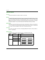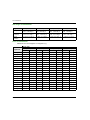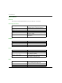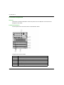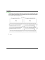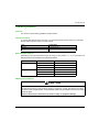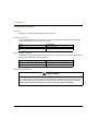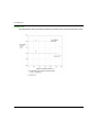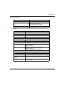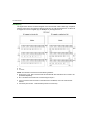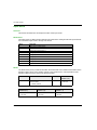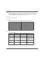
1
Modicon Momentum I/O Base 31001697 10/2013 Modicon Momentum I/O Base User Guide 31001697.16 10/2013 www.schneider-electric.com The information provided in this documentation contains general descriptions and/or technical characteristics of the performance of the products contained herein. This documentation is not intended as a substitute for and is not to be used for determining suitability or reliability of these products for specific user applications. It is the duty of any such user or integrator to perform the appropriate and complete risk analysis, evaluation and testing of the products with respect to the relevant specific application or use thereof. Neither Schneider Electric nor any of its affiliates or subsidiaries shall be responsible or liable for misuse of the information contained herein. If you have any suggestions for improvements or amendments or have found errors in this publication, please notify us. No part of this document may be reproduced in any form or by any means, electronic or mechanical, including photocopying, without express written permission of Schneider Electric. All pertinent state, regional, and local safety regulations must be observed when installing and using this product. For reasons of safety and to help ensure compliance with documented system data, only the manufacturer should perform repairs to components. When devices are used for applications with technical safety requirements, the relevant instructions must be followed. Failure to use Schneider Electric software or approved software with our hardware products may result in injury, harm, or improper operating results. Failure to observe this information can result in injury or equipment damage. © 2013 Schneider Electric. All rights reserved. 2 31001697 10/2013 Table of Contents Safety Information . . . . . . . . . . . . . . . . . . . . . . . . . . . . . About the Book. . . . . . . . . . . . . . . . . . . . . . . . . . . . . . . . Part I Using Momentum I/O Bases . . . . . . . . . . . . . . . . . Chapter 1 Introducing the TSX Momentum I/O Bases . . . . . . . . . Basic Features of I/O Bases . . . . . . . . . . . . . . . . . . . . . . . . . . . . . . . . Types of I/O Bases . . . . . . . . . . . . . . . . . . . . . . . . . . . . . . . . . . . . . . . Chapter 2 Selecting Other TSX Momentum Components . . . . . . Which Components Should I Use? . . . . . . . . . . . . . . . . . . . . . . . . . . . Communication Adapters . . . . . . . . . . . . . . . . . . . . . . . . . . . . . . . . . . Processor Adapters . . . . . . . . . . . . . . . . . . . . . . . . . . . . . . . . . . . . . . . Option Adapters. . . . . . . . . . . . . . . . . . . . . . . . . . . . . . . . . . . . . . . . . . Terminal Connectors . . . . . . . . . . . . . . . . . . . . . . . . . . . . . . . . . . . . . . Busbars . . . . . . . . . . . . . . . . . . . . . . . . . . . . . . . . . . . . . . . . . . . . . . . . Chapter 3 Assembly. . . . . . . . . . . . . . . . . . . . . . . . . . . . . . . . . . . . . Assembling an Adapter and an I/O Base . . . . . . . . . . . . . . . . . . . . . . Disassembling an Adapter from an I/O Base . . . . . . . . . . . . . . . . . . . Assembling a Processor Adapter and an Option Adapter . . . . . . . . . . Mounting the Assembled Adapters on the I/O Base . . . . . . . . . . . . . . Disassembling a Module with an Option Adapter . . . . . . . . . . . . . . . . Using Terminal Connector Coding Keys . . . . . . . . . . . . . . . . . . . . . . . Inserting Terminal Connectors . . . . . . . . . . . . . . . . . . . . . . . . . . . . . . Removing a Terminal Connector . . . . . . . . . . . . . . . . . . . . . . . . . . . . . Attaching a Busbar . . . . . . . . . . . . . . . . . . . . . . . . . . . . . . . . . . . . . . . Labeling the Components in the Assembly . . . . . . . . . . . . . . . . . . . . . Chapter 4 Dimensions and Mounting Instructions . . . . . . . . . . . . Dimensions of Assembled TSX Momentum Devices . . . . . . . . . . . . . Standard Adapter on a Typical Base. . . . . . . . . . . . . . . . . . . . . . . . . . Standard Adapter on a Discrete VAC Base. . . . . . . . . . . . . . . . . . . . . Processor and Option Adapter on a Typical Base. . . . . . . . . . . . . . . . Processor and Option Adapter on a Discrete VAC Base . . . . . . . . . . Mounting TSX Momentum Devices . . . . . . . . . . . . . . . . . . . . . . . . . . . Chapter 5 Power and Grounding Guidelines. . . . . . . . . . . . . . . . . Voltage Types . . . . . . . . . . . . . . . . . . . . . . . . . . . . . . . . . . . . . . . . . . . Structuring Your Power Supply System . . . . . . . . . . . . . . . . . . . . . . . Selecting Power Supplies . . . . . . . . . . . . . . . . . . . . . . . . . . . . . . . . . . 31001697 10/2013 15 17 19 21 22 24 27 28 30 31 33 34 36 39 40 43 45 47 50 53 54 55 56 57 59 60 61 62 63 64 65 67 68 69 70 3 Single Power Supply Configuration . . . . . . . . . . . . . . . . . . . . . . . . . . . Protective Circuits for DC Actuators. . . . . . . . . . . . . . . . . . . . . . . . . . . Protective Circuits for AC Actuators. . . . . . . . . . . . . . . . . . . . . . . . . . . Grounding Momentum Devices . . . . . . . . . . . . . . . . . . . . . . . . . . . . . . Grounding DIN Rail Terminals and Cabinets . . . . . . . . . . . . . . . . . . . . Grounding Analog I/O Lines. . . . . . . . . . . . . . . . . . . . . . . . . . . . . . . . . Part II I/O Base Descriptions . . . . . . . . . . . . . . . . . . . . . . Chapter 6 170 AAI 030 00 Analog 8 Channel Differential Input Module Base . . . . . . . . . . . . . . . . . . . . . . . . . . . . . . . . . . Front Panel Components . . . . . . . . . . . . . . . . . . . . . . . . . . . . . . . . . . . Specifications . . . . . . . . . . . . . . . . . . . . . . . . . . . . . . . . . . . . . . . . . . . . Internal Pin Connections . . . . . . . . . . . . . . . . . . . . . . . . . . . . . . . . . . . Field Wiring Guidelines . . . . . . . . . . . . . . . . . . . . . . . . . . . . . . . . . . . . Wiring Illustrations . . . . . . . . . . . . . . . . . . . . . . . . . . . . . . . . . . . . . . . . I/O Mapping . . . . . . . . . . . . . . . . . . . . . . . . . . . . . . . . . . . . . . . . . . . . . Analog Channel Parameters . . . . . . . . . . . . . . . . . . . . . . . . . . . . . . . . Analog Inputs . . . . . . . . . . . . . . . . . . . . . . . . . . . . . . . . . . . . . . . . . . . . Input Measuring Ranges . . . . . . . . . . . . . . . . . . . . . . . . . . . . . . . . . . . Chapter 7 170 AAI 140 00 Analog 16 Channel Single-Ended Input Module Base . . . . . . . . . . . . . . . . . . . . . . . . . . . . . . . . . . Front Panel Components . . . . . . . . . . . . . . . . . . . . . . . . . . . . . . . . . . . Specifications . . . . . . . . . . . . . . . . . . . . . . . . . . . . . . . . . . . . . . . . . . . . Internal Pin Connections . . . . . . . . . . . . . . . . . . . . . . . . . . . . . . . . . . . Field Wiring Guidelines . . . . . . . . . . . . . . . . . . . . . . . . . . . . . . . . . . . . Wiring Diagrams. . . . . . . . . . . . . . . . . . . . . . . . . . . . . . . . . . . . . . . . . . I/O Mapping . . . . . . . . . . . . . . . . . . . . . . . . . . . . . . . . . . . . . . . . . . . . . Analog Channel Parameters . . . . . . . . . . . . . . . . . . . . . . . . . . . . . . . . Analog Inputs . . . . . . . . . . . . . . . . . . . . . . . . . . . . . . . . . . . . . . . . . . . . Input Measuring Ranges . . . . . . . . . . . . . . . . . . . . . . . . . . . . . . . . . . . Chapter 8 170 AAI 520 40 Analog 4 Channel RTD, Therm. and mV Input Module Base . . . . . . . . . . . . . . . . . . . . . . . . . . . . . Front Panel Components . . . . . . . . . . . . . . . . . . . . . . . . . . . . . . . . . . . Specifications . . . . . . . . . . . . . . . . . . . . . . . . . . . . . . . . . . . . . . . . . . . . Internal Pin Connections . . . . . . . . . . . . . . . . . . . . . . . . . . . . . . . . . . . Field Wiring Guidelines . . . . . . . . . . . . . . . . . . . . . . . . . . . . . . . . . . . . Wiring Diagrams. . . . . . . . . . . . . . . . . . . . . . . . . . . . . . . . . . . . . . . . . . 4 71 73 75 76 78 79 81 83 84 86 89 90 92 93 94 96 98 101 102 104 106 107 109 110 111 113 115 117 118 120 129 130 132 31001697 10/2013 I/O Mapping . . . . . . . . . . . . . . . . . . . . . . . . . . . . . . . . . . . . . . . . . . . . . Analog Channel Parameters . . . . . . . . . . . . . . . . . . . . . . . . . . . . . . . . Analog Inputs. . . . . . . . . . . . . . . . . . . . . . . . . . . . . . . . . . . . . . . . . . . . RTD, Thermocouple and mV Input Measuring Ranges. . . . . . . . . . . . Chapter 9 170 AAO 120 00 Analog 4 Channel Output Module Base +/- 10 V, 0 - 20 mA . . . . . . . . . . . . . . . . . . . . . . . . . Front Panel Components. . . . . . . . . . . . . . . . . . . . . . . . . . . . . . . . . . . Specifications . . . . . . . . . . . . . . . . . . . . . . . . . . . . . . . . . . . . . . . . . . . Internal Pin Connections . . . . . . . . . . . . . . . . . . . . . . . . . . . . . . . . . . . Field Wiring Guidelines . . . . . . . . . . . . . . . . . . . . . . . . . . . . . . . . . . . . Wiring Diagrams . . . . . . . . . . . . . . . . . . . . . . . . . . . . . . . . . . . . . . . . . I/O Mapping . . . . . . . . . . . . . . . . . . . . . . . . . . . . . . . . . . . . . . . . . . . . . Analog Channel Parameters . . . . . . . . . . . . . . . . . . . . . . . . . . . . . . . . Analog Outputs . . . . . . . . . . . . . . . . . . . . . . . . . . . . . . . . . . . . . . . . . . Output Ranges . . . . . . . . . . . . . . . . . . . . . . . . . . . . . . . . . . . . . . . . . . Chapter 10 170 AAO 921 00 Analog 4 Channel Output Module Base +/- 10 V, 4 ... 20 mA . . . . . . . . . . . . . . . . . . . . . . . . Front Panel Components. . . . . . . . . . . . . . . . . . . . . . . . . . . . . . . . . . . Specifications . . . . . . . . . . . . . . . . . . . . . . . . . . . . . . . . . . . . . . . . . . . Internal Pin Connections . . . . . . . . . . . . . . . . . . . . . . . . . . . . . . . . . . . Field Wiring Guidelines . . . . . . . . . . . . . . . . . . . . . . . . . . . . . . . . . . . . Wiring Diagrams . . . . . . . . . . . . . . . . . . . . . . . . . . . . . . . . . . . . . . . . . I/O Mapping . . . . . . . . . . . . . . . . . . . . . . . . . . . . . . . . . . . . . . . . . . . . . Analog Channel Parameters . . . . . . . . . . . . . . . . . . . . . . . . . . . . . . . . Analog Outputs . . . . . . . . . . . . . . . . . . . . . . . . . . . . . . . . . . . . . . . . . . Output Ranges . . . . . . . . . . . . . . . . . . . . . . . . . . . . . . . . . . . . . . . . . . Chapter 11 170 ADI 340 00 24 VDC - 16 Pt. Discrete Input Module Base . . . . . . . . . . . . . . . . . . . . . . . . . . . . . . . . . . . . . . . . . Front Panel Components. . . . . . . . . . . . . . . . . . . . . . . . . . . . . . . . . . . Specifications . . . . . . . . . . . . . . . . . . . . . . . . . . . . . . . . . . . . . . . . . . . Internal Pin Connections . . . . . . . . . . . . . . . . . . . . . . . . . . . . . . . . . . . Field Wiring Guidelines . . . . . . . . . . . . . . . . . . . . . . . . . . . . . . . . . . . . Wiring Diagrams . . . . . . . . . . . . . . . . . . . . . . . . . . . . . . . . . . . . . . . . . I/O Mapping . . . . . . . . . . . . . . . . . . . . . . . . . . . . . . . . . . . . . . . . . . . . . 31001697 10/2013 133 134 139 141 143 144 146 148 149 151 152 153 155 156 157 158 160 162 163 165 166 167 169 170 171 172 174 176 177 179 181 5 Chapter 12 170 ADI 350 00 24 VDC - 32 Pt. Discrete Input Module Base. . . . . . . . . . . . . . . . . . . . . . . . . . . . . . . . . . . . . . . . . Front Panel Components . . . . . . . . . . . . . . . . . . . . . . . . . . . . . . . . . . . Specifications . . . . . . . . . . . . . . . . . . . . . . . . . . . . . . . . . . . . . . . . . . . . Internal Pin Connections . . . . . . . . . . . . . . . . . . . . . . . . . . . . . . . . . . . Field Wiring Guidelines . . . . . . . . . . . . . . . . . . . . . . . . . . . . . . . . . . . . Wiring Diagrams. . . . . . . . . . . . . . . . . . . . . . . . . . . . . . . . . . . . . . . . . . I/O Mapping . . . . . . . . . . . . . . . . . . . . . . . . . . . . . . . . . . . . . . . . . . . . . Chapter 13 170 ADI 540 50 120 VAC - 16 Point Discrete Input Module Base . . . . . . . . . . . . . . . . . . . . . . . . . . . . . . . . . . Front Panel Components . . . . . . . . . . . . . . . . . . . . . . . . . . . . . . . . . . . Specifications . . . . . . . . . . . . . . . . . . . . . . . . . . . . . . . . . . . . . . . . . . . . Internal Pin Connections . . . . . . . . . . . . . . . . . . . . . . . . . . . . . . . . . . . Field Wiring Guidelines . . . . . . . . . . . . . . . . . . . . . . . . . . . . . . . . . . . . Wiring Diagrams. . . . . . . . . . . . . . . . . . . . . . . . . . . . . . . . . . . . . . . . . . I/O Mapping . . . . . . . . . . . . . . . . . . . . . . . . . . . . . . . . . . . . . . . . . . . . . Chapter 14 170 ADI 740 50 230 VAC - 16 Point Discrete Input Module Base . . . . . . . . . . . . . . . . . . . . . . . . . . . . . . . . . . Front Panel Components . . . . . . . . . . . . . . . . . . . . . . . . . . . . . . . . . . . Specifications . . . . . . . . . . . . . . . . . . . . . . . . . . . . . . . . . . . . . . . . . . . . Internal Pin Connections . . . . . . . . . . . . . . . . . . . . . . . . . . . . . . . . . . . Field Wiring Guidelines . . . . . . . . . . . . . . . . . . . . . . . . . . . . . . . . . . . . Wiring Diagrams. . . . . . . . . . . . . . . . . . . . . . . . . . . . . . . . . . . . . . . . . . I/O Mapping . . . . . . . . . . . . . . . . . . . . . . . . . . . . . . . . . . . . . . . . . . . . . Chapter 15 170 ADM 350 10 24 VDC - 16 Pt. In / 16 Pt. Out Module Base. . . . . . . . . . . . . . . . . . . . . . . . . . . . . . . . . . . . . . . . . Front Panel Components . . . . . . . . . . . . . . . . . . . . . . . . . . . . . . . . . . . Specifications . . . . . . . . . . . . . . . . . . . . . . . . . . . . . . . . . . . . . . . . . . . . Internal Pin Connections . . . . . . . . . . . . . . . . . . . . . . . . . . . . . . . . . . . Field Wiring Guidelines . . . . . . . . . . . . . . . . . . . . . . . . . . . . . . . . . . . . Wiring Diagrams. . . . . . . . . . . . . . . . . . . . . . . . . . . . . . . . . . . . . . . . . . I/O Mapping . . . . . . . . . . . . . . . . . . . . . . . . . . . . . . . . . . . . . . . . . . . . . 6 185 186 188 190 191 193 195 199 200 202 205 206 207 209 213 214 216 219 220 221 223 227 228 230 233 234 236 241 31001697 10/2013 Chapter 16 170 ADM 350 11 24 VDC - 16 Pt. In / 16 Pt. Out Module Base . . . . . . . . . . . . . . . . . . . . . . . . . . . . . . . . . . . . . . . . . Front Panel Components. . . . . . . . . . . . . . . . . . . . . . . . . . . . . . . . . . . Specifications . . . . . . . . . . . . . . . . . . . . . . . . . . . . . . . . . . . . . . . . . . . Internal Pin Connections . . . . . . . . . . . . . . . . . . . . . . . . . . . . . . . . . . . Field Wiring Guidelines . . . . . . . . . . . . . . . . . . . . . . . . . . . . . . . . . . . . Wiring Diagrams . . . . . . . . . . . . . . . . . . . . . . . . . . . . . . . . . . . . . . . . . I/O Mapping . . . . . . . . . . . . . . . . . . . . . . . . . . . . . . . . . . . . . . . . . . . . . Chapter 17 170 ADM 350 15 24 VDC - 16 Pt. In / 16 Pt. Out Module Base . . . . . . . . . . . . . . . . . . . . . . . . . . . . . . . . . . . . . . . . . Front Panel Components. . . . . . . . . . . . . . . . . . . . . . . . . . . . . . . . . . . Specifications . . . . . . . . . . . . . . . . . . . . . . . . . . . . . . . . . . . . . . . . . . . Internal Pin Connections . . . . . . . . . . . . . . . . . . . . . . . . . . . . . . . . . . . Field Wiring Guidelines . . . . . . . . . . . . . . . . . . . . . . . . . . . . . . . . . . . . Wiring Diagrams . . . . . . . . . . . . . . . . . . . . . . . . . . . . . . . . . . . . . . . . . I/O Mapping . . . . . . . . . . . . . . . . . . . . . . . . . . . . . . . . . . . . . . . . . . . . . Chapter 18 170 ADM 370 10 24 VDC - 16 Pt. In / 8 Pt. Out @ 2 Amp. Module Base . . . . . . . . . . . . . . . . . . . . . . . . . . . . . . . . . . Front Panel Components. . . . . . . . . . . . . . . . . . . . . . . . . . . . . . . . . . . Specifications . . . . . . . . . . . . . . . . . . . . . . . . . . . . . . . . . . . . . . . . . . . Internal Pin Connections . . . . . . . . . . . . . . . . . . . . . . . . . . . . . . . . . . . Field Wiring Guidelines . . . . . . . . . . . . . . . . . . . . . . . . . . . . . . . . . . . . Wiring Diagrams . . . . . . . . . . . . . . . . . . . . . . . . . . . . . . . . . . . . . . . . . I/O Mapping . . . . . . . . . . . . . . . . . . . . . . . . . . . . . . . . . . . . . . . . . . . . . Chapter 19 170 ADM 390 10 24 VDC - 16 Pt. In / 12 Pt. Out Monitored Module Base . . . . . . . . . . . . . . . . . . . . . . . . . Front Panel Components. . . . . . . . . . . . . . . . . . . . . . . . . . . . . . . . . . . Specifications . . . . . . . . . . . . . . . . . . . . . . . . . . . . . . . . . . . . . . . . . . . Internal Pin Connections . . . . . . . . . . . . . . . . . . . . . . . . . . . . . . . . . . . Field Wiring Guidelines . . . . . . . . . . . . . . . . . . . . . . . . . . . . . . . . . . . . Wiring Diagrams . . . . . . . . . . . . . . . . . . . . . . . . . . . . . . . . . . . . . . . . . I/O Mapping . . . . . . . . . . . . . . . . . . . . . . . . . . . . . . . . . . . . . . . . . . . . . 31001697 10/2013 245 246 248 251 252 254 259 263 264 266 269 270 272 273 277 278 280 283 284 286 291 295 296 298 301 302 304 307 7 Chapter 20 170 ADM 390 30 24 VDC - 10 Pt. In / 8 Pt. Relay Out Module Base . . . . . . . . . . . . . . . . . . . . . . . . . . . . . . . . . . Front Panel Components . . . . . . . . . . . . . . . . . . . . . . . . . . . . . . . . . . . Specifications . . . . . . . . . . . . . . . . . . . . . . . . . . . . . . . . . . . . . . . . . . . . Internal Pin Connections . . . . . . . . . . . . . . . . . . . . . . . . . . . . . . . . . . . Field Wiring Guidelines . . . . . . . . . . . . . . . . . . . . . . . . . . . . . . . . . . . . Wiring Diagrams. . . . . . . . . . . . . . . . . . . . . . . . . . . . . . . . . . . . . . . . . . I/O Mapping . . . . . . . . . . . . . . . . . . . . . . . . . . . . . . . . . . . . . . . . . . . . . Chapter 21 170 ADM 390 31 24 VDC - 10 Pt. In / 8 Pt. Relay Out Module Base . . . . . . . . . . . . . . . . . . . . . . . . . . . . . . . . . . Front Panel Components . . . . . . . . . . . . . . . . . . . . . . . . . . . . . . . . . . . Specifications . . . . . . . . . . . . . . . . . . . . . . . . . . . . . . . . . . . . . . . . . . . . Internal Pin Connections . . . . . . . . . . . . . . . . . . . . . . . . . . . . . . . . . . . Field Wiring Guidelines . . . . . . . . . . . . . . . . . . . . . . . . . . . . . . . . . . . . Wiring Diagrams. . . . . . . . . . . . . . . . . . . . . . . . . . . . . . . . . . . . . . . . . . I/O Mapping . . . . . . . . . . . . . . . . . . . . . . . . . . . . . . . . . . . . . . . . . . . . . Chapter 22 170 ADM 540 80 120 VAC - 6 Pt. In / 3 Pt. Out Discrete MCC Module Base . . . . . . . . . . . . . . . . . . . . . . . . . . . . . Front Panel Components . . . . . . . . . . . . . . . . . . . . . . . . . . . . . . . . . . . Specifications . . . . . . . . . . . . . . . . . . . . . . . . . . . . . . . . . . . . . . . . . . . . Internal Pin Connections . . . . . . . . . . . . . . . . . . . . . . . . . . . . . . . . . . . Field Wiring Guidelines . . . . . . . . . . . . . . . . . . . . . . . . . . . . . . . . . . . . Wiring Diagrams. . . . . . . . . . . . . . . . . . . . . . . . . . . . . . . . . . . . . . . . . . I/O Mapping . . . . . . . . . . . . . . . . . . . . . . . . . . . . . . . . . . . . . . . . . . . . . General Modbus Message Rules. . . . . . . . . . . . . . . . . . . . . . . . . . . . . Output Words . . . . . . . . . . . . . . . . . . . . . . . . . . . . . . . . . . . . . . . . . . . . Output Words Control Modes. . . . . . . . . . . . . . . . . . . . . . . . . . . . . . . . Input Words . . . . . . . . . . . . . . . . . . . . . . . . . . . . . . . . . . . . . . . . . . . . . Input Words Control Modes . . . . . . . . . . . . . . . . . . . . . . . . . . . . . . . . . Chapter 23 170 ADM 690 50 120 VAC - 10 Pt. In / 8 Pt. Out Module Bases. . . . . . . . . . . . . . . . . . . . . . . . . . . . . . . . . . . . . . . . Front Panel Components . . . . . . . . . . . . . . . . . . . . . . . . . . . . . . . . . . . Specifications . . . . . . . . . . . . . . . . . . . . . . . . . . . . . . . . . . . . . . . . . . . . Internal Pin Connections . . . . . . . . . . . . . . . . . . . . . . . . . . . . . . . . . . . Field Wiring Guidelines . . . . . . . . . . . . . . . . . . . . . . . . . . . . . . . . . . . . Wiring Diagrams. . . . . . . . . . . . . . . . . . . . . . . . . . . . . . . . . . . . . . . . . . I/O Mapping . . . . . . . . . . . . . . . . . . . . . . . . . . . . . . . . . . . . . . . . . . . . . 8 311 312 314 317 318 320 323 327 328 330 333 334 336 339 343 344 346 349 350 353 354 356 359 362 367 369 373 374 376 379 380 382 385 31001697 10/2013 Chapter 24 170 ADM 690 51 120 VAC - 10 Pt. In / 8 Pt. Out Module Bases . . . . . . . . . . . . . . . . . . . . . . . . . . . . . . . . . . . . . . . . Front Panel Components. . . . . . . . . . . . . . . . . . . . . . . . . . . . . . . . . . . Specifications . . . . . . . . . . . . . . . . . . . . . . . . . . . . . . . . . . . . . . . . . . . Internal Pin Connections . . . . . . . . . . . . . . . . . . . . . . . . . . . . . . . . . . . Field Wiring Guidelines . . . . . . . . . . . . . . . . . . . . . . . . . . . . . . . . . . . . Wiring Diagrams . . . . . . . . . . . . . . . . . . . . . . . . . . . . . . . . . . . . . . . . . I/O Mapping . . . . . . . . . . . . . . . . . . . . . . . . . . . . . . . . . . . . . . . . . . . . . Chapter 25 170 ADM 850 10 10 to 60 VDC Module Base . . . . . . . . Front Panel Components. . . . . . . . . . . . . . . . . . . . . . . . . . . . . . . . . . . Specifications . . . . . . . . . . . . . . . . . . . . . . . . . . . . . . . . . . . . . . . . . . . Internal Pin Connections . . . . . . . . . . . . . . . . . . . . . . . . . . . . . . . . . . . Field Wiring Guidelines . . . . . . . . . . . . . . . . . . . . . . . . . . . . . . . . . . . . Wiring Diagrams . . . . . . . . . . . . . . . . . . . . . . . . . . . . . . . . . . . . . . . . . I/O Mapping . . . . . . . . . . . . . . . . . . . . . . . . . . . . . . . . . . . . . . . . . . . . . Chapter 26 170 ADO 340 00 24 VDC - 16 Pt. Discrete Output Module Base . . . . . . . . . . . . . . . . . . . . . . . . . . . . . . . . . . Front Panel Components. . . . . . . . . . . . . . . . . . . . . . . . . . . . . . . . . . . Specifications . . . . . . . . . . . . . . . . . . . . . . . . . . . . . . . . . . . . . . . . . . . Internal Pin Connections . . . . . . . . . . . . . . . . . . . . . . . . . . . . . . . . . . . Field Wiring Guidelines . . . . . . . . . . . . . . . . . . . . . . . . . . . . . . . . . . . . Wiring Diagrams . . . . . . . . . . . . . . . . . . . . . . . . . . . . . . . . . . . . . . . . . I/O Mapping . . . . . . . . . . . . . . . . . . . . . . . . . . . . . . . . . . . . . . . . . . . . . Chapter 27 170 ADO 350 00 24 VDC - 32 Pt. Discrete Output Module Base . . . . . . . . . . . . . . . . . . . . . . . . . . . . . . . . . . Front Panel Components. . . . . . . . . . . . . . . . . . . . . . . . . . . . . . . . . . . Specifications . . . . . . . . . . . . . . . . . . . . . . . . . . . . . . . . . . . . . . . . . . . Internal Pin Connections . . . . . . . . . . . . . . . . . . . . . . . . . . . . . . . . . . . Field Wiring Guidelines . . . . . . . . . . . . . . . . . . . . . . . . . . . . . . . . . . . . Wiring Diagrams . . . . . . . . . . . . . . . . . . . . . . . . . . . . . . . . . . . . . . . . . I/O Mapping . . . . . . . . . . . . . . . . . . . . . . . . . . . . . . . . . . . . . . . . . . . . . 31001697 10/2013 389 390 392 395 396 398 402 405 406 408 411 412 414 419 423 424 426 428 429 431 433 437 438 440 442 443 445 447 9 Chapter 28 170 ADO 530 50 120 VAC - 8 Point Discrete Output @ 2A Module Base . . . . . . . . . . . . . . . . . . . . . . . . . . . . . . . Front Panel Components . . . . . . . . . . . . . . . . . . . . . . . . . . . . . . . . . . . Specifications . . . . . . . . . . . . . . . . . . . . . . . . . . . . . . . . . . . . . . . . . . . . Internal Pin Connections . . . . . . . . . . . . . . . . . . . . . . . . . . . . . . . . . . . Field Wiring Guidelines . . . . . . . . . . . . . . . . . . . . . . . . . . . . . . . . . . . . Wiring Diagrams. . . . . . . . . . . . . . . . . . . . . . . . . . . . . . . . . . . . . . . . . . I/O Mapping . . . . . . . . . . . . . . . . . . . . . . . . . . . . . . . . . . . . . . . . . . . . . Chapter 29 170 ADO 540 50 120 VAC - 16 Point Discrete Output Module Base . . . . . . . . . . . . . . . . . . . . . . . . . . . . . . . . . . Front Panel Components . . . . . . . . . . . . . . . . . . . . . . . . . . . . . . . . . . . Specifications . . . . . . . . . . . . . . . . . . . . . . . . . . . . . . . . . . . . . . . . . . . . Internal Pin Connections . . . . . . . . . . . . . . . . . . . . . . . . . . . . . . . . . . . Field Wiring Guidelines . . . . . . . . . . . . . . . . . . . . . . . . . . . . . . . . . . . . Wiring Diagrams. . . . . . . . . . . . . . . . . . . . . . . . . . . . . . . . . . . . . . . . . . I/O Mapping . . . . . . . . . . . . . . . . . . . . . . . . . . . . . . . . . . . . . . . . . . . . . Chapter 30 170 ADO 730 50 230 VAC - 8 Point Discrete Output @ 2A Module Base . . . . . . . . . . . . . . . . . . . . . . . . . . . . . . . Front Panel Components . . . . . . . . . . . . . . . . . . . . . . . . . . . . . . . . . . . Specifications . . . . . . . . . . . . . . . . . . . . . . . . . . . . . . . . . . . . . . . . . . . . Internal Pin Connections . . . . . . . . . . . . . . . . . . . . . . . . . . . . . . . . . . . Field Wiring Guidelines . . . . . . . . . . . . . . . . . . . . . . . . . . . . . . . . . . . . Wiring Diagrams. . . . . . . . . . . . . . . . . . . . . . . . . . . . . . . . . . . . . . . . . . I/O Mapping . . . . . . . . . . . . . . . . . . . . . . . . . . . . . . . . . . . . . . . . . . . . . Chapter 31 170 ADO 740 50 230 VAC - 16 Point Discrete Output Module Base . . . . . . . . . . . . . . . . . . . . . . . . . . . . . . . . . . Front Panel Components . . . . . . . . . . . . . . . . . . . . . . . . . . . . . . . . . . . Specifications . . . . . . . . . . . . . . . . . . . . . . . . . . . . . . . . . . . . . . . . . . . . Internal Pin Connections . . . . . . . . . . . . . . . . . . . . . . . . . . . . . . . . . . . Field Wiring Guidelines . . . . . . . . . . . . . . . . . . . . . . . . . . . . . . . . . . . . Wiring Diagrams. . . . . . . . . . . . . . . . . . . . . . . . . . . . . . . . . . . . . . . . . . I/O Mapping . . . . . . . . . . . . . . . . . . . . . . . . . . . . . . . . . . . . . . . . . . . . . 10 451 452 454 457 458 460 463 467 468 470 473 474 476 479 483 484 486 489 490 492 495 499 500 502 505 506 508 511 31001697 10/2013 Chapter 32 170 ADO 830 30 6 Pt. Relay Out Module Base . . . . . . . Front Panel Components. . . . . . . . . . . . . . . . . . . . . . . . . . . . . . . . . . . Specifications . . . . . . . . . . . . . . . . . . . . . . . . . . . . . . . . . . . . . . . . . . . Internal Pin Connections . . . . . . . . . . . . . . . . . . . . . . . . . . . . . . . . . . . Field Wiring Guidelines . . . . . . . . . . . . . . . . . . . . . . . . . . . . . . . . . . . . Wiring Diagrams . . . . . . . . . . . . . . . . . . . . . . . . . . . . . . . . . . . . . . . . . I/O Mapping . . . . . . . . . . . . . . . . . . . . . . . . . . . . . . . . . . . . . . . . . . . . . Chapter 33 170 AMM 090 00 Analog 4 Ch. In / 2 Ch. Out Module Base w/ 24 VDC I/O Pts . . . . . . . . . . . . . . . . . . . . . . . . . Front Panel Components. . . . . . . . . . . . . . . . . . . . . . . . . . . . . . . . . . . Specifications . . . . . . . . . . . . . . . . . . . . . . . . . . . . . . . . . . . . . . . . . . . Internal Pin Connections . . . . . . . . . . . . . . . . . . . . . . . . . . . . . . . . . . . Field Wiring Guidelines . . . . . . . . . . . . . . . . . . . . . . . . . . . . . . . . . . . . Wiring Diagrams . . . . . . . . . . . . . . . . . . . . . . . . . . . . . . . . . . . . . . . . . I/O Mapping . . . . . . . . . . . . . . . . . . . . . . . . . . . . . . . . . . . . . . . . . . . . . Analog Channel Parameters . . . . . . . . . . . . . . . . . . . . . . . . . . . . . . . . Analog Outputs . . . . . . . . . . . . . . . . . . . . . . . . . . . . . . . . . . . . . . . . . . Analog Inputs. . . . . . . . . . . . . . . . . . . . . . . . . . . . . . . . . . . . . . . . . . . . Discrete Inputs and Outputs . . . . . . . . . . . . . . . . . . . . . . . . . . . . . . . . Input Measuring Ranges . . . . . . . . . . . . . . . . . . . . . . . . . . . . . . . . . . . Error Messages . . . . . . . . . . . . . . . . . . . . . . . . . . . . . . . . . . . . . . . . . . Chapter 34 170 AMM 090 01 Analog 4 Ch. In / 2 Ch. Out Module Base w/ 12 VDC I/O Pts . . . . . . . . . . . . . . . . . . . . . . . . . Front Panel Components. . . . . . . . . . . . . . . . . . . . . . . . . . . . . . . . . . . Specifications . . . . . . . . . . . . . . . . . . . . . . . . . . . . . . . . . . . . . . . . . . . Internal Pin Connections . . . . . . . . . . . . . . . . . . . . . . . . . . . . . . . . . . . Field Wiring Guidelines . . . . . . . . . . . . . . . . . . . . . . . . . . . . . . . . . . . . Wiring Diagrams . . . . . . . . . . . . . . . . . . . . . . . . . . . . . . . . . . . . . . . . . I/O Mapping . . . . . . . . . . . . . . . . . . . . . . . . . . . . . . . . . . . . . . . . . . . . . Analog Channel Parameters . . . . . . . . . . . . . . . . . . . . . . . . . . . . . . . . Analog Outputs . . . . . . . . . . . . . . . . . . . . . . . . . . . . . . . . . . . . . . . . . . Analog Inputs. . . . . . . . . . . . . . . . . . . . . . . . . . . . . . . . . . . . . . . . . . . . Discrete Inputs and Outputs . . . . . . . . . . . . . . . . . . . . . . . . . . . . . . . . Input and Output Measuring Ranges. . . . . . . . . . . . . . . . . . . . . . . . . . Error Messages . . . . . . . . . . . . . . . . . . . . . . . . . . . . . . . . . . . . . . . . . . 31001697 10/2013 515 516 518 521 522 524 526 529 530 532 536 537 539 542 544 546 547 548 549 555 557 558 560 564 565 567 570 572 574 575 576 577 583 11 Chapter 35 170AMM11030 Analog 2 Ch. In / 2 Ch. Out Module Base with 16 Discrete Inputs and 8 Discrete Output Points . . . . . . . . . . . . . . . . . . . . . . . . . . . . . . . . . . . . . . . Front Panel Components . . . . . . . . . . . . . . . . . . . . . . . . . . . . . . . . . . . Specifications . . . . . . . . . . . . . . . . . . . . . . . . . . . . . . . . . . . . . . . . . . . . Internal Pin Connections . . . . . . . . . . . . . . . . . . . . . . . . . . . . . . . . . . . Field Wiring Guidelines . . . . . . . . . . . . . . . . . . . . . . . . . . . . . . . . . . . . Wiring Diagrams. . . . . . . . . . . . . . . . . . . . . . . . . . . . . . . . . . . . . . . . . . I/O Map . . . . . . . . . . . . . . . . . . . . . . . . . . . . . . . . . . . . . . . . . . . . . . . . Register for Outputs . . . . . . . . . . . . . . . . . . . . . . . . . . . . . . . . . . . . . . . 4x Registers . . . . . . . . . . . . . . . . . . . . . . . . . . . . . . . . . . . . . . . . . . . . . Register for Inputs . . . . . . . . . . . . . . . . . . . . . . . . . . . . . . . . . . . . . . . . Analog Map . . . . . . . . . . . . . . . . . . . . . . . . . . . . . . . . . . . . . . . . . . . . . Discrete I/O Points and IEC Compliant Data Mapping. . . . . . . . . . . . . Input and Output Ranges . . . . . . . . . . . . . . . . . . . . . . . . . . . . . . . . . . . Chapter 36 170 ANR 120 90 Unipolar Analog 6 Ch. In / 4 Ch. Out Module Base with 24 VDC I/O Points . . . . . . . . . . . . . . Front Panel Components . . . . . . . . . . . . . . . . . . . . . . . . . . . . . . . . . . . Specifications . . . . . . . . . . . . . . . . . . . . . . . . . . . . . . . . . . . . . . . . . . . . Internal Pin Connections . . . . . . . . . . . . . . . . . . . . . . . . . . . . . . . . . . . Field Wiring Guidelines . . . . . . . . . . . . . . . . . . . . . . . . . . . . . . . . . . . . Wiring Diagrams. . . . . . . . . . . . . . . . . . . . . . . . . . . . . . . . . . . . . . . . . . I/O Mapping . . . . . . . . . . . . . . . . . . . . . . . . . . . . . . . . . . . . . . . . . . . . . Output Words . . . . . . . . . . . . . . . . . . . . . . . . . . . . . . . . . . . . . . . . . . . . Inputs Words . . . . . . . . . . . . . . . . . . . . . . . . . . . . . . . . . . . . . . . . . . . . Input and Qutput Measuring Ranges . . . . . . . . . . . . . . . . . . . . . . . . . . Error Messages . . . . . . . . . . . . . . . . . . . . . . . . . . . . . . . . . . . . . . . . . . Chapter 37 170 ANR 120 91 Bipolar Analog 6 Ch. In / 4 Ch. Out Module Base with 24 VDC I/O Points . . . . . . . . . . . . . . Front Panel Components . . . . . . . . . . . . . . . . . . . . . . . . . . . . . . . . . . . Specifications . . . . . . . . . . . . . . . . . . . . . . . . . . . . . . . . . . . . . . . . . . . . Internal Pin Connections . . . . . . . . . . . . . . . . . . . . . . . . . . . . . . . . . . . Field Wiring Guidelines . . . . . . . . . . . . . . . . . . . . . . . . . . . . . . . . . . . . Wiring Diagrams. . . . . . . . . . . . . . . . . . . . . . . . . . . . . . . . . . . . . . . . . . I/O Map . . . . . . . . . . . . . . . . . . . . . . . . . . . . . . . . . . . . . . . . . . . . . . . . Register for Outputs . . . . . . . . . . . . . . . . . . . . . . . . . . . . . . . . . . . . . . . 4x Registers . . . . . . . . . . . . . . . . . . . . . . . . . . . . . . . . . . . . . . . . . . . . . Register for Inputs . . . . . . . . . . . . . . . . . . . . . . . . . . . . . . . . . . . . . . . . 12 585 586 588 592 593 595 597 598 601 602 604 605 606 609 610 612 616 617 619 621 624 628 630 632 633 634 636 639 640 642 644 645 648 649 31001697 10/2013 Analog Map . . . . . . . . . . . . . . . . . . . . . . . . . . . . . . . . . . . . . . . . . . . . . Discrete I/O Points and IEC Compliant Data Mapping . . . . . . . . . . . . Input and Output Ranges . . . . . . . . . . . . . . . . . . . . . . . . . . . . . . . . . . Interpreting the Error Bits . . . . . . . . . . . . . . . . . . . . . . . . . . . . . . . . . . Chapter 38 170 ARM 370 30 24 VDC - 10 Pt. In / 8 Pt. Relay Out Module Base (120 VAC Powered) . . . . . . . . . . . . . . . . . Front Panel Components. . . . . . . . . . . . . . . . . . . . . . . . . . . . . . . . . . . Specifications . . . . . . . . . . . . . . . . . . . . . . . . . . . . . . . . . . . . . . . . . . . Internal Pin Connections . . . . . . . . . . . . . . . . . . . . . . . . . . . . . . . . . . . Field Wiring Guidelines . . . . . . . . . . . . . . . . . . . . . . . . . . . . . . . . . . . . Wiring Diagrams . . . . . . . . . . . . . . . . . . . . . . . . . . . . . . . . . . . . . . . . . I/O Mapping . . . . . . . . . . . . . . . . . . . . . . . . . . . . . . . . . . . . . . . . . . . . . Chapter 39 170 CPS 111 00 TIO Power Supply Module . . . . . . . . . Front Panel Components. . . . . . . . . . . . . . . . . . . . . . . . . . . . . . . . . . . Specifications . . . . . . . . . . . . . . . . . . . . . . . . . . . . . . . . . . . . . . . . . . . Terminal Connectors . . . . . . . . . . . . . . . . . . . . . . . . . . . . . . . . . . . . . . External Operating Voltage Connections . . . . . . . . . . . . . . . . . . . . . . Appendices ......................................... Appendix A System Specifications . . . . . . . . . . . . . . . . . . . . . . . . . . Power Supply Specifications . . . . . . . . . . . . . . . . . . . . . . . . . . . . . . . . Field Device Interfaces . . . . . . . . . . . . . . . . . . . . . . . . . . . . . . . . . . . . Environmental Specifications . . . . . . . . . . . . . . . . . . . . . . . . . . . . . . . Appendix B Interference Suppression . . . . . . . . . . . . . . . . . . . . . . . Interference Suppression . . . . . . . . . . . . . . . . . . . . . . . . . . . . . . . . . . Appendix C IEC 1131 Input Types . . . . . . . . . . . . . . . . . . . . . . . . . . . Input Voltage and Current Thresholds. . . . . . . . . . . . . . . . . . . . . . . . . Appendix D Field Wire Length . . . . . . . . . . . . . . . . . . . . . . . . . . . . . . Calculating Field Wire Length for AC and DC Devices . . . . . . . . . . . . Appendix E IEC Symbols . . . . . . . . . . . . . . . . . . . . . . . . . . . . . . . . . . Glossary of IEC Symbols. . . . . . . . . . . . . . . . . . . . . . . . . . . . . . . . . . . Index 31001697 10/2013 ......................................... 651 652 653 655 657 658 660 663 664 667 670 673 674 676 680 682 685 687 688 689 690 693 693 695 695 697 697 699 699 701 13 14 31001697 10/2013 Safety Information Important Information NOTICE Read these instructions carefully, and look at the equipment to become familiar with the device before trying to install, operate, or maintain it. The following special messages may appear throughout this documentation or on the equipment to warn of potential hazards or to call attention to information that clarifies or simplifies a procedure. 31001697 10/2013 15 PLEASE NOTE Electrical equipment should be installed, operated, serviced, and maintained only by qualified personnel. No responsibility is assumed by Schneider Electric for any consequences arising out of the use of this material. A qualified person is one who has skills and knowledge related to the construction and operation of electrical equipment and its installation, and has received safety training to recognize and avoid the hazards involved. 16 31001697 10/2013 About the Book At a Glance Document Scope This manual contains complete information about the Momentum I/O bases. It contains only passing references to other Momentum components, including processor adapters, option adapters, and communication adapters. Validity Note This document is valid from Unity Pro 7.0. The technical characteristics of the devices described in this document also appear online. To access this information online: Step Action 1 Go to the Schneider Electric home page www.schneider-electric.com. 2 In the Search box type the reference of a product or the name of a product range. Do not include blank spaces in the model number/product range. To get information on grouping similar modules, use asterisks (*). 3 If you entered a reference, go to the Product datasheets search results and click on the reference that interests you. If you entered the name of a product range, go to the Product Ranges search results and click on the product range that interests you. 4 If more than one reference appears in the Products search results, click on the reference that interests you. 5 Depending on the size of your screen, you may need to scroll down to see the data sheet. 6 To save or print a data sheet as a .pdf file, click Download XXX product datasheet. The characteristics that are presented in this manual should be the same as those characteristics that appear online. In line with our policy of constant improvement, we may revise content over time to improve clarity and accuracy. If you see a difference between the manual and online information, use the online information as your reference. 31001697 10/2013 17 Related Documents Title of Documentation Reference Number Momentum Processor Adapter and Option Adapter User Guide 870 USE 101 Momentum InterBus Communication Adapter User Manual 870 USE 009 Momentum Profibus-DP Communication Adapter User Manual 870 USE 004 Momentum FIPI/O Communication Adapter User Manual 870 USE 005 Momentum ControlNet Communication Adapter User Manual 870 USE 007 Momentum 170 AEC 920 00 I/O Base with 2 High-Speed Counters User Manual 870 USE 008 Momentum Modbus Plus PNT Series Communication Adapter User Manual 870 USE 103 Momentum DeviceNet Communication Adapter User Manual 870 USE 104 Momentum Modbus Plus NEF Series Communication Adapter User Manual 870 USE 111 Momentum 170ENT11001/170ENT11002 Ethernet Communications 870 USE 114 Adapter User Guide You can download these technical publications and other technical information from our website at www.schneider-electric.com. 18 31001697 10/2013 Modicon Momentum I/O Base Using Momentum I/O Bases 31001697 10/2013 Part I Using Momentum I/O Bases Using Momentum I/O Bases Overview This part describes how to assemble TSX Momentum I/O bases with other Momentum components, how to mount assembled modules, and how to ground them. What Is in This Part? This part contains the following chapters: Chapter 31001697 10/2013 Chapter Name Page 1 Introducing the TSX Momentum I/O Bases 21 2 Selecting Other TSX Momentum Components 27 3 Assembly 39 4 Dimensions and Mounting Instructions 59 5 Power and Grounding Guidelines 67 19 Using Momentum I/O Bases 20 31001697 10/2013 Modicon Momentum I/O Base Introducing the Momentum I/O Bases 31001697 10/2013 Chapter 1 Introducing the TSX Momentum I/O Bases Introducing the TSX Momentum I/O Bases Overview This chapter introduces the basic features and types of TSX Momentum I/O bases. What Is in This Chapter? This chapter contains the following topics: Topic Page Basic Features of I/O Bases 22 Types of I/O Bases 24 31001697 10/2013 21 Introducing the Momentum I/O Bases Basic Features of I/O Bases Overview This section provides a drawing of a typical I/O base and describes basic features of I/O bases. Front View The front panel components of a typical I/O base are shown in the illustration below Internal Communications Connector The internal communications connector on an I/O base provides automatic communication to any adapter mounted on the base. LED Display Each I/O base has a custom LED display, providing information about the status of input and output devices. Refer to the LED illustration and description for your I/O base for details. 22 31001697 10/2013 Introducing the Momentum I/O Bases Ground Contact This contact provides an earth ground connection to any adapter mounted on the base. Terminal Connector Sockets Each I/O base has sockets for as many as three terminal connectors. Terminal connectors are required for connecting I/O devices and must be ordered separately. For ordering information, see Terminal Connectors, page 29. Busbar Slot A slot at the bottom of the I/O base allows a busbar to be attached to support 3- and 4-wire field devices. Busbars are optional. They must be ordered separately. For ordering information, see Busbar Numbers, page 56. Mounting Each I/O base has mounting holes for a panel mount and a locking tab for a DIN rail mount. For mounting instructions, see Mounting TSX Momentum Devices, page 65. CE Compliant TSX Momentum I/O bases are designed to meet CE mark requirements for open equipment. Other agency approvals can be found in the specifications for each I/O base module. 31001697 10/2013 23 Introducing the Momentum I/O Bases Types of I/O Bases Overview This section provides part numbers and descriptions for the TSX Momentum I/O bases. Analog The following analog I/O bases are available. Part Number Channels Type Details 170 AAI 030 00 8 Input Broken wire detection 170 AAI 140 00 16 Input Single-ended 170 AAI 520 40 4 Input RTD/Thermocouple/mV 170 AAO 120 00 4 Output 0...20 mA 170 AAO 921 00 4 Output 4...20 mA Combination The following I/O bases support a combination of analog and discrete I/O. Part Number Channels Type 170 AMM 090 00 4 analog in 2 analog out 4 discrete in 2 discrete out Input/Output 6 analog in 4 analog out 8 discrete in 8 discrete out Input/Output 6 analog in 4 analog out 8 discrete in 8 discrete out Input/Output 170 ANR 120 90 Unipolar 170 ANR 120 91 Bipolar 24 Details 24 VDC 24 VDC 24 VDC 31001697 10/2013 Introducing the Momentum I/O Bases Discrete The following discrete I/O bases are available. Part Number Points Type Details 170 ADI 340 00 16 Input 24 VDC 170 ADI 350 00 32 Input 24 VDC 170 ADI 540 50 16 Input 120 VAC 170 ADI 740 50 16 Input 230 VAC 170 ADM 350 10 16 in 16 out Input Output 24 VDC, True High 170 ADM 350 11 16 in 16 out Input Output 24 VDC, True High Fast Inputs 170 ADM 350 15 16 in 16 out Input Output 24 VDC, True Low 170 ADM 370 10 16 in 8 out Input Output 24 VDC @ 2 A 170 ADM 390 10 16 in 12 out Input Output 24 VDC 170 ADM 390 30 10 in 8 relay out Input Output 24 VDC 170 ADM 690 51 10 in 8 out Input Output 120 VAC 170 ADO 340 00 16 Output 24 VDC 170 ADO 350 00 32 Output 24 VDC 170 ADO 530 50 8 Output 115 VAC @ 2A 170 ADO 540 50 16 Output 120 VAC 170 ADO 730 50 8 Output 230 VAC @ 2A 170 ADO 740 50 16 Output 230 VAC 170 ARM 370 30 10 in 8 out Input Output 120 VAC Powered 24 VDC in NOTE: The 170 ADM 690 50 has been replaced by the 170 ADM 690 51. 31001697 10/2013 25 Introducing the Momentum I/O Bases Specials The following specialty I/O bases are available. Part Number Points Type Details 170 AEC 920 00 2 Counter 24 VDC 170 ANM 050 10 170 ADM 540 80 26 Seriplex 6 in/3 out Modbus 120 VAC 31001697 10/2013 Modicon Momentum I/O Base Selecting Other Components 31001697 10/2013 Chapter 2 Selecting Other TSX Momentum Components Selecting Other TSX Momentum Components Overview A TSX Momentum I/O base must be assembled with a communication adapter or processor adapter in order to function. If you choose a processor adapter, you may also use an option adapter. This chapter describes: TSX Momentum adapters terminal connectors busbars What Is in This Chapter? This chapter contains the following topics: Topic Page Which Components Should I Use? 28 Communication Adapters 30 Processor Adapters 31 Option Adapters 33 Terminal Connectors 34 Busbars 36 31001697 10/2013 27 Selecting Other Components Which Components Should I Use? Overview This topic explains the choices you have in assembling a Momentum I/O device. Primary Adapter Each TSX Momentum I/O base must be assembled with a communication adapter or a processor adapter. Without one of these adapters, the I/O base will not function. Option Adapter If you use a processor adapter, you may add an option adapter. Option adapters cannot be used with communication adapters. 28 31001697 10/2013 Selecting Other Components Terminal Connectors Terminal connectors must be used to connect I/O devices to the I/O base. Busbars Busbars may be used to support 3- and 4-wire field devices. They are optional. 31001697 10/2013 29 Selecting Other Components Communication Adapters Overview This topic describes the function of communication adapters, the types available, and where to get more information. Function A communication adapter provides an interface between an I/O base and a number of industry standard open-communication networks. Types The following communication adapters are available. 30 For this Network... Order this Adapter... and this Manual... ControlNet 170 LNT 810 00 870 USE 007 DeviceNet 170 LNT 710 00 870 USE 104 Ethernet 170 ENT 110 01 870 USE 114 FIPI/O 170 FNT 110 00 870 USE 005 InterBus 170 INT 110 00 170 INT 110 01 170 INT 120 00 870 USE 009 Modbus Plus (IEC data format) 170 PNT 110 20 (Single Port) 170 PNT 160 20 (Dual Port) 870 USE 103 Modbus Plus (984 data format) 170 NEF 110 21 (Single Port) 170 NEF 160 21 (Dual Port) 870 USE 111 Profibus-DP 170 DNT 110 00 870 USE 004 31001697 10/2013 Selecting Other Components Processor Adapters Overview This topic describes the function of processor adapters, the types available, and where to get more information. Function A processor adapter is a programmable logic controller (PLC). It stores and executes a logic program, and controls I/O points over a common communication bus. It is designed to mount on any Momentum I/O base and control its points as local I/O. The following Momentum processor adapters are available. Model Internal Memory Flash RAM Clock Speed Comm Ports 171 CCS 700 00 64K bytes 256K bytes 20 MHz One Modbus RS-232 port 171 CCS 700 10 64K bytes 256K bytes 32 MHz One Modbus RS-232 port 171 CCS 760 00 256K bytes 256K bytes 32 MHz One Modbus RS-232 port 171 CCC 760 10 512K bytes 512K bytes 32 MHz One Modbus RS-232 port 171 CCS 780 00 64K bytes 256K bytes 20 MHz One Modbus RS-232 port 171 CCC 780 10 512K bytes 512K bytes 32 MHz One Modbus RS-232 port 171 CCC 960 20 512K bytes 512K bytes 50 MHz One Ethernet port 171 CCC 960 30 512K bytes 512K bytes 50 MHz One Ethernet port 171 CCC 980 20 512K bytes 1 M bytes 50 MHz One Ethernet port 171 CCC 980 30 512K bytes 1 M bytes 50 MHz One Ethernet port One I/O bus port One I/O Bus port One Modbus RS-485 port One Modbus RS-485 port One I/O Bus port One I/O bus port One Modbus RS-485 port One Modbus RS-485 port 31001697 10/2013 31 Selecting Other Components Model Internal Memory Flash RAM Clock Speed Comm Ports 171 CCC 960 91 512K bytes 512K bytes 50 MHz One Ethernet port One I/O bus port 171 CCC 980 91 512K bytes 1 M bytes 50 MHz One Ethernet port One Modbus RS-485 port 171 CBB 970 30 512K bytes 1 M bytes 50 MHz Four Ethernet ports One Modbus RS-232/485 port For More Information For detailed descriptions of all the processor adapters, refer to the TSX Momentum Processor Adapter and Option Adapter User Guide (870 USE 101). 32 31001697 10/2013 Selecting Other Components Option Adapters Overview This section describes the function of option adapters, the types available, and where to get more information. Function An option adapter is used in conjunction with a processor adapter and an I/O base to provide: a time-of-day clock a battery backup one or more additional communication ports Types The following option adapters are available For these Communication Ports... Order Adapter Part Number... One user-selectable RS-232/RS-485 port 172 JNN 210 32 One Modbus Plus port 172 PNN 210 22 Two (redundant) Modbus Plus ports 172 PNN 260 22 For More Information For detailed descriptions of all option adapters, refer to the TSX Momentum Processor Adapter and Option Adapter User Guide (870 USE 101). 31001697 10/2013 33 Selecting Other Components Terminal Connectors Overview This section describes: the function of terminal connectors the coding key feature types of terminal connectors available how many are needed how to order them Function Terminal connectors are used to connect I/O field devices and the power supply to the I/O base. While busbars may also be used, terminal connectors are electrically connected to the module, busbars are not. Coding Key Feature Some I/O bases can be operated over dangerous voltage ranges (above 42.4 VAC and above 60 VDC). Coding keys shipped with the I/O base and coding tabs shipped with the terminal connector can be used to prevent the accidental insertion into an I/O base of a terminal connector wired for the wrong voltage range. For information on using coding keys, see Using Terminal Connector Coding Keys (see page 53). NOTE: For maximum protection, key coding is required during installation. Types Terminal connectors are available in screw-in and spring-clip versions. How Many Do I Need? One terminal connector is required for each row of terminals that you will connect to the module’s operating voltages and field devices. 34 31001697 10/2013 Selecting Other Components Ordering Information Terminal connectors must be ordered separately. They are available in kits of three. They are not shipped with the Momentum I/O bases. Type Kit Part Number Wire Type 170 XTS 001 00 Screw-in (set of 3) Note: The recommended maximum torque for the screws on these connectors is 4.4 in/lb (0.5 Nm). Solid or stranded Spring-clip (set of 3) Solid only 31001697 10/2013 170 XTS 002 00 Wire Size If one wire, use 12AWG (2.5mm2) max. If two wires, use 14AWG (1.5mm2) max. 35 Selecting Other Components Busbars Overview This section describes: The function of busbars Types of busbars How to choose a busbar How to order a busbar Function A busbar may be plugged into the fourth row of an I/O base. Busbars provide a common connection for the field devices and serve as protective distribution connectors, for instance to PE. Each row of terminals on the busbar is connected internally. There is no electrical connection to the I/O base. Types Depending on the I/O base and the type and number of field devices to which it is connected, a 1, 2-, or 3-row busbar may be used. They are available in screw-in and spring-clip versions. 36 31001697 10/2013 Selecting Other Components Specifications Busbars have the following specifications: Busbar type Screw-in Spring-clip Max. load at 20 deg. C 250 V 14 A 250 V 17.5 A Short circuit 100 A 30 s 100 A 30 s Test voltage 2.2 kV 2.2 kV Creepage / air dist. per IEC 664A per IEC 664A Pollution Degree 2 Degree 2 Contact derating at 70 deg. C ca. 60% of nominal value ca. 60% of nominal value How to Choose a Busbar See the internal pin connections and field wiring diagrams associated with your I/O base to determine whether or not you need a busbar and which busbar best suits your needs. Ordering Information Busbars should be ordered separately. They are not shipped with I/O bases. Busbar Type Part Number # of Rows Wire Size Screw-in 170 XTS 006 01 1 If one wire, use 10AWG (4mm2) max. If two wires, use 14AWG (2.5mm2) max. Spring-clip 170 XTS 005 01 2 One or two wires 14AWG (2.5mm2) max. 170 XTS 004 01 3 One or two wires 14AWG (2.5mm2) max. 170 XTS 007 01 1 If one wire, use 10AWG (4mm2 max. If two wires, use 14AWG (2.5mm2) max. 31001697 10/2013 170 XTS 008 01 2 One or two wires 14AWG (2.5mm2) max. 170 XTS 003 01 3 One or two wires 14AWG (2.5mm2) max. 37 Selecting Other Components 38 31001697 10/2013 Modicon Momentum I/O Base Assembly 31001697 10/2013 Chapter 3 Assembly Assembly Overview This chapter describes how to assemble and disassemble the components of a TSX Momentum device: I/O bases communication adapters or processor adapters option adapters terminal connectors busbars labels What Is in This Chapter? This chapter contains the following topics: Topic Page Assembling an Adapter and an I/O Base 40 Disassembling an Adapter from an I/O Base 43 Assembling a Processor Adapter and an Option Adapter 45 Mounting the Assembled Adapters on the I/O Base 47 Disassembling a Module with an Option Adapter 50 Using Terminal Connector Coding Keys 53 Inserting Terminal Connectors 54 Removing a Terminal Connector 55 Attaching a Busbar 56 Labeling the Components in the Assembly 57 31001697 10/2013 39 Assembly Assembling an Adapter and an I/O Base Overview A processor adapter or communication adapter can be snapped directly onto a Momentum I/O base. This section contains safety precautions for handling components and an assembly procedure. Connection Points The adapter and I/O base connect at these three points. The plastic snap extensions on the two sides of the adapter fit into the two slots on the sides of the I/O base. The 12-pin ATI connectors on the two units mate together. No Tools Required NOTICE STATIC ELECTRICITY DAMAGE Use proper ESD procedures when handling the adapter, and do not touch the internal elements. The adapter’s electrical elements are sensitive to static electricity. Failure to follow these instructions can result in equipment damage. DANGER RISK OF ELECTRICAL SHOCK Make sure that the I/O base is not under power when it does not have an adapter mounted on it. Electrical circuitry on the I/O base may be exposed when a Momentum adapter is not mounted. To make sure that power is not present, do not insert the wiring connectors to the I/O base until after the adapter has been mounted. Failure to follow these instructions will result in death or serious injury. The components can be snapped together by hand. No assembly tools are required. 40 31001697 10/2013 Assembly Procedure Follow the steps in the table below to assemble an adapter and an I/O base. Step 1 Action Choose a clean environment to assemble the I/O base and adapter to protect the circuitry from contamination. 2 Make sure that the I/O base is not under power while you assemble the module. 3 Align the two plastic snap extensions on the adapter with the slots on the sides of the I/O base. The 12-pin ATI connectors will automatically line up when the units are in this position. The two devices should be oriented such that their communication ports are facing out on the back side of the assembly. 4 Push the adapter onto the base, gently pressing the locking tabs inward. Result: The locking tabs on each side of the adapter slide inside the I/O base and out through the locking slot. The 12-pin ATI connectors on the two units are mated to each other in the process. 31001697 10/2013 41 Assembly Next Step Once the adapter and I/O base have been assembled, the device can be mounted on a DIN rail or surface-mounted inside a panel enclosure. A Momentum device is classified as open equipment; i.e., electrical circuitry on the unit may be exposed. Open equipment should be installed in an industry-standard enclosure, and direct access must be restricted to qualified service personnel. 42 31001697 10/2013 Assembly Disassembling an Adapter from an I/O Base Overview This section contains safety precautions and a procedure for disassembling an adapter from an I/O base. Tools Required DANGER RISK OF ELECTRICAL SHOCK Before removing an adapter from the base, disconnect the wiring connectors. Make sure that the I/O base is not under power when it does not have a Momentum adapter mounted on it. Failure to follow these instructions will result in death or serious injury. A flat-head screw driver. 31001697 10/2013 43 Assembly Procedure Follow the steps in the table below to remove an adapter from an I/O base. Step 44 Action 1 Choose a clean environment to disassemble the unit, in order to protect the circuitry from contamination. 2 Make sure that the I/O base is not under power by removing the terminal connectors from the I/O base. 3 Use a screwdriver to push the clips on both sides of the adapter inward, as shown in the illustration below. 4 Lift off the adapter. 31001697 10/2013 Assembly Assembling a Processor Adapter and an Option Adapter Overview If a TSX Momentum option adapter is used, it is mounted between an M1 processor adapter and an I/O base in a three-tiered stack. This section contains guidelines, safety precautions and a procedure for assembling a processor adapter and an option adapter. Guidelines We recommend that you snap together the option adapter and the M1 processor adapter before mounting them on the I/O base. Connection Points The option adapter and M1 processor connect at these four points. The plastic snap extensions on the two sides of the processor adapter fit into the two slots on the sides of the option adapter. The 12-pin ATI connectors on the center of the back walls of the two units mate together. The 34-pin processor extension connectors that run along the left sidewalls of the components mate together. No Tools Required The components can be snapped together by hand; no assembly tools are required. A flat-head screw driver is required to disassemble the unit. Procedure Follow the steps in the table below to assemble an option adapter and an M1 processor adapter. Step Action 1 Choose a clean environment to assemble the option adapter and processor to protect the circuitry from contamination. 2 Align the two plastic snap extensions on the sides of the M1 processor adapter with the slots on the sides of the option adapter. The 12-pin ATI connectors and processor extension connectors will automatically line up when the units are in this position. The two devices should be oriented such that their communication ports are facing out on the back side of the assembly. 31001697 10/2013 45 Assembly Step 3 Action Push the processor adapter onto the option adapter, gently pressing the locking tabs inward. Result: The locking tabs on each side of the Processor Adapter slide inside the Option Adapter and out through the locking slot. The 12-pin ATI connectors on the two units are mated to each other in the process. NOTICE PIN ALIGNMENT Do not connect one side and try to rotate the M1 onto the option adapter. Proper assembly requires that the 34 pins on the processor extension connector be aligned correctly with the mating socket on the M1 processor adapter. Failure to follow these instructions can result in equipment damage. Next Step Follow the directions in the next section to mount the assembled adapters on the I/O base. 46 31001697 10/2013 Assembly Mounting the Assembled Adapters on the I/O Base Overview This section gives guidelines, safety precautions and a procedure for mounting the assembled processor and option adapter on an I/O base. Connection Points The assembled adapters connect with the I/O base at these seven points. Two plastic snaps on the front of the option adapter fit into two slots on the front of the I/O base. The plastic snap extensions on the two sides of the option adapter fit into the two slots on the sides of the I/O base. The 12-pin ATI connectors on the center of the back walls of the two units mate together. The plastic stirrup on the back of the option adapter clips onto the bottom of the I/O base. No Tools Required DANGER RISK OF ELECTRICAL SHOCK Make sure that the I/O base is not under power when it does not have an adapter mounted on it. Electrical circuitry on the I/O base may be exposed when a Momentum adapter is not mounted. To make sure that power is not present, do not insert the wiring connectors to the I/O base until after the adapter has been mounted. Failure to follow these instructions will result in death or serious injury. The components can be snapped together by hand; no assembly tools are required. A flat-head screw driver is required to disassemble the unit. 31001697 10/2013 47 Assembly Procedure Follow the steps in the table below to mount the assembly on an I/O base Step 48 Action 1 Make sure that the I/O base is not under power when you assemble the module. 2 Align the four plastic snap extensions (on the front and sides of the option adapter) with the slots on the I/O base. The 12-pin ATI connectors will automatically line up when the units are in this position. The devices should be oriented such that their communication ports are facing out on the back side of the assembly. 31001697 10/2013 Assembly Step 3 Action Push the assembled adapters onto the base, gently pressing the locking tabs inward. Snap #1 shown in the illustration below will not align properly with the mating slot in the I/O base unless the option adapter is placed straight onto the base. Do not attach just one latch and rotate the option adapter onto the I/O base. Result: The locking tabs on each side of the option adapter slide inside the I/O base and out through the locking slot. The 12-pin ATI connectors on the two units are mated to each other in the process. 4 31001697 10/2013 Apply slight pressure to the top of the stirrup on the back of the option adapter so that it snaps into place on the bottom of the I/O base. 49 Assembly Disassembling a Module with an Option Adapter Overview The three-tiered assembly is designed to fit together tightly so it can withstand shock and vibration in an operating environment. This section contains two procedures: removing the assembled adapters from the I/O base removing the option adapter from the processor Tools Required Flat-head screwdriver. Procedure 1 Follow the steps in the table below to remove the assembled option adapter and M1 processor adapter from the I/O base. Step 1 50 Action Make sure that the power is off by removing the terminal connectors from the I/O base. 2 Remove the assembled unit from its wall or DIN rail mounting surface. 3 Open the battery door and use a flat-head screwdriver to release snaps 1 and 2 as shown in the illustration below. 31001697 10/2013 Assembly Step Action 4 Once snaps 1 and 2 have been disengaged, use the screwdriver to release snaps 3 and 4 on the front of the assembly. 5 Gently lift the stirrup on the back of the option adapter with your fingers until it disengages from the bottom of the I/O base. Then lift the option adapter and M1 assembly from the I/O base. 6 Follow the directions in the next procedure to remove the option adapter from the Processor. NOTICE RISK OF DETERIORATION OF CIRCUITRY IN BATTERY COMPARTMENT Use care when you insert a screwdriver in the battery compartment so that you do not scratch any exposed elements. Failure to follow these instructions can result in equipment damage. 31001697 10/2013 51 Assembly Procedure 2 Follow the steps in the table below to remove the option adapter from the M1 processor. Step 52 Action 1 Use a screwdriver to push the clips on both sides of the adapter inward. 2 Lift off the adapter. 31001697 10/2013 Assembly Using Terminal Connector Coding Keys Overview This section describes how to use terminal connector coding keys. It also provides an illustrated example of coded terminals. How Coding Keys Work Each I/O base has a series of slots into which you can insert one or more of the coding keys. Each terminal connector has a similar series of slots into which you can insert one or more of the coding tabs. When a key and a tab are inserted into slots that should mate, the I/O base and the connector cannot be physically connected. NOTE: For maximum protection, key coding is required during installation. Example An example of a key-coded screw-in terminals is shown in the figure below. A) Coding for Voltage Range I (≤42.4 VAC / ≤60 VDC) e.g. 24 VDC B) Coding for Voltage Range II (≥ 42.4 VAC / ≥ 60 VDC) e.g. 60 VDC 31001697 10/2013 53 Assembly Inserting Terminal Connectors Overview DANGER RISK OF ELECTRIC SHOCK Make sure that power is not present while you are handling the coding keys on the I/O base and on the terminal connectors. Electrical voltages are present when the I/O base is under power. Failure to follow these instructions will result in death or serious injury. This section contains safety precautions and a diagram illustrating how to insert terminal connectors in a TSX Momentum I/O base. Inserting a Terminal Connector Install the terminal connectors by pushing them into the coded pin connectors (row 1 ... 3 of the I/O base). 54 31001697 10/2013 Assembly Removing a Terminal Connector Overview This section describes how to remove a terminal connector from a TSX Momentum I/O base. Diagram To remove a terminal connector, press the two tabs at the ends of the row (labeled 1 in the figure below). 31001697 10/2013 55 Assembly Attaching a Busbar Overview This section describes how to attach a busbar to an I/O base. General An optional busbar may be inserted into the fourth row of an I/O base. Busbars provide a common connection for the field devices and serve as protective distribution connectors, for instance to PE. Each row of terminals on the busbar is connected internally. There is no connection to the I/O base. NOTE: See the internal pin connections and field wiring diagrams associated with your I/O base to determine whether or not you need a busbar and which busbar best suits your needs. Busbar Types Depending on the I/O base and the type and number of field devices to which it is connected, a 1, 2-, or 3-row busbar may be used. Busbars are separately ordered items; they are not shipped with the I/O bases. They are available in either screw-in and spring-clip versions. Screw Size For a screw-in type busbar, use the two, self-tapping Phillips head machine screws provided, to fasten it to the I/O base. Busbar Numbers The following table provides ordering information on the different busbar types: Busbar Type Part Number # of Rows Wire Size Screw-in 170 XTS 006 01 1 One or two wires up to 10 AWG (4 mm2 170 XTS 005 01 2 One or two wires up to 14 AWG (1.5 mm2) Spring-clip 56 170 XTS 004 01 3 170 XTS 007 01 1 170 XTS 008 01 2 170 XTS 003 01 3 31001697 10/2013 Assembly Labeling the Components in the Assembly Overview A fill-in label is shipped with each I/O base. This label should be attached to the face of the communication adapter or M1 processor adapter that you mount on that base. This section describes the label and provides an illustrated example. Fill-In Label A completed label provides information about the assembled module and its I/O field devices that can be used by service and maintenance personnel. The model number of the I/O base is pre-screened onto the fill-in label directly above the color code. The cutout area above the I/O model number allows the pre-screened model number of the adapter to show through. NOTE: An option adapter may also be used in the assembled module. You will find its model number printed in the upper left corner of option adapter housing. Example of a Fill-In Label A sample fill-in label is illustrated in the diagram below. The numbered pointers in the diagram refer to the descriptions in the table that follows. 1 2 3 4 5 6 7 fields for plant name, station name and network address cutout–the model number of the adapter shows through model number of the I/O base color code of the I/O base short description of the I/O base field for the symbol name of inputs field for the symbol name of outputs 31001697 10/2013 57 Assembly 58 31001697 10/2013 Modicon Momentum I/O Base Dimensions and Mounting 31001697 10/2013 Chapter 4 Dimensions and Mounting Instructions Dimensions and Mounting Instructions Overview This chapter gives dimensions of assembled TSX Momentum devices and describes how to mount them on a DIN rail or wall. What Is in This Chapter? This chapter contains the following topics: Topic Page Dimensions of Assembled TSX Momentum Devices 60 Standard Adapter on a Typical Base 61 Standard Adapter on a Discrete VAC Base 62 Processor and Option Adapter on a Typical Base 63 Processor and Option Adapter on a Discrete VAC Base 64 Mounting TSX Momentum Devices 65 31001697 10/2013 59 Dimensions and Mounting Dimensions of Assembled TSX Momentum Devices Overview This section contains general information about the dimensions of TSX Momentuo assemblies. Dimension Factors The following factors influence the dimensions of the assembly: the type of I/O base use of an option adapter use of busbars Mandatory Vertical Clearances The vertical clearances illustrated in the dimension drawings must be maintained to assure proper heat dissipation. Horizontal Clearances Maintain 1 in of clearance between Momentum devices and the edge of the cabinet. 60 31001697 10/2013 Dimensions and Mounting Standard Adapter on a Typical Base Overview This section provides dimensions for a standard processor adapter or communications adapter mounted on a typical analog or VDC I/O base. Notes The wiring from the terminal connectors dictates the minimum depth (60 mm) of this assembly. The figure on the right shows an additional 30 mm length dimension for an optional three-row busbar. Illustration The following illustration shows dimensions for this assembly. 31001697 10/2013 61 Dimensions and Mounting Standard Adapter on a Discrete VAC Base Overview If you are using a discrete VAC I/O base such as a 170 ADI 540 50 or a 170 ADO 540 50, refer to the drawing below for your dimensions. Notes The minimum depth dimension (65 mm) is determined by the unit housings, not the wiring terminals. The figure on the right shows an addition 30 mm length dimension for an optional three-row busbar. Illustration The following illustration shows dimensions for this assembly. 62 31001697 10/2013 Dimensions and Mounting Processor and Option Adapter on a Typical Base Overview This section provides dimensions for a processor adapter and an option adapter mounted on a typical analog or VDC I/O base. Notes The option adapter adds to the width of this assembly (total 144 mm). The figure on the right shows an addition 30 mm length dimension for an optional three-row busbar. Illustration The following illustration provides dimensions for this assembly. 31001697 10/2013 63 Dimensions and Mounting Processor and Option Adapter on a Discrete VAC Base Overview This section provides dimensions for using processor and option adapters with a discrete VAC base. Notes The minimum depth (75 mm) includes both the option adapter and the built-in extender ring on the I/O base. The figure on the right shows an addition 30 mm length dimension for an optional three-row busbar. Illustration The following illustration shows dimensions for this assembly. 64 31001697 10/2013 Dimensions and Mounting Mounting TSX Momentum Devices Overview This section contains guidelines for installation and drawings which illustrate how to mount a TSX Momentum assembly on a DIN rail or wall. Guidelines TSX Momentum components are designed as open equipment per IEC 1131-2, 1.4.20. Open equipment should be installed in industry-standard enclosures, and access should be restricted to authorized personnel. Chassis Ground Contact springs on the back of the I/O base establish electrical contact (chassis ground) with the DIN rail mounting track. To establish chassis ground in a wall-mount situation, you will need to obtain two mounting screws for each unit. The body of the screws should be 4mm (0.16 in) in diameter and at least 25mm (0.97 in) long. The head of the screw must not exceed 8mm (0.31 in) in diameter. Mounting on a DIN Rail The numbers in the following illustration refer to the steps in the procedure below. 31001697 10/2013 65 Dimensions and Mounting Procedure Follow the steps in the table below to mount a TSX Momentum assembly on a DIN rail. Step Action 1 Hook the plastic tabs on the back of the device onto the DIN rail and swing the module down to rest against the rail. 2 Push the locking tab upward to secure the device in place. Mounting on a Wall Secure the device to the wall with two screws, as shown in the illustration below. The head of the screws must not exceed 8mm (0.31 in) in diameter. 66 31001697 10/2013 Modicon Momentum I/O Base Power and Grounding 31001697 10/2013 Chapter 5 Power and Grounding Guidelines Power and Grounding Guidelines Overview This chapter provides information about power supplies, circuits, and grounding. What Is in This Chapter? This chapter contains the following topics: Topic Page Voltage Types 68 Structuring Your Power Supply System 69 Selecting Power Supplies 70 Single Power Supply Configuration 71 Protective Circuits for DC Actuators 73 Protective Circuits for AC Actuators 75 Grounding Momentum Devices 76 Grounding DIN Rail Terminals and Cabinets 78 Grounding Analog I/O Lines 79 31001697 10/2013 67 Power and Grounding Voltage Types Overview In planning your circuit layout, you must differentiate between operating voltage, input voltage, and output voltage. Operating Voltage The operating voltage feeds the internal logic of the individual I/O bases. (Abbreviations: L+ / Mfor direct current; L1 / N for alternating current.) Input Voltage The input voltage supplies the sensors. (Abbreviations, where the leading numbers specify the groups: 1L+ / 1M-, 2L+ / 2M-, ... for direct current; 1L1 / 1N, 2L1 / 2N, ... for alternating current.) Output Voltage The output voltage drives the actuators. (Abbreviations equivalent to those for input voltage.) Common Reference Potential When two or more circuits have a common reference potential (i.e., they are not isolated), their corresponding reference conductors are abbreviated identically– for example, L+ / M- and 1L+ / Mare used when L+ and 1L+ are not isolated. 68 31001697 10/2013 Power and Grounding Structuring Your Power Supply System Overview This section contains guidelines for planning and wiring your power supply system. Use Separate Power Supply for Outputs Operating voltage and input voltage can be derived from one power supply (PS). We recommend that the output voltage be drawn from a separate power supply (e.g., 10 A or 25 A, referred to as PS1 and PS2). A separate output voltage supply prevents interferences caused by switching processes from affecting the voltage supply to the electronics. Where larger output currents are involved, provide additional power supplies for the output voltage (PS3, ...). Use Star Configuration CAUTION POTENTIAL FOR SHORT CIRCUITS AND/OR POWER-UP/POWER-DOWN SPIKES Provide external fuses on the operating voltage to protect the module. Appropriate fuse values are shown in the wiring diagrams. An unprotected module may be subject to short circuits and/or power-up/power-down spikes. Failure to follow these instructions can result in injury or equipment damage. Each I/O base should be fed by the power supply in star configuration, i.e., separate leads from the power supply to each module. Avoid Induction Loops Do not create any induction loops. (This can be caused by laying out the supply conductors L+/M, ... in pairs.) As a remedy, use twisted-pair wiring. Avoid Series Connections The series connections often found in automatic circuit breakers should be avoided since they increase the inductive component in the output-voltage leads. Potential-Isolated Fieldbus Islands The potential relationships of the bus adapters are designed so that the individual I/O stations form potential-isolated islands (e.g., by isolating the incoming remote bus of InterBus). To decide whether potential balancing is necessary, refer to the installation guidelines of the used communication adapter. 31001697 10/2013 69 Power and Grounding Selecting Power Supplies Overview This section provides guidelines for selecting power supplies. Using Three-Phase Bridges CAUTION RISK OF ELECTRICAL SHOCK Do electrically isolate the AC-to-DC converter between the input (primary) and output (secondary). Otherwise, voltage levels can be propagated to the output if the AC-to-DC converter fails. Failure to follow these instructions can result in injury or equipment damage. Unfiltered three-phase bridges can be used in 24 VDC power supplies for the I/O bases, the sensors, and the actuators. In view of the maximum permissible ripple of 5%, monitoring for phase failure is necessary. For single-phase rectification, the 24 VDC must be buffered to ensure conformance to the specifications in System Specifications (see page 687) (20...30V; max. ripple 5 %). Provide Reserve Capacity Startup transients, extra long cables, and low cross-sectional efficiency can lead to voltage supply breakdowns. Therefore, you should select power supplies with enough reserve capacity and select the proper cable lengths and cross sections. 70 31001697 10/2013 Power and Grounding Single Power Supply Configuration Overview This section contains illustrations of a sample circuit layout, potential bundling, and potential isolation for a single power supply configuration. Fusing in Circuit Layout Each of the following circuit branches must be fuse-protected (F in the figure below). In the case of long lines, the circuit branch must be provided with a suppressor circuit OVP 001/OVP 248. This protection selectively shuts off a circuit branch through the associated fuse even if the diode is short-circuited. Illustration The following illustration shows a sample circuit layout for a single power supply configuration. F automatic circuit breaker or fuse (see appropriate field wiring illustration in I/O base description) F10 optional circuit breaker (with over-voltage protection) PS power supply 24 VDC, max. 25 A V1 overvoltage protection circuit OVP 001, OVP 002 Fusing in Wiring Illustrations The fuses shown in the illustrations below must be selected on the basis of the type and number of the sensors and actuators used. 31001697 10/2013 71 Power and Grounding Potential Bundling In this example, the output voltage is drawn from a separate power supply. Potential Isolation In this example, the output voltage is drawn from a separate power supply 72 31001697 10/2013 Power and Grounding Protective Circuits for DC Actuators Overview This section discusses specific cases when inductive loads at output points require additional protective circuits (directly on the actuator) and provides two examples of protective circuitry. Case 1 When there are contacted circuit elements (e.g. for safety interlocks) in the output conductors. Case 2 When the leads are very long. Case 3 Where inductive actuators are operated via relay contacts of the I/O base (to extend contact life and for EMC considerations). Protective Circuit Types In all three cases, the protective circuit is a clamping diode. The following table provides generic selection guidelines. Type of Load Suppression Device Minimum Component Rating DC circuits a reverse-biased clamping diode across the load 2 A and greater than twice the maximum load voltage Consult relay and contactor manufacturers’ catalogs for commercial suppression devices matched to your particular products. 31001697 10/2013 73 Power and Grounding Example 1 An example of a protective circuit for inductive DC actuators is illustrated below: K1 contact, e.g., for safety interlocks V1 clamping diode as the protective circuit Example 2 Another example of a protective circuit for inductive DC actuators is illustrated below: V2 clamping diode as the protective circuit 74 31001697 10/2013 Power and Grounding Protective Circuits for AC Actuators Overview To reduce noise potentials and for EMC considerations you may need to equip the inductive actuators with noise suppressors, e.g., anti-interference capacitors, at the point of interference. Protective Circuit Types The following table provides generic selection guidelines. Type of Load Suppression Device Minimum Component Rating AC circuits 50 Ω resistor in series with a 0.47 μfd nonpolarized capacitor across the load for 120 VAC-powered loads 200 VAC for 220 VAC-powered loads 400 VAC Consult relay and contactor manufacturers’ catalogs for commercial suppression devices matched to your particular products. Example An example of a protective circuit for inductive AC actuators is illustrated below: 31001697 10/2013 75 Power and Grounding Grounding Momentum Devices Overview This section describes how to provide two types of grounding for assembled Momentum devices: functional earth (FE), used to discharge high frequency disturbances, guaranteeing proper EMC behavior protective earth (PE), used to protect against personal injuries according to IEC and VDE Grounding Momentum Devices Momentum devices consist of an I/O base assembled with a communications adapter or a processor adapter and possibly an option adapter. The PE of the adapters is electrically connected with the PE of the I/O base; you do not have to provide any further grounding of the adapter. Grounding Guidelines Follow these guidelines. Be sure you establish good ground contacts. Connect the grounding screw to protective earth (PE) for AC and DC modules with a recommended maximum torque of 4.4 in/lb (0.5 Nm) using a PZ2 driver. Cable Specifications When you are using ground cable up to 10 cm (4 in) long, its diameter should be at least 12 AWG (or 2.5 mm2). When longer cables are used, larger cable diameters are required, as shown in the following illustration. 76 31001697 10/2013 Power and Grounding Grounding Scheme The illustration below illustrates properly grounding modules and tracks. 1 2 3 grounding clamp, such as EDS 000 cable grounding rail (CER 001), an optional component for grounding lines close to PE/FE rail PE/FE rail in the cabinet or PE/FE screw in terminal cabinet NOTE: The lower DIN rail shows a cable grounding rail (CER 001), an optional component for grounding analog lines. For a procedure for grounding analog I/O lines, see Grounding Analog I/O Lines (see page 79). 31001697 10/2013 77 Power and Grounding Grounding DIN Rail Terminals and Cabinets Overview This section shows how to ground DIN rail terminals and cabinets. Illustration The following illustration shows how to ground DIN rail terminals and cabinets: 1 2 3 4 5 FE PE XY * 78 DIN rail for connecting the Momentum device and its accessories reference conductor system or rail (solid copper or connected terminals) grounding bar in the cabinet next cabinet grounding screw (PE/FE) in cabinet functional earth protective earth protective earth choke conductor cross section depends on the load of the system 31001697 10/2013 Power and Grounding Grounding Analog I/O Lines Overview Analog wires must be grounded directly when entering the cabinet. You may use commercial cleats or clamps or an analog cable grounding rail. This section describes both approaches. Principle High frequency interference can only be discharged via big surfaces and short cable lengths. Guidelines Follow these wiring guidelines: Use shielded, twisted-pair cabling Expose the shielding on one side (for instance, at the console exit) Make sure the track is properly grounded (see page 76) Grounding of the bus cable is determined by the bus adapter used. Look for details in your bus adapter manual. Using Cleats or Clamps Cleats or clamps can be mounted directly on the ground rail (PE/FE rail) in the cabinet, as shown in the illustration below. Be sure the cleats or clamps make proper contact. 31001697 10/2013 79 Power and Grounding 80 31001697 10/2013 Modicon Momentum I/O Base I/O Base Descriptions 31001697 10/2013 Part II I/O Base Descriptions I/O Base Descriptions Purpose This part provides descriptions of each I/O base. What Is in This Part? This part contains the following chapters: Chapter Chapter Name Page 6 170 AAI 030 00 Analog 8 Channel Differential Input Module Base 7 170 AAI 140 00 Analog 16 Channel Single-Ended Input Module Base 101 8 170 AAI 520 40 Analog 4 Channel RTD, Therm. and mV Input Module Base 117 9 170 AAO 120 00 Analog 4 Channel Output Module Base +/- 10 V, 0 - 20 mA 143 10 170 AAO 921 00 Analog 4 Channel Output Module Base +/- 10 V, 4 ... 20 mA 157 11 170 ADI 340 00 24 VDC - 16 Pt. Discrete Input Module Base 171 12 170 ADI 350 00 24 VDC - 32 Pt. Discrete Input Module Base 185 13 170 ADI 540 50 120 VAC - 16 Point Discrete Input Module Base 199 14 170 ADI 740 50 230 VAC - 16 Point Discrete Input Module Base 213 15 170 ADM 350 10 24 VDC - 16 Pt. In / 16 Pt. Out Module Base 227 16 170 ADM 350 11 24 VDC - 16 Pt. In / 16 Pt. Out Module Base 245 17 170 ADM 350 15 24 VDC - 16 Pt. In / 16 Pt. Out Module Base 263 18 170 ADM 370 10 24 VDC - 16 Pt. In / 8 Pt. Out @ 2 Amp. Module Base 277 19 170 ADM 390 10 24 VDC - 16 Pt. In / 12 Pt. Out Monitored Module Base 295 20 170 ADM 390 30 24 VDC - 10 Pt. In / 8 Pt. Relay Out Module Base 311 21 170 ADM 390 31 24 VDC - 10 Pt. In / 8 Pt. Relay Out Module Base 327 22 170 ADM 540 80 120 VAC - 6 Pt. In / 3 Pt. Out Discrete MCC Module Base 343 23 170 ADM 690 50 120 VAC - 10 Pt. In / 8 Pt. Out Module Bases 373 24 170 ADM 690 51 120 VAC - 10 Pt. In / 8 Pt. Out Module Bases 389 25 170 ADM 850 10 10 to 60 VDC Module Base 405 26 170 ADO 340 00 24 VDC - 16 Pt. Discrete Output Module Base 423 27 170 ADO 350 00 24 VDC - 32 Pt. Discrete Output Module Base 437 28 170 ADO 530 50 120 VAC - 8 Point Discrete Output @ 2A Module Base 451 29 170 ADO 540 50 120 VAC - 16 Point Discrete Output Module Base 467 30 170 ADO 730 50 230 VAC - 8 Point Discrete Output @ 2A Module Base 483 31001697 10/2013 83 81 I/O Base Descriptions Chapter 82 Chapter Name Page 31 170 ADO 740 50 230 VAC - 16 Point Discrete Output Module Base 499 32 170 ADO 830 30 6 Pt. Relay Out Module Base 515 33 170 AMM 090 00 Analog 4 Ch. In / 2 Ch. Out Module Base w/ 24 VDC I/O Pts 529 34 170 AMM 090 01 Analog 4 Ch. In / 2 Ch. Out Module Base w/ 12 VDC I/O Pts 557 35 170AMM11030 Analog 2 Ch. In / 2 Ch. Out Module Base with 16 Discrete Inputs and 8 Discrete Output Points 585 36 170 ANR 120 90 Unipolar Analog 6 Ch. In / 4 Ch. Out Module Base with 24 VDC I/O Points 609 37 170 ANR 120 91 Bipolar Analog 6 Ch. In / 4 Ch. Out Module Base with 24 VDC I/O Points 633 38 170 ARM 370 30 24 VDC - 10 Pt. In / 8 Pt. Relay Out Module Base (120 VAC Powered) 657 39 170 CPS 111 00 TIO Power Supply Module 673 31001697 10/2013 Modicon Momentum I/O Base 170 AAI 030 00 31001697 10/2013 Chapter 6 170 AAI 030 00 Analog 8 Channel Differential Input Module Base 170 AAI 030 00 Analog 8 Channel Differential Input Module Base Overview This chapter describes the 170 AAI 030 00 TSX Momentum I/O base. What Is in This Chapter? This chapter contains the following topics: Topic Page Front Panel Components 84 Specifications 86 Internal Pin Connections 89 Field Wiring Guidelines 90 Wiring Illustrations 92 I/O Mapping 93 Analog Channel Parameters 94 Analog Inputs 96 Input Measuring Ranges 98 31001697 10/2013 83 170 AAI 030 00 Front Panel Components Overview This section contains an illustration of the front panel of the 170 AAI 030 00 I/O base and a description of the LEDs. Front Panel Illustration The front panel of the I/O base is shown in the illustration below. Components of the I/O module 84 Label Description 1 Internal interface (ATI) connector 2 Locking and ground contact for the adapter 3 LED status display 4 Protective cover 5 Sockets for the terminal connectors 6 Grounding screw 7 Busbar mounting slot 8 Locking tab for DIN rail mount 9 Mounting holes for panel mount 31001697 10/2013 170 AAI 030 00 LED Illustration This I/O base has one LED, the ready indicator shown in the illustration below. LED Descriptions The ready indicator is described in the table below. Indicator Condition Message Ready Green Module is ready to communicate. Operating voltage for internal logic is present and self-test has been passed. Off Module is not ready. Operating voltage is not present or module is defective. 31001697 10/2013 85 170 AAI 030 00 Specifications Overview This section contains specifications for the 170 AAI 030 00 I/O base. General Specifications Module type 8 analog inputs Input voltage range +/- 10 V, +/- 5 V, 1 ... 5 V Input current range +/- 20 mA, 4 ... 20 mA Supply voltage 24 VDC Supply voltage range 20 ... 30 VDC Supply current consumption max. 362 mA at 24 VDC Power dissipation 3.73 W typical 6.58 W maximum I/O map 8 input words 2 output words Isolation Between channels 140 VAC Hz or 200 VDC, 1 min Between input channels and ground 500 VAC Internal (not user-replaceable) 2 A slow-blow External (recommended) 1 A slow-blow (Bussmann GDC-1A or equivalent) Immunity IEC 1131-2 Surge on auxiliary power supply 500 V Emissions EN 50081-2 Agency approvals UL, CSA, CE, FM Class 1 Div.2 pending Fuses EMC 86 31001697 10/2013 170 AAI 030 00 Physical Dimensions Width 125 mm (4.9 in) Depth (with no adapter) 40 mm (1.54 in) Length 141.5 mm (5.5 in) no busbar Weight 215 g (0.45 lb) Analog Inputs Surge tolerance: input voltage input current +/- 30 VDC +/- 25 mA Number of channels 8 Format of transmitted data full 16 bits signed (2’s complement) Protection polarity inversion Error indication none Common mode rejection 250 VAC @ 47 ... 63 Hz or 100 VDC channel-toground Update time for the inputs (in ms) 1.33 + n x 1.33 n = number of declared channels Filtering low pass with cutoff frequency 18 kHz Range Specific Data Range +/- 10 V +/- 5 V 1 ... 5 V +/- 20 mA 4 ... 20 mA Input impedance 20 MOhm 20 MOhm 20 MOhm 250 Ohm 250 Ohm Error at 25 deg. C 0.27% PE* 0.21% PE* 0.13% PE* 0.32% PE* 0.28% PE* Error at 60 deg. C 0.32% PE* 0.26% PE* 0.19% PE* 0.41% PE* 0.38% PE* Temperature drift (60 deg. C) 14 ppm PE*/ deg. C 14 ppm PE*/ deg. C 18 ppm PE*/ deg. C 24 ppm PE*/ deg. C 30 ppm PE*/ deg. C Resolution 14 bits + sign 15 bits 14 bits + sign 15 bits 31001697 10/2013 14 bits + sign 87 170 AAI 030 00 NOTE: *Not to be confused with Protective Earth. PE is used here as a European notation for full scale, with the following values: 88 10 V in range of +/- 10 V 5 V in range of +/- 5 V 4 V in range of 1 ... 5 V 20 mA in range of +/- 20 mA 16 mA in range of 4 ... 20 mA 31001697 10/2013 170 AAI 030 00 Internal Pin Connections Overview This section contains an illustration showing the internal connections between terminals on the I/O base. Illustration The following illustration shows the internal connections between terminals. 31001697 10/2013 89 170 AAI 030 00 Field Wiring Guidelines Overview This section contains wiring guidelines and precautions. Required Terminal Connector To connect field devices to the I/O base, you need a field wiring terminal connector. Schneider Electric sells terminal connectors in sets of three. Type Part Number Screw-in 170 XTS 001 00 Spring-clip 170 XTS 002 00 Mapping Terminal Blocks CAUTION POTENTIAL FOR SHORT CIRCUITS AND/OR POWER-UP SPIKES Provide external fuses on the operating voltage to protect the module. Appropriate fuse values are shown in the wiring illustration. An unprotected module may be subject to short circuits and/or power-up spikes. Failure to follow these instructions can result in injury or equipment damage. Mapping terminal blocks are described in the table below. Row Terminal No. 2 1, 3, 5, 7, 9,11, 13, 15 InU1 ... InU8 Voltage input, channel 1 ... 8 2, 4, 6, 8, 10, 12, 14, 16 InI1 ... InI8 Current input, channel 1 ... 8 17 M- - return (of operating voltage) 18 L+ + 24 VDC Operating voltage 1, 3, 5, 7, 9,11, 13, 15 Agnd1 ... Agnd8 Analog ground, channel 1 ... 8 2, 4, 6, 8, 10, 12, 14, 16 Inl1 ... Inl8 Current input, channel 1 ... 8 3 90 Description Function 31001697 10/2013 170 AAI 030 00 Signal Protection To protect the signal from external noise induced in serial or common mode, we recommend the following precautions. 2 Use shielded twisted-pair cables with a minimum conductor size of 24 AWG or 0.22 mm . Connect the cable shield to ground via the cable grounding rail (part number CER 001). You may combine the analog inputs on this I/O base in one multi-pair cable provided the same ground is used. When wiring the voltage supply, use sensors that do not have ground reference. 31001697 10/2013 91 170 AAI 030 00 Wiring Illustrations Overview This section contains an illustration to assist you in wiring the I/O base. Illustration The illustration below shows an example of wiring for voltage input and for current input. 92 31001697 10/2013 170 AAI 030 00 I/O Mapping Overview The 170 AAI 030 00 TSX Momentum I/O base supports 8 analog inputs. This section contains information about the mapping of the analog input values into input words and the usage of output words for channel configuration. I/O Map The I/O base must be mapped as eight contiguous input words and two contiguous output words, as follows: Word Input Data Output Data 1 Value, input channel 1 Parameters for input channels 1 ... 4 2 Value, input channel 2 Parameters for input channels 5 ... 8 3 Value, input channel 3 Not used 4 Value, input channel 4 Not used 5 Value, input channel 5 Not used 6 Value, input channel 6 Not used 7 Value, input channel 7 Not used 8 Value, input channel 8 Not used 31001697 10/2013 93 170 AAI 030 00 Analog Channel Parameters Overview Parameters must be set for all of the analog channels before the module can be commissioned. This section provides the codes for setting the parameters and gives examples of parameter settings. NOTE: If you set new parameters for the module, always send a complete set of parameters (all channels, inputs and outputs), even if you only want to change a single parameter. Otherwise the module will refuse the new parameters and continue working with the old ones. Key This section focuses on output words 1 and 2, as highlighted in the table below: Word Input Data Output Data 1 Value, input channel 1 Parameters for input channels 1 ... 4 2 Value, input channel 2 Parameters for input channels 5 ... 8 3 Value, input channel 3 Not used 4 Value, input channel 4 Not used 5 Value, input channel 5 Not used 6 Value, input channel 6 Not used 7 Value, input channel 7 Not used 8 Value, input channel 8 Not used Illustration Parameters are set by entering a four-bit code in output words 1 and 2, as follows: 94 31001697 10/2013 170 AAI 030 00 Codes for Analog Input Parameters Use the following codes to set the parameters for each analog input channel: Code (binary) Code (hex) Parameter 0000 0 Reserved value (see note below) 0010 2 +/-5V and +/-20mA input range 0011 3 +/-10V input range 0100 4 Channel inactive 1010 A 1 ... 5V and 4 ... 20 mA input range NOTE: The 0000 reserved value is more a control than a parameter. It forces the I/O base into a default condition where it continues to receive field inputs according to the previous channel parameters. 31001697 10/2013 95 170 AAI 030 00 Analog Inputs Overview This section describes how to interpret the value of the analog input channels. Key This section describes input words 1 ... 8, as highlighted in the table below: Word Input Data Output Data 1 Value, input channel 1 Parameters for input channels 1 ... 4 2 Value, input channel 2 Parameters for input channels 5 ... 8 3 Value, input channel 3 Not used 4 Value, input channel 4 Not used 5 Value, input channel 5 Not used 6 Value, input channel 6 Not used 7 Value, input channel 7 Not used 8 Value, input channel 8 Not used Bit Assignments The following table tells how bits are assigned: 96 Analog-to-digital conversion Carried out on 14 bits + sign for bipolar input ranges,15 bits for unipolar ranges Bit 15 Sign bit Bits 14 ... 0 Input channel values 31001697 10/2013 170 AAI 030 00 Analog Input Values Mapping of analog input values is shown below. Broken Wire Indication Broken wire detection is possible for the 4 ... 20 mA range. In this case, a current signal that is less than 1 mA on one of the inputs is detected as a broken wire. The input word of that channel returns the signed value -32,768. A broken wire indication has the following binary format: 31001697 10/2013 97 170 AAI 030 00 Input Measuring Ranges Overview This section contains illustrations explaining the analog/digital relation for the three input measuring ranges. +/- 10 V The following illustration shows the analog/digital relation at +/- 10 V: 98 31001697 10/2013 170 AAI 030 00 +/- 5 V The following illustration shows the analog/digital relation at +/- 5 V: +/- 20 mA The following illustration shows the analog/digital relation for the input measuring range +/- 20 mA 31001697 10/2013 99 170 AAI 030 00 1 ... 5 V The following illustration shows the analog/digital relation for the input measuring range 1 ... 5 V. 4 ... 20 mA The following illustration shows the analog/digital relation at 4 ... 20 mA current: 100 31001697 10/2013 Modicon Momentum I/O Base 170 AAI 140 00 31001697 10/2013 Chapter 7 170 AAI 140 00 Analog 16 Channel Single-Ended Input Module Base 170 AAI 140 00 Analog 16 Channel Single-Ended Input Module Base Overview This chapter describes the 170 AAI 140 00 TSX Momentum I/O base. What Is in This Chapter? This chapter contains the following topics: Topic Page Front Panel Components 102 Specifications 104 Internal Pin Connections 106 Field Wiring Guidelines 107 Wiring Diagrams 109 I/O Mapping 110 Analog Channel Parameters 111 Analog Inputs 113 Input Measuring Ranges 115 31001697 10/2013 101 170 AAI 140 00 Front Panel Components Overview This section contains an illustration of the front panel of the 170 AAI 140 00 I/O base and a description of the LEDs. Front Panel Illustration The front panel of the I/O base is shown in the illustration below. 102 Label Description 1 Internal interface (ATI) connector 2 Locking and ground contact for the adapter 3 LED status display 4 Mounting holes for panel mount 5 Grounding screw 6 Sockets for the terminal connectors 7 Locking tab for DIN rail mount 31001697 10/2013 170 AAI 140 00 LED Illustration This I/O base has one LED, the ready indicator shown in the illustration below. LED Descriptions The ready indicator is described in the table below. Indicator Condition Message Ready Green Module is ready to communicate. Operating voltage for internal logic is present and self-test has been passed. Off Module is not ready. Operating voltage is not present or module is defective. 31001697 10/2013 103 170 AAI 140 00 Specifications Overview This section contains specifications for the 170 AAI 140 00 I/O base. General Specifications Module type 16 analog inputs Input voltage range +/- 10 V, +/- 5 V Input current range 4 ... 20 mA Field device output driving capability 6K or less Supply voltage 24 VDC Supply voltage range 20 ... 30 VDC Supply current consumption max. 305 mA at 24 VDC Power dissipation 4.95 W typical 5.55 W maximum I/O map 16 input words 4 output words Isolation Between channels none Between base supply and ground 500 VDC, 1 min Between input channels and ground 500 VAC, 1 min Fuses Internal (not user-replaceable) 2 A slow-blow External (recommended) 1 A slow-blow (Bussmann GDC-1A or equivalent) EMC 104 Immunity IEC 1131-2 Surge on auxiliary power supply 500 V Emissions EN 50081-2 Agency approvals UL, CSA, CE, FM Class 1 Div. 2 31001697 10/2013 170 AAI 140 00 Physical Dimensions Width 125 mm (4.9 in) Depth (with no adapter) 40 mm (1.54 in) Length 141.5 mm (5.5 in) no busbar Weight 215 g (0.45 lb) Analog Inputs Surge tolerance: input voltage input current +/- 30 VDC +/- 25 mA Number of channels 16 Format of transmitted data full 16 bits signed (2’s complement) Protection polarity inversion Error indication none Common mode rejection 250 VAC @ 47 ... 63 Hz or 100 VDC channel-toground Update time for the inputs (in ms) 1 + 1.5 xn n = number of declared channels Filtering low pass with cutoff frequency 10 kHz Maximum Sensor Impedance In 6K ohms with AAI 14000 at PV02 Voltage Mode 1.5K ohms with AAI 14000 at PV01 Range Specific Data Range +/- 10 V +/- 5 V 4 ... 20 mA Input impedance 20 MOhm 20 MOhm 250 Ohm Error at 25 deg. C 0.27% PE* 0.21% PE* 0.28% PE* Error at 60 deg. C 0.32% PE* 0.26% PE* 0.38% PE* Temperature drift (60 deg. C) 14 ppm PE*/ deg. C 14 ppm PE*/ deg. C 30 ppm PE*/ deg. C Resolution 14 bits + sign 14 bits + sign 15 bits NOTE: *Not to be confused with Protective Earth. PE is used here as a European notation for full scale, with the following values: 10 V in range of +/- 10 V 5 V in range of +/- 5 V 16 mA in range of 4 ... 20 mA 31001697 10/2013 105 170 AAI 140 00 Internal Pin Connections Overview This section contains an illustration showing the internal connections between terminals on the I/O base. Illustration The following illustration shows the internal connections between terminals. 106 31001697 10/2013 170 AAI 140 00 Field Wiring Guidelines Overview This section contains wiring guidelines and precautions. Required Terminal Connector To connect field devices to the I/O base, you need a field wiring terminal connector. Schneider Electric sells terminal connectors in sets of three. Type Part Number Screw-in 170 XTS 001 00 Spring-clip 170 XTS 002 00 Mapping Terminal Blocks CAUTION POTENTIAL FOR SHORT CIRCUITS AND/OR POWER-UP SPIKES Provide external fuses on the operating voltage to protect the module. Appropriate fuse values are shown in the wiring illustration. An unprotected module may be subject to short circuits and/or power-up spikes. Failure to follow these instructions can result in injury or equipment damage. Mapping terminal blocks is described in the table below Row Terminal No. Description 1 1 ... 16 InI1+ ... InI16+ Input current mode, channel 1 ... 16 17, 18 - Not used 1 ... 16 AGND Analog ground connections (0 V input) 17 M- - Return (of operating voltage) 2 3 31001697 10/2013 Function 18 L+ + 24 VDC Operating voltage 1 ... 16 InU1+ ... InU16+ Input voltage mode, channel 1 ... 16 17, 18 - Not used 107 170 AAI 140 00 Signal Protection To protect the signal from external noise induced in serial or common mode, we recommend the following precautions. Use shielded twisted-pair cables with a minimum conductor cross section of 24 AWG or 0.22 mm2. Connect the cable shield to ground via the cable grounding rail (part number CER 001). You may combine the analog inputs on this I/O base in one multi-pair cable provided the same ground is used. When wiring the voltage supply, use sensors that do not have ground reference. 108 31001697 10/2013 170 AAI 140 00 Wiring Diagrams Overview This section contains a diagram to assist you in wiring this I/O base for voltage input and current input. Diagram The diagram below shows an example of wiring for voltage input and for current input. 31001697 10/2013 109 170 AAI 140 00 I/O Mapping Overview The 170 AAI 140 00 TSX Momentum I/O base supports 16 analog inputs. This section contains information about the mapping of the analog input values into input words and the usage of output words for channel configuration. I/O Map The I/O base must be mapped as 16 contiguous input words and four contiguous output words, as follows: 110 Word Input Data Output Data 1 = LSW Value, input channel 1 Parameters for input channels 1 ... 4 2 Value, input channel 2 Parameters for input channels 5 ... 8 3 Value, input channel 3 Parameters for input channels 9 ... 12 4 Value, input channel 4 Parameters for input channels 13 ... 16 5 ... 15 Value, input channel 5 ... 15 Not used 16 = MSW Value, input channel 16 Not used 31001697 10/2013 170 AAI 140 00 Analog Channel Parameters Overview Parameters must be set for all of the analog channels before the module can be commissioned. This section provides the codes for setting the parameters and gives examples of parameter settings. NOTE: If you set new parameters for the module, always send a complete set of parameters (all channels, inputs and outputs), even if you only want to change a single parameter. Otherwise the module will refuse the new parameters and continue working with the old ones. Key This section focuses on output words 1 ... 4, as highlighted in the table below: Word Input Data Output Data 1 = LSW Value, input channel 1 Parameters for input channels 1 ... 4 2 Value, input channel 2 Parameters for input channels 5 ... 8 3 Value, input channel 3 Parameters for input channels 9 ... 12 4 Value, input channel 4 Parameters for input channels 13 ... 16 5 ... 15 Value, input channel 5 ... 15 Not used 16 = MSW Value, input channel 16 Not used 31001697 10/2013 111 170 AAI 140 00 Illustration Parameters are set by entering a four-bit code in output words 1 ... 4, as follows: Codes for Analog Input Parameters Use the following codes to set the parameters for each analog input channel: Code (binary) Code (hex) Parameter 0000 0 Reserved value (see note below) 1010 A +/-5V input range 1011 B +/-10V input range 1100 C Channel inactive 1110 E 4 ... 20 mA NOTE: The 0000 reserved value is more a control than a parameter. It forces the I/O base into a default condition where it continues to receive field inputs according to the previous channel parameters. 112 31001697 10/2013 170 AAI 140 00 Analog Inputs Overview This section describes how to interpret the value of the analog input channels. Key This section describes input words 1 ... 16, as highlighted in the table below: Word Input Data Output Data 1 = LSW Value, input channel 1 Parameters for input channels 1 ... 4 2 Value, input channel 2 Parameters for input channels 5 ... 8 3 Value, input channel 3 Parameters for input channels 9 ... 12 4 Value, input channel 4 Parameters for input channels 13 ... 16 5 ... 15 Value, input channel 5 ... 15 Not used 16 Value, input channel 16 Not used Bit Assignments The following table tells how bits are assigned: Analog-to-digital conversion Carried out on 12 bits + sign Bit 15 Sign bit Bits 14 ... 3 Input channel values Bits 2 ... 0 Unused. Because these bits are always 0, the value of the word changes in increments of 8 31001697 10/2013 113 170 AAI 140 00 Analog Input Values Mapping of analog input values is shown below. Broken Wire Indication Broken wire detection is possible for the 4 ... 20 mA range. In this case, a current signal that is less than 1 mA on one of the inputs is detected as a broken wire. The input word of that channel returns the value -32,768. A broken wire indication has the following binary format: 114 31001697 10/2013 170 AAI 140 00 Input Measuring Ranges Overview This section contains illustrations explaining the analog/digital relation for the three input measuring ranges. +/- 10 V The following illustration shows the analog/digital relation at +/- 10 V: 31001697 10/2013 115 170 AAI 140 00 +/- 5 V The following illustration shows the analog/digital relation at +/- 5 V: 4 ... 20 mA The following illustration shows the analog/digital relation for the input measuring at 4 ... 20 mA current: 116 31001697 10/2013 Modicon Momentum I/O Base 170 AAI 520 40 31001697 10/2013 Chapter 8 170 AAI 520 40 Analog 4 Channel RTD, Therm. and mV Input Module Base 170 AAI 520 40 Analog 4 Channel RTD, Therm. and mV Input Module Base Overview This chapter describes the 170 AAI 520 40 TSX Momentum I/O base. What Is in This Chapter? This chapter contains the following topics: Topic Page Front Panel Components 118 Specifications 120 Internal Pin Connections 129 Field Wiring Guidelines 130 Wiring Diagrams 132 I/O Mapping 133 Analog Channel Parameters 134 Analog Inputs 139 RTD, Thermocouple and mV Input Measuring Ranges 141 31001697 10/2013 117 170 AAI 520 40 Front Panel Components Overview This section contains an illustration of the front panel of the 170 AAI 520 40 I/O base and a description of the LEDs. Front Panel Illustration The front panel of the I/O base is shown in the illustration below. 118 Label Description 1 Internal interface (ATI) connector 2 Locking and ground contact for the adapter 3 LED status display 4 Mounting holes for panel mount 5 Grounding screw 6 Locking tab for DIN rail mount 7 Sockets for the terminal connectors 31001697 10/2013 170 AAI 520 40 LED Illustration This I/O base has one LED, the ready indicator shown in the illustration below. LED Descriptions The ready indicator is described in the table below. Indicator Condition Message Ready Green Module is ready to communicate. Operating voltage for internal logic is present and self-test has been passed. Off Module is not ready. Operating voltage is not present or module is defective. 31001697 10/2013 119 170 AAI 520 40 Specifications Overview This section contains specifications for the 170 AAI 520 40 I/O base. General Specifications Module type 4 analog inputs Range - mV +/- 100 mV, +/- 25 mV Types - RTD Pt100, Pt 1000, Ni100 or Ni1000 Types - Thermocouple B, E, J, K, N, R, S or T Supply voltage 24 VDC Supply voltage range 20 ... 30 VDC Supply current consumption max. 330 mA at 24 VDC Power dissipation 3.5 W typical 5.5 W maximum I/O map 4 input words 4 output words Isolation 120 Between channels 400 VDC Between base supply and ground 500 Vcc, 1 min Between input channels and ground 500 VAC, 1 min Common mode channel/ground voltage +/-100 VDC, 250 VAC Common mode voltage between channels 200 VDC, 115 VAC single- or three-phase or 250 VAC single phase Common mode rejection between channel and ground 135 dB DC, 145 dB AC 50 Hz, 155 dB AC 60 Hz Common mode rejection between channels 120 dB DC, 130 dB AC 50 Hz, 140 dB AC 60 Hz Serial-mode rejection 35 dB AC 50 Hz, 45 dB AC 60 Hz Input protection +/- 30 VDC 31001697 10/2013 170 AAI 520 40 Fuses Internal (not user-replaceable) 2 A slow-blow External (recommended) 1 A slow-blow (Bussmann GDC-1A or equivalent) EMC Immunity IEC 1131-2 Surge on auxiliary power supply 500 V Emissions EN 50081-2 Agency approvals UL, CSA, CE, FM Class 1 Div. 2 Physical Dimensions Width 125 mm (4.9 in) Depth (with no adapter) 40 mm (1.54 in) Length 141.5 mm (5.5 in) no busbar Weight 215 g (0.45 lb) Analog Inputs mV Range Surge tolerance: input voltage +/- 30 VDC Number of channels 4 differential inputs Format of transmitted data full 16 bits signed (2’s complement) Current source 0.125 mA (for Pt1000 or Ni 1000 probe) Update time for the inputs 500 ms Voltage range +/-25 mV +/-100 mV Input impedance > 10 MOhm > 10 MOhm Error at 25 degrees C +/- 21 microV +/- 27 microV Error at 60 degrees C +/- 46 microV +/- 94 microV Resolution 15 bits + sign 15 bits + sign 31001697 10/2013 1.25 mA (for Pt 100 or Ni 100 probe) 121 170 AAI 520 40 RTD Ranges for Pt100/Pt1000 Range Pt100 (IEC751) Pt100 (US/JIS) Pt1000 (IEC751) Pt1000 (US/JIS) Input Span -200...+850 deg. C -328...+1562 deg. F -200...+510 deg. C -328...+950 deg. F -200...+850 deg. C -328...+1562 deg. F -200...+510 deg. C -328...+950 deg. F Resolution of conversion 0.029...0.043 deg. C 0.052...0.077 deg. F 0.029...0.037 deg. C 0.053...0.067 deg. F 0.029...0.043 deg. C 0.052...0.077 deg. F 0.029...0.037 deg. C 0.053...0.067 deg. F Display resolution 0.1 deg. C 0.1 deg. F 0.1 deg. C 0.1 deg. F 0.1 deg. C 0.1 deg. F 0.1 deg. C 0.1 deg. F Errors for Pt100/Pt1000 Maximum error at 25 degrees C in degrees C (1) Wiring Type Pt100 (IEC751) Pt100 (US/JIS) Pt1000 (IEC751) Pt1000 (US/JIS) 2/4 wires 3 wires 2/4 wires 3 wires 2/4 wires 3 wires 2/4 wires 3 wires -200 deg. C 0.2 [0.7] 0.4 [0.8] 0.2 [0.7] 0.4 [0.8] 0.2 [0.6] 0.4 [0.8] 0.2 [0.6] 0.4 [0.8] -100 deg. C 0.2 [0.9] 0.4 [1.0] 0.2 [0.9] 0.4 [1.0] 0.3 [0.8] 0.4 [1.0] 0.3 [0.8] 0.4 [1.0] Temperature 0 deg. C 0.3 [1.1] 0.4 [1.2] 0.3 [1.1] 0.4 [1.2] 0.3 [1.0] 0.4 [1.2] 0.3 [1.0] 0.4 [1.2] 100 deg. C 0.3 [1.2] 0.4 [1.4] 0.3 [1.3] 0.4 [1.4] 0.3 [1.2] 0.4 [1.4] 0.3 [1.2] 0.4 [1.4] 200 deg. C 0.3 [1.4] 0.4 [1.5] 0.3 [1.4] 0.4 [1.5] 0.3 [1.4] 0.5 [1.5] 0.3 [1.4] 0.5 [1.6] 300 deg. C 0.3 [1.6] 0.5 [1.8] 0.3 [1.7] 0.5 [1.8] 0.3 [1.6] 0.5 [1.8] 0.4 [1.6] 0.5 [1.8] 400 deg. C 0.3 [1.8] 0.5 [2.0] 0.3 [1.8] 0.5 [2.0] 0.4 [1.8] 0.5 [2.0] 0.4 [1.8] 0.5 [2.0] 500 deg. C 0.3 [2.1] 0.5 [2.2] 0.3 [2.1] 0.5 [2.2] 0.4 [2.0] 0.5 [2.2] 0.4 [2.0] 0.5 [2.2] 600 deg. C 0.4 [2.3] 0.5 [2.5] 0.4 [2.3] 0.5 [2.4] 700 deg. C 0.4 [2.5] 0.5 [2.7] 0.4 [2.5] 0.6 [2.7] 800 deg. C 0.4 [2.7] 0.6 [2.9] 0.5 [2.8] 0.6 [2.9] -300 deg. F 0.4 [1.3] 0.5 [1.5] 0.4 [1.3] 0.5 [1.5] 0.4 [1.2] 0.6 [1.4] 0.4 [1.1] 0.6 [1.4] -100 deg. F 0.4 [1.6] 0.6 [1.9] 0.4 [1.6] 0.6 [1.9] 0.5 [1.5] 0.6 [1.8] 0.5 [1.5] 0.6 [1.8] 100 deg. F 0.5 [2.0] 0.6 [2.3] 0.5 [2.0] 0.6 [2.2] 0.5 [1.9] 0.7 [2.2] 0.5 [1.9] 0.7 [2.2] 300 deg. F 0.5 [2.4] 0.6 [2.6] 0.5 [2.3] 0.6 [2.6] 0.5 [2.3] 0.7 [2.6] 0.5 [2.2] 0.7 [2.5] 500 deg. F 0.5 [2.8] 0.7 [3.0] 0.5 [2.7] 0.7 [3.0] 0.5 [2.7] 0.8 [3.0] 0.5 [2.7] 0.7 [3.0] 700 deg. F 0.6 [3.1] 0.7 [3.4] 0.5 [3.1] 0.7 [3.4] 0.6 [3.1] 0.8 [3.4] 0.6 [3.1] 0.8 [3.4] 900 deg. F 0.6 [3.6] 0.8 [3.9] 0.6 [3.5] 0.8 [3.8] 0.6 [3.5] 0.8 [3.9] 0.6 [3.5] 0.8 [3.8] 1100 deg. F 0.6 [4.0] 0.9 [4.3] 0.7 [4.0] 0.9 [4.4] 122 31001697 10/2013 170 AAI 520 40 Wiring Type Pt100 (IEC751) Pt100 (US/JIS) Pt1000 (IEC751) Pt1000 (US/JIS) 2/4 wires 3 wires 2/4 wires 2/4 wires 3 wires 2/4 wires 1300 deg. F 0.7 [4.6] 0.9 [4.8] 0.7 [4.5] 1.0 [4.8] 1500 deg. F 0.7 [5.0] 0.9 [5.3] 0.8 [5.0] 1.1 [5.3] Temperature 3 wires 3 wires (1) The values shown in brackets correspond to the maximum errors for temperatures in the range 0 ... 60 degrees C or 32 and 140 degrees F. Maximum Cable Resistance for Pt100/Pt1000 Pt100 (IEC751) Pt100 (US/JIS) Wiring type 2/4 wires 3 wires 2/4 wires Max. resistance per cable 50 Ohms with 4 wires 20 Ohms (1) 500 Ohms 20 Ohms (1) with 4 wires 3 wires Pt1000 (IEC751) Pt1000 (US/JIS) 2/4 wires 2/4 wires 3 wires 3 wires 500 Ohms 200 Ohms 500 Ohms 200 Ohms (1) (1) with 4 with 4 wires wires (1) Matching of line resistance for 3-conductor cables is < 0.02%. RTD Ranges for Ni100/Ni1000 Range Ni100 DIN43760 Ni1000 DIN43760 Input Span -60...+250 deg. C -76...+482 deg. F -60...+250 deg. C -76...+482 deg. F Resolution of conversion 0.026...0.012 deg. C 0.047...0.022 deg. F 0.026...0.0120 deg. C 0.047...0.022 deg. F Display resolution 0.1 deg. C 0.1 deg. F 0.1 deg. C 0.1 deg. F Errors for Ni100/Ni1000 Maximum error at 25 degrees C in degrees C (1) Wiring Type Temperature Ni100 DIN43760 -50 deg. C 0.3 [0.8] Ni1000 DIN43760 0.3 [1.0] 0.3 [0.8] 0.4 [0.9] 0 deg. C 0.2 [0.8] 0.3 [1.0] 0.3 [0.8] 0.3 [0.9] 50 deg. C 0.2 [0.8] 0.3 [0.9] 0.3 [0.8] 0.3 [0.9] 100 deg. C 0.2 [0.8] 0.3 [0.9] 0.3 [0.8] 0.3 [0.9] 150 deg. C 0.2 [0.8] 0.3 [0.9] 0.2 [0.8] 0.3 [0.9] 200 deg. C 0.2 [0.8] 0.3 [0.9] 0.2 [0.8] 0.3 [0.8] 31001697 10/2013 123 170 AAI 520 40 Wiring Type Temperature Ni100 DIN43760 250 deg. C 0.2 [0.8] Ni1000 DIN43760 0.3 [0.8] 0.2 [0.8] 0.3 [0.8] 0 deg. F 0.4 [1.4] 0.5 [1.6] 0.4 [1.3] 0.6 [1.6] 100 deg. F 0.4 [1.4] 0.5 [1.6] 0.4 [1.4] 0.5 [1.5] 200 deg. F 0.4 [1.4] 0.5 [1.5] 0.4 [1.4] 0.5 [1.5] 300 deg. F 0.4 [1.4] 0.5 [1.5] 0.4 [1.4] 0.5 [1.5] 400 deg. F 0.4 [1.4] 0.5 [1.5] 0.4 [1.4] 0.5 [1.5] (1) The values shown in brackets correspond to the maximum errors for temperatures in the range 0 ... 60 degrees C or 32 and 140 degrees F. Maximum Cable Resistance for Ni100/Ni1000 Ni100 DIN43760 Ni1000 DIN43760 Wiring Type 2/4 wires Max. resistance per cable 1000 Ohms with 200 Ohms (1) 4 wires 3 wires 2/4 wires 3 wires 1000 Ohms with 200 Ohms (1) 4 wires (1) Matching of line resistance for 3-conductor cables is < 0.02%. Thermocouple Ranges in Degrees C Input span and resolution in degrees C Thermocouple Type B E J K N R S T Input Span 0.0 +1802.0 -270.0 +1000.0 -210.0 +1200.0 -270.0 +1372.0 -270.0 +1300.0 -50.0 +1769.0 -50.0 +1769.0 -270.0 +400.0 Resolution of conversion 0.78... ...0.07 1.12... ...0.04 0.15... ...0.05 0.83... ...0.30 1.67... ...0.03 0.26... ...0.08 0.24... ...0.09 0.50... ...0.02 Display resolution 0.1 0.1 0.1 0.1 0.1 0.1 0.1 0.1 124 31001697 10/2013 170 AAI 520 40 Thermocouple Errors in Degrees C Maximum error at 25 degrees C in degrees C (1) Temperature Thermocouple Type B E J K N 6.9[14.6] 8.0[18.3] 3.6 [7.5] 4.0 [8.9] 2.9 [6.0] 3.3 [7.3] 6.4[13.1] 6.3[12.8] 3.0 [6.3] 2.7 [5.2] 2.9 [5.8] 3.1 [6.6] 4.7 [9.5] 4.8 [9.6] 2.6 [5.4] 2.7 [5.3] 3.2 [6.2] 2.8 [6.1] 4.2 [8.2] 4.4 [8.5] 2.4 [4.9] 2.4 [4.5] 2.9 [5.5] 3.1 [6.1] 2.7 [5.8] 3.9 [7.7] 4.1 [8.1] 2.3 [4.7] 2.4 [4.5] 3.0 [5.7] 3.2 [6.2] 2.8 [5.7] 3.8 [7.4] 4.0 [7.9] -200 deg. C 5.8 [11.8] -100 deg. C 3.4 [6.7] 0 deg. C 2.7 [5.3] 2.8 [5.5] 100 deg. C 2.5 [4.8] 200 deg. C 2.4 [4.5] 300 deg. C 400 deg. C 500 deg. C R S T 6.8[14.8] 4.0 [8.4] 2.4 [4.6] 3.1 [5.7] 3.3 [6.3] 2.8 [5.7] 3.7 [7.2] 4.1 [7.8] 600 deg. C 5.1 [9.5] 2.7 [4.8] 3.1 [5.7] 3.4 [6.5] 2.8 [5.8] 3.7 [7.0] 4.1 [7.7] 700 deg. C 4.5 [8.4] 2.8 [5.0] 3.0 [5.5] 3.6 [6.7] 3.0 [5.9] 3.7 [6.9] 4.1 [7.7] 800 deg. C 4.2 [7.7] 3.0 [5.3] 3.8 [7.0] 3.0 [6.1] 3.7 [6.9] 4.1 [7.6] 900 deg. C 4.0 [7.2] 4.0 [7.5] 3.2 [6.3] 3.7 [6.7] 4.1 [7.5] 1000 deg. C 3.8 [6.8] 4.2 [7.8] 3.3 [6.5] 3.7 [6.7] 4.1 [7.5] 1100 deg. C 3.6 [6.5] 4.5 [8.2] 3.6 [6.8] 3.7 [6.7] 4.2 [7.5] 1200 deg. C 3.6 [6.3] 4.7 [8.7] 3.7 [7.1] 3.7 [6.7] 4.2 [7.5] 1300 deg. C 3.6 [6.2] 3.9 [6.8] 4.3 [7.7] 1400 deg. C 3.6 [6.2] 4.0 [6.9] 4.4 [7.8] 1500 deg. C 3.6 [6.1] 4.1 [7.1] 4.6 [8.1] 1600 deg. C 3.8 [6.3] 4.3 [7.4] 4.8 [8.3] 1700 deg. C 3.8 [6.5] Overflow code + 1802.1 + 1000.1 + 1200.1 + 1372.1 + 1300.1 + 1769.1 + 1769.1 + 400.1 Underflow code - 0.1 - 270.1 - 210.1 - 270.1 - 270.1 - 50.1 - 50.1 - 270.1 Wiring default code - 0.2 - 270.2 - 210.2 - 270.2 - 270.2 - 50.2 - 50.2 - 270.2 (1) The values shown in brackets correspond to the maximum errors for temperatures in the range 0...60 degrees C or 32 and 140 degrees F. 31001697 10/2013 125 170 AAI 520 40 Thermocouple Ranges in Degrees F Input span and resolution in degrees F Thermocouple Type B E J K N R S T 32.0 +3275.6 -454.1 +1832.0 -346.1 +2192.0 -454.1 +2501.6 -454.1 +2372.0 -58.1 +3216.2 -58.1 +3216.2 -454.1 +752.0 Resolution of 1.40... conversion ...0.12 2.01... ...0.07 0.27... ...0.09 1.50... ...0.05 3.00... ...0.05 0.47... ...0.15 0.43... ...0.16 0.90... ...0.04 Display resolution 0.1 0.1 0.1 0.1 0.1 0.1 0.1 Input span 126 0.1 31001697 10/2013 170 AAI 520 40 Thermocouple Errors in Degrees F Maximum error at 77 degrees F in degrees F (1) Temperature Thermocouple Type B -300 deg. F E J K N 9.1 [18.5] 10.8 [22.3] 11.9 [27.5] 5.7[11.1] 6.1[12.4] 6.6[14.6] 5.1[10.5] 5.8[12.8] 5.5[10.9] 5.2[11.5] 5.7[11.2] 5.1[10.8] 5.7[11.2] 4.9[10.5] 5.9[11.3] 5.1[10.4] 6.1[11.7] 5.1[10.4] 6.5[12.1] 5.3[10.6] 6.9[12.9] 5.6[11.1] 7.1[12.8] 7.3[13.5] 5.8[11.5] 6.7[12.0] 7.8[14.2] 6.2[11.9] 6.5[11.5] 8.2[15.1] 6.6[12.4] 6.4[11.3] 8.9[16.2] 7.0[13.1] R S 10.9 [23.5] -200 deg. F 7.8[17.1] -100 deg. F 0 deg. F 5.1[10.0] 100 deg. F 4.7[9.2] 200 deg. F 4.4[8.3] 400 deg. F 4.3[8.1] 600 deg. F 4.4[8.1] 800 deg. F 4.6[8.3] 1000 deg. F 5.5[10.3] 9.2[17.1] 4.8[8.7] 8.1[15.1] 5.0[9.1] 7.4[13.7] 5.4[9.6] 1200 deg. F 1300 deg. F 5.5[10.0] 1400 deg. F 1500 deg. F 5.3[9.8] 1600 deg. F 1700 deg. F 1800 deg. F 1900 deg. F 2000 deg. F 2100 deg. F 2200 deg. F 2300 deg. F 2400 deg. F 2500 deg. F 31001697 10/2013 7.8[15.3] 4.3[8.8] 7.4[14.4] 4.2[8.3] 4.1[8.2] 6.8[13.1] 7.3[14.2] 6.7[12.8] 7.4[14.0] 6.7[12.6] 7.3[13.8] 6.6[12.4] 7.3[13.7] 6.6[12.3] 7.3[13.7] 6.7[12.1] 7.3[13.6] 6.7[12.0] 7.4[13.6] 6.8[11.9] 7.6[13.6] 6.8[12.0] 7.8[13.8] 6.9[11.9] 8.0[14.2] 6.4[11.1] 2600 deg. F 2700 deg. F 4.7[9.8] 4.3[8.5] 6.9[13.6] 5.5[10.3] 900 deg. F 8.7[17.5] 4.4[9.2] 7.5[14.8] 5.3[9.9] 700 deg. F 5.0[10.7] 8.6[17.4] 4.9[9.5] 500 deg. F 6.5[13.8] 12.7 [26.0] 12.3 [25.2] 5.6 [11.9] 4.9[9.4] 300 deg. F 1100 deg. F T 6.5[11.1] 127 170 AAI 520 40 Temperature Thermocouple Type B E J K N 2800 deg. F 2900 deg. F R S 6.9[11.9] 8.3[14.7] 7.0[12.0] 8.8[15.4] T 6.6[11.3] 3000 deg. F 3100 deg. F 6.6[11.7] Overflow code +3275.7 +1832.1 +2192.1 +2501.7 +2372.1 +3216.3 +3216.3 +752.1 Underflow code +31.9 -454.2 -346.2 -454.2 -454.2 -58.2 -58.2 -454.2 Wiring default code +31.8 -454.3 -346.3 -454.3 -454.3 -58.3 -58.3 -454.3 (1) The values shown in brackets correspond to the maximum errors for temperatures in the range 0...60 degrees C or 32 and 140 degrees F. 128 31001697 10/2013 170 AAI 520 40 Internal Pin Connections Overview This section contains an illustration showing the internal connections between terminals on the I/O base. Illustration The following illustration shows the internal connections between terminals. 31001697 10/2013 129 170 AAI 520 40 Field Wiring Guidelines Overview This section contains wiring guidelines and precautions. Terminal Connector To connect field devices to the I/O base, you need a field wiring terminal connector. Schneider Electric sells terminal connectors in sets of three. Type Part Number Screw-in 170 XTS 001 00 Spring-clip 170 XTS 002 00 Mapping Terminal Blocks Mapping terminal blocks is described in the table below. Row Terminal No. Description Function 2 1, 5, 9, 13 IS1+,IS2+ IS3+,IS4+ +Current source output, Channels 1 ... 4 2, 6, 10, 14 RTD1+, RTD2+ RTD4+, RTD4+ +RTD input, Channels 1 ... 4 3, 7, 11, 15 RTD1-, RTD2RTD4-, RTD4- -RTD input, Channels 1 ... 4 4, 8, 12, 16 IS1-,IS2IS3-,IS4- -Current source output, Channels 1 ... 4 17 M- - power supply return 18 L+ Module power supply + 24 V 1, 2, 5, 6, 9,10,13, 14 - Not used 3, 7, 11, 15 InU1+,InU2+ InU3+,InU4+ + thermocouple or voltage mode input, channels 1 ... 4 4, 8, 12, 16 InU1-,InU2InU-+,InU4- - thermocouple or voltage mode input, Channels 1 ... 4 17, 18 - Not used 3 130 31001697 10/2013 170 AAI 520 40 Signal Protection To protect the signal from external noise induced in serial or common mode, we recommend the following precautions. Use shielded twisted-pair cables with a minimum conductor cross section of 24 AWG or 0.22 mm2. Connect the cable shield to ground via the cable grounding rail (part number CER 01). You may combine the analog inputs on this I/O base in one multi-pair cable provided the same ground is used. When wiring the voltage supply, use sensors that do not have ground reference. ThermocoupleMeasurement Precautions For thermocouple measurements (except with thermocouple B), observe the following precautions to obtain the accuracies indicated in the performance tables. Wait 45 min. after powering up the base (the time required for the module to warm up to the temperature balance needed for internal cold junction compensation) prior to taking any measurements. The air circulation must not exceed a rate of 0.1 m/s; air circulation in excess of this amount will affect the thermal balance inside the base. Keep the rate of temperature fluctuations outside the base to less than 10 deg./hr. Keep the distance between the base and any heat source greater than 100 mm. 31001697 10/2013 131 170 AAI 520 40 Wiring Diagrams Overview This section contains an illustration to assist you in wiring the following types of devices: RTD 4-wire configuration RTD 3-wire configuration RTD 2-wire configuration Thermocouple input Diagram Examples of wiring are shown in the diagram below: 132 31001697 10/2013 170 AAI 520 40 I/O Mapping Overview The 170 AAI 520 40 TSX Momentum I/O base supports 4 analog inputs. This section contains information about the mapping of the analog input values into input words and the usage of output words for channel configuration. I/O Map The I/O base must be mapped as four contiguous input words and four contiguous output words, as follows: Word Input Data Output Data 1 = LSW Value, input channel 1 Parameters for input channels 1 2 Value, input channel 2 Parameters for input channels 2 3 Value, input channel 3 Parameters for input channels 3 4 = MSW Value, input channel 4 Parameters for input channels 4 31001697 10/2013 133 170 AAI 520 40 Analog Channel Parameters Overview Parameters must be set for all of the analog channels before the module can be commissioned. This section provides the codes for setting the parameters and gives examples of parameter settings. NOTE: If you set new parameters for the module, always send a complete set of parameters (all channels, inputs and outputs), even if you only want to change a single parameter. Otherwise, the module will refuse the new parameters and continue working with the old ones. Key This section focuses on output words 1 ... 4, as highlighted in the table below: Word Input Data Output Data 1 = LSW Value, input channel 1 Parameters for input channels 1 2 Value, input channel 2 Parameters for input channels 2 3 Value, input channel 3 Parameters for input channels 3 4 = MSW Value, input channel 4 Parameters for input channels 4 Illustration Parameters are set by entering a four-bit code in output words 1 ... 4, as follows: 134 31001697 10/2013 170 AAI 520 40 Parameters For each input channel, you may set the following parameters: Parameter Options Input range Type B,E,J,K,N,R,S or T thermocouple (according to IEC584 standard, June1989) with internal cold junction compensation RTD Pt100 or Pt1000 RTDs (according to IEC751, June 1986; or JIS C1604, January 1989), and Ni100 or Ni1000 RTDs (according to DIN standard 43.760, September 1987), with 2-, 3- or 4 wires Low voltage range +/-100 mV or +/-25 mV Broken wire detection Enabled or disabled NOTE: The 0000 reserved value is more a control than a parameter. It forces the I/O base into a default condition where it continues to receive field inputs according to the previous channel parameters. Thermocouple Parameter Codes Use the following codes to set your choice of parameters: Input range Temperature unit Broken-wire detection Parameter code (hex) Thermocouple B 1/10 degrees C disabled 2201 enabled 2301 1/10 degrees F Thermocouple E 1/10 degrees C 1/10 degrees F Thermocouple J 1/10 degrees C 1/10 degrees F Thermocouple K 1/10 degrees C 1/10 degrees F 31001697 10/2013 disabled 2281 enabled 2381 disabled 1202 enabled 1302 disabled 1282 enabled 1382 disabled 1203 enabled 1303 disabled 1283 enabled 1383 disabled 1204 enabled 1304 disabled 1284 enabled 1384 135 170 AAI 520 40 Input range Temperature unit Broken-wire detection Parameter code (hex) Thermocouple N 1/10 degrees C disabled 1205 enabled 1305 1/10 degrees F Thermocouple R 1/10 degrees C 1/10 degrees F Thermocouple S 1/10 degrees C 1/10 degrees F Thermocouple T 1/10 degrees C 1/10 degrees F disabled 1285 enabled 1385 disabled 2206 enabled 2306 disabled 2286 enabled 2386 disabled 2207 enabled 2307 disabled 2287 enabled 2387 disabled 2208 enabled 2308 disabled 2288 enabled 2388 RTD Parameter Codes Use the following codes to set your choice of parameters: Input range Wiring configuration Temperature unit Broken-wire detection Parameter code (hex) IEC PT100 RTD 2- or 4-wire 1/10 degrees C disabled 0A20 3-wire enabled 0B20 1/10 degrees F disabled 0AA0 enabled 0BA0 1/10 degrees C disabled 0E20 enabled 0F20 disabled 0EA0 enabled 0FA0 1/10 degrees F 136 31001697 10/2013 170 AAI 520 40 Input range Wiring configuration Temperature unit Broken-wire detection Parameter code (hex) IEC PT1000 RTD 2- or 4-wire 1/10 degrees C disabled 0221 enabled 0321 disabled 02A1 enabled 03A1 disabled 0621 enabled 0721 disabled 06A1 enabled 07A1 disabled 0A60 enabled 0B60 disabled 0AE0 enabled 0BE0 disabled 0E60 enabled 0F60 1/10 degrees F 3-wire 1/10 degrees C 1/10 degrees F US/JIS PT100 RTD 2- or 4-wire 1/10 degrees C 1/10 degrees F 3-wire 1/10 degrees C 1/10 degrees F US/JIS PT1000 RTD 2- or 4-wire 1/10 degrees C 1/10 degrees F 3-wire 1/10 degrees C 1/10 degrees F DIN Ni100 RTD 2- or 4-wire 1/10 degrees C 1/10 degrees F 3-wire 1/10 degrees C 1/10 degrees F 31001697 10/2013 disabled 0EE0 enabled 0FE0 disabled 0261 enabled 0361 disabled 02E1 enabled 03E1 disabled 0661 enabled 0761 disabled 06E1 enabled 07E1 disabled 0A23 enabled 0B23 disabled 0AA3 enabled 0BA3 disabled 0E23 enabled 0F23 disabled 0EA3 enabled 0FA3 137 170 AAI 520 40 Input range Wiring configuration Temperature unit Broken-wire detection Parameter code (hex) DIN Ni1000 RTD 2- or 4-wire 1/10 degrees C disabled 0222 enabled 0322 disabled 02A2 enabled 03A2 disabled 0622 enabled 0722 disabled 06A2 enabled 07A2 1/10 degrees F 3-wire 1/10 degrees C 1/10 degrees F Low Voltage Parameter Codes Use the following codes to set your choice of parameters: 138 Input range Broken-wire detection Parameter code (hex) +/-25mV disabled 2210 enabled 2310 +/-100mV enabled 1211 disabled 1311 31001697 10/2013 170 AAI 520 40 Analog Inputs Overview This section describes how to interpret the value of the analog input channels. Key This section describes input words 1 ... 8, as highlighted in the table below: Word Input Data Output Data 1 = LSW Value, input channel 1 Parameters for input channels 1 2 Value, input channel 2 Parameters for input channels 2 3 Value, input channel 3 Parameters for input channels 3 4 = MSW Value, input channel 4 Parameters for input channels 4 Analog Input Values Mapping of analog input values is shown below. 31001697 10/2013 139 170 AAI 520 40 Broken Wire Indication A broken wire indication has the following values: +/25mv value +/Ni100 Ni1000 Pt100 Pt1000 T 100mv S R N K J E B -32768 -32768 celsius -602 -602 -2002 -2002 -2702 -502 -502 -2702 -2702 -2102 -2702 -2 Farenheit -762 -762 -3283 -3283 -4542 -582 -582 -4542 -4542 -3462 -4542 318 140 31001697 10/2013 170 AAI 520 40 RTD, Thermocouple and mV Input Measuring Ranges Overview This section contains illustrations explaining the analog/digital relation for the various input measuring ranges. RTD or Thermocouple If a RTD or thermocouple input range is chosen, the digital value transmitted is the temperature value expressed as either a tenth of a degree Centigrade or a tenth of a degree Fahrenheit, depending on the temperature unit chosen in the configuration. +/- 100 mV The following illustration shows the analog/digital relation at +/- 100 mV: 31001697 10/2013 141 170 AAI 520 40 +/- 25 mV The following illustration shows the analog/digital relation at +/- 25 mV: 142 31001697 10/2013 Modicon Momentum I/O Base 170 AAO 120 00 31001697 10/2013 Chapter 9 170 AAO 120 00 Analog 4 Channel Output Module Base +/- 10 V, 0 - 20 mA 170 AAO 120 00 Analog 4 Channel Output Module Base +/10 V, 0 - 20 mA Overview This chapter describes the 170 AAO 120 00 TSX Momentum I/O base. What Is in This Chapter? This chapter contains the following topics: Topic Page Front Panel Components 144 Specifications 146 Internal Pin Connections 148 Field Wiring Guidelines 149 Wiring Diagrams 151 I/O Mapping 152 Analog Channel Parameters 153 Analog Outputs 155 Output Ranges 156 31001697 10/2013 143 170 AAO 120 00 Front Panel Components Overview This section contains an illustration of the front panel of the 170 AAO 120 00 I/O base and a description of the LEDs. Front Panel Illustration The front panel of the I/O base is shown in the illustration below. 144 Label Description 1 Internal interface (ATI) connector 2 Locking and ground contact for the adapter 3 LED status display 4 Mounting holes for panel mount 5 Grounding screw 6 Locking tab for DIN rail mount 7 Sockets for the terminal connectors 31001697 10/2013 170 AAO 120 00 LED Illustration This I/O base has one LED, the ready indicator shown in the illustration below. LED Descriptions The ready indicator is described in the table below. Indicator Condition Message Ready Green Module is ready to communicate. Operating voltage for internal logic is present and self-test has been passed. Off Module is not ready. Operating voltage is not present or module is defective. 31001697 10/2013 145 170 AAO 120 00 Specifications Overview This section contains specifications for the 170 AAO 120 00 I/O base. General Specifications Module type 4 analog outputs Output range +/- 10 V 0 ... 20 mA Supply voltage 24 VDC Supply voltage range 20 ... 30 VDC Supply current consumption (base) max. 530 mA at 24 VDC Supply current consumption (actuators) max. 150 mA at 24 VDC (+/- 5 % Power dissipation 5.6 W typical 8.5 W maximum I/O map 5 output words Isolation Between channels none Between base power supply and ground 500 Vcc, 1 min Between channels and ground 500 VAC, 1 min Output protections short circuits (in voltage) circuits open in current polarity inversion Base power supply protection +/- 30 V (voltage or current output) Common mode rejection 250 VAC @ 47 ... 63 or 250 VDC Channel-to-ground Fuses 146 Internal (not user-replaceable) 2 A slow-blow External (actuator power supply) 1 A slow-blow (Bussmann GDC-1A or equivalent) External (operating voltage) 1 A slow-blow (Bussmann GDC-1A or equivalent) 31001697 10/2013 170 AAO 120 00 EMC Immunity IEC 1131-2 Surge on auxiliary power supply 500V Radiated noise EN 50081-2 Agency approvals UL, CSA, CE, FM Class 1 Div.2 pending Physical Dimensions Width 125 mm (4.9 in) Depth (with no adapter) 40 mm (1.54 in) Length 141.5 mm (5.5 in) with no or one busbar Weight 240 g (0.55 lb) NOTE: The 24 VDC actuator power supply is protected in the same way as the analog outputs (different from the base power supply). Analog Outputs Number of channels 4 Format of transmitted data full 16 bits signed (2’s complement) Protection (base and actuators) polarity inversion Range +/-10 V 0 ... 20 mA (current source or sink) Load impedance 1 KOhm minimum 600 Ohms maximum Capacitative load < 1 micro F < 1 micro F Error at 25 deg. C 0.2% PE* 0.3% PE* Error at 60 deg. C 0.25% PE* 0.4% PE* Temperature drift (60 deg. C) 10ppmPE*/ deg. C 30ppmPE*/ deg. C Resolution 12 bits + sign 12 bits + sign Update time for the 4 outputs < 2 ms NOTE: *Not to be confused with Protective Earth. PE is used here as a European notation for full scale, with the following values: 10 V in range of +/- 10 V 20mA in range of 0 ... 20 mA 31001697 10/2013 147 170 AAO 120 00 Internal Pin Connections Overview This section contains an illustration showing the internal connections between terminals on the I/O base. Illustration The following illustration shows the internal connections between terminals. 148 31001697 10/2013 170 AAO 120 00 Field Wiring Guidelines Overview This section contains wiring guidelines and precautions. Terminal Connector To connect field devices to the I/O base, you need a field wiring terminal connector. Schneider Electric sells terminal connectors in sets of three. Type Part Number Screw-in 170 XTS 001 00 Spring-clip 170 XTS 002 00 Mapping Terminal Blocks CAUTION POTENTIAL FOR SHORT CIRCUITS AND/OR POWER-UP SPIKES Provide external fuses on the operating voltage to protect the module. Appropriate fuse values are shown in the wiring illustration. An unprotected module may be subject to short circuits and/or power-up spikes. Failure to follow these instructions can result in injury or equipment damage. Mapping terminal blocks is described in the table below. Row Terminal No. 2 4, 8, 12, 16 - Not used 1, 5, 9, 13 1L+ +24 V actuator power supply output 2, 3, 6, 7, 10, 11, 14, 15 1M- Actuator power supply neg. 0 V return 17 M- Module power supply 0 V 18 L+ Module power supply +24V 31001697 10/2013 Description Function 149 170 AAO 120 00 Row Terminal No. Description Function 3 1, 5, 9, 13 OUTI1-, OUTI2OUTI3-, OUTI4- Output current mode (sink) Channels 1 ... 4 2, 6, 10, 14 OUTI1+, OUTI2+ OUTI3+, OUTI4+ Output current mode (source) Channels 1 ... 4 3, 7, 11, 15 OUTU1+, OUTU2+ OUTU3+, OUTU4+ Output voltage mode Channels 1 ... 4 4, 8, 12, 16 - Not used 17 1M- Actuator power supply neg. 0 V return 18 1L+ +24 V actuator power supply output Fuse Required The 1 A slow-blow fuse shown in the wiring diagram (see page 151) must be wired into the actuator power supply. Signal Protection To protect the signal from external noise induced in serial or common mode, we recommend the following precautions. Use shielded twisted-pair cables with a minimum conductor cross section of 24 AWG or 0.22mm2. Connect the cable shield to ground via the cable grounding rail (part number CER 001). You may combine the analog inputs on this I/O base in one multi-pair cable provided they have the same reference relative to ground. The actuator power supply must be protected in the same way as the signal itself. 150 31001697 10/2013 170 AAO 120 00 Wiring Diagrams Overview This section contains a diagram to assist you in wiring the following types of devices: output voltage output current (source mode) output current (sink) voltage Diagram Examples of wiring are shown in the diagram below: 31001697 10/2013 151 170 AAO 120 00 I/O Mapping Overview The 170 AAO 120 00 TSX Momentum I/O base supports 4 analog outputs. This section contains information about the mapping of the output words into the analog output values and the usage of output words for channel configuration. I/O Map The I/O base must be mapped as five contiguous output words, as follows: 152 Word Output Data 1 = LSW Parameters for output channels 1 ... 4 2 Value, output channel 1 3 Value, output channel 2 4 Value, output channel 3 5 = MSW Value, output channel 4 31001697 10/2013 170 AAO 120 00 Analog Channel Parameters Overview Parameters must be set for all of the analog channels before the module can be commissioned. This section provides the codes for setting the parameters and gives examples of parameter settings. NOTE: If you set new parameters for the module, always send a complete set of parameters (all channels, inputs and outputs), even if you only want to change a single parameter. Otherwise the module will refuse the new parameters and continue working with the old ones. Key This section focuses on output word 1, as highlighted in the table below: Word Output Data 1 = LSW Parameters for output channels 1 ... 4 2 Value, output channel 1 3 Value, output channel 2 4 Value, output channel 3 5 = MSW Value, output channel 4 Illustration Parameters are set by entering a four-bit code in output word 1, as follows: 31001697 10/2013 153 170 AAO 120 00 Parameter Codes The value entered in this word defines the behaviour of the I/O module in case of loss of communication. Each 4-bit nibble in output word 1 must be configured with one of the following binary codes to define the channel parameters. Parameters must be set for all four channels before the module can be commissioned. In each case, the x may be a 0 or a 1: 154 Code Output Parameter) Function 0000 Reserved value Forces the I/O base into a default condition where it continues to receive field inputs according to the previous received-channel parameters. 00x1 Output to Zero Sends a value to the base that causes it to apply zero at the field output. 01x1 Full Range Sends a value to the base that causes it to apply full scale (+10 V or + 20 mA) at the field output. 10x1 Output Last Value Sends a value to the base that causes it to apply the last received value at the field output. 31001697 10/2013 170 AAO 120 00 Analog Outputs Overview This section describes how to interpret the value of the analog output channels. Key This section describes output words 2 ... 5, as highlighted in the table below: Word Output Data 1 = LSW Parameters for input channels 1 ... 4 2 Value, output channel 1 3 Value, output channel 2 4 Value, output channel 3 5 = MSW Value, output channel 4 Analog Output Values Mapping of analog output values is shown below. 31001697 10/2013 155 170 AAO 120 00 Output Ranges Overview This section contains illustrations explaining the analog/digital relation for the voltage and current output ranges. Voltage The following illustration shows the analog/digital relation for voltage: Current The following illustration shows the analog/digital relation for current: 156 31001697 10/2013 Modicon Momentum I/O Base 170 AAO 921 00 31001697 10/2013 Chapter 10 170 AAO 921 00 Analog 4 Channel Output Module Base +/- 10 V, 4 ... 20 mA 170 AAO 921 00 Analog 4 Channel Output Module Base +/10 V, 4 ... 20 mA Overview This chapter describes the 170 AAO 921 00 TSX Momentum I/O base. What Is in This Chapter? This chapter contains the following topics: Topic Page Front Panel Components 158 Specifications 160 Internal Pin Connections 162 Field Wiring Guidelines 163 Wiring Diagrams 165 I/O Mapping 166 Analog Channel Parameters 167 Analog Outputs 169 Output Ranges 170 31001697 10/2013 157 170 AAO 921 00 Front Panel Components Overview This section contains an illustration of the front panel of the 170 AAO 921 00 I/O base and a description of the LEDs. Front Panel Illustration The front panel of the I/O base is shown in the illustration below. Components of the I/O module 158 Label Description 1 Internal interface (ATI) connector 2 Locking and ground contact for the adapter 3 LED status display 4 Mounting holes for panel mount 5 Grounding screw 6 Locking tab for DIN rail mount 7 Sockets for the terminal connectors 31001697 10/2013 170 AAO 921 00 LED Illustration This I/O base has one LED, the ready indicator shown in the illustration below. LED Descriptions The ready indicator is described in the table below. Indicator Condition Message Ready Green Module is ready to communicate. Operating voltage for internal logic is present and self-test has been passed. Off Module is not ready. Operation voltage is not present or module is defective. 31001697 10/2013 159 170 AAO 921 00 Specifications Overview This section contains specifications for the 170 AAO 921 00 I/O base. General Specifications Module type 4 analog outputs Output range +/- 10 V 4 ... 20 mA Supply voltage 24 VDC Supply voltage range 20 ... 30 VDC Supply current consumption (base) max. 530 mA at 24 VDC Supply current consumption (actuators) max. 150 mA at 24 VDC (+/- 5 %) Power dissipation 5.6 W typical 8.5 W maximum I/O map 5 output words Isolation Between channels none Between base power supply and ground 500 Vcc, 1 min Between channels and ground 500 VAC, 1 min Output protections short circuits (in voltage) circuits open in current polarity inversion Base power supply protection +/- 30 V (voltage or current output) Common mode rejection 250 VAC @ 47 ... 63 Hz or 250 VDC Channel-toground Fuses 160 Internal (not user-replaceable) 2 A slow-blow External (actuator power supply) 1 A slow-blow (Bussmann GDC-1A or equivalent) 31001697 10/2013 170 AAO 921 00 EMC Immunity IEC 1131-2 Surge on auxiliary power supply 500V Emissions EN 50081-2 Agency approvals UL, CSA, CE, FM Class 1 Div. 2 pending Physical Dimensions Width 125 mm (4.9 in) Depth (with no adapter) 40 mm (1.54 in) Length 141.5 mm (5.5 in) with no or one busbar Weight 215 g (0.45 lb) NOTE: The 24 VDC actuator power supply is protected in the same way as the analog outputs (different from the base power supply). Analog Outputs Number of channels 4 Format of transmitted data full 16 bits signed (2’s complement) Protection (base and actuators) polarity inversion Range +/-10 V 4 ... 20 mA (current source or sink) Load impedance 1 KOhm minimum 600 Ohms maximum Capacitative load < 1 micro F < 1 micro F Error at 25 deg. C 0.2% PE* 0.4% PE* Error at 60 deg. C 0.25% PE* 0.5% PE* Temperature drift (60 deg. C) 10ppmPE*/ deg. C 30ppmPE*/ deg. C Resolution 12 bits + sign 12 bits + sign Update time for the 4 outputs 2 ms NOTE: *Not to be confused with Protective Earth. PE is used here as a European notation for full scale, with the following values: 10 V in range of +/- 10 V 20mA in range of 4 ... 20 mA 31001697 10/2013 161 170 AAO 921 00 Internal Pin Connections Overview This section contains an illustration showing the internal connections between terminals on the I/O base. Illustration The following illustration shows the internal connections between terminals. 162 31001697 10/2013 170 AAO 921 00 Field Wiring Guidelines Overview This section contains wiring guidelines and precautions. Terminal Connector To connect field devices to the I/O base, you need a field wiring terminal connector. Schneider Electric sells terminal connectors in sets of three. Type Part Number Screw-in 170 XTS 001 00 Spring-clip 170 XTS 002 00 Mapping Terminal Blocks CAUTION POTENTIAL FOR SHORT CIRCUITS AND/OR POWER-UP SPIKES Provide external fuses on the operating voltage to protect the module. Appropriate fuse values are shown in the wiring illustration. An unprotected module may be subject to short circuits and/or power-up spikes. Failure to follow these instructions can result in injury or equipment damage. Mapping terminal blocks is described in the table below. Row Terminal No. 2 4, 8, 12, 16 - Not used 1, 5, 9, 13 1L+ +24 V actuator power supply output 2, 3, 6, 7, 10, 11, 14, 15 1M- Actuator power supply neg. 0 V return 17 M- Module power supply 0 V 18 L+ Module power supply +24V 31001697 10/2013 Description Function 163 170 AAO 921 00 Row Terminal No. Description Function 3 1, 5, 9, 13 OUTI1-, OUTI2OUTI3-, OUTI4- Output current mode (sink) Channels 1 ... 4 2, 6, 10, 14 OUTI1+, OUTI2+ OUTI3+, OUTI4+ Output current mode (source) Channels 1 ... 4 3, 7, 11, 15 OUTU1+, OUTU2+ OUTU3+, OUTU4+ Output voltage mode Channels 1 ... 4 4, 8, 12, 16 - Not used 17 1M- Actuator power supply neg. 0 V return 18 1L+ +24 V actuator power supply output Fuse Required The 1 A slow-blow fuse shown in the wiring diagram (see page 165) must be wired into the actuator power supply. Signal Protection To protect the signal from external noise induced in serial or common mode, we recommend the following precautions. Use shielded twisted-pair cables with a minimum conductor cross section of 24 AWG or 0.22mm2. Connect the cable shield to ground via the cable grounding rail (part number CER 001). You may combine the analog inputs on this I/O base in one multi-pair cable provided they have the same reference relative to ground. The actuator power supply must be protected in the same way as the signal itself. 164 31001697 10/2013 170 AAO 921 00 Wiring Diagrams Overview This section contains a diagram to assist you in wiring the following types of devices: output voltage output current (source mode) output current (sink) voltage Diagram Examples of wiring are shown in the diagram below: 31001697 10/2013 165 170 AAO 921 00 I/O Mapping Overview The 170 AAO 921 00 TSX Momentum I/O base supports four analog output channels. This section contains information about the mapping of the I/O data into input words. I/O Map The I/O base must be mapped as five contiguos output words, as follows: 166 Word Output Data 1 = LSW Parameters for output channels 1 ... 4 2 Value for output channel 1 3 Value for output channel 2 4 Value for output channel 3 5 = MSW Value for output channel 4 31001697 10/2013 170 AAO 921 00 Analog Channel Parameters Overview Parameters must be set for all of the analog channels before the module can be commissioned. This section provides the codes for setting the parameters and gives examples of parameter settings. NOTE: If you set new parameters for the module, always send a complete set of parameters (all channels, inputs and outputs), even if you only want to change a single parameter. Otherwise the module will refuse the new parameters and continue working with the old ones. Key This section focuses on output word 1, as highlighted in the table below: Word Output Data 1 = LSW Parameters for Output channels 1 ... 4 2 Value, output channel 1 3 Value, output channel 2 4 Value, output channel 3 5= MSW Value, output channel 4 Illustration Parameters are set by entering a four-bit code in output word 1, as follows: 31001697 10/2013 167 170 AAO 921 00 Parameter Codes The value entered in this word defines the behaviour of the I/O module in case of loss of communication. Each 4-bit nibble in output word 1 must be configured with one of the following binary codes to define the channel parameters. Parameters must be set for all four channels before the module can be commissioned. In each case, the x may be a 0 or a 1: 168 Code Output Parameter) Function 0000 Reserved value Forces the I/O base into a default condition where it continues to receive field inputs according to the previous received channel parameters. 00x1 Output to Zero Sends a value to the base that causes it to apply zero at the field output. 01x1 Full Range Sends a value to the base that causes it to apply full scale (+10 V or + 20 mA) at the field output. 10x1 Output Last Value Sends a value to the base that causes it to apply the last received value at the field output. 31001697 10/2013 170 AAO 921 00 Analog Outputs Overview This section describes how to interpret the value of the analog output channels. Key This section describes output words 2 ... 5, as highlighted in the table below: Word Output Data 1 Parameters for output channels 1 ... 4 2 Value, output channel 1 3 Value, output channel 2 4 Value, output channel 3 5 Value, output channel 4 Analog Output Values Mapping of analog output values is shown below. 31001697 10/2013 169 170 AAO 921 00 Output Ranges Overview This section contains illustrations explaining the analog/digital relation for the voltage and current output ranges. +/- 10 V The following illustration shows the analog/digital relation at +/- 10 V: 4 ... 20 mA The following illustration shows the analog/digital relation at 4 ... 20 mA current: 170 31001697 10/2013 Modicon Momentum I/O Base 170 ADI 340 00 31001697 10/2013 Chapter 11 170 ADI 340 00 24 VDC - 16 Pt. Discrete Input Module Base 170 ADI 340 00 24 VDC - 16 Pt. Discrete Input Module Base Overview This chapter describes the 170 ADI 340 00 TSX Momentum I/O base. What Is in This Chapter? This chapter contains the following topics: Topic Page Front Panel Components 172 Specifications 174 Internal Pin Connections 176 Field Wiring Guidelines 177 Wiring Diagrams 179 I/O Mapping 181 31001697 10/2013 171 170 ADI 340 00 Front Panel Components Overview This section contains a photograph of the front panel of the 170 ADI 340 00 I/O base and a description of the LEDs. Front Panel Illustration The front panel of the I/O base is shown in the illustration below. 172 Label Description 1 Internal interface (ATI) connector 2 Locking and ground contact for the adapter 3 LED status display 4 Mounting holes for panel mount 5 Grounding screw 6 Busbar Mounting Slot 7 Locking tab for DIN rail mount 8 Sockets for the terminal connectors 31001697 10/2013 170 ADI 340 00 LED Illustration This I/O base has one LED, the ready indicator shown in the illustration below. LED Descriptions The ready indicator is described in the table below. Indicator Condition Message Ready Green Module is ready to communicate. Operating voltage for internal logic is present and self-test has been passed. Off Module not ready 1L+ IN 1...16 31001697 10/2013 Green Input voltage 1L+ of inputs 1 ... 16 is present Off Input voltage of inputs 1 ... 16 is not present Green Input status (an LED per input); input point active, i.e. input carries a 1 signal (logically ON) Off Input status (an LED per input); input point inactive, i.e. input carries a 0 signal (logically OFF) 173 170 ADI 340 00 Specifications Overview This section contains specifications for the 170 ADI 340 00 I/O base. General Specifications Module type 16 discrete inputs in 1 group Supply voltage 24 VDC Supply voltage range 20...30 VDC Supply current consumption max. 250 mA at 24 VDC Power dissipation 6 W + ( # of input points on x .144 W) I/O map 1 input word Isolation Input to input none Field to communication adapter Defined by Communication Adapter type Fuses Internal none External: operating voltage 1 A slow-blow (Bussmann GDC-1A or equivalent) External: input voltage According to the supply of the connected sensors– not to exceed 4A fast-blow Immunity IEC 1131-2 Surge on auxiliary power supply 500V Emissions EN 50081-2 Agency approvals UL, CSA, CE, FM Class 1 Div. 2 EMC 174 31001697 10/2013 170 ADI 340 00 Physical Dimensions Width 125 mm (4.9 in) Depth (with no adapter) 40 mm (1.54 in) Length 141.5 mm (5.5 in) no or one busbar 159.5mm (6.3in) two busbars 171.5 mm (6.75in) three busbars Weight 190 g (0.42 lb) Discrete Inputs Number of points 16 Number of groups 1 Points per group 16 Signal type True High IEC 1131 type 1+ (See appendix IEC 1131 Input Types, page 695 for definitions of IEC input types.) ON voltage +11 ... +30 VDC OFF voltage -3 ... +5 VDC Input current 2.5 mA minimum ON (6 mA at 24 VDC 1.2 mA maximum OFF Input voltage range -3 ... +30 VDC Input resistance 4 kOhm Response time 2.2 ms OFF to ON 3.3 ms ON to OFF 31001697 10/2013 175 170 ADI 340 00 Internal Pin Connections Overview This section contains an illustration showing the internal connections between terminals on the I/O base and an optional one-row busbar. Illustration Rows 1 through 3 show the internal connections between terminals on the I/O base. Row 4 shows the internal connections on the optional busbar. 176 31001697 10/2013 170 ADI 340 00 Field Wiring Guidelines Overview Inputs are field wired to row 1 of the base. This section contains wiring guidelines and precautions. Terminal Connector To connect field devices to the I/O base, you need a field wiring terminal connector. Schneider Electric sells terminal connectors in sets of three. Type Part Number Screw-in 170 XTS 001 00 Spring-clip 170 XTS 002 00 Busbar May Be Required If you are using 4-wire devices, you will need a 1-row busbar to connect them to protective earth (PE). Type Part Number Screw-in 170 XTS 006 01 Spring-clip 170 XTS 007 01 Mapping Terminal Blocks CAUTION POTENTIAL FOR SHORT CIRCUITS AND/OR POWER-UP SPIKES Provide external fuses on the operating voltage to protect the module. Appropriate fuse values are shown in the wiring illustration. An unprotected module may be subject to short circuits and/or power-up spikes. Failure to follow these instructions can result in injury or equipment damage. 31001697 10/2013 177 170 ADI 340 00 A busbar may be attached to this I/O base to provide a fourth row for protective earth (PE). Row Terminal Function 1 1...16 Inputs 17 Return (M-) 18 + 24 VDC Operating voltage (L+) 2 3 4 178 1 ... 17 Sensor/input device voltages 18 + 24 VDC for inputs 1 ... 17 Returns for sensor/input devices (for 3-and 4-wire devices) 18 Return for inputs 1 ... 18 Protective earth (PE) 31001697 10/2013 170 ADI 340 00 Wiring Diagrams Overview This section contains an illustration to assist you in wiring the following types of devices: 4-wire configuration 3-wire configuration 2-wire configuration 2-Wire Devices The diagram below shows an example of wiring for 2-wire devices: 31001697 10/2013 179 170 ADI 340 00 3- and 4-Wire Devices The diagram below shows an example of wiring for 3- and 4-wire devices: A 1-row busbar is used to provide PE for the 4-wire sensor. No busbar would be required if only 2and/or 3-wire sensors were used. Simplified Schematics The following diagram shows the field-side input circuitry. 180 31001697 10/2013 170 ADI 340 00 I/O Mapping Overview The 170 ADI 340 00 TSX Momentum I/O base supports 16 discrete inputs. This section contains information about the mapping of the I/O data into input words. I/O Map The I/O base may be mapped as one input word, or as 16 discrete input points. IEC vs. Ladder Logic In order to correctly field wire the inputs and map the input data, you need to know which type of Momentum Adapter is mounted on the base. Adapters may either be IEC compliant or 984 Ladder Logic compliant. IEC Compliant 984 Ladder Logic Compliant Momentum Processor Adapters All None Momentum Communication Adapters All, except 170 NEF 110 21 170 NEF 160 21 170 FNT 110 00 170 FNT 110 01 170 NEF 110 21 170 NEF 160 21 170 FNT 110 00 170 FNT 110 01 31001697 10/2013 181 170 ADI 340 00 Data Mapping The figure below shows how data is mapped on the I/O base with an IEC Compliant adapter. When the I/O is mapped as discrete points (1x), the MSB is assigned to Pin 1 and the LSB is assigned to Pin 16. When the I/O is mapped as a word or register (3x), the MSB (bit 15) is assigned to Pin 16 and the LSB (bit 0) is assigned to Pin 1. 1 182 inputs 31001697 10/2013 170 ADI 340 00 The figure below shows how data is mapped on the I/O base with a 984 Ladder Logic Compliant adapter. When the I/O is mapped as discrete points (1x), the MSB is assigned to Pin 16 and the LSB is assigned to Pin 1. When the I/O is mapped as a word or register (3x), the MSB is assigned to Pin 1(bit 15) and the LSB (bit 0) is assigned to Pin 16. 1 inputs 31001697 10/2013 183 170 ADI 340 00 184 31001697 10/2013 Modicon Momentum I/O Base 170 ADI 350 00 31001697 10/2013 Chapter 12 170 ADI 350 00 24 VDC - 32 Pt. Discrete Input Module Base 170 ADI 350 00 24 VDC - 32 Pt. Discrete Input Module Base Overview This chapter describes the 170 ADI 350 00 TSX Momentum I/O base. What Is in This Chapter? This chapter contains the following topics: Topic Page Front Panel Components 186 Specifications 188 Internal Pin Connections 190 Field Wiring Guidelines 191 Wiring Diagrams 193 I/O Mapping 195 31001697 10/2013 185 170 ADI 350 00 Front Panel Components Overview This section contains a photograph of the front panel of the 170 ADI 350 00 I/O base and a description of the LEDs. Front Panel Illustration The front panel of the I/O base is shown in the illustration below. Components of the I/O module 186 Label Description 1 Internal interface (ATI) connector 2 Locking and ground contact for the adapter 3 LED status display 4 Mounting holes for panel mount 5 Grounding screw 6 Busbar Mounting Slot 31001697 10/2013 170 ADI 350 00 Label Description 7 Locking tab for DIN rail mount 8 Sockets for the terminal connectors LED Illustration The LEDs are shown in the illustration below. LED Descriptions The LEDs are described in the table below. Indicator Condition Message Ready Green Module is ready to communicate. Operating voltage for internal logic (5 V) is present Off Module not ready 1L+ 2L+ Green Input voltage 1L+ of inputs 1 ... 16 (group 1) is present Off Input voltage of inputs 1 ... 16 (group 1) is not present Green Input voltage 2L+ of inputs 17 ... 32 (group 2) is present Off Input voltage of inputs 17 ... 32 (group 2) is not present Upper row IN 1...16 Green Input status (an LED per input) group 1; input point active, i.e. input carries a 1 signal (logically ON) Off Input status (an LED per input) group 1; input point inactive, i.e. input carries a 0 signal (logically OFF) Middle row IN 1...16 Green Input status (an LED per input) group 2; input point active, i.e. input carries a 1 signal (logically ON) Off Input status (an LED per input) group 2; input point inactive, i.e. input carries a 0 signal (logically OFF) 31001697 10/2013 187 170 ADI 350 00 Specifications Overview This section contains specifications for the 170 ADI 350 00 I/O base. General Specifications Module type 32 discrete inputs in 2 groups (16 inputs per group) Supply voltage 24 VDC Supply voltage range 20...30 VDC Supply current consumption max. 250 mA at 24 VDC Power dissipation 6 W + ( # of input points on x .144 W) I/O map 2 input word Isolation Input to input none Field to communication adapter Defined by Communication Adapter type Fuses Internal none External: operating voltage 1 A slow-blow (Bussmann GDC-1A or equivalent) External: input voltage According to the supply of the connected sensors– not to exceed 4A fast-blow Immunity IEC 1131-2 Surge on auxiliary power supply 500V Emissions EN 50081-2 Agency approvals UL, CSA, CE, FM Class 1 Div.2 pending EMC 188 31001697 10/2013 170 ADI 350 00 Physical Dimensions Width 125 mm (4.9 in) Depth (with no adapter) 40 mm (1.54 in) Length 141.5 mm (5.5 in) no or one busbar 159.5mm (6.3in) two busbars 171.5 mm (6.75in) three busbars Weight 200 g (0.44 lb) Discrete Inputs Number of points 32 Number of groups 2 Points per group 16 Signal type True High IEC 1131 type 1+ (See appendix IEC 1131 Input Types, page 695 for definitions of IEC input types.) ON voltage +11 ... +30 VDC OFF voltage -3 ... +5 VDC Input current 2.5 mA minimum ON(6 mA at 24 VDC 1.2 mA maximum OFF Input voltage range -3 ... +30 VDC Input resistance 4 kOhm Response time 2.2 ms OFF to ON 3.3 ms ON to OFF 31001697 10/2013 189 170 ADI 350 00 Internal Pin Connections Overview This section contains an illustration showing the internal connections between terminals on the I/O base and an optional busbar. Illustration Rows 1 through 3 show the internal connections between terminals on the I/O base. Row 4 through 6 show the internal connections on the optional busbar. 190 31001697 10/2013 170 ADI 350 00 Field Wiring Guidelines Overview This section contains wiring guidelines and precautions. Terminal Connector To connect field devices to the I/O base, you need a field wiring terminal connector. Schneider Electric sells terminal connectors in sets of three. Type Part Number Screw-in 170 XTS 001 00 Spring-clip 170 XTS 002 00 Busbar May Be Required Depending on the type of field devices you are using, you may need a 1-, 2-, or 3- row busbar. The following busbars are available from Schneider Electric: Type Number of Rows Part Number Screw-in 1 - row 170 XTS 006 01 2 - row 170 XTS 005 01 Spring-clip 3 - row 170 XTS 004 01 1 - row 170 XTS 007 01 2 - row 170 XTS 008 01 3 - row 170 XTS 003 01 Mapping Terminal Blocks CAUTION POTENTIAL FOR SHORT CIRCUITS AND/OR POWER-UP SPIKES Provide external fuses on the operating voltage to protect the module. Appropriate fuse values are shown in the wiring illustration. An unprotected module may be subject to short circuits and/or power-up spikes. Failure to follow these instructions can result in injury or equipment damage. 31001697 10/2013 191 170 ADI 350 00 The following table shows mapping terminal blocks and optional busbars. Row Terminal Function 1 1...16 Inputs for group 1 17 Return (M-) 18 + 24 VDC Operating voltage (L+) 2 3 192 1 ... 16 Inputs for group 2 17/18 + 24 VDC for input group 1 (1L+) and group 2 (2L+) 1 ... 16 Input voltage for inputs 1 ... 16 17/18 Return (M-) 4 1 ... 18 Input voltage for inputs 17 ... 32 5 1 ... 18 Return (M-) 6 1 ... 18 Return (M-) or Protective earth (PE) 31001697 10/2013 170 ADI 350 00 Wiring Diagrams Overview This section contains a diagram to assist you in wiring the following types of devices: 2-wire configuration 3-wire configuration 2-Wire Devices The diagram below shows an example of wiring for two-wire devices. This example uses an input from one group of input points. If you feed inputs using points from both input groups, you will need a busbar. 31001697 10/2013 193 170 ADI 350 00 3-Wire Devices The diagram below shows an example of wiring for 3-wire devices: Simplified Schematics The following diagram shows the field-side input circuitry. 194 31001697 10/2013 170 ADI 350 00 I/O Mapping Overview The 170 ADI 350 00 TSX Momentum I/O base supports 32 discrete inputs. This section contains information about the mapping of the I/O data into input words. I/O Map The I/O base may be mapped as two 16-bit input words, or as 32 discrete input points. IEC vs. Ladder Logic In order to correctly field wire the inputs and map the input data, you need to know which type of Momentum Adapter is mounted on the base. Adapters may be either IEC compliant or 984 Ladder Logic compliant: IEC Compliant 984 Ladder Logic Compliant Momentum Processor Adapters All None Momentum Communication Adapters All, except 170 NEF 110 21 170 NEF 160 21 170 FNT 110 00 170 FNT 110 01 170 NEF 110 21 170 NEF 160 21 170 FNT 110 00 170 FNT 110 01 31001697 10/2013 195 170 ADI 350 00 Data Mapping The figure below shows how data is mapped on the I/O base with an IEC Compliant adapter. When the I/O is mapped as discrete points (1x), the MSB is assigned to Pin 1 and the LSB is assigned to Pin 16. When the I/O is mapped as a word or register (3x), the MSB (bit 15) is assigned to Pin 16 and the LSB (bit 0) is assigned to Pin 1. 1 196 inputs 31001697 10/2013 170 ADI 350 00 The figure below shows how data is mapped on the I/O base with a 984 Ladder Logic Compliant adapter. When the I/O is mapped as discrete points (1x), the MSB is assigned to Pin 16 and the LSB is assigned to Pin 1. When the I/O is mapped as a word or register (3x), the MSB (bit15) is assigned to Pin 1 and the LSB (bit 0) is assigned to Pin 16. 1 inputs 31001697 10/2013 197 170 ADI 350 00 198 31001697 10/2013 Modicon Momentum I/O Base 170 ADI 540 50 31001697 10/2013 Chapter 13 170 ADI 540 50 120 VAC - 16 Point Discrete Input Module Base 170 ADI 540 50 120 VAC - 16 Point Discrete Input Module Base Overview This chapter describes the 170 ADI 540 50 TSX Momentum I/O base. What Is in This Chapter? This chapter contains the following topics: Topic Page Front Panel Components 200 Specifications 202 Internal Pin Connections 205 Field Wiring Guidelines 206 Wiring Diagrams 207 I/O Mapping 209 31001697 10/2013 199 170 ADI 540 50 Front Panel Components Overview This section contains an illustration of the front panel of the 170 ADI 540 50 I/O base and a description of the LEDs. Front Panel Illustration The front panel of the I/O base is shown in the illustration below. Components of the I/O module Label 200 Description 1 Internal interface (ATI) connector 2 Locking tab for the adapter 3 Ground contact for the adapter 4 LED status display 5 Module power and field inputs 6 Mounting holes for panel mount 7 Grounding screw 8 Busbar Mounting Slot 31001697 10/2013 170 ADI 540 50 Label Description 9 Locking tab for DIN rail mount 10 Sockets for the terminal connectors LED Illustration The LEDs are shown in the illustration below. LED Descriptions The LEDs are described in the table below. Indicator Condition Ready Green Module is ready to communicate on network Off Module not ready to communicate Green Input status (an LED per input); input point active, i.e. input carries a 1 signal (logically ON) Off Input status (an LED per input); input point inactive, i.e. input carries a 0 signal (logically OFF) Upper row IN 1 ... 16 31001697 10/2013 Message 201 170 ADI 540 50 Specifications Overview This section contains specifications for the 170 ADI 540 50 I/O base. General Specifications Module type 16 discrete inputs in 2 groups Supply voltage 120 VAC Supply voltage range 85 ... 132 VAC RMS @ 47 ... 63 Hz Supply current consumption 125 mA at 120 VAC Power dissipation 4 W + ( # of input points on x .62 W) I/O map 1 input word Isolation Input to input none Group to Group 1780 VAC Field to communication adapter 1780 VAC Internal (non-replaceable 200 mA slow-blow External (module power) 200 mA slow-blow (Wickmann 19502000 mA or equivalent) Immunity IEC 1131-2 Surge on auxiliary power supply 2 kV Emissions EN 50081-2 Agency approvals UL, CSA, CE FM Class 1,Div. 2 Fuses EMC 202 31001697 10/2013 170 ADI 540 50 Physical Dimensions Width 125 mm (4.9 in) Depth (with no adapter) 52 mm (2.05 in) Length 141.5 mm (5.5 in) no or one busbar 159.5mm (6.3in) two busbars 171.5 mm (6.75in) three busbars Weight 284 g (10 oz) Discrete Inputs Number of points 16 Number of groups 2 Points per group 8 Signal type True High Input current 10 mA minimum ON 2 mA maximum OFF Input resistance (nominal) 9.5 kOhm @ 50 7.5 kOhm @ 60 Switching level 74 VAC minimum ON 20 VAC minimum OFF Response time 35 ms @ 60 Hz ON to OFF 10 ms @ 60 Hz OFF to ONF 31001697 10/2013 203 170 ADI 540 50 Derating Curve The diagram below depicts the derating curve for this I/O base. 204 31001697 10/2013 170 ADI 540 50 Internal Pin Connections Overview This section contains an illustration showing the internal connections between terminals on the I/O base. Illustration The following illustration shows the internal connections between terminals. 31001697 10/2013 205 170 ADI 540 50 Field Wiring Guidelines Overview Inputs are field wired to row 1 of the base. This section contains wiring guidelines and precautions. Terminal Connector To connect field devices to the I/O base, you need a field wiring terminal connector. Schneider Electric sells terminal connectors in sets of three. Type Part Number Screw-in 170 XTS 001 00 Spring-clip 170 XTS 002 00 Mapping Terminal Blocks CAUTION POTENTIAL FOR SHORT CIRCUITS AND/OR POWER-UP SPIKES Provide external fuses on the operating voltage to protect the module. Appropriate fuse values are shown in the wiring illustration. An unprotected module may be subject to short circuits and/or power-up spikes. Failure to follow these instructions can result in injury or equipment damage. The following table shows mapping terminal blocks. Row Terminal 1 1...16 Inputs 17 Neutral - 120 VAC for module (N) 18 Line - 120 VAC for module (L1) 1 ... 8 Input group 1 - line (1L1) 2 3 206 Function 9 ... 16 Input group 2 - line (2L1) 17 Line for inputs group 1 (1L1) 18 Line for inputs group 2 (2L1) 1 ... 8 Input group 1 - neutral (1N) 9 ... 16 Input group 2 - neutral (2N) 17 Neutral for inputs group 1 (1N) 18 Neutral for inputs group 2 (2N1) 31001697 10/2013 170 ADI 540 50 Wiring Diagrams Overview This section contains diagrams to assist you in wiring the following types of devices: 2-wire configuration 3-wire configuration 2-Wire Devices The diagram below shows an example of wiring for 2-wire devices: 31001697 10/2013 207 170 ADI 540 50 3-Wire Devices The diagram below shows an example of wiring for 3-wire devices: Simplified Schematics The following diagram shows the field-side input circuitry. 208 31001697 10/2013 170 ADI 540 50 I/O Mapping Overview The 170 ADI 540 50 TSX Momentum I/O base supports 16 discrete inputs. This section contains information about the mapping of the I/O data into input words. I/O Map The I/O base may be mapped as one input word, or as 16 discrete input points. IEC vs. Ladder Logic In order to correctly field wire the inputs and map the input data, you need to know which type of Momentum adapter is mounted on the base. Adapters may be either IEC compliant or 984 ladder logic compliant. IEC Compliant 984 Ladder Logic Compliant Momentum Processor Adapters All None Momentum Communication Adapters All, except 170 NEF 110 21 170 NEF 160 21 170 FNT 110 00 170 FNT 110 01 170 NEF 110 21 170 NEF 160 21 170 FNT 110 00 170 FNT 110 01 31001697 10/2013 209 170 ADI 540 50 Data Mapping The figure below shows how data is mapped on the I/O base with an IEC compliant adapter. When the I/O is mapped as discrete points (1x), the MSB is assigned to pin 1 and the LSB is assigned to pin 16. When the I/O is mapped as a word or register (3x), the MSB (bit 15) is assigned to pin 16 and the LSB (bit 0) is assigned to pin 1. 1 210 inputs 31001697 10/2013 170 ADI 540 50 The figure below shows how data is mapped on the I/O base with a 984 ladder logic compliant adapter. When the I/O is mapped as discrete points (1x), the MSB is assigned to pin 16 and the LSB is assigned to pin 1. When the I/O is mapped as a word or register (3x), the MSB (bit 15) is assigned to pin 1 and the LSB (bit 0) is assigned to pin 16. 1 inputs 31001697 10/2013 211 170 ADI 540 50 212 31001697 10/2013 Modicon Momentum I/O Base 170 ADI 740 50 31001697 10/2013 Chapter 14 170 ADI 740 50 230 VAC - 16 Point Discrete Input Module Base 170 ADI 740 50 230 VAC - 16 Point Discrete Input Module Base Overview This chapter describes the 170 ADI 740 50 TSX Momentum I/O base. What Is in This Chapter? This chapter contains the following topics: Topic Page Front Panel Components 214 Specifications 216 Internal Pin Connections 219 Field Wiring Guidelines 220 Wiring Diagrams 221 I/O Mapping 223 31001697 10/2013 213 170 ADI 740 50 Front Panel Components Overview This section contains an illustration of the front panel of the 170 ADI 740 50 I/O base and a description of the LEDs. Front Panel Illustration The front panel of the I/O base is shown in the illustration below. Components of the I/O module Label 214 Description 1 Internal interface (ATI) connector 2 Locking tab for the adapter 3 Ground contact for the adapter 4 LED status display 5 Module power and field inputs 6 Mounting holes for panel mount 7 Grounding screw 8 Busbar Mounting Slot 31001697 10/2013 170 ADI 740 50 Label Description 9 Locking tab for DIN rail mount 10 Sockets for the terminal connectors LED Illustration The LEDs are shown in the illustration below. LED Descriptions The LEDs are described in the table below. Indicator Condition Ready Green Module is ready to communicate on network Off Module not ready to communicate Green Input status (an LED per input); input point active, i.e. input carries a 1 signal (logically ON) Off Input status (an LED per input); input point inactive, i.e. input carries a 0 signal (logically OFF) Upper row IN 1 ... 16 31001697 10/2013 Message 215 170 ADI 740 50 Specifications Overview This section contains specifications for the 170 ADI 740 50 I/O base. General Specifications Module type 16 discrete inputs in 2 groups Supply voltage 230 VAC Supply voltage range 164 - 253 VAC RMS @ 47 ... 63 Hz Supply current consumption 50 mA at 230 VAC Power dissipation 4 W + ( # of input points on x .62 W) I/O map 1 input word Isolation Input to input none Group to Group 1780 VAC Field to communication adapter 1780 VAC Fuses Internal (non-replaceable 200 mA slow-blow External (module power) 200 mA slow-blow (Wickmann 195020000 mA or equivalent) EMC Immunity 216 IEC 1131-2 Surge on auxiliary power supply 2 kV Emissions EN 50081-2 Agency approvals UL, CSA, CE FM Class 1,Div.2 pending 31001697 10/2013 170 ADI 740 50 Physical Dimensions Width 125 mm (4.9 in) Depth (with no adapter) 52 mm (2.05 in) Length 141.5 mm (5.5 in) no or one busbar 159.5mm (6.3in) two busbars 171.5 mm (6.75in) three busbars Weight 284 g (10 oz) Discrete Inputs Number of points 16 Number of groups 2 Points per group 8 Signal type True High Input current 10 mA minimum ON 2 mA maximum OFF Input resistance (nominal) 9.5 kOhm @ 50 Hz 7.5 kOhm @ 60 Hz Switching level 164 VAC minimum ON 40 VAC minimum OFF Response time 13.3 ms @ 60 Hz ON to OFF 13.0 ms @ 60 Hz OFF to ONF 31001697 10/2013 217 170 ADI 740 50 Derating Curve The diagram below depicts the derating curve for this I/O base. 218 31001697 10/2013 170 ADI 740 50 Internal Pin Connections Overview This section contains an illustration showing the internal connections between terminals on the I/O base. Illustration The following illustration shows the internal connections between terminals. 31001697 10/2013 219 170 ADI 740 50 Field Wiring Guidelines Overview Inputs are field wired to row 1 of the base. This section contains wiring guidelines and precautions. Terminal Connector To connect field devices to the I/O base, you need a field wiring terminal connector. Schneider Electric sells terminal connectors in sets of three. Type Part Number Screw-in 170 XTS 001 00 Spring-clip 170 XTS 002 00 Mapping Terminal Blocks CAUTION POTENTIAL FOR SHORT CIRCUITS AND/OR POWER-UP SPIKES Provide external fuses on the operating voltage to protect the module. Appropriate fuse values are shown in the wiring illustration. An unprotected module may be subject to short circuits and/or power-up spikes. Failure to follow these instructions can result in injury or equipment damage. The following table shows mapping terminal blocks Row Terminal 1 1...16 Inputs 17 Neutral - 230 VAC for module (N) 2 3 220 Function 18 Line - 230 VAC for module (L1) 1 ... 8 Input group 1 - line (1L1) 9 ... 16 Input group 2 - line (2L1) 17 Line for inputs group 1 (1L1) 18 Line for inputs group 2 (2L1) 1 ... 8 Input group 1 - neutral (1N) 9 ... 16 Input group 2 - neutral (2N) 17 Neutral for inputs group 1 (1N) 18 Neutral for inputs group 2 (2N1) 31001697 10/2013 170 ADI 740 50 Wiring Diagrams Overview This section contains diagrams to assist you in wiring the following types of devices: 2-wire configuration 3-wire configuration 2-Wire Devices The diagram below shows an example of wiring for 2-wire devices: 31001697 10/2013 221 170 ADI 740 50 3-Wire Devices The diagram below shows an example of wiring for 3-wire devices: Simplified Schematics The following diagram shows the field-side input circuitry. 222 31001697 10/2013 170 ADI 740 50 I/O Mapping Overview The 170 ADI 740 50 TSX Momentum I/O base supports 16 discrete inputs. This section contains information about the mapping of the I/O data into input words. I/O Map The I/O base may be mapped as one input word, or as 16 discrete input points. IEC vs. Ladder Logic In order to correctly field wire the inputs and map the input data, you need to know which type of Momentum Adapter is mounted on the base. Adapters may be either IEC compliant or 984 Ladder Logic compliant. IEC Compliant 984 Ladder Logic Compliant Momentum Processor Adapters All None Momentum Communication Adapters All, except 170 NEF 110 21 170 NEF 160 21 170 FNT 110 00 170 FNT 110 01 170 NEF 110 21 170 NEF 160 21 170 FNT 110 00 170 FNT 110 01 31001697 10/2013 223 170 ADI 740 50 Data Mapping The figure below shows how data is mapped on the I/O base with an IEC Compliant adapter. When the I/O is mapped as discrete ponts (1x) the MSB is assigned to Pin 1 and the LSB is assigned to Pin 16. When the I/O is mapped as a word or register (3x), the MSB (bit 15) is assigned to Pin 16 and the LSB (bit 0) is assigned to Pin 1. 1 224 inputs 31001697 10/2013 170 ADI 740 50 The figure below shows how data is mapped on the I/O base with a 984 Ladder Logic Compliant adapter. When the I/O is mapped as discrete points (1x) the MSB is assigned to Pin 16 and the LSB is assigned to Pin 1. When the I/O is mapped as a word or register (3x), the MSB (bit 15) is assigned to Pin 1 and the LSB (bit 0) is assigned to Pin 16. 1 inputs 31001697 10/2013 225 170 ADI 740 50 226 31001697 10/2013 Modicon Momentum I/O Base 170 ADM 350 10 31001697 10/2013 Chapter 15 170 ADM 350 10 24 VDC - 16 Pt. In / 16 Pt. Out Module Base 170 ADM 350 10 24 VDC - 16 Pt. In / 16 Pt. Out Module Base Overview This chapter describes the 170ADM 350 10 TSX Momentum I/O base. See also 170 ADM 350 11 (see page 245) and 170 ADM 350 15 (see page 263). What Is in This Chapter? This chapter contains the following topics: Topic Page Front Panel Components 228 Specifications 230 Internal Pin Connections 233 Field Wiring Guidelines 234 Wiring Diagrams 236 I/O Mapping 241 31001697 10/2013 227 170 ADM 350 10 Front Panel Components Overview This section contains an illustration of the front panel of the 170 ADI 350 10 I/O base and a description of the LEDs. Front Panel Illustration The front panel of the I/O base is shown in the illustration below. Components of the I/O module 228 Label Description 1 Internal interface (ATI) connector 2 Locking and ground contact for the adapter 3 LED status display 4 Mounting holes for panel mount 5 Grounding screw 6 Busbar Mounting Slot 31001697 10/2013 170 ADM 350 10 Label Description 7 Locking tab for DIN rail mount 8 Sockets for the terminal connectors LED Illustration The LEDs are shown in the illustration below. LED Descriptions The LEDs are described in the table below. Indicator Condition Message Ready Green Module is ready to communicate. Operating voltage for internal logic (5 V) is present. Off Module is not ready. 1L+ 2L+ Green Output voltage 1L+ for outputs 1 ... 8 (group 1) is present Off Output voltage for outputs 1 ... 8 (group 1) is not present Green Output voltage 2L+ for outputs 9 ... 16 (group 2) is present Off Output voltage for outputs 9 ... 16 (group 2) is not present Upper row IN 1...16 Green Input status (an LED per input); Input point active, ie. input carries a 1 signal (logically ON) Off Input point inactive, ie. input carries a 0 signal (logically OFF) Middle row OUT 1...16 Green Output status (an LED per output); Output point active, ie. output carries a 1 signal (logically ON) Off Output point inactive, ie. Output carries a 0 signal (logically OFF) Lower row ERR 1...16 Red Output overload (an LED per output). Short circuit or overload on the corresponding output. Off Outputs 1 ... 16 operating normally. 31001697 10/2013 229 170 ADM 350 10 Specifications Overview This section contains specifications for the 170 ADM 350 10 I/O base. General Specifications Module type 16 discrete inputs in 1 group 16 discrete outputs in 2 groups (8 pts/group) Supply voltage 24 VDC Supply voltage range 20...30 VDC Supply current consumption max. 250 mA at 24 VDC Power dissipation 6 W + ( ( # of input points on x .144 W) + (# of output points on x .25 W) ) I/O map 1 input word 1 output word Isolation Input to input none Output group to output group none Input to output group none Field to communication adapter Defined by communication adapter type Internal none Fuses External: operating voltage 1 A slow-blow (Bussman GDC-1A or equivalent) External: input voltage According to the supply of the connected sensors– not to exceed 4A fast-blow External: output voltage According to the supply of the connected actuators– not to exceed 4 A fast-blow/ group Immunity IEC 1131-2 Surge on auxiliary power supply 2 kV EMC 230 Emissions EN 50081-2 Agency approvals UL, CSA, CE, FM Class 1, Div. 2 pending 31001697 10/2013 170 ADM 350 10 Physical Dimensions Width 125 mm (4.9 in) Depth (with no adapter) 40 mm (1.54 in) Length 141.5 mm (5.5 in) no or one busbar 159.5mm (6.3in) two busbars 171.5 mm (6.75in) three busbars Weight 200 g (0.44 lb) Discrete Inputs Number of points 16 Number of groups 1 Points per group 16 Signal type True High IEC 1131 type 1+ (See Appendix IEC 1131 Input Types, page 695 for definitions of IEC input types.) ON voltage +11 ... +30 VDC OFF voltage -3 ... +5 VDC Input current 10.0 mA minimum ON 2.0 mA maximum OFF Input voltage range -3 ... +30 VDC Input resistance 4 kOhm Response time 2.2 ms OFF to ON 3.3 ms ON to OFF 31001697 10/2013 231 170 ADM 350 10 Discrete Outputs Output type Solid state switch Output supply voltage 24 VDC Output supply voltage range 20 ... 30 VDC Output voltage External supply - .5 VDC Number of points 16 Number of groups 2 Points per group 8 Current capacity 0.5 A/point maximum 4 A/group 8 A/module Signal type True High Leakage current (output out) < 1 mA @ 24 VDC Surge (inrush) current 5 A for 1 ms On state voltage drop < 0.5 VDC @ 0.5 A Fault sensing (See Note Below) Outputs are electronically safeguarded to assist in short circuit and overload protection Fault reporting 1 red LED/point (row 3) ON when short current/ overload occurs Error indication Output overload for at least one out put (I/O-Error) to communication adapter Response time (resistive load / 0.5 A) < 0.1 ms OFF to ON < 0.1 ms ON to OFF Maximum switching cycles 1000/h for 0.5 A inductive load 100/s for 0.5 A resistive load 8/s for 1.2 W Tungsten load NOTE: Discrete 24 VDC outputs incorporate thermal shutdown and overload protection. The output current of a shortened output is limited to a nondestructive value. The short circuit heats the output driver and the output will switch off. The output will switch on again if the driver leaves the overtemperature condition. If the short circuit still exists, the driver will reach the overtemperature condition again and will switch off again. 232 31001697 10/2013 170 ADM 350 10 Internal Pin Connections Overview This section contains an illustration showing the internal connections between terminals on the I/O base and an optional busbar. Illustration Rows 1 through 3 show the internal connections between terminals on the I/O base. Row 4 through 6 show the internal connections on the optional busbar. 31001697 10/2013 233 170 ADM 350 10 Field Wiring Guidelines Overview Inputs are field wired to row 1 of the base. The outputs are field wired to row 2. This section contains wiring guidelines and precautions. Terminal Connector To connect field devices to the I/O base, you need a field wiring terminal connector. Schneider Electric sells terminal connectors in sets of three. Type Part Number Screw-in 170 XTS 001 00 Spring-clip 170 XTS 002 00 Busbar May Be Required Depending on the type of field devices you are using, you may need a 1-, 2-, or 3- row busbar. The following busbars are available from Schneider Electric. Type Number of Rows Part Number Screw-in 1 - row 170 XTS 006 01 2 - row 170 XTS 005 01 3 - row 170 XTS 004 01 1 - row 170 XTS 007 01 2 - row 170 XTS 008 01 3 - row 170 XTS 003 01 Spring-clip Mapping Terminal Blocks CAUTION POTENTIAL FOR SHORT CIRCUITS AND/OR POWER-UP SPIKES Provide external fuses on the operating voltage to protect the module. Appropriate fuse values are shown in the wiring illustration. An unprotected module may be subject to short circuits and/or power-up spikes. Failure to follow these instructions can result in injury or equipment damage. 234 31001697 10/2013 170 ADM 350 10 The following table shows mapping terminal blocks and optional busbars. Row Terminal Function 1 1...16 Inputs 17 Return (M-) 18 + 24 VDC Operating voltage (L+) 1 ... 8 Outputs for group 1 9 ... 16 Outputs for group 2 2 17/18 + 24 VDC for output group 1 (1L+) and group 2 (2L+) 3 1 ... 16 Return for outputs 17/18 Return (M-) 4 1 ... 18 Input voltage for inputs I1 ... I16 or PE 5 1 ... 18 Return (M-) 6 1 ... 18 Protective earth (PE) Protective Circuit May Be Required When contacted switches are used on the input lines or when lines to the peripherals are very long, the outputs of inductive loads require protective circuitry with a clamping/suppressor diode. Install the protective circuit prallel to the operating coil. 31001697 10/2013 235 170 ADM 350 10 Wiring Diagrams Overview This section provides diagrams to assist you in wiring the following types of devices: 2-wire devices sensors activated by an output 4-wire sensors with a 2-wire actuator broken wire detection 2-Wire Devices The diagram below shows an example of wiring for two-wire devices. Separate connections to pins 17 and 18 are shown on row 3, even though these two pins are internally connected. This is done to halve the load. 236 31001697 10/2013 170 ADM 350 10 Sensor Activated by Output The wiring diagram below shows an example of a sensor activated by an output. The diagram shows the sensors being supplied with voltage only when the outputs on pins 6 and 14, row 2, are high. The inputs from pins 6 and 14, row 1, can be high only when one of the associated outputs is high. Separate connections to pins 17 and 18 are shown on row 3, even though these two pins are internally connected. This is done to halve the load. 31001697 10/2013 237 170 ADM 350 10 Four-Wire Sensor with a Two-Wire Actuator The diagram below shows a four-wire sensor with a two-wire actuator. The process of wiring a 3wire sensor is very similar to the one below. Because 3-wire sensors do not require PE, a 2-row busbar could be used instead of the 3-row busbar shown. Separate connections to pins 17 and 18 are shown on row 3, even though these two pins are internally connected. This is done to halve the load. 238 31001697 10/2013 170 ADM 350 10 Broken Wire Detection The diagram below shows a three-wire actuator with an optional wiring scheme for broken wire detection. The dotted line reads back whether or not current has reached the actuator. When the output on pin 6, row 2, is high, the input from pin 6, row 1, must also be high. Separate connections to pins 17 and 18 are shown on row 3, even though these two pins are internally connected. This is done to halve the load. Simplified Input Schematics The following diagram shows the field-side input circuitry. 31001697 10/2013 239 170 ADM 350 10 Simplified Output Schematics The following diagram shows the field-side output circuitry. 240 31001697 10/2013 170 ADM 350 10 I/O Mapping Overview The 170 ADM 350 10 TSX Momentum I/O base supports 16 discrete inputs and 16 discrete outputs. This section contains information about the mapping of the I/O data into input words and output words. I/O Map The I/O base may be mapped as one input word and as one output word, or as 16 discrete input points and as 16 discrete output points. IEC vs. Ladder Logic In order to correctly field wire the inputs/outputs and map the input/outputs data, you need to know which type of Momentum Adapter is mounted on the base. Adapters may be either IEC compliant or 984 Ladder Logic compliant. IEC Compliant 984 Ladder Logic Compliant Momentum Processor Adapters All None Momentum Communication Adapters All, except 170 NEF 110 21 170 NEF 160 21 170 FNT 110 00 170 FNT 110 01 170 NEF 110 21 170 NEF 160 21 170 FNT 110 00 170 FNT 110 01 31001697 10/2013 241 170 ADM 350 10 Data Mapping The figure below shows how data is mapped on the I/O base with an IEC Compliant adapter. When the I/O is mapped as discrete points (1x/0x), the MSB is assigned to Pin 1 and the LSB is assigned to Pin 16. When the I/O is mapped as a word or register (3x/4x), the MSB (bit 15) is assigned to Pin 16 and the LSB (bit 0) is assigned to Pin 1. 1 2 242 inputs outputs 31001697 10/2013 170 ADM 350 10 The figure below shows how data is mapped on the I/O base with a 984 Ladder Logic Compliant adapter. When the I/O is mapped as discrete points (1x/0x), the MSB is assigned to Pin 16 and the LSB is assigned to Pin 1. When the I/O is mapped as a word or register (3x/4x), the MSB (bit 15) is assigned to Pin 1 and the LSB (bit 0) is assigned to Pin 16 1 2 inputs outputs 31001697 10/2013 243 170 ADM 350 10 244 31001697 10/2013 Modicon Momentum I/O Base 170 ADM 350 11 31001697 10/2013 Chapter 16 170 ADM 350 11 24 VDC - 16 Pt. In / 16 Pt. Out Module Base 170 ADM 350 11 24 VDC - 16 Pt. In / 16 Pt. Out Module Base Overview This chapter describes the 170 ADM 350 11 TSX Momentum I/O base. What Is in This Chapter? This chapter contains the following topics: Topic Page Front Panel Components 246 Specifications 248 Internal Pin Connections 251 Field Wiring Guidelines 252 Wiring Diagrams 254 I/O Mapping 259 31001697 10/2013 245 170 ADM 350 11 Front Panel Components Overview This section contains an illustration of the front panel of the 170 ADI 350 11 I/O base and a description of the LEDs. Front Panel Illustration The front panel of the I/O base is shown in the illustration below. Components of the I/O module 246 Label Description 1 Internal interface (ATI) connector 2 Locking and ground contact for the adapter 3 LED status display 4 Mounting holes for panel mount 5 Grounding screw 6 Busbar Mounting Slot 31001697 10/2013 170 ADM 350 11 Label Description 7 Locking tab for DIN rail mount 8 Sockets for the terminal connectors LED Illustration This I/O base has one LED, the ready indicator shown in the illustration below. LED Descriptions The ready indicator is described in the table below. Indicator Condition Message Ready Green Module is ready to communicate. Operating voltage for internal logic (5 V) is present. Off Module is not ready. 1L+ 2L+ Green Output voltage 1L+ of inputs 1 ... 8 (group 1) is present Off Output voltage of inputs 1 ... 8 (group 1) is not present Green Output voltage 2L+ of inputs 9 ... 16 (group 2) is present Off Output voltage of inputs 9 ... 16 (group 2) is not present Upper row IN 1...16 Green Input status (an LED per input); Input point active, ie. input carries a 1 signal (logically ON) Off Input point inactive, ie. input carries a 0 signal (logically OFF) Middle row OUT 1...16 Green Output status (an LED per output); Output point active, ie. output carries a 1 signal (logically ON) Off Output point inactive, ie. Output carries a 0 signal (logically OFF) Lower row ERR 1...16 Red Output overload (an LED per output). Short circuit or overload on the corresponding output. Off Outputs 1 ... 16 operating normally. 31001697 10/2013 247 170 ADM 350 11 Specifications Overview This section contains specifications for the 170 ADM 350 11 I/O base. General Specifications Module type 16 discrete inputs in 1 group 16 discrete outputs in 2 groups (8 pts/group) Supply voltage 24 VDC Supply voltage range 20...30 VDC Supply current consumption max. 250 mA at 24 VDC Power dissipation 6 W + ( ( # of input points on x .144 W) + (# of output points on x .25 W) ) I/O map 1 input word 1 output word Isolation Input to input none Output group to output group none Input to output group none Field to communication adapter Defined by Communication Adapter type Internal none Fuses External: operating voltage 1 A slow-blow (Bussmann GDC-1A or equivalent) External: input voltage According to the supply of the connected sensors– not to exceed 4A fast-blow External: output voltage According to the supply of the connected actuators– not to exceed 4 A fast-blow/ group Immunity IEC 1131-2 Surge on auxiliary power supply 500V EMC 248 Emissions EN 50081-2 Agency approvals UL, CSA, CE, FM Class 1, Div. 2 pending 31001697 10/2013 170 ADM 350 11 Physical Dimensions Width 125 mm (4.9 in) Depth (with no adapter) 40 mm (1.54 in) Length 141.5 mm (5.5 in) no or one busbar 159.5mm (6.3in) two busbars 171.5 mm (6.75in) three busbars Weight 200 g (0.44 lb) Discrete Inputs Number of points 16 Number of groups 1 Points per group 16 Signal type True High IEC 1131 type 1+ (See Appendix IEC 1131 Input Types, page 695 for definitions of IEC input types.) ON voltage +11 ... +30 VDC OFF voltage -3 ... +5 VDC Input current 2.5 mA minimum ON (6 mA at 24 VDC) 1.2 mA maximum OFF Input voltage range -3 ... +30 VDC Input resistance 4 kOhm Response time 60 microsec OFF to ON 80 microsec ON to OFF Discrete Outputs Output type Solid state switch Output supply voltage 24 VDC Output supply voltage range 20 ... 30 VDC Output voltage External supply - .5 VDC Number of points 16 Number of groups 2 Points per group 8 Current capacity 0.5 A/point maximum 4 A/group 8 A/module Signal type True High 31001697 10/2013 249 170 ADM 350 11 Leakage current (output out) < 1 mA @ 24 VDC Surge (inrush) current 5 A for 1 ms On state voltage drop < 0.5 VDC @ 0.5 A Fault sensing (See Note Below) Outputs are electronically safeguarded to assist in short circuit and overload protection Fault reporting 1 red LED/point (row 3) ON when short current/ overload occurs Error indication Output overload for at least one out put (I/O-Error) to communication adapter Response time (resistive load / 0.5 A) < 0.1 ms OFF to ON < 0.1 ms ON to OFF Maximum switching cycles 1000/h for 0.5 A inductive load 100/s for 0.5 A resistive load 8/s for 1.2 W Tungsten load NOTE: Discrete 24 VDC outputs incorporate thermal shutdown and overload protection. The output current of a shortened output is limited to a nondestructive value. The short circuit heats the output driver and the output will switch off. The output will switch on again if the driver leaves the overtemperature condition. If the short circuit still exists, the driver will reach the overtemperature condition again and will switch off again. 250 31001697 10/2013 170 ADM 350 11 Internal Pin Connections Overview This section contains an illustration showing the internal connections between terminals on the I/O base and an optional busbar. Illustration Rows 1 through 3 show the internal connections between terminals on the I/O base. Row 4 through 6 show the internal connections on the optional busbar. 31001697 10/2013 251 170 ADM 350 11 Field Wiring Guidelines Overview Inputs are field wired to row 1 of the base. The outputs are field wired to row 2. This section contains wiring guidelines and precautions. Terminal Connector To connect field devices to the I/O base, you need a field wiring terminal connector. Schneider Electric sells terminal connectors in sets of three. Type Part Number Screw-in 170 XTS 001 00 Spring-clip 170 XTS 002 00 Busbar May Be Required Depending on the type of field devices you are using, you may need a 1-, 2-, or 3- row busbar. The following busbars are available from Schneider Electric. Type Number of Rows Part Number Screw-in 1 - row 170 XTS 006 01 2 - row 170 XTS 005 01 3 - row 170 XTS 004 01 1 - row 170 XTS 007 01 2 - row 170 XTS 008 01 3 - row 170 XTS 003 01 Spring-clip Mapping Terminal Blocks CAUTION POTENTIAL FOR SHORT CIRCUITS AND/OR POWER-UP SPIKES Provide external fuses on the operating voltage to protect the module. Appropriate fuse values are shown in the wiring illustration. An unprotected module may be subject to short circuits and/or power-up spikes. Failure to follow these instructions can result in injury or equipment damage. 252 31001697 10/2013 170 ADM 350 11 The following table shows mapping terminal blocks and optional busbars. Row Terminal Function 1 1...16 Inputs 17 Return (M-) 18 + 24 VDC Operating voltage (L+) 1 ... 8 Outputs for group 1 9 ... 16 Outputs for group 2 2 17/18 + 24 VDC for output group 1 (1L+) and group 2 (2L+) 3 1 ... 16 Return for outputs 17/18 Return (M-) 4 1 ... 18 Input voltage for inputs I1 ... I16 or PE 5 1 ... 18 Return (M-) 6 1 ... 18 Protective earth (PE) Protective Circuit May Be Required When contacted switches are used on the input lines or when lines to the peripherals are very long, the outputs of inductive loads require protective circuitry with a clamping/suppressor diode. Install the protective circuit prallel to the operating coil. 31001697 10/2013 253 170 ADM 350 11 Wiring Diagrams Overview This section provides diagrams to assist you in wiring the following types of devices: 2-wire devices sensors activated by an output 4-wire sensors with a 2-wire actuator broken wire detection 2-Wire Devices The diagram below shows an example of wiring for two-wire devices. Separate connections to pins 17 and 18 are shown on row 3, even though these two pins are internally connected. This is done to halve the load. 254 31001697 10/2013 170 ADM 350 11 Sensor Activated by Output The wiring diagram below shows an example of a sensor activated by an output. The diagram shows the sensors being supplied with voltage only when the outputs on pins 6 and 14, row 2, are high. The inputs from pins 6 and 14, row 1, can be high only when one of the associated outputs is high. Separate connections to pins 17 and 18 are shown on row 3, even though these two pins are internally connected. This is done to halve the load. 31001697 10/2013 255 170 ADM 350 11 Four-Wire Sensor with a Two-Wire Actuator The diagram below shows a four-wire sensor with a two-wire actuator. The process of wiring a 3wire sensor is very similar to the one below. Because 3-wire sensors do not require PE, a 2-row busbar could be used instead of the 3-row busbar shown. Separate connections to pins 17 and 18 are shown on row 3, even though these two pins are internally connected. This is done to halve the load. 256 31001697 10/2013 170 ADM 350 11 Broken Wire Detection The diagram below shows a three-wire actuator with an optional wiring scheme for broken wire detection. The dotted line reads back whether or not current has reached the actuator. When the output on pin 6, row 2, is high, the input from pin 6, row 1, must also be high. Separate connections to pins 17 and 18 are shown on row 3, even though these two pins are internally connected. This is done to halve the load. Simplified Input Schematics The following diagram shows the field-side input circuitry. 31001697 10/2013 257 170 ADM 350 11 Simplified Output Schematics The following diagram shows the field-side output circuitry. 258 31001697 10/2013 170 ADM 350 11 I/O Mapping Overview The 170 ADM 350 11 TSX Momentum I/O base supports 16 discrete inputs and 16 discrete outputs. This section contains information about the mapping of the I/O data into input words and output words. I/O Map The I/O base may be mapped as one input word and one output word, or as 16 discrete input points and 16 discrete output points. IEC vs. Ladder Logic In order to correctly field wire the inputs/outputs and map the input/output data, you need to know which type of Momentum Adapter is mounted on the base. Adapters may be either IEC compliant or 984 Ladder Logic compliant. IEC Compliant 984 Ladder Logic Compliant Momentum Processor Adapters All None Momentum Communication Adapters All, except 170 NEF 110 21 170 NEF 160 21 170 FNT 110 00 170 FNT 110 01 170 NEF 110 21 170 NEF 160 21 170 FNT 110 00 170 FNT 110 01 31001697 10/2013 259 170 ADM 350 11 Data Mapping The figure below shows how data is mapped on the I/O base with an IEC Compliant adapter. When the I/O is mapped as discrete points (1x/0x), the MSB is assigned to Pin 1 and the LSB is assigned to Pin 16. When the I/O is mapped as a word or register (3x/4x), the MSB (bit 15) is assigned to Pin 16 and the LSB (bit 0) is assigned to Pin 1. 1 2 260 inputs outputs 31001697 10/2013 170 ADM 350 11 The figure below shows how data is mapped on the I/O base with a Ladder Logic Compliant adapter. When the I/O is mapped as discrete points (1x/0x), the MSB is assigned to Pin 16 and the LSB is assigned to Pin 1. When the I/O is mapped as a word or register (3x/4x), the MSB (bit 15) is assigned to Pin 1 and the LSB (bit 0) is assigned to Pin 16. 1 2 inputs outputs 31001697 10/2013 261 170 ADM 350 11 262 31001697 10/2013 Modicon Momentum I/O Base 170 ADM 350 15 31001697 10/2013 Chapter 17 170 ADM 350 15 24 VDC - 16 Pt. In / 16 Pt. Out Module Base 170 ADM 350 15 24 VDC - 16 Pt. In / 16 Pt. Out Module Base Overview This chapter describes the 170 ADM 350 15 TSX Momentum I/O base. What Is in This Chapter? This chapter contains the following topics: Topic Page Front Panel Components 264 Specifications 266 Internal Pin Connections 269 Field Wiring Guidelines 270 Wiring Diagrams 272 I/O Mapping 273 31001697 10/2013 263 170 ADM 350 15 Front Panel Components Overview This section contains an illustration of the front panel of the 170 ADI 350 15 I/O base and a description of the LEDs. Front Panel Illustration The front panel of the I/O base is shown in the illustration below. Components of the I/O module 264 Label Description 1 Internal interface (ATI) connector 2 Locking and ground contact for the adapter 3 LED status display 4 Mounting holes for panel mount 5 Grounding screw 6 Busbar Mounting Slot 31001697 10/2013 170 ADM 350 15 Label Description 7 Locking tab for DIN rail mount 8 Sockets for the terminal connectors LED Illustration This I/O base has one LED, the ready indicator shown in the illustration below. LED Descriptions The ready indicator is described in the table below. Indicator Condition Message Ready Green Module is ready to communicate. Operating voltage for internal logic (5 V) is present. Off Module is not ready. 1L+ 2L+ Green Output voltage 1L+ of inputs 1 ... 8 (group 1) is present Off Output voltage of inputs 1 ... 8 (group 1) is not present Green Output voltage 2L+ of inputs 9 ... 16 (group 2) is present Off Output voltage of inputs 9 ... 16 (group 2) is not present Upper row IN 1...16 Green Input status (an LED per input); Input point active, ie. input carries a 1 signal (logically ON) Off Input point inactive, ie. input carries a 0 signal (logically OFF) Middle row OUT 1...16 Green Output status (an LED per output); Output point active, ie. output carries a 1 signal (logically ON) Off Output point inactive, ie. Output carries a 0 signal (logically OFF) Lower row ERR 1...16 Red Output overload (an LED per output). Short circuit or overload on the corresponding output. Off Outputs 1 ... 16 operating normally. 31001697 10/2013 265 170 ADM 350 15 Specifications Overview This section contains specifications for the 170 ADM 350 15 I/O base. NOTE: In order for the 170 ADM 350 15 module to comply with the Directives 73/23/EEC (LV) and 89/336/EEC (EMC) and the IEC standards, EN 61131-2:2003 and EN 55011, the module must be used with a Telemecanique power supply, model numbers ABL7 RE2403, ABL RE2405, or ABL RE2410. General Specifications Module type 16 discrete inputs in 1 group 16 discrete outputs in 2 groups (8 pts/group) Supply voltage 24 VDC Supply voltage range 20-30 VDC Supply current consumption max. 250 mA at 24 VDC Power dissipation 6 W + ( ( # of input points on x .144 W) + (# of output points on x .25 W) ) I/O map 1 input word 1 output word Isolation Input to input none Output to output none Input to output group 500 VAC for 1 minute I/O Points to Communication Interface 500 VAC for 1 minute Module power to logic none Module power to I/O points 500 VAC for 1 minute Fuses 266 Internal none External: module power 1 A slow-blow (Bussmann GDC-1A or equivalent) External: input power 1 A slow-blow (Bussmann GDC-1A or equivalent) External: output power According to the supply of the connected actuators– not to exceed 6.3 A fast-blow/ group 31001697 10/2013 170 ADM 350 15 EMC Immunity IEC 1131-2 Surge on auxiliary power supply 500V Emissions EN 50081-2 Agency approvals UL, CSA, CE, FM Class 1, Div. 2 pending Physical Dimensions Width 125 mm (4.9 in) Depth (with no adapter) 40 mm (1.54 in) Length 141.5 mm (5.5 in) no or one busbar 159.5mm (6.3in) two busbars 171.5 mm (6.75in) three busbars Weight 200 g (0.44 lb) Discrete Inputs Number of points 16 Number of groups 1 Points per group 16 Signal type True Low IEC 1131 type 1 (See Appendix IEC 1131 Input Types, page 695 for definitions of IEC input types.) ON voltage 0 ... 5 VDC OFF voltage 15 ... 30 VDC Input current 2.0 mA minimum ON 0.5 mA maximum OFF Input voltage range 0 ... +30 VDC Input resistance 4 kOhm Response time 2.2 ms OFF to ON 3.3 ms ON to OFF 31001697 10/2013 267 170 ADM 350 15 Discrete Outputs Output type Solid state switch (sinking) Output supply voltage 24 VDC Output supply voltage range 20-30 VDC Number of points 16 Number of groups 1 Current capacity 0.5 A/point maximum 5 A/module Signal type True Low Leakage current (output out) < 1 mA @ 24 VDC Surge (inrush) current 1 A for 1 ms Current limited On state voltage drop < 0.5 VDC @ 0.5 A Fault sensing (See Note Below) Outputs are electronically safeguarded to assist in short circuit and overload protection Fault indication 1 red LED/point (row 3) ON when short current/ overload occurs Error reporting none Response time (resistive load / 0.5 A) < 1 ms OFF to ON < 1 ms ON to OFF Maximum switching cycles 1000/h for 0.5 A inductive load 100/s for 0.5 A resistive load 8/s for 1.2 W Tungsten load Loads Inductive 500 mH @ 0.5 Hz Capacitance 50 microfarads Tungsten Load 12 W Input Voltage Surge 45 Volt for 10 ms 56 Volt for 1.3 mS decaying pulse NOTE: Discrete 24 VDC outputs incorporate thermal shutdown and overload protection. The output current of a shortened output is limited to a nondestructive value. The short circuit heats the output driver and the output will switch off. The output will switch on again if the driver leaves the over temperature condition. If the short circuit still exists, the driver will reach the over temperature condition again and will switch off again. 268 31001697 10/2013 170 ADM 350 15 Internal Pin Connections Overview This section contains an illustration showing the internal connections between terminals on the I/O base and an optional busbar. Illustration Rows 1 through 3 show the internal connections between terminals on the I/O base. Row 4 through 6 show the internal connections on the optional busbar. 31001697 10/2013 269 170 ADM 350 15 Field Wiring Guidelines Overview Inputs are field wired to row 1 of the base. The outputs are field wired to row 2. This section contains wiring guidelines and precautions. Terminal Connector To connect field devices to the I/O base, you need a field wiring terminal connector. Schneider Electric sells terminal connectors in sets of three. Type Part Number Screw-in 170 XTS 001 00 Spring-clip 170 XTS 002 00 Busbar May Be Required Depending on the type of field devices you are using, you may need a 1-, 2-, or 3- row busbar. The following busbars are available from Schneider Electric. Type Number of Rows Part Number Screw-in 1 - row 170 XTS 006 01 2 - row 170 XTS 005 01 3 - row 170 XTS 004 01 1 - row 170 XTS 007 01 2 - row 170 XTS 008 01 3 - row 170 XTS 003 01 Spring-clip Mapping Terminal Blocks CAUTION POTENTIAL FOR SHORT CIRCUITS AND/OR POWER-UP SPIKES Provide external fuses on the operating voltage to protect the module. Appropriate fuse values are shown in the wiring illustration. An unprotected module may be subject to short circuits and/or power-up spikes. Failure to follow these instructions can result in injury or equipment damage. 270 31001697 10/2013 170 ADM 350 15 The following table shows mapping terminal blocks and optional busbars. Row Terminal Function 1 1...16 Inputs 17 Return Inputs 18 + 24 VDC Power inputs 2 3 4 1 ... 16 Outputs 17 Return for outputs 18 + 24 VDC Power for outputs 1 ... 16 + 24 VDC Power for outputs (2L+) 17 Return Module power 18 + 24 VDC Power 1 ... 18 Return (M-) Protective Circuit May Be Required When contacted switches are used on the input lines or when lines to the peripherals are very long, the outputs of inductive loads require protective circuitry with a clamping/suppressor diode. Install the protective circuit prallel to the operating coil. 31001697 10/2013 271 170 ADM 350 15 Wiring Diagrams Overview This section provides a diagram to assist you in wiring 2-wire devices. 2-Wire Devices The diagram below shows an example of wiring for two-wire devices. 272 31001697 10/2013 170 ADM 350 15 I/O Mapping Overview The 170 ADM 350 15 TSX Momentum I/O base supports 16 discrete inputs and 16 discrete outputs. This section contains information about the mapping of the I/O data into input words and output words. I/O Map The I/O base may be mapped as one input word, and one input word, or as 16 discrete input points and 16 discrete output points. IEC vs. Ladder Logic In order to correctly field wire the inputs/outputs and map the input/output data, you need to know which type of Momentum Adapter is mounted on the base. Adapters may be either IEC compliant or 984 Ladder Logic compliant. IEC Compliant 984 Ladder Logic Compliant Momentum Processor Adapters All None Momentum Communication Adapters All, except 170 NEF 110 21 170 NEF 160 21 170 FNT 110 00 170 FNT 110 01 170 NEF 110 21 170 NEF 160 21 170 FNT 110 00 170 FNT 110 01 31001697 10/2013 273 170 ADM 350 15 Data Mapping The figure below shows how data is mapped on the I/O base with an IEC Compliant adapter. When the I/O is mapped as discrete points (1x/0x), the MSB is assigned to Pin 1 and the LSB is assigned to Pin 16. When the I/O is mapped as a word or register (3x/4x), the MSB (bit 15) is assigned to Pin 16 and the LSB (bit 0) is assigned to Pin 1. 1 2 274 inputs outputs 31001697 10/2013 170 ADM 350 15 The figure below shows how data is mapped on the I/O base with a Ladder Logic Compliant adapter. When the I/O is mapped as discrete points (1x/0x), the MSB is assigned to Pin 16 and the LSB is assigned to Pin 1. When the I/O is mapped as a word or register (3x/4x), the MSB (bit 15) is assigned to Pin 1 and the LSB (bit 0) is assigned to Pin 16. 1 2 inputs outputs 31001697 10/2013 275 170 ADM 350 15 276 31001697 10/2013 Modicon Momentum I/O Base 170 ADM 370 10 31001697 10/2013 Chapter 18 170 ADM 370 10 24 VDC - 16 Pt. In / 8 Pt. Out @ 2 Amp. Module Base 170 ADM 370 10 24 VDC - 16 Pt. In / 8 Pt. Out @ 2 Amp. Module Base Overview This chapter describes the 170 ADM 370 10 TSX Momentum I/O base. What Is in This Chapter? This chapter contains the following topics: Topic Page Front Panel Components 278 Specifications 280 Internal Pin Connections 283 Field Wiring Guidelines 284 Wiring Diagrams 286 I/O Mapping 291 31001697 10/2013 277 170 ADM 370 10 Front Panel Components Overview This section contains an illustration of the front panel of the 170 ADM 370 10 I/O base and a description of the LEDs. Front Panel Illustration The front panel of the I/O base is shown in the illustration below. Components of the I/O module 278 Label Description 1 Internal interface (ATI) connector 2 Locking and ground contact for the adapter 3 LED status display 4 Mounting holes for panel mount 5 Grounding screw 6 Busbar Mounting Slot 7 Locking tab for DIN rail mount 8 Sockets for the terminal connectors 31001697 10/2013 170 ADM 370 10 LED Illustration The LEDs are shown in the illustration below. LED Descriptions The LEDs are described in the table below. Indicator Condition Message Ready Green Module is ready to communicate. Operating voltage for internal logic (5 V) is present. Off Module not ready. Green Output voltage 1L+ of inputs 1 ... 4 (group 1) is present Off Output voltage of inputs 1 ... 4 (group 1) is not present Green Output voltage 2L+ of inputs 5 ... 8 (group 2) is present Off Output voltage of inputs 5... 8 (group 2) is not present 1L+ 2L+ Upper row IN Green 1...16 Input status (an LED per input); Input point active, ie. input carries a 1 signal (logically ON) Off Input status (an LED per input); Input point inactive, ie. input carries a 0 signal (logically OFF) Middle row OUT 1,3, 5, 7, 9, 11, 13, 15 Green Output status (an LED per output); Output point active, ie. output carries a 1 signal (logically ON) Off Output status (an LED per output); Output point inactive, ie. Output carries a 0 signal (logically OFF) Lower row ERR 1,3, 5, 7, 9, 11, 13, 15 Red Output overload (an LED per output). Overload on the corresponding output. Off Outputs 1 ... 8 operating normally. The following functionality and LEDs have been removed in PV02 units and later. Lower row ERR 2, 6, 10, 14 31001697 10/2013 Red Input sensor leads shorted circuit or overloaded (one LED per sensor supply line). Off Input sensor current applied 279 170 ADM 370 10 Specifications Overview This section contains specifications for the 170 ADM 370 10 I/O base. General Specifications Module type 16 discrete inputs in 1 group 8 discrete outputs in 2 groups (4 pts/group) Supply voltage 24 VDC Supply voltage range 20...30 VDC Supply current consumption max. 250 mA at 24 VDC Power dissipation 6 W + ( # of input points on x .144 W) + (# of output points on x 1 W) ) I/O map 1 input word 1 output word Isolation Input to input none Output group to output group 500 VAC Input to output group 500 VAC Field to communication adapter Defined by communication adapter type Internal none External: operating and input voltage According to the supply of the connected sensors– not to exceed 4A fast-blow External: output voltage According to the supply of the connected actuators– not to exceed 8 A slow-blow Immunity IEC 1131-2 Surge on auxiliary power supply 500V Emissions EN 50081-2 Agency approvals UL, CSA, CE, FM Class 1 Div. 2 pending Fuses EMC 280 31001697 10/2013 170 ADM 370 10 Physical Dimensions Width 125 mm (4.9 in) Depth (with no adapter) 40 mm (1.54 in) Length 141.5 mm (5.5 in) no or one busbar 159.5mm (6.3in) two busbars 171.5 mm (6.75in) three busbars Weight 220 g (0.49 lb) Discrete Inputs Number of points 16 Number of groups 4 Points per group 4 Signal type True High IEC 1131 type 1+ (See Appendix IEC 1131 Input Types, page 695 for definitions of IEC input types.) ON voltage +11 ... +30 VDC OFF voltage -3 ... +5 VDC Input current 2.5 mA minimum ON (6 mA at 24 VDC) 1.2 mA maximum OFF Input voltage range -3 ... +30 VDC Input resistance 4 kOhm Response time 2.2 ms OFF to ON 3.3 ms ON to OFF Discrete Outputs Output type Solid state switch Output supply voltage 24 VDC Output supply voltage range 20 ... 30 VDC Output voltage External supply - .5 VDC Number of points 8 Number of groups 2 Points per group 4 Current capacity 2 A/point maximum 8 A/group 16 A/module Signal type True High 31001697 10/2013 281 170 ADM 370 10 282 Leakage current (output out) < 1 mA @ 24 VDC Surge (inrush) current 2.8 A for 10 s max. On state voltage drop < 0.5 VDC @ 2 A Fault sensing Outputs are electronically safeguarded to assist in short circuit and overload protection Fault reporting outputs 1 red LED/point (row 3) ON when overload occurs Fault reporting input voltage 1 red LED (row 3) signals the state of 4 inputs belonging to the input power supply group Error indication In the event of an overload for on least 1 output, for a shortcircuit or overload in one of the 4 encoder supply groups, (I/O-Error) to communication adapter Response time (resistive load / 2 A) < 0.1 ms OFF to ON < 0.1 ms ON to OFF Maximum switching cycles 1000/h for 2 A inductive load (for inductances > 100 mH and switching currents > 1A, a clamping diode must be installed 100/s for 2 A resistive load 10/s for 1.2 W Tungsten load (when the startup-current factor <= 10 the nominal current) 31001697 10/2013 170 ADM 370 10 Internal Pin Connections Overview This section contains an illustration showing the internal connections between terminals on the I/O base and an optional busbar. Illustration Rows 1 through 3 show the internal connections between terminals on the I/O base. Row 4 through 5 show the internal connections on the optional busbar. 31001697 10/2013 283 170 ADM 370 10 Field Wiring Guidelines Overview Inputs are field wired to row 1 of the base. The outputs are field wired to row 2. This section contains wiring guidelines and precautions. Terminal Connector To connect field devices to the I/O base, you need a field wiring terminal connector. Schneider Electric sells terminal connectors in sets of three. Type Part Number Screw-in 170 XTS 001 00 Spring-clip 170 XTS 002 00 Busbar May Be Required Depending on the type of field devices you are using, you may need a 1-, 2-, or 3- row busbar. The following busbars are available from Schneider Electric. Type Number of Rows Part Number Screw-in 1 - row 170 XTS 006 01 2 - row 170 XTS 005 01 Spring-clip 1 - row 170 XTS 007 01 2 - row 170 XTS 008 01 Mapping Terminal Blocks CAUTION POTENTIAL FOR SHORT CIRCUITS AND/OR POWER-UP SPIKES Provide external fuses on the operating voltage to protect the module. Appropriate fuse values are shown in the wiring illustration. An unprotected module may be subject to short circuits and/or power-up spikes. Failure to follow these instructions can result in injury or equipment damage. 284 31001697 10/2013 170 ADM 370 10 The following table shows mapping terminal blocks and optional busbars. Row Terminal Function 1 1...16 Inputs 17 Return (M-) 18 + 24 VDC Operating voltage (L+) 2 3 1, 3, 5, 7 Outputs for group 1 9, 11, 13, 15 Outputs for group 2 2, 4, 6, 8 Return (1M-) group 1 outputs 10, 12, 14, 16 Return (2M-) group 2 outputs 17/18 + 24 VDC for output group 1 (1L+) and group 2 (2L+) 1 ... 4 Input voltage for terminal pins 1 ... 4 (L+) 5 ... 8 Input voltage for terminal pins 5 ... 8 (L+) 9 ... 12 Input voltage for terminal pins 9 ... 12 (L+) 13 ... 16 Input voltage for terminal pins 13 ... 16 (L+) 17/18 Return (1M-, 2M-) 4 1 ... 18 Return (M-) for sensors 5 1 ... 18 Protective earth (PE) Protective Circuit May Be Required When contacted switches are used on the input lines or when lines to the peripherals are very long, the outputs of inductive loads require protective circuitry with a clamping/suppressor diode. Install the protective circuit prallel to the operating coil. 31001697 10/2013 285 170 ADM 370 10 Wiring Diagrams Overview This section provides diagrams to assist you in wiring the following types of devices: 2-wire devices sensors activated by an output 4-wire sensors with a 2-wire actuator broken wire detection 2-Wire Devices The diagram below shows an example of wiring for two-wire devices. 286 31001697 10/2013 170 ADM 370 10 Sensor Activated by Output The wiring diagram below shows an example of a sensor activated by an output. The diagram shows the sensors being supplied with voltage only when the corresponding output delivers a high signal. A similar wiring connection scheme can be used with 2- and 3-wire sensors. 31001697 10/2013 287 170 ADM 370 10 Four-Wire Sensor with a Two-Wire Actuator The diagram below shows a four-wire sensor with a two-wire actuator. The process of wiring a 3wire sensor is very similar to the one below. Because 3-wire sensors do not require PE, a 1-row busbar could be used instead of the 2-row busbar shown. Separate connections to pins 17 and 18 are shown on row 3, even though these two pins are internally connected. This is done to halve the load. 288 31001697 10/2013 170 ADM 370 10 Broken Wire Detection The diagram below shows a three-wire actuator with an optional wiring scheme for broken wire detection. The dotted line reads back whether or not current has reached the actuator. When the output on pin 5, row 2, is high, the input from pin 6, row 1, must also be high. Simplified Input Schematics The following diagram shows the field-side input circuitry. 31001697 10/2013 289 170 ADM 370 10 Simplified Output Schematics The following diagram shows the field-side output circuitry. 290 31001697 10/2013 170 ADM 370 10 I/O Mapping Overview The 170 ADM 370 10 TSX Momentum I/O base supports 16 discrete inputs and 8 discrete outputs. This section contains information about the mapping of the I/O data into input words and output words. I/O Map The I/O base may be mapped as one input word and one output word or as 16 discrete input points and 8 discrete output points. IEC vs. Ladder Logic In order to correctly field wire the inputs/output and map the input/output data, you need to know which type of Momentum Adapter is mounted on the base. Adapters may be either IEC compliant or 984 Ladder Logic compliant. IEC Compliant 984 Ladder Logic Compliant Momentum Processor Adapters All None Momentum Communication Adapters All, except 170 NEF 110 21 170 NEF 160 21 170 FNT 110 00 170 FNT 110 01 170 NEF 110 21 170 NEF 160 21 170 FNT 110 00 170 FNT 110 01 31001697 10/2013 291 170 ADM 370 10 Data Mapping The figure below shows how data is mapped on the I/O base with an IEC Compliant adapter. When the I/O is mapped as discrete points (1x/0x) , the MSB is assigned to Pin 1and the LSB is assigned to Pin 16. When the I/O is mapped as a word or register (3x/4x), the MSB (bit 15) is assigned to Pin 16 and the LSB (bit 0) is assigned to Pin 1. 1 2 292 inputs outputs 31001697 10/2013 170 ADM 370 10 The figure below shows how data is mapped on the I/O base with a Ladder Logic Compliant adapter. When the I/O is mapped as discrete points (1x/0x), the MSB is assigned to Pin 16 and the LSB is assigned to Pin 1. When the I/O is mapped as a word or register, the MSB (bit 15) is assigned to Pin 1and the LSB (bit 0) is assigned to Pin 16. 1 2 inputs outputs 31001697 10/2013 293 170 ADM 370 10 294 31001697 10/2013 Modicon Momentum I/O Base 170 ADM 390 10 31001697 10/2013 Chapter 19 170 ADM 390 10 24 VDC - 16 Pt. In / 12 Pt. Out Monitored Module Base 170 ADM 390 10 24 VDC - 16 Pt. In / 12 Pt. Out Monitored Module Base Overview This chapter describes the 170 ADM 390 10 TSX Momentum I/O base. What Is in This Chapter? This chapter contains the following topics: Topic Page Front Panel Components 296 Specifications 298 Internal Pin Connections 301 Field Wiring Guidelines 302 Wiring Diagrams 304 I/O Mapping 307 31001697 10/2013 295 170 ADM 390 10 Front Panel Components Overview This section contains an illustration of the front panel of the 170 ADM 390 10 I/O base and a description of the LEDs. Front Panel Illustration The front panel of the I/O base is shown in the illustration below. Components of the I/O module 296 Label Description 1 Internal interface (ATI) connector 2 Locking and ground contact for the adapter 3 LED status display 4 Mounting holes for panel mount 5 Grounding screw 6 Busbar Mounting Slot 31001697 10/2013 170 ADM 390 10 Label Description 7 Locking tab for DIN rail mount 8 Sockets for the terminal connectors LED Illustration The LEDs are shown in the illustration below. LED Descriptions The LEDs are described in the table below. Indicator Condition Message Ready Green Module is ready to communicate. Operating voltage L+ for internal logic (5 V) is present. Off Module is not ready. 1L+ 2L+ Green Output voltage 1L+ of inputs 1 ... 8 (group 1) is present Off Output voltage of inputs 1 ... 8 (group 1) is not present Green Output voltage 2L+ of inputs 9 ... 12 (group 2) is present Off Output voltage of inputs 9 ... 12 (group 2) is not present Row 1 IN 1...16 Green Input status (an LED per input); Input point active, ie. input carries a 1 signal (logically ON) Off Input point inactive, ie. input carries a 0 signal (logically OFF) Row 2 ERR 1...16 RED Input detects broken wire (an LED per input) Off Inputs 1 ... 16 operating normally. Row 3 OUT 1...12 Green Output status (an LED per output); Output point active, ie. output carries a 1 signal (logically ON) Off Output status (an LED per output); Output point inactive, ie. Output carries a 0 signal (logically OFF) Row 4 ERR 1...12 Red Output overload (an LED per output). Short circuit or overload on the corresponding output. Off Outputs 1 ... 16 operating normally. 31001697 10/2013 297 170 ADM 390 10 Specifications Overview This section contains specifications for the 170 ADM 390 10 I/O base. General Specifications Module type 16 discrete inputs in 1 group 12 discrete outputs in 2 groups (8 pts/group 1 and 4 pts/group 2) Supply voltage 24 VDC Supply voltage range 20...30 VDC Supply current consumption max. 180 mA at 24 VDC Power dissipation 6 W + ( ( # of input points on x .125 W) + (# of output points on x .25 W) ) I/O map 3 input word 1 output word Isolation Input to input none Output group to output group none Input to output group none Field to communication adapter Defined by communication adapter type Fuses 298 Internal none Operating voltage 1 A slow-blow (Bussmann GDC-1A or equivalent) Input voltage According to the supply dimensioning of the connected sensors–not to exceed 4 A fast-blow/group Output voltage According to the supply dimensioning of the connected actuators– not to exceed 4 A fast-blow/group 31001697 10/2013 170 ADM 390 10 EMC Immunity IEC 1131-2 Surge on auxiliary power supply 500V Emissions EN 50081-2 Agency approvals UL, CSA, CE, FM Class 1, Div. 2 Physical Dimensions Width 125 mm (4.9 in) Depth (with no adapter) 40 mm (1.54 in) Length 141.5 mm (5.5 in) no or one busbar 159.5mm (6.3in) two busbars 171.5 mm (6.75in) three busbars Weight 200 g (0.495lb) Discrete Inputs Number of points 16 Number of groups 1 Points per group 16 Signal type True High IEC 1131 type 1+ (see appendix IEC 1131 Input Types, page 695 for definitions of IEC input types) ON voltage +11 ... +30 VDC OFF voltage -3 ... +5 VDC Input current 2.5 mA minimum ON (5.7 mA at 24 VDC) 1.2 mA maximum OFF Broken wire detection Input current less than 0.2 mA (0.3 mA required as minimum current for logical zero) Input resistance 4 kOhm Response time 2.2 ms OFF to ON 3.3 ms ON to OFF Fault reporting 1 red LED/point (row 2) ON when indicating a broken wire Error indication Broken wire detection for on least 1 input (I/O-Error) to communication adapter 31001697 10/2013 299 170 ADM 390 10 Discrete Outputs Output type 300 Solid state switch Output supply voltage 24 VDC Output supply voltage range 20 ... 30 VDC Output voltage External supply - .5 VDC Number of points 12 Number of groups 2 Points per group 8 (Group 1) and 4 (Group 2) Current capacity 0.5 A/point maximum 4 A/group 1 2 A/group 2 6 A/module Signal type True High Leakage current (output out) < 1 mA @ 24 VDC On state voltage drop < 0.5 VDC @ 0.5 A Fault sensing Outputs are electronically safeguarded to assist in short circuit and overload protection Fault reporting 1 red LED/point (row 4) ON when overload occurs Fault reporting input voltage 1 red LED (row 3) signals the state of 4 inputs belonging to the input power supply group Response time (resistive load / 0.5 A) < 0.1 ms OFF to ON < 0.1 ms ON to OFF Maximum switching cycles 1000/h for 0.5 A inductive load 100/s for 0.5 A resistive load 8/s for 1.2 W bulb load 31001697 10/2013 170 ADM 390 10 Internal Pin Connections Overview This section contains an illustration showing the internal connections between terminals on the I/O base and an optional busbar. Illustration Rows 1 through 3 show the internal connections between terminals on the I/O base. Row 4 through 5 show the internal connections on the optional busbar. 31001697 10/2013 301 170 ADM 390 10 Field Wiring Guidelines Overview Inputs are field wired to row 1 of the base. The outputs are field wired to row 2. This section contains wiring guidelines and precautions. Terminal Connector To connect field devices to the I/O base, you need a field wiring terminal connector. Schneider Electric sells terminal connectors in sets of three. Type Part Number Screw-in 170 XTS 001 00 Spring-clip 170 XTS 002 00 Busbar May Be Required Depending on the type of field devices you are using, you may need a 1-, 2-, or 3- row busbar. The following busbars are available from Schneider Electric. Type Number of Rows Part Number Screw-in 1 - row 170 XTS 006 01 Spring-clip 2 - row 170 XTS 005 01 1 - row 170 XTS 007 01 2 - row 170 XTS 008 01 Mapping Terminal Blocks CAUTION POTENTIAL FOR SHORT CIRCUITS AND/OR POWER-UP SPIKES Provide external fuses on the operating voltage to protect the module. Appropriate fuse values are shown in the wiring illustration. An unprotected module may be subject to short circuits and/or power-up spikes. Failure to follow these instructions can result in injury or equipment damage. 302 31001697 10/2013 170 ADM 390 10 The following table shows mapping terminal blocks and optional busbars. Row Terminal Function 1 1...16 Inputs 17 Return (M-) 18 + 24 VDC Operating voltage (L+) 1...8 Outputs for group 1 9...12 Outputs for group 2 2 13...16 not connected (nc) 17/18 + 24 VDC for output group 1 (1L+) and group 2 (2L+) 3 1 ... 18 - Return (M-) 4 1 ... 18 Input voltage for terminal pins 1...16, row 1, or PE 5 1 ... 18 Protective earth (PE) Protective Circuit May Be Required When contacted switches are used on the input lines or when lines to the peripherals are very long, the outputs of inductive loads require protective circuitry with a clamping/suppressor diode. Install the protective circuit prallel to the operating coil. 31001697 10/2013 303 170 ADM 390 10 Wiring Diagrams Overview This section provides diagrams to assist you in wiring the following types of devices: 2-wire configuration 3-wire configuration 4-wire configuration 2-Wire Devices The diagram below shows an example of wiring for 2-wire devices. Use a 1-row busbar for this configuration. 304 31001697 10/2013 170 ADM 390 10 3- and 4-Wire Devices To connect a 3- or 4-wire sensor, you need a 2-row busbar. 31001697 10/2013 305 170 ADM 390 10 Simplified Input Schematics The following diagram shows the field-side input circuitry. Simplified Output Schematics The following diagram shows the field-side output circuitry. 306 31001697 10/2013 170 ADM 390 10 I/O Mapping Overview The 170 ADM 390 10 TSX Momentum I/O base supports 16 discrete inputs and 12 discrete outputs. This section contains information about the mapping of the I/O data into input words and output words. I/O Map The I/O base must be mapped as three input word and one output word, as follows: Word Input Data Output Data 1 Fault detection status on the 12 outputs Value for output channels 1 ... 12 2 Fault detection status on the 16 inputs not used 3 Value for input channels 1 ... 16 not used Fault Detection for Outputs The following diagram shows how bits are assigned in the first input word: 31001697 10/2013 307 170 ADM 390 10 Fault Detection for Inputs The following diagram shows how bits are assigned in the second input word: IEC vs. Ladder Logic In order to correctly field wire the inputs/outputs and map the input/output data, you need to know which type of Momentum Adapter is mounted on the base. Adapters may be either IEC compliant or 984 Ladder Logic compliant. 308 IEC Compliant 984 Ladder Logic Compliant Momentum Processor Adapters All None Momentum Communication Adapters All, except 170 NEF 110 21 170 NEF 160 21 170 FNT 110 00 170 FNT 110 01 170 NEF 110 21 170 NEF 160 21 170 FNT 110 00 170 FNT 110 01 31001697 10/2013 170 ADM 390 10 Data Mapping The figure below shows how data is mapped on the I/O base with an IEC Compliant adapter. When the I/O is mapped as discrete points (1x/0x) the MSB is assigned to Pin 1 and the LSB is assigned to Pin 16. When the I/O is mapped as a word or register (3x/4x) the MSB is assigned to Pin 16 and the LSB is assigned to Pin 1. 1 2 inputs outputs 31001697 10/2013 309 170 ADM 390 10 The figure below shows how data is mapped on the I/O base with a Ladder Logic Compliant adapter. When the I/O is mapped as discrete points (1x/0x) the MSB is assigned to Pin16 and the LSB is assigned to Pin 1. When the I/O is mapped as a word or register (3x/4x) the MSB is assigned to Pin 1 and the LSB is assigned to Pin 16. 1 2 310 inputs outputs 31001697 10/2013 Modicon Momentum I/O Base 170 ADM 390 30 31001697 10/2013 Chapter 20 170 ADM 390 30 24 VDC - 10 Pt. In / 8 Pt. Relay Out Module Base 170 ADM 390 30 24 VDC - 10 Pt. In / 8 Pt. Relay Out Module Base Overview This chapter describes the 170 ADM 390 30 TSX Momentum I/O base. What Is in This Chapter? This chapter contains the following topics: Topic Page Front Panel Components 312 Specifications 314 Internal Pin Connections 317 Field Wiring Guidelines 318 Wiring Diagrams 320 I/O Mapping 323 31001697 10/2013 311 170 ADM 390 30 Front Panel Components Overview This section contains an illustration of the front panel of the 170 ADM 390 30 I/O base and a description of the LEDs. Front Panel Illustration The front panel of the I/O base is shown in the illustration below. Components of the I/O module 312 Label Description 1 Internal interface (ATI) connector 2 Locking and ground contact for the adapter 3 LED status display 4 Mounting holes for panel mount 5 Grounding screw 6 Busbar Mounting Slot 31001697 10/2013 170 ADM 390 30 Label Description 7 Locking tab for DIN rail mount 8 Sockets for the terminal connectors LED Illustration The LEDs are shown in the illustration below. LED Descriptions The LEDs are described in the table below. Indicator Condition Message Ready Green Module is ready to communicate. Operating voltage for internal logic (5 V) is present. Off Module is not ready. 1L+ Green Input voltage 1L+ of inputs 1 ... 10 is present Off Input voltage of inputs 1 ... 10 is not present Upper row IN 1...10 Green Input status (an LED per input); Input point active, ie. input carries a 1 signal (logically ON) Off Input status (an LED per input); Input point inactive, ie. input carries a 0 signal (logically OFF) Middle row OUT 9 ...16 Green Output status (an LED per output); Output point active, ie. output carries a 1 signal (logically ON) Off Output status (an LED per output) Output point inactive, ie. Output carries a 0 signal (logically OFF) 31001697 10/2013 313 170 ADM 390 30 Specifications Overview This section contains specifications for the 170 ADM 390 30 I/O base. General Specifications Module type 10 discrete inputs in 1 group 8 relay outputs as normally open contacts in 2 groups, 4 pts/group Supply voltage 24 VDC Supply voltage range 20...30 VDC Supply current consumption max. 250 mA at 24 VDC Power dissipation 6 W + (# of input points on x .144 W) I/O map 1 input word 1 output word Protective Circuit Required To reduce the effects of radiated noise, you must add snubbing components across inductive load devices. The following table provides generic selection guidelines. Type of Load Suppression Device Minimum Component Rating AC circuits 50 Ω resistor in series with a 0.47 μfd nonpolarized capacitor across the load for 120 VAC-powered loads 200 VAC for 220 VAC-powered loads 400 VAC a reverse-biased clamping diode across the load 2 A and greater than twice the maximum load voltage DC circuits Consult relay and contactor manufacturers’ catalogs for commercial suppression devices matched to your particular products. Isolation 314 Input to input none Output group to output group 1 780 VAC RMS Input to output 1 780 VAC RMS Output group to communication adapter 1 780 VAC RMS Field to communication adapter Defined by communication adapter type 31001697 10/2013 170 ADM 390 30 Fuses Internal none External: operating voltage (L+) 1 A slow-blow (Bussmann GDC-1A or equivalent) External: input voltage (1L+) max. 4 A fast-blow (Wickmann 19193-4A or equivalent) External: output voltage (1L1, 2L1) According to the supply of the connected actuators– not to exceed 8 A slow-blow/ group. EMC Immunity IEC 1131-2 Surge on auxiliary power supply AC 2 KV to PE, 1 KV to differential surge on auxiliary power supply DC 0.5 KV, Emissions EN 50081-2 Agency approvals UL, CSA, CE, FM Class 1 Div. 2 pending Physical Dimensions Width 125 mm (4.9 in) Depth (with no adapter) 40 mm (1.54 in) Length 141.5 mm (5.5 in) no or one busbar 159.5mm (6.3 in) two busbars 171.5 mm (6.75 in) three busbars Weight 260 g (0.57lb) Discrete Inputs Number of points 10 Number of groups 1 Signal type True High IEC 1131 type 1+ (See Appendix IEC 1131 Input Types, page 695 for definitions of IEC input types.) ON voltage +11 ... +30 VDC OFF voltage -3 ... +5 VDC Input current 2.5 mA minimum ON (6 mA at 24 VDC) 1.2 mA maximum OFF Input voltage range -3 ... +30 VDC 31001697 10/2013 315 170 ADM 390 30 Input resistance 4 kOhm Response time 2.2 ms OFF to ON 3.3 ms ON to OFF Relay Outputs Output type Relay normally open output Number of points 8 Number of groups 2 Points per group Current capacity 4 20 VDC > 5 mA (but only for new contacts) max 2 A (switching current <= 5 A) ohmic load max 1 A (L/R <= 40 ms) inductive load 115 VDC max. 0.5 A (switching current <= 1.5 A) ohmic load max. 0.15 A (L/R <= 40 ms) inductive load 24 VAC max. 2A (switching current <= 5 A) cos = 1 max. 1 A cos = 0.5 230 VAC max. 2A (switching current <= 5 A) cos = 1 max. 1 A cos = 0.5 Relay type Normally Open Leakage current (output out) < 1.2 mA @ 230 VAC Fault sensing These contacts have an internal suppressor circuit. Fault reporting None Error indication None Response time (resistive load / 0.5 A) 10 ms @ 60 Hz OFF to ON 10 ms @ 60 Hz ON to OFF Maximum switching cycles > 30 x 106 (mechanical) >=1 x 10⁵ (inductive load with external protective circuitry) 316 31001697 10/2013 170 ADM 390 30 Internal Pin Connections Overview This section contains an illustration showing the internal connections between terminals on the I/O base. Illustration Rows 1 through 3 show the internal connections between terminalson the I/O base. Row 4 shows the internal connections on the optional busbar. 31001697 10/2013 317 170 ADM 390 30 Field Wiring Guidelines Overview Inputs are field wired to row 1 of the base. The outputs are field wired to row 2. This section contains wiring guidelines and precautions. Terminal Connector To connect field devices to the I/O base, you need a field wiring terminal connector. Schneider Electric sells terminal connectors in sets of three. Type Part Number Screw-in 170 XTS 001 00 Spring-clip 170 XTS 002 00 Busbar May Be Required Depending on the type of field devices you are using, you may need a 1-row busbar. The following busbars are available from Schneider Electric. Type Part Number Screw-in 170 XTS 006 01 Spring-clip 170 XTS 007 01 Mapping Terminal Blocks CAUTION POTENTIAL FOR SHORT CIRCUITS AND/OR POWER-UP SPIKES Provide external fuses on the operating voltage to protect the module. Appropriate fuse values are shown in the wiring illustration. An unprotected module may be subject to short circuits and/or power-up spikes. Failure to follow these instructions can result in injury or equipment damage. 318 31001697 10/2013 170 ADM 390 30 The following table shows mapping terminal blocks and optional busbars. Row Terminal Function 1 1...10 Inputs 2 3 4 11, 12, 16 Input voltage for terminal pins 1 ... 10, (1L+) 13, 14, 15 Return (M-) for the inputs 17 Return (M-) for the module 18 + 24 VDC Operating voltage (L+) 1 ... 8 Input voltage for pins 1 ... 8, (1L+) 9 ... 12 Outputs for group 1 13 ... 16 Outputs for group 2 17 Output Voltage for relays 1 ... 4 (1L1, 20 ... 115 VDC or 24 ... 230 VDC 18 Output Voltage for relays 5 ... 8 (2L1, 20 ... 115 VDC or 24 ... 230 VDC 1 ... 8 Return (M-) for the inputs 9, 10, 11, 12 Return (1N) for the relays 1 ... 4 13, 14, 15, 16 Return (1N) for the relays 5 ... 8 17/18 Return/Neutral for relay outputs 1 ... 18 Protective earth (PE) Protective Circuit Required To reduce the effects of radiated noise, you must add snubbing components across inductive load devices. The following table provides generic selection guidelines. Type of Load Suppression Device Minimum Component Rating AC circuits 50 Ω resistor in series with a 0.47 μfd nonpolarized capacitor across the load for 120 VAC-powered loads 200 VAC for 220 VAC-powered loads 400 VAC a reverse-biased clamping diode across the load 2 A and greater than twice the maximum load voltage DC circuits Consult relay and contactor manufacturers’ catalogs for commercial suppression devices matched to your particular products. 31001697 10/2013 319 170 ADM 390 30 Wiring Diagrams Overview This section provides diagrams to assist you in wiring the following types of devices: 3-wire sensor with a 2-wire actuator 4-wire sensor with a 3-wire actuator 3-Wire Sensor with a 2-Wire Actuator The diagram below shows field wiring for a 3-wire (24 VDC) sensor and a 2-wire (230 VAC) actuator. 320 31001697 10/2013 170 ADM 390 30 4-Wire Sensor with a 3-Wire Actuator The diagram below shows field wiring for a 4-wire (24 VDC) sensor and a 3-wire (230 VAC) actuator. A 1-row busbar is used to provide PE for the 4-wire sensor. No busbar would be required if only 2and/or 3-wire sensors were used. Simplified Input Schematics The following diagram shows the field-side input circuitry. 31001697 10/2013 321 170 ADM 390 30 Simplified Output Schematics The following diagram shows the field-side output circuitry. 322 31001697 10/2013 170 ADM 390 30 I/O Mapping Overview The 170 ADM 390 30 TSX Momentum I/O base supports 10 discrete inputs and 8 discrete outputs. This section contains information about the mapping of the I/O data into input words and output words. I/O Map The I/O base may be mapped as one input word and one output word, or as 10 discrete input points and 8 discrete output points. IEC vs. Ladder Logic In order to correctly field wire the inputs/outputs and map the input/output data, you need to know which type of Momentum Adapter is mounted on the base. Adapters may be either IEC compliant or 984 Ladder Logic compliant. IEC Compliant 984 Ladder Logic Compliant Momentum Processor Adapters All None Momentum Communication Adapters All, except 170 NEF 110 21 170 NEF 160 21 170 FNT 110 00 170 FNT 110 01 170 NEF 110 21 170 NEF 160 21 170 FNT 110 00 170 FNT 110 01 31001697 10/2013 323 170 ADM 390 30 Data Mapping The figure below shows how data is mapped on the I/O base with an IEC Compliant adapter. When the I/O is mapped as discrete points (1x/0x), the MSB is assigned to Pin 1 and the LSB is assigned to Pin 16. When I/O is mapped as a word or register (3x/4x), the MSB (bit 15) is assigned to Pin 16 and LSB (bit 0) is assigned to Pin 1. 1 2 324 inputs outputs 31001697 10/2013 170 ADM 390 30 The figure below shows how data is mapped on the I/O base with a Ladder Logic Compliant adapter. When the I/O is mapped as discrete points (1x/0x), the MSB is assigned to Pin 16 and the LSB is assigned to Pin 1. When I/O is mapped as a word or register (3x/4x), the MSB (bit 15) is assigned to Pin 1 and LSB (bit 0) is assigned to Pin 16. 1 2 inputs outputs 31001697 10/2013 325 170 ADM 390 30 326 31001697 10/2013 Modicon Momentum I/O Base 170 ADM 390 31 31001697 10/2013 Chapter 21 170 ADM 390 31 24 VDC - 10 Pt. In / 8 Pt. Relay Out Module Base 170 ADM 390 31 24 VDC - 10 Pt. In / 8 Pt. Relay Out Module Base Overview This chapter describes the 170 ADM 390 31 TSX Momentum I/O base. What Is in This Chapter? This chapter contains the following topics: Topic Page Front Panel Components 328 Specifications 330 Internal Pin Connections 333 Field Wiring Guidelines 334 Wiring Diagrams 336 I/O Mapping 339 31001697 10/2013 327 170 ADM 390 31 Front Panel Components Overview This section contains an illustration of the front panel of the 170 ADM 390 31 I/O base and a description of the LEDs. Front Panel Illustration The front panel of the I/O base is shown in the illustration below. Components of the I/O module 328 Label Description 1 Internal interface (ATI) connector 2 Locking and ground contact for the adapter 3 LED status display 4 Mounting holes for panel mount 5 Grounding screw 6 Busbar Mounting Slot 31001697 10/2013 170 ADM 390 31 Label Description 7 Locking tab for DIN rail mount 8 Sockets for the terminal connectors LED Illustration The LEDs are shown in the illustration below. LED Descriptions The LEDs are described in the table below. Indicator Condition Message Ready Green Module is ready to communicate. Operating voltage for internal logic (5 V) is present. Off Module is not ready. 1L+ Green Input voltage 1L+ of inputs 1 ... 10 is present Off Input voltage of inputs 1 ... 10 is not present Upper row IN 1...10 Green Input status (an LED per input); Input point active, ie. input carries a 1 signal (logically ON) Off Input status (an LED per input); Input point inactive, ie. input carries a 0 signal (logically OFF) Middle row OUT 9 ...16 Green Output status (an LED per output); Output point active, ie. output carries a 1 signal (logically ON) Off Output status (an LED per output) Output point inactive, ie. Output carries a 0 signal (logically OFF) 31001697 10/2013 329 170 ADM 390 31 Specifications Overview This section contains specifications for the 170 ADM 390 31 I/O base. General Specifications Module type 10 discrete inputs in 1 group 8 relay outputs as normally open contacts in 2 groups, 4 pts/group Supply voltage 24 VDC Supply voltage range 20...30 VDC Supply current consumption max. 250 mA at 24 VDC Power dissipation 6 W + (# of input points on x .144 W) I/O map 1 input word 1 output word Protective Circuit Required To reduce the effects of radiated noise, you must add snubbing components across inductive load devices. The following table provides generic selection guidelines. Type of Load Suppression Device Minimum Component Rating DC circuits a reverse-biased clamping diode across the load 2 A and greater than twice the maximum load voltage Consult relay and contactor manufacturers’ catalogs for commercial suppression devices matched to your particular products. Isolation 330 Input to input none Output group to output group 1 780 VAC RMS Input to output 1 780 VAC RMS Output group to communication adapter 1 780 VAC RMS Field to communication adapter Defined by communication adapter type 31001697 10/2013 170 ADM 390 31 Fuses Internal none External: operating voltage (L+) 1 A slow-blow (Bussmann GDC-1A or equivalent) External: input voltage (1L+) max. 4 A fast-blow (Wickmann 19193-4A or equivalent) External: output voltage (1L1, 2L1) According to the supply of the connected actuators– not to exceed 8 A slow-blow/ group. EMC Immunity IEC 1131-2 Surge on auxiliary power supply AC 2 KV to PE, 1 KV to differential surge on auxiliary power supply DC 0.5 KV, Emissions EN 50081-2 Agency approvals UL, CSA, CE, FM Class 1 Div. 2 pending Physical Dimensions Width 125 mm (4.9 in) Depth (with no adapter) 40 mm (1.54 in) Length 141.5 mm (5.5 in) no or one busbar 159.5mm (6.3 in) two busbars 171.5 mm (6.75 in) three busbars Weight 260 g (0.57lb) Discrete Inputs Number of points 10 Number of groups 1 Signal type True High IEC 1131 type 1+ (See Appendix for definitions of IEC input types.) ON voltage +11 ... +30 VDC OFF voltage -3 ... +5 VDC Input current 2.5 mA minimum ON (6 mA at 24 VDC) 1.2 mA maximum OFF Input voltage range -3 ... +30 VDC 31001697 10/2013 331 170 ADM 390 31 Input resistance 4 kOhm Response time 2.2 ms OFF to ON 3.3 ms ON to OFF Relay Outputs Output type Relay normally open output Number of points 8 Number of groups 2 Points per group Current capacity 4 20 VDC > 5 mA (but only for new contacts) max 2 A (switching current <= 5 A) ohmic load max 1 A (L/R <= 40 ms) inductive load 24 VAC max. 2A (switching current <= 5 A) cos = 1 max. 1 A cos = 0.5 Relay type Normally Open Leakage current (output) < 0.2 mA @ 24 VAC Fault sensing These contacts have an internal suppressor circuit. Fault reporting None Error indication None Response time (resistive load / 0.5 A) 10 ms @ 60 Hz OFF to ON 10 ms @ 60 Hz ON to OFF Maximum switching cycles > 30 x 106 (mechanical) >=1 x 10⁵ (inductive load with external protective circuitry) 332 31001697 10/2013 170 ADM 390 31 Internal Pin Connections Overview This section contains an illustration showing the internal connections between terminals on the I/O base. Illustration Rows 1 through 3 show the internal connections between terminalson the I/O base. Row 4 shows the internal connections on the optional busbar. 31001697 10/2013 333 170 ADM 390 31 Field Wiring Guidelines Overview Inputs are field wired to row 1 of the base. The outputs are field wired to row 2. This section contains wiring guidelines and precautions. Terminal Connector To connect field devices to the I/O base, you need a field wiring terminal connector. Schneider Electric sells terminal connectors in sets of three. Type Part Number Screw-in 170 XTS 001 00 Spring-clip 170 XTS 002 00 Busbar May Be Required Depending on the type of field devices you are using, you may need a 1-row busbar. The following busbars are available from Schneider Electric. Type Part Number Screw-in 170 XTS 006 01 Spring-clip 170 XTS 007 01 Mapping Terminal Blocks CAUTION POTENTIAL FOR SHORT CIRCUITS AND/OR POWER-UP SPIKES Provide external fuses on the operating voltage to protect the module. Appropriate fuse values are shown in the wiring illustration. An unprotected module may be subject to short circuits and/or power-up spikes. Failure to follow these instructions can result in injury or equipment damage. 334 31001697 10/2013 170 ADM 390 31 The following table shows mapping terminal blocks and optional busbars. Row Terminal Function 1 1...10 Inputs 2 3 4 11, 12, 16 Input voltage for terminal pins 1 ... 10, (1L+) 13, 14, 15 Return (M-) for the inputs 17 Return (M-) for the module 18 + 24 VDC Operating voltage (L+) 1 ... 8 Input voltage for pins 1 ... 8, (1L+) 9 ... 12 Outputs for group 1 13 ... 16 Outputs for group 2 17 Output Voltage for relays 1 ... 4 (1L1, 20 ... 24 VDC 18 Output Voltage for relays 5 ... 8 (2L1, 20 ... 24 VDC 1 ... 8 Return (M-) for the inputs 9, 10, 11, 12 Return (1N) for the relays 1 ... 4 13, 14, 15, 16 Return (1N) for the relays 5 ... 8 17/18 Return/Neutral for relay outputs 1 ... 18 Protective earth (PE) Protective Circuit Required To reduce the effects of radiated noise, you must add snubbing components across inductive load devices. The following table provides generic selection guidelines. Type of Load Suppression Device Minimum Component Rating DC circuits a reverse-biased clamping diode across the load 2 A and greater than twice the maximum load voltage Consult relay and contactor manufacturers’ catalogs for commercial suppression devices matched to your particular products. 31001697 10/2013 335 170 ADM 390 31 Wiring Diagrams Overview This section provides diagrams to assist you in wiring the following types of devices: 3-wire sensor with a 2-wire actuator 4-wire sensor with a 3-wire actuator 3-Wire Sensor with a 2-Wire Actuator The diagram below shows field wiring for a 3-wire (24 VDC) sensor and a 2-wire actuator. 336 31001697 10/2013 170 ADM 390 31 4-Wire Sensor with a 3-Wire Actuator The diagram below shows field wiring for a 4-wire (24 VDC) sensor and a 3-wire actuator. A 1-row busbar is used to provide PE for the 4-wire sensor. No busbar would be required if only 2and/or 3-wire sensors were used. Simplified Input Schematics The following diagram shows the field-side input circuitry. 31001697 10/2013 337 170 ADM 390 31 Simplified Output Schematics The following diagram shows the field-side output circuitry. 338 31001697 10/2013 170 ADM 390 31 I/O Mapping Overview The 170 ADM 390 31 TSX Momentum I/O base supports 10 discrete inputs and 8 discrete outputs. This section contains information about the mapping of the I/O data into input words and output words. I/O Map The I/O base may be mapped as one input word and one output word, or as 10 discrete input points and 8 discrete output points. IEC vs. Ladder Logic In order to correctly field wire the inputs/outputs and map the input/output data, you need to know which type of Momentum Adapter is mounted on the base. Adapters may be either IEC compliant or 984 Ladder Logic compliant. IEC Compliant 984 Ladder Logic Compliant Momentum Processor Adapters All None Momentum Communication Adapters All, except 170 NEF 110 21 170 NEF 160 21 170 FNT 110 00 170 FNT 110 01 170 NEF 110 21 170 NEF 160 21 170 FNT 110 00 170 FNT 110 01 31001697 10/2013 339 170 ADM 390 31 Data Mapping The figure below shows how data is mapped on the I/O base with an IEC Compliant adapter. When the I/O is mapped as discrete points (1x/0x), the MSB is assigned to Pin 1 and the LSB is assigned to Pin 16. When I/O is mapped as a word or register (3x/4x), the MSB (bit 15) is assigned to Pin 16 and LSB (bit 0) is assigned to Pin 1. 1 2 340 inputs outputs 31001697 10/2013 170 ADM 390 31 The figure below shows how data is mapped on the I/O base with a Ladder Logic Compliant adapter. When the I/O is mapped as discrete points (1x/0x), the MSB is assigned to Pin 16 and the LSB is assigned to Pin 1. When I/O is mapped as a word or register (3x/4x), the MSB (bit 15) is assigned to Pin 1 and LSB (bit 0) is assigned to Pin 16. 1 2 inputs outputs 31001697 10/2013 341 170 ADM 390 31 342 31001697 10/2013 Modicon Momentum I/O Base 170 ADM 540 80 31001697 10/2013 Chapter 22 170 ADM 540 80 120 VAC - 6 Pt. In / 3 Pt. Out Discrete MCC Module Base 170 ADM 540 80 120 VAC - 6 Pt. In / 3 Pt. Out Discrete MCC Module Base Overview This chapter describes the 170 ADM 540 80 TSX Momentum I/O base. What Is in This Chapter? This chapter contains the following topics: Topic Page Front Panel Components 344 Specifications 346 Internal Pin Connections 349 Field Wiring Guidelines 350 Wiring Diagrams 353 I/O Mapping 354 General Modbus Message Rules 356 Output Words 359 Output Words Control Modes 362 Input Words 367 Input Words Control Modes 369 31001697 10/2013 343 170 ADM 540 80 Front Panel Components Overview This section contains a photograph of the front panel of the 170 ADM 540 80 I/O base and a description of the LEDs. Front Panel Illustration The front panel of the I/O base is shown in the illustration below. Components of the I/O module 344 Label Description 1 Internal interface (ATI) connector 2 Locking and ground contact for the adapter 3 LED status display 4 Protective cover 5 Sockets for the terminal connectors 6 Grounding screw 7 Busbar mounting slot 8 Locking tab for DIN rail mount 9 Mounting holes for panel mount 31001697 10/2013 170 ADM 540 80 LED Illustration The LEDs are shown in the illustration below. LED Descriptions The LEDs are described in the table below. Indicator Condition Message Ready Green Module has power. Off Module has no power. Check the L1 voltage source. FUSE Green Output voltage present and fuse 1 (group output) and field power is OK. Off Output voltage not present or fuse 1 or field power is not OK. IN 1 ... 6 Green Input status (an LED per input); input point active. Off Input status (an LED per input); input point inactive. OUT 1 ... 3 Green Output status (an LED per output); output point active. Off Output status (an LED per output); output point inactive. 31001697 10/2013 345 170 ADM 540 80 Specifications Overview This section contains specifications for the 170 ADM 540 80 I/O base. General Specifications Module type 6 inputs / 3 outputs, 120VAC Operating Voltage 120 VAC Range 85 ... 132 VAC @ 47 ... 63 Hz Current 125 mA Isolation Point to Point None I.O points to communication adapter 1250V RMS for one minute Module field power to communication adapter 1250V RMS for one minute Module power to I.O field power 1250V RMS for one minute Field input to field input 1250V RMS for one minute Modbus Port RS485 to communication adapter Not isolated Fuses Internal (replaceable) 2.5 A slow-blow (Wickmann 195125000 or equivalent) Internal (non-replaceable) 200 mA slow-blow External (field power) 2 A slow-blow (Wickmann 195120000 or equivalent) External (module power) 200 mA slow-blow (Wickmann 195020000 or equivalent) EMC Immunity 346 IEC 1131-2 Emissions EN 50081-2 Agency Approvals UL, CSA, CE FM Class 1, Div. 2 pending 31001697 10/2013 170 ADM 540 80 Physical Dimensions Width 125 mm (4.9 in) Depth (with no adapter) 52 mm (2.05 in) Length 141.1 mm (5.6 in) no or one busbar 159.5 mm (6.3 in) two busbars 171.5 mm (6.75 in) three busbars Weight 284 g (10 oz) Discrete Inputs Number of Points 6 Number of Groups 1, Non-isolated Points per Group 6 For range 47 ... 53 Hz ON Voltage Off Voltage ON current OFF current 85VAC 20VAC 5.5mA rms 1.9mA rms For range 57 ... 63 Hz ON Voltage Off Voltage ON current OFF current 79VAC 20VAC 5.5mA rms 1.9mA rms Absolute Maximum Input 132VAC rms continuous Input Response 1 line cycle maximum ON to OFF, 1 line cycle maximum OFF to ON Internal Impedance 12k ohms (nominal) @ 60Hz, predominantly capaci tive Input Protection Resistor limited Discrete Outputs . Number of Points 3 Number of Groups 1 fuse group Points per Group 3 Output Voltage 85 ... 120 ... 132 VACVAC @ 47 ... 63 Hz Surge Voltage 150 VAC for 10 sec 200 VAC for 1 cycle 31001697 10/2013 347 170 ADM 540 80 On State Voltage Drop 1.5 VAC max @ 0.5 A Output (Load) Current 0.5 A / point, 1.5 A / module Minimum Output Current 30 mA Maximum Surge Current (rms) 7.5 A per point, one cycle 5 A per point, two cycles Output Protection RC snubber suppression, varistor Leakage Current 1.9 mA @ 120 VAC Applied dV / dT 400 V / microseconds Response Time 0.5 of one line cycle max OFF to ON 0.5 of one line cycle max ON to OFF Modbus Port Baud 9600, 19200 Parity Even, odd or none Mode/data bits 8 bit RTU, 7 bit ASCII Stop bit 1 or 2 Modbus Address 0 ... 247 RS485 2 or 4 wire Timeout 150ms (after transmission, waiting for reception) Modbus Port Tests 348 Test Spec Reference Conditions/Levels Radiated EN61000-4-3 80 ... 1000Mhz, 10V/M Fast transients EN61000-4-4 1kV, CM, cap clamp Surge withstand (transients) EN61000-4-5 1kV, CM, 42Ω source Z Electrostatic discharge EN61000-4-2 8kV, air discharge, 4kV, contact Conducted RF ENV61000-4-6 0.15 ... 80Mhz 10 VRMS Pulsed modulated field ENV 50140 10V/M 31001697 10/2013 170 ADM 540 80 Internal Pin Connections Overview This section contains an illustration showing the internal connections between terminals on the I/O base and an optional one-row busbar. Illustration Rows 1 through 3 show the internal connections between terminals on the I/O base. Row 4 shows the internal connections on the optional busbar. 31001697 10/2013 349 170 ADM 540 80 Field Wiring Guidelines Overview Inputs are field wired to row 2 of the base. The outputs are field wired to row 3. This section contains wiring guidelines and precautions. Terminal Connector To connect field devices to the I/O base, you need a field wiring terminal connector. Schneider Electric sells terminal connectors in sets of three. Type Part Number Screw-in 170 XTS 001 00 Spring-clip 170 XTS 002 00 Busbar May Be Required Depending on the type of field devices you are using, you may need a 1-row busbar. The following busbars are available from Schneider Electric. Type Part Number Screw-in 170 XTS 006 01 Spring-clip 170 XTS 007 01 Mapping Terminal Blocks CAUTION VOLTAGE SPIKE MAY BE SUFFICIENT TO DAMAGE OR DESTROY MODULE If an external switch is wired to control an inductive load in parallel with the module output, then an external varistor (Harris V390ZA05 or equivalent) must be wired in parallel with the switch. Failure to follow these instructions can result in injury or equipment damage. 350 31001697 10/2013 170 ADM 540 80 The following table shows mapping terminal blocks and optional busbars. Row Terminal Connection 2 1 RxHi Modbus Master RS485 2 RxLo Modbus Master RS485 3 TxHi Modbus Master RS485 4 TxLo Modbus Master RS485 5 PE Earth Ground 3 4 6 - Not Used 7 ... 12 I1 ... I6 Inputs 1 ... 6 13 ... 16 2N Voltage for input field devices, Neutral 17 N Module operating voltage, Neutral 18 L1 Module operating voltage, Line 1 ... 4 PE Earth Ground 5 - Not Used 6, 8, 10 O1 ... O3 Outputs 1 ... 3 7, 9, 11 ... 16 1N Voltage for output field devices, Neutral 17 1N Voltage for output field devices, Neutral 18 1L1 Voltage for field devices, Line 18 PE Earth Ground NOTE: Rows 4, 5, 6 may be added by mounting a separate terminal block to the I/O base at the grounding busbar slot. 31001697 10/2013 351 170 ADM 540 80 Module RS-485 Termination The illustration below shows how to properly terminate the module’s RS-485 connector. Y-wire terminals with 120 Ohm only at each end of the network. 352 31001697 10/2013 170 ADM 540 80 Wiring Diagrams Overview This section contains a diagram to assist you in wiring 2-wire field devices. 2-Wire Devices The diagram below shows an example of wiring for 2-wire devices. The communication cable should be twisted shielded cable. Tie shield on both ends to earth ground near the associated Modbus equipment. 31001697 10/2013 353 170 ADM 540 80 I/O Mapping Overview The 170 ADM 540 80 TSX Momentum I/O base supports 6 discrete inputs and 3 discrete outputs. This section contains information about the mapping of the I/O data into input words and output words. I/O Map This module is I/O mapped as 6 input words and 3 output words. The Processor sends 3 bits of discrete output data to the 170 ADM 540 80 base as a single low byte (8-bits), and the base returns 6 input data bits in a single low byte (8-bits) to the processor. The inputs are field wired to row 2, and the outputs are field wired to row 3 of the base. IEC vs. Ladder Logic In order to correctly field wire the inputs/outputs and map the input /output data, you need to know which type of Momentum Adapter is mounted on the base. Adapters are either IEC compliant or 984 Ladder Logic compliant. 354 IEC Compliant 984 Ladder Logic Compliant Momentum Processor Adapters All None Momentum Communication Adapters All, except 170 NEF 110 21 170 NEF 160 21 170 FNT 110 00 170 FNT 110.01 170 NEF 110 21 170 NEF 160 21 170 FNT 110 00 170 FNT 110 01 31001697 10/2013 170 ADM 540 80 Data Mapping The figure below shows how data is mapped. 31001697 10/2013 355 170 ADM 540 80 General Modbus Message Rules Purpose The following rules state what is expected of the user and what the expected response is. Sequence Numbe A change in the sequence number starts any and all Modbus transactions. The I/O module contains the last sequence number written and starts with 0 at power-up. The sequence number is echoed to the input buffer after the Modbus message is complete. Continuous read data can be obtained after the first initial read, by incrementing the sequence number only every scan. Command and Response See Output Words Control Modes (see page 362) and Input Words Control Modes (see page 369). No more than 4 commands can be requested at any one time (Control Modes 4 ... 8). The response for the requests are returned in the response registers. Block Read Response All read commands are contiguous, incrementing up from the starting address to the numbers specified by length.The first read command with a length of zero or a length that is larger than the allocated response buffer will end further Modbus processing and the remainder of the input data field will be zeroed. The first read command starts at the end of the buffer, (words 15 and 16). The first word of the response data is placed in word 5 of the input buffer. After word 5 all read data values fill in consecutively as executed. Block Write Response All block write commands (Control Modes 2 and 3) are contiguous, incrementing up from the starting address to the numbers specified by length. Block write commands with a length of zero or a length that is larger than the allocated command buffer will not be executed. However, the read in control mode 3 will be executed regardless of the write command. Single Write Response All single write commands (Control Modes 4 ... 8) will be executed. Zero is a legal start address and a legal data value. Read / Write Commands All Write commands precede the read response. Modbus Message Time Out The Modbus message time out is fixed in the firmware at 200 msec and cannot be altered. 356 31001697 10/2013 170 ADM 540 80 Start Address Start address of 0 = Modbus register 400001. For example: A Modbus start address of 0 is actually Modbus register 400001. A value of 9 is actually 400010. Modbus Protocol For a better understanding of Modbus protocol, refer to PI-MBus-300, Modbus Protocol Reference Guide. General Modbus Response The table below lists the possible Modbus response codes. Response Code Illegal function 01 Hex Illegal data address 02 Hex Illegal data value 03 Hex Device failure 04 Hex Acknowledge 05 Hex Busy, message rejected 06 Hex Bad Modbus state Rcv_int 1C Hex Bad comm state trn_asc 1F Hex Bad comm state trn_rtu 1D Hex Bad comm state rcv_asc 20 Hex Command buffer full error 21 Hex Bad comm state rcv_rtu 22 Hex Bad frame type put_chr 23 Hex Bad transmit comm state 25 Hex Bad receive comm state 26 Hex Bad Modbus state tmr0_evt 27 Hex 3 char timeout ASCII mode 28 Hex No message requested 29 Hex Bad data length 2A Hex CRC error 2B Hex Illegal control mode (> 8) 2C Hex Control mode 0 failed 30 Hex Control mode 1 failed 31 Hex Control mode 2 failed 32 Hex Control mode 3 failed 33 Hex 31001697 10/2013 357 170 ADM 540 80 358 Response Code Control mode 4 failed 34 Hex Control mode 5 failed 35 Hex Control mode 6 failed 36 Hex Control mode 7 failed 37 Hex Control mode 8 failed 38 Hex Message Mismatch 50 Hex Message accepted 55 Hex 31001697 10/2013 170 ADM 540 80 Output Words Output Words 4x ... 4x + 15 16 words of output data are used for 3 120VAC output points and commands for the Modbus master device. The following table shows the function of the output words. Output Words Word 1 Sequence # Word 2 Output configuration Word 3 Control mode Word 4 Port configuration Word 5 ... 16 Message data field AC output Slave Node Depending on how the application is written, moving a block of data to the registers, which includes a change in the sequence number, is acceptable. Output Word 1 CAUTION INVALID DATA - OUTPUT SHUT DOWN Do not use a zero value in word one, which will cause an output shut down state. Failure to follow these instructions can result in injury or equipment damage. Valid settings are 1 ... FFFF. The module defaults to zero at power-up (module shut down). Whenever the module is set to zero, it goes to the module shut down state. When the value in the first output word is not equal to the first input word, then a Modbus message will be sent.. When they are equal, there will be no message activity. A change in the sequence word value starts the Modbus command execution. It is your responsibility to change the output data for the Modbus message. The sequence number must be the last word of information written in order to ensure Modbus messages are correctly handled. 31001697 10/2013 359 170 ADM 540 80 Module Shut Down Definition The Module shut down behaviour may be set to: hold last value - or user defined - or minimum output (OFF) NOTE: When the sequence number is 1 ... FFFF, the 120 VAC output and input data are collected every scan and are not affected by the sequence number. A sequence number of zero causes shutdown status, but inputs continue to be updated. Output Word 2 Output word 2 contains 3 bits of 120 VAC discrete output data, 3 bits of user defined output data shut down values, and 2 bits for user shut down state. Word 2 High Byte (Shut down states) Bit 15 0= Shut down state minimum output 1= Check bit 14 for shut down state Bit 14 0= Hold last value (shut down state) 1= User defined (shut down state) Bit 13 ... 11 Not used Bit 10 User defined value for output 3 (shut down) Bit 9 User defined value for output 2 (shut down) Bit 8 User defined value for output 1 (shut down) Word 2 Low Byte (120 VAC output data) Bit 7 ... 3 Not used Bit 2 Output 3 Bit 1 Output 2 Bit 0 Output 1 Output Word 3 Output word 3 contains the Modbus message control mode. Word 3 Control Modes 360 Mode Value Function Description Mode 0 0 Idle No Modbus activity. Input buffer to zero Mode 1 1 Modbus message The I/O module executes the data field from a user-defined Modbus message 31001697 10/2013 170 ADM 540 80 Word 3 Control Modes Mode 2 2 Block write The I/O module performs a block write command (Modbus function code 16) Mode 3 3 Block write and Block read The I/O module performs mode 2 plus a block read command Mode 4 4 4 single writes The I/O module performs 4 Modbus function code 06 commands (single writes) Mode 5 5 3 single writes and 1 block read The I/O module performs 3 Modbus function code 06 commands (single writes) and Modbus function code 03 (1 block read command) Mode 6 6 2 single writes and 2 block reads The I/O module performs 2 Modbus function code 06 commands (single writes) and Modbus function code 03 (2 block read commands) Mode 7 7 1 single writes and 3 block reads The I/O module performs 1 Modbus function code 06 commands (single writes) and Modbus function code 03 (3 block read commands) Mode 8 8 4 block reads The I/O module performs Modbus function code 03 (4 block read commands) Others - Illegal command Response = illegal control mode Output Word 4 Output word 4 contains the port configuration parameters (high byte) and the Modbus slave address (low byte). Word 4 - Port Configuration High Byte Bit 15 0= 1 stop bit 1= 2 stop bits Bit 14 0= 7 data bits 1= 8 data bits Bit 13 0= no parity 1= parity enabled Bit 12 0= odd parity 1= even parity Bits 11 ... 8 0010= 19.2 baud others= 9600 baud Low Byte Bits 7 ... 1 31001697 10/2013 Modbus slave node address 361 170 ADM 540 80 Output Words Control Modes Purpose This section describes output words 5 ... 16 control modes. Output Words 5 ... 16 Output words 5 ... 16 are used as data for specific control modes. NOTE: Be sure you read General Modbus Message Rules (see page 356). Output Words Mode Memory Allocation Output word modes are used for message data. The table below describes the specific memory allocation for each control mode. Control Mode 0 Control Mode 0 - Idle, Clear Response Buffer Word 1 Sequence # Word 2 Output Configuration Word 3 Control Mode 0 Word 4 Port Configuration Words 5 ... 16 Not used Output Slave node address Control Mode 1 Control Mode 1 - Modbus Message 362 Word 1 Sequence # Word 2 Output Configuration Word 3 Control Mode 1 Word 4 Port Configuration Words 5 ... 16 12 words of message output data Output Message length 31001697 10/2013 170 ADM 540 80 Control Mode 2 Control Mode 2 - Block Write Word 1 Sequence # Word 2 Output Configuration Word 3 Control Mode 2 Output Word 4 Port Configuration Word 5 Start address - value of 0 = 400001 Slave node address Word 6 Number of data words, 1 ... 10 are valid Words 7 ... 16 10 words of message output data Control Mode 3 Control Mode 3 - 1 Block Write And 1 Block Read Command Word 1 Sequence # Word 2 Output Configuration Word 3 Control Mode 3 Word 4 Port Configuration Output Slave node address Word 5 First write command address - value of 0 = 400001 Word 6 Number of data words, 1 ... 8 are valid Words 7 ... 14 8 words of message output data Word 15 First read command address Word 16 Number of data words to read, 1 ... 12 are valid 31001697 10/2013 363 170 ADM 540 80 Control Mode 4 Control Mode 4 - 4 Single Write Commands Word 1 Sequence # Word 2 Output Configuration Word 3 Control Mode 4 Output Word 4 Port Configuration Word 5 First single write command address - value of 0 = 400001 Word 6 1 word of message output data Word 7 Second single write command address - value of 0 = 400001 Word 8 1 word of message output data Word 9 Third single write command address - value of 0 = 400001 Word 10 1 word of message output data Word 11 Fourth single write command address - value of 0 = 400001 Word 12 1 word of message output data Words 13 ... 16 Not used Slave node address Control Mode 5 Control Mode 5 - 3 Single Writes and 1 Block Read Command 364 Word 1 Sequence # Word 2 Output Configuration Word 3 Control Mode 5 Word 4 Port Configuration Output Slave node address Word 5 First single write command address - value of 0 = 400001 Word 6 1 word of message output data Word 7 Second single write command address - value of 0 = 400001 Word 8 1 word of message output data Word 9 Third single write command address - value of 0 = 400001 Word 10 1 word of message output data Words 11 ... 14 Not used Word 15 First block read command address Word 16 Number of data words to read, 1 ... 12 are valid 31001697 10/2013 170 ADM 540 80 Control Mode 6 Control Mode 6 - 2 Single Writes And 2 Block Read Commands Word 1 Sequence # Word 2 Output Configuration Word 3 Control Mode 6 Output Word 4 Port Configuration Word 5 First single write command address - value of 0 = 400001 Slave node address Word 6 1 word of message output data Word 7 Second single write command address - value of 0 = 400001 Word 8 1 word of message output data Words 9 ... 12 Not used Word 13 Second block read command address Word 14 Number of data words to read Word 15 First block read command address Word 16 Number of data words to read NOTE: With control mode 6, words 14 and 16 combined length must be 1 ... 12. Control Mode 7 Control Mode 7 - 1 Write And 3 Block Read Commands Word 1 Sequence # Word 2 Output Configuration Word 3 Control Mode 7 Output Word 4 Port Configuration Word 5 First single write command address - value of 0 = 400001 Slave node address Word 6 1 word of message output data Words 7 ... 10 Not used Word 11 Third block read command address Word 12 Number of data words to read Word 13 Second block read command address Word 14 Number of data words to read Word 15 First block read command address Word 16 Number of data words to read NOTE: With control mode 7, words 14 and 16 combined length must be 1 ... 12. 31001697 10/2013 365 170 ADM 540 80 Control Mode 8 Control Mode 8 - 4 Block Read Commands Word 1 Sequence # Word 2 Output Configuration Word 3 Control Mode 8- 4 block read commands Output Word 4 Port Configuration Words 5 ... 8 Not used Slave node address Word 9 Fourth block read command address Word 10 Number of data words to read Word 11 Third block read command address Word 12 Number of data words to read Word 13 Second block read command address Word 14 Number of data words to read Word 15 First block read command address Word 16 Number of data words to read NOTE: With control mode 8, words 10, 14 and 16 combined length must be 1 ... 12. 366 31001697 10/2013 170 ADM 540 80 Input Words Purpose This section describes input words. Input Words 3x ... 3x + 15 16 words of input data are used for 6 120VAC input points and the Modbus master response buffer. Input Words Control Mode 1 Word 1 Sequence # Word 2 Status Word 3 ... 16 Message response data field AC input Input Words Control Modes 2 ... 8 Word 1 Sequence # Word 2 Status AC input Word 3 Message 1 response Message 2 response Word 4 Message 3 response Message 4 response Word 5 ... 16 Message response data field Input Word 1 Input word 1 contains an echo of the sequence number. Valid settings are 1 ... FFFF Whenever the module is set to zero, it goes to the module shut down state. When the value in the first input word is not equal to the output word then a Modbus message will be sent. If not, when they are equal, there will be no message activity. A change in the sequence word value starts the Modbus command execution. It is your responsibility to change the output data for the Modbus message. The sequence number must be the last word of information written in order to ensure Modbus messages are correctly handled. 31001697 10/2013 367 170 ADM 540 80 Input Word 2 Input word 2 contains 6 bits of 120 VAC input data and 8 bits for module status. Input Word 1 High Byte (Status). Bit 15 (MSB) 0= message processing done 1= message in process Bit 14 Copy of output 3 Bit 13 Copy of output 2 Bit 12 Copy of output 1 Bit 11 Not used Bit 9 1= fuse ok 0= fuse blown Bit 8 1= module healthy 0= module not healthy Input Word 1 Low Byte (Input Data Values). 368 Bit 7 ... 6 Not used Bit 5 Input 6 Bit 4 Input 5 Bit 3 Input 4 Bit 2 Input 3 Bit 1 Input 2 Bit 0 (LSB) Input 1 31001697 10/2013 170 ADM 540 80 Input Words Control Modes Purpose This section describes input words control modes. Input Words 3 ... 4 NOTE: In control mode 0, input words 3 and 4 are zeroed. NOTE: The message response code is contained in the Modbus message itself, so control mode 1, input buffer words 3 ... 16 are used as the actual message. NOTE: For control modes 2 ... 8, all four response fields are present whether used or not. The table below shows the input message responses to words 3 and 4. Control Modes 2 ... 8 Input Word 3 High Byte Input Word 3 Low Byte Message 1 response Message 2 response Input Word 4 High Byte Input Word 4 Low Byte Message 3 response Message 4 response Input Words 5 ... 16 Input words 5 ... 16 contain Modbus message response data. NOTE: Refer to General Modbus Message Rules, page 356. Input Words Mode Memory Allocation The tables below describe the specific memory allocation for each control mode. Control Mode 0 Control Mode 0 - Idle, Clear Response Buffer Word 1 Sequence # Word 2 Status Word 3 ... 16 Message data field = (00) hex 31001697 10/2013 6 120Vac inputs 369 170 ADM 540 80 Control Mode 1 Control Mode 1 - Modbus Message Word 1 Sequence # Word 2 Status Word 3 ... 16 Modbus Message data response 6 120Vac inputs Control Mode 2 and 4 Control Mode 2 and 4 - Write Commands Word 1 Sequence # Word 2 Status 6 120Vac inputs Word 3 Message 1 response Message 2 response Word 4 Message 3 response Message 4 response Word 5 ... 16 Not used. Input data values are 0 Control Mode 3 and 5 Control Mode 3 and 5 - 1 Write Command and 1 Block Read Command Word 1 Sequence # Word 2 Status 6 120Vac inputs Word 3 Message 1 response Message 2 response Word 4 Message 3 response Message 4 response Word 5 ... 16 12 words of message input data Control Mode 6 Control Mode 6 - 2 Single Write Commands and 2 Block Read Commands 370 Word 1 Sequence # Word 2 Status 6 120Vac inputs Word 3 Message 1 response Message 2 response Word 4 Message 3 response Message 4 response Word 5 ... 16 12 words shared between 2 input responses 31001697 10/2013 170 ADM 540 80 Control Mode 7 Control Mode 7 - 1 Write Command and 3 Block Read Commands Word 1 Sequence # Word 2 Status 6 120Vac inputs Word 3 Message 1 response Message 2 response Word 4 Message 3 response Message 4 response Word 5 ... 16 12 words shared between 3 input responses Control Mode 8 Control Mode 8 - 4 Block Read Commands Word 1 Sequence # Word 2 Status 6 120Vac inputs Word 3 Message 1 response Message 2 response Word 4 Message 3 response Message 4 response Word 5 ... 16 12 words shared between 4 input responses 31001697 10/2013 371 170 ADM 540 80 372 31001697 10/2013 Modicon Momentum I/O Base 170 ADM 690 50 31001697 10/2013 Chapter 23 170 ADM 690 50 120 VAC - 10 Pt. In / 8 Pt. Out Module Bases 170 ADM 690 50 120 VAC - 10 Pt. In / 8 Pt. Out Module Bases Overview This chapter describes the 170 ADM 690 50 TSX Momentum I/O base. What Is in This Chapter? This chapter contains the following topics: Topic Page Front Panel Components 374 Specifications 376 Internal Pin Connections 379 Field Wiring Guidelines 380 Wiring Diagrams 382 I/O Mapping 385 31001697 10/2013 373 170 ADM 690 50 Front Panel Components Overview This section contains an illustration of the front panel of the 170 ADM 690 50 I/O base and a description of the LEDs. Front Panel Illustration The front panel of the I/O base is shown in the illustration below. Components of the I/O module 374 Label Description 1 Internal interface (ATI) connector 2 Locking and ground contact for the adapter 3 LED status display 4 Mounting holes for panel mount 5 Grounding screw 6 Busbar Mounting Slot 31001697 10/2013 170 ADM 690 50 Label Description 7 Locking tab for DIN rail mount 8 Sockets for the terminal connectors LED Illustration TheLEDs are shown in the illustration below. LED Descriptions The LEDs are described in the table below. Indicator Condition Message Ready Green Module is ready to communicate. Operating voltage for internal logic (5 V) is present. Off Module not ready. FUSE 1 Green Output voltage of outputs 1 ... 4 (one common output voltage for group 1) present and fuse 1 is OK. Off Output voltage of outputs 1 ... 4 (one common output voltage for group 1) is not present and/or fuse 1 is defective Green Output voltage of outputs 5 ... 8 (one common output voltage for group 2) present and fuse 1 is OK. Off Output voltage of outputs 5 ... 8 (one common output voltage for group 2) is not present and/or fuse 1 is defective Green Input status (an LED per input); Input point active, ie. input carries a 1 signal (logically ON) Off Input status (an LED per input); Input point inactive, ie. input carries a 0 signal (logically OFF) FUSE 2 Upper row IN 1...10 Middle row Green OUT 1,3 ,5 ,7 , 9, Off 11, 13, 15 31001697 10/2013 Output status (an LED per output); Output point active, ie. output carries a 1 signal (logically ON) Output status (an LED per output) Output point inactive, ie. Output carries a 0 signal (logically OFF) 375 170 ADM 690 50 Specifications Overview This section contains specifications for the 170 ADM 690 50 I/O base. General Specifications Module type 10 discrete inputs in 1 group 8 triac outputs in 1 group (in 2 fuse groups) Supply voltage 120 VAC Supply voltage range 100 ... 132 VAC @ 47...63Hz Supply current consumption max. 160 mA at 120 VAC Power dissipation 6 W + ( ( # of input points on x .144 W) + (# of output points on x .75 W) ) I/O map 1 input word 1 output word Isolation Input to input none Output group to output group none Input to output group 125 VAC, tested with 1780 VAC Field to communication adapter 125 VAC, tested with 1780 VAC Fuses Internal Wickman 19195-2.5 ANote If you replace this fuse, you must use a Ferraz type W 020547 (UL listed). External: operating voltage (L1) 315 mA fast-blow, 250 V External: input voltage (2L1) max. 4 A fast-blow, 250 V External: output voltage (1L1) According to the supply of the connected actuators–not to exceed 8 A slow-blow EMC Immunity 376 IEC 1131-2 Surge on auxiliary power supply 2 KV to PE, 1 KV to differential Emissions EN 50081-2 Agency approvals UL, CSA, CE, FM Class 1 Div. 2 31001697 10/2013 170 ADM 690 50 Physical Dimensions Width 125 mm (4.9 in) Depth (with no adapter) 40 mm (1.54 in) Length 141.5 mm (5.5 in) no or one busbar 159.5mm (6.3in) two busbars 171.5 mm (6.75in) three busbars Weight 220 g (0.49 lb) Discrete Inputs Number of points 10 Number of groups 1 Signal type 120 VAC IEC 1131 type 2 (See Appendix IEC 1131 Input Types, page 695 for definitions of IEC input types.) ON voltage 74 AC OFF voltage 20 AC Input current 6 mA minimum ON 2.6 mA maximum OFF Input voltage range 74 ... 132 VAC Input resistance 4 kOhm Response time max. 1/2 x 1/f ms OFF to ON max. 1/2 x 1/f ms ON to OFF Discrete Outputs Output type Triac Output supply voltage 120 AC Output supply voltage range 100 ... 132 VAC Output voltage External supply - 1.5 VAC Number of points 8 Number of groups 1 Points per group 8, but 2 fuses Current capacity 0.5 A/point maximum, 30 mA/point minimum 2 A/group 4 A/module Signal type True High Leakage current (output out) < 1.3 mA @120 VAC 31001697 10/2013 377 170 ADM 690 50 378 On state voltage drop < 1.5 VAC @ 0.5 A Fault sensing One common voltage supply for output 1 .. 4 and output 5 ... 8, each is protected by an internal fuse against short-circuits (but not against overload). Each output is provided with an RC network (normal mode noise voltage rejection) and a Varistor (surge protection). Fault reporting none Error indication none Response time (resistive load / 0.5 A) max. 1/2 x 1/f ms OFF to ON max. 1/2 x 1/f ms ON to OFF Maximum switching cycles 3000/h for 0.5 A inductive load 31001697 10/2013 170 ADM 690 50 Internal Pin Connections Overview This section contains an illustration showing the internal connections between terminals on the I/O base and an optional busbar. Illustration Rows 1 through 3 show the internal connections between terminals on the I/O base. Row 4 through 6 show the internal connections on the optional busbar. 31001697 10/2013 379 170 ADM 690 50 Field Wiring Guidelines Overview Inputs are field wired to row 2 of the I/O base. Outputs are field wired to row 3. This section contains wiring guidelines and precautions for wiring the 170 ADM 690 50 TSX Momentum I/O base. Terminal Connector To connect field devices to the I/O base, you need a field wiring terminal connector. Schneider Electric sells terminal connectors in sets of three. Type Part Number Screw-in 170 XTS 001 00 Spring-clip 170 XTS 002 00 Busbar May Be Required Depending on the type of field devices you are using, you may need a 1-, 2-, or 3- row busbar. The following busbars are available from Schneider Electric. Type Number of Rows Part Number Screw-in 1 - row 170 XTS 006 01 2 - row 170 XTS 005 01 3 - row 170 XTS 004 01 1 - row 170 XTS 007 01 2 - row 170 XTS 008 01 3 - row 170 XTS 003 01 Spring-clip Mapping Terminal Blocks CAUTION POTENTIAL FOR SHORT CIRCUITS AND/OR POWER-UP SPIKES Provide external fuses on the operating voltage to protect the module. Appropriate fuse values are shown in the wiring illustration. An unprotected module may be subject to short circuits and/or power-up spikes. Failure to follow these instructions can result in injury or equipment damage. 380 31001697 10/2013 170 ADM 690 50 The following table shows mapping terminal blocks and optional busbars. Row Terminal Function 1 FUSE 1, FUSE 2 Internal fuses for output voltages 2 1 ... 10 Inputs 11 ... 16 Connected internally within the row, for general purpose use 17 Return (N) 3 18 120 VAC Operating voltage (L1) 1, 3, 5, 7, 9, 11, 13, 15 Outputs 2, 4, 6, 8, 10, 12, 14, 16 Return (1N) for the actuators 17 Return for the output voltage 18 20 ... 132 VAC Output voltage for terminal pins 1 ... 8 (1L1) 1 ... 18 120 VAC Input voltage (2L1) 5 1 ... 18 Return (2N) for sensors 6 1 ... 18 Protective earth (PE) 4 31001697 10/2013 381 170 ADM 690 50 Wiring Diagrams Overview This section provides diagrams to assist you in wiring the following types of devices: 2-wire sensor with a 2-wire actuator 4-wire sensor with a 3-wire actuator 2-Wire Sensor with a 2-Wire Actuator The diagram below shows field wiring for a 2-wire sensor and a 2-wire actuator. 382 31001697 10/2013 170 ADM 690 50 4-Wire Sensor with a 3-Wire Actuator The diagram below shows field wiring for a 4-wire sensor and a 3-wire actuator. When using 3phase current for supply L1, 1L1 and 2L1 must come from one phase. 31001697 10/2013 383 170 ADM 690 50 Simplified Input Schematics The following diagram shows the field-side input circuitry. Simplified Output Schematics The following diagram shows the field-side output circuitry. 384 31001697 10/2013 170 ADM 690 50 I/O Mapping Overview The 170 ADM 690 50 TSX Momentum I/O base supports 10 discrete inputs and 8 discrete outputs. This section contains information about the mapping of the I/O data into input words and output words. I/O Map The I/O base may be mapped as one input word and one output word, or as 10 discrete input points and 8 discrete output points. IEC vs. Ladder Logic In order to correctly field wire the inputs/outputs and map the input /output data, you need to know which type of Momentum Adapter is mounted on the base. Adapters may be either IEC compliant or 984 Ladder Logic compliant. IEC Compliant 984 Ladder Logic Compliant Momentum Processor Adapters All None Momentum Communication Adapters All, except 170 NEF 110 21 170 NEF 160 21 170 FNT 110 00 170 FNT 110 01 170 NEF 110 21 170 NEF 160 21 170 FNT 110 00 170 FNT 110 01 31001697 10/2013 385 170 ADM 690 50 Data Mapping The figure below shows how data is mapped on the I/O base with an IEC Compliant adapter. When the I/O is mapped as discrete points (1x/0x), the MSB is assigned to Pin1 and the LSB is assigned to Pin 16. When the I/O is mapped as a word or register (3x/4x), the MSB (bit 15) is assigned to Pin 16 and the LSB (bit 0) is assigned to Pin 1. 1 2 386 inputs outputs 31001697 10/2013 170 ADM 690 50 The figure below shows how data is mapped on the I/O base with a Ladder Logic Compliant adapter. When the I/O is mapped as discrete points (1x/0x), the MSB is assigned to Pin16 and the LSB is assigned to Pin 1. When the I/O is mapped as a word or register (3x/4x), the MSB (bit 15) is assigned to Pin 1 and the LSB (bit 0) is assigned to Pin 16. 1 2 inputs outputs 31001697 10/2013 387 170 ADM 690 50 388 31001697 10/2013 Modicon Momentum I/O Base 170 ADM 690 51 31001697 10/2013 Chapter 24 170 ADM 690 51 120 VAC - 10 Pt. In / 8 Pt. Out Module Bases 170 ADM 690 51 120 VAC - 10 Pt. In / 8 Pt. Out Module Bases Overview This chapter describes the 170 ADM 690 51 TSX Momentum I/O base. What Is in This Chapter? This chapter contains the following topics: Topic Page Front Panel Components 390 Specifications 392 Internal Pin Connections 395 Field Wiring Guidelines 396 Wiring Diagrams 398 I/O Mapping 402 31001697 10/2013 389 170 ADM 690 51 Front Panel Components Overview This section contains an illustration of the front panel of the 170 ADM 690 51 I/O base and a description of the LEDs. Front Panel Illustration The front panel of the I/O base is shown in the illustration below. Components of the I/O module 390 Label Description 1 internal interface (ATI) connector 2 locking and ground contact for the adapter 3 LED status display 4 mounting holes for panel mount 5 grounding screw 6 busbar mounting slot 31001697 10/2013 170 ADM 690 51 Label Description 7 locking tab for DIN rail mount 8 sockets for the terminal connectors LED Illustration TheLEDs are shown in the illustration below. LED Descriptions The LEDs are described in the table below. Indicator Condition Message Ready Green Module is ready to communicate. Operating voltage for internal logic (5 V) is present. Off Module not ready. FUSE 1 Green Output voltage of outputs 1 ... 4 (one common output voltage for group 1) present and fuse 1 is OK. Off Output voltage of outputs 1 ... 4 (one common output voltage for group 1) is not present and/or fuse 1 is defective Green Output voltage of outputs 5 ... 8 (one common output voltage for group 2) present and fuse 1 is OK. Off Output voltage of outputs 5 ... 8 (one common output voltage for group 2) is not present and/or fuse 1 is defective Green Input status (an LED per input); Input point active, i.e., input carries a 1 signal (logically ON) Off Input status (an LED per input); Input point inactive, i.e., input carries a 0 signal (logically OFF) FUSE 2 Upper row IN 1...10 Middle row Green OUT 1,3 ,5 ,7 , 9, Off 11, 13, 15 31001697 10/2013 Output status (an LED per output); Output point active, i.e., output carries a 1 signal (logically ON) Output status (an LED per output) Output point inactive, i.e., output carries a 0 signal (logically OFF) 391 170 ADM 690 51 Specifications Overview This section contains specifications for the 170 ADM 690 51 I/O base. General Specifications Module type 10 discrete inputs in 1 group 8 triac outputs in 1 group (in 2 fuse groups) Supply voltage 120 VAC Supply voltage range 100 ... 132 VAC @ 47...63Hz Supply current consumption max. 160 mA at 120 VAC Power dissipation 6 W + ( ( # of input points on x .144 W) + (# of output points on x .75 W) ) I/O map 1 input word 1 output word Isolation Input to input none Output group to output group none Input to output group 125 VAC, tested with 1780 VAC Field to communication adapter 125 VAC, tested with 1780 VAC Fuses Internal Wickman 19195-2.5 ANote If you replace this fuse, you must use a Ferraz type W 020547 (UL listed). External: operating voltage (L1) 315 mA fast-blow, 250 V External: input voltage (2L1) max. 4 A fast-blow, 250 V External: output voltage (1L1) According to the supply of the connected actuators–not to exceed 8 A slow-blow EMC 392 Immunity IEC 1131-2 Surge on auxiliary power supply 2 KV to PE, 1 KV to differential Emissions EN 50081-2 Agency approvals UL, CSA, CE, FM Class 1 Div. 2 31001697 10/2013 170 ADM 690 51 Physical Dimensions Width 125 mm (4.9 in) Depth (with no adapter) 40 mm (1.54 in) Length 141.5 mm (5.5 in) no or one busbar 159.5mm (6.3in) two busbars 171.5 mm (6.75in) three busbars Weight 220 g (0.49 lb) Discrete Inputs Number of points 10 Number of groups 1 Signal type 120 VAC IEC 1131 type 2 (See Appendix IEC 1131 Input Types, page 695 for definitions of IEC input types.) ON voltage 74 AC OFF voltage 20 AC Input current 6 mA minimum ON 2.6 mA maximum OFF Input voltage range 74 ... 132 VAC Input resistance 4 kOhm Response time max. 1/2 x 1/f ms OFF to ON max. 1/2 x 1/f ms ON to OFF Discrete Outputs Output type Triac Output supply voltage 120 AC Output supply voltage range 100 ... 132 VAC Output voltage External supply - 1.5 VAC Number of points 8 Number of groups 1 Points per group 8, but 2 fuses Current capacity 0.5 A/point maximum, 30 mA/point minimum 2 A/group 4 A/module Signal type True High Leakage current (output out) < 1.3 mA @120 VAC 31001697 10/2013 393 170 ADM 690 51 394 On state voltage drop < 1.5 VAC @ 0.5 A Fault sensing One common voltage supply for output 1 .. 4 and output 5 ... 8, each is protected by an internal fuse against short-circuits (but not against overload). Each output is provided with an RC network (normal mode noise voltage rejection) and a Varistor (surge protection). Fault reporting none Error indication none Response time (resistive load / 0.5 A) max. 1/2 x 1/f ms OFF to ON max. 1/2 x 1/f ms ON to OFF Maximum switching cycles 3000/h for 0.5 A inductive load 31001697 10/2013 170 ADM 690 51 Internal Pin Connections Overview This section contains an illustration showing the internal connections between terminals on the I/O base and an optional busbar. Illustration Rows 1 through 3 show the internal connections between terminals on the I/O base. Row 4 through 6 show the internal connections on the optional busbar. 31001697 10/2013 395 170 ADM 690 51 Field Wiring Guidelines Overview Inputs are field wired to row 2 of the I/O base. Outputs are field wired to row 3. This section contains wiring guidelines and precautions for wiring the 170 ADM 690 51 TSX Momentum I/O base. Terminal Connector To connect field devices to the I/O base, you need a field wiring terminal connector. Schneider Electric sells terminal connectors in sets of three. Type Part Number Screw-in 170 XTS 001 00 Spring-clip 170 XTS 002 00 Busbar May Be Required Depending on the type of field devices you are using, you may need a 1-, 2-, or 3- row busbar. The following busbars are available from Schneider Electric. Type Number of Rows Part Number Screw-in 1 - row 170 XTS 006 01 2 - row 170 XTS 005 01 3 - row 170 XTS 004 01 1 - row 170 XTS 007 01 2 - row 170 XTS 008 01 3 - row 170 XTS 003 01 Spring-clip Mapping Terminal Blocks CAUTION POTENTIAL FOR SHORT CIRCUITS AND/OR POWER-UP SPIKES Provide external fuses on the operating voltage to protect the module. Appropriate fuse values are shown in the wiring illustration. An unprotected module may be subject to short circuits and/or power-up spikes. Failure to follow these instructions can result in injury or equipment damage. 396 31001697 10/2013 170 ADM 690 51 The following table shows mapping terminal blocks and optional busbars. Row Terminal Function 1 FUSE 1, FUSE 2 Internal fuses for output voltages 2 1 ... 10 Inputs 11 ... 14 Connected internally within the row, for general purpose use 15 ... 16 2N for inputs 17 Return (N) 18 120 VAC Operating voltage (L1) 1, 3, 5, 7, 9, 11, 13, 15 Outputs 2, 4, 6, 8, 10, 12, 14, 16 Return (1N) for the actuators 17 Return for the output voltage 18 20 ... 132 VAC Output voltage for terminal pins 1 ... 8 (1L1) 4 1 ... 18 120 VAC Input voltage (2L1) 5 1 ... 18 Return (2N) for sensors 6 1 ... 18 Protective earth (PE) 3 31001697 10/2013 397 170 ADM 690 51 Wiring Diagrams Overview This section provides diagrams to assist you in wiring the following types of devices: 2-wire sensor with a 2-wire actuator 4-wire sensor with a 3-wire actuator Wiring a 170 ADM 690 51 as a 170 ADM 690 50 2-Wire Sensor with a 2-Wire Actuator The diagram below shows field wiring for a 2-wire sensor and a 2-wire actuator. 398 31001697 10/2013 170 ADM 690 51 4-Wire Sensor with a 3-Wire Actuator The diagram below shows field wiring for a 4-wire sensor and a 3-wire actuator. When using 3phase current for supply L1, 1L1 and 2L1 must come from one phase. 31001697 10/2013 399 170 ADM 690 51 Wiring a 170 ADM 690 51 as a 170 ADM 690 50 The following diagram shows the field-side input circuitry. Simplified Input Schematics The following diagram shows the field-side input circuitry. 400 31001697 10/2013 170 ADM 690 51 Simplified Output Schematics The following diagram shows the field-side output circuitry. 31001697 10/2013 401 170 ADM 690 51 I/O Mapping Overview The 170 ADM 690 51 TSX Momentum I/O base supports 10 discrete inputs and 8 discrete outputs. This section contains information about the mapping of the I/O data into input words and output words. I/O Map The I/O base may be mapped as one input word and one output word, or as 10 discrete input points and 8 discrete output points. IEC vs. Ladder Logic In order to correctly field wire the inputs/outputs and map the input/output data, you need to know which type of Momentum Adapter is mounted on the base. Adapters may be either IEC compliant or 984 Ladder Logic compliant. 402 IEC Compliant 984 Ladder Logic Compliant Momentum Processor Adapters All None Momentum Communication Adapters All, except 170 NEF 110 21 170 NEF 160 21 170 FNT 110 00 170 FNT 110 01 170 NEF 110 21 170 NEF 160 21 170 FNT 110 00 170 FNT 110 01 31001697 10/2013 170 ADM 690 51 Data Mapping The figure below shows how data is mapped on the I/O base with an IEC Compliant adapter. When the I/O is mapped as a discrete (1x/0x), the MSB is assigned to Pin 1 and the LSB is assigned to Pin 16. When the I/O is mapped as a word or register (3x/4x), the MSB (bit 15) is assigned to Pin 16 and the LSB (bit 0) is assigned to Pin 1. 1 2 inputs outputs 31001697 10/2013 403 170 ADM 690 51 The figure below shows how data is mapped on the I/O base with a Ladder Logic Compliant adapter. When the I/O is mapped as a discrete (1x/0x), the MSB is assigned to Pin 16 and the LSB is assigned to Pin 1. When the I/O is mapped as a word or register (3x/4x), the MSB (bit 15) is assigned to Pin 1 and the LSB (bit 0) is assigned to Pin 16. 1 2 404 inputs outputs 31001697 10/2013 Modicon Momentum I/O Base 170 ADM 850 10 31001697 10/2013 Chapter 25 170 ADM 850 10 10 to 60 VDC Module Base 170 ADM 850 10 10 to 60 VDC Module Base Overview This chapter describes the 170 ADM 850 10 module base. What Is in This Chapter? This chapter contains the following topics: Topic Page Front Panel Components 406 Specifications 408 Internal Pin Connections 411 Field Wiring Guidelines 412 Wiring Diagrams 414 I/O Mapping 419 31001697 10/2013 405 170 ADM 850 10 Front Panel Components Overview This section contains an illustration of the front panel of the 170 ADM 850 10 Momentum I/O base and a description of the LEDs. Front Panel Illustration The front panel of the I/O base is shown in the illustration below. Components of the I/O module: 406 Label Description 1 Internal interface (ATI) connector 2 Ground nut standoff 3 Locking and ground contact for the adapter 4 LED status display 5 Mounting holes for panel mount 6 Grounding screw 7 Busbar Mounting Slot 31001697 10/2013 170 ADM 850 10 Label Description 8 Locking tab for DIN rail mount 9 Sockets for the terminal connectors LED Illustration The LEDs are shown in the illustration below. LED Descriptions The LEDs are described in the table below. Indicator Condition Message Ready Green Module is ready to communicate. Operating voltage for internal logic (5 V) is present. Off Module not ready. Upper row IN 1...16 Green Input status (an LED per input); Input point active, ie. input carries a 1 signal (logically ON) Off Input point inactive, ie. input carries a 0 signal (logically OFF) Middle row OUT 1...16 Green Output status (an LED per output); Output point active, ie. output carries a 1 signal (logically ON) Off Output point inactive, ie. Output carries a 0 signal (logically OFF) Lower row ERR 1...16 Red Output overload (an LED per output). Short circuit or overload on the corresponding output. Off Outputs 1 ... 16 operating normally. 31001697 10/2013 407 170 ADM 850 10 Specifications Overview This section contains specifications for the 170 ADM 850 10 Momentum I/O base. General Specifications Module type 16 discrete inputs in 1 group 16 discrete outputs in 1 group Supply voltage 10-60 VDC Supply voltage range 10-60 VDC Supply current consumption max 500 mA at 12 VDC 250 mA at 24 VDC 125 mA at 48 VDC Power dissipation 6 W + ( ( # of input points on x .144 W) + (# of output points on x .25 W) ) I/O map 1 input word or 16 discrete inputs 1 output word or 16 discrete outputs Isolation Input to input none Output group to output group none Input to output 707 VDC Logic to output 707 VDC Field to protective earth 707 VDC Input to output 707 VDC Field to communication adapter Defined by Communication Adapter type Internal none External: operating voltage (row 1) 1 A slow-blow External: input reference voltage (row 3) 1 A slow-blow (Bussmann GDC-1A or equivalent) External: output voltage (row 2) According to the supply of the connected actuators, not to exceed 8 A fast-blow. Fuses 408 31001697 10/2013 170 ADM 850 10 EMC Immunity IEC 1131-2 Surge on auxiliary power supply, 500V Emissions EN 50081-2 (limitation A) Agency approvals UL, CSA, CE, FM Class 1, Div. 2 pending Physical Dimensions Width 125 mm (4.9 in) Depth (with no adapter) 40 mm (1.54 in) Length 141.5 mm (5.5 in) with or without one busbar 159.5mm (6.3in) two busbars 171.5 mm (6.75in) three busbars Weight 200 g (0.44 lb) Discrete Inputs Number of points 16 Number of groups 1 Points per group 16 Signal type True High IEC 1131 type 1+ (See Appendix for definitions of IEC input types.) Input Voltage Level 12 VDC +20%,-15% 24 VDC +25%,-20% 48 VDC +25%,-20% >7.5 VDC On, <2.5 VDC Off >11 VDC On, <5 VDC Off >30 VDC On, <10 VDC Off OFF State Leakage Current 12 VDC 24 VDC 48 VDC 1.5 mA and lower 1.5 mA and lower 1.5 mA and lower Input Operating Current 12 VDC ON Current 24 VDC ON Current 48 VDC ON Current 2.3 mA 2.7 mA 2.9 mA Input voltage range 10-60 VDC 31001697 10/2013 409 170 ADM 850 10 Input voltage surge 75 volts peak for 10ms Response time 3.5 ms OFF to ON 5.5 ms ON to OFF NOTE: Discrete 10-60 VDC inputs require an Input Voltage Reference (row 3 terminal block, terminals 17 and 18). The Input Voltage Reference must be the same voltage level as the voltage level as supplied to the inputs. This reference is required for the module to select the correct Turn On and Turn Off thresholds for the inputs. Discrete Outputs Output type Solid state switch Output supply voltage 10-60 VDC Number of points 16 Number of groups 1 Current capacity 460 mA/point maximum up to 40 degrees C 430 mA/point from 40 degrees C to 50 degrees C 375 mA/point from 50 degrees C to 60 degrees C Signal type True High (sourcing) Leakage current (output out) < 1 mA @ 60 VDC Surge (inrush) current 5 A for 1 ms On state voltage drop < 1.0 VDC @ 0.5 A Fault sensing (See Note Below) Outputs are electronically safeguarded to assist in short circuit and overload protection Fault reporting 1 red LED/point (row 3) ON when short current/ overload occurs Error indication Output overload for at least one output (I/O-Error) to communication adapter Response time (resistive load / 460 mA) < 3 ms OFF to ON < 3 ms ON to OFF Maximum switching cycles 1000/h for 0.5 A inductive load 100/s for 0.5 A resistive load 8/s for 1.2 W Tungsten load NOTE: Discrete 10-60 VDC outputs incorporate thermal shutdown and overload protection. The output current of a shortened output is limited to a nondestructive value. The short circuit heats the output driver and the output will switch off. The output will switch on again if the driver drops below the overtemperature threshold. If the short circuit still exists, the driver will reach the overtemperature condition again and will switch off again. 410 31001697 10/2013 170 ADM 850 10 Internal Pin Connections Overview This section contains an illustration showing the internal connections between terminals on the I/O base and an optional busbar. Illustration Rows 1 through 3 show the internal connections between terminals on the I/O base. Row 4 through 6 show the internal connections on the optional busbar. 31001697 10/2013 411 170 ADM 850 10 Field Wiring Guidelines Overview Inputs are field wired to row 1 of the base. The outputs are field wired to row 2. This section contains wiring guidelines and precautions. Terminal Connector To connect field devices to the I/O base, you need a field wiring terminal connector. Schneider Automation sells terminal connectors in sets of three. Type Part Number Screw-in 170 XTS 001 00 Spring-clip 170 XTS 002 00 Busbar May Be Required Depending on the type of field devices you are using, you may need a 1-, 2-, or 3- row busbar. The following busbars are available from Schneider Automation. Type Number of Rows Part Number Screw-in 1 - row 170 XTS 006 01 2 - row 170 XTS 005 01 3 - row 170 XTS 004 01 1 - row 170 XTS 007 01 2 - row 170 XTS 008 01 3 - row 170 XTS 003 01 Spring-clip Mapping Terminal Blocks CAUTION POTENTIAL FOR SHORT CIRCUITS AND/OR POWER-UP SPIKES Provide external fuses on the operating voltage to protect the module. Appropriate fuse values are shown in the wiring illustration. An unprotected module may be subject to short circuits and/or power-up spikes. Failure to follow these instructions can result in injury or equipment damage. 412 31001697 10/2013 170 ADM 850 10 The following table shows mapping terminal blocks and optional busbars. Row Terminal Function 1 1 through 16 Inputs 1 through 16 1 17 Power supply return for module (M-) 1 18 +10 to 60 VDC power for module (L+ 2 1 through 16 Outputs 1 through 16 2 17 Power supply return for outputs (1M-) 2 18 +10 to 60 VDC power for outputs (1L+) 3 1 through 16 Return connections for outputs 3 17 Power supply return for input voltage reference (2M-) 3 18 +10 to 60 VDC input reference voltage (2L+) 4 1 through 18 Input voltage for I1...I16 or PE 5 1 through 18 Return (M-) 6 1 through 18 Protective Earth (PE) Protective Circuit May Be Required When contacted switches are used on the input lines or when lines to the peripherals are very long, the outputs of inductive loads require protective circuitry with a clamping/suppressor diode. Install the protective circuit parallel to the operating coil. 31001697 10/2013 413 170 ADM 850 10 Wiring Diagrams Overview This section provides diagrams to assist you in wiring the following types of devices: 2-wire devices sensors activated by an output 4-wire sensors with a 2-wire actuator broken wire detection 2-Wire Devices The diagram below shows an example of wiring two-wire devices. Fuse table for F1 414 Voltage Fuse 12 VDC 1 A slow-blow 24 VDC 1 A slow-blow 48 VDC 1 A slow-blow 31001697 10/2013 170 ADM 850 10 Sensor Activated by Output The wiring diagram below shows an example of a sensor activated by an output. The diagram shows the sensors being supplied with voltage only when the outputs on pins 6 and 14, row 2, are high. The inputs from pins 6 and 14, row 1, can be high only when the associated outputs are high. Fuse table for F1 Voltage Fuse 12 VDC 1 A slow-blow 24 VDC 1 A slow-blow 48 VDC 1 A slow-blow 31001697 10/2013 415 170 ADM 850 10 Four-Wire Sensor with a Two-Wire Actuator The diagram below shows a four-wire sensor with a two-wire actuator. The process of wiring a three-wire sensor is very similar to the one below. Because three-wire sensors do not require PE, a two-row busbar could be used instead of the three-row busbar shown. Fuse table for F1 416 Voltage Fuse 12 VDC 1 A slow-blow 24 VDC 1 A slow-blow 48 VDC 1 A slow-blow 31001697 10/2013 170 ADM 850 10 Broken Wire Detection The diagram below shows a three-wire actuator with an optional wiring scheme for broken wire detection. The dotted line reads back whether or not current has reached the actuator. When the output on pin 6, row 2, is high, the input from pin 6, row 1, must also be high. Fuse table for F1 Voltage Fuse 12 VDC 1 A slow-blow 24 VDC 1 A slow-blow 48 VDC 1 A slow-blow 31001697 10/2013 417 170 ADM 850 10 Simplified Input Schematics The following diagram shows the field-side input circuitry. Simplified Output Schematics The following diagram shows the field-side output circuitry. 418 31001697 10/2013 170 ADM 850 10 I/O Mapping Overview The 170 ADM 850 10 TSX Momentum I/O base supports 16 discrete inputs and 16 discrete outputs. This section contains information about the mapping of the I/O data into input words and output words. I/O Map The I/O base may be mapped as one input word and as one output word, or as 16 discrete input points and as 16 discrete output points. IEC vs. Ladder Logic In order to correctly field wire the inputs/outputs and map the inputs/outputs data, you need to know which type of Momentum Adapter is mounted on the base. Adapters may be either IEC compliant or 984 Ladder Logic compliant. IEC Compliant 984 Compliant Momentum Processor Adapters All None Momentum Communication Adapters All, except 170 NEF 110 21 170 NEF 160 21 170 FNT 110 00 170 FNT 110 01 170 NEF 110 21 170 NEF 160 21 170 FNT 110 00 170 FNT 110 01 31001697 10/2013 419 170 ADM 850 10 Data Mapping The figure below shows how data is mapped on the I/O base with an IEC Compliant adapter. When the I/O is mapped as discrete points (1x/0x), the MSB is assigned to Pin 1 and the LSB is assigned to Pin 16. When the I/O is mapped as a word or register (3x/4x), the MSB (bit 15) is assigned to Pin 16 and the LSB (bit 0) is assigned to Pin 1. 1 2 420 inputs outputs 31001697 10/2013 170 ADM 850 10 The figure below shows how data is mapped on the I/O base with a 984 Ladder Logic Compliant adapter. When the I/O is mapped as discrete points (1x/0x), the MSB is assigned to Pin 16 and the LSB is assigned to Pin 1. When the I/O is mapped as a word or register (3x/4x), the MSB (bit 15) is assigned to Pin 1 and the LSB (bit 0) is assigned to Pin 16. 1 2 inputs outputs 31001697 10/2013 421 170 ADM 850 10 422 31001697 10/2013 Modicon Momentum I/O Base 170 ADO 340 00 31001697 10/2013 Chapter 26 170 ADO 340 00 24 VDC - 16 Pt. Discrete Output Module Base 170 ADO 340 00 24 VDC - 16 Pt. Discrete Output Module Base Overview This chapter describes the 170 ADO 340 00 TSX Momentum I/O base. What Is in This Chapter? This chapter contains the following topics: Topic Page Front Panel Components 424 Specifications 426 Internal Pin Connections 428 Field Wiring Guidelines 429 Wiring Diagrams 431 I/O Mapping 433 31001697 10/2013 423 170 ADO 340 00 Front Panel Components Overview This section contains an illustration of the front panel of the 170 ADO 340 00 I/O base and a description of the LEDs. Front Panel Illustration The front panel of the I/O base is shown in the illustration below. Components of the I/O module 424 Label Description 1 Internal interface (ATI) connector 2 Locking and ground contact for the adapter 3 LED status display 4 Protective cover 5 Mounting holes for panel mount 6 Grounding screw 7 Grounding Busbar Mounting Slot 31001697 10/2013 170 ADO 340 00 Label Description 8 Locking tab for DIN rail mount 9 Sockets for the terminal connectors LED Illustration The LEDs are shown in the illustration below. LED Descriptions The LEDs are described in the table below. Indicator Condition Message Ready Green Module is ready to communicate. Operating voltage for internal logic (5 V) is present. Off Module not ready. 1L+ 2L+ Green Output voltage 1L+ of inputs 1 ... 8 (group 1) is present Off Output voltage of inputs 1 ... 8 (group 1) is not present Green Output voltage 2L+ of inputs 9 ... 16 (group 2) is present Off Output voltage of inputs 9 ... 16 (group 2) is not present Middle row OUT 1...16 Green Output status (an LED per output); Output point active, ie. output carries a 1 signal (logically ON) Off Output status (an LED per output); Output point inactive, ie. output carries a 0 signal (logically OFF) Lower row ERR 1...16 Red Output overload (an LED per output). Short circuit or overload on the corresponding output. Off Outputs 1 ... 16 operating normally. 31001697 10/2013 425 170 ADO 340 00 Specifications Overview This section contains specifications for the 170 ADO 340 00 I/O base. General Specifications Module type 16 discrete outputs in 2 groups (8 pts/group) Supply voltage 24 VDC Supply voltage range 20...30 VDC Supply current consumption max. 250 mA at 24 VDC Power dissipation 6 W + (# of output points on x .25 W) I/O map 1 output word Isolation Output group to output group none Field to communication adapter Defined by communication adapter type Fuses Internal none External: operating voltage 1 A slow-blow (Bussmann GDC-1A or equivalent) External: output voltage According to the supply of the connected actuators– not to exceed 4 A slow-blow/ group Immunity IEC 1131-2 Surge on auxiliary power supply 500 V Emissions EN 50081-2 Agency approvals UL, CSA, CE, FM Class 1 Div. 2 pending EMC 426 31001697 10/2013 170 ADO 340 00 Physical Dimensions Width 125 mm (4.9 in) Depth (with no adapter) 40 mm (1.54 in) Length 141.5 mm (5.5 in) no or one busbar 159.5mm (6.3in) two busbars 171.5 mm (6.75in) three busbars Weight 210 g (0.46 lb) Discrete Outputs Output type Solid state switch Output supply voltage 24 VDC Output supply voltage range 20 ... 30 VDC Output voltage External supply - .5 VDC Number of points 16 Number of groups 2 Points per group 8 Current capacity 0.5 A/point maximum 4 A/group 8 A/module Signal type True High Leakage current (output out) < 1 mA @ 24 VDC Surge (inrush) current 5 A for 1 ms On state voltage drop < 0.5 VDC @ 0.5 A Fault sensing Outputs are electronically safeguarded to assist in short circuit and overload protection Fault reporting 1 red LED/point (row 3) ON when short current/ overload occurs Error indication Output overload for at least one output (I/O-Error) to communication adapter Response time (resistive load / 0.5 A) < 0.1 ms OFF to ON < 0.1 ms ON to OFF Maximum switching cycles 1000/h for 0.5 A inductive load 100/s for 0.5 A resistive load 8/s for 1.2 W Tungsten load 31001697 10/2013 427 170 ADO 340 00 Internal Pin Connections Overview This section contains an illustration showing the internal connections between terminals on the I/O base and an optional one-row busbar. Illustration Rows 1 through 3 show the internal connections between terminalson the I/O base. Row 4 shows the internal connections on the optional busbar. 428 31001697 10/2013 170 ADO 340 00 Field Wiring Guidelines Overview The outputs are field wired to row 2 of the base. This section contains wiring guidelines and precautions. Terminal Connector To connect field devices to the I/O base, you need a field wiring terminal connector. Schneider Electric sells terminal connectors in sets of three. Type Part Number Screw-in 170 XTS 001 00 Spring-clip 170 XTS 002 00 Busbar May Be Required Depending on the type of field devices you are using, you may need a 1-row busbar. The following busbars are available from Schneider Electric. Type Part Number Screw-in 170 XTS 006 01 Spring-clip 170 XTS 007 01 Mapping Terminal Blocks CAUTION POTENTIAL FOR SHORT CIRCUITS AND/OR POWER-UP SPIKES Provide external fuses on the operating voltage to protect the module. Appropriate fuse values are shown in the wiring illustration. An unprotected module may be subject to short circuits and/or power-up spikes. Failure to follow these instructions can result in injury or equipment damage. 31001697 10/2013 429 170 ADO 340 00 The following table shows mapping terminal blocks and optional busbars. Row Terminal 1 Not used 2 1 ... 8 Outputs for group 1 9 ... 16 Outputs for group 2 3 4 Function 17/18 24 VDC for output groups 1 and 2 (1L+, 2L+) 1 ... 16 Return (M-) for outputs 17 Return (M-) for module and outputs 18 + 24 VDC Operating voltage (L+) 1 ... 18 Protective earth (PE) Protective Circuit Required When contacted switches are used on the input lines or when lines to the peripherals are very long, the outputs of inductive loads require protective circuitry with a clamping/suppressor diode. Install the protective circuit prallel to the operating coil. 430 31001697 10/2013 170 ADO 340 00 Wiring Diagrams Overview This section provides diagrams to assist you in wiring the following types of devices: 2-wire actuators 3-wire actuators 2-Wire Actuators The diagram below shows an example of wiring for a 2-wire actuator. 31001697 10/2013 431 170 ADO 340 00 3-Wire Actuator The diagram below shows an example of wiring for 3-wire actuator. Simplified Schematics The following diagram shows the field-side output circuitry. 432 31001697 10/2013 170 ADO 340 00 I/O Mapping Overview The 170 ADO 340 00 TSX Momentum I/O base supports 16 discrete outputs. This section contains information about the mapping of the I/O data into output words. I/O Map The I/O base may be mapped as one output word,or as 16 discrete output points. IEC vs. Ladder Logic In order to correctly field wire the outputs and map the output data, you need to know which type of Momentum Adapter is mounted on the base. Adapters may be either IEC or 984 Ladder Logic Compliant. IEC Compliant 984 Ladder Logic Compliant Momentum Processor Adapters All None Momentum Communication Adapters All, except 170 NEF 110 21 170 NEF 160 21 170 FNT 110 00 170 FNT 110 01 170 NEF 110 21 170 NEF 160 21 170 FNT 110 00 170 FNT 110 01 31001697 10/2013 433 170 ADO 340 00 Data Mapping The figure below shows how data is mapped on the I/O base with an IEC Compliant adapter. When the I/O is mapped as discrete points (0x), the MSB is assigned to Pin 1 and the LSB is assigned to Pin 16. When the I/O is mapped as a word/register (4x), the MSB (bit 15) is assigned to Pin 16 and the LSB (bit 0) is assigned to Pin 1. 1 434 outputs 31001697 10/2013 170 ADO 340 00 The figure below shows how data is mapped on the I/O base with a Ladder Logic Compliant adapter. When the I/O is mapped as discrete points (0x), the MSB is assigned to Pin 16 and the LSB is assigned to Pin 1. When the I/O is mapped as a word/register (4x), the MSB (bit 15) is assigned to Pin 1 and the LSB (bit 0) is assigned to Pin 16. 1 outputs 31001697 10/2013 435 170 ADO 340 00 436 31001697 10/2013 Modicon Momentum I/O Base 170 ADO 350 00 31001697 10/2013 Chapter 27 170 ADO 350 00 24 VDC - 32 Pt. Discrete Output Module Base 170 ADO 350 00 24 VDC - 32 Pt. Discrete Output Module Base Overview This chapter describes the 170 ADO 350 00 TSX Momentum I/O base. What Is in This Chapter? This chapter contains the following topics: Topic Page Front Panel Components 438 Specifications 440 Internal Pin Connections 442 Field Wiring Guidelines 443 Wiring Diagrams 445 I/O Mapping 447 31001697 10/2013 437 170 ADO 350 00 Front Panel Components Overview This section contains an illustration of the front panel of the 170 ADO 350 00 I/O base and a description of the LEDs. Front Panel Illustration The front panel of the I/O base is shown in the illustration below. Components of the I/O module 438 Label Description 1 Internal interface (ATI) connector 2 Locking and ground contact for the adapter 3 LED status display 4 Mounting holes for panel mount 5 Grounding screw 6 Grounding busbar mounting Slot 7 Locking tab for DIN rail mount 8 Sockets for the terminal connectors 31001697 10/2013 170 ADO 350 00 LED Illustration The LEDs are shown in the illustration below. LED Descriptions The LEDs are described in the table below. Indicator Condition Message Ready Green Module is ready to communicate. Operating voltage for internal logic (5 V) is present. Off Module not ready. Green Output voltage 1L+ of inputs 1 ... 8 (group 1) is present Off Output voltage of inputs 1 ... 8 (group 1) is not present Green Output voltage 2L+ of inputs 9 ... 16 (group 2) is present 1L+ 2L+ Off Output voltage of inputs 9 ... 16 (group 2) is not present Upper row OUT 1...16 Green Status of outputs 1 ... 16 (an LED per output); Output point active, ie. output carries a 1 signal (logically ON) Off Status of outputs 1 ... 16 (an LED per output); Output point inactive, ie. output carries a 0 signal (logically OFF) Middle row OUT 1...16 Green Status of outputs 17 ... 32 (an LED per output); Output point active, ie. output carries a 1 signal (logically ON) Off Status of outputs 17 ... 32 (an LED per output); Output point inactive, ie. output carries a 0 signal (logically OFF) Lower row ERR 1, 5, 9, 13 Red Output overload in group 1 (one LED for every 4 outputs). Short circuit or overload on the corresponding output. Off Outputs 1 ... 16 operating normally. Lower row Red ERR 2, 6, 10, 14 Off 31001697 10/2013 Output overload in group 2 (one LED for every 4 outputs). Short circuit or overload on the corresponding output. Outputs 7 ... 32 operating normally. 439 170 ADO 350 00 Specifications Overview This section contains specifications for the 170 ADO 350 00 I/O base. General Specifications Module type 32 discrete outputs in 2 groups (16 pts/group) Supply voltage 24 VDC Supply voltage range 20...30 VDC Supply current consumption max. 250 mA at 24 VDC Power dissipation 6 W + (# of output points on x .25 W) I/O map 2 output word Isolation Output group to output group none Field to communication adapter Defined by communication adapter type Fuses Internal none External: operating voltage 1 A slow-blow (Bussmann GDC-1A or equivalent) External: output voltage According to the supply of the connected actuators– not to exceed 8 A slow-blow/ group Immunity IEC 1131-2 Surge on auxiliary power supply 500 V Emissions EN 50081-2 Agency approvals UL, CSA, CE, FM Class 1 Div. 2 pending EMC 440 31001697 10/2013 170 ADO 350 00 Physical Dimensions Width 125 mm (4.9 in) Depth (with no adapter) 40 mm (1.54 in) Length 141.5 mm (5.5 in) no or one busbar 159.5mm (6.3in) two busbars 171.5 mm (6.75in) three busbars Weight 210 g (0.46 lb) Discrete Outputs Output type Solid state switch Output supply voltage 24 VDC Output supply voltage range 20 ... 30 VDC Output voltage External supply - .5 VDC Number of points 32 Number of groups 2 Points per group 16 Current capacity 0.5 A/point maximum 8 A/group 16 A/module Signal type True High Leakage current (output out) < 1 mA @ 24 VDC Surge (inrush) current 5 A for 1 ms On state voltage drop < 0.5 VDC @ 0.5 A Fault sensing Outputs are electronically safeguarded to assist in short circuit and overload protection Fault reporting 1 red LED/point (row 3) ON when short current/ overload occurs Error indication Output overload for at least one out put (I/O-Error) to communication adapter Response time (resistive load / 0.5 A) < 0.1 ms OFF to ON < 0.1 ms ON to OFF Maximum switching cycles 1000/h for 0.5 A inductive load 100/s for 0.5 A resistive load 8/s for 1.2 W Tungsten load 31001697 10/2013 441 170 ADO 350 00 Internal Pin Connections Overview This section contains an illustration showing the internal connections between terminals on the I/O base and an optional busbar. Illustration Rows 1 through 3 show the internal connections between terminals on the I/O base. Row 4 through 6 show the internal connections on the optional busbar. 442 31001697 10/2013 170 ADO 350 00 Field Wiring Guidelines Overview This section contains wiring guidelines and precautions. Terminal Connector To connect field devices to the I/O base, you need a field wiring terminal connector. Schneider Electric sells terminal connectors in sets of three. Type Part Number Screw-in 170 XTS 001 00 Spring-clip 170 XTS 002 00 Busbar May Be Required Depending on the type of field devices you are using, you may need a 1-, 2-, or 3- row busbar. The following busbars are available from Schneider Electric. Type Number of Rows Part Number Screw-in 1 - row 170 XTS 006 01 2 - row 170 XTS 005 01 Spring-clip 3 - row 170 XTS 004 01 1 - row 170 XTS 007 01 2 - row 170 XTS 008 01 3 - row 170 XTS 003 01 Mapping Terminal Blocks CAUTION POTENTIAL FOR SHORT CIRCUITS AND/OR POWER-UP SPIKES Provide external fuses on the operating voltage to protect the module. Appropriate fuse values are shown in the wiring illustration. An unprotected module may be subject to short circuits and/or power-up spikes. Failure to follow these instructions can result in injury or equipment damage. 31001697 10/2013 443 170 ADO 350 00 The following table shows mapping terminal blocks and optional busbars Row Terminal Function 1 1...16 Outputs for group 1 17 Return (M-) for the module 18 + 24 VDC Operating voltage (L+) 2 3 1 ... 16 Outputs for group 2 17/18 + 24 VDC for output group 1 (1L+) and group 2 (2L+) 1 ... 16 Return (M-)for the outputs 17/18 Return (M-)for the output groups 4 1 ... 18 Return (M-) 5 1 ... 18 Protective earth (PE) 6 1 ... 18 Protective earth Protective Circuit May Be Required When contacted switches are used on the input lines or when lines to the peripherals are very long, the outputs of inductive loads require protective circuitry with a clamping/suppressor diode. Install the protective circuit prallel to the operating coil. 444 31001697 10/2013 170 ADO 350 00 Wiring Diagrams Overview This section provides diagrams to assist you in wiring the following types of devices: 2-wire actuators 3-wire actuators 2-Wire Actuators The diagram below shows an example of wiring for a 2-wire actuator. 31001697 10/2013 445 170 ADO 350 00 3-Wire Actuator The diagram below shows an example of wiring for 3-wire actuator. Simplified Schematics The following diagram shows the field-side output circuitry. 446 31001697 10/2013 170 ADO 350 00 I/O Mapping Overview The 170 ADO 350 00 TSX Momentum I/O base supports 32 discrete outputs. This section contains information about the mapping of the I/O data into output words. I/O Map The I/O base may be mapped as two output words, or as 32 discrete output points. IEC vs. Ladder Logic In order to correctly field wire the outputs and map the output data, you need to know which type of Momentum Adapter is mounted on the base. Adapters may be either IEC compliant or 984 Ladder Logic compliant. IEC Compliant 984 Ladder Logic Compliant Momentum Processor Adapters All None Momentum Communication Adapters All, except 170 NEF 110 21 170 NEF 160 21 170 FNT 110 00 170 FNT 110 01 170 NEF 110 21 170 NEF 160 21 170 FNT 110 00 170 FNT 110 01 31001697 10/2013 447 170 ADO 350 00 Data Mapping The figure below shows how data is mapped on the I/O base with an IEC Compliant adapter. When the I/O is mapped as discrete points (0x), the MSB is assigned to Pin 1 and the LSB is assigned to Pin 16. When the I/O is mapped as word or register (4x), the MSB (bit 15) is assigned to Pin 16 and the LSB (bit 0) is assigned to Pin 1. 1 448 outputs 31001697 10/2013 170 ADO 350 00 The figure below shows how data is mapped on the I/O base with a Ladder Logic Compliant adapter. When the I/O is mapped as discrete points (0x), the MSB is assigned to Pin 16 and the LSB is assigned to Pin 1. When the I/O is mapped as word or register (4x), the MSB (bit 15) is assigned to Pin 1 and the LSB (bit 0) is assigned to Pin 16. 1 outputs 31001697 10/2013 449 170 ADO 350 00 450 31001697 10/2013 Modicon Momentum I/O Base 170 ADO 530 50 31001697 10/2013 Chapter 28 170 ADO 530 50 120 VAC - 8 Point Discrete Output @ 2A Module Base 170 ADO 530 50 120 VAC - 8 Point Discrete Output @ 2A Module Base Overview This chapter describes the 170 ADO 530 50 TSX Momentum I/O base. What Is in This Chapter? This chapter contains the following topics: Topic Page Front Panel Components 452 Specifications 454 Internal Pin Connections 457 Field Wiring Guidelines 458 Wiring Diagrams 460 I/O Mapping 463 31001697 10/2013 451 170 ADO 530 50 Front Panel Components Overview This section contains an illustration of the front panel of the 170 ADO 530 50 I/O base and a description of the LEDs. Front Panel Illustration The front panel of the I/O base is shown in the illustration below. Components of the I/O module Label 452 Description 1 Internal interface (ATI) connector 2 Locking tab for the adapter 3 Ground contact for the adapter 4 LED status display 5 Fuses (under the cover) 6 Mounting holes for panel mount 7 Grounding screw 8 BGrounding busbar Mounting Slot 31001697 10/2013 170 ADO 530 50 Label Description 9 Locking tab for DIN rail mount 10 Sockets for the terminal connectors LED Illustration The LEDs are shown in the illustration below. LED Descriptions The LEDs are described in the table below. Indicator Condition Ready Green Module is ready to communicate on network Off Module is not ready to communicate Green Output voltage is present and fuse 1 and fuse 2 are OK. Off Output voltage is not present or fuse 1 or fuse 2 is not OK. Green Output status (an LED per output); Output point active, i.e. Output carries a 1 signal (logically ON) Off Output status (an LED per output); Output point inactive, i.e. Output carries a 0 signal (logically OFF) FUSE OUT 1 ... 8 31001697 10/2013 Message 453 170 ADO 530 50 Specifications Overview This section contains specifications for the 170 ADO 530 50 I/O base. General Specifications Module type 8 discrete outputs in 2 groups (4 points/group) Supply voltage 120 VAC Supply voltage range 85 ... 132 VAC @ 47...63Hz Supply current consumption 125 mA Power dissipation 5 W + (# of output points on x 3 W) I/O map 1 output word Isolation Point to point none Group to group none Field to communication adapter 1780 VAC Fuses Internal (replaceable) 5 A slow-blow (Wickmann 195150000 or equivalent) Internal (non-replaceable) 200 mA slow-blow External (field power) 10 A slow-blow (Wickmann 195210000 or equivalent) External (module power) 200 mA slow-blow (Wickmann 195020000 or equivalent) EMC Immunity 454 IEC 1131-2 Surge on auxiliary power supply 2 KV Emissions EN 50081-2 Agency approvals UL, CSA, CE FM Class 1, Div. 2 31001697 10/2013 170 ADO 530 50 Physical Dimensions Width 125 mm (4.9 in) Depth (with no adapter) 52 mm (2.05 in) Length 141.5 mm (5.5 in) no or one busbar 159.5mm (6.3in) two busbars 171.5 mm (6.75in) three busbars Weight 319 g (11.25 oz) Discrete Outputs Number of points 8 Number of groups 2 fuse groups, non-isolated Points per group 4 Output supply voltage 120 AC Output supply voltage range 85 ... 132 VAC Output voltage External supply - 1.5 VAC Surge voltage 300 VAC for 10 s 400 VAC for 1 cycle On state voltage drop 1.5 VAC max @ 2 A Output (load) current 2 A/point (see derating curve) 4 A/group 8 A/module Minimum output current 5 mA Maximum surge current (rms) 15 A/point, one cycle 10 A/point, two cycle 5 A/point, three cycle Output protection RC snubber Signal type True High Leakage current 1.9 mA @ 120 VAC max Applied dV / dT 400 V / microsecond Response time .5 of one line cycle max OFF to ON .5 of one line cycle max ON to OFF 31001697 10/2013 455 170 ADO 530 50 Derating Curve The diagram below shows the ambient temperature in relation to the load current per point in amps. 456 31001697 10/2013 170 ADO 530 50 Internal Pin Connections Overview This section contains an illustration showing the internal connections between terminals on the I/O base and an optional one-row busbar. Illustration Rows 1 through 3 show the internal connections between terminalson the I/O base. Row 4 shows the internal connections on the optional busbar. 31001697 10/2013 457 170 ADO 530 50 Field Wiring Guidelines Overview This section contains wiring guidelines and precautions. Terminal Connector To connect field devices to the I/O base, you need a field wiring terminal connector. Schneider Electric sells terminal connectors in sets of three. Type Part Number Screw-in 170 XTS 001 00 Spring-clip 170 XTS 002 00 Busbar May Be Required Depending on the type of field devices you are using, you may need a 1-row busbar. The following busbars are available from Schneider Electric. Type Part Number Screw-in 170 XTS 006 01 Spring-clip 170 XTS 007 01 Mapping Terminal Blocks CAUTION VOLTAGE SPIKE MAY BE SUFFICIENT TO DAMAGE OR DESTROY MODULE If an external switch is wired to control an inductive load in parallel with the module output, then an external varistor (Harris V390ZA05 or equivalent) must be wired in parallel with the switch. Failure to follow these instructions can result in injury or equipment damage. 458 31001697 10/2013 170 ADO 530 50 The following table shows mapping terminal blocks and optional busbars. Row Terminal Function 1 Fuse 1, Fuse 2 Output fuses 2 1, 3, 5, 7 Outputs for group 1 9, 11, 13, 15 Outputs for group 2 3 4 31001697 10/2013 17 Neutral for outputs (1N) 18 Line for outputs (1L1) 1 ... 16 Neutral for individual outputs (1N) 17 Neutral 120 VAC for module (N) 18 Line 120 VAC for module (L1) 1 ... 18 Protective earth (PE) 459 170 ADO 530 50 Wiring Diagrams Overview This section provides diagrams to assist you in wiring the following types of devices: 2-wire field devices 3-wire field devices 2-Wire Devices The diagram below shows an example of wiring for 2-wire devices: 460 31001697 10/2013 170 ADO 530 50 3-Wire Devices The diagram below shows an example of wiring for 3-wire devices: Simplified Schematics The following diagram shows the field-side output circuitry. 31001697 10/2013 461 170 ADO 530 50 Output Behavior The snubber circuit is there to protect the triac. When the triac is turned on, it is almost a short and AC voltage and current travels through it to the output. When the triac is not turned on, AC voltage will still pass through the snubber, as AC will pass through a capacitor, but the impedance through the snubber circuit is so high that usually only 5 mA maximum can flow. (This is generally referred to as leakage current.) Read the specifications for the field device to make sure it cannot be turned on by this leakage current. 462 31001697 10/2013 170 ADO 530 50 I/O Mapping Overview The 170 ADO 530 50 TSX Momentum I/O base supports 8 discrete outputs. This section contains information about the mapping of the I/O data into output words. I/O Map The I/O base may be mapped as one output word, or as 8 discrete output points. IEC vs. Ladder Logic In order to correctly field wire the outputs and map the output data, you need to know which type of Momentum Adapter is mounted on the base. Adapters may be either IEC compliant or 984 Ladder Logic compliant. IEC Compliant 984 Ladder Logic Compliant Momentum Processor Adapters All None Momentum Communication Adapters All, except 170 NEF 110 21 170 NEF 160 21 170 FNT 110 00 170 FNT 110 01 170 NEF 110 21 170 NEF 160 21 170 FNT 110 00 170 FNT 110 01 31001697 10/2013 463 170 ADO 530 50 Data Mapping The figure below shows how data is mapped on the I/O base with an IEC Compliant adapter. When the I/O is mapped as discrete points (0x), the MSB is assigned to Pin 1. When the I/O is mapped as a word or register (4x) the LSB (bit 0) is assigned to Pin 1. 1 464 outputs 31001697 10/2013 170 ADO 530 50 The figure below shows how data is mapped on the I/O base with a Ladder Logic Compliant adapter. When the I/O is mapped as discrete points (0x), the LSB is assigned to Pin 1. When the I/O is mapped as a word or register (4x) the MSB (bit 15) is assigned to Pin 1. 1 outputs 31001697 10/2013 465 170 ADO 530 50 466 31001697 10/2013 Modicon Momentum I/O Base 170 ADO 540 50 31001697 10/2013 Chapter 29 170 ADO 540 50 120 VAC - 16 Point Discrete Output Module Base 170 ADO 540 50 120 VAC - 16 Point Discrete Output Module Base Overview This chapter describes the 170 ADO 540 50 TSX Momentum I/O base. What Is in This Chapter? This chapter contains the following topics: Topic Page Front Panel Components 468 Specifications 470 Internal Pin Connections 473 Field Wiring Guidelines 474 Wiring Diagrams 476 I/O Mapping 479 31001697 10/2013 467 170 ADO 540 50 Front Panel Components Overview This section contains an illustration of the front panel of the 170 ADO 540 50 I/O base and a description of the LEDs. Front Panel Illustration The front panel of the I/O base is shown in the illustration below. Components of the I/O module Label 468 Description 1 Internal interface (ATI) connector 2 Locking tab for the adapter 3 Ground contact for the adapter 4 LED status display 5 Fuses (under the cover) 6 Mounting holes for panel mount 7 Grounding screw 8 Busbar Mounting Slot 31001697 10/2013 170 ADO 540 50 Label Description 9 Locking tab for DIN rail mount 10 Sockets for the terminal connectors LED Illustration The LEDs are shown in the illustration below. LED Descriptions The LEDs are described in the table below. Indicator Condition Message Ready Green Module is ready to communicate on network Off Module is not ready to communicate FUSE Green Output voltage is present and fuse 1 and fuse 2 are OK. Off Output voltage is not present or fuse 1 or fuse 2 is not OK. Green Output status (an LED per output); Output point active, i.e. Output carries a 1 signal (logically ON) Off Output status (an LED per output); Output point inactive, i.e. Output carries a 0 signal (logically OFF) OUT 1 ... 8 31001697 10/2013 469 170 ADO 540 50 Specifications Overview This section contains specifications for the 170 ADO 540 50 I/O base. General Specifications Module type 16 discrete outputs in 2 groups (8 points/group) Supply voltage 120 VAC Supply voltage range 85 ... 132 VAC @ 47...63Hz Supply current consumption 125 mA Power dissipation 5 W + (# of output points on x .75 W) I/O map 1 output word Isolation Point to point none Group to group none Field to communication adapter 1780 VAC Fuses Internal (replaceable) 5 A slow-blow (Wickmann 195150000 or equivalent) Internal (non-replaceable) 200 mA slow-blow External (field power) 10 A slow-blow (Wickmann 195210000 or equivalent) External (module power) 200 mA slow-blow (Wickmann 195020000 or equivalent) EMC Immunity 470 IEC 1131-2 Surge on auxiliary power supply 2 KV Emissions EN 50081-2 Agency approvals UL, CSA, CE FM Class 1, Div. 2 31001697 10/2013 170 ADO 540 50 Physical Dimensions Width 125 mm (4.9 in) Depth (with no adapter) 52 mm (2.05 in) Length 141.5 mm (5.5 in) no or one busbar 159.5mm (6.3in) two busbars 171.5 mm (6.75in) three busbars Weight 284 g (10 oz) Discrete Outputs Number of points 16 Number of groups 2 fuse groups, non-isolated Points per group 8 Output supply voltage 120 AC Output supply voltage range 85 ... 132 VAC Output voltage External supply - 1.5 VAC Surge voltage 300 VAC for 10 s 400 VAC for 1 cycle On state voltage drop 1.5 VAC max @ 0.5 A Output (load) current 0.5 A/point (see derating curve in next section) 4 A/group 8 A/module Minimum output current 30 mA Maximum surge current (rms) 15 A/point, one cycle 10 A/point, two cycle 5 A/point, three cycle Output protection RC snubber Signal type True High Leakage current 1.9 mA @ 120 VAC max Applied dV / dT 400 V / microsecond Response time .5 of one line cycle max OFF to ON .5 of one line cycle max ON to OFF 31001697 10/2013 471 170 ADO 540 50 Derating Curve The diagram depicts the derating curve for this I/O base. 472 31001697 10/2013 170 ADO 540 50 Internal Pin Connections Overview This section contains an illustration showing the internal connections between terminals on the I/O base and an optional one-row busbar. Illustration Rows 1 through 3 show the internal connections between terminalson the I/O base. Row 4 shows the internal connections on the optional busbar. 31001697 10/2013 473 170 ADO 540 50 Field Wiring Guidelines Overview Inputs are field wired to row 2 of the base. This section contains wiring guidelines and precautions. Terminal Connector To connect field devices to the I/O base, you need a field wiring terminal connector. Schneider Electric sells terminal connectors in sets of three. Type Part Number Screw-in 170 XTS 001 00 Spring-clip 170 XTS 002 00 Busbar May Be Required Depending on the type of field devices you are using, you may need a 1-row busbar. The following busbars are available from Schneider Electric. Type Part Number Screw-in 170 XTS 006 01 Spring-clip 170 XTS 007 01 Mapping Terminal Blocks CAUTION POTENTIAL FOR SHORT CIRCUITS AND/OR POWER-UP SPIKES Provide external fuses on the operating voltage to protect the module. Appropriate fuse values are shown in the wiring illustration. An unprotected module may be subject to short circuits and/or power-up spikes. Failure to follow these instructions can result in injury or equipment damage. 474 31001697 10/2013 170 ADO 540 50 The following table shows mapping terminal blocks and optional busbars. Row Terminal Function 1 Fuse 1, Fuse 2 Output fuses 2 1 ... 8 Outputs for group 1 9 ... 16 Outputs for group 2 17 Neutral for outputs (1N) 18 Line for inputs (1L1) 3 4 1 ... 16 Neutral for individual outputs (1N) 17 Neutral for module (N) 18 Line 120 VAC for module (L1) 1 ... 18 Protective earth (PE) Protective Circuit Required When contacted switches are used on the input lines or when lines to the peripherals are very long, the outputs of inductive loads require protective circuitry with a clamping/suppressor diode. Install the protective circuit prallel to the operating coil. 31001697 10/2013 475 170 ADO 540 50 Wiring Diagrams Overview This section provides diagrams to assist you in wiring the following types of devices: 2-wire field devices 3-wire field devices 2-Wire Devices The diagram below shows an example of wiring for 2-wire devices: 476 31001697 10/2013 170 ADO 540 50 3-Wire Devices The diagram below shows an example of wiring for 3-wire devices: Simplified Schematics The following diagram shows the field-side output circuitry. 31001697 10/2013 477 170 ADO 540 50 Output Behavior The snubber circuit is there to protect the triac. When the triac is turned on, it is almost a short and AC voltage and current travels through it to the output. When the triac is not turned on, AC voltage will still pass through the snubber, as AC will pass through a capacitor, but the impedance through the snubber circuit is so high that usually only 5 mA maximum can flow. (This is generally referred to as leakage current.) Read the specifications for the field device to make sure it cannot be turned on by this leakage current. 478 31001697 10/2013 170 ADO 540 50 I/O Mapping Overview The 170 ADO 540 50 TSX Momentum I/O base supports 16 discrete outputs. This section contains information about the mapping of the I/O data into output words. I/O Map The I/O base may be mapped as one output word, or as 16 discrete output points. IEC vs. Ladder Logic In order to correctly field wire the outputs and map the output data, you need to know which type of Momentum adapter is mounted on the base. Adapters may be either IEC compliant or 984 Ladder Logic compliant. IEC Compliant 984 Ladder Logic Compliant Momentum Processor Adapters All None Momentum Communication Adapters All, except 170 NEF 110 21 170 NEF 160 21 170 FNT 1100 00 170 FNT 1100 01 170 NEF 110 21 170 NEF 160 21 170 FNT 1100 00 170 FNT 1100 01 31001697 10/2013 479 170 ADO 540 50 Data Mapping The figure below shows how data is mapped on the I/O base with an IEC Compliant adapter. When the I/O is mapped as discrete points (0x) , the MSB is assigned to Pin 1, and the LSB is assigned to Pin 16. When the I/O is mapped as a word or register (4x), the MSB (bit 15) is assigned to Pin 16, and the LSB (bit 0) is assigned to Pin 1. 1 480 outputs 31001697 10/2013 170 ADO 540 50 The figure below shows how data is mapped on the I/O base with a Ladder Logic Compliant adapter. When the I/O is mapped as discrete points (0x), the MSB is assigned to Pin 16 and the LSB is assigned to Pin 1. When the I/O is mapped as a word or register (4x), the MSB (bit 15) is assigned to Pin 1, and the LSB (bit 0) is assigned to Pin 16. 1 outputs 31001697 10/2013 481 170 ADO 540 50 482 31001697 10/2013 Modicon Momentum I/O Base 170 ADO730 50 31001697 10/2013 Chapter 30 170 ADO 730 50 230 VAC - 8 Point Discrete Output @ 2A Module Base 170 ADO 730 50 230 VAC - 8 Point Discrete Output @ 2A Module Base Overview This chapter describes the 170 ADO 730 50 TSX Momentum I/O base. What Is in This Chapter? This chapter contains the following topics: Topic Page Front Panel Components 484 Specifications 486 Internal Pin Connections 489 Field Wiring Guidelines 490 Wiring Diagrams 492 I/O Mapping 495 31001697 10/2013 483 170 ADO730 50 Front Panel Components Overview This section contains an illustration of the front panel of the 170 ADO 730 50 I/O base and a description of the LEDs. Front Panel Illustration The front panel of the I/O base is shown in the illustration below. Components of the I/O module Label 484 Description 1 Internal interface (ATI) connector 2 Locking tab for the adapter 3 Ground contact for the adapter 4 LED status display 5 Fuses (under the cover) 6 Mounting holes for panel mount 7 Grounding screw 8 Busbar Mounting Slot 31001697 10/2013 170 ADO730 50 Label Description 9 Locking tab for DIN rail mount 10 Sockets for the terminal connectors LED Illustration The LEDs are shown in the illustration below. LED Descriptions The LEDs are described in the table below. Indicator Condition Message Ready Green Module is ready to communicate on network Off Module is not ready to communicate FUSE Green Output voltage is present and fuse 1 and fuse 2 are OK. Off Output voltage is not present or fuse 1 or fuse 2 is not OK. Green Output status (an LED per output); Output point active, i.e. Output carries a 1 signal (logically ON) Off Output status (an LED per output); Output point inactive, i.e. Output carries a 0 signal (logically OFF) OUT 1 ... 8 31001697 10/2013 485 170 ADO730 50 Specifications Overview This section contains specifications for the 170 ADO 730 50 I/O base. General Specifications Module type 8 discrete outputs in 2 groups (4 points/group) Supply voltage 230 VAC Supply voltage range 170 ... 264 VAC @ 47...63Hz Supply current consumption 65 mA Power dissipation 5 W + (# of output points on x 3 W) I/O map 1 output word Isolation Point to point none Group to group none Field to communication adapter 1780 VAC Fuses Internal (replaceable) 5 A slow-blow (Wickmann 195150000 or equivalent) Internal (non-replaceable) 200 mA slow-blow External (field power) 10 A slow-blow (Wickmann 195210000 or equivalent) External (module power) 200 mA slow-blow (Wickmann 195020000 or equivalent) EMC Immunity 486 IEC 1131-2 Surge on auxiliary power supply 2 KV Emissions EN 50081-2 Agency approvals UL, CSA, CE, FM Class 1, Div. 2 31001697 10/2013 170 ADO730 50 Physical Dimensions Width 125 mm (4.9 in) Depth (with no adapter) 52 mm (2.05 in) Length 141.5 mm (5.5 in) no or one busbar 159.5mm (6.3in) two busbars 171.5 mm (6.75in) three busbars Weight 284 g (10 oz) Discrete Outputs Number of points 8 Number of groups 2 fuse groups, non-isolated Points per group 4 Output supply voltage 230 AC Output supply voltage range 170 ... 264 VAC Output voltage External supply - 1.5 VAC Surge voltage 300 VAC for 10 s 400 VAC for 1 cycle On state voltage drop 1.5 VAC max @ 2 A Output (load) current 2 A/point (see derating curve) 4 A/group 8 A/module Minimum output current 5 mA Maximum surge current (rms) 15 A/point, one cycle 10 A/point, two cycle 5 A/point, three cycle Output protection RC snubber Signal type True High Leakage current 2.5 mA @ 230 VAC max Applied dV / dT 400 V / microsecond Response time .5 of one line cycle max OFF to ON .5 of one line cycle max ON to OFF 31001697 10/2013 487 170 ADO730 50 Derating Curve The diagram below shows the ambient temperature in relation to the load current per point in amps. 488 31001697 10/2013 170 ADO730 50 Internal Pin Connections Overview This section contains an illustration showing the internal connections between terminals on the I/O base and an optional one-row busbar. Illustration Rows 1 through 3 show the internal connections between terminals on the I/O base. Row 4 shows the internal connections on the optional busbar. 31001697 10/2013 489 170 ADO730 50 Field Wiring Guidelines Overview This section contains wiring guidelines and precautions. Terminal Connector To connect field devices to the I/O base, you need a field wiring terminal connector. Schneider Electric sells terminal connectors in sets of three. Type Part Number Screw-in 170 XTS 001 00 Spring-clip 170 XTS 002 00 Busbar May Be Required Depending on the type of field devices you are using, you may need a 1-row busbar. The following busbars are available from Schneider Electric. Type Part Number Screw-in 170 XTS 006 01 Spring-clip 170 XTS 007 01 Mapping Terminal Blocks CAUTION POTENTIAL FOR SHORT CIRCUITS AND/OR POWER-UP SPIKES Provide external fuses on the operating voltage to protect the module. Appropriate fuse values are shown in the wiring illustration. An unprotected module may be subject to short circuits and/or power-up spikes. Failure to follow these instructions can result in injury or equipment damage. The following table shows mapping terminal blocks and optional busbars. 490 Row Terminal Function 1 Fuse 1, Fuse 2 Output fuses 2 1, 3, 5, 7 Outputs for group 1 9,11 ,13, 15 Outputs for group 2 17 Neutral for outputs (1N) 18 Line for outputs (1L1) 31001697 10/2013 170 ADO730 50 Row Terminal 3 1 ... 16 Neutral for individual outputs (1N) 17 Neutral 120 VAC for module (N) 4 31001697 10/2013 Function 18 Line 120 VAC for module (L1) 1 ... 18 Protective earth (PE) 491 170 ADO730 50 Wiring Diagrams Overview This section provides diagrams to assist you in wiring the following types of devices: 2-wire field devices 3-wire field devices 2-Wire Devices The diagram below shows an example of wiring for 2-wire devices: 492 31001697 10/2013 170 ADO730 50 3-Wire Devices The diagram below shows an example of wiring for 3-wire devices: Simplified Schematics The following diagram shows the field-side output circuitry. 31001697 10/2013 493 170 ADO730 50 Output Behavior The snubber circuit is there to protect the triac. When the triac is turned on, it is almost a short and AC voltage and current travels through it to the output. When the triac is not turned on, AC voltage will still pass through the snubber, as AC will pass through a capacitor, but the impedance through the snubber circuit is so high that usually only 5 mA maximum can flow. (This is generally referred to as leakage current.) Read the specifications for the field device to make sure it cannot be turned on by this leakage current. 494 31001697 10/2013 170 ADO730 50 I/O Mapping Overview The 170 ADO 730 50 TSX Momentum I/O base supports 8 discrete outputs. This section contains information about the mapping of the I/O data into output words. I/O Map The I/O base may be mapped as one output word, or as 8 discrete output points. IEC vs. Ladder Logic In order to correctly field wire the outputs and map the output data, you need to know which type of Momentum Adapter is mounted on the base. Adapters may be either IEC compliant or 984 Ladder Logic compliant. IEC Compliant 984 Ladder Logic Compliant Momentum Processor Adapters All None Momentum Communication Adapters All, except 170 NEF 110 21 170 NEF 160 21 170 FNT 110 00 170 FNT 110 01 170 NEF 110 21 170 NEF 160 21 170 FNT 110 00 170 FNT 110 01 31001697 10/2013 495 170 ADO730 50 Data Mapping The figure below shows how data is mapped on the I/O base with an IEC Compliant adapter. When the I/O is mapped as discrete points (0x), the MSB is assigned to Pin 1. When the I/O is mapped as word or register (4x), the LSB (bit 0) is assigned to Pin 1. 1 496 outputs 31001697 10/2013 170 ADO730 50 The figure below shows how data is mapped on the I/O base with a Ladder Logic Compliant adapter. When the I/O is mapped as discrete points (0x), the LSB is assigned to Pin 1. When the I/O is mapped as word or register (4x), the MSB (bit 15) is assigned to Pin 1. 1 outputs 31001697 10/2013 497 170 ADO730 50 498 31001697 10/2013 Modicon Momentum I/O Base 170 ADO 740 50 31001697 10/2013 Chapter 31 170 ADO 740 50 230 VAC - 16 Point Discrete Output Module Base 170 ADO 740 50 230 VAC - 16 Point Discrete Output Module Base Overview This chapter describes the 170 ADO 740 50 TSX Momentum I/O base. What Is in This Chapter? This chapter contains the following topics: Topic Page Front Panel Components 500 Specifications 502 Internal Pin Connections 505 Field Wiring Guidelines 506 Wiring Diagrams 508 I/O Mapping 511 31001697 10/2013 499 170 ADO 740 50 Front Panel Components Overview This section contains an illustration of the front panel of the 170 ADO 740 50 I/O base and a description of the LEDs. Front Panel Illustration The front panel of the I/O base is shown in the illustration below. Components of the I/O module Label 500 Description 1 Internal interface (ATI) connector 2 Locking tab for the adapter 3 Ground contact for the adapter 4 LED status display 5 Fuses (under the cover) 6 Mounting holes for panel mount 7 Grounding screw 8 Grounding busbar Mounting Slot 31001697 10/2013 170 ADO 740 50 Label Description 9 Locking tab for DIN rail mount 10 Sockets for the terminal connectors LED Illustration The LEDs are shown in the illustration below. LED Descriptions The LEDs are described in the table below. Indicator Condition Message Ready Green Module is ready to communicate on network Off Module is not ready to communicate FUSE Green Output voltage is present and fuse 1 and fuse 2 are OK. Off Output voltage is not present or fuse 1 or fuse 2 is not OK. Green Output status (an LED per output); Output point active, i.e. Output carries a 1 signal (logically ON) Off Output status (an LED per output); Output point inactive, i.e. Output carries a 0 signal (logically OFF) OUT 1 ... 16 31001697 10/2013 501 170 ADO 740 50 Specifications Overview This section contains specifications for the 170 ADO 740 50 I/O base. General Specifications Module type 16 discrete outputs in 2 groups (8 points/group) Supply voltage 230 VAC Supply voltage range 170 ... 264 VAC @ 47...63Hz Supply current consumption 65 mA Power dissipation 5 W + (# of output points on x .75 W) I/O map 1 output word Isolation Point to point none Group to group none Field to communication adapter 1780 VAC Fuses Internal (replaceable) 5 A slow-blow (Wickmann 195150000 or equivalent) Internal (non-replaceable) 200 mA slow-blow External (field power) 10 A slow-blow (Wickmann 195210000 or equivalent) External (module power) 200 mA slow-blow (Wickmann 1915020000 or equivalent) EMC Immunity 502 IEC 1131-2 Surge on auxiliary power supply 2 KV Emissions EN 50081-2 Agency approvals UL, CSA, CE FM Class 1, Div. 2 31001697 10/2013 170 ADO 740 50 Physical Dimensions Width 125 mm (4.9 in) Depth (with no adapter) 52 mm (2.05 in) Length 141.5 mm (5.5 in) no or one busbar 159.5mm (6.3 in) two busbars 171.5 mm (6.75 in) three busbars Weight 284 g (10 oz) Discrete Outputs Number of points 16 Number of groups 2 fuse groups, non-isolated Points per group 8 Output supply voltage 230 AC Output supply voltage range 170 ... 264 VAC Output voltage External supply - 1.5 VAC Surge voltage 300 VAC for 10 s 400 VAC for 1 cycle On state voltage drop 1.5 VAC max @ 2 A Output (load) current 0.5 A/point (see derating curve) 4 A/group 8 A/module Minimum output current 30 mA Maximum surge current (rms) 15 A/point, one cycle 10 A/point, two cycle 5 A/point, three cycle Output protection RC snubber Signal type True High Leakage current 2.4 mA @ 230 VAC max Applied dV / dT 400 V / microsecond Response time .5 of one line cycle max OFF to ON .5 of one line cycle max ON to OFF 31001697 10/2013 503 170 ADO 740 50 Derating Curve The diagram below shows the ambient temperature in relation to the load current per point in amps. 504 31001697 10/2013 170 ADO 740 50 Internal Pin Connections Overview This section contains an illustration showing the internal connections between terminals on the I/O base and an optional one-row busbar. Illustration Rows 1 through 3 show the internal connections between terminalson the I/O base. Row 4 shows the internal connections on the optional busbar. 31001697 10/2013 505 170 ADO 740 50 Field Wiring Guidelines Overview The outputs are field wired to row 2 of the base. This section contains wiring guidelines and precautions. Terminal Connector To connect field devices to the I/O base, you need a field wiring terminal connector. Schneider Electric sells terminal connectors in sets of three. Type Part Number Screw-in 170 XTS 001 00 Spring-clip 170 XTS 002 00 Busbar May Be Required Depending on the type of field devices you are using, you may need a 1-row busbar. The following busbars are available from Schneider Electric. Type Part Number Screw-in 170 XTS 006 01 Spring-clip 170 XTS 007 01 Mapping Terminal Blocks CAUTION VOLTAGE SPIKE MAY BE SUFFICIENT TO DAMAGE OR DESTROY MODULE If an external switch is wired to control an inductive load in parallel with the module output, then an external varistor (Harris V390ZA05 or equivalent) must be wired in parallel with the switch. Failure to follow these instructions can result in injury or equipment damage. 506 31001697 10/2013 170 ADO 740 50 The following table shows mapping terminal blocks and optional busbars. Row Terminal Function 1 Fuse 1, Fuse 2 Output fuses 2 1 ... 8 Outputs for group 1 9 ... 16 Outputs for group 2 3 4 31001697 10/2013 17 Neutral for outputs (1N) 18 Line for outputs (1L1) 1 ... 16 Neutral for individual outputs (1N) 17 Neutral 230 VAC for module (N) 18 Line 230 VAC for module (L1) 1 ... 18 Protective earth (PE) 507 170 ADO 740 50 Wiring Diagrams Overview This section provides diagrams to assist you in wiring the following types of devices: 2-wire field devices 3-wire field devices 2-Wire Devices The diagram below shows an example of wiring for 2-wire devices: 508 31001697 10/2013 170 ADO 740 50 3-Wire Devices The diagram below shows an example of wiring for 3-wire devices: Simplified Schematics The following diagram shows the field-side output circuitry. 31001697 10/2013 509 170 ADO 740 50 Output Behavior The snubber circuit is there to protect the triac. When the triac is turned on, it is almost a short and AC voltage and current travels through it to the output. When the triac is not turned on, AC voltage will still pass through the snubber, as AC will pass through a capacitor, but the impedance through the snubber circuit is so high that usually only 5 mA maximum can flow. (This is generally referred to as leakage current.) Read the specifications for the field device to make sure it cannot be turned on by this leakage current. 510 31001697 10/2013 170 ADO 740 50 I/O Mapping Overview The 170 ADO 740 50 TSX Momentum I/O base supports 16 discrete outputs. This section contains information about the mapping of the I/O data into output words. I/O Map The I/O base may be mapped as one output word, or as 16 discrete output points. IEC vs. Ladder Logic In order to correctly field wire the outputs and map the output data, you need to know which type of Momentum Adapter is mounted on the base. Adapters may be either IEC compliant or 984 Ladder Logic compliant. IEC Compliant 984 Ladder Logic Compliant Momentum Processor Adapters All None Momentum Communication Adapters All, except 170 NEF 110 21 170 NEF 160 21 170 FNT 110 00 170 FNT 110 01 170 NEF 110 21 170 NEF 160 21 170 FNT 110 00 170 FNT 110 01 31001697 10/2013 511 170 ADO 740 50 Data Mapping The figure below shows how data is mapped on the I/O base with an IEC Compliant adapter. When the I/O is mapped as discrete points (0x), the MSB is assigned to Pin 1 and the LSB is assigned to Pin 16. When the I/O is mapped as a word or register (4x), the MSB (bit 15) is assigned to Pin 16 and the LSB (bit 0) is assigned to Pin 1. 1 512 outputs 31001697 10/2013 170 ADO 740 50 The figure below shows how data is mapped on the I/O base with a 984 Ladder Logic Compliant adapter. When the I/O is mapped as discrete points (0x), the MSB is assigned to Pin 16 and the LSB is assigned to Pin 1. When the I/O is mapped as a word or register (4x), the MSB (bit 15) is assigned to Pin 1 and the LSB (bit 0) is assigned to Pin 16. 1 outputs 31001697 10/2013 513 170 ADO 740 50 514 31001697 10/2013 Modicon Momentum I/O Base 170 ADO 830 30 31001697 10/2013 Chapter 32 170 ADO 830 30 6 Pt. Relay Out Module Base 170 ADO 830 30 6 Pt. Relay Out Module Base Overview This chapter describes the 170 ADO 830 30 Momentum I/O base. What Is in This Chapter? This chapter contains the following topics: Topic Page Front Panel Components 516 Specifications 518 Internal Pin Connections 521 Field Wiring Guidelines 522 Wiring Diagrams 524 I/O Mapping 526 31001697 10/2013 515 170 ADO 830 30 Front Panel Components Overview This section contains an illustration of the front panel of the 170 ADO 830 30 Relay I/O base and a description of the LEDs. Front Panel Illustration The front panel of the I/O base is shown below. Components of the I/O module 516 Label Description 1 Internal interface (ATI) connector 2 Ground nut standoff 3 Locking tab for the adapter 4 Ground contact for the adapter 5 LED status display 6 Mounting holes for panel mount 7 Grounding screw 8 Grounding busbar mounting slot 31001697 10/2013 170 ADO 830 30 Label Description 9 Locking tab for DIN rail mount 10 Sockets for the terminal connectors LED Illustration The LEDs are shown in the illustration below. LED Descriptions The LEDs are described in the table below. Indicator Condition Message Ready Green Module is ready to communicate. Operating voltage for internal logic (5 V) is present. Off Module not ready. OUT 2,4,6,8,10, 12 Green Output status (an LED per output); Output point active, (logically ON): For Normally Closed (N/C) Relay wiring, the output relay opens. For Normally Open (N/O) Relay wiring, the output relay closes. Off Output status (an LED per output); Output point inactive, (logically OFF): For Normally Closed (N/C) Relay wiring, the output relay is closed. For Normally Open (N/O) Relay wiring, the output relay is opened. 31001697 10/2013 517 170 ADO 830 30 Specifications Overview This section contains specifications for the 170 ADO 830 30 I/O base. General Specifications Module type 6 relay outputs normally open /normally closed Module supply voltage 120 to 230 VAC Module supply current consumption 125 mA at 120 VAC; 65 mA at 230 VAC Power dissipation 15 W I/O map 1 output word Isolation Output to output 1780 VAC RMS for 1 minute Field to logic 1780 VAC RMS for 1 minute 2500 VDC RMS for 1 minute Field to Protective Earth 1780 VAC RMS for 1 minute Field to communication adapter Defined by communication adapter type Fuses Internal none External: operating voltage (L+) 315 mA fast-blow (Wickman1930315000) EMC Immunity 518 IEC 1131-2 Surge on auxiliary power supply AC 2 KV to PE, 1 KV to differential surge on auxiliary power supply DC 0.5 KV. Emissions EN 50081-2 Agency approvals UL, CSA, CE FM Class 1 Div.2 pending 31001697 10/2013 170 ADO 830 30 Physical Dimensions Width 125 mm (4.9 in) Depth (with no adapter) 40 mm (1.54 in) Length 141.5 mm (5.5 in) with or without one busbar 159.5mm (6.3 in) two busbars 171.5 mm (6.75 in) three busbars Weight 260 g (0.57lb) Relay Outputs Output type Form C relay, NO/NC contact Relay contact material Gold lash over silver alloy Number of points 6 Number of groups 6 Points per group 1 Switched Output Voltage AC 20-250 VAC DC 30-150 VDC Maximum Load Current AC 5A @ 250 VAC @ 60 degrees C resistive load 2A Tungsten lamp load 3A @ power factor 0.4 DC 300mA resistive @ 60 degree C resistive load 100mA (L/R=10msec) 5A @ 5-30VDC @ 60 degrees C resistive load Minimum Load Current AC 0.5mA DC 0.5mA Maximum surge current 20A each point (cap. load @ 10 ms.) Maximum switching capability 1250 VAC (resistive load) Maximum module current 21A at 60 degrees C 25A at 30 degrees C 31001697 10/2013 519 170 ADO 830 30 Output leakage current < 100 microamps Fault sensing None Fault reporting None Error indication None Response time 10 ms @ 60 Hz OFF to ON 20 ms @ 60 Hz ON to OFF Maximum switching cycles > 30 x 106 (mechanical) >=1 x 10⁵ (inductive load with external protective circuitry) 520 31001697 10/2013 170 ADO 830 30 Internal Pin Connections Overview This section contains an illustration of the I/O base. Illustration There are no internal connections between terminals on the I/O base. 31001697 10/2013 521 170 ADO 830 30 Field Wiring Guidelines Overview This section contains wiring guidelines and precautions. Terminal Connector With respect to the terminal connector, the guidelines are as follows: Screw type, 17 pin, field connectors are included with this module and do not have to be ordered separately. Note that pin 1 has been removed and the connector begins at pin 2. 18 pin connectors that are used on other Momentum I/O Bases, cannot be used with this module. Busbar May Be Required Depending on the type of field devices you are using, you may need a 1-row busbar. The following busbars are available from Schneider Automation. Type Part Number Screw-in 170 XTS 006 01 Spring-clip 170 XTS 007 01 Mapping Terminal Blocks CAUTION POTENTIAL FOR SHORT CIRCUITS AND/OR POWER-UP SPIKES Provide external fuses on the operating voltage to protect the module. Appropriate fuse values are shown in the wiring illustration. An unprotected module may be subject to short circuits and/or power-up spikes. Failure to follow these instructions can result in injury or equipment damage. 522 31001697 10/2013 170 ADO 830 30 The following table shows mapping terminal blocks and optional busbars. Row Terminal Function 1 2,4,6,8,10,12 Relay Output 1 through 6 (normally open) 17 module neutral 18 120 to 230 VAC module power 2 2,4,6,8,10,12 Relay Output 1 through 6 (normally closed) 3 2,4,6,8,10,12 Relay Output Common 1 through 6 4 1 ... 18 Protective earth (PE) Protective Circuit Required When contacted switches are used on the input lines or when lines to the peripherals are very long, the outputs of inductive loads require protective circuitry with a clamping/suppressor diode. Install the protective circuit parallel to the operating coil. 31001697 10/2013 523 170 ADO 830 30 Wiring Diagrams Overview This section provides a diagram to assist you in wiring a 2-wire actuator. 2-Wire Actuator The diagram below shows field wiring for 2-wire 120 VAC actuators using a normally open and normally closed relay output. NOTE: The 6 relay outputs are individually isolated. This allows for the use of separate power sources for each output if individual isolation is required. 524 31001697 10/2013 170 ADO 830 30 Simplified Output Schematics The following diagram shows the relay output circuitry. 31001697 10/2013 525 170 ADO 830 30 I/O Mapping Overview The 170 ADO 830 30 TSX Momentum I/O base supports 6 relay outputs. This section contains information about the mapping of the I/O data into one output word. I/O Map The I/O base may be mapped as one output word, or as 16 discrete output points. IEC vs. Ladder Logic In order to correctly field wire the outputs and map the output data, you need to know which type of Momentum Adapter is mounted on the base. NOTE: Pin 1 of the module has been eliminated and the relay begins with pin 2. The field connectors come with the relay module and do not need to be ordered separately. Adapters may be either IEC compliant or 984 Ladder Logic compliant. 526 IEC Compliant 984 Compliant Momentum Processor Adapters All None Momentum Communication Adapters All, except 170 NEF 110 21 170 NEF 160 21 170 FNT 110 00 170 FNT 110 01 170 NEF 110 21 170 NEF 160 21 170 FNT 110 00 170 FNT 110 01 31001697 10/2013 170 ADO 830 30 Data Mapping The figure below shows how data is mapped on the I/O base with an IEC Compliant adapter. When the I/O is mapped as discrete points (0x), the MSB is assigned to Pin 2. When I/O is mapped as a word or register (4x), the LSB (bit 0) is assigned to Pin 2. NOTE: The terminal connectors have the following features: Screw type, 17 pin, field connectors that are included with this module and do not have to be purchased separately. Pin 1 has been removed and the connector begins at pin 2. 18 pin connectors that are used on other Momentum I/O Bases, cannot be used with this module. Connector part number: 170XTS01000 (contains 3 connectors). 31001697 10/2013 527 170 ADO 830 30 Data Mapping The figure below shows how data is mapped on the I/O base with a 984 Ladder Logic Compliant adapter. When the I/O is mapped as discrete points (0x), the LSB is assigned to Pin 2. When I/O is mapped as a word or register (4x), the MSB (bit 15) is assigned to Pin 2. 1 2 3 NO NC Common NOTE: The terminal connectors have the following features: 528 Screw type, 17 pin, field connectors that are included with this module and do not have to be purchased separately. Pin 1 has been removed and the connector begins at pin 2. 18 pin connectors that are used on other Momentum I/O Bases, cannot be used with this module. Connector part number : 170XTS01000 (contains 3 connectors). 31001697 10/2013 Modicon Momentum I/O Base 170 AMM 090 00 31001697 10/2013 Chapter 33 170 AMM 090 00 Analog 4 Ch. In / 2 Ch. Out Module Base w/ 24 VDC I/O Pts 170 AMM 090 00 Analog 4 Ch. In / 2 Ch. Out Module Base w/ 24 VDC I/O Pts Overview This chapter describes the 170 AMM 090 00 TSX Momentum I/O base. See also 170 AMM 090 01 (see page 557). What Is in This Chapter? This chapter contains the following topics: Topic Page Front Panel Components 530 Specifications 532 Internal Pin Connections 536 Field Wiring Guidelines 537 Wiring Diagrams 539 I/O Mapping 542 Analog Channel Parameters 544 Analog Outputs 546 Analog Inputs 547 Discrete Inputs and Outputs 548 Input Measuring Ranges 549 Error Messages 555 31001697 10/2013 529 170 AMM 090 00 Front Panel Components Overview This section contains an illustration of the front panel of the 170 AMM 090 00 I/O base and a description of the LEDs. Front Panel Illustration The front panel of the I/O base is shown in the illustration below. Components of the I/O module Label 530 Description 1 Internal interface (ATI) connector 2 Ground contact for the adapter 3 LED status display 4 Protective cover 5 Mounting holes for panel mount 6 Grounding screw 7 Busbar Mounting Slot 31001697 10/2013 170 AMM 090 00 Label Description 8 Locking tab for DIN rail mount 9 Sockets for the terminal connectors LED Illustration The LEDs are shown in the illustration below. LED Descriptions The LEDs are described in the table below. Indicator Condition Message Ready Green Module is ready to communicate on network. Operating voltage for internal logic is present and self-test has been passed. Off Module is not ready. 1L+ Green Supply voltage for outputs 1, 2 applied. Off Supply voltage for outputs 1, 2 not applied. Green Discrete input status (an LED per input). Input point active, i.e. input carries "1" signal (logically "ON"). Off Discrete input status (an LED per input). Input point inactive, i.e. input carries "0" signal (logically "OFF"). Green Discrete output status (an LED per output). Output point active, i.e. output carries "1" signal (logically "ON"). Off Discrete output status (an LED per output). Output point inactive, i.e. output carries "0" signal (logically "OFF"). Red Discrete output overload (one LED per output). Output concerned short-circuited or overloaded. Off Discrete outputs 1 ... 2 operating normally. Top row 13 ... 16 Middle row 13 , 14 Bottom row 13 , 14 31001697 10/2013 531 170 AMM 090 00 Specifications Overview This section contains specifications for the 170 AMM 090 00 I/O base. General Specifications Module type 4 differential inputs, 2 outputs (analog) 4 inputs, 2 outputs (discrete) Supply voltage 24 VDC Supply voltage range 20 ... 30 VDC Supply current consumption max. 350 mA at 24 VDC Power dissipation 4 W typical 6 W maximum I/O map 5 input words 5 output words Isolation Discrete inputs from outputs none Analog inputs from outputs none Analog inputs and outputs from operating voltage 500 VDC, 1 min Operating voltage and all inputs and outputs from ground 500 VDC, 1 min Fuses Internal none Operating voltage L+ 1 A slow-blow (Bussmann GDC-1A or equivalent) Output voltage 1L+ Depending on the application, max. 5 A fast-blow Input voltage 1L+ Depending on the application, max. 1 A fast-blow EMC 532 Immunity IEC 1131-2 (500 V disturbance pulse in operating voltage) Radiated noise EN 50081-2 Agency approvals UL, CSA, CE, FM Class 1, Div 2 31001697 10/2013 170 AMM 090 00 Physical Dimensions Width 125 mm (4.9 in) Depth (with no adapter) 40 mm (1.54 in) Length 141.5 mm (5.5 in) no busbar 159.5 mm (6.3 in) with two-row busbar 171.5 mm (6.75) with three-row busbar Weight 240 g (0.55 lb) Analog Inputs Number of channels 4 differential inputs Common mode voltage Input voltage from Ag +/- 11 V Common mode suppression > 54 dB Overvoltage (1 input) Static Dynamic Voltage ranges +/- 30 V when voltage source is 24 V +/- 50 V max. 100 s Current ranges, input current < 48 mA Input resistance > 1 MOhm voltage range 250 Ohm current range Input filter time constant 120 microsec. (typ.) Crosstalk Input channel from input channel approx -80 dB Range Specific Data Range +/- 10 V +/- 5 V 1 ... 5 V +/- 20 mA 4 ... 20 mA Conversion time 10 ms for all channels 10 ms for all channels 10 ms for all channels 10 ms for all channels 10 ms for all channels Conversion error at 25 deg. C max. 0.08 % of upper measuring range value max. 0.16 % of upper measuring range value max. 0.16 % of upper measuring range value max. 0.16 % of upper measuring range value max. 0.16 % of upper measuring range value Error at 0 ... 60 deg. C max. 0.15 % of upper measuring range value max. 0.3 % of upper measuring range value max. 0.3 % of upper measuring range value max. 0.3 % of upper measuring range value max. 0.3 % of upper measuring range value Conversion consistency max. 0.02 % of upper measuring range value max. 0.04 % of upper measuring range value max. 0.04 % of upper measuring range value max. 0.04 % of upper measuring range value max. 0.04 % of upper measuring range value Resolution) 14 bits 13 bits 12 bits 13 bits 12 bits 31001697 10/2013 533 170 AMM 090 00 Analog Outputs Number of channels 2 Conversion time 1 ms for all channels Conversion error at 25 deg. C max +/- 0.35 % of upper measuring range value Loop power supply None required Error at 0 ... 60 deg. C max +/- 0.7 % of upper measuring range value Linearity +/- 1 LSB (monotonous) Crosstalk Output channel from output channel approx. - 80 dB Range +/-10 V Voltage 0 ... 20 mA Current Output load >= 3 KOhm <= 600 Ohms Resolution 12 bits 12 bits Discrete Inputs 534 Number of points 4 Number of groups 1 Points per group 4 Signal type True High IEC 1131 type 1+ (See Appendix IEC 1131 Input Types, page 695 for definitions of IEC input types.) ON voltage +11 ... +30 VDC OFF voltage -3 ... +5 VDC Input current 2.5 mA minimum ON (6 mA at 24 VDC) 1.2 mA maximum OFF Input voltage range -3 ... +30 VDC Input resistance 4 kOhm Response time 2.2 ms OFF to ON 2.2 ms ON to OFF 31001697 10/2013 170 AMM 090 00 Discrete Outputs A 2-point temperature monitoring circuit protects each discrete output against short-circuiting and overload. The outputs will keep disconnecting and reconnecting until the cause of the error has been eliminated. Output type Semiconductor Output voltage External supply - .5 VDC Number of points 2 Number of groups 1 Points per group 2 Current capacity 1 A/point maximum 2 A/group 2 A/module Signal type True High Leakage current (output out) < 1 mA @ 24 VDC On state voltage drop < 0.5 VDC @ 0.5 A Output protection (See Note Below) Outputs are electronically safeguarded to assist in short circuit and overload protection Fault reporting 1 red LED/point (row 3) ON when short current/ overload occurs Error indication Message "I/O Error" on bus adapter if module is defective Response time (resistive load / 0.5 A) < 0.1 ms OFF to ON < 0.1 ms ON to OFF Maximum switching cycles 1000/h for 0.5 A inductive load 100/s for 0.5 A resistive load 8/s for 1.2 W Tungsten load NOTE: Discrete 24 VDC outputs incorporate thermal shutdown and overload protection. The output current of a shortened output is limited to a nondestructive value. The short circuit heats the output driver and the output will switch off. The output will switch on again if the driver leaves the overtemperature condition. If the short circuit still exists, the driver will reach the overtemperature condition again and will switch off again. 31001697 10/2013 535 170 AMM 090 00 Internal Pin Connections Overview This section contains an illustration showing the internal connections between terminals on the I/O base and an optional busbar. Illustration Rows 1 through 3 show the internal connections between terminals on the I/O base. Row 4 through 6 show the internal connections on the optional busbar. 536 31001697 10/2013 170 AMM 090 00 Field Wiring Guidelines Overview The discrete input points are field wired to row 2 of the base. The discrete output points are wired to row 3. This section contains wiring guidelines and precautions. Terminal Connector To connect field devices to the I/O base, you need a field wiring terminal connector. Schneider Electric sells terminal connectors in sets of three. Type Part Number Screw-in 170 XTS 001 00 Spring-clip 170 XTS 002 00 Busbar May Be Required Depending on the type of field devices you are using, you may need a 1-, 2-, or 3- row busbar. The following busbars are available from Schneider Electric. Type Number of Rows Part Number Screw-in 1 - row 170 XTS 006 01 2 - row 170 XTS 005 01 3 - row 170 XTS 004 01 1 - row 170 XTS 007 01 2 - row 170 XTS 008 01 3 - row 170 XTS 003 01 Spring-clip Mapping Terminal Blocks CAUTION POTENTIAL FOR SHORT CIRCUITS AND/OR POWER-UP SPIKES Provide external fuses on the operating voltage to protect the module. Appropriate fuse values are shown in the wiring illustration. An unprotected module may be subject to short circuits and/or power-up spikes. Failure to follow these instructions can result in injury or equipment damage. 31001697 10/2013 537 170 AMM 090 00 Mapping terminal blocks and busbars is described in the table below. Row Connection Signal Meaning 2 1, 3, 5, 7 U1+ ... U4+ pos. voltage input (analog) 2, 4, 6, 8 IS1 ... IS4 current sensing inputs (analog) 9, 11 QV1, QV2 analog output channels 1 ... 2 (voltage mode) 10, 12 QI1, QI2 analog outputs, channels 1 ... 2 (current mode) 13 ... 16 I1 ... I4 discrete inputs 1...4 17/ 18 M-/ L+ reference potential and operating voltage 1, 3, 5, 7 UI1- ... UI4- neg. voltage mode and current mode inputs (analog) 2, 4, 6, 8 I1+ ... I4+ pos. analog inputs, channels 1 ... 4 (current mode) 9 ... 12 Ag reference potential for analog channels 13, 14 O1, O2 discrete outputs 1,2 15, 16, 17 M- reference potential for discrete outputs 18 1L+ output voltage mode for discrete outputs 4 1 ... 18 1L+ sensor supply 5 1 ... 18 1M- reference potential for sensors 6 1 ... 18 PE protective ground 3 Protective Circuit May Be Required When contacted switches are used on the input lines or when lines to the peripherals are very long, the outputs of inductive loads require protective circuitry with a clamping/suppressor diode. Install the protective circuit prallel to the operating coil. 538 31001697 10/2013 170 AMM 090 00 Wiring Diagrams Overview This section contains diagrams to assist you in wiring the following types of devices: I/O Type Diagram Discrete input 2- and 4-wire sensors Discrete output 3-wire actuators Analog output 2-wire actuators Analog input 3-wire sensors Discrete Inputs The diagram below shows an example of wiring for discrete inputs: 31001697 10/2013 539 170 AMM 090 00 Discrete Outputs The diagram below shows an example of wiring for discrete outputs: Analog Outputs The diagram below shows an example of wiring for analog outputs: 540 31001697 10/2013 170 AMM 090 00 Analog Inputs The diagram below shows an example of wiring for analog inputs: 31001697 10/2013 541 170 AMM 090 00 I/O Mapping Overview The 170 AMM 090 00 TSX Momentum I/O base supports 4 analog inputs, 2 analog outputs,4 discrete inputs and 2 discrete outputs. This section contains information about the mapping of the output words into the analog/discrete output values, the usage of output words for channel configuration and the mapping of analog/discrete input values into input words. I/O Map The I/O base may be mapped as five contiguous input words and five contiguous output words, as follows: 542 Word Input Data Output Data 1 = LSW Value, input channel 1 Parameters for input channels 1 ... 4 2 Value, input channel 2 Parameters for output channels 1,2 3 Value, input channel 3 Value, output channel 1 4 Value, input channel 4 Value, output channel 2 5 = MSW Discrete inputs Discrete outputs 31001697 10/2013 170 AMM 090 00 Discrete I/O Mapping The figure below shows how data is mapped with an IEC Compliant adapter. 31001697 10/2013 543 170 AMM 090 00 Analog Channel Parameters Overview Parameters must be set for all of the analog channels before the module can be commissioned. This section provides the codes for setting the parameters and gives examples of parameter settings. NOTE: If you set new parameters for the module, always send a complete set of parameters (all channels, inputs and outputs), even if you only want to change a single parameter. Otherwise the module will refuse the new parameters and continue working with the old ones. Key This section focuses on output words 1 and 2, as highlighted in the table below: Word Input Data Output Data 1 = LSW Value, input channel 1 Parameters for input channels 1 ... 4 2 Value, input channel 2 Parameters for output channels 1 ... 2 3 Value, input channel 3 Not used 4 Value, input channel 4 Not used 5 = MSW Value, input channel 5 Not used Illustration Parameters are set by entering a four-bit code in output words 1 and 2, as follows: 544 31001697 10/2013 170 AMM 090 00 Codes for Analog Input Parameters Use the following codes to set the parameters for each analog input channel: Code (binary) Code (hex) Parameter 0100 4 Channel inactive 0010 2 +/-5V or +/-20mA input range 0011 3 +/-10V input range 1010 A 1 ... 5V or 4 ... 20 mA input range Example of Analog Input Parameters If output word 1 is initialized as A324 hex, then the input channels have the following parameters: Channel Parameter 1 Disabled 2 at +/- 5 V 3 at +/- 10 V 4 at 1 ... 5 V Codes for Analog Output Parameters Use the following codes to set the codes for each analog output channel. The remaining bit combinations are reserved. Code (Binary) Code (Hex) Parameter Reset Behavior of Outputs 0100 4 Channel inactive 0 V / 0 mA 0001 1 0 ... 20 mA 0 mA 0011 3 + / - 10 VDC 0V 0101 5 0 ... 20 mA 20 mA 0111 7 + / - 10 VDC + 10 VDC 1001 9 0 ... 20 mA Output is held 1011 B + / - 10 VDC Output is held Example of Analog Output Parameters If output word 2 is initialized as 0091 hex, then the output channels have the following parameters: Channel Parameter 1 0 ... 20 mA with reset to 0 2 0 ... 20 mA with reset to hold 31001697 10/2013 545 170 AMM 090 00 Analog Outputs Overview This section describes how to interpret the value of the analog output channels. Key This section describes output words 3 and 4, as highlighted in the table below: Word Input Data Output Data 1 = LSW Value, input channel 1 Parameters for input channels 1 ... 4 2 Value, input channel 2 Parameters for output channels 1, 2 3 Value, input channel 3 Value, output channel 1 4 Value, input channel 4 Value, output channel 2 5 = MSW Discrete inputs Discrete outputs Diagram The following diagrams explain how to interpret the value of output words 3 and 4. . 546 31001697 10/2013 170 AMM 090 00 Analog Inputs Overview This section describes how to interpret the value of the analog input channels. Key This section describes input words 1 ... 4, as highlighted in the table below: Word Input Data Output Data 1 = LSW Value, input channel 1 Parameters for input channels 1 ... 4 2 Value, input channel 2 Parameters for output channels 1, 2 3 Value, input channel 3 Value, output channel 1 4 Value, input channel 4 Value, output channel 2 5 = MSW Discrete inputs Discrete outputs Analog Input Values Mapping of analog input values is shown below. Resolution The resolution of the module is 12-, 13- or 14-bit, depending on the range. 31001697 10/2013 547 170 AMM 090 00 Discrete Inputs and Outputs Overview The 170 AMM 090 00 TSX Momentum I/O base supports 4 discrete inputs and 2 discrete outputs. This section describes how to map I/O data between the I/O base and the CPU. NOTE: You cannot commision the discrete I/O until parameters have been set for all six analog channels. You must configure analog inputs and outputs, even if they are not being used, for the discrete inputs and outputs to operate. Key The discrete inputs and outputs are I/O mapped as word 5, the most significant word, as shown in the table below: Word Input Data Output Data 1 = LSW Value, input channel 1 Parameters for input channels 1 ... 4 2 Value, input channel 2 Parameters for output channels 1,2 3 Value, input channel 3 Value, output channel 1 4 Value, input channel 4 Value, output channel 2 5 = MSW Discrete inputs Discrete outputs Number of Words The processor sends two discrete output data bits in one 16-bit word to the I/O base. The base returns four discrete input data bits, and possibly an error message, if one has been detected, to the processor in one 16-bit word. 548 31001697 10/2013 170 AMM 090 00 Input Measuring Ranges Overview This section contains illustrations explaining the analog/digital relation for the various input and output measuring ranges. Input Range +/- 10 V The following diagram shows the analog/digital relation for the input measuring range +/- 10 V. The voltage value is calculated along the following formula using the digital measurand: Vn = 3200 x Va (for the linear range): 31001697 10/2013 549 170 AMM 090 00 Input Range +/- 5 V The following diagram shows the analog/digital relation for the input measuring range +/- 5 V. The voltage value is calculated along the following formula using the digital measurand: Vn = 6400 x Va (for the linear range): 550 31001697 10/2013 170 AMM 090 00 Input Range +/- 20 mA The following diagram shows the analog/digital relation for the input measuring range +/- 20 mA. The current value is calculated along the following formula using the digital measurand: Vn = 1600 x Ia (for the linear range): 31001697 10/2013 551 170 AMM 090 00 Input Range 1 ... 5 V The following diagram shows the analog/digital relation for the input measuring range 1 ... 5 V. The voltage value is calculated along the following formula using the digital measurand: Vn = 8000 x Va - 8000 (for the linear range): 552 31001697 10/2013 170 AMM 090 00 Input Range 4 ... 20 mA The following diagram shows the analog/digital relation for the input measuring range 4 ... 20 mA. The current value is calculated along the following formula using the digital measurand: Vn = 2000 x Ia - 8000 (for the linear range). Disabled channels deliver a value of 0. 31001697 10/2013 553 170 AMM 090 00 Output Range +/- 10 V The following diagram shows the analog/digital relation for the output range +/- 10 V. When the bus is reset, the outputs use the configured parameters. If the module does not have valid parameters, the outputs will go to 0 V resp. 0 mA.The output voltage value is calculated along the following formula using the digital default value:Va = 1/3200 x Vn. Output Range 0 ... 20 mA The following diagram shows the analog/digital relation for the output range 0 ... 20 mA. When the bus is reset, the outputs use the configured parameters. If the module does not have valid parameters, the outputs will go to 0 V resp. 0 mA.The output current value is calculated along the following formula using the digital default value:Ia = 1/1600 x Vn. 554 31001697 10/2013 170 AMM 090 00 Error Messages Overview Error messages are stored in input word 5 (the 3x +4 register). This section explains how to interpret the bits in that register. Diagram This diagram explains the error message displayed by each bit. A value of 1 indicates the error has occurred. Not Ready (Bit 8) This error occurs when the I/O base has not yet received valid parameters or has just received parameters for the first time and is checking them. Invalid Parameters (Bit 9) This error occurs when the I/O base refuses one or more invalid parameters. The base will continue working with the old parameters until it receives a complete set of valid parameters. Overrange Indication (Bit 12) This error occurs when the I/O base detects an overrange analog input value. The threshold is range-dependent. Underrange Indication (Bit 13) This error occurs when the I/O base detects an underrange analog input value. The threshold is range-dependent. 31001697 10/2013 555 170 AMM 090 00 Broken Wire Detection (Bit 14)) Broken wire detection is possible for the 4 ... 20 mA range. In this case, a current signal that is less than 2 mA on one of the inputs is detected as a broken wire. The input word of that channel returns the value -32,768. In the 1 ... 5 VDC range, broken wire detection is correctly seen as undervoltage detection. A voltage of less than 0.5 VDC on on of the input channels is recognized as broken wire. The input word of that channel returns the value -32,768. In case of a broken wire, the input floats and bit 14 sets to one, only if a resistor is wired in parallel to the input terminals. This resistor discharges the input capacity, and broken wire detection will be available. The value of this resistor depends on internal resistance of the sensor. Values too low might influene the input signal and values too high lengthen the time for broken wire detection. Normally, values of less than 100 kOhm are appropriate. Short Circuit (Bit 15) This error occurs when the I/O base detects a short circuit on a discrete output. 556 31001697 10/2013 Modicon Momentum I/O Base 170 AMM 090 01 31001697 10/2013 Chapter 34 170 AMM 090 01 Analog 4 Ch. In / 2 Ch. Out Module Base w/ 12 VDC I/O Pts 170 AMM 090 01 Analog 4 Ch. In / 2 Ch. Out Module Base w/ 12 VDC I/O Pts Overview This chapter describes the 170 AMM 090 01 Momentum I/O base. What Is in This Chapter? This chapter contains the following topics: Topic Page Front Panel Components 558 Specifications 560 Internal Pin Connections 564 Field Wiring Guidelines 565 Wiring Diagrams 567 I/O Mapping 570 Analog Channel Parameters 572 Analog Outputs 574 Analog Inputs 575 Discrete Inputs and Outputs 576 Input and Output Measuring Ranges 577 Error Messages 583 31001697 10/2013 557 170 AMM 090 01 Front Panel Components Overview This section contains an illustration of the front panel of the 170 AMM 090 01 I/O base and a description of the LEDs. Front Panel Illustration The front panel of the I/O base is shown in the illustration below. Components of the I/O Module Label 558 Description 1 Internal interface (ATI) connector 2 Ground contact for the adapter 3 LED status display 4 Protective cover 5 Mounting holes for panel mount 6 Grounding screw 7 Busbar Mounting Slot 31001697 10/2013 170 AMM 090 01 Label Description 8 Locking tab for DIN rail mount 9 Sockets for the terminal connectors LED Illustration The LEDs are shown in the illustration below. LED Descriptions The LEDs are described in the table below. Indicator Condition Message Ready Green Module is ready to communicate on network. Operating voltage for internal logic is present and self-test has been passed. Off Module is not ready. 1L+ Green Supply voltage for outputs 1, 2 applied. Off Supply voltage for outputs 1, 2 not applied. Green Discrete input status (an LED per input). Input point active, i.e. input carries "1" signal (logically "ON"). Off Discrete input status (an LED per input). Input point inactive, i.e. input carries "0" signal (logically "OFF"). Green Discrete output status (an LED per output). Output point active, i.e. output carries "1" signal (logically "ON"). Off Discrete output status (an LED per output). Output point inactive, i.e. output carries "0" signal (logically "OFF"). Red Discrete output overload (one LED per output). Output concerned short-circuited or overloaded. Off Discrete outputs 1 ... 2 operating normally. Top row 13 ... 16 Middle row 13 , 14 Bottom row 13 , 14 31001697 10/2013 559 170 AMM 090 01 Specifications Overview This section contains specifications for the 170 AMM 090 01 I/O base. General Specifications Module type 4 differential inputs, 2 outputs (analog) 4 inputs, 2 outputs (discrete) Supply voltage 12 VDC Supply voltage range 9.6 ... 14.4 VDC Supply current consumption max. 750 mA at 12 VDC Power dissipation 4 W typical 6 W maximum I/O map 5 input words 5 output words Isolation Discrete inputs from outputs none Analog inputs from outputs none Analog inputs and outputs from operating voltage 500 VDC, 1 min Operating voltage and all inputs and outputs from ground 500 VDC, 1 min Fuses Internal none Operating voltage L+ 1 A slow-blow (Bussmann GDC-1A or equivalent) Output voltage 1L+ Depending on the application, max. 5 A fast-blow Input voltage 1L+ Depending on the application, max. 1 A fast-blow EMC 560 Immunity IEC 1131-2 (500 V disturbance pulse in operating voltage) Radiated noise EN 50081-2 Agency approvals UL, CSA, CE 31001697 10/2013 170 AMM 090 01 Physical Dimensions Width 125 mm (4.9 in) Depth (with no adapter) 40 mm (1.54 in) Length 141.5 mm (5.5 in) no busbar 159.5 mm (6.3 in) with two-row busbar 171.5 mm (6.75) with three-row busbar Weight 240 g (0.55 lb) Analog Inputs Number of channels 4 differential inputs Common mode voltage Input voltage from Ag +/- 11 V Common mode suppression > 54 dB Overvoltage (1 input) Static Dynamic Voltage ranges +/- 30 V when voltage source is 24 V +/50 V max. 100 s Current ranges, input current < 48 mA Input resistance > 1 MOhm voltage range 250 Ohm current range Input filter time constant 120 microsec. (typ.) Crosstalk Input channel from input channel approx -80 dB Range Specific Data Range +/- 10 V +/- 5 V 1 ... 5 V +/- 20 mA 4 ... 20 mA Conversion time 10 ms for all channels 10 ms for all channels 10 ms for all channels 10 ms for all channels 10 ms for all channels Conversion error at 25 deg. C max. 0.08 % of upper measuring range value max. 0.16 % of upper measuring range value max. 0.16 % of upper measuring range value max. 0.16 % of upper measuring range value max. 0.16 % of upper measuring range value Error at 0 ... 60 deg. C max. 0.15 % of upper measuring range value max. 0.3 % of upper measuring range value max. 0.3 % of upper measuring range value max. 0.3 % of upper measuring range value max. 0.3 % of upper measuring range value Conversion consistency max. 0.02 % of upper measuring range value max. 0.04 % of upper measuring range value max. 0.04 % of upper measuring range value max. 0.04 % of upper measuring range value max. 0.04 % of upper measuring range value Resolution) 14 bits 13 bits 12 bits 13 bits 12 bits 31001697 10/2013 561 170 AMM 090 01 Analog Outputs Number of channels 2 Conversion time 1 ms for all channels Conversion error at 25 deg. C max +/- 0.35 % of upper measuring range value Loop power supply None required Error at 0 ... 60 deg. C max +/- 0.7 % of upper measuring range value Linearity +/- 1 LSB (monotonous) Crosstalk Output channel from output channel approx. - 80 dB Range +/-10 V Voltage 0 ... 20 mA Current Output load >= 3 KOhm <= 600 Ohms Resolution 12 bits 12 bits Discrete Inputs 562 Number of points 4 Number of groups 1 Points per group 4 Signal type True High ON voltage +7.5 ... +15 VDC OFF voltage -1.5 ... +2.5 VDC Input current 2.5 mA minimum ON (5.5 mA at 12 VDC) 1.5 mA maximum OFF Input voltage range -1.5 ... +15 VDC Input resistance 2.1 kOhm Response time 2.2 ms OFF to ON 3.3 ms ON to OFF 31001697 10/2013 170 AMM 090 01 Discrete Outputs A 2-point temperature monitoring circuit protects each discrete output against short-circuiting and overload. The outputs will keep disconnecting and reconnecting until the cause of the error has been eliminated. Output type Semiconductor Output voltage External supply - .5 VDC Number of points 2 Number of groups 1 Points per group 2 Current capacity 1 A/point maximum 2 A/group 2 A/module Signal type True High Leakage current (output out) < 1 mA @ 12 VDC On state voltage drop < 0.5 VDC @ 0.5 A Output protection (See Note Below) Outputs are electronically safeguarded to assist in short circuit and overload protection Fault reporting 1 red LED/point (row 3) ON when short current/ overload occurs Error indication Message "I/O Error" on bus adapter if module is defective Response time (resistive load / 0.5 A) < 0.1 ms OFF to ON < 0.1 ms ON to OFF Maximum switching cycles 1000/h for 0.5 A inductive load 100/s for 0.5 A resistive load 8/s for 1.2 W Tungsten load NOTE: Discrete 12 VDC outputs incorporate thermal shutdown and overload protection. The output current of a shortened output is limited to a nondestructive value. The short circuit heats the output driver and the output will switch off. The output will switch on again if the driver leaves the overtemperature condition. If the short circuit still exists, the driver will reach the overtemperature condition again and will switch off again. 31001697 10/2013 563 170 AMM 090 01 Internal Pin Connections Overview This section contains an illustration showing the internal connections between terminals on the I/O base and an optional busbar. Illustration Rows 1 through 3 show the internal connections between terminals on the I/O base. Row 4 through 6 show the internal connections on the optional busbar. 564 31001697 10/2013 170 AMM 090 01 Field Wiring Guidelines Overview The discrete input points are field wired to row 2 of the base. The discrete output points are wired to row 3. This section contains wiring guidelines and precautions. Terminal Connector To connect field devices to the I/O base, you need a field wiring terminal connector. Schneider Electric sells terminal connectors in sets of three. Type Part Number Screw-in 170 XTS 001 00 Spring-clip 170 XTS 002 00 Busbar May Be Required Depending on the type of field devices you are using, you may need a 1-, 2-, or 3- row busbar. The following busbars are available from Schneider Electric. Type Number of Rows Part Number Screw-in 1 - row 170 XTS 006 01 2 - row 170 XTS 005 01 3 - row 170 XTS 004 01 1 - row 170 XTS 007 01 2 - row 170 XTS 008 01 3 - row 170 XTS 003 01 Spring-clip Mapping Terminal Blocks CAUTION POTENTIAL FOR SHORT CIRCUITS AND/OR POWER-UP SPIKES Provide external fuses on the operating voltage to protect the module. Appropriate fuse values are shown in the wiring illustration. An unprotected module may be subject to short circuits and/or power-up spikes. Failure to follow these instructions can result in injury or equipment damage. 31001697 10/2013 565 170 AMM 090 01 Mapping terminal blocks and busbars is described in the table below. Row Connection Signal Meaning 2 1, 3, 5, 7 U1+ ... U4+ pos. voltage input (analog) 2, 4, 6, 8 IS1 ... IS4 current sensing inputs (analog) 9, 11 QV1, QV2 analog output channels 1 ... 2 (voltage mode) 10, 12 QI1, QI2 analog outputs, channels 1 ... 2 (current mode) 13 ... 16 I1 ... I4 discrete inputs 1...4 17/ 18 M-/ L+ reference potential and operating voltage 1, 3, 5, 7 UI1- ... UI4- neg. voltage mode and current mode inputs (analog) 2, 4, 6, 8 I1+ ... I4+ pos. analog inputs, channels 1 ... 4 (current mode) 9 ... 12 Ag reference potential for analog channels 13, 14 O1, O2 discrete outputs 1,2 15, 16, 17 M- reference potential for discrete outputs 18 1L+ output voltage mode for discrete outputs 4 1 ... 18 1L+ sensor supply 5 1 ... 18 1M- reference potential for sensors 6 1 ... 18 PE protective ground 3 Protective Circuit May Be Required When contacted switches are used on the input lines or when lines to the peripherals are very long, the outputs of inductive loads require protective circuitry with a clamping/suppressor diode. Install the protective circuit prallel to the operating coil. 566 31001697 10/2013 170 AMM 090 01 Wiring Diagrams Overview This section contains diagrams to assist you in wiring the following types of devices: I/O Type Diagram Discrete input 2- and 4-wire sensors Discrete output 3-wire actuators Analog output 2-wire actuators Analog input 3-wire sensors Discrete Inputs The diagram below shows an example of wiring for discrete inputs: 31001697 10/2013 567 170 AMM 090 01 Discrete Outputs The diagram below shows an example of wiring for discrete outputs: Analog Outputs The diagram below shows an example of wiring for analog outputs: 568 31001697 10/2013 170 AMM 090 01 Analog Inputs The diagram below shows an example of wiring for analog inputs: 31001697 10/2013 569 170 AMM 090 01 I/O Mapping Overview The 170 AMM 090 01 TSX Momentum I/O base supports 4 analog inputs, 2 analog outputs,4 discrete inputs and 2 discrete outputs. This section contains information about the mapping of the output words into the analog/discrete output values, the usage of output words for channel configuration and the mapping of analog/discrete input values into input words. I/O Map The I/O base may be mapped as five contiguous input words and five contiguous output words, as follows: 570 Word Input Data Output Data 1 = LSW Value, input channel 1 Parameters for input channels 1 ... 4 2 Value, input channel 2 Parameters for output channels 1,2 3 Value, input channel 3 Value, output channel 1 4 Value, input channel 4 Value, output channel 2 5 = MSW Discrete inputs Discrete outputs 31001697 10/2013 170 AMM 090 01 Discrete I/O Mapping The figure below shows how data is mapped with an IEC Compliant adapter. 31001697 10/2013 571 170 AMM 090 01 Analog Channel Parameters Overview Parameters must be set for all of the analog channels before the module can be commissioned. This section provides the codes for setting the parameters and gives examples of parameter settings. NOTE: If you set new parameters for the module, always send a complete set of parameters (all channels, inputs and outputs), even if you only want to change a single parameter. Otherwise the module will refuse the new parameters and continue working with the old ones. Key This section focuses on output words 1 and 2, as highlighted in the table below: Word Input Data Output Data 1 = LSW Value, input channel 1 Parameters for input channels 1 ... 4 2 Value, input channel 2 Parameters for input channels 5 ... 8 3 Value, input channel 3 Not used 4 Value, input channel 4 Not used 5 = MSW Value, input channel 5 Not used Illustration Parameters are set by entering a four-bit code in output words 1 and 2, as follows: 572 31001697 10/2013 170 AMM 090 01 Codes for Analog Input Parameters Use the following codes to set the parameters for each analog input channel: Code (binary) Code (hex) Parameter 0100 4 Channel inactive 0010 2 +/-5V or +/-20mA input range 0011 3 +/-10V input range 1010 A 1 ... 5V or 4 ... 20 mA input range Example of Analog Input Parameters If output word 1 is initialized as A324 hex, then the input channels have the following parameters: Channel Parameter 1 Disabled 2 at +/- 5 V 3 at +/- 10 V 4 at 1 ... 5 V Codes for Analog Output Parameters Use the following codes to set the codes for each analog output channel. The remaining bit combinations are reserved. Code (Binary) Code (Hex) Parameter Reset Behavior of Outputs 0100 4 Channel inactive 0 V / 0 mA 0001 1 0 ... 20 mA 0 mA 0011 3 + / - 10 VDC 0V 0101 5 0 ... 20 mA 20 mA 0111 7 + / - 10 VDC + 10 VDC 1001 9 0 ... 20 mA Output is held 1011 B + / - 10 VDC Output is held Example of Analog Output Parameters If output word 2 is initialized as 0091 hex, then the output channels have the following parameters: Channel Parameter 1 0 ... 20 mA with reset to 0 2 0 ... 20 mA with reset to hold 31001697 10/2013 573 170 AMM 090 01 Analog Outputs Overview This section describes how to interpret the value of the analog output channels. Key This section describes output words 3 and 4, as highlighted in the table below: Word Input Data Output Data 1 = LSW Value, input channel 1 Parameters for input channels 1 ... 4 2 Value, input channel 2 Parameters for output channels 1, 2 3 Value, input channel 3 Value, output channel 1 4 Value, input channel 4 Value, output channel 2 5 = MSW Discrete inputs Discrete outputs Diagram The following diagrams explain how to interpret the value of output words 3 and 4. 574 31001697 10/2013 170 AMM 090 01 Analog Inputs Overview This section describes how to interpret the value of the analog input channels. Key This section describes input words 1 ... 4, as highlighted in the table below: Word Input Data Output Data 1 = LSW Value, input channel 1 Parameters for input channels 1 ... 4 2 Value, input channel 2 Parameters for output channels 1, 2 3 Value, input channel 3 Value, output channel 1 4 Value, input channel 4 Value, output channel 2 5 = MSW Discrete inputs Discrete outputs Analog Input Values Mapping of analog input values is shown below. Resolution The resolution of the module is 12-, 13- or 14-bit, depending on the range. 31001697 10/2013 575 170 AMM 090 01 Discrete Inputs and Outputs Overview The 170 AMM 090 01 TSX Momentum I/O base supports 4 discrete inputs and 2 discrete outputs. This section describes how to map I/O data between the I/O base and the CPU. NOTE: You cannot commission the discrete I/O until parameters have been set for all six analog channels. You must configure analog inputs and outputs, even if they are not being used, for the discrete inputs and outputs to operate. Key The discrete inputs and outputs are I/O mapped as word 5, the most significant word, as shown in the table below: Word Input Data Output Data 1 = LSW Value, input channel 1 Parameters for input channels 1 ... 4 2 Value, input channel 2 Parameters for output channels 1,2 3 Value, input channel 3 Value, output channel 1 4 Value, input channel 4 Value, output channel 2 5 = MSW Discrete inputs Discrete outputs Number of Words The processor sends two discrete output data bits in one 16-bit word to the I/O base. The base returns four discrete input data bits, and possibly an error message, if one has been detected, to the processor in one 16-bit word. 576 31001697 10/2013 170 AMM 090 01 Input and Output Measuring Ranges Overview This section contains illustrations explaining the analog/digital relation for the various input and output measuring ranges. Input Range +/- 10 V The following diagram shows the analog/digital relation for the input measuring range +/- 10 V. The voltage value is calculated along the following formula using the digital measurand: Vn = 3200 x Va (for the linear range): 31001697 10/2013 577 170 AMM 090 01 Input Range +/- 5 V The following diagram shows the analog/digital relation for the input measuring range +/- 5 V. The voltage value is calculated along the following formula using the digital measurand: Vn = 6400 x Va (for the linear range): 578 31001697 10/2013 170 AMM 090 01 Input Range +/- 20 mA The following diagram shows the analog/digital relation for the input measuring range +/- 20 mA. The current value is calculated along the following formula using the digital measurand: Vn = 1600 x Ia (for the linear range): 31001697 10/2013 579 170 AMM 090 01 Input Range 1 ... 5 V The following diagram shows the analog/digital relation for the input measuring range 1 ... 5 V. The voltage value is calculated along the following formula using the digital measurand: Vn = 8000 x Va - 8000 (for the linear range): 580 31001697 10/2013 170 AMM 090 01 Input Range 4 ... 20 mA The following diagram shows the analog/digital relation for the input measuring range 4... 20 mA. The current value is calculated along the following formula using the digital measurand: Vn = 2000 x Ia - 8000 (for the linear range). Disabled channels deliver a value of 0. 31001697 10/2013 581 170 AMM 090 01 Output Range +/- 10 V The following diagram shows the analog/digital relation for the output range +/- 10 V. When the bus is reset, the outputs use the configured parameters. If the module does not have valid parameters, the outputs will go to 0 V resp. 0 mA.The output voltage value is calculated along the following formula using the digital default value:Va = 1/3200 x Vn. Output Range 0 ... 20 mA The following diagram shows the analog/digital relation for the output range 0 ... 20 mA. When the bus is reset, the outputs use the configured parameters. If the module does not have valid parameters, the outputs will go to 0 V resp. 0 mA.The output current value is calculated along the following formula using the digital default value:Ia = 1/1600 x Vn 582 31001697 10/2013 170 AMM 090 01 Error Messages Overview Error messages are stored in input word 5 (the 3x +4 register). This section explains how to interpret the bits in that register. Diagram This diagram explains the error message displayed by each bit. A value of 1 indicates the error has occurred Not Ready (Bit 8) This error occurs when the I/O base has not yet received valid parameters or has just received parameters for the first time and is checking them. Invalid Parameters (Bit 9) This error occurs when the I/O base refuses one or more invalid parameters. The base will continue working with the old parameters until it receives a complete set of valid parameters. Overrange Indication (Bit 12) This error occurs when the I/O base detects an overrange analog input value. The threshold is range-dependent. Underrange Indication (Bit 13) This error occurs when the I/O base detects an underrange analog input value. The threshold is range-dependent. 31001697 10/2013 583 170 AMM 090 01 Broken Wire Detection (Bit 14)) Broken wire detection is possible for the 4 ... 20 mA range. In this case, a current signal that is less than 2 mA on one of the inputs is detected as a broken wire. The input word of that channel returns the value -32,768. In the 1 ... 5 VDC range, broken wire detection is correctly seen as undervoltage detection. A voltage of less than 0.5 VDC on one of the input channels is recognized as broken wire. The input word of that channel returns the value -32,768. In case of a broken wire, the input floats and bit 14 is not set in all cases. A reliable broken wire detection is only possible if a resistor is wired in parallel to the input terminals. This resistor will discharge the input capacity and broken wire detection will be available. The value of this resistor depends on internal resistance of the sensor. Values too low might influence the input signal and values too high lengthen the time for broken wire detection. Normally, values of less than 100 kOhm are appropriate. Short Circuit (Bit 15) This error occurs when the I/O base detects a short circuit on a discrete output. 584 31001697 10/2013 Modicon Momentum I/O Base 170AMM11030 Module 31001697 10/2013 Chapter 35 170AMM11030 Analog 2 Ch. In / 2 Ch. Out Module Base with 16 Discrete Inputs and 8 Discrete Output Points 170AMM11030 Analog 2 Ch. In / 2 Ch. Out Module Base with 16 Discrete Inputs and 8 Discrete Output Points Purpose This chapter describes the 170AMM11030 analog/discrete Momentum I/O base. What Is in This Chapter? This chapter contains the following topics: Topic Page Front Panel Components 586 Specifications 588 Internal Pin Connections 592 Field Wiring Guidelines 593 Wiring Diagrams 595 I/O Map 597 Register for Outputs 598 4x Registers 601 Register for Inputs 602 Analog Map 604 Discrete I/O Points and IEC Compliant Data Mapping 605 Input and Output Ranges 606 31001697 10/2013 585 170AMM11030 Module Front Panel Components Overview This section contains an illustration of the front panel of the 170AMM11030 I/O base and a description of the LEDs. Front Panel Illustration The illustration below shows the front panel of the I/O base. Components of the I/O Module: 586 Label Description 1 Internal interface (ATI) connector 2 Locking and ground contact for the adapter 3 LED status display 4 Protective cover 5 Sockets for the terminal connectors 6 Grounding screw 7 Busbar mounting slot 8 Locking tab for DIN rail mount 9 Mounting holes for panel mount 10 Standoff -- ground nut 31001697 10/2013 170AMM11030 Module LED Illustration The illustration below shows the LEDs. LED Descriptions The following table describes the LEDs. LED Color Status Meaning Ready Green ON I/O base is communicating with the comm adapter/CPU top hat. CPU must be in RUN state. I1, I2, I3, I4, I5, I6, I7, I8, I9, I10, I11, I12, I13, I14, I15, I16 Green ON Indicates the corresponding input point is ON. O1, O2, O3, O4, O5, O6, Green O7, O8 ON Indicates the corresponding discrete output point is ON. AO1, AO2 ON Indicates the corresponding analog output channel is active. 31001697 10/2013 Green 587 170AMM11030 Module Specifications Overview This section contains specifications for the 170AMM11030 Momentum I/O base. General Specifications The following table contains general specifications for the I/O base. Each discrete output is protected against short-circuiting and overload. External Power Requirement Normal Operating Voltage Range 16 to 42 VDC Absolute Minimum Voltage 12 VDC Absolute Maximum Voltage 45 VDC Electrical Module Current 400 mA at 24 VDC EMC for Industrial Environment Immunity IEC 1131-2 Surge on auxiliary power supply 500 V Emissions EN 50081-2 ENV 50140 10 V/M Agency Approvals UL, CSA, CE, FM Class 1, Div. 2 (pending) Isolation Discrete I/O point to discrete I/O point None Field to ground 500 VAC Field to communication adapter 500 VAC Analog output channel to channel 700 VDC Environmental 588 Storage Temperature -40 to 85° C Operating Temperature 0 to 60° C Humidity Operating 95% RH @ 60° C Humidity Non-Operating 95% RH @ 60° C Vibration Operating 10 - 57 HZ 0.075 MMDA 57 - 150 HZ 1 G Shock Non-Operating 15 G, 11 MS, 3 shocks/axis Free Fall (Unpackaged) 0.1 meter 31001697 10/2013 170AMM11030 Module Analog Inputs The following table contains specifications for analog inputs. Number of Channels 2 Input Ranges ± 10 VDC Input Type Single-ended Resolution 14 bit Surge Tolerance Voltage Input ± 30 VDC Over-range Tolerance 5% full scale Protection Polarity inversion Common Mode Rejection 250 VAC @ 47 to 63 HZ or 250 VDC channel to ground Cross Talk Between Channels ± lowest significant bit Common Mode Rejection Ration @ DC ± lowest significant bit Common Mode Rejection Ration @ 50/60 ± lowest significant bit Maximum Input Signal 15 VDC for voltage input Filtering Low pass with cutoff frequency 900 Hz Conversion Times 1.6 ms maximum for 2 input channels Sampling Period 3.2 ms per channel Range ± 10 VDC Input Impedance > 2.2 MOhm Error @ 25° C 0.2% for full scale Error @ 60° C 0.55% for full scale Temperature Drift @ 60° C 100ppm full scale /° C Analog Outputs The following table contains specifications for analog outputs. Number of Channels 2 Output Ranges ± 10 VDC Resolution 14 Bit Conversion Times 1.60 ms for all channels Output Setting Time 3.2 ms to 0.1% of final value Accuracy Max. error @ 25° C ± 0.4% for -10 to +10 VDC Linearity ± 1 LSB, Guaranteed Monotonic Output Impedance < 0.2 Ohms 31001697 10/2013 589 170AMM11030 Module Maximum Output Current 5 mA Maximum Temperature Drift @ 60° C ± 100 ppm of full scale per ° C Data Format Left justified Crosstalk Between Channels 80 dB Load > 2K Ohms @ ±10 VDC Channel to Channel Isolation 700 VDC Discrete Inputs The following table contains specifications for discrete inputs. Operating Voltage 16 to 42 VDC Absolute Minimum Voltage 12 VDC Absolute Maximum Voltage 45 VDC Number of Points 16 Number of Groups 1 Points per Group 16 Type of Signal True high (sourcing) IEC 1131 I/O Type @ 24 VDC 1+ Minimum ON Voltage > 11 VDC Maximum OFF Voltage < 5 VDC Input Operating Current 1.2 mA and lower, off 2.5 to 10 mA, on Input Voltage Range 16 to +42 VDC Surge 75 volt peak for 10 ms Response Time 6.2 ms OFF to ON @ 24 VDC 7.3 ms ON to OFF @ 24 VDC Discrete Outputs The following table contains specifications for discrete outputs. 590 Description Solid state switch Operating Voltage 16 - 42 VDC Absolute Minimum Voltage 12 VDC Absolute Maximum Voltage 45 VDC Maximum Voltage 50 VDC for 1 ms Number of Points 8 31001697 10/2013 170AMM11030 Module Number of Groups 1 Points per Group 8 Current Capacity 250 mA per point 2 amps per module Type of Signal True high (sourcing) Leakage Current < 1 mA @ 42 VDC Surge Current 5 amps for 1 ms On State Voltage Drop < 1.0 VDC max at 0.25 amp current Fault Sensing Overload and short circuit Fault Reporting System bit Response Time 1.8 ms OFF to ON 1.8 ms ON to OFF CAUTION Discrete VDC outputs incorporate thermal shutdown and overload protection. The output current of a shorted output is limited to a nondestructive value. The short circuit heats the output driver, and the output will switch off. The output will switch on again if the driver leaves the over temperature condition and the user resets the output under program control. If the short circuit still exists after the output point is reset, the driver will reach the over temperature condition again and will switch off again. Failure to follow these instructions can result in injury or equipment damage. Physical Dimensions The following table outlines physical dimensions for the I/O base. Width 125 mm (4.9 in) Depth (with no adapter) 40 mm (1.54 in) Length 141.5 mm (5.5 in) no or one busbar 159.5 mm (6.3 in) two busbars 171.5 mm (6.75 in) three busbars Weight 220 g (0.49 lb) 31001697 10/2013 591 170AMM11030 Module Internal Pin Connections Overview This section contains an illustration showing the internal connections between terminals on the I/O base and an optional busbar. Illustration The following illustration shows the internal connections between terminals. NOTE: AGND and DGND are connected at a single point inside the module. External digital inputs must be returned to the DGND terminal. External analog circuits must be returned to AGND terminals. 592 31001697 10/2013 170AMM11030 Module Field Wiring Guidelines Overview This section contains wiring guidelines and precautions for wiring the 170AMM11030 Momentum I/O base. Terminal Connector To connect field devices to the I/O base, you need a field wiring terminal connector. Schneider Electric sells terminal connectors in sets of three. Type Part Number Screw-in 170 XTS 001 00 Spring-clip 170 XTS 002 00 Busbar May Be Required Depending on the type of field devices you are using, you may need a 1-, 2-, or 3- row busbar. The following busbars are available from Schneider Electric. Type Number of Rows Part Number Screw-in 1 - row 170 XTS 006 01 2 - row 170 XTS 005 01 3 - row 170 XTS 004 01 Spring-clip 31001697 10/2013 1 - row 170 XTS 007 01 2 - row 170 XTS 008 01 3 - row 170 XTS 003 01 593 170AMM11030 Module Mapping Terminal Blocks and Busbars The following table shows the mapping of terminal blocks and optional busbars. Row # Terminal # Connection Function 2 1-8 01 ... 08 Discrete outputs 1-8 9-10 AI1, AI2 Analog inputs 1-2 11 & 13 AO1+, AO2+ Analog outputs 1-2 12 & 14 AO1-, AO2- Return for analog outputs 1-2 15 AGND Return for analog inputs 16 3 Return for discrete outputs 17 Return for outputs 18 +DC power for outputs 1-16 I1 ... I16 17 Return 18 4 594 1-18 Discrete inputs 1-16 +DC power PE Earth ground for field devices, PE analog ground 31001697 10/2013 170AMM11030 Module Wiring Diagrams Overview This section contains diagrams to assist you in wiring the following types of devices. discrete input and output analog input and output Discrete I/O Devices The diagram below shows field wiring for discrete input and discrete output devices. Recommended fuses: F1, F3: Use a 1A fuse, Wickman 19181-1A or equivalent. F2: Use a 2.5A fuse, Wickman 19181-2.5A or equivalent. 31001697 10/2013 595 170AMM11030 Module Analog I/O Devices The diagram below shows field wiring for analog input and analog output devices. Recommended fuses: F3: Use a 1A fuse, Wickman 19181-1A or equivalent. 596 31001697 10/2013 170AMM11030 Module I/O Map I/O Map Module Configuration The module must be I/O mapped as 8 contiguous input words and 8 contiguous output words. 31001697 10/2013 597 170AMM11030 Module Register for Outputs Overview 170AMM11030 analog and discrete output channels are configured by entering the appropriate information in output words 1 through 5 as follows. NOTE: The module will go to fail state values if network or communication adapter ATI communication is lost. Word Function 1 System information 2 Register for discrete reaction in a fail state 3 Register for analog reaction in a fail state 4 User defined analog fail state values for channel 1 5 User defined analog fail state values for channel 2 6 State of the 8 discrete outputs 7 Analog output word channel 1 8 Analog output word channel 2 Word 1 System Info Register This word enables the module’s operation, and specifies if user shutdown values are expected. CAUTION Zero is an illegal value for the parameter field (words 1-5). A zero value in the parameter field will cause an output shut down state, and no inputs or outputs are updated. Any bit set in the parameter field, including those defined as not used, will enable the module. Failure to follow these instructions can result in injury or equipment damage. Word 1 Bits 0 ... 14 Not used Bit 15 0 = Disables user defined shutdown values. 1 = Enables user defined shutdown values. 598 Description Valid setting for word one are 0001 ... FFFF The module’s default value at power-up for this register is zero (module shut down). 31001697 10/2013 170AMM11030 Module Word 2 Discrete Fail State Reaction and Value Register This word combines the discrete reaction in a fail state and values. Word 2 Description Bit 0 ... 7 Discrete fail state value for outputs 1 ... 8 Bits 8 ... 13 Not used Bit 14 0 = hold last value, 1 = user defined value Bit 15 0 = all outputs reset, 1 = check bit 14 Word 3 Analog Fail State Reaction Register This word contains two 2 bit fields that define the fail state for each channel. The four possible values of fail state are as follows. 2 Bit Value Fail State 00 Minimum output voltage 01 Hold last value (default) 10 User defined shutdown value 11 Hold last value (not normally used) Words 4 ... 5 Analog Fail State Value Register The module always expects two words of user defined data, even if the data is not used. The first word of the user shutdown field is used for channel 1, the second for channel 2. 31001697 10/2013 599 170AMM11030 Module Word 6 Discrete Output Register This word contains a right justified binary eight bit data field. Words 7 ... 8 Map to Analog Output Register Each word in this range contains a left justified binary 15 bit data field. The range is 0 ... 7FFE hex (0 ... 32766 decimal), but the resolution is only 14 bit. NOTE: If a user shutdown value is greater than the count range for the channel, then the count range maximum value will be used as the shutdown value. 600 31001697 10/2013 170AMM11030 Module 4x Registers Overview The 4x registers traffic copped to this module are used for output data as follows. I/O Map Register Data Type 4x + 5 Data for discrete output 4x + 6 Data for analog output channel 1 4x + 7 Data for analog output channel 2 Range Output Operating Range Output Voltage Data is Left Justified Comment Output Range -10.000 ... +10.000 00382 ... 32382 Nominal output voltage range Output Over Range +10.000 ... +10.238 32384 ... 32764 Linear over range output voltage Output Out of Range ≥10.238 32766 (7FFE Hex) Threshold limited to 32766 decimal Output Under Range -10.238 ... -10.000 00002 ... 00382 Linear under voltage range Output Out of Range ≤-10.238 00000 Threshold limited to 00000 31001697 10/2013 601 170AMM11030 Module Register for Inputs Overview The input register is arranged as follows. Word Function 1 Status word (module status) 2 State of the 16 discrete inputs 3 Analog input word channel 1 4 Analog input word channel 2 5 ... 8 Not used Word 1 The status word (word 1) contains information about the health of the module and the status of the discrete outputs, including over temperature or short circuit of the discrete outputs. Bit(s) Description 15 ... 9 Not used 8 0 = bad module health (loss of communication to the base) 1 = healthy module) 7 (Channel 8) 0 = fault 1 = no fault 6 (Channel 7) 0 = fault 1 = no fault 5 (Channel 6) 0 = fault 1 = no fault 4 (Channel 5) 0 = fault 1 = no fault 3 (Channel 4) 0 = fault 1 = no fault 2 (Channel 3) 0 = fault 1 = no fault 1 (Channel 2) 0 = fault 1 = no fault 0 (Channel 1) 0 = fault 1 = no fault NOTE: The output fault bits and the corresponding discrete output are latched OFF when a short circuit or over temperature condition is detected. To reset the fault condition and make the output operational, the output bit that faulted needs to be set to an OFF state. 602 31001697 10/2013 170AMM11030 Module Word 2 Discrete Input Register This word contains a right justified binary 16 bit data field. Words 3 ... 4 Analog Input Register Each word in this range contains a left justified 15 bit data field. The range is from 0H to 7FFE hex, but the resolution is 14 bit (0 ... 32766 decimal or 0 ... 7FFE hex). Words 5 ... 8 Words 5 ... 8 are not used. 3x Registers The 3x registers traffic copped to this module are used for input data as follows. I/O Map Register Data Type 3x + 1 Data for discrete input 3x + 2 Data for analog input channel 1 3x + 3 Data for analog input channel 2 Range Input Voltage Data is Left Justified Comment Input Range -10.000 ... +10.000 00382 ... 32382 Nominal input voltage range Input Over Range +10.000 ... +10.238 32384 ... 32764 Linear over range input voltage Input Out of Range ≥10.238 32766 (7FFE Hex) Input voltage exceeding threshold may damage the module. Input Under Range -10.238 ... -10.000 00002 ... 00382 Linear under voltage range Input Out of Range ≤-10.238 00000 Input voltage exceeding threshold may damage the module. 31001697 10/2013 603 170AMM11030 Module Analog Map Overview 170AMM11030 analog values are mapped as follows. NOTE: The display is standardized, and, in each case, the analog value will appear left justified. NOTE: The module resolution is 14-bit (0 ... 32766 decimal or 0 ... 7FFE hex). 604 31001697 10/2013 170AMM11030 Module Discrete I/O Points and IEC Compliant Data Mapping Overview The 170AMM11030 base returns 16 discrete input bits to the processor in one 16-bit word (3x). The input points are field wired to row 2 of the base. The processor sends 8 discrete output bits to the base as a single 16-bit word (4x). The output points are field wired to row 3. 31001697 10/2013 605 170AMM11030 Module Input and Output Ranges Ranges and Decimal Values Input Measuring Range ±10 V The voltage value is calculated with the following formula using the digital measurand: Vn = 1600 Va + 16382 (for the linear range). 606 31001697 10/2013 170AMM11030 Module Output Measuring Range ±10 V The voltage value is calculated with the following formula using the digital measurand: Vn = 1600 Va + 16382 (for the linear range). 31001697 10/2013 607 170AMM11030 Module 608 31001697 10/2013 Modicon Momentum I/O Base 170 ANR 120 90 31001697 10/2013 Chapter 36 170 ANR 120 90 Unipolar Analog 6 Ch. In / 4 Ch. Out Module Base with 24 VDC I/O Points 170 ANR 120 90 Unipolar Analog 6 Ch. In / 4 Ch. Out Module Base with 24 VDC I/O Points Overview This chapter describes the 170 ANR 120 90 TSX Momentum I/O base. What Is in This Chapter? This chapter contains the following topics: Topic Page Front Panel Components 610 Specifications 612 Internal Pin Connections 616 Field Wiring Guidelines 617 Wiring Diagrams 619 I/O Mapping 621 Output Words 624 Inputs Words 628 Input and Qutput Measuring Ranges 630 Error Messages 632 31001697 10/2013 609 170 ANR 120 90 Front Panel Components Overview This section contains a photograph of the front panel of the 170 ANR 120 90 I/O base and a description of the LEDs. Front Panel Illustration The front panel of the I/O base is shown in the illustration below. Components of the I/O module 610 Label Description 1 Internal interface (ATI) connector 2 Locking and ground contact for the adapter 3 LED status display 4 Protective cover 5 Sockets for the terminal connectors 6 Grounding screw 7 Busbar mounting slot 8 Locking tab for DIN rail mount 9 Mounting holes for panel mount 31001697 10/2013 170 ANR 120 90 LED Illustration The LEDs are shown in the illustration below. LED Descriptions The LEDs are described in the table below. LED Color Status Meaning Ready Green ON I/O base is communicating with the comm adapter/CPU top hat. CPU must be in RUN state. O1, O2, O3, O4, O5, O6, O7, O8 Green ON Indicates the corresponding discrete output point is ON I1, I2, I3, I4, I5, I6, I7, I8 Green ON Indicates the corresponding input point is ON AO1, AO2, AO3, AO4 Green ON Indicates the corresponding analog output channel is active 31001697 10/2013 611 170 ANR 120 90 Specifications Overview This section contains specifications for the 170 ANR 120 90 I/O base. NOTE: In order for the 170 ANR 120 90 module to comply with the Directives 73/23/EEC (LV) and 89/336/EEC (EMC) and the IEC standards, EN 61131-2:2003 and EN 55011, the module must be used with a Telemecanique power supply, model numbers ABL7 RE2403, ABL RE2405, or ABL RE2410. General Specifications Module type Analog 6 inputs / 4 outputs Discrete 8 inputs / 8 outputs Supply voltage 24 VDC Supply voltage range 20-30 VDC Supply current consumption max. 400 mA I/O map 12 input words 12 output words Isolation Between points none Between groups none Field to protective Earth 500 VAC Protection Discrete outputs protected against overload and short-circuiting EMC 612 Immunity IEC 1131-2 Surge on auxiliary power supply 500 V Emissions EN 50081-2 ENV 50140 10 V/M Agency Approval UL, CSA, CE 31001697 10/2013 170 ANR 120 90 Environment Storage temperature -40 TO 85 ° C Operating temperature 0 TO 60 ° C Humidity operating 95% RH @ 60 ° C Humidity non-operating 95% RH @ 60 ° C Vibration operating 10 - 57 HZ 0.075 MMDA 57-150 HZ 1 Shock non-operating 15 G, 11MS, 3 shocks/axis Free fall (unpackaged) 0.1 meter Physical Dimensions Width 125 mm (4.9 in) Depth (with no adapter) 40 mm (1.54 in) Length 141.5 mm (5.5 in) no or one busbar 159.5 mm (6.3 in) two busbars 171.5 mm (6.75 in) three busbars Weight 220 g (0.49 lb) Analog Inputs Number of input channels Six single-ended Range 0 to 10V Input impedance >1 megohm Resolution 14 bits Accuracy, 25 ° C 0.2% Linearity Integral linearity Differential linearity 0.006% Guaranteed monotonic Temp coefficient + 100PPM/° C Update time 0.75msec for all six channels Data format Left justified 31001697 10/2013 613 170 ANR 120 90 Analog Outputs Number of output channels 4 Range 0 to 10V Resolution 14 bits Accuracy, 25 ° C 0.4% Linearity Integral linearity Differential linearity 0.018% Guaranteed monotonic Temp coefficient + 100PPM/° C Update time 1.20 msec for all four channels Data format Left justified Discrete Inputs Number of points 8 sinking, type 2 Voltage and current thresholds 614 ON (voltage) >11VDC OFF (voltage) <5VDC ON (current) >6mA OFF (current) <2mA Absolute maximum input Continuous 32VDC Input response ON - OFF, OFF - ON 1.20msec maximum Input protection Resistor limited, varistors 31001697 10/2013 170 ANR 120 90 Discrete Outputs NOTE: The output current of a shortened output is limited to a nondestructive value. The short circuit heats the output driver and the output will switch off. The output will switch on again if the driver leaves the overtemperature condition and the user resets the output under program control. If the short circuit still exists after the output point is reset, the driver will reach the overtemperature condition again and will switch off again. Number of output points 8 sourcing Operating voltage Working 10 ... 30VDC Absolute maximum 50VDC for 1msec ON state drop / point 0.4VDC max at 0.25A Maximum load current Each point 0.25A Per module 2A Off state leakage / point (max) 0.4mA @ 30VDC Surge current maximum Per point 2.5A for 1msec Response OFF-ON, ON-OFF 1.20msec max Output protection (internal) Voltage suppressor diodes, Wickman 2.5A Fuse High-Speed Inputs and Electrical Noise NOTE: When using high speed inputs on the 170 ANR 120 90 and 170 ANR 120 91 modules, the normal filtering of electrical transient events is not as effective as with other modules, and the inputs may respond to electrical noise in some environments. 31001697 10/2013 615 170 ANR 120 90 Internal Pin Connections Overview This section contains an illustration showing the internal connections between terminals on the I/O base and an optional busbar. Illustration Rows 2 and 3 show the internal connections between terminals on the I/O base. Row 4 through 6 show the internal connections on the optional busbar. NOTE: AGND and DGND are seperated internally inside the module. External digital inputs must be returned the the DGND terminal. External analog circuits must be returned to AGND terminals. 616 31001697 10/2013 170 ANR 120 90 Field Wiring Guidelines Overview Inputs are field wired to row 2 of the I/O base. Outputs are field wired to row 3. This section contains wiring guidelines and precautions for wiring the 170 ANR 120 90 TSX Momentum I/O base. Terminal Connector To connect field devices to the I/O base, you need a field wiring terminal connector. Schneider Electric sells terminal connectors in sets of three. Type Part Number Screw-in 170 XTS 001 00 Spring-clip 170 XTS 002 00 Busbar May Be Required Depending on the type of field devices you are using, you may need a 1-, 2-, or 3- row busbar. The following busbars are available from Schneider Electric. Type Number of Rows Part Number Screw-in 1 - row 170 XTS 006 01 2 - row 170 XTS 005 01 3 - row 170 XTS 004 01 Spring-clip 31001697 10/2013 1 - row 170 XTS 007 01 2 - row 170 XTS 008 01 3 - row 170 XTS 003 01 617 170 ANR 120 90 Mapping Terminal Blocks The folowing table shows mapping terminal blocks and optional busbars. Row Terminal Connection Description 2 1-4 I1 ... I4 Discrete inputs 1 through 4 5 Digital ground Return for discrete inputs 6-9 I5 ... I8 Discrete inputs 5 through 8 10-12 AI1 ... AI3 Analog inputs 1, 2, 3 13 Analog ground Return for analog inputs 14-16 AI4 ... AI6 Analog inputs 4, 5, 6 17 M- Module operating voltage, 24VDC return 18 L+ Module operating voltage, 24VDC 1-4 O1 ... O4 Discrete outputs 1 through 4 5 1M- Return for discrete outputs 6-9 O5 ... O8 Discrete outputs 5 through 8 10, 12, 14, 16 AO1, AO2, AO3, AO4 Analog outputs 1, 2, 3, 4 11, 13, 15 Analog ground Return for analog outputs 17 1M- Voltage for field devices, 24VDC return 18 1L+ Voltage for field devices, 24VDC 1-18 PE Earth ground for field devices 3 4 618 31001697 10/2013 170 ANR 120 90 Wiring Diagrams Overview This section contains diagrams to assist you in wiring the following types of devices: Discrete input and output Analog input and output Discrete I/O Devices The diagram below shows an example of wiring for discrete I/O devices: Recommended fuses: F1,F3-use a 1A fuse, Wickman 181110000 or equivalent F2 -use a 2.5A fuse, Wickman 181125000 or equivalent 31001697 10/2013 619 170 ANR 120 90 Analog I/O Devices The diagram below shows an example of wiring for Analog I/O devices: Recommended fuses: F3-use a 1A fuse, Wickman 18111000 or equivalent 620 31001697 10/2013 170 ANR 120 90 I/O Mapping Overview The 170 ANR 120 90 TSX Momentum I/O base supports 6 analog inputs, 4 analog outputs,8 discrete inputs and 8 discrete outputs. This section contains information about the mapping of the output words into the analog/discrete output values, the usage of output words for channel configuration and the mapping of analog/discrete input values into input words. I/O Map The I/O base must be mapped as 12 contiguous input words and 12 contiguous output words, as follows: Word Input Data 1 Status word (module status) System information 2 State of the 8 discrete inputs Register for discrete reaction in a fail state 3 Analog input word channel 1 Register for analog reaction in a fail state 4 Analog input word channel 2 User defined analog fail state values for channel 1 5 Analog input word channel 3 User defined analog fail state values for channel 2 6 Analog input word channel 4 User defined analog fail state values for channel 3 7 Analog input word channel 5 User defined analog fail state values for channel 4 8 Analog input word channel 6 State of the 8 discrete outputs 9 Not used Analog output word channel 1 10 Not used Analog output word channel 2 11 Not used Analog output word channel 3 12 Not used Analog output word channel 4 31001697 10/2013 Output Data 621 170 ANR 120 90 Analog I/O MAP 170 ANR 120 90 analog values are mapped as follows: NOTE: The display is standardized and in each case the analog value will appear flush left. 622 31001697 10/2013 170 ANR 120 90 Discrete I/O MAP The 170 ANR 120 90 base returns eight discrete input bits to the Processor in one 16-bit word (3x). The input points are field wired to row 2 of the base. The Processor sends eight discrete output bits to the base as a single 16-bit word (4x). The output points are field wired to row 3. The figure below shows how the data is mapped between the base and the CPU. : 31001697 10/2013 623 170 ANR 120 90 Output Words Overview This section describes how to use the output words to configure the analog and discrete I/O channels. Words Used 170 ANR 120 90 analog and discrete output channels are configured by entering the appropriate information in output words 1 through 7 as follows. NOTE: If you are using Modsoft, the parameter words are modified through the zoom screen. The I/O base must be mapped as 12 contiguous input words and 12 contiguous output words, as follows: Word Output Data 1 System information 2 Register for discrete reaction in a fail state 3 Register for analog reaction in a fail state 4 User defined analog fail state values for channel 1 5 User defined analog fail state values for channel 2 6 User defined analog fail state values for channel 3 7 User defined analog fail state values for channel 4 8 State of the 8 discrete outputs 9 Analog output word channel 1 10 Analog output word channel 2 11 Analog output word channel 3 12 Analog output word channel 4 Word 1 CAUTION INVALID DATA CAUSE OUTPUT SHUT DOWN Do not use a zero value in word one because it causes an output shut down state, and no inputs or outputs are updated. Failure to follow these instructions can result in injury or equipment damage. System information 624 31001697 10/2013 170 ANR 120 90 The following table tells how bits are assigned: Word 1 Description Bits 0 ... 14 Not used or can be used to start the module. (Turns on the Ready LED with any value greater than zero.) Bit 15 1= Enable user defined shutdown values 2= Disables user defined shutdown values Valid setting for word one are 0001 ... FFFF It is essential for the module’s operation to have a value larger than 0 in this register. The module’s default value at power-up for this register is zero (module shut down. Word 2 Discrete Fail State Reaction and Value Register This word combines the value and reaction in a fail state: Word 2 Description Bits 0 ... 7 Discreet fail state value for outputs 1 8 Bits 8 ... 13 Not used Bit 14 0= hold last value, 1= user defined value Bit 15 0= all outputs reset, 1=check bit 14 Word 3 Analog Fail State Reaction Register This word contains four 2 bit fields which define the fail state for each channel. The four possible values of fail state are as follows: 2 bit value Fail State 00 Minimum output voltage 01 Hold last value (default) 10 User defined shutdown value 11 Hold last value 31001697 10/2013 625 170 ANR 120 90 The following picture shows how the channels are mapped into word 3: Words 4 ... 7 Analog Fail State Value Register The module always expects four words of user defined data, even if the data is not used. The first word of the user shutdown field is used for channel 1, the second for channel 2, . . . Word 8 Discrete Output RegisterThis word contains a right justified binary eight bit data field. Words 9 ... 12 Map to Analog Output Register Each word in this range contains a left justified, binary 15 bit data field. The range is 0 ... 7FFE hex (0 ... 32766 decimal), but the resolution is only 14 bit (See Analog I/O MAP, page 622). NOTE: If a user shutdown value is greater than the count range for the channel, then the count range maximum value will be used as the shutdown value. 4x Registers The 4x registers traffic copped to this module are used for output data as follows. 626 I/O Map Register Data Type 4x + 7 Data for discrete output 4x + 8 Data for analog output channel 1 4x + 9 Data for analog output channel 2 4x + 10 Data for analog output channel 3 4x + 11 Data for analog output channel 4 31001697 10/2013 170 ANR 120 90 Range Output operating range Output Voltage Data is left justified Comment Output Range 0 ... 10.000V 0 ... 32000 Nominal Output Voltage Range Output Over Range 10.000 ... 10.238V 32002 ... 32764 Linear Over Range Output Voltage Output Out of Range >=10.238 32766 (7FFE Hex) Threshold Will Be Limited To 32766 Decimal 31001697 10/2013 627 170 ANR 120 90 Inputs Words Overview This section describes how to interpret the value of the input words. Words Used The status of the 170 ANR 120 90 module and the values of the analog and discrete input channels are contained in input words 1 through 8 as follows: Word Input Data 1 Status word (module status) 2 State of the 8 discrete inputs 3 Analog input word channel 1 4 Analog input word channel 2 5 Analog input word channel 3 6 Analog input word channel 4 7 Analog input word channel 5 8 Analog input word channel 6 9 ... 12 Not used Word 1 The Status word (word 1) contains information about the health of the module and the status of the discrete outputs. Word 1 also contains network communication loss, over temperature of the discrete outputs and short circuit at the discrete outputs. 628 Bits 15 ... 9 Bit 8 Bits 7 ... 4 Bit 3 (Channel 7, 8) Not used 0 = Bad module health (module lost communication) 1 = Healthy module Not used 0 = Fault 1 = No fault Bit 2 (Channel 5, 6) Bit 1 (Channel 4, 3) Bit 0 (Channel 1, 2) 0 = Fault 1 = No fault 0 = Fault 1 = No fault 0 = Fault 1 = No fault 31001697 10/2013 170 ANR 120 90 Word 2 Discrete input register This word contains a right justified binary eight bit data field. Words 3 ... 8 Analog input register Words 3 ... 8 map to the analog input register. Each word in this range contains a left justified 15 bit data field. The range is from 0H to 7FFE hex, but the resolution is 14 bit. (0 ... 32766 decimal or 0 ... 7FFE hex). See Analog I/O Map (see page 622). Words 9 ...12 Words 9 ... 12 are not used. 3x Registers The 3x registers traffic copped to this module are used for input data as follows. I/O Map Register Data Type 3x + 1 Data for discrete input 3x + 2 Data for analog input channel 1 3x + 3 Data for analog input channel 2 3x + 4 Data for analog input channel 3 3x + 5 Data for analog input channel 4 3x + 6 Data for analog input channel 5 3x + 7 Data for analog input channel 6 Range Input operating range Input Voltage Data is left justified Comment Input Range 0 ... 10.000V 0 ... 32000 Nominal Input Voltage Range Input Over Range 10.000 ... 10.238V 32002 ... 32764 Nondestructive Tolerated Input Over Range Voltage Input Out of Range >=10.238 32766 (7FFE Hex) Input Voltage Exceeding This Threshold May Damage The Module 31001697 10/2013 629 170 ANR 120 90 Input and Qutput Measuring Ranges Overview This section contains illustrations explaining the analog/digital relation for the various input and output measuring ranges. Input Range 0 -10 V The following diagram shows the analog/digital relation for the input measuring range 0 - 10 V. The voltage value is calculated along the following formula using the digital measurand: Vn = 3200 x Va (for the linear range): 630 31001697 10/2013 170 ANR 120 90 Output Range 0 -10 V The following diagram shows the analog/digital relation for the output measuring range 0 -10 V. The voltage value is calculated along the following formula using the digital measurand: Vn = 3200 x Va (for the linear range): 31001697 10/2013 631 170 ANR 120 90 Error Messages Interpreting the Error Bits If an internal error is detected in the module, the module becomes nonoperational. Other error messages are posted in the four least significant bits of the status word. 632 31001697 10/2013 Modicon Momentum I/O Base 170 ANR 120 91 31001697 10/2013 Chapter 37 170 ANR 120 91 Bipolar Analog 6 Ch. In / 4 Ch. Out Module Base with 24 VDC I/O Points 170 ANR 120 91 Bipolar Analog 6 Ch. In / 4 Ch. Out Module Base with 24 VDC I/O Points Overview This chapter describes the 170 ANR 120 91bipolar analog TSX Momentum I/O base. What Is in This Chapter? This chapter contains the following topics: Topic Page Front Panel Components 634 Specifications 636 Internal Pin Connections 639 Field Wiring Guidelines 640 Wiring Diagrams 642 I/O Map 644 Register for Outputs 645 4x Registers 648 Register for Inputs 649 Analog Map 651 Discrete I/O Points and IEC Compliant Data Mapping 652 Input and Output Ranges 653 Interpreting the Error Bits 655 31001697 10/2013 633 170 ANR 120 91 Front Panel Components Overview This section contains an illustration of the front panel of the 170 ANR 120 91 I/O base and a description of the LEDs. Front Panel Illustration The illustration below shows the front panel of the I/O base. Components of the I/O Module: 634 Label Description 1 Internal interface (ATI) connector 2 Locking and ground contact for the adapter 3 LED status display 4 Protective cover 5 Sockets for the terminal connectors 6 Grounding screw 7 Busbar mounting slot 8 Locking tab for DIN rail mount 9 Mounting holes for panel mount 31001697 10/2013 170 ANR 120 91 LED Illustration The illustration below shows the LEDs. LED Descriptions The following table describes the LEDs. LED Color Status Meaning Ready Green ON I/O base is communicating with the comm adapter/CPU top hat. CPU must be in RUN state. O1, O2, O3, O4, O5, O6, Green O7, O8 ON Indicates the corresponding discrete output point is ON. I1, I2, I3, I4, I5, I6, I7, I8 Green ON Indicates the corresponding input point is ON. AO1, AO2, AO3, AO4 Green ON Indicates the corresponding analog output channel is active. 31001697 10/2013 635 170 ANR 120 91 Specifications Overview This section contains specifications for the 170 ANR 120 91 TSX Momentum I/O base. NOTE: In order for the 170 ANR 120 91 module to comply with the Directives 73/23/EEC (LV) and 89/336/EEC (EMC) and the IEC standards, EN 61131-2:2003 and EN 55011, the module must be used with a Telemecanique power supply, model numbers ABL7 RE2403, ABL RE2405, or ABL RE2410. General Specifications The following table contains general specifications for the I/O base. Each discrete output is protected against short-circuiting and overload. Electrical Module current 400 mA at 19.2 Vdc to 30 Vdc EMC for industrial environment Immunity IEC 1131-2 Surge on auxiliary power supply 500 V Emissions EN 50081-2 ENV 50140 10 V/M Agency approvals UL, CSA, CE Isolation Between points None Between groups None Field to protective Earth 500 VAC Environmental Storage temperature 636 -40 to 85° C Operating temperature 0 to 60° C Humidity operating 95% RH @ 60° C Humidity non-operating 95 RH @ 60° C Vibration operating 10 - 57 HZ 0.075 MMDA 57 - 150 HZ 1 G Shock non-operating 15 G, 11 MS, 3 shocks/axis Free fall (unpackaged) 0.1 meter 31001697 10/2013 170 ANR 120 91 Analog Inputs Number of input channels Six single-ended Range ±10V Input impedance >1 megohm Resolution 14 bits Accuracy, 25 ° C 0.2% Linearity integral Linearity differential 0.006% Guaranteed monotonic Temp coefficient + 100PPM/° C Update time 0.75 msec for all six channels Data format Left justified Analog Outputs Number of input Channels 4 Range ±10V Resolution 14 bits Accuracy, 25 ° C 0.4% Linearity integral Linearity differential 0.018% Guaranteed monotonic Temp coefficient + 100PPM/° C Update time 1.20 msec for all four channels Data format Left justified Discrete Inputs Number of points 8 sinking, type 2 Voltage and current thresholds ON (voltage) >11 VDC OFF (voltage) <5 VDC ON (current) >6 mA OFF (current) <2 mA Absolute maximum input Continuous 32 VDC Input response ON - OFF, OFF - ON 1.20 msec maximum Input protection Resistor limited, varistors 31001697 10/2013 637 170 ANR 120 91 Discrete Outputs NOTE: The output current of a shortened output is limited to a nondestructive value. The short circuit heats the output driver, and the output will switch off. The output will switch on again if the driver leaves the over temperature condition and the user resets the output under program control. If the short circuit still exists after the output point is reset, the driver will reach the over temperature condition again, and will switch off again. Number of output points 8 sourcing Operating voltage Working 10 ... 30 VDC Absolute maximum 50 VDC for 1 msec ON state drop / point 0.4 VDC max at 0.25 A Maximum load current Each point 0.25 A Per module 2A Off state leakage / point (max) 0.4 mA @ 30 VDC Surge current maximum Per point 2.5 A for 1 msec Response OFF-ON, ON-OFF 1.20 msec max Output protection (internal) Voltage suppressor diodes, Wickman 2.5A fuse Physical Dimensions Width 125 mm (4.9 in) Depth (with no adapter) 40 mm (1.54 in) Length 141.5 mm (5.5 in) no or one busbar 159.5 mm (6.3 in) two busbars 171.5 mm (6.75 in) three busbars Weight 220 g (0.49 lb) High-Speed Inputs and Electrical Noise NOTE: When using high speed inputs on the 170 ANR 120 90 and 170 ANR 120 91 modules, the normal filtering of electrical transient events is not as effective as with other modules, and the inputs may respond to electrical noise in some environments. 638 31001697 10/2013 170 ANR 120 91 Internal Pin Connections Overview This section contains an illustration showing the internal connections between terminals on the I/O base and an optional busbar. Illustration The following illustration shows the internal connections between terminals. NOTE: AGND and DGND are connected at a single point inside the module. External digital inputs must be returned to the DGND terminal. External analog circuits must be returned to AGND terminals. 31001697 10/2013 639 170 ANR 120 91 Field Wiring Guidelines Overview This section contains wiring guidelines and precautions for wiring the 170 ANR 120 91 TSX Momentum I/O base. Terminal Connector To connect field devices to the I/O base, you need a field wiring terminal connector. Schneider Automation sells terminal connectors in sets of three. Type Part Number Screw-in 170 XTS 001 00 Spring-clip 170 XTS 002 00 Busbar May Be Required Depending on the type of field devices you are using, you may need a 1-, 2-, or 3- row busbar. The following busbars are available from Schneider Automation. Type Number of Rows Part Number Screw-in 1 - row 170 XTS 006 01 2 - row 170 XTS 005 01 3 - row 170 XTS 004 01 Spring-clip 640 1 - row 170 XTS 007 01 2 - row 170 XTS 008 01 3 - row 170 XTS 003 01 31001697 10/2013 170 ANR 120 91 Mapping Terminal Blocks and Busbars The following table shows mapping terminal blocks and optional busbars. Row 2 3 4 31001697 10/2013 Terminal Connection Description 1-4 I1 ... I4 Discrete inputs 1 through 4 5 Digital ground Return for discrete inputs 6-9 I5 ... I8 Discrete inputs 5 through 8 10-12 AI1 ... AI3 Analog inputs 1, 2, 3 13 Analog ground Return for analog inputs 14-16 AI4 ... AI6 Analog inputs 4, 5, 6 17 M- Module operating voltage, 24VDC return 18 L+ Module operating voltage, 24VDC 1-4 O1 ... O4 Discrete outputs 1 through 4 5 1M- Return for discrete outputs 6-9 O5 ... O8 Discrete outputs 5 through 8 10, 12, 14, 16 AO1, AO2, AO3, AO4 Analog outputs 1, 2, 3, 4 11, 13, 15 Analog ground Return for analog outputs 17 1M- Voltage for field devices, 24VDC return 18 1L+ Voltage for field devices, 24VDC 1-18 PE Earth ground for field devices 641 170 ANR 120 91 Wiring Diagrams Overview This section contains diagrams to assist you in wiring the following types of devices: Discrete input and output Analog input and output Discrete I/O Devices The diagram below shows field wiring for discrete input and discrete output devices. Recommended fuses: F1,F3-use a 1A fuse, Wickman 19181-1A or equivalent F2 -use a 2.5A fuse, Wickman 19181-2.5A or equivalent 642 31001697 10/2013 170 ANR 120 91 Analog I/O Devices The diagram below shows field wiring for analog input and analog output devices. Recommended fuses: F3-use a 1A fuse, Wickman 19181-1A or equivalent 31001697 10/2013 643 170 ANR 120 91 I/O Map I/O Map Module Configuration The module must be I/O mapped as 12 contiguous input and output words. The first 7 output words are parameter data. 644 31001697 10/2013 170 ANR 120 91 Register for Outputs Overview 170 ANR 120 91 analog and discrete output channels are configured by entering the appropriate information in output words 1 through 7 as follows. NOTE: The module will go to fail state values if network or communication adapter ATI communication is lost. Word Function 1 System information 2 Register for discrete reaction in a fail state 3 Register for analog reaction in a fail state 4 User defined analog fail state values for channel 1 5 User defined analog fail state values for channel 2 6 User defined analog fail state values for channel 3 7 User defined analog fail state values for channel 4 8 State of the 8 discrete outputs 9 Analog output word channel 1 10 Analog output word channel 2 11 Analog output word channel 3 12 Analog output word channel 4 Word 1 CAUTION INVALID DATA CAUSE OUTPUT SHUT DOWN Do not use a zero value in word one because it causes an output shut down state, and no inputs or outputs are updated. Failure to follow these instructions can result in injury or equipment damage. 31001697 10/2013 645 170 ANR 120 91 System Info Register This word enables the module’s operation, and specifies if user shutdown values are expected. Word 1 Description Bits 0 ... 14 Not used or can be used to start the module. (Turns on the Ready LED with any value greater than zero.) Bit 15 1 = Enable user defined shutdown values. 2 = Disables user defined shutdown values. Valid setting for word one are 0001 ... FFFF. It is essential for the module’s operation to have a value larger than 0 in this register. The module’s default value at power-up for this register is zero (module shut down). Word 2 Discrete Fail State Reaction and Value Register This word combines the value and reaction in a fail state. Word 2 Description Bit 0 ... 7 Discrete fail state value for outputs 1 ... 8 Bits 8 ... 13 Not used Bit 14 0 = hold last value, 1 = user defined value Bit 15 0 = all outputs reset, 1 = check bit 14 Word 3 Analog Fail State Reaction Register This word contains four 2 bit fields that define the fail state for each channel. The four possible values of fail state are as follows. 646 2 Bit Value Fail State 00 Minimum output voltage 01 Hold last value (default) 10 User defined shutdown value 11 Hold last value (not normally used) 31001697 10/2013 170 ANR 120 91 Words 4 ... 7 Analog Fail State Value Register The module always expects four words of user defined data, even if the data is not used. The first word of the user shutdown field is used for channel 1, the second for channel 2, . . . Word 8 Discrete Output Register This word contains a right justified binary eight bit data field. Words 9 ... 12 Map to Analog Output Register Each word in this range contains a left justified binary 15 bit data field. The range is 0 ... 7FFE hex (0 ... 32766 decimal), but the resolution is only 14 bit (see page 651). NOTE: If a user shutdown value is greater than the count range for the channel, then the count range maximum value will be used as the shutdown value. 31001697 10/2013 647 170 ANR 120 91 4x Registers Overview The 4x registers traffic copped to this module are used for output data as follows. I/O Map Register Data Type 4x + 7 Data for discrete output 4x + 8 Data for analog output channel 1 4x + 9 Data for analog output channel 2 4x + 10 Data for analog output channel 3 4x + 11 Data for analog output channel 4 Range Output Operating Range 648 Output Voltage Data is Left Justified Comment Output Range -10.000 ... +10.000 00382 ... 32382 Nominal output voltage range Output Over Range +10.000 ... +10.238 32384 ... 32764 Linear over range output voltage Output Out of Range ≥10.238 32766 (7FFE Hex) Threshold will be limited to 32766 decimal. Output Under Range -10.238 ... -10.000 00002 ... 00382 Linear under voltage range Output Out of Range ≤-10.238 00000 Threshold limited to 00000. 31001697 10/2013 170 ANR 120 91 Register for Inputs Overview The Input Register is arranged as follows. Word Function 1 Status word (module status) 2 State of the eight discrete inputs 3 Analog input word channel 1 4 Analog input word channel 2 5 Analog input word channel 3 6 Analog input word channel 4 7 Analog input word channel 5 8 Analog input word channel 6 9 ... 12 Not used Word 1 The status word (word 0) contains information about the health of the module and the status of the discrete outputs. Word 0 also contains network communication loss, over temperature of the discrete outputs and short circuit at the discrete outputs. Bits 15 ... 9 Bit 8 Bits 7 ... 4 Bit 3 (Channel 7, 8) Not used 0 = Bad module health (module lost communication) 1 = Healthy module Not used 0 = Fault 1 = No Fault Bit 2 (Channel 5, 6) Bit 1 (Channel 4, 3) Bit 0 (Channel 1, 2) 0 = Fault 1 = No fault 0 = Fault 1 = No fault 0 = Fault 1 = No fault Word 2 Discrete Input Register This word contains a right justified binary eight bit data field. 31001697 10/2013 649 170 ANR 120 91 Words 3 ... 8 Analog Input Register Words 3 ... 8 map to the analog input register. Each word in this range contains a left justified 15 bit data field. The range is from 0H to 7FFE hex, but the resolution is 14 bit (0 ... 32766 decimal or 0 ... 7FFE hex). See (see page 651). Words 9 ... 12 Words 9 ... 12 are not used. 3x Registers The 3x registers traffic copped to this module are used for input data as follows. I/O Map Register Data Type 3x + 1 Data for discrete input 3x + 2 Data for analog input channel 1 3x + 3 Data for analog input channel 2 3x + 4 Data for analog input channel 3 3x + 5 Data for analog input channel 4 3x + 6 Data for analog input channel 5 3x + 7 Data for analog input channel 6 Range Input Operating Range Input Voltage Data is Left Justified Comment -10.000 ... +10.000 00382 ... 32382 Nominal input voltage range Input Over Range +10.000 ... +10.238 32384 ... 32764 Linear over range input voltage Input Range 650 Input Out of Range ≥10.238 32766 (7FFE Hex) Input voltage exceeding threshold may damage the module. Input Under Range -10.238 ... -10.000 00002 ... 00382 Linear under voltage range Input Out of Range ≤-10.238 00000 Input voltage exceeding threshold may damage the module. 31001697 10/2013 170 ANR 120 91 Analog Map Overview 170 ANR 120 91 analog values are mapped as follows. NOTE: The display is standardized, and, in each case, the analog value will appear flush left. NOTE: The module resolution is 14-bit (0 ... 32766 decimal or 0 ... 7FFE hex). 31001697 10/2013 651 170 ANR 120 91 Discrete I/O Points and IEC Compliant Data Mapping Overview The 170 ANR 120 91 base returns eight discrete input bits to the processor in one 16-bit word (3x). The input points are field wired to row 2 of the base. The processor sends eight discrete output bits to the base as a single 16-bit word (4x). The output points are field wired to row 3. 652 31001697 10/2013 170 ANR 120 91 Input and Output Ranges Ranges and Decimal Values Input Measuring Range ±10 V The voltage value is calculated with the following formula using the digital measurand: Vn = 1600 Va + 16382 (for the linear range). 31001697 10/2013 653 170 ANR 120 91 Output Measuring Range ±10 V The voltage value is calculated with the following formula using the digital measurand: Vn = 1600 Va + 16382 (for the linear range). 654 31001697 10/2013 170 ANR 120 91 Interpreting the Error Bits Overview If an internal error is detected in the module, the module becomes non-operational. Other error messages are posted in the four least significant bits of the status word. 31001697 10/2013 655 170 ANR 120 91 656 31001697 10/2013 Modicon Momentum I/O Base 170 ARM 370 30 31001697 10/2013 Chapter 38 170 ARM 370 30 24 VDC - 10 Pt. In / 8 Pt. Relay Out Module Base (120 VAC Powered) 170 ARM 370 30 24 VDC - 10 Pt. In / 8 Pt. Relay Out Module Base (120 VAC Powered) Overview This chapter describes the 170 ARM 370 30 TSX Momentum I/O base. What Is in This Chapter? This chapter contains the following topics: Topic Page Front Panel Components 658 Specifications 660 Internal Pin Connections 663 Field Wiring Guidelines 664 Wiring Diagrams 667 I/O Mapping 670 31001697 10/2013 657 170 ARM 370 30 Front Panel Components Overview This section contains an illustration of the front panel of the 170 ARM 370 30 I/O base and a description of the LEDs. Front Panel Illustration The front panel of the I/O base is shown in the illustration below. Components of the I/O module 658 Label Description 1 Internal interface (ATI) connector 2 Locking and ground contact for the adapter 3 LED status display 4 Mounting holes for panel mount 5 Grounding screw 6 Busbar Mounting Slot 31001697 10/2013 170 ARM 370 30 Label Description 7 Locking tab for DIN rail mount 8 Sockets for the terminal connectors LED Illustration The LEDs are shown in the illustration below. LED Descriptions The LEDs are described in the table below. Indicator Condition Message Ready Green Module is ready to communicate. Operating voltage for internal logic (5 V) is present. Off Module not ready. Green Input voltage of inputs 1 ... 10 is present 1L+ Off Input voltage of inputs 1 ... 10 is not present Upper row IN 1...10 Green Input status (an LED per input); Input point active, ie. input carries a 1 signal (logically ON) Off Input status (an LED per input); Input point inactive, ie. input carries a 0 signal (logically OFF) Middle row OUT 9 ...16 Green Output status (an LED per output); Output point active, ie. output carries a 1 signal (logically ON) Off Output status (an LED per output) Output point inactive, ie. Output carries a 0 signal (logically OFF) 31001697 10/2013 659 170 ARM 370 30 Specifications Overview This section contains specifications for the 170 ARM 370 30 I/O base. General Specifications Module type 10 discrete inputs in 1 group 8 relay outputs as normally open contacts in 2 groups, 4 pts/group Supply voltage 120 VAC Supply voltage range 85 ... 132 VAC RMS @ 47 ... 63 Hz Supply current consumption max. 250 mA at 120 VAC Power dissipation 5.5 W typical 8.5 W max I/O map 1 input word 1 output word Isolation Input to input none Output group to output group 1 780 VAC RMS Input to output 1 780 VAC RMS Output group to communication adapter 1 780 VAC RMS Field to communication adapter Defined by communication adapter type Fuses Internal 660 1A slowblow External: input voltage (1L+) max. 4 A fast-blow (193140000 or equivalent) External: output voltage (1L1, 2L1) According to the supply of the connected actuators– not to exceed 8 A slow-blow/ group. 31001697 10/2013 170 ARM 370 30 Physical Dimensions Width 125 mm (4.9 in) Depth (with no adapter) 40 mm (1.54 in) Length 141.5 mm (5.5 in) no or one busbar 159.5mm (6.3in) two busbars 171.5 mm (6.75in) three busbars Weight 260 g (0.57lb) Discrete Inputs Number of points 10 Number of groups 1 Signal type True High IEC 1131 type 1+ (see appendix (see page 695) for definitions of IEC input types) ON voltage +11 ... +30 VDC OFF voltage -3 ... +5 VDC Input current 2.5 mA minimum ON (6 mA at 24 VDC) 1.2 mA maximum OFF Input voltage range -3 ... +30 VDC Input resistance 4 kOhm Response time 2.2 ms OFF to ON 3.3 ms ON to OFF 31001697 10/2013 661 170 ARM 370 30 Relay Outputs Output type Relay normally open output Number of points 8 Number of groups 2 Points per group Current capacity 4 20 VDC > 5 mA (but only for new contacts) max 2 A (switching current <= 5 A) ohmic load max 1 A (L/R <= 40 ms) inductive load 115 VDC max. 0.5 A (switching current <= 1.5 A) ohmic load max. 0.15 A (L/R <= 40 ms) inductive load 24 VAC max. 2A (switching current <= 5 A) cos = 1 max. 1 A cos = 0.5 Relay type Normally Open Leakage current (output out) < 1.2 mA @ 115 VAC Fault sensing None Fault reporting None Error indication None Response time (resistive load / 0.5 A 10 ms @ 60 Hz OFF to ON 10 ms @ 60 Hz ON to OFF Maximum switching cycles > 30 x 106 (mechanical) >=1 x 10⁵ (inductive load with external protective circuitry) 662 31001697 10/2013 170 ARM 370 30 Internal Pin Connections Overview This section contains an illustration showing the internal connections between terminals on the I/O base. Illustration Rows 1 through 3 show the internal connections between terminalson the I/O base. Row 4 shows the internal connections on the optional busbar. 31001697 10/2013 663 170 ARM 370 30 Field Wiring Guidelines Overview Inputs are field wired to row 1 of the base. The outputs are field wired to row 2. This section contains wiring guidelines and precautions. Terminal Connector To connect field devices to the I/O base, you need a field wiring terminal connector. Schneider Electric sells terminal connectors in sets of three. Type Part Number Screw-in 170 XTS 001 00 Spring-clip 170 XTS 002 00 Busbar May Be Required Depending on the type of field devices you are using, you may need a 1-row busbar. The following busbars are available from Schneider Electric. Type Part Number Screw-in 170 XTS 006 01 Spring-clip 170 XTS 007 01 Mapping Terminal Blocks CAUTION POTENTIAL FOR SHORT CIRCUITS AND/OR POWER-UP SPIKES Provide external fuses on the operating voltage to protect the module. Appropriate fuse values are shown in the wiring illustration. An unprotected module may be subject to short circuits and/or power-up spikes. Failure to follow these instructions can result in injury or equipment damage. 664 31001697 10/2013 170 ARM 370 30 The following table shows mapping terminal blocks and optional busbars. Row Terminal Function 1 1...10 Inputs 2 3 4 11, 12 Input voltage for terminal pins 9 ... 10, (1L+) 13, 14 Return (M-) for the inputs 15, 16 Not connected 17 Return (N) for the module’s operating voltage 18 120 VAC Operating voltage (L1) 1 ... 8 Input voltage for pins 1 ... 8, (1L+) 9 ... 12 Outputs for group 1 13 ... 16 Outputs for group 2 17 Output Voltage for relays 1 ... 4 (1L1, 20 ... 115 VDC or 24 ... 115 VAC 18 Output Voltage for relays 5 ... 8 (2L1, 20 ... 115 VDC or 24 ... 115 VAC 1 ... 8 Return (M-) for the inputs 9, 10, 11, 12 Return (1N) for the relays 1 ... 4 13, 14, 15, 16 Return (2N) for the relays 5 ... 8 17/18 Return/Neutral for relay outputs 1 ... 18 Protective earth (PE) Protective Circuit Required To reduce the effects of radiated noise, you must add snubbing components across inductive load devices. The following table provides generic selection guidelines: Type of Load Suppression Device Minimum Component Rating AC circuits 50 Ω resistor in series with a 0.47 μfd nonpolarized capacitor across the load for 120 VAC-powered loads 200_VAC DC circuits a reverse-biased clamping diode across the load 2 A and greater than twice the maximum load voltage Consult relay and contactor manufacturers’ catalogs for commercial suppression devices matched to your particular products. 31001697 10/2013 665 170 ARM 370 30 Wiring Inputs to Avoid Error Messages To avoid I/O error messages, follow these guidelines when wiring. Inputs require a 56 kΩ resistor parallel to the contact. Otherwise the I/O error signal will be active as long as the input carries 0 signal. Unused inputs have to be wired to the sensor supply or to L+ on row 3 directly (logical 1) or with 56 kΩ (logical 0) to avoid permanently active I/O error message. 666 31001697 10/2013 170 ARM 370 30 Wiring Diagrams Overview This section provides diagrams to assist you in wiring the following types of devices: 3-wire sensor with a 2-wire actuator 4-wire sensor with a 3-wire actuator 3-Wire Sensor with a 2-Wire Actuator The diagram below shows field wiring for a 3-wire (24 VDC) sensor and a 2-wire (115 VAC) actuator. 31001697 10/2013 667 170 ARM 370 30 4-Wire Sensor with a 3-Wire Actuator The diagram below shows field wiring for a 4-wire (24 VDC) sensor and a 3-wire (115 VAC) actuator. A 1-row busbar is used to provide PE for the 4-wire sensor. No busbar would be required if only 2and/or 3-wire sensors were used. Simplified Input Schematics The following diagram shows the field-side input circuitry. 668 31001697 10/2013 170 ARM 370 30 Simplified Output Schematics The following diagram shows the field-side output circuitry. 31001697 10/2013 669 170 ARM 370 30 I/O Mapping Overview The 170 ARM 370 30 TSX Momentum I/O base supports 10 discrete inputs and 8 relay outputs. This section contains information about the mapping of the I/O data into input words and output words. I/O Map The I/O base must be mapped as one input word and one output word, or as 10 discrete inputs and 8 discrete outputs. IEC vs. Ladder Logic In order to correctly field wire the inputs/outputs and map the input/output data, you need to know which type of Momentum Adapter is mounted on the base . Adapters may be either IEC compliant or 984 Ladder Logic compliant. 670 IEC Compliant 984 Ladder Logic Compliant Momentum Processor Adapters All None Momentum Communication Adapters All, except 170 NEF 110 21 170 NEF 160 21 170 FNT110 00 170 FNT 110 01 170 NEF 110 21 170 NEF 160 21 170 FNT 110 00 170 FNT 110 01 31001697 10/2013 170 ARM 370 30 Data Mapping The figure below shows how data is mapped with an IEC Compliant Adapter. When the I/O is mapped as a discrete input point (1x) the MSB is assigned to Pin 1. When mapped as a discrete output (0x) the MSB is assigned to Pin 9. When the I/O is mapped as an input word/register (3x) the LSB is assigned to Pin 1.When mapped as an output word/register, the LSB is assigned to Pin 9. 1 2 inputs outputs 31001697 10/2013 671 170 ARM 370 30 The figure below shows how data is mapped with a Ladder Logic Compliant Adapter. When the I/O is mapped as discrete input points (0x) the LSB is assigned to Pin 1. When mapped as a discrete output points, the LSB is assigned to Pin 9. When the I/O is mapped as an input word/register (3x) the MSB is assigned to Pin 1. When mapped as an output word/register (4x) , the MSB is assigned to Pin 9. 1 2 672 inputs outputs 31001697 10/2013 Modicon Momentum I/O Base Power Supply Module 31001697 10/2013 Chapter 39 170 CPS 111 00 TIO Power Supply Module 170 CPS 111 00 TIO Power Supply Module Overview This chapter describes the 170 CPS 111 00 TIO power supply module. The module provides a regulated output voltage with protection against overload and overvoltage. It can be used to power TSX Momentum I/O bases. What Is in This Chapter? This chapter contains the following topics: Topic Page Front Panel Components 674 Specifications 676 Terminal Connectors 680 External Operating Voltage Connections 682 31001697 10/2013 673 Power Supply Module Front Panel Components Overview This section contains an illustration of the front panel of the 170 CPS 111 00 Power Supply and a description of the LEDs. Front Panel Illustration The front panel of the power supply module is shown in the illustration below. Components of the power supply module 674 Label Description 1 Module identifier 2 Identification label 3 LED status display 4 Protective cover 5 Input voltage (AC) terminal strip connector mounting slot 6 PE spade-lug connector 7 Output voltage (DC) terminal strip connector mounting slot 8 Grounding busbar connector mounting slot 31001697 10/2013 Power Supply Module LED Illustration This Module has one LED which is shown in the illustration below. LED Descriptions The Pwr OK LED is described in the table below. Indicator Condition Message Pwr ok Green Power supply module is ready Off Power supply module not ready 31001697 10/2013 675 Power Supply Module Specifications Overview This section contains specifications for the 170 CPS 111 00 power supply module. General Specifications Module type Power Supply Nominal Input voltage 230 VAC or 120 VAC (jumper selectable) Nominal Output voltage 24 VDC Maximum Output Current (isolated) 0.7 A Protective Circuitry Inputs Self-restoring fuse Outputs Overvoltage protection: limited by a transzorb diode (type: SM6T30A) Overload protection: by thermal current limiting (should the thermal current limiting respond, the input voltage must be switched -- off/on for reactivation). Power Frequency Input voltage 50/60 Hz + 5% Internal chopper frequency 90 ... 110 kHz Power Efficiency Typically 0.76 for IA = 0.7 A Apparent power Typically 32 VA for IA = 0.7 A Effective power Typically 21 W for IA = 0.7 A Isolation 676 Input/Output voltage L, N, PE isolated from UB, M Between base supply and ground 500 VDC, 1 min Between input channels and ground 500 VDC, 1 min 31001697 10/2013 Power Supply Module Fuses Internal (not user-replaceable) Internal self-restoring fuse External Min external F1: for 230 VAC, 0.315 A, slow-blow Min external F1: for 120 VAC, 0.63 A, slow-blow Fault Information Inputs None Outputs Green status LED for output voltage ok Physical Dimensions Width 74.2 mm Depth 40 mm Length 141.5 mm Environmental Conditions Regulations VDE 0160, UL 508 Permissable operating and ambient temperatures GUF (-40 ... +60 deg. C) adhering to DIN 40040, refer to the derating curve for uninhibited convection, operation orientation is vertical Permissable storage temperature -40 ... +85 deg. C Internal power dissipation Roughly 1.2 + 5 x IA (in W, IA in A) Noise immunity EN 50081-2 Safety classification Class 1 (VDE 0160, IEC 1131-2) AC Input Voltage Selectable by jumper Input Voltage EX - EY not jumpered L/N = 230 VAC EX - EY jumpered L/N = 120 VAC Limiting Values With jumper 100 Veff -15% to 120 Veff +10% Without jumper 230 Veff -15% to 240 Veff +10% 31001697 10/2013 677 Power Supply Module Power Failure Half wave loss at 100 Veff -15% Min. of a half wave at >= 100 Veff Min. of a half wave at 230 Veff -15% Input Current For 85 Veff Typically 0.366 Aeff, IA = 0.7 A For 170 Veff Typically 0.188 Aeff, IA = 0.7 A For 230 Veff Typically 0.188 Aeff, IA = 0.7 A Power on Current I2T 0.3 A2s IT 0.02 As Power on Surge Current Curve The following chart shows power on surge current for 120 VAC + 10% or 240 VAC + 10% DC Output Voltage Number 1 x UB = 24 VDC, max. 0.7 A, isolated Limiting Values UBmin 21 VDC UBmax 30 VDC Output Current IA 678 0 ... 0.7 A 31001697 10/2013 Power Supply Module Output Ripple Typical 150 mV/p-p (max. 20 MHz) Max. 250 mV/p-p (max. 20 MHz) - measured with a 0.1 microF capacitor Voltage Regulation Typically +500 mV for 0.7A after 0.35 A Typically -500 mV for 0.35A after 0.7 A Output Current Chart The following chart shows output current (derating) for uninhibited vertical convection. 31001697 10/2013 679 Power Supply Module Terminal Connectors Available Types Power is supplied to the module through an 8-pole terminal connector. Two types of terminal connectors are available: screw-in spring-clip Screw-In Version Screw-in terminals can be used with cable with a diameter of up to 12 AWG (2.5 mm2). They come in sets of three. The part number is 170 XTS 011 00. Spring-Clip Version Spring-clip terminals can be used with cable with a diameter of up to 14 AWG (1.5 mm2). They come in sets of three. The part number is 170 XTS 012 00. Safety Requirement This module is used in hazardous and harmless voltage ranges. For safety, code the terminal connectors and the power supply module to prevent inadvertent exchanges of terminal blocks. Coding Set To complete the coding described below, order the 170 XCP 200 00 coding set. This set contains coding keys and combs. 680 31001697 10/2013 Power Supply Module Coding Illustration Install coding keys in the positions shown in the following illustration: Mounting the Terminal Connectors To mount a terminal connector, press it into the module’s pin connector. Mounting the Terminal Connectors DANGER RISK OF ELECTRIC SHOCK Only mount and remove terminal connectors when the module is not under power. Failure to follow these instructions will result in death or serious injury. To remove a terminal connector, press both extractors, as shown in the illustration below: 31001697 10/2013 681 Power Supply Module External Operating Voltage Connections Overview This section contains a illustration of the external operating voltage connections and explanatory notes. Illustration The following illustration shows the external operating voltage connections for the 170 CPS 111 00 Power Supply module: Row Terminal Connection Function 2 1 EX Jumper connection 2 2 EY Jumper connection 2 3, 4 L AC input voltage, line 2 5, 6 N AC input voltage, neutral 2 7, 8 PE Earth ground 3 1, 2, 3, 4 UB DC output voltage 3 5, 6, 7, 8 M DC output voltage return Grounding The spade-lug connector on the front of the module provides a short, secure PE grounding surface. 682 31001697 10/2013 Power Supply Module Electrical safety Power supply modules may not be operated in parallel. Physically separate input cabling from output cabling. Fusing Dimension the F1 fuse to match the operative load, observing the minimum values in the following table: Voltage Jumper Placement External Fusing (min. F1) 120 VAC Mounted 0.63 A slow-blow 230 VAC Removed 0.315 A slow-blow 31001697 10/2013 683 Power Supply Module 684 31001697 10/2013 Modicon Momentum I/O Base 31001697 10/2013 Appendices Overview The appendices contain general information common to the Momentum I/O bases. What Is in This Appendix? The appendix contains the following chapters: Chapter A 31001697 10/2013 Chapter Name Page System Specifications 687 B Interference Suppression 693 C IEC 1131 Input Types 695 D Field Wire Length 697 E IEC Symbols 699 685 686 31001697 10/2013 Modicon Momentum I/O Base System Specifications 31001697 10/2013 Appendix A System Specifications System Specifications Overview This appendix provides system specifications for all TSX Momentum I/O bases. What Is in This Chapter? This chapter contains the following topics: Topic Page Power Supply Specifications 688 Field Device Interfaces 689 Environmental Specifications 690 31001697 10/2013 687 System Specifications Power Supply Specifications Overview This section contains power supply specifications for the following types of TSX Momentum I/O bases: 24 VDC AC voltages 24 VDC Power supply specifications for 24 VDC modules are contained in the table below. Operating voltage (internal logic) 20 ... 24 ... 30 VDC Input voltage (discrete inputs) 20 ... 24 ... 30 VDC Output voltage for electronic outputs 20 ... 24 ... 30 VDC Output voltage for relay outputs 24 ... 115 VDC Ripple max. 5 % effective, corresp. to relat. total oscillation amplitude per DIN 40 110 (unfiltered three-phase bridge permissible) Periodic peak values (including ripple) 18 ... 33 VDC Nonperiodic peak values max. 35 V at t <500 ms max. 45 V at t <10 ms Line power dropout max. 1 ms, repetition rate 1 s AC Voltages Power supply specifications for AC voltage modules are contained in the table below. 688 Operating voltage (internal logic) 100 ... 115 ... 132 VAC, 47 ... 63 Hz Input voltage (discrete inputs) 85 ... 115 ... 132 VAC, 47 ... 63 Hz Output voltage for electronic outputs 20 ... 115 ... 132 VAC, 47 ... 63 Hz Output voltage for relay outputs 24 ... 230 VAC Line power dropout max. 10 ms or 1 half-wave, repetition rate 1s 31001697 10/2013 System Specifications Field Device Interfaces Overview This section contains specifications for: operating thresholds, input current discrete outputs relay outputs Operating Thresholds, Input Current The table below contains specifcations for operating thresholds, input current. Rated voltage 24 VDC 115 VAC Signal level of "1"-signal +11 ... +30 VDC 74 ... 132 VAC Signal level of "0"-signal -3 ... +5 VDC 0 ... 20 VAC Minimum ON-voltage min. 2.5 mA, 6 mA at 24 VDC min. 6 mA Maximum OFF-voltage max. 1.2 mA max. 2.6 mA Input delay 0 -> 1: 2.2 ms 1 -> 0: 3.3 ms < 1 half-wave Discrete Outputs The table below contains specifications for discrete outputs. Rated voltage 24 VDC 115 VAC 230 VAC Voltage drop on "1"-Signal max. 0.5 V max. 1.5 V max. 1.5 V Leakage current on "0"-Signal max. 1 mA max. 1.3 mA - Load current per output max. 500 mA 2 A at ADM 370 10 30 ... 500 mA - Simultaneity factor 100 % 100 % 100 % Operating delay 3 ms < 1 half-wave - Relay Outputs The table below contains specifications for relay outputs. Rated voltage 24 ... 230 VAC 20 ... 115 VDC Relay type Normally open (NO) contact Rated current per output 0.5 ... 2 A, depending on operating voltage and power factor 31001697 10/2013 689 System Specifications Environmental Specifications Overview All Momentum I/O bases share the following environmental specifications. General The table below contains general environmental specifications: Safety Class Class 1, IEC 536 Safety Type IEC 529: IP20 Temperature range (operating) 0 ... +60 oC air intake temperature (without forced ventilation). Under more difficult ventilation conditions, power dissipation must be taken into account (refer to the module descriptions). Temperature range (storage) -40 ... +85 oC (without battery) -40 ... +70 oC (with battery) Relative humidity 95 % continuous for 30 days 75 % annual average, noncondensing Atmospheric pressure (operating) >=700 hPa (700 mbar) Atmospheric pressure (transport) >=230 hPa (230 mbar) Pollutants Maximum at 60% relative humidity, noncondensing S02 <= 0.5 ml/m3 H2S <= 0.1 ml/m3 690 Shock 15 g at 147 m/s2 for 11 ms Three shocks/axis per IEC 68.2-6EC Vibration 10...57 Hz @ 0.075mm d.a.57...150Hz @ 1 g per IEC 68.2-27EA Dielectric strength Conforms to IEC 664 Norms and Standards CE, UL, CSA, FM Equipment definition Open equipment (IEC 1131-2) 31001697 10/2013 System Specifications Noise Immunity The tables below contain specifications for noise immunity to line-conducted phenomena. Circuits RatedVoltage Fast transients / Burst per IEC61000-4-4 Power mains 24 VDC / 230 VAC +/-2 kV BinaryDiscrete inputs 24 VDC 230 VAC +/-1 kV +/-2 kV Analog inputs - +/-1 kV Discrete outputs (electronic) 24 VDC +/-1 kV Analog outputs - +/-1 kV Relay outputs 24 VDC / 230 VAC +/-1 kV Shielded cables - +/-1 kV . Noise immunity to electrostatic discharge +/-4 kV for indirect contact discharge Noise immunity to electromagnetic fields 10 V/m RFI suppression Limit curve A 31001697 10/2013 691 System Specifications 692 31001697 10/2013 Modicon Momentum I/O Base Interference Suppression 31001697 10/2013 Appendix B Interference Suppression Interference Suppression Interference Suppression Overview This section explains the interference suppression properties of TSX Momentum components, guidelines for interference suppression of your system, and recommendations for obtaining permits. TSX Momentum Components Under the RF Equipment Act, individual components and individually nonoperational subassemblies are not subject to the mandatory PT&T classification or registration rules. The components of the TSX Momentum are interference-suppressed to within EN 55011 Limit Curve A. Your System Assuming adherence to the configuration guidelines, even a total system constructed from TSX Momentum components typically meets this requirement, if: third-party add-on equipment and components are equally RFI-suppressed the operating instructions regarding RF suppression are adhered to, e.g.: filtering the line voltage using RFI filters noise filtering using anti-interference capacitors equipping inductive consumers with clamping diodes (suppressor diodes) to prevent the injection of RF noise potentials into neighboring lines Permits In some cases, so-called operating permits may be required. Obtaining the operating permit for the total system from the local RFI control agency is the responsibility of the user. It usually applies to systems operated in residential and mixed-zoning areas, government offices, hospitals and airports, but not within industrial zones. In the event of any problems with the operating permit or license, consult the system supplier first. In case of doubt, the latter can direct questions to the local distributor. 31001697 10/2013 693 Interference Suppression 694 31001697 10/2013 Modicon Momentum I/O Base IEC 1131 Input Types 31001697 10/2013 Appendix C IEC 1131 Input Types IEC 1131 Input Types Input Voltage and Current Thresholds Overview This section describes the voltage and current thresholds for three types of input, as defined by IEC 1131. Thresholds The following table shows the voltage and current thresholds for three input types at 24 VDC, as defined by IEC 1131. Input Type On Voltage On Current Off Voltage Off Current Type 1 +15 ... +30 V 2 ... 15 mA -3 ... +5 V ... 15 mA Type 1+ +11 ... +30 V 2.5 ... 10 mA -3 ... +5 V ... 10 mA Type 2 +11 ... +30 V 6 ... 30 mA -3 ... +5 V ... 30 mA Type 1+ This type is often used for active sensors and relays because the minimum on and maximum off current thresholds are higher. 31001697 10/2013 695 IEC 1131 Input Types 696 31001697 10/2013 Modicon Momentum I/O Base Field Wire Length 31001697 10/2013 Appendix D Field Wire Length Field Wire Length Calculating Field Wire Length for AC and DC Devices Introduction This section describes some considerations in calculating field wire length. Effect of IR Drop The IR drop is the product of the resistance of the wire (depends on wire gauge size) and the current drawn by the load. (IR = volts) After calculating the IR drop of the field wire, what you have left is available at the module input. Example The following example shows how to calculate the IR drop to see if enough is left over to turn on an I/O base’s input point. Step Action 1 Assume an I/O base needs 80 VAC minimum to turn on voltage and assume a field source of 120 VAC. 2 Assume the current drawn by the I/O base is 6 mA. 3 Consult the vendor of the wire to get the resistance of the wire (usually given in Ohms per 1000 feet, this depends on the gauge and length of the wire). For this example, assume the total resistance of the wire length is 1000 Ohms. 4 Calculate .006 A x 1000 Ohms = 6 VAC. This is the IR drop. 5 Calculate 120 VAC - 6 VAC = 114 VAC. This is plenty to turn on the inputs, as the minimum required is 80 VAC. Empirical Testing Required The IR drop calculation can only be a rough estimate. Empirical testing is required to fine-tune the wiring length. The result will depend on the following variables: shielded vs. unshielded wire single vs. wiring pairs wire impedance electrical noise routing of wiring, such as running in parallel with high voltage that can indudce capacitive and inductive coupling of noise spikes 31001697 10/2013 697 Field Wire Length 698 31001697 10/2013 Modicon Momentum I/O Base IEC Symbols 31001697 10/2013 Appendix E IEC Symbols IEC Symbols Glossary of IEC Symbols Overview This appendix contains illustrations and definitions of common IEC symbols used in describing TSX Momentum components. IEC Symbols Symbol Definition Actuator/output, e.g. contactor, lamp, valve, heating, etc. 3-wire actuator Digital sensor/input, e.g. contact, switch, initiator, light barrier, etc. 3-wire sensor 4-wire sensor 31001697 10/2013 699 IEC Symbols Symbol Definition Change-over break Analog sensor (voltage) Analog sensor (current) Thermocouple Element Resistor, general symbol Fuse Electrolytic Capacitator Earth Ground 700 31001697 10/2013 Modicon Momentum I/O Base Index 31001697 10/2013 Index 0-9 170AAI03000, 83 170AAI14000, 101 170AAI52040, 117 170AAO12000, 143 170AAO92100, 157 170ADI34000, 171 170ADI35000, 185 170ADI54050, 199 170ADI74050, 213 170ADM35010, 227 170ADM35011, 245 170ADM35015, 263 170ADM37010, 277 170ADM39010, 295 170ADM39030, 311 170ADM39031, 327 170ADM54080, 343 170ADM69050, 373 170ADM69051, 389 170ADM85010, 405 170ADO34000, 423 170ADO35000, 437 170ADO53050, 451 170ADO54050, 467 170ADO73050, 483 170ADO74050, 499 170ADO83030, 515 170AMM09000, 529 170AMM09001, 557 170AMM11030 3x registers, 603 4x registers, 601 analog I/O, 596 analog value, 604 busbar, 593 description, 587 discrete I/O, 595, 605 front panel, 586 I/O map, 597 IEC compliant, 605 illustration, 586, 587 input and output ranges, 606 input register, 602 internal connections, 592 LED, 587, 587 mapping terminal blocks, 594 output operating range, 601 specifications, 588 terminal connector, 593 170ANR12090, 609 170ANR12091, 633 170ARM37030, 657 170CPS11100, 673 3x registers 170AMM11030, 603 4x registers 170AMM11030, 601 A adapters communication, 30 option, 33 processor, 31 analog I/O 170AMM11030, 596 analog value 170AMM11030, 604 assembly I/O bases, 39 31001697 10/2013 701 Index B busbar 170AMM11030, 593 busbars, 36 C circuits I/O bases, 67 components I/O bases, 27 D description 170AMM11030, 587 dimensions I/O bases, 59 discrete I/O 170AMM11030, 595, 605 F front panel 170AMM11030, 586 G grounding guidelines I/O bases, 67 I I/O map 170AMM11030, 597 IEC compliant 170AMM11030, 605 IEC symbols, 699 IEC1131 input types, 695 illustration 170AMM11030, 586, 587 input and output ranges 170AMM11030, 606 702 input register 170AMM11030, 602 interference suppression, 693 internal connections 170AMM11030, 592 L LED 170AMM11030, 587, 587 M mapping terminal blocks 170AMM11030, 594 mounting instructions I/O bases, 59 O output operating range 170AMM11030, 601 P physical description I/O bases, 22 power guidelines I/O bases, 67 S specifications 170AMM11030, 588 system specifications I/O bases, 687 T terminal connector 170AMM11030, 593 terminal connectors, 34 31001697 10/2013 Index V voltage I/O bases, 67 W wire length, 697 31001697 10/2013 703 31001697 10/2013 704