1
32X
Hardware Manual
Doc. #MAR-32-R4-072294
1
History
Provisional Version 1:(May 11, 1994)
Introduction, Section 1 - 3.4, 6.2, 6.3
Total 64 pages
Provisional Version 2:(May 23, 1994)
Sections 3.5, 4.1 - 4.4, 6.1, additions
Total 99 pages
not created (chapter 5 Usage Examples)
Revision (1): (May 25, 1994)
Introduction, Chapters 1 and 2
Terminology
Title change (Chapter 2) "32x Features" (Configuration)
Coordination of items (2.1, 2.2)
Overview, Detail of features, points of caution in and after chapter 3
Revision (2):
(May 30, 1994)
Improved structure of Chapter 4
Listed accessible blocks
Deleted unneeded duplication between sections
Provisional Version 3:(June 1, 1994)
"SH2 Memory Map" (Chapter 3) FIFO 2 word ( 4 word
Contentes, index, etc
Indicated items sections 2.2, 3.3 concerning provisional version 2. But resulting applications
replacing section 2.2 were lost
Deleted entries concerning Chapter 5(Usage Examples)
Total 84 pages
2
Introduction
This manual applis to the development of game software and explains power up booster "32X"
hardware functions for the MEGA Drive.
Manual Configuration
This manual is composed of the following chapters.
Chapter 1
Introduction to the 32x
Introduces the main function of the 32X.
Chapter 2
Configuration
Explains the hardware configuration and purpose of each part.
Chapter 3
Functions
Mapping
Explains the layout on CPU address space of each hardware part.
Registers
Explains the meaning of register and buffer function seqaunce and address, also set values.
VDP
Explains functions as image data formatting, screen shift, character overwrite and Fill.
PWM
Explains the PWM sound source and the PCM data play method.
SH2
Explains the main CPU features and its communication with the MEGA Drive.
Chapter 4
Accessing the 32X Block
Explains about registers and buffers that can be accessed from each CPU, the method of taking
access authority, and access time.
Chapter 5
Miscellaneous
Boot ROM
Explains operations from when the power is turned on until executing the application.
Security
Explains areas decided by previous uses of the cartridge ROM.
Restrictions
Explains cautionary points in creating applications.
3
Terminology
RISC (Reduced Instruction Set Computer)
This computer architecture improves performance by simplifying instructions
specifications and has simplified hardware achieving a high efficiency pipeline (parallel
process of instructions within the computer).
SH2 (SH7095)
At the core of the RISC-type CPU in the Hitachi original microcomputer is a 32-bit
divider and cache memory.
Cache
The cache is comparatively small size high-speed memory placed between the large size
low-speed memory and the CPU. When data of the address to be accessed by the CPU is
stored in the cache memory, it is referred to as cache hits and because the data can be
accessed, the CPU can be operated at hight speeds. When address data to be accessed by
the CPU is not stored in the cache memory, it is referred to as a cache miss. The contents
of the cache memory is replaced by data in the main memory.
SDRAM (Synchronous Dynamic Random Access Memory)
The SDRAM differs from the typical DRAM data of a two line address is held internally
once. This is independantly synchronized to the clock and transfers continously separate
from the internal DRAM operation speed.
DSP (Digital Signal Processor)
Signal Processor containing a high-speed divider.
DMA (Direct Memory Access)
Transfers data directly between the memory and peripherals units (I/O) or between
memories without going trhough the CPU, usually achieved by the DMA controller
(DMAC)
FIFO (First-In First-Out)
Method of outputting in the same order as inputting in the input/ouput operation of a
buffer register or buffer memory.
Master / Slave
Refers to the prior order of user authorization of a bus to which more than one processoir
is connected. Master takes a normal bus authorization and slave obtains permission of the
master and takes bus athorization when slave bus access occurs.
4
Contents
1.
2.
3.
4.
5.
5
Introduction to 32X ...................................................................................................................................... 7
1.1.
Introduction to 32X ............................................................................................................................. 8
Configuration ............................................................................................................................................... 9
1.2.
32X Block Diagram .......................................................................................................................... 10
1.3.
About the 32X Block......................................................................................................................... 11
MEGA Drive I/F Component ..................................................................................................................... 11
32X Cartridge Component ........................................................................................................................ 11
SH2 Component ........................................................................................................................................ 11
SDRAM Component .................................................................................................................................. 12
Frame Buffer Component ......................................................................................................................... 12
VDP Component ....................................................................................................................................... 12
Color Palette Component.......................................................................................................................... 13
PWM Component ...................................................................................................................................... 13
Functions ................................................................................................................................................... 14
1.4.
Mapping ............................................................................................................................................ 15
MEGA Drive Memory Map ........................................................................................................................ 15
SH2 Memory Map ..................................................................................................................................... 17
1.5.
Registers........................................................................................................................................... 19
System Registers ...................................................................................................................................... 21
VDP Registers ........................................................................................................................................... 36
1.6.
VDP ................................................................................................................................................... 39
Display Mode ............................................................................................................................................. 40
Line Table Format ..................................................................................................................................... 47
Priority ........................................................................................................................................................ 48
Direct Color Mode ..................................................................................................................................... 49
Packed Pixel Mode.................................................................................................................................... 50
Run Length Mode ...................................................................................................................................... 52
FILL Function ............................................................................................................................................. 53
Clock Used by the 32X.............................................................................................................................. 54
HBlank and Display Periods ..................................................................................................................... 55
VBlank and Display Periods ..................................................................................................................... 55
VDP Register Latch Timing....................................................................................................................... 56
1.7.
PWM ................................................................................................................................................. 57
PWM Sound Sound Source ...................................................................................................................... 57
Functions of 32X PWM ............................................................................................................................. 58
Creating Wave Form Data ........................................................................................................................ 58
Cycle and Pulse Width Settings ............................................................................................................... 59
1.8.
SH2 ................................................................................................................................................... 60
Master and Slave ...................................................................................................................................... 62
Cache ......................................................................................................................................................... 63
Purge (Cache Initialization) ....................................................................................................................... 66
DMA ........................................................................................................................................................... 67
Master-Slave Communication................................................................................................................... 68
68000-SH2 Communication ...................................................................................................................... 69
Interrupt...................................................................................................................................................... 71
32X Block Access...................................................................................................................................... 72
1.9.
32X Block Access by SH2 ............................................................................................................... 73
1.10.
32X Block Access by 68000........................................................................................................ 75
1.11.
32X Block Access by Z80............................................................................................................ 76
1.12.
Access Timing of each CPU to 32X Block ................................................................................. 77
Other .......................................................................................................................................................... 79
1.13.
Boot ROM .................................................................................................................................... 80
1.14.
Security ........................................................................................................................................ 83
6.
6
1.15.
Restrictions .................................................................................................................................. 85
Annexes ..................................................................................................................................................... 88
1.16.
Master Boot ROM ........................................................................................................................ 89
1.17.
Initial program .............................................................................................................................. 95
1. Introduction to 32X
7
1.1.
Introduction to 32X
The 32X is a power-up booster installed in the MEGA Drive cartridge slot. This adds a
bitmap screen of up to 32,768 simultaneous colors and stero sound source that plays PCM
data to the graphics and sound of the existing MEGA Drive. Two 32-bit RISC CPUs are
mounted for starting screen graphics processing.
New Screen Offered
Frame buffer 1 Mbit DRAM x 2 (alternating draw/display)
Maximu 32,768 colors, bitmap format
3 mode data format
Direct color / Packed Pixel / Run Length
Scroll by hardware, no sprites exist
New Sounds Offered
Stero sound source that plays PCM data
D/A conversion by a PWM modulation (11-bit resolution)
High-Speed Microprocessor
Two SH2 chips for the main CPU
32-bit RISC chip with built-in process similar to DSP
Memory
4KByte Cache memory (built into the CPU)
2Mbit SDRAM (main memory)
Development Language
C Language, Assembly Language
Chapter 2 Configuration
8
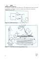
2. Configuration
9
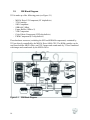
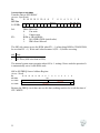
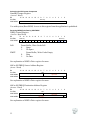
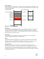
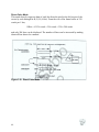
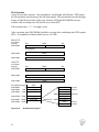
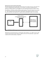
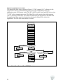
1.2.
32X Block Diagram
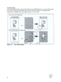
32X is made up of the following parts (see Figure 2.1)
-
MEGA Drive I/F Component (I/F chipbuilt-in)
32X Cartridge
SH2 Component
SDRAM (2 Mbit)
Frame Buffer (1Mbit x 2)
VDP Component
Color Palette Component (VDP chip built-in)
PWM Component (I/F chip built-in)
These hardware resources (excluding the SH2 and SDRAM components) contained by
32X are directly controlled by the MEGA Drive 68000 CPU. The ROM cartridge can be
read from both the MEGA Drive and 32X. Images and sound made by 32X are combined
with images and sound made by the MEGA Drive.
Figure 2.1
10
32X Block Diagram
1.3.
About the 32X Block
The role and features of each 32X block shown in section 2.1 is explained below. See
chapter 3 for more information.
MEGA Drive I/F Component
This is an interface connecting the 32X to the MEGA Drive. The 32X hardware resources
(graphics, sound, and coomunication with SH2) and cartridge ROM are mapped through
the MEGA Drive I/F in the MEGA Drive main CPU (68000) address space.
32X Cartridge Component
The content of the ROM ROM cartridge installed in the 32X cartridge slot can be read
from both the 32X CPU SH2 side and the MEGA Drive side 68000 (and Z80).
Nevertheless, SH2 has priority when conflict vetween the two exists.
SH2 Component
These are two SH2 chips as main CPUs mounted in the 32X, and the cartridge ROM is
connected with the 32X hardware ressources (graphics, sound, and communication to
68000) on a common bus. The 2 SH2 units are fixed to the master and slave by packaged
conditions; the normal master gest bus authorization and slave gets bus authorization after
obtaining permission of the master at the time of the bus access.
MEGA Drive hardware cannot map in SH2 address space. Consequently, MEGA Drive
information is indirectly received by communication with the 68000. The 32X has a
control register that issues interrupts from 68000 to SH2, a FIFO register that can send
data written from the 68000 to the DMA built-in the SH2, and a register that is able to
read and write from both the 68000 and SH2, and reads data written from the 68000.
11
SDRAM Component
The 32X has 2Mbits of SDRAM (synchronous DRAM) as its main memory for the SH2
chips. The SH2 program on the cartridge ROM is loaded in the SDRAM, then executed.
The SDRAM arranges 16 bytes and reads to the buffer inside the chip†; after which, in
order to synchronize to the SH2 clock and transfer sequentially all data after the second
data set can be transferred without any restrictions incurred by the operation within the
memory. The SH2 is able to rapidly execute data replacement by combining with the
SDRAM when cache miss occurs.
Frame Buffer Component
Memory that saves the display contents of one part of the color display is called a frame
buffer. For one screen, the display flickers when rewrite does not finish in V Blank
(vertical retrace line interval). Therefore, the memory is arranged as two screens in 32X
and a method is isued to alternatively switch between the update screen and display
screen. The frame buffer performs the switching operations with each Mbit and program.
VDP Component
32X VDP holds the frame buffer as a control screen and controls the display of the color
display. This screen combines MEGA Drive scroll A, scroll B, and sprite as one screen in
the front or back. The following three modes can be selected from data formats in the
frame buffer.
Direct Color Mode
The direct color mode allocates each of the 16 bits to 1 pixel on the screen of which 15
bits is used and indicates any color from 32,768 colors.
Packed Pixel Mode
The packed pixel mode allocates each of 8 bits to 1 pixel on the screen and colors
indicated on the color palette mnetionned later and indirectly indicated.
Run Length Mode
The run length mode allocates 16 bits as a collection of identically colored pixels that
continue with more than 1 pixel in the direction of the scan line. Pixel numbers that are
continuous with 8 of the 16 bits and colors indicated on the color palette with the
remaining 8 bits are indirectly indicated.
12
Color Palette Component
The color palette is a 256 word RAM block. When in the packed pixel mode or run length
mode, pixel data in the frame buffer select colors (256 colors from among 32,768 colors)
indirectly selected in advance.
The color selection format is the same whether selecting per frame buffer in the direct
color mode, or per color palette in the run-length mode. One color is 16 bits, of which 15
bits are used, and any color can be selected from 32,768 colors. The remaining 1 bit is
called a priority-bit (through-bit)†; pixels indicated by this bitís color are displayed
opposite to the MEGA Drive screen. For example, when 32X screens are combined in the
rear as a single scroll A, scroll B and sprite screen, only the pixels that indicated the color
of this bits is displayed in front of the MEGA Drive screen.
PWM Component
PWM (Pulse Width Modulation) replaces sampling data with the pulse width and outputs
the pulse width. If output is through an integrated circuit the amplitude can be controlled
by the pulse width. The 32X can regenerate in stereo PCM wave data converted in
advance fro PWM.
13
3. Functions
14
1.4.
Mapping
The 32x hardware can be controlled from both the main CPU SH2 and MEGA Drive
68000. As stated in the last chapter, the layout of each block in the address space of both
CPUs is explained here.
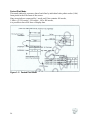
MEGA Drive Memory Map
In using the 32X, the exclusive initial program provided by SEGA is laid out cartridge
ROM of 3FAh or more and jumped by the reset vector. To map the 32X in 68000 address
space, this program sets the ADEN (address enable) bit to 1, initializes the hardware, and
executes the application. The figure below shows the 68000 address space immediately
after the power is turned on and the initial program executed.
When using Super 32x (ADEN = 1)
00 0000h
Vector ROM
40 0000h
40 0000h
See MD Manual
84 0000h
86 0000h
88 0000h
Frame Buffer
Overwrite Image
ROM Cartridge
0000 0000h 0007 FFFFh
90 0000h
ROM Cartridge
(4 Bank Switch)
A0 0000h
A1 30ECh
See MD Manual
Super 32X ID
A1 30ECh
A1 30F0h
A1 5100h
A1 5180h
100 0000h
Figure 3.1
15
See MD Manual
Super 32X ID
See MD Manual
A1 30F0h
Super 32X SYS REG A1 5100h
See MD Manual
A1 5180h
A1 5200h
A1 5400h
100 0000h
MEGA Drive Memory Map
See MD Manual
Super 32X SYS REG
VDP REG
Color Palette
See MD Manual
accessible when RV
=0
accessible
when RV =
1
When Power is on (ADEN = 0)
00 0000h
ROM Cartridge
"MARS
"
Custom internal ROM
00 0000h
00h
88 0200h
04h
88 0206h
08h
88 020Ch
0Ch
…
FCh
100h
4 bank
00 0000h
10 0000h
20 0000h
30 0000h
40 0000h
ROM Access when using the 32X
The 68000 vector area (00 0000h - 00 00FFh) is assigned by the custom built-in ROM.
Because the ROM contents are 88 0200h, 88 0206h, 88 020Ch, … . After 88 0200h (200h
of the cartridge ROM), 6-byte JUMP commands are arranged into a jump table.
Only when th RV (ROM to VRAM DMA) bit is 1 is it assigned by the cartridge ROM to
100h - 3F FFFFh. ROM access from the SH2 at this time waits until 68000 rewrites the
RV bit to 0.
When the RV bit is 0 access is from 88 0000h - 9F FFFFh to the cartridge ROM. 88
0000h - 8F FFFFh is allocated by fixing 00 0000h - 7F FFFFh (4Mbit) of the cartridge
ROM. In 90 0000h - 9F FFFFh, a cartridge area of 32Mbits is divised into 4 banks and
accessed by the bank set register.
When the 68000 and SH2 are accessed at the same time, the SH2 has priority. Otherwise
access is granted on a first come, first served basis : the second access waits until the first
is over.
When the 68000 and SH2 access the same area at the same time, the SH2 has priority.
Otherwise access is granted on a first come, first served basis : the second access waits
until the first is over.
The MEGA Drive has a bank set register (A1 30F1h - A1 30FFh odd numbered
addresses) for coping with a cartridge ROM that exceeds 32Mbits. The RV bit should be
set to "1" beforehand when accessing here.
Access to the 32X VDP
The FM (VDP access authorization) bit number must be 0 before the MEGA Drive can
access the Mars frame buffer, overwrite images, VDP register or color palette. When the
bit is 1, reads are undefined and writes are ignored. Color palette access is words only, not
bytes.
The frame buffer, overwrite image, VDP register, and color palette can be accessed from
the MEGA Drive side only when the FM (VDP access authorization) bit is 0. . When the
bit is 1, reads are undefined and writes are ignored. Color palette access is words only, not
bytes.
16
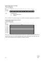
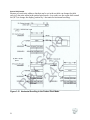
SH2 Memory Map
The 32X has two SH2 chips mounted to a common bus. Consequently, memory maps of
the two chips shown in Figure 3.2 are the same. The SH2 has a built-in cache memory for
increasing the speed of command and data accessing. Access of identical components of
the 32X can be accessed by two cache/ cache through addresses. In cases of the cache
address, if is read if data of the address to be is in the cache memory. If not in the cache
memory, is read directly from that address, and the cache memory is replaced by the data
Cache Through Address
2000 0000h
2000 4000h
2000 4100h
2000 4200h
2000 4400h
Cache Address
0000 0000h
0000 4000h
0000 4100h
0000 4200h
0000 4400h
2200 0000h
0200 0000h
2240 0000h
0240 0000h
2400 0000h
0400 0000h
Frame Buffer
2402 0000h
0402 0000h
Overwrite Image
2404 0000h
0404 0000h
2600 0000h
2604 0000h
0600 0000h
0604 0000h
2800 0000h
0800 0000h
Figure 3.2
17
SH2 Memory Map
Boot ROM
Super 32X SYS REG
VDP REG
Color Palette
ROM Cartirdge
SDRAM
Cannot be accessed when FM = 0
Color palette can access only in words
Cannot be accessed when RV = 1
Cannot be accessed when FM = 0
4 word write FIFO
Cache Area Access
Cache memory is memory used for rapidly supplying commands, operans, and data to the
CPU. The 32X accesses the cache after commands and data are loaded in the SDRAM. In
32X, after having loaded command and data into the SDRAM, the cache access is
performed. The 32X system register and VDP register, among others, must be cachethrough accessed because values through the VDP or other CPU are replaced and the
contents of the cache can no longer be guaranteed.
Cartridge ROM Access
Only when the RV (ROM to VRAM DMA) bit is 0 can SH2 be accessed to the cartirdge
ROM. When the RV bit is 1 and if accessing from SH2 to the cartridge ROM, a wait
occurs until 68000 replaces the TV bit with 0. The RV bit from SH2 can only read.
32X VDP Access
Only when the FM (VDP access authorization) bit is 1 can the frame buffer overwrite
images, VDP register, and color palette access from the SH22 side. When the FM bit is 0,
read is undefined and write is ignored. The color palette can access only in words but not
in bytes.
The frame buffer and overwrite image have 4 word write FIFO and can write in 3 clock
cycles. Five clock cycle are required when continuously writing 4 words or more.
18
1.5.
Registers
32X registers are classified ad shown below. Meanings of the address and set value of each
register are also shown.
32X System Register
[MEGA Drive]
Able to use 32X
Adapter control register
Issues interrupt for SH2
Interrupt control register
ROM cartirdge bank switching
Bank set register
Transfers data to SH2 DMAC
DREQ cotnrol register
68 to SH DREQ Source Address register
68 to SH DREQ Destination Address
register
68 to SH DREQ Length register
FIFO register
Register signal output to cartridge register
SEGA TC register
Communication in both direction with SH2
Communication port register
Control of PWM Sound Source
PWM Control register
Cycle register
L ch pulse width register
R ch pulse width register
Mono pulse width register
19
[SH2]
Interrupt control for SH2
Interrupt mask register
H Count register
VRES interrupt clear register
V interrupt clear register
H interrupt clear register
CMD interrupt clear register
PWM interrupt clear register
32X custom component activation
Standby changer register
MEGA Drive data receiv ed by DMAC of
SH2
DREQ cotnrol register
68 to SH DREQ Source Address register
68 to SH DREQ Destination Address
register
68 to SH DREQ Length register
FIFO register
Register signal output to cartridge register
SEGA TV register
Communication in both direction with SH2
Communication port register
Control of PWM Sound Source
PWM Control register
Cycle register
L ch pulse width register
R ch pulse width register
Mono pulse width register
VDP register
Display mode selection
Bitmap Mode register
Frame buffer switch
Frame buffer cotnrol register
Screen shift
Screen shift control register
Data fill for frame buffer
Auto Fill Length register
Auto Fill Start Address register
Auto Fil Data register
20
System Registers
[MEGA Drive side]
Using the 32X
Adapter Control Register
(Access : Byte/Word)
Bit
15 14 13 12 11 10 9
MD Side
R/W
FM
A1 5100h
-
FM:
REN:
RES:
ADEN:
8
7
6
5
4
3
2
Read only
-
REN
1
0
R/W R/W
-
-
-
-
-
RES
ADEN
VDP Access Authorization
0:
MD (Initial value)
1:
SH2
SH2 Reset Enable
0:
Disable
1:
Enable
Resets SH2
0:
Reset
1: Cancel reset (initialization by the inital program. Change not allowed.)
Adapter Enable Bit
0:
Prohibits use of 32X
1:
Permits use of 32X (initialization by the initial program. Change not
allowed.)
Switching access authorization is done while writing to the FM bit. Therefore, be aware
that if writing to the FM bit is done by MEGA Drive while SH2 accesses VDP, access
authorization is forced to switch to MEGA Drive.
21
Interrupt issued for SH2
Interrupt Control Register
(Access : Byte/Word)
Bit
15 14 13 12 11 10
MD Side
A1 5102h
-
INTS:
INTM:
9
8
7
6
5
4
3
2
1
0
R/W R/W
-
-
-
-
-
-
-
-
INTS
INTM
3
2
1
0
Slave SH2 interrupt command
0:
NO OPERATION (initial value)
1:
Interrupt command
Master SH2 interrupt command
0:
NO OPERATION (initial value)
1:
Interrupt command
Both are automatically cleared if SH2 does not interrupt clear.
Switches ROM Cartridge Bank
Bank Set Register
(Acces : Byte/Word)
Bit
15 14 13 12 11 10
MD Side
A1 5104h
BK1
0
0
1
1
22
BK0
0
1
0
1
9
8
7
6
5
4
R/W R/W
-
-
Data seen in 90 0000h – 9F FFFFh
00 0000h – 0F FFFFh (initial value)
10 0000h – 1F FFFFh
20 0000h – 2F FFFFh
30 0000h – 3F FFFFh
-
-
-
-
-
-
BK1 BK0
Transfers Data to SH2 DMAC
Transfers Data to SH2 DMAC
(Access : Byte/Word)
Bit
15 14 13 12 11 10 9
MD Side
A1 5106h
-
Ful:
RV:
8
7
6
5
4
3
Read only
FULL
-
2
1
0
R/W R/W R/W
-
-
-
-
68S
0
RV
DMA FIFO Full
0:
Can write
1:
Cannot write
ROM to VRAM DMA
0:
NO OPERATION (initial value)
1:
DMA Start Allowed
The SH2 side cannot access the ROM when RV = 1 (when doing ROM to VRAM DMA,
be sure that RV = 1). Waits until value becomes 0 (RV = 0) before accessing.
68S Mode
0
No Operation
1
CPU Write (68K writes data in FIFO)
The internal system starts operation when 68S is 1. writing 0 force-ends the operation. It
is automatically set to 0 after DMA ends.
68K to SH DREQ Source Address Register
(Acces : Word)
Bit
MD Side
A1 5108h
A1 510Ah
15 14 13 12 11 10
9
8
7
6
5
4
3
2
1
0
R/W
-
High Order
Low Order
0
Because the DREQ circuit does not use this data, nothing needs to be set ath the time of
CPU WRITE.
23
68K to SH DREQ Destination Address Register
(Acces : Word)
Bit
MD Side
A1 510Ch
A1 510Eh
15 14 13 12 11 10
9
8
7
6
5
4
3
2
1
0
R/W
-
High Order
Low Order
0
Sets the SH2 side (SDRAM) address. The DREQ circuit does not use this data. Thus,
when the destination address is known beforehand by SH2, or when SH2 doesnít need to
know, no settings are nedded.
68K to SH DREQ Length Register
(Acces : Word)
Bit
MD Side
A1 5110h
15 14 13 12 11 10
9
8
7
6
5
4
3
2
1
0
0
0
R/W
Sets the number of data items (unit : word) to be sent to SH2 side. The value to be set is in
4 word unites. Low order 2 bits write is ignored (00 fixed). Be sure to set this register for
CPU WRITE. At each transfer, this register is decremented and when it becomes 0, the
DREQ operation ends. Transfer is done 65 56 times when 0 is set. Read time reads the
actual count value.
FIFO Register
(Access : Word)
Bit
MD Side
A1 5112h
15 14 13 12 11 10
9
8
7
6
5
4
3
2
1
Write only
Data is written to this register when DREQ is used by CPU WRITE.
24
0
Refresh Singal Output to Cartridge
SEGA TV Register
(Acces: Byte/Word)
Bit
MD Side
A1 511Ah
CM:
15 14 13 12 11 10
9
8
7
6
5
4
3
2
1
-
-
-
-
-
-
-
-
-
0
R/W
-
-
-
-
-
-
CM
Cartridge Mode
0:
ROM (initial value)
1:
DRAM
This is a SEGA TV exclusive registe, use of this bit with other application is prohibited.
Communication in both directions with SH2
Communication Port
(Access : Byte/Word)
Bit
MD Side
A1 5120h
A1 5122h
A1 5124h
A1 5126h
A1 5128h
A1 512Ah
A1 512Ch
A1 512Eh
15 14 13 12 11 10
9
8
7
6
5
4
3
2
1
0
R/W
This is an 8 word bi-directionnal register. Read/write is possible from the MEGA Drive
and SH2 directions, but when writing the same register from both at the same time, the
value of that register becomes undefined. Caution is advised.
25
PWM Sound Source Control
PWM Control Register
(Access: Byte/Word)
Bit
MD Side
A1 5130h
15 14 13 12 11 10
RMD1
0
1
0
1
8
7
6
5
4
-
-
-
Read only
-
-
-
TM3~0:
RTP:
RMD0
0
0
1
1
9
-
3
2
1
0
R/W R/W R/W R/W
TM3 TM2 TM1 TM0 RTP
RMD0 RMD1 LMD0 LMD1
PWM timer interrupt interval
DREQ 1 occurrence enable (SH2 side only)
0:
OFF (initial value)
1:
ON
OUT
OFF
R
L
Setting not allowed
LMD0
0
0
1
1
LMD1
0
1
0
1
OUT
OFF
L
R
Setting not allowed
Both cannot be set to L ch or R ch.
Cycle Register
(Access : Byte/Word)
Bit
MD Side
A1 5132h
15 14 13 12 11 10
9
8
7
6
5
4
3
2
1
0
R/W
-
The base clock frequency of the cycle registers are fixed respectively: NTSC at
23.01MHz and PAL at 22.8MHz (set value x Scyc) becomes the cycle.
NTSC Scyc = 1/23.01 [MHz]
PAL Scyc = 1/22.8 [MHz]
The cycle counter does not operate when both L ch and R ch are off.
26
L ch Pulse Width Register
(Access : Byte/Word)
Bit
MD Side
A1 5134h
15
14
13 12 11 10
9
8
7
Read only
FULL EMPTY
6
5
4
3
2
1
0
4
3
2
1
0
4
3
2
1
0
Write only
-
-
The value set by bit 11~0 x Scyc becomes the pulse width.
FULL:
Conditions of pulse width FIFO
0:
Space available
1:
No space availabme
EMPTY:
Conditions of pulse width FIFO
0:
Data per FIFO
1:
No data per FIFO
R ch Pulse Width Register
(Access : Byte/Word)
Bit
MD Side
A1 5136h
15
14
13 12 11 10
9
8
7
Read only
FULL EMPTY
6
5
Write only
-
-
See explaination of L ch pulse width register
Mono Pulse Width Register
(Access : Byte/Word)
Bit
MD Side
A1 5138h
15
14
13 12 11 10
9
8
7
Read only
FULL EMPTY
6
5
Write only
-
-
See explaination of L ch pulse width register
If writing to this register, the same value is written to both L ch and R ch.
Note:
Bits D0~D11 of all L ch, R ch and MONO pulse width registers are write only. When read is
performed, undefined data is read. Each PWM of L ch and R ch have time separate FIFO steps.
When both the L and R channels are off, because the cycle counter does not operate, once the
FULL bit is set to ì1î, it will not become ì0î as long as the channels are not turned on. When
either the L of R channel is on, because the OFF side FIFO is also operating, no sound will be
output ; however, data within FIFO will disappear. If writing when FIFO is FULL, the oldest data
is discarded and shift occurs one item at a time.
27
[SH2 side]
Interrupt Control for SH2
Interrupt Mask Register
(Access : Byte/Word)
Bit
SH Side
2000 4000h
FM:
ADEN:
CART:
HEN:
V:
H:
CMD:
PWM:
15 14 13 12 11 10
9
8
7
6
5
4
-
-
-
Read only R/W
FM
-
-
-
-
-
ADEN CART
HEN
3
2
1
0
R/W R/W R/W R/W
V
H
CMD PWM
VDP Access Authorization
0:
MEGA DRIVE (initial value)
1:
SH2
Adapter enable bit
0:
the 32x use prohibited
1:
the 32X use allowed
Cartridge insert condition
0:
Inserted
1:
Not inserted
H INT approval within V Blank
0:
H INT not approved (initial value)
1:
H INT approved
V INT Mask
0:
Mask (initial value)
1:
Valid
H INT Mask
0:
Mask (initial value)
1:
Valid
Command Interrupt Mask
0:
Mask (initial value)
1:
Valid
PWM timer interrupt mask
0:
Mask (initial value)
1:
Valid
This register is mapped to the same address for both SH2 master side and slave side. But,
V, H, CMD and PWM each possesses exclusive address on the master side and the slave
side. Other bits are common to both the master and slave sides. Please note carefully that
if a ì1î is written to the FM bit, access authorisation is forced to switch to the SH2 side,
even if access of VDP is in progress in the MEGA Drive side.
28
H Count Register
(Access : Byte/Word)
Bit
SH Side
2000 4004h
15 14 13 12 11 10
9
8
7
6
5
4
3
2
1
0
R/W
-
Sets H int occurrence interval. Designates byt the number of lines. 0 = each line (initial
value).
VRES Interrupt Clear Register
(Access : Word)
Bit
SH Side
2000 4014h
15 14 13 12 11 10
9
8
7
6
5
4
3
2
1
0
Write only
Clears VRES interrupt (interrupt caused by pressing the MEGA Drive reset button). If not
cleared, interrupt will no longer occur.
V Interrupt Clear Register
(Access : Word)
Bit
SH Side
2000 4016h
15 14 13 12 11 10
9
8
7
6
5
4
3
2
1
0
1
0
1
0
Write only
Clears V interrupt. If not cleared, interrupt will no longer occur.
H Interrupt Clear Register
(Access : Word)
Bit
SH Side
2000 4018h
15 14 13 12 11 10
9
8
7
6
5
4
3
2
Write only
Clears H interrupt. If not cleared, interrupt will no longer occur.
CMD Interrupt Clear Register
(Access : Word)
Bit
SH Side
2000 401Ah
15 14 13 12 11 10
9
8
7
6
5
4
3
2
Write only
Clears CMD interrupt (command interrupt). If not cleared, interrupt will no longer occur.
29
PWM Interrupt Clear Register
(Access : Word)
Bit
SH Side
2000 401Ch
15 14 13 12 11 10
9
8
7
6
5
4
3
2
1
0
Write only
Clears PWM interrupt (command interrupt). If not cleared, interrupt will no longer occur.
30
Points to be aware of concerning interrput
Ex. 1.
32X has VRESINT, VINT, HINT, CMDINT and PWMINT, but among
these, only CMDINT has points which differ from other INT. Interrupt is enabled
by the Interrupt Mask Regsiter (2000 4000h) within the SH2 system register, INT
occurs, and when INT is masked by the Interrupt Mask Register within the system
register before that INT is received, the following will happen :
a. VRES INT, VINT, HINT, PWMINT : INT continues to occur unitl each
INT is cleared
b. CMDINT : INT is negated. But when CMDINT is enabled after CMDINT
is not received, CMDINT is again asserted.
In short, when all INT occur before they are masked, the INT conditions will
continue to be saved as long as that INT is not cleared. But when Interrupt is
amsked only for CMDINT, INT will temporarily disappear. Still, because
CMDINT information will be saved as long as it is not cleard, INT will again
occur if CMDINT is enabled.
Ex. 2.
HEN (HINT authorization bit during V Blank) inside the interrupt mask
register of SH2 is common in both Master and Slave. The HINT occurrence
interval is affected by this HEN bit.
The value set in the H Count register is enabled, as the next H Blank occurs, after
being loaded in the internal counter when H Blank is negated. Alos, the internal
counter generates HINT as a result of the count, but when H Blank is negated the
H Count register value is reloaded. Therefore, when the H Count register is set
when H Blank does not occur (becaus it is not loaded in the internal counter until
the next H Blank occurrs), HINT may occur according to the value prior to setting
the H Count.
Ex. 1.
When H Count register = 0, 1 is set in the H Count register during H Bank.
When HEN = 0, HINT occurs within the second H Blank after the existinf H Blank
is negated.
Ex. 2.
H Count register = 0 and H Count is set to 1 when H Blank does not occur.
When HEN = 0, HINT occurs during the next H Blank. HINT occurs during the
2nd H Blank after the H Blank is negated because the H Count register setting
(value) is loaded in the internal counter when this H Blank is negated.
31
Activating the 32X Custom Component
StandBy Changer Register
(Access : Word)
Bit
SH Side
2000 4002h
15 14 13 12 11 10
9
8
7
6
5
4
3
2
1
0
Write only
Use with system (Boot ROM). Access to this register from the application is prohibited.
Receiving MEGA Drive Data by SH2 DMAC
DREQ Control Register
(Access : Byte/Word)
Bit
SH Side
2000 4006h
Full:
EMPT:
15
14
13 12 11 10
9
8
7
6
5
4
3
Read only
FULL EMPTY
2
1
0
Read only
-
-
-
-
-
-
-
-
-
-
-
68S
0
RV
4
3
2
1
0
Frame Buffer, Write Cache Full
0:
Space
1:
No Space
Frame Buffer, Write Cache Empty
0:
Data
1:
No Data
See explanation of MEGA Drive register for more.
68K to SH DREQ Source Address Register
(Acces : Word)
Bit
SH Side
2000 4008h
2000 400Ah
15 14 13 12 11 10
9
8
7
6
5
R/W
-
High Order
Low Order
0
See explanation of MEGA Drive register for more.
68K to SH DREQ Destination Address Register
(Access : Word)
Bit
SH Side
2000 400Ch
2000 400Eh
15 14 13 12 11 10
9
8
7
6
4
3
2
1
0
R/W
-
High Order
Low Order
See explanation of MEGA Drive register for more.
32
5
0
68k to SH DREQ Length Register
(Access : Word)
Bit
SH Side
2000 4010h
15 14 13 12 11 10
9
8
7
6
5
4
3
2
1
0
0
0
Read only
See explanation of MEGA Drive register for more.
FIFO Register
(Access : Word)
Bit
SH Side
2000 4012h
15 14 13 12 11 10
9
8
7
6
5
4
3
2
1
0
5
4
3
2
1
0
Read only
See explanation of MEGA Drive register for more.
Communication in Both Directions with 68000
Communication Port Register
(Access : Byte/Word)
Bit
SH Side
2000 4020h
2000 4022h
2000 4024h
2000 4026h
2000 4028h
2000 402Ah
2000 402Ch
2000 402Eh
15 14 13 12 11 10
9
8
7
6
R/W
See explanation of MEGA Drive register for more.
33
PWM Sound Source Control
PWM Control Register
(Access : Byte/Word)
Bit
SH Side
2000 4030h
15 14 13 12 11 10
9
8
7
6
5
4
-
-
-
R/W R/W R/W R/W R/W
-
-
-
-
3
2
1
0
R/W R/W R/W R/W
TM3 TM2 TM1 TM0 RTP
RMD0 RMD1 LMD0 LMD1
See explanation of MEGA Drive register for more.
TM0~3 set the PWM timer interrupt interval and ROM to PWM transfer cycle. Interrupt
occurs by cycle register set value x TM cycle. When TM = 1 the interval is the same as
the cycle register. When TM = 0 the interval is 16 times the cycle register.
Cycle Register
(Access : Byte/Word)
Bit
SH Side
2000 4032h
15 14 13 12 11 10
9
8
7
6
5
4
3
2
1
0
R/W
-
See explanation of MEGA Drive register for more.
L ch Pulse Width Register
(Access : Byte/Word)
Bit
SH Side
2000 4034h
15
14
13 12 11 10
9
8
7
6
Read only
FULL EMPTY
5
4
3
2
1
0
4
3
2
1
0
4
3
2
1
0
Write only
-
See explanation of MEGA Drive register for more.
R ch Pulse Width Register
(Access : Byte/Word)
Bit
SH Side
2000 4036h
15
14
13 12 11 10
9
8
7
Read only
FULL EMPTY
6
5
Write only
-
See explanation of MEGA Drive register for more.
Mono Pulse Width Register
(Access : Byte/Word)
Bit
SH Side
2000 4038h
15
14
13 12 11 10
Read only
FULL EMPTY
9
8
7
6
-
See explanation of MEGA Drive register for more.
34
5
Write only
35
VDP Registers
(Both MEGA Drive and SH2 Common)
Display mode Selection
Bitmap Mode Register
(Access : Byte/Word)
15
14
13
12
11
10
9
8
Read only
MD Side
A1 5180h
SH Side 2000 4100h
PAL
7
6
5
-
-
-
-
-
-
-
PRI 240
-
TV format
0:
PAL
1:
NTSC
Switching is possible only during V Blank
PRI:
Screen priority (explained later)
0:
MEGA Drive has priority (initial value)
1:
32X has priority
Switching is always allowed, but is valid from the next line.
240:
240 Line Mode (Valid only when PAL)
0:
224 Line (initial value)
1:
240 Line
M1 M0 Mode
0
0 Blank Mode (intial vlaue)
0
1 Packed Pixel Mode
1
0 Direct Color Mode
1
1 Run Length Mode
Switching is always allowed, but is valid from the next line.
36
3
2
1
0
R/W R/W
Switching is always allowed, but is valid from the next line.
PAL:
4
R/W R/W
-
-
-
M1
M0
Frame Buffer Switching
Frame Buffer Control Register
(Access : Byte/Word)
15
MD Side
A1 518Ah
SH Side 2000 410Ah
VBLK:
HBLK:
PEN:
FEN:
FS:
13
12
11
10
9
8
7
6
5
4
3
2
-
-
-
-
-
-
-
-
-
-
-
Read only
VBLK HBLK
PEN
1
0
R/W R/W
FEN FS
V Blank
0:
During display period
1:
During V Blank
H Blank
0:
During display period
1:
During H Blank
Palette Access Approval
0:
Access denied
1:
Access approved
Frame Buffer Authorization
0:
Access approved
1:
Access denied
Frame Buffer Swap
0:
Transfers DRAM0 to VDP side (initial value)
1:
Transfers DRAM1 to VDP side
37
14
Swapping the Frame Buffer is allowed during V Blank (VBLK = 1) or
when in the blank mode. However, writing the FS bit is always allowed,
and when written during display, swapping is done at the next V Blank.
With respect to read, the value, which indicates DRAM during display
until the next V Blank, is returned.
When having swapped the Frame Buffer, be sure to access the Frame
Buffer after confirming that VBLK = 1 or FS bit has changed.
When ahving performed FILL, be sure to access the Frame Buffer after
confirming that FEN is equal to 0.
Palette access is possible only during H and V blank.
Palette can access whenever the bitmap mode is in the direct color mode,
as well as during Blank.
Screen Shift
Screen Shift Control Register
(Access : Byte/Word)
15
MD Side
A1 5182h
SH Side 2000 4102h -
SFT:
14
13
12
11
10
9
8
7
6
5
4
3
2
1
0
-
-
-
-
-
-
-
-
-
-
-
-
-
-
SFT
3
2
1
0
R/W
Screen 1 dot left shift (explianed later)
0:
OFF
1:
ON
Switching is allowed at any time, but is valid from the next line.
Data fill for Frame Buffer
Auto Fill Length Register
(Access : Byte/Word)
15
14
13
12
MD Side
A1 5184h
SH Side 2000 4104h
11
10
9
8
7
6
5
4
R/W
-
Word length when filling DRAM (frame buffer). To set this value, set the value for the tobe-filled word length (0~255).
Note : the Auto Fill function will be explained later.
Auto Fill Start Address Register
(Access : Word)
15
14
13
12
11
10
9
8
7
MD Side
A1 5186h
R/W
SH Side 2000 4106h A16 A15 A14 A13 A12 A11 A10 A9 A8
6
5
4
3
2
1
0
A7
A6
A5
A4
A3
A2
A1
Sets the start address of the area to be filled. A16-A9 remains as fixed, but A8~A1 are
incremented at each Fill.
Auto Fill Data Register
(Access : Word)
15
MD Side
A1 5188h
SH Side 2000 4108h
14
13
12
11
10
9
8
7
6
5
4
3
R/W
Sets data to be filled. The Fill operation begins when setting this register.
38
2
1
0
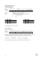
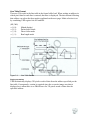
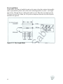
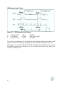
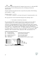
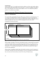
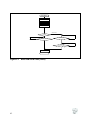
1.6.
VDP
32X VDP (referred to as VDP thereafter) controls the color display and has two 1 Mbit
frame buffer surfaces for control display screens. Display (to the display screen) is
synthesized and composed contextually of a single screen (plane) from thses screens and
the existing MEGA Drive screen.
MEGA Drive Screen
Scroll B
Scroll A
Priority
Window
Sprite
BG
Display Screen
Priority
32X Screen
DRAM0
DRAM1
Figure 3.3
39
Frame
Select
Combination with MEGA Drive Screens
Display Mode
Enables output of images that correspond to the NTSC format (Japan, USA) and the PAL
format (Western Europe). When the 32X image output is not blank, the MEGA Drive
display mode should select a resolution that is equal to the 32X resolution.
32X
Non blank
320 x 224 pixels
Non-blank
320 x 240 pixels
Blank
Table 3.1
40
MD
Graphic V
40 x 28 cells (320 x 224 pixels)
Graphic V
40 x 30 cells (320 x 240 pixels)
Graphics IV
32 x 28 (256 x 192 pixels)
Graphics V
32 x 28 cells(256 x 224 pixels)
40 x 28 cells (320 x 224 pixels)
32 x 30 cells (256 x 240 pixels)
40 x 30 cells (320 x 240 pixels)
Display Mode Possible Combinations
VDP Configuration
VDP is mapped, as shown below, from SH2 address 2000 4100h and 2400 0000h. These
exist as I/O devices for the CPU. As a resulte, acccessing without the color palette is only
a cache-through address.
SH (cache-through)
SH (cache-through)
VDP Register 2000 4100h
Bitmap mode
2000 4102h Screen Shift Control
2000 4104h
Auto Fill Length
2000 4106h Auto Fill Start Address
2000 4108h
Auto Fill Data
2000 410Ah Frame Buffer Control
2000 410Ch
Reserve
2400 0000h
2000 4200h
Color Palette
DRAM
1Mbit
2402 0000h
Over Write
Image
2404 0000h
2000 4400h
Figure 3.4
32X VDP Mapping
VDP Register
The VDP register controls RAM block access, the VDP mode, priority, etc. The VDP
register is read to the VDP display circuit when a horizontal return line is complete.
Consequently, after the register is set, the settings from the next line become valid for the
bitmap mode and screen shift control.
Color Palette
The color parlette is RAM block that designates display colors. A cache address is
possible. This block must always be word accessed.
DRAM
Also called a frame buffer, DRAM stores line tables and bit pattern data for each line.
Mapping is done for either DRAM0 or DRAM1. This block can write 8-bit or 16-bit
widths. Write speeds ar all the same, but 0 cannot be written in byte access.
Over Write Image
Data write can also be done from this area to the frame buffer. Because there is
specialization in character overwrite, if the significant or insignificant byte of data is 0
when accessing by word, only that part ignores overwrite and holds the original value.
This block can write in 8-bit or 16-bit widths. Write speeds are all the same, but 0 cannot
be written in byte access.
41
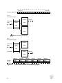
Switching Frame Buffers
By switching the FS bit, the DRAM draw previously handled by the CPU is transferred to
the VDP and the contents are displayed. In addition, DRAM that has been displayed is
mapeed instead in the address space, allowing the draw. For instance, animation can be
displayed repeatedly per each single frame (1/60 sec), and for the period equivalent to a
single frame (1/60 sec), write process can continue. Frame buffer can be switched only in
VBlank. During display, evan when writing to the FS bit, the buffer does not switch until
Vblank occurs. The FS bit, when read, returns the buffer selected on the current display
side. DRAM access should take place after confirming that VBLK=1, or the FS bit has
been switched.
42
15 14 13 12 11 10
Read only
SH Side 2000 410Ah VBLK HBLK PEN
-
-
-
9
8
7
6
5
4
3
2
1
0
R/W R/W
-
-
-
-
-
-
-
-
FEN
FS = 0
SH (Cache-through)
DRAM0
2400 0000h
Draw
DRAM
Display
1Mbit
1Mbit
2402 0000h
DRAM1
1Mbit
Rewrites FS bit during VBLANK
FS = 1
SH (Cache-through)
DRAM0
2400 0000h
Draw
DRAM
1Mbit
1Mbit
2402 0000h
DRAM1
Display
1Mbit
DRAM0
DRAM1
Figure 3.5
43
1/60 sec
Display
Draw
1/60 sec
Draw
Display
1/60 sec
Display
Draw
Animation
1/60 sec
Draw
Display
1/60 sec
Display
Draw
Frame Buffer Switch and Animaiton Display
1/60 sec
Draw
Display
FS
Color Palette
There is one DRAM0 and DRAM1 common color palette in the 32X, and 0~255 palette
code can be specified per each pixel. The figure belows shows the correlation between the
color data format, SH2 address, and palette code. Any of R, G, B, each with 5 bits, can be
selected from among 32 768 colors.
The color data format is 16-bit and the color for each pixel can be directly selected (when
in the direct color mode), but data size can be kept down by indirect-selecting using the 8bit palette code.
1 bit
5 bit
B
5
bit
R
5 bit
G
Through bit (See "Priority")
SH (Cachethrough)
2000 4200h
Through bit
Red brightness 1Fh (max)~00h (max) … 32 tones
Green brightness 1Fh (max)~00h (max) … 32 tones
Blue birghtness 1Fh (max)~00h (max) … 32 tones
Combined : 32 x 32 x 32 = 32768 colors
16 bit
B
G
R
Palette code 0 color designation
Palette code 1 color designation
Palette code 2 color designation
Color Palette
Palette code 255 color designation
2000 4400h
Figure 3.6
Color Data Format and Color Palette
Note:
Palette access is possible when PEN = 1 (Frame Buffer Control Register). If accessing when PEN
= 0, wait is held until PEN = 1. Also, when PEN goes from 1 ( 0, the written value is not
guaranteed. When the color is directly selectec, color palette can always be accessed.
44
Over Write Image
Allows RAM block that is physically identical to the DRAM area to be accessed from this
area. When writing data from this area, data on the frame buffer is not changed and
remains in its original state when 00h is written in 1 byte units.
Figure 3.7
45
Over Write Image
Overview of Display Specifications
Display Size
320 pixels x 224 pixels or 320 pixels x 240 pixels
only the non-interlace mode
Display Colors
32 768 color direct or 256 colors from 32 768 colors (color palette)
Frame Buffer
1Mbit DRAM x 2 (Line Table Format)
Draw Mode
Direct Color Mode (16 bit/1 pixel, 32K color direct)
Packed Pixel Mode (8 bits/1 pixel, 256 of 32K colors)
Run Length Mode (16 bits/continous same color pixels, 256 of 32K
colors)
Priority (Combine with To combine MEGA Drive scroll A, B and sprites into a single screen,
MEGA Drive screen)
32X screen is synthetized int the front or back
Other
Supports DRAM FILL at VDP side
Table 3.2
32X VDP Specifications
46
Line Table Format
There are 256 words in the line table in the frame buffer lead. When writing an address in
which pixel data for each line is entered, that liine is displayed. The data format following
that address can select the three modes explained on the next page. Mode selection is set
by combining VDP register bits M1 and M0.
(M1, M0)
= (0, 0):
= (0, 1):
= (1, 0):
= (1, 1):
(Blank display)
Packed pixel mode
Direct color mode
Run length mode
Figure 3.8
Line Table Format
Display precautions
VDP mechanically displays 320 pixels worth of data from the address specified per the
line table. Consequently, caution is required since the overwrite image area data is
displayed as is when there is no DRAM area for 320 pixels worth of data after the
specified address.
47
Priority
Select whether or not to use the PRI bit of the VDP register, and whether the 32X is to be
displayed in front of or behind the MD screen. Also, each through-bit 1-bit is added to the
color data. If the PRI bit is used, the pixel that designated the color is displayed in the side
opposite of the MD screen. When the MD color code is 0, and when the 32X designates
blank by the VDP register, each becomes transparent, the MD background is displayed.
Figure 3.9
48
Priority
Direct Color Mode
This mode directly expresses data of each line from the pixel in the left corner of the
screen by each through bit B, G, R (16-bit). From the size of the frame buffer at 320
words per 1 line,
1 Mbit = 65 536 words = 256 words + 320 x 204 words
and only 204 lines can be displayed. The number of lines can be increased by making
identical line data to be common.
Figure 3.10 Direct Color Mode
49
Packed Pixel Mode
This mode indirectly expresses data of each line by individual color palette codes (8-bit)
from pixels in the left corner of the screen.
Since two pixels are expressed by 1 word, and 1 line contains 160 words,
1 Mbit = 65 536 words = 256 words + 160 x 408 words,
it is possible to have 408 lines of display data.
Figure 3.11 Packed Pixel Mode
50
Screen Shift Control
Because of word units, address data that can be set in the ne table can change the table
only in 2-dot units when in the packed pixel mode. As a result, use the screen shift control
bit (SFT) to change the display position by 1-dot units for horizontal scrolling.
Figure 3.12 Horizontal Scrolling in the Packed Pixel Mode
51
Run Length Mode
In this mode, pixel data is handled in units as the same colors that continue horizontally,
and is represented in palette code (8-bit) and continuing number of pixels = run length
data (8-bit). Through-bits are valid in this mode as weel. When the run length exceeds
320 pixels for one line of data, the 320 pixels are displayed from the left, and all pixels
thereafter are ignored.
Figure 3.13 Run Length Mode
52
FILL Function
Auto Fill uses three registers : the start address, word length, and file data. VDP begins
the fill operation when writing to the file data register. The portion that exceeds the page
border is filled from the start of the page. Because VDP and SH2 DRAM accesses
conflict whil executing Auto Fill, do not access from SH2.
Fill execution time = 7 + 3 x length (cycle)
After executing Auto Fill, DRAM should be accessed after confirming that VDP register
FEN = 0 (completion of frame buffer access via VDP).
Before Fill
SH (Cachethrough)
2000 4104h
D15
D8 D7
is maintained
D0
10h
2000 4106h
20FEh
2000 4108h
1234h
After Fill
SH (Cachethrough)
2000 4104h
D15
D8 D7
is maintained
2000 4106h
200Eh
2000 4108h
1234h
SH (Cache-through)
2400 0000h
0
2400 0200h
100h
2400 0400h
200h
16 bit
1rst page
2nd page
2400 2E00h 1F00h
2400 4000h 2000h
2400 4200h 2100h
20the page
21rst page
D0
10h
200Eh
Figure 3.14
53
Example Executing Fill
1234h
1234h
3rd word
4th word
1234h
16th word
2400 41FCh 20FEh value before Fill
1234h
1rs word
1234h
2nd word
Clock Used by the 32X
The master clocks for NTSC and PAL used by the MEGA Drive and 32X are diffferent.
The 68000 and SH2 system clocks are shown belows as standards.
Mega Drive Master Clock Cycle
Mck = 1/fos [sec]
NTSC fosc = 53.693175 [MHz]
PAL fosc = 53.203424 [MHz]
68000 Clock Cycle
Vclk = 7Mck, but Mck is the value above.
SH2 Clock Cycle
Sclk = Vclk/3, but Vclk is the value above.
54
HBlank and Display Periods
Figure 3.15 HBLANK Period and Display Period
A:
B:
C:
D:
Blank Period
Display Period
HBLANK - VBLANK
HBLANK - XHDISP
100 dot
(860 Mck)
320 dot
(2560 Mck)
27 dot
(224 Mck)
3 dot
(24 Mck)
VBlank and Display Periods
Figure 3.16 VBLANK Period and Display Period
A: Blank Period
B: Display Period
55
NTSC
38h
224h
PAL (224)
89h
224h
PAL (240)
73h
240h
VDP Register Latch Timing
Figure 3.17 VDP Register Latch Timing
A:
B:
C:
H Blank - PEN
FEN Width
H Blank - latch
3 dot
40 Sclk
76 dot
(24 Mck)
(VDP side refresh)
(668 Mck)
The register set within interval C is valid at line n (the nth line), and for interval D is valid
at line n+1. Please avoid the type of phenomenon in which the VDP register latch and
CPU register access overlap. When the DRAM is being refreshed FEN is 1, but access of
the DRAM is possible. Be aware that if 1 is set in 240 bits when in the NTSC mode VDP
will have operating errors.
56
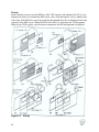
1.7.
PWM
PWM Sound Sound Source
32X outputs a 2 ch pusle wave as a sound source. The integrated wave form converts the
pulse width to wave height. A variety of sounds can be produced by continuously
cahnging the pusle width.
Figure 3.18 32X Sound Source
Figure 3.19 Pusle Wave and its Integrated Wave Form
57
Functions of 32X PWM
There are five registers within the SYS REG are for controlling PWM of the 32X (see
section 3.2). It is possible to access from both the SH2 and the MEGA Drive. Since any
register can be accessed in bytes, the MEGA Drive side can switch banks and be accessed
from the 68000 or Z80.
MD side
SH side
A1 5130h 2000 4030h
PWM Control
A1 5132h 2000 4032h
Cycle Register
A1 5134h 2000 4034h L ch Pulse Width Register
A1 5136h 2000 4036h R ch Pulse Width Register
A1 5138h 2000 4038h MONO Pulse Width Register
Figure 3.20 PWM Control Register
32X PWM has the following functions.
- Timer interrupt for SH2
- Can output the same signal as a transfer request (DREQ1) for DMAC built-in SH2
- L ch and R ch independent output of ON/OFF
- Switches L ch and R ch
- Sampling rate (pulse output cycle, left right common) variable
- Continuous write of pulse width (pulse width register is 3 step FIFO)
Creating Wave Form Data
Supplied as a Mars sound development tool, the wave form data can be played back by
the 32X PWM and output in AIFF (Audio Interchange File Format) using the off-theshelf sampling software and converted throught the waveform converter.
58
Cycle and Pulse Width Settings
Both the cycle and pulse width are 12-bit and can be set from 0 to 4095.
The cycle register obtains the required sampling rate with the set value –1 as a multiple of
the base clock cycle. When the set value = 0 the cycle is at a maximum (4095 times the
base clock cycle). When the set value = 1 (0 times the base clock cycle) PWM will no
longer operate and should not be set.
When 1047 is set in the cycle register, for example, the base clock for NTSC is 23.01
MHz and the sampling rate is :
23.01 x 10⁶ + (1047 – 1) = 22 x 103 = 22 [kHz]
In the pusle width register, the height of sample points based on the maximum negative
value of the amplitude are written successively. Because the set value – 1 is the height,
when 1 is set, the maximum negative point of the amplitude is 0 ; and when 0 is set, the
maximum positive point of the amplitude is 4095.
The pulse width register is a 3-step FIFO. The pulse width is refreshed per each sampling
cycle. When FIFO is empty, the previous pulse width is held. Immediately after reste,
FIFO is empty and the pusle width is 0.
bit 15 14 13 12 11 10 9 8 7 6 5 4 3 2 1 0
R/W
Cycle Register
Cycle
bit 15
14
13 12 11 10 9 8 7 6 5 4 3 2 1 0
Read only
Write Only
Pulse Width Register FULL EMPTY
Pulse Width
(L ch, R ch same form)
Figure 3.21 PWM Control Register
59
1.8.
SH2
SH2 is a RISC (Reduced Instruction Set Computer) type processor. As with other RISC
type processors, it has the following features due to its high speed instruction
implementation.
Program (application program) run-time is expressed by the product of the following
three elements, C, T and I.
Program run-time = C x T x I
C : cycle number / command, T: cycle time (clock speed), I: instruction number / task
Risc type processor executes instruction at high speed by reducing C and T.
Cycle number is reduced per instruction
The conventionnal CISC (Complex Instruction Set Computer) processor realizes a
complex instruction set by micro programs (programs from processor internal
instructions). This decoding and run-control is complex and because many execution
cycle are needed, SH2 (SH7095) has a simple instruction set with high-speeds by wired
logic. Furhter, by "5 step pipeline control" instruction execution, one instruction is
execute id 1 cycle (1 system clock cycle / 23.01 MHz operation time, 43.5 ns) ostensibly
by parallel execution of each stage, as shown in the Figure 3.22: instructions 1 "WB",
instuction 2 "MA", instruction 3 "EX", instruction 4 "ID", and instruciton 5 "IF".
5 Stages of the Instruction Execution
IF:
ID:
EX:
MA:
WB:
Instruction fetch
Instruction decode
Instruction execution
Memory access
Write back
Fetch instruction from memory
Decode fetched command
Execute decoded contents
Access to memory data
Return memory Access results to register
Instruction
Instruction 1 IF ID EX MA WB
Instruction 2
IF ID EX MA WB
Instruction 3
IF ID EX MA WB
Instruction 4
IF ID EX MA WB
Instruction 5
IF ID EX MA WB
Time
Figure 3.22 Pipeline of Instruction Execution
60
Reduced Cycle Time (Increased Clock Speed)
Internal operations can be made faster if the clock speed of the processor is increased, but
a gap is created between main memory access times, a wait state is produced in the
processor, and the effective cycle number per one instruction increases. In order to fill in
this difference, SH2 has a built-in 4Kbyte cache memory. The cache shortens access time
by 1 line compared to the main memory. When data of the address to access is stored
here, the wait state of the processor is reduced because that data is able to be accessed.
Cache memory
(comparitively small capacity
and high speed)
CPU
Main Memory
(large capacity
and low speed)
Figure 3.23 Cache Memory
When data accessed by the CPU is stored in the cache memory, it is called cache hit, and
when not stored in the cache memory is called cache miss. For cache miss, a part of the
contents of the cache memory is replaced.
61
Master and Slave
Two SH2 units are packaged on a common external bus in the 32X. SDRAM and 32X
hardware resources are connected to this bus and access the periphery while adjusting
(bus arbitration) conflicts of the bus. One side, the Master mode, releases the bus only
when bus authorization is requested from the outside with bus authorization under normal
conditions. The other side, Slave mode, does not have bus authorization under normal
conditions and requests bus authorization each time access to an outside CPU occurs.
In a packaged condition, two SH2 units are fixed to the Master mode and Slave mode
according to the settings of external pins, and normally the CPU itseld is divided by the
name "Master" and "Slave".
Note: SH2 is able to select a "partial slave mode" by indicating partial space sharing with
software from the Master mode, but because the necessary out circuitry is not packaged,
the Master mode must be used.
System performance does not double when two CPUs are used. It is less than double for
shared parts, such as memory or I/O, due to access competition. Accordingly, function
fragmenation or bus control that decreases the conflicts is required. Within 2 SH2 units, it
is normal for the master to control the entire 32X and the slave to restore the computing
element inside SH2 and works expecially in numerical computing.
Master and slave hardware listed below is held separately by the SH2 while everything
else is in common.
- BOOT ROM
- Interrupt Clear Register
- Bit 0~3 of the Interrupt Mask Register (V, H, CMD, PWM mask bits)
With the exception if CMD interrupt occurrence (INTM and INTS bits of the interrupt
control register), 68000 does not differentiate SH2 master and slave in terms of hardware.
62
Cache
SH2 contains 4-Kbyte cache memory. Since this memory is accessed per 1 cycle, it is
effectively executed by reducing the wait states during access to external chips, such as
SDRAM, and minimizing command execution pipeline perturbation.
Cache Specifications
-
4-Kbyte, command/data mixed type
64 entries x 4-way associative, 16-byte line length (selection of 64 entries x 2 ways
+ 2-kbyte RAM)
Data write is write-through type, LRU repress algorithm
able to select command only / data only repress.
0000 0000h
0200 0000h
0400 0000h
0600 0000h
0800 0000h
2000 0000h
2200 0000h
2400 0000h
2600 0000h
2800 0000h
4000 0000h
CS0 space cache area
CS1 space cache area
CS2 space cache area
CS3 space cache area
Reserve
CS0 space cache through area
CS1 space cache through area
CS2 space cache through area
CS3 space cache through area
Reserve
Associative purge
6000 0000h
Address array read/write space
8000 0000h
C000 0000h
Reserve
Data array read/write space
C000 1000h
E000 1000h
FFFF 8000h
(Occupied by shadow space)
(Occupied by shadow space)
Built-in I/O module
1
Address upper 3 bits = "000" space
Used when accessing CS0~3 through cache (Sets
control register CCR CE bit to 1)
Address upper 3 bits = "001" space
Used when accessing CS0~3 not through cache
Address upper 3 bits = "010" space
Used in purge of specific line of cache
Address upper 3 bits = "011" space
2
Used when directly accessing address array of
cache
Address upper 3 bits = "110" space
2
Used when directly accessing data array of cache
Address upper 3 bits = "111" space
Access through cache not possible
FFFF FFFFh
Note 1 : Specific address of access space
Note 2 : See next page
Figure 3.24
63
Relationship of SH2 Address Space and Cache
Cache Overview
In SH2, address bit 3~0 is called an intra-line byte address, and the cache handles address
space from the lead (0000 0000h) in line units (1line = 16 bytes). In addition, the address
bit 31~29 is called the access space specific address, bit 28~10 is called the tag address
and bit 9~4 is called the entry address.
31
28
9
3
Access space specific address Tag address Entry address Intra-line byte address
3
19
6
4
Figure 3.25 SH2 Address
The cache holds command/data from the address array and data array. The data array is 4way memory in which 64 entries (64 lines), considered as one way, correspond to an
entry address. The address array manages the valid/invalid conditions of the held contents
and the tag address by entry, way, as well as managaes the access order (LRU
information) of each way by entry.
Address Array
Tag Address, V
Tag Address, V
Tag Address, V
Tag Address, V
Data Array
Data (16 bytes/line)
Data (16 bytes/line)
Data (16 bytes/line)
Data (16 bytes/line)
64 entry
4 ways
V: valid bit
4 ways having identical entry address are selected in a specified order
Figure 3.26 Cache Configuration
When reading, the address to be access and indetical entries are checked all 4-ways and ar
read from the cache if there are tag address that match. If all 4-way tag addresses do not
match, they will be selected based upon the LRU information after reading from the offchip memory. Corresponding entry tag address and line data are replaced and output to
the CPU upon completion.
When writing, if tag address match, data in the cache is rewritten, as weel as contents of
the memory external to thc chip (write-through). If all 4-way tag addresses do not match,
they are only stored in the memory external to the chip (off-chip memory).
64
65
Cache after implemtenig BOOT ROM
The BOOT ROM mounted in the 32X, both master and slave, purges (initializes) and
enables the cache immediately after SLEEP from the initial program of the MEGA Drive
side has been canceled. At this time, 4-way mode, data replace, and command replace can
be selected. Initial data is loaded and settings stay unchanged until the application is
implemented.
Applications can be executed without tinkering with theses settings, but when transferring
DMA in the address are where cache is used, the operation can result in differences in the
cache memory and external memory contents, and therefore, purge becomes necessary.
Purge of all entries, and the purge of a specific line should be differentiated in response to
the need.
Purge (Cache Initialization)
Purge of all entries
If "1" is written to the CP bit of the cache control register (CCR), all cache entries will be
purged.
Purge of specific line
In associative purge spaces (4000 0000h ~5FFF FFFFh), the cache address to purge is
offset, and if write accessed, is checked 4 ways at the same time and only lines that
include correpsonding addresses are purged. For example, when the slave side cache is
purged because contents of the master side 0600 1004h address are replaced, write access
is performed in the 4600 1004h address by the slave CPU.
66
DMA
SH2 contains a 2 channel DMA. If transfer request is set to auto request and is within the
SH2 address space, transfer betwwen memories can be performed (at generation inside
the DMA).
When transfert request is done by an external request (DREQ), DMA transfer can be done
by the dual address mode for :
- channel 0 from FIFO to SH2-side RAM;
- channel 1 PWM sound source pulse width register.
DMA transfer can be done by the dual address mode. External requests should be used by
the edge trigger, not the level trigger.
SH2
DREQ0
CPU Write
68000
FIFO
Flow of Data
DMA
SDRAM
or
DRAM
Figure 3.27 DMA between MEGA Drive and 32X
DMA transfer from the MEGA Drive to 32X is done through the FIFO packaged 32X. If
data is set to this FIFO from the MEGA Drive, transfer request (DREQ0) occurs for the
DMA of SH2. In the SH2 side, DMA channel 0 is set in externalrequest and FIFO is
specified and transferred to the source address.
This sets data tot FIFO from the MEGA Drive side.
CPU Write is the method for writing to FIFO by 68000 directly for each word. At a time,
if the Full bit of the DREQ control register is 0 write is possible and if Full bit is 1 then it
is FIFO Full.
67
Master-Slave Communication
When communicating for coordination between the master and slave, it is important to
know how to properly receive data and take timings.
Built-in SCI (Serial Communication I/F)
SH2 has one SCI channel. In the 32X, the master and slave are connected to each other
making serial communication possible. If data receive interrupt is used, timing is effective
in severe cases. Data is iset in the SDRAM described below and timing can be taken by
SCI. Since the 32X is not equipped with and external clock source for the SH2 SCI an
internal clock must be selected. Otherwise any setting can be done.
SDRAM
This is a wide region able to capture large emounts of data. But because the internal
operation is in 1 line (=16 bytes) units, transfer of numercial bytes or flag polling is not
suitable. SH2 does not have a function that combines the cache memory contents of the
master and slave. As a result, the contents of memories used in common must either be
accessed by cache-through or accesed after purging by one CPU when the other CPU is
changed.
Communication Port
Because there are no SDRAM restrictions when going through the communication port,
speed is comparatively rapid even if polling by cache-through. However, large amounts of
data cannot be handled since the entire capacity, including communication with the
MEGA Drive, is eight words.
68
68000-SH2 Communication
INTS
INTM
8 Word
Communication Port
SH2
Master
MEGA
Drive
4 Word FIFO
SH2
Slave
4 Word FIFO
Figure 3.28 68000 and SH2 Communication
Communication Port
The 32X has an 8 word register that can read and write from both "communication ports"
used in 68000 and SH2 communication. After the power is turned on, the boot ROM
program, following its completion of the initialization and security, notifies the 68000,
and as a result, the SH2 master wirtes "M_OK" (ASCII code 4 bytes) to the start of the
communication port, and the slave writes "S_OK" to the 2nd and 3rd words.
Communication poorts from here after are opened in the application. If simultaneously
wirting the same register from both the 68000 and SH2, or if either the 68000 or SH2 is
writing while the other is reading, the value of that register becomes undefined. As a
result, dividing the register to be used as SH2 68000 and 68000 SH2 must be
avoided.
CMD Interrupt
When timing by both 68000 and SH2, not only can communication ports be polled
together but interrupt can occur from 68000 to SH2? INTM and INTS bits of the interrupt
control register correspond to the master side SH2 and the slave side SH2. CMD interrupt
occurs if 68000 is set to 1. Interrupt can be cleared if SH2 writes the CMD interrupt clear
register. Mask / mask cancel (0/1) can be done by the CMD bit of the interrupt mask
register. The CMD interrupt clear register and CMD bit are held separately by the master
and slave (addresses are the same). There are no interrupts from SH22 to 68000.
69
DMA
SH2 has a 2 channel DMA built-in to it. When the 32X uses channel 0 from among the
two channels, data can be transferred from the MEGA Drive side to the SH2 side. The
32X has a DREQ circuit for issuing transfer requests to channel 0 and a FIFO for
continuously transferring data. FIFO can be directly written to by the 68000.
70
Interrupt
There are five ways an interrupt can be created :
- pressing the MEGA Drive reset button
- during vertical feedback
- during horizontal feedback
- interrupt control register write from MEGA Drive
- PWM cycle timer
Each interrupt is cleared when written to an interrupt clear register by a different factor.
Interrupt continues indefinitely until cleared.
Mask / enable is allowed separately by setting the interrupt mask register V, H, CMD, and
PWM bits except fro the reset button. These four bits have separate registers by master /
slave*.
The priority order when using SH2 IRL interrupt (auto vector) is :
(Reset button) > (V Blank) > (H Blank) > (Command interrupt) > (PWM cycle timer)
Name
Mask bit
0: Mask, 1: Enable
VRES Interrupt
none
V Interrupt
V
H Interrupt
H
Command Interrupt CMD
PWM Interrupt
PWM
Level Interrupt factor
14
12
10
8
6
Reset button
V Blank
H Blank
Interrupt control register write from MD
PWM cycle timer
* : HEN (HINT enable bit inside V Blank) in the interrupt mask register has a common
master/slave.
71
4. 32X Block Access
72
1.9.
32X Block Access by SH2
Blocks that Can Be Directly Accessed
Access from SH2, 68000, and Z80 to all 32X buffer registers corresponds to the list
below (the V mark means access from Z80 is possible).
Object
SH2 dedicated
Use
SH2 built-in IO, DMA,
main memory
32X standby
Interrupt (mask clear)
Z80
V interrupt clear
H interrupt clear
CMD interrupt clear
PWM interrupt clear
DREQ control Reg
68 to SH DREQ Sourcce Address
68 to SH DREQ Destination Address
68 to SH DREQ Length
FIFO
V
Communication Port
Sound
V
V
V
V
V
PWM Control
Cycle Register
L ch Pulse Width register
R ch Pulse Width register
Mono Pulse Width register
Timer interrupt set for SH2
Sound source sampling cycle
Sampling data write
"
"
Graphics
V
V
Bitmamp Mode
Frame Buffer Control
V
V
Screen Shift Control
Frame Buffer
Color Palette
Packed pixel / Direct color / Run length
Draw / Display Switch, see VDP operate
status
Horizontal scroll of packed pixel mode
Draw memory
Use when indirectly indicating colors on
draw memory
Frame buffer data Fill
"
"
V
V
V
V
Adapter Control Reg
Bank Set Reg
SEGA TV Reg
Interrupt Control Reg
DREQ Control Reg
68 to SH DREQ Source Address
68 to SH DREQ Destination Address
68 to SH DREQ Length
FIFO
Auto Fill Length
Auto Fill Start Address
Auto Fill Data
Table 4.1
Boot time custom component
H interrupt interval
Use here without mask by SH2 internal
Clear interrupt by MEGA Drive reset
button
Communication
32X Use
Cartridge ROM access
DRAM cartridge
Interrupt Execute
DMA transfer (send)
Write by DMA/CPU
SH2/68000
Common
Description
Read opeation internal 16 byte fixed
Clear interrupt from 68000
Sampling data write timing
Set "Capture" (See dedication)
"
"
"
Transfer request execute to SH2 DMA
(read)
32X is mapped by address space
Mapping differs for the single MD
Refresh signal output to cartridge
Interrupt execute in SH2
Set "Capture"
"
"
"
Transfer request execute to SH2 DMA
(write)
Read/Write is possible from both
DMA transfer (receive)
68000 Dedicated
Buffer Register
(abbreviated)
SDRAM
Standby change
H Count
Interrupt mask
VRES interrupt clear
32X Buffer Register List
SH2 Address Space
SH2 divides and manages address space in the four areas from CS0 to CS3, but there is no
need for a special awareness that a program has four areas. The system is designed so that
a situation in which the area boundary is exceed and must be continuously accessed is not
created. The mapped device can be directly accessed by indicating that address.
73
Cache-through Access
System and VDP registers must be accessed by cache-through. Although system design
also allows access by cache, because there is no guarantee that data of an external device
or register which could be re-written by other processors would agree with cache data,
purge becomes necessary each time. Therefore, cache can not be used.
VDP Access Competition
When accessing from the SH2 to the VDP register, frame buffer and color palette, access
waits until the FM bit (interrupt mask register bit 15) is 1. After an access series has
ended, the FM bit becomes 0 and access authorization changes to 68000. This being the
case, SH22 and 68000 wait together until access authorization returns and accesses. When
finished, competition can be avoided by returning access authorization to the opponent.
When the FM bit from SH2 is "1", access from 68000 is interrupted by force and the
operation that follows is not guaranteed.
ROM Access Competition
SH2 has priority when 68000 and SH2 access the cartridge ROM at the same time. When
this happens, the second CPU to be accessed waits until access of the first CPU is
finished.
When the 68000 directly accesses contents of the cartridge ROM by the CPU, SH2 can
restore high speeds by accessing after the contents of the ROM cartridge is once loaded to
the SDRAM. As a result, SH2 access ROM data sporadically in certain amounts, whereas
ROM access by 68000 occurs regularly. When there is a problem in executing 68000
program interrupted by ROM access wait, the RV bit (DREQ control register bit 0) is set
to 1. Here, ROM access from SH2 is in a wait status until 68000 RV = 0. The bit from
SH2 is read only.
74
1.10.
32X Block Access by 68000
Blocks that can be directly accessed
After the power is turned on, address space of 68000 is mapped the same as the MEGA
Drive unit. If the 32X initial program provided by SEGA is installed following the
POWER ON reset vector address, 32X is mapped at the time the execution is transferred
to the application program, and is initialized in an access-enabled status.
See Table 4.1 "32X Buffer Register List" in section 4.1 for individual buffer registers.
Cartridge ROM Access When Using the 32X
ROM cartridge 00 0000h – 40 0000h is mapped unchanged in 68000 address space 00
0000h – 40 0000h when using the MEGA Drive unit. But when using the 32X, mapping
is done on and after 88 0000h when execution is handled by application program
68000 address
88 0000h ~ 8F FFFFh
90 0000h ~ 9F FFFFh
(4 bank switching)
cartridge ROM
00 0000h ~ 07 FFFFh
00 0000h ~ 0F FFFFh (initial condition)
10 0000h ~ 1F FFFFh
20 0000h ~ 2F FFFFh
30 0000h ~ 3F FFFFh
VDP Access Competition
When accessing from 68000 to the VDP register, frame buffer , and color palette, access
waits until the FM bit (interrupt mask register bit 15) is 0. After an access series has
ended, the FM bit becomes 1 and access authorization changes to SH2. Such being the
case, SH2 and 68000 wait together until access authorization returns and accesses. When
finished, competition can be avoided by returning access authorization to the opponent.
When the FM bit from 68000 is 0, access from SH2 is interrupted by force and the
operation that follows is not guaranteed.
ROM Access Competition
See "ROM Access Competition" in section 4.1
75
1.11.
32X Block Access by Z80
Blocks that can be directly accessed
Z80 is laoded as the MEGA Drive sound CPU. Event when 32X is mapping in the 68000
address space, 68000 memory area can access each 8000h by switching banks similar to
when using the Mega Drive unit. See Table 4.1 "32X Buffer Register List" in section 4.1
for individual buffer registers.
Competition with other CPUs
Access competition to the 32X block of 68000 and SH2 applies to both Z80 and SH2.
See section 4.2 for more information.
Frame Buffer Access
Frame buffer can be written in bytes but data 0 byte write is ignored (Same for write from
both 68000 and SH2).
76
1.12.
Access Timing of each CPU to 32X Block
The timing sequence when the CPU accesses the peripheral is called a bus cycle, and
takes a minimum of 4 Clock with 68000 and 2 Clock with SH2*. In addition, wait time is
created on the CPU side due to the difference of the peripheral and operating speeds. 1
Wait means that the minimum bus cycle + 1 Clock is necessary in the access. A wait is
required for all 32X blocks (as shown below) to access from 68000 and SH2 in response
to the process contents and operation status.
* : Besides inputting a Wait signal from the outside, SH2 can input Wait by setting the built-in
bus state controller, but after implementing boot ROM only external Wait is set.
32X Mode and Cartridge ROM
SH2 (Read/Write): 6 wait (min) ~ 15 wait (max)
68K (Read/Write): 0 wait (min) ~ 5 wait (max)
Frame Buffer
SH2 (Read):
SH2 (Write):
68K (Read):
68K (Write):
5 wait (min) ~ 12 wait (max)
1 wait (min) ~ 3 wait (max)
2 wait (min) ~ 4 wait (max)
0 wait (const)
Write access to the SH2 frame buffer assumes continuous accessing without an Idle Cycle. When
the Idle Cycle is inserted between accesses, the next access time is shortened only by the number
entered by the Idle Cycle. (The next access time cannot be shorter than a minimum cycle of 3
clock)
A 4 word component of FIFO is held for frame buffer writing. Thus, 5 Clock is required
if FIFO is FULL and 3 Clock is required if FIFO is not FULL.
Palette
SH2 (Read/Write): 5 wait (min) ~ 64µsec
68K (Read):
2 wait (min) ~ 64µsec
68K (Write):
3 wait (min) ~ 64µsec
Wait number 64µsec means that a wait of a 1 line component display is required. (If access to the
palette competes with the CPU and VDP, a wait of a 1 line component is required in the CPU
side.)
77
VDP Register
SH2 (Read/Write):
68K (Read):
68K (Write):
5 wait (const)
2 wait (const)
0 wait (const)
System Register
SH2 (Read/Write):
68K (Read/Write):
1 wait (const)
0 wait (const)
Boot ROM
SH2 (Read):
1 wait (const)
SDRAM Access Time
The 32X SDRAM is specialized for the "replace" in the case of the SH2 cache miss, and
read transfers in the 8 word busrts mode* while write transfers in the 1 word single mode.
Access time is fixed at the following values :
Read:
12 Clock / 8 Word
Write:
2 Clock / 1 Word
* : 8-Word burst mod of read is a read operation that takes data in batches of 8 word components
from the first address specified by the word address. Because 8 word corresponds to a single line
cache, there will be conformity when a cache miss-hit occurs and line data is replaced. But when
the SDRAM is read using cache-through, even if the data to be read is only a single word, the
access operation to the SH2 SDRAM is 8-word-burst-read-fixed, and action time is required by
that amount.
78
5. Other
79
1.13.
Boot ROM
The Boot ROM is an SH2 execution object that is loaded in 32X as ROM, and is different
in content with respect to the master CPU and slave CPU. SH2 itseld sleeps until
activated by the Mega Drive side initial program. After the Boot ROM is reactivated,
security (see 6.3 Security) is executed by the master CPU; and if OK, the Initial program
is executed after the initial data (application program) is loaded from the cartridge to
SDRAM.
Initial Data Load
Address 3C0h to 3EDh 3F0h of the ROM cartridge is called the user header. Shown in
figure 5.1 below are parameters of the initial data load given by the formal.
*________________________________________________*
MARS User Header ($00 03C0)
*________________________________________________*
MARSInitHeader:
dc.b 'MARS CHECK MODE '
dc.l $0
; module name
; version
dc.l
dc.l
dc.l
$0000c000
$0
$00004000
; source address
; destination address
; size
dc.l
dc.l
$06000120
$06002000
; SH2 (Master) start address
; SH2 (Slave) start address
dc.l
dc.l
$06000000
$06002000
; SH2 (Master) vector base address
; SH2 (Slave) vector base address
Figure 5.1
Example of User Header
The source address is the byte address in which the ROM cartridge lead is 0. The
destination address is the byte address in which the DRAM lead is 0. Size if indicated by
number of bytes. Because the boot ROM loads the initial data in long word units, an
address error will occur if the address is not set by the long word boundaries. Size must be
treated in multiples of four. And address error will also occur if the start address and
vector base address are not set within the long word boundaries.
80
Mega Drive and SH2 Synchronization
The Boot ROM flow chart is shown in Figure 5.2. The "comm 0, 4, 8" reference in the
figure below refers to communication ports on the 32X. Immediately before an
application starts, SH2 master writes "M_OK" (ASCII code 4 bytes) and SH2 slave writes
"S_OK" to the communication port. The Mega Drive side executes the initial program
(See 5.2 Security) at this time. To be able to synchronize the Mega Drive and SH2 with
the application, these must be cleared when moving the Mega Drive side to the
application. The SH2 side waits until it is cleared.
Boot (Master)
General Purpose
Register Initialization
Bus State
Controller Initialization
SDRAM Mode
32X usable
wait
Custom Standby
sleep
Custom Active
Custom Clear
Cache ON
NG
SDRAM Test
OK
SDRAM Clear
"SDER" comm0
doesn' exist
Cartridge
exists
NG
Security
comm0 = "_CD_"
OK
"SQER" comm0
Check SUM comm8
Initial data load
ROM SDRAM
"M_OK" comm0
Application Start
Figure 5.2
81
Flow Chart of Boot ROM (Master)
Y
Check SUM comm8
N
Boot (Master)
General Purpose
Register
Initialization
Custom
Clear
Bus State
Cache
ON
Controller Initialization
sleep
doesn' exist
Cartridge
exists
N
comm0 = "M_OK"
Y
comm0 = "_CD_"
Y
N
comm0 = "M_OK"
N
Y
"M_OK" comm0
Application Start
Figure 5.3
82
Boot ROM Flow Chart (Slave)
1.14.
Security
Initial Program
The Initial program performs hardware security and everything required upon resetting in
order to equalize all hardware conditions when the Mega Drive and 32X are powered on.
In the application program for 32X, the initial program (ICD_MARS.PRG) that replaces
the one used by the current Mega Drive must be included. This program is executed
immediately after the power is turned on or reset by the Mega Drive side. After activating
SH2 from the sleep, the Mega Drive and 32X hardware are initialized and their
applications executed.
Security
The Initial program must begin from the start of the program (address 3F0h) without
change. The Boot ROM built into 32X confirms that the Intial program is provided here.
When contents do not match, 32X becomes locked and access cannot be done from the
Mega Drive side.
Be aware that release cannot be done if the initial program has been changed or if the
initial program is not entered from the start.
83
Included in the Initial Program
A list of the Mega Drive side sample program is shown in Figure 5.4 below. The initial
program (ICD_MARS.PRG) appears in italics.
****************************************************************************
* MARS Sample Program
* Mega Drive Main Routine
* Copyright SEGA ENTREPRISES, LTD 1994
*____________________________________________________
* CS Hardware R&D Dept.
*
****************************************************************************
* global define
xref
colordata,colorbarcg
xref
cramdma,vramdma,vdpinit
* include file
.include md.i
.include mainwk.ass
.include m_const.ass
; add.asm
; vdp.h
; Mega Drive Map
; WorkRAM Assign
; Constant or Macro
.symbols
.list on
*____________________________________________________
* Vector / Mega Drive ID / Mars Initial Porgram
.include header.prg
; Mega Drive & 32X Header
.include icd_mars.prg
; Sega Designation
Initial Program & Security
*____________________________________________________
bcs
_error()
lea
marsreg,a5
; if cs=1 then ID error or Self check error
_init:
Figure 5.4
84
MAINPROG.ASM
1.15.
Restrictions
1. When performing SH2 auto request DMA, both master interrupt and slave
interrupt must be masked. If DMA is performed by both master and slave at the
same time, one side of DMA will perofrm very slow until the other side of DMA is
finished.
2. Since starting the interrupt process may take longer while executing auto request,
VDP cannot be accessed within H interrupt whild DMA is occurring. When PWM
is used, data write may not happen in time. As a result, when either master or slave
controls PWM, or when VDP is accessed in H interrupt, auto request DMA cannot
be used.
3. Because the time required for the SH2 interrupt to be received depends on the
status of the execution, when a high level interrupt is applied following a low level
interrupt, the high level interrupt may be received first regardless of the interrupt
sequence. Therefore, care is required regarding H interrupt immediately prior to V
interrupt and PWM interrupt.
4. When performing CPU write DMA, full bit should be checked for every four
words written. This is because the response to the SH2 side DMA may be longer
thant the 68K access cycle, depending on the access status.
5. When accessing the palette in the packed pixel and run length modes, access needs
to be done before 1µs in which the PEN bit changes "1" to "0". Because VDP
ignores this access interval, data can not be ensures for both write and read.
Precautions when using 32X SH2 (SH7095)
If the following operations are performed, the operation that follows can not be
guaranteed.
1. Do not use the TAS command with the 32X.
2. Do not use the sleep command in an application.
3. Do not access the bus state controller (FFFF FFE0h ~ FFFF FFFFh) in an
application.
4. Internal reset should not be done by "watch dog timer" in an application.
5. Do not access the standby control register (FFFF FE91h) in an application.
In addition, the following conditions exist.
1. Do not manually reset the 32X.
2. NMI is fixed to "H" in the 32X. (Intems that can be used depending on the
development tool also exist.)
3. Serial communication is connected between the master and slave. Because the
serial clock is also connected, it can be used in clock synchronization if one side
outputs and the other side inputs.
85
Please make the following setting in response to use when transferring with DMAC of
SH2.
1. Transfer from DREQ FIFO to memory (channel 0 is used by external request).
DMA Source Address Register 0 (FFFF FF80h)
2000 4012h fixed
DMA Destination Address Register 0 (FFFF FF84h)
optional
DMA Transfer Count Register 0 (FFFF FF88h)
same value as DREQ Length Register (2000 4010h)
DMA Channel Control Register 0 (FFFF FF8Ch)
0100 0100 1110 0XXXb (fixed except for X)
DMA Request / Response Select Control Register 0 (FFF FE71h)
00h fixed
DMA Operation Register (FFFF FFB0h)
optional
2. Transfer (channel 1 is used by external request) from memory to PWM FIFO
(pulse width register)
DMA Source Address Register 1 (FFFF FF90h)
optional
DMA Destination Address Register 1 (FFFF FF94h)
2000 4034h ~ 2000 4038h
DMA Transfer Count Register 1 (FFFF FF98h)
optional
DMA Channel Control Register 1 (FFFF FF9Ch)
00XX 0100 1110 0XXXb (fixed except for X)
or 00XX 1000 1110 0XXXb (fixed except for X)
DMA Request / Response Select Control Register 1 (FFF FE72h)
00h fixed
DMA Operation Register (FFFF FFB0h)
optional
3. Transfer (channels 0, 1 are used by external request) from memory to memory
DMA
DMA Channel Control Register 0/1 (FFFF FF8Ch /FFFF FF9Ch)
XXXX XX10 1110 0XXXB (fixed except for X)
Other registers are optional.
86
Restrictions Concerning SH2 Interrupt
The 32X SH2 has five types of interrupt.
Level 14
VRES interrupt
Level 12
V interrupt
Level 10
H interrupt
Level 8
Command interrupt
Level 6
PWM interrupt
The following restrictions occur when using two or more of the following interrupts along
with interrupts through the SH2 internal peripheral module at the same time.
1. There should always be 1 or more interrupt masks. Don't use interrupts of level 15,
level 13, level11, level 9, level 7 and level 1.
2. The SH2 internal free-run-time (FRT) cannot be used with programs. Use the
following values in the initial settings.
Timer interrupt eanble register (TIER)
Output compare register A (OCRA)
Free run timer control/status register (FCTST)
Timer control register (TOCR)
01h
0002h
01h
E2h
3. External interrupts and the built-in peripheral module interrupt jump destination
vector may be mis-recognized. Except for the Non-Maskable Interrupt (NMI) and
user brake, interrupt vectors should be set so that they all call the same process
routine. At the beginning of this process routine, individual process routines should
be called by deciding and branching the SH2 status register values. When the
internal peripheral module is assigned the same level as the external interrupt,
check the individual interrupt factor flags by the software and find which interrupt
occured.
4. Retuen from interrupt without doing anything when interrupt levels 15, 13, 11, 9,
7, and 1 occur.
5. Until the RTE command is executed after the external interrupt has been cleard,
two or mor cycles should be opened. Clearing external interrupt is done by writing
to the clear register. When the RTE command is executed, 2 or more commands
should be done afterward.
87
6. Annexes
88
1.16.
Master Boot ROM
org
$0
dc.l
dc.l
dc.l
dc.l
dc.l
dc.l
dc.l
dc.l
dc.l
dc.l
dc.l
dc.l
dc.l
reset
; 0: POWER ON RESET PC
0x06040000
; 1: POWER ON RESER SP
reset
; 2: MANUAL RESET PC
0x06040000
; 3: MANUAL RESET SP
forever ; 4: GENERAL ILLEGAL INSTRUCTION
0x00000000
; 5: SEGA RESERVED
forever ; 6: SLOT ILLEGAL INSTRUCTION
0x20100400
; 7: SEGA RESERVED
0x20100420
; 8: SEGA RESERVED
forever ; CPU ADDRESS ERROR
forever ; DMA ADDRESS ERROR
forever ; NMI INTERRUPT
forever ; USER BREAK INTERRUPT
* VBR
org
$34
* 76 bytes, SEGA Reserved
dc.l
0
dc.l
0
dc.l
0
dc.l
0
dc.l
0
dc.l
0
dc.l
0
dc.l
0
dc.l
0
dc.l
0
dc.l
0
dc.l
0
dc.l
0
dc.l
0
dc.l
0
dc.l
0
dc.l
0
dc.l
0
dc.l
0
org
* CPU Traps
dc.l
dc.l
dc.l
dc.l
dc.l
dc.l
dc.l
dc.l
* INT
$80
forever,forever,forever,forever
forever,forever,forever,forever
forever,forever,forever,forever
forever,forever,forever,forever
forever,forever,forever,forever
forever,forever,forever,forever
forever,forever,forever,forever
forever,forever,forever,forever
org
$100
dc.l
dc.l
forever,forever,forever,forever
forever,forever,forever,forever
org
* Peripherals
dc.l
dc.l
$120
forever,forever,forever,forever
forever,forever,forever
org
$13C
forever:
0x0000013C: 0xAFFE
0x0000013E: 0x0009
bra
nop
0x0000013C
org
$140
reset:
0x00000140: 0xD01A
0x00000142: 0x400E
mov.l
ldc
@(0x06C, pc), r0
; @0x000001AC = $000000F0
r0, sr
; Set Interrupt Mask Bits
89
GPRInit:
0x00000144:
0x00000146:
0x00000148:
0x0000014A:
0x0000014C:
0x0000014E:
0x00000150:
0x00000152:
0x00000154:
0x00000156:
0x00000158:
0x0000015A:
0x0000015C:
0x0000015E:
0x00000160:
0xE000
0xE100
0xE200
0xE300
0xE400
0xE500
0xE600
0xE700
0xE800
0xE900
0xEA00
0xEB00
0xEC00
0xED00
0xEE00
BusStateCtrlInit:
0x00000162: 0xD86F
0x00000164: 0xD96F
Register 1
0x00000166: 0x6086
0x00000168: 0x1900
0x0000016A: 0x6086
0x0000016C: 0x1901
0x0000016E: 0x6086
0x00000170: 0x1902
0x00000172: 0x6086
0x00000174: 0x1903
0x00000176: 0x6086
0x00000178: 0x1904
0x0000017A: 0x6086
0x0000017C: 0x1905
0x0000017E: 0x6086
0x00000180: 0x1906
SDRAMMode:
0x00000182:
0x00000184:
0x00000186:
0x00000188:
0x0000018A:
0xDE66
0x4E1E
0xD877
0xE000
0x2801
InterruptMaskTest:
0x0000018C: 0xC400
0x0000018E: 0xC802
0x00000190: 0x8B10
waitFor64kCycles:
0x00000192: 0xD007
0x00000194: 0xE101
0x00000196: 0x3018
0x00000198: 0x8800
0x0000019A: 0x8BFC
0x0000019C: 0xC101
0x0000019E: 0xD863
Register
0x000001A0: 0xE09F
0x000001A2: 0x2800
0x000001A4: 0x001B
0x000001A6: 0xAFFE
0x000001A8: 0x0009
dc.w
$0
org
dc.l
dc.l
#0x00,
#0x00,
#0x00,
#0x00,
#0x00,
#0x00,
#0x00,
#0x00,
#0x00,
#0x00,
#0x00,
#0x00,
#0x00,
#0x00,
#0x00,
mov.l
mov.l
@(0x1C0, pc), r8
@(0x1C0, pc), r9
mov.l
mov.l
mov.l
mov.l
mov.l
mov.l
mov.l
mov.l
mov.l
mov.l
mov.l
mov.l
mov.l
mov.l
@r8+, r0
r0, @(0x000,
@r8+, r0
r0, @(0x004,
@r8+, r0
r0, @(0x008,
@r8+, r0
r0, @(0x00C,
@r8+, r0
r0, @(0x010,
@r8+, r0
r0, @(0x014,
@r8+, r0
r0, @(0x018,
mov.l
ldc
mov.l
mov
mov.w
@(0x19C, pc), r14
; 0x0000031C
r14 = $20004000
r14, gbr
; GBR = $20004000
@(0x1E0, pc), r8
; 0x00000364, r8 = $FFFF8446
#0x00, r0
r0, @r8
; Set CAS Latency to 2
mov.b
tst
bf
@(0x000, gbr), r0
; r0 = $20004000, SH2 Interrupt Mask Register
#0x02, r0
; if (Command Interrupt Mask is mask) {
0x000001B4
mov.l
mov
sub
cmp/eq
bf
@(0x020, pc), r0
#0x01, r1
;
r1, r0
;
#0x00, r0
;
0x00000196
; }
;
int i = 0x00010000;
int j = 1;
i = i - j;
while (i>0) ;
mov.w
mov.l
r0, @(0x002, gbr)
@(0x190, pc), r8
; ???
; 0x0000032C, r8 = $FFFFFE91
r0
r1
r2
r3
r4
r5
r6
r7
r8
r9
r10
r11
r12
r13
r14
; 0x00000320 ; r8 = $00000348
; 0x00000324 ; r9 = $FFFFFFE0 Bus Control
; r0 = $00000348, r8 = $0000034C
r9)
;
r9)
; Bus Control Register 2
r9)
; Wait Control Register
r9)
; Memory Control Register
r9)
; Refresh Timer Control / Status Register
r9)
; Refresh Timer Counter
r9)
; Refresh Timer Constant Register
Standby Control
mov
#0x9F, r0
mov.b
r0, @r8
sleep
bra
0x000001A6
nop
padder
$1AC
$000000F0
$00010000
CacheInit:
0x000001B4: 0xD85D
90
mov
mov
mov
mov
mov
mov
mov
mov
mov
mov
mov
mov
mov
mov
mov
mov.l
Status Interrupt Mask bits
@(0x178, pc), r8
; 0x0000032C, r8 = $FFFFFE91
Standby Control
Register
0x000001B6:
0x000001B8:
0x000001BA:
Register
0x000001BC:
0x000001BE:
0xE000
0x2800
0xD95B
mov
mov.b
mov.l
#0x00, r0
r0, @r8
@(0x170, pc), r9
0xE011
0x2900
mov
mov.b
#0x11, r0
r0, @r9
SDRAMInit:
0x000001C0:
0x000001C2:
0x000001C4:
0x000001C6:
0x000001C8:
0x000001CA:
0x000001CC:
0x000001CE:
0x000001D0:
0x000001D2:
0x000001D4:
0x000001D6:
0x000001D8:
0xD860
0xD95F
0xE000
0x2805
0x7001
0x2805
0x7001
0x2805
0x7001
0x2805
0x7001
0x3980
0x8BF5
mov.l
mov.l
mov
mov.w
add
mov.w
add
mov.w
add
mov.w
add
cmp/eq
bf
@(0x184, pc), r8
; 0x00000344, r8 = $26040000
@(0x180, pc), r9
; 0x00000340, r9 = $26000000
#0x00, r0
r0, @-r8
#0x01, r0
r0, @-r8
#0x01, r0
; SDRAM = $0000, $0001, $0002, ...
r0, @-r8
#0x01, r0
r0, @-r8
#0x01, r0
r8, r9
0x000001C6
SDRAMCheck:
0x000001DA:
0x000001DC:
0x000001DE:
0x000001E0:
0x000001E2:
0x000001E4:
0x000001E6:
0x000001E8:
0x000001EA:
0x000001EC:
0x000001EE:
0x000001F0:
0x000001F2:
0x000001F4:
0x000001F6:
0x000001F8:
0x000001FA:
0xD85A
0xD958
0xE000
0xE102
0xE201
0xD305
0x3818
0x6481
0x2439
0x2039
0x3400
0x8B06
0x7001
0x3980
0x8BF6
0xA008
0x0009
mov.l
mov.l
mov
mov
mov
mov.l
sub
mov.w
and
and
cmp/eq
bf
add
cmp/eq
bf
bra
nop
@(0x16C, pc), r8
@(0x164, pc), r9
#0x00, r0
#0x02, r1
#0x01, r2
@(0x018, pc), r3
r1, r8
@r8, r4
r3, r4
r3, r0
r0, r4
0x00000200
#0x01, r0
r8, r9
0x000001E6
0x0000020C
; 0x00000344, r8 = $26040000
; 0x00000340, r9 = $26000000
@(0x008, pc), r0
r0, @(0x020, gbr)
0x00000200
; 0x00000208, r0 = 'SDER'
; Communication Port
org
dc.l
SDRAMError:
0x00000200:
0x00000202:
0x00000204:
0x00000206:
org
dc.l
SDRAMClear:
0x0000020C:
0x0000020E:
0x00000210:
0x00000212:
0x00000214:
0x00000216:
0x00000218:
0x0000021A:
0x0000021C:
; Cache Purge, Cache Enabled, 4-way
; 0x000001FC, r3 = $0000FFFF
$1FC
$0000FFFF
0xD001
0xC208
0xAFFC
0x0009
mov.l
mov.l
bra
nop
$208
$53444552
0xD84D
0xD94C
0xE000
0x2806
0x2806
0x2806
0x2806
0x3980
0x8BF9
PWMMaskTest:
0x0000021E: 0xC400
0x00000220: 0xC801
0x00000222: 0x8B59
0x00000224: 0xDD43
0x00000226: 0xDC06
91
; 0x00000328, r9 = $FFFFFE92
; SDER SDRAM Check Error
mov.l
mov.l
mov
mov.l
mov.l
mov.l
mov.l
cmp/eq
bf
@(0x138, pc), r8
@(0x134, pc), r9
#0x00, r0
r0, @-r8
r0, @-r8
r0, @-r8
r0, @-r8
r8, r9
0x00000212
mov.b
tst
bf
mov.l
mov.l
@(0x000, gbr), r0
#0x01, r0
0x000002D8
@(0x110, pc), r13
@(0x01C, pc), r12
; 0x00000344, r8 = $26040000
; 0x00000340, r9 = $26000000
; 0x00000334, r13 = $22000400
; 0x00000240, r12 = $0000036C
Cache Control
0x00000228: 0xDB06
InitialProgramCheck:
0x0000022A: 0x67C5
0x0000022C: 0x607D
0x0000022E: 0x66D5
0x00000230: 0x616D
0x00000232: 0x3100
0x00000234: 0x8B08
0x00000236: 0x3BC0
0x00000238: 0x8BF7
0x0000023A: 0xA00D
0x0000023C: 0x0009
0x0000023E: 0x0000
org
dc.l
dc.l
mov.w
@r12+, r7
extu.w r7, r0
mov.w
@r13+, r6
extu.w r6, r1
cmp/eq r0, r1
bf
0x00000248
cmp/eq r12, r11
bf
0x0000022A
bra
0x00000258
nop
unrecognized
mov.l
mov.l
mov
mov.b
bra
nop
$254
$53514552
ChecksumCompute:
0x00000258: 0xD816
0x0000025A: 0xD917
0x0000025C: 0x6191
0x0000025E: 0x601D
0x00000260: 0x8800
0x00000262: 0x890F
0x00000264: 0xD915
0x00000266: 0x6792
0x00000268: 0xD015
0x0000026A: 0x3708
0x0000026C: 0x4701
0x0000026E: 0xD115
0x00000270: 0x2719
0x00000272: 0x7701
0x00000274: 0xE000
0x00000276: 0xD314
ChecksumLoop:
0x00000278: 0x6285
0x0000027A: 0x2239
0x0000027C: 0x302C
0x0000027E: 0x2039
0x00000280: 0x4710
0x00000282: 0x8BF9
;
;
;
;
; 0x00000244, r11 = $0000076C
r7
r0
r6
r1
=
=
=
=
$46FC, r12 = $0000036E
$000046FC
$46FC, read from cartridge, r13 = $22000402
$000046FC
; Ensure the Intial Program is present
@(0x00C, pc), r0
r0, @(0x020, gbr)
#0x80, r0
r0, @(0x000, gbr)
0x00000248
; 0x00000254, r0 = 'SQER'
; Communication Port
; VDP access to Megadrive only
; SQER Security Code Mismatch
mov.l
mov.l
mov.w
extu.w
cmp/eq
bt
mov.l
mov.l
mov.l
sub
shlr
mov.l
and
add
mov
mov.l
@(0x05C, pc),
@(0x060, pc),
@r9, r1
r1, r0
#0x00, r0
0x00000284
@(0x058, pc),
@r9, r7
@(0x058, pc),
r0, r7
r7
@(0x058, pc),
r1, r7
#0x01, r7
#0x00, r0
@(0x054, pc),
mov.w
and
add
and
dt
bf
@r8+, r2
r3, r2
r2, r0
r3, r0
r7
0x00000278
CopyCartridgeIntoSDRAM:
0x00000284: 0xC114
mov.w
0x00000286: 0xDD2A
mov.l
0x00000288: 0x68D6
mov.l
0x0000028A: 0x69D6
mov.l
0x0000028C: 0x60D6
mov.l
0x0000028E: 0xD10F
mov.l
0x00000290: 0x381C
add
0x00000292: 0xD10F
mov.l
0x00000294: 0x391C
add
0x00000296: 0xE204
mov
CopyCartridgeIntoSDRAMLoop:
0x00000298: 0x6186
mov.l
0x0000029A: 0x2912
mov.l
0x0000029C: 0x7904
add
0x0000029E: 0x3028
sub
0x000002A0: 0x8800
cmp/eq
92
@(0x01C, pc), r11
$240
$0000036C
$0000076C
InitialProgramError:
0x00000248: 0xD002
0x0000024A: 0xC208
0x0000024C: 0xE080
0x0000024E: 0xC000
0x00000250: 0xAFFA
0x00000252: 0x0009
org
dc.l
mov.l
r8
r9
; 0x000002B4, r8 = $22000200
; 0x000002B8, r9 = $2200018E Checksum
; if cheksum is not null {
r9
; 0x000002BC, r9 = $220001A4
; r7 = End of ROM
r0
; 0x000002C0, r0 = $00000200
r1
; 0x000002C4, r1 = $003FFFFF
r3
; 0x000002C8, r3 = $0000FFFF
r0, @(0x028, gbr)
@(0x0AC, pc), r13
; 0x00000330, r13 = $220003D4
@r13+, r8
; r8 = Source from cartridge
@r13+, r9
; r9 = Destination from cartridge
@r13+, r0
; r0 = Size from cartridge
@(0x040, pc), r1
; 0x000002CC, r1 = $22000000
r1, r8
@(0x040, pc), r1
; 0x000002D0, r1 = $06000000
r1, r9
#0x04, r2
@r8+, r1
r1, @r9
#0x04, r9
r2, r0
#0x00, r0
0x000002A2: 0x8BF9
bf
0x000002A4:
0x000002A6:
0x000002A8:
0x000002AA:
0x000002AC:
0x000002AE:
0x000002B0:
0x000002B2:
mov.l
@(0x008, r13), r0
; r0 = Master SH2 VBR from cartridge
ldc
r0, vbr
mov.l
@r13, r8
; r8 = Master SH2 Start Address from cartridge
mov.l
@(0x02C, pc), r0
; Put M_OK on CommPort($20)
mov.l
r0, @(0x020, gbr)
jmp
@r8
nop
unrecognized
org
dc.l
dc.l
dc.l
dc.l
dc.l
dc.l
dc.l
dc.l
dc.l
0x000002D8:
0x000002DA:
0x000002DC:
0x000002DE:
0x50D2
0x402E
0x68D2
0xD00A
0xC208
0x482B
0x0009
0x0000
$2B4
$22000200
$2200018E
$220001A4
$00000200
$003FFFFF
$0000FFFF
$22000000
$06000000
$4D5F4F4B
0xD123
0xC608
0x3100
0x8BFC
mov.l
mov.l
cmp/eq
bf
* Request FrameBuffer Access
0x000002E0: 0xE080
mov
0x000002E2: 0xC000
mov.b
0x000002E4: 0xC400
mov.b
0x000002E6: 0xC880
tst
0x000002E8: 0x89FC
bt
0x00000298
; M_OK
@(0x090, pc), r1
@(0x020, gbr), r0
r0, r1
0x000002DA
; 0x00000368, r1 = '_CD_'
; while (CommPort($20)!='_CD_') ;
#0x80, r0
r0, @(0x000, gbr)
@(0x000, gbr), r0
#0x80, r0
0x000002E4
* Copy Frame Buffer into SDRAM ???
0x000002EA: 0xD813
mov.l
@(0x050, pc), r8
; 0x00000338, r8 = $24000018
0x000002EC: 0x5980
mov.l
@(0x000, r8), r9
; r9 = $24000018
0x000002EE: 0x5081
mov.l
@(0x004, r8), r0
; r0 = $2400001C
0x000002F0: 0x5A82
mov.l
@(0x008, r8), r10
; r10 = $24000020
0x000002F2: 0x5B84
mov.l
@(0x010, r8), r11
; r11 = $24000028
0x000002F4: 0x7820
add
#0x20, r8
; r8 = $24000038
0x000002F6: 0xD311
mov.l
@(0x048, pc), r3
; 0x0000033C, r3 = $0001FFE0
0x000002F8: 0xE400
mov
#0x00, r4
0x000002FA: 0xE204
mov
#0x04, r2
0x000002FC: 0x6186
mov.l
@r8+, r1
; r1 = $4AAD008 from cartridge ???
0x000002FE: 0x2912
mov.l
r1, @r9
0x00000300: 0x7904
add
#0x04, r9
0x00000302: 0x3028
sub
r2, r0
0x00000304: 0x3328
sub
r2, r3
0x00000306: 0x3340
cmp/eq r4, r3
0x00000308: 0x8901
bt
0x0000030E
0x0000030A: 0x8800
cmp/eq #0x00, r0
0x0000030C: 0x8BF6
bf
0x000002FC
0x0000030E: 0xD002
mov.l
@(0x00C, pc), r0
; 0x00000318, r0 = 'M_OK'
0x00000310: 0xC208
mov.l
r0, @(0x020, gbr)
0x00000312: 0x4B2E
ldc
r11, vbr
0x00000314: 0x4A2B
jmp
@r10
0x00000316: 0x0009
nop
org
dc.l
dc.l
dc.l
dc.l
dc.l
dc.l
dc.l
dc.l
dc.l
dc.l
93
$318
$4D5F4F4B
$20004000
$00000348
$FFFFFFE0
$FFFFFE92
$FFFFFE91
$220003D4
$220003D4
$22000400
$24000018
; M_OK
dc.l
dc.l
dc.l
dc.l
dc.l
dc.l
dc.l
dc.l
dc.l
dc.l
dc.l
dc.l
$0001FFE0
$26000000
$26040000
$A55A0001
$A55A00A8
$A55A0055
$A55A0AB8
$A55A0008
$A55A0000
$A55A0059
$FFFF8446
$5F43445F
; _CD_
org
$36C
incbin "ip.bin"
0x0000076C: 0xFFFF
...
0x000007FE: 0xFFFF
unrecognized
unrecognized
where ip.bin is
move.l #-64,a4
move.l #0,$a15128
and the initial program below.
94
1.17.
Initial program
*
DIAGNSTC\SOURCE\MD\SOURCE
*****************************************************************
*
MARS Initial & Security ( Cartridge Mode Only )
*
*
Copyright SEGA ENTERPRISES,LTD. 1994
*
*
SEGA ENTERPRISES,LTD.
*
CS Hardware R&D Dept.
*
T.Okawa
*
*---------------------------------------------------------------*
*
Version 0.5
3/31/94 Version 0.0 Board
*
Version 1.0
4/12/94 Version 1.0 Board
*
Version 1.1
4/19/94 Custom IC
*
Version 1.1a
5/12/94 Custom IC Bug Fix
*
Version 1.1b
6/02/94 a4 register clear miss
*
Version 1.1c
7/13/94 Check SUM compare miss
*****************************************************************
BankSet equ
AllBankSet
*
*
*
*
*
*
*
*
*
*
*
$c0
equ
$d4
Normal Mode
Mars Mode
StartMarsInit
000400H 880400H
CopyrightData
000510H 880510H
VdpRegInit
0005AAH 8805AAH
VramClear
0005D2H 8805D2H
FrameClear
000658H 880658H
PaletteClear 000696H 880696H
RestartPrg
0006BEH 8806BEH
Hot_Start
0007ECH 8807ECH
MarsError
0007FCH 8807FCH
IcdAllEnd
000800H 880800H
*-----------------------------------------------------------------------------------------------*
‚u‚…‚ƒ‚”‚_‚’‚q‚n‚l“àƒ‹_[ƒ`ƒ“
*-----------------------------------------------------------------------------------------------*
*
;----------------------------------------------------------*
;
Bank Set
*
;
*
; IN
a1.l
Bank Register Address ($a130f1-$a130ff)
*
;
d0.b
Bank Data ($00-$3f)
*
;----------------------------------------------------------* 000000C0
BankSet:
* 000000C0
08F9 0000 00A1 5107
bset.b #0,$a15107
; RV = 1
* 000000C8
1280
move.b d0,(a1)
* 000000CA
08B9 0000 00A1 5107
bclr.b #0,$a15107
; RV = 0
* 000000D2
4E75
rts
*
*
;----------------------------------------------------------*
;
All Bank Set
*
;
*
; IN
a0.l
Bank Register Data Table Address
*
;----------------------------------------------------------* 000000D4
AllBankSet:
* 000000D4
48E7 0140
movem.l d7/a1,-(sp)
* 000000D8
08F9 0000 00A1 5107
bset.b #0,$a15107
; RV = 1
* 000000E0
43F9 00A1 30F1
lea
$a130f1,a1
* 000000E6
7E07
moveq
#8-1,d7
* 000000E8
l0:
* 000000E8
1298
move.b (a0)+,(a1)
* 000000EA
D0FC 0002
adda
#2,a1
* 000000EE
51CF FFF8
dbra
d7,l0
* 000000F2
08B9 0000 00A1 5107
bclr.b #0,$a15107
; RV = 0
* 000000FA
4CDF 0280
movem.l (sp)+,d7/a1
* 000000FE
4E75
rts
*------------------------------------------------------------------------------------------------
95
*
*
Mega Drive / Genesis Initialize
*
MARS System Register Initialize
*
MARS VDP Register Initialize
*
MARS Frame Buffer Clear
*
SH2 SDRAM Clear & Program Loading
*
Check TV Mode
*
Check SUM Compare
*
*
*
* OUT
cc/cs
"MARS ID" and "Self Check" Complete / Error
*
*
d0.w
Error status
*
bit 0 MARS ID Error
*
bit 1 TV Mode Error
*
bit 2 Not used
*
bit 3 Not used
*
bit 4 Not used
*
bit 5 Check Sum Error
*
bit 6 Security Error
*
bit 7 SDRAM Self Check Error
*
|
*
bit 15 0: Cold Start / 1: Hot Start
*
*
d1.w
TV Mode Status
*
|
bit 15
| bit 14-8 | bit 7 |
bit 6
| bit 5 |
bit 4 | bit 3-0 |
*
| MARS TVmode | Not used | Country | MD TVmode | DISK | Not used | Version |
*
*
d2.w
Check Sum Data
*
*
*
$A15120.l
"SQER" : Security Error
*
$A15120.l
"SDER" : SDRAM Self Check Error
*
*
$A15120.l
"M_OK" : SH Master Setup OK
*
$A15124.l
"S_OK" : SH Slave Setup OK
*
*
__’_ˆÓ_–_€__
*
*
_›_?‚r‚g‚Q‚ªƒZƒbƒgƒAƒbƒv_I—_‚µ‚_‚±‚Æ‚_•K‚¸_m”F‚µ‚Ä‚_‚_‚_‚¢_B
*
_›_?‚±‚̃vƒ_ƒOƒ‰ƒ€‚ª___í_I—_‚µ‚È‚¢_ê_‡‚Í_Aƒ†_[ƒU_[‚É_Ú‘±“™‚_
*
_?_m”F‚·‚é‚æ‚€ƒ_ƒbƒZ_[ƒW‚_•\__‚µ‚Ä‚_‚_‚_‚¢_B
*
_›_?‚U‚W‚j‚Æ‚r‚g‚Q‚Ì‘¬“x_·‚ª‚©‚È‚è‚ ‚é‚_‚ß“¯_ú‚_•K‚¸‚Æ‚é‚æ‚€‚É
*
_?‚µ‚Ä‚_‚_‚_‚¢_B
*
*-----------------------------------------------------------------------------------------------*program start
org
$000003f0
move.l #-64,a4
move.l #0,$a15128
StartMarsInit:
move.w #$2700,sr
; Interrupt disenable
lea
$a10000,a5
moveq
cmp.l
bne
#1,d0
#'MARS',$30ec(a5)
MarsError
sh_wait:
btst.b #7,$5101(a5)
beq.b
sh_wait
; check MARS ID
; adapter control reg. REN=1 ?
* ---- Check Cold Start / Hot Start
tst.l
$8(a5)
; power on check cntl_A,cntl_B
beq.b
cold_start
; reset hot_start
tst.w
$c(a5)
; power on check cntl_C
96
beq.b
cold_start
btst.b #0,$5101(a5)
bne
Hot_Start
* power on (cold_start)
cold_start:
* ---- Security
move.b 1(a5),d0
andi.b #$000f,d0
beq.b
japan
move.l $55a,$4000(a5)
japan:
moveq
#0,d1
move.l d1,a6
move.l a6,usp
lea
bsr
bsr
vreg_dt,a0
VdpRegInit
VramClear
lea
z80_prg,a3
lea
$a00000,a1
lea
$c00011,a2
move.w #$100,d7
moveq
#0,d0
* Z80 self_initial
z80_clr:
move.w d7,$1100(a5)
move.w d7,$1200(a5)
z801:
btst
d0,$1100(a5)
bne.b
z801
moveq
#37,d2
z802:
move.b (a3)+,(a1)+
dbra
d2,z802
move
d0,$1200(a5)
move
d0,$1100(a5)
move
d7,$1200(a5)
; reset hot_start
; check adapter mode
; read Version No.
; Ver.No check
;security part move "SEGA"
; D1 set
0
; A6 $00000000
; User Stack Pointer
; VDP Register Initial
; VRAM,VSRAM,CRAM Clear
; Z80_BUSREQ ON
; Z80_RESET OFF
; Z80_BGACK
CHECK ?
; D2 is Z80_program's size
; move.B (z80_prg)+,($a00000)+
; Z80_RESET ON
; Z80_BUSREQ OFF
; Z80_RESET OFF(Z80 start)
move.b
move.b
move.b
move.b
(a3)+,(a2)
(a3)+,(a2)
(a3)+,(a2)
(a3)+,(a2)
; clear PSG
lea
lea
move.l
move.l
move.l
move.l
move.l
move.l
move.l
move.l
l0,a0
$ff0000,a1
(a0)+,(a1)+
(a0)+,(a1)+
(a0)+,(a1)+
(a0)+,(a1)+
(a0)+,(a1)+
(a0)+,(a1)+
(a0)+,(a1)+
(a0)+,(a1)+
; copy from ROM to WRAM
lea
jmp
$ff0000,a0
(a0)
l0:
move.b #1,$5101(a5)
* SH2 reset - wait 10ms lea
RestartPrg,a0
adda.l #$880000,a0
jmp
(a0)
vreg_dt:
dc.b
dc.b
dc.b
dc.b
97
; MARS mode
$04,$04,$30,$3c,$07,$6c,$00,$00
$00,$00,$ff,$00,$81,$37,$00,$02
$01,$00,$00
$00
;VDP REG #0-7
;VDP_REG #8-15
;VDP REG #16-18
; Rajout OB1.
z80_prg:
dc.b
dc.b
dc.b
dc.b
dc.b
dc.b
dc.b
dc.b
dc.b
dc.b
dc.b
dc.b
dc.b
dc.b
dc.b
dc.b
dc.b
dc.b
dc.b
dc.b
dc.b
dc.b
dc.b
dc.b
dc.b
psg_dat:
dc.b
$AF
$01,$D9,$1F
$11,$27,$00
$21,$26,$00
$F9
$77
$ED,$B0
$DD,$E1
$FD,$E1
$ED,$47
$ED,$4F
$D1
$E1
$F1
$08
$D9
$C1
$D1
$E1
$F1
$F9
$F3
$ED,$56
$36,$E9
$E9
;XOR
;LD
;LD
;LD
;LD
;LD
;LDIR
;POP
;POP
;LD
;LD
;POP
;POP
;POP
;EX
;EXX
;POP
;POP
;POP
;POP
;LD
;DI
;IM1
;LD
;JP
$9F,$BF,$DF,$FF
A
BC,1FD9H
DE,0027H
HL,0026H
SP,HL
(HL),A
IX
IY
I,A
R,A
DE
HL
AF
AF,AF'
BC
DE
HL
AF
SP,HL
(HL),$E9='JP (HL)'
(HL)
;PSG initial data
*----------------------------------------------*
Copyright
*----------------------------------------------CopyrightData:
dc.b
'MARS Initial & Security Program'
dc.b
'
Cartridge Version
'
dc.b
'Copyright SEGA ENTERPRISES,LTD.'
dc.b
' 1994
'
dc.b
'
ROM Version 1.0'
dc.b
0
; Rajout OB1.
*----------------------------------------------*
VDP Register & VRAM Initial
*
* IN
a0.l
Register Data Table Address
*----------------------------------------------VdpRegInit:
movem.l d0/d1/a1,-(a7)
*
dc.l
$48e7c040
l02:
*
lea
move.w
move.w
move.w
move.w
$c00004,a1
(a1),d0
#$8000,d0
#$100,d1
#19-1,d7
move.b
move.w
add.w
dbra
(a0)+,d0
d0,(a1)
d1,d0
d7,l02
;
;
;
;
VDP Dummy Read
Register No.
Increment Value
Register 0-18
movem.l (a7)+,d0/d1/a1
dc.l
$4cdf0203
rts
*----------------------------------------------*
VRAM,VSRAM,CRAM Clear
*-----------------------------------------------
98
VramClear:
movem.l d0/d7/a0/a1,-(a7)
*
dc.l
$48e781c0
lea
lea
move.w
move.w
move.w
move.w
move.w
move.w
move.w
move.l
move.w
chk_vdp:
move.w
btst
bne.b
fill_data,a0
$c00004,a1
(a0)+,(a1)
(a0)+,(a1)
(a0)+,(a1)
(a0)+,(a1)
(a0)+,(a1)
(a0)+,(a1)
(a0)+,(a1)
(a0)+,(a1)
d1,-4(a1)
;dma fill(VDP_VRAM CLEAR)
;fill data set $0
(a1),d0
#1,d0
chk_vdp ; DMA end/H
move.w (a0)+,(a1)
move.w (a0)+,(a1)
moveq
#0,d0
move.l #$c0000000,(a1)
moveq
#$80/2/4-1,d7
cclr:
vsclr:
move.w
move.w
move.w
move.w
dbra
d0,-4(a1)
d0,-4(a1)
d0,-4(a1)
d0,-4(a1)
d7,cclr
move.l #$40000010,(a1)
moveq
#$50/2/4-1,d7
move.w
move.w
move.w
move.w
dbra
*
; clear ColorRAM
; clear VscrollRAM
d0,-4(a1)
d0,-4(a1)
d0,-4(a1)
d0,-4(a1)
d7,vsclr
movem.l (a7)+,d0/d7/a0/a1
dc.l
$4cdf0381
rts
fill_data:
dc.w
dc.w
dc.l
dc.w
$8114,$8f01
$93ff,$94ff,$9500,$9600,$9780 ;VDP_REG #19-23
$40000080
;dma fill(VDP_VRAM clear)
$8104,$8f02
*----------------------------------------------*
Frame Buffer Clear
*----------------------------------------------FrameClear:
movem.l d0/d1/d7/a1,-(a7)
*
dc.l
$48e7c140
lea
$a15180,a1
fm:
bclr.b #7,-$80(a1)
bne.b
fm
; MD access
move.w #$20000/$200-1,d7
moveq
#0,d0
moveq
#0,d1
99
move.w #$ff,$4(a1)
; Fill Length Reg.
move.w d1,$6(a1)
move.w d0,$8(a1)
nop
; Fill Start Address Reg.
; Fill Data Reg.
btst.b
bne.b
add.w
dbra
; FEN = 0 ?
fill0:
fen0:
*
#1,$b(a1)
fen0
#$100,d1
d7,fill0
; Address = +200H
movem.l (a7)+,d0/d1/d7/a1
dc.l
$4cdf0283
rts
*----------------------------------------------*
Palette RAM Clear
*----------------------------------------------PaletteClear:
movem.l d0/d7/a0,-(a7)
*
dc.l
$48e78180
lea
$a15200,a0
fm2:
bclr.b #7,-$100(a0)
bne.b
fm2
; MD access
move.w #256/2/4-1,d7
pl:
move.l
move.l
move.l
move.l
dbra
*
d0,(a0)+
d0,(a0)+
d0,(a0)+
d0,(a0)+
d7,pl
movem.l (a7)+,d0/d7/a0
dc.l
$4cdf0181
rts
*----------------------------------------------*
PC = +$880000
*----------------------------------------------RestartPrg:
lea.l
move.w
moveq
wclr:
move.l
move.l
move.l
move.l
move.l
move.l
move.l
move.l
dbra
$ff0000,a0
; clear WorkRAM
#$10000/4/8-1,d7
#0,d0
d0,(a0)+
d0,(a0)+
d0,(a0)+
d0,(a0)+
d0,(a0)+
d0,(a0)+
d0,(a0)+
d0,(a0)+
d7,wclr
move.w #0,$1200(a5)
moveq
res_wait:
dbra
; Z80 RESET
#10,d7
d7,res_wait
* ---- Mars Register Initialize
lea
100
$a15100,a1
; 8
; 12*d7+10
* ---- Communication Reg. Clear
moveq
#0,d0
move.l d0,$20(a1)
; clear "M_OK"
move.l d0,$24(a1)
; clear "S_OK"
fm3:
move.b #3,$5101(a5)
move.l $880000,a7
; SH2 start
; set stack pointer
bclr.b
bne.b
moveq
move.w
move.w
move.w
move.l
move.l
move.w
move.w
move.w
move.w
; MD access
#7,(a1)
fm3
#0,d0
d0,2(a1)
d0,4(a1)
d0,6(a1)
d0,8(a1)
d0,$c(a1)
d0,$10(a1)
d0,$30(a1)
d0,$32(a1)
d0,$38(a1)
move.w d0,$80(a1)
move.w d0,$82(a1)
;
;
;
;
;
;
;
;
;
Interrupt Reg.
Bank Reg.
DREQ Control Reg.
DREQ Source Address Reg.
DREQ Destination Address Reg.
DREQ Length Reg.
PWM Control
PWM fs Reg.
PWM Mono Reg.
; Bitmap Mode Reg.
; Shift Reg.
* ---- Mars Frame Buffer Clear
fs0:
bclr.b #0,$8b(a1)
; FS = 0
bne.b
fs0
bsr
FrameClear
fs1:
bset.b #0,$8b(a1)
beq.b
fs1
bsr
; FS = 1
FrameClear
bclr.b #0,$8b(a1)
; FS = 0
* ---- Palette RAM Clear
bsr
PaletteClear
* ---- SH2 Check
move
#$40,d0
move.l $20(a1),d1
cmp.l
#'SQER',d1
beq
MarsError
move
move.l
cmp.l
beq
#$80,d0
$20(a1),d1
#'SDER',d1
MarsError
; Security Check
; SDRAM Self Check
*
move.l #$880200+6*27,$70
move.l #$8802A2,$70
; Set H Interrupt Vector
* ----
TV Mode Check
move
#2,d0
moveq
#0,d1
move.b $1(a5),d1
move.b $80(a1),d2
lsl.w
#8,d2
or.w
d2,d1
btst
#15,d1
bne.b
NTSC
PAL:
NTSC:
101
btst
beq
bra.b
#6,d1
MarsError
tvmodeok
btst
#6,d1
bne
tvmodeok:
* ----
MarsError
CheckSum Compare
moveq
#$20,d0
lea
$880000,a0
move.w $18e(a0),d6
tst.w
d6
beq
cksumend
; MARS Bank Image Address
; CheckSum Data
; if CheckSum = 0 then No check
cksum:
move.w $28(a1),d2
cmp.w
#0,d2
beq.b
cksum
cmp.w
bne.b
cksumend:
d6,d2
MarsError
; CheckSum Compare
complete:
* ---- Communication Reg. Clear
moveq
#0,d0
move.l d0,$28(a1)
; 8
move.l d0,$2c(a1)
; 12
move.w
movea.l
movem.l
*
dc.l
move
bra.b
Hot_Start:
lea
move.w
(a4),d7
#-64,a6
(a6),d0/d3-d7/a0-a6
$4cd67ff9
#0,ccr
; Complete
IcdAllEnd
$a15100,a1
d0,6(a1)
move.w #$8000,d0
bra.b
IcdAllEnd
MarsError:
move
#1,ccr
IcdAllEnd:
; DREQ Control Reg.
; Error
*****************************************************************
*
end of file
*****************************************************************
102