1
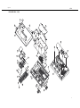
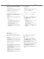
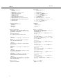
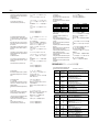
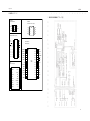
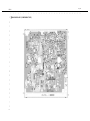
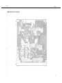
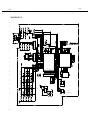
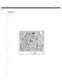
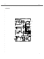
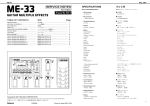
ME-30
Aug, 1997
ME-30
GUITAR MULTIPLE EFFECTS
Issued by RJA
TABLE OF CONTENTS
目次
SPECIFICATIONS ・・・・・・・・・・・・・・・・・・・・・・・・・・・・・
LOCATION OF CONTROLS ・・・・・・・・・・・・・・・・・・・・
EXPLODED VIEW ・・・・・・・・・・・・・・・・・・・・・・・・・・・・・
PARTS LIST ・・・・・・・・・・・・・・・・・・・・・・・・・・・・・・・・・・
LOADING FACTORY PRESET DATA ・・・・・・・・・・・・
TEST MODE ・・・・・・・・・・・・・・・・・・・・・・・・・・・・・・・・・・
IC DATA ・・・・・・・・・・・・・・・・・・・・・・・・・・・・・・・・・・・・・・
BLOCK DIAGRAM ・・・・・・・・・・・・・・・・・・・・・・・・・・・・・
CIRCUIT DIAGRAM & BOARD ・・・・・・・・・・・・・・・・・・
主な仕様 ・・・・・・・・・・・・・・・・・・・・・・・・・・・・・・・・・・・・2
パネル配置図 ・・・・・・・・・・・・・・・・・・・・・・・・・・・・・・・・3
分解図 ・・・・・・・・・・・・・・・・・・・・・・・・・・・・・・・・・・・・・・5
パーツリスト ・・・・・・・・・・・・・・・・・・・・・・・・・・・・・・・・6
工場出荷データの復帰方法 ・・・・・・・・・・・・・・・・・・・・7
テストモード ・・・・・・・・・・・・・・・・・・・・・・・・・・・・7∼12
ICデータ ・・・・・・・・・・・・・・・・・・・・・・・・・・・・・・・・・・・・13
ブロック図 ・・・・・・・・・・・・・・・・・・・・・・・・・・・・・・・・・・13
回路図&基板図 ・・・・・・・・・・・・・・・・・・・・・・・・・・14∼19
Page
ON / OFF
PHRASE GUITAR AMP
TRAINER SIMULATOR
EDIT / ESC
WRITE/COPY
ON /
OFF
REC
PEDAL
BYPASS
MANUAL
TUNER
CS
OD DS
1
/
REC
RV
2
DLY
3
MOD
Copyright c 1997 by ROLAND CORPORATION
All rights reserved. No part of this publication may be reproduced in any form without the written permission of
ROLAND CORPORATION.
本書の一部、もしくは全部を無断で複写・転載することを禁じます。
17059901
Printed in Japan AE00 (CR)
1
Aug, 1997
ME-30
SPECIFICATIONS/主な仕様
◎AD Conversion ‥‥‥‥‥‥‥‥‥‥‥‥‥‥‥‥:ΔΣ Method 20-bit ADC
◎DA Conversion ‥‥‥‥‥‥‥‥‥‥‥‥‥‥‥‥:ΔΣ Method 18-bit DAC
◎Sampling Frequency ‥‥‥‥‥‥‥‥‥‥‥‥‥‥:44.1kHz
◎Patches ‥‥‥‥‥‥‥‥‥‥‥‥‥‥‥‥‥‥‥‥:30(User)+30(Preset)+Manual Settings
◎Effects ‥‥‥‥‥‥‥‥‥‥‥‥‥‥‥‥‥‥‥‥:<Main Effects>
Compressor
Overdrive/Distortion
Equalizer/Phaser
Noise Suppressor
Delay
Chorus/Flanger/Pitch Shifter/Tremoro
Reverb
Gitar Amplifier Simulator
<Effects for Expression Pedal>
Volume Pedal
Pedal Wah
Tremoro Arm
Ring Modulator
-20dBm
◎Nominal Input Level ‥‥‥‥‥‥‥‥‥‥‥‥‥‥:INPUT:
AUX IN:
-10dBm
1MΩ
◎Input Impedance‥‥‥‥‥‥‥‥‥‥‥‥‥‥‥‥:INPUT:
AUX IN:
47kΩ
-20dBm
◎Nominal Output Level ‥‥‥‥‥‥‥‥‥‥‥‥‥:OUTPUT:
2kΩ
◎Output Impedance ‥‥‥‥‥‥‥‥‥‥‥‥‥‥‥:OUTPUT:
◎Display ‥‥‥‥‥‥‥‥‥‥‥‥‥‥‥‥‥‥‥‥:7 segments,1characterLED
Custom LCD(Luminous Display)
◎Jacks ‥‥‥‥‥‥‥‥‥‥‥‥‥‥‥‥‥‥‥‥‥:INPUT Jack
AUX IN Jack (Stereo Mini Type)
OUTPUT Jacks L(MONO)/R
Headphonse Jack (Stereo Mini Jack)
AC ADAPTOR Jack
◎Power Supply ‥‥‥‥‥‥‥‥‥‥‥‥‥‥‥‥‥:DC 9V:Dry Batteries(R6(AA)type) x6
AC Adptor(PAS-Series:Optional)
◎Current Draw ‥‥‥‥‥‥‥‥‥‥‥‥‥‥‥‥‥:170mA(DC 9V)
AC Adptor(PAS-Series:Optional)
◎Dimensions ‥‥‥‥‥‥‥‥‥‥‥‥‥‥‥‥‥‥:305(W) x 205(D) x 55(H)mm
12-1/16(W) x 8-1/8(D) x 2-3/16(H)inches
◎Weight ‥‥‥‥‥‥‥‥‥‥‥‥‥‥‥‥‥‥‥‥:1.5kg/3 lbs 5 oz (including batteries)
◎Accessories ‥‥‥‥‥‥‥‥‥‥‥‥‥‥‥‥‥‥:Owner's Manual(English)
Owner's Manual(Japanese)
Dry Batteries(R6(AA)type) x6(Alkaline)
Roland Service
PSA-Series
◎Options ‥‥‥‥‥‥‥‥‥‥‥‥‥‥‥‥‥‥‥‥:AC Adaptor
*0dBm=0.775 Vrms
2
(P/No.SE000129)
(P/No.SE000130)
(P/No.*********)
ME-30
Aug, 1997
LOCATION OF CONTROLS/パネル配置図
Rubber Switch
(#SE000079)
LCD Panel LS501
(#SE000091)
7 SEG LN514RK
(#SE000105)
VR Pedal Rubber Plate A
(#SE000074)
Display Panel
(#SE000080)
ON/OFF
PHRASE GUITAR AMP
TRAINER SIMULATOR
EDIT/ESC
WRITE/COPY
ON/
OFF
SW Pedal R
(#SE000073)
PEDAL
BYPASS
MANUAL
TUNER
CS
Label (OD/DS)
(DLY), (MOD),
(CS), (RV)
(#SE000126)
REC
OD DS
1
/
REC
RV
2
DLY
3
MOD
Top Case
(#SE000070)
VR Pedal Rubber Plate B
(#SE000075)
SW Pedal F
(#SE000072)
VR Pedal
(#SE000071)
3
Aug, 1997
ME-30
EXPLODED VIEW PARTS LIST/分解図パーツリスト
[PARTS]
No. Part Cord
q SE000070
w SE000074
e SE000075
r SE000080
t SE000126
y SE000126
u SE000126
i SE000126
o SE000126
!0 SE000072
!1 SE000073
!2 SE000076
!3 SE000131
!4 SE000091
!5 SE000092
!6 SE000082
!7 SE000081
!8 SE000079
!9 SE000094
@0 SE000095
@1 SE000128
@2 SE000071
@3 SE000083
@4 SE000084
@5 SE000085
@6 SE000089
@7 SE000087
@8 SE000088
@9 SE000086
#0 SE000090
#1 40238434
#2 SE000078
#3 SE000077
#4 SE000127
Part Name
Top Case
VR Pedal Rubber Plate A
VR Pedal Rubber Plate B
Display Panel
Label (OD/DS)
Label (DLY)
Label (MOD)
Label (CS)
Label (RV)
SW Pedal F
SW Pedal R
SW Pedal F/R Switch Knob
SW Spring
LCD Panel LS501
Luminous Sheet
LCD Cushion
LCD Connector
Rubber Switch
Main Board Assy
Jack Board Assy
PCB Support YP-17
VR Pedal
Battery Case A
Battery Case B
Battery Cover
Battery Terminal C
Battery Terminal A
Battery Terminal B
Bottom Cover
Bottom Cover Cushion C
CAUTION LABEL CANADA EMI
VR Pedal Cushion Rear
VR Pedal Cushion Front
VR Pedal Reflect seal
[SCREW]
No. PART No.
a 40010256
b 40011312
c 40011323
d SE000120
e SE000121
f SE000119
PART NAME
Binding M3x8 BZC
Binding M3x8 P-Tight BZC
Binding M3x10 P-Tight BZC
Hex Nut M6 BZC
Plain Washer
Cap Bolt M6x55 BZC
4
Description
M200004060
M203000410
M203000420
M203000400
M303002900
M303002900
M303002900
M303002900
M303002900
M400001770
M400001780
M205001210
M100001790
MA38000210
M303002890
M208001510
MA15000500
MA25000850
M001001670
M001001680
M208001540
M400001760
M200004070
M200004080
M200004090
MA34002570
MA34002550
MA34002560
M200004100
M208001270
M208001530
M208001520
M303002960
Qty
1
1
1
1
1
1
1
1
1
3
2
5
5
1
1
1
1
1
1
1
1
1
1
1
1
1
2
1
1
1
1
1
1
1
M100001630
M100001640
M100001620
3
21
4
1
2
1
Aug, 1997
ME-30
EXPLODED VIEW/分解図
c
31
30
20
b
b
21
29
4
5
2
25
17
19
24
26
18
3
16
15
27
27
28
8
14
6
32
a
9
7
f
23
e
1
e
33
d
12
22
12
13
13
34
11
10
5
Aug, 1997
ME-30
TRANSISTOR/トランジスター
PARTS LIST/パーツリスト
SAFETY PRECAUTIONS:*2
The parts marked ! have
safety-related characteristics.
Use only listed parts for
replacement.
安全上の注意:*2
!
が付いている部品は、安全上
特別な規格でつくられたもので
す。
交換の際は、注意をよく読み、
指定された部品番号以外の部品
は使わないようにして下さい。
CONSIDERATIONS ON PARTS ORDERING
When ordering any parts listed in the parts list, please specify the following items in the order sheet.
QTY
PART NUMBER
DESCRIPTION
MODEL NUMBER
Ex.
10
22575241
Sharp Key
C-20/50
15
2247017300
Knob (orange)
DAC-15D
Failure to completely fill the above items with correct number and description will result in delayed or
even undelivered replacement.
15119112
15309104
15319119
15319113
15329523
15129426
15139130
Q300 on MB
Q301 on MB
Q5-Q8 on MB
Q9.Q10 on MB
Q3.Q4.Q11.Q12.on MB
Q1 on JB
Q2 on JB
DIODE/ダイオード
#
パーツ発注に関するお願い
オーダーシートには、必ず下記の4項目は正確に記入して下さい。(例外は除く)
必 要 数 パーツナンバー 品 名 使用機種
例) 10 22575241 Sharp Key C-20/50
15 2247017300 Knob (orange)
DAC-15D もし記入漏れ、誤記等が有る場合、必要部品が発送出来なかったり、大幅な遅れの原因になります。
御協力をお願いします。
SE000104
01019534
MA111-(TX)
Diode 1SS355TE-17
15339120T0
15339122
00902978
00785856
15039118
Diode 1SS302
Diode 1SS301
Schottky Diode SB07-03N-AA
LED SLR-342VR3F(MN)
Diode S5688G(TPA2)
MD11000260
D4 on MB
D301.D307.D312.D316-D318.
D322.D327.D329.D330 on MB
D1.D3.D300 on MB
D11.D308-D315.D323.D326 on MB
D7 on MB D5 on JB
LED2-LED6 on MB
D6 on JB
MR13000110
MR13000100
MR13000080
RA2.RA3 on MB
RA1 on MB
RA4.RA5 on MB
RESISTOR ARRAY/抵抗アレイ
#
#
#
NOTE:*1 The parts marked # are new (initial parts)
注意:*1 #が付いた部品は新規部品です。
TRANSISTOR 2SA1015-Y
TRANSISTOR 2SA1586-GR(TE85L)
TRANSISTOR 2SC4213-A
TRANSISTOR 2SK880-GR
TRANSISTOR RN1307
TRANSISTOR 2SC2235-Y
FET 2SK184-GR
SE000107
SE000108
SE000109
EXBV8V681JV(5)
CNB2B9ZTE10KΩJ
EXBV8V101JV(5)
TRIMMER/半固定抵抗器
13299263
13299199
MB->Main Board , JB->Jack Board , SB->Sensor Board
*1*2
↓ ↓ CASING/ケース
#
#
#
#
#
#
#
#
#
#
#
#
#
#
SE000070
SE000071
SE000072
SE000073
SE000074
SE000075
SE000076
SE000077
SE000078
SE000080
SE000083
SE000084
SE000085
SE000086
Top Case
VR Pedal
SW Pedal F
SW Pedal R
VR Pedal Rubber Plate A
VR Pedal Rubber Plate B
SW Pedal F/R Switch Knob
VR Pedal Cushion Front
VR Pedal Cushion Rear
Display Panel
Battery Case A
Battery Case B
Battery Cover
Bottom Cover
SE000079
Rubber Switch
M200004060
M400001760
M400001770
M400001780
M203000410
M203000420
M205001210
M208001520
M208001530
M203000400
M200004070
M200004080
M200004090
M200004100
SE000106
12449456
12449457
13529246
SE000110
12449300
SE000111
#
#
13129776
SE000096
Tact SW SKQKAE
Slide SW HSW2022-010010
01019523
01340889
#
MA25000850
SE000091
SE000105
MA25000830
Mono Jack φ6.5 HLJ0521-01-1110
Stereo Jack φ3.5 HSJ0912-01-010
AC Adaptor Jack HEC2392-01-150
LCD Panel LS501
7 SEG.LED LN514RK
SW1.SW6.SW11.SW16.SW21 on MB
SW50 on JB
JK1-JK3 on JB
JK4.JK6 on JB
JK5 on JB
MA38000210
MA18000530
LED1 on MB
PCB ASSY/基板完成品
# ‰ SE000094
Main Board Assy
M001001670
NOTE:Replacement Main Board Assy includes Sensor Board Assy.
Exchange the Main Board and the Sensor board in the lump.
注意 :補修用 Main Board Assy は Sensor Board Assy を含みます。
基板交換の際は、Main Board と Sensor Board を同時に交換して下さい。
Sensor Board Assy
#
Jack Board Assy
SE000095
#
#
#
SE000081
SE000112
SE000113
#
#
#
#
#
SE000114
SE000115
SE000116
SE000117
SE000118
#
#
6
01238145
01235190
01238101
01238112
SE000097
SE000098
SE000099
SE000100
SE000101
15199159
SE000102
00452290
15289105
00452301
15289148
SE000103
15289408
15229728
15189189
MA33000010
Crystal DSX840GA 33.8688MHz
Crystal SMD-49 5MHz
X1 on MB
X2 on MB
LCD Connector
CONNECTOR B4B-PH-K-S
CONNECTOR B13B-PH-K-S
MA15000500
MA34002700
MA34002710
CN4 on MB
CN6 on MB
M001001680
Wiring A RED(for Battery Case)
Wiring B BLACK(for Battery Case)
Ribbon Cable 4P 2.0mm L=140mm
Wiring 4P l=80
Wiring 13P l=130
MA34002580
MA34002590
MA35000310
MA35000320
MA35000330
CN1.CN2 on MB & SB
CN3 on JB
CN5 on JB
MISCELLANEOUS/その他
#
#
#
#
#
#
#
#
#
#
#
#
#
#
#
SE000082
SE000087
SE000088
SE000089
SE000090
SE000092
SE000093
SE000122
SE000123
SE000124
SE000125
SE000126
SE000127
SE000128
SE000131
LCD Cushion
Battery Terminal A
Battery Terminal B
Battery Terminal C
Bottom Cover Cushion C
Luminous Sheet
LED Spacer
Shield Plate
Jack Holder
Jack Cover
Earth Spring
Label
VR Pedal Reflect seal
PCB Support YP-17
SW Spring
M208001510
MA34002550
MA34002560
MA34002570
M208001270
M303002890
M207001200
M200004210
M207001150
M200004160
M211000350
M303002900
M303002960
M208001540
M100001790
SPA2-SPA4 on MB
on MB
on JB
on JB
on JB
SCREW/ネジ類
IC/集積回路
#
#
#
#
#
#
#
#
#
MA37000100
L1 on MB
L9.L300 on MB
L15.L301-L307 on MB
FL1 on JB
L2-L8 on JB
L9 on JB
FC1
WIRING,CABLE/ワイヤリング、ケーブル
DISPLAY UNIT/表示ユニット
#
#
MA11000090
CONNECTOR/コネクター
JACK,SOCKET/ジャック、ソケット
13449722
13449443
13449717
Coil ELCO8D151E
EMI Filter BLM41A800SPB
EMI Filter BLM31A601SPB
EMI Filter DSS310-91D223S
Ferrite EXCELDR35V
Ferrite BL02RN1-R62
Ferrite Core FS0B190RT
CRYSTAL,RESONATOR/クリスタル、発振子
SWITCH/スイッチ
#
VR1 on MB
VR2 on MB
INDUCTOR,COIL,FILTER/インダクタ、コイル、フィルター
#
KNOB,BUTTON/ツマミ、ボタン
#
Trimmer EVND8AA03B52(500Ω)
Trimmer EVND8AA03B13(1KΩ)
CPU Mask μPD78064GF-095-3BA(FP)
MR2 Chip TC203C040AF-001(FP)
Audio CODEC AK4520A(SOP)
DAC PCM1718E(SOP)
DRAM HM51W4400BTT-6(TSOP)
EEPROM AT24C16N-10SC-2.7(SOP)
TTL TC74AC164F
TTL HD74HC4066FPEL
TTL HD74HC4052FPEL
DC/DC Converter IR3M03A
Reset IC M51955AFP600C
OP Amp M5216FP
OP Amp μPC4570G2-T2
OP Amp NJM2100M
OP Amp M5218AFP(Flat)
V.Reg.(3v) NJU7201U-32-TE1
V.Reg.(5v) M5278L05M
Photo Coupler GP2S24B
OP Amp μPC4570HA
MZ19000020
MZ21000020
MZ17000150
MZ17000130
MZ17000140
MZ24000270
MZ23000230
IC305 on MB
IC306 on MB
IC8 on MB
IC11 on MB
IC301 on MB
IC302 on MB
IC304.IC307 on MB
IC10 on MB
IC12 on MB
IC9 on MB
IC303 on MB
IC4 on MB
IC3 on MB
IC7 on MB
IC5.IC6 on MB
IC14 on MB
IC13 on MB
IC300 on SB
IC1.IC2 on JB
40011323
40010256
40011312
SE000119
SE000120
SE000121
#
#
#
Binding M3x10 P-Tite BZC
Binding M3x8 BZC
Binding M3x8 P-Tite BZC
Cap Bolt M6x55 BZC
Hex Nut M6 BZC
Plain Washer
M100001620
M100001630
M100001640
ACCESSORIES/標準付属品
#
#
#
SE000129
SE000130
********
Owners Manual(English)
M302001560
Owners Manual(Japanese)
M302001550
Battery LR6G/2ST
MA28000160
NOTE:The above part (LR6G/2ST) does not supply as replacement parts,
because it is options.
注意 :上記の部品(LR6G/2ST) は商品のため、補修用部品としては供給できません。
OPTIONS/オプション類
!
!
!
!
********
********
********
********
AC Adaptor PSA-100G 100V
AC Adaptor PSA-120 120V
AC Adaptor PSA-230G 230V
AC Adaptor PSA-240 240V
NOTE:The above part does not supply as replacement parts,
because it is options.
注意 :上記の部品は商品のため、補修用部品としては供給できません。
Aug, 1997
ME-30
IDENTIFYING VERSION NUMBER/バージョンの確認方法
1. Turn the power off.
1.電源をOFFにします。
2. While pressing the USER/PRESET Key and PHRASE
TRAINER ON/OFF Key simultaneously , turn the
power on.
The version number is displayed on the LCD.
2.USER/PRESET Key , PHRASE TRAINER ON/OFF Key
を同時に押しながら電源をONにします。
LCD にバージョンが表示されます。
3. Turn the power off to exit this mode.
3.電源をOFFにすると、このモードから抜けます。
LOADING FACTORY PRESET DATA/ファクトリー・プリセット・ロードの方法
◎ CAUTION !!
The user data cannot be saved to a sequencer via
MIDI.
Inform the user of this fact upon receiving a service
request.
◎ 注意!!
ME−30のユーザー・データは他のシーケンサーに
MIDIを使用して保存することが出来ません。
予め修理を依頼されたお客様に、その旨を連絡して下
さるようお願い致します。
1. Turn the power off.
1.電源をOFFにします。
2. While pressing the PARAMETER_R Key and
VALUE - Key simultaneously , turn the power on.
The " PRESET " is displayed on the LCD.
2.PARAMETER_R Key , VALUE - Key を同時に押
しながら電源をONにします。
LCD に PRESET と 表示されます。
3. Press the WRITE copy Key .
The " write " flashes on the LCD for a while.
When the initialization is complete , the unit returns
the Play Mode.
*To cancel the initialization at this time , turn the
power off.
3.WRITE/COPY Key を押すと LCD に WRITE の文
字がしばらく点滅します。
初期化が終了すると、通常の電源投入時と同じ状
態になります。
*初期化を中止するときは、電源をOFFにして
下さい。
TEST MODE/テストモード
The ME-30 provides six test modes ; from MODE 1 to
MODE 6. Use whichever appropriate for your situation.
ME−30のテスト・モードには、モード1からモード
6までの、6通りのテスト・モードがあります。
状況に応じて使い分けて下さい。
◎CAUTION !!
The user data cannot be saved to a sequencer via
MIDI. Inform the user of this fact upon receiving a
service request.
The test program will stop upon detecting a failure
component or circuit, and may not proceed to the next
step.
After taking a corrective action, restart the test
program from the beginning.
◎ 注意!!
ME−30のユーザー・データは他のシーケンサーに
MIDIを使用して保存することが出来ません。
予め修理を依頼されたお客様に、その旨を連絡して下
さるようお願い致します。
*テストモードで不良があれば次のステップに進む事が
出来ませんので、修理を行ってください。
また修理後は、最初から再度テストモードを行ってく
ださい。
*OUTPUTのテストでジャックをLch単体で使用
した場合、Lch , Rchの信号は内部でミキシング
されるため正常な波形が得られません。
正常な波形を得る為、Lchの測定時には、必ずRc
hに空プラグを挿入して下さい。
*OUTPUTチェックを行う際は、必要に応じてノイ
ズメーターとオシロスコープをOUTPUTジャック
に接続します。
Connection to OUTPUTs:
Unless otherwise specifically instructed, channels L
and R are independently monitored: first connect the
plug from the measuring
instrument (oscilloscope or noise meter, whichever
appropriate) into OUTPUT R, next, replace the
instrument plug with a blank
(open) plug and then connect the instrument to
OUTPUT L.
Note that the channel R signal is connected to the
OUTPUT L socket through the switch on the OUTPUT
R socket. To obtain pure
"L" channel signal, the R socket switch must be turned
off.
7
Aug, 1997
ME-30
◇Test Item
1. Panel LCD . LED Check
2. SW Check
3. DSP Check
4. Output Frequency Response Check
5. Output Mute Circuit Check
6. OD/DS Circuit Check
7. OD/DS Gain Check
8. Input Frequency Response Check
9. AUX Circuit Check
10. Residual Noise Check and Shock Noise Check
11. OD/DS Circuit Noise Check and Shock Noise Check
12. NS , Tuner Check
13. EV Pedal Check
◇テスト項目
1.LCD・LEDチェック
2.SWチェック
3.DSPチェック
4.出力部 f 特チェック
5.出力部ミュート回路動作チェック
6.OD/DS回路動作チェック
7.OD/DSゲイン動作チェック
8.入力部f特チェック
9.AUX回路動作チェック
10.残留ノイズ、ショック・ノイズチェック
11.OD/DS回路残留ノイズ、ショック・ノイズ
チェック
12.NS、チューナー動作チェック
13.EVペダル動作チェック
◇Equipment Required
. Oscillator ( Audio Generator )
. Oscilloscope
. Noise Meter
. Opened Plug
◇用意する物
・発振器
・オシロスコープ
・ノイズメーター
・空プラグ
◇To Enter the Test Mode
While pressing the EFFECT ON/OFF Key ,
PARAMETER ( L ) Key and PARAMETER ( R ) Key
simultaneously , turn the power
on.
All the LCD are turned on.
Do the following operation to select the mode.
◇テスト・モードの入り方
EFFECT ON/OFF Key , PARAMETER (L , R ) Key , 3カ
所を同時に押しながら電源ONすると、
LCDが全点灯します。
LCD全点灯の状態でのモードの選択方法は次のように
なります。
< Mode 1 >
Press PEDAL " 1 " to start with 「1. Panel LCD • LED
Check」.
NOTE : As for the following MODE 2 to MODE 6 ,
each mode starts after DSP check.
< Mode 2 >
Press PEDAL " 2 " to start with 「4. Output Frequency
Response Check 」.
<Mode 3 >
Press PEDAL " 3 " to start with 「6. DOD/DS Circuit
Check 」.
< Mode 4 >
Press PEDAL " BANK DOWN " to start with 「8. Input
Frequency Response Check」.
< Mode 5 >
Press PEDAL " BANK UP " to start with 「10.
Residual Noise Check and Shock Noise Check 」.
< Mode 6 >
Press MANUAL Key to start with 「13. EV Pedal
Check 」. Mode 6 to start DSP check , when return
back to the previous step.
◇Exiting test mode
Simply turn off the ME-30.
8
<モード1>
NO_1 PEDALを押すと、「1.LCD・LEDチェッ
ク」からスタートします。
以下のモードは、DSP動作確認を行ってから、各動作
チェックに移ります。
<モード2>
NO_2 PEDALを押すと、「4.出力部 f 特チェック」
からスタートします。
<モード3>
NO_3 PEDALを押すと、「6.OD/DS回路動作チェッ
ク」からスタートします。
<モード4>
BANK DOWN PEDALを押すと、「8.入力部f特チェ
ック」からスタートします。
<モード5>
BANK UP PEDALを押すと、
「10.残留ノイズチェッ
ク」からスタートします。
<モード6>
MANUAL Keyを押すと、「13.EVペダル動作チェッ
ク」からスタートします。
モード6は、前の検査に戻る時に、DSP動作チェック
を行います。
◇テスト・モードの抜け方
電源をOFFにします。
Aug, 1997
ME-30
1. LCD & LED test
Press the pedal "1". The LCD starts displaying the
test pattern shown in Fig. 1. Verify that the segments
are turned on.
Press a key and verify that the 7-seg LED and the
pedal LEDs are turned on in the order shown in Fig.
2.
2. Switch test
Press a key and the LCD will read "SW1".
Press the keys in the order shown in Fig. 3 and verify
that pressed key is represented on the LCD.
The test stops upon detecting a defective key and
won't proceed to the next key. Take a corrective
action and return to the step 1.
When the test is successful, the test program
proceeds to the step 3. DSP test.
1.LCD・LEDチェック
NO_1 PEDALを押すと、 LCD 表示パターン[ fig1
LCD テスト参照]がスタートします。
各セグメントが正常に点灯するか確認します。
どれかKeyを押すと、 7SEG , LED 表示パターン[
fig2 7SEG LED 及びペダル部 LED テスト参照]がス
タートしますので、各 LED が正常に点灯するか確認
します。
2.SWチェック
7SEG , LED 表示パターンに続いてどれか Key を押す
と、 LCD に " SW1 " と表示されます。
表示番号[ fig3 SW チェックテスト参照]に従って
Key を押し、これに対応して LCD の表示が変化する
ことを確認してください。
最後のSWが押され、SWチェックが正常に終了しま
すと、自動的に次のステップ(DSPチェック)へ
進みます。
この時、SWチェックでSW不良があれば次のSW
チェック及びステップに進む事が出来ません。
3. DSP test
The test program automatically starts the test step 3 1. after completion of the step 2.
3.DSPチェック
以下の検査を自動的に処理します。
3 - 1. Initialization
When the unit is initialized, the program goes to the
step 3 - .2. Otherwise, it displays "ERROR 1" and
jumps to the step 4.
3 - 2. Internal RAM test
The program writes the test data into and reads out
from the internal RAM and then goes to the step 3 - 3.
If error, it displays "ERROR 2" and jumps to the step
4.
3 - 3. External RAM test
The program writes the test data into and reads out
from the external RAM and then goes to the step 4.
If error, it displays "ERROR 3" and goes to the step 4.
3−1.初期化のテスト
結果が NG の場合、 LCD に " ERROR 1 " が表示され、
4.出力部f特チェックに進みます。
結果が OK であれば、何も表示せずに次のステップ
に進みます。
3−2.内部RAM読込み、書込みテスト
結果が NG の場合、 LCD に " ERROR 2 " が表示され、
4.出力部f特チェックに進みます。
結果が OK であれば、何も表示せずに次のステップ
に進みます。
3−3.外部RAM読込み、書込みテスト
結果が NG の場合、 LCD に " ERROR 3 " が表示され、
4.出力部f特チェックに進みます。
結果が OK であれば、何も表示せずに次のステップ
に進みます。
4. Output frequency response test
The LCD displays "TEST 1". Sine waves of 20 Hz - 1
kHz - 5 kHz - 15 kHz - 20 Hz from DSP are sent to
OUTPUT sockets at
0.8 sec.
interval.
Connect a noise meter to OUTPUT R. Set the meter
to "FLAT" and check the readings against the table
below.
Connect a noise meter to OUTPUT L (with the blank
plug in R) and check the readings.
The difference in readings between R and L must be
within 1 dBm.
Monitor OUTPUTs R and L and PHONES R and L in
that order on the oscilloscope and make sure they are
look like the waveforms shown in Fig. 4.
Frequency
20 Hz
1 kHz
5 kHz
15 kHz
Level
-20 dBm ± 1 dBm
-20 dBm ± 1 dBm
-20 dBm ± 1 dBm
-20 dBm ± 1 dBm
To go to the step 5, press VALUE + key.
4.出力部f特チェック
LCD に " TEST 1 " と表示されます。
0.8 秒間隔で、 20Hz , 1KHz , 5KHz , 15KHz サイン波
が出力されます。
(DSP内部発振、自動ループ)
ノイズ・メーターを“FLAT”に切り換えます。
Lch(MONO) , Rchを個別にチェックを行っ
て下さい。
Lch , Rch のレベル差は ±1dBm とします。
ノイズ・メーターでレベルを確認します。
オシロスコープで OUTPUT L/R , PHONES L/R の出力
波形が、歪んでいないか確認します。
[ fig4 テスト1波形図参照]
Lch(MONO) , Rchを個別にチェックを行っ
て下さい。
周波数
20 Hz
1 kHz
5 kHz
15 kHz
レベルl
-20 dBm ± 1 dBm
-20 dBm ± 1 dBm
-20 dBm ± 1 dBm
-20 dBm ± 1 dBm
VALUE Key +で次の検査に進みます。
5. Output stage muting test
The LCD displays "TEST 2". A 1 kHz sine wave from
DSP is sent to OUTPUT sockets at 0.5 sec. interval.
In the similar way as in the step 4 above, connect the
noise meter or scope to OUTPUT R and then L (with
the blank plug in R)
and check the readings. The difference in readings
between R and L must be within 1 dBm.
Monitor OUTPUTs R and L and PHONES R and L in
that order on the oscilloscope and make sure they are
look like
the waveforms shown in Fig. 5.
To go to the step 6, press VALUE + key.
To return back to the step 4, press VALUE - key.
6. OD and DS circuit test
The LCD displays "TEST 3". A 200 Hz square wave
from DSP is sent to OUTPUTs at 0.8 sec. interval at
four different levels.
Monitor the outputs by first connecting the scope to
OUTPUT R and then L (with the blank plug in R) and
make sure that
the waveforms look like the ones shown in Fig. 6.
To go to the step 7, press VALUE + key.
To return back to the step 5, press VALUE - key.
7. OD and DS gain test
The LCD displays "TEST 4". A 200 Hz sine wave from
DSP is sent to OUTPUTs at an 0.8 sec. interval at
four different levels.
Monitor the outputs by first connecting the scope to
OUTPUT R and then L (with the blank plug in R) and
make sure that
the waveforms look like the ones shown in Fig. 7.
5.出力部ミュート回路動作チェック
LCD に " TEST 2 " と表示されます。
0.5 秒間隔で、 1KHz サイン波が間欠出力されます。
(DSP内部発振、自動ループ)
OUTPUT L/R , PHONES L/R の出力波形を確認しま
す。[ fig5 テスト2波形図参照]
Lch(MONO) , Rchを個別にチェックを行っ
て下さい。
Lch , Rch のレベル差は ±1dBm とします。
VALUE Key +で次の検査に進みます。
VALUE Key −で前の検査に戻ります。
6.OD/DS回路動作チェック
LCD に " TEST 3 " と表示されます。
0.8 秒間隔で、4種類の波形が出力されます。
(DSP内部発振 200Hz 矩形波、自動ループ)
OUTPUT L/Rの出力波形を確認します。
[ fig6 テスト3
波形図参照]
Lch(MONO) , Rchを個別にチェックを行っ
て下さい。
VALUE Key +で次の検査に進みます。
VALUE Key −で前の検査に戻ります。
7.OD/DSゲイン動作チェック
LCD に " TEST 4 " と表示されます。
0.8 秒間隔で、4種類のレベル違う波形が出力されま
す。
(DSP内部発振 200Hz サイン波、自動ループ)
OUTPUT L/Rの出力波形を確認します。
[ fig7 テスト4
波形図参照]
Lch(MONO) , Rchを個別にチェックを行っ
て下さい。
To go to the step 8, press VALUE + key.
To return back to the step 6, press VALUE - key.
VALUE Key +で次の検査に進みます。
VALUE Key −で前の検査に戻ります。
8. Input frequency response test
The LCD displays "TEST 5". Apply a square wave of
200 Hz, 200 mV to INPUTs.
Monitor the outputs by first connecting the scope to
OUTPUT R and then L (with the blank plug in R) and
make sure that
the waveform looks like the one shown in Fig. 8.
8.入力部f特チェック
LCD に " TEST 5 " と表示されます。
INPUT に 200Hz ( 200mVp-p ) 矩形波を入力します。
OUTPUT L/Rの出力波形を確認します。
[ fig8 テスト5
波形図参照]
Lch(MONO) , Rchを個別にチェックを行っ
て下さい。
To go to the step 9, press VALUE + key.
To return back to the step 7, press VALUE - key.
VALUE Key +で次の検査に進みます。
VALUE Key −で前の検査に戻ります。
9. AUX circuit test
The LCD displays "TEST 6". Apply a square wave of
200 Hz, 200 mV to AUX INP.
The input signal is modified into three waveforms
which are sent to OUTPUTs at an 0.5 sec. interval.
Monitor the outputs by first connecting the scope to
OUTPUT R and then L (with the blank plug in R) and
make sure that
the waveforms look like the ones shown in Fig. 9.
To go to the step 10, press VALUE + key.
To return back to the step 8, press VALUE - key.
9.AUX回路動作チェック
LCD に " TEST 6 " と表示されます。
INPUT , AUX IN に 200Hz ( 200mVp-p ) 矩形波を入力
します。
0.5 秒間隔で、3種類の波形が出力されます。(自動
ループ)
OUTPUT L/Rの出力波形を確認します。
[ fig9 テスト6
波形図参照]
Lch(MONO) , Rchを個別にチェックを行っ
て下さい。
VALUE Key +で次の検査に進みます。
VALUE Key −で前の検査に戻ります。
10. Residual and shock noises
The LCD displays "TEST 7". Short-circuit the inputs
(e.g. insert a short circuit plug into INPUT and AUX
IN).
Set the noise meter to "JIS-A" or "IHF" and connect it
first to OUTPUT R and then L (with the blank plug in
R) and make sure that the readings are -88.0 dBm or
below. Also verify that difference in noise level
between channels is 1 dBm or less.
10.残留ノイズ、ショック・ノイズチェック
LCD に " TEST 7 " と表示されます。
ノイズ・メーターを“JIS−A”または“IHF”
のモードに切り換えます。
INPUT , AUX IN は無接続で(入力短絡、信号ライン
とGNDラインがショートされた状態)
、 OUTPUT L/R
の出力をノイズ・メーターで確認してください。
OUTPUT L , R -88.0dBm ( JIS-A ) 以下 又は、 88.0dBm ( IHF ) 以下
9
Aug, 1997
ME-30
In the similar way, connect a speaker via high gain
amplifier to individual OUTPUTs. Apply shocks to the
unit and make sure
no audible noises are heard.
To go to the step 11, press VALUE + key.
To return back to the step 9, press VALUE - key.
Lch(MONO) , Rchを個別にチェックを行っ
て下さい。
Lch , Rch のレベル差は ±1dBm とします。
ノイズメーターを外し、ハイ・ゲインのアンプをOU
TPUT L , R に接続し、スピーカーで聴いてくだ
さい。
本体に衝撃を与え、ショック・ノイズ無いか確認して
ください。
Lch(MONO) , Rchを個別にチェックを行っ
て下さい。
VALUE Key +で次の検査に進みます。
VALUE Key −で前の検査に戻ります。
11. OD and DS circuit residual and shock noises
The LCD displays "TEST 8". Short-circuit the inputs
(e.g. insert a short circuit plug into INPUT and AUX
IN).
Set the noise meter to "JIS-A" or "IHF" and connect it
first to OUTPUT R and then L (with the blank plug in
R) and make sure
that the readings are -84.0 dBm or below. Also verify
that difference in noise level between channels is 1
dBm or less.
In the similar way, connect a speaker via a high gain
amplifier to individual OUTPUTs. Apply shocks to the
unit and make sure
no audible noises are heard.
To go to the step 12, first connect the OUTPUT L to
the INPUT socket and then press VALUE + key (see
note in step 12).
To return back to the step 10, press VALUE - key.
11.OD/DS回路残留ノイズ、ショック・ノイズ
チェック
ノイズ・メーターを“JIS−A”または“IHF”
のモードに切り換えます。
INPUT , AUX IN は無接続で、
(入力短絡、信号ライン
とGNDラインがショートされた状態)、 OUTPUT L/R
の出力をノイズ・メーターで確認してください。
OUTPUT L , R -34.0dBm ( JIS-A ) 以下 又は、 34.0dBm (IHF ) 以下
Lch(MONO) , Rchを個別にチェックを行っ
て下さい。
Lch , Rch のレベル差は ±1dBm とします。
ノイズメーターを外し、ハイ・ゲインのアンプを O
UTPUT L , R に接続し、スピーカーで聴いてく
ださい。
本体に衝撃を与え、ショック・ノイズが無いか確認し
てください。
Lch(MONO) , Rchを個別にチェックを行っ
て下さい。
VALUE Key +で次の検査に進みます。
VALUE Key −で前の検査に戻ります。
12. NS and tuner test
Note: "ERROR *" will appear if VALUE - key has been
pressed without connecting OUTPUT L to the INPUT
socket.
12.NS、チューナー動作チェック
注 意 : OUTPUT_L と INPUT を 接 続 し て か ら 、
VALUE Key +を押して下さい。
上記の接続をせずに VALUE Key +を押した場合、
ERROR * が表示されます。
The LCD displays "TEST 9".
12 - 1. NS bias test
The program checks the NS bias and, if correct, goes
to the step 12.2. Otherwise, the program stops,
displaying "ERROR 4".
Adjust the bias and restart the test program from step
1.
LCD に " TEST 9 " と表示されます。
12−1.NSバイアスチェック
結果が NG なら " ERROR 4 " が表示され、次のステッ
プに進む事が出来ません。
結果が OK であれば、何も表示せずに次のステップに
進みます。
12 - 2. NS input test
When the input is as designed, the program displays
the tuner status. See Fig. 10. Press TUNER key.
12−2.NSインプットチェック
結果が NG なら " ERROR 5 " または " ERROR 6 " が表
示され、次のステップに進む事が出来ません。
結果が OK ならチューナー表示状態になります。
[ fig10 チューナーテスト参照]
If the input is incorrect, the program displays stops
here, displaying "ERROR 5" or "ERROR 6".
Isolate the cause and restart the test program from
step 1.
To go to the step 13, press VALUE + key.
To return back to the step 11, press VALUE - key.
13 EV pedal test
The LCD displays "TES***".
Swing the volume control foot pedal (EV) and check
the values shown on the LCD.
For pressing operation, refer to the EV adjustment
shown below.
Travel of EV pedal
Deep press
Press and release
Swing up
Down position
LCD 表示数値
220以上 224以下
210以下
002以下
150以上
ADJUSTEMENTS/調整仕様
*“13.EVペダル動作チェック”にて正常な値
が得られないとき、以下の調整を行ってください。
EVペダルの調整
最初は VR1 , VR2 共に中央の位置で有る事を確認す
る。
1.ペダルを上げた時に 2 になるように VR1 を調整
する。
(出来るだけ 0→2 に変わった付近に VR1 を合わせ
る)
2.ペダルを一番下まで強く踏み込んだ時に 220
以上、 224 以下になる事を確認する。
ならない場合は VR2 を動かして調整する。
3.ペダルから手(足)を離して 210 以下になる
事を確認する。
4.ペダルを上げた時に1.の状態に戻るかを確認す
る。
5.ペダルを踏み込み、クッションに軽く当たった状
態で 150 以上になる事を確認する。
6.再度、2.3.の状態になることを確認する。
ERROR MESSAGES/エラー・メッセージとその内容
If an error message is displayed in TEST MODE , take
the necessary to remove the cause described below.
Error Message
" ERROR 1 "
Description
DSP cannot
be accessed
" ERROR 2 "
DSP IRAM
defective
" ERROR 3 "
DSP ERAM
defective
" ERROR 4 "
NS Circuit
defective
NS Circuit
defective
NS Circuit
defective
" ERROR 5 "
" ERROR 6 "
エラー・メッセージ
" ERROR 1 "
" ERROR 2 "
" ERROR 3 "
" ERROR 4 "
" ERROR 5 "
" ERROR 6 "
10
EV ペダル
強く踏み込んだままのとき
強く踏み込んで力を抜いたとき
一番上にしたとき
軽く踏み込んだとき
If these values are not obtained, go to the FV
Adjustment below.
To return back to the step 12, press VALUE - key.
EV adjustment
Set VR1 and VR2 at the middle of the travel.
1. Swing up the pedal and adjust VR1 for 002 reading
on the LCD.
Make sure that the LCD reads 002 just before the
pedal is fully swung up.
2. Depress the pedal to the bottom and add a slightly
strong force.
Make sure that the LCD reads a value between 220
and 224. If outside the range, adjust VR2.
3. Release the pedal and make sure that the LCD
reading is decreasing to 210 or below.
4. Fully swing up the pedal and make sure that the
reading returns to 002.
5. Swing down the pedal until the bottom of the pedal
just touches the cushion. Make sure that LCD reads at
least 160.
6. Repeat steps 2 and 3 and verify that correct values
are displayed.
TUNER Key でチューナー表示状態から抜けます。
VALUE Key +で次の検査に進みます。
VALUE Key −で前の検査に戻ります。
LCD reading
220-224
210 min
002 max
150 min
13.EVペダル動作チェック
LCD に " TES *** " と表示されます。
EV ペダルを動かし表示数値を確認します。
テスト・モードでのエラー・メッセージとその不良内
容、主な原因について説明します。
Possible cause
・Solder bridge or improper soldering at portion anywhere between
CPU (IC305) and DSP (IC306).
・CPU (IC305) and/or DSP (IC306) defective.
・Solder bridge or improper soldering at portion anywhere between
CPU (IC305) and DSP (IC306).
・CPU (IC305) and/or DSP (IC306) defective.
・Solder bridge or improper soldering at portion anywhere between
CPU (IC305) and DSP (IC306).
・CPU (IC305) and/or DSP (IC306) defective.
・CPU (IC305) 29 , 30 pin around circuit and/or BIAS OPAMP (IC7)
around circuit defective.
・CPU (IC305) 29 , 30 pin around circuit and/or ENVELOP OPAMP
(IC7) around circuit defective.
・CPU (IC305) 29 , 30 pin around circuit and/or ENVELOP OPAMP
(IC7) around circuit defective.
主な原因
CPU ( IC305 ) - DSP ( IC306 )間の半田タッチ、
または半田付け不良。
CPU ( IC305 ) または DSP ( IC306 ) の不良。
DSP の IRAM エラー。 CPU ( IC305 ) - DSP ( IC306 )間の半田タッチ、
または半田付け不良。
CPU ( IC305 ) または DSP ( IC306 ) の不良。
DSP の ERAM エラー。 CPU ( IC305 ) - DSP ( IC306 )間の半田タッチ、
または半田付け不良。
CPU ( IC305 ) または DSP ( IC306 ) の不良。
CPU ( IC305 ) 29 , 30pin の周辺回路または
NS の回路 NG。
( BAIAS ) OPAMP ( IC7 ) の周辺回路の不良。
CPU ( IC305 ) 29 , 30pin の周辺回路または
NS の回路 NG。
( ENVELOP ) OPAMP ( IC7 ) の周辺回路の不良。
CPU ( IC305 ) 29 , 30pin の周辺回路または
NS の回路 NG。
( ENVELOP ) OPAMP ( IC7 ) の周辺回路の不良。
不良内容
DSP に
アクセス 出来ない。
Aug, 1997
ME-30
Fig.1. LCD TEST/LCDテスト
Fig.3. SW CHECK TEST/SWチェックテスト
q
SW1
SW12
SW2
ON / OFF
PHRASE GUITAR AMP
TRAINER SIMULATOR
w
EDIT / ESC
SW5
SW14
WRITE/COPY
SW6
ON /
OFF
SW16 SW17
SW7 SW15
REC
SW9
SW8
e
SW13
SW4
SW3
PEDAL
SW10
SW11
SW18
SW19
BYPASS
MANUAL
SW20
TUNER
r
CS
RV
t
SW21
1
y
OD DS
/
REC
SW25
u
SW22
2
DLY
SW24
3
MOD
SW23
i
o
Fig.2. 7SEG. & PEDAL LED TEST/7SEG. LED及びペダルLEDテスト
Fig.4 TEST 1
WAVE/テスト1 波形図
1
6
2
7
ON / OFF
PHRASE GUITAR AMP
TRAINER SIMULATOR
EDIT / ESC
5
4
3
WRITE/COPY
ON /
OFF
REC
8
PEDAL
BYPASS
MANUAL
TUNER
10
9
CS
12
13
1
RV
OD DS
/
REC
2
DLY
11
3
MOD
11
Aug, 1997
ME-30
Fig.5 TEST 2 WAVE
/テスト2 波形図
Fig.6 TEST 3
Fig.7 TEST 4 WAVE/テスト4 波形図
WAVE/テスト3 波形図
Fig.8 TEST 5 WAVE/テスト5 波形図
Fig.9 TEST 6 WAVE/テスト6 波形図
Fig.10. TUNER TEST/チューナーテスト
ON / OFF
PHRASE GUITAR AMP
TRAINER SIMULATOR
EDIT / ESC
WRITE/COPY
ON /
OFF
REC
PEDAL
BYPASS
TUNER
CS
1
12
OD DS
/
REC
RV
2
DLY
3
MOD
MANUAL
Aug, 1997
ME-30
IC DATA/ICデータ
1
A
RESET IC
MS1955AFP600C
1
2
3
4
M51955A/
BFP
M51956A/
BFP
NC
INPUT
NC
GND
NC
+VDD
OUT PUT
DRAM
HM51W4400BTT-6 (TSOP)
20
19
18
17
16
VSS
I/O4
I/O3
CAS
OE
A0 6
A1 7
A2 8
A3 9
VCC 10
15
14
13
12
11
A8
A7
A6
A5
A4
(Top view)
DAC
PCM1717E (SOP)
XTO
20
DGND
CLKO
19
3
Vdd
MUTE
18
4
LRCIN
DM1
17
5
DIN
DM0
16
6
BCKIN
RSTB
15
7
ZERO
FORMAT
14
8
D/CR
D/CL
13
9
VOUTR
VOUTL
12
10
AGND
VCC
11
1
XTI
2
4
5
6
7
8
9
10
11
12
13
BLOCK DIAGRAM/ブロック図
1
8
VCC
A1
2
7
WP
A2
3
6
SCL
GND
4
5
SDA
C
D
E
1
2
3
4
5
I/O1
I/O2
WE
RAS
A9
A0
NC
3
B
EEPROM
AT24C16N-10SC-2.7 (SOP)
8
7
6
5
2
F
AUDIO CODEC
AK4520A (SOP)
G
VREFH
1
28
VCOM
VREFL
2
27
AOUTR
AINR+
3
26
AOUTL
AINR-
4
25
COMODE
AINL+
5
24
PWAD
AINL-
6
23
PWDA
VA
7
22
DGND
AGND
8
21
VD
DIF0
9
20
TST1
DIF1
10
19
TST2
LRCK
12
17
TST3
SCLK
12
17
DEM1
SDTI
13
16
DEM0
SDTO
14
15
MCLK
Top
View
H
I
J
K
L
M
N
O
P
Q
R
S
T
U
13
14
15
Aug, 1997
ME-30
1
A
B
C
D
E
F
G
H
I
J
K
L
M
N
O
P
Q
R
S
T
U
14
2
3
4
5
6
7
8
9
‰MAIN BOARD ASSY (COMPONMENT SIDE)
10
11
12
13
14
15
16
17
18
19
20
21
22
23
24
25
26
27
28
ME-30
Aug, 1997
1
A
2
3
4
5
6
7
8
9
10
11
12
13
14
15
16
17
18
19
20
21
22
23
24
25
26
27
28
‰MAIN BOARD ASSY (SOLDER SIDE)
B
C
D
E
F
G
H
I
J
K
L
M
N
O
P
Q
R
S
T
U
15
Aug, 1997
ME-30
1
A
2
3
4
5
6
7
8
9
10
11
12
13
14
15
16
17
18
19
20
21
22
23
24
25
26
27
MAIN BOARD ASSY (1/2)
B
C
D300
1SS302
2
R300
390
D
R301
18k
3
C300
0.1
1
Q300
2SA1015Y
2
R330
100
AUX
ADA MUTE
SAMPLER
2
F
TP2
TP
1
MUTE
3
E
TP1
TP
3
R302
100
R337
82k
C301
0.1
3
VR1
EVND8AA03B52
OD_DRIVE1
OD_DRIVE0
OD_MODE1
OD_MODE0
2
VR2
1 EVND8AA03B13
1
TU
IC300
4
3
1
2
GP2S24B
CN1
CN2
1
1
2
2
3
3
4
4
R329
820
1 1
2 2
3 3
4 4
C354
0.1
NS
BATT CHECK
35A-P-10-29-4
IC304
3
4
LED6
SLR-342VR3F
G
1
LED5
SLR-342VR3F
LED2
SLR-342VR3F
5
LED3
SLR-342VR3F
1
1
1
1
6
LED4
SLR-342VR3F
10
11
2
2
2
2
12
2
13
H
R326
680
R325
680
R323
680
R322
680
R324
680
1
QA
CLR
QB
VCC
14
C326
47/16
C302
0.1
QD
GND
1
C333
100P
7
BANK
UP
DOWN
1
2
QG
A
B
CK
QH
R344
10k
R311
10k
3
J
COM C
AB
NC
AG
AC
ADP
AD
14
13
12
11
10
9
8
1
2
3
4
RA3
3
8
7
6
5
EXBV8V681JV
1
2
3
4
LN514RK
4
5
6
RA2
10
8
7
6
5
EXBV8V681JV
11
12
13
QA
CLR
QB
VCC
R340
10k
3
7
R312
10k
9
1
14
11
10
C325
10/6.3T
C303
0.1
QC
GND
7
C328
100P
QF
A
B
CK
QG
QH
C329
100P
C346
0.1
L
100
1
2
3
4
1
9 8 7 6 5 4 3 2
1
2
3
4
8
7
6
5
8
7
6
5
32
33
34
35
2
D329
1SS355
1
2
SW21
SKQKAE
N
BANK UP
2
TUNER
2
RA5
EXBV8V101JV
4 2
0 7
3
6 9
A V
V D
DD
D
V A
S V
S S
S
6
7
I
C
(
V
P
P
)
IC305
uPD78064
8
X
2
X
1
P30
P31
P32
P33
P34
P35
P36
P37
P00
100
SW16
SKQKAE
BANK DOWN
D317
1SS355
1
BYPASS
EDIT/ESC
1
2
1
SW19
carbon
PARA L
1
2
2
SW20
carbon
PLAY
1
2
SW13
carbon
2
2
WR/COPY
1
PARA R
1
2
SW8
carbon
EFF L
1
D308
1SS301
C341
Not Mount
STOP
1
3
USER/PRE
12
P02
P03
15
16
BIAS
VLC0
VLC1
VLC2
VSS
55
56
57
58
59
SW9
carbon
VAL -
1
4
3
2
1
1
4
3
2
1
5
4
48
49
50
45
46
47
42
43
1 2 2
9 0 3
2 2 2 2 3 3 3 3
6 5 2 4 6 7 8 9
1 1 1 9 8 1 1 1 1 1 2 3 3 3 3 3 3
6 3 1
0 2 4 7 8 7 0 1 2 3 4 5
IC306
TC203C040AF-001
CCCC
OOOO
MMMM
0 1 2 3
L300
BLM41A800SPT
10
CCCC
OOOO
MMMM
0 1 2 3
2
C335
10/16
R308
1k
R309
1k
R310
1k
C322
C323
C324
OCRW
EA A E
S S
1 1
1 2 8 9
DDDD
QQQQ
0 1 2 3
1 1 1 1 1
6 7 8 9 1 2 3 4 5 5
A A A A A A A A A A
0 1 2 3 4 5 6 7 8 9
VDD
C357
0.1
C318
0.1
20
0.1
1
R327
12k
0.1
R23
0.33(1/2W)
VSS
3
on JACK BOARD
5
C29
180p
SW10
carbon
RR
1
D310
1SS301
4
IPK
1
1
VIN-
CD
CT
CS
GND
ES
8
EFF R
SW5
carbon
SW4
carbon
1
2
2
2
VAL +
1
FF
1
R342
10k
L1
ELC08D151E
1
IN
GND
5
8
C306
0.1
4
R341
10k
8
6
5
4
2
2
D7
1 SB07-03N
R44
1.6k
C319
0.1
2
C31
0.1
3
1
NC
7
1
D311
1SS301
NC
7
C30
100/16
VCC
IR3M03A
2
3
NC
1
6
2
2
VDD
NC
R328
10k
IC9
To CN3
3
1
OUT
2
C28
0.1
2
2
3
SW3
carbon
1
1
M51955AFP
D316
1SS355
1
2
D309
1SS301
2
SW2
carbon
1
RESET
9 9 9 9 9 9 9 9
2 3 4 5 6 7 8 9
IC303
SW15
carbon
D315
1SS301
2
3
1
2
SW1
SKQKAE
2
1
100
6
2
3
1
1
P27
P26
P25
R307
1M
8 8 8 8
6 7 8 9
63
64
1
2
SW14
carbon
D314
1SS301
S ON/OFF
3
4
5
2
2
SW7
carbon
X1
DSX840GA 33.8688MHZ
IC301
HM51W4400BTT-6
CN4
B4B-PH-K-S
2
2
P70
P71
P72
1 2 3 4
R45
1k
3
16
2
2
SW6
SKQKAE
17
18
4 4 4 4 4 3 3 3 3 3 3 3 3 3 3 2 2 2 2 2 2 2 2 2 2 1 1 1 1 1 1 1 1 1 1
4 3 2 1 0 9 8 6 7 1 2 3 4 5 0 9 8 7 6 5 4 3 2 1 0 9 8 7 6 5 4 3 2 1 0 9 8 7 6 5
S S S S S S S S S S S S S S S S S S S S S S S S S S S S S S S S S S S S S S S S
3 3 3 3 3 3 3 3 3 2 2 2 2 3 2 2 2 2 2 2 1 1 1 1 1 1 1 1 1 1 9 8 7 6 5 4 3 2 1 0
9 8 7 6 5 4 3 1 2 6 7 8 9 0 5 4 3 2 1 0 9 8 7 6 5 4 3 2 1 0
C356
0.1
2
2
6
28
41
52
65
69
78
83
91
C308
0.1
3
7
15
21
29
40
44
51
53
62
66
72
75
79
82
90
LCD1
MSI_LCD
1
MANUAL
P04
P05
5 5 5 5
1 2 3 4
0.1
SW12
carbon
1
C352
0.1
C307
5P
C327
5P
54
55
56
57
58
59
60
61
3
D318
1SS355
1
19
20
21
22
23
24
25
26
6 6 6 6 6 6 6 6 6 6 7 7 7 7 7 7 7 7 7 7 8 8 8 8 8 8 8 8 8 8 9 9 9 9 9 9 9 9 9 9
0 1 2 3 4 5 6 7 8 9 0 1 2 3 4 5 6 7 8 9 0 1 2 3 4 5 6 7 8 9 0 1 2 3 4 5 6 7 8 9
2
C340
100P
D312
1SS355
C351
0.1
1
C358
0.1
1
SW18
carbon
2
U
SEL
2
2
2
D307
1SS355
T
SW25
carbon
1
D326
1SS301
1
S
SW24
carbon
P110
P111
P112
P113
P114
P115
P116
P117
7 7 7 7 8 8
3 4 6 7 0 1
1 1
6 7 4 3
2
3
SW17
carbon
SW11
SKQKAE
1
R
2
1
2
2
Q
1
2
E ON/OFF
7 7 6 6
0 1 7 8
1
8 8 0
4 5 0
2
1
1
R343
47k
1
D323
1SS301
1
P
G AMP
1
D330
1SS355
2
D322
1SS355
O
SW23
carbon
SW22
carbon
1
2
C350
0.1
BCLK
MASTERCLK
X2
SMD-49 5MHz
2
S S S S S S S S S S S S S S S S S S S S S S S S S S S S S S
S S S S S S S S S S 1 1 1 1 1 1 1 1 1 1 2 2 2 2 2 2 2 2 2 2 3 3 3 3 3 3 3 3 3 3
0 1 2 3 4 5 6 7 8 9 0 1 2 3 4 5 6 7 8 9 0 1 2 3 4 5 6 7 8 9 0 1 2 3 4 5 6 7 8 9
D327
1SS355
BLM31A601SPT
BLM31A601SPT
1
P14
P15
P16
P17
43
44
45
46
47
48
49
50
13
RA4
EXBV8V101JV
R338
M
L302
L301
C343
0.1
LRCLK
C320
33P
ANI0
ANI1
ANI2
ANI3
RA1
RCE9A103JA
R303
10k
BLM31A601SPT
C359
0.01
C321
33P
TI01
28
29
30
31
R339
R304
10k
0.1
0.1
P100
P101
P102
P103
14
1
2
8
A
V
R
E
F
XT2
P07
38
39
41
42
QD
QE
C304
C305
1
R313
47k
74AC164F
K
C342
0.1
ADDATA
L303
C332
10/6.3T
2
1
1
2
8
2
AA
AF
COM C
NC
NC
NC
AE
L307
BLM31A601SPT
DADATA2
DADATA1
100
QF
LED1
1
2
3
4
5
6
7
BLM31A601SPT
BLM31A601SPT
R345
R306
10k
2SA1586GR
IC307
I
L306
BLM31A601SPT
2 Q301
C330
100P
L305
L304
C345
0.1
R305
100
3
1
74AC164F
BANK
C344
0.1
2
QC
QE
D301
MA111
2
9
C32
470/16
1
VCC
SLC
SDA
VSS
7
WP 3
A2 2
A1 1
A0
IC302
AT24C16N-10SC-2.7
ME-30
DIGITAL Side
C317
C316
C315
C314
C311
C310
C309
0.1
0.1
0.1
0.1
0.1
0.1
0.1
28
Aug, 1997
1
A
ME-30
2
3
4
5
6
7
8
9
10
11
12
13
14
15
16
17
18
19
20
21
22
23
24
25
26
27
28
MAIN BOARD ASSY (2/2)
B
C
D
E
C353
0.1
R14
100
8
R9
100
C7
47/6.3
2
1
680k
C10
100/6.3
NJM2100M
1
220P
C8
D1
F
IC7C
2
R10
4
1SS302
C6
0.01
2
R8
10k
1
6
3
7
1
3
C84
100P
R6
22k
G
R7
22k
1
2
3
4
5
6
7
8
9
10
11
12
13
R12
12k
C5
47/16
TU
C100
0.018
LRCLK
BCK
MASTERCLK
C11
1/50
R16
1k
R150
4.7k
ADA MUTE
IC7A
NJM2100M
ADDATA
2
1
NS
2
C150
100/16
1
R115
4.7k
R112
470
C65
10/16
IC12
2
1
12
14
15
11
R32
100k
1
5
2
4
on JACK BOARD
16
3
IN
C
O
M
OUT
1
8
7
R61
4.7k
2
R26
10k
C59
1
0.1
VCC
0.1
2
R62
4.7k
K
GND
VEE
2
DIF0
DIF1
C12
0.001
C67
10/16
R20
470
LRCK
SCLK
1
AINL+
AINR+
MCLK
4
R33
100k
C57
100/6.3
1
C16
10/16
Q12
RN1307
C18
0.1
2
3
PWAD
2
VREFL
16
17
4
5
6
18
19
20
14
18
17
16
C126
0.1
23
24
C360
0.01
SAMPLER
15
1
C62
0.0022
3
R67
12k
3
R5
15k
C72
150P
8
9
R42
C63
220P
C37
2 10/16
C42
10/16
1
2
R69
12k
R68
12k
C86
R95
8.2k
6
7
C51
0.0015
CLKO
C40
0.0022
R51
10
1
C22
10/6.3
C125
0.1
1
R72
4.7k
R70
100k
2
3
Q9
2SK880GR
1
3
10/16
R39
100k
2
47k
C71
100/16
2
1
R30
1k
0.1
2
M5216FP
C73
150P
R71
100k
R73
4.7k
R48
180
10/16
Q10
2SK880GR
3
R74
1k
10/16
R46
180
Q4
RN1307
O
12
R34
10k
R117
P
2.2k
0.0082
C141
22P
IC5B
R35
10k
C68
10/16
1
C152
2
C76
100/6.3
2
R85
8.2k
1
R36
10k
6
74HC4066AF
R53
180k
C23
X
Y
X
13
CONT
R118
2.2k
R37
10k
1
D4
1
MA111
2
D3
2
1SS302
1
3
C88
0.047
1
2
3
Q5
2SC4213A
R79
1M
AUX
1
IC10B
74HC4066AF
5
3
CONT
X
Y
MUTE
4
R90
4.7k
R88
47k
ME-30
2
C54
1/50
C24
C77
0.033
R57
4.7k
IC6A
2
R56
4.7k
ANALOG Side
47P
1
C79
2
1
R91
470
R102
100k
C80
10/16
1
2
R50
47
3
5
R101
47
BATT CHECK
22/16
2
M5218AFP
M5218AFP
C78
0.22/50
Q3
RN1307
1
C85
0.047
R92
560
R103
43k
2
2
R60
100k
C45
470/6.3
C83
10/16
1
1
2
3
IC14
NJU7201U32
R58
1M
1
3
R75
1k
R47
100
3
CONT
1
IC6B
2
Y
74HC4066AF
R89
10k
74HC4066AF
R54
56k
100P
1
8
M5218AFP
C153
0.0082
IC5A
2 C53
1/50
9
7
5
2
C69
10/16
R86
6.8k
33k
6
7
Q
R87
Y
CONT
6
2
1
R55
2.2k
X
IC10C
10
C355
0.1
2
IC10A
IC10D
11
C347
0.1
R99
47k
Q11
RN1307
100P
Q6
2SC4213A
1
2
2
R114
1M
C52
2
3
C82
1
2
R59
100k
1
R49
100
2
3
2
Q7
2SC4213A
1
C81
1
D11
1SS301
3
2
3
R98
100k
1
N
R28
1k
5
R19
15k
R78
330
1
M
Q8
2SC4213A
1
C35
10/16
AGND
R27
1k
R77
330
R94
68k
1
1
R29
1k
1
22P
IC4B
7
6
5
IC3B
uPC4570G2
C70
100/16
2
M5216FP
R76
10K
R97
100k
19
V
C
C
C4
0.0015
R93
68k
C64
0.0022
A
G
N
D
IC3A
uPC4570G2
22P
IC4A
1
2
2
1
1
0 C36
C140
470/6.3
C44
1
1
D/C R
VOUTR
R96
8.2k
2
2
DGND
18
R65
12k
C38
10/16
FORMAT
MUTE
DM1
DM0
RSTB
C87
R66
12k
7
12
13
C39
0.0022
47k
C61
220P
C41
10/16
1
2
R63
4.7k
LRCIN
DIN
BCKIN
L15
C21
0.1
22
VA
2
C20
0.1
1
3
V
D
D
VOUTL
D/C L
BLM31A601SPT
7
0.1
2
D
G
N
D
XTI
21
VD
2
L9
BLM41A800SPT
ZERO
1
15
25
VCOM
C19
10/6.3
L
PWDA
VREFH
XTO
13
14
28
1
2
20
CMODE
R100
47k
1
11
12
R41
C33
IC11
PCM1718E
9
10
AOUTR
2
R110
1.8k
TST3
TST2
TST1
AOUTL
27
C17
0.1
DEM0
DEM1
AINR-
26
R111
4.7k
TC74HC4052AF
SDTI
SDTO
C13
0.001
R113
470
R31
100k
6
INH
AINL-
5
3
10
9
A
B
6
R116
1.8k
1
R38
100k
3
Y-COM
0Y
1Y
2Y
3Y
2
R64
12k
C34
10/16
1
2
IC8
AK4520A
1
C50
2
1
10/16
C56
470/6.3
2
C58
R3
470
C66
10/16
13
X-COM
0X
1X
2X
3X
C55
0.1
IC13
TA78L05F
R
C151
0.1
R151
4.7k
DADATA2
DADATA1
1
To CN5
J
C9
680P
2
1
2
3
4
5
6
7
8
9
10
11
12
13
H
I
R11
220k
IC7B
NJM2100M
R13
15k
CN6
B13B-PH-K-S
R17
1k
2
5
IC3C
1
8
M5218AFP
IC5C
8
IC6C
8
IC4C
IC10E
74HC4066AF
OD_MODE0
OD_MODE1
OD_DRIVE1
OD_DRIVE0
4
uPC4570G2
4
M5218AFP
4
M5218AFP
4
M5216FP
2
1
4
8
V
C
C
G
N
D
C49
0.1
IN
C46
OUT
C
O
M
3
2
1
C43
100/16
C47
1
7
0.1
0.1
S
T
U
17
Aug, 1997
ME-30
1
A
B
C
D
E
F
G
H
I
J
K
L
M
N
O
P
Q
R
S
T
U
18
2
3
4
JACK BOARD ASSY
5
6
7
8
9
10
11
12
13
14
15
16
17
18
19
20
21
22
23
24
25
26
27
28
ME-30
Aug, 1997
1
A
2
3
4
5
6
7
8
9
10
11
12
13
14
15
16
17
18
19
20
21
22
23
24
25
26
27
28
JACK BOARD ASSY
B
C
D
E
JACK COVER
F
JK3
2
4
1
INPUT
G
35A-P-10-32-4
R1
10K
L6
R52
47K
C48
0.047
2
Q2
2SK184GR
3
EXCELDR35V
R82
18K
R2
10K
C1
0.0022
IC1A
OUTPUT L(MONO)
HLJ0521-01-1110
or HTJ-064-10
4
uPC4570HA
L3
EXCELDR35V
2
4
1
H
JK2
OUTPUT R
R83
18K
HLJ0521-01-1110
or HTJ-064-10
L4
EXCELDR35V
C165
22P
I
J
C2
10/16
1
2
L7
EXCELDR35V
JK4
2
10
11
3
1
AUX IN
3
2
L5
EXCELDR35V
IC2A
uPC4570HA
L8
EXCELDR35V
HSJ0912-01-010
or HTJ-035-09
JK6
2
10
11
3
1
R4
47K
4
PHONES
HSJ0912-01-010
or HTJ-035-09
C162
0.1
C160
0.1
K
IC1B
uPC4570HA
R21
4.7K
L
8
C3
10/16
1
C27
100/16
1
1
2
3
4
5
6
7
8
9
10
11
12
13
C166
22P
7
2
R22
4.7K
CN5
R84
18K
6
R18
47K
2
7
8
C90
0.1
6
IC2B
uPC4570HA
FC1
FSOB190RT
M
L10
BL02RN1-R62T4
JK5
4
5
1
3
2
ADAPTOR
HEC2392-01-150
FL1
DSS310-91D223S
SW50
1
2
D5
SB07-03N-AA
1
BATTERY CASE
1.5V x 6
(+)
C25
220/16
2
IC1C
uPC4570HA
Q1
2SC2235Y
2
1
on MAIN BOARD
35A-P-10-28-4
4
3
2
1
To CN4
on MAIN BOARD
35A-P-10-27-4
2
1
2
3
R43
680
C60
1000/16
2
1
2
(-)
To CN6
CN3
4
3
2
1
IC2C
uPC4570HA
1
2
3
4
5
6
7
8
9
10
11
12
13
HSW2022-010010
D6
S5688G
O
JK1
2
R85
10K
N
2
4
1
3
R40
1M
HLJ0521-01-1110
or HTJ-064-10
L2
EXCELDR35V
1
C26
470/16
1
1
1
9
1
9
5
5
5
5
C161
0.1
C89
0.1
IC1D
uPC4570HA
IC2D
uPC4570HA
P
Q
R
S
T
U
19