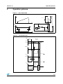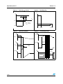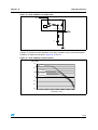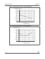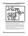
1
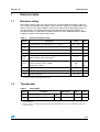
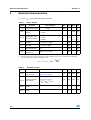
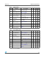
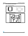
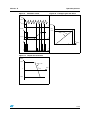
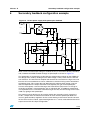
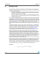
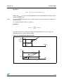
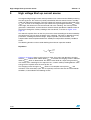
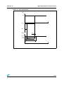
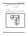
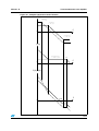
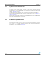
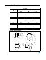
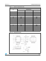
VIPer53 - E
OFF-line primary switch
General features
Type
European
(195 - 265Vac)
US / Wide range
(85 - 265 Vac)
DIP-8
50W
30W
PowerSO-10TM
65W
40W
PowerSO-10
DIP-8
Features
Description
■
Switching frequency up to 300kHz
■
Current limitation
■
Current mode control with adjustable limitation
■
Soft start and shut-down control
■
Automatic burst mode in standby condition
(“Blue Angel“ compliant )
■
Undervoltage lockout with Hysteresis
■
HIgh voltage star-tup current source
■
Overtemperature protection
■
Overload and short-circuit control
The VIPer53-E combines an enhanced current
mode PWM controller with a high voltage
MDMesh Power Mosfet in the same package.
Typical applications cover offline power supplies
with a secondary power capability ranging up to
30W in wide range input voltage, or 50W in single
European voltage range and DIP-8 package, with
the following benefits:
■
Overload and short circuit controlled by
feedback monitoring and delayed device reset.
■
Efficient standby mode by enhanced pulse
skipping.
■
Primary regulation or secondary loop failure
protection through high gain error amplifier.
Block diagram
OSC
DRAIN
ON/OFF
OSCILLAT OR
PW M
LATCH
OVERT EMP.
DET ECT OR
R1
S
BLANKING TIME
SELECTION
FF
Q
R2
R3 R4 R5
UVLO
COMPARATOR
1V
0.5V
150/400ns
BLANKING
VDD
8.4/
11.5V
PW M
COMPARATOR
STANDBY
COMPARATOR
0.5V
4V
HCOM P
CURRENT
AMPLIFIER
8V
125k
15V
ERROR
AMPLIFIER
4.35V
OVERLOAD
COMPARATOR
OVERVOLTAGE
COMPARATOR
4.5V
18V
T OVL
November 2006
Rev 1
COMP
SOURCE
1/36
www.st.com
36
Contents
VIPer53 - E
Contents
1
Electrical data . . . . . . . . . . . . . . . . . . . . . . . . . . . . . . . . . . . . . . . . . . . . . . 3
1.1
Maximum rating . . . . . . . . . . . . . . . . . . . . . . . . . . . . . . . . . . . . . . . . . . . . . 3
1.2
Thermal data . . . . . . . . . . . . . . . . . . . . . . . . . . . . . . . . . . . . . . . . . . . . . . . 3
2
Electrical characteristics . . . . . . . . . . . . . . . . . . . . . . . . . . . . . . . . . . . . . 4
3
Pin connections and function . . . . . . . . . . . . . . . . . . . . . . . . . . . . . . . . . 7
4
Operation pictures . . . . . . . . . . . . . . . . . . . . . . . . . . . . . . . . . . . . . . . . . . 9
5
Primary regulation configuration example . . . . . . . . . . . . . . . . . . . . . . 15
6
Secondary feedback configuration example . . . . . . . . . . . . . . . . . . . . 17
7
Current mode topology . . . . . . . . . . . . . . . . . . . . . . . . . . . . . . . . . . . . . . 19
8
Standby mode . . . . . . . . . . . . . . . . . . . . . . . . . . . . . . . . . . . . . . . . . . . . . 20
9
High voltage Start-up current source . . . . . . . . . . . . . . . . . . . . . . . . . . 22
10
Short-circuit and overload protection . . . . . . . . . . . . . . . . . . . . . . . . . . 24
11
Transconductance error amplifier . . . . . . . . . . . . . . . . . . . . . . . . . . . . . 25
12
Special recommendations . . . . . . . . . . . . . . . . . . . . . . . . . . . . . . . . . . . 30
13
Software implementation . . . . . . . . . . . . . . . . . . . . . . . . . . . . . . . . . . . . 30
14
Package mechanical data . . . . . . . . . . . . . . . . . . . . . . . . . . . . . . . . . . . . 31
15
Order codes . . . . . . . . . . . . . . . . . . . . . . . . . . . . . . . . . . . . . . . . . . . . . . . 34
16
Revision history . . . . . . . . . . . . . . . . . . . . . . . . . . . . . . . . . . . . . . . . . . . 35
2/36
VIPer53 - E
Electrical data
1
Electrical data
1.1
Maximum rating
Stressing the device above the rating listed in the “Absolute Maximum Ratings” table may
cause permanent damage to the device. These are stress ratings only and operation of the
device at these or any other conditions above those indicated in the Operating sections of
this specification is not implied. Exposure to Absolute Maximum Rating conditions for
extended periods may affect device reliability. Refer also to the STMicroelectronics SURE
Program and other relevant quality documents.
Table 1.
Absolute maximum rating
Symbol
VDS
ID
Parameter
Continuous drain current
Supply voltage
VOSC
OSC input voltage range
ITOVL
VESD
Unit
-0.3 ... 620
V
Internally limited
A
0 ... 19
V
0 ... VDD
V
-2 ... 2
mA
200
1.5
V
kV
Internally limited
°C
Continuous drain source voltage (TJ= 25 ... 125°C) (1)
VDD
ICOMP
Value
COMP and TOVL input current range (1)
Electrostatic discharge:
Machine model (R = 0Ω; C = 200pF)
Charged device model
TJ
Junction operating temperature
TC
Case operating temperature
-40 to 150
°C
Storage temperature
-55 to 150
°C
TSTG
1. In order to improve the ruggedness of the device versus eventual drain overvoltages, a resistance of 1kΩ
should be inserted in series with the TOVL pin.\
1.2
Thermal data
Table 2.
Symbol
Thermal data
Parameter
PowerSO-10 (1)
DIP-8 (2)
Unit
RthJC
Thermal Resistance Junction-case
Max
2
20
° C/W
RthJA
Thermal Resistance Ambient-case
Max
60
80
° C/W
1. When mounted on a standard single-sided FR4 board with 50mm² of Cu (at least 35 mm thick) connected
to the DRAIN pin.
2. When mounted on a standard single-sided FR4 board with 50mm² of Cu (at least 35 mm thick) connected
to the device tab.
3/36
Electrical characteristics
2
VIPer53 - E
Electrical characteristics
TJ = 25°C, VDD = 13V, unless otherwise specified
Table 3.
Symbol
BVDSS
IDSS
RDS(on)
Power section
Parameter
Test conditions
Drain-source voltage ID = 1mA; VCOMP = 0V
Off state drain
current
Static drain-source
On state resistance
Min.
Typ.
Max.
Unit
620
V
VDS = 500V; VCOMP = 0V;
TJ = 125°C
150
µA
1
1.7
Ω
Ω
ID = 1A; VCOMP = 4.5V; VTOVL = 0V
TJ = 25°C
0.9
TJ = 100°C
tfv
Fall time
ID = 0.2A; VIN = 300V (1)
100
ns
trv
Rise time
ID = 1A; VIN = 300V (1)
50
ns
Coss
Drain capacitance
VDS = 25V
170
pF
CEon
Effective output
capacitance
200V < VDSon < 400V (2)
60
pF
1. On clamped inductive load
2. This parameter can be used to compute the energy dissipated at turn on Eton according to the initial drain
to source voltage VDSon and the following formula:
V DSon 1.5
1
2
E ton = --- ⋅ C Eon ⋅ 300 ⋅ ⎛ ----------------⎞
⎝
2
300 ⎠
Table 4.
Symbol
FOSC1
Oscillator section
Parameter
Oscillator frequency
initial accuracy
Test conditions
RT = 8kΩ; CT = 2.2nF
Figure 12 on page 12
Min.
Typ.
Max.
Unit
95
100
105
kHz
93
100
107
kHz
RT = 8kΩ; CT = 2.2nF
4/36
Figure 16 on page 14
VDD = VDDon ... VDDovp;
TJ = 0 ... 100°C
FOSC2
Oscillator frequency
total variation
VOSChi
Oscillator peak
voltage
9
V
VOSClo
Oscillator valley
voltage
4
V
VIPer53 - E
Electrical characteristics
Table 5.
Symbol
Supply section
Parameter
Test conditions
Min.
Typ.
Max. Unit
Drain voltage starting
threshold
VDD = 5V; IDD = 0mA
34
IDDch1
Startup charging current
VDD = 0 ... 5V; VDS = 100V
Figure 5 on page 10
-12
mA
IDDch2
Startup charging current
VDD = 10V; VDS = 100VFigure 5.
-2
mA
IDDchoff
Startup charging current
in thermal shutdown
VDD = 5V; VDS = 100VFigure 7.
IDD0
Operating supply current
not switching
Fsw = 0kHz; VCOMP = 0V
8
IDD1
Operating supply current
switching
Fsw = 100kHz
9
VDDoff
VDD undervoltage
shutdown threshold
Figure 5 on page 10
7.5
8.4
9.3
V
VDDon
VDD startup threshold
Figure 5.
10.2
11.5
12.8
V
VDDhyst
VDD threshold hysteresis
Figure 5.
2.6
3.1
VDDovp
VDD Overvoltage
shutdown threshold
Figure 5.
17
18
Min.
Typ.
14.5
15
VDSstart
Table 6.
Symbol
TJ > TSD - THYST
50
0
V
mA
11
mA
mA
V
19
V
Error amplifier section
Parameter
Test conditions
Max. Unit
VDDreg
VDD regulation point
ICOMP = 0mA
Figure 11. on page 11
∆VDDreg
VDD regulation point
total variation
ICOMP = 0mA; TJ = 0 ... 100°C
2
%
GBW
Unity gain bandwidth
From Input = VDD to Output =
VCOMP
ICOMP = 0mA Figure 14 and 15
700
kHz
AVOL
Voltage gain
ICOMP = 0mA Figure 14 and 15
40
45
dB
DC transconductance
VCOMP = 2.5V Figure 11.
1
1.4
Gm
15.5
1.8
V
mS
VCOMPlo Output low level
ICOMP = -0.4mA; VDD = 16V
0.2
V
VCOMPhi Output high level
ICOMP = 0.4mA; VDD=14V(1)
4.5
V
ICOMPlo
Output sinking current
VCOMP = 2.5V; VDD = 16V
Figure 11. on page 11
-0.6
mA
ICOMPhi
Output sourcing current
VCOMP = 2.5V; VDD= 14V
Figure 11.
0.6
mA
1. In order to insure a correct stability of the error amplifier, a capacitor of 10nF (minimum value: 8nF) should
always be present on the COMP pin.
5/36
Electrical characteristics
Table 7.
Symbol
HCOMP
VIPer53 - E
PWM comparator section
Parameter
∆VCOMP / ∆IDPEAK
VCOMPos VCOMP Offset
Test conditions
VCOMP = 1 ... 4 V Figure 10.
dID/dt = 0
Typ.
Max.
Unit
1.7
2
2.3
V/A
dID/dt = 0 Figure 10. on page 11
IDlim
Peak drain current
limitation
ICOMP = 0mA; VTOVL = 0V
Figure 10.
dID/dt = 0
IDmax
Drain current
capability
VCOMP = VCOMPovl; VTOVL = 0V
dID/dt = 0
td
Min.
0.5
V
1.7
2
2.3
A
1.6
1.9
2.3
A
Current sense delay to
ID = 1A
Turn-Off
250
ns
1
V
VCOMP blanking time
change threshold
Figure 6 on page 10
tb1
Blanking time
VCOMP < VCOMPBLFigure 6.
300
400
500
ns
tb2
Blanking time
VCOMP > VCOMPBLFigure 6.
100
150
200
ns
tONmin1
Minimum On time
VCOMP < VCOMPBL
450
600
750
ns
tONmin2
Minimum On time
VCOMP > VCOMPBL
250
350
450
ns
VCOMPoff
VCOMP Shutdown
Threshold
Figure 9 on page 11
VCOMPbl
Table 8.
Symbol
0.5
V
Overload protection section
Parameter
VCOMPovl
VCOMP overload
threshold
VDIFFovl
VCOMPhi to VCOMPovl
voltage difference
Test conditions
Min.
ITOVL = 0mA (1)
Figure 4 on page 9
VDD = VDDoff ... VDDreg;
ITOVL= 0mA
Figure 4.
Typ.
Max.
4.35
50
150
Unit
V
250
mV
(1)
VOVLth
VTOVL overload
threshold
Figure 4.
4
V
tOVL
Overload delay
COVL = 100nF Figure 4.
8
ms
1. VCOMPovl is always lower than VCOMPhi
Table 9.
Symbol
TSD
THYST
6/36
Over temperature Protection Section
Parameter
Thermal shutdown
temperature
Thermal shutdown
hysteresis
Test Conditions
Figure 7 on page 10
Figure 7 on page 10
Min.
Typ.
Max.
Unit
140
160
°C
40
°C
VIPer53 - E
3
Pin connections and function
Pin connections and function
Figure 1.
Pin connection (top view)
COMP 1
8
TOVL
OSC 2
7
VDD
SOURCE 3
6
NC
SOURCE 4
5
DRAIN
DIP-8
Figure 2.
PowerSO-10
Current and voltage conventions
IDD
ID
VDD
DRAIN
IOSC
OSC
15V
VDD
TOVL
COMP
SOURCE
VDS
ITOVL
VOSC
ICOMP
VTOVL
V COMP
7/36
Pin connections and function
Table 10.
Pin function
Pin Name
Pin function
VDD
Power supply of the control circuits. Also provides the charging current of the external
capacitor during start-up. The functions of this pin are managed by four threshold
voltages:
- VDDon: Voltage value at which the device starts switching (Typically 11.5 V).
- VDDoff: Voltage value at which the device stops switching (Typically 8.4 V).
- VDDreg: Regulation voltage point when working in primary feedback
(Trimmed to 15 V).
- VDDovp: Triggering voltage of the overvoltage protection (Trimmed to 18 V).
SOURCE
8/36
VIPer53 - E
Power MOSFET source and circuit ground reference.
DRAIN
Power MOSFET drain. Also used by the internal high voltage current source during the
start-up phase to charge the external VDD capacitor.
COMP
Input of the current mode structure, and output of the internal error amplifier. Allows
the setting of thedynamic characteristic of the converter through an external passive
network. The useful voltage range extends from 0.5V to 4.5V. The Power MOSFET is
always off below 0.5V, and the overload protection is triggered if the voltage exceeds
4.35V. This action is delayed by the timing capacitor connected tothe TOVL pin.
TOVL
Allows the connection of an external capacitor for delaying the overload protection,
which is triggered by a voltage on the COMP pin higher than 4.35V.
OSC
Allows the setting of the switching frequency through an external Rt-Ct network.
VIPer53 - E
4
Operation pictures
Operation pictures
Figure 3.
Rise and fall time
ID
C<<C OSS
C
L
D
t
VDD
VDS
DRAIN
300V
OSC
90%
15V
trv
tfv
TOVL
10%
Figure 4.
COMP
SOURCE
t
Overloaded event
VDD
Normal
operation
Abnormal
operation
VDDon
VDDoff
VCOMP
VDIFFovl
VTOVL
VOVLth
tOVL
VDS
Not
switching
Switching
9/36
Operation pictures
Figure 5.
VIPer53 - E
Start-up VDD current
Figure 6.
Blanking time
tb
IDD
IDD0
tb1
VDDhyst
VDDoff
VDDon
VDD
IDDch2
VDS = 100 V
FSW = 0 kHz
tb2
IDDch1
VCOMPbl
Figure 7.
Thermal shutdown
Figure 8.
Tj
VDD
TSD
VDDovp
VCOMPhi
Overvoltage event
TSD-THYST
VDD
VDDon
VCOMP
VCOMP
Abnormal
operation
Automatic
startup
VDS
Not
switching
Switching
10/36
VIPer53 - E
Operation pictures
Figure 9.
Shutdown action
Figure 10. Comp pin gain and offset
VOSC
VOSChi
VOSClo
IDpeak
t
VCOMP
IDlim
IDmax
Slope = 1 / HCOMP
VCOMPoff
t
ID
VCOMP
VCOMPos
VCOMPovl VCOMPhi
t
Figure 11. Output characteristics
ICOMP
ICOMPhi
Slope = Gm
0
VDDreg
VDD
ICOMPlo
11/36
Operation pictures
VIPer53 - E
Figure 12. Oscillator schematic
Vcc
VDD
Rt
OSC
PWM
section
320 Ω
Ct
SOURCE
The switching frequency settings shown on the graphic here below is valid within the
following boundaries:
Rt > 2kΩ
FSW = 300kHz
Figure 13. Oscillator settings
Frequency (kHz)
300
2.2nF
1nF
4.7nF
100
10nF
22nF
10
1
10
RT (KΩ)
12/36
100
VIPer53 - E
Operation pictures
Figure 14. Error amplifier test cpfiguration
Vin
VDD
DRAIN
OSC
15V
TOVL
COMP
SOURCE
Vout
R
2.5 V
This configuration is for test purpose only. In order to insure a correct stability of the error
amplifier, a capacitor of 10nF (minimum value: 8nF) should be always connected between
COMP pin and ground. See figures Figure 18, 19 and 22.
Figure 15. Error amplifier transfer function
Gain (dB)
60
Open
40
R = 10 kΩ
20
R = 2.2 kΩ
R = 470 Ω
0
-20
-40
-60
1
10
100
1k
10k
100k
1M
10M
Frequency (Hz)
13/36
Operation pictures
VIPer53 - E
Figure 16. Typical frequency variation vs. junction temperature
Normalised Frequency
1.04
1.02
1
0.98
0.96
-20
0
20
40
60
80
100
120
Temperature (°C)
Figure 17. Typical current limitation vs. junction temperature
Normalised IDlim
1.04
1.02
1
0.98
0.96
-20
0
20
40
60
80
Temperature (°C)
14/36
100
120
VIPer53 - E
5
Primary regulation configuration example
Primary regulation configuration example
Figure 18. Off line power supply with auxiliary supply feedback
F1
C1
AC IN
D1
T1
C2
R1
R2
C3
T2
D2
L1
D4
D3
R4
C8
C9
DC OUT
U1
VIPer73
R3
VDD
DRAIN
C10
OSC
15V
TOVL
C4
COMP
R6
1k
C5
SOURCE
R5
C11
10nF
C6
C7
The schematic on Figure 18 delivers a fixed output voltage by using the internal error
amplifier of the device in a primary feedback configuration. The primary auxiliary winding
provides a voltage to the VDD pin, and is automatically regulated at 15V, due to the internal
error amplifier connected to this pin. The secondary voltage has to be adjusted through the
turn ratio of the transformer between auxiliary and secondary.
The error amplifier of the VIPer53 is a transconductance type: its output is a current
proportional to the difference of voltage between the VDD pin and the internally trimmed 15V
reference (i.e., the error voltage). As the transconductance value is set at a relatively low
value to control the overall loop gain and ensure stability, this current has to be integrated by
a capacitor (C7 in Figure 18). When the steady state operation is reached, this capacitor
blocks any DC current from the COMP pin and imposes a “nil” error voltage. Therefore, the
VDD voltage is accurately regulated to 15V.
This results in a good load regulation, which depends only on transformer coupling and
output diodes impedance. The current mode structure takes care of all incoming voltage
changes, thus providing at the same time an excellent line regulation.
15/36
Primary regulation configuration example
VIPer53 - E
The switching frequency can be set to any value through the choice of R3 and C5. This
allows to optimize the efficiency of the converter by adopting the best compromise between
switching losses, EMI (Lower with low switching frequencies) and transformer size (Smaller
with high switching frequencies). For an output power of a few watts, typical switching
frequencies between 20kHz and 40kHz because of the small size of the transformer. For
higher power, 70kHz to 130kHz are generally chosen.
The R5 compensation resistor value sets the dynamic behavior of the converter. It can be
adjusted to provide the best compromise between stability and recovery time with fast load
changes.
16/36
VIPer53 - E
6
Secondary feedback configuration example
Secondary feedback configuration example
Figure 19. Off line power supply with optocoupler feedback
F1
AC IN
C1
D1
T1
C2
R1
R2
C3
T2
D2
L1
D4
D3
R4
C8
C9
DC OUT
U1
VIPer73
R3
VDD
DRAIN
C10
OSC
15V
R8
TOVL
C4
COMP
SOURCE
U2
C5
R9
1k
C6
C11
10nF
R5
C12
C7
R7
U3
R6
When a more accurate output voltage is needed, the way is to monitor it directly secondary
side, and drive the PWM controller through an optocoupler as shown on Figure 17.
The optocoupler is connected in parallel with the compensation network on the COMP pin.
The design of the auxiliary winding that the VDD voltage is always lower than the internal
15V reference. The internal error amplifier will therefore be saturated in the high state, and
because of its transconductance nature, will deliver a constant biasing current of 0.6mA to
the optotransistor. This current does not depend on the compensation voltage, and so it
does not depend on the output load either. Consequently, the gain of the optocoupler
ensures consequently a constant biasing of the TL431 device (U3) which is in charge of
secondary regulation. If the optocoupler gain is sufficiently low, no additional components
are required to ensure a minimum current biasing of U3. Also, the low biasing current value
avoid any ageing of the optocoupler.
The constant current biasing can be used to simplify the secondary circuit: Instead of a
TL431, a simple zener and resistance network in series with the optocoupler diode can
insure a good secondary regulation. As the current flowing in this branch remains constant
for the same reason as above, typical load regulation of 1% can be achieved from zero to full
output current with this simple configuration.
17/36
Secondary feedback configuration example
VIPer53 - E
Since the dynamic characteristics of the converter are set on the secondary side through
components associated to U3, the compensation network has only a role of gain
stabilization for the optocoupler, and its value can be freely chosen. R5 can be set to a fixed
value of 1kΩ, offering the possibility of using C7 as a soft start capacitor: When starting up
the converter, the VIPer53 device delivers a constant current of 0.6 mA on the COMP pin,
creating a constant voltage of 0.6V in R5 and a rising slope across C7. This voltage shape,
together with the operating range of 0.5V to 4.5V provides a soft start-up of the converter.
The rising speed of the output voltage can be set through the value of C7. The C4 and C6
values must be adjusted accordingly in order to ensure a correct start-up.
18/36
VIPer53 - E
7
Current mode topology
Current mode topology
The VIPer53-E implements the conventional current mode control method for regulating the
output voltage. This kind of feedback includes two nested regulation loops:
The inner loop controls the peak primary current cycle by cycle. When the Power MOSFET
output transistor is on, the inductor current (primary side of the transformer) is monitored
with a SenseFET technique and converted into a voltage. When VS reaches VCOMP, the
power switch is turned off. This structure is completely integrated as shown on the Block
Diagram on page 1, with the current amplifier, the PWM comparator, the blanking time
function and the PWM latch. The following formula gives the peak current in the Power
MOSFET according to the compensation voltage:
Equation 1
V COMP – V COMPos
I Dpeak = ------------------------------------------------H COMP
The outer loop defines the level at which the inner loop regulates peak current in the power
switch. For this purpose, VCOMP is driven by the feedback network (TL431 through an
optocoupler in secondary feedback configuration, see Figure 19 on page 17) and is sets
accordingly the peak drain current for each switching cycle.
As the inner loop regulates the peak primary current in the primary side of the transformer,
all input voltage changes are compensated for before impacting the output voltage. This
results in an improved line regulation, instantaneous correction to line changes, and better
stability for the voltage regulation loop.
Current mode topology also provides a good converter start-up control. The compensation
voltage can be controlled to increase slowly during the start-up phase, so the peak primary
current will follow this soft voltage slope to provide a smooth output voltage rise, without any
overshoot. The simpler voltage mode structure which only controls the duty cycle, leads
generally to high current at start-up with the risk of transformer saturation.
An integrated blanking filter inhibits the PWM comparator output for a short time after the
integrated Power MOSFET is switched on. This function prevents anomalous or premature
termination of the switching pulse in the case of current spikes caused by primary side
transformer capacitance or secondary side rectifier reverse recovery time when working in
continuous mode.
19/36
Standby mode
8
VIPer53 - E
Standby mode
The device offers a special feature to address the low load condition. The corresponding
function described hereafter consists of reducing the switching frequency by going into burst
mode, with the following benefits:
– It reduces the switching losses, thus providing low consumption on the mains lines.
The device is compliant with “Blue Angel” and other similar standards, requiring less
than 0.5 W of input power when in standby.
– It allows the regulation of the output voltage, even if the load corresponds to a duty
cycle that the device is not able to generate because of the internal blanking time, and
associated minimum turn on.
For this purpose, a comparator monitores the COMP pin voltage, and maintains the PWM
latch and the Power MOSFET in the Off state as long as VCOMP remains below 0.5V (See
Block Diagram on page 1). If the output load requires a duty cycle below the one defined by
the minimum turn on of the device, the VCOMP net decreases its voltage until it reaches this
0.5V threshold (VCOMPoff). The Power MOSFET can be completely Off for some cycles, and
resumes normal operation as soon as VCOMP is higher than 0.5V. The output voltage is
regulated in burst mode. The corresponding ripple is not higher than the nominal one at full
load.
In addition, the minimum turn on time which defines the frontier between normal operation
and burst mode changes according to VCOMP value. Below 1.0V (VCOMPbl), the blanking
time increases to 400ns, whereas for higher voltages, it is 150ns Figure 6 on page 10 The
minimum turn on times resulting from these values are respectively 600 ns and 350 ns,
when taking into account internal propagation time. This brutal change induces an
hysteresis between normal operation and burst mode as shown on Figure 20 on page 21.
When the output power decreases, the system reaches point 2 where VCOMP equals
VCOMPbl. The minimum turn-on time passes immediately from 350ns to 600ns, exceeding
the effective turn-on time that should be needed at this output power level. Therefore the
regulation loop will quickly drive VCOMP to VCOMPoff (Point 3) in order to pass into burst
mode and to control the output voltage. The corresponding hysteresis can be seen on the
switching frequency which passes from FSWnom which is the normal switching frequency set
by the components connected to the OSC pin and to FSWstby. Note: This frequency is
actually an equivalent number of switching pulses per second, rather than a fixed switching
frequency since the device is working in burst mode.
As long as the power remains below PRST the output of the regulation loop remains stuck at
VCOMPsd and the converter works in burst mode. Its “density” increases (i.e. the number of
missing cycles decreases) as the power approaches PRST and finally resumes normal
operation at point 1. The hysteresis cannot be seen on the switching frequency, but it can be
seen in the sudden surge of the COMP pin voltage from point 3 to point 1 at that power level.
The power points value PRST and PSTBY are defined by the following formulas:
Equation 2
2
1
1
2
P RST = --- • F SWnom • ( tb 1 + td ) • V IN • ------Lp
2
20/36
VIPer53 - E
Standby mode
Equation 3
1
2
P STBY = --- • F SWnom • Ip ( V COMPbl ) • Lp
2
Where Ip(VCOMPbl2) is the peak Power MOSFET current corresponding to a compensation
voltage of VCOMPbl (1V).
Note:
The power point PSTBY where the converter is going into burst mode does not depend on
the input voltage.
The standby frequency FSWstby is given by:
Equation 4
P STBY
P SWstby = ----------------- • F SWnom
P RST
The ratio between the nominal and standby switching frequencies can be as high as 4,
depending on the Lp value and input voltage.
Figure 20. Standby mode implementation
ton
3
600ns
Minimum
turn on
1
2
350ns
VCOMP
VCOMPsd
VCOMPoff
VCOMPbl
PIN
1
PRST
3
2
PSTBY
FSW
FSWstby
FSWnom
21/36
High voltage Start-up current source
9
VIPer53 - E
High voltage Start-up current source
An integrated high voltage current source provides a bias current from the DRAIN pin during
the start-up phase. This current is partially absorbed by internal control circuits in standby
mode with reduced consumption, and also supplies the external capacitor connected to the
VDD pin. As soon as the voltage on this pin reaches the high voltage threshold VDDon of the
UVLO logic, the device turns into active mode and starts switching. The start-up current
generator is switched off, and the converter should normally provide the needed current on
the VDD pin through the auxiliary winding of the transformer, as shown on Figure 19 on
page 17.
The external capacitor CVDD on the VDD pin must be sized according to the time needed by
the converter to start-up, when the device starts switching. This time tss depends on many
parameters, including transformer design, output capacitors, soft start feature, and
compensation network implemented on the COMP pin and possible secondary feedback
circuit.
The following formula can be used for defining the minimum capacitor needed:
Equation 5
I DD1 ⋅ tss
C VDD > --------------------------V DDhyst
Figure 21 on page 23 shows a typical start-up event. VDD starts from 0V with a charging
current IDDch1 at about 9 mA. When about VDDoff is reached, the charging current is reduced
down to IDDch2 which is about 0.6mA. This lower current leads to a slope change on the VDD
rise. Device starts switching for VDD equal to VDDon, and the auxiliary winding delivers some
energy to VDD capacitor after the start-up time tss.
The charging current change at VDDoff allows a fast complete start-up time tSDU, and
maintains a low restart duty cycle. This is especially useful for short circuits and overloads
conditions, as described in the following section.
22/36
VIPer53 - E
High voltage Start-up current source
Figure 21. Start-up waveforms
IDD
IDD1
t
IDDch2
IDDch1
VDD
tSS
VDDreg
VDDst
VDDsd
tSU
t
23/36
Short-circuit and overload protection
10
VIPer53 - E
Short-circuit and overload protection
A VCOMPovl threshold of about 4.35V has been implemented on the COMP pin. When
VCOMP goes above this level, the capacitor connected on the TOVL pin begins to charge.
When reaching typically VOVLth (4V), the internal MOSFET driver is disabled and the device
stops switching. This state is latched because of to the regulation loop which maintains the
COMP pin voltage above the VCOMPovl threshold. Since the VDD pin does not receive any
more energy from the auxiliary winding, its voltage drops down until it reaches VDDoff and
the device is reset, recharging the VDD capacitor for a new restart cycle. Note: If VCOMP
drops below the VCOMPovl threshold for any reason during the VDD drop, the device
resumes switching immediately.
The device enters an endless restart sequence if the overload or short circuit condition is
maintained. The restart duty cycle DRST is defined as the time ratio for which the device tries
to restart, thus delivering its full power capability to the output. In order to keep the whole
converter in a safe state during this event, DRST must be kept as low as possible, without
compromising the real start-up of the converter. A typical value of about 10% is generally
sufficient. For this purpose, both VDD and TOVL capacitors can be used to satisfy the
following conditions:
Equation 6
C OVL > 12.5 ⋅ 10
–6
⋅ tss
Equation 7
4
OVL ⋅ I DDch2
1 - – 1⎞ ⋅ C
-------------------------------------C VDD > 8 ⋅ 10 ⋅ ⎛ ------------⎝D
⎠
V DDhyst
RST
Refer to the previous start-up section for the definition of tss, and CVDD must also be
checked against the limit given in this section. The maximum value of the two calculus will
be adopted.
All this behavior can be observed on Figure 8 on page 10. In Figure 10 on page 11 the value
of the drain current Id for VCOMP = VCOMPovl is shown. The corresponding parameter IDmax
is the drain current to take into account for design purposes. Since IDmax represents the
maximum value for which the overload protection is not triggered, it defines the power
capability of the power supply.
24/36
VIPer53 - E
11
Transconductance error amplifier
Transconductance error amplifier
The VIPer53-E includes a transconductance error amplifier. Transconductance Gm is the
change in output current ICOMP versus change in input voltage VDD. Thus:
Equation 8
∂I COMP
Gm = ------------------∂V DD
The output impedance ZCOMP at the output of this amplifier (COMP pin) can be defined as:
Equation 9
∂V COMP
∂V COMP
1
Z COMP = ---------------------- = ---------- ⋅ ---------------------∂I COMP Gm
∂V DD
This last equation shows that the open loop gain AVOL can be related to Gm and ZCOMP:
Equation 10
A VOL = Gm ⋅ Z COMP
where Gm value for VIPer53 is typically 1.4mA/V.
Gm is well defined by specification, but ZCOMP, and therefore AVOL, are subject to large
tolerances. An impedance Z must be connected between the COMP pin and ground in order
to accurately define the transfer function F of the error amplifier, the following equation, very
similar to the one above:
Equation 11
F ( s ) = Gm ⋅ Z ( s )
The error amplifier frequency response is shown in .0 for different values of a simple
resistance connected on the COMP pin. The unloaded transconductance error amplifier
shows an internal ZCOMP of about 140KΩ. More complex impedances can be connected on
the COMP pin to achieve different compensation methods. A capacitor provides an
integrator function, thus eliminating the DC static error, and a resistance in series leads to a
flat gain at higher frequency, introducing a zero level and ensuring a correct phase margin.
This configuration illustrated in Figure 22, for the schematic and Figure 23 on page 28 for
the error amplifier transfer function for a typical set of values of CCOMP and RCOMP.
Note that a 10nF capacitor (8nF, minimum value) should always be connected to the COMP
pin to ensure a correct stability of the internal error amplifier.
The complete converter open loop transfer function can be built from both power cell and
error amplifier transfer functions. A theoretical example can be seen in Figure 24 for a
discontinuous mode flyback loaded by a simple resistor, regulated from primary side (no
25/36
Transconductance error amplifier
VIPer53 - E
optocoupler, the internal error amplifier is fully used for regulation). A typical schematic
corresponding to this situation can be seen on Figure 18.
The transfer function of the power cell is represented as G(s) in Figure 24 Iexhibits a pole
which depends on the output load and on the output capacitor value. As the load of a
converter may change, two curves are shown for two different values of output resistance
value, RL1 and RL2. A zero at higher frequency values then appears, due to the output
capacitor ESR. Note: The overall transfer function does not depend on the input voltage
because of the current mode control.
The error amplifier has a fixed behavior, similar to the one shown in Figure 23. Its bandwidth
is to avoid injection of high frequency noise in the current mode section. A zero due to the
RCOMP-CCOMP network is set at the same value as the maximum load RL2 pole.
The total transfer function is shown as F(s). G(s) at the bottom of Figure 24. For maximum
load (plain line), the load pole is exactly compensated by the zero of the error amplifier, and
the result is a perfect first order decreasing until it reaches the zero of the output capacitor
ESR. The error amplifier cut-off then definitely any further spurious noise or resonance from
disturbing the regulation loop.
The point where the complete transfer function has a unity gain is known as the regulation
bandwidth and has:
–
The higher it is, the faster the reaction will be to an eventual load change, and the
smaller the output voltage change will be.
–
The phase shift in the complete system at this point has to be less than 135° to
ensure good stability. Generally, a first-order slope gives 90° of phase shift, and a
second-order gives 180°.
In Figure 24, the unity gain is reached in a first order slope, so the stability is ensured.
The dynamic load regulation is improved by increasing the regulation bandwidth, but some
limitations have to be respected: As the transfer function above the zero due the capacitor
ESR is not reliable (The ESR itself is not well specified, and other parasitic effects may take
place), the bandwidth should always be lower than the minimum of FC and ESR zero.
As the highest bandwidth is obtained with the highest output power (Plain line with RL2 load
in Figure 24), the above criteria will be checked for this condition and allows to define the
value of RCOMP, as the error amplifier gain depends only on this value for this frequency
range. The following formula can be derived:
Equation 12
R COMP =
2
V
R L2
OUT
With: POUT2 = --------------
26/36
P OUT2 F BW2 ⋅ R L2 ⋅ C OUT
----------------- ⋅ -----------------------------------------------------Gm
P MAX
1
2
and: PMAX = --- ⋅ L P ⋅ I LIM ⋅ F SW
2
VIPer53 - E
Transconductance error amplifier
The lowest load gives another condition for stability: The frequency FBW1 must not encounter
the second order slope generated by the load pole and the integrator part of the error
amplifier. This condition can be met by adjusting the CCOMP value:
Equation 13
R L1 ⋅ C OUT
C COMP > ------------------------------------------------------ ⋅
2
6.3 ⋅ Gm ⋅ R COMP
With:
P OUT1
-----------------P MAX
2
V OUT
P OUT1 = --------------R L1
The above formula gives a minimum value for CCOMP. It can be then increased to provide a
natural soft start function as this capacitor is charged by the error amplifier current capacity
ICOMPhi at start-up.
Figure 22. Typical compensation network
VDD
DRAIN
OSC
15V
TOVL
COMP
SOURCE
Rcomp
10nF
Ccomp
27/36
Transconductance error amplifier
VIPer53 - E
Figure 23. Typical transfer functions
Gain (dB)
60
Rcomp=4.7k
Ccomp=470nF
50
40
30
20
10
0
-10
1
10
100
1k
10k
100k
1M
Frequency (Hz)
Phase (°)
0
Rcomp=4.7k
Ccomp=470nF
-10
-20
-30
-40
-50
-60
-70
-80
-90
-100
1
10
100
1k
Frequency (Hz)
28/36
10k
100k
1M
VIPer53 - E
Transconductance error amplifier
Figure 24. Complete converter transfer function
G(S)
1
----------------------------------------------π⋅ R
⋅ C
L1
OUT
1
----------------------------------------------π⋅ R
⋅ C
L2
OUT
F
1
1
----------------------------------------------------------2 ⋅ π ⋅ ESR ⋅ C
OUT
F(S)
1
---------------------------------------------------------------------------2⋅ π⋅ R
⋅ C
COMP
COMP
FC
F
1
F(S).G(S)
FBW2
1
F
FBW1
29/36
Special recommendations
12
VIPer53 - E
Special recommendations
As steted in the error amplifier section, a capacitor of 10nF capacitor (minimum value: 8nF)
should always be connected to the COMP pin to ensure correct stability of the internal error
amplifier Figure 18, 19 and 22.
In order to improve the ruggedness of the device versus eventual drain overvoltages, a
resistance of 1kΩ should be inserted in series with the TOVL pin, as shown on Figure 18,
Figure 19 on page 17.
Note that, this resistance does not impact the overload delay, as its value is negligible prior
to the internal pull-up resistance (about 125kΩ).
13
Software implementation
All the above considerations and some others are included included in ST design software
which provides all of the needed components around the VIPer device for specified output
configurations, and is available on www.st.com.
30/36
VIPer53 - E
14
Package mechanical data
Package mechanical data
In order to meet environmental requirements, ST offers these devices in ECOPACK®
packages. These packages have a Lead-free second level interconnect. The category of
second Level Interconnect is marked on the package and on the inner box label, in
compliance with JEDEC Standard JESD97. The maximum ratings related to soldering
conditions are also marked on the inner box label. ECOPACK is an ST trademark.
ECOPACK specifications are available at: www.st.com.
31/36
Package mechanical data
Table 11.
VIPer53 - E
DIP8 mechanical data
Dimensions
Databook (mm)
Ref.
Nom.
Min
A
5.33
A1
0.38
A2
2.92
3.30
4.95
b
0.36
0.46
0.56
b2
1.14
1.52
1.78
c
0.20
0.25
0.36
D
9.02
9.27
10.16
E
7.62
7.87
8.26
E1
6.10
6.35
7.11
e
2.54
eA
7.62
eB
L
10.92
2.92
Package Weight
Figure 25. Package dimensions
32/36
Max
3.30
Gr. 470
3.81
VIPer53 - E
Package mechanical data
Table 12.
PowerSO-10 mechanical data
Dimensions
Databook (mm)
Ref.
Nom.
A
Min
3.35
Max
3.65
A1
0.00
0.10
B
0.40
0.60
c
0.35
0.55
D
9.40
9.60
D1
7.40
7.60
E
9.30
9.50
E1
7.20
7.40
E2
7.20
7.60
E3
6.10
6.35
E4
5.90
6.10
e
1.27
F
1.25
H
13.80
h
L
14.40
0.50
1.20
q
α
1.35
1.80
1.70
0°
8°
Figure 26. Package dimensions
33/36
Order codes
15
VIPer53 - E
Order codes
Table 13.
34/36
Order codes
Part Number
Package
Shipment
VIPer53DIP-E
DIP-8
Tube
VIPer53SP-E
PowerSO-10
Tube
VIPer53SPTR - E
PowerSO-10
Tape and reel
VIPer53 - E
16
Revision history
Revision history
Table 14.
Revision history
Date
Revision
13-Nov-2006
1
Changes
Initial release.
35/36
VIPer53 - E
Please Read Carefully:
Information in this document is provided solely in connection with ST products. STMicroelectronics NV and its subsidiaries (“ST”) reserve the
right to make changes, corrections, modifications or improvements, to this document, and the products and services described herein at any
time, without notice.
All ST products are sold pursuant to ST’s terms and conditions of sale.
Purchasers are solely responsible for the choice, selection and use of the ST products and services described herein, and ST assumes no
liability whatsoever relating to the choice, selection or use of the ST products and services described herein.
No license, express or implied, by estoppel or otherwise, to any intellectual property rights is granted under this document. If any part of this
document refers to any third party products or services it shall not be deemed a license grant by ST for the use of such third party products
or services, or any intellectual property contained therein or considered as a warranty covering the use in any manner whatsoever of such
third party products or services or any intellectual property contained therein.
UNLESS OTHERWISE SET FORTH IN ST’S TERMS AND CONDITIONS OF SALE ST DISCLAIMS ANY EXPRESS OR IMPLIED
WARRANTY WITH RESPECT TO THE USE AND/OR SALE OF ST PRODUCTS INCLUDING WITHOUT LIMITATION IMPLIED
WARRANTIES OF MERCHANTABILITY, FITNESS FOR A PARTICULAR PURPOSE (AND THEIR EQUIVALENTS UNDER THE LAWS
OF ANY JURISDICTION), OR INFRINGEMENT OF ANY PATENT, COPYRIGHT OR OTHER INTELLECTUAL PROPERTY RIGHT.
UNLESS EXPRESSLY APPROVED IN WRITING BY AN AUTHORIZED ST REPRESENTATIVE, ST PRODUCTS ARE NOT
RECOMMENDED, AUTHORIZED OR WARRANTED FOR USE IN MILITARY, AIR CRAFT, SPACE, LIFE SAVING, OR LIFE SUSTAINING
APPLICATIONS, NOR IN PRODUCTS OR SYSTEMS WHERE FAILURE OR MALFUNCTION MAY RESULT IN PERSONAL INJURY,
DEATH, OR SEVERE PROPERTY OR ENVIRONMENTAL DAMAGE. ST PRODUCTS WHICH ARE NOT SPECIFIED AS "AUTOMOTIVE
GRADE" MAY ONLY BE USED IN AUTOMOTIVE APPLICATIONS AT USER’S OWN RISK.
Resale of ST products with provisions different from the statements and/or technical features set forth in this document shall immediately void
any warranty granted by ST for the ST product or service described herein and shall not create or extend in any manner whatsoever, any
liability of ST.
ST and the ST logo are trademarks or registered trademarks of ST in various countries.
Information in this document supersedes and replaces all information previously supplied.
The ST logo is a registered trademark of STMicroelectronics. All other names are the property of their respective owners.
© 2006 STMicroelectronics - All rights reserved
STMicroelectronics group of companies
Australia - Belgium - Brazil - Canada - China - Czech Republic - Finland - France - Germany - Hong Kong - India - Israel - Italy - Japan Malaysia - Malta - Morocco - Singapore - Spain - Sweden - Switzerland - United Kingdom - United States of America
www.st.com
36/36