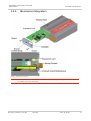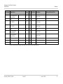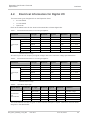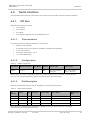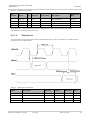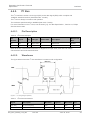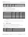
1
Expansion Card Product Technical Specification AirLink FXT Series WA_DEV_FEX20_PTS_004 001 June 30, 2010 Expansion Card Product Technical Specification Important Notice Due to the nature of wireless communications, transmission and reception of data can never be guaranteed. Data may be delayed, corrupted (i.e., have errors) or be totally lost. Although significant delays or losses of data are rare when wireless devices such as the Sierra Wireless modem are used in a normal manner with a well-constructed network, the Sierra Wireless modem should not be used in situations where failure to transmit or receive data could result in damage of any kind to the user or any other party, including but not limited to personal injury, death, or loss of property. Sierra Wireless accepts no responsibility for damages of any kind resulting from delays or errors in data transmitted or received using the Sierra Wireless modem, or for failure of the Sierra Wireless modem to transmit or receive such data. Safety and Hazards Do not operate the Sierra Wireless modem in areas where blasting is in progress, where explosive atmospheres may be present, near medical equipment, near life support equipment, or any equipment which may be susceptible to any form of radio interference. In such areas, the Sierra Wireless modem MUST BE POWERED OFF. The Sierra Wireless modem can transmit signals that could interfere with this equipment. Do not operate the Sierra Wireless modem in any aircraft, whether the aircraft is on the ground or in flight. In aircraft, the Sierra Wireless modem MUST BE POWERED OFF. When operating, the Sierra Wireless modem can transmit signals that could interfere with various onboard systems. Note: Some airlines may permit the use of cellular phones while the aircraft is on the ground and the door is open. Sierra Wireless modems may be used at this time. The driver or operator of any vehicle should not operate the Sierra Wireless modem while in control of a vehicle. Doing so will detract from the driver or operator’s control and operation of that vehicle. In some states and provinces, operating such communications devices while in control of a vehicle is an offence. Limitations of Liability This manual is provided “as is”. Sierra Wireless makes no warranties of any kind, either expressed or implied, including any implied warranties of merchantability, fitness for a particular purpose, or noninfringement. The recipient of the manual shall endorse all risks arising from its use. The information in this manual is subject to change without notice and does not represent a commitment on the part of Sierra Wireless. SIERRA WIRELESS AND ITS AFFILIATES SPECIFICALLY DISCLAIM LIABILITY FOR ANY AND ALL DIRECT, INDIRECT, SPECIAL, GENERAL, INCIDENTAL, CONSEQUENTIAL, PUNITIVE OR EXEMPLARY DAMAGES INCLUDING, BUT NOT LIMITED TO, LOSS OF PROFITS OR REVENUE OR ANTICIPATED PROFITS OR REVENUE ARISING OUT OF THE USE OR INABILITY TO USE ANY SIERRA WIRELESS PRODUCT, EVEN IF SIERRA WIRELESS AND/OR ITS AFFILIATES HAS BEEN ADVISED OF THE POSSIBILITY OF SUCH DAMAGES OR THEY ARE FORESEEABLE OR FOR CLAIMS BY ANY THIRD PARTY. Notwithstanding the foregoing, in no event shall Sierra Wireless and/or its affiliates aggregate liability arising under or in connection with the Sierra Wireless product, regardless of the number of events, occurrences, or claims giving rise to liability, be in excess of the price paid by the purchaser for the Sierra Wireless product. WA_DEV_FEX20_PTS_004 Rev 001 June 30, 2010 2 Expansion Card Product Technical Specification Patents Portions of this product may be covered by some or all of the following US patents: 5,515,013 6,191,741 6,653,979 6,968,171 7,287,162 5,629,960 6,199,168 6,697,030 6,985,757 D442,170 5,845,216 6,339,405 6,785,830 7,023,878 D459,303 5,847,553 6,359,591 6,845,249 7,053,843 D599,256 5,878,234 6,400,336 6,847,830 7,106,569 D560,911 5,890,057 6,516,204 6,876,697 7,145,267 5,929,815 6,561,851 6,879,585 7,200,512 6,169,884 6,643,501 6,886,049 7,295,171 and other patents pending. This product includes technology licensed from QUALCOMM® 3G Manufactured or sold by Sierra Wireless or its licensees under one or more patents licensed from InterDigital Group. Copyright © 2010 Sierra Wireless. All rights reserved. Trademarks ® ® AirCard and Watcher are registered trademarks of Sierra Wireless. Sierra Wireless™, AirPrime™, AirLink™, AirVantage™ and the Sierra Wireless logo are trademarks of Sierra Wireless. , , ®, inSIM®, WAVECOM®, WISMO®, Wireless Microprocessor®, Wireless CPU , Open AT are filed or registered trademarks of Sierra Wireless S.A. in France and/or in other countries. ® ® Windows® and Windows Vista® are registered trademarks of Microsoft Corporation. Macintosh and Mac OS are registered trademarks of Apple Inc., registered in the U.S. and other countries. QUALCOMM® is a registered trademark of QUALCOMM Incorporated. Used under license. Other trademarks are the property of the respective owners. Contact Information Sales Desk: Post: Fax: Web: Phone: 1-604-232-1488 Hours: 8:00 AM to 5:00 PM Pacific Time E-mail: [email protected] Sierra Wireless 13811 Wireless Way Richmond, BC Canada V6V 3A4 1-604-231-1109 www.sierrawireless.com Consult our website for up-to-date product descriptions, documentation, application notes, firmware upgrades, troubleshooting tips, and press releases: www.sierrawireless.com WA_DEV_FEX20_PTS_004 Rev 001 June 30, 2010 3 Expansion Card Product Technical Specification Document History Version Date Updates 001 June 30, 2010 Creation WA_DEV_FEX20_PTS_004 Rev 001 June 30, 2010 4 Contents 1. OVERVIEW......................................................................................................... 11 1.1. Expansion Card Features ........................................................................................... 11 1.2. Operating System ....................................................................................................... 11 1.3. Connection Interfaces ................................................................................................. 11 1.4. Environmental Compliance ......................................................................................... 12 1.4.1. RoHS Directive Compliant ................................................................................... 12 1.4.2. Disposing of the Product ...................................................................................... 12 2. FUNCTIONAL SPECIFICATIONS ...................................................................... 13 2.1. Operating System ....................................................................................................... 13 3. TECHNICAL SPECIFICATIONS ........................................................................ 14 3.1. Power Supply ............................................................................................................. 14 3.2. Mechanical Specifications ........................................................................................... 15 3.2.1. Expansion Card Mechanical Drawing ................................................................... 15 3.2.2. Expansion Card Design Suggestion ..................................................................... 16 3.2.3. Mechanical Integration ......................................................................................... 17 4. INTERFACES ..................................................................................................... 18 4.1. General Purpose Connector ....................................................................................... 18 4.1.1. Pin Description .................................................................................................... 19 4.2. Electrical Information for Digital I/O ............................................................................. 22 4.3. General Purpose Input/Output .................................................................................... 23 4.4. Serial Interface ........................................................................................................... 24 4.4.1. SPI Bus ............................................................................................................... 24 4.4.1.1. 4.4.1.2. 4.4.1.3. 4.4.1.4. 4.4.2. Characteristics ........................................................................................................ 24 Configuration........................................................................................................... 24 Pin Description ........................................................................................................ 24 Waveforms .............................................................................................................. 25 I2C Bus ................................................................................................................ 26 4.4.2.1. 4.4.2.2. Pin Description ........................................................................................................ 26 Waveforms .............................................................................................................. 26 4.5. Auxiliary Serial Link (UART2) ...................................................................................... 27 4.5.1. Pin Description .................................................................................................... 27 4.6. RF Interface................................................................................................................ 27 4.6.1. External Active Antenna Specifications ................................................................ 27 4.7. Digital Audio Interface (PCM) ...................................................................................... 28 4.7.1. Waveforms .......................................................................................................... 28 4.7.2. Pin Description .................................................................................................... 30 5. SIGNALS AND INDICATORS ............................................................................ 31 5.1. Reset Signal (~RESET) .............................................................................................. 31 5.1.1. Reset Sequence .................................................................................................. 31 5.1.2. Pin Description .................................................................................................... 31 5.1.3. Electrical Characteristics ...................................................................................... 32 WA_DEV_FEX20_PTS_004 Rev 001 June 30, 2010 5 Expansion Card Product Technical Specification 5.2. BOOT Signal .............................................................................................................. 32 5.2.1. Pin Description .................................................................................................... 33 5.3. External Interrupt ........................................................................................................ 33 5.3.1. Pin Description .................................................................................................... 33 5.3.2. Electrical Characteristics ...................................................................................... 33 5.4. GSM-2V8 and GSM-1V8 Output ................................................................................. 34 5.4.1. Pin Description .................................................................................................... 34 5.4.2. Electrical Characteristics ...................................................................................... 34 5.5. Analog to Digital Converter ......................................................................................... 34 5.5.1. Pin Description .................................................................................................... 34 5.5.2. Electrical Characteristics ...................................................................................... 34 5.6. Digital to Analog Converter ......................................................................................... 35 5.6.1. Pin Description .................................................................................................... 35 5.6.2. Electrical Characteristics ...................................................................................... 35 6. RELIABILITY COMPLIANCE AND RECOMMENDED STANDARDS ............... 36 6.1. Reliability Compliance................................................................................................. 36 6.2. Applicable Standards Listing ....................................................................................... 36 6.3. Environmental Specifications ...................................................................................... 37 6.3.1. Function Status Classification .............................................................................. 37 6.3.2. Reliability Prediction Model .................................................................................. 38 6.3.2.1. 6.3.2.2. 6.3.2.3. 6.3.2.4. 6.3.2.5. 6.3.2.6. Life Stress Test ....................................................................................................... 38 Environmental Resistance Stress Test ..................................................................... 38 Corrosive Resistance Stress Test ............................................................................ 39 Thermal Resistance Cycle Stress Test ..................................................................... 40 Mechanical Resistance Stress Tests ........................................................................ 40 Handling Resistance Stress Tests ............................................................................ 42 7. CERTIFICATION COMPLIANCE AND RECOMMENDED STANDARDS ......... 43 7.1. Certification Compliance ............................................................................................. 43 7.2. Applicable Standards Listing ....................................................................................... 43 8. DESIGN GUIDELINES ....................................................................................... 45 8.1. EMC Recommendations ............................................................................................. 45 9. CONNECTOR AND PERIPHERAL DEVICE REFERENCES ............................ 46 9.1. General Purpose Connector ....................................................................................... 46 10. REFERENCE DOCUMENTS .............................................................................. 47 10.1. Fastrack Xtend and Expansion Card Documents ........................................................ 47 10.2. Sierra Wireless Software Suite Documents ................................................................. 47 10.3. Firmware Documents .................................................................................................. 47 10.4. Plug-In Documents ..................................................................................................... 48 10.5. General Reference Documents ................................................................................... 48 11. LIST OF ABBREVIATIONS................................................................................ 49 12. SAFETY RECOMMENDATIONS (FOR INFORMATION ONLY) ....................... 52 WA_DEV_FEX20_PTS_004 Rev 001 June 30, 2010 6 Expansion Card Product Technical Specification 12.1. RF Safety ................................................................................................................... 52 12.1.1. General ............................................................................................................... 52 12.1.2. Exposure to RF Energy ........................................................................................ 52 12.1.3. Efficient Terminal Operation ................................................................................. 52 12.1.4. Antenna Care and Replacement .......................................................................... 52 12.2. General Safety............................................................................................................ 53 12.2.1. Driving ................................................................................................................. 53 12.2.2. Electronic Devices ............................................................................................... 53 12.2.3. Vehicle Electronic Equipment............................................................................... 53 12.2.4. Medical Electronic Equipment .............................................................................. 53 12.2.5. Aircraft ................................................................................................................. 53 12.2.6. Children ............................................................................................................... 54 12.2.7. Blasting Areas ..................................................................................................... 54 12.2.8. Potentially Explosive Atmospheres....................................................................... 54 13. APPENDIX ......................................................................................................... 55 13.1. Backplate Reference .................................................................................................. 55 13.2. Extraction Tool Reference........................................................................................... 58 WA_DEV_FEX20_PTS_004 Rev 001 June 30, 2010 7 List of Figures Figure 1. Signals Available on the 50-pin Expansion Card Connector ........................................ 13 Figure 2. Expansion Card Mechanical Drawing .......................................................................... 15 Figure 3. Suggested Expansion Card Dimension ....................................................................... 16 Figure 4. Mechanical Integration ................................................................................................ 17 Figure 5. SPI Timing Diagram (Mode 0, Master, 4 wires) ........................................................... 25 Figure 6. I2C Timing Diagram (Master) ....................................................................................... 26 Figure 7. PCM Frame Waveform ............................................................................................... 29 Figure 8. PCM Sampling Waveform ........................................................................................... 29 Figure 9. Reset Sequence Waveform ........................................................................................ 31 Figure 10. WM24097 Backplate Mechanical Drawing .................................................................. 56 Figure 11. WM24562 Backplate Mechanical Drawing .................................................................. 57 Figure 12. Extraction Tool Mechanical Specifications................................................................... 59 WA_DEV_FEX20_PTS_004 Rev 001 June 30, 2010 8 List of Tables Table 1: Power Supplies Pin Description .................................................................................. 14 Table 2: VCC-2V8 Supply Signal .............................................................................................. 14 Table 3: 4V Supply Signal ........................................................................................................ 14 Table 4: DC-IN Supply Signal ................................................................................................... 14 Table 5: Available Interfaces on the GPC ................................................................................. 18 Table 6: General Purpose Connector Pin Description ............................................................... 19 Table 7: Electrical Characteristics of a 2.8 volt Type Digital I/O ................................................. 22 Table 8: Electrical Characteristics of a 1.8 volt Type Digital I/O ................................................. 22 Table 9: Open Drain Output Type ............................................................................................. 22 Table 10: Reset State Definition ................................................................................................. 23 Table 11: GPIO Pin Description.................................................................................................. 23 Table 12: SPI Bus Configuration................................................................................................. 24 Table 13: SPI1 Bus Pin Description ............................................................................................ 24 Table 14: SPI2 Bus Pin Description ............................................................................................ 25 Table 15: SPI Bus AC Characteristics ........................................................................................ 25 Table 16: I2C Bus Pin Description ............................................................................................... 26 Table 17: I2C Bus AC Characteristics ......................................................................................... 26 Table 18: UART2 Pin Description ............................................................................................... 27 Table 19: External Antenna Characteristics ................................................................................ 28 Table 20: PCM AC Characteristics ............................................................................................. 30 Table 21: PCM Pin Description................................................................................................... 30 Table 22: Reset Signal Pin Description....................................................................................... 32 Table 23: Electrical Characteristics of the Reset Signal .............................................................. 32 Table 24: BOOT Settings ........................................................................................................... 32 Table 25: Boot Signal Pin Description......................................................................................... 33 Table 26: External Interrupt Pin Description ................................................................................ 33 Table 27: Electrical Characteristics of the External Interrupt ....................................................... 33 Table 28: GSM-2V8 and GSM-1V8 Output Pin Description ......................................................... 34 Table 29: Electrical Characteristics of GSM-2V8 and GSM-1V8 Output ....................................... 34 Table 30: Analog to Digital Pin Description ................................................................................. 34 Table 31: Electrical Characteristics of the Analog to Digital Converter......................................... 35 Table 32: Digital to Analog Pin Description ................................................................................. 35 Table 33: Electrical Characteristics of the Digital to Analog Converter......................................... 35 Table 34: Standards Conformity for the Fastrack Xtend Series ................................................... 36 Table 35: Applicable Standards and Requirements for the Fastrack Xtend ................................. 36 Table 36: Operating Class Temperature Range without an Expansion Card ............................... 37 Table 37: ISO Failure Mode Severity Classification..................................................................... 38 WA_DEV_FEX20_PTS_004 Rev 001 June 30, 2010 9 Expansion Card Product Technical Specification Table 38: Life Stress Test ........................................................................................................... 38 Table 39: Environmental Resistance Stress Test ........................................................................ 39 Table 40: Corrosive Resistance Stress Test ............................................................................... 39 Table 41: Thermal Resistance Cycle Stress Test ........................................................................ 40 Table 42: Mechanical Resistance Stress Tests ........................................................................... 40 Table 43: Handling Resistance Stress Tests ............................................................................... 42 Table 44: Standards Conformity for the Fastrack Xtend Series ................................................... 43 Table 45: Applicable Standards and Requirements for the Fastrack Xtend Series....................... 43 Table 46: Available Backplates ................................................................................................... 55 WA_DEV_FEX20_PTS_004 Rev 001 June 30, 2010 10 1. Overview The Expansion Card is a device that expands the functionality of a standard Fastrack Xtend programmable gateway into a state of the art device for machine to machine applications. With the Expansion Card, it is possible to utilize the Internal Expansion Socket (IES) which allows the Fastrack Xtend to have a bigger application potential. The Fastrack Xtend with an Expansion Card plugged-in may utilize one or more Plug-Ins of the Sierra Wireless Software Suite. The Sierra Wireless Software Suite is the world’s most comprehensive cellular development environment, which allows embedded standard ANSI C applications to be natively executed directly on intelligent embedded modules. 1.1. Expansion Card Features 1 – Secondary Serial Link (UART2) 6 – GPIOs 2 – SPI Bus 1 – ADC 1 – DAC 1 – PCM 1 – DTR 1 – Interrupt Reset access to the embedded module Boot access to the embedded module 2.8V supply from the Fastrack Xtend 4V supply from the Fastrack Xtend 2.8V Digital supply from the embedded module 1.8V Digital supply from the embedded module Access to 4.75 to 32V DC-IN 1.2. 1.3. Operating System Sierra Wireless Software Suite 2.31 or above ® Open AT OS 6.31 or above Connection Interfaces 50-pin Expansion Card Connector WA_DEV_FEX20_PTS_004 Rev 001 June 30, 2010 11 Expansion Card Product Technical Specification 1.4. Overview Environmental Compliance In order for the Fastrack Xtend to be fully RoHS Compliant, the add-on Expansion Card must also be RoHS Compliant. 1.4.1. RoHS Directive Compliant The Fastrack Xtend is compliant with RoHS Directive 2002/95/EC which sets limits for the use of certain restricted hazardous substances. This directive states that “from 1st July 2006, new electrical and electronic equipment put on the market does not contain lead, mercury, cadmium, hexavalent chromium, polybrominated biphenyls (PBB) or polybrominated diphenyl ethers (PBDE)”. 1.4.2. Disposing of the Product This electronic product is subject to the EU Directive 2002/96/EC for Waste Electrical and Electronic Equipment (WEEE). As such, this product must not be disposed off at a municipal waste collection point. Please refer to local regulations for directions on how to dispose of this product in an environmental friendly manner. WA_DEV_FEX20_PTS_004 Rev 001 June 30, 2010 12 2. Functional Specifications An example of a global architecture of the Expansion Card is described in the figure below. Figure 1. Signals Available on the 50-pin Expansion Card Connector Note: 2.1. References in the figure above to an MMCX connector and an IO expander connector are used as examples only. Operating System The Expansion Card is designed to integrate with the Fastrack Xtend which is Sierra Wireless Software Suite compliant. With the Sierra Wireless Software Suite, customers can embed their own applications with the Fastrack Xtend and Expansion Card and turn the Fastrack Xtend into a solution for their specific market need. WA_DEV_FEX20_PTS_004 Rev 001 June 30, 2010 13 3. Technical Specifications 3.1. Power Supply The Expansion Card power supplies are readily available on the 50-pin connector. The following table describes the pin description of the available power supplies from the 50-pin connector. Table 1: Power Supplies Pin Description Pin Number(s) Signal I/O Type Description 41 VCC-2V8 Supply LDO 46, 47 4V Supply High current power supply. 43, 44 DC-IN IESM Supply High current external power supply. The same supply provided on the 10-pin Micro-Fit connector with polarity protection. The following tables describe the electrical characteristics of each DC supply signal. Table 2: VCC-2V8 Supply Signal Parameter VCC-2V8 Table 3: Minimum Typical Maximum Unit Output voltage 2.73 2.8 2.87 V Output Current - - 100 mA Minimum Typical Maximum Unit Output voltage 3.91 4 4.12 V Output Current - - 300 mA Minimum Typical Maximum Unit Output voltage 5.5 13.2 32 V Output Current 218 91 37.5 mA 4V Supply Signal Parameter 4V Table 4: DC-IN Supply Signal Parameter DC-IN Warning: The total maximum power dissipation of these three power supplies must not exceed 1.2W. WA_DEV_FEX20_PTS_004 Rev 001 June 30, 2010 14 Expansion Card Product Technical Specification 3.2. 3.2.1. Technical Specifications Mechanical Specifications Expansion Card Mechanical Drawing Figure 2. Expansion Card Mechanical Drawing WA_DEV_FEX20_PTS_004 Rev 001 June 30, 2010 15 Expansion Card Product Technical Specification 3.2.2. Technical Specifications Expansion Card Design Suggestion Figure 3. Suggested Expansion Card Dimension WA_DEV_FEX20_PTS_004 Rev 001 June 30, 2010 16 Expansion Card Product Technical Specification 3.2.3. Technical Specifications Mechanical Integration Figure 4. Mechanical Integration Tip: The best grounding for the expansion card is utilized by using a ground spring contact that attaches to the middle screw of the back plate. WA_DEV_FEX20_PTS_004 Rev 001 June 30, 2010 17 4. Interfaces 4.1. General Purpose Connector The Expansion Card has a 50-pin expansion card connector. The high-density 50-pin Expansion Card Connector is used for interfacing the Expansion Card with the Fastrack Xtend motherboard. The interfaces available on the GPC are listed in the following table. Table 5: Available Interfaces on the GPC Driven by AT Commands Driven by the Sierra Wireless Software Suite Sub-section Interface 4.4 Serial Interface 4.5 Auxiliary Serial Link (UART2) 4.3 General Purpose Input/Output 5.5 Analog to Digital Converter 5.6 Digital to Analog Converter 5.3 External Interrupt 4.7 Digital Audio Interface (PCM) WA_DEV_FEX20_PTS_004 Rev 001 June 30, 2010 18 Expansion Card Product Technical Specification 4.1.1. Table 6: Interfaces Pin Description General Purpose Connector Pin Description Signal Name Pin Number Nominal Voltage I/O* Reset State Description Dealing with Unused Pins Multiplexed with 1 GND 2 GND 3 Reserved 4 Reserved 5 Reserved 6 Reserved 7 NC 8 NC 9 NC 10 1.8V Digital supply from the embedded module 1V8 O 1.8V Supply Output NC 11 2.8V Digital supply from the embedded module 2V8 O 2.8V Supply Output NC 12 BOOT 1V8 I Boot Input NC 13 RESET 1V8 I/O RESET Input NC 14 AUX-ADC Analog I Analog to Digital Input NC or Pull to GND 15 SPI1-CS GPIO31 2V8 O Z SPI1 Chip Select NC 16 SPI1-CLK GPIO28 2V8 O Z SPI1 Clock NC 17 SPI1-I GPIO30 2V8 I Z SPI1 Data Input NC 18 SPI1-IO GPIO29 2V8 I/O Z SPI1 Data Input / Output NC 19 SPI2-CLK GPIO32 2V8 O Z SPI2 Clock NC 20 SPI2-IO GPIO33 2V8 I/O Z SPI2 Data Input / Output NC WA_DEV_FEX20_PTS_004 Rev 001 June 30, 2010 19 Expansion Card Product Technical Specification Pin Number Signal Name 21 SPI2-CS 22 Interfaces Voltage I/O* Reset State Description Dealing with Unused Pins GPIO35 2V8 O Z SPI2 Chip Select NC SPI2-I GPIO34 2V8 I Z SPI2 Data Input NC 23 RXD2 GPIO15 1V8 O Z Auxiliary RS232 Receive Add a test point for debugging 24 TXD2 GPIO14 1V8 I Z Auxiliary RS232 Transmit (TXD2) Pull-up to VCC_1V8 with 100kΩ and add a test point for debugging 25 CTS2 GPIO16 1V8 O Z Auxiliary RS232 Clear To Send (CTS2) Add a test point for debugging 26 RTS2 GPIO17 1V8 I Z Auxiliary RS232 Request To Send (RTS2) Pull-up to VCC_1V8 with 100kΩ and add a test point for debugging 27 GPIO8 1V8 I/O Pull-up 28 GPIO26 Open Drain O Z 29 GPIO19 2V8 I/O Z 30 GPIO27 Open Drain I/O Z 31 GPIO20 2V8 I/O Undefined 32 INT0 GPIO3 1V8 I Z 33 GPIO23 * 2V8 I/O Z NC 34 GPIO22 * 2V8 I/O Z NC 35 DTR1-CT108/2 GPIO41 2V8 I Z Main RS232 Data Terminal Ready (DTR1) Pull-up to VCC_2V8 with 100kΩ 36 PCM-SYNC 1V8 O Pull-down PCM Frame Synchro NC 37 PCM-IN 1V8 I Pull-up PCM Data Input NC 38 PCM-CLK 1V8 O Pull-down PCM Clock NC 39 PCM-OUT 1V8 O Pull-up PCM Data Output NC 40 AUX-DAC Analog O Digital to Analog Output NC WA_DEV_FEX20_PTS_004 SCL SDA Rev 001 NC I²C Clock NC NC I²C Data NC NC Interruption 0 Input June 30, 2010 If INT0 is not used, it should be configured as GPIO 20 Expansion Card Product Technical Specification Interfaces Pin Number Signal Name Voltage I/O* 41 2.8V supply from the Fastrack Xtend 2V8 O 42 GND GND 43 DC-IN IESM 4.75V – 32V O Power Supply 44 DC-IN IESM 4.75V – 32V O Power Supply 45 GND GND 46 4V supply from the Fastrack Xtend 4V O Power Supply 47 4V supply from the Fastrack Xtend 4V O Power Supply 48 GND GND GND 49 GND GND GND 50 GND GND GND * Reset State Description Dealing with Unused Pins Power Supply GND GND For more information about the multiplexing of these signals, refer to section 4.3 General Purpose Input/Output. WA_DEV_FEX20_PTS_004 Rev 001 June 30, 2010 21 Expansion Card Product Technical Specification 4.2. Interfaces Electrical Information for Digital I/O There are three types of digital I/Os on the Expansion Card: 2.8 volt CMOS 1.8 volt CMOS Open drain Refer to the tables below for the electrical characteristics of these digital I/Os. Table 7: Electrical Characteristics of a 2.8 volt Type Digital I/O Parameter I/O Type Minimum Typical Maximum Internal 2.8V power supply VCC_2V8 2.74V 2.8V 2.86V VIL CMOS -0.5V* 0.84V VIH CMOS 1.96V 3.2V* VOL CMOS VOH CMOS Input/Output pin * 0.4V Condition IOL = - 4 mA 2.4V IOH = 4 mA IOH 4mA IOL - 4mA Absolute maximum ratings All 2.8V I/O pins do not accept input signal voltages above the maximum voltage specified above. Table 8: Electrical Characteristics of a 1.8 volt Type Digital I/O Parameter I/O Type Minimum Typical Maximum Internal 1.8V power supply VCC_1V8 1.76V 1.8V 1.94V VIL CMOS -0.5V* 0.54V VIH CMOS 1.33V 2.2V* VOL CMOS VOH CMOS Input/Output pin * Table 9: 0.4V Condition IOL = - 4 mA 1.4V IOH = 4 mA IOH 4mA IOL - 4mA Absolute maximum ratings Open Drain Output Type Signal Name SDA/GPIO27 and SCL/GPIO26 Parameter I/O Type Minimum Typical Maximum Condition VTOL Open Drain 3.3V Tolerated voltage VIH Open Drain VIL Open Drain 0.8V VOL Open Drain 0.4V IOL Open Drain 3mA 2V The reset states of the I/Os are given in each interface description chapter. Definitions of these states are given in the table below. WA_DEV_FEX20_PTS_004 Rev 001 June 30, 2010 22 Expansion Card Product Technical Specification Table 10: Interfaces Reset State Definition Parameter Definition 0 Set to GND 1 Set to supply 1V8 or 2V8 depending on I/O type Pull-down Internal pull-down with ~60K resistor. Pull-up Internal pull-up with ~60K resistor to supply 1V8 or 2V8 depending on I/O type. Z High impedance Undefined 4.3. Caution: Undefined must not be used in an application if a special state is required at reset. These pins may be a toggling a signal(s) during reset. General Purpose Input/Output The Expansion Card provides a total of 20 General Purpose I/O. These can be used to control any external device such as GPS, Bluetooth, LCD or any other external application. Note that these GPIOs are only available if the multiplexed counterparts aren’t used. Refer to the table below for the pin description of the GPIO. Table 11: GPIO Pin Description Pin Number Signal I/O I/O Type Reset State Multiplexed With 32 GPIO3 I/O 1V8 Z INT0 27 GPIO8 I/O 1V8 Pull-up Not mux 24 GPIO14 I/O 1V8 Z CT103 / TXD2 23 GPIO15 I/O 1V8 Z CT104 / RXD2 25 GPIO16 I/O 1V8 Z ~CT106 / CTS2 26 GPIO17 I/O 1V8 Z ~CT105 / RTS2 29 GPIO19 I/O 2V8 Z Not mux 31 GPIO20 I/O 2V8 Undefined Not mux 34 GPIO22 I/O 2V8 Z Not mux* 33 GPIO23 I/O 2V8 Z Not mux* 28 GPIO26 I/O Open Drain Z SCL 30 GPIO27 I/O Open Drain Z SDA 16 GPIO28 I/O 2V8 Z SPI1-CLK 18 GPIO29 I/O 2V8 Z SPI1-IO 17 GPIO30 I/O 2V8 Z SP1-I 15 GPIO31 I/O 2V8 Z ~SPI1-CS 19 GPIO32 I/O 2V8 Z SPI2-CLK 20 GPIO33 I/O 2V8 Z SPI2-IO 22 GPIO34 I/O 2V8 Z SP2-I 21 GPIO35 I/O 2V8 Z ~SPI2-CS 35 GPIO41 I/O 2V8 Z ~CT108-2 / DTR1 * If a Bluetooth module is used, these GPIOs must be reserved. Refer to section 4.2 Electrical Information for Digital I/O for open drain, 2V8 and 1V8 voltage characteristics and reset state definitions. WA_DEV_FEX20_PTS_004 Rev 001 June 30, 2010 23 Expansion Card Product Technical Specification 4.4. Interfaces Serial Interface The Expansion Card may be connected to an LCD driver through either of the two SPI bus interface. 4.4.1. SPI Bus Both SPI bus interface includes: a CLK signal an I/O signal an I signal a CS signal complying with the standard SPI bus 4.4.1.1. Characteristics The following lists the features available on the SPI bus: Master mode operation SPI speed is from 101.5 Kbit/s to 13 Mbit/s in master mode operation 3 or 4-wire interface SPI-mode configuration: 0 to 3 1 to 16 bits data length 4.4.1.2. Table 12: Configuration SPI Bus Configuration Operation Maximum Speed SPI-Mode Duplex 3-wire Type 4-wire Type Master 13 Mb/s 0,1,2,3 Half SPIx-CLK; SPIx-IO; ~SPIx-CS SPIx-CLK; SPIx-IO; SPIx-I; ~SPIx-CS Note that for the 4-wire configuration, SPIx-I/O is used as output only; and SPIx-I is used as input only. For the 3-wire configuration, SPIx-I/O is used as both input and output. 4.4.1.3. Pin Description Refer to the following tables for the pin description of both SPI bus interface. Table 13: SPI1 Bus Pin Description Pin Number Signal I/O I/O Type Reset State Description Multiplexed With 16 SPI1-CLK O 2V8 Z SPI Serial Clock GPIO28 18 SPI1-IO I/O 2V8 Z SPI Serial input/output GPIO29 17 SPI1-I I 2V8 Z SPI Serial input GPIO30 15 ~SPI1-CS O 2V8 Z SPI Enable GPIO31 Refer to section 4.2 Electrical Information for Digital I/O for open drain, 2V8 and 1V8 voltage characteristics and reset state definitions. WA_DEV_FEX20_PTS_004 Rev 001 June 30, 2010 24 Expansion Card Product Technical Specification Table 14: Interfaces SPI2 Bus Pin Description Pin Number Signal I/O I/O Type Reset State Description Multiplexed With 19 SPI2-CLK O 2V8 Z SPI Serial Clock GPIO32 20 SPI2-IO I/O 2V8 Z SPI Serial input/output GPIO33 22 SP2-I I 2V8 Z SPI Serial input GPIO34 21 ~SPI2-CS O 2V8 Z SPI Enable GPIO35 Refer to section 4.2 Electrical Information for Digital I/O for open drain, 2V8 and 1V8 voltage characteristics and reset state definitions. 4.4.1.4. Waveforms The figure below shows the waveforms for SPI transfers with a 4-wire configuration in master mode 0 (chip select is not represented). Figure 5. SPI Timing Diagram (Mode 0, Master, 4 wires) Table 15: SPI Bus AC Characteristics Signal Description Minimum CLK-cycle SPI clock frequency 0.1015 Data-OUT delay Data-OUT ready delay time Data-IN-setup Data-IN setup time 2 ns Data-OUT-hold Data-OUT hold time 2 ns WA_DEV_FEX20_PTS_004 Rev 001 Typical Maximum Unit 13 MHz 10 ns June 30, 2010 25 Expansion Card Product Technical Specification Interfaces I2C Bus 4.4.2. The I2C interface includes a clock signal (SCL) and a data signal (SDA) which complies with 100Kbit/s–standard interface (standard mode: s-mode). 2 The I C bus is always in master mode operation. The maximum speed transfer is 400Kbit/s (fast mode: f-mode). For more information on the I2C bus, see document [17] “I2C Bus Specification”, Version 2.0, Philips Semiconductor 1998. 4.4.2.1. Pin Description 2 Table 16: I C Bus Pin Description Pin Number Signal I/O I/O Type Reset State Description Multiplexed With 28 SCL O Open drain Z Serial Clock GPIO26 30 SDA I/O Open drain Z Serial Data GPIO27 Refer to section 4.2 Electrical Information for Digital I/O for open drain, 2V8 and 1V8 voltage characteristics and reset state definitions. 4.4.2.2. Waveforms The figure below shows the I2C bus waveforms in master mode configuration. 2 Figure 6. I C Timing Diagram (Master) Table 17: 2 I C Bus AC Characteristics Signal Description Minimum SCL-freq I²C clock frequency 100 T-start Hold time START condition 0.6 WA_DEV_FEX20_PTS_004 Rev 001 Typical Maximum Unit 400 KHz µs June 30, 2010 26 Expansion Card Product Technical Specification Interfaces Signal Description Minimum T-stop Setup time STOP condition 0.6 µs T-free Bus free time, STOP to START 1.3 µs T-high High period for clock 0.6 µs T-data-hold Data hold time 0 T-data-setup Data setup time 100 4.5. Typical Maximum 0.9 Unit µs ns Auxiliary Serial Link (UART2) GPS or Bluetooth applications can be interfaced on the auxiliary serial link (UART2). 4.5.1. Pin Description Refer to the following table for the pin description of the UART2 interface. Table 18: UART2 Pin Description Pin Number Signal I/O I/O Type Reset State Description Multiplexed With 24 CT103 / TXD2* I 1V8 Z Transmit serial data GPIO14 23 CT104 / RXD2* O 1V8 Z Receive serial data GPIO15 25 ~CT106 / CTS2* O 1V8 Z Clear To Send GPIO16 26 ~CT105 / RTS2* I 1V8 Z Request To Send GPIO17 * According to PC view Refer to section 4.2 Electrical Information for Digital I/O for open drain, 2V8 and 1V8 voltage characteristics and reset state definitions. The maximum baud rate of UART2 is 920Kbit/s. Tip: 4.6. The Fastrack Xtend is designed to operate using all serial interface signals and it is mandatory to use RTS2 and CTS2 for hardware flow control in order to avoid data corruption during transmission. RF Interface This interface allows an MMCX connector to be connected to the Expansion Card and has a 50Ω nominal impedance. Depending on the application used, this can be used for GPS, Bluetooth or other RF devices. 4.6.1. External Active Antenna Specifications Typically, if active antennas are used (GPS, for example), a DC supply is applied through the RF connector. The table below describes the common characteristics of a GPS external antenna. WA_DEV_FEX20_PTS_004 Rev 001 June 30, 2010 27 Expansion Card Product Technical Specification Table 19: Interfaces External Antenna Characteristics Antenna Frequency Range 1.57542GHz ± 1.023MHz (L1-Band) Impedance 50Ω nominal Voltage Supply 3.3V ± 0.5VDC Gain (antenna + cable) 2dBi (typical) 4.7. Digital Audio Interface (PCM) The Digital Audio Interface (PCM) interface allows connectivity with standard audio peripherals. It can be used, for example, to connect an external audio codec. The programmability of this mode allows addressing a large range of audio peripherals. The signals used by the Digital Audio Interface (PCM) are as follows: PCM-SYNC (output): The frame synchronization signal delivers an 8KHz frequency pulse that synchronizes the frame data-IN and the frame data-OUT. PCM-CLK (output): The frame bit clock signal controls data transfer with the audio peripheral. PCM-OUT (output): The frame “data-OUT” relies on the selected configuration mode. PCM-IN (input): The frame “data-IN” relies on the selected configuration mode. The Digital Audio Interface has the following features: IOM-2 compatible device on physical level Master mode only with 6 slots by frame, user only on slot 0 Bit rate single clock mode at 768KHz only 16 bits data word MSB first only Linear Law only (no compression law) Long Frame Synchronization only Push-pull configuration on PCM-OUT and PCM-IN Note that the digital audio interface configuration cannot differ from those specified above. 4.7.1. Waveforms The following figures describe the PCM Frame and Sampling waveforms. WA_DEV_FEX20_PTS_004 Rev 001 June 30, 2010 28 Expansion Card Product Technical Specification Interfaces Figure 7. PCM Frame Waveform Figure 8. PCM Sampling Waveform WA_DEV_FEX20_PTS_004 Rev 001 June 30, 2010 29 Expansion Card Product Technical Specification Table 20: Interfaces PCM AC Characteristics Signal Description Tsync_low + Tsync_high PCM-SYNC period 125 µs Tsync_low PCM-SYNC low time 93 µs Tsync_high PCM-SYNC high time 32 µs TSYNC-CLK PCM-SYNC to PCM-CLK time -154 ns TCLK-cycle PCM-CLK period 1302 ns TIN-setup PCM-IN setup time 50 ns TIN-hold PCM-IN hold time 50 ns TOUT-delay PCM-OUT delay time 4.7.2. Minimum Typical Maximum 20 Unit ns Pin Description Refer to the following table for the pin description of the PCM interface. Table 21: PCM Pin Description Pin Number Signal I/O I/O Type Reset State Description 36 PCM-SYNC O 1V8 Pull-down Frame synchronization 8Khz 38 PCM-CLK O 1V8 Pull-down Data clock 39 PCM-OUT O 1V8 Pull-up Data output 37 PCM-IN I 1V8 Pull-up Data input Refer to section 4.2 Electrical Information for Digital I/O for open drain, 2V8 and 1V8 voltage characteristics and reset state definitions. WA_DEV_FEX20_PTS_004 Rev 001 June 30, 2010 30 5. Signals and Indicators 5.1. Reset Signal (~RESET) This pin is tied to the internal reset pin of the Fastrack Xtend. It is used to force a reset procedure by providing the Expansion Card with a LOW level for at least 200µs. This signal must be considered as an emergency reset only. A reset procedure is already driven by the internal hardware during the power-up sequence. This signal may also be used to provide a reset to an external device (at power-ON only). If no external reset is necessary, this input may be left open. If used (emergency reset), it must be driven either by an open collector or an open drain. The Expansion Card remains in reset mode as long as the ~RESET signal is held LOW. Note that an operating system reset is preferred to a hardware reset. Caution: This signal should only be used for “emergency” resets. 5.1.1. Reset Sequence To activate the “emergency” reset sequence, the ~RESET signal has to be set to LOW for a minimum of 200s. As soon as the reset is completed, the AT interface answers the application with an “OK”. Figure 9. Reset Sequence Waveform At power-up, the ~RESET time (Rt) is carried out after switching the Fastrack Xtend ON. It is generated by the internal voltage supervisor. The ~RESET time is provided by the internal RC component. To keep the same time, it is not recommended to connect another R or C component (resistor or capacitor) on the ~RESET signal. Only a switch or an open drain gate is recommended. Ct is the cancellation time required for Fastrack Xtend initialization. Ct is automatically carried out after hardware reset. 5.1.2. Pin Description Refer to the following table for the pin description of the reset signal. WA_DEV_FEX20_PTS_004 Rev 001 June 30, 2010 31 Expansion Card Product Technical Specification Table 22: Signals and Indicators Reset Signal Pin Description Pin Number Signal I/O I/O Type Description 13 ~RESET I/O Open Drain 1V8 Fastrack Xtend Reset Refer to section 4.2 Electrical Information for Digital I/O for open drain, 2V8 and 1V8 voltage characteristics and reset state definitions. 5.1.3. Electrical Characteristics Refer to the following table for the electrical characteristics of the reset signal. Table 23: Electrical Characteristics of the Reset Signal Parameter Minimum Typical Maximum Unit Input Impedance (R)* 330K Input Impedance (C) 10n F ~RESET time (Rt) 1 200 2 20 ~RESET time (Rt) at power up only 40 Cancellation time (Ct) 0.57 VIL 0 VIH 1.33 Internal pull-up * VH: Hysterisis Voltage 100 34 VH * µs ms ms V 0.57 V V 1 This reset time is the minimum to be carried out on the ~RESET signal when the power supply is already stabilized. 2 This reset time is internally carried out by the Fastrack Xtend power supply supervisor only when the power supplies are powered ON. 5.2. BOOT Signal A specific BOOT control pin is for downloading firmware to the Fastrack Xtend. A specific PC software program, provided by Sierra Wireless, is needed to perform this specific download. The BOOT pin must be connected to VCC_1V8 for this specific download. Table 24: BOOT Settings BOOT Operating Mode Comment Leave open Normal use No download Leave open Download XMODEM AT command for Download AT+WDWL* 1 Download specific Need Sierra Wireless PC software * Refer to document [10] Firmware 7.4a AT Commands Manual (Sierra Wireless Software Suite 2.31)/Firmware 7.4 AT Commands Manual (Sierra Wireless Software Suite 2.30) for more information about this command. WA_DEV_FEX20_PTS_004 Rev 001 June 30, 2010 32 Expansion Card Product Technical Specification 5.2.1. Signals and Indicators Pin Description Refer to the following table for the pin description of the BOOT signal. Table 25: Boot Signal Pin Description Pin Number Signal I/O I/O Type Description 12 BOOT I 1V8 Download mode selection Refer to section 4.2 Electrical Information for Digital I/O for open drain, 2V8 and 1V8 voltage characteristics and reset state definitions. For more information about using AT Commands to manipulate this signal, refer to document [12] AT Commands Interface Guide. Note that this BOOT signal must be left open for normal use or XMODEM download. 5.3. External Interrupt The Expansion Card provides one external interrupt input. This interrupt input can be activated on the: High to low level transition Low to high level transition Low to high and high to low level transitions When used, the interrupt input must not be left open; when not used, this signal must be configured as a GPIO. 5.3.1. Pin Description Refer to the following table for the pin description of the external interrupt. Table 26: External Interrupt Pin Description Pin Number Signal I/O I/O Type Reset State Description Multiplexed With 32 INT0 I 1V8 Z External Interrupt GPIO3 Refer to section 4.2 Electrical Information for Digital I/O for open drain, 2V8 and 1V8 voltage characteristics and reset state definitions. 5.3.2. Electrical Characteristics Refer to the following table for the electrical characteristics of the external interrupt. Table 27: Electrical Characteristics of the External Interrupt Parameter INT0 Minimum VIL VIH WA_DEV_FEX20_PTS_004 Maximum Unit 0.54 V 1.33 Rev 001 V June 30, 2010 33 Expansion Card Product Technical Specification 5.4. Signals and Indicators GSM-2V8 and GSM-1V8 Output These outputs must be used as reference or as a pull-up resistor supplies only. The voltage supplies are available when the Fastrack Xtend is ON. 5.4.1. Pin Description Refer to the following table for the pin description of the GSM-2V8 and GSM-1V8 output. Table 28: GSM-2V8 and GSM-1V8 Output Pin Description Pin Number Signal I/O I/O Type Description 11 GSM-2V8 O Supply Digital supply 10 GSM-1V8 O Supply Digital supply 5.4.2. Electrical Characteristics Refer to the following table for the electrical characteristics of the GSM-2V8 and GSM-1V8 output. Table 29: Electrical Characteristics of GSM-2V8 and GSM-1V8 Output Parameter Output voltage GSM-2V8 Typical Maximum Unit 2.74 2.8 2.86 V 15 mA 1.76 1.8 1.94 V 15 mA Output current Output voltage GSM-1V8 5.5. Minimum Output current Analog to Digital Converter One Analog to Digital Converter input is available from the Expansion Card. The converter is a 10-bit resolution ADC ranging from 0 to 2V. 5.5.1. Pin Description Refer to the following table for the pin description of the analog to digital converter. Table 30: Analog to Digital Pin Description Pin Number Signal I/O I/O Type Description 14 AUX-ADC I Analog A/D converter 5.5.2. Electrical Characteristics Refer to the following table for the electrical characteristics of the analog to digital converter. WA_DEV_FEX20_PTS_004 Rev 001 June 30, 2010 34 Expansion Card Product Technical Specification Table 31: Signals and Indicators Electrical Characteristics of the Analog to Digital Converter Parameter Minimum Typical Resolution Maximum 10 Sampling rate Input signal range 0 Unit bits 138* sps 2 V INL (Integral non linearity) 15 mV DNL (Differential non linearity) 2.5 mV Input impedance 1M * AUX-ADC Sampling rate only for AUX-ADC and Sierra Wireless Software Suite application 5.6. Digital to Analog Converter One Digital to Analog Converter output is available from the Expansion Card. The converter is an 8-bit resolution DAC ranging from 0 to 2V. 5.6.1. Pin Description Refer to the following table for the pin description of the digital to analog converter. Table 32: Digital to Analog Pin Description Pin Number Signal I/O I/O Type Description 40 AUX-DAC O Analog D/A converter Note: This output assumes a typical external load of 2kΩ and 50pF in parallel to GND. 5.6.2. Electrical Characteristics Refer to the following table for the electrical characteristics of the digital to analog converter. Table 33: Electrical Characteristics of the Digital to Analog Converter Parameter Minimum Resolution Output signal range Typical Maximum 8 0 Output voltage after reset Unit bits 2.3 1.147 V V INL (Integral non linearity) -5 +5 LSB DNL (Differential non linearity) -1 +1 LSB WA_DEV_FEX20_PTS_004 Rev 001 June 30, 2010 35 6. Reliability Compliance and Recommended Standards 6.1. Reliability Compliance The Fastrack Xtend is compliant with the following requirements. Table 34: Standards Conformity for the Fastrack Xtend Series Abbreviation Definition IEC International Electro technical Commission ISO International Organization for Standardization 6.2. Applicable Standards Listing The table hereafter gives the basic list of standards applicable to the Fastrack Xtend. Note: Table 35: References to any features can be found from these standards. Applicable Standards and Requirements for the Fastrack Xtend Document Current Version Title IEC6006826 7.0 Environmental testing - Part 2.6: Test FC: Sinusoidal Vibration. IEC60068234 73 Basic environmental testing procedures part 2: Test FD: random vibration wide band - general requirements. Cancelled and replaced by IEC60068-2-64. For reference only. IEC60068264 2.0 Environmental testing - part 2-64: Test FH: vibration, broadband random and guidance. IEC60068232 2.0 Basic environmental testing procedures - part 2: Test ED: (procedure 1) Withdrawn & replaced by IEC60068-2-31. For reference only. IEC60068231 2.0 Environmental testing part 2-31: Test EC: rough handling shocks, primarily for equipment-type specimens. IEC60068229 2.0 Basic environmental testing procedures - part 2: Test EB and guidance: bump. Withdrawn and replaced by IEC60068-2-27. For reference only. IEC60068227 4.0 Environmental testing - part 2-27: Test EA and guidance: shock. IEC60068214 6.0 Environmental testing - part 2-14: Test N: change of temperature. IEC6006822 5.0 Environmental testing - part 2-2: Test B: dry heat. IEC6006821 6.0 Environmental testing - part 2-1: Test A: cold. IEC60068230 3.0 Environmental testing - part 2-30: Test DB: damp heat, cyclic (12 h + 12 h cycle). IEC6006823 69 w/A1 Basic environmental testing procedures part 2: Test CA: damp heat, steady State. Withdrawn and replaced by IEC60068-2-78. For reference only. IEC60068278 1.0 Environmental testing part 2-78: Test CAB: damp heat, steady state. WA_DEV_FEX20_PTS_004 Rev 001 June 30, 2010 36 Expansion Card Product Technical Specification Reliability Compliance and Recommended Standards Document Current Version Title IEC60068238 2.0 Environmental testing - part 2-38: Test Z/AD: composite temperature/humidity cyclic test. IEC60068240 1.0 w/A1 Basic environmental testing procedures - part 2: Test Z/AM combined cold/low air pressure tests. ISO167501 2ND Road vehicles - environmental conditions and testing for electrical and electronic equipment - part 1: general. ISO167502 2ND Road vehicles - environmental conditions and testing for electrical and electronic equipment - part 2: electrical loads. ISO167503 2ND Road vehicles - environmental conditions and testing for electrical and electronic equipment - part 3: mechanical loads. ISO167504 2ND Road vehicles - environmental conditions and testing for electrical and electronic equipment - part 4: climatic loads. IEC60529 2.1 w/COR2 Degrees of protection provided by enclosures (IP code). IEC60068217 4.0 Basic environmental testing procedures - part 2: Test Q: sealing. IEC60068218 2.0 Environmental testing - part 2-18: Tests - R and guidance: water. IEC60068270 1.0 Environmental testing - part 2: tests - test XB: abrasion of markings and letterings caused by rubbing of fingers and hands. IEC60068268 1.0 Environmental testing - part 2: tests - test l: dust and sand. IEC60068211 3.0 Basic environmental testing procedures, part 2: test KA: salt mist. IEC60068260 2.0 Environmental testing - part 2: Test KE: flowing mixed gas corrosion test. IEC60068252 2.0 w/COR Environmental testing - part 2: Test KB: salt mist, cyclic (sodium chloride solution). 6.3. Environmental Specifications The Fastrack Xtend is compliant with the operating classes listed below. To ensure the proper operation of the Expansion Card, the temperature of the environment must be within the specified range as described in the following tables. Table 36: Operating Class Temperature Range without an Expansion Card Conditions Temperature Range Operating / Class A -20 °C to +55°C Operating / Class B -30 °C to +75°C Operating / Class C -30 °C to +85°C Storage -40 °C to +85°C 6.3.1. Function Status Classification The classes reported below comply with the Annex “ISO Failure Mode Severity Classification”, ISO Standard 7637, and Section 1. Note: The word “function” used here only concerns the function performed by the Fastrack Xtend. WA_DEV_FEX20_PTS_004 Rev 001 June 30, 2010 37 Expansion Card Product Technical Specification Table 37: Reliability Compliance and Recommended Standards ISO Failure Mode Severity Classification Class Definition All equipment/system functions are fulfilled normally (100% functional) during and after the constraint. CLASS A The Fastrack Xtend and the Expansion Card shall exhibit normal function during and after environmental exposure. The Fastrack Xtend and the Expansion Card performance shall meet the minimum requirements of 3GPP or appropriate wireless standards. All equipment/system functions are fulfilled normally during application of the constraint; however, one or several of them may be out of the specified tolerances. After application of the constraint, all functions automatically return within standard limits. The memories shall remain in compliance with Class A. CLASS B The Fastrack Xtend and the Expansion Card shall exhibit the possibility at all times to establish a voice, SMS or DATA call. Unless otherwise stated, full performance should return to normal after the external influence has been removed. No functional requirement will be fulfilled during the application of the constraint; however, full functionality will automatically be returned after the constraint has been removed. CLASS C 6.3.2. Reliability Prediction Model The following tables enumerate the different tests performed on the Fastrack Xtend and their corresponding conditions and results. 6.3.2.1. Life Stress Test The following tests the Fastrack Xtend’s product performance. Table 38: Life Stress Test Designation Condition Standard: N/A Performance Test PT3T° & PT Special conditions: Temperature: Class A: -20 °C to +55°C Class B: -30 °C to +75°C Rate of temperature change: ± 3°C/min Recovery time: 3 hours Operating conditions: Powered Duration: 10 days 6.3.2.2. Environmental Resistance Stress Test The following tests the Fastrack Xtend’s resistance to extreme temperature. WA_DEV_FEX20_PTS_004 Rev 001 June 30, 2010 38 Expansion Card Product Technical Specification Table 39: Reliability Compliance and Recommended Standards Environmental Resistance Stress Test Designation Condition Standard: IEC 680068-2-1, Test Ab Cold Test COT Special conditions: Temperature: -40°C Rate of temperature change: dT/dt >= ± 3°C/min Recovery time: 3 hours Operating conditions: Un-powered Duration: 72 hours 6.3.2.3. Corrosive Resistance Stress Test The following tests the Fastrack Xtend’s resistance to corrosive atmosphere. Table 40: Corrosive Resistance Stress Test Designation Condition Standard: IEC 60068-2-30, Test Db Moist Heat Cyclic Test MHCT Special conditions: Upper temperature: +55 ± 2°C Lower temperature: +25 ± 2°C RH: Upper temperature: 93% Lower temperature: 95% Number of cycles: 21 (1 cycle/24 hours) Rate of temperature change: dT/dt >= ± 3°C/min Recovery time: 3 hours Operating conditions: Un-powered Duration: 21 days WA_DEV_FEX20_PTS_004 Rev 001 June 30, 2010 39 Expansion Card Product Technical Specification 6.3.2.4. Reliability Compliance and Recommended Standards Thermal Resistance Cycle Stress Test The following tests the Fastrack Xtend’s resistance to extreme temperature cycling. Table 41: Thermal Resistance Cycle Stress Test Designation Condition Standard: IEC 60068-2-14 Special conditions: Thermal Shock Test TSKT Upper temperature: +90°C Lower temperature: -40°C Rate of temperature change: 30s Number of cycles: 200 Duration of exposure: 30 minutes Recovery time: 3 hours Operating conditions: Un-powered Duration: 72 hours 6.3.2.5. Mechanical Resistance Stress Tests The following tests the Fastrack Xtend’s resistance to vibrations and mechanical shocks. Table 42: Mechanical Resistance Stress Tests Designation Condition Standard: IEC 60068-2-6, Test Fc Special conditions: Sinusoidal Vibration Test SVT1 Frequency range: 10Hz to 1000Hz Displacement: ±5mm (peak) Frequency range: 16Hz to 62Hz Acceleration: 5G Frequency range: 62Hz to 200Hz Acceleration: 3G Frequency range: 200Hz to 1000Hz Acceleration: 1G Sweep rate: 1 oct/min. Test duration: 20 cycles Sweep directions: X, Y and Z Operating conditions: Un-powered Duration: 72 hours Random Vibration Test WA_DEV_FEX20_PTS_004 Standard: IEC 60068-2-64 Rev 001 June 30, 2010 40 Expansion Card Product Technical Specification Reliability Compliance and Recommended Standards Designation Condition RVT Special conditions: Density spectrum: 0.96m2/s3 Frequency range: 2 0.1 g /Hz at 10Hz 2 0.01 g /Hz at 250Hz 0.0005 g2/Hz at 1000Hz 0.0005 g2/Hz at 2000Hz Slope: -3dB/octave Acceleration: 0.9gRMS Number of axis: 3 Operating conditions: Un-powered Duration: 16 hours Standard: IEC 60068-2-27, Test Ea Special conditions: Mechanical Shock Test MST Shock Test 1: Wave form: Half sine Peak acceleration: 30G Duration: 11ms Number of shocks: 8 per direction Number of directions: 6 (±X, ±Y, ±Z) Shock Test 2: Wave form: Half sine Peak acceleration: 200G Duration: 3ms Number of shocks: 3 per direction Number of directions: 6 (±X, ±Y, ±Z) Shock Test 3: Wave form: Half sine Peak acceleration: 100G Duration: 6ms Number of shocks: 3 per direction Number of directions: 6 (±X, ±Y, ±Z) Operating conditions: Un-powered Duration: 72 hours WA_DEV_FEX20_PTS_004 Rev 001 June 30, 2010 41 Expansion Card Product Technical Specification 6.3.2.6. Reliability Compliance and Recommended Standards Handling Resistance Stress Tests The following tests the Fastrack Xtend’s resistance to handling malfunctions and damage. Table 43: Handling Resistance Stress Tests Designation Condition ESD Test Standard: IEC 1000-4-2 Special conditions: Contact discharges: 10 positive and 10 negative applied Voltage: ±2kV, ±4kV, ±6kV Operating conditions: Powered Duration: 24 hours Standard: N/A Special Conditions: SIM Connector: Cycles: 40 Repetition Rate: 3s per cycle Objective: Mating and de-mating System Connector: Cycles: 40 Repetition Rate: 3s per cycle Objective: Mating and de-mating RF Connector: Cycles: 20 Repetition Rate: 5s per cycle Objective: Mating and de-mating Operational Durability OD Operating conditions: Un-powered Duration: 24 hours Free Fall Test FFT Standard : IEC 60068-2-32, Test Ed Special conditions: Drop: 2 samples for each direction Equivalent drop height: 1.5m Number of directions: 6 (±X, ±Y, ±Z) Number of drops/face: 2 Operating conditions: Un-powered Duration:24 hours WA_DEV_FEX20_PTS_004 Rev 001 June 30, 2010 42 7. Certification Compliance and Recommended Standards 7.1. Certification Compliance The Fastrack Xtend is compliant with the following requirements. Table 44: Standards Conformity for the Fastrack Xtend Series Domain Applicable Standard Safety standard EN 60950-1 (ed.2006) Health standard (EMF Exposure Evaluation) EN 62311 (ed. 2008) Efficient use of the radio frequency spectrum EN 301 511 (V 9.0.2) EN 300 440-2 (V1.2.1) EN 301 908-1 (V3.2.1) EN 301 908-2 (V3.2.1) (GPS variant only) (3G variants only) (3G variants only) EMC EN 301 489-1 (v1.8.1) EN 301 489-3 (v1.3.1) (2G variants only) EN 301 489-7 (v1.3.1) EN 301 489-24 (v1.4.1) (3G variants only) FCC FCC Part 15 FCC Part 22, 24 IC RSS-132 Issue 2 RSS-133 Issue 5 International Standard for Battery IEC 61951-2 7.2. Applicable Standards Listing The table hereafter gives the basic list of standards applicable for 2G and WCDMA (Rel. 5 to 7). Note: References to any features can be found from these standards. Table 45: Applicable Standards and Requirements for the Fastrack Xtend Series Document Current Version Title GCF 3.7.1 GSM Certification Forum - Certification Criteria NAPRD.03 2.6.0 Overview of PCS Type certification review board (PTCRB) Mobile Equipment Type Certification and IMEI control 8.3.0 3rd Generation Partnership Project; Technical Specification Group GSM/EDGE Radio Access Network; Digital cellular telecommunications system (Phase 2+); Mobile Station (MS) conformance specification; Part 1: Conformance specification 8.3.0 3rd Generation Partnership Project; Technical Specification Group GSM/EDGE Radio Access Network; Mobile Station (MS) conformance specification; Part 2: Protocol Implementation Conformance Statement (PICS) proforma specification TS 51.010-1 TS 51.010-2 WA_DEV_FEX20_PTS_004 Rev 001 June 30, 2010 43 Expansion Card Product Technical Specification Certification Compliance and Recommended Standards Current Version Title TS 51.010-4 4.14.1 3rd Generation Partnership Project; Technical Specification Group GSM/EDGE Radio Access Network; Digital cellular telecommunications system (Phase 2+); Mobile Station (MS) conformance specification; Part 4: SIM Application Toolkit Conformance specification EN 301 511 9.0.2 Global System for Mobile Communications (GSM); Harmonised standard for mobile stations in the GSM 900 and DCS 1800 bands covering essential requirements under article 3.2 of the R&TTE directive (1999/5/EC) 8.5.0 3rd Generation Partnership Project; Technical Specification Group Radio Access Network; User Equipment (UE) conformance specification; Radio transmission and reception (FDD); Part 1: Conformance specification (for 3G variants only) 8.5.0 3rd Generation Partnership Project; Technical Specification Group Radio Access Network User Equipment (UE) conformance specification; Radio transmission and reception (FDD); Part 2: Implementation Conformance Statement (ICS) (for 3G variants only) 3.2.1 Electromagnetic compatibility and Radio spectrum Matters (ERM); Base Stations (BS), Repeaters and User Equipment (UE) for IMT-2000 ThirdGeneration cellular networks; Part 1: Harmonized EN for IMT-2000, introduction and common requirements, covering essential requirements of article 3.2 of the R&TTE Directive (for 3G variants only) 3.2.1 Electromagnetic compatibility and Radio spectrum Matters (ERM); Base Stations (BS), Repeaters and User Equipment (UE) for IMT-2000 ThirdGeneration cellular networks; Part 2: Harmonized EN for IMT-2000, CDMA Direct Spread (UTRA FDD) (UE) covering essential requirements of article 3.2 of the R&TTE Directive (for 3G variants only) Document TS 34.121-1 TS 34.121-2 EN 301 908-1 EN 301 908-2 WA_DEV_FEX20_PTS_004 Rev 001 June 30, 2010 44 8. Design Guidelines 8.1. EMC Recommendations EMC tests must be performed on the application as soon as possible to detect any potential problems. When designing, special attention should be paid to: Tip: Possible spurious emission radiated by the application to the RF receiver in the receiver band ESD protection is mandatory on all signals which are externally accessible. Typically, ESD protection is mandatory for an IO Expander Connector. Ground plane: Sierra Wireless recommends a common ground plane for analog/digital/RF grounds and the IESM board must be properly grounded with Fastrack Xtend metallic housing. In order for the Expansion Card to have the best grounding, Sierra Wireless recommends attaching the ground plane of the PCB to the back plate instead of on the Fastrack Xtend’s main housing. Expansion Cards designed by Sierra Wireless achieves this by using a metallic spring that attaches to the middle screw of the back plate. WA_DEV_FEX20_PTS_004 Rev 001 June 30, 2010 45 9. Connector and Peripheral Device References This section contains a list of recommended manufacturers or suppliers for the peripheral devices to be used with the Expansion Card. For more information, refer to the following websites: Kyocera Elco: http://www.kyocera-elco.com/ Hirose: http://www.hirose.com/ AVX Corp: http://www.avx.com/ Amphenol: http://www.amphenol.com 9.1. General Purpose Connector The recommended 50-pin plug connector (Expansion Card side) has a 0.5mm pitch from Kyocera Elco with the following reference: 14 5078 050 515 861+ The recommended 50-pin connector mating connector (Fastrack Xtend side) is from Kyocera Elco with the following reference: 24 5078 050 513 861+ WA_DEV_FEX20_PTS_004 Rev 001 June 30, 2010 46 10. Reference Documents For more details, several reference documents can be consulted. The Sierra Wireless documents referenced herein are provided in the Sierra Wireless documentation package; however, the general reference documents which are not Sierra Wireless owned are not provided in the documentation package. 10.1. Fastrack Xtend and Expansion Card Documents [1] AirLink FXT Series User Guide Reference: WA_DEV_FEX20_UGD_002 [2] FXTE01 and FXTE02 User Guide Reference: WA_DEV_FEX20_UGD_008 [3] FXTE01 and FXTE02 Installation Guide Reference: WA_DEV_FEX20_UGD_009 10.2. Sierra Wireless Software Suite Documents [4] Getting started with SDK 4.22b Reference: WM_DEV_OAT_UGD_048 [5] Tutorial for IDE 1.08 (if using IDE; obsolete if using Developer Studio) Reference: WM_DEV_OAT_UGD_044 [6] Tools Manual for IDE (if using IDE; obsolete if using Developer Studio) Reference: WM_DEV_OAT_UGD_045 [7] Basic Development Guide for SDK 4.22 (if using IDE; obsolete if using Developer Studio) Reference: WM_DEV_OAT_UGD_050 [8] ADL User Guide for SDK 4.22 (if using IDE; obsolete if using Developer Studio) Reference: WM_DEV_OAT_UGD_051 [9] SDK 4.22 Official Release Note Reference: WM_DEV_OAT_DVD_338 10.3. Firmware Documents [10] Firmware 7.4a AT Commands Manual (Sierra Wireless Software Suite 2.31)/Firmware 7.4 AT Commands Manual (Sierra Wireless Software Suite 2.30) Reference: WM_DEV_OAT_UGD_079 (Version 12 and 11) [11] Firmware 7.4 Customer Release Note Reference: WA_PGM_OASIS_CRN_009 [12] AT Commands Interface Guide WA_DEV_FEX20_PTS_004 Rev 001 June 30, 2010 47 Expansion Card Product Technical Specification Reference Documents Reference: WM_ASW_OAT_UGD_00004 10.4. Plug-In Documents [13] Opus | C-GPS Application Note Reference: WM_DEV_C-GPS_APN_001 [14] C-GPS Development Kit User Guide Reference: WM_DEV_C-GPS_UGD_001 [15] e-Ride Datasheet for Prelude and Opus 1 Reference: WM_DEV_C-GPS_UGD_002 [16] e-Ride GPS Core Interface Rev 1.16.01 Reference: WM_DEV_C-GPS_IFS_003 10.5. General Reference Documents [17] “I2C Bus Specification”, Version 2.0, Philips Semiconductor 1998 [18] ISO 7816- Standard WA_DEV_FEX20_PTS_004 Rev 001 June 30, 2010 48 11. List of Abbreviations Abbreviation Definition AC Alternative Current ADC Analog to Digital Converter A/D Analog to Digital conversion AF Audio-Frequency AT ATtention (prefix for modem commands) AUX AUXiliary CAN Controller Area Network CB Cell Broadcast CEP Circular Error Probable CLK CLocK CMOS Complementary Metal Oxide Semiconductor CS Coding Scheme CTS Clear To Send DAC Digital to Analogue Converter dB Decibel DC Direct Current DCD Data Carrier Detect DCE Data Communication Equipment DCS Digital Cellular System DR Dynamic Range DSR Data Set Ready DTE Data Terminal Equipment DTR Data Terminal Ready EDGE Enhance Data rates for GSM Evolution EFR Enhanced Full Rate E-GSM Extended GSM EGPRS Enhance GPRS EMC ElectroMagnetic Compatibility EMI ElectroMagnetic Interference EMS Enhanced Message Service EN ENable ESD ElectroStatic Discharges FIFO First In First Out FR Full Rate FTA Full Type Approval GND GrouND GPI General Purpose Input GPC General Purpose Connector GPIO General Purpose Input Output GPO General Purpose Output WA_DEV_FEX20_PTS_004 Rev 001 June 30, 2010 49 Expansion Card Product Technical Specification List of Abbreviations Abbreviation Definition GPRS General Packet Radio Service GPS Global Positioning System GSM Global System for Mobile communications HR Half Rate I/O Input / Output LED Light Emitting Diode LNA Low Noise Amplifier MAX MAXimum MIC MICrophone MIN MINimum MMS Multimedia Message Service MO Mobile Originated MT Mobile Terminated na Not Applicable NF Noise Factor NMEA National Marine Electronics Association NOM NOMinal NTC Negative Temperature Coefficient PA Power Amplifier Pa Pascal (for speaker sound pressure measurements) PBCCH Packet Broadcast Control CHannel PC Personal Computer PCB Printed Circuit Board PDA Personal Digital Assistant PFM Power Frequency Modulation PSM Phase Shift Modulation PWM Pulse Width Modulation RAM Random Access Memory RF Radio Frequency RFI Radio Frequency Interference RHCP Right Hand Circular Polarization RI Ring Indicator RST ReSeT RTC Real Time Clock RTCM Radio Technical Commission for Maritime services RTS Request To Send RX Receive SCL Serial CLock SDA Serial DAta SIM Subscriber Identification Wireless CPU SMS Short Message Service SPI Serial Peripheral Interface SPL Sound Pressure Level WA_DEV_FEX20_PTS_004 Rev 001 ® June 30, 2010 50 Expansion Card Product Technical Specification List of Abbreviations Abbreviation Definition SPK SPeaKer SRAM Static RAM TBC To Be Confirmed TDMA Time Division Multiple Access TP Test Point TVS Transient Voltage Suppressor TX Transmit TYP TYPical UART Universal Asynchronous Receiver-Transmitter USB Universal Serial Bus USSD Unstructured Supplementary Services Data VSWR Voltage Standing Wave Ratio WA_DEV_FEX20_PTS_004 Rev 001 June 30, 2010 51 12. Safety Recommendations (For Information Only) For the efficient and safe operation of your GSM application, please read this information carefully. 12.1. RF Safety 12.1.1. General Your GSM terminal is based on the GSM standard for cellular technology. The GSM standard is spread all over the world. It covers Europe, Asia and some parts of America and Africa. This is the most used telecommunication standard. Your GSM terminal is actually a low power radio transmitter and receiver. It sends out as well as receives radio frequency energy. When you use your GSM application, the cellular system which handles your calls controls both the radio frequency and the power level of your cellular modem. 12.1.2. Exposure to RF Energy There has been some public concern about possible health effects of using GSM terminals. Although research on health effects from RF energy has focused on the current RF technology for many years, scientists have begun research regarding newer radio technologies, such as GSM. After existing research had been reviewed, and after compliance to all applicable safety standards had been tested, it has been concluded that the product was fitted for use. If you are concerned about exposure to RF energy, there are things you can do to minimize exposure. Obviously, limiting the duration of your calls will reduce your exposure to RF energy. In addition, you can reduce RF exposure by operating your cellular terminal efficiently by following the guidelines below. 12.1.3. Efficient Terminal Operation For your GSM terminal to operate at the lowest power level, consistent with satisfactory call quality: If your terminal has an extendable antenna, extend it fully. Some models allow you to place a call with the antenna retracted. However your GSM terminal operates more efficiently with the antenna when it is fully extended. Do not hold the antenna when the terminal is "IN USE". Holding the antenna affects call quality and may cause the modem to operate at a higher power level than needed. 12.1.4. Antenna Care and Replacement Do not use the GSM terminal with a damaged antenna. If a damaged antenna comes into contact with the skin, a minor burn may result. Replace a damaged antenna immediately. You may repair antenna to yourself by following the instructions provided to you. If so, use only a manufacturer-approved antenna. Otherwise, have your antenna repaired by a qualified technician. WA_DEV_FEX20_PTS_004 Rev 001 June 30, 2010 52 Expansion Card Product Technical Specification Safety Recommendations (For Information Only) Buy or replace the antenna only from the approved suppliers list. Using unauthorized antennas, modifications or attachments could damage the terminal and may contravene local RF emission regulations or invalidate type approval. 12.2. General Safety 12.2.1. Driving Check the laws and the regulations regarding the use of cellular devices in the area where you have to drive as you always have to comply with them. When using your GSM terminal while driving, please: give full attention to driving, pull off the road and park before making or answering a call if driving conditions so require. 12.2.2. Electronic Devices Most electronic equipment, for example in hospitals and motor vehicles is shielded from RF energy. However, RF energy may affect some improperly shielded electronic equipment. 12.2.3. Vehicle Electronic Equipment Check with your vehicle manufacturer representative to determine if any on-board electronic equipment is adequately shielded from RF energy. 12.2.4. Medical Electronic Equipment Consult the manufacturer of any personal medical devices (such as pacemakers, hearing aids, etc...) to determine if they are adequately shielded from external RF energy. Turn your terminal OFF in health care facilities when any regulations posted in the area instruct you to do so. Hospitals or health care facilities may be using RF monitoring equipment. 12.2.5. Aircraft Turn your terminal OFF before boarding any aircraft. Use it on the ground only with crew permission. Do not use it in the air. To prevent possible interference with aircraft systems, Federal Aviation Administration (FAA) regulations require you should have prior permission from a crew member to use your terminal while the aircraft is on the ground. To prevent interference with cellular systems, local RF regulations prohibit using your modem while airborne. WA_DEV_FEX20_PTS_004 Rev 001 June 30, 2010 53 Expansion Card Product Technical Specification Safety Recommendations (For Information Only) 12.2.6. Children Do not allow children to play with your GSM terminal. It is not a toy. Children could hurt themselves or others (by poking themselves or others in the eye with the antenna, for example). Children could damage the modem, or make calls that increase your modem bills. 12.2.7. Blasting Areas To avoid interfering with blasting operations, turn your unit OFF when you are in a "blasting area" or in areas posted: "turn off two-way radio". Construction crew often uses remote control RF devices to set off explosives. 12.2.8. Potentially Explosive Atmospheres Turn your terminal OFF when in any area with a potentially explosive atmosphere. Though it is rare, but your modem or its accessories could generate sparks. Sparks in such areas could cause an explosion or fire resulting in bodily injuries or even death. Areas with a potentially explosive atmosphere are often, but not always, clearly marked. They include fuelling areas such as petrol stations; below decks on boats; fuel or chemical transfer or storage facilities; and areas where the air contains chemicals or particles, such as grain, dust, or metal powders. Do not transport or store flammable gas, liquid, or explosives, in the compartment of your vehicle which contains your terminal or accessories. Before using your terminal in a vehicle powered by liquefied petroleum gas (such as propane or butane) ensure that the vehicle complies with the relevant fire and safety regulations of the country in which the vehicle is used. WA_DEV_FEX20_PTS_004 Rev 001 June 30, 2010 54 13. Appendix 13.1. Backplate Reference There are two types of backplates available to suit different Expansion Card usage and type of connectors used. Refer to the following table for the list of available backplates and the connector openings that they support. Table 46: Available Backplates Backplate Type Sierra Wireless Code MMCX LED 16-pin IO Connector 10-pin IO Connector Type 1 WM24097 X Type 2 WM24562 X X Refer to the following diagrams for the mechanical specifications of both backplate types. WA_DEV_FEX20_PTS_004 Rev 001 June 30, 2010 55 Expansion Card Product Technical Specification Figure 10. Appendix WM24097 Backplate Mechanical Drawing WA_DEV_FEX20_PTS_004 Rev 001 June 30, 2010 56 Expansion Card Product Technical Specification Figure 11. Appendix WM24562 Backplate Mechanical Drawing WA_DEV_FEX20_PTS_004 Rev 001 June 30, 2010 57 Expansion Card Product Technical Specification Appendix 13.2. Extraction Tool Reference Refer to the following diagram for more information regarding the extraction tool which is used to remove the Expansion Card from the Fastrack Xtend. Note: An oval hole is required on the Expansion Card with dimension 1x2.2mm. For details on the position of this oval hole, refer to section 3.2.1 Expansion Card Mechanical Drawing. WA_DEV_FEX20_PTS_004 Rev 001 June 30, 2010 58 Expansion Card Product Technical Specification Figure 12. Appendix Extraction Tool Mechanical Specifications WA_DEV_FEX20_PTS_004 Rev 001 June 30, 2010 59