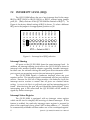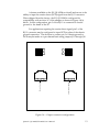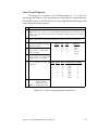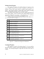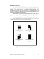
1
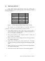
ES-100M / QS-100M
Multi-port Asynchronous
Communications Adapter
User's Manual
QUATECH, INC.
662 Wolf Ledges Parkway
Akron, Ohio 44311
TEL: (330) 434-3154
FAX: (330) 434-1409
BBS: (330) 434-2481
ES-100
User's Manual
Version 2.00
October 1994
P/N. 940-0019-200
WARRANTY INFORMATION
Quatech Inc. warrants the ES-100M / QS-100M to be free of
defects for one (1) year from the date of purchase. Quatech Inc. will
repair or replace any adapter that fails to perform under normal operating
conditions and in accordance with the procedures outlined in this
document during the warranty period. Any damage that results from
improper installation, operation, or general misuse voids all warranty
rights.
The authors have taken due care in the preparation of this
document and any associated software program(s). In no event will
Quatech Inc. be liable for damages of any kind, incidental or
consequential, in regard to or arising out of the performance or form of
the materials presented herein and in the program(s) accompanying this
document. No representation is made regarding the suitability of this
product for any particular purpose.
Quatech Inc. reserves the right to edit or append to this document
or the product(s) to which it refers at any time and without notice.
Please complete the following information and retain for your
records. Have this information available when requesting warranty
service.
Date of purchase:
Model Number:
ES-100 / QS-100M
Product Description:
Multi-port Asynchronous Communications
Adapter
Serial Number:
TABLE OF CONTENTS
List of Figures
I.
II.
III.
IV.
V.
VI.
VII.
VIII.
General Information
Installation
Addressing Ports
Interrupt Level (IRQ)
Interrupt Sharing
Interrupt Status Register
External Connections
Channel Output Configuration
Serial Port Functional Description
Accessing the Serial Port Registers
Interrupt Enable Register
Interrupt Identification Register
FIFO Control Register
Line Control Register
Modem Control Register
Line Status Register
Modem Status Register
Scratchpad Register
FIFO Interrupt Mode Operation
FIFO Polled Mode Operation
Baud Rate Selection
Serial Port Functional Description
Troubleshooting
iii
1
2
5
8
8
8
10
11
14
15
16
16
18
19
20
21
22
22
23
24
25
27
28
LIST OF FIGURES
Figure
Figure
Figure
Figure
Figure
Figure
Figure
Figure
Figure
Figure
Figure
Figure
Figure
Figure
Figure
Figure
Figure
Figure
Figure
Figure
Figure
Figure
Figure
Figure
Figure
1.
2.
3.
4.
5.
6.
7.
8.
9.
10.
11.
12.
13.
14.
15.
16.
17.
18.
19.
20.
21.
22.
23.
24.
25.
Default address and IRQ settings
Diagram of QS-100M / ES-100M
Port address map
Examination of a serial port base address
Serial port base I/O address selection switches
Interrupt level (IRQ) selection
Enabling the Interrupt Status Register
Interrupt Status Register contents
Use of DTEs and DCEs in a communications link
Cabling requirements for RS-232-C devices
QS-100M / ES-100M connector definitions
QS-100M / ES-100M output connectors
Auxiliary signal configuration jumpers
Output connector configuration
Serial port register address map for 16450/16550
Interrupt Enable Register bit definitions
Interrupt Identification Register bit definitions
Interrupt Identification Register bit decoding
16550 FIFO Control Register bit definitions
Line Control Register bit definitions
Modem Control Register bit definitions
Line Status Register bit definitions
Modem Status Register bit definitions
Input clock frequency options
Divisor latch settings for common baud rates
2
3
5
6
7
8
9
9
10
10
11
11
12
13
15
16
17
17
18
19
20
21
22
25
26
I.
GENERAL INFORMATION
The Quatech, Inc. ES-100M provides eight RS-232 asynchronous
serial communication interfaces for IBM-compatible personal computer
systems using the 16-bit ISA (Industry Standard Architecture) expansion
bus. The QS-100M is a four-port version of the same product (with
several blank areas on the circuit card). External connections are made
using RJ-11 "phone jack" connectors. This document uses "QS/ES-100M"
when information applies to either product.
The QS/ES-100M's serial ports are implemented using 16450
Universal Asynchronous Receiver/Transmitters (UARTs). For higher
performance, 16550 UARTs can be installed in place of the 16450 UARTs.
The 16550 contains a hardware buffer that reduces processing overhead.
Software must be aware of the 16550 UART for the device's extra
capabilities to be used, otherwise it will act as a 16450 UART. The 16550 is
suggested for multitasking environments and for applications involving
high data rates.
The QS/ES-100M is highly flexible with respect to addressing and
interrupt level use. The serial ports are addressed in a contiguous block
that can be placed anywhere within the range of 0000 hex to FFFF hex,
and available interrupt levels include IRQ2 to IRQ7, IRQ10 to IRQ12,
IRQ14, or IRQ15. (Early versions of the QS/ES-100M are limited to
IRQ2-7.)
All ports on the QS/ES-100M share one interrupt level. A special
interrupt status register is provided to allow controlling software to
manage the shared interrupt level.
The shared interrupt feature
minimizes the system resources consumed by the adapter.
In order to support the use of the shared interrupt feature of the
QS/ES-100M, Quatech has developed device drivers for several popular
operating systems and environments. The sales department can be
contacted for details on current offerings.
Quatech QS-100M/ES-100M User's Manual
1
II.
INSTALLATION
If the default address and interrupt settings are sufficient, the
QS/ES-100M can be quickly installed and put to use. The factory defaults
are listed in Figure 1.
PORT
ADDRESS
IRQ
Serial 1
300 hex
3
Serial 2
308 hex
3
Serial 3
310 hex
3
Serial 4
318 hex
3
Serial 5 (ES only)
320 hex
3
Serial 6 (ES only)
328 hex
3
Serial 7 (ES only)
330 hex
3
Serial 8 (ES only)
338 hex
3
Figure 1 --- Default address and IRQ settings for QS/ES-100M
The outputs of the QS/ES-100M are provided with RJ-11
connectors. See section V of this manual for connector details.
1. If the default settings are correct, skip to step 2, otherwise refer to
sections III and IV of this document for detailed information on
how to set the address and IRQ level.
2. Turn off the power of the computer system in which the
QS/ES-100M is to be installed.
3. Remove the system cover according to the instructions provided by
the computer manufacturer.
4. Install the QS/ES-100M in any vacant expansion slot. The board
should be secured by installing the Option Retaining Bracket (ORB)
screw.
5. Replace the system cover according to the instructions provided by
the computer manufacturer.
6. Attach and secure the cable connectors to the desired equipment.
2
Quatech QS-100M/ES-100M User's Manual
Figure 2 --- Diagram of QS/ES-100M
(SW1, SW2)
Set addresses here
SW2
J8
J9
J6
J7
J4
J5
J2
J3
(J10)
Set IRQ level here
QUATECH INC.
ES-100 / QS-100M
16450/16550
16450/16550
16450/16550
Shaded parts are not present on the QS-100M.
SW1
J1
16450/16550
J10
16450/16550
16450/16550
16450/16550
16450/16550
IRQ 2
IRQ 3
IRQ 4
IRQ 5
IRQ 6
IRQ 7
IRQ 10
IRQ 11
IRQ 12
IRQ 14
IRQ 15
Quatech QS-100M/ES-100M User's Manual
3
J17 J18
J15 J16
J13 J14
J11 J12
(Diagram not to scale)
CN1
(This page left blank intentionally.)
4
Quatech QS-100M/ES-100M User's Manual
III. ADDRESSING PORTS
Setting The Address
The base address of the QS/ES-100M is set using the two DIP
switch packs. When setting the address selection switches, a switch in the
"ON" position specifies that the corresponding address line must be a
logic 0 for the port to be selected. Similarly, a switch in the "OFF" position
forces the corresponding address line to be a logic 1 for the port to be
selected.
A full sixteen bit address decode is implemented to reduce the
chance of address conflicts with other adapters in the system. The base
address of the QS/ES-100M can be set anywhere in the range of 0000 hex
to FFFF hex. Each serial port on the QS/ES-100M uses 8 consecutive I/O
locations. The ports reside in a contiguous block of I/O space in eight
byte increments, for a total of 32 contiguous bytes in the case of the
QS-100M, or 64 contiguous bytes in the case of the ES-100M. This is
shown in Figure 3.
PORT
ADDRESS RANGE
Serial 1
Base Address + 0
to Base Address + 7
Serial 2
Base Address + 8
to Base Address + 15
Serial 3
Base Address + 16
to Base Address + 23
Serial 4
Base Address + 24
to Base Address + 31
Serial 5 (ES only)
Base Address + 32
to Base Address + 39
Serial 6 (ES only)
Base Address + 40
to Base Address + 47
Serial 7 (ES only)
Base Address + 48
to Base Address + 55
Serial 8 (ES only)
Base Address + 56
to Base Address + 63
Figure 3 --- Port address map
Quatech QS-100M/ES-100M User's Manual
5
Switch SW1 and the first four positions of switch SW2 select
address lines A15 through A6. The fifth position of SW2 selects address
line A5 on the QS-100M and is not used on the ES-100M. This reflects the
different I/O space requirements of the two products. The remaining
address lines, A4 - A0 for the QS-100M, or A5 - A0 for the ES-100M, are
used by the UART to select the register being accessed.
The sixth position on SW2 is used to enable or disable the interrupt
status register (see page 9).
Figure 4 shows how the switches on the QS/ES-100M represent the
address values for serial ports. This figure can be used to explain the
examples shown in Figure 5.
A serial port's address is a 16-bit quantity that is most often expressed
in four hexadecimal (base 16) digits. A hex digit can hold a value from 0 to
15 (decimal), and is made up of four binary bits given weights of eight, four,
two, and one, hence the maximum value of 8+4+2+1 = 15.
A possible serial port address is 5220 hex. The example below shows
how the hex digits are broken down into binary bits.
Binary bits
0 1 0 1
0 0 1 0
0 0 1 0
0 0 0 0
Bit weight
8 4 2 1
8 4 2 1
8 4 2 1
8 4 2 1
Sum of bits
0+4+0+1
0+0+2+0
0+0+2+0
0+0+0+0
Hex digits
5
2
2
0
These address bits are set by the switches.
All other bits are considered to be zero.
0 1 0 1
0 0 1 0
0 0 1 0
0 0 0 0
Figure 4 --- Examination of a serial port base address
6
Quatech QS-100M/ES-100M User's Manual
Switch on
bit = 0
Switch off
bit = 1
QS-100M
Position 6 of SW2 is used to enable or
disable the interrupt status register.
Factory default setting --- 0300 hex
SW1
SW2
ON
1
2
3
4
5
6
1
2
3
4
5
0
0
0
0
0
0
2
1
0
0
0
(no digits)
0
0
3
0
6
Another Example --- 5AC0 hex
SW1
SW2
ON
1
2
3
4
5
6
1
2
3
4
5
0
4
0
1
8
0
2
0
8
4
0
(no digits)
C
A
5
6
0
ES-100M
Position 6 of SW2 is used to enable or
disable the interrupt status register.
Factory default setting --- 0300 hex
SW1
SW2
ON
1
2
3
4
5
6
1
2
3
4
0
0
0
0
0
0
2
1
0
0
(no digits)
0
0
3
0
5
6
Another Example --- 5AC0 hex
SW1
SW2
ON
1
2
3
4
5
6
1
2
3
4
0
4
0
1
8
0
2
0
8
4
(no digits)
C
0
5
A
5
6
Figure 5 --- Serial port base I/O address selection switches
Quatech QS-100M/ES-100M User's Manual
7
IV. INTERRUPT LEVEL (IRQ)
IRQ11
IRQ12
IRQ14
IRQ15
10
11
12 13
14
15
16
3
4
5
1
2
6
IRQ10
9
IRQ7
22
IRQ6
21
IRQ5
20
IRQ4
17 18 19
IRQ3
IRQ2
The QS/ES-100M allows the use of any interrupt level in the range
IRQ2 to IRQ7, IRQ10 to IRQ12, IRQ14, or IRQ15, selected using jumper
pack J10. (Early versions of the QS/ES-100M are limited to IRQ2-7.) In
Figure 6, the factory default setting of IRQ3 is shown. To select a different
IRQ, move the jumper to the appropriate position on J10.
7
8
J10 --- Default is IRQ 3
Figure 6 --- Interrupt level (IRQ) selection
Interrupt Sharing
All ports on the QS/ES-100M share the same interrupt level. In
addition, an interrupt sharing circuit allows the QS/ES-100M to share its
interrupt with another Quatech adapter supporting sharable interrupts.
In either case, the software driving the serial ports must determine which
port or ports are requesting service when an interrupt is generated.
The QS/ES-100M signals a hardware interrupt when any port
requires service. The interrupt signal is maintained until no port requires
service. Because the ISA bus is edge-sensitive, this behavior forces the
interrupt service routine to ensure that all ports are checked before
exiting. A way to do this is to poll each port until an interrupting port is
found. After servicing the port, all ports should be checked again. If any
interrupting port is left unserviced the QS/ES-100M will be unable to
signal any further interrupts.
Interrupt Status Register
The QS/ES-100M is equipped with an interrupt status register
which can be used to simplify the servicing of shared interrupts. If this
feature is enabled, the read-only interrupt status register is accessed in
place of the scratchpad of any given UART at base address + 7. Virtually
no commercially available software makes use of the scratchpad register.
8
Quatech QS-100M/ES-100M User's Manual
The choice of using the interrupt status register or the UART scratchpads
(factory default) is made using position 6 of switch SW2 as shown in
Figure 7.
SW2
SW2
ON
ON
1
2
3
4
5
1
6
2
3
4
5
6
Scratchpad Register
(factory default)
Interrupt Status Register
Slide position 6 of SW2 toward the top of the QS/ES-100M to enable the
interrupt status register, or toward the bottom of the QS/ES-100M to disable it.
Figure 7 --- Enabling the Interrupt Status Register
When a hardware interrupt occurs, reading the interrupt status
register will return the interrupt status of the entire QS/ES-100M, as
shown in Figure 8. Individual bits are cleared as the interrupting ports are
serviced. The interrupt service routine must ensure that the interrupt
status register reads zero before exiting, or the QS/ES-100M will be
unable to signal subsequent interrupts.
If the QS/ES-100M is of revision level 'B' or higher, an I/O write to
the interrupt status register will cause another hardware interrupt to be
generated if the interrupt status register is non-zero. The value written is
ignored and has no effect on the contents of the interrupt status register.
Software written to take advantage of this retriggering will be transparent
to an older revision of the QS/ES-100M.
BIT
DESCRIPTION
7 (MSB)
Serial 8 --- 1 if interrupt pending (always 0 on QS-100M)
6
Serial 7 --- 1 if interrupt pending (always 0 on QS-100M)
5
Serial 6 --- 1 if interrupt pending (always 0 on QS-100M)
4
Serial 5 --- 1 if interrupt pending (always 0 on QS-100M)
3
Serial 4 --- 1 if interrupt pending
2
Serial 3 --- 1 if interrupt pending
1
Serial 2 --- 1 if interrupt pending
0
Serial 1 --- 1 if interrupt pending
Figure 8 --- Interrupt Status Register contents
Quatech QS-100M/ES-100M User's Manual
9
V.
EXTERNAL CONNECTIONS
RS-232-C devices are classified by their function as either Data
Terminal Equipment (DTE) or Data Communication Equipment (DCE).
Generally, data terminal equipment is defined as the communication
source and data communication equipment is defined as the device that
provides a communication channel between two DTE-type devices.
Modem
Terminal
DTE
RS-232-C
DCE
Telephone
line
Terminal
Modem
RS-232-C
DCE
DTE
Figure 9 --- Use of DTEs and DCEs in a communications link
DTE- and DCE-type devices have complementary pinouts to allow
terminals and modems to be connected directly using a one-to-one cable
as shown in Figure 10. In many applications, DCEs are unnecessary, and
in these cases a cable called a "null modem cable" or "modem eliminator
cable" is used to directly connect two DTE-type devices. A typical null
modem cable is also shown in Figure 10.
(3)
(2)
(4)
(5)
(20)
(6)
(8)
(22)
(7)
RxD
TxD
RTS
CTS
DTR
DSR
DCD
RI
GND
TxD
RxD
CTS
RTS
DSR
DTR
DCD
RI
GND
Typical DTE-to-DCE cable
(3)
(2)
(4)
(5)
(20)
(6)
(8)
(22)
(7)
(3)
(2)
(4)
(5)
(20)
(6)
(8)
(22)
(7)
RxD
TxD
RTS
CTS
DTR
DSR
DCD
RI
GND
RxD
TxD
RTS
CTS
DTR
DSR
DCD
RI
GND
(3)
(2)
(4)
(5)
(20)
(6)
(8)
(22)
(7)
Typical DTE-to-DTE null modem cable
Figure 10 --- Cabling requirements for RS-232-C devices
(cables using 25-pin connectors shown)
10
Quatech QS-100M/ES-100M User's Manual
Channel Output Configuration
The QS/ES-100M connects to peripheral equipment through RJ-11
connectors, or using the optional adapter cables, male D-25 connectors.
When the RJ-11 connector is converted to a D-25 connector, the conversion
cable must be assembled with respect to either a DTE or DCE
configuration. The standard serial port connections are listed in Figure 11.
RS-232 Signal
Description
DTE
connection
DCE
connection
RJ-11
D-25
RJ-11
D-25
AuxIn
(CTS)
(DSR)
1
5
6
1
4
20
Transmit Data
(TxD)
2
2
2
3
Chassis Ground
Carrier Detect
3
1
8
3
(DCD)
1
8
4
7
4
7
Signal Ground
Receive Data
(RxD)
5
3
5
2
AuxOut
(DTR)
(RTS)
6
20
4
6
6
5
Figure 11 --- QS/ES-100M connector definitions
(Top of board)
1
13
25
12
24
2
11
23
10
22
3
9
21
8
4
20
7
19
1
2
3
4
5
6
6
5
18
5
17
RJ-11 connector pinout
4
6
16
3
15
7
8
2
14
1
D-25 connector
(using adapter cable)
RJ-11 connectors in CN1
(5-8 present on ES-100M only)
Figure 12 --- QS/ES-100M output connectors
Quatech QS-100M/ES-100M User's Manual
11
The AUXIN and AUXOUT signals on the RJ-11 connector must be
determined as well. AUXIN may be selected to be either CTS or DSR.
AUXOUT may be selected to be either RTS or DTR. The decision of which
signals to use is made separately for each channel.
Figure 13 --- Auxiliary signal configuration jumpers.
12
Quatech QS-100M/ES-100M User's Manual
A feature available on the ES/QS-100M revision B and newer is the
ability to input the carrier detect (DCD) signal from the RJ-11 connector.
When shipped from the factory, the ES/QS-100M is configured for
compatibility with revision 'A' of the adapter as shown in Figure 14(A)
below. In this configuration, pin 3 of the RJ-11 is connected to chassis
ground i.e. the frame of the PC.
Carrier Detect (DCD)
Chassis Ground
For applications requiring the carrier detect signal, pin 3 of the
RJ-11 connector may be configured to input DCD in place of the chassis
ground connection. The decision to connect pin 3 to chassis ground or
DCD may be made on a per channel basis using jumpers J11 through J18.
Figure 14 --- Output connector configuration.
Quatech QS-100M/ES-100M User's Manual
13
VI. SERIAL PORT FUNCTIONAL
DESCRIPTION
This section contains information intended for advanced users
planning to do custom programming with the QS/ES-100M. The
information presented here is a technical description of the interface to the
16450 or 16550 UART.
The 16450 UART is an improved functional equivalent of the 8250
UART, performing serial-to-parallel conversion on received data and
parallel-to-serial conversion on output data. Designed to be compatible
with the 16450, the 16550 UART enters character (non-FIFO) mode on
reset. In this mode, the 16550 appears as a 16450 to application software.
An additional mode, FIFO mode, can be invoked through software
to reduce CPU overhead. FIFO mode increases performance by providing
two 16-byte hardware buffers, one for transmit and one for receive. This
can reduce the frequency of interrupts issued to the CPU by the UART.
Other features of the 16450 and 16550 include:
Programmable baud rate, character length, parity,
and number of stop bits.
Automatic control of start, stop, and parity bits.
Independent and prioritized interrupts.
Transmit clock output / receive clock input.
The QS/ES-100M's serial ports are controlled by 16450 or 16550
UARTs. The serial ports will generate interrupts in accordance with the
bits set in the interrupt enable register of the UARTs. In order to maintain
compatibility with earlier personal computer systems, the user-defined
output OUT2 is used as an external interrupt enable and must be set
active for interrupts to be generated. OUT2 is accessed through the
UART's MODEM control register.
The following pages provide a brief summary of the internal
registers available within the 16450 and 16550 UARTs. Registers and
functions specific to the 16550 will be indicated with boldface italic
notations.
14
Quatech QS-100M/ES-100M User's Manual
Accessing The Serial Port Registers
Figure 15 lists the address map for the 16450 and 16550 UARTs.
Each register can be accessed by reading from or writing to the proper
I/O address. This I/O address is determined by adding an offset to the
base address set for the particular serial port. The base address is set
using DIP switches on the QS/ES-100M (see section III).
Notice that two locations access different registers depending on
whether an I/O read or I/O write is attempted. Address [base+0]
accesses the receive buffer on an I/O read, or the transmit buffer on an
I/O write. Address [base+2] accesses the Interrupt Identification register
on an I/O read or the FIFO control register (16550 only) on an I/O write.
Also, notice that if address [base+0] or [base+1] is used with the DLAB bit
from the Line Control Register set to '1', the baud rate divisor latches are
accessed.
NOTE: All figures displaying bitmapped registers are
formatted such that bit 7 is the high-order bit.
UART Addressing
Register Description
DLAB
I/O Address
0
Base + 0
Receive buffer (read)
Transmit holding register (write)
0
Base + 1
Interrupt enable
X
Base + 2
Interrupt identification (read) (16450 and 16550)
FIFO control (write) (16550 only)
X
Base + 3
Line control
X
Base + 4
MODEM control
X
Base + 5
Line status
X
Base + 6
MODEM status
X
Base + 7
Scratchpad
1
Base + 0
Baud rate divisor latch (LSB) *
1
Base + 1
Baud rate divisor latch (MSB) *
(X = don't care)
* DLAB in Line Control Register must be set to access baud rate divisor latch.
Figure 15 --- Serial port register address map for 16450/16550 UART
Quatech QS-100M/ES-100M User's Manual
15
Interrupt Enable Register
This register is located at I/O address [base+1]. It enables the five
types of UART interrupts. Interrupts can be totally disabled by setting all
of the enable bits in this register to a logic 0. Setting any bit to a logic 1
enables that particular interrupt.
BIT
DESCRIPTION
7
0 --- reserved
6
0 --- reserved
5
0 --- reserved
4
0 --- reserved
3
EDSSI --- MODEM Status Interrupt:
When set (logic 1), enables interrupt on clear to send, data set ready, ring
indicator, and data carrier detect.
2
ELSI --- Receiver Line Status Interrupt:
When set (logic 1), enables interrupt on overrun, parity, framing errors, and
break indication.
1
ETBEI --- Transmitter Holding Register Empty Interrupt:
When set (logic 1), enables interrupt on transmitter holding register empty.
0
ETBEI --- Received Data Available Interrupt:
When set (logic 1), enables interrupt on received data available. For 16550
FIFO mode, interrupts are also enabled for receive FIFO trigger level reached
and for receive timeout.
Figure 16 --- Interrupt Enable Register bit definitions
Interrupt Identification Register
This read-only register is located at I/O address [base+2]. When
this register is read, the UART freezes all interrupts and indicates the
highest priority interrupt. During this time, new interrupts are detected
by the UART, but are not reported in this register until the access
completes.
For the 16550 only, this register can be used to indicate whether the
FIFO mode is engaged by examining bits 6 and 7.
16
Quatech QS-100M/ES-100M User's Manual
BIT
DESCRIPTION
7
FFE --- FIFO enable: (16550 only)
When logic 1, indicates FIFO mode enabled. Always logic 0 for the 16450.
6
FFE --- FIFO enable: (16550 only)
When logic 1, indicates FIFO mode enabled. Always logic 0 for the 16450.
5
0 --- reserved
4
0 --- reserved
3
IID2 ---
2
IID1 ---
1
IID0 ---
0
IP --- Interrupt pending:
When logic 0, indicates that an interrupt is pending and the contents of the interrupt
identification register may be used to determine the interrupt source. See Figure 18.
Interrupt Identification:
Indicates highest priority interrupt pending if any. See Figure 18.
NOTE: IID2 is always a logic 0 on the 16450 or in non-FIFO mode on the
16550.
Figure 17 --- Interrupt Identification Register bit definitions
Figure 18 gives the detail of the IIDx bits in the Interrupt
Identification Register. These bits are examined to determine the source
of an interrupt.
IIDx bits IP Priority
2
1
Interrupt Type
0
don't care 1
N/A
None
0
1
1
0
1st
Receiver Line Status: Indicates overrun, parity, framing errors or
break interrupts. The interrupt is cleared by reading the line status
register.
0
1
0
0
2nd
Received Data Ready (16450 or 16550): Indicates receive data
available. The interrupt is cleared by reading the receive buffer. In
16550 FIFO mode, indicates the receiver FIFO trigger level has been
reached. The interrupt is reset when the FIFO drops below the trigger
level.
1
1
0
0
2nd
Character Timeout (16550 FIFO mode only): Indicates no characters
have been removed from or input to the receiver FIFO for the last four
character times and there is data present in the receiver FIFO. The
interrupt is cleared by reading the receiver FIFO.
0
0
1
0
3rd
Transmitter Holding Register Empty: Indicates the transmitter
holding register is empty. The interrupt is cleared by reading the
interrupt identification register or writing to the transmitter holding
register. (Indicates transmit FIFO empty for 16550.)
0
0
0
0
4th
MODEM Status: Indicates clear to send, data set ready, ring indicator,
or data carrier detect have changed state. The interrupt is cleared by
reading the MODEM status register.
Figure 18 --- Interrupt Identification Register bit decoding
Quatech QS-100M/ES-100M User's Manual
17
Fifo Control Register (16550 Only)
This register, which applies only to the 16550 UART, is a write-only
register located at I/O address [base+2]. It is used to enable the FIFO
mode, clear the FIFOs, set the threshold level for the receive FIFO to
generate interrupts, and to set the mode under which the device uses
DMA. Note that DMA mode is NOT supported by the QS/ES-100M.
BIT
DESCRIPTION
7
RXT1 ---
6
RXT0 ---
5
0 --- reserved
4
0 --- reserved
3
DMAM --- DMA mode select (16550 only):
When set (logic 1), RxRDY and TxRDY change from mode 0 to mode 1 for DMA
transfers. (DMA mode is not supported on the QS/ES-100M.)
2
XRST --- Transmit FIFO reset (16550 only):
When set (logic 1), all bytes in the transmitter FIFO are cleared and the counter is
reset. The shift register is not cleared. XRST is self-clearing.
1
RRST --- Receive FIFO reset (16550 only):
When set (logic 1), all bytes in the receiver FIFO are cleared and the counter is reset.
The shift register is not cleared. RRST is self-clearing.
0
FE --- FIFO enable (16550 only):
When set (logic 1), enables transmitter and receiver FIFOs. When cleared (logic 0),
all bytes in both FIFOs are cleared. This bit must be set when other bits in the FIFO
control register are written to or the bits will be ignored.
Receiver FIFO Trigger Level (16550 only):
Determines the trigger level for the receiver FIFO interrupt
RXT0
Receiver FIFO trigger level (bytes)
RXT1
0
0
1
0
1
4
1
0
8
1
1
14
Figure 19 --- 16550 FIFO Control Register bit definitions
18
Quatech QS-100M/ES-100M User's Manual
Line Control Register
This register is located at I/O address [base+3]. It is used for
specifying the format of the asynchronous serial data to be processed by
the UART, and to set the Divisor Latch Access Bit (DLAB) allowing access
to the baud rate divisor latches.
BIT
DESCRIPTION
7
DLAB --- Divisor latch access bit:
DLAB must be set to logic 1 to access the baud rate divisor latches. DLAB must be set
to logic 0 to access the receiver buffer, transmitting holding register and interrupt
enable register.
6
BKCN --- Break control:
When set (logic 1), the serial output (SOUT) is forced to the spacing state (logic 0).
5
STKP --- Stick parity:
Forces parity to logic 1 or logic 0
if parity is enabled.
4
EPS --- Even parity select:
Selects even or odd parity if
parity is enabled.
3
PEN --- Parity enable:
Enables parity on transmission
and verification on reception.
2
STB --- Number of stop bits:
Sets the number of stop bits STB
0
transmitted.
0
0
0
1
1
1
1
1
WLS1 ---
0
WLS0 ---
STKP
x
0
0
1
1
EPS
x
0
1
0
1
PEN
0
1
1
1
1
PARITY
None
Odd
Even
Logic 1
Logic 0
WLS1 WLS0 WORD LEN STOP BITS
0
0
5 bits
1
0
1
6 bits
1
1
0
7 bits
1
1
1
8 bits
1
0
0
5 bits
1.5
0
1
6 bits
2
1
0
7 bits
2
1
1
8 bits
2
Word length select:
Determines the
number of bits per
transmitted word.
Figure 20 --- Line Control Register bit definitions
Quatech QS-100M/ES-100M User's Manual
19
Modem Control Register
This register is located at I/O address [base+4], and is used to
control the interface with the modem or device used in place of a modem.
This register allows the states of the "modem control signals" to be
changed. These are DTR (Data Terminal Ready) and RTS (Request To
Send). It is also possible to place the UART in a loopback mode for
testing. Finally, the user-defined outputs OUT1 and OUT2 are controlled
from this register.
The QS/ES-100M handles the OUT1 and OUT2 signals in the
manner appropriate for maintaining compatibility with standard PC serial
ports:
The OUT1 output is not connected.
The OUT2 output is used to globally enable interrupts to
the computer. It should be active at all times if interrupts
are being used.
BIT
DESCRIPTION
7
0 --- reserved
6
0 --- reserved
5
0 --- reserved
4
LOOP --- Loopback enable:
When set (logic 1), the transmitter shift register is connected directly to the receiver
shift register. The MODEM control inputs are internally connected to the MODEM
control outputs and the outputs are forced to the inactive state. All characters
transmitted are immediately received to verify transmit and receive data paths.
Transmitter and receiver interrupts still operate normally. MODEM control
interrupts are available but are now controlled through the MODEM control
register.
3
OUT2 --- Output 2:
When this bit is set (logic 1), the OUT2 output is forced active to a logic 0. When
cleared (logic 0), the OUT2 output is forced inactive to a logic 1.
Used for interrupt enable on the QS/ES-100M.
2
OUT1 --- Output 1:
When this bit is set (logic 1), the OUT1 output is forced active to a logic 0. When
cleared (logic 0), the OUT1 output is forced inactive to a logic 1.
Not connected on the QS/ES-100M.
1
RTS --- Request to send:
When this bit is set (logic 1), the RTS output is forced active to a logic 0. When
cleared (logic 0), the RTS output is forced inactive to a logic 1.
0
DTR --- Data terminal ready:
When this bit is set (logic 1), the DTR output is forced active to a logic 0. When
cleared (logic 0), the DTR output is forced inactive to a logic 1.
Figure 21 --- Modem Control Register bit definitions
20
Quatech QS-100M/ES-100M User's Manual
Line Status Register
This register is located at I/O address [base+5]. It is used to
provide various types of status information concerning the data transfer.
As Figure 22 shows, the Line Status Register indicates several types of
errors, an empty transmit buffer, a ready receive buffer, or a break on the
receive line.
BIT
DESCRIPTION
7
FFRX --- Error in RCVR FIFO (16550 FIFO mode only):
Always logic 0 in 16450 or 16550 non-FIFO mode.
Indicates one or more parity errors, framing errors, or break indications in the receiver
FIFO. FFRX is reset by reading the line status register.
6
TEMT --- Transmitter empty:
Indicates the transmitter holding register or FIFO (16550) AND the transmitter shift
register are empty and are ready to receive new data. TEMT is reset by writing a
character to the transmitter holding register.
5
THRE --- Transmitter holding register empty:
Indicates the transmitter holding register or FIFO (16550) is empty and it is ready to
accept new data. THRE is reset by writing data to the transmitter holding register.
4
BI --- Break interrupt:
Indicates the receive data input has been in the spacing state (logic 0) for longer than one
full word transmission time. In 16550 FIFO mode, only one zero character is loaded into
the FIFO and transfers are disabled until the serial data input goes to the mark state
(logic 1) and a valid start bit is received.
3
FE --- Framing error:
Indicates the received character had an invalid stop bit. The stop bit following the last
data or parity bit was a 0 bit (spacing level).
2
PE --- Parity error:
Indicates that the received data does not have the correct parity.
1
OE --- Overrun error:
Indicates the receive buffer was not read before the next character was received and the
character is destroyed. In 16550 FIFO mode, indicates the receive FIFO is full and
another character has been shifted in. The character in the shift register is destroyed but
is not transferred to the FIFO.
0
DR --- Data ready:
Indicates data is present in the receive buffer or FIFO (16550). DR is reset by reading the
receive buffer register or receiver FIFO.
Figure 22 --- Line Status Register bit definitions
Bits BI, FE, PE, and OE are the sources of receiver line status
interrupts. The bits are reset by reading the line status register. In 16550
FIFO mode, these bits are associated with a specific character in the FIFO
and the exception is revealed only when that character reaches the top of
the FIFO.
Quatech QS-100M/ES-100M User's Manual
21
Modem Status Register
This register is located at I/O address [base+6]. It reports on the
status of signals coming from the modem or equipment used in place of a
modem. It allows the current states of "modem control signals" to be
sensed. These signals include the DCD (Data Carrier Detect), RI (Ring
Indicator), DSR (Data Set Ready), and CTS (Clear To Send).
The Modem Status Register also provides change information for
each of these signals. When a modem control signal changes state, the
appropriate change bit is set to logic 1. The change bits (3, 2, 1, and 0) are
reset to logic 0 whenever the Modem Status Register is read.
A modem status interrupt is generated whenever any of bits 3, 2, 1
or 0 is set by the UART to a logic 1.
BIT
DESCRIPTION
7
DCD --- Data carrier detect:
Complement of the DCD input.
6
RI --- Ring indicator:
Complement of the RI input.
5
DSR --- Data set ready:
Complement of the DSR input.
4
CTS --- Clear to send:
Complement of the CTS input.
3
DDCD --- Delta data carrier detect:
Indicates the Data Carrier Detect input has changed state.
Cleared when this register is read.
2
TERI --- Trailing edge ring indicator:
Indicates the Ring Indicator input has changed from a low to a high state.
Cleared when this register is read.
1
DDSR --- Delta data set ready:
Indicates the Data Set Ready input has changed state.
Cleared when this register is read.
0
DCTS --- Delta clear to send:
Indicates the Clear to Send input has changed state.
Cleared when this register is read.
Figure 23 --- Modem Status Register bit definitions
Scratchpad Register
This register is located at I/O address [base+7]. It is not used by
the 16450 or 16550. It may be used by the programmer for temporary data
storage. The Scratchpad Register is eight bits wide and can be read or
written.
22
Quatech QS-100M/ES-100M User's Manual
FIFO Interrupt Mode Operation (16550 UART Only)
When The Receiver Fifo And Receiver Interrupts Are Enabled:
1. The receive data interrupt is issued when the receive FIFO reaches
the trigger level. The interrupt is cleared as soon as the receive
FIFO falls below the trigger level.
2. The Interrupt Identification Register's receive data available
indicator is set and cleared along with the receive data interrupt
when the receive FIFO falls below the trigger level.
3. The data ready indicator is set as soon as a character is transferred
into the receiver FIFO and is cleared when the FIFO is empty.
4. A FIFO timeout interrupt will occur if the receive FIFO contains at
least one character, at least four character-times have passed since
receipt of the last character, and the last read of the FIFO by the
CPU was done more than four character-times ago.
5. Timeout interrupts are cleared when a read of the receive FIFO is
done.
6. The receive FIFO timeout timer is reset whenever a new character
is received into the FIFO or a read of the FIFO is done.
When The Transmit Fifo And Transmit Interrupts Are Enabled:
1. The transmitter holding register empty interrupt occurs when the
transmit FIFO is empty, and is cleared when a character is written
to the FIFO or when the Interrupt Identification Register is read.
2. Transmitter FIFO empty indications are delayed by one
character-time less the last stop bit time when the transmitter
holding register is empty and there have not been at least two bytes
together in the transmit FIFO since the last time the transmitter
holding register was empty.
3. The first transmitter interrupt after enabling the FIFO mode will be
immediate if that interrupt is enabled.
Quatech QS-100M/ES-100M User's Manual
23
FIFO Polled Mode Operation (16550 UART Only)
The receiver and transmitter are operated independently, which
would allow either or both to be used in a polled mode rather than using
interrupts to determine when the UART needs to be serviced.
To use the UART in a polled mode, the software is responsible for
continuously checking for the conditions that normally cause interrupts to
occur. This would be done using the Line Status Register.
1. The Data Ready bit will be set to logic 1 whenever there is at least
one byte in the receive FIFO.
2. Errors can be detected using the various error bits.
3. The Transmitter Holding Register Empty bit can be used to
determine when the transmit FIFO is empty.
4. The Transmitter Empty bit indicates that the transmitter shift
register is empty as well as the transmit FIFO being empty.
5. Trigger levels and FIFO timeouts do not apply. Both FIFOs are
fully capable of holding multiple characters at any time.
24
Quatech QS-100M/ES-100M User's Manual
Baud Rate Selection
The 16450 or 16550 UART determines the baud rate of the serial
output using a combination of the clock input frequency and the value
written to the divisor latches. Standard personal computer serial
interfaces use an input clock of 1.8432 MHz. To increase versatility, the
QS/ES-100M uses an 18.432 MHz crystal and a frequency divider circuit
to produce the standard clock frequency.
Jumper block J1 is used to set the frequency input to the UART. It
may be connected to divide the clock input by 1, 2, 5, or 10. A table of
baud rates available using the 1.8432 MHz input is given in Figure 25.
For compatibility with standard serial ports, J1 should be
configured to divide by 10 as shown in Figure 24(d).
Divide-by-1 input clock
(A)
Divide-by-2 input clock
(B)
Divide-by-5 input clock
(C)
Divide-by-10 input clock
Factory default
(D)
Figure 24 --- Input clock frequency options
Quatech QS-100M/ES-100M User's Manual
25
DESIRED BAUD
RATE
DIVISOR LATCH
VALUE
ERROR BETWEEN DESIRED AND
ACTUAL VALUES (%)
50
2304
-
75
1536
-
110
1047
0.026
150
768
-
300
384
-
600
192
-
1200
96
-
1800
64
-
2000
58
0.69
2400
48
-
3600
32
-
4800
24
-
7200
16
-
9600
12
-
19200
6
-
38400
3
-
56000
2
2.86
Figure 25 --- Divisor Latch settings for common baud rates
using 1.8432 MHz input clock
26
Quatech QS-100M/ES-100M User's Manual
VII. SPECIFICATIONS
Bus interface:
Industry Standard Architecture (ISA)
16-bit bus
IBM PC-ATTM compatible
Dimensions:
Serial ports
Number of ports:
13.4" x 4.2"
QS-100M --- four ports
ES-100M --- eight ports
Controllers:
16450 (16550 optional)
Interface:
RJ-11 connector
Male D-25 connector
(using optional adapter cables)
Transmit drivers:
Receive buffers:
MC1488 or compatible
MC1489 or compatible
I/O Address range:
Interrupt levels:
0000H - FFFFH
IRQ2 to IRQ7
IRQ10 to IRQ12,
IRQ14, IRQ15
Power requirements
QS-100M:
+5 volts:
+12 volts:
-12 volts:
379 mA typ, 448 mA max
38 mA typ, 46 mA max
36 mA typ, 43 mA max
ES-100M:
+5 volts:
+12 volts:
-12 volts:
439 mA typ, 509 mA max
76 mA typ, 88 mA max
72 mA typ, 82 mA max
Quatech QS-100M/ES-100M User's Manual
27
VIII. TROUBLESHOOTING
Listed here are some common problems and frequent causes of
those problems. Suggestions for corrective action are given. If the
information here does not provide a solution, contact Quatech Customer
Service for technical support.
Any unauthorized repairs or modifications will void the
QS/ES-100M's warranty.
Computer will not boot up.
1. Is the QS/ES-100M properly inserted? Remove the card and try
again. Perhaps try a different expansion slot.
2. Is the base address correctly set? Check for address conflicts with
other devices in the system. Remember that the QS-100M requires
32 bytes of I/O space and the ES-100M requires 64 bytes of I/O
space. Set a different address if necessary.
3. The QS/ES-100M may be defective. Contact Quatech Customer
Service for instructions.
Cannot communicate with other equipment.
1. Are the cable connections correct?
attached?
Are the cables securely
2. Are the base address and interrupt level (IRQ) correctly set? Check
for address and IRQ conflicts with other devices in the system.
Change the settings if necessary.
3. If you are trying to communicate with a DTE, a null-modem cable
may be required.
4. If possible, use a loopback connector to test the port. This
connector needs to connect the following sets of signals on a D-25
connector:
TxD and RxD (pins 2 and 3)
RTS and CTS (pins 4 and 5)
DCD, DTR, DSR, and RI (pins 8, 20, 6 and 22)
28
Quatech QS-100M/ES-100M User's Manual