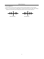
1
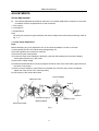
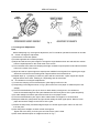
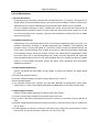
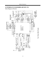
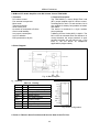
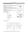
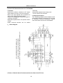
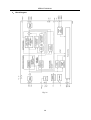
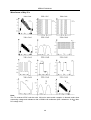
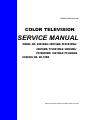
FILE NO. SM-CTV-O-142
COLOR TELEVISION
SERVICE MANUAL
MODEL NO. 25D26MA/ 25D19MA/ PF25D19MA/
29D18MA/ PF29D18MA/ 29D99MA/
PF29D99MA/ 34D18MA/ PF34D8MA
CHASSIS NO. CH-10DR
Please read this manual carefully before service.
TABLE OF CONTENTS
SAFETY INSTRUCTIONS ........................................................................................ 1
ADJUSTMENTS ....................................................................................................... 4
SYSTEM BLOCK DIAGRAMS AND ICS................................................................... 13
SERVICE DATA ....................................................................................................... 17
REPLACEMENT OF PARTS..................................................................................... 50
APPENDIX 1. CIRCUIT DIAGRAMS
2. PRINTED CIRCUIT BOARD LAYOUTS
3. FINAL ASSEMBLY DIAGRAMS
4. FINAL WIRING DIAGRAMS
SERVICE MANUAL
SAFETY INSTRUCTIONS AND MAINTENANCE
WARNING: BEFORE SERVICING THIS CHASSIS, READ THE “X-RAY RADIATION PRECAUTION”,
“SAFETY PRECAUTION”AND “PRODUCT SAFETY NOTICE”INSTRUCTIONS BELOW.
X-RAY RADIATION PRECAUTION
1. The EHT must be checked every time the TV is serviced to ensure that the CRT does not emit
X-ray radiation as result of excessive EHT voltage. The maximum EHT voltage permissible in any
operating circumstances must not exceed the rated value. When checking the EHT, use the High
Voltage Check procedure in this manual using an accurate EHT voltmeter.
2. The only source of X-RAY radiation in this TV is the CRT. The TV minimizes X-RAY radiation, which
ensures safety during normal operation. To prevent X-ray radiation, the replacement CRT must be
identical to the original fitted as specified in the parts list.
3. Some components used in this TV have safety related characteristics preventing the CRT from
emitting X-ray radiation. For continued safety, replacement component should be made after
referring the PRODUCT SAFETY NOTICE below.
4. Service and adjustment of the TV may result in changes in the nominal EHT voltage of the CRT
anode. So ensure that the maximum EHT voltage does not exceed the rated value after service
and adjustment.
SAFETY PRECAUTION
WARNING: REFER SERVICING TO QUALIFIED SERVICE PERSONNEL ONLY.
1. The TV has a nominal working EHT voltage. Extreme caution should be exercised when working
on the TV with the back removed.
1.1 Do not attempt to service this TV if you are not conversant with the precautions and procedures for
working on high voltage equipment.
1.2 When handling or working on the CRT, always discharge the anode to the TV chassis before
removing the anode cap in case of electric shock.
1.3 The CRT, if broken, will violently expel glass fragments. Use shatterproof goggles and take extreme
care while handling.
1.4 Do not hold the CRT by the neck as this is a very dangerous practice.
2. It is essential that to maintain the safety of the customer all power cord forms be replaced exactly
as supplied from factory.
3. Voltage exists between the hot and cold ground when the TV is in operation. Install a suitable
isolating transformer of beyond rated overall power when servicing or connecting any test
equipment for the sake of safety.
4. When replacing ICs, use specific tools or a static-proof electric iron with small power (below 35W).
5. Do not use a magnetized screwdriver when tightening or loosing the deflection yoke assembly to
1
SERVICE MANUAL
avoid electronic gun magnetized and decrement in convergence of the CRT.
6. When remounting the TV chassis, ensure that all guard devices, such as nonmetal control buttons,
switch, insulating sleeve, shielding cover, isolating resistors and capacitors, are installed on the
original place.
7. Replace blown fuses within the TV with the fuse specified in the parts list.
8. When replacing wires or components to terminals or tags, wind the leads around the terminal
before soldering. When replacing safety components identified by the international hazard symbols
on the circuit diagram and parts list, it must be the company-approved type and must be mounted
as the original.
9. Keep wires away from high temperature components.
PRODUCT SAFETY NOTICE
CAUTION: FOR YOUR PROTECTION, THE FOLLOWING PRODUCT SAFETY NOTICE SHOULD BE
READ CAREFULLY BEFORE OPERATING AND SERVICING THIS TV SET.
1. Do not slap or beat the cabinet or CRT, since this may result in fire or explosion.
2. Never allow the TV sharing a plug or socket with other large-power equipment. Doing so may result
in too large load, thus causing fire.
3. Do not allow anything to rest on or roll over the power cord. Protect the power cord from being
walked on, modified, cut or pinched, particularly at plugs.
4. Do not place any objects, especially heavy objects and lightings, on top of the TV set. Do not install
the TV near any heat sources such as radiators, heat registers, stove, or other apparatus that
produce heat.
5. Service personnel should observe the SAFETY INSTRUCTIONS in this manual during use and
servicing of this TV set. Otherwise, the resulted damage is not protected by the manufacturer.
6. Many electrical and mechanical components in this chassis have special safety-related
characteristics. These characteristics are often passed unnoticed by a visual inspection and the
X-ray radiation protection afforded by them cannot necessarily be obtained by using replacements
rated at higher voltages or wattage, etc. Components which have these special safety
characteristics in this manual and its supplements are identified by the international hazard
symbols on the circuit diagram and parts list. Before replacing any of these components read the
parts list in this manual carefully. Substitute replacement components which do not have the same
safety characteristics as specified in the parts list may create X-ray radiation.
Safety Symbol Description
The lightning symbol in the triangle tells you that the voltage inside this product may be
2
SERVICE MANUAL
strong enough to cause an electric shock. Extreme caution should be exercised when
working on the TV with the back removed.
This is an international hazard symbol, telling you that the components identified by the
symbol have special safety-related characteristics.
FDA This symbol tells you that the critical components identified by the FDA marking have
special safety-related characteristics.
UL
This symbol tells you that the critical components identified by the UL marking have
special safety-related characteristics.
MAINTENANCE
1. Place the TV set on a stable stand or base that is of adequate size and strength to prevent it from
being accidentally tipped over, pushed off, or pulled off. Do not place the set near or over a
radiator or heat register, or where it is exposed to direct sunlight.
2. Do not install the TV set in a place exposed to rain, water, excessive dust, mechanical vibrations or
impacts.
3. Allow enough space (at least 10cm) between the TV and wall or enclosures for proper ventilation.
4. Slots and openings in the cabinet should never be blocked by clothes or other objects.
5. Please power off the TV set and disconnect it from the wall immediately if any abnormal condition
are met, such as bad smell, belching smoke, sparkling, abnormal sound or no picture/sound/raster.
Hold the plug firmly when disconnecting the power cord.
6. Unplug the TV set from the wall outlet before cleaning or polishing it. Use a dry soft cloth for
cleaning the exterior of the TV set or CRT screen. Do not use liquid cleaners or aerosol cleaners.
3
SERVICE MANUAL
ADJUSTMENTS
Set-up Adjustments
The following adjustments should be made when a complete realignment is required or a new CRT
is installed. Perform the adjustments in order as follows.
1. Colour purity
2. Convergence
3. White Balance
Note:
The purity/convergence magnet assembly and rubber wedges need mechanical positioning. Refer to
Fig. 1, 2.
1. Colour Purity Adjustment
Note:
Before attempting any purity adjustment, the TV should be operated for at least 15 minutes.
1) Demagnetize the CRT and cabinet using a degaussing coil.
2) Set the brightness and contrast to maximum.
3) Receive the green raster pattern.
4) Loosen the clamp screw holding the deflection yoke and slide it backward or forward to display
vertical green belt (zone) on the screen.
5) Remove the rubber wedge.
6) Rotate and spread the tabs of the purity magnet around the neck of the CRT until the green belt is on
the center of the screen.
7) Slowly move the deflection yoke forward or backward until a uniform green screen is obtained.
Tighten the clamp screw of the yoke temporarily.
8) Check purity of the red and blue raster.
Dummy Wedge
Deflection Yoke
Rubber
Adhesive
Purity/Convergence
Magnet Module
Glass Cloth Tapes
Fig. 1
4
Deflection Yoke
SERVICE MANUAL
Fig. 2
2. Convergence Adjustment
Note:
Before attempting any convergence adjustment, the TV should be operated for at least 15 minutes.
Center convergence adjustment
1) Receive the cross hatch pattern.
2) Set the brightness and contrast properly.
3) Adjust two tabs of the 4-pole magnet to change the angle between them and red and blue vertical
lines are superimposed on the center area of the screen.
4) Turn both tabs at the same time keeping the angle constant to superimpose red and blue horizontal
lines on the center of the screen.
5) Adjust two tabs of 6-pole magnet to superimpose red/blue line and green line. Adjusting the angle
affects the vertical lines and rotating both magnets affects the horizontal lines.
6) Repeat steps 3)~5) keeping in mind red, green and blue movement. 4-pole magnet and 6-pole
magnet interact each other, resulting in complicating and dot movement.
Circumference convergence adjustment
1) Loosen the clamping screw of the defection yoke slightly to allow it to tilt.
2) Temporarily put a wedge as shown in Fig.1.(Do not remove cover paper on adhesive part of the
wedge.)
3) Tilt front of the deflection yoke up or down to obtain better convergence in circumference.
Push the mounted wedge into the space between the CRT and yoke to fix the yoke temporarily.
4) Put other wedge into bottom space and remove the cover paper to stick.
5) Tilt front of the deflection yoke right or left to obtain better convergence in circumference.
6) Keep the deflection yoke position and put another wedge in either upper space. Remove cover
paper and stick the wedge on the CRT to fix the yoke.
7) Detach the temporarily mounted wedge and put it in another upper space. Stick it on the CRT
to fix the yoke.
8) After fixing three wedges, recheck overall convergence.
Tighten the screw firmly to fix the yoke and check if the yoke is fixed.
9) Stick three adhesive tapes on wedges as shown in Fig. 1.
5
SERVICE MANUAL
BLU Red
Red/BLU GRN
BLU
Red/BLU
Red
GRN
4-pole Magnet Movement
6-pole Magnet Movement
Center Convergence by Convergence Magnets
Incline the Yoke Up (or Down)
Incline the Yoke Right (or Left)
Circumference Convergence by DEF Yoke
Fig. 3
6
SERVICE MANUAL
Circuit Adjustments
1. General Description
All adjustments are thoroughly checked and corrected before the TV outgoing. Therefore the TV
should operate normally and deliver proper colour pictures upon installation. However, several minor
adjustments may be required depending on the particular location where the TV is operated.
This TV is shipped completely in carton. Carefully take out the TV from the carton and remove all
packing materials. Connect the power cord into a 220V AC, 50Hz two-pin power outlet. Turn on the
TV. Check and adjust all the customer controls such as brightness, contrast and colour to obtain
natural colour pictures.
2. Automatic Degaussing
A degaussing coil is mounted around the CRT so that external degaussing after moving the TV is
generally unnecessary, providing it is properly degaussed upon installation. The degaussing coil
operates in about 1 second after power on. If the set is moved or faced to a different direction, the
power switch must be switched off for at least 30 minutes in order that the automatic degaussing
circuit operates properly. Should the chassis or parts of the cabinet become magnetized to cause
poor colour purity, use an external-degaussing coil. Slowly move the degaussing coil around the
screen,the sides and front of the TV and slowly withdraw the coil to a distance of about 2m before
unplug it. If colour shading still exists, perform the Colour Purity Adjustment and Convergence
Adjustment procedures.
3. Supply Voltage Adjustment
Caution: +B voltage has close relation to high voltage. To avoid X-ray radiation, +B voltage should
be +135V.
1) Set AC power supply to 220±5V.
2) Connect a digital voltmeter to two pins of C878, and then turn on the TV.
3) Receive Philips pattern.
4) The voltmeter should read 135±0.5V (For BCK-46A, BCK46D and BCK24306L series switch
transformers) or 145±1V (For BCK50, BCK25405L and BCK24307L series switch transformers).
4. High Voltage Inspection
Caution: No high voltage adjustment should be done in the chassis.
1) Connect a precise high voltmeter to the second anode of the CRT.
2) Turn on the TV and set the brightness and contrast to minimum (i.e. set beam current of the CRT to
zero).
3) The high voltage tested should be 26.5±1KV (for 25”CRT) or 28.5±1KV (for 29”CRT) or 30.5KV±1KV
(for 34” CRT).
4) Set the brightness to minimum or maximum, and ensure high voltage not beyond limitation of 29 KV
(for 25”CRT) or 31KV (for 29”CRT) or 35KV (for 34” CRT) in any case.
7
SERVICE MANUAL
5. Focus Adjustment
1) Use the remote control to set the contrast to maximum and the brightness, chroma to medium.
2) Set H. V. lines near center of Philips pattern to thinnest with the FCB on the FBT. After finishing
adjustment, ensure that no poor focusing exists near the center or around of the frame.
Before Adjusting
After Adjusting
8
SERVICE MANUAL
Service Mode and Bus Data
1. To enter the D/S (Design/Service) mode
a. To enter the USER SERVICE mode
Set the volume to 0. Then press and hold the MUTE button on the remote control, and press the
MENU button on the TV to enter the SERVICE mode. At this time, red “S” is displayed on the upper
center of the screen. Use the
button on the remote control to turn off the TV. In this case, the
SERVICE mode is quitted.
b. To select the SERVICE menu
Press the CAL button on the remote control to highlight two preset menus and 7 menus related to
TDA884X and TDA9178 in turn.
c. To select and adjust data
Use the↓/↑buttons to highlight an adjustment and the ←/→ buttons to adjust. The adjusted data
are immediately output and stored in the EEPROM.
Warning!
The user service mode adjustment can be changed only when service personnel adjust the whole set
data during servicing. As the control data have dramatic effects on functions and performance of the TV,
service personnel should not tell user how to enter the SERVICE mode to avoid improper data settings.
2. OPTION menu
Table 1
Item
Option Menu
Description
Bus Data
OPTION 1
AV
SOUND
SYS
PIM
COMB
SOU IC
AV terminals
Please refer to settings of your TV.
Sound system
DK
Picture improvement IC TDA9178:
1-Yes,0-No
Comb filter TDA9181: 1-Yes,0-No
Sound processing IC TDA9859: 1-Yes,
0-No
POW SET
1
0
1
0
LANGSET0
Language option 1
RUS
LANGSET1
Language option 2
ENG
WOOFER
Woofer: 1-Yes,0-No
0
AUT-SET
Auto test: 1-On,0-Off
1
R TIME
Realtime clock setup
0
BRAND
Brand
0
BLACK
Black screen
1
OPTION 2
AV.-TV
0
9
SERVICE MANUAL
3. ADJUST menu
Table 2
Item
Adjustment Menu
Description
Bus Data
Remarks
MENU 1
AFW
AFC bandwidth selection
0
For inspection only
IF-FREQ
IF frequency
38
For inspection only
AFA
Auto frequency tracing display
IN
For inspection only
AFB
Auto frequency tracing display
ABOVE
For inspection only
AGC-TAK
AGC control data
10
Adjustable
FIX AUD
Fixed audio amplitude output
0
VOL_MIN
Volume Min.
08
For inspection only
VOL_MID
Volume Mid.
27
For inspection only
43
For inspection only
VOL_016
MENU 2
BRI-MAX
Brightness Max.
63
BRI-MID
Brightness Mid.
31
CON-MAX
Contrast Max.
63
CON-MID
Contrast Mid.
31
COL-MID
Color Mid.
31
MENU 3
PAL
NTSC
V-HALF
Half vertical picture on/off
0
V-SLOPE
Vertical shift
31
V-AMPL
Vertical amplitude
34
S-CORR
PAL vertical shift
26
V-SHIFT
PAL vertical shift
24
V-ZOOM
Vertical zoom
25
For inspection only
V-SCROLL
Vertical captions mode-SCROLL
31
For inspection only
Set to optimum
37
Set to optimum
Set to optimum
27
Set to optimum
MENU 4
PAL
NTSC
Set to optimum
H-SHIFT
Horizontal shift
24
46
Set to optimum
H-AMPL
Horizontal amplitude
46
48
Set to optimum
H-PARAB
Pincushion correction
26
Set to optimum
H-CORNER
Quadrangle correction
38
Set to optimum
H-TRAP
Trapezoidal correction
34
Set to optimum
R-DRV
Red drive setup
31
For inspection only
G-DRV
Green drive setup
31
B-DRV
Blue drive setup
31
Y-DLY
Brightness delay setup
8
MENU 5
For inspection only
(continued)
10
SERVICE MANUAL
AKB
Cathode voltage adjustment
(1-BMCC CRT)
Auto dark balance adjusting switch
VSD
Vertical output switch
0
For inspection only
CB
Color band pass filter IF selection
0
For inspection only
CMB
Color sub-carrier output switch
Comb filter TD9181: 1-Yes,0-No
1
DS
Skin tone correction control: 1-On,
0-Off
1
CL
5
For inspection only
0
For inspection only
MENU 6
HCO
Skin tone correction angle: 1-Skin
of eastern, 0-Skin of western
Horizontal compensation
1
For inspection only
EVG
Vertical output guard switch
0
For inspection only
CHROMA
DELAY
BLACK
STRETC
NONLINEARI
Brightness/color transient
improvement delay adjustment
3
For inspection only
Black level stretching adjustment
16
For inspection only
Brightness linearity adjustment
32
For inspection only
VAR. GAMM
Vertical non-linearity adjustment
32
For inspection only
PEAKING
Peaking circuit
32
For inspection only
STEEPNESS
Steepness control
48
For inspection only
CORING
Coring circuit
32
For inspection only
LINE WIDTH
Line width adjustment
10
For inspection only
1
For inspection only
1
For inspection only
GBL
1
For inspection only
DGR
1
For inspection only
GGR
1
For inspection only
WGR
0
For inspection only
SGR
1
For inspection only
DSA
1
MENU 7
MENU 8
ASK
DBL
Blue level stretching
Notes:
① The data sheet may differ dependent on different models.
② The data sheet may differ dependent on different CRTs for the same model.
4. Service Mode Adjustment
1) Sub-brightness
a) Receive colour signals.
b) Set the contrast to maximum and brightness to medium.
c) Set the chroma to medium.
11
SERVICE MANUAL
Enter the TV to the Service mode. Select “SUB-BRIGHT” by pressing the ←/→ buttons on the
remote control,and set the data to 31 by pressing the data adjustment buttons. Operate the TV for 5
minutes in the mode.
d) Adjust the sub-bright data until blurry picture does not appear on the high bright area of the screen
and too dim picture not on the low-bright area.
e) Set the contrast and brightness to maximum or minimum, and then test normal picture alternation.
f) If the picture does not become dark when the contrast and brightness are set to minimum, or not
become bright when set to maximum, then adjust the sub-bright data to get normal picture.
2) White balance adjustment
a) Turn on the TV and preheat it for over 7 minutes.
b) Use the remote control to set the contrast to maximum and the brightness to medium. Set the
chroma to minimum.
c) Enter the TV to the Service mode, and set the following data without changing other items.
R-DRIVE············70
G-DRIVE············15
B-DRIVE············70
d) Pull out the external antenna and press the MUTE button once on the remote control until a right
horizontal line appears on the screen. Adjust the R-DRV data to get 160V±0.5 green gun voltage
across the CRT RGB PCB.
e) Adjust the G-DRV and B-DRV data according to Step 4 so that the bright horizontal line turns to
yellow,then to white.
3) Horizontal centering adjustment
Enter the TV to the Service mode and receive Philips pattern. Select “H.PH/60H” by pressing the ←
/→ buttons on the remote control, and adjust horizontal picture position in the center of screen by
pressing the data adjustment buttons.
4) Vertical centering adjustment
Enter the TV to the Service mode and receive Philips pattern. Select “V.POS/60H” by pressing the
←/→ buttons on the remote control, and adjust vertical picture position in the center of screen by
pressing the data adjustment buttons.
5) Vertical amplitude adjustment
Enter the TV to the Service mode and receive cross hatch pattern. Select “V.SIZE/60H” by pressing
the ←/→ buttons on the remote control, and adjust vertical amplitude by pressing the data
adjustment buttons so that vertical amplitude is not enough. Continue to adjust vertical amplitude by
pressing the data adjustment button until the first bar on the cross hatch pattern touches edge of the
screen.
12
SERVICE MANUAL
SYSTEM BLOCK DIAGRAMS AND KEY ICS
150-250V
50Hz
Fig. 4 Chassis Block Diagram
Block Diagram of Chassis
13
SERVICE MANUAL
Block Diagram of Supply Voltage System
150-250V
50Hz
Fig. 5 Block Diagram of Supply Voltage System
14
SERVICE MANUAL
Fig. 6 Block Diagram of Remote Control Structure
Block Diagram of Remote Control Structure
15
SERVICE MANUAL
Key ICs And Assemblies
Table 3 Key ICs and Assemblies
Serial
No.
Position No.
Type
Function Description
1
N001A
CH12T1007 (S3P8849XZZ)
Microcontroller
2
N002
AT24C08
EEPROM
3
N301
TDA8844/OM8839PS
Small signal processor
4
N401
TDA8350Q
Vertical output circuit
5
N601
TDA7057AQ
Sound power amplifier
6
N606
TDA9859
Audio processor
7
N811
TDA4605
Power control circuit
8
NY01
TDA6108JF
Video amplifier
9
NW01
TDA7056B
Audio amplifier
10
NW02
TA75558P
Dual operational amplifier
11
DS01/DS02/NP02
HEF4053
Analog switch circuit
12
N602
HEF4052
Analog switch circuit
13
NP01
TDA9178
YUV picture improvement
14
A101
TDQ-5B6M
Tuner
16
SERVICE MANUAL
SERVICE DATA
Technical Data of Key ICs
Power Control Circuit TDA4605
Control IC for Switched-Mode Power Supplies Using MOS-Transistor
1. Features
・Fold-back characteristics provide overload protection for external
components
・Burst operation under secondary short-circuit condition implemented
・Protection against open or a short of the control loop
・Switch-off if line voltage is too low (under voltage switch-off)
・Line voltage depending compensation of fold-back point
・Soft-start for quiet start-up without noise generated by the transformer
Fig.7
・Chip-over temperature protection implemented (thermal shutdown)
・On-chip ringing suppression circuit against parasitic oscillations of the transformer
・AGC-voltage reduction at low load
2. Block Diagram
Fig. 8
3. Refer to Table 12 about Functions and Service Data of the IC’s Pins.
17
SERVICE MANUAL
Microcontroller S3P8849XZZ/CH12T1007
S3C8835/C8837/P8837/P8849
The S3C8835 microcontroller has 16K bytes of on-chip program memory and the S3C8837 has
24K bytes. Both chips have a 272-byte general-purpose internal register file. The interrupt
structure has seven interrupt sources with six interrupt vectors. The CPU recognizes six interrupt
priority levels.
Using a modular design approach, the following peripherals were integrated with the SAM87 core
to make the S3C8835/C8837/P8837/P8849 suitable for use in color television and other types of
screen display applications:
- Four programmable I/O ports (26 pins total: 16 general-purpose I/O pins; 8 n-channel, open-drain
output pins)
- 2 channel A/D converter (4-bit resolution)
- 14-bit PWM output (one channel: push-pull type)
- Basic timer (BT) with watchdog timer function
- One 8-bit timer/counter (T0) with interval timer
- One 8-bit general-purpose timer/counter (TA) with prescalers
- On-screen display (OSD) with a wide range of programmable features including halftone control
signal output
1. Features
CPU
· SAM87 CPU core
Memory
· 16-K byte (S3C8835) or 24K- byte (S3C8837) internal program memory
· 272-byte general-purpose register area
Instruction Set
· 78 instructions
· IDLE and STOP instructions added for powerdown modes
Instruction Execution Time
· 750 ns (minimum) with an 8-MHz CPU clock
Interrupts
· 7 interrupt sources with 6 vectors
· 6 interrupt levels
· Fast interrupt processing for select levels
General I/O
· Four I/O ports (26 pins total)
· Six open-drain pins for up to 6-volt loads
· Two open-drain pins for up to 5-volt loads
8-Bit Basic Timer
· Three selectable internal clock frequencies
· Watchdog or oscillation stabilization function
Timer/Counters
· One 8-bit timer/counter (T0) with three internal clocks and interval timer mode.
18
SERVICE MANUAL
· One general-purpose 8-bit timer/counters with interval timer mode (timer A)
A/D Converter
· Two analog input pins; 4-bit resolution
· 3.125 μs conversion time (8-MHz CPU clock)
Pulse Width Modulation Module
· 14-bit PWM with one-channel output (push-pull type)
· PWM counter and data capture input pin
· Frequency: 5.859 kHz to 23.437 kHz with a 6-MHz CPU clock
On-Screen Display (OSD)
· Video RAM: 252’12 bits
· Character generator ROM: 256 ’ 18 ’ 16 bits (256 display characters: fixed: 2, variable: 254)
· 252 display positions (12 rows ’ 21 columns)
· 16-dot ’18-dot character resolution
· 16 different character sizes
· Eight character colors
· Vertical direction fade-in/fade-out control
· Eight colors for character and frame background
· Halftone control signal output; selectable for individual characters
· Synchronous polarity selector for H-sync and V-sync input
Oscillator Frequency
· 5-MHz to 8-MHz external crystal oscillator
· Maximum 8-MHz CPU clock
Operating Temperature Range
· - 20°C to + 85°C
Operating Voltage Range
· 4.5 V to 5.5 V
Package Type
· 42-pin SDIP
19
SERVICE MANUAL
2. Block Diagram
Fig.9
Block Diagram
20
SERVICE MANUAL
3. Pin Assignments
Fig.10 Pin Assignment Diagram
21
SERVICE MANUAL
4. Pin Descriptions
Table 4
5. Refer to Table 13 about Functions and Service Data of the IC’s Pins
22
SERVICE MANUAL
EEPROM AT24C08
1. Features
·Data EEPROM internally organized as 1024/2048
bytes and 64/128 pages×16 bytes
·Page protection mode, flexible page-by-page
hardware write protection
-Additional protection EEPROM of 64/128 bits,
1 bit per data page
-Protection setting for each data page by
writing its protection bit
-Protection management without switching
WP pin
·Low power CMOS
·Vcc=2.7 to 5.5V operation
·Two wire serial interface bus, I2C-Bus
compatible
·Filtered inputs for noise suppression with
Schmitt trigger
·Clock frequency up to 400 kHz
·High programming flexibility
-Internal programming voltage
-Self timed programming cycle including
erase
-Byte-write and page-write programming,
between 1 and 16 bytes
-Typical programming time 6 ms (<10 ms) for up to 16 bytes
·High reliability
-Endurance 106 cycles1)
-Data retention 40 years1)
-ESD protection 4000 V on all pins
·8 pin DIP/DSO packages
·Available for extended temperature ranges
-Industrial:
-40℃ to +85℃
-Automotive:
-40℃ to +125℃
3. Block Diagram
2. Pin Configuration
Fig. 11
Page
Prot.Bit
EEPROM
Fig. 12
4. Refer to Table 14 about Functions and Service Data of the IC’s Pins.
23
SERVICE MANUAL
I2C-bus Controlled PAL/NTSC/SECAM TV Processors OM8839PS/TDA8843/44
2. General Description
The various versions of the TDA884X/5X
series are I2C-bus controlled single chip TV
processors which are intended to be applied in
PAL, NTSC, PAL/NTSC and multi-standard
television receivers.
These ICs are nearly pin compatible with the
TDA 837× TV processors but have a higher
degree of integration because the delay line
(TDA4665 function) and the SECAM decoder
have been intagrated. In addition to these
functions some additional features have been
added
like
“Continuous
Cathode
Calibration”(2-point black current loop which
results in an accurate biasing of the 3 guns),
adjustable luminance delay time, blue
stretching and dynamic skin tone (“flesh”)
control.
Functionally the IC series is split up in 3
categories, viz
·Versions intended to be used in economy TV
receivers with all basic functions (envelope:
S-DIP 56 and QFP64)
·Versions with additional features like E-W
geometry control, H-V zoom function and
YUV interface which are intended for TV
receivers with 110° picture tubes (envelope:
S-DIP 56)
·Versions which have in addition a second
RGB input with saturation control and a
second CVBS output (envelope: QFP 64)
1. Features
The following features are available in all
ICs:
· Multi-standard vision IF circuit with PLL
demodulator without external components.
· Alignment-free multi-standard FM sound
demodulator (4.5 MHz to 6.5 MHz)
· Audio switch
· Flexible source selection with CVBS switch
and Y(CVBS)/C input so that a comb filter
can be applied
· Integrated chrominance trap circuit
· Integrated luminance delay line
· Asymmetrical peaking in the luminance
channel with a (defeatable) noise coring
function
· Black stretching of non-standard CVBS or
luminance signals
· Integrated chroma band-pass filter with
switchable centre frequency
· Dynamic skin tone control circuit
· Blue stretch circuit which offsets colors near
white towards blue
· RGB control circuit with “Continuous Cathode
Calibration” and white point adjustment
· Possibility to insert a “blue back” option when
no video signal is available
· Horizontal synchronization with two control
loops and alignment-free horizontal oscillator
· Vertical count-down circuit
· Vertical driver optimised for DC-coupled
vertical output stages
· I2C-bus control of various functions
24
SERVICE MANUAL
Fig.13
Block Diagram OM8839 (S-DIP 56 Envelope)
EW-GEOMETRY
45
ZW
3. Block Diagram
5. Refer to Table 15 about Functions and Service Data of the IC’s Pins.
25
SERVICE MANUAL
DC-coupled Vertical Deflection and East-West Output Circuit TDA8350Q
1. Features
·East-West output stage with one single
·Few external components
·Highly efficient fully DC-coupled vertical output
conversion resistor.
bridge circuit
·Vertical flyback switch
·Guard circuit
·Protection against:
-short-circuit of the output pins
-short-circuit of the output pins to Vp
·High EMC immunity due to common mode
inputs
·Temperature (thermal) protection
2. General Description
The TDA8350Q is a power circuit for use in 90°
and 110° color deflection systems for field
frequencies of 50 to 120 Hz. The circuit
provides a DC driven vertical deflection output
circuit, operating as a highly efficient class G
system and an East-West driver for sinking the
diode modulator current.
3. Block Diagram
Fig.14
4. Refer to Table 16 about Functions and Service Data of the IC’s Pins.
26
SERVICE MANUAL
TDA7057AQ
2×8W Stereo BTL Audio Output Amplifier with DC Volume Control
1. Features
2. General Description
The TDA7057AQ is a stereo BTL output
amplifier with DC volume control. The device
is designed for use in TVs and monitors, but is
also suitable for battery-fed portable recorders
and radios.
·DC volume control
·Few external components
·Mute mode
·Thermal protection
·Short-circuit proof
·No switch-on and switch-off clicks
·Good overall stability
·Low power consumption
·Low HF radiation
·ESD protected on all pins.
Missing Current Limiter (MCL)
A MCL protection circuit is built-in. The MCL
circuit is activated when the difference in
current between the output terminal of each
amplifier exceeds 100 mA (typical 300 mA).
This level of 100 mA allows for single-ended
headphone applications.
3. Block Diagram
Fig. 15
4. Refer to Table 17 about Functions and Service Data of the IC’s Pins.
27
SERVICE MANUAL
Triple Video Output Amplifier TDA6108JF/6107Q
1. Features
·Black-Current Stabilization (BCS) circuit
·Typical bandwidth of 9.0MHz (for TDA6108JF)
·Thermal protection.
or 5.5MHz (for TDA6107Q) for an output
2. General Description
signal of 60 V (peak-to-peak value)
The TDA6108JF includes three video output
·High slew rate of 1850V/μs (for TDA6108JF)
amplifiers in one plastic DIL-bent-SIL 9-pin
or 900V/μs (for TDA6107Q)
medium power (DBS9MPF) package (SOT 111
·No external components required
-1),using high-voltage DMOS technology, and is
·Very simple application
intended to drive the three cathodes of a color
·Single supply voltage of 200 V
CRT directly. To obtain maximum performance,
·Internal reference voltage of 2.5 V
the amplifier should be used with black-current
·Fixed gain of 51 (for TDA6108JF) or 50 (for
control.
TDA6107Q)
3. Ordering Information
Type
Number
Package
Description
Version
Plastic
DIL-bent-SIL
TDA6108JF/
DBS9MPF medium power SOT111-1
TDA6107Q
package with fin;
9 leads
4. Block Diagram
Name
TDA6108JF
/
Fig. 16
5. Pinning
Table 5 Pinning
SYMBOL
PIN
DESCRIPTION
Vi(1)
1
Inverting input 1
Vi(2)
2
Inverting input 2
Vi(3)
3
Inverting input 3
GND
4
Ground (fin)
Iom
5
Black-current measurement output
VDD
6
Supply voltage
Voc(3)
7
Cathode output 3
Voc(2)
8
Cathode output 2
Fig. 17 Pin configuration.
Voc(1)
9
Cathode output 1
6. Refer to Table 18 about Functions and Service Data of the IC’s Pins.
28
SERVICE MANUAL
Dual 4-channel Analog Multiplexer/Demultiplexer HEF4052
1. Description
The HEF4052 is a dual 4-channel analog
multiplexer/demultiplexer
with
common
channel
select
logic.
Each
multiplexer/demultiplexer
has
four
independent inputs/outputs (Y0 to Y3) and a
common input/output (Z). The common
channel select logic includes two address
inputs (A0 and A1) and an active LOW enable
input (E).
Both multiplexers/demultiplexers contain four
bidirectional analog switches, each with one
side connected to an independent input/output
(Y0 to Y3) and the other side connected to a
common input/output(Z).
With E LOW, one of the four switches is
selected (low impedance ON-state) by A0 and
A1. With E HIGH, all switches are in the high
impedance OFF-state, independent of A0 and
A1. VDD and Vss are the supply voltage
connections for the digital control inputs (A0, A1
and E). The VDD to Vss range is 3 to 15 V. The
analog inputs/outputs (Y0 to Y3, and Z) can
swing between VDD as a positive limit and VEE
as a negative limit.
VDD VEE may not exceed 15 V.
For
operation
as
a
digital
multiplexer/demultiplexer, VEE is connected to
VSS (typically ground)
Table 6
1. Block Diagrams
Pinning
YOA to Y3A
Independent inputs/outputs
YOB to Y3B
Independent inputs/outputs
AO
Address inputs
A1
E
ZA
Enable input (active LOW)
ZB
Common inputs/outputs
Family data, lDD LIMITS category MSI
See Family Specifications
HEF4052
Fig. 19 Pinning Diagram
HEF4052P (N):
16-lead DIL; plastic
(SOT38-1)
HEF4052D (F): 16-lead DIL; ceramic
(cerdip)
(SOT74)
HEF4052T (D): 16-lead SO; plastic
(SOT109-1)
( ): Package Designator North America
Fig. 18 Functional Diagram
29
SERVICE MANUAL
Fig. 20 Schematic Diagram (One Switch)
3. Function Table
Table 7
Inputs
Channel
E
A1
A0
On
L
L
L
YOA-ZA; YOB-ZB
L
L
H
Y1A-ZA; Y1B-ZB
L
H
L
Y2A -ZA; Y2B-ZB
L
H
H
Y3A-ZA; Y3B-ZB
H
X
X
none
Notes
H=HIGH state (the more positive voltage)
L=LOW state (the less positive voltage)
X=state is immaterial
Ratings
Limiting values in accordance with the Absolute Maximum System (IEC 134)
Supply voltage (with reference to VDD)
VEE
-18 to +0,5 V
Note
To avoid drawing VDD current out of terminal Z, when switch current flows into terminals Y, the
voltage drop across the bidirectional switch must not exceed 0,4V. If the switch current flows into
terminal Z, no VDD current will flow out of terminals Y, in this case is no limit for the voltage drop
across the switch, but the voltages at Y and Z may not exceed VDD or VEE
4.
Refer to Table 19 about Functions and Service Data of the IC’s Pins.
30
SERVICE MANUAL
Triple 2-channel Analog Multiplexer/Demultiplexer HEF4053
selected all switches are in the high
impedance OFF-state, independent of SA to
SC.
VDD and VSS are the supply voltage
connections for the digital control inputs (SA to
SC and E).
The VDD to VSS range is 3 to 15V. The analog
inputs/outputs (Y0, Y1 and Z) can swing
between VDD as a positive limit and VEE as a
negative limit. VDD-VEE may not exceed 15 V.
For operation as a digital multiplexer/
demultiplexer, VEE is connected to VSS
(typically ground).
1. Description
The HEF4053 is a triple 2-channel analog
multiplexer/demultiplexer with a common
enable
input
(E).
Each
multiplexer/demultiplexer has two independent
inputs/outputs (Y0 and Y1), a common
input/output (Z), and select inputs (Sn). Each
also
contains
two-bidirectional
analog
switches, each with one side connected to an
independent input/output (Y0 and Y1) and the
other side connected to a common
input/output(Z).
With (E) LOW, one of the two switches is
(low impedance ON-state) by Sn. With E HIGH,
2. Block Diagram
Fig. 21
Functional Diagram
31
SERVICE MANUAL
Table 8 Pinning
Independent inputs/outputs
Independent inputs/outputs
Select inputs
Enable input (active LOW)
Common inputs/outputs
Y0A to Y0C
Y1A to Y1C
SA to Sc
E
ZA to ZC
Fig. 22 Pinning Diagram
HEF4053P(N): 16-lead DIL ; plastic
(SOT38-1)
HEF4053D(F):16-lead DIL; ceramic
(cerdip)
(SOT74)
HEF4053T(D);16-lead S0; plastic
(SOT109-1)
(): Package Designator North America
Table 9
Inputs
E
L
L
H
Function Table
Channel
Sn
On
L
Y0n-Zn
H
Y1n-Zn
X
none
Notes
H=HIGH state (the more positive voltage)
L=LOW state (the less positive voltage)
X=STATE is immaterial
Fig. 23 Schematic Diagram (One Switch) Ratings
Limiting values in accordance with the Absolute Maximum System (IEC 134)
Supply voltage (with reference to VDD)
VEE
-18 to + 0,5 V
Note
To avoid drawing VDD current out of terminal Z, when switch current flows into terminals Y, the
voltage drop across the bidirecctional switch must not exceed 0,4 V. If the switch current flows into
terminal Z, no VDD current will flow out of terminals Y, in this case there is no limit for the voltage
drop across the switch, but the voltages at Y and Z may not exceed VDD or VEE.
3. Refer to Table 20 about Functions and Service Data of the IC’s Pins.
32
SERVICE MANUAL
5 W Mono BTL Audio Amplifier with DC Volume Control TDA7056B
1. Features
· DC volume control
· Few external components
· Mute mode
· Thermal protection
· Short-circuit proof
· No switch-on and switch-off clicks
· Good overall stability
· Low power consumption
· Low HF radiation
· ESD protected on all pins.
2. General Description
The TDA7056B is a mono Bridge-Tied Load
(BTL) output amplifier with DC volume control.
It is designed for use in TV and monitors, but is
also suitable for battery-fed portable recorders
and radios.
The device is contained in a 9-pin medium
power package.
A Missing Current Limiter (MCL) is built in. The
MCL circuit is activated when the difference in
current between the output terminal of each
amplifier exceeds 100 mA (300 mA typ.). This
level of 100 mA allows for headphone
applications (single-ended).
3. Block Diagram
Fig. 24 Block Diagram.
4. Pinning
Symbol
n.c.
VP
VI
GND1
VC
OUT+
GND2
OUTn.c.
Table 10 Pinning
Pin
Description
1
Not connected
2
Positive supply voltage
3
Voltage input
4
Signal ground
5
DC volume control
6
Positive output
7
Power ground
8
Negative output
9
Not connected
Fig. 25 Pin Configuration.
5. Refer to Table 21 about Functions and Service Data of the IC’s Pins.
33
SERVICE MANUAL
Dual Operational Amplifier TA75558P
The TA75558P, TA75558S and TA75558F are Low-Noise
Operational Amplifiers with High Speed and Wide Bandwidth.
1. Features
· Internal Frequency Compensation Type
· Pin Compatible with TA75558P, TA75558S and TA75558F
· Possible to Exchange the Position of 9 Pin for 1 Pin
Because of Pin Connection Being Symmetric. (TA75558S
Device Only)
· Wide Band Range; fT=3MHz(Typ.)
· Suitable Application for Active Filter Equalizer Amplifier and
Headphone Amplifier.
2. Pin Connection (top view)
Fig. 26
Fig. 27
3.Equivalent Circuit
Fig. 28
3. Refer to Table 22 about Functions and Service Data of the IC’s Pins.
34
SERVICE MANUAL
Universal Hi-Fi Audio Processor for TV TDA9859
externally
·Two general purpose logic output ports
·I2C-bus control of all functions.
1. Features
·Multi-source selector switches six AF inputs
(three stereo sources or six mono sources).
·Each of the input signals can be switched to
each of the outputs (crossbar switch).
·Outputs for loudspeaker channel and peri-TV
connector (SCART).
·Switchable spatial stereo and pseudo stereo
effects
·Audio surround decoder can be added
2. General Description
The TDA9859 provides control facilities for the
main and the SCART channel of a TV set. Due
to extended switching possibilities, signals
from three stereo sources can be handled.
3. Block Diagram
(1) For extended bass control the capacitor between CBR/L1 and CBR/L2 should be
replaced by the extended bass control network.
Fig. 29 Block Diagram and Application Circuit.
4. Refer to Table 23 about Functions and Service Data of the IC’s Pins.
35
SERVICE MANUAL
TDA9178
YUV One Chip Picture Improvement Based on Luminance Vector-, Color Vector- and
Spectral Processor
ratio of the most important parts of the scene
will be improved. Black restoration is available
in the event of a set-up in the luminance
signal.
1. Features
· Picture content dependent non-linear Y,U
and V processing by luminance histogram
analysis
· Variable gamma control
· Adaptive black and white stretch control
· Skin tone correction
· Green enhancement
· Blue stretch
· Luminance Transient Improvement (LTI)
· Smart peaking for detail enhancement
· Color Transient Improvement (CTI)
· Scan Velocity Modulation (SCAVEM) output
· Line Width Control (LWC)
· Video Dependent Coring (VDC)
· Color Dependent Sharpness (CDS)
· Noise measurement
· Feature Mode (FM) detector
· Cue Flash (CF) detector
· Three additional pins for access to 6-bit ADC
and I2C-bus
· Adjustable chrominance delay
· TV standard independent
· I2C-bus controlled
· 1fH and 2fH
· Demonstration Mode (DEMO).
A variable gamma function, after the histogram
conversion, offers the possibilities of
alternative brightness control or factory
adjustment of the picture tube.
The adaptive black stretch function of the
TDA9178 offers the possibility of having a
larger ‘weight’ for the black parts of the video
signal, the white stretch function offers an
additional overall gain for increased light
production.
To maintain a proper color reproduction, the
saturation of the U- and V-colour difference
signals is also controlled as a function of the
actual non-linearity in the luminance channel.
In the color vector processor, the dynamic skin
tone correction locally changes the hue of
colors that match skin tones to the correct hue.
The green enhancement circuit activates
medium saturated green towards to more
saturated green. The blue stretch circuit can
be activated which shifts colors near white
towards blue.
2. General Description
The TDA9178 is a transparent analog video
processor with YUV input and output
interfaces. It offers three main functions:
luminance vector processing, color vector
processing and spectral processing. Beside
these three main functions, there are some
additional functions.
The spectral processor provides 1D luminance
transient improvement, luminance detail
enhancement by smart peaking and a 1D color
transient improvement.
The TDA9178 can be used as a cost effective
alternative to (but also in combination with)
scan velocity modulation.
In the luminance vector processor, the
luminance transfer function is controlled in a
non-linear way by the distribution, in 5 discrete
histogram sections, of the luminance values
measured in a picture. As a result, the contrast
In the spectral processor line width control (or
aperture control) can be user defined. The
TDA9178 is capable of adjusting the amount
36
SERVICE MANUAL
of coring according to the video level with the
video dependent coring. The TDA9178 is also
capable to give extra sharpness in the cases
of saturated red and magenta parts of the
screen using the color dependent sharpness
feature.
separate pin) is available that detects when
the picture content has been changed
significantly, called cue flash.
An embedded 6-bit ADC can be used for
interfacing three analog low frequency voltage
signals (e.g. ambient light control or beam
current voltage level) to the I2C-bus.
An embedded noise detector measures noise
during the field retrace in parts which are
expected to be free from video or text
information. With the noise detector a variety
of ‘smart noise control’ architectures can be
set up.
In the demonstration mode all the features
selected by the user are automatically toggled
between on and off.
A feature mode detector is available for
detecting signal sources like VCR (in still
picture mode) that re-insert the levels of the
retrace part. For this kind of signals the noise
measurement of the TDA9178 is not reliable.
An output signal (on the I2C-bus and on a
symbol
SC
n.c.
ADEXT1
ADEXT2
ADEXT3
YIN
ADR
UIN
VIN
TP
SCL
n.c.
n.c.
SDA
DECDIG
VOUT
UOUT
VEE
YOUT
VCC
SOUT
CF
n.c.
n.c.
The TDA9178 concept has a maximum
flexibility which can be controlled by the
embedded I2C-bus. The supply voltage is 8 V.
The device is mounted in a 24-lead SDIP
package, or in a 24-lead SO package.
Table 11 Pinning
Pin Description
1
Sandcastle input
2
Not connected
3
ADC input 1
4
ADC input 2
5
ADC input 3
6
Luminance input
7
Address selection input
8
U signal input
9
V signal input
10
Test pin
11
Serial clock input (I2C-bus)
12
Not connected
13
Not connected
14
Serial data input/output (I2C-bus)
15
Decoupling digital supply
16
V signal output
17
U signal output
18
Ground
19
Luminance output
20
Supply voltage
21
SCAVEM output
22
Cue flash output
23
Not connected
24
Not connected
37
Fig. 30 Pin Configuration (SOT137-1).
SERVICE MANUAL
3. Block Diagram
Fig. 31
38
SERVICE MANUAL
Service Data of Key IC’s
Table 12 Functions and Service Data of TDA4605(N811)’s Pins
Pin
No.
1
Digital Multimeter
Function Description
Reference Voltage (V)
0.4
Regulation control
Positive Resistance (KΩ)
0.713
Negative Resistance (KΩ)
0.4
2
Primary current input
1.34
9.71
1.34
3
4
5
Primary voltage monitoring input
Ground
Drive pulse output
1.91
0
4.08
7.09
0
0.84
1.91
0
4.08
6
7
Supply voltage
Soft-start
0.74
2.36
16.35
8.69
4.9
6.19
8
Zero crossing input detection
0.33
6.72
5.94
Table 13 Functions and Service Data of S3P8849XZZ/ CH12T1007(N001A)’s Pins
Pin
No.
Function Description
Digital Multimeter
1
2
VT
EMC
Reference Voltage (V)
0.5
0
Positive Resistance (20KΩ)
103
1500
Negative Resistance (20KΩ)
105.
1120.
3
KAV1
0
25.4
25.4
4
5
6
KAV2
KAV3
L
0
0
4.8
25.5
25.8
14.3
25.5
25.8
14.3
7
8
H
U
4.8
0
14.3
1380
14.3
1100.
9
10
KEYB1
KEYB0
4.8
4.8
13.4
13.4
13.4
13.4
11
12
SCL1
SDA1
4.8
4.8
7
7
6.8
6.8
13
GND
0
0
0
14
15
16
NC
SYS0
SYS1
0
3.8
26
26
25.3
25.3
17
18
STDBY1
BASS-SW
4.8
3.5
25.6
25.6
156
19
20
S-SW
Y/C
0
0
20
1300
20
1000
21
22
HALFTONE
R
0
0
25.6
2.1
25.6
2.1
23
G
0
2.1
2.1
24
25
26
B
FB
HD
0
0
3.8
2.1
2
5.5
2.1
2
2
27
28
VD
OSC1
4.8
4.8
8.7
1300
8.4
1000
(continued)
39
SERVICE MANUAL
No.
29
Reference Voltage (V)
4.8
Positive Resistance (20KΩ)
1300
Negative Resistance (20KΩ)
1000
OSC2
30
TEST
0
0
0
31
32
XIN
XOUT
1.7
1.5
1500
1500
1100
1100
33
34
RESET
VCC
4.8
4.8
12.2
3.4
12.1
3.4
35
36
37
P/N
RMT
GND
0
4.8
0
1500
20.4
0
1100
20
0
38
39
MUTE
W/R
4.8
3
25.7
25.7
25.6
25.6
40
41
SCL
SDA
3.5
3.5
6.8
6.8
6.8
6.8
42
STANDBY
0
8.2
8.1
Table 14 Functions and Service Data of AT24C08-10P (N002)’s Pins
Pin
No.
1
2
3
4
5
6
7
8
Function Description
Address input
Address input
Address input
Common ground
Clock line
Data line
PW write protect
Supply voltage
Reference Voltage (V)
0.00
0.00
0.00
0.00
4.94
4.94
4.94
4.94
Digital Multimeter
Positive Resistance (20KΩ)
0.00
0.00
0.00
0.00
6.85
6.89
9.58
3.5
Negative Resistance (20KΩ)
0.00
0.00
0.00
0.00
4.83
5.15
6.31
3.25
Table 15 Functions and Service Data of OM8839PS (N301)’s Pins
Pin
No.
Function Description
Digital Multimeter
Reference Voltage (V)
Positive Resistance (20KΩ)
Negative Resistance (20KΩ)
1
SIF signal input
0.00
8.8
6.03
2
External audio signal input
3.61
8.69
6.03
3
Reference frequency resonant coil terminal
0.00
∞
∞
4
Reference frequency resonant coil terminal
0.00
∞
∞
5
PLL filter
2.45
8.54
5.79
6
Video detection output
2.77
2.19
2.19
7
Clock line
3.85
6.88
4.56
8
Two-way transmission data line
3.91
6.87
4.56
9
Gap decoupling
6.62
7.57
5.66
10
SVHS chroma signal input
1.37
8.65
5.99
11
SVHS luminance signal input
3.85
8.65
5.88
12
Supply voltage
8.22
2.09
2.09
13
Composite video signal input terminal
3.69
8.65
5.88
14
Ground
0.00
0.00
0.01
(continued)
40
SERVICE MANUAL
15
Audio signal output
401
8.74
5.96
16
Decoupling capacitor connection
0.02
∞
∞
17
Video input
3.35
8.65
5.88
18
Black current control input
5.87
8.73
5.81
19
Blue (B) signal output
2.36
5.74
5.08
20
Green (G) signal output
2.41
5.74
5.08
21
Red (R) signal output
2.39
5.74
5.08
22
Beam current control
1.77
7.87
5.84
23
Red (R) signal input
3.62
8.61
5.95
24
Green (G) signal input
3.63
8.61
5.95
25
Blue (B) signal input
3.61
8.61
5.95
26
Selectable primary color signal input control
0.07
0.99
0.99
27
Luminance signal input
2.54
6.84
5.83
28
Luminance signal output
2.54
6.91
5.92
29
B-Y color difference signal output
2.35
6.89
5.9
30
R-Y color difference signal output
2.35
6.9
5.9
31
B-Y color difference signal input
2.36
6.8
5.93
32
R-Y color difference signal input
2.35
6.84
5.93
33
Sub-carrier output for SECAM demodulation
4.23
6.68
5.82
34
3.58MHz crystal oscillator
2.56
7.87
5.91
35
4.43MHz crystal oscillator
2.56
7.87
5.91
36
APC low pass filter
4.95
8.75
5.9
37
Horizontal starting supply voltage
8.22
2.09
2.09
38
Composite video output
2.54
7.32
5.96
39
Black level stretch
4.86
8.68
4.69
40
Line drive pulse output
0.38
2.82
2.81
41
Horizontal flyback pulse input/sandcastle pulse output
0.74
8.81
5.75
42
Line discriminator
3.33
8.44
5.87
43
Line discriminator
3.89
8.75
5.87
44
Ground
0.00
0.00
0.00
45
Vertical frequency parabola output
0.14
8.83
5.89
46
Field drive signal output
2.3
8.8
5.82
Field drive signal output
2.34
8.8
5.8
48
IF signal input
4.55
8.23
6.05
49
IF signal input
4.55
8.21
6.05
50
High voltage detection input
2.01
7.68
5.95
47
51
Vertical sawtooth generation
3.72
8.35
5.91
52
Vertical reference bias setting
3.83
8.33
5.96
53
AGC filter for IF amplifier
4.44
8.72
5.89
54
AGC output for IF amplifier
1.31
10.13
5.69
55
Audio deemphasis
2.86
8.5
5.87
56
Audio decoupling
3.57`
8.78
5.89
41
SERVICE MANUAL
Table 16 Functions and Service Data of TDA8350Q-N6 (N401)’s Pins
Pin
No.
Function Description
Reference Voltage (V)
Digital Multimeter
Positive Resistance (20KΩ) Negative Resistance (20KΩ)
1
Vertical drive input (positive)
2.33
8.82
5.8
2
Vertical drive input (negative)
2.28
8.83
5.83
3
Feedback input
8.52
5.74
4.71
4
Supply voltage
17.23
7.92
4.2
5
Output 1
8.5
5.83
4.71
6
Not connected
0.00
∞
∞
7
Ground
0.00
0.00
0.00
8
Pump supply voltage input
49.31
∞
∞
9
Output 2
0.00
5.87
4.7
10
Guard output
0.2
8.64
5.88
11
Pincushion output
0.07
9.79
5.24
12
Pincushion input (negative)
2.43
∞
6.97
13
Pincushion input (positive)
2.91
∞
6.88
Table 17 Functions and Service Data of TDA7057AQ (N601)’s Pins
Pin
No.
Function Description
Reference Voltage (V)
Digital Multimeter
Positive Resistance (20KΩ) Negative Resistance (20KΩ)
1
Volume control input
0.95
6.85
6.15
2
Not connected
0.00
∞
∞
3
Audio R signal input
2.38
12.59
6.51
4
Supply voltage
17.48
0.47
0.47
5
Audio L signal input
2.37
12.5
6.51
6
Ground
0.00
0.00
0.00
7
Volume control input
0.95
6.85
0.15
8
Left channel in-phase signal output
8016
6.46
5.59
9
Ground
0.00
0.00
0.00
10
Left channel inverting signal output
8.25
6.46
5.59
11
Right channel inverting signal output
8.24
6.46
5.59
12
Ground
0.00
0.00
0.00
13
Right channel in-phase signal output
8.13
6.46
5.59
42
SERVICE MANUAL
Table 18 Functions and Service Data of TDA6108JF/TDA6107Q’s Pins
Pin
No.
Function Description
Digital Multimeter
Reference Voltage (V)
Positive Resistance (20KΩ)
Negative Resistance (20KΩ)
1
G inverting input
3.33
5.32
4.72
2
R inverting input
3.26
5.32
4.72
3
B inverting input
3.28
5.32
4.72
4
Ground
0.00
0.00
0.00
5
Black level current input
6.03
18.65
5.65
6
Supply voltage
199
∞
4.48
7
B output
69.9
∞
5.45
8
R output
69.18
∞
5.45
9
G output
65.9
∞
5.45
Table 19 Functions and Service Data of HEF4052 (N602)’s Pins
Pin
No.
Function Description
Digital Multimeter
Reference Voltage (V)
Positive Resistance (KΩ)
Negative Resistance (KΩ)
1
Signal input
0
12.52
6.46
2
Signal input
0
12.5
6.46
3
Signal input
0
12.52
6.46
4
Signal output
0
12.43
6.25
5
Signal input
0
12.5
6.46
6
Ground
0
0
0
7
Ground
0
0
0
8
Ground
0
0
0
9
Control signal input
4.98
7.8
5.6
10
Control signal input
4.98
7.8
5.6
11
Control signal input
0
0
0
12
Signal input
0
0
0
13
Signal output
0
0
0
14
Signal input
0
0
0
15
Audio output
0
12.48
6.46
16
Supply voltage
5.09
6.89
4.44
43
SERVICE MANUAL
Table 20 Functions and Service Data of HEF4053 (DS01/02/NP02)’s Pins
Pin
No.
Function Description
Digital Multimeter
Reference Voltage (V)
0
0
Positive Resistance (KΩ)
9.81
0
Negative Resistance (KΩ)
6.15
0
1
2
Signal input
Signal input
3
4
Signal input
Signal output
0
0
9.81
6.66
6.15
6.21
5
6
Signal input
Ground
0
0
0
0
0
0
7
8
Ground
Ground
0
0
0
0
0
0
9
10
Control signal input
Control signal input
0.12
0.12
7.97
7.99
5.7
5.7
11
12
Control signal input
Signal input
4.98
0
7.8
0
5.6
0
13
Signal output
0
9.81
6.15
14
15
16
Signal input
Audio output
Supply voltage
0
0
5.09
6.9
6.95
6.89
6.4
6.4
4.44
Table 21 Functions and Service Data of TD7056B (NW01)’s Pins
Pin
No.
Function Description
Digital Multimeter
Reference Voltage (V)
Positive Resistance (20KΩ)
Negative Resistance (20KΩ)
1
Not connected
0
∞
∞
2
3
Positive supply voltage
Voltage input
16
2
0.4
7.4
0.4
33
4
5
Signal ground
DC volume control
0
0
0
7
0
9
6
7
Positive output
Power ground
8
0
6
0
7.4
0
8
9
Negative output
Not connected
8
0
6
7.4
∞
∞
Table 22 Functions and Service Data of TA75558 (NW02)’s Pins
Pin
No.
Function Description
Reference Voltage (V)
Digital Multimeter
Positive Resistance (20KΩ)
Negative Resistance (20KΩ)
1
A output
3.7
6.4
13
2
A negative input
3.7
7.5
57
3
A positive input
3.7
0.8
0.8
4
Ground
0
0
0
5
B positive input
3.7
0.8
0.8
6
B negative input
3.2
7.5
80
7
B output
3.7
5.6
6.4
8
Supply voltage
7.3
1.1
1.1
44
SERVICE MANUAL
Table 23 Functions and Service Data of TDA9859 (N606)’s Pins
Pin
No.
1
2
3
4
5
6
7
8
9
10
11
12
13
Audio input
Output 1
Audio input
Reference voltage for filtering capacitor
Audio input
Supply voltage
Audio output
Ground
Audio output
Audio input 8
Channel 1 audio compensation
Channel 2 audio compensation
Audio output 8
14
15
16
17
18
19
20
Treble compensation
Audio output
Clock line
Serial data line
Audio output
Treble compensation
Audio output
21
22
23
24
25
26
27
28
29
30
31
32
Bass2 compensation
Bass1 compensation
Audio input
Audio output
Mode address selection
Audio output
Audio compensation 1
Audio input
Audio compensation 1
Audio input
Output 2
Audio input
Function Description
Reference Voltage (V)
4.14
0
4.14
8.18
4.14
8.26
4.15
0
4.15
4.15
4.15
4.15
0
Digital Multimeter
Positive Resistance (KΩ) Negative Resistance (KΩ)
7.62
5.85
7.86
6.26
7.61
5.84
7.46
5.94
7.62
5.83
1.62
1.62
7.41
5.98
0
0
7.36
5.79
7.36
5.79
7.38
6.12
7.61
6.03
∞
∞
4.15
4.13
4.33
4.53
4.13
4.14
0
7.48
6.78
7.02
6.98
6.78
7.48
6.24
5.66
5.25
5.21
5.65
6.24
∞
∞
4.15
4.15
4.15
4.15
0
4.15
4.14
4.14
4.14
4.14
0
4.14
7.59
7.37
7.34
7.34
0
7.38
7.64
7.59
7.61
7.57
7.84
7.57
6.04
6.12
5.77
5.77
0
5.96
6.22
5.83
6.24
5.83
6.24
5.83
Table 24 Functions and Service Data of TDQ-5B6M (A101)’s Pins
Pin
No.
1
2
3
4
5
6
7
8
9
10
11
Function Description
AGC
NC
NC
SCL
SDA
VDD
NC
NC
BT
NC
IF
Reference Voltage (V)
0.98
26.73
0.61
4.89
4.88
5
4.9
0
30.21
0
0
45
Digital Multimeter
Positive Resistance (20KΩ)
9.56
∞
9.79
9.58
9.58
2.2
2.2
0
∞
0
∞
Negative Resistance (20KΩ)
6.04
6.85
7.39
5.13
5.12
2.2
2.2
0
13.07
0
∞
SERVICE MANUAL
Waveforms of Key ICs
Note:
The TV receives NTSC color bar with 1KHz sine wave audio reception in Normal mode when
measuring voltage and resistance with a GDM-8145 multimeter (Max. resistance: 20 KΩ, Max.
DC voltage :20V).
46
SERVICE MANUAL
47
SERVICE MANUAL
48
SERVICE MANUAL
N606’s Pin3, Pin5, Pin7, Pin9 and Pin10
N606’s Pin11, Pin12, Pin19, Pin21 and Pin22 N606’s Pin14
49
SERVICE MANUAL
REPLACEMENT OF PARTS
1. Description
Many electrical and mechanical components in this chassis have special safety-related
characteristics. Components which have these special safety characteristics in this manual and its
supplements are identified by the international hazard symbols or UL, FCC, FDA or VDE marking
on the circuit diagram and parts list. When replacing any of these components, substitute the one
which has the same safety characteristics as specified in the manual.
Description of the special markings:
A: The components identified by the A marking have special safety-related characteristics.
AE: The components identified by the AE marking are listed by EMC and have special
safety-related characteristics.
G: The components identified by the G marking have critical characteristics.
Z: The components identified by the Z marking have important characteristics.
50