1
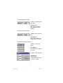
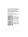
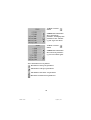
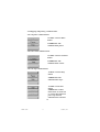
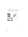
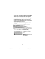
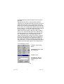
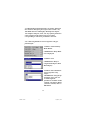
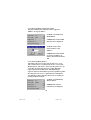
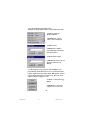
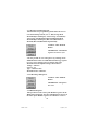
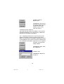
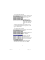
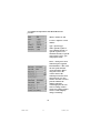
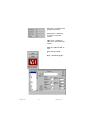
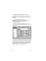
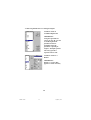
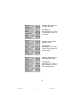
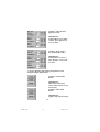
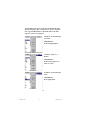
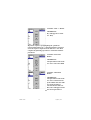
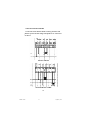
PowerSig
MULTIFUNCTION
TRANSDUCER
M560-AT*
OPERATING MANUAL
M560AT~1.PM5
1
01/08/101, 12:51
CONTENTS
Update: M560 Version 4
1. INTRODUCTION
2. PROGRAMMING PARAMETERS
3. PROGRAMMING ANALOGUE OUTPUTS
4. PROGRAMMING MODBUS REGISTER
SEQUENCE.
5. RS485 COMMUNICATION
6. INSTALLATION
7. CONNECTION DIAGRAMS
8. SPECIFICATION
Revision 4
Date 20-10-2011
Multitek Ltd. Lancaster Way, Earls Colne Business Park,
Earls Colne, Colchester, Essex. CO6 2NS. England.
Tel. (01787) 223228 Fax. (01787) 223607
E-MAIL: [email protected]
WEB SITE: WWW.multitek-ltd.com
2
M560 Version 4 update:
RS485 response time decreased to better than 10ms.
Choice of four Endian settings for floating point transmission.
Modbus 3X Register Order functions changed to 65 and 66.
Relay functions changed to 103 and 104.
Substitute MultiView for all references to Monitor95 or System Monitor.
Manual Ammendments:
Page 45: Changed 3X Modbus registers to odd numbers.
Page 50: Changed 4X Modbus registers to odd numbers.
Additional 4X registers:
40083 (0x0052) RESET Import kW.h Register (WO)
40085 (0x0054) RESET Export kW.h Register (WO)
40087 (0x0056) RESET Import kVAr.h Register (WO)
40089 (0x0058) RESET Export kVAr.h Register (WO)
40091 (0x005A) RESET kVA.h Register (WO)
40093 (0x005C) RESET Import A.h Register (WO)
For more information go to: www.multitek-ltd.com
M560 V4 Modbus 4X registers
Modbus
40001
40003
40005
40007
40009
40011
40013
40015
40017
40019
40021
40023
40025
40027
40029
40031
40033
40035
40037
40039
40041
40043
40045
40047
40049
40051
40053
40055
40057
40059
40061
40063
40065
40067
40069
40071
40073
40075
40077
40079
40081
40083
40085
40087
40089
40091
40093
40095
40097
40099
40101
Register
(0x0000)
(0x0002)
(0x0004)
(0x0006)
(0x0008)
(0x000A)
(0x000C)
(0x000E)
(0x0010)
(0x0012)
(0x0014)
(0x0016)
(0x0018)
(0x001A)
(0x001C)
(0x001E)
(0x0020)
(0x0022)
(0x0024)
(0x0026)
(0x0028)
(0x002A)
(0x002C)
(0x002E)
(0x0030)
(0x0032)
(0x0034)
(0x0036)
(0x0038)
(0x003A)
(0x003C)
(0x003E)
(0x0040)
(0x0042)
(0x0044)
(0x0046)
(0x0048)
(0x004A)
(0x004C)
(0x004E)
(0x0050)
(0x0052)
(0x0054)
(0x0056)
(0x0058)
(0x005A)
(0x005C)
(0x005E)
(0x0060)
(0x0062)
(0x0064)
Name
Mode
SYSTEM VOLTAGE (R/W)
SYSTEM CURRENT (R/W)
SYSTEM TYPE
(RO)
SYSTEM POWER
(RO)
DEMAND PERIOD
(R/W)
DEMAND STATUS
(RO)
Factoryuse
(ILLEGAL)
Factoryuse
(ILLEGAL)
RESET ALL ENERGY REGISTERS (WO)
RESET DEMANDS
(WO)
CALIBRATE INPUT (WO)
SET NODE ADDRESS (WO)
Analogue o/p1 assignment (M560) (R/W)
Analogue o/p1 nominal (M560)
(R/W)
Analogue o/p1 zero (M560)
(R/W)
Analogue o/p2 assignment (M560) (R/W)
Analogue o/p2 nominal (M560)
(R/W)
Analogue o/p2 zero (M560)
(R/W)
Analogue o/p3 assignment (M560) (R/W)
Analogue o/p3 nominal (M560)
(R/W)
Analogue o/p3 zero (M560)
(R/W)
RELAY ASSIGNMENT
(R/W)
RELAY DIVISOR
(R/W)
RELAY PULSE WIDTH
(R/W)
RESET FLASH/EEPROM DATA (WO)
I/P V1 GAIN FACTOR (R/W)
I/P V2 GAIN FACTOR (R/W)
I/P V3 GAIN FACTOR (R/W)
I/P I1 GAIN FACTOR (R/W)
I/P I2 GAIN FACTOR (R/W)
I/P I3 GAIN FACTOR (R/W)
Factoryuse
(ILLEGAL)
Factoryuse
(ILLEGAL)
Factoryuse
(ILLEGAL)
Factoryuse
(ILLEGAL)
SET PASSCODE
(WO)
CALIBRATION PASSCODE
(WO)
DtoA PASSCODE(M560)
(WO)
DtoA1 OVERRIDE(M560)
(WO)
DtoA2 OVERRIDE(M560)
(WO)
DtoA3 OVERRIDE(M560)
(WO)
RESET Import kW.h Register
(WO)
RESET Export kW.h Register
(WO)
RESET Import kVAr.h Register
(WO)
RESET Export kVAr.h Register
(WO)
RESET kVA.h Register (WO)
RESET Import A.h Register
(WO)
Future use
(R/W)
Future use
(R/W)
Future use
(R/W)
LOCK ACIA SETTINGS
(WO)
1.1 General
PowerSig M560 multifunction transducer is a complete
measuring system in a single 100mm Din rail mount case.
Measuring Phase Volts, Phase Current, Frequency, Active
Power, Reactive Power, Energy and Demand. The M560
provides up to 3 analogue outputs and the options of
RS485 modbus output and pulsed output.
Power Systems :Product code
1 Ph.
M560-AT1
1 Ph. 3 Wire
M560-AT1-3
3 Ph. 3W unbalanced load M560-AT4
3 Ph. 4W unbalanced load M560-AT9
The M560 units are fully programmed by the factory and
no further programming is necessary. If the RS485 option is
ordered, the user can reprogram parameters to individual
requirements, such as the voltage and current ratios, relay
output, demand times as well as assign different parameters to the outputs. These programming operations are
covered in this manual.
The M560 uses a high speed microprocessor and analogue
to digital conversion circuitry. Each phase current and
voltage is measured continuously and all other parameters
are derived from these measurements in the software.
Voltage and current measurements are true RMS.
1.2 Parameters Measured
The M560 Measures the following parameters :
Phase Voltage (V), Phase Current (I), Frequency (Hz),
Active Power per phase (W), System Active Power (W),
Reactive Power per phase (VAr), System Reactive Power
(VAr), Apparent Power per phase (VA), System Apparent
Power (VA), Import Active Energy (W.h), Export Active
Energy (W.h), Import Reactive Energy (VAr.h),
3
M560AT~1.PM5
3
01/08/101, 12:51
Export Reactive Energy (VAr.h), Power Factor per phase
(P.F.), System Power Factor (P.F.), Amp Demand, Watt
Demand, V A Demand, Maximum Amp Demand,
Maximum Watt Demand, Maximum VA Demand.
1.2 Memory
All data including energy registers, current and voltage
ratios and the calibration data is stored in a non volatile
e2prom. In power down (power loss) conditions all the
information is retained. The e2prom requires no battery or
other circuitry to maintain the stored data.
1.3 Relay Output (optional)
The relay output provides a pulsed output corresponding to
consumption Watt hour import or export, VAr hour import
or export, A.h or VA.h consumption. The relay can be
assigned to any of these parameters (see programming
section 2.15.1).
The M560 automatically calculates the pulse rate and
whether the units are W.h, kW.h or MW.h (VAr.h, kVAr.h
or MVAr.h) etc from the nominal voltage and current
inputs.
The relay is a normally open contact.
Pulse widths can be programmed into the M560, between
20 msec and 200 msec in steps of 20 msec. (See section
2.15.2).
4
M560AT~1.PM5
4
01/08/101, 12:51
1.4 Communications (optional)
The M560 has the option of providing RS485 output of all
measured parameters.
The serial port option enables remote reading and
programming of the M560 via a host computer, laptop etc.
The RS485 uses the Modbus protocol allowing multi-drop
with up to 32 M560s connected in parallel. The RS485
Modbus protocol allows the M560 to be used with PC,
PLC, RTU, Data loggers and Scada programs.
Software is available for programming and displaying
parameters. Contact your local distributor for a free copy
or visit our website www.multitek-ltd.com
1.5 LED indicator
The red LED on the front of the M560 serves three
purposes:
LED continually illuminated means that the power supply
is o.k.
LED illuminated and flashing every 10 seconds means that
the power supply o.k. and the M560 is communicating
correctly.
LED illuminated and flashing every second and 2 flashes
every 10 seconds means that the power supply o.k. and
that unit is communicating correctly, but there is no input
measuring voltage signal.
5
M560AT~1.PM5
5
01/08/101, 12:51
2.0 PROGRAMMING
If the unit has not been provided with a communication
option this section is not relevant, please move to section 6
installation.
2.1 Using the M560 Software Monitor 95.
(M560 Software Monitor 95 can be obtained from your
Multitek distributor, or the Multitek website
www.Multitek-Ltd.com)
2.2 Open the Monitor95.exe file and the following screen
will be displayed.
The following functions displayed relate to the PC or
master node and are set by default to the following
settings, Response time = 300mS, Node = 1, Baud Rate =
9600, Parity = None. It may not be necessary to alter the
above settings but the communication port has to be
opened by clicking on start and following section 2.5.
6
M560AT~1.PM5
6
01/08/101, 12:51
2.3 Changing Response Time
ACTION : Click Response
Time Box.
COMMENTS :
Enter Value of response
time. Minimum value
300mSec.
2.4 Changing Node Number
ACTION : Click Node No.
Box.
COMMENTS :
Enter Node Number any
number between 1 & 247.
2.5 Opening communication port.
ACTION : Click Start
Button.
COMMENTS :
Port selection box appears,
see below.
ACTION : Click Port Box.
COMMENTS :
Chose the PC's
communication port click
on Com 1 or Com 2
7
M560AT~1.PM5
7
01/08/101, 12:51
2.6 Changing Baud Rate.
ACTION : Click Baud Rate
Box.
COMMENTS :
Chose Baud Rate. Either
2400, 4800, 9600, 19200.
2.7 Changing Parity.
ACTION : Click Parity Box.
COMMENTS :
Choose Parity. Three
options Odd, Even or None.
2.8 Starting Communication
ACTION : Once Comms
Port, Baud Rate and parity
are set, Click on O.K.
COMMENTS : If
Communication is working
message modbus OK
appears in Modbus box.
COMMENTS :
M560 and PC
communicating correctly.
COMMENTS :
M560 and PC not
communicating correctly.
8
M560AT~1.PM5
8
01/08/101, 12:51
Note if wording in Modbus box is "NO REPLY FROM
NODE". Check polarity connection of RS485 link at M560
and PC. Check that M560 has auxiliary power by checking
Red LED on front of M560. If LED continually
illuminated power supply o.k. If LED illuminated and
flashing every 10 seconds, power supply ok M560
communicating ok. If LED flashing every second there is no
measuring input voltage signal.
2.9 Displaying parameters being measured.
Once M560 is communicating with your PC you can now
monitor different readings.
ACTION : None
COMMENTS : The 6 boxes
show line to line voltage and
line to neutral voltage for
each phase. Note if unit is 3
phase 3 wire M560-CT4
V1,V2,V3 are the same as
VL1-2, VL2-L3, VL3-1.
ACTION : Click on
button.
COMMENTS : The next six
parameters being monitored
are displayed. e.g I1,I2,I3,
WSum, VA Sum, VAR Sum.
9
M560AT~1.PM5
9
01/08/101, 12:51
ACTION : Click on
button.
COMMENTS : This button
moves forward one
parameter, and displays this
parameter in the sixth box
e.g. PF Avg is now shown.
ACTION : Click on
button.
COMMENTS : This button
moves back one parameter.
e.g. now I1 is shown again.
Note: The buttons work as follows:
This button scrolls up one parameter.
This button scrolls up six parameters.
This button scrolls down one parameter.
This button scrolls down six parameters.
10
M560AT~1.PM5
10
01/08/101, 12:51
2.10 Stopping and pausing communication.
2.10.1 To pause communication.
ACTION : Click on Pause
button.
COMMENTS : The
communication pauses.
2.10.2 To restart communication.
ACTION : Click on Continue
button.
COMMENTS : The
communication restarts.
2.10.3 To stop communication.
ACTION : Click on Stop
button.
COMMENTS : The
communication stops.
ACTION : Click Start
button.
COMMENTS : Follow
instructions in section 2.8
i.e. click on O.K. button in
port set up box and
communication will start.
11
M560AT~1.PM5
11
01/08/101, 12:51
2.11 Starting timer.
The timer is real time clock provided by the Monitor
program. It is useful for checking Watt hour readings etc.
ACTION : Click Start
button.
COMMENTS : The timer
starts.
ACTION : Click Stop
button.
COMMENTS : The timer
stops and gives option of
resetting or continuing.
ACTION : Click Reset
button.
COMMENTS : The timer
resets to zero.
ACTION : Click Continue
button.
COMMENTS : The timer
continues to count,
displaying the total time
from when counter initially
started.
12
M560AT~1.PM5
12
01/08/101, 12:52
2.12 Security code. (General Pass Code)
To program different CT & VT ratios, demand times, etc.
the General Pass Code must be entered. The General Pass
Code is 080453. This is general pass code and is only
applicable to Multitek M560 software. Pass Codes
necessary for use with other software are listed in Section 4
page 45 of this manual.
2.12.1 Entering General Pass Code
ACTION : Click General
Pass Code Button
COMMENTS :
Enter value box is
displayed.
ACTION : Enter value
COMMENTS : Enter
security code 080453 and
click on OK button
13
M560AT~1.PM5
13
01/08/101, 12:52
2.13 Communications Lock.
Response Time, Node Number, Communication Port, Baud
Rate and Parity are dependant on the system and PC etc.
that is being used. When connected to an existing Modbus
network the M560 will automatically detect and configure
itself to the network's settings. These settings can be locked
into the EEPROM of the M560 to prevent unnecessary
hunting. For a more detailed explanation of this facility see
help file in the Monitor95 Software.
2.13.1 To Lock communications setting into the M560
EEPROM.
ACTION : Click Lock
Button.
COMMENTS :
M560 communication port
will be locked onto existing
network settings.
2.13.2 To Unlock M560 communications settings.
ACTION : Click Unlock
Button.
COMMENTS :
M560 communication port is
now unlocked.
14
M560AT~1.PM5
14
01/08/101, 12:52
2.14 Programming of nominal voltage and current inputs
and ratios.
The program allows the user to program the nominal
voltage and current inputs and ratios. Please note the ratios
can be changed as long as the secondary (the input to the
M560) stays as shown on the data label which is on the side
of the product. For example if the M560 had been set by the
factory to have a C.T. ratio 200/5A and the change required
was for the input C.T. ratio to be 500/5A this can be
achieved by program changes. But if the change required
was for a C.T. ratio 500/1A then the unit would have to be
returned to the factory or distributor to have the internal
C.T. changed from 5A to 1A. The same applies to the
voltage if the M560 input voltage is 110 Volts L.L then an
external voltage transformer ratio can be programmed as
long as the nominal input to the M560 stays at 110V L-L
For example if the input was originally programmed for
6.6kV/110 and a V.T. of 11kV was required then this change
could be achieved through software. (See example below)
2.14.1 Changing VT ratio.
ACTION : Click Voltage
Button.
COMMENTS : Enter Value
box is displayed.
ACTION : None
COMMENTS : M560 is
programmed for 6600V
(6.6kV)
15
M560AT~1.PM5
15
01/08/101, 12:52
ACTION : Enter value
COMMENTS : Enter
11000 (11kV). Click on
O.K.
2.14.2Changing CT ratio.
For example to change for 200/5A change to 400/5 :ACTION : Click Current
Button.
COMMENTS : Enter Value
box is displayed.
ACTION : None
COMMENTS : M560 is
programmed to 200/5A
ACTION : Enter Value
COMMENTS : Enter 400
(400 Amps). Click on OK
16
M560AT~1.PM5
16
01/08/101, 12:52
2.15 Pulsed Output (Pulsed output is an option. If the unit
does not have this option please proceed to section 2.16)
The M560 measures and displays W.h Import & Export,
VAr.h Import & Export, VA.h, A.h. Any of these parameters
can be assigned to the output relay to give pulses
corresponding to which ever parameter is selected.
2.15.1 Selecting Parameter to be assigned to relay for
pulsed output.
ACTION : Click On Relay
Mode Button.
COMMENTS : Relay Mode
box is displayed.
ACTION : None
COMMENTS : Relay is
assigned W.h Import. (Watt
Hour Import)
ACTION : Select Parameter
to be assigned to relay
output.
COMMENTS : Using the up
and down cursor you can
scroll through the
parameters available. In this
example A.h (Ampere Hours
) has been selected, click on
OK Button.
17
M560AT~1.PM5
17
01/08/101, 12:52
2.15.2 Selecting Relay output pulse width.
The pulse width can be set between 0msec (off) and
200msec, in steps of 20msec.
ACTION : Click On Pulse
Width Button.
COMMENTS : Pulse Width
Selection box is displayed.
ACTION : Enter value
between 20msec and
200msec.
COMMENTS : Pulse widths
are in steps of 20msec. If
60msec enter 60 and click on
OK.
2.15.3 Selecting Relay Divisor
This allows the user to set the relay to pulse every 1, 10 ,
100 or 1000 counts. i.e. If the divisor is set to 1 every time
M560 registers and stores 1 count relay the pulses once. If
set to 100, the relay only pulses once after M560 has
registered and stored 100 counts. The M560 always
registers and stores the number of counts regardless of what
the relay divisor is set to. i.e. If the kilowatt consumption
was 500 kW per hour and relay divisor was set to 100 you
would get 5 pulses an hour.
ACTION : Click On Relay
Divisor Button.
COMMENTS : Divisor
selection box is displayed.
18
M560AT~1.PM5
18
01/08/101, 12:52
ACTION : None
COMMENTS : Divisor set
for 1. This means after every
1 unit that M560 counts the
relay pulses once.
ACTION : Select Divisor
required.
COMMENTS : Using the up
and down cursor you can
scroll through the divisor
values available. If a
divisor value of 100 is
required select 100 and
Click on OK.
2.16 The M560 measures Wd (Average Watt Demand
Import & Export) VAd (Average VA Demand ) Ad
(Average Amp Demand) Max Wd (Maximum Watt Demand
Import & Export) Max VAd (Maximum VA Demand) Max
Ad (Maximum Amp Demand). Demand times between 3
and 30 minutes can be programmed in 1 minute steps.
The M560 samples the instantaneous values for 1 minute
then takes the average of these samples and updates the
memory. This sampling and updating every minute
continues until the time period selected is reached. e.g. If
time period is 15 minutes then after 15 minutes the average
of 15 minute demand is displayed. When the 16th minute is
reached the M560 takes the average of minute 2 to 16 and
updates the memory. The Maximum Demand is the highest
value recorded by M560 from being powered up. This value
is retained until either registers are reset or auxiliary power
is removed.
19
M560AT~1.PM5
19
01/08/101, 12:52
2.16.1 Programming demand periods.
Example to change from 8 min to 30 min demand period :
ACTION : Click On
Demand Button.
COMMENTS : "Enter
Value" box is displayed.
ACTION : None.
COMMENTS : M560 is
programmed for a demand
time of 8 minutes.
ACTION : Enter Value.
COMMENTS : Enter 30 (30
minutes). Click on OK
Button.
2.17 Resetting of energy registers. The ENERGY reset
programming mode allows the User to reset the Watt hour
register import and export (W.h, kW.h, MW.h) the VAr hour
register import and export (VAr.h, kVAr.h, MVAr.h) VA.h
registers and A.h registers to zero.
ACTION : Click On Energy
Button
COMMENTS : All energy
registers are reset to zero.
20
M560AT~1.PM5
20
01/08/101, 12:52
2.17 Resetting of demand period.
The Demand reset programming mode allows the User to
reset the demand period to zero. i.e Wd (Average Watt
Demand Import and Export) VAd (Average VA Demand )
Ad (Average Amp Demand) Max Wd (Maximum Watt
Demand Import and Export) Max VAd (Maximum VA
Demand) Max Ad (Maximum Amp Demand)
ACTION : Click Demand
Button.
COMMENTS : All Demand
registers are reset to zero.
2.18 It is possible to reset all registers by clicking on the
EEProm button. This sets all Demand and Energy registers
to zero. It resets Voltage, Current, System Type and
Demand Period to Default Settings, shown below :
Voltage : 230V LN
Current : 5A
Type : 3 Phase 4 Wire
Demand Period : 8 minutes
2.18.1 Resetting All Registers
ACTION : Click EEProm
Button.
COMMENTS : All registers
are reset.
2.19 Modbus Registers
This operation sets the order of the Modbus registers in the
M560 being monitored. For more information on how to set
the order of the Modbus registers in a M560 see section 3.
21
M560AT~1.PM5
21
01/08/101, 12:52
ACTION : Click On
Registers Box
COMMENTS : The order of
the displayed measurements
now matches that of the
Modbus registers in the
node. See section 3
2.20 Setting of Node Addresses.
The number of node addresses available is 1 to 247. Each
individual M560 that is to be connected to a common bus,
must have its own unique node address.
Note : All M560 instruments are set by the factory to the
default node number 1 but all respond to a query using
address 254. This allows any M560 to communicate on any
existing Modbus network. Once the unit has communicated
successfully the node number required can be set as follows.
ACTION : Click On Node
Number Button.
COMMENTS : Enter Value
box is displayed.
ACTION : None
COMMENTS : M560 is set
to Node 15.
22
M560AT~1.PM5
22
01/08/101, 12:52
ACTION : Enter Node
Address Required.
COMMENTS : Example if
node address 30 is required
enter 30 and click OK Button
2.21 Calibration Factors.
This option allows the user to re-calibrate the M560
without using live voltage and current inputs
To enable the user to complete this, all the calibration data
has to be manually recorded and kept. It is suggest that the
user makes a note of the values and stores them with the a
note of the serial number of the M560 being used.
2.21.1 Calibration Enable.
Before the calibration part of the program can be used the
Calibration Enable Password has to be entered. The code is
the same as General Password 080453 for the M560
monitor software. (See page 45 for programming codes)
ACTION : Click Cal Enable
Button.
COMMENTS : Enter Value
box is displayed.
ACTION : Enter value.
COMMENTS :
Enter security code 080453
and click on OK Button
23
M560AT~1.PM5
23
01/08/101, 12:52
2.21.2 Reading Calibration Data
ACTION : Manually record
calibration figures for V1,
V2, V3, I1, I2, I3.
COMMENTS : These
values must be stored with
the serial number of the
M560 as these numbers are
unique to the M560 under
test.
Note Only complete the following operation in 2.21.3 if
the calibration data has been lost and you have recorded
original calibration data.
2.21.3 Entering Calibration Data
ACTION : Click on Manual
Button.
COMMENTS : Enter Value
box is displayed.
ACTION : Enter value .
COMMENTS : Enter
recorded values into V1, V2,
V3, I1, I2, I3 click on O.K.
The Clear button clears all calibration data from the
calibration registers and sets them all to 1.000000.
24
M560AT~1.PM5
24
01/08/101, 12:52
2.25 Additional Information that M560 Monitor95
provides :
Model = Model No 560
Version = Software version
number
Type = System Type.
either 3ph 4W (3 phase 4
wire unbalanced load) or
3ph 3W (3 phase 3 wire
unbalanced load) or 1ph 3W
(single phase 3 wire) 1 ph
(single phase load)
Power = Total power when
nominal input is applied.
Demand Status = This reads
the state of the demand
count-down timer. When
integration starts, the
counter loads in the
demand period and counts
down towards zero each
minute. The value returned
from the M560 is the
number of minutes
remaining before the unit
starts its sliding window
mode. Once sliding window
mode is reached display
changes to Rolling
25
M560AT~1.PM5
25
01/08/101, 12:52
Stack Free = Nodes internal
program, stack state.
Parity Errors = number of
errors since node cold
started.
CRC errors = Number of
CRC errors since node cold
started.
EEprom = Indicates O.K. or
error.
Quit = Ends program.
Help = Provides help files.
26
M560AT~1.PM5
26
01/08/101, 12:52
3.0 PROGRAMMING ANALOGUE OUTPUTS
If the unit has not been provided with a communication
option this section is not relevant, please move to section 6
installation.
3.1 Using the M560 Software Monitor 95.
(M560 Software Monitor 95 can be obtained from your
Multitek distributor, or the Multitek website
www.Multitek-Ltd.com)
3.2 Load disc and open file multd2a ( This is PowerSig
Analogue Outputs Program) and the following screen will
be displayed.
The parameters are set by default to following readings. All
can be changed if required, see section 2.3 to 2.6. Response
time = 300mS, Node = 1, Baud Rate = 9600, Parity = None
For the purpose of describing the programming of the
analogue outputs they will be left as shown.
27
M560AT~1.PM5
27
01/08/101, 12:52
3.3 Opening communication port.
ACTION : Click Comms
Button.
COMMENTS :
Choose which P.C.
communication port 1 or 2.
Click on Com 1 or Com 2
3.4 Addressing PowerSig Node.
The Node number of PowerSig being address has to be
entered.
ACTION : Click Node
Number Button.
COMMENTS :
Enter node number of
PowerSig to be addressed.
PowerSig can have any
number between 1 & 247.
Note : All PowerSigs will
respond if set to node 254.
28
M560AT~1.PM5
28
01/08/101, 12:52
3.5 Selecting Parameters For Analogue Outputs.
ACTION : Click on
Available Outputs Box
COMMENTS :
Using the up and down
cursor on your PC you can
scroll through all the
parameters that are
available. Select the
parameter required for
output 1. Example if Total
Current of system is
required select I sum.
ACTION : Click on >>
Button..
COMMENTS :
Output 1 = I sum (This
appears in Node No1 Box)
29
M560AT~1.PM5
29
01/08/101, 12:52
ACTION : Click on
Available Outputs Box.
COMMENTS :
Using the up and down
cursor choose parameter
required for analogue
output 2. Example if Watts
in Phase 3 is required select
W3.
ACTION : Click on >>
Button.
COMMENTS :
Output 2 = W3 (this appears
in Node No1 Box)
ACTION : Click on
Available Outputs Box.
COMMENTS :
Using the up and down
cursor choose parameter
required for analogue
output 3. Example if system
frequency is required choose
Hz.
Note : If a parameter is entered into the Node No1 box in
error, Click << button. The parameter is then removed and
the desired parameter can be entered. Click on Clear
Button and all parameters in Node No1 Box are removed.
30
M560AT~1.PM5
30
01/08/101, 12:52
ACTION : Click on >>
Button.
COMMENTS :
Output 3 = Hz. (This
appears in Node No 1 Box)
3.6 Selecting Output Values & Ranges For Analogue
Outputs.
The mA output range is specified at 20mA = 100%. All
following mA values are available 0-1mA 0-5mA 0-10mA
and 4-20mA (any value between 1 & 20mA can be
specified) These values are entered as a percentage of
20mA.
Example :
Output 1 (I sum) = 4-20mA.
Output 2 (W3) = +10m-0-10mA- (Note all parameters that
can be read as bipolar (like Watts) the Multd2a program
automatically sets the outputs as bipolar outputs)
Output 3 (Hz) = 0-1mA.
ACTION : Click On Zero
Offset Box CH1.
COMMENTS :
Nominal Box is set at 100%
= 20mA . Zero offset box is
set at 0 = 0mA.
31
M560AT~1.PM5
31
01/08/101, 12:52
ACTION : Enter Value 20
into Offset Box CH1.
COMMENTS :
Zero offset box is set at 20%
= 4mA. Output 1 is now set
to 4-20mA.
ACTION : Click On Zero
Offset Box CH2.
COMMENTS :
Nominal Box is set at 100%
= 20mA . Zero offset box is
set at 0 = 0mA.
ACTION : Enter Value 50
Into Nominal Box CH2.
COMMENTS :
Nominal box is set at 50% =
10mA. Output 1 is now set
at to +10mA-0-10mA-.
32
M560AT~1.PM5
32
01/08/101, 12:52
ACTION : Click On Zero
Offset Box CH3.
COMMENTS :
Nominal Box is set at 100%
= 20mA . Zero offset box is
set at 0 = 0mA.
ACTION : Enter Value 5
Into Nominal Box CH3.
COMMENTS :
Nominal box is set at 5% =
1mA. Output 1 is now set at
to 0-1mA.
3.7 Setting, Reading and Sending all parameters and
Analogue Output Information.
ACTION : Click Enable
Button.
COMMENTS :
This action sends a pass
code to allow data to be sent
to PowerSig.
ACTION : Click Send
Button.
COMMENTS :
Updates node output settings.
33
M560AT~1.PM5
33
01/08/101, 12:52
ACTION : Click Read Button
COMMENTS :
Reads all parameter
information and
corresponding outputs.
34
M560AT~1.PM5
34
01/08/101, 12:52
4.0 PROGRAMMING MODBUS REGISTERS SEQUENCE
If the unit has not been provided with a communication
option this section is not relevant, please move to section 6.0
If changing of the modbus order is not required please move
to section 4.0 communication.
4.1 Using the M560 Software.
M560 software can be obtained from your Multitek
distributor or from our website www.multitek-ltd.com.
4.2 Load disc and open Mbregs, (This is the Modbus Registers Tool program) and the screen below will be displayed.
4.3 This software allows the user to alter the sequence in
which the Modbus addresses are read. So for example if the
user was only interested in Watts Hz Power Factor, then
these 3 registers could be set as the first 3 and the
remaining registers ignored.
The following parameters are set by default to the
following readings, all can be changed if required. See
section 2.3 to 2.6. Response time = 300mS, Node = 1,
M560AT~1.PM5
35
01/08/101, 12:52
Baud Rate = 9600, Parity = None
4.4 Opening communication port.
ACTION : Click on Comms
Button.
COMMENTS :
Choose which communication port, 1 or 2. Click on
Comms 1 or Comms 2
4.5 Programming Modbus Register Sequence.
ACTION : Click on Default
Order Box
COMMENTS :
Using Up and Down cursor
you can scroll through all
parameters that are available and see the order that
they will appear in. This
order can be changed.
36
M560AT~1.PM5
36
01/08/101, 12:52
For Example if the order required is Total Watt (W sum),
System Frequency (Hz), Average Power Factor of System
(PF Avg) and Maximum VA Demand (Max VAd) This
sequence can be set as follows.
ACTION : Scroll Through
to W Sum.
COMMENTS :
W Sum is highlighted.
ACTION : Click on >>
Button.
COMMENTS :
W Sum (This appears in
Node No. Box)
ACTION : Scroll Through
to Hz
COMMENTS :
Hz is highlighted.
37
M560AT~1.PM5
37
01/08/101, 12:52
ACTION : Click >> Button.
COMMENTS :
Hz (This appears in Node
No. Box)
Repeat the sequence of highlighting the parameter
required and clicking on >> until all parameters required
are in the sequence required in the Node No. 1 box. Then
complete the following operations to send and read these
parameters.
ACTION : Click Send
Button.
COMMENTS :
All information in the Node
No. box is sent to the M560
ACTION : Click Read
Button.
38
M560AT~1.PM5
38
COMMENTS :
All information in the Node
No. box is read and stored
by the M560. This also adds
any of the parameters
not selected into Node No.
Box, these will appear below
the selected parameters.
01/08/101, 12:52
Note. The parameters not selected are placed in the default
order after the parameters chosen.
4.6 Additional Options the Modbus Register Tool Program
Offers.
<< = If you wish to remove a parameter from Node No.
Box, highlight the parameter and click on <<
Default = Clicking on default overrides parameters in Node
No. Box and replaces them in the Default order.
Clear = Clicking on Clear removes all parameters from the
Node No. Box.
Print = Allows printing of parameter order.
39
M560AT~1.PM5
39
01/08/101, 12:52
5.0 RS485 COMMUNICATION
The RS 485 allows remote reading and programming of the
M560 via a host computer. The communication
protocol used is a subset of Modicons Modbus, (see section
5.1) enabling the use of standard host computer, PLC and
scada programs. Up to 32 PowerSig M560s can be
connected in parallel to a single communication bus.
5.1 M560 Modbus Protocol
5.1.1 Physical Connections
The interface to the Modbus network is via an RS485
connection. This takes the form of a twisted pair cable
preferably screened, onto which up to 32 devices may be
connected, one of which will be the host PC or controller
node. The devices on the network are connected in parallel
+ to +, - to - and shield to shield ( screen to screen). The
shield should be connected to earth at one point of the
network only. Other manufacturers of devices intended for
use on the Modbus network may have different + and designations : some have Hi, Lo or A ,B. In any case
reversing the + and - connections may have the desired
results if the device fails to communicate with the master
node.
The maximum length of the twisted pair cable specified by
the RS standard is 1.2km. Any length over 200m should be
terminated at each end with a resistor equal to the cable's
characteristic impedance in series with a 0.1µF capacitor.
A typical network cable is Beldon 8761.
40
M560AT~1.PM5
40
01/08/101, 12:52
5.1.2 Communication Format
Baud rate : 2400, 4800, 9600, 19200
Low level character format :
With Odd or Even parity = 1 start bit, 8 data bits, 1 parity bit,
1 stop bit
With NO parity = 1 start bit , 8 data bits, 2 stops bits.
5.1.3 Modbus Format
Data format :
RTU
32 bit, floating point format to IEEE-754 standard, exponent
bias 127, most significant byte transmitted first. There is no
word reversal.
Address range: 1-247
Error Check :
Cyclic Redundancy Check (CRC), Polynomial exclusive
OR value A001h Low byte sent first.
5.3.5 Modbus Protocol
Only the RTU (Remote Terminal Unit) form of the Modbus
protocol will be supported and all references in this sheet
refer to RTU format.
Typically, the master or controller requests data from its
slaves by polling them one at a time and waiting for a
pre-defined amount of time for a response. If a node
doesn't respond within this time period the master will try
accessing it a further two times before indicating to the
Scada system that the node has gone off-line or there is a
fault with it. If all is well the node will respond with the
data requested.
41
M560AT~1.PM5
41
01/08/101, 12:52
A typical communication 'packet' will be in the form :
[Node Address] [Function] [Byte count, Data etc.] [Error
check].
Because Modbus is a word (2 byte) orientated protocol,
floating point (4 byte) register numbers are counted in
multiples of two.
viz
register 1 = start address 0
register 2 = start address 2
register 3 = start address 4
register 4 = start address 6
Formula = (register required -1) x2
This also applies to the number of registers requested. If 2
registers are requested the number of WORDS in the
packet's [Number of registers] slot should equal 4. (See
examples in the following sections.
CRC Calculations
To calculate the Cyclic Redundancy Check value.
Load a word register with 0xFFFF (CRCREG)
Repeat the following for each character in the Modbus
packet
{
XOR the low byte of the word register with the next (or
first) character in the buffer
Repeat the following for the whole character
{
Get the state of the lsb of CRCREG Low byte
Shift the CRCREG right by one bit shifting in a
zero in the msb
If the bit shifted out is a logical 1, XOR
CRCREG with 0xA001
}
}
CRCREG contains the CRC of the buffer
42
M560AT~1.PM5
42
01/08/101, 12:52
5.3.6 Timing
RTU frame timing :
The message starts with an interval of at least 3.5 character
times.
Following the last transmitted character, a similar interval
of a least 3.5 character times marks the end message.
The entire message frame must be transmitted as a
continuous stream.
5.3.7 Response time.
Modbus response time from reception of the last character
to the transmission of the 1st character in its reply is less
than 200 msec.
5.3.8 Codes Supported
Function 3 (03 hex) Read holding registers. (4X)
Function 4 (04 hex) Read input registers. (3X)
Function 16 (10 hex) Preset Multiple register. (4X)
Function 17 (11 hex) Report slave ID
Function 30 (1E hex) Modbus register order Write
Function 31 (1F hex) Modbus register order Read
BROADCAST is not supported and this command does not
cause the slave to respond to the master.
43
M560AT~1.PM5
43
01/08/101, 12:52
An EXCEPTION error will be generated if the node cannot
fulfil the task set by the Master or the Slave receives invalid
data in its data slot.
Exception code table
Code
Name
01
Illegal Function
02
Illegal Data Address
03
Illegal Data Value
5.3.8 Modbus Codes Reference
Function 4 (04 hex) - read input registers. (3X)
These registers contain the measured and calculated values
of the instrument. Register addresses in the instrument
start at 0 but in keeping with Modicon Modbus codes, are
designated addresses starting at 30001.
Packet from master format :
[Node Addr][04][reg start addr(2 bytes)][No. of reg (2
bytes)] [CRC(2 bytes)]
Response from slave format:
[Node Addr][04](Byte count][Data (byte count
bytes)][CRC(2 bytes)]
The following table lists the parameters with the Modbus
equivalent address and its address within the M560. Any
data requested that isn't applicable to the conditions
column will return the value -ve infinity (FFFFFFFFh)
3X Registers
The registers are listed with their Modbus addresses.
The data held at these addresses are Read-Only.
3X registers are read using function 04h.
44
M560AT~1.PM5
44
01/08/101, 12:52
A sample write packet will look like this:[Node][04][start address][No. of Double Registers
Requested][CRC(2 bytes)]
e.g. To read line to neutral voltages on node 23h:[23h][04h][0006h][0006h(3, 4 byte regs)] [CRC(2 bytes)]
The node’s return packet will look like:[23h][04h][000Ch][12 bytes of data = 3 floating point
numbers] [CRC(2 bytes)]
The list below is the default order of the 3X registers in
M560. The order can be altered using the Modbus Registers Tool Program, (see section 4), or by a suitable SCADA
program.
Modbus Add. Register Add.
30001
(0x00)
30003
(0x02)
30005
(0x04)
30007
(0x06)
30009
(0x08)
30011
(0x0A)
30013
(0x0C)
30015
(0x0E)
30017
(0x10)
30019
(0x12)
30021
(0x14)
30023
(0x16)
30025
(0x18)
30027
(0x1A)
30029
(0x1C)
30031
(0x1E)
Register Name Order No.
V L1-2
1
V L2-3
2
V L3-1
3
V 1*
4
V 2*
5
V 3*
6
I1
7
I2
8
I3
9
W Sum
10
VA Sum
11
VAR Sum
12
PF Avg
13
WHr (IMP)
14
VArHr (IMP)
15
Hz
16
45
Continued :Modbus Add.
30033
30035
30037
30039
30041
30043
30045
30047
30049
30051
30053
30055
30057
30059
30061
30063
30065
30067
30069
30071
30073
30075
30077
30079
30081
Register Add. Register Name Order No.
(0x20)
W1
17
(0x22)
W2
18
(0x24)
W3
19
(0x26)
VAr 1
20
(0x28)
VAr 2
21
(0x2A)
VAr 3
22
(0x2C)
Wd (IMP)
23
(0x2E)
VAd
24
(0x30)
Ad
25
(0x32)
Neutral I
26
(0x34)
VA 1
27
(0x36)
VA 2
28
(0x38)
VA 3
29
(0x3A)
PF L1
30
(0x3C)
PF L2
31
(0x3E)
PF L3
32
(0x40)
WHr (EXP)
33
(0x42)
VArHr (EXP)
34
(0x44)
VAHr
35
(0x46)
AHr
36
(0x48)
Wd (EXP)
37
(0x4A)
Max Wd (IMP) 38
(0x4C)
Max Wd (EXP) 39
(0x4E)
Max VAd
40
(0x50)
Max Ad
41
*In 3 wire mode system V1, V2, V3 will have same value as
volts L2-L1, L3-L2, L1-L3
46
Modbus Register Order: Overview (also see section 4 and
help file of M560 software)
M560 has the facility to reorder its Modbus 3X registers to
suit an existing Modbus network.
The Modbus Registers Tool program provides an easy
method of achieving this.
The order of the registers in any node connected to the
network can be read by the program by clicking on the
READ button.
The list can be modified (using the CLEAR, DEFAULT, <<
and >> buttons) to enable the most accessed parameters to
appear first in the Node’s list, thereby optimising the speed
of the system. The default order for the registers is listed in
the left hand area of the dialog box. Simply clear the right
hand list box and enter the register order required.
The same results can be achieved by using Modbus
function code 1Eh (30) to send a string of data to set the
order of the registers. The order will automatically be saved
in EEPROM.
47
M560AT~1.PM5
47
01/08/101, 12:52
A sample write packet will look like this:[Node][1E][start address][No. of Double Registers][Data
length in bytes] [REGISTERS][CRC(2 bytes)]
It is important to remember that each register in the
packet’s data field contains two references to the registers
to be reordered.
e.g. To set the 41 Modbus registers to their default order in
node 23h:[23h][1Eh][23h][1Eh][0000h][002Ah][0102h][0304h][0506h][0708h]
[090Ah][0B0Ch][0D0Eh][0F10h][1112h][1314h][1516h][1718h][191Ah]
[1B1Ch][1D1Eh][1F20h][2122h][2324h][2526h][2728h][29XX]
[CRC(2bytes)]
N.B. XX = don’t care.
To read the order of the registers use code 1F (31)
eg. [23h][1F][0000][0018h][CRC(2bytes)]
Example
To obtain all 3 line powers in a 4 wire system on Node 23h
Packet from master :
Start at Power L1 (0020), request 3 regs (0006 words)
[23][04][0020][0006][CRC(2bytes)]
Response from slave format :
[23][04][12 bytes of data(3 regs x 4 bytes)][CRC(2 bytes)]
Function 3 (03 hex) - Reading registers (4X)
These registers contain the system setting and controls.
Register addresses in the instrument start at 0, but in
keeping with Modicon Modbus codes, are designated
addresses starting at 40001.
48
M560AT~1.PM5
48
01/08/101, 12:52
Read
Packet from master format :
[Node addr][03][Register start addr.(2 bytes)][No of reg(2
bytes)][CRC (2 bytes)]
Response form Slave format :
[Node addr][03][Byte count][Data(byte count bytes)][CRC
( 2 bytes)]
Function 16 (10 hex) - Preset Multiple registers (4X)
These registers contain the system settings and controls.
Register addresses in the M560 at 0, but in keeping with
Modicon Modbus codes, are designated addresses starting
40001.
Write
Packet from master :
[Node addr][10][Register start address(2 bytes)][No of
registers(2 bytes)][Byte count][Data (byte count bytes)]
[CRC (2 bytes)]
Response from slave format :
[Node addr][10][Register start addr.(2 bytes)][No of
registers(2 bytes)][CRC (2 bytes)]
The following table lists the parameter, its Modbus
equivalent address and its address within the M560. Any
Illegal operation will return an Error code.
4X Registers
The registers are listed with their Modbus addresses.
The data held at these addresses are Read-Only, Write-Only
or Read+Write as indicated below.
4X registers are read using function 03h and written using
function 10h.
A sample write packet will look like this:49
M560AT~1.PM5
49
01/08/101, 12:52
[Node][10][start address][No. of Double Registers][Data
length in bytes][CRC(2 bytes)]
e.g. To set Node 23h System Voltage and System Current
together:[23h][10h][0000h][0004h(4, 2 byte regs)][08h(2, 4 byte
regs)][CRC(2 bytes)]
Modbus Add. Register Address/Name
Mode
40001
(0x00) SYSTEM VOLTAGE
(R/W)
40003
(0x02) SYSTEM CURRENT
(R/W)
40005
(0x04) SYSTEM TYPE
(R/W)
40007
(0x06) SYSTEM POWER
(RO)
40009
(0x08) DEMAND PERIOD
(R/W)
40011
(0x0A) DEMAND TIMER
(RO)
40013
(0x0C) RELAY DIVISOR
(R/W)
40015
(0x0E) RELAY PULSEWIDTH
(R/W)
40017
(0x10) RESET ENERGY
(WO)
40019
(0x12) RESET DEMANDS
(WO)
40021
(0x14) CALIBRATE INPUT
(WO)
40023
(0x16) SET NODE ADDRESS
(WO)
40025
(0x18) Analogue o/p 1 assignment (R/W)
40027
(0x1A) Analogue o/p1 nominal
(R/W)
40029
(0x1C) Analogue o/p 1 zero
(R/W)
40031
(0x1E) Analogue o/p 2 assignment (R/W)
40033
(0x20) Analogue o/p 2 nominal
(R/W)
40035
(0x22) Analogue o/p 2 zero
(R/W)
40037
(0x24) Analogue o/p 3 assignment (R/W)
40039
(0x26) Analogue o/p 3 nominal
(R/W)
40041
(0x28) Analogue o/p 3zero
(R/W)
40043
(0x2A) RELAY ASSIGNMENT
(R/W)
40045
(0x2C) RESET EEPROM DATA
(WO)
40047
(0x2E) I/P V1 GAIN FACTOR
(R/W)
50
40049
(0x30) I/P V2 GAIN FACTOR
(R/W)
40051
(0x32) I/P V3 GAIN FACTOR
(R/W)
40053
(0x34) I/P I1 GAIN FACTOR
(R/W)
40055
(0x36) I/P I2 GAIN FACTOR
(R/W)
40057
(0x38) I/P I3 GAIN FACTOR
(R/W)
40059
(0x3A) Future use
(ILLEGAL)
40061
(0x3C) Future use
(ILLEGAL)
40063
(0x3E) Future use
(ILLEGAL)
40065
(0x40) CLEAR GAIN FACTORS
(WO)
40067
(0x42) SET PASSCODE
(WO)
40069
(0x44) CALIBRATION PASSCODE (WO)
40071
(0x46) D to A PASSCODE
(WO)
40073
(0x48) D to A1 OVERRIDE
(WO)
40075
(0x4A) D to A2 OVERRIDE
(WO)
40077
(0x4C) D to A3 OVERRIDE
(WO)
40079
(0x4E) Future use
(R/W)
40081
(0x50) Future use
(R/W)
40083
(0x52) Future use
(R/W)
40085
(0x54) Future use
(R/W)
40087
(0x56) Future use
(R/W)
40089
(0x58) Future use
(R/W)
40091
(0x5A) Future use
(R/W)
40093
(0x5C) Future use
(R/W)
40095
(0x5E) Future use
(R/W)
40097
(0x60) LOCK ACIA SETTINGS
(WO)
40099
(0x62) Future use
(R/W)
40101
(0x64) Future use
(R/W)
40103
(0x66) Future use
(R/W)
N.B.
Addresses 40001 to 40003 are common to M550, MultiDin and
MultiGen.
Addresses 40005 to 40019 are common to M550 and MultiDin.
51
Example. To obtain System Volts & System Amps on Node
23h
Packet from master format :
Start at system voltage (0000), request 2 regs (0004 words)
[23][03][0000][0004][CRC(2 bytes)]
Response from slave format ;
[23][03][08][8 bytes of data(2 regs x 4 bytes)] [CRC (2 bytes)]
To set both System Volts and System Amps on Node 23h
Packet from the master format :
Start at system voltage (0000), set 2 regs (0004 words)
[23][10][0000][0004][08][8 bytes of data (2 regs x 4 bytes)]
[CRC (2 bytes)]
Response from slave format :
[23][10][0000][0004][CRC(2 bytes)]
Function 17 (11hex) - Report Slave ID
This function returns 10 floating point values.
To obtain ID on Node 23h
Packet from master format :
[23][11][CRC(2 bytes)]
Response from slave format :
[23][11][28][40 bytes of data (10 regs x 4 bytes)][CRC(2
bytes)]
Modbus Report Slave ID Function (code 11h)
This function returns the status of the M560.
The returned packet consists of 10, four byte floating point
numbers.(IEEE754)
1)
2)
Identification code of the node.
The amount of internal stack that hasn’t been used.
52
M560AT~1.PM5
52
01/08/101, 12:52
3)
The number of parity errors detected by the node.
(counts up to 255 then flips over to zero)
4)
The number of framing errors detected by the
node.(counts up to 255 then flips over to zero)
5)
Firmware Revision Number
6)
EEPROM status 0 = OK, 101 = Corrupted
7)
State of the Comms Lock
8)
Not used but transmitted
9)
Not used but transmitted
10) Not used but transmitted
N.B. Addresses 01 to 04 are common to M550, MultiDin and
MultiGen.
5.3.9 Password Code Numbers.
If M560 is being used with Multitek M560 software all
relevant codes are detailed in section 2. If user is using other
software, the codes required are as follows :General Password
18902
Calibration Enable
17901*
Comms Lock
20904*
Eprom Reset
19903*
*Note General pass code has to be sent first.
Examples of typical packets
Reset EEPROM
[01][10][002C][0002][04][469B7E00][B4E5]
General Passcode
[01][10][0042][0002][04][4693AC00][EE23]
Reset Energy
[01][10][0010][0002][04][00000000][F2A3]
Reset Demand
[01][10][0012][0002][04][00000000][737A]
Calibration Passcode
[01][10][0044][0002][04][468BDA00][C86E]
Comms Lock
[01][10][0060][0002][04][46A35000][2CED]
All values are in Hexadecimal.
53
M560AT~1.PM5
53
01/08/101, 12:52
6. INSTALLATION
6.1 Case
The M560 is designed for snap on to Din rail mount 35 x
7.5mm. Complies with DIN-EN 50022
CASE DIMENSIONS
rising clamp terminals
35 70
100
M3.5 terminals
DIN-EN 50022/BS5584
Rail fixing
54
M560AT~1.PM5
54
01/08/101, 12:52
6.2 Auxiliary Supply
The auxiliary supply can be connected in parallel with the
measuring input voltage, but this restricts the measuring
range of the input voltage to ± 15% of nominal. If the
auxiliary is separate the measuring range of the voltage
input is 10-120%.
6.3 Protective Fuses
It is good practice for the user to provide fuse protection to
all input circuits and the auxiliary supply.
6.4 Current Transformers
Internally the M560 has current transformers fitted which are
either 5 Amp or 1 Amp. The current circuit is designed for
connection to the secondary of external current
transformers. These transformers should conform to at least
Class 1 as per BS7626 (IEC 185) or equivalent. The
secondary of these external transformers must have the
same nominal current input as that specified on the data
label on the side of the M560. e.g. If the M560 has a current
ratio specified as 500/5A, then the current transformer could
be changed to 800/5A (or any ratio with secondary 5A) and
used once the current ratio has been programmed into the
M560, (see section 4.2.2.) But if the ratio change was 800/1A
the M560 would have to be returned to the factory to have the
internal current transformer changed to 1 amp.
Warning. The secondary of a current transformer must never
be allowed to be in an open circuit condition when the
primary is energized. In the open circuit condition high
voltage may be present. Each current transformer secondary
should be short-circuited when not connected to the meter.
55
M560AT~1.PM5
55
01/08/101, 12:52
6.5 Voltage Transformers
Connection of voltages higher than the rated voltage, that
is specified on the M560 data label, is possible using
external voltage transformers. These
transformers must be at least Class 1 accuracy. The
secondary of these transformers must have the same
nominal voltage as that specified on the data label on the
side of the M560. e.g. If the M560 had a voltage specified
as 110 Volts Line to Line, then a Transformer with Ratio of
6600/110 volt can be used, once this ratio has been
programmed into the M560 (See section 4.21.) But if the
ratio was 6600/400V the unit would have to be returned to
the factory or distributor to have internal component
changes to cater for the 400 Volt input.
56
M560AT~1.PM5
56
01/08/101, 12:52
7. CONNECTION DIAGRAMS
7.1 All connections must be made ensuring, all starts and
finishes of current and voltage transformers are connected
as shown.
SINGLE PHASE
SINGLE PHASE 3 WIRE
57
M560AT~1.PM5
57
01/08/101, 12:52
3 PHASE 3 WIRE UNBALANCED LOAD
3 PHASE 4 WIRE UNBALANCED LOAD
58
M560AT~1.PM5
58
01/08/101, 12:52
8. M560 SPECIFICATIONS
INPUT
Rated Un
Range
Burden
Overload
Rated In
Range
Burden
Overload
Frequency
SYSTEMS
Direct connected voltages between 57.8
and 600V. Specify nominal.
2-120% Un
0.5VA per phase
1.5 x Un continuous
4 x Un for 1 second
1 or 5 amp
0-120%
0.5VA per phase
4 x In continuous
50 x In for 1 second
50 / 60 Hz nominal range
45/65Hz
M560-AT1 Single phase
M560-AT1-3 Single phase 3 wire
M560-AT4 3 phase 3 wire unbalanced load
M560-AT9 3 phase 4 wire unbalanced load
ACCURACY
Specified@
Parameters unless stated
Volts and Amps
Frequency
Power Factor
Active & Reactive Energy
23 °C 10%-Un 10%-In
Class 0.3% to IEC 688
Class 0.25% to IEC 688
Class 0.1Hz to IEC 688
Class 1.0% to IEC 688
1% of reading IEC 1036
APPLIED STANDARDS
General
IEC 688 BSEN60688, BS4889, IEC 359
EMC
Emissions EN61326-1
Immunity EN61326-2
Safety
EN61010-1
59
AUXILIARY
AC voltage
DC voltage
115 or 230 or 277volts (±15%)
12 / 24 / 48 / 110 / 125 volts
RELAY OUTPUT : (optional)
Pulsed output
W.h or VAr.h or VA.h or A.h User
progammable import or export or used
as a control relay
COMMUNICATION OUTPUT : (optional)
Serial communication
RS485 output Modbus protocol
Baud Rate
Programmable
2400,4800,9600 and 19200
Parity
Odd, Even or No parity
Auto Detection
RS485
ANALOGUE OUTPUTS
3 outputs
Programmable to any 3 parameters (apart
from energy measurements W.h VAr.h VA.h A.h)
Rated value (software selectable)
0-1mA into <10kOhm load
0-5mA into <2kOhm load
0-10mA into <1kOhm load
0-20mA into <0.5kOhm load
4-20mA into <0.5kOhm load
0-10 volts >1kOhm load
Accuracy is relative to a standard 20mA or 10V output.
When outputs specified on order the accuracy will be
applicable to that output.
Load influence
<0.1%
Ripple
<0.5% peak-peak at full load
Response time
<400 msec for 0-99% at full load
Overload
<2 x rated value at full load
No load voltage
<18 volts
60
M560AT~1.PM5
60
01/08/101, 12:52
APPROVALS
UL. C-UL, CSA
Pending
INSULATION
Test Voltage
4kV RMS 50Hz for 1 min between
Input / Case / Auxiliary / Ouput
3kV RS485 / Outputs
1.5kV Relay
1kV between Analogue Outputs.
Impulse Test
EMC 5kV transient complying with
IEC 801/EN 55020 HF
Surge withstand
IEC 801 / EN55020 ANSI C37.90A
Interference
EHF 2.5kV 1MHz complying with
IEC255-4
Protection Class II Complying with IEC348
ENVIRONMENTAL
Working Temperature
Storage Temperature
Temperature Coefficient
Relatively Humidity
Warm up time
Shock
ENCLOSURE
Fixing
Mounting
Enclosure Code
0 to +60 deg C
-30 to +65 deg C
0.01% per deg C
0-95% non condensing
1 min.
20G in 3 planes
Snap on to Din rail
35 x 7.5mm complies with
DIN-EN 50022
Any position
Case IP 50 / terminals IP30
Complies with IEC 529
BS5490 DIN 40050
Multitek Ltd. Lancaster Way, Earls Colne Business Park,
Earls Colne, Colchester, Essex. CO6 2NS. England.
Tel. (01787) 223228 Fax. (01787) 223607
E-MAIL: [email protected]
WEB SITE: www.multitek-ltd.com
61
M560AT~1.PM5
61
01/08/101, 12:52