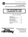
1
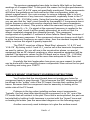
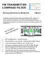
FM TRANSMITTER
LOWPASS FILTER
Ramsey Electronics Model No.
FMLP1
In today’s world, the importance of sticking to the “specs.” is
more important then ever! The FMLP1 has been designed
specifically to meet the Low Power FM broadcasters needs. No
more worrying about out-of-band harmonics interfering with your
neighbors!
Y!!
!!
BL
M
CE
E
N
S
MA
AS
OR
SY
F
A
E
ER
TP
A
E
GR
(Actual Size)
•
NO Tuning Required... Just build and go!
•
Excellent Return Loss, typically –18 dB or better without tuning
•
Lower your harmonic output by up to 70 dB or more
•
Designed for operation anywhere in the 88-108 MHz FM band
•
Great introductory kit for Surface Mount Technology usage
(50% more SMT parts included to ensure building ease)
•
‘Weather Tight’ case for harsh environment applications
•
Clear, concise instructions guide you step-by-step to a finished
product that works FIRST time
FMLP1 • 1
RAMSEY TRANSMITTER KITS
• FM100B Professional FM Stereo Transmitter
• FM25B Synthesized Stereo FM Transmitter
• MR6 Model Rocket Tracking Transmitter
• TV6 Television Transmitter
RAMSEY RECEIVER KITS
• FR1 FM Broadcast Receiver
• AR1 Aircraft Band Receiver
• SR2 Shortwave Receiver
• SC1 Shortwave Converter
RAMSEY HOBBY KITS
• SG7 Personal Speed Radar
• SS70A Speech Scrambler
• BS1 “Bullshooter” Digital Voice Storage Unit
• AVS10 Automatic Sequential Video Switcher
• WCT20 Cable Wizard Cable Tracer
• TFM3 Tri-Field Meter
• LC1 Inductance-Capacitance Meter
RAMSEY AMATEUR RADIO KITS
• DDF1 Doppler Direction Finder
• HR Series HF All Mode Receivers
• QRP Series HF CW Transmitters
• CPO3 Code Practice Oscillator
• QRP Power Amplifiers
RAMSEY MINI-KITS
Many other kits are available for hobby, school, Scouts and just plain FUN. New
kits are always under development. Write or call for our free Ramsey catalog.
FMLP1 LOWPASS FILTER KIT INSTRUCTION MANUAL
Ramsey Electronics publication No. FMLP1 Rev 1.0
First printing: April 2001
COPYRIGHT 2001 by Ramsey Electronics, Inc. 590 Fishers Station Drive, Victor, New York
14564 All rights reserved. No portion of this publication may be copied or duplicated without the
written permission of Ramsey Electronics, Inc. Printed in the United States of America.
FMLP1 • 2
Ramsey Publication No. MFMLP1
KIT ASSEMBLY
AND INSTRUCTION MANUAL FOR
FM TRANSMITTER
LOWPASS FILTER
TABLE OF CONTENTS
Introduction ......................................4
Circuit Description.............................5
SMT Soldering Instructions...............7
FMLP1 Parts List .............................9
Parts Layout Diagram ......................10
Schematic Diagram ..........................11
FMLP1 Assembly .............................12
Custom Case Assembly ..................17
Hook-up and Applications ................17
Conclusion .......................................18
Warranty ..........................................19
RAMSEY ELECTRONICS, INC.
590 Fishers Station Drive
Victor, New York 14564
Phone (585) 924-4560
Fax (585) 924-4555
www.ramseykits.com
FMLP1 • 3
INTRODUCTION
While this kit and manual were designed with the beginner in mind, it
should also be stated that this kit qualifies as a “Skill Level 2” due to the nature
of the assembly using surface mount components. While this isn’t intended to
“scare you off” it is not recommended that this be your first electronics
assembly project. While we have included extra SMT components in case you
lose or damage a “chip” component, care should still be taken to assemble the
kit with the utmost care - an uncontrolled sneeze could blow your kit away!
While the components may seem strange looking at first (where are the
leads??!!) rest assured that they are not too difficult to install. A friendly
warning, however; don’t pull out your trusty soldering gun for this project (our
repair techs have a pet statement, “do you know what the soldering gun’s light
is for - it’s to see what you’re burning up!”) as the gun generates too much heat
for the tiny solder “tabs” on the component ends. A small pair of tweezers and
good eye to hand coordination are also necessary for proper assembly of this
kit. A magnifying lens is recommended to check solder connections.
Enough already… what are we about to build?
The FM Low Pass Filter kit came about while designing the circuitry for
the PX1, Professional FM Broadcaster. The PX1 is a 35 Watt professional
grade FM stereo broadcast transmitter developed to meet the criteria of the
FCC Ruling 99-25. This ruling created a class of radio stations designed to
serve localized communities by authorizing new classes of noncommercial low
power FM radio services (LPFM). In order to meet the stringent guidelines of
the FCC, the PX1 underwent months of design sessions and many hours of
painstaking tests. One of the secrets to its clean output is the design
implementation of the FMLP1.
The FMLP1 offers the user superb Input Return Loss for the FM
Broadcast band, typically –18 dB or better. The filter’s Insertion Loss averages
about –60 dB up in the 2nd harmonic range of 176 MHz to 216 MHz eliminating
any unwanted signals.
The issue concerning harmonic frequency components for the FM
Broadcast band, especially the 2nd harmonics (176 - 216 MHz), is the possibility
of interference problems in other areas like the VHF TV High Band. This is not
a good thing and is frowned upon by the FCC!
The FMLP1 design was developed specifically to make our PX1
comply with the FCC guidelines. After its completion we thought to ourselves…
Hey I bet our customers would like this for their applications! Thus the kit
version of the FMLP1 was born.
FMLP1 • 4
CIRCUIT DESCRIPTION
The FMLP1 is a lowpass filter. This means that certain frequency
elements can pass from the input to the output unimpeded while others are
almost stopped in their tracks! The name of this type of filter gives away its
response characteristics when a signal is applied to the input… lowpass filter…
low frequency signals pass through. Conversely, high frequency signals are
greatly reduced in amplitude virtually rendering them to insignificant levels.
The concept of a lowpass filter is quite simple, the design and
construction, however, require a good bit of engineering. All of the variables
that must be taken into account to construct a high-performance lowpass filter
are beyond the scope of this circuit description. The basic function of the actual
component elements used in this kit are what will be covered.
Take a look at the schematic diagram on page 11. A good quality filter
does not require a lot of components. The trick is to use the proper parts
chosen specifically for your application taking into consideration such things as:
-Cut-off frequency (fc), the frequency at which the signal amplitude drops by 3
dB, half the original power. The FMLP1 has an fc equal to about 120 MHz
giving plenty of headroom to pass the desired 88 to 108 MHz signal.
-Number of poles, the number of component elements or element groups
(parallel or series grouped reactive components i.e. ‘L1 & C3’ and ‘L3 & C8’)
determining things like the frequency roll-off characteristics and circuit cost.
-Input signal power, the amount of signal that can be applied to the circuit
without degrading its operation or causing damage. The FMLP1 is constructed
from 50 Volt parts setting its max input power at 50 Watts (thanks Mr. Ohm, R =
V / I; P = I x V; P = V2 / R therefore P = 50 volts2 / 50 ohms = 50 Watts). In
practice an over-rating of 20% yields dependable results at 40 Watts without
major concerns for cooling.
There are 13 basic electrical components consisting of 9 capacitors
and 3 inductors that work in conjunction to filter the applied signal. The
capacitor pairs ‘C1 & C2’, ‘C4 & C5’, ‘C6 & C7’, and ‘C9 & C10’ can each be
combined to form their respective parallel capacitive values. Using pairs in this
manner helps to reduce the amount of power each capacitor must dissipate
increasing operational efficiency. Remember, capacitors in parallel add, C1 +
C2 = 10 pF + 10 pF = 20 pF equivalent.
If these capacitors are combined into their respective capacitance, the
circuit can be reduced to 7 reactive elements. Note that ‘L1 & C3’ act together
as one element, the same goes for ‘L3 & C8’ as well. The basic structure of the
design consisting of shunt capacitors, except for C3 and C8, and series
inductors shows the classic lowpass filter layout.
FMLP1 • 5
If you think for a moment about the fundamental operation of a
capacitor and an inductor when an RF (radio frequency) signal is applied, the
reasoning for the layout seen in the schematic is obvious. Thinking in terms of
extremes and going back to the basics of reactive elements, let’s examine each
one separately.
At very high frequencies a capacitor looks like a short circuit meaning
signals pass through it like it was just a piece of wire. On the opposite extreme,
at very low frequencies a capacitor looks like an open circuit blocking the signal
from passing through. Granted there are many factors that determine just how
much signal can pass through the capacitor at different frequencies due to XC
( XC = 1 / (2 x π x F x C), the capacitive reactance in ohms. The math is getting
too specific at this time for our proposes!
At very high frequencies an inductor looks like an open circuit blocking
the signal from passing through. On the opposite extreme, at very low
frequencies an inductor looks like a short circuit passing signals through it like it
was just a piece of wire (Hey that’s what it is!). Keep in mind again there are
many factors that determine just how much signal can pass through the
inductor at different frequencies due to XL ( XL = 2 x π x F x L), the inductive
reactance in ohms.
Armed with these simple concepts, look at the schematic again. We
stated earlier that a lowpass filter allows signals up to a certain cut-off
frequency (fc) to pass through while blocking any signals that are higher. Take
the following two opposite extremes:
1) fc = a constant DC Voltage, the lowest possible frequency input.
Look back at the schematic and remember the characteristics of a capacitor
and an inductor at low frequencies. Will the fc signal (DC for this example) pass
through a capacitor? Will the fc signal pass through an inductor? The lowpass
orientation of the components is easily apparent when you ask these questions.
A DC input, the lowest possible frequency, cannot pass through a capacitor so
it will not be shorted to ground by the shunt caps (C1, C2, C4, C5, C6, C7, C9,
& C10). The inductors however (L1, L2, & L3) will pass the DC input signal from
input J1 to the output J2 without any attenuation. Therefore low frequency
signals (fc = a DC voltage) pass through the circuit, hence Lowpass Filter!
2) fc = an infinitely high frequency, the highest possible frequency input.
Look back at the schematic again and remember the characteristics of a
capacitor and an inductor at high frequencies. Will the fc signal (very high for
this example) pass through a capacitor? Will the fc signal pass through an
inductor? At a very high frequency, the input will pass right through a capacitor
so it will be shorted to ground by the shunt caps. The inductors however will not
pass the high frequency input signal. Therefore any high frequency is blocked
from passing through the filter! Again, Lowpass Filter!
FMLP1 • 6
The previous paragraphs have help to shed a little light on the basic
workings of a lowpass filter. To this point the reason for the grouped elements
of ‘L1 & C3’ and ‘L3 & C8’ were not specifically mentioned. These components
still follow the guidelines set forth earlier but their configuration yields an
almost magical result. Our main concern for using a lowpass filter is to limit
the harmful presence of any harmonic frequencies, especially those in the 2nd
harmonic (176 - 216 MHz) realm. Using the formulas given prior for XC and XL,
you can see that the ‘tank’ circuit formed by the parallel LC components has a
certain frequency when both reactive elements reach the same impedance
(AC resistance in ohms). This point is called the resonant frequency (fr) and is
reached when XC = XL. If a signal at the resonant frequency is applied to the
input of the ‘tank’ circuit it will be greatly attenuated, so much so that it is
almost completely stopped from passing through. This component
configuration of a parallel LC network is often called a ‘Band Stop’ because of
its notch frequency response. If the component values are chosen such that fr
is at the harmonic frequency we want to stop, then the standard lowpass filters
ability to reduce this signal is greatly improved.
The FMLP1 uses two of these ‘Band Stop’ elements, ‘L1 & C3’ and
‘L3 & C8’. By tuning coils L1 and L3, fr can be set at the harmonic frequencies
we want to reduce. As you will see in the construction phase, no special
equipment like an RF network analyzer or other expensive equipment will be
needed! The harmonic values for the FM band are so close (176 - 216 MHz)
that normal building variances will be more than adequate to filter them out.
Hopefully this brief explanation has given you new respect for what
can be done with a few carefully chosen components! Now comes the fun part
of building and using your FMLP1!
SURFACE MOUNT COMPONENT SOLDERING INSTRUCTIONS:
You’ll notice that the circuit board does not contain any holes for
component leads to pass through. This is because the SMT components will
be affixed to the “solder” side of the PC board, the side that contains the PC
traces. Be aware that the component view for assembly is looking at the
solder side of the PC board.
Patience is the key when installing surface mount components.
Typically, the first step (after identifying the component) is to “tin” one of the
PC traces that will connect to the part. Once this is accomplished, the part can
be installed by holding it with tweezers in contact with the “tinned” trace and
re-heating the solder (see the associated diagrams on the following page).
Another commonly used technique is to glue the surface mount
FMLP1 • 7
components to the printed circuit board before soldering. The procedure is to
take a small amount of glue (usually with a pin or toothpick) and “dab” the
circuit board in the place where the component will be affixed. Be careful not
to apply too much glue as when the part is placed it may “squash” the glue
underneath the soldering tabs of the component. Carefully place the part into
position, and when the glue dries, solder the connection.
This may go a little “against the grain” at first, but it is by far the easiest method. Notice also that when reheating the solder that the iron tip
should come in contact with the “tab” on the body of the chip component.
Over heating of this solder tab is not as much of a problem as too much
pressure from the soldering iron. Brute force while positioning the caps can
cause a fracture of the bond to the component, causing an intermittent connection.
FMLP1 • 8
PARTS SUPPLIED WITH FMLP1 TRANSMITTER KIT
Capacitors -(50% more SMT capacitors are supplied with each kit)
4
2
4
10 pF chip capacitors (should be marked A1)
12 pF chip capacitors (should be marked C1)
27 pF chip capacitors (should be marked L1)
[C1,2,9,10]
[C3,8]
[C4,5,6,7]
Inductors
1
15” of #20 AWG enameled wire [used to make L1,2,3]
Hardware, Misc.
1
2
2
2
1
10” long RG-188A Teflon coaxial cable
‘F’ style panel mount connectors
0.375” GND solder lugs
Brass GND shields
1/4’-20 x 3/4” or longer bolt (used to wind coils)
Case Parts
2
1
1+1/2” diameter PVC end caps
3” long 1+1/2: diameter PVC pipe
FMLP1 • 9
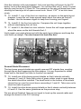
FMLP1 PARTS LAYOUT DIAGRAM
FMLP1 • 10
FMLP1 • 11
RAMSEY ASSEMBLY STRATEGY
As you can see in examining the circuit board and components, there is a bit
more to this kit than just soldering a few parts. So that you don't spend extra
time "troubleshooting" instead of getting on the air, we strongly recommend that
you follow the assembly strategy and step-by-step procedures we provide.
Our strategy in installing parts on the PC board is to deal with the surface
mount components first, then work upward from the board as the parts overlap.
This makes working with the smaller size parts easier and reduces the
occurrence of installation errors. Use a good pair of tweezers to place the parts.
FMLP1 ASSEMBLY
Use the boxes to check off your progress.
Check all received parts against the Parts list on page 9. The parts list
describes the various markings that may be found on the kit parts.
In ALL the following instruction steps, our word "INSTALL" means to line up the
component as shown in the parts layout diagram and solder any and all
electrical contacts respectively.
SMT components often are marked with very small indicators in the form of a
letter followed by a number to show the parts value i.e. ‘A1’ = 10 pF. The proper
markings are listed in the build procedure for each component as they are
installed. Use of a x5 eye loupe or magnifying glass makes parts identification
easier. To avoid confusion, the SMT chip capacitors have been taped to an ID
sheet; try not to mix them up. Even though they look the same, putting the
wrong value part anywhere in the circuit will greatly reduce its performance.
Mounting all the chip caps with the marking indicator facing upward will make
troubleshooting easier if you should have any problems.
Enough said. . . Let's get building!
SMT Capacitor Installation
1. Install C1, 10 pF chip capacitor (marked A1)
2. Install C2, 10 pF chip capacitor (marked A1)
3. Install C3, 12 pF chip capacitor (marked C1)
4. Install C4, 27 pF chip capacitor (marked L1)
5. Install C5, 27 pF chip capacitor (marked L1)
6. Install C6, 27 pF chip capacitor (marked L1)
FMLP1 • 12
7. Install C7, 27 pF chip capacitor (marked L1)
8. Install C8, 12 pF chip capacitor (marked C1)
9. Install C9, 10 pF chip capacitor (marked A1)
10. Install C10, 10 pF chip capacitor (marked A1)
This completes the first phase of construction of your FMLP1. Take a break
now to carefully examine all solder connections. Make certain there are no
solder ’blobs’ or small shorts on or around the components you have just
installed. It’s much easier to find a problem now, before all the parts are on the
PC board. Now the all of the SMT capacitors are in place, lets move on to the
coil winding phase.
Inductor Coil Winding and Placement
The next few parts need to be handmade! That’s right… we are now going to
build our own coils. It is important to follow the next few instructions to the
letter in order to achieve proper performance of the final product. All three of
our coils will be surface mounted. This means there are no holes in the PCB to
insert the end leads. Each coil will be wound, tinned, and then finally installed
in a similar manner as that of the SMT capacitors. Let’s go...
11. Wind L1, a 4 turn inductor. Use the #20 AWG enameled wire and
wrap four turns with the groves on the provided 1/4”-20 bolt. This method
gives you beautifully formed coils with precalculated inductance values.
The coil will appear to have 4 complete turns if viewed from the top. The
excess wire will be turned out at a 90 degree angle and clipped to about
1/8th of an inch long to provide us with suitable mounting leads.
4 TURNS
(SIDE VIEW) (ANGLE VIEW)
5 TURNS
(SIDE VIEW) (ANGLE VIEW)
12. Wind L3, another 4 turn inductor the same way as L1 above.
13. Wind L2, the five turn inductor in the same manner as L1 and L3 but
with one more wrap of wire. Look at the above diagram for reference.
14. Tin the ends of the coils to give them a good solder contact. This is
done by melting a little solder on the end of your iron and rubbing the 1/8th
of an inch long ends left for mounting the coil with the soldering iron. The
enamel will burn off giving you a clean contact to solder to the board. Spin
the coil back on the bolt before tinning the leads so you don’t your fingers!
FMLP1 • 13
Now the inductor coils are prepared. Let’s see how they will mount to the PC
board. Look at the parts layout diagram. You will see that coil L1 and L3 mount
directly over the top of C3 and C8. The enamel on the wire will keep them from
shorting but leaving a bit of space never hurts. About 1/32nd of an inch does
nicely.
15. Install L1, one of the four turn inductors, as shown on the parts layout
diagram. Leave the coil loops spread apart about the same as the bolt
threads. Use the tweezers again to keep from burning your fingers!
16. Install L2, the five turn inductor. Compress the coil loops together
without misshaping the coil form.
17. Install L3, the other four turn inductor. Leave the coil loops spread apart
about the same as the bolt threads like L1.
Verify again your parts placement with the parts layout diagram and keep the
coils lined up straight. You don’t want it to look like this:
Ground Shield Placement
The two brass ground shields are used to prevent RF signals from coupling
through the air and bypassing the filter stages. It is very important to solder
these well to the board for them to function as needed.
18. Install one of the brass ground shields so that it stands vertically
between L1 and L2. Note that a strip of green solder mask is open where
the shield should be installed. The small notch in the bottom of the shield
should line up over the circuit trace connecting L1 and L2. Take care not to
short the trace to ground.
19. Install the other brass ground shield so that it stands vertically between
L2 and L3. Use the same guidelines as the previous step.
We are almost finished. Now we just need to hook-up the coaxial cable and
arrange the board in the PVC housing!
FMLP1 • 14
20. Cut the 10” piece of RG-188A coax into two 5” pieces.
When we are finished preparing the cable in the next few steps, all four
ends should look similar to this:
Proper Coax
Preparation
21. Very carefully strip off the outer insulation on one end of a piece of
coax about 1/2” back from the end. Be careful not to remove any of the
outside ground shield braid. This is a gentle procedure, so take your time.
Use a sharp razor knife like an X-acto blade and lightly cut through the
coax's white insulation. Slip off the insulation to expose the coax braid. If
you run into trouble and cut too deep into the coax, clip off the damaged
end and do it again.
22. Lightly tin the entire exposed ground braid to form a cylinder on the
exposed end. Similar results can be seen in the picture above. Do not
unbraid the ground conductor and twist it together like the one shown
below.
Poor Coax
Preparation
23. Place the coax pieces flat on the table and use your razor to gently
score a ring around the tinned ground conductor about 1/4” from the end.
This is easily done by positioning the razor and rolling the coax on the table
top with your fingers while lightly pressing on the blade.
24. Snap off the 1/4” end of unwanted ground conductor by bending the
cylinder with a pair of pliers near the score mark. It should snap off easily,
otherwise score the ground conductor again but take care not to cut too
deep.
25. Next we will score through the inner insulation layer using the same
table top role method used with the ground braid. Score the white inner
insulation layer with the razor knife about 3/16th of an inch from the end.
26. Remove the unwanted piece of insulation and twist the inner conductor
wires together. Tin the wire ends by gently heating the conductor and then
FMLP1 • 15
applying solder. Use enough to coat the wires and form a strong connection
making for easier installation later.
27. Repeat steps 21 through 26 until both ends of each piece of coax are
prepared.
Examine your work with the RG-188A coax to this point. Use an ohmmeter or
continuity checker to verify that center conductor is not shorted to the ground
shield. Visual inspection is normally enough to check this. Remove any gobs of
solder with the hot soldering iron if any exist.
28. Take one of the coax pieces and line it up to connect the center
conductor in the hole labeled ‘J1’ and the tinned ground shield over one of
the holes labeled ‘GND’. Solder both the center conductor and the ground
shield in place.
Proper Coax
Installation
29. Attach the other piece of coax to the ‘J2’ end of the board in the same
fashion.
Now comes the time to mount the F-connectors to the ends of the coax. The
importance of a good ground can not be stressed enough. Follow each step
carefully and refer to the picture for added assurance of a correct installation.
Proper F-Connector
Installation
30. Slide one of the 0.375” GND solder lugs over the end of an F-connector
and secure it in place finger tight with a hex nut.
31. Bend the solder lug so that the coax can feed straight into the end of
the connector. The above picture represents the proper mounting
technique.
32. Solder the center conductor to the center post of the F-connector.
FMLP1 • 16
33. Solder the ground braid of the coax to the solder lug of the F-connector.
Poor connections can lead to poor performance. Check your work and make
sure the connection does not look like this:
Poor F-Connector
Installation
(This connection style acts as
a loop antenna and allows
signals to radiate across the
filter!)
34. Repeat steps 30 through 33 to attach the other F-connector.
Your FMLP1 kit is now assembled and almost ready for use. Let’s install it in
the case and call it a day!
CUSTOM CASE ASSEMBLY
The PVC enclosure will protect your electronics from many possible causes of
damage giving you years worth of enjoyment and usage. The rugged design
can be sealed with silicone RTV (after you verify its operation) to give you a
weather tight seal ensuring top notch operation under almost any condition.
35. Remove the hex nuts from the F-connectors.
36. Insert one of the F-connectors into the hole drilled in the center of one
of the PVC end caps. Insert it from the inside of the end cap.
37. Slide on an inner toothed washer and a hex nut then permanently
tighten it in place.
Slide the FMLP1 into the PVC body and twist PVC pieces together.
38. Attach the last F-connector to the other end cap as in step 36 and
gently position the excess coax into the PVC body. Twist the entire
assembly together and we’re ready to go!
HOOK-UP AND APPLICATION GUIDELINES
The FMLP1 is not polarized; the unit can be installed between the transmitter
and antenna in either direction. It has been optimized for usage at 40 Watts or
less in a 50 ohm environment. In low power applications such as 1 Watt, the 50
ohm match is not crucial. Applications on the higher end upward of 30 Watts
will notice increased performance when L1, L2, and L3 are spread or
compressed slightly for maximum power.
FMLP1 • 17
The Finished Product!!
CONCLUSION
We sincerely hope that you have enjoyed the construction and use of
this Ramsey Kit. As always, we have tried to compose our manual in the easiest, most “user friendly” format that is possible. As our customers, we value
your opinions, comments, and additions that you would like to see in future
publications. Please submit comments or ideas to:
Ramsey Electronics Inc.
590 Fishers Station Drive
Victor, NY 14564
And once again, thanks from the folks at Ramsey!
Visit us at: www.ramseyelectronics.com
FMLP1 • 18
The Ramsey Kit Warranty
Please read carefully BEFORE calling or writing in about your kit. Most problems can be
solved without contacting the factory.
Notice that this is not a "fine print" warranty. We want you to understand your rights and ours too!
All Ramsey kits will work if assembled properly. The very fact that your kit includes this new manual
is your assurance that a team of knowledgeable people have field-tested several "copies" of this kit
straight from the Ramsey Inventory. If you need help, please read through your manual carefully.
All information required to properly build and test your kit is contained within the pages!
1. DEFECTIVE PARTS: It's always easy to blame a part for a problem in your kit, Before you
conclude that a part may be bad, thoroughly check your work. Today's semiconductors and passive
components have reached incredibly high reliability levels, and it’s sad to say that our human
construction skills have not! But on rare occasions a sour component can slip through. All our kit
parts carry the Ramsey Electronics Warranty that they are free from defects for a full ninety (90)
days from the date of purchase. Defective parts will be replaced promptly at our expense. If you
suspect any part to be defective, please mail it to our factory for testing and replacement. Please
send only the defective part(s), not the entire kit. The part(s) MUST be returned to us in suitable
condition for testing. Please be aware that testing can usually determine if the part was truly
defective or damaged by assembly or usage. Don't be afraid of telling us that you 'blew-it', we're all
human and in most cases, replacement parts are very reasonably priced.
2. MISSING PARTS: Before assuming a part value is incorrect, check the parts listing carefully to
see if it is a critical value such as a specific coil or IC, or whether a RANGE of values is suitable
(such as "100 to 500 uF"). Often times, common sense will solve a mysterious missing part
problem. If you're missing five 10K ohm resistors and received five extra 1K resistors, you can
pretty much be assured that the '1K ohm' resistors are actually the 'missing' 10 K parts ("Hum-m-m,
I guess the 'red' band really does look orange!") Ramsey Electronics project kits are packed with
pride in the USA. If you believe we packed an incorrect part or omitted a part clearly indicated in
your assembly manual as supplied with the basic kit by Ramsey, please write or call us with
information on the part you need and proof of kit purchase.
3. FACTORY REPAIR OF ASSEMBLED KITS:
To qualify for Ramsey Electronics factory repair, kits MUST:
1. NOT be assembled with acid core solder or flux.
2. NOT be modified in any manner.
3. BE returned in fully-assembled form, not partially assembled.
4. BE accompanied by the proper repair fee. No repair will be undertaken until we have received
the MINIMUM repair fee (1/2 hour labor) of $25.00, or authorization to charge it to your
credit card account.
5. INCLUDE a description of the problem and legible return address. DO NOT send a separate
letter; include all correspondence with the unit. Please do not include your own hardware
such as non-Ramsey cabinets, knobs, cables, external battery packs and the like. Ramsey
Electronics, Inc., reserves the right to refuse repair on ANY item in which we find excessive
problems or damage due to construction methods. To assist customers in such situations,
Ramsey Electronics, Inc., reserves the right to solve their needs on a case-by-case basis.
The repair is $50.00 per hour, regardless of the cost of the kit. Please understand that our
technicians are not volunteers and that set-up, testing, diagnosis, repair and repacking and
paperwork can take nearly an hour of paid employee time on even a simple kit. Of course, if we find
that a part was defective in manufacture, there will be no charge to repair your kit (But please
realize that our technicians know the difference between a defective part and parts burned out or
damaged through improper use or assembly).
4. REFUNDS: You are given ten (10) days to examine our products. If you are not satisfied, you
may return your unassembled kit with all the parts and instructions and proof of purchase to the
factory for a full refund. The return package should be packed securely. Insurance is
recommended. Please do not cause needless delays, read all information carefully.
FMLP1 • 19
FM LOWPASS FILTER KIT
Quick Reference Page Guide
Introduction ...................................... 4
Circuit Description ............................ 5
SMT Soldering Instructions .............. 7
FMLP1 Parts List ............................. 9
Parts Layout Diagram ...................... 10
Schematic Diagram .......................... 11
FMLP1 Assembly ............................ 12
Custom Case Assembly .................. 17
Hook-up and Applications ............... 17
Conclusion ....................................... 18
Warranty .......................................... 19
REQUIRED TOOLS
• Soldering Iron Ramsey WLC100
• Thin Rosin Core Solder Ramsey RTS12
• Needle Nose Pliers Ramsey MPP4 or RTS05
• Small Diagonal Cutters Ramsey RTS04
<OR> Technician’s Tool Kit TK405
ADDITIONAL SUGGESTED ITEMS
Holder for PC Board/Parts Ramsey HH3
Desoldering Braid Ramsey RTS08
Digital Multimeter Ramsey M133
•
•
•
Price: $5.00
Ramsey Publication No. MFMLP1
Assembly and Instruction manual for:
RAMSEY MODEL NO. FMLP1
TOTAL SOLDER POINTS
38
RAMSEY ELECTRONICS, INC.
590 Fishers Station Drive
Victor, New York 14564
Phone (585) 924-4560
FMLP1 • 20
Fax (585) 924-4555
www.ramseykits.com
ESTIMATED ASSEMBLY
TIME
Beginner ............. 3 hrs
Intermediate ....... 1.5 hrs
Advanced ........... 45 min