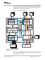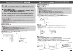
1
TMS320C6457
Fixed-Point Digital Signal Processor
Silicon Revisions 1.0, 1.1, 1.2, 1.3, 1.4
Silicon Errata
Literature Number: SPRZ293A
November 2009
www.ti.com
2
TMS320C6457 Fixed-Point Digital Signal Processor Silicon Errata
Silicon Revisions 1.0, 1.1, 1.2, 1.3, 1.4
SPRZ293A—November 2009
Submit Documentation Feedback
www.ti.com
Contents
Introduction. . . . . . . . . . . . . . . . . . . . . . . . . . . . . . . . . . . . . . . . . . . . . . . . . . . . . . . . . . . . . . . . . . . . . . . . . . . . . . . . . . . . . . . . . . . . . . . . . . . . . . 5
Device and Development Support Tool Nomenclature. . . . . . . . . . . . . . . . . . . . . . . . . . . . . . . . . . . . . . . . . . . . . . . . . . . . . . . . . . . . . 5
Package Symbolization and Revision Identification . . . . . . . . . . . . . . . . . . . . . . . . . . . . . . . . . . . . . . . . . . . . . . . . . . . . . . . . . . . . . . . . . . . . . . . . . 6
Silicon Updates. . . . . . . . . . . . . . . . . . . . . . . . . . . . . . . . . . . . . . . . . . . . . . . . . . . . . . . . . . . . . . . . . . . . . . . . . . . . . . . . . . . . . . . . . . . . . . . . . . . 8
Advisory 1— EMAC Boot Issue. . . . . . . . . . . . . . . . . . . . . . . . . . . . . . . . . . . . . . . . . . . . . . . . . . . . . . . . . . . . . . . . . . . . . . . . . . . . . . . . . . . . . . . . . . . . . 9
Advisory 2— EDMA3CC COMPACTV Issue. . . . . . . . . . . . . . . . . . . . . . . . . . . . . . . . . . . . . . . . . . . . . . . . . . . . . . . . . . . . . . . . . . . . . . . . . . . . . . . . .10
Advisory 3— SRIO Port0 Reset Issue . . . . . . . . . . . . . . . . . . . . . . . . . . . . . . . . . . . . . . . . . . . . . . . . . . . . . . . . . . . . . . . . . . . . . . . . . . . . . . . . . . . . . .12
Advisory 4— SRIO Outbound ACKID Issue . . . . . . . . . . . . . . . . . . . . . . . . . . . . . . . . . . . . . . . . . . . . . . . . . . . . . . . . . . . . . . . . . . . . . . . . . . . . . . . .13
Advisory 5— SRIO Bootloader Issue. . . . . . . . . . . . . . . . . . . . . . . . . . . . . . . . . . . . . . . . . . . . . . . . . . . . . . . . . . . . . . . . . . . . . . . . . . . . . . . . . . . . . . .14
Advisory 6— DMA Access to L2 SRAM May Stall When the DMA and the CPU Command Priority is Equal. . . . . . . . . . . . . . . . . . . .15
Advisory 7— DMA Corruption of External Data Buffer Issue. . . . . . . . . . . . . . . . . . . . . . . . . . . . . . . . . . . . . . . . . . . . . . . . . . . . . . . . . . . . . . . .17
Advisory 8— DMA Corruption of L2 Ram Data . . . . . . . . . . . . . . . . . . . . . . . . . . . . . . . . . . . . . . . . . . . . . . . . . . . . . . . . . . . . . . . . . . . . . . . . . . . .23
Advisory 9— L2 Victim Traffic Due To L2 Block Writeback During Any Pending CPU Request. . . . . . . . . . . . . . . . . . . . . . . . . . . . . . . .30
Advisory 10— L1P$ Miss May Block SDMA Accesses (Asymmetric Mode Only). . . . . . . . . . . . . . . . . . . . . . . . . . . . . . . . . . . . . . . . . . . . . .36
Usage Note 1— Manual Cache Coherence Operation Usage Note . . . . . . . . . . . . . . . . . . . . . . . . . . . . . . . . . . . . . . . . . . . . . . . . . . . . . . . . .39
Appendix A—Code Examples . . . . . . . . . . . . . . . . . . . . . . . . . . . . . . . . . . . . . . . . . . . . . . . . . . . . . . . . . . . . . . . . . . . . . . . . . . . . . . . . . . . .40
L1D Block Writeback Routine l1d_block_wb.asm . . . . . . . . . . . . . . . . . . . . . . . . . . . . . . . . . . . . . . . . . . . . . . . . . . . . . . . . . . . . . . . . . . . . . .40
L1D Block Writeback-Invalidate Routine l1d_block_wbinv.asm . . . . . . . . . . . . . . . . . . . . . . . . . . . . . . . . . . . . . . . . . . . . . . . . . . . . . . .41
Make Buffer Dirty Routine make_dirty . . . . . . . . . . . . . . . . . . . . . . . . . . . . . . . . . . . . . . . . . . . . . . . . . . . . . . . . . . . . . . . . . . . . . . . . . . . . . . . . . .42
Long Distance Load Word Routine ldld.asm . . . . . . . . . . . . . . . . . . . . . . . . . . . . . . . . . . . . . . . . . . . . . . . . . . . . . . . . . . . . . . . . . . . . . . . . . . . .43
IDMA Channel 1 Block Copy Routine idma1_util.asm. . . . . . . . . . . . . . . . . . . . . . . . . . . . . . . . . . . . . . . . . . . . . . . . . . . . . . . . . . . . . . . . . .44
Appendix B—Determining If Two Addresses are a Set Match. . . . . . . . . . . . . . . . . . . . . . . . . . . . . . . . . . . . . . . . . . . . . . . . . . . . . .46
Appendix C—UMAP0 and UMAP1 Addresses Ranges . . . . . . . . . . . . . . . . . . . . . . . . . . . . . . . . . . . . . . . . . . . . . . . . . . . . . . . . . . . . .47
SPRZ293A—November 2009
Submit Documentation Feedback
TMS320C6457
Fixed-Point Digital Signal Processor Silicon Errata
Silicon Revisions 1.0, 1.1, 1.2, 1.3, 1.4
3
.
www.ti.com
List of Figures
Figure 1
Figure 2
Figure 3
Figure 4
Figure 5
Figure 6
Figure 7
Lot Trace Code Examples for TMS320C6457 (CMH and GMH Packages) . . . . . . . . . . . . . . . . . . . . . . . . . . . . . . . . . . . . . . . . . . . . . . 6
Cache Line Operations Flow . . . . . . . . . . . . . . . . . . . . . . . . . . . . . . . . . . . . . . . . . . . . . . . . . . . . . . . . . . . . . . . . . . . . . . . . . . . . . . . . . . . . . .19
Sequence of Events. . . . . . . . . . . . . . . . . . . . . . . . . . . . . . . . . . . . . . . . . . . . . . . . . . . . . . . . . . . . . . . . . . . . . . . . . . . . . . . . . . . . . . . . . . . . . . .25
Decision Tree. . . . . . . . . . . . . . . . . . . . . . . . . . . . . . . . . . . . . . . . . . . . . . . . . . . . . . . . . . . . . . . . . . . . . . . . . . . . . . . . . . . . . . . . . . . . . . . . . . . . .26
IDMA, SDMA, and MDMA Paths . . . . . . . . . . . . . . . . . . . . . . . . . . . . . . . . . . . . . . . . . . . . . . . . . . . . . . . . . . . . . . . . . . . . . . . . . . . . . . . . . . .31
L2 P1 CMD Pipe – Time Progression . . . . . . . . . . . . . . . . . . . . . . . . . . . . . . . . . . . . . . . . . . . . . . . . . . . . . . . . . . . . . . . . . . . . . . . . . . . . . . .37
L1D Cache Address Mapping . . . . . . . . . . . . . . . . . . . . . . . . . . . . . . . . . . . . . . . . . . . . . . . . . . . . . . . . . . . . . . . . . . . . . . . . . . . . . . . . . . . . .46
List of Tables
Table 1
Table 2
Table 3
Table 4
Table 5
Table 6
Table 7
Table 8
Table 9
Table 10
Table 11
Table 12
4
Lot Trace Codes . . . . . . . . . . . . . . . . . . . . . . . . . . . . . . . . . . . . . . . . . . . . . . . . . . . . . . . . . . . . . . . . . . . . . . . . . . . . . . . . . . . . . . . . . . . . . . . . . . . 6
Silicon Revision Variables . . . . . . . . . . . . . . . . . . . . . . . . . . . . . . . . . . . . . . . . . . . . . . . . . . . . . . . . . . . . . . . . . . . . . . . . . . . . . . . . . . . . . . . . . . 7
Silicon Revisions 1.4, 1.3, 1.2, 1.1, and 1.0 Updates . . . . . . . . . . . . . . . . . . . . . . . . . . . . . . . . . . . . . . . . . . . . . . . . . . . . . . . . . . . . . . . . . . 8
TC Registers Summary . . . . . . . . . . . . . . . . . . . . . . . . . . . . . . . . . . . . . . . . . . . . . . . . . . . . . . . . . . . . . . . . . . . . . . . . . . . . . . . . . . . . . . . . . . .11
C6457 Default Master Priorities . . . . . . . . . . . . . . . . . . . . . . . . . . . . . . . . . . . . . . . . . . . . . . . . . . . . . . . . . . . . . . . . . . . . . . . . . . . . . . . . . . .15
UMAP0 Address Range for C6457 . . . . . . . . . . . . . . . . . . . . . . . . . . . . . . . . . . . . . . . . . . . . . . . . . . . . . . . . . . . . . . . . . . . . . . . . . . . . . . . . .22
Expected vs. Actual Data Values. . . . . . . . . . . . . . . . . . . . . . . . . . . . . . . . . . . . . . . . . . . . . . . . . . . . . . . . . . . . . . . . . . . . . . . . . . . . . . . . . . .25
VBUSM Masters and Associated Workarounds . . . . . . . . . . . . . . . . . . . . . . . . . . . . . . . . . . . . . . . . . . . . . . . . . . . . . . . . . . . . . . . . . . . . .35
C6457 Silicon Revisions and SDMA/IDMA Stall Conditions . . . . . . . . . . . . . . . . . . . . . . . . . . . . . . . . . . . . . . . . . . . . . . . . . . . . . . . . .36
Value of X for L1D Cache. . . . . . . . . . . . . . . . . . . . . . . . . . . . . . . . . . . . . . . . . . . . . . . . . . . . . . . . . . . . . . . . . . . . . . . . . . . . . . . . . . . . . . . . . .46
UMAP0 Address Range for C6457 . . . . . . . . . . . . . . . . . . . . . . . . . . . . . . . . . . . . . . . . . . . . . . . . . . . . . . . . . . . . . . . . . . . . . . . . . . . . . . . . .47
UMAP1 Address Range for C6457 . . . . . . . . . . . . . . . . . . . . . . . . . . . . . . . . . . . . . . . . . . . . . . . . . . . . . . . . . . . . . . . . . . . . . . . . . . . . . . . . .47
TMS320C6457 Fixed-Point Digital Signal Processor Silicon Errata
Silicon Revisions 1.0, 1.1, 1.2, 1.3, 1.4
SPRZ293A—November 2009
Submit Documentation Feedback
Silicon Errata
SPRZ293A—November 2009
TMS320C6457
Fixed-Point Digital Signal Processor
Silicon Revisions 1.0, 1.1, 1.2, 1.3, 1.4
Introduction
This document describes the silicon updates to the functional specifications for the
TMS320C6457 fixed point digital signal processor. See the device-specific data
manual, TMS320C6457 Fixed PointDigital Signal Processor data manual (literature
number SPRS582) for more information.
Note—TMS320C6457 Silicon Revision 1.1 was a manufacturing process
change. No design changes were made from revision 1.0 to revision 1.1. All
advisories for C6457 silicon revision 1.0 also apply to revision 1.1.
Device and Development Support Tool Nomenclature
To designate the stages in the product development cycle, TI assigns prefixes to the part
numbers of all DSP devices and support tools. Each DSP commercial family member
has one of three prefixes: TMX, TMP, or TMS (e.g., TMS320C6457GMH). Texas
Instruments recommends one of two possible prefix designators for its support tools:
TMDX and TMDS. These prefixes represent evolutionary stages of product
development from engineering prototypes (TMX/TMDX) through fully qualified
production devices/tools (TMS/TMDS).
Device development evolutionary flow:
TMX
Experimental device that is not necessarily representative of the final
device's electrical specifications
TMP
Final silicon die that conforms to the device's electrical specifications but
has not completed quality and reliability verification
TMS
Fully-qualified production device
Support tool development evolutionary flow:
TMDX
Development-support product that has not yet completed Texas
Instruments internal qualification testing
TMDS
Fully-qualified development-support product
TMX and TMP devices and TMDX development-support tools are shipped against the
following disclaimer:
Developmental product is intended for internal evaluation purposes.
SPRZ293A—November 2009
Submit Documentation Feedback
TMS320C6457 Fixed-Point Digital Signal Processor Silicon Errata
Silicon Revisions 1.0, 1.1, 1.2, 1.3, 1.4
5
.
Device and Development Support Tool Nomenclature
www.ti.com
TMS devices and TMDS development-support tools have been characterized fully, and
the quality and reliability of the device have been demonstrated fully. TI's standard
warranty applies.
Predictions show that prototype devices (TMX or TMP) have a greater failure rate than
the standard production devices. Texas Instruments recommends that these devices
not be used in any production system because their expected end-use failure rate still is
undefined. Only qualified production devices are to be used.
Package Symbolization and Revision Identification
The device revision can be determined by the lot trace code marked on the top of the
package. The location of the lot trace code for the CMH and GMH packages is shown
in Figure 1. Figure 1 also shows an example of C6457 package symbolization.
Figure 1
Lot Trace Code Examples for TMS320C6457 (CMH and GMH Packages)
DSP
DSP
TMS320C6457GMH
#xx−#######
TMS320C6457CMH
#xx−#######
Lot Trace Code
Lot Trace Code
Silicon revision correlates to the lot trace code marked on the package. This code is of
the format #xx-#######. If xx is 10, then the silicon is revision 1.0. Table 1 lists the
silicon revisions associated with each lot trace code for the C6457 devices.
.
Table 1
Lot Trace Codes
Lot Trace Code (xx)
Silicon Revision
Comments
14
1.4
Silicon revision 1.4
13
1.3
Silicon revision 1.3
12
1.2
Silicon revision 1.2
11
1.1
Silicon revision 1.1
10
1.0
Initial silicon revision
End of Table 1
The C6457 device contains multiple read-only register fields that report revision values.
The JTAG ID (JTAGID), Megamodule Revision ID (MM_REVID) and CPU Control
Status (CSR) registers allow the customer to read the current device and CPU level
revision of the C6457.
The JTAG ID register (JTAGID) is a read-only register that identifies to the customer
the JTAG/Device ID. The value in the VARIANT field of the JTAG ID Register changes
based on the revision of the silicon being used.
6
TMS320C6457 Fixed-Point Digital Signal Processor Silicon Errata
Silicon Revisions 1.0, 1.1, 1.2, 1.3, 1.4
SPRZ293A—November 2009
Submit Documentation Feedback
Device and Development Support Tool Nomenclature
www.ti.com
The Megamodule Revision ID register (MM_REVID) is a read-only register that
identifies to the customer the revision of the C64x+ Megamodule. The value in the
VERSION field of the Megamodule Revision ID Register changes based on the version
of the C64x+ Megamodule implemented on the device. More details on the
Megamodule Revision ID register can be found in the TMS320C6457 Fixed
PointDigital Signal Processor data manual (literature number SPRS582).
The CPU Control Status Register (CSR) contains a read-only REVISION_ID field that
identifies to the customer the revision of the CPU being used. More information about
the CPU Control Status Register can be found in the TMS320C64x+ DSP CPU and
Instruction Set Reference Guide (literature number SPRU732)
Table 2 shows the contents of the CPU Control Status Register CPU_ID and
REVISION_ID fields, C64x+ Megamodule MM_REVID Register REVISION field, and
the JTAGID register VARIANT field for each silicon revision of the C6457 device.
Table 2
Silicon
Revision
1.4
1.3
1.2
1.1
1.0
Silicon Revision Variables
CPU CSR
Register
C64x+ Megamodule
MM_REVID Register
CSR[CPU_ID] = 10h
Rev. 5.2
CSR[REVISION_ID] = 00h
MM_REVID[REVISION] = 0002h
CSR[CPU_ID] = 10h
Rev. 5.1
CSR[REVISION_ID] = 00h
MM_REVID[REVISION] = 0001h
CSR[CPU_ID] = 10h
Rev. 5.0
CSR[REVISION_ID] = 00h
MM_REVID[REVISION] = 0000h
CSR[CPU_ID] = 10h
Rev. 5.0
CSR[REVISION_ID] = 00h
MM_REVID[REVISION] = 0000h
CSR[CPU_ID] = 10h
Rev. 5.0
CSR[REVISION_ID] = 00h
MM_REVID[REVISION] = 0000h
C6457 JTAGID
Register
JTAGID[VARIANT] =3h
JTAGID[VARIANT] = 2h
JTAGID[VARIANT] = 1h
JTAGID[VARIANT] = 0h
JTAGID[VARIANT] = 0h
End of Table 2
More details on the JTAG ID and Megamodule Revision ID Registers can be found in
the TMS320C6457 Fixed Point DSP data manual (literature number SPRS582).
SPRZ293A—November 2009
Submit Documentation Feedback
TMS320C6457 Fixed-Point Digital Signal Processor Silicon Errata
Silicon Revisions 1.0, 1.1, 1.2, 1.3, 1.4
7
.
Silicon Updates
www.ti.com
Silicon Updates
Table 3 lists the silicon updates applicable to each silicon revision. For details on each
advisory, click on the link below.
Table 3
Silicon Revisions 1.4, 1.3, 1.2, 1.1, and 1.0 Updates
Applies To Silicon Revision
Silicon Update Advisory
See
1.4
1.3
1.2
1.1
1.0
X
X
EMAC Boot Issue
Advisory 1
EDMA3CC COMPACTV Issue
Advisory 2
X
X
SRIO Port0 Reset Issue
Advisory 3
X
X
X
X
X
SRIO Outbound ACKID Issue
Advisory 4
X
X
X
X
X
SRIO Bootloader Issue
Advisory 5
X
X
DMA Access to L2 SRAM May Stall When the DMA and the CPU Command Priority is Equal
Advisory 6
X
X
X
X
X
DMA Corruption of External Data Buffer Issue
Advisory 7
X
X
X
X
X
DMA Corruption of L2 RAM Data Issue
Advisory 8
X
X
X
L2 Victim Traffic Due to L2 Block Writeback During Any Pending CPU Request
Advisory 9
X
X
X
X
X
X
X
X
X
X
X
L1P$ Miss May Block SDMA Accesses (Asymmetric Mode Only)
Manual Cache Coherence Operation Usage Note
Advisory 10
Usage Note 1
X
End of Table 3
8
TMS320C6457 Fixed-Point Digital Signal Processor Silicon Errata
Silicon Revisions 1.0, 1.1, 1.2, 1.3, 1.4
SPRZ293A—November 2009
Submit Documentation Feedback
Silicon Updates
www.ti.com
Advisory 1
EMAC Boot Issue
Revision(s) Affected:
Details:
1.1, 1.0
The EMAC ready announcement frame is not transmitted when the C6457 device is
booted in master and slave modes.
When the DSP is booted in EMAC master/slave boot modes (boot modes 4, 5), the DSP
transmits an Ethernet Ready Announcement (ERA) frame in the form of a BOOTP
request. The BOOTP request is intended to inform the host server that the DSP is ready
to receive boot packets. The ERA frame packet is described in more detail in the TI
User’s Guide TMS320C645x/C647x DSP Bootloader (literature number SPRUEC6).
Texas Instruments will fix the Ethernet Ready Announcement frame transmission in
the next silicon revision for C6457 device.
Workaround 1:
Have the host that is responsible for sending the boot packets broadcast a small boot
table with the program that is shown in the example below. This will cause any C6457
device to restart the EMAC boot procedure (without configuring the MAC peripheral
again) and re-transmit the ERA.
Re-send ERA packet code:
BOOT_REENTRY_ADDR .equ 03c000110h
BOOT_EMAC_OPT .equ 01088480Ah
MVKL BOOT_EMAC_OPT, A1
MVKH BOOT_EMAC_OPT, A1
MVKL 0x00000026, A4 ;overwrite option field in EMAC bootparam
MVKH 0x00000026, A4
STH A4, *A1
NOP 4
MVKL BOOT_REENTRY_ADDR, B3
MVKH BOOT_REENTRY_ADDR, B3
BNOP B3, 5
Workaround 2:
The host server would need to rely on prior knowledge of the DSP MAC address to
transmit boot packets to the correct DSP. The DSP will be ready to receive EMAC boot
packets within 2 ms following deassertion of reset.
In the scenario where the boot server reads the MAC address of the DSP from the ERA
packet, the procedure would need to be changed. After some customer dependant delay
where the ERA is not received, the host sends the broadcast packet with the payload
described in Workaround 1.
SPRZ293A—November 2009
Submit Documentation Feedback
TMS320C6457 Fixed-Point Digital Signal Processor Silicon Errata
Silicon Revisions 1.0, 1.1, 1.2, 1.3, 1.4
9
.
Silicon Updates
www.ti.com
Advisory 2
EDMA3CC COMPACTV Issue
Revision(s) Affected:
Details:
1.1, 1.0.
A bug has been found inside the EDMA3 channel controller (EDMA3CC). The logic
for decrementing the completion request active (COMPACTV) counter is incorrect for
devices having six or more EDMA3 transfer controllers (EDMA3TCs). Therefore, the
C6457 device is affected by this bug.
The COMPACTV field inside the channel controller status register (CCSTAT)
indicates the count for the number of outstanding transfer requests requiring
completion status that have been submitted to the transfer controllers. The channel
controller increments this count every time a transfer request (TR) is submitted and is
programmed to report completion (the TCINTEN or TCCHEN, or the ITCINTEN or
ITCCHEN bits in OPT in the parameter entry associated with the TR are set). The
counter decrements for every valid transfer completion code (TCC) received back from
the transfer controllers. The bug occurs because the channel controller decrements the
counter by an insufficient value when multiple responses are received concurrently
from multiple (two or more) transfer controllers. Thus, the counter may gradually
increase over time until it saturates at 0x3F.
If at any time the count reaches a value of 0x3F, the channel controller does not service
new TRs until the count is less than 0x3F (which will happen when a transfer
completion code is received from a transfer controller for an in-flight request). Once
the state is reached where the counter is close to the saturation value of 0x3F, the
performance of the EDMA decreases dramatically. This decreased performance
happens because the channel controller will artificially limit its number of TRs in flight
to the COMPACTV saturation value thereby preventing full usage of the available TCs.
When the count reaches 0x3F, the TCCERR bit is set in the channel controller error
register (CCERR), causing an error interrupt when enabled.
Workaround:
The workaround is achieved by having the DSP directly program one of the transfer
controllers (bypassing the channel controller) with a transfer request that requires
completion. This request avoids the COMPACTV increment (because TC is
programmed directly) and forces a COMPACTV decrement when the TC responds to
the CC with the completion signaling.
A specific transfer controller and a specific TCC value should be dedicated in the
system for this workaround. TC4 or TC5 is suggested because their connectivity is
identical. However, the specific TC should be selected based on the end-system usage.
The DSP should poll the COMPACTV field often enough such that the counter is not
allowed to exceed 0x30. The actual COMPACTV polling interval may need to be set
through experimentation on the specific end system, because the rate of increment of
the counter is system- and load-specific.
10
TMS320C6457 Fixed-Point Digital Signal Processor Silicon Errata
Silicon Revisions 1.0, 1.1, 1.2, 1.3, 1.4
SPRZ293A—November 2009
Submit Documentation Feedback
Silicon Updates
www.ti.com
Upon polling, if the value of the COMPACTV field is greater than a certain threshold
(0x20 is suggested), then the DSP should program the TC with a COMPACTV
decrement transfer. Upon completion of that transfer (as signaled in the CC IPR
register) the COMPACTV field should be re-checked, and another COMPACTV
decrement transfer submitted until the value of the counter is less than the threshold.
Note—Care must be taken such that the software does not over-decrement the
counter because at the time of polling, multiple requests may be in flight in the
system and may result in additional decrements compared to the current
observed value. If too many decrements occur, the counter may roll under
from 0x0 to 0x3F and accidentally result in saturation of the counter. This is
why a value of 0x20 is suggested as the threshold value (sufficiently large with
respect to the number of actual requests that may be outstanding).
This workaround requires that a specific TC instance is dedicated to the COMPACTV
decrement transfer. The reason is that, depending on the nature of the traffic on a given
queue/TC, it may be difficult to control the timing of the normal CC TR submission to
that TC versus the DSP programming of that TC. There is no hardware protection to
prevent corruption of the TC registers in the case that both CC and DSP software
attempt to program the TC simultaneously.
For the base addresses of the TCs, see the TMS320C6457 Fixed Point Digital Signal
Processor data manual (literature number SPRS582). A brief summary of the TC
registers to be configured is provided in Table 4.
Table 4
TC Registers Summary 1
Address
Register Description Suggested Value
TCx Base + 0x0200
Prog Set Options
See the Prog Set Options Register description below
TCx Base + 0x0204
Prog Set Src Address
See Prog Set Src/Dst Address Register description below
TCx Base + 0x0208
Prog Set Count
0x00010004 (ACNT = 4 and BCNT = 1)
TCx Base + 0x020C Prog Set Dst Address
See Prog Set Src/Dst Address Register description below
TCx Base + 0x0210
0x0 (don't care because BCNT = 1). Writing to the PBIDX register
triggers the transfer. Thus, this register should be written.
Prog Set B-Dim Idx
End of Table 4
1. The five registers listed in Table 4 should be written in the sequence shown (i.e., top to bottom). The last write, to the Prog Set
B-Dim Idx register, triggers the transfer.
Prog Set Options Register
The Prog Set Option register is shown in Table 4. The TCINTEN bit should be set to
0x1. The TCC code should be set to some known value that is not used by other requests
in the system. The other fields should be set to 0x0. Upon completion of the transfer,
the TCC value will be set in the corresponding bit in the IPR/IPRH registers. The
software should poll for this bit in the IPR/IPRH registers and then clear it with the
ICR/ICRH registers before programming the next COMPACTV decrement transfer.
SPRZ293A—November 2009
Submit Documentation Feedback
TMS320C6457
Fixed-Point Digital Signal Processor Silicon Errata
Silicon Revisions 1.0, 1.1, 1.2, 1.3, 1.4
11
.
Silicon Updates
www.ti.com
Advisory 3
SRIO Port0 Reset Issue
Revision(s) Affected:
Details:
Workaround 1:
12
1.3, 1.2, 1.1, 1.0
The SERDES macro for SRIO should allow reset of individual 1× ports without
affecting the state of the other operational ports. There are dedicated MMR bits to reset
1× ports, which are the BLKn_EN (n=5..8) at offsets 0x60, 0x68, 0x70 and 0x78 for
C6457. However, the BLK5_EN, which controls reset for port0, also resets all other
ports. Therefore, it is impossible to reset port0 without affecting all other ports.
There is no workaround for this advisory.
TMS320C6457 Fixed-Point Digital Signal Processor Silicon Errata
Silicon Revisions 1.0, 1.1, 1.2, 1.3, 1.4
SPRZ293A—November 2009
Submit Documentation Feedback
Silicon Updates
www.ti.com
Advisory 4
SRIO Outbound ACKID Issue
Revision(s) Affected:
Details:
Workaround 1:
SPRZ293A—November 2009
Submit Documentation Feedback
1.3, 1.2, 1.1, 1.0
The OUTBOUND_ACKID field of the RIO_SP(n)_ACKID_STAT register should be
updated by hardware each time a packet is sent out. The value should reflect the
ACKID value to be used on the next transmit packet. This field is being updated by
hardware as expected. The field can be also written by software and these writes also
succeed. However, a hardware error prevents this field from being read. The
OUTBOUND_ACKID will always read as 0. This problem does not impact link
operation.
There is no workaround for this advisory.
TMS320C6457
Fixed-Point Digital Signal Processor Silicon Errata
Silicon Revisions 1.0, 1.1, 1.2, 1.3, 1.4
13
.
Silicon Updates
www.ti.com
Advisory 5
SRIO Bootloader Issue
Revision(s) Affected:
14
1.1, 1.0
Details:
Silicon revisions 1.0 and 1.1 of the C6457 device use the v1.5 bootloader. In SRIO boot
mode, when 4× mode falls back to 1× mode in certain hardware configurations, the
boot does not operate correctly. The boot ROM code erroneously expects the port to
initialize (Port_ok = 1) before the SRIO discovery timer (length of time it tries to
establish a 4× connection before falling back to 1×) has a chance to expire. When this
situation occurs, the DSP goes to the exception handler and waits until the program
counter is written with something other than 0. So, even though the program load and
Doorbell interrupt through SRIO were successful, the DSP will just sit there and not
jump to the application image entry point.
Workaround 1:
After the RapidIO system host sends the application image, the host needs to write an
application entry point to address 0x009FFFFC and then send the doorbell interrupt.
TMS320C6457 Fixed-Point Digital Signal Processor Silicon Errata
Silicon Revisions 1.0, 1.1, 1.2, 1.3, 1.4
SPRZ293A—November 2009
Submit Documentation Feedback
Silicon Updates
www.ti.com
Advisory 6
DMA Access to L2 SRAM May Stall When the DMA and the CPU
Command Priority is Equal
Revision(s) Affected:
Details:
1.3, 1.2, 1.1, 1.0
The L2 memory controller in the C64x+ Megamodule has programmable bandwidth
management features that are used to control bandwidth allocation for all requestors.
There are two parameters to control this feature: command priority and arbitration
counter MAXWAIT values.
Each requestor has a command priority and the requestor with the higher priority wins.
However, there are also counters associated with each requestor that track the number
of cycles each requestor loses arbitration. When this counter reaches a threshold
(MAXWAIT), which is programmed by the user (or default value), the losing requestor
gets an arbitration slot and wins for that cycle.
There are four such requestors: CPU, DMA (SDMA and IDMA), user cache coherency
operation, and global cache coherence. Global-coherence operations are highest
priority, while user-coherence operations are lowest priority. However, there is active
arbitration done for the CPU and the DMA (SDMA/IDMA) commands. The priority
for DMA commands comes from an external master as part of the SDMA command or
a programmable register, IDMA1_COUNT, in the C64x+ Megamodule for IDMA
commands. The priority for CPU accesses to L2 is in a programmable register,
CPUARBU, in the C64x+ Megamodule. For the default priority values, see Table 5.
Table 5
C6457 Default Master Priorities
Master
Default Master Priorities
0 = Highest Priority
7 = Lowest Priority
Priority Control
EDMA3TCx
0
QUEPRI.PRIQx1 (EDMA3 Register)
SRIO (Data Access)
0
PER_SET_CNTL.CBA_TRANS_PRI2
SRIO (Descriptor Access)
1
PRI_ALLOC.SRIO_CPPI
EMAC
1
PRI_ALLOC.EMAC
HPI
2
PRI_ALLOC.HOST
End of Table 5
1. EDMA3 Register
2. SRIO Register
The L2 memory controller is supposed to give equal bandwidth to the DMA and the
CPU, by alternating between the two for arbitration. Instead, the L2 memory controller
gives larger bandwidth allocation to the CPU accesses when the DMA and the CPU
priorities are the same. The CPU commands keep winning arbitration over the DMA
as long as there are no other internal conditions (stalls, etc.) that force the DMA to win
arbitration. This typically happens when CPU accesses keep the L2 memory controller
SPRZ293A—November 2009
Submit Documentation Feedback
TMS320C6457
Fixed-Point Digital Signal Processor Silicon Errata
Silicon Revisions 1.0, 1.1, 1.2, 1.3, 1.4
15
.
Silicon Updates
www.ti.com
busy every cycle. Hence, the DMAs stall until the stream of CPU accesses completes.
For example, if a continuous stream of L1D write misses to L2 keep the L2 memory
controller busy every cycle, the DMAs stall for the entire duration of the write miss
stream.
Note—When the SDMA has finished sending all of its commands to the L2
controller the C64x+ Megamodule drops the effective transfer priority down to
7 if no further commands are in the pipeline. This condition happens when
there is a single word access, a burst of less than 32B with no other SDMA
commands pending, or for only the last 64B of a burst that is greater than 64B
with no other SDMA commands pending. This effective priority level is what
the L2 controller uses to arbitrate these SDMA commands with the CPU,
irrespective of what the actual programmed priority value is of the master
peripheral. This means that if the CPU is programmed to priority 7, via the
CPUARB register, this issue will be triggered. Therefore, priority 7 is not a
valid priority level for CPU. If for any reason this demoted transfer is still
pending upon initiation of another transfer, it will automatically inherit the
priority of that new transfer and be pushed through such that it does not stall
the new transfer.
Workaround 1:
16
Set the CPU and the DMA commands to L2 on different priorities. As noted above,
Priority 7 is not a valid priority for the CPU.
TMS320C6457 Fixed-Point Digital Signal Processor Silicon Errata
Silicon Revisions 1.0, 1.1, 1.2, 1.3, 1.4
SPRZ293A—November 2009
Submit Documentation Feedback
Silicon Updates
www.ti.com
Advisory 7
DMA Corruption of External Data Buffer Issue
Revision(s) Affected:
Details:
1.3, 1.2, 1.1, 1.0
Under a specific set of circumstances, an L1D snoop-write will update an unintended
L1D cache line. This leads to a corrupted line in L1D, and can lead directly to program
misbehavior. If the corrupted line is then modified by a CPU write accesses, a
subsequent victim writeback from L1D could commit the corrupted line to lower levels
of memory. Two key requirements for this bug are:
• DMA writes to buffers in UMAP1 only
– This must be cached and unmodified in L1D (read by CPU but not yet
written to)
– The L2 memory is typically shared across the two unified memory access
ports, UMAP0 and UMAP1. This bug occurs only if the buffer is located in
UMAP1. For the UMAP1 allocation on the C6457 device, see Table 6.
• CPU reads from external, cacheable address
– UMAP0 and UMAP1 are the two ports on the C64x+ Megamodule used to
connect the L2 Memory controller and the physical RAMs. For the UMAP1
allocation on the C6457 device, see ‘‘Appendix C—UMAP0 and UMAP1
Addresses Ranges’’.
– For information on L1D cache coherence protocol, see section 3.3.6, Cache
Coherence Protocol, in the C64x+ DSP Megamodule Reference Guide
(literature number SPRU871).
– DMA in the following description refers to all non-CPU requestors. This
includes IDMA, EDMA, and any other master in the system.
Under the specific set of circumstances listed below, a snoop-write updates an L1D
cache line other than the one intended. This leads to a corrupted line in L1D.
Corruption happens only when the buffer in UMAP1 is cached in L1D while the CPU
is consuming external, cacheable data. The prerequisite before the window where the
bug occurs is:
• The CPU reads an L2 location in UMAP1 and has not modified (written) to the
same location before the window where the bug occurs.
– Because of this, a 64B cache line is allocated clean in L1D (referred to here as
Cache Line A).
The following steps must all occur concurrently to see the issue (note that the
concurrency is within the cache subsystem, so events visible at the CPU or the DMA
are not occurring during the same exact cycle):
1. The L1D is currently processing a snoop request or some other request that
prevents it from accepting new snoops. This could have been caused by any of the
following that is still being processed from previous actions:
– DMA read/write
– L1D read/invalidate
– L1D read + victim
2. The DMA writes to Cache Line A, mentioned in the prerequisite above. This
means that it is not necessarily the same exact address, but must be within the
same 64B cache line.
– As a result, a snoop-write request is generated but it is blocked because the
L1D is still busy with Step 1.
SPRZ293A—November 2009
Submit Documentation Feedback
TMS320C6457
Fixed-Point Digital Signal Processor Silicon Errata
Silicon Revisions 1.0, 1.1, 1.2, 1.3, 1.4
17
.
Silicon Updates
www.ti.com
3. The CPU reads from a cacheable, external memory (e.g., DDR) that is a set match
to Cache Line A (referred to here as Cache Line B). Determining if two addresses
are a set match can be done by comparing certain bits of two addresses. The
mapping of an address to a location in L1D cache is shown in Figure 7.
– Please see Appendix B—Determining If Two Addresses are a Set Match for
instructions on how to determine of two addresses are a set-match.
This results in a cache miss from the CPU for an external address and sends a read
request to L2 cache for the line (and possibly to the external source on an L2 cache miss
or if no L2 cache is present).
The results of the above cause the following to occur:
• L2 sends both the return data for the L1D read miss request (response of Step 3
above) and the data for the snoop-write (response of Step 2 above). The L1D
commits the snoop-write data after the L2 return data.
• As a result, L1D now holds the wrong data for the external address (Cache Line
B) and commits the data to cache. Cache Line B remains marked clean. If the
program does not write to the uncorrupted portion of the line and does not read
the corrupted portion of the line, the corruption goes unnoticed. If the program
writes to the uncorrupted portion of the line, the corrupted data gets written back
to L2 cache and/or external memory. Otherwise, the corruption disappears when
L1D discards the line.
• Cache lines holding external addresses are the only cache lines that exhibit
corruption. Corruption happens only when DMA buffers in UMAP1 get cached
in L1D. In addition, corruption happens only when the DMA buffer is clean,
meaning that it gets discarded without generating a victim. Thus, this affects
buffers where the DMA writes and the CPU reads. It does not affect buffers that
the CPU only writes and/or DMA only reads.
One can identify this bug unambiguously by examining the corrupted memory range
in CCStudio using the cache tag viewer. The corrupted data shows up in the include
L1D view in a memory window, but not in the exclude L1D view. The cache tag viewer
should indicate that the line is also clean and the corrupt data should also be visible in
its intended destination, which must be in UMAP1 and map to the same L1D set as the
corrupted line.
18
TMS320C6457 Fixed-Point Digital Signal Processor Silicon Errata
Silicon Revisions 1.0, 1.1, 1.2, 1.3, 1.4
SPRZ293A—November 2009
Submit Documentation Feedback
Silicon Updates
www.ti.com
Figure 2 shows the flow of these operations, the incorrect order that causes the issue,
and the correct order to avoid the issue. The solid line is Cache Line A and the dashed
line is Cache Line B.
Figure 2
Cache Line Operations Flow
UMAP0
UMAP1
External
Buffer
L1D
Cache Line B
Cache Line A
t2
Clean
t3
t1
CPU Read
(L2 Cache)
Corruption
t0
DMA Write
(Snoop Write)
t0: DMA Write
t0: DMA Write
t1: CPU Allocate
t1: CPU Allocate
t2: Allocation Data
t2: Snoop Write
t3: Snoop Write
t0: Allocation Data
Incorrect Order
Correct Order
All of the conditions described above must be true to see the issue. The workarounds
focus on picking one of the conditions and removing it so that the user does not need
to worry about the other condition.
TI proposes starting with workaround 1 as an immediate fix. The other workarounds
that follow may provide a solution with reduced overhead and/or simplified
implementation depending on the system scenario.
Workaround 1:
Write Back and Invalidate DMA Buffers
L1D corruption occurs when DMA writes to a buffer in UMAP1 that is also cached
in L1D, at the same time the L1D is discarding the buffer. Thus, this affects buffers
where the DMA writes, and the CPU reads. It does NOT affect buffers that the CPU
only writes and/or the DMA only reads.
SPRZ293A—November 2009
Submit Documentation Feedback
TMS320C6457
Fixed-Point Digital Signal Processor Silicon Errata
Silicon Revisions 1.0, 1.1, 1.2, 1.3, 1.4
19
.
Silicon Updates
www.ti.com
To prevent this sort of race condition, programs should discard in-bound DMA buffers
in UMAP1 immediately after use, and keep a strict policy of buffer ownership, such that
a given buffer is owned only by the CPU or the DMA at any given time.
This model assumes the following steps:
1. DMA fills the buffer during a period when the CPU does not access it
2. DMA engine or other mechanism signals to the CPU that it has finished filling
the buffer.
3. CPU operates on the buffer, reading and writing to it as necessary. The DMA
does not access the buffer at this time.
4. CPU relinquishes control of the buffer, so that DMA may refill it
– This last step may be an implicit step in many implementations if the period
between refills is much longer than the time it takes the CPU to process the
refilled buffer.
To implement this workaround, programmers must write back and invalidate the
buffer from L1D cache after step 3 and before step 4. This simply eliminates the
prerequisite for the bug to occur should another DMA in the future be a set match to
the reads that the CPU just performed.
There are multiple mechanisms for doing this, but the most straightforward is to use
the L1D block cache writeback-invalidate mechanism via L1DWIBAR / L1DWIWC.
Provided with this document is the recommended implementation (see the code listing
for l1d_block_wbinv.asm in section of Appendix A—Code Examples). It can be
invoked as follows:
void l1d_block_wbinv(void *base, size_t byte_count);
To writeback-invalidate a C array, one could then do:
char array[SIZE];
/* ... */
l1d_block_wbinv(&array[0], sizeof(array));
Programmers should insert such a call whenever the code is done with a particular
DMA buffer in UMAP1, before the DMA controller can refill it. The
l1d_block_wbinv() function is non-interruptible. Its overhead is proportional to the
size of the buffer.
20
TMS320C6457 Fixed-Point Digital Signal Processor Silicon Errata
Silicon Revisions 1.0, 1.1, 1.2, 1.3, 1.4
SPRZ293A—November 2009
Submit Documentation Feedback
Silicon Updates
www.ti.com
Workaround 2:
Make DMA Buffers Dirty After Use
The errant snoop-write occurs only when the DMA buffer in L1D has not been
modified. This is due to the additional snoop checking mechanisms associated with
tracking victims as they leave L1D.
Therefore, another workaround is to mark DMA buffers as dirty before releasing them.
This will generate additional victims whenever the buffer gets pushed out of L1D. It will
also block the errant snoop-write.
This workaround assumes a similar model to workaround #1. In place of
l1d_block_wbinv(), call the function make_dirty() provided in section of Appendix
A—Code Examples. The make_dirty() function reads one byte from each cache line of
the buffer and writes the same value back to it immediately.
The function is called as follows:
void make_dirty(void *base, size_t byte_count);
Note—This workaround is not acceptable if the DMA could be writing to the
buffer at the same time make_dirty() gets called. The process of making the
cache line dirty requires reading and writing within the buffer and so the CPU
writes could overwrite the inbound data from the DMA.
Note—Please see Advisory 8. “DMA Corruption of L2 Ram Data” for more
information. This workaround may cause the application to be affected by that
issue.
Workaround 3:
Do Not Cache Data from External Memory in L1D
If the user’s program only makes a small number of data accesses to external memory,
consider marking the data portions of external memory as non-cacheable. This
prevents caching copies of external memory in L1D cache.
Alternately, freeze the L1D cache around each access to an external address, to prevent
the line from allocating in L1D. The long_dist_load_word function (please see the code
listing for ldld.asm provided in section of Appendix A—Code Examples) is suitable
for isolated accesses. For larger accesses, such as reading a block, other techniques may
be more appropriate.
The incorrect snoop-write only occurs when the L1D read miss involved is to an
external address. The snoop-write corrupts the newly cached copy in L1D. If all
accesses to external data memory are non-cacheable or occur while L1D is frozen, this
prevents copies from being stored in L1D.
SPRZ293A—November 2009
Submit Documentation Feedback
TMS320C6457
Fixed-Point Digital Signal Processor Silicon Errata
Silicon Revisions 1.0, 1.1, 1.2, 1.3, 1.4
21
.
Silicon Updates
Workaround 4:
www.ti.com
Allocate DMA Buffers in L1D RAM or UMAP0
If possible, move DMA buffers that the CPU reads directly out of UMAP1 to either
UMAP0 or L1D RAM. A table showing UMAP0 addresses of the C6457 can be found
in Table 6. DMA buffers that the CPU does not access directly can remain in UMAP1
safely, as these will not generate snoops.
Table 6
UMAP0 Address Range for C6457
1
UMAP0
Address Range
RAM
0x00900000 - 0x009FFFFF
End of Table 6
1. Please note that L2 cache, if used, is a portion of the address range.
If the user’s set of in-bound DMA buffers does not fit in L1D RAM and UMAP0
statically, consider paging buffers from UMAP1 to either UMAP0 or L1D RAM. That
is, allow DMA to write to buffers in UMAP1 freely, but never read them directly from
the CPU. Instead, use IDMA to copy a buffer from UMAP 1 to either UMAP0 or L1D
RAM before using it.
The IDMA1 utility functions (please see the code listing for idma1_util.asm
provided in the section of Appendix A—Code Examples) can be used for copying data
with the IDMA controller.
22
TMS320C6457 Fixed-Point Digital Signal Processor Silicon Errata
Silicon Revisions 1.0, 1.1, 1.2, 1.3, 1.4
SPRZ293A—November 2009
Submit Documentation Feedback
Silicon Updates
www.ti.com
Advisory 8
DMA Corruption of L2 Ram Data
Revision(s) Affected:
Details:
1.2, 1.1, 1.0
Under a specific set of circumstances, a snoop-write updates an unintended L2 RAM
location. This is a result of a corrupted L1D cache writeback, and can lead directly to
program misbehavior. If that line is then modified by CPU accesses, a subsequent
victim writeback from L1D could commit this corrupted line to lower levels of
memory. Three key requirements for this bug are:
• The DMA reads or writes to buffers in L2 SRAM.
– This must be cached and modified in L1D (read and written by the CPU).
• The CPU reads from any L2 or external, cacheable address.
• A second DMA write to the same cache line address (within 64B) in L2 RAM that
the CPU is reading from.
Note—For Information on L1D cache coherence protocol, see section 3.3.6,
Cache Coherence Protocol, in the C64x+ DSP Megamodule Reference Guide
(SPRU871).
Note—The DMA in the following description refers to all non-CPU
requestors. This includes IDMA, EDMA, and any other master in the system.
Under the specific set of circumstances listed below, a snoop-write results in a data
corruption in L2 RAM. This bug exists only when L1D evicts a dirty line from its cache
while allocating a new line to the same set/way. Both lines must be from L2 SRAM in
either UMAP0 or UMAP1 (For the UMAP0 and UMAP1 allocation on the C6457
device, see ‘‘Appendix C—UMAP0 and UMAP1 Addresses Ranges’’). The bug occurs
when there is a DMA to L2 for the allocated (clean) line and a DMA to or from the
victim (dirty) line. The L2 sends the DMA request as a snoop-read or -write to the L1D
cache after it allocates the new line. When the bug occurs, the snoop-write to the
allocated line corrupts the line being evicted instead. The L2 writes this corrupted
victim back to L2 SRAM.
The prerequisite before the window where the bug occurs is:
• The CPU reads an L2 location and has modified (written to) the same cache line
location before the window where the bug occurs. That means that it is not
necessarily the same exact address that is written to, but within the same 64B
cache line.
– Because of this, a 64B cache line is allocated and dirty in L1D (referred to here
as Cache Line A).
SPRZ293A—November 2009
Submit Documentation Feedback
TMS320C6457
Fixed-Point Digital Signal Processor Silicon Errata
Silicon Revisions 1.0, 1.1, 1.2, 1.3, 1.4
23
.
Silicon Updates
www.ti.com
The following steps must all occur concurrently to see the issue:
1. The CPU reads from any address in L2 SRAM that is a set match to Cache Line A
(to determine if a set match condition exists, see Appendix B—Determining If
Two Addresses are a Set Match)
– The set match to Cache Line A is referred to here as Cache Line B.
– This results in a cache miss from the CPU and sends a read request to L2
cache for the line (and possibly an external source if it was through L2 cache
or if no L2 cache is present).
– Because Cache Line A is dirty, a victim is prepared to be sent after Cache Line
B is allocated and is held in a temporary victim data buffer
› Please see Appendix B—Determining If Two Addresses are a Set Match
for instructions on how to determine if two addresses are a set match.
2. The DMA read or writes from/to Cache Line A, mentioned in the prerequisite
above. This means that it is not necessarily the same exact address, but within the
same 64B cache line.
– As a result, a snoop-read/-write request is generated.
3. The DMA writes to Cache Line B, mentioned in Step 1. This means that it is not
necessarily the same exact address, but within the same 64B cache line as Step 1.
– As a result, a snoop-write request is generated but not immediately issued, as
it is blocked by the snoop-read/-write issued in Step 2.
The results of the above cause the following to occur:
• The L1D controller receives the new line (B) back from the L2 Controller.
• If Step 2 above was a write, the snoop-write to Cache Line A updates the victim
buffer correctly. If it was a read, the snoop-read returned the correct data to the
DMA.
• The snoop-write to Cache Line B (Step 3 above) incorrectly updates the victim
buffer instead of the newly allocated line that was returned in Step A.
As a result, the following is true:
1. Cache Line A now holds data that was corrupted by Steps 3 and C above.
– subsequent read of this data returns a corrupted value.
2. Cache Line B now holds stale data, as it was never updated with the data it was
supposed to get from Steps 3 and C.
– The CPU gets stale data (not updated).
Corruption happens only when the DMA accesses an L1D cache line that the CPU also
writes to. This results in DMAs that may match victim lines leaving L1D. Thus, it can
affect buffers that the CPU fills with writes and the DMA reads, as well as buffers where
both the DMA and CPU write. It does not affect DMA buffers that the CPU only reads.
24
TMS320C6457 Fixed-Point Digital Signal Processor Silicon Errata
Silicon Revisions 1.0, 1.1, 1.2, 1.3, 1.4
SPRZ293A—November 2009
Submit Documentation Feedback
Silicon Updates
www.ti.com
Figure 3 shows the sequence of events.
Figure 3
Sequence of Events
UMAPx
SRAM
L1D
t2
t1
Dirty
t3
t0
CPU Read
(L2 Cache)
Corruption
t3’
DMA Write
(Snoop Write)
t4
t0: CPU Allocate
t0: CPU Allocate
t1: Victim Start
t1: Victim Start
t2: Allocation Data
t2: Allocation Data
t3: DMA Write (SNPW)
t3: Victim Done
t4: Victim Done
t4: DMA Write (SNPW)
Correct Order
Incorrect Order
Table 7 shows the expected data values after this sequence completes and the actual
values that are now present because of this issue.
.
Table 7
Expected vs. Actual Data Values1
Buffer
Expected
Actual
Buffer A
A’’’
B’’
Buffer B
B’’
B
End of Table 7
1. Key:
A, B = Original Data
A’ = CPU-written data
A’’, B’’ = DMA-written data
A’’’ = CPU-and-DMA-written data, properly merged
SPRZ293A—November 2009
Submit Documentation Feedback
TMS320C6457
Fixed-Point Digital Signal Processor Silicon Errata
Silicon Revisions 1.0, 1.1, 1.2, 1.3, 1.4
25
.
Silicon Updates
www.ti.com
With all the steps above, it is fairly painful to determine if a particular buffer has the
potential to see this issue. Figure 4 is a simple decision tree to help make a
determination for a particular buffer.
Figure 4
Decision Tree
N
Is the CPU reading
from this buffer?
OK
Y
N
Is the CPU writing
to this buffer?
OK
Y
N
OK
Does the DMA access
the same buffer
(read or write)
?
Y
Y
OK
Is there a software
control mechanism to
force buffer ownership between
the CPU and the DMA
through WB/invalidate
?
N
Potential Problem
26
TMS320C6457 Fixed-Point Digital Signal Processor Silicon Errata
Silicon Revisions 1.0, 1.1, 1.2, 1.3, 1.4
SPRZ293A—November 2009
Submit Documentation Feedback
Silicon Updates
www.ti.com
When using the above flowchart, if one of the OK fields is reached, then the buffer
should not have a potential of being affected. When using the above flowchart, if one of
the Potential Problem fields is reached, see the workarounds below.
Note—Figure 4 assumes that each buffer is aligned to a 64B-boundary and
spans a multiple of 64B. This is because the cache line size of the L1D is 64B. If
that is not the case, there is a chance that the user might still see this issue even
if an OK state in the diagram was reached (see the Workaround for
False-sharing section below).
The bug occurs when the CPU writes within the same L1D cache line that the DMA
reads or writes. This can happen for multiple reasons. The following sections detail
workarounds for three scenarios:
1. The CPU writes to a buffer that the DMA then reads. This could either be due to
an in-place algorithm that operates on data brought to it by DMA or an
out-of-place algorithm in which the CPU fills a buffer that the DMA then reads.
In either case, the CPU and DMA explicitly synchronize.
2. The CPU and DMA are updating distinct or unrelated objects that happen to
share a cache line. (This is sometimes called false sharing.) Because the objects are
unrelated, the DMA and CPU are not synchronized.
3. The CPU and DMA are both writing to the same structure without external
synchronization. This pattern often underlies software synchronization
implementations and lockless multiprocessing algorithms.
Workaround 1:
Workaround for Synchronizing DMA and CPU Access to Buffers
The CPU potentially triggers this bug when it reads and later writes to a buffer that the
DMA also accesses (read or write). The bug can happen when the DMA accesses the
affected line when the L1D cache writes it back to L2. To avoid this bug, programmers
can explicitly manage coherence on the buffer so that the buffer is not present and dirty
in L1D when the DMA accesses it.
To explicitly manage coherence on the buffer, programmers should adhere to the
programming model described earlier: Programs should write back or discard
in-bound DMA buffers immediately after use and keep a strict policy of buffer
ownership such that a given buffer is owned only by the CPU or the DMA at any given
time.
This model assumes the following:
1. The DMA fills the buffer during a period when the CPU does not access it.
2. The DMA engine or other mechanism signals to the CPU that it has finished
filling the buffer.
3. The CPU operates on the buffer, reading and writing to it, as necessary. The DMA
does not access the buffer at this time.
4. The CPU relinquishes control of the buffer so that DMA may refill it. (This may
be an implicit step in many implementations if the period between refills is much
longer than the time it takes the CPU to process the refilled buffer.)
SPRZ293A—November 2009
Submit Documentation Feedback
TMS320C6457
Fixed-Point Digital Signal Processor Silicon Errata
Silicon Revisions 1.0, 1.1, 1.2, 1.3, 1.4
27
.
Silicon Updates
www.ti.com
To implement this workaround, programmers must write back (and optionally
invalidate) the buffer from L1D cache after Step 3 and before Step 4. There are multiple
mechanisms for doing this, but the most straightforward is to use the L1D block cache
writeback mechanism via L1DWBAR/L1DWWC or the L1D block cache
writeback-invalidate mechanism via L1DWIBAR/L1DWIWC.
The recommended implementation of this workaround requires calling the
l1d_block_wb.asm and l1d_block_wbinv.asm functions (see the L1D Block
Writeback and L1D Writeback-Invalidate Routines in Sections and of Appendix
A—Code Examples). The functions can be invoked as follows:
void l1d_block_wb(void *base, size_t byte_count);
or
void l1d_block_wbinv(void *base, size_t byte_count);
To writeback a C array, one could then do:
char array[SIZE];
/* ... */
l1d_block_wb(&array[0], sizeof(array));
The above example could be used to writeback-invalidate as well by calling the other
function. Programmers should insert such a call whenever the CPU code is done with
a particular DMA buffer, before the DMA controller can refill it. The l1d_block_wb()
and l1d_block_wbinv() functions are non-interruptible. The overhead is proportional
to the size of the buffer.
Note—To ensure complete effectiveness, ensure that the DMA buffers always
start on an L1D cache-line boundary (64-byte boundary) and occupy a
multiple of 64 bytes. This may require increasing the size of some DMA buffers
slightly. This is necessary to prevent accesses to an unrelated buffer or variable
from bringing a portion of the DMA buffer back into the L1D cache.
Workaround 2:
Workaround for False Sharing
This bug can occur when the CPU and the DMA both access distinct objects that share
a single L1D cache line. This is often referred to as false sharing. To avoid false sharing,
ensure that the DMA buffers begin on 64-byte boundaries and occupy a multiple of 64
bytes. This may require increasing the size of some DMA buffers. If an application has
many small DMA buffers, consider packing these together to limit the overall growth
in DMA buffer space implied by this workaround.
28
TMS320C6457 Fixed-Point Digital Signal Processor Silicon Errata
Silicon Revisions 1.0, 1.1, 1.2, 1.3, 1.4
SPRZ293A—November 2009
Submit Documentation Feedback
Silicon Updates
www.ti.com
Workaround 3:
Workaround for Buffers that the CPU and DMA Access Asynchronously
While this situation is rare in most programs, there are some cases where both the CPU
and the DMA access the same structure without explicit synchronization. In some
cases, this is due to the fact that said accesses are part of an algorithm that implements
a synchronization primitive. Regardless of the purpose, these accesses potentially
trigger this bug.
The easiest way to avoid the bug with this case is to freeze the L1D whenever the CPU
reads this buffer. This prevents the buffer from allocating in the L1D cache so that the
DMA never sends a snoop (read or write) to the DMC on behalf of this buffer.
Alternately, programs can always invalidate the line in L1D after reading it so that all
writes to the line miss L1D and the line is never present and dirty in L1D cache.
Programs can use the L1D block invalidate (L1DIBAR/L1DIWC) or L1D block
writeback-invalidate (L1DWIBAR/L1DWIWC) to perform these explicit coherence
operations.
SPRZ293A—November 2009
Submit Documentation Feedback
TMS320C6457
Fixed-Point Digital Signal Processor Silicon Errata
Silicon Revisions 1.0, 1.1, 1.2, 1.3, 1.4
29
.
Silicon Updates
www.ti.com
Advisory 9
L2 Victim Traffic Due To L2 Block Writeback During Any Pending CPU
Request
Revision(s) Affected:
Background:
1.2, 1.1, 1.0
The C64x+ megamodule has a Master Direct Memory Access (MDMA) bus interface
and a Slave Direct Memory Access (SDMA) bus interface. The MDMA interface
provides DSP access to resources outside the C64x+ megamodule (i.e., DDR2
memory). The MDMA interface is used for CPU/cache accesses to memory beyond the
level 2 (L2) memory level. These accesses include cache line allocates, write-backs, and
non-cacheable loads and stores to/from system memories. The SDMA interface allows
other master peripherals in the system to access level 1 data (L1D), level 1 program
(L1P), and L2 RAM DSP memories. The masters allowed accesses to these memories
are DMA controllers, EMAC, and SRIO. The DSP Internal Direct Memory Access
(IDMA) is a C64x+ megamodule DMA engine used to move data between internal DSP
memories (L1, L2) and/or the DSP peripheral configuration bus. The IDMA engine
shares resources with the SDMA interface.
The C64x+ megamodule has an L1D cache and an L2 cache, both of which implement
write-back data caches. The C64x+ megamodule holds updated values for external
memory as long as possible. It writes these updated values, called victims, to external
memory when it needs to make room for new data, when requested to do so by the
application, or when a load is performed from a non-cacheable memory for which
there is a set match in the cache (i.e., the non-cacheable line would replace a dirty line
if cached). The L1D sends its victims to L2. The caching architecture has pipelining,
meaning multiple requests could be pending between L1, L2, and MDMA. For more
details on the C64x+ megamodule and its MDMA and SDMA ports, see the
TMS320C64x+ Megamodule Reference Guide (literature number SPRU871).
Figure 5 shows IDMA, SDMA, and MDMA paths. Ideally, the MDMA (the blue lines)
and SDMA/IDMA paths (the orange lines) operate independently with minimal
interference. Normally, MDMA accesses may stall for extended periods of time (clock
cycles) due to expected system level delays (e.g., bandwidth limitations, DDR2 memory
refreshes).
However, when using L2 as RAM, SDMA, and/or IDMA accesses to L2/L1 may
experience unexpected stalling in addition to the normal stalls seen by the MDMA
interface. For latency-sensitive traffic, the SDMA stall can result in missing real-time
deadlines.
Note—SDMA/IDMA accesses to L1P/D will not experience an unexpected
stall if there are no SDMA/IDMA accesses to L2. Unexpected SDMA/IDMA
stalls to L1 happen only when they are pipelined behind L2 accesses.
30
TMS320C6457 Fixed-Point Digital Signal Processor Silicon Errata
Silicon Revisions 1.0, 1.1, 1.2, 1.3, 1.4
SPRZ293A—November 2009
Submit Documentation Feedback
Silicon Updates
www.ti.com
Figure 5 is a simplified view for illustrative purposes only. The IDMA/SDMA path
(orange lines) can also go to L1D/L1P memories and IDMA can go to the DSP CFG
peripherals. MDMA transactions (blue lines) can also originate from L1P or L1D
through the L2 controller or directly from the DSP.
Figure 5
IDMA, SDMA, and MDMA Paths
RAM/
Cache
RAM/
Cache
256
ROM
256
Cache Control
Memory Protect
L1P
256
256
Cache Control
256
Memory Protect
Bandwidth Mgmt
L2
Bandwidth Mgmt
256
128
256
256
Power Down
Instruction Fetch
Interrupt
Controller
Register
File A
IDMA
C64x + CPU
Register
File B
64
64
Bandwidth Mgmt
CFG
256
Memory Protect
L1D
Cache Control
MDMA
8 x 32
RAM/
Cache
32
Peripherals
EMC
SDMA
128
128
EDMA Master
Peripherals
CPU/Cache Access Origination
Master Peripheral Origination
The duration of the SDMA/IDMA stalls depend on the quantity/characteristics of the
L1/L2 cache and the MDMA traffic in the system. Therefore, it is difficult to predict if
stalling will occur and for how long.
SPRZ293A—November 2009
Submit Documentation Feedback
TMS320C6457
Fixed-Point Digital Signal Processor Silicon Errata
Silicon Revisions 1.0, 1.1, 1.2, 1.3, 1.4
31
.
Silicon Updates
www.ti.com
SDMA/IDMA stalling and any system impact is most likely in systems with excessive
context switching, L1/L2 cache miss/victim traffic, and heavily loaded EMIF.
Use the following steps to determine if SDMA/IDMA stalling is the cause of real-time
deadline misses for existing applications. Situations where real-time deadlines may be
missed include loss of McBSP samples and low peripheral throughput.
1. Determine if the transfer missing the real-time deadline is accessing L2 or L1D
memory. If not, then SDMA/IDMA stalling is not the source of the real-time
deadline miss.
2. Identify all SDMA transfers to/from L2 memory (e.g., EDMA transfer to/from L2
from/to a McBSP or from/to TCP). If there are no SDMA transfers going to L2,
then SDMA/IDMA stalling is not the source of the problem.
3. Redirect all SDMA transfers to L2 memory to other memories using one of the
following methods:
– Temporarily transfer all the L2 SDMA transfers to L1D SRAM.
– If not all L2 SDMA transfers can be moved to L1D memory, temporarily
direct some of the transfers to DDR memory and keep the rest in L1D
memory. There should be no L2 SDMA transfers.
– If neither of the above approaches are possible, move the transfer with the
real-time deadline to the EMAC CPPI RAM. If the EMAC CPPI RAM is not
big enough, a two-step mechanism can be used to page a small working buffer
defined in the EMAC CPPI RAM into a bigger buffer in L2 SRAM. The
EDMA module can be setup to automate this double buffering scheme
without CPU intervention for moving data from the EMAC CPPI RAM.
Some throughput degradation is expected when the buffers are moved to the
EMAC CPPI RAM.
Note—The EMAC CPPI RAM memory is word-addressable only, and,
therefore, must be accessed using an EDMA index of 4 bytes.
If real-time deadlines are still missed after implementing any of the options in Step 3,
then SDMA/IDMA stalling is likely not the cause of the problem. If real-time deadline
misses are solved using any of the options in Step 3, then SDMA/IDMA stalling is likely
the source of the problem.
An extreme manifestation of the IDMA/SDMA stall bug is the C64x+ MDMA-SDMA
deadlock that requires a device reset or power-on reset in order for the system to
recover. The following summarizes the deadlock conditions:
•
•
•
32
Master(s) on a single main MSCR port write to the C64x+'s SDMA followed by a
write to slaveX.
The C64x+ issues victim traffic or a non-cacheable write to slaveX.
Any one of the following:
– A write data path pipelined in main MSCR between master(s) and a C64x+
– SDMA
– A bridge exists between master(s) and the main MSCR
– Master(s) are able to issue a command to slaveX concurrent with the write to
the C64x+'s SDMA.
TMS320C6457 Fixed-Point Digital Signal Processor Silicon Errata
Silicon Revisions 1.0, 1.1, 1.2, 1.3, 1.4
SPRZ293A—November 2009
Submit Documentation Feedback
Silicon Updates
www.ti.com
Details:
Under certain conditions, L2 victim traffic due to a block writeback can block
SDMA/IDMA accesses to UMAP0 during CPU requests. For a definition of UMAP0
for the C6457 device, see ‘‘Appendix C—UMAP0 and UMAP1 Addresses Ranges’’.
There are four transactions that must occur to cause an SDMA/IDMA to stall because
of this condition:
1. L1D/L1P needs to create an L2$ hit. This happens as a result of one of the
following:
– An L1D victim (through L1D writeback or writeback-invalidate)
– An L1D read+victim (through L1D read miss resulting in a writeback)
– An L1D write miss (write-through to an uncached line)
– An L1D read miss
– An L1P fetch miss
2. A user-initiated L2 block writeback must occur involving the same cache set as
the previous L2$ hit.
3. An SDMA access to UMAP0
4. The CPU also accesses the same cache set as the previous 2 bullets. This happens
as a result of a CPU LDx/STx instruction that causes one of the following:
– • An L1D victim (through L1D writeback or writeback-invalidate)
– • An L1D write miss (write-through to an uncached line)
– • An L1D read miss
– • An L1P fetch miss
As a result of the four steps above, any further SDMA to UMAP0 are blocked. SDMA
to UMAP1 are unaffected. Again, note that the three of these items MUST involve the
same L2$ set in order to see the issue and thus is not as likely as the other conditions
listed in the original errata. The stall will persist until the operations above are
complete.
Workaround 1:
As mentioned in the background material above, issues such as dropped McBSP
samples can be worked around by moving latency-sensitive buffers outside the C64x+
megamodule. For example, rather than placing buffers for the McBSP into L1/L2, those
buffers can instead be placed in other memory, such as the EMAC CPPI RAM.
Note—The EMAC CPPI RAM memory is word-addressable only and,
therefore, must be accessed using an EDMA index of 4 bytes.
SPRZ293A—November 2009
Submit Documentation Feedback
TMS320C6457
Fixed-Point Digital Signal Processor Silicon Errata
Silicon Revisions 1.0, 1.1, 1.2, 1.3, 1.4
33
.
Silicon Updates
Workaround 2:
www.ti.com
To reduce the SDMA/IDMA stalling system impact, perform any of the following:
1. Improve system tolerance on DMA side (SDMA/IDMA/MDMA):
– Understand and minimize latency-critical SDMA/IDMA accesses to L2 or
L1P/D.
– Directly reduce critical real-time deadlines, if possible, at peripheral/IO level
(e.g., increase word size and/or reduce bit rates on serial ports).
– Reduce DSP MDMA latency:
› Increase the priority of the DSP access to DDR2 such that MDMA latency
of MDMA accesses causing stalls is minimized.
Note—Note: Other masters may have real-time deadlines that dictate higher
priority than the DSP.
Lower the PRIO_RAISE field setting in the DDR2 memory controller's
burst priority register. Values ranging between 0x10 and 0x20 should give
adequate performance and minimize latency; lower values may cause
excessive SDRAM row thrashing. Minimize offending scenarios on
DSP/caching side:
If the DSP performing non-cacheable writes is causing the issue, insert
protected non-cacheable reads (as shown in the last list item below) every few
writes to allow the write buffer to empty.
Use explicit cache commands to trigger cache writebacks during appropriate
times (L1D Writeback All, L2 Writeback All). Do not use these commands
when real-time deadlines must be met.
Restructure program data and data flow to minimize the offending cache
activity.
› Define the read-only data as const. The const C keyword tells the compiler
not to write to the array. By default, such arrays are allocated to the .const
section as opposed to BSS. With a suitable linker command file, the
developer can link the .const section off chip, while linking .bss on chip.
Because programs initialize .bss at run time, this reduces the program's
initialization time and total memory image.
› Explicitly allocate lookup tables and writeable buffers to their own
sections. The #pragma DATA_SECTION (label, section) directive tells
the compiler to place a particular variable in the specified COFF section.
The developer can explicitly control the layout of the program with this
directive and an appropriate linker command file.
› Avoid directly accessing data in slow memories (e.g., flash); copy at
initialization time to faster memories.
Modify troublesome code.
› Rewrite using DMAs to minimize data cache writebacks. If the code
accesses a large quantity of data externally, consider using DMAs to bring
in the data, using double buffering and related techniques. This will
minimize cache write-back traffic and the likelihood of SDMA/IDMA
stalling.
›
–
–
–
–
34
TMS320C6457 Fixed-Point Digital Signal Processor Silicon Errata
Silicon Revisions 1.0, 1.1, 1.2, 1.3, 1.4
SPRZ293A—November 2009
Submit Documentation Feedback
Silicon Updates
www.ti.com
Re-block the loops. In some cases, restructuring loops can increase reuse
in the cache and reduce the total traffic to external memory.
› Throttle the loops. If restructuring the code is impractical, then it is
reasonable to slow it down. This reduces the likelihood that consecutive
SDMA/IDMA blocks stack up in the cache request pipelines, resulting in
a long stall.
Protect non-cacheable reads from generating an SDMA stall by freezing the
L1D cache during the non-cacheable read access(es).
› The long_dist_load_word function (please see the code listing for
ldld.asm provided in section of Appendix A—Code Examples) is
suitable for isolated accesses, contains a function that protects
non-cacheable reads, avoids blocking during the reads, and, therefore,
avoids the deadlock state.
›
–
Workaround 3:
Entirely eliminate the exception by removing all SDMA/IDMA accesses to L2 SRAM.
For example, EMAC descriptors and EMAC payload cannot reside in L2. Master
peripherals like the EDMA/QDMA, IDMA, and SRIO cannot access L2. There are no
issues with the CPU itself accessing code/data in L2. This issue only pertains to
SDMA/IDMA accesses to L2.
Deadlock Avoidance
To avoid the manifestation of a C64x+ deadlock, several workarounds: are suggested
depending on the VBUSM master in question (Table 8):
Table 8
VBUSM Masters and Associated Workarounds
VBUSM Master
Workaround
EDMA3TCx
Inbound and outbound traffic should be programmed on different TC ports (i.e. two
different EDMA queues, because a given queue maps to a given TC). Note that
in-/out-bound direction is defined as the write direction, meaning that a DDR2-to-DDR2
transfer is outbound and L2-to-L2 is inbound. Any TC used to write to DDR should not be
used to write to a megamodule even when the TC writing to the DDR is also reading
from DDR.
EMAC
EMAC should write to the megamodule's memory or the DDR, but not both. This
includes buffers and buffer descriptors. EMAC CPPI descriptors should be placed entirely
in the local wrapper memory, any combination of wrapper and L2 memory (must match
other master transactions), or any combination of wrapper and DDR2 SDRAM (must
match other master transactions). Buffer descriptors should not be placed in any
combination of L2 and DDR2 SDRAM.
SRIO
SRIO should transfer payload data only to megamodule memories or to DDR2 SDRAM,
but not both. This includes any direct I/O writes as well as any inbound RX messaging
transfer.
SRIO CPPI
SRIO CPPI descriptors should be placed entirely in the local wrapper memory, any
combination of wrapper and L2 memory, or any combination of wrapper and DDR2
SDRAM. Buffer descriptors should not be placed in any combination of L2 and
DDR2 SDRAM.
End of Table 8
SPRZ293A—November 2009
Submit Documentation Feedback
TMS320C6457
Fixed-Point Digital Signal Processor Silicon Errata
Silicon Revisions 1.0, 1.1, 1.2, 1.3, 1.4
35
.
Silicon Updates
www.ti.com
Advisory 10
L1P$ Miss May Block SDMA Accesses (Asymmetric Mode Only)
Revision(s) Affected:
Details:
1.3, 1.2, 1.1, 1.0
This advisory is an update to Advisory 9 in this document. Advisory 9 lists the
following blocking condition:
• Stall Condition 1 - L2 victim traffic due to L2 block writeback during any pending
CPU request
This advisory covers one more blocking condition:
• Stall Condition 2 - L1P$ miss may stall SDMA accesses
For silicon versions 1.0, 1.1, and 1.2 that contain the original SDMA/IDMA blocking
advisory, this is a second way to hit the SDMA/IDMA stall in addition to the previously
communicated errata conditions in Advisory 9.
No additional deadlock risk potential is created by the addition of the new bug to
silicon 1.0, 1.1, and 1.2 that currently contain the first SDMA/IDMA blocking
condition (described in Advisory 9). That means that this new issue can lead to a
deadlock in the same manner that the other condition can. On silicon revision 1.3
without the original stall condition, this creates a deadlock condition that is identical to
the previous revisions.
Table 9
C6457 Silicon Revisions and SDMA/IDMA Stall Conditions
Silicon Revision
Stall Condition 1
Stall Condition 2
Rev 1.2 and earlier
YES
YES
Rev 1.3
NO
YES
Rev 1.4
NO
NO
End of Table 9
Under certain conditions, L2 accesses to external memory resulting from an L1P$ miss
can block SDMA/IDMA accesses during CPU/DMA requests. There are several
transactions that must happen to cause an SDMA/IDMA to stall because of this
condition:
1. A DMA access to UMAP0
1
2. An L1D$ read miss from UMAP0
3. An L1D$ write or victim to UMAP1. This happens as a result of one of the
following:
– An L1D victim (through L1D writeback or writeback-invalidate) to UMAP1
– An L1D read+victim (through L1D read miss resulting in a writeback) to any
2
L2
– An L1D write miss (write-through to an uncached line)
4. An L1P$ miss that results in an L2 access to external memory. L2 victim can
3
create deadlock or preceding long distance write.
4, 5
5. An SDMA access to UMAP
1.Note that if SW is currently running in L1D$ Freeze Mode during this transaction, transaction 1 is not needed to reproduce this issue.
2.The victim generated still needs to go to UMAP1. The reason that the L1D$ read can be to any L2 address (UMAP0 or UMAP1) is that there is no way of knowing if the least
recently used cache line that will be evicted is in UMAP0 or UMA1.
3.This step may not be necessary if a long distance write to external memory is currently pending.
4.It is also important to note that without step 5, this issue does not exist. That means that if the resolution of the pipeline is completed before (5), then the issue is not seen.
5.If an SDMA access to UMAP0 occurs before transaction (5), the pipeline is flushed and this issue is not seen.
36
TMS320C6457 Fixed-Point Digital Signal Processor Silicon Errata
Silicon Revisions 1.0, 1.1, 1.2, 1.3, 1.4
SPRZ293A—November 2009
Submit Documentation Feedback
Silicon Updates
www.ti.com
The SDMA in item 1 sets up a bank conflict for the L1D$ read in item 2. The L1D$
allocate in item 2 prevents the L1D$ write/victim (3) from advancing, so it is stuck in
the pipeline. This occurs at the same time as an L1P$ allocate that also results in an L2
access to external memory (4), which is also in the same pipeline stage as the L1D$
write/victim (3). At this point, the L1P$ allocate (4) advances to the next pipeline stage
but the L1D$ write/victim (3) is still stuck waiting on the L1D$ allocate (2). This now
sets up the pipeline for the stall condition, which is actually triggered by an SDMA to
UMAP1 (5). This is what causes further SDMAs to stall. After the L1P$ allocate (4) is
complete, (2) resolves, allowing (3) to resolve thus freeing the SDMA pipeline again.
Therefore, the stall is effectively for the length of the L1P$ allocate in item (4).
Please note that the above four conditions do not guarantee that a stall will occur, it may
stall depending on the timing between the transactions. Steps 2 and 3 must occur
within two CPU cycles of each other and steps 3 and 4 must occur within five CPU
cycles of each other.
Figure 6 shows this timing relationship.
Figure 6
L2 P1 CMD Pipe – Time Progression
L2 P1 CMD Pipe -- Time Progression
2 Cycles Between These Two Events
5 Cycles Between These Two Events
SDMA
to UMP0
L1D Read Miss
UMAP0
L1D WB (or) VCT
L1P Miss,
L2$ Miss
SDMA UMAP1
L2 WB/VCT in FSM
SDMA in FSM
L2 RD Miss in FSM
SDMA Stalled
SPRZ293A—November 2009
Submit Documentation Feedback
TMS320C6457
Fixed-Point Digital Signal Processor Silicon Errata
Silicon Revisions 1.0, 1.1, 1.2, 1.3, 1.4
37
.
Silicon Updates
Workaround 1:
www.ti.com
Leave in previous SDMA/IDMA stall workarounds (for devices with the original
SDMA/IDMA stall).
For silicon versions 1.0, 1.1, and 1,2 that were already affected with the first
SDMA/IDMA stall issue from Advisory 9, there is no additional workaround needed.
If all of the deadlock avoidance steps listed in Advisory 9 have been followed, there is
no risk for a deadlock because of this issue. Methods to reduce stalling due to this issue
are also already covered in advisory Advisory 9.
For silicon version 1.3 that fixed the initial condition of SDMA/IDMA stall issue, the
deadlock avoidance steps that are already listed in Advisory 9 for previous revisions of
silicon should be followed to ensure there is no chance of a deadlock. The workarounds
to avoid stalls are also the same as communicated in previous revisions of the device
with the issue.
Workaround 2:
Do not place program code in external memory.
This issue can be avoided by either ensuring that all program code is in L1P or L2
SRAM or SL2 SRAM. This eliminates the possibility of creating an L1P$ miss that
generates an L2 read from external memory.
Workaround 3:
Allocate all CPU writeable DMA buffers/variables in UMAP0 or L1D RAM.
Note—DMA in this case refers to EDMA and other masters external to the
C64x+ megamodule.
If possible, move DMA buffers that are also writeable by the CPU to completely reside
in UMAP0 or L1D RAM. This prevents SDMA traffic to multiple UMAP ports.
Workaround 4:
Allocate CPU Data Buffers/Variables in UMAP0.
If possible, move CPU data buffers/variables out of UMAP1 to UMAP0. This
eliminates the CPU data accesses to/from UMAP1. Please see ‘‘Appendix C—UMAP0
and UMAP1 Addresses Ranges’’.
Workaround 5:
Allocate CPU-readable Data Buffers/Variables in UMAP1.
Note—Because the L2$ is located in UMAP0, this workaround assumes that
L2$ is disabled.
If possible, move CPU-readable data buffers/variables out of UMAP0 to UMAP1. This
eliminates the CPU data reads from UMAP0. CPU writes are to UMAP1 are OK.
Again, please see ‘‘Appendix C—UMAP0 and UMAP1 Addresses Ranges’’.
38
TMS320C6457 Fixed-Point Digital Signal Processor Silicon Errata
Silicon Revisions 1.0, 1.1, 1.2, 1.3, 1.4
SPRZ293A—November 2009
Submit Documentation Feedback
Silicon Updates
www.ti.com
Usage Note 1
Manual Cache Coherence Operation Usage Note
Revision(s) Affected:
Details:
1.3, 1.2, 1.1, 1.0
When an L1DWB, L1DWBINV, L2DWB, or L2DWBINV command is executed, and
the writeback is complete, the C64x+ Megamodule will send a single 128-bit message
with the address of the last word that the block operation was for. On OMAP devices,
the extra sideband signal mentioned above is used to route that to a special endpoint.
On the HPMP devices, TI did not hook up this signal and therefore this looks like any
other write command.
Because CPU to CPU transfers are not allowed in the connectivity of the SCR, the
address is treated as an invalid address and the command is immediately terminated at
the null-endpoint within the SCR and goes nowhere. There should be no effect at all to
the system by this behavior.
Workaround 1:
SPRZ293A—November 2009
Submit Documentation Feedback
No workaround is available as there is no effect on the system by this behavior.
TMS320C6457
Fixed-Point Digital Signal Processor Silicon Errata
Silicon Revisions 1.0, 1.1, 1.2, 1.3, 1.4
39
.
Appendix A—Code Examples
www.ti.com
Appendix A—Code Examples
L1D Block Writeback Routine l1d_block_wb.asm
;;
;;
;;
;;
;;
;;
;;
;;
;;
;;
;;
;;
;;
;;
======================================================================== ;;
L1D Block Writeback
;;
;;
l1d_block_wb(void *base, size_t byte_count);
;;
;;
Performs a block writeback from L1D to L2. It can be used
;;
on any address range (L2 or external), but it only operates on L1D
;;
cache.
;;
;;
Maximum block size is 256K. Exact maximum byte count depends on the
;;
alignment of the block.
;;
;;
Interrupts are disabled during the block writeback operation.
;;
======================================================================== ;;
.asg 0x01844040, L1DW ; L1D Block Wb; BAR at 0, WC at 1
.global _l1d_block_wb
.text
.asmfunc
_l1d_block_wb:
MVC DNUM, B0
;
ADDK 0x10, B0
;
SHRU A4, 24, B2
;
CMPEQ B0, B2, B0
;
[ B0] EXTU A4, 8, 8, A4 ;
MVKL L1DW, B6
;
\_ Get global alias prefix
/
Get prefix from address
Check if address prefix is global
Remove global prefix from address
CLR A4, 0, 5, A1
ADD A4, B4, B1
; Align to L1D cache line boundary
; Compute end of buffer
ADDK 63, B1
CLR B1, 0, 5, B1
; \_ Round to next L1D cache line
; /
||
SUB B1, A1, B1
MVKH L1DW, B6
; Count cache-line span in bytes
;
||
SHR B1, 2, B1
DINT
; Convert to "word count"
; Disable interrupts
||
STW A1, *B6[0]
; Store base address
STW B1, *B6[1]
; Store word count
; Note: The following loop is intentionally low-rate to avoid
; interfering with the block writeback operation.
loop: LDW *B6[1], B1
; Read remaining word-count
NOP 4
[ B1] BNOP loop, 5 ; Loop until done
RINT
RETNOP B3, 5
.endasmfunc
; Reenable interrupts
; Return to caller
;; ======================================================================== ;;
;; End of file: l1d_block_wb.asm ;;
;; ======================================================================== ;;
40
TMS320C6457 Fixed-Point Digital Signal Processor Silicon Errata
Silicon Revisions 1.0, 1.1, 1.2, 1.3, 1.4
SPRZ293A—November 2009
Submit Documentation Feedback
Appendix A—Code Examples
www.ti.com
L1D Block Writeback-Invalidate Routine l1d_block_wbinv.asm
;;
;;
;;
;;
;;
;;
;;
;;
;;
;;
;;
;;
;;
;;
======================================================================== ;;
L1D Block Writeback-Invalidate
;;
;;
l1d_block_wbinv(void *base, size_t byte_count);
;;
;;
Performs a block writeback-invalidate from L1D to L2. It can be used
;;
on any address range (L2 or external), but it only operates on L1D
;;
cache.
;;
;;
Maximum block size is 256K. Exact maximum byte count depends on the
;;
alignment of the block.
;;
;;
Interrupts are disabled during the block writeback operation.
;;
======================================================================== ;;
.asg 0x01844030, L1DWI
.global _l1d_block_wbinv
.text
.asmfunc
_l1d_block_wbinv:
MVC DNUM, B0
ADDK 0x10, B0
SHRU A4, 24, B2
CMPEQ B0, B2, B0
[ B0] EXTU A4, 8, 8, A4
MVKL L1DWI, B6 ;
||
;
;
;
;
;
; L1D Block Wb-Inv; BAR at 0, WC at 1
\_ Get global alias prefix
/
Get prefix from address
Check if address prefix is global
Remove global prefix from address
CLR A4, 0, 5, A1
ADD A4, B4, B1
; Align to L1D cache line boundary
; Compute end of buffer
ADDK 63, B1
CLR B1, 0, 5, B1
; \_ Round to next L1D cache line
; /
||
SUB B1, A1, B1 ; Count cache-line span in bytes
MVKH L1DWI, B6 ;
||
SHR B1, 2, B1
DINT
; Convert to "word count"
; Disable interrupts
STW A1, *B6[0] ; Store base address
STW B1, *B6[1] ; Store word count
; Note: The following loop is intentionally low-rate to avoid
; interfering with the block writeback operation.
loop: LDW *B6[1], B1
; Read remaining word-count
NOP 4
[ B1] BNOP loop, 5 ; Loop until done
RINT
RETNOP B3, 5
.endasmfunc
; Reenable interrupts
; Return to caller
;; ======================================================================== ;;
;; End of file: l1d_block_wbinv.asm ;;
;; ======================================================================== ;;
SPRZ293A—November 2009
Submit Documentation Feedback
TMS320C6457
Fixed-Point Digital Signal Processor Silicon Errata
Silicon Revisions 1.0, 1.1, 1.2, 1.3, 1.4
41
.
Appendix A—Code Examples
www.ti.com
Make Buffer Dirty Routine make_dirty
;;
;;
;;
;;
;;
;;
======================================================================== ;;
Make a block of data "dirty" in L1D
;;
;;
make_dirty(void *base, size_t byte_count);
;;
;;
======================================================================== ;;
.global _make_dirty
.text
.asmfunc
_make_dirty:
ADDK 63, B4
SHR B4, 6, B4
MVC B4, ILC
MVK 64, A5
MVK 64, B5
MV A4, B4
NOP
SPLOOP 1
LDBU *A4++[A5], A1
NOP 4
MV.L A1, B1
STB B1, *B4++[B5]
SPKERNEL
RETNOP B3, 5
.endasmfunc
;; ======================================================================== ;;
;; End of file: make_dirty.asm
;;
;; ======================================================================== ;;
42
TMS320C6457 Fixed-Point Digital Signal Processor Silicon Errata
Silicon Revisions 1.0, 1.1, 1.2, 1.3, 1.4
SPRZ293A—November 2009
Submit Documentation Feedback
Appendix A—Code Examples
www.ti.com
Long Distance Load Word Routine ldld.asm
;;
;;
;;
;;
;;
;;
;;
;;
;;
;;
;;
;;
;;
;;
;;
;;
;;
;;
;;
;;
;;
;;
;;
;;
;;
;;
======================================================================== ;;
Long Distance Load Word
;;
;;
int long_dist_load_word(volatile int *addr)
;;
;;
This function reads a single word from a remote location with the L1D
;;
cache frozen. This prevents L1D from sending victims in response to
;;
these reads, thus preventing the L1D victim lock from engaging for the
;;
corresponding L1D set.
;;
;;
The code below does the following:
;;
;;
1. Disable interrupts
;;
2. Freeze L1D
;;
3. Load the requested word
;;
4. Unfreeze L1D
;;
5. Restore interrupts
;;
;;
Interrupts are disabled while the cache is frozen to prevent affecting
;;
the performance of interrupt handlers. Disabling interrupts during
;;
the long distance load does not greatly impact interrupt latency,
;;
because the CPU already cannot service interrupts when it's stalled by
;;
the cache. This function adds a small amount of overhead (~20 cycles)
;;
to that operation.
;;
;;
======================================================================== ;;
.asg 0x01840044, L1DCC ; L1D Cache Control
.global _long_dist_load_word
.text
.asmfunc
; int long_dist_load_word(volatile int *addr)
_long_dist_load_word:
MVKL L1DCC, B4
MVKH L1DCC, B4
|| DINT
; Disable interrupts
|| MVK 1, B5
STW B5, *B4 ; \_ Freeze cache
LDW *B4, B5 ; /
NOP 4
SHR B5, 16, B5 ; POPER -> OPER
|| LDW *A4, A4
; read value remotely
NOP 4
STW B5, *B4
; \_ Restore cache
RET B3
|| LDW *B4, B5
; /
NOP 4
RINT ; Restore interrupts
.endasmfunc
;; ======================================================================== ;;
;; End of file: ldld.asm
;;
;; ======================================================================== ;;
SPRZ293A—November 2009
Submit Documentation Feedback
TMS320C6457
Fixed-Point Digital Signal Processor Silicon Errata
Silicon Revisions 1.0, 1.1, 1.2, 1.3, 1.4
43
.
Appendix A—Code Examples
www.ti.com
IDMA Channel 1 Block Copy Routine idma1_util.asm
;;
;;
;;
;;
;;
;;
;;
;;
;;
;;
;;
;;
;;
;;
;;
;;
;;
;;
;;
;;
======================================================================== ;;
TEXAS INSTRUMENTS INC.
;;
;;
Block Copy with IDMA Channel 1
;;
;;
REVISION HISTORY
;;
13-Feb-2009 Initial version . . . . . . . . . . . J. Zbiciak
;;
;;
DESCRIPTION
;;
The following macro functions are defined in this file:
;;
;;
idma1_copy(void *dst, void *src, int word_count)
;;
idma1_wait(IDMA_PEND or IDMA_ACTV)
;;
;;
NOTE: The last arg is WORD count, not byte count. 1 word = 4 bytes.
;;
;;
------------------------------------------------------------------------ ;;
Copyright (c) 2009 Texas Instruments, Incorporated.
;;
All Rights Reserved.
;;
======================================================================== ;;
.asg
.asg
.asg
.asg
.asg
.asg
.asg
.asg
.asg
;;
;;
;;
;;
;;
;;
;;
;;
;;
;;
;;
0x01820100, IDMA1_STATUS
0x01820108, IDMA1_SOURCE
0x0182010C, IDMA1_DEST
0x01820110, IDMA1_COUNT
0x01820100, IDMA1_BASE
(IDMA1_STATUS - IDMA1_BASE), OFS_IDMA1_STATUS
(IDMA1_SOURCE - IDMA1_BASE), OFS_IDMA1_SOURCE
(IDMA1_DEST - IDMA1_BASE), OFS_IDMA1_DEST
(IDMA1_COUNT - IDMA1_BASE), OFS_IDMA1_COUNT
------------------------------------------------------------------------ ;;
IDMA1_COPY: Copy a block of words to dst from src with IDMA channel 1
;;
;;
USAGE
;;
idma1_copy( <dest address>, <source address>, <word count>)
;;
;;
Both source and destination addresses must be word aligned.
;;
;;
The IDMA gets issued at top priority. Only bits 13:0 of the word
;;
count are significant.
;;
------------------------------------------------------------------------ ;;
.global _idma1_copy
.asmfunc
_idma1_copy:
;
Point to IDMA channel 1's base
RET B3
; return; also protect from interrupts
|| MVKL IDMA1_SOURCE, A7
MVKH IDMA1_SOURCE, A7
;
Write second argument to "source" register
STW B4, *A7++(IDMA1_DEST - IDMA1_SOURCE)
;
Write first argument to "destination" register
STW A4, *A7++(IDMA1_COUNT - IDMA1_DEST)
;
Write last argument to "count" register.
EXTU A6, 18, 16, A6 ; truncate word count to 14 bits
STW A6, *A7
.endasmfunc
;;
;;
;;
;;
;;
;;
;;
;;
;;
;;
;;
;;
------------------------------------------------------------------------ ;;
IDMA1_WAIT: Wait for IDMA "pend" or "actv" slot to free up.
;;
;;
USAGE
;;
idma1_wait(IDMA_PEND) Waits for just PEND to be 0
;;
idma1_wait(IDMA_ACTV) Waits for ACTV (and PEND) to be 0
;;
;;
NOTE
;;
IDMA_PEND = 2
;;
IDMA_ACTV = 3
;;
;;
------------------------------------------------------------------------ ;;
.global _idma1_wait
.asmfunc
_idma1_wait:
MVKL IDMA1_STATUS, A6
MVKH IDMA1_STATUS, A6
|| MVK 1, A0
loop?:
44
TMS320C6457 Fixed-Point Digital Signal Processor Silicon Errata
Silicon Revisions 1.0, 1.1, 1.2, 1.3, 1.4
SPRZ293A—November 2009
Submit Documentation Feedback
Appendix A—Code Examples
www.ti.com
||
;
[ A0] LDW *A6, A0
[ A0] BNOP.1 loop?, 4
The 'AND' below is safe because IDMA never returns 10b in 2 LSBs
AND.L A4, A0, A0
RETNOP B3, 5
.endasmfunc
;; ======================================================================== ;;
;; End of file: idma1_util.asm
;;
;; ======================================================================== ;;
SPRZ293A—November 2009
Submit Documentation Feedback
TMS320C6457
Fixed-Point Digital Signal Processor Silicon Errata
Silicon Revisions 1.0, 1.1, 1.2, 1.3, 1.4
45
.
Appendix B—Determining If Two Addresses are a Set Match
www.ti.com
Appendix B—Determining If Two Addresses are a Set Match
Determining if two addresses are a set match can be done by comparing certain bits of
two addresses. The mapping of an address to a location in L1D cache is shown in
Figure 7.
Figure 7
L1D Cache Address Mapping
31
X+1 X
6 5
4 3
2 1
0
Offset
Tag
Set
Sub-line
Bank
Byte
The value X in Figure 7 is determined by how large the L1D cache is in the particular
application (see Table 10).
Table 10
Value of X for L1D Cache
Amount of L1D Cache
X Bit Position
0 KB
N/A
4 KB
10
8 KB
11
16 KB
12
32 KB
13
End of Table 10
If the user uses the default configuration, 32 KB, as an example, bits [13:6] are a set
match if they are identical in two different addresses. Some examples of set matches are
shown below:
• 0x0080 2A80 - 0b00000000100000000010101010000000
• 0x8000 2A80 - 0b10000000100000000010101010000000
• 0x0080 2A8A - 0b00000000100000000010101010001010
46
TMS320C6457 Fixed-Point Digital Signal Processor Silicon Errata
Silicon Revisions 1.0, 1.1, 1.2, 1.3, 1.4
SPRZ293A—November 2009
Submit Documentation Feedback
Appendix C—UMAP0 and UMAP1 Addresses Ranges
www.ti.com
Appendix C—UMAP0 and UMAP1 Addresses Ranges
The below tables detail the address ranges of UMAP0 and UMAP1 for the C6457
device.
Table 11
UMAP0 Address Range for C6457
1
UMAP0
Address Range
RAM
0x00900000 - 0x009FFFFF
End of Table 11
1. Please note that L2 cache, if used, is a portion of the address range.
Table 12
UMAP1 Address Range for C6457
UMAP1
Address Range
RAM
0x00800000 - 0x008FFFFF
End of Table 12
SPRZ293A—November 2009
Submit Documentation Feedback
TMS320C6457
Fixed-Point Digital Signal Processor Silicon Errata
Silicon Revisions 1.0, 1.1, 1.2, 1.3, 1.4
47
.
IMPORTANT NOTICE
Texas Instruments Incorporated and its subsidiaries (TI) reserve the right to make corrections, modifications, enhancements, improvements,
and other changes to its products and services at any time and to discontinue any product or service without notice. Customers should
obtain the latest relevant information before placing orders and should verify that such information is current and complete. All products are
sold subject to TI’s terms and conditions of sale supplied at the time of order acknowledgment.
TI warrants performance of its hardware products to the specifications applicable at the time of sale in accordance with TI’s standard
warranty. Testing and other quality control techniques are used to the extent TI deems necessary to support this warranty. Except where
mandated by government requirements, testing of all parameters of each product is not necessarily performed.
TI assumes no liability for applications assistance or customer product design. Customers are responsible for their products and
applications using TI components. To minimize the risks associated with customer products and applications, customers should provide
adequate design and operating safeguards.
TI does not warrant or represent that any license, either express or implied, is granted under any TI patent right, copyright, mask work right,
or other TI intellectual property right relating to any combination, machine, or process in which TI products or services are used. Information
published by TI regarding third-party products or services does not constitute a license from TI to use such products or services or a
warranty or endorsement thereof. Use of such information may require a license from a third party under the patents or other intellectual
property of the third party, or a license from TI under the patents or other intellectual property of TI.
Reproduction of TI information in TI data books or data sheets is permissible only if reproduction is without alteration and is accompanied
by all associated warranties, conditions, limitations, and notices. Reproduction of this information with alteration is an unfair and deceptive
business practice. TI is not responsible or liable for such altered documentation. Information of third parties may be subject to additional
restrictions.
Resale of TI products or services with statements different from or beyond the parameters stated by TI for that product or service voids all
express and any implied warranties for the associated TI product or service and is an unfair and deceptive business practice. TI is not
responsible or liable for any such statements.
TI products are not authorized for use in safety-critical applications (such as life support) where a failure of the TI product would reasonably
be expected to cause severe personal injury or death, unless officers of the parties have executed an agreement specifically governing
such use. Buyers represent that they have all necessary expertise in the safety and regulatory ramifications of their applications, and
acknowledge and agree that they are solely responsible for all legal, regulatory and safety-related requirements concerning their products
and any use of TI products in such safety-critical applications, notwithstanding any applications-related information or support that may be
provided by TI. Further, Buyers must fully indemnify TI and its representatives against any damages arising out of the use of TI products in
such safety-critical applications.
TI products are neither designed nor intended for use in military/aerospace applications or environments unless the TI products are
specifically designated by TI as military-grade or "enhanced plastic." Only products designated by TI as military-grade meet military
specifications. Buyers acknowledge and agree that any such use of TI products which TI has not designated as military-grade is solely at
the Buyer's risk, and that they are solely responsible for compliance with all legal and regulatory requirements in connection with such use.
TI products are neither designed nor intended for use in automotive applications or environments unless the specific TI products are
designated by TI as compliant with ISO/TS 16949 requirements. Buyers acknowledge and agree that, if they use any non-designated
products in automotive applications, TI will not be responsible for any failure to meet such requirements.
Following are URLs where you can obtain information on other Texas Instruments products and application solutions:
Products
Applications
Amplifiers
amplifier.ti.com
Audio
www.ti.com/audio
Data Converters
dataconverter.ti.com
Automotive
www.ti.com/automotive
DLP® Products
www.dlp.com
Communications and
Telecom
www.ti.com/communications
DSP
dsp.ti.com
Computers and
Peripherals
www.ti.com/computers
Clocks and Timers
www.ti.com/clocks
Consumer Electronics
www.ti.com/consumer-apps
Interface
interface.ti.com
Energy
www.ti.com/energy
Logic
logic.ti.com
Industrial
www.ti.com/industrial
Power Mgmt
power.ti.com
Medical
www.ti.com/medical
Microcontrollers
microcontroller.ti.com
Security
www.ti.com/security
RFID
www.ti-rfid.com
Space, Avionics &
Defense
www.ti.com/space-avionics-defense
RF/IF and ZigBee® Solutions www.ti.com/lprf
Video and Imaging
www.ti.com/video
Wireless
www.ti.com/wireless-apps
Mailing Address: Texas Instruments, Post Office Box 655303, Dallas, Texas 75265
Copyright © 2010, Texas Instruments Incorporated