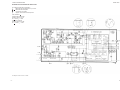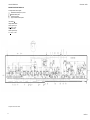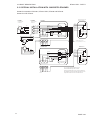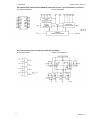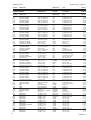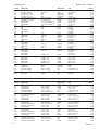
1
TECHNICAL MANUAL
FOR
COMPACT VHF RT2047/D
S.P. RADIO A/S
AALBORG
DENMARK
RT2047 DSC - PART I
CONTENTS
1
1.1
GENERAL INFORMATION
INTRODUCTION
1-1
1-1
2
2.1
2.2
2.3
2.4
2.5
2.6
2.7
2.8
2.9
2.10
2.11
INSTALLATION
INSTALLATION HINTS
MOUNTING POSSIBILITIES
DIMENSIONS AND DRILLING PLAN
HANDSET
MICROTELEPHONE CONNECTOR
POWER SUPPLY
POWER AND EXT. LOUDSPEAKER CONNECTOR
ANTENNAS
SPECIAL OPTIONS
REAR VIEW OF VHF RT2047
STANDARD FREQUENCY TABLE
2-1
2-1
2-2
2-4
2-9
2-9
2-9
2-10
2-10
2-10
2-11
2-12
RT2047 DSC - PART II
CONTENTS
1
1.1
1.2
1.3
1.4
1.5
GENERAL INFORMATION
GENERAL DESCRIPTION
TECHNICAL DATA
CONTROLS
PRINCIPLE OF OPERATION
BLOCKDIAGRAM
1-1
1-1
1-2
1-3
1-5
1-7
2
2.1
2.2
2.3
2.4
2.5
2.6
2.7
2.8
2.9
2.10
2.11
2.12
2.13
2.14
2.15
2.16
CIRCUIT DESCRIPTION
RECEIVER UNIT MODULE 100
RX-SYNTHESIZER UNIT MODULE 200
TX-EXCITER UNIT MODULE 300
TX-POWER AMPLIFIER MODULE 400
ANTENNA RELAY (500)
INTERFACE UNIT MODULE 6/600
KEYBOARD UNIT MODULE 7/700
DUPLEX FILTER MODULE 800
FILTER UNIT MODULE 9/900
MAIN DIAGRAM
MICROTELEPHONE INSTALLATION
SPECIAL INSTALLATION WITH 2 MICROTELEPHONES
SPECIAL INSTALLATION WITH 3 MICROTELEPHONES
MECHANICAL DIMENSIONS FOR HANDSET
DC POWER SUPPLY N418
N420 24V/12V REGULATOR
2-1
2-1
2-4
2-8
2-13
2-13
2-17
2-24
2-28
2-29
2-32
2-34
2-35
2-36
2-37
2-39
2-42
3
3.1
3.2
MECHANICAL DISASSEMBLING AND MODULE LOCATION
MECHANICAL DISASSEMBLING
MODULE LOCATION
3-1
3-1
3-3
4
4.1
4.2
4.3
4.4
4.5
4.6
4.7
4.8
4.9
4.10
SERVICE
MAINTENANCE
ADJUSTMENT INSTRUCTIONS
PROPOSAL FOR NECESSARY MEASURING INSTRUMENTS
CALIBRATION OF THE TEST PROBE
PROCEDURE FOR CALIBRATION
ADJUSTMENT PROCEDURE
TROUBLE-SHOOTING
REPLACEMENT OF COMPONENTS
REPLACEMENT OF MODULES
NECESSARY ADJUSTMENTS AFTER REPLACEMENT OF
A MODULE
PIN CONFIGURATION
PIN CONFIGURATIONS, BLOCK & SCHEMATIC
DIAGRAMS FOR IC’S
4-1
4-1
4-1
4-1
4-2
4-2
4-3
4-6
4-6
4-6
PARTS LIST
5-1
4.11
4.12
5
4-7
4-9
4-10
9546
RT2047 DSC - PART I
CONTENTS
1
GENERAL INFORMATION
1-1
1.1
INTRODUCTION
1-1
RT2047 DSC - PART I
1
GENERAL INFORMATION
1.1 INTRODUCTION
The RT2047 VHF Radiotelephone has been designed to be used with the Compact 2000 Module
Programme.
The VHF RT2047 can either be installed and operated as an independent unit or in combination with the
other modules in the Compact 2000 programme. These modules include a complete range of SSB
transmitters and receivers, MF/HF Digital Selective Calling unit and/or radiotelex equipment, a scrambler
that ensures complete communication secrecy and a VHF Digital Selective Call (DSC) unit. The DSCunit features direct dialling and reception of ship to shore, shore to ship and ship to ship calls as well as
automatic distress calls etc.
The VHF RT2047 has been constructed to withstand the most extreme conditions experienced in small,
semi-open boats. Its compact, weather proof construction ensures a degree of resistance to sea spray.
The printed circuits, which have made possible a combination of compactness and exceptional
performance, are coated with a special, moisture-repellent lacquer.
In the design of this VHF radiotelephone, S. P. Radio have taken into account all conditions it will be
exposed to in day-to-day operation. However, even a product of this high quality requires regular service
and maintenance, and we recommend the user to observe the maintainence instructions in the instruction
book.
S. P. Radio is Europe’s leading producer of maritime radio communication equipment - a position which
has been maintained by means of constant and extensive product development. We have a world-wide
network of dealers with general agencies in fifty countries. All our dealers are well-trained and will be able
to service all products.
PAGE 1-1
RT2047 DSC - PART I
CONTENTS
2
INSTALLATION
2-1
2.1
INSTALLATION HINTS
2-1
2.2
MOUNTING POSSIBILITIES
2-2
2.3
DIMENSIONS AND DRILLING PLAN
2-4
2.4
HANDSET
2-9
2.5
MICROTELEPHONE CONNECTOR
2-9
2.6
POWER SUPPLY
2-9
2.7
POWER AND EXT. LOUDSPEAKER CONNECTOR
2-10
2.8
ANTENNAS
2-10
2.9
SPECIAL OPTIONS
2-10
2.10
REAR VIEW OF VHF RT2047
2-11
2.11
STANDARD FREQUENCY TABLE
2-12
RT2047 DSC - PART I
2
INSTALLATION
2.1 INSTALLATION HINTS
Before installation of a VHF RT2047 the following points must be observed:
WHAT FACILITIES WILL HAVE TO BE ENABLED ?
Selcall, private channels, US-mode, dual watch, scanning facilities, etc. The procedure for enabling these
facilities is described in the manual: INSTRUCTIONS FOR IDENTITY AND SERVICE PROGRAMMING
OF VHF RT2047. This manual will only be delivered to dealers and general agents where it will be at the
disposal of trained personal in their service facilities.
IN WHAT WAY TO INSTALL THE VHF RT2047 ?
In section 2.2. MOUNTING POSSIBILITIES there’s installation instructions for the VHF RT2047 as an
independent unit or in combination with other units in the Compact 2000 programme.
HANDSET.
Installation of handset, see section 2.4. HANDSET.
EXTERNAL LOUDSPEAKER.
An external loudspeaker 4-8 ohm (4 W) can be connected to the power connector J802 pin 1 and 6, see
section 2.7. POWER CONNECTOR + EXT. LOUDSPEAKER.
SPECIAL OPTIONS:
The signals ‘remote alarm for selcall’, ‘AF to information decoder’, ‘AUX I’ , ‘AUX II’ etc. are available,
see section 2.9. SPECIAL OPTIONS.
PAGE 2-1
2 INSTALLATION
2.2 MOUNTING POSSIBILITIES
TABLETOP AND DECKHEAD
24889
Mounting bracket H2055
24890
Mounting kit H2068 and H2055
PAGE 2-2
RT2047 DSC - PART I
2 INSTALLATION
RT2047 DSC - PART I
BULKHEAD AND CONSOLE
24892
Mounting kit H2063
24893
Mounting kit H2062
24891
Mounting kit H2064
IN CONJUNCTION WITH OTHER “S.P. RADIO” EQUIPMENT.
Look up the INSTALLATION section for the S.P. RADIO unit in question.
PAGE 2-3
2 INSTALLATION
RT2047 DSC - PART I
2.3 DIMENSIONS AND DRILLING PLAN
115
UNIVERSAL MOUNTING BRACKET H2055
Permits a wide variety of installation possibilities, such as table top, bulkhead or deck head installation.
Fur other possibilities such as console installation, installation with 19" rack or assembly of all units in
the Compact programme on the bulkhead, see special information concerning installation of the
Compact programme.
48
225
min. 117
132
F
B
132
C
D
A
E
132
24894A
α
C
117
117
118
133
D
130
146
163
178
E
48
53
59
65
WEIGHT
Mounting kit H2055
H2054
H2074
CRY2001
RT2047
F
117
117
116
113
10 mm
C/F
A
B
0°
130 48
4.8° 142 48
9.6° 155 48
14.4° 167 45
Dimensions in mm.
24897
PAGE 2-4
132 mm
175 mm
80 mm
50 mm
100 mm
4 pcs ø6.5 mm
4 pcs ø4.5 mm
: 1.5 kg
: 5.5 kg
: 4.0 kg
: 3.2 kg
: 5.2 kg
2 INSTALLATION
RT2047 DSC - PART I
4 pcs M5x8
24896
215
Mounting kit H2068 and H2055
48
117
132
F
225
B
132
C
D
A
E
132
24895
α
A
B
0°
230 67
4.8° 243 67
9.6° 255 65
14.4° 265 62
Dimensions in mm.
C
D
E
F
117
129
142
155
230
245
262
270
67
72
78
89
117
117
115
112
WEIGHT
Mounting kit H2068 and H2055 : 1.5 kg
H2054
: 5.5 kg
H2074
: 4.0 kg
CRY2001
: 3.2 kg
RT2047
: 5.2 kg
PAGE 2-5
2 INSTALLATION
RT2047 DSC - PART I
Mounting kit H2063
min.295
24898
Free distance must be kept to
allow free air circulation ambient
temperature max. 40°C.
240mm
4.5mm
4.5mm
16mm
16mm
253mm
4 stk 6mm
WEIGHT
Mounting kit H2063
H2054
H2074
CRY2001
RT2047
113mm
100mm
4 stk 3.5mm uns for M3 DIN 963
16mm
16mm
Cutting out 231x100mm
27444A
4 pcs M3x30
4 pcs cover
8 pcs M5x8
24770
PAGE 2-6
4 pcs M5x30
: 1.0 kg
: 5.5 kg
: 4.0 kg
: 3.2 kg
: 5.2 kg
2 INSTALLATION
RT2047 DSC - PART I
Mounting kit H2064
min.295
24772
Free distance must be kept to
allow free air circulation ambient
temperature max. 40°C.
253.00
240.00
4.5mm
4.5mm
WEIGHT
20mm
20mm
Cutting out 231x200mm
221mm
208mm
20mm
4 stk ø3.5mm uns for M3 DIN 963
200mm
20mm
4 stk ø6mm
Mounting kit H2064
H2054
H2074
CRY2001
RT2047
: 1.5 kg
: 5.5 kg
: 4.0 kg
: 3.2 kg
: 5.2 kg
27447A
4 pcs M3x30
8 pcs cover
16 pcs M5x8
24899
4 pcs M5x30
PAGE 2-7
2 INSTALLATION
RT2047 DSC - PART I
Mounting kit H2062
min 295
28369
Free distance must be kept to
allow free air circulation ambient
temperature max. 40°C.
225.5mm
20mm
225.5mm
100mm
10mm
20mm
Cutting out 451x100mm
108mm
121mm
2 stk ø3mm
8 stk ø3.5mm uns for M3 DIN 963
10mm
WEIGHT
Mounting kit H2062
H2054
H2074
CRY2001
RT2047
20mm
4 stk ø6mm
6mm
4.5mm
6mm
20mm
473mm
460mm
27450
27451
*
8 pcs M3x30
*
8 pcs M3x8
12 pcs M5x8
2 pcs M3x30
24773
4 pcs M5x30
PAGE 2-8
: 1.5 kg
: 5.5 kg
: 4.0 kg
: 3.2 kg
: 5.2 kg
2 INSTALLATION
RT2047 DSC - PART I
2.4 HANDSET
The handset can be placed anywhere near the VHF set. The cable is nine cored and connected to the
rear plate through a 9 pin Sub D connector with lock nuts.
Installation of the cable, see the drawings of the mounting brackets, section 2.3 DIMENSIONS AND
DRILLING PLAN. The cable grommet must be placed in the most convenient groove in the mounting
bracket.
If more than one handset is needed, see section 2.12. and 2.13. in part II, SPECIAL INSTALLATION
WITH 2 OR 3 MICRO TELEPHONES.
2.5 MICROTELEPHONE CONNECTOR
Wiring of the micro telephone connector.
*/
**/
3,1180%(5
)81&7,21
1
2
3
4
5
6
7
8
9
Telephone +
Ground
Ground
Microphone
Handset key
AF from RX buffer
Interrupt/Distress cry *
Serial input/output
+13V Internal/Phone Patch**
Signal selection on jumper P608 on the Interface-unit.
Signal selection on jumper P934 on the Filter-unit
2.6 POWER SUPPLY
The standard power supply for RT2047 is 12V DC .
For 24V DC supply an external power supply N418 ( switch mode ) or the N420 a 24V DC to 13.2V DC
serial regulator can be used, see part II, section 2.14 . and 2.15 .For 110V AC, 127V AC, 220V AC or 237V
AC an external power supply N163S must be used together with N418 or N420 .
2.7 POWER AND EXT. LOUDSPEAKER CONNECTOR
Wiring of the power and ext. loudspeaker connector.
3,1180%(5
)81&7,21
1
2
3
4
5
6
+Ext. loudspeaker*
No connection
+12V Power Supply
ON/OFF for 24V Supply
-12V Power Supply
-Ext. loudspeaker*
*/ If necessary a 4-8 ohm (4 W) external loudspeaker can be connected to pin 1 and 6 of the power
connector J802. External loudspeakers H2054 and H2074 are available for this option.
PAGE 2-9
2 INSTALLATION
RT2047 DSC - PART I
2.8 ANTENNAS
All common 50 ohm antennas, which cover the used frequency range with a reasonable standing wave
ratio, maximum 1.5, are applicable.
The antenna is connected to the set by means of a 50 ohm coaxial cable with low loss, e.g. RG213U. At
the cable end a PL259 plug is mounted.
The antenna must be placed as high and as free of obstructions as possible. The horizontal distance to
metal parts must be at least 1.0 metre.
S. P. Radio has an antenna with the necessary specifications available for purchase. The mentioned
antenna is characterised by small external dimensions. See the special brochure ‘VHF AERIALS’ for
particulars.
2.9 SPECIAL OPTIONS
K-SWITCH.
It is possible to change between standard functions and the German river boat functions by installing an
external switch.
SELCALL RELAY.
When the selcall has accepted a CQ or individual call signal, the selcall relay, RE1-9 on the Filter-unit will
turn on and short-circuit two wires, which can be used for remote alarm. Max. contact load: 100V AC/24V
DC - 2A. This option is available on the filter print.
AF TO INFORM. DECODER.
The circuit giving AF signals to the information decoder is turned on when the set has accepted a CQ or
individual call signal. The circuit is turned “ON” or “OFF” like the relay RE1-9. This option can be found
in connector P4-6 on the interface print.
AUX II.
When an information on certain channels is wanted, i.e. controlling a watch keeping receiver, the AUX
II information can be used. A relay RE2-9 on the Filter-unit is controlled through the buffer/inverted U11/
5-6 from the ìC U19-6. Max. contact load: 100V AC / 24V DC - 2A. The AUX II option is available on the
filter print.
OUTPUT TO RECORDER.
Through the connector P4-6 pin 1 and 2 on the INTERFACE UNIT (6) the AF signal to the telephone output
can be led to a tape recorder. This option is located in connector P4-6.
AUX 1
The option AUX I is for-either internal or external use. It is placed in P3-6 pin 1 on the INTERFACE UNIT.
Max. level on the output of the U11-6 must not be more than the battery level, because a diode is
connected to the supply pin in the IC.
DISTRESS CRY / INTERRUPT
Jumper P8-6 on the interface print leads either ‘Distress Cry’ or ‘Interrupt’ through the filter print to the
handset key connector. The Interrupt signal is required when RT2047 is used with the VHF DSC RM2042
and Distress Cry is used for scramblers CRY2001 and CRY2002.
PHONE PATCH / +13V
Jumper P34-9 is used for selecting if The ‘Phone Patch’ signal or if ‘+13V’ should be led to the handset
key connector. +13V is required when RT2047 is used with the VHF DSC RM2042 and Phone Patch is
used for the Phone Patch unit H2047.
PAGE 2-10
2 INSTALLATION
RT2047 DSC - PART I
2.10 REAR VIEW OF VHF RT2047
Screws for Tx Power Transistor
T401’s heat sink conductor.
Power Supply
connector P802
Cable groove for
special options
12V DC
28368
Screws for Regulator Transistors
heat sink on Interface unit(6).
MUST BE REMOVED WHEN INTERFACE
UNIT HAS TO BE REMOVED!
Microtelephone
connector J803
Antenna
connector J801
PAGE 2-11
2 INSTALLATION
RT2047 DSC - PART I
2.11 STANDARD FREQUENCY TABLE
&+$11(/
75$160,77,1*
)5(48(1&<0+]
01
02
03
04
05
06
07
08
09
10
11
12
13
14
15
16
17
18
19
20
21
22
23
24
25
26
27
28
60
61
62
63
64
65
66
67
68
69
70
71
72
73
74
77
78
79
80
81
82
83
156.050
156.100
156.150
156.200
156.250
156.300
156.350
156.400
156.450
156.500
156.550
156.600
156.650
156.700
156.750
156.800
156.850
156.900
156.950
157.000
157.050
157.100
157.150
157.200
157.250
157.300
157.350
157.400
156.025
156.075
156.125
156.175
156.225
156.275
156.325
156.375
156.425
156.475
156.525
156.575
156.625
156.675
156.725
156.875
156.925
156.975
157.025
157.075
157.125
157.175
84
85
86
87
88
WX1
WX2
WX3
WX4
157.225
157.275
157.325
157.375
157.425
Inhibit
Inhibit
Inhibit
Inhibit
PAGE 2-12
5(&(,9,1*)5(48(1&<0+]
INT’L MODE
US MODE
(INT-CHANNELS)
(A-CHANNELS)
160.650
156.050
160.700
160.700
160.750
160.750
160.800
160.800
160.850
156.250
156.300
156.300
160.950
156.350
156.400
156.400
156.450
156.450
156.500
156.500
156.550
156.550
156.600
156.600
156.650
156.650
156.700
156.700
156.750
156.750
156.800
156.800
156.850
156.850
161.500
156.900
161.550
156.950
161.600
161.600
161.650
157.050
161.700
157.100
161.750
157.150
161.800
161.800
161.850
161.850
161.900
161.900
161.950
161.950
162.000
162.000
160.625
160.625
160.675
160.675
160.725
160.725
160.775
156.175
160.825
160.825
160.875
156.275
160.925
156.325
156.375
156.375
156.425
156.425
156.475
156.475
156.525
156.525
156.575
156.575
156.625
156.625
156.675
156.675
156.725
156.725
156.875
156.875
161.525
156.925
161.575
156.975
161.625
157.025
161.675
157.075
161.725
157.125
161.775
157.175
161.825
161.875
161.925
161.975
162.025
162.550
162.400
162.475
161.650
161.825
161.875
161.925
161.975
157.425
162.550
162.400
162.475
161.650
RT2047 DSC - PART II
CONTENTS
9546
1
GENERAL INFORMATION
1-1
1.1
GENERAL DESCRIPTION
1-1
1.2
TECHNICAL DATA
1-2
1.3
CONTROLS
1-3
1.4
PRINCIPLE OF OPERATION
1-5
1.4.1
FREQUENCY GENERATION
1-5
1.4.2
RECEIVER
1-5
1.4.3
TRANSMITTER
1-5
1.4.4
THE MICROCOMPUTERS
1-5
1.5
BLOCKDIAGRAM
1-7
RT2047 DSC - PART II
1
GENERAL INFORMATION
1.1 GENERAL DESCRIPTION
RT2047 can operate in duplex and simplex mode.
RT2047 is provided with built in duplex-filter for duplex communication with one antenna.
RT2047 includes all 55 international and U.S. VHF marine channels, and is prepared for up to 20 private
channels to be selected as simplex or duplex channels. As option up to 67 private channels can be
provided.
RT2047 has six scanning programmes, one standard programme, and 5 individually programmable
scanning programmes.
RT2047 has built in dual watch facility, which enables the operator to listen to two channels simultaneously (the selected channel and a preference channel - normally CH16.)
RT2047 is provided with quick selection of channel 16.
RT2047 is provided with selcall decoder. Selective calls (CALL) or all ships calls (CQ) from the coast
station will be decoded.
RT2047 receiver section is a double-conversion superheterodyne system, which makes use of a phaselocked digital frequency synthesizer for frequency generation based on a single crystal to provide all the
standard channels and the private channels.
RT2047 transmitter section is a phase-locked phase-modulated signal generator with a solid state RF
power amplifier.
RT2047 is provided with two microcomputers, one for controlling the frequency synthesizer, reading from
and to EEPROMS, controlling the squelch and volume functions, and controlling the selcall filter. The
other µC is controlling the display drivers, the dual watch and scanning functions.
RT2047 is for 12 Volt DC supply. Voltage change-over from 24V to 12V is done by the switch-mode power
supply N418.
RT2047 employs the most modern circuit technology, housed in a corrosion resistant aluminium cabinet
with a green nylon finish.
RT2047 is provided with membrane switches for controls, easy to use, reliable and hard-wearing. Cutouts in the metal front serve as a safe finger-guide.
RT2047 is fitted with night illumination.
RT2047 has been prepared with a serial communication interface for DSC (Digital Selective Call)
operation together with S.P. RADIO’s VHF DSC RM2042. DSC is the globally adopted general purpose
system for selective calling in the ship-to-ship, ship-to-shore and shore-to-ship directions and can best
be compared to ordinary telephony, giving you direct access to the national telephone network in those
areas where the coast stations have the automatic services. DSC also enables you to make automatic
distress calls containing the ships position etc. complying with the international requirements stated by
IMO in the Global Maritime Distress and Safety System, known as GMDSS.
RT2047 is prepared for scrambled communication in conjunction with Scramblers CRY2001 or
CRY2002, both produced by A/S.
9543
PAGE 1-1
1 GENERAL INFORMATION
RT2047 DSC - PART II
1.2 TECHNICAL DATA
VHF RT2047 fulfils the International CAPT regulations.
GENERAL SPECIFICATIONS
All international maritime VHF channels
Private Channels
20 as option up to 67
Operation
Duplex and Simplex
Modulation
G3EJN (Phase)
Antenna Impedance
50 ohm
Frequency Stability
+/- 10 ppm
Temperature Range
-20 C to +55 C
Nominal Power Supply
13.2V DC
Power Supply Variation
12V DC -10% to +30%
(with reduced data according to
international standards)
Power Consumption
Standby
= 0.5 Amp.
Transmit
= 6 Amp.
Dimensions
Height:
115 mm
Width:
225 mm
Depth:
262 mm
RECEIVER
Frequency Range Simplex
Frequency Range Duplex
Sensitivity
Duplex desensitisation
AF Output Power
Telephone Output
Distortion
Scanning Facilities
Selective Call Decoder
155.400 - 158.000 MHz
160.000 - 162.600 MHz
0.35 uV pd at 12 dB SINAD
Less than 2 dB
3 Watt/4 ohm
0.45V RMS/200 ohm
Less than 5%
5 scanning programmes with
possibility for all your
channels in each programme
except the private channels
from P20 to P67
According to CCIR
TRANSMITTER
Frequency Range
RF Output Power
Reduced RF Output
Distortion
155.400 - 158.000 MHz
25 Watt, +0 to -1 dB
0.5 to 1 Watt
Less than 2%
PAGE 1-2
9543
1 GENERAL INFORMATION
RT2047 DSC - PART II
1.3 CONTROLS
SCAN
SCAN
PROG
VOL
VOL
SQ
SQ
STOP
OFF
RUN
16
SCAN
DELETE
3
2
SCAN
TIME
D.W.
4
5
SELCALL
RESET
SELCALL
TEST
7
8
9
P
ENT
USA
ON
SCAN
ADD
1
Scan
DW USA CQ
Duplex Shift Call
Vol
SQ 1W Tx
SHIFT
6
1W
DIM
0
23990
Press
ON
OFF
Turns the set on or off.
VOL
Press
Increases volume progressively in 16 steps.
VOL
Press
Reduces volume progressively in 16 steps.
SQ
Press
Increases squelch sensitivity progressively in 8 steps, a gradual exclusion of weak
signals with atmospherics.
SQ
Reduces squelch sensitivity progressively in 8 steps.
Press
Press
Press
9543
STOP
RUN
Stops and starts scanning sequence. Listen on several predetermined channels.
16 Quick select of the call and distress channel 16.
Press
1 Digits from 1 to 0.
Press
P Selects private channels.
Press
ENT
Press
SHIFT
Terminates the keying in of selected channels, scanning programmes, scan time etc.
Activates the functions marked in orange on the keyboard.
PAGE 1-3
1 GENERAL INFORMATION
RT2047 DSC - PART II
SHIFT FUNCTIONS
SCAN
Selects scanning programmes.
Press
Press
Press
Press
Press
SCAN
ADD
SCAN
DELETE
SCAN
PROG
SCAN
TIME
Adds a channel to the scanning table.
Deletes a channel from the scanning table.
Stores the current scanning programme in the memory.
Selects the scan time from 1 to 99 seconds. The time chosen will be used to listen
on one of the secondary channels receiving a signal.
D.W.
Selects the dual watch facility.
Press
Press
Press
SELCALL
RESET
SELCALL
TEST
Resets the selcall decoder after a call.
Tests the selcall decoder.
1W
Press
Selects 1 W reduced power output.
USA
Press
Selects the VHF channels used in USA.
DIM
Press
Switches the panel illumination on or off.
Note: See the VHF RT2047 Operating Manual for functional description.
PAGE 1-4
9543
1 GENERAL INFORMATION
RT2047 DSC - PART II
1.4 PRINCIPLE OF OPERATION
1.4.1
FREQUENCY GENERATION
The frequencies are generated from a crystal oscillator operating on 21 MHz. The 21 MHz is divided in
the REFERENCE DIVIDER to 2.1 MHz which is the input to the RX-REFERENCE DIVIDER and also the
clock-signal for the microcomputer on the Interface Unit. In the RX-REFERENCE DIVIDER the 2.1 MHz
is divided by 168 to 12.5 KHz which is reference for the PHASE DETECTOR. This makes it possible to
change the frequency from the RX-VCO with 12.5 KHz intervals.
The signal from the RX-VCO is divided in a PRESCALER which divides by 33 until the A-COUNTER has
reached zero and then it divides by 32. The N-COUNTER divides the output from the PRESCALER, and
the output is led to the PHASE-DETECTOR, and here it is compared with the 12.5 KHz. If there is a
difference an error voltage will be generated. This is integrated in the LOOP-FILTER and the output of
this filter controls the RX-VCO. The frequency of the RX-VCO is the receiving frequency minus the
intermediate frequency.
fLO1 = fRX - f1IF = fRX -21.4 MHz
The output from the RX-VCO is mixed with the output from the TX-VCO which is in lock when it is 16.8
MHz above the RX-VCO. This means that the receiver always is 4.6 MHz above the transmitter, namely
21.4 - 16.8 = 4.6; and this difference is equal to the duplex distance. The 16.8 MHz from the MIXER is
divided by 32 to 525 KHz, which is compared with the 21 MHz divided by 40 in the REFERENCE DIVIDER.
The error voltage is integrated in the LOOP-FILTER, and the output of this filter controls the TX-VCO.
1.4.2
RECEIVER
The antenna-signal is led through the duplex-filter and the antenna relay to the RF-AMPLIFIER. The
bandpass filters are tuned by means of capacitor-diodes which are controlled by means of a DC-voltage
which is derived from the control-voltage to the RX-VCO. In the FIRST MIXER the antenna signal is mixed
with the output from the RX-VCO to the intermediate frequency 21.4 MHz. In the integrated IF circuit, the
first IF frequency on 21.4 MHz is mixed with a crystal oscillator signal on 20.945 MHz to reach the second
IF frequency on 455 kHz. This signal is filtered in the ceramic filter, before it is amplified and detected in
the integrated IF-circuit. The audio frequency signal is amplified and led through an active filter providing
the frequency response further to the telephone amplifier and the AF power amplifier.
1.4.3
TRANSMITTER
The microphone signal is led through the MICROPHONE AMPLIFIER where the necessary amplification,
limiting, and filtering takes place. The limiting is done by a clipper. The signal from the MICROPHONE
AMPLIFIER is led to the LOOP-FILTER, where the phase modulation of the transmitter takes place. As
the TX-VCO oscillates directly on the transmitting frequency, the signal only has to be amplified. This is
done in the TX-BUFFER, PA-DRIVER, and the PA-POWER AMPLIFIER. The power supply for the PAdriver is adjustable, and is used for adjusting the output power. The harmonics of the output is filtered in
HARM-FILTER , before it is led through the ANTENNA-RELAY and the DUPLEX-FILTER to the antenna.
1.4.4
THE MICROCOMPUTERS
The µC on the Interface Unit is taking care of calculating the dividing figure for the synthesizer, reading
from and to the EEPROMs, controlling the squelch and volume functions, and controlling the selcall filter.
The µC on the Keyboard Unit is taking care of the keyboard scanning, the input from the handset key and
the display drivers as well as the Dual Watch and Scanning functions. The keyboard µC is also handling
the serial SP VHF-BUS communication with external devices such as the VHF DSC - RM2042. The
communication between the two µC’s is accomplished by a RS232C -type serial connection.
9543
PAGE 1-5
1 GENERAL INFORMATION
PAGE 1-6
RT2047 DSC - PART II
9543
1 GENERAL INFORMATION
RT2047 DSC - PART II
INTERFACE (MODULE 6)
2.1MHz
Rx-Filter
Control-AMP
Antenna
Relay
fRx
+13V PS
-13V PS
ON/OFF to
24V Supply
RECEIVER (MODULE 100)
Filter
Control
First
Mixer
RF-AMP
21.4 MHz IF
Second
Mixer
f2IF
455 kHz IF
and Detector
Programmable
Counter
7
+13V
ON/OFF
AMP/Limiter
1
÷2
Switched
Capacitor
Bandpass
Filter
+13V
2.1MHz
Duplex
Filter
Detector
AF
Int
LCDDisplay
Serial
Interface
Buffers
5
8
48
9
PA-AMPLIFIER
(MODULE 400 & 500)
fLO1
uC
20.945 MHz
+10V Tx
Buffer +
Rx/Tx
Delay Driver
Rx VCO
Loop
Filter
PHONE
PATCH
INPUT
Rx-Reference
Divider
÷168
Phase
Detector
+10V
+13V
1
Battery
Sensor
Reset
1
Delayed OFF
EEPROM
Seriel
Interface
Buffers
3
+13V
7 bit
A-counter
AUX II Relay
+ Distress
Cry
10 bit
N-counter
Interrupt
Driver
Circuit
Display
Driver
3
1
5
uC
Int.
+10V Sensor
9
D/A
Converter
Rx-SYNTHESIZER
(MODULE 200)
Harm
Filter
PA-Power
AMP
Constant
Current
Generator
4
Serial
Communication
Interface
+10V
+10V VCO
ON/OFF
÷33/32
Prescaler
SERIAL DATA
INTERRUPT
1.5 BLOCKDIAGRAM
-
+13V
16.8 MHz
Mixer
16.8 MHz
AUX I
Driver
Control-logic
Selcall Relay
+AF to inform.
Decoder
÷32
3
1
Buffer
1
6dB/Octave
Filter
AF-Mute
Telephone
AMP
VolAttenuator
AF from Rx
Buffer
SQ-Filter
Rectifier
Comparator
+13V
AF-Power
Amplifier
+5V
+5V
Keyboard
PA-Driver
Tx-Buffer
fTx
Tx-VCO
Loop
Filter
Phase/Freq.
Detector
525 kHz
+
2.1 MHz
Reference
Divider
X-Tal
Oscilllator
21 MHz
PA-Reg
2
Loudspeaker
KEYBOARD (MODULE 7)
Tx-EXCITER (MODULE 300)
MIC.-AMP.
MIC.-AMP.
MIC. + AMP.
Clipper
Integrator
+13V
+5V
+5V
+13V
+10V
+10V
KEY-Buffer
Pre-Empaasis
9543
AUX LS
HANDSET KEY
AF FROM Rx
TELEPHONE OUT
MIC. IN
24312D
PAGE 1-7
RT2047 DSC - PART II
CONTENTS
9546
2
CIRCUIT DESCRIPTION
2-1
2.1
RECEIVER UNIT MODULE 100
2-1
2.2
RX-SYNTHESIZER UNIT MODULE 200
2-4
2.3
TX-EXCITER UNIT MODULE 300
2-8
2.4
TX-POWER AMPLIFIER MODULE 400
2-13
2.5
ANTENNA RELAY (500)
2-13
2.6
INTERFACE UNIT MODULE 6/600
2-17
2.7
KEYBOARD UNIT MODULE 7/700
2-24
2.8
DUPLEX FILTER MODULE 800
2-28
2.9
FILTER UNIT MODULE 9/900
2-29
2.10
MAIN DIAGRAM
2-32
2.11
MICROTELEPHONE INSTALLATION
2-34
2.12
SPECIAL INSTALLATION WITH 2 MICROTELEPHONES
2-35
2.13
SPECIAL INSTALLATION WITH 3 MICROTELEPHONES
2-36
2.14
MECHANICAL DIMENSIONS FOR HANDSET
2-37
2.15
DC POWER SUPPLY N418
2-39
2.16
N420 24V/12V REGULATOR
2-42
2 CIRCUIT DESCRIPTION
2
RT2047 DSC - PART II
CIRCUIT DESCRIPTION
2.1 RECEIVER UNIT MODULE 100
The receiver unit includes the following circuits:
2.1.1
RF-AMPLIFIER AND FIRST MIXER
The RF-amplifier working in the frequency range 155.4 MHz to 162.4 MHz consists of the transistor Q101
and the two double-tuned filters surrounding it. The signal is led from the aerial through the duplex-filter
to the antenna switch and from there to the receivers input-filter. The input filter and the intermediate filter
are variable capacitance tuned filters, controlled by a DC-voltage derived from the RX-VCO control
voltage. This secures an optimal filter response within the receivers frequency range. The two doubletuned filters create the necessary attenuation of signals distant from the wanted signal frequency in order
to give the wanted spurious rejection of such unwanted signals. The amplifying transistor Q101 (which
is a large current, low noise transistor in a common-base configuration) secures by its gain the receiver
overall noise figure and a good two-signal performance. The RF-input to the first mixer is taken from the
coil L104 in the intermediate filter. Mixer transistor Q102 is of the JFET-type, where the first LO-signal
is injecting into the source from a 50 ohm generator. The wanted 21.4 MHz IF-output is selected by means
of the tuned drain circuit consisting of L105, C117, C119, and R110 which also creates the necessary
impedance matching the IF-crystal filter.
2.1.2
IF-FILTER AND AMPLIFIER
The receivers adjacent channel selectivity is maintained by means of the crystal filter FL101. The output
from this filter is led to the IF-amplifier with the transistor Q103, L106, C123, and R112 giving the
appropriate impedance matching the filter output. The amplifier gives the needed power gain between
the crystal filter and the second mixer and also secures good large signal performance.
2.1.3
SECOND MIXER, CERAMIC FILTER, DETECTOR AND AF AMPLIFIER
The integrated IF circuit includes the second mixer, the limiting amplifier and the detector with post AF
amplifier.
The second local oscillator signal is generated by means of the integrated oscillator and an external
crystal X101, running on 20.945 MHz. The signal out of the second mixer (455 kHz) is fed through the
ceramic filter FL102 to the limiting amplifier and discriminator in U101.
The quadrature phase discriminator includes the external phase shift network consisting of the tank circuit
with L108, C129 and R120.
The AF output from the detector is amplified by means of an internal operational amplifier and finally
buffered by means of the discreet transistor amplifier with Q104.
2.1.4
IF POWER SUPPLY
The integrated IF circuit and AF buffer amplifier are powered from an integrated 5V series voltage
regulator U102. The input voltage for this circuit is the receiver 10V supply.
9543
PAGE 2-1
2 CIRCUIT DESCRIPTION
RT2047 DSC - PART II
COMPONENT LOCATION RECEIVER UNIT MODULE 100
View from component side
with upper side tracks.
View from component side
with lower side tracks.
32127B
PAGE 2-2
9641
2 CIRCUIT DESCRIPTION
RT2047 DSC - PART II
DIAGRAM RECEIVER UNIT MODULE 100
AC voltages outside frame of diagram.
: Measured with oscilloscope or frq. counter.
: Measured with test probe.
: Connections to module.
[]
: Approx. measurement with test probe.
Test conditions:
Voltages without brackets:
Antenna signal 1 mV pd:
Df= +3 kHz; fm = 1 kHz
Voltages in brackets:
Antenna signal 10 mV pd:
Df = + 3 kHz; fm = 1 kHz
This diagram is valid for PCB rev. 32127B.
9641
PAGE 2-3
2 CIRCUIT DESCRIPTION
RT2047 DSC - PART II
2.2 RX-SYNTHESIZER UNIT MODULE 200
The RX-synthesizer unit includes the following circuits:
2.2.1
RX-VCO AND BUFFER AMPLIFIERS
The transistor T203 is producing 8.3 V supply voltage for the RX-VCO and bias for the buffer amplifiers
consisting of the transistors T201 and T204. The RX-VCO comprises a Field Effect Transistor T202 (the
oscillator transistor), two coaxial coils L203, L204, two capacitors C212, C214, and a variable capacitance
diode D201. The frequency is mainly determined by the components L203, L204, C214, and D201. The
RX-VCO is a voltage controlled oscillator where the control voltage from the loop filter determines the
frequency by means of D201. A high control voltage to the variocap. diode D201 means a small
capacitance in the diode which means a high frequency of the VCO. In the opposite way a low control
voltage means a low VCO frequency. The RX-VCO signal is passed to two buffer amplifiers via low pass
filter C209, C206, L201. The L01 buffer transistor T201 is producing 5 mW for the 1st mixer in the receiver.
The 5 mW is taken from the tuned filter L202, R202, C207, and C208. The prescaler buffer transistor T204
is producing 0.25 mW for the 16.8 MHz mixer in the TX-Exciter-Unit. It is also producing signal for 32/33
prescaler. The signal from transistor T204 is led through a low pass filter C217, L206, and C222. The gain
in both buffers can be adjusted by the potentiometer R209.
2.2.2
32/33 PRESCALER
The integrated circuit IC201 is a two modulus prescaler based on the ECL technique. From the control
logic in the programmable divider IC202 pin 14, a high or low level is led to the prescaler IC201 pin 1. A
high level at IC201 pin 1 causes the prescaler to divide by 33 and in turn a low level at pin 1 sets it up for
dividing by 32. The resistor R232 and the diode D204 work as a speed-up circuit.
2.2.3
THE PROGRAMMABLE DIVIDER
The programmable divider IC202 contains two phase detectors, a lock detector, a reference divider, an
A-counter, a N-counter, control logic, and 8 latches. Only phase detector B of the detectors is in use. When
the VHF is switched on the microcomputer will load dividing figures into the reference divider and into the
A and N-counters. The microcomputer loads only one latch at a time.
By setting up a code at the address inputs Al - A2 the microcomputer selects a latch and at the same time
a code for the dividing figure is set up at the data inputs D0 - D3. The microcomputer sends a strobe pulse
to IC202 pin 12 and the selected latch is loaded. The procedure is then repeated until all the latches are
loaded.
When the channel or the function of the VHF is changed it is only the latches for the A and N-counter that
change data. The reference frequency is 2.1 MHz and it is constant. Therefore it is not necessary to
change the dividing figure every time.
In the beginning of a counting period the prescaler IC201 starts dividing by 33 and the A and N-counters
count down. First the A-counter reaches zero and stops counting and the control logic shifts the prescaler
to divide by 32. Then the N-counter reaches zero and sends a pulse to the phase detector B, and the
control logic shifts the prescaler to divide by 33. The control logic also reloads the A and N-counters with
data from their latches and the whole procedure starts from the beginning.
The pulse frequency from the reference divider is 12.5 KHz. If the RX-VCO frequency is correct the pulse
frequency of the N-counter is also 12.5 KHz and in phase with the pulse from the reference divider. The
phase detector B compares the phase of the two pulses. If they are not in phase the detector sends
correction pulses to the phase-detector-pump for correcting the frequency/phase of the RX-VCO.
However, the synthesizer circuit is born with a small phase error, therefore the phase detector is sending
small correction pulses to transistor T210 with a frequency of 12.5 KHz.
PAGE 2-4
9543
2 CIRCUIT DESCRIPTION
2.2.4
RT2047 DSC - PART II
PHASE DETECTOR PUMP AND LOOP FILTER
We assume that the RX-VCO frequency has decreased from its nominal frequency, The phase-detector
now sends negative correction pulses from IC202 pin 17 to T210, which goes on. A current will then flow
from C225 through R225 and R229 and into T210. This current will discharge C225 forcing the output
voltage from the transistors T205 and T206 to increase until the VCO reaches the correct frequency. If
the RX-VCO frequency is too high, the negative correction pulses from the detector at pin 16 of IC202
will turn transistor T209 off. The collector voltage of transistor T209 increases and a current will flow
through the diode D202, the resistor R225 and into the capacitor C225 and charge this capacitor. The
output voltage at the collector of the transistors T205 and T206 will decrease until the VCO reaches its
right frequency. If the phase-locked-loop is locked, both outputs of the phase-detector will be 5 V and the
output voltage of the transistors T205 and T206 will have a value between 2 V and 10 V corresponding
to the VC0-frequency. However, the system is working with a constant phase error and the phase detector
sends small correction pulses to transistor T210, even the phase-locked-loop is locked. The four
transistors T205, T206, T207, and T208 are working as an operational amplifier with the inverting input
at base of transistor T208. Non-inverting input is at transistor T207 while the transistors T205 and T206
forms the output stage.
9543
PAGE 2-5
2 CIRCUIT DESCRIPTION
RT2047 DSC - PART II
COMPONENT LOCATION RX-SYNTHESIZER UNIT MODULE 200
View from component side
with upper side tracks.
View from component side
with lower side tracks.
23694D
PAGE 2-6
9543
2 CIRCUIT DESCRIPTION
RT2047 DSC - PART II
DIAGRAM RX-SYNTHEZISER UNIT MODULE 200
AC voltages outside frame of diagram.
: Measured with oscilloscope or frq. counter.
: Measured with test probe.
: Connections to module.
[]
: Approx. measurement with test probe.
Test conditions:
Voltages without brackets:
Antenna signal 1 mV pd:
Df= +3 kHz; fm = 1 kHz
Voltages in brackets:
Antenna signal 10 mV pd:
Df = + 3 kHz; fm = 1 kHz
This diagram is valid for PCB rev. 23694D.
9543
PAGE 2-7
2 CIRCUIT DESCRIPTION
RT2047 DSC - PART II
2.3 TX-EXCITER UNIT MODULE 300
The TX exciter unit contains the following circuits:
2.3.1
INSULATION BUFFER AND 16.8 MHZ MIXER
From RX-VC0 the signal is led to transistor T301 and from TX-VC0 the signal is led to transistor T302.
The transistors are not coupled with common base and act as buffer amplifiers. The mixed signal over
resistor T305 is led to the mixer amplifier T303 via capacitor C305. The differential signal which is the TXVC0 frequency minus the RX-VC0 frequency is led to the amplifier transistor T304 through the low-pass
filter consisting of C310, L301 and C311. In transistor T305 the signal is amplified to TTL level. The diode
D301 works as a base clamp diode.
2.3.2
THE 21 MHZ OSCILLATOR
The oscillator is a Colpitt type and the oscillator transistor T308 is oscillating by means of a 21 MHz crystal
X301.
The trimmer capacitor C331 is for fine adjustment of the oscillator frequency.
RF signal for the reference divider is led to transistor T307 for amplifying. In transistor T306 the signal
is amplified to TTL level.
2.3.3
PHASE/FREQUENCY DETECTOR, 32 COUNTER AND REF. DIVIDER
The crystal frequency is led to IC306 pin 10 which is a decade counter. From output pin 5 of this, the
frequency is divided by 5. This frequency is led to flip-flop IC305a, where the frequency is divided by 2.
From IC305a pin 5, the 2.1 MHz is taken and this is the clock frequency for the microcomputer and the
RX synthesizer. The resistor R322 is for pull-up and the ferrite bead FP301 is blocking for higher
harmonics of the clock frequency.
From IC306 pin 8, the 21 MHz is also divided by 10. The frequency is divided by 2 in flip-flop IC305b and
divided by 2 in IC304a. At IC304b pin 13, the 21 MHz is then divided by 40 and the frequency is therefore
525 KHz at which the phase detector is working.
From the other side the mixed signal of 16.8 MHz is led to the binary divider IC301 pin 10 where it is divided
by 16. In flip-flop IC302b the signal is divided by 2. From IC320b pin 8 the 16.8 MHz is then divided by
32 giving 525 KHz.
The phase/frequency detector consists of IC302a, IC303, and IC304b. From IC304b pin 9 the detector
is connected to the loop filter via the pull-up resistor R321 and the diode D303. The phase corrections
pulse from the detector is active low and when the phase locked loop is in lock the duty cycle of the
correction pulse is about 30 per cent.
THE CORRECTION PULSES:
After the count down of the 21 MHz the IC304b pin 9 goes low. Pin 8 goes high and this is connected to
IC303 pin 2. When the 16.8 MHz is divided by 32 the IC302a pin 6 and IC303 pin 1 go high. When IC303
pin 13 is always high the IC303 pin 8 will go low and preset IC302a and IC304b; the correction pulse will
then go high and so on. The propagation delay in the two inserters IC303 determines the size of the preset
pulse.
PAGE 2-8
9543
2 CIRCUIT DESCRIPTION
2.3.4
RT2047 DSC - PART II
TX-VCO
The TX-VCO comprises a Field Effect Transistor T311 (oscillator transistor), two coaxial coils L309 and
L310, the capacitors C343 and C345, and a variocapacitor diode D302.
The frequency is mainly determined by L309, L310, C345, and D302. The TX-VCO is a Voltage Controlled
Oscillator, where the control voltage from the loop filter determines the frequency by means of the
variocapacitor diode D302. A high voltage to D302 means a smaller capacitor in D302 and again a higher
VCO frequency. In the opposite way a small control voltage means a smaller frequency.
From drain of transistor T311 the signal is led to a buffer amplifier T310 via a tuned filter consisting of L308,
R342, and C342. The ferrite bead is blocking for UHF oscillating. In the collector of T310 there is a tuned
filter consisting of L307 and C340. From here the signal for two circuits is taken.
From an output on coil L307 the signal to the TX-buffer is taken through capacitor C338. Here the TXVCO signal is amplified in transistor T309. In the drain of T309 there is a tuned filter consisting of L306,
C332, C333, R332, and R333, which gives a 50 ohm generator for the Power Amplifier Unit. The output
power from the TX-buffer is 25 mW and is adjusted by trimmer potentiometer R341.
Stop and start of both TX-buffer and TX-VCO are controlled from the microcomputer by controlling the
supply for the transistor. This secures that the frequency is correct before the transmitter is started. From
the collector of T310 the signal for the 16.8 MHz Mixer is taken via capacitor C341.
2.3.5
LOOP-FILTER
The Loop-filter amplifier is a differential amplifier (OP-Amp.) with the inverted input at the base of
transistor T314, where also the phase detector is connected. The base of transistor T313, which is the
non inverted input, is connected to +5V by means of R349 and R350. Transistor T312 is the output stage,
and the control voltage for TX-VCO is taken over the resistor R346 and is filtered in the ripple-filter
consisting of R345, C348, C347, and R344. At the input R351 and C352 are working as a filter against
the higher harmonics in the phase detector pulse.
We assume that the system is in lock. While the detector pulse is low a current is flowing out of the
capacitor C351 and the output voltage over R346 increases. The TX-VCO frequency is also increasing
until the detector pulse goes high again. Because the diode D303 is blocking, a current flows into C351
through the resistors R354 and R355. The control voltage over R346 decreases and the frequency is also
decreasing. The current which is flowing in and out of C351 is equal when the system is in lock. For
principal understanding accept that C353 and R352 have no influence on the current to C351.
If the TX-VCO frequency is too high, the detector pulse gets smaller and that means that more current
is flowing into C351 than out. That means again that the control voltage and the frequency will decrease
until the frequency is correct again.
The opposite process will happen if the frequency is too low. Even though the system is in lock there is
always a little phase error. The AF modulation signal is led into the Loop-filter via resistor R356. The
control voltage is then modulated which will modulate the phase in the TX-VCO again.
9543
PAGE 2-9
2 CIRCUIT DESCRIPTION
RT2047 DSC - PART II
COMPONENT LOCATION TX-EXCITER UNIT MODULE 300
View from component side with upper side tracks.
View from component side with lower side tracks.
23695D
PAGE 2-10
9543
2 CIRCUIT DESCRIPTION
RT2047 DSC - PART II
DIAGRAM TX-EXCITER UNIT MODULE 300
AC voltages outside frame of diagram.
: Measured with oscilloscope or frq. counter.
: Measured with test probe.
: Connections to module.
[]
: Approx. measurement with test probe.
Test conditions:
Voltages without brackets:
Antenna signal 1 mV pd:
Df= +3 kHz; fm = 1 kHz
Voltages in brackets:
Antenna signal 10 mV pd:
Df = + 3 kHz; fm = 1 kHz
This diagram is valid for PCB rev. 23695D.
9543
PAGE 2-11
2 CIRCUIT DESCRIPTION
RT2047 DSC - PART II
PAGE 2-12
9543
2 CIRCUIT DESCRIPTION
RT2047 DSC - PART II
2.4 TX-POWER AMPLIFIER MODULE 400
The TX-power-amplifier includes the amplifier and a harmonic filter.
2.4.1
TX-POWER-AMPLIFIER
The amplifier consists of a single transistor output amplifier and a two transistor power driver. The
transistors are both tuned classic amplifier circuits. The amplifier is made on double sided epoxy board,
using micro strip technique in the tuning circuits. The power driver is fed from a 50 ohm generator with
a power level of 25 mW. The final output power level is controlled by means of the supply voltage level
fed to the power driver. In full power mode, the power driver will deliver about 4.5 - 5 W to the output
transistor T401. The output signal is fed to the harmonic filter through capacitors C405 and C406.
2.4.2
HARMONIC FILTER
The harmonic filter is realised as a seventh-order Chebyschev-filter, which at the same time will provide
the necessary attenuation of the harmonics generated by the power amplifier and a low insertion loss at
the carrier frequency. The output from the harmonic filter is fed to the antenna relay.
2.5 ANTENNA RELAY (500)
The antenna relay, RE501, is placed in the Tx-power amplifier module (400).
The relay is equipped with 2 change-over contacts and is activated when the transmitter is keyed.
In simplex receiving mode the RF signal is led to the receiver (100) through both contacts from the Txsection of the duplex filter.
In simplex or duplex transmitting mode the Tx-signal is led from the harmonic filter through a pin to the
Tx-section of the duplex filter.
The other pin is grounded.
9543
PAGE 2-13
2 CIRCUIT DESCRIPTION
RT2047 DSC - PART II
COMPONENT LOCATION TX-POWER AMPLIFIER MODULE 400
AND ANTENNA RELAY (500)
View from component side with upper side tracks.
View from component side with lower side tracks.
PAGE 2-14
9619
2 CIRCUIT DESCRIPTION
RT2047 DSC - PART II
DIAGRAM TX-POWER AMPLIFIER MODULE 400
AND ANTENNA RELAY (500)
AC voltages outside frame of diagram.
: Measured with AF voltmeter.
Test conditions.
Voltages without brackets:
Operating in Rx position.
With antenna signal 1 mV EMF:
f= +3 KHz; fm = 1 KHz
Voltages in brackets:
No antenna signal, squelch max.
closed.
Df = + 3 KHz; fm = 1 KHz
This diagram is valid for PCB rev. 23973B
9543
PAGE 2-15
2 CIRCUIT DESCRIPTION
RT2047 DSC - PART II
PAGE 2-16
9543
2 CIRCUIT DESCRIPTION
RT2047 DSC - PART II
2.6 INTERFACE UNIT MODULE 6/600
2.6.1
ON/OFF FUNCTION
ON
When the ON/OFF push button is activated Q4-6 is turned on and the relay RE3-6 is engaged. When the
µC leaves reset condition PC5 is set to high level and Q5-6 will be conducting, keeping Q4-6 on.
OFF
When the ON/OFF push button is activated again U19-6 receives a message on the serial interface. Then
it stores the actual settings of the channel, volume, squelch, power level, INT/USA mode and scan time.
Afterwards PC5 is turned low, and Q5-6, Q4-6, and RE3-6 will switch off.
2.6.2
BATTERY SENSOR
If the battery voltage drops below approx. 9.5V the output of U7/3-6 goes high, and the µC will switch off
the set.
2.6.3
DELAYED OFF
If the ON/OFF push button is kept activated longer than approx. 3 seconds, pin 12 on U12/2-6 will go low
forcing the µC into reset. This means that as soon as the button is released the set will switch off.
2.6.4
TEMPERATURE SENSOR
Not mounted.
2.6.5
5V SUPPLY
The 5V power supply is an integrated, non adjustable regulator.
2.6.6
10V SUPPLY
The 10V supply is a serial regulator with current limiter. When it is switched on Q10-6 gets base current
through R32-6 and R41-6. Thus Q10-6 draws collector current so that Q9-6 turns on and the output
voltage rises. When Q13-6 begins to conduct the current in Q10-6 is reduced. Thus the base current in
Q9-6 is also reduced and the output voltage stabilises . The current limiting starts when the voltage across
R40-6 is big enough to turn Q6-6 on and makes the current flow through D8-6 to the emitter of Q10-6,
and therefore the current in Q10-6 and also in Q9-6 will decrease which results in a decrease of the output
voltage.
9543
PAGE 2-17
2 CIRCUIT DESCRIPTION
2.6.7
RT2047 DSC - PART II
PA REGULATOR
By means of the PA regulator it is possible to adjust the output power of the transmitter. When the output
from U3/2-6 is changed from O to 5V, Q7-6 is turned off. Thus Q8-6 is turned on and then also Q2-6 and
Q1-6 and the output voltage rises. When the voltage at the base of Q8-6 is equal to the voltage on the
base of Q7-6 the current in Q8-6 is reduced and then also in Q2-6 and Q1-6 and the output voltage
stabilises. The output power from the TX POWER AMPLIFIER is adjusted by changing the output voltage
of the PA REGULATOR with R68-6. When reduced output power is chosen (0W mode) the µC turns PB5
to 0 V and the reference voltage to the regulator will be lowered. It can be adjusted at R29-6, and thus
also the reduced output power.
2.6.8
RX FILTER CONTROL AMPLIFIER
The control voltage from the RX VCO is turned into a control voltage to the capacity diodes in the band
pass filters in the receiver.
2.6.9
MICROPHONE AMPLIFIER
The amplifier consists of three stages. In the first stage the signal is preemphasized. In the next stage
the signal is clipped when the input signal is big enough, and in the last stage the signal is deemphasize
before it is led to the modulator in the TX EXCITER. The deemphasizing is necessary because it is a phase
modulator.
2.6.10 SQUELCH CIRCUIT
The signal from the receiver is fed to the active high pass filter U5/1-6. The filter attenuates signals below
10 KHz which means that talk will not be detected. The output of the filter is fed to the clipper Q15-6 and
the detector comprising the capacitor C45-6, the diodes D13-6, D14-6, and the resistors R3/1-6 and R5/
1-6. The rectified noise level is compared with a reference level in the voltage comparator U15/2-6. When
the noise level is higher than the reference level, the output will be low. This output is connected to PD7
on the µC, which will turn off the AF by means of U18-6, except if the squelch setting is 0 ( in the display),
The correspondence between the number in the display and the latch U4-6 can be seen below:
64
:LWKRXWFDUULHU
%%%%
:LWKFDUULHU
%%%%
0
1
1
1
1
1
1
1
1
1
1
1
1
0
1
1
1
1
2
1
1
0
1
1
1
1
0
3
1
1
0
0
1
1
0
1
4
1
0
1
0
1
1
0
0
5
1
0
0
0
1
0
1
0
6
0
1
1
0
1
0
0
0
7
8
0
0
1
0
0
1
0
0
0
0
1
1
1
0
0
0
PAGE 2-18
9543
2 CIRCUIT DESCRIPTION
RT2047 DSC - PART II
2.6.11 AF CIRCUITS
The AF signal from the receiver is fed to the active filter U5/2-6. The filter provides a frequency response
of -6 dB/Oct. in the range 0.3 to 3 KHz and limits the signals outside this range. Further the signal is fed
to the telephone output amplifier U6/2-6 and Q6-6. From the telephone output the signal is fed through
the VOLUME CONTROL circuit U6-6 and the AL POWER AMP. The DC current in the differential amplifier
in the VOLUME CONTROL is controlled by the transistor between pins 9, 10 and 11. The attenuation will
be minimum when the current through the transistor between pins 3, 4 and 5 is maximum, and this is the
condition when the outputs B1-B4 on the latch U4-6 is high (display reading will be 15). In that case the
voltage on pin 4 of the differential amplifier will be the same as on pin 2. The D/A converter R131-6 to R1346 is together with the resistor R128-6 functioning as a voltage divider. With all the outputs B1 - B4 at 0V
the voltage between pin 4 and pin 2 will be approx. 200 Ms. This means that the current through the
transistor between pins 3, 4 and 5 will be minimum and the signal will be attenuated about 60 dB. Resistor
R125-6 and capacitor C58-6 prevents cross talk from the supply voltage to the output of the attenuator.
The AF signal from the receiver is also led through the ‘AF from RX Buffer’ to the Handset Key Connector.
The buffer is a common emitter amplifier with emitter resistance securing a low output impedance and
the signal amplitude required for compatibility with other S.P. RADIO products. This circuit consists of
C77-6 - C79-6, Q19-6 and R157-6 - R162-6. The variable resistor R12-6 is used for adjusting gain and
does in conjunction with C78-6 and R159-6 assure a correct cutoff frequency for the amplifier.
2.6.12 SELCALL
The input to the selcall is taken from the telephone output. The signal is first amplified and limited in U3/
1-6. Then it passes the band pass filter and after this it is rectified and compared with a reference level
in the comparator U15/1-6. 2.1 MHz is divided in the programmable counter U18-6. The output of this is
divided by 2 and turned into a square wave in the flip-flop U12/1-6. The outputs of the flip-flops are
connected to the switches U13-6. The frequency at which the switches around the capacitors C29-6 and
C30-6 are working determines the resonance frequency of the filter. Thus by changing the dividing figure
to U18-6 it is possible to change the resonance frequency of the filter. With R63-6 it is possible to adjust
the resonance frequency of the filter (see the adjustment procedure).
9543
)LJXUH
QXPEHU
IQRP LQDO
+]
,&LQSXW
IFORFN
+]
IUHVRQDQFH
+]
1
1124
1010001
12963
1127
2
1197
1001100
13816
1201
3
1275
1001000
14583
1268
4
1358
1000011
15672
1363
5
1446
0111111
16667
1449
6
1540
0111011
17797
1548
7
1640
0111000
18750
1630
8
1747
0110100
20192
1756
9
1860
0110001
21429
1863
0
R
1981
2110
0101110
0101011
22826
24419
1985
2123
PAGE 2-19
2 CIRCUIT DESCRIPTION
RT2047 DSC - PART II
When the radio is switched on the dividing figure corresponding to the first figure in the selcall number
is put on port A on the µC which is connected to the input of U18-6. If the correct tone is received the output
of the comparator U15/1-6 goes low. This output is connected to the µC’s INT-pin. When the tone
disappears again the µC will put out the dividing figure corresponding to the next figure in the selcall
number. If all five tones are received correctly then the µC will send a message on the serial interface to
the keyboard unit, turn on the selcall relay RE2-9 (on the filter unit), and send out an alarm tone from PC1
via the volume control and power amp. to the loudspeaker. The alarm tone lasts for 10 seconds after an
individual call and after an all call it lasts until the selcall is reset. If the SELCALL TEST button is activated
the alarm circuits and indicators will be tested.
2.6.13 THE EEPROM
The EEPROM contains an address/opcode register, a data I/O register, a memory array, an internal high
voltage generator (Vpp ) and some decoding logic. The Serial Data Clock (CK) is fed from PC7 on the µC
and all communication starts with the µC setting PC5 thus enabling the Chip Select (CS) on the eeprom
(U8-6). Instructions to U8-6 consists of a dummy 1, a 2 bit opcode, an 8 bit address and for some
instructions also a 16 bit data word. When the opcode is 00 the 2 first bits in the address serve as an
extended opcode.
INSTRUCTION SET FOR THE EEPROM (NMC93C56):
,QVWUXFWLRQ
2S
$GGUHVV
'DWD
&RPPHQW
FRGH
READ
10
A7-A0
Reads data at specified address
EWEN
0
11XXXXXX
Write enable, must precede all
programming modes
ERASE
11
A7-A0
Erase register A7-A0
ERAL
0
10XXXXXX
Erase all registers
WRITE
1
A7-A0
D15-D0
Writes reg if address unprotected
WRAL
0
01XXXXXX
D15-D0
Writes all registers. Valid only when
Protect Reg is cleared
EWDS
0
00XXXXXX
Disables all programming instructions
READ:
After a Read instruction is received, the instruction and address are decoded, followed by data transfer
from the selected memory register. A dummy 0 precedes the 16-bit data output string. Output data
changes are initiated by a low to high trasition of the SK clock.
WRITE:
The Write operation is followed by 16 bits of data to be written to the specified address. CS must then be
brought low before the next rising edge of the SK clock to initiate the self-timed programming cycle. D0
indicates the ready state ( 1/0 => ready/busy ) the chip is ready for another instruction.
PAGE 2-20
9543
2 CIRCUIT DESCRIPTION
RT2047 DSC - PART II
2.6.14 COMMUNICATION BETWEEN THE TWO MICROCOMPUTERS
The transmission of information between the 2 µC’s takes place on a serial bus similar to a RS232C serial
interface. Each byte consists of 8 bits of information, a start-, a stop-, and a parity bit. Odd parity is being
used and the transmission speed is 2400 Baud but only one byte will be transferred in each period of 10
mS. Transmission can only take place when the DTR (PD1) is high. The µC on the KEYBOARD UNIT
will take this line high once every 10 mS.
Transmission from U19-6 to U9-7 Transmission is allowed on the ROD line (PC4) as soon as DTR is high
independent of the level of RTS. U9-7 will keep DTR high as long as it is receiving a byte.
Transmission from U9-7 to U19-6 U9-7 will set RTS (PD6 on U19-6) to a high level at the same time
as it sets DTR high. If U19-6 has nothing to transmit it will answer by setting CUTS (PC6) to a high level
as soon as it is ready to receive. After U9-7 has received the ready signal it will start transmission on the
TXD line (PD0 on U19-6). The DTR, RTS and CTS will be kept high as long as the transmission takes
place.
2.6.15 THE KEY-FUNCTION
When the transmitter is keyed the input PD2 on the Interface µC is put to a high level by the Keyboard
µC assuming that TX is allowed, TX can be prohibited when the RT2047 is operated as a slave over the
SP VHF Bus ( Described in section 2.7.5 The SP VHF Bus ). If the radio is tuned on a simplex channel!
the AF is muted by setting the output PB4 to a high level. Then the synthesizer is moved 4.6 MHz upwards.
Then the TX-VCO is turned on by setting PB3 high and after approx. 15 mS also the TX-BUFFER on (PB1
high) and after further 60 mS the PA-REGULATOR is turned on by setting PB0 and PB5 high. If reduced
power is selected PB5 will be low. When the key is released the PA-REGULATOR is turned off first. After
approx. 15 mS the TX-BUFFER is turned off, and after further 45 mS the TX-VCO is turned off. If the set
is in a simplex channel the synthesizer is moved 4.6 MHz back again, and the AF is turned on.
2.6.16 THE MICROCOMPUTER
The µC is held in reset by a low voltage on the RESET input pin. As long as the µC is in reset it is inactive
and all ports are configured as input pins. The 10V-SENSOR secures that the capacitor C54-6 cannot
be charged before the 10V supply is higher than approx. 8V. The 5V is checked internally. When the
voltage on the reset pin is above the internal comparator level the µC starts. First all pins on PA, PB, and
PC are configured as outputs. PB4, PB6, PC2, PC4 and PC5 to high level and the rest to low level. Then
the µC reads the address range from 64 to 0F in the EEPROM U8-6. If there is an error in the range from
64 to 77 the µC will transmit an “E0” message to the display and go to test mode. If there is an error in
the address range from 78 to 0F it will always initiate with channel 16, volume level at Pos. 5 and the
squelch level at 4. If the first test is passed the µC will send information to the VOL/SQ latch (U4-6) and
the RX-synthesizer and also initiate the selcall. Then the µC supervises the KEY-input (PD2), the squelsh
detector (PD7), the selcall detector (INT pin), the RTS-input (PD6), and the battery sensor. (See the
appropriate sections).
9543
PAGE 2-21
2 CIRCUIT DESCRIPTION
RT2047 DSC - PART II
COMPONENT LOCATION INTERFACE UNIT MODULE 6/600
View from component side with upper side tracks.
View from component side with lower side tracks.
27746D
PAGE 2-22
9543
2 CIRCUIT DESCRIPTION
RT2047 DSC - PART II
DIAGRAM INTERFACE UNIT MODULE 6/600
This diagram is valid for PCB rev. 27746D.
9543
PAGE 2-23
2 CIRCUIT DESCRIPTION
RT2047 DSC - PART II
2.7 KEYBOARD UNIT MODULE 7/700
2.7.1
DISPLAY
The LCD-display is static driven with an 50 Hz AC signal measured with reference to the back plane input
(BP pin numbers 1, 27, 28, 54). A segment that is off always has the same voltage as the BP. The latches
(U1-7 - U6-7) is loaded serially from the µC. Every 10 mS a strobe pulse is sent to the latches, and the
content of the internal shift register in the latches is loaded into the output latches. Afterwards new
information is shifted into the shift registers so the content is ready when the next 10 msec cycle has
passed.
2.7.2
KEYBOARD
The keyboard is scanned once every 10 mS. First PA4 is turned low, and PAO- PA3 are turned into inputs.
Afterwards PCO-PC3 are read, and if there is a low level on one of these pins a push button is activated.
If they are all high PA3 is turned low and the others to input pins, and PCO-PC3 are read once more and
so on. When finished PAO is left at low level.
2.7.3
PANEL ILLUMINATION
The LEDs are driven with a constant current generator. With PB1 at OV the current generators are on
and with PB1 at 5V they are switched off.
2.7.4
THE MICROCOMPUTER
The µC uses the internal clock-generator and a ceramic resonator. The clock frequency is approx. 4 MHz.
The µC takes care of the dual watch and scanning functions and the keyboard and display. This means
that when scanning, the µC requests a new channel every 100 mS if it has not received a message telling
that there is a carrier. Concerning the serial interface see section 2.6.14 COMMUNICATION BETWEEN
THE TWO µC’S. When the radio is on and the ON/OFF switch is activated and released again the µC will
be interrupted. The µC will then transmit a message to U19-6 to tell it to switch off. C18-7 and R17-7 is
an external pullup of the RESET*-pin and keeps the RESET* set for 0.5 second after the set is turned off
allowing time for transferring the startup table to the Interface µC. The interface µC then stores this
information in the eeprom before the set is finally turned off.
2.7.5
THE SP VHF-BUS
The keyboard µC also handles the communication with external units on the SP VHF Bus. The structure
is a digital Command/Response time division multi-pleasing data bus, with an interrupt extension. The
interrupt signal is located on pin 23 (PC5) on the µC and the serial I/O signals on pin 29/30 (PD0/PD1).
The RT2047 will always behave as a slave in the communication but can initiate a dialogue with the
external unit by setting the interrupt pin. A communication sequence will typically be initiated by the
external unit ( the master ) with an Address Word specifying what slave it wants to contact, a Command
Code or a Transfer Code ordering the slave to execute a command or to transfer information to the master
and finally a number of Data Words. The number of data Words can vary from 0 to 10. The answer from
the slave (RT2047) could consists of a Status Word, specifying what slave the answer came from and
a Response Word confirming that the command has been executed, optionally a Message Code and a
number of Data Words corresponding to the data transfer requested by the master. The answer from the
slave could also consist of a Status Word with its Busy-bit set and a Response Word confirming that the
command was received. In this case the slave will set the interrupt pin when it’s ready and the following
communication will confirm that the command was executed or optionally give the data transfer
requested. There are several other types of communication. For these and for specifics we refer to the
documentation on the SP VHF-BUS.
PAGE 2-24
9543
2 CIRCUIT DESCRIPTION
RT2047 DSC - PART II
Q5-7, R18-7 and R19-7 is the Interrupt driver circuit and U10/2-7, Q4-7, C17-7, R14-7 - 16-7 and R22/
1-7 - R22/4-7 forms the serial interface circuit. This circuit transforms the µC’s two-wire serial
communication interface (SCI) into the one-wire SCI required for communication with external units. Data
output from the µC can be detected on pin PD1 and data input on pin PD0. The one-wire asynchronized
signal can be measured on R15-7 or P1/15-7.
2.7.6
DUAL WATCH
When the radio is dual-watching the receiver is watching CH16 for 100 mS once every 1.5 sec. If there
is a carrier on CH16 the receiver will stay there until the carrier disappears. When there is no carrier on
CH16 only the number of the primary channel is shown in the display along with the DW-symbol. The µC
on the keyboard is taking care of the timing and is requesting every change of channel.
2.7.7
SCANNING
When the radio is scanning the radio is listening to the channels in the scanning table for 100 mS each.
CH16 is being watched for 100 mS between every change of channel. If there is a carrier the receiver will
start dual watching on this channel as long as the SCAN TIME is set. There is built in hold time of 1.5
second so the receiver will stay there for 1.5 see after the carrier has disappeared.
9543
PAGE 2-25
2 CIRCUIT DESCRIPTION
RT2047 DSC - PART II
COMPONENT LOCATION KEYBOARD UNIT MODULE 7/700
View from component side with upper side tracks.
View from component side with lower side tracks.
27747C
PAGE 2-26
9543
2 CIRCUIT DESCRIPTION
RT2047 DSC - PART II
DIAGRAM KEYBOARD UNIT MODULE 7/700
This diagram is valid for PCB rev. 27747C.
9543
PAGE 2-27
2 CIRCUIT DESCRIPTION
RT2047 DSC - PART II
2.8 DUPLEX FILTER MODULE 800
With a duplex filter, DF801, placed in the station it is possible to operate in full duplex mode with only one
antenna installed.
The duplex filter consists of 7 cavities, three in the Rx-section and four in the Tx-section.
The cavities in the Tx-section are stagger tuned. Two cavities (D-E) are suppressing the noise in the
receiving band 160.625 MHz - 162.025 MHz with Minimal insertion loss in the transmission band.
The function of the other two cavities (F-G) is to provide a band stop filter within the image frequency band
range of the duplex distance, 4.6 MHz: 151.425 MHz -152.825 MHz.
The cavities (A-B-C) in the Rx-section are stagger tuned. They are suppressing the transmitting
frequencies with Mid. insertion loss in the receiving band.
See the plot of duplex filters frequency response below.
NB: The duplex filter is adjusted with special measuring equipment and should be adjusted by S.P. Radio
A/S only.
TECHNICAL DATA FOR DUPLEX FILTER FOR VHF RT146 - RT2047.
75$160,77(5
G%
5$1*(0+]
Band-stop attenuation
Band-stop attenuation
Insertion loss. Max
Return loss. Mid
-30
-47
1.6
1.7
151.425 - 152.825
156.025 - 157.425
-
5(&(,9(5
G%
5$1*(0+]
Band-stop attenuation
Insertion loss. Max
-60
1.5
160.625 - 162.025
-
dB 151.425
151.825
157.425
156.025
160.625
162.025
Frequency
(MHz)
Insert. loss.
max. 1.6dB
Insert. loss.
max. 1.5dB
Tx-section
-30dB
F
Rx-section
G
-47dB
E
D
-60dB
B
A
B
C
A
D
C
E
F
G
24902
PAGE 2-28
9543
2 CIRCUIT DESCRIPTION
RT2047 DSC - PART II
2.9 FILTER UNIT MODULE 9/900
The function of the Filter unit is to protect the set against RF interference from equipment installed near
the set. The two options AUX II and SELCALL RELAY requires the relays RE1-9 and RE2-9. These relays
are not a standard feature and can, if needed, be acquired from SP-Radio ( order number 21.300 ).
The function of jumper P34-9 is described in part I, section 2.9 Special Options.
9543
PAGE 2-29
2 CIRCUIT DESCRIPTION
RT2047 DSC - PART II
COMPONENT LOCATION FILTER UNIT MODULE 9/900
View from component side with upper side tracks.
View from component side with lower side tracks.
27749C
PAGE 2-30
9543
2 CIRCUIT DESCRIPTION
RT2047 DSC - PART II
DIAGRAM FILTER UNIT MODULE 9/900
This diagram is valid for PCB rev. 27749C.
9543
PAGE 2-31
9546
2 CIRCUIT DESCRIPTION
RT2047 DSC - PART II
32162
9546
PAGE 2-33
2 CIRCUIT DESCRIPTION
RT2047 DSC - PART II
2.11 MICROTELEPHONE INSTALLATION
VHF RT2047
SCRAMBLER CRY2001, RE2100, RT2047 prepared for DSC and RT2048
RED
YELLOW
SHORTWAVE S130X
RED
YELLOW
RED
WHITE
BROWN
BROWN
TC801
BROWN
1
TC1
TC1701
6
1
7
5
3
4
MIC PRE-AMP
MC1
WHITE
9
P1701
HIRSCHMANN
CONNECTOR
MIC PRE-AMP
5
BLUE
D-CONNECTOR
WHITE
D1
C8
MC801
S1701
4
P803
DIN
CONNECTOR
BLUE
2
HAND KEY
S1
C11
MIC PRE-AMP
HAND KEY
1
5
2
6
6
3
S801
BLUE
HAND KEY
T3
R9
MC1701
YELLOW
C7
C9
C1
T2
R10
R7
C2
C6
R3
C10
R4
R6
R2
OV
R8
C12
R5
C3
T1
C4
C13
R1
R11
OV
C5
10mV/DIV
0.5msec/DIV
10mV/DIV
0.5msec/DIV
R9
2k7
+10-18v
1n
C9
R10
120k
390
R7
2k2
R5
2k7
R3
8k2
D1
1N4148
10n
C2
100u
C1
R1
1k8
MIC. PRE-AMPLIFIER (100)
C7
C10
For TEST
10n
C11
1n
C8
2u2
27pf
C6
2u2
R8
6k8
C13
C12
R6
4k7
R4
18k
u47
C4
15pf
C14
15pf
C14
10u
MC1
T3
BC547C
T1
BC547C
27pf
*
10u
T2
BC547C
C3
C5
R2
1k8
R11
39k
33u
4-0-24025E
*
In orange marked microtelephone cartridge, R2 is changed from 1k8 to 5k6 ohm.
27777A
MICROTELEPHONE WITH ELECTRET MIC. AMP.
ECI A/S
5-0-24025D
60087
POSITION
DESCRIPTION
MANUFACTOR
TYPE
PART NO.
C1
C2
CAPACITOR ELECTROLYTIC
CAPACITOR CERAMIC
100uF 20% 10VDC
10nF -20/+80% CL2 50VDC
ERO
NKE
14.607
15.170
C3
C4
C5
C6
C7
C8
C9
C10
C11
CAPACITOR
CAPACITOR
CAPACITOR
CAPACITOR
CAPACITOR
CAPACITOR
CAPACITOR
CAPACITOR
CAPACITOR
10uF 20% 35VDC
0.47uF 20% 50VDC
2u2F 20% 50VDC
2u2F 20% 50VDC
10uF 20% 35VDC
1nF 10% 100V
1nF 10% 100V
33uF 20% 16VDC
10nF -20/+80% CL2 50VDC
ERO
ERO
ERO
ERO
ERO
*PHILIPS
*PHILIPS
ERO
NKE
D1
MC1
R1
R2
R3
R4
R5
R6
R7
R8
R9
R10
R11
S1
T1
T2
T3
TC1
DIODE
MICROPHONE ELECTRET
RESISTOR MF
RESISTOR MF
RESISTOR MF
RESISTOR MF
RESISTOR MF
RESISTOR MF
RESISTOR MF
RESISTOR MF
RESISTOR MF
RESISTOR MF
RESISTOR MF
MICROSWITCH
TRANSISTOR AF
TRANSISTOR AF
TRANSISTOR AF
TELEPHONE CARTRIDGE
1N4148 HIGH SPEED
ø9.7 x 6.7mm
1k8 OHM 5% 0.33W
1k8 OHM 5% 0.33W
8k2 OHM 5% 0.33W
18k OHM 5% 0.33W
2k7 OHM 5% 0.33W
4k7 OHM 5% 0.33W
2k2 OHM 5% 0.33W
6k8 OHM 5% 0.33W
2k7 OHM 5% 0.33W
120k OHM 5% 0.33W
39k OHM 5% 0.33W
E62-10H PDT
NPN BC547C TO-92
NPN BC547C TO-92
NPN BC547C TO-92
200 OHMS
PHILIPS
PANASONIC
PHILIPS
PHILIPS
PHILIPS
PHILIPS
PHILIPS
PHILIPS
PHILIPS
PHILIPS
PHILIPS
PHILIPS
PHILIPS
CHERRY
PHILIPS
PHILIPS
PHILIPS
S.E.K. (KIRK)
EKI 00 BB 310 C M0E
DT 350 758L F 103 Z 50V
FLAT PACK
EKI 00 AA 210 F M0E
EKI 00 AA 047 H M0E
EKI 00 AA 122 H M0E
EKI 00 AA 122 H M0E
EKI 00 AA 210 F M0E
2222 630 19102
2222 630 19102
EKI 00 AA 233 D M0E
DT 350 758L F 103 Z 50V
FLAT PACK
1N4148-143
WM-0344BY
2322 180 73182
2322 180 73182
2322 180 73822
2322 180 73183
2322 180 73272
2322 180 73472
2322 180 73222
2322 180 73682
2322 180 73272
2322 180 73124
2322 180 73393
E62-10H PDT
BC547C
BC547C
BC547C
T802 0113 2715
PAGE 2-34
ELECTROLYTIC
ELECTROLYTIC
ELECTROLYTIC
ELECTROLYTIC
ELECTROLYTIC
CERAMIC
CERAMIC
ELECTROLYTIC
CERAMIC
14.512
14.504
14.503
14.503
14.512
16.149
16.149
14.518
15.170
25.131
46.012
02.478
02.478
02.494
02.502
02.482
02.488
02.480
02.492
02.482
02.522
02.510
44.025
28.068
28.068
28.068
46.010
9543
2 CIRCUIT DESCRIPTION
RT2047 DSC - PART II
2.12 SPECIAL INSTALLATION WITH 2 MICROTELEPHONES
H2086 for scrambler CRY2001, RT2047 DSC, RT2048 and RE2100.
H2087 for VHF RT2047.
H2087
H2086
MICROTELEPHONE
CONNECTOR
MICROTELEPHONE
CONNECTOR
NORMAL MICROTELEPHONE
program 2000 (HANDSET)
Hook 1
TC
RED
YELLOW
RED
7
1
RED
2
YELLOW
3
WHITE
6
6
3
YELLOW
5
2
RED
7
1
4
WHITE
YELLOW
8
WHITE
4
BLUE
BLUE
5
BROWN
BLUE
WHITE
HAND KEY 1
BLUE
9
BROWN
1 2 3 4 5 6 7
BROWN
P1
S1
BROWN
BLUE/GREEN
BLUE/BLACK
MIC PRE-AMP
MC
5
9
Connection Board (1)
5-0-24281 B
J2
BROWN
4
8
RED
3
7
YELLOW
2
6
BLUE
1
BROWN
RED
WHITE
P1
YELLOW
WHITE
J2 (H2087)
BLUE
6
1
7
1
2
6
3
7
4
8
5
9
BROWN
BLUE
WHITE
YELLOW
5
RED
2
The cable between the Hooks
is not factory delivered (7 x 0.14 mm 2 )
P2
3
4
P2 (H2087)
MICROTELEPHONE
(HANDSET 2)
HOOK 2/3
6
7
1
3
2
5
TC
WHITE
BLUE
WHITE
YELLOW
RED
BROWN
RED
YELLOW
BROWN
1 2 3 4 5 6 7
4
RED
YELLOW
WHITE
BLUE
2
27778
9543
3
7
YELLOW
RED
6
4
8
4
8
BLUE
WHITE
HAND KEY 2
BLUE/GREEN
BLUE/BLACK
MIC PRE-AMP
MC
5
9
J3
Connection Board (1)
5-0-24281 B
5
9
P3
BROWN
1
3
7
BLUE
2
6
WHITE
1
S2
BROWN
S1. 2. 3 is shown with microtelephone in Hook.
Recommended cable lenght max. 20 meters.
If H2087 is used and if there is "Hum" or noice problems with
the modulations, the ground wires white and yellow in P3 must
be seperated. Yellow wire on Pin 2, and white wire in P7.
PAGE 2-35
2 CIRCUIT DESCRIPTION
RT2047 DSC - PART II
2.13 SPECIAL INSTALLATION WITH 3 MICROTELEPHONES
H2088 for scrambler CRY2001, RT2047 DSC, RT2048 and RE2100.
H2089 for VHF RT2047.
H2089
H2088
MICROTELEPHONE
CONNECTOR
MICROTELEPHONE
CONNECTOR
NORMAL MICROTELEPHONE
program 2000 (HANDSET)
Hook 1
TC
RED
YELLOW
1
RED
7
RED
6
6
3
YELLOW
2
RED
2
YELLOW
3
WHITE
4
BLUE
7
1
5
4
WHITE
YELLOW
8
BLUE
WHITE
9
BLUE
5
BROWN
1 2 3 4 5 6 7
BROWN
P1
S1
BROWN
BROWN
BLUE
WHITE
HAND KEY 1
BLUE/GREEN
BLUE/BLACK
MIC PRE-AMP
MC
5
9
Connection Board (1)
5-0-24281 B
J2
BROWN
4
8
RED
3
7
YELLOW
2
6
BLUE
1
BROWN
RED
WHITE
P1
YELLOW
WHITE
J2 (H2089)
BLUE
6
1
7
1
2
6
3
7
4
8
5
9
BROWN
BLUE
WHITE
YELLOW
5
RED
2
The cable between the Hooks
is not factory delivered (7 x 0.14 mm 2 )
P2
3
4
P2 (H2089)
MICROTELEPHONE
(HANDSET 2)
HOOK 2/3
6
7
1
3
TC
WHITE
BLUE
WHITE
YELLOW
RED
BROWN
RED
YELLOW
BROWN
RED
YELLOW
WHITE
1
2
3
7
4
Connection Board (1)
5-0-24281 B
J3
MC
BROWN
5
9
8
WHITE
RED
YELLOW
6
4
8
HAND KEY 2
MIC PRE-AMP
RED
3
7
WHITE
BLUE/GREEN
BLUE/BLACK
5
9
P3
BROWN
2
6
BLUE
1
BLUE
YELLOW
BLUE
S2
BROWN
BLUE
5
WHITE
2
1 2 3 4 5 6 7
4
MICROTELEPHONE
(HANDSET 3)
HOOK 2/3
TC
RED
YELLOW
1 2 3 4 5 6 7
BROWN
RED
YELLOW
WHITE
BLUE
2
27779
PAGE 2-36
3
7
YELLOW
RED
6
4
8
4
8
BLUE
WHITE
BLUE/GREEN
BLUE/BLACK
HAND KEY 3
MIC PRE-AMP
MC
5
9
J4
Connection Board (1)
5-0-24281 B
5
9
P4
BROWN
1
3
7
BLUE
2
6
WHITE
1
S3
BROWN
S1. 2. 3 is shown with microtelephone in Hook.
Recommended cable lenght max. 20 meters.
If H2089 is used and if there is "Hum" or noice problems with
the modulations, the ground wires white and yellow in P3 must
be seperated. Yellow wire on Pin 2, and white wire in P7.
9543
2 CIRCUIT DESCRIPTION
RT2047 DSC - PART II
2.14 MECHANICAL DIMENSIONS FOR HANDSET
MECHANICAL DIMENSIONS FOR HANDSET
81
43
80
64
275
65
151
ø4.5
80
43
ø4.5
32
32
27946
MECHANICAL DIMENSIONS FOR HANDSET HOLDER WITH MICROSWITCH
103
43
80
64
275
65
151
ø4.5
80
43
ø4.5
32
32
26999
9543
PAGE 2-37
2 CIRCUIT DESCRIPTION
RT2047 DSC - PART II
MECHANICAL DIMENSIONS FOR HANDSET
78
80
62
275
65
132
ø4.5
ø4.5
80
4-0-29938
32
32
MECHANICAL DIMENSIONS FOR HANDSET HOLDER WITH MICROSWITCH
103
43
80
64
275
65
151
ø4.5
80
43
ø4.5
4-0-29937
PAGE 2-38
32
32
9543
2 CIRCUIT DESCRIPTION
RT2047 DSC - PART II
2.15 DC POWER SUPPLY N418
GENERAL DESCRIPTION
The power supply N418 is constructed for supplying a 13.2V VHF from a 24V DC system. In order to obtain
high efficiency regulation is obtained by the switch mode principle.
TECHNICAL DATA:
The power supply N418 is controlled from the connected VHF unit by on/off.
Input voltage
Output voltage
Output current
Operation temperature range
Switch frequency
2.15.1
16-32V DC
13.2V DC
Max. 7A DC
-15 - +55 °C
Approx 40 KHz
PRINCIPLE OF OPERATION
The on/off information from the connected VHF unit is controlling the N418 via pin 4 of P201.
The regulation takes place after the forward principle, which means that during the “on time” of the
switching element T202, the coil L105 is connected directly from the input to the output.
When switching element T202 is turned off the stored energy in L105 maintains the supply current to the
output via diode D201.
Regulation of the output voltage takes place via pulse width regulation, which means that the “on time”
(duty cycle) of the switching element T202 is controlled. The regulation gives long “on time” when the input
voltage is low, a further decrease of input voltage allows the T202 to be on, continuously. If the input
voltage is increased the “on time” is shortened.
In order to limit the rush in current during switching there’s a built in soft start, thus enabling a short “on
time” for T202 immediately after the switching on, and afterwards the “on time” is slowly increased.
Current limitation is established by sensing the voltage over the resistor R126. If the current is too high,
the pulse width is shortened in order to reduce the output current.
2.15.2
CIRCUIT DESCRIPTION
When N418 is switched on R113 is connected to the negative terminal of the supply in the VHF and
transistor T102 is on. IC101 starts functioning. The voltage level on pin 9 of IC101 controls the duty cycle
and the voltage always starts from low level because C108 is discharged via transistor T101 every time
the N418 is switched off.
Pin 16 of IC101 is a 5V reference voltage, which is divided down in R104, R105, and R106 and connected
to pin 2 (the non-inverted input). Pin 1 of IC101 is connected to the output voltage via voltage divider R117
and R122, the two levels are compared and the pulse width is controlled so that the output voltage stays
stable. Pin 11 and 14 are outputs connected in parallel, the signal forms the drive signal for the switching
element T202 via T103 and T201 . The components L103, L104, R123, R124, R125, and C121 control
the on and off switching of T202 and D201. D105 prevents inverse polarity across T202.
The IC102 senses the output current via the voltage over R126. If this voltage is too high - due to an
overload - the pulse width and thus the output voltage is reduced.
The capacitors and coils in input and output suppresses switching noise enabling N418 to fulfill the CISPR
noice regulations.
9543
PAGE 2-39
2 CIRCUIT DESCRIPTION
2.15.3
RT2047 DSC - PART II
ADJUSTMENT PROCEDURE
ADJUSTMENT OF OUTPUT VOLTAGE.
Measure the output voltage across C126 with a load equal to the consumption of a VHF unit in receive
condition (0.5 - 0.8A). Adjust R105 until the output is 13.2V if necessary.
ADJUSTMENT OF MAX. CURRENT.
Check that the output voltage is still 13.2V with a load of 5.8A (2.3 ohm) across the output.
Change the load to 1,5 ohm by connecting 4.3 ohm in parallel with the 2.3 ohm. The voltage will then be
10.5V and the output 7A. If necessary adjust the output to 10.5V with R111.
COMPONENT LOCATION DC POWER SUPPLY N418
View from component side with lower side tracks.
23818C
PAGE 2-40
9543
2 CIRCUIT DESCRIPTION
RT2047 DSC - PART II
DIAGRAM DC POWER SUPPLY N418
This diagram is valid for PCB rev. 23818C.
PAGE 2-41
9543
2 CIRCUIT DESCRIPTION
RT2047 DSC - PART II
2.16 N420 24V/12V REGULATOR
GENERAL DESCRIPTION
The regulator N420 is a general purpose 24V DC to 13.2V DC regulator, e.g. to be used for supply of VHF
radiotelephones.
The regulator N420 is a serial regulator with excellent noise performance.
2.16.1
TECHNICAL DATA
The regulator N420 is controlled from the connected VHF unit by the on/off button.
,QSXW9ROWDJH
21.6 to 31.2V DC
2XWSXW9ROWDJH
13.4V DC
2XWSXW&XUUHQW
Max. 8A DC
2SHUDWLRQ7HPSHUDWXUH5DQJH
15°C to +55°C
)XVH
8 Amp. 5 x 20 mm
&XUUHQWIURPRQRII7HUPLQDO
Less than 15 mA DC
2.16.2
PRINCIPLE OF OPERATION
N420 is a linear serial regulator where most of the loss is dissipated in resistors. It is provided with a
terminal for remote shut-down. If the on/off terminal is connected to the -terminal, the regulator is on. If
the on/off terminal is disconnected, the regulator is off.
2.16.3
CIRCUIT DESCRIPTION
The output voltage is regulated by the integrated voltage regulator IC1. The output voltage is 12V DC plus
the forward voltage over diodes D5 and D6: approx. 13.4V DC in total if T4 is conducting. If the output
voltage drops the current through IC1 and R5 increases. An increase in voltage across R5 will result in
an increase in current in T1 and the resistors R10 - R23 resulting in an increase in the output current.
T1 delivers most of the output current and FC1 only a small driver current.
If the input voltage is low and the output current is high, the voltage across R10 -R23 results in T1 going
into saturation. The voltage across R4 increases and when the voltage across R4 and VBE Of T1 is greater
than approx. 1 Volt, T3 starts to conduct base current to T1. This transistor then shunts the remaining
current to the output, bypassing R10 - R23.
When the input voltage and the output current are high, T1 is nearly saturated. When the input voltage
is low and the output current is high, the resistors R1 - R3 will result in saturation of both T1 and T2. The
combination of T1 in saturation and T2 delivering the remaining output current divides the total loss, so
the main loss is in the resistors giving low loss in the semi-conductors and a lower junction temperature,
resulting in a higher reliability for the whole regulator.
T4 is used to switch the regulator ON and OFF. If the ON/OFF input is disconnected T4 is OFF and the
base currents to T1 and T2 are zero and the current through IC1 will also be reduced to zero. The standby current consumption is then less than 10 micro amp. If the ON/OFF input is connected to - input, T4
goes into saturation and the regulator starts.
PAGE 2-42
9543
2 CIRCUIT DESCRIPTION
RT2047 DSC - PART II
In case of a short-circuit over the output R5 and D3 limits the current through IC1 and T4 to approx. 250
mA and R1 - R3 and D3 limits the current through T1 and T2 to approx. 15 Amp. The temperature of the
cooling surface will increase and activate the thermal protection circuit inside IC1 and lower the output
voltage, even though a short-circuit of the output should be avoided.
The diode D1 protects against reverse input voltage. A fuse will blow in case of reverse input.
9543
PAGE 2-43
2 CIRCUIT DESCRIPTION
RT2047 DSC - PART II
COMPONENT LOCATION 24V/12V REGULATOR N420
View from component side with upper side tracks.
View from component side with lower side tracks.
24613F
PAGE 2-44
9543
2 CIRCUIT DESCRIPTION
RT2047 DSC - PART II
DIAGRAM 24V/12V REGULATOR N420
This diagram is valid for PCB rev. 24613F.
9543
PAGE 2-45
2 CIRCUIT DESCRIPTION
DIMENSION AND DRILLING PLAN N420
RT2047 DSC - PART II
PARTS LISTS N420
VOLTAGE REGULATOR
N420
ECI A/S
5-0-24613G
MANUFACTOR
TYPE
EB 00 FL 247 J
MKT1818
MKT1818
EB 00 FL 247 J
2222 371 28104
MR750
BAT43
BZX79C7V5
1N4148-143
1N4148-143
171 100 8AF
(DIN 41571/1)
MC7812CT
1R0 10% TYPE 296-0
1R0 10% TYPE 296-0
1R0 10% TYPE 296-0
MBB 0207-00-BX-47R 5%
2322 195 13279
2322 181 53102
2322 181 53102
2322 181 53103
SMA 0207 S TK100-2K2 5%
6R8 10% TYPE 296-0
6R8 10% TYPE 296-0
6R8 10% TYPE 296-0
6R8 10% TYPE 296-0
6R8 10% TYPE 296-0
6R8 10% TYPE 296-0
6R8 10% TYPE 296-0
6R8 10% TYPE 296-0
6R8 10% TYPE 296-0
6R8 10% TYPE 296-0
6R8 10% TYPE 296-0
6R8 10% TYPE 296-0
6R8 10% TYPE 296-0
6R8 10% TYPE 296-0
MJ2501
MJ2501
BC547B
BD140-10
POSITION
DESCRIPTION
C1
C2
C3
C4
C5
D1
D2
D3
D5
D6
F1
CAPACITOR ELECTROLYTIC
CAPACITOR MKT
CAPACITOR MKT
CAPACITOR ELECTROLYTIC
CAPACITOR MKT
DIODE
DIODE SCHOTTKY
DIODE ZENER
DIODE
DIODE
FUSE
47uF -10/+50% 63V
0.22uF 10% 63V
0.22uF 10% 63V
47uF -10/+50% 63V
100nF 10% 100VDC
MR750
BAT 43
7.5V 5% 0.4W BZX79C7V5
1N4148 HIGH SPEED
1N4148 HIGH SPEED
8AF 250V Ø5x20mm
ERO
ERO*
ERO*
ERO
PHILIPS
MOTOROLA
THOMSON-CSF
PHILIPS
PHILIPS
PHILIPS
ELU
IC1
R1
R2
R3
R4
R5
R6
R7
R8
R9
R10
R11
R12
R13
R14
R15
R16
R17
R18
R19
R20
R21
R22
R23
T1
T2
T3
T4
VOLTAGE REGULATOR
RESISTOR POWER
RESISTOR POWER
RESISTOR POWER
RESISTOR
RESISTOR PMF
RESISTOR MF
RESISTOR MF
RESISTOR MF
RESISTOR
RESISTOR POWER
RESISTOR POWER
RESISTOR POWER
RESISTOR POWER
RESISTOR POWER
RESISTOR POWER
RESISTOR POWER
RESISTOR POWER
RESISTOR POWER
RESISTOR POWER
RESISTOR POWER
RESISTOR POWER
RESISTOR POWER
RESISTOR POWER
TRANSISTOR DARLINGTON
TRANSISTOR DARLINGTON
TRANSISTOR AF
TRANSISTOR
+12V
1R0 OHM 10% 6.5W
1R0 OHM 10% 6.5W
1R0 OHM 10% 6.5W
47 OHM 5% 0.6W
27 OHM 5% 3W
1k0 OHM 5% 0.4W
1k0 OHM 5% 0.4W
10k OHM 5% 0.4W
2.2 KOHM 5% 0.6W
6R8 OHM 10% 6.5W
6R8 OHM 10% 6.5W
6R8 OHM 10% 6.5W
6R8 OHM 10% 6.5W
6R8 OHM 10% 6.5W
6R8 OHM 10% 6.5W
6R8 OHM 10% 6.5W
6R8 OHM 10% 6.5W
6R8 OHM 10% 6.5W
6R8 OHM 10% 6.5W
6R8 OHM 10% 6.5W
6R8 OHM 10% 6.5W
6R8 OHM 10% 6.5W
6R8 OHM 10% 6.5W
MJ2501
MJ2501
BC547B NPN TO-92
BD140-10
MOTOROLA*
VITROHM
VITROHM
VITROHM
BEYSCHLAG
PHILIPS
PHILIPS
PHILIPS
PHILIPS
DRALORIC
VITROHM
VITROHM
VITROHM
VITROHM
VITROHM
VITROHM
VITROHM
VITROHM
VITROHM
VITROHM
VITROHM
VITROHM
VITROHM
VITROHM
TEXAS*
TEXAS*
PHILIPS
AEG*
600416
PART No.
14.552
11.090
11.090
14.552
11.180
25.219
27.600
26.539
25.131
25.131
45.561
31.260
05.725
05.725
05.725
03.167
04.660
01.200
01.200
01.225
03.208
05.730
05.730
05.730
05.730
05.730
05.730
05.730
05.730
05.730
05.730
05.730
05.730
05.730
05.730
29.235
29.235
28.067
29.066
25332
N420 must only be mounted vertically.
Free distance must be kept to allow circulation.
PAGE 2-46
9543
RT2047 DSC - PART II
CONTENTS
9546
3
MECHANICAL DISASSEMBLING AND MODULE LOCATION
3-1
3.1
MECHANICAL DISASSEMBLING
3-1
3.2
MODULE LOCATION
3-3
RT2047 DSC - PART II
3
MECHANICAL DISASSEMBLING AND MODULE LOCATION
3.1 MECHANICAL DISASSEMBLING
9545
PAGE 3-1
3 MECHANICAL DISASSEMBLING AND MODULE LOCATION
PAGE 3-2
RT2047 DSC - PART II
9545
3 MECHANICAL DISASSEMBLING AND MODULE LOCATION
U2
RX-SYNTHESIZER (200)
FILTER UNIT (9/900)
POWER
CONNECTOR P802
MICROTELEPHONE
CONNECTOR J803
3.2 MODULE LOCATION
ANTENNA
CONNECTOR J801
RT2047 DSC - PART II
Q9
F1
U1
RE3
Q11
P3/PIN9
R68
R82
R65
R74
R29
R162
Q1
R63
INTERFACE UNIT
(6/600)
VDRX (R6)
R16
R13
R23
R61
DUPLEX FILTER
DF801
KEYBOARD UNIT
(7/700)
LOUDSPEAKER
LS801
VVCO (R217)
L101
L102
501293
L103
L104
FLO1 TO TX
L105
R209
L206
L106
L202
L108
FLO1 TO RX
RECEIVER UNIT (100)
501295
TX-POWER AMP
(400)
C408
C419
ANTENNA RELAY
(500)
C413
C407
C423
TX-EXCITER (300)
C331
L307
T306
R341
FP301
R344
L306
R332 TX TO
PA OUTPUT
DUPLEX FILTER
DF801
KEYBOARD UNIT
(7/700)
RECEIVER
(100)
LOUDSPEAKER
LS801
501294
KEYBOARD UNIT
(7/700)
LOUDSPEAKER
LS801
9545
501530
PAGE 3-3
501292
RT2047 DSC - PART II
CONTENTS
9546
4
SERVICE
4-1
4.1
MAINTENANCE
4-1
4.2
ADJUSTMENT INSTRUCTIONS
4-1
4.3
PROPOSAL FOR NECESSARY MEASURING INSTRUMENTS
4-1
4.4
CALIBRATION OF THE TEST PROBE
4-2
4.5
PROCEDURE FOR CALIBRATION
4-2
4.6
ADJUSTMENT PROCEDURE
4-3
4.7
TROUBLE-SHOOTING
4-6
4.8
REPLACEMENT OF COMPONENTS
4-6
4.9
REPLACEMENT OF MODULES
4-6
4.10
NECESSARY ADJUSTMENTS AFTER REPLACEMENT OF
A MODULE
4-7
4.11
PIN CONFIGURATION
4-9
4.12
PIN CONFIGURATIONS, BLOCK & SCHEMATIC
DIAGRAMS FOR IC’S
4-10
4 SERVICE
4
RT2047 DSC - PART II
SERVICE
4.1 MAINTENANCE
PREVENTIVE MAINTENANCE
If RT2047 has been installed properly the maintenance can be reduced to an overhaul at each visit of our
service staff. Inspect the set, the antenna, cables and plugs for mechanical damages, salt deposits,
corrosion and any foreign materials. Due to its solid structure the RT2047 has a long lifetime, but due to
the operating conditions it should be carefully controlled at maximum 12 month intervals. The set should
be taken to a certified service point for testing. Along with each set a “Test-sheet” is delivered in which
all the measurements made in the test department of the factory are listed. If the control measurements
made in the service workshop should show other values then those listed in the “Test-sheet”, the set must
be adjusted as specified under Adjustment Procedure.
4.2 ADJUSTMENT INSTRUCTIONS
INTRODUCTIONS
The measuring values indicated in paragraph 2 concerning circuit description and schematic diagrams
are typical values and it will be necessary to use instruments in absolute conformity with the list below:
4.3 PROPOSAL FOR NECESSARY MEASURING INSTRUMENTS
VHF Signal Generator type TF2015
FM Modulation Meter type TF2303
Distortion Analyzer type TF2337A
AF Volmeter type VT-121
Tone Generator type PM5107
Electronic Multi meter type PM2505
RF Directional Watt meter Model 43
50W Load with 30 dB Attenuator type 8321
MARCONI
MARCONI
MARCONI
TRIO
PHILIPS
PHILIPS
BIRD
BIRD
FREQUENCY COUNTER:
Frequency range
Sensitivity
Impedance
Accuracy
> 175 MHz
< 100 mV
> 1 MW & 50W
< 1×10⁻⁶
We also recommend the portable universal VHF test set from Radio Holland,
the Omnitester type RH-4316. This test set is designed especially for fast and accurate service of VHF
transceivers.
9545
PAGE 4-1
4 SERVICE
RT2047 DSC - PART II
TEST PROBE
1nF
ceramic
AA119
RF
AA119
1nF
ceramic
To multimeter
LAYOUT OF THE PROBE
70.00
ø10
10.00 12.00
Metal tube
Insulating material
25079
4.4 CALIBRATION OF THE TEST PROBE
For some test probe measurements it is necessary to use a test probe calibrated with a specified multi
meter.
NECESSARY EQUIPMENT FOR THIS PROCEDURE:
1.
Diagram for the measurements
2.
Test probe
3.
Multi meter
4.
New factory adjusted RT2047
4.5 PROCEDURE FOR CALIBRATION
1.
2.
3.
4.
5.
6.
Switch on the set.
Select channel 28.
Remove coax cable from the soldering point for FL01 to RX on the RX-Synthesizer and replace
it with a 50 resistor.
Connect the test probe to the point mentioned above and record the result in the diagram.
Remove the resistor and solder back the coax cable.
Follow the procedure mentioned above by measuring the levels from FL01 to TX on the RXSynthesizer and the TX drive level from the TX-Exciter.
All other test probe measurements are relative and ought to be measured with the same test probe and
recorded in the diagram.
PAGE 4-2
9545
4 SERVICE
RT2047 DSC - PART II
4.6 ADJUSTMENT PROCEDURE
4.6.1
ADJUSTMENTS OF INTERFACE UNIT MODULE 6/600
ADJUSTMENT AND CONTROL OF VOLTAGE REGULATORS.
1.
Switch on the set.
2.
Select channel 28.
3.
Check 13.2V with a multi-meter on fuse F1-6 and P3-6 pin 9.
4.
Check 5V +0.2V with a multi-meter on U1-6 pin 3.
5.
Connect the multi-meter to Q9-6’s collector and adjust the 10V regulator with R65-6 to 10V +0.2V.
6.
Connect the multi-meter to Q11-6’s collector and key the transmitter.
7.
Adjust the PA-regulator with R68-6 to 8.4V + 0.2V.
8.
Connect the multi-meter to R6-6.
9.
Adjust RX-control voltage (VDRX) to 8V + 0.2V with R16-6.
ADJUSTMENT OF SELCALL TEST TONE
The procedure is described in the manual, INSTRUCTIONS FOR IDENTITY AND
SERVICE PROGRAMMING OF VHF RT2047, section 3.8: SELCALL TEST TONE
4.6.2
1.
2.
3.
ADJUSTMENTS OF RX-SYNTHESIZER MODULE 200
Select channel 28.
Check the DC-control voltage on R217 with a multi meter to be 8V + 0.4V. If components have been
changed in the VCO-circuit, it is possible that the jump wire used for adjusting the VCO frequency
range has to be moved until the 8 + 0.4 V is achieved.
Control the frequency FL01 to RX with a frequency counter to be 140.600 MHz.
ADJUSTMENT OF FL01 TO TX AND FL01 TO RX.
1.
Connect “calibrated” test probe to soldering point for FL01 to TX.
2.
Adjust L202 until the core is 0.5 mm over the coil form and potentiometer R209 CCW to 1/3 of the
range.
3.
Adjust L206 to Max. deflection on the Tp meter.
4.
Select channel 6.
5.
Check the deflection on the Tp meter to be nearly the same as ch. 28. Otherwise obtain the level
on ch. 6 and ch. 28 to be nearly the same by adjusting L206.
6.
Connect test probe to soldering point for FL01 to RX.
7.
Adjust L202 to Max. deflection on the Tp meter and secure that deflection on ch. 6 and ch. 28 are
nearly the same.
The levels measured with power meter (mW) and 50 W impedance must be:
FL01 to TX: 0.25 mW
FL01 to RX: 5 mW +1.5 dB.
4.6.3
1.
2.
3.
4.
5.
9545
ADJUSTMENTS OF TX-EXCITER MODULE 300
Select channel 28.
Connect frequency counter to the top of T306.
Adjust trimming capacitor C331 until the frequency counter shows 21MHz + 20Hz. Note that when
the transmitter is keyed you can measure on R332 and adjust R331 until the frequency counter
show 157400000 Hz + 150 hz.
Check the clock frequency on microprocessor to be 2.1 MHz on FP301 .
Check the DC-control voltage on R344 to be 8 + 0.4V. If components have been changed in the
VCO-circuit it is possible that the jump wire used for adjusting the VCO frequency range has to be
moved until the 8 + 0.4V is achieved. (With the Transmitter Keyed)
PAGE 4-3
4 SERVICE
RT2047 DSC - PART II
ADJUSTMENT OF TX-DRIVE LEVEL.
1.
Remove coax cable from TX-PA and solder a 50 W resistor from TX to PA output to ground.
2.
Connect test probe to TX to PA output.
3.
Adjust coils L306 and L307 to Max deflection on the Tp meter and ensure that the levels on ch. 6
and ch. 28 are nearly the same.
4.
Adjust R341 to the correct output: about 3.8V on the Tp meter.
5.
Remove the 50 W resistor and solder the coax cable back to the output point.
4.6.4
ADJUSTMENTS OF TX-POWER AMPLIFIER MODULE 400
ADJUSTMENT OF OUTPUT POWER.
1.
Select channel 20.
2.
Connect RF-power meter and a 50 W/ 25 Watt load resistor to the antenna connector J801.
3.
Adjust trimming capacitors C423, C419, C413, C408, C407 to Max. deflection on the power meter.
4.
Repeat the adjustment under part 3 several times to get Max. output power.
5.
Adjust R68-6 on interface unit until the power meter shows 25 Watt. Max PA regulator Vcc = 10.5V.
6.
Set output power to 1W.
7.
Adjust R29-6 on the interface unit until the power meter shows 0.8 Watt.
4.6.5
1.
2.
3.
4.
5.
6.
7.
8.
9.
10.
11.
12.
13.
4.6.6
ADJUSTMENT OF MODULATION ON INTERFACE UNIT MODULE 6/600
Select channel 28.
Disconnect the blue wire on the Filter Unit coming from J3-8 pin 3.
Connect tone generator and AF Volmeter between the solder terminal for the disconnected blue
wire and ground (the white wire next to it).
Set power output level to 1W.
Connect modulation meter loosely to the RF-load resistor.
Connect distortion analyzer to the modulation meter.
Turn potentiometer R61 to the middle of its adjustment range.
Set the tone generator to a frequency of 1000 Hz and the output level to 1 VRMS (nominal level 100
mVRMS + 20 dB). Read the level on the AF-volmeter.
Key the transmitter.
Adjust R23-6 to Max. deviation: D F = + 5.0 kHz.
Set level of tone generator to nominal level: 100 mVRMS.
Adjust R61-6 to nominal modulation: D F = + 3.0 kHz.
Check that the distortion is less than 5%.
ADJUSTMENT OF RECEIVER UNIT MODULE 100
ADJUSTMENT OF RF AND IF AMPLIFIER
1.
Select channel 28.
2.
Connect the signal generator to the antenna connector J801.
3.
Connect the test probe to pin 16 on U101.
4.
Set the signal generator frequency to 162.000 MHz and increase the level until the deflection on
the Tp meter reaches 30% of maximum deflection.
5.
Readjust the signal generator level during the adjustment, if necessary to keep the same deflection
on the Tp meter. You must be sure that the signal is not compressed.
6.
Adjust coils L101, L102, L103, L104, L105, L106 to maximum deflection on the Tp meter.
7.
Select channel 6.
8.
Set signal generator to 156.300 MHz.
9.
Adjust potentiometer R16-6 (interface unit) to maximum deflection on the Tp meter.
10. Select channel 28.
11. Set the signal generator frequency to 162.000 MHz.
12. Adjust coils L101, L102, L103, L104 to maximum deflection on the Tp meter.
PAGE 4-4
9545
4 SERVICE
RT2047 DSC - PART II
ADJUSTMENT OF DETECTOR, TELEPHONE-AMPLIFIER, LF-POWER-AMPLIFIER AND THE AF
FROM RX BUFFER
1.
Select channel 6.
2.
Connect the signal generator to the antenna connector J801.
3.
Connect frequency counter between pin 3 of U101 and frame through a 10 uF capacitor.
4.
Set signal generator level to -30 dBm (no modulation)
5.
Adjust signal generator frequency until frequency counter shows 455.0 kHz ± 100 Hz.
6.
Set modulation on signal generator to nominal modulation, fm = 1kHz and frequency deviation D
f = ± 3 kHz.
7.
Connect the AF voltmeter to the telephone output, pin 1 on J803 or the solder terminal on the FilterUnit for the red/orange wire. (The telephone output must be loaded with 200 W or a telephone).
8.
Adjust coil L108 to maximum deflection on the AF voltmeter.
9.
Adjust potentiometer R74-6 to an AF level of 0.45 VRMS.
10. Connect a distortion analyzer between the orange and green wire (ground) on the Filter-Unit.
11. Set volume control to maximum level (Pos. 15).
12. Adjust potentiometer R113-6 to 3.3 VRMS over 4 W.
13. Check that distortion is below 5%.
14. Connect AF voltmeter to the ‘AF from Rx´-signal located in the Handset Key connector (J803), pin
6 or solder pin P25-9 on the Filter Unit. Also connect a 1 KW load.
15. Adjust potentiometer R162-6 until the AF voltmeter reads 0.25 VRMS.
ADJUSTMENT AND CONTROL OF RECEIVER SENSITIVITY:
l.
Select channel 6.
2.
Connect the signal generator to antenna connector J801.
3.
Connect distortion analyzer between the orange and green wire (ground) on Filter-Unit.
4.
Set the signal generator to best sensitivity (12 dB SINAD).
5.
Adjust potentiometer R16-6 (Interface Unit) to the best sensitivity.
6.
Adjust coils L101, L102, and L103 to Max. signal to noise ratio (best sensitivity).
7.
Check that the sensitivity is better than 0.8 uV EMF for 12 dB SINAD.
ADJUSTMENT OF SQUELCH:
1.
Select channel 28.
2.
Connect signal generator to antenna connector J801.
3.
Set squelch control to Pos. 0.
4.
Adjust signal generator to give -18 dB signal to noise ratio.
5.
Set squelch control to Max. position (Pos. 8).
6.
Adjust potentiometer R82-6 until the squelch just starts to cut the noise.
9545
PAGE 4-5
4 SERVICE
RT2047 DSC - PART II
4.7 TROUBLE-SHOOTING
Trouble-shooting should only be attempted by persons with a sufficient technical background, who have
the necessary measuring instruments at their disposal, and who have carefully studied the operation
principles and structure of RT2047.
Commence by ascertaining whether the fault is somewhere in the antenna circuit, the power source, the
handset or in the transmitter - receiver unit.
For help with trouble-shooting in the RT2047, the section 2 CIRCUIT DESCRIPTION, contains diagrams,
principal descriptions and drawings showing the location of the individual components. In the diagrams
typical values are indicated for the DC and AC voltages, just as the test points are indicated in the
diagrams.
RT2047 has a number of trimming cores and trimmers, which must not be touched, unless adjustments
like specified under section 4.5 ADJUSTMENT PROCEDURE can be made.
When measuring in the units, short-circuits must be avoided as the transistors could be destroyed.
A great help for trouble-shooting is the TEST PROGRAMMES FOR RT2047 mentioned in section 3. of
the manual: INSTRUCTIONS FOR IDENTITY AND SERVICE PROGRAMMING OF VHF RT2047.
Therefore we recommend all service personal to read sections 3,4 and 5 where the fault finding facilities
in the test programmes are located.
4.8 REPLACEMENT OF COMPONENTS
Changing of transistors, diodes, resistors, capacitors and similar components will involve the use of a
small “pencil” soldering iron of 30 to 75 Watt rating. The soldering must be performed rapidly to avoid over
heating, and the use of a tin sucker is recommended, as there is a risk that both the components and the
printed circuit will be damaged otherwise.
4.9 REPLACEMENT OF MODULES
If a fault has been located to certain module time can be saved by replacing it and repairing it on a later
occasion.
PAGE 4-6
9545
4 SERVICE
RT2047 DSC - PART II
4.10 NECESSARY ADJUSTMENTS AFTER REPLACEMENT OF A MODULE
4.10.1 REPLACEMENT OF RECEIVER UNIT MODULE 100
1.
2.
3.
4.
Adjustment of RF and IF amplifier, point 1 - 12.
Alignment of detector, telephone-amplifier, LF-power-amplifier and the AF from Rx buffer, point 1
- 15.
Adjustment and control of receiver sensitivity, point 1 - 7.
Adjustment of Squelch, point 1 - 6.
4.10.2 REPLACEMENT OF RX-SYNTHESIZER MODULE 200
Normally the module is adjusted from the factory. Just control the frequency on the soldering point for
FL01 to Rx on a simplex channels e.g. oh. 6 to be in Rx-mode: 156.300 MHz - 21.4 MHz = 134.900 MHz
and in Tx-mode: 156.300 MHz - 16.8 MHz = 139.500 Mhz.
4.10.3 REPLACEMENT OF TX-EXCITER MODULE 300
Follow the procedure in section 4.5.3. Adjustment of Tx-exciter:
1.
2.
Control of frequencies and DC-control voltage to VCO, point 1 - 5.
Adjustment of Tx-drive level, point 1 - 5.
4.10.4 REPLACEMENT OF TX-POWER AMPLIFIER MODULE 400
Follow the procedure in section 4.5.4. Adjustment of Tx-Power Amplifier about adjustment of output
power, point 1 - 7.
4.10.5 REPLACEMENT OF INTERFACE UNIT MODULE 6/600
1.
2.
3.
4.
9545
Follow the procedure in section 4.5.1. Adjustment of Interface Unit about adjustment and control
of voltage regulators, point 1 - 9 and adjustment of the SELCALL TEST TONE.
Section 4.5.5. Adjustment of Modulation on Interface Unit, point 1-13.
Section 4.5.6. Adjustment of Receiver Unit about adjustment of Telephone-amplifier, LF-poweramplifier and the AF from Rx buffer amplifier, point 1 - 15, leaving out point 3, 5 and 8 and about
adjustment of squelch, point 1 - 6.
Section 4.5.4. Adjustment of TX-Power Amplifier, point 5 - 7.
PAGE 4-7
4 SERVICE
PAGE 4-8
RT2047 DSC - PART II
9545
4 SERVICE
RT2047 DSC - PART II
4.11 PIN CONFIGURATION
9545
PAGE 4-9
4 SERVICE
RT2047 DSC - PART II
4.12 PIN CONFIGURATIONS, BLOCK & SCHEMATIC DIAGRAMS FOR IC’S
MC6805U3 8-BIT MICROCOMPUTER
PIN ARRANGEMENT
BLOCK DIAGRAM
MC68HC705C8 8-BIT MICROCOMPUTER
PIN ARRANGEMENT
BLOCK DIAGRAM
PAGE 4-10
9545
4 SERVICE
NMC93C56N
PIN ARRANGEMENT
RT2047 DSC - PART II
BLOCK DIAGRAM
LM393N
PIN ARRANGEMENT
9545
PAGE 4-11
4 SERVICE
RT2047 DSC - PART II
MC145146 4-BIT DATA BUS INPUT PLL FREQUENCY SYNTHESIZER
PIN ARRANGEMENT
BLOCK DIAGRAM
MC3361 FM IF AMPLIFIER, LIMITER AND DETECTOR
PIN ARRANGEMENT
BLOCK DIAGRAM
MC1458CP DUAL OPERATIONAL AMPLIFIER
CONNECTION DIAGRAM
PAGE 4-12
EQUIVALENT CIRCUIT SCHEMATIC
9545
4 SERVICE
RT2047 DSC - PART II
MC1413 HIGH-VOLTAGE, HIGH-CURRENT TRANSISTOR ARRAYS
PIN CONNECTIONS SCHEMATIC DIAGRAM
LM324 LOW POWER QUAD OPERATIONAL AMPLIFIERS
CONNECTION DIAGRAM SCHEMATIC DIAGRAM (EACH AMPLIFIER)
LF347 4 x JFET INPUT OP. AMP.
CONNECTION DIAGRAM SIMPLIFIED SCHEMATIC
9545
PAGE 4-13
4 SERVICE
RT2047 DSC - PART II
LM393 LOW POWER LOW OFFSET VOLTAGE COMPARATORS
CONNECTION DIAGRAM SCHEMATIC DIAGRAM
LM358 LOW POWER DUAL OPERATIONAL AMPLIFIERS
CONNECTION DIAGRAM (TOP VIEW) SCHEMATIC DIAGRAM (EACH AMPLIFIER)
LM3046 TRANSISTOR ARRAYS
SCHEMATIC AND CONNECTION DIAGRAM
PAGE 4-14
9545
4 SERVICE
9545
RT2047 DSC - PART II
SN74LS290
DECADE COUNTER
SN74LS293
BINARY COUNTER
FUNCTIONAL BLOCK DIAGRAM LS290
FUNCTIONAL BLOCK DIAGRAM LS293
SN74LS113AN
DUAL J-K FLIP-FLOP
SN74LS10N
TRIPLE 3-INPUT NAND GATES
PAGE 4-15
4 SERVICE
RT2047 DSC - PART II
MC14013B DUAL TYPE D FLIP-FLOP
BLOCK DIAGRAM LOGIC DIAGRAM
MC14094B 8-STAGE SHIFT/STORE REGISTER
PIN ARRANGEMENT
BLOCK DIAGRAM
PAGE 4-16
9545
4 SERVICE
RT2047 DSC - PART II
MC14569B HIGH SPEED PROGRAMABLE DIVIDE-BY-N DUAL 4 BIT BCD/BINARY COUNTER
PIN ARRANGEMENT
BLOCK DIAGRAM
MC14066B QUAD ANALOG SWITCH QUAD MULTIPLEXER
BLOCK DIAGRAM
CIRCUIT SCHEMATIC
9545
PAGE 4-17
4 SERVICE
RT2047 DSC - PART II
TDA2002 AF POWER AMP.
CONNECTION DIAGRAM
SCHEMATIC DIAGRAM
MC12015 TWO-MODULUS PRESCALER
PRESCALER BLOCK DIAGRAM
MC14069UB HEX INVERTER
LOGIC DIAGRAM
CIRCUIT SCHEMATIC
PAGE 4-18
9545
RT2047 DSC - PART II
CONTENTS
5
9546
PARTS LISTS
5-1
RT2047 DSC - PART II
5
PARTS LIST
MAIN CHASSIS RT2047/D
POSITION
DESCRIPTION
-1/100
-2/200
-3/300
-4/400
-6/600
-7/700
-9/900
VARIOUS
C801
C802
C803
C804
C805
C806
DF801
J801
J802
J803
LS801
P801
P802
R801
RECEIVER
RX-SYNTHESISER
TX-EXCITER
TX-POWER AMPLIFIER
INTERFACE UNIT
KEYBOARD UNIT
FILTER UNIT
MICROTELEPHONE FOR
CAPACITOR CERAMIC
CAPACITOR CERAMIC
CAPACITOR CERAMIC
CAPACITOR CERAMIC
CAPACITOR CERAMIC
CAPACITOR CERAMIC
DUPLEX FILTER
ANTENNA JACK (FEMALE)
SUPPLY JACK (FEMALE)
SOCKET SUB D 9 POLES
LOUDSPEAKER
AERIAL PLUG
SUPPLY JACK (MALE)
RESISTOR MF
MODULE 800
S.P.RADIO A/S VHF RADIOTELEFON DUPLEX 862047
MANUFACTOR
TYPE
ECI A/S
ECI A/S
ECI A/S
ECI A/S
ECI A/S
ECI A/S
ECI A/S
ECI A/S
KCK
KCK
FERROPERM
KCK
KCK
KCK
ECI A/S
KAJ V HANSEN
HIRSCHMANN
EDA INC.
VIFA
* RODAN
HIRSCHMANN
PHILIPS
4-6-32127B /4-0-32127B
5-0-23694D
5-0-23695D
5-0-23973B
5-0-27746D/4-0-27746D
5-0-27747C/4-0-27747B
700118 MICROTELEPHONE
HM60 SJ YB 471 K
HM60 SJ YB 471 K
9/0138,9 U/LAK+TR•D
HM60 SJ YB 471 K
HM60 SJ YB 471 K
HM11 SJ YE 472 Z
DF 801
SO239
973025-100
8SO-009SS-204T
S06FB-03-08
PL259/LODDE/TEFLON INDER
973020-100
2322 181 53153
MICROTELEPHONE w. CRADLE CRY2001/RE2100/RT2048
ECI A/S
3-0-25772
725772
POSITION
DESCRIPTION
MANUFACTOR
TYPE
PART NO.
VARIOUS
VARIOUS
VARIOUS
HANDSET HOLDER
MICROTELEPHONE FOR
LOCKING SCREW f. DCONN.
KORONA PLAST
ECI A/S
SOURIAU
0-3-29132A
700118 MICROTELEPHONE
8630-05
RECEIVERMODULE 100
MODULE 100
MODULE 200
MODULE 300
MODULE 400 & 500
MODULE 6/600
MODULE 7/700
MODULE 700
CRY2001, RT2048 & RE2100
470pF 10% 400VDC
470pF 10% 400VDC
1nF -20/+80% 400V
470pF 10% 400VDC
470pF 10% 400VDC
4n7F -20/80% 500VDC CL2
DF 801
SO239
MEK 60 BZ
SOLDER VERSION 4-40 NUT
8 OHM
PL259
MESEI 60
15k OHM 5% 0.4W
CRY2001, RT2048 & RE2100
ECI A/S
600009
600012
600100
600013
627746
627747
727749
700118
16.096
16.096
16.152
16.096
16.096
16.155
700084
78.504
78.309
78.172
46.040
78.502
78.320
01.229
48.669
700118
78.755
4-6-32127B /4-0-32127B
600009
MANUFACTOR
TYPE
PART NO.
2.7pF +/- 0.1pF 9/0112.9RT-HM60 SK CH 100 J
RT-HM60 SK CH 6R8 C
5-0-32127B / 1-0-32127A
RT-HM60 SK CH 6R8 C
RT-HM60 SK YB 471 K
2.7pF +/- 0.1pF 9/0112.9RT-HM60 SK CH 100 J
RT-HM60 SK YB 471 K
RT-HM60 SK YB 471 K
RT-HM60-SK CH 5R1 C
RT-HM60 SK 8R2 C
5-0-32127B / 1-0-32127A
RT-HM60 SK YB 471 K
RT-HM60 SK 8R2 C
2.2pF +/- 0.1pF 9/0112.99/0216,8
2222 370 88472
9/0216,8
RT-HM60 SK YB 471 K
2222 370 88472
RT-HE50 SK PH 330 J
9/0213,8
B32510-D6103-K000
RT-HM60 SK CH 150 J
B32510-D6103-K000
B32510-D6103-K000
2222 370 75104 (78104)
2222 431 82401
POSITION
DESCRIPTION
C101
C102
C103
C104
C105
C106
C107
C108
C109
C110
C111
C112
C113
C114
C115
C116
C117
C118
C119
C120
C121
C122
C123
C124
C125
C126
C127
C128
C129
CAPACITOR CERAMIC
CAPACITOR CERAMIC
CAPACITOR CERAMIC
RECEIVER (100) RT2047
CAPACITOR CERAMIC
CAPACITOR CERAMIC
CAPACITOR CERAMIC
CAPACITOR CERAMIC
CAPACITOR CERAMIC
CAPACITOR CERAMIC
CAPACITOR CERAMIC
CAPACITOR CERAMIC
RECEIVER (100) RT2047
CAPACITOR CERAMIC
CAPACITOR CERAMIC
CAPACITOR CERAMIC
CAPACITOR CERAMIC
CAPACITOR MKT
2p7F +/-0.1pF NPO 250VDC
10pF 5% NPO 500VDC
6p8F +-0.25pF NPO 500VDC
FERROPERM
KCK
KCK
6p8F +-0.25pF NPO 500VDC
470pF 10% 500VDC
2p7F +/-0.1pF NPO 250VDC
10pF 5% NPO 500VDC
470pF 10% 500VDC
470pF 10% 500VDC
5p1F +/-0.25pF NPO 500VDC
8p2F +-0.25pF NPO 500VDC
KCK
KCK
FERROPERM
KCK
KCK
KCK
KCK
KCK
470pF 10% 500VDC
8p2F +-0.25pF NPO 500VDC
2p2F +/-0.1pF NPO 400VDC
390P 25V 5% N150
4n7F 10% 63VDC
CAPACITOR CERAMIC
CAPACITOR MKT
CAPACITOR CERAMIC
CAPACITOR CERAMIC
CAPACITOR MKT
CAPACITOR CERAMIC
CAPACITOR MKT
CAPACITOR MKT
CAPACITOR MKT
CAPACITOR POLYSTYRENE
470pF 10% 500VDC
4n7F 10% 63VDC
33pF 5% N150 50VDC
100pF 5% N33 25V
10nF 10% 400V
15pF 5% NPO 500VDC
10nF 10% 400V
10nF 10% 400V
100nF 10% 63VDC
240pF 1% 630VDC
KCK
KCK
FERROPERM
FERROPERM
PHILIPS
FERROPERM
KCK
PHILIPS
KCK
#FERROPERM
SIEMENS
KCK
SIEMENS
SIEMENS
PHILIPS
PHILIPS
9810
PART NO.
15.516
15.565
15.023
51.783
15.023
16.095
15.516
15.565
16.095
16.095
15.539
15.030
51.783
16.095
15.030
15.513
15.800
11.374
15.778
16.095
11.374
15.092
15.781
11.381
15.590
11.381
11.381
11.136
10.410
PAGE 5-1
6 PARTSLIST
RT2047 DSC - PART II
POSITION
DESCRIPTION
C130
C131
C132
C133
C134
C135
C136
C137
C138
C139
C140
C141
C142
C143
C144
C145
D101
D102
D103
D104
FL101
FL102
U101
U102
L101
L102
L103
L104
L105
L106
L107
L108
L111
R101
R102
R103
R104
R105
R106
R107
R108
R109
R110
R111
R112
R113
R114
R115
R116
R117
R118
R119
R120
R121
R122
R123
R124
R125
R126
R127
R128
R129
Q101
Q102
Q103
Q104
X101
CAPACITOR CERAMIC
CAPACITOR POLYSTERENE
CAPACITOR MKT
CAPACITOR MKT
CAPACITOR POLYSTYRENE
CAPACITOR MKT
CAPACITOR MKT
CAPACITOR ELECTROLYTIC
CAPACITOR ELECTROLYTIC
CAPACITOR ELECTROLYTIC
CAPACITOR ELECTROLYTIC
CAPACITOR MKT
CAPACITOR ELECTROLYTIC
CAPACITOR CERAMIC
CAPACITOR CERAMIC
CAPACITOR CERAMIC
DIODE CAPASITANCE
DIODE CAPASITANCE
DIODE CAPASITANCE
DIODE CAPASITANCE
CRYSTAL FILTER
33pF 5% N150 50VDC
120pF 1% 630V
100nF 10% 63VDC
100nF 10% 63VDC
180pF 1% 630VDC
100nF 10% 63VDC
330nF 5% 63VDC
10uF 20% 35VDC
10uF 20% 35VDC
10uF 20% 35VDC
10uF 20% 35VDC
100nF 10% 63VDC
10uF 20% 35VDC
1nF 10% 50VDC CL2
1nF 10% 50VDC CL2
10nF -20/+80% CL2 50VDC
13pF/9VDC
13pF/9VDC
13pF/9VDC
13pF/9VDC
21.4 MHz
NBFM IF SYSTEM
POS. VOLTAGE REG. FIXED
COIL
COIL
COIL
COIL
COIL
COIL
CHOKE FIXED
COIL RF 568nH ADJUSTABLE
COIL
RESISTOR MF
RESISTOR MF
RESISTOR MF
RESISTOR MF
RESISTOR MF
RESISTOR MF
RESISTOR MF
RESISTOR MF
RESISTOR MF
RESISTOR MF
RESISTOR MF
RESISTOR MF
RESISTOR MF
RESISTOR MF
RESISTOR MF
RESISTOR MF
RESISTOR MF
RESISTOR MF
RESISTOR MF
RESISTOR MF
RESISTOR MF
RESISTOR MF
RESISTOR MF
RESISTOR MF
RESISTOR MF
RESISTOR MF
RESISTOR MF
RESISTOR MF
RESISTOR MF
TRANSISTOR RF
TRANSISTOR N-CHAN. JFET
TRANSISTOR MOSFET
TRANSISTOR AF
MC3361
5V/0.1A 78L05AC
TL355
TL356
TL357
TL358
TL360
TL361
4u7H 10%
PAGE 5-2
MANUFACTOR
TYPE
PART NO.
KCK
#PHILIPS
PHILIPS
PHILIPS
PHILIPS
PHILIPS
PHILIPS
ERO
ERO
ERO
ERO
PHILIPS
ERO
KCK
KCK
KCK
TOSHIBA
TOSHIBA
TOSHIBA
TOSHIBA
NDK
RT-HE50 SK PH 330 J
2222 431 81201
2222 370 75104 (78104)
2222 370 75104 (78104)
2222 431 81801
2222 370 75104 (78104)
2222 370 79334
EKI 00 AA 210 F M5K
EKI 00 AA 210 F M5K
EKI 00 AA 210 F M5K
EKI 00 AA 210 F M5K
2222 370 75104 (78104)
EKI 00 AA 210 F M5K
RT-SK-HE50 SJYB 102 K
RT-SK-HE50 SJYB 102 K
RT-HE70 SK YF 103 Z
1SV101 in matched group
1SV101 in matched group
1SV101 in matched group
1SV101 in matched group
21F15DH
STETT, CFU 455 D2
MC 3361 N
MC78L05ACP RA
6-0-23627
6-0-23628
6-0-23629
6-0-23630
6-0-23632A
6-0-23633
B78108-T1472-K
P-75B / 2175-2239-1025
6-0-23631
2322 181 53333
2322 181 53333
2322 181 53181
2322 181 53152
2322 181 53472
2322 181 53333
2322 181 53333
2322 181 53331
2322 181 53122
MUB 0207-50-5%-3k9
2322 181 53829
2322 181 53222
2322 181 53123
2322 181 53103
MUB 0207-50-5%-10R
MUB 0207-50-5%-150R
2322 181 53151
2322 156 15362
2322 181 53152
2322 181 53433
2322 181 53392
2322 181 53473
2322 181 53273
2322 181 53273
2322 181 53103
2322 181 53103
2322 181 53221
2322 181 53471
2322 181 53221
BF979
TM00 044-2
BF961
BC547BZL1
20,9450MHZ 20PPM HC43/U
15.092
10.403
11.136
11.136
10.407
11.136
11.184
14.512
14.512
14.512
14.512
11.136
14.512
16.160
16.160
15.170
26.135
26.135
26.135
26.135
40.022
81004552
31.325
31.135
400355
400356
400357
400358
400360
400361
20.355
38.432
400359
01.237
01.237
01.181
01.204
01.216
01.237
01.237
01.187
01.202
01.714
01.172
01.208
01.227
01.225
01.650
01.679
01.179
03.418
01.204
01.240
01.214
01.241
01.235
01.235
01.225
01.225
01.183
01.191
01.183
28.250
29.736
29.755
28.067
38350131
PHILIPS
MOTOROLA
ECI A/S
ECI A/S
ECI A/S
ECI A/S
ECI A/S
ECI A/S
SIEMENS
SUMIDA ELEC.CO.
TL359
ECI A/S
33k OHM 5% 0.4W
PHILIPS
33k OHM 5% 0.4W
PHILIPS
180 OHM 5% 0.4W
PHILIPS
1k5 OHM 5% 0.4W
PHILIPS
4k7 OHM 5% 0.4W
PHILIPS
33k OHM 5% 0.4W
PHILIPS
33k OHM 5% 0.4W
PHILIPS
330 OHM 5% 0.4W
PHILIPS
1k2 OHM 5% 0.4W
PHILIPS
3k9 OHM 5% 0.4W S
BEYSCHLAG
82 OHM 5% 0.4W
PHILIPS
2k2 OHM 5% 0.4W
PHILIPS
12k OHM 5% 0.4W
PHILIPS
10k OHM 5% 0.4W
PHILIPS
10 OHM 5% 0.4W S
BEYSCHLAG
150 OHM 5% 0.4W S
BEYSCHLAG
150 OHM 5% 0.4W
PHILIPS
5k36 OHM 1% 0.6W
PHILIPS
1k5 OHM 5% 0.4W
PHILIPS
43k OHM 5% 0.4W
PHILIPS
3k9 OHM 5% 0.4W
PHILIPS
47k OHM 5% 0.4W
PHILIPS
27k OHM 5% 0.4W
PHILIPS
27k OHM 5% 0.4W
PHILIPS
10k OHM 5% 0.4W
PHILIPS
10k OHM 5% 0.4W
PHILIPS
220 OHM 5% 0.4W
PHILIPS
470 OHM 5% 0.4W
PHILIPS
220 OHM 5% 0.4W
PHILIPS
LOW POWER PNP BF979/BF479 TELEFUNKEN AG
TIS88A2
MOTOROLA
BF961
TFK*
BC547B NPN TO-92
MOT.
9810
6 PARTSLIST
POSITION
DESCRIPTION
RX-SYNTHESISER
POSITION
DESCRIPTION
C201
C202
C203
C204
C205
C206
C207
C208
C209
C210
C211
C212
C213
C214
C215
C216
C217
C218
C219
C220
C221
C222
C223
C224
C225
C226
C227
C228
C229
C230
C231
C232
C233
C234
C235
C236
C237
C238
C239
C240
C241
C242
C243
C244
C245
C246
C247
D201
D202
D203
D204
IC201
IC202
L205
R201
R202
R203
R204
R205
R206
R207
R208
R209
R210
R211
R212
R213
R214
CAPACITOR CERAMIC
CAPACITOR CERAMIC
CAPACITOR CERAMIC
CAPACITOR CERAMIC
CAPACITOR CERAMIC
CAPACITOR CERAMIC
CAPACITOR CERAMIC
CAPACITOR CERAMIC
CAPACITOR CERAMIC
CAPACITOR CERAMIC
CAPACITOR ELECTROLYTIC
CAPACITOR CERAMIC
CAPACITOR CERAMIC
CAPACITOR CERAMIC
CAPACITOR CERAMIC
CAPACITOR CERAMIC
CAPACITOR CERAMIC
CAPACITOR POLYESTER
CAPACITOR POLYESTER
CAPACITOR POLYSTYRENE
CAPACITOR CERAMIC
CAPACITOR CERAMIC
CAPACITOR POLYESTER
CAPACITOR CERAMIC
CAPACITOR MKT
CAPACITOR CERAMIC
CAPACITOR CERAMIC
CAPACITOR CERAMIC
CAPACITOR ELECTROLYTIC
CAPACITOR MKT
CAPACITOR CERAMIC
CAPACITOR CERAMIC
CAPACITOR POLYESTER
CAPACITOR ELECTROLYTIC
CAPACITOR ELECTROLYTIC
CAPACITOR CERAMIC
CAPACITOR CERAMIC
CAPACITOR CERAMIC
CAPACITOR CERAMIC
CAPACITOR CERAMIC
CAPACITOR CERAMIC
CAPACITOR CERAMIC
CAPACITOR CERAMIC
CAPACITOR CERAMIC
CAPACITOR ELECTROLYTIC
CAPACITOR CERAMIC
CAPACITOR CERAMIC
DIODE CAPASITANCE
DIODE
DIODE
DIODE
INTEGRATED CIRCUIT
INTEGRATED CIRCUIT
CHOKE
RESISTOR MF
RESISTOR MF
RESISTOR MF
RESISTOR MF
RESISTOR MF
RESISTOR MF
RESISTOR MF
RESISTOR MF
POTENTIOMETER TRIMMING
RESISTOR MF
RESISTOR MF
RESISTOR MF
RESISTOR MF
RESISTOR MF
9810
RT2047 DSC - PART II
MODULE 200
220pF 10% 500VDC CL2
220pF 10% 500VDC CL2
220pF 10% 500VDC CL2
220pF 10% 500VDC CL2
220pF 10% 500VDC CL2
27pF 5% N150 50VDC
10pF 5% NPO 500VDC
27pF 5% N150 50VDC
27pF 5% N150 50VDC
220pF 10% 500VDC CL2
33uF 20% 16VDC
220pF 10% 500VDC CL2
220pF 10% 500VDC CL2
16pF 5% N150 50VDC
220pF 10% 500VDC CL2
220pF 10% 500VDC CL2
15pF 5% NPO 500VDC
150nF 10% 100VDC
68nF 10% 250V
820pF 1% 250VDC
220pF 10% 500VDC CL2
22pF 5% N150 500VDC
68nF 10% 250V
220pF 10% 500VDC CL2
2u2F 10% 100VDC
100pF 5% N150 500V
1nF 10% 50VDC CL2
1nF 10% 50VDC CL2
33uF 20% 16VDC
100nF 10% 100VDC
1nF 10% 50VDC CL2
100nF 10% 50V
0.22uF 10% 100V
33uF 20% 16VDC
33uF 20% 16VDC
33pF 5% N150 400V
220pF 10% 500VDC CL2
220pF 10% 500VDC CL2
220pF 10% 500VDC CL2
220pF 10% 500VDC CL2
220pF 10% 500VDC CL2
220pF 10% 500VDC CL2
220pF 10% 500VDC CL2
220pF 10% 500VDC CL2
33uF 20% 16VDC
220pF 10% 500VDC CL2
220pF 10% 500VDC CL2
13pF/9VDC
BAW62 HIGH SPEED
BAW62 HIGH SPEED
BAW62 HIGH SPEED
MC12015P
4BIT SER.INP.PLL SYNTHES
4u7H 10%
1k5 OHM 5% 0.4W S
1k0 OHM 5% 0.4W S
68 OHM 5% 0.4W S
33 OHM 5% 0.4W
68 OHM 5% 0.4W
390 OHM 5% 0.4W
560 OHM 5% 0.4W
560 OHM 5% 0.4W
470 OHM 10% 0.5W
56k OHM 5% 0.4W
33 OHM 5% 0.4W
5k6 OHM 5% 0.4W S
1k0 OHM 5% 0.4W
68 OHM 5% 0.4W
MANUFACTOR
TYPE
PART NO.
ECI A/S
5-0-23694D
600012
MANUFACTOR
TYPE
PART NO.
KCK
KCK
KCK
KCK
KCK
KCK
KCK
KCK
KCK
KCK
ERO
KCK
KCK
KCK
KCK
KCK
KCK
PHILIPS
ERO
PHILIPS
KCK
KCK
ERO
KCK
ERO
#KCK
KCK
KCK
ERO
ERO
KCK
SIEMENS
PHILIPS*
ERO
ERO
#KCK
KCK
KCK
KCK
KCK
KCK
KCK
KCK
KCK
ERO
KCK
KCK
TOSHIBA
PHILIPS
PHILIPS
PHILIPS
MOTOROLA
MOTOROLA
SIEMENS
BEYSCHLAG
BEYSCHLAG
BEYSCHLAG
PHILIPS
PHILIPS
PHILIPS
PHILIPS
PHILIPS
PHILIPS*
PHILIPS
PHILIPS
BEYSCHLAG
PHILIPS
PHILIPS
RT-HM60-SK YB 221 K
RT-HM60-SK YB 221 K
RT-HM60-SK YB 221 K
RT-HM60-SK YB 221 K
RT-HM60-SK YB 221 K
RT-HE50 SK PH 270 J
RT-HM60 SK CH 100 J
RT-HE50 SK PH 270 J
RT-HE50 SK PH 270 J
RT-HM60-SK YB 221 K
EKI 00 AA 233 D M5K
RT-HM60-SK YB 221 K
RT-HM60-SK YB 221 K
RT-HE40-SK PH 160 J
RT-HM60-SK YB 221 K
RT-HM60-SK YB 221 K
RT-HM60 SK CH 150 J
2222 372 28154
MKT1822
2222 430 88201
RT-HM60-SK YB 221 K
RT-HM SK PH 220 J
MKT1822
RT-HM60-SK YB 221 K
MKT 1822-522/01 5 R
HM11SJPH101J
RT-SK-HE50 SJYB 102 K
RT-SK-HE50 SJYB 102 K
EKI 00 AA 233 D M5K
MKT 1822-410/01 5
RT-SK-HE50 SJYB 102 K
B37987-F5104-K000
2222 369 28224
EKI 00 AA 233 D M5K
EKI 00 AA 233 D M5K
HM74SJPH330J
RT-HM60-SK YB 221 K
RT-HM60-SK YB 221 K
RT-HM60-SK YB 221 K
RT-HM60-SK YB 221 K
RT-HM60-SK YB 221 K
RT-HM60-SK YB 221 K
RT-HM60-SK YB 221 K
RT-HM60-SK YB 221 K
EKI 00 AA 233 D M5K
RT-HM60-SK YB 221 K
RT-HM60-SK YB 221 K
1SV101 in matched group
BAW62-143
BAW62-143
BAW62-143
MC12015P
SC145146P
B78108-T1472-K
MUB 0207-50-5%-1k5
MUB 0207-50-5%-1k0
MUB 0207-50-5%-68R
2322 181 53339
2322 181 53689
2322 181 53391
2322 181 53561
2322 181 53561
2322 484 75471
2322 181 53563
2322 181 53339
MUB 0207-50-5%-5k6
2322 181 53102
2322 181 53689
16.090
16.090
16.090
16.090
16.090
15.812
15.565
15.812
15.812
16.090
14.518
16.090
16.090
15.057
16.090
16.090
15.590
11.074
11.102
10.348
16.090
15.062
11.102
16.090
11.142
15.132
16.160
16.160
14.518
11.073
16.160
16.305
11.075
14.518
14.518
15.083
16.090
16.090
16.090
16.090
16.090
16.090
16.090
16.090
14.518
16.090
16.090
26.135
25.350
25.350
25.350
32.850
33.490
20.137
01.704
01.700
01.670
01.162
01.170
01.189
01.193
01.193
07.651
01.243
01.162
01.718
01.200
01.170
PAGE 5-3
6 PARTSLIST
POSITION
DESCRIPTION
R215
R216
R217
R218
R219
R220
R221
R222
R223
R224
R225
R226
R227
R228
R229
R230
R231
R232
R233
R234
T201
T202
T203
T204
T205
T206
T207
T208
T209
T210
L201
L202
L203
L204
L206
L207
RESISTOR MF
RESISTOR MF
RESISTOR MF
RESISTOR MF
RESISTOR MF
RESISTOR MF
RESISTOR MF
RESISTOR MF
RESISTOR MF
RESISTOR MF
RESISTOR MF
RESISTOR MF
RESISTOR MF
RESISTOR MF
RESISTOR MF
RESISTOR MF
RESISTOR MF
RESISTOR MF
RESISTOR MF
RESISTOR MF
TRANSISTOR RF
TRANSISTOR JFET
TRANSISTOR AF
TRANSISTOR RF
TRANSISTOR AF
TRANSISTOR AF
TRANSISTOR
TRANSISTOR
TRANSISTOR AF
TRANSISTOR AF
COIL
COIL
COIL
COIL
COIL
COIL
TX-EXCITER
POSITION
DESCRIPTION
C301
C302
C303
C304
C305
C306
C307
C308
C309
C310
C311
C312
C313
C314
C315
C316
C317
C318
C319
C320
C321
C322
C323
C324
C325
C326
C327
C328
C329
C330
CAPACITOR CERAMIC
CAPACITOR CERAMIC
CAPACITOR CERAMIC
CAPACITOR CERAMIC
CAPACITOR CERAMIC
CAPACITOR CERAMIC
CAPACITOR CERAMIC
CAPACITOR CERAMIC
CAPACITOR CERAMIC
CAPACITOR CERAMIC
CAPACITOR CERAMIC
CAPACITOR MKT
CAPACITOR MKT
CAPACITOR MKT
CAPACITOR MKT
CAPACITOR CERAMIC
CAPACITOR CERAMIC
CAPACITOR CERAMIC
CAPACITOR MKT
CAPACITOR CERAMIC
CAPACITOR ELECTROLYTIC
CAPACITOR MKT
CAPACITOR CERAMIC
CAPACITOR MKT
CAPACITOR POLYSTYRENE
CAPACITOR CERAMIC
CAPACITOR POLYSTYRENE
CAPACITOR CERAMIC
CAPACITOR MKT
CAPACITOR STYROFLEX
PAGE 5-4
RT2047 DSC - PART II
MANUFACTOR
TYPE
330 OHM 5% 0.4W
1k5 OHM 5% 0.4W
1k0 OHM 5% 0.4W
27 OHM 5% 0.4W
180 OHM 5% 0.4W
4k7 OHM 5% 0.4W S
4k7 OHM 5% 0.4W
6k8 OHM 5% 0.4W
10k OHM 5% 0.4W
390k OHM 5% 0.4W
100 OHM 5% 0.4W
820 OHM 5% 0.4W
390 OHM 5% 0.4W
120 OHM 5% 0.4W S
1k0 OHM 5% 0.4W
3k3 OHM 5% 0.4W
12k OHM 5% 0.4W
3k3 OHM 5% 0.4W
2k2 OHM 5% 0.4W
120 OHM 5% 0.4W
BFW92A
TIS88A3 TO-92
BC548B NPN TO-92
BFW92A
BC558B
BC548B NPN TO-92
BC549B
BC549B
BC548B NPN TO-92
BC558B
TL370
TL368
TL375
TL376
TL369
TL371
PHILIPS
PHILIPS
PHILIPS
PHILIPS
PHILIPS
BEYSCHLAG
PHILIPS
PHILIPS
PHILIPS
PHILIPS
PHILIPS
PHILIPS
PHILIPS
BEYSCHLAG
PHILIPS
PHILIPS
PHILIPS
PHILIPS
PHILIPS
PHILIPS
TFK
MOTORPLA
PHILIPS
TFK
ITT/MOT
PHILIPS
PHILIPS*
PHILIPS*
PHILIPS
ITT/MOT
S.P.RADIO
ECI A/S
ECI A/S
S.P.RADIO
S.P.RADIO
ECI A/S
2322 181 53331
2322 181 53152
2322 181 53102
2322 181 53279
2322 181 53181
MUB 0207-50-5%-4k7
2322 181 53472
2322 181 53682
2322 181 53103
2322 181 53394
2322 181 53101
2322 181 53821
2322 181 53391
MUB 0207-50-5%-120R
2322 181 53102
2322 181 53332
2322 181 53123
2322 181 53332
2322 181 53222
2322 181 53121
BFW92A
TM 00 044-3
BC548B-126
BFW92A
BC558B
BC548B-126
BC549B-126
BC549B-126
BC548B-126
BC558B
6-0-23686
6-0-23592
6-0-23696B
6-0-23697C
6-0-23662
6-0-23687
MODULE 300
ECI A/S
5-0-23695D
600100
MANUFACTOR
TYPE
PART NO.
KCK
KCK
#KCK
KCK
KCK
KCK
#KCK
KCK
KCK
KCK
KCK
SIEMENS
SIEMENS
SIEMENS
SIEMENS
KCK
KCK
KCK
SIEMENS
KCK
ERO
SIEMENS
KCK
SIEMENS
#PHILIPS
PHILIPS
PHILIPS
PHILIPS
SIEMENS
SIEMENS
RT-HE80-SK YD 472 M
RT-HM60-SK YB 221 K
HM74SJPH390J
RT-HM60-SK YB 221 K
RT-HM60-SK YB 221 K
RT-HM60-SK YB 221 K
HM74SJPH330J
RT-HM60-SK YB 221 K
RT-HE70 SK YF 103 Z
RT-HM60 SK CH 180 J
RT-HM60 SK CH 150 J
B32510-D6103-K000
B32510-D6103-K000
B32510-D6103-K000
B32510-D1224-K000
RT-HM60-SK YB 221 K
RT-HM60-SK YB 221 K
RT-HM60-SK YB 221 K
B32510-D1224-K000
RT-SK-HE50 SJYB 102 K
EKI 00 AA 233 D M5K
B32510-D6103-K000
RT-HM60-SK YB 221 K
B32510-D6103-K000
2222 431 88209
2222 689 46181
2222 431 81801
2222 689 46181
B32510-D6103-K000
B31063-B1470-H000
4n7F 20% CL2 50VDC
220pF 10% 500VDC CL2
39pF 5% N150 500V
220pF 10% 500VDC CL2
220pF 10% 500VDC CL2
220pF 10% 500VDC CL2
33pF 5% N150 400V
220pF 10% 500VDC CL2
10nF -20/+80% CL2 50VDC
18pF 5% NPO 500VDC
15pF 5% NPO 500VDC
10nF 10% 400V
10nF 10% 400V
10nF 10% 400V
220nF 10% 100V
220pF 10% 500VDC CL2
220pF 10% 500VDC CL2
220pF 10% 500VDC CL2
220nF 10% 100V
1nF 10% 50VDC CL2
33uF 20% 16VDC
10nF 10% 400V
220pF 10% 500VDC CL2
10nF 10% 400V
82pF 1% 630V
180pF 2% N330 100VDC
180pF 1% 630VDC
180pF 2% N330 100VDC
10nF 10% 400V
47pF 2,5% 160V
PART NO.
01.187
01.204
01.200
01.160
01.181
01.716
01.216
01.220
01.225
01.264
01.175
01.197
01.189
01.677
01.200
01.212
01.227
01.212
01.208
01.177
29.160
29.737
28.076
29.160
28.100
28.076
28.080
28.080
28.076
28.100
400370
400368
400375
400376
400369
400371
15.165
16.090
15.095
16.090
16.090
16.090
15.083
16.090
15.170
15.060
15.590
11.381
11.381
11.381
11.225
16.090
16.090
16.090
11.225
16.160
14.518
11.381
16.090
11.381
10.398
16.168
10.407
16.168
11.381
10.168
9810
6 PARTSLIST
POSITION
DESCRIPTION
C331
C332
C333
C334
C335
C336
C337
C338
C339
C340
C341
C342
C343
C344
C345
C346
C347
C348
C349
C350
C351
C352
C353
C354
C355
C356
D301
D302
D303
FP301
FP302
IC301
IC302
IC303
IC304
IC305
IC306
L301
L302
L303
L304
L305
L306
L307
L308
L309
L310
L311
R301
R302
R303
R304
R305
R306
R307
R308
R309
R310
R311
R312
R313
R314
R315
R316
R317
R318
R319
R320
R321
R322
R323
R324
R325
R326
CAPACITOR TRIMMING
CAPACITOR CERAMIC
CAPACITOR CERAMIC
CAPACITOR CERAMIC
CAPACITOR CERAMIC
CAPACITOR CERAMIC
CAPACITOR ELECTROLYTIC
CAPACITOR CERAMIC
CAPACITOR CERAMIC
CAPACITOR CERAMIC
CAPACITOR CERAMIC
CAPACITOR CERAMIC
CAPACITOR CERAMIC
CAPACITOR CERAMIC
CAPACITOR CERAMIC
CAPACITOR ELECTROLYTIC
CAPACITOR MKT
CAPACITOR MKT
CAPACITOR CERAMIC
CAPACITOR ELECTROLYTIC
CAPACITOR POLYSTYRENE
CAPACITOR MKT
CAPACITOR MKT
CAPACITOR ELECTROLYTIC
CAPACITOR MKT
CAPACITOR MKT
DIODE
DIODE CAPASITANCE
DIODE
FERRITE BEAD
FERRITE BEAD
INTEGRATED CIRCUIT
INTEGRATED CIRCUIT
INTEGRATED CIRCUIT
INTEGRATED CIRCUIT
INTEGRATED CIRCUIT
DECADE UP COUNTER
CHOKE
CHOKE
CHOKE
CHOKE
CHOKE FIXED
COIL
COIL
COIL
COIL
COIL
CHOKE
RESISTOR MF
RESISTOR MF
RESISTOR MF
RESISTOR MF
RESISTOR MF
RESISTOR MF
RESISTOR MF
RESISTOR MF
RESISTOR MF
RESISTOR MF
RESISTOR MF
RESISTOR MF
RESISTOR MF
RESISTOR MF
RESISTOR MF
RESISTOR MF
RESISTOR MF
RESISTOR MF
RESISTOR MF
RESISTOR MF
RESISTOR MF
RESISTOR MF
RESISTOR MF
RESISTOR MF
RESISTOR MF
RESISTOR MF
9810
RT2047 DSC - PART II
2-18pF PTFE
27pF 5% N150 50VDC
12pF 5% NPO 500VDC
220pF 10% 500VDC CL2
220pF 10% 500VDC CL2
220pF 10% 500VDC CL2
33uF 20% 16VDC
220pF 10% 500VDC CL2
220pF 10% 500VDC CL2
12pF 5% NPO 500VDC
5p1F +/-0.25pF N150 500V
10pF 5% N150 500VDC
220pF 10% 500VDC CL2
220pF 10% 500VDC CL2
8p2F +/-0.25pF N150 500V
4.7uF 20% 50VDC
3n3F 5% 400V
33nF 5% 250V
100pF 5% N150 500V
1uF 20% 50VDC
8,2nF 1% 160V
10nF 20% 100VDC
100nF 10% 100VDC
0.22uF 20% 50VDC
220nF 10% 100V
10nF 10% 400V
BAW62 HIGH SPEED
13pF/9VDC
BAW62 HIGH SPEED
•3,7x•1.2x3.5mm GRADE 3B
•3.7x•1.2x3.5mm GRADE 4B1
SN74LS293N
SN74LS113AN
SN74LS10N
SN74LS113AN
SN74LS113AN
SN74LS290N
2.2uH 10%
15uH 10%
15uH 10%
1uH 10%
470nH 10%
TL374
TL373
TL372
TL375
TL376
4u7H 10%
47 OHM 5% 0.4W S
12 OHM 5% 0.4W
470 OHM 5% 0.4W S
2k2 OHM 5% 0.4W S
56 OHM 5% 0.4W
2k2 OHM 5% 0.4W S
82 OHM 5% 0.4W
470 OHM 5% 0.4W S
12 OHM 5% 0.4W
1k5 OHM 5% 0.4W S
3k9 OHM 5% 0.4W
1k2 OHM 5% 0.4W S
270 OHM 5% 0.4W
56 OHM 5% 0.4W
2k2 OHM 5% 0.4W S
33 OHM 5% 0.4W
82 OHM 5% 0.4W
560 OHM 5% 0.4W S
3k3 OHM 5% 0.4W
1k0 OHM 5% 0.4W
47k OHM 5% 0.4W
2k2 OHM 5% 0.4W S
1k0 OHM 5% 0.4W
3k3 OHM 5% 0.4W S
390 OHM 5% 0.4W S
150 OHM 5% 0.4W
MANUFACTOR
TYPE
DAU
KCK
KCK
KCK
KCK
KCK
ERO
KCK
KCK
KCK
KCK
KCK
KCK
KCK
KCK
ERO
SIEMENS
SIEMENS
#KCK
ERO
#PHILIPS
PHILIPS
PHILIPS
ERO
SIEMENS
SIEMENS
PHILIPS
TOSHIBA
PHILIPS
PHILIPS
PHILIPS
FAIRCHILD*
MOTOROLA*
TEXAS*
MOTOROLA*
MOTOROLA*
MOTOROLA
FERROPERM
FERROPERM
FERROPERM
FERROPERM
SIEMENS
ECI A/S
S.P.RADIO
ECI A/S
ECI A/S
S.P.RADIO
SIEMENS
BEYSCHLAG
PHILIPS
BEYSCHLAG
BEYSCHLAG
PHILIPS
BEYSCHLAG
PHILIPS
BEYSCHLAG
PHILIPS
BEYSCHLAG
PHILIPS
BEYSCHLAG
PHILIPS
PHILIPS
BEYSCHLAG
PHILIPS
PHILIPS
BEYSCHLAG
PHILIPS
PHILIPS
PHILIPS
BEYSCHLAG
PHILIPS
BEYSCHLAG
BEYSCHLAG
PHILIPS
107.2901.018
RT-HE50 SK PH 270 J
RT-HM60-SK CH 120 J
RT-HM60-SK YB 221 K
RT-HM60-SK YB 221 K
RT-HM60-SK YB 221 K
EKI 00 AA 233 D M5K
RT-HM60-SK YB 221 K
RT-HM60-SK YB 221 K
RT-HM60-SK CH 120 J
RT-HM60-SK PH 5R1 C
RT-HM60-SK PH 100 J
RT-HM60-SK YB 221 K
RT-HM60-SK YB 221 K
RT-HM60-SK PH 8R2 C
EKI 00 AA 147 H M5K
B32520-B6332-J-289
B32510-D3333-J000
HM11SJPH101J
EKI 00 AA 110 H M5K
2222 429 88202
2222 370 38103
2222 371 28104
EKI 00 AA 022 H M0E
B32510-D1224-K000
B32510-D6103-K000
BAW62-143
1SV101 in matched group
BAW62-143
4322 020 34400
4322 020 34420
74LS293P
SN74LS113AN
SN74LS10N
SN74LS113AN
SN74LS113AN
SN74LS290N
1582
1582
1582
1582
B78108-T3471-K
6-0-23690
6-0-23689
6-0-23688
6-0-23696B
6-0-23697C
B78108-T1472-K
MUB 0207-50-5%-47R
2322 181 53129
MUB 0207-50-5%-470R
MUB 0207-50-5%-2k2
2322 181 53569
MUB 0207-50-5%-2k2
2322 181 53829
MUB 0207-50-5%-470R
2322 181 53129
MUB 0207-50-5%-1k5
2322 181 53392
MUB 0207-50-5%-1k2
2322 181 53271
2322 181 53569
MUB 0207-50-5%-2k2
2322 181 53339
2322 181 53829
MUB 0207-50-5%-560R
2322 181 53332
2322 181 53102
2322 181 53473
MUB 0207-50-5%-2k2
2322 181 53102
MUB 0207-50-5%-3k3
MUB 0207-50-5%-390R
2322 181 53151
PART NO.
17.100
15.812
15.575
16.090
16.090
16.090
14.518
16.090
16.090
15.575
16.107
16.113
16.090
16.090
16.112
14.510
11.371
11.497
15.132
14.506
10.298
11.168
11.219
14.502
11.225
11.381
25.350
26.135
25.350
35.180
35.181
34.260
33.841
33.534
33.841
33.841
34.251
20.131
20.152
20.152
20.115
20.075
400374
400373
400372
400375
400376
20.137
01.666
01.152
01.691
01.708
01.168
01.708
01.172
01.691
01.152
01.704
01.214
01.702
01.185
01.168
01.708
01.162
01.172
01.693
01.212
01.200
01.241
01.708
01.200
01.712
01.689
01.179
PAGE 5-5
6 PARTSLIST
POSITION
DESCRIPTION
R327
R328
R329
R330
R331
R332
R333
R334
R335
R336
R337
R338
R339
R341
R342
R343
R344
R345
R346
R347
R348
R349
R350
R351
R352
R353
R354
R355
R356
R357
T301
T302
T303
T304
T305
T306
T307
T308
T309
T310
T311
T312
T313
T314
X3O1
RESISTOR MF
RESISTOR MF
RESISTOR MF
RESISTOR MF
RESISTOR MF
RESISTOR MF
RESISTOR MF
RESISTOR MF
RESISTOR MF
RESISTOR MF
RESISTOR MF
RESISTOR MF
RESISTOR MF
PRESET CERMET
RESISTOR MF
RESISTOR MF
RESISTOR MF
RESISTOR MF
RESISTOR MF
RESISTOR MF
RESISTOR MF
RESISTOR MF
RESISTOR MF
RESISTOR MF
RESISTOR MF
RESISTOR MF
RESISTOR MF
RESISTOR MF
RESISTOR MF
RESISTOR MF
TRANSISTOR
TRANSISTOR
TRANSISTOR
TRANSISTOR RF
TRANSISTOR RF SWITCH
TRANSISTOR RF SWITCH
TRANSISTOR
TRANSISTOR
TRANSISTOR
TRANSISTOR RF
TRANSISTOR JFET
TRANSISTOR AF
TRANSISTOR
TRANSISTOR
CRYSTAL
TX-POWER AMPLIFIER
POSITION
DESCRIPTION
C401
C402
C403
C404
C405
C406
C407
C408
C409
C410
C411
C412
C413
C414
C415
C417
C418
C419
C420
C421
C422
CAPACITOR CERAMIC
CAPACITOR CERAMIC
CAPACITOR CERAMIC
CAPACITOR CERAMIC
CAPACITOR CERAMIC
CAPACITOR CERAMIC
CAPACITOR TRIMMING
CAPACITOR TRIMMING
CAPACITOR MULTI LAYER
CAPACITOR MKT
CAPACITOR MULTI LAYER
CAPACITOR MULTI LAYER
CAPACITOR TRIMMING
CAPACITOR MKT
CAPACITOR CERAM. SMD 1210
CAPACITOR ELECTROLYTIC
CAPACITOR CERAM. SMD 1210
CAPACITOR TRIMMING
CAPACITOR ELECTROLYTIC
CAPACITOR CERAM. SMD 1210
CAPACITOR MKT
PAGE 5-6
RT2047 DSC - PART II
MANUFACTOR
TYPE
1k0 OHM 5% 0.4W
560 OHM 5% 0.4W S
2k2 OHM 5% 0.4W
10k OHM 5% 0.4W
15k OHM 5% 0.4W
10 OHM 5% 0.4W
330 OHM 5% 0.4W
33 OHM 5% 0.4W
22 OHM 5% 0.4W S
560 OHM 5% 0.4W
2k2 OHM 5% 0.4W
100 OHM 5% 0.4W
82 OHM 5% 0.4W
200 OHM 10% 0.5W
10k OHM 5% 0.4W
560 OHM 5% 0.4W
2k7 OHM 5% 0.4W S
270 OHM 5% 0.4W S
2k2 OHM 5% 0.4W S
3k9 OHM 5% 0.4W S
10k OHM 5% 0.4W
6k81 OHM 1% 0.6W
6k81 OHM 1% 0.6W
82 OHM 5% 0.4W S
1k18 OHM 1% 0.6W
6k34 OHM 1% 0.6W
4k7 OHM 5% 0.4W
22k OHM 5% 0.4W S
15k OHM 5% 0.4W S
10 OHM 5% 0.4W
BF 506
BF 506
BF 506
BF199
2N2369A
2N2369A
BF 506
BF 506
J310
LOW POWER PNP BF979/BF479
TIS88A3 TO-92
BC558B
BC549C
BC549C
21.0 MHz NC-25B
PHILIPS
BEYSCHLAG
PHILIPS
PHILIPS
PHILIPS
PHILIPS
PHILIPS
PHILIPS
BEYSCHLAG
PHILIPS
PHILIPS
PHILIPS
PHILIPS
BOURNS
PHILIPS
PHILIPS
BEYSCHLAG
BEYSCHLAG
BEYSCHLAG
BEYSCHLAG
PHILIPS
PHILIPS
PHILIPS
BEYSCHLAG
PHILIPS
PHILIPS
PHILIPS
BEYSCHLAG
BEYSCHLAG
PHILIPS
SIEMENS
SIEMENS
SIEMENS
MOTOROLA
MOTOROLA
MOTOROLA
SIEMENS
SIEMENS
SILICONIX
TELEFUNKEN AG
MOTORPLA
ITT/MOT
PHILIPS*
PHILIPS*
DANTRONIC*
2322 181 53102
MUB 0207-50-5%-560R
2322 181 53222
2322 181 53103
2322 181 53153
2322 181 53109
2322 181 53331
2322 181 53339
MUB 0207-50-5%-22R
2322 181 53561
2322 181 53222
2322 181 53101
2322 181 53829
3386P-Y91-201
2322 181 53103
2322 181 53561
MUB 0207-50-5%-2k7
MUB 0207-50-5%-270R
MUB 0207-50-5%-2k2
MUB 0207-50-5%-3k9
2322 181 53103
2322 156 16812
2322 156 16812
MUB 0207-50-5%-82R
2322 156 11182
2322 156 16342
2322 181 53472
MUB 0207-50-5%-22k
MUB 0207-50-5%-15k
2322 181 53109
BF506-E6325
BF506-E6325
BF506-E6325
BF199ZL1
2N2369A
2N2369A
BF506-E6325
BF506-E6325
J310
BF979
TM 00 044-3
BC558B
BC549C-126
BC549C-126
21MHz NC25B
MODULE 400 & 500
ECI A/S
5-0-23973B
600013
MANUFACTOR
TYPE
PART NO.
KCK
FERROPERM
FERROPERM
KCK
KCK
KCK
DAU
DAU
TEKELEC
SIEMENS
TEKELEC
TEKELEC
DAU
SIEMENS
TEKELEC
ERO
TEKELEC
DAU
ERO
FERROPERM
SIEMENS
RT-HM60 SK CH 180 J
33pF +-5% 9/0112.9-400V
33pF +-5% 9/0112.9-400V
RT-HM60 SK CH 180 J
RT-HM60 SK YB 471 K
RT-HM60 SK YB 471 K
109.4901.060
109.3901.038
101 S41 L 220K T
B32511-D1474-K000
101 S41 L 680K T
101 S41 L 680K T
107.3901.027
B32529-B333-K-289
101 S41 L 330K T
EKI 00 AA 147 H M5K
101 S41 L 330K T
109.4901.060
EKI 00 AA 147 H M5K
56pF-10%-HQ-1210-200/400V
B32529-B333-K-289
18pF 5% NPO 500VDC
33pF 5% NPO 400VDC
33pF 5% NPO 400VDC
18pF 5% NPO 500VDC
470pF 10% 500VDC
470pF 10% 500VDC
5-60pF PTFE •9
3.5-38pF PTFE
22pF 10% HQ 100V
470nF 10% 100V
68pF 10% HQ 100V
68pF 10% HQ 100V
3.9-27pF PTFE
33nF 20% 63V
33pF 10% P90 100VDC
4.7uF 20% 50VDC
33pF 10% P90 100VDC
5-60pF PTFE •9
4.7uF 20% 50VDC
56pF 10% P90 100VDC
33nF 20% 63V
PART NO.
01.200
01.693
01.208
01.225
01.229
01.150
01.187
01.162
01.658
01.193
01.208
01.175
01.172
07.884
01.225
01.193
01.710
01.685
01.708
01.714
01.225
03.419
03.419
01.672
03.226
03.228
01.216
01.733
01.729
01.150
28.202
28.202
28.202
28.178
28.315
28.315
28.202
28.202
29.725
28.250
29.737
28.100
28.082
28.082
39.838
15.060
15.608
15.608
15.060
16.095
16.095
17.210
17.120
16.271
11.388
16.273
16.273
17.110
11.298
16.272
14.510
16.272
17.210
14.510
16.285
11.298
9810
6 PARTSLIST
POSITION
DESCRIPTION
C423
C424
C425
C426
C427
C428
C429
FP401
FP402
FP403
L401
L402
L403
L404
L405
L406
L407
L409
L410
L411
L412
L413
L414
L415
L416
L417
L419
L420
L421
R401
R402
R403
R404
R405
R406
T401
T402
T403
C501
C502
D501
RE501
CAPACITOR TRIMMING
CAPACITOR CERAMIC
PI-FILTER 2x1n5 + 0.5uH
PI-FILTER 2x1n5 + 0.5uH
PI-FILTER 2x1n5 + 0.5uH
CAPACITOR CERAM. SMD 1210
CAPACITOR MULTI LAYER
FERRITE BEAD
FERRITE BEAD
FERRITE BEAD
COIL
COIL
COIL
COIL PRINTED
COIL PRINTED
COIL
CHOKE FIXED
CHOKE FIXED
COIL
CHOKE FIXED
COIL
COIL PRINTED
CHOKE FIXED
CHOKE FIXED
COIL
COIL PRINTED
CHOKE FIXED
COIL PRINTED
COIL PRINTED
RESISTOR MF
RESISTOR MF
RESISTOR MF
RESISTOR MF
RESISTOR MF
RESISTOR MF
TRANSISTOR
TRANSISTOR
TRANSISTOR RF
CAPACITOR CERAMIC
CAPACITOR CERAMIC
DIODE GENERAL PURPOSE
RELAY DPDT
INTERFACE UNIT
POSITION
DESCRIPTION
C1-6
C2-6
C3-6
C4-6
C5-6
C6-6
C7-6
C8-6
C9-6
C10-6
C11-6
C12-6
C13-6
C14-6
C15-6
C16-6
C17-6
C18-6
C19-6
C20-6
C21-6
C22-6
C23-6
C24-6
CAPACITOR MKT
CAPACITOR MKT
CAPACITOR MKT
CAPACITOR CERAMIC
CAPACITOR CERAMIC
CAPACITOR CERAMIC
CAPACITOR ELECTROLYTIC
CAPACITOR MKT
CAPACITOR MKT
CAPACITOR MKT
CAPACITOR ELECTROLYTIC
CAPACITOR MKT
CAPACITOR ELECTROLYTIC
CAPACITOR ELECTROLYTIC
CAPACITOR MKT
CAPACITOR MKT
CAPACITOR MKT
CAPACITOR ELECTROLYTIC
CAPACITOR ELECTROLYTIC
CAPACITOR MKT
CAPACITOR POLYSTYRENE
CAPACITOR ELECTROLYTIC
CAPACITOR ELECTROLYTIC
CAPACITOR POLYSTYRENE
9810
RT2047 DSC - PART II
MANUFACTOR
TYPE
5-45pF PTFE
56pF 5% NPO
5ADC
5ADC
5ADC
33pF 10% P90 100VDC
82pF 10% HQ 100V
•3,7x•1.2x3.5mm GRADE 3B
•3,7x•1.2x3.5mm GRADE 3B
•3,7x•1.2x3.5mm GRADE 3B
TL367
TL367
TL367
DAU
#KCK
FERROPERM
FERROPERM
FERROPERM
TEKELEC
TEKELEC
PHILIPS
PHILIPS
PHILIPS
ECI A/S
ECI A/S
ECI A/S
TL067
150nH 10%
150nH 10%
TL067
150nH 10%
TL067
ECI A/S
SIEMENS
SIEMENS
ECI A/S
SIEMENS
ECI A/S
150nH 10%
150nH 10%
TL366
SIEMENS
SIEMENS
ECI A/S
330nH 10%
SIEMENS
22 OHM 5% 0.4W
2k2 OHM 5% 0.4W
68 OHM 5% 0.4W
22 OHM 5% 0.4W
180 OHM 5% 0.4W
82 OHM 5% 0.4W
MRF240
MRF237
2N4427
470pF 10% 500VDC
470pF 10% 500VDC
BAV21 200V/0.25A
12VDC 2A
PHILIPS
PHILIPS
PHILIPS
PHILIPS
PHILIPS
PHILIPS
MOTOROLA
MOTOROLA
MOTOROLA
KCK
KCK
PHILIPS
SDS
107.5901.045
HE60SJCH560J
138.64001
138.64001
138.64001
101 S41 L 330K T
101 S41 L 820K T
4322 020 34400
4322 020 34400
4322 020 34400
6-0-23639
6-0-23639
6-0-23639
5-0-23973B
5-0-23973B
6-0-20854A
B78108-T3151-K
B78108-T3151-K
6-0-20854A
B78108-T3151-K
6-0-20854A
5-0-23973B
B78108-T3151-K
B78108-T3151-K
6-0-23638
5-0-23973B
B78108-T3331-K
5-0-23973B
5-0-23973B
2322 181 53229
2322 181 53222
2322 181 53689
2322 181 53229
2322 181 53181
2322 181 53829
MRF 240
MRF237
2N4427
RT-HM60 SK YB 471 K
RT-HM60 SK YB 471 K
BAV21
NF2-EB-12V
MODULE 6/600
ECI A/S
5-0-27746D/4-0-27746D
627746
MANUFACTOR
TYPE
PART NO.
PHILIPS
PHILIPS
PHILIPS
KCK
KCK
KCK
SAMHWA ELEC.
PHILIPS
PHILIPS
PHILIPS
ERO
PHILIPS
ERO
ERO
ERO
ERO
PHILIPS
ERO
ERO
PHILIPS
#PHILIPS
ERO
ERO
PHILIPS
2222 370 75104 (78104)
2222 370 79334
2222 370 79334
RT-HM60 SK YB 471 K
RT-HE70 SK YF 103 Z
RT-HE70 SK YF 103 Z
SV-1000uF-35WV
2222 370 75104 (78104)
2222 370 75104 (78104)
2222 370 79224
EKI 00 AA 147 H M5K
2222 370 75104 (78104)
EKM 00 CC 310 E G5
EKI 00 AA 110 H M5K
MKT 1826-447/06 4-G
MKT 1826-447/06 4-G
2222 370 89223
EKI 00 AA 147 H M5K
EKI 00 AA 210 F M5K
2222 370 38103
2222 429 81302
EKI 00 BB 310 C M0E
EKM 00 CC 310 E G5
2222 429 84702
100nF 10% 63VDC
330nF 5% 63VDC
330nF 5% 63VDC
470pF 10% 500VDC
10nF -20/+80% CL2 50VDC
10nF -20/+80% CL2 50VDC
1000uF 20% 35VDC
100nF 10% 63VDC
100nF 10% 63VDC
220nF 5% 63VDC
4.7uF 20% 50VDC
100nF 10% 63VDC
100uF -10/+50% 25VDC
1uF 20% 50VDC
470nF 5% 63VDC
470nF 5% 63VDC
22nF 5% 100VDC
4.7uF 20% 50VDC
10uF 20% 35VDC
10nF 20% 100VDC
1.3nF 1% 160V
100uF 20% 10VDC
100uF -10/+50% 25VDC
4n70F 1% 160VDC
PART NO.
17.130
15.111
16.515
16.515
16.515
16.272
16.274
35.180
35.180
35.180
400367
400367
400367
51.784
51.784
400067
20.101
20.101
400067
20.101
400067
51.784
20.101
20.101
400366
51.784
20.107
51.784
51.784
01.158
01.208
01.170
01.158
01.181
01.172
29.252
29.249
28.330
16.095
16.095
25.340
21.193
11.136
11.184
11.184
16.095
15.170
15.170
14.655
11.136
11.136
11.182
14.510
11.136
14.610
14.506
11.187
11.187
11.169
14.510
14.512
11.168
10.279
14.607
14.610
10.292
PAGE 5-7
6 PARTSLIST
POSITION
DESCRIPTION
C25-6
C26-6
C27-6
C28-6
C29-6
C30-6
C31-6
C32-6
C33-6
C34-6
C35-6
C36-6
C37-6
C38-6
C39-6
C40-6
C41-6
C42-6
C43-6
C44-6
C45-6
C46-6
C47-6
C48-6
C52-6
C53-6
C54-6
C56-6
C57-6
C58-6
C59-6
C60-6
C61-6
C62-6
C63-6
C64-6
C65-6
C66-6
C67-6
C68-6
C69-6
C70-6
C71-6
C72-6
C73-6
C74-6
C75-6
C76-6
C77-6
C78-6
C79-6
D1-6
D2-6
D3-6
D4-6
D7-6
D8-6
D9-6
D10-6
D11-6
D12-6
D13-6
D14-6
D16-6
D17-6
D20-6
F1-6
P1-6
P2-6
P3-6
P4-6
P5-6
P6-6
P7-6
CAPACITOR MKT
CAPACITOR POLYSTYRENE
CAPACITOR ELECTROLYTIC
CAPACITOR ELECTROLYTIC
CAPACITOR POLYSTYRENE
CAPACITOR POLYSTYRENE
CAPACITOR POLYSTYRENE
CAPACITOR MKT
CAPACITOR MKT
CAPACITOR POLYSTYRENE
CAPACITOR POLYSTYRENE
CAPACITOR POLYSTYRENE
CAPACITOR MKT
CAPACITOR POLYSTYRENE
CAPACITOR MKT
CAPACITOR MKT
CAPACITOR MKT
CAPACITOR MKT
CAPACITOR MKT
CAPACITOR MKT
CAPACITOR MKT
CAPACITOR CERAMIC
CAPACITOR MKT
CAPACITOR ELECTROLYTIC
CAPACITOR MKT
CAPACITOR ELECTROLYTIC
CAPACITOR MKT
CAPACITOR CERAMIC
CAPACITOR ELECTROLYTIC
CAPACITOR ELECTROLYTIC
CAPACITOR MKT
CAPACITOR ELECTROLYTIC
CAPACITOR CERAMIC
CAPACITOR MKT
CAPACITOR ELECTROLYTIC
CAPACITOR ELECTROLYTIC
CAPACITOR MKT
CAPACITOR CERAMIC
CAPACITOR CERAMIC
CAPACITOR CERAMIC
CAPACITOR CERAMIC
CAPACITOR CERAMIC
CAPACITOR CERAMIC
CAPACITOR CERAMIC
CAPACITOR ELECTROLYTIC
CAPACITOR ELECTROLYTIC
CAPACITOR MKT
CAPACITOR CERAMIC
CAPACITOR MKT
CAPACITOR ELECTROLYTIC
CAPACITOR ELECTROLYTIC
TRANSIENT SUPPRESSOR 18V
DIODE
DIODE
DIODE GENERAL PURPOSE
DIODE HIGH SPEED
DIODE HIGH SPEED
DIODE ZENER
DIODE HIGH SPEED
DIODE HIGH SPEED
DIODE HIGH SPEED
DIODE
DIODE
DIODE
DIODE
DIODE
FUSE
PLUG MT
PLUG MT
PLUG MT
PLUG MT
PLUG MT
PLUG MT
MULTI PLUG
PAGE 5-8
RT2047 DSC - PART II
220nF 5% 63VDC
15nF 1% 160V
100uF -10/+50% 25VDC
10uF 20% 35VDC
8,2nF 1% 160V
8,2nF 1% 160V
15nF 1% 160V
100nF 10% 63VDC
100nF 10% 63VDC
1n00F 1% 250VDC
220pF 1% 630VDC
1n00F 1% 250VDC
22nF 5% 100VDC
3.3nF 1% 160V
22nF 5% 100VDC
22nF 5% 100VDC
220nF 5% 63VDC
220nF 5% 63VDC
470nF 5% 63VDC
220nF 5% 63VDC
220nF 5% 63VDC
4n7F 20% CL2 50VDC
100nF 10% 63VDC
33uF 20% 16VDC
220nF 5% 63VDC
33uF 20% 16VDC
100nF 10% 63VDC
4n7F 20% CL2 50VDC
220uF -20/+50% 16VDC
33uF 20% 16VDC
22nF 5% 100VDC
220uF -20/+50% 16VDC
220pF 10% 500VDC CL2
100nF 10% 63VDC
100uF -10/+50% 25VDC
220uF -10/+50% 40VDC
100nF 10% 63VDC
10nF -20/+80% CL2 50VDC
10nF -20/+80% CL2 50VDC
10nF -20/+80% CL2 50VDC
10nF -20/+80% CL2 50VDC
10nF -20/+80% CL2 50VDC
4n7F 20% CL2 50VDC
220pF 10% 500VDC CL2
220uF -20/+50% 16VDC
10uF 20% 35VDC
220nF 10% 63VDC
4n7F 20% CL2 50VDC
470nF 5% 63VDC
10uF 20% 35VDC
10uF 20% 35VDC
1N6277A, PFZ18A, KE1.5KE1
1N4148 HIGH SPEED
1N4148 HIGH SPEED
BAV21 200V/0.25A
1N4448
1N4448
5.1V 5% 0.4W BZX79C5V1
1N4448
1N4448
1N4448
BAW62 HIGH SPEED
BAW62 HIGH SPEED
1N4148 HIGH SPEED
1N4148 HIGH SPEED
1N4148 HIGH SPEED
8AF 250V •5x20mm
2 POLES
11 POLES
9 POLES
10 POLES
6 POLES
7 POLE
2x8 POLES PCB VERSION
MANUFACTOR
TYPE
PHILIPS
#PHILIPS
ERO
ERO
#PHILIPS
#PHILIPS
#PHILIPS
PHILIPS
PHILIPS
PHILIPS
PHILIPS
PHILIPS
PHILIPS
#PHILIPS
PHILIPS
PHILIPS
PHILIPS
PHILIPS
ERO
PHILIPS
PHILIPS
KCK
PHILIPS
ERO
PHILIPS
ERO
PHILIPS
KCK
ERO
ERO
PHILIPS
ERO
KCK
PHILIPS
ERO
ERO
PHILIPS
KCK
KCK
KCK
KCK
KCK
KCK
KCK
ERO
ERO
PHILIPS
KCK
ERO
ERO
ERO
MOTOROLA
PHILIPS
PHILIPS
PHILIPS
PHILIPS
PHILIPS
MOTOROLA
PHILIPS
PHILIPS
PHILIPS
PHILIPS
PHILIPS
PHILIPS
PHILIPS
PHILIPS
ELU
AMP
AMP
AMP
AMP
AMP
AMP
3M
2222 370 79224
2222 429 81503
EKM 00 CC 310 E G5
EKI 00 AA 210 F M5K
2222 429 88202
2222 429 88202
2222 429 81503
2222 370 75104 (78104)
2222 370 75104 (78104)
2222 430 81002
2222 431 82201
2222 430 81002
2222 370 89223
2222 429 83302
2222 370 89223
2222 370 89223
2222 370 79224
2222 370 79224
MKT 1826-447/06 4-G
2222 370 79224
2222 370 79224
RT-HE80-SK YD 472 M
2222 370 75104 (78104)
EKI 00 AA 233 D M5K
2222 370 79224
EKI 00 AA 233 D M5K
2222 370 75104 (78104)
RT-HE80-SK YD 472 M
EKM 00 CC 322 D G5
EKI 00 AA 233 D M5K
2222 370 89223
EKM 00 CC 322 D G5
RT-HM60-SK YB 221 K
2222 370 75104 (78104)
EKM 00 CC 310 E G5
EKM 05 DE 322 G 05
2222 370 75104 (78104)
RT-HE70 SK YF 103 Z
RT-HE70 SK YF 103 Z
RT-HE70 SK YF 103 Z
RT-HE70 SK YF 103 Z
RT-HE70 SK YF 103 Z
RT-HE80-SK YD 472 M
RT-HM60-SK YB 221 K
EKM 00 CC 322 D G5
EKI 00 AA 210 F M5K
2222 370 78224
RT-HE80-SK YD 472 M
MKT 1826-447/06 4-G
EKI 00 AA 210 F M5K
EKI 00 AA 210 F M5K
1N6277ARL4
1N4148-143
1N4148-143
BAV21
1N4448
1N4448
BZX79C5V1
1N4448
1N4448
1N4448
BAW62-143
BAW62-143
1N4148-143
1N4148-143
1N4148-143
171 100 8AF
0-826375-2
1-826375-1
0-826375-9
1-826375-0
0-826375-6
0-826375-7
3599-6002 / 7616-6002 JL
PART NO.
11.182
10.304
14.610
14.512
10.298
10.298
10.304
11.136
11.136
10.350
10.409
10.350
11.169
10.288
11.169
11.169
11.182
11.182
11.187
11.182
11.182
15.165
11.136
14.518
11.182
14.518
11.136
15.165
14.640
14.518
11.169
14.640
16.090
11.136
14.610
14.648
11.136
15.170
15.170
15.170
15.170
15.170
15.165
16.090
14.640
14.512
11.095
15.165
11.187
14.512
14.512
26.765
25.131
25.131
25.340
25.147
25.147
26.527
25.147
25.147
25.147
25.350
25.350
25.131
25.131
25.131
45.561
78.102
78.111
78.109
78.110
78.106
78.107
78.249
9810
6 PARTSLIST
POSITION
DESCRIPTION
P8-6
Q1-6
Q2-6
Q3-6
Q4-6
Q5-6
Q6-6
Q7-6
Q8-6
Q9-6
Q10-6
Q11-6
Q12-6
Q13-6
Q14-6
Q15-6
Q16-6
Q18-6
Q19-6
R1-6
R3-6
R4-6
R5-6
R6-6
R7-6
R8-6
R9-6
R10-6
R11-6
R12-6
R13-6
R14-6
R15-6
R16-6
R17-6
R18-6
R19-6
R20-6
R21-6
R22-6
R23-6
R24-6
R25-6
R26-6
R27-6
R28-6
R29-6
R30-6
R31-6
R32-6
R33-6
R34-6
R35-6
R36-6
R37-6
R38-6
R39-6
R40-6
R41-6
R42-6
R43-6
R44-6
R45-6
R46-6
R47-6
R48-6
R49-6
R50-6
R51-6
R52-6
R53-6
R54-6
R55-6
R56-6
SIL SQUARE PINS
TRANSISTOR
TRANSISTOR
TRANSISTOR
TRANSISTOR
TRANSISTOR AF
TRANSISTOR AF
TRANSISTOR AF
TRANSISTOR AF
TRANSISTOR AF POWER PNP
TRANSISTOR AF
TRANSISTOR AF MED.POWER
TRANSISTOR AF
TRANSISTOR AF
TRANSISTOR
TRANSISTOR
TRANSISTOR AF
TRANSISTOR
TRANSISTOR
RESISTOR MF
RESISTOR MF
RESISTOR MF
RESISTOR MF
RESISTOR MF
RESISTOR MF
RESISTOR MF
RESISTOR MF
RESISTOR MF
RESISTOR MF
RESISTOR MF
RESISTOR MF
RESISTOR MF
RESISTOR MF
PRESET CERMET
RESISTOR MF
RESISTOR MF
RESISTOR MF
RESISTOR MF
RESISTOR MF
RESISTOR MF
PRESET CERMET
RESISTOR MF
RESISTOR MF
RESISTOR MF
RESISTOR MF
RESISTOR MF
PRESET CERMET
RESISTOR MF
RESISTOR MF
RESISTOR MF
RESISTOR MF
RESISTOR MF
RESISTOR MF
RESISTOR MF
RESISTOR MF
RESISTOR MF
RESISTOR MF
RESISTOR MF
RESISTOR MF
RESISTOR MF
RESISTOR MF
RESISTOR MF
RESISTOR MF
RESISTOR MF
RESISTOR MF
RESISTOR MF
RESISTOR MF
RESISTOR MF
RESISTOR MF
RESISTOR MF
RESISTOR MF
RESISTOR MF
RESISTOR MF
RESISTOR MF
9810
RT2047 DSC - PART II
3 POLES CC=1/10"
BC638
BC638
BC638
BC638
BC548 NPN TO-92
BC328-25 PNP TO-92
BC558B
BC558B
BD138
BC548B NPN TO-92
BD234-BD236-BD238
BC338-25 NPN TO-92
BC548B NPN TO-92
BC547A
BC558 PNP TO-92
BC338-25 NPN TO-92
BC547A
BC556A
10k OHM 5% 0.4W
1k0 OHM 5% 0.4W
1k0 OHM 5% 0.4W
2k2 OHM 5% 0.4W
33k OHM 5% 0.4W
10k OHM 5% 0.4W
10k OHM 5% 0.4W
1k0 OHM 5% 0.4W
10k OHM 5% 0.4W
12k OHM 5% 0.4W
180k OHM 5% 0.4W
220k OHM 5% 0.4W
470k OHM 5% 0.4W
10k OHM 5% 0.4W
10k OHM 10% 0.5W
100k OHM 5% 0.4W
470k OHM 5% 0.4W
3k3 OHM 5% 0.4W
3k3 OHM 5% 0.4W
10k OHM 5% 0.4W
18k OHM 5% 0.4W
100k OHM 10% 0.5W
2k2 OHM 5% 0.4W
220k OHM 5% 0.4W
220k OHM 5% 0.4W
12k OHM 5% 0.4W
1k0 OHM 5% 0.4W
10k OHM 10% 0.5W
10k OHM 5% 0.4W
10k OHM 5% 0.4W
1k2 OHM 5% 0.4W
2k2 OHM 5% 0.4W
82k OHM 5% 0.4W
4k7 OHM 5% 0.4W
470 OHM 5% 0.4W
4k7 OHM 5% 0.4W
10k OHM 5% 0.4W
680k OHM 5% 0.4W
1R00 OHM 1% 0.6W
1k0 OHM 5% 0.4W
100 OHM 5% 0.4W
82k OHM 5% 0.4W
2k2 OHM 5% 0.4W
3k3 OHM 5% 0.4W
2k2 OHM 5% 0.4W
220 OHM 5% 0.4W
1k0 OHM 5% 0.4W
68 OHM 5% 0.4W
47k OHM 5% 0.4W
68k OHM 5% 0.4W
1M2 OHM 5% 0.4W
680 OHM 5% 0.4W
330 OHM 5% 0.4W
100 OHM 5% 0.4W
470 OHM 5% 0.4W
MANUFACTOR
TYPE
AMP
MOTOROLA*
MOTOROLA*
MOTOROLA*
MOTOROLA*
PHILIPS
PHILIPS
ITT/MOT
ITT/MOT
MOTOROLA
PHILIPS
MOTOROLA
PHILIPS
PHILIPS
MOTOROLA*
PHILIPS
PHILIPS
MOTOROLA*
PHILIPS*
PHILIPS
PHILIPS
PHILIPS
PHILIPS
PHILIPS
PHILIPS
PHILIPS
PHILIPS
PHILIPS
PHILIPS
PHILIPS
PHILIPS
PHILIPS
PHILIPS
BOURNS
PHILIPS
PHILIPS
PHILIPS
PHILIPS
PHILIPS
PHILIPS
BOURNS
PHILIPS
PHILIPS
PHILIPS
PHILIPS
PHILIPS
BOURNS
PHILIPS
PHILIPS
PHILIPS
PHILIPS
PHILIPS
PHILIPS
PHILIPS
PHILIPS
PHILIPS
PHILIPS
PHILIPS
PHILIPS
PHILIPS
PHILIPS
PHILIPS
PHILIPS
PHILIPS
PHILIPS
PHILIPS
PHILIPS
PHILIPS
PHILIPS
PHILIPS
PHILIPS
PHILIPS
PHILIPS
PHILIPS
0-826629-3 (0-826647-3)
BC638ZL1 / BC640ZL1
BC638ZL1 / BC640ZL1
BC638ZL1 / BC640ZL1
BC638ZL1 / BC640ZL1
BC548 (-A/-B/-C)126
BC328-25-126
BC558B
BC558B
BD138
BC548B-126
BD238 (BD234,BD236)
BC338-25-126
BC548B-126
BC547AZL1
BC558-126
BC338-25-126
BC547AZL1
BC556A-126
2322 181 53103
2322 181 53102
2322 181 53102
2322 181 53222
2322 181 53333
2322 181 53103
2322 181 53103
2322 181 53102
2322 181 53103
2322 181 53123
2322 181 53184
2322 181 53224
2322 181 53474
2322 181 53103
3386P-Y91-103
2322 181 53104
2322 181 53474
2322 181 53332
2322 181 53332
2322 181 53103
2322 181 53183
3386P-Y91-104
2322 181 53222
2322 181 53224
2322 181 53224
2322 181 53123
2322 181 53102
3386P-Y91-103
2322 181 53103
2322 181 53103
2322 181 53122
2322 181 53222
2322 181 53823
2322 181 53472
2322 181 53471
2322 181 53472
2322 181 53103
2322 181 53684
2322 156 11008
2322 181 53102
2322 181 53101
2322 181 53823
2322 181 53222
2322 181 53332
2322 181 53222
2322 181 53221
2322 181 53102
2322 181 53689
2322 181 53473
2322 181 53683
2322 181 53125
2322 181 53681
2322 181 53331
2322 181 53101
2322 181 53471
PART NO.
78.323
28.117
28.117
28.117
28.117
28.070
28.052
28.100
28.100
29.057
28.076
29.070
28.058
28.076
28.065
28.097
28.058
28.065
28.084
01.225
01.200
01.200
01.208
01.237
01.225
01.225
01.200
01.225
01.227
01.256
01.258
01.266
01.225
07.889
01.250
01.266
01.212
01.212
01.225
01.231
07.893
01.208
01.258
01.258
01.227
01.200
07.889
01.225
01.225
01.202
01.208
01.247
01.216
01.191
01.216
01.225
01.270
03.125
01.200
01.175
01.247
01.208
01.212
01.208
01.183
01.200
01.170
01.241
01.245
01.277
01.195
01.187
01.175
01.191
PAGE 5-9
6 PARTSLIST
POSITION
DESCRIPTION
R57-6
R58-6
R59-6
R60-6
R61-6
R62-6
R63-6
R64-6
R65-6
R66-6
R67-6
R68-6
R69-6
R70-6
R71-6
R72-6
R73-6
R74-6
R75-6
R76-6
R77-6
R78-6
R79-6
R80-6
R81-6
R82-6
R83-6
R84-6
R85-6
R86-6
R87-6
R88-6
R89-6
R90-6
R92-6
R93-6
R94-6
R95-6
R96-6
R97-6
R99-6
R101-6
R102-6
R103-6
R104-6
R105-6
R106-6
R107-6
R108-6
R112-6
R113-6
R114-6
R119-6
R120-6
R121-6
R122-6
R123-6
R124-6
R125-6
R126-6
R127-6
R128-6
R129-6
R130-6
R131-6
R132-6
R133-6
R134-6
R135-6
R136-6
R137-6
R138-6
R139-6
R140-6
RESISTOR
RESISTOR MF
RESISTOR
RESISTOR MF
PRESET CERMET
RESISTOR MF
PRESET CERMET
RESISTOR MF
PRESET CERMET
RESISTOR MF
RESISTOR MF
PRESET CERMET
RESISTOR MF
RESISTOR MF
RESISTOR
RESISTOR MF
RESISTOR MF
PRESET CERMET
RESISTOR MF
RESISTOR MF
RESISTOR MF
RESISTOR MF
RESISTOR MF
RESISTOR MF
RESISTOR MF
PRESET CERMET
RESISTOR MF
RESISTOR MF
RESISTOR MF
RESISTOR MF
RESISTOR MF
RESISTOR MF
RESISTOR MF
RESISTOR MF
RESISTOR MF
RESISTOR MF
RESISTOR MF
RESISTOR MF
RESISTOR MF
RESISTOR MF
RESISTOR MF
RESISTOR MF
RESISTOR MF
RESISTOR MF
RESISTOR
RESISTOR MF
RESISTOR MF
RESISTOR MF
RESISTOR MF
RESISTOR MF
PRESET CERMET
RESISTOR MF
RESISTOR MF
RESISTOR MF
RESISTOR MF
RESISTOR MF
RESISTOR MF
RESISTOR MF
RESISTOR MF
RESISTOR MF
RESISTOR MF
RESISTOR MF
RESISTOR MF
RESISTOR MF
RESISTOR
RESISTOR MF
RESISTOR
RESISTOR
RESISTOR
RESISTOR MF
RESISTOR
RESISTOR
RESISTOR MF
RESISTOR MF
PAGE 5-10
RT2047 DSC - PART II
15.8 KOHM 1% 0.4W
14k0 OHM 1% 0.6W
15.8 KOHM 1% 0.4W
178 OHM 1% 0.6W
1k0 OHM 10% 0.5W
5k1 OHM 5% 0.4W
2k0 OHM 5% 0.5W
1k2 OHM 5% 0.4W
500 OHM 10% 0.5W
1k2 OHM 5% 0.4W
560 OHM 5% 0.4W
1k0 OHM 10% 0.5W
820 OHM 5% 0.4W
392 OHM 1% 0.6W
15.8 KOHM 1% 0.4W
5k6 OHM 5% 0.4W
18k OHM 5% 0.4W
10k OHM 10% 0.5W
82k OHM 5% 0.4W
3k9 OHM 5% 0.4W
220k OHM 5% 0.4W
47k OHM 5% 0.4W
47k OHM 5% 0.4W
10k OHM 5% 0.4W
180k OHM 5% 0.4W
5k0 OHM 10% 0.5W
22k OHM 5% 0.4W
680 OHM 5% 0.4W
22k OHM 5% 0.4W
100k OHM 5% 0.4W
47k OHM 5% 0.4W
47k OHM 5% 0.4W
330k OHM 5% 0.4W
10k OHM 5% 0.4W
4k7 OHM 5% 0.4W
100k OHM 5% 0.4W
12k OHM 5% 0.4W
39k OHM 5% 0.4W
1k5 OHM 5% 0.4W
18k OHM 5% 0.4W
10k OHM 5% 0.4W
120k OHM 5% 0.4W
390k OHM 5% 0.4W
10k OHM 5% 0.4W
ZERO OHM 2AMPS
39k OHM 5% 0.4W
33k OHM 5% 0.4W
56k OHM 5% 0.4W
18k OHM 5% 0.4W
220 OHM 5% 0.4W
5k0 OHM 10% 0.5W
10k OHM 5% 0.4W
33k OHM 5% 0.4W
15k OHM 5% 0.4W
100k OHM 5% 0.4W
10k OHM 5% 0.4W
10k OHM 5% 0.4W
178 OHM 1% 0.6W
3k3 OHM 5% 0.4W
2k2 OHM 5% 0.4W
2k2 OHM 5% 0.4W
178 OHM 1% 0.6W
6R8 OHM 5% 0.4W
220 OHM 5% 0.4W
63.4 KOHM 1% 0.4W
31k6 OHM 1% 0.6W
15.8 KOHM 1% 0.4W
8.06 KOHM 1% 0.4W
63.4 KOHM 1% 0.4W
31k6 OHM 1% 0.6W
15.8 KOHM 1% 0.4W
8.06 KOHM 1% 0.4W
3k01 OHM 1% 0.6W
1 OHM 5% 0.4W
MANUFACTOR
TYPE
*PHILIPS
PHILIPS
*PHILIPS
PHILIPS
BOURNS
PHILIPS
BOURNS
PHILIPS
BOURNS
PHILIPS
PHILIPS
BOURNS
PHILIPS
PHILIPS
*PHILIPS
PHILIPS
PHILIPS
BOURNS
PHILIPS
PHILIPS
PHILIPS
PHILIPS
PHILIPS
PHILIPS
PHILIPS
BOURNS
PHILIPS
PHILIPS
PHILIPS
PHILIPS
PHILIPS
PHILIPS
PHILIPS
PHILIPS
PHILIPS
PHILIPS
PHILIPS
PHILIPS
PHILIPS
PHILIPS
PHILIPS
PHILIPS
PHILIPS
PHILIPS
BEYSCHLAG
PHILIPS
PHILIPS
PHILIPS
PHILIPS
PHILIPS
BOURNS
PHILIPS
PHILIPS
PHILIPS
PHILIPS
PHILIPS
PHILIPS
PHILIPS
PHILIPS
PHILIPS
PHILIPS
PHILIPS
PHILIPS
PHILIPS
*PHILIPS
PHILIPS
*PHILIPS
*PHILIPS
*PHILIPS
PHILIPS
*PHILIPS
*PHILIPS
PHILIPS
PHILIPS
2322 156 11583
2322 156 11403
2322 156 11583
2322 156 11781
3386P-Y91-102
2322 181 53512
3386P-Y91-202
2322 181 53122
3386P-Y91-501
2322 181 53122
2322 181 53561
3386P-Y91-102
2322 181 53821
2322 156 13921
2322 156 11583
2322 181 53562
2322 181 53183
3386P-Y91-103
2322 181 53823
2322 181 53392
2322 181 53224
2322 181 53473
2322 181 53473
2322 181 53103
2322 181 53184
3386P-Y91-502
2322 181 53223
2322 181 53681
2322 181 53223
2322 181 53104
2322 181 53473
2322 181 53473
2322 181 53334
2322 181 53103
2322 181 53472
2322 181 53104
2322 181 53123
2322 181 53393
2322 181 53152
2322 181 53183
2322 181 53103
2322 181 53124
2322 181 53394
2322 181 53103
MRA 0204-0R0
2322 181 53393
2322 181 53333
2322 181 53563
2322 181 53183
2322 181 53221
3386P-Y91-502
2322 181 53103
2322 181 53333
2322 181 53153
2322 181 53104
2322 181 53103
2322 181 53103
2322 156 11781
2322 181 53332
2322 181 53222
2322 181 53222
2322 156 11781
2322 181 53688
2322 181 53221
2322 156 16343
2322 156 13163
2322 156 11583
2322 156 18062
2322 156 16343
2322 156 13163
2322 156 11583
2322 156 18062
2322 156 13012
2322 181 53108
PART NO.
03.430
03.432
03.430
03.380
07.886
01.217
07.887
01.202
07.885
01.202
01.193
07.886
01.197
03.389
03.430
01.218
01.231
07.889
01.247
01.214
01.258
01.241
01.241
01.225
01.256
07.888
01.233
01.195
01.233
01.250
01.241
01.241
01.262
01.225
01.216
01.250
01.227
01.239
01.204
01.231
01.225
01.252
01.264
01.225
02.395
01.239
01.237
01.243
01.231
01.183
07.888
01.225
01.237
01.229
01.250
01.225
01.225
03.380
01.212
01.208
01.208
03.380
01.145
01.183
03.444
03.436
03.430
03.422
03.444
03.436
03.430
03.422
03.411
01.125
9810
6 PARTSLIST
POSITION
DESCRIPTION
R141-6
R143-6
R144-6
R145-6
R146-6
R147-6
R148-6
R150-6
R151-6
R152-6
R153-6
R154-6
R155-6
R156-6
R157-6
R158-6
R159-6
R160-6
R161-6
R162-6
RA1-6
RA2-6
RE3-6
U1-6
U2-6
U3-6
U4-6
U5-6
U6-6
U7-6
U8-6
U11-6
U12-6
U13-6
U14-6
U15-6
U16-6
U17-6
U18-6
U19-6
RESISTOR MF
RESISTOR MF
RESISTOR MF
RESISTOR MF
RESISTOR MF
RESISTOR MF
RESISTOR MF
RESISTOR MF
RESISTOR MF
RESISTOR MF
RESISTOR MF
RESISTOR MF
RESISTOR MF
RESISTOR
RESISTOR MF
RESISTOR MF
RESISTOR MF
RESISTOR MF
RESISTOR MF
PRESET CERMET
RESISTOR ARRAY
RESISTOR ARRAY
RELAY
VOLTAGE REGULATOR FIXED
INTEGRATED CIRCUIT
DUAL OP AMP
8-STAGE SHIFT/STORE REG.
DUAL OPERATIONAL AMP.
TRANSISTOR ARRAY
QUAD VOLTAGE COMPERATOR
EEPROM
POW.DARLINGTON DRIVER x 7
DUAL TYPE D FLIP-FLOP
INTEGRATED CIRCUIT
INTEGRATED CIRCUIT
DUAL DIFF.COMPARATOR
HEX INVERTERS
QUAD OP.AMP.
INTEGRATED CIRCUIT
PROG. PROCESSOR U19 FOR
KEYBOARD UNIT
POSITION
DESCRIPTION
C1-7
C2-7
C3-7
C4-7
C5-7
C6-7
C7-7
C8-7
C9-7
C11-7
C12-7
C13-7
C14-7
C15-7
C16-7
C17-7
C18-7
D1-7
D2-7
D3-7
D4-7
D5-7
D6-7
D7-7
D8-7
P1-7
CAPACITOR CERAMIC
CAPACITOR CERAMIC
CAPACITOR CERAMIC
CAPACITOR CERAMIC
CAPACITOR CERAMIC
CAPACITOR MKT
CAPACITOR CERAMIC
CAPACITOR CERAMIC
CAPACITOR MKT
CAPACITOR CERAMIC
CAPACITOR CERAMIC
CAPACITOR CERAMIC
CAPACITOR CERAMIC
CAPACITOR CERAMIC
CAPACITOR ELECTROLYTIC
CAPACITOR CERAMIC
CAPACITOR MKT
DIODE
DIODE LIGHT EMITTING
DIODE LIGHT EMITTING
DIODE LIGHT EMITTING
DIODE LIGHT EMITTING
DIODE LIGHT EMITTING
DIODE LIGHT EMITTING
LIQUID CRYSTAL DISPLAY
MULTI PLUG
9810
RT2047 DSC - PART II
MANUFACTOR
TYPE
10k OHM 5% 0.4W
1k0 OHM 5% 0.4W
1k0 OHM 5% 0.4W
3k3 OHM 5% 0.4W
10k OHM 5% 0.4W
10k OHM 5% 0.4W
10k OHM 5% 0.4W
56k OHM 5% 0.4W
10k OHM 5% 0.4W
10k OHM 5% 0.4W
10k OHM 5% 0.4W
10k OHM 5% 0.4W
220k OHM 5% 0.4W
11 KOHM 1% 0.4W
4k7 OHM 5% 0.4W
820 OHM 5% 0.4W
68 OHM 5% 0.4W
150 OHM 5% 0.4W
8k2 OHM 5% 0.4W
500 OHM 10% 0.5W
8x10k OHM 5% 1/8W
4x4k7 OHM 5% 1/8W
E3206H
5V/1A, MC7805, LM340T-5.0
TDA2002V
LM358N
MC14094, CD4094,
MC1458/LM1458
3046
LM339
2k BIT SERIAL
ULN2003/MC1413
MC14013BCP
QUAD ANALOG SWITCH
LF347N
LM393
74HC04
324
MC14569BCP
627746,INTERFACE,RT2047/D
PHILIPS
PHILIPS
PHILIPS
PHILIPS
PHILIPS
PHILIPS
PHILIPS
PHILIPS
PHILIPS
PHILIPS
PHILIPS
PHILIPS
PHILIPS
*PHILIPS
PHILIPS
PHILIPS
PHILIPS
PHILIPS
PHILIPS
BOURNS
PANASONIC
BOURNS
EICHHOFF
MOTOROLA
SGS*
MOTOTOLA
MOTOROLA
MOTOROLA
NATIONAL
NATIONAL
NATIONAL
MOTOROLA
MOTOROLA*
MOTOROLA
#NATIOPNAL
TEXAS
TEXAS
NAT/SGS
* MOTOROLA
S.P.RADIO A/S
2322 181 53103
2322 181 53102
2322 181 53102
2322 181 53332
2322 181 53103
2322 181 53103
2322 181 53103
2322 181 53563
2322 181 53103
2322 181 53103
2322 181 53103
2322 181 53103
2322 181 53224
2322 156 11103
2322 181 53472
2322 181 53821
2322 181 53689
2322 181 53151
2322 181 53822
3386P-Y91-501
EXB-F9E-103 J
4608X-102-472
BV-55-280R
MC7805CT (MC7805BT)
TDA2003
LM 358N
MC14094BCP
MC1458CP1
LM3046N
LM339N
NMC93C56N
MC1413P
MC14013BCP
MC14066BCP
LF347N
LM393P
SN74HC04N
LM324N
MC14569BCP
C1112B - 2F60
MODULE 7/700
ECI A/S
5-0-27747C/4-0-27747B
627747
MANUFACTOR
TYPE
PART NO.
KCK
KCK
KCK
KCK
KCK
ERO
KCK
KCK
ERO
KCK
KCK
KCK
KCK
KCK
ERO
KCK
PHILIPS
PHILIPS
SANKEN
SANKEN
SANKEN
SANKEN
SANKEN
SANKEN
STANDISH(HAMLIN
3M
RT-HE70 SK YF 103 Z
RT-HE70 SK YF 103 Z
RT-HE70 SK YF 103 Z
RT-HE70 SK YF 103 Z
RT-HE70 SK YF 103 Z
MKT 1826-422/06 6-G
RT-HE50-SK PH 270 J
RT-HE50-SK PH 270 J
MKT 1826-422/06 6-G
RT-HM60 SK YB 102 K
RT-HM60 SK YB 102 K
RT-HM60 SK YB 102 K
RT-HM60 SK YB 102 K
RT-HM60 SK YB 102 K
EKI 00 AA 233 D M5K
RT-HM60 SK YB 102 K
2222 370 78105
1N4148-143
SEL 1913K
SEL 1913K
SEL1910D
SEL1910D
SEL 1913K
SEL 1913K
SP TG.0-3-23886A
3599-6002 / 7616-6002 JL
10nF -20/+80% CL2 50VDC
10nF -20/+80% CL2 50VDC
10nF -20/+80% CL2 50VDC
10nF -20/+80% CL2 50VDC
10nF -20/+80% CL2 50VDC
220nF 20% 63VDC
27pF 5% N150 50VDC
27pF 5% N150 50VDC
220nF 20% 63VDC
1n0F 10% CL2 500VDC
1n0F 10% CL2 500VDC
1n0F 10% CL2 500VDC
1n0F 10% CL2 500VDC
1n0F 10% CL2 500VDC
33uF 20% 16VDC
1n0F 10% CL2 500VDC
1u0F 10% 63VDC
1N4148 HIGH SPEED
ORANGE 5mm
ORANGE 5mm
YELLOW 5mm
YELLOW 5mm
ORANGE 5mm
ORANGE 5mm
COSTUM DESIGNED RT2047
2x8 POLES PCB VERSION
PART NO.
01.225
01.200
01.200
01.212
01.225
01.225
01.225
01.243
01.225
01.225
01.225
01.225
01.258
03.458
01.216
01.197
01.170
01.179
01.222
07.885
08.630
08.625
21.026
31.250
31.480
31.100
33.305
31.215
31.025
31.075
32.710
31.077
33.056
33.233
31.530
31.105
34.520
31.065
33.449
728228
15.170
15.170
15.170
15.170
15.170
11.183
15.076
15.076
11.183
15.160
15.160
15.160
15.160
15.160
14.518
15.160
11.137
25.131
25.631
25.631
25.630
25.630
25.631
25.631
25.705
78.249
PAGE 5-11
6 PARTSLIST
POSITION
DESCRIPTION
P2-7
P3-7
P4-7
Q1-7
Q2-7
Q3-7
Q4-7
Q5-7
R1-7
R2-7
R3-7
R4-7
R5-7
R7-7
R8-7
R9-7
R10-7
R11-7
R12-7
R13-7
R14-7
R15-7
R16-7
R17-7
R18-7
R19-7
R20-7
R21-7
R22-7
R23-7
U1-7
U2-7
U3-7
U4-7
U5-7
U6-7
U7-7
U8-7
U9-7
U10-7
XR1-7
PLUG MT
PLUG RIGHT ANGEL
SIL SQUARE PINS
TRANSISTOR
TRANSISTOR AF
TRANSISTOR AF
TRANSISTOR AF
TRANSISTOR AF
RESISTOR MF
RESISTOR MF
RESISTOR MF
RESISTOR MF
RESISTOR MF
RESISTOR MF
RESISTOR MF
RESISTOR MF
RESISTOR MF
RESISTOR MF
RESISTOR MF
RESISTOR
RESISTOR MF
RESISTOR MF
RESISTOR MF
RESISTOR MF
RESISTOR MF
RESISTOR MF
RESISTOR ARRAY
RESISTOR ARRAY
RESISTOR ARRAY
RESISTOR MF
8-STAGE SHIFT/STORE REG.
8-STAGE SHIFT/STORE REG.
8-STAGE SHIFT/STORE REG.
8-STAGE SHIFT/STORE REG.
8-STAGE SHIFT/STORE REG.
8-STAGE SHIFT/STORE REG.
HEX INVERTERS
VOLTAGE REGULATOR FIXED
PROG. PROCESSOR U9 FOR
DUAL DIFF.COMPARATOR
CERAMIC RESONATOR 4 MHz
FILTER UNIT
POSITION
DESCRIPTION
C1-9
L1-9
LC1-9
LC2-9
LC3-9
LC4-9
LC5-9
LC6-9
LC7-9
LC8-9
LC9-9
LC10-9
LC11-9
LC12-9
P1-9
P2-9
P3-9
P4-9
P5-9
P6-9
P7-9
P8-9
P9-9
P10-9
P11-9
CAPACITOR MKT
FERRITE BEAD INDUCTOR
EMI SUPPRESSION FILTER
EMI SUPPRESSION FILTER
EMI SUPPRESSION FILTER
EMI SUPPRESSION FILTER
EMI SUPPRESSION FILTER
EMI SUPPRESSION FILTER
EMI SUPPRESSION FILTER
EMI SUPPRESSION FILTER
EMI SUPPRESSION FILTER
EMI SUPPRESSION FILTER
EMI SUPPRESSION FILTER
EMI SUPPRESSION FILTER
SOLDER LUG
SOLDER LUG
SOLDER LUG
SOLDER LUG
SOLDER LUG
SOLDER LUG
SOLDER LUG
SOLDER LUG
SOLDER LUG
SOLDER LUG
SOLDER LUG
PAGE 5-12
RT2047 DSC - PART II
MANUFACTOR
TYPE
2 POLES
1/10" SIL SQ.PINS 11POLES
2 POLES CC=1/10"
BC558 PNP TO-92
BC548B NPN TO-92
BC548B NPN TO-92
BC328-25 PNP TO-92
BC548B NPN TO-92
4k7 OHM 5% 0.4W
4k7 OHM 5% 0.4W
1k0 OHM 5% 0.4W
1k0 OHM 5% 0.4W
1k0 OHM 5% 0.4W
10k OHM 5% 0.4W
8k2 OHM 5% 0.4W
1k5 OHM 5% 0.4W
1k0 OHM 5% 0.4W
68 OHM 5% 0.4W
68 OHM 5% 0.4W
22 OHM 5% 0.5W
1k0 OHM 5% 0.4W
47 OHM 5% 0.4W
3k9 OHM 5% 0.4W
220k OHM 5% 0.4W
330 OHM 5% 0.4W
10k OHM 5% 0.4W
10x10k OHMS 5% 1/8W
8x10k OHM 5% 1/8W
4x10k OHM 5% 1/8W
1M0 OHM 5% 0.4W
MC14094, CD4094,
MC14094, CD4094,
MC14094, CD4094,
MC14094, CD4094,
MC14094, CD4094,
MC14094, CD4094,
74HC04
5V/1A, MC7805, LM340T-5.0
627747,KEYBOARD,RT2047/D
LM393
AMP
EURO DIP
AMP
PHILIPS
PHILIPS
PHILIPS
PHILIPS
PHILIPS
PHILIPS
PHILIPS
PHILIPS
PHILIPS
PHILIPS
PHILIPS
PHILIPS
PHILIPS
PHILIPS
PHILIPS
PHILIPS
PHILIPS
PHILIPS
PHILIPS
PHILIPS
PHILIPS
PHILIPS
PHILIPS
PANASONIC
PANASONIC
PANASONIC
PHILIPS
MOTOROLA
MOTOROLA
MOTOROLA
MOTOROLA
MOTOROLA
MOTOROLA
TEXAS
MOTOROLA
S.P.RADIO A/S
TEXAS
MURATA
0-826375-2
PH3-025/057-11-Z
0-826629-2
BC558-126
BC548B-126
BC548B-126
BC328-25-126
BC548B-126
2322 181 53472
2322 181 53472
2322 181 53102
2322 181 53102
2322 181 53102
2322 181 53103
2322 181 53822
2322 181 53152
2322 181 53102
2322 181 53689
2322 181 53689
2322 156 12209
2322 181 53102
2322 181 53479
2322 181 53392
2322 181 53224
2322 181 53331
2322 181 53103
EXB-F 11 E 103 J
EXB-F9E-103 J
EXBF8V103G (4X10K)
2322 181 53105
MC14094BCP
MC14094BCP
MC14094BCP
MC14094BCP
MC14094BCP
MC14094BCP
SN74HC04N
MC7805CT (MC7805BT)
C1111A - BBED
LM393P
CSA 4.00 MG TF01
MODULE 9/900
ECI A/S
5-0-27749C / 4-0-27749C
627749
MANUFACTOR
TYPE
PART NO.
PHILIPS
MURATA
MURATA
MURATA
MURATA
MURATA
MURATA
MURATA
MURATA
MURATA
MURATA
MURATA
MURATA
MURATA
VOGT AG
VOGT AG
VOGT AG
VOGT AG
VOGT AG
VOGT AG
VOGT AG
VOGT AG
VOGT AG
VOGT AG
VOGT AG
2222 370 78105
BL02RN2-R62T2
DST310-92(91)Y5S 222M 100
DST310-92(91)Y5S 222M 100
DST310-92(91)Y5S 222M 100
DST310-92(91)Y5S 222M 100
DST310-92(91)Y5S 222M 100
DST310-92(91)Y5S 222M 100
DST310-92(91)Y5S 222M 100
DST310-92(91)Y5S 222M 100
DST310-92(91)Y5S 222M 100
DST310-92(91)Y5S 222M 100
DST310-92(91)Y5S 222M 100
DST310-92(91)Y5S 222M 100
01015/Bz-Sn
01015/Bz-Sn
01015/Bz-Sn
01015/Bz-Sn
01015/Bz-Sn
01015/Bz-Sn
01015/Bz-Sn
01015/Bz-Sn
01015/Bz-Sn
01015/Bz-Sn
01015/Bz-Sn
1u0F 10% 63VDC
DOUBLE BEAD CORE
Fo=70MHz
Fo=70MHz
Fo=70MHz
Fo=70MHz
Fo=70MHz
Fo=70MHz
Fo=70MHz
Fo=70MHz
Fo=70MHz
Fo=70MHz
Fo=70MHz
Fo=70MHz
PCB VERSION
PCB VERSION
PCB VERSION
PCB VERSION
PCB VERSION
PCB VERSION
PCB VERSION
PCB VERSION
PCB VERSION
PCB VERSION
PCB VERSION
PART NO.
78.102
78.352
78.322
28.097
28.076
28.076
28.052
28.076
01.216
01.216
01.200
01.200
01.200
01.225
01.222
01.204
01.200
01.170
01.170
03.159
01.200
01.166
01.214
01.258
01.187
01.225
08.618
08.630
08.615
01.275
33.305
33.305
33.305
33.305
33.305
33.305
34.520
31.250
728229
31.105
41.510
11.137
35.300
18.550
18.550
18.550
18.550
18.550
18.550
18.550
18.550
18.550
18.550
18.550
18.550
82.005
82.005
82.005
82.005
82.005
82.005
82.005
82.005
82.005
82.005
82.005
9810
6 PARTSLIST
9810
POSITION
DESCRIPTION
P12-9
P13-9
P14-9
P15-9
P16-9
P17-9
P18-9
P19-9
P20-9
P21-9
P22-9
P23-9
P24-9
P25-9
P26-9
P27-9
P28-9
P29-9
P30-9
P31-9
P32-9
P33-9
P34-9
P35-9
RE1-9
RE2-9
SOLDER LUG
SOLDER LUG
SOLDER LUG
SOLDER LUG
SOLDER LUG
SOLDER LUG
SOLDER LUG
SOLDER LUG
SOLDER LUG
SOLDER LUG
SOLDER LUG
SOLDER LUG
SOLDER LUG
SOLDER LUG
SOLDER LUG
SOLDER LUG
SOLDER LUG
SOLDER LUG
SOLDER LUG
SOLDER LUG
SOLDER LUG
SOLDER LUG
SIL SQUARE PINS
SOLDER LUG
RELAY
RELAY
RT2047 DSC - PART II
PCB VERSION
PCB VERSION
PCB VERSION
PCB VERSION
PCB VERSION
PCB VERSION
PCB VERSION
PCB VERSION
PCB VERSION
PCB VERSION
PCB VERSION
PCB VERSION
PCB VERSION
PCB VERSION
PCB VERSION
PCB VERSION
PCB VERSION
PCB VERSION
PCB VERSION
PCB VERSION
PCB VERSION
PCB VERSION
3 POLES CC=1/10"
PCB VERSION
12VDC 1SH. 2A.
12VDC 1SH. 2A.
MANUFACTOR
TYPE
VOGT AG
VOGT AG
VOGT AG
VOGT AG
VOGT AG
VOGT AG
VOGT AG
VOGT AG
VOGT AG
VOGT AG
VOGT AG
VOGT AG
VOGT AG
VOGT AG
VOGT AG
VOGT AG
VOGT AG
VOGT AG
VOGT AG
VOGT AG
VOGT AG
VOGT AG
AMP
VOGT AG
ORIGINAL ELECTR
ORIGINAL ELECTR
01015/Bz-Sn
01015/Bz-Sn
01015/Bz-Sn
01015/Bz-Sn
01015/Bz-Sn
01015/Bz-Sn
01015/Bz-Sn
01015/Bz-Sn
01015/Bz-Sn
01015/Bz-Sn
01015/Bz-Sn
01015/Bz-Sn
01015/Bz-Sn
01015/Bz-Sn
01015/Bz-Sn
01015/Bz-Sn
01015/Bz-Sn
01015/Bz-Sn
01015/Bz-Sn
01015/Bz-Sn
01015/Bz-Sn
01015/Bz-Sn
0-826629-3 (0-826647-3)
01015/Bz-Sn
OUC-SS-112D (-S-/-SH-)
OUC-SS-112D (-S-/-SH-)
PART NO.
82.005
82.005
82.005
82.005
82.005
82.005
82.005
82.005
82.005
82.005
82.005
82.005
82.005
82.005
82.005
82.005
82.005
82.005
82.005
82.005
82.005
82.005
78.323
82.005
21.300
21.300
PAGE 5-13