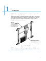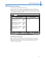
1
EPC®-3305 Hardware Reference www.radisys.com World Headquarters 5445 NE Dawson Creek Drive • Hillsboro, OR 97124 USA Phone: 503-615-1100 • Fax: 503-615-1121 Toll-Free: 800-950-0044 International Headquarters Gebouw Flevopoort • Televisieweg 1A NL-1322 AC • Almere, The Netherlands Phone: 31 36 5365595 • Fax: 31 36 5365620 07-1076-00 July 2000 EPC, iRMX, INtime, Inside Advantage, and RadiSys are registered trademarks of RadiSys Corporation. Spirit, DAI, DAQ, ASM, Brahma, and SAIB are trademarks of RadiSys Corporation. † All other trademarks, registered trademarks, service marks, and trade names are the property of their respective owners. July 2000 Copyright 2000 by RadiSys Corporation All rights reserved Before you begin This guide provides the information you need to install the EPC-3305 and configure its BIOS. It contains detailed hardware reference information for OEMs, system integrators, and others who use the EPC-3305 as a component of their CompactPCI† bus systems. In addition, this manual assumes that you are familiar with PC sytems based on the Intel x86 architecture and have some familiarity with CompactPCI bus architecture. About this guide Guide contents Chapters Chapter 1 Overview 2 Configuration and installation 3 BIOS configuration 4 Theory of operation Description Introduces the EPC-3305, briefly describes its features, and lists specifications. Explains how to install the EPC-3305 in a CompactPCI mainframe and how to install driver software. Explains how to configure the BIOS using the builtin BIOS setup menus. Describes how EPC-3305 components provide a CompactPCI bus compatible embedded computer with standard PC peripherals and a PCI and ISA interfaces. Appendices Appendix A Chipset and I/O map B Interrupts C Connectors D Error messages Description Maps the addresses used for I/O and by the chipset registers. Lists DMA channel and IRQ assignments to the peripherals supported by the EPC-3305. Details the location, form, and pin-outs of the connectors used in the EPC-3305. Provides explanations of common error messages and start-up codes. 1 EPC-3305 Hardware Reference Appendix E Rear Transition module (RTM) F Re-programming the flash chip Description Describes how to install, configure, and use the Rear Transition Module (RTM). Details how to update or recover your system BIOS, Flash Boot Device (FBD), and Boot Block by re-programming all or part of the EPC-3305’s flash chip Notational conventions This manual uses the following conventions: • Screen text and syntax strings appear in this font. • All numbers are decimal unless otherwise stated. • Bit 0 is the low-order bit. If a bit is set to 1, the associated description is true unless otherwise stated. Notes indicate important information about the product. Tips indicate alternate techniques or procedures that you can use to save time or better understand the product. The globe indicates a World Wide Web address. Cautions indicate situations that may result in damage to data or the hardware. This includes situations that may cause damage to hardware via electro-static discharge (ESD). Warnings indicate situations that may result in physical harm to you or the hardware. Where to get more information About the EPC-3305 You can find out more about EPC-3305 from these sources: • World Wide Web: RadiSys maintains an active site on the World Wide Web. The site contains current information about the company and locations of sales offices, new and existing products, contacts for sales, service, and technical support information. You can also send e-mail to RadiSys using the web site. When sending e-mail for technical support, please include information about both the hardware and software, plus a detailed description of the problem, including how to reproduce it. To access the RadiSys web site, enter this URL in your web browser: http://www.radisys.com Requests for sales, service, and technical support information receive prompt response. 2 Before you begin • Other: If you purchased your RadiSys product from a third-party vendor, you can contact that vendor for service and support. About related RadiSys products EPC-3306: The EPC-3306 is a high-performance single-slot CompactPCI module that operates as system controller. It incorporates two PMC sites for flexibility using a variety of PMC modules such as SVGA, LAN adapter or WAN adapters. It offers a choice of three memory configurations to address different needs up to 512 MB. For more information about the EPC-3306, see the RadiSys web site. 3 EPC-3305 Hardware Reference 4 Contents Chapter 1: Overview. Feature summary .............................................................................................................................. CompactPCI bus............................................................................................................................... Specifications ................................................................................................................................... 2. 3. 4. Chapter 2: Configuration and installation. Setting jumpers and headers ............................................................................................................. Flash .......................................................................................................................................... MFG .......................................................................................................................................... Inserting the EPC-3305..................................................................................................................... Maintaining and upgrading the EPC-3305........................................................................................ Removing the EPC-3305 ............................................................................................................ Replacing the battery ................................................................................................................. 6. 6. 7. 7. 8. 8. 8. Chapter 3: BIOS configuration. BIOS Setup Screens ........................................................................................................................... Menu map.................................................................................................................................. Navigation ................................................................................................................................. Main Setup menu ............................................................................................................................. Primary/Secondary Master/Slave sub-menus............................................................................... Keyboard Features sub-menu ..................................................................................................... UBE Shadow Control sub-menu ................................................................................................. About shadow memory regions ........................................................................................... Advanced menu ................................................................................................................................ Console Redirection sub-menu ................................................................................................... I/O Device Configuration sub-menu ........................................................................................... PCI Device Configuration sub-menu .......................................................................................... PCI/PNP ISA UMB Region Exclusion sub-menu .................................................................. PCI/PNP ISA IRQ Resource Exclusion sub-menu ................................................................ Cache Memory sub-menu .......................................................................................................... Advanced Chipset Control sub-menu ......................................................................................... Boot menu ........................................................................................................................................ Exit menu ......................................................................................................................................... CMOS Save and Restore sub-menu ............................................................................................ 11. 12. 12. 13. 15. 19. 21. 21. 23. 26. 28. 30. 31. 32. 33. 38. 39. 40. 42. Chapter 4: Theory of operation. Overview .......................................................................................................................................... Organization..................................................................................................................................... Block diagram ............................................................................................................................ Features ............................................................................................................................................ CPU module............................................................................................................................... Memory map ....................................................................................................................... Interrupt usage..................................................................................................................... 43. 44. 44. 44. 44. 45. 45. v EPC-3305 Hardware Reference Flash boot device ................................................................................................................. BIOS ROM and ROM shadowing ....................................................................................... 443BX host bridge ..................................................................................................................... 443BX PCI bus .................................................................................................................... DRAM/SDRAM memory controller .................................................................................... PIIX4E PCI-ISA bridge ............................................................................................................... PCI-ISA bridge..................................................................................................................... IDE controller...................................................................................................................... Compatibility devices........................................................................................................... Enhanced USB controller ..................................................................................................... SMBus interface and implementation................................................................................... RTC..................................................................................................................................... Power management logic ..................................................................................................... Intel 21154 PCI-PCI bridge ........................................................................................................ CPU board reset on host command over CompactPCI......................................................... Reset Control register .......................................................................................................... 3.3V PMC site............................................................................................................................ CompactPCI Hot Swap .............................................................................................................. PCI bus implementation and devices .......................................................................................... PCI Ethernet controllers....................................................................................................... Ejector handle switch........................................................................................................... Battery ....................................................................................................................................... Super I/O.................................................................................................................................... Floppy disk .......................................................................................................................... COM ports .......................................................................................................................... Keyboard and mouse controller ........................................................................................... Special features .................................................................................................................... CPLD ISA interface.............................................................................................................. Reset controller.................................................................................................................... Reset control........................................................................................................................ Watchdog timer ................................................................................................................... Front panel red/green LED ......................................................................................................... Local interrupt control register................................................................................................... CompactPCI features register ..................................................................................................... BIOS bank switching .................................................................................................................. Power monitoring, consumption, and reset generation ............................................................... 45. 46. 47. 47. 47. 48. 48. 48. 48. 49. 49. 49. 50. 50. 51. 52. 52. 53. 53. 53. 54. 54. 55. 55. 55. 55. 56. 56. 57. 57. 58. 59. 59. 60. 61. 62. Appendix A: Chipset and I/O map. .............................................................................................. 65. Appendix B: Interrupts. .................................................................................................................... 75. Appendix C: Connectors. Connector locations.......................................................................................................................... Backplane J3 and J5.......................................................................................................................... CompactPCI J1 and J2...................................................................................................................... Ethernet ............................................................................................................................................ RS-232 serial port (COM 1) ............................................................................................................. Front panel ....................................................................................................................................... LEDs .......................................................................................................................................... Reset switch ............................................................................................................................... vi 78. 79. 80. 83. 83. 83. 83. 83. Contents Appendix D: Error messages. Boot failures ..................................................................................................................................... 85. Appendix E: Rear Transition module (RTM). Features ............................................................................................................................................ CPU board I/O ........................................................................................................................... Installing and configuring the RTM .................................................................................................. Inserting the RTM...................................................................................................................... Removing the RTM.................................................................................................................... Connectors ....................................................................................................................................... Connector locations ................................................................................................................... Backplane J3 .............................................................................................................................. Backplane J5 .............................................................................................................................. Ethernet ..................................................................................................................................... H1 (COM 1) ............................................................................................................................ IDE (secondary) ......................................................................................................................... Keyboard/mouse ........................................................................................................................ PIM (PMC I/O Module) ............................................................................................................. RS-232 (COM 2) ....................................................................................................................... USB ............................................................................................................................................ 87. 87. 88. 88. 89. 90. 90. 91. 92. 92. 93. 93. 94. 95. 97. 97. Appendix F: Re-programming the flash chip. About the flash chip.......................................................................................................................... About re-programming the flash chip ............................................................................................... Before you begin ............................................................................................................................... Creating a Flash Boot diskette .......................................................................................................... Using phlash.exe to re-program the flash chip .................................................................................. Using BIOS configuration options to re-program the flash chip ........................................................ Using jumpers to re-program the flash chip ...................................................................................... 99. 100. 102. 103. 105. 106. 107. Glossary. ............................................................................................................................................... 109. Index. .................................................................................................................................................... 117. vii EPC-3305 Hardware Reference Figures Figure 1-1. The EPC-3305....................................................................................................................... 1. Figure 2-1. EPC-3305 CPU board: jumper locations ............................................................................... 6. Figure 2-2. Flash header settings ............................................................................................................. 6. Figure 2-3. Replacing the battery ............................................................................................................ 8. Figure 3-1. BIOS Main Setup menu......................................................................................................... 13. Figure 3-2. Primary/Secondary Master/Slave sub-menus.......................................................................... 15. Figure 3-3. Keyboard Features sub-menu ................................................................................................ 19. Figure 3-4. UBE Shadow Control sub-menu............................................................................................ 21. Figure 3-5. Advanced menu..................................................................................................................... 23. Figure 3-6. Console Redirection sub-menu.............................................................................................. 26. Figure 3-7. I/O Device Configuration sub-menu...................................................................................... 28. Figure 3-8. PCI Device Configuration sub-menu ..................................................................................... 30. Figure 3-9. PCI/PNP ISA UMB Region Exclusion sub-menu ................................................................... 31. Figure 3-10. PCI/PNP ISA IRQ Resource Exclusion sub-menu ................................................................ 32. Figure 3-11. Cache Memory sub-menu ................................................................................................... 33. Figure 3-12. Advanced Chipset Control sub-menu .................................................................................. 38. Figure 3-13. Boot menu........................................................................................................................... 39. Figure 3-14. Exit menu............................................................................................................................ 40. Figure 3-15. CMOS Save and Restore sub-menu ..................................................................................... 42. Figure 4-1. Block diagram of the EPC-3305 ............................................................................................ 44. Figure 4-2. Flash boot device memory..................................................................................................... 46. Figure 4-2. BIOS paging .......................................................................................................................... 62. Figure C-1. EPC-3305 Main board: connectors....................................................................................... 78. Figure E-1. EPC-3305 Rear Transition module: connectors..................................................................... 90. Figure F-1. Flash chip configuration........................................................................................................ 99. Figure F-2. Flash chip re-programming coverage..................................................................................... 100. Figure F-3. Flash chip re-programming process flow ............................................................................... 101. viii Contents Tables Table 1-1. EPC-3305 environmental specifications.................................................................................. Table 4-1. 443BX unsupported commands.............................................................................................. Table 4-2. PCI device configuration......................................................................................................... Table 4-3. CPLD I/O ports ...................................................................................................................... Table 4-4. CPLD indexes for function registers ....................................................................................... Table 4-5. Reset control register .............................................................................................................. Table 4-6. Reset event register ................................................................................................................. Table 4-7. Watchdog control register....................................................................................................... Table 4-8. Front panel user LED control ................................................................................................. Table 4-9. Local interrupt enables ........................................................................................................... Table 4-10. CompactPCI features register ............................................................................................... Table 4-11. CompactPCI geographical address........................................................................................ Table 4-12. BIOS control register ............................................................................................................ Table 4-13. Flash banks........................................................................................................................... Table 4-14. Power estimates .................................................................................................................... Table A-1. First (8-bit) DMA controller .................................................................................................. Table A-2. First interrupt controller ........................................................................................................ Table A-3. PCI arbiter control ................................................................................................................. Table A-4. Time/counter functions .......................................................................................................... Table A-5. Keyboard controller ............................................................................................................... Table A-6. Real-time clock ...................................................................................................................... Table A-7. POST checkpoint ................................................................................................................... Table A-8. DMA page registers: Intel EX 82371EB of PC/AT ................................................................. Table A-9. Port A .................................................................................................................................... Table A-10. VGA controller .................................................................................................................... Table A-11. Second interrupt controller .................................................................................................. Table A-12. Power management controller.............................................................................................. Table A-13. Second (16-bit) DMA controller .......................................................................................... Table A-14. Coprocessor interface........................................................................................................... Table A-15. VGA controller .................................................................................................................... Table A-16. Secondary IDE ..................................................................................................................... Table A-17. CPLD................................................................................................................................... Table A-18. Primary IDE......................................................................................................................... Table A-19. ISA Plug and Play................................................................................................................. Table A-20. EGA..................................................................................................................................... Table A-21. Serial I/O (COM 4) port ...................................................................................................... Table A-22. Serial I/O (COM 2) port ...................................................................................................... Table A-23. Secondary IDE ..................................................................................................................... Table A-24. Parallel I/O (LPT1) port ....................................................................................................... Table A-25. EPP port............................................................................................................................... Table A-26. VGA controller .................................................................................................................... Table A-27. EGA controller..................................................................................................................... Table A-28. CGA controller .................................................................................................................... Table A-29. COM 3 serial poert.............................................................................................................. Table A-30. Floppy disk controller .......................................................................................................... Table A-31. Primary IDE......................................................................................................................... Table A-32. Serial I/O (COM 1) port ...................................................................................................... 4. 47. 53. 56. 56. 58. 58. 59. 59. 60. 60. 61. 62. 62. 63. 65. 65. 65. 66. 66. 66. 66. 67. 67. 67. 67. 67. 68. 68. 68. 68. 69. 69. 69. 69. 69. 69. 70. 70. 70. 70. 70. 71. 71. 71. 71. 72. ix EPC-3305 Hardware Reference Table A-33. Interrupts ............................................................................................................................. Table A-34. ECP registers........................................................................................................................ Table A-35. ISA Plug and Play................................................................................................................. Table A-36. 443BX configuration address register .................................................................................. Table A-37. PIIX4E ................................................................................................................................. Table A-38. 443BX configuration data register ....................................................................................... Table B-1. Interrupts ............................................................................................................................... Table C-1. Backplane connector J3.......................................................................................................... Table C-2. Backplane connector J5.......................................................................................................... Table C-3. Compact PCI J1 connector..................................................................................................... Table C-4. Compact PCI J2 connector..................................................................................................... Table C-5. RJ45 phone jack pin-out ........................................................................................................ Table C-6. DB-9 pin-out.......................................................................................................................... Table E-1. Backplane connector J3 .......................................................................................................... Table E-2. Backplane connector J5 .......................................................................................................... Table E-3. RJ45 phone jack pin-out ........................................................................................................ Table E-4. H1 (COM 2) pin-out.............................................................................................................. Table E-5. Secondary IDE connector ...................................................................................................... Table E-6. Keyboard/mouse pin-out ........................................................................................................ Table E-7. PIM connector pin-out: J20.................................................................................................... Table E-8. PIM connector pin-out: J24.................................................................................................... Table E-9. DB-9 pin-out .......................................................................................................................... Table E-10. USB connector pin-out ......................................................................................................... x 72. 72. 72. 72. 72. 73. 75. 79. 79. 80. 81. 83. 83. 91. 92. 92. 93. 93. 94. 95. 96. 97. 97. 1 Overview The EPC-3305, a CompactPCI† Peripheral Processor Board, operates in a 6U peripheral slot of a CompactPCI system. The EPC-3305 hardware is compatible with all major PC software environments including Microsoft† Windows† 95, Windows 98, and Windows NT† 4.0. It can also run other PC operating systems, including Linux†, Solaris†, and DOS. The EPC-3305 includes these subsystems: CPU board A single-slot system controller which plugs into a 6U System Slot of a CompactPCI system. Rear Transition module A rear I/O transition module which plugs into a rear I/O slot of a CompactPCI system. Figure 1-1. The EPC-3305 The EPC-3305 requires a backplane that supports the CompactPCI Specification Revision 2.1 and the pinouts detailed in Table E-1, Backplane connector J3 and Table E-2, Backplane connector J5. 1 EPC-3305 Hardware Reference Feature summary This section describes CPU board features. For more information about RTM features, see Appendix E, Rear Transition module (RTM). The EPC-3305 CPU board is a Pentium† III-based, PC-compatible, single slot CompactPCI computer designed for use with CompactPCI bus. The EPC-3305 is an EMC2-based design that accepts a Pentium III based EMC2. To achieve this, the CPU board uses the Intel 21554 PCI-PCI bridge (Drawbridge), a non-transparent PCI-PCI bridge that allows the CPU board to interface to an intelligent host. The Intel Pentium III chipset (443BX and PIIX4E) provides the local PCI (bus-0) interface. Four integrated PCI peripherals provide cPCI, dual Ethernet, EIDE, and ISA interfaces. Of these, the PIIX4E provides the EIDE, and ISA interfaces. The EPC-3305 CPU board includes: • Intel EMC2: Pentium III with 100 MHz. Front Side Bus • Intel North Bridge 443BX: Host Bus to PCI bridge Memory bus controller • 64-bit CompactPCI interface on J1/J2 using Intel 21554 non-transparent PCI bridge with I/O slot compatibility • Hot Swappable • Two PMC sites with RTM Interface on Jn4 • On-board SDRAM operating at 100MHz; up to 512MB of ECC SDRAM on board. Build-time options allow for configurations of: 128M, 256M or 512M • Optional Rear Transition Module provides: • 2 • COM 1 RS232 (DB9) • COM 1 RS232 (10 pin header) • One USB connector • Connectors for mouse and keyboard • A header for secondary EIDE • Two Ethernet ports that support 10/100BASE-T • PIM S17E Intel South Bridge PIIX4E: • PCI to ISA bridge • Battery-backed RTC • Two independent EIDE channels • 4MByte Boot Block Flash memory, partitioned into eight 512Mbyte banks • Onboard headers for: • Floppy • ITP • Mouse/Keyboard • RadiSys manufacturing Header • Port 80 Header • CPLD JTAG Chapter 1: Overview • • • Front Panel Interface • Blue HS LED • RJ45 for COM-1 • RJ45 for Ethernet 1 • Reset Button National Semiconductor 87309 Super I/O • Two RS-232 serial ports • Floppy drive connection • Intel 82C42 compatible keyboard and mouse controller Programmable Watchdog timer with two programmable timeouts: • The first timeout can be set to provide NMI and/or INIT to CPU allowing for a “soft” reset. • The second timeout forces a “hard” reset. CompactPCI bus The CompactPCI bus is accessed from the EPC-3305’s PCI bus via an Intel 21554 PCI-to-PCI bridge. This bridge connects the onboard PCI bus (bus 0) with the CompactPCI bus (bus 1), which may have as many as seven additional CompactPCI devices connected to it. The CompactPCI standard was developed by a consortium of manufacturers known as the PCI Industrial Computer Manufacturers Group (PICMG). For more information about PICMG and the CompactPCI standard consult the PICMG website at this URL: http://www.picmg.org 3 EPC-3305 Hardware Reference Specifications Table 1-1. EPC-3305 environmental specifications Characteristic Temperature Humidity Airflow Vibration Shock EMC ESD susceptibility1 Radiated susceptibility1 1 4 State Operating Value 0°C to 60°C at point of entry of forced air derated 2°C per 1000 ft (300 m) over 6600 ft (2000m) with sufficient airflow to keep within the termperature specification. Storage –40°C to 85°C Operating/storage 5% to 95% noncondensing 10% per hour maximum excursion gradient Operating 200 LFM (linear feet per minute) Operating 0.04G2/Hz from 5–1000 Hz random, 10 min. per sweep cycle Storage 0.06G2/Hz from 5–1000 Hz random, 10 min. per sweep cycle Operating 30 G, 11 ms duration, half-sine shock pulse Storage 50G, 11ms, half-sine shock pulse Operating Designed to pass CE Mark and FCC Class B Operating 4KV direct contact, 8KV air Operating IEC 801-3:1984/EN50082-1 (1992): 3V/m (not tested) Performance criteria: A These are system-level tests. The EPC-3305’s conformance to these specifications may be affected by the rest of the system’s ability to conform. 2 Configuration and installation This chapter explains how to install the EPC-3305 in a CompactPCI chassis. When reading this file online, you can immediately view information about any installation topic by placing the mouse cursor over a connector name and clicking. For information about... Go to this page... Setting jumpers and headers............................................................................... 6 Inserting the EPC-3305....................................................................................... 7 Maintaining and upgrading the EPC-3305 .......................................................... 8 Removing the EPC-3305.................................................................................. 8 Replacing the battery....................................................................................... 8 Avoid causing ESD (electrostatic discharge) damage: • Remove modules from their antistatic bags only in a static-free environment. • Perform the installation process (described later in this chapter) only in a static-free environment. • During external cable installation, ensure that the cables are not active. The EPC-3305 is not designed for hot insertion of any interface. The EPC-3305 modules, like most other electronic devices, are susceptible to ESD damage. ESD damage is not always immediately obvious. It can cause a partial breakdown in semiconductor devices that might not result in immediate failure. Other setup is done by configuring BIOS options as described in Chapter 3, BIOS configuration. 5 EPC-3305 Hardware Reference Setting jumpers and headers Flash: MFG Figure 2-1. EPC-3305 CPU board: jumper locations Jumper pins are labeled from the point of view of looking at the front of the connector. Flash The CPU board provides a 2x5-pin header (H2) that you use to re-program the Flash chip. For detailed information about re-programming the flash chip, see Appendix F, Re-programming the flash chip. Flash jumper settings are typically used during manufacturing for re-programming the BIOS in the Flash Boot Device (FBD) and are included here only for reference. There are no user-configurable jumpers on the test header for normal operation. 1 2 1 2 9 10 9 10 Pins 1 and 2: Force BIOS Recovery Pins 4 and 5: Boot Block Enable Figure 2-2. Flash header settings Function Force BIOS Recovery 6 Pins 1, 2 Description To force recovery of the BIOS, connect pin 1 (~FRC_RCVR) to pin 2 (GND). This signal is connected to the P1.3 input of the keyboard controller. It is readable by the Boot Block BIOS code and forces the Boot Block to initiate a recovery sequence at power-up should other methods of initiating the sequence become inaccessible. Chapter 2: Configuration and installation Function Boot Block Enable Pins 4, 5 Description To enable re-programming of the Boot Block, connect pin 5 (BBEN) to pin 4 (VCC). The BBEN pins are separated to prevent accidental connections of these pins (i.e. they cannot be easily jumpered together). The Boot Block is typically NEVER re-programmed, even when the main and parameter blocks are re-programmed. However, the capability to program the Boot Block facilitates quick changes during manufacturing. MFG This jumper block is reserved by the board manufacturer for testing purposes. Inserting the EPC-3305 You install the EPC-3305 CPU board on the CompactPCI bus backplane. Before installation, ensure that all options are installed on the EPC-3305 as described in Maintaining and upgrading the EPC-3305 later in this chapter. 1. RadiSys recommends that power to your CompactPCI system is off. When handling or inserting the EPC-3305, avoid touching the circuit board and connector pins, and ensure that the environment is static-free. 2. Ensure that the ejector handles are in the normal (eject) position. (Push the top handle up and the bottom handle down so that the handles are now tilted.) 3. Slide the EPC-3305 module into the slot. Use firm pressure on the handles to mate the module with the connectors and snap connectors into normal position. 4. Tighten the retaining screws in the top and bottom of the front panel to ensure proper connector mating and prevent the module from loosening due to vibration. 5. Connect peripherals to the EPC-3305. Periperals typically include a video display and keyboard, but also perhaps a mouse, modem, USB device, and so on. For information about connector pinouts, see Appendix C, Connectors and Appendix E, Rear Transition module (RTM) Observe the following while the system is powered up: • Do not plug cables or connectors into the front panel connectors. Because electronics equipment generally cannot withstand fluctuations in power, damage can arise from plugging in a device or board while power is on. • Do not plug in a serial or parallel device, keyboard, transceiver, monitor or other component. This applies to equipment at either end of an interface cable. 6. Complete remaining steps as required. Typical remaining steps include: 7 EPC-3305 Hardware Reference • BIOS configuration (For information about setting up the BIOS configuration, see Chapter 3, BIOS configuration) • Driver software installation • Application software installation Your system may be preconfigured by your supplier or you may need to perform these tasks yourself. Maintaining and upgrading the EPC-3305 Removing the EPC-3305 To remove the EPC-3305 from the CompactPCI chassis: 1. Press the latch part of the extractors inward until the extractor handle swings out and pivots freely. 2. Pull outward on the extractor handles until the EPC-3305 disengages from the rear connector. 3. Slide the EPC-3305 out of the CompactPCI chassis and place it in the anti-static bag that it came in. Replacing the battery 1. Before you begin, write down all the CMOS setup parameters while the battery is still good, or save them, using the CMOS save and restore feature of the BIOS configuration as described in the Exit menu on page 40. 2. Turn off the power. If you leave the power on when removing the battery, setup values return to default conditions. 3. Remove the EPC-3305 from the CompactPCI chassis as described in Removing the EPC-3305. 4. Locate the battery on the main board, then lift the battery out. Battery Figure 2-3. Replacing the battery 8 Chapter 2: Configuration and installation 5. Press the new battery into place, positive (+) side up. There is danger of explosion if battery is incorrectly replaced. Replace only with same or equivalent type recommended by RadiSys. Dispose of used batteries according to manufacturer’s instructions. 6. Replace the EPC-3305 in the CompactPCI chassis as described in Inserting the EPC-3305. 7. Restore the CMOS settings as described in the CMOS Save and Restore submenu on page 42. After replacing the battery, you may need to reset the system clock. 9 EPC-3305 Hardware Reference 10 3 BIOS configuration The EPC-3305 uses the Phoenix NuBIOS to configure and select various system options. This chapter details the various menus and sub-menus used to configure the system. This chapter is written as though you are setting up each field in sequence and for the first time. Your system may be correctly pre-configured and require very little setup. To revert to the original BIOS settings, select Get Default Values from the Exit menu on page 40. This restores the original BIOS settings. You may see some error messages during the execution of the BIOS initialization sequence. If errors occur during the POST (Power-On Self-Test), the BIOS displays the error on the appropriate line of the screen display and, depending on how your system is configured, either pauses or tries to continue. For information about error messages, see Appendix D, Error messages. Pressing the Escape key during POST displays the Boot-First pop-up menu after POST completes. You can use this menu to override, for only this boot, the boot options. This menu includes the same options as the Boot Menu’s top level. For information about the options, see Boot menu on page 39. BIOS Setup Screens The EPC-3305’s BIOS includes a setup program that displays and modifies the system configuration. The EPC-3305’s nonvolatile CMOS RAM stores configuration information, and the BIOS uses it to initialize the EPC-3305 hardware. You can enter the BIOS Setup only during the system reset process, following a power-up, front panel reset, or equivalent. To enter Setup, press the F2 key when prompted. 11 EPC-3305 Hardware Reference Menu map You set up the BIOS by making selections from the menus shown in the next table. When reading this file online, you can immediately view information about any menu by placing the mouse cursor over menu name and clicking: Menu Main Setup menu Advanced menu Boot menu Exit menu Sub-menu Primary/Secondary Master/Slave sub-menus Keyboard Features sub-menu UBE Shadow Control sub-menu I/O Device Configuration sub-menu PCI Device Configuration sub-menu PCI/PNP ISA UMB Region Exclusion sub-menu PCI/PNP ISA IRQ Resource Exclusion sub-menu Cache Memory sub-menu None CMOS Save and Restore sub-menu Navigation To... Display a menu Do... Press the left or right cursor (arrow) keys and press the Enter key. If you use the arrow keys to leave a menu and then return, your active field is always at the beginning of the menu. Display a submenu Move the cursor to a field with a triangle and press the (fields with a triangle at left) Enter key. If you select a sub-menu and then return to the main menu, the active field is that sub-menu heading. Select a field Press the up or down cursor (arrow) keys Select an option Do one of these: • Press the + and – keys to rotate through available options. • In certain numeric fields, simply enter the desired number. The remainder of this chapter describes the fields in each menu and sub-menu. Additional help information is available in the help area on the Setup screen. 12 Chapter 3: BIOS configuration Main Setup menu PhoenixBIOS Setup Utility Main Advanced Main Boot Exit System Time: System Date: [16:17:18] [01/01/1997] BIOS Version 01.00.00 Legacy Diskette A: Legacy Diskette B: [1.44/1.25 MB 3½”] [Disabled] Primary Master Primary Slave Secondary Master Secondary Slave [None] [None] [None] [None] Keyboard Features UBE Shadow Control System Memory: Extended Memory: 640 KB 31744 KB F1 ESC Help Exit ↑↓ ←→ Select Item Select Menu Item Specific Help <Tab>, <Shift-Tab>, or <Enter> selects field. -/+ Change Values Enter Select Sub-Menu F9 F10 Setup Defaults Save and Exit Figure 3-1. BIOS Main Setup menu The far right menu in the menu bar is the Exit Menu. Use the options in the Exit menu to save your changes, re-load default BIOS settings, and so on. Press the ESC key to go immediately to the Exit Menu. The fields in each menu and sub-menu are explained below. Additional help information is available in the help area on the BIOS setup screen. Field Description System Time/System Date Sets the system time and date. To change these values, go to each field and enter the desired value. Press the tab key to move from hour to minute to second, or from month to day to year. The default system time is 00:00; the default date is 01/01/1998. BIOS Version Identifies the BIOS version. This is the same BIOS version that displays during boot. This field is not editable; no user interaction is required. 13 EPC-3305 Hardware Reference Field LegacyDiskette A LegacyDiskette B Description Identifies the type of floppy disk drive installed as the A: or B: drive. Possible settings include: • Disabled (default for the B: drive) • 1.44/1.25MB 31/2" (default for the A: drive) Note: The 1.25MB 31/2" diskette requires a 3-Mode floppy disk drive. • 1.2MB, 5¼" • 2.88 MB, 3½" • 360 KB, 5¼" • 720 KB, 3½" Primary Master sub-menu Displays a menu that you use to enter information for the master IDE drive connected to the primary IDE controller. For more information, see Primary/Secondary Master/Slave sub-menus on page 15. Primary Slave sub-menu Displays a menu that you use to enter information for the slave IDE drive connected to the primary IDE controller.For more information, see Primary/Secondary Master/Slave sub-menus on page 15. Secondary Displays a menu that you use to enter information for the Master sub-menu Master IDE drive connected to the secondary IDE controller. For more information, see Primary/Secondary Master/Slave sub-menus on page 15. Secondary Displays a menu that you use to enter information for the Slave sub-menu Master IDE drive connected to the secondary IDE controller. For more information, see Primary/Secondary Master/Slave sub-menus on page 15. Boot Options sub-menu Displays a menu that you use to specify the PC’s behavior during the boot process. For more information, see Boot menu on page 39. Keyboard Features Displays a menu that you use to enable or disable various sub-menu keyboard features. For more information, see Keyboard Features sub-menu on page 19. UBE Shadow Control Displays a menu that you use to specify BIOS shadow sub-menu options. For more information, see UBE Shadow Control sub-menu on page 21. System memory Displays the amount of conventional memory (below 1MB). This field is not editable; no user interaction is required. Extended memory Displays the amount of extended memory (above 1MB). This field is not editable; no user interaction is required. 14 Chapter 3: BIOS configuration Primary/Secondary Master/Slave sub-menus There are a total of four IDE adapter sub-menus for the primary and secondary hard disk controllers, each having a master and slave drive menu. Access this screen to: • See or reconfigure the detailed characteristics of the primary hard disk (select the IDE Adapter 0 Master item from the Main BIOS Setup). • Set up new disks and allow the Setup program to determine the proper settings based on information on the disk. Note that the Setup program can detect these settings only on drives that comply with ANSI specifications. • Set up existing (formatted) disks. Note that you must use the same parameters used when the disk originally was formatted. You must select an option for the Type field, then enter the specific cylinder, head, and sector information listed on the label attached to the drive at the factory. PhoenixBIOS Setup Utility Main Main Primary Master [Primary Master ] Type: [Auto] CHS format Cylinders: Heads: Sectors: Item Specific Help <Tab>, <Shift-Tab>, or <Enter> selects field. [ 0] [ 1] [ 0] LBA Format Total Sectors: Maximum Capacity: 0MB 0MB Multi-Sector Transfers: LBA Mode Control: 32 Bit I/O: Transfer Mode: [Disabled] [Disabled] [Disabled] [Standard] [Disabled] Ultra DMA Mode F1 ESC Help Exit ↑↓ ←→ Select Item Select Menu -/+ Change Values Enter Select Sub-Menu F9 F10 Setup Defaults Save and Exit Figure 3-2. Primary/Secondary Master/Slave sub-menus 15 EPC-3305 Hardware Reference Field Type Cylinders Heads Sectors Maximum Capacity 16 Description Identifies the disk type. You can select one of these: Note: You must press + and - to change this field’s values. • Auto (default): Select this option when you want the POST to query the hard disk for its parameters whenever the POST runs. Note: If you set a hard disk to “Auto”, but no hard disk is actually present, the BIOS queries the (non-existent) hard disk until it times out, slightly increasing the duration of the POST. • None: Select this option if yours is not an IDE hard disk drive. • User: Select this option if you have an IDE disk but cannot employ the “Autotype” feature. Then enter the correct drive values for cylinders, heads, sectors/track, and write precompensation. • CD-ROM: Select this option if you have a CD-ROM drive. Note: For disks not supplied, consult the product documentation. When finished, press the ESC key to return to the Main Setup menu. Specifies the number of cylinders on this system. You can specify a number from 1 to 16. Note: You can edit this field only when the Type field contains a value of [User]. Specifies the number of heads on this system. Note: You can edit this field only when the Type field contains a value of [User]. Specifies the number of sectors in each track on this system. Note: You can edit this field only when the Type field contains a value of [User]. Displays the amount of disk space available on this system. This field is not editable; no user interaction is required. Note: This field displays in the Primary Master sub-menu only if the Type field contains a value of [Auto] or [User]. It displays in the Secondary Master, Primary Slave and Secondary Slave sub-menus only if the Type field contains a value of [Auto]. Chapter 3: BIOS configuration Field Multi-Sector Transfers LBA Mode Control 32-bit I/O Description Allows the System BIOS to read ahead by the specified number of sectors during disk access. This has the effect of reading more data at once to reduce the absolute number of discrete disk reads performed by the operating system, which may increase system performance. You can select one of these: • Disabled (default if no drive is installed) • 2 Sectors • 4 Sectors • 8 Sectors • 16 Sectors (default if a drive is installed) Note: Autotyping may change this value if the hard disk reports that it supports block accesses. Determines how the System BIOS references hard disk data. You can use this option only if both the hard disk being configured and the operating system support Logical Block Addressing (LBA). Autotyping may change this value if the hard disk reports that it supports LBA. You can select one of these: • Disabled (default if no drive is installed): Reference hard disk data using the Cylinders/Heads/Sectors (CHS) method. • Enabled (default if a drive is installed): Reference hard disk data as logical blocks. Determines how the System BIOS accesses the hard disk controller. Autotyping does not affect this option. Accesses with 32-bit I/O accesses. This option increases system performance. You can select one of these: • Disabled: Select this option if an ISAbus IDE controller is installed in the system. • Enabled: Select this option to maximize system performance when the onboard PCI IDE controller is used. 17 EPC-3305 Hardware Reference Field Transfer Mode Ultra DMA Mode 18 Description Selects the mode that the System BIOS uses to access the hard disk. You can select one of these: • Standard (default) • Fast PIO 1 • Fast PIO 2 • Fast PIO 3 • Fast PIO 4 • FPIO 3 / DMA 1 • FPIO 4 / DMA 2 Older hard disks only support “Standard”. Newer hard disks adhering to “Fast ATA” or “Enhanced IDE” specifications may support the fast programmed I/O or DMA modes. Note that autotyping may change this value depending on the transfer modes that the hard disk reports it supports. The fast DMA modes take full advantage of the onboard bus mastering hard disk controller and should yield the highest performance when used in conjunction with multitasking operating systems that support it. Selects the Ultra DMA Mode that the System BIOS uses to access the hard disk. You can select one of these: • Mode 2 (default) • Mode 1 • Mode 0 • Disabled Note: Autotyping derives this value from information reported by the drive. Chapter 3: BIOS configuration Keyboard Features sub-menu Use this sub-menu to enable or disable various keyboard features. PhoenixBIOS Setup Utility Main Main Keyboard Features NumLock: Key Click: Keyboard auto-repeat rate: Keyboard auto-repeat delay: F1 ESC Help Exit ↑↓ ←→ Item Specific Help [Auto] [Disabled] [30/sec] [1/2 sec] Select Item Select Menu <Tab>, <Shift-Tab>, or <Enter> selects field. -/+ Change Values Enter Select Sub-Menu F9 F10 Setup Defaults Save and Exit Figure 3-3. Keyboard Features sub-menu Field Numlock Key Click Description Determines whether the keypad keys (the Numlock feature) operates. You can select one of these: • Auto (default): Engages the Numlock feature at boot. • Off: Disengages the Numlock feature at boot. • On: Engages the Numlock feature at boot. Determines whether the keyboard produces an audible click each time a key is pressed. You can select one of these: • Disabled (default): The keyboard does not produce audible clicks when keys are pressed. • Enabled: The keyboard produces an audible click each time a key is pressed. 19 EPC-3305 Hardware Reference Field Description Keyboard auto-repeat rate Sets the auto-repeat rate when holding a key down on the keyboard. You can select one of these: • 30/seconds (default) • 26.7/seconds • 21.8/seconds • 18.5/second • 13.3/seconds • 10/seconds • 6/seconds • 2/seconds Keyboard auto-repeat Sets the delay between when a key is pressed and when delay the auto-repeat feature begins. You can select one of these: • ¼ second • ½ second (default) • ¾ second • 1 second 20 Chapter 3: BIOS configuration UBE Shadow Control sub-menu Use this menu to specify BIOS shadow options. Shadowing refers to the technique of copying BIOS extensions from ROM into DRAM and accessing them from DRAM. This allows the CPU to access the BIOS extensions much more quickly and generally increases system performance if many calls to the BIOS extensions are made. PhoenixBIOS Setup Utility Main Advanced UBE Shadow Control Item Specific Help BIOS Extension Source Offset: Shadow Destination address: BIOS Extension Size: [1C000h ] [D6000h] [8KB] BIOS Extension Source Offset: Shadow Destination address: BIOS Extension Size: [1C000h ] [D6000h] [8KB] BIOS Extension Source Offset: Shadow Destination address: BIOS Extension Size: [1C000h ] [D6000h] [8KB] F1 ESC Help Exit ↑↓ ←→ Select Item Select Menu <Tab>, <Shift-Tab>, or <Enter> selects field. -/+ Change Values Enter Select Sub-Menu F9 F10 Setup Defaults Save and Exit Figure 3-4. UBE Shadow Control sub-menu About shadow memory regions There is no effect on the system if a region is shadowed that does not contain a BIOS extension. Note that each shadow region in the setup menu is 16KB in size. Multiple shadow regions may have to be enabled if the BIOS extension to be shadowed is larger than 16KB. 21 EPC-3305 Hardware Reference Field BIOS Extension Source Offset Shadow Destination Address BIOS Extension Size 22 Description Controls the location of the user BIOS extension to shadow. You can select one of these: • Disabled (default) • E000h • 0000h • 10000h • 2000h • 12000h • 4000h • 14000h • 6000h • 16000h • 8000h • 18000h • A000h • 1A000h • C000h • 1C000h Controls the destination address of the BIOS extension in shadow memory. You can select one of these: • D0000h • D8000h • D2000h • DA000h • D4000h • DC009h • D6000h (default) • DE000h Note: This field displays only if the BIOS Extension Source field contains a value other than [Disabled]. Size of the extension in increments of 8KBytes. You can select one of these: • 8KBytes (default) • 40KBytes • 16KBytes • 48KBytes • 24KBytes • 56KBytes • 32KBytes • 64KBytes Note: This field displays only if the BIOS Extension Source field contains a value other than [Disabled]. Chapter 3: BIOS configuration Advanced menu This menu contains settings for integrated peripherals, memory shadow, cache, and large disk access mode. You access this menu by selecting Advanced from the Main BIOS Setup menu. PhoenixBIOS Setup Utility Main Advanced Main Boot Ethernet 1 Port: BIOS Reboot: Exit [Auto detect] [Warm Start] Console Redirection I/O Device Configuration PCI Configuration Cache Memory Item Specific Help <Tab>, <Shift-Tab>, or <Enter> selects field. QuickBoot Mode: [Disabled] Installed O/S: [No] Reset Configuration Data: [No] PS/2 Mouse: [No] Legacy USB Support: [Disabled] Large Disk Access Mode: [Other] Local Bus IDE adapter: [Both] Advanced Chipset Control F1 ESC Help Exit ↑↓ ←→ Select Item Select Menu -/+ Change Values Enter Select Sub-Menu F9 F10 Setup Defaults Save and Exit Figure 3-5. Advanced menu Field Ethernet 1 Port BIOS Reboot Console Redirection sub-menu Description Determines whether the system checks for Ethernet connections. You can select one of these: • Auto Detect (default): The system checks for Ethernet connections on both the front and rear panel connectors. • Front Panel: The system checks for Ethernet connections on the front panel connectors. • Real Panel: The system checks for Ethernet connections on the rear panel connectors. Determines the reboot type. You can select one of these: • Warm Start (default): The system performs an abbreviated reboot and preserves DRAM memory contents. • Cold Start: The system reboots as if power was cycled. Displays a menu that you use to redirect console output. For more information, see Console Redirection sub-menu on page 26. 23 EPC-3305 Hardware Reference Field Description I/O Device Configuration Displays a menu that you use to configure peripheral sub-menu devices. For more information, see I/O Device Configuration sub-menu on page 28. PCI Device Configuration Displays a menu that you use to configure PCI devices. sub-menu For more information, see PCI Device Configuration sub-menu on page 30. Cache Memory sub-menu Displays a menu that you use to control the use of the CPU cache. For more information, see Cache Memory sub-menu on page 33. Quick Boot Mode Determines which tests run during boot. • Disabled (default): Runs all tests. Select this option to ensure a robust boot. • Enabled: Skips some tests. Select this option to boot more quickly. Installed OS Identifies the OS you plan to use on this system. Identifying the OS determines how much initialization the BIOS performs. You can select one of these: • Other (default): The Plug-and-Play BIOS completes PCI initialization. Select this option when you plan to use an OS other than Windows 95. • Win95: Only boot devices are initilized; the remainder of initialization is completed by the OS. Select this option when you plan to use Windows 95 as your OS. Note: Setting this to the incorrect value may produce unexpected results. Reset Configuration Data Determines whether to clear the Extended System Configuration Data (ESCD) block that resides in the Flash Boot Device (FBD). You can select one of these: • No (default): Does not clear the ESCD block. • Yes: Clears the ESCD block. You must clear the block the first time a system is turned on or if the ESCD becomes corrupted. This option automatically resets to “No” after the block is cleared. PS/2 Mouse Determines whether a PS/2 mouse functions on this system. • Auto Detect (default): Allows the system BIOS to determine whether a PS/2 mouse functions on this system. • Enabled: Sets the system to use a PS/2 mouse, if installed. • Disabled: Prevents any installed PS/2 mouse from functioning and frees IRQ 12. 24 Chapter 3: BIOS configuration Field Legacy USB Support Description Determines whether the system supports the Legacy Universal Serial Bus (USB). You can select one of these: • Enabled (default): The system supports the Legacy USB. Select this option only if you use a USB keyboard or mouse, and you use it with an OS that does not have USB drivers. This option reduces system performance due to frequent SMI interrupts (see note below). • Disabled: The system does not support the Legacy USB. USB is still functional during POST; it is disabled at INT19 (Boot Time). Note: USB is implemented using SMIs and, if enabled, consumes CPU, IRQ, and memory resources. Many current OSs such as Windows 98 or Windows 2000 include built-in USB support and do not rely on BIOS USB support. Large Disk Access Mode Specifies whether MS-DOS systems can use hard disks up to 8GB (1024C x 255H x 63S) without special drivers or LBA. If the drive fails while installing new software, change this setting and try again. You can select one of these: • DOS (default): Causes the System BIOS to perform cylinder/head translation if the drive is configured in Setup to have more than 1024 cylinders. Select this option if your system uses a drive larger than 528 MB and runs DOS or MS-DOS†. • Other: Select this option if your system uses a drive larger than 528 MB and runs an OS other than DOS. Local Bus IDE Adapter Configures the integrated local bus IDE adapter. You can select one of these: • Both (default) • Disabled • Primary • Secondary Advanced Chipset Control Displays a menu that you use to control chip behavior. For sub-menu more information, see Advanced Chipset Control sub-menu on page 38. 25 EPC-3305 Hardware Reference Console Redirection sub-menu Options in this menu configure console redirection. PhoenixBIOS Setup Utility Main Advanced Main Boot Com Port Address [On-board COM A] Baud Rate Console Type Flow Control Console connection: Continue C.R. after POST: F1 ESC Help Exit ↑↓ ←→ Exit [PC ANSI] [CTS/RTS] [Direct] [Off] Select Item Select Menu Item Specific Help <Tab>, <Shift-Tab>, or <Enter> selects field. -/+ Change Values Enter Select Sub-Menu F9 F10 Setup Defaults Save and Exit Figure 3-6. Console Redirection sub-menu Field COM Port Address Baud Rate Console Type 26 Description Specifies the serial port to use for console redirection. You can select one of these: • On-board COM A (default): The system uses COM A for redirection. • On-board COM B: The system uses COM B for redirection. • Disabled: The system does not redirect input. Specifies the baud rate at which the COM port operates. You can select one of these: • 600 • 9600 • 1200 • 19.2 • 2400 • 38.4K • 4800 • 115.2 Identifies the console type. You can select one of these: • PC ANSI (default) • VT100 Chapter 3: BIOS configuration Field Flow Control Description Specifies flow control. You can select one of these: • CTS/RTS (default) • XON/XOFF • None Console connection Specifies how the console connects to the system. You can select one of these: • Direct (default): Connects the console directly to the system. • Via modem: Connects the console to the system via a modem. Continue C.R. after POST Determines whether console redirection occurs. You can select one of these: • Off (default): Console redirection stops after the OS loads. • On: Console redirection continues after the OS loads. 27 EPC-3305 Hardware Reference I/O Device Configuration sub-menu Use the options in this sub-menu to configure the onboard serial and parallel port and disk controllers. PhoenixBIOS Setup Utility Main Advanced I/O Device Configuration Serial port A: Base I/O address: Interrupt: [3F8] [IRQ 4] [Enabled] Serial port B: Base I/O address: Interrupt: [2F8] [IRQ 4] F1 ESC Help Exit ↑↓ ←→ <Tab>, <Shift-Tab>, or <Enter> selects field. [Enabled] Floppy disk controller: Base I/O address: Item Specific Help [Enabled] [Primary] Select Item Select Menu -/+ Change Values Enter Select Sub-Menu F9 F10 Setup Defaults Save and Exit Figure 3-7. I/O Device Configuration sub-menu Field Description Serial Port A/Serial Port B Configures the selected serial port. You can select one of these: • Enabled (default): The user configures the serial port. • Auto: Either the BIOS or OS configures the serial port. • Disabled: The serial port is not configured. Base I/O Address Configures the base address for the serial port. If you select a value already used by another serial port, an asterisk displays at the left side of the screen. You can select one of these: • 2F8 (default, Port B) • 2E8 • 3F8 (default, Port A) • 3E8 Note: This field displays only if the Serial Port field contains a value of [Enabled]. 28 Chapter 3: BIOS configuration Field Interrupt Floppy Disk Controller Base I/O Address Description Configures the serial port interrupt. You can select one of these: • IRQ3 (default, Port B) • IRQ4 (default, Port A) Note: This field displays only if the Serial Port field contains a value of [Enabled]. Determines whether the floppy disk controller is available for use. You can select one of these: • Enabled (default): User configuration. • Disabled: No configuration. • Auto: Either the BIOS or OS configures the floppy disk. Configures the base address for the parallel port. You can select one of these: • Primary (default) • Secondary 29 EPC-3305 Hardware Reference PCI Device Configuration sub-menu Use the options in this sub-menu to control the exclusion of the UMB region for PCI or ISA and the exclusion of the IRQs for PCI or ISA. PhoenixBIOS Setup Utility Main Advanced PCI Configuration ISA graphics device installed: PCI IRQ line A: PCI IRQ line B: PCI IRQ line C: PCI IRQ line D: Item Specific Help [No] [Auto Select] [Auto Select] [Auto Select] [Auto Select] <Tab>, <Shift-Tab>, or <Enter> selects field. PCI/PNP ISA UMB Region Exclusion PCI/PNP ISA IRQ Resource Exclusion F1 ESC Help Exit ↑↓ ←→ Select Item Select Menu -/+ Change Values Enter Select Sub-Menu F9 F10 Setup Defaults Save and Exit Figure 3-8. PCI Device Configuration sub-menu Field ISA graphics device installed Description Specifies whether an ISA graphics device is installed in the system. • No (default): No ISA graphics device exists in this system. • Yes: An ISA graphics device exists in this system. PCI IRQ Line A–D Determines which IRQ is used by PCI IRQ (PIRQ) 1, 2, 3, and 4. You can select one of these: • Auto Select (default) • 9 • Disabled • 10 •3 • 11 •4 • 12 •5 • 14 •7 • 15 PCI/PNP ISA UMB Region Displays a menu that you use to control the exclusion of Exclusion sub-menu PCI and ISA Upper Memory Block (UMB) regions. For more information, see PCI/PNP ISA UMB Region Exclusion sub-menu on page 31. 30 Chapter 3: BIOS configuration Field PCI/PNP ISA IRQ Resource Exclusion sub-menu Description Displays a menu that you use to control the exclusion of PCI and ISA interrupt resources. For more information, see PCI/PNP ISA IRQ Resource Exclusion sub-menu on page 32. PCI/PNP ISA UMB Region Exclusion sub-menu The PCI/PNP ISA UMB Region Exclusion Sub-Menu controls the exclusion of PCI and ISA UMB regions. PhoenixBIOS Setup Utility Main Advanced PCI/PNP ISA UMB Region Exclusion D000–D3FF: D400–D7FF: D800–DBFF: DC00–DFFF: F1 ESC Help Exit [Available] [Available] [Available] [Available] ↑↓ ←→ Select Item Select Menu Item Specific Help <Tab>, <Shift-Tab>, or <Enter> selects field. -/+ Change Values Enter Select Sub-Menu F9 F10 Setup Defaults Save and Exit Figure 3-9. PCI/PNP ISA UMB Region Exclusion sub-menu Field Memory Regions Description Determines the use of each UMB region. You can select one of these: • Available (default): Makes the regions available for PCI use. • Reserved: Reserves the specified block of upper memory regions for ISA use. 31 EPC-3305 Hardware Reference PCI/PNP ISA IRQ Resource Exclusion sub-menu The PCI/PNP ISA IRQ Resource Exclusion Sub-Menu controls the exclusion of PCI and ISA interrupt regions. PhoenixBIOS Setup Utility Main Advanced PCI/PNP ISA IRQ Resource Exclusion IRQ 3: IRQ 4: IRQ 5: IRQ 7: IRQ 9: IRQ 10: IRQ 11: IRQ 12: F1 ESC Help Exit [Available] [Available] [Available] [Reserved] [Available] [Reserved] [Reserved] [Available] ↑↓ ←→ Select Item Select Menu Item Specific Help <Tab>, <Shift-Tab>, or <Enter> selects field. -/+ Change Values Enter Select Sub-Menu F9 F10 Setup Defaults Save and Exit Figure 3-10. PCI/PNP ISA IRQ Resource Exclusion sub-menu Field Interrupts 32 Description Determines the use of each interrupt. You can select one of these: • Available (default for IRQs 3, 4, 5, 9, and 12): Makes the ISA IRQ available for PCI use. • Reserved (default for IRQs 7, 10, and 11): Reserves the interrupt for ISA use. Select this option if the IRQ is required by an on-board ISA peripheral or an ISA card. Note: The following interrupts are reserved for the following purposes: IRQ7 Hot Swap / Enum IRQ10 Soft reset IRQ11 Hot Swap / Latch Chapter 3: BIOS configuration Cache Memory sub-menu The options in this sub-menu control the cacheability of certain memory regions and also the settings of the Level 2 (L2) cache. PhoenixBIOS Setup Utility Main Advanced Memory Cache Item Specific Help Memory Cache: [Enabled] Cache System BIOS Area: [Write Protect] Cache Video BIOS Area: [Write Protect] Cache Base 0–512k: [Write Back] Cache Base 512k–640k: [Write Back] Cache Extended Memory Area [Write Back] Cache A000 – AFFF: Cache B000 – BFFF: Cache C800 – CBFF: Cache CC00 – CFFF: Cache D000 – D3FF: Cache D400 – DFFF: Cache D800 – DBFF: Cache DC00 – DFFF: Cache E000 – E3FF: F1 ESC Help Exit ↑↓ ←→ <Tab>, <Shift-Tab>, or <Enter> selects field. [Disabled] [Disabled] [Disabled] [Disabled] [Disabled] [Disabled] [Disabled] [Disabled] [Write Protect] Select Item Select Menu -/+ Change Values Enter Select Sub-Menu F9 F10 Setup Defaults Save and Exit Figure 3-11. Cache Memory sub-menu Field Memory Cache Description Determines whether to use L1 and L2 memory caching. You can select one of these: • Enable (default): L1 and L2 memory caching occurs. • Disable: L1 and L2 memory caching does not occur. Cache System BIOS Area Determines whether the System BIOS is cached in DRAM. You can select one of these: • Write Protect (default): caches the System BIOS in the F0000h through FFFFFh DRAM area • uncached: Does not cache the system BIOS. Cache Video BIOS Area Determines whether the VGA BIOS is cached in a region. You can select one of these: • Write Protect (default): caches the VGA BIOS in the C0000h through C7FFFh region. • uncached: Does not cache the VGA BIOS. 33 EPC-3305 Hardware Reference Field Cache Base 0–512k Cache Base 512–640k Cache Extended Memory Area 34 Description Determines how the system caches base memory in the specified area: You can select one of these: • Write Back (default): Writes and reads to and from system memory are cached, then written to system memory when you perform a write-back operation. Select this option to reduce bus traffic by eliminating unnecessary writes to system memory. This option provides the best performance, but requires that all devices that access system memory on the system bus be able to snoop memory accesses to ensure system memory and cache coherency. • Write Through: Writes and reads to and from system memory are cached. Select this option for frame buffers or when there are devices on the system bus that access system memory, but do not perform snooping of memory accesses. • Write Protect: Reads come from cache lines when possible, and read misses cause cache fills. Writes are propagated to the system bus and cause corresponding cache lines on all processors on the bus to be invalidated. Speculative reads are allowed. • uncached: The system does not cache memory. Determines how the system caches extended memory. You can select one of these: • Write Back (default): Writes and reads to and from system memory are cached, then written to system memory when you perform a write-back operation. Select this option to reduce bus traffic by eliminating unnecessary writes to system memory. This option provides the best performance, but requires that all devices that access system memory on the system bus be able to snoop memory accesses to ensure system memory and cache coherency. • Write Through: Writes and reads to and from system memory are cached. Select this option for frame buffers or when there are devices on the system bus that access system memory, but do not perform snooping of memory accesses. • Write Protect: Reads come from cache lines when possible, and read misses cause cache fills. Writes are propagated to the system bus and cause corresponding cache lines on all processors on the bus to be invalidated. Speculative reads are allowed. • uncached: The system does not cache memory. Chapter 3: BIOS configuration Field Cache Memory Regions: A000–AFFF B000–BFFF Description Determines how the system deals with specified memory blocks or shadow1 memory. You can select one of these: • Disabled (default): The system does not cache memory. • USWC Caching: System memory locations are not cached (as with uncacheable memory) and coherency is not enforced by the processor’s bus coherency protocol. Speculative reads are allowed. Writes may be delayed and combined in the write buffer to reduce memory accesses. Select this option for video frame buffers, where the write order is unimportant as long as the writes update memory so they can be seen on the graphics display. • Write Back: Writes and reads to and from system memory are cached, then written to system memory when you perform a write-back operation. Select this option to reduce bus traffic by eliminating unnecessary writes to system memory. This option provides the best performance, but requires that all devices that access system memory on the system bus be able to snoop memory accesses to ensure system memory and cache coherency. • Write Through: Writes and reads to and from system memory are cached. Select this option for frame buffers or when there are devices on the system bus that access system memory, but do not perform snooping of memory accesses. • Write Protect: Reads come from cache lines when possible, and read misses cause cache fills. Writes propagate to the system bus and cause corresponding cache lines on all processors on the bus to be invalidated. Speculative reads are allowed. When BIOS extensions are present in these regions, enabling caching for that region increases performance 35 EPC-3305 Hardware Reference Field Cache Memory Regions: C800–CBFF CC00–CFFF D400–D7FF D800–DBFF DC00–DFFF 36 Description Memory regions. Determines how the system deals with specified memory blocks or shadow1 memory. You can select one of these: • Disabled (default): The system does not cache memory. • Write Back: Writes and reads to and from system memory are cached, then written to system memory when you perform a write-back operation. Select this option to reduce bus traffic by eliminating unnecessary writes to system memory. This option provides the best performance, but requires that all devices that access system memory on the system bus be able to snoop memory accesses to ensure system memory and cache coherency. • Write Through: Writes and reads to and from system memory are cached. Select this option for frame buffers or when there are devices on the system bus that access system memory, but do not perform snooping of memory accesses. • Write Protect: Reads come from cache lines when possible, and read misses cause cache fills. Writes propagate to the system bus and cause corresponding cache lines on all processors on the bus to be invalidated. Speculative reads are allowed. When BIOS extensions are present in these regions, enabling caching for that region increases performance Chapter 3: BIOS configuration Field Cache Memory Regions: E000–E3FF E400–E7FF E800–EBFF EC00–EFFF 1 Description Memory used in the E0000h–EFFFFh DRAM region. Determines how the system deals with specified memory blocks or shadow1 memory. You can select one of these: • Disabled (default): The system does not cache memory. • Write Back: Writes and reads to and from system memory are cached, then written to system memory when you perform a write-back operation. Select this option to reduce bus traffic by eliminating unnecessary writes to system memory. This option provides the best performance, but requires that all devices that access system memory on the system bus be able to snoop memory accesses to ensure system memory and cache coherency. • Write Through: Writes and reads to and from system memory are cached. Select this option for frame buffers or when there are devices on the system bus that access system memory, but do not perform snooping of memory accesses. • Write Protect: Reads come from cache lines when possible, and read misses cause cache fills. Writes propagate to the system bus and cause corresponding cache lines on all processors on the bus to be invalidated. Speculative reads are allowed. When BIOS extensions are present in these regions, enabling caching for that region increases performance Shadowing refers to the technique of copying BIOS extensions from ROM into DRAM and accessing them from DRAM. This allows the CPU to access the BIOS extensions much more quickly and generally increases system performance if many calls to the BIOS extensions are made. 37 EPC-3305 Hardware Reference Advanced Chipset Control sub-menu Options in this menu control ?. PhoenixBIOS Setup Utility Main Advanced Main ECC Config: Boot Exit [ECC] Item Specific Help <Tab>, <Shift-Tab>, or <Enter> selects field. F1 ESC Help Exit ↑↓ ←→ Select Item Select Menu -/+ Change Values Enter Select Sub-Menu F9 F10 Figure 3-12. Advanced Chipset Control sub-menu Field ECC Config 38 Description You can select one of these: • ECC (default) • EC • ECC Scrub • Disabled Setup Defaults Save and Exit Chapter 3: BIOS configuration Boot menu The Boot menu: • Specifies the order in which the system tries to boot from devices attached to the system. • Specifies the boot order of devices in the same class, such as hard drives. Boot order is assigned from top to bottom, with the uppermost enabled boot device in each class being the boot candidate from that device class. PhoenixBIOS Setup Utility Main Advanced Main Boot Exit + Hard Drive + Removable Devices ATAPI CD-ROM Drive Network Boot MBA UNDI (Bus 0 Slot 2) MBA UNDI (Bus 0 Slot 3) F1 ESC Help Exit ↑↓ ←→ Item Specific Help <Tab>, <Shift-Tab>, or <Enter> selects field. Select Item Select Menu -/+ Change Values Enter Select Sub-Menu F9 F10 Setup Defaults Save and Exit Figure 3-13. Boot menu To move an item to a higher level in the list, highlight the item and then press the “+” key. To move an item to a lower level in the list, highlight the item and then press the “–” key. To display all boot device sub-menus under all respective device types, press the Ctrl and Enter keys at the same time. To display a sub-menu that lists all devices of a specified type available on the system, highlight the device type and press the Enter key. If more than one device of that type exists, use the “+” and “–” keys to change the boot order within the given device type To enable a device, highlight the desired device and press the Shift and 1 keys. An exclamation point ( ! ) displays to the left of enabled devices. To disable a device. highlight the device, then press the Shift and 1 keys again. 39 EPC-3305 Hardware Reference Field Boot order Description Determines the boot order of boot devices. This is the default boot order: 1. Hard Drive 2. Removable Devices 3. ATAPI CD-ROM Drive 4. Network Boot 5. MBA UNDI (Bus 0 Slot 2) 6. MBA UNDI (Bus 0 Slot 3) Exit menu Use the options in this menu to save and exit, or abandon your changes and exit to the system. PhoenixBIOS Setup Utility Main Advanced Main Boot Exit Exit Saving Changes Exit Discarding Changes Load Setup Defaults Discard Changes Save Changes Exit & Update BIOS Item Specific Help <Tab>, <Shift-Tab>, or <Enter> selects field. CMOS Save & Restore F1 ESC Help Exit ↑↓ ←→ Select Item Select Menu -/+ Change Values Enter Select Sub-Menu F9 F10 Setup Defaults Save and Exit Figure 3-14. Exit menu Field Exit Saving Changes Exit Discarding Changes 40 Description Saves into CMOS the values you just entered and exits the Setup program. The new values load, and the system reboots. Discards the changes you just made and reverts to the BIOS as it was before you entered the BIOS Setup program. The system boots with the old values. Chapter 3: BIOS configuration Field Load Setup Values Discard Changes Save Changes Exit & Update BIOS CMOS Save & Restore sub-menu Description Resets the BIOS values to the original, default values set at the factory, before any suppliers or other end users made changes. Loads the system with the values that existed before this editing session started. You do not exit. Saves to CMOS the edits you made during this session but does not exit the Setup program. Updates the BIOS from a floppy disk. For detailed information about updating the BIOS from a floppy disk, see Appendix F, Re-programming the flash chip. Note: Select this exit option only if you obtained BIOS update replacement software from your supplier and reviewed the documentation and procedures provided with that distribution. This option changes the flash contents only if the vendor-supplied floppy is installed. If you select this option by mistake, changes made to the BIOS are lost unless already saved using the Save Current Values option. The system automatically seaches for the update program that should be on the floppy disk inserted in drive A. If no floppy exists, cycle power to reset the system to its previous state. Displays a menu that controls how the system handles CMOS values. For more information, see CMOS Save and Restore sub-menu on page 42. 41 EPC-3305 Hardware Reference CMOS Save and Restore sub-menu Use the options in this menu to save, restore, or erase CMOS settings in the FBD (Flash Boot Device). PhoenixBIOS Setup Utility Main Exit CMOS Save & Restore CMOS Restore Condition: [Never] Item Specific Help <Tab>, <Shift-Tab>, or <Enter> selects field. Save CMOS to Flash Restore CMOS from Flash Erase CMOS from Flash F1 ESC Help Exit ↑↓ ←→ Select Item Select Menu -/+ Change Values Enter Select Sub-Menu F9 F10 Setup Defaults Save and Exit Figure 3-15. CMOS Save and Restore sub-menu Field Restore Condition Description Determines the conditions under which the BIOS restores CMOS RAM from the FBD when booting. You can select one of these: • Never (default) • CMOS Corruption • Always Save CMOS to Flash Immediately saves current settings in the Setup program to CMOS RAM and into the FBD. This process may take several seconds to complete. Note: Always select this option before restoring CMOS from Flash. Restore CMOS from Flash Immediately restores CMOS RAM and current settings in the Setup program from the FBD. Note: This option is available only if the CMOS was previously saved to the FBD. Erase CMOS from Flash Immediately erases the CMOS image stored in the FBD. 42 4 Theory of operation Chapter 4 Overview The EPC-3305 includes these subsystems: • CPU board: A single-slot peripheral CPU which plugs into a 6U peripheral slot of a CompactPCI system. • Rear Transition module (RTM): A rear I/O transition module which plugs into a rear I/O slot of a CompactPCI system. For more information about the RTM, see Appendix E, Rear Transition module (RTM). The EPC-3305’s CPU board is a Pentium-III based, PC-compatible, single-slot CompactPCI computer designed for use with CompactPCI bus. The CPU board can pass hardware compatibility tests for Microsoft’s Windows 95, Windows 98, and Windows NT 4.0. It can also run other PC operating systems, including Linux, Solaris, and DOS. 43 EPC-3305 Hardware Reference Organization Block diagram The next figure shows the division and interconnection of EPC-3305 functions. These are described below. Switching regulator Mobile PIII FSB Intel PIII LPM 443BX host bridge Kybd, Mouse FDD HDR HDR AGP PCI Bank 0 Bank 2 Bank 3 Bank 4 128MByte 128MByte 128MByte 128MByte on-board on-board on-board on-board SDRAM SDRAM SDRAM SDRAM batt. ISA Super I/O PIIX4E PCMSA Flash memory Watchdog timer and Reset Controller PCI-33MHz SEC IDE ENET 10/100 BaseT ENET 10/100 BaseT USB0 USB1 PMC PCI/PCI PMC J11/J12 J21/J22 bridge 64bit cPCI PMC J14 PMC J24 COM1, 2 Reset switch RJ45 RJ45 PMC B PMC B cPCI J3 cPCI J5 cPCI J1/J2 Front panel Figure 4-1. Block diagram of the EPC-3305 Features CPU module The design of the board centers on an Intel EMC2 (Embedded Mobile Cartridge). The EMC2 incorporates a 500MHz Pentium III processor. The 443BX Host Bridge and core voltage power supply are also included on the EMC2. The module connects to the board by a 400-pin connector that routes the PCI and Memory bus to the system and power and ground pins to the module. The CPU bus frequency is 100MHz. 44 Chapter 4: Theory of operation Memory map The 232 byte physical address space seen by the Intel Pentium III occupies three areas: 1. From 0 to 1 MB is largely defined by the IBM PC/AT architecture. 2. From 1 to 256 MB depends on how much DRAM is installed in the EPC-3305. 3. Memory addresses from the Pentium between 0 and 4 MB (0FFFFFFFh) is mapped as follows: Range 0–640Kb 640Kb–1MB Content 00000000–0009FFFF First 640 KB of DRAM (DOS memory) 000A0000–000BFFFF VGA video DRAM, mapped to the Video Module 000C0000–000CBFFF Write-protected DRAM containing shadowed video BIOS (48 KB) 000D0000–000DFFFF BIOS extensions 000E0000–000FFFFF System BIOS shadow 1MB–512MB 00100000–0FFFFFFF DRAM (511 MB) 512MB–top 1MB Top 512Kb Cacheable Yes No Yes Yes1 Yes 10000000–FFEFFFFF ISA bus (aliased) Yes2 No FFF80000–FFFFFFFF Flash memory No 1 If no BIOS extensions, ISA bus (aliased); not cacheable. 2 If no DRAM, ISA bus (aliased); not cacheable. Interrupt usage For details about EPC-3305 PC-compatible interrupt usage, see Appendix B, Interrupts. Flash boot device A boot block Flash memory stores system start-up code for the CPU board. This is flash-updatable BIOS containing the boot, main, and parameter blocks shown in Figure 4-2. The Main and Parameter blocks of the BIOS are reprogrammed under program control. Registers contained within the 443BX protect these areas from inadvertent writes. The BIOS chip select signal asserts only when the chipset is to write within the range of the BIOS Flash boot device. This device is 1Mbyte and is controlled as having two pages of 512kBytes. A register in the CPLD controls the paging. 45 EPC-3305 Hardware Reference The Plug-and-Play ESCD is also stored in the Boot-Block FLASH device in the block addressed from FFFFA000h–FFFFBFFFh. This block is always accessible for re-programming. Use extreme caution when re-programming the flash chip. The Boot Block rarely changes and should not require re-programming. For information about re-programming the Flash chip, see Appendix F, Re-programming the flash chip. A “forced recovery” jumper is provided and is connected to the G-PI2O of the PIIX4. The Boot Block can read this jumper and can force a recovery sequence at power-up should other methods of initiating the sequence, such as crisis recovery, become inaccessible. The Flash BIOS device is memory addressed and resides in the last 512 KB of system memory at address FFF80000h–FFFFFFFFh. BIOS ROM and ROM shadowing The EPC-3305 utilizes a Flash Boot Device (FBD) as its BIOS ROM. The BIOS ROM is mapped into the top of the processor's 32-bit address space. The BIOS consists of a 16 KByte boot block and the System BIOS in the 96KB Main block and both 8KB parameter blocks. The layout is described in the next figure. Physical address Device offset FFFFFFFFh FFFFC000h 16 KB BIOS Recovery Code FFFFFh FC000h FFFFBFFFh FFFFA000h 8 KB Parameter Block 2 ESCD FBFFFh FA000h FFFF9FFFh FFFF8000h 8 KB Parameter Block 1 F9FFFh F8000h FFFF7FFFh FFFE0000h 96 KB Main Block 8 System BIOS, PCI BIOS, Plug n Play BIOS Manufacturing BIOS F7FFFh E0000h FFFDFFFFh FFFC0000h 128 KB Main Block 7 DFFFFh C0000h FFFBFFFFh FFFA0000h 128 KB Main Block 6 User Extensions (128KB) BFFFFh A0000h FFF9FFFFh FFF80000h 128 KB Main Block 5 CSR/CMOS data 9FFFFh 80000h Figure 4-2. Flash boot device memory 46 Chapter 4: Theory of operation The BIOS initialization software copies the ROM contents into DRAM (a process called shadowing) at addresses E0000h–FFFFFh. The VGA BIOS is copied into C0000h–C7FFFh of DRAM. After copying into these areas, the BIOS write-protects them. Subsequent writes to these areas complete successfully but do not alter the data in DRAM. There are two parameter blocks, each 8KB in size, used for BIOS code. 443BX host bridge The Intel 443BX is a 492 pin BGA running on 3.3V with mixed +5V, 3.3V, and GTL+ termination voltages. It dissipates a maximum of 3W if AGP is disabled. The 443BX contains support for a CPU-to-PCI bridge, a CPU-to-AGP bridge, a DRAM/ SDRAM memory controller, and the central arbitration functions for the PCI bus. The 443BX supports concurrent CPU, AGP, and PCI transactions to main memory. 443BX PCI bus The Intel 443BX supports CPU-to-PCI cycles. The 443BX and the PCI CLK run at 33 MHz. When acting as a PCI target, the 443BX does not respond to the cycles listed in the left column of Table 4-1. When acting as a bus master on behalf of the CPU, the 443BX does not issue PCI commands for the host bus commands listed in the right column of Table 4-1. Table 4-1. 443BX unsupported commands PCI target Interrupt acknowledge Special cycle I/O read I/O write Configuration read Configuration write Dual address cycle Reserved commands Host bus Deferred reply Branch trace message Memory read of 16 bytes Memory write of 16 bytes EA memory access PCI Bus features include: • • • • • Fully synchronous, minimum latency 33 MHz PCI bus interface Zero wait state CPU-to-PCI write timings (no IRDY stall) PCI 2.1 compliant Data streaming support from PCI to DRAM Supports five PCI bus masters in addition to the Host and PCI to ISA bridge DRAM/SDRAM memory controller The 443BX supports 66 MHz or 100 MHz SDRAM memory. Memory is in a 16Mx8-bit format. The CPU includes four banks of nine chips, each bank capable of accommodating 128MB of memory with ECC. The CPU board may be purchased with 128MB, 256MB, or 512MB of soldered-down memory. 47 EPC-3305 Hardware Reference The 443BX generates all control signals (such as ~RAS, ~CAS, ~WE, ~CS, and ~DQM) and multiplexed addresses for the SDRAM array. The address and data flow through the 443BX for all SDRAM accesses. PIIX4E PCI-ISA bridge The Intel PIIX4E is a 324 pin BGA that runs on +3.3V with a reference voltage tied to +5V for +5V signal compatibility. It dissipates a maximum of 1 W. The PIIX4E provides support for a PCI-to-ISA bridge, an IDE controller, compatibility devices, a dual USB controller, SMBus, a real time clock (RTC), and power management logic. A detailed description of each of these follows. PCI-ISA bridge The PIIX4E is PCI 2.1 and IEEE996 compatible (ISA, AT bus). On PCI, the PIIX4E operates as a bus master for various internal modules, such as the USB controller, DMA controller, IDE bus master controller, distributed DMA masters, and on behalf of ISA masters. Internal registers or cycles passed to the ISA or EIO buses make the PIIX4E operate as a target. All internal registers are positively decoded. The PIIX4E chip drives the ISA bus directly. The PIIX4E incorporates an ISA bus compatible master and CPU interface, and can drive five ISA slots without external data buffers. The ISA interface also provides byte swap logic, I/O recovery support, wait state generation, and SYSCLK generation. There are three devices on the CPU board connected to the ISA bus: SuperI/O, Flash ROM BIOS, and Watchdog CPLD. IDE controller The PIIX4E fast IDE interface supports up to four IDE devices through two independent IDE signal channels. The IDE interface supports PIO IDE transfers up to 14 MB/s and Bus Master IDE transfers up to 33 MB/s. It does not consume any ISA DMA resources and integrates eight 32-bit buffers for optimal transfers. The PIIX4E chip supports Modes 1, 2, 3, and 4 as well as Bus Master (DMA) Modes 0, 1, and 2. There is no support for the obsolete IDE register at I/O address 0x3F7. The PIIX4E supports “Ultra DMA/33” Synchronous DMA Mode Transfers. Only PCI Masters have access to the IDE port. ISA Bus masters cannot access the IDE I/O port addresses. The IDE data transfer command strobes, DMA request and grant signals, and IORDY signals interface directly to the PIIX4E chipset. The primary IDE channel is connected to on-board Flash with an IDE interface. A header for the secondary IDE is available on the RTM. Compatibility devices The PIIX4E contains three compatibility devices: • 48 DMA controller: The DMA controller incorporates the logic of two 82C37 DMA controllers. The DMA controller has seven independently programmable channels. Channels [3:0] are hardwired to 8 bit, count-by-byte transfers. Channels [7:5] are hardwired to 16-bit, count by word transfers. Any two of the seven DMA channels can provide support for fast Type-F transfers. The DMA Chapter 4: Theory of operation controller also generates the ISA refresh cycles. The DMA controller supports two separate methods for handling legacy DMA via the PCI bus: • PC/PCI protocol: Allows PCI-based peripherals to initiate DMA cycles by encoding requests and grants via three PC/PCI ~REQ/~GNT pairs. • Distributed DMA: Allows PCI devices to receive reads and writes to 82C37 registers. The DMA controller also provides support for the serial interrupt scheme typically associated with Distributed DMA. • Timer/counters: The timer/counter block contains three counters that are equivalent in function to those found in one 82C54 programmable interval timer. The timer/counter block provides the system timer function, refresh request, and speaker tone. The 14.31818 MHz oscillator input provides the clock source for these three counters. • Interrupt controller: The ISA-compatible interrupt controller incorporates the functionality of two 82C59 interrupt controllers. Cascading of the interrupt controllers provides 14 external and two internal interrupts. Additionally, PIIX4E supports a serial interrupt scheme. All registers in these modules can be read and restored. This allows saving and restoring the system state after removing power and restoring it to the circuit. Enhanced USB controller The PIIX4E USB controller provides enhanced support for the Universal Host Controller Interface (UHCI). This includes support that allows legacy software to use a USB-based keyboard and mouse. When enabled, the USB controller uses PIRQD. The USB ports are routed to CompactPCI Backplane connector J3. SMBus interface and implementation The PIIX4E SMBus interface allows the CPU to communicate via SMBus to other peripherals. The SMBus is a subset of the I2C protocol. RTC The real-time clock (RTC): • Keeps track of time of day by counting seconds, minutes, hours, days, day of the week, date, month, and year with leap year compensation. Daylight savings compensation is optional. • Provides a time-of-day alarm with once a second to once a month range, periodic rates of 122 ms to 500 ms, and end-of-update cycle notification. • Stores system data including during a system power-down via battery backedup operation. The PIIX4E RTC is Motorola MC146818 RTC compatible with 256 bytes battery backed RAM in two banks: • Standard bank: Contains 10 bytes indicating time and date information, 4 bytes used as four Control Register (A,B,C,D), and 114 bytes used as general purpose RAM. 49 EPC-3305 Hardware Reference • Extended bank: Contains 128 bytes used as general purpose RAM. Time, calendar, and alarm can be represented in either binary or BCD format. The format is determined by bit 2 of Control Register B. The hour is represented in 12- or 24-hour format, and the format is selected by bit 1 of Control Register B. When changing the format, the time registers must be reinitialized to the corresponding data format. The RTC operates on a 32.768 kHz crystal and a separate battery. The RTC also supports two lockable memory ranges. Configuration space allows locking two 8 byte ranges to read and write accesses by setting specific bits. This prevents unauthorized reading of passwords or other system security information. The RTC (as supported by the BIOS) is Y2K compliant. Power management logic The PIIX4E provides full support for the Advanced Configuration and Power Interface (ACPI) Specification. For detailed information, see the 82371AB PCI-to-ISA / IDE Xcelerator (PIIX4) specification available from Intel’s web page. Intel 21154 PCI-PCI bridge Do not disable this clock via the Chip Control Register (bit-11 at CD:CCh) in the 21554 PCI Configuration space. The Secondary clock out from the 21554 is used by the CPU board. This clock output is enabled at POR by an external strapping option. The 21554 performs PCI bridging functions for embedded and intelligent I/O applications. The 21554 is a non-transparent PCI-to-PCI bridge that acts as a gateway to an intelligent subsystem. The 21554 functions as a bridge between two PCI processor domains, the host domain and the local domain. Special features of the 21554 include: • Support for independent primary and secondary PCI clocks • Independent primary and secondary address spaces • Address translation between the primary (host) and secondary (local) PCI buses (domains). The 21554 creates a configuration barrier between the two PCI domains. Standard hierarchical PCI configuration methods using Type 1 configuration transactions cannot be used to access the configuration space of devices on the opposite side of the 21554. The 21554 uses a Type 0 configuration header, which presents the entire subsystem as a single “device” to the host processor. The 21554 forwards transactions between the primary and secondary PCI buses as does a transparent PCI-to-PCI bridge. In contrast to a transparent PCI-to-PCI bridge, however, the 21554 can translate the address of a forwarded transaction from a system address to a local address, or vice versa. This mechanism allows the 50 Chapter 4: Theory of operation 21554 to hide subsystem resources from the host processor and to resolve any resource conflicts that may exist between the host and local subsystems. The 21554 configuration space is divided into these parts: • Primary interface configuration registers • Secondary interface configuration registers • Device-specific configuration registers Both the primary and secondary interface configuration headers contain the 64-byte Type 0 configuration header that corresponds to that interface. The device-specific configuration registers are specific to the 21554, some of which apply to the primary interface, others to the secondary interface, and some to other 21554 functions. Both the primary and secondary interfaces support access to the 21554 configuration registers. The serial ROM attached to the 21554 can pre-load some configuration parameters prior to initialization. This enables vendor-specific configuration parameters to load into the 21554 configuration registers, replacing default values specified by Intel. These vendor-specific parameters load before configuration of the 21554 by the local and/or host processors. Pre-loadable parameters include address mapping requirements, Class Code, Subsystem ID and Subsystem Vendor ID, and others. During the preload operation, all accesses to the 21554 configuration registers receive a target retry. CPU board reset on host command over CompactPCI The CPU board may be reset by the System Slot CPU. This is achieved by having the Host write to the Reset Control Register in the Drawbridge’s PCI configuration space. The secondary reset out from the Drawbridge will force a hard reset of the CPU board. There are two bits the host can use, bit-0 and bit-1. If it is desired to hold the CPU board in rest the host should write a value of one to D8. The board will then stay in reset until the host clears that bit. If it is desired to only reset the board, the host should set D8 to a value of two. This will reset the board and is self clearing, requiring no further action by the host. (21554 PCI-to-PCI Bridge for Embedded Applications User’s Manual, page 7-39 ) 51 EPC-3305 Hardware Reference Reset Control register Primary byte offset: DB:D8h Secondary byte offset: DB:D8h Bit 0 Name Secondary Reset R/W R/(WP) 1 Chip Reset R/(WP) Description Secondary bus reset. When 0: The 21554 deasserts s_rst_l. This bit must be cleared by a configuration write in the case when it is set by a configuration write. Otherwise, it clears automatically after 100 msec or when p_rst_l deasserts. When 1: The 21554 asserts s_rst_l. This bit is set automatically when the Chip Reset bit is written with a 1 or when p_rst_l is asserted, or is set with aconfiguration write. Reset value: 0 (disabled). 1 Chip Reset R/(WP) Chip reset control. When 1: Causes the 21554 to perform a chip reset and to assert s_rst_l. Data buffers, configuration registers, and both the primary and secondary interfaces are reset to their initial state. The 21554 clears this bit once chip reset is complete. Reset value: 0 3.3V PMC site The CPU Board supports a two PMC sites on the system board. Each PMC site uses three PMC connectors. Two connectors (denoted as J11 and J12 on slot A and J21 and J22 on slot B) carry the 32-bit PCI signals.The third connector (denoted as J14 on slot A and J24 on slot B) routes the PMC I/O signals. The I/O signals from slot A are routed to cPCI connector J5 while the I/O signals from slot B are routed to CompactPCI connector J3. PMC A has a four 100ohm differential pairs that go to the J5 connector. These signal are paired as follows: Pair 1: PMCA 25 and 15 Pair 2: PMCA 29 and 28 Pair 3: PMCA 19 and 18 Pair 4: PMCA 26 and 22 Both PMC sites provide power for 3.3V, 5V, 12V and –12V. The PCI interface uses 3.3V signaling and is keyed for 3.3V operation. 52 Chapter 4: Theory of operation CompactPCI Hot Swap The CPU Board can interrupt the local processor with IRQ10 on a hot swap switch event. The hot swap switch is indirectly connected to IRQ10. If enabled, this IRQ line will be asserted as long as the ejector handles are open. The local processes may use this interrupt to perform and orderly shut down. For details of software control for the hot swap interrupt, see Special features on page 56. PCI bus implementation and devices The CPU board implements a +3.3V, 32-bit local PCI bus. The bus runs at 33 MHz and has the 443BX as the central resource. The local PCI bus has these peripherals connected to it: • Host/PCI bus bridge (described in 443BX host bridge on page 47) • PCI/ISA bridge • Two Ethernet controllers • PCI-to-PCI bridge chip • Two PMC sites Table 4-2 describes the on-board devices PCI configuration space. The IDSEL pin on each device connects to the listed PCI address pin. To select the configuration registers of a given device, a PCI Configuration Space access must be made with the device’s corresponding IDSEL address bit set. Table 4-2. PCI device configuration Peripheral Intel BX443 North Bridge PCI Intel BX443 North Bridge AGP1 Intel 82559 Ethernet 1 Intel 82559 Ethernet 2 PMC site A PMC site B Intel 21154 PCI-PCI bridge PCI/ISA bus bridge (PIIX4E) PCI/ISA bridge IDE interface USB (if enabled) 1 This IDSEL AD11 AD12 Device Function I~INTx Arbitration signals REQ/GNT 0 0 – – 1 0 – – AD13 AD14 A15 A16 AD19 AD19 2 3 4 5 8 10 0 0 0 0 0 C D A,B,C,D A,B,C,D A 0 1 2 – – 0 1 3 4 2 ~PHLD/~PHLDA directly from the BX443 device is disabled, but consumes a logical device space as indicated. PCI Ethernet controllers Two Intel 82559 fast Ethernet controllers incorporate internal MAC and PHY interfaces, providing support for 10/100BASE-T connections. The two Ethernet controllers route their RX/TX pairs to CompactPCI Backplane connector J5. One of the controllers also routes its RX/TX pair to an RJ45 connector on the front 53 EPC-3305 Hardware Reference panel. For the Ethernet channel routed to both the front panel and J5 there is an auto detect circuit, which routes the signal to the appropriate RJ45. Once the autodetect circuit has routed the signal, only a loss of link can cause the auto-detect circuit to re-activated. The Ethernet controllers use PCI interrupts and REQ/GNT signals shown in Table 4-2. PCI Device Configuration. The 82559s have a standard PCI 2.1 compliant configuration space allowing easy system identification and configuration. The PHY enables direct connection to the network media using a 25 MHz, 25 ppm crystal to derive its internal transmit digital clocks. In 100BASE-TX mode, the analog subsection of the PHY does the following: • Takes received analog data from the RD pair and converts it into a digital 125 Mbps stream, recovering both clock and data. • Converts a digital 125 Mbps stream into the proper format and drive it through the TD pair into the physical medium. The 82559 defines a maximum distance of 25.4 mm between itself and the associated magnetics and another 25.4 mm distance between the magnetics and the RJ45. The Intel specification for distance from the PHY to the magnetics must be violated in this design since the magnetics reside on the RTM near the RJ45. Ejector handle switch Two ejector handles with built-in switches are provided on the front panel of the CPU Board. Releasing the ejector handles from the lock position to the eject position sets a switch which is connected to the LID input of the PIIX4E. When asserted, the LID input sets a bit in the general purpose status register (see the PIIX4E datasheet for more details). Assertion of this bit can generate an SMI if this response is enabled. The BIOS does not enable the SMI feature. The OS/application software must enable the SMI feature and have a SMI handler in place to respond to this type of event. Battery The 3.0V lithium battery supplied with the EPC-3305 and mounted on the CPU board is a Renata CR2032 “coin cell” or equivalent. Should the battery fail, you may obtain and install a replacement. For information about replacing the battery, see Replacing the battery on page 8. Write down all CMOS setup parameters while the battery is still good, or save them using the options available on the BIOS configuration’s CMOS Save and Restore sub-menu. The battery powers the CMOS RAM and TOD clock when system power is not present. If system power is present, the +5V voltage also powers the CMOS RAM and TOD clock. This is done with the +3.3V isolation diodes, so that either the 54 Chapter 4: Theory of operation onboard battery or the +3.3V power supply voltage can supply power and neither power source affects the other. The battery has an expected battery life of 2 years on continuous battery power. In a system that is powered on much of the time and where the ambient power-off temperature is less than 60°C, the battery is estimated to have a life of 10 years. Super I/O The National PC87309 SuperI/O controller provides a floppy controller, parallel port, serial port, and a keyboard and mouse controller. It interfaces through the ISA bus and requires external decoding of the high-orer address bits for full 16-bit decoding required by PC95/PC97. It uses a 48MHz clock. This design does not use the chip’s parallel port features. Floppy disk The floppy controller device resides inside the Super I/O chip and is accessed at the standard PC I/O addresses 3F0–3F7h. Floppy interrupts are signaled on IRQ6. The floppy signals connect to a header on the CPU board allowing ribbon cable connection of a floppy disk drive. Power is provided to the floppy disk drive via a jumper that allows user selection of powered or non-powered connection. COM ports The Super I/O includes two RS-232 compatible serial ports. The Super I/O chip includes 16C550 compatible UARTs with separate send and receive 16-byte FIFOs. • COM 1: Configured at I/O addresses 3F8–3FFh and uses IRQ4, COM 1 signals pass through a RS232 transceiver IC and out the front panel via an RJ45 connector. This transceiver’s I/O pins meet the electrical portion of the EIA/ TIA-232-E specification as well as EIA/TIA-574-E. COM 1 signals also go out CompactPCI Backplane connector J3. Do not use both the front and rear connections to COM 1 at the same time. Only one connection to COM 1 may be used at a time. • COM 2: Configured at I/O addresses 2F8–2FFh and uses IRQ3, COM 2 signals pass through a RS232 transceiver IC and out Backplane connector J3. The COM 2 connector can only be accessed by the use of an RTM. The Super I/O chip allows relocation of these ports to the COM 3 and/or COM 4 standard I/O addresses, respectively. If so configured, COM 3 and COM 4 use I/O addresses 3E8–3EFh and 2E8–2EFh respectively. If not needed, you can disable these serial ports in the BIOS setup program’s I/O Device Configuration sub-menu to free the I/O address and interrupt for usage by other expansion products. Keyboard and mouse controller The Super I/O provides an integrated keyboard and mouse controller. The Super I/O keyboard controller, located at I/O locations 60–64h, is functionally equivalent to the industry standard 8042A controller. 55 EPC-3305 Hardware Reference The keyboard interrupt connects to IRQ1. If enabled, the mouse interrupt utilizes IRQ12. The keyboard and mouse connectors are located on the RTM. Special features The EPC-3305 includes these features: • Watchdog timer • Three reset modes • Software access to CompactPCI Geographical Address and ~SYSEN pin • Interrupt routing to allow all CompactPCI interrupts to be routed to the local PIIX4E • Multiple BIOS flash pages • Local interrupt on a Hot Swap event The CPU board uses a CLPD to implement the unique features. CPLD ISA interface The CPLD provides an ISA interface to control feature parameters. The default values of the CPLD registers shown are for a Power on Reset (POR). The ISA interface uses an I/O address each for data, an index register, and the kick watchdog bit. The base address is 0x0180 and is implemented with ~PCS1 of the PIIX4. If ~PCS1 is asserted, data can be written into either register or read from the data register. Note that the index register is write-only. The PIIX ~PCS1 is configured by the BIOS to decode an I/O range from 0180 to 018F. The register offsets are defined as follows: Table 4-3. CPLD I/O ports Name Index Base (Set by ~PCS1 in the PIIX) Default 0x0185 0x00 Kickdog 0x0186 N/A Data 0x00 0x0187 Function Points to register inside CPLD for reading or writing Kicks watchdog to prevent a watchdog timeout Data to be read or written Table 4-4. CPLD indexes for function registers Name Reserved Watchdog control Unused Front panel LED 56 Index value 0x00 0x01 R/W — R/W Function — Kick watchdog, enable watchdog 0x02 0x03 N/A — None Controls R/G LED on front panel Chapter 4: Theory of operation Table 4-4. CPLD indexes for function registers Index value 0x04 R/W R Function Identifies reset source 0x05 R/W 0x06 R/W Unused BIOS control 0x07 0x08 N/A R/W CompactPCI features 0x09 R/ W bit-5 only Unused 0x0A– 0xFE 0xFF — Enables/disables various interrupts from the CPLD Assigns Hard or Soft reset attribute to various reset sources None Selects which BIOS banks are active, enables/diables WP. CompactPCI geographical addres, ~SYSGEN, CompactPCI interrupt route, RTM present. — R Indicates PLD revision Name Reset event register Local interrupt enables Reset control CPLD revision Software must first write to the index register before reading or writing to the data register. Reset controller The EPC-3305 implements three types of resets: POR, Hard Reset, and Soft Reset. A POR and Hard Reset are identical: all registers are set to their initial value (with the exception of the Reset Event Register which retains the source of the hard reset). A soft reset only resets the processor through an INIT. The INIT, in conjunction with the BIOS, preserves memory contents on a soft reset. There are two stages to a soft reset: 1. The CPU is issued an NMI or IRQ10 (if enabled) then, 62 ms after the NMI, an INIT is issued to the CPU. 2. A timer starts in the CPLD. If the BIOS fails to write to the KickDog register after four seconds during boot, the timer times out and produces a hard reset. This prevents a hang condition if the soft reset fails. The CPU board can also be reset individually by the host CPU through CompactPCI configuration space. Reset control Each of the reset sources can be independently configured to generate a soft or a hard reset. This attribute is controlled by the Assign Reset Type register. The default 57 EPC-3305 Hardware Reference (POR) value is zero, indication hard reset. A value of one causes that reset source to generate a soft reset sequence. Table 4-5. Reset control register R/W R/W Index Default 0x05 0x00 FP_RST D7 — D6 — D5 — D4 — D3 FP_RST D2 RTM_RST D1 — D0 WD_RST Selects one of these hard or soft reset attributes for the Front Panel reset switch: 0 (zero) Hard reset. 1 Soft reset. RTM_RST Selects one of these hard or soft reset attribute for the RTM reset switch: 0 (zero) Hard reset. 1 Soft reset. WD_RST Selects one of these hard or soft reset attribute for the Watchdog timer: 0 (zero) Hard reset. 1 Soft reset. The Reset Event register determines the source of the last reset. Table 4-6. Reset event register R/W R/W Index Default D7 0x04 0x20 FAIL_SOFT D6 — D5 POR D4 — D3 FP D2 RTM D1 cPCI D0 WD FAIL_SOFT Indicates that the soft reset attempt failed, and was therefore followed by a hard reset. POR Identifies the last reset as a Power on Reset, active high FP Identifies the last reset as from the Front Panel Switch, active high RTM Indicates that the last reset was from the RTM, active high WD Indicates that the last reset was from the Watchdog timer, active high Watchdog timer The watchdog timer is a counter that can be programmed to time out and produce a hard or soft reset. The timeout has six selections ranging from 0.5s to 4 minutes. The type of reset generated is selected by the Reset Control Register, bit 0. Application software can prevent the watchdog event from occurring by a dummy write (data written is irrelevant) to the Kickdog Register. 58 Chapter 4: Theory of operation When exiting a CPU reset condition, the BIOS or application software can check the Reset Event Register to determine the source of the reset. Table 4-7. Watchdog control register R/W R/W Index Default D7 0x01 0x00 WD_EN WD_EN D6 — D5 — D4 — D3 FP D2 SEL2 D1 SEL1 D0 SEL0 Enables watchdog timer. 0 (zero) Disables the watchdog timer. 1 Enables the watchdog timer. SEL0, 1, 2 Selects watchdog timeout value: Timeout 0.5s 1s 8s 32s 64s (1 min) 258s (4min) rsvd rsvd SEL2 0 0 0 0 1 1 1 1 SEL1 0 0 1 1 0 0 1 1 SEL0 0 1 0 1 0 1 0 1 Front panel red/green LED The CPU has one dual-color, user-controllable LED on the front panel. The colors are red and green. A one written to this register illuminates the LED. Both colors can be illuminated simultaneously. Table 4-8. Front panel user LED control R/W R/W Index Default 0x03 0x00 G_LED R_LED D7 — D6 — D5 — D4 — D3 — D2 — D1 G_LED D0 R_LED Determines the green LED’s state: 0 (zero) The LED remains unlit. 1 Illuminates the LED. Determines the red LED’s state: 0 (zero) The LED remains unlit. 1 Illuminates the LED. Local interrupt control register The EPC205 Special Features CPLD controls several interrupts and the CPU INIT signal. The Local Interrupt Control register enables or disables these signals. The 59 EPC-3305 Hardware Reference next table defines the bit position to control these features. All bits are active high, with the exception of the ENUM bit. Table 4-9. Local interrupt enables R/W R/W Index Default 0x05 0x04 D7 — D6 IRQ7 D5 — D4 IRQ 11 D3 — D2 INIT D1 IRQ 10 D0 NMI IRQ_7 Enables an interrupt on ENUM from the 21554 drawbridge or CompactPCI backplane. If set to one, an interrupt occurs when ENUM asserts. IRQ_11 Enables IRQ 11 when the CPU ejector latch opens. If set to one, IRQ 11 asserts as long as the latch remains in the open position. INIT Enables an INIT on a soft reset. If set to one, the INIT line to the processor is strobed on a soft reset. You can use these values: Disabled A reset source programmed to generate a soft reset does not reset (INIT) the processor. Enabled (POR default) Resets (INIT) the processor. Use this to produce a timed interrupt with no processor reset. IRQ_10 Enables IRQ_10 on a soft reset. If set to one, IRQ 10 asserts for 63 ms before the INIT signal to the processor is strobed. NMI Enables an NMI on a soft reset. If set to one, the NMI line asserts for 63 ms before the INIT signal to the processor is strobed. CompactPCI features register The CompactPCI Features register provides a means for software to read: • CompactPCI geographic address • CompactPCI SYSEN bit • RTM present This register allows software to route CompactPCI interrupts to the local processor. Note that the CompactPCI backplanes rotate the interrupts from slot to slot. It is up to software to de-rotate (if required) the source of the interrupts. Slot position can be determined by reading the Geographical Address from the CPLD. Plug the EPC-3305 into a system slot only if the system is specifically designed around the EPC-3305 feature set. The EPC-3305 is not designed as a system card. Table 4-10. CompactPCI features register R/W Index R (D5 R/W) 0x09 D7 SYSEN SYSEN 60 D6 D5 #RTM _P INTS_ IN D4 GA4 D3 GA3 D2 GA2 D1 GA1 D0 GA0 The SYSEN signal from the CompactPCI backplane. This is an active low signal. If zero it indicated that the CPU card is plugged into the System Chapter 4: Theory of operation Slot of the CompactPCI chassis. RTM_P Indicates that a Rear Transition Module is installed. It is an active low signal. If zero it indicates that the RTM for the CPU is present in the system. INTS_IN Routes CompactPCI interrupts to the processor. If set to one the CPU receives ~INTA , ~INTB, ~INTC, and ~INTD from the CompactPCI backplane. GA4:0 The CompactPCI Geographical Address pins from the CompactPCI backplane. They are used to determined which CompactPCI slot the CPU is in. Table 4-11. CompactPCI geographical address Slot number 0 1 2 3 4 5 6 7 8 9 10 11 12 13 14 15 GA4 0 0 0 0 0 0 0 0 0 0 0 0 0 0 0 0 GA3 0 0 0 0 0 0 0 0 1 1 1 1 1 1 1 1 GA2 0 0 0 0 1 1 1 1 0 0 0 0 1 1 1 1 GA1 0 0 1 1 0 0 1 1 0 0 1 1 0 0 1 1 GA0 0 1 0 1 0 1 0 1 0 1 0 1 0 1 0 1 BIOS bank switching The CPU Board has eight pages of Flash at the top of memory. Each page is 512k bytes, in an 8-bit format. One of the pages, the PC BIOS page, has a boot block architecture. The remaining seven pages are made from an Intel Strata Flash. The BIOS control Register in the CPLD controls which page is active. On initial powerup, the BIOS Control Register will be set to point at the top of the boot block flash, where the PC BIOS resides. At some time later, software can select one of the other seven banks to execute from. The BIOS Control Register will be reset on all reset 61 EPC-3305 Hardware Reference types (hard, Soft, and POR). Figure 4-2 shows the memory overlay at the top of memory space. Boot Block Flash FFFF,FFFF Strata flash PC BIOS 512K User Flash 512K User Flash 512K User Flash 512K User Flash 512K User Flash 512K User Flash 512K User Flash 111 110 101 100 011 010 001 000 FFF8,0000 BC[2:0] Figure 4-2. BIOS paging Each Flash device has its own write protect mechanism. The Boot Block of the PC BIOS can only be re-written if the write-protect jumper is installed on the board. The Strata Flash part is write protected by bit-7 in the BIOS Control Register. A one in this position (D7) disables write protection of the device. disabled. The next table shows the page select mapping. Table 4-12. BIOS control register R/W R/W Index 0x08 Default 0x00 D7 WP D6 — D5 — D4 — D3 — D2 BC2 D1 BC1 D0 BC0 WP Write-protects user Flash banks (Not the PC BIOS Boot block). If set to zero the user Flash banks are write protected. When set to one the user my update any of the seven user banks of the Flash. BC2:0 Selects one of eight Flash banks. Table 4-13. Flash banks BC2 1 1 1 1 0 0 0 0 BC1 1 1 0 0 1 1 0 0 BC0 1 0 1 0 1 0 1 0 Bank PC BIOS (POR default) 512k user space 512k user space 512k user space 512k user space 512k user space 512k user space 512k user space Power monitoring, consumption, and reset generation The CPU board has power conditioning, monitors for board input voltages, and generates a local reset. The power conditioning provides live insertion and removal without damage. Monitoring of input voltages ensures operation within a legal 62 Chapter 4: Theory of operation voltage range. The global system reset provides a clean system restart whenever the system becomes unstable due to power. A Linear Technology 1643L Hot Swap power controller provides controlled powering up and down of the CPU board. With its internal FETs for ±12V and external FET gate control for 3.3V and 5V, the power controller ramps power up and down for the CPU board upon insertion or extraction. It also provides microsecond rate response to over current conditions that may exist on any of these voltages. A precision voltage reference in conjunction with a voltage comparator provides monitoring of 3.3V, 5V, and the EMC2 module power good signal. All devices are kept in reset for at least 100ms after all voltages are stable. The CPU board will properly operate with power voltages that comply with the tolerances in the PICMG 2.1 Hot Swap Revision 1.0 specification. The input DC power levels pass through hot swap controller circuitry reducing the amplitude of these signals slightly, based on how much current is being drawn. The 5V signal passes through a single sense resistor and FET, while the 3.3V signal passes through parallel sense resistors and FET switches. Each sense resistor is 7 milliohms while the FET resistance is 13.5 milliohms. Using this circuitry with 5A, the voltage drop for 5V due to the hot swap circuitry is 103mV. Similarly, with 10A, the voltage drop for 3.3V is 138mV. The +12V and – 12V signals only pass through the hot swap power controller creating a 600mV drop for +12V (at 500mA) and a 250mV drop for –12V (at 100mA). The following table represents a compilation of power estimates. It represents worst case total power consumption. Table 4-14. Power estimates Voltage 3.3V 5V 12V –12V 1 Maximum power, watts 12W 11S 1W 01 Total power: 24W The only power consumed by –12V on the CPU board is in the loss due to hot swap controller switching. 63 EPC-3305 Hardware Reference 64 A Chipset and I/O map This appendix contains the port I/O addresses for the address-mapped devices in the EPC-3305. As is standard for the ISA bus, the A[15:0] bits are decoded for the 0200h–03FFh range and A[15] and A[9:0] are decoded for addresses above 8000h. Table A-1. First (8-bit) DMA controller I/O Addr 0000 0001 0002 0003 0004 0005 0006 0007 0008 Functional group DMA Controller 1 0009 000A 000B 000C 000D 000E 000F R/W R/W R/W R/W R/W R/W R/W R/W R/W R W W W W W W W R/W Usage DMA 1 channel 0 address DMA 1 channel 0 count DMA 1 channel 1 address DMA 1 channel 1 count DMA 1 channel 2 address DMA 1 channel 2 count DMA 1 channel 3 address DMA 1 channel 3 count DMA 1 command DMA 1 status DMA 1 write request DMA 1 single mask bit DMA 1 Write mode DMA 1 clear byte pointer DMA 1 master clear DMA 1 clear mask DMA 1 read/write all mask register bits Table A-2. First interrupt controller I/O Addr 0020 0021 Functional group Interrupt Controller 1 R/W R/W R/W Usage INT 1 control INT 1 mask Table A-3. PCI arbiter control I/O Addr 0022 Functional group PCI arbiter control R/W R/W Usage 433BX PCI arbiter control 65 EPC-3305 Hardware Reference Table A-4. Time/counter functions I/O Addr 0040 0041 0042 0043 Functional group Timer/counter R/W R/W R/W R/W W Usage Counter 0 count Counter 1 count Counter 2 count Command mode Table A-5. Keyboard controller I/O Addr 0060 0061 Functional group Keyboard controller NMI status and control 0064 Keyboard controller R/W R/W R R W R W Usage Data I/O register Reset Xbus IRQ12/M and IRQ1 NMI status NMI control Status register Command register Table A-6. Real-time clock I/O Addr 0070 Functional group Real-time clock, NMI 0071 R/W W R/W Usage RTC index register = bits 6–0 NMI enable = bit 7 RTC data register 0 seconds 1 seconds alarm 2 minutes 3 minutes alarm 4 hours 5 hours alarm 6 day of week 7 date of month 8 month 9 year A status A B status B C status C D status D E...3F NVRAM Table A-7. POST checkpoint I/O Addr 0080 66 Functional group POST checkpoint R/W W Usage Phoenix BIOS status information Appendix A: Chipset and I/O map Table A-8. DMA page registers: Intel EX 82371EB of PC/AT I/O Addr 0080 0081 0082 0083 0084 0085 0086 0087 0089 008A 008B 008C 008D 008E 008F Functional group DMA R/W R R/W R/W R/W R/W R/W R/W R/W R/W R/W R/W R/W R/W R/W R/W Usage DMA page (reserved) DMA channel 2 page register DMA channel 3 page register DMA channel 1 page register DMA page (reserved) DMA page (reserved) DMA page (reserved) DMA channel 0 page register DMA channel 6 page register DMA channel 7 page register DMA channel 5 page register DMA page (reserved) DMA page (reserved) DMA page (reserved) DMA low page register refresh Table A-9. Port A I/O Addr 0092 Functional group Port A R/W R/W Usage Fast A20 and reset control Table A-10. VGA controller I/O Addr x094 Functional group VGA controller R/W R/W Usage POS102 access control Table A-11. Second interrupt controller I/O Addr 00A0 00A1 Functional group Interrupt controller 2 R/W R/W R/W Usage INT 2 control INT 2 mask Table A-12. Power management controller I/O Addr 00B2 00B3 Functional group Power management R/W R/W R/W Usage Control Status 67 EPC-3305 Hardware Reference Table A-13. Second (16-bit) DMA controller I/O Addr 00C0 00C2 00C4 00C6 00C8 00CA 00CC 00CE 00D0 Functional group DMA controller 2 00D2 00D4 00D6 00D8 00DA 00DC 00DE R/W R/W R/W R/W R/W R/W R/W R/W R/W R W W W W W W W R/W Usage DMA 2 channel 4 address DMA 2 channel 4 count DMA 2 channel 5 address DMA 2 channel 5 count DMA 2 channel 6 address DMA 2 channel 6 count DMA 2 channel 7 address DMA 2 channel 7 count DMA 2 status DMA 2 command DMA 2 write request DMA 2 write single mask bit DMA 2 write mode DMA 2 clear byte pointer DMA 2 master clear DMA 2 clear mask DMA 2 read/write all register mask bits Table A-14. Coprocessor interface I/O Addr 00F0 Functional group Coprocessor R/W W Usage Coprocessor error Table A-15. VGA controller I/O Addr x102 Functional group VGA controller R/W R/W Usage POS102 register Table A-16. Secondary IDE I/O Addr 0170 0171 0172 0173 0174 0175 0176 0177 68 Functional group Secondary IDE R/W R/W R/W R/W R/W R/W R/W R/W R/W Usage Data Error/features Sector count Sector number Cylinder low Cylinder high Drive/head Status/command Appendix A: Chipset and I/O map Table A-17. CPLD I/O Addr 0180– 018F Functional group CPLD R/W R/W Usage See Table 4-3, CPLD I/O ports on page 56. Table A-18. Primary IDE I/O Addr 01F0 01F1 01F2 01F3 01F4 01F5 01F6 01F7 Functional group Primary IDE R/W R/W R/W R/W R/W R/W R/W R/W R/W Usage Data Error/features Sector count Sector number Cylinder Low Cylinder high Drive/head Status/command Table A-19. ISA Plug and Play I/O Addr x279 Functional group ISA Plug and Play R/W R/W Usage (Undocumented source?) Table A-20. EGA I/O Addr x2B0– x2DF Functional group EGA R/W R/W Usage (For compatibility reasons) Table A-21. Serial I/O (COM 4) port I/O Addr 02E8– 02EF Functional group COM 4 serial port R/W R/W Usage COM 2 moved to COM 4 (see register description at COM 2) Table A-22. Serial I/O (COM 2) port I/O Addr x2F8 x2F9 x2FA x2FB Functional group COM 2 serial port R/W R W R/W R/W R/W R W R/W Usage Receiver buffer Transmitter buffer Baud rate divisor latch (LSB) Interrupt enable register Baud rate divisor latch (MSB) Interrupt ID register FIFO control register Line control register 69 EPC-3305 Hardware Reference Table A-22. Serial I/O (COM 2) port I/O Addr x2FC x2FD x2FE Functional group R/W R/W R R/W Usage Modem control register Line status register Modem status register Table A-23. Secondary IDE I/O Addr 0374 0375 0376 Functional group Secondary IDE R/W R/W Usage Reserved Reserved Alt status/device control Table A-24. Parallel I/O (LPT1) port I/O Addr x378 x379 Functional group LPT1 parallel port x37A R/W R/W R W R/W Usage Printer data register Printer status register Printer status register (EPP only) Printer control register Table A-25. EPP port I/O Addr x37B x37C x37D x37E x37F Functional group EPP R/W R/W R/W R/W R/W R/W Usage EPP address port EPP data port 0 EPP data port 1 EPP data port 2 EPP data port 3 Table A-26. VGA controller I/O Addr x3B4 x3B5 x3BA Functional group VGA controller R/W R/W R/W R W Usage CRT controller index (mono) CRT controller data (mono) Input status register 1 (mono) Feature control output (mono) Table A-27. EGA controller I/O Addr x3C0 x3C1 x3C2 x3C3 70 Functional group EGA controller R/W W R R W R/W Usage Attribute controller index/data Attribute controller index/data Input status register 0 Miscellaneous output Motherboard sleep Appendix A: Chipset and I/O map Table A-27. EGA controller I/O Addr x3C4 x3C5 x3C6 Functional group R/W R/W R/W R/W R/W R W R/W R/W R R R/W R/W x3C7 x3C8 x3C9 x3CA x3CC x3CE x3CF Usage Sequencer index Sequencer data Video DAC pixel mask Hidden DAC register DAC state Pixel address read mode Pixel mask write mode Pixel data Feature control readback Miscellaneous output readback Graphics controller index Graphics controller data Table A-28. CGA controller I/O Addr x3D4 x3D5 x3DA Functional group CGA controller R/W R/W R/W R W Usage CRT controller index (color) CRT controller data (color) Input status register 1 (color Feature control (color) Table A-29. COM 3 serial poert I/O Addr x3E8x3EF Functional group COM 3 serial port R/W R/W Usage COM 1 moved to COM 3 (see register description in Table A-32, Serial I/O (COM 1) port on page 72 Table A-30. Floppy disk controller I/O Addr x3F0 x3F1 x3F2 x3F3 x3F4 Functional group Floppy disk controller x3F5 R/W R R R/W R/W R W R/W Usage Status register A Status register B Digital output register Tape driver register Main status register Data rate select register Data register Table A-31. Primary IDE I/O Addr x3F6 x3F7 Functional group Primary IDE R/W R/W R W Usage Alternate status/device control Digital input register Configuration control register 71 EPC-3305 Hardware Reference Table A-32. Serial I/O (COM 1) port I/O Addr 3F8 Functional group COM 1 serial port R/W R W R/W R/W R/W R W R/W R/W R R/W 3F9 3FA 3FB 3FC 3FD 3FE Usage Receiver buffer Transmitter buffer Baud rate divisor latch (LSB) Interrupt enable register Baud rate divisor latch (MSB) Interrupt ID register FIFO control register Line control register Modem control register Line status register Modem status register Table A-33. Interrupts I/O Addr 04D0 04D1 Functional group Interrupts R/W R/W R/W Usage INT1 Edge/level control INT2 Edge/level control Table A-34. ECP registers I/O Addr x778 x779 x77A Functional group ECP registers R/W R/W R/W R/W Usage FIFO Configuration register B Extended control register Table A-35. ISA Plug and Play I/O Addr 0A79 Functional group ISA Plug and Play R/W R/W Usage Data register Table A-36. 443BX configuration address register I/O Addr 0CF8– 0CFB (DWORD only) Functional group 443BX configuration address register R/W R/W Usage Configuration address register Table A-37. PIIX4E I/O Addr 0CF9 72 Functional group PIIX4E R/W R/W Usage Turbo reset control register Appendix A: Chipset and I/O map Table A-38. 443BX configuration data register I/O Addr Functional group R/W Usage R/W Configuration data register 443BX configuration 0CFC– data register1 0CFF (DWORD only) 1 This I/O location is only active when bit 31 of the 443BX configuration address register is 1. 73 EPC-3305 Hardware Reference 74 B Interrupts The following table shows interrupt assignments for the EPC-3305. Table B-1. Interrupts Interrupt IRQ0 IRQ1 IRQ2 IRQ3 IRQ4 IRQ5 IRQ6 IRQ7 IRQ8 IRQ9 IRQ10 IRQ11 IRQ12 IRQ13 IRQ14 IRQ15 NMI SMI PIRQA PIRQB PIRQC PIRQD Description System timer (internal PIIX4E connection) Keyboard controller Cascade interrupt input (internal PIIX4E connection) COM 1 COM 2 Unused Floppy (if enabled) CompactPCI Hot Swap interrupt (if enabled) Real time clock Unused Hot Swap event Watchdog first stage timeout PS/2 mouse (if enabled) Numeric coprocessor ~FERR (internal PIIX4E connection) Primary IDE Unused PIIX4E when ~SERR or ~IOCHK is asserted (software controlled) Power management PMC A, PMC B, CompactPCI ~INTA if receive CompactPCI interrupts is enabled Drawbridge, PMC A, PMC B, CompactPCI ~INTB if receive CompactPCI interrupts is enabled ENET 1, PMC A, PMC B, CompactPCI ~INTC if receive CompactPCI interrupts is enabled ENET 2, PMC A, PMC B, CompactPCI ~INTD if receive CompactPCI interrupts is enabled Note that PIRQ[A–D] correspond directly to the PCI interrupts INT[A–D]. The software may steer these interrupts to any of the 11 interrupts (IRQ[15, 14, 12–9, 7–3]) using the Interrupt Route Control register. 75 EPC-3305 Hardware Reference 76 C Connectors This appendix details the connectors on the EPC-3305 CPU board and gives the signal pinout of each connector. For more information about connectors on the RTM, see Appendix E, Rear Transition module (RTM). This product includes the connectors listed in the table below. When reading this file online, you can immediately view information about any connector by placing the mouse cursor over a connector name and clicking. For information about... Go to this page... Connector locations.......................................................................................... 78 Backplane J3 and J5 ........................................................................................ 79 CompactPCI J1 and J2 ..................................................................................... 80 Ethernet ........................................................................................................... 83 RS-232 serial port (COM 1) .............................................................................. 83 Front panel ...................................................................................................... 83 LEDs .......................................................................................................... 83 Reset switch ............................................................................................... 83 77 EPC-3305 Hardware Reference Connector locations Figure C-1 shows the locations of the connectors on the EPC-3305’s CPU board. For information about installing peripherals and jumper settings, see Chapter 2, Configuration and installation. Backplane J3 and J5 CompactPCI J1 and J2 Ethernet RS-232 serial port (COM 1) Reset switch Swap-ready LEDs Figure C-1. EPC-3305 Main board: connectors 78 Appendix C: Connectors Backplane J3 and J5 The J3 connector specified in CompactPCI is a female 2mm-pitch 6 column by 19 row right angle Hard Metric (HM) connector. The signals on this connector are proprietary and include the USB port, COM1 and COM2 ports, and PMC socket B I/O signals. The next table shows this connector’s pinout. Table C-1. Backplane connector J3 Pin 1 2 3 4 5 6 7 8 9 10 11 12 13 14 15 16 17 18 19 A B C GND PMCBIO64 PMCBIO63 PMCBIO60 PMCBIO59 PMCBIO58 PMCBIO55 PMCBIO54 PMCBIO53 PMCBIO50 PMCBIO49 PMCBIO48 PMCBIO45 PMCBIO44 PMCBIO43 PMCBIO40 PMCBIO39 PMCBIO38 PMCBIO35 PMCBIO34 PMCBIO33 PMCBIO30 PMCBIO29 PMCBIO28 PMCBIO25 PMCBIO24 PMCBIO23 PMCBIO20 PMCBIO19 PMCBIO18 PMCBIO15 PMCBIO14 PMCBIO13 PMCBIO10 PMCBIO9 PMCBIO8 PMCBIO5 PMCBIO4 PMCBIO3 +3.3V +3.3V +3.3V ~COM1_RTS COM1_RXD ~COM2_RTS ~COM1_CTS COM1_TXD ~COM2_CTS ~COM1_DSR ~COM1_DCD ~COM2_DSR ~COM1_DTR COM1_RI ~COM2_DTR USB1_DAT+ USB1_DAT– USB0_DAT+ D E PMCBIO62 PMCBIO61 PMCBIO57 PMCBIO56 PMCBIO52 PMCBIO51 PMCBIO47 PMCBIO46 PMCBIO42 PMCBIO41 PMCBIO37 PMCBIO36 PMCBIO32 PMCBIO31 PMCBIO27 PMCBIO26 PMCBIO22 PMCBIO21 PMCBIO17 PMCBIO16 PMCBIO12 PMCBIO11 PMCBIO7 PMCBIO6 PMCBIO2 PMCBIO1 +5V +5V COM2_RXD NC COM2_TXD NC ~COM2_DCD NC COM2_RI NC USB0_DAT– NC F GND GND GND GND GND GND GND GND GND GND GND GND GND GND GND GND GND GND GND The back plane connector J5 routes both Ethernet channels, keybard and mouse, secondary EIDE, and PMC socket A I/O signals to the CompactPCI backplane. The next table shows this connector’s pinout. Table C-2. Backplane connector J5 Pin 1 2 3 4 5 6 7 A ~TM_PRNT PMCAIO60 PMCAIO55 PMCAIO50 PMCAIO45 PMCAIO40 PMCAIO35 B PMCAIO64 PMCAIO59 PMCAIO54 PMCAIO49 PMCAIO44 PMCAIO39 PMCAIO34 C PMCAIO63 PMCAIO58 PMCAIO53 PMCAIO48 PMCAIO43 PMCAIO38 PMCAIO33 D PMCAIO62 PMCAIO57 PMCAIO52 PMCAIO47 PMCAIO42 PMCAIO37 PMCAIO32 E PMCAIO61 PMCAIO56 PMCAIO51 PMCAIO46 PMCAIO41 PMCAIO36 PMCAIO31 F GND GND GND GND GND GND GND 79 EPC-3305 Hardware Reference Table C-2. Backplane connector J5 Pin 8 9 10 11 12 13 14 15 16 17 18 19 20 21 22 A PMCAIO30 PMCAIO25 PMCAIO20 PMCAIO15 PMCAIO10 PMCAIO5 IDE_D0 IDE_D5 IDE_D10 gnd ETH1_TX– ETH1_TX+ GND ETH0_TX– ETH0_TX+ B PMCAIO292 PMCAIO24 PMCAIO19 PMCAIO14 PMCAIO9 PMCAIO4 IDE_D1 IDE_D6 IDE_D11 AUXVCC ETH1_RX– ETH1_RX+ AUXVCC ETH0_RX– ETH0_RX+ C PMCAIO28 PMCAIO23 PMCAIO18 PMCAIO13 PMCAIO8 PMCAIO3 IDE_D2 IDE_D7 IDE_D12 IDE_D15 AUX_CLK AUX_DAT ~RESET_IN KBD_CLK KBD_DAT D E PMCAIO27 PMCAIO26 PMCAIO22 PMCAIO21 PMCAIO17 PMCAIO16 PMCAIO12 PMCAIO11 PMCAIO7 PMCAIO6 PMCAIO2 PMCAIO1 IDE_D3 IDE_D4 IDE_D8 IDE_D9 IDE_D13 IDE_D14 IDE_A0 IDE_A1 ~IDE_IOR IDE_A2 ~IDE_IOW IDE_DREQ IDE_ORDY ~IDE_CS3 ~IDE_DACK~IDE_CS1 IDE_INTR !IDE_RSTDRV F GND GND GND GND GND GND GND GND GND GND GND GND GND GND GND CompactPCI J1 and J2 The CompactPCI J1connector is a female 2mm-pitch 6 column by 25 row right angle Hard Metric (HM) connector with a guide lug in the center. The CompactPCI J2 connector is exactly the same as the J1 connector except there are only 22 rows numbered 1–22, and the center guide lug is eliminated. All these signals have the standard CompactPCI revision 2.1 bus definitions. Table C-3. Compact PCI J1 connector A B C D E 1 5V –12V ~TRST13 +12V 5V 2 TCK13 ~INTA NC 5V BRSV11 ~REQ AD[30] AD[26] ~C/BE[3] AD[21] AD[18] BRSV11 GND AD[29] GND IDSEL GND AD[17] TMS14 ~INTC V(I/O) ~RST TDO14 5V INTP GND TDI14 ~INTD INTS ~GNT GND GND GND AD[31] AD[27] AD[24] AD[22] AD[19] C/~BE[2] GND GND GND GND GND GND ~TRDY GND 3 4 5 6 7 8 9 10 11 12–14 15 3.3V 80 F8 GND Pin ~INTB GND ~FRAME 3.3V CLK AD[28] GND V(I/O) AD[25] AD[23] GND 3.3V AD[20] AD[16] GND Key Area ~IRDY ~BD_SEL7 GND Appendix C: Connectors Table C-3. Compact PCI J1 connector Pin A B C D E 16 ~DEVSEL GND ~STOP ~LOCK 17 18 19 20 3.3V ~SERR 3.3V AD[12] NC GND AD[15] GND V(I/O)(2)(6) NC 3.3V AD[14] F8 GND GND PAR GND AD[11] ~PERR C/~BE[1] AD[13] AD[10] GND GND GND GND 21 3.3V AD[9] M66EN5 C/~BE[0] GND 22 23 24 AD[7] 3.3V AD[1] GND AD[4] 5V AD[6] 5V AD[0] AD[5] AD[2] ~ACK64 GND GND GND 25 5V ~REQ64 3.3V 5V GND V(I/O)(2) AD[8] 3.3V AD[3] V(I/O)2 ~ENUM Table C-4. Compact PCI J2 connector Pin A B C D E 13 RSV GND RSV RSV RSV F8 GND 23 RSV RSV RSV RSV GND 33 4 5 RSV GND UNC(4) RSV RSV RSV GND V(I/O) C/~BE[5] BRSV GND C/~BE[7] GND C/~BE[4] C/~BE[6] PAR64 GND GND 6 7 AD[63] AD[59] AD[62] GND AD[61] GND AD[58] AD[60] AD[57] GND GND 8 9 AD[56] AD[52] AD[55] GND GND AD[51] AD[53] AD[50] GND GND 10 11 AD[49] AD[45] AD[48] GND GND AD[44] AD[46] AD[43] GND GND 12 13 AD[42] AD[38] AD[41] GND AD[39] AD[36] GND GND 14 15 16 17 18 19 20 21 22 AD[35] BRSV BRSV BRSV BRSV RSV RSV RSV AD[34] GND BRSV GND BRSV RSV RSV RSV V(I/O)2 AD[33] RSV RSV RSV BRSV RSV RSV RSV GND AD[37] GND RSV GND RSV GND RSV GND( RSV AD[32] RSV BRSV RSV BRSV RSV RSV RSV GA412 GA312 GA212 GA112 GA012 GND GND GND GND GND GND GND GND GND V(I/O)2 V(I/O)2 AD[54] V(I/O)2 AD[47] V(I/O)2 AD[40] 81 EPC-3305 Hardware Reference Notes: 1 This diagram defines the pin assignments from the front of the system chassis. All pins are medium length (level 2) except connector J1 pins C16 and D15, which are long (level 3) and short (level 1), respectively. 2 The V(I/O) signals are either 5V or 3.3V, depending on the system implementation. 3 The following positions in rows 1-3 of connector P2 are implemented on the System Slot board: A1-3, B2, C1-3, and E1-3. Additionally, the following positions in rows 15-17 and 19-21 of connector P2 are also implemented only on the System Slot board: C15, C16, D17, E15, E17, A19, A21, B19, B20 and B21. 4 Connector P2 pin C2 is grounded at the System Slot only. Remaining slots leave C2 unconnected. Boards that use this signal (e.g., CPU boards that may be used in the System Slot or Peripheral Slot) shall provide a local pullup to V(I/O). System Slot only boards should tie this pin directly to the ground plane. 5 Connector P1 pin D21 (M66EN)is defined as GND for 33MHz backplanes. Use of this signal in 66MHz systems will be as a bussed signal to all slots. 6 Connector P1 pin C16 (long, level 3) was originally used for early power to hot swap capable boards for controlling the buffer logic. The PICMG Hot Swap Subcommittee no longer considers this method viable, and other alternatives are under consideration. 7 Connector P1 pin D15 (short, level 1) was originally used as a board select for hot swap capable boards. The PICMG Hot Swap Subcommittee no longer considers this method viable, and other alternatives are under consideration. 8 Observation: Some manufacturers of top shields utilize every other ground pin while some use every ground pin. Note: Shield connections mate at approximately the same timer as medium length pins. 9 CompactPCI connector pin numbering is intentionally different from the connector manufacturer’s pin numbering. This was done to allow the connectors to start at the bottom of the board and “grow” upward from J1/P1 through J5/P5. 10 P1 and P2 connector tail lengths are defined to be “short” tail connectors with 4.5mm tails. 11 BRSV signals accommodate PCI reserved signals. Bus segments shall bus these signals even though the PCI specification defines these pins as no connects. 12 GA[4..0] shall be used for geographic addressing on the backplane. Each backplane connector in a CompactPCI system has a unique encoding for GA[4..0]. 13 Boards designed to CompactPCI Specification R1.0 are not required to connect these grounds and may claim compatibility. 14 Use of JTAG signals is discouraged. Their usage will be redefined in future revisions of the CompactPCI specification. 82 Appendix C: Connectors Ethernet The DTE RJ-45 phone jack provides support for one 10/100BASE-T Ethernet channel. Table C-5. RJ45 phone jack pin-out 1 2 3 4 5 6 7 8 Pin 1 2 3 4 Signal Transmit+ Transmit– Receive+ Center tap transmit Pin 5 6 7 8 Signal Center tap transmit Receive– Center tap receive Center tap receive RS-232 serial port (COM 1) The RS-232 serial port is an RJ-45 phone jack. Table C-6. DB-9 pin-out 1 2 3 4 5 6 7 8 Pin 1 2 3 4 Signal Pin Data carrier detect IN/CD 6 Request to send OUT/RTS 7 Signal ground 8 Transmit data OUT/TxD 9 Signal Receive data IN/RxD Signal ground Clear to send IN/CTS Data terminal ready OUT/ DTR Front panel LEDs LED Swap-ready Color Blue User configurable Red/green Description Indicates that it is safe to eject the CPU board. The ejector handle switch must be activated first then, after the OS has been notified, the OS illuminates the LED, indicating it is safe to pull the CPU board out from the chassis. You can configure this dual-color LED to indicate an event of your choosing. For information about configuring these LEDs, see Front panel red/green LED on page 59. Reset switch The front panel includes a push-button reset switch which, when pressed, initiates a “soft” reset sequence. 83 EPC-3305 Hardware Reference 84 D Error messages Boot failures The System BIOS attempts to display an error message on the VGA and halts when it encounters the following error conditions: 1. Fixed disk error • No drive connected • Configured for 0 cylinders • Controller reset failed • Drive not ready • Track 0 seek timed out • Drive initialization failed • Drive recalibration failed • Last track seek failed 2. Video error • Color/Mono switch not set correctly 3. Timer error • System timer (0) failed 4. Diskette error • Floppy type does not match setup 5. I/O chip error • I/O conflicts exist for serial and parallel ports, floppy, hard disk (any or all) 6. Other error • IRQ conflict, unsupported COM port configuration, keyboard locked • Pentium cooling fan has failed • The System BIOS prints an error message but does not halt when it encounters the following error conditions: • • Configuration error • Previous POST execution was incomplete User BIOS Extension Region X exceeds DFFFFh 85 EPC-3305 Hardware Reference 86 E Rear Transition module (RTM) This appendix describes the Rear Transition module (RTM), a single slot rear I/O module which connects to the backside of the J3 and J5 connectors, directly behind the CPU board. This appendix includes the topics listed in the table below. When reading this file online, you can immediately view information about any topic by placing the mouse cursor over a connector name and clicking. For information about... Go to this page... Features........................................................................................................... 87 Installing and configuring the RTM ................................................................... 88 Connectors....................................................................................................... 90 Features The RTM includes: • Two Ethernet 10/100BASE-TX RJ-45 connectors via the backplane J4 connector interface. • A PC-compatible RS-232 serial port (16550C Compatible) via backplane J3 and J4 connectors. • PS/2-style keyboard and mouse connectors. • A USB connector. CPU board I/O The following I/O ports are routed from the backplane connectors to the rear panel connectors: • Ethernet (2x) • Serial • Mouse • Keyboard • USB (2x) 87 EPC-3305 Hardware Reference Installing and configuring the RTM This explains how to install the EPC-3305 in a CompactPCI chassis. For information about... Go to this page... Inserting the RTM............................................................................................. 88 Removing the RTM........................................................................................... 89 Inserting the RTM To insert the EPC-3305 RTM on the PCIbus backplane. 1. Ensure that power to your CompactPCI system is off, or that the CPU card is removed from the front of the chassis. When handling or inserting the EPC-3305, avoid touching the circuit board and connector pins, and ensure that the environment is static-free. 2. Ensure that the ejector handles are in the normal (non-eject) position. (Push the top handle down and the bottom handle up so that the handles are not tilted.) 3. Slide the RTM into the slot. Use firm pressure on the handles to mate the module with the connectors. 4. Tighten the retaining screws in the top and bottom of the front panel to ensure proper connector mating and prevent the module from loosening due to vibration. 5. Connect peripherals to the RTM, if needed. Periperals typically include a keyboard, but also perhaps a mouse, modem, printer, and so on. For information about front-panel connector pinouts, see Appendix C, Connectors. Observe the following while the system is powered up: Do not plug cables or connectors into the front panel connectors. Because electronics equipment generally cannot withstand fluctuations in power, damage can arise from plugging in a device or board while power is on. Do not plug in a serial or parallel device, keyboard, transceiver, monitor or other component. This applies to equipment at either end of an interface cable. 6. Complete remaining steps as required. Typical remaining steps include: • BIOS configuration (For information about setting up the BIOS configuration, see Chapter 3, BIOS configuration) • Driver software installation • Application software installation Your system may be preconfigured by your supplier or you may be required to perform these tasks yourself. 88 Appendix E: Rear Transition module (RTM) Removing the RTM Occasionally you may need to remove the RTM to perform maintenance tasks such as replacing the battery. To remove the RTM from the CompactPCI chassis: 1. Press the latch part of the extractors inward until the extractor handle swings out and pivots freely. 2. Pull outward on the extractor handles until the RTM disengages from the rear connector. 3. Slide the RTM out of the CompactPCI chassis. When finished with the tasks at hand, follow the instructions in Inserting the RTM on page 88 to re-install the RTM. 89 EPC-3305 Hardware Reference Connectors This details the connectors used by the EPC-3305 RTM and gives the signal pinout of each connector. For information about... Go to this page... Connector locations.......................................................................................... 90 Backplane J3.................................................................................................... 91 Backplane J5.................................................................................................... 92 Ethernet ........................................................................................................... 92 H1 (COM 1)..................................................................................................... 93 IDE (secondary) ............................................................................................... 93 Keyboard/mouse .............................................................................................. 94 RS-232 (COM 2) .............................................................................................. 97 USB ................................................................................................................. 97 Connector locations Figure E-1 shows the locations of connectors on the EPC-3305 RTM Backplane J5 IDE (secondary) Ethernet Keyboard/mouse Backplane J3 RS-232 (COM 2) USB PIM (PMC I/O Module) H1 (COM 1) Figure E-1. EPC-3305 Rear Transition module: connectors 90 Appendix E: Rear Transition module (RTM) Backplane J3 The J3 connector specified in CompactPCI is a female 2mm-pitch 6 column by 19 row right angle Hard Metric (HM) connector. The signals on this connector are proprietary and include the USB port, COM 1 and COM 2 ports, and PMC socket B I/O signals. The next table shows this connector’s pinout. Table E-1. Backplane connector J3 Pin 1 2 3 4 5 6 7 8 9 10 11 12 13 14 15 16 17 18 19 A B C GND PMCBIO64 PMCBIO63 PMCBIO60 PMCBIO59 PMCBIO58 PMCBIO55 PMCBIO54 PMCBIO53 PMCBIO50 PMCBIO49 PMCBIO48 PMCBIO45 PMCBIO44 PMCBIO43 PMCBIO40 PMCBIO39 PMCBIO38 PMCBIO35 PMCBIO34 PMCBIO33 PMCBIO30 PMCBIO29 PMCBIO28 PMCBIO25 PMCBIO24 PMCBIO23 PMCBIO20 PMCBIO19 PMCBIO18 PMCBIO15 PMCBIO14 PMCBIO13 PMCBIO10 PMCBIO9 PMCBIO8 PMCBIO5 PMCBIO4 PMCBIO3 +3.3V +3.3V +3.3V ~COM1_RTS COM1_RXD ~COM2_RTS ~COM1_CTS COM1_TXD ~COM2_CTS ~COM1_DSR ~COM1_DCD ~COM2_DSR ~COM1_DTR COM1_RI ~COM2_DTR USB1_DAT+ USB1_DAT– USB0_DAT+ D E PMCBIO62 PMCBIO61 PMCBIO57 PMCBIO56 PMCBIO52 PMCBIO51 PMCBIO47 PMCBIO46 PMCBIO42 PMCBIO41 PMCBIO37 PMCBIO36 PMCBIO32 PMCBIO31 PMCBIO27 PMCBIO26 PMCBIO22 PMCBIO21 PMCBIO17 PMCBIO16 PMCBIO12 PMCBIO11 PMCBIO7 PMCBIO6 PMCBIO2 PMCBIO1 +5V +5V COM2_RXD NC COM2_TXD NC ~COM2_DCD NC COM2_RI NC USB0_DAT– NC F GND GND GND GND GND GND GND GND GND GND GND GND GND GND GND GND GND GND GND 91 EPC-3305 Hardware Reference Backplane J5 The back plane connector J5 routes both Ethernet channels, keybard and mouse, secondary EIDE, and PMC socket A I/O signals to the CompactPCI backplane. The next table shows this connector’s pinout. Table E-2. Backplane connector J5 Pin 1 2 3 4 5 6 7 8 9 10 11 12 13 14 15 16 17 18 19 20 21 22 A ~TM_PRNT PMCAIO60 PMCAIO55 PMCAIO50 PMCAIO45 PMCAIO40 PMCAIO35 PMCAIO30 PMCAIO25 PMCAIO20 PMCAIO15 PMCAIO10 PMCAIO5 IDE_D0 IDE_D5 IDE_D10 gnd ETH1_TX– ETH1_TX+ GND ETH0_TX– ETH0_TX+ B PMCAIO64 PMCAIO59 PMCAIO54 PMCAIO49 PMCAIO44 PMCAIO39 PMCAIO34 PMCAIO292 PMCAIO24 PMCAIO19 PMCAIO14 PMCAIO9 PMCAIO4 IDE_D1 IDE_D6 IDE_D11 AUXVCC ETH1_RX– ETH1_RX+ AUXVCC ETH0_RX– ETH0_RX+ C PMCAIO63 PMCA7O58 PMCAIO53 PMCAIO48 PMCAIO43 PMCAIO38 PMCAIO33 PMCAIO28 PMCAIO23 PMCAIO18 PMCAIO13 PMCAIO8 PMCAIO3 IDE_D2 IDE_D7 IDE_D12 IDE_D15 AUX_CLK AUX_DAT ~RESET_IN KBD_CLK KBD_DAT D E PMCAIO62 PMCAIO61 PMCAIO57 PMCAIO56 PMCAIO52 PMCAIO51 PMCAIO47 PMCAIO46 PMCAIO42 PMCAIO41 PMCAIO37 PMCAIO36 PMCAIO32 PMCAIO31 PMCAIO27 PMCAIO26 PMCAIO22 PMCAIO21 PMCAIO17 PMCAIO16 PMCAIO12 PMCAIO11 PMCAIO7 PMCAIO6 PMCAIO2 PMCAIO1 IDE_D3 IDE_D4 IDE_D8 IDE_D9 IDE_D13 IDE_D14 IDE_A0 IDE_A1 ~IDE_IOR IDE_A2 ~IDE_IOW IDE_DREQ IDE_ORDY ~IDE_CS3 ~IDE_DACK~IDE_CS1 IDE_INTR !IDE_RSTDRV F GND GND GND GND GND GND GND GND GND GND GND GND GND GND GND GND GND GND GND GND GND GND Ethernet Two RJ45-style connectors provide 10/100BASE-T Ethernet ports. Both ports are mounted on the RTM and are accessible on the rear panel. Table E-3. RJ45 phone jack pin-out 1 2 3 4 5 6 7 8 92 Pin 1 2 3 4 Signal Transmit+ Transmit– Receive+ Center tap transmit Pin 5 6 7 8 Signal Center tap transmit Receive– Center tap receive Center tap receive Appendix E: Rear Transition module (RTM) H1 (COM 1) Table E-4. H1 (COM 2) pin-out 1 2 9 10 Pin 1 3 5 7 9 Signal Carrier detect Receive data Transmit data Data terminal ready Ground Pin 2 4 6 8 10 Signal Data set ready Request to send Clear to send Ring indicator N.C. IDE (secondary) The secondary IDE connector is a male 44-pin right-angle header located on the RTM. The pins and signals are defined as: Table E-5. Secondary IDE connector 1 2 43 44 Pin 1 3 5 7 9 11 13 15 17 19 21 23 25 27 29 31 33 35 37 39 41 43 Signal ~RST D7 D6 D5 D4 D3 D2 D1 D0 GND DRQ ~IOW ~IOR IORDY ~DAK IRQ A1 A0 ~CS0 ACT Vcc GND Pin 2 4 6 8 10 12 14 16 18 20 22 24 26 28 30 32 34 36 38 40 42 44 Signal GND D8 D9 D10 D11 D12 D13 D14 D15 N.C. GND GND GND PPU GND N.C. N.C. A2 ~CS1 GND Vcc GND 93 EPC-3305 Hardware Reference Keyboard/mouse The keyboard and mouse connector, located on the RTM’s rear panel, is a 6-pin mini-DIN defined as: Table E-6. Keyboard/mouse pin-out 4 6 2 1 3 5 Pin 1 2 3 Signal Keyboard data Mouse data Ground Pin 4 5 6 Signal +5V Keyboard clock Mouse clock The EPC-3305 keyboard and mouse pins are opposite the laptop industry standard. This allows a keyboard to plug in directly without the pigtail. 94 Appendix E: Rear Transition module (RTM) PIM (PMC I/O Module) The PIM connector, located on the RTM’s rear panel, accepts a PIM that receives rear I/O from PMC site B, connector J24. The pinout has a one-to-one mapping from PMC site J24 to PIM J24. Table E-7. PIM connector pin-out: J20 1 2 63 64 Pin 1 3 5 7 9 11 13 15 17 19 21 23 25 27 29 31 33 35 37 39 41 43 45 47 49 51 53 55 57 59 61 63 Signal N.C. N.C. +5V N.C. N.C. N.C. GND N.C. N.C. N.C. +5V N.C. N.C. N.C. GND N.C. N.C. N.C. +5V N.C. N.C. N.C. GND N.C. N.C. N.C. +5V N.C. N.C. N.C. –12V N.C. Pin 2 4 6 8 10 12 14 16 18 20 22 24 26 28 30 32 34 36 38 40 42 44 46 48 50 52 54 56 58 60 62 64 Signal +12V N.C. N.C. N.C. +3.3V N.C. N.C. N.C. GND N.C. N.C. N.C. +3.3V N.C. N.C. N.C. GND N.C. N.C. N.C. +3.3V N.C. N.C. N.C. GND N.C. N.C. N.C. +3.3V N.C. N.C. N.C. 95 EPC-3305 Hardware Reference Table E-8. PIM connector pin-out: J24 96 1 2 63 64 Pin 1 3 5 7 9 11 13 15 17 19 21 23 25 27 29 31 33 35 37 39 41 43 45 47 49 51 53 55 57 59 61 63 Signal I/O I/O I/O I/O I/O I/O I/O I/O I/O I/O I/O I/O I/O I/O I/O I/O I/O I/O I/O I/O I/O I/O I/O I/O I/O I/O I/O I/O I/O I/O I/O I/O Pin 2 4 6 8 10 12 14 16 18 20 22 24 26 28 30 32 34 36 38 40 42 44 46 48 50 52 54 56 58 60 62 64 Signal I/O I/O I/O I/O I/O I/O I/O I/O I/O I/O I/O I/O I/O I/O I/O I/O I/O I/O I/O I/O I/O I/O I/O I/O I/O I/O I/O I/O I/O I/O I/O I/O Appendix E: Rear Transition module (RTM) RS-232 (COM 2) The RS-232 serial port is a male DB-9 DTE. The port is mounted on the RTM and is accessible on the rear panel Table E-9. DB-9 pin-out 6 1 9 5 Pin 1 2 3 4 5 Signal Carrier detect Receive data Transmit data Data terminal ready Signal ground Pin 6 7 8 9 Signal Data set ready Request to send Clear to send Ring indicator USB One externally accessible USB (Universal Serial Bus) connector, located on the RTM’s rear panel, is a 4-pin single height connector defined as follows: Table E-10. USB connector pin-out 1 2 3 4 Pin Mechanical Solder Lug 1 2 3 4 Mechanical Solder Lug Signal Shield Ground +5V DATA– DATA+ Ground Shield Ground 97 EPC-3305 Hardware Reference 98 F Re-programming the flash chip F This appendix details how to update or recover your system BIOS, Flash Boot Device (FBD), and Boot Block. You accomplish this by re-programming all or part of the EPC-3305’s flash chip. When reading this file online, you can immediately view information about any topic by placing the mouse cursor over a task and clicking. For information about... Go to this page... About the flash chip ......................................................................................... 99 About re-programming the flash chip.............................................................. 100 Before you begin ............................................................................................ 102 Creating a Flash Boot diskette ........................................................................ 103 Using phlash.exe to re-program the flash chip ................................................. 105 Using BIOS configuration options to re-program the flash chip ........................ 106 Using jumpers to re-program the flash chip ..................................................... 107 About the flash chip The EPC-3305 flash chip contains these major sections: • Boot block: A 16 KB, hardware-write-protected area Boot block that contains the Boot Block program. This program: ESCD • Completes minimal hardware setup, including checking for conditions that require re-programming the flash chip. BIOS • Other: CSR, user extensions, BIOS extensions, etc. Initiates a re-flash if conditions warrant. When initiating a re-flash, this program looks for the file necessary to re-flash (described in Creating a Flash Boot diskette on page 103) in a floppy diskette drive. • Passes control to the BIOS program. Figure F-1. Flash chip configuration • BIOS: Initializes the hardware and finds a device from which to bootload. The BIOS menus enable you to change the system’s behavior and configuration. For details about the EPC-3305 BIOS, see Chapter 3, BIOS configuration. • Other: The remaining reprogrammable area contains various BIOS data structures. 99 EPC-3305 Hardware Reference About re-programming the flash chip On rare occasions, part or all of the flash chip contents may require replacement. Use extreme caution when re-programming the flash chip. The Boot Block rarely changes and should not require re-programming. Boot block ESCD BIOS: Re-programs only BIOS-related sections of the flash chip. Boot Block (BB): Re-programs only the Boot Block portion of the flash chip. BIOS Flash Boot Device (FBD): Re-programs all of the flash chip except the Boot Block. Other: CSR, user extensions BIOS extensions, etc. Figure F-2. Flash chip re-programming coverage You can set options that force re-programming upon reboot via one of these: 100 • phflash program: Re-programs the flash chip from a DOS command prompt. • BIOS configuration program options: This is the easiest and fastest way to re-program the flash chip, provided your system is connected to a floppy drive. • Force recovery jumper: This technique is useful if a keyboard and monitor are not available. Appendix F: Re-programming the flash chip When re-programming the flash chip, follow this process. The rest of this chapter includes detailed instructions for each task: Re-programming the flash chip BIOS What part to re-program ? FBD Boot Block Download biosrec.zip Download bbrec.zip Download fbdrec.zip Create a Flash Boot diskette Which re-program method? Run phlash.exe Set BIOS configuration No monitor or keyboard exists, or the BIOS is corrupt. Use the Force Recovery jumper Done Figure F-3. Flash chip re-programming process flow 101 EPC-3305 Hardware Reference Before you begin • Ensure that you have the following: • Minimum 2 MB of DRAM to run the re-flash program • A 3.5" 1.44 MB floppy diskette drive attached to or installed in the system • A floppy diskette • Access to the RadiSys web site. To access the RadiSys web site, enter this URL in your web browser: http://www.radisys.com • Decide which portion of your flash chip to re-program: • BIOS: Re-program the BIOS to fix bugs, add new features, and replace a corrupted BIOS. This is the portion of the flash chip most frequently updated. You can perform this update whether or not the BIOS can boot the system. • FBD: Re-program the FBD when you need to re-program all of the flash chip except the Boot Block. Your flash chip may require this type of update if code or data structures outside the BIOS area require an update. You can perform this update whether or not the BIOS or FBD can boot the system. • Boot Block: Re-program only the Boot Block. You will perform this type of update rarely, if ever. If the Boot Block is corrupt and not executable, return the EPC-3305 to the factory for repair. For information about returning items to RadiSys, see the RadiSys web site. • Decide which re-programming process to use: • phlash program: Use this method to re-program the BIOS or FBD from the DOS command line. RadiSys recommends this as the method that provides the most feedback during the re-programming process. This process cannot be performed in a non-DOS OS (for example: Windows NT, QNX, or LINUX). • BIOS configuration program options: Use this method if the existing BIOS runs. RadiSys recommends this as the simplest method. Select this process if your system runs a non-DOS OS (for example: Windows NT, QNX, or LINUX). • 102 Force recovery jumper: Use this method when you have physical access to the board, but no keyboard or monitor, or when the BIOS is corrupt. Appendix F: Re-programming the flash chip Creating a Flash Boot diskette Re-programming the flash chip requires a Flash Boot diskette that contains both code to perform the task and data to place in the chip. To create the Flash Boot diskette: 1. Locate the appropriate file from the RadiSys web site and download it to your computer: • biosrec.zip: Select this file when you want to re-program only the BIOS-related files. • fbdrec.zip: Select this file when you want to re-program all of the flash chip except the Boot Block. • bbrec.zip: Select this file when you plan to re-program only the Boot Block. Use extreme caution when re-programming the Boot Block. A BIOS boot block rarely changes and should not require re-programming. 2. Unzip the contents to a directory on your hard drive. When unzipped, verify that these files required to re-program the flash chip are copied successfully to your hard drive: Filename readme.txt bios.rom crisboot.bin crisdisk.bat makeboot.exe phlash.exe platform.bin minidos.sys Description Describes the transmittal and includes instructions and issues that arose too late to include in other documentation A binary file that contains the BIOS image and Boot Block. The boot sector image. A batch file that creates the Flash Boot diskette. Creates the custom boot sector on the diskette. The program that re-programs the flash chip using data from the other files. A file that describes the flash chip configuration, and identifies which blocks to erase and re-program. A file that takes the place of DOS on the flash boot diskette. 3. Run crisdisk.bat. This program runs on MS-DOS, Windows 95, Windows 98, or Windows NT. Select this program if your system runs only MS-DOS or if you prefer to respond to command line prompts. If your Flash Diskette contains only one of these programs, you must use that program to create the Flash Boot diskette. Insert a blank, formatted, 1.44MB floppy diskette into the system drive, then complete tasks as prompted by the program. 103 EPC-3305 Hardware Reference Now that you have created a Flash Boot diskette, re-flash your system using the directions for the re-flash method you want to use: Method Using phlash.exe to re-program the flash chip Using BIOS configuration options to re-program the flash chip Using jumpers to re-program the flash chip 104 Page 105 106 107 Appendix F: Re-programming the flash chip Using phlash.exe to re-program the flash chip 1. If you plan to include the Boot Block when re-programming the flash chip, connect the Boot Block Write Enable pins: Do not install this jumper unless a Boot Block update is required. A BIOS boot block rarely changes and seldom, if ever, requires re-programming. A. Turn system power off, then remove the EPC-3305 from the CompactPCI chassis. B. Connect these pins: 1 2 Pins 3 and 8 required to re-program the Boot Block 9 10 2. Boot system into MS-DOS with no memory managers running. If your system runs Windows 95, or Windows 98, press the F8 key during boot to enter DOS. 3. Insert the Flash Boot diskette into the floppy drive. For detailed information about creating a Flash Boot diskette, see Before you begin on page 102 4. Start the re-programming process by entering the drive the floppy disk is in followed by the phlash command. For example: a:\phlash When finished, the phlash program displays a message. 5. Remove the Flash Boot diskette from the drive when the drive stops accessing the disk. Determining when disk access has stopped is difficult. Typically, the disk drive makes anywhere from 15–30 accesses, then stops making access sounds for about 5 seconds. At this time you should remove the disk. If disk access sounds resume, the re-program process is repeating. Wait until disk access again stops, then remove the disk. 6. If you re-programmed the Boot Block, remove the Boot Block write enable jumper and return the system to normal operation: A. Turn system power off. B. Locate the BIOS configuration jumper block and disconnect the Boot Block Write Enable pins. C. Replace the EPC-3305 in the CompactPCI chassis. D. Power up the EPC-3305. 105 EPC-3305 Hardware Reference Using BIOS configuration options to re-program the flash chip 1. If you plan to re-program the Boot Block, connect the Boot Block Write Enable pins: Do not install this jumper unless a Boot Block update is required. A BIOS boot block rarely changes and seldom, if ever, requires re-programming. A. Turn system power off, then remove the EPC-3305 from the CompactPCI chassis. B. Connect these pins: 1 9 2 10 Pins 3 and 8 required to re-program the Boot Block C. Power up the EPC-3305 and run the BIOS configuration program. 2. Select the Exit and Update BIOS option in the BIOS configuration program’s Exit menu. The BIOS configuration program instructs the BIOS to run an update (re-program the flash chip) upon reboot, then terminates and reboots the system. 3. Re-program the flash chip: A. Insert the Flash Boot diskette into the floppy drive. The phlash.exe program automatically runs and re-programs the flash chip. No video displays during this type of update. A. Remove the Flash Boot diskette from the drive when the drive stops accessing the disk. 4. If you re-programmed the Boot Block, remove the Boot Block write enable jumper and return the system to normal operation: A. Turn system power off. B. Locate the BIOS configuration jumper block and disconnect the Boot Block Write Enable pins. C. Replace the EPC-3305 in the CompactPCI chassis. D. Power up the EPC-3305. 106 Appendix F: Re-programming the flash chip Using jumpers to re-program the flash chip 1. Install the force recovery jumper: A. Turn system power off, then remove the EPC-3305 from the CompactPCI chassis. B. Locate the BIOS configuration jumper block and connect the appropriate pins: i. To re-program the BIOS or the FBD, connect the Force BIOS Recovery pins: 1 9 2 10 Pins 5 and 6 required to re-program the FBD or BIOS ii. To re-program the Boot Block, you must also connect the Boot Block Write Enable pins: Do not install this jumper unless a Boot Block update is required. A BIOS boot block rarely changes and seldom, if ever, requires re-programming. 1 9 2 10 Pins 3 and 8 required to re-program the Boot Block 2. Re-program the flash chip: A. Insert the Flash Boot diskette into the floppy drive. B. Power up the EPC-3305. The phlash.exe program automatically runs and re-programs the flash chip. C. Remove the Flash Boot diskette from the drive when the drive stops accessing the disk. Determining when disk access has stopped is difficult. Typically, the disk drive makes anywhere from 15–30 accesses, then stops making access sounds for about 5 seconds. At this time you should remove the disk. If disk access sounds resume, the re-program process is repeating. Wait until disk access again stops, then remove the disk. 3. Remove the force recovery jumper and return the system to normal operation: A. Turn system power off. B. Locate the BIOS configuration jumper block and disconnect the Force BIOS Recovery pins and, if you connected them, the Boot Block Write Enable pins. C. Replace the EPC-3305 in the CompactPCI chassis. D. Power up the EPC-3305. 107 EPC-3305 Hardware Reference 108 Glossary Access Time A factor in measurement of a memory storage device’s operating speed. It is the amount of time required to perform a read operation. More specifically, it is the period of time between which the memory receives a read command signal and the time when the requested data becomes available to the system data bus. Address A number that identifies the location of a word in memory. Each word in a memory storage device or system has a unique address. Addresses are always specified as a binary number, although octal, hexadecimal, and decimal numbers are often used for convenience. APM 1.1 (Advanced Power Management) A software interface specification that allows operating system device drivers to control the power management functionality of a PC. ANSI (American National Standards Institute) An organization dedicated to advancement of national standards related to product manufacturing. ATA (AT Bus Attachment) An interface definition for PC peripherals. See IDE. Autotype A convenient method of IDE device detection whereby the system BIOS queries the IDE device to obtain operational parameters. If the device supports autotype, this information is passed to the BIOS where it is used to automatically configure the drive controller. BIOS (Basic Input/Output System) Firmware in a PC-compatible computer that runs when the computer is powered up. The BIOS initializes the computer hardware, allows the user to configure the hardware, boots the operating system, and provides standard mechanisms that the operating system can use to access the PC’s peripheral devices. BDA (BIOS Data Area) BIOS Data Area. A 256 byte block of DRAM starting at address 400H that contains data initialized and used by the System BIOS detailing the system configuration and errors encountered during POST. BIOS Extension An object code module that is typically integrated into the FBD or placed into a ROM that is accessible on the peripheral bus (PCI, ISA, etc.) in the address range 0C0000h through 0DFFFFh. BIOS extensions have a pre-defined header format and contain code that is used to extend the capabilities of the System BIOS. BIOS Image Information contained in the flash boot device in binary file format consisting of initialzation data, setup configuration data, diagnostic sequences, and other instructions necessary to start up a computer and prepare it to load an operating system. BIOS Recovery A process whereby an existing, corrupt BIOS image in the flash boot device is overwritten with a new image. Also referred to as a flash recovery. 109 EPC-3305 Hardware Reference BIOS Update A process whereby an existing, uncorrupted BIOS image in the flash boot device is overwritten with a new image. Also referred to as a flash update. Bit A binary digit. Boot The process of starting a computer and loading the operating system from a powered down state (cold boot) or after a computer reset (warm boot). Before the operating system loads, the computer performs a general hardware initialization and resets internal registers. Boot Block A write-protected 16KB section of the flash boot device located at physical address FFFFC000h to FFFFFFFFh which contains code to perform rudimentary hardware intitialization at system power up. The boot block also contains code to recover the BIOS via floppy disk. Boot Device The storage device from which the computer boots the operating system. Boot Sequence The order in which a computer searches external storage devices for an operating system to boot. The boot device must be the first in the boot sequence. Byte A group of 8 bits. CPU (Central Processing Unit) A semiconductor device which performs the processing of data in a computer. The CPU, also referred to as the microprocessor, consists of an arithmetic/logic unit to perform the data processing, and a control unit which provides timing and control signals necessary to execute instructions in a program. Chipset One or more integrated circuits that, along with a CPU, memory, and other peripherals, implements an IBM PC-AT compatible computer. The chipset typically implements a DRAM controller, bus, interface logic, and PC peripheral devices. CAS (Column Address Strobe) An input signal from the DRAM controller to an internal DRAM latch register specifying the column at which to read or write data. The DRAM requires a column address and a row address to define a memory address. Since both parts of the address are applied at the same DRAM inputs, use of column addresses and row addresses in a multiplexed array allows use of half as many pins to define an address location in a DRAM device as would otherwise be required. COM Port A bi-directional serial communication port which implements the RS-232 specification. CMOS (Complimentary Metal Oxide Semiconductor) A fast, low power semiconductor RAM used to store system configuration data. Convention al Memory The first 640 KB of a computer’s total memory capacity. If a computer has no extended memory, conventional memory equals the total memory capacity. In typical computer systems, conventional memory can contain BIOS data, the operating system, applications, application data, and terminate and stay resident (TSR) programs. Also called system memory. CSR (CMOS Save and Restore) A System BIOS feature that allows the user to backup the contents of CMOS RAM (contained within the real time clock) to the BIOS Flash device to be restored later if necessary (such as when the real time clock battery dies). 110 Glossary CHS (Cylinders/Heads/Sectors) A specification of disk drive operating parameters consisting of the number of disk cylinders, disk drive read/write heads, and disk sectors. Default The state of all user-changeable hardware and software settings as they are originally configured before any changes are made. DOS (Disk Operating System) One or more programs which allow a computer to use a disk drive as an external storage device. These programs manage storage and retrieval of data to and from the disk and interpret commands from the computer operator. Driver A software component of the operating system which directs the computer interface with a hardware device. The software interface to the driver is standardized such that application software calling the driver requires no specific operational information about the hardware device. DIP (Dual In-Line Package) A semiconductor package configuration consisting of a rectangular plastic case with two rows of pins, one row on each lengthwise side. DRAM. (Dynamic Random Access Memory) Semiconductor RAM memory devices in which the stored data does not remain permanently stored, even with the power applied, unless the data are periodically rewritten into memory during a refresh operation. EEPROM (Electrically Erasable Programmable ROM) Specifically, those EPROMs which may be erased electrically as compared to other erasing methods. Error Checking and Correction A feature of the T2 chipset that enables it to detect single or multi-bit errors in DRAM reads and correct single bit errors. This feature requires that all banks of DRAM use x36 (parity) SO DIMMs. ECP (Extended Capabilities Port) An enhancement of the standard PC parallel port that allows high speed bi-directional data transfers and other features. EDO (Extended Data Out) A type of DRAM that allows higher memory system performance since the data pins are still driven when CAS# is de-asserted. This allows the next DRAM address to be presented to the device sooner than with Fast Page Mode DRAM. Extended Memory The RAM address space, in a computer so equipped, above the 1 MB level. ESCD (Extended System Configuration Data) A block of nonvolatile memory that stores information on the devices found and configured by the Plug and Play BIOS. External Device A peripheral or other device connected to the computer from an external location via an interface cable. FPM (Fast Page Mode) A “standard” type of DRAM that is lower performance than EDO. Fixed Disk A hard disk drive or other data storage device having no removable storage medium. Fixed disk storage devices use inflexible disk media and are sealed to prevent data loss due to media surface contamination. Fixed disks generally provide the most storage space for a given cost when compared to semiconductor, tape, and other popular mass storage technologies. 111 EPC-3305 Hardware Reference FPGA (Field Programmable Gate Array) A large, general-purpose logic device that is programmed at power-up to perform specific logic functions. FBD (Flash Boot Device) A flash memory device containing the computer’s BIOS. In the NY1210, a 1 MByte Intel 28F800B5 semiconductor flash memory containing the system and video BIOS images, the BIOS initializing code and the recovery code which allows self hosted reflashing. Flash Memory A fast EEPROM semiconductor memory typically used to store firmware such as the computer BIOS. Flash memory also finds general application where a semiconductor non-volatile storage device is required. Flash Recovery See BIOS Recovery. Flash Update See BIOS Update. Force Update See BIOS Recovery. GB or GByte (Gigabyte) Approximately one billion (US) or one thousand million (Great Britain) bytes. 2^30 = 1,073,741,824 bytes exactly. Hang A condition where the system microprocessor suspends processing operations due to an anomaly in the data or an illegal instruction. Header A mechanical pin and sleeve style connector on a circuit board. The header may exist in either a male or female configuration. For example, a male header has a number and pattern of pins which corresponds to the number and pattern of sleeves on a female header plug. h (Hexadecimal) A base-16 numbering system using numeric symbols 0 through 9 plus alpha characters A, B, C, D, E, and F as the 16 digit symbols. Digits A through F are equivalent to the decimal values 10 through 15. Host Bus The address/data bus that connects the CPU and the chipset. ISA (Industry Standard Architecture) A popular microcomputer expansion bus architecture standard. The ISA standard originated with the IBM PC when the system bus was expanded to accept peripheral cards. I/O (Input/Output) The communication interface between system components and between the system and connected peripherals. IDE (Integrated Drive Electronics) A hard disk drive/controller interface standard. IDE drives contain the controller circuitry at the drive itself, as compared to the location of this circuitry on the computer motherboard in non-IDE systems. IDE drives typically connect to the system bus with a simple adapter card containing a minimum of on-board logic. IRDA or IrDA (Infra-red Data Association) A specification for high-speed data communication using infrared drivers and receivers for short-range wireless data transmission. INT (Interrupt Request) A software-generated interrupt request. IRQ (Interrupt Request) In ISAbus systems, a microprocessor input from the control bus used by I/O devices to interrupt execution of the current program and cause the 112 Glossary microprocessor to jump to a special program called the interrupt service routine. The microprocessor executes this special program, which normally involves servicing the interrupting device. When the interrupt service routine is completed, the microprocessor resumes execution of the program it was working on before the interruption occurred. ISR (Interrupt Service Routine) A program executed by the microprocessor upon receipt of an interrupt request from an I/O device and containing instructions for servicing of the device. Jumper A set of male connector pins on a circuit board over which can be placed coupling devices to electrically connect pairs of the pins. By electrically connecting different pins, a circuit board can be configured to function in predictable ways to suit different applications. KB or KByte (Kilobyte) Approximately one thousand bytes. 210 = 1024 bytes exactly. Logical Address The memory-mapped location of a segment after application of the address offset to the physical address. LBA (Logical Block Addressing) A method the system BIOS uses to reference hard disk data as logical blocks, with each block having a specific location on the disk. LBA differs from the CHS reference method in that the BIOS requires no information relating to disk cylinders, heads, or sectors. LBA can be used only on hard disk drives designed to support it. MB or MByte (Megabyte) Approximately one million bytes. 2^20 = 1,048,576 bytes exactly. Memory A designated system area to which data can be stored and from which data can be retrieved. A typical computer system has more than one memory area. See Conventional Memory and Extended Memory. Memory shadowing Copying information from an extension ROM into DRAM and accessing it in this alternate memory location. Offset The difference in location of memory-mapped data between the physical address and the logical address. Operating System See DOS. PMC (PCI Mezzanine Card) A new standard form factor for PCI add-in modules. PMCs mate with their respective connectors on the motherboard and are secured with screws. PCI (Peripheral Connect Interface) A popular microcomputer bus architecture standard. Peripheral Device An external device connected to the system for the purpose of transferring data into or out of the system. PC/AT (Personal Computer/Advanced Technology) A popular computer design first introduced by IBM in the early 1980s. PS/2 (Personal System 2) Computers designed with IBM’s proprietary bus architecture known as Micro Channel. 113 EPC-3305 Hardware Reference PLL (Phase-Locked Loop) A semiconductor device which functions as an electronic feedback control system to maintain a closely regulated output frequency from an unregulated input frequency. The typical PLL consists of an internal phase comparator or detector, a low pass filter, and a voltage controlled oscillator which function together to capture and lock onto an input frequency. When locked onto the input frequency, the PLL can maintain a stable, regulated output frequency (within bounds) despite frequency variance at the input. Physical Address The address or location in memory where data is stored before it is moved as memory remapping occurs. The physical address is that which appears on the computer’s address bus when the CPU requests data from a memory address. When remapping occurs, the data can be moved to a different memory location or logical address. Pinout A diagram or table describing the location and function of pins on an electrical connector. PQFP (Plastic Quad Flat Pack) A popular package design for integrated circuits of high complexity. POST (Power On Self Test) A diagnostic routine which a computer runs at power up. Along with other testing functions, this comprehensive test initializes the system chipset and hardware, resets registers and flags, performs ROM checksums, and checks disk drive devices and the keyboard interface. Program A set of instructions a computer follows to perform specific functions relative to user need or system requirements. In a broad sense, a program is also referred to as a software application, which can actually contain many related, individual programs. PAL (Programmable Array Logic) A semiconductor programmable ROM which accepts customized logic gate programming to produce a desired sum-of-products output function. RAM (Random Access Memory) Memory in which the actual physical location of a memory word has no effect on how long it takes to read from or write to that location. In other words, the access time is the same for any address in memory. Most semiconductor memories are RAM. ROM (Read Only Memory) A broad class of semiconductor memories designed for applications where the ratio of read operations to write operations is very high. Technically, a ROM can be written to (programmed) only once, and this operation is normally performed at the factory. Thereafter, information can be read from the memory indefinitely. Real Mode The operational mode of Intelx86 CPUs that uses a segmented, offset memory addressing method. These CPUs can address 1 MB of memory using real mode. Real Mode Address A memory address composed of two 16-bit values: a segment address and an offset quantity. A real mode address is constructed by shifting a segment address 4 bits to the left and then adding the offset value. A real mode address is a physical address. RTC (Real Time Clock) Peripheral circuitry on a computer motherboard which provides a nonvolatile time-of-day clock, an alarm, calendar, programmable interrupt, square wave generator, and a small amount of SRAM. In the NY1210, the RTC operates independently of the system PLL which generates the internal system clocks. The 114 Glossary RTC is typically receives power from a small battery to retain the current time of day when the computer is powered down. Reflashing The process of replacing a BIOS image, in binary format, in the flash boot device. Register An area typically inside the microprocessor where data, addresses, instruction codes, and information on the status on various microprocessor operations are stored. Different types of registers store different types of information. Reset A signal delivered to the microprocessor by the control bus, which causes a halt to internal processing and resets most CPU registers to 0. The CPU then jumps to a starting address vector to begin the boot process. RFA (Resident Flash Array) The RFA represents flash memory that is resident on the hardware platform that is utilized for OS or application purposes. RS-232 A popular asynchronous bi-directional serial communication protocol. Among other things, the RS-232 standard defines the interface cabling and electrical characteristics, and the pin arrangement for cable connectors. RAS (Row Address Strobe) An input signal to an internal DRAM latch register specifying the row at which to read or write data. The DRAM requires a row address and a column address to define a memory address. Since both parts of the address are applied at the same DRAM inputs, use of row addresses and column addresses in a multiplexed array allows use of half as many pins to define an address location in a DRAM device as would otherwise be required. Segment A section or portion of addressable memory serving to hold code, data, stack, or other information allowing more efficient memory usage in a computer system. A segment is the portion of a real mode address which specifies the fixed base address to which the offset is applied. Serial Port A physical connection with a computer for the purpose of serial data exchange with a peripheral device. The port requires an I/O address, a dedicated IRQ line, and a name to identify the physical connection and establish serial communication between the computer and a connected hardware device. A serial port is often referred to as a COM port. Shadow Memory RAM in the address range 0xC000h through 0xFFFFFh used for shadowing. Shadowing is the process of copying BIOS extensions from ROM into DRAM for the purpose of faster CPU access to the extensions when the system requires frequent BIOS calls. Typically, system and video BIOS extensions are shadowed in DRAM to increase system performance. SIMM (Single In-Line Memory Module) A small, rectangular circuit board on which is mounted semiconductor memory ICs. SO DIMM (Small Outline Dual Inline Memory Module) A new form factor for memory modules that is smaller and denser than SIMMs. Standoff A mechanical device, typically constructed of an electrically non-conductive material, used to fasten a circuit board to the bottom, top, or side of a protective enclosure. 115 EPC-3305 Hardware Reference SRAM (Static Random Access Memory) A semiconductor RAM device in which the data remains permanently stored as long as power is applied, without the need for periodically rewriting the data into memory. Symmetrically Addressable SIMM A SIMM, the memory content of which is configured as two independent banks. Each 16-bit wide bank contains an equal number of rows and columns and is independently addressable by the CPU via twin row address strobe registers in the DRAM controller. SYSCLK (ISAbus System Clock) The ~8.33MHz clock signal present on the ISAbus to which all bus transactions are synchronized. System Memory See Conventional Memory. TB or TByte (Terabyte) Approximately one thousand billion (US) or one billion (Great Britain) bytes. 2^40 = 1,099,511,627,776 bytes exactly. USB (Universal Serial Bus) A new serial data bus that is intended to eliminate the need for separate serial, parallel, mouse, keyboard, joystick, etc. ports on a PC-compatible. These ports can be conceivably replaced by a few, daisy-chained USB ports, all with identical connectors but capable of much higher throughput, upwards of 12Mbs. UED (User Editable Drive) A feature of the NY1210’s Phoenix NuBIOS. When a “User” type hard disk drive setting shows in the IDE Adapter Sub-Menu the BIOS queries the hard disk drive for the purpose of retrieving disk geometry. If the hard disk drive is capable of providing this information, the BIOS uses it to automatically set up the drive for use with the system. VESA (Video Electronics Standards Association) A group of hardware and software vendors that define specifications for hardware and software interfaces for a variety of devices. VGA (Video Graphics Adapter) A popular PC graphics controller and display adapter standard developed by IBM. The standard specifies, among other things, the resolution capabilities of the display device. Display devices meeting the VGA standard must be capable of displaying a minimum resolution of 640 horizontal pixels by 480 vertical pixels with at least 16 screen colors. Wait State A period of one or more microprocessor clock pulses during which the CPU suspends processing while waiting for data to be transferred to or from the system data or address buses. 116 N A B C D E F G H I J K L M N O P Q R S T U V W X Y Z Index Numerics 32-bit I/O 17. A access time, defined 109. addresses defined 109. logical, defined 113. physical, defined 114. real mode, defined 114. Advanced Chipset Control sub-menu 25. Advanced menu 23. airflow 4. altitude 4. ANSI, defined 109. arbiter, PCI control 65. autotype, defined 109. B bank switching, BIOS 61. battery 54. replacing 8. BIOS bank switching 61. data area, defined 109. defined 109. extension, defined 109. recovery, defined 109. setup main menu 13. update, defined 110. bios.rom file 103. boot block, defined 110. device, defined 110. sequence, defined 110. Boot menu 39. Boot Options sub-menu 14. byte, configuration 110. C cache system BIOS 33. Video BIOS 33. Cache Memory sub-menu 33. chipset, defined 110. clock, TOD 55. CMOS RAM 11., 55. COM 1 83., 97. CompactPCI features register 60. geographical address 61. configuration byte, defined 110. I/O device 24. PCI 24. connectors EIDE primary 93. Ethernet 83., 92. keyboard 94. mouse 94. RS-232 83., 97. USB 97. console redirection 23., 26., 38. control, PCI arbiter 65. controllers Ethernet 53. first interrupt 65. floppy disk 55. keyboard 55. keyboard, I/O map 66. mouse 55. power management 67. reset 57. second interrupt 67. super I/O 55. VGA 67., 68. conventional memory, defined 110. conventions, notational 2. CPLD 69. I/O ports 56. indexes for function registers 56. ISA interface 56. crisboot.bin 103. crisdisk.bat 103. Cylinders/Heads/Sectors (CHS), defined 111. D data area, defined 109. DB-9 83., 97. 117 EPC-3305 Hardware Reference N A B C D E F G H device configuration, I/O 24. DMA controller, I/O Map 65., 68. driver, defined 111. I J K Dynamic Random Access Memory (DRAM), defined 111. L M N O P Q R S T U V W X Y hard disk, transfer mode 18. header, defined 112. help 2. Hot Swap LED 83. humidity 4. E EDO DRAMs, defined 111. EGA 69. EIDE connector, primary 93. electrostatic discharge, avoiding 5. e-mail address, RadiSys 2. ESCD block 24., 46. ESD, avoiding 5. Ethernet connector 83., 92. controllers 53. extended memory 14. system configuration data block 24. extended memory, defined 111. extension, BIOS 109. F Fast Page Mode DRAMs, defined 111. FBD 45., 100., 101. first interrupt controller 65. flash banks 62. boot device 45. boot device, defined 112. jumper 6. recovery, defined 112. update, defined 112. Flash Boot diskette, creating 103. flash chip, re-programming described 99. using BIOS options 106. using jumpers 107. using phlash.exe 105. floppy disk drives identifying 14. front panel LEDs 59., 83. reset switch 83. I I/O device configuration 24. I/O Map addresses 65. DMA controller 65., 68. Parallel I/O (LPT1) Port 70. Phoenix NuBIOS 66. port A 67. real-time clock 66. serial I/O (COM 4) port 69. VGA controller 67., 68. I/O map coprocessor interface 68. IDE control 69. IDE, primary 69., 71. IDE, secondary 68., 70. parallel I/O (LPT1) port 70. serial I/O (COM 2) port 69. timer-counter 66. IDE control, I/O map 69. hard disk type 16. I/O map, primary 69., 71. I/O map, secondary 68., 70. identifying floppy disk drives 14. inserting the board 7., 88. interrupt mapping assignments 75. request (IRQ), defined 112. ISA, CPLD interface 56. J jumpers defined 113. flash 6. H1 (COM2) 93. MFG 7. re-programming the flash chip 107. G K geographical address, CompactPCI 61. glossary 109. green LED 59. keyboard 7. connecting 88. connector 94. controller, I/O map 66. H H1 (COM2) jumper 93. 118 Z Index N A B C D E F G H L Large Disk Access Mode 25. LBA Mode Control 17. LEDs 59., 83. Local interrupt control register 59. logical address, defined 113. LPT1 41. I J K L M N O P Q R Plug-and-Play 46. port A 67. M main menu, BIOS setup 13. makeboot.exe 103. maximum capacity, viewing 16. memory conventional, defined 110. extended, defined 111. random access, defined 114. shadow 21. system, defined 116. Memory Cache sub-menu 14., 24. memory map 45. MFG jumper 7. minidos.sys 103. modem, connecting 88. mouse 7. connector 94. mouse, connecting 88. Multi-Sector Transfers 17. N notational conventions 2. O offset, defined 113. operating system (OS) installed 24. operating system, defined 113. P parallel port (LPT1) I/O map 70. PCI arbiter control 65. PCI configuration 24. PCI/PNP ISA IRQ Region Exclusion Sub-Menu 32. PCI/PNP ISA UMB Region Exclusion Sub-Menu 31. peripherals 7. peripherals, connecting 88. phlash.exe 103., 105. Phoenix NuBIOS 11. I/O Map 66. physical address, defined 114. PICMG URL 3. platform.bin 103. S T U V W X Y Z ports parallel 55., 70. serial 55., 83., 97. POST 11., 114. POST checkpoint 66. power 62. management, controller 67. Power-On Self Test (POST) defined 114. Power-On Self-Test (POST) 11. primary EIDE connector 93. primary IDE, I/O map 69., 71. Primary Slave sub-menu 14. printer, connecting 88. R RadiSys, contacting 2., 102. RAM, CMOS 55. RAM, defined 114. Random Access Memory (RAM), defined 114. readme.txt file 103. Real Mode Address, defined 114. real-time clock, I/O Map 66. red LED 59. redirection, console 23., 26., 38. reflashing, defined 115. registers CompactPCI features 60. CPLD indexes 56. local interrupt control 59. reset control 58. reset event 58. watchdog control 59. replacing the battery 8. re-programming the flash chip explained 100. using BIOS options 106. using jumpers 107. using phlash.exe 105. requests IRQ, defined 112. reset control 57. control register 58. controller 57. event register 58. switch 83. reset, defined 115. ROM 46. shadowing 47. RS-232 port 83., 97. 119 EPC-3305 Hardware Reference N A B C D E F G H I J K S second interrupt controller 67. secondar IDE, I/O map 68., 70. serial I/O (COM 2) port I/O map 69. serial I/O (COM 4) port I/O Map 69. serial port 83., 97. shadowing 47. shock 4. SIMMs defined 115. symmetrically addressable, defined 116. Single In-Line Memory Module (SIMM), defined 115. L M N O P Q R S T U V W X Y transfer mode, hard disk 18. troubleshooting 2. type, disk 16. U UBE Shadow Control Sub-Menu 21. UED, term defined 116. updates BIOS, defined 110. flash, defined 112. URL, RadiSys 2., 102. USB connector 97. User Editable Drive (UED), defined 116. V specifications 4. support 2. Symmetrically Addressable SIMM, defined 116. system BIOS, caching 33. memory, amount displayed 14. system memory defined 116. VGA BIOS 33. defined 116. VGA controller 67., 68. vibration 4. video 7. video BIOS 45. video display, connecting 88. T W technical support 2. temperature 4. time, access 109. time-counter functions, I/O map 66. timer, watchdog 58. TOD clock 55. watchdog control register 59. watchdog timer 58. World-Wide Web URLs PICMG 3. RadiSys 2., 102. 120 Z