1
-
CE-1600E
SHARP
SERVICE MANUAL
CODE:
MODEL
OOZCE1600f:SME
CE-1600E
PARALLEL AND POCKET DISK INTERFACE
(FOR PC-1600)
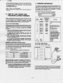
3. NAME OF EACH PART AND ITS
USE
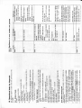
1. SPECIFICATIONS
Model:
Product name:
Power source:
Power required:
Batlery operating time:
Temperature:
Dimensions:
Weight:
Accessories:
Optional Accessories:
Usable Printers:
CE-1600E
Parallel and pocket disk interface
7.5V DC supplied by five AA batleries or
optional AC adaptor (EA-160)
2.8W
approx. 50 minutes using manganese
batleries approx. 120 minutes using
alkaline batleries (at 20°C with a CE-1600F
connected while continuously writing and
reading a 4 K-byte prägram at 5 second
intervals)
1Q°C - 35°C
320mm(W) x 123mm(D) x 40mm(H)
approx. 640g (includes batleries)
AA batleries (5), screws (XBBSD20P
05000, PRICE RANK: AA) (2), Operation
Manual (1)
EA-158C (printer cable)
EA-160 (AC adaptor)
CE-1600F (pocket disk drive)
SHARP CE-515P, CE-516P, CE-700P
EPSON FX-80
See the operation manual for your printer
for information on electrical requirements
and printable characters.
Be sure to confirm compatibility (e.g. by
referring to the printer's manual) before
use for any printer no listed above.
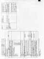
®
Pocket disk drive
connector
(50-pin)
@ Adaptor
plug
Note: The interface does not have apower switch. The power is
switched together with the power switch of the connected
computer. Disconnecting the computer turns off the power
for the interface.
CD
Computer connector
Connects the computer (PC-1600).
® Printer connector
Connects a printer through the printer cable (EA-158C).
® Pocket disk drive connector
Connects the pocket disk drive (CE-1600F)
@ Adaptor plug
Connects the AC adaptor (EA-160)
4. POWER SUPPLY
Size AA batleries (or an adaptor) are required in the interface to
operate the disk drive.
When the IBAIT I symbol is shown on the top right of the computer's
display, the batlery vohage is low. Replace the batleries in the
interface early.
2. SYSTEM ORGANIZATION
The entire system is shown below.
Printer
(optional)
CE-1600F
(optional)
Note: The interface and computer both supply power alternately.
Thus, operation is possible if power is available from either
one. However, the disk drive's motor operates from the power
supplied by the interface.
5. ERROR CODES
EA-158C
(optional)
,
The interface issues error code 69 during an error.
ErrorCode
"",,,,(,
pti~~
69
SHARP CORPORATION
Description
Printer is not connected. Printer is not on. Printer
is out of paper. Other printer related error
conditions.
•
CE-1600E
If the printer takes 10 seconds or more lor the new page operation,
an error occurs when an attempt is made to output data following
the new page code (LPRINT CHR$(12);). I1 an error occurs, add
the following command.
1 ON ERROR GOTO 60000
60000 IF ERN = 69 THEN RESUME
Lines 1 and 60000 are repeated until the new page operation
completed.
is
7. PRINTER INTERFACE
The interface can connect with most Centronics compatible printers.
The interface uses handshaking through the BUSY siqnal. For your
reference, the printer interface connector signals, printer cable
wiring, signal timing chart, and electrical requtrements are given in
the following. The information
is not necessary il a SHARP
recommended printer and cable are used.
(1) Printer Interface Connector Signals
\<D 0
6. END OF LlNE CODES AND
PROGRAM LlSTING FORMATS
0 --------------- 00
~ 0-------------------0 ®
Output of the end of line code at the end of a line can be turned
on and off if the amount of data exceeds the number of columns
per line specified in the PCONSOLE
statement. Also, when
outputling a program listing, printing of the 2nd and subsequent
lines can be started from the first column or the 8th column.
Signal
Name
Direction of
signal as seen
fromthe
interface
1
STROBE
Output
2
3
4
5
DATA1
DATA2
DATA3
DATA4
Output
Output
Output
Output
6
7
8
10
DATA5
DATA6
DATA7
DATA8
BUSY
Output
Output
Output
Output
Input
11
EXPRM
Output
12
13
14 - 25
N.C.
N.C.
GND
Pin
Number
®}
Description
Strebe pulse used to output
data.
End of Llne Code Output
Problems may arise if the number of print columns per line set in
the PCONSOLE statement is not the same as the number of printable
columns for the printer. Furthermore, most printers automatically
perform a line feed after receiving an entire line of printable
characters.
(1) Select "do not output end 01 line code" Irom below il the value
132 is set in the PCONSOLE statement and the number of
printable columns for the printer is 80.
If "output end of line code" is selected, the printer will
automatically perform a line feed after the 80th column and
again after the 132nd column.
(2) Select "output end of line code" from below if the value 80 is
set in the PCONSOLE statement and the number 01 printable
columns for the printer is 132.
I1 "do not output end of line code" is selected, the 81st column
will be output on the same line. Furthermore, if "print from the
8th column" has been selected, 7 spaces will be inserted
between the 80th and 81 st columns.
9
Selectlon of the Start Prlntlng Position
The EA-158C is wired as shown below.
Computer end
Key Entry: POKE & FE79, X
(X denotes the value 0-3 as shown in the table below.)
Output End 01Line Code
Listing Format
Printer end
1
2
3
1
2
3
4
4
5
6
5
6
0
No
Print from 8th column
7
7
1
Yes
Print from 8th column
2
No
Print from 1st column
8
9
3
Yes
8
9
11
~-
The printer is ready to
receive data when low.
Signal used to initialize the
printer. A Iow pulse is output
when the computer is tumed
on (exceptwhen ~
is
pressed after an autopower off) or when the
reset button is pressed.
Notused
Notused
Ground
(2) Printer Cable Wlring
Since the line number is printed from the first column, long program
lines that require 2 or more printed lines can be printed with 2nd
and subsequent printed lines starting from the 8th column to make
the overall program listing easier to read. Select this indentation
leature for easier to red program listings.
x
8 bit data signals with the
signal high when the data
is "1".
The MSB is DA TA 8.
The LSB is DATA 1.
10
Print from 1st column
11
14-25
31
16,17,19
- 27,
29,30
When the PC-1600 is connected to interface for the first time or
when the raset button is pressed, X = 0 will be selected. Futhermore,
whenever the power is tumed on again, the previous values that
were specified belore the power was tumed off are retained.
Note: The end of line code referred to on the previous page is
specified in the PCONSOLE statement. However, if a program
line is less that the number of columns per line specified in
the PCONSOLE statement, the end of line code specified in
the PCONSOLE statement will be output.
Pin 36 at the printer is not connected in the EA-158C. Some printers
use pin 36 for the SELECT IN signal wh ich must be in the SELECT
state. See the operaation manual for your printer. Also some printers
provide a switch for the SELECT state.
-2-
--
CE-1600E
(3) Signal Timing Chart
(4) Electrical Requirements
Moment when the power is turned on or when the reset button is
pressed (except when @ffi is pressed after an auto-power off.)
1.
Signal Levels
Input signal: TTL level
Output signal: TTL level (capable of driving one TTL IC)
2.
1/0
Input signal:
-1
EXPRM t--Tt--I
DATA1- .... _
DATA8~~-
Vcc
x:---x
STROBE
Tl:
T2:
T3:
T4:
Output signal:
approx. 20ms
1.5ms or more
1.5ms or more
15-20 µ.s
2.8K
M54514AP
or equivalent
Since all the outputs are through an open-collector, a pull-up resistor
(approx.
1kn - 10kn) at the printer is required. SHARP
recommended printers al ready include a pull-up resistor.
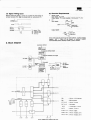
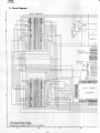
8. Block diagram
Centronics interface
PC-l600
EA-l60
(AC adapter)
v« __ ---!
ir
vrc
CE-I600F
(2.5"FDD)
PC-l600
'-- __
..J
AAx5
(SUM3x5)
power supply circuit
11!Q
,---
1
...
NU
I'BO-7N
PTI .PUI .EZI
MINI.IORQ
MRQI.RDNI
WRNI
I'CO-7N
1/0
Bu
: 8 bits
Mu
: Mul t iplexer
FFl-3
: 8 bi ts Latch
DCl-3
Buffer
Decorder
INT
: Interrupt
RST
: Reset
PAO-7I
: 8 bi ts input
PBO-7N
: 8 bi ts output
port
PC 0-7 N : 8 bi ts output
port
circuit
cireuit
RSTI--~----4_------~--~
,
- -----,-- - - - - - - - - - - . - - -f - -f - .,
~----CSNO
107N
RSTN
GNU
vcc
[Fig.2) LR38045 block diagram gate array
-
CE-1600E
9. Description of each block
Block name
Description
9-1. LR38045 gate array
Table-1 describes the gate array internal blocks and port addresses
(see block diagram [Fig.2]).
VCC~
Reset line capacitor
/'
RST'
~
.P""'~J~"OO::.~
Block name
Description
Bu
Bidirectional 8- bit 10 buffer.
(8-bit inputoutput buffer)
Mu
(Multiplexer)
Data i1 FF1, FF2, FF3, or PA Port are sent from
the gate array.
FF1-FF3
(8-bit latch)
FF1: FF1 output is used to control the interrupt
circuit. For instance, '1' in a bit
FF2:
RSTN
'RESET
'';TE.
(PC-1600J:1)
SW
IlI>Il·~'
I ;
:0
'----
t>
1
--- -----
I
-
-----
.FFI-3RESET'
------]
[Fig.4] Reset circuit
FF3:
DC1-3
(Decoder)
{
DC1: 32KB ROM c~ select (CSNO)
W-, Tt_
DC2: 2.5' FDD select signal (I07N)
Reset signal, ~
DC3: FF1- - - FF3 and FDD reset latch select
during data write.
FF1- - -FF3 and PA port select during
data read.
INT
(Interrupt circuits)
F~'~~
Ths signal is OOedwi1ha PA POrt (PAOI- - -61)
i1put to be sUppliedto IRQas an nternet signa,
As PA01---61 correspond wi1h 00---06
of
FF1, the interrupt becomes valid when '1' is
'----v------FD resets softwarewise
[Fig.5] Reset circuit timings
established for FFI.
(The interrupt equivelent circuit is shown in
[Fig.3J. )
NOTE: Port PA, PB, PC are all active high inside the gate array,
but converted into active low outside the gate array (see
the figure below).
.
, RO
sv ~
Gate array
,
ri
~
I~
Inside , Outside
PA
~
OO~
PAO I
0'
02
~
OS
V"
O'
Q5
"""
Q6
A.
PA I J
PB
PA2 I
PA3t
PA.
I
PAS I
PA61
'--
?1",+-tv'J
-t'"
ACTIVE
RST
(Reset circuit)
[Fig.3J Interrupt circuit
An input of the reset signal on RSTI resets
FF1- - -3. At the same time, RSTN is issuedto
HIGH
ACTIVE
LOW
For instance, "1" on 00 of FF2 sets the PBON output low.
the 2.5" FDD reset line and remains issued until
the reset signa is canceled soltwarewise.
It is possble to output RSTNsoftwarewiserrespecti
ve of the i1put to RSTI.
Reset eQuivaientcircuit is sOOwnin [Fig,4] andits
timings in [Fig. 5], )
-4-
·_
CE-1600E
10RQ
MI
Address
Data
A7 A6 AS A4 A3 A2
1
1
0
0
0
0
0
0
0
0
0
0
0
Al
0
0
1
1
AO
WR IID
0
1
0
D6
1
FFI data write
0
*
1
0
FF 1 data read
1
1
0
1
1
Q
0
I
1
11
1
NOTE: All are active high (1: active,
D7
0
0
1
Operation
FD reset
05
D4
v------
----1
---
D3
D2
FD INT
Enable
1
1
1
01
l----1
FF2(~)
data write
FF2(~)
data read
FF3(~)
1
data write
FF3(~)
0
data read
0: inactive)
as seen
.>
(0 )
-:
Pullup
1
1
Centronics ~entronics
DATAI
DATA2
1
(0)
(0)
Centronics
Centronics
iNiT
"STJm!it
1
1
Centronics
Irom the CPU, except
--
LB
1
1
DATA4
1
1
lor FD reset
Vp LB
I----
~
Centronics Centronics
DATA3
1
Comparator
FD INT
1
FD Reset
(0: re set)
PAO-7read
-DO
1
Centronics
--
BUSY
1
Centronics
Centronics
Centronics
OATAS
DATA6
DATA7
DATA8
1
1
1
T
(0: active).
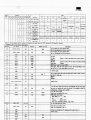
© LR38045 gate array signal description
PIN No.
1-8
9-16
17
Pin name
PC7N-PCON
PB7N-PBON
1/0
Out
Out
effective
low
low
Highlow at reset
High
High
Descriltion
8-bit
output port (port address 83H)
00-D7
I-bit
corresponds to PCO-7N via FF3.
output port (port address 82H)
00-D7
corresponds to PCO-7N via FF2.
(NC)
18
PUl
In
(Low)
PU input
19
PTI
In
(High)
PT input
20
EZI
In
(High)
Eminput
21
MINI
In
(High)
MI irclut
22
10RQ
In
High
IORQ input
23
MRQI
In
High
MREQ input (used to create CSNO).
24
RSTI
In
High
[ Used to create 32KB ROM select signal (CSNO).
J
[~ed to create 107N and gate array interna! enableJ
Signals.
Reset input. When the reset signal is entered, the intemal ~1Iop is reset
and RSTN (2.5'
FDD reset signal) is sent out.
.
25
Vcc
26
GND
27
IRQ
Out
Low
28
RDNI
In
low
Jm"input
29
WRNI
In
low
WR"input
AOI- A71A141, A1SI
In
) Power supply
High Z
All N-cIW1nel open drain interrupt signal output wtich is puIed ~ toVCC
on the PC-1600
siele.
30
I
Address input
39
40
(NC)
41
RSTN
2.5' FDD reset signal output.Sent out lIlCOIidiliolfilly with the reset signal
Out
low
low
and must be canceled by means of software.
softwarewise.
42
107N
Out
low
(High)
43
CSNO
Out
low
(High)
It is possble to send out
(Address 81H, 00, WR")
2.5' FOD select signal.
(SenT out via address 70H-7FH.)
321<8ROM select signal.
rm
MREQ. PT··High
pU··low
44-51
DBO-DB7
ln/Out
PAOI-PASI
In
Address··
·4000H -7FFFH
(PV"'low;
Centronics interface,
(8-bit)
High; FDD)
data input and output.
52
I
Il1lut port (port address 81H)
low
PAD-61 corresponds to DO-6.
57
60
PA61
(Interrupt
58
GNO'
Power supply
59
(NC)
61
PA7B
Out
62
PA7N
(Out)
64
PA71
In
63
(NC)
High
High
controled
by FFI (address 80H) output 00-6.)
-
CE-1600E
PC-16 0 0
CE-1600E
9-2. Centronics interface
(*u: )
VCC4-~----+--------------'
VC
-=-UM-3
Fig. M54514AP
driver equivalent
(X4)
ifr
circuit
Seven above circuits are implemented on a single chip of the driver
and two chips are used in the CE-1600E. Among 14 circuits (7
circuitsx2), 8 circuits are used lor data output and 4 tor STROBE
and INIT outputs, 1 for BUSY input, and remaining one circuit is not
After the batlery power supply is ORed with VBAT of th
CE-1600E, VCC is regulated to 4.7V before supplied to th
CE-1600P. (See the figure below.)
When the main power is off, VCC is not supplied.
used.
G) Data output
9-4. Low battery detect circuit
CD
VP low banery detect circuit
V OUT
From gate array ~
~OW
®
STROBE, INIT outputs
Because both signals are active low and the gate array goes
high during reset, a non-inversion butler is provided between
port and Centronics interface.
From gate array
--'M---l
The MN1280Q low batlery detect IC is used in the VP low low
batlery detect circuit. (Rank Q=VDL: 3.8-4.1V)
VOUT must be inverted in the comparator before supplied to the
gate array.
:-,L..Jr, ,
WLOW
®
MN 1280 output characteristics
I
CE-1600E___.)
LO",,'
~
To pnnteer
To prevent malfunction at power on and oft, a pull~ resistor is
inserted to PB6N.
BUSY input
When the printer is not in connection, a pullup resistor is used
to set it in the busy state. A diode is used to prevent intrusion
01the power supply when oft.
vo:
Vp
VOUT
MN1280Q
>
•
To gate array
PAI I
1.1-2.4V
®
,
,
I
I
I
I
VP, VCC comparator circuit
As it is necessary to satisfy the condition of VP>VCC+01V in
order to 5VC inside the CE-1600F, the condition is monitored
by means 01the comparator.
~CE-1600E
To printer ___.)
VP
9-3. Power supply circuit
VP, VBAT circuit
100KO
about 9.4V
SUM3x5
,
r
,
>
D3
D2
N
ACaoapter, __/jl
N
•
•
....Vp
t
To gate array
PA21
,
D4
.. VBAT
L-.{>I
D6
{>!
5KO
J
Dl,D5,D6
D2,D3,D4
nOOO3
1O,EIN
(Potentiometer adjusting method)
1) Add 4.5 to 5V to the VCC pad.
2) Add VCC+O.1V to the VP pad.
3) Rotate VR counterclockwise and set the LBtest pad vohage to OV.
4) Slowly rotate VR clockwise and stop it when the LB test pad
voltage came to be VCC. (See the parts and signal description
lor the location 01test pad.)
01:
For prevention of counter current flow from the battery to
the adapter.
D2, 03: To drop the voltage from the adapter to the f10PPVdiskdrive
voltage, 7.5V, maximum.
04:
For prevention 01 counter current f10w from VßAT (main
unit) to VP (Iloppy disk).
05, D6: For prevention 01counter current flow to the battery when
the adapter is in use.
-~-
§
.9o
..
§
5
~
Q;
Co
o
-'"
.II!
-0
..
50
..Cl
o
.~
I
...
<:>
Q)
:c
'u;
(1)
oQ,
"C
C
ca
""
Q)
.c
E
:;,
e
...
e
""
""
Q)
e
...
..
o >
t:: °C
..Q
Ö
<:>
....
ä5
Q)
c
C
ca
o
:ee
... ,-
g
Q)
'(1)
w
"9:;,
oca
~Q:
- .......
....
....
.....
ä5
ä5
....
....
I
"?
....
a:
o
a:
a:
o
a:
~
a:
~
a:
w
w
w
a:
.-(,)
a:
a:
.~
::r:
o
o
-0
C
11l
Q;
c:
.~
"E
Q;
a.
CD
'ü
:e:::l
C
CD
I
C')
Cl)
s:
~
w
ö
~
o
(/)
C
-e
,.........__.",
)(
z
cn
tU
'"
'"
CD
U
U
)(
ci
01
-
Gi
~
o
a.
"E
Q)
'ü
:E
:::l
(/)
..
..
(1)
E
11l
0,
(1)
Q)
o ea.
o
:;::
...
tU .!:!
Q) üio .
e, CW
o
ClO
.~ 0
-0(0
ci
CD '
.s:;W
~
,.... t--ü
-7-
-
CE-1600E
~
~
~u
u
§
s
...
Cl)
~
t::
0
u
Q.I
.
-
u5:-t:
~
~
c
.-
:8,
(ij«J8
~
iU
'iii
~~~
~ 0
«ic
~.,.,~
~
B
•
'.._
~
CU
~
__
~
0
Q)
a.Clc.
,~S~
.,!S~~
:tj~~
.~~~:::tj
~~~~c::::>~c~
IOuD~_mua..O
..
.,
u
~
i;j
~
~.~
~
~~
'.._
~t/)
a.
Q.:a
.§;
.~
S~
co
~-~
IJ)
~
_~
CU
~
::::>
m
CO
~~~oO
...... Q,)
I
WQ)>_(1)1
2~s
«J
'-
I
-
~tj":~-E~~
~~~~~~c
..
.
_a..UQ
~
e~
=s
1i
.~
0
...
.,
<..>
: :E~
Cl,)
~
~
:J
~ 5
~
't:
~
= ~
1;;
U
~ ~
~
~
'E
....J
~.§
0..
c,
~.
0
""~
8.E_
uD
~.
~
l
o ...
t: V)
o
~c
:~!
~"H.Q
~
Cl)
Q)
~
'"
"_CQ)
QJ
I
c
~~~
bG
!i1
g. _ ~;:::;~
«
QJ(Q-a..o.
~.s;: .~
"- ·E
~ ~
C.8~
~
"'~
, ~~fi
!i1 ~ ~
.~c.~
~~
~ u
. ~
u
c
c.~C1)~
c
ffi
_
...
~
~
<..>
.SR ~
Co
.,
s ~
-
~., ~~
~
gs
CI:
CI:.,
ffi
ffi
--
_'" U
c
., ""<..> .
1:'e;
.~ .~ ~
c
(5 .~
.1;
f=.
**
*
:.r::
ci
CI>
c
E
o
Cll
E
o
"0
ü5
c
CD
5Z
<t
**
*
Cl
0'
o
CI>
.s
..
r'"..
5
<0
~
U
§
Q.
.,E
5
.,
.<:I
>
CIJ
CIJ
w
o
o
w
o
o
CD
W
ö
;,ü ..
X
:l.. :
)
-0
o
e
<t
0
...J
CD
.s
<t
w
e>
e>
CD
CD
cn
w
(.)
o
c
~
..
'"...
.x.
U
:::
ü
IJ)
U>
...
GI
::::J
"C
GI
~
a... ...'"
~a
In
I
'"
..-
w
(.)~ '"
'"~ 5.,
..
~
....
8.
5
'"
U
o...
..
Q.
fIj
GI
I-
ott
c
I
o
,..
~
.,
!5 5
I-
-8-
0
-
•
CE-1600E
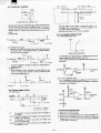
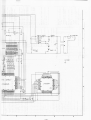
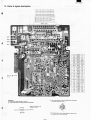
11. Circuit Diagram
60pln
r---
o
BO
59
5B
57
5B
30
29
2B
27
2B
'IC
55
2!5
GNO
GNO
GNC
•• •
BFO
54
53
52
5I
50
24
23
22
2I
20
MAEQ
49
I9
DIS
~
NC
~,
Vb..
4B
47
4B
IB
17
IB
OB
07
PV •• ,
-
Vb..
FGND
FGND
N
45
PU
40
39
15
14
13
12
11
10
9
38
8
!"NT
AO
37
36
35
34
33
32
31
7
6
A
A2
5
A3
4
3
2
I
M
A5
A6
A7
EC
~l:
I
_
5
r-.r-I r-<
I-
v..
I
-
CONNECTOR
.1iC_
~
VII
...I 5
~
~
,.-~
~
~
,.--
AI4
A 13
"12
AI
10
9
'8
U
43
42
H
•••
,.
10
Ht
1,"3'J311
><
OC
~
0
><
03
04
~
:l
1001:
2 _
,
r--+-+-----
•
- ~
-
.;
v..
--
- - - --
...........'
2
'"
I '"
PT
ASTE
~liC
--
><,
,___
,
'r
~
...
71,
a:,
l
Jf'-'-""---
>
T
r--
~
MNI280
«n
MI
I-I-I-I-I-I-I-I--
11 1
I
00
DSUB-25M
OCNCMI304CC2F
•
S5
zi
•
0
I'"
I!~
<
~r:
<
o
•
,~
I.
M545 I 4AP,----J
X
l;,
13/~.7K
!
= ,~
!
~
2.7K
I~
~~
I
50,'.
"~l1>.
VP
VP
L..._
r-
GND
GND
47
46
22
21
45
(4
20
19
BFI
43
42
41
18
17
MREO
AO
16
A
L
II
VCC
23
ITH
GND
RIJ
WR"
107N
O""""
I----
r-r-r-r-r--
... ,
T
~~~I, 4~1:11!Z11:~1:711:~IZ!I~39
I
0
r
-
=:EZ'
'---~
~
IORQ
1
~
~
T -~
A
A
40
39
3B
15
14
13
A2
A3
A4
~
~
~
A
A9
A8
37
3B
35
12
I I
0
A5
A6
A7
I--I---
I---
I--~
F~~~
~~
:
~~TN
I-
I--~
II-
~~
INTF
28
I
10
4
28
3
)5
21
2
)6
,.--~
..
A
r----
is 25WV, O.lµ.F (F), chip capacitor.
c
B
-9-
I.
71
-
u
·
~fz;,i
~~,~
ARRA v
..
..
..
I~-l~~cl~~~:
I~I ~
~.
iji
is chip diode.
with no comment
0
3D
2) All 01 Resistors are 1/8W, chip resistors.
3) Capacitor
~":,, '"
L R 380 4 5
IRQ
.1l
~+ ~
4
z e~I:
~:~
v ....
AL3_
i! i
....
GA TE
.!!ll!..
~
~
29
-
"
20
~
~
Ne
lil
YGG
0
: ~ z ~ ~ ~:
AL~
:;Ol
1) Diode with no comment
24
25
:~r ;
I
,.--
["
I
.8
IAIT
10RO
"15
2
411
50
~~~
1
CONNEClOA
1f
~IA
o
3
-I~
~
n
1
i-----r------~
~N 1280
5
I OE I N
«n
I OE IN
110003
i
I 10003
11111111111
t
I I
I I
I
I I
I
I
I OE I N
1
'110003
T
{::;
__.11
4
TCJ_
..-
°1°1°1°1°1°1°1°1°1°1°1°
zzzzzzzzzzzz
CJClOClOO(!)OOOOO
I
I
L.±
T
r1
----'--
2200 JkF
/16V
~OAPTOR
I I
0·
1===1.
4
SUM3 X 5
Lo-
r--'- .....
-
FGNo
I
3
10
I'l
I
E ARRAY
JB8045
2
lOOK
1
--10
E
.I.
..r.
T
T
100,. /lOV
T
e
F
-10-
H
-
CE-1600E
12. Parts & signal description
~1~1~1~1~1~1c:;;1~lgJl;;:;l~
- '" '" ..,.
w
al -
0<
0: ff- <:
Cf) 0
'"
<D
..,. '"
< < < -<
~
~
~
~
o 0 o 0
'"
cc
<-
cc
'"
;::
=I~I~
<D
<-
<Xl
>-
I~I~I~
< <: <:
Cf)
f- f- f- ::>
<: <
o 0 ~ al
,---------------,
~---L-----~~B-2-:p.0-----
ADPADP+
BAT+
8AT-
,
Vcc
25 50
vcc
24 49
Vp
Vp
GNO
2348
22 47
GNO
GNO
Marked with ..
test
@ ~eocares
RO
WR
I07N
20 45
ELH
WAIT
19 44
IORQ
MREQ
1843
BFO
AO
17 42
AI5
AI
16 41
AI4
A2
1540
A3
1439
AI3
AI2
A4
1338
A5
12 37
l! 36
A6
A7
pad
A 9
A 8
00
934
833
FGNO
01
732
PVOUT
02
6 31
PU
03
530
PT
04
429
Ne
05
328
2'2:/
06
07
@ Lead of lhe same color must be connected 10 Ihe circuil pattern
Precautions:
Match the
~
of Ihe same number for Ihe coi!.
®3
cut in the tC with the
arrowIlead of the resist.
I PWB
end
+
o All component
pins must.be
-11-
parts must be closely attached on the board, and
cut to 1.5mm at lhe most.
Al!
A10
1035
RSTN
(j) Diode must be closely attached on the PWB.
® The flgure below shows the inslalling direction of the MNl2800.
21 46
Vp
I 26
FGND
MI
VGG
INTF
-
CE-1600E
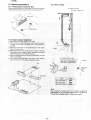
13. Service precautions
13-3. Wire routing
13-1. Frame ground continuity test
Check continuity between the shield plate 01 the 60-pin connector
and the static terminals and make sure that it is not more than 1Oll.
AC adapter jack socket
QJAKCI003CCZZ
13-2. Square jumper installation
CD
®
®
Make preliminary solder coating on the PWB.
Remove the back paper 01 the guide sheet, match the holes 01
the PWB with the holes 01 the sheet, then bond the sheet over
the PWB.
Remove the back paper 01 the double tack tape on the reverse
side 01 the guide sheet.
PWB
@ Remove the protect sheet of the strip of the jumper, match the
®
®
circuit pattern with the jumper position, and attach the covered
portion 01 the jumper to the double tack tape.
Apply the soldering pencil over the strip 01 eacM jumper and melt
solder on the pattern.
Then, stroke the soldered portion with the tip 01 the soldering
oencil to ensure that it has been completely soldered.
Wind sold er on the (+) side
CD
Apply small amount 01 solder to the
inside 01 the (-) side and do not
permit solder to spread outside.
Strip
<:Be
( -) terminal
/
=
~~~~soldel
SOld~
I
@
~d'~'"
I
I
Name
Length
Jumper (Black)
200nn
<Il
Jumper (Red)
200nn
@
Jumper
__
260nn
CD
I
I
L....=...L._.
(Gray)
J
I
13-4.
After completion of troubleshooting,
it is necessary to adjust the
potentiometer
for the low battery detect circuit, in reference to
"Potentiometer adjusting method" in this service manual,
-12-
-
CE-1600E
14. Character Codes
• When you create a program for the plotter, be sure to use its unique
character code commands.
• SO (&OE) and SI (&OF) are special purpose characters and should not
be used.
• 'i (&5C) and characters Irom &AO to &DF are lor Japanese letters.
(Shaded area)
Some characters that are displayed on the PC-1600 may be different from
those printed on the printer. Furthermore, codes &00-&1F are usually
control codes on most printers and will differ from the displayed characters. See the operation manual lor your printer. The character lonts may
also differ depending on your printer.
CE-516P (IBM PC (USA) MODE)
ESC + R + 0
Mode 0 Character Code Table
Upper 4 bits
In Mode 0, the PC-1600 character set includes graphic and Greek symbols
and internationa' onaracters in addition to the normal upper and lower
case leiters, numbers and symbols. This character set is similar to the
IBM PC character set.
1
Hex
0
o
NUL
1
2
3
4
5
6
7
8
9
A
0
@
p
,
p
t:
1
2
A
B
C
0
Q
a
9
..
.3
..2
c
R
S
T
b
r
i[
0
C
5
d
t,
E
u
e
LI
;,
F
G
U
I
v
w
ä
7
9
w
(
8
H
X
h
x
)
9
:
;
J
K
<
=
>
N
'?
0
2
3
4
ij
3
$
4
5
%
5
5
s
6
7
8
9
A
8
C
D
E
F
8EL
BS
HT
LF
*
t
VT
,
FF
CR
SO
SI
v
LI
e
a
~
0
,;;
N
y
0
o.j
Z
J
z
e
[
I
I
C
L
,
k
I
:
i
L
M
1
m
)
n
-
I
•
0
~
A
Po
J
C
o
E
F
L
11
o
_j_
T
T
"1T
II
1 ~
-
1
~
tIf
I1
Q
11
c-
l
~ il
- 11
~ 11
u
~
'i
,;,
c..
c..
e
e
::~
u
0
I
-
,
o
a
B
..
!J
Ö
V
<
>
d
1
13
:':
r
1
n
~
2:
f
0
J
r
fJ
z
T
u
rr
'f
<!>
J
8
!!o
f
lr
li
=
Jl
u
.J..
-
r
t
»
0 1 2 3 4 5 6 7 8 9 A B C 0 E F
Lcwer
4 bits
mBI
27
58
,
SC
-,
]
J =t'
n
L
MODEl
5D
SE
5F
,
e
60
6
-
7B
7C
,
{
70
o
SPI
5
0
@
6
4 0
$ 4
f
m
~
""
C; E a
Q a q Ü
ce I
e
0
~=~ T- ß
j_
6
0 T d t ä
Ir
n1
N~ t
Ö
F
' 7 GW 9 w
Cf
Cl
Q
8
( 8 H X h X
i
9
9
) 9 IY
r:
~I rrJ
A
*:
B
+ ; K [ k
II~
C
,<
I
0
- = M ]m
7F
718191AIBICIDIEIF
P
J
Z
j
L "- I
. >
F
/ ?0-
N
11
Ir*
l!:+
Tl
JL
11
'1'
:
I 1: % :!J
J
r '"
0
<t>
e .
I
et % 11 lr
{
Q -
H o .J
If 11
n
00
I
JL
::l
( lr I •
} 1
~ 0
n
- Ä
R
0
Ä
,
E
-,
a
F rr µ
7
i
r
b~
.9.
e y
Y e Ö
z e Ü
±
Li tt s;
(J
-
Ö
-
r~
~...:
~ 6 ~=t T lT
c s ä
§ %5 E U e u ä
LJl a
--
cl U
Upper 4 bits
2
# 3 C S
@
& 6 F V f V
CE-515P
o
3 <::?
6
7E
A
" 2 B R b r
",
n
}
2
0
In Mode 1, the PC-1600 character set is modilied to make it compatible
with the more limited character set in the PC-1500. The table below gives
the hexadecimal value of the character position, and the corresponding
character for Mode 1.
MODE0
2 1A
I
Mode 1 Character Code Table
HEX CODE
1
5
-
I
I
m
0
5~
11
p , p
0
f )
.lJ -
</> 2
•
..l..
l
¤
Tl
When the CE-516P is used in the IBM-pe mode, the character set is the
same with that for mode 0 except for &7F.
q
CE-700P, FX-80 (USA character set)
U.S.A.
$
.r-;'".[i:l;\';;
%
Cf)
&16
"<t
v
~
~~
7
7
G
~
81BS
8
H
W
A
Sl:1.
p
,.~.~'.:.~::l;
ocz
g
-#T:"-;:;-~ ....
9
A
oe, s
Y
ILF
•
y
BEL
c
CA"
<ILI'!'
1fT
MI)
E ISO
F I SI
>IN
/
Im 11
n
O·
C
D
A
CI
T
d
.:,
• "SP" means space. The pen proceeds to the next position without plotting any characters.
• Blank means "not defined" and nothing is plotted.
A I
lF
{
"
x
I
y
oe,
$
C
5
c
D
T
d
u
BEL
I
lF
{
VT
1I
vr
F"F
D I
(lI
11
E I
so
N
n
so
0
0
"
•
I
Characters
-13-
v
CI
E5C
E
.11"
U
K
D ICR
b
v
IIS
C
D
z
B ILUIESCI +
R
C
X
-
•
p
\
I
I
•
I
u
F
V
c
..
9
H
Je
h
x
Y
J
Y
~z
ESC
•
It
F"F
L
("l!
"
•
11
I
o
lor &20 - &7F are the same with those for mode O.
-
CE-1600E
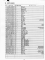
15. PARTS GUIDE
NO.
1
2
3
4
5
6
7
8
9
10
11
12
13
14
15
16
17
\8
19
20
PARTS CODE
TlABHl126ECZZ
TlABMl120ECZZ
GCABB1025ECZZ
QJAKC1003CCZZ
l..Y..TANZ1006ECZZ
_QT A N Z 1 3 7 7 C C
QTANZl124CCZZ
PSlDC1008ECZZ
PTPEH1020ECZZ
QTANZ1003ECZZ
PCUSS1227CCZZ
GFTAB1011ECZZ
lX
BZ1017ECZZ
XUBSD20P06000
GCABA1026ECZZ
GlEGG1001ECZZ
TlABZ2121CCZZ
XUBSD26P06000
TlABPl140ECZZ
XUBSD26P12000
DUNTK1210ECZA
21
DUNTK1210ECZZ
22 lX
BZ1155CCZZ
23 TlABP1150ECZZ
25 TlA8Z1153ECZZ
26 lX
WZI001CCZZ
27 PZETlI028ECZZ
28 P Z E T l 1 0 3 4 E C
29 PTPEH1278CCZZ
30 PSHEZ1021ECZZ
101 PSHEZ1017ECZZ
102 PSHEGI041CCZZ
QCNCMI014EC2E
103
.QCNCMl
0 15EC2E
104 _Q_CNCM1295CC6J
105 QCNCWl
00 4EC5
106 jLC NW
1023ECZZ
107 RFilN1008CCZZ
108 VCKYTPIEFI04Z
109 R V R -M 5 3 1 O_QC
110 VCEAGUIAWI07M
III VCEAGUICW228M
112 VCKYTPIEB104K
113 VHDDAP202K/-l
114 VHD10EIN///-1
115 VHOIIDQ03//
116 VHi
iR9393N/
118 VHilH5357R6-1
119 VHilR38045/
120 VHiMN1280V/
121 VHiM54514AP-l
122 VRS
TP2BDI00J
123 VRS
TP2BDI03J
124 VRS-TP2BD104J
125 VRS
TP2BD183J
126 VRS-TP2BD272J
127 VRS
TP2B0273J
128 VRS
TP2B0392J
129 VRS
TP2BD473J
130 VRS
TP2BD512J
131 VRS
T P 2 B0 5 6
132 XBBS020P08000
133 XBBSD20PI0000
134 X B B S D 3 0 P 0 6 0
135 XNES020
16 0
201 TiNSM1121ECZZ
204 SPAKA0267ECZZ
206 SPAKC0271ECZZ
207 PCAPHI013CCZZ
208 XBBS020P05000
209 PCAPHI014CCZZ
210 DUNT
1271ECZZ
211 TlABH1168ECZZ
212 PTPEH1228CCZZ
Z Z
Z Z
J
Z Z
1
1
1
1
2 J
0 0
0 0
PRICE
RANK
AE
AD
AK
AD
AA
AB
AA
AE
AD
AC
AA
AD
AB
AA
AP
AC
AC
AA
AC
AA
BR
BR
AA
AA
AA
AA
AA
AD
AA
AE
AB
AA
Al
Al
AV
AS
AU
AH
AA
AD
AB
AE
AA
AB
AB
AE
AO
AU
AQ
AE
AF
AA
AA
AA
AA
AA
AA
AA
AA
AA
AA
AA
AA
AA
AA
AS
AK
AG
AD
AA
AD
AD
AB
AA
NEW
MARK
N
N
~
N
N
N
N
N
N
N
N
N
N
N
N
N
N
N
N
N
PART
RANK
D
D
D
B
C
C
C
C
C
C
C
D
C
C
D
C
D
C
D
C
E
E
C
C
D
C
C
C
C
C
C
C
C
C
C
C
C
C
C
B
C
C
C
B
B
B
B
B
B
B
B
C
C
C
C
C
C
C
C
C
C
C
C
C
C
D
0
0
C
C
C
C
D
C
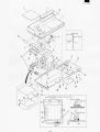
DESCRIPTION
Caution label
Decoration label
Top cabinet
Jack lor AC ad~tor
Batterv terminal B
8attery terminal t:i
Batterv terminal EB
Connector shield~ate
Static tape
Static terminal
Cushion
Lid lor batt~
Screw
Screw C2X6)
Bottom cabinet
Rubber foot
Reset label
Screw (2.6X6)
label lor battery
Screw (2.6 x 12)
Main PWB unit
Main PWB unit
Screw (2 X 3.5)
Parallel label
label for static
Washer
Insulator sheet
Insulator sheet
Tape (Ior No.283Q2
Sheet
Sheet
Sheet
Connector (25pin)
Connector (2~'1l.
Connector 160pi'1l.
Connector (50pin)
F.P.C. C62pi'1l.
Filter (ESD H 14B)
Capaeiter (25WV O.I~F)
Variable resistor
Capacitor (lOWV 1~U.
Capacitor_{16WV 220<>.M.tl
Capacitor (25WV O.!J!.El
Diode (DAP202lU
Diode (lOEIl
Diode GI QQ.031
IC (lR9393N)
IC (lH5357R6.l
IC_(lR38045)
IC (MNI280Q)
IC (M54514AP.l
Resistor_(l/8W
100 +5%)
Resistor (l/8W 10KO +5%)
Resistor_il/8W
100KO +5%)
Resistor (l/8W 18KO + 5%l
Resistor (l/8W 2.7KO +5%)
Resistor_il/8W
27KO +00
Resistor_il/8W
3.9KO +5%)
Resistor (l/8W 47KO +5%)
Resistor (l/8W 5.1KO +5%)
Resistor1..l/8W 5.6KO +00
Screw (2X8)
Screw (2 X lQ)_
Screw 1..3 X 6)
Nut (M2)
Instruction book
Packin_g_cushion tor set
Packing case
Connector c~
Screw (2 X 5)
Connector c~
FCC wire
Instruction label
Tape (tor No.2 11)
-14-
1..U.S.A. Canada)
(Other countrie~
(U.S.A.)
_{U.S.A.}
(U.S.A.)
(exceet U.S.A. Canada)
CU.S.A. Canad;tl.
.
(tor
(Ior
(tor
(for 50
50pin
6QRin
25pin
60pin
connector)
connecto!l
connector)
connector)
(Ior 60pin connector)
(for cotion CE 1600El
(tor 25pin connector)
_iU.S.A.}
. (U.S.A.)
l_U.S.Al.
..
CE-1600E
2
3
I J nsulator
I
shee t
I
I
I
(No. 27
)
I
I
I
L
21
./
./
./
././
(./
I
I
I
I
I
I
I
I
I
I
co"
I
l_
<,
30
<,
<,
<,
'--
-15-
_
CE-1600E
SHARP
COPYRIGHT
©
1987 BY SHARP CORPORATION
All rights reserved.
Printed in Japan.
No part of this publication
may be reproduced,
stored in a retrieval system, or transmitted,
in any form or by any means,
electronic, mechanical, photocopying,
without
prior written
recordinq, or otherwise,
permission of the publisher.
SHARP CORPORA TION
Information Systems Group
Ouality & Reliability Control Center
Yamatokoriyama, Nara 639-11, Japan
1987
May Printed in Japan
®