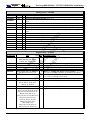
1
Single-Chip SMA North Bridge for Pentium 4™ CPUs with 400 MHz FSB, External 4x AGP Bus and Integrated ProSavage8™ AGP Graphics Core plus Advanced ECC Memory Controller supporting PC2100 / PC1600 DDR SDRAM and PC133 / PC100 SDR SDRAM for Desktop PC Systems Revision 1.1 July 19, 2002 a joint development of VIA TECHNOLOGIES, INC. and S3 GRAPHICS, INC. Copyright Notice: Copyright © 1999, 2000, 2001, 2002 VIA Technologies Incorporated. All Rights Reserved. No part of this document may be reproduced, transmitted, transcribed, stored in a retrieval system, or translated into any language, in any form or by any means, electronic, mechanical, magnetic, optical, chemical, manual or otherwise without the prior written permission of VIA Technologies Incorporated. The material in this document is for information only and is subject to change without notice. VIA Technologies Incorporated reserves the right to make changes in the product design without reservation and without notice to its users. Copyright © 1999, 2000, 2001 S3 Graphics Incorporated. All rights reserved. If you have received this document from S3 Graphics Incorporated in electronic form, you are permitted to make the following copies for business use related to products of S3 Graphics Incorporated: one copy onto your computer for the purpose of on-line viewing, and one printed copy. With respect to all documents, whether received in hard copy or electronic form, other use, copying or storage, in whole or in part, by any means electronic, mechanical, photocopying or otherwise, is not permitted without the prior written consent of S3 Graphics Incorporated. The material in this document is for information only and is subject to change without notice. S3 Graphics Incorporated reserves the right to make changes in the product design without reservation and without notice to its users. Trademark Notices: VT82C585, VT82C586B, VT82C587, VT82C590, VT82C595, VT82C596B, VT82C597, VT82C598, VT8501, VT82C680, VT82C685, VT82C686A, VT82C686B, VT82C687, VT82C596A, VT82C691, VT82C692, VT82C693, VT82C693A, VT82C694, VT82C694A, VT82C694X, VT8231, VT8233, VT8363, VT8363A, VT8364, VT8365, VT8365A, VT8366, VT8372, VT8374, VT8601, VT8601A, VT8603, VT8604, VT8605, VT8606, VT8612, VT8614, VT8633, VT8751, VT8753, Mobile South, Super South, Apollo VP, Apollo VPX, Apollo VP2, Apollo VP3, Apollo MVP3, Apollo MVP4, Apollo P6, Apollo Pro, Apollo ProPlus, Apollo Pro133, and Apollo ProMedia may only be used to identify products of VIA Technologies. The S3 Corporate Logo is a trademark of SONICblue Incorporated. Savage™, Savage3D™, Savage4™, Savage/MX™, Savage2000™, ProSavage8™, and Twister™ are trademarks of S3 Graphics, Inc. Intel™, Pentium™ and MMX™ are registered trademarks of Intel Corp. Cyrix™, Cyrix6X86™ and WinChip™ are registered trademarks of VIA Technologies Athlon™, AMD5K86™, AMD6K86™, AMD-K5™, and AMD-K6™ are registered trademarks of Advanced Micro Devices Corp. Windows XP™. Windows 2000™. Windows ME™, Windows 98™, Windows 95™ and Plug and Play™ are registered trademarks of Microsoft Corp. PCI™ is a registered trademark of the PCI Special Interest Group. PS/2™ is a registered trademark of International Business Machines Corp. VESA™ is a trademark of the Video Electronics Standards Association. All trademarks are the properties of their respective owners. Disclaimer Notice: No license is granted, implied or otherwise, under any patent or patent rights of VIA Technologies or S3 Graphics. VIA Technologies and S3 Graphics make no warranties, implied or otherwise, in regard to this document and to the products described in this document. The information provided by this document is believed to be accurate and reliable to the publication date of this document. However, VIA Technologies and S3 Graphics assume no responsibility for any errors in this document. Furthermore, VIA Technologies and S3 Graphics assume no responsibility for the use or misuse of the information in this document and for any patent infringements that may arise from the use of this document. The information and product specifications within this document are subject to change at any time, without notice and without obligation to notify any person of such change. Offices: VIA Technologies Incorporated Taiwan Office: th 8 Floor, No. 533 Chung-Cheng Road, Hsin-Tien Taipei, Taiwan ROC Tel: 886-2-2218-5452 FAX: 886-2-2218-5453 Home page: http://www.via.com.tw VIA Technologies Incorporated USA Office: 940 Mission Court Fremont, CA 94539 USA Tel: 510-683-3300 FAX: 510-683-3301 or 510-687-4654 Home Page: http://www.viatech.com S3 Graphics Incorporated USA Office: 1045 Mission Court Fremont, CA 94539 USA Tel: 510-687-4900 FAX: 510-687-4901 Home Page: http://www.s3graphics.com Technologies, Inc. ProSavageDDR P4M266 – VT8751 P4 DDR SMA North Bridge We Connect REVISION HISTORY Document Release 1.0 1.01 Date 2/13/02 3/19/02 1.1 7/19/02 Revision 1.1, July 19, 2002 Revision Initial external release (same as internal revision 0.95) Updated company address and company / product logos Added weight specifications Added power consumption and timing data to electrical specs -i- Initials DH DH DH Revision History Technologies, Inc. We Connect ProSavageDDR P4M266 – VT8751 P4 DDR SMA North Bridge TABLE OF CONTENTS REVISION HISTORY .......................................................................................................................................................................I TABLE OF CONTENTS.................................................................................................................................................................. II LIST OF FIGURES .........................................................................................................................................................................IV LIST OF TABLES ...........................................................................................................................................................................IV PRODUCT FEATURES.................................................................................................................................................................... 1 OVERVIEW....................................................................................................................................................................................... 4 HIGH-PERFORMANCE 3D ACCELERATOR.................................................................................................................................... 5 128-BIT 2D GRAPHICS ENGINE ..................................................................................................................................................... 5 DVD PLAYBACK AND VIDEO CONFERENCING ............................................................................................................................. 5 FLAT PANEL MONITOR / TV OUT SUPPORT ................................................................................................................................ 5 HIGH SCREEN RESOLUTION CRT SUPPORT ................................................................................................................................ 6 PINOUTS............................................................................................................................................................................................ 7 PIN DESCRIPTIONS...................................................................................................................................................................... 10 REGISTERS..................................................................................................................................................................................... 20 REGISTER OVERVIEW ................................................................................................................................................................. 20 MISCELLANEOUS I/O .................................................................................................................................................................. 24 CONFIGURATION SPACE I/O ....................................................................................................................................................... 24 DEVICE 0 REGISTER DESCRIPTIONS ........................................................................................................................................... 25 Device 0 Host Bridge Header Registers .............................................................................................................................. 25 Device 0 Host Bridge Device-Specific Registers................................................................................................................. 27 V-Link Control...................................................................................................................................................................................... 27 Host CPU Control ................................................................................................................................................................................. 30 DRAM Control ..................................................................................................................................................................................... 32 PCI Bus Control.................................................................................................................................................................................... 39 GART / Graphics Aperture Control ...................................................................................................................................................... 41 AGP Control ......................................................................................................................................................................................... 42 AGP Control (continued) ...................................................................................................................................................................... 43 V-Link Control...................................................................................................................................................................................... 44 DRAM Interface Control ...................................................................................................................................................................... 45 Power Management............................................................................................................................................................................... 45 ECC Error Control ................................................................................................................................................................................ 45 AGTL+ I/O Control .............................................................................................................................................................................. 46 Frame Buffer and High Memory Control.............................................................................................................................................. 47 BIOS Scratch ........................................................................................................................................................................................ 47 DEVICE 1 REGISTER DESCRIPTIONS ........................................................................................................................................... 48 Device 1 PCI-to-PCI Bridge Header Registers .................................................................................................................. 48 Device 1 PCI-to-PCI Bridge Device-Specific Registers ..................................................................................................... 50 AGP Bus Control .................................................................................................................................................................................. 50 FUNCTIONAL DESCRIPTION - INTEGRATED SAVAGE4 GRAPHICS............................................................................. 53 CONFIGURATION STRAPPING ...................................................................................................................................................... 53 PCI CONFIGURATION AND INTEGRATED AGP .......................................................................................................................... 53 Revision 1.1, July 19, 2002 -ii- Table of Contents Technologies, Inc. We Connect ProSavageDDR P4M266 – VT8751 P4 DDR SMA North Bridge PCI Configuration ................................................................................................................................................................ 53 PCI Subsystem ID................................................................................................................................................................. 54 Integrated AGP..................................................................................................................................................................... 54 DISPLAY MEMORY ...................................................................................................................................................................... 55 INTERRUPT GENERATION ........................................................................................................................................................... 55 DISPLAY INTERFACES.................................................................................................................................................................. 56 TFT Flat Panel DVI Interface ............................................................................................................................................. 56 CRT Interface ....................................................................................................................................................................... 56 External TV Encoder Interface........................................................................................................................................... 57 I2C Serial Communications Port ......................................................................................................................................... 57 ELECTRICAL SPECIFICATIONS .............................................................................................................................................. 58 ABSOLUTE MAXIMUM RATINGS ................................................................................................................................................. 58 DC CHARACTERISTICS ............................................................................................................................................................... 58 PACKAGE WEIGHT SPECIFICATIONS .......................................................................................................................................... 58 POWER CHARACTERISTICS ......................................................................................................................................................... 59 AC TIMING SPECIFICATIONS ...................................................................................................................................................... 60 MECHANICAL SPECIFICATIONS............................................................................................................................................. 62 Revision 1.1, July 19, 2002 -iii- Table of Contents Technologies, Inc. We Connect ProSavageDDR P4M266 – VT8751 P4 DDR SMA North Bridge LIST OF FIGURES FIGURE 1. P4M266 CHIPSET SYSTEM BLOCK DIAGRAM .................................................................................................. 4 FIGURE 2. VT8751 / P4M266 BALL DIAGRAM (TOP VIEW)................................................................................................. 7 FIGURE 3. REFERENCE COMPONENT PLACEMENT USING THE P4M266 CHIPSET ............................................... 11 FIGURE 4. GRAPHICS APERTURE ADDRESS TRANSLATION......................................................................................... 41 FIGURE 5. DVI INTERFACE ...................................................................................................................................................... 56 FIGURE 6. EXTERNAL TV ENCODER INTERFACE ............................................................................................................ 57 FIGURE 7. MECHANICAL SPECIFICATIONS - 664-PIN HSBGA BALL GRID ARRAY PACKAGE WITH HEAT SPREADER .............................................................................................................................................................................. 62 LIST OF TABLES TABLE 1. SUPPORTED CRT SCREEN RESOLUTIONS.......................................................................................................... 6 TABLE 2. VT8751 PIN LIST (NUMERICAL ORDER)............................................................................................................... 8 TABLE 3. VT8751 PIN LIST (ALPHABETICAL ORDER)........................................................................................................ 9 TABLE 4. VT8751 / P4M266 PIN DESCRIPTIONS................................................................................................................... 10 TABLE 5. VT8751 / P4M266 REGISTERS.................................................................................................................................. 20 TABLE 6. SYSTEM MEMORY MAP.......................................................................................................................................... 32 TABLE 7. DEVICE 0 RX58 MA MAP TYPE ENCODING....................................................................................................... 33 TABLE 8. MEMORY ADDRESS MAPPING TABLE ............................................................................................................... 33 TABLE 9. DIMM MODULE CONFIGURATION...................................................................................................................... 38 TABLE 10. VGA/MDA MEMORY/IO REDIRECTION ........................................................................................................... 50 TABLE 11. DEFINITION OF STRAPPING BITS AT THE RISING EDGE OF RESET#.................................................... 53 TABLE 12. PCI SUBSYSTEM ID AND SUBSYSTEM VENDOR ID REGISTERS............................................................... 54 TABLE 13. SUPPORTED FRAME BUFFER MEMORY CONFIGURATIONS.................................................................... 55 TABLE 14. EXTERNAL TV ENCODER OUTPUT DATA FORMATS .................................................................................. 57 TABLE 15. ABSOLUTE MAXIMUM RATINGS....................................................................................................................... 58 TABLE 16. DC CHARACTERISTICS......................................................................................................................................... 58 TABLE 17. PACKAGE WEIGHT SPECIFICATIONS ............................................................................................................. 58 TABLE 18. POWER CHARACTERISTICS – INTERNAL AND INTERFACE DIGITAL LOGIC .................................... 59 TABLE 19. POWER CHARACTERISTICS – ANALOG AND REFERENCE VOLTAGES................................................ 60 TABLE 20. AC TIMING MIN / MAX CONDITIONS ............................................................................................................... 60 TABLE 21. AC TIMING – CPU INTERFACE ........................................................................................................................... 61 TABLE 22. AC TIMING – MEMORY INTERFACE ................................................................................................................ 61 TABLE 23. AC TIMING – V-LINK INTERFACE ..................................................................................................................... 61 TABLE 24. AC TIMING – AGP INTERFACE ........................................................................................................................... 61 Revision 1.1, July 19, 2002 -iv- Table of Contents Technologies, Inc. ProSavageDDR P4M266 – VT8751 P4 DDR SMA North Bridge We Connect PROSAVAGEDDR P4M266 CHIPSET VT8751 Single-Chip SMA North Bridge for Pentium 4 CPUs with 400 MHz Front Side Bus, External 4x AGP Bus and Integrated ProSavage8 AGP Graphics core plus Advanced ECC Memory Controller supporting PC2100 / PC1600 DDR SDRAM and PC133 / PC100 SDR SDRAM for Desktop PC Systems PRODUCT FEATURES • Defines Integrated Solutions for Value PC Desktop Designs – – – – – • High Performance CPU Interface – – – – • VIA VT8751 High Performance SMA North Bridge: Integrated Pentium 4 DDR VIA North Bridge and S3 Graphics ProSavage8 2D/3D Graphics Controller with equivalent 8x AGP performance in a single chip 64-bit Advanced ECC Memory controller supporting PC2100/PC1600 DDR and PC100/PC133 SDR SDRAM Combines with VIA VT8233 V-Link South Bridge for integrated LAN, Audio, ATA100 IDE, and 6 USB ports 2.5V Core and AGTL+ I/O 37.5 x 37.5mm HSBGA (Ball Grid Array with Heat Spreader) package with 664 balls Support for Intel™ Pentium 4 processors with 400 MHz (100 MHz QDR) CPU Front Side Bus (FSB) Built-in Phase Lock Loop circuitry for optimal skew control within and between clocking regions Nine outstanding transactions (eight In-Order Queue (IOQ) plus one output latch) Dynamic deferred transaction support High Bandwidth 266MB/S 8-bit V-Link Host Controller – – – – – – – – – – – Supports 66MHz V-Link Host interface with peak bandwidth of 266MB/S Operates at 2X or 4X modes Full duplex commands with separate command / strobe Request / Data split transaction Configurable outstanding transaction queue for Host to V-Link Client accesses Supports Defer / Defer-Reply transactions Transaction assurance for V-Link Host to Client access eliminates V-Link Host-Client Retry cycles Intelligent V-Link transaction protocol to eliminate data wait-state / throttle transfer latency All V-Link transactions for both Host and Client have a consistent view of transaction data depth and buffer size to avoid data overflow Highly efficient V-Link arbitration with minimum overhead All V-Link transactions have predictable cycle length with known command / data duration Revision 1.1, July 19, 2002 -1- Product Features Technologies, Inc. We Connect • Advanced High-Performance DDR / SDR DRAM Controller – – – – – – – – – – – – – – – – – – – – – – – – – • DRAM interface pseudo-synchronous with host CPU (100 MHz) for most flexible configuration DRAM interface may be faster than CPU by 33 MHz to allow use of 133 MHz memory with 100 MHz FSB clock Concurrent CPU, AGP, and V-Link access Supports SDR and DDR SDRAM memory types Clock Enable (CKE) control for SDRAM power reduction in high speed systems Mixed 16M / 32M / 64M x 8/16/32 DRAMs Supports 8 banks up to 4 GB DRAMs (512Mb x8/x16 DRAM technology) Flexible row and column addresses. 64-bit data width only LVTTL 3.3V DRAM interface with 5V-tolerant inputs for SDR SDRAM and 2.5V SSTL-2 DRAM interface for DDR SDRAM Programmable I/O drive capability for MA, MD, and command signals Dual copies of MA and control signals for improved drive Optional ECC (single-bit error correction and multi-bit error detection) or EC (error checking only) for DRAM integrity Two-bank interleaving for 16Mbit SDRAM support Two-bank and four bank interleaving for 64Mb, 128Mb, 256Mb, 512Mb SDRAM support Supports maximum 16-bank interleave (i.e., 16 pages open simultaneously); banks are allocated based on LRU Seamless DRAM command scheduling for maximum DRAM bus utilization – (e.g., precharge other banks while accessing the current bank) Four cache lines (16 quadwords) of CPU to DRAM write buffers Four cache lines of CPU to DRAM read prefetch buffers Read around write capability for non-stalled CPU read Speculative DRAM read before snoop result Burst read and write operation Burst length 4 and 8 for SDR and DDR Supports DDR SDRAM CL 2/2.5/3 and 1T per command 1T and 2T command rate for SDR and DDR which can be specified bank by bank Decoupled and burst DRAM refresh with staggered RAS timing (CAS before RAS or self refresh) Full Featured Accelerated Graphics Port (AGP) Controller – – – – – – – – – – – – Supports 266 MHz 4x and 133 MHz 2x transfer modes for AD and SBA signaling AGP specification v2.0 compliant Pseudo-synchronous with the host CPU bus with optimal skew control Supports SideBand Addressing (SBA) mode (non-multiplexed address / data) AGP pipelined split-transaction long-burst transfers up to 1GB/sec Eight level read request queue Four level posted-write request queue Thirty-two level (quadwords) read data FIFO (256 bytes) Sixteen level (quadwords) write data FIFO (128 bytes) Intelligent request reordering for maximum AGP bus utilization Supports Flush/Fence commands Graphics Address Relocation Table (GART) – – – – – • ProSavageDDR P4M266 – VT8751 P4 DDR SMA North Bridge One level TLB structure Sixteen entry fully associative page table LRU replacement scheme Independent GART lookup control for host / AGP / PCI master accesses Windows 95 OSR-2 VXD and integrated Windows 98 / 2000 miniport driver support High Resolution CRT RGB Interface – – – – 250 MHz RAMDAC on chip with Gamma Correction Horizontal / Vertical Sync outputs compliant with Monitor Power Management protocols I2C Serial Bus for DDC Monitor Communications Simultaneous display of CRT with TV or DVI Flat Panel Monitor Revision 1.1, July 19, 2002 -2- Product Features Technologies, Inc. We Connect • Integrated ProSavage8 2D / 3D Graphics Controller and Video Accelerator – – – – – – – – – – – – • Digital Visual Interface (DVI) 1.0 compliant Optional configuration of DVI outputs as digital output port for external NTSC/PAL TV encoder Full Software Support – – • High quality up/down scaler Planar to packed format conversion Motion compensation for full speed DVD playback Hardware subpicture blending and highlights Multiple video windows for video conferencing Contrast, hue, saturation, brightness and gamma controls Flat Panel Monitor / TV Output Support – – • ROP3 Ternary Raster Operation BitBLTs 8, 16, and 32 bpp mode acceleration Motion Video Architecture – – – – – – • Single-pass multiple textures Anisotropic filtering 8-bit stencil buffer 32-bit true color rendering Specular lighting and diffuse shading Alpha blending modes Massive 2K x 2K textures MPEG-2 video textures Vertex and table fog 16 or 24-bit Z-buffering Reflection mapping, texture morphing, shadows, procedural textures and atmospheric effects 2D Hardware Acceleration Features – – • Optimized Shared Memory Architecture (SMA) Equivalent 8x AGP internal performance 8 / 16 / 32 MB frame buffer using system memory Floating point triangle setup engine Single cycle 128-bit 3D architecture 8M triangles/second setup engine 140M pixels/second trilinear fill rate Microsoft DirectX texture compression Next generation, 128-bit 2D graphics engine High quality DVD video playback Flat panel monitor support 2D/3D resolutions up to 1920x1440 3D Rendering Features – – – – – – – – – – – • ProSavageDDR P4M266 – VT8751 P4 DDR SMA North Bridge Drivers for major operating systems and APIs: Windows 9x/ME, Windows NT 4.0, Windows 2000, Windows XP, Direct3D, DirectDraw and DirectShow, and OpenGL ICD for Windows 9x/ME, NT, 2000, and XP North Bridge/Chipset and Video BIOS support Advanced System Power Management Support – – – – – Power down of SDRAM (CKE) VTT suspend power plane preserves memory data Suspend-to-DRAM and self-refresh power down Low-leakage I/O pads ACPI 1.0B and PCI Bus Power Management 1.1 compliant Revision 1.1, July 19, 2002 -3- Product Features Technologies, Inc. ProSavageDDR P4M266 – VT8751 P4 DDR SMA North Bridge We Connect OVERVIEW The ProSavageDDR P4M266 (VT8751 North Bridge plus VT8233 South Bridge) is a high performance, cost-effective and energy efficient SMA chip set for the implementation of desktop personal computer systems with 400 MHz (100 MHz QDR) CPU host bus (“Front Side Bus”) based on 64-bit Intel Pentium-4 super-scalar processors. This data sheet describes the VT8751 North Bridge portion of the P4M266 chipset (except for detailed register descriptions for the integrated graphics controller which are described in a separate document published by S3 Graphics). The VT8233 South Bridge is described in a separate data sheet. Pentium 4 CPU 400 MHz (100 MHz QDR) FSB System Management Bus 64-bit 133/100 MHz DDR or SDR / ECC 66MHz QDR, 8-bit V-Link ProSavage P4M266 Chipset 4x AGP Slot Network Interface PHY PCI Slots VT8751 Pentium 4 DDR SMA North Bridge 33MHz, 32-bit PCI 664-pin PBGA VT6103 10/100 Ethernet UDMA / ATA 33 / 66 / 100 MII ProSavage P4M266 Chipset VT8233 or VT8233C V-Link South Bridge 376-pin PBGA Direct EPROM Or LPC LPC 12-bit DVI Or TV Out CRT AC-Link TV Encoder 6X USB VT1616 AC'97 Audio Codec MC-97 Modem Codec Integrated AC'97 Audio Flat Panel Monitor VT1211 LPC Super I/O Serial / IR Parallel Floppy Disk Keyboard Mouse Figure 1. P4M266 Chipset System Block Diagram The ProSavageDDR P4M266 chipset consists of the VT8751 DDR SMA North Bridge (664 pin BGA) and the VT8233 V-Link South Bridge (376 pin BGA). The VT8751 (which may also be referred to as a “Host System Controller”) integrates VIA’s VT8653 Apollo Pro266T system controller with CPU bus extensions to support Pentium 4, S3 Graphics’ 128-bit ProSavage8 2D/3D graphics accelerator and S3 Graphics’ flat panel monitor and TV out interfaces into a single 664 BGA package. The VT8751 provides superior performance between the CPU, DRAM, V-Link bus and internal or external AGP 4x graphics controller bus with pipelined, burst, and concurrent operation. The VT8233 South Bridge (which may also be referred to as a “V-Link Client Controller”) is a highly integrated PCI / LPC controller. Its internal bus structure is based on 66 MHz PCI bus that provides 2x bandwidth compare to previous generation PCI bridge chips. The VT8233 also provides a 266MB/sec bandwidth Host/Client VLink interface with V-Link-PCI and V-Link-LPC controllers. It supports five PCI slots of arbitration and decoding for all integrated functions and LPC bus. The VT8751 supports eight banks of SDR / DDR SDRAMs up to 4 GB. The DRAM controller supports PC2100 / PC1600 Double-Data-Rated (DDR) SDRAM but can also support standard PC133 / PC100 Synchronous DRAM (SDR SDRAM). The DDR / SDR DRAM interface allows zero wait state bursting between the DRAM and the data buffers at 100 / 133 MHz. The different banks of DRAM can be composed of an arbitrary mixture of 1M / 2M / 4M / 8M / 16M / 32M / 64M x 8/16/32 DRAMs. The DRAM controller also supports optional ECC (single-bit error correction and multi-bit detection) or EC (error checking) capability. The DRAM controller can run either synchronous or pseudo-synchronous with the host CPU bus. The VT8751 host system controller supports a high speed 8-bit 66 MHz Quad Data Transfer interconnect (V-Link) to the VT8233 South Bridge. The chip also contains a built-in bus-to-bus bridge to allow simultaneous concurrent operations on each bus. Five levels (doublewords) of post write buffers are included to allow for concurrent CPU and V-Link operation. For V-Link Host operation, forty-eight levels (doublewords) of post write buffers and sixteen levels (doublewords) of prefetch buffers are included for concurrent V-Link bus and DRAM/cache accesses. When combined the V-Link Host / Client controllers, it realizes a complete PCI sub-system and supports enhanced PCI bus commands such as Memory-Read-Line, Memory-Read-Multiple and MemoryWrite-Invalid commands to minimize snoop overhead. In addition, advanced features are supported such as snoop ahead, snoop filtering, L1 write-back forward to PCI master, and L1 write-back merged with PCI post write buffers to minimize PCI master read latency and DRAM utilization. Delay transaction and read caching mechanisms are also implemented for further improvement of overall system performance. Revision 1.1, July 19, 2002 -4- Overview Technologies, Inc. We Connect ProSavageDDR P4M266 – VT8751 P4 DDR SMA North Bridge P4M266 also integrates S3 Graphics’ 128-bit ProSavage8 graphics accelerator into a single chip. P4M266 brings mainstream graphics performance to the Value PC with leading-edge 2D, 3D and DVD video acceleration into a cost effective package. Based on its capabilities, P4M266 is an ideal solution for the consumer, corporate mobile users and entry level professionals. The industry’s first integrated Pentium 4 AGP solution to support DDR memory, P4M266 combines AGP 8x performance with Microsoft DirectX texture compression and massive 2Kx2K textures to deliver unprecedented 3D performance and image quality for the Value PC mobile market. The 376-pin Ball Grid Array VT8233 Client V-Link PCI / LPC controller supports four levels (doublewords) of line buffers, type F DMA transfers and delay transaction to allow efficient PCI bus utilization and (PCI-2.1 compliant). The VT8233 integrated PCI controller and PCI arbitration for up to five PCI slots. One of the PCI REQ / GNT pair can be configured as high-priority to better support a low latency PCI bus master device. The VT8233 integrated networking MAC controller with standard MII interface to an external PHY for 10/100Mb base-T Ethernet or 1/10Mb PNA home networking. The VT8233 also includes an integrated keyboard controller with PS2 mouse support, integrated DS12885 style real time clock with extended 256 byte CMOS RAM, integrated master mode enhanced IDE controller with full scatter / gather capability and extension to UltraDMA-33/66/100 for 33/66/100 MB/sec transfer rate, integrated USB interface with root hubs and six functional ports with built-in physical layer transceivers, Distributed DMA support, and OnNow / ACPI compliant advanced configuration and power management interface. For sophisticated power management, P4M266 provides independent clock stop control for the CPU / SDRAM and AGP bus plus Dynamic CKE control for powering down of the SDRAM. A separate suspend-well plane is implemented for the SDRAM control signals for Suspend-to-DRAM operation. Coupled with the VT8233 south bridge chip, a complete power conscious PC main board can be implemented with no external TTLs. High-Performance 3D Accelerator Featuring a new super-pipelined 128-bit engine, P4M266 utilizes a single cycle architecture that provides high performance along with superior image quality. Several new features enhance the 3D architecture, including single-pass multitexturing, anisotropic filtering, and an 8-bit stencil buffer. In addition with DDR266 (PC2100) system memory, the ProSavage8 graphics controller will achieve up to 8x AGP equivalent performance (2.1 MB/sec 3D data transfers). P4M266 also offers the industry’s only simultaneous usage of single-pass multitexturing and single-cycle trilinear filtering – enabling stunning image quality without performance loss. P4M266 further enhances image quality with true 32-bit color rendering throughout the 3D pipeline to produce more vivid and realistic images. P4M266’s advanced triangle setup engine provides industry leading 3D performance for a realistic user experience in games and other interactive 3D applications. The 3D engine is optimized for AGP texturing from system memory. 128-bit 2D Graphics Engine P4M266’s advanced 128-bit 2D graphics engine delivers high-speed 2D acceleration for productivity applications. Several enhancements have been made to the 2D architecture to optimize SMA performance and to provide acceleration in all color depths. DVD Playback and Video Conferencing P4M266 provides the ideal architecture for high quality MPEG-2 based DVD applications and video conferencing. For DVD playback, P4M266’s video accelerator offloads the CPU by performing the planar to packed format conversion and motion compensation tasks, while its enhanced scaling algorithm delivers incredible full-screen video playback. For video conferencing, P4M266’s multiple video windows enable a cost effective solution. Flat Panel Monitor / TV Out Support The P4M266 can drive an external flat panel monitor via a 12-bit interface to a TMDS encoder. This inteface is Digital Visual Interface (DVI) 1.0 compliant. All resolutions are supported up to 1280x1024. This interface can alternately be configured to drive an external TV encoder chip for driving a standard television set. Revision 1.1, July 19, 2002 -5- Overview Technologies, Inc. ProSavageDDR P4M266 – VT8751 P4 DDR SMA North Bridge We Connect High Screen Resolution CRT Support Resolutions Supported 640x480x8/16/32 800x600x8/16/32 1024x768x8/16/32 1280x1024x8 1280x1024x16 1280x1024x32 1600x1200x8 1600x1200x16 1600x1200x32 1920x1440x8 1920x1440x16 System Memory Frame Buffer Size 8 MB 16/32 MB ✔ ✔ ✔ ✔ ✔ ✔ ✔ ✔ ✔ ✔ ✔ ✔ ✔ ✔ ✔ ✔ ✔ ✔ ✔ ✔ ✔ ✔ Table 1. Supported CRT Screen Resolutions Revision 1.1, July 19, 2002 -6- Overview Technologies, Inc. ProSavageDDR P4M266 – VT8751 Pentium 4 DDR SMA North Bridge We Connect PINOUTS Key 1 A NC B G GNT# C G REQ# D SBS# E SBA 5 F GD31 Figure 2. VT8751 / P4M266 Ball Diagram (Top View) 2 GCMP N0 3 4 GND VCC QQ QQ GND GND GCMP N1 SBA SBA GND 1 0 GND SBA 4 SBA 6 NC SBA 7 SBS G GD26 GD27 GD29 H GD24 GND GD25 GD23 GDS 1# GDS 1 J K GD21 GD19 GD20 L GD18 GND GD17 M GI RDY# GBE 2# GD16 N GD14 GD15 GBE 1# P GD10 GND GD11 R GBE 0# GD9 GD8 T GD6 GD7 GD4 U GD2 GND GD5 V W Y AA AB AC AD GD3 GD0 GD1 VAD3 VAD5 VAD1 strap strap strap UP UP GND CMD STB# DN DN DN STB CMD STB# GND AG 6 R SET AB AR GND RGB VCC DAC 7 8 9 10 11 12 XIN V INT FPDET FPD11 FPD7 XDCK SYNC A# TV11 TVBL# TVD7 GND H BIST FPDE FPD10 FPD8 PLL1 SYNC IN# TVCKI TVD10 TVD8 VCC DCLK SP FPVS FPD6 PLL1 I CLK1 TVVS GND TVD6 GND GND DAC VCC RGB GND DCLK SP PLL2 O DAT1 VCC SP SP PLL2 DAT2 CLK2 GND VCC 25 ST0 ST1 G AGP GD30 PIPE# VREF G VCC GD28 RBF# 25 VCC GND ST2 25 VCC GD22 GBE 3# AGP G G VCC FRM# WBF# AGP VCC GND NC AGP G VCC GD13 DSEL# 25 GT VCC GD12 RDY# 25 G AGP GND STOP# VREF GDS GDS VCC 0 0# AGP G G VCC PAR CLK AGP GND VBE# GND VAD0 strap VL VREF VAD4 strap GND UP STB VAD6 VAD strap 7 PWR GND OK VCC AGP VCC 25 VCC 25 VCC 25 VAD2 VL VSUS GND strap COMP 25 RE SUS MD59 GND SET# ST# DQM MD63 GND MD58 MD62 DQS 7# 7 AE MD57 MD61 MD56 AF MD51 AG MD55 MD50 MD52 AH DQS GND MD48 6# DQM MD53 MD47 6 AJ SBA 3 SBA 2 5 GND MD60 GND GND F7 8 9 H CRT FPHS GP FPD5 TVHS OUT TVD5 GPO0 FPCLK FPD9 XECK TVCK TVD9 VCC 25 10 VCC 25 GND 11 12 Pins FPM Pins VCC AGP VCC AGP VCC AGP VCC AGP VCC AGP VCC AGP VCC AGP VCC VL VCC FP VCC FP 16 17 18 19 20 21 22 23 24 25 26 HD61 HD58 HD56 HD62 HD48 HD47 HD44 HD35 HD40 HD32 HD36 HD16 HD18 HD63 HD55 GND HDS 3# HDS 3 HD49 HD46 HD45 HD43 HDBI 2# HD39 HD33 HD19 13 FPD2 TVD2 FPD1 TVD1 FPD0 TVD0 FPD3 TVD3 FPD4 TVD4 HD 60 CPU RST# HD57 VTT GND VCC 25 VCC 25 HD VREF 13 14 GND 14 15 HD59 GND GND HDBI 3# 15 16 HD53 VTT 17 L AGP M Pins N P R T U V W Y AA VCC VL VCC VL Vlink VCC VL VCC Pins MEM GND VCC AGP VCC AGP VCC AGP VCC AGP VCC AGP VCC AGP VCC VL GND GND HD38 HD28 GND GND GND HD37 HD30 GND HD21 GND HD17 HD24 HD13 HD52 GND TT HDS 2 HDS 2# HD42 HD34 VTT GND GND GND HD12 HD4 VTT HD VREF VCC 25 VCC 25 HD VREF VTT HD VREF HCMP VREF VCC 25 VCC 25 HR COMP HD3 HD9 HD11 HD1 HD14 GND HDBI 0# HDS 0 HDS 0# HD5 HD15 GND GND HD10 HITM# HD6 HD2 HD0 HD8 D BSY# H LOCK# H CLK# H CLK GND RS2# RS0# RS1# 18 19 20 21 MEM VREF 22 VTT VTT VTT VTT VTT Pins VTT 9 VCC 25 10 K 13 14 15 16 17 18 L19 VTT L M GND GND GND GND GND GND GND M VTT M N GND GND GND GND GND GND GND N VTT N P GND GND GND GND GND GND GND P VTT P R GND GND GND GND GND GND GND R VTT R T GND GND GND GND GND GND GND T VTT T U GND GND GND GND GND GND GND U VTT U VCC VCC GND GND GND GND GND GND GND V V VL MEM VCC VCC W19 MEM 12 13 14 15 16 17 18 MEM W11 VCC VCC VCC VCC VCC VCC VCC VCC VCC VCC VCC MEM MEM MEM MEM MEM MEM MEM MEM MEM MEM MEM VCC VCC VCC VCC VCC VCC VCC VCC VCC VCC VCC MEM MEM MEM MEM MEM MEM MEM MEM MEM MEM MEM VCC 25 SCAS A# J 12 V W Y Mem Pins 8 G23 L11 AB AC7 VTT 11 VCC 25 MAB 10 12 13 14 15 MEM VREF 16 -7- 17 SWE B# GND HD20 HD31 HD23 HD41 CPU K HD25 GND 29 HD50 HD51 J VCC FP HD26 28 HDBI 1# H VCC VCC GND SCAS NC 25 25 MDLL B# SWE VCC MAA CS4# MECC GND CS6# CS7# MD41 NC CS0# 7 A# MDLL 1 MECC MECC GND MD54 MD43 MD45 GND CS1# MD38 GND CS5# MAA GND 0 1 0 MECC DQS MAB SRAS MD49 MD42 MD40 CS3# MD39 MD34 MD33 MD36 MAA 12 3 8# 1 A# MAB DQS GND MD32 MAA GND MECC MECC GND CS2# GND GND DQM 2 4 10 11 4# 5 MAA MD35 DQM MD37 MAB MAB MECC DQM MECC MAB MD44 MD46 DQS 12 0 6 8 5 2 4 11 5# Revision 1.1, July 19, 2002 HD54 HD22 HD27 HD29 27 HDS 1 HDS 1# 18 19 MEM SRAS VREF B# GND GND 20 21 VCC 25 MAA 6 VCC 25 MAA 5 MAB 5 MAB 14 MAA MD30 GND MD25 4 MAA MD27 MAB MD29 6 3 MAB MD31 GND DQS MD24 3# 3 MAA MAB MD26 DQM MD28 3 2 4 VTT HD7 GTL B B VREF REQ# HIT# GND PRI# GND HT DE D HCK RDY# FER# RDY# BNR# VCC GND HREQ HA7 HA3 HCK 2# GND ADS# HREQ HREQ GND HREQ TT 4# 1# 3# HA HREQ HA5 HA4 HA11 HA6 VREF 0# VTT HAS GND HA9 HA15 HA8 0# GND HA16 GND HA12 HA13 HA VREF HA10 VCC TEST 25 IN# VCC VTT 25 HA14 HA19 HA18 HA17 GND HA25 HA22 HA24 HA30 HAS 1# GND VTT HA29 AA VTT HA23 HA26 HA21 HA20 HA28 AB VTT GND GND HA33 HA31 HA27 GND MCLK GND HA32 22 AC23 MCK VCC MEM VCC MCLK MD2 MD1 25 VREF MCK F MAA MAB MAB MAA MAB MD6 7 8 7 13 13 MAB GND MD18 MD17 GND MAA 9 9 MAA MD22 MD21 MD10 MD15 MD9 8 GND MD11 DQM GND MD19 DQS 1 2# MAA MD23 DQM MD16 MD20 MD14 2 14 GND MD0 MD5 MD4 DQM 0 DQS 0# GND MD7 MD8 MD3 GND MD12 DQS 1# MD13 Overview Technologies, Inc. ProSavageDDR P4M266 – VT8751 P4 DDR SMA North Bridge We Connect Table 2. VT8751 Pin List (Numerical Order) Pin # A01 A02 A03 A04 A05 A06 A07 A08 A09 A10 A11 A12 A13 A14 A15 A16 A17 A18 A19 A20 A21 A22 A23 A24 A25 A26 A27 A28 A29 B01 B03 B05 B06 B07 B08 B09 B10 B11 B12 B13 B14 B15 B17 B18 B19 B20 B21 B22 B23 B24 B25 B26 B27 B29 C01 C02 C03 C05 C06 C07 C08 C09 C10 C12 C13 C15 C17 C18 C19 C20 C23 C24 Pin Name AI P P AO AI I O O IO O O O IO IO IO IO IO IO IO IO IO IO IO IO IO IO IO IO O AI AO AO P O I OI O O O IO IO IO IO IO IO IO IO IO IO IO IO IO IO I I I P P P I IO O O O IO IO IO IO IO IO IO Pin # NC GCOMPN0 GNDQQ VCCQQ AG RSET XIN / XDCLK VSYNC INTA# FPDET/TVD11 FPD11/TVBL# FPD07/TVD7/str p FPD02/TVD2/str p HD61 HD58 HD56 HD62 HD48 HD47 HD44 HD35 HD40 HD32 HD36 HD16 HD18 HDS1 HD22 HD27 GGNT# GCOMPN1 AB AR GNDPLL1 HSYNC BISTIN# FPDE/TVCKI FPD10/TVD10 FPD08/TVD8 FPD01/TVD1/str HD63 HD55 HDS3# HD49 HD46 HD45 HD43 HDBI2# HD39 HD33 HD19 HD29 HDS1# HD23 GREQ# SBA1 SBA0 GNDRGB VCCDAC VCCPLL1 DCLKI SPCLK1 FPVS / TVVS FPD06/TVD6/str FPD00/TVD0/str p HD59 HDS3 HD51 HD50 HD41 HD38 HD28 VCC25 Pins (26 pins): VCCMEM Pins (26 pins): VCCAGP Pins (19 pins): VCCVL (4 pins): VCCFP (3 pins): VTT Pins (25 pins): GND Pins (133 pins): C25 C26 C27 C28 C29 D01 D02 D03 D04 D06 D07 D08 D09 D10 D11 D12 D13 D14 D16 D17 D20 D22 D23 D25 D27 D28 D29 E01 E03 E04 E05 E06 E07 E08 E09 E10 E11 E12 E13 E14 E15 E17 E18 E19 E20 E21 E22 E27 E28 E29 F01 F02 F03 F05 F16 F19 F22 F24 F25 F26 F27 F28 F29 G01 G02 G03 G04 G05 G06 G24 G25 G27 IO IO IO IO IO I I I I P P O IO O O O O IO IO IO IO IO IO IO IO IO IO I I I O P P IO IO O O O O O IO IO IO P IO IO IO IO IO IO IO I O P P P P AI IO IO IO IO IO IO IO IO I P P IO IO Pin Name Pin # HDBI1# HD26 HD25 HD20 HD31 SBS# SBS SBA4 SBA3 GNDDAC GNDPLL2 DCLKO SPDAT1 FPHS / TVHS GPOUT FPD05/TVD5/str FPD03/TVD3/str HD60 HDBI3# HD54 HDS2 HD37 HD30 HD21 HD17 HD24 HD13 SBA5 SBA6 SBA2 ST0 VCCRGB VCCPLL2 SPDAT2 SPCLK2 GPO0 FPCLK/TVCKO FPD09/TVD9/str FPD04/TVD4/str CPURST# HD57 HD53 HD52 GNDTT HDS2# HD42 HD34 HD12 HD04 HD07 GD31 NC SBA7 ST1 HDVREF HDVREF HDVREF HDVREF HRCOMP HD03 HD09 HD11 HD01 GD26 GD27 GD29 GD30 GPIPE# AGPVREF HCMPVREF HD14 HDBI0# G28 G29 H01 H03 H04 H05 H25 H26 H29 J01 J02 J03 J05 J25 J26 J27 J28 J29 K01 K02 K03 K04 K05 K25 K27 K28 K29 L01 L03 L04 L05 L24 L25 L26 L27 L29 M01 M02 M03 M05 M24 M25 M26 M27 M28 M29 N01 N02 N03 N04 N05 N24 N25 N27 N28 N29 P01 P03 P04 P05 P24 P25 P26 P27 P29 R01 R02 R03 R05 R06 R24 R25 IO IO IO IO IO I IO IO IO IO IO IO O I IO IO IO IO IO IO IO IO IO IO IO IO IO IO IO IO I P I O IO IO IO IO IO P I IO IO IO IO IO IO IO IO IO P I IO IO IO IO IO IO IO P IO IO IO IO IO IO IO IO P P IO Pin Name Pin # HDS0 HDS0# GD24 GD25 GD28 GRBF# HD05 HD15 HD10 GD23 GDS1# GDS1 ST2 HITM# HD06 HD02 HD00 HD08 GD21 GD19 GD20 GD22 GBE3# DBSY# RS2# RS0# RS1# GD18 GD17 GFRM# GWBF# GTLVREF HLOCK# BREQ# HIT# BPRI# GIRDY# GBE2# GD16 NC GNDHCK HCLK# HTRDY# DEFER# DRDY# BNR# GD14 GD15 GBE1# GDEVSEL# GD13 VCCHCK HCLK HREQ2# HA07 HA03 GD10 GD11 GD12 GTRDY# GNDTT ADS# HREQ4# HREQ1# HREQ3# GBE0# GD9 GD8 GSTOP# AGPVREF HAVREF HREQ0# R26 R27 R28 R29 T01 T02 T03 T04 T05 T25 T27 T28 T29 U01 U03 U04 U05 U26 U28 U29 V01 V02 V03 V05 V24 V25 V26 V27 V28 V29 W01 W02 W03 W05 W25 W27 W28 W29 Y01 Y03 Y05 Y26 Y27 Y29 AA01 AA02 AA03 AA04 AA05 AA25 AA26 AA27 AA28 AA29 AB01 AB02 AB03 AB04 AB05 AB27 AB28 AB29 AC01 AC03 AC04 AC05 AC24 AC25 AC27 AC29 AD01 AD02 IO IO IO IO IO IO IO IO IO IO IO IO IO IO IO IO I IO IO IO IO IO IO IO P IO IO IO IO IO IO IO IO IO I IO IO IO I I P IO IO IO O O O I IO IO IO IO IO IO IO IO IO AI P IO IO IO I I I IO P O IO IO IO IO Pin Name Pin # HA05 HA04 HA11 HA06 GD6 GD7 GD4 GDS0 GDS0# HAS0# HA09 HA15 HA08 GD2 GD5 GPAR GCLK HA16 HA12 HA13 GD3 GD0 GD1 VBE# HAVREF HA10 HA14 HA19 HA18 HA17 VAD3 / strap VAD5 / strap VAD1 / strap VAD0 / strap TESTIN# HA25 HA22 HA24 UPCMD UPSTB# VLVREF HA30 HAS1# HA29 DNSTB DNCMD DNSTB# UPSTB VAD4 / strap HA23 HA26 HA21 HA20 HA28 VAD6 / strap VAD7 VAD2 / strap VLCOMP VSUS25 HA33 HA31 HA27 PWROK RESET# SUSST# MD59 GNDMCK MCLK HA32 MD00 MD58 MD62 AD03 AD04 AD05 AD07 AD08 AD12 AD15 AD16 AD17 AD18 AD19 AD23 AD24 AD25 AD26 AD27 AD28 AD29 AE01 AE02 AE03 AE05 AE06 AE07 AE08 AE09 AE10 AE11 AE12 AE13 AE14 AE15 AE16 AE20 AE21 AE22 AE23 AE24 AE25 AE26 AE27 AE28 AE29 AF01 AF03 AF04 AF05 AF06 AF08 AF09 AF11 AF12 AF14 AF15 AF17 AF18 AF20 AF21 AF23 AF24 AF26 AF27 AF29 AG01 AG02 AG03 AG04 AG05 AG06 AG07 AG08 AG09 IO O IO P P P O O P O P P I IO IO IO IO IO IO IO O O IO O O O O IO O P O O O O O O O O IO O IO IO IO IO IO IO O IO O O IO IO O IO IO O IO IO O O IO IO IO IO IO IO IO O IO IO Pin Names Pin # DQS7# / CKE7 DQM7 / CKE7 MD63 MEMVREF NC MEMVREF GNDMDLL SCASB# SWEB# MEMVREF SRASB# MEMVREF VCCMCK MCLKF MD02 MD01 MD05 MD04 MD57 MD61 MD56 CS6# CS7# MD41 NC CS0# SCASA# MAB10 CS4# MECC7 / CKE7 SWEA# VCCMDLL MAA01 MAA06 MAA05 MAA07 MAB08 MAB07 MAA13 MAB13 MD06 DQM0 / CKE0 DQS0# / CKE0 MD51 MD60 MD54 MD43 MD45 CS1# MD38 CS5# MAA00 MECC1 / CKE1 MECC0 / CKE0 MAA04 MD30 MD25 MAB05 MD18 MD17 MAA09 MAB09 MD07 MD55 MD50 MD52 MD49 MD42 MD40 CS3# MD39 MD34 AG10 AG11 AG12 AG13 AG14 AG15 AG16 AG17 AG18 AG19 AG20 AG21 AG22 AG23 AG24 AG25 AG26 AG27 AG28 AG29 AH01 AH03 AH05 AH06 AH08 AH09 AH11 AH12 AH14 AH15 AH17 AH18 AH20 AH21 AH23 AH24 AH26 AH27 AH29 AJ01 AJ02 AJ03 AJ04 AJ05 AJ06 AJ07 AJ08 AJ09 AJ10 AJ11 AJ12 AJ13 AJ14 AJ15 AJ16 AJ17 AJ18 AJ19 AJ20 AJ21 AJ22 AJ23 AJ24 AJ25 AJ26 AJ27 AJ28 AJ29 Pin Name IO IO O IO IO O O O IO O IO O O IO IO IO IO IO IO IO IO IO O O O IO IO O IO IO O IO IO IO IO IO IO O IO O IO IO IO IO IO O IO O IO O O IO O IO O O O IO O IO O IO O IO IO IO IO IO MD33 MD36 MAA12 MECC3 / CKE3 DQS8# MAB01 SRASA# MAA03 MD27 MAB06 MD29 MAB14 MAA08 MD22 MD21 MD10 MD15 MD09 MD08 MD03 DQS6# / CKE6 MD48 DQM5 / CKE5 CS2# MAB11 DQS4# / CKE4 MD32 MAA10 MECC2 / CKE2 MECC4 / CKE4 MAB03 MD31 DQS3# / CKE3 MD24 MD19 DQS2# / CKE2 MD11 DQM1 / CKE1 MD12 DQM6 / CKE6 MD53 MD47 MD46 DQS5# / CKE5 MD44 MAA11 MD35 DQM4 / CKE4 MD37 MAB12 MAB00 MECC6 / CKE6 DQM8 MECC5 / CKE5 MAB02 MAA02 MAB04 MD26 DQM3 / CKE3 MD28 MAA14 MD23 DQM2 / CKE2 MD16 MD20 MD14 DQS1# / CKE1 MD13 F9-11,14-15,20-21, H6,24, J6,24, N6, P6, W6,24, Y6,24, AA6, AD9-11,13-14,20-22 V20, W10,20, Y10-20, AA9-20 K6,9, L6,9-10, M6,9-10, N9-10, P9-10, R9-10, T6,9-10, U6, V6 U9-10, V9-10, W9, Y9 K11-13 E16, E23, F17-18,23, K14-20,24, L20, M20, N20, P20, R20,T20,24, U20,24, Y25, AA24, AB24 B2,4,16,28, C4,11,14,16,21-22, D5,15,18-19,21,24,26, E2,24-26, F4,6-8,12-13, G26, H2,27-28, J4, K10,26, L2,28, M4,12-18, N12-18,26, P2,12-18,28, R4,12-18, T12-18,26, U2,12-18,25,27, V4,12-18, W4,26, Y2,4,28, AB6,25-26, AC2,6,26,28, AD6, AE4,17-19, AF2,7,10,13,16,19,22,25,28, AH2,4,7,10,13,16,19,22,25,28 Revision 1.1, July 19, 2002 -8- Pin Lists Technologies, Inc. ProSavageDDR P4M266 – VT8751 P4 DDR SMA North Bridge We Connect Table 3. VT8751 Pin List (Alphabetical Order) Pin # B05 P25 A05 G06 R06 B06 B09 M29 L29 L26 E14 AE09 AF08 AH06 AG07 AE12 AF11 AE05 AE06 K25 D08 C08 M27 AA02 AA01 AA03 AE28 AH27 AJ24 AJ20 AJ09 AH05 AJ01 AD04 AJ14 AE29 AJ28 AH24 AH20 AH09 AJ05 AH01 AD03 AG14 M28 E11 C13 B13 A13 D13 E13 D12 C12 A12 B12 E12 B11 A11 B10 A10 D10 C10 R01 N03 M02 K05 U05 A02 B03 V02 V03 U01 Pin Name AO IO AO P P AO I IO IO O O O O O O O O O O IO O I IO O O O O O O O O O O O O IO IO IO IO IO IO IO IO IO IO O O O O O O O O O O O O O OI IO O O IO IO IO IO I AI AI IO IO IO Pin # Pin Name AB V01 IO GD3 ADS# T03 IO GD4 AG U03 IO GD5 AGPVREF T01 IO GD6 AGPVREF T02 IO GD7 AR R03 IO GD8 BISTIN# R02 IO GD9 BNR# P01 IO GD10 BPRI# P03 IO GD11 BREQ# P04 IO GD12 CPURST# N05 IO GD13 CS0# N01 IO GD14 CS1# N02 IO GD15 CS2# M03 IO GD16 CS3# L03 IO GD17 CS4# L01 IO GD18 CS5# K02 IO GD19 CS6# K03 IO GD20 CS7# K01 IO GD21 DBSY# K04 IO GD22 DCLKO J01 IO GD23 DCLKI H01 IO GD24 DEFER# H03 IO GD25 DNCMD G01 IO GD26 DNSTB G02 IO GD27 DNSTB# H04 IO GD28 DQM0 / CKE0 G03 IO GD29 DQM1 / CKE1 G04 IO GD30 DQM2 / CKE2 F01 IO GD31 DQM3 / CKE3 T04 IO GDS0 DQM4 / CKE4 T05 IO GDS0# DQM5 / CKE5 J03 IO GDS1 DQM6 / CKE6 J02 IO GDS1# DQM7 / CKE7 N04 IO GDEVSEL# DQM8 L04 IO GFRM# DQS0# / CKE0 B01 O GGNT# DQS1# / CKE1 M01 IO GIRDY# DQS2# / CKE2 D06 P GNDDAC DQS3# / CKE3 M24 P GNDHCK DQS4# / CKE4 AC24 P GNDMCK DQS5# / CKE5 AD15 P GNDMDLL DQS6# / CKE6 B07 P GNDPLL1 DQS7# / CKE7 D07 P GNDPLL2 DQS8# A03 P GNDQQ DRDY# C05 P GNDRGB FPCLK/TVCKO E19 P GNDTT FPD00 / TVD0 / strap P24 P GNDTT FPD01 / TVD1 / strap U04 IO GPAR FPD02 / TVD2 / strap G05 I GPIPE# FPD03 / TVD3 / strap E10 O GPO0 FPD04 / TVD4 / strap D11 O GPOUT FPD05 / TVD5 / strap H05 I GRBF# FPD06 / TVD6 / strap C01 I GREQ# FPD07 / TVD7 / strap R05 IO GSTOP# FPD08 / TVD8 L24 P GTLVREF FPD09 / TVD9 / strap P05 IO GTRDY# FPD10 / TVD10 L05 I GWBF# FPD11 / TVBL# N29 IO HA03 FPDE / TVCKI R27 IO HA04 FPDET / TVD11 R26 IO HA05 FPHS / TVHS R29 IO HA06 FPVS / TVVS N28 IO HA07 GBE0# T29 IO HA08 GBE1# T27 IO HA09 GBE2# V25 IO HA10 GBE3# R28 IO HA11 GCLK U28 IO HA12 GCOMPN0 U29 IO HA13 GCOMPN1 V26 IO HA14 GD0 T28 IO HA15 GD1 U26 IO HA16 GD2 V29 IO HA17 VCC25 Pins (26 pins): VCCMEM Pins (26 pins): VCCAGP Pins (19 pins): VCCVL (4 pins): VCCFP (3 pins): VTT Pins (25 pins): GND Pins (133 pins): Pin # V28 V27 AA28 AA27 W28 AA25 W29 W27 AA26 AB29 AA29 Y29 Y26 AB28 AC27 AB27 T25 Y27 R24 V24 N25 M25 G24 J28 F29 J27 F26 E28 H25 J26 E29 J29 F27 H29 F28 E27 D29 G25 H26 A25 D27 A26 B25 C28 D25 A28 B29 D28 C27 C26 A29 C24 B26 D23 C29 A23 B24 E22 A21 A24 D22 C23 B23 A22 C20 E21 B21 A20 B20 B19 A19 A18 IO IO IO IO IO IO IO IO IO IO IO IO IO IO IO IO IO IO P P I I P IO IO IO IO IO IO IO IO IO IO IO IO IO IO IO IO IO IO IO IO IO IO IO IO IO IO IO IO IO IO IO IO IO IO IO IO IO IO IO IO IO IO IO IO IO IO IO IO IO Pin Name Pin # HA18 HA19 HA20 HA21 HA22 HA23 HA24 HA25 HA26 HA27 HA28 HA29 HA30 HA31 HA32 HA33 HAS0# HAS1# HAVREF HAVREF HCLK HCLK# HCMPVREF HD00 HD01 HD02 HD03 HD04 HD05 HD06 HD07 HD08 HD09 HD10 HD11 HD12 HD13 HD14 HD15 HD16 HD17 HD18 HD19 HD20 HD21 HD22 HD23 HD24 HD25 HD26 HD27 HD28 HD29 HD30 HD31 HD32 HD33 HD34 HD35 HD36 HD37 HD38 HD39 HD40 HD41 HD42 HD43 HD44 HD45 HD46 HD47 HD48 B18 C19 C18 E18 E17 D17 B15 A16 E15 A15 C15 D14 A14 A17 B14 G27 C25 B22 D16 G28 G29 A27 B27 D20 E20 C17 B17 F16 F19 F22 F24 L27 J25 L25 F25 R25 P27 N27 P29 P26 B08 M26 A09 AF12 AE16 AJ17 AG17 AF17 AE21 AE20 AE22 AG22 AF26 AH12 AJ07 AG12 AE25 AJ22 AJ12 AG15 AJ16 AH17 AJ18 AF21 AG19 AE24 AE23 AF27 AE11 AH08 AJ11 AE26 Pin Name Pin # IO IO IO IO IO IO IO IO IO IO IO IO IO IO IO IO IO IO IO IO IO IO IO IO IO IO IO P P P P IO I I AI IO IO IO IO IO O IO O O O O O O O O O O O O O O O O O O O O O O O O O O O O O O HD49 HD50 HD51 HD52 HD53 HD54 HD55 HD56 HD57 HD58 HD59 HD60 HD61 HD62 HD63 HDBI0# HDBI1# HDBI2# HDBI3# HDS0 HDS0# HDS1 HDS1# HDS2 HDS2# HDS3 HDS3# HDVREF HDVREF HDVREF HDVREF HIT# HITM# HLOCK# HRCOMP HREQ0# HREQ1# HREQ2# HREQ3# HREQ4# HSYNC HTRDY# INTA# MAA00 MAA01 MAA02 MAA03 MAA04 MAA05 MAA06 MAA07 MAA08 MAA09 MAA10 MAA11 MAA12 MAA13 MAA14 MAB00 MAB01 MAB02 MAB03 MAB04 MAB05 MAB06 MAB07 MAB08 MAB09 MAB10 MAB11 MAB12 MAB13 AG21 AC25 AD25 AC29 AD27 AD26 AG29 AD29 AD28 AE27 AF29 AG28 AG27 AG25 AH26 AH29 AJ29 AJ27 AG26 AJ25 AF24 AF23 AH23 AJ26 AG24 AG23 AJ23 AH21 AF20 AJ19 AG18 AJ21 AG20 AF18 AH18 AH11 AG10 AG09 AJ08 AG11 AJ10 AF09 AG08 AG06 AE07 AG05 AF05 AJ06 AF06 AJ04 AJ03 AH03 AG04 AG02 AF01 AG03 AJ02 AF04 AG01 AE03 AE01 AD01 AC05 AF03 AE02 AD02 AD05 AF15 AF14 AH14 AG13 AH15 O O I IO IO IO IO IO IO IO IO IO IO IO IO IO IO IO IO IO IO IO IO IO IO IO IO IO IO IO IO IO IO IO IO IO IO IO IO IO IO IO IO IO IO IO IO IO IO IO IO IO IO IO IO IO IO IO IO IO IO IO IO IO IO IO IO IO IO IO IO IO Pin Names Pin # MAB14 MCLK MCLKF MD00 MD01 MD02 MD03 MD04 MD05 MD06 MD07 MD08 MD09 MD10 MD11 MD12 MD13 MD14 MD15 MD16 MD17 MD18 MD19 MD20 MD21 MD22 MD23 MD24 MD25 MD26 MD27 MD28 MD29 MD30 MD31 MD32 MD33 MD34 MD35 MD36 MD37 MD38 MD39 MD40 MD41 MD42 MD43 MD44 MD45 MD46 MD47 MD48 MD49 MD50 MD51 MD52 MD53 MD54 MD55 MD56 MD57 MD58 MD59 MD60 MD61 MD62 MD63 MECC0 /CKE0 MECC1 /CKE1 MECC2 /CKE2 MECC3 /CKE3 MECC4 /CKE4 AJ15 AJ13 AE13 AD07 AD12 AD18 AD23 A01 F02 M05 AD08 AE08 AC01 AC03 K28 K29 K27 A06 C03 C02 E04 D04 D03 E01 E03 F03 D02 D01 AE10 AD16 C09 E09 D09 E08 AG16 AD19 E05 F05 J05 AC04 AE14 AD17 W25 Y01 AA04 Y03 W05 W03 AB03 W01 AA05 W02 AB01 AB02 V05 C06 N24 AD24 AE15 C07 E07 A04 E06 AB04 Y05 AB05 A08 A07 Pin Name IO IO IO P P P P I I IO IO IO AI I I I I I I I I I I O O IO IO IO IO O O O O O I O O I I I I IO IO IO IO IO IO IO IO IO P P P P P P P P AI P P O I MECC5 /CKE5 MECC6 /CKE6 MECC7 /CKE7 MEMVREF MEMVREF MEMVREF MEMVREF NC NC NC NC NC PWROK RESET# RS0# RS1# RS2# RSET SBA0 SBA1 SBA2 SBA3 SBA4 SBA5 SBA6 SBA7 SBS SBS# SCASA# SCASB# SPCLK1 SPCLK2 SPDAT1 SPDAT2 SRASA# SRASB# ST0 ST1 ST2 SUSST# SWEA# SWEB# TESTIN# UPCMD UPSTB UPSTB# VAD0 / strap VAD1 / strap VAD2 / strap VAD3 / strap VAD4 / strap VAD5 / strap VAD6 / strap VAD7 VBE# VCCDAC VCCHCK VCCMCK VCCMDLL VCCPLL1 VCCPLL2 VCCQQ VCCRGB VLCOMP VLVREF VSUS25 VSYNC XIN / XDCLK F9-11,14-15,20-21, H6,24, J6,24, N6, P6, W6,24, Y6,24, AA6, AD9-11,13-14,20-22 V20, W10,20, Y10-20, AA9-20 K6,9, L6,9-10, M6,9-10, N9-10, P9-10, R9-10, T6,9-10, U6, V6 U9-10, V9-10, W9, Y9 K11-13 E16, E23, F17-18,23, K14-20,24, L20, M20, N20, P20, R20,T20,24, U20,24, Y25, AA24, AB24 B2,4,16,28, C4,11,14,16,21-22, D5,15,18-19,21,24,26, E2,24-26, F4,6-8,12-13, G26, H2,27-28, J4, K10,26, L2,28, M4,12-18, N12-18,26, P2,12-18,28, R4,12-18, T12-18,26, U2,12-18,25,27, V4,12-18, W4,26, Y2,4,28, AB6,25-26, AC2,6,26,28, AD6, AE4,17-19, AF2,7,10,13,16,19,22,25,28, AH2,4,7,10,13,16,19,22,25,28 Revision 1.1, July 19, 2002 -9- Pin Lists Technologies, Inc. ProSavageDDR P4M266 – VT8751 P4 DDR SMA North Bridge We Connect PIN DESCRIPTIONS Table 4. VT8751 / P4M266 Pin Descriptions CPU Interface Signal Name Pin # I/O Signal Description HA[33:3]# (see pinout tables) IO HAS[1:0]# Y27, T25 IO HD[63:0]# (see pinout tables) D16, B22, C25, G27 IO Host CPU Address Bus. Connect to the address bus of the host CPU. Inputs during CPU cycles and driven by the P4M266 during cache snooping operations. HA[33:32] are reserved for future use in supporting up to 16 Gbytes of real memory. Host CPU Address Strobe. Source synchronous strobes used to transfer HA[31:3]# and HREQ[4:0]# at a 2x transfer rate. HAS1# is the strobe for HA[31:17]# and HAS0# is the strobe for HA[16:3] and HREQ[4:0]#. Host CPU Data. These signals are connected to the CPU data bus. Host CPU Dynamic Bus Inversion. Driven along with HD[63:0]# to indicate if the associated signals are inverted or not. Used to limit the number of simultaneously switching signals to 8 for the associated 16-bit data pin group (HDBI3# for HD[63:48]#, HDBI2# for HD[47:32]#, HDBI1# for HD[31:16]#, and HDBI0# for HD[15:0]#). HDBIn# is asserted such that the number of data bits driven low for the corresponding group does not exceed 8. C17, D20, IO Host CPU Differential Data Strobes. Source synchronous strobes used to transfer HDS[3:0] A27, G28 HD[63:0]# and HDBI[3:0]# at a 4x transfer rate. HDS3 / HDS3# are the strobes for HD[63:48]# and HDBI3#; HDS2 / HDS2# are the strobes for HD[47:32]# and HDBI2#; B17, E20, HDS1 / HDS1# are the strobes for HD[31:16]# and HDBI1#; and HDS0 / HDS0# are the HDS[3:0]# B27, G29 strobes for HD[15:0]# and HDBI0#. P25 IO Address Strobe. The CPU asserts ADS# in T1 of the CPU bus cycle. ADS# K25 IO Data Bus Busy. Used by the data bus owner to hold the data bus for transfers requiring DBSY# more than one cycle. M28 IO Data Ready. Asserted for each cycle that data is transferred. DRDY# L27 IO Hit. Indicates that a caching agent holds an unmodified version of the requested line. HIT# Also driven in conjunction with HITM# by the target to extend the snoop window. J25 I Hit Modified. Asserted by the CPU to indicate that the address is modified in the L1 HITM# cache and needs to be written back. L25 I Host Lock. All CPU cycles sampled with the assertion of HLOCK# and ADS# until the HLOCK# negation of HLOCK# must be atomic. P26, P29, IO Request Command. Asserted during both clocks of the request phase. In the first clock, HREQ[4:0]# N27, P27, the signals define the transaction type to a level of detail that is sufficient to begin a snoop R25 request. In the second clock, the signals carry additional information to define the complete transaction type. M26 IO Host Target Ready. Indicates that the target of the processor transaction is able to enter HTRDY# the data transfer phase. K27, IO Response Signals. Indicates the type of response per the table below: RS[2:0]# K29, RS[2:0]# Response type RS[2:0]# Response type K28 000 Idle State 100 Hard Failure 001 Retry Response 101 Normal Without Data 010 Defer Response 110 Implicit Writeback 011 Reserved 111 Normal With Data Note: Clocking of the CPU interface is performed with HCLK and HCLK#. Note: Internal pullup resistors are provided on all AGTL+ interface pins. If the CPU does not have internal pullups, these north bridge internal pullups may be enabled to allow the interface to meet AGTL+ bus interface specifications (see VAD3 strap). HDBI[3:0]# Revision 1.1, July 19, 2002 IO -10- Pin Descriptions Technologies, Inc. ProSavageDDR P4M266 – VT8751 P4 DDR SMA North Bridge We Connect CPU Interface (continued) Signal Name Pin # I/O Signal Description BREQ# BPRI# L26 L29 O IO BNR# M29 IO DEFER# M27 IO CPURST# E14 O Bus Request. Bus request output to CPU. Priority Agent Bus Request. The owner of this signal will always be the next bus owner. This signal has priority over symmetric bus requests and causes the current symmetric owner to stop issuing new transactions unless the HLOCK# signal is asserted. The P4M266 drives this signal to gain control of the processor bus. Block Next Request. Used to block the current request bus owner from issuing new requests. This signal is used to dynamically control the processor bus pipeline depth. Defer. The P4M266 uses a dynamic deferring policy to optimize system performance. The P4M266 also uses the DEFER# signal to indicate a processor retry response. CPU Reset. Reset output to CPU. External pullup and filter capacitor to ground should be provided per CPU manufacturer’s recommendations. The pinouts were defined assuming the ATX PCB layout model shown below (and general pin layout shown) as a guide for PCB component placement. Other PCB layouts (AT, LPX, and NLX) were also considered and can typically follow the same general component placement. Power Supply Pentium 4 CPU PCI Slots AGP Slot 1 26 CRT /FPM VT8233 South Bridge IDE Connectors A CPU AGP VT VL 8751 … DRAM F DRAM Modules Figure 3. Reference Component Placement Using the P4M266 Chipset Revision 1.1, July 19, 2002 -11- Pin Descriptions Technologies, Inc. We Connect ProSavageDDR P4M266 – VT8751 P4 DDR SMA North Bridge DRAM Interface Signal Name Pin # I/O Signal Description (see pin lists) IO MECC[7:0] / CKE[7:0] AE13, AJ13, AJ15, AH15, AG13, AH14, AF14, AF15 IO MAA[14:0] O O Memory Address B. DRAM address lines (two sets for better drive). Output drive strength may be set by Device 0 Rx6C[5-4]. SRASA#, SCASA#, SWEA# AJ22, AE25, AG12, AJ7, AH12, AF26, AG22, AE22, AE20, AE21, AF17, AG17, AJ17, AE16, AF12 AG21, AE26, AJ11, AH8, AE11, AF27, AE23, AE24, AG19, AF21, AJ18, AH17, AJ16, AG15, AJ12 AG16, AE10, AE14 Memory Data. These signals are connected to the DRAM data bus. Output drive strength may be set by Device 0 Rx6D[1-0]. DRAM ECC or EC Data: when ECC is enabled. Clock Enables: For each DRAM bank for powering down the SDRAMs in notebook applications. Also used in desktop systems for clock control to reduce power usage and for reducing heat/temperature in high-speed memory systems. Memory Address A. DRAM address lines (two sets for better drive). Output drive strength may be set by Device 0 Rx6C[7-6]. O SRASB#, SCASB#, SWEB# AD19, AD16, AD17 O AE6, AE5, AF11, AE12, AG7, AH6, AF8, AE9 AJ14, AD4, AJ1, AH5, AJ9, AJ20, AJ24, AH27, AE28 AG14, AD3, AH1, AJ5, AH9, AH20, AH24, AJ28, AE29 (see above) O Row Address, Column Address and Write Enable Command Indicator Set A. (two sets for better drive). Output drive strength may be set by Device 0 Rx6C[7-6]. Row Address, Column Address and Write Enable Command Indicator Set B. (two sets for better drive). Output drive strength may be set by Device 0 Rx6C[5-4]. Chip Select. Chip select of each bank. Output drive strength may be set by Device 0 Rx6D[3-2]. Data Mask. Data mask of each byte lane plus DQM8 for ECC byte. Output drive strength may be set by Device 0 Rx6D[5-4]. DDR Data Strobe. Data strobe of each byte lane plus DQS8# for ECC byte. Output drive strength may be set by Device 0 Rx6C[3-2]. Clock Enables. Clock enables for each DRAM bank for powering down the SDRAM or clock control for reducing power usage and for reducing heat / temperature in high-speed memory systems. See Device 0 Rx78[0] for CKE function enable. MD[63:0] MAB[14:0] CS[7:0]# DQM[8], DQM[7:0] / CKE[7:0] DQS[8], DQS[7:0]# / CKE[7:0] CKE[7:0] / MECC[7:0] -orCKE[7:0] / DQM[7:0] -orCKE[7:0] / DQS[7:0]# Revision 1.1, July 19, 2002 O IO O -12- Pin Descriptions Technologies, Inc. ProSavageDDR P4M266 – VT8751 P4 DDR SMA North Bridge We Connect AGP Bus Interface Signal Name Pin # I/O Signal Description GD[31:0] (see pinlist) K5, M2, N3, R1 IO GPAR GDS0, GDS0# U4 T4, T5 IO IO GDS1, GDS1# J3, J2 IO GFRM# L4 IO GIRDY# M1 IO GTRDY# P5 IO GSTOP# R5 IO GDEVSEL# N4 IO GPIPE# G5 I Address / Data Bus. Address is driven with GDS assertion for AGP-style transfers and with GFRM# assertion for PCI-style transfers. Command / Byte Enables. AGP: These pins provide command information (different commands than for PCI) driven by the master (graphics controller) when requests are being enqueued using GPIPE#. These pins provide valid byte information during AGP write transactions and are driven by the master. The target (this chip) drives these lines to “0000” during the return of AGP read data. PCI: Commands are driven with GFRM# assertion. Byte enables corresponding to supplied or requested data are driven on following clocks. AGP Parity. A single parity bit is provided over GD[31:0] and GBE[3:0]. Bus Strobe 0. Source synchronous strobes for GD[15:0] (the agent that is providing the data drives these signals). GDS0 provides timing for 2x data transfer mode; GDS0 and GDS0# provide timing for 4x transfer mode. Bus Strobe 1. Source synchronous strobes for GD[31:16] (i.e., the agent that is providing the data drives these signals). GDS1 provides timing for 2x data transfer mode; GDS1 and GDS1# provide timing for 4x transfer mode. Frame. Assertion indicates the address phase of a PCI transfer. Negation indicates that one more data transfer is desired by the cycle initiator. Initiator Ready. AGP: For write operations, the assertion of this pin indicates that the master is ready to provide all write data for the current transaction. Once this pin is asserted, the master is not allowed to insert wait states. For read operations, the assertion of this pin indicates that the master is ready to transfer a subsequent block of read data. The master is never allowed to insert a wait state during the initial block of a read transaction. However, it may insert wait states after each block transfers. PCI: Asserted when the initiator is ready for data transfer. Target Ready. AGP: Indicates that the target is ready to provide read data for the entire transaction (when the transaction can complete within four clocks) or is ready to transfer a (initial or subsequent) block of data when the transfer requires more than four clocks to complete. The target is allowed to insert wait states after each block transfer for both read and write transactions. PCI: Asserted when the target is ready for data transfer. Stop (PCI transactions only). Asserted by the target to request the master to stop the current transaction. Device Select (PCI transactions only). This signal is driven by the VT8753 when a PCI initiator is attempting to access main memory. It is an input when the VT8753 is acting as PCI initiator. Not used for AGP cycles. Pipelined Request. Asserted by the master (the external graphics controller) to indicate that a full-width request is to be enqueued by the target VT8753. The master enqueues one request each rising edge of GCLK while GPIPE# is asserted. When GPIPE# is deasserted no new requests are enqueued across the AD bus. GBE[3:0]# Revision 1.1, July 19, 2002 IO -13- Pin Descriptions Technologies, Inc. ProSavageDDR P4M266 – VT8751 P4 DDR SMA North Bridge We Connect AGP Bus Interface (continued) Signal Name Pin # I/O H5 I L5 F3, E3, E1, D3, D4, E4, C2, C3 I I SBS, SBS# ST[2:0] D2, D1 J5, F5, E5 I O GREQ# GGNT# C1 B1 I O GRBF# GWBF# SBA[7:0] Signal Description Read Buffer Full. Indicates if the master (graphics controller) is ready to accept previously requested low priority read data. When GRBF# is asserted, the VT8753 will not return low priority read data to the graphics controller. Write Buffer Full. SideBand Address. Provides an additional bus to pass address and command information from the master (graphics controller) to the target (VT8753 north bridge logic). These pins are ignored until enabled. Sideband Strobe. Driven by the master to provide timing for SBA[7:0]. SBS is used for AGP 2x while SBS and SBS# are used together for AGP 4x. Status (AGP only). Provides information from the arbiter to a master to indicate what it may do. Only valid while GGNT# is asserted. 000 Indicates that previously requested low priority read or flush data is being returned to the master (graphics controller). 001 Indicates that previously requested high priority read data is being returned to the master. 010 Indicates that the master is to provide low priority write data for a previously enqueued write command. 011 Indicates that the master is to provide high priority write data for a previously enqueued write command. 100 Reserved. (arbiter must not issue, may be defined in the future). 101 Reserved. (arbiter must not issue, may be defined in the future). 110 Reserved. (arbiter must not issue, may be defined in the future). 111 Indicates that the master (graphics controller) has been given permission to start a bus transaction. The master may enqueue AGP requests by asserting PIPE# or start a PCI transaction by asserting GFRM#. ST[2:0] are always outputs from the target (north bridge logic) and inputs to the master (graphics controller). Request. Master (graphics controller) request for use of the AGP bus. Grant. Permission is given to the master (graphics controller) to use the AGP bus. Note: For PCI operation on the AGP bus, the following pins are not required: - PERR# (parity and error reporting not required on transient data devices such as graphics controllers) - LOCK# (no lock requirement on AGP) - IDSEL (internally connected to AD16 on AGP-compliant masters) Note: Separate system interrupts are not provided for AGP. The AGP connector provides interrupts via PCI bus INTA-B#. Note: The AGP bus supports only one master directly (REQ[3:0]# and GNT[3:0]# are not provided). External logic is required to implement additional master capability. Note that the arbitration mechanism on the AGP bus is different from the PCI bus. Note: A separate reset is not required for the AGP bus (RESET# resets both PCI and AGP buses) Note: Two mechanisms are provided by the AGP bus to enqueue master requests: GPIPE# (to send addresses multiplexed on the AD lines) and the SBA port (to send addresses unmultiplexed). AGP masters implement one or the other or select one at initialization time (they are not allowed to change during runtime). Therefore only one of the two will be used and the signals associated with the other will not be used. Therefore the VT8753 has an internal pullup on GRBF# to maintain it in the de-asserted state in case it is not implemented on the master device. Revision 1.1, July 19, 2002 -14- Pin Descriptions Technologies, Inc. ProSavageDDR P4M266 – VT8751 P4 DDR SMA North Bridge We Connect V-Link Interface Signal Name Pin # I/O Signal Description VAD7, VAD6 / strap, VAD5 / strap, VAD4 / strap, VAD3 / strap, VAD2 / strap, VAD1 / strap, VAD0 / strap AB2 AB1 W2 AA5 W1 AB3 W3 W5 IO IO IO IO IO IO IO IO Address / Data Bus. Strap Strap Name VAD6 Auto-Configure VBE# UPCMD UPSTB UPSTB# DNCMD DNSTB DNSTB# V5 Y1 AA4 Y3 AA2 AA1 AA3 IO I I I O O O Definition (L=strap low, H=high) L=Disable (use on-chip defaults) H=Enable (get from ROMSIP) L=1x, H=4x L=1x, H=2x L=Disable, H=Enable. L=1-level, H=8-level. LL=66, LH=100, HL=Auto, HH=133 MHz VAD5 AGTL+ Drive Strength 4x VAD4 AGTL+ Drive Strength 2x VAD3 AGTL+ Internal Pullups VAD2 In Order Queue Depth VAD1 CPU Clock Speed Msb VAD0 CPU Clock Speed Lsb Byte Enable. Command from Client-to-Host. Strobe from Client-to-Host. Complement Strobe from Client-to-Host. Command from Host-to-Client. Strobe from Host-to-Client. Complement Strobe from Host-to-Client. Register Rx54[5] SB Pin SDA2 Rx50[6] Rx50[7] Rx54[7] Rx54[6] SDA1 SDA0 SA19 SA18 SA17 SA16 CRT Interface Signal Name AR AB AG HSYNC VSYNC RSET Pin # I/O Signal Description B6 B5 A5 B8 A8 A6 AO AO AO O O AI Analog Red. Analog red output to the CRT monitor. Analog Blue. Analog blue output to the CRT monitor. Analog Green. Analog green output to the CRT monitor. Horizontal Sync. Output to CRT. Vertical Sync. Output to CRT. Reference Resistor. Tie to GNDRGB through an external 140Ω resistor to control the RAMDAC full-scale current value. SMB / I2C Interface Signal Name Pin # I/O Signal Description SPCLK[2:1] E9, C9 IO SPDAT[2:1] E8, D9 IO Serial Port (SMB/I2C) Clocks. These are the clocks for serial data transfer. SPCLK1 is typically used for I2C communications. As an output, it is programmed via CRA0[0]. As an input, its status is read via CRA0[2]. In either case the serial port must be enabled by CRA0[4] = 1. SPCLK2 is typically used for DDC monitor communications. As an output, it is programmed via CRB1[0]. As an input, its status is read via CRB1[2]. The port is enabled via CRB1[4] = 1. Serial Port (SMB/I2C) Data. These are the data signals used for serial data transfer. SPDAT1 is typically used for I2C communications. As an output, it is programmed via CRA0[1]. As an input, its status is read via CRA0[3]. In either case the serial port must be enabled by CRA0[4] = 1. SPDAT2 is typically used for DDC monitor communications. As an output, it is programmed via CRB1[1]. As an input, its status is read via CRB1[3]. The port is enabled via CRB1[4] = 1. Revision 1.1, July 19, 2002 -15- Pin Descriptions Technologies, Inc. ProSavageDDR P4M266 – VT8751 P4 DDR SMA North Bridge We Connect Flat Panel Monitor (DVI) Interface Signal Name Pin # I/O Signal Description FPD11 / TVBL#, FPD10 / TVD10, FPD9 / TVD9 / strap, FPD8 / TVD8, FPD7 / TVD7 / strap, FPD6 / TVD6 / strap, FPD5 / TVD5 / strap, FPD4 / TVD4 / strap, FPD3 / TVD3 / strap, FPD2 / TVD2 / strap, FPD1 / TVD1 / strap, FPD0 / TVD0 / strap FPCLK / TVCLKO FPHS / TVHS FPVS / TVVS FPDE / TVCLKI FPDET / TVD11 A11 B11 E12 B12 A12 C12 D12 E13 D13 A13 B13 C13 E11 D10 C10 B10 A10 O Panel Data. 8mA is the default. 16mA is selected via SR3D[6]=1. This function is selected on these pins when SR31[4] = 1. O O O O I Panel Clock. 8mA is the default. 16mA may also be selected. Panel Horizontal Sync. Panel Vertical Sync. Panel Data Enable. Panel Detect. If SR30[1]=0, SR30[2] will read 1 if a Flat Panel is appropriately connected. Must be tied to ground if not used. TV Encoder Interface Signal Name Pin # I/O TVD11 / FPDET, TVD10 / FPD10, TVD9 / FPD9 / strap, TVD8 / FPD8, TVD7 / FPD7 / strap, TVD6 / FPD6 / strap, TVD5 / FPD5 / strap, TVD4 / FPD4 / strap, TVD3 / FPD3 / strap, TVD2 / FPD2 / strap, TVD1 / FPD1 / strap, TVD0 / FPD0 / strap TVCLKI / FPDE TVCLKO / FPCLK TVHS / FPHS TVVS / FPVS TVBL# / FPD11 A10 B11 E12 B12 A12 C12 D12 E13 D13 A13 B13 C13 B10 E11 D10 C10 A11 O TV Encoder Output Data. I O O O O TV Encoder Clock In. Input clock from encoder. TV Encoder Clock Out. Output clock to TV encoder. TV Encoder HSYNC. TV Encoder VSYNC. TV Encoder Blanking. Revision 1.1, July 19, 2002 Signal Description -16- Pin Descriptions Technologies, Inc. ProSavageDDR P4M266 – VT8751 P4 DDR SMA North Bridge We Connect Clocks, Resets, Power Control, General Purpose I/O, Interrupts and Test Signal Name Pin # I/O HCLK N25 I HCLK# MCLK M25 AC25 I O MCLKF DCLKI AD25 C8 I I DCLKO D8 O GCLK XIN / XDCLK U5 A7 I I RESET# AC3 I PWROK SUSST# AC1 AC4 I I GPOUT GOP0 / XECLK D11 E10 O O INTA# BISTIN# A9 B9 O I TESTIN# W25 I A7 E10 A1, F2, M5, AD8, AE8 I I – XDCLK / XIN XECLK / GOP0 NC Revision 1.1, July 19, 2002 Signal Description Host Clock. This pin receives the host CPU clock (100 MHz). This clock is used by all P4M266 logic that is in the host CPU domain. Host Clock Complement. Used for Quad Data Transfer on host CPU bus. Memory (SDRAM) Clock. Output from internal clock generator to the external clock buffer. Memory (SDRAM) Clock Feedback. Input from the external clock buffer. Dot Clock (Pixel Clock) In. Used for external EMI reduction circuit if used. Connect to GND if external EMI reduction circuit not implemented. Dot Clock (Pixel Clock) Out. Used for external EMI reduction circuit if used. NC if external EMI reduction circuit not implemented. Graphics Clock. Clock for internal graphics controller logic. Reference Frequency Input. External 14.31818 MHz clock source. All internal graphics controller clocks are synthesized on chip using this frequency as a reference. This pin may also be used as a direct external pixel clock input for the internal graphics controller, bypassing the on-chip graphics clock synthesizers (for more information, see the FPD3 pin strap description, graphics controller register CR37[3], and Table 11 in the Functional Description section of this document). Reset. Input from the South Bridge chip. When asserted, this signal resets P4N266 and sets all register bits to the default value. The rising edge of this signal is used to sample all power-up strap options Internally puled up. Power OK. Connect to South Bridge and Power Good circuitry. Suspend Status. For implementation of the Suspend-to-DRAM feature. Connect to an external pullup to disable. Internally pulled up. General Purpose Output. This pin reflects the state of SRD[0]. General Output Port. When SR1A[4] is cleared, this pin reflects the state of CR5C[0]. This pin may also be used as a direct external clock input for the internal graphics controller (for more information, see the FPD3 pin strap description, graphics controller register CR37[3], and Table 11 in the Functional Description section of this document). Interrupt. PCI interrupt output (handled by the interrupt controller in the South Bridge) BIST In. This pin is used for testing and must be tied high (connected to 3.3V) on all board designs. Test In. This pin is used for testing and must be left unconnected or tied high on all board designs. External DCLK. Used for test of the on-chip Graphics Controller subsystem. External ECLK. Used for test of the on-chip Graphics Controller subsystem. No Connect. -17- Pin Descriptions Technologies, Inc. ProSavageDDR P4M266 – VT8751 P4 DDR SMA North Bridge We Connect Configuration Straps Signal Name Pin # I/O Strap / FPD9 / TVD9, Strap / FPD7 / TVD7, Strap / FPD6 / TVD6, Strap / FPD5 / TVD5, Strap / FPD4 / TVD4, Strap / FPD3 / TVD3, Strap / FPD2 / TVD2, Strap / FPD1 / TVD1, Strap / FPD0 / TVD0 E12 A12 C12 D12 E13 D13 A13 B13 C13 I Signal Description Straps. Strap Strap Name Definition (L=low, H=high) Register FPD9 Graphics Test Mode L=Disable, H=Enable FPD7-4 Panel Type OEM Defined CRF0[3:0] FPD3 XDCLK clock input on XIN L=Disable, H=Enable CR37[3] FPD2 PCI Base Address Mapping L=Map0, H=Map1 CRB0[7] FPD1 I/O Disable L=Enable, H=Disable CR36[4] FPD0 PCI Interrupt Disable L=Enable, H=Disable CR36[0] (for more information on straps, see Table 11 in the Functional Description section of this document) Reference Voltages Signal Name Pin # I/O GTLVREF L24 P F16, F19, F22, F24 R24, V24 P HCMPVREF G24 P MEMVREF AD7, AD12, AD18, AD23 Y5 P G6, R6 P HDVREF HAVREF VLVREF AGPVREF P P Signal Description Host CPU Interface AGTL+ Voltage Reference. 2/3 VTT ±2% typically derived using a resistive voltage divider. See P4M266 Design Guide. Host CPU Data Voltage Reference. 2/3 VTT ±2% typically derived using a resistive voltage divider. See P4M266 Design Guide. Host CPU Address Voltage Reference. 2/3 VTT ±2% typically derived using a resistive voltage divider. See P4M266 Design Guide. Host CPU Compensation Voltage Reference. 1/3 VTT ±2% typically derived using a resistive voltage divider. See P4M266 Design Guide. Memory Voltage Reference. 1/2 VCC25 ±2% typically derived using a resistive voltage divider. See P4M266 Design Guide. V-Link Voltage Reference. 0.9V derived using a resistive voltage divider consisting of 2K Ω 1% to VCC25 and 1.13K Ω 1% to ground. AGP Voltage Reference. 0.4 VCCQQ (1.32V) when VCCQQ is 3.3V and 0.5 VCCQQ (0.75V) when VCCQQ is 1.5V. Check the VT8751 Design Guide for additional information. Compensation Signal Name Pin # I/O Signal Description HRCOMP F25 AI VLCOMP GCOMPN0 GCOMPN1 AB4 A2 B3 AI AI AI Host CPU Compensation. Connect 20.5Ω 1% resistor to ground. Used for Host CPU interface I/O buffer calibration. Vlink P-Channel Compensation. Connect 70Ω 1% resistor to ground. AGP N-Channel Compensation 0. AGP N-Channel Compensation 1. Revision 1.1, July 19, 2002 -18- Pin Descriptions Technologies, Inc. ProSavageDDR P4M266 – VT8751 P4 DDR SMA North Bridge We Connect Analog Power / Ground Signal Name Pin # I/O VCCHCK GNDHCK N24 M24 P P VCCMCK GNDMCK VCCMDLL GNDMDLL AD24 AC24 AE15 AD15 P P P P VCCRGB GNDRGB VCCDAC GNDDAC VCCPLL1 GNDPLL1 VCCPLL2 GNDPLL2 E6 C5 C6 D6 C7 B7 E7 D7 P P P P P P P P Signal Description Power for Host CPU Clock PLL (2.5V ±5%) Ground for Host CPU Clock Circuitry. Connect to main ground plane through a ferrite bead. Power for Memory Clock PLL (2.5V ±5%) Ground for Memory Clock Circuitry. Connect to main ground plane through a ferrite bead. Power for Memory Strobe DLL (2.5V ±5%) Ground for Memory Strobe DLL Circuitry. Connect to main ground plane through a ferrite bead. Power for CRT RGB Outputs (2.5V ±5%). Connection Point for RGB Load Resistors. Connect to main ground plane. Power for DAC Digital Logic. (2.5V ±5%) Ground for DAC Analog Circuitry. Connect to main ground plane through a ferrite bead. Power for PLL1 (2.5V ±5%). Ground for PLL1. Connect to main ground plane through a ferrite bead. Power for PLL2 (2.5V ±5%). Ground for PLL2. Connect to main ground plane through a ferrite bead. Digital Power / Ground Signal Name VTT GNDTT VCCMEM VCCVL VCCFP VCCAGP VCCQQ GNDQQ VCC25 VSUS25 GND Pin # I/O E16,23, F17-18,23, K14-20,24, L20, M20, N20, P20, R20, T20,24, U20,24, Y25, AA24, AB24 E19, P24 V20, W10,20, Y10-20, AA9-20 U9-10, V9-10, W9, Y9 K11-13 K6,9, L6,9-10, M6,9-10, N9-10, P910, R9-10, T6,9-10, U6, V6 A4 P Power for CPU I/O Interface Logic (25 Pins). 1.65V ±5% P P P P P P P Ground for CPU I/O Interface Logic (2 Pins). Power for Memory I/O Interface Logic (26 Pins). 2.5 ±5%. Power for V-Link I/O Interface Logic (6 Pins). 2.5V ±5% Power for Flat Panel I/O Interface Logic (3 Pins). 3.3V ±5% Power for AGP Bus I/O Interface Logic (19 Pins). 1.5 / 3.3V ±5% (Device 0 RxB2[1] should be set to indicate the voltage). AGP Quiet Power. Connect to main AGP power (VCCAGP = 1.5 / 3.3V ±5%) through a ferrite bead. Ground for AGP Quiet Power. Connect to main ground plane. Power for Internal Logic (26 Pins). 2.5V ±5% P P Suspend Power. 2.5V ±5% Digital Ground (133 Pins) A3 F9-11,14-15,20-21, H6,24, J6,24, N6, P6, W6,24, Y6,24, AA6, AD9-11,13-14,20-22 AB5 B2,4,16,28, C4,11,14,16,21-22, D5,15,18-19,21,24,26, E2,24-26, F4,6-8,12-13, G26, H2,27-28, J4, K10,26, L2,28, M4,12-18, N12-18,26, P2,12-18,28, R4,12-18, T12-18,26, U2,12-18,25,27, V4,12-18, W4,26, Y2,4,28, AB6,25-26, AC2,6,26,28, AD6, AE4,17-19, AF2,7,10,13,16,19,22,25,28, AH2,4,7,10,13,16,19,22,25,28 Revision 1.1, July 19, 2002 P Signal Description -19- Pin Descriptions Technologies, Inc. We Connect ProSavageDDR P4M266 – VT8751 P4 DDR SMA North Bridge REGISTERS Register Overview The following tables summarize the configuration and I/O registers of the P4M266. These tables also document the power-on default value (“Default”) and access type (“Acc”) for each register. Access type definitions used are RW (Read/Write), RO (Read/Only), “—” for reserved / used (essentially the same as RO), RWC (or just WC) (Read / Write 1’s to Clear individual bits), and W1 (Write Once then Read / Only after that). Registers indicated as RW may have some read/only bits that always read back a fixed value (usually 0 if unused); registers designated as RWC or WC may have some read-only or read write bits (see individual register descriptions following these tables for details). All offset and default values are shown in hexadecimal unless otherwise indicated. The graphics registers are described in a separate document. Table 5. VT8751 / P4M266 Registers P4M266 I/O Ports Port # 22 CFB-8 CFF-C I/O Port PCI / AGP Arbiter Disable Configuration Address Configuration Data Revision 1.1, July 19, 2002 Default 00 0000 0000 0000 0000 Acc RW RW RW -20- Register Overview Technologies, Inc. We Connect ProSavageDDR P4M266 – VT8751 P4 DDR SMA North Bridge P4M266 Device 0 Registers - Host Bridge Header Registers Offset 1-0 3-2 5-4 7-6 8 9 A B C D E F 13-10 14-2B 2D-2C 2F-2E 30-33 37-34 38-3F Configuration Space Header Vendor ID Device ID Command Status Revision ID Program Interface Sub Class Code Base Class Code -reservedLatency Timer Header Type Built In Self Test (BIST) Graphics Aperture Base -reservedSubsystem Vendor ID Subsystem ID -reservedCapability Pointer -reserved- Default 1106 3148 0006 0210 0n 00 00 06 00 00 00 00 0000 0008 00 0000 0000 00 0000 00A0 00 Acc RO RO RW WC RO RO RO RO — RW RO RO RW — W1 W1 — RO — Device-Specific Registers Offset 40 41 42 44-43 45 46 47 48 49 4A 4C-4B 4D 4E 4F V-Link Control V-Link Revision ID V-Link NB Capability V-Link NB Downlink Command V-Link NB Uplink Status V-Link NB Bus Timer V-Link Misc NB Control V-Link Control V-Link NB/SB Configuration V-Link SB Capability V-Link SB Downlink Status V-Link SB Uplink Command V-Link SB Bus Timer CCA Master High Priority V-Link SB Miscellaneous Control Default 00 18 88 8280 44 00 00 18 18 88 8280 44 00 00 Acc RO RO RW RO RW RW RW RW RO RO RW RW RW RW Offset 50 51 52 53 54 Host CPU Protocol Control CPU Interface Request Phase Control CPU Interface Basic Control CPU Interface Advanced Control CPU Interface Arbitration Control CPU Frequency Default 00 00 00 03 00 Acc RW RW RW RW RW Revision 1.1, July 19, 2002 -21- Device-Specific Registers (continued) Offset 55 56-57 59-58 5F-5A 5A 5B 5C 5D 5E 5F 56 57 60 61 62 63 64 65 66 67 68 69 6A 6B 6C 6D 6E 6F DRAM Control Default Acc DRAM Control 00 RW (see below) MA Map Type RW 2222 DRAM Row Ending Address: Bank 0 Ending (HA[31:24]) RW 01 Bank 1 Ending (HA[31:24]) RW 01 Bank 2 Ending (HA[31:24]) RW 01 Bank 3 Ending (HA[31:24]) RW 01 Bank 4 Ending (HA[31:24]) RW 01 Bank 5 Ending (HA[31:24]) RW 01 Bank 6 Ending (HA[31:24]) RW 01 Bank 7 Ending (HA[31:24]) RW 01 DRAM Type 00 RW ROM Shadow Control C0000-CFFFF 00 RW ROM Shadow Control D0000-DFFFF 00 RW ROM Shadow Control E0000-FFFFF 00 RW DRAM Timing for All Banks RW E4 DRAM Arbitration Timer 00 RW DRAM Arbitration Control 00 RW DRAM DQS/SDR/MD Read Delay 00 RW DRAM DDR Control 00 RW DRAM Clock Select 00 RW DRAM Refresh Counter 00 RW DRAM Arbitration Control RW 10 DRAM Drive Control 1 00 RW DRAM Drive Control 2 00 RW ECC Control 00 RW ECC Status 00 WC Offset 70 71 72 73 74 75 76 77-7D 7E-7F PCI Bus Control PCI Buffer Control CPU to PCI Flow Control -reservedPCI Master Control -reservedPCI Arbitration 1 PCI Arbitration 2 -reservedReserved (do not program) Default Acc 00 RW 48 WC 00 — 00 RW 00 — 00 RW 00 RW 00 — 00 RW Register Summary Tables Technologies, Inc. ProSavageDDR P4M266 – VT8751 P4 DDR SMA North Bridge We Connect Device 0 Device-Specific Registers (continued) Device 0 Device-Specific Registers (continued) Offset 83-80 84 85 86-87 8B-88 8C-9F GART/TLB Control Default Acc GART/TLB Control 0000 0000 RW Graphics Aperture Size 00 RW Write Policy 00 RW -reserved00 — Gr. Aperture TLB Base Register Base 0000 0000 RW -reserved00 — Offset A0 A1 A2 A3 A7-A4 AB-A8 AC AD AE AF B0 B1 B2 B3 AGP Control AGP ID AGP Next Item Pointer AGP Specification Revision -reservedAGP Status AGP Command AGP Control AGP Miscelleneous Control AGP Miscellaneous Control -reservedAGP Compensation Control / Status AGP Output Drive Strength AGP Pad Drive & Delay Control AGP Strobe Drive Strength Default 02 C0 20 00 1F00 0207 0000 0000 00 02 00 00 8x 63 08 63 Acc RO RO RO — RO RW RW RW RW — RW RW RW RW Offset B4 B5 B6-B7 B8 B9 V-Link Control V-Link NB Compensation Control V-Link NB Drive Control -reservedV-Link SB Compensation Control V-Link SB Drive Control BA-BD -reserved- Default 00 00 00 00 00 00 Acc RW RW — RW RW — Offset DRAM Interface Control BE MECC Drive Strength BF MA / SCMD Pad Toggle Reduction Default 00 00 Acc RW RW Offset C0 C1 C2 C3 C4 C5 C6 C7 C8-CF Default 01 00 02 00 00 00 00 00 00 Acc RO RO RO RO RW RO RO RO — Power Mgt. &Misc. Control Power Management Capability Power Management Next Pointer Power Management Capabilities I Power Management Capabilities II Power Management Control/Status Power Management Status PCI-to-PCI Bridge Support Extension Power Management Data -reserved- Revision 1.1, July 19, 2002 -22- Offset D3-D0 D4 D5-D7 ECC Error Control ECC Error Address ECC Error Syndrome Bit -reserved- Default xx xx 00 Acc RO RO — Offset D8 D9 DA DB DC DD DE DF AGTL+ I/O Control Host Address (2x) Pullup Drive Host Address (2x) Pulldown Drive Host Data (4x) Pullup Drive Host Data (4x) Pulldown Drive AGTL+ Output Delay / Stagger Ctrl AGTL+ I/O Control AGTL+ Compensation Status AGTL+ AutoCompensation Offset Default 00 00 00 00 00 00 00 00 Acc RW RW RW RW RW RW RW RW Offset E0 E1 E2 E3 E4 E5 E6 E7 E8 E9-EF Frame Buffer & High Memory Ctrl CPU Direct Access FB Base CPU Direct Access FB Size VGA Arbitration Timer 1 SMA Control Low Top Address Low Low Top Address High SMM / APIC Decoding -reservedVGA Arbitration Timer 2 -reserved- Default 00 00 00 00 00 FF 01 00 00 00 Acc RW RW RW RW RW RW RW — RW — Offset F0-F2 F3-F4 F5-FF Test, BIOS Scratch, Miscellaneous Reserved (Do Not Program) BIOS Scratch Registers Reserved (Do Not Program) Default 00 00 00 Acc RW RW RW Register Summary Tables Technologies, Inc. We Connect ProSavageDDR P4M266 – VT8751 P4 DDR SMA North Bridge P4M266 Device 1 Registers - PCI-to-PCI Bridge Header Registers Offset 1-0 3-2 5-4 7-6 8 9 A B C D E F 10-17 18 19 1A 1B 1C 1D 1F-1E 21-20 23-22 25-24 27-26 28-33 34 35-3D 3F-3E Configuration Space Header Vendor ID Device ID Command Status Revision ID Program Interface Sub Class Code Base Class Code -reservedLatency Timer Header Type Built In Self Test (BIST) -reservedPrimary Bus Number Secondary Bus Number Subordinate Bus Number Secondary Latency Timer I/O Base I/O Limit Secondary Status Memory Base Memory Limit (Inclusive) Prefetchable Memory Base Prefetchable Memory Limit -reservedCapability Pointer -reservedPCI-to-PCI Bridge Control Revision 1.1, July 19, 2002 Device-Specific Registers Default 1106 B091 0007 0230 nn 00 04 06 00 00 01 00 00 00 00 00 00 F0 00 0000 FFF0 0000 FFF0 0000 00 80 00 00 Acc RO RO RW WC RO RO RO RO — RO RO RO — RW RW RW RO RW RW RO RW RW RW RW — RO — RW -23- Offset 40 41 42 43 44 45 47-46 48-7F 80 81 82 83 84 85 86 87 88-FF AGP Bus Control CPU-to-AGP Flow Control 1 CPU-to-AGP Flow Control 2 AGP Master Control AGP Master Latency Timer Reserved (Do Not Program) Fast Write Control PCI-to-PCI Bridge Device ID -reservedCapability ID Next Pointer Power Management Capabilities 1 Power Management Capabilities 2 Power Management Control / Status Power Management Status PCI-PCI Bridge Support Extensions Power Management Data -reserved- Default 00 08 00 43 00 72 0000 00 01 00 02 00 00 00 00 00 00 Acc RW RW RW RW RW RW RW — RO RO RO RO RW RO RO RO — Register Summary Tables Technologies, Inc. We Connect ProSavageDDR P4M266 – VT8751 P4 DDR SMA North Bridge Miscellaneous I/O Configuration Space I/O One I/O port is defined in the P4M266: Port 22. All registers in the P4M266 (listed above) are addressed via the following configuration mechanism: Port 22 – PCI / AGP Arbiter Disable ..............................RW 7-2 Reserved ........................................ always reads 0 1 AGP Arbiter Disable 0 Respond to GREQ# signal .....................default 1 Do not respond to GREQ# signal 0 PCI Arbiter Disable 0 Respond to all REQ# signals .................default 1 Do not respond to any REQ# signals, including PREQ# This port can be enabled for read/write access by setting bit-7 of Device 0 Configuration Register 78. Mechanism #1 These ports respond only to double-word accesses. Byte or word accesses will be passed on unchanged. Port CFB-CF8 - Configuration Address......................... RW 31 Configuration Space Enable 0 Disabled................................................. default 1 Convert configuration data port writes to configuration cycles on the PCI bus 30-24 Reserved ........................................always reads 0 23-16 PCI Bus Number Used to choose a specific PCI bus in the system 15-11 Device Number Used to choose a specific device in the system (devices 0 and 1 are defined for the P4M266) 10-8 Function Number Used to choose a specific function if the selected device supports multiple functions (only function 0 is defined for the P4M266). 7-2 Register Number (also called the "Offset") Used to select a specific DWORD in the P4M266 configuration space 1-0 Fixed ........................................always reads 0 Port CFF-CFC - Configuration Data.............................. RW Refer to PCI Bus Specification Version 2.2 for further details on operation of the above configuration registers. Revision 1.1, July 19, 2002 -24- Miscellaneous and Configuration Space I/O Technologies, Inc. We Connect ProSavageDDR P4M266 – VT8751 P4 DDR SMA North Bridge Device 0 Register Descriptions Device 0 Offset 7-6 – Status (0210h)..............................RWC 15 Detected Parity Error 0 No parity error detected......................... default 1 Error detected in either address or data phase. This bit is set even if error response is disabled (command register bit-6). ....write one to clear 14 Signaled System Error (SERR# Asserted) ........................................always reads 0 13 Signaled Master Abort 0 No abort received .................................. default 1 Transaction aborted by the master ................... ..................................write one to clear 12 Received Target Abort 0 No abort received .................................. default 1 Transaction aborted by the target ..................... ..................................write one to clear 11 Signaled Target Abort .......................always reads 0 0 Target Abort never signaled 10-9 DEVSEL# Timing 00 Fast 01 Medium ...................................always reads 01 10 Slow 11 Reserved 8 Data Parity Error Detected 0 No data parity error detected ................. default 1 Error detected in data phase. Set only if error response enabled via command bit-6 = 1 and P4M266 was initiator of the operation in which the error occurred......write one to clear 7 Fast Back-to-Back Capable ...............always reads 0 6 User Definable Features ....................always reads 0 5 66MHz Capable..................................always reads 0 4 Supports New Capability list.............always reads 1 3-0 Reserved ........................................always reads 0 Device 0 Host Bridge Header Registers All registers are located in PCI configuration space. They should be programmed using PCI configuration mechanism 1 through CF8 / CFC with bus number, function number, and device number equal to zero. Device 0 Offset 1-0 - Vendor ID (1106h) ..........................RO 15-0 ID Code (reads 1106h to identify VIA Technologies) Device 0 Offset 3-2 - Device ID (3148h)............................RO 15-0 ID Code (reads 3148h to identify the P4M266) Device 0 Offset 5-4 –Command (0006h)..........................RW 15-10 Reserved ........................................ always reads 0 9 Fast Back-to-Back Cycle Enable ........................ RO 0 Fast back-to-back transactions only allowed to the same agent........................................default 1 Fast back-to-back transactions allowed to different agents 8 SERR# Enable...................................................... RO 0 SERR# driver disabled...........................default 1 SERR# driver enabled (SERR# is used to report ECC errors). 7 Address / Data Stepping ...................................... RO 0 Device never does stepping....................default 1 Device always does stepping 6 Parity Error Response........................................RW 0 Ignore parity errors & continue..............default 1 Take normal action on detected parity errors 5 VGA Palette Snoop .............................................. RO 0 Treat palette accesses normally..............default 1 Don’t respond to palette accesses on PCI bus 4 Memory Write and Invalidate Command ......... RO 0 Bus masters must use Mem Write..........default 1 Bus masters may generate Mem Write & Inval 3 Special Cycle Monitoring .................................... RO 0 Does not monitor special cycles.............default 1 Monitors special cycles 2 PCI Bus Master.................................................... RO 0 Never behaves as a bus master 1 Can behave as a bus master....................default 1 Memory Space...................................................... RO 0 Does not respond to memory space 1 Responds to memory space....................default 0 I/O Space .......................................................... RO 0 Does not respond to I/O space ..............default 1 Responds to I/O space Revision 1.1, July 19, 2002 Device 0 Offset 8 - Revision ID (0nh)............................... RO 7-0 Chip Revision Code........................always reads 0nh Device 0 Offset 9 - Programming Interface (00h)........... RO 7-0 Interface Identifier .........................always reads 00h Device 0 Offset A - Sub Class Code (00h)........................ RO 7-0 Sub Class Code .......reads 00 to indicate Host Bridge Device 0 Offset B - Base Class Code (06h)....................... RO 7-0 Base Class Code.. reads 06 to indicate Bridge Device Device 0 Offset D - Latency Timer (00h) ........................ RW Specifies the latency timer value in PCI bus clocks. 7-3 Guaranteed Time Slice for CPU ............... default=0 2-0 Reserved (fixed granularity of 8 clks) .. always read 0 These bits are writeable but read 0 for PCI specification compatibility. The programmed value may be read back in Rx75[6-4] (PCI Arbitration 1). -25- Device 0 Register Descriptions Technologies, Inc. We Connect ProSavageDDR P4M266 – VT8751 P4 DDR SMA North Bridge Device 0 Host Bridge Header Registers (continued) Device 0 Offset 2D-2C – Subsystem Vendor ID (0000h)R/W1 15-0 Subsystem Vendor ID .............................. default = 0 This register may be written once and is then read only. Device 0 Offset E - Header Type (00h).............................RO 7-0 Header Type Code ............. reads 00: single function Device 0 Offset F - Built In Self Test (BIST) (00h)..........RO 7 BIST Supported .......reads 0: no supported functions 6-0 Reserved ........................................ always reads 0 Device 0 Offset 2F-2E – Subsystem ID (0000h)........... R/W1 15-0 Subsystem ID ............................................ default = 0 This register may be written once and is then read only. Device 0 Offset 13-10 - Graphics Aperture Base (00000008h) .......................................................................RW 31-28 Upper Programmable Base Address Bits ...... def=0 27-20 Lower Programmable Base Address Bits ...... def=0 These bits behave as if hardwired to 0 if the corresponding Graphics Aperture Size register bit (Device 0 Offset 84h) is 0. 27 26 25 24 23 22 21 20 7 6 5 4 3 2 1 0 RW RW RW RW RW RW RW RW RW RW RW RW RW RW RW 0 RW RW RW RW RW RW 0 0 RW RW RW RW RW 0 0 0 RW RW RW RW 0 0 0 0 RW RW RW 0 0 0 0 0 RW RW 0 0 0 0 0 0 RW 0 0 0 0 0 0 0 0 0 0 0 0 0 0 0 Device 0 Offset 37-34 - Capability Pointer (000000A0h) RO Contains an offset from the start of configuration space. 31-0 AGP Capability List Pointer ........ always reads A0h (This Register) (Gr Aper Size) 1M 2M 4M 8M 16M 32M 64M 128M 256M 19-0 Reserved ................................ always reads 00008 Note: The locations in the address range defined by this register are prefetchable. Revision 1.1, July 19, 2002 -26- Device 0 Register Descriptions Technologies, Inc. We Connect ProSavageDDR P4M266 – VT8751 P4 DDR SMA North Bridge Device 0 Host Bridge Device-Specific Registers These registers are normally programmed once at system initialization time. V-Link Control Device 0 Offset 40 – V-Link Specification ID (00h) ........RO 7-0 Specification Revision...................... always reads 00 Device 0 Offset 45 –NB V-Link Bus Timer (44h)........... RW 7-4 Timer for Normal Priority Requests from SB 0000 Immediate 0001 1*4 VCLKs 0010 2*4 VCLKs 0011 3*4 VCLKs 0100 4*4 VCLKs ........................................... default 0101 5*4 VCLKs 0110 6*4 VCLKs 0111 7*4 VCLKs 1000 8*4 VCLKs 1001 16*4 VCLKs 1010 32*4 VCLKs 1011 64*4 VCLKs 11xx Own the bus for as long as there is a request 3-0 Timer for High Priority Requests from SB 0000 Immediate 0001 1*2 VCLKs 0010 2*2 VCLKs 0011 3*2 VCLKs 0100 4*2 VCLKs ........................................... default 0101 5*2 VCLKs 0110 6*2 VCLKs 0111 7*2 VCLKs 1000 8*2 VCLKs 1001 16*2 VCLKs 1010 32*2 VCLKs 1011 64*2 VCLKs 11xx Own the bus for as long as there is a request Device 0 Offset 41 – NB V-Link Capability (18h) ...........RO 7-6 Reserved ........................................ always reads 0 5 16-bit Bus Width Supported ...............................RO 0 Not Supported ........................................default 1 Supported 4 8-Bit Bus Width Supported.................................RO 0 Not Supported 1 Supported ...............................................default 3 4x Rate Supported ...............................................RO 0 Not Supported 1 Supported ...............................................default 2 2x Rate Supported ...............................................RO 0 Not Supported ........................................default 1 Supported 1-0 Reserved ........................................ always reads 0 Device 0 Offset 42 – NB Downlink Command (88h) ......RW 7-4 DnCmd Max Request Depth (0=1 DnCmd) . def = 8 3-0 DnCmd Write Buffer Size (doublewords)..... def = 8 Device 0 Offset 44-43 – NB Uplink Status (8280h) ..........RO 15-12 UpCmd P2C Write Buffer Size (max lines).. def = 8 11-8 UpCmd P2P Write Buffer Size (max lines) .. def = 2 7-4 UpCmd Max Request Depth (0=1 UpCmd) . def = 8 3-0 Reserved ........................................ always reads 0 Revision 1.1, July 19, 2002 -27- Device 0 Register Descriptions Technologies, Inc. We Connect ProSavageDDR P4M266 – VT8751 P4 DDR SMA North Bridge Device 0 Offset 48 – NB/SB V-Link Configuration (18h)RW 7 Reserved ........................................always reads 0 6 Rest Bus Width Supported 0 Not Supported ....................................... default 1 Supported 5 16-bit Bus Width Supported 0 Not Supported ....................................... default 1 Supported 4 8-Bit Bus Width Supported 0 Not Supported 1 Supported .............................................. default 3 4x Rate Supported 0 Not Supported 1 Supported .............................................. default 2 2x Rate Supported 0 Not Supported ....................................... default 1 Supported 1-0 Reserved ........................................always reads 0 Device 0 Offset 46 – NB V-Link Misc Control (00h)......RW 7 Downstream High Priority 0 Disable High Priority Down Commands .....def 1 Enable High Priority Down Commands 6 Downlink Priority 0 Treat Downlink Cycles as Normal Priority.def 1 Treat Downlink Cycles as High Priority 5-4 Combine Multiple STPGNT Cycles Into One VLink Command 00 Compatible, 1 command per V-Link cmd....def 01 2 commands per V-Link command 10 3 commands per V-Link command 11 4 commands per V-Link command 3-2 V-Link Master Access Ordering Rules 00 High priority read, pass normal read (not pass write) .....................................................default 01 Read (high/normal) pass write (HR>LR>W) 1x Read / write in order 1-0 Reserved ........................................ always reads 0 Device 0 Offset 49 – SB V-Link Capability (18h) ........... RO 7-6 Reserved ........................................always reads 0 5 16-bit Bus Width Supported .............................. RO 0 Not Supported ....................................... default 1 Supported 4 8-Bit Bus Width Supported ................................ RO 0 Not Supported 1 Supported .............................................. default 3 4x Rate Supported............................................... RO 0 Not Supported 1 Supported .............................................. default 2 2x Rate Supported............................................... RO 0 Not Supported ....................................... default 1 Supported 1-0 Reserved ........................................always reads 0 Device 0 Offset 47 – V-Link Control (00h) .....................RW 7-3 Reserved ........................................ always reads 0 2 Auto-Disconnect 0 Disable ...................................................default 1 Enable 1 V-Link Disconnect Cycle for HALT cycle 0 Disable ...................................................default 1 Enable 0 V-Link Disconnect Cycle for STPGNT Cycle 0 Disable ...................................................default 1 Enable Revision 1.1, July 19, 2002 -28- Device 0 Register Descriptions Technologies, Inc. We Connect ProSavageDDR P4M266 – VT8751 P4 DDR SMA North Bridge Device 0 Offset 4E – CCA Master Priority (00h)........... RW 7 1394 High Priority 0 Low priority........................................... default 1 High priority 6 LAN / NIC High Priority 0 Low priority........................................... default 1 High priority 5 Reserved ........................................always reads 0 4 USB High Priority 0 Low priority........................................... default 1 High priority 3 Reserved ........................................always reads 0 2 IDE High Priority 0 Low priority........................................... default 1 High priority 1 AC97-ISA High Priority 0 Low priority........................................... default 1 High priority 0 PCI High Priority 0 Low priority........................................... default 1 High priority Device 0 Offset 4A – SB Downlink Status (88h) ..............RO 7-4 DnCmd Max Request Depth (0=1 DnCmd) . def = 8 3-0 DnCmd Write Buffer Size (doublewords)..... def = 8 Device 0 Offset 4C-4B – SB Uplink Command (8280h).RW 15-12 UpCmd P2C Write Buffer Size (max lines).. def = 8 11-8 UpCmd P2P Write Buffer Size (max lines) .. def = 2 7-4 UpCmd Max Request Depth (0=1 UpCmd) . def = 8 3-0 Reserved ........................................ always reads 0 Device 0 Offset 4D – SB V-Link Bus Timer (44h) ..........RW 7-4 Timer for Normal Priority Requests from SB 0000 Immediate 0001 1*4 VCLKs 0010 2*4 VCLKs 0011 3*4 VCLKs 0100 4*4 VCLKs ............................................default 0101 5*4 VCLKs 0110 6*4 VCLKs 0111 7*4 VCLKs 1000 8*4 VCLKs 1001 16*4 VCLKs 1010 32*4 VCLKs 1011 64*4 VCLKs 11xx Own the bus for as long as there is a request 3-0 Timer for High Priority Requests from SB 0000 Immediate 0001 1*2 VCLKs 0010 2*2 VCLKs 0011 3*2 VCLKs 0100 4*2 VCLKs ............................................default 0101 5*2 VCLKs 0110 6*2 VCLKs 0111 7*2 VCLKs 1000 8*2 VCLKs 1001 16*2 VCLKs 1010 32*2 VCLKs 1011 64*2 VCLKs 11xx Own the bus for as long as there is a request Revision 1.1, July 19, 2002 Device 0 Offset 4F – SB V-Link Misc Control (00h) ..... RW 7 Upstream Command High Priority 0 Disable high priority up commands....... default 1 Enable high priority up commands 6-1 Reserved ........................................always reads 0 0 Down Cycle Wait for Up Cycle Write Flush (Except Down Cycle Post Write) 0 Disable................................................... default 1 Enable -29- Device 0 Register Descriptions Technologies, Inc. We Connect ProSavageDDR P4M266 – VT8751 P4 DDR SMA North Bridge Host CPU Control Device 0 Offset 51 – CPU Interface Basic Control (00h)RW 7 CPU Read DRAM Fast Ready 0 Medium / Slow Ready (see bit 0) .......... default 1 Fast Ready (bit-0 of this register is ignored) 6 Read Around Write 0 Disable................................................... default 1 Enable 5 DRQ Control 0 Non pipelined similar to VT8633.......... default 1 Pipelined 4 CPU to PCI Read Defer 0 Disable................................................... default 1 Enable 3 Two Defer / Retry Entries 0 Disable................................................... default 1 Enable 2 Two Defer / Retry Entries Shared 0 Each entry is dedicated to 1 CPU .......... default 1 Each entry is shared by 2 CPUs 1 PCI Master Pipelined Access 0 Disable................................................... default 1 Enable 0 CPU Read DRAM Ready (this bit is ignored if bit-7 = 1) 0 Slow .................................................... default 1 Medium Device 0 Offset 50 – Request Phase Control (00h) .........RW 7 CPU Hardwired IOQ (In Order Queue) Size....RO Default set from the inverse of the VAD2 (south bridge SA18) strap. E.g., this bit can be strapped 0 (strap pin pulled high) to restrict the chip to one level of IOQ. 0 1-Level (strap pin pulled high) 1 8-Level (strap pin pulled low) 6 AGTL+ Pullups Default set from the inverse of the VAD3 (south bridge SA19) strap. 0 Disable (strap pulled high) 1 Enable (strap pulled low) 5 Fast DRAM Access 0 Disable ...................................................default 1 Enable 4-0 Dynamic Defer Snoop Stall Count (granularity = 2T, normally set to 01000b) Revision 1.1, July 19, 2002 -30- Device 0 Register Descriptions Technologies, Inc. We Connect ProSavageDDR P4M266 – VT8751 P4 DDR SMA North Bridge Device 0 Offset 52 – CPU Interface Advanced Ctrl (00h)RW 7 CPU RW DRAM 0WS for Back-to-Back Pipeline Access 0 Disable ...................................................default 1 Enable 6 HREQ High Priority 0 Disable ...................................................default 1 Enable 5 C2P2 Timing 0 Compatible.............................................default 1 Enhanced This bit should always be set to 1. 4 Dynamic Snoop Stall for CPU FIFO Full 0 Disable ...................................................default 1 Enable 3 Write Retire Policy After 2 Writes 0 Disable ...................................................default 1 Enable 2 133 / 100 DADS Fast Conversion 0 Disable ...................................................default 1 Enable 1 Consecutive Speculative Read 0 Disable ...................................................default 1 Enable 0 Speculative Read 0 Disable ...................................................default 1 Enable Device 0 Offset 53 – CPU Arbitration Control (03h) .....RW 7-4 Host Timer .............................................. default = 0 3-0 BPRI Timer (units of 4 HCLKs) .............. default = 3 Revision 1.1, July 19, 2002 -31- Device 0 Offset 54 – CPU Frequency (00h) .................... RW 7-6 CPU Clock Frequency .....Set from VAD1-0 Straps 00 66 MHz 01 100 MHz 10 Auto 1 133 MHz 5 Auto Configure (ROMSIP) . Set from VAD6 Strap 0 Disable (strap pulled low). Chip configuration settings per on-chip defaults. 1 Enable (strap pulled high). AGTL+ Drive settings and other chip configuration settings are stored in ROM, transferred from the south bridge (via the V-Link bus), and loaded into the VT8703 automatically after system reset. Refer to the VT8703 BIOS Porting Guide for layout of the AutoConfigure settings in ROM and for recommended bit settings. 4 SDRAM Burst Length of 8 0 Disable................................................... default 1 Enable 3 Reserved ........................................always reads 0 2 PCI Master 8QW Operation 0 Disable................................................... default 1 Enable 1 AGP Capability Header Support 0 Disable................................................... default 1 Enable 0 Reserved ........................................always reads 0 Device 0 Register Descriptions Technologies, Inc. ProSavageDDR P4M266 – VT8751 P4 DDR SMA North Bridge We Connect DRAM Control These registers are normally set at system initialization time and not accessed after that during normal system operation. Some of these registers, however, may need to be programmed using specific sequences during power-up initialization to properly detect the type and size of installed memory (refer to the VIA Technologies VT8751 BIOS porting guide for details). Device 0 Offset 55 – DRAM Control (00h)..................... RW 7 0WS Back-to-Back Write to Different DDR Bank 0 Disable................................................... default 1 Enable 6 Reserved ........................................always reads 0 5 DQS Input DLL Adjustment 0 Disable................................................... default 1 Enable 4 DQS Output DLL Adjustment 0 Disable................................................... default 1 Enable 3 DQM Removal (Always Perform 4-Burst RW) 0 Disable................................................... default 1 Enable 2 DQS Output 0 Disable................................................... default 1 Enable 1 Auto Precharge for TLB Read or CPU WriteBack 0 Disable................................................... default 1 Enable 0 Write Recovery Time 0 1T .................................................... default 1 2T Table 6. System Memory Map Space Start Size Address Range DOS 0 640K 00000000-0009FFFF Comment Cacheable VGA 640K 128K 000A0000-000BFFFF Used for SMM BIOS BIOS BIOS BIOS BIOS BIOS BIOS BIOS BIOS BIOS 768K 784K 800K 816K 832K 848K 864K 880K 896K 960K 16K 16K 16K 16K 16K 16K 16K 16K 64K 64K 000C0000-000C3FFF 000C4000-000C7FFF 000C8000-000CBFFF 000CC000-000CFFFF 000D0000-000D3FFF 000D4000-000D7FFF 000D8000-000DBFFF 000DC000-000DFFFF 000E0000-000EFFFF 000F0000-000FFFFF Shadow Ctrl 1 Shadow Ctrl 1 Shadow Ctrl 1 Shadow Ctrl 1 Shadow Ctrl 2 Shadow Ctrl 2 Shadow Ctrl 2 Shadow Ctrl 2 Shadow Ctrl 3 Shadow Ctrl 3 Sys 1MB — 00100000-DRAM Top Can have hole Bus D Top DRAM Top-FFFEFFFF Init 4G-64K 64K FFFEFFFF-FFFFFFFF 000Fxxxx alias Revision 1.1, July 19, 2002 -32- Device 0 Register Descriptions Technologies, Inc. We Connect ProSavageDDR P4M266 – VT8751 P4 DDR SMA North Bridge Device 0 Offset 5F-5A – DRAM Row Ending Address: Offset 5A – Bank 0 Ending (HA[31:24]) (01h) .......... RW Offset 5B – Bank 1 Ending (HA[31:24]) (01h) .......... RW Offset 5C – Bank 2 Ending (HA[31:24]) (01h) .......... RW Offset 5D – Bank 3 Ending (HA[31:24]) (01h) .......... RW Offset 5E – Bank 4 Ending (HA[31:24]) (01h) .......... RW Offset 5F – Bank 5 Ending (HA[31:24]) (01h) .......... RW Offset 56 – Bank 6 Ending (HA[31:24]) (01h)........... RW Offset 57 – Bank 7 Ending (HA[31:24]) (01h)........... RW Note : BIOS is required to fill the ending address registers for all banks even if no memory is populated. The endings have to be in incremental order. Device 0 Offset 59-58 - DRAM MA Map Type (2222h) .RW 15-13 Bank 5/4 MA Map Type (see table below) 12 Bank 5/4 1T Command Rate 0 2T Command .........................................default 1 1T Command 11-9 Bank 7/6 MA Map Type (see table below) 8 Bank 7/6 1T Command Rate 0 2T Command .........................................default 1 1T Command 7-5 Bank 1/0 MA Map Type (see table below) 4 Bank 1/0 1T Command Rate 0 2T Command .........................................default 1 1T Command 3-1 Bank 3/2 MA Map Type (see table below) 0 Bank 3/2 1T Command Rate 0 2T Command .........................................default 1 1T Command Device 0 Offset 60 – DRAM Type (00h).......................... RW 7-6 DRAM Type for Bank 7/6 5-4 DRAM Type for Bank 5/4 3-2 DRAM Type for Bank 3/2 1-0 DRAM Type for Bank 1/0 00 SDR SDRAM........................................ default 01 -reserved- (do not program) 10 DDR SDRAM 11 -reserved- Table 7. Device 0 Rx58 MA Map Type Encoding 000 16Mb 001 64/128Mb 010 64/128Mb 011 64/128Mb 100 101 256Mb 110 256Mb 111 256Mb 8-bit, 9-bit, 10-bit Column Address 8-bit Column Address ...................default 9-bit Column Address 10/11-bit Column Address -reserved8-bit Column Address 9-bit Column Address 10/11-bit Column Address Revision 1.1, July 19, 2002 Table 8. Memory Address Mapping Table SDR / DDR SDRAM (x4 DRAMs supported by SDR only) MA: 16Mb (000) 64/128Mb 2K page 001 4K page 010 8K page 011 256Mb 2K page 101 4K page 110 8K page 111 -33- 14 13 12 11 10 9 8 7 6 5 4 3 2 1 0 24 13 12 11 14 22 21 20 19 18 17 16 15 12 row 13 PC 24 23 10 9 8 7 6 5 4 3 10,9,8 col x16 (14,8) 14 24 14 13 12 11 23 22 21 20 19 18 17 16 15 x32 (14,8) 27 14 13 PC 26 25 10 9 8 7 6 5 4 3 x8 (14,9) 14 25 14 13 12 24 23 22 21 20 19 18 17 16 15 x16 (14,9) 27 14 13 PC 26 11 10 9 8 7 6 5 4 3 x4 (14,10) 14 26 14 13 25 24 23 22 21 20 19 18 17 16 15 x8 (14,10) 27 14 13 PC 12 11 10 9 8 7 6 5 4 3 x4 (14,11) 25 24 27 26 25 27 27 26 28 14 14 14 14 14 14 13 13 13 13 13 13 12 11 23 22 21 20 8 12 24 23 22 21 20 PC 26 11 10 9 8 25 24 23 22 21 20 PC 12 11 10 9 8 PC 26 25 10 9 19 7 19 7 19 7 18 6 18 6 18 6 17 5 17 5 17 5 16 4 16 4 16 4 15 3 15 3 15 3 x32 (15,8) x16 (15,9) x8 (15,10) x4 (15,11) Device 0 Register Descriptions Technologies, Inc. We Connect ProSavageDDR P4M266 – VT8751 P4 DDR SMA North Bridge Device 0 Offset 63 - Shadow RAM Control 3 (00h) ....... RW 7-6 E0000h-EFFFFh 00 Read/write disable ................................. default 01 Write enable 10 Read enable 11 Read/write enable 5-4 F0000h-FFFFFh 00 Read/write disable ................................. default 01 Write enable 10 Read enable 11 Read/write enable 3-2 Memory Hole 00 None .................................................... default 01 512K-640K 10 15M-16M (1M) 11 14M-16M (2M) 1 A0000 / B0000 SMRAM Direct Access 0 Enable.................................................... default 1 Disable 0 A0000 / B0000 DRAM Access 0 Enable.................................................... default 1 Disable Device 0 Offset 61 - Shadow RAM Control 1 (00h)........RW 7-6 CC000h-CFFFFh 00 Read/write disable..................................default 01 Write enable 10 Read enable 11 Read/write enable 5-4 C8000h-CBFFFh 00 Read/write disable..................................default 01 Write enable 10 Read enable 11 Read/write enable 3-2 C4000h-C7FFFh 00 Read/write disable..................................default 01 Write enable 10 Read enable 11 Read/write enable 1-0 C0000h-C3FFFh 00 Read/write disable..................................default 01 Write enable 10 Read enable 11 Read/write enable Device 0 Offset 62 - Shadow RAM Control 2 (00h)........RW 7-6 DC000h-DFFFFh 00 Read/write disable..................................default 01 Write enable 10 Read enable 11 Read/write enable 5-4 D8000h-DBFFFh 00 Read/write disable..................................default 01 Write enable 10 Read enable 11 Read/write enable 3-2 D4000h-D7FFFh 00 Read/write disable..................................default 01 Write enable 10 Read enable 11 Read/write enable 1-0 D0000h-D3FFFh 00 Read/write disable..................................default 01 Write enable 10 Read enable 11 Read/write enable Revision 1.1, July 19, 2002 SMI Mapping Control Bits 1-0 00 01 10 11 -34- SMM Code Data DRAM DRAM DRAM DRAM DRAM PCI DRAM DRAM Non-SMM Code Data PCI PCI DRAM DRAM PCI PCI DRAM DRAM Device 0 Register Descriptions Technologies, Inc. We Connect ProSavageDDR P4M266 – VT8751 P4 DDR SMA North Bridge Device 0 Offset 64 - DRAM Timing for All Banks (E4h)RW 7 Precharge Command to Active Command Period 0 TRP = 2T 1 TRP = 3T................................................default 6 Active Command to Precharge Command Period 0 TRAS = 5T 1 TRAS = 6T..............................................default 5-4 CAS Latency SDR DDR 00 1T 01 2T 2T 10 3T 2.5T...........................................default 11 3T 3 Reserved ........................................ always reads 0 2 ACTIVE to CMD 0 2T 1 3T ....................................................default 1-0 Bank Interleave 00 No Interleave..........................................default 01 2-way 10 4-way 11 Reserved For 16Mb SDRAMs bank interleave is always 2-way Device 0 Offset 67 – DDR Strobe Input Delay (00h) ..... RW DDR: 7-6 CS Early Clock Select .............................. default = 0 5-0 DQS Input Delay ...................................... default = 0 (if Rx66[7]=0, read DLL calibration result) 7-5 4 3 2-0 SDR: Reserved ........................................always reads 0 MD Latch Clock Select 0 Internal clock......................................... default 1 External feedback clock Reserved ........................................always reads 0 MD Latch Delay Device 0 Offset 68 – DDR Strobe Output Delay (00h)... RW 7-0 DDR DQS Output Delay ......................... default = 0 Device 0 Offset 65 - DRAM Arbitration Timer (00h) ....RW 7-4 AGP Timer (units of 4 MCLKs) .............. default = 0 3-0 CPU Timer (units of 4 MCLKs)............... default = 0 Device 0 Offset 66 - DRAM Arbitration Control (00h)..RW 7 SDR – Feedback Clock Select DDR - DQS Input Delay Setting 0 Auto (Rx67 reads DLL calibration result) ...def 1 Manual (Rx67 reads DQS input delay) 6 DRAM Access Timing 0 2T .....................................................default 1 3T (Set this bit for 133 MHz DRAM clock) 5-4 Arbitration Parking Policy 00 Park at last bus owner ............................default 01 Park at CPU 10 Park at AGP 11 -reserved3-0 AGP / CPU Priority (units of 4 MCLKs) Revision 1.1, July 19, 2002 -35- Device 0 Register Descriptions Technologies, Inc. We Connect ProSavageDDR P4M266 – VT8751 P4 DDR SMA North Bridge Device 0 Offset 6A - Refresh Counter (00h)................... RW 7-0 Refresh Counter (in units of 16 MCLKs) 00 DRAM Refresh Disabled ...................... default 01 32 MCLKs 02 48 MCLKs 03 64 MCLKs 04 80 MCLKs 05 96 MCLKs … … Device 0 Offset 69 – DRAM Clock Select (00h)..............RW 7 CPU Operating Frequency Faster Than DRAM 0 CPU Same As or Equal to DRAM.........default 1 CPU Faster Than DRAM by 33 MHz 6 DRAM Operating Frequency Faster Than CPU 0 DRAM Same As or Equal to CPU.........default 1 DRAM Faster Than CPU by 33 MHz Bits 7-6 10 00 01 5 4 3 2 1 0 CPU / DRAM 100 / 66 100 / 100..........................................default 100 / 133 The programmed value is the desired number of 16MCLK units minus one. Device 0 Offset 6B - DRAM Arbitration Control (10h) RW 7 Fast Read to Write Turn-around 0 Disable................................................... default 1 Enable 6 Page Kept Active When Cross Bank 0 Disable................................................... default 1 Enable 5 Burst Refresh 0 Disable................................................... default 1 Enable 4 CKE Function 0 Disable 1 Enable ................................................... default 3 HA14 / HA22 Swap 0 Normal................................................... default 1 Swap to improve performance 2-0 SDRAM Operation Mode Select 000 Normal SDRAM Mode ......................... default 001 NOP Command Enable 010 All-Banks-Precharge Command Enable (CPU-to-DRAM cycles are converted to All-Banks-Precharge commands). 011 MSR Enable CPU-to-DRAM cycles are converted to commands and the commands are driven on MA[14:0]. The BIOS selects an appropriate host address for each row of memory such that the right commands are generated on MA[14:0]. 100 CBR Cycle Enable (if this code is selected, CAS-before-RAS refresh is used; if it is not selected, RAS-Only refresh is used) 101 Reserved 11x Reserved S1 Resume 0 Compatible.............................................default 1 Enhanced DRAM Controller Queue Not Equal to 4 0 Disable ...................................................default 1 Enable DRAM 8K Page Enable 0 Disable ...................................................default 1 Enable DRAM 4K Page Enable 0 Disable ...................................................default 1 Enable DIMM Type 0 Unbuffered .............................................default 1 Registered Multiple Page Mode 0 Disable ...................................................default 1 Enable Revision 1.1, July 19, 2002 -36- Device 0 Register Descriptions Technologies, Inc. We Connect ProSavageDDR P4M266 – VT8751 P4 DDR SMA North Bridge Device 0 Offset 6D – DRAM Drive Control 2 (00h)....... RW 7-6 Early Clock Select for SCMD, MA Output (for 1T Command) 00 Latest .................................................... default 01 10 11 Earliest 5-4 DQM Drive 00 Lowest ................................................... default 01 10 11 Highest 3-2 CS# Drive 00 Lowest ................................................... default 01 10 11 Highest 1-0 Memory Data Drive (MD, MECC) 00 Lowest ................................................... default 01 10 11 Highest Device 0 Offset 6C – DRAM Drive Control 1 (00h) .......RW 7-6 SDRAM A Drive – SRASA/SCASA/SWEA, MAA 00 Lowest....................................................default 01 10 11 Highest 5-4 SDRAM B Drive – SRASB/SCASB/SWEB, MAB 00 Lowest....................................................default 01 10 11 Highest 3-2 DDR DQS Drive 00 Lowest....................................................default 01 10 11 Highest 1-0 MD/MECC/DQM/CKE Early Clock Select 00 Latest .....................................................default 01 10 11 Earliest Note: Refer to the VT8751 BIOS Porting Guide for SDRAM configuration algorithms and recommended settings for these bits for typical memory system configurations. Revision 1.1, July 19, 2002 Note: Refer to the VT8751 BIOS Porting Guide for SDRAM configuration algorithms and recommended settings for these bits for typical memory system configurations. -37- Device 0 Register Descriptions Technologies, Inc. ProSavageDDR P4M266 – VT8751 P4 DDR SMA North Bridge We Connect If error checking / reporting only (EC) is selected, all read and write cycles will use normal timing. Partial writes (with EC or ECC enabled) will use read-modify-write cycles to maintain correct error correction codes in the additional 8 data bits. If EC and ECC are disabled for a particular bank pair, partial writes to that bank pair will use the byte enables to write only the selected bytes (using normal write cycles and cycle timing). If error correction (ECC) is selected, the first read of a transaction will always have one additional cycle of latency. Device 0 Offset 6E - ECC Control (00h) .........................RW 7 ECC / EC Mode Select 0 ECC Checking and Reporting................default 1 ECC Checking, Reporting, and Correcting 6 Perform Read-Modify-Write for Partial Write 0 Disable ...................................................default 1 Enable 5 Enable SERR# on ECC / EC Multi-Bit Error 0 Don’t assert SERR# for multi-bit errors .....def 1 Assert SERR# for multi-bit errors 4 Enable SERR# on ECC / EC Single-Bit Error 0 Don’t assert SERR# for single-bit errors .....def 1 Assert SERR# for single-bit errors 3 ECC / EC Enable - Bank 7/6 (DIMM 3) 0 Disable (no ECC or EC for banks 7/6)...default 1 Enable (ECC or EC per bit-7) 2 ECC / EC Enable - Bank 5/4 (DIMM 2) 0 Disable (no ECC or EC for banks 5/4)...default 1 Enable (ECC or EC per bit-7) 1 ECC / EC Enable - Bank 3/2 (DIMM 1) 0 Disable (no ECC or EC for banks 3/2)...default 1 Enable (ECC or EC per bit-7) 0 ECC / EC Enable - Bank 1/0 (DIMM 0) 0 Disable (no ECC or EC for banks 1/0)...default 1 Enable (ECC or EC per bit-7) Error checking / correction may be enabled bank-pair by bankpair (DIMM by DIMM) by using bits 0-3 above. Bank pairs must be populated with 72-bit memory to enable for EC or ECC since the additional data bits must be present in either case. For this reason, if 64-bit memory is populated in a particular bank pair, the corresponding bit 0-3 should be set to 0 to disable both EC and ECC for that bank pair. For those bank pairs that have 72-bit memory available (and have the corresponding bit 0-3 set), either EC or ECC may be selected via bit-7 above (i.e., all enabled bank pairs will use EC or all will use ECC). Bit-7 Bits 3-0 RMW Error Checking Error Correction 0/1 0 No No No 0 1 Yes Yes No 1 1 Yes Yes Yes Device 0 Offset 6F - ECC Status (00h)..........................RWC 7 Multi-bit Error Detected .............. write of ‘1’ resets 6-4 Multi-bit Error DRAM Bank.................... default=0 Encoded value of the bank with the multi-bit error. 3 Single-bit Error Detected ............. write of ‘1’ resets 2-0 Single-bit Error DRAM Bank .................. default=0 Encoded value of the bank with the single-bit error. Table 9. DIMM Module Configuration Rx6B Rx6E Rx6E Rx55 [4] CKE Ena [3-0] ECC Ena [6] RMW Ena [3] No DQM 1 1 1 1 1 0 1 0 0 1 1 0 0 1 0 1 0 x 1 1 0 0 0 0 Revision 1.1, July 19, 2002 DIMM Module Configuration MECC [7-0] Pins DQM [8-0] Pins DQS# [8-0] Pins DDR Only x4 with ECC DDR Only x8 with ECC DDR Only x8 no ECC MECC[7-0] MECC[7-0] CKE[7-0] CKE[7-0] CKE[7-0] DQM[7-0] DQS[8-0]# DQS[8-0]# DQS[7-0]# 0 0 184-Pin DDR/SDR Mix 168-Pin SDR Only CKE[7-0] MECC[7-0] DQM[8-0] DQM[8-0] DQS[8-0]# CKE[7-0] 1 0 2 DDR + 2 SDR (SDR Installed) 2 DDR + 2 SDR (DDR Installed) CKE[7-0] CKE[7-0] DQM[7-0] DQS[7-0]# DQS[7-0]# -38- Device 0 Register Descriptions Technologies, Inc. We Connect ProSavageDDR P4M266 – VT8751 P4 DDR SMA North Bridge PCI Bus Control These registers are normally programmed once at system initialization time. Device 0 Offset 73 - PCI Master Control (00h) .............. RW 7 Reserved ........................................always reads 0 6 PCI Master 1-Wait-State Write 0 Zero wait state TRDY# response........... default 1 One wait state TRDY# response 5 PCI Master 1-Wait-State Read 0 Zero wait state TRDY# response........... default 1 One wait state TRDY# response 4 WSC# 0 Disable................................................... default 1 Enable 3-1 Reserved ........................................always reads 0 0 PCI Master Broken Timer Enable 0 Disable................................................... default 1 Enable. Force into arbitration when there is no FRAME# 16 PCICLK’s after the grant. Device 0 Offset 70 - PCI Buffer Control (00h)................RW 7 CPU to PCI Post-Write 0 Disable ...................................................default 1 Enable 6 Reserved ........................................ always reads 0 5-4 PCI Master to DRAM Prefetch 00 Always prefetch .....................................default x1 Never prefetch 10 Prefetch only for Enhance command 3-2 Reserved ........................................ always reads 0 1 Delay Transaction 0 Disable ...................................................default 1 Enable 0 Reserved ........................................ always reads 0 Device 0 Offset 71 - CPU to PCI Flow Control (48h).. RWC 7 Retry Status...................................................... RWC 0 No retry occurred ...................................default 1 Retry occurred 6 Retry Timeout Action 0 Retry forever (record status only) 1 Flush buffer or return FFFFFFFFh for reads .....................................................default 5-4 Retry Count and Retry Backoff 00 Retry 2 times, backoff CPU ...................default 01 Retry 16 times 10 Retry 4 times 11 Retry 64 times 3 PCI Burst 0 Disable 1 Enable ...................................................default 2 Reserved ........................................ always reads 0 1 Compatible Type#1 Configuration Cycles 0 Disable (fixed AD31).............................default 1 Enable 0 IDSEL Control 0 AD11, AD12 ..........................................default 1 AD30, AD31 Revision 1.1, July 19, 2002 -39- Device 0 Register Descriptions Technologies, Inc. We Connect ProSavageDDR P4M266 – VT8751 P4 DDR SMA North Bridge Device 0 Offset 76 - PCI Arbitration 2 (00h).................. RW 7 I/O Port 22 Access 0 CPU access to I/O address 22h is passed on to the PCI bus ............................................ default 1 CPU access to I/O address 22h is processed internally 6 Reserved ........................................always reads 0 5-4 Master Priority Rotation Control 00 Disable................................................... default 01 Grant to CPU after every PCI master grant 10 Grant to CPU after every 2 PCI master grants 11 Grant to CPU after every 3 PCI master grants Setting 01: the CPU will always be granted access after the current bus master completes, no matter how many PCI masters are requesting. Setting 10: if other PCI masters are requesting during the current PCI master grant, the highest priority master will get the bus after the current master completes, but the CPU will be guaranteed to get the bus after that master completes. Setting 11: if other PCI masters are requesting, the highest priority will get the bus next, then the next highest priority will get the bus, then the CPU will get the bus. In other words, with the above settings, even if multiple PCI masters are continuously requesting the bus, the CPU is guaranteed to get access after every master grant (01), after every other master grant (10) or after every third master grant (11). 3-2 Select REQn# to REQ4# mapping 00 REQ4#................................................... default 01 REQ0# 10 REQ1# 11 REQ2# 1 Reserved ........................................always reads 0 0 REQ4# is High Priority Master 0 Disable................................................... default 1 Enable Device 0 Offset 75 - PCI Arbitration 1 (00h) ..................RW 7 Arbitration Mode 0 REQ-based (arbitrate at end of REQ#) ..default 1 Frame-based (arbitrate at FRAME# assertion) 6-4 Latency Timer........... read only, reads Rx0D bits 2:0 3 Reserved ........................................ always reads 0 2-0 PCI Master Bus Time-Out (force into arbitration after a period of time) 000 Disable ...................................................default 001 1x16 PCICLKs 010 2x16 PCICLKs 011 3x16 PCICLKs 100 4x16 PCICLKs ... ... 111 7x16 PCICLKs Revision 1.1, July 19, 2002 -40- Device 0 Register Descriptions Technologies, Inc. ProSavageDDR P4M266 – VT8751 P4 DDR SMA North Bridge We Connect Device 0 Offset 83-80 - GART/TLB Control (00000000h) RW 31-16 Reserved ........................................always reads 0 15-8 Reserved (test mode status) .................................RO 7 Flush Page TLB 0 Disable................................................... default 1 Enable 6-0 Reserved ........................................always reads 0 GART / Graphics Aperture Control The function of the Graphics Address Relocation Table (GART) is to translate virtual 32-bit addresses issued by an AGP device into 4K-page based physical addresses for system memory access. In this translation, the upper 20 bits (A31A12) are remapped, while the lower 12 address bits (A11-A0) are used unchanged. Note: For any master access to the Graphics Aperture range, snoop will not be performed. A one-level fully associative lookup scheme is used to implement the address translation. In this scheme, the upper 20 bits of the virtual address are used to point to an entry in a page table located in system memory. Each page table entry contains the upper 20 bits of a physical address (a "physical page" address). For simplicity, each page table entry is 4 bytes. The total size of the page table depends on the GART range (called the "aperture size") which is programmable in the P4M266. Device 0 Offset 84 - Graphics Aperture Size (00h) ........ RW 7-0 Graphics Aperture Size 11111111 1M 1111000 16M 11111110 2M 1110000 32M 11111100 4M 11000000 64M 11111000 8M 10000000 128M 00000000 256M This scheme is shown in the figure below. 31 12 11 Virtual Page Address Offset 85 – Write Policy (00h) ......................................... RW 7 Reserved ........................................always reads 0 6-4 Write Request Limit ................................ default = 0 3 Reserved ........................................always reads 0 2-0 Write Request Base .................................. default = 0 0 Page Offset index Offset 8B-88 - GA Translation Table Base (00000000h) RW 31-12 Graphics Aperture Translation Table Base. Pointer to the base of the translation table in system memory used to map addresses in the aperture range (the pointer to the base of the "Directory" table). 11-2 Reserved ........................................always reads 0 1 Graphics Aperture Enable 0 Disable................................................... default 1 Enable Note: To disable the Graphics Aperture, set this bit to 0 and set all bits of the Graphics Aperture Size to 0. To enable the Graphics Aperture, set this bit to 1 and program the Graphics Aperture Size to the desired aperture size. 0 DRAM Power Reduction 0 Disable................................................... default 1 Enable (use only with 1 bank DRAM module) TLB Base Page Table 31 12 11 Physical Page Address 0 Page Offset Figure 4. Graphics Aperture Address Translation Since address translation using the above scheme requires an access to system memory, an on-chip cache (called a "Translation Lookaside Buffer" or TLB) is utilized to enhance performance. The TLB in the P4M266 contains 16 entries. Address "misses" in the TLB require an access of system memory to retrieve translation data. Entries in the TLB are replaced using an LRU (Least Recently Used) algorithm. Addresses are translated only for accesses within the "Graphics Aperture" (GA). The Graphics Aperture can be any power of two in size from 1MB to 256MB (i.e., 1MB, 2MB, 4MB, 8MB, etc). The base of the Graphics Aperture can be anywhere in the system virtual address space on an address boundary determined by the aperture size (e.g., if the aperture size is 4MB, the base must be on a 4MB address boundary). The Graphics Aperture Base is defined in register offset 10 of device 0. The Graphics Aperture Size and TLB Table Base are defined in the following register group (offsets 84 and 88 respectively) along with various control bits. Revision 1.1, July 19, 2002 -41- Device 0 Register Descriptions Technologies, Inc. We Connect ProSavageDDR P4M266 – VT8751 P4 DDR SMA North Bridge AGP Control Device 0 Offset AC - AGP Control (00h)........................ RW 7 AGP Disable..........................................................RO 0 Disable................................................... default 1 Enable This bit is latched from MA9 at the rising edge of RESET#. 6 AGP Read Synchronization 0 Disable................................................... default 1 Enable 5 AGP Read Snoop DRAM Post-Write Buffer 0 Disable................................................... default 1 Enable 4 GREQ# Priority Becomes Higher When Arbiter is Parked at AGP Master 0 Disable................................................... default 1 Enable 3 2X Rate Supported 0 Disable................................................... default 1 Enable 2 Fence / Flush 0 Disable – low priority requests may be executed out of order. ............................ default 1 Enable – all normal priority AGP operations will be executed in order 1 AGP Grant Parking Policy 0 Non-Parking Grant – if GFRM# or GPIPE# is asserted, GGNT# is deasserted.............. default 1 Parking Grant – if GFRM# or GPIPE# is asserted, GGNT# is not de-asserted until GREQ# is deasserted or timeout 0 AGP to PCI Master or CPU to PCI Turnaround Cycle 0 2T or 3T Timing .................................... default 1 1T Timing Device 0 Offset A3-A0 - AGP Capability Identifier (0020C002h) ..........................................................RO 31-24 Reserved ...................................... always reads 00 23-20 Major Specification Revision ..... always reads 0010 Major rev # of AGP spec to which device conforms 19-16 Minor Specification Revision ..... always reads 0000 Minor rev # of AGP spec to which device conforms 15-8 Pointer to Next Item .... always reads C0h (last item) 7-0 AGP ID .. (always reads 02 to indicate it is AGP) Device 0 Offset A7-A4 - AGP Status (1F000207h) ..........RO 31-24 Maximum AGP Requests................ always reads 1F Max # of AGP requests the device can manage (32) 23-10 Reserved ........................................ always reads 0 9 Supports SideBand Addressing ........ always reads 1 8-6 Reserved ........................................ always reads 0 5 4G Supported ................. (can be written at RxAE[5] 4 Fast Write Supported .... (can be written at RxAE[4] 3 Reserved ........................................ always reads 0 2 4X Rate Supported ............................ always reads 1 1 2X Rate Supported ............................ always reads 1 0 1X Rate Supported ............................ always reads 1 Device 0 Offset AB-A8 - AGP Command (00000000h)..RW 31-24 Request Depth (reserved for target) ..always reads 0s 23-10 Reserved .......................................always reads 0s 9 SideBand Addressing Enable 0 Disable ...................................................default 1 Enable 8 AGP Enable 0 Disable ...................................................default 1 Enable 7-6 Reserved .......................................always reads 0s 5 4G Enable 0 Disable ...................................................default 1 Enable 4 Fast Write Enable 0 Disable ...................................................default 1 Enable 3 Reserved .......................................always reads 0s 2 4X Mode Enable 0 Disable ...................................................default 1 Enable 1 2X Mode Enable 0 Disable ...................................................default 1 Enable 0 1X Mode Enable 0 Disable ...................................................default 1 Enable Revision 1.1, July 19, 2002 -42- Device 0 Register Descriptions Technologies, Inc. We Connect ProSavageDDR P4M266 – VT8751 P4 DDR SMA North Bridge AGP Control (continued) Device 0 Offset AD – AGP Miscellaneous Control (02h)RW 7 AGP Performance Improvement 0 Disable ...................................................default 1 Enable 6 Pipe Mode Performance Improvement 0 Disable ...................................................default 1 Enable 5 Input on AGP GD / GBE Pads 0 Disable ...................................................default 1 Enable 4 AGP Performance Improvement 0 Disable ...................................................default 1 Enable 3-0 AGP Data Phase Latency Timer ........ default = 02h Device 0 Offset AE – AGP Miscellaneous Control (00h)RW 7-6 Reserved ........................................ always reads 0 5 4G Supported 0 4G not supported....................................default 1 4G supported 4 Fast Write Supported 0 Fast Write not supported ........................default 1 Fast Write supported 3 Reserved ........................................ always reads 0 2 4X Rate Supported 0 Disable ...................................................default 1 Enable 1-0 Reserved ........................................ always reads 0 Device 0 Offset B0 – AGP Pad Control / Status (8xh) ...RW 7 AGP 4x Strobe VREF Control This bit is valid only when RxA8[2] = 1 (4x transfer mode enabled), otherwise, STB VREF is AGPVREF. 0 STB VREF is STB# and vice versa 1 STB VREF is AGPVREF .....................default The reference voltage is also determined by setting of RxB2[1] (AGP Bus Voltage): AGP Voltage This Bit Strobe Reference Voltage 3.3V don’t care AGPVREF = 0.4 x 3.3V 1.5V 1 AGPVREF = 0.5 x 1.5V 1.5V 0 STB / STB# 6 AGP 4x Strobe & GD Pad Drive Strength 0 Drive strength set to compensation circuit default ....................................................default 1 Drive strength controlled by RxB1[7-0] 5-3 AGP Compensation Circuit N Control Output.RO 2-0 AGP Compensation Circuit P Control Output .RO Revision 1.1, July 19, 2002 Device 0 Offset B1 – AGP Drive Strength (63h) ............ RW 7-4 AGP Output Buffer Drive Strength N Ctrl....def=6 3-0 AGP Output Buffer Drive Strength P Ctrl ....def=3 Device 0 Offset B2 – AGP Pad Drive & Delay Ctrl (08h)RW 7 GD/GDS/GDS#/GBE Pad Control.......... default = 0 SA / SBS GD / GBE / GDS 0 VDDQ=1.5V: Normal Normal VDDQ=3.3V: Delayed Normal 1 VDDQ=1.5V: Normal Delayed VDDQ=3.3V Delayed Delayed 6 External AGP Pad Power Down 0 Disable................................................... default 1 Enable 5 GDS/GDS# Skew Relative to GD/GBE# (see bit-2) 4 GD[31:16] Output Stagger Delay 0 No delay ................................................ default 1 Delay GD[31:16] by 1 ns 3 GD/GBE#, GDS, GDS# Slew Rate Control 0 Disable 1 Enable................................................... default 2 GDS/GDS# Skew Relative to GD/GBE# (part of a 2-bit field; this bit is lsb & bit-5 is msb) 00 GDS/GDS# early by 150 pS.................. default 01 GDS/GDS# center of GD 10 GDS/GDS# lags 150 pS from center of GD 10 GDS/GDS# lags 300 pS from center of GD 1 AGP Bus Voltage 0 1.5V .................................................... default 1 3.3V 0 GDS Output Delay 0 No delay ................................................ default 1 Delay GDS by 400 ps (GDS & GDS# will be delayed 1 ns more if bit-4 = 1) Device 0 Offset B3 – AGP Strobe Drive Strength (63h) RW 7-4 AGP Strobe Output Drive Strength N Ctrl ...def=6 3-0 AGP Strobe Output Drive Strength P Ctrl....def=3 -43- Device 0 Register Descriptions Technologies, Inc. We Connect ProSavageDDR P4M266 – VT8751 P4 DDR SMA North Bridge V-Link Control Device 0 Offset B4 – V-Link NB Compensation Ctrl (00h)RW 7-6 V-Link Autocomp Output Value...... always reads 0 5 Pullup Compensation Selection 0 Auto Comp (use values in bits 7-6)........default 1 Manual Comp (use values in bits 3-2) 4 Pulldown Compensation Selection 0 Auto Comp (use values in bits 7-6)........default 1 Manual Comp (use values in bits 1-0) 3-2 Pullup Compensation Manual Setting ......... def = 0 1-0 Pulldown Compensation Manual Setting .... def = 0 Device 0 Offset B8 – V-Link SB Compensation Ctrl (00h)RW 7-6 V-Link Autocomp Output Value ......always reads 0 5 Pullup Compensation Selection 0 Auto Comp (use values in bits 7-6) ....... default 1 Manual Comp (use values in bits 3-2) 4 Pulldown Compensation Selection 0 Auto Comp (use values in bits 7-6) ....... default 1 Manual Comp (use values in bits 1-0) 3-2 Pullup Compensation Manual Setting.......... def = 0 1-0 Pulldown Compensation Manual Setting..... def = 0 Device 0 Offset B5 – V-Link NB Drive Control (00h)....RW 7-6 NB V-Link Strobe Pullup Manual Setting 5-4 NB V-Link Strobe Pulldown Manual Setting 3-1 Reserved ........................................ always reads 0 0 NB V-Link Slew Rate Control 0 Disable ...................................................default 1 Enable Device 0 Offset B9 – V-Link SB Drive Control (00h).... RW 7-6 SB V-Link Strobe Pullup Manual Setting 5-4 SB V-Link Strobe Pulldown Manual Setting 3-1 Reserved ........................................always reads 0 0 SB V-Link Slew Rate Control 0 Disable................................................... default 1 Enable Revision 1.1, July 19, 2002 -44- Device 0 Register Descriptions Technologies, Inc. We Connect ProSavageDDR P4M266 – VT8751 P4 DDR SMA North Bridge DRAM Interface Control Power Management Device 0 Offset BE – MECC Drive Strength (00h) ........RW 7-6 MECC Drive Strength ............................ default = 0 5-0 Reserved ........................................ always reads 0 Device 0 Offset C0 – Power Management Capability IDRO 7-0 Capability ID ..................................always reads 01h Device 0 Offset BF – DRAM Pad Toggle Reduction (00h)RW 7 MA / SCMD Pin Toggle Reduction 0 Disable ...................................................default 1 Enable (MA and S command pins won’t toggle if not accessed) 6 Slew Rate Control for MA / SCMD Group A 0 Disable ...................................................default 1 Enable 5 Slew Rate Control for MA / SCMD Group B 0 Disable ...................................................default 1 Enable 4 Reserved ........................................ always reads 0 3 DIMM #3 MAA / MAB Select 0 MAA .....................................................default 1 MAB 2 DIMM #2 MAA / MAB Select 0 MAA .....................................................default 1 MAB 1 DIMM #1 MAA / MAB Select 0 MAA .....................................................default 1 MAB 0 DIMM #0 MAA / MAB Select 0 MAA .....................................................default 1 MAB Device 0 Offset C1 – Power Management New Pointer . RO 7-0 Next Pointer ............................................................... Device 0 Offset C2 – Power Mgmt Capabilities I ........... RO 7-0 Power Management Capabilities ..always reads 02h Device 0 Offset C3 – Power Mgmt Capabilities II.......... RO 7-0 Power Management Capabilities ..always reads 00h Device 0 Offset C4 – Power Mgmt Control / Status ...... RW 7-2 Reserved ........................................always reads 0 1-0 Power State 00 D0 .................................................... default 01 -reserved10 -reserved11 D3 Hot Device 0 Offset C5 – Power Management Status............ RO 7-0 Power Management Status............always reads 00h Device 0 Offset C6 – PCI-to-PCI Bridge Support Ext.... RO 7-0 P2P Bridge Support Extensions ....always reads 00h Device 0 Offset C7 – Power Management Data .............. RO 7-0 Power Management Data ..............always reads 00h ECC Error Control Device 0 Offset D3-D0 – ECC Error Address (xxh) ....... RO Device 0 Offset D4 – ECC Error Syndrome (xxh).......... RO Revision 1.1, July 19, 2002 -45- Device 0 Register Descriptions Technologies, Inc. We Connect ProSavageDDR P4M266 – VT8751 P4 DDR SMA North Bridge AGTL+ I/O Control Device 0 Offset DD – AGTL+ I/O Control (00h) ........... RW 7 AGTL+ 4x Input Increase Delay to Filter Noise 0 Disable................................................... default 1 Enable 6 AGTL+ 2x Input Increase Delay to Filter Noise 0 Disable................................................... default 1 Enable 5 AGTL+ Slew Rate Control 0 Disable................................................... default 1 Enable 4 Reserved ........................................always reads 0 3 Input Pullup 0 Disable................................................... default 1 Enable 2 AGTL+ Strobe Internal Termination Pullups 0 Disable................................................... default 1 Enable 1 AGTL+ Data Internal Termination Pullups 0 Disable................................................... default 1 Enable 0 AGTL+ Dynamic Compensation 0 Disable................................................... default 1 Enable Device 0 Offset D8 – Host Address (2x) Pullup Drive....RW 7 Reserved ........................................ always reads 0 6-4 Strobe Pullup Drive (HAS#) ................... default = 0 3 Reserved ........................................ always reads 0 2-0 Address Pullup Drive (HA,HREQ#) ...... default = 0 Device 0 Offset D9 – Host Address (2x) Pulldown DriveRW 7 Reserved ........................................ always reads 0 6-4 Strobe Pulldown Drive (HAS#) .............. default = 0 3 Reserved ........................................ always reads 0 2-0 Address Pulldown Drive (HA,HREQ#) . default = 0 Device 0 Offset DA – Host Data (4x) Pullup Drive.........RW 7 Reserved ........................................ always reads 0 6-4 Strobe Pullup Drive (HDS,HDS#) .......... default = 0 3 Reserved ........................................ always reads 0 2-0 Address Pullup Drive (HD,HDBI#)........ default = 0 Device 0 Offset DB – Host Data (4x) Pulldown Drive ....RW 7 Reserved ........................................ always reads 0 6-4 Strobe Pulldown Drive (HDS,HDS#) ..... default = 0 3 Reserved ........................................ always reads 0 2-0 Address Pulldown Drive (HD,HDBI#)... default = 0 Note: Refer to the VT8751 BIOS Porting Guide for recommended settings for these bits for typical system configurations. Device 0 Offset DE – AGTL+ Comp Status (00h) ......... RW 7 Select AutoCompensation Drive 0 Disable................................................... default 1 Enable (RxD8-DB set automatically on-chip based on auto compensation results) 6-4 AGTL+ Compensation Result ................ default = 0 3 AGTL+ POS Function 0 Inputs always powered .......................... default 1 Inputs powered down when not in input mode 2 DBI Double Check 0 Disable................................................... default 1 Enable (bit-1 must also be 1) 1 DBI (Dynamic Bus Inversion) Function 0 Enable.................................................... default 1 Disable (DBI always high) 0 Reserved ........................................always reads 0 Device 0 Offset DC – Output Delay / Stagger Control...RW 7-6 Data / Strobe Relative Delay 00 Data delay = strobe delay + 150 psec.....default 01 Data delay = strobe delay 10 Data delay = strobe delay – 150 psec 11 Data delay = strobe delay – 300 psec 5 HD[63:48, 31:16], HDBI[3,1]# Output Stagger 0 No delay.................................................default 1 1 nsec delay 4 HA[31:17] Output Stagger 0 No delay.................................................default 1 1 nsec delay 3-2 HDS / HDS# Output Extra Delay 00 No delay.................................................default 01 150 psec delay 10 300 psec delay 11 450 psec delay 1-0 HAS # Output Extra Delay 00 No delay.................................................default 01 150 psec delay 10 300 psec delay 11 450 psec delay Revision 1.1, July 19, 2002 Device 0 Offset DF – AGTL+ Auto Comp Offset (00h). RW 7-4 AGTL+ Drive Offset to Comp Result for 2x Pad .............................................. default = 0 3-0 AGTL+ Drive Offset to Comp Result for 4x Pad .............................................. default = 0 -46- Device 0 Register Descriptions Technologies, Inc. We Connect ProSavageDDR P4M266 – VT8751 P4 DDR SMA North Bridge Frame Buffer and High Memory Control Device 0 Offset E4 – Low Top Address Low (00h) ........ RW 7-4 Low Top Address Low............................. default = 0 3-0 DRAM Granularity 0 16M Total DRAM less than 4G ........ default 1 32M Total DRAM less than 8G 2 64M Total DRAM less than 16G 3 128M Total DRAM less than 32G 4 256M Total DRAM less than 64G 5-7 -reserved- Device 0 Offset E0 – CPU Direct Access FB Base (00h) RW 7-1 CPU Direct Access FB Base Address[27:21] . def=0 0 CPU Direct Access Frame Buffer 0 Disable ...................................................default 1 Enable Device 0 Offset E1 – CPU Direct Access FB Size (00h)..RW 7 Internal VGA 0 Disable ...................................................default 1 Enable 6-4 Frame Buffer Size 000 None .....................................................default 001 Reserved 010 Reserved 011 8MB 100 16MB 101 32MB 11x -reserved3-0 CPU Direct Access FB Base Address[31:28] . def=0 Device 0 Offset E5 – Low Top Address High (FFh) ...... RW 7-0 Low Top Address High........................default = FFh Device 0 Offset E6 – SMM / APIC Decoding (01h) ....... RW 7-6 Reserved ........................................always reads 0 5 Reserved (Do Not Program) .................... default = 0 4 I/O APIC Decoding 0 FECxxxxx accesses go to PCI............... default 1 FEC00000 to FEC7FFFF accesses go to PCI FEC80000 to FECFFFFF accesses go to AGP 3 MSI (Processor Message) Support 0 Disable (master access to FEExxxxx will go to PCI) .................................................... default 1 Enable (master access to FEExxxxx will be passed to host side to do snoop) 2 Top SMM 0 Disable................................................... default 1 Enable 1 High SMM 0 Disable................................................... default 1 Enable 0 Compatible SMM 0 Disable 1 Enable................................................... default Device 0 Offset E2 – VGA Arbitration Timer 1 (00h) ...RW 7-4 Timer to Promote High Priority Display ..... def = 0 3-0 Timer for Promoted High Priority Display . def = 0 The fields above are defined in units of 16 MCLKs. See note under VGA Timer 2 description). Device 0 Offset E3 – SMA Control (00h) ........................RW 7-5 Reserved ........................................ always reads 0 4 Frame Buffer Address Conversion 0 Disable ...................................................default 1 Enable Setting this bit further optimizes the MA table for VGA frame buffer accesses according to the DRAM page size in use. Setting this bit should improve VGA performance especially in tiling address mode. This but cannot be used at the same time as CPU Direct Access FB mode. If used, this bit must be set before enabling the internal VGA to prevent display corruption. 3 Frame Buffer Page Close Prediction in Tiling Address Mode 0 Disable ...................................................default 1 Enable This feature automatically closes the FB DRAM pages that are no longer needed in tiling address mode. This bit can be set / cleared any time. This feature will show maximum performance increase if frame buffer address conversion is also enabled. 2-0 Frame Buffer Bank Device 0 Offset E8 – VGA Arbitration Timer 2 (00h)... RW 7-4 Timer to Promote Low Priority Display ..... def = 0 3-0 Timer for Promoted Low Priority Display .. def = 0 The fields above are defined in units of 16 MCLKs. VGA timers 1 and 2 are access arbitration timers between the display engine and the graphics engine. Normally the display engine has lower priority than the graphics engine unless the display buffer is below the threshold level where display requests become high priority. The VGA Timers provide the ability to override this deault behavior. These bits should be set prior to turning on the VGA. BIOS Scratch Device 0 Offset F3-F4 – BIOS Scratch Registers ........... RW 7-0 No hardware function .............................. default = 0 Revision 1.1, July 19, 2002 -47- Device 0 Register Descriptions Technologies, Inc. We Connect ProSavageDDR P4M266 – VT8751 P4 DDR SMA North Bridge Device 1 Register Descriptions Device 1 Offset 7-6 - Status (Primary Bus) (0230h).....RWC 15 Detected Parity Error ........................always reads 0 14 Signaled System Error (SERR#).......always reads 0 13 Signaled Master Abort 0 No abort received .................................. default 1 Transaction aborted by the master with Master-Abort (except Special Cycles).............. ....................................... write 1 to clear 12 Received Target Abort 0 No abort received .................................. default 1 Transaction aborted by the target with TargetAbort ....................................... write 1 to clear 11 Signaled Target Abort .......................always reads 0 10-9 DEVSEL# Timing 00 Fast 01 Medium ...................................always reads 01 10 Slow 11 Reserved 8 Data Parity Error Detected ...............always reads 0 7 Fast Back-to-Back Capable ...............always reads 0 6 User Definable Features ....................always reads 0 5 66MHz Capable..................................always reads 1 4 Supports New Capability list.............always reads 1 3-0 Reserved ........................................always reads 0 Device 1 PCI-to-PCI Bridge Header Registers All registers are located in PCI configuration space. They should be programmed using PCI configuration mechanism 1 through CF8 / CFC with bus number of 0 and function number equal to 0 and device number equal to one. Device 1 Offset 1-0 - Vendor ID (1106h) ..........................RO 15-0 ID Code (reads 1106h to identify VIA Technologies) Device 1 Offset 3-2 - Device ID (B091h) ...........................RO 15-0 ID Code (reads B091h to identify the P4M266 PCIto-PCI Bridge device) Device 1 Offset 5-4 – Command (0007h).........................RW 15-10 Reserved ........................................ always reads 0 9 Fast Back-to-Back Cycle Enable ........................ RO 0 Fast back-to-back transactions only allowed to the same agent........................................default 1 Fast back-to-back transactions allowed to different agents 8 SERR# Enable...................................................... RO 0 SERR# driver disabled...........................default 1 SERR# driver enabled (SERR# is used to report ECC errors). 7 Address / Data Stepping ...................................... RO 0 Device never does stepping....................default 1 Device always does stepping 6 Parity Error Response........................................RW 0 Ignore parity errors & continue..............default 1 Take normal action on detected parity errors 5 Reserved ........................................ always reads 0 4 Memory Write and Invalidate Command ......... RO 0 Bus masters must use Mem Write..........default 1 Bus masters may generate Mem Write & Inval 3 Special Cycle Monitoring .................................... RO 0 Does not monitor special cycles.............default 1 Monitors special cycles 2 Bus Master .........................................................RW 0 Never behaves as a bus master 1 Enable to operate as a bus master on the primary interface on behalf of a master on the secondary interface ...............................default 1 Memory Space.....................................................RW 0 Does not respond to memory space 1 Enable memory space access ................default 0 I/O Space .........................................................RW 0 Does not respond to I/O space 1 Enable I/O space access ........................default Revision 1.1, July 19, 2002 Device 1 Offset 8 - Revision ID (00h) ............................... RO 7-0 P4M266 Chip Revision Code (00=First Silicon) Device 1 Offset 9 - Programming Interface (00h)........... RO This register is defined in different ways for each Base/SubClass Code value and is undefined for this type of device. 7-0 Interface Identifier ...........................always reads 00 Device 1 Offset A - Sub Class Code (04h)........................ RO 7-0 Sub Class Code .reads 04 to indicate PCI-PCI Bridge Device 1 Offset B - Base Class Code (06h)....................... RO 7-0 Base Class Code.. reads 06 to indicate Bridge Device Device 1 Offset D - Latency Timer (00h) ......................... RO 7-0 Reserved ........................................always reads 0 Device 1 Offset E - Header Type (01h) ............................ RO 7-0 Header Type Code............ reads 01: PCI-PCI Bridge Device 1 Offset F - Built In Self Test (BIST) (00h) ......... RO 7 BIST Supported....... reads 0: no supported functions 6 Start Test .......... write 1 to start but writes ignored 5-4 Reserved ........................................always reads 0 3-0 Response Code..........0 = test completed successfully -48- Device 1 Register Descriptions Technologies, Inc. We Connect ProSavageDDR P4M266 – VT8751 P4 DDR SMA North Bridge Device 1 Offset 3F-3E – PCI-to-PCI Bridge Control (0000h) .............................................................................. RW 15-4 Reserved ........................................always reads 0 3 VGA-Present on AGP 0 Forward VGA accesses to PCI Bus....... default 1 Forward VGA accesses to AGP Bus Note: VGA addresses are memory A0000-BFFFFh and I/O addresses 3B0-3BBh, 3C0-3CFh and 3D03DFh (10-bit decode). "Mono" text mode uses B0000-B7FFFh and "Color" Text Mode uses B8000BFFFFh. Graphics modes use Axxxxh. Mono VGA uses I/O addresses 3Bx-3Cxh and Color VGA uses 3Cx-3Dxh. If an MDA is present, a VGA will not use the 3Bxh I/O addresses and B0000-B7FFFh memory space; if not, the VGA will use those addresses to emulate MDA modes. 2 Block / Forward ISA I/O Addresses 0 Forward all I/O accesses to the AGP bus if they are in the range defined by the I/O Base and I/O Limit registers (device 1 offset 1C1D) .................................................... default 1 Do not forward I/O accesses to the AGP bus that are in the 100-3FFh address range even if they are in the range defined by the I/O Base and I/O Limit registers. 1-0 Reserved ........................................always reads 0 Device 1 Offset 18 - Primary Bus Number (00h)............RW 7-0 Primary Bus Number .............................. default = 0 This register is read write, but internally the chip always uses bus 0 as the primary. Device 1 Offset 19 - Secondary Bus Number (00h) ........RW 7-0 Secondary Bus Number........................... default = 0 Note: AGP must use these bits to convert Type 1 to Type 0. Device 1 Offset 1A - Subordinate Bus Number (00h) ....RW 7-0 Primary Bus Number .............................. default = 0 Note: AGP must use these bits to decide if Type 1 to Type 1 command passing is allowed. Device 1 Offset 1B – Secondary Latency Timer (00h) ....RO 7-0 Reserved ........................................ always reads 0 Device 1 Offset 1C - I/O Base (f0h)..................................RW 7-4 I/O Base AD[15:12].......................... default = 1111b 3-0 I/O Addressing Capability ...................... default = 0 Device 1 Offset 1D - I/O Limit (00h)................................RW 7-4 I/O Limit AD[15:12] ................................ default = 0 3-0 I/O Addressing Capability ...................... default = 0 Device 1 Offset 1F-1E - Secondary Status........................RO 15-0 Secondary Status Rx44[4] = 0: these bits read back 0000h Rx44[4] = 1: these bits read back same as Rx7-6 Device 1 Offset 21-20 - Memory Base (fff0h) ..................RW 15-4 Memory Base AD[31:20] ...................default = FFFh 3-0 Reserved ........................................ always reads 0 Device 1 Offset 23-22 - Memory Limit (Inclusive) (0000h) RW 15-4 Memory Limit AD[31:20] ....................... default = 0 3-0 Reserved ........................................ always reads 0 Device 1 Offset 25-24 - Prefetchable Memory Base (fff0h) RW 15-4 Prefetchable Memory Base AD[31:20]default = FFFh 3-0 Reserved ........................................ always reads 0 Device 1 Offset 27-26 - Prefetchable Memory Limit (0000h) ...............................................................................RW 15-4 Prefetchable Memory Limit AD[31:20] . default = 0 3-0 Reserved ........................................ always reads 0 Device 1 Offset 34 - Capability Pointer (80h) ..................RO Contains an offset from the start of configuration space. 7-0 AGP Capability List Pointer......... always reads 80h Revision 1.1, July 19, 2002 -49- Device 1 Register Descriptions Technologies, Inc. ProSavageDDR P4M266 – VT8751 P4 DDR SMA North Bridge We Connect Device 1 PCI-to-PCI Bridge Device-Specific Registers AGP Bus Control Device 1 Offset 40 - CPU-to-AGP Flow Control 1 (00h) RW 7 CPU-AGP Post Write 0 Disable ...................................................default 1 Enable 6 Reserved ........................................ always reads 0 5 CPU-AGP One Wait State Burst Write 0 Disable ...................................................default 1 Enable 4-3 Read Prefetch Control 00 Always prefetch .....................................default x1 Never prefetch 10 Prefetch only for Enhance command 2 MDA Present on AGP 0 Forward MDA accesses to AGP ............default 1 Forward MDA accesses to PCI Note: Forward despite IO / Memory Base / Limit Note: MDA (Monochrome Display Adapter) addresses are memory addresses B0000h-B7FFFh and I/O addresses 3B4-3B5h, 3B8-3BAh, and 3BFh (10-bit decode). 3BC-3BE are reserved for printers. Note: If Rx3E bit-3 is 0, this bit is a don't care (MDA accesses are forwarded to the PCI bus). 1 AGP Master Read Caching 0 Disable ...................................................default 1 Enable 0 AGP Delay Transaction 0 Disable ...................................................default 1 Enable Device 1 Offset 41 - CPU-to-AGP Flow Control 2 (08h) RW 7 Retry Status 0 No retry occurred................................... default 1 Retry Occurred ........................write 1 to clear 6 Retry Timeout Action 0 No action taken except to record status ....... def 1 Flush buffer for write or return all 1s for read 5-4 Retry Count 00 Retry 2, backoff CPU ............................ default 01 Retry 4, backoff CPU 10 Retry 16, backoff CPU 11 Retry 64, backoff CPU 3 CPU-to-AGP Bursting Timeout 0 Disable 1 Enable................................................... default 2 Reserved ........................................always reads 0 1 CPU-to-PCI/AGP Cycles Invalidate PCI/AGP Buffered Read Data 0 Disable................................................... default 1 Enable 0 Reserved ........................................always reads 0 Device 1 Offset 42 - AGP Master Control (00h) ............ RW 7 Reserved ........................................always reads 0 6 AGP Master One Wait State Write 0 Disable................................................... default 1 Enable 5 AGP Master One Wait State Read 0 Disable................................................... default 1 Enable 4 Break Consecutive PCI Master Accesses 0 Disable................................................... default 1 Enable 3 Reserved ........................................always reads 0 2 Claim I/O R/W and Memory Read Cycles 0 Disable................................................... default 1 Enable 1 Claim Local APIC FEEx xxxx Cycles 0 Disable................................................... default 1 Enable 0 Snoop Write Enable 2T Rate, Support Host Side Snoop Cycles at 2T Rate 0 Disable................................................... default 1 Enable Table 10. VGA/MDA Memory/IO Redirection 3E[3] 40[2] VGA MDA VGA MDA is is Pres. Pres. on on 0 PCI PCI 1 0 AGP AGP 1 1 AGP PCI Revision 1.1, July 19, 2002 Axxxx, B8xxx Access PCI AGP AGP B0000 -B7FFF Access PCI AGP PCI 3Cx, 3Dx I/O PCI AGP AGP 3Bx I/O PCI AGP PCI -50- Device 1 Register Descriptions Technologies, Inc. We Connect ProSavageDDR P4M266 – VT8751 P4 DDR SMA North Bridge Device 1 Offset 45 – Fast Write Control (72h) ............... RW 7 Force Fast Write Cycle to be QW Aligned (if Rx45[6] = 0) 0 Disable................................................... default 1 Enable 6 Merge Multiple CPU Transactions Into One Fast Write Burst Transaction 0 Disable 1 Enable................................................... default 5 Merge Multiple CPU Write Cycles To Memory Offset 23-20 Into Fast Write Burst Cycles (if Rx45[6] = 0) 0 Disable 1 Enable................................................... default 4 Merge Multiple CPU Write Cycles To Prefetchable Memory Offset 27-24 Into Fast Write Burst Cycles (if Rx45[6] = 0) 0 Disable 1 Enable................................................... default 3 Reserved ........................................always reads 0 2 Fast Write Burst 4T Max (No Slave Flow Control) 0 Disable................................................... default 1 Enable 1 Fast Write Fast Back to Back 0 Disable 1 Enable................................................... default 0 Fast Write Initial Block 1 Wait State 0 Disable................................................... default 1 Enable Device 1 Offset 43 - AGP Master Latency Timer (22h) RW 7-4 Host to AGP Time slot 0 Disable (no timer) 1 16 GCLKs 2 32 GCLKs .............................................default … … F 128 GCLKs 3-0 AGP Master Time Slot 0 Disable (no timer) 1 16 GCLKs 2 32 GCLKs .............................................default … … F 128 GCLKs Rx45 CPU Write CPU Write Bits Address Address 7-4 in Mem1 in Mem2 x1xx 0000 x010 0 0 0010 0 1 x010 1 x001 0 0 x001 1 0001 1 0 x011 0 0 x011 1 x011 0 1 1000 1010 0 1 1001 1 0 Revision 1.1, July 19, 2002 -51- Fast Write Cycle Alignment QW aligned, burstable DW aligned, nonburstable n/a DW aligned, non-burstable QW aligned, burstable n/a QW aligned, burstable DW aligned, non-burstable n/a QW aligned, burstable QW aligned, burstable QW aligned, non-burstable QW aligned, non-burstable QW aligned, non-burstable Device 1 Register Descriptions Technologies, Inc. We Connect ProSavageDDR P4M266 – VT8751 P4 DDR SMA North Bridge Device 1 Offset 80 – Capability ID (01h)..........................RO 7-0 Capability ID.................................. always reads 01h Device 1 Offset 84 – Power Mgmt Ctrl/Status (00h)...... RW 7-2 Reserved ........................................always reads 0 1-0 Power State 00 D0 .................................................... default 01 -reserved10 -reserved11 D3 Hot Device 1 Offset 81 – Next Pointer (00h)............................RO 7-0 Next Pointer: Null .......................... always reads 00h Device 1 Offset 85 – Power Mgmt Status (00h)............... RO 7-0 Power Mgmt Status .................................. default = 00 Device 1 Offset 47-46 – PCI-to-PCI Bridge Device ID...RW 15-0 PCI-to-PCI Bridge Device ID ........... default = 0000 Device 1 Offset 86 – P2P Br. Support Extensions (00h) . RO 7-0 P2P Bridge Support Extensions ............... default = 00 Device 1 Offset 82 – Power Mgmt Capabilities 1 (02h)...RO 7-0 Power Mgmt Capabilities.............. always reads 02h Device 1 Offset 87 – Power Management Data (00h) ..... RO 7-0 Power Management Data ......................... default = 00 Device 1 Offset 83 – Power Mgmt Capabilities 2 (00h)...RO 7-0 Power Mgmt Capabilities.............. always reads 00h Revision 1.1, July 19, 2002 -52- Device 1 Register Descriptions Technologies, Inc. ProSavageDDR P4M266 – VT8751 P4 DDR SMA North Bridge We Connect FUNCTIONAL DESCRIPTION - INTEGRATED SAVAGE4 GRAPHICS Configuration Strapping PCI Configuration and Integrated AGP Certain P4M266 graphics functions have options that must be selected and fixed at reset (before the register bits controlling these functions can be programmed by software). This is accomplished via power-on configuration strapping. PCI Configuration The P4M266 graphics Vendor ID register (Index 00H) in the PCI Configuration space is hardwired to 5333H to specify S3 Graphics Incorporated as the vendor. The Device ID register is hardwired to 8D04H. All strapping pins must be individually pulled high or low through 10 KOhm resistors. These pull-ups and pull-downs do not affect normal operation of the pins, but they do force the pins to a definite state during reset. At the rising edge of the reset signal, this state is sampled, the result is inverted and the data loaded into the CR36, CR37, CRB0 and CRF0 registers. The data is used for system configuration. The definitions of the graphics controller strapping bits at the rising edge of the reset signal are shown in Table 11. Nongraphics straps are described in the pinouts section of this document (see the VAD pin descriptions). Pin Name Ball # FPD9 E12 FPD7 FPD6 FPD5 FPD4 FPD3 A12 C12 D12 E13 P4 FPD2 A13 FPD1 B13 FPD0 C13 CR Bit(s) Value (n/a) 1 0 CRF0[3] CRF0[2] CRF0[1] CRF0[0] CR37[3] 1 0 CRB0[7] 1 0 CR36[4] 1 0 CR36[0] 1 0 Bits 10-9 of the Status register (Index 06H) are hardwired to 01b to specify medium DEVSEL timing. The Class Code register (Index 08H) is hardwired to 30000xxH to specify that the P4M266 is a VGA compatible device. There are two MMIO address mappings, as determined by the state of CRB0[7]. By default, CRB0[7] = 1, which selects Mapping 0. This uses the PCI base addresses specified by PCI10 and PCI14. 16 Mbytes of address space is claimed by PCI10 and 128 Mbytes of address space is claimed by PCI14. If the MA4 pin is strapped high at reset, a 0 is latched in CRB0[7] and selects Mapping 1. This uses base addresses PCI10 (same as Mapping 0), PCI14 (redefined from Mapping 0 to claim 16 Mbytes) and adds PCI18, PCI1C, PCI20 and PCI24, each claiming 16 Mbytes. Thus, Mapping 1 allows the address space claimed to be broken up into smaller blocks, as required by some operating systems. The Base Address 0 register (Index 10H) defaults to address 7000 0000H. This is the relocatable base address for memory-mapped I/O register accessing. Description Graphics Test Mode Enable Disable OEM-Defined Panel Type External XDCLK Input on XIN Enable (use clock from XIN) Disable (generate clock internally) PCI Base Address Mapping Address Mapping 1 Address Mapping 0 (PCI10, 14) (16M assigned to PCI0; 128M assigned to PCI14) IO Disable Disable I/O access PCI04[0] ignored Enable I/O access via PCI04[0] = 1. PCI Interrupt Disable INTA# claim (00H in PCI3D) Enable INTA# claim (01H in PCI3D) PCI06[4] is hardwired to 1 to indicate a capabilities list is available. PCI34[7-0] point to the PCI power management registers starting at offset DC. The basic power states (D0D3) are supported as explained by the PCI Bus Power Management Interface Specification, Revision 1.1. Table 11. Definition of Strapping Bits at the Rising Edge of RESET# Revision 1.1, July 19, 2002 -53- Functional Description Technologies, Inc. ProSavageDDR P4M266 – VT8751 P4 DDR SMA North Bridge We Connect PCI Subsystem ID Integrated AGP The Subsystem ID and Subsystem Vendor ID are located in a 32-bit read only register at PCI Configuration Space Index 2C. These registers reflect the content of 4 read/write CR registers as follows: P4M266 graphics conform with the requirements of Revision 2.0 of the AGP Interface Specification. Internal AGP P4M266 graphics are enabled by default, but the internal graphics controller may be disabled in order to enable the external AGP bus instead. Register Subsystem Vendor ID Low Byte Subsystem Vendor ID High Byte Subsystem ID Low Byte Subsystem ID High Byte CR Space CR81 CR82 PCI Configuration Space Index 2CH Index 2DH CR83 CR84 Index 2EH Index 2FH For the most part, AGP configuration is identical to PCI (VLink) configuration. PCI04[4] is hardwired to 1 to indicate that P4M266 graphics implements a list of capabilities. PCI34[7-0] point to the location of this list, which is at offset 80H. PCI80, PCI84 and PCI88 implement the register bits required by the AGP specification. PCI88[2-0] select the data rate. PCI88[8] = 1 enables AGP bus master operations. PCI88[9] =1 enables sideband addressing. This is indicated by PCI84[9] (1 = sideband addressing supported). The state of PCI84[9] is determined by the state of CR70[7]. Table 12. PCI Subsystem ID and Subsystem Vendor ID Registers These registers allow identification of particular vendors using the same graphics chip. The following design allows the subsystem identification to be handled by software (no hardwiring). All P4M266 motherboard designs will incorporate the video BIOS into the system BIOS ROM. The system BIOS must load the subsystem ID information in the P4M266 before any ID scanning takes place. To do this, it must turn on the P4M266, enable I/O accesses in the PCI configuration space, unlock the CR registers, program the subsystem ID information in the registers described above, then turn off the P4M266. Revision 1.1, July 19, 2002 -54- Functional Description Technologies, Inc. We Connect ProSavageDDR P4M266 – VT8751 P4 DDR SMA North Bridge Display Memory Interrupt Generation The P4M266 north bridge utilizes a Shared Memory Architecture (SMA) for Frame Buffer Memory. SMA allows system memory to be efficiently shared by the host CPU and the P4M266 north bridge graphics controller. By default, no system memory is allocated for the graphics frame buffer, but up to 32 Mbytes may be allocated depending on user preference, application requirements, and the total size of system memory. Whatever the mode of operation (VGA or Enhanced), bit 4 of CR32 must be set to 1 to enable interrupt generation. When an enabled interrupt is generated, INTA# is pulled low unless CR36[0] = 0 (MA2 pulled high at reset), for which case no PCI interrupt line is claimed during PCI configuration. When P4M266 graphics are being operated in VGA mode (CR66[0] = 0), only vertical retrace can generate an interrupt. This is enabled when CR11[5] = 0 and CR11[4] = 1. When an interrupt occurs, it is cleared by writing a 0 to CR11[4]. The interrupt must then be re-enabled by writing a 1 to the same bit. Note that the BIOS clears both bit 4 and bit 5 of CR11 during power-on, a mode set, or a reset. Thus, interrupt generation is disabled until bit 4 is set to 1. Note: Frame buffer memory is allocated from system memory at bootup time. Changing the display settings to a resolution requiring additional frame buffer memory will require a system reboot to be performed. In Enhanced mode (CR66[0] = 1 or 3D operation), interrupts can be generated by vertical retrace, command or bus FIFO overflow, command or bus FIFO empty, or by a BCI command. These interrupts are enabled and cleared and their status reported via MM8504. Serial port interrupts are controlled via MMFF08. If interrupts are used, they should be cleared before they are enabled. Frame Buffer Dev 0 RxFB[6-4] CR36[7-5] † Size Register Setting Register Setting 0 Mbytes 000 000 8 Mbytes 011 011 16 Mbytes 100 100 32 Mbytes 101 101 † For driver information only (not connected to hardware) Multiple interrupts can be enabled at the same time in Enhanced mode. The interrupt pin will remain asserted until all interrupt status bits are cleared. Table 13. Supported Frame Buffer Memory Configurations Revision 1.1, July 19, 2002 -55- Functional Description Technologies, Inc. ProSavageDDR P4M266 – VT8751 P4 DDR SMA North Bridge We Connect Display Interfaces TFT Flat Panel DVI Interface CRT Interface Figure 5 shows the hardware connections to a transceiver conforming to the DVI 1.0 standard. This interface allows the P4N266 to drive a TFT flat panel over considerable distance and is active when CRB0[3] = 1 and CRB0[4] = 1. Panel power sequencing is controlled by the receiver components. P4M266 provides the following CRT interface signals: • • • • • DVI TRANSCEIVER FPD[11:0] In addition, DDC2 monitor communications can be implemented via the serial communications port controlled by CRB1[4:0]. These bits control two-way communications over the SPCLK2 (clock) and SPDAT2 (data) lines. The operation is the same as described for the I2C serial communications port section except that interrupts and wait states are not supported. D[11:0] IDCLK FPCLK FPDE DE FPVS VSYNC FPHS FPDET HSYNC RED (analog red) GREEN (analog green) BLUE (analog blue) HSYNC (horizontal sync) VSYNC (vertical sync) HOTPLUG DFPIF Figure 5. DVI Interface P4M266 provides the following panel detection capability. If SR30[1] = 0 and the FPDET pin is properly connected to a voltage source indicating the presence/absence of a panel, SR30[1] will reflect the high/low state of this input. A read of 1 indicates that a powered-up panel is connected. For proper flat panel output with a standard VGA primary screen and the Streams Processor active, the following special register settings are required: CR3A[4] = 1 CR67[3-2] = 01b (Streams Processor secondary and VGA primary CR67[7-4] = desired bits/pixel mode CR90[3] = 1 (CR0 must be programmed before this is set to 1. Setting this bit is not required for 8 bit/pixel modes) CR90[6] = 1 (this bit must also be set to 1 for 8 bit/pixel modes) MM8180 = 00000000h These settings are required for correct automatic centering and expansion with Streams Processor operation. Revision 1.1, July 19, 2002 -56- Functional Description Technologies, Inc. ProSavageDDR P4M266 – VT8751 P4 DDR SMA North Bridge We Connect External TV Encoder Interface I2C Serial Communications Port Figure 6 shows the interface to an external TV encoder (BT868/869, VIA VT1621, or compatible device). The TV outputs are generated whenever the clock input from the decoder is present on the TVCLK pin, CRB0[3] = 1, and CRB0[4] = 0. The encoder is controlled via the I2C interface. TV monitor detection is also done via this interface. The TV encoder interface and the flat panel interface are multiplexed on common pins, so only one of the two (either the TV interface or the flat panel interface) can be enabled at any given time One serial communications port is implemented in a register that can be accessed either via MMFF20 or CRA0. Bit 4 is set to 1 to enable the interface. The clock is written to bit 0 (= 0) and data to bit 1 (= 0), driving the SPCLK1 and SPDAT1 pins low respectively. The state of the SPCLK1 pin can be read via bit 2 and the state of the SPDAT1 pin can be read via bit 3. The SPCLK1 and SPDAT1 pins are tri-stated when their corresponding control bits are reset to 0, allowing other devices to drive the serial bus. This serial port is typically used for I2C interfacing. When SPCLK1 and SPDAT1 are tri-stated, the P4M266 can detect an I2C start condition (SPDAT1 driven low while SPCLK1 is not driven low). This condition is generated by another I2C master that wants control of the I2C bus. If bit 19 of MMFF08 is set to 1, detection of a start condition generates an interrupt and sets bit 3 of MMFF08 to 1. If bit 24 of MMFF08 is set to 1, the P4M266 drives SPCLK1 low to generate I2C wait states until the Host can clear the interrupt and service the I2C bus. TV ENCODER P[11:0] TVD[11:0] CLKO TVCLK CLKI TVCLKR TVVS VSYNC TVHS TVBLANK BLANK HSYNC SIC SPCLK1 SPDAT1 MS1TV SID Figure 6. External TV Encoder Interface The P4M266 chipset VT8751 north bridge chip supports three output formats as shown in Table 14. As shown in Figure 6, P[11:0] on the encoder connect to TVD[11:0] on the VT8751 chip. The CLKI pin on the encoder connects to the TVCLKR pin on the VT8751 chip. Pin P11 P10 P9 P8 P7 P6 P5 P4 P3 P2 P1 P0 SR35[5-4] = 00 CLK1 CLKI Rising Falling G4 R7 G3 R6 G2 R5 B7 R4 B6 R3 B5 G7 B4 G6 B3 G5 G0 R2 B2 R1 B1 R0 B0 G1 SR35[5-4] = 01 CLK1 CLKI Rising Falling B7 G3 B6 G2 B5 G1 B4 G0 B3 R7 B2 R6 B1 R5 B0 R4 G7 R3 G6 R2 G5 R1 G4 R0 SR35[5-4] = 10 CLK1 CLKI Rising Falling R7 G3 R6 G2 R5 G1 R4 G0 R3 B7 R2 B6 R1 B5 R0 B4 G7 B3 G6 B2 G5 B1 G4 B0 Table 14. External TV Encoder Output Data Formats Revision 1.1, July 19, 2002 -57- Functional Description Technologies, Inc. ProSavageDDR P4M266 – VT8751 P4 DDR SMA North Bridge We Connect ELECTRICAL SPECIFICATIONS Absolute Maximum Ratings Table 15. Absolute Maximum Ratings Symbol TC Parameter Min Case operating temperature Max Unit Notes 85 oC 1 1 0 TS Storage temperature -55 125 oC VIN Input voltage -0.5 VRAIL + 10% Volts 1, 2 Output voltage -0.5 VRAIL + 10% Volts 1, 2 VOUT Note 1. Stress above the conditions listed may cause permanent damage to the device. Functional operation of this device should be restricted to the conditions described under operating conditions. Note 2. VRAIL is defined as the VCC level of the respective rail. The CPU interface can be 3.3V or 2.5V. Memory can be 3.3V only. PCI can be 3.3V or 5.0V. Video can be 3.3V or 5.0V. Flat Panel can be 3.3V only. AGP can be 1.5V (4x transfer mode) or 3.3V (2x transfer mode). DC Characteristics TC = 0-85oC, VRAIL = VCC +/- 5%, VCORE = 2.5V +/- 5%, GND=0V Table 16. DC Characteristics Symbol Parameter Min Max Unit Condition VIL Input Low Voltage -0.50 0.8 V VIH Input High Voltage 2.0 VCC+0.5 V VOL Output Low Voltage - 0.55 V IOL=4.0mA VOH Output High Voltage 2.4 - V IOH=-1.0mA IIL Input Leakage Current - +/-10 uA 0<VIN<VCC IOZ Tristate Leakage Current - +/-20 uA 0.55<VOUT<VCC Package Weight Specifications Table 17. Package Weight Specifications Symbol WP Parameter Min Typ Max Unit Condition Package Weight 7.99 8.00 8.02 grams Standard earth gravity Revision 1.1, July 19, 2002 -58- Electrical Specifications Technologies, Inc. ProSavageDDR P4M266 – VT8751 P4 DDR SMA North Bridge We Connect Power Characteristics TC = 0-85oC, VRAIL = VCC +/- 5%, VCORE = 2.5V +/- 5%, GND=0V Table 18. Power Characteristics – Internal and Interface Digital Logic Symbol Parameter Typ Max Unit Condition ITT Power Supply Current – VTT 46 mA Full-On Operation ITTPOS Power Supply Current – VTT 54.5 mA POS ITTSTR Power Supply Current – VTT 0.002 mA STR ITTSOF Power Supply Current – VTT 0.002 mA Soft-Off ICCG Power Supply Current – VCCAGP 1.38 mA Full-On Operation ICCGPOS Power Supply Current – VCCAGP 1.1 mA POS ICCGSTR Power Supply Current – VCCAGP 0.002 mA STR ICCGSOF Power Supply Current – VCCAGP 0.002 mA Soft-Off ICCV Power Supply Current – VCCVL mA Full-On Operation ICCVPOS Power Supply Current – VCCVL mA POS ICCVSTR Power Supply Current – VCCVL mA STR ICCVSOF Power Supply Current – VCCVL mA Soft-Off ICCM Power Supply Current – VCCMEM mA Full-On Operation ICCMPOS Power Supply Current – VCCMEM mA POS ICCMSTR Power Supply Current – VCCMEM mA STR ICCMSOF Power Supply Current – VCCMEM mA Soft-Off ICCF Power Supply Current – VCCFP mA Full-On Operation ICCFPOS Power Supply Current – VCCFP mA POS ICCFSTR Power Supply Current – VCCFP mA STR ICCFSOF Power Supply Current – VCCFP mA Soft-Off ICC25 Power Supply Current – VCC25 1920 mA Full-On Operation ICC25POS Power Supply Current – VCC25 52.8 mA POS ICC25STR Power Supply Current – VCC25 0.003 mA STR ICC25SOF Power Supply Current – VCC25 0.003 mA Soft-Off ISUS25 Power Supply Current – VSUS25 3.3 mA Full-On Operation ISUS25POS Power Supply Current – VSUS25 0.95 mA POS ISUS25STR Power Supply Current – VSUS25 0.016 mA STR ISUS25SOF Power Supply Current – VSUS25 0.016 mA Soft-Off ICCQQ Power Supply Current – VCCQQ mA Max operating frequency ICCDAC Power Supply Current – VCCDAC mA Max operating frequency W Max operating frequency PD Power Dissipation Revision 1.1, July 19, 2002 4.84 -59- Electrical Specifications Technologies, Inc. ProSavageDDR P4M266 – VT8751 P4 DDR SMA North Bridge We Connect Table 19. Power Characteristics – Analog and Reference Voltages Symbol Parameter Typ Max Unit Condition ICCGTL Power Supply Current – GTLVREF mA Max operating frequency ICCHAREF Power Supply Current – HAVREF mA Max operating frequency ICCHDREF Power Supply Current – HDVREF mA Max operating frequency ICCHCREF Power Supply Current – HCMPVREF mA Max operating frequency ICCMREF Power Supply Current – MEMVREF mA Max operating frequency ICCGREF Power Supply Current – AGPVREF mA Max operating frequency ICCVLREF Power Supply Current – VLVREF mA Max operating frequency ICCHCK Power Supply Current – VCCHCK mA Max operating frequency ICCMCK Power Supply Current – VCCMCK mA Max operating frequency ICCMDLL Power Supply Current – VCCMDLL mA Max operating frequency ICCRGB Power Supply Current – VCCRGB mA Max operating frequency ICCPLL1 Power Supply Current – VCCPLL1 mA Max operating frequency ICCPLL2 Power Supply Current – VCCPLL2 mA Max operating frequency AC Timing Specifications AC timing specifications provided are based on external zero-pf capacitance load. Min/max cases are based on the following table: Table 20. AC Timing Min / Max Conditions Parameter Min Max Unit 3.3V Power (I/O Pads, VCCQ for 2x transfer mode) 3.135 3.465 Volts 2.5V Power (Internal Logic) 2.375 2.625 Volts 1.5V Power (VCCQ for 4x transfer mode) 1.425 1.575 0 85 Volts oC Case Temperature Drive strength for selected output pins is programmable. See Rx6D for details. Revision 1.1, July 19, 2002 -60- Electrical Specifications Technologies, Inc. ProSavageDDR P4M266 – VT8751 P4 DDR SMA North Bridge We Connect Table 21. AC Timing – CPU Interface Signal Reference Signal Setup Hold Min Delay Max Delay Unit HD Bus HDS[3:0]# 0.55 0.55 0.85 0.80 ns HA Bus HAS[1:0]# 0.50 0.55 1.6 1.6 ns HREQ[4:0]# HAS0# 0.50 0.55 1.6 1.6 ns ADS# HCLK 2.4 –0.20 ns DBSY# HCLK 2.4 –0.20 ns DRDY# HCLK 2.4 –0.20 ns HIT# HCLK 2.4 –0.20 ns HITM# HCLK 2.4 –0.20 ns HLOCK# HCLK 2.4 –0.20 ns Table 22. AC Timing – Memory Interface Signal Reference Signal Setup Hold Min Delay Max Delay Unit MD Bus DQS[7:0]# -1.2 2 1.10 1.05 ns MA Bus – – – ns SRAS# Bus – – – ns SCAS# Bus – – – ns SWE# Bus – – – ns CS# Bus – – – ns DQM Bus – – – ns Table 23. AC Timing – V-Link Interface Signal VAD Bus Reference Signal Setup Hold Min Delay Max Delay Unit Strobes 0.45 0.45 1.1 1.1 ns Min Delay Max Delay Unit 0.90 0.85 ns Table 24. AC Timing – AGP Interface Signal Reference Signal GD Bus GDS[1:0]# Revision 1.1, July 19, 2002 Setup -61- Hold Electrical Specifications Technologies, Inc. ProSavageDDR P4M266 – VT8751 P4 DDR SMA North Bridge We Connect MECHANICAL SPECIFICATIONS 34.50 REF Ø 1.00(3X) REF 4.60*45º (4X) 29 28 27 26 25 24 23 22 Chipset Name 21 20 19 34.50 REF 18 17 16 P4M266 15 14 13 Date Code, Chip Version, and Country of Assembly Lot Code VT8751 YYWWVV TAIWAN LLLLLLLLLL © M 12 11 10 9 8 Part Number (optional – if not marked, chipset name should be used for part identification) 7 6 5 4 3 2 1 A B C D E F G H J K L M N P R T U V W Y AA AB AC AD AE AF AG PIN #1 CORNER AH AJ Ø 0.10 S C Ø 0.30 S C A S B S 29 28 27 26 25 24 23 22 21 20 19 18 17 16 15 14 13 12 11 10 9 8 7 6 5 4 3 2 1 Ø 0.70 ±0.20 (664x) A B C D E 1.27 F G 664-Pin BGA H J K L 37.50 ±0.20 M N 35.56 P R T U V W Y AA AB 37.5x37.5x2.33 mm AC AD AE AF AG AH AJ 1.27 B 35.56 37.50 ±0.20 A 30º TYP 1.17 REF C 0.15 C 0.20(4X) JED EC Spec M O-151 SEATING PLANE 0.60 ±0.10 0.68 REF 2.33 ±0.13 Figure 7. Mechanical Specifications - 664-Pin HSBGA Ball Grid Array Package with Heat Spreader Revision 1.1, July 19, 2002 -62- Mechanical Specifications