1
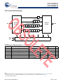
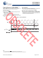
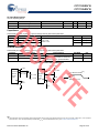
THIS SPEC IS OBSOLETE Spec No: 001-00350 Spec Title: CY7C1292DV18/CY7C1294DV18 9-Mbit QDR® II SRAM 2-Word Burst Architecture Sunset Owner: AJU Replaced By: None CY7C1292DV18 CY7C1294DV18 9-Mbit QDR® II SRAM 2-Word Burst Architecture Features Configurations ■ Separate independent read and write data ports ❐ Supports concurrent transactions CY7C1292DV18 – 512K x 18 CY7C1294DV18 – 256K x 36 ■ 250 MHz clock for high bandwidth Functional Description ■ 2-Word Burst on all accesses ■ Double Data Rate (DDR) interfaces on both read and write ports (data transferred at 500 MHz) at 250 MHz ■ Two input clocks (K and K) for precise DDR timing ❐ SRAM uses rising edges only ■ Two input clocks for output data (C and C) to minimize clock-skew and flight-time mismatches ■ Echo clocks (CQ and CQ) simplify data capture in high speed systems ■ Single multiplexed address input bus latches address inputs for both read and write ports ■ Separate Port Selects for depth expansion ■ Synchronous internally self-timed writes ■ Available in x 18 and x 36 configurations ■ Full data coherency, providing most current data ■ Core VDD = 1.8V (±0.1V); I/O VDDQ = 1.4V to VDD The CY7C1292DV18 and CY7C1294DV18 are 1.8V Synchronous Pipelined SRAMs, equipped with QDR®-II architecture. QDR II architecture consists of two separate ports to access the memory array. The read port has dedicated Data Outputs to support read operations and the write port has dedicated Data Inputs to support write operations. QDR II architecture has separate data inputs and data outputs to completely eliminate the need to “turn-around” the data bus required with common I/O devices. Access to each port is accomplished through a common address bus. The read address is latched on the rising edge of the K clock and the write address is latched on the rising edge of the K clock. Accesses to the QDR II read and write ports are completely independent of one another. To maximize data throughput, both read and write ports are equipped with Double Data Rate (DDR) interfaces. Each address location is associated with two 18-bit words (CY7C1292DV18) or 36-bit words (CY7C1294DV18) that burst sequentially into or out of the device. Because data can be transferred into and out of the device on every rising edge of both input clocks (K and K and C and C), memory bandwidth is maximized while simplifying system design by eliminating bus “turn-arounds.” ■ Available in 165-ball FBGA package (13 x 15 x 1.4 mm) ■ Offered in both Pb-free and non Pb-free packages ■ Variable drive HSTL output buffers ■ JTAG 1149.1 compatible test access port ■ Delay Lock Loop (DLL) for accurate data placement Depth expansion is accomplished with Port Selects for each port. Port selects allow each port to operate independently. All synchronous inputs pass through input registers controlled by the K or K input clocks. All data outputs pass through output registers controlled by the C or C (or K or K in a single clock domain) input clocks. Writes are conducted with on-chip synchronous self-timed write circuitry. Selection Guide Description 250 MHz 200 MHz 167 MHz Unit Maximum Operating Frequency 250 200 167 MHz Maximum Operating Current 600 550 500 mA Cypress Semiconductor Corporation Document #: 001-00350 Rev. *E • 198 Champion Court • San Jose, CA 95134-1709 • 408-943-2600 Revised October 19, 2010 CY7C1292DV18 CY7C1294DV18 Contents Features .............................................................................. 1 Configurations .................................................................... 1 Functional Description ....................................................... 1 Selection Guide .................................................................. 1 Contents .............................................................................. 2 Logic Block Diagram (CY7C1292DV18) ............................ 3 Logic Block Diagram (CY7C1294DV18) ............................ 3 Pin Configuration ............................................................... 4 165-Ball FBGA (13 x 15 x 1.4 mm) Pinout .................... 4 Pin Definitions .................................................................... 5 Functional Overview .......................................................... 7 Read Operations ........................................................... 7 Write Operations ........................................................... 7 Byte Write Operations ................................................... 7 Single Clock Mode ........................................................ 7 Concurrent Transactions ............................................... 7 Depth Expansion ........................................................... 7 Programmable Impedance ............................................ 7 Echo Clocks .................................................................. 7 DLL ................................................................................ 8 Application Example .......................................................... 8 Truth Table .......................................................................... 9 Write Cycle Descriptions ................................................... 9 Write Cycle Descriptions ................................................. 10 IEEE 1149.1 Serial Boundary Scan (JTAG) .................... 11 Disabling the JTAG Feature ........................................ 11 Test Access Port—Test Clock ..................................... 11 Test Mode Select ........................................................ 11 Test Data-In (TDI) ....................................................... 11 Test Data-Out (TDO) ................................................... 11 Performing a TAP Reset ............................................. 11 TAP Registers ............................................................. 11 Document #: 001-00350 Rev. *E TAP Instruction Set ..................................................... 11 TAP Controller State Diagram ......................................... 13 TAP Controller Block Diagram ........................................ 14 TAP Electrical Characteristics ........................................ 14 TAP Timing and Test Conditions .................................... 15 Identification Register Definitions .................................. 16 Scan Register Sizes ......................................................... 16 Instruction Codes ............................................................. 16 Boundary Scan Order ...................................................... 17 Power up Sequence in QDR II SRAM ............................. 18 Power up Sequence .................................................... 18 DLL Constraints .......................................................... 18 Maximum Ratings ............................................................. 19 Operating Range .............................................................. 19 Electrical Characteristics ................................................ 19 DC Electrical Characteristics ....................................... 19 AC Input Requirements ............................................... 20 Capacitance ...................................................................... 20 Thermal Resistance ......................................................... 20 Switching Characteristics ............................................... 21 Switching Waveforms ...................................................... 22 Ordering Information ....................................................... 23 Ordering Code Definition.................................................. 23 Package Diagram ............................................................. 23 Document History Page ................................................... 24 Sales, Solutions, and Legal Information ........................ 25 Worldwide Sales and Design Support ......................... 25 Products ...................................................................... 25 PSoC Solutions ........................................................... 25 Page 2 of 26 CY7C1292DV18 CY7C1294DV18 Logic Block Diagram (CY7C1292DV18) K K CLK Gen. DOFF Address Register Read Add. Decode 18 Write Reg 256K x 18 Array Address Register Write Reg 256K x 18 Array A(17:0) 18 Write Add. Decode D[17:0] 18 RPS Control Logic C C Read Data Reg. 36 VREF WPS Control Logic BWS[1:0] A(17:0) CQ CQ 18 Reg. 18 Reg. 18 18 Reg. Q[17:0] 18 Logic Block Diagram (CY7C1294DV18) DOFF VREF WPS BWS[3:0] CLK Gen. Address Register Read Add. Decode K K Write Reg 128K x 36 Array 17 Address Register Write Reg 128K x 36 Array A(16:0) 36 Write Add. Decode D[35:0] 17 RPS Control Logic C C Read Data Reg. 72 Control Logic 36 36 Reg. Reg. CQ CQ 36 Reg. 36 36 Document #: 001-00350 Rev. *E A(16:0) Q[35:0] Page 3 of 26 CY7C1292DV18 CY7C1294DV18 Pin Configuration The pin configuration for CY7C1292DV18 and CY7C1294DV18 follow. [1] 165-Ball FBGA (13 x 15 x 1.4 mm) Pinout CY7C1292DV18 (512K x 18) 1 A B C D E F G H J K L M N P R CQ 2 3 NC/144M NC/36M 4 5 6 7 8 9 10 11 WPS BWS1 K NC/288M K BWS0 NC/18M NC NC/72M NC RPS A NC CQ Q8 A VSS A VSS A VSS VSS VSS NC NC Q7 NC D8 D7 NC Q9 D9 A NC NC NC D11 D10 Q10 VSS VSS NC NC Q11 VDDQ VSS VSS VSS VDDQ NC D6 Q6 NC Q12 D12 VDDQ VSS NC NC Q5 D13 VREF NC Q13 VDDQ D14 VDDQ VDDQ VDDQ VDD VDD VDD VSS VSS VSS VDD VDDQ NC VDD VDD VDD VDD VDDQ VDDQ VDDQ NC VDDQ NC NC VREF Q4 D5 ZQ D4 NC NC Q14 VDDQ VDD VSS VDD VDDQ NC D3 Q3 NC Q15 D15 VDDQ VSS VSS VSS VDDQ NC NC Q2 NC NC NC D17 D16 Q16 VSS VSS VSS A VSS A VSS A VSS VSS NC NC Q1 NC D2 D1 NC NC Q17 A A C A A NC D0 Q0 TDO TCK A A A C A A A TMS TDI 7 8 9 10 11 RPS A DOFF NC CY7C1294DV18 (256K x 36) 1 A B C D E F G H J K L M N P R CQ Q27 2 3 NC/288M NC/72M 4 5 6 WPS A BWS2 K BWS1 A VSS K NC/18M VSS BWS0 A VSS VSS VSS D16 Q16 Q7 D15 D8 D7 VSS VSS VSS VDDQ Q15 D6 Q6 VDD VDDQ D14 Q14 Q5 VDD VDD VDD VDDQ VDDQ VDDQ Q13 VDDQ D12 D13 VREF Q4 D5 ZQ D4 NC/36M NC/144M D17 Q17 CQ Q8 Q18 D18 D27 D28 Q28 D20 D19 Q19 VSS VSS Q29 D29 Q20 Q30 VDDQ Q21 D21 D30 VDDQ DOFF D31 Q22 VDDQ D23 VDDQ VDDQ VDDQ VDD VSS D22 VREF Q31 VDD VDD VDD VSS VSS VSS Q32 D32 Q23 VDDQ VDD VSS VDD VDDQ Q12 D3 Q3 Q33 Q24 D24 VDDQ VSS VSS VSS VDDQ D11 Q11 Q2 D33 D34 Q34 D26 D25 Q25 VSS VSS VSS A VSS A VSS A VSS VSS D10 Q10 Q1 D9 D2 D1 Q35 D35 Q26 A A C A A Q9 D0 Q0 TDO TCK A A A C A A A TMS TDI BWS3 Note 1. NC/18M, NC/36M, NC/72M, NC/144M, and NC/288M are not connected to the die and can be tied to any voltage level. Document #: 001-00350 Rev. *E Page 4 of 26 CY7C1292DV18 CY7C1294DV18 Pin Definitions Pin Name I/O Pin Description D[x:0] InputData Input Signals, sampled on the rising edge of K and K clocks during valid write operations. Synchronous CY7C1292DV18 - D[17:0] CY7C1294DV18 - D[35:0] WPS InputWrite Port Select, Active LOW. Sampled on the rising edge of the K clock. When asserted active, Synchronous a write operation is initiated. Deasserting deselects the write port. Deselecting the write port causes D[x:0] to be ignored. BWS0, BWS1, BWS2, BWS3 InputByte Write Select 0, 1, 2 and 3 Active LOW. Sampled on the rising edge of the K and K clocks Synchronous during write operations. Used to select which byte is written into the device during the current portion of the write operations. Bytes not written remain unaltered. CY7C1292DV18 BWS0 controls D[8:0], BWS1 controls D[17:9]. CY7C1294DV18BWS0 controls D[8:0], BWS1 controls D[17:9],BWS2 controls D[26:18] and BWS3 controls D[35:27]. All the Byte Write Selects are sampled on the same edge as the data. Deselecting a Byte Write Select causes the corresponding byte of data to be ignored and not written into the device. A InputAddress Inputs. Sampled on the rising edge of the K (read address) and K (write address) clocks Synchronous during active read and write operations. These address inputs are multiplexed for both read and write operations. Internally, the device is organized as 512K x 18 (2 arrays each of 256K x 18) for CY7C1292DV18 and 256K x 36 (2 arrays each of 128K x 36) for CY7C1294DV18. Therefore 18 address inputs for CY7C1292DV18 and 17 address inputs for CY7C1294DV18. These inputs are ignored when the appropriate port is deselected. Q[x:0] OutputsData Output Signals. These pins drive out the requested data during a read operation. Valid data Synchronous is driven out on the rising edge of both the C and C clocks during read operations or K and K when in single clock mode. When the read port is deselected, Q[x:0] are automatically tristated. CY7C1292DV18 Q[17:0] CY7C1294DV18 Q[35:0] RPS InputRead Port Select, Active LOW. Sampled on the rising edge of Positive Input Clock (K). When active, Synchronous a read operation is initiated. Deasserting causes the read port to be deselected. When deselected, the pending access is allowed to complete and the output drivers are automatically tristated following the next rising edge of the C clock. Each read access consists of a burst of two sequential transfers. C Input-Clock Positive Input Clock for Output Data. C is used in conjunction with C to clock out the read data from the device. C and C can be used together to deskew the flight times of various devices on the board back to the controller. See application example for further details. C Input-Clock Negative Input Clock for Output Data. C is used in conjunction with C to clock out the read data from the device. C and C can be used together to deskew the flight times of various devices on the board back to the controller. See application example for further details. K Input-Clock Positive Input Clock Input. The rising edge of K is used to capture synchronous inputs to the device and to drive out data through Q[x:0] when in single clock mode. All accesses are initiated on the rising edge of K. K Input-Clock Negative Input Clock Input. The rising edge of K is used to capture synchronous inputs being presented to the device and to drive out data through Q[x:0] when in single clock mode. CQ Echo Clock CQ is Referenced with Respect to C. This is a free running clock and is synchronized to the input clock for output data (C) of the QDR II. In the single clock mode, CQ is generated with respect to K. The timings for the echo clocks are shown in the AC Timing table. CQ Echo Clock ZQ Input CQ is Referenced with Respect to C. This is a free running clock and is synchronized to the input clock for output data (C) of the QDR II. In the single clock mode, CQ is generated with respect to K. The timings for the echo clocks are shown in the AC Timing table. Output Impedance Matching Input. This input is used to tune the device outputs to the system data bus impedance. CQ, CQ, and Q[x:0] output impedance are set to 0.2 x RQ, where RQ is a resistor connected between ZQ and ground. Alternately, this pin can be connected directly to VDDQ, which enables the minimum impedance mode. This pin cannot be connected directly to GND or left unconnected. Document #: 001-00350 Rev. *E Page 5 of 26 CY7C1292DV18 CY7C1294DV18 Pin Definitions (continued) Pin Name I/O Pin Description DOFF Input DLL Turn Off, Active LOW. Connecting this pin to ground turns off the DLL inside the device. The timings in the DLL turned off operation are different from those listed in this data sheet. TDO Output TCK Input TCK pin for JTAG. TDI Input TDI pin for JTAG. TMS Input TMS pin for JTAG. NC N/A Not connected to the Die. Can be tied to any voltage level. NC/18M N/A Not connected to the Die. Can be tied to any voltage level. NC/36M N/A Not connected to the Die. Can be tied to any voltage level. NC/72M N/A Not connected to the Die. Can be tied to any voltage level. NC/144M N/A Not connected to the Die. Can be tied to any voltage level. NC/288M N/A VREF InputReference VDD VSS VDDQ TDO for JTAG. Not connected to the Die. Can be tied to any voltage level. Reference Voltage Input. Static input used to set the reference level for HSTL inputs and Outputs and AC measurement points. Power Supply Power Supply Inputs to the Core of the Device. Ground Ground for the Device. Power Supply Power Supply Inputs for the Outputs of the Device. Document #: 001-00350 Rev. *E Page 6 of 26 CY7C1292DV18 CY7C1294DV18 Functional Overview The CY7C1292DV18 and CY7C1294DV18 are synchronous pipelined Burst SRAMs equipped with both a read port and a write port. The read port is dedicated to read operations and the write port is dedicated to write operations. Data flows into the SRAM through the write port and out through the read port. These devices multiplex the address inputs to minimize the number of address pins required. By having separate read and write ports, the QDR II completely eliminates the need to “turn-around” the data bus and avoids any possible data contention, thereby simplifying system design. Each access consists of two 18-bit data transfers in the case of CY7C1292DV18 and two 36-bit data transfers in the case of CY7C1294DV18 in one clock cycle. Accesses for both ports are initiated on the rising edge of the positive Input Clock (K). All synchronous input timings are referenced from the rising edge of the input clocks (K and K) and all output timings are referenced to the rising edge of output clocks (C and C or K and K when in single clock mode). All synchronous data inputs (D[x:0]) inputs pass through input registers controlled by the input clocks (K and K). All synchronous data outputs (Q[x:0]) outputs pass through output registers controlled by the rising edge of the output clocks (C and C or K and K when in single clock mode). All synchronous control (RPS, WPS, BWS[x:0]) inputs pass through input registers controlled by the rising edge of the input clocks (K and K). CY7C1292DV18 is described in the following sections. The same basic descriptions apply to CY7C1294DV18. Read Operations The CY7C1292DV18 is organized internally as two arrays of 256K x 18. Accesses are completed in a burst of two sequential 18-bit data words. Read operations are initiated by asserting RPS active at the rising edge of the Positive Input Clock (K). The address is latched on the rising edge of the K Clock. The address presented to Address inputs is stored in the read address register. Following the next K clock rise the corresponding lowest order 18-bit word of data is driven onto the Q[17:0] using C as the output timing reference. On the subsequent rising edge of C, the next 18-bit data word is driven onto the Q[17:0]. The requested data is valid 0.45 ns from the rising edge of the output clock (C and C or K and K when in single clock mode). Synchronous internal circuitry automatically tristates the outputs following the next rising edge of the Output Clocks (C/C). This allows for a seamless transition between devices without the insertion of wait states in a depth expanded memory. Write Operations Write operations are initiated by asserting WPS active at the rising edge of the Positive Input Clock (K). On the same K clock rise, the data presented to D[17:0] is latched and stored into the lower 18-bit Write Data register provided BWS[1:0] are both asserted active. On the subsequent rising edge of the Negative Input Clock (K), the address is latched and the information presented to D[17:0] is stored into the Write Data register provided BWS[1:0] are both asserted active. The 36 bits of data are then written into the memory array at the specified location. When Document #: 001-00350 Rev. *E deselected, the write port ignores all inputs after the pending write operations are completed. Byte Write Operations Byte Write operations are supported by the CY7C1292DV18. A write operation is initiated as described in the write Operations section above. The bytes that are written are determined by BWS0 and BWS1, which are sampled with each 18-bit data word. Asserting the appropriate Byte Write Select input during the data portion of a write allows the data being presented to be latched and written into the device. Deasserting the Byte Write Select input during the data portion of a write allows the data stored in the device for that byte to remain unaltered. This feature is used to simplify read/modify/write operations to a Byte Write operation. Single Clock Mode The CY7C1292DV18 is used with a single clock that controls both the input and output registers. In this mode, the device recognizes only a single pair of input clocks (K and K) that control both the input and output registers. This operation is identical to the operation if the device had zero skew between the K/K and C/C clocks. All timing parameters remain the same in this mode. To use this mode of operation, the user must tie C and C HIGH at power on. This function is a strap option and not alterable during device operation. Concurrent Transactions The read and write ports on the CY7C1292DV18 operate completely independently of one another. Because each port latches the address inputs on different clock edges, the user can read or write to any location, regardless of the transaction on the other port. Also, reads and writes can be started in the same clock cycle. If the ports access the same location at the same time, the SRAM delivers the most recent information associated with the specified address location. This includes forwarding data from a write cycle that was initiated on the previous K clock rise. Depth Expansion The CY7C1292DV18 has a Port Select input for each port. This allows for easy depth expansion. Both Port Selects are sampled on the rising edge of the Positive Input Clock only (K). Each port select input can deselect the specified port. Deselecting a port does not affect the other port. All pending transactions (read and write) are completed prior to the device being deselected. Programmable Impedance An external resistor, RQ, must be connected between the ZQ pin on the SRAM and VSS to allow the SRAM to adjust its output driver impedance. The value of RQ must be 5x the value of the intended line impedance driven by the SRAM. The allowable range of RQ to guarantee impedance matching with a tolerance of ±15% is between 175 and 350, with VDDQ = 1.5V.The output impedance is adjusted every 1024 cycles upon power-up to account for drifts in supply voltage and temperature. Echo Clocks Echo clocks are provided on the QDR II to simplify data capture on high speed systems. Two echo clocks are generated by the QDR II. CQ is referenced with respect to C and CQ is referenced Page 7 of 26 CY7C1292DV18 CY7C1294DV18 with respect to C. These are free-running clocks and are synchronized to the output clock (C/C) of the QDR II. In the single clock mode, CQ is generated with respect to K and CQ is generated with respect to K. The timings for the echo clocks are shown in the AC Timing table. DLL These chips utilize a Delay Lock Loop (DLL) that is designed to function between 80 MHz and the specified maximum clock frequency. During power-up, when the DOFF is tied HIGH, the DLL gets locked after 1024 cycles of stable clock. The DLL can also be reset by slowing or stopping the input clock K and K for a minimum of 30 ns. However, it is not necessary for the DLL to be specifically reset to lock the DLL to the desired frequency. The DLL automatically locks 1024 clock cycles after a stable clock is presented. The DLL may be disabled by applying ground to the DOFF pin. For information refer to the application note “DLL Considerations in QDRII/DDRII/QDRII+/DDRII+”. Application Example Figure 1 shows four QDR II used in an application. Figure 1. Application Example SRAM #1 Vt R D A R P S # W P S # B W S # ZQ CQ/CQ# Q C C# K K# DATA IN DATA OUT Address RPS# BUS WPS# MASTER BWS# (CPU CLKIN/CLKIN# or Source K ASIC) Source K# R = 250ohms SRAM #4 R P S # D A R W P S # B W S # ZQ R = 250ohms CQ/CQ# Q C C# K K# Vt Vt Delayed K Delayed K# R Document #: 001-00350 Rev. *E R = 50ohms Vt = Vddq/2 Page 8 of 26 CY7C1292DV18 CY7C1294DV18 Truth Table The truth table for CY7C1292DV18 and CY7C1294DV18 follows. [3, 4, 5, 6, 7, 8] Operation K RPS WPS Write Cycle: Load address on the rising edge of K clock; input write data on K and K rising edges. L-H X L D(A + 0) at K(t) D(A + 1) at K(t) Read Cycle: Load address on the rising edge of K clock; wait one and a half cycle; read data on C and C rising edges. L-H L X Q(A + 0) at C(t + 1) Q(A + 1) at C(t + 2) NOP: No Operation L-H H H D = X, Q = High-Z D = X, Q = High-Z Stopped X X Previous State Previous State Standby: Clock Stopped DQ DQ Write Cycle Descriptions The write cycle description table for CY7C1292DV18 follows. [3, 9] BWS0 BWS1 K L L L-H L L – L H L-H L H – H L L-H H L – H H L-H H H – K – Comments During the data portion of a write sequence both bytes (D[17:0]) are written into the device. L-H During the data portion of a write sequence both bytes (D[17:0]) are written into the device. – During the data portion of a write sequence only the lower byte (D[8:0]) is written into the device. D[17:9] remains unaltered. L-H During the data portion of a write sequence only the lower byte (D[8:0]) is written into the device. D[17:9] remains unaltered. – During the data portion of a write sequence only the upper byte (D[17:9]) is written into the device. D[8:0] remains unaltered. L-H During the data portion of a write sequence only the upper byte (D[17:9]) is written into the device. D[8:0] remains unaltered. – No data is written into the devices during this portion of a write operation. L-H No data is written into the devices during this portion of a write operation. Notes 2. The above application shows four QDR II being used. 3. X = “Don't Care,” H = Logic HIGH, L= Logic LOW, represents rising edge. 4. Device powers up deselected and the outputs in a tristate condition. 5. “A” represents address location latched by the devices when transaction was initiated. A + 0, A + 1 represents the internal address sequence in the burst. 6. “t” represents the cycle at which a Read/Write operation is started. t + 1 and t + 2 are the first and second clock cycles respectively succeeding the “t” clock cycle. 7. Data inputs are registered at K and K rising edges. Data outputs are delivered on C and C rising edges, except when in single clock mode. 8. It is recommended that K = K and C = C = HIGH when clock is stopped. This is not essential, but permits most rapid restart by overcoming transmission line charging symmetrically. 9. Assumes a write cycle was initiated per the Write Port Cycle Description Truth Table. BWS0, BWS1, BWS2, and BWS3 can be altered on different portions of a write cycle, as long as the setup and hold requirements are achieved. Document #: 001-00350 Rev. *E Page 9 of 26 CY7C1292DV18 CY7C1294DV18 Write Cycle Descriptions The write cycle description table for CY7C1294DV18 follows. [3, 9] BWS0 BWS1 BWS2 BWS3 K K Comments L L L L L-H - During the data portion of a write sequence, all four bytes (D[35:0]) are written into the device. L L L L - L H H H L-H L H H H - H L H H L-H H L H H - H H L H L-H H H L H - H H H L L-H H H H L - H H H H L-H H H H H - Document #: 001-00350 Rev. *E L-H During the data portion of a write sequence, all four bytes (D[35:0]) are written into the device. - During the data portion of a write sequence, only the lower byte (D[8:0]) is written into the device. D[35:9] remains unaltered. L-H During the data portion of a write sequence, only the lower byte (D[8:0]) is written into the device. D[35:9] remains unaltered. - During the data portion of a write sequence, only the byte (D[17:9]) is written into the device. D[8:0] and D[35:18] remains unaltered. L-H During the data portion of a write sequence, only the byte (D[17:9]) is written into the device. D[8:0] and D[35:18] remains unaltered. - During the data portion of a write sequence, only the byte (D[26:18]) is written into the device. D[17:0] and D[35:27] remains unaltered. L-H During the data portion of a write sequence, only the byte (D[26:18]) is written into the device. D[17:0] and D[35:27] remains unaltered. During the data portion of a write sequence, only the byte (D[35:27]) is written into the device. D[26:0] remains unaltered. L-H During the data portion of a write sequence, only the byte (D[35:27]) is written into the device. D[26:0] remains unaltered. - No data is written into the device during this portion of a write operation. L-H No data is written into the device during this portion of a write operation. Page 10 of 26 CY7C1292DV18 CY7C1294DV18 IEEE 1149.1 Serial Boundary Scan (JTAG) These SRAMs incorporate a serial boundary scan test access port (TAP) in the FBGA package. This part is fully compliant with IEEE Standard #1149.1-1900. The TAP operates using JEDEC standard 1.8V I/O logic levels. Disabling the JTAG Feature It is possible to operate the SRAM without using the JTAG feature. To disable the TAP controller, TCK must be tied LOW (VSS) to prevent clocking of the device. TDI and TMS are internally pulled up and may be unconnected. They may alternately be connected to VDD through a pull-up resistor. TDO should be left unconnected. Upon power-up, the device comes up in a reset state which does not interfere with the operation of the device. Test Access Port—Test Clock The test clock is used only with the TAP controller. All inputs are captured on the rising edge of TCK. All outputs are driven from the falling edge of TCK. Test Mode Select The TMS input is used to give commands to the TAP controller and is sampled on the rising edge of TCK. It is allowable to leave this pin unconnected if the TAP is not used. The pin is pulled up internally, resulting in a logic HIGH level. Test Data-In (TDI) The TDI pin is used to serially input information into the registers and can be connected to the input of any of the registers. The register between TDI and TDO is chosen by the instruction that is loaded into the TAP instruction register. For information on loading the instruction register, see the TAP Controller State Diagram. TDI is internally pulled up and can be unconnected if the TAP is unused in an application. TDI is connected to the most significant bit (MSB) on any register. Test Data-Out (TDO) The TDO output pin is used to serially clock data-out from the registers. The output is active depending upon the current state of the TAP state machine (see Instruction codes). The output changes on the falling edge of TCK. TDO is connected to the least significant bit (LSB) of any register. Performing a TAP Reset A Reset is performed by forcing TMS HIGH (VDD) for five rising edges of TCK. This RESET does not affect the operation of the SRAM and may be performed while the SRAM is operating. At power-up, the TAP is reset internally to ensure that TDO comes up in a high-Z state. Instruction Register Three-bit instructions can be serially loaded into the instruction register. This register is loaded when it is placed between the TDI and TDO pins as shown in TAP Controller Block Diagram. Upon power-up, the instruction register is loaded with the IDCODE instruction. It is also loaded with the IDCODE instruction if the controller is placed in a reset state as described in the previous section. When the TAP controller is in the Capture IR state, the two least significant bits are loaded with a binary “01” pattern to allow for fault isolation of the board level serial test path. Bypass Register To save time when serially shifting data through registers, it is sometimes advantageous to skip certain chips. The bypass register is a single-bit register that can be placed between TDI and TDO pins. This allows data to be shifted through the SRAM with minimal delay. The bypass register is set LOW (VSS) when the BYPASS instruction is executed. Boundary Scan Register The boundary scan register is connected to all of the input and output pins on the SRAM. Several no connect (NC) pins are also included in the scan register to reserve pins for higher density devices. The boundary scan register is loaded with the contents of the RAM Input and Output ring when the TAP controller is in the Capture-DR state and is then placed between the TDI and TDO pins when the controller is moved to the Shift-DR state. The EXTEST, SAMPLE/PRELOAD and SAMPLE Z instructions can be used to capture the contents of the Input and Output ring. The Boundary Scan Order tables show the order in which the bits are connected. Each bit corresponds to one of the bumps on the SRAM package. The MSB of the register is connected to TDI, and the LSB is connected to TDO. Identification (ID) Register The ID register is loaded with a vendor-specific, 32-bit code during the Capture-DR state when the IDCODE command is loaded in the instruction register. The IDCODE is hardwired into the SRAM and can be shifted out when the TAP controller is in the Shift-DR state. The ID register has a vendor code and other information described in the Identification Register Definitions table. TAP Instruction Set TAP Registers Eight different instructions are possible with the three-bit instruction register. All combinations are listed in the Instruction Code table. Three of these instructions are listed as RESERVED and should not be used. The other five instructions are described in detail below. Registers are connected between the TDI and TDO pins and allow data to be scanned into and out of the SRAM test circuitry. Only one register can be selected at a time through the instruction registers. Data is serially loaded into the TDI pin on the rising edge of TCK. Data is output on the TDO pin on the falling edge of TCK. Instructions are loaded into the TAP controller during the Shift-IR state when the instruction register is placed between TDI and TDO. During this state, instructions are shifted through the instruction register through the TDI and TDO pins. To execute the instruction after it is shifted in, the TAP controller needs to be moved into the Update-IR state. Document #: 001-00350 Rev. *E Page 11 of 26 CY7C1292DV18 CY7C1294DV18 IDCODE The IDCODE instruction causes a vendor-specific, 32-bit code to be loaded into the instruction register. It also places the instruction register between the TDI and TDO pins and allows the IDCODE to be shifted out of the device when the TAP controller enters the Shift-DR state. The IDCODE instruction is loaded into the instruction register upon power-up or whenever the TAP controller is given a test logic reset state. SAMPLE Z The SAMPLE Z instruction causes the boundary scan register to be connected between the TDI and TDO pins when the TAP controller is in a Shift-DR state. The SAMPLE Z command puts the output bus into a High-Z state until the next command is given during the “Update IR” state. SAMPLE/PRELOAD SAMPLE/PRELOAD is a 1149.1 mandatory instruction. When the SAMPLE/PRELOAD instructions are loaded into the instruction register and the TAP controller is in the Capture-DR state, a snapshot of data on the inputs and output pins is captured in the boundary scan register. The user must be aware that the TAP controller clock can only operate at a frequency up to 20 MHz, while the SRAM clock operates more than an order of magnitude faster. Because there is a large difference in the clock frequencies, it is possible that during the Capture-DR state, an input or output undergoes a transition. The TAP may then try to capture a signal while in transition (metastable state). This does not harm the device, but there is no guarantee as to the value that is captured. Repeatable results may not be possible. PRELOAD allows an initial data pattern to be placed at the latched parallel outputs of the boundary scan register cells prior to the selection of another boundary scan test operation. The shifting of data for the SAMPLE and PRELOAD phases can occur concurrently when required—that is, while data captured is shifted out, the preloaded data can be shifted in. BYPASS When the BYPASS instruction is loaded in the instruction register and the TAP is placed in a Shift-DR state, the bypass register is placed between the TDI and TDO pins. The advantage of the BYPASS instruction is that it shortens the boundary scan path when multiple devices are connected together on a board. EXTEST The EXTEST instruction enables the preloaded data to be driven out through the system output pins. This instruction also selects the boundary scan register to be connected for serial access between the TDI and TDO in the shift-DR controller state. EXTEST OUTPUT BUS TRISTATE IEEE Standard 1149.1 mandates that the TAP controller be able to put the output bus into a tristate mode. The boundary scan register has a special bit located at bit #47. When this scan cell, called the “extest output bus tristate,” is latched into the preload register during the “Update-DR” state in the TAP controller, it directly controls the state of the output (Q-bus) pins, when the EXTEST is entered as the current instruction. When HIGH, it enables the output buffers to drive the output bus. When LOW, this bit places the output bus into a High-Z condition. To guarantee that the boundary scan register captures the correct value of a signal, the SRAM signal must be stabilized long enough to meet the TAP controller's capture setup plus hold times (tCS and tCH). The SRAM clock input might not be captured correctly if there is no way in a design to stop (or slow) the clock during a SAMPLE/PRELOAD instruction. If this is an issue, it is still possible to capture all other signals and simply ignore the value of the CK and CK captured in the boundary scan register. This bit can be set by entering the SAMPLE/PRELOAD or EXTEST command, and then shifting the desired bit into that cell, during the “Shift-DR” state. During “Update-DR”, the value loaded into that shift-register cell latches into the preload register. When the EXTEST instruction is entered, this bit directly controls the output Q-bus pins. Note that this bit is pre-set LOW to enable the output when the device is powered-up, and also when the TAP controller is in the “Test-Logic-Reset” state. When the data is captured, it is possible to shift out the data by putting the TAP into the Shift-DR state. This places the boundary scan register between the TDI and TDO pins. Reserved Document #: 001-00350 Rev. *E These instructions are not implemented but are reserved for future use. Do not use these instructions. Page 12 of 26 CY7C1292DV18 CY7C1294DV18 TAP Controller State Diagram The state diagram for the TAP controller follows. [10] 1 TEST-LOGIC RESET 0 0 TEST-LOGIC/ IDLE 1 1 1 SELECT DR-SCAN SELECT IR-SCAN 0 0 1 1 CAPTURE-DR CAPTURE-IR 0 0 0 SHIFT-DR 0 SHIFT-IR 1 1 1 EXIT1-DR 1 EXIT1-IR 0 0 PAUSE-DR 0 0 PAUSE-IR 1 1 0 0 EXIT2-DR EXIT2-IR 1 1 UPDATE-DR 1 0 UPDATE-IR 1 0 Note 10. The 0/1 next to each state represents the value at TMS at the rising edge of TCK. Document #: 001-00350 Rev. *E Page 13 of 26 CY7C1292DV18 CY7C1294DV18 TAP Controller Block Diagram 0 Bypass Register 2 Selection Circuitry TDI 1 0 Selection Circuitry Instruction Register 31 30 29 . . 2 1 0 1 0 TDO Identification Register 106 . . . . 2 Boundary Scan Register TCK TAP Controller TMS TAP Electrical Characteristics Over the Operating Range [11, 12, 13] Parameter Description Test Conditions Min. Max. Unit VOH1 Output HIGH Voltage IOH =2.0 mA 1.4 V VOH2 Output HIGH Voltage IOH =100 A 1.6 V VOL1 Output LOW Voltage IOL = 2.0 mA 0.4 V VOL2 Output LOW Voltage IOL = 100 A 0.2 V VIH Input HIGH Voltage 0.65VDD VDD + 0.3 V VIL Input LOW Voltage –0.3 0.35VDD V IX Input and Output Load Current 5 5 A GND VI VDD Notes 11. These characteristic pertain to the TAP inputs (TMS, TCK, TDI, and TDO). Parallel load levels are specified in the Electrical Characteristics table. 12. Overshoot: VIH(AC) < VDDQ +0.85V (Pulse width less than tCYC/2), Undershoot: VIL(AC) > –1.5V (Pulse width less than tCYC/2). 13. All voltage referenced to Ground. Document #: 001-00350 Rev. *E Page 14 of 26 CY7C1292DV18 CY7C1294DV18 TAP AC Switching Characteristics Over the Operating Range [14, 15] Parameter Description Min. Max. Unit 20 MHz tTCYC TCK Clock Cycle Time tTF TCK Clock Frequency tTH TCK Clock HIGH 20 ns tTL TCK Clock LOW 20 ns tTMSS TMS Setup to TCK Clock Rise 5 ns tTDIS TDI Setup to TCK Clock Rise 5 ns tCS Capture Setup to TCK Rise 5 ns tTMSH TMS Hold after TCK Clock Rise 5 ns tTDIH TDI Hold after Clock Rise 5 ns tCH Capture Hold after Clock Rise 5 ns 50 ns Setup Times Hold Times Output Times tTDOV TCK Clock LOW to TDO Valid tTDOX TCK Clock LOW to TDO Invalid 10 0 ns ns TAP Timing and Test Conditions Figure 2 shows the TAP timing and test conditions. [15] Figure 2. TAP Timing and Test Conditions 0.9V 1.8V 50 TDO 0V Z0 = 50 (a) ALL INPUT PULSES 0.9V CL = 20 pF tTH GND tTL Test Clock TCK tTCYC tTMSH tTMSS Test Mode Select TMS tTDIS tTDIH Test Data In TDI Test Data Out TDO tTDOV tTDOX Notes 14. tCS and tCH refer to the setup and hold time requirements of latching data from the boundary scan register. 15. Test conditions are specified using the load in TAP AC Test Conditions. tR/tF = 1 ns. Document #: 001-00350 Rev. *E Page 15 of 26 CY7C1292DV18 CY7C1294DV18 Identification Register Definitions Instruction Field Value CY7C1292DV18 CY7C1294DV18 000 000 Cypress Device ID (28:12) 11010011010010110 11010011010100110 Cypress JEDEC ID (11:1) 00000110100 00000110100 ID Register Presence (0) 1 1 Revision Number (31:29) Description Version number. Defines the type of SRAM. Unique identification of SRAM vendor. Indicates the presence of an ID register. Scan Register Sizes Register Name Bit Size Instruction 3 Bypass 1 ID 32 Boundary Scan Cells 107 Instruction Codes Instruction Code Description EXTEST 000 Captures the Input/Output ring contents. IDCODE 001 Loads the ID register with the vendor ID code and places the register between TDI and TDO. This operation does not affect SRAM operation. SAMPLE Z 010 Captures the Input/Output contents. Places the boundary scan register between TDI and TDO. Forces all SRAM output drivers to a High-Z state. RESERVED 011 Do Not Use: This instruction is reserved for future use. SAMPLE/PRELOAD 100 Captures the Input/Output ring contents. Places the boundary scan register between TDI and TDO. Does not affect the SRAM operation. RESERVED 101 Do Not Use: This instruction is reserved for future use. RESERVED 110 Do Not Use: This instruction is reserved for future use. BYPASS 111 Places the bypass register between TDI and TDO. This operation does not affect SRAM operation. Document #: 001-00350 Rev. *E Page 16 of 26 CY7C1292DV18 CY7C1294DV18 Boundary Scan Order Bit # Bump ID Bit # 0 6R 27 1 6P 28 2 6N 29 3 7P 30 4 7N 31 5 7R 6 8R 7 8P Bump ID Bit # Bump ID Bit # Bump ID 11H 54 7B 81 3G 10G 55 6B 82 2G 9G 56 6A 83 1J 11F 57 5B 84 2J 11G 58 5A 85 3K 32 9F 59 4A 86 3J 33 10F 60 5C 87 2K 34 11E 61 4B 88 1K 8 9R 35 10E 62 3A 89 2L 9 11P 36 10D 63 1H 90 3L 10 10P 37 9E 64 1A 91 1M 11 10N 38 10C 65 2B 92 1L 12 9P 39 11D 66 3B 93 3N 13 10M 40 9C 67 1C 94 3M 14 11N 41 9D 68 1B 95 1N 15 9M 42 11B 69 3D 96 2M 16 9N 43 11C 70 3C 97 3P 17 11L 44 9B 71 1D 98 2N 18 11M 45 10B 72 2C 99 2P 19 9L 46 11A 73 3E 100 1P 20 10L 47 Internal 74 2D 101 3R 21 11K 48 9A 75 2E 102 4R 22 10K 49 8B 76 1E 103 4P 23 9J 50 7C 77 2F 104 5P 24 9K 51 6C 78 3F 105 5N 25 10J 52 8A 79 1G 106 5R 26 11J 53 7A 80 1F Document #: 001-00350 Rev. *E Page 17 of 26 CY7C1292DV18 CY7C1294DV18 Power Up Sequence in QDR II SRAM [16, 17] DLL Constraints QDR II SRAMs must be powered up and initialized in a predefined manner to prevent undefined operations. ■ DLL uses K clock as its synchronizing input. The input should have low phase jitter, which is specified as tKC Var. ■ The DLL functions at frequencies down to 80 MHz. ■ If the input clock is unstable and the DLL is enabled, then the DLL may lock onto an incorrect frequency, causing unstable SRAM behavior. To avoid this, provide 1024 cycles stable clock to relock to the desired clock frequency. Power Up Sequence ■ Apply power with DOFF tied HIGH (All other inputs can be HIGH or LOW) ❐ Apply VDD before VDDQ ❐ Apply VDDQ before VREF or at the same time as VREF ■ Provide stable power and clock (K, K) for 1024 cycles to lock the DLL. ~ ~ Figure 3. Power Up Waveforms K K ~ ~ Unstable Clock > 1024 Stable clock Start Normal Operation Clock Start (Clock Starts after V DD / V DDQ Stable) VDD / VDDQ DOFF V DD / V DDQ Stable (< +/- 0.1V DC per 50ns ) Fix High (or tied to VDDQ) Notes 16. It is recommended that the DOFF pin be pulled HIGH via a pull up resistor of 1 K. 17. During power up, when the DOFF is tied HIGH, the DLL gets locked after 1024 cycles of stable clock. Document #: 001-00350 Rev. *E Page 18 of 26 CY7C1292DV18 CY7C1294DV18 Maximum Ratings Neutron Soft Error Immunity Exceeding maximum ratings may impair the useful life of the device. These user guidelines are not tested. Storage Temperature ................................. –65°C to +150°C Ambient Temperature with Power Applied ............................................ –55°C to +125°C Supply Voltage on VDD Relative to GND ........–0.5V to +2.9V Supply Voltage on VDDQ Relative to GND.......–0.5V to +VDD DC Voltage Applied to Outputs in High-Z State..................................... –0.5V to VDDQ + 0.3V DC Input Voltage[12]............................... –0.5V to VDD + 0.3V Current into Outputs (LOW)......................................... 20 mA Static Discharge Voltage.......................................... > 2001V (per MIL-STD-883, Method 3015) Description Test Conditions Typ Max* Unit LSBU Logical Single-Bit Upsets 25°C 320 368 FIT/ Mb LMBU Logical Multi-Bit Upsets 25°C 0 0.01 FIT/ Mb Single Event Latchup 85°C 0 0.1 FIT/ Dev Parameter SEL * No LMBU or SEL events occurred during testing; this column represents a statistical 2, 95% confidence limit calculation. For more details refer to Application Note AN 54908 “Accelerated Neutron SER Testing and Calculation of Terrestrial Failure Rates” Latch-up Current.................................................... > 200 mA Operating Range Range Ambient Temperature (TA) VDD[20] VDDQ[20] 0°C to +70°C 1.8 0.1 V 1.4V to VDD Com’l Ind’l –40°C to +85°C Electrical Characteristics DC Electrical Characteristics Over the Operating Range[13, 20] Parameter VDD VDDQ Description Test Conditions Min Typ Max Unit Power Supply Voltage 1.7 1.8 1.9 V I/O Supply Voltage 1.4 1.5 VDD V V VOH Output HIGH Voltage Note 18 VDDQ/2 – 0.12 VDDQ/2 + 0.12 VOL Output LOW Voltage Note 19 VDDQ/2 – 0.12 VDDQ/2 + 0.12 V VOH(LOW) Output HIGH Voltage IOH =0.1 mA, Nominal Impedance VDDQ – 0.2 VDDQ V VOL(LOW) Output LOW Voltage IOL = 0.1 mA, Nominal Impedance VIH Input HIGH Voltage[12] VIL Input LOW IX Input Leakage Current IOZ Output Leakage Current 0.2 V VDDQ+0.3 V –0.3 VREF – 0.1 V GND VI VDDQ 5 5 A GND VI VDDQ, Output Disabled 5 5 A 0.95 V VDD = Max., IOUT = 0 mA, 167 MHz f = fMAX = 1/tCYC 200 MHz 500 mA 550 mA 250 MHz 600 mA Max. VDD, Both Ports 167 MHz Deselected, VIN VIH or 200 MHz VIN VIL f = fMAX = 1/tCYC, 250 MHz Inputs Static 240 mA 260 mA 280 mA Voltage[12] VREF Input Reference Voltage[21] IDD VDD Operating Supply ISB1 VSS VREF + 0.1 Automatic Power Down Current Typical Value = 0.75V 0.68 0.75 Notes 18. Output are impedance controlled. IOH = –(VDDQ/2)/(RQ/5) for values of 175 RQ 350s. 19. Output are impedance controlled. IOL = (VDDQ/2)/(RQ/5) for values of 175 RQ 350. 20. Power up: Assumes a linear ramp from 0V to VDD(min.) within 200 ms. During this time VIH < VDD and VDDQ < VDD. 21. VREF (Min.) = 0.68V or 0.46VDDQ, whichever is larger, VREF (Max.) = 0.95V or 0.54VDDQ, whichever is smaller. 22. Tested initially and after any design or process change that may affect these parameters. Document #: 001-00350 Rev. *E Page 19 of 26 CY7C1292DV18 CY7C1294DV18 AC Input Requirements Over the Operating Range Min Typ Max Unit VIH Parameter Input HIGH Voltage Description Test Conditions VREF + 0.2 – – V VIL Input LOW Voltage – – VREF - 0.2 V Capacitance Tested initially and after any design or process change that may affect these parameters. Parameter Description CIN Input Capacitance CCLK Clock Input Capacitance CO Output Capacitance Test Conditions TA = 25C, f = 1 MHz, VDD = 1.8V VDDQ = 1.5V Max Unit 5 pF 6 pF 7 pF 165 FBGA Unit 28.51 C/W 5.91 C/W Thermal Resistance Tested initially and after any design or process change that may affect these parameters. Parameter Description Test Conditions Thermal Resistance (Junction to Ambient) Test conditions follow standard test methods and procedures for measuring Thermal Resistance (Junction to Case) thermal impedance, per EIA/JESD51. JA JC Figure 4. AC Test Loads and Waveforms VREF = 0.75V VREF 0.75V VREF OUTPUT Z0 = 50 Device Under Test ZQ (a) RL = 50 VREF = 0.75V RQ = 250 0.75V R = 50 OUTPUT Device Under Test ZQ 5 pF RQ = 250 0.25V ALL INPUT PULSES 1.25V 0.75V [23] Slew Rate = 2 V/ns (b) Note 23. Unless otherwise noted, test conditions assume signal transition time of 2V/ns, timing reference levels of 0.75V, Vref = 0.75V, RQ = 250, VDDQ = 1.5V, input pulse levels of 0.25V to 1.25V, and output loading of the specified IOL/IOH and load capacitance shown in (a) of AC Test Loads and Waveforms. Document #: 001-00350 Rev. *E Page 20 of 26 CY7C1292DV18 CY7C1294DV18 Switching Characteristics Over the Operating Range[23, 24] Cypress Consortium Parameter Parameter Description 250 MHz Min. Max. 200 MHz Min. Max. 167 MHz Min. Max. Unit tPOWER tKHKH VDD(Typical) to the first Access[25] tCYC tKHKL K Clock and C Clock Cycle Time 4.0 6.3 5.0 7.9 6.0 7.9 ns tKH tKLKH Input Clock (K/K and C/C) HIGH 1.6 – 2.0 – 2.4 – ns tKL tKHKH 1.6 – 2.0 – 2.4 – ns tKHKH tKHCH Input Clock (K/K and C/C) LOW K Clock Rise to K Clock Rise and C to C Rise (rising edge to rising edge) 1.8 – 2.2 – 2.7 – ns tKHCH tKHKH K/K Clock Rise to C/C Clock Rise (rising edge to rising edge) 0.0 1.8 0.0 2.2 0.0 2.7 ns 1 1 1 ms Setup Times tSA tAVKH Address Setup to Clock (K/K) Rise 0.35 – 0.4 – 0.5 – ns tSC tIVKH 0.35 – 0.4 – 0.5 – ns tSCDDR tIVKH Control Setup to K Clock Rise (RPS, WPS) Double Data Rate Control Setup to Clock (K/K) Rise (BWS0, BWS1, BWS3, BWS4) 0.35 – 0.4 – 0.5 – ns tSD tDVKH D[X:0] Setup to Clock (K/K) Rise 0.35 – 0.4 – 0.5 – ns tHA tKHAX Address Hold after Clock (K/K) Rise 0.35 – 0.4 – 0.5 – ns tHC tKHIX 0.35 – 0.4 – 0.5 – ns tHCDDR tKHIX Control Hold after K Clock Rise (RPS, WPS) Double Data Rate Control Hold after Clock (K/K) Rise (BWS0, BWS1, BWS3, BWS4) 0.35 – 0.4 – 0.5 – ns tHD tKHDX D[X:0] Hold after Clock (K/K) Rise 0.35 – 0.4 – 0.5 – ns – 0.45 – 0.45 – 0.50 ns –0.45 – -0.45 – -0.50 – ns – 0.45 – 0.45 – 0.50 ns –0.45 – –0.45 – –0.50 – ns – 0.30 – 0.35 – 0.40 ns –0.30 – –0.35 – –0.40 – ns – 0.45 – 0.45 – 0.50 ns –0.45 – –0.45 – –0.50 – ns – 0.20 – 0.20 – 0.20 ns 1024 – 1024 – 1024 – cycles Hold Times Output Times tCO tCHQV C/C Clock Rise (or K/K in Single Clock Mode) to Data Valid tDOH tCHQX Data Output Hold after Output C/C Clock Rise (Active to Active) tCCQO tCHCQV C/C Clock Rise to Echo Clock Valid tCQOH tCHCQX Echo Clock Hold after C/C Clock Rise tCQD tCQHQV Echo Clock High to Data Valid tCQDOH tCQHQX Echo Clock High to Data Invalid tCHZ tCHQZ Clock (C/C) Rise to High-Z (Active to High-Z)[26,27] Low-Z[26,27] tCHQX1 Clock (C/C) Rise to tKC Var tKC Var Clock Phase Jitter tKC lock tKC lock DLL Lock Time (K, C) tCLZ DLL Timing tKC Reset K Static to DLL Reset 30 – 30 – 30 – ns tKC Reset Notes 24. All devices can operate at clock frequencies as low as 119 MHz. When a part with a maximum frequency above 133 MHz is operating at a lower clock frequency, it requires the input timings of the frequency range in which it is being operated and outputs data with the output timings of that frequency range. 25. This part has a voltage regulator internally; tPOWER is the time that the power needs to be supplied above VDD minimum initially before a read or write operation can be initiated. 26. tCHZ, tCLZ, are specified with a load capacitance of 5 pF as in (b) of AC Test Loads. Transition is measured 100 mV from steady-state voltage. 27. At any given voltage and temperature tCHZ is less than tCLZ and tCHZ less than tCO. Document #: 001-00350 Rev. *E Page 21 of 26 CY7C1292DV18 CY7C1294DV18 Switching Waveforms Figure 5. Read/Write/Deselect Sequence [28, 29, 30] READ WRITE READ WRITE READ WRITE NOP WRITE NOP 1 2 3 4 5 6 7 8 9 10 K tKH tKL tKHKH tCYC K RPS tSC t HC WPS A D A1 A2 tSA tHA tSA tHA D11 D30 A0 D10 A3 A4 A5 D31 D50 D51 tSD Q00 t CLZ C tKL tKH tKHCH D60 D61 tSD tHD tHD Q tKHCH A6 Q01 tDOH tCO Q20 Q21 Q41 Q40 tCQDOH t CHZ tCQD t CYC tKHKH C tCQOH tCCQO CQ tCQOH tCCQO CQ DON’T CARE UNDEFINED Notes 28. Q00 refers to output from address A0. Q01 refers to output from the next internal burst address following A0 (A0 + 1). 29. Output are disabled (High-Z) one clock cycle after a NOP. 30. In this example, if address A2 = A1,then data Q20 = D10 and Q21 = D11. Write data is forwarded immediately as read results. This note applies to the whole diagram. Document #: 001-00350 Rev. *E Page 22 of 26 CY7C1292DV18 CY7C1294DV18 Ordering Information The following table contains only the parts that are currently available. If you do not see what you are looking for, contact your local sales representative. For more information, visit the Cypress website at www.cypress.com and refer to the product summary page at http://www.cypress.com/products Cypress maintains a worldwide network of offices, solution centers, manufacturer’s representatives and distributors. To find the office closest to you, visit us at http://www.cypress.com/go/datasheet/offices. Table 1. Ordering Information Speed (MHz) 167 Ordering Code CY7C1292DV18-167BZC Package Diagram Package Type 51-85180 165-ball Fine Pitch Ball Grid Array (13 x 15 x 1.4 mm) Operating Range Commercial CY7C1294DV18-167BZC Ordering Code Definition CY 7 C 12xx D V18 Voltage: 1.8 V Die Revision 9-Mbit QDR® II SRAM 2-Word Burst Architecture Technology: CMOS Marketing Code: 7= SRAM Company ID : CY = Cypress Document #: 001-00350 Rev. *E Page 23 of 26 CY7C1292DV18 CY7C1294DV18 Package Diagram Figure 6. 165-Ball FBGA (13 x 15 x 1.4 mm), 51-85180 TOP VIEW BOTTOM VIEW PIN 1 CORNER PIN 1 CORNER 1 2 3 4 5 6 7 8 9 10 11 Ø0.08 M C Ø0.25 M C A B A Ø0.50 B 11 10 9 8 7 6 5 4 -0.06 +0.14 3 (165X) 2 1 C A D B E C 1.00 F D 15.00±0.10 G E H F K L G 14.00 15.00±0.10 J H J M K N L 7.00 P M R N P A R A 1.00 5.00 B 13.00±0.10 1.40 MAX. SEATING PLANE C 0.15 C 0.53±0.05 0.36 0.25 C 10.00 B 13.00±0.10 0.15(4X) NOTES : SOLDER PAD TYPE : NON-SOLDER MASK DEFINED (NSMD) PACKAGE WEIGHT : 0.475g JEDEC REFERENCE : MO-216 / ISSUE E PACKAGE CODE : BB0AC 51-85180-*C Document #: 001-00350 Rev. *E Page 24 of 26 CY7C1292DV18 CY7C1294DV18 Document History Page Document Title: CY7C1292DV18/CY7C1294DV18 9-Mbit QDR® II SRAM 2-Word Burst Architecture Document Number: 001-00350 Rev. ECN No. Submission Date Orig. of Change ** 380737 See ECN SYT New data sheet *A 485631 See ECN NXR Converted from Preliminary to Final Removed 300MHz Speed Bin. Changed address of Cypress Semiconductor Corporation on Page# 1 from “3901 North First Street” to “198 Champion Court” Changed C/C Pin Description in the features section and Pin Description. Modified the ZQ Definition from Alternately, this pin can be connected directly to VDD to Alternately, this pin can be connected directly to VDDQ. Changed tTH and tTL from 40 ns to 20 ns, changed tTMSS, tTDIS, tCS, tTMSH, tTDIH, tCH from 10 ns to 5 ns and changed tTDOV from 20 ns to 10 ns in TAP AC Switching Characteristics table Added power-up sequence details and waveforms. Added foot notes #15 and 16 on page# 18. Included Maximum Ratings for Supply Voltage on VDDQ Relative to GND Changed the Maximum rating of Ambient Temperature with Power Applied from –10°C to +85°C to –55°C to +125°C Changed the Maximum Ratings for DC Input Voltage from VDDQ to VDD. Changed the description of IX from Input Load Current to Input Leakage Current on page# 13. Modified the IDD and ISB values Modified test condition in Footnote #20 on page# 19 from VDDQ < VDD to VDDQ < VDD. Changed the Min. Value of tSC and tHC from 0.5ns to 0.35ns for 250 MHz and 0.6ns to 0.4ns for 200 MHz speed bins. Changed the description of tSA from K Clock Rise to Clock (K/K) Rise. Changed the description of tSC and tHC from Clock (K and K) Rise to K Clock Rise. Replaced Package Name column with Package Diagram in the Ordering Information table. Updated the Ordering Information Table. *B 2880098 02/17/10 *C 3050740 12/10/2010 AJU Parts are being pruned CY7C1292DV18-167BZC and CY7C1294DV18-167BZC. The spec is Obsoleted as part of the prune project. *D 3058147 13/10/2010 NJY Parts are reflecting in the CYWEB CY7C1292DV18-167BZC and CY7C1294DV18-167BZC. It should be linked to the web. Added ordering code definition. *E 3066710 October 18, 2010 NJY Obsoleted datasheet again. Document #: 001-00350 Rev. *E Description of Change VKN/AESA Included Soft Error Immunity Data Modified Ordering Information table by including parts that are available and modified the disclaimer for the Ordering information Updated package outline diagram. Page 25 of 26 CY7C1292DV18 CY7C1294DV18 Sales, Solutions, and Legal Information Worldwide Sales and Design Support Cypress maintains a worldwide network of offices, solution centers, manufacturer’s representatives, and distributors. To find the office closest to you, visit us at Cypress Locations. Products Automotive Clocks & Buffers Interface Lighting & Power Control cypress.com/go/automotive PSoC Solutions cypress.com/go/clocks psoc.cypress.com/solutions cypress.com/go/interface PSoC 1 | PSoC 3 | PSoC 5 cypress.com/go/powerpsoc cypress.com/go/plc Memory Optical & Image Sensing PSoC Touch Sensing USB Controllers Wireless/RF cypress.com/go/memory cypress.com/go/image cypress.com/go/psoc cypress.com/go/touch cypress.com/go/USB cypress.com/go/wireless © Cypress Semiconductor Corporation, 2005-2010. The information contained herein is subject to change without notice. Cypress Semiconductor Corporation assumes no responsibility for the use of any circuitry other than circuitry embodied in a Cypress product. Nor does it convey or imply any license under patent or other rights. Cypress products are not warranted nor intended to be used for medical, life support, life saving, critical control or safety applications, unless pursuant to an express written agreement with Cypress. Furthermore, Cypress does not authorize its products for use as critical components in life-support systems where a malfunction or failure may reasonably be expected to result in significant injury to the user. The inclusion of Cypress products in life-support systems application implies that the manufacturer assumes all risk of such use and in doing so indemnifies Cypress against all charges. Any Source Code (software and/or firmware) is owned by Cypress Semiconductor Corporation (Cypress) and is protected by and subject to worldwide patent protection (United States and foreign), United States copyright laws and international treaty provisions. Cypress hereby grants to licensee a personal, non-exclusive, non-transferable license to copy, use, modify, create derivative works of, and compile the Cypress Source Code and derivative works for the sole purpose of creating custom software and or firmware in support of licensee product to be used only in conjunction with a Cypress integrated circuit as specified in the applicable agreement. Any reproduction, modification, translation, compilation, or representation of this Source Code except as specified above is prohibited without the express written permission of Cypress. Disclaimer: CYPRESS MAKES NO WARRANTY OF ANY KIND, EXPRESS OR IMPLIED, WITH REGARD TO THIS MATERIAL, INCLUDING, BUT NOT LIMITED TO, THE IMPLIED WARRANTIES OF MERCHANTABILITY AND FITNESS FOR A PARTICULAR PURPOSE. Cypress reserves the right to make changes without further notice to the materials described herein. Cypress does not assume any liability arising out of the application or use of any product or circuit described herein. Cypress does not authorize its products for use as critical components in life-support systems where a malfunction or failure may reasonably be expected to result in significant injury to the user. The inclusion of Cypress’ product in a life-support systems application implies that the manufacturer assumes all risk of such use and in doing so indemnifies Cypress against all charges. Use may be limited by and subject to the applicable Cypress software license agreement. Document #: 001-00350 Rev. *E Revised October 19, 2010 Page 26 of 26 QDR RAMs and Quad Data Rate RAMs comprise a new family of products developed by Cypress, IDT, NEC, Renesas, and Samsung. All product and company names mentioned in this document are the trademarks of their respective holders. Mouser Electronics Authorized Distributor Click to View Pricing, Inventory, Delivery & Lifecycle Information: Cypress Semiconductor: CY28517ZXCT CY7C1292DV18-167BZC CY7C1294DV18-167BZC