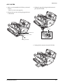
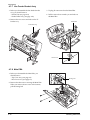
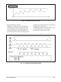
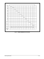
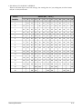
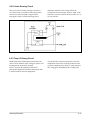
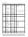
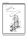
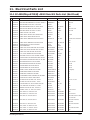
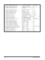
1
SF-4500/4500C
Msys4700/4800
MJ-4500C
SERVICE
Manual
INKJET PRINTER COMPOUND
CONTENTS
1. Precaution
2. Specifications
3. Installations
4. Disassembly & Assembly
5. List of Abbreviations
6. Special Circuit Descriptions
7. Theory of Mechanism
8. Troubleshooting
9. Exploded Views and Parts List
10. Packing Diagram and Parts List
11. Electrical Parts List
12. Block Diagrams
13. PCB Diagrams
14. Schematic Diagrams
1. Precautions
Follow these safety, ESD, and servicing precautions to prevent personal injury and equipment damage.
1-1 Safety Precautions
1. Be sure that all built-in protective devices are in
place. Restore any missing protective shields.
2. Make sure there are no cabinet openings through
which people- particularly children- might insert
fingers or objects and contact dangerous
voltages.
3. When re-installing chassis and assemblies, be
sure to restore all protective devices, including
control knobs and compartment covers.
4. Design Alteration Warning:
Never alter or add to the mechanical or electrical
design of this equipment, such as auxiliary
connectors, etc. Such alterations and
modifications will void the manufacturer’s
warranty.
7. Product Safety Notice:
Some electrical and mechanical parts have
special safety-related characteristics which might
not be obvious from visual inspection. These safety features and the protection they provide could
be lost if a replacement component differs from
the original. This holds true, even though the
replacement may be rated for higher voltage,
wattage, etc.
Components critical for safety are indicated in the
parts list with symbols
. Use only replacement components that have the same
ratings, especially for flame resistance and dielectric specifications. A replacement part that does
not have the same safety characteristics as the
original may create shock, fire, or other
safety hazards.
5. Components, parts, and wiring that appear to
have overheated or are otherwise damaged
should be replaced with parts which meet the
original specifications. Always determine the
cause of damage or overheating, and correct any
potential hazards.
6. Observe the original lead dress, especially
near sharp edges, AC, and high voltage power
supplies. Always inspect for pinched,
out-of-place, or frayed wiring. Do not change
the spacing between components and the
printed circuit board.
Samsung Electronics
1-1
Precautions
1-2 ESD Precautions
Certain semiconductor devices can be easily
damaged by static electricity. Such components are
commonly called “Electrostatically Sensitive (ES)
Devices”, or ESDs. Examples of typical ESDs are:
integrated circuits, some field effect transistors, and
semiconductor “chip” components.
The techniques outlined below should be followed to
help reduce the incidence of component damage
caused by static electricity.
CAUTION: Be sure no power is applied to the
chassis or circuit, and observe all
other safety precautions.
1. Immediately before handling a semiconductor
component or semiconductor-equipped assembly,
drain off any electrostatic charge on your body by
touching a known earth ground. Alternatively,
employ a commercially available wrist strap
device, which should be removed for your personal safety reasons prior to applying power to
the unit under test.
2. After removing an electrical assembly equipped
with ESDs, place the assembly on a conductive
surface, such as aluminum or copper foil, or
conductive foam, to prevent electrostatic charge
buildup in the vicinity of the assembly.
3. Use only a grounded tip soldering iron to solder
or desolder ESDs.
4. Use only an “anti-static” solder removal device
Some solder removal devices not classified as
“anti-static” can generate electrical charges
sufficient to damage ESDs.
5. Do not use Freon-propelled chemicals. When
sprayed, these can generate electrical charges sufficient to damage ESDs.
6. Do not remove a replacement ESD from its
protective packaging until immediately before
installing it. Most replacement ESDs are
packaged with all leads shorted together by
conductive foam, aluminum foil, or a
comparable conductive material.
7. Immediately before removing the protective
shorting material from the leads of a
replacement ESD, touch the protective material to
the chassis or circuit assembly into which the
device will be installed.
8. Maintain continuous electrical contact between
the ESD and the assembly into which it will be
installed, until completely plugged or soldered
into the circuit.
9. Minimize bodily motions when handling unpackaged replacement ESDs. Normal motions, such as
the brushing together of
clothing fabric and lifting one’s foot from a
carpeted floor, can generate static electricity
sufficient to damage an ESD.
1-3 Lithium Battery Precautions
1. Exercise caution when replacing a Lithium
battery. There could be a danger of explosion and
subsequent operator injury and/or
equipment damage if incorrectly installed.
3. Lithium batteries contain toxic substances and
should not be opened, crushed, or burned for disposal.
2. Be sure to replace the battery with the same or
equivalent type recommended by the
manufacturer.
1-2
Samsung Electronics
Specification
2. Specification
2-1 Printer Engine
Thermal Inkjet
Technology
1-pen & Print Head Swapping Type
Speed
Color (*1)
3ppm at Draft Mode
Mono (*2)
8ppm at Draft Mode
Color
600 x 600 dpi (1200 x 1200 dpi Addressable)
Mono
600 x 600 dpi (1200 x 1200 dpi Addressable)
Resolution
Printing Width
203mm
Automatic
130 Sheets of 20lb cut sheets
Manual Tray
No
Feeding Method
Emulation
Host Based Printing (GDI)
Printer Driver
Windows 3.1/3.11, Windows 95/98 driver
Interface
IEEE 1284 Compatible Parallel Interface (ECP)
(*1) The average printing time with 15%/A4 test image of Samsung.
(*2) The average printing time with 4%/A4 test image of Samsung.
2-2 Head
Ink M-3
Ink C-3
Print Head
208 nozzles
192 nozzles
Ink type
Pigment
Dye
Ink Color
Black
Color
Ink Yield
about 600 sh.
about 200 sh.
Samsung Electronics
2-1
Specification
2-3 Facsimile
GENERAL
Compatibility
ITU-G3
Scan method
CIS
Scan width
Max. 216mm, Effective: 210mm
Scan Resolution
300 x 300 dpi
Scan Speed
3 sec
Feeding method
Sheet-fed
ADF
30 sheets
Guide
Document Input Guide
Stacker
Document Output Stacker (No Paper Stacker)
Paper Tray
BIN Type (No Manual Tray)
Modem Speed
14.4 Kbps
Coding Method
MH, MR, MMR, Error Correction Mode
LCD
2 Lines Each of 16 Characters
Resolution
Selectable by 1-Key, 2-LEDs
- Standard : 200 x 100 dpi
- Fine
: 200 x 200 dpi (Default)
- Superfine : 300 x 300 dpi
Gray Scale & Contrast
Selectable by 1-Key, 2-LEDs
-Darken
- Lighten
- Photo : Error diffusion
Capacity (*3)
SF-4500/Msys4700 : 1.0 Mbyte (Factory Option : 3M)
SF-4500C/Msys4800/MJ-4500C : 0.5 Mbyte (Factory Option : 2.5M)
Back-up Time
30 Minutes (Continuous Power Failare)
Confidential
No
Delayed
Upto 30 Locations
Group Dial
5 Number Programmable
Forced Memory Tx.
Yes
Priority Tx.
Yes
Memory Rx.
Automatic reception when paper empty.
SCANNING
MEMORY
(*3) Monochromatic CCITT NO. 1 CHART can be saved by 80 sheets per 1.0M Byte.
2-2
Samsung Electronics
Specification
2-3 Facsimile (continued)
TELEPHONE
REPORT &
LIST
COPY
One-touch Dial
20 Locations
Speed Dial
50 Locations
Chain Dial
Yes
Handset & Cradle
Option
On-hook Dial
Yes, 1-Key
Last Number Redial
Yes, 1-Key
Auto Busy Redial
Yes
No Power Operation
UK : CALLING only, Other Country : No
Hold & Mute
No
Pause
Yes, Use Redial Key
Ringer Volume
S/W Option Setting (4Steps)
Tone/pulse Select
S/W Option setting (Pulse for NPO)
Flash
UK : Yes, Other Country : No
Mercury
No
DRPD
US : Yes, Other Country : No
TX/RX Journal
Yes
Image TCR
Yes, Reduction of First Page Sent by Memory Tx
Delayed Dial List
Yes
System Data
Yes
Tel Number List
Yes
Help List
Yes
Multipage Copy
Upto 99 Pages
Gray Scale
256 Levels
Reduction &
Enlargement
25%~200%
(Reference is the top center of Document)
Answering I/F
Yes
Ext. Phone
1-jack, Extension Phone Transfer
Polling
Yes
Sensors
No Paper, Paper Jam
Error Indicator
1-LED
Voice Request
Yes, On-hook Dial
Real Time Clock
Yes
RTI
Yes
TEL I/F
OTHERS
Samsung Electronics
2-3
Specification
2-4 Scanner
Compatibility
TWAIN
Technology
Platen CIS
Light Source for Color CIS
RGB LEDs (Line Order Control)
2-5 Power & Size
Power Source
USA : 110V 60 Hz, UK/GER : 220V 50 HZ
Dimensions (W x D x H)
360 x 325 x 190 mm (Without Handset)
Weight
5.7Kg
2-6 Accessaries
Handset / curlcord
1EA / 1EA
Tel Line
1EA
Tel
Power Cord
1EA
Parrallel Cable
No
FAX Driver
2 Diskettes
Ink Cartridge
INK-M3 (MONO) 1EA (*4), INK-C3 (COLOR) 1EA (*4’)
Manual
Yes
Carrier Sheet
Yes (*4)
Bundle S/W
(one CD-ROM)
Contents (*5)
Electronic Manual, Prt Driver, Presto page manager, Smart_Fax,
Photo Album, Twain Driver
Supply
Default
(*4) SF-4500/SF-4500C/Msys4700/Msys4800 only
(*4’) SF-4500C/MJ-4500C only
(*5) The smart_fax allows a on-screen remote control.
2-4
Samsung Electronics
3. Installation
3-1 Handset and Handset Cradle
Cradle
00000000000000000000000
1. Plug one end of the coiled cord into the jack on
the handset.
3. Attach the handset cradle to the main body. Insert
the two tabs of the cradle into the slots on the left
side of the main body as shown, and push it up.
Handset
0000000000
2. Plug the cradle’s modular cords into the modular
jacks on the left side of your machine.
Note: If you want to remove the handset, slide it
down, then take it out.
Be sure to insert white
cord into the front hole
3-2 Document Tray
1. Pull the document tray upward.
Samsung Electronics
2. Fold out the extender on the document tray.
3-1
3-3 Document Exit Tray
1. Insert the two tabs on the document exit tray into
the slots on the front of your machine.
Document exit tray
2. Fold out the extender, if necessary.
Extender
3-4 Telephone Line
Plug one end of the telephone line cord into the TEL
LINE jack and the other end into a standard phone
wall jack.
000000
00000000
0000
000000
0000
3-5 Extension Phone (Optional)
Plug one end of the modular cord into the EXT.TEL
jack on the back of your machine.
000000
000000
00000000
0000
Plug the other end of the cord into a modular
jack on a telephone answering device or a regular
telephone to use as an extension.
0000
3-2
Samsung Electronics
3-6 AC Power Cord
Plug one end of the cord into the back of the
machine and the other end into a standard,
grounded 3-prong AC power outlet.
The machine turns on. All lamps on the control
panel light up and the LCD displays ‘SYSTEM
INITIAL’ then ‘PAPER OUT’. Load the paper as
described on page 3-4.
If you want to turn it off, unplug the power cord.
Note : If documents are deleted from memory due
to a power failure, the machine automatically
prints out a Power failure report after power is
supplied.
3-7 Connecting Printer Cable
1. Connect a bi-directional parallel printer cable to
the 36 pin printer jack on your machine.
It is recommended to use the parallel cable that
supports IEEE-1284 bi-directional communications.
2. Fasten the metal clips to the parallel cable.
3. Connect the other end of the parallel cable to
your computer.
000000
00000000
0000
000000
0000
Printer cable
Samsung Electronics
3-3
3-8 Loading Paper
The LCD displays ‘PAPER OUT’ when paper is not loaded. You can load approximately 130 sheets of paper.
1. Pull the paper support on the paper bin all the
way up.
3. Hold the left paper guide and move it to the right
to match the width of the paper.
Paper support
2. Fan the paper and insert the paper with the print
side facing you.
Paper Guide
3-9 Loading an Envelope
You can load a standard or non-standard sized envelope.
1. Turn the envelope guide upright.
3. Slide the left paper guide to the right to match the
width of the envelope.
Envelope Guide
Paper Guide
2. Load the envelope and move it to the far right 1.
Then push it slightly down 2. The right edge of
the envelope must align with the raised edge of
the envelope guide.
1
2
Notes :
•If you remove the envelope after it is loaded, you
must press the Form Feed button to load the envelope again.
•The acceptable width of the envelope is in the
range of 98.5mm ~ 215.9mm.
•The envelope should be made of 20-24lb paper.
3-4
Samsung Electronics
3-10 Installing Print Cartridge
3-10-1 Print Cartridge
1. When you install a new print cartridge, press the
Cartridge button on the control panel. The LCD
displays ‘CHECK CARTRIDGE! PLEASE
INSTALL’, and the print cartridge moves to the
load position.
If you install a color cartridge, use ‘Install
Cartridge’ tab in the SF4400 Control Program on
your PC.
2. Lift the control panel 1 with your hand and open
the cartridge compartment cover 2.
3. If you are replacing a used cartridge, remove the
old cartridge.
Pull the print cartridge handle toward you until
you hear a click, then remove the print cartridge.
Cartridge
handle
Cartridge compartment cover
2
1
4. Remove the new print cartridge from its packaging. Hold the print cartridge by the black areas or
colored top only. Do not touch the copper area.
Control panel
5. Carefully remove the tape covering the printhead.
Be sure to remove all the tape.
Samsung Electronics
3-5
6. Insert the print cartridge in the carrier.
8. After installing the print cartridge, close the cover
and replace the control panel.
9. Use ‘Install Cartridge’ tab on your PC for a color
cartridge.
The LCD displays ‘THE CARTRIDGE IS 1:NEW
2:USED’.
10. Choose ‘1:NEW’ by using the F or E button, or by
pressing the 1 button.
11. Press the Cartridge button. The LCD displays
briefly ‘MONO INSTALLED’ (or ‘COLOR
INSTALLED’ for color print cartridge).
Use ‘Install Cartridge’ tab on your PC for a color
cartridge.
7. Push the cartridge firmly in the direction of the
arrow until it clicks into place.
If the cartridge is not installed properly, the LCD
displays ‘CHECK CARTRIDGE! PLEASE
INSTALL’. Remove the cartridge and re-insert it.
Notes :
• When you install a new cartridge, you must choose
‘1:NEW.’ When you install a used cartridge, select
‘2:USED’, which helps you check the amount of ink
remaining. If you mix up several used cartridges, it
will be difficult to check the amount of ink remaining. Once a new print
cartridge is installed, use it until it has completely
run out of.
• If you want to install a color cartridge to print a file
from your PC, you should use ‘Install Cartridge’
tab in the SF4500 Control Program on your PC. If
you use the Cartridge button on this machine, the
machine beeps a warning tone and briefly displays
‘RE-INSTALL COLOR USING
PC-DRIVER’. Press ‘Install Cartridge’ tab on your
PC, or the file may print using composite black.
3-6
Samsung Electronics
3-10-2 Print Cartridge Storage Unit
The print cartridge storage unit provides a
convenient place to store an extra black or color print
cartridge, and prevents an opened cartridge from
drying out.
TO STORE A PRINT CARTRIDGE IN THE
STORAGE UNIT
Insert the print cartridge into the storage unit and
slightly push it down.
TO REMOVE A PRINT CARTRIDGE FROM
THE STORAGE UNIT
Push the cartridge slightly down and pull it toward
you.
When switching between the color and black print
cartridges, keep the unused one in the print
cartridge storage unit. The storage unit prevents the
print cartridge from drying out while providing easy
access to it.
Storage unit
Cartridge
Samsung Electronics
3-7
4. Disassembly and Reassembly
4-1 General Precautions on Disassembly
When you disassemble and reassemble components, you must use extreme caution. The close proximity of cables
to moving parts makes proper routing a must. If components are removed or replaced, any cables
disturbed by the procedure must be replaced as close as possible to their original positions. Before removing any
component from the machine, note the cable routing that will be affected.
Whenever servicing the machine, you must perform as follows:
1. Check to verify that documents are not stored in memory.
2. Move the printer cartridge to far right to cap the nozzle.
3. Unplug the power cord.
4. Use a flat and clean surface.
5. Replace only with authorized components.
6. Do not force plastic-material components.
7. Make sure all components are in their proper position.
4-2 White Roller Ass’y
1. Lift the control panel using hand.
2. Push the bushing on both ends of the roller slightly inward, then rotate it until it reaches the slot as
shown below. Then lift the roller out.
B
Note : Check the roller for any dirt. If dirty, wipe it
off with soft cloth dampened with water. If
the roller is heavily worn, replace it with a
new one.
A
Bushing
Control panel
Samsung Electronics
White roller
4-1
Disassembly
4-3 Top Cover Ass’y
1. Lift the control panel and open the print
cartridge compartment cover. Remove the white
roller ass’y. Remove the six screws shown below.
Note: When you reassemble the top cover ass’y,
make sure the tabs in the bottom of the ass’y fit
into the slots in the base ass’y.
Cartridge compartment
cover
Control panel
Base ass’y
2. Remove the print cartridge. Remove the two
screws shown below and take out the top cover
ass’y.
Top cover ass’y
4-2
Samsung Electronics
Disassembly
4-4 Rear Cover Ass’y
1. Holding the paper guide, move it in the direction
of arrow.
3. Holding the rear cover ass’y, take it out by
rotating it to be released properly.
Rear cover ass’y
Paper guide
2. Remove the storage Unit, and remove the six
screws shown below.
Rear cover ass’y
Samsung Electronics
4-3
Disassembly
4-5 Base Ass’y
4-5-1 Rollers (ADF Roller, Drive Roller,
Exit Shaft)
Drive roller
CIS harness
1. Before you disassemble the rollers, you should
remove:
– Top Cover Ass’y (see page 4-2)
CIS ass’y
2. Take out the rollers from the base ass’y.
ADF roller
Drive roller
4. Turn the CIS ass’y over. Remove the one screw to
release the CIS from the bracket.
Note: Be careful not to lose the springs.
CIS
Exit shaft
Mono
Bracket
Note : Clean the surface of the rollers with ethyl alcohol. After wiping them, you must dry them
completely.
Spring
CIS
4-5-2 CIS (Contact Image Sensor)
1. Before you disassemble the CIS, you should
remove:
– Top Cover Ass’y (see page 4-2)
Color
Bracket
Spring
2. Remove the drive roller as described in ‘4-5-1
Rollers’.
3. Remove the one screw securing the CIS ass’y and
unplug the CIS harness. Take out the CIS ass’y.
Note : Check the glassy surface of the CIS for any
stain or scratch. If stained, wipe off with ethyl
alcohol. If it is heavily stained or scratched,
replace it with a new one.
Note : There is a little difference mono bracket and
color bracket.
4-4
Samsung Electronics
Disassembly
3. Remove the two screws as shown below and take
out the scan motor ass’y.
4-5-3 Scan Motor
1. Before you disassemble the CIS, you should
remove:
– Top Cover Ass’y (see page 4-2)
– Rear Cover Ass’y (see page 4-3)
2. Unplug the motor connector from the main PBA.
Make sure the harness is released from two hooks
securing the harness as shown below.
Hook1
Scan motor ass’y
4. Remove the two screws securing the motor to the
motor bracket.
Main PBA
Motor harness
Hook2
Motor bracket
Samsung Electronics
4-5
Disassembly
4-5-4 SMPS
1. Before you disassemble the SMPS, you should
remove:
– Rear Cover Ass’y (see page 4-3)
4. Remove the one screw securing the ground wire
to the main frame as shown. Make sure the
harness is released from the hook securing as
shown below.
2. Unplug the SMPS connector from the Main PBA.
Make sure the harness is released from the hook
as shown below.
Hook
Ground
wire 2
SMPS
Main frame
5. Pushing down the hooks on both ends, pull out
the SMPS.
Bracket-LF
SMPS connector
3. Remove the one screw securing the ground wires
to the bracket as shown.
SMPS
Hook
LIU ground wire
4-6
Samsung Electronics
Disassembly
4-5-5 LIU PBA
1. Before you disassemble the LIU PBA, you should
remove:
– Rear Cover Ass’y (see page 4-3)
3. Pulling the snap fits locking the PBA outward,
push up the LIU PBA.
2. Remove the one screw securing the ground wires
to the bracket.
LIU PBA
Bracket-LF
LIU ground wire
SMPS ground wire
4. Unplug all the connectors from the LIU PBA.
Samsung Electronics
4-7
Disassembly
4-5-6 Speaker and Buzzer*
4-5-7 Volume PBA
1. Before you disassemble the speaker and buzzer,
you should remove:
– Printer Unit (see page 4-11)
1. Before you disassemble the Volume PBA, you
should remove:
– Top Cover Ass’y (see page 4-2)
2. Remove the four screws securing the speaker and
buzzer.
2. Unplug the one connector and remove the one
screw shown below, and take out the PBA.
Speaker
Buzzer*
*Optional
4-8
Samsung Electronics
Disassembly
4-6 OPE Ass’y
4-6-1 ADF Rubber Pad
1. Open the OPE unit.
2. Insert a flat blade screw driver into the slot as
shown below, and release the latches. Take out the
rubber holder, sheet ADF and the rubber pad.
Notes:
• When you reassemble the rubber pad, be sure that
the rubber pad, sheet ADF and holder fit into the
guide boss and the holder latches fit into the
corresponding hole. Then push firmly until it
clicks.
Guide boss
OPE unit
Rubber holder
Rubber pad
Samsung Electronics
• Clean the surface of the rubber pad with ethyl alcohol. After wiping it, be sure to dry it.
Check the rubber wear. If the wear reaches 1/2
its original thickness, replace it with a new one.
4-9
Disassembly
4-6-2 OPE Unit
1. Before you disassemble the OPE unit, you should
remove:
– Top Cover Ass’y (see page 4-2)
– Rear Cover Ass’y (see page 4-4)
3. Turn the tie stopper 90 degrees as shown below
and take out the OPE unit.
OPE unit
2. Unplug the OPE (NPO) connector from the LIU
PBA.
Tie stopper
4-10
Samsung Electronics
Disassembly
4-6-3 Roll Pinch
4-6-4 OPE PBA
1. Before you disassemble the roll pinch, you
should remove:
– OPE Unit (see page 4-9)
1. Before you disassemble the OPE PBA, you
should remove:
– OPE Unit (see page 4-9)
2. Remove the four screws securing the OPE unit.
2. Remove the four screws securing the OPE unit.
3. Turn the upper scan frame of the OPE unit over.
3. Remove the nine screws and take out the PBA
and LCD.
4. Remove the three screws and take out the spring
pinch. Then take out the roll pinch.
Spring pinch
Upper scan
frame
Roll pinch
Notes:
• Do not turn the OPE unit upside down after you
remove the screws securing the PBA. Keys and
rubber contacts may be separated and easily lost.
• When you reassemble the OPE unit, make sure
the keys are in correct position.
• When you reassemble the PBA, secure the screws
according in the order of the number printed on
the PBA.
• After reassembling, operate the machine to make
sure it works properly.
• After reassembling, make sure the LCD is not
blocked.
Samsung Electronics
4-11
Disassembly
4-7 Printer Ass’y
4-7-1 Printer Unit
1. Before you disassemble the printer unit, you
should remove:
– Top Cover Ass’y (see page 4-2)
– Rear Cover Ass’y (see page 4-3)
3. Remove the ASF feeder ass’y from the printer unit
by pushing the tab inward and take the ass’y out
in the direction of arrow.
2. Remove the two screws securing the printer unit,
and unplug the six connectors from the Main
PBA. Take out the printer unit.
Main PBA
ASF feeder ass’y
CR motor
TX motor
LIU OPE
Print Head
Main PBA
Senser
SMPS
CIS
Speaker
LF motor
Note: When you reassemble the unit, do not pinch or
short the wire harness.
4-12
Samsung Electronics
Disassembly
4-7-2 ASF Feeder Ass’y
1. Before you disassemble the ASF feeder ass’y, you
should remove:
– Rear Cover Ass’y (see page 4-3)
4. Remove the one screw, then remove pick up shaft
from the ASF frame while pushing it to the right
to disengage the gear.
2. Unplug all connectors from the Main PBA and
remove the two screws shown below.
Pick up shaft
Note : When you reassemble the ASF feeder ass’y,
insure the harness in the line feed motor is not
pinched or shorted.
Samsung Electronics
4-13
Disassembly
4-7-3 Home Ass’y
4-7-5 Base Frame Ass’y
1. Before you disassemble the home ass’y, you
should remove:
– Printer Unit (see page 4-11)
1. Before you disassemble the base frame ass’y, you
should remove:
– Printer Unit (see page 4-11)
– Carrier Ass’y
2. Pushing the both ends of the home ass’y, take out
the ass’y in the direction of arrow.
2. Remove the friction ass’y, then take out the
actuator feed.
3. Pull out the base frame ass’y.
Actuator feed
Home ass’y
Roller friction ass’y
Base frame ass’y
4-14
Samsung Electronics
Disassembly
4-7-4 Carrier Ass’y
4-7-6 Feed Roller Ass’y
1. Before you disassemble the carrier ass’y, you
should remove:
– Printer Unit (see page 4-11)
1. Before you disassemble the feeder roller ass’y, you
should remove:
– Printer Unit (see page 4-11)
– Carrier Ass’y
– Base Frame Ass’y
2. Remove the cable holder. Remove the one screw
on the right side of the main frame, and remove
the spring. Then take out the carrier shaft.
2. Remove the bearing feed from the main frame.
Pull the feeder roller in the direction of arrow and
take it out.
Carrier shaft
Feed roller
Bearing feed
Head cable
Cable holder
Samsung Electronics
4-15
Disassembly
4-7-7 Line Feeder Bracket Ass’y
1. Before you disassemble the line feeder bracket
ass’y, you should remove:
– Printer Unit (see page 4-11)
– Feeder Roller Ass’y (see page 4-12)
3. Unplug all connectors from the Main PBA.
4. Pull the sensor lever towards you and take out
the Main PBA.
2. Remove the two screws and take out the LF
bracket ass’y.
Main PBA
LF bracket ass’y
Sensor lever
4-7-8 Main PBA
1. Before you disassemble the Main PBA, you
should remove:
– Top Cover Ass’y (see page 4-2)
– Rear Cover Ass’y (see page 4-3)
Timing belt
2. Remove the three screws securing the Main PBA.
When you remove the one screw at the bottom,
pull the timing belt.
4-16
Samsung Electronics
6. Circuit
6-1 Main PBA
6-1-1 Summary
The main circuit that consists of CPU, MFP
controller (built-in 32bit RISC processor core:
ARM7TDMI) including various I/O device
drivers, system memory, scanner, printer, motor
driver, PC I/F, and FAX transceiver controls the
whole system. The entire structure of the main
circuit is as follows:
Fig.6-1-1. Entire Structure of Main Circuit for Each Key Signal
Samsung Electronics
6-1
6-1-2 MFP Controller (KS32C6200 : U16)
MFP Controller consists of CPU(ARM7TDMI RISC
processor), 2K-byte cache, data and address buses,
serial communication part with LIU(Line Interface
Unit), OPE(OPERATION PANEL) print head controller, parallel port interface, external DMApart to
receive data from external color image processor
(SCANIP:U18), LF/CR motor diver
controller and I/O controller.
6-1-2-1. SYSTEM CLOCK
The internal clock frequency is 30MHz. 30MHz
system clock (MCLK) supplied from the outside is
used without being divided inside.
with /RD and /WR pin of RAM, ROM, MODEM
and the outside devices and becomes active.
• CHIP SELECT (/IP_CS, /ROMCS, /MCS /
RAMCS)
- /IP-CS : SCANIP(U18) CHIP SELECT (LOW
ACTIVE)
- /ROMCS : ROM/FLASH MEMORY(U5) CHIP
SELECT (LOW ACTIVE)
- /MCS : MODEM(U15) CHIP SELECT (LOW
ACTIVE)
- /RAMCS : SRAM (U14) CHIP SELECT (LOW
ACTIVE)
When each CHIP SELECT is low, data can be read or
written.
6-1-2-2. DATA & ADDRESS BUS CONTROL
• /RD & /WR
/RD & /WR signals are synchronized with
MCLK(30MHz) and become LOW ACTIVE.
These signals are strobe signals used to read and
write data when each CHIP SELECT is connected
6-2
• D0 - D15
- 16bit data bus
• A0 - A17
- ADDRESS BUS (A18 - A21 are reserved.)
Samsung Electronics
6-1-2-3, LIU(Line Interface Unit) Serial
Communication Part
UART (Universal Asynchronous
Receiver/Transmitter) at KS32C6200 enables the
main and LIU, main and OPE to transmit serial
data. The block diagram of UART is as follows:
(Fig.6-1-2) KS32C6200 has 2 UART channels. The
baud rate is 9600bps.
Fig.6-1-2. UART BLOCK DIAGRAM
Fig.6-1-3 UART DATA FORMAT
Samsung Electronics
6-3
6-1-2-4 EXTERNAL DMA
It brings data from an external device (SCANIP:U18)
using DMAchannel 0. DMAREQUEST sent from an
external device to KS32C6200 activates DMA
ACKNOWLEDGE signal and drives DMAchannel 0
to produce CHIP SELECT and READ STROBE (/RD)
at the external
device and bring data from it. It generates address of
destination memory, CHIP SELECT and WRITE
STROBE (/WR) in order to move this data into
destination memory, and then stores the data.
Fig.6-1-4 EXTERNAL DMA TIMING DIAGRAM
6-4
Samsung Electronics
6-1-2-5. DRAM CONTROLLER
6-1-2-6. PARALLEL PORT INTERFACE
As KS32C6200 has DRAM controller in it, DRAM can
be connected with external memory.
The control mode of DRAM controller enabling
EARLY WRITE, NORMALREAD, PAGE MODE,
and BYTE/HALF WORD ACCESS supports EDO
DRAM as well as normal DRAM. DRAM
READ/WRITE signals are /RD and /WR signals
used to control system buses. It supports CAS
BEFORE RAS for DRAM REFRESH and self-refresh
mode for DRAM backup. Connected with common
/LCAS, /UCAS and RAS [1:0], it consists of 2 banks.
Though each may be connected with up to 1M - 4M
halfword, two (2) of 512 Kbytes are
connected for this product.
This part connected with the computer through the
centronics connector makes possible parallel
interface with the computer. Data is transmitted
according to the standard of IEEE P1284. This MFP
controller supports compatibility mode the
traditional way to transmit print data, nibble mode
(4bit data) to upload data to the computer, and
duplex high-speed transmission with the computer
ECP (Extended Capabilities Port: 8bit data
transmission) all together.
It enables PC data to be printed and scanned data to
be uploaded quickly to the computer. Besides,
various data transmission and reception with the
computer such as uploading received fax data,
downloading fax data to be sent, and monitoring system control signals and system conditions are carried
out here.
Fig.6-1-5 Compatibility Hardware handshaking Timing
Samsung Electronics
6-5
Fig.6-1-6 ECP Hardware Handshaking Timing (forward)
Fig.6-1-7 ECP Hardware Handshaking Timing (reverse)
6-6
Samsung Electronics
6-1-2-7. INKJET HEAD CONTROLLER
This part produces major control signals used to
drive INKJET head. It consists of signals to drive
head nozzles, /HGA[13:1], HOE[16:1], /FAULTTEST, /HEAD-EN, and BIASOFF, and consists of signals to check the status of the head, HEAD-DATA.
It has double height print head, system 208 nozzles
for mono and 192 nozzles for color, and uses
/HGA[13:1], HOE[16:1] signals and /HEAD-EN to
drive these nozzles. Fig.5-1-8 is timing diagram of
each signal.
Fig.6-1-8 Timing Diagram to Drive Head
Samsung Electronics
6-7
Fig.6-1-9. Timing Diagram for Each Nozzle
The above control signals are sent to head driver and
the head driver converts these signals to the level
(+11.75V) to drive head nozzles.
according to the kind of motors. Though full step,
half step and software control are possible for both,
bi-polar CR motor is controlled half step and LF
motor is controlled half step and quarter step here.
5-1-2-8. PRINTER MOTOR CONTROLLER
(CRPHA, CRPHB, CRIA0, 1, CRIB0, 1,
LFPHA, LFPHB, LFIA0, 1, LFIB0, 1)
MFP Controller (KS32C6200:U16) supports 2
stepper motors. It controls CR (Carriage Return)
motor used to print documents and LF (Line Feed)
motor used to feed and eject paper.
CR motor controller can support 75, 150, 200, 300,
600, or 1200dpi according to resolution, while LF
motor controller supports uni-polar and bi-polar
6-8
Samsung Electronics
5-1-2-9. I/O PORT FOR KS32C6200
PIN NAME
DESCRIPTION FOR STATE
PIN NO
I/O
PORT NAME
GOP0/TXD0
122
p
LIT_TXD
Serial Data Output to ILIU
GOP1/TXD1
124
p
OPE_TXD
Serial Data Output to OPE
GOP2/nEDACK
139
p
nXDACK
GOP3/TONE
149
p
KEYCLICK
Keyclick Tone
GOP4/nRST0
150
p
nRST0
Watchdog Reset Signal Output
GOP5/nIOWR1
134
p
nFAULT_TEST
–
Head Fault Test Enable
GOP6/nIOWR2
155
p
RX_CTL
Line for RX.
Line for TX. or Remote
GOP7/nIORD1
156
p
nHEAD_EN
–
Head Enable
GOP8/nIORD2
151
p
TONE_CTL
Line Monitoring
Keyclick
GOP9/CLKOUT
152
p
IP_CLK
Clock Output for Scan_IP
GOP10/FIREPS
153
p
nRST_OUT
External Reset Output
GOP11/nHSC
154
p
BIASOFF
–
Head Data Read
GOP12/nHSM
30
p
CR_REF
LQ Mode Printing
Draft Mode Printing
GIP0/nRXD1
123
I
LIU_RXD
Serial Data Input from ILIU
GIP1/nRXD2
125
I
OPE_RXD
Serial Data Input from OPE
GIP2/nEINT1
136
I
nMIRQ
–
GIP3/nEINT2
137
I
nTX_INT
–
GIP4/nEDREQ
138
I
nXDREQ
–
GIP5/UCLK
128
I
HEAD_DATA
Serial Head Data from Head
GIOP0/TCK
37
B
TCK
Test Clock for ICE
GIOP1/TMS
38
B
TMS
GIOP2/TDI
39
B
TDI
GIOP3/nTRST
40
B
nTRST
GIOP4/TDO
41
B
TDO
H
L
DMA Acknowledge to
–
Scan_IP
Modem Interrupt request
SCAN motor Interrupt
Samsung Electronics
request
DMA Request from Scan_IP
TAP Controller Enable
–
Serial Data Input from Emulator
–
TAP Controller Reset
Serial Data Output to Emulator
6-9
6-1-2-10. RESET CIRCUIT
As for this product, there are 2 power resets of primary reset(/F-POR) and secondary reset(/POR) and
also reset by watchdog timer (/RSTO). Primary reset
is used to initialize flash memory when the system is
turned on, while secondary reset is used to initialize
the whole system by initializing MFP controller
(KS32C6200) after primary
reset. Primary reset makes flash memory wait in
READ mode to fetch program
codes, and secondary reset makes the main
controller (KS32C6200) wake up and initialize
external peripherals to operate the system.
Fig.5-1-10 is Power Reset Timing Diagram.
Fig.6-1-10 POWER RESET TIMING DIAGRAM
• POWER MONITOR (U103: KIA7045F)
If +5V supplied to KIA7045F is so unstable as to
reach +4.65V - +4.35V (typically 4.5V), it will
recognize it as power failure. Then KIA7045F
output terminal becomes low (0V) and the voltage
is impressed to flash memory and KS32C6200, running RESET (LOW ACTIVE). Flash memory and
6-10
KS32C6200 are reset first. Thereafter modem, print
control parts and SCANIP(Color Image Processor)
linked to /RSTOUT terminal of KS32C6200 are
reset as well. KIA7045F output
terminal of open drain structure is pulled up 5.1kΩ
and put out.
Samsung Electronics
6-1-4-2. SCAN RESOLUTION
6-1-3 System Memory
System memory consists of 512KB flash memory,
2MB DRAM, and 32KB SRAM. Flash memory,
DRAM and SRAM are selected by each CHIP
SELECT (/ROMCS, /RAS0, /RAS1, /LCAS, /UCAS,
/RAMCS), and data is accessed half word (16bits) by
half word and one byte (8bits) by one byte.
DRAM is designed to be able to add 2MB to the basic
2MB so that buyers can make their options.
In addition, the backup circuit built in for DRAM
keeps data in user memory during at least
30-miniute power failure. Super capacitor
(1F) is used as a backup element. SRAM holds
telephone numbers and journal information and can
keep minimum information using backup battery
(Lithium).
6-1-4. Scanner
6-1-4-1. SUMMARY
This sheet-fed type device to read manuscripts has
300dpi CIS as an image sensor. The design is focused
on 30-sheet ADF and 3-second quick scan functions.
– Normal(Quick) : 1/3.85mm, 1/8mm (98×203dpi)
– Fine
: minor scanning 1/7/7mm, main
scanning 1/8mm (196×203dpi)
– Super Fine
: minor scanning 1/300inch, main
scanning 1/300inch(300×3000dpi)
6-1-4-3. CIS : Contact Image Sensor improves
productivity and is designed to be replaced easily.
Color models have color CIS.
➀ SF-4500/Msys4700/MJ-4500 : BN-30216D, 10Pin
Connector
– Minimum Scan Line Time: 1.8mS
– Light Source Power : 12V
– Maximum Pixel frequency : 2MHz
– Effective Sensor Element : 2552
– Clamp Level : 1.2 - 1.6V
– Bright Output : MIN 0.8V
➁ SF-4500C/Msys4800/MJ-4500C : CXB-30216G, 12
Pin Connector
– Minimum Scan Line Time for one color : 1.5mS
– Color Separation : RGB LED transfer mode
– Light Source Power : 12V
– Maximum Pixel frequency : 2MHz
– Effective Sensor Element : 2552
– Clamp Level : 1.2 - 1.6V
– Bright Output : MIN 0.8V
SCANIP
CIS Control
CIS
Fig.6-1-11 CIP1A Block Diagram
Samsung Electronics
6-11
6-1-4-4. IMAGE PROCESSING
1) Image signal input: CIS output signals are offset at
1-4V with about 2.8V white level. Optimum input
level of SCANIP is 1.5V offset and 3.5V white
level. So OPAMP is used to design
interface circuit of SCANIP.
2) Image processing : The scanner reads pixel data
value of image sensor CIS(Contact Image Sensor)
300dpi lines by 300dpi lines, and stores it in scan
buffer through TIP algorithm if Normal is
selected for Image Processor SCANIP, through
Error Diffusion algorithm if medium, or through
DMA without algorithm if PC Scan mode.
Commonly for all the three modes, it is processed
after shading correction and gamma correction.
5×5 Window Processing begins after data is stored
in 32K Byte external SRAM.
Image Processor SCANIPhas the following
specifications:
➀ Package: 128 Pin QFP
➁ Operating Frequency: 25 - 40MHz
➂ Minimum Scan Line Time: 1.5mS
➃ Scan Resolution: Max. 300DPI
➄ Scan Width: B4
➅ Major functions
– Internal 8bit ADC
– Black/White shading correction for each color
R.G.B
– Gamma correction for each color R.G.B
– Mono CIS (Canon, Dyna) interface
– Color CIS (Canon, Dyna, Toshiba) interface
– Automatic Motor Control
– Image Processing Mode : TIP, Ordered dither,
Error diffusion
– 256 Gray Scale
– AGC function
– PC Gray Scan function
➆ External SRAM: 32Kbyte, 15Ns Access Time
6-12
3) CIS LED Driver: LED in CIS is on with 11.75V. TR
circuit is built in to drive this LED.
– Maximum LED current: 300mA
4) PC Scan function
– Resolution(V×H) : 300×300/75×75dpi
(Pre-scanning mode)
196×203/98×203dpi
– Mono Bit Depth : 8bits Gray Scan/1bit Text
Scan/1bit Halftone Scan
– Color Bit Depth : 24bits (8bits/R.G.B.)
– PC Interface: IEEE 1284 NIBBLE, BYTE, ECP
– TWAIN Driver: 1CD-ROM title provided along
with Bundle S/W.
5) Additional Spec.
– Scan Line Time : 2.5mS/line
– Contrast Control : 3 Step
(Normal/Darken/Lighten)
– Enlargement & Reduction : 25 ~ 200%
Samsung Electronics
6-1-4-5 I/O PORT FOR SCANIP
REGISTER
NAME
PIN NAME
for ASIC
I/O
PORT NAME
GPI0
I
GPI1
H
L
OK2PRINT
Head OK
Head NG
I
HOME_SEN
Head parking
–
GPI2
I
reserved
GPI3
I
nP_EXIT
–
Paper Detected
GPI4
I
P_EMPTY
Paper empty
–
GPI5
I
nRING_DET
–
Ring Detected
GPI6
I
nHOOK_OFF
–
H/S hook off
GPI7
I
RY/nBY
Flash Ready
Flash Busy
GPO0
p
reserved
GPO1
p
nOPE_RST
OPE reset off
OPE seset on
GPO2
p
BLED(C/–)1
BLED On
BLED Off
GPO3
p
RLED(C/–)1
RLED On
RLED Off
GPO4
p
GLED(C/M)2
GLED On
GLED Off
GPO5
p
RTC_EN
RTC Enable
RTC disable
GPO6
p
PRE_HEAT
Head Preheat On
–
GPO7
p
CLK_SEL
Jupiter idle mode
Jupiter ?? mode
GPIO0
p
reserved
GPIO1
p
reserved
GPIO2
p
reserved
GPIO3
p
reserved
GPIO4
p
reserved
GPIO5
p
reserved
GPIO6
p
reserved
GPIO7
p
reserved
GPIO8
p
CMLON
Fax or Tel Line
Ext Phone Connection
GPIO9
p
VOL2
Connection
GPIO10
p
VOL1
Bell (3 level)
GPIO11
p
VOL0
Bell or Volume control
GPIO12
p
reserved
–
GPIO13
p
nSPK_CTL
GPIO14
p
THM_CLK
Clock IN for Thermometer
GPIO15
B
THM_DATA
Serial Data from/to Thermometer
GPI
GPO
GPIO1
GPIO2
DESCRIPTION FOR STATE
Audio amp. off
Volume (4 level)
Audio amp. on
1 C/– : Color Only
2 C/M : Color/Mono
Samsung Electronics
6-13
6-1-5 Printer
6-1-5-1. GENERAL
It drives inkjet head to print printing data received
from the computer or fax data coming through the
line. It roughly consists of head driver, head
controller, and the ambient temperature sensor. Fig.61-11. Block Diagram of Printer shows the entire structure.
6-1-5-2. HEAD DRIVER (U26, U27, U32, U22)
This part drives and inks inkjet head. Color inkjet
head drives 192 nozzles, while mono inkjet head drives 208 nozzles. Mono inkjet head is composed of 16
groups of 13 nozzles. As to the driver that composes
each nozzle, 13 row 7-bit driver (U26, U27) selects
head address and 16 column 8-bit
driver (U32, U33) sends head data. Head driver
converts control signals from MFP controller to
+11.75V, the level to be able to drive the head, and
provides them for the inkjet head.
• Column Driver Circuit (HD8:U32,U33)
It is the fire enable pulse of real head. 16 lines are
put out as head driving data lines through the output port of MFP controller (HOE1 - HOE16).
Enable pulse impressed to the head is put out within window time (Low). It has the function to move
it forward or backward by the register in MFP controller. Besides the output signal may
differ in accordance with the type of head (mono or
color). If there is data, printing image is put out at
“H”. If not, it is put out at “L”. In case of Babbage
head, pulse width is always 1.3use regardless of
the type of the head, with the
maximum driving current 400mAand output voltage +11.75V.
• Row Driver Circuit (HD7:U26:U27)
This is a 13-line signal impressed to row drive IC
through the output port of MFP controller(/HGA1
- /HGA13), used as an address to drive the head in
ink cartridge. Pulse period differs according to
head driving
frequency. In 1200dpi (in case of Head: 12KHz)
mode, timing period is 2.6usec (1/1200÷16 groups).
The signal put in each driver(window time) is
active “L”, with the biggest driver current max
100mA and output voltage +11.75V.
6-14
Samsung Electronics
6-1-5-3. HEAD CONTROLLER
This part consists of +22V Power Controller to
control head driver, Fault Test, Head Detection,
Substrate Heating and ambient Temperature
Sensor. It checks and controls head driver and ink
cartridge.
Fig.6-1-12 Block Diagram of Printer
Samsung Electronics
6-15
• +22V Power Controller
If you insert power cords, the main board will be
supplied with power. /POR signal put out through
reset circuit activates MFP controller
(K32C6200:U16) and MFP controller puts out external circuit reset signal /RST-OUT. This /
RST-OUT signal and Vrefx (+2.5V) divided through
+30V are impressed to the input
terminal of the comparator, putting out +22V if the
output of the comparator is “high” or getting
turned off if “low”.(in case of /FAULT-TEST
signal: HIGH) While +22V is being impressed after
/RST-OUT is “High”, comparator output gets
“low” and turns off +22V driving TR(TIP112) if
/FAULT-TEST signal is put out at “low” when you
check a short of the head driver and the ink cartridge (head).
• FAULT TEST CIRCUIT
This is a signal to detect whether the head
receiving the output of head column driver is in a
short. After /FAULT-TEST signal is put out at
“low” and +22V is turned “off”, “OK2PRINT”
signal is entered. The port of KS32C6200(U16)
shows normal condition if “H” and a short if “L”.
If you make FAULT-TEST output “L” to detect
fault of the head, +22V gets off. If the head is in a
short (LOW), when the level of “/FAULT-TEST”
signal goes “L” and final “OK2PRINT” output
goes “L”. KS32C6200(U16) reads this signal and
checks whether the head input receiving the
driver output is in a short. Diode cathode is
attached to each output transistor collector in the
column driver. 8 anode terminals of diode become
common as one and put out /FAULT signal, which
is pulled up by bias circuit controlled by /FAULTTEST and shows the condition by OK2PRINT
through the comparator.
• SUBSTRATE HEAT CIRCUIT
Mono ink cartridge of Babbage head is 600dpi head
that uses pigment ink. It is very sensitive to the
temperature in and around the cartridge. In
particular, the viscosity of ink affects print quality
as it is inversely proportional to temperature by an
exponential function. This signal used to
compensate it helps you get equal inking quality
by warming the ink chamber in the cartridge with
aluminum pattern heater before starting to print if
the surrounding temperature is lower than
standard (below 35°…).(Refer to Timing Chart.) It
sends PRE-HEAT signal through I/O port of
SCANIP(Color Image Processor:U18) and supplies
+11.75V.
Mono Head
70°C
35°C
Pre-Heat if below 35°c
Fig.6-1-13. Temperature around Mono Head
6-16
Samsung Electronics
Color Head
70°C
Fig.6-1-14. Temperature around Color Head
• HEAD DETECTION CIRCUIT
Babbage ink cartridge has 8-bit mask ROM I.D. to
check the type of cartridge. In order to detect the
head, HSM signal is used as ENABLE signal and
BA3 signal as START & STOP BIT, and BA1 and
BA2 as clock signal of each bit, and ID signal in the
cartridge is put in HEAD-DATAport of KS32C6200
through BSF line. With each bit
controlled, 8bit I.D data is read and STOP bit is put
out of BA3(LOAD) port. Then it finishes.
If data is mono, it is 07H. If color, 08H.
Fig.6-1-15. HEAD DETECTION TIMING DIAGRAM
Samsung Electronics
6-17
• SURROUNDING TEMPERATURE SENSOR
DS1621S(DALLAS SEMI.) is applied to read the
temperature around ink cartridge. It is used to get
optimum inking quality by keeping the viscosity of
ink in the cartridge in the specified lerel. The way
to read temperature is similar to EEPROM, controlled by THM-CLK, THM-DATALINE. Digital
thermometer to check the surrounding temperature
is assembled along with home sensor in the frame
of assembly CR. After each line is inked, it reads
the surrounding temperature and heats substrate
heater in the ink cartridge during the accelerating
time of CR to keep the viscosity of ink in the specified lerel.
6-1-5-4. HEAD DRIVING TIMING
Control signal from MFP controller (KS32C6200:U16)
enters the head driver (U26, U27, U32, U33) and it
becomes the level to be able to drive the head nozzles
(+11.75V). It is depicted in the following diagram.
Fig.6-1-16. HEAD DRIVING TIMING DIAGRAM
6-18
Samsung Electronics
Fig.6-1-17. TIMING DIAGRAM FOR EACH NOZZLE
Samsung Electronics
6-19
6-1-5-5. INK CARTRIDGE
• PIN ARRAY OF MONO INK CARTRIDGE
There are 208 heater chips in mono ink cartridge.
Address (BA1_ ~ BA13_)
Column
6-20
Data(BPx)
1
2
3
4
5
6
7
8
9
10
11
12
13
1
1
21
15
9
3
23
17
11
5
25
19
13
7
2
20
14
8
2
22
16
10
4
24
18
12
6
26
3
27
47
41
35
29
49
43
37
31
52
45
39
33
4
46
40
34
28
49
42
36
30
50
44
38
32
52
5
53
73
67
61
55
75
69
63
57
77
71
65
59
6
72
66
60
54
74
68
62
56
76
70
64
58
78
7
79
99
93
87
81
101
95
89
83
103
97
91
85
8
98
92
86
80
100
94
88
82
102
96
90
84
104
9
105
125
119
113
107
127
121
115
109
129
123
117
111
10
124
118
112
106
126
120
114
108
128
122
116
110
130
11
131
151
145
139
133
153
147
141
135
155
149
143
137
12
150
144
138
132
152
146
140
134
154
148
142
136
156
13
157
177
171
165
159
179
173
167
161
181
175
169
163
14
176
170
164
158
178
172
166
160
180
174
168
162
182
15
183
203
197
191
185
205
199
193
187
207
201
195
189
16
202
196
190
184
204
198
192
186
206
200
194
188
208
Samsung Electronics
• PIN ARRAY OF COLOR INK CARTRIDGE
There are 192 heater chips in mono ink cartridge. One cartridge has 64 Cyan, 64 Magenta, 64 Yellow heaters
and (64 x 3 colors) 192 nozzles.
Address (BA1_ ~ BA13_)
Column
Data(BPx)
1
2
3
4
5
6
7
8
9
10
11
12
13
1
-
19
13
7
11
21
15
9
3
23
17
11
5
2
15
12
6
-
20
14
8
2
22
16
10
4
24
3
25
45
39
33
27
47
41
35
29
49
43
37
31
4
44
38
32
26
46
40
34
28
48
42
36
30
50
5
51
71
65
59
53
73
67
61
55
75
69
63
57
6
70
64
58
52
72
66
60
54
74
68
62
56
76
7
77
97
91
85
79
99
93
87
81
101
95
89
83
8
96
90
84
78
98
92
86
80
100
94
88
82
102
9
103
123
117
111
105
125
119
113
107
127
121
115
109
10
122
166
110
104
124
118
112
106
126
120
114
108
128
11
129
149
143
137
131
151
145
139
133
153
147
141
135
12
148
142
136
130
150
144
138
132
152
146
140
134
154
13
155
175
169
163
157
177
171
165
159
179
173
167
161
14
174
168
162
156
176
170
164
158
178
172
166
160
180
15
181
-
-
189
183
-
-
191
185
-
-
-
187
16
-
-
188
182
-
-
190
184
-
-
192
186
-
Samsung Electronics
6-21
6-1-6 Motor Driver
6-1-6-1. GENERAL
6-1-6-2. CR (CARRIAGE RETURN) MOTOR
DRIVING CIRCUIT
This product use 3 stepper motors, i.e. CR(Cartridge
Return) motor and LF(Line Feed) motor, TX
(Transmission) motor.
CR motor moves left and right all-in-one carriage of
inkjet head and shuttle scanner. It helps the printer
print accurately on the paper. LF motor is driven to
feed and eject paper for printing and to feed and eject
documents to read for scanning. Bi-polar CR motor is
controlled half step with maximum 24ips(inch/sec),
while LF motor half step and
quarter step at maximum 6ips.
CR motor moves the carriage left and right when ink
cartridge prints something on paper.
- Motor Type : Stepper motor, bi-polar
- Driving Voltage : +30V
- Winding Resistance : 6Ω ± 10%
- Driving IC : TEA3718DP × 2
CR_REF
CRIA1
(CRIB1)
CRIA0
(CRIB0)
CURRENT(mA)
OPERATION
H
L
L
490
Mono LQ is being driven
L
L
L
670
Color draft is being driven
L
L
L
670
Mono draft is being driven
X
H
H
0
No current
As shown in the above table, current in each mode is
adjusted by voltage of driver(U25, U28) CRVREF
input. If the output of CR_REF signal controlled by
MFP controller(U16) is “low”, TR(Q12) will be turned
off and the voltage put in to CRVREF of
driver (U25, U28) with +5V divided will go up
(+4.5V).
6-22
REMARK
It becomes the standard of the driver, resulting in
high current. If CR_REF output is “high”, TR(Q12)
will be turned on and the voltage put in to CRVREF
will go down (+3.0V), resulting in low current in the
motor.
Samsung Electronics
6-1-6-3. LF (LINE FEED) MOTOR DRIVING CIRCUIT
LF motor is driven to feed and eject documents and paper.
- Motor Type: stepper motor, bi-polar
- Driving Voltage : +30V
- Winding Resistance : 12Ω ± 10%
- Driving IC : PBL3717A × 2
LFIA1
LFIA0
CURRENT(mA)
OPERATION
L
L
670
When feeding document/paper
L
H
400
When ejecting document/paper
X
H
0
No current
REMARK
6-1-6-4. TX(TRANSMISSION) MOTOR DRIVING CIRCUIT
TX Motor is driven at maximum 1200pps when feeding or ejecting sheets.
- Motor Type: stepper motor
- Driving Voltage : +30V
- Winding Resistance : 4.6Ω ± 10%
- Step Degree : 7.5 deg/step
- Driving IC : PBL3717A × 2
TXIA1
TXIA0
CURRENT(mA)
OPERATION
L
L
670
Quick Scan/Fine/Super Fine
H
L
221
Standby
H
H
0
Idle
MODE
PHASE
SPEED
Quick Scan
2–2 phase
1200pps
Fine
1–2 phase
400pps
Super Fine
2–2 phase
400pps
REMARK
Driving speed for each mode
Samsung Electronics
REMARK
6-23
6-1-7 FAX Transceiver
6-1-7-1. GENERAL
6-1-7-3. TRANSMITTER
This circuit processes transmission signals of modem
and between LIU and modem.
This circuit is added only to SmartJet 2000,
SF-4300C.
This circuit processes transmission output, analog
signal of modem(KS16117).
Output signal in each mode goes out of modem
(TXOUT:U15-44). After D/Asignals are smoothed
and filtered through active filter (U12-2), they are
buffered under OPAMP(U12-6) and put out to LINE
through LIU board.
6-1-7-2. MODEM (U15)
KS16117 is a single chip fax modem. It has functions
of DTMF detection and DTMF signal production
as well as functions of modem. TX OUT is
transmission output port and RX IN is received data
input port. /POR signal controlled by MFP
controller (U16:KS32C6200) can initialize
modem(/RST_OUT) without turning off the system.
D0 - D7 are 8-bit data buses. RS0 - RS4 signals to
select the register in modem decide the mode. /CS is
a
signal to select modem chips. /RD and /WR signals
control READ and WRITE respectively. /IRQ is a signal for modem interrupt.
Transmission speed of KS16117 is supported up to
14.4k.
6-1-7-4. RECEIVER
In the receiving mode, analog signals coming in
through LIU board are amplified at OP AMP
(U13-6), and then transmitted to input terminal of
modem (RXIN:U15-45) through smoothing filter
(U13-2).
U12
FAX TRANSMISSION
LIU
MODEM
KS16117
(U15)
U13
FAX RECEPTION
Fig.6-1-18. FAX TRANSCEIVER
6-24
Samsung Electronics
6-2. OPE PBA
6-2-1. SUMMARY
6-2-2 OPE Circuit
OPE Board is separated functionally from the main
board and operated by the micom(Z8601) in the
board. OPE and the main use UART (universal asynchronous receiver/transmitter) channel to exchange
information. OPE reset can be controlled by the main.
OPE micom controls key-scanning and LCD and
LED display, detects documents and
senses SCAN position. If there occurs an event in
OPE (such as key touch and sensor level change), it
sends specific codes to the main to respond to the situation and the main analyzes these codes and operates the system. For example, if the main is to display
messages in OPE, the main transmits data through
UART line to OPE according to the
designated format and OPE displays this on LCD,
LED. OPE’s sensing is also transmitted to the main
through UART line and then the main drives
necessary operation.
OPE PBAconsists of U1 (MICOM, Z8601), LCD, key
matrix, LED indicators, SCAN position sensor and
the document detect sensor. Refer to OPE Schematic
Diagram and Wiring Diagram sections of this manual.
• Signals from the key matrix are delivered to
U1X/Y input pin group (P1-x).
• U1 pin 4 (TX DATA) is the UART code sent to
MAIN PBA.
• Display from the controller is received at U1 pin 5
(RX DATA).
• LCD drive signals are sent from U1 P2-x pin group,
P3-4~P3-6 pins.
• Machine status LED drive signals are sent from U1
P0-x pin group.
• Document detect sensor output is received at U1
pin 33 (P3-3).
• Scan position sensor output is received at U1 pin 43
(P3-1).
Fig.6-2-1. OPE BLOCK DIAGRAM
Samsung Electronics
6-25
6-3 LIU PBA
6-3-1 Summary
6-3-4 Dialer
LIU(Line Interface Unit) circuit added only to
SF-4500, SF-4500C is controlled by the main circuit.
It monitors telephone line and helps interface
between the system and the telephone line. It uses
1-LIU(STI9510) to control the whole LIU,
MODEM/LINE INTERFACE, RING SIGNAL
DETECTOR, DIALER, LINE CURRENT
DETECTOR, and SERIAL INTERFACE.
6-3-4-1. MF DIAL
6-3-2 Modem/Line Interface
This is the path through which transmitted and
received data of modem is put in and out.
• CML1 Relay: It divides telephone line into
external telephone and fax.
• U3-3 TIT(Transformer Input from Transformer):
This single ended input receives image signals
from modem through transformer T2 and
transmits them on telephone line.
• U3-40 ROT(Receive Output Transformer): This output transformer receives signals on telephone line
and delivers them to modem through
transformer T1. It has AC impedance of 10Kohm or
over.
• AC impedance: Normal operation range of
U3(STI9510) is from 15mAto 100mA. DC
characteristics depend on the voltage of U3-37
LI(Line Input) terminal and the voltage of
resistance R48 between U3-37 LI(Line Input)
terminal and U3-39 LS terminal.
6-3-3 Ring Signal Detector
• U3-28(MO) terminals are ring signal output
terminals. Q4 and Q5 put out ring signals and
drive Piezzo. It has only the functions related to
ring detection such as driving the photocoupler of
U4 and delivering ring signals to MFP
controller of the main.
6-26
• Default mode it is set in DP. You can change it to
MF mode by control of MFP controller.
• MF signal can be measured at (tone level of low
group: typical - 14dBm) U3-4 MFO(DTMF
Generator Output). The signal is adjustable by R40,
R41 and C29. The adjusted signal enters U3-9 MFI
(DTMF Amplifier Input) and is amplified to be
transmitted on telephone line.
• U3-39 LS(Line Current Sense Input) terminals
show the final signals transmitted to telephone
line.
6-3-4-2. DP DIAL
• If U3-2(DMS) is made Vcc by R42, it is set at 33:67
DP signal. If it is made Vss by R43, it is set at DP
signal. This product is set at DP signal.
• DP signal is made by U3-27(DPn) terminals. This
signal turns on/off Q1. The signal made at that
time turns on/off Q2, which interrupts DC
current on telephone line and puts out pulse
signal on telephone line.
• U3-35 CS terminals : It makes Make Resistance by
shorting telephone line with Vss during Make period of DP dial.
6-3-5 Line Current Detector
• When CML1 relay connects telephone line, U3
(STI9510) of LIU board and MFP controller of the
main board (U16) start communication through
UART. U3 of LIU board sends signal that includes
information of line current value, whenever it
receives orders or data from U16 of the main board.
Samsung Electronics
6-3-6 Serial Interface
• This part does serial communication with MFP
controller of the main board (MAIN PBA:U16) that
controls the whole system. It controls LIU by giving and taking all control orders and line
status.
• U3-11 RxD : Schmitt Trigger input, Receiving
terminal.
• U3-29 TxD : Open Drain output terminal
• Standard UART communication
- Baud Rate : 9600bps
- Start, Stop bit : 1bit each
- Data bits : 8 bit
- Parity bit : none
6-3-7 MAJOR FUNCTIONS OF PARTS
1) U3 : STI9510
- Key part of LIU board. Speech Network,
Dialer, Ringer and UART are built in one IC
package.
2) U5 : PC817
- Photo coupler. It enables UART of
U3(STI9510) to receive control signal or
dialing information from MFP controller of
the main board (U15).
- Insulation Detween prinary and secondany
circuit part.
3) U6 : PC817
- Photo coupler. It enables UART(U3-29:TxD)
of U3(STI9510) to deliver telephone line
status or response signal about control
signal or dialing information from LIU MFP
controller of the main board (U15).
- Insulation Detween prinary and secondany
circuit part.
Samsung Electronics
4) U4 : PC817
- It senses and delivers ring signal to the main
board.
- Insulation Detween prinary and secondany
circuit part.
5) U2 : PC814
- It senses hook-off (Line connection) of the
external telephone and delivers it to the
main board.
- Insulation Detween prinary and secondany
circuit part.
6) BD1 : BRIDGE DIODE
- Regardless of the polarity of DC power
from telephone line, the voltage put out on
Pin.1 has always + polarity against pin
Pin.2. So DC loop forms always in the same
direction regardless of the polarity of the
telephone line.
7) T2,T3 : TRANSFORMER
- It delivers signals from the telephone line
to modem or signals from modem to the
telephone
line.
- Insulation Detween prinary and
secondany circuit part.
6-27
6-4 SMPS
6-4-1 Block Diagram of Power Circuit
Refer to the following block diagram.
POWER SUPPLY
6-4-2. Specifications of Power Circuit
6-4-2-1. INPUT CONDITIONS
120V
220V
Free Voltage
AC120Vac (a)
AC220–240Vac (a)
AC110–240Vac (a)
AC85–135Vac (b)
AC180–270Vac (b)
AC85–270Vac (b)
1
Input Rated Voltage
2
Input Voltage Turning Range
3
Rated Grequency
60Hz
50–60Hz
50–60Hz
4
Frequency Range
57–63Hz
47–63Hz
47–63Hz
5
Input Current
0.5Arms
0.3Arms
0.5Arms
6-28
Samsung Electronics
6-4-2-2. OUTPUT CONDITIONS
NO
ITEM
CH1
CH2
CH3
1
RATED OUTPUT VOLTAGE
+5.0V
+11.75V
+30V
2
RATED OUTPUT CURRENT
0.5A
0.8A
0.5A
3
MAXIMUM LOAD CURRENT
0.8A
1.3A
0.76A
4
LOAD CHANGE RANGE
0.1 ~ 0.8A
0.03 ~ 1.3A
0.05 ~ 0.76A
6-4-3. Power Circuit
6-4-3-1 INPUT
6-4-3-2 DRIVING CIRCUIT (START-UP CIRCUIT)
This product is equipped with a three-wire
grounding-type power inlet. Insulation is class 1.
When a power device part breaks down or some
trouble in this circuit causes a short, excess current
runs through a fuse and blows it to protect power
devices and the system from excess current and
prevent a fire.
Input filter of power input terminal removes line
noise flown in from outside and reduces noise which
is made in power circuit and logic part and conducted or radiated through power cords.
AC input voltage is rectified by bridge diode of full
wave rectifier, is converted to DC voltage by smoothing circuit, and switches the power device of this
voltage.
If you insert a power plug into AC outlet, full-wave
rectified DC output voltage is generated at input
electrolysis condenser and supplied to the gate of a
switching device through driving resistance. This
voltage drives the switching device. Once it is
driven, it continues to switch via PWM control
circuit with power supplied by auxiliary coil Nb.
As switching is in RCC(Ringing Choke Converter)
mode, switching frequency changes from about
50KHz to 100KHz.
PWM(Pulse Width Modulation) Control Circuit
adjusts the duty of the switching device by sensing
the change of output voltage, and protects this
product from excess current by receiving signals
from excess current detecting circuit.
Samsung Electronics
6-4-3-3 SWITCHING CIRCUIT
(VOLTAGE STABILIZATION)
11.75V of 2nd voltage is detected by voltage detector
and feeds back through photo coupler to 1st PWM
Control Circuit signals compared by error amplifier.
PWM Control Circuit controls the gate of power transistor according to the feedback voltage so as to supply load with stable output voltage.
6-29
6-4-3-4 OCP CIRCUIT
(OVER CURRENT PROTECTIVE CIRCUIT)
If a short in secondary load terminal or a short inside
power device causes excess current, power consumption increases. Then it increases current of power
transistor.
The current of power transistor increases linearly
when it is on. This current is detected by sensing
resistance and is impressed to excess voltage
protective circuit of PWM control circuit through RC
integration circuit where over current protection is
built in.
If this voltage becomes bigger than Vbe of excess
current control transistor, the potential of power transistor gate falls immediately and it stops driving
power transistor to protect it from excess current.
6-4-3-5 OVP CIRCUIT
(OVER VOLTAGE PROTECTIVE CIRCUIT)
If the main power of power device 11.75V increases
abnormally, this excess voltage is detected by OVP
detecting circuit and 11.75V output terminal shifts to
a state similar to
a short.
If 11.75V output terminal shorts, over current runs on
over current detecting terminal and OCP circuit
operates to prevent a fire in power device.
6-4-3-6 +5V OUTPUT TERMINAL
Square wave voltage generated by Ns1 produces DC
voltage rectified and smoothed by half-wave rectifier.
This voltage put in to a three-wire regulator generates stable DC power of +5V.
6-4-3-7 +30V OUTPUT TERMINAL
Square wave voltage generated by Ns2 is rectified
and smoothed by half-wave rectifier and supplies
load with output voltage without separate
regulation.
6-4-3-8 +11.75V OUTPUT TERMINAL
Square wave voltage generated by Ns3 is rectified
and smoothed by half-wave rectifier, and then detected by voltage detector. Signals compared by error
amplifier are fed back to primary PWM
control circuit through photo coupler.
PWM control circuit controls the voltage of power
transistor gate driver according to the voltage to supply load with stable output voltage.
6-5. Others
6-5-1. Paper Sensing Circuit
This circuit senses whether there is paper or not,
using photo interrupter. If there is no paper, the lever
will cover its sensor and output “/P_EXIT”
6-30
will become “High”. If there is paper, the lever will
be lifted and output “/P_EXIT” will become “Low”.
Samsung Electronics
6-5-2. Home Sensing Circuit
This circuit senses whether carriage is at home or
not. This function is carried out when the system is
turned on or when the head is capped. Photo
interrupter is used as a home detecting sensor,
attached to the back of the carriage. When the
carriage moves left and right, output is “high” if the
frame rib covers the center of the sensor and “low” if
it is out of home.
6-5-3 Temp IC Driving Circuit
TEMP IC(DC1621S, Thermometer) mounted on the
sensor card on the back of the carriage is used to read
the temperature around ink cartridge.
This IC converts the temperature around IC
package into digital and sends the temperature data
to serial to make it sense the temperature
Samsung Electronics
around the head. It senses temperature so that the
temperature of the head can be the optimum when
you print something. The above IC sends data serially using signal lines(THM_DATA, THM_CLK).
6-31
8. Troubleshooting
8-1 SCANNER
8-1-1. COPY
PROBLEM
ITEMS TO BE CHECKED
HOW TO SOLVE
White Copy
• Check shading profile.
• Check white Ref. value and black
Ref. value.
• Check CIS signal input level.
• Remake shading profile in the tech mode.
• Replace U17 if it is defective.
(white Ref. =3.0V. black Ref=1.4V)
• Check if it is 3.0V when operating and
1.5V when idle. If defective, replace CIS.
Black Copy
• Check shading profile.
• Check if CIS LED is on/off.
• Check white ref.value and black
Ref.value.
• Check CIS signal input level.
• Remake shading profile in the tech mode.
• Check if CIS harness is pluged.
• If defective, replace U17.
(white Ref.=3.0V. black Ref=1.4V)
• Check if it is 3.0V when operating and
1.5V when idle. If defective, replace CIS.
Defective image
quality
• Check shading profile.
• Check printing quality.
• Remake shading profile.
• Refer to printing quality.
8-1-2. PC-SCAN
PROBLEM
Scanning error
ITEMS TO BE CHECKED
• Check if printer cable is installed.
• Check if printer cable is correctly installed.
• Check if printer cable is appropriate.
• Check if printer cable is proper for
IEEE1284.
• Reboot the system after TWAIN driver is
installed again.
• Replace the main PBA.
• Check how TWAIN driver is installed.
• Check parallel port I/P part.
➀ Check the early state of J2 print
signals.: #1, 10-14, 31, 32, 36
➁ Check U4 input/output signals.
➂ Check input/output signals of
U16-43 ~ 51, U16 - 53 ~ 61.
Defective image
quality
Samsung Electronics
HOW TO SOLVE
Refer to ‘1.COPY’.
Refer to ‘1.COPY’.
8-1
8-1-3 Service Mode
8-1-3-1 HOW TO ENTER SERVICE MODE
In service (tech) mode, the technician can check the
machine and perform various test to isolate the cause
of a malfunction.
To enter the service (tech) mode, press MENU, #, 1,
9, 3, 4 in sequence, and the LCD briefly displays
‘TECH’, the machine has entered service (tech) mode.
While in service (tech) mode, the machine still
performs all normal operations. To return to normal
user mode, press MENU, #, 1, 9, 3, 4 in sequence
again, or turn the power off, then on by unplugging
and plugging the power cord.
Options changed while in service mode do not
remain changed unless you clear the machine’s
memeory.
8-1-4 Setting-up System
8-1-4-1 Options
Options in User Mode
RINGER VOLUME
Item
Default Status
[LOW/MEDIUM/HIGH]
HIGH
E RESOLUTION
[STANDARD/FINE/SUPER FINE]
FINE
E CONTRAST
[NORMAL/DARKEN/LIGHTEM/PHOTO]
MORMAL
HOME SETTING
Options in Tech Mode
MODEM TEST
Item
Default Status
FSK/2400/4800/7200/
9600/12000/14400 bps
DTMF TEST
1100/1650/1850/2100Hz
ADJUST SCAN LED ON TIME
RINGER VOLUME
[LOW/MEDIUM/HIGH]
HIGH
E RESOLUTION
[STANDARD/FINE/SUPER FINE]
FINE
E CONTRAST
[NORMAL/DARKEN/LIGHTEN/PHOTO]
NORMAL
HOME SETTING
PROGRAM DOWNLOAD
Samsung Electronics
8-2
8-1-4-2 OPTIONS IN SYSTEM SETUP
MODEM TEST
The modem will send various transmit signals on the
telephone line you can check the fallowing:
• FSK tect
• Tones : 1100Hz, 1650Hz, 1850Hz, 2100Hz
• G3 training : 14400, 12000, 9600, 7200, 4800, 2400bpi
DTMF
DTMF (Dual Tone Multiple Frequency) signal can be
checked.
• 1, 2, 3, 4, 5, 6, 7, 8, 9, 0, *, #
Fig.8-1-4-2-1 Mono Shading Waveform
ADJUST SCAN LED ON TIME
• It is used to adjust the anount of light of CIS. It is
already set at CIS LED ON TIME to get optimum
quality.
WARNNING!
Shading profile MUST be made after
Downloading a new Firmware. If not, system
will not work properly.
ADJUST SEQUENCES
1. Load All White Document in scanner Unit
2. Enter ‘Tech Mode’
3. Press MENU → 04(SYSTEM SETUP) → ✔ → ✔
4. LCD will display ‘ADJUST SCAN LED ON TIME?’
5. Press ‘START’ then LCD will display ‘SHADING..’
6. After scanning, Shading waveform will be printed
out.
7. Press ‘STOP’
8. Turn OFF system and Turn ON
Fig.8-1-4-2-2 Color Shading Waveform
Samsung Electronics
8-3
RINGER VOLUME
•Refer to User’s Guide.
HOME SETTING
•Refer to User’s Guide.
PROGRAM DOWNLOAD
• It is used to download ROM files into the machine
using its flash ROM. If you download CIS or the
main board again, you should adjust SCAN LED
ON TIME.
• Download Sequences:
➀ Press the ‘START’ key in ‘PROGRAM DOWNLOAD?’ then the display shows ‘ARE YOU
SURE? 1. YES 2. NO’
➁ Press the ‘I’ key
➂ Download ROM files from a PC that can be connected with Pallel cable (IEEE 1284).
8-1-5 Changing System data
8-1-5-1 Selectable System data
System data in User Mode
Item
Default Status
FAX PAPER SIZE
[LETTER/A4/LEGAL]
A4
MESSAGE CONFIRMATION REPORT
[ON/OFF/ERROR]
ON-ERROR
AUTO TX/RX REPORT
[ON/OFF]
OFF
REMOTE RCV MF CODE
[0-9]
*9*
DIAL MODE
[TONE/PLUSE]
TONE
ECM MODE
[ON/OFF]
ON
DIRECT COPY
[ON/OFF]
OFF
AUTO REDUCTION
[ON/OFF]
ON
[ON/OFF]
OFF
DISCARD SIZE
[0-30]
8mm
RETRY INTERVAL
[1-7]
3minutes
RETRY COUNT
[0-2]
2
AUTO RECEIVE ON RING COUNT
[1-7]
2
FORCED MEMORY TX
[ON/OFF]
OFF
RECEIVE TERMINAL ID.
[ON/OFF]
OFF
CONTINUOUS POLL REPORT
[ON/OFF]
OFF
FAX PRINT QUALITY
[LQ/DRAFT]
LQ
E VERTICAL REDUCTION ONLY
System data in Tech Mode
Item
Default Status
MODEM SPEED
[2400/4800/7200/9600/12000/14400]
14.4 KBPS
FAX TX LEVEL
[1-15]
–12dBm
FAX RX LEVEL
[40-50]
–43dBm
FLASH TIME
[100/280/600]
100ms
PAUSE TIME
[1-9]
4sec
Samsung Electronics
8-4
8-1-5-2 SYSTEM DATA
8-1-5-3 CHANGING SYSTEM DATA
MODEM SPEED
Press MENU and one-touch button 01 system data.
Then press 1 to choose ‘Tech’. Press ▲ or ▼
repeatedly to select the desired system data.
When the desired system data appears, enter the corresponding information to change the status of the
selected function. Press STOP to return to the date
and time display.
Default = 14400 bps
Select baud rate of 14400, 12000, 9600, 7200, 4800, or
2400 bps. The lower the baud rate, the larger the
acceptable error rate. T30 protocol has a fixed speed
of 300 bps in the protocol mode. When the TX speed
is set to 14400 or 12000 bps, the RX speed will be
either V.17 or V.33. When the TX speed is set to 9600
or 7200 bps, the RX speed will be either V.29 or V.27
ter. When the TX speed is set to 4800 or 2400 bps, the
RX speed will be V.27 ter.
FAX TX LEVEL
Default = –12 dBm
FCC requires that the transmission level be less than
–9 dBm. From –9 dBm to –15 dBm is acceptable. You
can set the transmission level between 0 and –15
dBm in 1dBm steps using the control panel keypad.
Accuracy is +0/–3 dBm.
FAX RX LEVEL
Default = –43 dBm
Reception level may be too low due to cable losses. If
set to –43 dBm, reception sensitivity will be betWeen
0 and –43 dBm.
FLASH TIME
Default = 100 mseconds
Choose flash time 100/280/600 milliseconds.
PAUSE TIME
Default = 4.0 seconds
This sets the length of the pause time from 1 through
9 seconds, when the pause button is pressed.
Samsung Electronics
8-5
8-2 FAX/TELEPHONE Precautions
PROBLEM
ITEMS TO BE CHECKED
HOW TO SOLVE
• When you pick up the handset:
➀ Check line cord connection and
P3(LIU) connection.
➁ Check hook switch of H/B Cradle
and D2(LIU) connection.
➂ Check the circuit around R2, Q1
and Q2 of LIU PBA.
➃ Can’t you hear dial tone though the
line is engaged?
• When you press “OHD” key:
➀ Check line cord connection.
➁ Check U7(main PBA), main LIU
harness, and P1(LIU PBA).
➂ Check relaying operation of LIU
PBA : Is the control signal of
U18-49(main) high?
• ➀ Insert it correctly into the connection jack
called “line”.
➁ Replace defective parts.
➂ Replace LIU PBA.
➃ Replace the handset.
Cannot MF dial.
• Check U7(main PBA), main-LIU
harness, and P1(LIU PBA)
• Check signals of U16-122, 123.
• Replace defective parts.
• Replace main PBA if the signals of U16122(LIU_TXD) are abnormal. Replace LIU
PBA if the signals of U16-123(LIU_RXD).
MF dial is possible
but not DP dial.
• Check DP control signal of U3-27 of
LIU PBA and the circuit around R2, Q1
and Q2.
• Check connection of R43 of LIU PBA.
• Replace LIU PBA.
• Replace LIU PBA.
Defective fax
transmission
• Check U7(main PBA), main LIU
harness, and P1(LIU PBA).
• a Is the external phone hooked off?
b Is the output of U2-4(LIU PBA) low?
• Check ‘hook off’. : Refer to ‘TEL LINE
CANNOT BE ENGAGED’.
• Check the control signals of U15-122,
123.
• Check transmission path.: Check
output of U15-44(main PBA) and input
of U3-3(LIU PBA).
• Check reception path.: Check output of
U3-40(LIU PBA) and input of
U15-45(main PBA).
• Replace defective parts.
• a Hook on the external phone correctly.
b Replace LIU PBA if low.
• Refer to ‘TEL LINE CANNOT BE
ENGAGED’.
• Replace main PBA if the signals of
U15-122 (LIU_TXD) are abnormal.
Replace LIU PBA if the signals of
U15-123 (LIU_RXD) are abnormal.
• Replace main PBA, if abnormal.
• Replace LIU PBA if the output of
U3-40 (LIU PBA) is not confirmed.
Check the circuit around U6 (main PBA)
if the input of U21-45 (main PBA) is not
confirmed though the output of
U3-40 (LIU PBA) is confirmed.
Defective automatic
fax reception
• Is the ring checked?
Check ring pattern at U18-84(main
PBA).
• Refer to ‘Defective Transmission’.
• Replace LIU PBA if it cannot be checked.
• Refer to ‘Defective Transmission’.
TEL LINE CANNOT
BE ENGAGED (NO
DIAL TONE)
Samsung Electronics
• ➀ Insert it correctly into the connection jack
called “line”.
➁ Replace defective parts.
➂ Replace main PBA IF the control signal of
U18-49(main) is low. Replace LIU PBA if
high but phone line cannot be connected.
8-6
8-3 Paper Feed
PROBLEM
ITEMS TO BE CHECKED
HOW TO SOLVE
ASF feeds paper
but paper is not
supplied to the
engine.
• Check if actuator feed operates
perfectly.
• Check if paper sensor is normal.
• Replace actuator-feed, spring, or other
defective parts.
• Replace the paper sensor.
ASF cannot feed
paper.
• Check if stopper clutch operates
perfectly.
• Check if too much paper has been
supplied.
• Check if pickup roller rubber of the
ASF is worn out.
• Replace stopper clutch assembly.
Can’t feed
envelopes
• Check the location of the envelope
guide of ASF.
• Open the envelope guide when you feed
envelopes.
• Check if paper guide of the ASF is
adjusted to the size of paper.
• Adjust paper guide to the size of paper.
Tilted Printing
• Supply appropriate amount of paper(130
sheets of normal copying paper).
• Replace pickup roller rubber.
* ASF: Automatic Sheet Feeder
Samsung Electronics
8-7
8-4. Printing Quality
8-4-1 White lines on letters or graphics.
■ Cause
If nozzles in print head has a problem, white lines
are marked on the print.
‘Self-Test printing’ will let you know if nozzles have
fallen problems.
If this line is broken, it confirms that
nozzles have problems.
■ Solution
1) Run ‘print control panel’ to “clean cartridge” and
check if nozzles have been blocked.
2) Wipe with soft cloth the contact surfaces of ink cartridge and carriage, and check if nozzles have been
cleaned properly.
3) Separate ink cartridge from carriage and combine
them. Repeat it about 5 to 6 times and check if connection is proper.
Samsung Electronics
4) Replace ink cartridge and check whether there’s a
problem with thehead.
5) Check if head cable is inserted well into the main
circuit board and then check if nozzles have problems.
6) Check if head cable is broken or torn and then
check if nozzles have problems.
7) Replace the main circuit board with a new one and
check if nozzles have problems.
8-8
8-4-2 When Vertical lines are printed
crookedly
2) Select the best one of the above samples and enter
the number.
3) This function to align Vertical lines is available
both for mono and color cartridges.
■ Cause : Vertical lines are printed crookedly if you
do not “align Vertical lines” on the printer.
■ Solution
1) Run print control panel to “align Vertical lines”,
and
1
2
3
4
5
8-4-3 When ink spreads on transparent
film
■ Cause : You selected a wrong medium on the
driver or you did not use transparent film
designated for inkjet.
■ Solution
Samsung Electronics
1) Use only transparent film designated for inkjet
when you print on transparent film by an inkjet
printer.
2) Run “Windows driver” and select “transparent
film” as the kind of paper if you print on
Windows.
8-9
8-5. Defective Operation
PROBLEM
LCD does not
display
(operation panel)
ITEMS TO BE CHECKED
• Powered up?
• VCC(+5v) M+4.5V?
• Is the level of U16-130(_POR) high
(more than +4V)?
• Check Main to OPE harness and
J3(main).
• Is the level of U16-153 (_RST_OUT)
high (more than +4V)?
• Is the level of U18-31 (_OPE_RST)
high (more than +4V)?
• Check control signals of U16-124,
125(OPE_TXD, OPE_RXD).
Cannot enter by
keys(operation
panel)
• Refer to 4-7 of “LCD does not display”.
• Check OPE key contacts.
LF MOTOR does
not operate.
• Check the control signals of U16141~145.
• Check power.(SMPS)
a Check if the cord is connected.
b Check each power channel. (+5V,
+11.75V, +30V)
• Check power harness.
• Check the circuit around U103.
• Replace defective parts.
• Check the state of data bus of U16.:
Replace the main PBA.
• Check the circuit around U18.
• If signals of OPE_TXD are defective,
replace the main PBA. If signals of
OPE_RXD is defective, replace OPE
PBA.(Refer to circuit explanation.
• Refer to 4-7 of “LCD does not display”.
• Replace OPE.
• Check input signals and driving output
of U1 and U2.
CR MOTOR does
not operate.
HOW TO SOLVE
• Check the control signals of U1631~36.
• Check input signals and driving output
of U25 and U28.
• If control signals are not made when the
other functions are normal, replace the
main PBA.
• If driving output is defective when input
signals are normal, replace U1 and U2.
• If control signals are not made when the
other functions are normal, replace the
main PBA.
• If driving output is defective when input
signals are normal, replace U25 and
U28.
TX MOTOR does
not operate.
• Check the operation of the document
sensor of OPE PBA.
• Check the operation of TX Motor.
➀ Check the control signals of U18105~110.
➁ Check input signals and driving output of U23 and U24.
• If defective, replace the sensor.
• ➀ If control signals are not made when
the other functions are normal, replace
the main PBA
➁ If driving output is defective when the
other functions are normal, replace
U23 and U24.
Paper Jam
• Check sheet feeder and ejector.
• Check the operation of LF motor.
• Check paper exit sensor.
• Get rid of jammed paper.
• Refer to “LF motor does not operate.”
• If the sensor senses paper exit when it
operates normally, replace the main
PBA.
Samsung Electronics
8-10
PROBLEM
Document Jam
ITEMS TO BE CHECKED
• Check document feeder.
• Check the operation of TX motor.
➀ Check the control signals of U18105~110.
➁ Check the input signals and driving
output of U23 and U24.
HOW TO SOLVE
• Remove jammed documents and insert it
again.
• ➀ If control signals are not made when
other functions are normal, replace
the main PBA
➁ If driving output is defective when
input signals are normal, replace U23
and U24.
No Paper
• Paper Empty?
• U18-48 is HIGH? (+4V or over)
• Feed paper.
• If high, replace the paper empty sensor.
If low, replace the main PBA.
No Document
• No document?
• Check the document sensor of OPE
PBA.
• Insert documents.
• If high, replace the document sensor. If
low, replace the OPE PBA.
No Cartridge
• Check if ink cartridge is installed.
• Insert ink cartridge.
• Check contacted part of the head.
• Clean it.
• Check head checking circuit and
• Replace the main PBA.
driver.: Check U16-8,9,10,128,154,156,
U18-103 control signals and head data.
Bad Cartridge
• Check if ink cartridge is defective.
• Check the output level of U22-1.
• Replace ink cartridge.
• If low, replace the main PBA.
Ink low
• Check the amount of ink.
• Replace ink cartridge using ‘cartridge’
key.
Can’t PRINT
• Check centronics cable connection.
• Connect it correctly.
• Check what type of print driver has
• Install the print driver again and reboot
been installed.
the system.
• Check I/F part of parallel port.
• Replace the main PBA.
➀ Check the initial state of J2 print
control signal of CON8.: No.1,
10 - 14, 31, 32, 36
➁ Check input and output signal of U4.
➂ Check input and output signals of
U16-43 ~ 51 and U16-53 ~ 61.
Samsung Electronics
8-11
9. Exploded Views and Parts List
9-1 Main Assembly Parts
Samsung Electronics
9-1
<Main Assembly Parts>
NO
0
1
2
3
4
5
6
7
8
9
10
C1
11
12
13
14
15
16
17
18
19
20
21
22
23
24
25
26
27
28
29
30
31
32
33
34
35
36
S1
9-2
DESCRIPTION
SF-4500
Msys4700
MJ-4500
SF-4500C
Msys4800
MJ-4500C
UNIT-Cartridge(M)
UNIT-Cartridge(C)
Dummy-Cradle
Unit-Handset
Unit-Cradle
Curl cord
Unit-OPE Ass’y
White-Roller Ass’y
Bushing-White
Roller-CIS
Gear-Drive (B4)
Ring-C
Top-Cover Ass’y
Cover-Top
Label-Nameplate
Label-Replace
Label-Cleaning
Dummy-Chute
Chute
Guide DOC L
Guide DOC R
Door
Spring Curve
Gear pinion
Label-Serial
Garage Ass’y
Rubber-Cap, Head
Holder-Cap
Spring-Cap
Garage
Cover-Rear
Unit-Engine
Unit-Base Ass’y
Harness-LIU
Stacker-Tx ass’y
Stacker-Tx(2)
Stacker-Tx(1)
Sheet-ADF
Screw-Tapping, M3 × L8
SEC CODE
SF-4500/XEU
SF-4500/XAR
SF-4500M/XAR
SF-4500C/XEU
SF-4500C/XAR
SF-4500MC/XAR
JB59-10507A
JB59-10504A
JG72-41081A
JG96-00680B
JG96-00681B
JG39-60503A
–
JG97-01035A
JF72-41306A
JG75-10546A
JG72-40740A
6044-000159
JG97-01029A
JG72-41066A
JG71-10525A
JG68-10583A
JG68-30591A
JG72-41069A
JG72-41068A
JG72-41071A
JG72-41070A
JG72-41067A
JG61-70004A
JG66-40003A
–
JB97-00925A
JB73-10903A
JB72-40248A
6107-000014
JB72-40947A
JG72-41073A
–
–
JG39-41012A
JG75-10548A
JG72-41075A
JG72-41074A
JB72-10908A
6002-000175
Q’TY
1
1
AVALABLE SVC PART
1
1
1
1
1
1
1
1
2
1
1
2
1
1
1
1
1
1
1
1
1
1
1
1
1
1
1
1
1
1
1
1
1
1
1
1
1
1
11
v
v
v
v
v
v
v
v
v
v
v
v
v
v
Samsung Electronics
9-2 Unit-OPE Ass’y
Samsung Electronics
9-3
<Unit-OPE Ass’y>
NO
0
1
2
3
4
5
6
7
8
9
10
11
12
13
14
15
16
17
18
19
20
21
22
23
24
25
26
27
28
S1
S2
9-4
DESCRIPTION
Unit-OPE Ass’y
Cover-Address
Paper-Address
COVER-LCD
COVER-LCD
COVER-OPE
KEY-Mode
KEY-OT
KEY-SCROLL
KEY-STOP
KEY-COPY
KEY-START
Rubber-OT
KEY-OHD
KEY-TEL
Rubber-Scroll
Rubber-TEl
PBA-OPE
PBA-OPE
GND WIRE (OPE)
Spring-Pinch Ass’y
Ground-Sensor
Spring-Coil
Support-ADF
Lever-Sensor
Frame-Upper
Roll-Pinch
Shaft-Pinch
Holder-Rubber
Rubber-ADF
Cable-Clamp
Screw-Taptite M3u8L
Screw-Taptite M2.5u6L
SEC CODE
–
JG74-10543A
JG74-10544A
JG72-41054A
JG72-41054B
JG72-41065A
JG72-41063A
JG72-41059A
JG72-41058A
JG72-41061A
JG72-41057A
JG72-41060A
JG73-40515A
JG72-41056A
JG72-40947B
JG73-40514A
JG73-40513A
JG92-01020A
JB92-00945A
JG39-41016A
JG75-10550A
JG71-10524A
JG70-40514A
JG72-41083A
JG72-40918A
JG72-41082A
JG72-40663A
JG70-40521B
JG72-40044A
JG73-10003A
6502-000121
6002-000175
6003-000193
Q’TY
1
1
1
1
1
1
2
1
1
1
1
1
1
1
1
1
1
1
1
1
1
1
1
1
1
1
2
1
1
1
1
14
2
AVALABLE SVC PART
v
v
v
v
v
v
v
v
v
v
v
v
v
v
v
v
v
v
v
v
v
v
v
v
v
v
v
v
v
v
v
v
(for Mono)
(for Color)
(for Mono)
(for Color)
Samsung Electronics
9-3 Unit-Base Ass’y
Samsung Electronics
9-5
<Unit-Base Ass’y>
NO
0
1
2
3
4
5
6
7
8
9
10
11
C1
12
13
14
15
16
17
C1
C2
18
19
20
21
22
23
24
25
26
27
28
29
30
31
32
9-6
DESCRIPTION
Unit-Base Ass’y
SMPS
SMPS
LIU PBA
Harness CIS (M)
Harness CIS (C)
Harness CIS GND
CIS (M)
CSI (C)
Bracket CIS (C)
Bracket CIS (CC)
Spring CIS (2)
Harness LIU/Cradle
Shaft Exit
Drive Roller Ass’y
Gear Drive (B4)
Ring-C (ID3)
ADF Roller Ass’y
Roller ADF
Shaft-ADF
Spring-Clutch
Gear-ADF
Bushing-holder
Ring-C (ID3)
Ring-C (ID5)
PBA-R/T/P
Harness-LIU/RINGER
Spring-GND
Harness-LIU/Modular
Harness-LIU/Modular
Speaker Ass’y
Buzzer
Locker-TX
TIE-Stopper
Cover-Base Ass’y
Cover-Base
Bushing-TX(B4)
Felt-Ink
Foot-Rubber
Sheet-Dummy
Scan Motor Ass’y
SEC CODE
–
JB44-10504A
JB44-10503A
JG92-01031A
JG39-41017A
JG39-41018A
JG39-41025A
0609-001030
0609-001062
JG70-10724A
JG70-10725A
JG61-70549A
JG39-41020A
JG72-40042A
JG97-01040A
JG72-40740A
6400-000159
JG97-01039A
JG75-10016A
JG70-40548A
JG70-40534A
JG72-40659A
JG72-40732A
6044-000159
6044-000156
JG61-70547A
JG39-41023A
JG39-41021A
JG96-01040A
JG64-30001A
JG72-40717A
JG75-10547A
JG72-41053A
JG72-40744A
JB74-10901A
JB61-40001A
JG74-10009A
JG96-01036A
Q’TY
1
1
1
1
1
1
1
1
1
1
1
2
1
1
1
1
1
1
1
1
1
1
1
1
1
1
1
1
1
1
1
1
2
1
1
1
9
1
2
1
1
AVALABLE SVC PART
v
v
v
v
v
v
v
v
v
v
v
v
v
v
(for UK)
(for USA)
(for SF-4500C/Msys4800/MJ-4500C)
(for SF-4500C/Msys4800/MJ-4500C)
v
v
v
v
v
v
v
v
v
v
v
(option)
(option)
(for UK)
(for USA)
(option)
v
Samsung Electronics
<Unit-Base Ass’y (cont.)>
NO
33
34
35
36
37
38
39
40
C2
S1
S2
S3
DESCRIPTION
Bracket-Motor
Motor-Tx
Gear-Spur
Gear-17/35
Gear-20/33
Gear-Idle25
Gear-17/35
Gear-17/27
Ring-C (ID3)
Screw-Tapping, M3 u L8
Screw-Tapping, M2.5 u L6
Screw-Taptite, M3 u L6
Samsung Electronics
SEC CODE
JG70-10723A
3101-001120
JG66-40001A
JG66-40039A
JG66-40038A
JG66-40036A
JG66-40039A
JG66-40037A
6044-000159
6002-000175
6003-000193
6003-000269
Q’TY
1
1
1
1
1
2
1
1
2
13
1
2
AVALABLE SVC PART
v
v
v
9-7
TOP
9-4 Engine-Ass’y
9-8
Samsung Electronics
<Engine-Ass’y>
NO
0
1
2
3
4
5
6
7
8
9
10
11
12
13
14
15
16
17
18
19
20
21
22
23
24
25
26
27
28
29
30
31
32
33
34
35
36
37
38
39
40
41
42
DESCRIPTION
Engine-Ass’y
PBA-Main
PBA-Main
Carriage Ass’y
Frame-CR
Rubber-Contact
Craddle Head
Latch-Head
Spring-CS
Deflector-Guide
Harness-FPC
Belt-Timing
PBA-SUB Sensor
Holder FPC
Frame Base Ass’y
Frame Base
Pulley Exit
Rubber Pulley
Spring-Ring (0.5 DIA)
Rex-Feed Exit
Roller Exit (9)
Wheel Star (T)
Holder Wheel
Lever Exit
Spring-CS (EXIT)
Holder-Exit (11)
Lever Exit (2)
Roller-Feed Ass’y
Roller Feed
Gear Feed
Spring-ES (Damp)
MEA-BRKT LF1
BRKT-LF Ass’y
BRKT-LF MOTOR
Gear-LF IDLE1
Gear-LF IDLE2
Gear-LF IDEL3
Gear-LF IDEL4
Bearing-Feed “L”
Motor-Step (LF)
MEA-Pulley IDLE
Gear IDLE
Holder Pulley
Shaft Pulley
Samsung Electronics
SEC CODE
–
JG92-01020A
JB92-00945A
JB97-00933A
JB72-40936A
JB73-10901A
JB72-40243A
JB72-40244A
6107-000015
JB70-10904A
JB39-40501A
JB66-20901A
JB92-00911A
JB72-00935A
JB97-01034A
JB72-40930A
JB72-40934A
JB73-40902A
JB61-70906A
JB73-20901A
JB72-41207A
JB70-10101A
JB72-40237A
JB72-40933A
JB61-70907A
JG72-41087A
JG72-41087A
JB97-00939A
JB75-10926A
JB66-40001A
6107-000003
JB97-00945A
JB75-10934A
JB70-10902A
JB66-40002A
JB66-40003A
JB66-40902A
JB66-40903A
JB66-10001A
3101-001079
JB97-00242D
JB66-40203A
JB72-40283A
JB70-40100A
Q’TY
1
1
1
1
1
1
1
1
1
1
1
1
1
1
1
1
1
1
1
2
1
11
11
9
1
1
2
1
1
1
1
1
1
1
1
1
1
1
1
1
1
1
1
1
AVALABLE SVC PART
v (Mono)
v (Color)
v
v
v
v
v
v
v
v
v
v
v
v
9-9
<Engine-Ass’y (cont.)>
NO
43
44
45
46
47
48
49
50
51
52
53
54
55
56
57
58
59
60
61
62
63
64
65
66
67
68
69
70
71
72
73
74
75
76
77
78
79
80
81
82
83
84
85
9-10
DESCRIPTION
Spring-CS (Pulley)
Spring-CR Shaft
Shaft-CR
Cable Clamp
MEA-Frame Main
Frame Main
Frame Rail
Motor-CR
MEA-Roller SUB
Holder Roller
Actuator feed
Spring-Actuator
MEA-Friction Roller
Holder Friction
Roller Friction
Spring-Friction
Spacer ASF
MEA-Frame Home
Rubber Cap Head
Holder-Cap
Spring CS (Cap)
Guide-Cap
Rubber-wipe head
Guide wiper
Spring-Lever
Frame-Home
MEA-ASF Ass’y
Guide Paper side
Guide Latch
Lever damper
Plate-knock up
MMP-Pad : Cork
Guide-Envelope
Guide-Extension A
MEC-CLUTH
Hub-CLUTH
RATCHET-CLUTH
Spring-CLUTH
Spring-RATCHET
Gear-CLUTH
Stopper-CLUTH
Frame-ASF
Spring-Knock up
SEC CODE
6107-001004
JB61-70007A
JB70-40901A
6502-000133
JB97-00935A
JB70-10901A
JB70-10002A
3101-001077
JB97-00240A
JB72-40232A
JB72-40236A
JB61-70004A
JB97-00938A
JB72-40914A
JB70-40902A
JB61-70902A
JB72-10901A
JB97-00944A
JB73-10903A
JB72-40248A
6107-000014
JB72-40940A
JB73-10902A
JB72-40938A
JB61-70908A
JB72-40937A
JG97-01032A
JB72-40918A
JB70-10906A
JB72-40950A
JB72-40917A
829-492001A
JB72-40951A
JB72-40218A
JB75-10931A
JB72-40927A
JB72-40928A
JB61-70904A
JB61-70905A
JB66-40901A
JB39-40929A
JB72-40915A
6107-000010
Q’TY
1
1
1
1
1
1
1
1
1
1
1
1
4
4
4
4
1
1
1
1
1
1
1
1
1
1
1
1
1
1
1
1
1
1
1
1
1
1
1
1
1
1
2
AVALABLE SVC PART
v
v
v
v
v
v
v
v
v
v
v
v
v
v
v
Samsung Electronics
<Engine-Ass’y (cont.)>
NO
86
87
88
89
90
91
92
93
94
95
96
97
98
99
100
101
102
S1
S2
S3
S4
S5
S6
DESCRIPTION
Cam-pick up
FINGER-ASF
Spring-FINGER
Spring-FINGER LEVER
Bracket-FINGER
Lever-FINGER
Rubber-Pick Up
Roller-Idle
Shaft-Pick Up
Actuator PE
Photo-Interrupter
Harness-PES
Bearing-Feed “R”
Spring-Return Lever
Lever-Return
Bushing-Lever
Guide-Edge
Screw-Taptite, M3 u L6
Screw-Taptite, M3 u L6
Screw-Taptite, M3
Screw-Machine, M3 u L6
Screw-Taptite, M3
Screw-Taptite, M2.5 u L6
Samsung Electronics
SEC CODE
JB72-40926A
JB72-40923A
6107-000011
JB61-70903A
JB70-10903A
JB72-40924A
JB73-40901A
JB72-40925A
JB72-40921A
JB72-40958A
0604-001050
JB39-40504A
JB66-10002A
JB61-70935A
JB72-41155A
JB72-41156A
JG72-41094A
6003-000126
6003-000179
6002-001016
6001-000131
6003-000269
6003-000193
Q’TY
1
1
1
1
1
1
2
6
1
1
1
1
1
1
1
2
1
2
3
3
2
2
1
AVALABLE SVC PART
v
v
v
v
v
v
v
v
9-11
9-5 Unit Handset
9-12
Samsung Electronics
<Unit Handset>
NO
0
1
2
3
4
5
6
7
8
9
10
11
12
S1
DESCRIPTION
Unit-Handset
Handset-Upper
Weight-balance
PBA-Hook
Harness, CBF-JACK
MIC-CONDENSOR
RMO-Rubber MIC
DIODE-Zener
Unit-Fixing
Audio-Receiver
RING-op
Handset-Lower
Hole-dummy
Screw-Taptite(M3u8L)
Samsung Electronics
SEC CODE
JG96-00680B
JG72-40942B
JG70-10694A
JF92-00682A
JF39-41070A
3003-000102
JG73-40508A
0403-000142
GB70-10500A
3009-00101
6044-000138
JG72-40943B
JF73-40512C
6003-000168
Q’TY
1
1
1
1
1
1
1
1
1
1
1
1
1
6
AVALABLE SVC PART
v
9-13
9-6 Unit-Cradle
7
9-14
Samsung Electronics
<Unit Cradle>
NO
0
1
2
3
4
5
6
7
S1
S2
DESCRIPTION
Unit-Cradle
Cradle-Upper
Cover-Hook
Hook-PBA
LINE-CO(210mm)
LINE-CO(170mm)
Cradle-Lower
Cradle Cap
Screw-Taptite(M3 u L6)
Screw-Taptite(M3 u L8)
Samsung Electronics
SEC CODE
JG96-00681B
JG72-40944B
JG72-40946B
JG92-00587A
JG39-50504A
JG39-50503A
JG72-40945B
JB72-41234A
6003-000165
6003-000168
Q’TY
1
1
1
1
1
1
1
1
1
2
AVALABLE SVC PART
v
IVORY
BLK
9-15
10. Packing Diagram and Parts List
NMANUAL
APPLICATIO
22
23
24
Samsung Electronics
10-1
<Package>
NO
1
DESCRIPTION
Box(p)-Master
2
SF-4500
Msys4700
SF-4500C
Msys4800
MJ-4500C
BAG-SET
Cushion “L”
Cushion “R”
Unit-Cartridge (M)
Unit-Cartridge (C)
User’s Manual
Stacker-Tx Ass’y
CurL cord
CurL cord
CD-ROM
LINE-CORD
LINE-CORD
POWER-CORD
Man (card)-BITS
BAG-Accessory
Handset
BAG-Cradle
Cradle
Tam Cord
Spacer ASF
Paper Address
Application Manual
WinFax LITE 4.0 Disk 1
WinFax LITE 4.0 Disk 2
BAG-ZIPPER
Winfax Manual
3
4
5
6
7
8
9
10
11
12
13
14
15
16
17
18
19
20
21
22
23
24
25
10-2
SEC CODE
JG69-10552A
JB69-10961A
JG69-10552C
JG69-10552D
JB69-10970A
SF-4500/XEU
SF-4500/XAR
SF-4500C/XEU
SF-4500C/XAR
SF-4500CM/XAR
JG69-30508A
JG69-20524A
JG69-20524A
JB59-10507A
JB59-10504A
JB68-60948A
JG75-10548A
JG39-30503A
JF39-60001A
JB46-10529B
JF39-50054B
JF39-50094B
GA39-10100A
JF68-70652B
JG69-30510A
JG96-00680B
JF69-30501F
JG96-00681B
JF39-50079A
JB72-10901A
JG74-10544A
JB68-60956A
JG46-10021B
JG46-10030B
JG69-30200A
JB68-60936A
Q’TY
1
1
1
1
1
1
1
1
1
1
1
1
1
1
1
1
1
1
1
1
1
1
1
1
1
1
1
1
1
1
1
1
1
1
1
1
AVALABLE SVC PART
v (for SF-4500)
v (for SF-4500C)
v (for Msys4700)
v (for Msys4800)
v (for MJ-4500C)
v
v
v
v
v
v
v
v
v
v
v
v
v
v
v
v
v
v
v
v
v
v
v
v
v
v
(for UK)
(for USA)
(for UK)
(for USA)
(UK only)
Samsung Electronics
11. Electrical Parts List
11-1 SF-4500/Msys4700/MJ-4500 Main B’d Parts List (Not Fixed)
NO
SEC CODE
DESCRIPTION
PART NUMBER
VENDER
Q`TY
REFERENCE
1
0401-000116
DIODE-SWITCHING, MMSD914T1, 100V, 200mA, 225mW, 4nS
MMSD914T1
MOT
3
D103, D104, D106
2
0401-001003
DIODE-SWITCHING, MMBD6050LT1, 70V, 200mA, 225mW, 4n
MMBD6050LT1
MOT
2
D109, D110
3
0402-000199
DIODE-RECTIFIER, EGL41B, 100V, 1A, DO-213AB
EGL41B
GI
1
D111
4
0403-000287
DIODE-ZENER, MMBZ5251B, 22V, 5%, 225mW, SOT-23
MMBZ5251
MOT, MATSU
1
ZD101
5
0404-000112
DIODE-SCHOTTKY, RB420D, 25V, 100mA, SOT-23
RB420D T147
ROHM
3
D105, D107, D108
6
0407-001008
DIODE-ARRAY, DA204K, 20V, 100mA, C2-3, SOT-2
DA204K
ROHMK
2
D101, D102
7
0501-000279
TR-SMALL, KSA1182-Y, PNP, 150mW
KSA1182-Y
SEC
1
Q4
8
0501-000342
TR-SMALL SIGNAL, KSC1623-Y, NPN, 200mW, SOT-23
KSC1623-Y
SEC
2
Q5, Q101
9
0501-000415
TR-SMALL SIGNAL, KSP56, PNP, 625mW, TO-92
KSP56
SEC
1
Q6
10
0501-000457
TR-SMALL SIGNAL, MMBT2222A, NPN, 225mW, SOT-23
KST2222A-TF
SEC, MOT
6
Q2, Q102, Q103, Q105, Q106,
Q107
11
0501-000462
TR-SMALL SIGNAL, MMBT2907A, PNP, 225mW, SOT-23
KST2907A
SEC, MOT, PHI
1
Q104
12
0503-000129
TR-DARLINGTON, TIP112, NPN, 2W, TO-220AB
TIP112
SEC
1
Q7
13
0604-001033
PHOTO-INTERRUPTER
GP1S523
SHARP
1
S1
14
0801-000379
IC-CMOS LOGIC, 74HC00, NAND GATE, SOP, 14P, 150MIL
GD74HC00D/RT
LGS, PHI, TI
1
U101
15
0801-000387
IC-CMOS LOGIC, 74HC08, AND GATE, SOP, 14P, 150MIL
MC74HC08AD
MOT, HARRI
1
U3
16
0801-000794
IC-CMOS LOGIC, 7S08, AND GATE, SOP, 5P, 64MIL
TC7S08FUTE85L
TSB
1
U105
17
0803-000916
IC-TTL, 74LS245, TRANSCEIVER, SOP, 20P, 300MIL
SN74LS245DW
MOT.NSC
1
U4
18
0909-000101
IC-REAL TIME CLOCK, 4513, SOP, 14P, 300MIL, 0.032MHz
RTC-4513
EPSON
1
U102
19
1001-000170
IC-ANALOG SWITCH, MC14051BD, SPDT CMOS, SOP, 16P
MC14051BD
MOT
1
U11
20
1001-000171
IC-ANALOG SWITCH, MC14053BD, SPDT CMOS, SOP, 16P, 150MIL
MC14053BD
MOT
1
U9
21
1003-000243
IC-MOTOR DRIVER, PBL3717A, DIP, 16P, 300MIL
PBL3717A
SGS
4
U1, U2, U23, U24
22
1003-001102
IC-MOTOR DRIVER, TEA3718DP, DIP, 16P, 300MIL
TEA3718DP
SGS
2
U25, U28
23
1003-001137
IC-SOURCE DRIVER, HD8, CD1603, SOP, 24P
CD1603(R)
PHI
2
U32, U33
24
1003-001138
IC-SOURCE DRIVER, HD7, CD1602, SOP, 20P
CD1602(R)
PHI
2
U26, U27
25
1105-001030
IC-DRAM, 416C1200, 1Mu16BIT, SOJ, 42P, 400MIL
KM416C1200BLJ-6
SEC
2
U6, U8(option)
26
1106-000197
IC-SRAM, 62256B, 32K*8BIT, SOP, 28P, 450MIL
KM62256BLG-10
SEC
1
U14
27
1106-001012
IC-SRAM, 68257, 32Ku8BIT, SOJ, 28P, 300MIL
KM68257CJ-15
SEC
1
U21
28
1107-001081
IC-FLASH MEMORY, 29F400, 256Ku16BIT, SOP, 48P, 600MIL
AM29F400BB-70EC
AMD
1
U5
29
1201-000105
IC-AUDIO AMP, 34119, SOP, 8P, 150MIL, SINGLE
MC34119DR2
MOT
1
U10
30
1201-000167
IC-OP AMP, 358, SOP, 8P, 150MIL, DUAL, 100V/mV
KA358D-T/F
SEC
4
U12, U13, U17, U20
31
1201-001052
IC-OP AMP, 14577, SOP, 8P, 150, DUAL, -, PLASTI
MC14577CFR2
MOT
1
U19
32
1202-000170
IC-VOLTAGE COMP, 339, SOP, 14P, 150MIL, QUAD, 36V
KA339D
SEC, PHI
1
U22
33
1203-000623
IC-VOL. DETECTOR, 7045, SOT-89, 3P, -, PLASTIC
KIA7045F
KEC
1
U103
34
1205-001134
IC-MODEM, KS16117Q, QFP, 100P, -, PLASTIC, 5V
KS16117Q
SEC
1
U15
35
2001-000202
R-CARBON, 0.5ohm, 5%, 1/2W, AA, TP, 3.3u9mm
CR1/2W, 0.5, J
ABCO
6
R1, R2, R12~R15
36
2007-000023
R-CHIP, 120ohm, 5%, 1/10W, DA, TP, 2012
RC2012J121CS
SEM, ROHMK
1
R102
37
2007-000026
R-CHIP, 200ohm, 5%, 1/10W, DA, TP, 2012
RC2012J201CS
SEM, ROHMK
3
R110, R112, R147
38
2007-000028
R-CHIP, 39ohm, 5%, 1/10W, DA, TP, 2012
RC2012J390CS
SEM, ROHMK
8
R106, R108, R109, R113, R114
39
2007-000028
R-CHIP, 39ohm, 5%, 1/10W, DA, TP, 2012
RC2012J390CS
SEM, ROHMK
6
R123, R125, R126, R129,
40
2007-000029
R-CHIP, 0ohm, 5%, 1/10W, DA, TP, 2012
RC2012J000CS
SEM, ROHMK
4
R165, R181, R223, R322
41
2007-000223
R-CHIP, 1.2Kohm, 5%, 1/8W, DA, TP, 3216
RC3216J122CS
SEM, ROHMK
1
R278
42
2007-000238
R-CHIP, 1.5Kohm, 1%, 1/10W, DA, TP, 2012
RC2012F1501CS
SEM, ROHMK
4
R156, R196, R251, R296
43
2007-000245
R-CHIP, 1.5Kohm, 5%, 1/8W, DA, TP, 3216
RC3216J152CS
SEM, ROHMK
1
R312
R117, R118, R121
R143, R307
Samsung Electronics
11-1
<SF-4500/Msys4700/MJ-4500 Main B’d Parts List (cont.)>
NO
SEC CODE
44
2007-000282
R-CHIP, 100Kohm, 5%, 1/10W, DA, TP, 2012
DESCRIPTION
RC2012J104CS
PART NUMBER
SEM, ROHMK
VENDER
Q`TY
5
R170, R176, R178, R224
REFERENCE
45
2007-000285
R-CHIP, 100Kohm, 5%, 1/8W, DA, TP, 3216
RC3216J104CS
SEM, ROHMK
2
R272, R283
46
2007-000290
R-CHIP, 100ohm, 5%, 1/10W, DA, TP, 2012
RC2012J101CS
SEM, ROHMK
10
R215, R217, R218, R220,
R249
R252, R256, R279, R280,
R281, R282
47
2007-000290
R-CHIP, 100ohm, 5%, 1/10W, DA, TP, 2012
RC2012J101CS
SEM, ROHMK
7
R288, R292~R295, R298,
48
2007-000290
R-CHIP, 100ohm, 5%, 1/10W, DA, TP, 2012
RC2012J101CS
SEM, ROHMK
7
R300, R301, R308, R309, R310,
49
2007-000297
R-CHIP, 10Kohm, 1%, 1/10W, DA, TP, 2012
RC2012F1002CS
SEM, ROHMK
5
R103, R245, R253, R297,
50
2007-000300
R-CHIP, 10Kohm, 5%, 1/10W, DA, TP, 2012
RC2012J103CS
SEM, ROHMK
8
R152, R167, R183, R188, R195,
51
2007-000300
R-CHIP, 10Kohm, 5%, 1/10W, DA, TP, 2012
RC2012J103CS
SEM, ROHMK
10
R205~R207, R225, R247,
52
2007-000325
R-CHIP, 118Kohm, 1%, 1/10W, DA, TP, 2012
RC2012J1183CS
SEM
1
R177
53
2007-000395
R-CHIP, 150Kohm, 5%, 1/10W, DA, TP, 2012
RC2012J154CS
SEM, ROHMK
2
R166, R174
54
2007-000406
R-CHIP, 15Kohm, 1%, 1/10W, DA, TP, 2012
RC2012F1502CS
SEM, ROHMK
1
R243
R299
R311, R313
R306
R201~R203
R315~R318, R319
55
2007-000409
R-CHIP, 15Kohm, 5%, 1/10W, DA, TP, 2012
RC2012J153CS
SEM, ROHMK
1
R287
56
2007-000444
R-CHIP, 180Kohm, 5%, 1/10W, DA, TP, 2012
MCR10EZHJ184
ROHMK
2
R171, R189
57
2007-000449
R-CHIP, 180ohm, 5%, 1/10W, DA, TP, 2012
RC2012J181CS
SEM, ROHMK
2
R208, R209
58
2007-000465
R-CHIP, 1Kohm, 1%, 1/10W, DA, TP, 2012
RC2012F1001CS
SEM, ROHMK
5
R226, R228, R242, R244,
59
2007-000468
R-CHIP, 1Kohm, 5%, 1/10W, DA, TP, 2012
RC2012J102CS
SEM, ROHMK
8
R101, R115, R116, R119, R120,
60
2007-000468
R-CHIP, 1Kohm, 5%, 1/10W, DA, TP, 2012
RC2012J102CS
SEM, ROHMK
7
R128, R131, R133, R137,
61
2007-000468
R-CHIP, 1Kohm, 5%, 1/10W, DA, TP, 2012
RC2012J102CS
SEM, ROHMK
4
R234, R260, R262, R263
62
2007-000468
R-CHIP, 1Kohm, 5%, 1/10W, DA, TP, 2012
RC2012J102CS
SEM, ROHMK
5
R267, R269, R271, R285,
R286
R122, R124, R127
R150, R158, R163
R303
63
2007-000477
R-CHIP, 1Mohm, 5%, 1/10W, DA, TP, 2012
RC2012J105CS
SEM, ROHMK
2
R148, R182
64
2007-000508
R-CHIP, 2.4Kohm, 1%, 1/10W, DA, TP, 2012
RC2012F2401CS
SEM, ROHMK
1
R229
65
2007-000542
R-CHIP, 200ohm, 5%, 1/8W, DA, TP, 3216
RC3216J201CS
SEM, ROHMK
3
R241, R275, R277
66
2007-000551
R-CHIP, 20ohm, 5%, 1/10W, DA, TP, 2012
RC2012J200CS
SEM, ROHMK
1
R199
67
2007-000565
R-CHIP, 220Kohm, 5%, 1/10W, DA, TP, 2012
RC2012J224CS
SEM, ROHMK
2
R186, R197
68
2007-000586
R-CHIP, 22Kohm, 5%, 1/10W
RC2012J223CS
SEM, ROHMK
1
R168
69
2007-000671
R-CHIP, 2Kohm, 5%, 1/10W, DA, TP, 2012
RC2012J202CS
SEM, ROHMK
3
R135, R211, R255
70
2007-000703
R-CHIP, 3.6Kohm, 5%, 1/10W, DA, TP, 2012
RC2012J362CS
SEM, ROHMK
2
R136, R268
71
2007-000705
R-CHIP, 3.6Kohm, 5%, 1/8W, DA, TP, 3216
RC3216J362CS
SEM, ROHMK
1
R291
72
2007-000728
R-CHIP, 300ohm, 5%, 1/10W, DA, TP, 2012
RC2012J301CS
SEM, ROHMK
1
R190
73
2007-000738
R-CHIP, 30Kohm, 5%, 1/10W, DA, TP, 2012
RC2012J303CS
SEM, ROHMK
2
R149, R192
74
2007-000757
R-CHIP, 330Kohm, 5%, 1/10W
RC2012J334CS
SEM, ROHMK
4
R179, R186, R323, R324
75
2007-000766
R-CHIP, 330ohm, 5%, 1/10W, DA, TP, 2012
RC2012J331CS
SEM, ROHMK
2
R265 R276
76
2007-000791
R-CHIP, 36.5Kohm, 1%, 1/10W, DA, TP, 2012
RC2012F3652CS
SEM, ROHMK
1
R194
77
2007-000814
R-CHIP, 39.2Kohm, 1%, 1/8W, DA, TP, 3216
RC3216F3922CS
SEM, ROHMK
1
R238
78
2007-000844
R-CHIP, 3Kohm, 5%, 1/10W, DA, TP, 2012
RC2012J302CS
SEM, ROHMK
4
R139, R172, R193, R270
79
2007-000872
R-CHIP, 4.7Kohm, 5%, 1/10W, DA, TP, 2012
RC2012J472CS
SEM, ROHMK
4
R153, R169, R200, R305
80
2007-000920
R-CHIP, 47.5Kohm, 1%, 1/10W, DA, TP, 2012
RC2012F4752CS
SEM, ROHMK
1
R191
11-2
Samsung Electronics
NO
SEC CODE
81
2007-000941
R-CHIP, 47Kohm, 5%, 1/10W, DA, TP, 2012
DESCRIPTION
2007-000964
R-CHIP, 5.1Kohm, 5%, 1/10W, DA, TP, 2012
PART NUMBER
RC2012J473CS
VENDER
SEM, ROHMK
Q`TY
REFERENCE
7
R138, R151, R180, R235,
8
R105, R107, R111, R134, R144,
R250, R266, R274
82
RC2012J512CS
SEM, ROHMK
R146, R231, R232
83
2007-000964
R-CHIP, 5.1Kohm, 5%, 1/10W, DA, TP, 2012
RC2012J512CS
SEM, ROHMK
3
R248, R259, R264
84
2007-000981
R-CHIP, 5.6Kohm, 5%, 1/10W, DA, TP, 2012
RC2012J562CS
SEM, ROHMK
2
R210, R227
85
2007-000998
R-CHIP, 510ohm, 1%, 1/10W, DA, TP, 2012
RC2012F5100CS
SEM, ROHMK
3
R104, R257, R304
86
2007-001013
R-CHIP, 51ohm, 5%, 1/10W, DA, TP, 2012
RC2012J510CS
SEM, ROHMK
1
R320
87
2007-001039
R-CHIP, 56Kohm, 5%, 1/10W, DA, TP, 2012
RC2012J563CS
SEM, ROHMK
7
R130, R132, R246, R261,
88
2007-001055
R-CHIP, 6.2Kohm, 5%, 1/10W, DA, TP, 2012
RC2012J622CS
SEM, ROHMK
1
R258
89
2007-001078
R-CHIP, 600ohm, 5%, 1/10W, DA, TP, 2012
RC2012J601CS
SEM, ROHMK
1
R175
90
2007-001100
R-CHIP, 62ohm, 5%, 1/10W, DA, TP, 2012
RC2012J620CS
SEM, ROHMK
1
R204
91
2007-001152
R-CHIP, 750ohm, 1%, 1/10W, DA, TP, 2012
RC2012F7500CS
SEM, ROHMK
2
R145, R254
92
2007-001201
R-CHIP, 820ohm, 5%, 1/10W, DA, TP, 2012
RC2012J821CS
SEM, ROHMK
1
R198
93
2007-001220
R-CHIP, 86.6Kohm, 1%, 1/10W, DA, TP, 2012
RC2012F8662CS
SEM, ROHMK
2
R184, R187
94
2104-000111
VR-SMD, 10Kohm, 25%, 0.15W, TOP
RH03A3A14R-10KB
ALPS.MURATA
1
R9
95
2203-000009
C-CHIP, 820pF, 10%, 50V, X7R, TP, 2012
CL21B821KCACA
SEM, ROHM
8
C111, C113, C115, C116, C213, C216,
96
2203-000009
C-CHIP, 820pF, 10%, 50V, X7R, TP, 2012
CL21B821KCACA
SEM, ROHM
5
C231, C233, C254, C256,
97
2203-000199
C-CHIP, 100nF, +80-20%, 50V, Z5U, TP, 2012
GRM40Z5U104Z50PT MURATA, AVX, TDKK
7
C1, C102~C105, C112, C128
98
2203-000199
C-CHIP, 100nF, +80-20%, 50V, Z5U, TP, 2012
GRM40Z5U104Z50PT MURATA, AVX, TDKK
16
R273, R284, R302
C218, C221
C258
C132~C136, C140~C148,
C151, C153
99
2203-000199
C-CHIP, 100nF, +80-20%, 50V, Z5U, TP, 2012
GRM40Z5U104Z50PT MURATA, AVX, TDKK
13
100 2203-000199
C-CHIP, 100nF, +80-20%, 50V, Z5U, TP, 2012
GRM40Z5U104Z50PT MURATA, AVX, TDKK
18
C155, C158~C160, C162, C163,
C165, C167~C172
C175~C183, C185~C190, C193
C194 C197
101 2203-000199
C-CHIP, 100nF, +80-20%, 50V, Z5U, TP, 2012
GRM40Z5U104Z50PT MURATA, AVX, TDKK
9
C199~C203, C205, C207,
102 2203-000199
C-CHIP, 100nF, +80-20%, 50V, Z5U, TP, 2012
GRM40Z5U104Z50PT MURATA, AVX, TDKK
7
C219, C220, C222~C224,
C214, C215
C229, C232
103 2203-000199
C-CHIP, 100nF, +80-20%, 50V, Z5U, TP, 2012
GRM40Z5U104Z50PT MURATA, AVX, TDKK
13
C234~C239, C244, C245,
C252, C255, C257, C259,
C267
104 2203-000199
C-CHIP, 100nF, +80-20%, 50V, Z5U, TP, 2012
GRM40Z5U104Z50PT MURATA, AVX, TDKK
7
C264, C268, C269,
105 2203-000239
C-CHIP, 100pF, 5%, 50V, NPO, TP, 2012
CL21C101JBNCA
SEM, MURATA, AVX
7
C117, C127, C196,
106 2203-000239
C-CHIP, 100pF, 5%, 50V, NPO, TP, 2012
CL21C101JBNCA
SEM, MURATA, AVX
13
C240~C243, C248~C251,
107 2203-000260
C-CHIP, 10nF, 10%, 50V, X7R, TP, 2012
CL21B102KBNCA
SEM, MURATA, AVX
4
C195, C211, C280, C281
108 2203-000295
C-CHIP, 10PF, 5%, 50V, NPO, 2012
GRM40COG100J50
AVX, MURATA
2
C192, C204
109 2203-000316
C-CHIP, 120pF, 5%, 50V, NPO, 2012
CL21C121JBNC
SEM, MURATA, AVX
1
C154
110 2203-000429
C-CHIP, 18pF, 5%, 50V, NPO, 2012
CL21C180JBNC
SEM, MURATA
1
C273
111
2203-000455
C-CHIP, 1nF, 5%, 50V, NPO, TP, 2012
CL21C102JBNCA
SEM, MURATA
11
C108, C109, C119~C126,
112 2203-000455
C-CHIP, 1nF, 5%, 50V, NPO, TP, 2012
CL21C102JBNCA
SEM, MURATA
5
C156, C157, C166, C184,
C270~C272, C283
C225~C228
C260~C263, C279
C130
C191
Samsung Electronics
11-3
NO
SEC CODE
DESCRIPTION
PART NUMBER
VENDER
Q`TY
REFERENCE
113 2203-000476
C-CHIP, 1uF, +80-20%, 16V, Y5V, TP, 2012
CL21F105ZONC
SEM, MURATA, AVX
2
C137, C138
114 2203-000595
C-CHIP, 220pF, 5%, 50V, NPO, TP, 2012
CL21C221JBNC
SEM, MURATA, AVX
4
C101, C118, C131, C286
115 2203-000634
C-CHIP, 22pF, 5%, 50V, NPO, 2012
CL21C220JBNC
SEM, MURATA, AVX
8
C106, C107, C110, C114, C208, C212,
C217, C230
116
C-CHIP, 22pF, 5%, 50V, NPO, 2012
CL21C220JBNC
SEM, MURATA, AVX
5
117 2203-000661
2203-000634
C-CHIP, 270pF, 5%, 50V, NPO, 2012
CL21C271JBNC
SEM, MURATA, AVX
1
C253, C274~C277
C139
118 2203-000683
C-CHIP, 27pF, 5%, 50V, NPO, 2012
CL21C270JBNC
SEM, MURATA
2
C198, C210
119 2203-000818
C-CHIP, 33pF, 5%, 50V, NPO, 2012
08055A330JATMA
AVX, MURATA
2
C209, C287
120 2203-000858
C-CHIP, 39PF, 5%, 50V, NPO, 2012
CL21C390JBNC
SEM, MURATA
1
C278
121 2203-001139
C-CHIP, 68nF, +80-20%, 50V, Z5U, TP, 2012
CL21E683ZBNC
SEM, MURATA, AVX
2
C152, C288
122 2203-001158
C-CHIP, 68pF, 5%, 50V, NPO, 2012
CL21C680JBNC
SEM, MURATA, AVX
1
C174
123 2203-001517
C-CHIP, 15pF, 5%, 50V, NPO, TP, 2012
CL21C150JBNC
SEM, MURATA, AVX
2
C164, C173
124 2401-000172
C-AL, 1000uF, 20%, 35V, GP, TP, 12.5u20mm
1SD1VWB108M1320
SAMY, SAMHE
1
C15
125 2401-001143
C-AL, 330uF, 20%, 50V, GP, TP, 10u20, 5mm
CESSL1H331M1020A
SEM, SAMY
1
C10
126 2402-000110
C-AL, SMD, 10uF, 20%, 16V, GP, TP, 4u5.2, 1.4mm
ECEV1CA100SR
MATSU, SAMY
2
C9, C13
127 2402-000117
C-AL, SMD, 10uF, 20%, 35V, GP, 5*5.2mm, 1.4mm
ECEV1VA100SR
MATSU, SAMY
1
C7
128 2402-000135
C-AL, SMD, 22uF, 20%, 16V, -, 5.3u5.3u5.2
ECEV1CA220SR
MATSU, SAMY
3
C5, C8, C12
129 2402-000168
C-AL, SMD, 100uF, 20%, 16V, -, TP, 8u6.3
ECEV1CA101P
MATSU, SAMY, NICH
2
C4, C11
130 2402-000173
C-AL, SMD, 4.7uF, 20%, 35V, -, TP, 4u5.2
ECEV1VA4R7SR
MATSU, SAMY
1
C14
131 2402-000179
C-AL, SMD, 47uF, 20%, 16V, -, TP, 6.3u5.2
ECEV1CA470SP
MATSU, SAMY
2
C2, C3
132 2404-000151
C-TA, CHIP, 1uF, 20%, 16V, -, TP, 3216
TCSCN1C105MAAR
SEM, KEMET, AVX
1
C161
133 2409-001020
C-EDL, 1F, 5.5V.RADIL, 20.5u5
EECS5R5V105
PGCOM
1
C6
134 2703-000125
INDUCTOR-SMD, 10uH, 10%, 1.25u2u1.25mm
MLF2012E100K
TDK
1
L104
135 2801-003330
CRYSTAL-UNIT, 38.00053MHz, 15ppm, 28-AAM, 18pF
HC-49/U
SUNNY, ITC
1
Y1
136 2801-003582
CRYSTAL-UNIT, 30MHz, 50ppm, 28-AAM, 20pF, 40ohm
HC-49/S
ITC
1
Y2
137 3301-000325
CORE-FERRITE BEAD, AB, 3.2u2.5u1.3mm
HF50ACB322513-T
TDK
3
L101, L102, L105
138 3301-000325
CORE-FERRITE BEAD, AB, 3.2u2.5u1.3mm
HF50ACB322513-T
TDK
2
L109, L113
139 3301-000362
BEAD-CHIP, FERRITE CORE
HF50ACC322513
TDK
4
L108, L110~L112
140 3702-000001
CONNECTOR-RIBBON, 36P, STRAIGHT, AU, FEMALE, P-BRON
5T40360M-30NT
DDK
1
J2
141 3708-001187
CONNECTOR-FPC/FC/PIC, 23P, 1mm, STRAIGHT, SN
08-6232-023-007-800
ELCOK, FCI
2
JP1, JP2
142 3711-003976
CONNECTOR-HEADER, 1WALL, 4P, RED, 1R, 2.5mm, STRAIGHT
35300-0452
MOLEX
1
J10
143 3711-000225
CONNECTOR-HEADER, 1WALL, 4P, 1R, 2.5mm, STRAIGHT
5045-04A, ST
MOLEX
2
J4, J12
144 3711-000280
CONNECTOR-HEADER, 1WALL, 6P, 1R, 2.5mm, STRAIGHT
5045-06A, ST
MOLEX
1
J1
145 3711-002811
CONNECTOR-HEADER, BOX, 10P, 1R, 2mm, STRAIGHT
35303-1050
MOLEX
1
J5
146 3711-002813
CONNECTOR-HEADER, BOX, 12P, 1R, 2mm, STRAIGHT
35303-1250
MOLEX
1
J7
147 3711-003408
CONNECTOR-HEADER, BOX, 2P, 1R, 2mm, STRAIGHT
35303-0250
MOLEX
1
J8
148 3711-003409
CONNECTOR-HEADER, BOX, 3P, 1R, 2mm, STRAIGHT
35303-0350
MOLEX
1
J11
149 3711-003411
CONNECTOR-HEADER, BOX, 5P, 1R, 2mm, STRAIGHT
35303-0550
MOLEX
1
J3
150 4301-000108
BATTERY-LI, 3V, 210mAH, BUTTON, 20u3.2mm
CR2032
MATSU, EI
1
BT1
151 4701-001020
FREQ-ATTENUATOR, 5-80MHz, 15dB, -, 0.03W
FS741AZB
IMI
1
U104
152 JB13-10503A
IC ASIC-CPU, MJ-715S, KS32C6200, QFP, 160P
KS32C6200
SEC
1
U16
153 JG13-10062A
IC ASIC-IMAGE CHIP, SF4300, SCAN IP, QFP, 128P
STOA7110
SEC
1
U18
154 JG41-10118A
PCB-MAIN, SF4400, FR-4, 4L, T1.6mm, 215*87
PCB
KIJU
1
PCB
11-4
Samsung Electronics
11-2 SF-4500C/Msys4800/MJ-4500C Main B’d Parts List
NO
SEC CODE
DESCRIPTION
PART NUMBER
VENDER
Q`TY
REFERENCE
1
0401-000116 DIODE-SWITCHING, MMSD914T1, 100V, 200mA, 225mW, 4nS
MMSD914T1
MOT
3
D103, D104, D106
2
0401-001003 DIODE-SWITCHING, MMBD6050LT1, 70V, 200mA, 225mW, 4n
MMBD6050LT1
MOT
2
D109, D110
3
0402-000199 DIODE-RECTIFIER, EGL41B, 100V, 1A, DO-213AB
EGL41B
GI
1
D111
4
0403-000287 DIODE-ZENER, MMBZ5251B, 22V, 5%, 225mW, SOT-23
MMBZ5251
MOT, MATSU
1
ZD101
5
0404-000112 DIODE-SCHOTTKY, RB420D, 25V, 100mA, SOT-23
RB420D T147
ROHM
3
D105, D107, D108
6
0407-001008 DIODE-ARRAY, DA204K, 20V, 100mA, C2-3, SOT-2
DA204K
ROHMK
2
D101, D102
7
0501-000279 TR-SMALL, KSA1182-Y, PNP, 150mW
KSA1182-Y
SEC
1
Q4
8
0501-000342 TR-SMALL SIGNAL, KSC1623-Y, NPN, 200mW, SOT-23
KSC1623-Y
SEC
2
Q5, Q101
9
0501-000415 TR-SMALL SIGNAL, KSP56, PNP, 625mW, TO-92
KSP56
SEC
1
Q6
10
0501-000457 TR-SMALL SIGNAL, MMBT2222A, NPN, 225mW, SOT-23
KST2222A-TF
SEC, MOT
6
Q2, Q102, Q103, Q105, Q106, Q107
11
0501-000457 TR-SMALL SIGNAL, MMBT2222A, NPN, 225mW, SOT-23
KST2222A-TF
SEC, MOT
2
Q1, Q3 COLOR ONLY
12
0501-000462 TR-SMALL SIGNAL, MMBT2907A, PNP, 225mW, SOT-23
KST2907A
SEC, MOT, PHI
1
Q104
13
0503-000129 TR-DARLINGTON, TIP112, NPN, 2W, TO-220AB
TIP112
SEC
1
Q7
14
0604-001033 PHOTO-INTERRUPTER
GP1S523
SHARP
1
S1
15
0801-000379 IC-CMOS LOGIC, 74HC00, NAND GATE, SOP, 14P, 150MIL
GD74HC00D/RT
LGS, PHI, TI
1
U101
16
0801-000387 IC-CMOS LOGIC, 74HC08, AND GATE, SOP, 14P, 150MIL
MC74HC08AD
MOT, HARRI
1
U3
17
0801-000794 IC-CMOS LOGIC, 7S08, AND GATE, SOP, 5P, 64MIL
TC7S08FUTE85L
TSB
1
U105
18
0803-000916 IC-TTL, 74LS245, TRANSCEIVER, SOP, 20P, 300MIL
SN74LS245DW
MOT.NSC
1
U4
19
0909-000101 IC-REAL TIME CLOCK, 4513, SOP, 14P, 300MIL, 0.032MHz
RTC-4513
EPSON
1
U102
20
1001-000170 IC-ANALOG SWITCH, MC14051BD, SPDT CMOS, SOP, 16P
MC14051BD
MOT
1
U11
21
1001-000171 IC-ANALOG SWITCH, MC14053BD, SPDT CMOS, SOP, 16P, 150MIL
MC14053BD
MOT
1
U9
22
1003-000243 IC-MOTOR DRIVER, PBL3717A, DIP, 16P, 300MIL
PBL3717A
SGS
4
U1, U2, U23, U24
23
1003-001102 IC-MOTOR DRIVER, TEA3718DP, DIP, 16P, 300MIL
TEA3718DP
SGS
2
U25, U28
24
1003-001137 IC-SOURCE DRIVER, HD8, CD1603, SOP, 24P
CD1603(R)
PHI
2
U32, U33
25
1003-001138 IC-SOURCE DRIVER, HD7, CD1602, SOP, 20P
CD1602(R)
PHI
2
U26, U27
26
1105-001030 IC-DRAM, 416C1200, 1Mx16BIT, SOJ, 42P, 400MIL
KM416C1200BLJ-6
SEC
2
U6, U8(option)
27
1106-000197 IC-SRAM, 62256B, 32K*8BIT, SOP, 28P, 450MIL
KM62256BLG-10
SEC
1
U14
28
1106-001012 IC-SRAM, 68257, 32KX8BIT, SOJ, 28P, 300MIL
KM68257CJ-15
SEC
1
U21
29
1107-001081 IC-FLASH MEMORY, 29F400, 256Kx16BIT, SOP, 48P, 600MIL
AM29F400BB-70EC
AMD
1
U5
30
1201-000105 IC-AUDIO AMP, 34119, SOP, 8P, 150MIL, SINGLE
MC34119DR2
MOT
1
U10
31
1201-000167 IC-OP AMP, 358, SOP, 8P, 150MIL, DUAL, 100V/mV
KA358D-T/F
SEC
4
U12, U13, U17, U20
32
1201-001052 IC-OP AMP, 14577, SOP, 8P, 150, DUAL, -, PLASTI
MC14577CFR2
MOT
1
U19
33
1202-000170 IC-VOLTAGE COMP, 339, SOP, 14P, 150MIL, QUAD, 36V
KA339D
SEC, PHI
1
U22
34
1203-000623 IC-VOL. DETECTOR, 7045, SOT-89, 3P, -, PLASTIC
KIA7045F
KEC
1
U103
35
1205-001134 IC-MODEM, KS16117Q, QFP, 100P, -, PLASTIC, 5V
KS16117Q
SEC
1
U15
36
2001-000202 R-CARBON, 0.5ohm, 5%, 1/2W, AA, TP, 3.3u9mm
CR1/2W, 0.5, J
ABCO
6
R1, R2, R12~R15
37
2007-000023 R-CHIP, 120ohm, 5%, 1/10W, DA, TP, 2012
RC2012J121CS
SEM, ROHMK
1
R102
38
2007-000026 R-CHIP, 200ohm, 5%, 1/10W, DA, TP, 2012
RC2012J201CS
SEM, ROHMK
3
R110, R112, R147
39
2007-000028 R-CHIP, 39ohm, 5%, 1/10W, DA, TP, 2012
RC2012J390CS
SEM, ROHMK
8
R106, R108, R109, R113, R114, R117, R118, R121
40
2007-000028 R-CHIP, 39ohm, 5%, 1/10W, DA, TP, 2012
RC2012J390CS
SEM, ROHMK
6
R123, R125, R126, R129, R143, R307
41
2007-000029 R-CHIP, 0ohm, 5%, 1/10W, DA, TP, 2012
RC2012J000CS
SEM, ROHMK
4
R165, R181, R223, R322
42
2007-000223 R-CHIP, 1.2Kohm, 5%, 1/8W, DA, TP, 3216
RC3216J122CS
SEM, ROHMK
1
R278
43
2007-000238 R-CHIP, 1.5Kohm, 1%, 1/10W, DA, TP, 2012
RC2012F1501CS
SEM, ROHMK
4
R156, R196, R251, R296
44
2007-000238 R-CHIP, 1.5Kohm, 1%, 1/10W, DA, TP, 2012
RC2012F1501CS
SEM, ROHMK
2
R155, R157
45
2007-000245 R-CHIP, 1.5Kohm, 5%, 1/8W, DA, TP, 3216
RC3216J152CS
SEM, ROHMK
1
R312
46
2007-000282 R-CHIP, 100Kohm, 5%, 1/10W, DA, TP, 2012
RC2012J104CS
SEM, ROHMK
5
R170, R176, R178, R224, R249
47
2007-000285 R-CHIP, 100Kohm, 5%, 1/8W, DA, TP, 3216
RC3216J104CS
SEM, ROHMK
2
R272, R283
48
2007-000290 R-CHIP, 100ohm, 5%, 1/10W, DA, TP, 2012
RC2012J101CS
SEM, ROHMK
10
R215, R217, R218, R220, R252, R256, R279, R280~R282
Samsung Electronics
11-5
49
2007-000290 R-CHIP, 100ohm, 5%, 1/10W, DA, TP, 2012
RC2012J101CS
SEM, ROHMK
7
50
2007-000290 R-CHIP, 100ohm, 5%, 1/10W, DA, TP, 2012
RC2012J101CS
SEM, ROHMK
7
R300, R301, R308, R309, R310, R311, R313
51
2007-000297 R-CHIP, 10Kohm, 1%, 1/10W, DA, TP, 2012
RC2012F1002CS
SEM, ROHMK
5
R103, R245, R253, R297, R306
52
2007-000300 R-CHIP, 10Kohm, 5%, 1/10W, DA, TP, 2012
RC2012J103CS
SEM, ROHMK
8
R152, R167, R183, R188, R195, R201~R203
53
2007-000300 R-CHIP, 10Kohm, 5%, 1/10W, DA, TP, 2012
RC2012J103CS
SEM, ROHMK
10
R205~R207, R225, R247, R315~R318, R319
54
2007-000325 R-CHIP, 118Kohm, 1%, 1/10W, DA, TP, 2012
RC2012J1183CS
SEM
1
R177
55
2007-000395 R-CHIP, 150Kohm, 5%, 1/10W, DA, TP, 2012
RC2012J154CS
SEM, ROHMK
2
R166, R174
56
2007-000406 R-CHIP, 15Kohm, 1%, 1/10W, DA, TP, 2012
RC2012F1502CS
SEM, ROHMK
1
R243
57
2007-000409 R-CHIP, 15Kohm, 5%, 1/10W, DA, TP, 2012
RC2012J153CS
SEM, ROHMK, NIC 1
R287
58
2007-000444 R-CHIP, 180Kohm, 5%, 1/10W, DA, TP, 2012
MCR10EZHJ184
ROHMK, MATSU
R171, R189
59
2007-000449 R-CHIP, 180ohm, 5%, 1/10W, DA, TP, 2012
RC2012J181CS
SEM, ROHMK
2
R208, R209
60
2007-000465 R-CHIP, 1Kohm, 1%, 1/10W, DA, TP, 2012
RC2012F1001CS
SEM, ROHMK
5
R226, R228, R242, R244, R286
61
2007-000465 R-CHIP, 1Kohm, 1%, 1/10W, DA, TP, 2012
RC2012F1001CS
SEM, ROHMK
1
R240
62
2007-000468 R-CHIP, 1Kohm, 5%, 1/10W, DA, TP, 2012
RC2012J102CS
SEM, ROHMK
8
R101, R115, R116, R119, R120, R122, R124, R127
63
2007-000468 R-CHIP, 1Kohm, 5%, 1/10W, DA, TP, 2012
RC2012J102CS
SEM, ROHMK
7
R128, R131, R133, R137, R150, R158, R163
64
2007-000468 R-CHIP, 1Kohm, 5%, 1/10W, DA, TP, 2012
RC2012J102CS
SEM, ROHMK
4
R234, R260, R262, R263
65
2007-000468 R-CHIP, 1Kohm, 5%, 1/10W, DA, TP, 2012
RC2012J102CS
SEM, ROHMK
5
R267, R269, R271, R285, R303
66
2007-000477 R-CHIP, 1Mohm, 5%, 1/10W, DA, TP, 2012
RC2012J105CS
SEM, ROHMK
2
R148, R182
67
2007-000508 R-CHIP, 2.4Kohm, 1%, 1/10W, DA, TP, 2012
RC2012F2401CS
SEM, ROHMK, KAMAY
1
R229
68
2007-000542 R-CHIP, 200ohm, 5%, 1/8W, DA, TP, 3216
RC3216J201CS
SEM, ROHMK
3
R241, R275, R277
69
2007-000551 R-CHIP, 20ohm, 5%, 1/10W, DA, TP, 2012
RC2012J200CS
SEM, ROHMK
1
R199
70
2007-000565 R-CHIP, 220Kohm, 5%, 1/10W, DA, TP, 2012
RC2012J224CS
SEM, ROHMK
2
R186, R197
71
2007-000586 R-CHIP, 22Kohm, 5%, 1/10W
RC2012J223CS
SEM, ROHMK
1
R168
72
2007-000671 R-CHIP, 2Kohm, 5%, 1/10W, DA, TP, 2012
RC2012J202CS
SEM, ROHMK
3
R135, R211, R255
73
2007-000703 R-CHIP, 3.6Kohm, 5%, 1/10W, DA, TP, 2012
RC2012J362CS
SEM, ROHMK
2
R136, R268
74
2007-000705 R-CHIP, 3.6Kohm, 5%, 1/8W, DA, TP, 3216
RC3216J362CS
SEM, ROHMK
1
R291
75
2007-000728 R-CHIP, 300ohm, 5%, 1/10W, DA, TP, 2012
RC2012J301CS
SEM, ROHMK
1
R190
76
2007-000738 R-CHIP, 30Kohm, 5%, 1/10W, DA, TP, 2012
RC2012J303CS
SEM, ROHMK
2
R149, R192
77
2007-000757 R-CHIP, 330Kohm, 5%, 1/10W
RC2012J334CS
SEM, ROHMK
4
R179, R186, R323, R324
78
2007-000766 R-CHIP, 330ohm, 5%, 1/10W, DA, TP, 2012
RC2012J331CS
SEM, ROHMK
2
R265 R276
79
2007-000791 R-CHIP, 36.5Kohm, 1%, 1/10W, DA, TP, 2012
RC2012F3652CS
SEM, ROHMK
1
R194
80
2007-000814 R-CHIP, 39.2Kohm, 1%, 1/8W, DA, TP, 3216
RC3216F3922CS
SEM, ROHMK
1
R238
81
2007-000844 R-CHIP, 3Kohm, 5%, 1/10W, DA, TP, 2012
RC2012J302CS
SEM, ROHMK
4
R139, R172, R193, R270
82
2007-000844 R-CHIP, 3Kohm, 5%, 1/10W, DA, TP, 2012
RC2012J302CS
SEM, ROHMK
2
R141, R154
83
2007-000872 R-CHIP, 4.7Kohm, 5%, 1/10W, DA, TP, 2012
RC2012J472CS
SEM, ROHMK
4
R153, R169, R200, R305
84
2007-000920 R-CHIP, 47.5Kohm, 1%, 1/10W, DA, TP, 2012
RC2012F4752CS
SEM, ROHMK
1
R191
85
2007-000941 R-CHIP, 47Kohm, 5%, 1/10W, DA, TP, 2012
RC2012J473CS
SEM, ROHMK
7
R138, R151, R180, R235, R250, R266, R274
86
2007-000964 R-CHIP, 5.1Kohm, 5%, 1/10W, DA, TP, 2012
RC2012J512CS
SEM, ROHMK
8
R105, R107, R111, R134, R144, R146, R231, R232
87
2007-000964 R-CHIP, 5.1Kohm, 5%, 1/10W, DA, TP, 2012
RC2012J512CS
SEM, ROHMK
3
R248, R259, R264
88
2007-000981 R-CHIP, 5.6Kohm, 5%, 1/10W, DA, TP, 2012
RC2012J562CS
SEM, ROHMK
2
R210, R227
89
2007-000998 R-CHIP, 510ohm, 1%, 1/10W, DA, TP, 2012
RC2012F5100CS
SEM, ROHMK
3
R104, R257, R304
90
2007-001013 R-CHIP, 51ohm, 5%, 1/10W, DA, TP, 2012
RC2012J510CS
SEM, ROHMK
1
R320 MONO ONLY
91
2007-001013 R-CHIP, 51ohm, 5%, 1/10W, DA, TP, 2012
RC2012J510CS
SEM, ROHMK
1
R230 COLOR ONLY
92
2007-001039 R-CHIP, 56Kohm, 5%, 1/10W, DA, TP, 2012
RC2012J563CS
SEM, ROHMK
7
R130, R132, R246, R261, R273, R284, R302
93
2007-001055 R-CHIP, 6.2Kohm, 5%, 1/10W, DA, TP, 2012
RC2012J622CS
SEM, ROHMK
1
R258
94
2007-001078 R-CHIP, 600ohm, 5%, 1/10W, DA, TP, 2012
RC2012J601CS
SEM, ROHMK
1
R175
95
2007-001100 R-CHIP, 62ohm, 5%, 1/10W, DA, TP, 2012
RC2012J620CS
SEM, ROHMK
1
R204
96
2007-001152 R-CHIP, 750ohm, 1%, 1/10W, DA, TP, 2012
RC2012F7500CS
SEM, ROHMK
2
R145, R254
11-6
2
R288, R292~R295, R298, R299
Samsung Electronics
97
2007-001201 R-CHIP, 820ohm, 5%, 1/10W, DA, TP, 2012
RC2012J821CS
SEM, ROHMK
1
R198
98
2007-001220 R-CHIP, 86.6Kohm, 1%, 1/10W, DA, TP, 2012
RC2012F8662CS
SEM, ROHMK
2
R184, R187
99
2104-000111 VR-SMD, 10Kohm, 25%, 0.15W, TOP
RH03A3A14R-10KB
ALPS.MURATA
1
R9
CL21B821KCACA
SEM, ROHM
8
C111, C113, C115, C116, C213, C216, C218, C221
101 2203-000009 C-CHIP, 820pF, 10%, 50V, X7R, TP, 2012
CL21B821KCACA
SEM, ROHM
5
C231, C233, C254, C256, C258
102 2203-000199 C-CHIP, 100nF, +80-20%, 50V, Z5U, TP, 2012
GRM40Z5U104Z50PT
MURATA, AVX, TDKK
7
C1, C102~C105, C112, C128
103 2203-000199 C-CHIP, 100nF, +80-20%, 50V, Z5U, TP, 2012
GRM40Z5U104Z50PT
MURATA, AVX, TDKK
16
C132~C136, C140~C148, C151, C153
104 2203-000199 C-CHIP, 100nF, +80-20%, 50V, Z5U, TP, 2012
GRM40Z5U104Z50PT
MURATA, AVX, TDKK
13
C155, C158~C160, C162, C163, C165, C167~C172
105 2203-000199 C-CHIP, 100nF, +80-20%, 50V, Z5U, TP, 2012
GRM40Z5U104Z50PT
MURATA, AVX, TDKK
18
C175~C183, C185~C190, C193 C194 C197
106 2203-000199 C-CHIP, 100nF, +80-20%, 50V, Z5U, TP, 2012
GRM40Z5U104Z50PT
MURATA, AVX, TDKK
9
C199~C203, C205, C207, C214, C215
107 2203-000199 C-CHIP, 100nF, +80-20%, 50V, Z5U, TP, 2012
GRM40Z5U104Z50PT
MURATA, AVX, TDKK
7
C219, C220, C222~C224, C229, C232
108 2203-000199 C-CHIP, 100nF, +80-20%, 50V, Z5U, TP, 2012
GRM40Z5U104Z50PT
MURATA, AVX, TDKK
13
C234~C239, C244, C245, C252, C255,
109 2203-000199 C-CHIP, 100nF, +80-20%, 50V, Z5U, TP, 2012
GRM40Z5U104Z50PT
MURATA, AVX, TDKK
2
C265, C266
110 2203-000199 C-CHIP, 100nF, +80-20%, 50V, Z5U, TP, 2012
GRM40Z5U104Z50PT
MURATA, AVX, TDKK
7
C264, C268, C269, C270~C272, C283
111 2203-000239 C-CHIP, 100pF, 5%, 50V, NPO, TP, 2012
CL21C101JBNCA
SEM, MURATA, AVX
7
C117, C127, C196, C225~C228
112 2203-000239 C-CHIP, 100pF, 5%, 50V, NPO, TP, 2012
CL21C101JBNCA
SEM, MURATA, AVX
13
C240~C243, C248~C251, C260~C263, C279
113 2203-000260 C-CHIP, 10nF, 10%, 50V, X7R, TP, 2012
CL21B102KBNCA
SEM, MURATA, AVX
4
C195, C211, C280, C281
114 2203-000295 C-CHIP, 10PF, 5%, 50V, NPO, 2012
GRM40COG100J50PT
AVX, MURATA
2
C192, C204
115 2203-000316 C-CHIP, 120pF, 5%, 50V, NPO, 2012
CL21C121JBNC
SEM, MURATA, AVX
1
C154
116 2203-000429 C-CHIP, 18pF, 5%, 50V, NPO, 2012
CL21C180JBNC
SEM, MURATA
1
C273
117 2203-000455 C-CHIP, 1nF, 5%, 50V, NPO, TP, 2012
CL21C102JBNCA
SEM, MURATA
11
C108, C109, C119~C126, C130
118 2203-000455 C-CHIP, 1nF, 5%, 50V, NPO, TP, 2012
CL21C102JBNCA
SEM, MURATA
5
C156, C157, C166, C184, C191
119 2203-000476 C-CHIP, 1uF, +80-20%, 16V, Y5V, TP, 2012
CL21F105ZONC
SEM, MURATA, AVX
2
C137, C138
120 2203-000595 C-CHIP, 220pF, 5%, 50V, NPO, TP, 2012
CL21C221JBNC
SEM, MURATA, AVX
4
C101, C118, C131, C286
121 2203-000634 C-CHIP, 22pF, 5%, 50V, NPO, 2012
CL21C220JBNC
SEM, MURATA, AVX
8
C106, C107, C110, C114, C208, C212, C217, C230
122 2203-000634 C-CHIP, 22pF, 5%, 50V, NPO, 2012
CL21C220JBNC
SEM, MURATA, AVX
5
C253, C274~C277
123 2203-000661 C-CHIP, 270pF, 5%, 50V, NPO, 2012
CL21C271JBNC
SEM, MURATA, AVX
1
C139
124 2203-000683 C-CHIP, 27pF, 5%, 50V, NPO, 2012
CL21C270JBNC
SEM, MURATA
2
C198, C210
125 2203-000818 C-CHIP, 33pF, 5%, 50V, NPO, 2012
08055A330JATMA
AVX, MURATA
2
C209, C287
126 2203-000858 C-CHIP, 39PF, 5%, 50V, NPO, 2012
CL21C390JBNC
SEM, MURATA
1
C278
127 2203-001139 C-CHIP, 68nF, +80-20%, 50V, Z5U, TP, 2012
CL21E683ZBNC
SEM, MURATA, AVX
2
C152, C288
128 2203-001158 C-CHIP, 68pF, 5%, 50V, NPO, 2012
CL21C680JBNC
SEM, MURATA, AVX
1
C174
129 2203-001517 C-CHIP, 15pF, 5%, 50V, NPO, TP, 2012
CL21C150JBNC
SEM, MURATA, AVX
2
C164, C173
130 2401-000172 C-AL, 1000uF, 20%, 35V, GP, TP, 12.5u20mm
1SD1VWB108M1320
SAMY, SAMHE
1
C15
131 2401-001143 C-AL, 330uF, 20%, 50V, GP, TP, 10u20, 5mm
CESSL1H331M1020A
SEM, SAMY
1
C10
100 2203-000009 C-CHIP, 820pF, 10%, 50V, X7R, TP, 2012
C257, C259, C267
132 2402-000110 C-AL, SMD, 10uF, 20%, 16V, GP, TP, 4u5.2, 1.4mm
ECEV1CA100SR
MATSU, SAMY
2
C9, C13
133 2402-000117 C-AL, SMD, 10uF, 20%, 35V, GP, 5*5.2mm, 1.4mm
ECEV1VA100SR
MATSU, SAMY
1
C7
134 2402-000135 C-AL, SMD, 22uF, 20%, 16V, -, 5.3u5.3u5.2
ECEV1CA220SR
MATSU, SAMY
3
C5, C8, C12
135 2402-000168 C-AL, SMD, 100uF, 20%, 16V, -, TP, 8u6.3
ECEV1CA101P
MATSU, SAMY, NICH
2
C4, C11
136 2402-000173 C-AL, SMD, 4.7uF, 20%, 35V, -, TP, 4u5.2
ECEV1VA4R7SR
MATSU, SAMY
1
C14
137 2402-000179 C-AL, SMD, 47uF, 20%, 16V, -, TP, 6.3u5.2
ECEV1CA470SP
MATSU, SAMY
2
C2, C3
138 2404-000151 C-TA, CHIP, 1uF, 20%, 16V, -, TP, 3216
TCSCN1C105MAAR
SEM, KEMET, AVX
1
C161
139 2409-001020 C-EDL, 1F, 5.5V.RADIL, 20.5u5
EECS5R5V105
PGCOM
1
C6
140 2703-000125 INDUCTOR-SMD, 10uH, 10%, 1.25u2u1.25mm
MLF2012E100K
TDK
141 2801-003330 CRYSTAL-UNIT, 38.00053MHz, 15ppm, 28-AAM, 18pF
HC-49/U, 38.00053MHz SUNNY, ITC
1
L104
1
Y1
142 2801-003582 CRYSTAL-UNIT, 30MHz, 50ppm, 28-AAM, 20pF, 40ohm
HC-49/S(30MHz, 50ppm)
ITC
1
Y2
143 3301-000325 CORE-FERRITE BEAD, AB, 3.2u2.5u1.3mm
HF50ACB322513-T
TDK
3
L101, L102, L105
Samsung Electronics
11-7
144 3301-000325 CORE-FERRITE BEAD, AB, 3.2u2.5u1.3mm
HF50ACB322513-T
TDK
2
L109, L113
145 3301-000362 BEAD-CHIP, FERRITE CORE
HF50ACC322513
TDK
4
L108, L110~L112
146 3702-000001 CONNECTOR-RIBBON, 36P, STRAIGHT, AU, FEMALE, P-BRON
5T40360M-30NT
DDK
1
J2
147 3708-001187 CONNECTOR-FPC/FC/PIC, 23P, 1mm, STRAIGHT, SN
08-6232-023-007-800
ELCOK, FCI
2
JP1, JP2
148 3711-003977 CONNECTOR-HEADER, BOX, 12P, RED, 1R, 2mm, STRAIGHT
35303-1252
MOLEX
1
J6
149 3711-003976 CONNECTOR-HEADER, 1WALL, 4P, RED, 1R, 2.5mm, STRAIGHT
35300-0452
MOLEX
1
J10
150 3711-000225 CONNECTOR-HEADER, 1WALL, 4P, 1R, 2.5mm, STRAIGHT
5045-04A, ST
MOLEX
2
J4, J12
151 3711-000280 CONNECTOR-HEADER, 1WALL, 6P, 1R, 2.5mm, STRAIGHT
5045-06A, ST
MOLEX
1
J1
152 3711-002811 CONNECTOR-HEADER, BOX, 10P, 1R, 2mm, STRAIGHT
35303-1050
MOLEX
1
J5
153 3711-002813 CONNECTOR-HEADER, BOX, 12P, 1R, 2mm, STRAIGHT
35303-1250
MOLEX
1
J7
154 3711-003408 CONNECTOR-HEADER, BOX, 2P, 1R, 2mm, STRAIGHT 35303-0250
MOLEX
1
J8
155 3711-003409 CONNECTOR-HEADER, BOX, 3P, 1R, 2mm, STRAIGHT 35303-0350
MOLEX
1
J11
156 3711-003411 CONNECTOR-HEADER, BOX, 5P, 1R, 2mm, STRAIGHT 35303-0550
MOLEX
1
J3
157 4301-000108 BATTERY-LI, 3V, 210mAH, BUTTON, 20u3.2mm
CR2032
MATSU, EI
1
BT1
158 4701-001020 FREQ-ATTENUATOR, 5-80MHz, 15dB, -, 0.03W
FS741AZB
IMI
1
U104
159 JB13-10503A IC ASIC-CPU, MJ-715S, KS32C6200, QFP, 160P
KS32C6200
SEC
1
U16
160 JG13-10062A IC ASIC-IMAGE CHIP, SF4300, SCAN IP, QFP, 128P
STOA7110
SEC
1
U18
161 JG41-10118A PCB-MAIN, SF4400, FR-4, 4L, T1.6mm, 215*87
PCB
KIJU
1
PCB
11-8
Samsung Electronics
11-3 SF-4500/4500C LIU B’d Parts List
1
0401-000140 DIODE-SWITCHING, 1N4148, 100V, 200mA, 500mW, 4nS, DO
1N4148T/R
2
0402-000339 DIODE-BRIDGE, W06F, 600V, 1.5A
GI
3
0403-000139 DIODE-ZENER, 1N4734A, 5.6V, 5%, 1W, DO-41, TP
1N4734AT/R
ITT, MOT
1
ZD8
4
0403-000155 DIODE-ZENER, 1N4748A, 22V, 5%, 1W, DO-41, TP
1N4748A
ITT, MOT
1
ZD5
5
0403-000294 DIODE-ZENER, MTZ4.7B, 4.7V, 4.55-4.80V, 500
MTZ4.7B
ROHMK
2
ZD1, ZD2
6
0403-000532 DIODE-ZENER, 1N4740A, 10V, 5%, 1W, DO-41, TP
1N4740A
ITT, MOT
1
ZD7
7
0403-000537 DIODE-ZENER, 1N4749A, 24V, 5%, 1W, DO-41, TP
1N4749A
ITT, MOT
1
ZD9
8
0407-000122 DIODE-ARRAY, KDS226, 80V, 300mA, C2-3, SOT-23
KDS226
KEC, TSB
4
D2~D5
Q5
W06G
DSMS, NSC, TERR
1
2
D1, D8
1
Q1
BD1
9
0501-000242 TR-SMALL SIGNAL, BC547B, NPN, 500mW, TO-92, TP, 200 BC547B
ITT, NSC
1
10
0501-000500 TR-SMALL SIGNAL, KSP45, NPN, 625mW, TO-92, TP, 50-20
MPSA45
SEC, MOT
11
0501-000550 TR-SMALL SIGNAL, BC327-16, PNP, 625mW, TO-92, TP
BC327-16
SEC, ITT
2
Q6-7
12
0502-000133 TR-POWER, 2SA1156, PNP, 1W, TO-126, -, 40-80
2SA1156-R
SEC, NEC
1
Q2
13
0505-000123 FET-SILICON, BS170, N, 60V, 500mA, 5ohm, 350mW
BS170-RLRA
ITT, MOT
1
Q4
14
0604-000118 PHOTO-COUPLER, TR, 20-300%, 200mW, DIP-4, ST
PC814
SHARP, KOC, TSB
1
U2
15
0604-000119 PHOTO-COUPLER, PC817C, 200-400%
PC817C
SHARP, KOC, TSB
1
U6
16
0604-000237 PHOTO-COUPLER, PC817, NO-MARKING
PC817
SHARP, KOC, TSB
2
U4-5
17
1405-000170 VARISROR, 82V, DISC, 9MM
V82ZA2
HARRIS, MATSU
1
VAR1
18
1405-000226 VARISTOR, 25A, 5mm, TP
VR61BTP
ORIGI
2
VAR2, VAR3
19
4715-000127 SURGE ABSORBER, MEP, ARRESTER, 2P, 5u11, 300V
DSS-301L-A22R
MITSU
4
ARS1, ARS2, ARS3, ARS4
20
2001-000065 REF-CARBON, 10Kohm, 5%, 1/4W
CR1/4W, 10K, J
ABCO
1
R6
21
2001-000294 REF-CARBON, 10M, 5%, 1/4W
CR1/4W, 10M, J
ABCO
1
R7
22
2001-000626 REF-CARBON, 300, 300ohm, 5%, 1/4W
MR1/4W, 300, F
ABCO
1
R49
23
2001-000637 REF-CARBON, 30, 2%, 1/2W
CR1/2W, 30, G
ABCO
1
R48
24
2001-000643 REF-CARBON, 330K, 5%, 1/4W
CR1/4W, 330K, J
ABCO
1
R9
25
2001-001004 REF-CARBON, 82ohm, 5%, 1/4W
CR1/4W, 82, J
ABCO
1
R4
26
2007-000002 REF-CHIP, 75Kohm, 5%, 1/10W, 2012
RC2012J753CS
SEM, ROHMK
1
R1
27
2007-000029 REF-CHIP, 0, 5%, 1/10W, 2012
RC2012J000BS
SEM, ROHMK
3
R26, R27, R42
28
2007-000033 REF-CHIP.0, 5%, 1/8W, 3216
RC3216J000BS
SEM, ROHMK
2
R36, R50
29
2007-000033 REF-CHIP.0, 5%, 1/8W, 3216
RC3216J000BS
SEM, ROHMK
30
J2~J4, J6~J8, J10~J33
30
2007-000282 REF-CHIP, 100K, 5%, 1/10W, 150V
RC2012J104BS
SEM, ROHMK
3
R3, R33, R101
31
2007-000300 REF-CHIP, 10K, 5%, 1/10W, 150V
RC2012J103BS
SEM, ROHMK
1
R38
32
2007-000409 REF-CHIP, 15Kohm, 5%, 1/10W, 150V
RC2012J153CS
SEM, ROHMK
2
R30, R40
33
2007-000465 REF-CHIP, 1Kohm, 1%, 1/10W, 150V
RC2012F1001CS
SEM, ROHMK
1
R11
34
2007-000468 REF-CHIP, 1K, 5%, 1/10W, 150V
RC2012J102BS
SEM, ROHMK
2
R13, R17
35
2007-000498 REF-CHIP, 2.2M, 5%, 1/10W, 150V
RC2012J225BS
SEM, ROHMK
2
R22, R24
36
2007-000572 REF-CHIP, 220ohm, 5%, 1/10W, 2012
RC2012J221CS
SEM, ROHMK
1
R45
37
2007-000671 REF-CHIP, 2Kohm, 5%, 1/10W, 2012
RC2012J202CS
SEM, ROHMK
1
R51
38
2007-000686 REF-CHIP, 3.3Kohm, 5%, 1/10W, 2012
RC2012J332CS
SEM, ROHMK
1
R18
39
2007-000757 REF-CHIP, 330K, 5%, 1/10W, 150V
RC2012J334BS
SEM, ROHMK
3
R10, 21, R23
40
2007-000774 REF-CHIP, 33K, 5%, 1/10W, 150V
RC2012J333CS
SEM, ROHMK
1
R41
41
2007-000822 REF-CHIP, 390ohm, 5%, 1/10W, 2012
RC2012J391CS
SEM, ROHMK
1
R46
42
2007-000859 REF-CHIP, 4.3K, 5%, 1/10W, 151V
RC2012J432CS
SEM, ROHMK
1
R12
43
2007-000931 REF-CHIP, 470, 5%, 1/10W
RC2012J471CS
SEM, ROHMK
1
R44
44
2007-000964 REF-CHIP, 5.1K, 5%, 1/10W, 150V
RC3216J512CS
SEM, ROHMK
1
R32
45
2007-001001 REF-CHIP, 510, 5%, 1/10W
RC2012J511BS
SEM, ROHMK
1
R39
46
2007-001071 REF-CHIP, 6.8K, 5%, 1/10W, 150V
RC2012J682CS
SEM, ROHMK
1
R2
47
2007-001177 REF-CHIP, 8.2K, 5%, 1/10W, 150V
RC2012J822CS
SEM, ROHMK
1
R47
48
2203-000192 CAP-CERAMIC, 100NF, 50V, 5%
CL21F104ZBNC
SEM, MURATA
1
C37
49
2203-000260 CAP-CERAMIC, 10NF, 50V, 5%, 2012
CL21B103KBNC
SEM, MURATA
4
C11, C47~C49
50
2203-000374 CAP-CERAMIC, 15NF, 50V, 5%, 2012
CL21B153KBNC
SEM, MURATA
2
C6, C40
51
2203-000376 CAP-CERAMIC, 15NF, 50V, 5%, 3216
CL31B153KBNC
SEM, MURATA
1
C30
52
2203-000429 CAP-CERAMIC, 18PF, 5%, 50V, 2012
CL21C180JBNC
SEM, MURATA
1
C27
Samsung Electronics
11-9
53
2203-000455 CAP-CERAMIC, 1NF, 50V, 5%, 5M, NPO
CL21C102JBNC
SEM, MURATA
3
C1, C12, C22
54
2203-000595 CAP-CERAMIC, 220PF, 50V, 5%, 2012
CL31C221JBNC
SEM, MURATA
7
C13~C17, 20, 21
55
2203-000609 CAP-CERAMIC, 22NF, 50V, 5%, 2012
CL21B223KBNC
SEM, MURATA
1
C46
56
2203-000979 CAP-CERAMIC, 47NF, 50V, 5%, 2012
GRM40X7R473K50PT
MURATA, AVX, KY
2
C19,
C23
57
2203-001142 CAP-CERAMIC, 68NF, 50V, 5%, 2012
CL21B683KANC
SEM, MURATA
2
C4, C18
58
2305-000218 CAP-FILM, MPEF, 1UF, 250V, 10%
MMT.2E, 105K
SHIN
1
C3
59
2305-000378 CAP-FILM, MPEF, 4.7nF, 10%, 400V
MMY7.5-472K400V YUCHA
1
C8
60
2401-000042 CAP-AL.ELEC, 100UF, 16V, 20%
1SS1CAB107M
SEM, SAMH
2
C24, C39
61
2401-000217 CAP-AL.ELEC, 100NF, 50V, 20%
1SS1HAB104MAN04007 SEM, SAMH
1
C45
62
2401-000486 CAP-AL.ELEC, 10UF, 50V
CESSM1H100MAAT SEM, SAMY, SAMH
3
C25, C28, C38
63
2401-000597 CAP-AL.ELEC, 1UF, 50V
CESSM1H010MAAB SEM, SAMY, SAMH
2
C34, C42
64
2401-000911 CAP-AL.ELEC, 22UF, 16V
CESSM1C220M0507BB
65
2401-001368 CAP-AL.ELEC, 470UF, 16V
CESSL1C471MAAT SEM, SAMY, SAMH
1
C32
C31, C43
SEM, SAMY, SAMH
1
C44
66
2401-001775 CAP-AL, ELEC, 0.47UF/50V
CESSM1HR47MAAB SEM, SAMY, SAMH
2
67
2403-000124 CAP-TA, DIPPED, 10uF, 20%, 16V(50v)
TBG1C-100MSS
1
C362403-000123(AM)
68
2404-000151 CAP-TA.ELEC, 1UF, 20%
T491A105M016AS SEM, AVX, KEMET
1
C10
69
2802-001029 C-RESO, 3.58M, 0.5%:CSA3.58MHz
CSA3.58MG312AM MURATA
1
X1
70
3501-001025 RELAY-MINIATURE, 12V:2FORM
G6A-234P-BS
OMRON
1
CML1
71
3711-002807 CONN-HEADER, 6P, 2MM, STRAIGHT
35303-0650
MOLEX
1
P3
72
3711-002808 CONN-HEADER, 7P, 2MM, STRAIGHT
35303-0750
MOLEX
1
P4
73
3711-002812 CONN-HEADER, 11P, 2MM, STRAIGHT
35303-1150
MOLEX
1
P2
74
3711-002813 CONN-HEADER, 12P, 2mm, STRAIGHT
35303-1250
MOLEX
1
P1
75
BH39-40305UWIRE-NO SHEATH, JUMPER WIRE, AWG22(0.6PI)
JUMPER-WIRE
KJEW, LGC
13
JP2, JP3, JP5~JP11, JP13~JP16
76
JB41-10508A MJ-715S, FR-4, 1L, T1.6mm, 110u90, LIU PCB
LIU PCB
CJE
1
PCB
77
JF13-10073A I-LIU Chip, STI9510, DIP, 40P
STI9510
AMS
1
U3
78
JF27-30051A COIL-RF, SF1000, 5.6UH, 1.9OHM
BAL03NA5R6K
BOAM, TAIYO
4
L4~L7
79
JF27-60051A COIL-FILTER, IND-RF, 60UH
SBT-0260T
TOKIN
2
FLT1-2
80
JG26-50001A 600:600 Transformer, 100-1016
100-1016
SUNGMOON
2
T2, T3
11-10
DAEWO, SPRAG
Samsung Electronics
11-4 Msys4700/4800 LIU B’d Parts List
1
0401-000140 DIODE-SWITCHING, 1N4148, 100V, 200mA, 500mW, 4nS, DO
1N4148T/R
2
0402-000339 DIODE-BRIDGE, W06F, 600V, 1.5A
GI
3
0403-000139 DIODE-ZENER, 1N4734A, 5.6V, 5%, 1W, DO-41, TP
1N4734AT/R
ITT, MOT
1
ZD8
4
0403-000155 DIODE-ZENER, 1N4748A, 22V, 5%, 1W, DO-41, TP
1N4748A
ITT, MOT
1
ZD5
5
0403-000294 DIODE-ZENER, MTZ4.7B, 4.7V, 4.55-4.80V, 500
MTZ4.7B
ROHMK
2
ZD1, ZD2
6
0403-000532 DIODE-ZENER, 1N4740A, 10V, 5%, 1W, DO-41, TP
1N4740A
ITT, MOT
1
ZD7
7
0403-000537 DIODE-ZENER, 1N4749A, 24V, 5%, 1W, DO-41, TP
1N4749A
ITT, MOT
1
ZD9
8
0407-000122 DIODE-ARRAY, KDS226, 80V, 300mA, C2-3, SOT-23
KDS226
KEC, TSB
4
D2~D5
Q5
W06G
DSMS, NSC, TERR
1
2
D1, D8
1
Q1
BD1
9
0501-000242 TR-SMALL SIGNAL, BC547B, NPN, 500mW, TO-92, TP, 200 BC547B
ITT, NSC
1
10
0501-000500 TR-SMALL SIGNAL, KSP45, NPN, 625mW, TO-92, TP, 50-20
MPSA45
SEC, MOT
11
0501-000550 TR-SMALL SIGNAL, BC327-16, PNP, 625mW, TO-92, TP
BC327-16
SEC, ITT
2
Q6-7
12
0502-000133 TR-POWER, 2SA1156, PNP, 1W, TO-126, -, 40-80
2SA1156-R
SEC, NEC
1
Q2
13
0505-000123 FET-SILICON, BS170, N, 60V, 500mA, 5ohm, 350mW
BS170-RLRA
ITT, MOT
1
Q4
14
0604-000118 PHOTO-COUPLER, TR, 20-300%, 200mW, DIP-4, ST
PC814
SHARP, KOC, TSB
1
U2
15
0604-000119 PHOTO-COUPLER, PC817C, 200-400%
PC817C
SHARP, KOC, TSB
1
U6
16
0604-000237 PHOTO-COUPLER, PC817, NO-MARKING
PC817
SHARP, KOC, TSB
2
U4-5
17
1405-000170 VARISROR, 82V, DISC, 9MM
V82ZA2
HARRIS, MATSU
1
VAR1
18
1405-000226 VARISTOR, 25A, 5mm, TP
VR61BTP
ORIGI
2
VAR2, VAR3
19
4715-000127 SURGE ABSORBER, MEP, ARRESTER, 2P, 5u11, 300V
DSS-301L-A22R
MITSU
4
ARS1, ARS2, ARS3, ARS4
20
2001-000065 REF-CARBON, 10Kohm, 5%, 1/4W
CR1/4W, 10K, J
ABCO
1
R6
21
2001-000294 REF-CARBON, 10M, 5%, 1/4W
CR1/4W, 10M, J
ABCO
1
R7
22
2001-000626 REF-CARBON, 300, 300ohm, 5%, 1/4W
MR1/4W, 300, F
ABCO
1
R49
23
2001-000637 REF-CARBON, 30, 2%, 1/2W
CR1/2W, 30, G
ABCO
1
R48
24
2001-000643 REF-CARBON, 330K, 5%, 1/4W
CR1/4W, 330K, J
ABCO
1
R9
25
2001-001004 REF-CARBON, 82ohm, 5%, 1/4W
CR1/4W, 82, J
ABCO
1
R4
26
2007-000002 REF-CHIP, 75Kohm, 5%, 1/10W, 2012
RC2012J753CS
SEM, ROHMK
1
R1
27
2007-000029 REF-CHIP, 0, 5%, 1/10W, 2012
RC2012J000BS
SEM, ROHMK
3
R26, R27, R42
28
2007-000033 REF-CHIP.0, 5%, 1/8W, 3216
RC3216J000BS
SEM, ROHMK
2
R36, R50
29
2007-000033 REF-CHIP.0, 5%, 1/8W, 3216
RC3216J000BS
SEM, ROHMK
30
J2~J4, J6~J8, J10~J33
30
2007-000282 REF-CHIP, 100K, 5%, 1/10W, 150V
RC2012J104BS
SEM, ROHMK
3
R3, R33, R101
31
2007-000300 REF-CHIP, 10K, 5%, 1/10W, 150V
RC2012J103BS
SEM, ROHMK
1
R38
32
2007-000409 REF-CHIP, 15Kohm, 5%, 1/10W, 150V
RC2012J153CS
SEM, ROHMK
2
R30, R40
33
2007-000465 REF-CHIP, 1Kohm, 1%, 1/10W, 150V
RC2012F1001CS
SEM, ROHMK
1
R11
34
2007-000468 REF-CHIP, 1K, 5%, 1/10W, 150V
RC2012J102BS
SEM, ROHMK
2
R13, R17
35
2007-000498 REF-CHIP, 2.2M, 5%, 1/10W, 150V
RC2012J225BS
SEM, ROHMK
2
R22, R24
36
2007-000572 REF-CHIP, 220ohm, 5%, 1/10W, 2012
RC2012J221CS
SEM, ROHMK
1
R45
37
2007-000671 REF-CHIP, 2Kohm, 5%, 1/10W, 2012
RC2012J202CS
SEM, ROHMK
1
R51
38
2007-000686 REF-CHIP, 3.3Kohm, 5%, 1/10W, 2012
RC2012J332CS
SEM, ROHMK
1
R18
39
2007-000757 REF-CHIP, 330K, 5%, 1/10W, 150V
RC2012J334BS
SEM, ROHMK
3
R10, 21, R23
40
2007-000774 REF-CHIP, 33K, 5%, 1/10W, 150V
RC2012J333CS
SEM, ROHMK
1
R41
41
2007-000822 REF-CHIP, 390ohm, 5%, 1/10W, 2012
RC2012J391CS
SEM, ROHMK
1
R46
42
2007-000859 REF-CHIP, 4.3K, 5%, 1/10W, 151V
RC2012J432CS
SEM, ROHMK
1
R12
43
2007-000931 REF-CHIP, 470, 5%, 1/10W
RC2012J471CS
SEM, ROHMK
1
R44
44
2007-000964 REF-CHIP, 5.1K, 5%, 1/10W, 150V
RC3216J512CS
SEM, ROHMK
1
R32
45
2007-001001 REF-CHIP, 510, 5%, 1/10W
RC2012J511BS
SEM, ROHMK
1
R39
46
2007-001071 REF-CHIP, 6.8K, 5%, 1/10W, 150V
RC2012J682CS
SEM, ROHMK
1
R2
47
2007-001177 REF-CHIP, 8.2K, 5%, 1/10W, 150V
RC2012J822CS
SEM, ROHMK
1
R47
48
2203-000192 CAP-CERAMIC, 100NF, 50V, 5%
CL21F104ZBNC
SEM, MURATA
1
C37
49
2203-000260 CAP-CERAMIC, 10NF, 50V, 5%, 2012
CL21B103KBNC
SEM, MURATA
4
C11, C47~C49
50
2203-000374 CAP-CERAMIC, 15NF, 50V, 5%, 2012
CL21B153KBNC
SEM, MURATA
2
C6, C40
51
2203-000376 CAP-CERAMIC, 15NF, 50V, 5%, 3216
CL31B153KBNC
SEM, MURATA
1
C30
52
2203-000429 CAP-CERAMIC, 18PF, 5%, 50V, 2012
CL21C180JBNC
SEM, MURATA
1
C27
Samsung Electronics
11-11
53
2203-000455 CAP-CERAMIC, 1NF, 50V, 5%, 5M, NPO
CL21C102JBNC
SEM, MURATA
3
C1, C12, C22
54
2203-000595 CAP-CERAMIC, 220PF, 50V, 5%, 2012
CL31C221JBNC
SEM, MURATA
7
C13~C17, 20, 21
55
2203-000609 CAP-CERAMIC, 22NF, 50V, 5%, 2012
CL21B223KBNC
SEM, MURATA
1
C46
56
2203-000979 CAP-CERAMIC, 47NF, 50V, 5%, 2012
GRM40X7R473K50PT
MURATA, AVX, KY
2
C19,
C23
57
2203-001142 CAP-CERAMIC, 68NF, 50V, 5%, 2012
CL21B683KANC
SEM, MURATA
2
C4, C18
58
2305-000218 CAP-FILM, MPEF, 1UF, 250V, 10%
MMT.2E, 105K
SHIN
1
C3
59
2305-000378 CAP-FILM, MPEF, 4.7nF, 10%, 400V
MMY7.5-472K400V YUCHA
1
C8
60
2401-000042 CAP-AL.ELEC, 100UF, 16V, 20%
1SS1CAB107M
SEM, SAMH
2
C24, C39
61
2401-000217 CAP-AL.ELEC, 100NF, 50V, 20%
1SS1HAB104MAN04007 SEM, SAMH
1
C45
62
2401-000486 CAP-AL.ELEC, 10UF, 50V
CESSM1H100MAAT SEM, SAMY, SAMH
3
C25, C28, C38
63
2401-000597 CAP-AL.ELEC, 1UF, 50V
CESSM1H010MAAB SEM, SAMY, SAMH
2
C34, C42
64
2401-000911 CAP-AL.ELEC, 22UF, 16V
CESSM1C220M0507BB
65
2401-001368 CAP-AL.ELEC, 470UF, 16V
CESSL1C471MAAT SEM, SAMY, SAMH
1
C32
C31, C43
SEM, SAMY, SAMH
1
C44
66
2401-001775 CAP-AL, ELEC, 0.47UF/50V
CESSM1HR47MAAB SEM, SAMY, SAMH
2
67
2403-000124 CAP-TA, DIPPED, 10uF, 20%, 16V(50v)
TBG1C-100MSS
1
C362403-000123(AM)
68
2404-000151 CAP-TA.ELEC, 1UF, 20%
T491A105M016AS SEM, AVX, KEMET
1
C10
69
2802-001029 C-RESO, 3.58M, 0.5%:CSA3.58MHz
CSA3.58MG312AM MURATA
1
X1
70
3501-001025 RELAY-MINIATURE, 12V:2FORM
G6A-234P-BS
OMRON
1
CML1
71
3711-002807 CONN-HEADER, 6P, 2MM, STRAIGHT
35303-0650
MOLEX
1
P3
72
3711-002808 CONN-HEADER, 7P, 2MM, STRAIGHT
35303-0750
MOLEX
1
P4
73
3711-002812 CONN-HEADER, 11P, 2MM, STRAIGHT
35303-1150
MOLEX
1
P2
74
3711-002813 CONN-HEADER, 12P, 2mm, STRAIGHT
35303-1250
MOLEX
1
P1
75
BH39-40305UWIRE-NO SHEATH, JUMPER WIRE, AWG22(0.6PI)
JUMPER-WIRE
KJEW, LGC
13
JP2, JP3, JP5~JP11, JP13~JP16
76
JB41-10508A MJ-715S, FR-4, 1L, T1.6mm, 110u90, LIU PCB
LIU PCB
CJE
1
PCB
77
JF13-10073A I-LIU Chip, STI9510, DIP, 40P
STI9510
AMS
1
U3
78
JF27-30051A COIL-RF, SF1000, 5.6UH, 1.9OHM
BAL03NA5R6K
BOAM, TAIYO
4
L4~L7
79
JF27-60051A COIL-FILTER, IND-RF, 60UH
SBT-0260T
TOKIN
2
FLT1-2
80
JG26-50001A 600:600 Transformer, 100-1016
100-1016
SUNGMOON
2
T2, T3
11-12
DAEWO, SPRAG
Samsung Electronics
11-5 SF-4500/4500C/Msys4700/4800/MJ-4500C Sensor B’d
NO
SEC CODE
DESCRIPTION
PART NAME
VENDOR
Q’T
PART NUMBER
1
0604-001045 PHOTO-INTERRUPTER, TR, 0.8%-, 100mW, DIP
GP1S94
SHARP
1
S1
2
1209-001016 C-THERMOMETER, DS1621, SOP, 8P
DS1621S
DALLA
1
U1
3
2007-000941 R-CHIP, 47Kohm, 5%, 1/10W
RC2012J473CS
SEM, ROHMK
3
R1, R2, R4
4
2007-000542 R-CHIP, 200ohm, 5%, 1/8W
RC3216J201CS
SEM, ROHMK
1
R3
5
2203-000192 C-CHIP, 100nF, 5%, 50V, NPO, 2012
CL21F104ZBNC
SEM, MURATA
1
C1
6
3708-001198
04-6232-106-103-800 ELCO
1
CN1
7
JB41-10504A SENSOR PCB
PCB
1
PCB
CONN-FPC, 6P, 1mm, SMD
ZERO
11-6 SF-4500/4500C/Msys4700/4800/MJ-4500C OPE B’d
NO
SEC CODE
DESCRIPTION
PART NAME
VENDOR
Q’T
PART NUMBER
1
0401-000116
DIODE-SWITCHING, MMSD914T1, 100V, 200mA, 225mW, 4ns
MMSD914T1
MOT
1
D8
2
0404-000112
DIODE-SCHOTTKY, RB420D, 25V, 100mA, SOT-23, TPR
B420D T147
ROHM
7
D1~D7
3
0601-000012 LED, CHIP, Y/GRN, 1.5u0.9MM, TP, 25MA
SM2331-H
AUK
7
LED1, LED3-LED8
4
0601-000208 LED, CHIP, RED, 1.5u2mm, 660nm
BR1102W-TR
STANL
1
LED2
5
0604-000229 PHOTO-INTERRUPTER, TR
OS-110703-304
ALEPH, AUK
1
S1
6
0604-001006 PHOTO-INTERRUPTER, TR, DIP-4
OJ-1202
ALEPH
1
S2
7
2007-000033 R-CHIP, 0ohm, 5%, 1/8W, DA, TP, 3216
RC3216J000CS
SEM, ROHMK, BECK 31
J1~J29, R4, R6
8
2007-000303 R-CHIP, 10Kohm, 5%, 1/8W, DA, TP, 3216
RC3216J103CS
SEM, ROHMK
R7, R10, R15, R23
9
2007-000403 R-CHIP, 150ohm, 5%, 1/8W, DA, TP, 3216
RC3216J151CS
SEM, ROHMK, BECK 2
R3, R24
10
2007-000542 R-CHIP, 200ohm, 5%, 1/8W, DA, TP, 3216
RC3216J201CS
SEM, ROHMK
3
R8, R12, R13
4
11
2007-000589 R-CHIP, 22Kohm, 5%, 1/8W, DA, TP, 3216
RC3216J223CS
SEM, ROHMK
9
R11, R14, R16~R22
12
2007-000768 R-CHIP, 330ohm, 5%, 1/8W, DA, TP, 3216
RC3216J331CS
SEM, ROHMK
8
R1, R2, R25~R30
13
2007-001121
RC3216J681CS
SEM, ROHMK
1
R9
14
2203-000208 C-CERAMIC, CHIP, 100nF, 10%, 50V, X7R, 3216
CL31B104KBNC
SEM, MURATA, AVX
6
C3~C5, C7, C12,
15
2203-000242 C-CERAMIC, CHIP, 100pF, 5%, 50V, NPO, 3216
CL31C101JBNC
SEM, MURATA, AVX
2
C2
16
2203-000583 C-CERAMIC, CHIP, 220pF, 5%, 50V, NPO, TP, 3216
12065A221KAT2A
MURATA, AVX
3
C6, C10, C11
17
2203-001005 C-CERAMIC, CHIP, 47pF, 5%, 50V, NPO, 3216
CL31C470JBNC
SEM, MURATA, AVX
2
C8, C9
18
2402-000110
R-CHIP, 680ohm, 5%, 1/8W, DA, TP, 3216
C13
C-AL, SMD, 10uF, 20%, 16V, GP, TP, 4u5.2, 1.4mm
CECBX1C100M0405RG
SEM, MATSU, SAMY
1
C1
19
2802-001069 CHIP, RESONATOR-CERAMIC, 7.37MHz
CSACS7.37MT
MURAT
1
OSC1
11-7 SF-4500/4500C/Msys4700/4800/MJ-4500C Hook PBA
NO
SEC CODE
DESCRIPTION
1
JG41-10090A PCB-HOOK PCB, SF6000, FR-1, 1L, 1.6T, 50u35MM
2
3409-000127 SWITCH-HOOK, 60V, 200mA, -, 8mm
3
3711-000503
PART NAME
SPPY43050A
CONNECTOR-HEADER, 3WALL, 7P, 1R, 2mm, STRAIGHT, SN
Samsung Electronics
VENDOR
Q’T
PART NUMBER
CJE
1
PCB
ALPS
1
SW1
GILS-7P-S2T2-EF(S) LGC
1
P1
11-13
11-8 SF-4500/Msys4700 Others Parts List
NO
SEC CODE
1
0609-001030
DESCRIPTION
PART NUMBER
2
GA39-10100A CBF-HARNESS, PAWER CORD, 220V
3
JB44-10504A
SMPS, AMUNDSEN, AC/DC, 50W, HV, 220V
AMUNDSEN-HV
DYREL, KASHI
1
SMPS
4
JB59-10504A
UNIT-CARTRIDGE, AMUNDSEN, 1382331, COLOR
1382331
LEXMARK
1
CARTRIDGE(COLOR)
5
JB59-10507A
UNIT-CARTRIDGE, AMUNDSEN, 1362731, MONO
1362731
LEXMARK
1
CARTRIDGE(MONO)
6
JC39-40301H CABLE, MAIN-PRINTER, 36P
A12H04879A
SAMGI, SANCH
1
PRINTER CABLE
7
JF39-50054B
STUK10+3M+US4/6(CUT) SANTA
1
TEL LINE CORD
8
JG07-20001A DISPLAY-LCD, SF4000, UC-162937-TNAR5-A, BLK/G
UC-162937-TNAR5-A SEM
1
LCD
9
JG39-41012A CBF HARNESS-LIU, SF4400, WIRE, UL1007, 190mm
*
1
MAIN-LIU
10
JG39-41013A CBF HARNESS-LIU GND, SF4400, WIRE, UL1007, 145mm, GRN/Y
*
SUNJI
CONTACT IMAGE SENSOR, MONO, 216mm, 2574, 1.8mS, 1MHz
CBF-LINE CORD, TEL, 6P, 3000MM, IVR
25056 (3AFUSE)
*
VENDER
BN-30216D
KAWAS
SUNJI
Q`TY
REFERENCE
CANON 1
1
SUNJI 1
1
CIS
POWER CORD
LIU GND
11
JG39-41014A CBF HARNESS-OPE, SF4400, WIRE, UL1061, 422mm
12
JG39-41015A CBF HARNESS-NPO, OPE, SF4400, WIRE, UL1061, 750mm
LIU-OPE1
SUNJI 1
MAIN-OPE
NPO-OPE
13
JG39-41016A CBF HARNESS-SCAN GND, SF4400, WIRE, UL1007, 288mm, GRN/Y
*
SUNJI 1
SCAN GND
14
JG39-41018A CBF HARNESS-COLOR CIS, SF4400, WIRE, UL1061, 342mm
*
SUNJI 1
MAIN-COLOR
15
JG39-41019A CBF HARNESS-LCD, SF4400, WIRE, UL2878, 40mm, GRY
*
SUNJI 1
OPE-LCD
16
JG39-41020A CBF HARNESS-CRADLE, SF4400, WIRE, UL1061, 260mm
*
SUNJI 1
LIU-CRADLE
17
JG39-41024A CBF HARNESS-MJ, SF4400, WIRE, UL1061, 140mm
SUNJI
18
JG39-41025A CBF HARNESS-CIS GND, SF4400, WIRE, UL1007, 70mm, GRN/Y
*
SUNJI 1
19
JG39-41026A CBF HARNESS-NPO, LIU, SF4400, WIRE, UL1061, 750mm
LIU-OPE2
SUNJI 1
NPO-LIU
20
JG39-60503A CBF-UK CURL CORD, SF4000, 4P, 360MM, IVORY, MODULAR
*
GENYA 1
CURL CORD
21
JG96-00680B HANDSET, SF6000, SEUK, UK
SYI
CIS
11-14
*
*
1
1
LIU-MJ
CIS GND
HANDSET
Samsung Electronics
11-9 SF-4500C/Msys4800/MJ-4500C Others Parts List
NO
SEC CODE
1
0609-001030
DESCRIPTION
PART NUMBER
2
GA39-10100A CBF-HARNESS, PAWER CORD, 220V
25056 (3AFUSE)
KAWAS
1
3
JB44-10504A
SMPS, AMUNDSEN, AC/DC, 50W, HV, 220V
AMUNDSEN-HV
DYREL, KASHI
1
SMPS
4
JB59-10504A
UNIT-CARTRIDGE, AMUNDSEN, 1382331, COLOR
1382331
LEXMARK
1
CARTRIDGE(COLOR)
5
JB59-10507A
UNIT-CARTRIDGE, AMUNDSEN, 1362731, MONO
1362731
LEXMARK
1
CARTRIDGE(MONO)
6
JC39-40301H CABLE, MAIN-PRINTER, 36P
A12H04879A
SAMGI, SANCH
7
JF39-50054B
STUK10+3M+US4/6(CUT) SANTA
8
JG07-20001A DISPLAY-LCD, SF4000, UC-162937-TNAR5-A, BLK/G
UC-162937-TNAR5-A SEM
1
LCD
9
JG39-41012A CBF HARNESS-LIU, SF4400, WIRE, UL1007, 190mm
*
1
MAIN-LIU
CONTACT IMAGE SENSOR, MONO, 216mm, 2574, 1.5mS, 1MHz
CBF-LINE CORD, TEL, 6P, 3000MM, IVR
VENDER
BN-30216D
SUNJI
Q`TY
REFERENCE
CANON 1
CIS
POWER CORD
1
PRINTER CABLE
1
TEL LINE CORD
10
JG39-41013A CBF HARNESS-LIU GND, SF4400, WIRE, UL1007, 145mm, GRN/Y
*
11
JG39-41014A CBF HARNESS-OPE, SF4400, WIRE, UL1061, 422mm
SUNJI
12
JG39-41015A CBF HARNESS-NPO, OPE, SF4400, WIRE, UL1061, 750mm
LIU-OPE1
SUNJI 1
NPO-OPE
13
JG39-41016A CBF HARNESS-SCAN GND, SF4400, WIRE, UL1007, 288mm, GRN/Y
*
SUNJI 1
SCAN GND
14
JG39-41018A CBF HARNESS-COLOR CIS, SF4400, WIRE, UL1061, 342mm
*
SUNJI 1
MAIN-COLOR
15
JG39-41019A CBF HARNESS-LCD, SF4400, WIRE, UL2878, 40mm, GRY
*
SUNJI 1
OPE-LCD
16
JG39-41020A CBF HARNESS-CRADLE, SF4400, WIRE, UL1061, 260mm
*
SUNJI 1
LIU-CRADLE
17
JG39-41024A CBF HARNESS-MJ, SF4400, WIRE, UL1061, 140mm
18
JG39-41025A CBF HARNESS-CIS GND, SF4400, WIRE, UL1007, 70mm, GRN/Y
*
SUNJI 1
19
JG39-41026A CBF HARNESS-NPO, LIU, SF4400, WIRE, UL1061, 750mm
LIU-OPE2
SUNJI 1
NPO-LIU
20
JG39-60503A CBF-UK CURL CORD, SF4000, 4P, 360MM, IVORY, MODULAR
*
GENYA 1
CURL CORD
21
JG96-00680B HANDSET, SF6000, SEUK, UK
SYI
*
SUNJI 1
1
LIU GND
MAIN-OPE
CIS
Samsung Electronics
*
*
SUNJI
1
1
LIU-MJ
CIS GND
HANDSET
11-15
11-10 SF-4500/4500C/Msys4700/4800/MJ-4500C SMPS B’d
<SF-4500/4500C Power B’d Parts List>
NO
ITEM
PART NUMBER
DESCRIPTION
Q`TY
LOCATION
1
U1
1
U2
1
D1
1
D2
1
D3, D4
1
ZD1
1
ZD2
1
ZD3
800V 5A
SAMSUNG
KEC
SAMSUNG
KEC
ROHM KOREA
UNIZON
MICRO SEMI
SHINDENGEN
MICRO SEMI
SHINDENGEN
ROHM KOREA
UNIZON
ROHM KOREA
UNIZON
ROHM KOREA
UNIZON
SAMSUNG
1
Q1
KSC5020-0
500V 3A
SAMSUNG
1
Q2
TR-SWITCHING
KSC1008-Y
80V 0.7A
SAMSUNG
2
Q3, Q4
1012
1012-A
1013
PHOTO-COUPLER
PC817XF
LTV817
D2SB(A)60
5KVac 50mA
SHARP
LITEON
SHINDENGEN
1
PC1
1
BD1
2001
2001-A
2002
2002-A
2003
2003-A
2004
2004-A
2005
2005-A
2006
2006-A
2007
2007-A
2008
2008-A
2009
2009-A
2010
2010-A
2011
CAP-X
KNB1530-154
PCX2 335M 154
HCYE2G222MAA
SCE2G222M08BS7
HCYE2G222MAD
SDE2G222M10BS1
SMG400V150uF
HC400V150uF
SXE16V820uF
RX16V820uF
SMS25V47uF
SG25V47uF
SXE50V330uF
RX50V330uF
SXE25V560uF
RX25V560uF
SRE50V1uF
SE50V1uF
SMS50V22uF
SG50V22uF
CKR3A221K06BS
AC275V 154M MINI
TYPE
AC275V 154M (17*15*8)
AC100V 222M
VDE(2600V)
AC400V 222M (4000V)
ISKRA
PILKOR
SAMSUNG
SAMHWA
SAMSUNG
SAMHWA
SAMYOUNG
SAMHWA
SAMYOUNG
SAMHWA
SAMYOUNG
SAMHWA
SAMYOUNG
SAMHWA
SAMYOUNG
SAMHWA
SAMYOUNG
SAMHWA
SAMYOUNG
SAMHWA
SAMHWA
2
C1, 4
2
C2, 3
1
C6
1
C7
1
C14
2
C16, 23
2
C17, 18
2
C20, 21
1
C22
1
C19
1
C9
40V 0.1A
FET
KA431AZ
KIA431Z
KA7805P
KIA7805P
1N4148
1N4148
1N5822
D3S6M
SF34
S3L20U
MTZ20C
UZ20BSC
MTZ6.2C
UZ6.2BSC
TZP15B
UZP15B
SSP5N80A
TR
1011
1001
1001-A
1002
1002-A
1003
1003-A
1004
1004-A
1005
1005-A
1006
1006-A
1007
1007-A
1008
1008-A
1009
1009-A
1010
IC-SHUNT REG
11-16
IC-REGULATOR
DIODE-SWITCHING
DIODE-SCHOTTKY
DIODE-F.R
DIODE-ZENER
DIODE-ZENER
DIODE-ZENER
DIODE-BRIDGE
CAP-Y
CAP-Y
CAP-ELEC
CAP-ELEC
CAP-ELEC
CAP-ELEC
CAP-ELEC
CAP-ELEC
CAP-ELEC
CAP-CERAMIC
5V 1A
75V 0.15A
40V 2.5A
60V 2.5A
200V 3A
0.5W 20V
0.5W 6.2V
1.0W 15V
600V 2A
400V 150uF 25*30
16V
820uF 10*25
25V
47uF
5*11
50V
330uF 10*30
25V
560uF 10*25
50V
1uF
3.5*5
50V
22uF
5*11
VENDER
Samsung Electronics
<SF-4500/4500C Power B’d Parts List (cont.)>
NO
2011-A
2012
2012-A
2013
2013-A
2014
2014-A
2015
2015-A
2016
2016-A
3001
3002
3002-A
3003
3003-A
3004
3004-A
3005
3005-A
3006
3006-A
3007
3007-A
3008
3008-A
3009
3009-A
3010
3010-A
3011
3011-A
3012
3012-A
3013
3013-A
3014
3014-A
3015
3015-A
4001
4001-A
4002
4002-A
4003
4003-A
4004
ITEM
PART NUMBER
R-VARIABLE
R-METAL
HCYB3A221KDS
CKR3A101K06BS
HCYB3A101K06BS
CCYV1H104ZF
CGF1H104ZFK
TY2A223J
TS1H223J
TY2A683J
CQ92MST2A683J
TM2J333K
MMW630V333K
EVNDJAA03B52
1/2W 560K-J MINI
R-METAL OXIDE
1W 330K-J MINI
R-METAL OXIDE
1W 68-J MINI
R-METAL OXIDE
1W 470-J MINI
R-METAL
1/8W 100-J
R-METAL
1/8W 47K-J
R-METAL OXIDE
1W 0.47-J MINI
R-METAL
1/8W 330-J
R-METAL
1/4W 360-J
R-METAL OXIDE
1W 110-J MINI
R-METAL
1/8W 4.7K-J
R-METAL
1/8W 68-J
R-METAL
1/8W 10K-J
R-METAL
1/8W 2.4K-J
CAP-CERAMIC
CAP-CERAMIC
CAP-MYLAR
CAP-MYLAR
CAP-M.F
DSC 10D-9
NTC 10D-9
SURGE ABSORBER JVR14N471K UL
SVC471D-14A
BFD3550R2F
BEAD CORE
RTD3550S(R2)
BFS3550R2F
BEAD CORE
DESCRIPTION
1KV
221K
BL
1KV
101K
BL
50V
104Z
100V 223J
50V 223J
100V 683J
630V 333K
1/2W 500Ω TOP ADJ
THERMISTOR
Samsung Electronics
10ohm
9pi
VENDER
SEMCO
SAMHWA
SEMCO
SEMCO
SAMHWA
SAMHWA
SAMHWA
SAMHWA
DONGSUNG
SAMHWA
DONGSUNG
MATSUSHITA
PILKOR
ABCO
PILKOR
ABCO
PILKOR
ABCO
PILKOR
ABCO
PILKOR
ABCO
PILKOR
ABCO
PILKOR
ABCO
PILKOR
ABCO
PILKOR
ABCO
PILKOR
ABCO
PILKOR
ABCO
PILKOR
ABCO
PILKOR
ABCO
PILKOR
ABCO
SHINHO
SAMKYUNG
JOYIN
SAMHWA
SAMHWA
SAMHWA
Q`TY
LOCATION
1
C12
1
C15
1
C10
1
C11
1
C8
1
1
VR1
R1
2
R2, 3
1
R4
1
R5
1
R6
1
R7
2
R8, 9
1
R10
1
R11
1
R12
1
R13
1
R14
1
R15
1
R16
1
NT1
1
TNR1
1
B1
2
B2, B4
11-17
<SF-4500/4500C Power B’d Parts List (cont.)>
NO
4004-A
4005
ITEM
BEAD CORE
PART NUMBER
DESCRIPTION
VENDER
Q`TY
LOCATION
1
B3
1
CON1
1
LUG2
1
LUG3
BAE EUN
INALWAYS
BUJEON
YOUNHWA
NAMYANG
DONGHEUNG
SUNGWON
ASEA
DONGYANG
TRIAD
1
INLET
2
LF1,2
1
L1
1
PT1
2
FOR F1
TRIAD
1
F1
RTS3550S(R1)
F-FB35T
3.5*6*1
4005
OUTPUT HARNESS
IFPS HARNESS
4006
GND WIRE ASS’Y
IFPS G/W - 1
6PIN 320mm
150mm GREEN
4008
GND WIRE ASS’Y
IFPS G/W - 2
4009
4009-A
4010
4010-A
4011
4011-A
4012
4012-A
4012-B
4013
INLET
LINE FILTER
BCP-03A
0714-FR7
US35060
CHOKE-COIL
BAR5*20(15.5TS)
4014
FUSE-GLASS
215mm GREEN/YELLOW
UU1116 0.35*60T
5.5 uF
TRANSFORMER
IFPS-V1/V3
IPT-1/3
FC51F
CLIP FUSE
51S 020H (¿¸)
IFPS
4015
4015-A
4016
4016-A
4017
4018
4019
4020
4021
4022
4022-A
4023
4023-A
4024
4025
4026
4027
4028
4029
11-18
250V 2.0A
1
SHIELD PLATE
SECC T=1.0
PCB
IFPS-V3
FR-1 1.6T
CLAMP*TR4
IFPS-V3
MSBH 4*6
MSBH 3*6
MSBH 3*10
0.6mm
TUBE 9.5*27
CAP TO-220
SPCC 1.6T
SOLDER WIRE
SOLDER BAR
AUTO(POST)FLUX
THINNER
LUG GROUND
LUG GROUND
SN63% 1.0
SN60%
JS-90TVS
4662M
4ø0.5T
3ø0.5T
LABEL POWER
SCREW-FG
SCREW
SCREW
WIRE JUMPER
SILICON RUBBER
SCREW + WASHER
TAPTITE GLD
GLD
0.45T
0.45T
SAMSUNG PRINTEC
DAEKYUNG
DAEKYUNG
DAEKYUNG
SAMEUN
1
1
4
2
8
2
2
J1~J4,
J6~J9
Q1,2
APEX
DONG IL
SANKEI KOREA
KESTER
1
2
LUG1
LUG2,
Samsung Electronics
<Msys4700/4800/MJ-4500C Power B’d Parts List >
NO
1001
1001-A
1002
1002-A
1003
1003-A
1004
1004-A
1005
1005-A
1006
1006-A
1007
1007-A
1008
1008-A
1009
1009-A
1010
ITEM
DESCRIPTION
TR
500V 3A
SAMSUNG
KEC
SAMSUNG
KEC
ROHM KOREA
UNIZON
MICRO SEMI
SHINDENGEN
MICRO SEMI
SHINDENGEN
ROHM KOREA
UNIZON
ROHM KOREA
UNIZON
ROHM KOREA
UNIZON
SAMSUNG
SAMSUNG
SAMSUNG
1011
TR-SWITCHING
KSC1008-Y
80V 0.7A
1012
PHOTO-COUPLER
LTV817
DIODE-BRIDGE
PC817XF
CAP-X
KNB1530-104
PX2 335 104
HCYE2G222MAA
SCE2G222M
SMG200V200uF
HC200V220uF
SXE16V820uF
RX16V820uF
SMS25V47uF
SG25V47uF
SXE50V330uF
2001
2001-A
2002
2002-A
2003
2003-A
2004
2004-A
2005
2005-A
2006
2006-A
2007
2007-A
2008
2008-A
2009
2009-A
2010
2010-A
2011
IC-REGLLATOR
DIODE-SWITCHING
DIODE-SCHOTTKHY
DIODE-F.R
DIODE-ZENER
DIODE-ZENER
DIODE-ZENER
FET
CAP-Y
CAP-ELEC
CAP-ELEC
CAP-ELEC
CAP-ELEC
RX50V330uF
CAP-ELEC
CAP-ELEC
CAP-ELEC
CAP-CERAMIC
CAP-CERAMIC
Samsung Electronics
D2SB(A)60
SXE25V560uF
RX25V560uF
SRE50V1uF
SE50V1uF
SAMS50V22uF
SG50V22uF
CKR3A470K06BS
HCYB3A471KDS
CKR3A101K06BS
40V 0.1A
VENDER
KA431AZ
K1A431Z
KA7805P
K1A7805P
1N4148
1N4148
1N5822
D3S6M
SF34
S3L20U
MTZ2OC
UZ20BSC
MTZ6.2C
UZ6.2BSC
TZP15B
UZP15B
IRF830
IRF830A
KSC5020-0
1013
IC-SHUNT REG
PART NUMBER
Q`TY
LOCATION
1
U1
1
U2
1
D1
1
D2
2
D3, D4
1
ZD1
1
ZD2
1
ZD3
1
Q1
1
Q2
SAMSUNG
2
Q3.4
5KVac 50mA
LITEON
600V 2A
SHARP
1
PCI
SHINDENGEN
1
BD1
AC250V 104M
AC275V 104M
AC400V 222M VDE
ISKRA
PHILKOR
SAMSUNG
SAMHWA
SAMYOUNG
SAMHWA
SAMYOUNG
SAMHWA
SAMYOUNG
SAMHWA
SAMYOUNG
SAMHWA
SAMYOUNG
SAMHWA
SAMYOUNG
SAMHWA
SAMYOUNG
SAMHWA
SAMHWA
SEMCO
SAMHWA
2
C1.4
3
C2, 3, 6
1
C7
1
C14
2
C16, 23
2
C17,18
2
C20, 21
1
C22
1
C19
1
C9
1
C12
5V-1A
75V 0.15A
40V 2.5A
60V 2.5A
200V 3A
0.5W 20V
0.5W 6.2V
1.0W 15V
800V 4.5A
200V 220uF 22*25
16V 820uF 10*25
25V 47uF 5*11
50V 330uF 10*30
25V 560uF 10*25
50V 1uF 3.5*5
50V 22uF 5*11
1KV 471K BL
1KV 101K BL
11-19
<Msys4700/4800/MJ-4500C Power B’d Parts List (cont.)>
NO
ITEM
PART NUMBER
DESCRIPTION
VENDER
Q`TY
LOCATION
1
C15
1
C10
1
C11
2011-A
2012
CAP-CERAMIC
2012-A
2013
CAP-MYLAR
2013-A
2014
CAP-MYLAR
HCYB3A101KDS
CCYV1H104ZF
CGF1H104ZFK
TY2A223J
TS1H223J
TY2A686J
100V 223J
50V 223J
100V 683J
SEMCO
SEMCO
SAMHWA
SAMHWA
SAMHWA
SAMHWA
2015
CAP-M.F
TL2J683K
630V 683K
SAMHWA
1
C8
3001
R-VAR1ABLE
EVNDJAA03B52
1/2W 500
MATSUSHITA
1
C8
3002
3002-A
3002-B
3003
3003-A
3004
3004-A
3005
3005-A
3006
3006-A
3007
3007-A
3008
3008-A
3009
3009-A
3010
3010-A
3011
3011-A
3012
3012-A
3013
3013-A
3014
3014-A
3015
3015-A
4001
4001-A
4002
4002-A
4003
4004
R-METAL
R-M.O
1/2W 560K-J
1W 560K-J
NORMAL TYPE
MINI TYPE
1
R1
R-METAL OXIDE
1W 220K-J MINI
2
R2,3
R-METAL OXIDE
1W 680-J MINI
1
R4
R-METAL OXIDE
1W680-J MINI
1
R5
R-METAL
1/8W
100-J
1
R6
R-METAL
1/8W
47K-J
1
R7
R-METAL OXIDE
1W 0.47-J MINI
2
R8,9
R-METAL
1/8W 330-J
1
R10
R-METAL
1/4W 330-J
1
R11
R-METAL OXIDE
1W
1
R12
R-METAL
1/8W 4.7K-J
1
R13
R-METAL
1/8W 68-J
1
R14
R-METAL
1/8W 10K-J
1
R15
R-METAL
1/8W 2.4K-J
1
R16
CHERMISTOR
DSC 10D-9
NTC 10D-9
JVR14N221K UL
INR14D221K
D69Z0V102RA220
BFD3550R2F
ABC0
PILKOR
ABCO
PHILKOR
ABCO
PHILKOR
ABCO
PHILKOR
ABCO
PHILKOR
ABCO
PHILKOR
ABCO
PHILKOR
ABCO
PHILKOR
ABCO
PHILKOR
ABCO
PHILKOR
ABCO
PHILKOR
ABCO
PHILKOR
ABCO
PHILKOR
ABCO
PHILKOR
ABCO
SHINHO
SAMKYUNG
JOYIN
ILJIS
MAIDA
SAMHWA
1
NT1
1
TNR1
1
1
TNR2
B1
11-20
SURGE ABSORBER
SURGE ABSORBER
BEAD CORE
RTD3550S (R2)
50V 104Z
110-J MINI
10OHM 9PI
TOP ADJ
L:9mm
NAMYANG
Samsung Electronics
<Msys4700/4800/MJ-4500C Power B’d Parts List (cont.)>
NO
4005
ITEM
PART NUMBER
DESCRIPTION
Q`TY
LOCATION
SAMHWA
2
B2,B4
NAMYANG
1
B3
SHINJIN
1
CON1
SHINJIN
1
LUG2
SHINJIN
1
LUG3
BAE EUN
INALWAY
BUEON
YOUNHWA
NAMYANG
DONGHEONG
SUGNWON
DONGYANG
ASEA
TRIAD
1
INLET
2
LF1.2
1
U1
1
PT1
1
F1
F1
4006
BEAD CORE
RTS3550S (R1)
BEAD CORE
F-FB35T
4007
OUTPUT HARNESS
IFPS HARNESS
4008
GND WIRE ASS’Y
IFPS G/W-1
4009
GND WIRE ASS’Y
1FPS G/W-2
4010
4010-A
4011
4011-A
4012
4012-A
4013
4013-A
4013-B
4014
INLET
LINE FILTER
BCP-03A
0714-FR7
US40040
UU1116 0.4*40T
CHOKE-COIL
BAR5u20 (15. 6TS)
5.5IN
TRANSFORMER
1FPS-V1/V3
1PT-1/3
CLIP FUSE
FC51F
FUSE-GLASS
51S 020L
125V 2.0A
TRIAD
1
SHIELD PLATE 1FPS
1FPS
SECC T=1.0
1
PCB
1FPS-V1
FR-1 1.6T
LABEL
SCREW-FG
SCREW
SCREW
WIRE
1FPS-V1
MSBE 4*6
MSBH 3*6
MSBH 3*10
JUMPER
SCREW+WASHER
TAPTITE GLD
GLD
0.6mm
SHENWOO
YUCHANG
CHUNGJU
GANA
SAMSUNG PRINTEC
DAEKYUNG
DAEKYUNG
DAEKYUNG
SAMEUN
SILICON RUBBER
TUBE 9.5*27
CAP T0-220
SPCC 1.6T
4015
4016
4016-A
4017
4017-A
4018
4019
4020
4021
4022
J6~19
4023
4023-A
4024
4024-A
4024-B
4025
4026
4027
4028
4029
4030
CLAMP-TR4
CLAMP-TR
SOLDER WIRE
SOLDER BAR
AUTO(POST)FLUX
THINNER
LUG GROUND
LUG GROUND
Samsung Electronics
BFS3550R2F
VENDER
NAMYANG
3.5*6*1
6PIN 330mm
SEOIL
150mm GREEN
SEOIL
190mm GREEN/YELLOW
SEOIL
0.45T
0.45T
1FPS
SN63% 1.0
SN60%
JS-90TVS
4662SM
4x 0.5T
3x 0.5T
MYUNGSUNG
APEX
DONG IL
YUCHANG
YUCHANG
SEOUL
SEOUL
SANKEI KOREA
KESTER
DONG IL
DONG IL
1
1
1
4
2
8
J1~J4
2
Q1,2
2
1
2
LUG1
LUG2, LUG3
11-21
5. List Abbreviations
Acrynym
Definition
MFP
Multi Function Peripheral
I/F
INTERFACE
UART
Universal Asynchronous Receiver/Transmitter
ECP
Extended Capabilities Port
CR
CARRIAGE RETURN
LF
LINE FEED
SCANIP
SCAN IMAGE PROCESSOR
CIS
CONTACT IMAGE SENSOR
A/D
ANALOG TO DIGITAL
D/A
DIGITAL TO ANALOG
LIU
Line Interface Unit
TIT
Transformer Input from Transformer
ROT
Receive Output Transformer
LI
Line Input
Samsung Electronics
5-1
7. Theory of Mechanism
7-1 Scanner Mechanism
The scanner mechanism consists of components which feed, scan, and eject the documents that are to be copied
or transmitted to a remote facsimile unit. These components and their functions are explained below.
7-1-1 Automatic Document Feeder
(ADF) Mechanism
The automatic document feeder, consisting of
various rollers, ADF rubber pad, and springs,
automatically separates and feeds the pages of a document over the scanning area and stacks them on the
document exit tray.
7-1-2 Contact Image Sensor (CIS)
The contact image sensor unit consist of LEDs, rod
lens array, and a photo sensor. The LEDs illuminate
the document to be scanned when the leading edge
is detected by the document scan sensor. The LEDs
turn off when the document exits the scanner
mechanism.
Documents up to 30 pages can be placed in the automatic document feeder for scanning. The
leading edge of the document will move the
document detect sensor lever when the operator
slides the stack into the ADF. The scan motor starts to
rotate when the document detect sensor has detected
the leading edge of the document. The ADF roller
feeds the first page of the document into the feeder.
The LEDs illuminate the document to obtain an
image from the document through the rod lens array,
where the image is translated into voltage
levels.
The scan motor is stopped when the leading edge of
the page actuates the document scan sensor. The
page is now in the scan position.
There are two document sensors in the scanner
mechanism; the document detect and the document
scan sensor. The document detect sensor, detects
whether or not a document is loaded, and the
document scan sensor detects the scan position of the
document.
The ADF rubber prevents multiple sheets from being
feed. A spring provides forces that the pad places on
the document pages for proper separation.
7-1-3 Document Sensors
The scan motor is turned on when the machine is
ready to scan the document and drives the feed roller
at a speed determined by the resolution
selected. The scan motor is stopped after a set
period of time when the trailing edge of the page
releases the document scan sensor. If another page is
detected as the tailing edge of the page releases the
document scan sensor, the next page will be fed to
the scan position. The exit roller pushes the page out
onto the document exit tray where it is stacked.
Samsung Electronics
7-1
7-2 Printer Mechanism
7-2-1 Paper Feed Mechanism
7-2-2 Home Ass’y
This mechanism consists of the automatic sheet feeder (ASF), feed roller ass’y, line feed motor, and gear
ass’y to move the paper in and out of the
printer.
When capping is released, the print cartridge carrier
moves left and wipe the bottom of ink nozzle. After
wiping it, the carrier rib pushes the rib in the dotted
round as shown in the figure below. The home ass’y
converts into standby mode.
When paper is fed in the printer, the line feed motor
rotates briefly counterclockwise then regularly
rotates clockwise to move the paper inside the
printer.
(Wiping)
The stopper clutch transfers or interrupt power to
the gear clutch according to the direction of motor
rotation.
When a power is supplied to the gear clutch, it transfers the power to the pickup roller in ASF.
Wiper
When the line feed motor rotates clockwise and
power is transferred to the gear clutch, the power
pulls the paper in the printer.
Stopper clutch
(Standby)
Latchet clutch
Idle gear 3
Idle gear 2
Idle gear 1
Gear clutch
Feed roller gear
Hub clutch
Idle gear 4
Motor
Wiper
When the line feed motor rotates clockwise, the stopper clutch interrupt power so that the gear clutch is
in idle state. The power is transferred to the idle gear
and the paper is pulled in the printer and out of the
printer.
Stopper clutch
Latchet clutch
Idle gear 3
Idle gear 2
Idle gear 1
Gear clutch
Feed roller gear
Hub clutch
Idle gear 4
Motor
Samsung Electronics
7-2