1
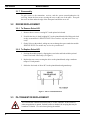
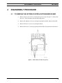
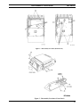
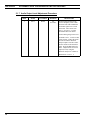
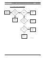
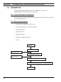
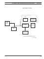
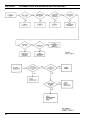
LBI-38425A
Maintenance Manual
Service Section
MLS II Highband Two-Way
Mobile Radios
MLSH041
LBI-38425A
GENERAL INFORMATION
NOTICE!
Repairs to this equipment should be made only by an authorized service technician or facility designated by the supplier. Any repairs,
alterations or substitution of recommended parts made by the user to this equipment not approved by the manufacturer could void the user's
authority to operate the equipment in addition to the manufacturer's warranty.
NOTICE!
The software contained in this device is copyrighted by Com-Net Ericsson Critical Radio Systems, Inc.
Unpublished rights are reserved under the copyright laws of the United States.
This manual is published by Com-Net Ericsson Critical Radio Systems, Inc., without any warranty. Improvements and
changes to this manual necessitated by typographical errors, inaccuracies of current information, or improvements to
programs and/or equipment, may be made by Com-Net Ericsson Critical Radio Systems, Inc., at any time and without
notice. Such changes will be incorporated into new editions of this manual. No part of this manual may be reproduced or
transmitted in any form or by any means, electronic or mechanical, including photocopying and recording, for any purpose,
without the express written permission of Com-Net Ericsson Critical Radio Systems, Inc.
Copyright © 1990-2000, Com-Net Ericsson Critical Radio Systems, Inc. All rights reserved.
2
TABLE OF CONTENTS
LBI-38425A
TABLE OF CONTENTS
Page
1
Description................................................................................................................................................ 4
2
Initial Adjustment .................................................................................................................................... 4
2.1 Transmitter Adjustment ................................................................................................................... 4
2.2 Receiver Adjustment........................................................................................................................ 4
2.3 Re-Installation.................................................................................................................................. 4
3
Maintenance ............................................................................................................................................. 5
3.1 Preventive Maintenance ................................................................................................................... 5
3.1.1
Connections ....................................................................................................................... 5
3.1.2
Electrical System ............................................................................................................... 5
3.1.3
Mechanical Inspection ....................................................................................................... 5
3.1.4
Antenna.............................................................................................................................. 5
3.1.5
Alignment .......................................................................................................................... 5
3.1.6
Frequency Check ............................................................................................................... 5
3.1.7
Disassembly....................................................................................................................... 6
3.2 Driver Replacement ......................................................................................................................... 6
3.2.1
To Remove Driver HC1..................................................................................................... 6
3.2.2
To Replace Driver HC1 ..................................................................................................... 6
3.3 PA Transistor Replacement.............................................................................................................. 6
3.4 Chip Component Replacement......................................................................................................... 8
3.4.1
To Remove Chip Components........................................................................................... 8
3.4.2
To Replace Chip Components ........................................................................................... 8
4
Disassembly Procedure............................................................................................................................ 9
4.1 To Remove the System Control/Synthesizer Board ......................................................................... 9
4.2 To Remove the Transmitter/Receiver Board.................................................................................... 9
4.3 To Remove the Front Panel/Control Unit ........................................................................................ 10
5
Alignment and Troubleshooting Procedures ......................................................................................... 12
5.1 Synthesizer ....................................................................................................................................... 12
5.1.1
Test Equipment Required .................................................................................................. 12
5.1.2
TX VCO & RX VCO Alignment....................................................................................... 13
5.1.3
Transmitter Frequency Adjustment.................................................................................... 14
5.1.4
Receiver Frequency Adjustment ........................................................................................ 15
5.1.5
Modulation Level Adjustment ........................................................................................... 15
5.1.6
Audio Check ...................................................................................................................... 15
5.1.7
Audio Output Level Adjustment Procedure....................................................................... 16
5.1.8
Control Logic Troubleshooting ......................................................................................... 17
5.2 Transmitter....................................................................................................................................... 18
5.2.1
General Description of Adjustment ................................................................................... 18
5.2.2
Measuring Instruments....................................................................................................... 18
5.2.3
Transmitter Adjustment Procedure .................................................................................... 20
5.3 Receiver ........................................................................................................................................... 23
5.3.1
Receiver Alignment ........................................................................................................... 23
5.3.2
Alignment Procedure ......................................................................................................... 24
5.3.3
Fixed Squelch Adjustment................................................................................................. 25
5.3.4
Receiver Test Procedures .................................................................................................. 25
3
LBI-38425A
1
DESCRIPTION AND INITIAL ADJUSTMENT
DESCRIPTION
The service section contains the information necessary for aligning and troubleshooting
the MLS II (MLSH041) two-way FM mobile radio. In addition, information is provided
for removing and replacing chip components, disassembly procedures and module
replacement procedures.
2
INITIAL ADJUSTMENT
The following adjustments should be made by a certified electronics technician after the
radio has been installed as described in the Installation Manual.
2.1
TRANSMITTER ADJUSTMENT
The transmitter has been adjusted at the factory and should require no readjustment.
However, the antenna length should he adjusted for optimum VSWR, and the frequency
and modulation measured and recorded for future reference. For the complete
transmitter alignment, refer to the Alignment Procedure (see Table of Contents).
2.2
RECEIVER ADJUSTMENT
No initial adjustments to the receiver are required. Refer to the Table of Contents for the
complete receiver alignment.
2.3
RE-INSTALLATION
The MLS II series mobile radios are designed to operate in 12-Volt negative ground
vehicles only. If the mobile radio is moved to a different vehicle, always check the
battery polarity of the new vehicle system.
4
MAINTENANCE
3
LBI-38425A
MAINTENANCE
3.1
PREVENTIVE MAINTENANCE
To insure high operating efficiency and to prevent mechanical and electrical failures
from interrupting system operations, routine checks should be made of all mechanical
and electrical parts at regular intervals. Preventive maintenance should include the
following checks:
3.1.1 Connections
Ground connections to the voltage source should be periodically checked for tightness,
Loose or poor connections to the power source will cause excessive voltage drops and
faulty operation. When ground connections are not made directly to the battery, the
connection from the battery to vehicle chassis must be checked for low impedance. A
high impedance may cause excessive voltage drops and alternator noise problems.
3.1.2 Electrical System
Check the voltage regulator and alternator or generator periodically to keep the electrical
system within safe and economical operating limits. Over-voltage is indicated when the
battery loses water rapidly. Usage of 1 or 2 ounces of water per cell per week is
acceptable for batteries in continuous operation. A weak battery will often cause
excessive noise or faulty operation.
3.1.3 Mechanical Inspection
Since mobile units are subject to constant shock and vibration, check for loose plugs,
nuts, screws and parts to make sure that nothing is working loose.
3.1.4 Antenna
The antenna, antenna base, and all contacts should be kept clean and free from dirt or
corrosion. If the antenna or its base should become coated or poorly grounded, loss of
radiation and a weak signal will result.
3.1.5 Alignment
The transmitter and receiver meter readings should be checked periodically, and the
alignment “touched up” when necessary. Refer to applicable Alignment Procedure and
Troubleshooting sheet for typical voltage readings.
3.1.6 Frequency Check
Check transmitter frequency and deviation. Normally, these checks are made when the
unit is first put into operation, after the first six months and once a year thereafter.
5
LBI-38425A
MAINTENANCE
3.1.7 Disassembly
To gain access to the transmitter, receiver, and the system control/synthesizer for
servicing, loosen the four screws securing the cover at the rear of the radio. Then pull
the cover out from under the edge of the front panel and lift the cover off.
3.2
DRIVER REPLACEMENT
3.2.1 To Remove Driver HC1
1. Remove the two screws securing HC1 to the printed wire board.
2. Unsolder the four (4) leads bridging HC1 to the printed board while lifting each lead
as they are unsoldered. SERVICE NOTE: These leads are soft and can be bent very
easily.
3. Gently lift up on the module, taking care not to damage the spacer under the module.
SERVICE NOTE: The module may stick to the printed board.
3.2.2 To Replace Driver HC1
1. Position the module properly, aligning the screw holes and leads with the printed
board. Trim leads if necessary (see Figure 1).
2. Replace the two screws securing the driver to the printed board, using a moderate
torque of 5 inch-pounds.
3. Solder the four leads of driver HC1 to the printed board and ground strap.
Figure 1 - Driver Lead Identification
3.3
PA TRANSISTOR REPLACEMENT
The PA transistor contains Beryllium Oxide, a TOXIC substance. If the ceramic or
other encapsulation is opened, crushed, broken or abraded, the escaping dust may be
hazardous if inhaled. Use care when replacing the module.
WARNING
6
MAINTENANCE
LBI-38425A
1. Remove the two retaining screws securing PA transistor TR1 to chassis assembly.
2. Unsolder and remove capacitors. Use a desoldering tool as necessary while lifting
the transistor leads with a small screwdriver or pick. Discard old capacitors.
3. Unsolder the emitter, base, and collector leads of the transistor, and remove it from
the printed board.
4. Remove all excess solder from the board, and clean the holes to allow the new
transistor to be positioned properly and the capacitors to fit into proper locations.
Refer to Figure 2 and trim the new transistor leads (if required) to the lead length of
the removed transistor.
5. Apply silicon grease to the back of the replacement transistor and place the transistor
into the mounting slot.
6. Replace the transistor mounting screws using a moderate torque of 5 inch-pounds.
7. Tack solder the four base leads to the printed board, using minimum solder. Then
solder the emitter and collector leads.
8. Install the capacitors into their proper mounting areas, flush to the board.
9. Solder the capacitor bodies to the printed board by first soldering the outside edge.
Then, holding the iron to the outside edge, touch the solder to the inside edge of the
capacitor. Be careful not to create solder bridges at the front and back edges of the
capacitors.
10. Remove any flux left on the board.
Figure 2 - PA Transistor Lead Identification
7
LBI-38425A
3.4
MAINTENANCE
CHIP COMPONENT REPLACEMENT
Replacement of chip capacitors should always be done with a temperature controlled
soldering iron, using a controlled temperature of 700°F (371°C). However, DO NOT
touch black metal film of the resistors or the ceramic body of capacitors with the
soldering iron.
The metallized end terminations of the parts may be touched with the soldering iron
without causing damage.
NOTE
3.4.1 To Remove Chip Components
1. Using two soldering irons, heat each end of the chip at the same time until solder
flows and then remove and discard the chip.
2. Remove excess solder with a vacuum solder extractor.
3. Carefully remove the epoxy adhesive and excess flux to prevent damage to the
printed board.
3.4.2 To Replace Chip Components
1. Using as little solder as possible, “tin” one end of the component and one of the pads
on the printed wiring board.
2. Place the “tinned” end of the component on the “tinned” pad on the board and
simultaneously touch the component and the pad with a well “tinned” soldering iron
while pressing the component down on the board.
3. Place the “tinned” soldering iron on the other end of the component and the pad
simultaneously. Apply solder to the top of the end of the component until the solder
starts to flow. Use as little solder as possible while getting a good joint.
4. After the component has cooled, remove all flux from the component and printed
wiring board area with alcohol.
h
8
The CMOS integrated Circuit devices used in this equipment can be destroyed by static
discharges. Before handling one of these devices, the serviceman should discharge
himself by touching the case of a bench test instrument that has a 3-prong power cord
connected to an outlet with a known good earth ground. When soldering or desoldering
a CMOS device, the soldering iron should also have a 3-prong power cord connected to
an outlet with a known good earth ground. A battery-operated soldering iron may be
used in place of the regular soldering iron.
DISASSEMBLY PROCEDURE
4
LBI-38425A
DISASSEMBLY PROCEDURE
4.1
TO REMOVE THE SYSTEM CONTROL/SYNTHESIZER BOARD
1. Remove the two (2) screws ! securing the top cover (refer to Figure 3). Remove the
top cover. Then disconnect the interconnecting cables.
2. Remove the eight (8) screws " securing the Synthesizer shield. Remove the shield.
3. Remove the three (3) screws # securing the board.
4. Remove the screws $ securing regulator and carefully lift up and remove the board.
Figure 3 – Disassembly Procedure (Top View)
9
LBI-38425A
4.2
DISASSEMBLY PROCEDURE
TO REMOVE THE TRANSMITTER/RECEIVER BOARD
1. Remove the screws ! and % securing the top cover and the bottom cover (refer to
Figures 3 & 4).
2. Disconnect the interconnecting cables and then remove the seven (7) screws &
securing the shield to the board.
3. Disconnect the interconnecting cable. Remove the four (4) screws ' securing the
antenna shield.
4. Remove the two (2) screws ( connecting the power supply cable to the board and
turn the cable stopper mounted on the rear of the frame assembly 90 degrees. Lift up
the cable stopper and remove the power supply cable.
5. Remove the two (2) screws ) securing power module HC1. Remove the screws *
securing the power transistor TR1.
6. Remove the two (2) screws + securing the board. Carefully lift up and remove the
board.
4.3
TO REMOVE THE FRONT PANEL/CONTROL UNIT
1. Remove the four (4) screws , securing the front panel to the frame assembly (refer
to Figure 5).
2. Carefully disconnect the speaker cable from the connector on the Control/
Synthesizer board.
3. Separate the front panel from the frame assembly.
4. Carefully disconnect the ribbon cable connecting the Front Panel/Control unit to the
Control/Synthesizer Board at -.
5. Remove the two (2) screws located at ..
6. While pushing the lock tabs at / remove the Control Panel towards the front.
10
DISASSEMBLY PROCEDURE
LBI-38425A
Figure 4 – Disassembly Procedure (Bottom View)
Figure 5 – Disassembly Procedure (Front Panel)
11
LBI-38425A
5
ALIGNMENT AND TROUBLESHOOTING PROCEDURES
ALIGNMENT AND TROUBLESHOOTING
PROCEDURES
Radio maintenance is facilitated by using the Troubleshooting Procedures and servicing
techniques unique to this radio. The Troubleshooting Procedures are designed to lead
the serviceman rapidly to the defective component or circuit.
Troubleshooting procedures are provided for most major problems that might arise in the
System Control/Synthesizer Board, the Transmitter, and the Receiver.
5.1
SYNTHESIZER
The Alignment and Troubleshooting procedures for Synthesizer Circuitry on System
Control/Synthesizer Board CMC-552 are as follows:
5.1.1 Test Equipment Required
•
Audio Oscillator
•
Deviation Monitor
•
Oscilloscope
•
Frequency Counter
•
RF Wattmeter (50 ohms, 100 W)
•
VTVM
•
Digital Voltmeter
•
Power Supply, 13.6 VDC regulated
Measuring System
J701-4
Audio
Oscillator
Radio
J701-3
J1
Coupler
(50Ω)
RF wattmeter
P1
Power Supply
13.6 Vdc
Deviation
Monitor
Oscilloscope
Frequency
Counter
RC-5429B
12
ALIGNMENT AND TROUBLESHOOTING PROCEDURES
LBI-38425A
5.1.2 TX VCO & RX VCO Alignment
STEP
1
METERING
POINT
TP201 Control
Voltage
Monitor
TUNING
CONTROL
CV202
METER
READING
4.0 VDC
7.0 VDC
2
TP201
CV201
7.0 VDC
3
TP201
3.5-7.5 VDC
4
J201
+2 to +8 dBm
PROCEDURE
In case that highest transmit
frequency is < 156.8 MHz.
Select lowest frequency transmit
channel. With 50 ohm load on the
antenna connector J1, key the
radio. Monitor TP201 with digital
voltmeter and tune CV202 for 4.0
VDC ±0.1 V. Unkey the radio.
In case that highest transmit
frequency is 156.8 MHz. Select
highest frequency transmit
channel. With 50 ohm load on the
antenna connector J1, key the
radio. Monitor TP201 with a
digital voltmeter and tune CV202
for 7.0 VDC ±0.1 V. Unkey the
radio.
Select the highest frequency
receive channel. Monitor TP201
with digital voltmeter and tune
CV201 for 7.0 VDC ±0.1 V.
Select lowest frequency channel.
Voltage should be between 3.5 –
7.5 VDC transmit and receive for
lowest and highest frequency
channels.
RX/EX injection level should be
between +2 and +8 dBm.
NOTE: Refer to Figure 6 for location of tuning and adjustment controls.
13
LBI-38425A
ALIGNMENT AND TROUBLESHOOTING PROCEDURES
5.1.3 Transmitter Frequency Adjustment
STEP
METERING
POINT
TUNING
CONTROL
METER
READING
1
J201 (or J1)
FREQ TRIM
Control on
TCXO
(XU201)
Channel
Operating
Frequency
PROCEDURE
NOTE
This step assumes the frequency
is measured when the
transmitter is first keyed. If
delayed, the rapidly rising
ambient temperature must be
taken into consideration. The
Oscillator frequency should be
set at 25°C ambient
temperature.
Press the PTT switch while
monitoring RX/EX injection
frequency at J201. Adjust FREQ
TRIM Control on TCXO
(XU201) for the assigned channel
frequency ±0.5 PPM.
Figure 6 – Synthesizer Adjustment
14
ALIGNMENT AND TROUBLESHOOTING PROCEDURES
LBI-38425A
5.1.4 Receiver Frequency Adjustment
1. No receiver frequency adjustment is required.
2. With proper alignment of EX injection frequency, RX injection frequency will
automatically be correct.
5.1.5 Modulation Level Adjustment
Procedure for synthesizer Transmit Deviation
1. Select the highest frequency channel.
2. Rotate CG DEV ADJUST, RV202 fully counterclockwise.
3. Connect the audio oscillator and apply a 1 kHz tone at 850 mVrms to MIC HI, J7014. Connect the deviation monitor to the antenna connector, J1 through a 30 dB
decoupler. Key the radio. Set DEV ADJUST, RV201 for ±3.75 kHz deviation.
4. Set RV202 fully clockwise. Remove P602 from position 1-2 and set aside. Apply a
400 Hz tone to J602-2 and with the radio keyed, vary its amplitude until the
Deviation Monitor reads 2 kHz. Note the level.
5. Change the audio oscillator frequency for a 10 Hz tone at the same level and set
LOOP MOD ADJUST RV203 for a deviation of 2 kHz. Unkey the radio.
6. Disconnect the audio oscillator and replace P602 in position 1-2.
7. Select a frequency with Tone Channel Guard.
8. Key the radio and set CG DEVIATION ADJUST RV202 for a deviation reading of
±0.75 kHz.
If channel guard is not used on any frequency channel, CG DEV ADJUST, RV201,
may be set for ± 4.5 kHz deviation instead of ±3.75 kHz.
NOTE
5.1.6 Audio Check
Audio Sensitivity
1. Connect audio oscillator output to MIC HI, J701-4. Adjust output for 1 kHz at 1
Vrms.
2. Reduce oscillator output until deviation monitor indication falls to ±3.0 kHz for
radios without Channel Guard or to ± 2.25 kHz for radios with Channel Guard.
Oscillator output voltage should be less than 120 millivolts.
15
LBI-38425A
ALIGNMENT AND TROUBLESHOOTING PROCEDURES
5.1.7 Audio Output Level Adjustment Procedure
STEP
METERING
POINT
TUNING
CONTROL
METER
READING
1
J701-1
RV601
See
Procedure
PROCEDURE
Set the signal generator to the
receiver frequency with ±3 kHz
deviation and 1 kHz modulation.
Set the RF signal level to 1000
microvolts. Move P551 from
J551-1, 2 to J551-2, 3 on the
Transmitter/Receiver Board.
Connect RF signal generator to J1.
Terminate J701-1, 6 with a 4 ohm,
6-watt resistor, connect the audio
level meter and the distortion
analyzer input across the resistor.
Set the volume to the maximum
point. Press DOWN button two
times. Adjust RV601 for 4-watt
output (4 Vrms, using the
distortion analyzer as voltmeter).
Return P551 to J551-1, 2.
16
ALIGNMENT AND TROUBLESHOOTING PROCEDURES
LBI-38425A
5.1.8 Control Logic Troubleshooting
NO
OPERATION
DC
VOLTAGE
IC701- 38
~ 5V?
YES
YES
NO
NO
CHECK
IC608
CHECK
IC609
IC701-4
HIGH?
PSEN
(IC701-26)
RUNNING?
YES
CHECK
IC704-IC708
NO
XTAL
X701
OK?
YES
CHECK
IC701,
IC702,
IC703
NO
REPLACE
X701
RC-5432B
17
LBI-38425A
5.2
ALIGNMENT AND TROUBLESHOOTING PROCEDURES
TRANSMITTER
Alignment and troubleshooting procedures for Transmitter circuitry on the
Transmitter/Receiver board CMN-233 are as follows:
5.2.1 General Description of Adjustment
This manual is prepared for adjustments and confirmations of the Exciter/PA section and
covers the following items:
5.2.2 Measuring Instruments
•
AVR (DC Power Supply DC 0-20V, 20A)
•
Power Meter (usable at the value above 80 W)
•
Directional Coupler
•
Signal Generator
•
Spectrum Analyzer
•
Attenuator (30 dB, above 80 W)
•
Tester
START
1
Initial Setting
2
Confirming the Voltage
3
Confirming the APC Section
4
Adjustment and Setting of the Transmitting Output
DC power ON
SG, PTT ON
STOP
18
ALIGNMENT AND TROUBLESHOOTING PROCEDURES
LBI-38425A
ADJUSTMENT SYSTEM
*
30 dB
ATT
SPECTRUM
ANALYZER
AVR
POWER
SUPPLY
DIRECTIONAL
COUPLER
POWER
METER
RADIO
SPECTRUM
ANALYZER
* FOR MEASURING SPURIOUS ONLY.
RC-5434B
19
LBI-38425A
ALIGNMENT AND TROUBLESHOOTING PROCEDURES
5.2.3 Transmitter Adjustment Procedure
TEST
POINT
TUNING
CONTROL
STEP
ITEM
PROCEDURE
1
Initial Setting
Turn the volume on APC RV1,
RV2 fully counterclockwise
(CCW).
2
Confirming the
voltage
Disconnect RF cable P101 from
connector J201.
Turn on the power.
Turn on the PTT (ground J7012).
Confirm voltage of TR6
collector is 9V at TP4 and that
the relay K1 clicks at this time.
TP4
3
20
Setting APC
off power
Connect RF cable P101 to J201.
RV1
Turn the volume RV1 on APC
fully clockwise (CW).
RV2
Next, turn the volume RV2
slowly CW and set an output of
48W ±2W at the center
frequency of each band.
4
Confirming
minimum
power
RV1
Turn the volume RV1 on APC
fully CCW and confirm
minimum power of 20W or less.
5
Confirming
APC on power
RV1
Turn volume RV1 on APC
slowly CW and set an output of
44W ±2W at the highest
frequency of each band. 40W or
more for other Frequencies.
ALIGNMENT AND TROUBLESHOOTING PROCEDURES
LBI-38425A
TRANSMITTER TROUBLESHOOTING
21
LBI-38425A
22
ALIGNMENT AND TROUBLESHOOTING PROCEDURES
ALIGNMENT AND TROUBLESHOOTING PROCEDURES
5.3
LBI-38425A
RECEIVER
Alignment and Troubleshooting procedures for
Transmitter/Receiver Board CMN-233 are as follows:
Receiver
Circuitry
on
5.3.1 Receiver Alignment
Equipment Required:
•
RF Signal Generator (150.8 – 174 MHz)
•
DC Voltmeter
•
Frequency Counter (up to 500 MHz with 0.05 V sensitivity)
•
Audio Level Meter and Distortion Analyzer
•
4 Ohm, 6 Watt Resistor
5.3.1.1
1.
Preliminary Adjustment
Connect 13.8 VDC to P2.
2. Set MONITOR switch to “out” position.
3. Select desired channel.
4. Disable Channel Guard by connecting ground to J701-7.
5. Connect RF Signal Generator to antenna jack J1.
Make sure the transmitter is properly aligned before aligning the receiver.
NOTE
23
LBI-38425A
ALIGNMENT AND TROUBLESHOOTING PROCEDURES
5.3.2 Alignment Procedure
STEP
TEST
POINT
TUNING
CONTROL
METER
READING
PROCEDURE
9.0 ± 0.2 VDC
Connect the DC Voltmeter to TP501.
1
TP501
2
TP504
L511
See Procedure
Connect RF signal probe from the
frequency counter to TP504. Check
for a reading of 81.745 MHz ±200
Hz.
3
TP503
L513
See Procedure
Set the signal generator on the receive
frequency with ±3 kHz deviation and
1 kHz modulation.
Set the RF signal level to 1000
microvolts.
Connect the audio level meter (use a
high impedance meter) to TP503.
Adjust the L513 until audio output
level becomes maximum.
4
J701-1
See Procedure
Move P551 from J551-1 & 2 to J5512 & 3 in receiver unit.
Terminate J701-1 & -6 with a 4 ohm,
6 watt resistor.
-6
Connect the Audio Level Meter and
Distortion Analyzer input across the
resistor.
Adjust the volume control for 4 W
output (4.0 Vrms) using Audio Level
Meter.
5
J701-1
L501
L503
See Procedure
Set the output signal level of RF
signal generator so as to obtain 12 dB
SINAD at audio output.
Adjust coils L501 and L503 to obtain
maximum 12 dB SINAD sensitivity.
Return P551 to J551-1, 2.
24
ALIGNMENT AND TROUBLESHOOTING PROCEDURES
LBI-38425A
5.3.3 Fixed Squelch Adjustment
1. Disable Channel Guard, if present, (ground J701-7). Set Squelch control RV502 full
CCW.
2. Connect a signal generator to antenna jack J1 and adjust for nominal 8 dB SINAD
signal.
3. Adjust squelch control RV531 to maximum squelch. Receiver must be muted.
4. Adjust squelch control RV531 slowly until receiver unmutes.
5. Check that the squelch opens at an input signal level corresponding to 8 dB SINAD
(±1 dB).
6. Remove ground from J701-7 or re-enable Channel Guard.
5.3.4 Receiver Test Procedures
5.3.4.1
TEST PROCEDURES
These Test Procedures are designed to help you service a receiver that is operating, but
not properly. The problems encountered could be low power, poor sensitivity, distortion,
or low gain. By following the sequence of test steps starting with Step 1, the defect can
be quickly localized. Once the defective stage is pin-pointed, refer to the “Service
Check” listed to correct the problem. Additional corrective measures are included in the
Troubleshooting Procedures. Before starting with the Receiver Test Procedures, be sure
the receiver is tuned and aligned to the proper operating frequency and the transmitter is
operating properly.
5.3.4.2
TEST EQUIPMENT REQUIRED
•
Distortion Analyzer
•
RF Signal Generator
•
dB Attenuation Pad
•
4.0 Ohm, 6 Watt Resistor
5.3.4.3
TEST PROCEDURE
STEP 1: Audio Output and Distortion
Measure Audio Power Output as follows:
1. Apply a 1000 microvolt, on-frequency test signal modulated by 1000 Hz with 3.0
kHz deviation to antenna jack J1.
2. With 4 Watt Speaker: Disconnect speaker plug if present. Connect a 4.0 ohm, 6
watt load resistor across the external speaker loads
25
LBI-38425A
ALIGNMENT AND TROUBLESHOOTING PROCEDURES
3. Adjust the VOLUME control for rated power output of 4 watts (4.0 Vrms across the
4 ohm load) using the Distortion Analyzer as a voltmeter.
4. Make distortion measurements according to manufacturer’s instructions. Reading
should be less than 5%. If the receiver sensitivity is to be measured, leave all
controls and equipment as they are.
Service Check
If the distortion is more than 5%, or maximum audio output is less than 4 watts, make the
following checks: Battery and regulator voltage, low voltage will cause distortion.
Audio Gain (refer to Receiver Troubleshooting Procedure).
FM Detector Alignment (refer to Receiver Alignment).
STEP 2: Usable Sensitivity (12 dB SINAD)
If Step 1 checks out properly, measure the receiver sensitivity as follows:
1. Apply a 1000 microvolt, on-frequency signal modulated by 1000 Hz with 3 kHz
deviation to J1.
2. Place the RANGE switch on the Distortion Analyzer in the 200 to 2000 Hz distortion
range position (1000 Hz filter in the circuit). Tune the filter for minimum reading or
null on the lowest possible scale (100%, 30%, etc.).
3. Place the RANGE switch to SET LEVEL position (filter out of the circuit) and
adjust the input LEVEL control for a +2 dB reading on a mid range (30%).
4. Set signal generator output to 0.3 V. Switch the RANGE control from SET LEVEL
to the distortion range. Readjust Distortion Analyzer SET LEVEL as required until
a 12 dB difference (+2 dB to –10 dB) is obtained between the SET LEVEL and
distortion range positions (filter out and filter in).
5. The 12 dB difference (Signal plus Noise and Distortion to noise plus distortion ratio)
is the “usable” sensitivity level. The sensitivity should be less than rated 12 dB
SINAD specifications with an audio input of at least 2 watts (2.83 Vrms across the 4
ohm receiver load using the meter).
6. Leave all controls as they are and all equipment connected if the Modulation
Acceptance Bandwidth test is to be performed.
Service Check
If the sensitivity level is more than rated 12 dB SINAD, check the alignment of the IF
stage as directed in the Alignment Procedure.
STEP 3: Modulation Acceptance (Bandwidth or IF Bandwidth)
If Steps 1 and 2 check out properly, measure the bandwidth as follows:
26
ALIGNMENT AND TROUBLESHOOTING PROCEDURES
LBI-38425A
1. Set the Signal Generator output for twice the microvolt reading obtained in the 12 dB
SINAD measurement.
2. Set the Range control on the Distortion Analyzer in the SET LEVEL position (1000
Hz filter out of the circuit), and adjust the input LEVEL control for a +2 dB reading
on the 30% range.
3. While increasing the deviation of the Signal Generator, switch the RANGE control
from SET LEVEL to distortion range until a 12 dB difference is obtained between
the SET LEVEL and distortion range readings (from +2 dB to –10 dB).
4. The deviation control reading for the 12 dB difference is the Modulation Acceptance
Bandwidth of the receiver. It should be more than ±6.5 kHz.
Service Check
If the Modulation Acceptance Bandwidth test does not indicate the proper width, refer to
the Receiver Troubleshooting Procedure.
27
LBI-38425A
28
ALIGNMENT AND TROUBLESHOOTING PROCEDURES
ALIGNMENT AND TROUBLESHOOTING PROCEDURES
LBI-38425A
This Page Intentionally Left Blank
29
Com-Net Ericsson Critical Radio Systems, Inc.
P.O. Box 2000
Lynchburg, Virginia 24501
Phone: 1-800-431-2345 or (Outside USA, 1-804-592-6100)
www.com-netericsson.com
Printed in U.S.A.