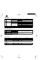
1
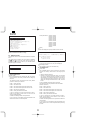
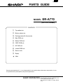
SERVICE MANUAL
MODEL
ER-A770
(For "U"&"A" version)
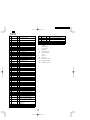
CONTENTS
CHAPTER 1. SPECIFICATIONS ................................................................1 - 1
CHAPTER 2. OPTIONS ..............................................................................2 - 1
CHAPTER 3. SERVICE PRECAUTION ......................................................3 - 1
CHAPTER 4. SRV RESET (Program Loop Reset) and switch to SRV mode...4 - 1
CHAPTER 5. MASTER RESET ..................................................................5 - 1
CHAPTER 6. DIAGNOSTICS SPECIFICATIONS.......................................6 - 1
CHAPTER 7. CIRCUIT DESCRIPTION ......................................................7 - 1
CHAPTER 8. CIRCUIT DIAGRAM ..............................................................8 - 1
CHAPTER 9. PWB LAYOUT.......................................................................9 - 1
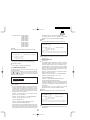
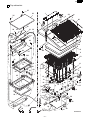
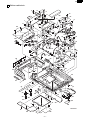
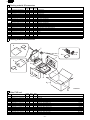
PARTS GUIDE
Parts marked with " " are important for maintaining the safety of the set. Be sure to replace these parts with specified
ones for maintaining the safety and performance of the set.
SHARP CORPORATION
This document has been published to be used
for after sales service only.
The contents are subject to change without notice.
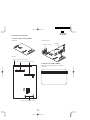
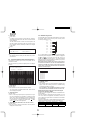
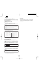
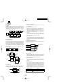
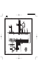
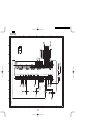
CHAPTER 1. SPECIFICATION
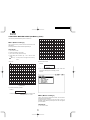
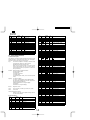
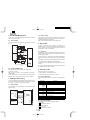
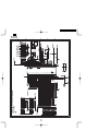
1. Apearance
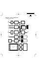
3. Keyboard
External view
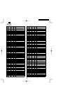
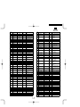
1) Standard keyboard layout
Front view
Operator display
91
92
93
94
95
96
97
82
83
84
85
86
87
88
73
64
55
Keyboard
46
38
Power switch
Insure that the power
switch is placed in the
OFF position prior to
connecting AC power.
Left side
of the
machine
30
74
65
56
47
39
31
75
66
57
48
40
32
76
67
58
49
41
33
77
68
59
50
42
34
78
69
60
51
43
35
79
70
61
52
LEVEL LEVEL LEVEL LEVEL LEVEL MISC
1
2
3
4
5
FUNC
89
80
71
62
53
TAX1
90 SHIFT
81
BILL
TAX2
SHIFT
AUTO
1
AUTO
RP
2
ROUND
MODE
NC
72
GLU RFND
RCPT
RECALL
63
PBAL
54
VOID
SEAT
#
-1
%1
MDSE
SBTL
MSG
#
CHK
#
CH
#
SRVC
PAST
VOID
SBTL
VOID
PLU/
SUB
FINAL
CL
BS
44
45
36
PAGE
UP
37
7
8
9
BT
CANCEL
4
5
6
NEXT
$
1
0
2
00
3
•
SBTL
22
23
24
25
26
27
28
PAGE
29 DOWN
14
15
16
17
18
19
20
21
7
8
9
10
11
12
13
1
2
3
4
5
6
ENTER
SERV @
FOR
#
CA/AT
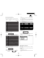
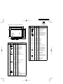
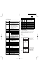
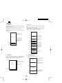
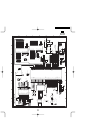
2) Key top name
Standard key top
IPL switch cover
Contrast control
Brightness
control
Rear view
Rear cover
Power switch
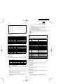
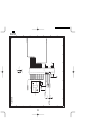
2. Rating
External dimensions
11.4 (W)
(290 (W)
14.4 (D) 11.1 (H) in.
365 (D) 282 (H))mm
Weight
12.4 lbs.(5.6 kg)
Power source
120 V AC
Power consumption
Stand-by: 22W
Operating: 32W
Working temperatures
32 to 104 °F (0 to 40 °C)
10%, 60Hz
KEY TOP
0 ~ 9, 00
•
CL
@/FOR
RCPT
RP ROUND
1
%1
TAX1 SHIFT ~ TAX2 SHIFT
RFND
VOID
PAST VOID
SBTL VOID
BILL
PLU/SUB
1 ~ 97
LEVEL1 ~ LEVEL5
SRVC
FINAL
NC
GLU RECALL
PBAL
SERV#
MSG#
MISC FUNC
MODE
ENETER
AUTO1, AUTO2
CH#
CHK#
NEXT$
MDSE SBTL
SBTL
CA/AT
BS
DESCRIPITON
Numeric keys
Decimal point key
Clear key
Multiplication key
Receipt print key
Repeat round key
Discount 1 key
Percent 1 key
Tax 1 and 2 shift keys
Refund key
Void key
Past void key
Subtotal void key
Bill print key
Price lookup/subdepartment key
Direct price lookup key
PLU level shift 1 thru 5 keys
Service key
Final key
New check key
Table# recall key
Previous balance key
Server code entry key
Message number entry key
Miscellaneous function key
Mode key
Enter key
Automatic sequencing 1 and 2 keys
Charge menu key
Check menu key
Next high dollar key
Merchandise subtotal key
Subtotal key
Cash/amount tendered key
Bill separation key
>>>>> USE FONT <<<<<
Helvetica/ Helvetica-Condensed/ Century-Schoolbook/ Symbol & OriginalFonts: (RingWorld2/RingFont2/Pa
Symbol/PartsCod)
- - - - - - - - - - - - - - - - - - - - - - - - - - - - - - - - - - - - - - - - - - - - - - - - - - - - - - -
KEY TOP
BT
SEAT#
PAGE UP, PAGE DOWN
,
, ,
CANCEL
DESCRIPITON
Bill totals/Bill transfer key
(CHECK-ADD)
Seat number entry key
Page up/down keys
Cursor (up/down/right/left arrow) keys
Cancel key
Optional key top
KEY TOP
000
98 ~ 135
1 ~ 50
%2 ~ %9
2~ 9
CH1 ~ CH8
CA2
CONV1 ~ CONV4
RA1, RA2
PO1, PO2
AUTO3 ~ AUTO25
CHK1 ~ CHK4
TRANS OUT
TRANS IN
CASH TIP
CHARGE TIP
TIP PAID
EAT IN 1 ~ EAT IN 3
TAX3 SHIFT, TAX4 SHIFT
DEPOSIT
DEPOSIT RF
TAX
GRT EX
COVER CNT
BAL
CONV#
SHIFT1 ~ SHIFT5
BACK SPACE
DELETE
DRV NC
DRV PBAL
TRAY SUBTL
RTN
RP SEND
EMPL.#
EMPL.CH
#
NS
MGR#
OPEN TARE
REPEAT
IND. PAYMENT
EMPL. SALES
RCP SW
SCALE
LEVEL6 ~ LEVEL10
WAIT
RECALL
WASTE
C NEXT
TIME IN
TIME OUT
KEY TOP
BREAK
D-THRU
EDIT TIP
MSG1 ~ MSG9
PLU MENU1 ~
PLU MENU50
DESCRIPTION
Break key
Drive-thru screen key
Edit tip key
Message 1 thru 9 keys
PLU menu 1 thru 50 keys
3) Text programming key sheet layout
DESCRIPTION
000 key
Direct price lookup key
Department keys
Percent 2 thru 9 keys
Discount 2 thru 9 keys
Charge 1 thru 8 keys
Cash 2 key
Conversion 1 thru 4 keys
Received-on-account 1 and 2 keys
Paid-out 1 and 2 keys
Automatic sequencing 3 thru 25 keys
Check 1 thru 4 keys
Transfer out key
Transfer in key
Cash tip key
Charge tip key
Tip paid key
Eat in 1 thru 3 keys
Tax 3 and 4 shift keys
Deposit key
Deposit refund key
Manual tax key
Gratuity exempt key
Cover count entry key
Balane key
Currency conversion menu key
Price level shift 1 thru 5 keys
Back space key
Delete key
New check 2 key (for drive thru)
Previous balance 2 key (for drive thru)
Tray subtotal key
Return key
Remote printer send key
Employee code entry key
Employee charge key
Non-add code entry key
No-sale key
Manager code entry key
Tare entry key
Repeat entry key
Individual payment key
Employee sales key
Receipt ON/OFF key
Scale entry key
PLU level shift 6 thru 10 key
Wait key
Recall key
Waste mode key
Condiment next key
Time-in key
Time-out key
[
]
Ñ
_
-
”
+
,
¿
{
}
?
<
>
(MODE)
!
@
#
$
%
ˆ
&
(
)
=
(INS)
Q
W
E
R
T
Y
U
I
O
P
/
(DEL)
A
S
D
F
G
H
J
K
L
:
BACK
SPAC E
Z
X
C
V
B
N
M
,
;
.
(SHIFT)
(SPACE) (SPACE) (SPACE) (SPACE) (SPACE)
(RECALL)
PREV
RECORD
NEXT
RECORD
(DC)
@
PAGE
UP
FOR
CL
PAGE
DOWN
7
8
9
(CANCEL)
4
5
6
(ENTER)
1
2
3
0 00
UP
DATA
SBTL
CA/AT
: The shaded area contains the character keys which are
used for programming characters.
KEY TOP
DESCRIPTION
SHIFT
Used for programming characters. For more
information about programming characters.
DC
INS
DEL
BACK SPACE
[ ], [ ], [ ], [ ] Used to move the cursor.
ENTER
Used to program each setting.
CA/AT
Used to finalize programming.
Used to cancel programming and to get back
CANCEL
to the previous screen.
MODE
Used for changing the operating mode.
Used to go back to the previous record, e.g.,
PREV RECORD from the department 2 programming window
back to the department 1 programming window.
Used to go to the next record, for example, in
NEXT RECORD order to program unit prices for sequential
departments.
Used to scroll the window to go to the next
PAGE DOWN
page.
Used to scroll the window to go back to the
PAGE UP
previous page.
Used to clear the last setting you have
CL
programmed or clear the error state.
•
Used to toggle between two or more options.
Used to list those options which you can toggle
SBTL
by the • key.
RECALL
Used to call up a desired code.
RECALL
Used to update PLU unit price or name.
Numeric keys
Used for entering figures.
• Screen example 2 (PGM mode)
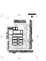
4) Blank key sheet layout
Time
Mode name
Window
In the PGM mode,
programmable items are listed.
3. Display
Double-size character mode indicator (W):
Appears when the double-size character
mode is selected during text programming.
1) Operator display
• Screen example 1 (REG mode)
Caps lock indicator (A/a):
The upper-case letter “A” appears when
Caps Lock is on, and the lower-case
letter “a” appears when Caps Lock is off
during text programming.
Sales amount including taxes
Tax amount
Merchandise subtotal excluding taxes
Mode name
Time
Screen save mode
When you want to save the electric power or save the display’s
life, use the screen save function. This function can turn the LCD
backlight off when any server does not operate the POS terminal
for an extended period of time. You can program the time for
which your POS terminal should keep the normal status (in which
the backlight is "ON") before it goes into the screen save mode.
To go back to the normal mode, press any key.
Numeric entry:
Entered figures appear at the
cursor position.
Received
media
type
Server
name
Server code
Menu level shift indicator (L1~L10):
Shows the menu level currently selected.
Price level shift indicator (P1~P5):
Shows the PLU price level currently selected.
Receipt ON/OFF status indicator (R):
Appears when the receipt ON-OFF function
signs OFF. Disappears when the function
signs ON.
Sentinel mark (X):
Appears in the lower right corner of the screen
when the cash in drawer exceeds a programmed
sentinel amount. The sentinel check is performed
for the total cash in drawer.
Device type
LCD display
Dot format
320(W)
Dot size
0.33
Dot space
0.03 mm
Dot color
White
240(H) Full dot
0.33 mm
Back color
Dark blue
Weight
180 g
2) Display adjustment
You can adjust the brightness and contrast of the display by using the
corresponding controls.
Window
In the REG mode, it shows sales information you have just
entered such as items, tax amounts and media types.
IPL switch cover
Brightness control
Turning the control backwards
darkens the display and turning it
forwards brightens the display.
Contrast control
Turning the control backwards
darkens the display and turning
it forwards lightens the display.
Pole Display
<Option>
UP-P16DP
Remote
Drawer
<Option>
ER-03DW/
04DW
Expansion
memory
board
<Option>
UP-P02MB2
INLINE (SRN) Communication
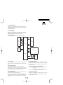
1. System configuration
CHAPTER 2. OPTIONS
<Option>
UP-I16DP
Integrated
customer
display
Master machine
ER-A770
MCR
<Option>
UP-E12MR
(RS-232)
(SRN)
Satelite machine
ER-A770
<Max. 15 >
RS-232 Communication
<Local purchase>
Coin dispencer
R/J Printer
<Option>
ER-01PU
PC
<Local purchase>
<Local purchase>
CAT
PC
<Local purchase>
Remote Printer
<Option>
ER-04RP/03RP
CVM (Color video monitor)
<Local purchase>
>>>>> USE FONT <<<<<
Helvetica/ Helvetica-Condensed/ Century-Schoolbook/ Symbol & OriginalFonts: (RingWorld2/RingFont2/Pa
Symbol/PartsCod)
- - - - - - - - - - - - - - - - - - - - - - - - - - - - - - - - - - - - - - - - - - - - - - - - - - - - - - -
2. Sales Options
No.
CLASSIFICATION
Printer
COMPONENT NAME
External R/J printer
Remote printer
Display
Remote display (Pole type)
Customer display
Remote drawer
1
2
Drawer
Coin case
3
4
5
6
Memory
On-line function
OTHER
Expansion RAM disk board
RS232 I/F board
MCR (Magnetic Card Reader)
MODEL NAME
ER-01PU
ER-03RP
ER-04RP
UP-P16DP
UP-I16DP
ER-03DW
ER-04DW
ER-75CC3
ER-48CC3
ER-55CC2
ER-48CC2
UP-P02MB2
ER-A7RS
UP-E12MR
REMARK
Via RS-232 I/F
Via SRN I/F
11-Dig. 7-Seg. +16-Dig. Dot
11-Dig. 7-Seg. +16-Dig. Dot
7B/5C
5B/5C
7B/5C (For "U" version of ER03DW)
4B/8C (For "A" version of ER-03DW)
5B/5C (For "U" version of ER-04DW)
4B/8C (For "A" version of ER-04DW)
2M bytes PS-RAM board
2 ports RS232 I/F
3. Local purchase options
No.
1
2
3
4
5
COMPONENT NAME
CAT terminal
Scale
Coin Dispenser
Color Kitchen Monitor
PC
MODEL NAME
Omni-Series
PNC-330
Toledo, NCI
Telequip Coporation
Progressive sys.
This equipment will be purchased locally and it will be connected to
ER-A770 via RS232 I/F.
If standard RS 232 2 ports are not available, ER-A7RS is needed.
This equipment will be purchased locally and it will be connected to
ER-A770 via SRN and RS 232 I/F.
4. Service options : None
5. Service tools
No.
1
2
3
4
NAME
Terminator(50 Ω)
MCR test card
RS232 loop back connector
Expansion PWB
PARTS CODE
PRICE
AZ
BE
BC
BX
PARTS CODE
PRICE
AQ
6. Supplies
No.
1
NAME
Blank key sheet
DESCRIPTION
for SRN in-line system
for UP-E12MR
for RS232 connector
7. How to use service tools
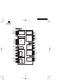
7-1. Expansion PWB : CKOG-6724BHZZ
• Connection diagram
• External view
ER-A7RS
ER-A770 bus connector
• Plain view
Test pins : Used to check the bus signals.
Bus connector : Used to check the bus signals.
7-2. MCR test card: UKOG-6718RCZZ
• Used when executing the diagnostics of the UP-E12MR.
• External view
Connected to the ER-A770 Mother PWB.
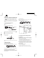
CHAPTER 3. SERVICE PRECAUTION
1. Adjustment for SRN (IN-LINE) interface
circuit
If transistor Q9 in the transmitter/receiver section has been replaced
or if the SRN level requires readjustment, the following alignment is
required:
Waveform adjustment
Adjust VR1 until the signal waveform as shown in Fig. 4 is obtained
across TP1 and TP2 (GND).
Turning VR1 clockwise extends the interval of T1.
VOH
VOL
T1
1) Tools and Instruments Required
T2
T1=580 to 620ms
T2=380 to 420ms
Oscilloscope (50MHz or better) ........................................... 1
Fig. 4 Receiver regeneration waveform (with dummy network)
ER-A770.............................................................................. 1
2) Dummy Network Specifications
R2
R1
C1
R1 100ΩJ (1/4W carbon)
R2 150ΩJ (1/4W carbon)
C1 0.01µF(mylar firm)
Fig. 1 Dummy network
The oscillator should be connected to the points indicated by
.
and
TP2
: Connect the positive side of the oscillator.
TP1
Fig. 5 Board location
: Connect the negative side of the oscillator.
3) Connections
2. IPL (Initial program Loading) function
1) Introduction
Main PWB
BNC connector
Fig. 2
Attach the BNC connector to the SRN connector (CN7) on the main
PWB.
4) Alignment Procedure
When Using an Oscillator
a) Checking the 1MHz oscillator output
Using an oscilloscope check the 1MHz oscillator’s output waveform.
5V
0V
0.5µS
0.5µS
Fig. 3 1MHz oscillator output waveform
NOTE: The oscillator used should have an output impedance of
50Ω.
b) Connecting the oscillator and its adjustment
Connect a dummy network or branch-trunk network to the output of
the SRN connector (CN7), and connect the oscillator to the dummy or
branch-trunk network.
The application software of the ER-A770 is written in the flash ROM.
In the following cases, the replacement procedure of the application
software into the flash ROM is required
• When the flash ROM is replaced with new one. The service part
flash ROM does not include the application software in it.
• When IPL writing is required because of change in the software.
The service part ofthe main PWB unit includes the flash ROM with
the application software written in it, and there is no need for
writing the application software when replacing the main PWB unit.
2) IPL procedure
There are two ways of IPL procedures.
• IPL from P-ROM via ER-A7RS
• IPL from PC communication (Please refer the next section)
The detailed descriptions on the above procedures are given below.
>>>>> USE FONT <<<<<
Helvetica/ Helvetica-Condensed/ Century-Schoolbook/ Symbol & OriginalFonts: (RingWorld2/RingFont2/Pa
Symbol/PartsCod)
- - - - - - - - - - - - - - - - - - - - - - - - - - - - - - - - - - - - - - - - - - - - - - - - - - - - - - -
3) IPL from P-ROM via ER-A7RS
3. ER-A770 Utility tools
(1) Install the two master ROMs to the IC socket (IC12 , IC13) on the
ER-A7RS.
1. Outline
Master ROM -1 : VHI27801RAJxx
Master ROM -2 : VHI27801RAKxx
This Specification document describes the explanation about "POSUTILITYTOOL.EXE and "02FD.EXE".
(2) Remove AC power from the ER-A770.
"POSUTILITYTOOL.EXE" and "02FD.EXE" works with Windows95/98
operating systems and have the following functions by connecting
ER-A770 via RS232.
(3) Set the IPL switch of the ER-A7RS : Set the IPL SW to ON position.
POSUTILITYTOOL.EXE : IPL of ER-A770 Program Object
02FD.EXE
IPL SW
OFF
: All RAM Data Upload/Download
(PC software tool instead of the current
ER-02FD.)
IC13 ROM2
MASTER
P-ROM -2
2. Environment
IC12 ROM1
MASTER
P-ROM -1
PC and ER-A770 are connected by RS232.
ON
Connect the CH2 port of the ER-A770 to the RS-232 interface of the
PC.
(4) Install the ER-A7RS to the ER-A770. (The ER-A770 power should
be turned OFF.)
(5) Turned on the power of the ER-A770.
RS-232
(6) The buzzer sounds intermittently during the running of IPL and the
program finishes after the buzzer gives five beeps at short intervals.
CH2
PC
POS
(7) Turn OFF the power of the ER-A770.
Fig. 1 Connection between PC and ER-A770
(8) Remove the ER-A7RS from the ER-A770.
(9) Perform the Master reset.
RS232 Cable Connecting:
[PC]
3 TXD
[ER-A770]
3 TXD
2 RXD
2 RXD
5 S.G.
5 S.G.
3. Procedure
3.1 POS UTILITY TOOL
NOTE : The screen layouts for the PC-based POS utilities may change without notice for improrement.
No
1
Procedure on P.C. side
No
Procedure on ER-A770 side
Install "POSUTILITYTOOL.EXE" on the P.C.
2
Turn OFF the power.
3
Select "IPL Mode".
Set "IPL Switch" of ER-A770 to "ON".
IPL SW
OFF
ON
4
Turn ON the power.
5
Starting of "IPL Mode".
ER-A770 shows
"IPL from Serial I/O"
IPL from Serial I/O
6
Connect P.C. and ER-A770 (CH2) via RS232. (Fig 1)
No
Procedure on P.C. side
7
Execute "POSUTILITUTOOL.EXE" on P.C.
*Don’t execute the other Software at the same time.
8
Select the ROM object Files by "Add Files.." button.
9
Push "SEND" button.
Program data is sent to ER-A770 automatically.
No
9
Procedure on ER-A770 side
Program data is received from P.C. automatically.
ER-A770 shows
IPL from IR
Connected 115200
21 22 23 24 25 26 27 28
10
When sending is completed,
the initial Window is shown after "Complete" window.
10
ER-A770 shows
"Completed."
IPL from Serial I/O
Connected 115200
21 22 23 24 25 26 27 28
29 2A 2B 2C 2D 2E 2F
Completed.
IPL from Serial I/O
Connected 115200
30 31 32 33 34 35 36 37
38 39 3A 3B 3C 3D 3E 3F
Completed.
11
Turn OFF the power.
12
Select "Normal Mode".
Set "IPL switch" to "OFF".
(Ref. Hardware manual)
13
Execute "Service Reset" or "Master Reset" on ER-A770.
3.2 02FD
No
1
2
Procedure on P.C. side
Install "02FD.EXE" on the P.C.
ALL RAM Data UpLoad : Go to "2"
ALL RAM Data DownLoad : Go to "9"
ALL RAM Data UpLoad
Connect P.C. and ER-A770 (CH2) via RS232. (Fig 1)
No
2
3
Procedure on ER-A770 side
Enter the SRV mode.
Select " 2 SETTING ".
Select " 14 BACKUP SEND"
ER-A770 shows
BACKUP SEND
SEND DATA
ALL RAM
SPEED
4
Execute "02FD.EXE" on P.C.
*Don’t execute the other Software at the same time.
5
Set the Communication method by "Setting" Button.
6
7
Push "OK" Button.
Push "Receive Start" Button.
And Select the Receiving File.
Communication starts.
7
PROGRAMMED SPEED
Push CA/AT key. ER-A770 shows
SENDING
8
9
UpLoad is completed.
The initial Window is shown.
Push "Exit" Button.
ALL RAM Data UpLoad
Connect P.C. and ER-A770 (CH2) via RS232. (Fig 1)
00000
8
UpLoad is completed.
The SETTING menu is shown.
9
Enter the SRV mode.
Select " 2 SETTING".
Select " 15 BACKUP RECEIVE"
10
ER-A770 shows
BACKUP RECEIVE
SPEED
Push CA/AT key.
PROGRAMMED SPEED
No
11
Procedure on P.C. side
Execute "02FD.EXE" on P.C.
*Don’t execute the other Software at the same time.
12
Set the Communication method by "Setting" Button.
13
14
Push "OK" Button.
Push "Transmit Start" Button.
And Select the Sending File.
Communication starts.
No
14
Procedure on ER-A770 side
ER-A770 shows
RECEIVING
15
DownLoad is completed.
The initial Window is shown.
Push "Exit" Button.
4. Note for handling of LCD
• The LCD elements are made of glass. BE careful not to give them
strong mechanical shock, or they may be broken. Use extreme
care not to break them.
15
DownLoad is completed.
The SETTING menu is shown.
16
Execute "Service Reset" on ER-A770.
00000
5. Note for removing Top-Cabinet
When removing the top cabinet, use caution not to apply unnecessary force on the LCD cable on the main PWB or inverter cable
connector.
• If the liquid is attached to your skin or any part of your body or
cloth, immediately clean with soap.
• Use the unit under the rated conditions to prevent against damage.
• Be careful not to drop water or other liquid on the display surface.
• The reflection plate and the polarizing plate are easily scratched.
BE careful not to touch them with a hard objects such as glass,
tweezers, etc. Never hit, push, or rub the surface with hard things.
• When installing the unit, be careful not to apply stress to the LCD
module. If excessive stress is applied, abnormal display or uneven
color may result.
6. Others
When replacing the main PWB or fuse (F4A), use caution not to allow
the C27A body to contact the fuse. (It is good practice to bring it down
in the direction opposite the fuse.)
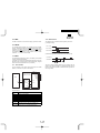
CHAPTER4. SRV RESET (Program Loop Reset) and switch to SRV mode
In the ER-A770, the following reset switch (location No. : SW1) is
used to switch to the service (SRV) mode and to reset.
SRV. reset
Used to return the machine back to its operation state after a lock up
has occurred.
PROCEDURE
1) Turn off the AC switch.
2) Set the reset switch to "ON" position
3) Turn on the AC switch. (Wait one second)
4) Turn to "OFF" the reset switch.
5) The SRV mode is displayed as shown below.
DISPLAY:
Reset
switch
ON
RESET SW
SW1
OFF
Rear side :"ON" position(Reset state)
ON
RESET SW
OFF
Front side :"OFF" position(Run state)
CHAPTER 5. MASTER RESET (All Memory Clear)
There are three possible methods to perform a master reset.
c
a
b
d
MRS-1 (Master resetting 1)
Used to clear all memory contents and return machine back to its
initial settings.
Return keyboard back to default for default kyeboard layout.
PROCEDURE
1) Turn off the AC switch.
2) Set the reset switch to "ON" position
3) Turn on the AC switch. (Wait one second)
4) While holding down the MRS-1 key , turn to "OFF" the reset
switch.
MRS-1 key : The key located on Left upper corner of the keyboard.
MRS-1 Key
keyboard layout
6) Master reset is started.
DISPLAY:
MASTER RESET
7) After completion of the master reset, the buzzer sounds three
times and the following SRV mode display is shown.
DISPLAY:
keyboard layout
5) Enter the password key operation
DISPLAY:
ENTER PASSWORD
Password input procedure: Press the four corners of the key-board
in the sequence of a, b, c, and d.
MRS-2 (Master resetting 2)
Used to clear all memory and keyboard contents. This reset returns
all programming back to defaults.
The keyboard must be entered by hand. This reset is used if an
application needs different keyboard layout other than that supplied
by a normal MRS-1.
PROCEDURE
1) Turn off the AC switch.
>>>>> USE FONT <<<<<
Helvetica/ Helvetica-Condensed/ Century-Schoolbook/ Symbol & OriginalFonts: (RingWorld2/RingFont2/Pa
Symbol/PartsCod)
- - - - - - - - - - - - - - - - - - - - - - - - - - - - - - - - - - - - - - - - - - - - - - - - - - - - - - -
NOTES:
2) Set the reset switch to "ON" position
1: When the 0 key is pressed, the key of the key number on
display is disabled.
3) Turn on the AC switch. (Wait one second)
4) While holding down the MRS-2 key , turn to "OFF" the reset switch.
MRS-2 key:
2: Push the key on the position to be assigned. With this, the
key of the key number on display is assigned to that key
position.
The key located on Right upper corner of the
keyboard.
MRS-2 Key
3: When relocating the keyboard, the PGM 1/2 mode use
standard key layouts shown on page 1-2. (Text programming key sheet layout)
Key
No.
001
002
003
004
005
006
007
008
009
010
Key
name
"0" key
"1" key
"2" key
"3" key
"4" key
"5" key
"6" key
"7" key
"8" key
"9" key
Key
No.
011
013
014
015
016
017
018
019
020
021
Key name
"00" key
Decimal point "•" key
"CL" key
"@/FOR" key
"SBTL" key
"MODE" key
UP " " key
DOWN " " key
LEFT " " key
RIGHT " " key
Key
No.
022
023
024
Key name
"CANCEL" key
"ENTER" key
"CA/AT" key
7) Master reset is started.
DISPLAY:
keyboard layout
MASTER RESET
5) Enter the password key operation
DISPLAY:
8) After completion of the master reset, the buzzer sounds three
times and the following SRV mode display is shown.
ENTER PASSWORD
Password input procedure: Press the four corners of the key-board
in the sequence of a, b, c, and d.
c
a
b
d
keyboard layout
MRS-3 (Master resetting 3)
6) Set the fixed keys in the table below. (Start from the zero "0" key,
The keys are displayed sequentially.)
DISPLAY:
ENTER 0
DISPLAY:
Master resetting 3 requires the entry of Serial No. in addition to
master resetting 1.
After complete the MRS-3, following operations and programming will
be inhibited.
KEY
1. GT programming.
[Key setup procedure]
MRS-2
executed
0
Key
position set
Free key
0
Disable
Setup
complete
2. All memory download via RS-232.
3. GT resets with Z report. ( Z report can be made, but GT will not be
reset.)
7) Set the fixed keys in the table below. (Start from the zero "0" key,
The keys are displayed sequentially.)
PROCEDURE
1) Turn off the AC switch.
DISPLAY:
2) Set the resetswitch to "ON" position.
ENTER 0
3) Turn on the AC switch. (Wait one second)
4) While holding down MRS-3 key , turn to "OFF" the reset switch.
MRS-3 key:
The key located on Left lower corner of the keyboard.
KEY
[Key setup procedure]
MRS-3
executed
Key
position set
0
Free key
Setup
complete
0
Disable
NOTES:
1: When the 0 key is pressed, the key of the key number on
display is disabled.
2: Push the key on the position to be assigned. With this, the
key of the key number on display is assigned to that key
position.
3: When relocating the keyboard, the PGM 1/2 mode use
standard key layout.
Key
No.
001
002
003
004
005
006
007
008
009
010
MRS-3 Key
keyboard layout
5) Enter the password key operation
DISPLAY:
ENTER PASSWORD
Password input procedure: Press the four corners of the key-board
in the sequence of a, b, c, and d.
c
Key
name
"0" key
"1" key
"2" key
"3" key
"4" key
"5" key
"6" key
"7" key
"8" key
"9" key
Key
No.
011
013
014
015
016
017
018
019
020
021
Key name
"00" key
Decimal point "•" key
"CL" key
"@/FOR" key
"SBTL" key
"MODE" key
UP " " key
DOWN " " key
LEFT " " key
RIGHT " " key
Key
No.
022
023
024
Key name
"CANCEL" key
"ENTER" key
"CA/AT" key
8) Master reset is started.
DISPLAY:
MASTER RESET
a
9) After completion of the master reset, the buzzer sounds three
times and the following SRV mode display is shown.
DISPLAY:
b
d
keyboard layout
6) The products serial No. input window is displayed as shown below.
DISPLAY:
SERIAL No.
00000000
Enter the products serial No. of this POS and enter the [CA/AT] key.
CHAPTER 6. DIAGNOSTICS SPECIFICATIONS
CONTENTS
1. General
1. General ........................................................................................ 1
2. System configuration ................................................................... 1
2-1.
Test system ....................................................................... 1
This diagnostics program is used as a simplified check of the ERA770 series operations in servicing.
The diagnostics program is built in the standard ROM.
3. Diagnostics .................................................................................. 1
1) Master reset procedure ............................................... 1
2) Program reset (service reset) procedure ..................... 1
3-1.
Execution of diagnostics ................................................... 1
3-2.
RAM Diagnostics .............................................................. 2
1) Standard RAM Check ................................................. 2
2. System configuration
2-1. Test system
ER-A770 only
2) UP-P02MB2 Check .................................................... 2
3-3.
ROM & SSP Diagnostics .................................................. 3
ER-A770
1) Standard ROM Check ................................................. 3
2) SERVICE ROM Check ................................................ 3
3) SSP Check ................................................................. 4
3-4.
Timer & Keyboard & Clerk Switch Diagnostics ................. 4
3. Diagnostics
1) Timer Check ................................................................ 4
2) Keyboard Check .......................................................... 4
4) CH3 Check .................................................................. 5
This diagnostics program is written in the external ROM and executed
by the CPU (H8/510). To operate this program, the following conditions must be satisfied.
The power for the logic system is proper.
(+5V, VRAM, VCKDC, POFF, +20V)
The input/output pins and the internal logic of the CPU are normal.
In addition, CKDC9, MPCA8, the system bus, and the standard
ROM/RAM are normal.
5) CH4 Check .................................................................. 5
To start the machine for the first time, perform the master reset.
6) CH5 Check .................................................................. 5
In order to add an option unit when the machine is normally operating, perform the program reset.
3) Clerk SW Check .......................................................... 4
3-5.
RS232 I/F Diagnostics ...................................................... 4
1) CHANNEL Check ........................................................ 4
2) CH1 Check .................................................................. 5
3) CH2 Check .................................................................. 5
7) CH6 Check .................................................................. 5
8) CH7 Check .................................................................. 6
9) CH8 Check .................................................................. 6
3-6.
Liquid Crystal Display Diagnostics .................................... 6
1) Liquid Crystal Display Check ...................................... 6
3-7.
Rear & Pole Display Diagnostics ...................................... 7
1) Rear & Pole Display Check ......................................... 7
3-8.
Starting the diagnostics
SHARP Retail Network Diagnostics .................................. 7
1) SRN Self Check ........................................................... 7
2) SRN Flag Send Check ................................................ 8
3) SRN Data Send Check ................................................ 8
When adding the memory option, a master reset is required.
1) Master reset procedure
Turn off the power.
Set the CKDC reset switch to RESET position.
Turn on the power.
While pressing the specified key, set the CKDC reset switch to the
normal position.
2) Program reset (service reset) procedure
Turn off the power.
Set the CKDC reset switch to RESET position.
Turn on the power.
Set the CKDC reset switch to the normal position. (Do not pressany key.)
4) Data Transmission Check ........................................... 8
3-9.
Magnetic Card Reader Diagnostics ................................ 10
3-1. Execution of diagnostics
1) Magnetic Card Reader Check ................................... 10
To start the diagnostics, select "DIAGNOSTICS" with the cursor in the
menu selection in SRV mode, and press the enter key.
The DIAG MAIN MENU is started and the following menu screen is
display. The cursor position is highlighted. Use key and key to
move the cursor. Move the cursor to the process you desire and
press the enter key. The selected individual diagnostics program is
executed. When the individual diagnostics program is completed, the
display returns to the menu screen. To terminate the diagnostics,
press the CANCEL key. Then the display returns to the SRV mode
menu screen.
3-10. Drawer Diagnostics ......................................................... 10
1) Drawer 1 Check ......................................................... 10
2) Drawer 2 Check ......................................................... 10
ER-A770 Diagnostics V 1.0A
Product & Test Diagnostics
RAM Diagnostics
ROM & SSP Diagnostics
Clock & Keyboard & Clerk Diagnostics
Serial I/O Diagnostics
LCD Diagnostics
Rear & Pole Display Diagnostics
SRN Diagnostics
MCR Diagnostics
Drawer Diagnostics
Diagnostics End
Check point address = 700000H, 700001H
700002H, 700004H
700008H, 700010H
700020H, 700040H
700080H, 700100H
700200H, 700400H
700800H, 701000H
702000H, 704000H
708000H, 710000H
720000H, 740000H
780000H
Display
The screen displays the capacity of RAM in the units of 64 KB.
"Product & Test Diagnostics" is used only in the production
process, and must be not used in servicing.
Standard RAM Check
3-2. RAM Diagnostics
Standard memory size : 1024KB PASS!!(or ERROR!!)
This diagnostics is used to test the standard RAM and the expansion
RAM.
Error Address xxxxxxH
Write Data xxxxH
Read Data xxxxH
The following menu is displayed. The cursor position is highlighted.
Use key and key to move the cursor. Move the cursor to the
process you desire and press the enter key. The selected individual
diagnostics program is executed.
The error address and the bit are displayed only when the error
occurs. (If the error does not occur, they are not displayed.)
Terminating procedure
RAM Diagnostics
Standard RAM Check
UP-P02MB2 Check
After completion of check, press the CANCEL key.
2) UP-P02MB2 Check
Check content
The UP-P02MB2 presence check is performed in the following
procedure. The memory contents must not be changed by this
check.
1) Standard RAM Check
Check content
For the pseudo SRAM of the standard RAM 1MB, the following
check is performed. The memory contents will not be changed by
this check.
The following processes are performed for the memory address
(700000H ~ 7FFFFFH) to be checked.
• 55AAH is written into 9FFFFEH.
• 9FFFFEH is read and compared with 55AAH. If the both data
are correct, the following procedure is performed. The system
reads 9FFFFEH and compares it with 55AAH. If both data are
correct, the following tests will be performed. If not, the screen
displays the message "Extended RAM size : 0KB", and ends
the test.
For the UP-P02MB2, the following check is performed.
PASS1:
Memory data save
PASS2:
Data "0000H" write
The following processes are performed for the check address
(800000H ~ 9FFFFFH).
PASS3:
Data "0000H" read/compare, data "5555H" write
PASS1:
Memory data save
PASS4:
Data "5555H" read/compare, data "AAAAH" write
PASS2:
Data "0000H" write
PASS5:
Data "AAAAH" read/compare
PASS3:
Data "0000H" read/compare, data "5555H" write
PASS6:
Memory data writed the saved data
PASS4:
Data "5555H" read/compare, data "AAAAH" write
In case of a compare error in the check sequences of PASS1 ~
PASS6, an error display is made. If there is no error at all, the
check is normally terminated.
In addition, the following address check is performed.
In case of an error, an error display is made and read/write of the
address where the error occurred is repeated.
PASS5:
Data "AAAAH" read/compare
PASS6:
Memory data writes the saved data
In case of a compare error in the check sequences of PASS1 ~
PASS6, an error display is made. If there is no error at all, the
check is normally terminated.
In addition, the following address check is performed in the above
check sequence.
In case of an error, an error display is made and read/write of the
address where the error occurred is repeated without performing
the check.
Check point address = 800000H,800001H
800002H,800004H
800008H,800010H
800020H,800040H
800080H,800100H
800200H,800400H
800800H,801000H
802000H,804000H
808000H,810000H
820000H,840000H
880000H,900000H
Display
The screen displays the capacity of RAM in the unit of 64 KB.
UP-P02MB2 Check
each block becomes 01H, and the total of 2MByte is 20H.
The program version of the IPL is displayed so that 0PAGE
(BLOCK) where the IPL is stored is individually controlled.
Display
The screen displays the capacity of RAM in the unit of 64 KB.
Standard ROM Sum Check : PASS!!(or ERROR!!)
IPL PROGRAM Version
**
← Displays the version.
APL PROGRAM Version
27801R**** ER-A770
27801R**** ER-A770
BLOCK Version
20=**,21=**,22=**,23=**,24=**,25=**,26=**,27=**
28=**,29=**,2A=**,2B=**,2C=**,2D=**,2E=**,2F=**
:
Extended RAM size : 2048KB PASS!!(or ERROR!!)
Terminating procedure
Error Address xxxxxxH
Write Data xxxxH
Read Data xxxxH
After displaying the check result, press the CANCEL key to terminate the check.
2) SERVICE ROM Check
The error address and the bit are displayed only when the error
occurs. (If the error does not occur, they are not displayed.)
Terminating procedure
After completion of check, press the CANCEL key.
3-3. ROM & SSP Diagnostics
The standard ROM and the service ROM are checked. The SSP
circuit is also checked.
The following menu is displayed. The cursor position is highlighted.
Use key and key to move the cursor. Move the cursor to the
process you desire and press the enter key. The selected individual
diagnostics program is executed.
ROM & SSP Check
Standard ROM Check
Service ROM Check
SSP Check
1) Standard ROM Check
Check contents
The standard ROM area (200000H ~ 3FFFFFH) is added in the
unit of byte. If the lower two digits of the result is 20H, it is normal.
The ROM version and the model name code which are stored in
address 31FFE0H ~ 31FFEFH where the ROM version and the
check sum correction data are stored are displayed. The format of
data (ASCII) to be stored is as follows:
31FFE0H ~ 31FFEFH: Model name code (example: ER-A770.
Display is made up to 00H of data.)
31FFF0H ~ 31FFF9H: 27801R****(****=PROGRAM VERSION)
31FFFAH ~ 31FFFBH: BLOCK NO. ("20" ~ "3F")
31FFFCH: TERMINATOR ("=")
31FFFDH ~ 31FFFEH: BLOCK VERSION (example "00")
31FFFFH: CHECK SUM CORRECTION DATA
The flash ROM used as the standard ROM has rewriting block of
64KB as the unit. To control the version in each block, the composition is the same as the above 31FFF0H or later and arranged in
each 64KByte. At that time, correction is made so that the sum of
Check content
For the SERVICE ROM area (D00000H ~ EFFFFFH) consisting of
two EPROMs, addition is made in the unit of byte for each chip.
The lower two digits of the result are 10H, it is regarded as normal.
The ROM version and the model name code which are stored in
address D1FFE0H ~ D1FFFFH where the ROM version and the
check sum correction data are stored are displayed. The format of
data (ASCII) to be stored is as follows:
D1FFE0H ~ D1FFEFH: Model name code (example: ER-A770.
Display is made up to 00H of data.)
D1FFF0H ~ D1FFF9H: 27801R****(****=PROGRAM VERSION)
D1FFFAH ~ D1FFFBH: BLOCK NO. ("20" ~ "2F")
D1FFFCH: TERMINATOR ("=")
D1FFFDH ~ D1FFFEH: BLOCK VERSION (example "00")
D1FFFFH: CHECK SUM CORRECTION DATA
This SERVICE ROM allows to write into the FLASH ROM when
re-execution is impossible because of an abnormality during rewriting into the FLASH ROM. The composition is the same as the
standard ROM.
The program version of the IPL is displayed so that 0PAGE
(BLOCK) where the IPL is stored is individually controlled.
Display
The screen displays the capacity of RAM in the unit of 64 KB.
Service ROM Sum Check 1 : PASS!!(or ERROR!!)
Service ROM Sum Check 2 : PASS!!(or ERROR!!)
IPL PROGRAM Version
**
APL PROGRAM Version
← Displays the version.
27801R**** ER-A770
27801R**** ER-A770
BLOCK Version
20=**,21=**,22=**,23=**,24=**,25=**,26=**,27=**
28=**,29=**,2A=**,2B=**,2C=**,2D=**,2E=**,2F=**
:
Terminating procedure
After displaying the check result, press the CANCEL key to terminate the check.
3) SSP Check
3-5. RS232 I/F Diagnostics
Check content
By starting this check program, the SSP setting for checking is
automatically performed and the SSP check is executed and the
result is displayed.
The SSP check sets data for check in the vacant space in the
SSP entry register, and deletes the data for check after completion of checking. Therefore, the already set data are not changed
by this check.
Display
The main PWB and the option PWB (RS232 interface of ER-A7RS)
are checked. Attach the 9-pin D-Sub loop back connector (UKOG6717RCZZ) of wiring in Fig. 3-11.
SSP Check
SSP (NMI) Check
: PASS!!(ERROR!!)
Terminating procedure
After displaying the check result, press the CANCEL key to terminate the check.
3-4. Timer & Keyboard & Clerk Switch Diagnostics
The operation of the clock crystal of CKDC, the keyboard, and the
clerk switch are tested.
When the CANCEL key is pressed, the display returns to the diagnos
tics menu.
Timer & Keyboard & Clerk SW Diagnostics
CD
1pin
RD
2pin
SD
3pin
ER
4pin
GND
5pin
DR
6pin
RS
7pin
CS
8pin
CI
9pin
Fig. 3-11. Wiring diagram of loop back connector (UKOG-6717RCZZ)
The following menu is displayed. The cursor position is highlighted.
Use key and key to move the cursor. Move the cursor to the
process you desire and press the enter key. The selected individual
diagnostics program is executed. When the CANCEL key is pressed,
the display returns to the diagnostics menu.
When setting channels of RS232, do not set two or more ports to
one channel. In the ER-A770, max. two units of ER-A7RS can be
installed. In each PWB, do not set two or more ports to the same
channel. If two or more ports should be set to one channel, the
hardware would be destroyed.
DATA & TIME = YY/MM/DD & HH:MM:SS
KEY CODE = ***
CLERK CODE = ***
RS232 I/F Diagnostics
CHANNEL Check
CH1 Check
CH2 Check
CH3 Check
CH4 Check
CH5 Check
CH6 Check
CH7 Check
CH8 Check
1) CHANNEL Check
Check content
1) Timer Check
Check content
The operation of the clock crystal of CKDC9 is checked.
The screen displays "YY/MM/DD & MM:HH:SS". Make sure that
the time displayed is updated.
2) Keyboard Check
Check content
The A770 main body keyboard input test is performed. The position code corresponding to the inputted key is displayed in three
digits. The key layout corresponding to the input is displayed on
the LCD screen. Press the corresponding key to input. The display
of the inputted key is changed from white square
to black
square
and a catch sound is generated.
3) Clerk SW Check (Not used for "U" and "A" version)
Check content
The code of the key which is inserted into the clerk key switch is
displayed in a decimal number.
The CHANNEL setting of the connected RS232 is displayed. The
display content and the setting of DIP SW for CHANNEL setting
on the RS232 I/F PWB are compared.
Since the RS232 on the main PWB of the ER-A770 is fixed to
CH1 and CH8, that in the ER-A7RS must be set to CH2 ~ CH7.
Relationship between the physical channel and logical
channel of the ER-A770’s RS232.
The ER-A770 comes equipped with 2 channels of the RS232C interface as standard.
These two channels are expressed as physical channels "CH1" and
"CH2" on the cabinet and application. On hardware, however, the
"CH2" is defined as a logical channel "CH8" because it has a different
circuit configuration.
Therefore, the relationship of channel definitions between the cabinet
indication and the RS232 I/F Diag is as shown in the table below.
Cabinet indication
Logical channel
Definition in Diag.
Application
CH1
CH2
CH1
CH8
CH1
CH8
CH1
CH2
The above check is repeated four cycles.
RS232 I/F Diagnostics
CHANNEL Check
CH1 = exist!
CH2 = exist!
CH3 = none!
CH4 = none!
CH5 = none!
CH6 = none!
CH7 = none!
• Data transfer check
The loop back data (256 bytes) of 00H ~ 0FFH are used for
data transfer check. The baud rate is set to 38400BPS.
← Display when channel present
• Timer check (RS232 on board timer)
← Display when no channel
Before performing the check, set the timer to RCVDT start and
5ms. Then perform the following procedure.
During execution of the check, TRQ- must not be generated.
After 5ms from completion of the check, TRQ- must be generated.
(Reference) ER-A7RS CHANNEL setting (In the table below, "1" =
SW OFF, "0" = SW ON.)
ER-A7RS CON3
S1-1
0
0
0
0
1
1
1
1
RS232 CH1 Check
S1-2
0
0
1
1
0
0
1
1
S1-3
0
1
0
1
0
1
0
1
LOGICAL CHANNEL
Invalid
CHANNEL 1: Impossible to set
CHANNEL 2:
CHANNEL 3
CHANNEL 4
CHANNEL 5
CHANNEL 6
CHANNEL 7
S1-6
0
1
0
1
0
1
0
1
LOGICAL CHANNEL
Invalid
CHANNEL 1: Impossible to set
CHANNEL 2
CHANNEL 3
CHANNEL 4
CHANNEL 5
CHANNEL 6
CHANNEL 7
ER-A7RS CON3
S1-4
0
0
0
0
1
1
1
1
Display
S1-5
0
0
1
1
0
0
1
1
Terminating procedure
Press the CANCEL key to terminate the check.
ER-DR
ERROR
No.
1
2
3
4
5
6
7
8
9
10
11
12
13
14
15
16
When the channel is not set, an error display is made (ERROR:CH1). When the channel is set, the following check is performed.
RSn
OFF
ON
OFF
ON
17
ERROR display
ERROR content
ER-DR:ERROR
ER-CI:ERROR
RS-CD:ERROR
RS-CS:ERROR
CI INT:ERROR
CD INT:ERROR
CS INT:ERROR
TXEMP:ERROR
TXEMP INT:ERROR
TXRDY:ERROR
TXRDY INT:ERROR
RCVRDY:ERROR
ER-DR LOOP ERROR
ER-CI LOOP ERROR
RS-CD LOOP ERROR
RS-CS LOOP ERROR
CI interruption is not made.
CD interruption is not made.
CS interruption is not made.
TXEMP is not set.
TXEMP interruption is not made.
TXRDY interruption is not made.
TXRDY interruption is not made.
RCVRDY is not set.
(Reception enabled. TR-Q is
generated during check)
RCVRDY INT:ERROR RCVRDY interruption is not made.
SD-RD:ERROR
SD-RD LOOP ERROR
(DATA ERROR)
SD-RD:ERROR
SD-RD LOOP ERROR (DATA
ERROR
TIMER:ERROR
TIMER ERROR (TMRQ is not set
after completion of check.)
TIMER INT:ERROR
TRQ-1 interruption is not made.
Terminating procedure
• Control signal check
ERn
OFF
OFF
ON
ON
ERROR!!
All the contents of an error must be displayed.
2) CH1 Check
Check content
:
Press the CANCEL key to terminate the check.
DRn
OFF
OFF
ON
ON
CIn
OFF
OFF
ON
ON
CDn
OFF
ON
OFF
ON
CSn
OFF
ON
OFF
ON
The read check of the above inputs and the interruption check of
CS, CI, and CD are performed.
In the read check, ER and RS are changed over in the above
sequence and the logic states of DR, CI, CD, and CS are
checked.
If the logic differs from that in the table, an error display is made.
3) CH2 Check
Check content
The check procedure, the display, and the terminating procedure
are the same as CH1 Check.
4) CH3 Check
Check content
The check procedure, the display, and the terminating procedure
are the same as CH1 Check.
5) CH4 Check
Check content
"ON" in the table means Active LOW, and "OFF" means Active
HIGH.
In the interruption check, an interruption of CS, CI, or CD is
allowed one by one. (MASK is canceled.)
If an interruption is not made when each signal is active, or if an
interruption is made when each signal is not active, an error
display is made.
The check procedure, the display, and the terminating procedure
are the same as CH1 Check.
6) CH5 Check
Check content
The check procedure, the display, and the terminating procedure
are the same as CH1 Check.
Terminating procedure
7) CH6 Check
Check content
Press the CANCEL key to terminate the check.
The check procedure, the display, and the terminating procedure
are the same as CH1 Check.
8) CH7 Check
The ER-A770 LCD display is checked.
Check content
The check procedure, the display, and the terminating procedure
are the same as CH1 Check.
9) CH8 Check
Check content
Check content
• Control signal check
RSn
OFF
ON
OFF
ON
The test program displays the patterns in the following sequence.
Every time when the ENTER key is pressed, the next pattern is
displayed. When the ENTER key is pressed at the final pattern, or
when the CANCEL key is pressed at the midst of the check, the
display returns to the menu screen.
1) Liquid Crystal Display Check
When the channel is set, the following check is performed.
Ern
OFF
OFF
ON
ON
3-6. Liquid Crystal Display Diagnostics
DRn
OFF
OFF
ON
ON
Cin
OFF
OFF
ON
ON
CDn
OFF
ON
OFF
ON
CSn
OFF
ON
OFF
ON
The test patterns are displayed in the following sequence. When
the ENTER key is pressed, the next pattern is displayed.
• Black and white pattern at 1 dot pitch
The read check of the above inputs.
In the read check, ER and RS are changed over in the above
sequence and the logic states of DR, CI, CD, and CS are
checked.
If the logic differs from that in the table, an error display is made.
"ON" in the table means Active LOW, and "OFF" means Active
HIGH.
• Reversed pattern of the above
The above check is repeated four cycles.
• Data transfer check
The loop back data (256 bytes) of 00H ~ 0FFH are used for
data transfer check. The baud rate is set to 115200BPS.
Display
RS232 CH1 Check
ER-DR
:
• Vertical stripe pattern at 1 dot pitch
ERROR!!
All the contents of an error must be displayed.
ERROR
No.
1
2
3
4
5
6
7
8
9
10
11
12
13
14
15
16
17
ERROR display
ER-DR:ERROR
ER-CI:ERROR
RS-CD:ERROR
RS-CS:ERROR
ERROR content
ER-DR LOOP ERROR
ER-CI LOOP ERROR
RS-CD LOOP ERROR
RS-CS LOOP ERROR
TXEMP is not set.
TXEMP interruption is not made.
TXRDY interruption is not made.
TXRDY interruption is not made.
RCVRDY is not set.
(Reception enabled. TR-Q is
generated during check)
RCVRDY INT:ERROR RCVRDY interruption is not made.
SD-RD:ERROR
SD-RD LOOP ERROR (DATA
ERROR)
SD-RD:ERROR
SD-RD LOOP ERROR
(DATA ERROR, FRAMING
ERROR, etc.)
• Reversed pattern of the above
TXEMP:ERROR
TXEMP INT:ERROR
TXRDY:ERROR
TXRDY INT:ERROR
RCVRDY:ERROR
• Horizontal stripe pattern at 1 dot pitch
• Reversed pattern of the above
display.
3-8. SHARP Retail Network Diagnostics
The SRN test is performed.
To perform this test, the following composition is required.
• The outermost peripheral of the LCD’s active area is displayed
in one-dot line.
• ER-A770
• Terminal resistor
• Branch (trunk) cable (only for data transfer test)
The following menu is displayed. The cursor position is highlighted.
Use key and key to move the cursor. Move the cursor to the
process you desire and press the enter key. The selected individual
diagnostics program is executed. When the individual diagnostics
program is completed, the display returns to this menu screen. When
the CANCEL key is pressed, the display returns to the diagnostics
menu.
SRN Diagnostics
• "H" pattern. "H" is displayed in 40 digits and 15 lines. The 15th
Self
Flag
Data
Data
Data
Check
Send Check
Send Check
Check (Satellite Machine)
Check (Master Machine)
line only has 39 digits of "H."
1) SRN Self Check
Check content
The ROM and RAM for SRN are checked, and CTC interruption and
carrier sense are checked. Also ADLC function and transmission/reception DMA check is made by using the self loop function of ADLC
(MC6854). In addition, the other signals are checked. The check
procedure is as follows:
Terminating procedure
Press the ENTER key at the final pattern, or press the CANCEL
key to terminate the check.
• Execute diagnostics command 2. The number of resending is
displayed.
• Execute diagnostics command 0. The error status is displayed.
The error status is as shown in the table below. When an error
occurs in this test, the following tests are not performed.
3-7. Rear & Pole Display Diagnostics
b7
An error occurs. (The error print is always 1.)
The rear display is checked.
b6
An unexpected interruption is made.
The test program displays the following patterns. When the CANCEL
key is pressed, the display returns to the diagnostics menu.
b5
A collision is generated.
b4
An interruption of send complete cannot be made.
(DMAC TC UP interruption)
Check content
b3
An interruption of carrier OFF cannot be made. The
mirror image of carrier OFF shows carrier ON.
The test patterns are displayed in the following sequence. When
the ENTER key is pressed, the next pattern is displayed.
b2
An interruption of CTC CH2 or CH3 cannot be made.
(Timer interruption)
b1
ROM sum check error
b0
RAM error
1) Rear & Pole Display Check
(i) The test pattern below is displayed.
DOT DISPLAY
:
7SEG DISPLAY :
0123456789;AaBbC
0. 1. 2. 3. 4. 5. 6. 7. 8. 9. -.
(ii) The screen displays a test pattern showing that all digits are lit.
Display
Rear Display Check
Terminating procedure
Press the CANCEL key to turn off all the elements of the rear
• Execute diagnostics command 1. The error status is displayed.
The error status is as shown in the table below.
b7
An error is generated. (The error print is always 1.)
b6
An unexpected interruption is generated.
b5
DMA sent data and received data are different.
b4
The number of data received in DMA is abnormal.
b3
The number of data transmitted in DMA is abnormal.
b2
An overrun error is generated.
b1
An underrun error is generated.
b0
An interruption of send complete cannot be made.
(DMAC TC UP interruption)
• Execute diagnostics command 5. The error status is displayed.
The names and the directions of the signals which are subject
to diagnostics 5 command are as shown in the table below.
Signal name
perform the service reset.
2) SRN Flag Send Check
Check content
Execute diagnostics 3 command to send Flag (7EH) continuously.
Display
Direction
SRN Flag Send Check
Host
Controller
Power interruption ON initialization
Host
Controller
Power interruption ON continuation
Host
Controller
Terminating procedure
Power interruption process complete
Host
Controller
Perform the service reset.
CH1 reception data present.
Host
Controller
CH2 reception data present.
Host
Controller
Power interruption notice
Check that the target bit of two statuses obtained by diagnostics
5 command is "0" for ST1 and "1" for ST2. (The other bits must
be masked.) In the other cases, the error status is displayed with
the error occurrence bit as "1." The normal bit shows "0."
The error status from the host to the controller is as shown in the
table below.
b7
Not used. ("0" is always displayed.)
b6
Power interruption notice
b5
Not used. ("0" is always displayed.)
b4
Not used. ("0" is always displayed.)
b3
Not used. ("0" is always displayed.)
b2
Not used. ("0" is always displayed.)
b1
Power ON continuation
b0
Power ON initializing
3) SRN Data Send Check
Check content
Execute diagnostics 4 command to send data of 00H ~ FFH
(256Byte) as one packet at 12.8msec packet interval at 1Mbps
continuously.
Display
SRN Data Send Check
Terminating procedure
Perform the service reset.
4) Data Transmission Check
Data transmission is checked in an actually composed system. The
system is composed of one master machine and max. 15 satellite
machines.
Note for starting the check
The error status from the controller to the host is as shown in the
table below.
• When checking the set in which the SRN setting has been
made, cancel the SRN setting before starting this check.
• When checking the actually composed system, disconnect the
b7
Not used. ("0" is always displayed.)
b6
Power interruption notice
b5
Not used. ("0" is always displayed.)
b4
CH2 reception data exits.
b3
CH1 reception data exits.
b2
Power interruption process complete
Setting procedure
b1
Not used. ("0" is always displayed.)
• Satellite machine setting
b0
Not used. ("0" is always displayed.)
SRM cables of the sets which are not checked, or cancel the
SRN setting. If it is set to "SRN exits," data may be destroyed.
celing the SRN setting of all the sets in the system. First, set
the satellite machines, then set the master machine.
Display
In the menu screen, select "Data Transmission Check (Satellite)."
The display is as follows:
SRN Self Check
DATA RETRY CNT.=xxx
ACK RETRY CNT.=xxx
DIAG 0
:xxxxxxxx
DIAG 1
• The transmission check setting must be performed after can-
:xxxxxxxx
The number of resending is displayed
in xxx with a decimal number.
In the sequence of b7, b6, ..., b0 from
the left. "1" is displayed in case of an
error, and "0" when normal.
In the sequence of b7, b6, ..., b0 from
the left. "1" is displayed in case of an
error, and "0" when normal.
DIAG 5 H→C
:xxxxxxxx
In the sequence of b7, b6, ..., b0 from
the left. "1" is displayed in case of an
error, and "0" when normal.
DIAG 5 H←C
:xxxxxxxx
In the sequence of b7, b6, ..., b0 from
the left. "1" is displayed in case of an
error, and "0" when normal.
Terminating procedure
Press the CANCEL key to terminate the check. After terminating,
Data Transmission Check (Satellite)
Input Terminal Number
:
Enter the terminal No. (000 ~ 254, 3 digits) of the machine to be
checked and press the ENTER key. The display is as shown
below.
Data Transmission Check (Satellite)
Input Terminal Number : xxx
Data Sequence Number : 0000
The entered
terminal No.
is displayed.
• Master machine setting
• The master machine receives the data, and checks the sequence No. and 256byte AAH data. In case of an error, the
master machine displays an error code and terminates the
check. If two or more satellite machines are used, the above
operation is repeated. If data transmission with all the satellite
machines are normally completed, the master machine incre
ments the sequence No.
The above operation is repeated.
In the menu screen, select "Data Transmission Check (Master
Machine)." The display is as shown below.
Data Transmission Check (Master)
Input Master Terminal Number :
Error display
Enter the terminal No. (000 ~ 254, 3 digits) of the machine to be
checked and press the ENTER key. The display is as shown
below.
Data Transmission Check (Master)
Input Master Terminal Number
: xxx
Input Satellite Terminal Number : xxx
xxx xxx xxx xxx xxx
Data Transmission Check (Master)
Input Master Terminal Number
:xxx
Input Satellite Terminal Number:
The entered
terminal No.
is displayed.
Enter the terminal No. (000 ~ 254, 3 digits) of the machine to be
connected to the machine to be checked and press the ENTER
key. The display is as shown below.
Input Master Terminal Number
:xxx
Input Satellite Terminal Number:xxx
The entered
terminal No.
of satellite
machine is
displayed.
When checking with two or more satellite machines connected,
enter the terminal No. (000 ~ 254, 3 digits) and press the ENTER key similarly. To execute, press the ENTER key without
entering the terminal No. The display is as shown below. Do not
use the same terminal No. for different machines (master/satellite).
Data Transmission Check (Master)
Input Master Terminal Number
: xxx
Input Satellite Terminal Number : xxx
xxx xxx xxx xxx xxx
: 0000
With the above setting, data transmission between the master
machine and the satellite machine is started.
Check content
• Data in the following format composed of 2byte sequence No.
and 254byte AAH data are transmitted from the master machine to the satellite machine. The master machine displays the
sequence No.
1
2
3
4
5
254
255
256
XX
XX
AA
AA
AA
AA
AA
AA
Byte
XXXX : Sequence No. (2byte: 4digits of binary decimal numbers)
AA
: Transmission data (AAH) x 254 bytes
• The satellite machine sends back the received data to the master machine. The satellite machine displays the received sequence No.
: xxxx
: xx
The
error
code is
displayed
The error codes are as shown below.
01
Data Transmission Check (Master)
Data Sequence Number
Data Sequence Number
IRC Error
Command abnormality (except for during transmission)
02
No data received.
03
Received data present.
Received data remained.
04
Remote station not ready (in sending)
"NTDY" is sent back because the remote station is not
ready for reception.
05
Reception buffer full (in sending)
The controller reception buffer of the remote machine is full.
06
Resend error (in sending)
Retry over (5 times) when no response
07
Collision error (in sending)
When an collision occurred in data transmission
08
Line busy time out
Transmission cannot be made by multi-station
communication to cause time out in data send wait time.
09
Reception size over (in receiving)
The reception buffer size is insufficient.
0A
Hardware error
Interface abnormality (No SRN interface or abnormality in
SRN controller)
Terminating procedure
Press the CANCEL key to terminate the check. After terminating,
perform the service reset.
3-9. Magnetic Card Reader Diagnostics
2) Drawer 2 Check
Read check of the optional UP-E12MR is performed.
Check content
The test program reads the magnetic card of ISO 7811/1-5 standard
and displays the data. When the CANCEL key is pressed, the display
returns to the diagnostics menu.
The solenoid of drawer 2 is turned on, and the drawer open
sensor value is sensed at every 100ms, and the state is displayed.
1) Magnetic Card Reader Check
Check content
The test program reads tracks 1 and 2 of the magnetic card of
ISO 7811/1-5, and displays the data in ASCII code.
Display
MCR (Magnetic Card Reader) Check
TRACK1:
xxxxxxxxxxxxxxxxxxxxxxxxxxxxxxxxxxxxxxxxxxxxxxxxxxxxxxxxxxxxxx
xxxxxxxxxx
xxxxxxxxxxxxxxxxxxxxxxxxxxxxxxxxxxxxxxxxxxxxxxx
TRACK2:
xxxxxxxxxxxxxxxxxxxxxxxxxxxxxxxxxxxxxxxxxxxxxxxxxxxxxxxxxxxx
XXXXX shows the data read by the MCR. Incase of an error, the
error code is displayed as shown below.
Magnetic Card Reader Check
TRACK1:BUFFER EMPTY
Displayed when TRACK1 empty
code is sent back.
TRACK1:MCR ERROR
Displayed when TRACK1 empty
code is sent back.
TRACK2:BUFFER EMPTY
Displayed when TRACK2 empty
code is sent back.
TRACK2:MCR ERROR
Displayed when TRACK2 empty
code is sent back.
Terminating procedure
Press the CANCEL key to terminate the check.
3-10. Drawer Diagnostics
This diagnostics is used to check the drawer open and sensors.
The following menu is displayed. The cursor position is highlighted.
Use key and key to move the cursor. Move the cursor to the
process you desire and press the enter key. The selected individual
diagnostics program is executed. When the CANCEL key is pressed,
the display returns to the diagnostics menu.
Drawer Diagnostics
Drawer 1 Check
Drawer 2 Check
1) Drawer 1 Check
Check content
The solenoid of drawer 1 is turned on, and the drawer open
sensor value is sensed at every 100ms, and the state is displayed.
Display
Drawer 1 Check
Drawer Open Sensor
:
OPEN (or CLOSE)
Terminating procedure
Press the CANCEL key to terminate the check.
The display and the terminating procedure are the same as
Drawer 1 Check.
CHAPTER 7. CIRCUIT DESCRIPTION
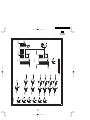
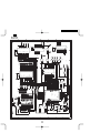
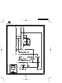
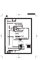
1. Hardware block diagram
Drawer X 2
Driver
CPU
FLASH ROM
+20V
H8/510
2MB
RAM Connector
MCR
G.A.
Option Display
SO-DIMM
72pin
MPCA8
PSEUDO SRAM
lsp2032
1MB
UP-P16DP or UP-I16DP
RS232 X 2
Keyboard
Driver
/
Receiver
G.A.
CKDC9
OPC2
SRN
SRN
ER-A7RS
Logic
VRAM
EDO-DRAM
512KB
ER-A7RS
VGAC
or
ER-02EF
MN89303A
Inverter
LCD Module
Power
QVGA (320 X 240)
supplay
Mono
BIAS
and
Contrast
>>>>> USE FONT <<<<<
Helvetica/ Helvetica-Condensed/ Century-Schoolbook/ Symbol & OriginalFonts: (RingWorld2/RingFont2/Pa
Symbol/PartsCod)
- - - - - - - - - - - - - - - - - - - - - - - - - - - - - - - - - - - - - - - - - - - - - - - - - - - - - - -
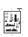
2. Description of main LSI’s
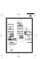
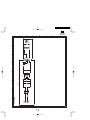
2-1. CPU (HD6415108FX)
112
111
110
109
108
107
106
105
104
103
102
101
100
99
98
97
96
95
94
93
92
91
90
89
88
87
86
85
STBY
MD2
MD1
MD0
VCC
RFSH
LWR
HWR
RD
AS
E
X
VSS
XTAL
EXTAL
VSS
TXD2
RXD2
TXD1
RXD1
SCK2/IRQ3
SCK1/IRQ2
IRQ1
IRQ0
VCC
AVCC
P73
P72
1) Pin description
84
83
82
81
80
78
78
77
76
75
74
73
72
71
70
69
68
67
66
65
64
63
62
61
60
59
58
57
29
30
31
32
33
34
35
36
37
38
39
40
41
42
43
44
45
46
47
48
49
50
51
52
53
54
55
56
1
2
3
4
5
6
7
8
9
10
11
12
13
14
15
16
17
18
19
20
21
22
23
24
25
26
27
28
A8
A9
A10
A11
A12
A13
A14
A15
VSS
A16
A17
A18
A19
A20
A21
A22
A23
VSS
P30/WAIT
P31/BACK
P32/BREQ
P33
P34
P35
P36
P37
VCC
P40
RES
NMI
VSS
P10
P11
P12
P13
P14
P15
P16
P17
D8
D9
D10
D11
D12
D13
D14
D15
VSS
A0
A1
A2
A3
A4
A5
A6
A7
P71
P70
AVSS
VSS
P67
P66
P65
P64
P63
P62
P61
P60
P57
P56
P55
P54
P53
P52
P51
P50
VSS
P47
P46
P45
P44
P43
P42
P41
P10
P11
P12
P13
P14
P15
P16
P17
D15
D14
D13
D12
D11
D10
D9
D8
2) Block diagram
P27/A23
Data bus
P26/A22
Port 1
Port 2
P25/A21
P24/A20
P23/A19
P22/A18
P21/A17
Clock
oscillator
X
Watch
dog timer
E
MD2
MD1
H8/500 CPU
A15
A14
A13
A12
A11
A10
A9
A8
A7
A6
A5
A4
A3
A2
A1
A0
Address bus
XTAL
Address bus
EXTAL
Data bus (Upper)
Data bus (Lower)
P20/A16
DTC
MD0
RES
STBY
NMI
Interruption controller
AS
P37
RD
P36
HWR
P35
16bit free running
timer x 2ch
Refresh controller
RFSH
Port 3
LWR
P34
P33
BREQ
Wait state
controller
8bit timer
A/D convertor
Serial
communication
interface x 2ch
VCC
BACK
WAIT
VCC
P47
VCC
VSS
P45
Port 4
VSS
P46
VSS
VSS
P44
P43
VSS
P42
VSS
P41/TMCI
VSS
P40
VSS
AVCC
P50
P51
P52
P53
P54
P55
P56
Port 5
P57
P67
P66
P65
P64
P63
P62
P61
P60
Port 6
P70
P71
P73
IRQ0
IRQ1
Port 7
SCK1/IRQ2
SCK2/IRQ3
RXD1
TXD1
RXD2
TXD2
Port 8
P72
AVSS
3) Pin description
/RES
Signal
name
/RESET
In/
Out
In
2
NMI
NMI
In
3
4
5
6
7
8
9
10
11
12
13
14
15
16
17
18
19
20
21
22
23
24
25
26
27
28
29
30
31
32
33
34
35
36
37
38
39
40
41
42
43
44
45
46
47
VSS
D0
D1
D2
D3
D4
D5
D6
D7
D8
D9
D10
D11
D12
D13
D14
D15
VSS
A0
A1
A2
A3
A4
A5
A6
A7
A8
A9
A10
A11
A12
A13
A14
A15
VSS
A16
A17
A18
A19
A20
A21
A22
A23
VSS
P30
GND
D0
D1
D2
D3
D4
D5
D6
D7
D8
D9
D10
D11
D12
D13
D14
D15
GND
A0
A1
A2
A3
A4
A5
A6
A7
A8
A9
A10
A11
A12
A13
A14
A15
GND
A16
A17
A18
A19
A20
A21
A22
A23
GND
/WAIT
In
I/O
I/O
I/O
I/O
I/O
I/O
I/O
I/O
I/O
I/O
I/O
I/O
I/O
I/O
I/O
I/O
In
Out
Out
Out
Out
Out
Out
Out
Out
Out
Out
Out
Out
Out
Out
Out
Out
In
Out
Out
Out
Out
Out
Out
Out
Out
In
In
48
P31
/BACK
Out
49
50
51
52
53
54
55
56
57
58
P32
P33
P34
P35
P36
P37
VCC
P40
P41
P42
/BREQ
DOPS
/DR0
/DR1
NC
NC
VCC
VCC
GND
GND
In
In
Out
Out
NC
NC
In
In
In
In
Pin
No.
1
Symbol
Function
Reset signal
Non-maskable interrupt input
for SSP interrupt input.
GND
Data bus
Data bus
Data bus
Data bus
Data bus
Data bus
Data bus
Data bus
Data bus
Data bus
Data bus
Data bus
Data bus
Data bus
Data bus
Data bus
GND
Address bus
Address bus
Address bus
Address bus
Address bus
Address bus
Address bus
Address bus
Address bus
Address bus
Address bus
Address bus
Address bus
Address bus
Address bus
Address bus
GND
Address bus
Address bus
Address bus
Address bus
Address bus
Address bus
Address bus
Address bus
GND
Wait signal
Bus control request
acknowledge signal
Bus control request signal
Drawer open signal
Option drawer open signal
Option drawer open signal
NC
NC
+5V
+5V
GND
GND
P43
P44
P45
Signal
name
GND
MCRINT
GND
In/
Out
In
In
In
62
P46
/SHEN
In
63
64
65
66
67
68
69
70
71
72
73
74
75
76
P47
VSS
P50
P51
P52
P53
P54
P55
P56
P57
P60
P61
P62
P63
GND
GND
–
–
–
–
–
NC
–
/STOP
/IPLON0
/IPLON1
GND
NORDY
In
In
Out
In
In
In
In
Out
In
Out
In
In
In
In
77
P64
FVPON
Out
78
79
80
81
82
83
84
85
86
87
88
89
90
P65
P66
P67
VSS
AVSS
P70
P71
P72
P73
AVCC
VCC
/IRQ0
/IRQ1
BANK
GND
GND
GND
GND
GND
GND
GND
GND
VCC
VCC
/IRQ0
/IRQ1
Out
In
In
In
In
In
In
In
In
In
In
In
In
91
/IRQ2
UASCK
In
92
/IRQ3
SCKI
Out
93
94
95
RXD1
TXD1
RXD2
/RCVDT2
TXD2
RXDI
In
Out
In
96
TXD2
TXDI
Out
97
VSS
GND
In
98
EXTAL
EXTAL
In
99
XTAL
XTAL
In
100
101
102
103
104
105
106
107
108
109
110
111
112
VSS
X
E
/AS
RD
/HWR
/LWR
/RFSH
VCC
MD0
MD1
MD2
/STBY
GND
#
NC
/AS
/RD
/HWR
/LWR
/RFSH
VCC
IPLON0
IPLON0
/IPLON0
VCC
In
Out
NC
Out
Out
Out
Out
Out
In
In
In
In
In
Pin
No.
59
60
61
Symbol
Function
GND
MCR interrupt signal
GND
CKDC interface shift enable
signal
GND
GND
/DTR2 : Data Terminal Ready2
/DSR2 : Data Set Ready2
/CTS2 : Clear To Send2
/DCD2 : Carriar Detect2
NC
/RTS2:Request To Send2
/CI2:Calling Indicator2
System reset output signal
From IPL SW of ER-A7RS
From IPL SW of ER-A770
GND
Flash Memory ready ("H" active)
Flash Memory write protect ("L"
active)
For IPL ROM
GND
GND
GND
GND
GND
GND
GND
GND
+5V
+5V
Interrupt signal 0
Interrupt signal 1
Synchronizing shift clock signal
for USART
CKDC interface synchronizing
shift clock
RXD signal for RS232
TXD signal for RS232
CKDC interface shift input data
CKDC interface shift output
data
GND
Crystal oscillator connection
19.6MHz
Crystal oscillator connection
19.6MHz
GND
System clock
NC
Address strobe
Read signal
Write signal (HIGH)
Write signal (LOW)
Refresh cycle signal
+5V
From IPL SW of ER-A7RS
From IPL SW of ER-A7RS
From IPL SW of ER-A7RS
+5V
2-2. G.A.(MPCA8)
160
159
158
157
156
155
154
153
152
151
150
149
148
147
146
145
144
143
142
141
140
139
138
137
136
135
134
133
132
131
130
129
128
127
126
125
124
123
122
121
RASP
RCP2
LCDWT
CLS2
RDD2
TEST2
TEST1
TEST0
STH2
SCK2
HTS2
RCP1
SLMTS
SLMTD
CLS1
RAS3
RDD1
GND
VDD
ASKRXZ
SYNC
DT8
DT9
RJMTD
RJMTS
DT5
DT6
DT7
GND
DT1
DT2
DT3
DT4
RJTMG
TPCKI
TPTXD
RAS2
ROS2Z
ROS1Z
OPTCSZ
1) Pin configuration
120
119
118
117
116
115
114
113
112
111
110
109
108
107
106
105
104
103
102
101
100
99
98
97
96
95
94
93
92
91
90
89
88
87
86
85
84
83
82
81
41
42
43
44
45
46
47
48
49
50
51
52
53
54
55
56
57
58
59
60
61
62
63
64
65
66
67
68
69
70
71
72
73
74
75
76
77
78
79
80
1
2
3
4
5
6
7
8
9
10
11
12
13
14
15
16
17
18
19
20
21
22
23
24
25
26
27
28
29
30
31
32
33
34
35
36
37
38
39
40
ID3
GND
ID4
ID5
ID6
ID7
SSPRQZ
RESETZ
INT2Z
INT3Z
RXDI
TXDI
SCKI
IRQ0Z
A0
A1
A2
A3
A4
A5
GND
VDD
A6
A7
A8
A9
A10
A11
A12
A13
A14
A15
A16
A17
A18
A19
A20
A21
A22
LCDCZ
RF
JF
PCUTZ
FCUTZ
VFZ
STAMPZ
VIOZ
VMEMZ
SWAPZ
RESZ
FROS1Z
FROMLZ
POFF
INT1Z
HTS1
SCK1
STH1
MCRINT
VWAITZ
VDD
GND
MCRINTZ
VRESC
SLTMG
SLRST
ASZ
RDZ
WRZ
PHAI
RASPN1
RASPN1E
RASPN12Z
GND
RASPN2
RASPN2E
VGALZ
SDT1Z
ID0
ID1
ID2
EXINT0Z
EXINT1Z
EXINT2Z
EXINT3Z
WROZ
RDOZ
RA15
RA16
GND
RA17
RA18
EXWAITZ
WAITZ
MCR2Z
IPLON
DAX2
DAX1
RCRXZ
IRRXZ
GND
VDD
UATXZ
UARXZ
UASCK
IRTX
RCO
RCVRDY2
RCVRDY1
TPRDY
TPTRDYZ
TPRRDYZ
TESTZ
MD0
MD1
IPLONZ
INT4Z
PRST
PTMG
TRGI
A23
2) Block diagram
MPCA8
A23-A0
IPLONZ
VMEMZ
DROS1Z
RASPN1
RASPN1E
RASPN12Z
RASPN2
RASPN2E
D0-D7
DECODE
SSP COMPARISON
REGISTER
BAR
IRTX
IRRXZ
RCRXZ
BUFFER
IR
CONTROL
ASZ
RDZ
WRZ
RDOZ
WROZ
PHAI
RESETZ
RESZ
VRESC
POFFZ
VWAITZ
EXWAITZ
TXDI
SCKI
RXDI
SERIAL
CHANNEL
SELECT
(for CKDC)
WAITZ
MCRINT
MCRINTZ
RDD1
CLS1
RCP1
MCR I/F
USART
X2
INT
CONTROL
RDD2
CLS2
RCP2
TPRDY
TPTRDYZ
TPRRDYZ
TPTXD
TPRXD
TPCKI
UASCK
UARXZ
UATXZ
DAX1
DAX2
READ
WRITE
CONTROL
WAIT
CONTROL
SSPRQZ
HTS1
SCK1
STH2
HTS2
SCK2
STH2
INT4Z
INT1Z
INT2Z
INT3Z
EXINT0Z
EXINT1Z
EXINT2Z
EXINT3Z
IRQ02
TOUCH PANEL I/F
TEST
LOGIC
USART
TESTZ
TEST0
TEST1
TEST2
MD0
MD1
3) Pin description
Pin
No.
Name
I/O
Pin
No.
Name
I/O
1
RF
ON
2
JF
ON
NU
54
IRQ0Z
O
INTERRUPT SIGNAL FOR CPU
NU
55
A0
I
3
PCUTZ
ADDRESS BUS
ON
NU
56
A1
I
4
ADDRESS BUS
FCUTZ
ON
NU
57
A2
I
ADDRESS BUS
5
VFZ
ON
NU
58
A3
I
ADDRESS BUS
6
STAMPZ
ON
NU
59
A4
I
ADDRESS BUS
7
VIOZ
O
NU
60
A5
I
ADDRESS BUS
8
VMEMZ
O
VRAM DECODE
61
GND
–
9
SWAPZ
O
NU
62
VDD
–
10
RESZ
63
A6
I
ADDRESS BUS
11
FROS1Z
O
FLASH ROM DECODE
64
A7
I
ADDRESS BUS
12
FROMLZ
O
NU
65
A8
I
ADDRESS BUS
13
POFF
IC
POWER OFF SIGNAL INPUT
66
A9
I
ADDRESS BUS
14
INT1Z
ICU
INTERRUPT SIGNAL INPUT
67
A10
I
ADDRESS BUS
15
HTS1
O
SERIAL OUT (CKDC INTERFACE)
68
A11
I
ADDRESS BUS
16
SCK1
O
SERIAL CLOCK (CKDC INTERFACE)
69
A12
I
ADDRESS BUS
17
STH1
IS
SERIAL IN (CKDC INTERFACE)
70
A13
I
ADDRESS BUS
18
MCRINT
O
MCR INTERRUPT OUT
71
A14
I
ADDRESS BUS
19
VWAITZ
IU
VGA WAIT INPUT
72
A15
I
ADDRESS BUS
20
VDD
–
73
A16
I
ADDRESS BUS
21
GND
–
74
A17
I
ADDRESS BUS
22
MCRINTZ
O
MCR INTERRUPT OUT
75
A18
I
ADDRESS BUS
23
VRESC
ON
TURNS ACTIVE WHEN
RESET&POWER DOWN IS MET
76
A19
I
ADDRESS BUS
77
A20
I
ADDRESS BUS
Description
O6M RESET
Description
24
SLTMG
ICS
GND
78
A21
I
ADDRESS BUS
25
SLRST
ICS
GND
79
A22
I
ADDRESS BUS
26
ASZ
I
ADDRESS STROBE
80
LCDCZ
O
NU
27
RDZ
I
READ STROBE
81
A23
I
ADDRESS BUS
WRITE STROBE
82
TRGI
IS
NU
SYSTEM CLOCK (9.83MHz)
83
PTMG
O
NU
84
PRST
O
NU
85
INT4Z
ICU
86
IPLONZ
IU
28
WRZ
I
29
PHAI
IS
30
RASPN1
O
PSRAM DECODE1
31
RASPN1E
O
PSRAM DECODE1 (EVEN)
32
RASPN12Z
O
PSRAM DECODE1 OR 2
INTERRUPT INPUT (SHEN2 FOR
OPTION CKDC)
IPL SIGNAL FROM OPTION
CONNECTER
33
GND
–
34
RASPAN2
O
PSRAM DECODE2
35
RASPN2E
O
PSRAM DECODE2(EVEN)
87
MD1
ICU
TEST PIN
NU
88
MD0
ICU
TEST PIN
NU
89
TESTZ
ICU
TPRRDYZ
O
NU
TPTRDYZ
O
NU
36
37
VGALZ
SDT1Z
O
O
TEST PIN
38
ID0
IO
DATA BUS
90
39
ID1
IO
DATA BUS
91
40
ID2
IO
DATA BUS
92
TPRDY
O
NU
41
ID3
IO
DATA BUS
93
RCVRDY1
IU
NU
42
GND
–
94
RCVRDY2
IU
NU
RCO
O
NU
NU
43
ID4
IO
DATA BUS
95
44
ID5
IO
DATA BUS
96
IRTX
O
DATA BUS
97
UASCK
O
USART CLOCK
UARXZ
O
NU
UATXZ
IU
NU
–
45
ID6
IO
46
ID7
IO
DATA BUS
98
47
SSPRQZ
O
SSP REQUEST FOR CPU
99
48
RESETZ
ICS
MPCA RESET
100
VDD
49
INT2Z
ICU
INTERRUPT INPUT (NU)
101
GND
–
50
INT3Z
ICU
INTERRUPT INPUT (NU)
102
IRRXZ
ICS
NU
51
RXDI
O
SERIAL OUT FOR CPU
103
RCRXZ
ICS
NU
52
TXDI
IS
SERIAL IN FROM CPU
53
SCKI
IU
SERIAL CLOCK FROM CPU
104
DAX1
OSCI IR CLOCK (7.37MHz)
Pin
No.
Name
105
DAX2
I/O
Pin
No.
Name
156
RDD2
ICS
SERIAL IN FROM MCR TRACK1
157
CLS2
ICS
CARD SENSE ON MCR TRACK1
Description
OSCO IR CLOCK (7.37MHz)
I/O
106
IPLON
O
IPLON SIGNAL
158
LCDWT
IU
107
MCR2Z
O
NU
159
RCP2
ICS
160
RASP
O
Description
NU
CLOCK PULSE FROM MCR TRACK1
108
WAITZ
O
WAIT FOR CPU
109
EXWAITZ
IU
EXTERNAL WAIT INPUT SIGNAL
110
RA18
O
NU
I
TTL input
111
RA17
O
NU
IS
TTL Schmidt input
112
GND
–
113
RA16
O
NU
IU
TTL pull up input
114
RA15
O
NU
IC
CMOS input
CMOS Schmidt input
RDOZ
O8M EXPANSION RD
ICS
116
WROZ
O8M EXPANSION WR
ICU
CMOS pull up input
117
EXINT3Z
ICS
EXPANSION INTERRUPT SIGNAL
IO
TTL I/O
118
EXINT2Z
ICS
EXPANSION INTERRUPT SIGNAL
119
EXINT1Z
ICS
EXPANSION INTERRUPT SIGNAL
115
NU
O
Output 4mA
EXPANSION INTERRUPT SIGNAL
O8M
Output 8mA
ON
Nch open drain output
OSIC
Oscillation circuit input
OSCI
Oscillation circuit output
120
EXINT0Z
ICS
121
OPTCSZ
O
BASE DECODE SIGNAL FOR
EXPANSION SLOT
122
ROS1Z
O
NU
123
ROS2Z
O
NU
124
RAS2
O
NU
125
TPTXD
O
NU
126
TPRXD
ICS
NU
127
TPCKI
ICS
NU
128
DT4
ON
NU
129
DT3
ON
NU
130
DT2
ON
NU
131
DT1
ON
NU
132
GND
–
133
DT7
ON
NU
134
DT6
ON
NU
135
DT5
ON
NU
136
RJMTS
ON
NU
137
RJMTD
ON
NU
138
DT9
ON
NU
139
DT8
ON
NU
140
SYNC
IU
NU
141
ASKRXZ
ICS
NU
142
VDD
–
143
GND
–
144
RDD1
ICS
145
RAS3
O
146
CLS1
ICS
147
SLMTD
ON
NU
148
SLMTS
ON
NU
149
RCP1
ICS
CLOCK PULSE FROM MCR TRACK1
150
HTS2
O
SERIAL OUT (OPTION CKDC
INTERFACE)
151
SCK2
O
SERIAL CLOCK (OPTION CKDC
INTERFACE)
152
STH2
IS
SERIAL IN (OPTION CKDC
INTERFACE)
153
TEST0
I
TEST PIN
154
TEST1
I
TEST PIN
155
TEST2
I
TEST PIN
SERIAL IN FROM MCR TRACK1
NU
CARD SENSE ON MCR TRACK1
41
42
43
44
45
46
47
48
49
50
51
52
53
54
55
56
57
58
59
60
61
62
63
64
65
66
67
68
69
70
71
72
73
74
75
76
77
78
79
80
SL00
SL01
SL02
SL10
SL11
SL12
SL20
SL21
SL22
SL30
SL31
SL32
/CD0
BRK0
TRNEMP0
RCVRDY0
TRNRDY0
/CTS0
RCVDT0
VCC
GND
/CI0
/RTS0
/CS0
/CD1
BRK1
TRNEMP1
RCVRDY1
TRNRDY1
/CTS1
RCVDT1
/CI1
/RTS1
/CS1
/CD2
TRNEMP2
RCVRDY2
TRNRDY2
CTS2Z
RCVDT2
/CI2
/CS2
/CD3
BRK3
TRNEMP3
RCVRDY3
TRNRDY3
/CTS3
RCVDT3
/CI3
/CS3
D0
D1
D2
D3
GND
D4
D5
D6
D7
GND
VCC
X1
X2
XOUT
TRCK
AB0
AB1
US1CH
PX
/POF
/RSRQ
/TRV
RXDATA0
TXE
/TRRQ
/TRQ1
/TRQ2
A0
A1
160
159
158
157
156
155
154
153
152
151
150
149
148
147
146
145
144
143
142
141
140
139
138
137
136
135
134
133
132
131
130
129
128
127
126
125
124
123
122
121
MCLK
RST
RSLCT1
RSLCT0
/RIN
/WIN
SYCBKD
TRNEMPD
RCVRDYD
TRNRDYD
/DSRD
/CTSD
RCVDTD
/RTSD
/DTRD
TRNDTD
/CSD
GND
VCC
SYCBKC
TRNEMPC
RCVRDYC
TRNRDYC
/DSRC
/CTSC
RCVDTC
/RTSC
/DTRC
TRNDTC
/CSC
GND
SYCBKB
TRNEMPB
RCVRDYB
TRNRDYB
/DSRB
/CTSB
RCVDTB
/RTSB
/DTRB
2-3. OPC2
1) Pin configuration
1
2
3
4
5
6
7
8
9
10
11
12
13
14
15
16
17
18
19
20
21
22
23
24
25
26
27
28
29
30
31
32
33
34
35
36
37
38
39
40
120
119
118
117
116
115
114
113
112
111
110
109
108
107
106
105
104
103
102
101
100
99
98
97
96
95
94
93
92
91
90
89
88
87
86
85
84
83
82
81
TRNDTB
/CSB
GND
SYCBKA
TRNEMPA
RCVRDYA
TRNRDYA
/DSRA
/CTSA
RCVDTA
/RTSA
/DTRA
TRNDTA
/CSA
UTST
DBTST
RCVCLK
TRNCLK
RES
GND
VCC
/W
/R
DB7
DB6
DB5
DB4
GND
DB3
DB2
DB1
DB0
/RES
/WR
/RD
/OPTCS
A5
A4
A3
A2
2) Block diagram
OPC2
OPC1
DATA BUS
OPC1~USART
BAUD RATE GENERATOR
BAUD RATE GENERATOR
USART
USART
USART
USART
A
B
C
D
USART
Common input
3) Pin description
Pin
NO.
1
2
3
4
5
6
7
8
9
10
11
12
Name
ER-A770
I/O
SL00
SL01
SL02
SL10
SL11
SL12
SL20
SL21
SL22
SL30
SL31
SL32
VCC
GND
GND
GND
GND
GND
GND
GND
GND
GND
GND
GND
ISU
ISU
ISU
ISU
ISU
ISU
ISU
ISU
ISU
ISU
ISU
ISU
13
/CD0
/DCD1
IS
14
BRK0
BRK1
IS
15
TRNEMP0
TRENMP1
IS
16
RCVRDY0
RCVRDY1
IS
17
TRNRDY0
TRNRDY1
IS
18
/CTS0
/CTS1
IS
19
RCVDT0
RCVDT1
IS
20
21
VCC
GND
VCC
GND
22
/CI0
/CI1
IS
23
/RTS0
/RTS1
O
Description
RS-232/UNIT0
channel select
RS-232/UNIT1
channel select
RS-232/UNIT2
channel select
RS-232/UNIT3
channel select
RS-232 control
signal /CD input
RS-232 break signal
RS-232 transmission
buffer empty signal
RS-232 data
reception enable
signal
RS-232 transmission
enable signal
RS-232 clear to send
signal
RS-232 reception
data signal
+5V
GND
RS-232 control
signal /CI input
RS-232 request to
send signal
Pin
NO.
Name
ER-A770
I/O
24
/CS0
/CS1
O
25
/CD1
/DCD2
IS
26
27
28
29
30
BRK1
TRNEMP1
RCVRDY1
TRNRDY1
/CTS1
BRK2
TRENMP2
RCVRDY2
TRNRDY2
/CTS2
IS
IS
IS
IS
IS
31
RCVDT1
RCVDT2
IS
32
/CI1
/CI2
IS
33
/RTS1
/RTS2
O
34
/CS1
/CS2
O
35
36
37
38
39
40
41
42
/CD2
TRNEMP2
RCVRDY2
TRNRDY2
CTS2Z
RCVDT2
/CI2
/CS2
VCC
TRENMP3
RCVRDY3
TRNRDY3
/CTS3
RCVDT3
VCC
/CS3
IS
IS
IS
IS
IS
IS
IS
O
43
/CD3
/SINT
IS
44
45
46
47
BRK3
TRNEMP3
RCVRDY3
TRNRDY3
GND
GND
GND
GND
IS
IS
IS
IS
Description
RS-232 chip select
signal
RS-232 control
signal /CD input
GND
GND
GND
GND
+5V
RS-232 reception
data signal
RS-232 control
signal /CI input
RS-232 request to
send signal
RS-232 chip select
signal
+5V
GND
GND
GND
+5V
GND
+5V
NU
RS-232: /CD,
IN-LINE : /P1
GND
GND
GND
GND
Pin
NO.
48
49
50
Name
ER-A770
I/O
/CTS3
RCVDT3
/CI3
GND
GND
GND
IS
IS
IS
51
/CS3
52
53
54
55
56
57
58
59
60
61
62
63
64
65
66
D0
D1
D2
D3
GND
D4
D5
D6
D7
GND
VCC
X1
X2
XOUT
TRCK
67
AB0
68
AB1
69
70
71
72
73
74
US1CH
PX
/POF
/RSRQ
/TRV
RXDATA0
75
TXE
76
/TRRQ
77
/TRQ1
78
/TRQ2
79
80
81
82
83
84
A0
A1
A2
A3
A4
A5
85
/OPTCS
86
/RD
87
/WR
88
/RES
89
90
91
92
93
94
95
96
DB0
DB1
DB2
DB3
GND
DB4
DB5
DB6
Description
GND
GND
GND
RS-232/INLINE chip
/SRCS
O
select signal
D0
IO
Data bus (CPU)
D1
IO
Data bus (CPU)
D2
IO
Data bus (CPU)
D3
IO
Data bus (CPU)
GND
GND
D4
IO
Data bus (CPU)
D5
IO
Data bus (CPU)
D6
IO
Data bus (CPU)
D7
IO
Data bus (CPU)
GND
GND
VCC
+5V
NC
O OSI14 NC
#
I OSI14 System clock
CLK_USART
O
Clock (USART)
NC
O
NC
Address bus for
AH0
O
USART
Address bus for
AH1
O
USART
GND
IS
GND
NC
O
NC
/POFF
IS
POFF signal
/IRQ1
3S
RS232 INTERRUPT
GND
IS
GND
NC
O
NC
INLINE SOFT
/SRESET
O
RESET
/TRQ2
3S
INLINE INTERRUPT
TIMER INTERRUPT
/TRQ1
ON6
(RS232)
TIMER INTERRUPT
NC
ON6
(INLINE)
A0
I
Address bus for CPU
A1
I
Address bus for CPU
A2
I
Address bus for CPU
A3
I
Address bus for CPU
A4
I
Address bus for CPU
A5
I
Address bus for CPU
Option chip select
/OPTCS
I
(from MPCA)
Read signal (from
/RDO
I
CPU)
Write signal (from
/WRO
I
CPU)
Reset signal (from
/RES
IS
CPU)
DB0
IO
DATA BUS (USART)
DB1
IO
DATA BUS (USART)
DB2
IO
DATA BUS (USART)
DB3
IO
DATA BUS (USART)
GND
GND
DB4
IO
DATA BUS (USART)
DB5
IO
DATA BUS (USART)
DB6
IO
DATA BUS (USART)
Pin
NO.
97
Name
ER-A770
I/O
Description
DB7
DB7
IO
98
/R
/RDH
O
99
/W
/WRH
O
100
101
VCC
GND
VCC
GND
102
RES
RES USART
O
103
104
TRNCLK
RCVCLK
GND
GND
I
I
105
DBTST
/SRCS
ID
106
UTST
VCC
ID
107
/CSA
/CS1
IS
108
TRNDTA
TXD1
O
109
/DTRA
/DTR1
O
110
/RTSA
NC
O
111
RCVDTA
RCVDT1
IS
112
/CTSA
GND
IS
113
/DSRA
/DSR1
IS
114
TRNRDYA
TRNRDY1
O
115
RCVRDYA
RCVRDY1
O
116
TRNEMPA
TRNEMP1
O
117
SYCBKA
BRK1
IO
118
119
120
121
122
123
124
125
126
127
128
129
130
131
132
133
134
135
136
137
138
139
140
141
GND
/CSB
TRNDTB
/DTRB
/RTSB
RCVDTB
/CTSB
/DSRB
TRNRDYB
RCVRDYB
TRNEMPB
SYCBKB
GND
/CSC
TRNDTC
/DTRC
/RTSC
RCVDTC
/CTSC
/DSRC
TRNRDYC
RCVRDYC
TRNEMPC
SYCBKC
GND
/CS2
TXD2
/DTR2
NC
RCVDT2
GND
/DSR2
TRNRDY2
RCVRDY2
TRNEMP2
BRK2
GND
/CS3
TXD3
/DTR3
/RTS3
RCVDT3
GND
/DSR3
TRNRDY3
RCVRDY3
TRNEMP3
NC
DATA BUS (USART)
Read signal (to
USART)
Write signal (to
USART)
+5V
GND
Reset signal (to
USART)
GND
GND
RS-232/INLINE
USART chip select
+5V
USART_A chip
select
RS-232 transmission
data signal
RS-232 data
terminal ready signal
NC
RS-232 reception
data signal
GND
RS-232 data set
ready signal
RS-232 data
transmission enable
signal
RS-232 data
reception enable
signal
RS-232 transmission
buffer empty signal
Break code detection
signal
GND
USART_B chip select
NC
NC
NC
GND
GND
GND
NC
NC
NC
NC
GND
USART_C chip select
NC
NC
NC
GND
GND
GND
NC
NC
NC
NC
IS
O
O
O
IS
IS
IS
O
O
O
IO
IS
O
O
O
IS
IS
IS
O
O
O
IO
Pin
NO.
142
143
144
145
146
147
148
149
150
151
152
153
154
155
156
157
158
159
160
Name
ER-A770
VCC
GND
/CSD
TRNDTD
/DTRD
/RTSD
RCVDTD
/CTSD
/DSRD
TRNRDYD
RCVRDYD
TRNEMPD
SYCBKD
/WIN
/RIN
RSLCT0
RSLCT1
RST
MCLK
VCC
GND
VCC
NC
NC
NC
GND
GND
GND
NC
NC
NC
NC
/WRH
/RDH
AH0
AH1
RES USART
CLK USART
I/O
Description
IS
O
O
O
IS
IS
IS
O
O
O
IO
I
I
I
I
IS
I
+5V
GND
+5V
NC
NC
NC
GND
GND
GND
NC
NC
NC
NC
Write signal
Read signal
Address bus
Address bus
Reset signal
Clock (4.91MHz)
M1
I
TTL input
ID
TTL input with pull down
IS
TTL Schmidt input
ISU
TTL Schmidt input with pull up
IO
TTL I/O
3S
3-state Buffer (6mA)
ON6
Open drain (6mA)
A1
SYSTEM
CONTROL
The extensive instruction set contains 158 instructions, including the
8080A instruction set as a subset.
• NMOS version for low cost high performance solutions, CMOS
version for high performance low power designs.
• Z0840006 - 6.17 MHz
• CMOS Z84C0006 - DC to 6.17 MHz, Z84C008 - DC to 8 MHz,
Z84C0010 - DC to 10 MHz, Z84C0020 - DC - 20 MHz
• 6 MHz version can be operated at 6.144 MHz clock.
• The Z80 microprocessors and associated family of peripherals can
be linked by a vectored interrupt system. This system can be
daisy-chained to allow implementation of a priority interrupt
scheme.
• Duplicate set of both general-purpose and flag registers.
• Two sixteen-bit index registers.
• Three modes of maskable interrupts:
Mode 0 — 8080A similar;
Mode 1 — Non-Z80 environment, location 38H;
Mode 2 — Z80 family peripherals, vectored interrupts.
• On-chip dynamic memory refresh counter.
MREQ
IORQ
RD
A2
WR
A5
A3
A4
A6
RFSH
ADDRESS
BUS
A7
A8
HALT
A9
A10
WAIT
CPU
CONTROL
INT
NMI
Z8400
Z80 CPU
A11
A12
A13
A14
A15
RESET
D0
CPU
BUS
CONTROL
BUSREQ
D1
BUSACK
D2
D3
CLK
+5V
GND
DATA
BUS
D4
D5
D6
D7
Figure 1. Pin functions
2) Pin configuration
44
2-4. Z80 CPU
1) Features
A0
34
1
33
CLK
D4
D3
D5
D6
+5V
D2
D7
D0
D1
NC
NC
A5
A4
A3
A2
A1
A0
GND
RFSH
M1
RESET
Z80 CPU
11
23
12
22
44Pin Quad Flat Pack (QFP), Pin Assignments
(Only available for 84C00)
3) General description
Pin
No.
The CPUs are fourth-generation enhanced microprocessors with exceptional computational power. They offer higher system throughput
and more efficient memory utilization than comparable second- and
third-generation microprocessors. The internal registers contain 208
bits of read/write memory that are accessible to the programmer.
These registers include two sets of six general-purpose registers
which may be used individually as either 8-bit registers or as 16-bit
register pairs. In addition, there are two sets of accumulator and flag
registers. A group of "Exchange" instructions makes either set of
main or alternate registers accessible to the programmer. The alternate set allows operation in foreground/background mode or it may
be reserved for very fast interrupt response.
The CPU also contains a Stack Pointer, Program Counter, two index
registers, a Refresh register (counter), and an Interrupt register. The
CPU is easy to incorporate into a system since it requires only a
single +5V power source. All output signals are fully decoded and
timed to control standard memory or peripheral circuits; the CPU is
supported by an extensive family of peripheral controllers.
The internal block diagram (Figure 3) shows the primary functions of
the processors. Subsequent text provides more detail on the I/O controller family, registers, instruction set, interrupts and daisy chaining,
and CPU timing.
8-BIT
DATA BUS
DATA BUS
INTERFACE
INSTRUCTION
DECODER
INSTRUCTION
INTERNAL DATA BUS
REGISTER
ALU
+5V
GND
REGISTER
ARRAY
CLOCK
CPU
TIMING
CONTROL
Symbol
Signal
name
In/Out
Function
18
RD
S RDS
Out
Rread signal
19
WR
S WRS
Out
Write signal
20
BUSAK
BUSAK
Out
Bus acknowledge signal
21
WAIT
S WAIT
In
Wait signal
22
BUSRQ
BUSRQ
In
Bus request signal
23
RESET
S RES
In
Reset signal
24
M1
S M1
Out
Machine cycle one signal
25
RFSH
NC
—
NC
26
GND
GND
—
GND
27
A0
S A0
Out
Address bus
28
A1
S A1
Out
Address bus
29
A2
S A2
Out
Address bus
30
A3
S A3
Out
Address bus
31
A4
S A4
Out
Address bus
32
A5
S A5
Out
Address bus
33
NC
NC
—
NC
34
A6
S A6
Out
Address bus
35
A7
S A7
Out
Address bus
36
A8
S A8
Out
Address bus
37
A9
S A9
Out
Address bus
38
A10
S A10
Out
Address bus
39
NC
NC
—
NC
40
A11
S A11
Out
Address bus
42
A13
S A13
Out
Address bus
43
A14
S A14
Out
Address bus
44
A15
S A15
Out
Address bus
2-5. Z80 CTC
CPU
TIMING
1) Features
ADDRESS
LOGIC AND
BUFFERS
5 CPU
8 SYSTEMS
AND CPU CONTROL
CONTROL INPUTS
OUTPUTS
16-BIT
ADDRESS BUS
Figure 3. Z80C CPU Block Diagram
• Four independently programmable counter/timer channels, each
with a readable downcounter and a selectable 16 or 256 prescaler.
Downcounters are reloaded automatically at zero count.
• Selectable positive or negative trigger initiates timer operation.
• Three channels have Zero Count/Timeout outputs capable of driving Darlington transistors. (1.5mV @ 1.5V)
4) Pin description
•
•
•
•
NMOS version for cost sensitive performance solutions.
CMOS version for the designs requiring low power consumption
Pin
No.
Symbol
Signal
name
In/Out
1
CLK
CLK
In
2
D4
S D4
In/Out
Data bus
3
D3
S D3
In/Out
Data bus
4
D5
S D5
In/Out
Data bus
5
D6
S D6
In/Out
Data bus
6
+5V
VCC
—
7
D2
S D2
In/Out
Data bus
8
D7
S D7
In/Out
Data bus
• 6 MHz version supports 6.144 MHz CPU clock operation.
9
D0
S D0
In/Out
Data bus
2) General description
10
D1
S D1
In/Out
Data bus
11
NC
NC
—
NC
12
INT
S INT
In
Interrupt request signal
13
NMI
VCC
—
Non-maskable interrupt
signal
The Z80 CTC, hereinafter referred to as Z80 CTC or CTC, four-channel counter/timer can be programmed by system software for a broad
range of counting and timing applications. The four independently
programmable channels of the Z80 CTC satisfy common microcomputer system requirements for event counting, interrupt and interval
timing, and general clock rate generation.
System design is simplified because the CTC connects directly to
both the Z80 CPU and the Z80 SIO with no additional logic. In larger
systems, address decoders and buffers may be required.
Function
Clock
+5V
14
HALT
VCC
—
+5V
15
MREQ
S MRQ
Out
Memory request signal
16
IORQ
S IORQ
Out
Input / Output request signal
17
NC
NC
—
NC
NMOS Z0843004 - 4 MHz, Z0843006 - 6.17 MHz.
CMOS Z84C3006 - DC to 6.17 MHz, Z84C3008 - DC to 8 MHz,
Z84C3010 - DC to 10 MHz
• Interfaces directly to the Z80 CPU or—for baud rate generation—
to the Z80 SIO.
• Standard Z80 Family daisy-chain interrupt structure provides fully
vectored, prioritaized interrupts without external logic. The CTC
may also be used as an interrupt controller.
D0
CLK/TRG0
D1
ZC/TO0
D2
CPU
DATA
BUS
D3
CLK/TRG1
D4
ZC/TO1
D5
D6
CLK/TRG2
D7
ZC/TO2
CHANNEL
SIGNALS
CE
CLK/TRG3
CS0
CTC
CONTROL
FROM
CPU
CS1
M1
RESET
IORQ
RD
DAISY
CHAIN
INTERRUPT
CONTROL
Z80 CTC
IEI
IEO
INT
CLK
+5V
GND
Figure 1. Pin Functions
Programming the CTC is straightforward: each channel is programmed with two bytes: a third is necessary when interrupts are
enabled. Once started, the CTC counts down, automatically reloads
its time constant, and resumes counting. Software timing loops are
completely eliminated. Interrupt processing is simplified because only
one vector need be specified: the CTC internally generates a unique
vector for each channel.
The Z80 CTC requires a single +5% V power supply and the standard
Z80 single-phase system clock. It is packaged in 28-pin DIPs, a 44pin plastic chip carrier, and a 44-pin Quad Flat Pack. (Figures 2a, 2b,
and 2c). Note that the QFP package is only available for CMOS
versions.
3) Pin configuration
33
23
34
22
NC
IEO
CSI
IORQ
CLK/TRG3
NC
CLK/TRG2
ZC/TO2
NC
ZC/TO1
CMOS
Z80 CTC
NC
CLK/TRG1
NC
ZC/TO0
CLK/TRG0
NC
NC
RD
+5V
GND
NC
D7
44
12
1
11
Figure 2c. 44-pin Quad Flat Pack Pin Assignments
4) Functional description
The Z80 CTC has four independent counter/timer channels. Each
channel is individually programmed with two words: a control word
and a time-constant word. The control word selects the operating
mode (counter or timer), enables or disables the channel interrupt,
and selects certain other operating parameters. If the timing mode is
selected, the control word also sets a prescaler, which divides the
system clock by either 16 or 256. The time-constant word is a value
from 1 to 256.
During operation, the individual counter channel counts down from
the preset time constant value. In counter mode operation the counter
decrements on each of the CLK/TRG input pulses until zero count is
reached. Each decrement is synchronized by the system clock. For
counts greater than 256, more than one counter can be cascaded. At
zero count, the down-counter is automatically reset with the time
constant value.
The timer mode determines time intervals as small as 2 µs (8 MHz), 3
µs (6 MHz), or 4 µs (4 MHz) without additional logic or software timing
loops. Time intervals are generated by dividing the system clock with
a prescaler that decrements a preset down-counter.
Thus, the time interval is an integral multiple of the clock period, the
prescaler value (16 or 256), and the time constant that is preset in the
down-counter. A timer is triggered automatically when its time constant value is programmed, or by an external CLK/TRG input.
Three channels have two outputs that occur at zero count.
The first output is a zero-count/timeout pulse at the ZC/TO output.
The fourth channel (Channel 3) does not have a ZC/TO output;interrupt request is the only output available from Channel 3.
The second output is Interrupt Request (INT), which occurs if the
channel has its interrupt enabled during programming. When the Z80
CPU acknowledges Interrupt Request, the Z80 CTC places an interrupt vector on the data bus.
The four channels of the Z80 CTC are fully prioritized and fit into four
configuous slots in a standard Z80 daisy-chain interrupt structure.
Channel 0 is the highest priority and Channel 3 the lowest. Interrupts
can be individually enabled (or disabled) for each of the four channels.
5) Pin description
Pin
No.
1
2
3
4
5
6
7
8
10
11
12
13
14
15
16
17
18
19
20
21
22
23
24
25
26
27
28
29
30
31
32
33
34
Symbol
D0
D1
D2
D3
NC
NC
NC
D4
D6
NC
D7
GND
RD
NC
ZC/TO0
NC
ZC/TO1
ZC/TO2
NC
IORQ
IEO
INT
NC
IEI
NC
M1
NC
CLK
NC
CE
RESET
CS0
NC
Signal
name
S D0
S D1
S D2
S D3
NC
NC
NC
S D4
S D6
NC
S D7
GND
S RDS
NC
S TM0
NC
NC
NC
NC
S IORQ
NC
S INT
NC
VCC
NC
S M1
NC
CLK
NC
S A6
S RES
S A0
NC
In/Out
Function
In/Out
In/Out
In/Out
In/Out
—
—
—
In/Out
In/Out
—
In/Out
—
In
—
Out
—
—
—
—
In
—
Out
—
—
—
In
—
In
—
In
In
In
—
Data bus
Data bus
Data bus
Data bus
NC
NC
NC
Data busj*9
Data bus
NC
Data bus
GND
Read cycle status signal
NC
Zero count / Timeout signal
NC
NC
NC
NC
Input / Output request signal
NC
Interrupt request signal
NC
+5V
NC
Machine cycle one signal
NC
System clock
NC
Chip enable signal
Reset signal
Channel select signal
NC
Pin
No.
35
36
37
38
39
40
41
42
43
44
Symbol
CS1
CLK/TRG3
CLK/TRG2
NC
NC
CLK/TRG1
CLK/TRG0
NC
+5V
NC
Signal
name
S A1
S TM1
S TM0
NC
NC
S INTS
VCC
NC
VCC
NC
In/Out
In
In
In
—
—
In
In
—
—
—
3) Pin configuration
Function
Channel select signal
External clock / timer signal
External clock / timer signal
NC
NC
External clock / timer signal
+5V
NC
+5V
NC
Pin
No.
Symbol
Signal
name
In/
Out
1
READY
READY
In
2
HLDAK
HLDAK
In
3
ASTB
S ASTB
Out
Address strobe signal
Function
Ready signal
Hold acknowledge signal
4
AEN
S AEN
Out
Address enable signal
5
HLDRQ
HLDRQ
Out
Hold request signal
6
NC
NC
—
NC
7
CS
CS
In
Chip select signal
8
CLK
CLK
In
Clock
2-6. µPD71037
9
RESET
SRNRESET
In
Reset signal
10
DMAAK2
S DACK2
Out
DMA CONTROLLER
11
DMAAK3
S DACK3
Out
The µPD71037 is a direct memory access controller (DMAC) for the
micro processor system. It provides higher processing speed and
lower power consumption in comparison with those in conventional
use. Each of the four built-in DMA channels has 64-KB addresses
and the function of counting the number of bytes of transferred data,
and can transfer data from I/O to memory and from memory to memory as well.
12
DMARQ3
S DRQ3
In
DMA request signal
13
DMARQ2
S DRQ2
In
DMA request signal
14
DMARQ1
S DRQ1
In
DMA request signal
15
DMARQ0
S DRQ0
In
DMA request signal
16
GND
GND
—
GND
17
NC
NC
—
NC
18
A15/D7
S D7
In/Out Data bus
19
A14/D6
S D6
In/Out Data bus
20
A13/D5
S D5
In/Out Data bus
21
DMAAK1
S DACK1
Out
DMA acknowledge signal
22
DMAAK0
S DACK0
Out
DMA acknowledge signal
Each channel can be self-initialized.
23
A12/D4
S D4
In/Out Data bus
Data is transferrable from memory to memory.
24
A11/D3
S D3
In/Out Data bus
Data in memory can independently initialized by block.
25
A10/D2
S D2
In/Out Data bus
High speed data transfer:
26
A9/D1
S D1
In/Out Data bus
27
A8/D0
S D0
In/Out Data bus
28
NC
NC
—
NC
29
VDD
VCC
—
+5V
(Expansion mode).
30
A0
S A0
In
Address bus
END input when data transfer is finished.
31
A1
S A1
In
Address bus
32
A2
S A2
In
Address bus
33
A3
S A3
In
Address bus
34
NC
NC
—
NC
35
END / TC
TC
36
A4
S A4
In
Address bus
37
A5
S A5
In
Address bus
38
A6
S A6
In
Address bus
In
Address bus
1) FEATURES
• The clock speed is 10 MHz, twice that of the µPD8237A-5 (clock
speed of 5 MHz).
•
•
•
•
•
•
Each of the four DMA channels can be operated independently.
3.2 MB/sec. (clock seed of 10 MHz, normal transfer mode)
5.0 MB/sec. (clock speed of 10 MHz, compression transfer mode)
• The number of DMA channels can directly be expanded
•
•
•
•
Software DMA request available.
CMOS
Low power consumption.
2) Pin configuration
A7
S A7
IORD
S IOR
In/Out I/O read signal
In/Out I/O write signal
41
IOWR
S IOW
42
MRD
S MRD
Out
MWR
NC
—
NC
NC
NC
—
NC
33
A3
HLDAK
2
32
A2
43
ASTB
3
31
A1
44
4
30
A0
5
29
VDD
NC
6
28
NC
CS
7
27
A8/D0
CLK
8
26
A9/D1
RESET
9
25
A10/D2
DMAAK2
10
24
A11/D3
DMAAK3
11
23
A12/D4
µPD71037GB-3B4
In/Out End / Terminal cut signal
40
1
AEN
DMA acknowledge signal
39
READY
HLDRQ
DMA acknowledge signal
Memory read signal
(a) I/O address generation circuit
2-7. MB62H149
1) Outline
The MB62H149 is a semi-custom LSI chip for the peripheral circuits
in the SRN (SHARP Retail Network), its main function is to communicate data with the host CPU and control the peripheral circuits and
transmission control circuits of the Sub CPU (Z-80). Fig. 2. shows the
general configuration of the functions:
Line
SUB-CPU
(Z-80)
DMAC
TIMER
COUNTER
ADLC
HOST CPU
DATA HAND
SHAKING
CIRCUIT
PERIPHERAL
CIRCUIT
TRANSMISSION
CONTROL
CIRCUIT
A total of 11 I/O addresses are generated by A0, A1, A4, A5 and
RD and WR signals.
(b) CPU and DMAC wait signal control unit
Clocks into the CPU (Z-80), SUB CPU and its peripheral LSI,
DMAC and CTC are operated respectively on 4 MHz.
While, the ADLC (MC68B54) (Advanced Data Link Control) is
operated by the E (Enable clock) of 2 MHz according to restrictions in terms of the hardware of the LSI.
It is necessary to synchronize the timing of the write and read in
the ADLC.
To control synchronization, timing, and input, the wait signal goes
into the CPU for CPU access and into the DMAC for DMA access.
This block is a circuit to generate such wait signal.
(c) Clock dividing circuit
MB62H149
Fig. 2
2) Internal functions
This block divides the blocks according to the CLK supplied from
outside to generate the clock for CPU, DMAC and CTC and the E
and transmission clock rate (480 KBPS or 1 MBPS selectable) for
the ADLC.
(1) Data handshaking circuit
(3) Transmission control circuit
Is used because data processing speeds vary and the timing of the
HOST CPU and SUB CPU do not synchronize, the MB62H149 is
used for data handshaking. When the data handshaking portion is
broken down, the system consists of a Write Signal from the HOST
CPU to the MB62H149, Read Signal from the MB62H149 of the SUB
CPU, Write Signal from the SUB CPU to the MB62H149 and Read
Signal from the MB62H149 of the HOST CPU, all of which from two
blocks as shown.
The transmission control circuit is divided into the modem unit, carrier
detect unit, collision detect unit.
HOST CPU
HOST CPU
Write
MB62H149
Read
MB62H149
Read
Write
ADLC TDY
ADLC RDX
Collision detect
SUB CPU
(HOST CPU TO SUB CPU)
Carrier detect 1
(for data)
SUB CPU
(FROM SUB CPU TO HOST CPU)
Carrier detect 2
(for resronse)
To transmission driver
MODEM unit
From transmission receiver
Collision
detect unit
Carrier
detect unit
Fig. 3
Fig. 6
HOST CPU
DATA BUS
(8bit)
HOST CPU
write register
(SUB CPU
read register)
SUB CPU
write register
(HOST CPU
read register)
HOST CPU address
and RD, WR
HOST CPU
address
decode
(a) Modem circuit
SUB CPU
DATA BUS
(8bit)
HOST CPU
write & SUB
CPU read
control unit
(DMA & CPU
access)
The transmission data input from the ADLC are PE modulated
(phase encoding modulation), the circuit to be output to the transmission driver and the reception data input from the transmission
receiver are demodulated and produced at the ADLC.
(b) Collision detect circuit
HOST CPU · SUB CPU
& DMAC control
SUB CPU
write & HOST
CPU read control
unit (DMA &
CPU access)
(c) Carrier detect circuit
Fig. 4
(2) Peripheral circuit
The peripheral circuit consists of an I/O address generation unit on
the SUB CPU, block dividing circuit, and the wait signal control unit.
SUB CPU address
& RD, WR
The data transmitted from the home station is received and detects a collision on the transmission line by means of an exclusive
OR gate.
SUB CPU address
decoding unit
I/O address
CPU & DMAC wait
signal control unit
Wait signal
This circuit detects whether data is flowing on the transmission
line. It consists of a circuit which immediately senses a no data
status on the line. When data is not on the line the circuit functions
to sense an elapse of the fixed time rate. The immediate sensing
circuit is used for response testing and the delayed sensing circuit
is used for data testing.
The fixed time rate is selectable according to the transmission
speed as shown below via SRV-mode programming. Job #922.
Transmission speed
CLK (16 MHz)
Clock dividing
circuit
Fig. 5
System clock
(4 MHz)
Delay time
1 MBPS
1.6m sec, 3.2m sec, 4.8m sec, 6.4m sec.
480 KBPS
3.2m sec, 6.4m sec, 9.6m sec, 12.8m sec.
3) Terminal Name and Description (MB62H149)
23.9 ± 0. 6
20
41
64
14
17.9 ± 0.4
40
65
INDEX
80
25
LEAD
1
NO
0.8 ± 0.15
0.35 ±
0.1
24
Fig. 7
Pin
No.
1
2
3
4
5
6
7
8
9
10
11
12
13
14
16
17
18
19
20
21
22
23
24
25
26
27
28
29
30
31
32
33
34
35
36
37
38
39
40
Terminal
name
CLK
—
IORQ
MREQ
RDS
WRS
INTS
φ
TM0
TM1
MRD
VSS
WAIT
A15
A9
A8
A5
A4
A1
A0
DAK01
—
MWR0
D7
D6
D5
D4
D3
D2
D1
D0
VDD
—
RES
IO/WR
IO/RD
AEN
AST
TCS
Host/
Sub
Sub
—
Sub
Sub
Sub
Sub
Sub
Sub
Sub
Sub
Sub
—
Sub
Sub
Sub
Sub
Sub
Sub
Sub
Sub
Sub
—
Sub
Sub
Sub
Sub
Sub
Sub
Sub
Sub
Sub
—
—
Host
Sub
Sub
Sub
Sub
Sub
In/
Out
In
—
In
In
In
In
Out
Out
In
Out
Out
—
Out
Out
Out
Out
In
In
In
In
In
—
Out
I/O
I/O
I/O
I/O
I/O
I/O
I/O
I/O
—
—
In
I/O
I/O
In
In
In
Description
Clock in (16 MHz)
N.U.
I/O request
Memory request
Read from sub
Write from sub
Interrupt to sub
Clock out
Timer 0
Timer 1
Memory read
GND
Wait signal
Address bus for DMA
DMA acknowledge 0+1
N.U.
Memory write
Data bus
+5V
N.U.
Reset
I/O write
I/O read
Address enable from DMAC
Address strobe from DMAC
Terminal count
Pin
No.
41
42
43
44
45
46
47
48
49
50
51
52
53
54
55
56
57
58
59
60
61
62
63
64
65
66
67
68
69
70
71
72
73
74
75
76
77
78
79
80
Terminal
name
DAK23
DRQRS
DRQWS
RDH
WRH
INTH
DAK
TCH
DRQWH
DRQWH
CS
VSS
—
DB0
DB1
DB2
DB3
DB4
DB5
DB6
DB7
AB0
—
AB1
COL
RDI
TDI
RTS
RXC
RXD
TXC
TXD
VDD
E
IRQ
LCS
—
RS1
RS0
MSK
Host/
Sub
Sub
Sub
Sub
Host
Host
Host
Host
Host
Host
Host
Host
—
—
Host
Host
Host
Host
Host
Host
Host
Host
Host
—
Host
Sub
Sub
Sub
Sub
Sub
Sub
Sub
Sub
—
Sub
Sub
Sub
—
Sub
Sub
Sub
In/
Out
In
Out
Out
In
In
Out
In
In
Out
Out
In
—
—
I/O
I/O
I/O
I/O
I/O
I/O
I/O
I/O
In
—
In
In
In
Out
In
Out
Out
Out
In
—
In
In
Out
—
Out
Out
Out
Description
DMA acknowledge 2+3
DMA request read to sub
DMA request write to sub
Read from Host
write from Host
Interrupt to host
DMA acknowledge from host
Terminal count from host
DMA request read to host
DMA request write to host
Chip select from host
GND
N.U.
Data bus
Data bus
Data bus
Data bus
Data bus
Data bus
Data bus
Data bus
Address bus from host
N.U.
Address bus from host
Collision detect signal
Receive data from receiver
Transmmit data to driver
Request to send
Receive clock to ADLC
Receive data to ADLC
Transmmit clock
Transmmit data
+5V
Enable clock to ADLC
Interrupt request from ADLC
Link controller chip select
N.U.
Register select 1
Register select 0
Mask signal
2-8. VGA controller (MN89303A)
128
127
126
125
124
123
122
121
120
119
118
117
116
115
114
113
112
111
110
109
108
107
106
105
104
103
102
101
100
99
98
97
XO
GND
MINTEST
TEST
RESET
VDD
GND
MD0
MD1
MD2
MD3
MD4
MD5
MD6
MD7
MD8
MD9
VDD
GND
MD10
MD11
MD12
MD13
MD14
MD15
/WE
/LCAS
/UCAS
/RAS
VDD
GND
MA0
1) Pin Configuration
1
2
3
4
5
6
7
8
9
10
11
12
13
14
15
16
17
18
19
20
21
22
23
24
25
26
27
28
29
30
31
32
96
95
94
93
92
91
90
89
88
87
86
85
84
83
82
81
80
79
78
77
76
75
74
73
72
71
70
69
68
67
66
65
GND
VDD
SD15
SD14
SD13
SD12
GND
SD11
SD10
SD9
VDD
SD8
SD7
SD6
GND
SD5
SD4
SD3
SD2
SD1
SD0
GND
VDD
IOCHRDY
/MEMCS16
/IOCS16
GND
VDD
DCLK
DISP
LP
FP
33
34
35
36
37
38
39
40
41
42
43
44
45
46
47
48
49
50
51
52
53
54
55
56
57
58
59
60
61
62
63
64
XIN
GND
AEN
/SBEH
/IOWR
/IORD
/SMEMW
/SMEMR
A21
A20
SA19
SA18
SA17
SA16
SA15
SA14
SA13
SA12
SA11
SA10
SA9
SA8
SA7
SA6
SA5
SA4
SA3
SA2
SA1
SA0
/BIOSEN
/REFRESH
2) Block diagram
Gray scale
engine
RAM table
Hardware
cursor
UD[7:0]
LD[7:0]
BACKON
LCDON
83
84
LOGICON
85
LP
63
FO
DISP
DCLK
XIN
RESET
TEST/MINTEST
LCD panel
controller
Attributer
64
62
61
Video FIFO
1
124
LCD/CRT
controller
126/125
ADDRESS[21:0]
SD[15:0]
MA[9:0]
AEN
3
SBHE
4
IOWR
5
IORD
6
SMEMW
SMEMR
IOCHRDY
REFRESH
MEMCS16
IOCS16
7
8
56
32
57
58
Mmory
interface
Host
interface
Memory
write
buffer
100
Access
attributer
101
Graphics
controller
103
102
31
MD[15:0]
RAS
UCAS
LCAS
WE
BIOSEN
MA1
MA2
MA3
MA4
MA5
MA6
MA7
MA8
MA9
VDD
GND
LOGICON
LCDON
BACKON
LD0
LD1
LD2
LD3
LD4
LD5
LD6
LD7
VDD
GND
UD0
UD1
UD2
UD3
UD4
UD5
UD6
UD7
3) Pin configuration
Pin
No.
1
2
3
4
5
6
7
8
9
10
11
12
13
14
15
16
17
18
19
20
21
22
23
24
25
26
27
28
29
30
31
32
33
34
35
36
37
38
39
40
41
42
43
44
45
46
47
48
49
50
51
52
53
54
55
56
57
58
59
Symbol
XIN
GND
AEN
/SBEH
/IOWR
/IORD
/SMEMW
/SMEMR
A21
A20
SA19
SA18
SA17
SA16
SA15
SA14
SA13
SA12
SA11
SA10
SA9
SA8
SA7
SA6
SA5
SA4
SA3
SA2
SA1
SA0
/BIOSEN
/REFRESH
GND
VDD
SD15
SD14
SD13
SD12
GND
SD11
SD10
SD9
VDD
SD8
SD7
SD6
GND
SD5
SD4
SD3
SD2
SD1
SD0
GND
VDD
IOCHRDY
/MEMCS16
/IOCS16
GND
Signal
name
XIN
GND
GND
/SBEH
/IOWR
/IORD
/SMEMW
/SMEMR
GND
GND
VCC
GND
VCC
A16
A15
A14
A13
A12
A11
A10
A9
A8
A7
A6
A5
A4
A3
A2
A1
A0
NC
/RFSH
GND
VCC
D7
D6
D5
D4
GND
D3
D2
D1
VCC
D0
D15
D14
GND
D13
D12
D11
D10
D9
D8
GND
VCC
/VWAITI
NC
NC
GND
In/
Out
In
In
In
In
In
In
In
In
In
In
In
In
In
In
In
In
In
In
In
In
In
In
In
In
In
In
In
In
In
In
In
In
In
In
I/O
I/O
I/O
I/O
In
I/O
I/O
I/O
In
I/O
I/O
I/O
In
I/O
I/O
I/O
I/O
I/O
I/O
In
In
Out
In
In
In
Function
25.175MHz
GND
GND
System byte high enable
I/O write
I/O read
Memory write
Memory read
GND
GND
+5V
GND
+5V
Address bus
Address bus
Address bus
Address bus
Address bus
Address bus
Address bus
Address bus
Address bus
Address bus
Address bus
Address bus
Address bus
Address bus
Address bus
Address bus
Address bus
NC
Refresh signal
GND
+5V
Data bus
Data bus
Data bus
Data bus
GND
Data bus
Data bus
Data bus
+5V
Data bus
Data bus
Data bus
GND
Data bus
Data bus
Data bus
Data bus
Data bus
Data bus
GND
+5V
Channel ready signal
NC
NC
GND
Pin
No.
60
61
62
63
64
65
66
67
68
69
70
71
72
73
74
75
76
77
78
79
80
81
82
83
84
85
86
87
88
89
90
91
92
93
92
91
92
93
94
95
96
97
98
99
100
101
102
103
104
105
106
107
108
109
110
111
112
113
114
Symbol
VDD
DCLK
DISP
LP
FP
UD7
UD6
UD5
UD4
UD3
UD2
UD1
UD0
GND
VDD
LD7
LD6
LD5
LD4
LD3
LD2
LD1
LD0
BACKON
LCDON
LOGICON
GND
VDD
MA9
MA8
MA7
MA6
MA5
MA4
MA3
MA2
MA5
MA4
MA3
MA2
MA1
MA0
GND
VDD
/RAS
/UCAS
/LCAS
/WE
MD15
MD14
MD13
MD12
MD11
MD10
GND
VDD
MD9
MD8
MD7
Signal
name
VCC
XCK
DISP
LP
YD
DU7
DU6
DU5
DU4
DU3
DU2
DU1
DU0
GND
VCC
DL7
DL6
DL5
DL4
DL3
DL2
DL1
DL0
BKLT
LCDON
NC
GND
VCC
NC
MA8
MA7
MA6
MA5
MA4
MA3
MA2
MA5
MA4
MA3
MA2
MA1
MA0
GND
VCC
/RASV
/UCASV
/LCASV
/WEV
MD15
MD14
MD13
MD12
MD11
MD10
GND
VCC
MD9
MD8
MD7
In/
Out
In
Out
Out
Out
OUt
Out
Out
Out
Out
Out
Out
Out
Out
In
In
Out
Out
Out
Out
Out
Out
Out
Out
Out
Out
Out
In
In
Out
Out
Out
Out
Out
Out
Out
Out
Out
Out
Out
Out
Out
Out
In
In
Out
Out
Out
Out
I/O
I/O
I/O
I/O
I/O
I/O
In
In
I/O
I/O
I/O
Function
+5V
Data shift clock
Display enable
Line pulse
Frame pulse
Upper data
Upper data
Upper data
Upper data
Upper data
Upper data
Upper data
Upper data
GND
+5V
Lower data
Lower data
Lower data
Lower data
Lower data
Lower data
Lower data
Lower data
Back light On
LCD drive power on signal
LCD logic power on signal
GND
+5V
NC
Memory address bus
Memory address bus
Memory address bus
Memory address bus
Memory address bus
Memory address bus
Memory address bus
Memory address bus
Memory address bus
Memory address bus
Memory address bus
Memory address bus
Memory address bus
GND
VCC
RAS address strobe
Upper CAS address strobe
Lower CAS address strobe
Write enable
Memory data
Memory data
Memory data
Memory data
Memory data
Memory data
GND
+5V
Memory data
Memory data
Memory data
Pin
No.
115
116
117
118
119
120
121
122
123
124
125
126
127
128
Signal
name
MD6
MD5
MD4
MD3
MD2
MD1
MD0
GND
VCC
RESET
GND
GND
GND
XO
Symbol
MD6
MD5
MD4
MD3
MD2
MD1
MD0
GND
VDD
RESET
MINTEST
TEST
GND
XO
In/
Out
I/O
I/O
I/O
I/O
I/O
I/O
I/O
In
In
In
In
In
In
Out
Function
Memory data
Memory data
Memory data
Memory data
Memory data
Memory data
Memory data
GND
+5V
Reset signal
GND
GND
GND
25.175MHz
2-9. CKDC9 (HD404728B02FS)
1) General description
The CKDC9 is a 4-bit microcomputer developed for the ER-A770 and
provides functions to control the real-time clock, keys, and displays.
The basic functions of the CKDC7 are shown below.
Keys:
The CKDC9 is capable of controlling a maximum of 256
momentary keys. (Sharp 2-key rollover control)
Simultaneous scanning of key and switch
(When a key is scanned, the state of a mode and clerk
switch is also buffered. The host can scan the state of
switch together with the key entry data at the same time
the key is scanned.)
Switches: Mode switch with 14 positions maximum
8-bit clerk (cashier) switch
2-bit feed switch
1-bit receipt on/off switch
1-bit option switch
4-bit general-purpose switch (1-bit is used for keyboard
select)
Displays:
16-column dot display
12-column 7-segment display (column digit selectable)
All column blink controlled for the dot and 7-segment display decimal point and indicators
Programmable patterns for 7-segment display:
Four patterns
Internal driver for 7-segment display
Buzzer:
Single tone control
Clock:
Year, month, day of month, day of week, hour, minute
Alarm:
Hour, minute
Interrupt request (event control):
Detection of key input, switch position change, alarm issue, and counter overflow
2) Pin description
Pin
No.
1
2
3
4
5
6
7
8
Symbol
SB
SC
SD
SE
SF
SG
P4
P0
Signal
name
SB
SC
SD
SE
SF
SG
AP
NC
In/
Out
Out
Out
Out
Out
Out
Out
Out
—
Function
Segment B
Segment C
Segment D
Segment E
Segment F
Segment G
NC
Pin
No.
9
10
11
12
P1
P2
P3
MODR
Signal
name
NC
DP
ID
VCC
In/
Out
—
Out
Out
—
13
CFSR
CFSR
In
14
15
16
17
18
19
20
21
22
23
24
KEX0
KEX1
RQ
SKR0
ST0
ST1
ST2
ST3
POFF
STOP
DDIG
NC
NC
GND
VCC
ST0
ST1
ST2
ST3
POFF
STOP
VCC
Out
Out
—
—
Out
Out
Out
Out
In
In
—
25
DCS
DCS
—
26
27
28
29
30
31
32
33
34
35
36
37
38
39
40
41
42
43
44
45
46
47
48
49
50
51
52
53
54
55
56
57
58
59
60
61
62
63
64
VCC
SCK
HTS
STH
SDISP
BUZZ
DSCK
SRES
DS0
SHEN
IRQ
KR0
KR1
KR2
KR3
RESET
OSC2
OSC1
GND
CL1
CL2
TEST
G0
G1
G2
G3
G4
G5
G6
G7
G8
G9
G10
G11
PO0
PO1
PO2
PO3
SA
VCKDC
SCK
HTS
STH
GND
BUZZ
DSCK
RESET
DSO
SHEN
KRQ
KR0
KR1
KR2
KR3
CKDCR
OSC2
OSC1
GND
CL1
CL2
VCKDC
G1
G2
G3
G4
G5
G6
G7
G8
G9
G10
G11
NC
NC
NC
NC
NC
SA
—
In
In
Out
—
Out
—
Out
—
Out
Out
In
In
In
In
In
—
—
—
—
—
—
Out
Out
Out
Out
Out
Out
Out
Out
Out
Out
Out
Out
Symbol
—
—
—
Function
NC
Decimal point
Indicator
+5V
Clerk key, Feed key, Switch
return signal
NC
NC
GND
+5V
Key strobe signal
Key strobe signal
Key strobe signal
Key strobe signal
Power off signal
STOP signal
+5V
Dot display controller chip select
DCS
+5V
Clock signal
Key data from host
Key data to host
GND
Buzzer
Dot display controller SCK
Reset signal
Dot display controller SO
Shift enable signal
Key request signal
Key return signal
Key return signal
Key return signal
Key return signal
CKDC reset signal
Clock
Clock
GND
Time clock
Time clock
+5V
Display digit signal
Display digit signal
Display digit signal
Display digit signal
Display digit signal
Display digit signal
Display digit signal
Display digit signal
Display digit signal
Display digit signal
Display digit signal
NC
NC
NC
NC
NC
Segment A
2-10. ISP2032
This IC has been developed specially for UP-3300 to achieve VGA
CHIP and PSRAM interfaces.
Pin
No.
Name
I/O
32
RASPN2
In
33
/RASPN12
In
34
35
36
37
/AS
/RD
/RFSH
/SMEMR
In
In
In
Out
38
/SMEMW
Out
39
40
41
42
43
44
GND
/COE0
/IORD
/IOWR
/SBHE
/VIO2
Out
Out
Out
Out
Pin descriotion
Pin
No.
1
Name
/VMEM
I/O
In
2
/VMEM2
In
3
4
5
6
7
8
/HWR
/LWR
PHAI
VCC
/ISPEN
/VWAITI
In
In
In
9
/VWAIT
Function
VIDEO MEMORY DECODE
C00000H ∼ C1FFFFH
16bit/8bit access, 8 bit read from the
CPU is treated as 16-bit on the VGA.
VIDEO MEMORY DECODE (ONLY FOR
GRAPHICS MODE; 8BIT)
C80000H ∼ C9FFFFH 8-bit access only.
/VMEM and /VMEM2 differ in their
apparent address to each other, but the
contents of memory to be accessed are
the same.
They differ in access method
(WORD/BYTE).
HIGH BYTE WRITE FROM CPU
LOW BYTE WRITE FROM CPU
CLOCK FROM CPU
Function
EXTENDED PSRAM2 DECODE
(FROM MPCA)
800000H ∼ 9FFFFFH
PSRAM DECODE (FROM MPCA)
600000H ∼ 9FFFFFH
/AS FROM CPU
/RD FROM CPU
/RFSH FROM CPU
VIDEO MEMORY READ (TO VGA CHIP)
VIDEO MEMORY WRITE (TO VGA
CHIP)
Not used
VGA IO READ (TO VGA CHIP)
VGA IO WRITE (TO VGA CHIP)
BUS HIGH ENABLE (TO VGA CHIP)
VGA IO CHIP SELECT
3. Address map
3-1. Total memory space
In
In
Out
10
/DWRI
In
11
/DWRO
Out
12
/DRDI
In
13
/DRD
Out
14
RES
Out
15
16
17
18
/RES
A0
GND
A20
In
In
19
PCE21E
Out
20
PCE210
Out
21
PCE220
Out
22
PCE22E
Out
23
24
25
/IPLON0
/PSRF0
/OWR
In
Out
Out
26
/M3SWP
Out
27
28
29
30
Y2/SCLK
VCC
Y1/RESET
MODE
31
RASPN2E
for ISP (In System Program)
WAIT FROM VGA CHIP (IOCHRDY)
WAIT TO MPCA
There are following 2 ORs.
IOCHRDY from VGA CHIP
1 WAIT is generated when VRAM.
VGA I/O is accessed. (Because
IOCHRDY is slow, 1 WAIT is generated
prior to it.)
DELAYED WRITE (FOR VGA CHIP
TIMING)
WRITE FOR /DWRI
DELAYED READ (FOR VGA CHIP
TIMING)
READ FOR /PRDI
RESET OUTPUT
NOT (/RESET)
RESET
/RESET INPUT
A0
The address map of the total memory space is shown below. As you
can see, the memory space is divided into the following 5 blocks:
0page area (including the I/O area)
•
•
•
•
VRAM
RAM
ROM
Extended I/O area
000000h
0 page area
(64KB)
* In the 0 page area, lower 64KB
or less of the flash area is
mapped.
By mapping the ROM area, the
reset start and other vectors
become addressable.
00FFFFh
200000h
Flash
(4MB)
600000h
In
A20
EXTENDED PSRAM1 DECODE (EVEN)
800000H ∼ 8FFFFFH
EXTENDED PSRAM1 DECODE (ODD)
800000H ∼ 8FFFFFH
EXTENDED PSRAM2 DECODE (ODD)
900000H ∼ 9FFFFFH
EXTENDED PSRAM2 DECODE (EVEN)
900000H ∼ 9FFFFFH
IPL SIGNAL
PSRAM REFRESH
PSRAM WRITE (ODD SIDE)
MODE3 BUS SWAP (FOR PSRAM
ACCESS WHEN IPL)
ISP
RAM
(6MB)
C00000h
D00000h
VRAM
(1MB)
EP-ROM
(2MB)
F00000h
Extended I/O area
In
ISP
ISP
EXTENDED PSRAM2 DECODE
(FROM MPCA)
800000H ∼ 9FFFFFH
FFFFFFh
(1MB)
Fig. 2
* The expanded I/O area means
the space for the I/O device
addressed in the area excluding
the 0 page one.
MPCA8 uses FFFF00h to
FFFFFFh for the addressed
register (BAR) of SSP.
The I/O register for VGAC is
included.
3-2. 0page area
3-3. I/O areas
The 0page area consists of four spaces: the ROM mapped area,
internal and external I/O areas.
The ROM mapped space have been devised for the following purposes:
The addresses from 00FF80h to 00FFFFh are called the internal I/O
area.
The internal I/O area is a space where the control registers and
built-in ports inside the CPU are addressed.
The external I/O area is a space where the peripheral devices outside
the CPU or devices on an optional card are addressed.
Simplifying the procedure for booting the IPL program
Achieving high-speed accessing, and accessing by abbreviated
instructions.
00FE80h
000000h
Internal I/O area
* The ROM area 200000h to
20FFFFh (ROS1 lower 64KB)
is mapped on the ROMmapping
area.
00FF80h
* MPCCS and expanded MPC
signals are base signals for
MPCA8 internal register
decode. There is no external
signal.
MPCCS
ROM mapping area
* The internal I/O area is used
for peripheral modules inside
the CPU; the external I/O area
is used for peripheral modules
outside the CPU.
For more information, refer to
the H8/510 hardware manual
and peripheral device
specification.
00FE80h
00FFA0h
Expanded MPC
(not used)
00FFB0h
MCR1Z
00FFB4h
MCR2Z
00FFB8h
T/PZ
Internal I/O area
I/O area
00FF80h
External I/O area
* MCR1Z and MCR2Z are chip
select signals for the magnet
card reader.
(Use lower 2bytes.)
00FFBCh
PRNZ (not used)
* T/PZ is the internal decode
signal for USART built in
MPCA8. Thereis no external
signal. (Use lower 2bytes.)
00FFC0h
00FFFFh
* OPCCS1 and OPCCS2
signals are decoded inside
the OPC (OPTION PERIPHERAL CONTROLLER)
using the option decode
signal OPTCS. There is no
external signal.
OPCCS1
Fig. 3
00FFD0h
OPCCS2
00FFE0h
CPCSZ (not used)
OPTCSZ
Not used
00FFF0h
TPRCI (not used)
* CPCSZ is CPC select for
Centronics Interface.
00FFFFh
Fig. 4
3-4. ROM space
3-5. VRAM & RAM space
Fig.5 shows the ROM space. The ER-A770 uses 2MB of NOR-type
flash memory instead of conventional ROM, so that the FROS1# from
the MPCA8 is input into the chip enable of the flash memory.
The VRAM is the display memory of the LCD.
600000h
* All the decode signals in the
area in the figure are supported
by MPCA8.
RAS1
200000h
(2MB)
* Lower 64KB of the ROS1 is
mapped on the 0 page area.
* RAS1 signals from MPCA8
correspond to 2MB 600000h to
7FFFFFh.
800000h
* OPTION RAM board (1MB and
2MB) interfaces using RAS2
as the base signal.
ROS1
* ROS1 is decoded by
MPCA8.
(MAX4MB)
A00000h
RAS2
(2MB)
5FFFFF
Fig. 5
BFFFFFh
* The actual VRAM is 512KB,
but it is accessed by every
128KB of bank according to
VGAC specification.
VRAM
(1MB)
D00000h
Fig. 6
3-6. Extended I/O area
The addresses from F00000h to FFFFFFh are called an extended I/O
area. The ER-A770 uses the following addresses as the break address register (BAR) for SSP.
• FFFF00h ∼ FFFFFFh
4. LCD display
The ER-A770 uses a 320 x 240 dot monochromatic LCD for the main
display and VGAC (MN89303A) for the display controller which is
connected to H8/510 in the ISA bus connection mode.
4-1. Block diagram
Here is the block diagram of the LCD and its allied components.
RD#
CPU
H8/510
WR#
SD0-15
RAS/CAS
SA0-16
WE#
WE#
IORD#
VRAM
DRAM:512KB
MEMRD#
IOWR#
MEMWR#
PHAI
RAS/CAS
CLK
MD0-15
D0-15
MA0-9
A0-9
LD0-3
LD0-3
WAIT#
WAIT#
LCDWT
MPCA8
RFSH#
LP
LP
FP
FP
LCD (320X240)
DCLK
DCLK
VEE
BACKLIGHT
MN89303A
LCDON
BIAS
INVERTER
BACKON
Fig. 7
4-2. LCD panel
4-5. Back light control
The LCD panel uses a dot-matrix liquid crystal module LM320153
with monochromatic STN and COFT backlight. The resolution is 320
x 240.
The back light is turned ON/OFF by the MN89303A terminal
BACKON. The initial value is "L" and the back light is off. By setting
the expanded function control register bit6 of MN89303A to "H", the
inverter unit is turned on.
4-3. Display controller
Matsushita VGAC (MN89303A) is used for display controller.
VRAM is on the address space of the CPU and data can be written
on and read from it by every 128 KB of bank at the address C00000H
∼ C1FFFFH from the CPU side. VRAM consists of 4 banks.
4-4. LCD ON control
The LCD’s is bias power supply is controlled by the MN89303A terminal LCDON to turn the LCD screen on and off.
The LCDON is at "L" at resetting +5V power is supplied to the LCD by
setting the expanded function control register bit5 of MN89303A to
"H" with software. The LCD screen isn’t turned on until +5V is supplied.
4-6. Luminance and contrast adjustment
• Luminance: Luminance is adjusted with an inverter which has dimming function.
• Contrast:
Contrast is adjusted by controlling the contrast adjustment voltage (VCON) of the LM320153
5. Customer display
The ER-A770 can incorporate a UP-I16DP (display tube unit for the
UP-P16DP) for the customer display to carry out the same control as
for the pole display (UP-P16DP).
6. Pseudo SRAM (Standard)
7-2. Device control
The device is a TOSHIBA 4MB SRAM (TC51V8512AFT 512K 8bit)
with an access time of 120ns.
After resetting, the device automatically enters the array read mode
and perform the same action as the usual ROM, thus requiring no
special consideration when reading data.
6-1. CPU interface
Data can be written at high speed by using the page buffer.
The figure below shows a typical pseudo SRAM interface in the ERA770.
ISP2032
Odd side PSRAM
/WR
/CE
/OWR
The ER-A770 uses flash memory in the place of EPROM, so it is
possible to rewrite the contents of the flash memory in changing the
program. However, since the existing gate array MPCA8 is used, it is
also possible to use the conventional SSP.
/LWR
/HWR
A0
/AS
/RESET
/PCE1_O
8. SSP control
Gate Array
RASPN1
/WSWAP
SD7~SD0
8-1. Operation
D7~D0
Like the MPCA7, the MPCA8 adopts the break address register comparison method for detecting addresses. The operation of this method
is briefly explained below.
EVEN side PSRAM
D15~D8
SD7~SD0
/WR
/CE
/RSWAP
/HWR
/AS
/RESET
/PCE1_E
RASPN1E
The gate array always compares the break address register (BAR)
built in the gate array, with the address bus to monitor the address
bus.
RASPN1
A0
/OE . /REFSH
If both agree, the gate array outputs the NMI signal to the CPU, which
in turn shifts from normal handling to exception handling.
/PR
REFSH
/RD
Q
D
CLK
QB
CLR
/RASPN12
In both the MPCA7 and the MPCA8, SSP is achieved by the above
operation.
RASPN1
or
RASPN2
The setting of the break address register (BAR) is directly written in
the addresses from FFFF00h to FFFFFFh.
Fig. 8
6-2. Pseudo SRAM address
9. Interrupt control
Standard SRAM is decoded as follows by the RASPN1 signal.
700000h ∼ 7FFFFFh
There are roughly two types of interrupts:
The base signal is 2MB. It thus wraparounds with 600000H ∼
6FFFFFH 1MB.
Pseudo SRAM consists of 1 chip for respective even and odd number
addresses. Both of word and byte access from CPU are available.
• Internal interrupts: Controlled inside the CPU
• External interrupts: Input into the CPU from outside
9-1. Internal interrupts
Device interrupts built in the CPU are used for the following applications:
7. NOR-type flash memory
Event factor
SC11
SC12
FRT1 (ICI)
(OCRA)
(OCRB)
(OVF)
FRT2 (ICI)
(OCRA)
(OCRB)
(OVF)
TMR (CMA)
(CMB)
(OVF)
WDT (OVF)
A/D
NMI
Here is the explanation for the interface of NOR-type flash memory.
The device is Sharp’s LH28F016SU flash memory which consists of
512 K words × 16 or 1 MB × 8, with 32 blocks of 64 KB.
7-1. CPU interface
The figure below shows a typical interface for the LH28F016SU of the
ER-A770 system.
5V
DATA
ADDRES
H8/510
VPP
OE#
RD-
PORT63
VCC
A0~A2
WE#
HWR-
PORT64
DQ0~DQ1
FVPON
NORDY
RESET-
WP#
LH28F
016SUT
RY/BY#
RP#
Application
Interrupt source as RS232 : CH8
Not used (SC1 is used for CKDC interface.)
INTMCR ∼ MCR interrupt (to FT11 terminal)
Standard SHEN event (for CKDC)
Simple IRC timer event
RS232 timer event
System timer (53 ms)
Drawer open timer
Not used
SSP request
9-2. External interrupts
MPCA8 FROS1-
CE0#
CE1#
BYTE#
3/5#
GND
The following types of external interrupts are available:
• NMI (SSP)
•
•
•
•
IRQ0 (Standard I/O interrupt)
IRQ1 (RS232 interrupt)
IRQ2 (Not Used)
IRQ3 (Used as SCK terminal)
10. WAIT control
The weight control function built in the MPCA8 is used to provide an
interface with low-speed devices.
10-1. Block diagram
The block diagram of the wait control function is shown.
φ
CLK
WAIT RESET Counter
START
/AS
/RESET for 1,2,3WAIT
WAIT
enable
For
RASP-
WAIT
enable
For
MISC
D
Selector
/Q
/RESET
D
Selector
/Q
/RESET
WAIT
Count
For
WAIT
Count
For
RASP
MISC
WAIT
enable
For
VRAM
•
VGA
I/O
D
D
Selector
/Q
/Q
/RESET
for
1WAIT
/RESET
WAIT
Count
For
WAIT
Count
For
RASPN
RASPN
Terminal autoweight signal
/WAITZ
/EXWAIT
/VWAIT
/LCDWAIT
Fig. 10
In the figure, the decoder, wait enabling register, AND-OR sections
are the same as those in the MPCA6 or 7, but other components are
newly incorporated in the MPCA7.
12. Option RAM interface
EXWAITZ and WAITZ are external weight signals which are to be
logically ORed inside the MPCA8 and output to the WAITZ. The
EXWAITZ is a general-purpose wait request terminal, and WAITZ is
the wait request signal from the VGA controller.
The expanded RAM connector terminals are shown in the table.
11. CKDC9
The ER-A770 on CKDC9 for the CKDC PWB and one CKDC9 for
POLE display (option) to carry out the following control operations.
CKDC PWB CKDC9:
• Clock (second data readable)
• Buzzer
• System reset
• Key/Clerk switch
POLE CKDC9(UP-P16DP or UP-I16DP)
• Customer display tube
11-1. Interface
CKDC9 is connected through the MPCA8.
UP-P16DP/UP-I16DP
MPCA8
H8/510
HTS2
SCK2
STH2
INT4
TXD2(P87)
SCK2(P83)
RXD2(P84)
HTS
SCK
STH
IRQ0
RES
STOP
(P57) FTI2
RESET
TXDI
SCKI
RXDI
HTS1
SCK1
STH1
CKDC9
VFDC
SHEN
RESET
HTS
SCK
STH
reset from MAIN
Key
CKDC9
INT1
KRQ
SHEN
RESET
SRES
IRQ0
VFD
HTS
SCK
STH
STOP
RESET
SW
Buzzer
12-1. Interface
The 72 pin S.O. DIMM is used for the connector.
Extension RAM connector terminals
Signal
Name
GND
GND
—
—
—
—
—
—
—
—
A14
A15
A16
A17
A18
A19
—
PCE22_E
PCE21_E
—
PSREF
PCE22_O
PCE21_O
GND
Pin
No.
1
2
3
4
5
6
7
8
9
10
11
12
13
14
15
16
17
18
19
20
21
22
23
24
Signal
Name
—
—
—
—
A13
A12
A11
A10
A9
A8
A7
A6
A5
A4
A3
A2
A1
A0
D15
D14
D13
D12
D11
D10
Pin
No.
25
26
27
28
29
30
31
32
33
34
35
36
37
38
39
40
41
42
43
44
45
46
47
48
Signal
Name
D9
D8
D7
D6
D5
D4
D3
D2
D1
D0
GND
NC
OWR
—
—
—
—
—
HWR
—
VMEM
VMEM
GND
GND
Pin
No.
49
50
51
52
53
54
55
56
57
58
59
60
61
62
63
64
65
66
67
68
69
70
71
72
Flow chart
13. Reset sequence
The reset sequence block diagram is shown below. Note that RESET
signal (system reset) and CKDCR signal (CKDC reset) are different
from each other.
Star
t
CKDC start
condition read
VCC
SLIDE
SW
CKDCR
(CKDC reset)
No
Hard reset
start?
CKDC9
STOP
POFF
Yes
*Slide Switch
operation
POWER
SUPPLY
CPU
RESET
(System reset)
INT0
IRQ0
PASSWORD
judgement
13-1. Power ON/OFF
The flow of signal processing at the time of the power supply turning
On/Off is as follows:
OK?
Yes
No
PASSWORD
judgement
Table 19
Yes
IRQ0
No
OK?
<Power OFF>
MPCA8
No
MRS2 key
ON?
Yes
Fig. 14
1
2
3
SRV reset
Yes
Recovery
MRS1 key
ON?
MPCA8
Power supply
POFF
L
No
Normal
start?
POFF
CPU
CKDC9
SRV reset
MRS reset
Yes
10-key position
input sequence
SRV reset
L
STOP
L
MRS reset
RESET
L
(System reset)
4
Table 20
Fig. 16
14. Drawer
<Power ON>
1
Power supply
POFF
H
MPCA8
CPU
CKDC9
RESET
H
(System reset)
2
The table below shows the timing chart.
Power supply On
+5V,+12V
Power supply Off
10ms MIN
PG GOOD
(POFF)
RESET
(System)
STOP
SHEN
SCK
8 PULSE
Fig. 15
13-2. MRS, SRV reset
The ER-A770 does not have the mode switch. The procedure for
resetting MRS, SRV is different from that of conventional cash registers.
in the ER-A770, MRS, SRV resetting is selected and executed by the
key which has bee depressed when the CKDC reset is released to
start the system.
(In the case of MRS, security is added by a key operation equivalent
to a pass word.)
The ER-A770 can use up to 2 optional external drawers.
14-1. Drawer solenoid drive
P34 ∼ P37 inside the CPU are allocated for the port output of the
drawer solenoid drive.
Built-in port
Signal name
P34
DR0
Drawer 1 (optional drawer)
Remarks
P35
DR1
Drawer 2 (optional drawer)
P36
DR2
Reserved
P37
DR3
Reserved
One port corresponds to one drawer. Theoretically, it is possible to
drive multiple drawers at the same time, but this processing must be
controlled by software because of power supply capacity and driver
hardware factors. If a power failure is detected, the drawer solenoid
drive must be stopped as soon as possible.
The drawer solenoid drive time must controlled in the range of 40
ms to 50 ms by the timer.
14-2. Drawer open/close sense
The drawer open/close sense signal is input into the built-in port of
the CPU. the sense signal of an optional drawer sensor is also logically wired ORed before inputting.
• P33=1: Any of the drawers is open.
17-2. MCR interface
15. SRN
The SRN of the ER-A770 use the same topology as previous models.
The operating timing of the MCR interface signals is given below.
(1) Example of timing
16. RS232
Two standard RS232 channels are compatible with the ER-A5RS.
However, while the ER-A5RS uses the IRQ2 terminal of the CPU for
interruption of the RS232, the ER-A770 cannot use the IRQ1 terminal
instead of it. (The IRQ2 terminal is used for IR as the SCK1 terminal.)
The standard RS232 is fixed to the logic channels 1 and 8. Use the
channels 2, 3, 4, 5 and 6 for the ER-A7RS.
CLS1/CLS2
RCP1/RCP2
RDD1/RDD2
(2) Detailed timing (relation between DATA and CLOCK PULSE)
17. MCR
RCP1/RCP2
This paragraph describes MCR option (UP-E12MR) control defined
by ER-A770 hardware architecture.
2 channels of the serial port (interchangeable with 8251) built in the
MPCA8 are used. 2 tracks of data are read simultaneously. Supports
the first and second tracks MCR of ISO. (UP-E12MR)
17-1. CPU interface
The CPU interface for the USART (8251) and magnet card reader
(MCM-21) in the ER-A770 system is shown below.
8251 x 2
RCVCLK1
Integrated as MPCA8
in the ER-A770 system.
RCVDT1
RCVCLK2
RCVDT2
CPU
/DSR1
/DSR2
MPCA7
RCVRDY1
RCVRDY1
INTMCR
ICI
INTMCR
RCVRDY2
SYNC
RCVRDY2
CLS1,
CLS2
Signal description
RCP1
RDD1
RCP2
RDD2
CLS1
CLS2
RCVRDY1
RCVRDY2
INTMCR
TRACK 1 CLOCK PULSE
TRACK 1 DATA SIGNAL
TRACK 2 CLOCK PULSE
TRACK 2 DATA SIGNAL
TRACK 1 CARD DETECTION SIGNAL
TRACK 2 CARD DETECTION SIGNAL
TRACK 1 DATA RECEIVING SIGNAL
TRACK 2 DATA RECEIVING SIGNAL
INTERRUPT SIGNAL OR-SYNTHESIZED from
RCVRDY and SYNC input
2 chip select signals for 8251 are generated inside MPCA8.
RCP1
RDD1
RCP2
RDD2
CLS1
CLS2
RDD1/RDD2
"0"
Approx. 16µ s
"1"
"1"
Min. 5µ s
The "NULL" CODE is basically written prior to the opening code. The
opening code detection algorithm is considered because data may
become corrupt before and after the CARD detection signal due to a
worn magnet stripe.
A
B
C
D
VCC
7
6
8
A16
A17
A18
A19
A20
A21
A22
A23
C238
C239
C223
C231
C215
C249
C230
C180
A16
A17
A18
A19
A20
A21
A22
A23
A0
A1
A2
A3
A4
A5
A6
A7
A8
A9
A10
A11
A12
A13
A14
A15
D0
D1
D2
D3
D4
D5
D6
D7
7
100pF
X8
C193
C214
C207
C201
C224
C216
C208
C202
100pF
X8
D8
D9
D10
D11
D12
D13
D14
D15
100pF
X8
C232
C250
C251
C233
C240
C259
C241
C225
C222
R186
R189
R190
R187
R230
R234
R78
R77
X8
X8
A0
A1
A2
A3
A4
A5
A6
A7
A8
A9
A10
A11
A12
A13
A14
A15
X24
10K
10K
R180
R216
R210
R212
R205
R206
R198
R200
R195
R201
R199
R213
R207
R196
R197
R188
10K
R221
R227
R232
R235
R233
R228
R222
R217
R214
R219
R225
R231
R226
R220
R215
R211
A[0..23]
VCC
CPU
1. Main PWB
100
X16
100pF
X8
6
C188
C194
C209
C196
C203
C217
C195
C189
D[0..15]
D[0..15]
CHAPTER 8. CIRCUIT DIAGRAM
8
R168
R154
R167
R153
R144
R146
R158
R174
/RESET
NMI
/WAIT
/BACK
/BREQ
100pF
X8
5
C192
C258
C113
C191
C185
C248
C108
D0
D1
D2
D3
D4
D5
D6
D7
D8
D9
D10
D11
D12
D13
D14
D15
5
C165
100pF
DOPS
/DR0
/DR1
R176
R160
R175
R159
R147
R143
R152
R166
2
3
4
5
6
7
8
9
10
11
12
13
14
15
16
17
18
19
20
21
22
23
24
25
26
27
28
29
30
31
32
33
34
35
36
37
38
39
40
41
42
43
44
45
46
47
48
49
50
51
52
53
54
55
56
R141
10K
VCC
1
C155
100pF
VCC
4
HD641510810
RES
NMI
VSS
D0
D1
D2
D3
D4
D5
D6
D7
D8
D9
D10
D11
D12
D13
D14
D15
VSS
A0
A1
A2
A3
A4
A5
A6
A7
A8
A9
A10
A11
A12
A13
A14
A15
VSS
A16
A17
A18
A19
A20
A21
A22
A23
VSS
P30 WAIT
P31 BACK
P32 BREQ
P33
P34
P35
P36
P37
VCC
P40
IC30
4
C183
0.1uF
STBY
MD2
MD1
MD0
VCC
RFSH
LWR
HWR
RD
AS
E
X
VSS
XTAL
EXTAL
VSS
TXD2
RXD2
TXD1
RXD1
SCK2 IRQ3
SCK1 IRQ2
IRQ1
IRQ0
VCC
AVCC
P73
P72
P71
P70
AVSS
VSS
P67
P66
P65
P64
P63
P62
P61
P60
P57
P56
P55
P54
P53
P52
P51
P50
VSS
P47
FTI2 P46
P45
FTI1 P44
P43
P42
P41
VCC
C151
0.1uF
112
111
110
109
108
107
106
105
104
103
102
101
100
99
98
97
96
95
94
93
92
91
90
89
88
87
86
85
84
83
82
81
80
79
78
77
76
75
74
73
72
71
70
69
68
67
66
65
64
63
62
61
60
59
58
57
VCC
3
IPLON0
47
R157
R133
10K
C163
330pF
R148
VCC
10K
R139
10K
VCC
FB15
BFW7550R2
VCC
C147
0.1uF
33
2
C134
470pF
R140
10K
VCC
SW3
TXDI
RXDI
C172
R164
10K
VCC
1
2
C154
330pF
R136
8pF
C145
8pF
C146
0
100pFX4
#
/AS
/RD
/HWR
/LWR
VCC
1/14
/RFSH
1
MCRINT
/SHEN1
/STOP
1
FOR RS232C CH8
TXD2
RCVDT2
X7
19.6608MHz
R130
C174
R172
10K
VCC
FROM MPCA8
R132
10K
VCC
1
2
3
4
NOT USED
SCKI
UASCK
/IRQ1
/IRQ0
IPLON SW
/IPLON0
X1
X2
GND
FS0
C170
R156
10K
VCC
W42C31-03
OE#
FS1
VDD
CLK
IC27
C168
R150
10K
VCC
NOT USED
8
7
6
5
! Be Short Pattern
R131
C17
10uF/10V OS
VCC
C159
R137
10K
VCC
2
NOT USED
R178
10K
VCC
C177
X4
19.66MHz
47
FOR RS232C CH8
R138
47
47
R165
R151
47
47
R173
R179
C30
10uF/10V OS
/DCD2
/CTS2
/DSR2
/DTR2
/CI2
/RTS2
/IPLON1
/IPLON0
BANK
FVPON
NORDY
3
A
B
C
D
A
B
C
D
0.1uF
C79
/VIO2
/VMEM2
15
14
13
12
11
10
9
7
R128
74LV138
Y0
Y1
Y2
Y3
Y4
Y5
Y6
Y7
IC48
0
C182
VCC
13
12
11
8
IC41 VCC --- GND
7PIN - - - GND
IC41 14PIN - - - VCC
74HC00
IC41D
IC48 VCC --- GND
0.1uF
VCC
8PIN - - - GND
G1
G2A
G2B
A
B
C
33
R129
/RES
A0
33
0
R135
R121
IC48 16PIN - - - VCC
A20
PCE21E
PCE21O
PCE22O
PCE22E
330pF X2
C162
C157
/VWAITI
/VWAIT
/VMEM
/VMEM2
/HWR
/LWR
#
C158
47pF
2
1
3
0.1uF
C55
IC6A
74HC00
IC41A
7
VCC
3
7
DCLK
DISP
LP
FP
VCC
C148
100pF
C267
51pF
C190
100pF
44
43
42
41
40
39
38
37
36
35
34
33
32
31
30
29
28
27
26
25
24
23
A[0..23]
/RFSH
D15
D14
D13
D12
D11
D10
D9
D8
D0
D3
D2
D1
D7
D6
D5
D4
/SBHE
/IOWR
/IORD
/SMEMW
/SMEMR
VCC
C156 C149 C152
330pF 330pF 330pF
1K
R125
VCC
/VIO2
/SBHE
/IORW
/IORD
/COE0
GND
/SMEMW
/SMEMR
/RFSH
/RD
/AS
/RASPN12
RASPN2
RASPN2E
MODE
Y1/RESET
VCC
Y2/SCLK
/M3SWP
/OWR
/PSRFO
/IPLON0
D[0..15]
A21
A20
A22
A23
/VWAITI
2
1
A19
A18
A17
4
2
15MHz
3
1
X5
ISPLSI2032
/VHEM
/VHEM2
/HWR
/LWR
DHAI
VCC
/ISPEN
/VWAITI
/VWAIT
/DWRI
/DWRO
/DRDI
/DRDO
RES
/RES
A0
GND
A20
PCE21E
PCE21O
PCE22O
PCE22E
IC28
74LV08
VCC
1
2
3
4
5
6
7
8
9
10
11
12
13
14
15
16
17
18
19
20
21
22
IC6 VCC --- GND
for LCD CN
6
4
5
1
2
3
C161
0.01uF
/DRDI
/DWRI
VCC
VGA CONTROLLER
8
6
R124
R134
R126
R127
33 x 4
A16
A15
A14
A13
A12
A11
A10
A9
A8
A7
A6
A5
A4
A3
A2
A1
A0
/M3SWP
/OWR
/PSRFO
/IPLON0
/SMEMW
/SMEMR
/RFSH
/RD
/AS
/RASPN12
RASPN2
RASPN2E
/VIO2
/SBHE
/IOWR
/IORD
6
VCC
1
2
3
4
5
6
7
8
9
10
11
12
13
14
15
16
17
18
19
20
21
22
23
24
25
26
27
28
29
30
31
32
33
34
35
36
37
38
39
40
41
42
43
44
45
46
47
48
49
50
51
52
53
54
55
56
57
58
59
60
61
62
63
64
C186
100pF
MN89303A
VCC
5
100pF
NOT USED
= IC29
XO
GND
TEST
MINTEST
RESET
VDD
GND
MD0
MD1
MD2
MD3
MD4
MD5
MD6
MD7
MD8
MD9
VDD
GND
MD10
MD11
MD12
MD13
MD14
MD15
-WE
-LCAS
-UCAS
-RAS
VDD
GND
MA0
MA1
MA2
MA3
MA4
MA5
MA6
MA7
MA8
MA9
VDD
GND
LOGICON
LCDON
BACKON
LD0
LD1
LD2
LD3
LD4
LD5
LD6
LD7
VDD
GND
UD0
UD1
UD2
UD3
UD4
UD5
UD6
UD7
OS 10uF/10V
194
C153
1000pF
RES
IC29 VCC --- GND
C150
0.1uF
OS 33uF/10V
C23
XIN
GND
AEN
-SBEH
-IOWR
-IORD
-SMEMW
-SMEMR
A21
A20
SA19
SA18
SA17
SA16
SA15
SA14
SA13
SA12
SA11
SA10
SA9
SA8
SA7
SA6
SA5
SA4
SA3
SA2
SA1
SA0
-BIOSEN
-REFRESH
GND
VDD
SD15
SD14
SD13
SD12
GND
SD11
SD10
SD9
VDD
SD8
SD7
SD6
GND
SD5
SD4
SD3
SD2
SD1
SD0
GND
VDD
IOCHRDY
-MEMCS16
-IOCS16
GND
VDD
DCLK
DISP
LP
FP
IC29
IC28 VCC --- GND
C167
0.1uF
VCC
5
128
127
126
125
124
123
122
121
120
119
118
117
116
115
114
113
112
111
110
109
108
107
106
105
104
103
102
101
100
99
98
97
96
95
94
93
92
91
90
89
88
87
86
85
84
83
82
81
80
79
78
77
76
75
74
73
72
71
70
69
68
67
66
65
IC37
4
VCC
4
VCC
8
7
6
5
C29
OS 10uF/10V
BFW7550R2
IC29 #1
FB16
NOT USED
BKLT
LCDENB
MA0
MA1
MA2
MA3
MA4
MA5
MA6
MA7
MA8
MD10
MD11
MD12
MD13
MD14
MD15
MD0
MD1
MD2
MD3
MD4
MD5
MD6
MD7
MD8
MD9
BR2
33X4
BR1
33X4
VCC
C181
0.1uF
R170
C171
C173
C175
C178
C160
C164
C166
C169
BR33x4
1
2
3
4
C220
100pF
BR3
MA8A
MA7A
MA6A
MA5A
MA4A
MA3A
MA2A
MA1A
MA0A
C33
10uF/10V
33
C211
C210
C205
C204
C197
C199
C198
C206
C212
8
7
6
5
3
X1
X2
GND
FS0
W42C31-03
OE#
FS1
VDD
CLK
IC31
330pF x 4
R202
R208
21
35
40
11
12
15
30
1
6
20
26
25
24
23
22
19
18
17
16
1
2
3
4
DL4
DL5
DL6
DL7
DL0
DL1
DL2
DL3
LCDENB
R192
R193
VCC
MA8A
MA7A
MA6A
MA5A
MA4A
MA3A
MA2A
MA1A
MA0A
C221
100pF
-WEV
-LCASV
-UCASV
-RASV
R191
10K
X5
5
6
7
8
5
6
7
8
NOT USED
100pF x 2
C219
C218
IC37,IC32
VCC --- GND
C247
0.1uF
4
3
2
1
4
3
2
1
R185
33
3
2
3
2
C179
C176
R163
VCC
NOT USED
25.175MHz
X6
0
R155
R149
R145
R142
3
33 x 4
1
27
13
14
29
28
39
38
37
36
34
33
32
31
10
9
8
7
5
4
3
2
DL0..DL3
X2
Q4
3
29
15
16
31
30
43
42
41
40
38
37
36
35
10
9
8
7
5
4
3
2
1
VEE
1
2
3
4
CN12
3
R182
15K
1
Q5
KTC3199GR
2
1
R183
47K
1
2/14
-24V
for LCD CN
5
6
7
8
5
6
7
8
5
6
7
8
5
6
7
8
33X4
33X4
33X4
BR4
33X4
BR5
BR6
BR7
4
3
2
1
4
3
2
1
4
3
2
1
4
3
2
1
-WEV
-RASV
-LCASV
-UCASV
MD15A
MD14A
MD13A
MD12A
MD11A
MD10A
MD9A
MD8A
MD7A
MD6A
MD5A
MD4A
MD3A
MD2A
MD1A
MD0A
C261
C260
C254
C253
C244
C243
C235
C234
C228
C236
C237
C245
C246
C255
C256
C262
DL4
DL5
DL6
DL7
KTA1273Y 2
R181
47K
1/2W 1.2K
8pF
D15
D14
D13
D12
D11
D10
D9
D8
D7
D6
D5
D4
D3
D2
D1
D0
-WEV
-RASV
-LCASV
-UCASV
MD15A
MD14A
MD13A
MD12A
MD11A
MD10A
MD9A
MD8A
MD7A
MD6A
MD5A
MD4A
MD3A
MD2A
MD1A
MD0A
OE#
WE#
RAS#
LCAS#
UCAS#
R161
+12V
M5M4V4265T-6
GND
GND
GND
NC
NC
NC
NC
VCC
VCC
VCC
A8
A7
A6
A5
A4
A3
A2
A1
A0
Q2
DTC114YK
R184
R177
R169
R162
R171
1
VCC
23
39
44
13
14
17
32
1
6
22
OE#
WE#
RAS#
LCAS#
UCAS#
D15
D14
D13
D12
D11
D10
D9
D8
D7
D6
D5
D4
D3
D2
D1
D0
2
IC32
Q3
DTA144EK
2
VCC
28
27
26
25
24
21
20
19
18
HY514264B(SOJ)
GND
GND
GND
NC
NC
NC
NC
VCC
VCC
VCC
A8
A7
A6
A5
A4
A3
A2
A1
A0
IC37
MD[0..15]
A
B
C
D
>>>>> USE FONT <<<<<
Helvetica/ Helvetica-Condensed/ Century-Schoolbook/ Symbol & OriginalFonts: (RingWorld2/RingFont2/Pa
Symbol/PartsCod)
- - - - - - - - - - - - - - - - - - - - - - - - - - - - - - - - - - - - - - - - - - - - - - - - - - - - - - -
A
B
C
D
8
NORDY
100pF
C213
1K
R203
VCC
FLASH ROM
8
/FROS1
7
A21
7
0
R204
3
2
1
NOT USED
A[0..20]
/IPLON0
/HWR
FVPON
/RES
7S04FU
IC47
/IPLON0
/RD
/HWR
/A21
VCC
R209
6
4
5
6
A0
A1
A2
A3
A4
A5
A6
A7
A8
A9
A10
A11
A12
A13
A14
A15
A16
A17
A18
A19
A20
5
21
42
48
14
2
54
55
56
16
53
31
1
32
28
27
26
25
24
23
22
20
19
18
17
13
12
11
10
8
7
6
5
4
5
VCC
VCC
VCC
VPP
NC
NC
NC
4
9
37
43
15
3
29
30
33
35
38
40
44
46
49
51
34
36
39
41
45
47
50
52
C34
10uF/16V
DQ0
DQ1
DQ2
DQ3
DQ4
DQ5
DQ6
DQ7
DQ8
DQ9
DQ10
DQ11
DQ12
DQ13
DQ14
DQ15
(BE1H#)
LH28F016SUT
GND
GND
GND
CE0
CE1
OE
WE
WP
RP
RY/BY
BYTE
3/5
A0
A1
A2
A3
A4
A5
A6
A7
A8
A9
A10
A11
A12
A13
A14
A15
A16
A17
A18
A19
A20
IC35
IC35 VCC --- GND
C257
0.1uF
VCC
4
A21
D0
D1
D2
D3
D4
D5
D6
D7
VCC
D8
D9
D10
D11
D12
D13
D14
D15
3
3
2
2
1
D[0..7]
D[8..15]
1
3/14
A
B
C
D
A
B
C
D
13
12
VMEM
10
9
VMEM
5
4
VMEM
13
12
1
4
IC25D
IC22A
1
4
/RESET
2
1
VMEM
5
8
7
IC26D
74LVX08
1
4
7
11
PCE21E
PCE22E
PCE21O
7
/RESET
/RESET
/RESET
5
4
VMEM
13
12
VMEM
10
9
VMEM
10
9
PCE22O
/RESET
/RESET
4
1
4
IC25A
IC24C
IC25C
1
4 IC24D
7
74LVX00
1
4 IC25B
7
74LVX00
7
74LVX00
1
4
7
74LVX00
1
4
7
74LVX00
1
4
7
7
1
4
IC24B
74LVX00
2
1
VMEM
VMEM
IC26C
74LVX08
8
from MPCA
RASPN1E
from MPCA
RASPN1
/RESET
VMEM
11
3
11
/PSRFO
7
1
4
74LVX08
7
7
6
IC22D
74LVX32
1
4
7
74LVX32
1
4
7
74LVX00
IC26B
VMEM
2
1
VMEM
13
12
VMEM
PSRAM
8
8
8
6
11
3
6
/AS
/AS
/AS
/AS
6
5
4
VMEM
13
12
5
4
VMEM
10
9
VMEM
10
9
1
4
1
4 IC23A
IC23B
7
74LVX32
IC22C
7
74LVX32
1
4 IC22B
7
74LVX32
1
4 IC23C
7
74LVX32
1
4
7
6
8
8
6
1
4 IC23D
7
74LVX32
VMEM
2
1
74LVX32
/PSREF
VMEM
VMEM
/AS
/AS
74LVX08
3
IC26A
6
11
3
5
/PCE21_E
/PCE22_E
/PCE21_O
/PCE22_O
/PCE1_E
/PCE1_O
5
VMEM
C137
0.1uF
A1
A2
A3
A4
A5
A6
A7
A8
A9
A10
A11
A12
A13
A14
A15
A16
A17
A18
A19
/PCE1_E
/PSREF
/HWR
4
C138
0.1uF
12
11
10
9
8
7
6
5
27
26
23
25
4
28
3
31
2
30
1
22
24
29
2
1
VMEM
12
11
10
9
8
7
6
5
27
26
23
25
4
28
3
31
2
30
1
22
24
29
GND
VCC
D0
D1
D2
D3
D4
D5
D6
D7
3
GND
VCC
IC24A
C139
0.1uF
7
74LVX00
1
4
3
3
TC51V8512AFT
A0
A1
A2
A3
A4
A5
A6
A7
A8
A9
A10
A11
A12
A13
A14
A15
A16
A17
A18
CE
OE/RFSH
R/W
IC34
D0
D1
D2
D3
D4
D5
D6
D7
TC51V8512AFT
A0
A1
A2
A3
A4
A5
A6
A7
A8
A9
A10
A11
A12
A13
A14
A15
A16
A17
A18
CE
OE/RFSH
R/W
IC33
ODD SIDE
EVEN SIDE
A1
A2
A3
A4
A5
A6
A7
A8
A9
A10
A11
A12
A13
A14
A15
A16
A17
A18
A19
/PCE1_O
/PSREF
/OWR
IC22,IC23,IC24,IC25,IC26 VCC --- GND
C136
0.1uF
/HWR
A[1..19]
/OWR
4
C140
0.1uF
16
32
13
14
15
17
18
19
20
21
16
32
13
14
15
17
18
19
20
21
C187
0.1uF
D8
D9
D10
D11
D12
D13
D14
D15
C184
0.1uF
D0
D1
D2
D3
D4
D5
D6
D7
D0
D1
D2
D3
D4
D5
D6
D7
C32
OS 10uF/10V
D[8..15]
C31
OS 10uF/10V
D[0..7]
2
2
18
17
16
15
14
13
12
11
G
DIR
A1
A2
A3
A4
A5
A6
A7
A8
C265
0.1uF
74AHCT245NS
B1
B2
B3
B4
B5
B6
B7
B8
IC38
19
1
2
3
4
5
6
7
8
9
VCC
0
R3
0
R4
C36
10uF/16V
/RD
D8
D9
D10
D11
D12
D13
D14
D15
10PIN - - - GND
IC34 20PIN - - - VCC
1
VMEM
VCKDC
D[8..15]
4/14
/M3SWP
/RD
1
A
B
C
D
A
B
C
D
for CKDC CN
8
10K
X3
330pF
A[0..23]
C118
0.1uF
D[8..15]
100pF
RASPN2
RASPN2E
RASPN1
RASPN1E
/RASPN12
C126
/POFF
/KRQ
HTS1
/SCK1
STH1
MPCA8
8
X5
X5
C123
C130
C12
10uF/16V
C141
VCC
C135
C109
0.1uF
7
A[0..23]
/VMEM
C131
100pF
/FROS1
D[8..15]
C143
C144
C142
R119
R117
R118
R120
R116
VCC
C128
7
C127
X2
R107
X2
10K
VCC
D12
D13
D14
D15
D8
D9
D10
D11
R194
NMI
6
RXDI
TXDI
SCKI
/IRQ0
/RESET
C200
6
A23
A6
A7
A8
A9
A10
A11
A12
A13
A14
A15
A16
A17
A18
A19
A20
A21
A22
A0
A1
A2
A3
A4
A5
/AS
/RD
/HWR
#
VRESC
MCRINT
/VWAIT
/RES
VCC
1
2
3
4
5
6
7
8
9
10
11
12
13
14
15
16
17
18
19
20
21
22
23
24
25
26
27
28
29
30
31
32
33
34
35
36
37
38
39
40
41
42
43
44
45
46
47
48
49
50
51
52
53
54
55
56
57
58
59
60
61
62
63
64
65
66
67
68
69
70
71
72
73
74
75
76
77
78
79
80
MPCA8
5
RF
JF
PCUT
FCUT
VF
STAMP
VIO
VMEM
SWAP
RES
FROS1
FROML
INT0
INT1
HTS1
SCK1
STH1
MCRINT
VWAIT
VCC
VSS
MCRINT
VRESC
SLTMG
SLRST
AS
RD
WR
PHAI
RASPN1
RASPN1E
RASPN12
VSS
RASPN2
RASPN2E
VGAL
SDT1
D0
D1
D2
D3
VSS
D4
D5
D6
D7
SSPRQ
RESET
INT2
INT3
RXDI
TXDI
SCK1
IRQ0
A0
A1
A2
A3
A4
A5
VSS
VCC
A6
A7
A8
A9
A10
A11
A12
A13
A14
A15
A16
A17
A18
A19
A20
A21
A22
LCDC
IC17
5
4
RASP
RCP2
LCDWT
CLS2
RDD2
TEST2
TEST1
TEST0
STH2
SCK2
HTS2
RCP1
SLMTS
SLMTD
CLS1
RAS3
RDD1
VSS
VCC
ASKRX
SYNC
DOT8
DOT9
RJMTD
RJMTS
DOT5
DOT6
D0T7
VSS
DOT1
DOT2
DOT3
DOT4
TPCKI
TPRXD
TPTXD
RAS2
ROS2
ROS1
OPTCS
EXINT0
EXINT1
EXINT2
EXINT3
WRO
RDO
RA15
RA16
VSS
RA17
RA18
EXWAIT
WAIT
MCR2
IPLON
DAX2
PHAI
RCI
IRRX
VSS
VCC
UATX
UARX
UASCK
IRTX
RCO
RCVRDY2
RCVRDY1
TPRDY
TPTRDY
TPRRDY
TEST
MD0
MD1
IPLON
INT4
PRST
PTMG
TRGI
A23
4
160
159
158
157
156
155
154
153
152
151
150
149
148
147
146
145
144
143
142
141
140
139
138
137
136
135
134
133
132
131
130
129
128
127
126
125
124
123
122
121
120
119
118
117
116
115
114
113
112
111
110
109
108
107
106
105
104
103
102
101
100
99
98
97
96
95
94
93
92
91
90
89
88
87
86
85
84
83
82
81
VCC
RDD1
CLS1
RCP1
CLS2
RDD2
RCP2
100pF
C115
3
C117
C124
C121
VCC
C46
/EXWAIT
10K
R81
330pF
X3
TO CPU
/IPLON0
/SHEN2
UASCK
PHAI
IPLON0
/WAIT
/TRQ1
/TRQ2
for MCR
for MCR
3
R75
1M
R90
R85
R80
2
680
R72
100pF
10K
R76
VCC
C114
C107
C116
C112
R87
STH2
/SCK2
HTS2
2
X5
RCRSP5019BCZZ
7.3728MHz
X2
X5
1
1
/WRO
/RDO
/OPTCS
/EXINT0
/EXINT1
5/14
A
B
C
D
A
B
C
D
8
MCR I/F
8
7
5045-0810
8
7
6
5
4
3
2
1
CN11
MCR CN
7
CLS1#
RDD1#
RCP1#
CLS2#
RDD2#
RCP2#
VCC
FB40
6
FB12
6
BLM31
X6
FB13
FB37
FB14
FB35
5
R111
4.7KX6
5
VCC
R104
R95
R99
R108
4
R114
4
R115
10K
R109
10K
R100
10K
R94
10K
R103
10K
R110
10K
3
3
RCP2
RDD2
CLS2
RCP1
RDD1
CLS1
2
2
1
1
6/14
A
B
C
D
A
B
C
D
8
OPC2
8
AH0
AH1
100pF
AH0
AH1
C95
R59
10K X3
VCC
C101
R67
A[0..5]
FL2
RCORF6702BHZZ
C103
330pF
VCC
7
C96
X2
R65
10K X2
CLK_USART
/SRCS
/CS1
R68
10K
VCC
PLZ BE SHORT PATTERN!
7
D[8..15]
/TRQ2
/TRQ1
/POFF
/IRQ1
#
/SINT
/CI1
/RTS1
/CTS1
RCVDT1
/DCD1
6
6
D12
D13
D14
D15
D8
D9
D10
D11
/RES
A0
A1
5
4
74LV08
IC6B
1
2
3
4
5
6
7
8
9
10
11
12
13
14
15
16
17
18
19
20
21
22
23
24
25
26
27
28
29
30
31
32
33
34
35
36
37
38
39
40
41
42
43
44
45
46
47
48
49
50
51
52
53
54
55
56
57
58
59
60
61
62
63
64
65
66
67
68
69
70
71
72
73
74
75
76
77
78
79
80
7PIN - - - GND
IC6 14PIN - - - VCC
/SRESET
/SRESET
RCVDT1
BRK1
TRNEMP1
RCVRDY1
TRNRDY1
VCC
5
OPC2
6
SL00
SL01
SL02
SL10
SL11
SL12
SL20
SL21
SL22
SL30
SL31
SL32
CD0
BRK0
TRNEMP0
RCVRDY0
TRNRDY0
CTS0
RCVDT0
VCC
GND
CI0
RTS0
CS0
CD1
BRK1
TRNEMP1
RCVRDY1
TRNRDY1
CTS1
RCVDT1
CI1
RTS1
CS1
CD2
TRNEMP2
RCVRDY2
TRNRDY2
CTS2
RCVDT2
CI2
CS2
CD3
BRK3
TRNEMP3
RCVRDY3
TRNRDY3
CTS3
RCVDT3
CI3
CS3
D0
D1
D2
D3
GND
D4
D5
D6
D7
GND
VCC
X1
X2
XOUT
TRCK
AB0
AB1
US1CH
PX
POF
RSRQ
TRV
RXDATA0
TXE
TRRQ
TRQ1
TRQ2
A0
A1
IC10
5
1
2
160
159
158
157
156
155
154
153
152
151
150
149
148
147
146
145
144
143
142
141
140
139
138
137
136
135
134
133
132
131
130
129
128
127
126
125
124
123
122
121
120
119
118
117
116
115
114
113
112
111
110
109
108
107
106
105
104
103
102
101
100
99
98
97
96
95
94
93
92
91
90
89
88
87
86
85
84
83
82
81
4
VCC
A5
A4
A3
A2
/SRCS
/CS1
RCVDT1
BRK1
TRNEMP1
RCVRDY1
TRNRDY1
CLK_USART
RES_USART
AH1
AH0
/RDH
/WRH
/SRNRESET
SRNRESET
7PIN - - - GND
IC44 14PIN - - - VCC
74HC04
IC44A
MCLK
RST
RSLCT1
RSLCT0
RIN
WIN
SYCBKD
TRNEMPD
RCVRDYD
TRNRDYD
DSRD
CTSD
RCVDTD
RTSD
DTRD
TRNDTD
CSD
GND
VCC
SYCBKC
TRNEMPC
RCVRDYC
TRNRDYC
DSRC
CTSC
RCVDTC
RTSC
DTRC
TRNDTC
CSC
GND
SYCBKB
TRNEMPB
RCVRDYB
TRNRDYB
DSRB
CTSB
RCVDTB
RTSB
DTRB
TRNDTB
CSB
GND
SYCBKA
TRNEMPA
RCVRDYA
TRNRDYA
DSRA
CTSA
RCVDTA
RTSA
DTRA
TRNDTA
CSA
UTST
DBTST
RCVCLK
TRNCLK
RES
GND
VCC
W
R
DB7
DB6
DB5
DB4
GND
DB3
DB2
DB1
DB0
RES
WR
RD
OPTCS
A5
A4
A3
A2
4
/RES
/WRO
/RDO
/OPTCS
/DTR1
TXD1
/DSR1
3
C98
R63
3
C86
R54
C83
R53
C80
R52
C78
R51
C97
R66
C88
R55
C89
C92
R57
R58
C7
10uF/16V
C82
0.1uF
C94
X10
DB7
DB6
DB5
DB4
DB3
DB2
DB1
DB0
/WRH
/RDH
2
330pF X10
10K
R60
VCC
VCC
2
C77
NU
DB[0..7]
/WRH
/RDH
1
1
7/14
A
B
C
D
A
B
C
D
8
RS232
8
7
/DSR2
RCVDT2
/DSR1
RCVDT1
7
C69
100pF
C61
100pF
/DCD2
/CI2
/DCD1
/CI1
/DCD2
/CI2
C71
100pF
/RTS2
6
/CTS2
/DTR2
TXD2
C56
100pF
/RTS1
/CTS1
/DTR1
TXD1
/DCD1
/CI1
6
8
C62
100pF
C51
100pF
IC3B
SN75189
5
IC3A
SN75189
5
7PIN - - - GND
IC3 14PIN - - - VCC
6
3
4
9
8
2
6
11
/DSR2
7
10
4
5
13
12
/DTR2
2
/RTS2
15
RCVDT2
3
16
7
4
/CTS2
14
TXD2
1
11
/DSR1
MC145406
9
10
/RTS1
1
6
13
/CTS1
5
2
12
MC145406
16
3
15
IC4
IC2
IC3D
SN75189
13
/DTR1
14
1
11
1
2
IC3C
SN75189
10
RCVDT1
TXD1
+12V
-12V
C52
100pF
C63
100pF
8
9
5
VCC
C57
330pF
C48
330pF
C49
330pF
C58
330pF
BLM31
FB21
BLM31
FB20
BLM31
BLM31
FB28
FB32
BLM31
FB29
BLM31
BLM31
FB23
BLM31
FB30
FB18
BLM31
FB19
BLM31
FB22
VCC
4
4
BLM31
FB31
BLM31
FB25
BLM31
FB26
BLM31
BLM31
FB27
FB17
BLM31
FB24
POLY SW
PF1
3
1
0
R9
SSSS312
SW2
2
3
GND
CI2
ER2
CS2
SD2
RS2
RD2
DR2
CD2
GND
CI1
ER1
CS1
SD1
RS1
RD1
DR1
CD1
3
CHANNEL 1
FOR DSUB 9PIN
CHANNEL 8
FOR DSUB 9PIN
MLX 53014-0910
9
8
7
6
5
4
3
2
1
CN58
MLX 53014-0910
9
8
7
6
5
4
3
2
1
CN4
2
2
1
1
8/14
A
B
C
D
A
B
C
D
8
9
10
S_DACK2
S_DACK3
VCC
IC42A
IC42
VCC---GND
C47
0.1uF
/TC
IC44F
74HC04
4
1
1
1
3
1
2
R64
0
5
S_DACK0
2
C227
100pF
3
X1
CSTCS16MX040
1M
74HCU04
2
R50
14
VCC
/RDH
/WRH
3
7
/SINT
AH0
AH1
DB0
DB1
DB2
DB3
DB4
DB5
DB6
DB7
4
74HCU04
IC42B
C8
0.1uF
S
_
D
1
5
S
_
D
2
S
_
D
3
S
_
D
4
S
_
D
5
S
_
D
6
S_AEN
S_ASTB
/TC
S_MRD-
42
43
4
3
35
S_DACK0
S_DACK1
S_DACK2
S_DACK3
S_D0
S_D1
S_D2
S_D3
S_D4
S_D5
S_D6
S_D7
22
21
10
11
27
26
25
24
23
20
19
18
S
_
D
7
S
_
M
R
D
-
S
_
I
O
R
-
C67
S_D7
C85
100pF
S_16MHz
VCC
D
R I
Q N A A C R T C T T R R
WT B B O D D L MM T X
H H 1 0 L I I K 0 1 S C
A1
A4
A5
A8
A9
A10
A15
IOREQ
MREQ
RDS
WRS
INTS
MWR
MSK
RS0
RS1
LCS
IRQ
E
TXD
TXC
RXD
BLM21
FB33
6
S
_
T
M
0
S
_
T
M
1
S
_
R
T
S
-
6 4 4 4 5 4 6 6 6 6 6
1 6 6
1 7 8 9 0 6 4 2 5 6 7 1 9 0 8 9
D
R
D D T Q
B A C R
7 K H H
MB62H149
NC: 2 PIN
23 PIN
63 PIN
77 PIN
D D D D D D D D M P R I D I WA
0 1 2 3 4 5 6 7 R H E O A O A 0
D A S / K / I
I
R 0 W T
D 1 R
74HC04
IC44D
8
74HC04
6
20
19
18
17
16
15
14
3
4
5
6
7
24
80
79
78
76
75
74
72
71
70
4
R91
R71
R70
R49
R89
R48
R92
R97
FL3
S_DACK01
S_IOW-
S_MRD-
S_A1
S_A4
S_A5
S_A8
S_A9
S_A10
S_A15
S_IORQS_MRQS_RDSS_WRSS_INTSS_MWRS_MSK
S_RS0
S_RS1
S_LCSS_IRQS_E
S_TXD
S_TXC
S_RXD
5
4
3K
10K
3K
10K
10K
10K
10K
10K
RCORF6702BHZZ
5
C104
330pF
74HC04
IC44C
VCC
R69
10K
IC11
S_A0
C59
S_D6
S S
_ _
I W
O A
W I
- T
-
C68
S_D5
3
C65
S_D4
IC44B
C106
C73
C72
C70
X8
S_D3
S_D2
S_D1
9
100pF
S_D0
6
3 3 3 2 2 2 2 2 1
3 3 2 3 1 2
2 1 0 9 8 7 6 5 1 8 5 7 2 6 3 1
S
_
D
0
VCC
IC13 VCC---GND
C1
10uF/16V
VCC
S_WAIT-
TCS
AEN
ASTB
DRQRS
DRQWS
DAK23
RDH
WRH
VDD
VDD
NC
NC
VSS
VSS
CS
DB0
DB1
DB2
DB3
DB4
DB5
DB6
S_RES-
40
38
39
42
43
41
44
45
33
73
34
53
12
52
51
54
55
56
57
58
59
60
S_DACK23
C81
0.1uF
S_AEN
S_ASTB
S_DRQ2
S_DRQ3
8
/SRCS
VCC
S_DACK01
1
6
C263
0.1uF
C99
10pF
IC43
UPD71037GB
1K
R62
2
9
7
/SRNRESET
6
15
14
13
12
7
1
8
9
2
C6
OS 33uF/10V
DB[0..7]
R61
10K
VCC
74HC00
IC41C
IC41B
74HC00
S_DRQ0
S_DRQ1
S_DRQ2
S_DRQ3
SRNRESET
VCC
74HC74
IC13A
40
41
Q5
4
S_IORS_IOW-
Q6
2
PR
D
30
31
32
33
36
37
38
39
CL
3
C
L
K
S_A0
S_A1
S_A2
S_A3
S_A4
S_A5
S_A6
S_A7
1
S_DACK1
S_RES-
7,10,11,13PIN - - - GND
IC13 14PIN - - - VCC
SRN1
8
9
5
10
74HC08
IC45C
74HC08
IC45B
5
6
8
S_RES-
S_INT
S_WAIT-
S_MRQS_IORQS_WRSS_RDS-
S_M1
C43
0.1uF
VCC
1
22
20
23
12
13
21
14
25
15
16
19
18
24
S_RES-
S_LCS-
S_TXC
S_RXC
S_RXD
S_RS0
S_RS1
S_E
IC14
Z80-CPU
CLK
BUSRQ
BUSAK
RESET
INT
NMI
WAIT
HALT
REFSH
MREQ
IORQ
WR
RD
M1
2
6
8
12
9
5
28
4
3
27
10
11
13
G
N
D
6
V
S
S
4
10
0.1uF
74HC04
IC44E
/SRN_RTS
TDI
RDI
COL
11
D0
D1
D2
D3
D4
D5
D6
D7
A0
A1
A2
A3
A4
A5
A6
A7
A8
A9
A10
A11
A12
A13
A14
A15
C102
1
IC21
MC68B54
RESET
R/W
CS
TXC
CTS
RXC
RXD
DCD
RSO
RS1
E
+
5
V
4
TXD
RTS
VCC
22
21
20
19
18
17
16
15
24
23
7
/SRN_RTS
TDI
RDI
COL
SRN_RTS
S_D0
S_D1
S_D2
S_D3
S_D4
S_D5
S_D6
S_D7
S_IRQ-
S_TXD
S_RTS-
R102
10k
S_D0
S_D1
S_D2
S_D3
S_D4
S_D5
S_D6
S_D7
S_A0
S_A1
S_A2
S_A3
S_A4
S_A5
S_A6
S_A7
S_A8
S_A9
S_A10
S_A11
S_A12
S_A13
S_A14
S_A15
VCC
IC44 VCC---GND
C105
0.1uF
D0
D1
D2
D3
D4
D5
D6
D7
TDSR
RDSR
IRQ
26
25
6
2
VCC
S_D0
S_D1
S_D2
S_D3
S_D4
S_D5
S_D6
S_D7
S_A0
S_A1
S_A2
S_A3
S_A4
S_A5
S_A6
S_A7
S_A8
S_A9
S_A10
S_A11
S_A12
S_A13
S_A14
S_A15
LO/DTR
FLAG/D
V
C
C
1
4
9
10
7
3
2
4
5
8
27
28
29
30
31
32
34
35
36
37
38
40
41
42
43
44
10K
3
10K
R98
VCC
IC42F
IC42E
8
6
3
12
10
IC42D
IC42C
74HCU04
14PIN VCC
7PIN GND
13
11
9
5
74HC08
11
VCC
VCC
S_DRQ1
C111
0.1uF
VCC
S_DRQ0
C119
220pF
S_INT
S_M1
S_IORQS_RDS-
IC45 VCC---GND
IC45A
TO SRN2
C120
220pF
1
2
74HC08
IC45D
S_A6
S_A0
S_A1
S_D0
S_D1
S_D2
S_D3
S_D4
S_D5
S_D6
S_D7
14PIN VCC
7PIN GND
12
13
R32
R40
R33
R74
R23
R18
R12
R17
VCC
R39
R31
R38
R30
R37
R29
R36
R28
R14
R21
R16
R15
R35
R20
R84
VCC
10K X 8
R22
X 16
3
2
C2
4
3
2
8
V
C
C
A0
A1
A2
A3
A4
A5
A6
A7
A8
A9
A10
A11
A12
10
9
20
22
1
10
9
8
7
6
5
4
3
25
24
21
23
2
26
27
IC39C
IC8
EP-ROM
CE
OE
VPP
A0 G
A1 N
D
A2
A3
A4
A5
A6
A7
A8
A9
A10
A11
A12
A13
A14
C64
0.1uF
74HC00
1
4
CS1
CS2
WE
OE
1
4
G
N
D
32
36
37
19
40
18
41
16
V
C
C
2
8
1
11
12
13
15
16
17
18
19
1
S_D0
S_D1
S_D2
S_D3
S_D4
S_D5
S_D6
S_D7
IC39
14PIN VCC
7PIN GND
S_MWRS_MRD-
S_RES-
S_TM1
S_TM0
/RESET
9/14
S_INTS-
S_A0
S_A1
S_A2
S_A3
S_A4
S_A5
S_A6
S_A7
S_A8
S_A9
S_A10
VCC
O0
O1
O2
O3
O4
O5
O6
O7
100pF
C42
8
20
26
27
22
10
9
8
7
6
5
4
3
25
24
21
23
2
VCKDC
C41
0.1uF
RESET
CLK/TRG3
CLK/TRG2
ZC/TO2
CLK/TRG1
ZC/TO1
CLK/TRG0
ZC/TO0
V
C
C
IC1
BR6265BF-10L
D0
D1
D2
D3
D4
D5
D6
D7
VCC
S_A15
S_MRD-
S_A0
S_A1
S_A2
S_A3
S_A4
S_A5
S_A6
S_A7
S_A8
S_A9
S_A10
S_A11
S_A12
S_A13
10uF/16V
C66
1000pF
S_RES-
11
12
13
15
16
17
18
19
1
3
G
N
D
IC20
Z80-CTC
IEO
INT
CLK
CE
CS0
CS1
M1
IORQ
RD
IEI
D0
D1
D2
D3
D4
D5
D6
D7
C129
0.1uF
S_A15
S_D0
S_D1
S_D2
S_D3
S_D4
S_D5
S_D6
S_D7
22
23
29
31
33
35
27
21
14
25
1
2
3
4
8
9
10
12
2
A
B
C
D
A
B
C
D
8
13
12
SRN2
8
74LV08
IC6D
11
SRN_RTS
TDI
7
COL
RDI
/SRN_RTS
7
560
R19
IC6C
+12V
D1
1SS353
C53
0.1uF
R13
15K
74LV08
6
VCC
10
9
6
8
C4
0.22uF/50V
7
5
6
4
3
9
11
10
12
13
1
5
8
TP2
5
IC5A
SN75115
G
A
N
B
D
RT
RTC
STRB
8
IC5B
SN75115
1.6K
V
C
C
1
6
VCC
V
C
C
1
6
VCC
1.6K
R24
YP
YS
YP
YS
C5
0.1uF/50V
R26
3
G
A
N
B
D
RT
RTC
STRB
2
IC9
KIA7806
2
2
1
14
15
1
3
TP1
Q8
2SC4699K
4
G
R1
150 3W
+12V
4
D
2SJ187
Q7
S
VR1
20K VOL.
1SS353
D5
RB160L40
D2
3
1.5KG
R27
12K
R25
3300pF
C74
R42
3.9KG
1k
R43
3
2
R41
1.2K
VCC
Q9
1 2SC4699K
3
D3
1SS353
D4
1SS353
2
2
BFD3580R2F
FB11
R44
51 1/2W
(NOT INSTALL)
FL1
CFI06B1H101
1
5045-02
(SRN CN)
1
2
CN7
10/14
1
A
B
C
D
A
B
C
D
8
DRSNS
DRAWER
8
+20V
7
C66673
FB3
7
/DRAW1
/DRAW0
5
1000pF
47K
10K
C54
R11
R8
2.2K
IC7
TD62308F
5
R6
6
6
DOPS
4
DRSNS
/DR1
/DR0
4
C66673
FB1
C66673
FB9
C39
0.1uF
C40
0.1uF
3
C76
0.1uF
3
+20V
VRES
C37
0.1uF
C38
0.1uF
2
FB2
C66673
ICP1
ICP1.0
2
1
5046-03A
DRAWER CN0
3
2
1
5046-03A
DRAWER CN1
CN2
3
2
1
CN3
11/14
1
A
B
C
D
A
B
C
D
7
8
MLX 5274-02A
CN9A
C10A
7
0.01uF/100V
(103K)
T1.6AL/250V
UL/CSA 1.5A/125V
F3A
+24V/+5V POWER CIRCUIT
8
C11A
1uF
50V
CP301
BD1A
6
6
R86A
9.1KG
R82A
15KG
R79A
6.2KG
+20V
C9A
4700uF
50V
C13A
10uF/50V
5
4.3K
2200pF
C125A
IC19A
L4960H
R105A
C15A
10uF/50V
ZD1A
MTZ5.1A
R88A
2.7K
IC18A
L4960H
NU
R106A
5
2
3
4.3K
R113A
4
8
C122A
33000pF
15K
R93A
2200pF
C133A
KIA393
1
IC15AA
4
56K
R83A
1SS353
D6A
D7A
1SR159
-200
220uH
L2A
/POFF
C20A
1000uF
16V
SD
D8A
1SR159
-200
R73A
2.7K
VCC
C110A
1000pF
150uH
L1A
C132A
33000pF
15K
R112A
4
3
KIA7045F
IC16A
ZD3A
PTZ5.6B
C22A
1000uF
50V
3
C21A
OS
220uF
10V
R96A
4.7KF
R101A
14KF
2
C18A
OS
33uF
16V
2
Q1A
2SA1270
ZD2A
PTZ30B
+20V
+5V
1K
R122A
5.6K
R123A
+20V
1
VRES
VRESC
VCC
12/14
1
A
B
C
D
A
B
C
D
B
KTD1413
8
3K
R224A
30KF
R241A
10K
R245A
10K
VCC
300
E
C
R240A
51K
1
2
3
R223A
5.1KF
100K
VCC
14
R242A
1.1K
R239A
6.2K
4
5
R238A
4.3K
VCC
C242A
0.015uF
R236A
1.5K
VCC
BA10339F
1
IC36AA
R237A
7
C252A
330pF
6
7
7
+20V
DC-DC CNV CIRCUIT
8
6
1
2
3
+20V
1
2
3
+20V
6
T500mA/250V (V)
10
11
1
2
3
+20V
IC36AC
BA10339F
8
9
BA10339F
13
IC36AD
BA10339F
2
IC36AB
C226A
0.1uF
+20V
F4A
R229A
1.5K
VCC
UL/CSA 500mA/125V (U/A)
5
5
R5A
1W 0.39
KTD1413
Q6A
1
4
T1A
10
8
7
6
RB160L40
D9A
RB160L40
D10A
RB160L40
D11A
4
C26A
100uF
50V
4
2
3
VIN
IC46A
KIA79L24F
VIN
G
N
D
G
N
D
IC58A
TA79L24BP
1
2
3
VOUT
3
1
C27A
100uF
50V
VOUT
3
C24A
330uF
50V
C25A
100uF
50V
2
UDZ33B
ZD4A
ZD5A
UDZ33B
2
1
-24V
-12V
+12V
13/14
1
A
B
C
D
A
B
C
D
8
20 5061 080 053
01
02
03
04
05
06
07
08
09
10
11
12
13
14
15
16
17
18
19
20
21
22
23
24
25
26
27
28
29
30
31
32
33
34
35
36
37
38
39
40
CN6B
41
42
43
44
45
46
47
48
49
50
51
52
53
54
55
56
57
58
59
60
61
62
63
64
65
66
67
68
69
70
71
72
73
74
75
76
77
78
79
80
C3
CHIP
47uF/25V
MOTHER CN
CN6A
1
01 2
02 3
03 4
04 5
05 6
06 7
07 8
08 9
09 10
10 11
11 12
12 13
13 14
14 15
15 16
16 17
17 18
18 19
19 20
20 21
21 22
22 23
23 24
24 25
25 26
26 27
27 28
28 29
29 30
30 31
31 32
32 33
33 34
34 35
35 36
36 37
37 38
38 39
39 40
40
-12V
/HWR
A2
D15
D14
D13
D12
D11
D10
D9
D8
/POFF
VCKDC
+12V
A3
+20V
R47
4.7K
/RESET
VCC
CONNECTOR
8
-12V
BANK
/RES
/AS
+20V
+12V
/RFSH
/IPLON0
/RD
/EXWAIT
/BREQ
/BACK
/TRQ2
/TRQ1
/EXINT1
/EXINT0
R46
4.7K
VCC
/RESET
/OPTCS
A1
A0
A23
A22
A21
A20
A19
A18
A17
A16
A15
A14
A13
A12
A11
A10
A9
A8
A7
A6
A5
A4
+24V
7
/IRQ1
VCC
R246
1/2W 13
R244
1/2W 13
RB160L40
D12
D[8..15]
R45
4.7K
VCC
R34
10K
VCC
A3
A2
/RDO
/WRO
A[0..23]
7
6
5267-02
BAT CN
1
2
VIN
VOUT
A13
A12
A11
A10
A9
A8
A7
A6
A5
A4
A3
A2
A1
A0
A14
A15
A16
A17
A18
A19
3
/HWR
GIL-S-4P-S2T2
1
2
3
4
5
VCC
C264
1uF
VMEM
5
VCKDC 1
2
3
VMEN
10K
15
14
13
12
11
10
9
8
7
6
5
4
3
2
1
LCD CN
CN10
1
VR2
5K
2
MLX 53047-1510
BKLT
R218
C28
OS
10uF
1
2
3
4
5
6
7
8
9
10
11
12
13
14
15
16
17
18
CKDC CN
CN8
53015-1010
1
2
3
4
5
6
7
8
9
10
CN1
3
OPTION DISP CN
MLX 52045-1845
/10V
JP3
CN15
VMEM
/PSREF
/PCE22_O
/PCE21_O
/PCE22_E
/PCE21_E
A[0..19]
D[0..15]
/OWR
INVERTOR CN
CN13
1
G
N
D
HWR-
D15
D14
D13
D12
D11
D10
D9
D8
D7
D6
D5
D4
D3
D2
D1
D0
IC49
RX5RE
C266
0.1uF
2
1
2
3
4
5
6
7
8
9
10
11
12
13
14
15
16
17
18
19
20
21
22
23
24
25
26
27
28
29
30
31
32
33
34
35
36
37
38
39
40
41
42
43
44
45
46
47
48
49
50
51
52
53
54
55
56
57
58
59
60
61
62
63
64
65
66
67
68
69
70
71
72
VCKDC
BTCN1
C35
10uF
16V
VCKDC
MM20-72B
RAM CN
CN14
6
WF
C
CP1
CP2
VDD
VSS
VEE
DL0A
DL1A
DL2A
DL3A
VEE
VO
VSS
/RESA
RESA
SCK2A
/HTS2A
/STH2A
SHEN2A
4
C14
3.3uF
50V
/STOP
STH1
HTS1
/SCK1
/KRQ
/SHEN1
C268
10uF
50V
R2
1/5W 220
VCC
F2A
500mA/125V
4
C16
3.3uF
50V
C84
0.1uF
/POFF
+24V
VCKDC
+20V
2
1
3
SW1
4
2
R56
10K
FB7
2
1
8
FB10
6
FB8
X4
FB6
R247
1.2K
VR3
5K
3
FB39
FB44
VEE
9
5
3
1
X4
VCC
74HC00
FB38
FB43
BLM31X8
FB36
FB42
C90
1000pF
3
5
4
FB34
FB41
HTS2
/SCK2
/RES
RES
7PIN - - - GND
14PIN - - - VCKDC
IC12A
IC40D
IC40C
IC40B
74LV14A
IC40A
SSSS312
HARDWARE RESET SW
R243
15K
VCC
C87
1000pF
/HTS2A
SCK2A
RESA
/RESA
BLM31
3
2
DL0
DL1
DL2
DL3
DISP
FP
LP
DCLK
6
SHEN2A
FB4
X2
FB5
DISP
FP
LP
DCLK
C93
1000pF
C50
470pF
BLM31
/STH2A
74HC00
IC12B
2
11
13
/RESET
R10
1K
IC40E
10
12
74LV14A
IC40F
DL0..DL3
R7
4.7K
VCC
1
/SHEN2
STH2
X2
14/14
1
A
B
C
D
A
B
C
D
*
VFD POWER SUPPLY
-29V
VF2
VF1
-29V
VF2
VF1
C3
0.1u
VCC
IS NOT USED.
C2
10u/16V
NOT USED BY ER-A770
C1
10u/10V
OS
8
1
2
3
4
5
6
7
8
9
10
11
12
13
14
15
16
17
18
CON4
MLX 5597-18CPB
CKDC
2. CKDC PWB
8
7
0
R34
0
R27
POPUP CON2
+24V
VCKDC
FB3
FB6
FB8
7
VF2R
COM/AP
SF
SG
SE
SD
G6
G5
G4
-29V
G3
G2
G1
G0
ID
DP
SC
SB
SA
VF1R
FB1
FB2
FB5
C7
470p
C5
470p
6
C4
470p
1
2
3
4
5
6
7
8
9
CON5
1
2
3
4
5
6
7
8
9
10
11
CON3
KEYIF.SCH
CKDC PWB2
CKDCR
/RESETS
/STOP
/POFF
FB4
FB7
STH
HTS
/SCK
/IRQ
/SHEN
POPUP CON1
FB9
C6
470p
6
5
/KR[0..3]
ST2
ST3
ST0
ST1
/CFSR
KEX0
KEX1
5
ST2
ST3
ST0
ST1
/CFSR
KEX0
KEX1
DP
ID
SB
SC
SD
SE
SF
SG
COM/AP
R57
R58
R59
R60
R61
R62
R63
R64
R65
-29V
4
VCC
PJ
PJ1
4
C16
0.1u
-29V
VCC
100K
X9
1
2
3
4
5
6
7
8
9
10
11
12
13
14
15
16
17
18
19
100K
R48
G G G G G G G G
1 1 9 8 7 6 5 4
1 0
CKDC9
IC8
VCC
3
/
S
T
O
P
/
S H S
C T T
K S H
2 2 2 2 2 2 2 2 2 2 3 3 3
0 1 2 3 4 5 6 7 8 9 0 1 2
/
P
O
F
F
R47
R46
R45
R44
R43
R42
R41
R40
51
50
49
48
47
46
45
44
43
42
41
40
39
38
37
36
35
34
33
100K
C11
1000p
G3
G2
G1
G0
TEST
CL2
CL1
GND
OSC1
OSC2
RESET
KR3
KR2
KR1
KR0
IRQ
SHEN
DS0
SRES
S
P S D
D B D
S S O T D D V S H S I U S
T T F O I C C C T T S Z C
2 3 F P G S C K S H P Z K
SB
SC
SD
SE
SF
SG
P4
P0
P1
P2
P3
MODR
CFSR
KEX0
KEX1
RQ
SKR0
ST0
ST1
S P P P P G G G G G G G G
A O O O O 1 1 9 8 7 6 5 4
3 2 1 0 1 0
6 6 6 6 6 5 5 5 5 5 5 5 5
4 3 2 1 0 9 8 7 6 5 4 3 2
S
A
3
2
2
3
VCC
VCC
C12
10u/16V
1
X4
X1
32.768KHz
100K
Q1
DTC114YK
G3
G2
G1
G0
R29
R30
R31
R32
-29V
/RESETS
CKDCR
/KR3
/KR2
/KR1
/KR0
/IRQ
/SHEN
X8
2
15p
15p
C9
C8
BUZ
1
X2
4.19MHz
BZ1
D26
1SS353
R33
1M
-29V
1
1/2
A
B
C
D
A
B
C
D
VCC
R1
R2
R3
R4
R5
R6
R7
R8
R9
R10
R11
R12
ST3
2-5B
8
47K x12
ST0
ST1
ST2
2-5C
2-5C
2-5B
KEY I/F
8
/KR0A
/KR1A
/KR2A
/KR3A
/KR0B
/KR1B
/KR2B
/KR3B
/KR0C
/KR1C
/KR2C
/KR3C
ST3
ST0
ST1
ST2
1
2
3
4
5
6
7
8
9
10
11
12
CON2
VCC
74LS138
G1
G2A
G2B
A
B
C
IC2
74LS138
G1
G2A
G2B
A
B
C
IC1
7
/KR0A
/KR1A
/KR2A
/KR3A
/KR0B
/KR1B
/KR2B
/KR3B
/KR0C
/KR1C
/KR2C
/KR3C
6
4
5
1
2
3
6
4
5
1
2
3
7
Y0
Y1
Y2
Y3
Y4
Y5
Y6
Y7
Y0
Y1
Y2
Y3
Y4
Y5
Y6
Y7
KEX0
KEX1
15
14
13
12
11
10
9
7
15
14
13
12
11
10
9
7
/S8
/S9
/S10
/S11
/S12
/S0
/S1
/S2
/S3
/S4
/S5
/S6
/S7
R13
4.7K
R16
R20
R24
/KR1A
/KR1B
/KR1C
KEX0
KEX1
R15
R19
R23
R18
R22
R26
/KR3A
/KR3B
/KR3C
/KR0A
/KR0B
/KR0C
R17
R21
R25
/KR2A
/KR2B
/KR2C
6
6
47K x3
47K x3
R14
4.7K
47K x3
47K x3
VCC
VCC
14
2
1
15
10
11
12
13
6
5
4
3
14
2
1
15
10
11
12
13
6
5
4
3
2Y
1Y
2Y
1Y
5
74HC153
A
B
1G
2G
2C0
2C1
2C2
2C3
1C0
1C1
1C2
1C3
IC4
74HC153
A
B
1G
2G
2C0
2C1
2C2
2C3
1C0
1C1
1C2
1C3
IC5
5
9
7
9
7
/S2
/S3
/S4
/S5
/S6
/S7
/S8
/S0
/S1
/S2
/S3
/S4
/S5
/S6
/S7
/S8
/S9
/S10
/S11
/S12
D23
D21
D19
D14
D13
D11
D9
D7
D5
D3
D1
/KR1
/KR0
/KR3
/KR2
4
2-1B
2-1B
2-1B
2-1B
1SS353 X 20
D22
D20
D15
D12
D10
D8
D6
D4
D2
4
2-5C
/CFSR
/C0
/C1
/C2
/C3
/C4
/C5
/C6
/KS0
/KS1
/KS2
/KS3
/KS4
/KS5
/KS6
/KS7
/KS8
/KS9
/KS10
/KS11
/KS12
/CFSR
1
2
3
4
5
6
7
8
CON7
1
2
3
4
5
6
7
8
9
10
11
12
13
CON1
/CFSR
3
R28
4.7K
VCC
3
1SS353
D24
/S2
/S3
/S4
/S5
/S6
/S7
/S8
/S9
11
8
6
3
11
8
6
3
12
9
5
2
12
9
5
2
2
IC6D
74LS125
1
3
IC6C
74LS125
1
0
IC6B
74LS125
4
IC6A
74LS125
1
IC3D
74LS125
1
3
IC3C
74LS125
1
0
IC3B
74LS125
4
IC3A
74LS125
1
2
FB10
BLM31
FB17
BLM31
FB16
BLM31
FB15
BLM31
FB13
BLM31
FB14
BLM31
FB12
BLM31
FB11
BLM31
/X0
/X1
/X2
/X3
/X4
/X5
/X6
/X7
VCC
1
1
1
2
3
4
5
6
7
8
9
10
11
12
CON6
2/2
A
B
C
D
A
B
C
D
EH S2B
2
1
CON6
EH S2B
2
1
CON4
4
3
2
1
CON5
NOT USED
8
MLX52044-1245
12
11
10
9
8
7
6
5
4
3
2
1
CON2
R1
4.7K
C6
1uF
16V
3. INVERTOR PWB
8
7
7
15
14
13
12
11
10
9
8
7
6
5
4
3
2
1
CON1
LT1184CS
NC
NC
SHDN
AGND
VC
DIO
ICCFL
PGND
IC1
MLX 53048-1510
8
7
6
5
4
3
2
1
18pF/3KV
C1
6
NC
NC
REF
VIN
ROYER
BAT
BULB
VSW
6
9
10
11
12
13
14
15
16
SFPB54
D2
D1
SFPB54
C3
1000pF
5
R5
8.2KG
R6
3.3K
5
R3
100K
220K
R2
4
C2
2.2uF
16V
T1
RTRNH6896RCZZ
4
5
100V
0.022uF
C5
4
3
Q2
Q1
C5001 C5001
1
10
3
100uH
L1
3
6
2
2
750
R4
2
C4
2.2uF/16V
F1
ICP 0.5A
1
NOT USED
F1
125V/630mA
MLX 53015-0410
1
2
3
4
CON3
1
A
B
C
D
L
N
8
7
6
5
4
J2A
TRCN
CN2A
3
2
POWER TRANS
2
1
1
D
A
C2
0.1uF
250V
J1A
120V
3
A
C1A
0.1uF
250v
SL1A
RCILC6654BHZZ
4
B
POWER
SWITCH
390K
1/2W
R1A
(U/A)
5
B
UL/CSA 1.5A/125V
F1A
S1A
N/F PWB
6
C
BLOCK T/M
CN1A
7
C
D
4. N/F PWB
8
>>>>> USE FONT <<<<<
Helvetica/ Helvetica-Condensed/ Century-Schoolbook/ Symbol & OriginalFonts: (RingWorld2/RingFont2/Pa
Symbol/PartsCod)
- - - - - - - - - - - - - - - - - - - - - - - - - - - - - - - - - - - - - - - - - - - - - - - - - - - - - - -
CHAPTER 9. PWB LAYOUT
1. Main PWB (Side-A)
2. Main PWB (Side-B)
3. Mother PWB
4. CKDC PWB
5. Inverter PWB
6. Noise filter PWB
ER-A770U/A
PARTS GUIDE
MODEL
ER-A770
(for U.S.A,Canada)
CONTENTS
1 Top cabinet etc.
2 Bottom cabinet etc.
3 Packing material & Accessories
4 Main PWB unit
5 Mother PWB unit
6 CKDC PWB unit
7 NF PWB unit
8 Inverter PWB unit
9 Service tools
F Supply
■
Index
Because parts marked with "!" are indispensable for the machine safety maintenance and poeration, it must
be replaced with the parts specific to the product specification.
SHARP CORPORATION
This document has been published to be
used for after sales service only.
The contents are subject to change without
notice.
ER-A770U/A
1 Top cabinet etc.
NO.
1
2
3
4
5
6
8
9
10
11
12
13
14
15
17
19
20
21
22
23
24
25
26
27
28
29
32
35
36
37
38
39
44
45
49
50
51
55
56
57
58
59
60
61
62
63
501
502
PARTS CODE
GCOVA7080BHSC
GCOVB2503BHZZ
GCABB7202BHSC
MHNG-6638BHZZ
XBBSD40P12000
MHNG-6637BHZZ
GCOVB7082BHZZ
LFRM-6691BHZZ
PGUMM6712BHZZ
CSHEP6817BH01
LPLTM6693BHZZ
XEBSD30P08000
XEBSD30P10000
LANGT7559BHZZ
GCOVA7131BHSB
LANGQ7565BHZZ
LX-BZ6782BHZZ
CPWBN7512BH01
CPWBN7511BH04
GCOVH7133BHZZ
QCNW-7830BHZZ
PSHEK2903BHZZ
PSHEK2905BHZZ
RCORF6697BHZZ
XBBSD30P06000
RCORF6698BHZZ
QCNW-7829BHZZ
XEBSF30P08000
GCABR7256BHSA
LPLTM6714BHZZ
XHBSD30P04000
QCNW-7828BHZZ
XEBSD30P06000
GCABF2551BHZZ
LHLDW6843BHZZ
QCNW-3051BHZZ
XJPSD30P05000
RCORF6695BHZZ
HDECP2369BHZZ
RCORF6699BHZZ
LHLDW0006SCZZ
NSFTA2349BHZZ
NSFTA2350BHZZ
PGUMM2391BHZZ
PGUMM2429BHZZ
LX-WZ7056AFZZ
DUNTK4783BHZZ
VVLLM320153-1
PRICE NEW
RANK MARK
AR
BR
BF
AU
AA
AU
AZ
AZ
BG
BB
AX
AA
AA
AW
AH
AE
AA
BQ
BR
N
AH
AQ
AT
N
AT
N
AF
AA
AR
AP
AA
AZ
AV
AA
BC
AA
AY
AE
AE
AA
AK
BA
AU
AB
AK
N
AK
N
AL
N
AL
N
AB
BN
BW
PART
RANK
D
D
D
C
C
C
D
D
C
C
C
C
C
C
D
C
C
E
E
D
C
C
C
C
C
C
C
C
D
C
C
C
C
D
C
C
C
C
D
C
C
C
C
C
C
C
E
E
DESCRIPTION
LCD cover A
Key cover A
Top cabinet
Tilt hinge R
Screw (4×12j
Tilt hinge L
Key cover B
Key frame
Key rubber
Key sheet unit
key plate
Screw (3×8)
Screw (3×10)
PWB angle A
Clerk cover
Earth spring
Screw (3×6)
Inverter PWB unit
CKDC PWB uni
Inverter cover
Flat cable (18pin)
Sstandard key sheet
Progming key sheet
Core (TC18A15)
Screw (3×6)
Core (SC18B)
Inverter cable
Screw (3×8)
LCD rear cabinet
LCD plate
Screw (3×4)
LCD cable
Screw (3×6)
LCD front cabinet
Quick clamp(midle)
Earth wire (BLACK)
Screw (3×5)
Core (OP14A)
LCD panel
Core (BNF28)
Cable holder (3N)
K/B shaft A
K/B shaft B
LCD gum B
LCD cushion A
Fiber washer
Key board(flat)
LCD unit (LM320153)
–1–
[include No.9∼13]
ER-A770U/A
1 Top cabinet etc.
35
1
36
35
59
4
2
60
6
28
28
21 32
23
3
29
39
5
44
25
26
60
14
44
38
8
5
37
9
51
502
10
51
62
61
11
61
49
55
12
49
17
62
13
45
14
13
19
13
14
14
15
63
13
49 14
14
49
55
56
14
49
49 14
27
14
58
58
57
14
C
24
50
A
22
B
20
D
49
20
RCP00332
–2–
ER-A770U/A
2 Bottom cabinet etc.
NO.
!
!
!
1
2
3
4
5
6
7
8
9
10
11
12
13
14
16
17
18
19
20
21
22
23
24
25
26
27
28
29
30
31
32
33
34
35
36
37
38
39
40
41
42
43
44
45
46
47
48
49
50
51
52
53
54
55
56
57
58
59
60
61
62
64
65
66
67
68
PARTS CODE
LANGK7617BHZZ
XHBSD30P04000
XEBSD30P06000
LX-BZ6782BHZZ
LANGK7618BHZZ
LANGT7607BHZB
CPWBX2868BH01
LANGK2884BHZZ
XBPSD30P06K00
LANGT2886BHZZ
XEBSD30P08000
RCORF6698BHZZ
XBPBZ40P06K00
QTANZ6661BHZZ
LX-BZ6781BHZZ
CPWBF2867BH03
XBPSD30P08KS0
RTRNP2418BHZZ
LBNDJ2003SCZZ
QCNW-3091BHZZ
CPWBX2869BH02
TLABH7100BHZZ
GFTAS6790BHSC
GCOVA7085BHZB
GCOVA7086BHZA
GFTAS6789BHSC
XJSSF30P12000
QCNW-3030BHZZ
LX-BZ6792BHZZ
QCNW-7871BHZZ
GCABA7205BHZB
QACCD8411BHNA
XUPSD40P12000
GFTAS6927BHSA
XEBSD30P10000
GLEGG6656BHZZ
UBATN2338RCZZ
GFTAB6788BHZD
LCHSM6707BHZZ
GCOVH7150BHZZ
GFTAS6787BHSC
GLEGP6658BHSA
GLEGP6657BHSA
GLEGG6659BHZZ
TLABG6967BHZZ
TCAUZ6684BHZA
TCAUZ6685BHZB
PSHEP6853BHZZ
LCHSM6708BHZA
XEPSD30P10000
TLABH7105BHSA
PSHEP2918BHZZ
RCORF6695BHZZ
LHLDW6843BHZZ
RCORF6697BHZZ
TLABS7021BHZZ
QTANP0004BHZA
PSHEP2902BHZZ
TLABH7101BHZA
PSHEP2907BHZZ
LANGT2885BHZZ
XJSSD30P08000
TLABG7097BHZZ
RCORF6705BHZZ
LANGT2896BHZZ
XHBSD30P06000
PCUSG2416BHZZ
PRICE NEW
RANK MARK
BA
AA
AA
AA
AQ
AT
BL
AS
AA
AU
AA
AR
AA
AE
AB
BF
N
AA
BL
N
AA
AP
CX
N
AL
AH
BB
N
AZ
AH
AB
BG
AF
BC
BE
N
AX
N
AA
AM
AA
AF
BE
AN
AN
AR
AM
AL
AM
AE
AC
AE
AF
AG
AR
AA
AH
AK
AK
AE
AF
AD
AE
AK
AL
AP
AS
AA
AF
AM
AL
N
AA
AE
N
PART
RANK
C
C
C
C
C
C
E
C
C
C
C
C
C
C
C
E
C
B
C
C
E
D
D
D
D
D
C
C
C
C
D
B
C
D
C
D
B
D
C
D
D
D
D
D
D
D
D
C
C
C
D
C
C
C
C
D
C
C
D
C
C
C
D
C
C
C
C
DESCRIPTION
Option angle 1
Screw (3×4)
Screw (3×6)
Screw (3×6)
Option angle 2
M/B angle
Mother PWB unit
N/F cover
Screw (M3×6K)
Trans plate
Screw (3×8)
Core (SC18B)
Screw (M4×6K)
Faston terminal
Screw (M3×16)
N/F PWB unit
Screw (3×8KS)
Power transformer
Cable band (Large)
Battery cable
Main PWB unit
S/W label
Side cover R
Rear cover
Rear d/p cover
Side cover L
Screw (M3×12)
BNC cable (F-TYPE)
Bolt(d-sub screw)
RS232C cable
Bottom cabinet
AC cord (SP-035)
Screw (M4×12)(M)
AC cord cover
Screw (3×10)
Gum leg
Battery (3HR-AAC)
Battery cover
Main chssis 1
HDD cover
AT cover
Tilt leg B
Tilt leg A
T/gum leg
Battery label
Caution label
Caution label
K/B sheet
Main chassis 2
Screw (3×10)
Connector label
IPL sheet
Core (OP14A)
Quick clamp(midle)
Core (TC18A15)
Battery label
Earth terminal
Ventilation hole sheet
Volume label
Option C/N sheet
Option C/N angle
Screw (3×8)
Battery caution label
Core (CABLE33)
Rear plate
Screw (3×6)
Cushion
–3–
[U.S.A]
[Canada]
[Canada]
ER-A770U/A
2 Bottom cabinet etc.
11
3
5
2
11
13
48
57
11
2
9
1
7
11
8
6
4
11
54
62
16
4
14
61
67
A
20
17
9
18
4
60
9
18
31
18
30
19
11
30
29
2
11
31
11
12
D
65
11
4
10
11
11
C
22
B
26
2
33
55
24
54
53
34
36
28
66
3
25
35 36
23
32
27
28
34
58
37
52
51
56
38
43
43
59
68
42
44
37
11
44
21
39
45
45
11
41
2
2
50
40
64
2
RCP00333
11
49
46
47
–4–
ER-A770U/A
3 Packing material & Accessories
NO.
1
2
3
4
5
6
7
8
9
10
12
13
14
15
18
19
20
PARTS CODE
SPAKA8409BHAL
SSAKH0003DHZZ
SPAKA8410BHAR
SPAKC3132BHSA
SPAKA8435BHZZ
SSAKH4231CCZZ
SPAKA3129BHZZ
SSAKH3015CCZZ
TINSE4854BHZZ
TINSK4855BHZZ
SSAKA5004CCZZ
TCADH6788BHZA
RCORF6699BHZZ
RCORF6700BHZZ
UBNDA6629BHZZ
LBNDJ2003SCZZ
SPAKA3145BHZZ
SPAKA8447BHZZ
PRICE NEW
RANK MARK
AX
AE
AX
BA
N
AF
AA
AU
AA
AX
N
AX
N
AA
AC
AU
AS
AA
AA
AM
N
AF
N
PART
RANK
D
D
D
D
D
D
D
D
D
D
D
D
C
C
C
C
D
D
DESCRIPTION
Packing add L
Vinyl bag (640×560mm)
Packing add R
Packing case
Pad C
Vinyl bag (140×500mm)
Pad 1
Vinyl bag (200×300mm)
Instruction book
Instruction book
Vinyl bag (100×300mm)
Caution card (Black)
Core (BNF28)
Core (BNF-14)
AC cord band (4mm×200mm)(Green)
Cable band (Large)
Pad sheet
Pad D
[U.S.A]
[Canada]
3 Packing material & Accessories
8
7
18
19
10
14
13
15
3
8
6
5
20
9
12
1
2
4
RCP00334
4 Main PWB unit
NO.
1
2
3
4
5
6
7
8
9
10
11
12
13
14
PARTS CODE
LX-BZ6644BHZZ
PRDAF2379BHZZ
QCNCM1060AC03
QCNCM1101BHZZ
QCNCM2551RC1J
QCNCM5278NCZZ
QCNCM7057BH08
QCNCM7075BH0B
QCNCM7128BH1E
QCNCM7129BH0D
QCNCM7222BH0I
QCNCW1057ACZZ
QCNCW7081BHZZ
QCNCW7204RC8J
PRICE NEW
RANK MARK
AA
AS
AB
AC
AF
AC
AG
AB
AH
AB
AD
AB
AB
AM
PART
RANK
C
C
C
C
C
C
C
C
C
C
C
C
C
C
DESCRIPTION
Screw (M3.5×8S)
Heat sink
Connector (Short Pin 3P)
Connector (5273-2)(2P)
Connector (10pin)
Connector (3pin)(5046-03A)
MCR Connector (5045-0810)
Connector (5045-03A)
Connector (MLX 53047-1510)
Inverter connector (GIL-S-4P-S2T2-EF)(4PIN)
Connector (MLX53014-0910)
Connector (Short socket)
Connector (5267-02 BLUE)
I/O Connector (80pin)(10-5061-080)
–5–
[CN15]
[CN9A]
[CN1]
[CN2,3]
[CN11]
[CN7]
[CN10]
[CN13]
[CN4,5]
[CN15]
[BTCN1]
[CN6]
ER-A770U/A
4 Main PWB unit
NO.
!
!
15
16
17
18
19
20
21
22
23
24
25
26
27
28
29
30
31
32
33
34
35
36
37
38
39
40
41
42
43
44
45
46
47
48
49
50
51
52
53
54
55
56
57
58
59
60
61
62
63
64
65
66
67
68
69
PARTS CODE
QCNCW7206RC1H
QCNW-3054BHZZ
QFS-B1002CCZZ
QFS-C5012CCZZ
QFSHD2109AFZZ
QSOCZ1012AC7B
QSOCZ6428ACZZ
QSW-S0744AFZZ
QSW-S6894BHZZ
RC-EZ106ARC1A
RC-EZ2271RC1A
RC-EZ336ARC1A
RCILC2421BHZZ
RCILC2422BHZZ
RCILZ5017SCZ/
RCILZ5017SCZ/
RCILZ5017SCZ/
RCILZ5017SCZ/
RCILZ5017SCZ/
RCORF1008ACZZ
RCORF2337BHZZ
RCORF6691BHZZ
RCORF6702BHZZ
RCRMZ1016LCZZ
RCRSP5019BCZZ
RCRSP6664RCZZ
RCRSZ2407RCZZ
RMPTQ4330QCJJ
RTRNH2419RCZZ
RVR-B2410QCZZ
RVR-M2415QCN3
VCCCTV1HH100J
VCCCTV1HH101J
VCCCTV1HH101J
VCCCTV1HH101J
VCCCTV1HH101J
VCCCTV1HH101J
VCCCTV1HH101J
VCCCTV1HH101J
VCCCTV1HH101J
VCCCTV1HH101J
VCCCTV1HH101J
VCCCTV1HH101J
VCCCTV1HH101J
VCCCTV1HH101J
VCCCTV1HH101J
VCCCTV1HH221J
VCCCTV1HH331J
VCCCTV1HH331J
VCCCTV1HH331J
VCCCTV1HH331J
VCCCTV1HH470J
VCCCTV1HH471J
VCCCTV1HH510J
VCEAEU1CW106M
VCEAEU1VW476M
VCEAGA1HW104M
VCEAGA1HW105M
VCEAGA1HW106M
VCEAGA1HW107M
VCEAGA1HW224M
VCEAGA1HW335M
VCEAGD1CW108M
VCEAGD1HW337M
VCEAGU1HW108M
VCEAGU1HW478M
VCKYTV1CF105Z
VCKYTV1HB102K
VCKYTV1HB103K
VCKYTV1HB153K
VCKYTV1HB222K
VCKYTV1HB332K
VCKYTV1HB333K
VCKYTV1HF104Z
VCKYTV1HF104Z
VCKYTV1HF104Z
VCKYTV1HF104Z
VCKYTV1HF104Z
VCKYTV1HF104Z
VCQYNA2AM103K
PRICE NEW
RANK MARK
AG
AE
N
AE
AF
AC
AP
AE
AG
AK
AD
AM
AB
AP
AP
AF
AF
AF
AF
AF
AB
AN
AD
AF
AF
AD
AF
AQ
N
AC
AV
AG
AE
AA
AA
AA
AA
AA
AA
AA
AA
AA
AA
AA
AA
AA
AA
AA
AA
AA
AA
AA
AA
AA
AA
AA
AA
AB
AB
AB
AA
AA
AA
AB
AE
AF
AF
AL
AB
AA
AB
AA
AA
AA
AA
AA
AA
AA
AA
AA
AA
AA
PART
RANK
C
C
A
A
C
C
C
B
B
C
C
C
C
C
C
C
C
C
C
C
C
C
C
B
B
B
B
B
B
B
B
C
C
C
C
C
C
C
C
C
C
C
C
C
C
C
C
C
C
C
C
C
C
C
C
C
C
C
C
C
C
C
C
C
C
C
C
C
C
C
C
C
C
C
C
C
C
C
C
C
DESCRIPTION
CKDC Connector (18PIN)(MLX52045-1845)
GND wire (270mm)
Fuse (UL/CSA 1.5A/125V)(QFS-B1037CCZZ)
Fuse (500mA/250V)
Fuse holder (HD2109AF)
Socket (MM20-72B2-1-T24)
IC socket (28P)
Reset switch (SSS312)
Slide switch
Capacitor (10WV 10µF)
Capacitor (220µF/10V)
Capacitor (10WV 33µF)
Coil (150µH)
Coil (220µH)
Chip core (BLM31)
Chip core (BLM31)
Chip core (BLM31)
Chip core (BLM31)
Chip core (BLM31)
Chip bead (BUM21A05)
Ferrite core (BFR601009C8NG)
Core (BFS3550R2F)
EMI filter (100pF)
Crystal (16MHz(CSTCS16MX040))
Crystal (7.37MHz)
Crystal (19.66MHz)
X-TAL (15MHz)
Block resistor (33Ω×4 1/16W ±5%)
DC-DC converter (SEE-16)
Variable resistor (5K)
Variable resistor (20K)
Capacitor (50WV 10PF)
Capacitor (50WV 100PF)
Capacitor (50WV 100PF)
Capacitor (50WV 100PF)
Capacitor (50WV 100PF)
Capacitor (50WV 100PF)
Capacitor (50WV 100PF)
Capacitor (50WV 100PF)
Capacitor (50WV 100PF)
Capacitor (50WV 100PF)
Capacitor (50WV 100PF)
Capacitor (50WV 100PF)
Capacitor (50WV 100PF)
Capacitor (50WV 100PF)
Capacitor (50WV 100PF)
Capacitor (50WV 220PF)
Capacitor (50WV 330PF)
Capacitor (50WV 330PF)
Capacitor (50WV 330PF)
Capacitor (50WV 330PF)
Capacitor (50WV 47PF)
Capacitor (50WV 470PF)
Capacitor (50WV 51PF)
Capacitor (16WV 10µF)
Capacitor (35WV 47µF)
Capacitor (0.1µF/50V)
Capacitor (50WV 1µF)
Capacitor (50WV 10µF)
Capacitor (50WV 100µF)
Capacitor (50WV 0.22µF)
Capacitor (50WV 3.3µF)
Capacitor (16WV 1000µF)
Capacitor (330µF/50V SD)
Capacitor (50WV 1000µF)
Capacitor (50WV 4700µF)
Capacitor (16WV 1µF)
Capacitor (50WV 1000PF)
Capacitor (50WV 0.010µF)
Capacitor (50WV 0.015µF)
Capacitor (50WV 2200pF)
Capacitor (50WV 3300PF)
Capacitor (50WV 0.033µF)
Capacitor (50WV 0.10µF)
Capacitor (50WV 0.10µF)
Capacitor (50WV 0.10µF)
Capacitor (50WV 0.10µF)
Capacitor (50WV 0.10µF)
Capacitor (50WV 0.10µF)
Capacitor (100WV 0.010µF)
–6–
[CN8]
[GND9]
[F3A]
[F2A,F4A]
[F2A,F3A,F4A]
[CN14]
[IC8]
[SW1]
[SW3]
[C19,28,30,31,32]
[C21A]
[C6,23]
[L1A]
[L2A]
[FB4,5,6,7,8,10,12,13,14]
[FB17,18,19,20,21,22,23,24]
[FB25,26,27,28,29,30,31,32]
[FB34,35,36,37,38,39,40,41]
[FB42,43,44]
[FB33]
[FB1,2,3,9]
[FB11]
[FL1,2,3]
[X1]
[X2]
[X4]
[X5]
[BR1,2,3,4,5,6,B7]
[T1A]
[VR2,VR3]
[VR1]
[C99]
[C42,51,52,56,59,61,62,63,65,67]
[C68,69,70,71,72,73,85,96,101]
[C106,107,108,112,113,114,115,116]
[C117,127,135,141,142,143,144,148]
[C155,165,168,170,174,177,180,185]
[C186,188,189,190,191,192,193,194]
[C195,196,197,198,199,200,201,202]
[C203,204,205,206,207,208,209,210]
[C211,212,213,214,215,216,217,218]
[C219,220,221,222,223,224,225,227]
[C228,230,231,232,233,234,235,236]
[C237,238,239,240,241,243,244,245]
[C246,248,249,250,251,253,254,255]
[C256,258,259,260,261,262]
[C119,120]
[C46,48,49,57,58,78,80,83,86,88]
[C89,92,94,95,97,98,103,104,121]
[C123,124,128,130,149,152,154,156]
[C157,162,163,171,173,175,178,252A]
[C158]
[C50,134]
[C267]
[C1,2,7,12,33,34,35,36]
[C3]
[C5]
[C11A]
[C13A,15A]
[C24A,26A,27A]
[C4]
[C14,16]
[C20A]
[C25A]
[C22A]
[C9A]
[C264]
[C54,66,87,90,93,110A,153]
[C161]
[C242A]
[C125A,133A]
[C74]
[C122A,132A]
[C8]
[C37,38,39,40,41,43,47,53,55]
[C64,76,79,81,82,84,102,105,109]
[C111,118,129,136,137,138,139,140]
[C150,151,167,182,183,184,187,226A]
[C247,257,263,265,266]
[C10A]
ER-A770U/A
4 Main PWB unit
NO.
70
71
72
73
74
75
76
77
78
79
80
81
82
83
84
85
86
87
88
89
90
91
92
93
94
95
96
97
98
99
100
101
102
103
104
105
106
107
108
109
110
111
112
113
114
115
116
117
118
119
120
121
122
123
124
125
126
127
128
129
130
131
132
PARTS CODE
VHD1SR159//-1
VHD1SS353//-1
VHDCP301///-1
VHDRB160L-401
VHEMTZ5.1A/-1
VHEPTZ30B++-1
VHEPTZ5.6B/-1
VHEUDZ33B//-1
VHI2032ARAB1A
VHI28F016SU70
VHI4M16SOJ60/
VHI51V8512T12
VHI74AHCT245D
VHI74LV08/DR/
VHI74LV138DR/
VHI74LV14ADR/
VHI74LVX00/SJ
VHI74LVX08/SJ
VHI74LVX32/SJ
VHIBA10339F-1
VHIBA10393F-1
VHIBR6265BF10
VHIH641510810
VHIKIA7045F-1
VHIKIA7806P-1
VHIL4960V//-1
VHILZ9FK13/-1
VHILZ9FT18/-1
VHI27256RDH1A
VHIMB62H149-1
VHIMC145406F1
VHIMC68B54/-1
VHIMN89303/-1
VHIRH5RE33A-1
VHISN74HC00DR
VHISN74HC00DR
VHISN74HC04DR
VHISN74HC08DR
VHISN74HC74D1
VHISN74HCU04D
VHISN75115NS1
VHISN75189DR/
VHITA79L024-1
VHITD62308F-1
VHIUPD71037GB
VHIZ84C0006FE
VHIZ84C3006FE
VHVICPS1.0/-1
VRD-RC2EY221J
VRS-RE3AAR39J
VRS-RE3LA151J
VRS-TS2AD000J
VRS-TS2AD000J
VRS-TS2AD101J
VRS-TS2AD101J
VRS-TS2AD102J
VRS-TS2AD103J
VRS-TS2AD103J
VRS-TS2AD103J
VRS-TS2AD103J
VRS-TS2AD103J
VRS-TS2AD103J
VRS-TS2AD103J
VRS-TS2AD103J
VRS-TS2AD103J
VRS-TS2AD103J
VRS-TS2AD103J
VRS-TS2AD103J
VRS-TS2AD103J
VRS-TS2AD103J
VRS-TS2AD103J
VRS-TS2AD104J
VRS-TS2AD105J
VRS-TS2AD112J
VRS-TS2AD122J
VRS-TS2AD123J
VRS-TS2AD143F
VRS-TS2AD152G
VRS-TS2AD153G
VRS-TS2AD162J
PRICE NEW
RANK MARK
AF
AB
AL
AG
AC
AG
AG
AC
AZ
BR
AV
BG
AP
AK
AP
AM
AL
AG
AL
AD
AC
AR
BA
AL
AK
AS
BA
AZ
AW
BC
AL
BB
BD
AF
AG
AG
AG
AL
AG
AG
AN
AK
AE
N
AH
AY
AT
AT
AF
AA
AB
AC
AA
AA
AA
AA
AA
AA
AA
AA
AA
AA
AA
AA
AA
AA
AA
AA
AA
AA
AA
AA
AA
AA
AA
AA
AA
AB
AA
AA
AA
PART
RANK
B
B
B
B
B
B
B
B
B
B
B
B
B
B
B
B
B
B
B
B
B
B
B
B
B
B
B
B
B
B
B
B
B
B
B
B
B
B
B
B
B
B
B
B
B
B
B
B
C
C
C
C
C
C
C
C
C
C
C
C
C
C
C
C
C
C
C
C
C
C
C
C
C
C
C
C
C
C
C
C
DESCRIPTION
Chip diode (1SR159-200)
Diode (1SS353)
Diode (CP301)
Diode (RB160L-40)
Zener diode (MTZ5.1A)
Zener diode (PTZ30B)
Zener diode (PTZ5.6B)
Zener diode (32.15-33.79)(UDZ33B)
IC (ISPLS2032B1A)
Flash memory (28F016SU70)
DRAM (4M16SOJ60)
4M PSRAM (TC51V8512AFT)
IC (74AHCT245NS)
IC (74LV08)
IC (74LV138)
IC (74LV14A)
IC (74LVX00)
IC (74LVX08)
IC (74LVX32)
IC (BA10339F)
IC (BA10393F)
IC (BR6265BF10)
CPU (H641510810)
IC (KIA7045)
IC (KIA7806P)
IC (L4960H)(ST TYPE)
IC (MPCA8)(LZ9FK13)
IC (OPC2)(LZ9FT18)
EP ROM (27256RDH1A)
IC (MB62H149)
IC (MC145406SOP)(VHIMC145406F-)
IC (MC6BB54P)
IC (MN890303)
IC (RX5RE)
IC (74HC00)
IC (74HC00)
IC (SN74HC04DR)
IC (SN74HC08DR D014 TAPPING)
IC (SN74HC74)
IC (SN74HCU04)
IC (SN75115NS1)
IC (SN75189DR)
Regurator IC (TA79L24BP)
IC (TD62308F)
IC (UPD71037GB)
IC (Z80-CPU)(Z84C0006FE)
IC (Z80-CTC)(Z84C3006FE)
IC protector (ICPS1.0)
Resistor (1/4W 220Ω ±5%)
Resistor (1W 0.39Ω ±5%)
Resistor (3.0W 150Ω ±5%)
Resistor (1/10W 0Ω ±5%)
Resistor (1/10W 0Ω ±5%)
Resistor (1/10W 100Ω ±5%)
Resistor (1/10W 100Ω ±5%)
Resistor (1/10W 1.0KΩ ±5%)
Resistor (1/10W 10KΩ ±5%)
Resistor (1/10W 10KΩ ±5%)
Resistor (1/10W 10KΩ ±5%)
Resistor (1/10W 10KΩ ±5%)
Resistor (1/10W 10KΩ ±5%)
Resistor (1/10W 10KΩ ±5%)
Resistor (1/10W 10KΩ ±5%)
Resistor (1/10W 10KΩ ±5%)
Resistor (1/10W 10KΩ ±5%)
Resistor (1/10W 10KΩ ±5%)
Resistor (1/10W 10KΩ ±5%)
Resistor (1/10W 10KΩ ±5%)
Resistor (1/10W 10KΩ ±5%)
Resistor (1/10W 10KΩ ±5%)
Resistor (1/10W 10KΩ ±5%)
Resistor (1/10W 100KΩ ±5%)
Resistor (1/10W 1MΩ ±5%)
Resistor (1/10W 1.1KΩ ±5%)
Resistor (1/10W 1.2KΩ ±5%)
Resistor (1/10W 12KΩ ±5%)
Resistor (1/10W 14KΩ ±1%)
Resistor (1/10W 1.5KΩ ±2%)
Resistor (1/10W 15KΩ ±2%)
Resistor (1/10W 1.6KΩ ±5%)
–7–
[D7A,8A]
[D1,3,4,5]
[BD1A]
[D2,9A,10A,11A,12]
[ZD1A]
[ZD2A]
[ZD3A]
[ZD4A,5A]
[IC28]
[IC35]
[IC37]
[IC33,34]
[IC38]
[IC6]
[IC48]
[IC40]
[IC24,25]
[IC26]
[IC22,23]
[IC36A]
[IC15A]
[IC1]
[IC30]
[IC16A]
[IC9]
[IC18A,19A]
[IC17]
[IC10]
[IC8]
[IC11]
[IC2,4]
[IC21]
[IC29]
[IC49]
[IC12]
[IC39,41]
[IC44]
[IC45]
[IC13]
[IC42]
[IC5]
[IC3]
[IC58A]
[IC7]
[IC43]
[IC14]
[IC20]
[ICP1]
[R2]
[R5A]
[R1]
[R3]
[R9,64,121,128,163,204]
[R143,144,146,147,152,153,154,158]
[R159,160,166,167,168,174,175,176]
[R10,43,62,122A,125,203]
[R6,12,14,15,16,17,18,20,21,22]
[R23,28,29,30,31,32,33,34,35,36]
[R37,38,39,40,48,49,51,52,53,54]
[R55,56,57,58,59,60,61,63,65,66]
[R67,68,69,71,74,76,77,78,80,81]
[R84,85,87,89,90,92,94,97,98,100]
[R102,103,107,109,110,115,116,117]
[R118,119,120,132,133,137,139,140]
[R141,148,150,156,164,172,178,180]
[R186,187,188,189,190,191,192,193]
[R194,195,196,197,198,199,200,201]
[R202,205,206,207,208,210,211,212]
[R213,214,215,216,217,218,219,220]
[R221,222,225,226,227,228,230,231]
[R232,233,234,235,241A,245A]
[R237A]
[R50,75]
[R242A]
[R41,247]
[R25]
[R101A]
[R27,229A,236A]
[R13,82A,93A,112A,182,243]
[R24,26]
ER-A770U/A
4 Main PWB unit
NO.
133
134
135
136
137
138
139
140
141
142
143
144
145
146
147
148
149
150
151
152
153
154
155
156
157
158
159
160
161
162
901
PARTS CODE
VRS-TS2AD222J
VRS-TS2AD272J
VRS-TS2AD302J
VRS-TS2AD303F
VRS-TS2AD330J
VRS-TS2AD330J
VRS-TS2AD392G
VRS-TS2AD432J
VRS-TS2AD470J
VRS-TS2AD472F
VRS-TS2AD472J
VRS-TS2AD472J
VRS-TS2AD473J
VRS-TS2AD512F
VRS-TS2AD513J
VRS-TS2AD561J
VRS-TS2AD562J
VRS-TS2AD563J
VRS-TS2AD622F
VRS-TS2AD681J
VRS-TS2AD912G
VRS-TS2HD122J
VRS-TS2HD130J
VS2SA1270-/-1
VS2SC4699KP-1
VS2SJ187-//-1
VSDTA144EK/-1
VSDTC114YK/-1
VSKTA1273//-1
VSKTC3199//-1
VSKTD1413++-1
XBPSD30P06000
(Unit)
CPWBX2869BH02
PRICE NEW
RANK MARK
AA
AA
AA
AA
AA
AA
AA
AA
AA
AA
AA
AA
AA
AA
AA
AA
AA
AA
AA
AA
AA
AC
AD
AF
AC
AF
AC
AC
AF
AC
AN
AA
CX
N
PART
RANK
C
C
C
C
C
C
C
C
C
C
C
C
C
C
C
C
C
C
C
C
C
C
C
B
B
B
B
B
B
B
B
C
E
DESCRIPTION
Resistor (1/10W 2.2KΩ ±5%)
Resistor (1/10W 2.7KΩ ±5%)
Resistor (1/10W 3.0KΩ ±5%)
Resistor (1/10W 30KΩ ±1%)
Resistor (1/10W 33Ω ±5%)
Resistor (1/10W 33Ω ±5%)
Resistor (1/10W 3.9KΩ ±2%)
Resistor (1/10W 4.3KΩ ±5%)
Resistor (1/10W 47Ω ±5%)
Resistor (1/10W 4.7KΩ ±1%)
Resistor (1/10W 4.7KΩ ±5%)
Resistor (1/10W 4.7KΩ ±5%)
Resistor (1/10W 47KΩ ±5%)
Resistor (1/10W 5.1KΩ ±1%)
Resistor (1/10W 51KΩ ±5%)
Resistor (1/10W 560Ω ±5%)
Resistor (1/10W 5.6KΩ ±5%)
Resistor (1/10W 56KΩ ±5%)
Resistor (1/10W 6.2KΩ ±1%)(VRS-TS2AD622G)
Resistor (1/10W 680Ω ±5%)
Resistor (1/10W 9.1KΩ ±2%)
Resistor (1/2W 1.2KΩ ±5%)
Resistor (1/2W 13Ω ±5%)
Transistor (2SA1270)
Transistor (2SC4699YK)
Transistor (2SJ187)
Digital transistor (DTA144EK)
Transistor (DTC114YK)
Transistor (KTA1273Y)(VSKTA1273Y/-1)
Transistor (KTC3199GR)(VSKTC3199GR-1)
Transistor (KTD1413)
Screw (M3×6)
[R8]
[R73A,88A]
[R70,91]
[R224A]
[R124,126,127,129,131,134,135,162]
[R169,177,184,185]
[R42]
[R105A,113A,238A]
[R138,151,157,165,173,179]
[R96A]
[R7,45,46,47,95,99,104,108,111]
[R114]
[R11,181,183]
[R223A]
[R240A]
[R19]
[R123A]
[R83A]
[R79A,239A]
[R72]
[R86A]
[R161]
[R244,246]
[Q1A]
[Q8,Q9]
[Q7]
[Q3]
[Q2]
[Q4]
[Q5]
[Q6A]
Main PWB unit
5 Mother PWB unit
NO.
PARTS CODE
1 QCNCM7203RC8J
2 QCNCW7204RC8J
3 VCEAEU1VW476M
(Unit)
901 C P W B X 2 8 6 8 B H 0 1
PRICE NEW
RANK MARK
AN
AM
AB
BL
PART
RANK
C
OPTION Connector (20-5061-080)
C
I/O Connector (80pin)(10-5061-080)
C
Capacitor (35WV 47µF)
E
DESCRIPTION
[CN12]
[CN10,11]
[C1]
Mother PWB unit
6 CKDC PWB unit
NO.
PARTS CODE
PSHEP2477BHZZ
QCNCM5091BC1B
QCNCM7136BHZZ
QCNCW7207RC1H
QCNW-2990BHZZ
RALMB6640RCZZ
RCORF6691BHZZ
RCRSP6676RCZZ
RCRSZ6644RCZZ
VCCCTV1HH150J
VCCCTV1HH471J
VCEAPS1CC106M
VCKYTV1HB102K
VCKYTV1HF104Z
VHD1SS353//-1
VHI74HC138DR/
VHIH4728B02FS
VHISN74HC153D
VRS-TS2AD105J
VRS-TS2AD472J
VRS-TS2AD473J
21
VRS-TS2AD473J
22 V S D T C 1 1 4 Y K / - 1
(Unit)
901 C P W B N 7 5 1 1 B H 0 4
1
2
3
4
5
6
7
8
9
10
11
12
13
14
15
16
17
18
19
20
PRICE NEW
RANK MARK
AF
N
AD
AB
AL
AP
AF
AD
AG
AD
AA
AA
AC
AA
AA
AB
AK
AW
AK
AA
AA
AA
AA
AC
BR
N
PART
RANK
C
C
C
C
C
B
C
B
B
C
C
C
C
C
B
B
B
B
C
C
C
C
B
E
DESCRIPTION
Insulation sheet
Connector (MLX 5597-12CPB)
Connector (MLX 5229-13APB)
CKDC connector (MLX5597-18CPB)
GND wire
Buzzer (SMX06)
Core (BFS3550R2F)
Crystal (32.768KHz)
Crystal (4.19MHz)
Capacitor (50WV 15PF)
Capacitor (50WV 470PF)
Capacitor (16WV 10µF)
Capacitor (50WV 1000PF)
Capacitor (50WV 0.10µF)
Diode (1SS353)
IC (SN74HC138DR)
IC (CKDC9)(H4728B02FS)
IC (SN74HC153DR)
Resistor (1/10W 1MΩ ±5%)
Resistor (1/10W 4.7KΩ ±5%)
Resistor (1/10W 47KΩ ±5%)
Resistor (1/10W 47KΩ ±5%)
Transistor (DTC114YK)
CKDC PWB uni
–8–
[CON7(RIGHT SIDE
HOLE)]
[CON2]
[CON1]
[CON4]
[CON1(RIGHT SIDE HOLE)]
[BZ1]
[FB1,2,3,4,5,6,7,8,9]
[X1]
[X2]
[C8,9]
[C4,5,6,7]
[C2,12]
[C11]
[C3,16]
[D1,2,3,4,5,6,7,8,9,10,11,12,13]
[IC1,2]
[IC8]
[IC5,4]
[R33]
[R13,14,28]
[R1,2,3,4,5,6,7,8,9,10,11,12,15]
[R16,17,18,19,20,21,22,23,24,25,26]
[Q1]
ER-A770U/A
7 NF PWB unit
NO.
!
PARTS CODE
QCNCW7199BH0E
QFS-B1002CCZZ
QFSHD2109AFZZ
QSW-C1262QCZZ
QTANN6658RCZZ
RC-FZ1041RC2E
RCILC6654BHZZ
VRD-RB2HY394J
(Unit)
901 C P W B F 2 8 6 7 B H 0 3
1
2
3
4
5
6
7
8
PRICE NEW
RANK MARK
AE
AE
AC
AR
AH
AE
AR
AA
BF
N
PART
RANK
C
A
C
B
C
C
C
C
E
DESCRIPTION
Connector (35328-0510)
Fuse (UL/CSA 1.5A/125V)(QFS-B1037CCZZ)
Fuse holder (HD2109AF)
Power switch (AJ7241B)
Block terminal
Capacitor (250WV 0.1µF)
Coil (5021C)
Resistor (1/2W 390KΩ ±5%)
[CN2A]
[F1A]
[F1A]
[SW1A]
[CN1A]
[C1A,2A]
[L1A]
[R1A]
N/F PWB unit
8 Inverter PWB unit
NO.
!
1
2
3
4
5
6
7
8
9
10
11
12
13
14
15
16
17
18
19
20
21
PARTS CODE
QCNCM7179BH0D
QCNCM7209RC1E
QCNCM7212RC0B
QCNCW7208RC1B
RC-AZ1801RC0F
RC-FZ2241RC2A
RCILC6659RCZZ
RTRNH6896RCZZ
VCEAPS1CC225M
VCKYTV1CF105Z
VCKYTV1HB102K
VHDSFPB54//-1
VHILT1184CS-1
VHVICPS0.5/-1
VRS-TS2AD104J
VRS-TS2AD224J
VRS-TS2AD332F
VRS-TS2AD472J
VRS-TS2AD751J
VRS-TS2AD822G
VS2SC5001R/-1
PRICE NEW
RANK MARK
AD
AL
AC
AG
AE
AG
AR
BA
AF
AB
AA
AC
BE
AF
AA
AA
AA
AA
AA
AA
AF
PART
RANK
C
C
C
C
C
C
C
B
C
C
C
B
B
B
C
C
C
C
C
C
B
INV connector (MLX53015-0410)
LCD I/Fconnector (MLX 53048-1510)
CCFT connector (EH S2B)
LCD connector (MLX 52044-1245)
Capacitor (3.15KV 18pF)
Capacitor (100WV 0.22µF)
Chock coil (D10F,A814AY-101K)
D/A inverter transformer (841TN-1024)
Capacitor (16WV 2.2µF)
Capacitor (16WV 1µF)
Capacitor (50WV 1000PF)
Diode (SFPB54)
IC (LT1184)
IC-protector (ICPS0.5)
Resistor (1/10W 100KΩ ±5%)
Resistor (1/10W 220KΩ ±5%)
Resistor (1/10W 3.3KΩ ±1%)
Resistor (1/10W 4.7KΩ ±5%)
Resistor (1/10W 750Ω ±5%)
Resistor (1/10W 8.2KΩ ±2%)
Transistor (2SC5001)
PRICE NEW
RANK MARK
AZ
BE
BC
BQ
PART
RANK
S
S
S
S
Temainator (50Ω)
MCR test card
RS232 loop back connector
Expansion PWB
PRICE NEW
RANK MARK
AQ
PART
RANK
S
Blank key sheet
DESCRIPTION
[CON3]
[CON1]
[CON4,6]
[COM2]
[C1]
[C5]
[L1]
[T1]
[C2,4]
[C6]
[C3]
[D1,2]
[IC1]
[F1]
[R3]
[R2]
[R6]
[R1]
[R4]
[R5]
[Q1,Q2]
9 Service tools
NO.
1
2
3
4
PARTS CODE
QCNCM7145RCZZ
UKOG-6718RCZZ
UKOG-6705RCZZ
CKOG-6724BHZZ
DESCRIPTION
[for SRN in-line system]
[for UP-E12MR]
[for RS232 connector]
10 Supply
NO.
PARTS CODE
1 PSHEK6818BHZZ
–9–
DESCRIPTION
ER-A770U/A
■
Index
PARTS CODE
[C]
CKOG-6724BHZZ
CPWBF2867BH03
"
CPWBN7511BH04
"
CPWBN7512BH01
CPWBX2868BH01
"
CPWBX2869BH02
"
CSHEP6817BH01
[D]
DUNTK4783BHZZ
[G]
GCABA7205BHZB
GCABB7202BHSC
GCABF2551BHZZ
GCABR7256BHSA
GCOVA7080BHSC
GCOVA7085BHZB
GCOVA7086BHZA
GCOVA7131BHSB
GCOVB2503BHZZ
GCOVB7082BHZZ
GCOVH7133BHZZ
GCOVH7150BHZZ
GFTAB6788BHZD
GFTAS6787BHSC
GFTAS6789BHSC
GFTAS6790BHSC
GFTAS6927BHSA
GLEGG6656BHZZ
GLEGG6659BHZZ
GLEGP6657BHSA
GLEGP6658BHSA
[H]
HDECP2369BHZZ
[L]
LANGK2884BHZZ
LANGK7617BHZZ
LANGK7618BHZZ
LANGQ7565BHZZ
LANGT2885BHZZ
LANGT2886BHZZ
LANGT2896BHZZ
LANGT7559BHZZ
LANGT7607BHZB
LBNDJ2003SCZZ
"
LCHSM6707BHZZ
LCHSM6708BHZA
LFRM-6691BHZZ
LHLDW0006SCZZ
LHLDW6843BHZZ
"
LPLTM6693BHZZ
LPLTM6714BHZZ
LX-BZ6644BHZZ
LX-BZ6781BHZZ
LX-BZ6782BHZZ
"
LX-BZ6792BHZZ
LX-WZ7056AFZZ
[M]
MHNG-6637BHZZ
MHNG-6638BHZZ
[N]
NSFTA2349BHZZ
NSFTA2350BHZZ
[P]
PCUSG2416BHZZ
PGUMM2391BHZZ
PGUMM2429BHZZ
PGUMM6712BHZZ
PRDAF2379BHZZ
PSHEK2903BHZZ
PSHEK2905BHZZ
PSHEK6818BHZZ
PARTS CODE
NO.
PRICE
RANK
9- 4
2- 17
7-901
1- 22
6-901
1- 21
2- 7
5-901
2- 22
4-901
1- 11
BQ
BF
BF
BR
BR
BQ
BL
BL
CX
CX
BB
1-501
BN
211112211112222222222-
32
3
45
36
1
25
26
17
2
8
23
41
39
42
27
24
35
37
45
44
43
BE
BF
AY
AZ
AR
BB
AZ
AH
BR
AZ
AH
AR
AN
AM
AH
AH
AM
AF
AE
AM
AL
1- 56
BA
D
2221222122322111211421221-
8
1
5
19
61
10
66
15
6
20
18
40
49
9
58
49
54
12
37
1
16
20
4
30
63
AS
BA
AQ
AE
AS
AU
AL
AW
AT
AA
AA
AN
AR
AZ
AB
AE
AE
AX
AV
AA
AB
AA
AA
AF
AB
C
C
C
C
C
C
C
C
C
C
C
C
C
D
C
C
C
C
C
C
C
C
C
C
C
11-
6
4
AU
AU
1- 59
1- 60
AK
AK
N
N
C
C
AE
AL
AL
BG
AS
AT
AT
AQ
N
N
N
C
C
C
C
C
C
C
S
211141110-
68
61
62
10
2
25
26
1
NEW
MARK
N
N
N
N
N
N
PART
RANK
S
E
E
E
E
E
E
E
E
E
C
E
N
N
N
D
D
D
D
D
D
D
D
D
D
D
D
D
D
D
D
D
D
D
D
D
C
C
N
N
PSHEP2477BHZZ
PSHEP2902BHZZ
PSHEP2907BHZZ
PSHEP2918BHZZ
PSHEP6853BHZZ
[Q]
QACCD8411BHNA
QCNCM1060AC03
QCNCM1101BHZZ
QCNCM2551RC1J
QCNCM5091BC1B
QCNCM5278NCZZ
QCNCM7057BH08
QCNCM7075BH0B
QCNCM7128BH1E
QCNCM7129BH0D
QCNCM7136BHZZ
QCNCM7145RCZZ
QCNCM7179BH0D
QCNCM7203RC8J
QCNCM7209RC1E
QCNCM7212RC0B
QCNCM7222BH0I
QCNCW1057ACZZ
QCNCW7081BHZZ
QCNCW7199BH0E
QCNCW7204RC8J
"
QCNCW7206RC1H
QCNCW7207RC1H
QCNCW7208RC1B
QCNW-2990BHZZ
QCNW-3030BHZZ
QCNW-3051BHZZ
QCNW-3054BHZZ
QCNW-3091BHZZ
QCNW-7828BHZZ
QCNW-7829BHZZ
QCNW-7830BHZZ
QCNW-7871BHZZ
QFS-B1002CCZZ
"
QFS-C5012CCZZ
QFSHD2109AFZZ
"
QSOCZ1012AC7B
QSOCZ6428ACZZ
QSW-C1262QCZZ
QSW-S0744AFZZ
QSW-S6894BHZZ
QTANN6658RCZZ
QTANP0004BHZA
QTANZ6661BHZZ
[R]
RALMB6640RCZZ
RC-AZ1801RC0F
RC-EZ106ARC1A
RC-EZ2271RC1A
RC-EZ336ARC1A
RC-FZ1041RC2E
RC-FZ2241RC2A
RCILC2421BHZZ
RCILC2422BHZZ
RCILC6654BHZZ
RCILC6659RCZZ
RCILZ5017SCZ/
RCORF1008ACZZ
RCORF2337BHZZ
RCORF6691BHZZ
"
RCORF6695BHZZ
"
RCORF6697BHZZ
"
RCORF6698BHZZ
"
RCORF6699BHZZ
"
RCORF6700BHZZ
RCORF6702BHZZ
RCORF6705BHZZ
– 10 –
NO.
PRICE
RANK
NEW
MARK
PART
RANK
62222-
1
58
60
52
48
AF
AK
AP
AK
AG
N
C
C
C
C
C
24446444446985884447454686214211124744744744722-
33
3
4
5
2
6
7
8
9
10
3
1
1
1
2
3
11
12
13
1
14
2
15
4
4
5
29
50
16
21
39
32
24
31
17
2
18
19
3
20
21
4
22
23
5
57
14
AX
AB
AC
AF
AD
AC
AG
AB
AH
AB
AB
AZ
AD
AN
AL
AC
AD
AB
AB
AE
AM
AM
AG
AL
AG
AP
BG
AE
AE
AP
BC
AP
AQ
BC
AE
AE
AF
AC
AC
AP
AE
AR
AG
AK
AH
AE
AE
N
B
C
C
C
C
C
C
C
C
C
C
S
C
C
C
C
C
C
C
C
C
C
C
C
C
C
C
C
C
C
C
C
C
C
A
A
A
C
C
C
C
B
B
B
C
C
C
684447844784444612121213342-
6
5
24
25
26
6
6
27
28
7
7
29
30
31
32
7
55
53
27
55
29
12
57
13
14
33
65
AF
AE
AD
AM
AB
AE
AG
AP
AP
AR
AR
AF
AB
AN
AD
AD
AK
AK
AF
AF
AR
AR
AU
AU
AS
AF
AM
N
B
C
C
C
C
C
C
C
C
C
C
C
C
C
C
C
C
C
C
C
C
C
C
C
C
C
C
ER-A770U/A
PARTS CODE
RCRMZ1016LCZZ
RCRSP5019BCZZ
RCRSP6664RCZZ
RCRSP6676RCZZ
RCRSZ2407RCZZ
RCRSZ6644RCZZ
RMPTQ4330QCJJ
RTRNH2419RCZZ
RTRNH6896RCZZ
RTRNP2418BHZZ
RVR-B2410QCZZ
RVR-M2415QCN3
[S]
SPAKA3129BHZZ
SPAKA3145BHZZ
SPAKA8409BHAL
SPAKA8410BHAR
SPAKA8435BHZZ
SPAKA8447BHZZ
SPAKC3132BHSA
SSAKA5004CCZZ
SSAKH0003DHZZ
SSAKH3015CCZZ
SSAKH4231CCZZ
[T]
TCADH6788BHZA
TCAUZ6684BHZA
TCAUZ6685BHZB
TINSE4854BHZZ
TINSK4855BHZZ
TLABG6967BHZZ
TLABG7097BHZZ
TLABH7100BHZZ
TLABH7101BHZA
TLABH7105BHSA
TLABS7021BHZZ
[U]
UBATN2338RCZZ
UBNDA6629BHZZ
UKOG-6705RCZZ
UKOG-6718RCZZ
[V]
VCCCTV1HH100J
VCCCTV1HH101J
VCCCTV1HH150J
VCCCTV1HH221J
VCCCTV1HH331J
VCCCTV1HH470J
VCCCTV1HH471J
"
VCCCTV1HH510J
VCEAEU1CW106M
VCEAEU1VW476M
"
VCEAGA1HW104M
VCEAGA1HW105M
VCEAGA1HW106M
VCEAGA1HW107M
VCEAGA1HW224M
VCEAGA1HW335M
VCEAGD1CW108M
VCEAGD1HW337M
VCEAGU1HW108M
VCEAGU1HW478M
VCEAPS1CC106M
VCEAPS1CC225M
VCKYTV1CF105Z
"
VCKYTV1HB102K
"
"
VCKYTV1HB103K
VCKYTV1HB153K
VCKYTV1HB222K
VCKYTV1HB332K
VCKYTV1HB333K
VCKYTV1HF104Z
"
VCQYNA2AM103K
VHD1SR159//-1
VHD1SS353//-1
NO.
444646448244-
PRICE
RANK
NEW
MARK
PART
RANK
34
35
36
8
37
9
38
39
8
19
40
41
AF
AD
AF
AG
AQ
AD
AC
AV
BA
BL
AG
AE
3- 7
3- 19
3- 1
3- 3
3- 5
3- 20
3- 4
3- 10
3- 2
3- 8
3- 6
AU
AM
AX
AX
AF
AF
BA
AA
AE
AA
AA
32233222222-
12
47
47
9
9
46
64
23
59
51
56
AC
AE
AF
AX
AX
AC
AF
AL
AL
AH
AD
2- 38
3- 15
9- 3
9- 2
BE
AA
BC
BE
B
C
S
S
446444464445444444444468484684444446444-
AA
AA
AA
AA
AA
AA
AA
AA
AA
AA
AB
AB
AB
AB
AA
AA
AA
AB
AE
AF
AF
AL
AC
AF
AB
AB
AA
AA
AA
AB
AA
AA
AA
AA
AA
AA
AA
AF
AB
C
C
C
C
C
C
C
C
C
C
C
C
C
C
C
C
C
C
C
C
C
C
C
C
C
C
C
C
C
C
C
C
C
C
C
C
C
B
B
42
43
10
44
45
46
47
11
48
49
50
3
51
52
53
54
55
56
57
58
59
60
12
9
61
10
62
13
11
63
64
65
66
67
68
14
69
70
71
N
N
N
N
N
N
N
B
B
B
B
B
B
B
B
B
B
B
B
D
D
D
D
D
D
D
D
D
D
D
D
D
D
D
D
D
D
D
D
D
D
PARTS CODE
VHD1SS353//-1
VHDCP301///-1
VHDRB160L-401
VHDSFPB54//-1
VHEMTZ5.1A/-1
VHEPTZ30B++-1
VHEPTZ5.6B/-1
VHEUDZ33B//-1
VHI2032ARAB1A
VHI27256RDH1A
VHI28F016SU70
VHI4M16SOJ60/
VHI51V8512T12
VHI74AHCT245D
VHI74HC138DR/
VHI74LV08/DR/
VHI74LV138DR/
VHI74LV14ADR/
VHI74LVX00/SJ
VHI74LVX08/SJ
VHI74LVX32/SJ
VHIBA10339F-1
VHIBA10393F-1
VHIBR6265BF10
VHIH4728B02FS
VHIH641510810
VHIKIA7045F-1
VHIKIA7806P-1
VHIL4960V//-1
VHILT1184CS-1
VHILZ9FK13/-1
VHILZ9FT18/-1
VHIMB62H149-1
VHIMC145406F1
VHIMC68B54/-1
VHIMN89303/-1
VHIRH5RE33A-1
VHISN74HC00DR
VHISN74HC04DR
VHISN74HC08DR
VHISN74HC153D
VHISN74HC74D1
VHISN74HCU04D
VHISN75115NS1
VHISN75189DR/
VHITA79L024-1
VHITD62308F-1
VHIUPD71037GB
VHIZ84C0006FE
VHIZ84C3006FE
VHVICPS0.5/-1
VHVICPS1.0/-1
VRD-RB2HY394J
VRD-RC2EY221J
VRS-RE3AAR39J
VRS-RE3LA151J
VRS-TS2AD000J
VRS-TS2AD101J
VRS-TS2AD102J
VRS-TS2AD103J
VRS-TS2AD104J
"
VRS-TS2AD105J
"
VRS-TS2AD112J
VRS-TS2AD122J
VRS-TS2AD123J
VRS-TS2AD143F
VRS-TS2AD152G
VRS-TS2AD153G
VRS-TS2AD162J
VRS-TS2AD222J
VRS-TS2AD224J
VRS-TS2AD272J
VRS-TS2AD302J
VRS-TS2AD303F
VRS-TS2AD330J
VRS-TS2AD332F
VRS-TS2AD392G
VRS-TS2AD432J
VRS-TS2AD470J
– 11 –
NO.
PRICE
RANK
6- 15
4- 72
4- 73
8- 12
4- 74
4- 75
4- 76
4- 77
4- 78
4- 98
4- 79
4- 80
4- 81
4- 82
6- 16
4- 83
4- 84
4- 85
4- 86
4- 87
4- 88
4- 89
4- 90
4- 91
6- 17
4- 92
4- 93
4- 94
4- 95
8- 13
4- 96
4- 97
4- 99
4-100
4-101
4-102
4-103
4-104
4-105
4-106
6- 18
4-107
4-108
4-109
4-110
4-111
4-112
4-113
4-114
4-115
8- 14
4-116
7- 8
4-117
4-118
4-119
4-120
4-121
4-122
4-123
4-124
8- 15
4-125
6- 19
4-126
4-127
4-128
4-129
4-130
4-131
4-132
4-133
8- 16
4-134
4-135
4-136
4-137
8- 17
4-138
4-139
4-140
AB
AL
AG
AC
AC
AG
AG
AC
AZ
AW
BR
AV
BG
AP
AK
AK
AP
AM
AL
AG
AL
AD
AC
AR
AW
BA
AL
AK
AS
BE
BA
AZ
BC
AL
BB
BD
AF
AG
AG
AL
AK
AG
AG
AN
AK
AE
AH
AY
AT
AT
AF
AF
AA
AA
AB
AC
AA
AA
AA
AA
AA
AA
AA
AA
AA
AA
AA
AB
AA
AA
AA
AA
AA
AA
AA
AA
AA
AA
AA
AA
AA
NEW
MARK
N
PART
RANK
B
B
B
B
B
B
B
B
B
B
B
B
B
B
B
B
B
B
B
B
B
B
B
B
B
B
B
B
B
B
B
B
B
B
B
B
B
B
B
B
B
B
B
B
B
B
B
B
B
B
B
B
C
C
C
C
C
C
C
C
C
C
C
C
C
C
C
C
C
C
C
C
C
C
C
C
C
C
C
C
C
ER-A770U/A
PARTS CODE
VRS-TS2AD472F
VRS-TS2AD472J
"
"
VRS-TS2AD473J
"
VRS-TS2AD512F
VRS-TS2AD513J
VRS-TS2AD561J
VRS-TS2AD562J
VRS-TS2AD563J
VRS-TS2AD622F
VRS-TS2AD681J
VRS-TS2AD751J
VRS-TS2AD822G
VRS-TS2AD912G
VRS-TS2HD122J
VRS-TS2HD130J
VS2SA1270-/-1
VS2SC4699KP-1
VS2SC5001R/-1
VS2SJ187-//-1
VSDTA144EK/-1
VSDTC114YK/-1
"
VSKTA1273//-1
VSKTC3199//-1
VSKTD1413++-1
VVLLM320153-1
[X]
XBBSD30P06000
XBBSD40P12000
XBPBZ40P06K00
XBPSD30P06000
XBPSD30P06K00
XBPSD30P08KS0
XEBSD30P06000
"
XEBSD30P08000
"
XEBSD30P10000
"
XEBSF30P08000
XEPSD30P10000
XHBSD30P04000
"
XHBSD30P06000
XJPSD30P05000
XJSSD30P08000
XJSSF30P12000
XUPSD40P12000
NO.
PRICE
RANK
NEW
MARK
PART
RANK
4-141
4-142
6- 20
8- 18
4-143
6- 21
4-144
4-145
4-146
4-147
4-148
4-149
4-150
8- 19
8- 20
4-151
4-152
4-153
4-154
4-155
8- 21
4-156
4-157
4-158
6- 22
4-159
4-160
4-161
1-502
AA
AA
AA
AA
AA
AA
AA
AA
AA
AA
AA
AA
AA
AA
AA
AA
AC
AD
AF
AC
AF
AF
AC
AC
AC
AF
AC
AN
BW
C
C
C
C
C
C
C
C
C
C
C
C
C
C
C
C
C
C
B
B
B
B
B
B
B
B
B
B
E
1- 28
1- 5
2- 13
4-162
2- 9
2- 18
1- 44
2- 3
1- 13
2- 11
1- 14
2- 36
1- 35
2- 50
1- 38
2- 2
2- 67
1- 51
2- 62
2- 28
2- 34
AA
AA
AA
AA
AA
AA
AA
AA
AA
AA
AA
AA
AA
AA
AA
AA
AA
AA
AA
AB
AA
C
C
C
C
C
C
C
C
C
C
C
C
C
C
C
C
C
C
C
C
C
PARTS CODE
– 12 –
NO.
PRICE
RANK
NEW
MARK
PART
RANK
>>>>> USE FONT <<<<<
Helvetica/ Helvetica-Condensed/ Century-Schoolbook/ Symbol & OriginalFonts: (RingWorld2/RingFont2/Pa
Symbol/PartsCod)
- - - - - - - - - - - - - - - - - - - - - - - - - - - - - - - - - - - - - - - - - - - - - - - - - - - - - - -
COPYRIGHT 2000 BY SHARP CORPORATION
All rights reserved.
Printed in Japan.
No part of this publication may be reproduced,
stored in a retrieval system, or transmitted.
In any form or by any means,
electronic, mechanical, photocopying, recording, or otherwise,
without prior written permission of the publisher.
SHARP CORPORATION
Information Systems Group
Quality & Reliability Control Center
Yamatokoriyama, Nara 639-1186, Japan
2000 May Printed in Japan