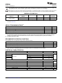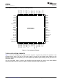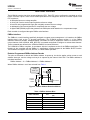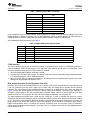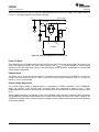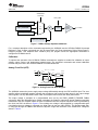
1
UCD9246
www.ti.com
SLVSA34 – JANUARY 2010
Digital PWM System Controller
FEATURES
Tool to Simulate, Configure, and Monitor
Power Supply Performance
1
•
2
•
•
•
•
•
•
•
•
•
•
•
•
•
•
•
•
Fully Configurable Multi-Output and MultiPhase Non-Isolated DC/DC PWM Controller
Controls Up to 4 Voltage Rails and Up to 6
Phases
Supports Switching Frequencies Up to 2MHz
with 250 ps Duty-Cycle Resolution
Up To 1mV Closed Loop Resolution
Hardware-Accelerated, 3-Pole/3-Zero
Compensator with Non-Linear Gain for
Improved Transient Performance
Supports Multiple Soft-Start and Soft-Stop
Configurations Including Prebias Start-up
Supports Voltage Tracking, Margining and
Sequencing
Supports Current and Temperature Balancing
for Multi-Phase Power Stages
Supports Phase Adding/Shedding for
Multi-Phase Power Stages
Sync In/Out Pins Align DPWM Clocks Between
Multiple UCD92xx Devices
12-Bit Digital Monitoring of Power Supply
Parameters Including:
– Input/Output Current and Voltage
– Temperature at Each Power Stage
Multiple Levels of Over-current Fault
Protection:
– External Current Fault Inputs
– Fast Overcurrent Protection
– Current Continually Digitally Monitored
Over- and Under-voltage Fault Protection
Over-temperature Fault Protection
Enhanced Nonvolatile Memory with Error
Correction Code (ECC)
Device Operates From a Single Supply with an
Internal Regulator Controller That Allows
Operation Over a Wide Supply Voltage Range
Supported by Fusion Digital Power™
Designer, a Full Featured PC Based Design
APPLICATIONS
•
•
•
•
•
•
Industrial/ATE
Networking Equipment
Telecommunications Equipment
Servers
Storage Systems
FPGA, DSP and Memory Power
DESCRIPTION
The UCD9246 is a multi-rail, multi-phase
synchronous buck digital PWM controller designed for
non-isolated DC/DC power applications. This device
integrates dedicated circuitry for DC/DC loop
management with flash memory and a serial interface
to
support
configurability,
monitoring
and
management.
The UCD9246 was designed to provide a wide
variety of desirable features for non-isolated DC/DC
converter applications while minimizing the total
system component count by reducing external
circuits.
The
solution
integrates
multi-loop
management with sequencing, margining, tracking
and intelligent phase management to optimize for
total
system
efficiency.
Additionally,
loop
compensation and calibration are supported without
the need to add external components.
To facilitate configuring the device, the Texas
Instruments Fusion Digital Power™ Designer is
provided. This PC based Graphical User Interface
offers an intuitive interface to the device. This tool
allows the design engineer to configure the system
operating parameters for the application, store the
configuration to on-chip non-volatile memory and
observe both frequency domain and time domain
simulations for each of the power stage outputs.
TI has also developed multiple complementary power
stage solutions – from discrete drivers in the UCD7k
family to fully tested power train modules in the PTD
family. These solutions have been developed to
complement the UCD9k family of system power
controllers.
1
2
Please be aware that an important notice concerning availability, standard warranty, and use in critical applications of Texas
Instruments semiconductor products and disclaimers thereto appears at the end of this data sheet.
Fusion Digital Power, Auto-ID are trademarks of Texas Instruments.
PRODUCTION DATA information is current as of publication date.
Products conform to specifications per the terms of the Texas
Instruments standard warranty. Production processing does not
necessarily include testing of all parameters.
Copyright © 2010, Texas Instruments Incorporated
UCD9246
SLVSA34 – JANUARY 2010
www.ti.com
This integrated circuit can be damaged by ESD. Texas Instruments recommends that all integrated circuits be handled with
appropriate precautions. Failure to observe proper handling and installation procedures can cause damage.
ESD damage can range from subtle performance degradation to complete device failure. Precision integrated circuits may be more
susceptible to damage because very small parametric changes could cause the device not to meet its published specifications.
ORDERING INFORMATION (1)
OPERATING TEMPERATURE
RANGE, TA
ORDERABLE PART
NUMBER
PIN COUNT
SUPPLY
PACKAGE
TOP SIDE
MARKING
UCD9246RGCR
64-pin
Reel of 2000
QFN
UCD9246
UCD9246RGCT
64-pin
Tray of 250
QFN
UCD9246
–40°C to 125°C
(1)
For the most current package and ordering information, see the Package Option Addendum at the end of this document, or see the TI
web site at www.ti.com.
ABSOLUTE MAXIMUM RATINGS (1)
VALUE
UNIT
Voltage applied at V33D to DGND
–0.3 to 3.8
V
Voltage applied at V33A to AGND
–0.3 to 3.8
V
Voltage applied to any pin (2)
–0.3 to 3.8
V
Storage temperature (TSTG)
–40 to 150
°C
(1)
(2)
Stresses beyond those listed under absolute maximum ratings may cause permanent damage to the device. These are stress ratings
only and functional operation of the device at these or any other conditions beyond those indicated under recommended operating
conditions is not implied. Exposure to absolute-maximum-rated conditions for extended periods may affect device reliability.
All voltages referenced to GND.
RECOMMENDED OPERATING CONDITIONS
over operating free-air temperature range (unless otherwise noted)
V
Supply voltage during operation, V33D, V33DIO, V33A
TA
Operating free-air temperature range (1)
TJ
Junction temperature
(1)
MIN
NOM
3
3.3
MAX
UNIT
3.6
V
125
°C
125
°C
TYP
MAX
UNIT
–40
(1)
When operating, the UCD9246’s typical power consumption causes a 15°C temperature rise from ambient.
ELECTRICAL CHARACTERISTICS
PARAMETER
TEST CONDITIONS
MIN
SUPPLY CURRENT
IV33A
V33A = 3.3 V
8
15
IV33DIO
V33DIO = 3.3 V
2
10
V33D = 3.3 V
40
45
V33D = 3.3 V storing configuration parameters
in flash memory
50
55
3.3
3.6
4
4.6
IV33D
Supply current
IV33D
mA
INTERNAL REGULATOR CONTROLLER INPUTS/OUTPUTS
V33
3.3-V linear regulator
V33FB
3.3-V linear regulator feedback
IV33FB
Series pass base drive
Beta
Series NPN pass device
Emitter of NPN transistor
3.25
VVIN = 12 V
10
V
mA
40
EXTERNALLY SUPPLIED 3.3 V POWER
V33D
Digital 3.3-V power
TA = 25°C
3.0
3.6
V
V33A
Analog 3.3-V power
TA = 25°C
3.0
3.6
V
2
Submit Documentation Feedback
Copyright © 2010, Texas Instruments Incorporated
UCD9246
www.ti.com
SLVSA34 – JANUARY 2010
ELECTRICAL CHARACTERISTICS (continued)
PARAMETER
TEST CONDITIONS
MIN
TYP
MAX
UNIT
ERROR AMPLIFIER INPUTS EAPn, EANn
VCM
Common mode voltage each pin
VERROR
Internal error voltage range
AFE_GAIN field of CLA_GAINS = 0 (1)
–0.15
1.848
–256
248
mV
EAP-EAN
Error voltage digital resolution
AFE_GAIN field of CLA_GAINS = 3
REA
Input Impedance
Ground reference
0.5
IOFFSET
Input offset current
1 kΩ source impedence
–5
V
3
MΩ
5
µA
1
1.5
mV
Vref 10-bit DAC
Vref
Reference voltage setpoint
Vrefres
Reference voltage resolution
0
1.6
V
1.56
mV
ANALOG INPUTS CS-1A, CS-1B, CS-2A, CS-2B, CS-3A, CS-4A, Vin/Iin, TEMP, ADDR-0, ADDR-1, Vtrack, ADCref
VADDR_OPEN
Voltage indicating open pin
ADDR-0,1 open
VADDR_SHORT
Voltage indicating shorted pin
ADDR-0,1 short to ground
VADC_RANGE
Measurement range for voltage monitoring
Inputs: Vin/Iin, Vtrack, Temp, CS-1A, CS-1B,
CS-2A, CS-2B CS-3A, CS-4A
VOC_THRS
Over-current comparator threshold voltage
range (2)
Inputs: CS-1A, CS-2A, CS-3A, CS-4A
VOC_RES
Over-current comparator threshold voltage
range
Inputs: CS-1A, CS-2A, CS-3A, CS-4A
ADCref
External reference input
Tempinternal
Int. temperature sense accuracy
INL
ADC integral nonlinearity
Ilkg
Input leakage current
3V applied to pin
RIN
Input impedance
Ground reference
CIN
Current Sense Input capacitance
2.37
V
0.36
V
0
2.5
V
0.032
2
V
31.25
Over range from 0°C to 125°C
mV
1.8
V33A
V
–5
5
°C
2.5
mV
–2.5
100
nA
8
MΩ
10
pF
Dgnd
+0.25
V
DIGITAL INPUTS/OUTPUTS
VOL
Low-level output voltage
IOL = 6 mA (3), V33DIO = 3 V
VOH
High-level output voltage
IOH = -6 mA (4), V33DIO = 3 V
VIH
High-level input voltage
V33DIO = 3V
VIL
Low-level input voltage
V33DIO = 3.5 V
V33DIO
–0.6V
2.1
V
3.6
V
1.1
V
SYSTEM PERFORMANCE
VRESET
Voltage where device comes out of reset
V33D Pin
tRESET
Pulse width needed for reset
nRESET pin
VRefAcc
Setpoint reference accuracy
Vref commanded to be 1V, at 25°C,
AFEgain = 4, 1V input to EAP/N measured at
output of the EADC (5)
2.3
Setpoint reference accuracy over temperature –40°C to 125°C
VDiffOffset
Differential offset between gain settings
2.4
V
2
AFEgain = 4 compared to AFEgain = 1, 2, or 8
µs
–10
10
mV
–20
20
mV
–4
4
mV
240
240 + 1
switchi
ng
cycle
ns
tDelay
Digital compensator delay
FSW
Switching frequency
Duty
Max and Min duty cycle
V33Slew
Minimum V33 slew rate
V33 slew rate between VRESET min and 2.9V
0.25
V/ms
tretention
Retention of configuration parameters
TJ = 25°C
100
Years
Write_Cycles
Number of nonvolatile erase/write cycles
TJ = 25°C
20
K cycles
(1)
(2)
(3)
(4)
(5)
15.260
2000
0%
100%
kHz
See the UCD92xx PMBus Command Reference for the description of the AFE_GAIN field of CLA_GAINS command.
Can be disabled by setting to '0'
The maximum IOL, for all outputs combined, should not exceed 12 mA to hold the maximum voltage drop specified.
The maximum IOH, for all outputs combined, should not exceed 48 mA to hold the maximum voltage drop specified.
With default device calibration. PMBus calibration can be used to improve the regulation tolerance
Copyright © 2010, Texas Instruments Incorporated
Submit Documentation Feedback
3
UCD9246
SLVSA34 – JANUARY 2010
www.ti.com
ADC MONITORING INTERVALS AND RESPONSE TIMES
The ADC operates in a continuous conversion sequence that measures each rail's output voltage, each power
stage's output current, plus four other variables (external temperature, Internal temperature, input voltage and
current, and tracking input voltage). The length of the sequence is determined by the number of output rails
(NumRails) and total output power stages (NumPhases) configured for use. The time to complete the monitoring
sampling sequence is give by the formula:
tADC_SEQ = tADC × (NumRAILS + NumPHASE + 4)
PARAMETER
tADC
TEST CONDITIONS
MIN
ADC single-sample time
tADC_SEQ
ADC sequencer interval
TYP
MAX
3.84
Min = 1 Rail + 1 Phase + 4 = 6 samples
Max = 4 Rails + 8 Phases + 4 = 16 samples
23.04
UNIT
µs
61.44
µs
The most recent ADC conversion results are periodically converted into the proper measurement units (volts,
amperes, degrees), and each measurement is compared to its corresponding fault and warning limits. The
monitoring operates asynchronously to the ADC, at intervals shown in the table below.
PARAMETER
TEST CONDITIONS
MIN
TYP
MAX
UNIT
tVout
Output voltage monitoring interval
200
tIout
Output current monitoring interval
200 × NRails
µs
µs
tVin
Input voltage monitoring interval
2
ms
tIin
Input current monitoring interval
2
ms
tTEMP
Temperature monitoring interval
100
ms
tIbal
Output current balancing interval
2
ms
Because the ADC sequencer and the monitoring comparisons are asynchronous to each other, the response
time to a fault condition depends on where the event occurs within the monitoring interval and within the ADC
sequence interval. Once a fault condition is detected, some additional time is required to determine the correct
action based on the FAULT_RESPONSE code, and then to perform the appropriate response. The following
table lists the worse-case fault response times.
PARAMETER
tOVF, tUVF
tOCF, tUCF
tOTF
(1)
(2)
4
MAX TIME
UNIT
Over-/under-voltage fault response time during
normal operation
Normal regulation, no PMBus activity, 8
stages enabled
TEST CONDITIONS
300
µs
Over-/under-voltage fault response time, during
data logging
During data logging to nonvolatile memory (1)
800
µs
Over-/under-voltage fault response time, when
tracking or sequencing enable
During tracking and soft-start ramp.
400
µs
Over-/under-current fault response time during
normal operation
Normal regulation, no PMBus activity, 8
stages enabled 75% to 125% current step
100 + (600 ×
NRails) (2)
µs
Over-/under-current fault response time, during
data logging
During data logging to nonvolatile memory
75% to 125% current step
600 + (600 × NRails)
µs
Over-/under-current fault response time, when
tracking or sequencing enable
During tracking and soft start ramp 75% to
125% current step
300 + (600 × NRails)
µs
Over-temperature fault response time
Temperature rise of 10°C/sec,
OT threshold = 100°C
2.5
S
During a STORE_DEFAULT_ALL command, which stores the entire configuration to nonvolatile memory, the fault detection latency can
be up to 10 ms.
Because the current measurement is averaged with a smoothing filter, the response time to an over-current condition depends on a
combination of the time constant from Table 4, the recent measurement history, and how much the measured value exceeds the
over-current limit.
Submit Documentation Feedback
Copyright © 2010, Texas Instruments Incorporated
UCD9246
www.ti.com
SLVSA34 – JANUARY 2010
HARDWARE FAULT DETECTION LATENCY
The controller contains hardware fault detection circuits that are independent of the ADC monitoring sequencer.
PARAMETER
tFAULT
tCLF
TEST CONDITIONS
MAX
UNIT
15 + 3 ×
NumPhases
µs
Time to disable DPWM output based on corresponding
active FLTpin
High level on FAULT pin
Time to disable the first DPWM output based on
internal analog comparator fault
Step change in CS voltage from 0V to
2.5V
4
Switch
Cycles
Time to disable all remaining DPWM and SRE outputs
configured for the voltage rail after an internal analog
comparator fault
Step change in CS voltage from 0V to
2.5V
10 + 3 ×
NumPhases
µs
PMBUS/SMBUS/I2C
The timing characteristics and timing diagram for the communications interface that supports I2C, SMBus and
PMBus are shown below.
I2C/SMBus/PMBus TIMING CHARACTERISTICS
TA = –40°C to 125°C, 3V < V33 < 3.6V, typical values at TA = 25°C
PARAMETER
TEST CONDITIONS
MIN
TYP
MAX
UNIT
fSMB
SMBus/PMBus operating frequency
Slave mode; SMBC 50% duty cycle
10
1000
kHz
fI2C
I2C operating frequency
Slave mode; SCL 50% duty cycle
10
1000
kHz
t(BUF)
Bus free time between start and stop
t(HD:STA)
t(SU:STA)
4.7
µs
Hold time after (repeated) start
0.26
µs
Repeated start setup time
0.26
µs
t(SU:STO)
Stop setup time
0.26
µs
t(HD:DAT)
Data hold time
0
ns
t(SU:DAT)
Data setup time
t(TIMEOUT)
Error signal/detect
t(LOW)
Clock low period
Receive mode
50
See
(1)
ns
35
0.5
ms
µs
t(HIGH)
Clock high period
See
(2)
50
µs
t(LOW:SEXT)
Cumulative clock low slave extend time
See
(3)
25
ms
tFALL
Clock/data fall time
See
(4)
120
ns
See
(5)
120
ns
tRISE
(1)
(2)
(3)
(4)
(5)
Clock/data rise time
0.26
The UCD9246 times out when any clock low exceeds t(TIMEOUT).
t(HIGH), max, is the minimum bus idle time. SMBC = SMBD = 1 for t > 50 µs causes reset of any transaction involving UCD9246 that is in
progress.
t(LOW:SEXT) is the cumulative time a slave device is allowed to extend the clock cycles in one message from initial start to the stop.
Rise time tRISE = (VVILMAX – 0.15) to (VVIHMIN + 0.15)
Fall time tFALL = 0.9 V33 to (VILMAX – 0.15)
Copyright © 2010, Texas Instruments Incorporated
Submit Documentation Feedback
5
UCD9246
SLVSA34 – JANUARY 2010
www.ti.com
Figure 1. I2C/SMBus/PMBus Timing in Extended Mode Diagram
6
Submit Documentation Feedback
Copyright © 2010, Texas Instruments Incorporated
UCD9246
www.ti.com
SLVSA34 – JANUARY 2010
Fusion Power Peripheral 4
EAp4
EAn4
Analog front end
(AFE)
Digital
High Res
PWM
Compensator
3P/3Z IIR
DPWM-4A
FAULT -4A
Fusion Power Peripheral 3
EAp3
EAn3
Analog front end
(AFE)
Digital
High Res
PWM
Compensator
3P/3Z IIR
DPWM-3A
FAULT -3A
Fusion Power Peripheral 2
EAp2
EAn2
Analog front end
(AFE)
Digital
High Res
PWM
Compensator
3P/3Z IIR
DPWM-2A
DPWM-2B
FAULT -2A
FAULT -2B
Fusion Power Peripheral 1
Aalog front end
EAp1
EAn1
Diff
Amp
Ref
Compensator
Err
Amp
Digital
High Res
PWM
IIR
3P/3Z
Coeff.
Regs
ADC
6 bit
DPWM-1A
DPWM-1B
FAULT -1A
FAULT -1B
SYNC-IN (TDI)
SYNC-OUT (TDO)
5
V33x
6
xGnd
BPCap
3.3V reg.
controller
& 1.8V
regulator
Analog Comparators
Ref 1
ADDR-0
ADDR-1
CS-1A
CS-1B
CS-2A
CS-2B
CS-3A
CS-4A
Vin/Iin
Vtrack
Temperature
Ref 2
12-bit
ADC
260 ksps
Ref 3
Ref 4
Trip1
ARM-7 core
SRE
control
SRE-4A
SRE-3A
SRE-2B
SRE-2A
SRE-1B
SRE-1A
Trip2
Trip3
Trip4
Flash
memory with
ECC
Mux
control
Seq.
control
Osc
POR/BOR
internal
Temp sense
PMBus
TMUX0
TMUX1
TMUX2
SEQ_1
SEQ_2
PMBus-Clk
PMBus-Data
PMBus-Alert
PMBus-Cntl
PGood
nRESET
Figure 2. Functional Block Diagram
Copyright © 2010, Texas Instruments Incorporated
Submit Documentation Feedback
7
UCD9246
SLVSA34 – JANUARY 2010
www.ti.com
AGND3
CS-1B
CS-2B
ADDR-0
ADDR-1
CS-1A
V33FB
EAN4
EAP4
EAN3
EAP3
EAN2
EAP2
EAN1
EAP1
AGND2
64
63
62
61
60
59
58
57
56
55
54
53
52
51
50
49
The UCD9246 is available in an 64-pin QFN package (RGC).
CS-4A
1
48
AGND1
CS-3A
2
47
BPCap
CS-2A
3
46
V33A
Vin/ Iin
4
45
V33D
Vtrack
5
44
V33DIO
Temperature
6
43
DGND3
V33DIO
7
42
TMUX-2
DGND1
8
41
SEQ-2
nRESET
9
40
nTRST
TRCK
10
39
TMS/PGood
FLT-1A
11
38
TDI /Sync_in
FLT-1B
12
37
TDO/Sync_out
FLT-2A
13
36
TCK/SEQ-1
FLT-2B
14
35
SRE-2B
PMBus_Clock
15
34
FLT-4A
PMBus_Data
16
33
SRE-2A
25
26
27
28
29
30
FLT-3A
DGND2
PMBus_Alert
PMBus_Cntl
SRE-3A
SRE-4A
32
24
SRE-1B
TMUX-1
23
DPWM-4A
31
22
SRE-1A
TMUX-0
21
DPWM-3A
19
DPWM-2A
20
18
DPWM-1B
DPWM-2B
17
DPWM-1A
UCD9246
Figure 3. Pin Assignment Diagram
TYPICAL APPLICATION SCHEMATIC
Figure 4 shows the UCD9246 power supply controller as part of a system that provides the regulation of one
six-phase power supply. The loop for the power supply is created by the voltage output feeding into the
differential voltage error ADC (EADC) input, and completed by DPWM outputs feeding into the gate drivers for
each power stage.
The ±Vsenserail signal must be routed to the EAp/EAn input that matches the number of the lowest DPWM
configured as part of the rail. (See more detail in Flexible Rail/Power Stage Configuration.)
8
Submit Documentation Feedback
Copyright © 2010, Texas Instruments Incorporated
UCD9246
www.ti.com
SLVSA34 – JANUARY 2010
UCD7231 Power Stage
Vin
Vin
Vin
+3.3V
BST
PWM
HS_Gate
SRE
VGG
LS_Gate
PwPd
AGND
VGG_DIS
FLT-1A
Vtrack
Temperature
+Vs1
PGND
RDLY
BPCAP
V33DIO
V33DIO
V33A
V33D
V33FB
ILIM
Vin/Iin
-Vs
UCD7231
SRE_Mode
Vin/Iin
Temp _1A
+Vs
SW
IOUT
BP3
Temperature
Sensor
HS_SNS
FF
CSP
CSN
DPWM-1A
Temperature
SRE-1A
CS-1A
EAP1
EAN1
-Vs1
FLT-1B
EAP2
PWM
SRE-1B
SRE
CS-1B
EAP3
Temp
FF
DPWM-1B
EAN2
UCD7231 Power Stage
Temp _1B
+Vs
-Vs
IOUT
EAN3
FLT-2A
EAP4
PWM
SRE-2A
SRE
CS-2A
SEQ-2
Temp
FF
DPWM-2A
EAN4
UCD7231 Power Stage
Temp _2A
+Vs1
+Vs
-Vs
IOUT
-Vs1
TMUX-0
TMUX-0
TMUX-1
TMUX-2
+3.3V
TMUX-1
UCD9246
FLT-2B
TMUX-2
PWM
SRE
CS-2B
IOUT
TRCK
Temp
FF
DPWM-2B
SRE-2B
UCD7231 Power Stage
Temp _2B
+Vs
-Vs
TMS/ PGood
TDI/Sync-in
FLT-3A
TDO/Sync-out
PWM
SRE-3A
nTRST
Temp
FF
DPWM-3A
TCK/SEQ-1
SRE
CS-3A
UCD7231 Power Stage
Temp _3A
+Vs
-Vs
IOUT
ADDR-0
ADDR-1
FLT-4A
PMBus_Clock
SRE-4A
PMBus_Alert
CS-4A
Temp
FF
DPWM-4A
PMBus_Data
PWM
SRE
UCD7231 Power Stage
Temp _4A
+Vs
-Vs
IOUT
PowerPad
DGND3
DGND2
DGND1
AGND3
AGND2
nRESET
AGND1
PMBus_Cntl
+3.3V
+3.3V
Vcc
Temperature
Temp _1A
A0
Temp _1B
A1
Temp _2A
A2
Temp _2B
A3
Temp _3A
A7
Temp _4A
A5
S2
TMUX-2
A6
S1
TMUX-1
A7
S0
TMUX-0
A
Vcc
Iin
Vin
B2
A
SN74LVC1G3157
B1
S
Gnd
CD74HC4051
Vin/Iin
TMUX-0
Vee Gnd E
Figure 4. Typical Application Schematic
Copyright © 2010, Texas Instruments Incorporated
Submit Documentation Feedback
9
UCD9246
SLVSA34 – JANUARY 2010
www.ti.com
PIN DESCRIPTIONS
PIN NO.
10
PIN NAME
DESCRIPTION
1
CS-4A
Power stage 4A current sense input and input to analog comparator 4
2
CS-3A
Power stage 3A current sense input and input to analog comparator 3
3
CS-2A
Power stage 2A current sense input and input to analog comparator 2
4
Vin/Iin
Input supply sense, alternates between Vin and Iin
5
Vtrack
Voltage track input
6
Temperature
Temperature sense input
7
V33DIO
Digital I/O 3.3 V supply
8
DGND1
Digital Ground
9
nRESET
Active low device reset input, pullup to 3.3V with 10 kΩ resistor
10
TRCK
JTAG Test return clock
11
FLT-1A
External fault input 1A, active high
12
FLT-1B
External fault input 1B, active high
13
FLT-2A
External fault input 2A, active high
14
FLT-2B
External fault input 2B, active high
15
PMBus_Clock
PMBus Clock, pullup to 3.3 V with 2 kΩ resistor
16
PMBus_Data
PMBus Data, pullup to 3.3 V with 2 kΩ resistor
17
DPWM-1A
Digital Pulse Width Modulator output 1A
18
DPWM-1B
Digital Pulse Width Modulator output 1B
19
DPWM-2A
Digital Pulse Width Modulator output 2A
20
DPWM-2B
Digital Pulse Width Modulator output 2B
21
DPWM-3A
Digital Pulse Width Modulator output 3A
22
SRE-1A
Synchronous rectifier enable output 1A, active high
23
DPWM-4A
Digital Pulse Width Modulator output 4A
24
SRE-1B
Synchronous rectifier enable output 1B, active high
25
FLT-3A
External fault input 3A, active high
26
DGND2
Digital Ground
27
PMBus_Alert
PMBus Alert, pullup to 3.3V with 2 kΩ resistor
28
PMBus_Cntl
PMBus Control, pullup to 3.3V with 2 kΩ resistor
29
SRE-3A
Synchronous rectifier enable output 3A, active high
30
SRE-4A
Synchronous rectifier enable output 4A, active high
31
TMUX-0
Temperature multiplexer select output S0, Vin/Iin select
32
TMUX-1
Temperature multiplexer select output S1
33
SRE-2A
Synchronous rectifier enable output 2A, active high
34
FLT-4A
External fault input 4A, active high
35
SRE-2B
Synchronous rectifier enable output 2B, active high
36
TCK/SEQ-1
JTAG Test Clock (multiplexed with Sequencing Input/Output)
37
TDO/Sync_Out
JTAG Test data out (multiplexed with Synchronization Output from DPWM)
38
TDI/Sync_In
JTAG Test data in tie to V33D with 10kΩ resistor (multiplexed with Synchronization Input to DPWM)
39
TMS/PGood
JTAG Test mode select – tie to V33D with 10kΩ resistor (multiplexed with Power Good indication, Active
high open-drain output. Pull-up to 3.3V with 10kΩ resistor.)
40
nTRST
JTAG Test reset – tie to ground with 10kΩ resistor
41
SEQ-2
Sequencing Input/Output
42
TMUX-2
Temperature multiplexer select output S2
43
DGND3
Digital Ground
44
V33DIO
Digital I/O 3.3V supply
45
V33D
Digital core 3.3V supply
46
V33A
Analog 3.3V supply
Submit Documentation Feedback
Copyright © 2010, Texas Instruments Incorporated
UCD9246
www.ti.com
PIN NO.
SLVSA34 – JANUARY 2010
PIN NAME
DESCRIPTION
47
BPCap
1.8V bypass capacitor connection
48
AGND1
Analog Ground
49
AGND2
Analog Ground
50
EAP1
Error analog, differential voltage. Positive channel #1 input
51
EAN1
Error analog, differential voltage. Negative channel #1 input
52
EAP2
Error analog, differential voltage. Positive channel #2 input
53
EAN2
Error analog, differential voltage. Negative channel #2 input
54
EAP3
Error analog, differential voltage. Positive channel #3 input
55
EAN3
Error analog, differential voltage. Negative channel #3 input
56
EAP4
Error analog, differential voltage. Positive channel #4 input
57
EAN4
Error analog, differential voltage. Negative channel #4 input
58
V33FB
Connection to the base of the 3.3V linear regulator transistor. (no connect if not using an external
transistor)
59
CS-1A
Power stage 1A current sense input and input to analog comparator 1
60
ADDR-1
Address sense input. Channel 1
61
ADDR-0
Address sense input. Channel 0
62
CS-2B
Power stage 2B current sense input
63
CS-1B
Power stage 1B current sense input
64
AGND3
Analog Ground
PowerPad PowerPad
It is recommended that this pad be connected to analog ground
Copyright © 2010, Texas Instruments Incorporated
Submit Documentation Feedback
11
UCD9246
SLVSA34 – JANUARY 2010
www.ti.com
FUNCTIONAL OVERVIEW
The UCD9246 contains four fusion power peripherals (FPP). Each FPP can be configured to regulated up to four
DC/DC converter outputs. There are six PWM outputs that can be assigned to drive the converter outputs. Each
FPP consists of:
• A differential input error voltage amplifier
• A 10-bit DAC used to set the output regulation reference voltage.
• A fast ADC with programmable input gain to digitally measure the error voltage.
• A dedicated 3-pole/3-zero digital filter to compensate the error voltage.
• A digital PWM (DPWM) engine that generates the PWM pulse width based on the compensator output.
Each controller is configured through a PMBus serial interface.
PMBus Interface
The PMBus is a serial interface specifically designed to support power management. It is based on the SMBus
interface that is built on the I2C physical specification. The UCD9246 supports revision 1.1 of the PMBus
standard. Wherever possible, standard PMBus commands are used to support the function of the device. For
unique features of the UCD9246, MFR_SPECIFIC commands are defined to configure or activate those features.
These commands are defined in the UCD92xx PMBUS Command Reference.
The UCD9246 is PMBus compliant, in accordance with the Compliance section of the PMBus specification. The
firmware is also compliant with the SMBus 1.1 specification, including support for the SMBus ALERT function.
The hardware can support 100 kHz, 400 kHz, or 1 MHz PMBus operation.
Resistor Programmed PMBus Address Decode
Two pins are allocated to decode the PMBus address. At power-up, the device applies a bias current to each
address detect pin, and the voltage on that pin is captured by the internal 12-bit ADC. The PMBus address is
calculated as follows:
PMBus Address = 12 × PMBus Address 1 + PMBus Address 0
Where PMBus Address 1 and 0 are selected from Table 1.
V33
ADDR-0,
ADDR-1 pins
UCD9246
10 mA
IBIAS
Resistor to
set PMBus
Address
To 12-bit ADC
Figure 5. PMBus Address Detection Method
Table 1. PMBus Address Bins
PMBus ADDRESS
12
Submit Documentation Feedback
RPMBus PMBus RESISTANCE
(kΩ)
open
–
11
205
10
178
9
154
8
133
7
115
Copyright © 2010, Texas Instruments Incorporated
UCD9246
www.ti.com
SLVSA34 – JANUARY 2010
Table 1. PMBus Address Bins (continued)
PMBus ADDRESS
RPMBus PMBus RESISTANCE
(kΩ)
6
100
5
86.6
4
75
3
64.9
2
56.2
1
48.7
0
42.2
short
–
A low impedance (short) on either address pin that produces a voltage below the minimum voltage causes the
PMBus address to default to address 126. A high impedance (open) on either address pin that produces a
voltage above the maximum voltage also causes the PMBus address to default to address 126.
Some addresses should be avoided, see Table 2
Table 2. PMBus Address Assignment Rules
ADDRESS
STATUS
0
Prohibited
1-10
Avaliable
11
Avoid
12
Prohibited
13–125
Avaliable
126
Avoid
127
Prohibited
REASON
SMBus generall address call
Causes confilcts with other devices during program flash updates.
PMBus alert response protocol
Default value; may cause conflicts with other devices.
Used by TI manufacturing for device tests.
JTAG Interface
The JTAG interface can provide an alternate interface for programming the device. It is disabled by default in
order to enable the SEQ-1 sequencing pin, sync, and power good status pins with which it is multiplexed. There
are three conditions under which the JTAG interface is enabled:
1. When the ROM_MODE PMBus command is issued.
2. On power-up if the Data Flash is blank. This allows JTAG to be used for writing the configuration parameters
to a programmed device with no PMBus interaction.
3. When an invalid address is detected at power-up. By shorting one of the address pins to ground, an invalid
address can be generated that enables JTAG.
Bias Supply Generator (Shunt Regulator Controller)
Internally, the circuits in the UCD9246 require 3.3V to operate. This can be provided directly on the V33x pins, or
it can be generated from the power supply input voltage using an internal shunt regulator and an external
transistor. The requirements for the external transistor are that it be an NPN device with a beta of at least 40.
Figure 6 shows the typical application using the external series pass transistor. The base of the transistor is
driven by a 10kΩ resistor to Vin and a transconduction amplifier whose output is on the VD33FB pin. The NPN
emitter becomes the 3.3V supply for the chip and requires bypass capacitors of 0.1µF and 4.7µF.
The transconductance amplifier sinks current into the V33FB pin, in order to regulate the amount of current
allowed into the base of the transistor, which regulates the collector current, which determines the emitter voltage
(3.3V). The resistor value should be sized low enough to give sufficient base drive at minimum input voltage, yet
large enough to not exceed the maximum current sink capability of the V33FB pin at maximum input voltage.
Higher beta transistors help in increasing the minimum resistance value, as less base current is needed to
sufficiently drive the higher beta transistor. A resistor value of 10 kOhms works well for most applications that
use the FCX491A BJT.
Copyright © 2010, Texas Instruments Incorporated
Submit Documentation Feedback
13
UCD9246
SLVSA34 – JANUARY 2010
www.ti.com
Some circuits in the device require 1.8V that is generated internally from the 3.3V supply. This voltage requires a
0.1 µF to 1 µF bypass capacitor from BPCap to ground.
To Power Stage
Vin
FCX491A
+3.3 V
10 kW 4.7 mF
0.1 mF
+1.8 V
V33A
V33D
BPCap
V33FB
0.1 mF
UC9246
Figure 6. 3.3V Shunt Regulator Controller I/O
Power On Reset
The UCD9246 has an integrated power-on reset (POR) circuit that monitors the supply voltage. At power-up, the
POR circuit detects the V33D rise. When V33D is greater than VRESET, the device initiates an internal startup
sequence. At the end of the delay sequence, the device begins normal operation, as defined by the downloaded
device PMBus configuration.
External Reset
The device can be forced into the reset state by an external circuit connected to the nRESET pin. A logic low
voltage on this pin holds the device in reset. To avoid an erroneous trigger caused by noise, a 10 kΩ pull up
resistor to 3.3V is recommended.
Output Voltage Adjustment
The nominal output voltage is programmed by a combination of PMBus commands: VOUT_COMMAND,
VOUT_CAL_OFFSET, VOUT_SCALE_LOOP, and VOUT_MAX. Their relationship is shown in Figure 7. These
PMBus parameters need to be set such that the resulting Vref DAC value does not exceed the maximum value
of Vref.
Output voltage margining is configured by the VOUT_MARGIN_HIGH and VOUT_MARGIN_LOW commands.
The OPERATION command selects between the nominal output voltage and either of the margin voltages. The
OPERATION command also includes an option to suppress certain voltage faults and warnings while operating
at the margin settings.
14
Submit Documentation Feedback
Copyright © 2010, Texas Instruments Incorporated
UCD9246
www.ti.com
SLVSA34 – JANUARY 2010
OPERATION
Command
VOUT_MAX
VOUT_MARGIN_HIGH
+
3:1
Mux
VOUT_COMMAND
VOUT_
SCALE_
LOOP
Limiter
Vref DAC
VOUT_MARGIN_LOW
VOUT_CAL_OFFSET
Figure 7. PMBus Voltage Adjustment Methods
For a complete description of the commands supported by the UCD9246 see the UCD92xx PMBUS Command
Reference. Each of these commands can also be issued from the Texas Instruments Fusion Digital Power™
Designer program. This Graphical User Interface (GUI) PC program issues the appropriate commands to
configure the UCD9246 device.
Calibration
To optimize the operation of the UCD9246, PMBus commands are supplied to enable fine calibration of output
voltage, output current, and temperature measurements. The supported commands and related calibration
formulas may be found in the UCD92xx PMBUS Command Reference.
Analog Front End (AFE)
VEAP
VEA
GAFE = 1, 2, 4, or 8
Vead
VEAN
6-bit
result
EADC
GeADC = 8 mV/LSB
Vref DAC
CPU
Vref = 1.563 mV/LSB
PMBus
Figure 8. Analog Front End Block Diagram
The UCD9246 senses the power supply output voltage differentially through the EAP and EAN pins. The error
amplifier utilizes a switched capacitor topology that provides a wide common mode range for the output voltage
sense signals. The fully differential nature of the error amplifier also ensures low offset performance.
The output voltage is sampled at a programmable time (set by the EADC_SAMPLE_TRIGGER PMBus
command). When the differential input voltage is sampled, the voltage is captured in internal capacitors and then
transferred to the error amplifier where the value is subtracted from the set-point reference which is generated by
the 10-bit Vref DAC as shown in Figure 8. The resulting error voltage is then amplified by a programmable gain
circuit before the error voltage is converted to a digital value by the error ADC (EADC). This programmable gain
is configured through the PMBus and affects the dynamic range and resolution of the sensed error voltage as
shown in Table 3.
Copyright © 2010, Texas Instruments Incorporated
Submit Documentation Feedback
15
UCD9246
SLVSA34 – JANUARY 2010
www.ti.com
Table 3. Analog Front End Resolution
AFE_GAIN for
PMBus COMMAND
AFE GAIN
EFFECTIVE EADC RESOLUTION
(mV)
DIGITAL ERROR VOLTAGE
DYNAMIC RANGE (mV)
0
1
8
–256 to 248
1
2
4
–128 to 124
2
4
2
–64 to 62
3
8
1
–32 to 31
The AFE variable gain is one of the compensation coefficients that are stored when the device is configured by
issuing the CLA_GAINS PMBus command. Compensator coefficients are arranged in several banks: one bank
for start/stop ramp or tracking, one bank for normal regulation mode and one bank for light load mode. This
allows the user to trade-off resolution and dynamic range for each operational mode.
The EADC, which samples the error voltage, has high accuracy, high resolution, and a fast conversion time.
However, its range is limited as shown in Table 3. If the output voltage is different from the reference by more
than this, the EADC reports a saturated value at –32 LSBs or 31 LSBs. The UCD9246 overcomes this limitation
by adjusting the Vref DAC up or down in order to bring the error voltage out of saturation. In this way, the
effective range of the ADC is extended. When the EADC saturates, the Vref DAC is slewed at a rate of 0.156
V/ms, referred to the EA differential inputs.
The differential feedback error voltage is defined as VEA = VEAP – VEAN. An attenuator network using resistors R1
and R2 (see Figure 9) should be used to ensure that VEA does not exceed the maximum value of Vref when
operating at the commanded voltage level. The commanded voltage level is determined by the PMBus settings
described in the Output Voltage Adjustment section.
R1
EAP
+Vout
R2
C2
Rin
Ioff
-Vout
EAN
Figure 9. Input Offset Equivalent Circuit
Voltage Sense Filtering
Conditioning should be provided on the EAP and EAN signals. Figure 9 shows a divider network between the
output voltage and the voltage sense input to the controller. The resistor divider is used to bring the output
voltage within the dynamic range of the controller. When no attenuation is needed, R2 can be left open and the
signal conditioned by the low-pass filter formed by R1 and C2.
As with any power supply system, maximize the accuracy of the output voltage by sensing the voltage directly
across an output capacitor as close to the load as possible. Route the positive and negative differential sense
signals as a balanced pair of traces or as a twisted pair cable back to the controller. Put the divider network close
to the controller. This ensures that there is low impedance driving the differential voltage sense signal from the
voltage rail output back to the controller. The resistance of the divider network is a trade-off between power loss
and minimizing interference susceptibility. A parallel resistance (RP) of 1kΩ to 4kΩ is a good compromise. Once
RP is chosen, R1 and R2 can be determined from the following formulas.
R
R1 = P
K
(1)
Rp
R2 =
1 - K
(2)
16
Submit Documentation Feedback
Copyright © 2010, Texas Instruments Incorporated
UCD9246
www.ti.com
SLVSA34 – JANUARY 2010
Where
K=
VEA
VOUT
@ VOUT_SCALE_LOOP
(3)
It is recommended that a capacitor be placed across the lower resistor of the divider network. This acts as an
additional pole in the compensation and as an anti-alias filter for the EADC. To be effective as an anti-alias filter,
the corner frequency should be 35% to 40% of the switching frequency. Then the capacitor is calculated as:
1
C2 =
2 p ´ 0.35 ´ FSW ´ RP
(4)
To obtain the best possible accuracy, the input resistance and offset current on the device should be considered
when calculating the gain of a voltage divider between the output voltage and the EA sense inputs of the
UCD9246. The input impedance and input offset current are specified in the parametric tables in this datasheet.
VEA = VEAP – VEAN in the equation below.
R2
R1R2
VEA =
VO UT +
IOFFSET
æ R1R 2 ö
æ R1R2 ö
R1 + R2 + ç
R1 + R2 + ç
÷
÷
è REA ø
è RE A ø
(5)
The effect of the offset current can be reduced by making the resistance of the divider network low.
Digital Compensator
Each voltage rail controller in the UCD9246 includes a digital compensator. The compensator consists of a
nonlinear gain stage, followed by a digital filter consisting of a second order infinite impulse response (IIR) filter
section cascaded with a first order IIR filter section.
The Texas Instruments Fusion Digital Power™ Designer development tool can be used to assist in defining the
compensator coefficients. The design tool allows the compensator to be described in terms of the pole
frequencies, zero frequencies and gain desired for the control loop. In addition, the Fusion Digital Power™
Designer can be used to characterize the power stage so that the compensator coefficients can be chosen based
on the total loop gain for each feedback system. The coefficients of the filter sections are generated through
modeling the power stage and load.
Additionally, the UCD9246 has three banks of filter coefficients: Bank-0 is used during the soft start/stop ramp or
tracking; Bank-1 is used while in regulation mode; and Bank-2 is used when the measured output current is
below the configured light load threshold.
Copyright © 2010, Texas Instruments Incorporated
Submit Documentation Feedback
17
UCD9246
SLVSA34 – JANUARY 2010
www.ti.com
Figure 10. Digital Compensation
The nonlinear gain block allows a different gain to be applied to the system when the error voltage deviates from
zero. Typically Limit 0 and Limit 1 would be configured with negative values between –1 and –32 and Limit 2 and
Limit 3 would be configured with positive values between 1 and 31. However, the gain thresholds do not have to
be symmetric. For example, the four limit registers could all be set to positive values causing the Gain 0 value to
set the gain for all negative errors and a nonlinear gain profile would be applied to only positive error voltages.
The cascaded 1st order filter section is used to generate the third zero and third pole.
DPWM Engine
The output of the compensator feeds the high resolution DPWM engine. The DPWM engine produces the pulse
width modulated gate drive output from the device. In operation, the compensator calculates the necessary duty
cycle as a digital number representing a value from 0 to 100%. This duty cycle value is multiplied by the
configured period to generate a comparator threshold value. This threshold is compared against the high speed
switching period counter to generate the desired DPWM pulse width. This is shown in Figure 11.
Each DPWM engine can be synchronized to another DPWM engine or to an external sync signal via the
SYNC_IN and SYNC_OUT pins. Configuration of the synchronization function is done through a MFR_SPECIFIC
PMBus command. See the DPWM Synchronization section for more details.
18
Submit Documentation Feedback
Copyright © 2010, Texas Instruments Incorporated
UCD9246
www.ti.com
SLVSA34 – JANUARY 2010
DPWM Engine (1 of 4)
SysClk
SyncIn
Clk
high res
ramp
counter
reset
S
Switch period
R
PWM gate drive
output
Current balance adj
Compensator output
EADC trigger
(Calculated duty cycle)
EADC trigger
SyncOut
threshold
Figure 11. DPWM Engine
Flexible Rail/Power Stage Configuration
The UCD9246 can control up to four rails, each of which can comprise a programmable number of power stages.
Constraints on the mapping of power stages to rails are described in detail in the UCD92xx PMBus Command
Reference under the PHASE_INFO command.
While there is significant flexibility in terms of mapping power stages to output rails, the differential voltage
feedback signals (EAP/EAN) cannot be re-mapped through any commands, and therefore, must be connected to
the proper input on the circuit board. Because the EADC sample trigger for a given front end stage is derived
from the ramp timer of the first (lowest numbered) DPWM on the rail, the system must ensure that the number of
the EADC and the number of the first DPWM match. For example, consider a two rail configuration in which 4
power stages (1A, 2A, 1B and 2B) are assigned to the first rail and 2 power stages (3A and 4A) to the second.
The first DPWM on the first rail is 1; its voltage feedback must be through EAP1/EAN1. The first DPWM on the
second rail is 3; its voltage feedback must be through EAP3/EAN3. (In this configuration EAP2/EAN2 and
EAP4/EAN4 are unused and are disabled to reduce unnecessary power consumption.)
DPWM Phase Distribution
The number of voltage rails is configured using the PHASE_INFO PMBus command. The UCD9246
automatically synchronizes the first power stage of each voltage rail. The phase (in time) of each 1st power stage
is shifted by an amount in order to minimize input current ripple. The amount that each 1st power stage is shifted
is:
3t
trail-rail spread = sw
13
(6)
Where tSW is the period of the rail with the fastest switching frequency.
The ratio 3/13 is chosen because it is close to 1/4, but it is a prime ratio. This should ensure that any
configuration of rails and power stages should not have the leading edge of the DPWM signal aligned.
Copyright © 2010, Texas Instruments Incorporated
Submit Documentation Feedback
19
UCD9246
SLVSA34 – JANUARY 2010
www.ti.com
The PHASE_INFO PMBus command is also used to configure the number of power stages driving each voltage
rail. When multiple power stages are configured to drive a voltage rail, the UCD9246 automatically distributes the
phase of each DPWM output to minimize ripple. This is accomplished by setting the rising edge of each DPWM
pulse to be separated by:
tsw
tphase-phase spread =
Nphases
(7)
Where tSW is the switching period and NPhases is the number of power stages driving a voltage rail.
DPWM Synchronization
DPWM synchronization provides a method to link the timing between rails on two distinct devices at the switching
rate; i.e., two rails on different devices can be configured to run at the same frequency and sync forcing them not
to drift from each other. (Note that within a single device, because all rails are driven off a common clock there is
no need for an internal sync because rails will not drift.)
The PMBus SYNC_IN_OUT command sets which rails (if any) should follow the sync input, and which rail (if
any) should drive the sync output.
For rails that are following the sync input, the DPWM ramp timer for that output is reset when the sync input goes
high. This allows the slave device to sync to inputs that are faster. On the fast side, there is no limit to how much
faster the input is compared to the defined frequency of the rail; when the pulse comes in, the timer is reset and
the frequencies are locked. This is the standard mode of operation -setting the slave to run slower, and letting
the sync speed it up.
The Sync Input and Output Configuration Word set by the PMBus command consists of two bytes. The upper
byte (sync_out) controls which rail drives the sync output signal (0=DPWM1, 1=DPWM2, 2=DPWM3, 3=DPWM4.
Any other value disables sync_out). The lower byte (sync_in) determines which rail(s) respond to the sync input
signal (each bit represents one rail -note that multiple rails can be synchronized to the input). The DPWM period
is aligned to the sync input. For more information, see the UCD92xx PMBUS Command Reference.
Note that once a rail is synchronized to an external source, the rail-to-rail spacing that attempts to minimize input
current ripple is lost. Rail-to-rail spacing can only be restored by power cycling or issuing a SOFT_RESET
command.
Phase Shedding at Light Current Load
By issuing LIGHT_LOAD_LIMIT_LOW, LIGHT_LOAD_LIMIT_HIGH, and LIGHT_LOAD_CONFIG commands, the
UCD9246 can be configured to shed (disable) power stages when at light load. When this feature is enabled, the
device disables the configured number of power stages when the average current drops below the specified
LIGHT_LOAD_LIMIT_LOW. In addition, a separate set of compensation coefficients can be loaded into the
digital compensator when entering a light load condition.
Phase Adding at Normal Current Load
After shedding phases, if the current load is increased past the LIGHT_LOAD_LIMIT_HIGH threshold, all phases
are re-enabled. If the compensator was configured for light load, the normal load coefficients are restored as
well. See the UCD92xx PMBUS Command Reference for more information.
Output Current Measurement
Pins CS-1A, CS-1B, CS-2A, CS-2B, CS-3A, and CS-4A are used to measure either output current or inductor
current in each of the controlled power stages. PMBus commands IOUT_CAL_GAIN and IOUT_CAL_OFFSET
are used to calibrate each measurement. See the UCD92xx PMBus Command Reference for specifics on
configuring this voltage to current conversion.
When the measured current is outside the range of either the over-current or undercurrent threshold, a FAULT is
declared and the UCD9246 performs the PMBus configured fault recovery. ADC current measurements are
digitally averaged before they are compared against the FAULT threshold. The output current is measured at a
rate of one output rail per 200 microseconds. The current measurements are then passed through a smoothing
filter to reduce noise on the signal and prevent false errors. The output of the smoothing filter asymptotically
approaches the input value with a time constant that is approximately 3.5 times the sampling interval.
20
Submit Documentation Feedback
Copyright © 2010, Texas Instruments Incorporated
UCD9246
www.ti.com
SLVSA34 – JANUARY 2010
Table 4. Output Current Filter Time Constants
NUMBER OF OUTPUT RAILS
OUTPUT CURRENT SAMPLING
INTERVALS (µs)
FILTER TIME CONSTANTS
(ms)
1
200
0.7
2
400
1.4
3
600
2.1
4
800
2.8
This averaged current measurement is used for output current fault detection; see “Over-Current Detection”
section.
In response to a PMBus request for a current reading, the device returns an average current value. When the
UCD9246 is configured to drive a multi-phase power converter, the device adds the average current
measurement for each of the power stages tied to a power rail.
Current Sense Input Filtering
Each power stage current is monitored by the device at the CS pins. There are 4 "A" channel pins and 2 "B"
channel pins. The B channel monitors the current with a 12-bit ADC and samples each current sense voltage in
turn. The A channels monitor the current with the same12-bit ADC and also monitor the current with a digitally
programmable analog comparator. The comparator can be disabled by writing a zero to the
FAST_OC_FAULT_LIMIT.
Because the current sense signal is both digitally sampled and compared to the programmable over-current
threshold, it should be conditioned with an RC network acting as an anti-alias filter. If the comparator is disabled,
the CS input should be filtered at 35% of the sampling rate. An RC network with this characteristic can be
calculated as
N T
R = 0.45 rails Iout
C
(8)
Where Nrails is the number of rails configured and TIout is the sample period for the current sense inputs.
Therefore, when the comparator is not used, the recommended component values for the RC network are C = 10
nF and R = 35.7 kΩ.
When the fast over-current comparator is used, the filter corner frequency based on the ADC sample rate may
be too slow and a corner frequency that is a compromise between the requirements of fast over-current detection
and attenuating aliased content in the sampled current must be sought. In this case, the filter corner frequency
can be calculated based on the time to cross the over-current threshold.
(
VOC_thres = VCS_nom + DVImon 1 - e-t t
)
(9)
Where VOC_thres is the programmed OC comparator threshold, VCS_nom is the nominal CS voltage, ΔVImon is the
change in CS voltage due to an over-current fault and is the filter time constant. Using the equation for the
comparator voltage above, the RC network values can be calculated as
T
1
R = det
C ln(D VImon ) - ln(ΔVImon - VOC_thres + VCS_nom )
(10)
Where Tdet is the time to cross the over-current comparator threshold. For Tdet = 10 µsec, ΔVImon = 1.5V, VOC_thres
= 2.0V and VCS_nom = 1.5V, the corner frequency is 6.4 kHz and the recommended RC network component
values are C = 10 nF and R = 2.49 kΩ.
Output Current Balancing
When the UCD9246 is configured to drive multiple power stage circuits from one compensator, current balancing
is implemented by adjusting each gate drive output pulse width to correct for current imbalance between the
connected power stage sections. The UCD9246 balances the current by monitoring the current at the CS analog
input for each power stage and then adding a current balance adjustment value to the DPWM ramp threshold
value for each power stage.
When there is more than one power stage connected to the voltage rail, the device continually determines which
Copyright © 2010, Texas Instruments Incorporated
Submit Documentation Feedback
21
UCD9246
SLVSA34 – JANUARY 2010
www.ti.com
stage has the highest measured current and which stage has the lowest measured current. To balance the
currents while maintaining a constant total current, the adjustment value for the power stage with the lowest
current is increased by the same amount as the adjustment value for the power stage with the highest current is
decreased. A slight modification to this algorithm is made to keep the adjustment values positive in order to
ensure that a positive DPWM duty cycle is commanded under all conditions.
Over-Current Detection
Several mechanisms are provided to sense output current fault conditions. This allows for the design of power
systems with multiple layers of protection.
1. An integrated gate driver, such as the UCD72xx family of integrated gate drivers, can be used to generate
the FAULT signal. The driver monitors the voltage drop across the high side FET and if it exceeds a
resistor/voltage programmed threshold, the driver activates its fault output. The FAULT input can be disabled
by reconfiguring the FAULT pin to be a sequencing pin. A logic high signal on the FAULT input causes a
hardware interrupt to the internal CPU. The CPU then determines which DPWM outputs are configured to be
associated with the voltage rail that contained the fault and disables those DPWM and SRE outputs. This
process takes about 14 microseconds.
2. Inputs CS-1A, CS-2A, CS-3A and CS-4A each drive an internal analog comparator. These comparators can
be used to detect the voltage output of a current sense circuit. Each comparator has a separate PMBus
configurable threshold. This threshold is set by issuing the FAST_OC_FAULT_LIMIT command. Though the
command is specified in amperes, the hardware threshold is programmed with a value between 31mV and
2V in 64 steps. The conversion from amperes to volts is accomplished by issuing the IOUT_CAL_GAIN
command. When the current sense voltage exceeds the configured threshold the corresponding DPWM and
SRE outputs are driven low on the voltage rail with the fault.
3. Each Current Sense input to the UCD9246 is also monitored by the 12-bit ADC. Each measured value is
scaled using the IOUT_CAL_GAIN and IOUT_CAL_OFFSET commands. The currents for each power stage
configured as part of a voltage rail are summed and compared to the OC limit set by the
IOUT_OC_FAULT_LIMIT command. The action taken when a fault is detected is defined by the
IOUT_OC_FAULT_RESPONSE command.
Because the current measurement is averaged with a smoothing filter, the response time to an over-current
condition depends on a combination of the time constant (t) from Table 4, the recent measurement history, and
how much the measured value exceeds the over-current limit. When the current steps from a current (I1) that is
less than the limit to a higher current (I2) that is greater than the limit, the output of the smoothing filter is:
(
Ismoothed (t) = I1 + (I2 - I1 ) 1 - e-t/t
)
(11)
At the point when Ismoothed exceeds the limit, the smoothing filter lags time, tlag is:
æ I - I1 ö
tlag = t ln ç 2
÷
è I2 - Ilimit ø
(12)
The worst case response time to an over-current condition is the sum of the sampling interval (see Table 4) and
the smoothing filter lag, tlag from the equation above.
Current Foldback Mode
When the measured output current exceeds the value specified by the IOUT_OC_FAULT_LIMIT command, the
UCD9246 attempts to continue to operate by reducing the output voltage in order to maintain the output current
at the value set by IOUT_OC_FAULT_LIMIT. This continues indefinitely as long as the output voltage remains
above the minimum value specified by IOUT_OC_LV_FAULT_LIMIT. If the output voltage is pulled down to less
than that value, the device shuts down, if programmed to do so by the IOUT_OC_LV_FAULT_RESPONSE
command.
22
Submit Documentation Feedback
Copyright © 2010, Texas Instruments Incorporated
UCD9246
www.ti.com
SLVSA34 – JANUARY 2010
Input Voltage and Current Monitoring
The Vin/Iin pin on the UCD9246 monitors the input voltage and current. To measure both input voltage and input
current, an external multiplexer is required, see Figure 4. If measurement of only the input voltage, and not input
current, is desired, then a multiplexer is not needed. The multiplexer is switched between voltage and current
using the TMUX-0 signal. (This signal is the LSB of the temperature mux select signals, so the TMUX-0 signal is
connected both to the temperature multiplexer as well as the voltage/current multiplexer). When TMUX-0 is low
the Vin/Iin pin will be sampled for Vin. When TMUX-0 is high the Vin/Iin pin will be sampled for Iin. The Vin/Iin pin is
monitored using the internal 12-bit ADC and so has a dynamic range of 0 to VADC_RANGE. The fault thresholds for
the input voltage are set using the VIN_OV_FAULT_LIMIT and VIN_UV_FAULT_LIMIT commands. The scaling
for Vin is set using the VIN_SCALE_MONITOR command, and the scaling for Iin is set using the
IIN_SCALE_MONITOR command.
Input UV Lockout
The input supply lock-out voltage thresholds are configured with the VIN_ON and VIN_OFF commands. When
input supply voltage drops below the value set by VIN_OFF, the device starts a normal soft stop ramp. When the
input supply voltage drops below the voltage set by VIN_UV_FAULT_LIMIT, the device performs per the
configuration using the VIN_UV_FAULT_RESPONSE command. For example, when the bias supply for the
controller is derived from another source, the response code can be set to "Continue" or "Continue with delay,"
and the controller attempts to finish the soft stop ramp. If the bias voltages for the controller and gate driver are
uncertain below some voltage, the user can set the UV fault limit to that voltage and specify the response code
to be "shut down immediately" disabling all DPWM and SRE outputs. If VIN_OFF sets the voltage at which the
output voltage soft-stop ramp is initiated, and VIN_UV_FAULT_LIMIT sets the voltage where power conversion is
stopped.
Temperature Monitoring
Both the internal device temperature and up to six external temperatures are monitored by the UCD9246. The
controller supports multiple PMBus commands related to temperature, including READ_TEMPERATURE_1,
which reads the internal temperature, READ_TEMPERATURE_2, which reads the external power stage
temperatures, OT_FAULT_LIMIT, which sets the over temperature fault limit, and OT_FAULT_RESPONSE,
which defines the action to take when the configured limit is exceeded.
If more than one external temperature is to be measured, the UCD9246 provides analog multiplexer select pins
(TMUX0-2) to allow up to 6 external temperatures to be measured. The output of the multiplexer is routed to the
Temperature pin. The controller cycles through each of the power stage temperature measurement signals. The
signal from the external temperature sensor is expected to be a linear voltage proportional to temperature. The
PMBus commands TEMPERATURE_CAL_GAIN and TEMPERATURE_CAL_OFFSET are used to scale the
measured temperature-dependent voltage to °C.
The inputs to the multiplexer are mapped in the order that the outputs are assigned using the PHASE_INFO
PMBus command. For example, if only one power stage is wired to each DPWM, the four temperature signals
should be wired to the first four multiplexer inputs.
The UCD9246 monitors temperature using the 12-bit monitor ADC, sampling each temperature in turn with an
100 ms sample period. These measurements are smoothed by a digital filter, similar to that used to smooth the
output current measurements. The filter has a time constant 15.5 times the sample interval, or 1.55 s (15.5 × 100
ms = 1.55 seconds). This filtering reduces the probability of false fault detections.
Copyright © 2010, Texas Instruments Incorporated
Submit Documentation Feedback
23
UCD9246
SLVSA34 – JANUARY 2010
www.ti.com
+3.3 V
Vcc
Temperature
Temp _1A
Temp _1B
A0
Temp _2A
Temp _2B
A2
A3
Temp _3A
A7
Temp _4A
A5
S2
TMUX-2
A6
S1
TMUX-1
A7
S0
TMUX-0
A
A1
CD74HC4051
Vee Gnd E
Figure 12. Temperature Mux (1 rail, 8 phases)
Below is an example of a system with two output voltage rails driven by 3 power stages each. The first output
voltage rail is driven with DPWM-1A, DPWM-1B and DPWM-3A. The second output voltage rail is driven with
DPWM-2A, DPWM-2B and DPWM-4A. The order in which the temperature multiplexer inputs are assigned is
shown in Table 5.
24
Submit Documentation Feedback
Copyright © 2010, Texas Instruments Incorporated
UCD9246
www.ti.com
SLVSA34 – JANUARY 2010
Table 5. Temperature Sensor Mapping
TEMPERATURE MUX INPUT
POWER STAGE
A0
DPWM-1A
A1
DPWM-1B
A2
DPWM-3A
A3
DPWM-2A
A4
DPWM-2B
A5
DPWM-4A
A6
n/c
A7
n/c
Temperature Balancing
Temperature balancing between phases is performed by adjusting the current such that cooler phases draw a
larger share of the current. Temperature balancing occurs slowly (the loop runs at a 10 Hz rate), and only when
the phase currents exceeds the PMBus settable TEMP_BALANCE_IMIN. This minimum current threshold
prevents the controller from "winding up" and forcing one phase to carry all the current under a low-load
condition, when the total current may be insufficient to significantly affect phase temperatures.
Soft Start, Soft Stop Ramp Sequence
The UCD9246 performs soft start and soft stop ramps under closed loop control.
.Performing a start or stop ramp or tracking is considered a separate operational mode. The other operational
modes are normal regulation and light load regulation. Each operational mode can be configured to have an
independent loop gain and compensation. Each set of loop gain coefficients is called a "bank" and is configured
using the CLA_GAINS PMBus command.
The soft start ramp is performed by waiting for the configured start delay TON_DELAY and then ramp the
internal reference toward the commanded reference voltage at the rate specified by the TON_RISE time and
VOUT_COMMAND. The DPWM and SRE outputs are enabled when the internal ramp reference equals the
preexisting voltage (pre-bias) on the output and the calculated DPWM pulse width exceeds the pulse width
specified by DRIVER_MIN_PULSE. This ensures that a constant ramp rate is maintained, and that the ramp is
completed at the same time it would be if there were not a pre-bias condition.
Figure 13 shows the operation of soft-start ramps and soft-stop ramps.
Figure 13. Start and Stop Ramps
Copyright © 2010, Texas Instruments Incorporated
Submit Documentation Feedback
25
UCD9246
SLVSA34 – JANUARY 2010
www.ti.com
When a voltage rail is in its idle state, the DPWM and SRE outputs are disabled, and the differential voltage on
the EAP/EAN pins are monitored by the controller. During idle the Vref DAC is adjusted to minimize the error
voltage. If there is a pre-bias (that is, a non-zero voltage on the regulated output), then the device can begin the
start ramp from that voltage with a minimum of disturbance. This is done by calculating the duty cycle that is
required to match the measured voltage on the rail. Nominally this is calculated as Vout / Vin. If the pre-bias
voltage on the output requires a smaller pulse width than the driver can deliver, as defined by the
DRIVER_MIN_PULSE PMBus command, then the start ramp is delayed until the internal ramp reference voltage
has increased to the point where the required duty cycle exceeds the specified minimum duty.
Once a soft start/stop ramp has begun, the output is controlled by adjusting the Vref DAC at a fixed rate and
allowing the digital compensator control engine to generate a duty cycle based on the error. The Vref DAC
adjustments are made at a rate of 10 kHz and are based on the TON_RISE or TOFF_FALL PMBus configuration
parameters.
Although the presence of a pre-bias voltage or a specified minimum DPWM pulse width affects the time when
the DPWM and SRE signals become active, the time from when the controller starts processing the turn-on
command to the time when it reaches regulation is TON_DELAY plus TON_RISE, regardless of the pre-bias or
minimum duty cycle.
During a normal ramp (i.e. no tracking, no current limiting events and no EADC saturation), the set point slews at
a pre-calculated rate based on the commanded output voltage and TON_RISE. Under closed loop control, the
compensator follows this ramp up to the regulation point.
Because the EADC in the controller has a limited range, it may saturate due to a large transient during a
start/stop ramp. If this occurs, the controller overrides the calculated set point ramp value, and adjusts the
reference DAC in the direction to minimize the error. It continues to step the reference DAC in this direction until
the EADC comes out of saturation. Once it is out of saturation, the start ramp continues, but from this new set
point voltage; and therefore, has an impact on the ramp time.
Voltage Tracking
Each voltage rail can be configured to operate in a tracking mode. When a voltage rail is configured to track
another voltage rail, it adjusts the set point to follow the master, which can be either another internal rail or the
external Vtrack pin. As in standard non-tracking mode, a target Vout is still specified for the voltage rail. If the
tracking input exceeds this target, the tracking voltage rail stops following the master signal, switches to
regulation gains, and regulates at the target voltage. When the tracking input drops below the target with 20 mV
of hysteresis, start-stop gains are re-loaded and the voltage rail follows the tracking reference. Note that the
target can be set above the range of the tracking input, forcing the voltage rail to always remain in tracking mode
with the start-stop gain.
During tracking, the Vref DAC is permitted to change only as fast as is possible without inducing the EADC to
saturate. This limit may be reached if the master ramps at an extremely fast rate, or if the master is at a
significantly different voltage when the rail is turned on. A current limit (current foldback) or the detection of the
EADC saturating will force the rail to temporarily deviate from the tracking reference. This behavior is the same in
normal regulation mode.
The PMBus command TRACKING_SOURCE is available to enable tracking mode and select the master to track.
The tracking mode is set individually for each rail, allowing each rail to have a different master, multiple rails to
share a master, or some rails to track while others remain independent. Additionally,
TRACKING_SCALE_MONITOR permits tracking at voltage with a fixed ratio to a master voltage. For example, a
ratio of 0.5 causes the rail to regulate at one half of the master’s voltage.
Sequencing
There are three methods to sequence voltage rails controlled by the UCD9246 that allow for a variety of system
sequencing configurations. Each of these options is configurable in the GUI. These methods include:
1. Use the PMBus to set the soft start/stop parameters for each rail. Multiple start/stop sequences may be
triggered simultaneously. Each voltage rail performs its sequencing in an open-loop manner. If any rail fails
to complete its sequence, all other rails are unaffected.
2. Daisy-chain the Power Good output signal from one controller to the PMBus_Cntl input on another.
3. Use the GPIO_SEQ_CONFIG command to assign dependencies between rails, or to configure unused pins
as sequencing control inputs or sequencing status outputs.
26
Submit Documentation Feedback
Copyright © 2010, Texas Instruments Incorporated
UCD9246
www.ti.com
SLVSA34 – JANUARY 2010
Method 1: Each rail has programmable delay times, TON_DELAY and TOFF_DELAY, before beginning a soft
start ramp or a soft stop ramp, and programmable ramp times, TON_RISE and TOFF_FALL determine how long
the ramp takes. These PMBus commands are defined in the UCD92xx PMBUS Command Reference. The
parameters can also be configured using the Fusion Digital Power™ Designer GUI
(see http://focus.ti.com/docs/toolsw/folders/print/fusion_digital_power_designer.html).
The configurable times can be used to program a time based sequence for each voltage rail. Using this method
each rail ramps independently and completes the ramp regardless of the success of the other rails.
The start/stop sequence is initiated for a single rail by the PMBus_Cntl pin or via the PMBus using the
OPERATION or ON_OFF_CONTROL commands.
The start/stop sequence may be initiated simultaneously for multiple rails within the same controller by
configuring each rail to respond to the PMBus_Cntl pin. Alternatively, after setting the PMBus PAGE variable to
255, subsequent OPERATION or ON_OFF_CONTROL commands applies to all rails at the same time.
To simultaneously initiate start/stop sequences in multiple controllers, a common PMBus_Cntl signal can be fed
into each controller. Alternatively, the PMBus Group Command Protocol may be used to send separate
commands to multiple controllers. All the commands are sent in one continuous transmission and wait for the
final STOP signal in order to start executing their commands simultaneously.
Method 2: The PGood pin can be used to coordinate multiple controllers by running the PGood pin output from
one controller to the PMBus_Cntl input pin of another. This imposes a master/slave relationship between multiple
devices. During startup, the slave controllers initiate their start sequences after the master completes its start
sequence and reaches its regulation voltage. During shut-down, as soon as the master starts its shut-down
sequence, the shut-down signals to its slaves.
Unlike Method 1, a shut-down on one or more rails on the master can initiate shut-downs of the slave devices.
The master shut-downs can initiate intentionally or by a fault condition.
The PMBus specification implies that the PGood signal is active when ALL the rails in a controller are above their
power-good “on” threshold setting. The UCD9246 allows the PGood pin to be reprogrammed using the
GPIO_SEQ_CONFIG command so that the pin responds to a desired subset of rails.
This method works to coordinate multiple controllers, but it does not enforce interdependency between rails
within a single controller.
Method 3: Using the GPIO_SEQ_CONFIG command, several sequencing options can be configured using
undedicated pins for input/output. As many as four pins can be configured as inputs, and as many as six as
outputs. The outputs can be open-drain or actively driven with selectable polarity.
Each rail can be configured to respond to a combination of the power-good status of other internal rails and/or
the state of sequencing input pins. The output pins can be configured to reflect the power-good status of a
combination of rails, or to one of several status indicators including power-good, an over-current warning, or the
“open-drain outputs valid” signal.
When using the output signals for sequencing, they may be routed to sequencing control inputs or to the
PMBus_Cntl inputs on other controllers.
Once each rail’s turn-on and stay-on dependencies are configured, the rail responds to those input pins or
internal rails. Like method 2, shut-downs on one rail or controller can initiate shut-downs of other rails or
controllers. Unlike method 2, GPIO_SEQ_CONFIG offers much more flexibility in assigning relationships
between multiple rails within a single controller or between multiple controllers. It is possible for each controller to
be both a master and a slave to another controller.
GPIO_SEQ_CONFIG allows the configuration of fault relationships such that a fault on one rail can result in the
shut down of any selection of rails in addition to the rail at fault. These fault interactions are not constrained to a
single master/slave relationship; for example, a system can be configured such that a fault on any rail shuts
down all rails. If the fault response of the failing rail is to shut down immediately, all dependent rails follow suit
and shuts down immediately regardless of their programmed response code. The fault slaves can be configured
to shut down when the master first reports the fault or after the master has exhausted its retries.
Copyright © 2010, Texas Instruments Incorporated
Submit Documentation Feedback
27
UCD9246
SLVSA34 – JANUARY 2010
www.ti.com
Each rail can be optionally configured to monitor a sequencing input pin for a specified period of time after it
turns on and reaches its power good threshold. If the programmable timeout is reached before the input pin state
matches its defined logic level, the rail is shut down, and a status error posted. This feature could be used, for
example, to ensure that an LDO on the board did turn on when the main system voltage came up. Each rail is
enabled independently of the other rails and has a unique timeout value; a single input pin is used as the timeout
source.
The setup of the GPIO_SEQ_CONFIG command is aided by the use of the Fusion Digital Power™ Designer,
which graphically displays relationships between rails and provides intuitive controls to allocate and configure
available resources.
The following pins are available for use as sequencing control, provided they are not being used for their primary
purpose:
PIN NAME
64-PIN
DPWM-1A
IN/OUT
DPWM-1B
IN/OUT
DPWM-2A
IN/OUT
DPWM-2B
IN/OUT
DPWM-3A
IN/OUT
DPWM-4A
IN/OUT
FLT-1A
IN/OUT
FLT-1B
IN/OUT
FLT-2A
IN/OUT
FLT-2B
IN/OUT
FLT-3A
IN/OUT
FLT-4A
IN/OUT
SRE-1A
IN/OUT
SRE-1B
IN/OUT
SRE-2A
IN/OUT
SRE-2B
IN/OUT
SRE-3A
IN/OUT
SRE-4A
IN/OUT
PGOOD
IN/OUT
SEQ-1
IN/OUT
SEQ-2
IN
Non-volatile Memory Error Correction Coding
The UCD9246 uses Error Correcting Code (ECC) to improve data integrity and provide high reliability storage of
Data Flash contents. ECC uses dedicated hardware to generate extra check bits for the user data as it is written
into the Flash memory. This adds an additional six bits to each 32-bit memory word stored into the Flash array.
These extra check bits, along with the hardware ECC algorithm, allow for any single bit error to be detected and
corrected when the Data Flash is read.
APPLICATION INFORMATION
Automatic System Identification ( Auto-ID™)
By using digital circuits to create the control function for a switch-mode power supply, additional features can be
implemented. One of those features is the measurement of the open loop gain and stability margin of the power
supply without the use of external test equipment. This capability is called automatic system identification or
Auto-ID™. To identify the frequency response, the UCD9246 internally synthesizes a sine wave signal and
injects it into the loop at the DPWM output DAC. This signal excites the system, and the closed-loop response to
that excitation can be measured at another point in the loop. The UCD9246 measures the response to the
excitation at the EADC input. The open-loop transfer function may be calculated from the closed-loop response.
28
Submit Documentation Feedback
Copyright © 2010, Texas Instruments Incorporated
UCD9246
www.ti.com
SLVSA34 – JANUARY 2010
Note that since the compensator and DPWM are digital, their transfer functions are known exactly and can be
divided out of the measured open-loop gain. In this way the UCD9246 can accurately measure the power
stage/load plant transfer function in situ (in place), on the factory floor or in an end equipment application and
send the measurement data back to a host through the PMBus interface without the need for external test
equipment. Details of the Auto-ID™ PMBus measurement commands can be found in the UCD92xx PMBus
Command Reference.
Data Logging
The UCD9246 maintains a data log in non-volatile memory. This log tracks the peak internal and external
temperature sensor measurements, peak current measurements and fault history. The LOGGED_PEAKS and
LOGGED_FAULTS PMBus commands and data format for the Data Logging can be found in the UCD92xx
PMBus Command Reference (SLUU337).
Copyright © 2010, Texas Instruments Incorporated
Submit Documentation Feedback
29
PACKAGE OPTION ADDENDUM
www.ti.com
11-Apr-2013
PACKAGING INFORMATION
Orderable Device
Status
(1)
Package Type Package Pins Package
Drawing
Qty
Eco Plan
Lead/Ball Finish
(2)
MSL Peak Temp
Op Temp (°C)
Top-Side Markings
(3)
(4)
UCD9246RGCR
ACTIVE
VQFN
RGC
64
2000
Green (RoHS
& no Sb/Br)
CU NIPDAU
Level-3-260C-168 HR
-40 to 125
UCD9246
UCD9246RGCT
ACTIVE
VQFN
RGC
64
250
Green (RoHS
& no Sb/Br)
CU NIPDAU
Level-3-260C-168 HR
-40 to 125
UCD9246
(1)
The marketing status values are defined as follows:
ACTIVE: Product device recommended for new designs.
LIFEBUY: TI has announced that the device will be discontinued, and a lifetime-buy period is in effect.
NRND: Not recommended for new designs. Device is in production to support existing customers, but TI does not recommend using this part in a new design.
PREVIEW: Device has been announced but is not in production. Samples may or may not be available.
OBSOLETE: TI has discontinued the production of the device.
(2)
Eco Plan - The planned eco-friendly classification: Pb-Free (RoHS), Pb-Free (RoHS Exempt), or Green (RoHS & no Sb/Br) - please check http://www.ti.com/productcontent for the latest availability
information and additional product content details.
TBD: The Pb-Free/Green conversion plan has not been defined.
Pb-Free (RoHS): TI's terms "Lead-Free" or "Pb-Free" mean semiconductor products that are compatible with the current RoHS requirements for all 6 substances, including the requirement that
lead not exceed 0.1% by weight in homogeneous materials. Where designed to be soldered at high temperatures, TI Pb-Free products are suitable for use in specified lead-free processes.
Pb-Free (RoHS Exempt): This component has a RoHS exemption for either 1) lead-based flip-chip solder bumps used between the die and package, or 2) lead-based die adhesive used between
the die and leadframe. The component is otherwise considered Pb-Free (RoHS compatible) as defined above.
Green (RoHS & no Sb/Br): TI defines "Green" to mean Pb-Free (RoHS compatible), and free of Bromine (Br) and Antimony (Sb) based flame retardants (Br or Sb do not exceed 0.1% by weight
in homogeneous material)
(3)
MSL, Peak Temp. -- The Moisture Sensitivity Level rating according to the JEDEC industry standard classifications, and peak solder temperature.
(4)
Multiple Top-Side Markings will be inside parentheses. Only one Top-Side Marking contained in parentheses and separated by a "~" will appear on a device. If a line is indented then it is a
continuation of the previous line and the two combined represent the entire Top-Side Marking for that device.
Important Information and Disclaimer:The information provided on this page represents TI's knowledge and belief as of the date that it is provided. TI bases its knowledge and belief on information
provided by third parties, and makes no representation or warranty as to the accuracy of such information. Efforts are underway to better integrate information from third parties. TI has taken and
continues to take reasonable steps to provide representative and accurate information but may not have conducted destructive testing or chemical analysis on incoming materials and chemicals.
TI and TI suppliers consider certain information to be proprietary, and thus CAS numbers and other limited information may not be available for release.
In no event shall TI's liability arising out of such information exceed the total purchase price of the TI part(s) at issue in this document sold by TI to Customer on an annual basis.
Addendum-Page 1
Samples
PACKAGE MATERIALS INFORMATION
www.ti.com
11-Apr-2015
TAPE AND REEL INFORMATION
*All dimensions are nominal
Device
Package Package Pins
Type Drawing
SPQ
Reel
Reel
A0
Diameter Width (mm)
(mm) W1 (mm)
B0
(mm)
K0
(mm)
P1
(mm)
W
Pin1
(mm) Quadrant
UCD9246RGCR
VQFN
RGC
64
2000
330.0
16.4
9.3
9.3
1.1
12.0
16.0
Q2
UCD9246RGCR
VQFN
RGC
64
2000
330.0
16.4
9.3
9.3
1.5
12.0
16.0
Q2
UCD9246RGCT
VQFN
RGC
64
250
180.0
16.4
9.3
9.3
1.5
12.0
16.0
Q2
UCD9246RGCT
VQFN
RGC
64
250
180.0
16.4
9.3
9.3
1.1
12.0
16.0
Q2
Pack Materials-Page 1
PACKAGE MATERIALS INFORMATION
www.ti.com
11-Apr-2015
*All dimensions are nominal
Device
Package Type
Package Drawing
Pins
SPQ
Length (mm)
Width (mm)
Height (mm)
UCD9246RGCR
VQFN
RGC
64
2000
367.0
367.0
38.0
UCD9246RGCR
VQFN
RGC
64
2000
367.0
367.0
38.0
UCD9246RGCT
VQFN
RGC
64
250
210.0
185.0
35.0
UCD9246RGCT
VQFN
RGC
64
250
210.0
185.0
35.0
Pack Materials-Page 2
IMPORTANT NOTICE
Texas Instruments Incorporated and its subsidiaries (TI) reserve the right to make corrections, enhancements, improvements and other
changes to its semiconductor products and services per JESD46, latest issue, and to discontinue any product or service per JESD48, latest
issue. Buyers should obtain the latest relevant information before placing orders and should verify that such information is current and
complete. All semiconductor products (also referred to herein as “components”) are sold subject to TI’s terms and conditions of sale
supplied at the time of order acknowledgment.
TI warrants performance of its components to the specifications applicable at the time of sale, in accordance with the warranty in TI’s terms
and conditions of sale of semiconductor products. Testing and other quality control techniques are used to the extent TI deems necessary
to support this warranty. Except where mandated by applicable law, testing of all parameters of each component is not necessarily
performed.
TI assumes no liability for applications assistance or the design of Buyers’ products. Buyers are responsible for their products and
applications using TI components. To minimize the risks associated with Buyers’ products and applications, Buyers should provide
adequate design and operating safeguards.
TI does not warrant or represent that any license, either express or implied, is granted under any patent right, copyright, mask work right, or
other intellectual property right relating to any combination, machine, or process in which TI components or services are used. Information
published by TI regarding third-party products or services does not constitute a license to use such products or services or a warranty or
endorsement thereof. Use of such information may require a license from a third party under the patents or other intellectual property of the
third party, or a license from TI under the patents or other intellectual property of TI.
Reproduction of significant portions of TI information in TI data books or data sheets is permissible only if reproduction is without alteration
and is accompanied by all associated warranties, conditions, limitations, and notices. TI is not responsible or liable for such altered
documentation. Information of third parties may be subject to additional restrictions.
Resale of TI components or services with statements different from or beyond the parameters stated by TI for that component or service
voids all express and any implied warranties for the associated TI component or service and is an unfair and deceptive business practice.
TI is not responsible or liable for any such statements.
Buyer acknowledges and agrees that it is solely responsible for compliance with all legal, regulatory and safety-related requirements
concerning its products, and any use of TI components in its applications, notwithstanding any applications-related information or support
that may be provided by TI. Buyer represents and agrees that it has all the necessary expertise to create and implement safeguards which
anticipate dangerous consequences of failures, monitor failures and their consequences, lessen the likelihood of failures that might cause
harm and take appropriate remedial actions. Buyer will fully indemnify TI and its representatives against any damages arising out of the use
of any TI components in safety-critical applications.
In some cases, TI components may be promoted specifically to facilitate safety-related applications. With such components, TI’s goal is to
help enable customers to design and create their own end-product solutions that meet applicable functional safety standards and
requirements. Nonetheless, such components are subject to these terms.
No TI components are authorized for use in FDA Class III (or similar life-critical medical equipment) unless authorized officers of the parties
have executed a special agreement specifically governing such use.
Only those TI components which TI has specifically designated as military grade or “enhanced plastic” are designed and intended for use in
military/aerospace applications or environments. Buyer acknowledges and agrees that any military or aerospace use of TI components
which have not been so designated is solely at the Buyer's risk, and that Buyer is solely responsible for compliance with all legal and
regulatory requirements in connection with such use.
TI has specifically designated certain components as meeting ISO/TS16949 requirements, mainly for automotive use. In any case of use of
non-designated products, TI will not be responsible for any failure to meet ISO/TS16949.
Products
Applications
Audio
www.ti.com/audio
Automotive and Transportation
www.ti.com/automotive
Amplifiers
amplifier.ti.com
Communications and Telecom
www.ti.com/communications
Data Converters
dataconverter.ti.com
Computers and Peripherals
www.ti.com/computers
DLP® Products
www.dlp.com
Consumer Electronics
www.ti.com/consumer-apps
DSP
dsp.ti.com
Energy and Lighting
www.ti.com/energy
Clocks and Timers
www.ti.com/clocks
Industrial
www.ti.com/industrial
Interface
interface.ti.com
Medical
www.ti.com/medical
Logic
logic.ti.com
Security
www.ti.com/security
Power Mgmt
power.ti.com
Space, Avionics and Defense
www.ti.com/space-avionics-defense
Microcontrollers
microcontroller.ti.com
Video and Imaging
www.ti.com/video
RFID
www.ti-rfid.com
OMAP Applications Processors
www.ti.com/omap
TI E2E Community
e2e.ti.com
Wireless Connectivity
www.ti.com/wirelessconnectivity
Mailing Address: Texas Instruments, Post Office Box 655303, Dallas, Texas 75265
Copyright © 2015, Texas Instruments Incorporated