1
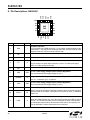
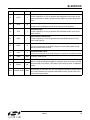
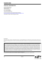
S i 4 0 6 3/60 H I G H - P ERFORMANCE , L O W -C U R R E N T T RANSMITTER Features Smart metering Remote control Home security and alarm Telemetry Garage and gate openers Remote keyless entry Home automation Industrial control Sensor networks Health monitors Electronic shelf labels 1 20 19 18 17 16 NC 2 15 nSEL NC 3 14 SDI GND PAD TX 4 13 SDO NC 5 Description Silicon Laboratories' Si406x devices are high-performance, low-current transmitters covering the sub-GHz frequency bands from 142 to 1050 MHz. The radios are part of the EZRadioPRO® family, which includes a complete line of transmitters, receivers, and transceivers covering a wide range of applications. All parts offer extremely low active and standby current consumption. The Si406x includes optimal phase noise performance for narrow band applications, such as FCC Part90 and 169 MHz wireless Mbus. The Si4063 offers exceptional output power of up to +20 dBm with outstanding TX efficiency. The high output power allows extended ranges and highly robust communication links. The Si4060 active mode TX current consumption of 18 mA at +10 dBm coupled with extremely low standby current and fast wake times ensure extended battery life in the most demanding applications. The Si4063 can achieve up to +27 dBm output power with built-in ramping control of a low-cost external FET. The devices are compliant with all worldwide regulatory standards: FCC, ETSI, and ARIB. All devices are designed to be compliant with 802.15.4g and WMbus smart metering standards. Rev 0.1 12/12 SDN XOUT XIN GND Pin Assignments Applications Copyright © 2012 by Silicon Laboratories 12 SCLK 6 7 8 9 10 GPIO1 GPIO0 GPIO2 VDD Power supply = 1.8 to 3.6 V Highly configurable packet handler TX 64 byte FIFO Low BOM Low battery detector Temperature sensor 20-Pin QFN package IEEE 802.15.4g compliant FCC Part 90 Mask D, FCC part 15.247, 15,231, 15,249, ARIB T-108, T-96, T-67, China regulatory ETSI Class-I Operation GPIO3 Frequency range = 142–1050 MHz Modulation (G)FSK, 4(G)FSK, (G)MSK OOK Max output power +20 dBm (Si4063) +13 dBm (Si4060) PA support for +27 or +30 dBm Ultra low current powerdown modes 30 nA shutdown, 50 nA standby Data rate = 100 bps to 1 Mbps Fast wake times TXRamp VDD 11 nIRQ Patents pending Si4063/60 Si4063/60 Functional Block Diagram GPIO3 GPIO2 XIN XOUT Loop Filter PFD / CP VCO FBDIV TX DIV 30 MHz XO Frac-N Div LO Gen Bootup OSC SDN PA PowerRamp Cntl LDOs PA LDO VDD 2 Digital Logic POR LBD 32K LP OSC TXRAMP VDD GPIO0 GPIO1 Product Freq. Range Max Output Power TX Current Narrowband Operation Si4063 Major bands 142–1050 MHz +20 dBm 169 MHz: 70 mA 915 MHz: 85 mA Si4060 Major bands 142–1050 MHz +13 dBm +10 dBm: 18 mA Rev 0.1 SPI Interface Controller TX ADC Temp sensor MODEM FIFO Packet Handler nSEL SDI SDO SCLK nIRQ Si4063/60 TABLE O F C ONTENTS Section Page 1. Electrical Specifications . . . . . . . . . . . . . . . . . . . . . . . . . . . . . . . . . . . . . . . . . . . . . . . . . . .4 1.1. Definition of Test Conditions . . . . . . . . . . . . . . . . . . . . . . . . . . . . . . . . . . . . . . . . . . . 10 2. Functional Description . . . . . . . . . . . . . . . . . . . . . . . . . . . . . . . . . . . . . . . . . . . . . . . . . . . 11 3. Controller Interface . . . . . . . . . . . . . . . . . . . . . . . . . . . . . . . . . . . . . . . . . . . . . . . . . . . . . . 12 3.1. Serial Peripheral Interface (SPI) . . . . . . . . . . . . . . . . . . . . . . . . . . . . . . . . . . . . . . . . 12 3.2. Fast Response Registers . . . . . . . . . . . . . . . . . . . . . . . . . . . . . . . . . . . . . . . . . . . . .14 3.3. Operating Modes and Timing . . . . . . . . . . . . . . . . . . . . . . . . . . . . . . . . . . . . . . . . . . 14 3.4. Application Programming Interface (API) . . . . . . . . . . . . . . . . . . . . . . . . . . . . . . . . . 18 3.5. Interrupts . . . . . . . . . . . . . . . . . . . . . . . . . . . . . . . . . . . . . . . . . . . . . . . . . . . . . . . . . . 18 3.6. GPIO . . . . . . . . . . . . . . . . . . . . . . . . . . . . . . . . . . . . . . . . . . . . . . . . . . . . . . . . . . . . . 19 4. Modulation and Hardware Configuration Options . . . . . . . . . . . . . . . . . . . . . . . . . . . . . 20 4.1. Modulation Types . . . . . . . . . . . . . . . . . . . . . . . . . . . . . . . . . . . . . . . . . . . . . . . . . . . 20 4.2. Hardware Configuration Options . . . . . . . . . . . . . . . . . . . . . . . . . . . . . . . . . . . . . . . . 20 5. Internal Functional Blocks . . . . . . . . . . . . . . . . . . . . . . . . . . . . . . . . . . . . . . . . . . . . . . . . 21 5.1. Synthesizer . . . . . . . . . . . . . . . . . . . . . . . . . . . . . . . . . . . . . . . . . . . . . . . . . . . . . . . .21 5.2. Transmitter (TX) . . . . . . . . . . . . . . . . . . . . . . . . . . . . . . . . . . . . . . . . . . . . . . . . . . . .22 5.3. Crystal Oscillator . . . . . . . . . . . . . . . . . . . . . . . . . . . . . . . . . . . . . . . . . . . . . . . . . . . .25 6. Data Handling and Packet Handler . . . . . . . . . . . . . . . . . . . . . . . . . . . . . . . . . . . . . . . . . .26 6.1. TX FIFOs . . . . . . . . . . . . . . . . . . . . . . . . . . . . . . . . . . . . . . . . . . . . . . . . . . . . . . . . . . 26 6.2. Packet Handler . . . . . . . . . . . . . . . . . . . . . . . . . . . . . . . . . . . . . . . . . . . . . . . . . . . . . 26 7. Auxiliary Blocks . . . . . . . . . . . . . . . . . . . . . . . . . . . . . . . . . . . . . . . . . . . . . . . . . . . . . . . . . 27 7.1. Wake-up Timer and 32 kHz Clock Source . . . . . . . . . . . . . . . . . . . . . . . . . . . . . . . . 27 7.2. Low Duty Cycle Mode . . . . . . . . . . . . . . . . . . . . . . . . . . . . . . . . . . . . . . . . . . . . . . . . 29 7.3. Temperature, Battery Voltage, and Auxiliary ADC . . . . . . . . . . . . . . . . . . . . . . . . . . 30 7.4. Low Battery Detector . . . . . . . . . . . . . . . . . . . . . . . . . . . . . . . . . . . . . . . . . . . . . . . . .31 8. Pin Descriptions: Si4063/60 . . . . . . . . . . . . . . . . . . . . . . . . . . . . . . . . . . . . . . . . . . . . . . . 32 9. Ordering Information . . . . . . . . . . . . . . . . . . . . . . . . . . . . . . . . . . . . . . . . . . . . . . . . . . . . . 34 10. Package Outline: Si4063/60 . . . . . . . . . . . . . . . . . . . . . . . . . . . . . . . . . . . . . . . . . . . . . . . 35 11. PCB Land Pattern: Si4063/60 . . . . . . . . . . . . . . . . . . . . . . . . . . . . . . . . . . . . . . . . . . . . .37 12. Top Marking . . . . . . . . . . . . . . . . . . . . . . . . . . . . . . . . . . . . . . . . . . . . . . . . . . . . . . . . . . .39 12.1. Si4063/60 Top Marking . . . . . . . . . . . . . . . . . . . . . . . . . . . . . . . . . . . . . . . . . . . . . . 39 12.2. Top Marking Explanation . . . . . . . . . . . . . . . . . . . . . . . . . . . . . . . . . . . . . . . . . . . . 39 Contact Information . . . . . . . . . . . . . . . . . . . . . . . . . . . . . . . . . . . . . . . . . . . . . . . . . . . . . . . .40 Rev 0.1 3 Si4063/60 1. Electrical Specifications Table 1. DC Characteristics1 Parameter Min Typ Max Unit 1.8 3.3 3.6 V RC Oscillator, Main Digital Regulator, and Low Power Digital Regulator OFF — 30 — nA IStandby Register values maintained and RC oscillator/WUT OFF — 50 — nA ISleepRC RC Oscillator/WUT ON and all register values maintained, and all other blocks OFF — 900 — nA ISleepXO Sleep current using an external 32 kHz crystal.2 — 1.7 — µA ISensor Low battery detector ON, register values maintained, and all other blocks OFF — 1 — µA IReady Crystal Oscillator and Main Digital Regulator ON, all other blocks OFF — 1.8 — mA TUNE Mode Current ITune_TX TX Tune, High Performance Mode — 8 — mA TX Mode Current (Si4063) ITX_+20 +20 dBm output power, class-E match, 915 MHz, 3.3 V — 85 — mA +20 dBm output power, class-E match, 460 MHz, 3.3 V — 75 — mA +20 dBm output power, square-wave match, 169 MHz, 3.3 V — 70 — mA +10 dBm output power, Class-E match, 868 MHz, 3.3 V2 — 18 — mA Supply Voltage Range Symbol VDD Power Saving Modes IShutdown -LBD TX Mode Current (Si4060) Test Condition ITX_+10 Notes: 1. All specifications guaranteed by production test unless otherwise noted. Production test conditions and max limits are listed in the "Production Test Conditions" section of "1.1. Definition of Test Conditions" on page 10. 2. Guaranteed by qualification. Qualification test conditions are listed in the “Qualification Test Conditions” section in "1.1. Definition of Test Conditions" on page 10. 4 Rev 0.1 Si4063/60 Table 2. Synthesizer AC Electrical Characteristics1 Parameter Synthesizer Frequency Range (Si4063/60) Synthesizer Frequency Resolution2 Symbol Test Condition FSYN Min Typ Max Unit 850 — 1050 MHz 420 — 525 MHz 284 — 350 MHz 142 — 175 MHz FRES-960 850–1050 MHz — 28.6 — Hz FRES-525 420–525 MHz — 14.3 — Hz FRES-350 283–350 MHz — 9.5 — Hz FRES-175 142–175 MHz — 4.7 — Hz Synthesizer Settling Time3 tLOCK Measured from exiting Ready mode with XOSC running to any frequency. Including VCO Calibration. — 50 — µs Phase Noise3 L(fM) F = 10 kHz, 460 MHz, High Perf Mode — –106 — dBc/Hz F = 100 kHz, 460 MHz, High Perf Mode — –110 — dBc/Hz F = 1 MHz, 460 MHz, High Perf Mode — –123 — dBc/Hz F = 10 MHz, 460 MHz, High Perf Mode — –130 — dBc/Hz Notes: 1. All specification guaranteed by production test unless otherwise noted. Production test conditions and max limits are listed in the “Production Test Conditions” section in "1.1. Definition of Test Conditions" on page 10. 2. Default API setting for modulation deviation resolution is double the typical value specified. 3. Guaranteed by qualification. Qualification test conditions are listed in the "Qualification Test Conditions" section in "1.1. Definition of Test Conditions" on page 10. Rev 0.1 5 Si4063/60 Table 3. Transmitter AC Electrical Characteristics1 Parameter Symbol Test Condition TX Frequency Range (Si4063/60) Min Typ Max Unit 850 — 1050 MHz 420 — 525 MHz 284 — 350 MHz 142 — 175 MHz FTX (G)FSK Data Rate2,3 DRFSK 0.1 — 500 kbps 4(G)FSK Data Rate2,3 DR4FSK 0.2 — 1000 kbps OOK Data Rate2,3 DROOK 0.1 — 120 kbps Modulation Deviation Range2 Modulation Deviation Resolution2,4 f960 850–1050 MHz — 1.5 — MHz f525 420–525 MHz — 750 — kHz f350 283–350 MHz — 500 — kHz f175 142–175 MHz — 250 — kHz FRES-960 850–1050 MHz — 28.6 — Hz FRES-525 420–525 MHz — 14.3 — Hz FRES-350 283–350 MHz — 9.5 — Hz FRES-175 142–175 MHz — 4.7 — Hz Output Power Range (Si4063)5 PTX –20 — +20 dBm Output Power Range (Si4060)5 PTX60 –40 — +13 dBm TX RF Output Steps2 PRF_OUT Using switched current match within 6 dB of max power — 0.1 — dB TX RF Output Level2 Variation vs. Temperature PRF_TEMP –40 to +85 C — 1 — dB TX RF Output Level Variation vs. Frequency2 PRF_FREQ Measured across 902–928 MHz — 0.5 — dB B*T Gaussian Filtering Bandwith Time Product — 0.5 — Transmit Modulation Filtering2 Notes: 1. All specification guaranteed by production test unless otherwise noted. Production test conditions and max limits are listed in the "Production Test Conditions" section in "1.1. Definition of Test Conditions" on page 10. 2. Guaranteed by qualification. Qualification test conditions are listed in the "Qualification Test Conditions" section in "1.1. Definition of Test Conditions" on page 10. 3. The maximum data rate is dependent on the XTAL frequency and is calculated as per the formula: Maximum Symbol Rate = Fxtal/60, where Fxtal is the XTAL frequency (typically 30 MHz). 4. Default API setting for modulation deviation resolution is double the typical value specified. 5. Output power is dependent on matching components and board layout. 6 Rev 0.1 Si4063/60 Table 4. Auxiliary Block Specifications1 Parameter Temperature Sensor Sensitivity2 Low Battery Detector Resolution Microcontroller Clock Output Frequency Range3 Symbol Min Typ Max Unit TSS — 4.5 — LBDRES — 50 — ADC Codes/ °C mV 32.768K — Fxtal Hz — 3 — ms 25 — — 250 32 — MHz µs — 70 — fF — — 2 2500 — — sec ppm — — 5 ms FMC Test Condition Configurable to Fxtal or Fxtal divided by 2, 3, 7.5, 10, 15, or 30 where Fxtal is the reference XTAL frequency. In addition, 32.768 kHz is also supported. Programmable setting TEMPCT Temperature Sensor Conversion2 XTAL Range4 XTALRange 30 MHz XTAL Start-Up Time t30M Using XTAL and board layout in reference design. Start-up time will vary with XTAL type and board layout. 30MRES 30 MHz XTAL Cap Resolution2 32 kHz XTAL Start-Up Time2 t32k 32 kHz Accuracy using 32KRCRES Internal RC Oscillator2 POR Reset Time tPOR Notes: 1. All specification guaranteed by production test unless otherwise noted. Production test conditions and max limits are listed in the "Production Test Conditions" section in "1.1. Definition of Test Conditions" on page 10. 2. Guaranteed by qualification. Qualification test conditions are listed in the "Qualification Test Conditions" section in "1.1. Definition of Test Conditions" on page 10. 3. Microcontroller clock frequency tested in production at 1 MHz, 30 MHz and 32.768 kHz. Other frequencies tested in bench characterization. 4. XTAL Range tested in production using an external clock source (similar to using a TCXO). Rev 0.1 7 Si4063/60 Table 5. Digital IO Specifications (GPIO_x, SCLK, SDO, SDI, nSEL, nIRQ, SDN)1 Parameter Rise Time 2,3 Fall Time3,4 Symbol Test Condition Min Typ Max Unit TRISE 0.1 x VDD to 0.9 x VDD, CL = 10 pF, DRV<1:0> = HH — 2.3 — ns TFALL 0.9 x VDD to 0.1 x VDD, CL = 10 pF, DRV<1:0> = HH — 2 — ns Input Capacitance CIN — 2 — pF Logic High Level Input Voltage VIH VDD x 0.7 — — V Logic Low Level Input Voltage VIL — — VDD x 0.3 V Input Current IIN 0<VIN< VDD –10 — 10 µA Input Current If Pullup is Activated IINP VIL = 0 V 1 — 10 µA LL3 — 6.66 — mA DRV[1:0] = LH 3 — 5.03 — mA IOmaxHL DRV[1:0] = HL 3 — 3.16 — mA IOmaxHH DRV[1:0] = HH3 — 1.13 — mA IOmaxLL 3 — 5.75 — mA 3 — 4.37 — mA IOmaxHL DRV[1:0] = HL3 — 2.73 — mA IOmaxHH DRV[1:0] = HH3 — 0.96 — mA IOmaxLL 3 — 2.53 — mA LH3 — 2.21 — mA IOmaxHL DRV[1:0] = HL 3 — 1.7 — mA IOmaxHH DRV[1:0] = HH3 — 0.80 — mA Logic High Level Output Voltage VOH DRV[1:0] = HL VDD x 0.8 — — V Logic Low Level Output Voltage VOL DRV[1:0] = HL — — VDD x 0.2 V Drive Strength for Output Low Level Drive Strength for Output High Level Drive Strength for Output High Level for GPIO0 IOmaxLL IOmaxLH IOmaxLH IOmaxLH DRV[1:0] = DRV[1:0] = LL DRV[1:0] = LH DRV[1:0] = LL DRV[1:0] = Notes: 1. All specifications guaranteed by qualification. Qualification test conditions are listed in the "Qualification Test Conditions" section in "1.1. Definition of Test Conditions" on page 10. 2. 8 ns is typical for GPIO0 rise time. 3. Assuming VDD = 3.3 V, drive strength is specified at Voh (min) = 2.64 V and Vol(max) = 0.66 V at room temperature. 4. 2.4 ns is typical for GPIO0 fall time. 8 Rev 0.1 Si4063/60 Table 6. Absolute Maximum Ratings Parameter Value Unit VDD to GND –0.3, +3.6 V Instantaneous VRF-peak to GND on TX Output Pin –0.3, +8.0 V Sustained VRF-peak to GND on TX Output Pin –0.3, +6.5 V Voltage on Digital Control Inputs –0.3, VDD + 0.3 V Voltage on Analog Inputs –0.3, VDD + 0.3 V –40 to +85 C Thermal Impedance JA 30 C/W Junction Temperature TJ +125 C –55 to +125 C Operating Ambient Temperature Range TA Storage Temperature Range TSTG Note: Stresses beyond those listed under “Absolute Maximum Ratings” may cause permanent damage to the device. These are stress ratings only and functional operation of the device at or beyond these ratings in the operational sections of the specifications is not implied. Exposure to absolute maximum rating conditions for extended periods may affect device reliability. Power Amplifier may be damaged if switched on without proper load or termination connected. TX matching network design will influence TX VRF-peak on TX output pin. Caution: ESD sensitive device. Rev 0.1 9 Si4063/60 1.1. Definition of Test Conditions Production Test Conditions: TA = +25 °C. VDD TX = +3.3 VDC. output power measured at 915 MHz. reference signal (XOUT) = 1.0 VPP at 30 MHz, centered around 0.8 VDC. External Production test schematic (unless noted otherwise). All TX output levels are referred to the pins of the Si4063/60 (not the output of the RF module). Qualification Test Conditions: TA = –40 to +85 °C (Typical TA = 25 °C). VDD All 10 = +1.8 to +3.6 VDC (Typical VDD = 3.3 VDC). RF levels referred to the pins of the Si4063/60 (not the RF module). Rev 0.1 Si4063/60 2. Functional Description The Si406x devices are high-performance, low-current, wireless ISM transmitters that cover the sub-GHz bands. The wide operating voltage range of 1.8–3.6 V and low current consumption make the Si406x an ideal solution for battery powered applications. A single high precision local oscillator (LO) is used for transmit mode. The LO is generated by an integrated VCO and Fractional-N PLL synthesizer. The synthesizer is designed to support configurable data rates from 100 bps to 1 Mbps. The Si4063/60 operate in the frequency bands of 142–175, 283–350, 420–525, and 850–1050 MHz with a maximum frequency accuracy step size of 28.6 Hz. The transmit FSK data is modulated directly into the data stream and can be shaped by a Gaussian low-pass filter to reduce unwanted spectral content. The Si4063/60 contains a power amplifier (PA) that supports output power up to +20 dBm with very high efficiency, consuming only 70 mA at 169 MHz and 85 mA at 915 MHz. The integrated +20 dBm power amplifier can also be used to compensate for the reduced performance of a lower cost, lower performance antenna or antenna with size constraints due to a small form-factor. Competing solutions require large and expensive external PAs to achieve comparable performance. The Si4060 is designed to support single coin cell operation with current consumption below 18 mA for +10 dBm output power. Two match topologies are available for the Si4060, Class-E and switched-current. Class-E matching provides optimal current consumption, while switched-current matching demonstrates the best performance over varying battery voltage and temperature with slightly higher current consumption. The PA is single-ended to allow for easy antenna matching and low BOM cost. The PA incorporates automatic ramp-up and ramp-down control to reduce unwanted spectral spreading. The Si406x family supports frequency hopping to extend the link range and improve performance. A highly configurable packet handler allows for autonomous encoding of nearly any packet structure. Additional system features, such as an automatic wake-up timer, low battery detector, and 64 byte TX FIFOs, reduce overall current consumption and allows for the use of lower-cost system MCUs. An integrated temperature sensor, power-on-reset (POR), and GPIOs further reduce overall system cost and size. The Si406x is designed to work with an MCU, crystal, and a few passive components to create a very low-cost system. SDO 10 9 Microcontroller 16 XIN 17 GNDX 18 GPIO2 19 XOUT SDI GPIO1 L1 GPIO0 C2 8 C3 13 nSEL SCLK 12 11 nIRQ VDD C1 C4 15 Si406x 7 L2 SDN 14 TXRAMP NC 2 NC 3 TX 4 NC 5 VDD L3 L4 1 6 SDN 20 GPIO3 30 MHz VDD C5 C6 C7 Figure 1. Si406x Application Example Rev 0.1 11 Si4063/60 3. Controller Interface 3.1. Serial Peripheral Interface (SPI) The Si406x communicates with the host MCU over a standard 4-wire serial peripheral interface (SPI): SCLK, SDI, SDO, and nSEL. The SPI interface is designed to operate at a maximum of 10 MHz. The SPI timing parameters are demonstrated in Table 7. The host MCU writes data over the SDI pin and can read data from the device on the SDO output pin. Figure 2 demonstrates an SPI write command. The nSEL pin should go low to initiate the SPI command. The first byte of SDI data will be one of the firmware commands followed by n bytes of parameter data which will be variable depending on the specific command. The rising edges of SCLK should be aligned with the center of the SDI data. Table 7. Serial Interface Timing Parameters Symbol Parameter Min (ns) tCH Clock high time 40 tCL Clock low time 40 tDS Data setup time 20 tDH Data hold time 20 tDD Output data delay time 20 tEN Output enable time 20 tDE Output disable time 50 tSS Select setup time 20 tSH Select hold time 50 tSW Select high period 80 Diagram SCLK tSS tCL tCH tDS tDH tDD tSH tDE SDI SDO tEN tSW nSEL nSEL SDO SDI FW Command Param Byte 0 Param Byte n SCLK Figure 2. SPI Write Command The Si406x contains an internal MCU which controls all the internal functions of the radio. For SPI read commands a typical MCU flow of checking clear-to-send (CTS) is used to make sure the internal MCU has executed the command and prepared the data to be output over the SDO pin. Figure 3 demonstrates the general flow of an SPI read command. Once the CTS value reads FFh then the read data is ready to be clocked out to the host MCU. The typical time for a valid FFh CTS reading is 20 µs. Figure 4 demonstrates the remaining read cycle after CTS is set to FFh. The internal MCU will clock out the SDO data on the negative edge so the host MCU should process the SDO data on the rising edge of SCLK. 12 Rev 0.1 Si4063/60 Firmware Flow 0xFF Send Command Read CTS CTS Value Retrieve Response 0x00 NSEL CTS SDO SDI ReadCmdBuff SCK Figure 3. SPI Read Command—Check CTS Value NSEL SDO Response Byte 0 Response Byte n SDI SCK Figure 4. SPI Read Command—Clock Out Read Data Rev 0.1 13 Si4063/60 3.2. Fast Response Registers The fast response registers are registers that can be read immediately without the requirement to monitor and check CTS. There are four fast response registers that can be programmed for a specific function. The fast response registers can be read through API commands, 0x50 for Fast Response A, 0x51 for Fast Response B, 0x53 for Fast Response C, and 0x57 for Fast Response D. The fast response registers can be configured by the “FRR_CTL_X_MODE” properties. The fast response registers may be read in a burst fashion. After the initial 16 clock cycles, each additional eight clock cycles will clock out the contents of the next fast response register in a circular fashion. The value of the FRRs will not be updated unless NSEL is toggled. 3.3. Operating Modes and Timing The primary states of the Si406x are shown in Figure 5. The shutdown state completely shuts down the radio to minimize current consumption. Standby/Sleep, SPI Active, Ready, and TX Tune are available to optimize the current consumption and response time to TX for a given application. The API commands, START_TX and CHANGE_STATE, control the operating state with the exception of shutdown which is controlled by SDN, pin 1. Table 8 shows each of the operating modes with the time required to reach TX mode as well as the current consumption of each mode. The times in Table 9 are measured from the rising edge of nSEL until the chip is in the desired state. Note that these times are indicative of state transition timing but are not guaranteed and should only be used as a reference data point. An automatic sequencer will put the chip into TX from any state. It is not necessary to manually step through the states. To simplify the diagram it is not shown but any of the lower power states can be returned to automatically after TX. Sleep Shutdown SPI Active Ready Tx Tune Tx Figure 5. State Machine Diagram 14 Rev 0.1 Si4063/60 Table 8. Operating State Response Time and Current Consumption* State/Mode Response Time to TX Current in State /Mode Shutdown State 15 ms 30 nA Standby State Sleep State SPI Active State Ready State TX Tune State 440 µs 440 µs 340 µs 126 µs 58 µs 50 nA 900 nA 1.35 mA 1.8 mA 8 mA TX State — 18 mA @ +10 dBm Figure 6 shows the POR timing and voltage requirements. The power consumption (battery life) depends on the duty cycle of the application or how often the part is in TX state. In most applications the utilization of the standby state will be most advantageous for battery life but for very low duty cycle applications shutdown will have an advantage. For the fastest timing the next state can be selected in the START_TX API commands to minimize SPI transactions and internal MCU processing. 3.3.1. Power on Reset (POR) A Power On Reset (POR) sequence is used to boot the device up from a fully off or shutdown state. To execute this process, VDD must ramp within 1ms and must remain applied to the device for at least 10ms. If VDD is removed, then it must stay below 0.15V for at least 10ms before being applied again. Please see Figure x and Table x for details. VDD VR RH VR RL Time tSR tPORH Figure 6. POR Timing Diagram Rev 0.1 15 Si4063/60 Table 9. POR Timing Variable tPORH Description High time for VDD to fully settle POR circuit. tPORL Low time for VDD to enable POR. VRRH Voltage for successful POR VRRL Starting Voltage for successful POR tSR Min Typ Max Units 10 ms 10 ms 90%*Vdd V 0 Slew rate of VDD for successful POR 150 mV 1 ms 3.3.2. Shutdown State The shutdown state is the lowest current consumption state of the device with nominally less than 30 nA of current consumption. The shutdown state may be entered by driving the SDN pin (Pin 1) high. The SDN pin should be held low in all states except the shutdown state. In the shutdown state, the contents of the registers are lost and there is no SPI access. When coming out of the shutdown state a power on reset (POR) will be initiated along with the internal calibrations. After the POR the POWER_UP command is required to initialize the radio. The SDN pin needs to be held high for at least 10us before driving low again so that internal capacitors can discharge. Not holding the SDN high for this period of time may cause the POR to be missed and the device to boot up incorrectly. If POR timing and voltage requirements cannot be met, it is highly recommended that SDN be controlled using the host processor rather than tying it to GND on the board. 3.3.3. Standby State Standby state has the lowest current consumption with the exception of shutdown but has much faster response time to TX mode. In most cases standby should be used as the low power state. In this state the register values are maintained with all other blocks disabled. The SPI is accessible during this mode but any SPI event, including FIFO R/W, will enable an internal boot oscillator and automatically move the part to SPI active state. After an SPI event the host will need to re-command the device back to standby through the “Change State” API command to achieve the 50 nA current consumption. If an interrupt has occurred (i.e., the nIRQ pin = 0) the interrupt registers must be read to achieve the minimum current consumption of this mode. 3.3.4. Sleep State Sleep state is the same as standby state but the wake-up-timer and a 32 kHz clock source are enabled. The source of the 32 kHz clock can either be an internal 32 kHz RC oscillator which is periodically calibrated or a 32 kHz oscillator using an external XTAL.The SPI is accessible during this mode but an SPI event will enable an internal boot oscillator and automatically move the part to SPI active mode. After an SPI event the host will need to re-command the device back to sleep. If an interrupt has occurred (i.e., the nIRQ pin = 0) the interrupt registers must be read to achieve the minimum current consumption of this mode. 3.3.5. SPI Active State In SPI active state the SPI and a boot up oscillator are enabled. After SPI transactions during either standby or sleep the device will not automatically return to these states. A “Change State” API command will be required to return to either the standby or sleep modes. 3.3.6. Ready State Ready state is designed to give a fast transition time to TX state with reasonable current consumption. In this mode the Crystal oscillator remains enabled reducing the time required to switch to TX mode by eliminating the crystal start-up time. 3.3.7. TX State The TX state may be entered from any of the state with the “Start TX” or “Change State” API commands. A built-in sequencer takes care of all the actions required to transition between states from enabling the crystal oscillator to ramping up the PA. The following sequence of events will occur automatically when going from standby to TX state. 1. Enable internal LDOs. 2. Start up crystal oscillator and wait until ready (controlled by an internal timer). 16 Rev 0.1 Si4063/60 3. Enable PLL. 4. Calibrate VCO/PLL. 5. Wait until PLL settles to required transmit frequency (controlled by an internal timer). 6. Activate power amplifier and wait until power ramping is completed (controlled by an internal timer). 7. Transmit packet. Steps in this sequence may be eliminated depending on which state the chip is configured to prior to commanding to TX. By default, the VCO and PLL are calibrated every time the PLL is enabled. When the START_TX API command is utilized the next state may be defined to ensure optimal timing and turnaround. Figure 7 shows an example of the commands and timing for the START_TX command. CTS will go high as soon as the sequencer puts the part into TX state. As the sequencer is stepping through the events listed above, CTS will be low and no new commands or property changes are allowed. If the Fast Response (FRR) or nIRQ is used to monitor the current state there will be slight delay caused by the internal hardware from when the event actually occurs to when the transition occurs on the FRR or nIRQ. The time from entering TX state to when the FRR will update is 5 µs and the time to when the nIRQ will transition is 13 µs. If a GPIO is programmed for TX state or used as control for a transmit/receive switch (TR switch) there is no delay. CTS NSEL SDI Current State FRR START_TX YYY State Tx State YYY State TXCOMPLETE_STATE Tx State TXCOMPLETE_STATE nIRQ GPIOx – TX state Figure 7. Start_TX Commands and Timing Rev 0.1 17 Si4063/60 3.4. Application Programming Interface (API) An application programming interface (API), which the host MCU will communicate with, is embedded inside the device. The API is divided into two sections, commands and properties. The commands are used to control the chip and retrieve its status. The properties are general configurations which will change infrequently. 3.5. Interrupts The Si406x is capable of generating an interrupt signal when certain events occur. The chip notifies the microcontroller that an interrupt event has occurred by setting the nIRQ output pin LOW = 0. This interrupt signal will be generated when any one (or more) of the interrupt events (corresponding to the Interrupt Status bits) occur. The nIRQ pin will remain low until the microcontroller reads the Interrupt Status Registers. The nIRQ output signal will then be reset until the next change in status is detected. The interrupts sources are grouped into three groups: packet handler, chip status, and modem. The individual interrupts in these groups can be enabled/disabled in the interrupt property registers, 0101, 0102, and 0103. An interrupt must be enabled for it to trigger an event on the nIRQ pin. The interrupt group must be enabled as well as the individual interrupts in API property 0100. Number Command Summary 0x20 GET_INT_STATUS Returns the interrupt status—packet handler, modem, and chip 0x21 GET_PH_STATUS Returns the packet handler status. 0x22 GET_MODEM_STATUS 0x23 GET_CHIP_STATUS Returns the modem status byte. Returns the chip status. Number Property Default Summary 0x0100 INT_CTL_ENABLE 0x04 Enables interrupt groups for PH, Modem, and Chip. 0x0101 INT_CTL_PH_ENABLE 0x00 Packet handler interrupt enable property. 0x0102 INT_CTL_MODEM_ENABLE 0x00 Modem interrupt enable property. 0x0103 INT_CTL_CHIP_ENABLE 0x04 Chip interrupt enable property. Once an interrupt event occurs and the nIRQ pin is low there are two ways to read and clear the interrupts. All of the interrupts may be read and cleared in the “GET_INT_STATUS” API command. By default all interrupts will be cleared once read. If only specific interrupts want to be read in the fastest possible method the individual interrupt groups (Packet Handler, Chip Status, Modem) may be read and cleared by the “GET_MODEM_STATUS”, “GET_PH_STATUS” (packet handler), and “GET_CHIP_STATUS” API commands. The instantaneous status of a specific function maybe read if the specific interrupt is enabled or disabled. The status results are provided after the interrupts and can be read with the same commands as the interrupts. The status bits will give the current state of the function whether the interrupt is enabled or not. The fast response registers can also give information about the interrupt groups but reading the fast response registers will not clear the interrupt and reset the nIRQ pin. 18 Rev 0.1 Si4063/60 3.6. GPIO Four general purpose IO pins are available to utilize in the application. The GPIO are configured by the GPIO_PIN_CFG command in address 13h. For a complete list of the GPIO options please see the API guide. GPIO pins 0 and 1 should be used for active signals such as data or clock. GPIO pins 2 and 3 have more susceptibility to generating spurious in the synthesizer than pins 0 and 1. The drive strength of the GPIOs can be adjusted with the GEN_CONFIG parameter in the GPIO_PIN_CFG command. By default the drive strength is set to minimum. The default configuration for the GPIOs and the state during SDN is shown below in Table 10.The state of the IO during shutdown is also shown inTable 10. As indicated previously in Table 5, GPIO 0 has lower drive strength than the other GPIOs. Table 10. GPIOs Pin SDN State POR Default GPIO0 0 POR GPIO1 0 CTS GPIO2 0 POR GPIO3 0 POR nIRQ resistive VDD pull-up nIRQ SDO resistive VDD pull-up SDO SDI High Z SDI Rev 0.1 19 Si4063/60 4. Modulation and Hardware Configuration Options The Si406x supports different modulation options and can be used in various configurations to tailor the device to any specific application or legacy system for drop in replacement. The modulation and configuration options are set in API property, MODEM_MOD_TYPE. 4.1. Modulation Types The Si406x supports five different modulation options: Gaussian frequency shift keying (GFSK), frequency-shift keying (FSK), four-level GFSK (4GFSK), four-level FSK (4FSK), on-off keying (OOK). Minimum shift keying (MSK) can also be created by using GFSK settings. GFSK is the recommended modulation type as it provides the best performance and cleanest modulation spectrum. The modulation type is set by the “MOD_TYPE[2:0]” registers in the “MODEM_MOD_TYPE” API property. A continuous-wave (CW) carrier may also be selected for RF evaluation purposes. The modulation source may also be selected to be a pseudo-random source for evaluation purposes. 4.2. Hardware Configuration Options There are different receive demodulator options to optimize the performance and mutually-exclusive options for how the TX data is transferred from the host MCU to the RF device. 4.2.1. TX Data Interface With MCU There are two different options for transferring the data from the RF device to the host MCU. FIFO mode uses the SPI interface to transfer the data, while direct mode transfers the data in real time over GPIO. 4.2.1.1. FIFO Mode In FIFO mode, the transmit data is stored in integrated FIFO register memory. The TX FIFO is accessed by writing Command 66h followed directly by the data/clk that the host wants to write into the TX FIFO. If the packet handler is enabled, the data bytes stored in FIFO memory are “packaged” together with other fields and bytes of information to construct the final transmit packet structure. These other potential fields include the Preamble, Sync word, Header, CRC checksum, etc. The configuration of the packet structure in TX mode is determined by the Automatic Packet Handler (if enabled), in conjunction with a variety of Packet Handler properties. If the Automatic Packet Handler is disabled, the entire desired packet structure should be loaded into FIFO memory; no other fields (such as Preamble or Sync word) will be automatically added to the bytes stored in FIFO memory. For further information on the configuration of the FIFOs for a specific application or packet size, see "6. Data Handling and Packet Handler" on page 26. The chip will return to the IDLE state programmed in the argument of the “START TX” API command, TXCOMPLETE_STATE[3:0]. For example, the chip may be placed into TX mode by sending the “START TX” command and by writing the 30h to the TXCOMPLETE_STATE[3:0] argument. The chip will transmit all of the contents of the FIFO, and the ipksent interrupt will occur. When this event occurs, the chip will return to the ready state as defined by TXCOMPLETE_STATE[3:0] = 30h. 4.2.1.2. Direct Mode For legacy systems that perform packet handling within the host MCU or other baseband chip, it may not be desirable to use the FIFO. For this scenario, a Direct mode is provided, which bypasses the FIFOs entirely. In TX Direct mode, the TX modulation data is applied to an input pin of the chip and processed in “real time” (i.e., not stored in a register for transmission at a later time). Any of the GPIOs may be configured for use as the TX Data input function. Furthermore, an additional pin may be required for a TX Clock output function if GFSK modulation is desired (only the TX Data input pin is required for FSK). To achieve direct mode, the GPIO must be configured in the “GPIO_PIN_CFG” API command as well as the “MODEM_MOD_TYPE” API property. For GFSK, “TX_DIRECT_MODE_TYPE” must be set to Synchronous. For 2FSK or OOK, the type can be set to asynchronous or synchronous. The MOD_SOURCE[1:0] should be set to 01h for are all direct mode configurations. 20 Rev 0.1 Si4063/60 5. Internal Functional Blocks The following sections provide an overview to the key internal blocks and features. 5.1. Synthesizer An integrated Sigma Delta () Fractional-N PLL synthesizer capable of operating over the bands from 142–175, 283–350, 420–525, and 850–1050 MHz for the Si406x. Using a synthesizer has many advantages; it provides flexibility in choosing data rate, deviation, channel frequency, and channel spacing. The transmit modulation is applied directly to the loop in the digital domain through the fractional divider, which results in very precise accuracy and control over the transmit deviation. The frequency resolution in the 850–1050 MHz band is 28.6 Hz with more resolution in the other bands. The nominal reference frequency to the PLL is 30 MHz, but any XTAL frequency from 25 to 32 MHz may be used. The modem configuration calculator in WDS will automatically account for the XTAL frequency being used. The PLL utilizes a differential LC VCO with integrated on-chip inductors. The output of the VCO is followed by a configurable divider, which will divide the signal down to the desired output frequency band. 5.1.1. Synthesizer Frequency Control The frequency is set by changing the integer and fractional settings to the synthesizer. The WDS calculator will automatically provide these settings, but the synthesizer equation is shown below for convenience. The APIs for setting the frequency are FREQ_CONTROL_INTE, FREQ_CONTROL_FRAC2, FREQ_CONTROL_FRAC1, and FREQ_CONTROL_FRAC0. freq_xo fc_frac- 2 ----------------------------- Hz RF_channel = fc_inte + ----------------19 outdiv 2 Note: The fc_frac/219 value in the above formula has to be a number between 1 and 2. Table 11. Output Divider (Outdiv) Values for the Si4063/60 Outdiv Lower (MHz) Upper (MHz) 24 142 175 12 284 350 8 420 525 4 850 1050 Rev 0.1 21 Si4063/60 5.1.1.1. EZ Frequency Programming In applications that utilize multiple frequencies or channels, it may not be desirable to write four API registers each time a frequency change is required. EZ frequency programming is provided so that only a single register write (channel number) is required to change frequency. A base frequency is first set by first programming the integer and fractional components of the synthesizer. This base frequency will correspond to channel 0. Next, a channel step size is programmed into the FREQ_CONTROL_CHANNEL_STEP_SIZE_1 and FREQ_CONTROL_CHANNEL_STEP_SIZE_0 API registers. The resulting frequency will be: RF Frequency = Base Frequency + Channel Stepsi ze The second argument of the START_TX is CHANNEL, which sets the channel number for EZ frequency programming. For example, if the channel step size is set to 1 MHz, the base frequency is set to 900 MHz with the INTE and FRAC API registers, and a CHANNEL number of 5 is programmed during the START_TX command, the resulting frequency will be 905 MHz. If no CHANNEL argument is written as part of the START_TX command, it will default to the previous value. The initial value of CHANNEL is 0; so, if no CHANNEL value is written, it will result in the programmed base frequency. 5.2. Transmitter (TX) The Si4063 contains an integrated +20 dBm transmitter or power amplifier that is capable of transmitting from –20 to +20 dBm. The output power steps are less than 0.25 dB within 6 dB of max power but become larger and more non-linear close to minimum output power. The Si4063 PA is designed to provide the highest efficiency and lowest current consumption possible. The Si4060 is designed to supply +10 dBm output power for less than 20 mA for applications that require operation from a single coin cell battery. The Si4060 can also operate with either class-E or switched current matching and output up to +13 dBm TX power. All PA options are single-ended to allow for easy antenna matching and low BOM cost. Automatic ramp-up and ramp-down is automatically performed to reduce unwanted spectral spreading. Chip’s TXRAMP pin is disabled by default to save current in cases where on-chip PA will be able to drive the antenna. In cases where on-chip PA will drive the external PA, and the external PA needs a ramping signal, TXRAMP is the signal to use. To enable TXRAMP, set the API Property PA_MODE[7] = 1. TXRAMP will start to ramp up, and ramp down at the SAME time as the internal on-chip PA ramps up/down. The ramping speed is programmed by TC[3:0] in the PA_RAMP_EX API property, which has the following characteristics: 22 TC Ramp Time (µs) 0.0 2.0 1.0 2.1 2.0 2.2 3.0 2.4 4.0 2.6 5.0 2.8 6.0 3.1 7.0 3.4 8.0 3.7 9.0 4.1 10.0 4.5 11.0 5.0 12.0 6.0 Rev 0.1 Si4063/60 13.0 8.0 14.0 10.0 15.0 20.0 The ramping profile is close to a linear ramping profile with smoothed out corner when approaching Vhi and Vlo. The TXRAMP pin can source up to 1 mA without voltage drooping. The TXRAMP pin’s sinking capability is equivalent to a 10 k pull-down resistor. Vhi = 3 V when Vdd > 3.3 V. When Vdd < 3.3 V, the Vhi will be closely following the Vdd, and ramping time will be smaller also. Vlo = 0 V when NO current needed to be sunk into TXRAMP pin. If 10 µA need to be sunk into the chip, Vlo will be 10 µA x 10k = 100 mV. Number Command Summary 0x2200 PA_MODE 0x2201 PA_PWR_LVL 0x2202 PA_BIAS_CLKDUTY Adjust TX power in coarse steps and optimizes for different match configurations. 0x2203 PA_TC Changes the ramp up/down time of the PA. Sets PA type. Adjust TX power in fine steps. 5.2.1. Si4063: +20 dBm PA The +20 dBm configuration utilizes a class-E matching configuration. Typical performance for the 900 MHz band for output power steps, voltage, and temperature are shown in Figures 8–10. The output power is changed in 128 steps through PA_PWR_LVL API. For detailed matching values, BOM, and performance at other frequencies, refer to the PA Matching application note. TX Power(dBm) TX Power vs. PA_PWR_LVL 25 20 15 10 5 0 -5 -10 -15 -20 -25 -30 -35 0 10 20 30 40 50 60 70 80 90 100 110 120 PA_PWR_LVL Figure 8. +20 dBm TX Power vs. PA_PWR_LVL Rev 0.1 23 Si4063/60 TX Power vs. VDD TX Power (dBm) 22 20 18 16 14 12 10 1.8 2 2.2 2.4 2.6 2.8 3 3.2 3.4 3.6 Supply Voltage (VDD) Figure 9. +20 dBm TX Power vs. VDD TX Power vs Temp TX Power (dBm) 20.5 20 19.5 19 18.5 18 -40 -30 -20 -10 0 10 20 30 40 50 60 Temperature (C) Figure 10. +20 dBm TX Power vs. Temp 24 Rev 0.1 70 80 Si4063/60 5.3. Crystal Oscillator The Si406x includes an integrated crystal oscillator with a fast start-up time of less than 250 µs. The design is differential with the required crystal load capacitance integrated on-chip to minimize the number of external components. By default, all that is required off-chip is the crystal. The default crystal is 30 MHz, but the circuit is designed to handle any XTAL from 25 to 32 MHz. If a crystal different than 30 MHz is used, the POWER_UP API boot command must be modified. The WDS calculator crystal frequency field must also be changed to reflect the frequency being used. The crystal load capacitance can be digitally programmed to accommodate crystals with various load capacitance requirements and to adjust the frequency of the crystal oscillator. The tuning of the crystal load capacitance is programmed through the GLOBAL_XO_TUNE API property. The total internal capacitance is 11 pF and is adjustable in 127 steps (70 fF/step). The crystal frequency adjustment can be used to compensate for crystal production tolerances. The frequency offset characteristics of the capacitor bank are demonstrated in Figure 11. Figure 11. Capacitor Bank Frequency Offset Characteristics Utilizing the on-chip temperature sensor and suitable control software, the temperature dependency of the crystal can be canceled. A TCXO or external signal source can easily be used in place of a conventional XTAL and should be connected to the XIN pin. The incoming clock signal is recommended to be peak-to-peak swing in the range of 600 mV to 1.4 V and ac-coupled to the XIN pin. If the peak-to-peak swing of the TCXO exceeds 1.4 V peak-to-peak, then dc coupling to the XIN pin should be used. The maximum allowed swing on XIN is 1.8 V peak-to-peak. The XO capacitor bank should be set to 0 whenever an external drive is used on the XIN pin. In addition, the POWER_UP command should be invoked with the TCXO option whenever external drive is used. Rev 0.1 25 Si4063/60 6. Data Handling and Packet Handler 6.1. TX FIFOs One 64-byte FIFO is integrated into the chip for TX as shown in Figure 12. Writing to command Register 66h loads data into the TX FIFO. The TX FIFO has a threshold for when the FIFO is almost empty, which is set by the “TX_FIFO_EMPTY” property. An interrupt event occurs when the data in the TX FIFO reaches the almost empty threshold. If more data is not loaded into the FIFO, the chip automatically exits the TX state after the PACKET_SENT interrupt occurs. The TX FIFO may be cleared or reset with the “FIFO_RESET” command. TX FIFO TX FIFO Almost Empty Threshold Figure 12. TX FIFO 6.2. Packet Handler Config 0, 2, o r 4 Bytes Con fig 0, 2, o r 4 Bytes Con fig 0, 2, o r 4 B ytes C RC Field 5 (op t) Field 5 (opt) Data C RC Field 4 (op t) Field 4 (opt) Data C RC Field 3 (op t) Field 3 (opt) Data Con fig C RC Field 2 (op t) 1-4 Bytes F ield 2 (o pt) Pkt Len gth or Data Field 1 Header or Data 1-255 Bytes C RC Field 1 (op t) Preamble Sync Word When using the FIFOs, automatic packet handling may be enabled. The usual fields for network communication, such as preamble, synchronization word, headers, packet length, and CRC, can be configured to be automatically added to the data payload. The fields needed for packet generation normally change infrequently and can therefore be stored in registers. Automatically adding these fields to the data payload in TX mode greatly reduces the amount of communication between the microcontroller and Si406x. It also greatly reduces the required computational power of the microcontroller. The general packet structure is shown in Figure 13. Any or all of the fields can be enabled and checked by the internal packet handler. Con fig 0, 2, or 4 Bytes 0, 2, or 4 Bytes Figure 13. Packet Handler Structure The fields are highly programmable and can be used to check any kind of pattern in a packet structure. The general functions of the packet handler include the following: Construction of Preamble field in TX mode Construction of Sync field in TX mode Construction of Data Field from FIFO memory in TX mode Construction of CRC field (if enabled) in TX mode Data whitening and/or Manchester encoding (if enabled) in TX mode 26 Rev 0.1 Si4063/60 7. Auxiliary Blocks 7.1. Wake-up Timer and 32 kHz Clock Source The chip contains an integrated wake-up timer that can be used to periodically wake the chip from sleep mode. The wake-up timer runs from either the internal 32 kHz RC Oscillator, or from an external 32 kHz XTAL. The wake-up timer can be configured to run when in sleep mode. If WUT_EN = 1 in the GLOBAL_WUT_CONFIG property, prior to entering sleep mode, the wake-up timer will count for a time specified defined by the GLOBAL_WUT_R and GLOBAL_WUT_M properties. At the expiration of this period, an interrupt will be generated on the nIRQ pin if this interrupt is enabled in the INT_CTL_CHIP_ENABLE property. The microcontroller will then need to verify the interrupt by reading the chip interrupt status either via GET_INT_STATUS or a fast response register. The formula for calculating the Wake-Up Period is as follows: WUT_R 42 WUT = WUT_M ----------------------------- ms 32 768 The RC oscillator frequency will change with temperature; so, a periodic recalibration is required. The RC oscillator is automatically calibrated during the POWER_UP command and exits from the Shutdown state. To enable the recalibration feature, CAL_EN must be set in the GLOBAL_WUT_CONFIG property, and the desired calibration period should be selected via WUT_CAL_PERIOD[2:0] in the same API property. During the calibration, the 32 kHz RC oscillator frequency is compared to the 30 MHz XTAL and then adjusted accordingly. The calibration needs to start the 30 MHz XTAL, which increases the average current consumption; so, a longer CAL_PERIOD results in a lower average current consumption. The 32 kHz XTAL accuracy is comprised of both the XTAL parameters and the internal circuit. The XTAL accuracy can be defined as the XTAL initial error + XTAL aging + XTAL temperature drift + detuning from the internal oscillator circuit. The error caused by the internal circuit is typically less than 10 ppm. Rev 0.1 27 Si4063/60 Table 12. WUT Specific Commands and Properties API Properties Description Requirements/Notes GLOBAL_WUT_CONFIG GLOBAL WUT configuration WUT_EN—Enable/disable wake up timer. WUT_LBD_EN—Enable/disable low battery detect measurement on WUT interval. WUT_LDC_EN: 0 = Disable low duty cycle operation. 2 = TX LDC operation treated as wakeup START_TX WUT state is used CAL_EN—Enable calibration of the 32 kHz RC oscillator WUT_CAL_PERIOD[2:0]—Sets calibration period. GLOBAL_WUT_M_15_8 Sets HW WUT_M[15:8] WUT_M—Parameter to set the actual wakeup time. See equation above. GLOBAL_ WUT_M_7_0 Sets HW WUT_M[7:0] WUT_M—Parameter to set the actual wakeup time. See equation above. GLOBAL_WUT_R Sets WUT_R[4:0] Sets WUT_SLEEP to choose WUT state WUT_R—Parameter to set the actual wakeup time. See equation above. WUT_SLEEP: 0 = Go to ready state after WUT 1 = Go to sleep state after WUT GLOBAL_WUT_LDC Sets FW internal WUT_LDC WUT_LDC—Parameter to set the actual wakeup time. Table 13. WUT Related API Commands and Properties Command/Property Description Requirements/Notes WUT Interrupt Enable INT_CTL_ENABLE INT_CTL_CHIP_ENABLE Interrupt enable property CHIP_INT_STATUS_EN—Enables chip status interrupt. Chip interrupt enable property WUT_EN—Enables WUT interrupt. 32 kHz Clock Source Selection GLOBAL_CLK_CFG Clock configuration options CLK_32K_SEL[2:0]—Configuring the source of WUT. WUT Interrupt Output GPIO_PIN_CFG Host can enable interrupt on WUT expire GPIOx_MODE[5:0] = 14 and NIRQ_MODE[5:0] = 39. TX Operation START_TX 28 START TX when wake up timer START = 1. expire Rev 0.1 Si4063/60 7.2. Low Duty Cycle Mode The low duty cycle (LDC) mode is implemented to automatically wake-up the transmitter to send a packet. It allows low average current polling operation by the Si406x for which the wake-up timer (WUT) is used. TX LDC operation must be set via the GLOBAL_WUT_CONFIG property when setting up the WUT. The LDC wake-up period is determined by the following formula: WUT_R 42 LDC = WUT_LDC ----------------------------- ms 32 768 where the WUT_LDC parameter can be set by the GLOBAL_WUT_LDC property. The WUT period must be set in conjunction with the LDC mode duration; for the relevant API properties, see the wake-up timer (WUT) section. Figure 14. TX LDC Sequences In TX LDC mode, the transmitter periodically wakes itself up to transmit a packet that is in the data buffer. If a packet has been transmitted, nIRQ goes low if the option is set in the INT_CTL_ENABLE property. After transmitting, the transmitter immediately returns to the WUT state and stays there until the next wake-up time expires. Rev 0.1 29 Si4063/60 7.3. Temperature, Battery Voltage, and Auxiliary ADC The Si406x family contains an integrated auxiliary ADC for measuring internal battery voltage, an internal temperature sensor, or an external component over a GPIO. The ADC utilizes a SAR architecture and achieves 11-bit resolution. The Effective Number of Bits (ENOB) is 9 bits. When measuring external components, the input voltage range is 1 V, and the conversion rate is between 300 Hz to 2.44 kHz. The ADC value is read by first sending the GET_ADC_READING command and enabling the inputs that are desired to be read: GPIO, battery, or temp. The temperature sensor accuracy at 25 °C is typically ±2 °C. Command Stream GET_ADC_READING Command 7 6 5 4 3 CMD 2 1 0x14 ADC_EN 0 0 0 ADC_CFG Reply TEMPERATURE_EN BATTERY_VOLTAGE_EN UDTIME[3:0] ADC_GPIO_ EN ADC_GPIO_ PIN[1:0] GPIO_ATT[3:0] Stream GET_ADC_READING Reply 7 6 5 4 3 CTS CTS[7:0] GPIO_ADC GPIO_ADC[15:8] GPIO_ADC GPIO_ADC[7:0] BATTERY_ADC BATTERY_ADC[15:8] BATTERY_ADC BATTERY_ADC[7:0] TEMP_ADC TEMP_ADC[15:8] TEMP_ADC TEMP_ADC[7:0] RESERVED Reserved RESERVED Reserved 2 1 Parameters TEMPERATURE_EN 0 = Do not perform ADC conversion of temperature. This will read 0 value in reply TEMPERATURE. 1 = Perform ADC conversion of temperature. This results in TEMP_ADC. Temp (°C) = TEMP_ADC[15:0] x 568/2560 – 297 BATTERY_VOLTAGE_EN 0 = Don't do ADC conversion of battery voltage, will read 0 value in reply BATTERY_ADC 1 = Do ADC conversion of battery voltage, results in BATTERY_ADC. Vbatt = 3*BATTERY_ADC/1280 ADC_GPIO_EN 0 = Don't do ADC conversion on GPIO, will read 0 value in reply 1 = Do ADC conversion of GPIO, results in GPIO_ADC. Vgpio = GPIO_ADC/GPIO_ADC_DIV where GPIO_ADC_DIV is defined by GPIO_ATT selection. ADC_GPIO_PIN[1:0] - Select GPIOx pin. The pin must be set as input. 0 = Measure voltage of GPIO0 1 = Measure voltage of GPIO1 2 = Measure voltage of GPIO2 30 0 Rev 0.1 0 Si4063/60 3 = Measure voltage of GPIO3 - ADC conversion Time = SYS_CLK / 12 / 2^(UDTIME + 1). Defaults to 0xC if ADC_CFG is 0. Selecting shorter conversion times will result in lower ADC resolution and longer times will result in higher ADC resolution. GPIO_ATT[3:0] - Sets attenuation of gpio input voltage when vgpio measured. Defaults to 0xC if ADC_CFG is 0. 0x0 = ADC range 0 to 0.8V. GPIO_ADC_DIV = 2560 0x4 = ADC range 0 to 1.6V. GPIO_ADC_DIV = 1280 0x8 = ADC range 0 to 2.4V. GPIO_ADC_DIV = 853.33 0x9 = ADC range 0 to 3.6V. GPIO_ADC_DIV = 426.66 0xC = ADC range 0 to 3.2V. GPIO_ADC_DIV = 640 UDTIME[7:4] Response GPIO_ADC[15:0] - ADC value of voltage on GPIO - ADC value of battery voltage TEMP_ADC[15:0] - ADC value of temperature sensor voltage RESERVED[7:0] - RESERVED FOR FUTURE USE RESERVED[7:0] - RESERVED FOR FUTURE USE BATTERY_ADC[15:0] 7.4. Low Battery Detector The low battery detector (LBD) is enabled and utilized as part of the wake-up-timer (WUT). The LBD function is not available unless the WUT is enabled, but the host MCU can manually check the battery voltage anytime with the auxiliary ADC. The LBD function is enabled in the GLOBAL_WUT_CONFIG API property. The battery voltage will be compared against the threshold each time the WUT expires. The threshold for the LBD function is set in GLOBAL_LOW_BATT_THRESH. The threshold steps are in increments of 50 mV, ranging from a minimum of 1.5 V up to 3.05 V. The accuracy of the LBD is ±3%. The LBD notification can be configured as an interrupt on the nIRQ pin or enabled as a direct function on one of the GPIOs. Rev 0.1 31 Si4063/60 SDN 1 XOUT XIN GND GPIO2 GPIO3 8. Pin Descriptions: Si4063/60 20 19 18 17 16 NC 2 15 nSEL NC 3 14 SDI GND PAD TX 4 13 SDO Pin Pin Name 7 8 9 VDD GPIO0 10 11 nIRQ GPIO1 6 TXRamp 12 SCLK VDD NC 5 I/0 Description I Shutdown Input Pin. 0–VDD V digital input. SDN should be = 0 in all modes except Shutdown mode. When SDN = 1, the chip will be completely shut down, and the contents of the registers will be lost. Can be used to reset the chip 1 SDN 2 NC 3 NC 4 TX 5 NC 6 VDD VDD 7 TXRAMP O 8 VDD VDD 9 GPIO0 I/O General Purpose Digital I/O. 10 GPIO1 I/O May be configured through the registers to perform various functions including: Microcontroller Clock Output, FIFO status, POR, Wake-Up timer, Low Battery Detect, etc. Transmit Output Pin. O The PA output is an open-drain connection, so the L-C match must supply VDD (+3.3 VDC nominal) to this pin. No Connect. Not connected internally to any circuitry. +1.8 to +3.6 V Supply Voltage Input to Internal Regulators. The recommended VDD supply voltage is +3.3 V. Programmable Bias Output with Ramp Capability for External FET PA. See "5.2. Transmitter (TX)" on page 22. +1.8 to +3.6 V Supply Voltage Input to Internal Regulators. The recommended VDD supply voltage is +3.3 V. General Microcontroller Interrupt Status Output. 11 32 nIRQ O When the Si406x exhibits any one of the interrupt events, the nIRQ pin will be set low = 0. The Microcontroller can then determine the state of the interrupt by reading the interrupt status. No external resistor pull-up is required, but it may be desirable if multiple interrupt lines are connected. Rev 0.1 Si4063/60 Pin Pin Name I/0 Description Serial Clock Input. 12 SCLK I 13 SDO O 0–VDD V digital input. This pin provides the serial data clock function for the 4-line serial data bus. Data is clocked into the Si406x on positive edge transitions. 0–VDD V Digital Output. Provides a serial readback function of the internal control registers. Serial Data Input. 14 SDI I 0–VDD V digital input. This pin provides the serial data stream for the 4-line serial data bus. Serial Interface Select Input. 15 nSEL I 0–VDD V digital input. This pin provides the Select/Enable function for the 4-line serial data bus. Crystal Oscillator Output. 16 XOUT O 17 XIN I 18 GND GND 19 GPIO2 I/O General Purpose Digital I/O. I/O May be configured through the registers to perform various functions, including Microcontroller Clock Output, FIFO status, POR, Wake-Up timer, Low Battery Detect. GND The exposed metal paddle on the bottom of the Si406x supplies the RF and circuit ground(s) for the entire chip. It is very important that a good solder connection is made between this exposed metal paddle and the ground plane of the PCB underlying the Si406x. 20 PKG GPIO3 PADDLE_GND Connect to an external 25 to 32 MHz crystal, or leave floating when driving with an external source on XIN. Crystal Oscillator Input. Connect to an external 25 to 32 MHz crystal, or connect to an external source. Connect to PCB ground. Rev 0.1 33 Si4063/60 9. Ordering Information Part Number1,2 Description Package Type Si4063-Bxx-FM ISM EZRadioPRO Transmitter QFN-20 Pb-free –40 to 85 °C Si4060-Bxx-FM ISM EZRadioPRO Transmitter QFN-20 Pb-free –40 to 85 °C Notes: 1. Add an “(R)” at the end of the device part number to denote tape and reel option. 2. For Bxx, the first “x” indicates the ROM version, and the second “x” indicates the FW version in OTP. 34 Operating Temperature Rev 0.1 Si4063/60 10. Package Outline: Si4063/60 Figure 15 illustrates the package details for the Si406x. Table 14 lists the values for the dimensions shown in the illustration. 2X bbb C B A D D2 Pin 1 (Laser) e 20 20x L 1 E E2 2X aaa C A1 20x b ccc C ddd C A B eee C A C A3 SEATING PLANE Figure 15. 20-Pin Quad Flat No-Lead (QFN) Rev 0.1 35 Si4063/60 Table 14. Package Dimensions Dimension Min Nom Max A 0.80 0.85 0.90 A1 0.00 0.02 0.05 A3 b 0.20 REF 0.18 0.25 D D2 0.30 4.00 BSC 2.45 2.60 e 0.50 BSC E 4.00 BSC 2.75 E2 2.45 2.60 2.75 L 0.30 0.40 0.50 aaa 0.15 bbb 0.15 ccc 0.10 ddd 0.10 eee 0.08 Notes: 1. All dimensions are shown in millimeters (mm) unless otherwise noted. 2. Dimensioning and tolerancing per ANSI Y14.5M-1994. 3. This drawing conforms to the JEDEC Solid State Outline MO-220, Variation VGGD-8. 4. Recommended card reflow profile is per the JEDEC/IPC J-STD-020C specification for Small Body Components. 36 Rev 0.1 Si4063/60 11. PCB Land Pattern: Si4063/60 Figure 16 illustrates the PCB land pattern details for the Si406x. Table 15 lists the values for the dimensions shown in the illustration. Figure 16. PCB Land Pattern Rev 0.1 37 Si4063/60 Table 15. PCB Land Pattern Dimensions Symbol Millimeters Min Max C1 3.90 4.00 C2 3.90 4.00 E 0.50 REF X1 0.20 0.30 X2 2.55 2.65 Y1 0.65 0.75 Y2 2.55 2.65 Notes: General 1. All dimensions shown are in millimeters (mm) unless otherwise noted. 2. This land pattern design is based on IPC-7351 guidelines. Solder Mask Design 3. All metal pads are to be non-solder mask defined (NSMD). Clearance between the solder mask and the metal pad is to be 60 µm minimum, all the way around the pad. Stencil Design 4. A stainless steel, laser-cut and electro-polished stencil with trapezoidal walls should be used to assure good solder paste release. 5. The stencil thickness should be 0.125 mm (5 mils). 6. The ratio of stencil aperture to land pad size should be 1:1 for the perimeter pads. 7. A 2x2 array of 1.10 x 1.10 mm openings on 1.30 mm pitch should be used for the center ground pad. Card Assembly 8. A No-Clean, Type-3 solder paste is recommended. 9. The recommended card reflow profile is per the JEDEC/IPC J-STD-020 specification for small body components. 38 Rev 0.1 Si4063/60 12. Top Marking 12.1. Si4063/60 Top Marking 12.2. Top Marking Explanation Mark Method YAG Laser Line 1 Marking Part Number 40631B = Si4063 Rev 1B1 40601B = Si4060 Rev 1B1 Line 2 Marking TTTTT = Internal Code Internal tracking code.2 Line 3 Marking YY = Year WW = Workweek Assigned by the Assembly House. Corresponds to the last significant digit of the year and workweek of the mold date. Notes: 1. The first letter after the part number is part of the ROM revision. The last letter indicates the firmware revision. 2. The first letter of this line is part of the ROM revision. Rev 0.1 39 Si4063/60 CONTACT INFORMATION Silicon Laboratories Inc. 400 West Cesar Chavez Austin, TX 78701 Tel: 1+(512) 416-8500 Fax: 1+(512) 416-9669 Toll Free: 1+(877) 444-3032 Please visit the Silicon Labs Technical Support web page: https://www.silabs.com/support/pages/contacttechnicalsupport.aspx and register to submit a technical support request. Patent Notice Silicon Labs invests in research and development to help our customers differentiate in the market with innovative low-power, small size, analog-intensive mixed-signal solutions. Silicon Labs' extensive patent portfolio is a testament to our unique approach and world-class engineering team. The information in this document is believed to be accurate in all respects at the time of publication but is subject to change without notice. Silicon Laboratories assumes no responsibility for errors and omissions, and disclaims responsibility for any consequences resulting from the use of information included herein. Additionally, Silicon Laboratories assumes no responsibility for the functioning of undescribed features or parameters. Silicon Laboratories reserves the right to make changes without further notice. Silicon Laboratories makes no warranty, representation or guarantee regarding the suitability of its products for any particular purpose, nor does Silicon Laboratories assume any liability arising out of the application or use of any product or circuit, and specifically disclaims any and all liability, including without limitation consequential or incidental damages. Silicon Laboratories products are not designed, intended, or authorized for use in applications intended to support or sustain life, or for any other application in which the failure of the Silicon Laboratories product could create a situation where personal injury or death may occur. Should Buyer purchase or use Silicon Laboratories products for any such unintended or unauthorized application, Buyer shall indemnify and hold Silicon Laboratories harmless against all claims and damages. Silicon Laboratories and Silicon Labs are trademarks of Silicon Laboratories Inc. Other products or brandnames mentioned herein are trademarks or registered trademarks of their respective holders. 40 Rev 0.1