1
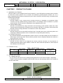
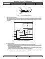
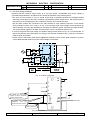
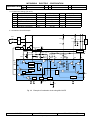
MITSUBISHI
Application Note
Prep.
ELECTRIC
CORPORATION
Rev.
Apr.
TENTATIVE
DIP-PFC
APPLICATION NOTE
MITSUBISHI ELECTRIC CORPORATION
POWER SEMICONDUCTOR
DEVICE DIVISION
DIP-PFC
DPH−2635e−
(1/27)
APPLICATION NOTE
MITSUBISHI
Application Note
Prep.
ELECTRIC
CORPORATION
Rev.
Apr.
Table of Contents
Chapter 1 Product Outlines………………………………………………………………………..3
1.1 Applications and Features..……………..…………………………………………………………… 3
1.2 Products Line-up………..…………………………………………………………………………….. 3
1.3 Structure and Functions………...……………………………………………………………………. 3
1.3.1 Module Structure…………………………………………………………………………………….. 3
1.3.2 Internal Circuit Topology……………………………………………………………………………..4
1.3.3 Built-in Functions….…………………………………………………………………………………..4
Chapter 2 Electric Characteristics.……………………………………………………………………………….5
2.1 Static Characteristics…….……………………………………………………………………………..5
2.2 Switching Characteristics……..……………………………………………………………………… 5
2.3 Recommended Operation Conditions………………………………………………………………. 5
2.4 Waveforms of Input Current/Voltage and Current Harmonic……………………………………… 5
Chapter 3 Package…………………………………………………………………………………………………. 6
3.1 Package Outlines Drawing.……………………………………………………………………………6
3.2 Laser Marking…..……………………………………………………………………………………… 6
3.3 Description of Input and output Terminals……………………………………………………………6
3.4 Function Description…….…………………………………………………………………………….. 7
3.5 Installation Guidelines……………..………………………………………………………………….. 8
3.6 Temperature Measurement of DIP-PFC case and Heat Sink…………………………………….. 9
Chapter 4 System Applications…………………………………………………………………………………..10
4.1 System Connections…………………………………………………………………………………..10
4.2 Recommended System Composition……………………………………………………………….10
4.3 DIP-PFC Wiring Guidelines…..………………………………………………………………………11
4.4 DIP-PFC Operation Sequence….……………………………………………………………………12
4.5 Start-up and Stop Operation Sequence of AC Supply, Control Supply Control Signal.………12
4.6 Noise Withstand Capability…………………………………………………………………………..13
Chapter 5 Additional Guidelines……………………………………………………………………………….. 14
5.1 Packaging Specifications…..…………………………………………………………………………14
5.2 Attention s for Handling.…..…………………………………………………………………………..15
Appendix Control IC of DIP-PFC……………………………………………………………………………….. 16
A.1 About M81012FP……………………………………………………………………………………... 16
A.2 About M63914FP……………………………………………………………………………………... 18
A.3 Protective Functions………………………………………………………………………………….. 20
A.4 Fault Output Condition and Its Timing……………………………………………………………… 20
A.5 Example of Interface Design………………………………………………………………………… 21
DIP-PFC
DPH−2635e−
(2/27)
APPLICATION NOTE
MITSUBISHI
Application Note
Prep.
ELECTRIC
CORPORATION
Rev.
Apr.
CHAPTER 1
PRODUCT OUTLINES
1.1 Applications and Features
DIP-PFC(Dual‐In‐line‐Package Power-Factor-Correction) is an IPM used for the power factor correction
of AC-DC-AC inverter systems such as inverter air-conditioners, general-purpose inverters, etc. It is a
highly integrated power module manufactured by the means of transfer mold technology, and featured with
the following advantages:
(1) Compact Structure
DIP-PFC realizes a very compact active converter structure by Integrating a conventional AC/DC
converter, and high speed switching elements IGBT in one package, which contributes to a perfect
system solution of with small size, simplification, high reliability and low cost.
(2) Transfer Mold Package
DIP-PFC is manufactured by using the transfer mold technology, which realizes smaller size, lower
cost and improved productivity. Furthermore, By mounting a DIP-PFC on the same control board with
DIP-IPM, minimum wiring and share of one heat sink can be easily realized.
(3) Lower Power Loss
DIP-PFC employs the low loss IGBT and Diode chips. The total power loss is reduced by about 10%
comparing to traditional products, which contributes to an improved system efficiency.
(4) Excellent Performance
By combined utilization with the application specific control IC, the output voltage can be controlled in a
wider range, and the high order current harmonic problem can be completely cleared which leads to a
high power factor over 99%.
(5) Abundant Protective Functions
DIP-PFC and the control IC are designed with various protective functions for the prevention of
module destruction against steep variation of load and various abnormal operations, which improves
the reliability of the total system.
1.2 Products Line-up
PS51277-A
PS51259-A
Input Voltage
Rating (Vi)
90∼264V
90∼264V
Table 1 DIP-PFC family
Input Current
Typical Switching
rating (Ii)
Frequency (fPWM)
15Arms
20kHz
20Arms
20kHz
Isolation Grade
Viso
AC1500Vrms
(Sinusoidal 1min)
1.3 Structure and Functions
1.3.1 Module Structure
Fig.1(a) and (b) show the DIP-PFC package photograph and its cross-section diagram, respectively.
In order to avoid erroneous installation with DIP-IPM, some pins are specially treated, such as lead cut
and with wider width.
Fig.1(a) DIP-PFC photograph
DIP-PFC
DPH−2635e−
(3/27)
APPLICATION NOTE
MITSUBISHI
Application Note
ELECTRIC
Prep.
CORPORATION
Rev.
Apr.
Lead Frame
Mold Resin
Heat Sink
LVIC
Di, IGBT
Fig.1(b) Cross-Section diagram of DIP-PFC
1.3.2 Internal Circuitry Topology
Fig.2 shows the internal circuitry of DIP-PFC, which consists of a full-wave diode rectifier bridge and
two IGBT elements parallel connected to the negative-side of the diode bridge, and an LVIC for drive of
the IGBTs.
P
R
S
LVIC
VD
VCC
ROUT
VIN
VIN
N2
SOUT
GND
GND
VNO
N
Fig.2 DIP-PFC circuitry diagram
1.3.3 Built-in Functions
(a) AC/DC conversion: Converting commercial single phase AC input into DC output.
(b) IGBT drive and protection: The built-in LVIC provides the functions of IGBT gate drive and control
supply under voltage (UV) protection.
PFC operation becomes unstable and easy to cause malfunction if control supply is below a certain
level. It is necessary to block IGBT operation immediately if UV happens.
(Note): LVIC inside the DIP-PFC only provides the function of IGBT gate drive and UV protection, the
DIP-PFC control circuitry and OV/OC protective functions are not built-in. Therefore, a set
utilization of the control IC with the DIP-PFC is necessary.
DIP-PFC
DPH−2635e−
(4/27)
APPLICATION NOTE
MITSUBISHI
Application Note
ELECTRIC
Prep.
CORPORATION
Rev.
Apr.
CHAPTER 2
ELECTRIC CHARACTERISTICS
2.1 Static Characteristics
Table 2 Typical static characteristics of DIP-PFC
Rating
Symbol
Parameters
Condition
VF
Collector-emitter shut-down
VCE=600V, Tj=25℃
current
Collector-emitter saturation
VD=15V, VCIN=5V,Tj=25℃
voltage
Diode Forward voltage drop Tj=25℃, VCIN=5V
Irr
Diode Recovery current
ICES
VCE(sat)
PS51277-A
PS51259-A
1.0mA(max.)
1.0mA(max.)
(Note1)
2.0V(Typ.)
1.8V(Typ.)
(Note 2)
1.6V(Typ.)
2.1V(Typ.)
(Note 3)
13A(Typ.)
13A(Typ.)
Vcc=300V,VD=15V, Tj=25℃
Note1:PS51277-A@Ic=30A、PS51259-A@Ic=50A
Note 2:PS51277-A@-Ic=30A、PS51259-A@-Ic=50A
Note 3:PS51277-A@Ic=20A、PS51259-A@Ic=30A
2.2 Switching Characteristics
Table 3 Typical switching characteristics of DIP-PFC
Rating
Symbol
Parameter
Condition
ton
toff
tc(on)
VCC=300V, VD=15V
Tj=125℃, VIN=0⇔5V,
Inductive Load
Switching time
(Note 4)
tc(off)
PS51277-A
PS51259-A
0.23us(Typ.)
0.29us(Typ.)
0.43us(Typ.)
0.46us(Typ.)
0.14us(Typ.)
0.15us(Typ.)
0.23us(Typ.)
0.17us(Typ.)
Note 4:PS51277-A@Ic=20A、PS51259-A@Ic=30A
2.3 Recommended Operation Conditions
Item
AC input voltage
Control Supply
PWM Carrier Frequency
Symbol
VCC
VD
fPWM
Input on voltage
VIN(ON)
Input off voltage
VIN(OFF)
Condition
Value
typ.
Between S-R terminals
min.
90
Between VD−GND terminals
13.5
−
15.0
−
20
Tc≦100°C,Tj≦125°C
Between VIN−GND terminals
max.
264
V
−
kHz
4.0∼VD
V
0∼1.0
V
1000.0A
100.0A
10.0A
Standard
Measured Value
1.0A
Vi:250V/div
0.1A
0.01A
10
20
30
40
Fig.3 Input current/voltage wave of PS51259-A
Fig. 4 Current harmonic of PS51259-A
Condition: Vi=200V, Ii=15.732A, Vo=275.6V, P.F=99.9%
Condition: Vi=200Vrms, 60Hz, Vo=370V, fsw=20kHz
DIP-PFC
DPH−2635e−
(5/27)
Vrms
16.5
2.4 Waveforms of Input Current/Voltage and Current Harmonic
Ii:10A/div
Unit
APPLICATION NOTE
MITSUBISHI
Application Note
Prep.
CHAPTER 3
ELECTRIC
CORPORATION
Rev.
Apr.
PACKAGE
8±0.5
A
16±1
3.1 Package Outline Drawing
Fig. 5 Package Outlines
3.2 Laser Marking
Fig. 6 shows the laser marking range of DIP-PFC. Mitsubishi mark, type name(area A), lot
number(area B) are marked in an area of 42.5×8mm, positioned 38mm far away from the right edge
of the package.
Marking Area
5
PS21XXX
Fig. 6 Laser marking
DIP-PFC
DPH−2635e−
(6/27)
APPLICATION NOTE
MITSUBISHI
Application Note
Prep.
ELECTRIC
CORPORATION
Rev.
Apr.
3.3 Description of Input/Output Terminal
Table 4 Description of input/output terminal
No.
symbol
Terminal Name
Content
・
Connected
with
the
minus
side of the converter.
1
Output Terminal of
N2
・ A shunt resistor is inserted between N2 and N terminals
PFC
2
to detect DC bus current.
・ This is the GND of DIP-PFC.
GND
of
Control ・ In order to avoid the GND potential variation due to
14
GND
Supply
IGBT switching, please add a fast clamp diode between
this GND and the N terminal.
・ The positive terminal of the 15V supply of LVIC.
・ Please add a noise filter with good temperature and
frequency characteristics near the terminal to prevent
DIP-PFC malfunction from noise intereference.
15
VD
Control Supply(+)
・ Please ensure the voltage ripple within the specifications.
・ Please add a Zenner diode(24V/1W) between the control
supply terminals to protect LVIC from surge destruction if
the surge voltage is large.
・ Input terminal of LVIC. Please connect it to the output
terminal of the control IC. If the signal is affected by
16
VIN
Control Input
noise, please add a noise filter with good temperature
and frequency characteristics near the input terminal.
・ The input signal GND, connected to the control supply
17
GND
GND
GND inside.
・ Connected with the positive side of internal converter.
・ Connect to the positive polarity of inverter input terminal.
Output Terminal of ・ An electrolytic condenser should be mounted as closely
22
P
PFC
as possible to the P&N terminals so as to suppress surge
voltage. In addition, a film condenser with good frequency
characteristics is also necessary.
23
S
AC Input Terminal
・ Connect to commercial AC supply via ACL.
24
R
AC Input Terminal
・ Connect to commercial AC supply via ACL.
25
・ In order to measure the bus line current, please insert a
N
IGBT Emitter
shunt resistor between N and N2 terminals.
26
・ The two IGBTs’ terminals are connected inside DIP-PFC.
Note: No. 3∼13,18∼21pins are dummy pins, therefore, should not be connected to PCB pattern
3.4 Function Description
Item
Normal
Operation
Control Supply
Under Voltage
DIP-PFC
Symbol
―
UV
Table 5 Function description
Content
・ The input drive logic is high-active.
・ IGBT turns on if the input signal voltage level is higher than Vth(on), and
IGBT turns off if the signal level is lower than Vth(off),
・ The LVIC monitors the control supply voltage. If there is an under voltage
happens within a certain period of time, IGBT gate will be interrupted
immediately, and the control input will be suspended.
・ The UV state is defined to be the period from the time the control supply
drops below the UV trip level to it rises again to the UV reset level.
・ The control input will be released in the next pulse soon after the control
supply rises over the UV reset level.
DPH−2635e−
(7/27)
APPLICATION NOTE
MITSUBISHI
Application Note
ELECTRIC
Prep.
CORPORATION
Rev.
Apr.
3.5 Installation Guidelines
Fastening a module to a heat sink with excessive uneven stress might cause devices to be damaged or
degraded because over stress will apply to the internal silicon chips. An example of recommended
fastening order is shown in Figure 7. Approximately, set the temporary fastening torque to be 20∼30 %
of the maximum rating.
Temporary fastening
①→②
Permanent fastening
①→②
Fig. 7 Recommended Fastening Order of Mounting Screws
Table 6. Mounting Torque and Heat Sink Flatness Specifications
Item
Mounting torque
Mounting screw :
M4
DIP-PFC flatness
Heat sink flatness
Condition
Reccomended 1.18N・m
Reccomended 12 kg・cm
−
DIP-PFC
Min.
0.98
10
−50
−50
Max.
1.47
15
+100
+100
Unit
N・m
kg・cm
um
um
Surface applied grease
DIP-PFC
Measurement point
+−
Typ.
1.18
12
―
―
3mm
+
Base-plate edge
−
Place to contact a heat
Heat sink
sink
Heat sink flatness range
−
+
Heat sink
Fig. 8 Flatness measurement point of heat sink.
Tightening torque test
Tightening torque test is to investigate the maximum allowable
tightening torque under which DIP-PFC package will not broke or
voltage endurance; inserting a 100um thickness gauge between
DIP-PFC and Heat-sink, tightening DIP-IPM gradually to the
heat-sink with 0.098N・m (1kg・cm) unit from 1.18Nm (12kg・cm).
Tightening torque is confirmed to be more than 0.98N・m (10kg・
cm), even in the worst condition.
A
B
Planar
DIP-PFC
gauge
Heat-sink
Fig.9 Tightening torque test
Heat sink flatness is prescribed as shown in Figure 8. For most effective heat-radiation it is necessary to
enlarge as much as possible, the contact area between the module and the heat sink to minimize the
contact thermal resistance. According to the heat sink flatness (surface warp/concavity and convexity) on
the module installation surface (refer to Figure 9). Also, the surface finishing-treatment should be less than
12um.
Evenly apply 100um∼200um grease with good thermal-conductivity over the contact surface between a
module and a heat sink. It is also helpful for preventing the contact surface from corrosion . Further more,
use grease with stable quality within the operating temperature range and have long endurance. Use a
torque wrench to fasten up to the specified torque. Exceeding the maximum torque limitation might cause
DIP-PFC
DPH−2635e−
(8/27)
APPLICATION NOTE
MITSUBISHI
Application Note
ELECTRIC
Prep.
CORPORATION
Rev.
Apr.
the modules to be damaged or degraded as the above mentioned fastening with uneven stress. Please pay
attention not to remain any ash on the contact surface of the module and the heat sink.
3.6 Temperature measurement of DIP-PFC Case and Heat Sink
The heat sink should be such designed to have enough thermal dissipation capability that the case
temperature and IGBT junction temperature of DIP-PFC would not exceed the maximum ratings even at the
worst condition. If the DIP-PFC operates at a temperature over the specification, it will possibly lead to a
thermal destruction.
Therefore, please select the heat sink on the basis of a careful thermal calculation. In addition, it is also
necessary to confirm the effect by a prototype evaluation.
Please measure the case temperature at the position as shown in Fig. 10.
Control Terminals
Heat Sink Position
Heat Sink
Power Terminals
Tc
Tc
Fig. 10 Case temperature measurement point
DIP-PFC
DPH−2635e−
(9/27)
APPLICATION NOTE
MITSUBISHI
Application Note
ELECTRIC
Prep.
CORPORATION
Rev.
Apr.
CHAPTER 4
SYSTEM APPLICATIONS
4.1 System Connections
DIP-IPM
DIP-PFC
P
P
Relay
N/F
R
LVIC
ACL
S
Q2
AC200V
Co’
Co
Co’’
M
Q1
N
N2
N
HVIC
Control
IC
HVIC
HVIC
LVIC
MCU
Fig. 11 System connection block diagram
Note:
2. To operate DIP−PFC properly and make full use of its excellent performance, it is necessary that the
DIP-PFC should be used together with its control IC and DIP-IPM.
3. It is necessary to operate DIP-PFC, the control IC, DIP-IPM and MCU on the same GND stage. This
GND is usually set to the DIP-PFC N terminal.
4. A large charge current of the electrolytic condenser will flow on the DIP-PFC when applying AC supply,
which might cause destruction. Therefore, An Inrush current prevention circuit shown in Fig. 10 is
necessary. Open the relay when condenser Co is initially charged, and close it after the charge is over.
5. Large surge voltage is easily produced between P&N terminals when switching large current at a high
frequency. The countermeasure to the surge is to shorten the DC-link bus wiring between DIP-PFC and
the DIP-IPM as possible as you can. Also, the capacitance of the electrolytic condenser should be large
enough to absorb the surge voltage generated both by DIP-PFC and DIP-IPM. In addition, it is
necessary to mount a condenser with good high frequency characteristics, such as polypropylene film
condenser closely to the P and N terminals of DIP-PFC.
6. In case of mounting the DIP-PFC on the same heat sink as that of DIP-IPM, please make sure that the
mounting height and grease thickness of the two modules are the same, so as to minimize the
contacting thermal resistance of both modules.
7. Recommendation: ACL:1mH,
Co: Electrolytic condenser(sutibale for high frequency),1000∼2000uF/450VDC,
Co’: Polypropylene film Condenser(suitable for high frequency), 0.22uF/630VDC
* Concerning DIP-IPM, please refer to its application note DPH-0352-B.
4.2 Recommended system Composition
PFC
PS51277-A
PS51259-A
Control IC
M81012FP*
M63914FP
IPM
PS21865, PS21245-E
PS21867, PS21246-E
Remark
(*) Under Development
DIP-PFC
DPH−2635e−
(10/27)
APPLICATION NOTE
MITSUBISHI
Application Note
ELECTRIC
Prep.
CORPORATION
Rev.
Apr.
4.3 DIP-PFC Wiring Guidelines
Because DIP-PFC switches large current at a very high speed, considerable large surge voltage is
generated easily between P and N terminals. Please pay attention to the following items:
・The area of P-Co-N shown in Fig. 12 should be as small as possible because the rectangle shaped
switching current flows on this route. In addition, please add a bypass condenser Co’ with good frequency
response such as a polypropylene film condenser closely to the P and N terminals.
・The two IGBT emitters are connected to the VNO terminal of LVIC inside the DIP-PFC. If the internal
wiring inductance shown as L1 and L2 in Fig. 13 is too large, large surge voltage will be generated by
di/dt. Especially, the lower the temperature, the faster the switching speed, therefore the larger the di/dt.
This surge voltage applies to the VNO and N terminals, which is possible to destruct LVIC.
・In order to suppress the surge voltage, the external wiring method shown in Fig. 13 is recommended. To
reduce the parasitic wiring inductance, the wiring of the external terminals of N(N-1) and N(N-2) should be
made as short as possible.
・Please mount a fast clamp diode (EG01Y@Sanken) between N and control GND terminals to prevent
control GND potential variation from the minus voltage of N terminal.
P
R
N/F
+
S
Co’
Co
VD
N2
LVIC
GND
VNO
N
(N-1,N-2)
VIN
Control IC
MCU
Fig. 12 DIP-PFC Interface
N2
N2
P
S
+
R
L2
To restrain the IPM surge
voltage, mount the condenser
closely to the terminals
N(N-1)
L1
To reduce the parasitic
inductance,
this
wire
should close to N terminal
VD
+
GND
VD
VIN
Control input
GND
N(N-2)
Insert a diode here
Fig. 13 Recommended wiring method
DIP-PFC
DPH−2635e−
(11/27)
APPLICATION NOTE
MITSUBISHI
Application Note
ELECTRIC
Prep.
CORPORATION
Rev.
Apr.
4.4 DIP-PFC Operation Sequence
DIP-PFC
Control
Input
IGBT gate signal
IGBT collector current
Fig. 14 DIP-PFC operating sequence
4.5 Start-up and Stop Operation Sequence of AC Supply, Control Supply and Control Signal
Please follow the sequence shown in Fig. 15 to start-up and stop PFC so as to avoid malfunction or
abnormal destruction due to noise or other disturbance at start-up and stop operation.
The DC voltage control signal Vctrl should be activated after the ON/OFF switch is turned on.
AC Supply Input
Vi
0V
Control Supply Voltage
VD
0V
ON/OFF signal
ON
0FF
DC Voltage
>=3V
Control Signal
0V
(a) Start-up sequence
(b) Stop sequence
Fig. 15 Start-up and stop operation sequence
There are possibility that the LVIC output will not be ON when the VD is in rising state from 0V even the
ON/OFF signal is set to ON level.
This phenomenon is understood that the initial state of the internal protective circuit is not stable (Hi or Lo)
at the control voltage rising period. In this case, please turn off the ON/OFF signal to reset the IC. In
addition, even if the IC output can set to ON state, the IGBT gate might be blocked due to abnormal input
such as noise.
To avoid such problem, please set the ON/OFF signal after the VD has completely established.
DIP-PFC
DPH−2635e−
(12/27)
APPLICATION NOTE
MITSUBISHI
Application Note
ELECTRIC
Prep.
CORPORATION
Rev.
Apr.
4.6 Noise Withstand Capability
The noise withstand capability of DIP-PFC is carried out under the following conditions, from which over ±
2.0kV withstand capability has been confirmed. However, noise withstand capability greatly depends on the
test conditions, such as the wiring patterns of control substrate, parts layout, and motor type etc., therefore
the actual system test should be performed. Fig. 16 shows the evaluation system.
(1) Common noise test condition:
Vi=200V, VD=15V, Ta=-20∼80℃, Line noise pulse width tw=1μs/T=16ms, Amplitude=±2kV
Continuous pulse input with pulse width 15μs/T=50μs to DIP-PFC input terminals.
(2) Thunder surge test condition:
Vi=200V, VD=15V, Ta=25℃, Thunder surge pulse width tw=1.2μs/T=50μs, Amplitude=±7kV
Continuous pulse input with pulse width 15μs/T=50μs to DIP-PFC input terminals.
Heat Sink
DIP-PFC
Noise Simulator
Io
P
Brake
Slider
Iin
R
IC
S
Q2
AC200V
Q1
4700pF
N
N2
ON/OFF
Applying noise to
R-G / S-G
・VD Control Supply
・Continuous Pulse Input
tw=15μs/T=50μs
G
Fig. 16 Common noise evaluation circuit
Heat Sink
DIP-PFC
Thunder Simulator
P
Brake
Noise Filter
Slider
Iin
R
IC
S
Q2
AC200V
Q1
N
N2
ON/OFF
Applying thunder surge
to U-G / V-G
Io
・VD Control Supply
・Continuous Pulse Input
tw=15μs/T=50μs
G
Fig. 17 Thunder surge evalution circuit
DIP-PFC
DPH−2635e−
(13/27)
APPLICATION NOTE
MITSUBISHI
Application Note
ELECTRIC
Prep.
CHAPTER 5
CORPORATION
Rev.
Apr.
ADDITIONAL GUIDELINES
5.1 Packaging Specifications
( 44 )
( 22 )
Plastic tube
Per tube
DIP − PFC
6 pieces of DIP-PFC per tube
(520)
5 columns
of tube
Per package box (Max.)
6 rows
of tube
Partition
Total number of tubes is 30.
(5 columns×6 rows)
Total number of DIP-PFC is 180.
(30 tubes×6 pieces)
(250)
Weight
Approximately 54g /Per DIP―PFC
(180)
Approximately 420g/Per tube
Approximately 14kg /Per package
The above weights are ones when the
maximum number of DIP-PFC is
packaged.
Spacer
Package box
(600)
Fig. 18 DIP-IPM Packaging Specification
DIP-PFC
DPH−2635e−
(14/27)
APPLICATION NOTE
MITSUBISHI
Application Note
Prep.
ELECTRIC
CORPORATION
Rev.
Apr.
5.2 Handling Precautions
Transportation
・Put package boxes in the correct direction. Putting them upside down, leaning them or
giving them uneven stress might cause electrode terminals to be deformed or resin case to
be damaged.
・Throwing or dropping the packaging boxes might cause the devices to be damaged.
・Wetting the packaging boxes might cause the breakdown of devices when operating. Pay
attention not to wet them when transporting on a rainy or a snowy day.
Storage
・We recommend room temperature and humidity in the ranges 5∼35℃ and 45∼75%,
respectively, for the storage of modules. The quality or reliability of the modules might
decline if the storage conditions are much different from the above.
Long storage
・When storing modules for a long time (more than one year), keep them dry. Also, when
using them after long storage, make sure that there is no visible flaw, stain or rust, etc. on
their exterior.
Surroundings
・Keep modules away from places where water or organic solvent may attach to them directly
or where corrosive gas, explosive gas, fine dust or salt, etc. may exist. They might cause
serious problems.
Disposal
・The epoxy resin and the case materials are made of approved products in the UL standard
94-V0, still they are incombustible.
Static electricity
・Exclusive ICs of MOS gate structure are used for the DIP-PFC power modules. Please keep
the following notices to prevent modules from being damaged by static electricity.
(1)Notice of breakdown by static electricity
Excessively high voltage (over the Max. rated input terminal voltage) resulting from the
static electricity of human bodies and packaging materials, might cause the modules to be
damaged if applied on the control terminals. For countermeasures against static
breakdown, it is important to control the static electricity as much as possible and when it
exists, discharge it as soon as possible.
*Do not use containers which are easy to be electro-staticly charged during transportation.
*Be sure to short the control terminals with carbon cloth, etc. just before using the module.
Also, do not touch between the terminals with bare hands.
*During assembly (after removing the carbon cloth, etc.), earth machines used and human
bodies. We suggest putting a conductive mat on the surface of the operating table and the
surrounding floor.
*When the terminals on the printed circuit board with mounted modules are open, the
modules might be damaged by static electricity on the printed circuit board.
*When using a soldering iron, earth its tip.
(2)Notice when the control terminals are open
*When the control terminals are open, do not apply voltage between the collector and
emitter.
*Short the terminals before taking a module off.
DIP-PFC
DPH−2635e−
(15/27)
APPLICATION NOTE
MITSUBISHI
Application Note
ELECTRIC
Prep.
CORPORATION
Rev.
Apr.
Appendix
TENTATIVE
Specific Control IC for DIP-PFC
A.1 M81012FP (Under Development)
A.1.1 Introduction
M81012FP is an integrated circuit specially developed for the control
of DIP-PFC. It is designed in a standard 24-pin SSOP outline as
shown in Fig. 19.
A.1.2 Feature
■ Automatically synchronizing to the AC input supply, and
generating referenced sinusoidal current waveform (50/60Hz);
■ Voltage over-shot restraint function in light load(OV1)
■ Soft start function
■ Built-in protective function
−Over Voltage protection (OV2)
−Over Current protection (OC) by using external shunt resistor
CT
1
24
OUT
RT
2
23
Fo
IAOUT
3
22
CFO
IA+
4
21
ON/OFF
20
CIN
IA-
5
SOUT
6
19
OV2
0cross
7
18
OV1
NC
8
17
VA-
VDD
9
16
VAOUT
M81012FP
NC
10
15
NC
DGND
11
14
V-LMT
GND
12
13
SS
Fig.19 Pin Arrangement of M81012FP
A.1.3 Pin Arrangement and Description
No.
1
2
3
4
5
6
7
8
9
10
11
12
13
14
15
16
17
18
19
20
21
22
23
24
Symbol
CT
RT
IAOUT
IA+
IASOUT
0cross
NC
VDD
NC
DGND
GND
SS
V-LMT
NC
VAOUT
VAOV1
OV2
CIN
ON/OFF
CFO
Fo
OUT
DIP-PFC
Content
The oscillator frequency is determined by the potential of middle point of
RC, the frequency can be set in the range of 10kHz∼50kHz
Current error amplifier output
Current error amplifier input, referenced current signal
Current error amplifier input, actual current signal
Referenced standard sinusoidal current
Zero cross signal input, synchronized to AC voltage
Null
Positive terminal of 5V power supply
Null
GND terminal of IC, please make it short circuit to the GND (No.12 pin)
GND of 5V power terminal
Terminal for setting soft start time
Terminal for setting current limit in soft start operation
Null
Voltage error amplifier output
Voltage error amplifier input, from DC output voltage signal
Voltage overshot restraint at light load, from DC output voltage signal
Over Voltage protection terminal, from DC output voltage signal
Over current protection terminal, input from shunt voltage signal
Input terminal of ON/OFF signal for DIP-PFC start/stop control
Fault signal output pulse width setting terminal
Fault signal output terminal
PWM output for IGBT gate drive, connected to DIP-PFC Vin Terminal
DPH−2635e−
(16/27)
APPLICATION NOTE
MITSUBISHI
Application Note
ELECTRIC
Prep.
CORPORATION
Rev.
Apr.
A.1.4 Maximum Ratings (Ta=25℃)
No.
Item
1
Supply Voltage
2
Input Operating Voltage
3
Output Voltage
4
OSC Frequency Capability
5
Fo Output Current
6
Operating Temperature
Symbol
Rating
-0.3∼+6.5
-0.3∼VDD+0.3
-0.3∼VDD+0.3
100
+15
-20∼80
VDD
Vi
VO
fOSC
IFO
Topr
Unit
V
V
V
kHz
mA
℃
VDD
Note
(Typ.)=5V
Typical value=20kHz
A.1.5 Interface Circuit Example
470kΩ
ACL
470kΩ
470kΩ
6.2kΩ
LOAD
1000μF
N/F
4700p
470kΩ
3.3μF
Gate
Drive
Shunt Resistor
470Ω
4.22kΩ
0.068μ
470Ω
0.018μF
SOUT
0.033μF
3300pF
820pF IA-
IA+
Level-shift circuit.
Refer to Fig.38
5.76kΩ
Vctrl
4.7kΩ 0.033μF
56Ω
470Ω
68kΩ
470kΩ
IAOUT
VAOUT
100kΩ
VA-
470pF
OV2
OV1
CIN
VDD
D/A
GND
ROM
Adress
0CROSS
Q S
CL
R
ON/OFF
OUT
Fo Circuit
OS
CT
RT
Fo
Limiter
SS
Cs
0.47μF
V-LMT
CFO
2.5V
Fig. 20
DIP-PFC
Example of evaluation circuit using M81012FP
DPH−2635e−
(17/27)
APPLICATION NOTE
MITSUBISHI
Application Note
ELECTRIC
Prep.
CORPORATION
Rev.
Apr.
A.2 M63914FP
A.2.1 Introduction
M63914FP is a semiconductor integrated circuit specifically
developed for the control of active filter. Fig. 19 shows its
package outline of 36-pin SSOP.
A.2.2 Features
■ Voltage overshot restraint function (OV1)
■ Soft start function (SS1)
■ Built-in protective functions
−Over voltage protection (OV2)
−OC/SC protection by using external shunt resistor
−Control voltage under voltage protection(UV)
−Over temperature (OT)
A.2.3 Terminal Arrangement and Description
No.
1
2
3
4
5
6
7
8
9
10
11
12
13
14
15
16
17
18
19
20
21
22
23
24
25
26
27
Symbol
ON/OFF
TEST
Vcc
NC
NC
PVcc
OUT
P-GND
S-GND
S-GND
Cin
OV2
OT
Vreg
CFO
VA+
VAVAOUT
Iac
MPOUT
IA+
IAIAOUT
OV1+
OV1OV1OUT
S-GND
DIP-PFC
ON/OFF
1
36
Fo
TEST
2
35
CAOUT
VCC
3
34
CA+
NC
4
33
SS1
NC
5
32
SS2
PVCC
6
31
CT
OUT
7
30
RT
P-GND
8
29
S-GND
S-GND
9
28
S-GND
S-GND 10
27
S-GND
CIN 11
26
OV1OUT
OV2+ 12
25
OV1-
OT 13
24
OV1+
Vreg 14
23
IAOUT
CFO
15
22
IA-
VA+
16
21
IA+
VA-
17
20
MPOUT
VAOUT 18
19
IAC
M63914FP
Fig. 21 Pin Arrangement of M63914FP
Content
Input terminal of DIP-PFC operation start signal
Test terminal, please shorten it to the GND in actual use
15V control supply
Null
Null
Power supply terminal for control output
PWM Output terminal for IGBT gate drive
Shorten to GND
Shorten to GND
Shorten to GND
Over current protection terminal, input from shunt voltage signal
Over Voltage protection terminal, from DC output voltage signal
Output terminal for over temperature
IC internal regular supply
Fault signal output pulse setting terminal
Voltage error amplifier input, reference voltage
Voltage error amplifier input, from DC output voltage signal
Voltage error amplifier output, connected to the multiplier input
Multiplier input, actual current signal
Multiplier output, connected with IA+ terminal
Current error amplifier input, Referenced sinusoidal current signal
Current error amplifier input, Actual current signal
Current error amplifier output
Voltage error amplifier input, form DC output voltage
Voltage error amplifier input, form DC output voltage
Voltage error amplifier output, used for voltage overshot control
Connect to GND
DPH−2635e−
(18/27)
APPLICATION NOTE
MITSUBISHI
Application Note
28
29
30
31
32
33
34
35
36
ELECTRIC
Prep.
CORPORATION
Rev.
Apr.
S-GND
S-GND
RT
CT
SS2
SS1
CA+
CAOUT
Fo
Connect to GND
Connect to GND
The oscillator frequency is determined by the potential of middle point of
RC, the frequency can be set in the range of 10kHz∼50kHz
Referenced voltage generating terminal
Used for soft start time setting(0.1μF for about 1sec)
Buffer for control signal input
Buffer for control signal output
Fault output terminal
A.2.4 Maximum Ratings (Ta=25℃)
No.
Item
1
Supply Voltage 1
2
Supply Voltage 2
3
Output Voltage
4
Output Current
5
OSC Frequency Capability
6
Fo Output Current
7
Operating Temperature
Symbol
Rating
-0.2∼+20
-0.2∼VDD+0.2
-0.2∼VDD+0.2
±1
50
+15
-20∼80
VDD
PVDD
VOUT
IOUT
fOSC
IFO
Topr
Unit
V
V
V
A
kHz
mA
℃
VDD
Note
(Typ.)=15V
Typical value=20kHz
A.2.5 Interface Circuit Example
470kΩ
Vreg
Vreg
ACL
470kΩ
470p
470kΩ
4.12kΩ
470p
4.12kΩ
5.1kΩ
1000μF
6.2kΩ
470kΩ
Gate
Driv
LOAD
4.12kΩ
N/F
4700p
F
3.3μF
Shunt Resistor
470kΩ
470Ω
56Ω
820pF
IA+
MPOUT
5.76kΩ
68kΩ
470kΩ
Vctrl
4.7kΩ 0.033μF
0.018μF
0.033u
10kΩ
Iac
Level-shift circuit
Refer to Fig.38
470Ω
100kΩ
0.033μF
3300pF
IAOUT
IA-
VAOUT
VA-
470pF
VA+
OV1+
OV1-
OV1OUT
OV2
CIN
Multip
PVcc
Vcc
R
OUT
S
Q
Q
R
S
Vreg
P-GND
S-GND
OSC
TEST
GND
CA+
CAOUT
OT
FO
CFO ON/OFF
SS1
SS2
330pF
Vsig
Fig. 22
DIP-PFC
CT
RT
100kΩ
Example of evaluation circuit using M63914FP
DPH−2635e−
(19/27)
APPLICATION NOTE
MITSUBISHI
Application Note
Prep.
ELECTRIC
CORPORATION
Rev.
Apr.
A.3 Protective Function (M81012FP, M63914FP)
(1) Voltage Overshot Control Function (OV1)
Generally, the output voltage of a boost type active filter will rise greatly at a light load. OV1 is designed
to restrain the overshot of the output voltage. When the voltage exceeds the defined value by about 20V,
IGBT gate input will be blocked so that the further voltage rise can be restrained.
OV1 protection can be released automatically if the output voltage drops below the OV1 trip level.
(2) Over Voltage Protection(OV2)
IGBT gate input will be interrupted if the DC bus voltage exceeds the OV2 trip level. This can prevent
the over voltage applying to the DC smoothing condenser and the load.
(3) Over Current / Short Circuit Protection (OC/SC)
The DC bus current is detected by using an external shunt resistor. If the current exceeds the SC trip
level, IGBT gate input will be blocked to prevent DIP-PFC from over current destruction.
(4) Soft Start Function (SS)
This function is used to start the PFC softly so as to restrain the over current at start-up.
A.4 Fault Output Condition and Its Timing(M81012FP, M63914FP)
The control IC will assert an Fo signal when the following abnormal state is detected
Over Voltage
Fault signal will output if the output voltage exceeds the OV2 trip level, and at the same time, IGBT
operation will be stopped. Over voltage protection cannot be released automatically. To activate the
DIP-PFC from an OV2 protection, please reset the ON/OFF signal once again.
Over Current
Fault signal will output if the bus current exceeds the OC/SC trip level, and at the same time, IGBT
operation will be stopped. Over current protection cannot be released automatically. To activate the
DIP-PFC from a OC/SC protection, please reset the ON/OFF signal once again.
Note : For UV protection, IGBT gate will be interrupted when control voltage drops below the UV trip level,
and the protection will be released automatically if the control voltage recovers to the UV reset level.
Because UV protection is realized by the LVIC instead of the control IC in M81012FP, Fo signal will not
be asserted by the control IC. However, Fo will be asserted by M63914FP.
OV1 Restraint OV2 Protection SC Protection
UV Protection
DC Output Voltage
Load current
Collector Current
Control Voltage
Fault Output
ON/OFF Signal
Control Signal
IGBT Gate
Fig.23 Fault output timing chart.
DIP-PFC
DPH−2635e−
(20/27)
APPLICATION NOTE
MITSUBISHI
Application Note
ELECTRIC
Prep.
CORPORATION
Rev.
Apr.
A.5 Example of Interface Circuit Design
(1) PFC ON/OFF Circuit (M81012FP, M63914FP)
The start-up and stop operation of DIP-PFC is controlled by the ON/OFF command usually from a MCU.
The ON/OFF control is high active. Fig. 24 shows an interface circuit. It consists of two transistors for
level shift. Also, a hard interruption circuit is realized synchronously to the Fo signal coming from DIP-IPM.
It is necessary to consider the parameter dispersion of the total resistors in designing the circuit.
6.2Vtyp.(M81012FP)
16.5Vtyp.(M63914FP)
DTC2
RT1P141C
Control IC
DTC1
RT1N141M
MCU
0N/OFF
Fo
R1 4.7KΩ
D1
W2838
R3
33KΩ
5V
R2
4.7KΩ
Fo from Control IC
Fo from DIP-IPM
HD74HC00
Fig. 24 ON/OFF circuit
・PFC ON
The internal circuit of ON/OFF terminal connecting to a comparator, therefore, current cannot flow into
this terminal. Hence, the collector current of DTC2 can only flow on the resistor R3. Please control the
DTC2 base current so that the voltage drop of R3 is within the IC on threshold range of 2.4∼2.6V.
・PFC OFF
To stop PFC, the base of DTC1 should be set to low by the MCU. In addition, If the Fo output of DIP-IPM
becomes low, the base of DTC1 will also become low due to clamp of the diode D1. Therefore, DTC1 as
well as DTC2 will be turned off, and PFC will be stopped.
(2) Carrier Frequency Setting Circuit (M81012FP, M63914FP)
The carrier frequency of the IC can be arbitrary set by using the external resistor Rt and the condenser Ct.
To make the PFC work most effectively, it is recommended that the carrier frequency to be set to 20∼25k
Hz.
Carrier frequency can be determined as follows:
Ict=Vrt/Rt
Control IC
Where Ict is the current flows on the condenser, and Vrt the
RT
CT
reference voltage of internal oscillator.
The ON and OFF time can be calculate by using the upper
100k
330p
and lower threshold value Vosch,Voscl of the oscillator,
Ton=Toff=(Vosch−Voscl)×Ct/Ict
Therefore, the carrier frequency can be got from
fPWM=1/(Ton+Toff)
As for MP81012FP, Vrt=1.73V, Vosch=3.0V, Voscl=1.7V.
Fig. 25 Carrier frequency setting circuit
Suppose RT=100kΩ, CT=330PF, then
DIP-PFC
DPH−2635e−
(21/27)
APPLICATION NOTE
MITSUBISHI
Application Note
ELECTRIC
Prep.
CORPORATION
Rev.
Apr.
Ton=Toff=(3.0−1.7)×330P/(1.73/100k)=24.8(μsec)
fPWM=1/(Ton+Toff)=20.16kHz
(3) Soft Start Setting Circuit (M81012FP, M63914FP)
The DC voltage will be overshot easily if starting-up the
Control IC
PFC at the condition of a very low bus voltage. To restrain
SS
the peak value of voltage overshot, the control IC provide
the soft start function, which starts the PFC slowly so that
the voltage rises softly to the demand value.
Cs
0.47uF
The soft start time is determined by the condenser
connected to the SS terminal as shown in Fig.26. The
relationship between the soft start time and the capacitance
is as follows:
Fig. 26 Soft start setting circuit
Ts=3.25×10⁵×Cs (s) for M81012FP
Ts=1.83×10⁵×Cs (s) for M63914FP
For you reference, from the internal circuit constant, the voltage overshot becomes zero if the DC voltage
control signal varies from 5V (PFC off) to 1.14V (300V) within 500ms. In actual use, the capacitance should
be determined by according to the allowable maximum overshot and available mounting space for the
condenser of the application system.
(4) Current Limitation Setting Circuit (M81012FP)
The control IC provide the current limitation function for soft
Control IC
start operation. The demanded current level can be set by
V-LMT
the reference voltage of the V-LMT terminal, as shown in
Fig. 27
Limited current(A)=V(V-LMT)×20(A/V)
Vref
Note 1: The control IC might not make response if the
V-LMT voltage is under 1.0V.
Note 2: If the referenced voltage is obtained by using
Fig. 27 Current limit setting circuit
resistor division, please pay attention to the
resistance dispersion and temperature characteristics of the resistors.
400
DC Output Voltage (V)
(5) DC Voltage Control Circuit (M81012FP, M63914FP)
Because DIP-PFC is a boost type active converter, it is
necessary to ensure the DC bus line voltage to be higher
than the maximum peak value of the AC input voltage with
a merging of about 30V. The DC output voltage is set by a
microprocessor or a hardware circuit instead of the control
IC. Figure 28 shows the relationship of DC output voltage
versus the voltage command value. For reference,
Vdc=300@Vctrl=1.04V. The maximum DC voltage should
not be larger than the over voltage trip level..
The DC voltage setting circuit is shown in Fig. 29. The
desired voltage is kept by the voltage feedback to the error
amplifier in the control IC.
The DC voltage can be calculated as follows:
380
360
340
320
300
280
0.4
0.6
0.8
1
Voltage Command (V)
Fig. 28 DC voltage via command value
Vdc=Vctrl+((Vreg−Vctrl)*(R1+R2))/R1
DIP-PFC
DPH−2635e−
(22/27)
1.2
APPLICATION NOTE
MITSUBISHI
Application Note
ELECTRIC
Prep.
CORPORATION
Rev.
Apr.
Vdc
Control IC
Vreg.
To current-limit
circuit
R2
940k
+
Vctrl
VA-
0.22u
R1
5.6k
VAOUT
_
R3 68k
0.033u
470k
Fig. 29 DC output voltage setting circuit
(6) Zero Cross Capturing Circuit (M81012FP)
The control IC captures the zero cross point of AC input voltage, and generates the referenced sinusoidal
current waveform with the internal digital/analog circuit. Figure 30 shows the zero cross capturing circuit.
Opto-coupler is used to isolate the power side and the control side. The zero cross input to the control IC is
pulse signal.
When a forward AC voltage is applied, PC1 turns on and current flows on the primary side. DTC1 also
turns on because its base becomes low due to pull-down of R2. The 0cross input becomes high due to the
R4.
On the other hand, when a reverse AC voltage is applied, the current is bypassed by diode D1, and the
opto-coupler turns off. DTC1 also turns off, which leads to a low input to the 0cross terminal.
Therefore, it is understood that a high level zero cross signal corresponds to the positive waveform, and a
low signal corresponds to a negative waveform of the AC input voltage.
The zero cross pulse signal might be not so precisely synchronized to the Ac input voltage because of the
on/off threshold value of the opto-coupler and the inherent delay of the circuit. Please make compensation
to the delay if necessary.
6.2Vtyp
R2
300Ω
R1 39K
AC
R3
4.7kΩ
C1
0.033μF
D1
PC1
PS2501-1
DTC1
RT1P141C
0cross
R4
3KΩ
Control IC
Fig. 30 Zero cross capturing circuit
(7) Referenced Sinusoidal Current Generating Circuit (M81012FP)
The control IC generates the referenced sinusoidal current waveform by the internal digital/analog circuit
based on the detected zero cross signal and the demand current amplitude.
DIP-PFC
DPH−2635e−
(23/27)
APPLICATION NOTE
MITSUBISHI
Application Note
ELECTRIC
Prep.
CORPORATION
Rev.
Apr.
Analog current input
Referenced sinusoidal
current
4.22kΩ
470Ω
4.7kΩ
56Ω
0.068p
SOUT
IA+
0.018μF
3300pF
820pF IA-
IAOUT
+
- +
D/A
ROM
Adress
0CROSS
Control IC
CL
Fig. 31 Referenced sinusoidal current generating circuit
Fig. 32 Signal waveforms
AC voltage is high
Note: The PWM on pulse width becomes small when the AC
input current phase is near 90°. The output of the voltage
error amplifier comes to the peak values of the triangular carrier,
as shown in Fig. 33. Therefore, IGBT on pulse is easily
imposed by noise, which makes the output of SOUT unstable.
If the output voltage of the error amplifier becomes smaller than
the minimum value of the carrier, on pulse will not be generated
and IGBT will not turns on.
A countermeasure to the problem is to connect a bypass
film condenser to the SOUT terminal to filter the noise.
PWM signal is easily affected by noise
Fig. 33 Noise interference
For M63914FP, please input the AC current signal to Iac terminal (input of the multiplier) as shown in Fig. 22.
(8) Voltage Error Amplifier Interface Circuit (M81012FP, M63914FP)
The internal error amplifier compares the actual voltage Vdc and the demanded signal Vctrl, and regulate
the PWM duty so as to keep the DC voltage to the demanded value. However, error might happens
because of the dispersion of the circuit constants. Please make compensation if necessary.
Vdc
Control IC
470k
470k
MCU
-
Vctrl
OV1
5.6k
OUT
+
68k
470P
0.22u
Fig. 34 Voltage error amplifier circuit
DIP-PFC
DPH−2635e−
(24/27)
APPLICATION NOTE
MITSUBISHI
Application Note
ELECTRIC
Prep.
CORPORATION
Rev.
Apr.
(9) Current Error Amplifier Interface Circuit (M81012FP, M63914FP)
The internal error amplifier compares the actual bus current with the referenced sinusoidal current, and
regulates the PWM duty so as to make the actual current follow the referenced one. The output of the error
amplifier is compared to the triangular carrier wave, and the result is then sent to DIP-PFC control input. If
the wiring of this signal line is too long, noise maybe imposed on it, and result malfunction of DIP-PFC.
0.068uF
470
Vshunt
+
IA+
56
820pF
IAOUT
_
IA-
0.018uF
C4 3300pF
Vb
SOUT
470
4.22k
4.7k
0.033uF
Referenced
sinusoidal current
Fig. 35 Current error amplifier circuit
(10) Fault Output (Fo) Circuit (M81012FP, M63914FP)
The control outputs an Fo signal when there is a on over voltage or over current in the DIP-PFC. Since Fo
terminal is open collector type, it is necessary to pull it up to 5V logic supply through a resistor of about 4.7
kΩ. The electric characteristics of terminal is as follows:
Item
Fo output voltage
Code
VFO(L)
Condition
IFO(L)=10mA in operation
Please ensure that IFO(L) will not exceed 10mA.
The operation of DIP-PFC will be interrupted by the
circuit shown in Fig.24, however, to make the system
fail-safe against noise, please also stop the PWM output
of the microprocessor. In DIP-PFC/DIP-IPM system,
although DIP-IPM can work with only a pure diode
rectifier bridge, it is better to stop the total system by
software in case there is Fo output either from DIP-PFC
or DIP-IPM. In addition, a noise filter is recommended in
the circuit. The time constant should be determined
according to actual application condition.
Rating
1.0max
Control IC
Unit
V
5V
4.7k
CFO
Fo
1.0k
100
MCU
CFO
3300PF
Fig. 36 Fo output circuit
The Fo output pulse width is determined by the condenser connected to the CFO terminal.
(Example: CFO=22nF ⇒ tFo=1.8ms(typ.))
(11) Over Voltage detecting Circuit (M81012FP, M63914FP)
There are two over voltage control functions (OV1, OV2) in the control IC. OV1 is used for the restraint of
voltage overshot in light load, it will not latch-up and can recover to normal state if the OV1 lock is released.
OV2 is used for the protection DIP-PFC from over voltage destruction, it will stop the DIP-PFC and keep
the latch-up state. The control IC outputs Fo only an OV2 failure is detected.
The over voltage detecting circuit of OV2 is shown in Fig.36. The DC bus voltage signal is obtained by the
division of resistors, and is compared with the fixed reference voltage by the internal error amplifier. If the
DIP-PFC
DPH−2635e−
(25/27)
APPLICATION NOTE
MITSUBISHI
Application Note
ELECTRIC
Prep.
CORPORATION
Rev.
Apr.
DC voltage exceeds the setting value, the error amplifier will output a latch signal to the OV2 protection
circuit to stop the DIP-PFC.
To prevent malfunction due to noise, a noise filter with a time constant of about 2μs is recommended.
Vdc
Control IC
470k
470k
OV2
6.2k
Shut-down
latch circuit
+
4700p
Fig. 37 Over voltage detecting circuit
(12) PFC Over Current Detecting Circuit (M81012FP, M63914FP)
The PFC DC bus line current is detected by using a shunt resistor. The detected current signal is
transferred to the control IC with the circuit shown as Fig. 38
N2
Rshunt
N
Idc
5V
5V
15k
5V
33k
5V
4.7k
2.4k
−
+
3300p
0.1u
Control IC
CIN
+
−
0.1u
2k
470p
0.5V
Fig. 38 Current detecting circuit
The maximum value of over current should be set below the 1.7 times of the IGBT current rating. In
addition, please set the RC filter constant to 1.5∼2.0 μsec so as to shut down PFC quickly in case of a
over current.
DIP-PFC
DPH−2635e−
(26/27)
APPLICATION NOTE
MITSUBISHI
Application Note
Prep.
ELECTRIC
CORPORATION
Rev.
Apr.
Notice for Safe Designs
•
We are making every effort to improve the quality and reliability of our products. However, there are
possibilities that semiconductor products be damaged or malfunctioned. Pay much attention to take
safety into consideration and to adopt redundant, fireproof and malfunction-proof designs, so that the
breakdown or malfunction of these products would not cause accidents including human life, fire, and
social damages.
Notes When Using This Specification
•
This specification is intended as reference materials when customers use semiconductor products of
Mitsubishi Electric. Thus, we disclaim any warranty for exercise or use of our intellectual property
rights and other proprietary rights regarding the product information described in this specification.
•
We assume absolutely no liability in the event of any damage and any infringement of third party’s
rights arising from the use of product data, diagrams, tables, and application circuit examples
described in this specification.
•
All data including product data, diagrams, and tables described in this specification are correct as of
the day it was issued, and they are subject to change without notice. Always verify the latest
information of these products with Mitsubishi Electric and its agents before purchase.
•
The products listed in this specification are not designed to be used with devices or systems, which
would directly endanger human life. Should you intend to use these products for special purposes
such as transportation equipment, medical instruments, aerospace machinery, nuclear-reactor
controllers, fuel controllers, or submarine repeaters, please contact Mitsubishi Electric and its agents.
•
Regarding transmission or reproduction of this specification, prior written approval of Mitsubishi
Electric is required.
•
Please contact Mitsubishi Electric and its agents if you have any questions about this specification.
DIP-PFC
DPH−2635e−
(27/27)
APPLICATION NOTE