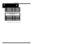
1
EPC©-30
Hardware Reference
Manual
RadiSys Corporation
5445 NE Dawson Creek Drive
Hillsboro, OR 97124
(503) 615-1100
FAX: (503) 615-1150
www.radisys.com
RadiSys is registered trademark of RadiSys Corporation.
IBM, PC/XT and PC/AT are registered trademarks of International Business
Machines Corporation.
PhoenixPICO, PicoCard, PhoenixBIOS, and PhoenixCard Manager are registered
trademarks of Phoenix Technologies, Ltd. Portions of this manual are copyright 1995
by Phoenix Technologies, Ltd.
Microsoft Windows, Windows 95, Windows NT and MS-DOS are registered
trademarks of Microsoft Corporation.
_______________________________________________________________________
07-0857-00
November 1996
EPC-30 Hardware Reference
WINMODE and CLMODE are trademarks of Cirrus Logic, Inc. Portions of this
manual are copyright 1995 by Cirrus Logic, Inc.
Intel and Intel386 EX are registered trademarks of Intel Corporation.
All other trademarks, registered trademarks, service marks, and trade names are
property of their respective owners.
November 1996
Copyright 1996 by RadiSys Corporation
All rights reserved.
Hardware Warranty
RadiSys Corporation ("RadiSys") warrants the EPC product to the original purchaser
for two years from the product’s shipping date. If an EPC product fails to operate in
compliance with its specification during this period, RadiSys will, at its option, repair
or replace the product at no charge. The customer is, however, responsible for
shipping the product; RadiSys assumes no responsibility for the product until it is received. This warranty does not cover repair of products that have been damaged by
abuse, accident, disaster, misuse, or incorrect installation.
RadiSys’ limited warranty covers products only as delivered. User modification, such
as the addition of memory arrays or other devices, may void the warranty, and if the
product is damaged during installation of the modifications, this warranty does not
cover repair or replacement.
This warranty in no way warrants suitability of the product for any specific
application.
IN NO EVENT WILL RADISYS BE LIABLE FOR ANY DAMAGES,
INCLUDING LOST PROFITS, LOST SAVINGS, OR OTHER INCIDENTAL OR
CONSEQUENTIAL DAMAGES ARISING OUT OF THE USE OR INABILITY TO
USE THE PRODUCT EVEN IF RADISYS HAS BEEN ADVISED OF THE
POSSIBILITY OF SUCH DAMAGES, OR FOR ANY CLAIM BY ANY PARTY
OTHER THAN THE PURCHASER.
THE ABOVE WARRANTY IS IN LIEU OF ANY AND ALL OTHER WARRANTIES, EXPRESSED OR IMPLIED OR STATUTORY, INCLUDING THE
WARRANTIES OF MERCHANTABILITY, FITNESS FOR A PARTICULAR
PURPOSE OR USE, TITLE AND NON-INFRINGEMENT.
Repair or replacement as provided above shall be the Purchaser’s sole and exclusive
remedy and RadiSys’ exclusive liability for any breach of warranty.
Page ii
EPC-30 Hardware Reference
NOTES
Page iii
EPC-30 Hardware Reference
Table of Contents
Chapter 1 - Introduction 1
Purpose 1
About This Manual
1
Overview
3
Specifications 5
Additional References
7
Chapter 2 - Getting Started
9
Before You Begin
9
Supplied Equipment
10
Optional Parts 10
Diskettes
10
Unpack and Inspect the EPC-30 10
Mounting and Installation 11
Setting the EPC-30 Jumpers
12
Jumpers12
Connecting the SIMM and Peripherals
Power Supply Requirements
14
Powering Up the EPC-30 14
Setting Up the BIOS
15
Main BIOS Setup Menu 15
System Time/System Date:
16
Diskette A/Diskette B
16
IDE Adapter 0 Master/Slave Sub-menus
Video System 16
Memory Shadow Sub-menu
17
Boot Options Sub-menu 17
Embedded Features Sub-menu
18
System Memory 18
Extended Memory
18
IDE Adapter Sub-menus 18
Autotype Fixed Disk
18
Type 18
Memory Shadow Sub-menu
21
Boot Options Sub-menu 22
Serial Video
22
Boot Sequence 22
About Drive Letter Assignment 22
Setup Prompt 23
POST Errors
23
14
16
Page iv
EPC-30 Hardware Reference
Summary Screen23
Embedded Features Sub-menu
25
Advanced Menu 28
RFA Access Mode
28
RFA Data Access Mode 28
Large Disk Access Mode 28
Integrated Peripherals Sub-menu 29
Exit Menu
31
Save Changes and Exit 31
Exit Without Saving Changes
31
Get default values
32
Load previous values
32
Save Changes 32
Chapter 3 - Theory of Operation 33
Block Diagram 34
Processor
34
R380EX/Intel386 EX-based System Functional Unit Summary
DRAM Interface/Bus Control
35
Memory
36
BIOS Flash EPROM
36
Super VGA/Flat Panel Controller Subsystem
37
Flash Disk Subsystem
38
Hard Drive and Floppy Disk Drive Controller
40
Serial and parallel ports 40
PCMCIA controller
41
Watchdog timer 42
ISA-bus42
Miscellaneous Functions 44
Keyboard controller
44
Battery 44
Speaker 44
LEDs 44
Reset Signal
44
Power requirements
45
3.3V Operation 45
Mechanical specifications
46
Resetting the EPC-30
47
Brown-Out Protection
47
Chapter 4 - Connectors 49
COMB RS-232 and RS-422 Pinouts
49
COMC Header Pinout
49
Floppy Drive Pinout
51
34
Page v
EPC-30 Hardware Reference
Power 52
Manufacturing Test Socket
53
IDE Header
54
Flat Panel Header
55
Auxiliary VGA Stake-Pin Header Pinout 56
Parallel Port
57
VGA Connector 58
COMA Serial Port
59
Keyboard and Mouse Stake-Pin Connector 59
COMB DB-9
59
Keyboard Connector
60
AT Bus Pinout 60
PC/104 Connector
63
PCMCIA Connector
65
Chapter 5 - Troubleshooting and Error Messages 67
Troubleshooting 67
Common Error Messages 69
BIOS Checkpoints
73
PhoenixBIOS Messages 75
Chapter 6 - Support and Service 81
In North America
81
Technical Support
81
World Wide Web
81
Repair Services 81
Warranty Repairs
82
Non-Warranty Services 82
Arranging Service
82
Other Countries 84
Appendix A - I/O & Memory Maps
A-1
I/O Map
A-1
Memory Chip Selects
A-2
Memory Map A-3
Appendix B - IRQ Map B-1
System IRQ Map
B-1
Appendix C - VGA Interface
C-1
Video Controller Hardware
C-1
Display Drivers and Optional Utilities Software
C-1
Before You Begin
C-1
Installation
C-2
DOS Installation C-2
Contacting Cirrus Logic C-2
CLMODE
C-2
Page vi
EPC-30 Hardware Reference
Using the CLMODE Menu-driven Interface C-3
Configuring the Attached Monitor C-3
Using the CLMODE Command Line Options
Other Utilities On the Diskette
C-5
WINMODE
C-6
Display drivers C-7
Before You Begin
C-7
Microsoft Windows 3.1 C-7
Before Upgrading From a Previous Release C-7
Installing Windows 3.1 Display Drivers
C-8
Appendix D - Reflashing the FBD1
About the Flash Boot Device
1
When to Reflash the FBD 4
Before You Begin
4
Reflashing Processes
6
Flash Update Process
6
Force Update Flash Recovery Process
8
Appendix E - LCD Flat Panel Interface E-1
Constructing Interface Cables
E-1
About LCD Flat Panels E-2
Active Matrix Displays E-2
Passive Matrix Displays E-3
Driving the Flat Panel Display
E-4
LCD Contrast/Backlight Control E-4
Flat Panel Contrast and Backlight Control E-4
LCD Contrast Control
E-4
LCD Backlight Control E-4
Appendix F - PC Card Interface F-1
Appendix G - Glossary G-1
Index I-1
C-4
List of Illustrations
Figure 2-1.
Figure 2-2.
Figure 2-3.
Figure 2-4.
Figure 2-5.
Figure 2-6.
Figure 2-7.
Figure 2-8.
EPC-30 Mounting Hole Locations 12
EPC-30 Jumpers 13
Main Menu
16
IDE Adapter Sub-menu 19
Memory Shadow Sub-menu
21
Boot Options Sub-menu 22
Embedded Features Sub-menu
25
Advanced Menu 28
Page vii
EPC-30 Hardware Reference
Figure 2-9.
Figure 2-10.
Figure 3-1.
Figure 4-1.
Figure D-1.
Figure D-2.
Integrated Peripherals Sub-menu
Exit Menu
31
EPC-30 Block Diagram 34
EPC-30 Connector Locations
EPC-30 FBD Memory Map
Null Modem Cable Connector
29
55
D-2
D-8
Page viii
EPC-30 Hardware Reference
List of Tables
Table 1-1.
Table 1-2.
Table 1-3.
Table 2-1.
Table 2-2.
Table 3-1.
Table 3-2.
Table 3-3.
Table 4-1.
Table 4-2.
Table 4-3.
Table 4-4.
Table 4-5.
Table 4-6.
Table 4-7.
Table 4-8.
Table 4-9.
Table 4-10.
Table 4-11.
Table 4-12.
Table 4-13.
Table 4-14.
Table 4-15.
Table 4-16.
Table 4-17.
Table 4-18.
Table 4-19.
Table 5-1.
Table 5-2.
Table 5-3.
Table 5-4.
Table A-1.
Table A-2.
Table A-3.
Table B-1.
Tabel D-1.
Table E-1.
Environmental Specifications
5
Electrical Specifications 6
Physical Specifications
6
EPC-30 Jumper Settings 13
COMA/COMB address and IRQ settings
30
Functional Unit Summary 35
COM Locations/Interrupts 41
Terminations
43
COMB RS-232 and RS-422 Pinout 49
COMC RS-232 and RS-422 Pinout 50
Floppy Drive Pinout
51
Power Connector Pinout 52
Manufacturing Test Socket Pinout 53
IDE Header Pinout
54
Connection List for Flat Panel Header
55
Auxiliary VGA Connector Pinout 56
Parallel Port Header Pinout
57
VGA Standard Connector Pinout 58
COMA Connector Pinout 59
Keyboard and Mouse Stake-Pin Connector Pinout
COMA DB-9 Connector Pinout
60
Keyboard Connector Pinout
60
ISA Bus Connector Pinout (XT Side)
61
ISA Bus Connector Pinout (AT Side)
62
PC/104 Connector Pinout (1 of 2) 63
PC/104 Connector Pinout (2 of 2) 64
PCMCIA Connector
65
Troubleshooting General Problems 67
POST Checkpoint Codes 73
Auxiliary POST Checkpoint Codes 76
Phoenix PicoBIOS Boot Block Checkpoint Codes
EPC-30 System I/O Map A-1
EPC-30 Memory Chip Selects
A-2
Memory Map
A-3
EPC-30 System IRQ Map B-1
FBD Object Placement
D-3
EPC-30/Sharp LM64P89 Flat Panel Interface
59
76
E-2
Page ix
EPC-30 Hardware Reference
Page 10
1
1
Introduction
Purpose
This manual contains information about the EPC-30 single board computer.
The purpose of this manual is to fully explain the standard software and
hardware that ships with each EPC-30.
About This Manual
This manual assumes that the reader possesses a good working knowledge of
microcomputer system architectures and peripheral devices. Use this manual
to install and set up the EPC-30 to suit your application.
This manual consists of the following chapters and information:
Chapter 1
Introduction. This chapter provides an overview of the
EPC-30 and includes electrical and environmental specifications.
Chapter 2
Getting Started. Provides information about how to install
the
EPC-30, set jumpers on the board, set up the Phoenix BIOS, power up the
board, and boot an operating system.
Chapter 3
Theory of Operation. Contains detailed information about
the on-board processor, memory, chipset, and peripheral interfaces.
Chapter 4
Connectors. Provides pinout diagrams and other
information about the connectors and headers on the board.
Chapter 5
Troubleshooting and Error Messages. Provides a list of
error
messages you may encounter and how to resolve error
causes.
Chapter 6
Support and Service. Provides information about how to
contact technical support engineers regarding this product.
Appendix A
Chipset and I/O Map. Provides information about registers
and the I/O map.
Appendix B
IRQ Map. Lists the IRQs used by the EPC-30.
Appendix C
VGA Interface. Describes the optional Cirrus Logic
software and VGA drivers.
Appendix D
Reflashing the Flash Boot Device. Provides in-depth
information about the reflashing the EPC-30 BIOS.
Appendix E
LCD Flat Panel Interface. Describes how to build cables
for flat panels supported by the Cirrus Logic VGA chip.
Appendix F
PC Card Interface. Defines supported EPC-30 PC card
interfaces and optional Card and Socket Services software.
Page 1
Introduction
1
1
Appendix G
Glossary. Defines terms used in this manual.
Overview
The EPC-30 is a single board computer based on the Intel386 EX
processor and combines integrated graphics and a mass storage interface.
The board runs any
PC-compatible operating system such as Windows, and includes a
reflashable Phoenix PicoBIOS for enhanced PC compatibility. The EPC-30
feature set includes the following components and technologies:
• 5V 33MHz C-Step Intel386 EX Processor
◊ Static Intel386 SX core
◊ Powerdown mode
◊ Full 32-bit internal architecture
◊ Runs Intel386 software in a 16-bit environment
◊ High-performance 16-bit data bus
◊ Integrated memory management unit
◊ Virtual 8086 mode allows execution of 8086 software in a protected and
paged system
◊ Large uniform address space
◊ On-chip debugging support including breakpoint registers
◊ Complete system development support
◊ High-speed CHMOS technology
◊ Two package types
• Rev 1 R380EX Embedded System Controller featuring:
◊ DRAM controller (1MB to 16MB modules supported)
◊ Integrated real-time clock
◊ Keyboard and mouse controller
◊ IDE interface
◊ True single-chip ISA implementation
◊ BIOS shadowing
◊ Power management
◊ SMI support
◊ Supports Intel386 EX DMA (channels 0 and 1)
◊ Programmable I/O chip selects
◊ 16-bit digital I/O port plus 6-bit output port
◊ Speaker interface for system and PCMCIA sounds
◊ Flash SIMM controller
Page 2
Introduction
1
1
• 2/4/8Mb Intel SmartVoltage boot-block Flash EPROM containing BIOS
(4Mb part populated)
• One 72-pin SIMM socket providing the capability for 1MB to 16MB of
DRAM
• Pad patterns for 1MB, 2 MB or 4 MB soldered down DRAM
configurations
• IC Works W48C54A-59 clock generator chip with resistor options for
33/40/50/66MHz CLK2 selection. Note that the CPU runs at half the clock
speed.
• One Resident Flash Array (RFA) site for 1 MB, 2MB or 4 MB parts
• Cirrus Logic PD6710 PCMCIA controller on the ISA bus
• Optional PC-104 form-factor daughter card that supports Type I, II and
III PCMCIA cards
• LCD/VGA controller on the Intel386 EX local bus (Cirrus Logic
GD6245 with 512K RAM)
• Standard D-SUB 15-pin VGA connector and 10-pin header
• Three RS232C serial ports available through one standard DB9
connector and two 10-pin headers (using the “commonly available” pinout
rather than the “IDC connector cable” pinout). COMA provided by the
Intel386 EX; COMB & COMC provided by the Super I/O chip
• PS/2 compatible keyboard interface via a 6-pin mini-DIN connector and
a stake-pin header
• PS/2 compatible mouse interface via a stake-pin header
• Floppy drive controller using programmed I/O (not DMA) that is
accessed through a standard header connector. Supports power through the
cable in standard configurations (can be disabled)
• Enhanced parallel printer port (LPT1) that is available through a 26-pin
stake pin header using the commonly available pinout
• Standard 44-pin IDE interface connector, supporting 2.5” and 3.5”
drives and providing power through the cable
• Standard PC/104 socket
• ISA bus card-edge connector
• Reset jumper on Misc. connector
• Keyed PC FDD power connector (+12, GND, GND, +5) can provide
power to the board
Page 3
Introduction
1
1
• Extended life battery with switch over/reset controller for use with
R380EX’s RTC
MANY OF THE CONNECTORS ON THE EPC-30
PROVIDE POWER FOR PERIPHERAL DEVICES
THROUGH DIFFERENT PINS. MAKING INCORRECT
CONNECTIONS CAN DAMAGE THE EPC-30 AND MAY
DAMAGE THE DEVICE BEING CONNECTED. USE
EXTREME CAUTION WHEN PREPARING
TO
CONNECT CABLES TO THIS PRODUCT. REFER TO
CHAPTER 4 FOR CONNECTOR LOCATIONS AND PINOUT
INFORMATION.
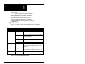
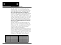
Specifications
Tables 1-1 through 1-3 define environmental, electrical, and physical
specifications of the EPC-30.
Characteristic
Environmental
Temperature
operating
storage
Humidity
Altitude
Vibration
operating
storage
operating
storage
operating
storage
Shock
operating
storage
Value
0°C to 60°C, derated 2°C per 1,000 feet
(300 meters) over 10,000 feet (3,000 meters)
2°C per minute maximum excursion gradient
-40° to 85°C, 5°C per minute maximum
excursion gradient
5% to 95% non-condensing
5% to 95% non-condensing
0 to 10,000 feet (3,000 meters)
0 to 40,000 feet (12,000 meters)
0.015 inch (0.38 mm) P-P displacement with
2.5 g peak (maximum) acceleration over 5 to
2000 Hz
0.030 inch (0.76 mm) P-P displacement with
5.0 g peak (maximum) acceleration over 5 to
2000 Hz.
30 g, 11 ms duration, half-sine shock pulse
50 g, 11 ms duration, half-sine shock pulse
Table 1-1. Environmental Specifications.
Page 4
Introduction
1
1
Table 1-2 shows electrical specifications of the EPC-30 equipped with a 1
MB SIMM, and no keyboard, disk drive, or PC card.
Characteristic
Value
Electrical
Current
+5 VDC
1.3 A max., 1 A typical
+12 VDC
40 mA maximum
-12 VDC
Not used
Table 1-2. Electrical Specifications.
Table 1-3 shows physical specifications of the EPC-30 equipped with a 1
MB SIMM, and no keyboard, disk drive, or PC card.
Characteristic
Value
Physical
Length
7.2 inches
Height
4.8 inches
Thickness
0.5 inches, including SIMM
Table 1-3. Physical Specifications.
Additional References
CL-GD6245 Advanced Data Book, Cirrus Logic Corporation, Version 1.1,
September, 1994.
CL-GD624X Applications Book, Cirrus Logic Corporation, Revision 1.0,
June 17, 1994.
Phoenix BIOS User’s Manual, Phoenix Technologies, Ltd., September,
1994.
Memory Products Data Manual, Intel Corporation, 1995.
Intel386 SX Programmer’s Reference Manual, Intel Corporation, 1995.
The Intel 386EX Microprocessor’s Enhanced DMA and DOS
Compatibility, Intel Corporation.
Intel 386EX Processor C-Step Definition, Intel Corporation.
Intel 386EX Embedded Microprocessor User’s Manual, Intel Corporation,
February 1995.
RadiSys R380EX Memory/Bus Controller Data Sheet, RadiSys Corporation,
1996.
Page 5
Introduction
1
1
Technical Reference, Personal Computer AT, International Business
Machines Corporation, 1985.
PhoenixBIOS 4.0 Technical Reference, Phoenix Technologies, Ltd.,
3/15/94 (NOTE: This document can only be distributed to customers upon
receipt of written permission from Phoenix Technologies, Ltd.).
Phoenix PicoCard Technical Reference, Phoenix Technologies, Ltd.,
3/15/94 (NOTE: This document can only be distributed to customers upon
receipt of written permission from Phoenix Technologies, Ltd.).
Phoenix PicoFlash Technical Reference, Phoenix Technologies, Ltd.,
3/15/94 (NOTE: This document can only be distributed to customers upon
receipt of written permission from Phoenix Technologies, Ltd.).
Page 6
Introduction
1
1
NOTES
Page 7
Introduction
1
1
Page 8
Getting Started Update
This chapter contains step-by-step instructions to help you install and set up the
EPC-30 for operation. The chapter includes instructions explaining how to set
jumpers on the board, configure the board for external peripherals, apply power, and
use the menu-driven software to set up the EPC-30 BIOS.EXPLR1 Overview
Before You Begin
Before you begin, have the following equipment ready to use:
• Video device (VGA or better monitor or flat panel display)
• Power supply (PC or portable power supply)
• PC/AT PS/2 style keyboard to enter BIOS setup information
• SIMM (4 MB or better recommended)
(EPC-30s constructed without video hardware will require either a VGA
card (ISA or PC-104) to display video or another computer with a serial
interface to use the
EPC-30’s serial video/keyboard function.)
And optionally, you’ll need one of the following mass storage devices to
boot from:
• IDE hard disk drive
• Floppy disk drive
• A properly configured RFA on the unit
• A PCMCIA card
Supplied Equipment
Each EPC-30 includes the following:
• Small plastic bag of jumpers
• EPC-30 diskettes
• This manual
Optional Parts
The following parts are available as options from your dealer or RadiSys:
• 4 MB SIMM
• 8 MB SIMM
• 16 MB SIMM
2
2
Page 9
2
2
Getting Started
Diskettes
The EPC-30 utilities diskette set contains the following software:
Disk 1 contains Reflash and all BIOS images.
Disk 2 contains Phoenix BIOS images and utilities.
Disk 3 contains Cirrus Logic VGA utilities.
Disk 4 contains RFA CONFIG utilities.
Unpack and Inspect the EPC-30
Unpack and visually inspect the board for damage which may have occurred
in shipment. Retain all packing material and shipping documentation in case
reshipment becomes necessary.
Page 10
2
2
Getting Started
If damage has occurred in shipment, notify the carrier at once to initiate a
damage claim. Contact your dealer or RadiSys customer service for
replacement of damaged products. The RadiSys customer service telephone
number appears on the front cover of this manual.
Make sure you take great care in providing protection from Electro-Static
Discharge (ESD).
DO NOT REMOVE ANY MODULES FROM THEIR ANTISTATIC BAGS UNLESS YOU ARE IN A STATIC-FREE
ENVIRONMENT. THE EPC-30, LIKE MOST OTHER
ELECTRONIC DEVICES, IS SUSCEPTIBLE TO ESD
DAMAGE. ESD DAMAGE IS NOT ALWAYS IMMEDIATELY OBVIOUS -IT CAN CAUSE A PARTIAL
BREAKDOWN IN SEMICONDUCTOR DEVICES THAT
MIGHT NOT IMMEDIATELY RESULT IN FAILURE.
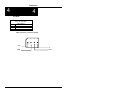
Mounting and Installation
Install the EPC-30 in a suitable enclosure using mounting holes or desktop
fashion. Ensure that environmental conditions in the enclosure will
consistently meet the conditions shown in the product specifications in
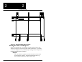
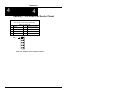
Chapter 1. Figure 2-1 shows the board dimensions and mounting hole
locations.
NOTE: If the EPC-30 installation location provides limited accessibility,
check the jumper settings on the board before you install it. Refer to the next
section for information on how to set jumpers on the board.
Page 11
2
2
Getting Started
Figure 2-1. EPC-30 Mounting Hole Locations.
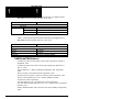
Setting the EPC-30 Jumpers
Before you install the EPC-30, familiarize yourself with the locations and
functions of jumpers on the board. Under normal circumstances, you should
not need to change the factory-installed jumper settings with the exception of
the Flat Panel BIOS selection jumpers.
Jumpers
There are a number of jumpers located on the EPC-30 board used
for the following functions. Jumpers denoted with a letter (e.g.,
JP3A) signify a single jumper within a larger block.
Page 12
2
2
Getting Started
On-board Jumper Usage
JP1
BB ENBL
JP2
Manufacturing
Loop
Flat Panel BIOS
Select
JP3A,B,C
Use to enable writes to the boot block in the BIOS.
Default is not populated.
Jumper for enabling manufacturing loop.
Default is not populated.
3-bit selection for panel type. Install jumpers for all ‘0’ bits.
Default is not populated.
Table 2-1. EPC-30 Jumper Settings.
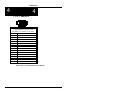
Figure 2-2. EPC-30 Layout.
Connecting the SIMM and Peripherals
Page 13
2
2
Getting Started
Select a 72-pin SIMM for use with the EPC-30 and install carefully. Make
sure you are using a SIMM with gold-plated connections.
The EPC-30 supports several standard PC-compatible I/O peripherals,
including a PS/2-compatible mouse, PS/2-compatible keyboard, IDE hard
disk drive, and VGA monitor or LCD flat panel display. Refer to Chapter 4
for connector descriptions and pinout diagrams.
Before you power up the EPC-30, connect the peripherals as the following
steps describe. You can connect the peripherals in any order.
1. Connect a PS/2 keyboard or compatible (6-pin mini DIN connector) to
J15.
2. Connect a VGA monitor (15-pin D-sub connector) to J11 or a 1/10”
socket to J8.
3. OPTIONAL - Boot Device. Connect a bootable IDE hard disk drive to
J6 or connect the floppy drive at J3.
4. OPTIONAL - Connect an LCD flat panel display to header J7 if you
will not use a VGA monitor. Note that software is required to run both a
VGA monitor and a flat panel display, as the hardware can sense the load on
the VGA connector and then disables the flat panel interface.
5. OPTIONAL - Connect a PS/2 mouse or compatible to J13. If you will
use a serial mouse, connect it to serial port COMA J14 (DB-9) or J12 (stake
pin header).
Power Supply Requirements
You can power the EPC-30 using the 4-pin connector found on any standard
PC/AT compatible +5 VDC/+12 VDC power supply such as that normally
used with a PC’s 3.5” floppy disk drive. The EPC-30 requires +5 VDC
power to operate and +12 VDC power to erase or program most flash
devices. Note: +12V is also supplied to the PCMCIA connector S1. Figure 22 shows the location of the power connector on the board.
Powering Up the EPC-30
DO NOT POWER UP THE EPC-30 UNTIL YOU MAKE
ALL CONNECTIONS.
Before you power up the EPC-30, complete the following steps.
Page 14
2
2
Getting Started
1. Inspect the board, noting the location of the connectors, jumpers, and
major components. Refer to Figure 2-2.
2. Check the jumper settings to make sure they are correct. In most cases
the jumper defaults should be adequate for your needs.
3. Connect all peripherals (mouse, keyboard, disk drives, monitor) to the
board.
4. Connect the power supply to the board or insert into a passive
backplane.
The EPC-30 is now ready for power up.
Setting Up the BIOS
This section details the various menus and sub-menus you can use to
configure the BIOS. The section presents each field in sequence as you
would encounter it for the first time. Help is available in the “Item Specific
Help” area of each menu.
Nonvolatile CMOS RAM on the EPC-30 board maintains the BIOS settings
you save. The BIOS uses these settings to initialize the hardware.
You can access the BIOS setup menus only during the system boot process.
Chapter 3 fully describes ways you can reset the EPC-30; you can use
CTRL-ALT-DEL, for example. To access the BIOS setup menus, press the
F2 key as the system boots.
Use the up and down cursor (arrow) keys to move from field to field on a
menu. Use the right and left cursor keys to move from menu to menu, as
noted in the menu bar at the top of the screen. If you leave a menu and then
return, the active field is always at the top of the menu. If you select a submenu and then return to the main menu, you return to that sub-menu
heading. For System Time and Date, press the TAB key to move between
the date and time fields.
Fields with a triangle to the left represent sub-menu headings. Press the
ENTER key when the cursor rests on one of these headings to reach the
respective sub-menu. For most fields, position the cursor at the field, and
from the numeric keypad, press the + and - keys to scroll through available
choices. You can also enter certain numeric fields by using number keys on
the keyboard. Once you change an entry to the desired value, use the up and
down cursor keys to move to the next field.
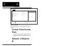
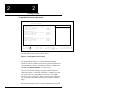
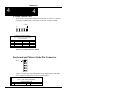
Main BIOS Setup Menu
Figure 2-3 shows the BIOS setup Main Menu.
Page 15
2
2
Getting Started
PhoenixBIOS Setup - Copyright 1985-96 Phoenix Technologies Ltd.
Main
Advanced
Exit
System Time:
System Date:
Diskette A:
Diskette B:
IDE Adapter 0 Master:
IDE Adapter 0 Slave:
Video System:
Memory Shadow
Boot Sequence:
Embedded Features:
System Memory:
Extended Memory:
F1
ESC
Help
Exit
[16:17:18]
[03/01/96]
[1.44 MB, 3½”]
[Not Installed]
(C: 235 Mb)
(None)
[EGA / VGA]
Item Specific Help
<Tab>, <Shift-Tab>, or
<Enter> selects field.
[A: then C:]
640 KB
3072 KB
Select Item
Select Menu
-/+ Change Values
Enter Select Sub-Menu
F9 Setup Defaults
F10 Previous Values
Figure 2-3. Main Menu.
This section explains the fields in each menu and sub-menu. If you
need help with the settings, refer to the “Item Specific Help” area of
the menu.
System Time/System
Date:
You can change these values by moving to each field and
typing the desired entry. Press the TAB key to move from
hour to minute to second, or from month to day to year.
Diskette A/Diskette
B
Page 16
2
2
Getting Started
Select the proper setting for your floppy disk drive by
choosing one of the following:
for 5-1/4” drives
360K or 1.2 MB
for 3-1/2” drives
720K or 1.44 MB or 2.88 MB
You can set up an A drive and a B drive using the proper
cable. The BIOS defaults to Not Installed for drive A: and
Not Installed for drive B:.
IDE Adapter 0
Master/Slave Submenus
>
These fields are headings for sub-menus which allow you
to enter complete disk drive information or auto-type the
drive. Once you set up drive information, the Main Menu
shows the drive designation and size. For more
information, refer to the description of the IDE Adapter
Sub-menus later in this chapter.
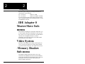
Video System
Select the video output you are using. In the majority of
cases, you will select EGA/VGA. Other options include
CGA 80x25 and monochrome. The default is EGA/VGA.
Memory Shadow
Sub-menu
>
The Memory Shadow Sub-menu allows you to copy
information from ROM (on the ISA bus) into RAM and
access the information in this alternate location. For more
information, refer to the section which explains the
Memory Shadow Sub-menu.
Page 17
2
2
Getting Started
Boot Options Submenu
>
The Boot Options Sub-menu allows changing the boot
delay, boot sequence, serial video, as well as disabling
several displays during the boot process, such as the
SETUP prompt, POST errors, floppy drive check, and
summary screen. It also allows enabling and disabling of
serial video. Once the boot sequence has been set, it
displays in this entry in the Main menu. For more
information, refer to the section which explains the Boot
Options Sub-menu.
Page 18
2
2
Getting Started
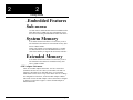
Embedded Features
Sub-menu
>
Use this menu to enable ROM extensions embedded in the
Flash Boot Device (FBD). For more information, refer to
the section concerning the Embedded Features Sub-menu.
System Memory
You cannot edit this field and it is not necessary to do so.
The field shows the amount of conventional memory (that
below 1 MB) available.
NOTE: The amount of conventional memory is actually
less than 640 KB, as the extended BIOS data area uses
some of this memory to support the PS/2 mouse interface.
Extended Memory
You cannot edit this field and it is not necessary to do so.
The field shows the amount of extended memory (that
above 1 MB) available.
>IDE Adapter Sub-menus
There are two IDE Adapter Sub-menus: one for a master drive
(bootable) and one for a slave drive (not bootable). The EPC-30
supports a maximum of two hard disk drives. To see detailed
characteristics of the device set up as the master drive or to change
the configuration of the drive, choose the IDE Adapter 0 Master
Sub-menu. Choose the IDE Adapter 0 Slave Sub-menu to configure
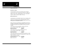
or change a second drive. Figure 2-4 shows the IDE Adapter 0
Master Sub-menu.
Page 19
2
2
Getting Started
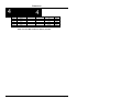
PhoenixBIOS Setup - Copyright 1985-96 Phoenix Technologies Ltd.
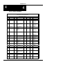
IDE Adapter 0 Master
(C:
704Mb)
Item Specific Help
Autotype Fized Disk:
[Press Enter]
Type:
Cylinders:
Heads:
Sectors/Track:
Write Precomp:
[User] 704 Mb
[ 1365]
[
16]
[
63]
[None]
Multi-Sector Transfers:
LBA Mode Control:
Transfer Mode:
[16 sectors]
[Enabled]
[Standard]
F1
ESC
Help
Exit
Select Item
Select Menu
<Tab>, <Shift-Tab>, or
<Enter> selects field.
-/+ Change Values
Enter Select Sub-Menu
F9 Setup Defaults
F10 Previous Values
Figure 2-4. IDE Adapter Sub-menu.
Autotype Fixed Disk
Use this option when setting up a new disk drive. Press
ENTER to start the process; the BIOS will change each
setting it has information for. This option ensures that the
BIOS determines the proper settings of the drive, based on
the manufacturer’s information. You can use this option
with any IDE drive that complies with ANSI
specifications.
When you manually enter information for a pre-formatted
disk drive, take care to use the same parameters that were
used originally when the disk was formatted. If the specific
cylinder, head, and sector information used was different
than the manufacturer’s settings, autotyping the disk will
supply the wrong configuration. Most likely you will be
unable to boot an operating system under such
circumstances.
Page 20
2
2
Getting Started
Type
In most cases, the IDE interface involves a hard disk drive
but the interface can involve other devices. If you are not
using an IDE hard disk drive, select ‘None.’ Also select
‘None’ if you use an SRAM PC card. If you use a disk
drive device not conforming to ANSI standards and cannot
employ the Autotype feature, select ‘User’ for the type and
enter the correct values for disk cylinders, heads, etc. from
the drive’s documentation or label.
There are some restrictions when setting up devices on the
EPC-30. Booting from an ATA card can only be
accomplished using a ROM extension such as the
PhoenixPICO PCMBOOT.BIN file. The ROM extension
reads the Card Information Structure (CIS) from the
PCMCIA card and reads the geometry of the card.
Once you complete the setup for the IDE Master, you can
choose the IDE Adapter 0 Slave Sub-menu to set up a
second hard disk drive. When the setup is complete, press
the ESC key to return to the Main Menu.
Multi-Sector Transfers
This option allows the user to configure the System BIOS
to read ahead by the specified number of sectors whenever
a disk access is performed. This has the effect of reading
more data at once to reduce the absolute number of
discrete disk reads performed by the operating system,
which may increase system performance. The possible
selections are disabled, 2, 4, 8, or 16 sectors. Note that
autotyping may change this value if the hard disk reports
that it supports block accesses. The default is disabled.
LBA Mode Control
When enabled, this option allows the System BIOS to
reference hard disk data as logical blocks instead of using
the traditional Cylinders/Heads/Sectors (CHS) method.
This option can only be used if both the hard disk being
configured and the operating system support Logical Block
Addressing (LBA). If disabled, then CHS mode is used.
Page 21
2
2
Getting Started
Note that autotyping may change this value if the hard disk
reports that it supports LBA. The default is disabled.
Transfer Mode
This option selects the mode that the System BIOS uses to
access the hard disk. The only available selection is:
Standard (default)
Note that autotyping may change this value depending on
the transfer modes that the hard disk reports it supports.
Once you have set up the IDE Adapter 0 Master, if
necessary you can set up an IDE Adapter 0 Slave. The
default setting is None.
When you complete entries to the IDE Adapter Submenus, exit to the Main BIOS Setup Menu using the ESC
key.
Page 22
2
2
Getting Started
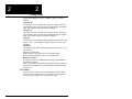
Memory Shadow Sub-menu
The term “shadowing” refers to the technique of copying BIOS
extensions from ROM into DRAM and accessing them from
DRAM. This allows the CPU to access the BIOS extensions much
more quickly and generally increases system performance if many
calls to the BIOS extensions are made. The Memory Shadow Submenu is shown below.
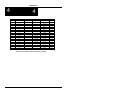
PhoenixBIOS Setup - Copyright 1985-96 Phoenix Technologies Ltd.
Memory Shadow
Item Specific Help
System Shadow:
Video Shadow:
Enabled
[Disabled]
Shadow Memory Regions:
C800-CBFF:
CC00-CFFF:
D000-D3FF:
D400-D7FF:
D800-DBFF:
DC00-DFFF:
[Disabled]
[Disabled]
[Disabled]
[Disabled]
[Disabled]
[Disabled]
F1
ESC
Help
Exit
Select Item
Select Menu
<Tab>, <Shift-Tab>, or
<Enter> selects field.
-/+ Change Values
Enter Select Sub-Menu
F9 Setup Defaults
F10 Previous Values
Figure 2-5. Memory Shadow Sub-menu.
The shadow regions should be used only if an ISABus card is
installed in the system that contains a BIOS extension (ROM)
although there is no effect on the system if a region is shadowed
that does not contain a BIOS extension. Note that each shadow
region in the setup menu is 16KB in size. Multiple shadow regions
may have to be enabled if the BIOS extension to be shadowed is
larger than 16KB.
Note: when shadowing a BIOS extension contained in the FBD, the
user must ensure that the same region is not shadowed in this menu.
The region selected in the BIOS extension shadowing menu
supersedes the region selected in this menu.
Page 23
2
2
Getting Started
System Shadow
This option is not editable since the System BIOS is always
shadowed.
Video Shadow
This option determines whether the VGA BIOS is shadowed.
Shadowing greatly improves system performance. The default is
disabled.
Shadow Memory Regions
These options enable or disable shadowing for the associated
memory region. The default is disabled for each region.
>Boot Options Sub-menu
The Boot Options Sub-menu allows you to change boot options.
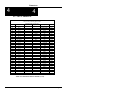
PhoenixBIOS Setup
-
Copyright 1985-95 Phoenix Technologies Ltd.
Boot Options
Serial Video:
[Enabled]
Boot Sequence:
[C: then A:]
SETUP Prompt:
[Enabled]
POST Errors:
[Enabled]
Summary Screen:
[Enabled]
F1
ESC
Help
Exit
Select Item
Select Menu
Item Specific Help
<Tab>, <Shift-Tab>, or
<Enter> selects field.
-/+ Change Values
Enter Select
Sub-Menu
F9 Setup Defaults
F10 Previous Values
Figure 2-6. Boot Options Sub-menu.
Serial Video
Use this option to enable or disable serial video. The
default is enabled. J10, pin 11, when forced low, will
enable serial video regardless of this setting. When pin 11
is not forced low, this setting takes precedence.
Page 24
2
2
Getting Started
Boot Sequence
Use this option to set the system boot sequence. You can
select a boot from ‘C only’ to slightly speed the booting
process when the system boots from an external hard disk
drive. To boot from the A: drive, change the sequence to
‘A then C.’
About Drive Letter
Assignment
If you specify an IDE Adapter 0 Master drive, it becomes
drive ‘C’ and serves as the boot drive. If you specify an
IDE Adapter 0 Slave drive, it becomes drive ‘D.’ If you
use an ATA PC card, it carries the drive ‘C’ designation
and replaces the IDE hard disk drive. An exception occurs
if you use Card and Socket Services software drivers to
access the ATA PC card. In this case, the hard disk drive
retains the ‘C’ drive designation and the software driver
controls the PC card interface. Any activated BIOS
extension supersedes the C: drive setup in the BIOS. Thus
if the RFA contains a bootable image, it becomes the C:
drive and an IDE drive switches to the D: drive. The last
BIOS image copied into a region of the RFA becomes the
C: drive, so if you activate multiple BIOS extensions, you
can push an IDE drive setup as C: all the way to E:, which
would not be visible to the system.
Setup Prompt
Page 25
2
2
Getting Started
Use this option to enable or disable the message ‘Press F2
to enter Setup.’ The default is enabled. Even if you disable
the message, you can always press F2 during the boot
process to enter the Setup Menu.
POST Errors
Use this option to stop the boot if, during the process, the
system encounters boot failure errors. Otherwise, the
system will continue to attempt to boot despite most
startup error messages that display. The default is enabled.
The following errors halt the system when the POST
Errors option is enabled:
1. Fixed disk error
• No drive connected
• Configured for 0 cylinders
• Controller reset failed
• Drive not ready
• Track 0 seek timed out
• Drive initialization failed
• Drive recalibration failed
• Last track seek failed
2. Video error
• Color/Mono switch not set correctly (not applicable to
the EPC-30)
3. Timer error
• System timer (0) failed
4. I/O chip error
• I/O conflicts exist for serial and parallel ports, hard
disk (any or all)
5. Other error
• Embedded Shadowed region exceeded DFFFF
• IRQ conflict, unsupported COM port configuration,
keyboard locked
NOTE: The system displays an error message but will not
halt if it encounters RTC, CMOS, or configuration errors
from the previous POST.
Page 26
2
2
Getting Started
Summary Screen
Use this option to enable or disable a summary of the
system configuration, which displays before the operating
system begins to load. To save booting time, or to preserve
POST data, you can disable the summary screen. The
default is enabled.
When you complete entries to the Boot Options Sub-menu,
exit to the Main BIOS Setup Menu using the ESC key.
Page 27
2
2
Getting Started
>Embedded Features Sub-menu
PhoenixBIOS Setup
-
Copyright 1985-95 Phoenix Technologies Ltd.
Embedded Features
Item Specific Help
BIOS Extension 0
Offset of BIOS extension in FBD
Destination Address
BIOS extension size
[xxxxx]
[xxxxx]
[xxxxx]
BIOS Extension 1
Offset of BIOS extension in FBD
Destination Address
BIOS extension size
[xxxxx]
[xxxxx]
[xxxxx]
BIOS Extension 2
Offset of BIOS extension in FBD
Destination Address
BIOS extension size
[xxxxx]
[xxxxx]
[xxxxx]
F1
ESC
Help
Exit
Select Item
Select Menu
<Tab>, <Shift-Tab>, or
<Enter> selects field.
-/+ Change Values
Enter Select Sub-Menu
F9 Setup Defaults
F10 Previous Values
The Embedded Features menu is shown below:
Figure 2-7. Embedded Features Menu.
It is through this menu that you control booting from BIOS
extensions. The use of BIOS extensions is a general mechanism for
executing ROM extensions. The ROM extensions are flashed into
the FBD using REFLASH.EXE or serial recovery.
This screen controls the loading (copying) of BIOS extensions
contained in Block 3 of the FBD. This block is 128KB in size and
can contain up to eleven 8KB BIOS extensions, or one 88KB
extension, or any combination. These extensions can be shadowed
into 11 possible real memory locations in the C8000h ~ DFFFFh
range.
Note that the granularity of the extension in ROM can be as small
Page 28
2
2
Getting Started
as 8KB, and can be copied down on 8KB boundaries. However, the
granularity of the shadow is 16KB.
Page 29
2
2
Getting Started
Flash Boot Device
The three regions selectable in the Embedded Features Menu
require you to enter a source base address and the size of the
extension. Then the extension is copied into a specified area:
8K
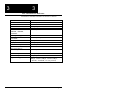
8K
8K
8K
8K
8K
8K
8K
8K
8K
8K
8K
DE000
DC000
DA000
D8000
D6000
D4000
D2000
D0000
CE000
CC000
CA000
C8000
Offset of BIOS Extension in FBD:
This field identifies the source offset of the ROM extension in the
Flash Boot Device (FBD). There are eleven 8KB (2000H bytes)
Page 30
2
2
Getting Started
sectors to choose from.
Destination Address:
This field identifies where in conventional memory the BIOS
extension will be copied. Although the boundaries are 8KB in the
FBD, the target area has 16KB granularity. If only a single 8KB
region is copied, it consumes 16KB in the target.
BIOS Extension Size:
This field checks for the number of bytes to copy. Anything copied
in this menu will supersede all ISA shadowing setups. Check to
make sure you are not locating an embedded BIOS extension in the
same address as an ISA BIOS extension.
NOTE: The factory has installed two optional BIOS extensions in
the FBD. The PhoenixPICO Flash RFA BIOS extension is located
at 4C000H. The Phoenix PicoCard BIOS extension is located at
4A000H.
To boot from a factory prepared RFA, use these parameters:
Offset of BIOS extension in FBD [4C000H]
Destination Address
[D0000H]
BIOS extension size
[4000H]
To boot from a factory-prepared FLASH or ATA card:
Offset of BIOS extension in FBD [4A000H]
Destination Address
[C8000H]
BIOS extension size
[2000H]
To boot PICO flash, follow the instructions in Appendix F for disk
(RFA) preparation. Use the DOS command SYS d: to install a boot
image on the RFA. In CMOS,
Offset of BIOS extension in FBD [4C000H]
Destination Address
[D8000H]
BIOS extension size
[4000H]
Page 31
2
2
Getting Started
Advanced Menu
PhoenixBIOS Setup - Copyright 1985-96 Phoenix Technologies Ltd.
Main
Advanced
Exit
Item Specific Help
Warning!
Setting items on this menu to incorrect values
may cause your system to malfunction.
<Tab>, <Shift-Tab>, or
<Enter> selects field.
Integrated Peripherals
RFA Access Mode:
RFA Data Mode:
[Linear]
[Word]
Large Disk Access Mode:
[Other]
F1
ESC
Help
Exit
Select Item
Select Menu
-/+ Change Values
Enter Select Sub-Menu
F9 Setup Defaults
F10 Previous Values
Figure 2-8. Advanced Menu
The Advanced Menu contains settings for integrated peripherals
and to set the large disk access mode. The figure below shows this
menu.
>Integrated Peripherals Sub-menu
This option is used to select the Integrated Peripherals sub-menu in
order to configure the onboard COM ports, parallel port and floppy
drive. Refer to the Integrated Peripherals Sub-menu section for
more information.
RFA Access Mode
This option is used to
select between Linear
Page 32
2
2
Getting Started
and I/O paged access
modes to the RFA.
RFA Data Access
Mode
This option is used to
select between byte
and word data access.
Large Disk Access
Mode
If you use a drive larger than 528 MB and you run DOS,
set the Large Disk Access Mode to ‘DOS.’ This is the
default setting. If you use a different operating system, set
it to ‘Other.’ The ‘DOS’ setting causes the system BIOS to
store in its two hard disk tables (located in the extended
BIOS data area) the number of cylinders divided by two
and the number of heads multiplied by two (if the drive is
configured in setup to have more than 1024 cylinders).
This allows MS-DOS systems to use hard disks of up to 8
Page 33
2
2
Getting Started
GB in size, or 1024 C x 255 H x 63 S, without special
drivers or LBA.
Integrated Peripherals Sub-menu
PhoenixBIOS Setup - Copyright 1985-96 Phoenix Technologies Ltd.
Integrated Peripherals
Item Specific Help
386EX COMA:
Super I/O-COMB:
Super I/O-COMC:
LPT port:
LPT Mode:
Diskette controller:
F1
ESC
Help
Exit
[Enabled]
[Disabled]
[Disabled]
[378, IRQ7]
[Output Only]
[Enabled]
Select Item
Select Menu
<Tab>, <Shift-Tab>, or
<Enter> selects field.
-/+ Change Values
Enter Select Sub-Menu
F9 Setup Defaults
F10 Previous Values
Figure 2-9. Integrated Peripherals Menu
The options in this sub-menu are used to configure the onboard
serial and parallel port and disk controllers.
386EX COMA:
This option is used to enable or disable the serial port COMA. This
port is provided by the 386EX and is not configurable. The default
is enabled, at 3F8 and IRQ4.
If the COMB or COMC base The IRQ setting can be
address is set to this:
one of these:
3F8
IRQ4, IRQ5 or IRQ9
3E8
IRQ4, IRQ5 or IRQ9
2F8
IRQ3, IRQ5 or IRQ9
2E8
IRQ3, IRQ5 or IRQ9
Table 2-2. COMB and COMC address and IRQ settings.
Page 34
2
2
Getting Started
NOTE: IRQ4 cannot be used by COMB or COMC if COMA is
enabled.
COM port B:
This option is used to configure the serial port COMB. This port is
off of the SMC super I/O chip, and is configurable for base address
3F8h, 2F8h, 3E8h or 2E8h. The default is Disabled.
COM port C:
This option is used to configure the serial port COMC. This port is
off of the SMC super I/O chip, and is configurable for base address
3F8h, 2F8h, 3E8h or 2E8h. The default is Disabled.
LPT port
This option is used to configure the parallel port labeled on the front
panel as “LPT”. The defaults for this LPT port are I/O base 378h
and IRQ7.
LPT Mode
This option sets the mode under which the LPT port operates. The
selections are:
Output only (the default)
Bi-directional (accepts inputs as well as standard output)
ECP (extended capabilities protocol as per IEEE 1284)
Diskette Controller
This option enables or disables the onboard floppy disk controller.
The default is enabled.
When you complete entries in the Integrated Peripherals Sub-menu
and the Advanced Menu, exit to the Main BIOS Setup Menu using
the ESC key.
Exit Menu
Use the options in this menu to save the BIOS setup into CMOS
and exit to the operating system, or to abandon your changes and
exit to the system. Figure 2-10 shows the Exit Menu.
Page 35
2
2
Getting Started
PhoenixBIOS Setup
Main
-
Advanced
Copyright 1985-95 Phoenix Technologies Ltd.
Exit
Item Specific Help
Save Changes and Exit
Exit Without Saving Changes
Get Default Values
Load Previous Values
Save Changes
F1
ESC
Help
Exit
Select Item
Select Menu
<Tab>, <Shift-Tab>, or
<Enter> selects field.
-/+ Change Values
Enter Select
Sub-Menu
F9 Setup Defaults
F10 Previous Values
Figure 2-10. Exit Menu.
Save Changes and
Exit
Use this option if you want to save your entered values
into CMOS and exit to load the operating system. The
EPC-30 saves the new values, exits the BIOS setup mode,
and reboots using the new values.
Exit Without Saving
Changes
Use this option if you want to discard the changes you
made and revert to the BIOS setup as it was before you
Page 36
2
2
Getting Started
began making changes. The EPC-30 reboots with the old
setup values.
Get default values
Use this option if you need to reset the BIOS setup values
to those that were set at the factory as default values before
any changes were made. The EPC-30 does not exit from
the BIOS setup mode and you can continue to edit.
Load previous values
Use this option if you wish to load the system with the
previous BIOS setup values, or those values that existed
before you began making changes. The EPC-30 does not
exit from the BIOS setup mode and you can continue to
edit.
Save Changes
Use this option to save changes you made during the
editing session. The EPC-30 does not exit from the BIOS
setup mode and you can continue to edit.
Page 37
2
2
Getting Started
Page 38
Theory of Operation Update
This chapter contains information about the following components, functions, and
aspects of the EPC-30:
• Overview
• EPC-30 processor
• Functional Unit Summary
• DRAM Interface/Bus Control
• Memory
• BIOS Flash EPROM
• Super VGA/Flat Panel Controller Subsystem
• Flash Disk Subsystem
• Hard Drive and Floppy Disk Drive Controller
• Miscellaneous Functions
• Power Requirements
• 3.3V Operation
• Mechanical Specifications
• Resetting the EPC-30
Block Diagram
3
3
Page 33
3
3
EPC-30 Hardware Reference
Figure 3-1. EPC-30 Block Diagram.
• The Real-Time Clock and 82C42PE are normally used inside the
R380EX.
ProcessorEXPLR1 Overview
The standard EPC-30 uses the 33 MHz Intel386 EX in a 132-pin PQFP
package. The 386 EX is a fully static, 32-bit processor optimized for
embedded applications. It features low power consumption, a 16-bit external
data bus, a 26-bit external address bus, and a 32-bit programming
architecture compatible with Intel386 processors.
R380EX/Intel386 EX-based System Functional
Unit Summary
Component
PC-Compatible
Features
Functional Unit
Interrupt
Controllers (2)
Description
8259A-Compatible Peripheral Interrupt controller.
Page 34
3
3
EPC-30 Hardware Reference
Timer/Counters (3)
Asynchronous
Serial Ports (2)
Intel386 EX
Embedded
Extensions
DMA Controller
Clock & Power
Management Unit
Watchdog Timer
Synchronous Serial
Port (1)
Parallel I/O Port
Programmable Chip
Select Units (8)
DRAM Refresh
Control
JTAG Test-logic
RadiSys
R380EX
PC-Compatible
Features
Real Time Clock
Keyboard/Mouse
Controller
R380EX
Core System
Support Features
PC Speaker/”Port
B” Functionality
DRAM Refresh
Controller
Power Management
Support
ROM/Flash ROM
Controller
Digital IO Port
Programmable Chip
Select Units (4)
IDE Interface
LED Control
82C54-Compatible Programmable Interval Timer with
enhancements to allow remapping of peripheral addresses &
interrupt assignments.
NS16450 Compatible UART. All interrupts may be connected to
the interrupt controller or two may be connected to the DMA
controller.
PC-Compatible to a certain extent. Backward compatible with
8237A. Two independent DMA channels can be 8 or 16 bits
wide.
Provides a programmable clock signal for EX core and for
peripherals. Power management capability provides idle (stops
CPU clock; peripheral clock runs) and powerdown (both CPU
and peripheral clocks stopped) modes.
General purpose 32-bit timer.
Provides bi-directional serial I/O up to 5 Mbps. Built-in protocols
are not included. Synchronous serial IO interrupts may be
connected to the DMA controller for high-speed transfers.
Generates periodic refresh requests and refresh addresses.
Simplifies board level testing. Fully compliant with IEEE Std
1149.1-1990.
Provides Motorola 146818A-compatible real time clock and
alarm with 114 bytes of battery-backed CMOS memory. The
RTC also generates a periodic interrupt. Access to the CMOS
memory is through registers 070h and 071h in an index/data
fashion. The Real-time clock is enabled or disabled by bootstrap
pins on the R380EX.
Implements a 8042-Compatible keyboard controller with
extensions to support a PS/2 mouse. The controller is enabled or
disabled by bootstrap pins on the R380EX.
Port B register is located at 061h.
Supports two banks of SIMMs as FPM, EDO or Flash SIMMs.
Second bank start address is configurable. Supports EDO/FPM
memory type detection.
Supports Power Management with Halt detection logic, SMI
generation logic, and glitchless clock switching.
Supports SIMM-style Flash.
16 General-purpose I/O bits.
Control for ISA Bus peripheral devices.
Supports EIDE transfer modes (PIO4). Located at 01F0h.
Control for two pins/external indicators available
Page 35
3
3
EPC-30 Hardware Reference
Table 3-1. Functional Unit Summary.
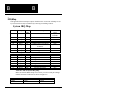
DRAM Interface/Bus Control
The processor-to-board interface supporting DRAM and bus control is
managed by the RadiSys R380EX memory/bus controller (U20). The
R380EX is designed specifically for use with the Intel386 EX processor and
provides the support the Intel386 EX requires for DRAM, flash or EPROM
control, reset synchronization, ready generation, data bus transceiver control,
and the ISA bus.
The R380EX fast page mode, zero wait state DRAM controller includes
address multiplexers, page hit logic for address pipelining, RAS and CAS
generation and CAS before RAS DRAM refresh control. The DRAM
controller provides support for 1, 2, 4, 8, and 16 MB SIMMs.
Functionally, the R380EX provides control signals for flash memory, the
real time clock, IDE interface, and the keyboard/mouse controller. It also
generates a clock synchronized RESET signal for the Intel386 EX, and the
READY# signal for non-local bus access cycles. The R380EX also generates
I/O read/write, memory read/write, address latch enable and other signals.
A data buffer control signal prevents data bus contention that could result
from direct use of the Intel386 EX RD# signal as the output enable for
external devices.
Memory
The EPC-30 supports 70ns fast page mode (FPM) or extended data out
(EDO) DRAM installed in a 72-pin SIMM socket. SIMM memory may be
installed to support from 1MB up to 16MB of DRAM. Physically, the EPC30 has only one SIMM socket. The second module is the soldered-down
DRAM (1MB, 2MB or 4MB configuration). After power on reset, the BIOS
will find and size memory present in the system. The EPC-30 does not
support parity DRAM.
To improve the performance of the BIOS that is initially contained in a 16bit wide flash EPROM, the main BIOS and, optionally, the video BIOS will
be shadowed in the DRAM.
Use of a double-sided SIMM with soldered-down DRAM is not
recommended due to RAS line restrictions.
The DRAM controller’s address pipelining supports zero wait state read and
write cycles to and from the DRAM. With a two-bank, symmetrical
Page 36
3
3
EPC-30 Hardware Reference
configuration in the SIMM, the DRAM controller functions as two
independent controllers, managing each bank of DRAM in an interleaved
fashion. The controller determines accesses to each DRAM bank.
BIOS Flash EPROM
The system BIOS and video BIOS reside in a single 2MB boot-block flash
EPROM (Intel 28F200BV-T or equivalent). It is based on the Phoenix
PicoBIOS code base. It includes the video BIOS, supplied by Cirrus, and
support for flat panel displays. The BIOS includes support for a set of three
different displays.
The most common types of displays that work with the EPC-30 board are
Monochrome, Passive Color, and TFT Color. Refer to the next section in this
chapter, as well as Appendix E, LCD Flat Panel Interface, for more
information.
The boot-block flash EPROM allows BIOS changes and upgrades to be
loaded and programmed into the flash BIOS after the board leaves the
factory. It is anticipated that this feature may be required to support different
flat-panel displays, without requiring that the flash device be replaced.
The EPC-30 uses a signal on the miscellaneous expansion header to force an
update of the BIOS. This signal is connected to an input pin of the R380EX,
and it is used when the BIOS is so corrupted that the operating system does
not boot. The BIOS will then be updated from the serial COMA port. Refer
to Appendix D, Reflashing the BIOS, for more details on this operation.
A jumper is provided to enable programming of the boot block. Selection of
the source of the chip select (either the R380 BIOS CS or the 386EX UCS
signal) for the BIOS component is controlled by resistor options. Refer to
Chapter 2, Installation and Configuration.
Super VGA/Flat Panel Controller Subsystem
A VGA-compatible video and flat-panel display controller can be provided
on the CPU board. The video subsystem is implemented with a Cirrus CLGD6245 along with 512KB of video memory implemented with one
256Kx16 DRAM device.
The Cirrus VGA chip supports a variety of 640x480 LCDs along with
simultaneous CRT and LCD operation. CRT resolutions of 1024x768 with
16 colors or 800x600 with 256 colors and up to 64 gray shades (at 640x480)
with monochrome STN and TFT LCDs may be obtained. The VGA
controller is on the Intel386 EX local bus.
Page 37
3
3
EPC-30 Hardware Reference
The 6245 is also capable of Standby and Suspend modes for reduced power
consumption. The hardware suspend function of the VGA controller is
supported by connecting the 386EX port bit P2.4 to the VGA controller
SUSPEND input. Refer to the CL-GD6245 datasheet and applications notes
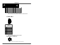
for details of the suspend function’s operation.
Appendix C contains information on how to install the Cirrus Logic utility
software. Appendix E contains cabling information for the flat panel
connector. Pinouts are described in Chapter 4, Connectors.
Note that the system BIOS does not support both the VGA connector and the
flat panel connector in use at the same time. The flat panel is only supported
when the VGA connector is not in use. However, software utilities available
from Cirrus Logic can drive a CRT and a flat panel at the same time.
The VGA controller provides the following set of output connectors:
1.
A standard 15-pin high-density D-sub connector used to connect to
a standard VGA monitor.
2.
A 10-pin header carrying standard VGA signals.
3.
A 50-pin 2.0mm pitch shrouded header to provide connection for
flat panel displays.
The ROM BIOS code for the VGA controller is included in the same BIOS
flash EPROM as the main system BIOS. Since it is contained in a bootblock flash device, it is possible to upgrade the video BIOS to include
different flat-panel displays after the board has left the factory. At power-up,
a set of jumpers is read by the VGA controller to select which of the options
is used.
The BIOS includes space for the different types of panels to be supported. At
release, only one panel has been validated, the Sharp LM64P89
(Monochrome), but others are expected. Check the RadiSys Web page for
more information, or contact RadiSys Technical Support.
No circuitry is included on the EPC-30 for LCD contrast or backlight
control.
Flash Disk Subsystem
The EPC-30 implements a Resident Flash Array (RFA) as a fully bootable
read/write flash file system. The RFA site is compatible with 2MB (28F016)
and 4MB (28F032) devices. A second pad pattern at the same site accepts
1MB (28F008) devices.
The interface to the RFA may be accomplished one of two ways, depending
on the setup menu settings.
Page 38
3
3
EPC-30 Hardware Reference
The RFA access may be implemented through a 16K memory window in the
processor’s address space. This is useful for real mode operating systems
such as DOS. The processor’s CS6 is used in addressing the RFA along with
additional address bits from an upper address register. A 10-bit upper
address register (only eight bits are used) resides on the ISA data bus which
is accessed using CS2 from the R380EX. This memory window is
programmed using the processor’s and R380EX’s chip selects. To access
the RFA in this manner, the BIOS needs to be configured to select IO
mapped page operation of the RFA. The factory-shipped implementation of
Phoenix PICO Flash uses D4000h as the window address and 380h as the
page register.
The RFA may also be mapped as linear high memory to 48 MBytes, or
3000000H. In this mode of operation, the 386EX CS6 chip select is used
alone to select the device in its entirety. To select this method of operation,
change the BIOS screen in the Advanced Menu to select linear memory
addressing for the RFA. The BIOS initially programs the RFA at 48MB
(3000000H).
A resistor setting is used to provide control of the programming voltage to
the flash device. A separate resistor selects the source of the write enable
signal into the part, either the R380 flash write or 386EX ~WR signal. A
programmable pin on the 386 EX (configurable in the BIOS setup) can force
the RFA to operate in a byte-wide mode (as opposed to 16-bit operation).
Page 39
3
3
EPC-30 Hardware Reference
Hard Drive and Floppy Disk Drive Controller
A floppy disk drive controller is contained in a Super-I/O chip, the
FDC37C665GT, manufactured by Standard Microsystems Corp. For details
of the operation of these functions, refer to the SMC datasheet for this
device. Note that this device also contains the two serial ports and one
parallel port; see below.
The floppy disk controller uses programmed I/O mode; DMA operation is
not supported. This makes it incompatible with some operating systems that
don’t use the BIOS for floppy support. The EPC-30 supports one or two
5.25" 360KB and 1.2MB as well as 3.5" 720KB, 1.44MB, and 2.88MB
drives and media. The floppy controller occupies I/O addresses 0x3F2,
0x3F4, 0x3F5, and 0x3F7. It uses the AT bus interrupt IRQ6. Connection to
a floppy disk drive is made via an “untwisted”
34-pin ribbon cable. NOTE: The EPC-30 by default will supply power to
the floppy disk drive using the untwisted cable and a fuse. Configurations
that do not supply power through the cable (those pins are instead grounded)
are available.
The IDE hard disk interface is provided by the R380EX. The IDE hard disk
is mapped to I/O addresses 0x1F0 - 0x1F7, 0x3F6, and 0x3F7. Note that I/O
address 0x3F7 is shared with the floppy disk controller as required for PC
compatibility. The IDE interface chip selects ~HCS0 and ~HCS1 are
generated by R380 chip selects. ~HCS0 corresponds to CS3, and ~HCS1
corresponds to CS1.
The IDE hard disk uses AT-bus interrupt IRQ14. Connection to an IDE hard
disk is made through a standard 2mm pitch 44-pin ribbon cable header
mounted on the PCB. This interface is designed to support 2.5’ drives that
take power through the cable. Up to two drives are supported by the IDE
interface.
Serial and parallel ports
The EPC-30 contains one PC-compatible parallel printer port and
up to three
PC-compatible serial ports (COMA from the Intel386 EX and
COMB/COMC from the Super I/O). The COMB and COMC serial
ports from the Super I/O include NS16C550-compatible UARTs to
support high-speed operation (including 16-byte FIFO as default).
The COMA serial port in the Intel386 EX is NS16C450compatible.
Page 40
3
3
EPC-30 Hardware Reference
The COMA serial port is provided by the first UART in the
Intel386 EX processor, and is located in the I/O address range
0x3F8-0x3FF. COMA serial port interrupts are signaled using the
interrupt IRQ4 within the processor. Disabling this COMA port
routes its IRQ4 signal to an external pin on the 386EX, which
makes it available for the SMC COMB and COMC ports.
Connection to COMA is made either through a standard male DB-9
connector or via a standard 10-pin header configured to match
readily available pig-tails. The DB-9 is typically installed. It is not
possible to populate both the DB-9 connector and the 10-pin header.
The COMB serial port is provided by the first UART in the Super
I/O chip, and can be located at the base I/O addresses 3F8, 2F8,
3E8, or 2E8. COMB serial port interrupts are signaled using either
IRQ3, IRQ4, IRQ5 or IRQ9, selected by a resistor. Connection to
COMB is made via a standard 10-pin header configured to match
readily available pig-tails.
The COMC serial port is provided by the second UART in the
Super I/O chip, and can be located at the base I/O addresses 3F8,
2F8, 3E8, or 2E8. COMC serial port interrupts are signaled using
the interrupt IRQ3, IRQ4, IRQ5 or IRQ9, selected by a resistor.
Connection to COMC is made via a standard 10-pin header
configured to match readily available pig-tails.
Note that the arrangement of IRQs allows the Super I/O ports to be
mapped as COM1 (instead of COM4) if the 386EX internal UARTs
are disabled. This may be desired if 386EX port pins that are used
for the serial ports are needed for other uses, such as DMA. Not all
IRQ options are available to all addresses. See Table 3-2 for a
comprehensive list of IRQ and Base Address configurations.
COMB
COMC
Base Address
3F8
2F8
3E8
2E8
3F8
2F8
3E8
IRQ Options
IRQ 4,5,9
IRQ 3,5,9
IRQ 4,5,9
IRQ 3,5,9
IRQ 4,5,9
IRQ 3,5,9
IRQ 4,5,9
Page 41
3
3
EPC-30 Hardware Reference
2E8
IRQ 3,5,9
Table 3-2. COM Locations/Interrupts
The LPT1 parallel port is located in the I/O address range 0x3780x37F. LPT1 parallel port interrupts are signaled using the AT bus
interrupt IRQ7. Connection to this port is made via a 26-pin
shrouded stake-pin header. This is a multi-mode IBM PC/XT,
PC/AT and PS/2-compatible bi-directional parallel port. It also
supports enhanced modes including: Enhanced Parallel Port (EPP)
versions 1.7 and 1.9, and Extended Capabilities Port (ECP). These
enhanced features are IEEE 1284-1 Compliant.
PCMCIA controller
The EPC-30 includes a PCMCIA controller, using the Cirrus Logic
CL-PD6710 device. This device is compatible with the popular
82365 interface.
The connector employed accepts type I, type II, or type III cards.
12V VPP is supplied to the memory card as required, as is 5V and
3.3V (if the 3.3V regulator is installed).
Refer to Chapter 2 for information about BIOS extensions. Refer to
Appendix F for details of the software support of the PCMCIA
controller.
Watchdog timer
A watchdog timer function is included as part of the functionality of
the Intel386 EX processor and is connected to provide a RESET
signal to the CPU and ISA bus connector in the event that software
loses control of the system.
ISA-bus
Connection is made to the ISA-bus through two alternate connector
schemes. The first is a standard PC/AT-style card edge connector.
This connector includes two sections: one is a 31-position
connector, and the second an 18-position connector. Each position
has one contact on each side of the board.
The second ISA-bus connection may be made via two standard
0.100" [2.54 mm] square-pin type sockets arranged to meet the
PC/104 standard. The header corresponding to the 31-position card
edge is a 32x2 position socket, and the header corresponding to the
18-position card edge is a 20x2 position socket. "Extra" pins on
these header connectors are connected to ground. These sockets
Page 42
3
3
EPC-30 Hardware Reference
allow topside mounting of PC/104 cards. Four 0.125” holes are
present in the PCB at standard PC/104 locations.
The ISA-bus signals are provided by the R380EX devices. External
buffers are used to interface the R380 to all of the external ISA bus
devices and the ISA connectors. The buffer strengths, Iol and Ioh,
on the bus are 24 mA or greater.
The clock speed of the ISA-bus is a function of the divide ratio
programmed in the R380EX and is set to approximately 8 MHz.
Page 43
3
3
EPC-30 Hardware Reference
Terminations contained on the EPC-30 board are as follows:
Address lines:
SA0 - SA19, and LA17 - LA24:
Data lines
SD0 - SD15:
Control strobes:
~IOR, ~IOW, ~MEMR,
~MEMW, ~SMEMR,
~SMEMW:
Xfer response signals:
~IOCS16, ~MEMCS16, ~0WS,
~MASTER:
DRQ inputs:
IRQ inputs:
~REFRESH output:
RESETDRV, OSC, BALE,
AEN, SYSCLK, TC
~SBHE output:
Driven by R380EX
10K pull-up to VCC
Driven by R380EX
300 ohm pull-up to VCC
10K pull-down to GND
10K pull-up to VCC
Driven by R380EX
No termination
Driven by R380EX
~IOCHCK input:
IOCHRDY input:
Signals Not Supported:
4.7K pull-up to VCC
1K pull-up to VCC
~IOCHCKK, DRQ2, DACK2, DRQ3, ~DACK3,
DRQ5, ~DACK5, DRQ6, ~DACK6, DRQ7,
~DACK7, ~MASTER, -5V (not powered)
Table 3-3. Terminations.
Page 44
3
3
EPC-30 Hardware Reference
Miscellaneous Functions
Keyboard controller
A PC-compatible keyboard controller is provided as part of the
R380EX. Connection to it is made with a 6-pin mini-DIN circular
connector, the type used in PS/2 designs and in other RadiSys CPU
designs. These signals are duplicated in a 10-pin shrouded stake
pin header. The keyboard may be attached there through an adaptor
instead of at the mini-DIN connector.
Power to the keyboard is fused to meet safety agency requirements
(e.g., UL1950).
Battery
A built-in socketed coin cell battery is provided for backup of the
real-time clock and CMOS RAM which is part of the R380EX.
This cell is installed at the factory, and is user-replaceable. The cell
used is a 3V lithium coin cell, Duracell part number BR2450
(600mA-hour) or equivalent.
Speaker
A small speaker is installed on the PCB and connected to the
standard PC "beep" generation circuit. The speaker is directly
driven by the R380EX. The R380EX includes a routing feature
which allows combining of the normal PC speaker signal with the
PCMCIA speaker signal, thus eliminating the need for a second
speaker.
LEDs
The following LED and LED interfaces are provided:
HDD access LED signal - an LED can be connected to monitor the
hard drive ~HACT signal. The LED will illuminate when the drive
is accessed. This signal is present on the misc. expansion header.
Current is limited by a 510Ω resistor.
Power on LED signal - a signal to drive an LED when power is
applied to the system. This signal is present on the misc. expansion
header. Current is limited by a 510Ω resistor.
Reset Signal
A reset signal is provided on the board, in the miscellaneous
expansion header, to provide a reset input to the system.
Page 45
3
3
EPC-30 Hardware Reference
Power requirements
In most applications, the EPC-30 operates on 5V DC power only. The
voltage supplied must be between 4.75 volts and 5.25 volts. +12V must be
supplied to erase or program non-Smart voltage FLASH devices, including
the BIOS, if 5V-only components are not installed on the board. The +12V
supply from the power input connector is connected to the ISA and PC/104
connectors.
Normally, -5V is also supplied by the PC power supply, but it is only
connected to the ISA and PC/104 connectors, and is seldom used by any
board. This design does not make provisions for sourcing or connecting to
the -5V supply.
The last two letters in Flash chip part numbers identify smart-voltage and
non-smart-voltage parts. For example, the 28F016SV is a smart-voltage chip
that can use 5V or 12V. the 28F016SA requires 12V to program.
The current consumption of the EPC-30 is 1.3 amps or less (1 amp typical)
in 5V mode, using a 33MHz Intel386 EX C-step processor, with a base
memory configuration of 4 MB, in an idle state (DOS prompt).
This current draw does not include current drawn for the keyboard, or any
daughter cards that might be installed on the ISA-bus or PC/104 sockets.
3.3V Operation
Circuitry is included on the EPC-30 board for a 5V to 3.3V linear voltage
regulator. Some of the passive components are populated, but the converter
is not populated. In order to run 3.3V PCMCIA cards, the regulator needs to
be installed and other changes must be made.
Page 46
3
3
EPC-30 Hardware Reference
The following modifications must be performed to operate the board at 3.3V:
1. The CPU needs to be replaced with a 3.3V processor.
2. The regulator and components to be installed.
3. The zero-ohm resistors connecting 3.3V to VCC need to be removed.
4. The DRAM SIMM installed must be operable at 3.3V.
5. The 74ABT16245 buffers in the IDE interface need to be replaced with
5V-safe, 3.3V parts, such as 74LVT16245s.
6. A resistor needs to be removed and one installed to set the RFA part for
3.3V operation.
Mechanical specifications
Mechanically, the EPC-30 is a 7.2” long x 4.8” high ISA card.
Mounting holes are positioned on the PCB to allow for mounting of the
EPC-30. Refer to Figure 2-1 in Chapter 2 for more information.
The EPC-30 meets the PC/104 specification for the mounting of topsidemounted PC/104 cards.
A complete mechanical drawing of the board with detailed dimensions and
the positions of connectors and mounting holes is available.
The EPC-30 is designed to meet the standard RadiSys environmental
specifications. This includes operation at temperatures from 0 to +60
degrees C. EPC-30 meets this specification in still air, with no forced cooling
required.
Page 47
3
3
EPC-30 Hardware Reference
Resetting the EPC-30
The EPC-30 can be reset in the following ways:
• Power-off, power-on
• Resets the entire system. The EPC-30 runs the power-on self tests and
reboots the operating system.
• External Reset Input
• A normally open reset switch on the misc. expansion header allows
external resets. Grounding the signal performs a hardware reset. A power-on
self test and a reboot of the operating system follow the external reset.
• BIOS Setup Exit Menu
• When you exit the BIOS set up menus using the ‘Exit and Save
Changes’ option on the Exit Menu, a hardware reset occurs. The system runs
the power-on self tests and reboots the operating system.
• CTRL+ALT+DEL
• Pressing the CTRL, ALT, and DEL keys simultaneously on the
keyboard causes a “warm boot.” The EPC-30 does not reinitialize all of the
processor’s hardware. The power-on self test does not run, but the operating
system reloads.
• NOTE: The CTRL+ALT+ DEL reset method typically works only
under DOS.
• Abnormally Low Supply Voltage
• The EPC-30 resets if the power supply input voltage (+5 VDC Vcc)
falls to +4.65 VDC. The system remains in reset until 200 ms after supply
voltage rises once again above +4.65 VDC.
Brown-Out Protection
The EPC-30 board provides brown-out protection using a Dallas
power supply monitoring chip (U24). When Vcc falls to +4.65
VDC, the Dallas chip detects the voltage drop and drives ~RESET
low. The EPC-30 stays in reset as long as the voltage is at +4.65
VDC or lower and for 200 ms after the voltage rises above
+4.65 VDC.
NOTES
Page 48
3
3
EPC-30 Hardware Reference
Page 49
4
4
Connectors
This chapter describes the connectors on the EPC-30. These connectors adhere to
existing standards. This chapter shows illustrations of each connector with pins
oriented as they appear when you view the front of the connector.
COMB RS-232 and RS-422 Pinouts
1
3
5
7
9
RS-232 COMB (J1):
5x2, 0.100" [2.54 mm] pitch header
3M 2510-6002-UB
DCD
2
DSR
RXD
4
RTS
TXD
6
CTS
DTR
8
RI
GND
10
GND
1
3
5
7
9
RS-422 COMB (J1):
5x2, 0.100" [2.54 mm] pitch header
3M 2510-6002-UB
GND
2
CTSRTS+
4
CTS+
RTS6
RXD+
TXD+
8
RXDTXD10
GND
Table 4-1. COMB RS-232 and RS-422 Pinouts.
COMC Header Pinout
1
RS-232 COMC (J2):
5x2, 0.100" [2.54 mm] pitch header
3M 2510-6002-UB
DCD
2
DSR
Page 49
Connectors
4
4
3
5
7
9
1
3
5
7
9
RXD
TXD
DTR
GND
4
6
8
10
RTS
CTS
RI
N/C
TTL COMC (J2):
5x2, 0.100" [2.54 mm] pitch header
3M 2510-6002-UB
DCD
2
DSR
RXD
4
RTS
TXD
6
CTS
DTR
8
RI
GND
10
+5V
Table 4-2. COMC RS-232 and TTL Pinouts.
Page 50
Connectors
4
4
Floppy Drive Pinout
1
3
5
7
9
11
13
15
17
19
21
23
25
27
29
31
33
FDD pinout: (J3)
17x2, 0.100" [2.54 mm] pitch header
3M 2534-6002-UB
GND
~DENS
2
N/C
N/C
4
N/C
N/C
6
N/C
~INDEX
8
Fused Vcc*
~MTR1
10
Fused Vcc*
~DS0
12
Fused Vcc*
~DS1
14
GND
~MTR0
16
GND
~DIR
18
GND
~STEP
20
GND
~WDATA 22
GND
~WGATE 24
GND
~TRK0
26
GND
~WRPRT
28
GND
~RDATA
30
GND
~HDSEL
32
GND
~DSKCH
34
Table 4-3. Floppy Drive Connector Pinout.
• Pins 9, 11 and 13 can be grounded if necessary. Remove the fuse at F1
and install a zero-ohm resistor at R14.
Page 51
Connectors
4
4
Power
1
2
3
4
AT-Power Header (J4)
4x1, 0.156” [3.96 mm]
AMP 171825-4
+12
GND
GND
+5
Table 4-4. Power Connector Pinout.
1
+12V
GND
2
3
4
+5
GND
Page 52
Connectors
4
4
Manufacturing Test Socket
Manufacturing Test Socket (J5)
7x2, 2mm Socket
SAMTEC SMM-107-01-S-D
Vcc
2 D0
D1
4 D2
D3
6 D4
D5
8 D6
D7
10 PWRGOOD
~IOW80
12 ATB.~IOW
GND
14 N/C
1
3
5
7
9
11
13
Table 4-5. Manufacturing Test Socket Pinout.
IDE Header
2
1
3
5
Pin 1
IDE HDD pinout: (J6)
22x2, 0.079" [2.0 mm] pitch header
SAMTEC STMM-122-01-S-D-20
~RESET
GND
2
D7
D8
4
D6
D9
6
Page 53
Connectors
4
4
7
9
11
13
15
17
19
21
26
25
27
29
31
33
35
37
39
41
43
D5
D4
D3
D2
D1
D0
GND
N/C
~IOW
~IOR
IOCHRDY
n/c
IRQ
A1
A0
~HCS0
~DASP
VCC
GND
D10
D11
D12
D13
D14
D15
N/C (key)
GND
GND
GND
n/c
GND
~IOCS16
N/C
A2
~HCS1
GND
VCC
N/C
8
10
12
14
16
18
20
22
24
26
28
30
32
34
36
38
40
42
44
Table 4-6. IDE Header Pinout.
Page 54
Connectors
4
4
Flat Panel Header
Flat Panel Header (J7)
25x2 0.079” (2.0 mm) pitch header
3M 953229-01-25-30
Pi
n
Signal
Type
Description
Pin
Signal
Type
Description
1
3
PVCC
NC
PWR
VCC for flat panel
2
4
VSS
LD0
GND
O
Ground
Lower Data0
for Mono,
Lower Data0
for STN
Lower Data1
for Mono,
Lower Data1
for STN
Ground
5
FPBACKEN
O
Flat Panel Backlight
Enable
6
LD1
O
7
FPVCCEN
O
8
VSS
GND
9
FPVEEEN
O
Flat Panel VCC
Enable
Flat Panel VEE
Enable
10
LD2
O
11
VSS
GND
Ground
12
LD3
O
13
15
MOD
FLM
O
O
Modulation
LCD VSYNC (LFS)
14
16
VSS
LD4
GND
O
17
VSS
GND
Ground
18
LD5
O
19
LP
O
20
VSS
GND
21
FPDEN
O
22
LD6
O
23
VSS
GND
LCD HSYNC
(LLCLK)
Flat Panel Display
Enable
Ground
24
LD7
O
25
SCLK
O
26
VSS
GND
27
29
VSS
SUD0
GND
0
28
30
R4
R5
O
O
R4 for TFT
R5 for TFT
31
SUD1
0
32
VSS
GND
Ground
33
35
VSS
SUD2
GND
O
34
36
NC
NC
37
SUD3
O
Shift Clock
(FPVDCLK)
Ground
Upper Data0 for
Mono, Upper Data0
for STN
Upper Data1 for
Mono, Upper Data1
for STN
Ground
Upper Data2 for
Mono, Upper Data2
for STN
Upper Data3 for
Mono, Upper Data3
Lower Data6
for STN
Lower Data7
for STN
Ground
38
VSS
GND
Ground
Lower Data2
for Mono,
Lower Data2
for STN
Lower Data3
for Mono,
Lower Data3
for STN
Ground
Lower Data4
for STN
Lower Data5
for STN
Ground
Page 55
Connectors
4
4
39
41
43
45
47
49
VSS
SUD4
SUD5
VSS
SUD6
SUD7
GND
O
O
GND
O
O
for STN
Ground
Upper Data4 for STN
Upper Data5 for STN
Ground
Upper Data6 for STN
Upper Data7 for STN
40
42
44
46
48
50
NC
NC
VSS
NC
NC
VSS
GND
Ground
GND
Ground
Pin 1
Table 4-7. Connection List for Flat Panel Header.
Page 56
Connectors
4
4
Auxiliary VGA Stake-Pin Header Pinout
1
3
5
7
9
Auxillary VGA Header (J8):
5x2, 0.100" [2.54 mm] pitch header
3M 2510-6002-UB
RED
2 ANALOG GND
GREEN
4 ANALOG GND
BLUE
6 ANALOG GND
HSYNC
8 GND
VSYNC
10 GND
Pin 1
Table 4-8. Auxiliary VGA Connector Pinout.
Page 57
Connectors
4
4
Parallel Port
1
3
5
7
9
11
13
15
17
19
21
23
25
Parallel Port Pinout (J9):
13x2, 0.100" [2.54 mm] pitch header
3M 2526-6002-UB
~STB
2 ~AFD
PD0
4 ~ERR
PD1
6 ~INIT
PD2
8 ~SELECT
PD3
10 GND
PD4
12 GND
PD5
14 GND
PD6
16 GND
PD7
18 GND
~ACK
20 GND
BUSY
22 GND
PE
24 GND
SELECT
26 GND
Table 4-9: Parallel Port Header Pinout
Page 58
Connectors
4
4
VGA Connector
VGA pinout (J11)
15-pin female high-density D-sub
JST KSEY-15S-1A3F19-13 or equiv.
Pin
Signal
1
RED
2
GREEN
3
BLUE
4
N/C
5
GND
6
ANALOG GND (RED)
7
ANALOG GND (GREEN)
8
ANALOG GND (BLUE)
9
N/C (plug)
10
GND
11
N/C
12
N/C
13
H SYNC
14
V SYNC
15
N/C
Table 4-10. VGA Standard Connector Pinout.
Page 59
Connectors
4
4
COMA Serial Port
There are two 10-pin header COM ports on the EPC-30. Table 4-11 defines
serial ports COMB/COMC, while Table 4-2 defines serial port COMA.
Pin 1
9
1
3
5
7
9
COMA (J12) Stake-Pin pinout:
5x2, 0.100" [2.54 mm] pitch header
3M 2510-6002-UB
DCD
2
RXD
TXD
4
DTR
GND
6
DSR
RTS
8
CTS
RI
10
Table 4-11. COM1 Connector Pinout.
Keyboard and Mouse Stake-Pin Connector
Pin 1
Pin
Table 4-12 defines the 10-pin shrouded stake pin header that provides PS/2
mouse signals and duplicates the PS/2 keyboard signals.
Mouse Connector (J13)
5x2, 0.100” Stake-pin Header
3M 2510-6002-UB
Signal
Pin
Signal
Page 60
Connectors
4
4
1
3
5
7
9
Mouse Data
Mouse CLK
Shield
Keyboard DATA
Keyboard CLK
2
4
6
8
10
Keyboard VCC
Keyboard GND
Shield
Keyboard VCC
Keyboard GND
Table 4-12. Keyboard and Mouse Stake-Pin Connector Pinout.
COMA DB-9
1
6
9
5
COMA DB-9 (J14)
pinout:
9-pin male D-sub
JSEY-9P-1A3F19-13
1
DCD
2
RXD
3
TXD
4
DTR
5
GND
6
DSR
7
RTS
8
CTS
9
RI
Table 4-13. COMA DB-9 Connector Pinout.
Keyboard Connector
Table 4-14 defines the 6-pin DIN keyboard connector.
Page 61
Connectors
4
4
Keyboard Connector (J15)
6-pin mini-DIN Circular
AMP 749266-1 or equivalent
Pin
Signal
Pin
Signal
1 Keyboard Data
4 Keyboard VCC
2 N/C
5 Keyboard Clock
3 Ground
6 N/C
Table 4-14. Keyboard Connector Pinout.
AT Bus Pinout
P1
A1
A2
A3
A4
A5
A6
A7
A8
A9
A10
A11
A12
A13
A14
A15
A16
A17
A18
A19
A20
A21
A22
A23
A24
A25
Signal
Vcc
SD7
SD6
SD5
SD4
SD3
SD2
SD1
SD0
IOCHRDY
AEN
SA19
SA18
SA17
SA16
SA15
SA14
SA13
SA12
SA11
SA10
SA9
SA8
SA7
SA6
AT-bus pinout (XT side):
Signal Name
Signal Name
~IOCHCK
-5V
DRQ2
~DACK3
DRQ3
Signal
GND
RESETDRV
VCC
IRQ9
n/c
n/c
-12V
~0WS
+12V
GND
~SMEMW
~SMEMR
~IOW
~IOR
Pull Up
n/c
~DACK1
DRQ1
~REFRESH
SYSCLK
IRQ7
IRQ6
IRQ5
IRQ4
IRQ3
P1
B1
B2
B3
B4
B5
B6
B7
B8
B9
B10
B11
B12
B13
B14
B15
B16
B17
B18
B19
B20
B21
B22
B23
B24
B25
Page 62
Connectors
4
4
A26
A27
A28
A29
A30
A31
SA5
SA4
SA3
SA2
SA1
SA0
~DACK2
Pull Up
TC
BALE
VCC
OSC
GND
B26
B27
B28
B29
B30
B31
Table 4-15. ISA Bus Connector Pinout (XT side).
Page 63
Connectors
4
4
P2
C1
C2
C3
C4
C5
C6
C7
C8
C9
C10
C11
C12
C13
C14
C15
C16
C17
C18
Signal
~SBHE
LA23
LA22
LA21
LA20
LA19
LA18
LA17
~MEMR
~MEMW
SD8
SD9
SD10
SD11
SD12
SD13
SD14
SD15
AT-bus pinout (AT side):
Signal Name
Signal Name
~DACK5
DRQ5
~DACK6
DRQ6
~DACK7
DRQ7
~MASTER
Signal
~MEMCS16
~IOCS16
IRQ10
IRQ11
IRQ12
IRQ15
IRQ14
~DACK0
DRQ0
Pull Up
n/c
Pull Up
n/c
Pull Up
n/c
VCC
Pull Up
GND
P2
D1
D2
D3
D4
D5
D6
D7
D8
D9
D10
D11
D12
D13
D14
D15
D16
D17
D18
Table 4-16. ISA Bus Connector Pinout (AT side).
Page 64
Connectors
4
4
PC/104 Connector
CN9
A1
A2
A3
A4
A5
A6
A7
A8
A9
A10
A11
A12
A13
A14
A15
A16
A17
A18
A19
A20
A21
A22
A23
A24
A25
A26
A27
A28
A29
A30
A31
A32
Signal
~IOCHCK
SD7
SD6
SD5
SD4
SD3
SD2
SD1
SD0
IOCHRDY
AEN
SA19
SA18
SA17
SA16
SA15
SA14
SA13
SA12
SA11
SA10
SA9
SA8
SA7
SA6
SA5
SA4
SA3
SA2
SA1
SA0
GND
PC/104 pinout:
32x2, 0.100" [2.54 mm] pitch socket
SAMTEC ESQ 132-37-G-D
Signal Name
Signal Name
DRQ2
KEY
~DACK3
DRQ3
~DACK2
Signal
GND
RESETDRV
VCC
IRQ9
N/C
N/C
-12V
~0WS
+12V
N/C
~SMEMW
~SMEMR
~IOW
~IOR
Pull Up
N/C
~DACK1
DRQ1
~REFRESH
SYSCLK
IRQ7
IRQ6
IRQ5
IRQ4
IRQ3
Pull Up
TC
BALE
VCC
OSC
GND
GND
CN9
B1
B2
B3
B4
B5
B6
B7
B8
B9
B10
B11
B12
B13
B14
B15
B16
B17
B18
B19
B20
B21
B22
B23
B24
B25
B26
B27
B28
B29
B30
B31
B32
Table 4-17. PC/104 Connector Pinout (1 of 2).
Page 65
Connectors
4
4
CN9
C0
C1
C2
C3
C4
C5
C6
C7
C8
C9
C10
C11
C12
C13
C14
C15
C16
C17
C18
C19
Signal
GND
~SBHE
LA23
LA22
LA21
LA20
LA19
LA18
LA17
~MEMR
~MEMW
SD8
SD9
SD10
SD11
SD12
SD13
SD14
SD15
GND
PC/104 pinout :
20x2, 0.100" [2.54 mm] pitch socket
Signal Name
Signal Name
~DACK5
DRQ5
~DACK6
DRQ6
~DACK7
DRQ7
~MASTER
Signal
GND
~MEMCS16
~IOCS16
IRQ10
IRQ11
IRQ12
IRQ15
IRQ14
~DACK0
DRQ0
Pull Up
N/C
Pull Up
N/C
Pull Up
N/C
VCC
Pull Up
GND
GND
CN9
D0
D1
D2
D3
D4
D5
D6
D7
D8
D9
D10
D11
D12
D13
D14
D15
D16
D17
D18
D19
Table 4-18. PC/104 Connector Pinout (continued).
Page 66
Connectors
4
4
PCMCIA Connector
PCMCIA Connector (S1):
69-Pin SMT CONAN Connector 0.039 in (1.0mm) Centerline
BERG 91931-31169
Pin #
Signal
Pin #
Signal
1
2
3
4
5
6
7
8
9
10
11
12
13
14
15
16
17
18
19
20
21
22
23
24
25
26
27
28
29
30
31
32
33
34
35
N/C
GND
CD3
CD4
CD5
CD6
CD7
CCE1
CA10
~COE
CA11
CA9
CA8
CA13
CA14
~CWE
CRDY
PCMVCC
PCMVPP
CA16
CA15
CA12
CA7
CA6
CA5
CA4
CA3
CA2
CA1
CA0
CD0
CD1
CD2
CWP
GND
36
37
38
39
40
41
42
43
44
45
46
47
48
49
50
51
52
53
54
55
56
57
58
59
60
61
62
63
64
65
66
67
68
69
GND
CCD1
CD11
CD12
CD13
CD14
CD15
CCE2
RFV
~CIOR
~CIOW
CA17
CA18
CA19
CA20
CA21
PCMVCC
PCMVPP
CA22
CA23
CA24
CA25
RFV
CRESET
CWAIT
CINPACK
CREG
CBVD2
CBVD1
CD8
CD9
CD10
CCD2
GND
Table 4-19. PCMCIA Connector.
Page 67
Connectors
4
4
Page 68
Connectors
4
4
NOTES
Page 69
Connectors
4
4
Page 70
5
5
Troubleshooting and
Error Messages
Troubleshooting
Symptoms
System appears to
boot (evidenced
by being on and
hard disk being
accessed) but
provides no video.
System fails at
power-up -will not
run power-on
self-test.
Possible Cause(s)
Monitor or cable
problem.
Solution
Verify that the cable pins are not bent
and the cable is fully seated in the VGA
connector. If necessary, try the monitor
on another system to verify that the
monitor is good.
The system is not
getting power.
Verify that +5 VDC power is good and
that the connector on the power supply is
fully seated. in the power connector on
the board.
Reset signal is
shorted.
Check the signal on the misc. expansion
header.
This section deals with problems that you may encounter that do not provide
an error message. Table 5-1 lists general problems and their solutions. If an
error message displays, see the next section of this chapter, Common Error
Messages.
Table 5-1. Troubleshooting General Problems.
Table 5-1. Troubleshooting General Problems (cont.)
Symptoms
Possible Cause(s)
Solution
Page 67
Troubleshooting and Error Messages
5
5
Serial ports do
not work.
System hangs
either before or
after operating
system boot.
Floppy
problems can’t read
floppy drive.
Interrupt conflicts.
An external peripheral may be using the
same interrupts as COM1 and/or
COMA/B. Verify that no other device is
using IRQ3 or IRQ4.
Serial ports not
enabled in CMOS
setup.
Check BIOS settings.
Incorrect base
address setting.
Be sure all software is configured to find
the serial ports at the addresses chosen in
the BIOS setup.
Port hardware
failure.
System clock
signal degradation.
Replace the unit.
Floppy uses DMA1
not DMA2; any OS
that does not use
the BIOS (i.e.,
QNX) won’t
recognize the
floppy.
Cable has a twist.
Noise entering the EPC-30 system
through the connection of a peripheral
device may be degrading the CPU clock.
Disconnect the peripheral device and
reboot the system to verify system clock
integrity.
No workaround.
Use a straight-through cable.
Common Error Messages
This section contains a summary of error and warning messages in
alphabetical order by the message text. The BIOS or MS-DOS generates
these messages, which typically relate to your hardware configuration. If you
experience a system failure after you make changes in the BIOS setup
menus, you may be able to correct the problem by entering setup and
restoring the original values.
BAD OR MISSING COMMAND INTERPRETER
DOS
Page 68
Troubleshooting and Error Messages
5
5
Problem:
DOS cannot find the command line interpreter.
Solution(s):
Either COMMAND.COM is not present at the specified
(or default) directory level of the boot disk or the "SHELL=" statement in
your CONFIG.SYS lists the file incorrectly (wrong directory or misspelled).
DISK BOOT FAILURE, INSERT SYSTEM DISK AND PRESS ENTER
BIOS
Problem:
No boot disk could be found. Your hard disk may not have
been partitioned into logical drive(s). PCs look for logical drives from which
to boot. Hard disks are physical drives; partitions are logical drives.
Solution(s):
If your BIOS setup screen has all disks disabled, or if your
hard disk is disabled, run the BIOS setup program and verify that all disk
parameters are correct. If a hard disk is present, verify that it is properly
partitioned and formatted as a system disk and that one partition is set active.
FAILURE FIXED DISK 0
BIOS
Problem:
The IDE disk controller for drive ‘C’ cannot be initialized.
Solution(s):
Ensure that the +5 VDC power to the controller and hard
disk are good and, if used, the ribbon cable to the hard disk is fully seated.
If you are not using an IDE drive, enter the BIOS setup program.
Access the IDE Adapter Sub-menu menu as Section 2 describes. Change the
drive type to match the device being used. If the drive conforms to ANSI
specifications, you can use the Autotype feature to automatically configure
the controller for the drive.
If you install Pico Card and attempt to boot off an ATA card, make
sure the IDE drive is set to NONE.
GENERAL FAILURE READING DRIVE ...
DOS
Problem:
This almost always indicates the presence of an
unformatted hard disk partition or diskette.
Solution(s):
Format the partition or diskette using the utilities your
operating system provides.
INVALID DRIVE SPECIFICATION
DOS
Problem:
You are trying to access a logical drive (e.g., ‘C,’ ‘D,’ ...)
that is not known to the operating system.
Solution(s):
Select a different logical drive. If you are trying to access a
hard disk, you may need to create the logical partition.
KEYBOARD ERROR
BIOS
Problem:
This message indicates that the system did not recognize a
keyboard at power-up or you pressed a key during the power-on self test.
Page 69
Troubleshooting and Error Messages
5
5
Solution(s):
Check the integrity of the keyboard connector.
If you think you pressed a key during power-up, reboot the system.
Some keyboards are designed with a switch (or jumper) to allow the
user to configure the keyboard for use with an AT machine or an XT
machine. If this is the case with your keyboard, verify that the switch is in
the AT position.
The keyboard may not be a valid PC/AT keyboard (e.g., it is a
PC/XT-only or PS/2 keyboard). If this is the case, replace the keyboard with
a PC/AT style keyboard.
MISSING OPERATING SYSTEM
BIOS
Problem:
Although the system could read the hard disk and find the
active partition, the operating system files could not be found.
Solution(s):
This can be caused by using a drive type number in the
BIOS setup menu that does not match the type number used to format the
hard disk. Run the BIOS setup program. Enter the IDE Adapter Sub-menu.
Select the correct drive type to match the type used to format the disk
originally. If the drive conforms to ANSI specifications, you may use the
Autotype feature to automatically configure the controller for the drive being
used. Save the changes and reboot the system.
This problem can also occur if:
• the hard disk is partitioned and one partition is set active, but the
partition is not formatted. Format the partition using the utilities your
operating system provides.
• the system attempts to boot from a floppy disk that is not bootable.
Page 70
Troubleshooting and Error Messages
5
5
PARITY ERROR IN SEGMENT ...
DOS
Problem:
This could be a software error (reading a nonexistent
memory area) or a true hardware failure.
Solution(s):
Attempt to repeat the error. If the error occurs during the
execution of your own proprietary software, verify that the memory location
your software specifies is valid.
PRESS A KEY TO REBOOT
BIOS
Problem:
A drive assigned as drive ‘C’ exists but is not set active.
Solution(s):
Run your operating system disk partitioning program (like
FDISK) and set the primary partition active.
REAL TIME CLOCK ERROR - RUN SETUP
BIOS
Problem:
The battery-backed TOD clock is incorrect.
Solution(s):
Run the BIOS setup program to determine what is wrong,
and make corrections. If the error occurs repeatedly, the CMOS battery has
failed.
SYSTEM CMOS CHECKSUM BAD -- RUN SETUP
CMOS
Problem:
One of the entries in the CMOS RAM is incorrect.
Solution(s):
Run the BIOS setup program to determine what is wrong,
and make correction. If the error occurs repeatedly, the CMOS battery has
failed.
Page 71
Troubleshooting and Error Messages
5
5
BIOS Checkpoints
The Phoenix PicoBIOS in the EPC-30 writes a number of POST checkpoint
codes to I/O port 80h just before each checkpoint executes. Table 5-2
describes these checkpoint codes and instructions.
NOTE: The POST checkpoint codes generally execute in the order the table
shows. The codes may not execute in the exact order in the table.
Beep Code POST CODE
Checkpoint Description
02h
Verify Real Mode
04h
Get CPU type
06h
Initialize system hardware
08h
Initialize chipset registers with initial POST values
09h
Set in POST flag
0Ah
Initialize CPU registers
0Ch
Initialize cache to initial POST values
0Eh
Initialize I/O
10h
Initialize Power Management
11h
Load alternate registers with initial POST values
12h
Jump to UserPatch0
14h
Initialize keyboard controller
1-2-2-3
16h
BIOS ROM checksum
18h
8254 timer initialization
1Ah
8237 DMA controller initialization
1Ch
Reset Programmable Interrupt Controller
1-3-1-1
20h
Test DRAM refresh
1-3-1-3
22h
Test 8742 Keyboard Controller
24h
Set ES segment register to 4 GB
28h
Autosize DRAM
2Ah
Clear 512 KB base RAM
1-3-4-1
2Ch
Test 512 KB base address lines
1-3-4-3
2Eh
Test 512 KB base memory
32h
Test CPU bus-clock frequency
37h
Reinitialize the chipset
38h
Shadow system BIOS ROM
39h
Reinitialize the cache
3Ah
Autosize cache
Table 5-2. POST Checkpoint Codes.
Page 72
Troubleshooting and Error Messages
5
5
Beep Code
POST Code
Checkpoint Description
3Ch
Configure advanced chipset registers
3Dh
Load alternate registers with CMOS values
40h
Set initial CPU speed
42h
Initialize interrupt vectors
44h
Initialize BIOS interrupts
2-1-2-3
46h
Check ROM copyright notice
47h
Initialize manager for PCI Option ROMs
48h
Check video configuration against CMOS
49h
Initialize PCI bus and devices
4Ah
Initialize all video adapters in system
4Ch
Shadow video BIOS ROM
4Eh
Display copyright notice
50h
Display CPU type and speed
52h
Test keyboard
54h
Set key click if enabled
56h
Enable keyboard
2-2-3-1
58h
Test for unexpected interrupts
5Ah
Display prompt “Press F2 to enter SETUP”
5Ch
Test RAM between 512 KB and 640 KB
60h
Test extended memory
62h
Test extended memory address
64h
Jump to UserPatch1
66h
Configure advanced cache registers
68h
Enable external and CPU caches
6Ah
Display external cache size
6Ch
Display shadow message
6Eh
Display non-disposable segments
70h
Display error messages
72h
Check for configuration errors
74h
Test real-time clock
76h
Check for keyboard errors
7Ch
Set up hardware interrupt vectors
7Eh
Test coprocessor if present
80h
Disable onboard I/O ports
82h
Detect and install external RS232 ports
Table 5-2. POST Checkpoint Codes (cont.)
Page 73
Troubleshooting and Error Messages
5
5
Beep Code
POST CODE
Checkpoint Description
84h
Detect and install external parallel ports
86h
Re-initialize onboard I/O ports
88h
Initialize BIOS Data Area
8Ah
Initialize Extended BIOS Data Area
8Ch
Initialize floppy controller
90h
Initialize hard disk controller
91h
Initialize local bus hard disk controller
92h
Jump to UserPatch2
94h
Disable A20 address line
96h
Clear huge ES segment register
98h
Search for option ROMs
9Ah
Shadow option ROMs
9Eh
Enable hardware interrupts
A0h
Set time of day
A2h
Check keylock
A8h
Erase F2 prompt
AAh
Scan for F2 keystroke
ACh
Enter SETUP
AEh
Clear in-POST flag
B0h
Check for errors
B2h
POST done - prepare to boot operating system
B4h
One beep
B6h
Check password (optional)
B8h
Clear global descriptor table
BCh
Clear parity checkers
BEh
Clear screen (optional)
BFh
Check virus and backup reminders
C0h
Try to boot with INT19
Table 5-2. POST Checkpoint Codes (cont.)
Beep Code
POST Code
Checkpoint Description
D0h
Interrupt handler error
D2h
Unknown interrupt error
D4h
Pending interrupt error
D6h
Initialize option ROM error
D8h
Shutdown error
DAh
Extended Block Move
Page 74
Troubleshooting and Error Messages
5
5
DCh
Shutdown 10 error
Table 5-3. Auxiliary POST Checkpoint Codes.
Beep Code
Post Code
Checkpoint Description
E2H
Initialize the chipset
E3H
Initialize refresh counter
E4H
Check for Forced Flash
E5H
Check HW status of ROM
E6H
BIOS ROM is OK
E7H
Do a complete RAM test
E8H
Do OEM initialization
E9H
Initialize interrupt controller
EAH
Read in bootstrap code
EBH
Initialize all vectors
ECH
Boot the Flash program
EDH
Initialize the boot device
EEH
Boot code was read OK
Table 5-4. Phoenix PicoBIOS Boot Block Checkpoint Codes
Page 75
Troubleshooting and Error Messages
5
5
PhoenixBIOS Messages
The following is an explanation of each of the Phoenix BIOS messages.
Diskette drive A error or
Diskette drive B error
Floppy disk drive A: or B: is present but fails the BIOS POST diskette tests.
Check to see that the drive is defined with the proper diskette type in Setup
and that the diskette drive is attached correctly. The EPC-30 does not require
a twisted cable.
Embedded Region 0-2 Shadowed The system successfully copied the
BIOS extension.
Embedded Region 0-2 Failed to Shadow Check the BIOS settings in the
Embedded Features Sub-menu to make sure the settings are correct.
Entering SETUP ... This message signals that the system is starting the
BIOS Setup program
Extended RAM Failed at offset: nnnn Extended memory is not working
or is not configured properly at offset nnnn.
nnnn Extended RAM Passed Where nnnn is the amount of RAM in
kilobytes successfully tested.
Failing Bits: nnnn The hex number nnnn is a map of the bits at the RAM
address (in System, Extended, or Shadow memory) which failed the memory
test. Each 1 (one) in the map indicates a failed bit.
Fixed Disk 0 Failure or
Fixed Disk 1 Failure or
Fixed Disk Controller Failure The fixed disk is not working or is not
configured properly. Check to see if the fixed disk is attached properly and
has power. Run Setup to be sure the fixed-disk type is correctly identified.
Incorrect Drive A type - run SETUP Type of floppy drive A: not correctly
identified in Setup.
Incorrect Drive B type - run SETUP Type of floppy drive B: not correctly
identified in Setup.
Invalid NVRAM media type There is a problem with NVRAM (CMOS)
access.
Keyboard controller error The keyboard controller failed its test. You may
have to replace the keyboard or the controller.
Keyboard error The keyboard is not working, but the controller is
operating.
Keyboard error nn The BIOS discovered a stuck key and displays the scan
code nn for the stuck key.
Keyboard locked - Unlock key switch Unlock the system to proceed.
Page 76
Troubleshooting and Error Messages
5
5
Monitor type does not match CMOS - Run SETUP Monitor type not
correctly identified in Setup
Operating system not found Operating system cannot be located on either
drive A: or drive C:. Enter Setup and see if the fixed disk or drive A: are
properly identified.
Parity Check 1 Parity error found in the system bus. BIOS attempts to
locate the address and display it on the screen. If it cannot locate the address,
it displays ????.
Parity Check 2 Parity error found in the I/O bus. BIOS attempts to locate
the address and display it on the screen. If it cannot locate the address, it
displays ????.
Press <F1> to resume, <F2> to Setup Displayed after any recoverable
error message. Press <F1> to start the boot process or <F2> to enter Setup
and change any settings.
Press <F2> to enter SETUP Optional message displayed during POST. Can
be turned off in Setup.
Previous boot incomplete - Default configuration used
Previous POST did not complete successfully. POST loads default values
and offers to run Setup. If the failure was caused by incorrect values and
they are not corrected, the next boot will likely fail. On systems with control
of wait states, improper Setup settings can also terminate POST and cause
this error on the next boot. Run Setup and verify that the wait-state
configuration is correct. This error is cleared the next time the system is
booted.
Real time clock error Real-time clock fails BIOS test. May require board
repair.
Shadow Ram Failed at offset: nnnn Shadow RAM failed at offset nnnn of
the 64k block at which the error was detected.
Page 77
Troubleshooting and Error Messages
5
5
nnnn Shadow RAM Passed Where nnnn is the amount of shadow RAM in
kilobytes successfully tested.
System battery is dead - Replace and run SETUP The CMOS clock
battery indicator shows the battery is dead. Replace the battery and run Setup
to reconfigure the system.
System BIOS shadowed System BIOS copied to shadow RAM.
System cache error - Cache disabled RAM cache failed the BIOS test.
BIOS disabled the cache.
System CMOS checksum bad - run SETUP System CMOS has been
corrupted or modified incorrectly, perhaps by an application program that
changes data stored in CMOS. Run Setup and reconfigure the system either
by getting the Default Values and/or making your own selections.
System RAM Failed at offset: nnnn System RAM failed at offset nnnn of
in the 64k block at which the error was detected.
nnnn System RAM Passed Where nnnn is the amount of system RAM in
kilobytes successfully tested.
System timer error The timer test failed. Requires repair of system board.
UMB upper limit segment address: nnnn Displays the address nnnn of
the upper limit of Upper Memory Blocks, indicating released segments of
the BIOS which may be reclaimed by a virtual memory manager.
Video BIOS shadowed Video BIOS successfully copied to shadow RAM
Page 78
Troubleshooting and Error Messages
5
5
NOTES
Page 79
Troubleshooting and Error Messages
5
5
Page 80
6
6
Support and Service
In North America
Technical Support
RadiSys maintains a technical support phone that is staffed
weekdays (except holidays) between 8:00 AM and 5:00 PM Pacific
time. If you require assistance outside these hours, you can leave a
message on voice-mail using the same phone number. You can also
request help via electronic mail or by FAX addressed to RadiSys
Technical Support Department. See the cover of this manual for the
RadiSys telephone and FAX numbers. The RadiSys e-mail address
on the internet is [email protected]. If you are sending e-mail
or a FAX, please include information on both the hardware and
software being used and a detailed description of the problem,
specifically how the problem can be reproduced. We will respond
by e-mail, phone or FAX by the next business day.
Technical support services are designed for customers who have
purchased their products from RadiSys or an authorized sales
representative. If your RadiSys product is part of a piece of OEM
equipment, or was integrated by someone else as part of a system,
support will be better provided by the OEM or system vendor that
did the integration and understands the final product and
environment.
World Wide Web
RadiSys maintains an active site on the world wide web. The homepage URL is http://www.radisys.com. The site contains current
information about the company and locations of sales offices, new
and existing products, contacts for sales, service, and technical
support information. You can also send e-mail to RadiSys using the
web site. Requests for sales, service, and technical support
information receive prompt response.
Repair Services
RadiSys provides Factory Repair Service for the entire RadiSys
product line. Standard service for all RadiSys products covers
factory repair with customers paying shipping to the factory and
RadiSys paying for return shipment. Overnight return shipment is
Page 81
Support and Service
6
6
available at customer expense. Normal turn-around time for repair
and re-certification is five working days.
Quick Exchange services (immediate shipment of a loaner unit
while the failed product is being repaired) are available. Negotiate
these or other extra-cost services in advance to allow RadiSys to
pool the correct product configurations. RadiSys does not maintain
a general "loaner" pool: units are available only for customers who
have negotiated this service in advance.
RadiSys does not provide a fixed-price "swap-out" repair service.
Many customers indicate that issues of serial number tracking and
version control make it more convenient to receive their original
products back after repair.
Warranty Repairs
RadiSys will repair at no charge products having manufacturing
defects during the warranty period. See the warranty information at
the front of this manual. Products without fault sent in for warranty
repair will be subject to a recertification charge. Extended
warranties are available at a standard price for any product still
under original warranty. RadiSys will gladly quote prices for
extended warranties on products with lapsed original warranties;
contact the factory if this applies.
Customer induced damage (resulting from misuse, abuse, or
exceeding the product specifications) is not covered by warranty.
Non-Warranty Services
There are several classes of non-warranty service. These include
repair of customer induced problems, repairs of failures for
products outside the warranty period, recertification (functional
testing) of a product either in or out of warranty, and procurement
of spare parts.
All non-warranty repairs are subject to service charges. RadiSys has
determined that pricing repairs based on time and materials is more
cost-effective for the customer than a flat-rate repair charge.
RadiSys analyzes the product after it is received. When instructed to
do so, RadiSys informs the customer of repair costs for
authorization. After the customer authorizes repairs and makes
billing arrangements, RadiSys repairs the product and returns it to
the customer.
RadiSys provides a recertification service for products either in or
out of warranty. This service verifies correct operation of a product
Page 82
Support and Service
6
6
by inspecting and testing the product using standard manufacturing
tests. There is a product-dependent charge for recertification.
Generally, very few components are field-repairable. However,
since RadiSys understands that some customers want or need the
option of repairing their own equipment, all components are
available in a spares program. RadiSys charges a minimum billing
for this program.
Arranging Service
To schedule service for a product, please call the RadiSys Technical
Support Department. The telephone number appears on the cover of
this manual. Have the product model and serial numbers available,
along with a description of the problem. A technical support
representative will issue a Returned Materials Authorization (RMA)
number, a code number by which RadiSys tracks the product while
it is being processed. Once you receive the RMA number, follow
the instructions of the technical support representative and return
the product to RadiSys, freight prepaid. Mark the RMA number
clearly on the exterior of the package. If possible, re-use original
shipping containers and packaging. In any case, be sure you follow
good ESD-control practices when handling the product. Use antistatic bags and packing materials with adequate padding and shockabsorbing properties.
Before you ship the product, include the following information:
return address, contact names and phone numbers in purchasing and
engineering, and a description of the problem. If available, include
ancillary information related to the problem.
Ship the product, freight prepaid, to the RadiSys Product Service
Center at the address shown on the front cover of this manual.
Page 83
Support and Service
6
6
Other Countries
Use the RadiSys world wide web site to contact us, or contact the sales
organization from which you purchased your RadiSys product for service
and support. The RadiSys world wide web URL is http://www.radisys.com.
Page 84
Support and Service
6
6
Page 85
A
A
I/O & Memory Maps
This appendix defines the I/O address map, memory chip selections, and memory
map for the EPC-30.
I/O Map
The EPC-30 uses both internal and external I/O mapped peripherals. Some
of the external devices require the use of a chip select while others perform
the address decode themselves.
Chip Select
Device
Address Range
Wait
Data
(Hex)
States
Width
Internal
PIC 0
0020-0021
Internal
Address Cfg. Reg.
0022-0023
Internal
Timers 0-2
0040-0043
GCS1#
Keybrd/Mouse Ctrl.
0060, 0064
15d*
8
GCS2#
RTC & Ext. CMOS
0070-0071
15d*
8
Internal
Port 92
0092
Internal
PIC 1
00A0-00A1
GCS4#
IDE CS0
01F0-01F7
8/15d*
8/16*
Internal
COMB
02E8-02FF
CL-GD6245
VGA Controller
03B0-03DF, 46E8
8/16 (2)
CL-PD6710 PC Card Controller
03E0-03E1
15d*
8/16 (2)
GCS3#
IDE CS1
03F6-03F7
15d*
8
Internal
COM1
03F8-03FF
Internal
Chip Cfg.
F400-F85F
Internal
LPT Data
F860-F864
Internal
LPT Ctrl./Stat.
F870-F874
Internal
Chip Cfg.
F875-F8FF
Table A-1. EPC-30 System I/O Map.
* Default cycles are 15 wait states for 8-bit and eight wait states for 16-bit.
Memory Chip Selects
Chip
Select
Device
Address Range
(Hex)
Wait
States
Data
Width
Memory
Speed (ns)
Page 1
A
A
I/O and Memory Maps
GCS5#
UCS#
GCS6#
None
1MB DRAM
2 MB DRAM
4MB DRAM
8 MB DRAM
16MB DRAM
512 KB Flash
2 MB Flash
4 MB Flash
0000000-00FFFFF
0000000-01FFFFF
0000000-03FFFFF
0000000-07FFFFF
0000000-0FFFFFF
3F80000-3FFFFFF
3000000-3400000
00A0000-00DFFFF
00A0000-00BFFFF
Table A-2. EPC-30 Memory Chip Selects.
0,1,2,3
16
70
2
3
16
8/16
80
80
8/15*
16/8*
-
*Default cycles are 15 wait states for 8-bit and eight wait states for 16-bit.
Page 2
A
A
I/O and Memory Maps
Memory Map
Physical addresses are mapped into memory in the following manner. The
BIOS extension regions and windows may change depending on
requirements. PicoCard needs an 8K BIOS extension and PicoFlash needs a
16K BIOS extension. Additionally, they use an 8-16K window for memory
access.
Physical Address Range
Region Description
00000000 - 0009FFFF
DRAM
000A0000 - 000BFFFF
VGA
000C0000 - 000C7FFF
Shadowed VGA BIOS
000C8000 - 000C9FFF
Manufacturing BIOS Extension
000C8000 - 000CFFFF
BIOS Extension area (PicoFlash/Card, etc.) *
000D0000 - 000D3FFF
PicoCard 16K window
000D4000 - 000D7FFF
PicoFlash 16K window (PicoFlash/Card, etc.) *
000D8000 - 000DFFFF
BIOS Extension area (PicoFlash/Card, etc.) *
000E0000 - 000FFFFF
Shadowed System BIOS
00100000 - 007FFFFF
DRAM
00200000 - 002FFFFF
Unused
03000000 - 033FFFFF
Linear Flash Address (using 28F032)
03F80000 - 03FFFFFF
Flash Boot Device
Table A-3. Memory Map.
∗ Signifies range of possible locations
When booting from the PICO Card BIOS extension, the window is located at
the first free area of the D page.
Page 3
A
A
I/O and Memory Maps
NOTES
Page 4
A
A
I/O and Memory Maps
Page 5
B
B
IRQ Map
This appendix defines interrupt requests which the EPC-30 decodes. All IRQs are set
by resistors and can only be modified by removing or installing resistors.
System IRQ Map
PC INT#
IRQx
EPC-30 Usage
NM1
Vector
(Hex)
8
2
8
9
A
B
C
IRQ0
IRQ1
IRQ2
IRQ3
IRQ4
20
24
28
2C
30
D
E
F
70
71
72
73
74
75
76
77
IRQ5
IRQ6
IRQ7
IRQ8
IRQ9
IRQ10
IRQ11
IRQ12
IRQ13
IRQ14
IRQ15
34
38
3C
1C0
1C4
1C8
1CC
1D0
1D4
1D8
1DC
Interval Timer 0
Keyboard Controller
Cascade Interrupt Input
COMB/COMC or PCMCIA
COMA/COMB/COMC or
PCMCIA
COMB/COMC or PCMCIA
Floppy Drive
LPT1
Real Time Clock
COMB/COMC or PCMCIA
Not supported on Intel386 EX
Not supported on Intel386 EX
PS/2 Mouse or ISA
Not supported on Intel386 EX
IDE / PCMCIA
Internal 386 EX use
Shutdown
Standard PC
Usage
Parity ErrorI/OCHK
same
same
same
same
same
LPT2
same
same
same
VGA
ISA
ISA
Mouse (PS/2)
Co-processor
HDC
ISA
Table B-1. EPC-30 System IRQ Map.
Make sure that the BIOS Setup screen where you select serial port settings
matches the actual connection as shown in Figure 2-2:
Figure 2-2 Listing:
COMA
COMB
Recognized by DOS as:
COM1
COM1/COM2/COM3
BIOS Setup should be:
COMA
COMB
Page 1
B
B
I/O Map
COMC
COM1/COM2/COM3
COMC
Page B2
B
B
I/O Map
Page B3
C
C
VGA Interface
Video Controller Hardware
The EPC-30 contains the Cirrus Logic CL-GD6245 Super VGA (SVGA)
graphics controller. The controller’s connection with the local bus yields the
best possible graphics performance. SVGA memory is 512 KB, using one
256 Kb x 16 DRAM. This provides standard VGA modes on a CRT or flat
panel display. With the appropriate display drivers, the SVGA chip can
provide SVGA modes up to 800 x 600 on flat panel displays, CRT displays
of up to 800 x 600 in 256colors, and up to 1024 x 768 in 16 colors (noninterlaced).
Display Drivers and Optional Utilities Software
Cirrus Logic supplies the SVGA Driver and optional utilities software. The
VGA display driver diskette is made available by Cirrus Logic for DOS and
for Windows 3.1x.. Contact Cirrus Logic as this Appendix later describes or
contact your dealer or RadiSys to obtain additional software support. The
Cirrus Logic utilities diskette includes display drivers for 640 x 480 and 800
x 600 in both 16 and 256 colors, and 1024 x 768 in 16 colors. These drivers
are suitable for use with CRT monitors and LCD flat panel displays. An
included utility allows use of both display devices simultaneously. Be sure to
check for READ.ME files on the diskette before you begin to install any
utility. Cirrus Logic, Inc. copyrights portions of this Appendix.
NOTE: The Cirrus Logic display driver for Windows 3.1x should work with
Windows 95, although RadiSys has not validated this configuration with the
EPC-30.
For DOS users, the CLMODE utility program configures flat panel options,
defines the type of monitor attached, and sets the video modes supported by
the Cirrus Logic chipset. The Cirrus Logic SVGA software includes
CLMODE. The following section describes these utilities and how to use
them.
For Windows users, the WINMODE utility configures Windows for use with
the Cirrus Logic chipset, just as CLMODE works for DOS.
Before You Begin
The following instructions assume that you are familiar with DOS and
common DOS commands. You may wish to review the associated DOS
commands before installing the software.
Page 1
C
C
VGA Interface
Installation
The installation utility facilitates smooth installation of the display drivers
and utility software. The menu-driven installation program allows you to
select and install only those display drivers for software and applications
currently in use.
NOTE: Some display drivers require that the driver vendor’s application
program be installed on the system prior to loading the Cirrus Logic SVGA
display drivers. In other cases, you load the display driver during the
vendor’s product installation process. Please review the driver product
section below for specific instructions before you run the installation
program.
This appendix assumes that you will use your floppy disk drive carrying the
drive ‘A’ designation.
DOS Installation
The diskette labeled VGA Disk contains the DOS installation
utility. To install the desired display drivers and utilities, insert the
diskette into the ‘A’ drive, then type the following:
A:
INSTALL
This begins the installation for the English version of the software.
Follow the instructions on the screen to install the listed display
drivers and Cirrus Logic software. The installation process asks you
the destination directory, then gives you the option to install the
Cirrus Logic GD624x utilities, as well as several other application
drivers. You need only to choose the utilities. Press the space bar to
toggle the selection field to ‘Yes.’ At any time, you can press ESC
to abort the installation process and return to DOS.
Contacting Cirrus Logic
If there are any newer versions of the software, they will be
available on the Cirrus Logic BBS or web site.
Cirrus Logic’s BBS is a WILDCAT! BBS. The phone number is
(510) 440-9080. The BBS can handle modems running up to 28.8K
baud. The modem should be set to NO parity, 8 data bits, 1 stop bit.
Before you are able to download software, you must join the
conference(s) for the product(s) that you are interested in.
The URL for the Cirrus Logic web site is http://www.cirrus.com.
Page 2
C
C
VGA Interface
CLMODE
The CLMODE utility allows you to configure the panel options, define the
type of monitor you use, and set the video modes which the Cirrus Logic
chipset supports.
Using the CLMODE Menu-driven Interface
At the DOS prompt, type: CLMODE to invoke the utility.
The main pop-up window consists of a number of buttons. Each
button represents a different option or menu. The underlined letter
of a button name specifies the hot key combination for that item.
For example, press the [ALT] and the underlined letter keys
simultaneously or just the underlined letter key to select an option.
NOTE: It is convenient to install a mouse driver prior to running
CLMODE in order to use the mouse pointer to select buttons.
Configuring the Attached Monitor
Selecting the proper monitor brand and model allows the Cirrus
Logic chipset to display the highest quality output that it is capable
of with the monitor you use. The monitor type determines which
video modes will be available to your system. It also determines the
available vertical refresh rates. Generally, the higher the refresh
rate, the better the screen looks.
Configuration. You can select from several options, including
reverse video setup, bold fonts, panel expanded mode, font load in
display switch, panel power, black and white enhancement, CRT
high refresh, display, graphics shading, text shading, and vertical
position.
Monitor Type. There are eight possible choices for the type of
monitor, ranging from straight VGA to extended and super VGA
multi-frequency monitors. You can test your selection using the
Verify button.
Video Modes. Based on the monitor type you select, you can
preview various video modes to determine which one your system
can support. Most systems can support 800 x 600 in 256 colors, or
1024 x 768 in 16 colors.
Page 3
C
C
VGA Interface
About. Use this button to view the version number of the CLMODE
utility program.
Exit. When you exit the program, you are given the option to have
CLMODE append your AUTOEXEC.BAT file with an entry
containing the resolution and vertical refresh settings you have
selected. You should allow CLMODE to append
AUTOEXEC.BAT. This way, your system will load the correct
VGA modes each time you boot it.
NOTE: There is on-line help available in this screen for the
Configuration, Monitor Type, and Video Mode main choices.
Page 4
C
C
VGA Interface
Using the CLMODE Command Line Options
When you issue command line options for CLMODE.EXE at the
DOS prompt, the menu-driven windows do not display. You can set
the configuration, monitor type, video mode and refresh rate from
the DOS prompt using command line options. The command line
options for CLMODE.EXE are:
CLMODE {modenum} {montype} | {s n} }
Where:
{modenum} mode number
{montype} monitor type
Valid monitor types:
0 VGA
1 8514
2 SVGA
3 Extended Super VGA
4 Multifrequency
5 Extended Multifrequency
6 Super Multifrequency
7 Extended Super Multifrequency
{montype} monitor type
t6=x(Hz)
640 x 480 @ (0 = 60, 1 = 72)
t8=x(Hz)
800 x 600 @ (0 = 56, 1 = 60, 2 = 72)
t1=x(Hz)
1024 x 768 @ (0 = 87i, 1 = 60, 2 = 70)
t2=x(Hz)
1280 x 1024 @ (0 = 87i, 1 = Not available)
s
List status information.
For example, to set video mode 3, type:
CLMODE 3
For example, to select custom monitor timings with 640 x 480 at 60
Hz and 800 x 600 at 72 Hz refresh, type:
CLMODE t6=0 t8=2
Typing an invalid option causes the command line help text to
display. Typing [S] as a command line option displays the current
CLMODE settings.
Page 5
C
C
VGA Interface
Other Utilities On the Diskette
There are six additional utility programs on the Cirrus Logic
Utilities diskette. These utilities control the Cirrus Logic CLGD6245 graphics controller operation modes. The additional
utilities are:
CRT.EXE
resets CRT mode
PANEL.EXE
starts PANEL mode
SIMUL.EXE
simultaneous mode
SWITCHER.COM
switches from CRT to PANEL
BOLD_DRV.COM
uses bold font for driver
TSRFONT.COM
a TSR for font display
It is beyond the scope of this appendix to describe the installation
and use of each utility. For additional information about these
utilities, contact Cirrus Logic. See Contacting Cirrus Logic earlier
in this appendix.
WINMODE
The WINMODE utility runs under Windows 3.1 and allows you to change
the screen resolution, number of available colors, and select either large or
normal size fonts and system resources.
This application assumes that the basic Windows VGA drivers are currently
installed and set up using Windows Setup.
If you are unsure about the resolution and color options which are available,
refer to the previous section of this appendix which contains information on
how to determine available resolutions using CLMODE.
The WINMODE icon runs WINMODE. The first time that you run
WINMODE, the settings for the current driver will not be correct. You must
make the correct settings, which the system will retain until you change
them.
You can make the following selections in WINMODE:
Resolution. If you are unsure, select a safe setting to start, such as 800 x 600.
Colors. If you are unsure, select a safe setting to start, such as 16 or 256.
Font Size. You can choose between large and small fonts. With smaller
monitors, larger fonts are more readable. Small fonts are for large monitors
which display higher resolutions.
Monitor Refresh Rates. Once you select the brand and model, WINMODE
displays several options for refresh rates at various settings. For some
Page 6
C
C
VGA Interface
settings, there may be only one refresh rate option available. Settings for
some of the higher resolutions may not be available.
Font Cache Size. You can increase or decrease the font cache size,
depending on your needs. The font cache is memory available for saving
bitmaps of frequently used fonts. WINMODE tries to set the optimum cache
size for you, but you can adjust the setting.
Operating System. Choose between DOS-Windows and OS/2-Windows,
depending on your system.
After you finish selecting options, click the OK button. WINMODE asks if
you are ready to restart Windows in order for your changes to take effect. If
you choose ‘No’, WINMODE discards the changes you made.
For help on the WINMODE utility, select Help from the program menu.
Display drivers
The Cirrus Logic video controller is 100% VGA compatible. The display
drivers which this Appendix describes improve the resolution for software
application packages which the controller supports.
Cirrus Logic supplies the SVGA driver and optional utilities software. The
installation instructions for each display driver follow an introduction.
Follow the instructions carefully to be sure that each display driver installs
correctly. The installation instructions assume that the VGA diskette is
located in drive ‘A.’ If you use drive ‘B,’ change the instructions
appropriately.
Before You Begin
Not all video modes will be available on all systems. If you install
an extended mode driver for a video mode that is not available, the
application program will not function properly. A number of things
determine the list of available video modes, including the current
monitor type, the amount of installed memory, and the revision of
the controller. To determine which modes are available before
installing the driver, run the CLMODE program and examine the
list of available video modes.
Microsoft Windows 3.1
Before Upgrading From a Previous Release
Cirrus Logic supplies the SVGA driver and optional utilities
software. Before installing the new drivers, use Windows Setup to
select the VGA or SVGA video driver so that when you begin the
Page 7
C
C
VGA Interface
installation, there is no chance of overwriting the driver that
Windows uses to control the display.
Change to the system directory, and find a file named OEM?.INF
where the question mark is a number. There may be more than one
of these files. The question marked files are different
OEMSETUP.INF files that have been used to configure Windows
for different devices. Using a text editor, such as Notepad or Edit,
look at the file names until you find the file for the previous version
of the Cirrus Logic video driver. Delete the file. This is not
absolutely necessary, but if you don’t delete old files, the drop down
box for Setup soon becomes cluttered with different versions of the
same files. In many cases, the old files may have been overwritten
by newer ones and no longer exist.
Installing Windows 3.1 Display Drivers
If you haven’t already installed WINMODE, these instructions will
help you install a single driver for a single resolution. If you want to
be able to easily switch between different resolutions, install
WINMODE before following this procedure.
To install the Windows 3.1 drivers from the DOS prompt, proceed
as follows:
1. Check that Windows 3.1 is already installed on your computer.
2. From the Windows directory, at the DOS prompt, type SETUP
to run the Windows SETUP.EXE program. Follow the instructions
on the screen. When you see the screen listing hardware and
software components (such as the display adapter, keyboard type,
mouse type, etc.), go to the Display selection by using cursor keys
to move the highlighted bar. Then press [Enter].
3. The next menu lists display options. Scroll to the bottom of the
list, and highlight the following text:
Other (Requires disk provided by a hardware manufacturer)
Press [Enter] and when the prompt displays, insert the Windows
Display Driver diskette into drive ‘A’ or ‘B’ and type ‘A:\’ or ‘B:\.’
Then press [Enter].
4. You will see a list of drivers and their associated resolutions,
such as:
CIRRUS 624X V1.0, 1280X1024X16
CIRRUS 624X V1.0, 1024X768X16
CIRRUS 624X V1.0, 640X480X16
Page 8
C
C
VGA Interface
CIRRUS 624X V1.0, 640X480X256
CIRRUS 624X V1.0, 800X600X16
CIRRUS 624X V1.0, 800X600X256
5. Move the cursor to highlight the correct driver. Then press
[Enter].
6. Continue with the remainder of the setup procedure.
To install the Windows 3.1 drivers from within Windows, proceed
as follows:
1. Ensure that Windows 3.1 is already installed on your computer.
Start Windows.
2. From the Main window of the Program Manager, run the
Windows 3.1 Setup program.
3. Select ‘Change Systems Settings...’ from the Options menu.
4. Click on the down arrow at the right side of the Display: line.
Scroll to the end of the list of available display drivers and select
‘Other display (Requires disk from OEM).’
5. Insert the Windows display driver diskette into drive ‘A’ and
type ‘A:\’ as the pathname. Then click on ‘OK.’
6. You will see a list of available drivers with their associated
resolutions, such as:
CIRRUS 624x v1.0, 1024x768x16
CIRRUS 624x v1.0, 640x480x16
CIRRUS 624x v1.0, 640x480x256
CIRRUS 624x v1.0, 640x480x64K
CIRRUS 624x v1.0, 800x600x16
CIRRUS 624x v1.0, 800x600x256
7. Move the cursor to highlight the correct driver. Then click on
‘OK.’
8. Continue with the remainder of the setup procedure. Changes
you make will not take effect until you restart Windows.
This completes Cirrus Logic video driver installation. For additional
information about the driver software, contact Cirrus Logic.
Page 9
C
C
VGA Interface
Page 10
D
D
Reflashing the FBD
This appendix describes how to reflash the Intel Flash Boot Device (FBD) which
contains the EPC-30 System BIOS and, optionally, ROM BIOS extensions. Appendix
D first presents information about the BIOS structure, then defines the reflashing
processes and describes how to accomplish them.
About the Flash Boot Device
The EPC-30 employs Phoenix PicoBIOS version 4.05 implemented as a
flash BIOS using the 2 MB (256 KB) Intel PA28F200BV-T SmartVoltage
Boot Block Flash Device. The Flash Boot Device (FBD) contains a 16 KB
boot block which holds the BIOS initializing and recovery code.
Main block #1 contains a Cirrus Logic video BIOS extension, an 8KB
RadiSys manufacturing BIOS, the PicoCard BIOS extension, and the
PicoFlash BIOS extension.
The system BIOS code image resides in main block 2.
Parameter block 1 contains the System BIOS.
Parameter block 2 is unused.
See Figure D-1
Figure D-1. EPC-30 FBD Memory Map.
The FBD is memory addressed and resides in the last 256KB of physical
address space at addresses 3F80000h through 3FFFFFFh. The System BIOS
is shadowed and write-protected at 0E0000H through 0FFFFFH (128KB)
upon any system reset (warm boot, shutdown, power-up or "reset signal"
reset).
The boot block, main blocks, and parameter blocks are protected against
accidental writes. Three register bits in the R380EX’s BIOS Control
Register gate the WE# signal into the flash parts, and the boot block is
further protected by a jumper which must also be in place before writes to
the boot block can take place.
A "force recovery" signal is provided on the misc. expansion header that is
readable by the boot block and can force the boot block to initiate a BIOS
recovery sequence. This signal can force the boot block to initiate a recovery
sequence should the other methods of initiating the sequence become
inaccessible (for example, the System BIOS becomes corrupted such that the
system cannot boot to the OS). The value of the signal is readable by the
R380EX using the SMI Control/Status Register.
Page D-11
Reflashing the Flash Boot Device
The following table describes the exact sizes and placement of the various
code and data objects present in the FBD:
Object Name
FBD Offset
Object Size
Write Enable
Boot and Recovery Code
7C000H
16KB
BB write
enable jumper
System BIOS
60000H
96KB
In chipset
3rd Party BIOS Extensions
4A000H
88KB
In chipset
VGA BIOS Extension
40000H
32KB
In chipset
Table D-1. FBD Object Placement
Sections of the EPC-30 FBD can be reflashed if a user requests it or the
System BIOS image becomes corrupted. The process of reflashing is
defined as an update if the System BIOS is not corrupt and can be executed.
The process of reflashing is defined as a recovery if the System BIOS is
corrupt or the force recovery jumper is installed.
The recovery process occurs only when the force recovery jumper is
installed. The value of the force recovery jumper is reflected by the
FRCUPD bit in the SMI Control/Status Register in the R380EX.
The recovery is performed by using any Serial Communication Package
(SCP) which supports the XModem/CRC protocol. The SCP speed is
determined automatically.
To determine the baud rate that the SCP is running at, the user repeatedly
presses the space bar. The autobaud mechanism should determine the baud
rate that the SCP is running at. If the baud rate is not determined before a
predetermined timeout value, the baud rate is defaulted to 9600 baud. The
recovery module autobaud mechanism then detects one of the following
supported baud rates: 9600, 19200, 38400, 56800 or 115200.
The SCP is executed on an external host computer and establishes a
communication link with the EPC-30 via the recovery serial port. The
recovery mechanism supports the recovery of:
1. Bootblock
2. Video and System BIOSes Main Blocks 1-2, Parameter block 1
3. FBD, the entire 256K (minus the 16K bootblock) device is reflash, no
attempt is made to reprogram the bootblock.
4. RFA
Images suitable for update or recovery use absolute binary format (8-bit
data, little endian byte ordering).
D
D
Page D-12
Reflashing the Flash Boot Device
The EPC-30 boot block XModem serial communication requires a straightthrough serial connection to the external host computer and operates at the
auto-detected baud rate with no parity, eight data bits, and 1 stop bit.
Cabling between the host and the EPC-30 may be dictated by the SCP.
However, the only RS-232 signals required by the EPC-30 are Tx, Rx, and
Gnd.
When to Reflash the FBD
Reflashing the FBD is necessary in only two instances:
1. To accomplish a flash update
This instance assumes that the system can successfully boot to an operating
system, such as DOS. This instance also assumes a valid and executable
FBD structure.
2. To accomplish a flash recovery
This instance assumes a corrupt FBD structure, resulting in an unsuccessful
attempt to boot to an operating system. This instance further assumes that the
boot block, containing the recovery code, is not corrupt.
Before You Begin
USE EXTREME CAUTION WHILE REFLASHING
THE FBD. POWERING DOWN OR RESETTING THE
EPC-30 DURING A REFLASHING PROCESS WILL
CORRUPT THE FBD. POWERING DOWN OR
RESETTING THE EPC-30 DURING BOOT BLOCK
REFLASHING WILL REQUIRE FACTORY
REPAIRS.
Before you update the FBD, you should have the following items ready for
use:
• EPC-30 diskette containing reflashing programs REFLASH.EXE and
READ.ME files containing current information about the reflashing
software. The diskette also includes EPC-30 video and system BIOS images.
If you believe there may be updated software, check the RadiSys Web site or
contact RadiSys Technical Support using the information shown on the
cover of this manual for the most current EPC-30 BIOS images.
D
D
Page D-13
Reflashing the Flash Boot Device
• Any other images to flash. These can be optional BIOS/ROM extensions
or ROMable DOS images.
• NOTE: The EPC-30 must be equipped with at least 2 MB of DRAM in
order to run the REFLASH.EXE reflashing program.
Before you begin an FBD force update flash recovery, have the following
items ready for use:
• External host computer with an installed Xmodem serial communication
program, such as PROCOMM.
• Null modem cable.
• The new images for the FBD. Contact the RadiSys Web site at the URL
shown on the cover of this manual for the most current EPC-30 BIOS.
D
D
Page D-14
Reflashing the Flash Boot Device
Reflashing Processes
The boot block will set the RFA for Linear Mode and Byte-wide Access in
case the RFA reflash is invoked during serial recovery.
To use REFLASH.EXE under DOS, the BIOS settings for the RFA must be
set to Linear Mode and Byte-wide Access. Newly flashed images are not
immediately effective; you must reboot the system as soon as reflashing is
completed.
The EPC-30 must be equipped with at least 2 MB of DRAM in order to
perform the flash update process.
Flash Update Process
You can perform the flash update process only if the EPC-30 is
capable of booting DOS and is equipped with at least 2 MB of
DRAM. Use the RadiSys reflashing software consisting of the
program REFLASH.EXE. The REFLASH.EXE program
manages this self-hosted reflashing process.
You will need to create a bootable floppy disk, then copy over the
REFLASH.EXE program from the EPC-30 utilities diskette set.
You must also copy to the floppy disk the BIOS image files you
will use to reflash the FBD. These image files must be in absolute
binary format (.BIN). Set your system BIOS options to boot from a
floppy.
NOTE: The REFLASH.EXE program uses protected mode access
routines. Run this program from DOS only.
Using REFLASH.EXE is the preferred method for installing BIOS
extensions.
REFLASH.EXE erases and updates the blocks of the FBD
specified on the command line. Specify the file to flash by using the
/F=<filename> and the FBD offset at which to begin flashing by
using the /O=<offset> command line parameters. Figure D-1 shows
each FBD segment address. For example, REFLASH.EXE
/F=[filename] /O=0 begins the flash update process without an
address offset. The program requires both of the command line
parameters. To view the command line parameters on the screen,
type REFLASH.EXE with no parameters.
D
D
Page D-15
Reflashing the Flash Boot Device
Command line parameters are:
/F=<filename>
flashed into the
device.
File (in absolute binary format) to be
/O
flashing; offsets
Offset (in HEX) at which to begin
are relative to the lowest address of the
device; these are
not physical memory
addresses. See the offset values in
Figure D-1.
An offset of zero specifies that flashing is
to begin at the very first byte of the
device.
/S
Suppress reboot. Suppresses the
automatic reboot at
completion of
the reflashing process. Use this option with
care.
New images you flash into the FBD are not
immediately effective as the EPC-30 supports
BIOS shadowing.
/C
Clear CMOS setup information stored in
the FBD. Some
RadiSys products allow you to
store CMOS setup
information in
the FBD. This information, when stored,
resides in Parameter Block 2. See Figure D-1. Invoking
the /C option clears Parameter Block 2,
clearing the
stored CMOS setup
information from the FBD. The EPC30
does not allow you to store CMOS setup information
in the FBD.
/P
Physical base address of device being
reflashed.
When the flash update is complete and the binary images you
specified are written into the FBD or RFA, the system reboots with
D
D
Page D-16
Reflashing the Flash Boot Device
the updated BIOS images. No reboot occurs if you used the /S
command line parameter.
If you supressed the automatic reboot for any reason, power down
the system at the earliest opportunity. Be sure to remove the Boot
Block Write Enable jumper at JP1 if you performed a boot block
update. Then power up the system and resume operation. The
system boots with the updated BIOS images.
D
D
Page D-17
Reflashing the Flash Boot Device
Force Update Flash Recovery Process
A force update is necessary only to:
• replace a system or video BIOS image damaged by power
failure during an earlier flash update process
• recover from accidental writes to the FBD
• enable FBD recovery when the system cannot boot to a DOScompatible operating system
Perform the force update flash recovery process by connecting a
null modem serial cable between the EPC-30 COMA port and a
source computer on which is installed an SCP that supports the
Xmodem protocol. See Figure D-2. The SCP should also support
terminal emulation, as the source computer serves only as a remote
console during the flash recovery process. The SCP dictates
necessary cabling between the source computer and the EPC-30,
however, the only RS-232 signals required by the EPC-30 are Tx,
Rx, and GND. See Chapter 4 for the COM1 port connector pinout.
EPC-30
COM1
Source Computer
Serial Port
TXD
TXD
RXD
RXD
GND
GND
Figure D-2. Null Modem Cable Connection.
Power up the EPC-30 and execute the SCP on the source computer.
Press the space bar to invoke the autobaud capability, which
automatically sets the baud rate for you. Set up the SCP to
communicate with no parity, eight data bits, and 1 stop bit. The SCP
should establish a straight-through serial communication link with
the EPC-30 COM1 port.
D
D
Page D-18
Reflashing the Flash Boot Device
The EPC-30 boot block contains resident Xmodem code necessary
to establish communication with the SCP, serially download the
images to flash, and re-program the FBD.
Once the BIOS configures the communication port, the EPC-30 is
ready to synchronize with the source computer through Xmodem.
The EPC-30 receives no data from the source computer via the
serial port until synchronization is complete.
When synchronization is complete and the force update flash
recovery process is ready to begin, you must enter one of the
following commands to define how the process will occur:
FBD - Use this command to reflash the entire FBD
(except the boot block)
BB Use this command to reflash the FBD boot block.
BIOS - Use this command to reflash the system and video
BIOS images.
EXIT - Use this command to ignore the force recovery
jumper and
continue booting the system
BIOS.
HELP - Use this command to print help messages
explaining the FBD, BB,
and BIOS commands.
RFA - Causes a reflash of the RFA.
RFA2 - Second 2MB of 4MB part (hidden switch)
The boot block will ensure that the RFA is configured for Linear
Mode and Byte Access.
The force update flash recovery process will not begin unless you
enter a command. When you enter the FBD, BB, or BIOS
commands, code in the boot block automatically initiates the
reflashing process. The SCP indicates the status of the recovery
process while it occurs, displaying the activities of erasing and
rewriting each image.
When the force update flash recovery process is complete and the
FBD is recovered, the program issues the statement “flash recovery
successful.” Power down the
EPC-30 and remove the serial interface cable. Remove the write
enable jumper if you reflashed the FBD boot block. When you
power up the system, it will boot with the recovered BIOS images.
D
D
Page D-19
Reflashing the Flash Boot Device
NOTES
D
D
Page D-20
Reflashing the Flash Boot Device
D
D
Page D-21
E
E
LCD Flat Panel Interface
This Appendix describes how to interface LCD flat panel displays with the EPC-30.
The Cirrus Logic CL-GD6245 VGA driver supports several different flat panel
displays. RadiSys has tested the EPC-30 only with the following flat panel:
Sharp
LM64P89
Monochrome LCD
Information in this Appendix includes instructions to configure the EPC-30 for use
with this flat panel display. To do this, you must properly set jumpers at JP3. Then,
construct a cable to interface with the display using pinout information shown in the
tables. Last, connect the flat panel display cable to the EPC-30 at the flat panel
header.
Constructing Interface Cables
The following table describes how to construct cables for the Sharp
LM64P80 monochrome flat panel display. The cable connects to the EPC-30
at the flat panel header.
Page 1
E
E
LCD Flat Panel Interface
Sharp LM64P89 Monochrome LCD
LM64P89
1
2
3
4
5
6
7
8
9
10
11
12
13
14
15
Signal Name
S
CP1
CP2
DISP
VDD
GND
-18V (extern)
DU0
DU1
DU2
DU3
DL0
DL1
DL2
DL3
EPC-30
15
19
25
9
1
8
16
18
22
24
4
6
10
12
Signal Name
FLM (HSYNC)
LP (VSYNC)
SCLK
Vee ENABLE
PVCC
GND
N/C
LD4
LD5
LD6
LD7
LD0
LD1
LD2
LD3
Table E-1. EPC-30/Sharp LM64P89 Flat Panel Interface.
Refer to Chapter 4, Connectors, for information about the LCD/Flat Panel
connector.
Refer to documentation from the flat panel manufacturer for additional
configuration information.
JP3 Jumper Settings for the LM64P89:
A
off
B
on
C
on
About LCD Flat Panels
LCD flat panel displays fall into two general categories, based upon the
method the manufacturer uses to drive the display pixels. The two categories
are active matrix displays and passive matrix displays. Each display category
suits itself to particular applications and has unique advantages and
disadvantages. Application data for each display category is available from
flat panel manufacturers.
Page 2
E
E
LCD Flat Panel Interface
Active Matrix Displays
In an active matrix flat panel display, each pixel receives output
from an attached transistor to precisely control the display. The
transistors connect in an X, Y grid located on the same substrate as
the pixels. Switching signals drive the transistors in the X grid,
while video signals drive the transistors in the Y grid.
A popular active matrix flat panel display type is the Thin Film
Transistor (TFT). In this display type, a layer of liquid crystal lies
sandwiched between a pair of electrodes and a pair of polarizing
filters positioned at a 90 degree phase difference from each other.
The liquid crystal molecules align naturally in a twisted state with
no particular order or direction. Light entering the display “twists”
as it passes through the layer of liquid crystal and the polarizing
filters. After striking a reflective layer at the back of the display, the
light passes back through the front of the display. A pixel in this
state is not visible from the front of the display.
When current is applied to the liquid crystal molecules, they align
in a single direction, changing the light’s path through the display.
Without the twisting effect provided by the natural state of the
liquid crystal molecules, the polarizing filters, placed at the 90
degree phase difference from each other, block the passage of light
through the display. A pixel in this state is visible from the front of
the display.
Passive Matrix Displays
Technical improvements by leading manufacturers of passive
matrix displays, such as the Super Twist Nematic (STN) type, have
made this type of display an attractive choice for a broadening
variety of applications. These improvements include higher contrast
and brightness, and faster video signal response than was available
with the earlier Twisted Nematic (TN) type displays.
As with active matrix displays, a layer of liquid crystal lies
sandwiched between a pair of electrodes and a pair of polarizing
filters positioned at a 90 degree phase difference from each other.
The liquid crystal molecules, depending on their alignment, control
passage of light through the display. However, in a passive matrix
flat panel display, X grid conductors connect to the lower display
Page 3
E
E
LCD Flat Panel Interface
substrate, while Y grid conductors connect to the upper substrate.
Applying an electrical signal to both conductors at the location of a
pixel causes that pixel to be visible from the front of the display.
Driving the Flat Panel Display
Several methods exist to drive the flat panel display. One method involves
use of a single scan in one pass of the display pixels to provide display drive.
A faster method which provides better response and display contrast
involves splitting the screen into two equal parts (upper and lower) and
scanning each separately, thus reducing the time required to complete each
scan cycle. This method is known as dual scanning.
Pixel information in monochrome displays shifts into the matrix at each
controller clock pulse. This information can be shifted into the matrix by the
controller at up to eight pixels per clock pulse.
In color displays, bits of color data can be shifted into the display matrix at a
rate of up to six bits per color per pixel during one clock pulse. New
technology promises to increase this rate to eight bits per color per pixel.
During dual scans of the display, the controller can deliver four data bits to
the upper area and four data bits to the lower area simultaneously.
LCD Contrast/Backlight Control
Flat Panel Contrast and Backlight Control
Although the EPC-30 does not support flat panel display contrast or
backlight control, these functions are supported by the Cirrus Logic
CL-GD6245 display driver IC. You must use an external power
supply which provides the correct control voltages to enable these
functions. Refer to documentation from the flat panel manufacturer
for additional information.
LCD Contrast Control
An adjustable power supply and associated circuitry are necessary
to allow control of the contrast setting of an LCD flat panel. This
device should provide two variable voltages, positive and negative,
to the flat panel at the appropriate cable pins. Varying these
voltages (positive and negative values changing together) causes
contrast change in the flat panel.
LCD Backlight Control
Page 4
E
E
LCD Flat Panel Interface
In typical applications, use of a software addressable on/off FET
switch allows application software control of the LCD backlight.
The output from the FET switch triggers power sequencing in the
flat panel driver, effecting backlight control at the flat panel.
In a simpler application, direct application of backlight power to the
flat panel provides direct backlight control. Refer to documentation
from the flat panel manufacturer for recommended voltages and
control methods.
Page 5
E
E
LCD Flat Panel Interface
NOTES
Page 6
E
E
LCD Flat Panel Interface
Page 7
F
F
PC Card Interface
The EPC-30 supports use of flash or ATA PC cards as Chapter 2 discusses. Many of
the supported PC card configurations require the use of appropriate card and socket
services software to provide PC card slot drivers and a suitable format for the card.
This appendix briefly describes the PCM+ Card and Socket Services software from
Phoenix Technologies, Ltd. and provides a summary of PC card interfaces. RadiSys
has tested the EPC-30 interface with ATA PC cards using this software.
A read/write interface between the EPC-30 and a flash PC card requires optional
Flash File System software. The PCM+ utilities can configure only I/O PC cards. This
does not include flash PC cards. RadiSys has tested the EPC-30 flash PC card
interface using Flash File System software from M-Systems Flash Disk Pioneers, Ltd.
and Cardsoft, Inc.
Refer to the documentation from Phoenix included with the EPC-30 diskettes for
more information.
The following is a description of how to bring the RFA up using the PICOFA driver.
Contents of the distribution diskette:
CONFIG.SYS A sample configuration.
PICOFA.SYS The device driver.
PFORMAT.EXE The format utility.
DOS format utility will not work for the RFA.
PICOFA.BIN The BIOS extension.
REFLASH.EXE Utility to flash the BIOS extension.
Step 1: Load the driver (This can be done either as a BIOS extension or as a
device driver).
Step 1A (Load as device driver)
Add the line "DEVICE=PICOFA.SYS" to your CONFIG.SYS file.
The jumpers on the board for linear/paged mode and byte/word access to the RFA
should be set to byte mode and paged I/O in the BIOS setup menus.
Reboot the system. The driver will load and echo out a message that says which DOS
device has been assigned to the RFA. If the setting is not right, the driver will echo a
message stating the required RFA mode settings.
Step 1B (Load as BIOS extension)
Note that if the driver is loaded as a BIOS extension, the system will attempt to boot
from the device. This means that the RFA must be formatted and loaded with system
files before the driver can be successfully loaded as a BIOS extension.
Page 1
F
F
PC Card Interface
Flash the device driver into the BIOS:
Using the REFLASH.EXE (version 2.0+) utility provided on the diskette, issue the
following command:
REFLASH /F=PICOFA.BIN /O=4C000
[Note: This step is only necessary if the FBD was changed. The EPC-30 comes
default from the factory with this extension installed.] When this process successfully
completes, the Picoflash device driver will have been transferred into the 16KB area
of memory from 0x4C000 - 0x4FFFF.
Inform the setup menu of how to load the extension:
Now reboot the machine and go into setup (by hitting the F2 key at boot time), and
enter the ‘Embedded Features’ menu. In this menu, one of the three Embedded
Shadow Regions, specify the “Offset of BIOS extension in FBD” as 0x4C000, and
the BIOS extension size as 04000.
Next, the “Destination Address” needs to be specified. Depending on your particular
system configuration, this address may vary. The BIOS extension uses a 16KB I/O
window from 0xD4000 to 0xD7FFF. If there are no other extensions installed, use
0xD8000 as your “Destination Address” which will load the BIOS extension into the
16KB window from 0xD8000 to 0xDBFFF.
Final reboot:
Finally, now that the BIOS extension is properly flashed, and the BIOS setup menu
knows how to position it, reboot the machine one more time. During this next boot
cycle, the BIOS extension for the Picoflash should be loaded at 0xD8000.
Step 2: Format the drive
Assuming that the driver loaded successfully (either as a device driver or as a BIOS
extension), run the PFORMAT.EXE utility as follows:
PFORMAT D: /C /V
The /C confirms the format, and the /V switch says to put a volume label on the drive.
When the format completes, give the drive a volume label. This should complete the
process of making the RFA into a Flash File System. If you are going to use the RFA
as a bootable device, the system must be transferred to the RFA device. This can be
done by using the DOS 'SYS' command.
The RFA should now be set up for use as a DOS Flash File System. The standard
DOS copy, delete, and other utilities for file creation/modification should function
correctly.
Page 2
F
F
PC Card Interface
NOTES
Page 3
F
F
PC Card Interface
Page 4
G
G
Glossary
A
Access Time: A factor in measurement of a memory storage device’s operating
speed. It is the amount of time required to perform a read operation. More
specifically, it is the period of time between which the memory receives a read
command signal and the time when the requested data becomes available to the
system data bus.
Address: A number that identifies the location of a word in memory. Each word in a
memory storage device or system has a unique address. Addresses are always
specified as a binary number, although octal, hexadecimal, and decimal numbers are
often used for convenience.
American National Standards Institute (ANSI): An organization dedicated to
advancement of national standards related to product manufacturing.
Autotype: A convenient method of IDE device detection whereby the system BIOS
queries the IDE device to obtain operational parameters. If the device supports
autotype, this information is passed to the BIOS where it is used to automatically
configure the drive controller.
B
Basic Input/Output System (BIOS): Firmware in a PC-compatible computer that
runs when the computer is powered up. The BIOS initializes the computer hardware,
allows the user to configure the hardware, boots the operating system, and provides
standard mechanisms that the operating system can use to access the PC’s peripheral
devices.
BIOS Data Area (BDA): BIOS Data Area. A 256 byte block of DRAM starting at
address 400H that contains data initialized and used by the System BIOS detailing the
system configuration and errors encountered during POST.
BIOS Extension: An object code module that is typically integrated into the FBD or
placed into a ROM that is accessible on the peripheral bus (PCI, ISA, etc.) in the
address range 0C0000H through 0DFFFFH. BIOS extensions have a pre-defined
header format and contain code that is used to extend the capabilities of the System
BIOS.
BIOS Image: Information contained in the flash boot device in binary file format
consisting of initialzation data, setup configuration data, diagnostic sequences, and
other instructions necessary to start up a computer and prepare it to load an operating
system.
BIOS Recovery: A process whereby an existing, corrupt BIOS image in the flash
boot device is overwritten with a new image. Also referred to as a flash recovery.
Page 1
G
G
Glossary
BIOS Update: A process whereby an existing, uncorrupted BIOS image in the flash
boot device is overwritten with a new image. Also referred to as a flash update.
Bit: A binary digit.
Boot: The process of starting a computer and loading the operating system from a
powered down state (cold boot) or after a computer reset (warm boot). Before the
operating system loads, the computer performs a general hardware initialization and
resets internal registers.
Boot Block: A write-protected 16KB section of the flash boot device located at
physical address FFFFC000h to FFFFFFFFh which contains code to perform
rudimentary hardware intitialization at system power up. The boot block also contains
code to establish an Xmodem serial communication link with a host PC when
reflashing the BIOS.
Boot Device: The storage device from which the computer boots the operating
system.
Boot Sequence: The order in which a computer searches external storage devices for
an operating system to boot. The boot device must be the first in the boot sequence.
Byte: A group of 8 bits.
C
Central Processing Unit (CPU): A semiconductor device which performs the
processing of data in a computer. The CPU, also referred to as the microprocessor,
consists of an arithmetic/logic unit to perform the data processing, and a control unit
which provides timing and control signals necessary to execute instructions in a
program.
Chipset: One or more integrated circuits that, along with a CPU, memory, and other
peripherals, implements an IBM PC-AT compatible computer. The chipset typically
implements a DRAM controller, bus, interface logic, and PC peripheral devices.
Complimentary Hi-performance Metal Oxide Semiconductor (CHMOS): A
proprietary CMOS technology used by Intel Corporation in the 386EX CPU and other
Intel microprocessor ICs.
Column Address Strobe (CAS): An input signal from the DRAM controller to an
internal DRAM latch register specifying the column at which to read or write data.
The DRAM requires a column address and a row address to define a memory address.
Since both parts of the address are applied at the same DRAM inputs, use of column
addresses and row addresses in a multiplexed array allows use of half as many pins to
define an address location in a DRAM device as would otherwise be required.
COM Port: A bi-directional serial communication port which implements the
RS-232 specification.
Page 2
G
G
Glossary
Complimentary Metal Oxide Semiconductor (CMOS): A fast, low power
semiconductor RAM used to store system configuration data.
Configuration Byte: A set up value in the EPC-30 BIOS enabling it to establish a
pointer to an ATA PC card configuration register. Once the pointer has been
established, the BIOS requires a register location to successfully complete an AT PC
card interface.
Conventional Memory: The first 640 KB of a computer’s total memory capacity. If a
computer has no extended memory, conventional memory equals the total memory
capacity. In typical computer systems, conventional memory can contain BIOS data,
the operating system, applications, application data, and terminate and stay resident
(TSR) programs. Also called system memory.
Cylinders/Heads/Sectors (CHS): A specification of disk drive operating parameters
consisting of the number of disk cylinders, disk drive read/write heads, and disk
sectors.
D
Default: The state of all user-changeable hardware and software settings as they are
originally configured before any changes are made.
Disk Operating System (DOS): One or more programs which allow a computer to
use a disk drive as an external storage device. These programs manage storage and
retrieval of data to and from the disk and interpret commands from the computer
operator.
Driver: A software component of the operating system which directs the computer
interface with a hardware device. The software interface to the driver is standardized
such that application software calling the driver requires no specific operational
information about the hardware device.
Dual In-Line Package (DIP): A semiconductor package configuration consisting of
a rectangular plastic case with two rows of pins, one row on each lengthwise side.
Dynamic Bus Sizing: The ability of the Intel386EX microprocessor, via a dedicated
signal from the memory/bus controller, to engage 16-bit to 8-bit conversion cycles
and adjust wait states when accessing an 8-bit device.
Dynamic Random Access Memory (DRAM): Semiconductor RAM memory
devices in which the stored data will not remain permanently stored, even with the
power applied, unless the data are periodically rewritten into memory during a refresh
operation.
E
Electrically Erasable Programmable ROM (EEPROM): Specifically, those
EPROMs which may be erased electrically as compared to other erasing methods.
Page 3
G
G
Glossary
Erasable Programmable ROM (EPROM): A semiconductor ROM device capable
of being erased and reprogrammed by the user as often as desired. Once programmed,
the EPROM is a nonvolatile memory that will hold its stored data indefinitely.
Extended Data Out (EDO): A type of DRAM that allows higher memory system
performance since the data pins are still driven when CAS# is de-asserted. This
allows the next DRAM address to be presented to the device sooner than with Fast
Page Mode DRAM.
Extended Memory: The RAM address space, in a computer so equipped, above the 1
MB level.
External Device: A peripheral or other device connected to the computer from an
external location via an interface cable.
F
Fast Page Mode (FPM): A “standard” type of DRAM that is lower performance
than EDO but is less expensive.
Fixed Disk: A hard disk drive or other data storage device having no removable
storage medium. Fixed disk storage devices use inflexible disk media and are sealed
to prevent data loss due to media surface contamination. Fixed disks generally
provide the most storage space for a given cost when compared to semiconductor,
tape, and other popular mass storage technologies.
Flash Boot Device (FBD): A flash memory device containing the computer’s BIOS.
In the EPC-30, a 512 KB Intel 28F400BV-T semiconductor flash memory containing
the system and video BIOS images, the BIOS initializing code and the recovery code
which allows self hosted reflashing.
Flash Card: A removable read/write flash storage device closely resembling a credit
card in size and able to hold several megabytes of data.
Flash Memory: A fast EEPROM semiconductor memory typically used to store
firmware such as the computer BIOS. Flash memory also finds general application
where a semiconductor non-volatile storage device is required.
Flash Recovery: See BIOS Recovery.
Flash Update: See BIOS Update.
Force Update: See BIOS Recovery.
G
Gigabyte (GB): One billion bytes; 2 30 = 1,073,741,824 to be exact.
H
Hang: A condition where the system microprocessor suspends processing operations
due to an anomaly in the data or an illegal command in the instruction set.
Page 4
G
G
Glossary
Header: A mechanical pin and sleeve style connector on a circuit board. The header
may exist in either a male or female configuration. For example, a male header has a
number and pattern of pins which corresponds to the number and pattern of sleeves on
a female header plug.
Hexadecimal (h): A base 16 numbering system using numeric symbols 0 through 9
plus alpha characters A, B, C, D, E, and F as the 16 digit symbols. Digits A through F
are equivalent to the decimal values 10 through 15.
I
Industry Standard Architecture (ISA): A popular microcomputer expansion bus
architecture standard. The ISA standard originated with the IBM PC when the system
bus was expanded to accept peripheral cards.
Input/Output (I/O): The communication interface between system components and
between the system and connected peripherals.
Integrated Drive Electronics (IDE): A hard disk drive/controller interface standard.
IDE drives contain the controller circuitry at the drive itself, as compared to the
location of this circuitry on the computer motherboard in non-IDE systems. IDE
drives typically connect to the system bus with a simple adapter card containing a
minimum of on-board logic.
Interrupt Request (INT): A software-generated interrupt request.
Interrupt Request (IRQ): In ISA bus systems, a microprocessor input from the
control bus used by I/O devices to interrupt execution of the current program and
cause the microprocessor to jump to a special program called the interrupt service
routine. The microprocessor executes this special program, which normally involves
servicing the interrupting device. When the interrupt service routine is completed, the
microprocessor resumes execution of the program it was working on before the
interruption occurred.
Interrupt Service Routine (ISR): A program executed by the microprocessor upon
receipt of an interrupt request from an I/O device and containing instructions for
servicing of the device.
J
Jumper: A set of male connector pins on a circuit board over which can be placed
coupling devices to electrically connect pairs of the pins. By electrically connecting
different pins, a circuit board can be configured to function in predictable ways to suit
different applications.
K
Kilobyte (KB): One thousand bytes; 210 = 1024 bytes, to be exact..
L
Liquid Crystal Display (LCD): A device containing a series or matrix of liquid
crystal diodes. Each diode consists of a sandwich of transparent electrodes, between
Page 5
G
G
Glossary
which is a layer of liquid crystal. Behind the sandwich is a reflective layer. In an
unpowered state, light is reflected through the electrodes and liquid crystal to the
reflective layer and back. When current is applied to the liquid crystal, its molecular
structure changes in such a way as to prevent light from passing back from the
reflective layer.
Logical Address: The memory-mapped location of a segment after application of the
address offset to the physical address.
Logical Block Addressing (LBA): A method the system BIOS uses to reference hard
disk data as logical blocks, with each block having a specific location on the disk.
LBA differs from the CHS reference method in that the BIOS requires no information
relating to disk cylinders, heads, or sectors. LBA can be used only on hard disk drives
designed to support it.
M-N
Megabyte (MB): One million bytes; 220 = 1,048,576 bytes to be exact.
Memory: A designated system area to which data can be stored and from which data
can be retrieved. A typical computer system has more than one memory area. See
Conventional Memory and Extended Memory.
O
Offset: The difference in location of memory-mapped data between the physical
address and the logical address.
Operating System: See Disk Operating System.
P-Q
Peripheral Connect Interface (PCI): A popular microcomputer bus architecture
standard.
Peripheral Device: An external device connected to the system for the purpose of
transferring data into or out of the system.
Personal Computer/Advanced Technology (PC/AT): A popular computer design
first introduced by IBM in the early 1980s.
Personal Computer Memory AT Attachment (PCM ATA): A popular standard for
interfacing flash memory cards in computer systems.
Personal Computer Memory Card International Association (PCMCIA): The
group of computer hardware designers responsible for development of standards for
use and application of flash memory cards in computer systems.
Personal System 2 (PS/2): Computers designed with IBM’s proprietary bus
architecture known as Micro Channel.
Phase-Locked Loop (PLL): A semiconductor device which functions as an
electronic feedback control system to maintain a closely regulated output frequency
from an unregulated input frequency. The typical PLL consists of an internal phase
comparator or detector, a low pass filter, and a voltage controlled oscillator which
Page 6
G
G
Glossary
function together to capture and lock onto an input frequency. When locked onto the
input frequency, the PLL can maintain a stable, regulated output frequency (within
bounds) despite frequency variance at the input.
Physical Address: The address or location in memory where data is stored before it is
moved as memory remapping occurs. The physical address is that which appears on
the computer’s address bus when the CPU requests data from a memory address.
When remapping occurs, the data can be moved to a different memory location or
logical address.
Pinout: A diagram or table describing the location and function of pins on an
electrical connector.
Plastic Quad Flat Pack (PQFP): A popular package design for integrated circuits of
high complexity.
Power On Self Test (POST): A diagnostic routine which a computer runs at power
up. Along with other testing functions, this comprehensive test initializes the system
chipset and hardware, resets registers and flags, performs ROM checksums, and
checks disk drive devices and the keyboard interface.
Program: A set of instructions a computer follows to perform specific functions
relative to user need or system requirements. In a broad sense, a program is also
referred to as a software application, which can actually contain many related,
individual programs.
Programmable Array Logic (PAL): A semiconductor programmable ROM which
accepts customized logic gate programming to produce a desired sum-of-products
output function.
R
Random Access Memory (RAM): Memory in which the actual physical location of
a memory word has no effect on how long it takes to read from or write to that
location. In other words, the access time is the same for any address in memory. Most
semiconductor memories are RAM.
Read Only Memory (ROM): A broad class on semiconductor memories designed
for applications where the ratio of read operations to write operations is very high.
Technically, a ROM can be written to (programmed) only once, and this operation is
normally performed at the factory. Thereafter, information can be read from the
memory indefinitely.
Real Mode: The operational mode of Intelx86 CPUs that uses a segmented, offset
memory addressing method. These CPUs can address 1 MB of memory using real
mode.
Real Mode Address: A memory address composed of two 16-bit values: a segment
address and an offset quantity. A real mode address is constructed by shifting a
Page 7
G
G
Glossary
segment address 4 bits to the left and then adding the offset value. A real mode
address is a physical address.
Real Time Clock (RTC): Peripheral circuitry on a computer motherboard which
provides a nonvolatile time-of-day clock, an alarm, calendar, programmable interrupt,
square wave generator, and a small amount of SRAM. In the EPC-30, the RTC
operates independently of the system PLL which generates the internal system clocks.
The RTC is typically receives power from a small battery to retain the current time of
day when the computer is powered down.
Reflashing: The process of replacing a BIOS image, in binary format, in the flash
boot device.
Register: An area typically inside the microprocessor where data, addresses,
instruction codes, and information on the status on various microprocessor operations
are stored. Different types of registers store different types of information.
Register Location: A set up value in the EPC-30 BIOS which defines the base
location at which the configuration register block in an ATA PC card may be found.
Reset: A signal delivered to the microprocessor by the control bus, which causes a
halt to internal processing and resets most CPU registers to 0. The CPU then jumps to
a starting address vector to begin the boot process.
Resident Flash Array (RFA): The RFA represents flash memory that is resident on
the hardware platform that is utilized for OS or application purposes.
Rommable DOS: A special DOS designed specifically to load into and operate from
semiconductor ROM. Rommable DOS consumes much less memory space than DOS,
and because it resides in ROM, boots much more quickly than DOS.
ROM/RAM Disk: A feature of the Phoenix PicoBIOS allowing the use of RAM,
ROM, a PC card or other semiconductor memory storage devices to be accessed by
the CPU like a fixed disk in the same manner as a fixed disk.
RS-232: A popular asynchronous bi-directional serial communication protocol.
Among other things, the RS-232 standard defines the interface cabling and electrical
characteristics, and the pin arrangement for cable connectors.
Row Address Strobe (RAS): An input signal to an internal DRAM latch register
specifying the row at which to read or write data. The DRAM requires a row address
and a column address to define a memory address. Since both parts of the address are
applied at the same DRAM inputs, use of row addresses and column addresses in a
multiplexed array allows use of half as many pins to define an address location in a
DRAM device as would otherwise be required.
S-T
Segment: A section or portion of addressable memory serving to hold code, data,
stack, or other information allowing more efficient memory usage in a computer
Page 8
G
G
Glossary
system. A segment is the portion of a real mode address which specifies the fixed
base address to which the offset is applied.
Serial Host: A computer connected to another through a serial interface. Connected
together this way, one computer can execute a program remotely on the other “host”
computer.
Serial Port: A physical connection with a computer for the purpose of serial data
exchange with a peripheral device. The port requires an I/O address, a dedicated IRQ
line, and a name to identify the physical connection and establish serial
communication between the computer and a connected hardware device. A serial port
is often referred to as a COM port.
Shadow Memory: RAM in the address range 0xC000h through 0xFFFFFh used for
shadowing. Shadowing is the process of copying BIOS extensions from ROM into
DRAM for the purpose of faster CPU access to the extensions when the system
requires frequent BIOS calls. Typically, system and video BIOS extensions are
shadowed in DRAM to increase system performance.
Single In-Line Memory Module (SIMM): A small, rectangular circuit board on
which is mounted semiconductor memory ICs.
Standoff: A mechanical device, typically constructed of an electrically nonconductive material, used to fasten a circuit board to the bottom, top, or side of a
protective enclosure.
Static Random Access Memory (SRAM): A semiconductor RAM device in which
the data will remain permanently stored as long as power is applied, without the need
for periodically rewriting the data into memory.
Symmetrically Addressable SIMM: A SIMM, the memory content of which is
configured as two independent banks. Each 16-bit wide bank contains an equal
number of rows and columns and is independently addressable by the CPU via twin
row address strobe registers in the DRAM controller.
Synchronous Expansion Bus (SEB): An extension of the EPC-30 local bus provided
for the purpose of convenient interface with a user-designed peripheral board. The
SEB operates at the speed of the CPU and provides an ISA-like interface to the
SVGA, PCM ATA, keyboard/mouse, and IDE controllers.
System Memory: See Conventional Memory.
U
User Editable Drive (UED): A feature of the EPC-30’s Phoenix PicoBIOS. When a
“User” type hard disk drive setting shows in the IDE Adapter Sub-Menu the BIOS
queries the hard disk drive for the purpose of retrieving disk geometry. If the hard
disk drive is capable of providing this information, the BIOS uses it to automatically
set up the drive for use with the system.
V
Page 9
G
G
Glossary
Video Graphics Adapter (VGA): A popular PC graphics controller and display
adapter standard developed by IBM. The standard specifies, among other things, the
resolution capabilities of the display device. Display devices meeting the VGA
standard must be capable of displaying a resolution of 640 horizontal pixels by 480
vertical pixels with 16 screen colors.
W
Wait State: A period of one or more microprocessor clock pulses during which the
CPU suspends processing while waiting for data to be transferred to or from the
system data or address buses.
X-Y-Z
Xmodem: A popular serial communication protocol which specifies, among other
things, the size of data packets to be transmitted or received, and error correction
methodology.
Page 10
G
G
Glossary
Page 11
I
I
Index
A
access time, G-1
address, G-1
ANSI, G-1
Autotype
setting up a disk drive using, 19
term defined, G-1
B
Battery
errors caused by failure of CMOS back-up, 72
BIOS, G-1
auxiliary POST checkpoints defined, 76
common errors reported by the, 69
force update flash recovery process defined, 8
messages, Error! Not a valid bookmark in entry on page 77
POST checkpoints defined, 73
setting up the, 15
setting up the IDE adapter sub-menus, 18
updating the, 6
BIOS Data Area, G-1
BIOS extension
term defined, G-2
BIOS Recovery
term defined, G-2
BIOS Setup
advanced menu defined, 28
boot sequence setup, 17, 22
controlling POST error system halt, 23
discarding changes to the, 31
embedded features sub-menu setup, 18
enable/disable setup prompt, 23
exit from, 31
exit menu defined, 31
getting default values for the, 32
getting started, 9
hard disk type, 19
IDE adapter sub-menu setup, 17
Index-1
I
I
Index
large disk access mode setup, 29
loading previous values for the, 32
main setup menus defined, 16
saving changes to the, 31, 32
summary screen defined, 24
system time and date setup, 16, 17
BIOS Update
performing a, 6
term defined, G-2
Boot Block
description of the FBD, 1
reflashing the, 9
term defined, G-2
Boot Device
assigning a, 23
term defined, G-2
Boot Failure Errors
definition of, 23
Boot Sequence
setting the, 23
sub-menu defined, 17, 22
term defined, G-2
Brown-Out
resetting the EPC-30 after a, 47
C
Card and Socket Services
requirements for use of software, F-1
Central Processing Unit (CPU)
integrated peripherals of the, 34
term defined, G-3
Chipset
EPC-41 I/O defined, A-1
term defined, G-3
Cirrus Logic
Bulletin Board Service, C-3
display driver for Windows, C-8
Index-2 display driver software description, C-1
I
I
Index
display driver software installation, C-2
Windows display driver description, C-8
world wide web access, C-3
Cirrus Logic VGA
CL6245 functional description, C-1
CLMODE
command line options for, C-5
instructions to use, C-1
interface defined, C-3
use of mouse with, C-3
utility description, C-3
CMOS RAM
errors caused by failed battery, 72
function of, 15
COM Port
pinout diagram for each, 59
Configuration Byte
functional definition of the, G-3
Connectors
keyboard pinout diagram, 60
location of EPC-41, 49
mouse pinout diagram, 59
serial port pinout diagram, 59
Conventional Memory
amount displayed in BIOS setup menu, 18
term defined, G-3
current, 6
Cylinders/Heads/Sectors
setting up a disk drive using, 19
Cylinders/Heads/Sectors (CHS)
term defined, G-3
D
Date
setting the system, 16, 17
DISK BOOT FAILURE
ERROR MESSAGE DEFINED, 69
Index-3 Display Drivers and Utilities
I
I
Index
defined, C-1
installing the, C-2
DRAM Interface
defined, 36
Drive Designation
assigning a, 23
Driver
term defined, G-4
Drivers
video display software description, C-1
video display software installation, C-2, C-8
Windows video display software description, C-8
Dynamic Bus Sizing
term defined, G-4
Dynamic Random Access Memory (DRAM)
term defined, G-4
E
EDO DRAMs
term defined, G-4
Embedded Features
sub-menu defined, 18
EPC-30
flat panel interface with, E-1
IRQ map, B-1
system interrupts defined, B-1
troubleshooting the, 67
VGA controller defined, C-1
EPC-41
location of connectors on the, 49
memory chip select and address defined, A-2
error
messages, Error! Not a valid bookmark in entry on page 77
Error Messages
defined, 67
EPC-30
board dimensions of, 11
Index-4 connecting external peripherals to the, 14
I
I
Index
DRAM interface with the, 36
equipment supplied with the, 10
features defined, 3
installing the, 11
optional parts for the, 10
powering the, 14, 15
processor operation defined, 34
resetting the, 47
specifications for the, 5
SRAM disk interface with, 39
Extended Memory
amount displayed in BIOS setup menu, 18
term defined, G-5
F
Fast Page Mode DRAMs
term defined, G-5
Flash Boot Device
boot block description, 1
flash recovery commands defined, 8
functional description of the, 1
recovery process defined, 8
reflashing processes defined, 6
reflashing the, 1
term defined, G-5
update process defined, 6
when to reflash the, 4
Flash Card
term defined, G-5
Flash Recovery
term defined, G-5
Flash Update
performing a, 6
term defined, G-5
Flat Panel Displays
active matrix description, E-3
driving methods for, E-4
Index-5 passive matrix description, E-3
I
I
Index
Flat Panels
constructing interface cables for, E-1
contrast/backlight control description, E-4
interface with the EPC-30, E-1
interface with the EPC-41, 38
G
General Failure
definition of error message, 70
Glossary of Terms, G-1
H
Hard Disk
setting up the EPC-30 for use with a, 19
Hard Disk Drive
connecting a, 14
Hard Drive
assigning as boot device, 23
Header
location of each, 49
term defined, G-6
I
I/O Map
chip select/address defined for EPC-41, A-1
IDE Adapter
master and slave setup sub-menus defined, 17
setting up the, 18, 19
sub-menus defined, 18
IDE Header
pinout diagram of the, 54
Installation
consideration of environment for, 11
location of mounting holes for, 11
Interrupt Request (IRQ)
map of those EPC-30 uses, B-1
term defined, G-6
IRQ Map, B-1
J
Index-6 Jumper
I
I
Index
POST Loop Test, 14
Jumpers
term defined, G-6
K
Keyboard
connecting a, 14
Keyboard Connector
pinout diagram of the, 60
Keyboard Error
definition of, 71
L
Large Disk Access Mode
setting up the BIOS for, 29
LCD Flat Panel
connecting a, 14
LCD Flat Panel Interface
constructing cables for the, E-1
LCD contrast/backlight control description, E-4
LCD Flat Panels
active matrix description, E-3
driving methods for, E-4
passive matrix description, E-3
Logical Address
term defined, G-7
M
Manual
organization of, 1
Memory
amount displayed in BIOS setup menu, 18
chip selects definded, A-2
EPC-30 DRAM operation and control defined, 36
messages, BIOS, Error! Not a valid bookmark in entry on page 77
Monitor
connecting a, 14
Mounting Holes
location of, 11
Index-7 Mouse
I
I
Index
connecting a, 14
Mouse Connector
pinout diagram of the, 59
N
Null Modem
use of connection for reflashing, 8
O
Offset
term defined, G-7
Operating System
common errors reported by the, 69
error report of missing, 71
term defined, G-7
Operating Systems
EPC-30 compatibility with, 3
P
PARITY ERROR
DEFINITION OF, 72
PC Cards
EPC-30 interface with, F-1
establishing an interface with a, F-1
Peripherals
connecting to the EPC-30, 14
definition of supported, 14
EPC-30/flat panel interface, E-1
I/O map, A-1
interfacing external to the EPC-30, 9
Physical Address
term defined, G-8
POST
auxilliary checkpoints defined, 76
checkpoints defined, 73
messages, 77
POST Errors
definition of those which halt system boot, 23
Index-8 system halt when encountered, 23
I
I
Index
Power
brown out protection defined, 47
Power Connector
location of EPC-30, 14
Power Supply
connecting a, 14
Power-On Self Test (POST)
definition of BIOS checkpoints during, 73
term defined, G-9
Processor
operation of the EPC-30, 34
R
R300EX Memory/Bus Controller
functional description of, 36
Random Access Memory (RAM)
term defined, G-9
Real Mode Address
tem defined, G-9
REAL TIME CLOCK
DEFINITION OF ERROR, 72
References, 7
REFLASH.EXE
command line parameters defined, 6
description of, 6
Reflashing
flash recovery commands defined, 8
flash recovery process defined, 8
flash recovery serial connection, 8
term defined, G-10
update process description, 6
Reset
accomplishing a system, 47
causes of system, 47
term defined, G-10
ROM/RAM Disk
Index-9 term defined, G-10
I
I
Index
ROMDOS
term defined, G-10
S
Serial Host
term defined, G-11
Serial Ports
pinout diagrams of EPC-41, 59
Setup Prompt
enabling or disabling, 23
Setup Screen
definition of BIOS, 16
Single In-Line Memory Module (SIMM)
term defined, G-11
Specifications, 5
Electrical, 6
Environmental, 5
humidity, 6
Physical, 6
power, 6
shock, 6
vibration, 6
Speifications
altitude, 6
SRAM Disk
interface with EPC-30, 39
Summary Screen
controlling display of BIOS, 24
Super VGA/Flat Panel Controller
functional description of, 37
Symmetrically Addressable SIMM
term defined, G-11
Synchronous Expansion Bus
functional description of the, G-11
System
I/O map for EPC-41, A-1
IRQ map for EPC-30, B-1
Index-10memory chip selects for EPC-41, A-2
I
I
Index
VGA controller defined, C-1
System Memory
term defined, G-11
T
Technical Support
accessing, 81
arranging service, 83
e-mail address, 81
FAX number, 81
mailing address, 83
non-warranty repairs defined, 82
phone number, 81
repair service policy defined, 82
warranty repair policy defined, 82
world wide access to, 84
world wide web access, 81
Time
setting the system, 16, 17
Troubleshooting
process defined, 67
U
UMB expansion, 79
User Editable Drive (UED)
term defined, G-12
V
VGA
installing the driver, C-2
installing WINMODE, C-7
term defined, G-12
VGA Connector
pinout diagram of the, 58
VGA Controller
display driver installation, C-8
functional description of, C-1
utility program description, C-1
VGA Memory
Index-11structure defined, C-1
I
I
Index
VGA Software
CLMODE defined, C-1
WINMODE defined, C-1, C-7
Video
configuring a monitor using CLMODE, C-3
controller defined, C-1
display driver installation, C-2
display driver software description, C-1
display driver software installation, C-2, C-8
memory structure defined, C-1
Windows display driver description, C-8
Video Controller
changing screen resolution, C-7
use of CLMODE command line options, C-5
Windows display drivers defined, C-9
W
Windows
display drivers for, C-9
WINMODE
instructions to use, C-1, C-7
X
Xmodem
term defined, G-12
use of for self-hosted reflashing, 8
NOTES
Index-12
I
I
Index
Index-2