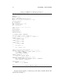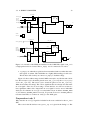
1
Laboratory manual for TSEA44 Olle Seger, Per Karlström, Andreas Ehliar Computer Engineering Department of Electrical Engineering Linköping University, S-581 83 Linköping, Sweden Email: [email protected], [email protected], [email protected] October 28, 2014 2 Contents 1 The system 1.1 Introduction . . . . . . . . . . . . . . . . . 1.2 Hardware . . . . . . . . . . . . . . . . . . 1.2.1 Virtex-II Development board . . . . 1.2.2 Communication/Memory Module . 1.2.3 Virtex-II 4000 FPGA . . . . . . . . 1.3 Open RISC . . . . . . . . . . . . . . . . . 1.3.1 Top Design . . . . . . . . . . . . . 1.3.2 Structure of the Verilog code . . . . 1.3.3 OR1200 CPU . . . . . . . . . . . . 1.3.4 The Wishbone Interconnect Bus . . 1.3.5 Memory Controller . . . . . . . . . 1.3.6 Ethernet Controller . . . . . . . . . 1.3.7 VGA Controller . . . . . . . . . . 1.3.8 UART . . . . . . . . . . . . . . . . 1.4 Software . . . . . . . . . . . . . . . . . . . 1.4.1 Memory map . . . . . . . . . . . . 1.4.2 A simple boot monitor . . . . . . . 1.4.3 The simulator or32-uclinux-sim 1.4.4 µClinux . . . . . . . . . . . . . . . . . . . . . . . . . . . . . . . . . . 7 7 8 8 9 10 11 11 12 13 14 15 15 16 16 16 16 16 19 20 . . . . . . . . . 23 23 23 23 24 24 26 26 26 27 3 Lab task 1 - Interfacing to the Wishbone bus 3.1 Introduction . . . . . . . . . . . . . . . . . . . . . . . . . . . . . . . 3.2 Some Basic Facts on the Wishbone Bus . . . . . . . . . . . . . . . . 3.2.1 A Wishbone Interconnect . . . . . . . . . . . . . . . . . . . . 29 29 30 31 2 Lab task 0 - Build a UART in Verilog 2.1 Introduction . . . . . . . . . . . . 2.2 A simple UART . . . . . . . . . . 2.2.1 The RS232 protocol . . . 2.2.2 The hardware . . . . . . . 2.2.3 A simple testbench . . . . 2.3 Exercises . . . . . . . . . . . . . 2.3.1 Commands . . . . . . . . 2.3.2 A User Constraint File . . 2.4 gtkterm usage . . . . . . . . . . . 3 . . . . . . . . . . . . . . . . . . . . . . . . . . . . . . . . . . . . . . . . . . . . . . . . . . . . . . . . . . . . . . . . . . . . . . . . . . . . . . . . . . . . . . . . . . . . . . . . . . . . . . . . . . . . . . . . . . . . . . . . . . . . . . . . . . . . . . . . . . . . . . . . . . . . . . . . . . . . . . . . . . . . . . . . . . . . . . . . . . . . . . . . . . . . . . . . . . . . . . . . . . . . . . . . . . . . . . . . . . . . . . . . . . . . . . . . . . . . . . . . . . . . . . . . . . . . . . . . . . . . . . . . . . . . . . . . . . . . . . . . . . . . . . . . . . . . . . . . . . . . . . . . . . . . . . . . . . . . . . . . . . . . . . . . . . . . . . . . . . . . . . . . . . . . . . . . . . . . . . . . . . . . . . . . . . . . . . . . . . . . . . . . . . . . . . . . . . . . . . . . . . . . . . . . . CONTENTS 4 3.3 . . . . . . . . . . . . . . . . . . . . . . . . . . . . . . . . . . . . . . . . . . . . . . . . . . . . . . . . . . . . . . . . . . . . . . . . . . . . . . . . . . . . . . . . . . . . . . . . . . . . . . . . . . . . . . . . . . . . . . . . . . . . . . . . 32 32 32 34 35 36 36 36 38 38 38 40 40 41 41 42 4 Lab task 2 - Design a JPEG accelerator 4.1 The lab system . . . . . . . . . . . . . . . . . . . . . . 4.2 Proposed architecture . . . . . . . . . . . . . . . . . . . 4.2.1 Block RAMs in VirtexII . . . . . . . . . . . . . 4.2.2 Distributed RAMs . . . . . . . . . . . . . . . . 4.2.3 The transpose memory . . . . . . . . . . . . . . 4.2.4 WB memory map . . . . . . . . . . . . . . . . . 4.3 Introduction to µClinux . . . . . . . . . . . . . . . . . . 4.3.1 Compiling an application to µClinux . . . . . . 4.3.2 Starting the TFTP server . . . . . . . . . . . . . 4.3.3 Downloading applications via TFTP . . . . . . . 4.4 Introduction to jpegfiles . . . . . . . . . . . . . . . . . . 4.4.1 Important files in the lab skeleton . . . . . . . . 4.4.2 The jpegtest application . . . . . . . . . . . . . 4.4.3 The webcam application . . . . . . . . . . . . . 4.5 Timestamps . . . . . . . . . . . . . . . . . . . . . . . . 4.6 Quantization . . . . . . . . . . . . . . . . . . . . . . . . 4.6.1 General . . . . . . . . . . . . . . . . . . . . . . 4.6.2 Design of a hardware accelerator for quantization 4.7 Tips and tricks . . . . . . . . . . . . . . . . . . . . . . . 4.8 What to include in the lab report . . . . . . . . . . . . . . . . . . . . . . . . . . . . . . . . . . . . . . . . . . . . . . . . . . . . . . . . . . . . . . . . . . . . . . . . . . . . . . . . . . . . . . . . . . . . . . . . . . . . . . . . . . . . . . . . . . . . . . . . . . . . . . . . . . . . . . . . . . . . . . . . . . . . . . . . . 43 43 43 44 45 46 46 47 47 47 48 48 48 50 50 50 51 51 52 53 53 . . . . . . 55 55 55 56 58 58 59 3.4 3.5 3.6 3.7 A Simple Computer . . . . . . . . . . . . . . . . . 3.3.1 General . . . . . . . . . . . . . . . . . . . 3.3.2 A Wishbone Interface for the UART . . . . 3.3.3 The Monitor . . . . . . . . . . . . . . . . 3.3.4 Test Your Design . . . . . . . . . . . . . . A Benchmark Program . . . . . . . . . . . . . . . 3.4.1 JPEG Compression . . . . . . . . . . . . . 3.4.2 Integer DCT . . . . . . . . . . . . . . . . 3.4.3 The Test Program dct_sw . . . . . . . . . 3.4.4 A Test Example . . . . . . . . . . . . . . . Design a Performance Counter Module . . . . . . Useful Commands . . . . . . . . . . . . . . . . . 3.6.1 Synthesis Reports . . . . . . . . . . . . . . How to get Started Writing/Executing C Programs . 3.7.1 A Note on Volatile . . . . . . . . . . . . . 3.7.2 What to Include in the Lab Report . . . . . 5 Lab task 3 5.1 DMA in the DCT Accelerator . . . . . 5.1.1 Proposed architecture . . . . . . 5.1.2 jpeg_dma.sv . . . . . . . . . . 5.1.3 How to use DMA in jpegfiles 5.1.4 Cache coherency issue . . . . . 5.2 What to Include in the Lab Report . . . . . . . . . . . . . . . . . . . . . . . . . . . . . . . . . . . . . . . . . . . . . . . . . . . . . . . . . . . . . . . . . . . . . . . . . . . . . . . . . . . . . . . . . . . . . . . . . . . . . . . . . . . . . . . . . . . . . . . . . . . . . CONTENTS 5 6 Lab task 4 - Custom Instructions 6.1 Introduction . . . . . . . . . . . . . . . . 6.1.1 Huffman Coding . . . . . . . . . 6.1.2 The Problem . . . . . . . . . . . 6.2 Adding a New Instruction . . . . . . . . . 6.2.1 Making the Processor Understand 6.2.2 Adding Special Purpose Registers 6.2.3 Adding the Required Hardware . 6.3 Proposed Architecture . . . . . . . . . . 6.3.1 Control Unit . . . . . . . . . . . 6.3.2 Data Path . . . . . . . . . . . . . 6.3.3 Store Unit . . . . . . . . . . . . . 6.3.4 Multi Cycle Instructions . . . . . 6.3.5 Instruction Details . . . . . . . . 6.4 Hardware Implementation . . . . . . . . 6.4.1 Constructing the Hardware . . . . 6.5 Software Implementation . . . . . . . . . 6.5.1 Running the Instruction . . . . . 6.5.2 Integration into jpegfiles . . . . . 6.5.3 JPEG Markers . . . . . . . . . . 6.6 Important Files For this lab task . . . . . 6.7 Tips and tricks . . . . . . . . . . . . . . . 6.8 What to Include in the Lab Report . . . . 6.9 Beyond tsea44 . . . . . . . . . . . . . . . . . . . . . . . . . . . . . . . . . . . . . . 61 61 61 62 62 62 62 63 63 63 64 64 64 64 64 65 65 65 67 67 68 68 69 70 A Open RISC Reference Platform A.1 Address map . . . . . . . . . . . . . . . . . . . . . . . . . . . . . . A.2 Interrupts . . . . . . . . . . . . . . . . . . . . . . . . . . . . . . . . 73 73 74 B The Wishbone specification B.1 Introduction . . . . . . . . . . . . . B.2 Interface signals . . . . . . . . . . . B.2.1 adr . . . . . . . . . . . . . B.2.2 dat_o and dat_i . . . . . . B.2.3 we . . . . . . . . . . . . . . B.2.4 sel . . . . . . . . . . . . . B.2.5 stb . . . . . . . . . . . . . B.2.6 cyc . . . . . . . . . . . . . B.2.7 ack . . . . . . . . . . . . . B.2.8 cti . . . . . . . . . . . . . B.2.9 bte . . . . . . . . . . . . . B.2.10 err . . . . . . . . . . . . . B.3 Wishbone classical cycles . . . . . . B.4 Wishbone incrementing burst cycles B.5 System Verilog Interface . . . . . . 75 75 76 76 76 76 76 76 77 77 77 77 77 77 78 79 C Tips & Trix . . . . . . . . . . . . . . . . . . . . . . . . . . . . . . . . . . . . . . . . . . . . . . . . . . . . . . . . . . . . . . . . . . . . . . . . . . . . . . . . . . . . . . . . . . . . . . . . . . . . . . . . . . . . . . . . . . . . . . . . . . . . . . . . . . . . . . . . . . . . . . . . . . . . . . . . . . . . . . . . . . . . . . . . . . . . . . . . . . . . . . . . . . . . . . . . . . . . . . . . . . . . . . . . . . . . . . . . . . . . . . . . . . . . . . . . . . . . . . . . . . . . . . . . . . . . . . . . . . . . . . . . . . . . . . . . . . . . . . . . . . . . . . . . . . . . . . . . . . . . . . . . . . . . . . . . . . . . . . . . . . . . . . . . . . . . . . . . . . . . . . . . . . . . . . . . . . . . . . . . . . . . . . . . . . . . . . . . . . . . . . . . . . . . . . . . . . . . . . . . . . . . . . . . . . . . . . . . . . . . . . . . . . . . . . . . . . . . . . . . . . . . . . . . . . . . . . . . . . . . . . . . . . . . . . . . . . . . . . . . . . . . . . . . . . . . . . . . . . . . . . . . . . . . . . . . . . . . . . . . . . . . . . . . . . . . . . . . . . . . . . . . . . . . . . . . . . . . . . . . . . . . . . . . . . . . . . . . . . . . . . . . . . . . . . . . 81 6 CONTENTS Chapter 1 The system 1.1 Introduction This text is intended as a laboratory compendium for the course TSEA44 Computer Hardware - a System On a Chip. We begin with a presentation of the hardware and software used for the laboratory exercises. If you wonder, the name dafk seen in many places in this course, comes from the name DAtorteknik FortsättningsKurs which is the Swedish name of the first version of this course. Roughly translated it means advanced course in computer technology. 7 CHAPTER 1. THE SYSTEM 8 Figure 1.1: Block diagram of the Avnet main board. 1.2 Hardware 1.2.1 Virtex-II Development board In the course we will use a development FPGA board from Avnet Corporation. A block diagram of this board is shown in Figure 1.1. More details are given in the User’s Guide, [1]. 1.2. HARDWARE RJ45 9 irDA Transceiver USB PCMCIA 16MBytes FLASH (x32) Magnetics Micron MT28F640J3A USB 2.0 XCVR Cypress CY7C68013 1MByte SRAM (x32) Cypress CY7C1041V33 10/100/1000 Ethernet PHY National DP83861 Buffer Buffer Buffer Buffer 64MBytes SDRAM (x32) Micron MT48LC16M16A2 AvBus Connectors (x2) Figure 1.2: Block diagram of the Avnet communication and memory module. 1.2.2 Communication/Memory Module The main FPGA board is extended with a Communication and Memory Module, shown in Figure 1.2. More details are given in the User’s Guide, [2]. Features of the Communication/Memory module are: • 1 MB SRAM. • 16 MB Flash memory. • 64 MB SDRAM. • 10(/100/1000) Mb/s Ethernet PHY. • (IrDA for infrared communication). • (USB2.0 PHY). • (PC card connector). Features within parentheses will not be used in this course. CHAPTER 1. THE SYSTEM 10 CLB (1 CLB = 4 slices = Max 128 bits) Device System Gates Array Row x Col. Slices SelectRAM Blocks Maximum Distributed RAM Kbits Multiplier Blocks 18 Kbit Blocks Max R AM (Kbits) DCMs Max I/O Pads(1) XC2V40 40K 8x8 256 8 4 4 72 4 88 XC2V80 80K 16 x 8 512 16 8 8 144 4 120 XC2V250 250K 24 x 16 1,536 48 24 24 432 8 200 XC2V500 500K 32 x 24 3,072 96 32 32 576 8 264 XC2V1000 1M 40 x 32 5,120 160 40 40 720 8 432 XC2V1500 1.5M 48 x 40 7,680 240 48 48 864 8 528 XC2V2000 2M 56 x 48 10,752 336 56 56 1,008 8 624 XC2V3000 3M 64 x 56 14,336 448 96 96 1,728 12 720 XC2V4000 4M 80 x 72 23,040 720 120 120 2,160 12 912 XC2V6000 6M 96 x 88 33,792 1,056 144 144 2,592 12 1,104 XC2V8000 8M 112 x 104 46,592 1,456 168 168 3,024 12 1,108 Table 1.1: Virtex-II table. XC2V4000 is our FPGA. 1.2.3 Virtex-II 4000 FPGA The most important circuit on the board is of course the mighty Virtex-II 4000 FPGA, [5]. The table 1.1 gives some details of this impressive circuit, which is shipped in an 1152 pin BGA (ball grid array). The internal configurable logic in the FPGA includes four major elements organized in a regular array: • CLBs (Configurable Logic Blocks): This is the programmable logic used to build combinatorial and sequential logic. The FPGA contains 80 × 72 = 5760 CLBs. Each CLB is made up of 4 slices, see Figure 1.4. • Multipliers: The FPGA contains 120 18 × 18-bit multipliers. These are used for the ALU in the OR1200 CPU. • Block RAMs: The FPGA contains 120 18 kbit RAMs. These are typically used for cache memories inside the CPU, FIFOs in the UART and Ethernet controller. • DCMs (Digital Clock Managers): The FPGA contains 12 DCMs. The DCMs can divide/multiply the input clock frequency. We use a DCM to transform the input 40 MHz to 25 MHz. A floorplan of the Virtex-II is shown in Figure 1.3. The CLBs are organized in an array and connected to a switching matrix. Each CLB comprises 4 slices, which are connected locally. Each slice includes two 4-input function generators, carry logic, multiplexers and two storage elements, see Figure 1.4. The function generator can be programmed as a 4-input lookup table (LUT), 16-bit RAM or 16-bit variable-tap shift register. 1.3. OPEN RISC 11 DCM DCM IOB Global Clock Mux Configurable Logic Programmable I/Os CLB Block SelectRAM Multiplier Figure 1.3: Virtex-II architectural overview. 1.3 Open RISC 1.3.1 Top Design The computer used in this lab course is designed with Verilog modules, which can be downloaded free from Open Cores (www.opencores.org) and some modules designed by us. This section describes the main system defined in the file dafk.sv, which you will use in lab task 2–4 The computer in Figure 1.5 consists of the following modules: • OR1200 CPU: 32 bit RISC CPU with a 5-stage pipeline. • Wishbone: An interconnect bus with 16 ports, 8 master ports and 8 slave ports. • Memory Controller: A memory controller for SRAM, SDRAM and Flash memories. • UART: A 16550 UART with baudrates up to 115200 b/s. • Ethernet Controller: An implementation of the MAC layer, which requires an external PHY circuit for a complete solution. • Parallel Port • VGA Controller • Camera Controller • DCT Accelerator: It will be your task to finish the implementation of this module. CHAPTER 1. THE SYSTEM 12 FXINA FX MUXFX FXINB Y DY D Q FF/LAT CE LUT G inputs D YQ CLK SR REV BY F5 MUXF5 X LUT F inputs DX D D Q XQ FF/LAT CE CLK SR REV BX CE CLK SR a) b) Figure 1.4: a) Virtex-II slice configuration b) Detail of slice (top half). 1.3.2 Structure of the Verilog code The structure of the Verilog code closely resembles the block diagram shown in Figure 1.5. Components outside the FPGA are simulated. Here is a list of the hierarchy instantiated in dafk_tb: • phy0: Simulation model of the Ethernet physical to logic level chip • videomem: Simulation model of the video memory • mysram: Simulation model of the SRAM • sdram0: Simulation model of the SDRAM • dafk_top: The code to be synthesized in the FPGA – sys_sig_gen: Generates clock and reset signals – or1200_top: The OR1200 CPU – pkmc_top: Memory controller – rom0: The boot monitor code and vector table resides here – uart2: UART 16550 – eth3: Ethernet controller – dvga: VGA controller – pia: Simple parallel port – jpg0: DCT accelerator – perf: Performance counters – leela: Camera module – wb_conbus: The wishbone bus 1.3. OPEN RISC 13 SRAM 1 MB Master Slave 0 0 Mem Ctrl OR1200 CPU 4kBRAM 4kBROM 1 1 SDRAM 64 MB FLASH 16 MB 2 UART 7 JTAG Debug Parport LED, DIPswitch 3 4 Wishbone PS2 Keyboard Accelerator 5 VGA Leela SRAM 2 3 Ether Ctrl PHY FPGA Hub Figure 1.5: An Open RISC computer. 1.3.3 OR1200 CPU A block diagram of the OR1200 CPU is shown in Figure 1.6. More information about the CPU can be found in [6, 7]. Figure 1.6: Block diagram of the OR1200 CPU. CHAPTER 1. THE SYSTEM 14 The OR1200 CPU, [8], consists of several blocks: • High Performance 32-Bit CPU/DSP – 32-bit architecture implementing ORBIS32 instruction set – Scalar, single-issue 5-stage pipeline delivering sustained throughput – Single-cycle instruction execution on most instructions – Can be run at 250MHz in an ASIC – Thirty-two, 32-bit general-purpose registers – Custom user instructions • L1 Caches – Harvard model with split instruction and data cache – Instruction/data cache size scalable from 1KB to 64KB • Memory Management Unit – Harvard model with split instruction and data MMU – Instruction/data TLB size scalable from 16 to 256 entries – Direct-mapped hash-based TLB – Linear address space with 32-bit virtual address and physical address from 24 to 32 bits – Page size 8KB with per-page attributes • Advanced Debug Unit – Conventional target-debug agent with a debug exception handler – Non-intrusive debug/trace for both RISC and system – Access and control of debug unit from RISC or via development interface • Integrated Tick Timer – Task scheduling and precise time measuring – Maximum timer range of 232 clock cycles – Maskable tick-timer interrupt • Programmable Interrupt Controller – 2 non-maskable interrupt sources – 30 maskable interrupt sources – two interrupt priorities In this lab course the Power Management module is disabled. 1.3.4 The Wishbone Interconnect Bus The Wishbone Interconnect is a standard way of connecting IP (Intellectual Property) blocks in System-on-Chip designs, see for instance [9]. It can be implemented in different ways ranging from a fully connected crossbar to an ordinary shared bus. In this course the shared bus variant is used. It is important to understand that there is no parallelism in this implementation. It is just a connection between one master and one 1.3. OPEN RISC 15 slave. Furthermore tristate is not used, instead there are two databuses, one in each direction. The address bus and the data busses are 32 bits wide. Master Slave A0,D0 A0,D0,STB A0,D0,STB A1,D1 i_bus_m A0,D0 A7,D7 gnt A0 Arbiter gnt A7 Address Decoder D1,ACK D1 D0, D1 ,ACK i_dat_s, i_bus_s D1 D7, Figure 1.7: The Wishbone interconnect bus. In this example Master 0 is addressing Slave 1. Master 0 has won the arbitration. We will briefly explain how the Wishbone bus works with a simple example. We assume a computer system like in Figure 1.5 and that the CPU executes a program in the memory, that is connected to slave port 1, see Figure 1.7. The CPU places an address A0 at the address lines at master port 0 and asserts the signal STB. The arbiter inside the Wishbone grants the bus to master 0. The address A0 will now show up on all slave ports. Address decoding logic routes the asserted STB-signal only to slave port 1. The memory at slave port 1 places D1 on the data bus and asserts the signal ACK. D1 will now show up on all master ports, but ACK will only be asserted at master port 0. 1.3.5 Memory Controller In this lab course we will use a simple memory controller, designated PKMC, designed by us. PKMC is implemented for this particular system and thus needs no configuration. PKMC handles all communications with the SRAM, SDRAM and FLASH memory. Especially ensuring that the SDRAM is refreshed correctly. 1.3.6 Ethernet Controller The Ethernet IP Core, [10], consists of five modules: • The MAC (Media Access Control) module, formed by transmit, receive, and control module • The MII (Media Independent Interface) Management module • The Host Interface CHAPTER 1. THE SYSTEM 16 The Ethernet IP Core is capable of operating at 10 or 100 Mbps for Ethernet and Fast Ethernet applications. An external PHY is needed for a complete Ethernet solution. In short the ethernet controller works as follows. There are 64 transmit buffers and 64 receive buffers. These buffers are typically located in the SRAM. To each such buffer there is a pair of registers (a buffer descriptor) inside the Ethernet Controller, one register holds the address of the buffer and one register is a control/status-register. The ethernet controller transmits/receives packets from/to the SRAM buffers with DMA. 1.3.7 VGA Controller The VGA controller used is designed by us and is a simple single-video-mode controller for use in FPGA or ASIC environments. The VGA controller supports a single resolution/refresh rate in grey scale or 8-bit pseudocolor with 15-bit color sprites. For further details see [12]. 1.3.8 UART The UART (Universal Asynchronous Receiver Transmitter) is an implementation of the industry standard 16550 device. Details can be found in [13]. 1.4 Software 1.4.1 Memory map Address 0x0000_0000 - 0x03ff_ffff 0x2000_0000 - 0x200f_ffff 0x4000_0000 - 0x4000_5fff 0x4001_1000 - 0x4001_1fff 0x9000_0000 - 0x90ff_ffff 0x9100_0000 - 0x91ff_ffff 0x9200_0000 - 0x92ff_ffff 0x9600_0000 - 0x96ff_ffff 0xf000_0000 - 0xf0ff_ffff 1.4.2 Type SDRAM SRAM ROM RAM UART Parallel port Ethernet Accelerator FLASH Content Programs can be loaded and run here 64 MB Data area 1MB Boot monitor, 24kB Data area for the monitor and stack 8kB Your JPEG accelerator Bender, µClinux and Linux A simple boot monitor A simple monitor runs in the memory on slave port 1. The monitor will start at boot. Use for instance gtkterm and adjust the baud rate to 115200 b/s. Format should be 8N1 and no flow control. The port shall be /dev/ttyUSB0. Type h for help. Some available commands are explained in table 1.2. Type l and then use the command File -> Send raw file in gtkterm to load an Intel hex file into memory. The hex file itself contains address information. 1.4. SOFTWARE 17 Command d <addr> m <addr> <data> g <addr> l u Explanation display memory content modify memory content go (execute) load Intel hex file boot uClinux (copy from FLASH) Table 1.2: Some useful commands in the monitor. A simple program. In this section we will demonstrate how to compile, load and run a C-program in the monitor evironment. We will use the program described in Listing 1.1 as an example. Listing 1.1: simpleprog # i n c l u d e " common .h" i n t main ( v o i d ) { i n t Begin_Time , User_Time ; int i ; p r i n t f ( " Hello ␣ world !\n" ) ; Begin_Time = g e t _ t i m e r ( 0 ) ; f o r ( i = 0 ; i < 1 0 ; i ++) { l e d ( i ) ; / ∗ S e t t h e l e d d i s p l a y on t h e c a r d ∗ / p r i n t f ( "%d\n" , i ) ; sleep ( 1 ) ; /∗ sleep 1 s ∗/ } User_Time = g e t _ t i m e r ( Begin_Time ) ; p r i n t f ( "Time=␣%d␣s\n" , User_Time ) ; return ( 0 ) ; } The program prints a string, counts on the LEDs and measures the elapsed time. To build simpleprog we use a Makefile described in Listing 1.2, in the Makefile we observe the following: • A cross-compiler, or32-uclinux-gcc, must be used. • The functions printf, get_timer, led and sleep are library functions in openrisclib, which is included in the lab skeleton for lab 1. • A link script ram.ld is used to determine where in memory our program should be located. CHAPTER 1. THE SYSTEM 18 Listing 1.2: Makefile for simpleprog (Listing 1.1) # The name o f t h e program we want t o c o m p i l e PROGRAM = s i m p l e p r o g # The d i r e c t o r y c o n t a i n i n g t h e open r i s c s u p p o r t d i r LIBDIR = . . / l i b INCLUDEDIR = . . / i n c l u d e CFLAGS += −I $ ( INCLUDEDIR ) −Wall −W s t r i c t−p r o t o t y p e s CFLAGS += −Werror−i m p l i c i t −f u n c t i o n −d e c l a r a t i o n CFLAGS += −Os −g −fno−b u i l t i n −f o m i t−frame−p o i n t e r −n o s t d l i b # Toolchain configuration AS = or32−u c l i n u x−a s CC = or32−u c l i n u x−g c c LD = or32−u c l i n u x−l d DUMP = or32−u c l i n u x−objdump −S −D −EB COPY = or32−u c l i n u x−o b j c o p y SIM = or32−u c l i n u x−sim # F l a g s t o LD , n e e d t o i n c l u d e a l i n k s c r i p t h e r e LDFLAGS = −Tram . l d OBJFILES=$ (PROGRAM ) . o HEXFILE=$ (PROGRAM ) . hex SIMPROGRAM=$ (PROGRAM) sim a l l : $ (PROGRAM) $ ( HEXFILE ) $ (SIMPROGRAM) # The m i n i m a l s u p p o r t l i b c o n t a i n i n g p r i n t f / s l e e p / e t c o p e n r i s c l i b : $ ( LIBDIR ) / o p e n r i s c l i b . a $ ( LIBDIR ) / c r t . o $ ( LIBDIR ) / r e s e t . o # Commands t o make t h e open r i s c s u p p o r t l i b $ ( LIBDIR ) / o p e n r i s c l i b . a : cd $ ( LIBDIR ) && $ (MAKE) $ ( LIBDIR ) / c r t . o : cd $ ( LIBDIR ) && $ (MAKE) $ ( LIBDIR ) / r e s e t . o : cd $ ( LIBDIR ) && $ (MAKE) .S.o: $ (CC) $ ( CFLAGS) −c $< .c.o: $ (CC) −c $ (CFLAGS) −o $@ $< # L i n k t h e program t o g e t h e r w i t h t h e s u p p o r t l i b # ( And c r e a t e a t e x t f i l e w i t h t h e d i s a s s e m b l e d c o n t e n t s o f t h e program ) $ (PROGRAM ) : $ ( OBJFILES ) ram . l d o p e n r i s c l i b $ (LD) −B s t a t i c $ ( LIBDIR ) / c r t . o $ ( OBJFILES ) $ ( LIBDIR ) / o p e n r i s c l i b . a \ $ (LDFLAGS) −o $ (PROGRAM) $ (DUMP) $ (PROGRAM) > $ (PROGRAM ) . t x t # C r e a t e an i n t e l h e x dump o f t h e program $ ( HEXFILE ) : $ (PROGRAM) $ (COPY) −O i h e x $ (PROGRAM) $ ( HEXFILE ) # C r e a t e a b i n a r y we can s i m u l a t e w i t h t h e o p e n r i s c s i m u l a t o r $ (SIMPROGRAM ) : $ (PROGRAM) ram . l d o p e n r i s c l i b $ (LD) −B s t a t i c $ ( LIBDIR ) / r e s e t . o $ (PROGRAM) $ (LDFLAGS) −o $ (SIMPROGRAM) $ (DUMP) $ (SIMPROGRAM) > $ (SIMPROGRAM ) . t x t # Run t h e s i m u l a t o r on t h e program sim : $ (SIMPROGRAM) $ ( SIM ) −i −f sim . c f g $ (SIMPROGRAM) clean : rm −f ∗ . o ∗~ sim . p r o f i l e $ (PROGRAM) $ (SIMPROGRAM) $ ( HEXFILE ) ∗ . t x t ua rt 0 . tx ua rt 0 . rx We place all the segments of simpleprog at the address 0x2000 with the link script shown in Listing 1.3. 1.4. SOFTWARE 19 Listing 1.3: Link script for simpleprog (Listing 1.1) MEMORY { vectors sdram } : ORIGIN = 0 x00000000 , LENGTH = 0 x00002000 : ORIGIN = 0 x00002000 , LENGTH = 0 x03ffe000 SECTIONS { . vectors : { *(. vectors ) } > vectors . text : { *(. text ) } > sdram . rodata ALIGN (4) : { *(. rodata ) } > sdram . rodata . str1 .1 ALIGN (4) : { *(. rodata . str1 .1) } > sdram . data ALIGN (4): { *(. data ) } > sdram . bss ALIGN (4): { *(. bss ) } > sdram } 1.4.3 The simulator or32-uclinux-sim The simulator is started with the command or32-uclinux-sim -f sim.cfg prog , where sim.cfg describes the hardware and prog is the program to run on the simulated hardware. Some help is printed out by the command or32-uclinux-sim -h . CHAPTER 1. THE SYSTEM 20 The simulator can also be started in an interactive mode by or32-uclinux-sim -f sim.cfg -i prog . In Figure 1.8 we show as an example the simulation of a simple monitor in an xterm window. Figure 1.8: Simulation of the bender monitor. The command help lists available commands, for instance t (trace): >t 00000100: : 00000000 l.j 0x0 (executed) [time 40ns, #1] 00000104: : 00000000 l.j 0x0 (next insn) (delay insn) GPR00: 00000000 GPR01: 00000000 GPR02: 00000000 GPR03: GPR04: 00000000 GPR05: 00000000 GPR06: 00000000 GPR07: GPR08: 00000000 GPR09: 00000000 GPR10: 00000000 GPR11: GPR12: 00000000 GPR13: 00000000 GPR14: 00000000 GPR15: GPR16: 00000000 GPR17: 00000000 GPR18: 00000000 GPR19: GPR20: 00000000 GPR21: 00000000 GPR22: 00000000 GPR23: GPR24: 00000000 GPR25: 00000000 GPR26: 00000000 GPR27: GPR28: 00000000 GPR29: 00000000 GPR30: 00000000 GPR31: 1.4.4 00000000 00000000 00000000 00000000 00000000 00000000 00000000 00000000 flag: µClinux µClinux, which stands for microcontroller Linux, is a Linux variant intended for computers without a Memory Management Unit (MMU). This means that the kernel and the processes reside in the same address space. You can start µClinux by giving the u command from the boot monitor. µClinux is now copied from FLASH (0xf 0100000) to SDRAM (0x0) and the booting process starts. 0 1.4. SOFTWARE 21 The command help will list the built-in shell commands. An important file is /etc/rc, the start-up file, which is shown in Listing 1.4. If you want to change the start-up behavior of µClinux this the file to change. In a running µClinux this file resides in a non-writable file system. A new system must be recompiled on a host computer, downloaded over the serial port and flashed to the flash memory. It is very unlikely that you have to do this in the course of this lab series. Listing 1.4: µClinux configuration file /etc/rc # ! / bin / sh # s e t e n v PATH / b i n : / s b i n : / u s r / b i n hostname bender # mount − t p r o c none / p r o c # / b i n / e x p a n d / r a m f s 5 1 2 . img / dev / ram1 mount − t e x t 2 / dev / ram1 / v a r m k d i r / v a r / l o g / v a r / l o g / boa / v a r / l o c k / v a r / tmp / v a r / r u n chmod 777 / v a r / tmp # / b i n / e x p a n d / r a m f s 8 1 9 2 . img / dev / ram2 mount − t e x t 2 / dev / ram2 / mnt m k d i r / mnt / b i n # S e t up t h e w e b s e r v e r s t u f f m k d i r / mnt / h t d o c s cp / m i s c / ∗ / mnt / h t d o c s m k d i r / mnt / h t d o c s / c g i −b i n # B r i n g up t h e l o c a l i n t e r f a c e / sbin / ifconfig lo 127.0.0.1 / s b i n / r o u t e add −n e t 1 2 7 . 0 . 0 . 0 # S e t IP a d d r e s s f r o m c o n f i g u r a t i o n d a t a i n f l a s h / sbin / setip # S t a r t t h e web s e r v e r / s b i n / boa −d & Running programs under µClinux We demonstrate how to run a program in the µClinux environment by an example. The program, shown in Listing 1.5, displays the contents of a Special Purpose Register (SPR). It uses inline assembler to read a register. We use the Makefile shown in Listing 1.6 to compile the program shown in Listing 1.5. The flags -r and -d to $CC are important, otherwise the program will not execute. CHAPTER 1. THE SYSTEM 22 Listing 1.5: Program showing contents of a special purpose register. # include # include # include # include # include < s y s / t y p e s . h> < s y s / s t a t . h> <asm / i o . h> <asm / s p r _ d e f s . h> <asm / b o a r d . h> i n t main ( i n t a r g c , char ∗ a r g v [ ] ) { unsigned long val , addr ; i f ( a r g c == 2) { addr = s t r t o u l ( argv [ 1 ] , 0 , 0 ) ; / ∗ Read SPR ∗ / asm ( "l. mfspr ␣%0 ,%1 ,0" : "=r" ( v a l ) : "r" ( a d d r ) ) ; p r i n t f ( "\nSPR␣%04 lx:␣%08 lx\n" , a d d r , v a l ) ; } e l s e r e t u r n −1; return 0; } Listing 1.6: Makefile to compile the program showing an SPR (Listing 1.5). CC = or32−u c l i b c −g c c STRIP = or32−u c l i b c − s t r i p PRGS = m f s p r a l l : $ ( PRGS ) mfspr : mfspr . o $ (CC) −r −d m f s p r . o −o $@ $ ( STRIP ) −g $@ Finally the program can be downloaded with tftp. Change directory (cd) to a writable portion of the filesystem, like for instance /var/tmp. Then start the tftp client > tftp IP_address_of_your_tftp_server Retrieve the program: > get mfspr See section 4.3.2 for more information on how to start the TFTP server. Chapter 2 Lab task 0 - Build a UART in Verilog 2.1 Introduction In this introductory lab exercise you will learn the HDL Verilog. We require that you are familiar with another HDL, typically VHDL. In our opinion hardware design is done by drawing hardware diagrams, so that the programming in Verilog is just a final simple translation step! You will also get (re)acquainted with the tools used in this course, ModelSim and make (or Xilinx Project Navigator). 2.2 A simple UART 2.2.1 The RS232 protocol In this exercise you shall design a simple RS232 transceiver in Verilog. We assume that the serial port of the FPGA board is connected to a PC, where a terminal program is running. This is typically gtkterm if you are using Linux or Teraterm if you are running in Windows. The bit rate should be fixed 115200 bits/s. Your design shall use the parameters 8N1, that is 8 message bits, no parity bit and 1 stop bit, see Figure 2.1. Messages are sent and received with LSB first. Furthermore your UART shall support full duplex operation, that is be able to transmit and receive at the same time. start 1 0 0 0 0 0 1 0 stop Figure 2.1: The letter A (0x41). Time per bit is 8.68 µs. 23 t CHAPTER 2. LAB TASK 0 - BUILD A UART IN VERILOG 24 2.2.2 The hardware The system clock is running at 40 MHz. You will need a reset-signal and a send-signal, see Figure 2.2. Both these signals are active-high. send_i(SW2) rst_i(SW1) switch_i tx_o UART led_o rx_i clk_i Figure 2.2: The UART. Your task is twofold: • send an ASCII-coded character from the DIP switch to the PC by pressing the switch SW2, see Figure 2.2. • catch the incoming characters from rx_i and present the ASCII code on the LED display, see Figure 2.2. Some advice before you start: • The signal rx_i is asynchronous. We strongly advice you to synchronize it! • You will use your UART in lab task 1 with a slower system clock 25 MHz. We suggest that you prepare the frequency change with an ‘ifdef ‘else ‘endif construct. 2.2.3 A simple testbench You will also need a test bench. Since you are designing both a transmitter and a receiver you may choose to test them both at the same time, see Figure 2.3. testbench send_i rst_i switch_i tx_o UART led_o rx_i clk_i Figure 2.3: A testbench. The code for the test bench shown in Figure 2.3, is listed in Listing 2.1. 2.2. A SIMPLE UART 25 Listing 2.1: Test bench for the UART. ‘ t i m e s c a l e 1 n s / 10 p s module l a b 0 _ t b ( ) ; reg c l k _ i ; reg r s t _ i ; reg s e n d _ i ; reg [ 7 : 0 ] s w i t c h _ i ; wire [ 7 : 0 ] led_o ; wire jumper ; / / I n s t a n t i a t e a UART lab0 u a r t ( . c l k _ i ( c l k _ i ) , . r s t _ i ( r s t _ i ) , . r x _ i ( jumper ) , . tx_o ( jumper ) , . led_o ( led_o ) , . switch_i ( switch_i ) , . send_i ( send_i ) ) ; always #12.5 c l k _ i = ~ c l k _ i ; initial begin c l k _ i = 1 ’ b0 ; s w i t c h _ i = 8 ’ h41 ; // A r s t _ i = 1 ’ b1 ; s e n d _ i = 1 ’ b0 ; #100 r s t _ i = 1 ’ b0 ; #1000 s e n d _ i = 1 ’ b1 ; #1100 s e n d _ i = 1 ’ b0 ; end endmodule / / 40 MHz c l o c k CHAPTER 2. LAB TASK 0 - BUILD A UART IN VERILOG 26 2.3 Exercises Preparation task 1 Draw a HW diagram of the UART. Use simple components like counters, registers, shift registers, and state machines. Laboration task 1 a) Translate your HW diagram into Verilog code. b) Simulate your design in ModelSim. c) Synthesize your design, program the FPGA and test run your design. 2.3.1 Commands To start the simulator, use the command make sim_lab0. To generate a bitfile to program the FPGA with use make lab0. To configure the FPGA with a .bit file, use make prog_lab0. 2.3.2 A User Constraint File You will need the User Constraint File shown in Listing 2.2. The exact same signals and names mentioned in Listing 2.2 must be present in the interface declaration of you top module. Comment out the lines that you don’t use. (This file is included in the lab skeleton as lab0.ucf.) Listing 2.2: User constraints file for your UART NET " clk_i " NET " rst_i " NET " send_i " LOC = "AK19" ; / / 40 MHz i n t h i s l a b LOC = "C2" ; / / SW1 ( r e d ) on g r e e n f l e x o LOC = "B3" ; / / SW2 ( b l a c k ) on g r e e n f l e x o 2.4. GTKTERM USAGE / / b l u e DIP s w i t c h NET "switch_i <7>" LOC NET "switch_i <6>" LOC NET "switch_i <5>" LOC NET "switch_i <4>" LOC NET "switch_i <3>" LOC NET "switch_i <2>" LOC NET "switch_i <1>" LOC NET "switch_i <0>" LOC / / row o f LEDs NET "led_o <7>" LOC NET "led_o <6>" LOC NET "led_o <5>" LOC NET "led_o <4>" LOC NET "led_o <3>" LOC NET "led_o <2>" LOC NET "led_o <1>" LOC NET "led_o <0>" LOC / / rainbow f l a t cable NET "rx_i" LOC NET "tx_o" LOC 27 = = = = = = = = "AL3" ; "AK3" ; "AJ5" ; "AH6" ; "AG7" ; "AF7" ; "AF11" ; "AE11" ; // // // // // // // // SWITCH SWITCH SWITCH SWITCH SWITCH SWITCH SWITCH SWITCH = = = = = = = = "N9" ; "P8" ; "N8" ; "N7" ; "M6" ; "M3" ; "L6" ; "L3" ; // // // // // // // // LED LED LED LED LED LED LED LED 1 2 3 4 5 6 7 8 D4 D5 D6 D7 D8 D9 D10 D11 = "M9" ; = "K5" ; 2.4 gtkterm usage Start gtkterm in a shell or from Applications->Accessories->GTKTerm. Communication parameters are set from Configuration->Port and should be /dev/ttyUSB0, speed 115200, no parity, 8 bits, 1 stop bit and no flow control. 28 CHAPTER 2. LAB TASK 0 - BUILD A UART IN VERILOG Chapter 3 Lab task 1 - Interfacing to the Wishbone bus 3.1 Introduction In this lab exercise you will get acquainted with the OR 1200 RISC processor and particularly the Wishbone bus. You will do this by designing and interfacing two modules, a UART and a performance counter module to the Wishbone bus. WB 0 Boot Monitor in ROM RAM 1 OR1200 1 stx_pad_o I/F 2 7 UART Parallel Port 9 I/F srx_pad_i out_pad_o in_pad_i Performance Counters lab1.sv clk_i rst_i Figure 3.1: The computer. The two gray modules will be designed by you. Figure 3.1 depicts the computer that you are going to work with in this laboratory exercise. You will have to: 1. modify your UART from the previous lab and interface it to the Wishbone bus. The wishbone interface should be inserted into lab1/lab1_uart_top.sv. 2. check the UART device drivers in the boot monitor. The driver is in this file monitor/firmware/src/uartfun.c. 3. download and execute a benchmark program, that performs the DCT part of JPEG compression on a small image in your RAM module. 29 30 CHAPTER 3. LAB TASK 1 - INTERFACING TO THE WISHBONE BUS 4. simulate the computer running the benchmark program. 5. design a module containing hardware performance counters (perf_top.sv in the lab skeleton). 3.2 Some Basic Facts on the Wishbone Bus The Wishbone bus is intended for implementation in FPGAs or ASICs. Typical for such a bus is that multiplexers are used instead of tristate buffers. Two data buses are used, one for each direction, see Figure 3.2a. clk wb.adr Master Slave wb.adr wb.stb wb.cyc wb.dat_o wb.dat_o wb.stb wb.cyc wb.dat_i wb.ack wb.we wb.ack (a) A Wishbone Master/Slave interface. (b) A Wishbone write cycle. wb.adr wb.stb wb.cyc wb.we wb.ack wb.dat_i (c) A Wishbone read cycle. Figure 3.2: The Wishbone bus protocol. In this lab we will only need a subset of the Wishbone protocol, namely the basic write and read bus cycles. For the write cycle, see Figure 3.2b, we have: 1. The master places address and data on the buses wb.adr and wb.dat_o, respectively. Finally the master asserts the wb.stb-signal, wb.cyc-signal, and wb.we-signal. 2. The slave, when ready, decodes the address bus, latches the data and asserts the wb.ack-signal. 3.2. SOME BASIC FACTS ON THE WISHBONE BUS 31 3. The Master deasserts the wb.stb, wb.cyc and wb.we-signals. 4. The slave deasserts the wb.ack-signal. For the read cycle, see Figure 3.2c, we have: 1. The master places the address on the bus wb.adr and asserts the wb.stb-signal, the wb.cyc-signal, and deasserts the wb.we-signal. 2. The slave, when ready, decodes the address bus, places the data on the data bus wb.dat_i and asserts the wb.ack-signal. 3. The Master deasserts the wb.stb and wb.cyc-signals. 4. The slave deasserts the wb.ack-signal. In these basic write and read bus cycles the wb.stb and wb.cyc-signals are identical. The wb.cyc-signal is used for arbitration of the bus, so the master may assert it for many cycles, for instance during a cache line refill. 3.2.1 A Wishbone Interconnect Before we begin with the actual integration of the computer we would like to give a short explanation of the Wishbone interconnect. In Figure 3.3 we show an example of 2 masters and 3 slaves connected to a Wishbone bus. The m-bus is all the signals going from the master to a slave, like the address bus, data bus and in particular the stb-signal. The s-bus is all the signals going from the slave to a master, like the data bus and the ack-signal. M0 M1 cyc0 cyc1 m0 m1 M−mux s−bus ARB m−bus DEC S−mux s0 S0 S1 s1 s2 S2 Figure 3.3: A Wishbone interconnect for 2 masters and 3 slaves. An arbiter, a finite state machine, listens to the cyc-signals from the masters. The masters M0 and M1 are, in our implementation, granted the bus in a round-robin fashion. The m-bus is then connected to all the slaves. The stb-signal is, however, only asserted at the addressed slave port. CHAPTER 3. LAB TASK 1 - INTERFACING TO THE WISHBONE BUS 32 In the return path the addressed slave’s s-bus is connected to all the masters. This is handled by the block DEC. The ack-signal is, however, only asserted at the master that won the arbitration. 3.3 A Simple Computer 3.3.1 General For the lab you will have to download tsea44.tgz if you haven’t done so already. Uncompress the zip-file to your home directory. Inspect the directory hw and you will find: • the file lab1/lab1_uart_top.sv, a skeleton for the top file. • the file lab1.ucf, a User Constraints File. • the directory or1200 containing the CPU. The top file is or1200_top.sv. • the directory monitor containing both HW and SW for the boot monitor. • the directory wb containing the Wishbone interconnect. • the directory include containing some include files. • the directory firmware, which contains the example program dct_sw/dct_sw that can be downloaded to your computer with the boot monitor. 3.3.2 A Wishbone Interface for the UART Let’s start our computer design with the UART. In the introductory lab you designed a simple UART. All that is needed now is to attach a Wishbone interface to your design, see Figure 3.4. Since you will use a boot monitor that is written for the standard 16550 UART, you will want to make your design emulate that UART. Luckily our device driver does not use much of the functionality in the 16550. The main enhancement in the 16550 are 16 character FIFOs in both directions. This is more or less mandatory when you run an OS, which always has some interrupt latency. The driver routine expects three bytesized registers: 1. transmit register, adr=0, write-only 2. receive register, adr=0, read-only 3. status register, adr=5, read-only In the status register, you will only need two F/Fs: • rx_full, set when the stop-bit is received and reset when the receive register is read. Use signal wb_sel[3] to determine when the receive register is read. 3.3. A SIMPLE COMPUTER 33 rx_full F/F wb.dat_i[16] wb.stb wb.we wb.sel[3] S R rd Control Unit end_char_rx & wb.adr[2] load rx shift shift_rx Shift rx reg wb.dat_i[31:24] Reg in wb.stb wb.ack tx_empty F/F wb.stb wb.we wb.sel[3] wb.adr[2] end_char_tx S R wb.dat_i[22:21] send wr Control Unit & load tx reg wb.dat_o[31:24] load_tx load shift Shift Reg shift_tx >=1 tx out Figure 3.4: A sketch of the Wishbone interface for the UART. The signal load_tx is a single-pulsed version of send. The tx_empty F/F is connected to two wires. • tx_empty, set when the stop-bit has been transmitted and reset when the transmit register is written. The 16550 has two slightly different flags for this case. The monitor will work if you connect tx_empty to both these flags. Figure 3.5 shows address maps for the UART connected to an 8 bit bus and a 32 bit bus. The transmit register should be placed on wb.dat_o[31:24], the receive register on wb.dat_i[31:24]. The status register should be placed on wb.dat_i[23:16]. What about address decoding? The 8 most significant bits are already decoded in the wb.stb-signal. Since we are now using a 32 bit data bus, we will not use the two least significant address bits. Instead the wb.sel-signal is used to access individual data bytes. For instance wb.sel[3] is asserted when a byte on address 0x9000_0000 or (for instance) 0x9000_0004 is accessed. To prevent an access to 0x9000_0004 to reset the status F/Fs, we connect wb.adr[2] to the AND gates. Preparation task 2 Why must the wb.sel[3]-signal be included in the reset condition for the rx_full F/F? The code for the lab skeleton lab1_uart_top.sv is given in the listing 3.1. The CHAPTER 3. LAB TASK 1 - INTERFACING TO THE WISHBONE BUS 34 a) b) sel[3] 7 rx/tx 0 31 rx/tx sel[2] 23 sel[1] 15 sel[0] 7 0 9000_0000 4 9000_0000 1 2 3 4 5 tx_empty rx_full tx_empty rx_full Figure 3.5: a) Address map for the UART connected to an 8 bit bus b) Address map for the UART connected to a 32 bit bus. The sel-signals are used to address individual bytes. definition of the wishbone SystemVerilog interface can be found in the appendix section B.5. Listing 3.1: Lab skeleton lab1_uart_top.sv. module l a b 1 _ u a r t _ t o p ( w i s h b o n e . s l a v e wb , output wire i n t _ o , input wire s r x _ p a d _ i , output wire stx_pad_o ) ; assign assign assign assign i n t _ o = 1 ’ b0 ; wb . e r r = 1 ’ b0 ; wb . r t y = 1 ’ b0 ; wb . a c k = wb . s t b ; // // // // I n t e r r u p t , not used in t h i s lab Error , not used i n t h i s lab Retry , not used in t h i s lab change i f needed / / Here you m u s t i n s t a n t i a t e l a b 0 _ u a r t o r c u t and p a s t e / / You w i l l a l s o h a v e t o c h a n g e t h e i n t e r f a c e o f l a b 0 _ u a r t t o make t h i s work . a s s i g n s t x _ p a d _ o = s r x _ p a d _ i ; / / Change t h i s l i n e . . : ) endmodule Preparation task 3 Write Verilog code for the Wishbone interface of your UART. Preparation task 4 Inspect the driver routines getch and putch in the file monitor/firmware/src/uartfun.c. You will also have to look in uartfun.h. 3.3.3 The Monitor The monitor directory contains a couple of Verilog files that implements an 8 kB block RAM at base address 0x4001_0000. This RAM will contain the stack of the monitor. The monitor itself is implemented in a 24 kB block ROM at base address 0x4000_0000. The contents of the block ROM is in the Verilog file mon_prog_bram_contents.v. The software is in the sub directories firmware/src and firmware/include. 3.3. A SIMPLE COMPUTER 35 Check mon2.c to see what the monitor does at startup so that you can verify that the hardware does the correct thing. 3.3.4 Test Your Design In Figure 3.6a we show a test bench for the computer. The only signals that the test bench has to activate in this case are the clk_i- and rst_i-signals. We check the behavior of the computer by listening to tx-signal from the UART. Part of a testbench has already been written for you in dafk_tb/lab1_tb.v. This test bench can be started with make sim_lab1. WB 0 1 Boot Monitor in ROM RAM 2 I/F 7 Parallel Port 9 I/F OR1200 1 UART uart_tasks Performance Counters lab1.sv clk_i rst_i lab1_tb.sv (a) A test bench. The module uart_tasks gives a nice printout. (b) A test run in ModelSim, showing the signals tx and rx_data in the test bench. Figure 3.6: Simulation of your design There is also a smaller test bench, lab1/uart_tb.sv, that will test only your UART design. This test bench can be started with make sim_uart. Laboration task 2 Test your computer. CHAPTER 3. LAB TASK 1 - INTERFACING TO THE WISHBONE BUS 36 3.4 A Benchmark Program 3.4.1 JPEG Compression We will use the first part, DCT, of the JPEG compression algorithm to test our computer. This section is inspired by [3]. We begin with a short discussion of how DCT works. 3.4.2 Integer DCT The two dimensional discrete cosine transform (DCT) for an 8 × 8 array a[x, y] is defined as A[u, v] = c[u]c[v] · 7 7 X X a[x, y] cos x=0 y=0 πu 1 πv 1 (x + ) cos (y + ) 8 2 8 2 (3.1) √ where c[0] = 1/ 8 and c[u] = 1/2 when u 6= 0. The transform in (3.1) can be separated. First compute a one-dimensional DCT on each row and then a one-dimensional DCT on each column. ( ) 7 7 X X 2π 2π A[u, v] = c[v] · c[u] a[x, y] cos (2x + 1)u cos (2v + 1)y (3.2) 32 32 y=0 x=0 The innermost part of (3.1) is the 1-D DCT, which we repeat with slightly different notation: 7 X 2π (2x + 1)u (3.3) a[x] cos A[u] = c[u] · 32 x=0 By using all possible symmetries of the cosine function it is not so difficult to figure out a fast DCT, see Figure 3.7. This computation scheme is usually referred to√as Loeffler’s algorithm. It computes the 1-D DCT as defined in (3.2) multiplied with 8. 0 stage 1 stage 2 stage 3 stage 4 1 4 2 √ 3 4 5 6 0 2 2c6 c3 c1 7 6 7 3 5 1 Figure 3.7: Loeffler’s original algorithm for fast DCT. Black circles means √ addition, dashed lines multiplication with -1 and white circles multiplication with 2. White boxes marked cn denote rotation with nπ/16. The white boxes in Figure 3.7 denote rotation with nπ/16 : xout = xin · cos nπ/16 + yin · sin nπ/16 yout = −xin · sin nπ/16 + yin · cos nπ/16 (3.4) 3.4. A BENCHMARK PROGRAM 37 Sofar we have presented three ways of computing the 2-D DCT. We compare the computation complexity of the algorithms: Algorithm Eq (3.1) Eq (3.2) Loeffler original MUL 4096 1024 224 ADD 4032 892 416 The post multiplication with c[u] has been left out of the table. √ The OR1200 CPU has no floating point arithmetic, so the sin/cosine factors and 2 in Figure 3.7 must be mapped to integers. We have chosen to multiply with 213 and rounding to the nearest integer. We have the following correspondences: Real number √ 2 cos π/16 sin π/16 cos 3π/16 sin √ 3π/16 √2 cos 6π/16 2 sin 6π/16 Integer 11585 8035 1598 6811 4551 4433 10703 The scheme in Figure 3.7 has a serious drawback. The outputs 3 and 5 pass through two multipliers. There is, however, a modified version where this flaw has been removed at the price of 1 extra multiplier and 3 extra adders. The last 3 stages on the lower part of Figure 3.7 is replaced with the computation scheme in Figure 3.8. This modification is not, in our opinion, so easy to figure out. The interested reader is therefore directed to the original article, [4]. X X X X + X + X + X + X + X a b c d e f g h i + + + + + 7 + + 5 3 + 1 + + Figure 3.8: Loeffler’s modified algorithm. Computation of the odd part with parallel multiplications. We conclude that Loeffler’s modified algorithm can be used with integer arithmetic. After each run all outputs, except 0 and 4, must be arithmetic right shifted 13 steps. The 2-D DCT will be 8 · A[u, v] compared to (3.2), which can be compensated for in later stages in the JPEG compression algorithm. CHAPTER 3. LAB TASK 1 - INTERFACING TO THE WISHBONE BUS 38 Preparation task 5 Why do we go through all the trouble inserting the module in Figure 3.8? Why is it so bad having 2 multipliers in series? 3.4.3 The Test Program dct_sw For this lab you will get a test program dct_sw.c, written by us. It is a straightforward implementation of Loeffler’s algorithm and computes the 2-D DCT of an 8 × 8 image. You will actually find two copies: • in the directory hw/firmware/jpeg for downloading and running on the target computer. You can also run it on the host computer. • in the directory hw/monitor/firmware/src for simulation. A call to the DCT program has been inserted in the beginning of the monitor program mon2.c. 3.4.4 A Test Example 1 9 17 25 a[x, y] = 33 41 49 57 2 10 18 26 34 42 50 58 3 11 19 27 35 43 51 59 4 12 20 28 36 44 52 60 5 13 21 29 37 45 53 61 6 14 22 30 38 46 54 62 7 15 23 31 39 47 55 63 8 16 24 32 40 48 56 (3.5) 64 Origo is shown in bold text. The JPEG algoritm includes a subtraction with 128 from each pixel. −6112 −152 0 −16 0 −8 0 −8 −1167 0 0 0 0 0 0 0 0 0 0 0 0 0 0 0 −122 0 0 0 0 0 0 0 8 · DCT [a − 128] = 0 0 0 0 0 0 0 0 −37 0 0 0 0 0 0 0 0 0 0 0 0 0 0 0 −10 0 0 0 0 0 0 0 (3.6) 3.5 Design a Performance Counter Module As a last task in this lab you shall design a simple performance counter module, see Figure 3.1. The module shall: 1. be connected to slave port 9 of the Wishbone bus. 2. have the port definition shown in Listing 3.2. 3.5. DESIGN A PERFORMANCE COUNTER MODULE 39 3. contain four 32 bit counters that can be read and written on the addresses 0x9900_0000 to 0x9900_000c. 4. The counter on address 0x9900_0000 shall count the number of clock cycles that m0.cyc and m0.stb are both asserted. The counter on address 0x9900_0004 shall count the number of clock cycles that m0.ack is asserted. 5. The counter on address 0x9900_0008 shall count the number of clock cycles that m1.cyc and m1.stb are both asserted. The counter on address 0x9900_000c shall count the number of clock cycles that m1.ack is asserted. 6. Be aware that you will add extra signals (and counters )to this module in later labs to measure DMA activities. 7. You may optionally use the m?.we signals to gather even more statistics. Listing 3.2: Performance counter module port definition. The definition of the wishbone SystemVerilog interface can be found in the appendix, section B.5. module p e r f _ t o p ( w i s h b o n e . s l a v e wb , w i s h b o n e . m o n i t o r m0 , m1 ) ; reg assign [31:0] ctr0 , ctr1 ; / / your c o u n t e r s wb . a c k = wb . s t b && wb . c y c ; / / how t o f i x t h e ack−s i g n a l / / your code goes here endmodule / / p e r f _ t o p Laboration task 3 Design the performance counter module and use these counters to measure the performance of the dct_sw.c program. There is also a free running timer present in the processor. You can access it on SPR register 0x5002. In this lab you may also use the regular timer register in the processor since no operating system will modify it. CHAPTER 3. LAB TASK 1 - INTERFACING TO THE WISHBONE BUS 40 3.6 Useful Commands We have prepared a makefile based build system that is responsible for both building the monitor firmware and synthesizing the hardware from the RTL source code. You can use it on the Linux computers in Muxen 1. The following targets will be useful for you: • make lab1 Creates a bit file of the computer in this lab task. • make sim_lab1 Launches Modelsim on the “lab1” system. • make sim_uart Launches Modelsim on your UART. • make dafk Creates a bit file of the complete system. • make sim Launches Modelsim on the complete system. • make simfiles Recompiles all source files for use with Modelsim but does not launch Modelsim itself. This is mainly useful if you already have Modelsim running and want to try out some changes to your source code. This way you don’t need to close Modelsim, it is enough to issue a restart command in Modelsim. • make clean Removes intermediate files and backup files. • make updatebit Compiles the monitor and updates dafk.bit, and lab1.bit with the new monitor. This way you don’t need to resynthesize the design to test changes in your monitor. The updated bit file is named updated_dafk.bit for dafk.bit and so on. We also have some utilities that you might be interested in. The first of these is download.sh which you can use to download your design. (You may use this script either in Windows or Linux. In Windows it will invoke Impact in batch mode and in Linux it will invoke xc3sprog.) Invoke it as in the following example: utils/download.sh dafk.bit Another utility is designed to highlight the error and warning messages in the various reports that the Xilinx flow will output. Use it on (for example) the synthesis report with the following command: utils/checklogs.pl synthdir/dafk.syr | less -r The other alternative is to pipe the output of make through checklogs: make dafk.bit | utils/checklogs.pl 3.6.1 Synthesis Reports If you use make, the following files will be of special interest to you: (look in /nobackup/local/<your name>/ 3.7. HOW TO GET STARTED WRITING/EXECUTING C PROGRAMS 41 • synthdir/foo.syr: Synthesis report • synthdir/foo_map.mrp: Map report • synthdir/foo.par: Place and Route report • synthdir/foo.twr: Timing analyzer report (Where foo is the name of the top level file you compiled, as in dafk or lab1). 3.7 How to get Started Writing/Executing C Programs A good starting point is the program simpleprog situated in the directory firmware. It can be compiled with make in Linux. The executable file is simpleprog.hex which can be downloaded with the command l in the monitor and File->Send Raw File in gtkterm. You run the program with g 2000 or just g. The size of the DRAM is 64 MB, so there is plenty of room for your program. You can check the length of the program by looking inside the file simpleprog.txt, which is a disassembled version of simpleprog. The length of simpleprog is 2800 bytes. 3.7.1 A Note on Volatile Normally, the compiler assumes that memory locations will not change unless the program itself changes it. This assumption does not hold when the program tries to access I/O memory. For example, in the following code shown in Listing 3.3, the programmer wants the program to wait until pin 1 of the parallel port is set to 1. The problem is that an optimizing compiler will generate assembler code doing approximately what is shown in Listing 3.4. Listing 3.3: Volatile is not used for memory mapped I/O. u n s i g n e d i n t ∗ p a r p o r t = 0 x91000000 ; w h i l e ( ( ∗ p a r p o r t & 0 x1 ) ! = 1 ) ; / ∗ Busy w a i t ∗ / Listing 3.4: Resulting assembler from code in Listing 3.3. LOAD R0 , [ 0 x91000000 ] AND R0 , R0 , 0 x1 CMP R0 , 0 x1 loop : BNEQ l o o p ; Load v a l u e f r o m memory ; And R0 w i t h 1 ; Compare R0 w i t h 1 ; Jump t o l o o p i f R0 was n o t e q u a l t o 1 This is certainly not what the programmer had in mind. This kind of error is even more insidious because in some cases it might work ok and in some cases it will fail sporadically and in some cases it might not work at all. It will also depend on the optimization level of the compiler. The correct way to deal with this situation is to tell the C compiler that the memory location can change at any time. This will force the compiler to generate code that reloads the memory location every time it is referenced. This can be done using the volatile keyword. We recommend that you use the CHAPTER 3. LAB TASK 1 - INTERFACING TO THE WISHBONE BUS 42 macros shown in Listing 3.5 to access memory mapped I/O. These macros are defined in both the monitor (mon2.h) and in jpeglib.h but if you write a small test program you might have to include them in your own source code as well. Using these macros1 the program from Listing 3.3 would look like whats shown in Listing 3.6. Listing 3.5: Recommended macros for memory mapped I/O access. # d e f i n e REG32 ( add ) ∗ ( ( v o l a t i l e u n s i g n e d l o n g ∗ ) ( add ) ) # d e f i n e REG16 ( add ) ∗ ( ( v o l a t i l e u n s i g n e d s h o r t ∗ ) ( add ) ) # d e f i n e REG8 ( add ) ∗ ( ( v o l a t i l e u n s i g n e d char ∗ ) ( add ) ) Listing 3.6: Correct program, using volatile. w h i l e ( ( REG32 ( 0 x91000000 ) & 0 x1 ) ! = 1 ) ; / ∗ Busy w a i t ∗ / 3.7.2 What to Include in the Lab Report The lab report should contain all source code that you have written. (The source code should of course be commented.) We would also like you to include a block diagram of your hardware. If you have written any FSM you should include a state diagram graph of the FSM. We would also like you to discuss the following questions: • How did you verify that your computer hardware worked? • What is the performance of the 2D DCT software? (Try it with and without caches.) • How much of the FPGA is used by our design? And of course, the normal parts of a lab report such as a table of contents, an introduction, a conclusion, etc. The source code that you have written should be included in appendices and referred to from the main document. 1 The macros assume that a long is 32 bits, a short is 16 bits and a char is 8 bits. Chapter 4 Lab task 2 - Design a JPEG accelerator 4.1 The lab system In this lab task you will learn how to build a hardware accelerator for the JPEG image compression algorithm. In this lab you will use the build target dafk.bit. This is a complete system with the following components: • OR1200 CPU • Boot monitor • UART • VGA controller • Camera controller • Ethernet controller • SDRAM, SRAM, and flash memory controller µClinux is programmed into the flash memory on the FPGA board and we will use this operating system for the remainder of this course. Examples of how to compile for Linux are included in the lab skeleton in the hello directory. 4.2 Proposed architecture We propose the general architecture shown in Figure 4.1. It works in the following way: 1. An 8 × 8 bytes image is written from the Wishbone bus by the application program to the in RAM in 16 write cycles. Pixels are 8-bit positive numbers and packed in one 32-bit word. We recommend that you subtract 128 from each pixel before it is written to the in RAM. The accelerator is then started by setting the START bit in csr (Control/Status Register). 43 CHAPTER 4. LAB TASK 2 - DESIGN A JPEG ACCELERATOR 44 32 wb.dat_o NC wb.adr Block RAM wb.stb in counter t_rd 8x12=96 Transpose Memory WB Ctrl 1 DCT 32 t_wr 8x12=96 64 wb.ack NC 32 Q2 32 8x16=128 ... Block RAM wb.dat_o DCT2 Control Unit counter out wb.dat_i 1 32 wb.adr csr NC Figure 4.1: Proposed architecture for the 2-D DCT-accelerator. csr is a Control/Status register. Not all wires are shown. 2. A row of the image is read from the in RAM in 2 clock cycles. This is repeated 8 times. 3. The rows are transformed in DCT (12-bit signed numbers) and written to the transpose memory in the same tempo 4. When all rows have been written to T, columns, 8 × 12 bits, can be read from T and fed into the DCT again. A complete column can be read per clock cycle. After the second DCT the values are 16-bit signed numbers. 5. Finally 2 × 16 bits per clock cycle are quantized in Q2 and written to the out RAM. When all columns have been written, the RDY bit in csr is set. You √ will receive a Verilog module, dct.v, that computes a 1-D DCT multiplied with 8. This file is a straightforward implementation in Verilog of the computation schemes (modified Loeffler) in Figures 3.7 and 3.8 in Chapter 3. Preparation task 6 Open the file dct.v and have a look at what it does. What are the inputs, what are the outputs? How many clock cycles does a computation take? Is it pipelined? 4.2.1 Block RAMs in VirtexII The VirtexII-4000 FPGA contains 120 18 kbit block RAMs. They are dual ported with two completely independent sets of synchronous read and write ports. The easiest way 4.2. PROPOSED ARCHITECTURE 45 to use a block RAM is, in our opinion, to instantiate a library primitive. The code in Listing 4.1 instantiates a block RAM shown in Figure 4.2. SSR is a set/reset signal, that only affects the output latches, not the RAM memory cells. DIP and DOP can be used for additional data such as parity bits but we do not use them in this lab. It is important to understand that both reads and writes are synchronous as opposed to an ordinary RAM that you might have used in one of our earlier courses such as Digital Konstruktion. Listing 4.1: Instantiation of a block RAM as shown in Figure 4.2 w i r e [ 3 1 : 0 ] doa , d i a , dob , d i b ; wire [ 8 : 0 ] addra , addrb ; w i r e c l k , cea , wea , ceb , web ; / / d u a l p o r t 512 x32 RAM RAMB16_S36_S36 memory ( / / port A .DOA( doa ) , . DOPA ( ) , .ADDRA( a d d r a ) , . CLKA( c l k ) , . DIA ( d i a ) , . DIPA ( 4 ’ h0 ) , . ENA( c e a ) , . SSRA ( 1 ’ b0 ) , .WEA( wea ) , / / port B .DOB( dob ) , . DOPB ( ) , .ADDRB( a d d r b ) , . CLKB( c l k ) , . DIB ( d i b ) , . DIPB ( 4 ’ h0 ) , . ENB( c e b ) , . SSRB ( 1 ’ b0 ) , .WEB( web ) ) ; DIA 32 DIB 32 9 9 ADDRA ADDRB CLKA,ENA, WEA CLKB,ENB, WEB 32 DOA 32 DOB Figure 4.2: Dualported 512 × 32 bit block RAM. 4.2.2 Distributed RAMs Small RAMs can be designed using the LUTs in the FPGA. A LUT is a 16 × 1 RAM. Distributed RAM memory supports the following: • Single-port RAM with one synchronous write and one combinatorial read port • Dual-port RAM with one synchronous write port and two asynchronous read ports For instance a 16 × 8 RAM can be designed in Verilog as shown in Listing 4.2. Listing 4.2: Distributed RAM instantiaton in Verilog. r e g [ 7 : 0 ] mem [ 1 5 : 0 ] ; CHAPTER 4. LAB TASK 2 - DESIGN A JPEG ACCELERATOR 46 wire [ 7 : 0 ] d a t a _ i , d a t a _ o ; wire [ 3 : 0 ] addr_a , addr_b ; / / 1 c o m b i n a t o r i a l read port a s s i g n d a t a _ o = mem[ a d d r _ a ] ; / / 1 synchronous write port a l w a y s @( p o s e d g e c l k ) b e g i n i f ( we ) mem[ a d d r _ b ] <= d a t a _ i ; end 4.2.3 The transpose memory The transpose memory shall: • be designed as a Verilog module, with the interface shown in Listing 4.3. • hold an 8 × 8 × 12 bit image. • allow writes of rows and reads of columns in one clock cycle. • have no address inputs. Listing 4.3: Transpose memory interface module t r a n s p o s e ( i n p u t c l k , r s t , wr , rd , input [ 9 5 : 0 ] in , output [ 9 5 : 0 ] u t ) ; We leave it to the designer to decide how the signals wr, rd exactly work. 4.2.4 WB memory map The accelerator shall have the memory map shown in Table 4.1. csr is the Control/Status register. The accelerator is started by setting (from WB) bit 0, the START bit. When the accelerator is ready bit 7, the RDY bit, is set. The START bit is cleared by the DCT2 Control Unit and the RDY bit by software. mem in out csr dma Base Address 0x9600_0000 0x9600_0800 0x9600_1000 0x9600_1800 Size 512 × 32 512 × 32 1×8 Read/Write WO 32 bit RO RW 8 bits For use in lab 3 Table 4.1: Accelerator memory map Preparation task 7 Draw a block diagram of the transpose memory. Rows can be written and columns can be read in 1 clock cycle. 4.3. INTRODUCTION TO µCLINUX 47 Laboration task 4 Design and implement the DCT accelerator with a WB interface. Laboration task 5 Write a testbench for your DCT accelerator. 4.3 Introduction to µClinux In the remaining labs we are going to run µClinux on the openrisc system. The most important difference between µClinux and Linux is that µClinux works without an MMU. This means that there is no memory protection for programs running on µClinux. Therefore, extra care must be taken during development since a bug in a program may cause the entire operating system to crash. You can start µClinux on the openrisc system by using the u command in the monitor. This will copy a µClinux image from the flash memory to the SDRAM and boot µClinux. If everything worked you will get a prompt and you should also be able to browse a web page on the µClinux machine. The IP address of the µClinux machine is printed by the boot script. On the µClinux machine, most directories are read only but /mnt and /var is writable. /mnt is a good directory to download programs to. The base directory for the web server documents is in /mnt/htdocs. Laboration task 6 Boot µClinux and familiarize yourself with it. 4.3.1 Compiling an application to µClinux In the hello directory of the lab skeleton there is a sample hello world application. This has to be cross compiled on one of the Linux machines in the lab. The cross compiler has access to a C library so you can use all standard functions like printf, fopen, fread, etc. If you are interested in how the cross compiler is invoked, you can take a look at the Makefile. Just type make in the hello directory to compile it. 4.3.2 Starting the TFTP server In order to download applications via tftp we first need to start a TFTP server on one of the Linux computers in the lab. In Linux, this can be started with the following command: /usr/sbin/in.tftpd --daemon --no-fork --port 5050 -r 1 ~/tftp This will start a TFTP server listening on UDP port 50501 . Files will be served from the tftp directory in your home directory. The options --daemon --no-fork are used so that the tftp client can be interrupted with ctrl c. (We don’t want any TFTP 1 Port 69 is actually the standardized TFTP port but non privileged users in Linux are not permitted to open ports below 1024 so we decided to use port 5050 instead. CHAPTER 4. LAB TASK 2 - DESIGN A JPEG ACCELERATOR 48 servers to be left after you log out since this would prohibit other lab groups from starting a TFTP server.) 4.3.3 Downloading applications via TFTP In order to download and run the hello application we must use tftp. First, hello has to be copied to the tftp directory in your home directory. After that you can write the following commands in µClinux: /> cd /mnt /mnt> tftp 192.168.0.62 tftp> get hello Received 28664 bytes in 0.8 seconds tftp> quit /mnt> chmod 755 hello /mnt> hello 3 2 1 Hello uClinux! /mnt> Laboration task 7 Download and test hello. It can be noted that tftp sometimes says “Not a typewriter” and aborts the transfer. This has not been fully debugged yet unfortunately. If it happens to you, just try again, it rarely happens twice in a row. 4.4 Introduction to jpegfiles In this lab series we will be using and enhancing a library written originally by the Independent JPEG Group. (IJG) The software package has been somewhat modified by us for the TSEA44 course. First of all, we have removed a lot of files that are not needed for a µClinux target (configuration files and Makefiles for other platforms, etc). Some of the more interesting functions have been instrumented with performance counters in order to measure how much of the CPU time is spent in these functions. Finally, we have modified the DCT handling code to correspond to the verilog source code for the 1D DCT which is used in the lab skeleton. 4.4.1 Important files in the lab skeleton In this section we describe a number of important files that you will need to look at in this lab. • Makefile Contains the build instructions. If you need to modify the compilation flags, this is the file to look inside. 4.4. INTRODUCTION TO JPEGFILES 49 • jpegtest.c contains the test program we will use • testbild.raw is a grayscale image in raw format. • perfctr.c,perfctr.h This is the place to look if you want to add a new performance counter • jcdctmgr.c Contains the main computation loop and definitions of static variables. Also contains the forward_DCT function which calls the 2D DCT kernel and does the quantization. • jdct.c Contains the 2D DCT kernel • jchuff.c Contains the Huffman and RLE encoder. • webcam.c Another test application we will use Below is a call graph of the important functions called by jpegtest: main() +-- draw_image() +-- init_encoder() +-- encode_image() | +-- forward_DCT() | | +-- jpeg_fdct_islow() | +-- encode_mcu_huff() | +-- emit_bits() +-- finish_pass_huff (jpegtest.c) (jpegtest.c) (jcdctmgr.c) (jcdctmgr.c) (jcdctmgr.c) (jdct.c) (jchuff.c) (jchuff.c) (jchuff.c) • encode_image() - Creates a buffer for an 8 × 8 block and calls forward_dct(8x8 buffer), the returned buffer is sent to encode_mcu_huff(8x8 buffer). This will encode the first block of the image and save it in memory. The procedure is then repeated until every block is encoded and then finish_pass_huff() is called to write the memory buffer to file. • forward_dct() - Extracts the first 8 × 8 block from the image and then runs the DCT on this block. The result is returned to encode_image(). • encode_mcu_huff() - Uses a predefined Huffman code to compress the data returned from forward_dct() and sends the Huffman codes to emit_bits(). • emit_bits() - Recieves Huffman codes and save them until enough bits to write a byte are received, then a byte is written to buffer[]. • buffer[] - Storage for the encoded image memory during operation. • finish_pass_huff() - Calls emit_bits() to write leftover bits to buffer[] and then calls write_data(). • write_data() - Writes the contents of buffer[] to file. Preparation task 8 Take a look at the file containing the 2D DCT kernel and figure out how to change it to use your 2D DCT hardware. CHAPTER 4. LAB TASK 2 - DESIGN A JPEG ACCELERATOR 50 4.4.2 The jpegtest application This is the main test application we are going to use in the lab series. It will first read a raw picture from a file named testbild.raw, encode it to JPEG format and write it to an output file which you specify on the command line. It will also output performance data on how many clock cycles some important functions consumed. In order to see the encoded image you can place it in the /mnt/htdocs directory and download it to your computer via the web server on the µClinux machine. Laboration task 8 Download and test the jpegtest application. Both with and without the testbild.raw program. 4.4.3 The webcam application The lab skeleton also includes a simple webcam application. You can download webcam.cgi to /mnt/htdocs/cgi-bin and look at the webcam via the web browser. Laboration task 9 Modify jpegfiles to use your 2D DCT hardware and test it by using jpegtest and webcam.cgi. The results should be exactly the same as if you were using the software only version. 4.5 Timestamps The size of the test image wunderbart.jpg is 512 × 400 pixels, or 64 × 50 8 × 8blocks. The Figure 4.3 shows the result of collecting timestamps in the beginning of block row 50. The order of the operations is 1. read a block from DRAM (w/o DMA) 2. calculate DCT on the block (w/o HW DCT) 3. quantize the block (w/o HW Quantization) 4. readout of the block 5. Huffman encoding of the block (w/o special instruction) In Figure 4.3 we have implemented all the HW accelerators except the quantization step. It is evident that the design will gain a lot from the acceleration of the quantization step. Putting more work into the DCT-accelerator is wasted hardware. The DCTaccelerator will always be overlapped by (typically) the Huffman encoding. Timestamps can be collected by using timestamp = gettimer(); gettimer is a macro defined in perfctr.h in jpegfiles. The completion of the HW DCT operation can not be determined by software. Instead you can include a 10-bit counter (for instance) in the accelerator. The counter can be mapped into the free bits of the control register. 4.6. QUANTIZATION 51 1.8 1.6 CPU 1.4 1.2 read(N) 1 Q(N) huff(N) 0.8 0.6 ACC 0.4 0.2 0 dmadct(N) 0 0.5 1 1.5 2 clockcycles 2.5 4 x 10 Figure 4.3: Timestamps for JPEG compression pipeline. Each color coded patch represents the processing of an 8 × 8-block. Colorcodes: DMA+DCT red, readout green, quantization blue and Huffman encoding yellow. 4.6 Quantization 4.6.1 General The standard JPEG quantization table for the luminance channel is given by 16 12 14 14 QL [u, v] = 18 24 49 72 11 12 13 17 22 35 64 92 10 14 16 22 37 55 78 95 16 24 40 19 26 58 24 40 57 29 51 87 56 68 109 64 81 104 87 103 121 98 112 100 51 61 60 55 69 56 80 62 . 103 77 113 92 120 101 103 99 (4.1) To get higher image quality this table is divided by 2. Reciprocals are then computed by the formula R[u, v] = 214 , QL [u, v]/2 (4.2) which is the table in the file jcdctmgr.c. As an example we use A[u, v] from (3.6). Before quantizing A[u, v] we subtract 64 × 128 = 8192 from the DC value A[0, 0], which corresponds to taking the DCT of a[x, y] − 128. This procedure is meant to give a smaller value on the average, which however is false in this particular case. Finally we compensate for the scale factor 8 introduced in the DCT2 step by right- CHAPTER 4. LAB TASK 2 - DESIGN A JPEG ACCELERATOR 52 shifting 17 steps: Y [u, v] = round (A[u, v] − 8192 · δ[u, v]) · R[u, v] · 2−17 −96 −3 0 0 0 0 0 0 −24 0 0 0 0 0 0 0 0 0 0 0 0 0 0 0 −2 0 0 0 0 0 0 0 , = 0 0 0 0 0 0 0 0 0 0 0 0 0 0 0 0 0 0 0 0 0 0 0 0 0 0 0 0 0 0 0 0 (4.3) which left only four non zero coefficients. 4.6.2 Design of a hardware accelerator for quantization The following piece of code in jcdctmgr.c in jpegfiles calculates the quantization of one block. Instead of division multiplication with the reciprocal is used. Listing 4.4: C code for quantization in jcdctmgr.c. i n t r e c i p r o c a l s [ ] = {2048 , 2731 , 2341 , 2341 , 1820 , 1365 , 669 , 455 , 2979 , 2731 , 2521 , 1928 , 1489 , 936 , 512 , 356 , 3277 , 2341 , 2048 , 1489 , 886 , 596 , 420 , 345 , 2048 , 1365 , 819 , 1725 , 1260 , 565 , 1365 , 819 , 575 , 1130 , 643 , 377 , 585 , 482 , 301 , 512 , 405 , 315 , 377 , 318 , 271 , 334 , 293 , 328 , 643 , 546 , 475 , 410 , 318 , 290 , 273 , 318 , ... f o r ( i = 0 ; i < DCTSIZE2 ; i ++) { rval = reciprocals [ i ]; / / 16 b i t s i g n e d temp = w o r k s p a c e [ i ] ; / / 16 b i t s i g n e d temp = temp ∗ r v a l ; i f ( temp & 0 x10000 ) { temp = temp >> 1 7 ; temp += 1 ; } else temp = temp >> 1 7 ; c o e f _ b l o c k [ i ] = ( s h o r t ) temp ; / / 16 b i t s i g n e d } ... Preparation task 9 Design a HW Quantization unit (Q2 in Figure 4.1), that calculates exactly the same values as the code in Listing 4.4. Instantiate your Q2 unit and modify the code in listing 4.4. We propose that Q2 should be able to quantize 2 numbers per clock cycle. 537 , 596 , 585 , 529 , 426 , 356 , 324 , 331}; 4.7. TIPS AND TRICKS 53 4.7 Tips and tricks In this section we have collected some notes that you might find useful. • If you want to simulate the 2D DCT accelerator together with the rest of the system, you will have to modify the monitor to run your testcode right after the system has started. See the directions in section 3.3.3 on how to modify the monitor. • In order to improve the performance of the code you can remove some of the performance counters. But the performance counters in jpegtest has to remain! • If you encounter some weird problems with the hardware you can try to turn the power off to the FPGA system before configuring it. We have had some problems with the FPGA board which can be solved in this manner. 4.8 What to include in the lab report The lab report should contain all source code that you have written. (The source code should of course be commented.) We would also like you to include a block diagram of your hardware. If you have written any FSM you should include a state diagram graph of the FSM. We would also like you to discuss the following questions in detail somewhere in your lab report. • How does your 2D DCT hardware work? • How did you verify that your 2D DCT hardware works correctly? • What is the performance with and without the 2D DCT hardware? This should include measurements of both the 2D DCT kernel and the entire application. • A timestamp diagram. • How much of the FPGA is used by the 2D DCT hardware? • How much is the 2D DCT hardware used while encoding an image in jpegtest? • Is the size of the 2D DCT hardware justified by the performance improvements? • What would be required in order to implement more functionality like zigzag addressing in the 2D DCT hardware module? Would it be difficult to modify jpegfiles to take advantage of such optimizations? And of course, the normal parts of a lab report such as a table of contents, an introduction, a conclusion, etc. The source code that you have written should be included in appendices and referred to from the main document. 54 CHAPTER 4. LAB TASK 2 - DESIGN A JPEG ACCELERATOR Chapter 5 Lab task 3 5.1 DMA in the DCT Accelerator In this lab we will improve the DCT accelerator by using DMA. You can find a specification on how to do DMA in wishbone in appendix B. 5.1.1 Proposed architecture In this lab we will modify the DCT accelerator created in lab 2 to use DMA. In this case the idea is that the DMA module will feed the DCT accelerator with data from the system memory but the CPU is still responsible for reading the data from the DCT accelerator. This means that the changes in jpegfiles will be kept to a minimum. The only changes will be to initialize the DMA as early as possible and to change jpegfiles to not write data to the DCT accelerator. There are of course a wide variety of ways to do this but we propose that the accelerator should use the following interface: 0x9600_1800: SRCADDR, the address of the grayscale image we want to convert. 0x9600_1804: PITCH, the width of the image in bytes. 0x9600_1808: ENDBLOCK_X, the width of the image in macroblocks minus one. 0x9600_180c: ENDBLOCK_Y, the height of the image in macroblocks minus one. 0x9600_1810: CONTROL (When reading) Bit 0 indicates that the DMA is not idling, bit 1 indicates that a DCT operation for one block has been finished. 0x9600_1810: CONTROL (When writing) Writing a 1 to bit 0 starts the DMA FSM whereas writing a 1 to bit 1 tells the accelerator that the processor has read the result of one block and the DMA accelerator may proceed with the next block. 55 CHAPTER 5. LAB TASK 3 56 WAITREADY_LAST IDLE RELEASEBUS GETBLOCK WAITREADY Figure 5.1: The proposed state diagram for the DMA accelerator. In Figure 5.1 there is a state diagram which is suitable for the DMA accelerator. The states are described below: • IDLE: The DMA module is not doing anything. • GETBLOCK: The DMA module is fetching an 8x8 block. Once the block is fetched we go to the WAITREADY state and starts the DCT transform. • RELEASEBUS: The DMA accelerator has to release the bus regularly so that other components can access it. You should do this for every line of a macroblock that you read. • WAITREADY: In this state we wait until the program tells us that it has read the result of the transform by writing to the control register. • WAITREADY_LAST: Same as WAITREADY except that we go to the IDLE state when done. 5.1.2 jpeg_dma.sv The interface to the jpeg_dma module consists of a wishbone master interface, a simplified wishbone slave port and some control signals that are connected to the DCT accelerator in the jpeg_top module. A simplified view of the proposed architecture is shown in figure 5.2. Some of the most important signals are described below: 5.1. DMA IN THE DCT ACCELERATOR 57 • dma_bram_data: The data we want to write to inmem in jpeg_top. • dma_bram_addr: The address we want to write the data to. • dma_bram_we: The write enable signal for inmem. • dma_start_dct: When this clock signal is high for one clock cycle, the DMA accelerator will start to transform the current block in inmem. • dct_busy: This input signal is high from one clock cycle after dma_start_dct has been activated to the moment all results have been written to outmem. (You have to make sure that your DCT accelerator busy signal actually works like this.) The interface to the address generator is as follows: • resetaddr_i: The address generator sets the address to the start address specified in dma_srcaddr. • incaddr_i: The address generator will increase the address to the next word we need to read. • address_o: The current address of the image. • endframe_o: This signal is active when the current address is the last address of the image. • endblock_o: This signal is active when the current address is the last address of an 8x8 block. • endline_o: This signal is active when the current address is the last address of a line of an 8x8 block. • dma_srcaddr, dma_pitch, dma_endblock_x,dma_endblock_y: As described above. There are also some other important signals that are available such as: • startfsm: This signal is active when the CPU has written a 1 to bit 0 of the CONTROL register. • startnextblock: This signal is one when the CPU writes a 1 to bit 1 of the CONTROL register. CHAPTER 5. LAB TASK 3 58 It is important to note that the DCT accelerator should still work as before if DMA is not in use. But you are (of course) allowed to assume that the accelerator will be used either in DMA mode or regular mode at one time. This means that the results when both the DMA module and a wishbone master tries to write to inmem in jpeg_top at the same time are allowed to be undefined. You should mainly modify jpeg_dma.sv in this lab but you will also have to modify jpeg_top.sv to account for the dma_bram_ signals. In jpeg_dma.sv some code already exists, for example, an address generator capable of generating the addresses required to read in the frame in 8×8 blocks is already instantiated. The writing and reading of control registers and status registers are also complete. Your main task is to complete the finite state machine. In order to simplify debugging of your DMA accelerator it is useful to make sure that you can change the DMA accelerator state to IDLE by writing to a control register in the accelerator. This means that you don’t have to reset your system if jpegtest aborts in the middle of a frame. Preparation task 10 Complete as much as possible of the FSM in Figure 5.1 by filling in the conditions for the state transitions. (Hint: The lab skeleton already has code for some of the state transitions.) Laboration task 10 Modify the DCT accelerator in lab 2 to use DMA. Laboration task 11 Test your DCT accelerator in modelsim by modifying the monitor to use your accelerator. Some initial code is available in dma_dct_hw() in hw/monitor/firmware/src/dct2.c. 5.1.3 How to use DMA in jpegfiles You will have to make a few changes to jpegfiles in this lab. You should modify both jdct.c and jcdctmgr.c so that no values are copied from memory to your DCT accelerator. You should also note that there is a level conversion of the indata in jcdctmgr.c, that is the pixels are modified by subtracting 128 from them. You will have to take this into account by modifying your hardware. 5.1.4 Cache coherency issue Normally, once DMA is involved in a system it is very important to take cache coherency issues into account. Especially if the processor has no bus snooping facility to update the caches automatically. However, since the OR1200 has write through caches and the DMA accelerator only reads from memory we will not have any cache coherency issues. Laboration task 12 Modify jpegfiles to use the DMA enabled DCT accelerator. 5.2. WHAT TO INCLUDE IN THE LAB REPORT 59 5.2 What to Include in the Lab Report The lab report should contain all source code that you have written. (The source code should of course be commented.) We would also like you to include a block diagram of your hardware. If you have written any FSM you should include a state diagram graph of the FSM. We would also like you to discuss the following questions in detail somewhere in your lab report1 : • How does your hardware work? • How did you verify that your hardware worked? • How did you modify the software? • A timing diagram. • What is the utilization of your accelerator? • What is the performance of jpegtest with DMA enabled? • How long does it take (on average) to read a macroblock into the DCT accelerator via DMA? • How much is the wishbone bus used by the DMA unit and how much is the bus used by the CPU? And of course, the normal parts of a lab report such as a table of contents, an introduction, a conclusion, etc. The source code that you have written should be included in appendices and referred to from the main document. 1 In order to answer some of these questions you will probably have to modify the performance counters you added in lab 1 and add support for (at least) the DMA bus master to it. CHAPTER 5. LAB TASK 3 60 wbm.adr wbm.stb wbm.cyc wbm.dat_i wbm.ack DMA Address Generator Module wbs.adr wbs.dat_o wbs.dat_i dct_busy dma_start_dct dma_bram_we dma_bram_data 32 NC wbs.dat_o dma_bram_addr Block RAM wbs.adr counter in wbs.stb t_rd Transpose 8x12=96 Memory WB Ctrl 1 DCT 32 t_wr 8x12=96 64 wbs.ack NC 32 Q2 32 8x16=128 ... Block RAM wbs.dat_o counter out wbs.dat_i 1 DCT2 Control Unit wbs.addr csr 32 NC Figure 5.2: The proposed architecture for the DMA based DCT accelerator. Chapter 6 Lab task 4 - Custom Instructions 6.1 Introduction In this lab task you will learn how to design and integrate a new instruction into the processor. This part will target the bit alignment problem arising when trying to write bit streams to the memory. A bit stream is here defined as a stream of bits with no particular memory alignment. In accordance with jpegfiles the bit pattern to write to the stream will be called the code and the number of bits to write the size of the code. The extension you will make to the instruction set is called a Variable Length eXtension, or VLX for short. 6.1.1 Huffman Coding First a short review of the principles of Huffman encoding. Huffman encoding works by encoding the most frequently occurring item with the fewest number of bits and then using more bits for items occurring less frequently. For instance take the sequence ABAACDAAAB, the letter’s frequencies are calculated and listed in 6.1 Four different values imply that we at least need two bits per value thus we would need 10 · 2 = 20 bits to encode the string. If we were to use the Huffman codes in 6.1 we would need only 6 · 1 + 2 · 2 + 3 + 3 = 16 bits, thus saving four bits. How the Huffman codes are calculated is not in the scope of this course, for further information about Huffman coding see for example [14]. When the Huffman tables are calculated the encoding process is simple, just do a lookup and replace, e.g. simply replace the data with its corresponding code. In our case jpegfiles uses already pre calculated Huffman tables, the JPEG standard Letter A B C D Frequency 6 2 1 1 Huffman code 0 10 110 111 Table 6.1: Letter frequencies and Huffman codes 61 CHAPTER 6. LAB TASK 4 - CUSTOM INSTRUCTIONS 62 suggests four Huffman tables. Two for the luminance, one for the DC values and one for the AC values. And two for the chrominance channel one for the DC values and one for the AC values. the size of the Huffman codes in a JPEG stream varies from 1 to 16 bit. 6.1.2 The Problem Although the lookup and replace is an easy operation the problem arises when we want to write the bit stream to the memory. A consecutive stream of codes varying in length from one 1 to 16 bits has to be written to memory. In this lab your task is to design and add new hardware to the processor that can be used by an instruction to ease the bit stream writing, the idea is that it can be used as a normal store operation where the length of the data to be stored can be specified and the data stream will be packed in memory, i.e. each Huffman code will follow directly after the previous Huffman code. Preparation task 11 Suggest a method to handle the bit field writing in software. Hint, look into the jchuff.c file in jpegfiles. Preparation task 12 Suggest a method to handle the bit field writing in hardware. 6.2 Adding a New Instruction In order to add a new instruction we first need to find a suitable instruction to use for our purpose. Looking through the open RISC instruction set we find that there are some instructions used for storing double words (64-bits) and we can thus “kidnap” one of these instructions, l.sd is a suitable instruction to use. Of course if you feel like recoding the assembler you can name your instruction whatever you feel like. How you use this instruction is up to you, remember that for one vlx operation you have to specify the code and the size of the code. 6.2.1 Making the Processor Understand In order to add a new instruction we need to make the processor aware of the instruction we intend to add. The first stage is to make some modifications to the instruction decoder. In the file or1200_ctrl.sv you will find a number of ‘ifdef OR1200_SBIT_IMPL preprocessor directives. Inside some of these you will find a comment asking you to write some code there. Find these places and add the missing code. Once this is done correctly you should be able to use the l.sd instruction without causing an illegal instruction exception but it will behave as a nop instruction. 6.2.2 Adding Special Purpose Registers The hardware you are going to construct will use a number of special purpose registers to maintain observability and make it possible to handle some unusual situa- 6.3. PROPOSED ARCHITECTURE 63 tions in software. We will add a new group of special purpose registers to the processor, therefore we must make some changes in the or1200_sprs module. In the file or1200_sprs.sv you will find a ‘ifdef OR1200_SBIT_IMPL preprocessor directive. Add the missing code inside this directive. Once this is done you should be able to use the special purpose registers since they have already been implemented for you. 6.2.3 Adding the Required Hardware Finally you must add the hardware using your instruction. The main part of the work is to extend the load and store unit described in the or1200_lsu module. In the file or1200_lsu.sv you will find a number of ‘ifdef OR1200_SBIT_IMPL preprocessor directives. Inside some of these you will find a comment asking you to write some code there. Find these places and add the missing code. In addition to this you will find the or1200_vlx_top module instantiated. This is the top module for the hardware handling the stream writing. The code for this module can be found in the or1200_vlx_top.sv file. Further instructions on how this module should be implemented can be found in section 6.3 and section 6.4. 6.3 Proposed Architecture We propose the general architecture shown in figure 6.1. Gray arrows represent control signals and black arrows represent data. CONTROL CONTROL OUT STORE UNIT ADDRESS OUT SIZE DATA PATH DATA OUT CODE Figure 6.1: Proposed architecture for the set bit instruction. 6.3.1 Control Unit The control unit should be defined in the or1200_vlx_ctrl module, a stub can be found in file or1200_vlx_ctrl.sv. The control unit’s purpose is, as it sounds, to control the other units. This unit might include a simple FSM or this unit might not even be needed. All depending on your design. CHAPTER 6. LAB TASK 4 - CUSTOM INSTRUCTIONS 64 6.3.2 Data Path The data path unit should defined in the or1200_vlx_dp module, a stub can be found in file or1200_vlx_dp.sv. The data path unit should contain all logic relevant for the data manipulation needed. This unit will be responsible for aligning and merging the incoming bits with the bits previously stored. Different solutions are possible, either taking one or several clock cycles. This is basically a trade off between speed and hardware. It is your task to implement this module of course in conjunction with how you implemented the control unit. 6.3.3 Store Unit The store unit should be defined in the or1200_vlx_su module, a stub can be found in file or1200_vlx_su.sv. The store unit is responsible for storing a full bit vector to memory. A suggested solution is to take a 32 bit word and store it to main memory one byte at a time, doing the zero stuffing if necessary. Remember that a 0xF F byte has to be stored as two bytes 0xF F 0x00. It is of course faster to store the data to the memory 32 bits at a time but keep in mind that nothing more than byte alignment is ensured by jpegfiles. Important! This is worth repeating, jpegfiles only ensures byte aligned data. If you do not understand the implications of this, consult some one in the course staff before starting to implement your VLX unit. 6.3.4 Multi Cycle Instructions Some instructions might be multicycle instructions, your solution will need to stall the processor at certain points, at least when the bit buffer is stored to memory. This is done by setting the stall_cpu_o signal high in the or1200_vlx_top module. When high it will stop the cpu from fetching new instructions. This is useful, and so used, when executing an instruction with indeterminable execution time, such as writing or reading from memory. 6.3.5 Instruction Details Although a lot of information about how the instruction is supposed to work is given in this lab manual you have to work out the finer details yourself. A good place to start is to look into the jchuff.c file. Also all other place in the code surrounded by the #ifdef HW_INST (grep is a good tool) can be of interest. Also remember to design for test, the more status you can view of your hardware when it is running for real, the easier it will be for you to debug it if something fails. 6.4 Hardware Implementation In this lab task you are supposed to construct much of the hardware yourself. You have to modify a small part of the or1200_lsu module (Load Store Unit). Three special purpose registers are already present in the VLX hardware, the bit_reg register, the bit_reg_wr_pos register, and the vlx_add_o register. They are all mapped to the special 6.5. SOFTWARE IMPLEMENTATION 65 purpose register space in group 24 (the group is selected with bit 15 - 11 of a special purpose register address), the three addresses for the three special purpose registers in the vlx unit is shown in table 6.2. If you feel like adding more special purpose registers you are free to do so, you are also free to remap the special purpose registers, e.g. if you want to use a 64 bit buffer instead of intended 32 bit version. Although if you remap the special purpose registers you have to specify the new mapping in your lab report. In case you do a remapping of the special purpose registers, you have to map your new registers to group 24 (or any other group free for custom use see [6], but this requires more extensive modifications in other modules of the processor). Register Name bit_reg_wr_pos bit_reg vlx_addr_o Register Function next free bit position in the bit buffer buffers 32 bit, written to memory when full next address to write a full buffer to SPR address 0xc000 0xc001 0xc002 Table 6.2: VLX register specification Write your RTL code inside the ‘ifdef OR1200_SBIT_IMPL ... ‘endif regions, this makes it easy for you to identify your code and you can also easily remove your hardware from the design. 6.4.1 Constructing the Hardware Some general advise, worth repeating, when building the hardware is to always know what you are building when writing the Verilog code. In general, you should have a clear picture of the RTL design, before you start writing the HDL code. A good design methodology is to do hierarchical design, i.e. create and instantiate a number of modules. Each module can then be tested with a separate test bench before integrating them. You are encouraged to use the suggested architecture discussed in section 6.3 but of course you are free to come up with an architecture of your own. 6.5 Software Implementation When you think that your hardware works it is time to put the new instruction to use. 6.5.1 Running the Instruction If you have built the hardware correctly it should now be possible to use the new instruction in your program. However the compiler does not know anything about the new instruction. So either you have to modify the compiler or you can use in-line assembler in your C program. The in-line assembler directive allows you to insert assembly code verbatim into the object file. A short example is shown in Listing 6.1. This and the rest of the text will show you what you need to know for this task. Listing 6.1: Inline assembler example. asm v o l a t i l e ( a s s e m b l e r t e m p l a t e 66 CHAPTER 6. LAB TASK 4 - CUSTOM INSTRUCTIONS : output operands : input operands : l i s t of clobbered r e g i s t e r s ); The asm volatile keyword instructs the compiler to insert exactly this assembler instruction at exactly this position into the compiled code. The first part of the construct is an assembler template string, e.g. "l.sd 0x0(%0),%1" . The output operands is a comma separated list of output operands, the one you most probably are going to use is "=r"(var) meaning that the output from the assembly instruction is a write only to a register operation and that the the variable var in the C code is assigned the output value. The input operand list is a comma separated list of input operands. The format you most probably are going to use is the "r"(var_in) . This means that the variable var_in is assigned to a register used in the assembly instruction. The input and output operands are mapped, by order of appearance, to the "assembler template" string. E.g. "l.or %0,%1,%2" : "=r"(res) : "r"(in_a), "r"(in_b) will map the res to be the destination (%0), in_a source one (%1), and in_b source two (%2). The list of clobbered registers is a comma separated list of registers that have been modified by the assembly and not assigned by the compiler with the % notation. I.e. if you have written asm volatile("l.ori r20,r10,r11") r20 has to be listed as a clobbered register like this asm volatile("l.ori r20,r10,r11"::"r20") . This since the compiler must be informed if we modify some registers in the inline assembly instruction, otherwise it will happily assume that the value of a register is the same after the inline assembly block as it was before the section in question. If you want to write a consecutive block of assembler code this is done as shown in Listing 6.2. Listing 6.2: Consecutive block of inline assembler. asm v o l a t i l e ( "l. instr ␣%0,␣%2,␣%3" "\n\t" "l.bnf␣ label_1 " "\n\t" "l.nop␣0x0" "\n\t" "l. movhi ␣%1,␣%4" "\n\t" "l.j␣ label_2 " "\n\t" "l.nop␣0x0" "\n\t" " label_1 :" "\n\t" "l. movhi ␣%1,␣%5" "\n\t" " label_2 :" "\n\t" : "=r" ( r e s 1 ) , "=r" ( r e s 2 ) : "r" ( a r g 1 ) , "r" ( a r g 2 ) , "i" ( 0 x1 ) , "i" ( 0 x0 ) ) ; To omit the "\n\t" is not a syntactic error, but if not used the disassembled object file will look messed up. We can also see from Listing 6.2 that it is possible to use labels in inline assembler constructs. For a more detailed description of the gcc in-line assembly see [15] 6.5. SOFTWARE IMPLEMENTATION 6.5.2 67 Integration into jpegfiles When you find that the hardware is working and you have written some test programs to verify that the the processor can execute your instruction. You are ready for the next step, to get the instruction to work for you in jpegfiles. You need to add code for three phases of operation, as described below. The only file you need to modify is jchuff.c, look for the #ifdef HW_INST blocks. Phase 1: VLX Initialization This, the first, phase is executed before processing of the bit stream starts. In this phase you must ensure that your hardware is properly initialized. It is important to set the address where your hardware shall start writing the bit stream to memory. Phase 2: VLX Operation This, the second, phase is executed as long as there is new data to encode. This phase is rather simple, just use your hardware to write the incoming bit stream to memory. Phase 3: VLX Finalization This, the third and final, phase is executed when there are no more data to encode. In this phase you must ensure that data not yet written to memory, still residing in your hardware, is correctly put in the memory. Also you must ensure that you make a clean hand off to jpegfiles so it can take care of some finalization operations, like writing the JPEG end marker. Take note of the next_buffer variable and think about what you have to do with it. 6.5.3 JPEG Markers There are a number of bit strings called markers in the JFIF binary file. A marker is always byte aligned and starts with the byte 0xF F , the next byte specifies what marker it is. For this reason if 0xF F is encountered in the scan data, 0xF F must be written as 0xF F 00. Some markers are stand alone markers, meaning that the marker has no additional information associated with it. Otherwise the marker has a two byte code immediately following the marker specifying the length in byte of extra data associated with the marker. A marker followed by data is referred to as a marker segment. Table 6.3 list a few important markers, see [17] for more information about markers and [18] for some specific restriction of markers in JFIF. Laboration task 13 Implement the new instruction in hardware and show that you can use the new instruction using inline assembler in C-code. Laboration task 14 Modify the jpegfiles code to use your new instruction. CHAPTER 6. LAB TASK 4 - CUSTOM INSTRUCTIONS 68 Code 0xF F C0 Name SOF0 Explanation Start of frame for baseline coded pictures. Stands Alone No 0xF F E0 APP0 Application specific data used by JFIF. No 0xF F DA SOS Start of scan. The image data starts after this marker segment. No 0xF F Dn RSTn Restart marker n(n = 0, 1...7), restart decoding after this marker. Yes 0xF F D9 EOI End of image, data after this marker is ignored. Yes Table 6.3: Important JFIF markers 6.6 Important Files For this lab task In addition to the files listed in section 4.4.1 also the following files are important. • or1200_lsu.sv: Load Store Unit, the module used by the or1200 processor to load/store from/to memory. • or1200_defines.v: Defines for the or1200 RTL code, look for ‘ifdef OR1200_SBIT_IMPL . • or1200_vlx_top.sv: A skeleton top level module for the set bit instruction. • or1200_ctrl.sv: The instruction decoder. • or1200_sprs.sv: Special purpose register control. • jchuff.c: Code dealing with the Huffman-encoding. 6.7 Tips and tricks In this section we have collected some notes that you might find useful. • If you want to simulate the set bit instruction together with the rest of the system, you will have to modify the monitor to run your test code right after the system has started. See the directions in section 3.3.3 on how to modify the monitor. • In order to improve the performance of the code you can remove some of the performance counters. But all performance counters in jpegtest.c has to remain! • How to write to a special purpose registers with address 0xC000 in C-code: asm volatile("l.mtspr %0,%1,0x0" : : "r"(0xc000),"r"(value)) 6.8. WHAT TO INCLUDE IN THE LAB REPORT 69 • How to read from a special purpose registers with address 0xC000 in C-code: asm volatile("l.mfspr %0,%1,0x0" : "=r"(result) : "r"(0xc000)) • If you are writing inline assembler with more than one instruction you should read the following paragraph for information about input and output operands[16]: Unless an output operand has the & constraint modifier, GCC may allocate it in the same register as an unrelated input operand, on the assumption the inputs are consumed before the outputs are produced. This assumption may be false if the assembler code actually consists of more than one instruction. In such a case, use & for each output operand that may not overlap an input. 6.8 What to Include in the Lab Report The lab report should contain all source code that you have written. (The source code should of course be commented.) We would also like you to include a block diagram of your hardware. If you have written any FSM you should include a state graph of the FSM. We would also like you to discuss the following questions in detail somewhere in your lab report: • How does your hardware work? • How did you verify that your set bit hardware worked? • What is the performance with and without the set bit hardware? This should include measurements of both the entire application and the set bit instruction by itself, assuming good code in a software implementation (take a look at how the software solution in jpegfiles). • How much of the FPGA does your hardware use? • How would your design change if you had to achieve even higher speed using more hardware? • How would your design change if you had to use less hardware at the cost of a slower solution? • What are the problems with using your new hardware in a multitasking operating system? How can the problem(s) be solved? • What is the performance of your final system? • What was the hardest problems you encountered during the entire lab course? And if you want to, we would appreciate some comments on the following questions, either in the lab report or by some other means of communications: • What did you think of the TSEA44 course? • What was good? CHAPTER 6. LAB TASK 4 - CUSTOM INSTRUCTIONS 70 • What was bad? • What can we improve for the next year? • Do you have any other ideas for this course? • Did you feel that you learned anything of value? • Any other comments you may have. • A rough estimation of time spent on the lab tasks. And of course, the normal parts of a lab report such as a table of contents, an introduction, a conclusion, etc. The source code that you have written should be included in appendices and referred to from the main document. 6.9 Beyond tsea44 If you found this course fun and interesting you can probably find an interesting master thesis project with us. We have master thesis projects in the following areas: • Application, Algorithm and Architecture – Wireless Baseband Processing – Internetworking (Network Processor and Security Issues) – Multimedia (Audio, Image and Video Processing) – Computer Graphics • Processor and Circuit Design – General DSP Processor – Mulit-core SoC Platform – Network-on-chip (NoC) – High Performance Circuit • SW/HW Codesign of Embedded System – Scheduling – RTOS for Embedded SoC – IDE and other toolkit for DSP – Design Methodology etc. If any of this sounds interesting, or if you have a proposal for a master thesis project which might fit into our research areas, feel free to contact us to get more information. Bibliography [1] Xilinx Virtex-II Development Kit, www.avnet.com [2] Communications/Memory Module User’s Guide, www.avnet.com [3] Per Karlström,Mikael Andersson: Parallel JPEG Processing with a Hardware Accelerated DSP Processor, LITH-ISY-EX-3548-20004 [4] Loeffler,Ligtenberg and Moschytz: Practical Fast 1-D DCT Algorithms with 11 Multiplications, ICASSP-89, pp. 988-991 [5] Virtex-II Platform FPGAs:Complete Data Sheet, www.xilinx.com [6] OpenRISC 1000 Architecture Manual, www.opencores.org [7] Lampret,D: OpenRISC 1200 IP Core Specification, www.opencores.org [8] OpenRISC 1200 RISC/DSP Core, www.opencores.org [9] WISHBONE System-on-Chip (SoC) Interconnection Architecture for Portable IP Cores, www.opencores.org [10] Mohor,I: Ethernet IP Core Specification, www.opencores.org [11] Herveille, R: VGA/LCD Core v2.0 Specifications, www.opencores.org [12] Wiklund, D: DVGA http://www.da.isy.liu.se/courses/tsea02 Core Specifications v1.0, [13] Gorban, J: UART IP Core Specification, www.opencores.org [14] Miano, J: Compressed Image File Formats: JPEG, PNG, GIF, XBM, BMP, Addison-Wesley, 1994 [15] Sandeep, S: GCC-Inline-Assembly-HOWTO, http://www.ibiblio.org/gferg/ldp/GCC-Inline-Assembly-HOWTO.html [16] FSF: GCC Manual, Extended Asm, http://gcc.gnu.org/onlinedocs/gcc-3.2.3/gcc/ExtendedAsm.html#Extended%20Asm [17] ITU T.81: JPEG compression, http://www.w3.org/Graphics/JPEG/itu-t81.pdf [18] JFIF File Format: JFIF specification, http://www.w3.org/Graphics/JPEG/jfif3.pdf 71 72 BIBLIOGRAPHY Appendix A Open RISC Reference Platform This is the ORP standard memory map. The actual memory map for our system is in section 1.4.1. A.1 Address map Start F0000000 C0000000 B8000000 A6000000 A5000000 A4000000 A3000000 A2000000 A1000000 A0000000 9F000000 9E000000 9D000000 9C000000 9B000000 9A000000 99000000 98000000 97000000 96000000 95000000 94000000 93000000 92000000 91000000 90000000 80000000 40000000 00000000 End FFFFFFFF EFFFFFFF BFFFFFFF B7FFFFFF A5FFFFFF A4FFFFFF A3FFFFFF A2FFFFFF A1FFFFFF A0FFFFFF 9FFFFFFF 9EFFFFFF 9DFFFFFF 9CFFFFFF 9BFFFFFF 9AFFFFFF 99FFFFFF 98FFFFFF 97FFFFFF 96FFFFFF 95FFFFFF 94FFFFFF 93FFFFFF 92FFFFFF 91FFFFFF 90FFFFFF 8FFFFFFF 7FFFFFFF 3FFFFFFF Cache Y Y N N N N N N N N N N N N N N N N N N N N N N N N N N Y Size 256 MB 768 MB 128 MB 288 MB 16 MB 16 MB 16 MB 16 MB 16 MB 16 MB 16 MB 16 MB 16 MB 16 MB 16 MB 16 MB 16 MB 16 MB 16 MB 16 MB 16 MB 16 MB 16 MB 16 MB 16 MB 16 MB 256 MB 1 GB 1 GB 73 Description ROM Reserved Reserved for custom devices Reserved Debug 0-15 Digital Camera Controller 0-15 I2C Controller 0-15 TDM Controller 0-15 HDLC Controller 0-15 Real-Time Clock 0-15 Firewire Controller 0-15 IDE Controller 0-15 Audio Controller 0-15 USB Host Controller 0-15 USB Func Controller 0-15 General-Purpose DMA 0-15 PCI Controller 0-15 IrDA Controller 0-15 Graphics Controller 0-15 PWM/Timer/Counter Contr 0-15 Traffic COP 0-15 PS/2 Controller 0-15 Memory Controller 0-15 Ethernet Controller 0-15 General-Purpose I/O 0-15 UART16550 Controller 0-15 PCI I/O Reserved RAM APPENDIX A. OPEN RISC REFERENCE PLATFORM 74 A.2 Interrupts Number 0 1 2 3 4 5 6 7 8 9 10 11 12 13 14 15 16 17 18 19 Peripheral Reserved Reserved UART16550 Controller General-Purpose I/O Ethernet Controller PS/2 Controller Traffic COP , Real-Time Clock PWM/Timer/Counter Controller Graphics Controller IrDA Controller PCI Controller General-Purpose DMA USB Func Controller USB Host Controller Audio Controller IDE Controller Firewire Controller HDLC Controller TDM Controller I2C Controller, Digital Camera Controller Appendix B The Wishbone specification B.1 Introduction The Wishbone specification basically dictates the interfaces and how they should behave. The method of connecting the interfaces to each other is very much up to the designer. This chapter contains a brief explanation of the Wishbone specification (which consists of approximately 140 pages). More information can be found in the official specification [9]. Some rules from the specification are cited in the following text. RST_I CLK_I ADR_O DAT_O DAT_I WE_O SEL_O STB_O CYC_O ACK_I CTI_O BTE_O ERR_I RST_I CLK_I ADR_I DAT_I DAT_O WE_I SEL_I STB_I CYC_I ACK_O CTI_I BTE_I ERR_O Wishbone Slave Wishbone Master SYSCON Figure B.1: Direct connection of Wishbone master and slave. The interface specification can be used for connecting two cores directly just as well as it can be used for connecting several cores through some kind of bus. Fig. B.1 shows a direct connection of a master and a slave. This is the typical connection referred to in the timing diagrams later. 75 APPENDIX B. THE WISHBONE SPECIFICATION 76 Table B.1: Wishbone signals (named from the master side). Name adr dat_o dat_i we sel stb cyc ack cti bte err Direction M->S M->S M<-S M->S M->S M->S M->S M<-S M->S M->S M<-S Width 32 32 32 1 4 1 1 1 3 2 1 Description Address bus Data bus out Data bus in Write enable Byte selects Strobe signal Valid bus cycle Bus cycle acknowledgment Cycle type identifier Burst type extension Bus cycle error B.2 Interface signals The Wishbone signals all use active-high logic (rule 2.30). Table B.1 shows a summary of the signals in the Wishbone interface. The following subsections will describe each signal in more detail. All signal names correspond to the master side. B.2.1 adr The adr signal is used to pass a binary address from the master to the slave. Note that the address granularity is on byte level. B.2.2 dat_o and dat_i The dat_o signal is used to pass a binary data from the master to the slave. The dat_i signal is used to pass a binary data from the (selected) slave to the master. The minimum granularity of the data is byte level as selected with the sel signal. B.2.3 we This signal indicated whether the current bus cycles is a write or a read. The signal is asserted for write cycles and negated for read cycles. B.2.4 sel The sel signal indicates where valid data is present/expected on the dat_* signals during the current bus cycle. With byte (8-bit) granularity on a 32-bit bus this signal will have four wires. Each wire will indicate that the corresponding byte is/should be valid. B.2.5 stb This signal indicates a valid data transfer cycle. The slave will assert either ack or err in response to every assertion of this signal. B.3. WISHBONE CLASSICAL CYCLES B.2.6 77 cyc This signal indicates that a valid bus cycle is in progress. This signal should be asserted for the duration of all (consecutive) bus cycles. B.2.7 ack This acknowledgment input indicates the normal termination of a bus cycle. Abnormal termination is indicated through the err signal. B.2.8 cti The cti signal indicates the current bus cycle type. This signal is described in more detail in the section on incrementing burst cycles, see section B.4. B.2.9 bte The cti signal indicates the current bus cycle burst type. This signal is described in more detail in the section on incrementing burst cycles, see section B.4. B.2.10 err This error signal indicates the abnormal termination of a bus cycle. The behavior of the master and slave in response to the err signal is not defined in the standard. Master signals B.3 Wishbone classical cycles CLK_I ADR_O DAT_O DAT_I WE_O SEL_O STB_O CYC_O ACK_I −WSS− VALID VALID VALID Figure B.2: Wishbone classical single read cycle. A Wishbone classical bus cycle is signaled by asserting cyc and stb to the slave. These signals are acknowledged by the ack signal from the slave. Whether to read or write can then be selected by setting the other interface signals to appropriate levels. Fig. B.2 shows a timing diagram for a Wishbone classical single read bus cycle. The WSS (wait state slave) signifies that the slave can insert any number of wait states by keeping the ack signal low. Fig. B.3 shows a Wishbone classical single write. The Wishbone classical bus cycles require the entire bus cycle to finish before starting a new cycle. This disallows bursty accesses from occupying a minimum of time since no overlapping is allowed. This has been addressed in revision B.3 of the Wishbone standard, see section B.4. APPENDIX B. THE WISHBONE SPECIFICATION Master signals 78 CLK_I ADR_O DAT_O DAT_I WE_O SEL_O STB_O CYC_O ACK_I −WSS− VALID VALID VALID WSM WSS WSM CLK_I CYC_O STB_O ACK_I WSS Figure B.3: Wishbone classical single write cycle. Figure B.4: Wishbone classical block cycles. Burst-style accesses can be done through the classical bus cycles. This will (almost always) require wait-states to be inserted at various points during the access. Fig. B.4 shows a simplified timing diagram for a block (burst) access. The cyc signal indicates that a valid bus cycle is in progress. During the bus cycle the master can respond to the acknowledgment signal by either negating or asserting the stb signal in order to insert wait states or start new transactions respectively. Just as with a single read/write, the slave can keep the acknowledgment signal negated to insert wait states if needed. B.4 Wishbone incrementing burst cycles So called Wishbone registered feedback bus cycles were introduced with revision B.3 of the standard. Of these bus cycles, the Wishbone incrementing burst cycles are most useful. This bus cycle can be used for doing burst read accesses with high throughput because the start of a new transaction is allowed to happen before the current transaction has finished. The cti and bte signals indicate the type of burst cycle in progress. Table B.2 shows the meaning of these signals1 . In order to keep compatibility between revisions of the standard, slaves can ignore these signals and revert to classical bus cycles. This should give the same behavior as if the extensions were not used at all. Fig. B.5 shows a linear address burst read of four data. As can be seen the address from the master is held constant until an acknowledgment has been received. This ensures compatibility with the Wishbone classical cycles. After the first data has been read the acknowledgment is kept asserted and the data is delivered at a rate of one per cycle. This continues until the master 1 The 4-beat, 8-beat, and 16-beat wrap bursts mean that a set of 4, 8, or 16 addresses are repeated and is not very useful in this lab. B.5. SYSTEM VERILOG INTERFACE 79 Table B.2: cti and bte signal values Signal group cti Master signals bte Value 000 001 010 011-110 111 00 01 10 11 Description Classic cycle Constant address burst cycle Incrementing burst cycle Reserved End of burst Linear burst 4-beat wrap burst 8-beat wrap burst 16-beat wrap burst CLK_I CTI_O BTE_O ADR_O DAT_O DAT_I WE_O SEL_O CYC_O STB_O ACK_I 010 111 00 n VALID n+4 n+8 n+C VALID VALID VALID VALID Figure B.5: Wishbone linear increment burst. signals the end of the burst by setting the cti signal to 111. The slave will not get a new address until the last transfer is completed as is obvious from the figure. This means that the slave will have to generate the following addresses internally according to the cti and bte signals. In the case of a linear increment this implies that the slave must contain a counter that increments the address. B.5 System Verilog Interface This is the System Verilog interface declaration used in the lab course. Listing B.1: System Verilog Interface for the Wishbone bus i n t e r f a c e wishbone ( input l o g i c clk , r s t ) ; typedef logic [31:0] adr_t ; typedef logic [31:0] dat_t ; adr_t dat_t adr ; dat_o ; / / a d d r e s s bus / / w r i t e data bus APPENDIX B. THE WISHBONE SPECIFICATION 80 dat_t logic logic logic logic [3:0] logic logic logic logic logic [2:0] logic [1:0] dat_i ; stb ; cyc ; we ; sel ; ack ; err ; rty ; cab ; cti ; bte ; // // // // // // // // // // // read data bus strobe cycle valid indicates write transfer byte select normal t e r m i n a t i o n termination w/ error termination w/ r e t r y cycle type i d e n t i f i e r burst type extension modport m a s t e r ( output a d r , d a t _ o , s t b , cyc , we , s e l , cab , c t i , b t e , input c l k , r s t , d a t _ i , ack , e r r , r t y ) ; modport s l a v e ( input output c l k , r s t , a d r , d a t _ o , s t b , cyc , we , s e l , cab , c t i , b t e , d a t _ i , ack , e r r , r t y ) ; modport monitor ( input c l k , r s t , a d r , d a t _ o , s t b , cyc , we , s e l , cab , c t i , b t e , d a t _ i , ack , e r r , r t y ) ; e n d i n t e r f a c e : wishbone Appendix C Tips & Trix In this appendix we have collected a number of tips and trix that you might find useful. • If you encounter some weird problems with the hardware you can try to turn the power off to the FPGA system before configuring it. We have had some problems with the FPGA board which can be solved in this manner. • You do not have to restart Modelsim or recompile all files to get new changes included in the simulation. Just recompile the file you changed and type restart -f in Modelsim. Now your new changes is included. • If you use emacs you can compile your Verilog file from emacs. M-x compile vlog -work {work directory} +incdir+{include directory} {file} • To log more signals than you want to display in the wave window you can use the log command. To log all signals under e.g. dafk_tb/dafk_top/cpu you can use log -r dafk_tb/dafk_top/cpu/* . • To make backspace work in µClinux when using Teraterm. Under Setup->Keyboard... make sure that the check box for how the backspace key is sent is set. • If you haven’t setup the backspace key to work correctly in µClinux, you can still use some other standard unix key combinations: control-w will erase the previous word. control-u will erase the entire line. • If you find it hard to see if a signal is a 1 or a 0 in modelsim when many 1 bit signals are next to each other in the wave window you might want to change the colors for 1 and 0 respectively. This can be done by using Tools -> Edit preferences.. menu selection on the modelsim main window. In the window that opens up, select WaveWindows. • If you use verilog-mode in emacs, you can press control-c control-d to go to another module. (The default module name is taken from the location of the cursor in the buffer.) • If you use the command show_dafk_window in modelsim you will get a window that allows you to add a number of different signals to your modelsim window. You can look at the file modelsim.tcl in the simulator directory to see how this is implemented. You may also press the button named Show dafk window in the wave window to open this window (the button is only visible if the wave window is removed from the main modelsim window). • If you use some of the virtual signals declared by us, make sure to use the restart script restart-f.do instead of restarting Modelsim the normal way. 81 82 APPENDIX C. TIPS & TRIX • If you cannot find certain commands, make sure that the following commands are present in your .bashrc: source /opt/Xilinx/settings.sh export PATH=$PATH:/usr/local/bin:/opt/or32-uclinux/bin