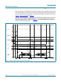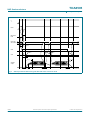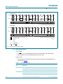
1
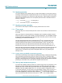
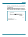
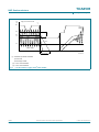
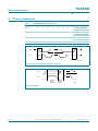
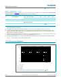
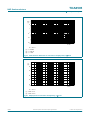
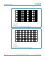
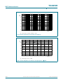
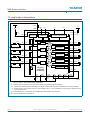
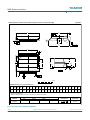
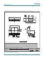
TDA8595 I2C-bus controlled 4 45 W power amplifier Rev. 5 — 11 June 2013 Product data sheet 1. General description The TDA8595 is a complementary quad Bridge Tied Load (BTL) audio power amplifier made in BCDMOS technology. It contains four independent amplifiers in BTL configuration. Through the I2C-bus, diagnosis of temperature warning and clipping level is fully programmable and the information available via two diagnostic pins is selectable. The status of each amplifier (output offset, load or no load, short-circuit or speaker incorrectly connected) can be read separately. 2. Features and benefits 2.1 General Operates in legacy mode (non I2C-bus) and I2C-bus mode (3.3 V and 5 V compliant) Three hardware-programmable I2C-bus addresses Drive 4 or 2 loads Speaker fault detection Independent short-circuit protection per channel Loss of ground and open VP safe (with 150 m series impedance and a supply decoupling capacitor of 2200 F maximum) All outputs short-circuit proof to ground, supply voltage and across the load All pins short-circuit proof to ground Temperature-controlled gain reduction to prevent audio holes at high junction temperatures Low battery voltage detection Offset detection This part has been qualified in accordance with AEC-Q100 2.2 I2C-bus mode DC load detection: open-circuit, short-circuit and load present AC load (tweeter) detection During start-up, can detect which load is connected so the appropriate gain can be selected without audio pop Independently selectable soft mute of front channels (channel 1 and channel 3) and rear channels (channel 2 and channel 4) Programmable gain (26 dB and 16 dB) of front channels and rear channels Fully programmable diagnostic levels can be set: Programmable clip detection: 2 %, 5 % or 10 % Programmable thermal pre-warning TDA8595 NXP Semiconductors I2C-bus controlled 4 45 W power amplifier Selectable information on the DIAG and STB pins: The STB pin can be programmed/multiplexed with second clip detection Clip information of each channel can be directed separately to the DIAG pin or the STB pin Independent enabling of thermal, clip or load fault detection (short across or to VP or to ground) on DIAG pin 3. Quick reference data Table 1. Quick reference data Refer to test circuit (see Figure 30) at VP = VP1 = VP2 = 14.4 V; RL = 4 ; f = 1 kHz; RS = 0 ; normal mode; unless otherwise specified. Tested at Tamb = 25 C; guaranteed for Tamb = 40 C to +105 C. Symbol Parameter Conditions Min Typ Max Unit VP supply voltage RL = 4 8 14.4 18 V Iq quiescent current no load - 270 400 mA Po output power VP = 14.4 V RL = 4 ; THD = 0.5 % 18 20 - W RL = 4 ; THD = 10 % 23 25 - W RL = 4 ; maximum power; Vi = 2 V (RMS) square wave 37 40 - W RL = 2 ; maximum power; Vi = 2 V (RMS) square wave 58 64 - W - 0.01 0.1 % normal mode - 45 65 V line driver mode - 22 29 V THD total harmonic distortion RL = 4 ; f = 1 kHz; Po = 1 W to 12 W Vn(o) noise output voltage filter 20 Hz to 22 kHz; RS = 1 k 4. Ordering information Table 2. TDA8595 Product data sheet Ordering information Type number Package Name Description Version TDA8595J DBS27P plastic DIL-bent-SIL (special bent) power package; 27 leads (lead length 6.8 mm) SOT827-1 TDA8595TH HSOP36 plastic, heatsink small outline package; 36 leads; low stand-off height SOT851-2 TDA8595SD RDBS27P plastic rectangular-DIL-bent-SIL (reverse bent) power package; 27 leads (row spacing 2.54 mm) SOT878-1 All information provided in this document is subject to legal disclaimers. Rev. 5 — 11 June 2013 © NXP B.V. 2013. All rights reserved. 2 of 51 TDA8595 NXP Semiconductors I2C-bus controlled 4 45 W power amplifier 5. Block diagram SCL ADSEL SDA VP2 VP1 1 (28) 26 (26) 23 (22) 21 (20, 21) 7 (34, 35) 5 (33) STB IN1 2 (29) DIAG I2C-BUS INTERFACE STANDBY/ FAST MUTE 12 (6) CLIP DETECT/DIAGNOSTIC MUTE 10 (4) 26 dB/ 16 dB 8 (2) OUT1+ OUT1− PROTECTION/ DIAGNOSTIC IN3 16 (12) MUTE 18 (14) 26 dB/ 16 dB 20 (17) OUT3+ OUT3− PROTECTION/ DIAGNOSTIC IN2 13 (7) 6 (30) MUTE 26 dB/ 16 dB 4 (32) OUT2+ OUT2− PROTECTION/ DIAGNOSTIC IN4 15 (11) 22 (25) MUTE 26 dB/ 16 dB VP 24 (23) SVR 14 (9) SGND OUT4− PROTECTION/ DIAGNOSTIC TDA8595J TDA8595SD (TDA8595TH) 11 (5) OUT4+ 27 (36) 17 (13) ACGND 9 (3) PGND1 3 (31) PGND2 19 (16) PGND3 25 (24) TAB 001aad135 PGND4 The pin numbers in parenthesis represent TDA8595TH. Fig 1. Block diagram TDA8595 Product data sheet All information provided in this document is subject to legal disclaimers. Rev. 5 — 11 June 2013 © NXP B.V. 2013. All rights reserved. 3 of 51 TDA8595 NXP Semiconductors I2C-bus controlled 4 45 W power amplifier 6. Pinning information 6.1 Pinning ADSEL 1 STB 2 PGND2 3 OUT2− 4 DIAG 5 OUT2+ 6 VP2 7 OUT1− 8 PGND1 9 OUT1+ 10 SVR 11 IN1 12 IN2 13 SGND 14 IN4 15 TDA8595J TDA8595SD IN3 16 ACGND 17 OUT3+ 18 PGND3 19 OUT3− 20 VP1 21 OUT4+ 22 SCL 23 OUT4− 24 PGND4 25 SDA 26 TAB 27 001aad136 Fig 2. Pin configuration TDA8595J and TDA8595SD TDA8595 Product data sheet All information provided in this document is subject to legal disclaimers. Rev. 5 — 11 June 2013 © NXP B.V. 2013. All rights reserved. 4 of 51 TDA8595 NXP Semiconductors I2C-bus controlled 4 45 W power amplifier TAB 36 1 n.c. VP2 35 2 OUT1− VP2 34 3 PGND1 DIAG 33 4 OUT1+ OUT2− 32 5 SVR PGND2 31 6 IN1 OUT2+ 30 7 IN2 STB 29 8 n.c. ADSEL 28 9 SGND TDA8595TH n.c. 27 10 n.c. SDA 26 11 IN4 OUT4+ 25 12 IN3 PGND4 24 13 ACGND OUT4− 23 14 OUT3+ SCL 22 15 n.c. VP1 21 16 PGND3 VP1 20 17 OUT3− n.c. 19 18 n.c. 001aad138 Fig 3. Pin configuration TDA8595TH 6.2 Pin description Table 3. Symbol TDA8595 Product data sheet Pin description Pin Description TDA8595J TDA8595SD[1] TDA8595TH ADSEL 1 28 I2C-bus address select STB 2 29 standby (I2C-bus mode) or mode pin (legacy mode); programmable second clip indicator PGND2 3 31 power ground channel 2 OUT2 4 32 negative channel 2 output DIAG 5 33 diagnostic/clip detection output OUT2+ 6 30 positive channel 2 output VP2 7 34 and 35 supply voltage 2 n.c. - 1 not connected OUT1 8 2 negative channel 1 output PGND1 9 3 power ground channel 1 OUT1+ 10 4 positive channel 1 output SVR 11 5 half supply filter capacitor IN1 12 6 channel 1 input IN2 13 7 channel 2 input n.c. - 8 not connected SGND 14 9 signal ground All information provided in this document is subject to legal disclaimers. Rev. 5 — 11 June 2013 © NXP B.V. 2013. All rights reserved. 5 of 51 TDA8595 NXP Semiconductors I2C-bus controlled 4 45 W power amplifier Table 3. Symbol Pin description …continued Pin Description TDA8595J TDA8595SD[1] TDA8595TH n.c. - 10 not connected IN4 15 11 channel 4 input IN3 16 12 channel 3 input ACGND 17 13 AC ground input OUT3+ 18 14 positive channel 3 output n.c. - 15 not connected PGND3 19 16 power ground channel 3 OUT3 20 17 negative channel 3 output n.c. - 18 and 19 not connected VP1 21 20 and 21 supply voltage 1 OUT4+ 22 25 positive channel 4 output SCL 23 22 I2C-bus clock input OUT4 24 23 negative channel 4 output PGND4 25 24 power ground channel 4 SDA 26 26 I2C-bus data input/output n.c. - 27 not connected TAB 27 36 heatsink connection; must be connected to ground [1] To keep the output pins on the front side, special reverse bending is applied. 7. Functional description The TDA8595 is a complementary quad BTL audio power amplifier made in BCDMOS technology. It contains four independent amplifiers in BTL configuration (see Figure 1). Through the I2C-bus, the diagnostic functions of temperature level and clip level are fully programmable and the information to be shown on the two diagnostic pins can be selected. The status of each amplifier (output offset, load or no load, short-circuit or speaker incorrectly connected) can be read separately. The TDA8595 is protected against overvoltage, short-circuit, over-temperature, open ground and open VP connections. Three different I2C-bus addresses are selected with an external resistor connected to the ADSEL pin. If the ADSEL pin is short-circuit to ground, the TDA8595 operates in legacy mode. In this mode, no I2C-bus is needed and the function of the STB pin will change from two level (Standby mode and On mode) to a three level pin (Standby mode, On mode and mute). TDA8595 Product data sheet All information provided in this document is subject to legal disclaimers. Rev. 5 — 11 June 2013 © NXP B.V. 2013. All rights reserved. 6 of 51 TDA8595 NXP Semiconductors I2C-bus controlled 4 45 W power amplifier 7.1 Input stage The input stage is a high-impedance pseudo-differential input stage. The negative inputs of the four channels are combined on the ACGND pin. For the best performance on supply voltage ripple rejection and pop noise, the capacitor connected to the ACGND pin must be four times the value of the input capacitor (or as close to the value as possible). 7.2 Output stage The output stage of each amplifier channel consists of two PMOS power transistors and two NMOS transistors in BTL configuration. The process used is the BCDMOS process with an isolated substrate, SOI process, which has almost no parasitic components and therefore prevents latch-up. 7.3 Distortion (clip-) detection If the output of the amplifier starts clipping to the supply voltage or to ground, the output will become distorted. If the distortion per channel exceeds a selectable threshold (2 %, 5 % or 10 %), one of the two diagnostic pins (DIAG pin or STB pin) will be activated. To be able to detect if, for instance, the front channels (channel 1 and channel 3) or rear channels (channel 2 and channel 4) are clipping, the clip information can be directed per channel to the DIAG pin or the STB pin. It is possible to have only the clip information on the diagnostic pins by disabling the temperature and load information on the diagnostic pin. In this mode the temperature and load protection are still functional but can only be read via the I2C-bus. 7.4 Output protection and short-circuit operation When a short-circuit to ground, VP or across the load occurs on one or more outputs of an amplifier, only the amplifier with the short-circuit is switched off. The channel that has a short-circuit and the type of short-circuit can be read-back via the I2C-bus. If the diagnostic pin is enabled for load fault information (IB2[D4] = 0) the DIAG pin will be pulled LOW. After 16 ms the amplifier will be switched on again and, if the short-circuit conditions still occur, the amplifier will be switched off. The 16 ms cycle will reduce the dissipation. To prevent audible distortion, the amplifier channel with the short-circuit can be disabled via the I2C-bus. 7.5 SOAR protection The output transistors are protected by Safe Operating ARea (SOAR) protection. The TDA8595 has a two-stage SOAR protection: • If the differential output voltage across the load is less than 1 V, and the current through the load is more than 4 A, the amplifier channel will be switched off during 16 ms. To prevent incorrect switch-off with an inductive load or very high input signals, the condition (Vo < 1 V and IL > 4 A) must exist for more than 300 s. • If the differential output voltage across the load is more than 1 V, and the current through the load is more than 8 A, the amplifier channel will be switched off during 16 ms. TDA8595 Product data sheet All information provided in this document is subject to legal disclaimers. Rev. 5 — 11 June 2013 © NXP B.V. 2013. All rights reserved. 7 of 51 TDA8595 NXP Semiconductors I2C-bus controlled 4 45 W power amplifier 7.6 Speaker protection To prevent damage of the speaker when one side of the speaker is connected to ground, a missing current protection is implemented. When in one channel the current in the high side power is not equal to the current in the low side power, a fault condition is assumed and the channel will be switched off. The speaker protection will be activated under the following conditions: • Vo < 1.75 V and Imissing(det) > 1 A during 80 s • Vo > 1.75 V and Imissing(det) > 3 A during 80 s 7.7 Standby and mute operation The function of the STB pin is different in legacy mode and I2C-bus mode. 7.7.1 I2C-bus mode When the STB pin is LOW, the total quiescent current is low, and the I2C-bus lines will not be loaded. When the STB pin is switched HIGH the TDA8595 is put in operating condition and will perform a power-on reset, which results in a LOW-level DIAG pin. The TDA8595 will start up when instruction bit IB1[D0] is set. Bit D0 will also reset the ‘power-on reset occurred’ bit (DB2[D7]) and releases the DIAG pin. The soft mute and soft mute can be activated via the I2C-bus. The soft mute can be activated independently for the front channels (channel 1 and channel 3) and rear channels (channel 2 and channel 4), and mutes the audio in 20 ms. The fast mute activates the mute for all channels at the same time and mutes the audio in 0.1 ms. Releasing the mute after a fast mute will be by a soft un-mute of approximately 20 ms. When the STB pin is switched to Standby mode and the amplifier has started, first the fast mute will be activated and then the amplifier will shut-down. For instance, during an engine start, it is possible to fully mute the amplifiers within 100 s by switching the STB pin to zero. 7.7.2 Legacy mode (pin ADSEL connected to ground) The function of the STB pin will change from standby/operating to standby/mute/operating and the amplifier will start directly when the STB is put into mute or operating. Mute operating is controlled via an internal timer (20 ms) to minimize mute-on pops. When the STB pin is switched directly from operating to standby, first the fast mute will be activated (switching to mute within 100 s) and then the amplifier will shut-down. 7.8 Start-up and shut-down sequence To prevent the amplifier producing switch-on or switch-off pop noise, the capacitor on the SVR pin is used for smooth start-up and shut-down. Increasing the value of the SVR capacitor will mean a longer start-up and shut-down time. The amplifier output voltage is charged to half the supply voltage minus 1.4 V in mute condition, independent of the I2C-bus mute settings in I2C-bus mode or pin STB voltage in legacy mode. The last 1.4 V, where the output will reach half the supply voltage, is used to release the mute if the I2C-bus bits (IB2[D2:D0] = 000) were set to mute-off (VSTB > 6.5 V in legacy mode), or will stay in mute when the bits were set to mute (2.6 V < VSTB < 4.5 V in legacy mode). TDA8595 Product data sheet All information provided in this document is subject to legal disclaimers. Rev. 5 — 11 June 2013 © NXP B.V. 2013. All rights reserved. 8 of 51 TDA8595 NXP Semiconductors I2C-bus controlled 4 45 W power amplifier When the amplifier is switched off by pulling the STB pin LOW, the amplifier is first muted (fast mute) and then the capacitor on the SVR pin is discharged. With an SVR capacitor of 22 F the standby current is reached 1 second after the STB pin is switched to zero (see Figure 4, Figure 5, Figure 6 and Figure 7). The start-up and shut-down pop can be further decreased by activating the low pop mode. When the low pop mode is enabled (IB2[D3] = 0), the output voltage rise from ground level during start-up will be slower (see Figure 6). This will decrease the pop even more but will increase the start-up time. VP DIAG DB2 bit D7 POR IB1 bit D0 start enable twake STB SVR toff tamp_on fast mute amplifier output td(mute_off) Fig 4. td(soft_mute) td(fast_mute) 001aad168 Start-up and shut-down timing in I2C-bus mode TDA8595 Product data sheet All information provided in this document is subject to legal disclaimers. Rev. 5 — 11 June 2013 © NXP B.V. 2013. All rights reserved. 9 of 51 TDA8595 NXP Semiconductors I2C-bus controlled 4 45 W power amplifier VP DIAG DB2 bit D7 POR IB1 bit D0 start enable twake STB SVR tload tamp_on toff fast mute amplifier output td(mute_off) Fig 5. td(soft_mute) td(fast_mute) 001aad169 Start-up and shut-down timing with DC load active in I2C-bus mode TDA8595 Product data sheet All information provided in this document is subject to legal disclaimers. Rev. 5 — 11 June 2013 © NXP B.V. 2013. All rights reserved. 10 of 51 TDA8595 NXP Semiconductors I2C-bus controlled 4 45 W power amplifier VP DIAG DB2 bit D7 POR IB1 bit D0 start enable twake STB SVR tload tamp_on toff fast mute amplifier output td(mute_off) td(soft_mute) td(fast_mute) 001aad170 Fig 6. Start-up and shut-down timing with low audible pop and DC load activated TDA8595 Product data sheet All information provided in this document is subject to legal disclaimers. Rev. 5 — 11 June 2013 © NXP B.V. 2013. All rights reserved. 11 of 51 TDA8595 NXP Semiconductors I2C-bus controlled 4 45 W power amplifier VP DIAG on STB mute standby SVR tamp_on toff soft mute fast mute amplifier output td(mute_off) td(soft_mute) td(mute_on) td(fast_mute) 001aad171 Fig 7. Start-up and shut-down timing in legacy mode 7.9 Power-on reset and supply voltage spikes If in I2C-bus mode the supply voltage drops below 5 V (see Figure 10) the content of the I2C-bus latches cannot be guaranteed and the power-on reset will be activated. All latches are reset, the amplifier is switched off and the DIAG pin is pulled LOW to indicate that a power-on reset has occurred (see bit DB2[D7]). When bit IB1[D0] is set, the power-on flag is reset, the DIAG pin will be released and the amplifier will start-up. In legacy mode a supply voltage drop below 5 V will switch off the amplifier and the DIAG pin will not be pulled LOW. 7.10 Engine start and low voltage operation The DC output voltage of the amplifier (VO) is set to half of the supply voltage and is related to the voltage on the SVR pin (see Figure 8; VO = VSVR 1.4 V). A capacitor is connected on the SVR pin to suppress the ripple on the power supply. If the supply voltage drops, for instance, during an engine start, the output follows slowly due to the SVR capacitor. The headroom voltage is the voltage needed for good operation of the amplifier and is defined as Vhr = VP VO (see Figure 8). If the headroom voltage becomes lower than the headroom protection threshold of 1.6 V, the headroom protection is activated to prevent pop noise at the output. This protection first activates the hard mute and then discharges the capacitors on the SVR and ACGND pins to generate more headroom for the amplifier (see Figure 9.) TDA8595 Product data sheet All information provided in this document is subject to legal disclaimers. Rev. 5 — 11 June 2013 © NXP B.V. 2013. All rights reserved. 12 of 51 TDA8595 NXP Semiconductors I2C-bus controlled 4 45 W power amplifier When the SVR capacitor has discharged, the amplifier starts up again if the VP voltage is above the low VP mute threshold, typically 7.5 V. Below the low VP mute threshold, the outputs of the amplifier remain low. In I2C-bus mode, a supply voltage drop below VP(reset), typically 5 V, results in setting bit DB2[D7]. The amplifiers will not start-up but wait for an I2C-bus command to start-up. The amplifier prevents audio pops during engine start. To prevent pops on the output caused by the application during an engine start (for instance tuner regulator out of regulation), the STB pin can be made zero when an engine start is detected. The STB pin activates the fast mute and disturbances at the amplifier inputs are suppressed. V (V) 14 VP VSVR Vhr (1) 8.4 7 VO (2) 1.6 V headroom protection threshold (3) t (s) 001aad172 (1) Headroom voltage Vhr = VP VO. (2) Steady state output voltage VO = VSVR 1.4 V. (3) Headroom protection threshold = VO + 1.6 V. Fig 8. Low headroom protection TDA8595 Product data sheet All information provided in this document is subject to legal disclaimers. Rev. 5 — 11 June 2013 © NXP B.V. 2013. All rights reserved. 13 of 51 TDA8595 NXP Semiconductors I2C-bus controlled 4 45 W power amplifier VO (V) legacy and I2C-bus mode VP 14.4 output voltage (1) 8.8 Vhr 8.6 (3) (2) 7.2 VSVR 3.5 output voltage (3) t (s) t(start-Vo(off)) t(start-SVRoff) 001aad173 (1) Headroom protection activated: a) Fast mute b) Discharge of SVR. (2) Low VP mute activated. (3) Low VP mute released. Fig 9. Low VP behavior; legacy and I2C-bus modes TDA8595 Product data sheet All information provided in this document is subject to legal disclaimers. Rev. 5 — 11 June 2013 © NXP B.V. 2013. All rights reserved. 14 of 51 TDA8595 NXP Semiconductors I2C-bus controlled 4 45 W power amplifier VO (V) I2C-bus mode only VP 14.4 8.8 8.6 (1) 7.2 (2) 5.0 3.5 VSVR output voltage 0 POR IB1 bit D0 DIAG t (s) 001aad185 (1) Low VP mute activated. (2) VPOR: VP level at which Power-On Reset (POR) is activated. Fig 10. Low VP behavior; I2C-bus mode only 7.11 Overvoltage and load dump protection When the battery voltage VP is higher than 22 V, the amplifier stage will be switched to high-impedance. The TDA8595 is protected against load dump voltage with supply voltage up to 50 V. 7.12 Thermal pre-warning and thermal protection If the average junction temperature reaches a level that is adjustable via the I2C-bus, selected with bit IB3[D4], the pre-warning will be activated resulting in a LOW-level on pin DIAG (if selected) and can be read out via the I2C-bus. The default setting for the thermal pre-warning is IB3[D4] = 0, setting the warning level at 145 C. In legacy mode the thermal pre-warning is set at 145 C. If the temperature increases further, the temperature controlled gain reduction will be activated for all four channels to reduce the output power (see Figure 11). If this does not reduce the average junction temperature, all four channels will be switched off at the absolute maximum temperature Toff, typical 175 C. TDA8595 Product data sheet All information provided in this document is subject to legal disclaimers. Rev. 5 — 11 June 2013 © NXP B.V. 2013. All rights reserved. 15 of 51 TDA8595 NXP Semiconductors I2C-bus controlled 4 45 W power amplifier 001aad174 30 Gv (dB) 20 10 0 145 155 165 175 Tj (°C) Fig 11. Temperature controlled amplifier gain 7.13 Diagnostics Diagnostic information can be read via the I2C-bus, and can also be available on the DIAG pin or on the STB pin. The DIAG pin has both fixed information (power-on reset occurred, low battery and high battery) and, via the I2C-bus, selectable information (temperature, load fault and clip). This information will be seen at the DIAG pin as a logic OR. In case of a failure, the DIAG pin remains LOW and the microprocessor can read the failure information via the I2C-bus (the DIAG pin can be used as microprocessor interrupt to minimize I2C-bus traffic). When the failure is removed, the DIAG pin will be released. To have full control over the clipping information, the STB pin can be programmed as a second clip detection pin. The clip detection level can be selected for all channels at once. It is possible to select whether the clip information is available on the DIAG pin or on the STB pin, for each channel separately. It is, for instance, possible to distinguish between clipping of the front and the rear channels. Diagnostic information selection possibilities are shown in Table 4. Table 4. TDA8595 Product data sheet Diagnostic information availability Diagnostic information I2C-bus mode Power-On Reset (POR) after power-on reset, no DIAG pin will remain LOW until amplifier has been started no Low battery yes no yes Clip detection can be enabled per channel can be enabled per channel yes, fixed level for all channels on 2 % Temperature prewarning can be enabled no yes, pre-warning level is 145 C Short can be enabled no yes DIAG pin Legacy mode STB pin All information provided in this document is subject to legal disclaimers. Rev. 5 — 11 June 2013 DIAG pin © NXP B.V. 2013. All rights reserved. 16 of 51 TDA8595 NXP Semiconductors I2C-bus controlled 4 45 W power amplifier Table 4. Diagnostic information availability …continued Diagnostic information I2C-bus mode DIAG pin STB pin DIAG pin Speaker protection (missing current) can be enabled no yes Offset detection no no no Load detection no no no Overvoltage yes no yes Legacy mode 7.14 Offset detection The offset detection can be performed with no input signal (for instance when the DSP is in mute after a start-up) or with an input signal. In I2C-bus mode, if an I2C-bus read of the output offset is performed, the I2C-bus latches DBx[D2] will be set. When the amplifier BTL output voltage is within a window with threshold of 1.75 V typical, the latches DBx[D2] are reset and setting is disabled. If, for instance, after one second an I2C-bus read is performed again and the offset bits are still set, the output has not crossed the offset threshold during the last second (see Figure 12). This can mean the applied frequency is below 1 Hz (one second I2C-bus read interval) or an output offset of more than 1.75 V is present. I2C-bus mode only VO = VOUT+ − VOUT− offset threshold t reset: setting disabled t = 1 s: read = no offset DB1 bit D2 reset VO = VOUT+ − VOUT− offset threshold t read = set bit t = 1 s: read = offset DB1 bit D2 set 001aad175 Fig 12. Offset detection 7.15 DC load detection When the DC load detection is enabled with bit IB1[D1], an offset is slowly applied at the output of the amplifiers during the start-up cycle and the load currents are measured. Different load levels will be detected to differentiate between normal load, line driver load or open load (see Figure 13). TDA8595 Product data sheet All information provided in this document is subject to legal disclaimers. Rev. 5 — 11 June 2013 © NXP B.V. 2013. All rights reserved. 17 of 51 TDA8595 NXP Semiconductors I2C-bus controlled 4 45 W power amplifier NORMAL LOAD DETECTION LEVEL LINE DRIVER MODE 20 Ω 100 Ω 800 Ω OPEN-CIRCUIT 5 kΩ 001aad176 Fig 13. DC load detection levels If the amplifier is used as line driver and the external booster has an input impedance of more than 100 and less than 800 (DC-coupled), the DC load bits will contain DBx[D5:D4] = 10, independent of the gain setting (see Table 5). Table 5. DC load detection DC load bits Meaning (when IB1[D2] = 0) DBx[D5] DBx[D4] 0 0 normal load 1 0 line driver load 1 1 open load 0 1 not valid By reading the I2C-bus bits the microprocessor can determine, after the start-up of the amplifier, whether a speaker or an external booster is connected. Depending on these bits, the amplifier gain can be selected, 26 dB for normal mode or 16 dB for line driver mode. If the gain select is performed when the amplifier is muted, the gain select will be pop free. The DC load bits are combined with the AC load bits and are only valid when the AC load detection is disabled. When the AC load detection is enabled (IB1[D2] = 1), the bits DBx[D4] will show the content of the AC load detection. When the AC load detection is disabled again, bit DBx[D4] will show the content of the DC load measurement, which was stored during the AC load measurement. The AC load detection can only be performed after the amplifier has completed its start-up cycle and will not conflict with the DC load detection. 7.16 AC load detection The AC load detection, enabled with IB1[D2] = 1, is used to detect if AC coupled speakers, for example tweeters, are connected correctly during assembly. The detection is audible because a sine wave of a certain frequency (e.g. 19 kHz) needs to be applied to the inputs of the amplifier. The output voltage over the load impedance will generate an amplifier current. If the amplifier peak current triggers a 460 mA (peak) threshold detector three times, the AC load detection bit will be set. A three ‘threshold cross’ counter is used to prevent false AC load detection when switching the input signal on or off. An AC coupled speaker will reduce the impedance at the output of the amplifier in a certain frequency band. The presence of an AC coupled speaker can be determined using 460 mA (peak) and 230 mA (peak) threshold current detection. For instance, at an output voltage of 2 V (peak) the total impedance must be less than 4 to detect the AC coupled load, or more than 8 to guarantee only a DC connection is detected. TDA8595 Product data sheet All information provided in this document is subject to legal disclaimers. Rev. 5 — 11 June 2013 © NXP B.V. 2013. All rights reserved. 18 of 51 TDA8595 NXP Semiconductors I2C-bus controlled 4 45 W power amplifier The interpretation of line driver and normal mode DC load bit setting for AC load detection is shown in Table 6. Table 6. AC load detection DBx[D4] Meaning (when IB1[D2] = 1) 0 no AC load detected 1 AC load detected When bit IB1[D2] = 1, the AC load detection is enabled. The AC load detection can only be performed after the amplifier has completed its start-up cycle and will not conflict with the DC load detection. 001aad177 20 |Zth(load)| (Ω) 16 (1) 12 8 (2) 4 0 0 1 2 3 4 5 VoM (V) (1) IoM < 230 mA (no load detection level) (2) IoM > 460 mA (load detection level) Fig 14. AC load impedance as a function of peak output voltage 7.17 I2C-bus diagnostic readout The diagnostic information of the amplifier can be read via the I2C-bus. The I2C-bus bits are set on a failure and will be reset with the I2C-bus read command. Even when the failure is removed, the microprocessor will know what was wrong by reading the I2C-bus. The consequence of this procedure is that old information is read during the I2C-bus readout. Most actual information will be gathered after two successive read commands. The DIAG pin will give actual diagnostic information (when selected). When a failure is removed, the DIAG pin will be released instantly, independently of the I2C-bus latches. TDA8595 Product data sheet All information provided in this document is subject to legal disclaimers. Rev. 5 — 11 June 2013 © NXP B.V. 2013. All rights reserved. 19 of 51 TDA8595 NXP Semiconductors I2C-bus controlled 4 45 W power amplifier 8. I2C-bus specification Table 7. TDA8595 hardware address select Pin ADSEL A6 A5 A4 A3 A2 A1 A0 R/W Open 1 1 0 1 1 0 0 0 = write to TDA8595 1 = read from TDA8595 51 k to ground 1 1 0 1 1 0 1 0 = write to TDA8595 1 = read from TDA8595 10 k to ground 1 1 0 1 1 1 1 0 = write to TDA8595 1 = read from TDA8595 Ground no I2C-bus; legacy mode SDA SCL S P START condition STOP condition mba608 Fig 15. Definition of START and STOP conditions SDA SCL data line stable; data valid change of data allowed mba607 Fig 16. Bit transfer TDA8595 Product data sheet All information provided in this document is subject to legal disclaimers. Rev. 5 — 11 June 2013 © NXP B.V. 2013. All rights reserved. 20 of 51 TDA8595 NXP Semiconductors I2C-bus controlled 4 45 W power amplifier I2C-BUS WRITE SCL 1 SDA MSB 2 7 MSB − 1 S 8 LSB + 1 ADDRESS 9 ACK 1 MSB 2 MSB − 1 A W 7 LSB + 1 8 LSB 9 ACK A WRITE DATA P To stop the transfer, after the last acknowledge (A) a STOP condition (P) must be generated I2C-BUS READ SCL 1 SDA MSB 2 7 MSB − 1 S 8 LSB + 1 9 ACK R ADDRESS 1 MSB 2 7 MSB − 1 A LSB + 1 READ DATA : generated by slave : START P : STOP A : acknowledge NA : not acknowledge R/W : read / write LSB 9 ACK NA P To stop the transfer, the last byte must not be acknowledged and a STOP condition (P) must be generated : generated by master (microcontroller) S 8 001aac649 Fig 17. I2C-bus read and write modes 8.1 Instruction bytes I2C-bus mode: • If R/W bit = 0, the TDA8595 expects three instruction bytes; IB1, IB2 and IB3 • After a power-on reset, all instruction bits are set to zero Legacy mode: • All bits equal to zero define the setting, with the exception of bit IB1[D0] which is ignored (see Table 8). Table 8. Instruction byte IB1 Bit Description D7 don’t care D6 channel 3 clip information on DIAG or STB pin 0 = clip information on DIAG pin 1 = clip information on STB pin D5 channel 1 clip information on DIAG or STB pin 0 = clip information on DIAG pin 1 = clip information on STB pin TDA8595 Product data sheet All information provided in this document is subject to legal disclaimers. Rev. 5 — 11 June 2013 © NXP B.V. 2013. All rights reserved. 21 of 51 TDA8595 NXP Semiconductors I2C-bus controlled 4 45 W power amplifier Table 8. Instruction byte IB1 …continued Bit Description D4 channel 4 clip information on DIAG or STB pin 0 = clip information on DIAG pin 1 = clip information on STB pin D3 channel 2 clip information on DIAG or STB pin 0 = clip information on DIAG pin 1 = clip information on STB pin D2 AC load detection enable: 0 = AC load detection disabled 1 = AC load detection enabled; bit DBx[D4] not available for DC load detection D1 DC load detection enable: 0 = DC load detection disabled 1 = DC load detection enabled D0 amplifier start enable 0 = amplifier not enabled, DIAG pin will remain LOW 1 = amplifier will start up, power-on occurred (DB2[D7] will be reset) and DIAG pin will be released Table 9. Instruction byte IB2 Bit Description D7 and D6 clip detection level 00 = clip detection level 2 % 01 = clip detection level 5 % 10 = clip detection level 10 % 11 = clip detection level disabled D5 temperature information on DIAG pin 0 = temperature information on DIAG pin 1 = no temperature information on DIAG pin D4 load fault information (shorts, missing current) on DIAG pin 0 = fault information on DIAG pin 1 = no fault information on DIAG pin D3 low pop (slow start) enable 0 = low pop enabled 1 = low pop disabled D2 soft mute channel 1 and channel 3 (mute delay 20 ms) 0 = no mute 1 = mute D1 soft mute channel 2 and channel 4 (mute delay 20 ms) 0 = no mute 1 = mute TDA8595 Product data sheet All information provided in this document is subject to legal disclaimers. Rev. 5 — 11 June 2013 © NXP B.V. 2013. All rights reserved. 22 of 51 TDA8595 NXP Semiconductors I2C-bus controlled 4 45 W power amplifier Table 9. Instruction byte IB2 …continued Bit Description D0 fast mute all amplifier channels (mute delay 100 s) 0 = no mute 1 = mute Table 10. Instruction byte IB3 Bit Description D7 don’t care D6 amplifier channel 1 and channel 3 gain select 0 = 26 dB 1 = 16 dB D5 amplifier channel 2 and channel 4 gain select 0 = 26 dB 1 = 16 dB D4 temperature pre-warning level 0 = warning level on 145 C 1 = warning level on 122 C D3 disable channel 3 0 = channel 3 enabled 1 = channel 3 disabled D2 disable channel 1 0 = channel 1 enabled 1 = channel 1 disabled D1 disable channel 4 0 = channel 4 enabled 1 = channel 4 disabled D0 disable channel 2 0 = channel 2 enabled 1 = channel 2 disabled 8.2 Data bytes I2C-bus mode: • If R/W = 1, the TDA8595 sends four data bytes to the microprocessor: DB1, DB2, DB3 and DB4 • All bits except DB1[D7] and DB3[D7] are latched • All bits except DBx[D4] and DBx[D5] are reset after a read operation. Bit DBx[D2] is set after a read operation, see Section 7.14 • For explanation of AC and DC load detection bits, see Section 7.15 and Section 7.16 TDA8595 Product data sheet All information provided in this document is subject to legal disclaimers. Rev. 5 — 11 June 2013 © NXP B.V. 2013. All rights reserved. 23 of 51 TDA8595 NXP Semiconductors I2C-bus controlled 4 45 W power amplifier Table 11. Data byte DB1 Bit Description D7 temperature pre-warning 0 = no warning 1 = junction temperature too high D6 speaker fault channel 2 (missing current) 0 = no missing current 1 = missing current D5 and D4 channel 2 DC load or AC load detection if bit IB1[D2] = 1, AC load detection is enabled, bit D5 is don’t care, bit D4 has the following meaning 0 = no AC load 1 = AC load detected if bit IB1[D2] = 0, AC load detection is disabled, bits D5 and D4 are available for DC load detection 00 = normal load 01 = not valid 10 = line driver load 11 = open load D3 channel 2 shorted load 0 = not shorted load 1 = shorted load D2 channel 2 output offset 0 = no output offset 1 = output offset D1 channel 2 short to VP 0 = no short to VP 1 = short to VP D0 channel 2 short to ground 0 = no short to ground 1 = short to ground Table 12. Data byte DB2 Bit Description D7 power-on reset and amplifier status 0 = amplifier on 1 = power-on reset has occurred; amplifier off D6 speaker fault channel 4 (missing current) 0 = no missing current 1 = missing current TDA8595 Product data sheet All information provided in this document is subject to legal disclaimers. Rev. 5 — 11 June 2013 © NXP B.V. 2013. All rights reserved. 24 of 51 TDA8595 NXP Semiconductors I2C-bus controlled 4 45 W power amplifier Table 12. Data byte DB2 …continued Bit Description D5 and D4 channel 4 DC load or AC load detection if bit IB1[D2] = 1, AC load detection is enabled, bit D5 is don’t care, bit D4 has the following meaning 0 = no AC load 1 = AC load detected if bit IB1[D2] = 0, AC load detection is disabled, bits D5 and D4 are available for DC load detection 00 = normal load 01 = not valid 10 = line driver load 11 = open load D3 channel 4 shorted load 0 = not shorted load 1 = shorted load D2 channel 4 output offset 0 = no output offset 1 = output offset D1 channel 4 short to VP 0 = no short to VP 1 = short to VP D0 channel 4 short to ground 0 = no short to ground 1 = short to ground Table 13. Data byte DB3 Bit Description D7 maximum temperature protection 0 = no protection 1 = maximum temperature protection D6 speaker fault channel 1 (missing current) 0 = no missing current 1 = missing current TDA8595 Product data sheet All information provided in this document is subject to legal disclaimers. Rev. 5 — 11 June 2013 © NXP B.V. 2013. All rights reserved. 25 of 51 TDA8595 NXP Semiconductors I2C-bus controlled 4 45 W power amplifier Table 13. Data byte DB3 …continued Bit Description D5 and D4 channel 1 DC load or AC load detection if bit IB1[D2] = 1, AC load detection is enabled, bit D5 is don’t care, bit D4 has the following meaning 0 = no AC load 1 = AC load detected if bit IB1[D2] = 0, AC load detection is disabled, bits D5 and D4 are available for DC load detection 00 = normal load 01 = not valid 10 = line driver load 11 = open load D3 channel 1 shorted load 0 = not shorted load 1 = shorted load D2 channel 1 output offset 0 = no output offset 1 = output offset D1 channel 1 short to VP 0 = no short to VP 1 = short to VP D0 channel 1 short to ground 0 = no short to ground 1 = short to ground Table 14. Data byte DB4 Bit Description D7 reserved D6 speaker fault channel 3 (missing current) 0 = no missing current 1 = missing current D5 and D4 channel 3 DC load or AC load detection if bit IB1[D2] = 1, AC load detection is enabled, bit D5 is don’t care, bit D4 has the following meaning 0 = no AC load 1 = AC load detected if bit IB1[D2] = 0, AC load detection is disabled, bits D5 and D4 are available for DC load detection 00 = normal load 01 = not valid 10 = line driver load 11 = open load TDA8595 Product data sheet All information provided in this document is subject to legal disclaimers. Rev. 5 — 11 June 2013 © NXP B.V. 2013. All rights reserved. 26 of 51 TDA8595 NXP Semiconductors I2C-bus controlled 4 45 W power amplifier Table 14. Data byte DB4 …continued Bit Description D3 channel 3 shorted load 0 = not shorted load 1 = shorted load D2 channel 3 output offset 0 = no output offset 1 = output offset D1 channel 3 short to VP 0 = no short to VP 1 = short to VP D0 channel 3 short to ground 0 = no short to ground 1 = short to ground 9. Limiting values Table 15. Limiting values In accordance with the Absolute Maximum Rating System (IEC 60134). TDA8595 Product data sheet Symbol Parameter Conditions Min Max Unit VP supply voltage operating - 18 V non operating 1 +50 V load dump protection; duration 50 ms, rise time > 2.5 ms - 50 V 10 minutes maximum VP(r) reverse supply voltage - 2 V IOSM non-repetitive peak output current - 13 A IORM repetitive peak output current - 8 A Tj(max) maximum junction temperature - 150 C Tstg storage temperature 55 +150 C Tamb ambient temperature V(prot) protection voltage Vx voltage on pin x 40 +105 C - VP V SCL and SDA 0 6.5 V IN1, IN2, IN3, IN4, SVR, ACGND and DIAG 0 13 V STB 0 24 V AC and DC short-circuit voltage of output pins and across the load All information provided in this document is subject to legal disclaimers. Rev. 5 — 11 June 2013 © NXP B.V. 2013. All rights reserved. 27 of 51 TDA8595 NXP Semiconductors I2C-bus controlled 4 45 W power amplifier Table 15. Limiting values …continued In accordance with the Absolute Maximum Rating System (IEC 60134). Symbol Parameter Conditions Min Max Unit Ptot total power dissipation Tcase = 70 C - 80 W Vesd electrostatic discharge voltage human body model; C = 100 pF; Rs = 1.5 k - 2000 V machine model; C = 200 pF; Rs = 10 ; Ls = 0.75 H - 200 V 10. Thermal characteristics Table 16. Symbol Thermal characteristics Parameter Conditions Typ Unit TDA8595J; TDA8595SD Rth(j-c) thermal resistance from junction to case 1 K/W Rth(j-a) thermal resistance from junction to ambient in free air 40 K/W TDA8595TH Rth(j-c) thermal resistance from junction to case 1 K/W Rth(j-a) thermal resistance from junction to ambient in free air 40 K/W 11. Characteristics Table 17. Characteristics Refer to test circuit (see Figure 30) at VP = VP1 = VP2 = 14.4 V; RL = 4 ; f = 1 kHz; RS = 0 ; normal mode; unless otherwise specified. Tested at Tamb = 25 C; guaranteed for Tamb = 40 C to +105 C. Symbol Parameter Conditions Min Typ Max Unit 8 14.4 18 V Supply voltage behavior VP supply voltage RL = 4 RL = 2 [1] 8 14.4 16 V Iq quiescent current no load - 270 400 mA Istb standby current VSTB = 0.4 V - 4 15 A VO output voltage 6.7 7 7.2 V VP(low)(mute) low supply voltage mute with rising supply voltage 6.9 7.5 8 V with falling supply voltage 6.3 6.8 7.4 V VP(low)(mute) low supply voltage mute hysteresis 0.1 0.7 1 V Vth(ovp) overvoltage protection threshold voltage 18 20 22 V Vhr headroom voltage 1.1 1.6 2.0 V VPOR power-on reset voltage see Figure 9 4.1 5.0 5.8 V VO(offset) output offset voltage amplifier on 95 0 +95 mV amplifier mute 25 0 +25 mV line driver mode 40 0 +40 mV TDA8595 Product data sheet when headroom protection is activated; see Figure 8 All information provided in this document is subject to legal disclaimers. Rev. 5 — 11 June 2013 © NXP B.V. 2013. All rights reserved. 28 of 51 TDA8595 NXP Semiconductors I2C-bus controlled 4 45 W power amplifier Table 17. Characteristics …continued Refer to test circuit (see Figure 30) at VP = VP1 = VP2 = 14.4 V; RL = 4 ; f = 1 kHz; RS = 0 ; normal mode; unless otherwise specified. Tested at Tamb = 25 C; guaranteed for Tamb = 40 C to +105 C. Symbol Parameter Conditions Min Typ Max Unit RL(tol) load resistance tolerance VP 18 V 3.2 4 - VP 16 V 1.6 2 - I2C-bus mode - - 1 V legacy mode - - 1 V 2.5 - 4.5 V I2C-bus mode 2.5 - VP V legacy mode 6.5 - VP V ISTB = 150 A 5.6 - 6.1 V ISTB = 500 A 6.1 - 7.2 V clip detection not active; I2C-bus mode - 4 30 A legacy mode - 10 70 A - 300 500 s - - 10 A I2C-bus mode; with ILO = 10 A +15 ms; no DC load (IB1[D1] = 0); low pop disabled (IB2[D3] = 1); see Figure 4 295 465 795 ms I2C-bus mode; with ILO = 10 A +20 ms; DC load active (IB1[D1] = 1); low pop disabled (IB2[D3] = 1); see Figure 5 500 640 940 ms I2C-bus mode; with ILO = 10 A +20 ms; DC load active (IB1[D1] = 1); low pop enabled (IB2[D3] = 0); see Figure 6 640 830 1190 ms legacy mode; with ILO = 10 A +20 ms; VSTB = 7 V; RADSEL = 0 ; see Figure 7 430 650 1030 ms Mode select and second clip detection: pin STB VSTB voltage on pin STB Standby mode selected mute selected legacy mode Operating mode selected low voltage on pin STB when pulled down during clipping ISTB current on pin STB [2] VSTB from 0 V to 8.5 V Start-up / shut-down / mute timing twake wake-up time ILO(SVR) output leakage current on pin SVR td(mute_off) mute off delay time TDA8595 Product data sheet time after wake-up via STB pin before first I2C-bus transmission is recognized; see Figure 4 10 % of output signal; ILO = 0 A All information provided in this document is subject to legal disclaimers. Rev. 5 — 11 June 2013 [3] © NXP B.V. 2013. All rights reserved. 29 of 51 TDA8595 NXP Semiconductors I2C-bus controlled 4 45 W power amplifier Table 17. Characteristics …continued Refer to test circuit (see Figure 30) at VP = VP1 = VP2 = 14.4 V; RL = 4 ; f = 1 kHz; RS = 0 ; normal mode; unless otherwise specified. Tested at Tamb = 25 C; guaranteed for Tamb = 40 C to +105 C. Symbol tamp_on toff Parameter amplifier on time amplifier switch-off time Conditions Min Typ Max Unit I2C-bus mode; with ILO = 10 A +30 ms; no DC load (IB1[D1] = 0); low pop disabled (IB2[D3] = 1); see Figure 4 360 520 870 ms I2C-bus mode; with ILO = 10 A +35 ms; DC load active (IB1[D1] = 1); low pop disabled (IB2[D3] = 1); see Figure 5 565 695 1015 ms I2C-bus mode; with ILO = 10 A +30 ms; DC load active (IB1[D1] = 1); low pop enabled (IB2[D3] = 0); see Figure 6 710 890 1270 ms legacy mode; with ILO = 10 A +20 ms; VSTB = 7 V; RADSEL = 0 ; see Figure 7 510 720 1120 ms low pop disabled (IB2[D3] = 1); with ILO = 10 A +0 ms; see Figure 5 120 245 530 ms low pop enabled (IB2[D3] = 0); with ILO = 10 A +0 ms; see Figure 6 140 280 620 ms time from amplifier mute to amplifier on; 90 % of output signal; ILO = 0 A time to DC output voltage < 0.1 V; I2C-bus mode; ILO = 0 A [3] [3] td(mute-on) mute to on delay time from 10 % to 90 % of output signal; IB2[D1/D2] = 1 to 0; Vi = 50 mV; see Figure 7 - 20 40 ms td(soft_mute) soft mute delay time from 90 % to 10 % of output signal; Vi = 50 mV; IB2[D1/D2] = 0 to 1; see Figure 7 - 20 40 ms td(fast_mute) fast mute delay time from 90 % to 10 % of output signal; VSTB from 8 V to 1.3 V; see Figure 7 - 0.1 1 ms t(start-Vo(off)) engine start to output off time VP from 14.4 V to 7 V; Vo < 0.5 V; see Figure 9 - 0.1 1 ms t(start-SVRoff) engine start to SVR off time VP from 14.4 V to 7 V; VSVR < 2 V; see Figure 9 - 40 75 ms - - 1.5 V 5.5 V - 0.4 V I2C-bus interface[4] VIL LOW-level input voltage pins SCL and SDA VIH HIGH-level input voltage pins SCL and SDA 2.3 VOL LOW-level output voltage pin SDA; IL = 5 mA - TDA8595 Product data sheet All information provided in this document is subject to legal disclaimers. Rev. 5 — 11 June 2013 © NXP B.V. 2013. All rights reserved. 30 of 51 TDA8595 NXP Semiconductors I2C-bus controlled 4 45 W power amplifier Table 17. Characteristics …continued Refer to test circuit (see Figure 30) at VP = VP1 = VP2 = 14.4 V; RL = 4 ; f = 1 kHz; RS = 0 ; normal mode; unless otherwise specified. Tested at Tamb = 25 C; guaranteed for Tamb = 40 C to +105 C. Symbol Parameter fSCL SCL clock frequency Conditions Min Typ Max Unit - 400 - kHz I2C-bus address A[6:0] = 110 1100 155 - - k I2C-bus address A[6:0] = 110 1101 42 51 57 k I2C-bus address A[6:0] = 110 1111 7 10 15 k legacy mode - - 0.5 k fault condition; IDIAG = 1 mA - - 0.3 V 1.5 1.75 2.2 V IB2[D7:D6] = 10 5 10 16 % IB2[D7:D6] = 01 3 5 7 % IB2[D7:D6] = 00 1 2 3 % total harmonic distortion clip detection level variation between IB2[D7:D6] = 10 and IB2[D7:D6] = 01 1 4 9 % between IB2[D7:D6] = 01 and IB2[D7:D6] = 00 1 3.5 6 % Tj(AV)(pwarn) pre-warning average junction temperature IB3[D4] = 0 135 145 155 C IB3[D4] = 1 112 122 132 C Tj(AV)(G(0.5dB)) average junction Vi = 0.05 V temperature for 0.5 dB gain reduction 150 155 160 C Tj(pw-G(0.5dB)) prewarning to 0.5 dB gain reduction junction temperature difference 7 10 13 C Tj(G(0.5dB)-off) difference in junction temperature between 0.5 dB gain reduction and off 10 15 20 C - 20 - dB normal load detection - - 20 line driver load detection 100 - 800 5000 - - AC load bit is set 460 - - mA AC load bit is not set - - 230 mA RADSEL resistance on pin ADSEL Diagnostic VOL(DIAG) LOW-level output voltage on pin DIAG VO(offset_det) output voltage at offset detection THDclip total harmonic distortion clip detection level THDclip G(th_fold) gain reduction of thermal foldback all channels will switch off Zth(load) load detection threshold impedance I2C-bus mode Zth(open) open load detection threshold impedance I2C-bus Ith(o)det(load)AC AC load detection output threshold current I2C-bus mode TDA8595 Product data sheet mode All information provided in this document is subject to legal disclaimers. Rev. 5 — 11 June 2013 © NXP B.V. 2013. All rights reserved. 31 of 51 TDA8595 NXP Semiconductors I2C-bus controlled 4 45 W power amplifier Table 17. Characteristics …continued Refer to test circuit (see Figure 30) at VP = VP1 = VP2 = 14.4 V; RL = 4 ; f = 1 kHz; RS = 0 ; normal mode; unless otherwise specified. Tested at Tamb = 25 C; guaranteed for Tamb = 40 C to +105 C. Symbol Parameter Conditions Min Typ Max Unit output power RL = 4 ; VP = 14.4 V; THD = 0.5 % 18 20 - W RL = 4 ; VP = 14.4 V; THD = 10 % 23 25 - W RL = 4 ; VP = 14.4 V; maximum power; Vi = 2 V (RMS) square wave 37 40 - W RL = 4 ; VP = 15.2 V; maximum power; Vi = 2 V (RMS) square wave 41 45 - W RL = 2 ; VP = 14.4 V; THD = 0.5 % 29 32 - W RL = 2 ; VP = 14.4 V; THD = 10 % 37 41 - W RL = 2 ; VP = 14.4 V; maximum power; Vi = 2 V (RMS) square wave 58 64 - W Po = 1 W to 12 W; f = 1 kHz; RL = 4 - 0.01 0.1 % Po = 1 W to 12 W; f = 10 kHz - 0.09 0.3 % Amplifier Po THD cs total harmonic distortion channel separation Po = 1 W to 12 W; f = 20 kHz - 0.14 0.4 % line driver mode; Vo = 1 V (RMS) and 5 V (RMS), f = 20 Hz to 20 kHz; complex load; see Figure 32 - 0.02 0.05 % f = 1 kHz; RS = 1 k; RACGND = 250 [5] 65 80 - dB f = 10 kHz; RS = 1 k; RACGND = 250 [5] 60 65 - dB SVRR supply voltage ripple rejection 100 Hz to 10 kHz; RS = 1 k; RACGND = 250 [5] 55 70 - dB CMRR common mode rejection ratio normal mode; Vcm = 0.3 V (p-p); f = 1 kHz to 3 kHz, RS = 1 k; RACGND = 250 [5] 45 65 - dB Vcm(max)(rms) maximum common mode voltage (RMS value) f = 1 kHz - - 0.6 V Vn(o) output noise voltage filter 20 Hz to 22 kHz; RS = 1 k mute mode - 19 26 V line driver mode - 22 29 V normal mode - 45 65 V normal mode 25.5 26 26.5 dB line driver mode 15.5 16 16.5 dB Gv voltage gain TDA8595 Product data sheet single ended in; differential out All information provided in this document is subject to legal disclaimers. Rev. 5 — 11 June 2013 © NXP B.V. 2013. All rights reserved. 32 of 51 TDA8595 NXP Semiconductors I2C-bus controlled 4 45 W power amplifier Table 17. Characteristics …continued Refer to test circuit (see Figure 30) at VP = VP1 = VP2 = 14.4 V; RL = 4 ; f = 1 kHz; RS = 0 ; normal mode; unless otherwise specified. Tested at Tamb = 25 C; guaranteed for Tamb = 40 C to +105 C. Symbol Parameter Conditions Min Typ Max Unit Zi input impedance Tamb = 40 C to +105 C 50 70 95 k Tamb = 0 C to 105 C 60 70 95 k mute mute attenuation Vo / Vo(mute); Vi = 50 mV 80 92 - dB Vo(mute)(RMS) RMS mute output voltage Vi = 1 V (RMS); filter 20 Hz to 22 kHz - 25 - V Bp power bandwidth 1 dB - 20 to 20000 - Hz [1] Operation above 16 V in a 2 mode with reactive load can trigger the amplifier protection. The amplifier switches off and will restart after 16 ms resulting in an ‘audio hole’. [2] VSTB depends on the current into the STB pin: minimum = (1429 ISTB) + 5.4 V, maximum = (3143 ISTB) + 5.6 V. [3] The times are specified without leakage current. For a leakage current of 10 A on the SVR pin, the delta time is specified. If the capacitor value on the SVR pin changes with 30 %, the specified time will also change with 30 %. The specified times include an ESR of 15 for the capacitor on the SVR pin. [4] Standard I2C-bus specification: maximum LOW-level = 0.3 VDD, minimum HIGH-level = 0.7 VDD. To comply with 5 V and 3.3 V logic the maximal LOW-level is defined by VDD = 5 V and the minimum HIGH-level by VDD = 3.3 V. [5] For optimum channel separation (cs), supply voltage ripple rejection (SVRR) and common mode rejection ratio (CMRR), a resistor RS R ACGND = ------ should be in series with the ACGND capacitor. 4 12. Performance diagrams 001aad139 102 THD (%) 10 1 10−1 (1) 10−2 (2) (3) 10−3 10−2 10−1 1 102 10 Po (W) VP = 14.4 V. (1) f = 10 kHz. (2) f = 1 kHz. (3) f = 100 Hz. Fig 18. Total harmonic distortion as a function of output power; 4 load TDA8595 Product data sheet All information provided in this document is subject to legal disclaimers. Rev. 5 — 11 June 2013 © NXP B.V. 2013. All rights reserved. 33 of 51 TDA8595 NXP Semiconductors I2C-bus controlled 4 45 W power amplifier 001aad140 102 THD (%) 10 1 (1) 10−1 (2) (3) 10−2 10−3 10−2 10−1 1 102 10 Po (W) VP = 14.4 V. (1) f = 10 kHz. (2) f = 100 Hz. (3) f = 1 kHz. Fig 19. Total harmonic distortion as a function of output power; 2 load 001aad141 28 (1) Po (W) 26 24 22 (2) 20 18 10−2 10−1 1 102 10 f (kHz) VP = 14.4 V. (1) THD = 10 %. (2) THD = 0.5 %. Fig 20. Output power as a function of frequency; 4 load TDA8595 Product data sheet All information provided in this document is subject to legal disclaimers. Rev. 5 — 11 June 2013 © NXP B.V. 2013. All rights reserved. 34 of 51 TDA8595 NXP Semiconductors I2C-bus controlled 4 45 W power amplifier 001aad142 55 Po (W) 45 (1) 35 (2) 25 10−2 10−1 1 102 10 f (kHz) VP = 14.4 V. (1) THD = 10 %. (2) THD = 0.5 %. Fig 21. Output power as a function of frequency; 2 load 001aad143 60 Po (W) (1) 40 (2) (3) 20 0 5 10 15 20 VP (V) f = 1 kHz. (1) Po(max). (2) THD = 10 %. (3) THD = 0.5 %. Fig 22. Output power as a function of supply voltage; 4 load TDA8595 Product data sheet All information provided in this document is subject to legal disclaimers. Rev. 5 — 11 June 2013 © NXP B.V. 2013. All rights reserved. 35 of 51 TDA8595 NXP Semiconductors I2C-bus controlled 4 45 W power amplifier 001aad144 100 Po (W) 80 (1) 60 (2) 40 (3) 20 0 5 10 15 20 VP (V) f = 1 kHz. (1) Po(max). (2) THD = 10 %. (3) THD = 0.5 %. Fig 23. Output power as a function of supply voltage; 2 load 001aad145 1 THD (%) 10−1 10−2 (1) (2) 10−3 10−2 10−1 1 102 10 f (kHz) VP = 14.4 V; RL = 4 . (1) Po = 1 W. (2) Po = 10 W. Fig 24. Total harmonic distortion as a function of frequency; normal mode TDA8595 Product data sheet All information provided in this document is subject to legal disclaimers. Rev. 5 — 11 June 2013 © NXP B.V. 2013. All rights reserved. 36 of 51 TDA8595 NXP Semiconductors I2C-bus controlled 4 45 W power amplifier 001aad146 10−1 THD (%) 10−2 (1) (2) 10−3 10−2 10−1 1 102 10 f (kHz) VP = 14.4 V; RL = 600 . (1) Vo = 1 V. (2) Vo = 5 V. Fig 25. Total harmonic distortion as a function of frequency; line driver mode 001aad147 −40 SVRR (dB) −50 −60 −70 −80 −90 10−2 10−1 1 102 10 f (kHz) VP = 14.4 V; RL = 4 ; RS = 1 k; Vripple = 2 V (p-p). Fig 26. Supply voltage ripple rejection as a function of frequency TDA8595 Product data sheet All information provided in this document is subject to legal disclaimers. Rev. 5 — 11 June 2013 © NXP B.V. 2013. All rights reserved. 37 of 51 TDA8595 NXP Semiconductors I2C-bus controlled 4 45 W power amplifier 001aad148 100 αcs (dB) 90 80 70 60 50 10−2 10−1 1 102 10 f (kHz) VP = 14.4 V; RL = 4 ; RS = 1 k; Po = 1 W. Fig 27. Channel separation as a function of frequency 001aad711 50 P (W) 40 30 20 10 0 0 10 20 30 40 Po (W) VP = 14.4 V; RL = 4 ; f = 1 kHz. Fig 28. Power dissipation as a function of output power; 4 load TDA8595 Product data sheet All information provided in this document is subject to legal disclaimers. Rev. 5 — 11 June 2013 © NXP B.V. 2013. All rights reserved. 38 of 51 TDA8595 NXP Semiconductors I2C-bus controlled 4 45 W power amplifier 001aad712 100 P (W) 80 60 40 20 0 0 20 40 60 80 Po (W) VP = 14.4 V; RL = 2 ; f = 1 kHz. Fig 29. Power dissipation as a function of output power; 2 load TDA8595 Product data sheet All information provided in this document is subject to legal disclaimers. Rev. 5 — 11 June 2013 © NXP B.V. 2013. All rights reserved. 39 of 51 TDA8595 NXP Semiconductors I2C-bus controlled 4 45 W power amplifier 13. Application information 8.5 V (2) RADSEL SDA 5V VP2 VP1 SCL ADSEL 1 (28) 26 (26) 23 (22) 21 (20, 21) 7 (34, 35) 10 kΩ 5 (33) DIAG STB 2 (29) I2C-BUS INTERFACE STANDBY/ FAST MUTE CLIP DETECT/DIAGNOSTIC (4) RS 470 nF MUTE IN1 12 (6) (1) 1.8 nF RS 470 nF RS MUTE IN3 16 (12) 470 nF 8 (2) OUT1− (4) 18 (14) OUT3+ 26 dB/ 16 dB 20 (17) OUT3− PROTECTION/ DIAGNOSTIC IN2 13 (7) MUTE (1) 1.8 nF RS 26 dB/ 16 dB PROTECTION/ DIAGNOSTIC (1) 1.8 nF 470 nF 10 (4) OUT1+ (4) 6 (30) OUT2+ 26 dB/ 16 dB 4 (32) OUT2− PROTECTION/ DIAGNOSTIC IN4 15 (11) (1) 1.8 nF MUTE VP 26 dB/ 16 dB 24 (23) OUT4− PROTECTION/ DIAGNOSTIC TDA8595J TDA8595SD (TDA8595TH) 27 (36) TAB 11 (5) 14 (9) 17 (13) SVR SGND ACGND (2) 22 μF (4) 22 (25) OUT4+ 9 (3) PGND1 3 (31) PGND2 19 (16) PGND3 25 (24) PGND4 (3) (2) 2.2 μF 001aad149 The pin numbers in parenthesis represent TDA8595TH. (1) For EMC reasons a capacitor of 1.8 nF from the input pin to the SGND is advised (optional). (2) The SVR and ACGND capacitors and the RADSEL resistor should first be connected to SGND before connecting to PGND. (3) ACGND capacitor value must be close to 4 input capacitor value. 4 470 nF capacitors can be used as an alternative to the 2.2 F capacitor shown. (4) For EMC reasons, a 10 nF capacitor can be added from each amplifier output to ground. Fig 30. Test and application information TDA8595 Product data sheet All information provided in this document is subject to legal disclaimers. Rev. 5 — 11 June 2013 © NXP B.V. 2013. All rights reserved. 40 of 51 TDA8595 NXP Semiconductors I2C-bus controlled 4 45 W power amplifier ACGND 17 (13) TDA8595 1 μF 0.22 μF 1.7 kΩ MICROCONTROLLER 100 Ω 47 pF 001aad150 The pin number in parenthesis represents TDA8595TH. Fig 31. Beep input circuit (gain = 0 dB) to apply a microcontroller beep signal to all four amplifiers positive output 180 pF a) 47 kΩ negative output 3.9 nF 3.9 nF 47 kΩ positive output 200 Ω 180 pF b) negative output 3.9 nF 3.9 nF 001aad134 Fig 32. Complex loads for measuring THD in line driver mode 8.5 V 5.6 kΩ 4.7 kΩ 18 kΩ 3.3 V MICROCONTROLLER 2 STB TDA8595 (29) switch 10 kΩ 001aad152 The pin number in parenthesis represents TDA8595TH. Fig 33. Circuit for combined STB and clip detection functions on pin STB TDA8595 Product data sheet All information provided in this document is subject to legal disclaimers. Rev. 5 — 11 June 2013 © NXP B.V. 2013. All rights reserved. 41 of 51 TDA8595 NXP Semiconductors I2C-bus controlled 4 45 W power amplifier 13.1 PCB layout top 001aad162 Fig 34. PCB layout of test and application circuit for TDA8595J or TDA8595SD; copper layer top tob 001aad163 Fig 35. PCB layout of test and application circuit for TDA8595J or TDA8595SD; copper layer bottom (top view) TDA8595 Product data sheet All information provided in this document is subject to legal disclaimers. Rev. 5 — 11 June 2013 © NXP B.V. 2013. All rights reserved. 42 of 51 TDA8595 NXP Semiconductors I2C-bus controlled 4 45 W power amplifier Sense GND address select top TDA8594/TDA8595 VP 2200 μF D8 (00) DA (01) clip 2 + 12C supply 1 μF Philips Semiconductors DE (11) + 2.2 μF + mode on + 2.2 μF + 10 μF D1 470 nF 470 nF diag s. by 12C on GND VP Mute −4+ −3+ +1− OUT off +2− + 5V SGND 10 kΩ Legacy 3 4 DZ 8.2 V IN SCL GND OUT 2 SDA 1 001aad164 Fig 36. PCB layout of test and application circuit for TDA8595J or TDA8595SD; components top tob 220 nF 10 kΩ 220 nF BC859 TDA3664 2 kΩ 10 kΩ 12 kΩ 4 × 470 nF 51 kΩ 250 Ω 4.7 kΩ 18 kΩ 470 nF 22 kΩ 470 nF 001aad165 Fig 37. PCB layout of test and application circuit for TDA8595J or TDA8595SD; components bottom (top view) 14. Test information 14.1 Quality information This product has been qualified in accordance with the Automotive Electronics Council (AEC) standard Q100 - Failure mechanism based stress test qualification for integrated circuits, and is suitable for use in automotive applications. TDA8595 Product data sheet All information provided in this document is subject to legal disclaimers. Rev. 5 — 11 June 2013 © NXP B.V. 2013. All rights reserved. 43 of 51 TDA8595 NXP Semiconductors I2C-bus controlled 4 45 W power amplifier 15. Package outline DBS27P: plastic DIL-bent-SIL (special bent) power package; 27 leads (lead length 6.8 mm) SOT827-1 non-concave x Dh D Eh view B: mounting base side A2 d B j E A L4 L3 L 1 L2 27 e1 Z w bp e c Q v e2 m 0 10 20 mm x Z(1) scale 1.8 0.03 1.2 Dimensions (mm are the original dimensions) Unit mm max nom min A A2 bp c 4.6 0.60 0.5 D(1) d Dh 29.2 24.8 19 E(1) 0.45 0.3 e1 e2 Eh j L 2 1 4 8 3.55 3.40 3.25 6.8 15.9 12 4.4 e 28.8 24.4 15.5 L2 3.9 L3 L4 1.15 22.9 References IEC JEDEC JEITA Q 3.1 0.85 22.1 v w 0.6 0.25 2.1 4 Note 1. Plastic or metal protrusions of 0.25 mm maximum per side are not included. Outline version m 1.8 sot827-1_po European projection Issue date 13-02-13 13-05-30 SOT827-1 Fig 38. Package outline SOT827-1 (DBS27P) TDA8595 Product data sheet All information provided in this document is subject to legal disclaimers. Rev. 5 — 11 June 2013 © NXP B.V. 2013. All rights reserved. 44 of 51 TDA8595 NXP Semiconductors I2C-bus controlled 4 45 W power amplifier HSOP36: plastic, heatsink small outline package; 36 leads; low stand-off height SOT851-2 D E A x c y X E2 v HE M A D1 D2 1 18 pin 1 index Q A A2 E1 (A 3) A4 θ Lp detail X 36 19 z w bp e M 0 5 10 mm scale DIMENSIONS (mm are the original dimensions) A UNIT max. A2 mm 3.5 A3 A4(1) +0.08 3.5 0.35 −0.04 3.2 D1 D2 E (2) E1 E2 e HE Lp Q 0.38 0.32 16.0 13.0 0.25 0.23 15.8 12.6 1.1 0.9 11.1 10.9 6.2 5.8 2.9 2.5 0.65 14.5 13.9 1.1 0.8 1.7 1.5 bp c D (2) v w x y 0.25 0.12 0.03 0.07 Z θ 2.55 2.20 8° 0° Notes 1. Limits per individual lead. 2. Plastic or metal protrusions of 0.25 mm maximum per side are not included. OUTLINE VERSION REFERENCES IEC JEDEC JEITA SOT851-2 EUROPEAN PROJECTION ISSUE DATE 04-05-04 Fig 39. Package outline SOT851-2 (HSOP36) TDA8595 Product data sheet All information provided in this document is subject to legal disclaimers. Rev. 5 — 11 June 2013 © NXP B.V. 2013. All rights reserved. 45 of 51 TDA8595 NXP Semiconductors I2C-bus controlled 4 45 W power amplifier RDBS27P: plastic rectangular-DIL-bent-SIL (reverse bent) power package; 27 leads (row spacing 2.54 mm) SOT878-1 non-concave Dh x D Eh view B: mounting base side d A2 B j E A L 1 27 c e1 Z e e2 Q w bp v L1 0 10 20 mm scale Dimensions (mm are the original dimensions) Unit mm A max nom 13.5 min A2 bp c 4.6 0.60 0.5 D(1) d Dh 29.2 24.8 E(1) 0.45 0.3 e1 e2 Eh 2 1 2.54 8 15.9 12 4.4 e 28.8 24.4 15.5 j L L1 3.55 3.75 3.75 3.40 3.25 3.15 3.15 Q v References IEC JEDEC JEITA Z(1) x 2.1 1.8 0.6 1.8 Note 1. Plastic or metal protrusions of 0.25 mm maximum per side are not included. Outline version w 0.25 0.03 1.2 sot878-1_po European projection Issue date 12-12-19 13-02-13 SOT878-1 Fig 40. Package outline SOT878-1 (RDBS27P) TDA8595 Product data sheet All information provided in this document is subject to legal disclaimers. Rev. 5 — 11 June 2013 © NXP B.V. 2013. All rights reserved. 46 of 51 TDA8595 NXP Semiconductors I2C-bus controlled 4 45 W power amplifier 16. Mounting 2 1 27 1 2.54 26 2 hole diameter min. 0.92 ∅ 0.08 M Dimensions in mm sot878-1_fr Dimensions in mm. Reflow soldering is the recommended soldering method. Dimension ‘1’ relates to dimension ‘e1’ in Figure 40; dimension ‘2’ relates to dimension ‘e2’ in Figure 40. Fig 41. SOT878-1 reflow soldering footprint 17. Abbreviations Table 18. TDA8595 Product data sheet Abbreviations Acronym Description BCDMOS Bipolar CMOS/DMOS BTL Bridge Tied Load CMOS Complementary Metal-Oxide Semiconductor DMOS Diffusion Metal Oxide Semiconductor DSP Digital Signal Processor EMC ElectroMagnetic Compatibility ESR Equivalent Series Resistance NMOS Negative Metal Oxide Semiconductor PMOS Positive Metal Oxide Semiconductor POR Power-On Reset SOAR Safe Operating ARea SOI Silicon On Insulator All information provided in this document is subject to legal disclaimers. Rev. 5 — 11 June 2013 © NXP B.V. 2013. All rights reserved. 47 of 51 TDA8595 NXP Semiconductors I2C-bus controlled 4 45 W power amplifier 18. Revision history Table 19. Revision history Document ID Release date Data sheet status Change notice Supersedes TDA8595 v.5 20130611 Product data sheet - TDA8595_4 - TDA8595_3 Modifications: TDA8595 v.4 Modifications: TDA8595 v.3 Modifications: TDA8595_2 Modifications: TDA8595_1 (9397 750 15067) TDA8595 Product data sheet • The package outline Figure 38 has been updated. 20130226 • 20130221 • Product data sheet The template has been updated to the latest version. Product data sheet - TDA8595_2 The package outline figures, Figure 38 and Figure 40, have been updated. 20071121 Product data sheet - TDA8595_1 • The format of this data sheet has been redesigned to comply with the new identity guidelines of NXP Semiconductors. • • • Legal texts have been adapted to the new company name where appropriate. • • • • Figure 33: changed base-emitter resistor value 10 k to 5.6 k. Changed the term ‘plop’ into ‘pop’. Figure 1 and Figure 30: changed internal circuit on pin SVR and pull-down transistors on pins STB and DIAG. Table 17: changed names of junction temperature-related symbols. Table 17: changed symbol IoM into Ith(o)det(load)AC and adapted parameter description. Section 2.1 and Section 14: added AEC-Q100 quality information. 20060420 Product data sheet - All information provided in this document is subject to legal disclaimers. Rev. 5 — 11 June 2013 - © NXP B.V. 2013. All rights reserved. 48 of 51 TDA8595 NXP Semiconductors I2C-bus controlled 4 45 W power amplifier 19. Legal information 19.1 Data sheet status Document status[1][2] Product status[3] Definition Objective [short] data sheet Development This document contains data from the objective specification for product development. Preliminary [short] data sheet Qualification This document contains data from the preliminary specification. Product [short] data sheet Production This document contains the product specification. [1] Please consult the most recently issued document before initiating or completing a design. [2] The term ‘short data sheet’ is explained in section “Definitions”. [3] The product status of device(s) described in this document may have changed since this document was published and may differ in case of multiple devices. The latest product status information is available on the Internet at URL http://www.nxp.com. 19.2 Definitions Draft — The document is a draft version only. The content is still under internal review and subject to formal approval, which may result in modifications or additions. NXP Semiconductors does not give any representations or warranties as to the accuracy or completeness of information included herein and shall have no liability for the consequences of use of such information. Short data sheet — A short data sheet is an extract from a full data sheet with the same product type number(s) and title. A short data sheet is intended for quick reference only and should not be relied upon to contain detailed and full information. For detailed and full information see the relevant full data sheet, which is available on request via the local NXP Semiconductors sales office. In case of any inconsistency or conflict with the short data sheet, the full data sheet shall prevail. Product specification — The information and data provided in a Product data sheet shall define the specification of the product as agreed between NXP Semiconductors and its customer, unless NXP Semiconductors and customer have explicitly agreed otherwise in writing. In no event however, shall an agreement be valid in which the NXP Semiconductors product is deemed to offer functions and qualities beyond those described in the Product data sheet. 19.3 Disclaimers Limited warranty and liability — Information in this document is believed to be accurate and reliable. However, NXP Semiconductors does not give any representations or warranties, expressed or implied, as to the accuracy or completeness of such information and shall have no liability for the consequences of use of such information. NXP Semiconductors takes no responsibility for the content in this document if provided by an information source outside of NXP Semiconductors. In no event shall NXP Semiconductors be liable for any indirect, incidental, punitive, special or consequential damages (including - without limitation - lost profits, lost savings, business interruption, costs related to the removal or replacement of any products or rework charges) whether or not such damages are based on tort (including negligence), warranty, breach of contract or any other legal theory. Notwithstanding any damages that customer might incur for any reason whatsoever, NXP Semiconductors’ aggregate and cumulative liability towards customer for the products described herein shall be limited in accordance with the Terms and conditions of commercial sale of NXP Semiconductors. Right to make changes — NXP Semiconductors reserves the right to make changes to information published in this document, including without limitation specifications and product descriptions, at any time and without notice. This document supersedes and replaces all information supplied prior to the publication hereof. TDA8595 Product data sheet Suitability for use — NXP Semiconductors products are not designed, authorized or warranted to be suitable for use in life support, life-critical or safety-critical systems or equipment, nor in applications where failure or malfunction of an NXP Semiconductors product can reasonably be expected to result in personal injury, death or severe property or environmental damage. NXP Semiconductors and its suppliers accept no liability for inclusion and/or use of NXP Semiconductors products in such equipment or applications and therefore such inclusion and/or use is at the customer’s own risk. Applications — Applications that are described herein for any of these products are for illustrative purposes only. NXP Semiconductors makes no representation or warranty that such applications will be suitable for the specified use without further testing or modification. Customers are responsible for the design and operation of their applications and products using NXP Semiconductors products, and NXP Semiconductors accepts no liability for any assistance with applications or customer product design. It is customer’s sole responsibility to determine whether the NXP Semiconductors product is suitable and fit for the customer’s applications and products planned, as well as for the planned application and use of customer’s third party customer(s). Customers should provide appropriate design and operating safeguards to minimize the risks associated with their applications and products. NXP Semiconductors does not accept any liability related to any default, damage, costs or problem which is based on any weakness or default in the customer’s applications or products, or the application or use by customer’s third party customer(s). Customer is responsible for doing all necessary testing for the customer’s applications and products using NXP Semiconductors products in order to avoid a default of the applications and the products or of the application or use by customer’s third party customer(s). NXP does not accept any liability in this respect. Limiting values — Stress above one or more limiting values (as defined in the Absolute Maximum Ratings System of IEC 60134) will cause permanent damage to the device. Limiting values are stress ratings only and (proper) operation of the device at these or any other conditions above those given in the Recommended operating conditions section (if present) or the Characteristics sections of this document is not warranted. Constant or repeated exposure to limiting values will permanently and irreversibly affect the quality and reliability of the device. Terms and conditions of commercial sale — NXP Semiconductors products are sold subject to the general terms and conditions of commercial sale, as published at http://www.nxp.com/profile/terms, unless otherwise agreed in a valid written individual agreement. In case an individual agreement is concluded only the terms and conditions of the respective agreement shall apply. NXP Semiconductors hereby expressly objects to applying the customer’s general terms and conditions with regard to the purchase of NXP Semiconductors products by customer. No offer to sell or license — Nothing in this document may be interpreted or construed as an offer to sell products that is open for acceptance or the grant, conveyance or implication of any license under any copyrights, patents or other industrial or intellectual property rights. All information provided in this document is subject to legal disclaimers. Rev. 5 — 11 June 2013 © NXP B.V. 2013. All rights reserved. 49 of 51 TDA8595 NXP Semiconductors I2C-bus controlled 4 45 W power amplifier Export control — This document as well as the item(s) described herein may be subject to export control regulations. Export might require a prior authorization from competent authorities. Non-automotive qualified products — Unless this data sheet expressly states that this specific NXP Semiconductors product is automotive qualified, the product is not suitable for automotive use. It is neither qualified nor tested in accordance with automotive testing or application requirements. NXP Semiconductors accepts no liability for inclusion and/or use of non-automotive qualified products in automotive equipment or applications. In the event that customer uses the product for design-in and use in automotive applications to automotive specifications and standards, customer (a) shall use the product without NXP Semiconductors’ warranty of the product for such automotive applications, use and specifications, and (b) whenever customer uses the product for automotive applications beyond NXP Semiconductors’ specifications such use shall be solely at customer’s own risk, and (c) customer fully indemnifies NXP Semiconductors for any liability, damages or failed product claims resulting from customer design and use of the product for automotive applications beyond NXP Semiconductors’ standard warranty and NXP Semiconductors’ product specifications. Translations — A non-English (translated) version of a document is for reference only. The English version shall prevail in case of any discrepancy between the translated and English versions. 19.4 Trademarks Notice: All referenced brands, product names, service names and trademarks are the property of their respective owners. I2C-bus — logo is a trademark of NXP B.V. 20. Contact information For more information, please visit: http://www.nxp.com For sales office addresses, please send an email to: [email protected] TDA8595 Product data sheet All information provided in this document is subject to legal disclaimers. Rev. 5 — 11 June 2013 © NXP B.V. 2013. All rights reserved. 50 of 51 TDA8595 NXP Semiconductors I2C-bus controlled 4 45 W power amplifier 21. Contents 1 2 2.1 2.2 3 4 5 6 6.1 6.2 7 7.1 7.2 7.3 7.4 7.5 7.6 7.7 7.7.1 7.7.2 7.8 7.9 7.10 7.11 7.12 7.13 7.14 7.15 7.16 7.17 8 8.1 8.2 9 10 11 12 13 13.1 14 14.1 15 16 17 General description . . . . . . . . . . . . . . . . . . . . . . 1 Features and benefits . . . . . . . . . . . . . . . . . . . . 1 General . . . . . . . . . . . . . . . . . . . . . . . . . . . . . . . 1 I2C-bus mode . . . . . . . . . . . . . . . . . . . . . . . . . . 1 Quick reference data . . . . . . . . . . . . . . . . . . . . . 2 Ordering information . . . . . . . . . . . . . . . . . . . . . 2 Block diagram . . . . . . . . . . . . . . . . . . . . . . . . . . 3 Pinning information . . . . . . . . . . . . . . . . . . . . . . 4 Pinning . . . . . . . . . . . . . . . . . . . . . . . . . . . . . . . 4 Pin description . . . . . . . . . . . . . . . . . . . . . . . . . 5 Functional description . . . . . . . . . . . . . . . . . . . 6 Input stage . . . . . . . . . . . . . . . . . . . . . . . . . . . . 7 Output stage . . . . . . . . . . . . . . . . . . . . . . . . . . . 7 Distortion (clip-) detection . . . . . . . . . . . . . . . . . 7 Output protection and short-circuit operation . . 7 SOAR protection. . . . . . . . . . . . . . . . . . . . . . . . 7 Speaker protection . . . . . . . . . . . . . . . . . . . . . . 8 Standby and mute operation. . . . . . . . . . . . . . . 8 I2C-bus mode . . . . . . . . . . . . . . . . . . . . . . . . . . 8 Legacy mode (pin ADSEL connected to ground) . . . . . . . . . . . . . . . . . . . . . . . . . . . . . . . 8 Start-up and shut-down sequence . . . . . . . . . . 8 Power-on reset and supply voltage spikes . . . 12 Engine start and low voltage operation. . . . . . 12 Overvoltage and load dump protection. . . . . . 15 Thermal pre-warning and thermal protection . 15 Diagnostics . . . . . . . . . . . . . . . . . . . . . . . . . . . 16 Offset detection. . . . . . . . . . . . . . . . . . . . . . . . 17 DC load detection . . . . . . . . . . . . . . . . . . . . . . 17 AC load detection . . . . . . . . . . . . . . . . . . . . . . 18 I2C-bus diagnostic readout . . . . . . . . . . . . . . . 19 I2C-bus specification . . . . . . . . . . . . . . . . . . . . 20 Instruction bytes . . . . . . . . . . . . . . . . . . . . . . . 21 Data bytes. . . . . . . . . . . . . . . . . . . . . . . . . . . . 23 Limiting values. . . . . . . . . . . . . . . . . . . . . . . . . 27 Thermal characteristics . . . . . . . . . . . . . . . . . 28 Characteristics . . . . . . . . . . . . . . . . . . . . . . . . . 28 Performance diagrams . . . . . . . . . . . . . . . . . . 33 Application information. . . . . . . . . . . . . . . . . . 40 PCB layout . . . . . . . . . . . . . . . . . . . . . . . . . . . 42 Test information . . . . . . . . . . . . . . . . . . . . . . . . 43 Quality information . . . . . . . . . . . . . . . . . . . . . 43 Package outline . . . . . . . . . . . . . . . . . . . . . . . . 44 Mounting. . . . . . . . . . . . . . . . . . . . . . . . . . . . . . 47 Abbreviations . . . . . . . . . . . . . . . . . . . . . . . . . . 47 18 19 19.1 19.2 19.3 19.4 20 21 Revision history . . . . . . . . . . . . . . . . . . . . . . . Legal information . . . . . . . . . . . . . . . . . . . . . . Data sheet status . . . . . . . . . . . . . . . . . . . . . . Definitions . . . . . . . . . . . . . . . . . . . . . . . . . . . Disclaimers . . . . . . . . . . . . . . . . . . . . . . . . . . Trademarks . . . . . . . . . . . . . . . . . . . . . . . . . . Contact information . . . . . . . . . . . . . . . . . . . . Contents. . . . . . . . . . . . . . . . . . . . . . . . . . . . . . 48 49 49 49 49 50 50 51 Please be aware that important notices concerning this document and the product(s) described herein, have been included in section ‘Legal information’. © NXP B.V. 2013. All rights reserved. For more information, please visit: http://www.nxp.com For sales office addresses, please send an email to: [email protected] Date of release: 11 June 2013 Document identifier: TDA8595