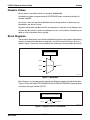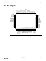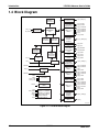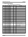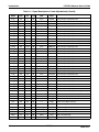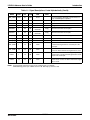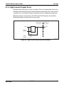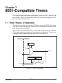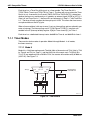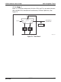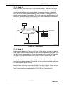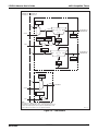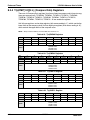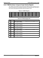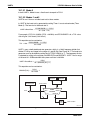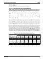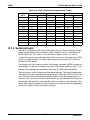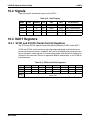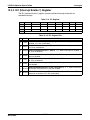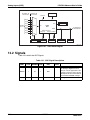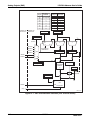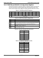
1
LZ87010 User’s Guide (Advance) 1/15/03 This document is released as Beta-level documentation. SHARP reserves the right to change and amend this documentation as necessary to represent the final Production-level development of this device. Specifications are subject to change without notice. Suggested applications (if any) are for standard use; See Important Restrictions for limitations on special applications. See Limited Warranty for SHARP’s product warranty. The Limited Warranty is in lieu, and exclusive of, all other warranties, express or implied. ALL EXPRESS AND IMPLIED WARRANTIES, INCLUDING THE WARRANTIES OF MERCHANTABILITY, FITNESS FOR USE AND FITNESS FOR A PARTICULAR PURPOSE, ARE SPECIFICALLY EXCLUDED. In no event will SHARP be liable, or in any way responsible, for any incidental or consequential economic or property damage. Purchase of I2C components from SHARP Corporation or one of its sublicensed Associated Companies conveys a license under the Philips I2C Patent. Rights are granted to use these components in an I2C system, provided that the system conforms to the I2C Standard Specification as defined by Philips. LZ87010 Advance User’s Guide Produced by the SHARP Microelectronics of the Americas Technical Publication Group. © 2002 Copyright SHARP Microelectronics of the Americas. Printed and Bound in USA. Reference No. SMA02048 Table of Contents Preface What’s in This User’s Guide ................................................................................... xiii Chapter 1 – Introduction ..................................................................................... xiii Chapter 2 – System Clocking ............................................................................. xiii Chapter 3 – 8051-Compatible Core ................................................................... xiii Chapter 4 – Internal RAM................................................................................... xiii Chapter 5 – Internal Flash .................................................................................. xiii Chapter 6 – I/O Ports ......................................................................................... xiii Chapter 7 – 8051-Compatible Timers ................................................................ xiii Chapter 8 – Enhanced Timers ...........................................................................xiv Chapter 9 – Watchdog Timer .............................................................................xiv Chapter 10 – UARTS .........................................................................................xiv Chapter 11 – External Memory ..........................................................................xiv Chapter 12 – Interrupts ......................................................................................xiv Chapter 13 – Analog Inputs (ADC).....................................................................xiv Chapter 14 – Analog Outputs (DAC) ..................................................................xiv Chapter 15 – I2C Interface .................................................................................xiv Chapter 16 – Debug Interface ............................................................................xiv Chapter 17 – Reset ............................................................................................xiv Chapter 18 – Electrical Characteristics ..............................................................xiv Chapter 19 – Mechanical Specifications ............................................................xiv Terms and Conventions ..........................................................................................xv Multiplexed Pins ..................................................................................................xv Pin Names ...........................................................................................................xv Peripheral Devices ..............................................................................................xv Register Addresses .............................................................................................xv Register Tables ..................................................................................................xvi Reading and Writing .......................................................................................xvi Reserved Bits and Fields................................................................................xvi 1/15/03 i Table of Contents LZ87010 Advance User’s Guide Chapter 1 – Introduction 1.1 Features ........................................................................................................... 1-1 1.2 Description ....................................................................................................... 1-2 1.3 Pin Diagram...................................................................................................... 1-3 1.4 Block Diagram .................................................................................................. 1-4 1.5 Signal Descriptions........................................................................................... 1-5 1.6 Functional Description...................................................................................... 1-8 1.6.1 8051-Compatible Processor Core ............................................................. 1-8 1.6.2 Program Memory....................................................................................... 1-9 1.6.3 Internal Data RAM ..................................................................................... 1-9 1.6.4 MOVX Data RAM ...................................................................................... 1-9 1.6.5 SHARP Debug Interface ........................................................................... 1-9 1.6.6 Interrupt Controller .................................................................................. 1-10 1.6.7 External Program Memory Interface ....................................................... 1-10 1.6.8 I/O Ports .................................................................................................. 1-11 1.6.9 UARTs ..................................................................................................... 1-11 1.6.10 I2C Interface .......................................................................................... 1-11 1.6.11 Analog Inputs (ADC) ............................................................................. 1-11 1.6.12 Analog Outputs (DACs) and Waveform Generators ............................. 1-11 1.6.13 Counter/Timer/PWM.............................................................................. 1-12 1.6.14 Clocks.................................................................................................... 1-12 1.6.15 Reset ..................................................................................................... 1-14 1.6.16 Power and Ground ................................................................................ 1-14 1.6.17 Low-Power Modes................................................................................. 1-14 1.7 Register Summary.......................................................................................... 1-15 1.8 Instruction Set Summary ................................................................................ 1-18 Chapter 2 – System Clocking 2.1 Theory of Operation ......................................................................................... 2-1 2.1.1 Internal Clocks........................................................................................... 2-2 2.1.1.1 HFCLK................................................................................................ 2-2 2.1.1.2 SUBCLK ............................................................................................. 2-2 2.1.1.3 CCLK .................................................................................................. 2-2 2.1.1.4 SCLK .................................................................................................. 2-2 2.1.1.5 PCLK .................................................................................................. 2-2 2.1.1.6 ADCCLK ............................................................................................. 2-2 2.1.2 Power-Saving Modes ................................................................................ 2-4 2.1.2.1 Idle Mode............................................................................................ 2-4 2.1.2.2 Stop Mode .......................................................................................... 2-4 2.2 Signals.............................................................................................................. 2-5 2.3 Registers .......................................................................................................... 2-6 2.3.1 CLKCFG (Clock Configuration) Register................................................... 2-6 2.3.2 PCON (Power Control) Register ............................................................... 2-7 ii 1/15/03 LZ87010 Advance User’s Guide Table of Contents Chapter 3 – 8051-Compatible Core 3.1 Theory of Operation ......................................................................................... 3-1 3.2 Registers .......................................................................................................... 3-1 3.2.1 ACC (Accumulator) Register ..................................................................... 3-2 3.2.2 B Register.................................................................................................. 3-2 3.2.3 DPH, DPL, DPH1, and DPL1 (Data Pointer) Registers............................. 3-2 3.2.4 DPS (Data Pointer Select) Register .......................................................... 3-3 3.2.5 PSW (Program Status Word) Register ...................................................... 3-4 3.2.6 SP (Stack Pointer) Register ...................................................................... 3-4 Chapter 4 – Internal RAM 4.1 Theory of Operation ......................................................................................... 4-1 4.1.1 Scratchpad RAM (256 Bytes) .................................................................... 4-1 4.1.2 MOVX RAM (4,096 Bytes) ........................................................................ 4-2 4.1.3 Expansion.................................................................................................. 4-2 Chapter 5 – Internal Flash 5.1 Theory of Operation ......................................................................................... 5-1 5.1.1 The Info Array............................................................................................ 5-1 5.1.2 Flash Timing .............................................................................................. 5-2 5.1.3 Secure Mode ............................................................................................. 5-2 5.2 Registers .......................................................................................................... 5-3 5.2.1 FLASHCFG (Flash Configuration) Register .............................................. 5-3 5.2.2 FLASHTB (Flash Timebase) Register ....................................................... 5-4 Chapter 6 – I/O Ports 6.1 Theory of Operation ......................................................................................... 6-2 6.1.1 General-Purpose I/O Ports ........................................................................ 6-2 6.1.1.1 Idle and Stop-Mode Current ............................................................... 6-2 6.1.2 High-Current Output Ports......................................................................... 6-3 6.2 Signals.............................................................................................................. 6-4 6.3 Registers .......................................................................................................... 6-5 6.3.1 General-Purpose I/O Registers ................................................................. 6-5 6.3.2 High-Current Output Registers .................................................................. 6-6 Chapter 7 – 8051-Compatible Timers 7.1 Timer Theory of Operation ............................................................................... 7-1 7.1.1 Timer Modes ............................................................................................. 7-2 7.1.1.1 Mode 0................................................................................................ 7-2 7.1.1.2 Mode 1................................................................................................ 7-3 7.1.1.3 Mode 2................................................................................................ 7-4 7.1.1.4 Mode 3................................................................................................ 7-4 7.2 Timer 0 and Timer 1 Signals ............................................................................ 7-6 7.3 Timer 0 and 1 Registers ................................................................................... 7-6 7.3.1 TCON (Timer 0 and 1 Control) Register.................................................... 7-6 7.3.2 TMOD (Timer 0 and 1 Mode) Registers .................................................... 7-7 7.3.3 Timer Data Registers (TH0, TH1, TL0, TL1) ............................................. 7-8 1/15/03 iii Table of Contents LZ87010 Advance User’s Guide Chapter 8 – Enhanced Timers 8.1 Enhanced Timer Signals .................................................................................. 8-3 8.2 Enhanced Timer Theory of Operation .............................................................. 8-3 8.2.1 Reading 16-bit Timer Registers................................................................. 8-3 8.2.2 Writing 16-bit Timer Registers ................................................................... 8-4 8.2.3 Timer Clocking .......................................................................................... 8-5 8.2.4 Timing and Counting ................................................................................. 8-5 8.2.5 Capture...................................................................................................... 8-5 8.2.6 Compare.................................................................................................... 8-8 8.2.7 PWM........................................................................................................ 8-11 8.2.8 Timer Interrupts ....................................................................................... 8-13 8.3 Enhanced Timer Registers............................................................................. 8-14 8.3.1 T2CAP and T3CAP (Capture Control) Registers .................................... 8-14 8.3.2 T(x)CAP(y) (Captured Data) Registers ................................................... 8-15 8.3.3 T(x)CMP (Compare Control) Registers ................................................... 8-17 8.3.4 T(x)CMP[1:0][H:L] (Compare Data) Registers......................................... 8-18 8.3.5 T(x)CNTH and T(x)CNTL (Timer Count) Registers ................................. 8-19 8.3.6 T(x)CON (Timer Configuration) Registers ............................................... 8-20 8.3.7 T(x)STA (Timer Status) Registers ........................................................... 8-21 8.3.8 TCMPOE (Timer Compare Output Enable) Register .............................. 8-22 Chapter 9 – Watchdog Timer 9.1 Theory of Operation ......................................................................................... 9-1 9.1.1 Setting the Timer Interval .......................................................................... 9-1 9.1.2 Stopping the Watchdog Timer in Idle Mode .............................................. 9-2 9.2 Watchdog Timer Registers............................................................................... 9-2 9.2.1 WDTCTL Register ..................................................................................... 9-2 9.2.2 WDTCNT Register .................................................................................... 9-3 Chapter 10 – UARTs 10.1 Theory of Operation ..................................................................................... 10-1 10.1.1 Receive Operation................................................................................. 10-1 10.1.2 Transmit Operation................................................................................ 10-3 10.1.3 Generating Baud Rates ......................................................................... 10-6 10.1.3.1 Mode 0............................................................................................ 10-8 10.1.3.2 Modes 1 and 3................................................................................ 10-8 10.1.3.3 Mode 2............................................................................................ 10-9 10.1.3.4 Crystal Selection for RS-232 Baud Rates ...................................... 10-9 10.1.4 Serial Interrupts ................................................................................... 10-10 10.2 Signals........................................................................................................ 10-11 10.3 UART Registers ......................................................................................... 10-11 10.3.1 SCON and SCON1 (Serial Control) Registers .................................... 10-11 10.3.2 SBUF and SBUF1 (Serial Data Buffer) Registers ............................... 10-13 10.3.3 BRGCNTH and BRGCNTL (Baud Rate Generator Count) Registers . 10-14 iv 1/15/03 LZ87010 Advance User’s Guide Table of Contents Chapter 11 – External Memory 11.1 Theory of Operation ..................................................................................... 11-1 11.1.1 Writing to External Memory ................................................................... 11-1 11.1.2 Reading from External Memory............................................................. 11-1 11.2 Signals.......................................................................................................... 11-3 11.3 Registers ...................................................................................................... 11-4 11.4 External Memory Timing .............................................................................. 11-5 Chapter 12 – Interrupts 12.1 Theory of Operation ..................................................................................... 12-1 12.1.1 Interrupt-Related Registers ................................................................... 12-1 12.1.2 Interrupt Vectors .................................................................................... 12-2 12.1.2.1 Vectors and Status Bits .................................................................. 12-3 12.1.3 Interrupt Sources ................................................................................... 12-4 12.1.4 Interrupt Priority ..................................................................................... 12-5 12.1.5 External Interrupts ................................................................................. 12-5 12.1.5.1 INT[0] and INT[1] ............................................................................ 12-5 12.1.5.2 INT[7:2]........................................................................................... 12-6 12.2 Signals.......................................................................................................... 12-7 12.3 Registers ...................................................................................................... 12-7 12.3.1 ALTFEN1 (Alternate Function Enable) Register ................................... 12-7 12.3.2 IE (Interrupt Enable) Register................................................................ 12-8 12.3.3 IE1 (Interrupt Enable 1) Register........................................................... 12-9 12.3.4 IP and IPH (Interrupt Priority) Registers .............................................. 12-10 12.3.5 IP1 and IPH1 (Interrupt Priority) Registers .......................................... 12-11 Chapter 13 – Analog Inputs (ADC) 13.1 Theory of Operation ..................................................................................... 13-1 13.2 Signals.......................................................................................................... 13-2 13.3 Registers ...................................................................................................... 13-3 13.3.1 ADCC (ADC Control) Register .............................................................. 13-3 13.3.2 ADCDH (ADC Data High) Register ....................................................... 13-4 13.3.3 ADCDL (ADC Data Low) Register......................................................... 13-5 Chapter 14 – Analog Outputs (DAC) 14.1 Theory of Operation ..................................................................................... 14-1 14.1.1 Digital-to-Analog Converter (DAC) ........................................................ 14-1 14.1.2 Waveform Generator ............................................................................. 14-3 14.2 Signals.......................................................................................................... 14-4 14.3 Registers ...................................................................................................... 14-4 14.3.1 DACC (DAC Control) Register .............................................................. 14-4 14.3.2 WGCTL0 and WGCTL1 (Control) Registers ......................................... 14-5 14.3.3 WGCFG0 and WGCFG1 (Configuration) Registers .............................. 14-6 14.3.4 WGINX0 and WGINX1 (Index) Registers.............................................. 14-7 14.3.5 WGMA0 and WGMA1 (Memory Address) Registers............................. 14-7 14.3.6 WGMD0 and WGMD1 (Memory Data) Registers.................................. 14-8 1/15/03 v Table of Contents LZ87010 Advance User’s Guide Chapter 15 – I2C Interface 15.1 Theory of Operation ..................................................................................... 15-1 15.1.1 Setting I2C Clock Timing ....................................................................... 15-1 15.2 Interrupt Handling......................................................................................... 15-2 15.2.1 Slave Mode ........................................................................................... 15-3 15.2.2 Master Mode ......................................................................................... 15-3 15.3 Signals.......................................................................................................... 15-3 15.4 Registers ...................................................................................................... 15-4 15.4.1 ICCON (I2C Configuration) Register ..................................................... 15-4 15.4.2 ICSAR (I2C Slave Address) Register .................................................... 15-5 15.4.3 ICUSAR (I2C Upper Slave Address) Register ....................................... 15-6 15.4.4 ICDATA (I2C Data) Register.................................................................. 15-7 15.4.5 ICHCNT (I2C Clock High Time) Register............................................... 15-8 15.4.6 ICLCNT (I2C Clock Low Time) Register ................................................ 15-9 15.4.7 ICDBUG (I2C Debug) Register ............................................................ 15-10 15.4.8 ICSTAT (I2C Status) Register ............................................................. 15-11 Chapter 16 – Debug Interface 16.1 Theory of Operation ..................................................................................... 16-1 16.2 Signals.......................................................................................................... 16-2 Chapter 17 – Reset 17.1 Theory of Operation ..................................................................................... 17-1 17.2 Signals.......................................................................................................... 17-1 vi 1/15/03 List of Figures Preface Figure 1. Multiplexer................................................................................................... xvii Figure 2. Register with Bit Field Named..................................................................... xvii Figure 3. Register with Multiple Bit Fields Named..................................................... xviii Figure 4. Register with Bit Field Numbered............................................................... xviii Chapter 1 – Introduction Figure 1-1. LZ87010 Pin Diagram .............................................................................. 1-3 Figure 1-2. LZ87010 Block Diagram .......................................................................... 1-4 Figure 1-3. LZ87010 Application Diagram Example................................................... 1-8 Figure 1-4. Sharp Debug Interface............................................................................. 1-9 Figure 1-5. External Clock Circuitry.......................................................................... 1-12 Figure 1-6. Simplified System Clocking.................................................................... 1-13 Figure 1-7. Register Description by Functional Unit................................................. 1-15 Chapter 2 – System Clocking Figure 2-1. System Oscillator Alternatives ................................................................. 2-1 Figure 2-2. Internal Clock Generation ........................................................................ 2-3 Chapter 4 – Internal RAM Figure 4-1. Memory Map ............................................................................................ 4-2 Chapter 6 – I/O Ports Figure 6-1. General-Purpose I/O Port (One Bit Shown)............................................. 6-1 Figure 6-2. High-Current Output Port (One Bit Shown).............................................. 6-3 Chapter 7 – 8051-Compatible Timers Figure 7-1. Timer 0-1 Clocking................................................................................... 7-1 Figure 7-2. Timer Mode 0........................................................................................... 7-2 Figure 7-3. Timer Mode 1........................................................................................... 7-3 Figure 7-4. Timer Mode 2........................................................................................... 7-4 Figure 7-5. Timer Mode 3........................................................................................... 7-5 Chapter 8 – Enhanced Timers Figure 8-1. Overall Timer Block Diagram ................................................................... 8-2 Figure 8-2. Reading from Count and Capture Registers............................................ 8-4 Figure 8-3. Writing to Compare Registers.................................................................. 8-4 Figure 8-4. Timer Block Diagram (Does Not Show Capture and Compare) .............. 8-6 Figure 8-5. Capture Unit Block Diagram .................................................................... 8-7 Figure 8-6. Compare Unit Block Diagram .................................................................. 8-9 Figure 8-7. PWM Operation ..................................................................................... 8-11 Figure 8-8. PWM Output Signal Timing.................................................................... 8-12 1/15/03 vii List of Figures LZ87010 Advance User’s Guide Chapter 10 – UARTs Figure 10-1. Receive Operation, Modes 1-3 ............................................................ 10-2 Figure 10-2. Receive Operation, Mode 0 ................................................................. 10-3 Figure 10-3. Transmit Operation, Modes 1 - 3 ......................................................... 10-4 Figure 10-4. Transmit Operation, Mode 0 ................................................................ 10-5 Figure 10-5. Clock Selection, UART 0 ..................................................................... 10-6 Figure 10-6. Clock Selection, UART 1 ..................................................................... 10-7 Figure 10-7. Baud Rate Generator, UART 1 ............................................................ 10-8 Chapter 11 – External Memory Figure 11-1. External Memory Interface................................................................... 11-2 Figure 11-2. External Memory Read, No Wait States .............................................. 11-6 Figure 11-3. External Memory Read, One Wait State.............................................. 11-7 Figure 11-4. External Memory Write, No Wait States .............................................. 11-8 Figure 11-5. External Memory Write, One Wait State .............................................. 11-9 Chapter 12 – Interrupts Figure 12-1. External Interrupts INT[7:2].................................................................. 12-6 Chapter 13 – Analog Inputs (ADC) Figure 13-1. ADC Block Diagram ............................................................................. 13-2 Chapter 14 – Analog Outputs (DAC) Figure 14-1. DAC and Waveform Generator (One Channel Shown) ....................... 14-2 Figure 14-2. Effect of Step Values in Waveform Generation ................................... 14-3 Chapter 16 – Debug Interface Figure 16-1. SHARP Debug Interface (SDI) Wiring ................................................. 16-1 viii 1/15/03 List of Tables Preface Table 1. Register Name ..............................................................................................xvi Table 2. Register Bit Fields .........................................................................................xvi Chapter 1 – Introduction Table 1-1. Signal Descriptions, Listed Alphabetically................................................. 1-5 Table 1-2. Interrupt Sources and Vectors ................................................................ 1-10 Table 1-3. Instruction Set Summary......................................................................... 1-18 Table 1-4. Operand Types ....................................................................................... 1-21 Table 1-5. Instructions’ Effect on Flag Bits............................................................... 1-22 Table 1-6. Command Matrix..................................................................................... 1-23 Chapter 2 – System Clocking Table 2-1. System Clock Signals ............................................................................... 2-5 Table 2-2. CLKCFG (Clock Configuration) Register .................................................. 2-6 Table 2-3. CLKCFG Register Fields........................................................................... 2-6 Table 2-4. CLKADC[2:0] Encoding............................................................................. 2-6 Table 2-5. CLKDIV[2:0] Encoding .............................................................................. 2-6 Table 2-6. PCON (Power Control) Register ............................................................... 2-7 Table 2-7. PCON Register Fields............................................................................... 2-7 Chapter 3 – 8051-Compatible Core Table 3-1. Core Registers .......................................................................................... 3-1 Table 3-2. ACC (Accumulator) Register..................................................................... 3-2 Table 3-3. B Register ................................................................................................. 3-2 Table 3-4. DPH and DPH1 Registers......................................................................... 3-2 Table 3-5. DPL and DPL1 Registers .......................................................................... 3-2 Table 3-6. DPS Register ............................................................................................ 3-3 Table 3-7. DPS Register Bits ..................................................................................... 3-3 Table 3-8. PSW Register............................................................................................ 3-4 Table 3-9. PSW Register Bits..................................................................................... 3-4 Table 3-10. SP Register ............................................................................................. 3-4 Chapter 5 – Internal Flash Table 5-1. Approximate Flash Timing ........................................................................ 5-2 Table 5-2. FLASHCFG Register................................................................................. 5-3 Table 5-3. FLASHCFG Register Bits.......................................................................... 5-3 Table 5-4. FMOD Field Decoding............................................................................... 5-3 Table 5-5. FLASHTB Register.................................................................................... 5-4 Table 5-6. FLASHTB Register Bits............................................................................. 5-4 1/15/03 ix List of Tables LZ87010 Advance User’s Guide Chapter 6 – I/O Ports Table 6-1. I/O Port Signal Descriptions ...................................................................... 6-4 Table 6-2. PORT0, PORT1, PORT3, PORT5, PORT6, PORT7, PORT8 Registers .. 6-5 Table 6-3. General-Purpose I/O Register Bits............................................................ 6-5 Table 6-4. PORT2 and PORT9 Registers .................................................................. 6-6 Table 6-5. High-Current Output Register Bits ............................................................ 6-6 Chapter 7 – 8051-Compatible Timers Table 7-1. Timer 0 and Timer 1 I/O ............................................................................ 7-6 Table 7-2. TCON Register.......................................................................................... 7-6 Table 7-3. TCON Register Bits................................................................................... 7-6 Table 7-4. TMOD Register ......................................................................................... 7-7 Table 7-5. TMOD Register Bits .................................................................................. 7-7 Table 7-6. M(x)[1:0] Bit Field Decoding...................................................................... 7-7 Table 7-7. TH0, TH1, TL0, TL1 Registers .................................................................. 7-8 Chapter 8 – Enhanced Timers Table 8-1. Timer 2 - Timer 5 I/O................................................................................. 8-3 Table 8-2. Capture Function....................................................................................... 8-7 Table 8-3. Compare Function................................................................................... 8-10 Table 8-4. Output Polarity for Compare Pins ........................................................... 8-10 Table 8-5. T2CAP Register ...................................................................................... 8-14 Table 8-6. T3CAP Register ...................................................................................... 8-14 Table 8-7. T2CAP and T3CAP Register Bits............................................................ 8-14 Table 8-8. Capture Registers ................................................................................... 8-15 Table 8-9. T2CAP0H Register.................................................................................. 8-15 Table 8-10. T2CAP0L Register ................................................................................ 8-15 Table 8-11. T2CAP1H Register................................................................................ 8-15 Table 8-12. T2CAP1L Register ................................................................................ 8-15 Table 8-13. T3CAP0H Register................................................................................ 8-16 Table 8-14. T3CAP0L Register ................................................................................ 8-16 Table 8-15. T3CAP1H Register................................................................................ 8-16 Table 8-16. T3CAP1L Register ................................................................................ 8-16 Table 8-17. T(x)CMP Registers................................................................................ 8-17 Table 8-18. T(x)CMP Register Bits .......................................................................... 8-17 Table 8-19. T(x)CMP0H Registers ........................................................................... 8-18 Table 8-20. T(x)CMP0L Registers............................................................................ 8-18 Table 8-21. T(x)CMP1H Register............................................................................. 8-18 Table 8-22. T(x)CMP1L Register ............................................................................. 8-18 Table 8-23. T(x)CNTH Register ............................................................................... 8-19 Table 8-24. T(x)CNTL Register ................................................................................ 8-19 Table 8-25. T(x)CON Register ................................................................................. 8-20 Table 8-26. T(x)CON Register Bits .......................................................................... 8-20 Table 8-27. T(x)STA Register .................................................................................. 8-21 Table 8-28. T(x)STA Register Bits ........................................................................... 8-21 Table 8-29. TCMPOE Register ................................................................................ 8-22 Table 8-30. TCMPOE Register Bits ......................................................................... 8-22 x 1/15/03 LZ87010 Advance User’s Guide List of Tables Chapter 9 – Watchdog Timer Table 9-1. WDTCTL Register..................................................................................... 9-2 Table 9-2. WDTCTL Register Bits.............................................................................. 9-2 Table 9-3. WDTCNT Register .................................................................................... 9-3 Table 9-4. WDTCNT Register Bits ............................................................................. 9-3 Chapter 10 – UARTs Table 10-1. UART 0 Baud Rate Example, Modes 1 and 3....................................... 10-9 Table 10-2. UART 1 Baud Rate Example, Modes 1 and 3..................................... 10-10 Table 10-3. UART Signals...................................................................................... 10-11 Table 10-4. SCON and SCON1 Registers ............................................................. 10-11 Table 10-5. SCON and SCON1 Register Bits ........................................................ 10-12 Table 10-6. SM[0:1] UART 0 and UART 1 Mode Bits ............................................ 10-12 Table 10-7. SBUF and SBUF1 Registers............................................................... 10-13 Table 10-8. SBUF, SBUF1 Register Bits................................................................ 10-13 Table 10-9. BRGCNTH Register ............................................................................ 10-14 Table 10-10. BRGCNTL Register........................................................................... 10-14 Chapter 11 – External Memory Table 11-1. External Memory Signals ...................................................................... 11-3 Table 11-2. XMCFG Register................................................................................... 11-4 Table 11-3. XMCFG Register Bits............................................................................ 11-4 Table 11-4. XMBNK[2:0] Field Encoding.................................................................. 11-4 Chapter 12 – Interrupts Table 12-1. Interrupt-Related Registers ................................................................... 12-1 Table 12-2. Interrupt Vectors.................................................................................... 12-2 Table 12-3. Interrupt Summary ................................................................................ 12-4 Table 12-4. Interrupt Signals .................................................................................... 12-7 Table 12-5. ALTFEN1 Register ................................................................................ 12-7 Table 12-6. ALTFEN1 Register Bits ......................................................................... 12-7 Table 12-7. IE Register ............................................................................................ 12-8 Table 12-8. IE Register Bits ..................................................................................... 12-8 Table 12-9. IE1 Register .......................................................................................... 12-9 Table 12-10. IE1 Register Bits ................................................................................. 12-9 Table 12-11. IP and IPH Register .......................................................................... 12-10 Table 12-12. IP, IPH Register Bits ......................................................................... 12-10 Table 12-13. IP1 and IPH1 Register ...................................................................... 12-11 Table 12-14. IP1, IPH1 Register Bits ..................................................................... 12-11 Chapter 13 – Analog Inputs (ADC) Table 13-1. ADC Signal Descriptions....................................................................... 13-2 Table 13-2. ADCC Register...................................................................................... 13-3 Table 13-3. ADCC Register Bits............................................................................... 13-3 Table 13-4. ADCDH Register ................................................................................... 13-4 Table 13-5. ADCDH Register Bits ............................................................................ 13-4 Table 13-6. ADCDL Register.................................................................................... 13-5 Table 13-7. ADCDL Register Bits............................................................................. 13-5 1/15/03 xi List of Tables LZ87010 Advance User’s Guide Chapter 14 – Analog Outputs (DAC) Table 14-1. DAC Signals.......................................................................................... 14-4 Table 14-2. DACC Register...................................................................................... 14-4 Table 14-3. DACC Register Bits............................................................................... 14-4 Table 14-4. WGCTL0 and WGCTL1 Registers ........................................................ 14-5 Table 14-5. WGCTL0 and WGCTL1 Register Bits................................................... 14-5 Table 14-6. Waveform Generator Clock Input Select............................................... 14-5 Table 14-7. WGCFG0 and WGCFG1 Registers ...................................................... 14-6 Table 14-8. WGCFG0 and WGCFG1 Register Bits ................................................. 14-6 Table 14-9. Waveform Generator Interrupt Intervals................................................ 14-6 Table 14-10. Waveform Generator Step Index ........................................................ 14-6 Table 14-11. WGINX Registers................................................................................ 14-7 Table 14-12. WGINX0 and WGINX1 Register Bits .................................................. 14-7 Table 14-13. WGMA0 and WGMA1 Register........................................................... 14-7 Table 14-14. WGMA0 and WGMA1 Register Bits.................................................... 14-7 Table 14-15. WGMD0 and WGMD1 Registers ........................................................ 14-8 Table 14-16. WGMD0 and WGMD1 Register Bits ................................................... 14-8 Chapter 15 – I2C Interface Table 15-1. I2C Clock Parameters ........................................................................... 15-1 Table 15-2. Sample I2C HIGH Period Counts .......................................................... 15-2 Table 15-3. I2C Registers......................................................................................... 15-3 Table 15-4. ICCON Register .................................................................................... 15-4 Table 15-5. ICCON Register Bits ............................................................................. 15-4 Table 15-6. ICSAR Register..................................................................................... 15-5 Table 15-7. ICSAR Register Bits.............................................................................. 15-5 Table 15-8. ICUSAR Register .................................................................................. 15-6 Table 15-9. ICUSAR Register Bits ........................................................................... 15-6 Table 15-10. ICDATA Register................................................................................. 15-7 Table 15-11. ICDATA Register Bits.......................................................................... 15-7 Table 15-12. ICHCNT Register ................................................................................ 15-8 Table 15-13. ICHCNT Register Bits ......................................................................... 15-8 Table 15-14. ICLCNT Register................................................................................. 15-9 Table 15-15. ICLCNT Register Bits.......................................................................... 15-9 Table 15-16. ICDBUG Register.............................................................................. 15-10 Table 15-17. ICDBUG Register Bits....................................................................... 15-10 Table 15-18. ICSTAT Register ............................................................................... 15-11 Table 15-19. ICSTAT Register Bits ........................................................................ 15-11 Chapter 16 – Debug Interface Table 16-1. Debug Signal Descriptions.................................................................... 16-2 Chapter 17 – Reset Table 17-1. Reset Signal.......................................................................................... 17-1 xii 1/15/03 Preface The SHARP LZ87010 is a high-performance 8-bit microcontroller. This User’s Guide is the principal technical reference for this device. This document assumes the reader is familiar with 8051 programming. For abridged versions of this User’s Guide, consult the LZ87010 Data Sheet and the single page Product Brief. For details, contact a SHARP representative or see the SHARP Microelectronics of the Americas website at http://www.sharpsma.com. Application Notes and further information on connecting, programming and implementing the LZ87010, along with suggestions for companion parts, can be found on SHARP's website. Browse to http://www.sharpsma.com. What’s in This User’s Guide Chapter 1 – Introduction This Chapter presents the theory of operation of the LZ87010 microcontroller, including features, benefits, pinout, signal description, and an overview of the entire device. Chapter 2 – System Clocking This Chapter describes the use of crystal oscillators or external clock generators with the LZ87010, the internal clocking structure, and the use of clock-stopping power-saving modes. Chapter 3 – 8051-Compatible Core This Chapter presents an overview of the 8051-compatible core. 8051-compatible I/O, however, is presented in later chapters. Chapter 4 – Internal RAM This Chapter describes the two blocks of on-chip data memory, the 256-byte scratchpad RAM and the 4,096-byte MOVX RAM. Chapter 5 – Internal Flash This Chapter describes the 64KB internal Flash memory, which can be programmed externally or internally, through software control. Chapter 6 – I/O Ports This Chapter describes the seven 8-bit general-purpose I/O ports and the two 8-bit highcurrent output ports. Chapter 7 – 8051-Compatible Timers This Chapter describes Timer 0 and Timer 1, which are compatible with the standard 8051. 1/15/03 xiii Preface LZ87010 Advance User’s Guide Chapter 8 – Enhanced Timers This Chapter describes Timers 2, 3, 4, and 5, which are enhanced 16-bit timers providing a total of four counters, four capture units, four PWM units, and eight compare units. Chapter 9 – Watchdog Timer This Chapter describes the LZ87010 Watchdog Timer (WDT). Chapter 10 – UARTS This Chapter describes the LZ87010 UARTs, UART 0 and UART 1. Both are 8051compatible, except that UART1 has a dedicated baud-rate generator. Chapter 11 – External Memory This Chapter describes the LZ87010 External Memory interface, which allows up to 64KB of external program memory to be used, replacing part or all of on-chip Flash memory. Chapter 12 – Interrupts This Chapter describes the LZ87010 interrupt structure, interrupt priority, and interrupt vectors. Chapter 13 – Analog Inputs (ADC) This Chapter describes the LZ87010 12-bit, 8-input analog-to-digital converter (ADC). Chapter 14 – Analog Outputs (DAC) This Chapter presents the LZ87010 two 8-bit digital-to-analog converters (DACs) and their dedicated waveform generators. Chapter 15 – I2C Interface This Chapter presents the LZ87010 I2C serial interface, which can operate at both 100 kbit/s and 400 kbit/s data rates, and supports both master and slave modes of operation. Chapter 16 – Debug Interface This Chapter presents the SHARP Debug Interface (SDI). Chapter 17 – Reset This Chapter describes system reset and power-up. Chapter 18 – Electrical Characteristics This Chapter includes DC and AC specifications, timing Information, and timing diagrams for the LZ87010 microcontroller. Chapter 19 – Mechanical Specifications This Chapter contains physical dimension specifications for the LZ87010 microcontroller. xiv 1/15/03 LZ87010 Advance User’s Guide Preface Terms and Conventions Multiplexed Pins The LZ87010 is manufactured in an LQFP package with 100 pins. Some pins have only one function, but others support two functions. These multiplexed pins have both functions available simultaneously. Pin Names Package pins are named to indicate the signal(s) or functionality available at the pin. If the signal or function is active LOW, the name is prefixed with a lower-case ‘n’, such as nPSWR. Multiplexed pins are named to indicate all available functions, such as Pin 80: P0[5]/INT[5], which can function as either General-Purpose I/O Port 0, bit 5, or Interrupt Request bit 5. These naming conventions help designers recognize and avoid collisions between multiplexed functions but can complicate explanatory text, so this Guide uses the name appropriate to the context. A discussion of an interrupt, for example, would refer to signal INT[5], but information about Port 0 bit 5 would use P0[5]. Readers must be aware that these are separate signals, with distinctly different functionality, which happen to be available on the same pin. Peripheral Devices The LZ87010 is an 8-bit microcontroller using an 8051-compatible architecture. Additional functionality not available in the standard 8051 consists mostly of additional peripheral devices not present in the 8051. These devices have their I/O and control registers mapped to the ‘Special Function Register’ (SFR) memory space of the 8051 architecture, which is in the data memory address range of 0x80-0xFF. Register Addresses The LZ87010 is a memory-mapped device with programmable, internal registers that control its operation. Each internal register is located at a unique address in the memory map. In this Guide, the addresses for all registers are expressed as an absolute hex address. 1/15/03 xv Preface LZ87010 Advance User’s Guide Register Tables All Registers are presented in tabular format. A primary table presents each register’s name, address, permissions, bit names and the register’s contents at reset. Subsequent tables, if present, detail the specific names and function(s) of all bits and bit fields in the register and explain any important variations that may exist. Reading and Writing An important detail to note is that all registers are not perfectly writable and readable. Some will exhibit different characteristics on a write, while a read may not return the expected result. Reserved Bits and Fields At the same time, not all bit fields in all registers can be written, nor can all register bits and fields yield useful information when read. These restricted register bits and fields will be specifically called out with three slashes (///) and the word ‘Reserved’, along with their special conditions in the bit field tables. See Table 1 and Table 2 for examples of this practice. Table 1. Register Name BIT 7 6 5 4 3 FIELD /// /// /// TRAP_EN /// DPSEL RESET 0 0 0 0 0 0 RO RO RO RW RO RW RW ADDR 2 1 0xA2 Table 2. Register Bit Fields xvi BIT NAME 7:5 /// 4 TRAP_EN 3 /// 2:0 DPSEL DESCRIPTION Reserved Reads return ‘0’; write as ‘0’. Example Bit Name A description of this bit’s functionality will be found in this space. Reserved Reads return ‘0’; write as ‘0’. Example Field Name A description of these bits’ functionality will be found in this space. 1/15/03 0 LZ87010 Advance User’s Guide Preface Numeric Values Binary values are prefixed with 0b; for example, 0b00001000. Hexadecimal values are expressed with UPPERCASE letters and prefixed with 0x; for example, 0x0FBC. All numeric values not specifically identified with the above prefixes as either binary or hexadecimal are decimal values. Registers and bit fields with 0b0 in all bits are referred to as ‘cleared’ or as 0. Registers and bit fields with 0b1 values in all bits are referred to as ‘set’ or as the binary, hexadecimal, or decimal value of the entire field or register. Block Diagrams The functional descriptions in this Guide include block diagrams with symbols representing logical or mathematical operations or selections, usually the result of writing a value to a register. Figure 1 shows one such multiplexer with three inputs and one output (the result). CONTROL SIGNAL or REGISTER: BITFIELD INPUT INPUT FUNCTION OUTPUT INPUT LZ87010-75 Figure 1. Multiplexer Block diagrams can include symbols representing Registers and the bit fields within them. Figure 2 shows that the BITFIELDNAME bit field in the REGISTERNAME register enables or disables the signal named OUTPUT. REGISTERNAME: BITFIELDNAME INPUT f() OUTPUT LZ87010-76 Figure 2. Register with Bit Field Named 1/15/03 xvii Preface LZ87010 Advance User’s Guide Figure 4 is similar to Figure 2 except that Figure 4 references multiple (different) BITFIELDS in the REGISTERNAME register. REGISTERNAME: [BITFIELDNAME, BITFIELDNAME] INPUT f() OUTPUT LZ87010-78 Figure 3. Register with Multiple Bit Fields Named Not all bit fields are named. If a bit field has no name, the Register is shown with numbers indicating the appropriate bit positions, with the least significant bit on the right, as in Figure 4. This bit ordering matches that of the Register tables, shown in Table 1. REGISTERNAME: 15:3 INPUT f() OUTPUT LZ87010-77 Figure 4. Register with Bit Field Numbered xviii 1/15/03 Chapter 1 Introduction 1.1 Features • 8-bit, 40 MHz, 8051-compatible CPU core: – Two-clock Machine Cycle – Equivalent to a 240 MHz 8051 • Two-wire Debug Interface with Breakpoint and Trace • 64KB On-chip Flash Program Memory – Enough Memory for Demanding Applications – In-circuit Serially Programmable – New 8051 Instruction for Writable Code Memory • External (Off-chip) Program Memory Interface – 16-bit Address/8-bit Data Busses – Supports Reads and Writes • 4KB On-chip MOVX Data RAM • 256 Bytes Scratchpad RAM • Six 16-bit Multifunction Timer/Counters – Two 8051-compatible Timers – Two with Capture/Compare/PWM Capability – Two with Compare/PWM Capability • Serial Interfaces – Two 8051-compatible UARTs, One with a Dedicated Internal Baud Rate Generator – I2C™ Interface • A/D Converter – Eight Analog Inputs, 12-bit Resolution – 500,000 Samples/second • D/A Converters – Two Independent Analog Output Channels – 8-bit Resolution • Waveform Generators – Twin D/A Converters are Driven by Dual Waveform Generators with 128-byte Wavetable RAMs – Flexible Clocking and Indexing • Sixteen High Current Output Pins • Up to 56 General-Purpose I/O Pins 1/15/03 1-1 Introduction LZ87010 Advance User’s Guide • Interrupt Controller – 8 External Interrupt Pins – 13 Internal Interrupt Sources – 4 Software-Selectable Interrupt Priorities • Watchdog Timer • Flexible Internal Clocking Architecture • Low Power Modes: Active, Idle, Stop • 3.3 V (±10%) Power Supply • 100-Pin LQFP Package 1.2 Description The LZ87010 is a high-performance, feature-rich 8-bit microcontroller based on the 8051 microprocessor architecture. It combines: • A high-performance, enhanced 8051 core that gives performance equivalent to a 240 MHz 8051 • Large amounts of on-chip memory, including 64KB of Flash program memory and 4.25KB of data memory (256 bytes of scratchpad RAM and 4,096 bytes of MOVX data RAM) to support complex applications • A wide range of I/O devices, including: – Two UARTs – Six counter/timers – An eight-input 12-bit ADC – Two wavetable-driven analog outputs – An I2C serial port – A dedicated serial debug interface – Up to 16 high-current output signals – Up to 56 general-purpose I/O signals. Extended features are accessed through special function registers (SFRs) that were unassigned in the original 8051. Two new instructions have been added to allow software breakpoints and writes to code memory. 1-2 1/15/03 1 2 3 4 5 6 7 8 9 10 11 12 13 14 15 16 17 18 19 20 21 22 23 24 25 26 27 28 29 30 P0_5/INT5 P0_6/INT6 P0_7/INT7 P6_0/CTIN4 P6_1 P6_2/CTCMP4A P6_3/CTCMP4B P6_4/CTIN5 P6_5 P6_6/CTCMP5A P6_7/CTCMP5B VDD P9_0 P9_1 P9_2 P9_3 P9_4 P9_5 P9_6 P9_7 P1_0/CTIN3 P1_1 P1_2/CTCAP3A P1_3/CTCAP3B P1_4/CTCMP3A P1_5/CTCMP3B P1_6/nPSWR P1_7/nPSEN VSS P5_0/XMD0 P5_1/XMD1 P5_2/XMD2 P5_3/XMD3 P5_4/XMD4 P5_5/XMD5 P5_6/XMD6 P5_7/XMD7 P2_0/XMA8 P2_1/XMA9 P2_2/XMA10 P2_3/XMA11 P2_4/XMA12 P2_5/XMA13 P2_6/XMA14 P2_7/XMA15 VDD RESET P8_0/XMA0 P8_1/XMA1 P8_2/XMA2 80 79 78 77 76 75 74 73 72 71 70 69 68 67 66 65 64 63 62 61 60 59 58 57 56 55 54 53 52 51 P0_4/INT4 P0_3/INT3 P0_2/INT2 P0_1/INT1 P0_0/INT0 XTAL2 XTAL1 XTAL_SUB2 XTAL_SUB1 SDI_DATA SDI_CLK P3_7/SDA P3_6/SCL VDD_CORE P3_5/WFGIN0 P3_4/WFGIN1 VSS P3_3/RXD1 P3_2/TXD1 P3_1/TXD0 P3_0/RXD0 VSSA AN7 AN6 AN5 AN4 AN3 AN2 AN1 AN0 LZ87010 Advance User’s Guide Introduction 1.3 Pin Diagram 100-PIN LQFP TOP VIEW 81 82 83 84 85 86 87 88 89 90 91 92 93 94 95 96 97 98 99 100 50 49 48 47 46 45 44 43 42 41 40 39 38 37 36 35 34 33 32 31 1/15/03 ADVREF DAVREF DA0 VDDA DA1 ENDC P7_7/CTIN1 P7_6/CTIN0 VSS P7_5/CTCMP2B P7_4/CTCMP2A P7_3/CTCAP2B P7_2/CTCAP2A P7_1 P7_0/CTIN2 P8_7/XMA7 P8_6/XMA6 P8_5/XMA5 P8_4/XMA4 P8_3/XMA3 LZ87010-3 Figure 1-1. LZ87010 Pin Diagram 1-3 Introduction LZ87010 Advance User’s Guide 1.4 Block Diagram PROGRAM MEMORY 64KB FLASH SDI_CLK SDI_DATA 8051COMPATIBLE CPU DEBUG INTERFACE MOVX DATA RAM 4,096 BYTES INTERNAL DATA RAM 256 BYTES DAC0 WAVETABLE 128 BYTES DAC1 WAVETABLE 128 BYTES DA0 DAC0 DA1 DAC1 PORT 0, INTERRUPTS P0[7:0], INT[7:0] PORT 1 [7:6], EXTERNAL MEMORY R/W P1[7], nPSEN P1[6], nPSWR PORT 1 [5:0], TIMER 3 P1[5], CTCMP3B P1[4], CTCMP3A P1[3], CTCAP3B P1[2], CTCAP3A P1[1] P1[0], CTIN3 PORT 2, EXTERNAL MEMORY ADDRESS PORT 3 [7:6], I2C P3[7], SDA P3[6], SCL PORT 3 [5:4], WAVEFORM GENERATOR CLOCK P3[5], WFGIN0 P3[4], WFGIN1 PORT 3 [3:2], UART1 PORT 3 [1:0], UART0 PORT 5, EXTERNAL MEMORY DATA DAVREF PORT 6 [7:4], TIMER 5 ADC 12 BITS AN[7:0] PORT 6 [3:0], TIMER 4 ADVREF XTAL2 XTAL1 XTAL_SUB2 XTAL_SUB1 RESET VDD VDD_CORE VDDA ENDC VSS VSSA P2[7:0], XMA[15:8] P3[3], RXD1 P3[2], TXD1 P3[1], TXD0 P3[0], RXD0 P5[7:0], XMD[7:0] P6[7], CTCMP5B P6[6], CTCMP5A P6[5] P6[4], CTIN5 P6[3], CTCMP4B P6[2], CTCMP4A P6[1] P6[0], CTIN4 CLOCKING PORT 7 [7:6], TIMERS 1 and 0 RESET, WATCHDOG TIMER DIGITAL 3.3 V POWER DIGITAL 2.5 V POWER ANALOG 3.3 V POWER REGULATOR ENABLE DIGITAL GROUND ANALOG GROUND PORT 7 [5:0], TIMER 2 PORT 8, EXTERNAL MEMORY ADDRESS PORT 9 P7[7], CTIN1 P7[6], CTIN0 P7[5], CTCMP2B P7[4], CTCMP2A P7[3], CTCAP2B P7[2], CTCAP2A P7[1] P7[0], CTIN2 P8[7:0], XMA[7:0] P9[7:0] LZ87010-63 Figure 1-2. LZ87010 Block Diagram 1-4 1/15/03 LZ87010 Advance User’s Guide Introduction 1.5 Signal Descriptions Table 1-1. Signal Descriptions, Listed Alphabetically SIGNAL NAME SIGNAL TYPE* PIN NO. PIN TYPE FUNCTIONAL UNIT SHARED WITH ADVREF I 50 I ADC Analog input. Voltage Reference for Analog-toDigital Converter; sets upper limit of conversion range. AN[7:0] I 58:51 I ADC Analog Input Ports CTCAP2A I 38 I/O Timers P7[2] Timer 2 Capture 0 Input CTCAP2B I 39 I/O Timers P7[3] Timer 2 Capture 1 Input CTCAP3A I 3 I/O Timers P1[2] Timer 3 Capture 0 Input DESCRIPTION CTCAP3B I 4 I/O Timers P1[3] Timer 3 Capture 1 Input CTCMP2A O 40 I/O Timers P7[4] Timer 2 Compare 0 Output CTCMP2B O 41 I/O Timers P7[5] Timer 2 Compare 1 Output CTCMP3A O 5 I/O Timers P1[4] Timer 3 Compare 0 Output CTCMP3B O 6 I/O Timers P1[5] Timer 3 Compare 1 Output CTCMP4A O 86 I/O Timers P6[2] Timer 4 Compare 0 Output CTCMP4B O 87 I/O Timers P6[3] Timer 4 Compare 1 Output CTCMP5A O 90 I/O Timers P6[6] Timer 5 Compare 0 Output CTCMP5B O 91 I/O Timers P6[7] Timer 5 Compare 1 Output CTIN0 I 43 I/O Timers P7[6] Timer 0 Clock Input CTIN1 I 44 I/O Timers P7[7] Timer 1 Clock Input CTIN2 I 36 I/O Timers P7[0] Timer 2 Clock Input CTIN3 I 1 I/O Timers P1[0] Timer 3 Clock Input CTIN4 I 84 I/O Timers P6[0] Timer 4 Clock Input CTIN5 I 88 I/O Timers P6[4] Timer 5 Clock Input DA0 O 48 O DACs DA1 O 46 O DACs Waveform Generator 1 Analog Output DACs Voltage Reference for Digital-to-Analog Converters; sets upper limit of conversion range Internal Voltage Regulator Enable. If HIGH, 2.5 V core voltage is supplied by internal regulator from 3.3 V supply. If LOW, 2.5 V core voltage is supplied externally on VDD_CORE. DAVREF I 49 I ENDC I 45 I Power INT[7:0] I 83:76 I/O Interrupts Waveform Generator 0 Analog Output P0[7:0] Interrupt Request Signals nPSEN O 8 I/O External Memory P1[7] External Memory Output Enable nPSWR O 7 I/O External Memory P1[6] External Memory Read/Write P0[7:0] I/O 83:76 I/O Ports INT[7:0] General Purpose Input/Output Pin P1[0] I/O 1 I/O Ports CTIN3 General Purpose Input/Output Pin P1[1] I/O 2 I/O Ports General Purpose Input/Output Pin P1[2] I/O 3 I/O Ports CTCAP3A General Purpose Input/Output Pin P1[3] I/O 4 I/O Ports CTCAP3B General Purpose Input/Output Pin P1[4] I/O 5 I/O Ports CTCMP3A General Purpose Input/Output Pin CTCMP3B General Purpose Input/Output Pin P1[5] I/O 6 I/O Ports P1[6] I/O 7 I/O Ports nPSWR 1/15/03 General Purpose Input/Output Pin 1-5 Introduction LZ87010 Advance User’s Guide Table 1-1. Signal Descriptions, Listed Alphabetically (Cont’d) SIGNAL NAME SIGNAL TYPE* PIN NO. PIN TYPE FUNCTIONAL UNIT SHARED WITH P1[7] I/O 8 I/O Ports nPSEN P2[7:0] O 25:18 O Ports P3[0] I/O 60 I/O Ports RXD0 General Purpose Input/Output Pin P3[1] I/O 61 I/O Ports TXD0 General Purpose Input/Output Pin P3[2] I/O 62 I/O Ports TXD1 General Purpose Input/Output Pin P3[3] I/O 63 I/O Ports RXD1 General Purpose Input/Output Pin P3[4] I/O 65 I/O Ports WFGIN1 General Purpose Input/Output Pin P3[5] I/O 66 I/O Ports WFGIN0 P3[6] I/O 68 I/O Ports SCL General Purpose Input/Output Pin (Open Collector) P3[7] I/O 69 I/O Ports SDA General Purpose Input/Output Pin (Open Collector) DESCRIPTION General Purpose Input/Output Pin XMA[15:8] General Purpose Output-Only Port (High Current) P4[7:0] General Purpose Input/Output Pin Port 4 is not implemented in the LZ87010. P5[7:0] I/O 17:10 I/O Ports P6[0] I/O 84 I/O Ports XMD[7:0] General Purpose Input/Output Pin P6[1] I/O 85 I/O Ports General Purpose Input/Output Pin P6[2] I/O 86 I/O Ports CTCMP4A General Purpose Input/Output Pin P6[3] I/O 87 I/O Ports CTCMP4B General Purpose Input/Output Pin P6[4] I/O 88 I/O Ports P6[5] I/O 89 I/O Ports General Purpose Input/Output Pin P6[6] I/O 90 I/O Ports CTCMP5A General Purpose Input/Output Pin P6[7] I/O 91 I/O Ports CTCMP5B General Purpose Input/Output Pin P7[0] I/O 36 I/O Ports P7[1] I/O 37 I/O Ports General Purpose Input/Output Pin P7[2] I/O 38 I/O Ports CTCAP2A General Purpose Input/Output Pin P7[3] I/O 39 I/O Ports CTCAP2B General Purpose Input/Output Pin P7[4] I/O 40 I/O Ports CTCMP2A General Purpose Input/Output Pin P7[5] I/O 41 I/O Ports CTCMP2B General Purpose Input/Output Pin P7[6] I/O 43 I/O Ports CTIN4 CTIN5 CTIN2 CTIN0 General Purpose Input/Output Pin General Purpose Input/Output Pin General Purpose Input/Output Pin General Purpose Input/Output Pin P7[7] I/O 44 I/O Ports CTIN1 General Purpose Input/Output Pin P8[7:0] I/O 35:28 I/O Ports XMA[7:0] General Purpose Input/Output Pin P9[7:0] O 100:93 O Ports General Purpose Output-Only Port (High Current) RESET I 27 I Reset System Reset RXD0 I 60 I/O UART P3[0] UART 0 Receive Data RXD1 I 63 I/O UART P3[3] UART 1 Receive Data SCL I/O 68 I/O I2C P3[6] I2C Bus Clock (Open Collector) SDA I/O 69 I/O I2C P3[7] I2C Bus Data (Open Collector) SDI_CLK I 70 I Debug SHARP Debug Interface Clock SDI_DATA I/O 71 I/O Debug SHARP Debug Interface Data TXD0 O 61 I/O UART P3[1] UART 0 Transmit Data TXD1 O 62 I/O UART P3[2] UART 1 Transmit Data VDD PWR 26, 92 PWR Power 1-6 Main Digital Power Supply, 3.3 V ± 10% 1/15/03 LZ87010 Advance User’s Guide Introduction Table 1-1. Signal Descriptions, Listed Alphabetically (Cont’d) SIGNAL NAME SIGNAL TYPE* PIN NO. PIN TYPE FUNCTIONAL UNIT SHARED WITH VDD_CORE PWR 67 PWR Power Core Power Supply. Normally connected only to a 4.7 µF tantalum bypass capacitor. VDDA PWR 47 PWR Power Analog Power, 3.3 V ± 10%. Must be derived from VDD 9, 42, 64 GND DESCRIPTION VSS GND Power Digital Ground VSSA GND 59 GND Power Analog Ground WFGIN0 I 66 I/O Waveform Generator P3[5] Waveform Generator Clock Input 0 WFGIN1 I 65 I/O Waveform Generator P3[4] Waveform Generator Clock Input 1 XMA[15:8] O 25:18 O External Memory P2 External Memory Address Bus, Upper 8 Bits XMA[7:0] O 35:28 I/O External Memory P8 External Memory Address Bus, Lower 8 Bits XMD[7:0] I/O 17:10 I/O External Memory P5 External Memory Data Bus XTAL_SUB1 I 72 I/O Clock Crystal Oscillator Connection for 32 kHz subclock. If an external clock generator is used, this pin is the clock input. XTAL_SUB2 O 73 I/O Clock Crystal Oscillator Connection for 32 kHz subclock. Connect to VSS if external clock generator is used. XTAL1 I 74 I/O Clock Crystal Oscillator Connection for High-Frequency System Clock. If an external clock generator is used, this pin is the clock input. XTAL2 O 75 I/O Clock Crystal Oscillator Connection for High-Frequency System Clock. Connect to VSS if external clock generator is used. NOTE: *The signal type is shown for each use of a multi-use pin. For example, TXD0 and P3[1] share a pin. TXD0 is shown as O, while P3[1] is shown as I/O. 1/15/03 1-7 Introduction LZ87010 Advance User’s Guide 1.6 Functional Description The broad range of features in the LZ87010 allows it to support complex applications, such as the one shown in Figure 1-3. 1.6.1 8051-Compatible Processor Core The LZ87010 processor core is compatible with the industry-standard 8051. The additional features of the LZ87010 have been mapped to unused addresses in the SFR (special function register) memory space. Two new instructions add software breakpoints and allow writes to program memory. The LZ87010 provides a sixfold increase in execution efficiency compared to the 8051 (two clock cycles per machine cycle instead of 12). Thus, a 40 MHz LZ87010 is equivalent in performance to a 240 MHz 8051. REMOTE SENSOR ARRAY RS-422 TRANSCEIVER MOTOR DRIVER MOTOR UART GPIO D/A A/D LZ87010 CODE EXPANSION A/D UART SENSOR ARRAY I2 C EEPROM LZ87010-2A Figure 1-3. LZ87010 Application Diagram Example 1-8 1/15/03 LZ87010 Advance User’s Guide Introduction 1.6.2 Program Memory Program memory is a 64K × 8 Flash array. On Reset, execution begins at Flash memory address 0. Program memory can also be used for read/write data storage. This memory is shipped from the factory with all bytes set to 0xFF. Initial programming takes place under the control of either an external bulk programmer or the debug interface. Subsequent reprogramming can be controlled by an external bulk programmer, a bootstrap loader or the debug interface. Both sector erase and mass erase functions are supported (sectors are 512 bytes). A security feature allows the program memory interface to be read-protected if desired, preventing its contents from being downloaded via the debug interface. 1.6.3 Internal Data RAM The internal data RAM consists of 256 bytes of static RAM. The processor’s direct and indirect addressing modes can access the lower 128 bytes of RAM, while the upper 128 bytes of RAM can be accessed by the indirect addressing mode only. 1.6.4 MOVX Data RAM An additional 4KB of static RAM is provided on the chip and is accessible through the MOVX instruction. 1.6.5 SHARP Debug Interface The debug interface uses a two-wire serial data channel to connect with external debugging hardware. Internally, it provides single-step support, start/stop control, breakpoint memory, trace memory, and read/write access to registers and memory. The internal Flash memory can be programmed over this interface. The pins of the debug interface are also used for manufacturing testing. See Figure 1-4. EXTERNAL TO THE LZ87010 INTERNAL TO THE LZ87010 DEBUG MODE CONTROL TRACE CONTROL TRACE MEMORY SDI_DATA SDI_CLK SHARP DEBUG INTERFACE BREAKPOINT CONTROL BREAKPOINT MEMORY TEST LZ87010-65 Figure 1-4. Sharp Debug Interface 1/15/03 1-9 Introduction LZ87010 Advance User’s Guide 1.6.6 Interrupt Controller The interrupt controller arbitrates between 13 interrupt sources, each with its own execution vector. Each of these sources is assigned by software to one of four interrupt priority levels. Eight external interrupt signals (INT[7:0]) are supported, sharing pins with Port 0. INT[0] and INT[1] each have their own interrupt vector, while INT[7:2] share a single vector. For these, the interrupt service routine identifies the asserted pin by reading Port 0 and scanning for set bits. External interrupts can be selected to be edge-sensitive or level-sensitive. Table 1-2. Interrupt Sources and Vectors DESCRIPTION VECTOR INTERRUPT ADDRESS LEVEL* External Interrupt 0 (INT0 pin) 0x0003 0 Timer 0 0x000B 1 External Interrupt 1 (INT1 pin) 0x0013 2 Timer 1 0x001B 3 UART 0 0x0023 4 Timer 4/Timer 5 0x0033 6 Timer 2/Timer 3 0x003B 7 I 0x0043 8 UART 1 0x004B 9 ADC 0x0053 10 DAC 0 Waveform Generator 0x005B 11 DAC 1 Waveform Generator 0x0063 12 External Interrupt 2 (INT7:2 pins) 0x006B 13 2C NOTE: *The interrupt level shows the order in which simultaneous interrupts will be serviced if they are all set to the same priority level. The lowest level is serviced first. Levels 5 and 14 are not implemented in the LZ87010. 1.6.7 External Program Memory Interface The external program memory interface supports up to 64KB of off-chip memory that can be used for both code and data. (Banking can extend this address space by using generalpurpose I/O pins to provide additional high-order address bits). The interface provides 16 address pins, 8 data pins, and two control pins: nPSEN and nPSWR (read and write enables, respectively). It provides glueless support for static RAM, ROM, EPROM, and EEPROM devices. The XMCFG register enables external memory access, determines how much of the internal Flash will be replaced by external memory, and sets the number of wait states. The standard MOVC instruction allows software to read external program memory. An extended instruction (MOVC @(DPTR++),A) allows software to write it as well. 1-10 1/15/03 LZ87010 Advance User’s Guide Introduction 1.6.8 I/O Ports Nine 8-bit ports can be assigned to up to 72 of the LZ87010’s 100 pins. Seven of these ports provide general-purpose I/O functions on all pins. Two provide high-current outputs. Most I/O ports are dual-purpose and have both a dedicated function (such as TXD0, the Transmit Data output of UART 0) and a generalized I/O function (such as P3[1]). The read/write ports contain weak internal pull-up resistors with a nominal value of 90 kΩ. When a ‘1’ bit is written, the port is driven strongly HIGH for one cycle, then tri-stated. This drives the signal HIGH more quickly than is possible with a weak pull-up alone. The pullup then maintains the HIGH state. When a ‘0’ bit is written to a port, it is driven LOW continuously. The port should be written with ‘1’ bits before being used in read mode to place the port in a high-impedance state. The output-only ports (PORT 2 and PORT 9) are driven continuously in both the HIGH and LOW output states. Reads from these registers return the last value written. 1.6.9 UARTs The LZ87010 contains two general-purpose serial interfaces: UART 0 and UART 1. Both are 8051-compatible. UART 1 adds a dedicated internal baud-rate generator. 1.6.10 I2C Interface A two-wire serial interface provides master and slave communications using the industrystandard I2C protocol, in both standard mode (100 kbit/s) and fast mode (400 kbit/s). 1.6.11 Analog Inputs (ADC) Analog-to-digital conversion is provided for eight analog inputs, with 12-bit resolution over the range of 0 to 3.3 V. The analog input section consists of an 8-input analog MUX, an analog voltage reference input pin, and a single ADC with sample-and-hold. Analog-to-digital conversions are initiated under software control, and a status bit reports when the conversion is complete. A separate ADC clock divider allows the ADC unit to operate at a different frequency from the core. 1.6.12 Analog Outputs (DACs) and Waveform Generators Two identical 8-bit digital-to-analog converters, DAC 0 and DAC 1, provide analog outputs. Each DAC has a 128 byte waveform RAM that can provide output waveforms of any desired shape. Programmable indexing, clocking, and interrupt generation make this function extremely flexible. The waveform generators can be bypassed when direct access to the DAC is desirable. The two DACs share a voltage reference input that sets the maximum output voltage. 1/15/03 1-11 Introduction LZ87010 Advance User’s Guide 1.6.13 Counter/Timer/PWM Six timers are provided: two standard 8051 timers (Timer 0 and Timer 1) and four enhanced timers (Timer 2 through Timer 5). The enhanced timers use 16-bit counter/ capture/compare registers and can be configured for the following functions: • Interval timing, using either the system clock or the subclock (divided by a power of two between 1 and 32,768) as the interval • Event timing, using an external pin as an event counter • Signal capture (timers 2 and 3 only), using the timer to record when an input signal transition takes place • Comparison, where the count is compared to a preselected value, and the result optionally written to an output pin • Pulse-width modulation, where the counter and compare registers are used to modulate an output pin. All of these functions can optionally generate an interrupt. A one-second timer tick can be generated by selecting the 32.768 kHz subclock and applying the maximum clock divisor of 32,768. 1.6.14 Clocks Two input clocks are used: a high-frequency system clock in the range of 20 - 40 MHz (XTAL1/XTAL2) and a low-frequency subclock running at 32.768 kHz (XTAL_SUB1/ XTAL_SUB2). The LZ87010 supports clock generation through crystals connected directly to the device. See Figure 1-5. Alternatively, external clock generators can be used. XTAL1 39 pF 20-40 MHz XTAL2 39 pF LZ87010 XTAL_SUB1 32.768 kHz 22M 27 pF XTAL_SUB2 27 pF LZ87010-66 Figure 1-5. External Clock Circuitry 1-12 1/15/03 LZ87010 Advance User’s Guide Introduction The active CPU clock source and clock divisor are chosen under software control. See Figure 1-6. Three main clocks are derived from this divided clock: • CCLK, the core clock, which runs at the divided clock frequency. CCLK halts in both Idle and Stop modes. • SCLK, the State Machine clock, which runs at the same frequency as CCLK. Unlike CCLK, SCLK continues to run in Idle mode, halting only in Stop mode. • PCLK, the peripheral clock, which runs at half the speed of SCLK. PLCK runs in Active and Idle modes, and halts in Stop Mode. Many of the peripherals, including the timers and UARTs, can perform additional clock division. Some can choose either of the two input clocks independently of the SCLK source. The ADC clock runs off the undivided system oscillator (XTAL1/XTAL2), applying its own clock division. EXTERNAL TO THE LZ87010 INTERNAL TO THE LZ87010 XTAL_SUB1 SUB-CLOCK OSCILLATOR SUBCLK XTAL_SUB2 SCLK 1 MUX nEN CLOCK DIVIDER 0 SEL CCLK IDLE STOP DIVIDE BY 2 PCLK nEN XTAL1 XTAL2 HIGHFREQUENCY OSCILLATOR HFCLK ADC CLOCK DIVIDER ADCCLK LZ87010-86 Figure 1-6. Simplified System Clocking 1/15/03 1-13 Introduction LZ87010 Advance User’s Guide 1.6.15 Reset The RESET pin, when asserted HIGH, drives the entire device to a known state. Shortly after RESET is released, execution proceeds from address 0 in the embedded Flash program memory. A watchdog timer, if enabled, will reset the chip after a period of inactivity. 1.6.16 Power and Ground The LZ87010 is typically operated from a single 3.3 V supply. The device uses 2.5 V for the core, provided by an on-chip voltage regulator. Separate analog power and ground pins are provided to allow extra filtering on the board for the analog power. The analog and digital supplies must be derived from the same source to prevent latch-up. 1.6.17 Low-Power Modes The LZ87010 has three operating modes: Active, Idle, and Stop. In Idle mode, the oscillators continue to run and the peripherals remain active, but the processor core halts until an interrupt is received. In Stop mode, the oscillators are halted, the core and the peripherals halt, and operation can be resumed only by asserting RESET. Power consumption is significantly reduced in low-power modes. Further power savings can be obtained by disabling the internal voltage regulator (by tying ENDC LOW) and using an external 2.5 V power supply on the VDD_CORE pin. 1-14 1/15/03 LZ87010 Advance User’s Guide Introduction 1.7 Register Summary The registers of the LZ87010 are listed in Table 1-7. As in the 8051, registers with addresses ending in 0x0 or 0x8 are bit-addressable. Figure 1-7. Register Description by Functional Unit NAME ADDRESS* DESCRIPTION ADCC 0xC3 ADC REGISTERS ADC Control ADCDL 0xC1 ADC Data [3:0] ADCDH 0xC2 ADC Data [11:4] CPU CORE REGISTERS ACC 0xE0* Accumulator ALTFEN1 0x95 Alternate Function Enables B 0xF0* B Register CLKCFG 0x94 System Clock Configuration DPH 0x83 Data Pointer [15:8] DPH1 0x85 Data Pointer 1 [15:8] DPL 0x82 Data Pointer [7:0] DPL1 0x84 Data Pointer 1 [7:0] DPS 0x86 Data Pointer Select and Extended Operation IE 0xA8* Interrupt Enable IE1 0xE8* Interrupt Enable 1 IP 0xB8* Interrupt Priority Control IP1 0xF8* Interrupt Priority Control IPH 0xB9 Interrupt Priority Control IPH1 0xF9 Interrupt Priority Control PSW 0xD0* Program Status Word SP 0x81 Stack Pointer EXTERNAL MEMORY REGISTERS XMCFG 0xC5 External Memory Configuration FLASH REGISTERS FLASHCFG 0x96 Flash Memory Configuration FLASHTB 0x97 Flash Write Timebase I2C REGISTERS ICCON 0xB4 I2C Configuration ICDATA 0xB7 I2C Data ICDBUG 0xBE I2C Debug ICHCNT 0xBC I2C Clock HIGH Time ICLCNT 0xBD I2C Clock LOW Time ICSAR 0xB5 I2C Slave Addr [7:0] ICSTAT 0xBF I2C Status ICUSAR 0xB6 I2C Slave Addr [9:8] I/O PORT REGISTERS P0 0x80* General-Purpose I/O Port 0 PORT 1 0x90* General-Purpose I/O Port 1 PORT 2 0xA0* Output Port 2 1/15/03 1-15 Introduction LZ87010 Advance User’s Guide Figure 1-7. Register Description by Functional Unit (Cont’d) NAME ADDRESS* DESCRIPTION PORT 3 PORT 5 0xB0* 0x91 General-Purpose I/O Port 3 General-Purpose I/O Port 5 PORT 6 0xC0* General-Purpose I/O Port 6 PORT 7 0xD8* General-Purpose I/O Port 7 PORT 8 0x93 General-Purpose I/O Port 8 PORT 9 0xA9 Output Port 9 POWER REGISTERS DACC 0xC4 DAC Power Enable PCON 0x87 Power Control T2CAP 0xD9 Timer 2 Capture Control T2CAP0H 0xDB Timer 2 Capture 0 MSB T2CAP0L 0xDA Timer 2 Capture 0 LSB T2CAP1H 0xDD Timer 2 Capture 1 MSB T2CAP1L 0xDC Timer 2 Capture 1 LSB TIMER REGISTERS 1-16 T2CMP 0xD3 Timer 2 Compare Control T2CMP0H 0xD5 Timer 2 Compare 0 MSB T2CMP0L 0xD4 Timer 2 Compare 0 LSB T2CMP1H 0xD7 Timer 2 Compare 1 MSB T2CMP1L 0xD6 Timer 2 Compare 1 LSB T2CNTH 0xDF Timer 2 Count MSB T2CNTL 0xDE Timer 2 Count LSB T2CON 0xD1 Timer 2 Control T2STA 0xD2 Timer 2 Status T3CAP 0xE9 Timer 3 Capture Control T3CAP0H 0xEB Timer 3 Capture 0 MSB T3CAP0L 0xEA Timer 3 Capture 0 LSB T3CAP1H 0xED Timer 3 Capture 1 MSB T3CAP1L 0xEC Timer 3 Capture 1 LSB T3CMP 0xE3 Timer 3 Compare Control T3CMP0H 0xE5 Timer 3 Compare 0 MSB T3CMP0L 0xE4 Timer 3 Compare 0 LSB T3CMP1H 0xE7 Timer 3 Compare 1 MSB T3CMP1L 0xE6 Timer 3 Compare 1 LSB T3CNTH 0xEF Timer 3 Count MSB T3CNTL 0xEE Timer 3 Count LSB T3CON 0xE1 Timer 3 Control T3STA 0xE2 Timer 3 Status T4CMP 0xF3 Timer 4 Compare Control T4CMP0H 0xF5 Timer 4 Compare 0 MSB T4CMP0L 0xF4 Timer 4 Compare 0 LSB T4CMP1H 0xF7 Timer 4 Compare 1 MSB T4CMP1L 0xF6 Timer 4 Compare 1 LSB T4CNTH 0xFF Timer 4 Count MSB T4CNTL 0xFE Timer 4 Count LSB 1/15/03 LZ87010 Advance User’s Guide Introduction Figure 1-7. Register Description by Functional Unit (Cont’d) NAME ADDRESS* DESCRIPTION T4CON T4STA 0xF1 0xF2 Timer 4 Control Register Timer 4 Status T5CMP 0xA3 Timer 5 Compare Control T5CMP0H 0xA5 Timer 5 Compare 0 MSB T5CMP0L 0xA4 Timer 5 Compare 0 LSB T5CMP1H 0xA7 Timer 5 Compare 1 MSB T5CMP1L 0xA6 Timer 5 Compare 1 LSB T5CNTH 0xAF Timer 5 Count MSB T5CNTL 0xAE Timer 5 Count LSB T5CON 0xA1 Timer 5 Control T5STA 0xA2 Timer 5 Status TCMPOE 0xB3 Timer Compare Output Enable TCON 0x88* Timer/Counter 0 and 1 Control TH0 0x8C Timer/Counter 0 Data High TH1 0x8D Timer/Counter 1 Data High TL0 0x8A Timer/Counter 0 Data Low TL1 0x8B Timer/Counter 1 Data Low TMOD 0x89 Timer/Counter 0 and 1 Mode UART REGISTERS BRGCNTH 0xC7 Baud Rate Generator Timing [15:8] BRGCNTL 0xC6 Baud Rate Generator Timing [7:0] SBUF 0x99 UART 0 Data SBUF1 0xC9 UART 1 Data SCON 0x98* UART 0 Control SCON1 0xC8* UART 1 Control WDTCNT 0xAD Watchdog Timer Count 0xAC Watchdog Timer Control WATCHDOG RESET REGISTERS WDTCTL WAVEFORM GENERATOR REGISTERS WGCFG0 0xCC Waveform Generator 0 Configuration WGCTL0 0xCA Waveform Generator 0 Control WGINX0 0xCE Waveform Generator 0 Index WGCFG1 0xCD Waveform Generator 1 Configuration WGCTL1 0xCB Waveform Generator 1 Control WGINX1 0xCF Waveform Generator 1 Index WGMD0 0xFB Waveform Generator 0 Data WGMD1 0xFD Waveform Generator 1 Data WGMA0 0xFA Waveform Generator 0 Memory Address WGMA1 0xFC Waveform Generator 1 Memory Address NOTE: *Registers marked with an asterisk (*) are bit-addressable. 1/15/03 1-17 Introduction LZ87010 Advance User’s Guide 1.8 Instruction Set Summary The LZ87010 instruction set consists of the 8051 instruction set plus two new instructions: TRAP and MOVC @(DPTR++),A. The TRAP instruction causes the LZ87010 to enter debug mode under software control. Once in debug mode, single-stepping and other debugging features can be used. Debug mode can also be entered under hardware control through the debug interface. The MOVC @(DPTR++),A instruction allows code memory to be written. It copies the contents of the Accumulator to the code memory address pointed to by the DPTR register, then increments DPTR. This instruction writes to the currently selected code memory space (internal or external program memory). Table 1-3 summarizes the LZ87010’s instruction set. Table 1-4 lists the mnemonics for operands. Table 1-5 lists the instructions that affect flag bits. CAUTION Writing improperly to the Flash memory can damage the device. The appropriate Flash timings must be observed. Table 1-3. Instruction Set Summary INSTRUCTION 1-18 DESCRIPTION BYTES CYCLES CALL addr 11 Absolute jump to subroutine 2 2 ADD A,#d Add immediate to A 2 1 ADD A,@Ri Add indirect memory to A 1 1 ADD A,dir Add direct byte to A 2 1 ADD A,Rn Add register to A 1 1 ADDC A,#d Add immediate to A with carry 2 1 ADDC A,@Ri Add indirect memory to A with carry 1 1 ADDC A,dir Add direct byte to A with carry 2 1 ADDC A,Rn Add register to A with carry 1 1 AJMP addr 11 Absolute jump unconditional 2 2 ANL A,#d AND immediate to A 2 1 ANL A,@Ri AND indirect memory to A 1 1 ANL A,dir AND direct byte to A 2 1 ANL A,Rn AND register to A 1 1 ANL C,/bit AND direct bit inverse to carry 2 2 ANL C,bit AND direct bit to carry 2 2 ANL dir,#d AND immediate to direct byte 3 2 ANL dir,A AND A to direct byte 2 1 CJNE @Ri,#d,rel Compare indirect immediate, jump if not equal 3 2 CJNE A,#d,rel Compare A immediate, jump if not equal 3 2 CJNE A,dir,rel Compare A direct, jump if not equal 3 2 1/15/03 LZ87010 Advance User’s Guide Introduction Table 1-3. Instruction Set Summary (Cont’d) INSTRUCTION DESCRIPTION BYTES CYCLES CJNE Rn,#d,rel Compare register immediate, jump if not equal 3 2 CLR A Clear A 1 1 CLR bit Clear direct bit 2 1 CLR C Clear carry 1 1 CPL A Complement A 1 1 CPL bit Complement direct bit 2 1 CPL C Complement carry 1 1 DA A Decimal Adjust A 1 1 DEC @Ri Decrement indirect memory 1 1 DEC A Decrement A 1 1 DEC dir Decrement direct byte 2 1 DEC Rn Decrement register 1 1 DIV AB Divide A by B 1 4 DJNZ dir,rel Decrement direct byte, jump if not zero 3 2 DJNZ Rn,rel Decrement register, jump if not zero 2 2 INC @Ri Increment indirect memory 1 1 INC A Increment A 1 1 INC dir Increment direct byte 2 1 INC DPTR Increment data pointer 1 2 INC Rn Increment register 1 1 JB bit,rel Jump on direct bit set 3 2 JBC bit,rel Jump on direct bit set, clear bit 3 2 JC rel Jump on carry bit set 2 2 JMP @A+DPTR Jump indirect relative to data pointer 1 2 JNB bit,rel Jump on direct bit clear 3 2 JNC rel Jump on carry bit clear 2 2 JNZ rel Jump on accumulator not equal to zero 2 2 JZ rel Jump on accumulator equal to zero 2 2 LCALL addr 16 Long jump to subroutine 3 2 LJMP addr 16 Long jump (unconditional) 3 2 MOV @Ri,#d Move immediate to indirect memory 2 1 MOV @Ri,A Move A to indirect memory 1 1 MOV @Ri,dir Move direct byte to indirect memory 2 2 MOV A,#d Move immediate to A 2 1 MOV A,@Ri Move indirect memory to A 1 1 MOV A,dir Move direct byte to A 2 1 MOV A,Rn Move register to A 1 1 MOV bit,C Move carry to direct bit 2 2 MOV C,bit Move direct bit to carry 2 1 1/15/03 1-19 Introduction LZ87010 Advance User’s Guide Table 1-3. Instruction Set Summary (Cont’d) INSTRUCTION 1-20 DESCRIPTION BYTES CYCLES MOV dir,#d Move immediate to direct byte 3 2 MOV dir,@Ri Move indirect memory to direct byte 2 2 MOV dir,A Move A to direct byte 2 1 MOV dir,dir Move direct byte to direct byte 3 2 MOV dir,Rn Move register to direct byte 2 2 MOV DPTR,#dd Move immediate to data pointer 3 2 MOV Rn,#d Move immediate to register 2 1 MOV Rn,A Move A to register 1 1 MOV Rn,dir Move direct byte to register 2 2 MOVC @(DPTR++),A Write program memory 1 2 MOVC A,@A+DPTR Move code byte relative DPTR to A 1 2 MOVC A,@A+PC Move code byte relative PC to A 1 2 MOVX @DPTR,A Move A to ‘external’ data RAM (16-bit address)* 1 2 MOVX @Ri,A Move A to ‘external’ data RAM (8-bit address)* 1 2 MOVX A,@DPTR Move ‘external’ data (16-bit address) to A* 1 2 MOVX A,@Ri Move ‘external’ data (8-bit address) to A* 1 2 MUL AB Multiply A by B 1 4 NOP No Operation 1 1 ORL A,#d OR immediate to A 2 1 ORL A,@Ri OR indirect memory to A 1 1 ORL A,dir OR direct byte to A 2 1 ORL A,Rn OR register to A 1 1 ORL C,/bit OR direct bit inverse to carry 2 2 ORL C,bit OR direct bit to carry 2 2 ORL dir,#d OR immediate to direct byte 3 2 ORL dir,A OR A to direct byte 2 1 POP dir Pop direct byte from stack 2 2 PUSH dir Push direct byte onto stack 2 2 RET Return from subroutine 1 2 RETI Return from interrupt 1 2 RL A Rotate A left 1 1 RLC A Rotate A left through carry 1 1 RR A Rotate A right 1 1 RRC A Rotate A right through carry 1 1 SETB bit Set direct bit 2 1 SETB C Set carry bit 1 1 SJMP rel Short jump (relative address) 2 2 SUBB A,#d Subtract immediate from A with borrow 2 1 SUBB A,@Ri Subtract indirect memory from A with borrow 1 1 1/15/03 LZ87010 Advance User’s Guide Introduction Table 1-3. Instruction Set Summary (Cont’d) INSTRUCTION DESCRIPTION BYTES CYCLES SUBB A,dir Subtract direct byte from A with borrow 2 1 SUBB A,Rn Subtract register from A with borrow 1 1 SWAP A Swap nibbles of A 1 1 TRAP Software break command 1 1 XCH A,@Ri Exchange A and indirect memory 1 1 XCH A,dir Exchange A and direct byte 2 1 XCH A,Rn Exchange A and register 1 1 XCHD A,@Ri Exchange A and indirect memory nibble 1 1 XRL A, @Ri Exclusive-OR indirect memory to A 1 1 XRL A,#d Exclusive-OR immediate to A 2 1 XRL A,dir Exclusive-OR direct byte to A 2 1 XRL A,Rn Exclusive-OR register to A 1 1 XRL dir,#d Exclusive-OR immediate to direct byte 3 2 XRL dir,A Exclusive-OR A to direct byte 2 1 NOTE: *‘External’ data memory is actually on-chip in the LZ87010. Table 1-4. Operand Types SYMBOL DESCRIPTION #d Immediate data, 8 bits wide, included as part of the instruction #dd Immediate data, 16 bits wide, included as part of the instruction @Ri Indirect addressing mode. Register R0 (if i=0) or R1 (if i=1) contains the 8-bit address of the operation. The full range of 0x00 to 0xFF refers to internal RAM. addr 11 11-bit address. The upper 5 bits of the program counter are used to extend this address to 16 bits. This form of addressing is limited to the 2KB block of memory containing the instruction. addr 16 16-bit absolute address, included as part of the instruction bit Direct-addressed bit in internal RAM or SFR dir Direct addressing mode. Addresses 0x00-0x7F refer to internal RAM. Addresses 0x80-0xFF refer to SFRs. rel Two’s complement address offset, relative to the program counter Rn Register R0-R7 in the currently selected register bank 1/15/03 1-21 Introduction LZ87010 Advance User’s Guide Table 1-5. Instructions’ Effect on Flag Bits 1-22 INSTRUCTION C OV AC ADD x x x ADDC x x x SUBB x x x MUL 0 x DIV 0 x DA x RRC x RLC x SETB C 1 CLR C 0 CPL C x ANL C, bit x ANL C, /bit x ORL C, bit x ORL C, /bit x MOV C, bit x CJNE x 1/15/03 LZ87010 Advance User’s Guide Introduction Table 1-6. Command Matrix x0 NOP 0x 1x 2x 3x 4x 5x 6x 7x 8x 9x Ax Bx Cx Dx Ex Fx 1,1 JBC bit,rel 3,2 JB bit,rel 3,2 JNB bit,rel 3,2 JC rel 2,2 JNC rel 2,2 JZ rel 2,2 JNZ rel 2,2 SJMP rel 2,2 MOV DPTR,#dd 3,2 ORL C,/bit 2,2 ANL C,/bit 2,2 PUSH dir 2,2 POP dir 2,2 MOVX A,@DPTR 1,2 MOVX @DPTR,A 1,2 x1 x2 x3 x4 x5 AJMP LJMP RR INC INC addr 11 2,2 ACALL addr 11 2,2 AJMP addr 11 2,2 ACALL addr 11 2,2 AJMP addr 11 2,2 ACALL addr 11 2,2 AJMP addr 11 2,2 ACALL addr 11 2,2 AJMP addr 11 2,2 ACALL addr 11 2,2 AJMP addr 11 2,2 ACALL addr 11 2,2 AJMP addr 11 2,2 ACALL addr 11 2,2 AJMP addr 11 2,2 ACALL addr 11 2,2 addr 16 3,2 LCALL addr 16 3,2 RET A 1,1 RRC A 1,1 RL A 1,1 RLC A 1,1 ORL dir,#d 3,2 ANL dir,#d 3,2 XRL dir,#d 3,2 JMP @A+DPTR 1,2 MOVC A,@A+PC 1,2 MOVC A,@A+DPTR 1,2 INC DPTR 1,2 CPL C 1,1 CLR C 1,1 SETB C 1,1 MOVX A,@R1 1,2 MOVX @R1,A 1,2 A 1,1 DEC A 1,1 ADD A,#d 2,1 ADDC A,#d 2,1 ORL A,#d 2,1 ANL A,#d 2,1 XRL A,#d 2,1 MOV A,#d 2,1 DIV AB 1,4 SUBB A,#d 2,1 MUL AB 1,4 CJNE A,#d,rel 3,2 SWAP A 1,1 DA A 1,1 CLR A 1,1 CPL A 1,1 dir 2,1 DEC dir 2,1 ADD A,dir 2,1 ADDC A,dir 2,1 ORL A,dir 2,1 ANL A,dir 2,1 XRL A,dir 2,1 MOV dir,#d 3,2 MOV dir,dir 3,2 SUBB A,dir 2,1 MOVC @(DPTR++),A 1,2 CJNE A,dir,rel 3,2 XCH A,dir 2,1 DJNZ dir,rel 3,2 MOV A,dir 2,1 MOV dir,A 2,1 1,2 RETI 1,2 ORL dir,A 2,1 ANL dir,A 2,1 XRL dir,A 2,1 ORL C,bit 2,2 ANL C,bit 2,2 MOV bit,C 2,2 MOV C,bit 2,1 CPL bit 2,1 CLR bit 2,1 SETB bit 2,1 MOVX A,@R0 1,2 MOVX @R0,A 1,2 x6 INC @R0 1,1 DEC @R0 1,1 ADD A,@R0 1,1 ADDC A,@R0 1,1 ORL A,@R0 1,1 ANL A,@R0 1,1 XRL A,@R0 1,1 MOV @R0,#d 2,1 MOV dir, @R0 2,2 SUBB A,@R0 1,1 MOV @R0,dir 2,2 CJNE @R0,#d,rel 3,2 XCH A,@R0 1,1 XCHD A,@R0 1,1 MOV A,@R0 1,1 MOV @R0,A 1,1 x7 INC @R1 1,1 DEC @R1 1,1 ADD A,@R1 1,1 ADDC A,@R1 1,1 ORL A,@R1 1,1 ANL A,@R1 1,1 XRL A,@R1 1,1 MOV @R1,#d 2,1 MOV dir, @R1 2,2 SUBB A,@R1 1,1 MOV @R1,dir 2,2 CJNE @R1,#d,rel 3,2 XCH A,@R1 1,1 XCHD A,@R1 1,1 MOV A,@R1 1,1 MOV @R1,A 1,1 x8-xF INC Rn 1,1 DEC Rn 1,1 ADD A,Rn 1,1 ADDC A,Rn 1,1 ORL A,Rn 1,1 ANL A,Rn 1,1 XRL A,Rn 1,1 MOV Rn,#d 2,1 MOV dir,Rn 2,2 SUBB A,Rn 1,1 MOV Rn,dir 2,2 CJNE Rn,#d,rel 3,2 XCH A,Rn 1,1 DJNZ Rn,rel 2,2 MOV A,Rn 1,1 MOV Rn,A 1,1 NOTES: 1/15/03 1-23 Introduction 1. 2. 3. 4. LZ87010 Advance User’s Guide #d is an 8-bit immediate; #dd is a 16-bit immediate. Bottom row gives bytes, cycles. In rightmost column, ‘n’ in ‘Rn’ ranges from 0x0-0x7 for opcodes ending in 0x8-0xF. Opcode 0xA5 is also used for the TRAP instruction (1 byte, 1 cycle). The DPS register controls which instruction is active. 1-24 1/15/03 Chapter 2 System Clocking 2.1 Theory of Operation System clocking in the LZ87010 is provided by two sets of clock inputs: high-frequency inputs XTAL1 and XTAL2, and low-frequency subclock inputs XTAL_SUB1 and XTAL_SUB2. These inputs can be used either with crystal oscillators or external clock generators, as shown in Figure 2-1. The high-frequency oscillator operation is guaranteed from 20 MHz to 40 MHz. The lowfrequency oscillator is optimized for 32.768 kHz. The oscillator circuit operates in Active and Standby modes, but in Stop mode the oscillator is disabled. This means that Stop mode must be exited through a valid reset sequence, and the oscillators must be given time to achieve stability before the reset is concluded. XTAL1 EXTERNAL CLOCK XTAL1 39 pF 20-40 MHz XTAL2 39 pF LZ87010 XTAL_SUB1 32.768 kHz 22M XTAL2 LZ87010 EXTERNAL CLOCK XTAL_SUB1 27 pF XTAL_SUB2 XTAL_SUB2 27 pF LZ87010-74 Figure 2-1. System Oscillator Alternatives 1/15/03 2-1 System Clocking LZ87010 Advance User’s Guide 2.1.1 Internal Clocks Internal clocking is shown in Figure 2-2. The individual clock signals are described here. 2.1.1.1 HFCLK This is the output of the high-frequency oscillator on the XTAL1 and XTAL2 pins. It is used by the ADC and the system clock generator. HFCLK halts in Stop mode. 2.1.1.2 SUBCLK This is the output of the 32 kHz subclock oscillator on the XTAL_SUB1 and XTAL_SUB2 pins. It provides a low-frequency clock for the enhanced timer units and can be used as the system clock when low-frequency operation is desired. The subclock halts in Stop mode. 2.1.1.3 CCLK The LZ87010 allows software to choose whether HFCLK or SUBCLK will be used as the processor core clock. The selected clock is divided by a software-selectable value (chosen from: 1, 2, 4, 8, 16, 32, 64, or 128). The resulting clock is called CCLK (Core Clock) and has a duty cycle of 50%. See Figure 2-2. CCLK halts in Idle and Stop modes. 2.1.1.4 SCLK SCLK (State Machine Clock), runs at the same frequency as CCLK, but, unlike CCLK, it is not halted in Idle mode. Instead, it halts only in Stop mode. SCLK is used for internal state machines that are not visible to the user. 2.1.1.5 PCLK PCLK (Peripheral Clock) is used to clock most of the peripherals in the LZ87010. PCLK always runs at half the speed of SCLK. It halts only in Stop mode. 2.1.1.6 ADCCLK The ADC Clock (ADCCLK) is derived from HFCLK, and can be divided by 1, 3, 4, or 5. For proper ADC operation, the ADC clock divider should be selected to run ADCCLK within the range given in the AC Specifications. ADCCLK halts only in Stop mode. 2-2 1/15/03 LZ87010 Advance User’s Guide EXTERNAL TO THE LZ87010 System Clocking INTERNAL TO THE LZ87010 XTAL_SUB1 SUB-CLOCK OSCILLATOR SUBCLK XTAL_SUB2 SCLK 1 CLOCK DIVIDER MUX nEN 0 SEL 3 1 STOP ENABLE CCLK DIV IDLE DIVIDEBY 2 PCLK CLKCFG.CLKDIV CLKCFG.CLKSEL nEN XTAL1 XTAL2 HIGHFREQUENCY OSCILLATOR HFCLK ADC CLOCK DIVIDER STOP IDLE 1 1 PCON.PD PCON.IDL ADCCLK DIV 3 CLKCFG.ADCDIV LZ87010-81 Figure 2-2. Internal Clock Generation 1/15/03 2-3 System Clocking LZ87010 Advance User’s Guide 2.1.2 Power-Saving Modes During periods when full operation is not required, significant power savings can be achieved by deactivating portions of the LZ87010 using the PCON register. 2.1.2.1 Idle Mode When PCON.IDL is set to ‘1’ by software, the microcontroller enters Idle Mode. In this mode, the processor core is halted (by stopping CCLK), but the peripherals (including the timers) continue to operate. The mode can be exited via an enabled interrupt (generated from either an internal or an external source). The interrupt causes the PCON.IDL bit to be reset to ‘0’. Alternatively, Idle mode can be exited by asserting Reset. Idle Mode is used in applications where continuous processing is not required, an example application being a keyboard controller. In this application, the core would be put into the Idle mode with a timer interrupt enabled and the timer running with an appropriate period (for instance,15 ms). Each timer interrupt would cause the CPU to exit Idle Mode and execute a keyboard scanning routine to detect keypresses. At the end of the scanning routine, the CPU would be placed back in Idle mode. The Watchdog Timer should be halted before the system is placed into Idle Mode, to preclude unwanted resets. 2.1.2.2 Stop Mode Stop Mode is entered by setting PCON.PD to ‘1’. In this mode, the entire microcontroller is stopped. The oscillators are halted, and no clocking occurs within the device. Stop Mode can only be exited by asserting a Reset. The external Reset that restarts the clocks after a Stop must allow for the recovery time of the high-frequency crystal oscillator, which is typically on the order of a few milliseconds. In addition to explicit power-saving modes, it is possible to save power by reducing the clock frequency by choosing a large clock divisor in the CLKCFG.CLKDIV field, or by clocking the system with the subclock instead of the main clock. 2-4 1/15/03 LZ87010 Advance User’s Guide System Clocking 2.2 Signals Table 2-1 details the system clocking signals. Table 2-1. System Clock Signals SIGNAL NAME SIGNAL PIN PIN FUNCTIONAL TYPE NO. TYPE UNIT DESCRIPTION XTAL_SUB1 I 72 I/O Clock Subclock Crystal When a 32.768 kHz crystal is used, this pin connects to one of the crystal pins. When an external clock generator is used, this pin is the clock input. If the subclock is not needed, this pin should be tied to VDD. XTAL_SUB2 O 73 I/O Clock Subclock Crystal When a 32.768 kHz crystal is used, this pin connects to one of the crystal pins. Otherwise, this pin is tied to VSS. Clock System Crystal When a 20-40 MHz crystal is used for the high-frequency system oscillator, this signal connects to one of the crystal pins. When an external clock generator is used, this pin is the clock input. Clock System Crystal When a 20-40 MHz crystal is used for the high-frequency system oscillator, this signal connects to one of the crystal pins. When an external clock generator is used, this pin connects to VSS. XTAL1 XTAL2 I O 74 75 I/O I/O 1/15/03 2-5 System Clocking LZ87010 Advance User’s Guide 2.3 Registers 2.3.1 CLKCFG (Clock Configuration) Register The CLKCFG (Clock Configuration) register determines the active system clock, the current system clock divider, and the current ADC clock divider. Table 2-2. CLKCFG (Clock Configuration) Register BIT 7 6 5 4 3 2 1 0 FIELD CLKSEL /// CLKADC[2] CLKADC[1] CLKADC[0] CLKDIV[2] CLKDIV[1] CLKDIV[0] RESET 0 0 1 0 1 0 0 0 RW RW RW RW RW RW RW RW RW ADDR 0x94 Table 2-3. CLKCFG Register Fields BIT 7 6 NAME DESCRIPTION Clock Select Selects the oscillator used for the system clocks (CCLK, SCLK, and PCLK). When ‘1’, the core clock source is the 32 kHz subclock (SUBCLK) CLKSEL oscillator, when ‘0’ it is the high-frequency (HFCLK) oscillator. The selected clock is divided as specified in the CLKDIV[2:0] field to generate CCLK and SCLK. SCLK is divided by 2 to generate PCLK. /// Reserved Reads return 0; writes are ignored. A/D Converter Clock Divider The ADC clock (ADCCLK) is derived from the 5:3 CLKADC high-frequency oscillator (HFCLK) by dividing it as specified in this field, which is decoded as shown in Table 2-4. 2:0 CLKDIV Clock Divider CCLK and SCLK are generated by dividing HFCLK by a value encoded in the CLKDIV[2:0] field. The encoding is shown in Table 2-5. Table 2-4. CLKADC[2:0] Encoding CLKADC[2:0] DIVIDE HFCLK BY 000 1 011 3 100 4 Others 5 Table 2-5. CLKDIV[2:0] Encoding 2-6 CLKDIV[2:0] DIVIDE CLOCK BY 000 1 001 2 010 4 011 8 100 16 101 32 110 64 111 128 1/15/03 LZ87010 Advance User’s Guide System Clocking 2.3.2 PCON (Power Control) Register The PCON (Power Control) register selects the current power-saving mode (one of: Active, Idle, and Stop), and implements a bit to double the baud rate of UART 0 (in Modes 1 - 3). It also contains two general-purpose read/write bits that can be used by software for any desired purpose. Table 2-6. PCON (Power Control) Register BIT FIELD 7 6 5 4 3 2 1 0 SMOD /// /// /// GF1 GF0 PD IDL RESET RW 0 0 0 0 0 0 0 0 RW RO RO RO RW RW RW RW ADDR 0x87 Table 2-7. PCON Register Fields BIT NAME 7 SMOD 6:4 /// 3:2 GF[1:0] 1 0 DESCRIPTION Serial Clock Mode If ‘1’, the baud rate of UART 0 will double in modes 1, 2, and 3. Otherwise, UART 0 runs at its nominal rate. This bit has no effect on UART 1. Reserved Reads return ‘0’; writes are ignored. General-purpose Flag Bits These read/write bits do not affect the operation of the device. They can be used by software for any desired purpose. PD Power Down The device enters Stop mode when this bit is set to ‘1’. In Stop mode, all circuitry is halted and power consumption is very low. Stop mode can only be exited through a device Reset. IDL Idle Mode The device enters Idle mode when this bit is set to ‘1’. In Idle mode, the processor core halts, but the UARTs, timers, and external interrupt signals are still active. Idle mode is exited automatically when an interrupt is received from an active peripheral, or on a device Reset. 1/15/03 2-7 Chapter 3 8051-Compatible Core 3.1 Theory of Operation The LZ87010 has an 8051-compatible core that supports the full instruction set of the 8051 architecture. It supports all the 8051 Special Function Registers (SFRs, called simply ‘registers’ in this document), plus a large number of additional functions. The LZ87010 has a ‘machine cycle’ of only two clock cycles. That is, most instructions execute in two system clock (CCLK) cycles, compared with 12 cycles in the original 8051. In addition to the increase in per-cycle performance, the LZ87010 core integrates many special features, including on-chip hardware debugging features, four levels of interrupt priority, Watchdog reset timer, and many more. These features are covered in their respective chapters. 3.2 Registers Most registers are associated with functional units covered in other chapters. For example, the SBUF (Serial Data Buffer) register is covered in the UART chapter. The descriptions of such registers are not repeated here. Table 3-1. Core Registers NAME ADDRESS* DESCRIPTION ACC 0xE0* Accumulator B 0xF0* B Register DPH 0x83 Data Pointer [15:8] DPH1 0x85 Data Pointer 1 [15:8] DPL 0x82 Data Pointer [7:0] DPL1 0x84 Data Pointer 1 [7:0] DPS 0x86 Data Pointer Select and Extended Operation PSW 0xD0* Program Status Word SP 0x81 Stack Pointer NOTE: *Registers marked with an asterisk (*) are bit-addressable. 1/15/03 3-1 8051-Compatible Core LZ87010 Advance User’s Guide 3.2.1 ACC (Accumulator) Register The ACC (Accumulator) register provides an 8-bit value as one of the operands for many processor instructions. Table 3-2. ACC (Accumulator) Register BIT FIELD 7 6 5 4 3 2 1 0 ACC[7] ACC[6] ACC[5] ACC[4] ACC[3] ACC[2] ACC[1] ACC[0] RESET RW 0 0 0 0 0 0 0 0 RW RW RW RW RW RW RW RW ADDR 0xE0 3.2.2 B Register The B register provides the second operand for a multiply or divide instruction, and can also be used as a read/write scratchpad register. Table 3-3. B Register BIT 7 6 5 4 3 2 1 0 FIELD B[7] B[6] B[5] B[4] B[3] B[2] B[1] B[0] RESET 0 0 0 0 0 0 0 0 RW RW RW RW RW RW RW RW RW ADDR 0xF0 3.2.3 DPH, DPL, DPH1, and DPL1 (Data Pointer) Registers The DPL, DPH, DPL1, and DPH1 registers make up the two Data Pointer (DPTR) registers, of which only one is active at a time. DPTR uses a pair of registers, either DPL and DPH, or DPL1 and DPH1. Which register pair is used depends on the state of the DPS (Data Pointer Select) register. The DPTR register is used in instructions requiring 16-bit addressing. The lower 8 bits come from the DPL or DPL1 register, while the upper 8 bits come from the DPH or DPH1 register. Table 3-4. DPH and DPH1 Registers BIT FIELD RESET RW 7 6 5 4 3 2 1 0 DPTR[15] DPTR[14] DPTR[13] DPTR[12] DPTR[11] DPTR[10] DPTR[9] DPTR[8] 0 0 0 0 0 0 0 0 RW RW RW RW RW RW RW RW DPH: 0x83 DPH1: 0x85 ADDR Table 3-5. DPL and DPL1 Registers BIT FIELD RESET RW 7 6 5 4 3 2 1 0 DPTR[7] DPTR[6] DPTR[5] DPTR[4] DPTR[3] DPTR[2] DPTR[1] DPTR[0] 0 0 0 0 0 0 0 0 RW RW RW RW RW RW RW RW DPL: 0x82 DPL1: 0x84 ADDR 3-2 1/15/03 LZ87010 Advance User’s Guide 8051-Compatible Core 3.2.4 DPS (Data Pointer Select) Register The DPS (Data Pointer Select) register determines whether the DPL/DPH or DPL1/DPH1 register pairs are used as the 16-bit DPTR register. It also contains the bit that determines whether opcode 0xA5 is the TRAP or the ‘MOVC @(DPTR++),A’ (program memory write) instruction. Table 3-6. DPS Register BIT 7 6 5 4 3 2 1 0 FIELD /// /// /// TRAP_EN /// /// /// DPSEL RESET 0 0 0 0 0 0 0 0 RO RO RO RW RO RO RO RW RW ADDR 0x86 Table 3-7. DPS Register Bits BIT NAME 7:5 /// 4 TRAP_EN 3:1 /// 0 DPSEL DESCRIPTION Reserved Reads return ‘0’; write as ‘0’. Trap Enable If ‘1’, opcode 0xA5 functions as the TRAP (software breakpoint) instruction. If ‘0’, opcode 0xA5 functions as the ‘MOVC @(DPTR++),A’ instruction Reserved Reads return ‘0’; write as ‘0’. Data Pointer Select Selects which register pair forms the 16-bit DPTR register: 0 = DPTR is taken from DPL and DPH 1 = DPTR is taken from DPL1 and DPH1 1/15/03 3-3 8051-Compatible Core LZ87010 Advance User’s Guide 3.2.5 PSW (Program Status Word) Register The PSW (Program Status Word) register contains processor status information. Table 3-8. PSW Register BIT 7 6 5 4 3 2 1 0 FIELD CY AC F0 RS1 RS0 OV F1 P RESET 0 0 0 0 0 0 0 0 RW RW RW RW RW RW RW RO RW ADDR 0xD0 Table 3-9. PSW Register Bits BIT NAME DESCRIPTION 7 CY ALU Carry Flag 6 AC ALU Auxiliary Carry Flag 5 F0 User-Definable Flag 0 4 RS1 Register Bank Select 1 3 RS0 Register Bank Select 0 2 OV ALU Overflow Flag 1 F1 User-Definable Flag 1 0 P Accumulator Parity Flag (read-only) 3.2.6 SP (Stack Pointer) Register The SP (Stack Pointer) register is a pointer for the subroutine and interrupt call stack. The stack can also be accessed by the PUSH and POP instructions. SP is pre-incremented on a stack push and post-decremented on a stack pop. The stack pointer points to the top of the stack, which holds the last byte written. Table 3-10. SP Register BIT 7 6 5 4 3 2 1 0 FIELD SP[7] SP[6] SP[5] SP[4] SP[3] SP[2] SP[1] SP[0] RESET 0 0 0 0 0 1 1 1 RW RW RW RW RW RW RW RW RW ADDR 3-4 0x81 1/15/03 Chapter 4 Internal RAM The LZ87010 has two areas of on-chip Data RAM: 256 bytes of scratchpad RAM and 4,096 bytes of MOVX RAM. 4.1 Theory of Operation The LZ87010 has four distinct addressing spaces: 1. A 256-byte data address space containing scratchpad RAM at addresses 0x00-0xFF. 2. A 128-byte data address space containing memory-mapped registers (also called ‘special function registers’) at addresses 0x80-0xFF. This overlaps scratchpad RAM in the memory map. The overlapping spaces are accessed by different addressing modes. 3. A 64KB data address space at addresses 0x000-0xFFFF, populated with 4KB of onchip MOVX RAM. This memory is not expandable. The 4KB RAM is accessed with the MOVX instruction. It is mapped to fill the full 64KB space, meaning that any MOVX access in the range of 0x0000-0xFFFF will be treated as an access to the RAM at 0x0000-0x0FFF. 4. A 64KB code address space at addresses 0x0000-0xFFFF mapped either to on-chip Flash, external program memory, or partly Flash and partly external program memory. This program memory can also be used for data storage. These overlapping address spaces can cause confusion. Code memory and data memory occupy different memory spaces. Data memory is subdivided into four memory spaces, as shown in Figure 4-1. In software, there is no ambiguity about which space is being addressed, because different opcodes are used for different address spaces. This is true everywhere except for selecting between on-chip Flash and external program memory, which is controlled through the XMCFG register. Figure 4-1 shows the system memory map. 4.1.1 Scratchpad RAM (256 Bytes) The 256-byte scratchpad RAM (also called ‘internal’ RAM) is used by the 8051 processor for registers R0-R7, for the return stack, and for miscellaneous uses. This RAM space is implemented as high-speed static RAM which can be accessed in a single clock cycle. This RAM is mapped to the data address range of 0x00-0xFF. The area from 0x00-0x7F can be addressed with either the direct or indirect addressing modes, both of which use an 8-bit address. The area from 0x80-0xFF overlaps the special function register (SFR) space and can be accessed only by the indirect addressing mode; the direct addressing mode accesses the SFRs. 1/15/03 4-1 Internal RAM LZ87010 Advance User’s Guide 4.1.2 MOVX RAM (4,096 Bytes) The 4,096 byte memory space is mapped to addresses 0x0000-0x0FFF and is accessed by the MOVX instruction, which allows 16-bit addresses. The upper 4 bits of the MOVX address are ignored. Any MOVX instruction will thus access the 4KB RAM. Like the 256byte memory, the 4,096 byte MOVX RAM is implemented in high-speed, single-cycleaccess memory. In traditional 8051 terminology, this memory would be called ‘external data RAM,’ but it is internal to the LZ87010. 4.1.3 Expansion Data memory is not expandable. Additional data storage can be obtained by using code memory, which can be accessed in software through the MOVC instruction. Code memory can be expanded through the external memory interface. 0xFFFF 0x0FFF CODE MEMORY (INTERNAL FLASH or EXTERNAL CODE MEMORY) 64KB MOVX RAM 4KB 0x00FF SPECIAL FUNCTION REGISTERS (SFRs) 128 BYTES SCRATCHPAD RAM 128 BYTES 0x007F SCRATCHPAD RAM 128 BYTES 0x0000 ACCESSED VIA: DIRECT ADDRESSING MODE EXAMPLES: MOV A, T2CNTL INC P0 ADD A, P2 DIRECT AND INDIRECT INDIRECT ADDRESSING ADDRESSING MODES MODE MOV A, DATA MOV @R1,A MOV A, @R0 MOV @R1,A EXTERNAL ADDRESSING MODE CODE MEMORY ADDRESSING MODE MOVX A, @R1 MOVX @R0,A MOVC A, (DPTR) MOVC (DPTR++),A LZ87010-84 Figure 4-1. Memory Map 4-2 1/15/03 Chapter 5 Internal Flash The LZ87010 has 64KB of internal Flash memory, mapped as program memory. At Reset, execution begins at address 0x0000 of this memory space. This memory supports zerowait-state execution at full processor speed. The Flash can be written under external control or through the control of on-chip software. Both Mass Erase of the entire Flash and Sector Erase of individual 512-byte sectors is supported. Once a sector is erased, individual bytes can be written with the enhanced ‘MOVC @(DPTR++,A)’ instruction. External writing can take place over the SHARP Debug Interface or with a bulk programmer. 5.1 Theory of Operation The Flash controller has four basic modes of operation that are selected in the FLASHCFG.FMOD field: 1. Normal Mode (a random-access read-only mode) 2. Program Mode (a random-access read/write mode) 3. Sector Erase (a write to an address erases the entire sector containing the address) 4. Mass Erase (any write erases the entire array). Random-access reads are available in all modes. In Program Mode, data writes are random-access. CAUTION Care must be taken by the user when writing to the Flash. Improper write timing can damage the Flash cells. Writing and erasing the Flash are guaranteed down to a minimum of 0°C. 5.1.1 The Info Array In addition to the 64KB Data Array, there is a 128-byte Info Array. The last byte of the Info Array is used to implement Secure Mode. The remaining 127 bytes have no special significance to the Flash controller, and can be used for general-purpose storage. The Info Array is mapped to the upper 128 bytes of memory (0xFF80-0xFFFF) if the FLASHCFG.FMAP bit is set to ‘1’. Otherwise, the Info Array is not accessible. When the Info Array is accessible, the Flash’s Main Array is also still accessible except for this 128byte segment. 1/15/03 5-1 Internal Flash LZ87010 Advance User’s Guide 5.1.2 Flash Timing Timing of individual Flash operations is controlled by the Flash controller. In normal (readonly) operation, Flash reads have no wait states. When writing is enabled, reads have two wait states. During programming and erasure, the Flash controller generates processor wait states to prevent access to the Flash while an operation is in progress. To accommodate different system clock frequencies, a Flash timebase register (FLASHTB) must be set up to the number of HFCLK cycles in a 5 µs period, minus one. For example, at a 40 MHz crystal, there are 200 HFCLK cycles in 5 µs, so the FLASHTB register would be programmed to 199 (decimal). The FLASHTB register can only be set when the clock divider in CLKCFG.CLKDIV is 0b000 (which sets the clock divider to 1). If the clock divider is subsequently changed, the Flash controller will adjust its internal copy of FLASHTB to maintain consistent timing. The Flash controller does not scale its timing when the 32 kHz SUBCLK is used as the system clock. The Flash should not be written under these circumstances. Write timing varies according to the type of operation, as shown in Table 5-1. Table 5-1. Approximate Flash Timing Timing Parameter Value Byte Write Time 20 - 40 µs Sector Erase Time 10 ms Mass Erase Time 200 ms 5.1.3 Secure Mode Secure Mode prevents the downloading or partial modification of the contents of Flash memory, to protect the software from copying, reverse-engineering, or tampering. Secure Mode can be exited by mass erasing the entire Flash. In Secure Mode, the following restrictions apply: • Data writes to Flash memory are ignored • Sector Erase requests are ignored • The Flash memory cannot be read via the Debug Interface • External memory is disabled by forcing the XMCFG.XMALL bit to ‘1’. Secure Mode is entered automatically on Reset if the last byte of the Info Array contains 0x55. 5-2 1/15/03 LZ87010 Advance User’s Guide Internal Flash 5.2 Registers 5.2.1 FLASHCFG (Flash Configuration) Register The FLASHCFG register configures the operating mode of the Flash memory and determines whether the Info Array is visible or not. Table 5-2. FLASHCFG Register BIT FIELD 7 6 5 4 3 2 1 0 SECURE /// FMAP FMOD[4] FMOD[3] FMOD[2] FMOD[1] FMOD[0] RESET RW 0 0 0 0 0 0 0 1 RO RW RW RW RW RW RW RW ADDR 0x96 Table 5-3. FLASHCFG Register Bits BIT 7 NAME DESCRIPTION Secure Mode This read-only bit is ‘1’ if the Flash controller is in Secure Mode. Secure Mode is entered on Reset if the last byte of the Info Array is 0x55. SeSECURE cure Mode can be exited by Mass Erasing the Flash. In Secure Mode, byte writes and sector erasure is not allowed, nor is reading the Flash over the Debug Interface. 6 /// Reserved Returns ‘0’, write as ‘0’. 5 FMAP Flash Memory Map If ‘0’, the main 64KB Data Array occupies the entire Flash memory space. If ‘1’, the Info Array replaces the upper 128 bytes of the Data Array (addresses 0xFF80-0xFFFF). 4:0 FMOD Flash Mode Selects between Normal, Program, Sector Erase, and Mass Erase modes. See Table 5-4. Table 5-4. FMOD Field Decoding FMOD[4:0] DESCRIPTION 0b00001 Normal (Read-Only) Access Mode 0b00010 Reserved 0b00100 Program Mode Writes to the Flash are allowed. Note that in Program Mode, reads have 2 wait states. In all other modes, they have no wait states. 0b01000 Sector Erase Mode Writes perform Sector Erase cycle on the 512-byte sector containing the address written. 0b10000 Mass Erase Mode Writes trigger a Mass Erase cycle. 1/15/03 5-3 Internal Flash LZ87010 Advance User’s Guide 5.2.2 FLASHTB (Flash Timebase) Register The FLASHTB (Flash timebase) register calibrates the Flash controller relative to the system clock, so the time-sensitive Flash operations can take place accurately. Table 5-5. FLASHTB Register BIT FIELD 7 6 5 4 3 2 1 0 FTB[7] FTB[6] FTB[5] FTB[4] FTB[3] FTB[2] FTB[1] FTB[0] RESET RW 0 1 1 0 0 0 1 1 RW RW RW RW RW RW RW RW ADDR 0x97 Table 5-6. FLASHTB Register Bits BIT NAME 7:0 5-4 FTB DESCRIPTION Flash Timebase For proper Flash timing on Write and Erase cycles, this field must be set to the number of HFCLK periods (minus 1) that occur in a 5 µs period. For example, with a HFCLK of 40 MHz, there are 200 HFCLK cycles in 5 ms, so the FTB field should be set to 199 (decimal). Note that this register is read/write only when the system clock divisor is 1 (CLKCFG.CLKDIV = 0). It is read-only otherwise. The Flash controller will compensate by scaling its timing automatically whenever the CLKCFG.CLKDIV field is updated. 1/15/03 Chapter 6 I/O Ports The LZ87010 has seven 8-bit general-purpose I/O ports and two 8-bit high-current output ports. These ports are read and written under software control. Most ports are bitaddressable, allowing individual bits to be set or cleared without disturbing the other bits in the port. Most of the general-purpose I/O pins are shared with other functions. In general, all functions sharing a pin are simultaneously active, and it is up to the programmer to ensure that functions not desired at the moment are not driving their output pins. The nine ports have mnemonics PORT0 through PORT9. They are also called P0 through P9. PORT4 is not implemented on the LZ87010. INTERNAL TO THE LZ87010 EXTERNAL TO THE LZ87010 VDD 90 kΩ DATA OUT I/O PIN D Q CLK CCLK DATA IN LZ87010-82 Figure 6-1. General-Purpose I/O Port (One Bit Shown) 1/15/03 6-1 I/O Ports LZ87010 Advance User’s Guide 6.1 Theory of Operation From the point of view of the world outside the LZ87010, inputs and outputs are asynchronous, as no reference clock is provided. From the LZ87010’s point of view, reads and writes can take place at the rate of one every Peripheral Clock (PCLK) cycle. This is the same as the instruction rate. 6.1.1 General-Purpose I/O Ports The general-purpose I/O ports are Port 0, Port 1, Port 3, Port 5, Port 6, Port 7, and Port 8. All of the ports except Port 5 and Port 8 are bit addressable. General-purpose I/O ports can be both read and written. When a ‘0’ is written to a generalpurpose I/O port, a LOW level is driven continuously. When a ‘1’ is written, the pin is driven HIGH for one Core Clock (CCLK) cycle, then the output driver is tri-stated. An internal weak pull-up resistor maintains the HIGH level after this drive is removed. Figure 6-1 shows a general-purpose I/O port. The output state of a general-purpose I/O pin is not altered when using it as an input. To use a general-purpose I/O pin as an input, one must first write a ‘1’ to it. This will turn off the output driver after one CCLK cycle and leave the pin in a high-impedance state (consisting of pin capacitance and the internal pull-up resistor with a nominal value of 90 kΩ). The general-purpose I/O signals can drive a minimum of 4 mA when LOW. NOTE: Pins P3[7:6] do not have internal pull-up resistors. These two pins also serve as I2C pins SCL and SDATA, and the I2C specification requires open-collector signals. When using these pins as generalpurpose I/O signals, external pull-up resistors of approximately 90 kΩ should be supplied externally. If a single 8-bit port is used for both inputs and outputs, care must be taken not to write a ‘0’ to any of the pins used as an input. Reading a port and then writing the same data back to it will turn any input bit whose state was read as ‘0’ into an output that drives ‘0’ continuously. Read-modify-write instructions, including the bit-manipulation instructions ‘SETB’ and ‘CLR bit’, will also have this affect. In general, it is best to avoid using the same port for both input and output bits. When this is unavoidable, the port should be manipulated by: 1. Reading the port by copying it to a register, as in ‘MOV A,PORT’. 2. Performing the desired operation on the port bits. 3. Explicitly masking the input bits to ‘1’, as in ‘ORL A,#0xF0’ for a port whose 4 high bits are inputs. 4. Writing the port back, as in ‘MOV PORT,A’. 6.1.1.1 Idle and Stop-Mode Current When the logic level is LOW, current flows continuously through the pull-up resistors. This current continues to flow in low-power modes (Idle Mode and Stop Mode). To minimize power dissipation in low-power modes, general-purpose I/O ports should be set HIGH. 6-2 1/15/03 LZ87010 Advance User’s Guide I/O Ports 6.1.2 High-Current Output Ports The high-current output ports are Port 2 and Port 9. Port 2 is bit-addressable; Port 9 is not. These ports are driven continuously in both the HIGH and LOW output states. They can drive a minimum of 12 mA. Figure 6-2 shows an equivalent circuit for a high-current output pin. While the output pins are write-only, the PORT2 and PORT9 registers are read/write. Reading the register will return the last value written. INTERNAL TO THE LZ87010 DATA WRITE STROBE D Q EXTERNAL TO THE LZ87010 I/O PIN CLK READ STROBE LZ87010-87 Figure 6-2. High-Current Output Port (One Bit Shown) 1/15/03 6-3 I/O Ports LZ87010 Advance User’s Guide 6.2 Signals Table 6-1. I/O Port Signal Descriptions SIGNAL SIGNAL NAME TYPE* PIN NO. PIN FUNCTIONAL SHARED WITH TYPE UNIT DESCRIPTION P0[7:0] I/O 83:76 I/O Ports INT[7:0] General Purpose Input/Output Pin P1[7] I/O 8 I/O Ports nPSEN General Purpose Input/Output Pin P1[6] I/O 7 I/O Ports nPSWR General Purpose Input/Output Pin P1[5] I/O 6 I/O Ports CTCMP3B General Purpose Input/Output Pin P1[4] I/O 5 I/O Ports CTCMP3A General Purpose Input/Output Pin P1[3] I/O 4 I/O Ports CTCAP3B General Purpose Input/Output Pin P1[2] I/O 3 I/O Ports CTCAP3A General Purpose Input/Output Pin P1[1] I/O 2 I/O Ports P1[0] I/O 1 I/O Ports CTIN3 P2[7:0] O 25:18 O Ports XMA[15:8] P3[7] I/O 69 I/O Ports SDA General Purpose Input/Output Pin (Open Collector) P3[6] I/O 68 I/O Ports SCL General Purpose Input/Output Pin (Open Collector) P3[5] I/O 66 I/O Ports WFGIN0 General Purpose Input/Output Pin P3[4] I/O 65 I/O Ports WFGIN1 General Purpose Input/Output Pin P3[3] I/O 63 I/O Ports RXD1 General Purpose Input/Output Pin P3[2] I/O 62 I/O Ports TXD1 General Purpose Input/Output Pin P3[1] I/O 61 I/O Ports TXD0 General Purpose Input/Output Pin P3[0] I/O 60 I/O Ports RXD0 General Purpose Input/Output Pin P5[7:0] I/O 17:10 I/O Ports XMD[7:0] General Purpose Input/Output Pin P6[7] I/O 91 I/O Ports CTCMP5B General Purpose Input/Output Pin P6[6] I/O 90 I/O Ports CTCMP5A P6[5] I/O 89 I/O Ports General Purpose Input/Output Pin P4[7:0] General Purpose Input/Output Pin General Purpose Output-Only Port (High Current) Port 4 is not implemented General Purpose Input/Output Pin General Purpose Input/Output Pin P6[4] I/O 88 I/O Ports CTIN5 General Purpose Input/Output Pin P6[3] I/O 87 I/O Ports CTCMP4B General Purpose Input/Output Pin P6[2] I/O 86 I/O Ports CTCMP4A P6[1] I/O 85 I/O Ports P6[0] I/O 84 I/O Ports CTIN4 General Purpose Input/Output Pin P7[7] I/O 44 I/O Ports CTIN1 General Purpose Input/Output Pin P7[6] I/O 43 I/O Ports CTIN0 General Purpose Input/Output Pin P7[5] I/O 41 I/O Ports CTCMP2B General Purpose Input/Output Pin P7[4] I/O 40 I/O Ports CTCMP2A General Purpose Input/Output Pin P7[3] I/O 39 I/O Ports CTCAP2B General Purpose Input/Output Pin P7[2] I/O 38 I/O Ports CTCAP2A P7[1] I/O 37 I/O Ports General Purpose Input/Output Pin General Purpose Input/Output Pin General Purpose Input/Output Pin General Purpose Input/Output Pin P7[0] I/O 36 I/O Ports CTIN2 General Purpose Input/Output Pin P8[7:0] I/O 35:28 I/O Ports XMA[7:0] General Purpose Input/Output Pin P9[7:0] O 100:93 I/O Ports General Purpose Output-Only Port (High Current) NOTE: *The I/O Type is shown for each use of a multi-use pin. For example, TXD0 and P3[1] share a pin. TXD0 is shown as O, while P3[1] is shown as I/O. 6-4 1/15/03 LZ87010 Advance User’s Guide I/O Ports 6.3 Registers 6.3.1 General-Purpose I/O Registers The general-purpose I/O registers sample external I/O pins when read by the processor and drive external I/O pins when written by the processor. These bits are set to ‘1’ on Reset (with the exception of PORT3[7:6], which are set to ‘0’) to set the pins HIGH, which is the state that allows the pins to function as inputs. The HIGH state also minimizes power consumption. The PORT0, PORT1, ... PORT8 registers are also called the P0, P1, ... P8 registers. Table 6-2. PORT0, PORT1, PORT3, PORT5, PORT6, PORT7, PORT8 Registers BIT 7 6 5 4 3 2 1 0 FIELD D[7] D[6] D[5] D[4] D[3] D[2] D[1] D[0] RESET 1* 1* 1 1 1 1 1 1 RW RW RW RW RW RW RW RW RW PORT0: 0x80 PORT1: 0x90 PORT3: 0xB0 PORT5: 0x91 PORT6: 0xC0 PORT7: 0xD8 PORT8: 0x93 ADDR NOTE: *On PORT3 only, bits [7:6] (which are shared with the I2C pins SCL and SDA) are zero on Reset. Table 6-3. General-Purpose I/O Register Bits BIT NAME 7:0 D DESCRIPTION Data When this field is read, the input pins will be sampled, and the register state will be updated to reflect the state of the pins (active HIGH logic; a HIGH signal will result in a ‘1’ bit in the register). Those I/O ports that are bit-addressable (Ports 0, 1, 3, 6, and 7) can be updated one bit at a time. When this field is written, the state of the pins will be updated to match the state of the register. To put bits into a highimpedance state suitable for being used as inputs, ‘1’ bits should be written prior to reading. Otherwise, bus contention will result. 1/15/03 6-5 I/O Ports LZ87010 Advance User’s Guide 6.3.2 High-Current Output Registers Writes to the high-current output registers cause the high-current output pins to change state to match the bits in the register. These bits default to ‘1’ on Reset, corresponding to a HIGH output level. Table 6-4. PORT2 and PORT9 Registers BIT 7 6 5 4 3 2 1 0 FIELD D[7] D[6] D[5] D[4] D[3] D[2] D[1] D[0] RESET 1 1 1 1 1 1 1 1 RW RW RW RW RW RW RW RW RW PORT2: 0xA0 PORT9: 0xA9 ADDR Table 6-5. High-Current Output Register Bits BIT NAME 7:0 6-6 D DESCRIPTION Data When this field is read, the value of the last write is returned. When this field is written, the output pins are updated to match the state of the register bits, with a logic HIGH corresponding to a ‘1’ bit. Port 2 is bit addressible. Individual bits can be altered without affecting the others. 1/15/03 Chapter 7 8051-Compatible Timers The LZ87010 includes standard 8051 counter/timers: Timer 0 and Timer 1. Both are 16-bit count-up timers that can be clocked internally by PCLK or externally through the CTIN0 pin (Timer 0) or CTIN1 pin (Timer 1). 7.1 Timer Theory of Operation The timers are controlled by two registers: TCON (timer control) and TMOD (timer mode). Timer data is stored in four registers: TH0 and TL0 for Timer 0 high and low bytes, respectively, and TH1 and TL1 for Timer 1. Up to four pins are used with these timers: CTIN0, CTIN1, INT[0], and INT[1]. CTIN0 and CTIN1 are the external clock signals for Timer 0 and Timer 1, respectively. The timer clock is selected from either the external clock input or PCLK. See Figure 7-1. EXTERNAL TO THE LZ87010 INTERNAL TO THE LZ87010 TMOD.CT(x) PCLK 0 TCLK(x) CTIN(x) 1 TMOD.GATE(x) TCON.TR(x) INT(x) LZ87010-100 Figure 7-1. Timer 0-1 Clocking 1/15/03 7-1 8051-Compatible Timers LZ87010 Advance User’s Guide Each timer has a Timer Run bit that acts as a timer enable. The Timer Run bit is TCON.TR0 for Timer 0 and TCON.TR1 for Timer 1. The timer will not run unless the Timer Run bit is set. A second bit, the Gate bit (TMOD.GATE0 or TMOD.GATE1), determines whether the timer runs continuously or is gated by an external signal (INT[0] or INT[1]). If Gate is ‘0’ and Timer Run is ‘1’, the timer will run continuously. If Gate is ‘1’ and Timer Run is ‘1’, The timer will only run when the interrupt input is HIGH. This allows the timer to measure pulse widths on the INT(x) pins. When a timer overflows (rolls over to zero), it sets an interrupt flag and can optionally generate an interrupt. The interrupt flags are in TCON.IF0 and TCON.IF1. Interrupts are enabled in the IE (interrupt enable) register: IE[0] for Timer 0 and IE[1] for Timer 1. Each timer has a dedicated interrupt vector: 0x000B for Timer 0, and 0x001B for timer 1. 7.1.1 Timer Modes There are four basic modes of operation: Mode 0 through Mode 4. In all modes, the timers count up. 7.1.1.1 Mode 0 Mode 0 is a 13-bit free-running mode. The high 8 bits of the count are in TH(x) (that is, TH0 for Timer 0 and TH1 for Timer 1), and the low 5 bits of the count are in TL(x)[4:0]. Bits TL(x)[7:5] are undefined. With a 20 MHz PCLK, the counter will overflow every 0.4096 ms (2,441 Hz). See Figure 7-2. 13 n[12:0] TCLK(x) f(n) = n+1 CLK f[12:5] f[4:0] TCON.TF(x) XXX 8 3 TH(x) 8 TO INTERRUPT CONTROLLER OVF 5 TL(x) 3 5 XXX LZ87010-101 Figure 7-2. Timer Mode 0 7-2 1/15/03 LZ87010 Advance User’s Guide 8051-Compatible Timers 7.1.1.2 Mode 1 Mode 1 is a 16-bit free-running mode. All 16 bits of TH(x) and TL(x) are used for the count. With a 20 MHz PCLK, the counter will overflow every 3.2768 ms (305.18 Hz). See Figure 7-3. 16 n[15:0] TCLK(x) f(n) = n+1 CLK f[15:8] 8 TH(x) 8 TO INTERRUPT CONTROLLER OVF f[7:0] 8 TCON.TF(x) TL(x) 8 LZ87010-102 Figure 7-3. Timer Mode 1 1/15/03 7-3 8051-Compatible Timers LZ87010 Advance User’s Guide 7.1.1.3 Mode 2 Mode 2 is an 8-bit auto-reload mode. TL(x) is the 8-bit counter. TH(x) holds the reload value. Whenever TL(x) overflows to zero, it is reloaded with TH(x). See Figure 7-4. The auto-reload feature allows timers running Mode 2 to generate overflows at the rate of (256 - TH1) PCLK cycles if internal clocking is used (CTIN0 or CTIN1 replace PCLK if external clocking is used). For example, a TH1 value of 100 gives an overflow every 156 clock cycles, which with internal clocking and a PCLK rate of 20 MHz gives an overflow interval of 0.05 to 12.8 µs (78,125 Hz to 20 MHz). TH(x) 8 8 PRE TCLK(x) CLK f(n) = n+1 f[7:0] n[7:0] OVF TO INTERRUPT CONTROLLER RELOAD TCON.TF(x) 8 TL(x) 8 LZ87010-103 Figure 7-4. Timer Mode 2 7.1.1.4 Mode 3 Mode 3 operates differently in Timer 0 and Timer 1. When Timer 1 is placed into Mode 3, it halts. When Timer 0 is placed into Mode 3, it splits into two independent 8-bit timers, TL0 and TH0. Two bits are borrowed from Timer 1 and given to the timer using TH0. These bits are TCON.TR1 (Timer Run Enable 1) and TCON.TF1 (Timer Interrupt Flag 1). See Figure 7-5. Because Timer 1 lacks an interrupt bit when Timer 0 is in Mode 3, it can only be used for tasks that do not require interrupts. For example, Timer 1 can be put into Mode 2 and used as a baud-rate generator for UART 0. Because Timer 1 also lacks a run-enable bit when Timer 0 is in Mode 3, Timer 1 will run continuously if placed in Modes 0-2. If placed in Mode 3, it stops. This mechanism allows Timer 1 to be started and stopped when the TCON.TR1 bit is unavailable to it. 7-4 1/15/03 LZ87010 Advance User’s Guide EXTERNAL TO THE LZ87010 8051-Compatible Timers INTERNAL TO THE LZ87010 TIMER 0 TMOD.CT0 8 PCLK 0 n[7:0] TCLK0 CLK f(n) = n+1 TO INTERRUPT CONTROLLER OVF f[7:0] 1 CTIN0 8 TMOD.GATE0 TCON.TR0 TCON.TF0 TL0 8 INT0 8 TCON.TR1 n[7:0] PCLK f(n) = n+1 CLK TO INTERRUPT CONTROLLER OVF f[7:0] 8 TCON.TF1 TH0 8 TIMER 1 CLOCKING TMOD.CT1 PCLK 0 TCLK1 CTIN1 TO TIMER 1 1 TMOD.GATE1 INT1 NOTE: When Timer 0 is in Mode 3, it uses Timer 1's interrupt and enable bits (TCON.TF1 and TCON.TR1). Timer 1 will be disabled if it is placed in Mode 3 and enabled if placed in any other mode. While Timer 1 will run when Timer 0 is in Mode 3, it can not generate interrupts. LZ87010-104 Figure 7-5. Timer Mode 3 1/15/03 7-5 8051-Compatible Timers LZ87010 Advance User’s Guide 7.2 Timer 0 and Timer 1 Signals Table 7-1. Timer 0 and Timer 1 I/O NAME DIRECTION DESCRIPTION CTIN0 In External clock input, Timer 0 CTIN1 In External clock input, Timer 1 EXT0 In Clock enable/disable, Timer 0 EXT1 In Clock enable/disable, Timer1 7.3 Timer 0 and 1 Registers 7.3.1 TCON (Timer 0 and 1 Control) Register Table 7-2. TCON Register BIT FIELD 7 6 5 4 3 2 1 0 TF1 TR1 TF0 TR0 IE1 IT1 IE0 IT0 RESET RW 0 0 0 0 0 0 0 0 RW RW RW RW RW RW RW RW ADDR 0x88* Table 7-3. TCON Register Bits BIT NAME 7-6 DESCRIPTION 7 TF1 Timer 1 Overflow Set automatically by the timer hardware when Timer 1 overflows (that is, when it goes from all ‘1’ bits to all ‘0’ bits). Cleared automatically when the processor calls the Timer 1 interrupt service routine. 6 TR1 Timer 1 Run Control 5 TF0 Timer 0 Overflow Set automatically by the timer hardware when Timer 0 overflows (that is, when it goes from all ‘1’ bits to all ‘0’ bits). Cleared automatically when the processor calls the Timer 0 interrupt service routine. 4 TR0 Timer 0 Run Control 3 IE1 Interrupt Edge 1 (Not timer-related.) Set automatically in hardware when the assertion of external interrupt 1 is detected. Cleared automatically when the processor calls the interrupt service routine. 2 IT1 Interrupt Type 1 (Not timer-related.) Determines whether external interrupts are strobed (edge-triggered) or held asserted (level-triggered). If ‘1’, external interrupt 1 is triggered by a falling signal edge. If ‘0’, it is triggered by a LOW input signal. 1 IE0 Interrupt Edge 0 (Not timer-related.) Set automatically in hardware when the assertion of external interrupt 0 is detected. Cleared automatically when the processor calls the interrupt service routine. 0 IT0 Interrupt Type 0 (Not timer-related.) Determines whether external interrupts are strobed (edge-triggered) or held asserted (level-triggered). If ‘1’, external interrupt 1 is triggered by a falling signal edge. If ‘0’, it is triggered by a LOW input signal. The timer runs if this bit is set and stops if it is cleared. The timer runs if this bit is set and stops if it is cleared. 1/15/03 LZ87010 Advance User’s Guide 8051-Compatible Timers 7.3.2 TMOD (Timer 0 and 1 Mode) Registers Table 7-4. TMOD Register BIT FIELD 7 6 5 4 3 2 1 0 GATE1 CN1 M1[1] M1[0] GATE0 CT0 M0[1] M0[0] RESET RW 0 0 0 0 0 0 0 0 RW RW RW RW RW RW RW RW ADDR 0x89 Table 7-5. TMOD Register Bits BIT 7 NAME DESCRIPTION Timer 1 Gate Flag When this bit is ‘1’ Timer 1 runs only when the INT[1] pin is GATE1 HIGH. When this bit is ‘0’, Timer 1 runs continuously. (In either case, the timer must be enabled in the TCON register.) 6 CT1 Counter/Timer 1 Selector If ‘1’, Timer 1 is clocked by the CTIN1 pin (counter operation). If ‘0’, Timer 1 is clocked internally by PCLK (timer operation). 5:4 M1[1:0] Mode Select Field 3 See Table 7-6. Timer 0 Gate Flag When this bit is ‘1’ Timer 0 runs only when the INT[0] pin is GATE0 HIGH. When this bit is ‘0’, Timer 0 runs continuously. (In either case, the timer must be enabled in the TCON register.) 2 CT0 Counter/Timer 0 Selector If ‘1’, Timer 0 is clocked by the CTIN0 pin (counter operation). If ‘0’, Timer 0 is clocked internally by PCLK (timer operation). 1:0 M0[1:0] Mode Select Field See Table 7-6. Table 7-6. M(x)[1:0] Bit Field Decoding M[1:0] DESCRIPTION 00 13-bit Timer/Counter Operation The TH(x) register holds the upper 8 bits of the count. TL(x)[4:0] hold the lower five bits of the count. TL(x)[7:5] are undefined in this mode. 01 16-bit Timer/Counter Operation The TH(x) register holds the high byte of the count, and the TL(x) register holds the low byte of the count. 10 8-bit Auto-reload Timer/Counter TL(x) holds the count. When the count overflows to zero, TL(x) is reloaded with the value in TH(x). Dual 8-bit Timer/Counter Operation 11 Timer 0: TL0 operates in either timer or counter mode, controlled by TMOD[3:2]. TH0 operates in timer mode only, controlled by TMOD[7:6]. Timer 1: This mode halts the timer. 1/15/03 7-7 8051-Compatible Timers LZ87010 Advance User’s Guide 7.3.3 Timer Data Registers (TH0, TH1, TL0, TL1) Table 7-7. TH0, TH1, TL0, TL1 Registers BIT FIELD RESET RW 7 6 5 4 3 2 1 0 D[7] D[6] D[5] D[4] D[3] D[2] D[1] D[0] 0 0 0 0 0 0 0 0 RW RW RW RW RW RW RW RW TH0: 0x8C TH1: 0x8D TL0: 0x8A TL1: 0x8B ADDR 7-8 1/15/03 Chapter 8 Enhanced Timers The LZ87010 has four enhanced 16-bit timer/counters: Timer 2, Timer 3, Timer 4, and Timer 5. These timers are not 8051-compatible. A top-level block diagram of these timers is given in Figure 8-1. All four timers are 16-bit count-up timers with the following features: • Timing, where the counter free-runs and generates an interrupt when it overflows • Counting, where the timer is incremented each time an external signal is asserted • Compare, where each time the timer is incremented, it is compared to a specified value. An interrupt or output pin is optionally asserted on a match. • Capture (external event timing), where the current timer value is copied to a capture register when an external capture signal is asserted, with an optional interrupt on capture. (Timers 4 and 5 do not have the capture function.) • Pulse-width Modulation (PWM), where two compare registers are used together to produce an output signal of any desired duty cycle. The four timers are very similar to one another, but are not identical. Their differences are: • Timer 2 and Timer 3 have the capture function, while Timer 4 and Timer 5 do not • Timer 2 and Timer 4 have the ability to choose as their clock input the output of one of the compare pins of Timer 3 and Timer 5, respectively • Timer 2 and Timer 4 have a maximum clock divisor of 128. Timer 3 and Timer 5 have a maximum clock divisor of 32,768. The timers are otherwise identical. Throughout this chapter, discussions applying to multiple timers will replace the timer number with ‘(x)’. For example, the low-order timer count registers may be referred to as ‘T(x)CNTL’. In addition, the multiple capture and compare units per timer lead to the use of, for example, the notation ‘T(x)CAP(y)L’ to indicate the low-order capture data in all the capture units of each timer that has capture capability. 1/15/03 8-1 Enhanced Timers LZ87010 Advance User’s Guide TIMER 2 BLOCK PCLK XTAL_SUB TM3CMP1 CTIN2 CLOCK T2CLK DIVIDER CLOCK SELECT TIMER/COUNTER 16 BITS INTERRUPT CONTROL OVF, CMP, CAP TO INTERRUPT CONTROLLER TO CTCMP2A CTCAP2A INPUT CAPTURE (2) CTCAP2B COMPARE VALUE (2) PWM TO CTCMP2B TIMER 3 BLOCK PCLK XTAL_SUB CTIN3 CLOCK T3CLK DIVIDER CLOCK SELECT TIMER/COUNTER 16 BITS CTCAP3A INPUT CAPTURE (2) CTCAP3B INTERRUPT CONTROL OVF, CMP, CAP COMPARE VALUE (2) PWM TO INTERRUPT CONTROLLER TO CTCMP3A TO CTCMP3B TIMER 4 BLOCK PCLK XTAL_SUB TM5CMP1 CTIN4 CLOCK T4CLK DIVIDER CLOCK SELECT TIMER/COUNTER 16 BITS INTERRUPT CONTROL OVF, CMP COMPARE VALUE (2) PWM TO INTERRUPT CONTROLLER TO CTCMP4A TO CTCMP4B TIMER 5 BLOCK PCLK XTAL_SUB CTIN5 CLOCK SELECT CLOCK T5CLK DIVIDER TIMER/COUNTER 16 BITS INTERRUPT CONTROL OVF, CMP COMPARE VALUE (2) PWM TO INTERRUPT CONTROLLER TO CTCMP5A TO CTCMP5B LZ87010-68 Figure 8-1. Overall Timer Block Diagram 8-2 1/15/03 LZ87010 Advance User’s Guide Enhanced Timers 8.1 Enhanced Timer Signals Table 8-1. Timer 2 - Timer 5 I/O NAME CTIN2, CTIN3, CTIN4, CTIN5 CTCMP2A, CTCMP2B, CTCMP3A, CTCMP3B, CTCMP4A, CTCMP4B, CTCMP5A, CTCMP5B DIRECTION DESCRIPTION In External clock inputs for Timers 2 - 5 Out CTCAP2A, CTCAP2B, CTCAP3A, CTCAP3B In Compare outputs Capture inputs 8.2 Enhanced Timer Theory of Operation 8.2.1 Reading 16-bit Timer Registers Because the LZ87010 has an 8-bit data path, while the timers are 16 bits wide, it takes two read operations for a program to retrieve the timer value. To allow the registers to be updated while the timers are running, while avoiding the coherency problems that can occur when the registers are updated one at a time, the LZ87010 has special circuitry for reading the 16-bit count data register pairs (T(x)CNTH and T((x)CNTL) and the capture data register pairs (T(x)CAP0H and T(x)CAP0L or T(x)CAP1H and T(x)CAP1L). This mechanism is dependent on the programmer always reading the register pairs in ‘Low, High’ order. If the order is reversed, the value returned for the upper 8 bits will be that of the previous read, not the current one. When the least significant byte of the register pair is read (for example, T2CNTL), the LZ87010 copies, at the same time, the most-significant byte (T2CNTH), to a shadow register. When a program reads T2CNTH, it is this holding register that is read, not the current value of the upper 8 timer bits. This guarantees that the value returned to the program will be the actual timer contents at the time T2CNTL was read. See Figure 8-2. For example: // Read Timer 2 while it is running. // Correct order is always LSB first, then MSB. MOV A,T2CNTL // Read LSB first, MOV TMPL,A // save it, MOV A,T2CNTH // then read MSB. MOV TMPH,A NOTE: The conventional 8051 practice is to read the high byte, then the low byte, and then the high byte again, and repeat if the two high bytes are not equal. This method (while appropriate to 8051compatible Timer 0 and Timer 1) is not necessary with Timers 2 through 5. It will work, but the comparison is likely to fail the first time through the loop and succeed on the second. 1/15/03 8-3 Enhanced Timers LZ87010 Advance User’s Guide MOV reg, timer_data_low MOV reg, timer_data_high 8 TMP TMP 8 8 T(x)CNTH T(x)CNTL T(x)CNTH HIGH-BYTE DATA IS MOVED TO A TEMPORARY REGISTER WHEN LOW BYTE IS READ T(x)CNTL HIGH-BYTE IS READ FROM TEMPORARY REGISTER LZ87010-69 Figure 8-2. Reading from Count and Capture Registers 8.2.2 Writing 16-bit Timer Registers Writes also have a mechanism to allow updating while the timer is running.This mechanism also uses a temporary register and works the compare data register pairs (T(x)CMP0H and T(x)CMP0L or T(x)CMP1H and T(x)CMP1L). Data is written first to the low-order register, which the LZ87010 holds in a temporary register. When the high-order register is written, the 16-bit target register pair is updated with the 16-bit quantity. See Figure 8-3. For example: // Write Timer 2 Compare 1 // Correct order is always MOV A,#EXAMPLE_LSB MOV T2CMP1L,A // MOV A,#EXAMPLE_MSB MOV T2CMP1H,A // unit while Timer 2 is running. LSB first, then MSB. Write the LSB first, then the MSB. compare_data_low, data compare_data_high, data 8 TMP 8 TMP 8 T(x)CMP(y)H T(x)CMP(y)L LOW-BYTE DATA IS HELD IN A TEMPORARY REGISTER T(x)CMP(y)H T(x)CMP(y)L BOTH BYTES ARE WRITTEN WHEN THE HIGH BYTE IS WRITTEN LZ87010-70 Figure 8-3. Writing to Compare Registers 8-4 1/15/03 LZ87010 Advance User’s Guide Enhanced Timers 8.2.3 Timer Clocking Each timer has either three or four clock inputs, as shown in Figure 8-1. These always include PCLK (the peripheral clock, which is always half the core clock), SUBCLK (the 32.768 kHz subclock), and an external clock input. Each timer has its own dedicated clock input pin, CTIN2-CTIN5. Timers 2 and 4 also have the option of using the output of an adjacent timer’s compare unit output. Timer 2 can be clocked by TM3CMP1, and Timer 4 can be clocked by TM5CMP1. This allows one timer to be used as a programmable clock generator for another timer. Clock selection is controlled by the T(x)CON.CLK_SEL register field. The maximum speed for external clocking on CTIN2-CTIN5 is two PCLK periods plus the setup and hold times for the selected input. Regardless of its source, the selected input clock is divided by a clock divider value. For timers 2 and 4, the clock divider is one of: 1, 2, 4, 8, 16, 32, 64, 128. For timers 3 and 5, it is one of: 1, 2, 4, 8, 16, 32, 64, 32,768. By using the 32.768 kHz subclock and a clock divider of 32,768, one can achieve a one-second timer tick. The clock divider is selected in the T(x)CON.DIV field. 8.2.4 Timing and Counting A timer increments on each rising edge of the selected, divided clock. The count is kept in the T(x)CNTH and T(x)CNTL registers. For example, the count of Timer 2 is kept in T2CNTH and T2CNTL. T2CNTH holds the upper 8 bits of the count, while T2CNTL holds the lower 8 bits. When the count overflows, the overflow bit in the timer’s status register (T(x)STA.OVF_ST) will be set. This status bit will remain set until cleared by software. See Figure 8-4. 8.2.5 Capture The input capture function is used to record the time at which external events occur. When an external capture signal is asserted, the current timer value is copied into the corresponding capture registers, a status bit is set, and an interrupt is optionally asserted. Timers 2 and 3 have two capture input signals each: CTCAP2A, CTCAP2B, CTCAP3A, and CTCAP3B. Timers 4 and 5 do not have capture inputs. See Table 8-2. The capture signal is sampled on the rising edge of PCLK, and needs to be asserted for at least one PCLK period plus the sample and hold times for the input. The capture can be triggered on a rising edge, a falling edge, both, or neither. This is selected by the T(x)CAP.IED[1:0] field. Because the capture inputs can generate an interrupt on any selected signal edges, they can be used as general-purpose edge-triggered interrupts. 1/15/03 8-5 8-6 1/15/03 1 2 3 (See Note) CTIN(x) TM3CMP1 RESERVED TM5CMP1 RESERVED TIMER 2 TIMER 3 TIMER 4 TIMER 5 INPUT 2 MUX TIMER NOTE 0 PCLK XTAL_SUB 2 T(x)CON.CLK_SEL CLOCK SOURCE CLOCK DIVIDER 3 T(x)CON.DIV (TIMER 2 and TIMER 4) 128 (TIMER 3 and TIMER 5) 32,768 0b111 0b111 16-BIT COUNTER COMPARE, CAPTURE 16 OVF T(x)CNT[H:L] CLR TO COMPARE AND CAPTURE FUNCTIONS CLEAR ON COMPARE T(x)CON.CCL CLEAR COUNTER T(x)CON.CS CLK 32 64 0b101 0b110 N+1 16 0b100 ENABLE COUNTER CLOCK DIVIDER 4 8 0b011 2 0b001 CLOCK DIVISOR 0b010 1 0b000 T(x)CON.DIV OVERFLOW INTERRUPT ENABLE T(x)STA.OVF_EN LZ87010-80 TO INTERRUPT CONTROLLER OVERFLOW STATUS BIT T(x)STA.OVF_ST Enhanced Timers LZ87010 Advance User’s Guide Figure 8-4. Timer Block Diagram (Does Not Show Capture and Compare) LZ87010 Advance User’s Guide EXTERNAL TO THE LZ87010 Enhanced Timers INTERNAL TO THE LZ87010 TIMER 2 or TIMER 3 COUNT T(x)CNTH T(x)CAP.IED(y) INTERRUPT ENABLE T(x)CNTL T(x)CAP.IIE(y) 2 8 8 1 n TO INTERRUPT CONTROLLER f(n) CTCAP(x)(y) CLK 8 8 PCLK 1 T(x)CAP(y)H T(x)CAP(y)L CAPTURED TIMER COUNT n T(x)STA.CAP(y)_ST CAPTURE STATUS f(n) 00 CAPTURE DISABLED 01 CAPTURE ON RISING EDGE 10 CAPTURE ON FALLING EDGE 11 CAPTURE ON BOTH EDGES LZ87010-98 Figure 8-5. Capture Unit Block Diagram Table 8-2. Capture Function TIMER 2 3 SIGNAL EDGE SELECT REGISTERS STATUS BIT INTERRUPT ENABLE CTCAP2A T2CAP.IED0[1:0] TM2CAP0H, TM2CAP0L T2STA.CAP0_ST T2CAP.IIE0 CTCAP2B T2CAP.IED1[1:0] TM2CAP1H, TM2CAP1L T2STA.CAP1_ST T2CAP.IIE1 CTCAP3A T3CAP.IED0[1:0] TM3CAP0H, TM3CAP0L T3STA.CAP0_ST T3CAP.IIE0 CTCAP3B T3CAP.IED1[1:0] TM3CAP1H, TM3CAP1L T3STA.CAP1_ST T3CAP.IIE1 1/15/03 8-7 Enhanced Timers LZ87010 Advance User’s Guide 8.2.6 Compare All four enhanced timers have a dual compare function, where two 16-bit values can be stored and compared against the current timer value. When a match occurs, an external signal and an interrupt can be asserted. Both actions are optional and are independent of one another. The T(x)CMP(y).CMP0 and T(x)CMP(y).CMP1 bit fields determine the output polarity of the compare unit. This is the polarity of the output on a compare match. The polarity of the compare output is given in Table 8-4. If the CMP(y) field is written with 0b01 or 0b10 (setting a HIGH on compare match or LOW on compare match, respectively), its output is driven to the opposite of the polarity. When a compare match occurs, the compare output is driven to the selected state for the duration of the match—one timer clock cycle—then the output returns to the ‘no match’ state. If the CMP(y) field is written with 0b00, the output is not changed, either before or after a compare match. If the CMP(y) field is written with 0b11, the output remains in its current state until a match occurs. The compare output is then toggled on each compare match. The output is not strobed for one timer cycle, but is held until the next compare match. The output of the compare unit can be driven onto the CTCMP(x)(y) pins. Whether the output pins are driven depends on bit-mapped output enables in the TCMPOE register. Independently of whether an output pin is driven, the compare output can be used as the input clock for a waveform generator or (in the case of Timer 3 and Timer 5) the input clock for another timer. Writing to the GPIO ports that share the CTCMP(x)(y) pins has no effect on the compare unit. In toggle mode, the compare unit inverts an internal state bit; it does not read the GPIO bit. The interrupt status of the compare unit is not affected by the output polarity or the state of the TCMPOE enables. The status bit is set and, if enabled, an interrupt is asserted when a timer match occurs. This interrupt is edge-triggered to ensure that multiple interrupts will not happen with slow timer clocks. The higher-numbered compare units (T(x)CMP1) can clear the counter on a compare match. This is controlled by the T(x)CMP.TC bit. 8-8 1/15/03 LZ87010 Advance User’s Guide Enhanced Timers TO COUNTER UNIT (T(x)CNT) CLEAR ON COMPARE INTERNAL TO THE LZ87010 16-BIT COUNT EXTERNAL TO THE LZ87010 COMPARE 1 UNIT T(x)CMP.CMP1 T(x)CMP1H 2 16 n T(x)CMP1L 8 TCMPOE.TM(x)OE1 = 8 CTCMP(x)B PIN f(n) 16 INTERRUPT ENABLE T(x)CMP.CMP1_EN CLEAR COUNT ON COMPARE T(x)CMP.TC TO INTERRUPT CONTROLLER COMPARE STATUS T(x)STA.CMP1_ST COMPARE 0 UNIT T(x)CMP.PWM PWM MODE SELECT T(x)CMP.CMP0 T(x)CMP0H 2 TCMPOE.TM(x)OE0 n T(x)CMP0L 8 = 8 CTCMP(x)A PIN f(n) 16 INTERRUPT ENABLE T(x)CMP.CMP0_EN n f(n) 00 NO OUTPUT 01 DRIVE OUTPUT LOW 10 DRIVE OUTPUT HIGH 11 TOGGLE OUTPUT TO INTERRUPT CONTROLLER COMPARE STATUS T(x)STA.CMP0_ST LZ87010-99 Figure 8-6. Compare Unit Block Diagram 1/15/03 8-9 Enhanced Timers LZ87010 Advance User’s Guide Table 8-3. Compare Function TIMER OUTPUT POLARITY SIGNAL REGISTERS STATUS BIT INTERRUPT ENABLE OUTPUT ENABLE CTCMP2A T2CMP.CMP0[1:0] T2CMP0H, T2CMP0L T2STA.CMP0_ST T2CMP.IOE0 TCMPOE[7] CTCMP2B T2CMP.CMP1[1:0] T2CMP1H, T2CMP1L T2STA.CMP1_ST T2CMP.IOE1 TCMPOE[6] CTCMP3A T3CMP.CMP0[1:0] T3CMP0H, T3CMP0L T3STA.CMP0_ST T3CMP.IOE0 TCMPOE[5] CTCMP3B T3CMP.CMP1[1:0] T3CMP1H, T3CMP1L T3STA.CMP1_ST T3CMP.IOE1 TCMPOE[4] CTCMP4A T4CMP.CMP0[1:0] T4CMP0H, T4CMP0L T4STA.CMP0_ST T4CMP.IOE0 TCMPOE[3] CTCMP4B T4CMP.CMP1[1:0] T4CMP1H, T4CMP1L T4STA.CMP1_ST T4CMP.IOE1 TCMPOE[2] CTCMP5A T5CMP.CMP0[1:0] T5CMP0H, T5CMP0L T5STA.CMP0_ST T5CMP.IOE0 TCMPOE[1] CTCMP5B T5CMP.CMP1[1:0] T5CMP1H, T5CMP1L T5STA.CMP1_ST T5CMP.IOE1 TCMPOE[0] 2 3 4 5 Table 8-4. Output Polarity for Compare Pins T(x)CMP.CMP(y)[1:0] 8-10 DESCRIPTION 00 No change in output state. 01 Output pin driven LOW during compare match and HIGH otherwise. 10 Output pin driven HIGH during compare match and LOW otherwise. 11 Output pin toggled on compare match and held steady between matches. 1/15/03 LZ87010 Advance User’s Guide Enhanced Timers 8.2.7 PWM In PWM mode, a timer’s two compare units are used together to form an output oscillator with controllable frequency and duty cycle. Both compare units control the same pin, CTCMP(x)A. The lower-numbered compare unit is programmed to drive the signal to one state (LOW, for example) on a compare match, and the other compare unit is programmed to drive the signal to the opposite state on a compare match, and to clear the counter. The count starts again from zero, and the process repeats. PWM mode is enabled by setting the T(x)CMP.PWM bit. See Figure 8-7. Output to the CTCMP(x)A pin must also be enabled in the TCMPOE register. To get the required duty cycle, set the 16-bit register pair of T(x)CMP0[H:L] to HIGH time minus 1 (or LOW time minus 1, as desired) and the T(x)CMP1[H:L] registers to the period minus 1. For example, to get a 75% duty cycle, the PWM unit can be set to give 3 cycles of HIGH time and 1 cycle of LOW time. This can be done by setting T(x)CMP1[H:L] = 3 (period minus one), and T(x)CMP0[H:L] = 0 (LOW time minus one). See Figure 8-8. It can also be achieved by setting T(x)CMP1[H:L] = 3 as before, but setting T(x)CMP0[H:L] = 2 (HIGH time minus one) and inverting the polarity of the output in the T(x)CMP.CMP0 and T(x)CMP.CMP1 fields. See Note 3 See Note 2 COUNT = T(x)CMP1 COUNT T(x)CNT[H:L] COUNT = T(x)CMP0 See Note 1 T(x)CNT = 0 TIME OUTPUT CTCMP(x)A NOTES: 1. Count (T(x)CNT) is incremented on every CLK cycle. 2. Count matches T(X)CMP0, set output = 1. 3. Count matches T(x)CMP1 set output = 0, clear counter. LZ87010-93 Figure 8-7. PWM Operation 1/15/03 8-11 Enhanced Timers LZ87010 Advance User’s Guide PCLK T(x)CLK T(x)CMP REGISTER T(x)CNT REGISTER 0b11011011 0x02 0x03 0x00 0x01 T(x)CMP1 REGISTER 0x03 T(x)CMP0 REGISTER 0x00 0x02 0x03 0x00 PWM OUTPUT TM(x)CMP0 NOTE: (x) = 2 - 5 LZ87010-50 Figure 8-8. PWM Output Signal Timing 8-12 1/15/03 LZ87010 Advance User’s Guide Enhanced Timers 8.2.8 Timer Interrupts Timer 2 and Timer 3 share interrupt vector 0x003B and interrupt level 7. Interrupt sources are: Overflow, Compare 0, Compare 1, Capture 0, and Capture 1. When any enabled interrupt condition in either of the two timers occurs, the interrupt service routine at 0x003B will be called. The interrupt software is responsible for identifying the interrupt source (by reading the interrupt status registers T2STA and T3STA) and clearing the interrupt status bits. Clearing the interrupt bits in the T(x)STA registers will clear the interrupt condition. However, setting the bits will not cause an interrupt. Timer 4 and Timer 5 share interrupt vector 0x0033, with interrupt level 6. Interrupt sources are: Overflow, Compare 0, and Compare 1. Interrupt handling is the same as with Timer 2 and Timer 3. 1/15/03 8-13 Enhanced Timers LZ87010 Advance User’s Guide 8.3 Enhanced Timer Registers 8.3.1 T2CAP and T3CAP (Capture Control) Registers The two capture control registers, T2CAP and T3CAP, set the operating mode of the Timer 2 and Timer 3 capture units. Both timers have two capture units. These registers select the active edge (rising, falling, both, or none) on the external capture input signal that triggers a capture operation, and selects whether a capture will also generate an interrupt. Table 8-5. T2CAP Register BIT 7 6 5 4 3 2 1 0 FIELD /// /// IIE1 IIE0 IDE1[1] IDE1[0] IDE0[1] IDE0[0] RESET 0 0 0 0 0 0 0 0 RW RW RW RW RW RW RW RW RW ADDR 0xD9 Table 8-6. T3CAP Register BIT 7 6 5 4 3 2 1 0 FIELD /// /// IIE1 IIE0 IED1[1] IDE1[0] IED0[1] IDE0[0] RESET RW 0 0 0 0 0 0 0 0 RW RW RW RW RW RW RW RW ADDR 0xE9 Table 8-7. T2CAP and T3CAP Register Bits BIT NAME 7:6 /// 5 IIE1 Interrupt Enable for Capture 1 If ‘1’, interrupts are generated on capture complete. If ‘0’, no interrupt is generated 4 IIE0 Interrupt Enable for Capture 0 If ‘1’, interrupts are generated on capture complete. If ‘0’, no interrupt is generated 3:2 1:0 8-14 IED1[1:0] IED0[1:0] DESCRIPTION Reserved Reads ‘0’, write ‘0’. Input Edge Select for Capture 1 Detects which edge will trigger data capture. Choices are: rising edge, falling edge, both edge, neither edge (disable capture). The capture input for the Capture 1 channel is CTCAP2B for Timer 2, and CTCAP3B for Timer 3. 00 = Capture input is ignored 01 = Rising edge 10 = Falling edge 11 = Both edges Input Edge Select for Capture 0 Detects which edge will trigger data capture. Choices are: rising edge, falling edge, both edge, neither edge (disable capture). The capture input for the Capture 1 channel is CTCAP2A for Timer 2, and CTCAP3A for Timer 3. 00 = Capture input is ignored 01 = Rising edge 10 = Falling edge 11 = Both edges 1/15/03 LZ87010 Advance User’s Guide Enhanced Timers 8.3.2 T(x)CAP(y) (Captured Data) Registers When a capture event is triggered by asserting an external capture pin, the current 16-bit timer value is copied into a pair of 8-bit captured data registers, shown in Table 8-8. These registers are read-only. Half of these registers are low-byte registers (with names ending in ‘L’), which contain the lower 8 bits of the compare value. Half are high-byte registers (with names ending in ‘H’), which contain the upper 8 bits of the compare value. NOTE: Always read the LSB first, then the MSB. See Section 8.2.1. Table 8-8. Capture Registers CHANNEL BITS[15:8] BITS[7:0] Capture 2A T2CAP0H T2CAP0L Capture 2B T2CAP1H T2CAP1L Capture 3A T3CAP0H T3CAP0L Capture 3B T3CAP1H T3CAP1L Table 8-9. T2CAP0H Register BIT FIELD RESET RW 7 6 5 4 3 2 1 0 T2CAP0[15] T2CAP0[14] T2CAP0[13] T2CAP0[12] T2CAP0[11] T2CAP0[10] T2CAP0[9] T2CAP0[8] 0 0 0 0 0 0 0 0 RO RO RO RO RO RO RO RO ADDR 0xDB Table 8-10. T2CAP0L Register BIT 7 6 5 4 3 2 1 0 FIELD T2CAP0[7] T2CAP0[6] T2CAP0[5] T2CAP0[4] T2CAP0[3] T2CAP0[2] T2CAP0[1] T2CAP0[0] RESET 0 0 0 0 0 0 0 0 RO RO RO RO RO RO RO RO 2 1 0 RW ADDR 0xDA Table 8-11. T2CAP1H Register BIT FIELD RESET RW 7 6 5 4 3 T2CAP1[15] T2CAP1[14] T2CAP1[13] T2CAP1[12] T2CAP1[11] T2CAP1[10] T2CAP1[9] T2CAP1[8] 0 0 0 0 RO RO RO RO ADDR 0 0 0 0 RO RO RO RO 0xDD Table 8-12. T2CAP1L Register BIT FIELD RESET RW 7 6 5 4 3 2 1 0 T2CAP1[7] T2CAP1[6] T2CAP1[5] T2CAP1[4] T2CAP1[3] T2CAP1[2] T2CAP1[1] T2CAP1[0] 0 0 0 0 0 0 0 0 RO RO RO RO RO RO RO RO ADDR 0xDC 1/15/03 8-15 Enhanced Timers LZ87010 Advance User’s Guide Table 8-13. T3CAP0H Register BIT FIELD RESET RW 7 6 5 4 3 2 1 0 T3CAP0[15] T3CAP0[14] T3CAP0[13] T3CAP0[12] T3CAP0[11] T3CAP0[10] T3CAP0[9] T3CAP0[8] 0 0 0 0 0 0 0 0 RO RO RO RO RO RO RO RO ADDR 0xEB Table 8-14. T3CAP0L Register BIT FIELD RESET RW 7 6 5 4 3 2 1 0 T3CAP0[7] T3CAP0[6] T3CAP0[5] T3CAP0[4] T3CAP0[3] T3CAP0[2] T3CAP0[1] T3CAP0[0] 0 0 0 0 0 0 0 0 RO RO RO RO RO RO RO RO 2 1 0 ADDR 0xEA Table 8-15. T3CAP1H Register BIT FIELD RESET RW 7 6 5 4 3 T3CAP1[15] T3CAP1[14] T3CAP1[13] T3CAP1[12] T3CAP1[11] T3CAP1[10] T3CAP1[9] T3CAP1[8] 0 0 0 0 RO RO RO RO ADDR 0 0 0 0 RO RO RO RO 0xED Table 8-16. T3CAP1L Register BIT 7 6 5 4 3 2 1 0 FIELD T3CAP1[7] T3CAP1[6] T3CAP1[5] T3CAP1[4] T3CAP1[3] T3CAP1[2] T3CAP1[1] T3CAP1[0] RESET 0 0 0 0 0 0 0 0 RO RO RO RO RO RO RO RO RW ADDR 8-16 0xEC 1/15/03 LZ87010 Advance User’s Guide Enhanced Timers 8.3.3 T(x)CMP (Compare Control) Registers Each timer has two compare units, T(x)CMP0 and T(x)CMP1, whose operating modes are set in the T(x)CMP registers. The fields in these registers include interrupt enables, output edge selects, and PWM mode select. Table 8-17. T(x)CMP Registers BIT 7 6 5 4 3 2 1 0 FIELD IOE1 IOE0 CMP1[1] CMP1[0] CMP0[1] CMP0[0] TC PWM RESET 0 0 0 0 0 0 0 0 RW RW RW RW RW RW RW RW RW T2CMP: 0xD3 T3CMP: 0xE3 T4CMP: 0xF3 T5CMP: 0xA3 ADDR Table 8-18. T(x)CMP Register Bits BIT NAME DESCRIPTION 7 IOE1 Interrupt Enable for Compare 1 If ‘1’, interrupts are generated on compare complete. If ‘0’, no interrupt is generated. 6 IOE0 Interrupt Enable, Compare 0 If ‘1’, interrupts are generated on compare complete. If ‘0’, no interrupt is generated. Compare Output Value Select 1 Sets the reference value (at which compare match should occur) that is to be output to CTCMP(x)B when T(x)CNT = T(x)CMP1. 00 = No change to CTCMP(x)B 5:4 CMP1[1:0] 01 = Output ‘0’ to CTCMP(x)B 10 = Output ‘1’ to CTCMP(x)B 11 = Toggle the output on each compare match Each time this field is written with 0b01 or 0b10, the output state is set to the opposite of the selected state to signal the ‘no match’ condition. 3:2 CMP0[1:0] Compare Output Value Select 0 1 TC As CMP1[1:0], but for Compare unit 0. Timer Clear This bit selects between operation as a free running-counter or as an interval counter. When ‘1’, the counter clears upon matching TxCMP1. When ‘0’, the count continues after the match. This operation is only available with the T(x)CMP1 registers. 0 = Inhibit counter clear (operates as free running counter) 1 = Clear counter upon T(x)CNT = T(x)CMP1 0 PWM Pulse Width Modulator This bit allows the use of CTCMP(x)A as a PWM output. This is done by properly setting up this bit as well as other bits in this register. If ‘1’, the CTCMP(x)A output operates in PWM mode. If ‘0’, it operates in Compare mode. 1/15/03 8-17 Enhanced Timers LZ87010 Advance User’s Guide 8.3.4 T(x)CMP[1:0][H:L] (Compare Data) Registers There are 16 Compare Data registers (four timers times two compare units times two registers per compare unit): T2CMP0H, T2CMP0L, T2CMP1H, T2CMP1L, T3CMP0H, T3CMP0L, T3CMP1H, T3CMP1L, T4CMP0H, T4CMP0L, T4CMP1H, T4CMP1L, T5CMP0H, T5CMP0L, T5CMP1H, T5CMP1L. All are read/write registers. Half of these registers are low-byte registers (with names ending in ‘L’), which contain the lower 8 bits of the compare value. Half are high-byte registers (with names ending in ‘H’), which contain the upper 8 bits of the compare value. NOTE: Always write the LSB first, then the MSB. See Section 8.2.2. Table 8-19. T(x)CMP0H Registers BIT FIELD RESET RW 7 6 5 4 3 2 1 0 CMP0[15] CMP0[14] CMP0[13] CMP0[12] CMP0[11] CMP0[10] CMP0[9] CMP0[8] 1 1 1 1 1 1 1 1 RW RW RW RW RW RW RW RW T2CMP0H: 0xD5 T3CMP0H: 0xE5 T4CMP0H: 0xF5 T5CMP0H: 0xA5 ADDR Table 8-20. T(x)CMP0L Registers BIT 7 6 5 4 3 2 1 0 FIELD CMP0[7] CMP0[6] CMP0[5] CMP0[4] CMP0[3] CMP0[2] CMP0[1] CMP0[0] RESET 1 1 1 1 1 1 1 1 RW RW RW RW RW RW RW RW RW T2CMP0L: 0xD4 T3CMP0L: 0xE4 T4CMP0L: 0xF4 T5CMP0L: 0xA4 ADDR Table 8-21. T(x)CMP1H Register BIT FIELD RESET RW 7 6 5 4 3 2 1 0 CMP1[15] CMP1[14] CMP1[13] CMP1[12] CMP1[11] CMP1[10] CMP1[9] CMP1[8] 1 1 1 1 1 1 1 1 RW RW RW RW RW RW RW RW T2CMP1H: 0xD7 T3CMP1H: 0xE7 T4CMP1H: 0xF7 T5CMP1H: 0xA7 ADDR Table 8-22. T(x)CMP1L Register BIT 7 6 5 4 3 2 1 0 FIELD CMP1[7] CMP1[6] CMP1[5] CMP1[4] CMP1[3] CMP1[2] CMP1[1] CMP1[0] RESET 1 1 1 1 1 1 1 1 RW RW RW RW RW RW RW RW RW T2CMP1L: 0xD6 T3CMP1L: 0xE6 T4CMP1L: 0xF6 T5CMP1L: 0xA6 ADDR 8-18 1/15/03 LZ87010 Advance User’s Guide Enhanced Timers 8.3.5 T(x)CNTH and T(x)CNTL (Timer Count) Registers The T(x)CNTH (timer count high) and T(x)CNTL (timer count low) registers contain the current value of the 16-bit timers. These registers can be read at any time, but writes to these registers while the timer is running will be ignored. The timers are enabled and disabled in the T(x)CON (timer control) registers, which also contain clock divider, interrupt enable, and other control fields. The T(x)CMP(y) (compare control) registers contain a ‘clear on compare match’ field that, when enabled, will set the timer count registers to zero whenever the count equals the compare value. NOTE: Always read or write the LSB first, then the MSB. See Section 8.2.1 and Section 8.2.2. Table 8-23. T(x)CNTH Register BIT 7 6 5 4 3 2 1 0 FIELD CNT[15] CNT[14] CNT[13] CNT[12] CNT[11] CNT[10] CNT[9] CNT[8] RESET 0 0 0 0 0 0 0 0 RW RW RW RW RW RW RW RW RW Timer 2: 0xDF Timer 3: 0xEF Timer 4: 0xFF Timer 5: 0xAF ADDR Table 8-24. T(x)CNTL Register BIT 7 6 5 4 3 2 1 0 FIELD CNT[7] CNT[6] CNT[5] CNT[4] CNT[3] CNT[2] CNT[1] CNT[0] RESET 0 0 0 0 0 0 0 0 RW RW RW RW RW RW RW RW RW Timer 2: 0xDE Timer 3: 0xEE Timer 4: 0xFE Timer 5: 0xAE ADDR 1/15/03 8-19 Enhanced Timers LZ87010 Advance User’s Guide 8.3.6 T(x)CON (Timer Configuration) Registers The T(x)CON (timer configuration) registers set up the timers, with input clock source, input clock divider, enable/disable/clear control, and overflow interrupt enable fields. The timer should be stopped first (by setting the T(x)CON.CS field to zero) before other changes are made. Table 8-25. T(x)CON Register BIT FIELD RESET RW 7 6 5 4 3 2 1 0 CLK_SEL[1] CLK_SEL[0] CS OVF_EN CCL DIV[2] DIV[1] DIV[0] 0 0 0 0 0 0 0 0 RW RW RW RW RW RW RW RW Timer 2: 0xD1 Timer 3: 0xE1 Timer 4: 0xF1 Timer 5: 0xA1 ADDR Table 8-26. T(x)CON Register Bits BIT NAME DESCRIPTION Clock Select Selects the input clock, which is then divided by the clock divisor selected in the DIV[2:0] field. This field should not be changed unless the timer is stopped. 7:6 CLK_SEL[1:0] 5 CS 00 = PCLK 01 = CLK_SUB 10 = Timer 2: TM3CMP1, Timer4: TM5CMP1, Others: Reserved 11 = CTIN(x) Counter Start 0 = Stop count 1 = Start count Overflow Interrupt Enable 4 OVF_EN 3 CCL 0 = No interrupt request occurs when counter overflow 1 = Interrupt request occurs when counter overflows Clear Count Setting this bit to ‘1’ clears the contents of the counter to 0x0000. The bit is reset to ‘0’ automatically when the counter is cleared. Clock Divider These bits select the divisor for this timer. The source for the clock is determined by CLK_SEL. This field should not be changed unless the timer is stopped. 2:0 8-20 DIV[2:0] 000 = CLK 001 = CLK ÷ 2 010 = CLK ÷ 4 011 = CLK ÷ 8 100 = CLK ÷ 16 101 = CLK ÷ 32 110 = CLK ÷ 64 111 = CLK ÷ 128 (Timer 2 and Timer 4) 111 = CLK ÷ 32,768 (Timer 3 and Timer 5) 1/15/03 LZ87010 Advance User’s Guide Enhanced Timers 8.3.7 T(x)STA (Timer Status) Registers The T(x)STA (timer status) registers contain status bits for the individual interrupt sources in the Timer unit. These bits are set when the corresponding condition occurs, regardless of whether the interrupt is enabled. Bits in this register remain set until cleared by software. Clearing a bit also clears the associated interrupt. Setting a bit does not cause an interrupt. Table 8-27. T(x)STA Register BIT 7 6 5 4 3 2 1 0 FIELD /// /// /// OVF_ST CMP1_ST CMP0_ST CAP1_ST CAP0_ST RESET RW 0 0 0 0 0 0 0 0 RW RW RW RW RW RW RW RW Timer 2: 0xD2 Timer 3: 0xE2 Timer 4: 0xF2 Timer 5: 0xA2 ADDR Table 8-28. T(x)STA Register Bits BIT NAME 7:5 /// 4 OVF_ST DESCRIPTION Reserved Reads ‘0’, write ‘0’. Overflow Status Set to ‘1’ when the timer rolls over to zero. 3 CMP1_ST Compare 1 Status Set to ‘1’ when the Compare 1 value matches the count. 2 CMP0_ST Compare 0 Status Set to ‘1’ when the Compare 0 value matches the count. Capture 1 Status 1 CAP1_ST Timer 2 and Timer 3: Set to ‘1’ when the Capture 1 unit is triggered. Timer 4 and Timer 5: Reserved. 0 CAP0_ST Timer 2 and Timer 3: Set to ‘1’ when the Capture 0 unit is triggered. Timer 4 and Timer 5: Reserved. Capture 0 Status 1/15/03 8-21 Enhanced Timers LZ87010 Advance User’s Guide 8.3.8 TCMPOE (Timer Compare Output Enable) Register The TCMPOE (timer compare output enable) register determines which compare units are driven onto external pins. By enabling the compare units but disabling output, the compare units can be used to generate interrupts without occupying I/O pins. Table 8-29. TCMPOE Register BIT FIELD RESET RW 7 6 5 4 3 2 1 0 TM5OE1 TM5OE0 TM4OE1 TM4OE0 TM3OE1 TM3OE0 TM2OE1 TM2OE0 0 0 0 0 0 0 0 0 RW RW RW RW RW RW RW RW ADDR 0xB3 Table 8-30. TCMPOE Register Bits 8-22 BIT NAME DESCRIPTION 7 TM5OE1 Timer 5 Output Enable 1 If ‘1’, the output of the Timer 5 Compare 1 unit is driven onto pin CTCMP5B. 6 TM5OE0 Timer 5 Output Enable 0 If ‘1’, the output of the Timer 5 Compare 0 unit is driven onto pin CTCMP5A. 5 TM4OE1 Timer 4 Output Enable 1 If ‘1’, the output of the Timer 4 Compare 1 unit is driven onto pin CTCMP4B. 4 TM4OE0 Timer 4 Output Enable 0 If ‘1’, the output of the Timer 4 Compare 0 unit is driven onto pin CTCMP4A. 3 TM3OE1 Timer 3 Output Enable 1 If ‘1’, the output of the Timer 3 Compare 1 unit is driven onto pin CTCMP3B. 2 TM3OE0 Timer 3 Output Enable 0 If ‘1’, the output of the Timer 3 Compare 0 unit is driven onto pin CTCMP3A. 1 TM2OE1 Timer 2 Output Enable 1 If ‘1’, the output of the Timer 2 Compare 1 unit is driven onto pin CTCMP2B. 0 TM2OE0 Timer 2 Output Enable 0 If ‘1’, the output of the Timer 2 Compare 0 unit is driven onto pin CTCMP2A. 1/15/03 Chapter 9 Watchdog Timer The Watchdog Timer can be used to detect a ‘hung’ system and reset it, causing it to resume operation. If enabled, the Watchdog Timer will reset the system when it counts down to zero. The system software prevents this from occurring by periodically reloading the Watchdog Timer as part of a timer interrupt routine. If the software ceases functioning, the Watchdog Timer will not be reloaded before counting down to zero, and the system will be reset. 9.1 Theory of Operation The Watchdog Timer is implemented as two cascaded count-down timers, a prescale timer, which cannot be read by software, and an 8-bit Watchdog Timer. The prescale timer reloads automatically each time it counts down to zero, using a value specified in the WTCTL.WDTPR field. The Watchdog Timer also has a reload value, which is set by writing the WDCNT register as part of Watchdog initialization. Each time the prescale timer counts down to zero, the Watchdog Timer is decremented. A Watchdog reset occurs if both the Watchdog Timer and the prescale timer are zero, and the Watchdog Timer Enable bit (WDCTL.WDTEN) is set. The Watchdog Timer is reloaded whenever the WTCTL.WDTRL bit is cleared and then set within 32 CCLK periods. If an interrupt occurs between the two writes, the operation may not succeed. The two writes can be followed by a read of the WDCNT register to see if it has been reloaded. If not, the writes to the WTCTL.WDTRL bit can be attempted again. The Watchdog Timer is disabled following a reset, including those it asserts itself. 9.1.1 Setting the Timer Interval The Watchdog interval depends on the prescaler value, the TIMEOUT reload value, and the PCLK frequency: Watchdog interval(s) = prescaler × (reload + 1)/PCLK (Hz) For example, with a prescaler value of 32,768, a reload value of 256, and a PCLK of 20 MHz, the interval would be (to three significant figures) 0.421 seconds. 1/15/03 9-1 Watchdog Timer LZ87010 Advance User’s Guide 9.1.2 Stopping the Watchdog Timer in Idle Mode If enabled, the Watchdog Timer continues to count in Idle mode, which is undesirable unless the system is guaranteed to spend only a short period in Idle mode. During long periods in Idle Mode, the Watchdog Timer might count down all the way to zero. If this happened, it would assert a Reset when Idle mode was exited. To prevent this, the Watchdog Timer should be disabled before entering Idle mode, which will stop the counters. After Idle mode is exited, the Watchdog Timer can be re-enabled. 9.2 Watchdog Timer Registers 9.2.1 WDTCTL Register Table 9-1. WDTCTL Register BIT 7 6 5 4 3 2 1 0 FIELD /// /// /// WDTPR[2] WDTPR[1] WDTPR[0] WDTEN WDTRL RESET 0 0 0 0 0 0 0 0 RW RW RW RW RW RW RW W RW ADDR 0xAC Table 9-2. WDTCTL Register Bits BIT NAME 7:5 /// DESCRIPTION Reserved Reads ‘0’, write ‘0’. Watchdog Timer Prescaler PRESCALE counter. 4:2 1 0 9-2 These bits determine the reload value of the 000b = PCLK ÷ 256 001b = PCLK ÷ 512 WDTPR[2:0] 010b = PCLK ÷ 1,024 011b = PCLK ÷ 2,048 100b = PCLK ÷ 4,096 101b = PCLK ÷ 8,192 110b = PCLK ÷ 16,384 111b = PCLK ÷ 32,768 WDTEN Watchdog Timer Enable When set, the Watchdog Timer is enabled. When clear, the Watchdog counters do not run and a reset will not be generated. WDTRL Watchdog Timer Reload Reads from this bit return zero. This is a writeonly bit. Writing a ‘0’ to this bit and then writing a ‘1’ within 32 CCLKs forces a reload of the TIMEOUT counter. Otherwise, the writes have no effect. The reload value is provided by the WDTCNT register. The reload operation is not affected by the state of the WDTEN bit. 1/15/03 LZ87010 Advance User’s Guide Watchdog Timer 9.2.2 WDTCNT Register Table 9-3. WDTCNT Register BIT FIELD RESET RW 7 6 5 4 3 2 1 0 WDTCD[7] WDTCD[6] WDTCD[5] WDTCD[4] WDTCD[3] WDTCD[2] WDTCD[1] WDTCD[0] 0 0 0 0 0 0 0 0 RW RW RW RW RW RW RW RW ADDR 0xAD Table 9-4. WDTCNT Register Bits BIT NAME DESCRIPTION Counter Data These bits have different read/write functions. Writes to this register set the reload value for the TIMEOUT counter and have no immedi7:0 WDTCD[7:0] ate effect on watchdog operation. Reads from this register return the value of the TIMEOUT counter. 1/15/03 9-3 Chapter 10 UARTs 10.1 Theory of Operation The LZ87010 has two UARTs, UART 0 and UART 1. UART 0 is 8051-compatible. UART 1 is almost identical to UART 0, except that in Modes 1 and 3, it derives its serial clock from a dedicated baud rate generator, while UART 0 uses Timer 1. 10.1.1 Receive Operation In modes 1-3, incoming data on the RXD0 or RXD1 pin is signaled by a start bit that pulls the input LOW for one bit period. This is sampled on every cycle of a clock running at 16 times the UART’s baud rate. The falling edge of the start bit synchronizes the transfer with a resolution of 1/16 of a bit period. The UART then samples the RXD0 or RXD1 pin during each bit period until it accumulates an entire character. The transfer ends with a HIGH stop bit. On a successful transfer, the serial data is copied into SBUF or SBUF1 (and, in 9-bit modes, into the SCON.RB8 or SCON1.RB8 bit as well) and the receive interrupt bit (SCON.RI or SCON1.RI) is set. If the RI bit is already set, indicating that a previous transfer has not yet been serviced, the new serial data is discarded. For greater noise immunity, each bit is sampled three times near the middle of the bit period, at intervals of one 16x serial clock period. Whichever logic level is sampled at least two of the three times will be the one used. In Mode 0, there are no start or stop bits, and the character is 8 bits long. Mode 0 is a synchronous mode in which the serial clock is provided on TXD0 or TXD1, and input data is read on RXD0 or RXD1. The serial clock is provided by the LZ87010. The data rate is fixed at one bit per PCLK cycle. A falling edge on TXD0 or TXD1 signals that a new data bit should be written to RXD0 or RXD1. This bit is sampled at the rising edge of TXD0 or TXD1. See Figure 10-1. In the other modes, each character has one start bit and one stop bit. Mode 1 transfers 8 data bits; Modes 2 and 3 transfer 9 data bits. The lower 8 bits are stored in the SBUF register (UART 0) or SBUF1 register (UART 1). The ninth bits are stored in the SCON.RB8 or SCON1.RB8 register bits. See Figure 10-2. There is one character of buffering on receive; the previous character can be read from the SBUF or SBUF1 register (and, in nine-bit modes, SCON.RB8 or SCON1.RB8) at any time before the next character is fully received. The RXD0 and RXD1 pins are shared with general/purpose I/O ports. To prevent spurious serial data from being received when the pin is not being used for that purpose, the receive function of the UART can be disabled in the SCON (UART 0) or SCON1 (UART 1) register, using the SCON.REN or SCON1.REN (receive enable) bits. 1/15/03 10-1 UARTs LZ87010 Advance User’s Guide See NOTE 1 INTERNAL TO THE LZ87010 SCON.REN EXTERNAL TO THE LZ87010 NEW RI SCON.RI OLD RI DONE EN RI_IN 16X SERIAL CLOCK SM2 16XCLK SCON.SMOD[2] RECEIVE CONTROL RB8 MODE SAMPLE SCON.SMOD[1:0] START DETECT SHIFT RXD(x) SHIFT DIRECTION TO INTERRUPT CONTROLLER See NOTE 2 IN SHIFT RECEIVE SHIFT REGISTER SAMPLE WE D8 D7 D6 D5 D4 D3 D2 D1 D0 SCON.RB8 SBUF NOTES: 1. DONE = 1 If shifting is complete AND (RI_IN = 0) AND (SM2 = 0) OR (RB8 = 1) 2. Serial data is 10 bits in mode 1 (START, D7 - D0, STOP), 11 bits in modes 2 - 3 (START, D8 - D0, STOP) MODE 1 RECEIVE TIMING 16XCLK RXD(x)INPUT START BIT D0 D1 D2 D3 D4 D5 D6 D7 STOP BIT SAMPLE SHIFT DONE WE, RI MODE 2, MODE 3 RECEIVE TIMING 16XCLK RXD(x)INPUT START BIT D0 D1 D2 D3 D4 D5 D6 D7 RB8 STOP BIT SAMPLE SHIFT DONE WE, RI LZ87010-91 Figure 10-1. Receive Operation, Modes 1-3 10-2 1/15/03 LZ87010 Advance User’s Guide UARTs See NOTE 1 INTERNAL TO THE LZ87010 SCON.REN EXTERNAL TO THE LZ87010 NEW RI SCON.RI OLD RI DONE EN RI_IN 16X SERIAL CLOCK CLK RCV RECEIVE CONTROL MODE SCON.SMOD[1:0] RXD(x) (Transmit and Receive Data) SHIFT DIRECTION TO INTERRUPT CONTROLLER IN SHIFT RECEIVE SHIFT REGISTER SAMPLE WE D7 D6 D5 D4 D3 D2 D1 D0 See NOTE 2 SBUF TXD(x) (Serial Clock) NOTES: 1. Done = 1 If shifting is complete AND (RI_IN = 0) 2. Serial data is 8 bits in mode 0 ( no START bit, 8 data bits, no STOP bit) MODE 0 RECEIVE TIMING SCON.RI TXD(x) CLK OUTPUT RXD(x) INPUT D0 D1 D2 D3 D4 D5 D6 D7 LZ87010-94 Figure 10-2. Receive Operation, Mode 0 10.1.2 Transmit Operation In Modes 1-3, writing to the SBUF or SBUF1 register causes the data written to be sent out the TXD0 or TXD1 pin in the same serial format as described for the received data. For formats with nine-bit data (Modes 2 and 3), the ninth bit comes from the SCON.TB8 or SCON1.TB8 bit field. See Figure 10-3. In Mode 0, writing to the SBUF or SBUF1 register causes the data to be sent out the RXD0 or RXD1 pin (which is used for both sending and receiving data in this mode). The serial clock is provided on TXD0 or TXD1. The receiving device should sample the serial data on the rising edge of the serial clock. See Figure 10-4. Because the transmit section will not drive the bus unless software writes to SBUF or SBUF1 register, the transmit section does not require an enable/disable bit to allow the pin to be shared with other functions. 1/15/03 10-3 UARTs LZ87010 Advance User’s Guide INTERNAL TO THE LZ87010 SCON.TB8 SCON.SMOD[1:0] EXTERNAL TO THE LZ87010 SMOD = 0b01 MODE SCON.TI DONE START TRANSMIT CONTROL TO INTERRUPT CONTROLLER SBUF SBUF WRITE 1 CLK 0 STOP D8 D7 D6 D5 D4 D3 D2 D1 D0 START XMIT LOAD TRANSMIT SHIFT REGISTER SERIAL CLOCK SERIAL OUT TXD(x) CLK SHIFT DIRECTION NOTE: In Mode 1, 10 bits are shifted (Start, D7 - D0, Stop). In Modes 2 and 3, 11 bits are shifted (Start, D8 - D0, Stop). See NOTE MODE 1 TRANSMIT TIMING SBUF WRITE CLK TXD(x) OUTPUT START BIT D0 D1 D2 D3 D4 D5 D6 D7 STOP BIT TI MODE 2, MODE 3 TRANSMIT TIMING SBUF WRITE CLK TXD(x) OUTPUT START BIT D0 D1 D2 D3 D4 D5 D6 D7 RB8 STOP BIT TI LZ87010-92 Figure 10-3. Transmit Operation, Modes 1 - 3 10-4 1/15/03 LZ87010 Advance User’s Guide UARTs TO INTERRUPT CONTROLLER INTERNAL TO THE LZ87010 EXTERNAL TO THE LZ87010 SCON.TI DONE CLK PCLK TRANSMIT CONTROL XMIT MODE SCON.SMOD[1:0] START SHIFT DIRECTION SHIFT LOAD RXD(x) (Transmit and Receive Data) TRANSMIT SHIFT REGISTER See NOTE D7 D6 D5 D4 D3 D2 D1 D0 SBUF WRITE SBUF TXD(x) (Serial Clock) NOTE: Serial data is 8 bits in Mode 0 (no START bit, 8 data bits, no STOP bit). MODE 0 TRANSMIT TIMING SBUF WRITE TXD(x) CLK OUTPUT RXD(x) OUTPUT D0 D1 D2 D3 D4 D5 D6 D7 LZ87010-95 Figure 10-4. Transmit Operation, Mode 0 1/15/03 10-5 UARTs LZ87010 Advance User’s Guide 10.1.3 Generating Baud Rates Baud-rate generation is mode-dependent, as shown in Figure 10-5 and Figure 10-6. TIMER 1 DIVIDE BY 2 0 1 MUX SEL TCON.SMOD 16x BIT CLOCK (MODES 1 and 3) DIVIDE BY 16 0 PCLK 1 DIVIDE BY 64 2 3 MUX BIT CLOCK SEL 2 SCON.SMOD[1:0] LZ87010-96 Figure 10-5. Clock Selection, UART 0 10-6 1/15/03 LZ87010 Advance User’s Guide UARTs BRGCNTH BRGCNTL 8 8 16 BAUD-RATE GENERATOR 16x BIT CLOCK (MODES 1 and 3) DIVIDE BY 16 0 PCLK 1 DIVIDE BY 64 2 3 MUX BIT CLOCK SEL 2 SCON1.SMOD[1:0] LZ87010-97 Figure 10-6. Clock Selection, UART 1 1/15/03 10-7 UARTs LZ87010 Advance User’s Guide 10.1.3.1 Mode 0 In both UARTs, Mode 0 uses a fixed baud rate equal to PCLK. 10.1.3.2 Modes 1 and 3 UART 0 and 1 have a variable baud rate in these modes. In UART 0, the baud rate is generated by setting Timer 1 to auto-reload mode (Timer Mode 2). The formula for the baud rate is: ( PCON.SMOD + 1 ) × PCLKUART 0 Baud Rate = ------------------------------------------------------------------------32 × ( 256 – TH1 ) For example, if PCLK is 20 MHz (XTAL = 40 MHz) and PCON.SMOD is 0, a TH1 value of 0 will give 2,441 baud (2,441 bits/s). This equation can be restated as: ( PCON.SMOD + 1 ) × PCLK TH1 = 256 – -------------------------------------------------------------------------32 × Baud UART 1 uses a dedicated baud-rate generator, which is a 16-bit frequency divider that divides PCLK by any integer in the range of 1 and 65,536. See Figure 10-7. The baud-rate generator must be enabled by setting the ALTFEN1.UEN bit to ‘1’. The frequency divisor is selected by writing to the register pair BRGCNTH and BRGCNTL. UART 1 has a range of 19 baud to 1.25 Mbaud when the system oscillator is 40 MHz. PCLK UART 1 Baud Rate = ----------------------------------------------------------------16 × ( BRGCNT[H:L] + 1 ) This equation can be restated as: PCLK - – 1 BRGCNT[H:L] = -------------------------16 × Baud BRGCNTH BRGCNTL 8 ALTFEN1.UEN 8 16-BIT COUNT 16 1 N CLK PCLK N-1 PRESET DOWN COUNTER RESET UNDRFLW 16 DIVIDEBY-16 UART1 CLOCK LZ87010-83 Figure 10-7. Baud Rate Generator, UART 1 10-8 1/15/03 LZ87010 Advance User’s Guide UARTs 10.1.3.3 Mode 2 In Mode 2, both UARTs use a fixed baud rate of PCLK/64. 10.1.3.4 Crystal Selection for RS-232 Baud Rates Modes 1 and 3 can be used to generate standard RS-232 baud rates. Some readily available crystal frequencies are ideal for RS-232 baud-rate generation because they are an exact integer multiple of all the desired RS-232 data rates. For example, a 22.184 MHz crystal will provide bit rates with a nominal frequency error of zero between 2,400 and 76,800 baud on UART 0, and between 110 baud and 115,200 baud on UART 1. Other standard crystals are not exact multiples of standard baud rates, and only an approximation to the desired rate will be possible. Crystal frequencies of 20 MHz or 40 MHz will give frequency errors in excess of 1% for several baud rates in these ranges. This is shown in Table 10-1 and Table 10-2. The maximum theoretical timing error margin (from all causes) in RS-232 communications occurs when the cumulative error adds up to one-half of a bit period across the entire character of 10-11 bits, or roughly 5%. This is reduced by the start-bit synchronization granularity of 1/16 bit period, with an addition 1/16 bit period in either direction caused by triplesampling, which reduces the theoretical tolerance to 3/8 of a bit period, or roughly 3.75%. Communications will be more reliable if the frequency error on each end is kept well below this value, which is the total combined error of both the sending and receiving devices. Errors such as the 1.4% to 1.7% errors shown in Table 10-1 and Table 10-2 are not advisable when connecting to unknown serial devices, but can be tolerated under favorable circumstances, such as debugging, where cable lengths are short and the other device is a standard PC serial port, which is known to have zero nominal error at normal baud rates. Table 10-1. UART 0 Baud Rate Example, Modes 1 and 3 BAUD BAUD RATE, RATE, SMOD = 0 SMOD = 1 20 MHz XTAL TH1 Error 22.1184 MHz XTAL 40 MHz XTAL TH1 Error TH1 Error 1,200 2,400 0 -1.7% 2,400 4,800 126 -0.2% 112 0.0% 0 -1.7% 4,800 9,600 191 -0.2% 184 0.0% 126 -0.2% 9,600 19,200 223 1.4% 220 0.0% 191 -0.2% 19,200 38,400 240 -1.7% 238 0.0% 223 1.4% 38,400 76,800 248 -1.7% 247 0.0% 240 -1.7% 1/15/03 10-9 UARTs LZ87010 Advance User’s Guide Table 10-2. UART 1 Baud Rate Example, Modes 1 and 3 20 MHz XTAL 22.1184 MHz XTAL 40 MHz XTAL BAUD RATE BRGCNT Error BRGCNT Error BRGCNT Error 110 4,681 0.0% 6,283 0.0% 11,363 0.0% 134.5 4,646 0.0% 5,138 0.0% 9,293 0.0% 300 2,082 0.0% 2,303 0.0% 4,166 0.0% 600 1,041 0.0% 1,151 0.0% 2,082 0.0% 1,200 520 0.0% 575 0.0% 1041 0.0% 2,400 259 -0.2% 287 0.0% 520 0.0% 4,800 129 -0.2% 143 0.0% 259 -0.2% 9,600 64 -0.2% 71 0.0% 129 -0.2% 19,200 32 1.4% 35 0.0% 64 -0.2% 38,400 15 -1.7% 17 0.0% 32 1.4% 76,800 7 -1.7% 8 0.0% 15 -1.7% 115,200 4 -8.5% 5 0.0% 10 1.4% 10.1.4 Serial Interrupts The UARTs can generate both transmit and receive interrupts. Receive interrupts are generated at the end of the receive operation, which is when the last bit is sampled on the RXD0 or RXD1 pin. This last bit is a stop bit except in Mode 0, when it is a data bit. Transmit interrupts are generated when the last data bit has been transmitted to the TXD0 or TXD1 pin. Received data is available when the receive interrupt bit (RI) is set in the SCON or SCON1 register. The processor will call an interrupt routine if the interrupt is enabled. UART 0 has interrupt vector 0x0023. Its interrupt is enabled setting the IE.ES interrupt enable bit. UART 1 has interrupt vector 0x004B and is enabled by setting the IE1.IES0 interrupt enable bit. The same vector is used by both transmit and receive interrupts. The interrupt handler determines which interrupts are pending by testing the RI and TI bits of the SCON or SCON1 register. These bits must be cleared by the interrupt handler to clear the pending interrupt. In particular, if RI is still set from a previous data transfer, any new received data transfers will be discarded. This test of RI is made when the stop bit is received on a new character, which means that the interrupt handler has one character time (ten or eleven bit periods, depending on the serial mode) to process the previous character. 10-10 1/15/03 LZ87010 Advance User’s Guide UARTs 10.2 Signals Table 10-3 details the external signals for the UARTs. Table 10-3. UART Signals SIGNAL NAME SIGNAL TYPE PIN NUMBER PIN TYPE FUNCTIONAL UNIT SHARED WITH RXD0 I 60 I/O UART P3[0] UART 0 Receive Data RXD1 I 63 I/O UART P3[3] UART 1 Receive Data TXD0 O 61 I/O UART P3[1] UART 0 Transmit Data TXD1 O 62 I/O UART P3[2] UART 1 Transmit Data DESCRIPTION 10.3 UART Registers 10.3.1 SCON and SCON1 (Serial Control) Registers The SCON and SCON1 registers control the operating modes of UART 0 and UART 1. SCON and SCON1 set the serial port operating mode and enable or disable the serial receive and transmit functions. In addition, the Transmit and Receive Data interrupt status bits are reported in these registers. For serial modes where ninth data bits or stop bits are significant, the state of this extra bit is reported in RB8 for received data, or set in TB8 for transmitted data. Table 10-4. SCON and SCON1 Registers BIT FIELD RESET RW 7 6 5 4 3 2 1 0 SM[0] SM[1] SM[2] REN TB8 RB8 TI RI 0 0 0 0 0 0 0 0 RW RW RW RW RW RW RW RW SCON: 0x98 SCON1: 0xC8 ADDR 1/15/03 10-11 UARTs LZ87010 Advance User’s Guide Table 10-5. SCON and SCON1 Register Bits BIT NAME DESCRIPTION 7 SM[0] Serial Mode Determines the operating mode of the UART. See Table 10-6. 6 SM[1] Serial Mode Determines the operating mode of the UART. See Table 10-6. Serial Mode In Mode 0, this bit must be ‘0’. In other modes, this bit, if ‘1’, will suppress the Receive Data Interrupt if the data is not valid. The definition of ‘valid’ depends on the mode, as described below. If ‘0’, the Receive Data Interrupt functions normally. In Mode 1, this bit, if ‘1’, will cause the receive data interrupt to be suppressed if a valid stop bit was not received. In Modes 2 and 3, this bit, if ‘1’, enables the ‘multiprocessor communication’ feature, where the receive data interrupt is suppressed if the ninth data bit (RB8) is ‘0’. This feature is intended to allow multiple receiving units on a single serial line. Characters with the ninth data bit (RB8) set to ‘1’ are broadcast characters received by all listeners. 5 SM[2] 4 REN Receive Enable 1 = The receive data channel of the UART is enabled. 0 = The receive data channel of the UART is disabled. 3 TB8 Transmit Data Bit[8] 2 RB8 Receive Data Bit[8] In Modes 2 and 3, this is the ninth bit received. In Mode 1, if SM[0:1] = 0 this is the stop bit received. In Mode 0, this bit is not used. 1 TI Transmit Interrupt Flag Set by hardware at the end of the eighth bit in Mode 0 or at the beginning of the stop bit in other modes. Must be cleared by software. Setting this bit in software will generate an interrupt. RI Receive Interrupt Flag Set by hardware at the end of the eighth bit in Mode 0 or halfway through the stop bit in other modes. If at that point the RI bit is already set, the received data will be discarded: RI, RB8, and SBUF will not be updated. Must be cleared by software. Setting this bit in software will generate an interrupt. 0 In Modes 2 and 3, this is the ninth bit transmitted. Table 10-6. SM[0:1] UART 0 and UART 1 Mode Bits SM[0] SM[1] MODE 0 0 0 BAUD RATE Baud rate is PCLK. For example, if PCLK is 10 MHz, the baud rate is 10 Mbit/s. UART 0: The baud rate is determined by the SMOD bit in the PCON register and by Timer 1: 0 1 1 Baud Rate = (PCON.SMOD + 1) × PCLK ÷ (32 × (256 – TH1)). Timer 1 is set up to run in auto-reload mode (Timer Mode 2). UART 1: The baud rate is determined by the baud rate generator’s 16-bit counter value: Baud Rate = PCLK ÷ ((BRGCNTH,BRGCNTL + 1) × 16). 10-12 1 0 2 The baud rate is PCLK/64. 1 1 3 Same as Mode 1. 1/15/03 LZ87010 Advance User’s Guide UARTs 10.3.2 SBUF and SBUF1 (Serial Data Buffer) Registers Each UART has a serial buffer register (SBUF for UART 0, and SBUF1 for UART 1), which has different functions on reads and writes. Writing to SBUF or SBUF1 copies the written data to the output section of the UART, where it is shifted out the TXD0 or TXD1 pin as serial data. Reading SBUF or SBUF1 reads the least-significant eight bits of the character most recently received. The UARTs each have one character of data buffering for reads and one for writes. On writes, a character can be written while the previous character is being shifted out through the UART’s transmit shift register. On reads, the previously received character can be read while the next character is being shifted in through the UART’s receive shift register. Additional writes to the SBUF or SBUF1 register will overrun the transmit side and will corrupt the transmitted data. To prevent this, handshaking is provided through the RI and TI bits (receive and transmit interrupt bits) of the SCON and SCON1 registers. Table 10-7. SBUF and SBUF1 Registers BIT FIELD RESET RW 7 6 5 4 3 2 1 0 D[7] D[6] D[5] D[4] D[3] D[2] D[1] D[0] — — — — — — — — RW RW RW RW RW RW RW RW SBUF: 0x99 SBUF1: 0xC9 ADDR Table 10-8. SBUF, SBUF1 Register Bits BIT NAME 7:0 DESCRIPTION Serial Data When data is written to this register, it is copied to a shift register and sent as serial data over a Transmit Data pin. When a full character of serial data is D[7:0] received over a Receive Data pin, it is copied from the receive data shift register to this field. Nine-bit formats use the TB8 and RB8 bits of the UART’s control register (SCON or SCON1) as well. These registers are undefined on Reset. 1/15/03 10-13 UARTs LZ87010 Advance User’s Guide 10.3.3 BRGCNTH and BRGCNTL (Baud Rate Generator Count) Registers The UART 1 baud rate generator is implemented as an auto-reloading 16-bit countdown time clocked by PCLK. When the counter rolls over, it is reloaded with the 16-bit value in the BRGCNTH and BRGCNTL registers. The baud rate is determined by the following equation: Baud Rate = PCLK ÷ ((BRGCNTH,BRGCNTL) +1) × 16) Loading BRGCNTL and BRGCNTH with 0xffff gives the minimum possible clock rate (19 baud with a 40 MHz CCLK), and loading them with 0x0 gives the maximum baud rate (1.25 Mbaud). UART1 will not function unless the ALTFEN1.UEN bit is set to ‘1’. Table 10-9. BRGCNTH Register BIT 7 6 5 4 3 2 1 0 FIELD CNT[15] CNT[14] CNT[13] CNT[12] CNT[11] CNT[10] CNT[9] CNT[8] RESET 0 0 0 0 0 0 0 0 RW RW RW RW RW RW RW RW RW ADDR 0xC7 Table 10-10. BRGCNTL Register BIT FIELD RESET RW 7 6 5 4 3 2 1 0 CNT[7] CNT[6] CNT[5]] CNT[4] CNT[3] CNT[2] CNT[1] CNT[0] 0 0 0 0 0 0 0 0 RW RW RW RW RW RW RW RW ADDR 10-14 0xC6 1/15/03 Chapter 11 External Memory 11.1 Theory of Operation The LZ87010 supports up to 64KB of external memory, using an interface bus consisting of a 16-bit address bus (XMA[15:0]), an 8-bit data bus (XMD[7:0]), a write-enable signal (nPSWR), and an output enable signal (nPSEN). This interface is suitable for glueless operation with asynchronous memory devices such as static RAMs, EPROMs, and EEPROMs. At reset, Flash is enabled and external memory is disabled. External memory can replace all or part of Flash memory by setting the XMCFG (external memory configuration) register. If the Flash has been placed into Secure mode, however, the Flash is always enabled, and no external memory accesses are possible. This is because the use of external program memory is inconsistent with program security. A programmable number of wait states is inserted between the assertion of the address and the end of the transfer. A block diagram of the LZ87010’s external memory interface is shown in Figure 11-1. 11.1.1 Writing to External Memory External memory is mapped to the program memory space of the 8051-compatible core. In the standard 8051 architecture, program memory is read-only. The LZ87010 implements read/write access to both internal Flash memory and external memory through a new instruction, MOVC (@DPTR++),A at opcode 0xA5. This instruction uses the Data Pointer register to refer to a 16-bit address. The Data Pointer is auto-incremented after each write. NOTE: Opcode 0xA5 is shared with another instruction, the software break command TRAP. The MOVC (@DPTR++),A instruction is enabled when the TRAP_EN bit in the DPS register is ‘0’. 11.1.2 Reading from External Memory While external memory is mapped as ‘program memory’, it can also be used for data storage. It is read with the standard 8051 MOVC instruction and (as already described) written with the MOVC (@DPTR++),A instruction. 1/15/03 11-1 External Memory LZ87010 Advance User’s Guide FLASH XMBNK[2:0] ADDRESS RANGE EXTERNAL MEMORY ADDRESS RANGE 000 0x0000 - 0xDFFF 0xE000 - 0xFFFF 001 0x0000 - 0xBFFF 0xC000 - 0xFFFF 010 0x0000 - 0x9FFF 0xA000 - 0xFFFF 011 0x0000 - 0x7FFF 0x8000 - 0xFFFF 100 0x0000 - 0x5FFF 0x6000 - 0xFFFF 101 110 0x0000 - 0x3FFF 0x0000 - 0x1FFF 0x4000 - 0xFFFF 0x2000 - 0xFFFF 111 NONE 0x0000 - 0xFFFF INTERNAL TO THE LZ87010 EXTERNAL TO THE LZ87010 FLASH MEMORY MEMORY MAP CONTROL XMCFG.XMBNK XMCFG.XMALL EN A[15:0] nRD nWR D[7:0] 3 1 MEMORY SELECT EXTERNAL MEMORY TIMING CONTROL MAP ALL TO FLASH EXTERNAL MEMORY EN A[15:0] 16 A[15:0] nRD XMA[15:0] nPSWR nRD nWR nWR D[7:0] D[7:0] WAIT WAIT nPSEN XMD[7:0] A[15:0] nWR nOE D[7:0] 4 XMCFG.XMCC 0 - 15 WAIT STATES LZ87010-90 Figure 11-1. External Memory Interface 11-2 1/15/03 LZ87010 Advance User’s Guide External Memory 11.2 Signals All of the external memory signals are shared with I/O ports, as shown in Table 11-1. Port 2, Port 5, and Port 8 are used in their entirety for address and data buses, while two bits of Port 1 provide output enable and write enable signals. The 16-bit address uses two 8-bit ports. One of these, Port 2, is a high-current output port, while the other, Port 8, is a general-purpose I/O port. Designers should note that the output timing and characteristics of the two halves of the address are therefore not identical. Table 11-1. External Memory Signals SIGNAL NAME SIGNAL PIN PIN FUNCTIONAL SHARED TYPE NUMBERS TYPE UNIT WITH DESCRIPTION nPSEN O 8 I/O External Memory P1[7] External Memory Output Enable nPSWR O 7 I/O External Memory P1[6] External Memory Read/Write XMA[15:8] O 25:18 O External Memory P2 External Memory Address Bus, Upper 8 Bits XMA[7:0] O 35:28 I/O External Memory P8 External Memory Address Bus, Lower 8 Bits XMD[7:0] I/O 17:10 I/O External Memory P5 External Memory Data Bus 1/15/03 11-3 External Memory LZ87010 Advance User’s Guide 11.3 Registers The external memory system is controlled by a single register, XMCFG. This register enables external memory, determines how much of the Flash memory is replaced by external memory, and sets the number of wait states to use on memory accesses. Table 11-2. XMCFG Register BIT FIELD RESET RW 7 6 5 4 3 2 1 0 XMCC[3] XMCC[2] XMCC[1] XMCC[0] XMBNK[2] XMBNK[1] XMBNK[0] XMALL 0 0 0 0 0 0 0 1 RW RW RW RW RW RW RW RW ADDR 0xC5 Table 11-3. XMCFG Register Bits BIT 7:4 NAME XMCC[3:0] DESCRIPTION External Memory Command Control Sets the number of wait states used in both read and write cycles. For reads, nPSEN will be asserted for one CCLK cycle plus the number of wait states specified in this field. For writes, nPSWR will be asserted for CCLK cycle plus the number of wait states specified in this field. For example, if XMCC[3:0] is set to 0b0101, five wait states will be used, meaning that nPSEN will be asserted for six cycles on reads, and nPSWR will be asserted for six cycles on writes. Since the external memory interface has no handshaking, this field must be programmed to take care of the worst-case timing of the external memory device. External Memory Bank Select These bits determine how much of the in3:1 XMBNK[2:0] ternal Flash memory will be replaced with external memory. See Table 11-4 for the decoding of this field. 0 XMALL External Memory All On-chip Enable When set to ‘1’, all program memory accesses refer to on-chip Flash. When ‘0’, the mapping given in the XMBNK[2:0] field determines whether a given access uses on-chip Flash or external program memory. If the Flash has been placed in Secure Mode, this bit will be set to ‘1’ and writes to it will be ignored. This prevents external memory access in Secure Mode. The default on Reset is for this bit to be set, enabling only the on-chip Flash. Table 11-4. XMBNK[2:0] Field Encoding XMBNK[2:0] 11-4 FLASH EXTERNAL MEMORY ADDRESS RANGE ADDRESS RANGE 000 0x0000 - 0xDFFF 0xE000 - 0xFFFF 001 0x0000 - 0xBFFF 0xC000 - 0xFFFF 010 0x0000 - 0x9FFF 0xA000 - 0xFFFF 011 0x0000 - 0x7FFF 0x8000 - 0xFFFF 100 0x0000 - 0x5FFF 0x6000 - 0xFFFF 101 0x0000 - 0x3FFF 0x4000 - 0xFFFF 110 0x0000 - 0x1FFF 0x2000 - 0xFFFF 111 None 0x0000 - 0xFFFF 1/15/03 LZ87010 Advance User’s Guide External Memory 11.4 External Memory Timing When the LZ87010 reads data, the address is asserted first on XMA[15:0], followed by the assertion of the output enable, nPSEN, as shown in Figure 11-2. nPSEN is asserted for one cycle plus the number of wait states specified in the XMCFG register. Figure 11-3 shows a read with one wait state. The data on the XMD[7:0] pins is latched when nPSEN is deasserted. Writes involve the successive assertion of address (XMA[15:0]), data (XMD[7:0]), and nPSWR, as shown in Figure 11-4. nPSWR is asserted for one cycle plus the number of wait states specified in the XMCFG register. Figure 11-5 shows a write with one wait state. The external memory device is expected to sample the data when nPSWR is deasserted. As can be seen in Figure 11-2 through Figure 11-5, both reads and writes have a minimum cycle time of 7 CCLK periods, which can be extended by wait states. The minimum access time is 5 CCLK periods for both reads and writes. 1/15/03 11-5 LZ87010 Advance User’s Guide XMD[7:0] nPSWR nPSEN XMA[15:0] CCLK A1 D1 A2 LZ87010-27 External Memory Figure 11-2. External Memory Read, No Wait States 11-6 1/15/03 External Memory XMD[7:0] nPSWR nPSEN XMA[15:0] CCLK A1 D1 A2 LZ87010-71 LZ87010 Advance User’s Guide Figure 11-3. External Memory Read, One Wait State 1/15/03 11-7 LZ87010 Advance User’s Guide nPSWR nPSEN XMD[7:0] XMA[15:0] CCLK A1 D1 A2 LZ87010-28 External Memory Figure 11-4. External Memory Write, No Wait States 11-8 1/15/03 External Memory nPSWR nPSEN XMD[7:0] XMA[15:0] CCLK A1 D1 A2 LZ87010-72 LZ87010 Advance User’s Guide Figure 11-5. External Memory Write, One Wait State 1/15/03 11-9 Chapter 12 Interrupts 12.1 Theory of Operation 12.1.1 Interrupt-Related Registers Many of the registers in the LZ87010 are interrupt-related, containing interrupt enable, status, or priority bits. Table 12-1 is a list of registers with interrupt-related functions. Table 12-1. Interrupt-Related Registers NAME ADDRESS DESCRIPTION ALTFEN1 0x95 Alternate Function Enables UARTs External Interrupts ICSTATE 0xBF I2 I2C IE 0xA8* Interrupt Enable IE1 0xE8* Interrupt Enable 1 IP 0xB8* Interrupt Priority Control IP1 0xF8* Interrupt Priority Control IPH 0xB9 Interrupt Priority Control IPH1 0xF9 Interrupt Priority Control SCON 0x98* UART 0 Control SCON1 0xC8* UART 1 Control T2CAP 0xD9 Timer 2 Capture Control T2CMP 0xD3 Timer 2 Compare Control T2CON 0xD1 Timer 2 Control T2STA 0xD2 Timer 2 Status T3CAP 0xE9 Timer 3 Capture Control T3CMP 0xE3 Timer 3 Compare Control T3CON 0xE1 Timer 3 Control T3STA 0xE2 Timer 3 Status T4CMP 0xF3 Timer 4 Compare Control T4CON 0xF1 Timer 4 Control T4STA 0xF2 Timer 4 Status TCON 0x88* Timer/Counter 0 and 1 Control TMOD 0x89 Timer/Counter 0 and 1 Mode WDTCTL 0xAC Watchdog Timer Control Watchdog Reset WGCFG0 0xCC Waveform Generator 0 Configuration Waveform Generators WGCFG1 0xCD Waveform Generator 1 Configureation C Status UNIT Interrupts UARTs Enhanced Timers 8051-Compatible Timers NOTE: *Registers with addresses ending in ‘8’ or ‘0’ are bit-addressable. 1/15/03 12-1 Interrupts LZ87010 Advance User’s Guide 12.1.2 Interrupt Vectors The LZ87010 uses 13 different interrupt vectors, each dedicated to a particular use. For example, a Timer 0 interrupt causes the interrupt controller to call the interrupt routine at 0x000B, while a Timer 1 interrupt calls the interrupt routine at 0x001B. Table 12-2 lists all of the interrupt vectors and their sources. Each interrupt vector has an associated interrupt level, which determines the order in which interrupts are serviced if they have been assigned the same interrupt priority (That is, interrupt priority takes precedence over interrupt level). Interrupts with low interrupt levels are serviced before interrupts with higher interrupt levels. The interrupt vector is related to the interrupt level as follows: Vector = (Level × 8) + 3 Thus, the vector for interrupt level 0 is at address 0x0003. Eight bytes are reserved for each vector. Some interrupt service routines are short enough to fit in this space. Otherwise, a jump can be made to another point in code memory. (Address 0x0000 is reserved for the reset vector, and the three bytes allotted to it are just enough for a long jump instruction.) Table 12-2. Interrupt Vectors DESCRIPTION VECTOR INTERRUPT ADDRESS LEVEL* External Interrupt 0 (INT0 pin) 0x0003 0 Timer 0 0x000B 1 External Interrupt 1 (INT1 pin) 0x0013 2 Timer 1 0x001B 3 UART 0 0x0023 4 Timer 4/Timer 5 0x0033 6 Timer 2/Timer 3 0x003B 7 I C 0x0043 8 UART 1 0x004B 9 ADC 0x0053 10 DAC 0 Waveform Generator 0x005B 11 DAC 1 Waveform Generator 0x0063 12 External Interrupt 2 (INT7:2 pins) 0x006B 13 2 NOTE: *The interrupt level shows the order in which simultaneous interrupts will be serviced if they are all set to the same priority level. The lowest level is serviced first. Levels 5 and 14 are not implemented in the LZ87010. 12-2 1/15/03 LZ87010 Advance User’s Guide Interrupts 12.1.2.1 Vectors and Status Bits An interrupt vector that is shared between two or more interrupt sources requires a status register so the interrupt handler can determine which interrupt was asserted. For example, Timer 2 has five interrupt sources that are handled by a single vector. The T2STA register contains a bit for each interrupt source, allowing the interrupt handler to determine which sources are active. An interrupt source that has a vector to itself does not require a status bit. The fact that the interrupt handler has been called indicates that the interrupt has been asserted. For this reason, some interrupts do not have status at all, and others have status bits that are cleared upon entry to the associated interrupt handler. In the latter case, the interrupt status bits can be used when polling is preferred to interrupts. 1/15/03 12-3 Interrupts LZ87010 Advance User’s Guide 12.1.3 Interrupt Sources Most of the functional units in the LZ87010 can assert interrupts. The different interrupt sources are listed in Table 12-3. Table 12-3. Interrupt Summary INTR. PIN ENABLE STATUS ADC IE1.EADC ADCC.STATUS* DAC0 IE1.EDAC0 DAC1 IE1.EDAC1 DESCRIPTION ADC Interrupt Asserted at end of analog conversion. DAC 0, DAC 1 Interrupts Asserted after a pre-selected number of waveform generator outputs, as set in WGCFG(x).IVL[2:0] I2C SDATA IE1.EI2C ICSTAT.INTR INT[0] INT[0] IE.EX0 TCON.IE0* External Interrupt 0 Asserted on LOW level if TCON.IT0 = 0; asserted on falling edge if TCON.IT0 = 1 INT[1] INT[1] IE.EX1 TCON.IE1* External Interrupt 1 Asserted on LOW level if TCON.IT1 = 0; asserted on falling edge if TCON.IT1 = 1 INT[7:2] INT[7:2] IE1.EX2 I2C Interrupt Asserted when any I2C interrupt occurs. External Interrupts 7:2 Asserted on AND(INT[7:0]) = 0 (any signal LOW) when ALTFEN1.IT2 = 0. Asserted on rising edge of OR(INT[7:0] = 1 (rising edge of any signal) if ALTFEN.IT2 = 1. Status of individual pins can be read on P0[7:2] (same pins as INT[7:2]) if interrupt source is still asserted when P0 is read by the interrupt handler. P0[7:2] TIMER 0 IE.ET0 Timer 0 Interrupt Asserted when Timer 0 overflows. TIMER 1 IE.ET1 Timer 1 Interrupt Asserted when Timer 1 overflows. CTCAP2A, TIMER 2, CTCAP2B, TIMER 3 CTCAP3A, CTCAP3B IE1.ET2T3, T(x)CAP.IIE0, T(x)CAP.IIE1, T(x)CMP.IOE0, T(x)CMP.IOE1, T(x)CON.OVF_EN TIMER 4, TIMER 5 IE1.ET4T5, T(x)STA.CMP0_ST, Timer 4 and Timer 5 Interrupts Asserted when any T(x)CMP.IOE0, T(x)STA.CMP1.ST, enabled interrupt condition in either Timer 4 or Timer 5 T(x)CMP.IOE1, T(x)STA.OVF_ST, occurs. The status bits must be cleared in software. T(x)CON.OVF_EN T(x)STA.CAP0_ST, T(x)STA.CAP1_ST, T(x)STA.CMP0_ST, T(x)STA.CMP1.ST, T(x)STA.OVF_ST, Timer 2 and Timer 3 Interrupts Asserted when any enabled interrupt condition in either Timer 2 or Timer 3 occurs. Set status bits must be cleared in software. The four CTCAP(x)(y) pins can be used as general-purpose edgetriggered interrupts as well as external event timers. UART 0 RXD0, TXD0 IE.ES SCON.RI, SCON.TI UART 0 Interrupt Asserted when either the receive buffer is full or the transmit buffer is empty. The SCON.RI bit must be cleared in software for further receive interrupts to occur. UART1 RXD1, TXD1 IE1.ES1 SCON1.RI, SCON1.TI UART 1 Interrupt As UART 0. NOTE: *These status registers are cleared automatically upon entry to the interrupt handler, which means that the interrupt routine cannot test them successfully. 12-4 1/15/03 LZ87010 Advance User’s Guide Interrupts 12.1.4 Interrupt Priority There are four interrupt priority levels, given as a two-bit quantity. The LSB is in IP or IP1, while the MSB is in IPH or IPH1. For example, the Timer 0 interrupt priority LSB is in IP1 and its MSB is in IPH1. Interrupt 0b00 is the lowest priority and 0b11 is the highest. Note that this is the reverse of the numbering scheme used for interrupt levels. 12.1.5 External Interrupts External interrupts have two modes: level-triggered and edge-triggered (also called levelsensitive and edge-sensitive). These are handled differently in both hardware and software. With level-triggered interrupts, the interrupt is asserted by pulling one of the external interrupt pins LOW. This signal is held LOW until the interrupt handler explicitly signals that it be released, generally by dedicating I/O port pins as interrupt acknowledge outputs. Care should be taken to ensure that an incoming interrupt cannot be dropped if it is asserted too close to the acknowledge, and that, on the other hand, a single interrupt assertion will never be serviced twice. With edge-triggered interrupts, the interrupt is asserted by strobing the external interrupt pin (a falling edge in the case of INT[0] or INT[1], and a rising edge in the case of INT[7:2]). With edge-triggered interrupts, the interrupt source does not have to be cleared explicitly, simplifying hardware design. The minimum pulse width for edge-triggered interrupts is two PCLK cycles. 12.1.5.1 INT[0] and INT[1] External interrupts 0 and 1 use the INT[0] and INT[1] pins. Each has its own interrupt vector and status bit. These two interrupts are 8051-compatible. They can be individually selected as being edge-triggered on a falling edge or level-triggered on a LOW level, using the TCON.IT0 and TCON.IT1 bits. 1/15/03 12-5 Interrupts LZ87010 Advance User’s Guide 12.1.5.2 INT[7:2] The external interrupts INT[7:2] consist of six interrupt pins sharing a single vector. The six pins are either all level-triggered on a LOW level or all edge-triggered on a rising edge. See Figure 12-1. The INT[7:2] pins have no status register. Instead, these interrupts are mapped to the same pins as P0[7:2]. Because both functions of dual-function pins are simultaneously active, the state of the interrupt pins can be read by reading P0. P0[7] gives the state of INT[7], for example. This works well with level-triggered interrupts, but when INT[7:2] are used as edge-triggered interrupts, a strobed interrupt assertion is likely to have been deasserted before the interrupt handler can test P0, making it impossible to determine which interrupt pin was asserted. This problem does not occur if only one of the INT[7:2] interrupt pins is used, or if the interrupt strobe is held in the same manner as level-triggered level-triggered interrupts. EXTERNAL TO THE LZ87010 INTERNAL TO THE LZ87010 INT[7] INT[6] INT[5] TO INTERRUPT CONTROLLER f(x) INT[4] CLR INT3] INT[2] X IE1.EX2 INTERRUPT ACKNOWLEDGE ALTFEN1.IT2 ALTFEN1.IE2 CLR NOTE: f(x): If x = 0: Asserted if AND (INT[7:2]) = 0 (any signal LOW). If x = 1: Strobed on transition from AND (INT [7:2]) = 1 to AND (INT [7:2]) = 0. Figure 12-1. External Interrupts INT[7:2] 12-6 1/15/03 LZ87010-88 LZ87010 Advance User’s Guide Interrupts 12.2 Signals Table 12-4 shows the interrupt request signals in the LZ87010. Table 12-4. Interrupt Signals SIGNAL NAME SIGNAL TYPE PIN NUMBER PIN TYPE FUNCTIONAL UNIT SHARED WITH INT[7:0] I 83:76 I/O Interrupts P0[7:0] DESCRIPTION Interrupt Request Signals 12.3 Registers This section lists registers that deal primarily with interrupts. Many other registers have some interrupt-related functions. These are listed in Table 12-1 and are covered in other chapters. 12.3.1 ALTFEN1 (Alternate Function Enable) Register The ALTFEN1 (Alternate Function Enable) register enables and disables UART 1 and selects between edge and level triggering on the INT[7:2] pins. Table 12-5. ALTFEN1 Register BIT 7 6 5 4 3 2 1 0 FIELD /// /// /// /// /// UEN IE2 IT2 RESET 0 0 0 0 0 0 0 0 RW RW RW RW RW RW RO RW RW ADDR 0x95 Table 12-6. ALTFEN1 Register Bits BIT NAME 7:3 /// 2 UEN 1 0 DESCRIPTION Reserved Reads return 0; write as 0. UART 1 Enable When ‘1’, UART 1 is enabled. When ‘0’, UART 1 is inactive. IE2 Interrupt Edge Flag When ‘interrupt 2’ (INT[7:2]) is set to be edge-sensitive (ALTFEN1.IT2 = 1), this bit is set whenever the hardware detects a rising edge on the OR function of INT[7:2]. It is cleared automatically upon entry to the interrupt service routine. When INT[7:2] is set to be level-sensitive (ALTFEN1.IT2 = 0), this bit always returns 0. IT2 Interrupt Trigger Mode This bit selects whether interrupt pins INT[7:2] are level-sensitive or edge sensitive. If ‘1’, the interrupts are edge-sensitive and will be asserted when a rising edge is detected on the OR function of INT[7:2]. If ‘0’, the interrupts are level-sensitive and are asserted whenever any interrupt input in INT[7:2] is LOW (that is, whenever a bitwise AND of INT[7:2] is zero). 1/15/03 12-7 Interrupts LZ87010 Advance User’s Guide 12.3.2 IE (Interrupt Enable) Register The IE (interrupt enable) register contains a global interrupt enable bit and individual interrupt enable bits for the standard 8051 interrupts. Table 12-7. IE Register BIT FIELD 7 6 5 4 3 2 1 0 EA /// /// ES ET1 EX1 ET0 EX0 RESET RW 0 0 0 0 0 0 0 0 RW RO RO RW RW RW RW RW ADDR 0xA8 Table 12-8. IE Register Bits BIT NAME 12-8 DESCRIPTION 7 EA Enable All Global interrupt enable bit. If ‘1’, interrupt processing is enabled. If ‘0’, all interrupts are disabled. 6:5 /// Reserved 4 ES Enable Serial Port 0 Interrupts are disabled. 3 ET1 Enable Timer 1 Interrupt If ‘1’, Timer 1 interrupts are enabled. If ‘0’, they are disabled. 2 EX1 Enable External Interrupt 1 If ‘1’, INT[1] interrupts are enabled. If ‘0’, they are disabled. 1 ET0 Enable Timer 0 Interrupt If ‘1’, Timer 0 interrupts are enabled. If ‘0’, they are disabled. 0 EX0 Enable External Interrupt 0 If ‘1’, INT[0] interrupts are enabled. If ‘0’, they are disabled. Reads return 0; write as 0. 1/15/03 If ‘1’, UART 0 interrupts are enabled. If ‘0’, they LZ87010 Advance User’s Guide Interrupts 12.3.3 IE1 (Interrupt Enable 1) Register The IE1 (Interrupt Enable 1) register contains individual interrupt enable bits for extended interrupts. Table 12-9. IE1 Register BIT FIELD 7 6 5 4 3 2 1 0 EX2 EDAC1 EDAC0 EADC ES1 EI2C ET2T3 ET4T5 RESET RW 0 0 0 0 0 0 0 0 RW RW RW RW RW RW RW RW ADDR 0xE8 Table 12-10. IE1 Register Bits BIT NAME DESCRIPTION 7 EX2 6 EDAC1 Enable Extended Interrupt 12 (DAC 1) If ‘0’, they are disabled. If ‘1’, DAC 1 interrupts are enabled. 5 EDAC0 Enable Extended Interrupt 11 (DAC 0) ‘0’, they are disabled. If ‘1’, DAC 0 interrupts are enabled. If 4 EADC Enable Extended Interrupt 10 (ADC) they are disabled. 3 ES1 Enable Extended Interrupt 9 (UART 1) If ‘1’, UART 1 interrupts are enabled. If ‘0’, they are disabled. 2 EI2C Enable Extended Interrupt 8 (I2C) are disabled. 1 ET2T3 Enable Extended Interrupt 7 (Timer 2 and Timer 3) 3 interrupts are enabled. If ‘0’, they are disabled. 0 ET4T5 Enable External Interrupt 6 (Timer 4 and Timer 5) interrupts are enabled. If ‘0’, they are disabled. Enable Extended Interrupt 13 (INT[7:2]) enabled. If ‘0’, they are disabled. 1/15/03 If ‘1’, external interrupts INT[7:2] are If ‘1’, ADC interrupts are enabled. If ‘0’, If ‘1’, I2C interrupts are enabled. If ‘0’, they If ‘1’, Timer 2 and Timer If ‘1’, Timer 4 and Timer 5 12-9 Interrupts LZ87010 Advance User’s Guide 12.3.4 IP and IPH (Interrupt Priority) Registers The IP and IPH (Interrupt Priority) registers set the priority of the standard 8051 interrupts. Priority level is a two-bit number, with priority 0b00 being the lowest priority and 0b11 the highest. The least-significant bits of the individual interrupt priorities are in the IP and IP1 registers, while the most-significant bits are in the IPH and IPH1 registers. For example, to set a priority level of 0b10 for UART 0, IP.PS would be 0b0 and IPH.PS would be 0b1. Table 12-11. IP and IPH Register BIT 7 6 5 4 3 2 1 0 FIELD /// /// /// PS PT1 PX1 PT0 PX0 RESET RW 0 0 0 0 0 0 0 0 RW RW RW RW RW RW RW RW IP: 0xB8 IPH: 0xB9 ADDR Table 12-12. IP, IPH Register Bits BIT NAME 12-10 DESCRIPTION 7:5 /// Reserved 4 PS Priority for Serial Port 0 3 PT1 Priority for Timer 1 2 PX1 Priority for INT[1] 1 PT0 Priority for Timer 0 0 PX0 Priority for INT[0] 1/15/03 Reads return ‘0’; write as ‘0’. LZ87010 Advance User’s Guide Interrupts 12.3.5 IP1 and IPH1 (Interrupt Priority) Registers The IP1 and IPH1 (Interrupt Priority) registers set the priority of the extended interrupts. Priority level is a two-bit number, with priority 0b00 being the lowest priority and 0b11 the highest. The least-significant bits of the individual interrupt priorities are in the IP and IP1 registers, while the most-significant bits are in the IPH and IPH1 registers. Table 12-13. IP1 and IPH1 Register BIT FIELD RESET RW 7 6 5 4 3 2 1 0 PI13 PI12 PI11 PI10 PI9 PI8 PI7 PI6 0 0 0 0 0 0 0 0 RW RW RW RW RW RW RW RW IP1: 0xF8 IPH1: 0xF9 ADDR Table 12-14. IP1, IPH1 Register Bits BIT NAME DESCRIPTION 7 PI13 Priority of Interrupt 13 (INT[7:2]) 6 PI12 Priority of Interrupt 12 (DAC 1) 5 PI11 Priority of Interrupt 11 (DAC 0) 4 PI10 Priority of Interrupt 10 (ADC) 3 PI9 Priority of Interrupt 9 (UART 1) 2 PI8 Priority of Interrupt 8 (I2C) 1 PI7 Priority of Interrupt 7 (Timer 2 and Timer 3) 0 PI6 Priority of Interrupt 6 (Timer 4 and Timer 5) 1/15/03 12-11 Chapter 13 Analog Inputs (ADC) 13.1 Theory of Operation The 8 analog inputs AN[7:0] connect to an 8:1 analog multiplexer, which in turn connects to a 12-bit analog-to-digital converter (ADC), using a successive approximation register (SAR) algorithm. Figure 13-1 shows a block diagram of the ADC. The maximum voltage of the ADC is set by the voltage reference signal ADVREF. The maximum conversion rate is 500,000 samples per second (with a 10 MHz ADC clock). The ADC unit is clocked by a divided HFCLK signal. The CLKCFG.ADCDIV field (described in Chapter 2) sets the divisor. The ADC unit should be clocked between 1.6 MHz and 10 MHz. The value returned by the ADC is formatted as a 16-bit unsigned integer with zeroes in the least-significant 4 bits. The upper 8 bits are returned in ADCDH and the lower 4 bits are returned in ADCDL. This value represents a fraction, where: ADCD[H:L] = V(AN[ADCC.SEL])/V(ADVREF) A value of 0xFFF0 (the maximum value) indicates that the analog input is greater than (0xFFF0/0x10000) × ADVREF, or (4,095/4,096) × ADVREF. All voltages are referenced to VSSA. Using the ADC requires the following steps: 1. Set the ADC clock divisor to achieve an ADC clock rate between 1.6 and 10 MHz. This uses the CLKCFG.ADCCLK field. For example, a value of 0b100 selects a clock divisor of 4, suitable for a 40 MHz HFCLK oscillator. 2. Enable the ADC by setting ADCC.PWEN = 0b1. Wait for the ADC to power up (see the ADC AC Specifications). 3. Select the desired ADC input pin (one of AN[7:0]) by writing the ADCC.SEL field with a value equal to the signal number. For example, select AN[3] by setting ADCC.SEL = 0b011. 4. Before each conversion, set ADCC.START to 0b1 to begin sampling (tracking) the selected signal. The ADCC.STATUS bit will change to 0b0 to indicate that a start-ofconversion request is now pending. The output of the previous conversion will remain in the ADCDH and ADCDL registers until Step 6. 5. Wait at least one ADCCLK period to allow the inputs to settle after MUX selection. 6. Start the conversion by setting ADCC.START to 0b0. This will capture (hold) the analog sample and process the A-to-D conversion. 7. Wait for conversion to complete. If the ADC interrupt is enabled, the interrupt handler will be called upon completion. If polling, completion is indicated by ADCC.STATUS = 0b1. (Note that ADCC.STATUS will be cleared on entry to the interrupt handler, so this bit should only be tested in a polled environment.) Conversion takes 16 ADCCLK cycles. 8. Read the resulting 12-bit unsigned ADC value from ADCDH and ADCDL. 1/15/03 13-1 Analog Inputs (ADC) LZ87010 Advance User’s Guide EXTERNAL TO THE LZ87010 ANALOG INPUTS INTERNAL TO THE LZ87010 AN[7] 7 AN[6] 6 AN[5] 5 AN[4] 4 AN[3] 3 AN[2] 2 AN[1] 1 AN[0] 0 ADCC.START ADCCLK START CLK nPD 12-BIT ADC AIN MUX ADCC.PWEN TO INTERRUPT CONTROLLER DONE DIGITAL OUTPUT ADC[3:0] 0b0000 ADC[11:4] SEL 8 4 4 3 ADCC.SEL ADCDL ADCDH ADCC.STATUS IE1.EADC LZ87010-85 Figure 13-1. ADC Block Diagram 13.2 Signals Table 13-1 details the ADC Signals. Table 13-1. ADC Signal Descriptions SIGNAL NAME 13-2 SIGNAL PIN PIN TYPE NUMBER TYPE FUNCTIONAL UNIT SHARED WITH DESCRIPTION ADVREF I 50 I ADC Analog input. Voltage Reference for Analog-to-Digital Converter. This pin sets the upper limit of the voltage conversion range. See the DC Specifications for the maximum and minimum ADVREF voltages. AN[7:0] I 58:51 I ADC Analog Input Ports 1/15/03 LZ87010 Advance User’s Guide Analog Inputs (ADC) 13.3 Registers 13.3.1 ADCC (ADC Control) Register The ADCC (ADC Control) register contains the ADC’s configuration and status bits. Table 13-2. ADCC Register BIT 7 6 5 4 3 2 1 0 FIELD PWEN /// /// STATUS START SEL[2] SEL[1] SEL[0] RESET 0 0 0 0 0 0 0 0 RW RW RW R RW RW RW RW RW ADDR 0xC3 Table 13-3. ADCC Register Bits BIT NAME DESCRIPTION Power Enable Allows the ADC to be turned off when not in use to conserve power. 7 PWEN 6:5 /// 4 3 2:0 0 = Off 1 = On Reserved Reads return ‘0’. Write as ‘0’. Status Read-only status bit. A ‘1’ indicates that the conversion is complete. STATUS This bit is cleared on entry to the interrupt handler and when a new conversion is started. START Start Conversion To start a conversion, write a ‘1’ to this bit, followed by a ‘0’. The time between these two writes defines the sampling window and must be at least one ADCCLK period. Input Select Selects the analog input pin. The three-bit value maps directly SEL[2:0] to AN[7:0]. The settling time of the ADC is the time between selecting the input and the second write to ADCC.START (the ‘0’ that starts the conversion). 1/15/03 13-3 Analog Inputs (ADC) LZ87010 Advance User’s Guide 13.3.2 ADCDH (ADC Data High) Register The ADCDH (ADC Data High) register returns the upper 8 bits of the 12-bit analog-to-digital conversion. Table 13-4. ADCDH Register BIT FIELD RESET RW 7 6 5 4 3 2 1 0 ADCD[11] ADCD[10] ADCD[9] ADCD[8] ADCD[7] ADCD[6] ADCD[5] ADCD[4] 0 0 0 0 0 0 0 0 RO RO RO RO RO RO RO RO ADDR 0xC2 Table 13-5. ADCDH Register Bits BIT NAME 7:0 ADCD[11:4] 13-4 DESCRIPTION ADC Data Register High Bits This register holds the 8 most-significant bits of the converted analog signal. 1/15/03 LZ87010 Advance User’s Guide Analog Inputs (ADC) 13.3.3 ADCDL (ADC Data Low) Register The ADCDL (ADC Data Low) register returns the lower 4 bits of the 12-bit analog-to-digital conversion. Note that these bits are left-aligned in the register. Table 13-6. ADCDL Register BIT 7 6 5 4 3 2 1 0 FIELD ADCD[3] ADCD[2] ADCD[1] ADCD[0] /// /// /// /// RESET 0 0 0 0 0 0 0 0 RO RO RO RO RO RO RO RO RW ADDR 0xC1 Table 13-7. ADCDL Register Bits BIT NAME DESCRIPTION 7:4 ADCD[3:0] ADC Data Register Low Bits This register holds the least significant 4 bits of the converted analog signal. 3:0 /// Reserved Reads return ‘0’. 1/15/03 13-5 Chapter 14 Analog Outputs (DAC) 14.1 Theory of Operation The LZ87010 has two identical 8-bit digital-to-analog converters (DACs), DAC0 and DAC1. Each DAC has an associated waveform generator with 128 bytes of RAM. Figure 14-1 shows a block diagram of one DAC and waveform generator. 14.1.1 Digital-to-Analog Converter (DAC) The DAC is implemented as a pair of 4-bit static sub-ranging DACs with power-down. It consists of input decoders, coarse and fine resolution resistor networks and an output buffer amplifier.The maximum voltage of the output is set by the voltage reference DAVREF relative to VSSA. The DAC’s maximum settling time is 0.45 µs (99.9%). 1/15/03 14-1 Analog Outputs (DAC) LZ87010 Advance User’s Guide EXTERNAL TO THE LZ87010 IVL[2:0] INTERRUPT INTERVAL STEP[2:0] 000 INT DISABLED 000 0 001 1 001 1 010 2 010 2 011 4 011 4 100 8 100 8 101 110 16 32 101 110 16 32 111 64 111 RESERVED INTERNAL TO THE LZ87010 WGCTL(x).IVL STEP SIZE WGCTL(x).STEP WGCTL(x).CLK 7 CLOCK SELECT 3 PRE CLK =0 N + SEL TM5CMP1 5 TM4CMP0 4 TM3CMP1 3 TM2CMP0 2 WFGIN1 1 WFGIN0 0 + N-1 7 7 TO INTERRUPT CONTROLLER CLK WGINX(x) MUX WGINX(x) CLK EN A WGCTL(x).START WGCTL(x).WEN WAVEFORM MEMORY D WGMD(x) 7 WGMD(x) ACCESS 7 DACC.PWEN(x) DIGITAL IN EN DAC DAVREF VREF ANALOG OUT DA(x) LZ87010-89 Figure 14-1. DAC and Waveform Generator (One Channel Shown) 14-2 1/15/03 LZ87010 Advance User’s Guide Analog Outputs (DAC) 14.1.2 Waveform Generator The waveform generator can send a new value to the DAC automatically, on each cycle of its selected input clock. This clock can be external, on the WFGIN0 or WFGIN1 pin, or internal, using the output of one of the Timer 2-5 Compare units. The waveform generator has a selectable step size and a programmable interrupt rate. See Figure 14-2. An index register allows patterns to begin at any point in waveform memory, and multiple patterns may be stored if desired. Patterns can wrap around from the end of the 128-byte memory to the beginning. The processor can write also directly to a DAC if the waveform feature is not desired. The waveform generator can be clocked at speeds of up to PCLK/2. 300 DAC OUTPUT VALUE 250 200 150 100 50 0 1 8 15 22 29 36 43 50 57 64 71 78 85 92 99 106 113 120 127 WAVEFORM GENERATOR RAM TABLE INDEX NOTE: STEP = 1 STEP = 8 STEP = 32 LZ87010-79 Figure 14-2. Effect of Step Values in Waveform Generation 1/15/03 14-3 Analog Outputs (DAC) LZ87010 Advance User’s Guide 14.2 Signals Table 14-1 details the DAC and waveform generator signals. Table 14-1. DAC Signals SIGNAL SIGNAL PIN PIN FUNCTIONAL SHARED NAME TYPE NUMBER TYPE UNIT WITH DESCRIPTION DA0 O 48 O DACs DAC 0 Analog Output DA1 O 46 O DACs DAC 1 Analog Output Voltage Reference for Digital-to-Analog Converters DAVREF I 49 I DACs WFGIN0 I 66 I/O Waveform Generator P3[5] Waveform Generator Clock Input 0 WFGIN1 I 65 I/O Waveform Generator P3[4] Waveform Generator Clock Input 1 14.3 Registers 14.3.1 DACC (DAC Control) Register The DACC (DAC Control) register contains power enable bits for both DACs. Powering down the DACs when not in use reduces system power consumption. Table 14-2. DACC Register BIT FIELD RESET RW 7 6 5 4 3 2 1 0 PWEN1 /// /// /// PWEN0 /// /// /// 0 0 0 0 0 0 0 0 RW RW RW RW RW RW RW RW ADDR 0xC4 Table 14-3. DACC Register Bits BIT 14-4 NAME 7 PWEN1 6:4 /// 3 PWEN0 2:0 /// DESCRIPTION Power Enable for DAC 1 use, conserving power. Allows the DAC to be shut down when not in 0 = Off 1 = On Reserved Reads ‘0’. Write as ‘0’. Power Enable for DAC 0 use, conserving power. Allows the DAC to be shut down when not in 0 = Off 1 = On Reserved Reads ‘0’. Write as ‘0’. 1/15/03 LZ87010 Advance User’s Guide Analog Outputs (DAC) 14.3.2 WGCTL0 and WGCTL1 (Control) Registers The WGCTL0 and WGCTL1 (Waveform Generator Control) registers select the clock source for the waveform generator, determine whether processor writes go to the waveform generator or directly to the DAC, and start or stop the waveform generator. Table 14-4. WGCTL0 and WGCTL1 Registers BIT 7 6 5 4 3 2 1 0 FIELD /// /// /// CLK[2] CLK[1] CLK[0] START WEN RESET 0 0 0 0 0 0 0 0 RW RW RW RW RW RW RW RW RW WGCTL0: 0xCA WGCTL1: 0xCB ADDR Table 14-5. WGCTL0 and WGCTL1 Register Bits BIT NAME 7:5 /// 4:2 CLK[2:0] DESCRIPTION Reserved Reads ‘0’. Write as ‘0’. Clock Select Table 14-6. Sets the source of the Waveform Generator Clock. See Start/Stop Enables or disables clocking of the Waveform Generator. The DAC is still active when the Waveform Generator is stopped. 1 START 0 = Stop Waveform Generator 1 = Start Waveform Generator When START is set, reads and writes to RAM are ignored. Waveform RAM can only be accessed by software when the waveform generator is stopped. Write Enable 0 WEN 0 = Disable writes to RAM. Writes go directly to the DAC. 1 = Enables writes to RAM. Disables direct DAC writes. Table 14-6. Waveform Generator Clock Input Select CLK[2:0] CLOCK INPUT 000 WFGIN0 pin 001 WFGIN1 pin 010 TM2CMP0 (output of Timer 2 Compare 0 unit) 011 TM3CMP1 (output of Timer 3 Compare 1 unit) 100 TM4CMP0 (output of Timer 4 Compare 0 unit) 101 TM5CMP1 (output of Timer 5 Compare 1 unit) 110 Reserved 111 Reserved 1/15/03 14-5 Analog Outputs (DAC) LZ87010 Advance User’s Guide 14.3.3 WGCFG0 and WGCFG1 (Configuration) Registers The WGCFG0 and WGCFG1 (Waveform Generator Configuration) registers control the interrupt interval (the number of waveform generator input clocks between interrupts) and the memory step (the number of bytes added to the waveform generator index after an access). Table 14-7. WGCFG0 and WGCFG1 Registers BIT 7 6 5 4 3 2 1 0 FIELD /// IVL[2] IVL[1] IVL[0] /// STEP[2] STEP[1] STEP[0] RESET RW 0 0 0 1 0 0 0 0 RW RW RW RW RW RW RW RW WGCFG0: 0xCC WGCFG1: 0xCD ADDR Table 14-8. WGCFG0 and WGCFG1 Register Bits BIT NAME 7 /// 6:4 IVL[2:0] 3 /// 2:0 STEP[2:0] DESCRIPTION Reserved Reads ‘0’. Write as ‘0’. Interrupt Interval Determines the number of input clock cycles before an interrupt is generated. If IVL[2:0] is ‘0’, no interrupt is generated. The default is an interrupt generated on every input clock cycle. See Table 14-9. Reserved Reads ‘0’. Write as ‘0’. Memory Step Determines the step value added to INDEX on each input clock cycle. See Table 14-10. Table 14-9. Waveform Generator Interrupt Intervals IVL[2:0] 000 001 010 011 100 101 110 111 INTERVAL No Interrupt 1 2 4 8 16 32 64 Table 14-10. Waveform Generator Step Index 14-6 STEP[2:0] STEP SIZE 000 0 001 1 010 2 011 4 100 8 101 16 110 32 111 Reserved 1/15/03 LZ87010 Advance User’s Guide Analog Outputs (DAC) 14.3.4 WGINX0 and WGINX1 (Index) Registers The WGINX0 and WGINX1 (Waveform Generator Index) registers hold a pointer to the next byte in waveform memory that will be sent to the DAC. Table 14-11. WGINX Registers BIT 7 6 5 4 3 2 1 0 FIELD /// INDEX[6] INDEX[5] INDEX[4] INDEX[3] INDEX[2] INDEX[1] INDEX[0] RESET RW 0 0 0 0 0 0 0 0 RW RW RW RW RW RW RW RW WGINX0: 0xCE WGINX1: 0xCF ADDR Table 14-12. WGINX0 and WGINX1 Register Bits BIT NAME 7 /// 6:0 INDEX[6:0] DESCRIPTION Reserved Reads ‘0’. Write as ‘0’. Memory Address Index Set by software to the initial address of the waveform pattern. This is incremented by STEP (modulo 128) on each input clock cycle. 14.3.5 WGMA0 and WGMA1 (Memory Address) Registers The WGMA0 and WGMA1 (Waveform Generator Memory Address) registers hold the next value to be read or written by the processor when it accesses the WGMD0 or WGMD1 register. These registers are post-incremented by WGMD0.STEP or WGMD1.STEP after each access. To write a waveform pattern to waveform memory, the processor writes the starting address to WGMA0 or WGMD0 and sets the STEP field, then writes successive bytes to the WGMD0 or WGMD1 register. Table 14-13. WGMA0 and WGMA1 Register BIT 7 6 5 4 3 2 1 0 FIELD /// WGMA[6] WGMA[5] WGMA[4] WGMA[3] WGMA[2] WGMA0[1] WGMA[0] RESET RW 0 0 0 0 0 0 0 0 RW RW RW RW RW RW RW RW WGMA0: 0xFA WGMA1: 0xFC ADDR Table 14-14. WGMA0 and WGMA1 Register Bits BIT NAME 7 /// DESCRIPTION Reserved Reads ‘0’. Write as ‘0’. Waveform Memory Address Determines the address of the waveform memory when data is read or written by software. This value is post6:0 WGMA[6:0] incremented by the value of the STEP field on reads or writes to WGMD0 or WGMD1 register. 1/15/03 14-7 Analog Outputs (DAC) LZ87010 Advance User’s Guide 14.3.6 WGMD0 and WGMD1 (Memory Data) Registers The WGMD0 and WGMD1 (Waveform Generator Memory Data) registers are used to access waveform memory or the DACs. If waveform memory accesses are enabled, (WGCTL(x).WEN = 1) reads and writes go to waveform memory. Otherwise (WGCTL(x).WEN = 0), they go directly to the DAC. Table 14-15. WGMD0 and WGMD1 Registers BIT FIELD RESET RW 7 6 5 4 3 2 1 0 WGMD[7] WGMD[6] WGMD[5] WGMD[4] WGMD[3] WGMD[2] WGMD[1] WGMD[0] 0 0 0 0 0 0 0 0 RW RW RW RW RW RW RW RW WGMD0: 0xFB WGMD1: 0xFD ADDR Table 14-16. WGMD0 and WGMD1 Register Bits BIT 7:0 14-8 NAME DESCRIPTION WGMD[7:0] Waveform Memory Data Register If the WEN field of the WGCTL(x) register is ‘0’, data written to this register is sent directly to the DAC. If the WEN field is ‘1’, reading this register returns value of the waveform memory at the address stored in WGMA(x)[6:0]. Writing to this register stores the value in the waveform memory at the address in WGMA(x)[6:0]. WGMA(x) is postincremented by the value of STEP on both reads and writes. 1/15/03 Chapter 15 2 I C Interface 15.1 Theory of Operation The LZ87010 includes a two-wire I2C serial interface capable of operating in either Master or Slave mode. The two wires are SCL (serial clock) and SDA (serial data). Both are opencollector I/O pins. The interface has a single byte of serial data buffering on receive and transmit. Registers provide control over operating mode, serial clock frequency, and slave-mode address. A debug register gives real-time status information about the interface, and a status register contains status bits that remain set until cleared by software. Interrupts are generated on a variety of conditions, and are vectored to address 0x0043. They are enabled or disabled by the IE1.EI2C bit. 15.1.1 Setting I2C Clock Timing When the I2C interface is in Master mode, the serial clock (SCL) is generated from PCLK, using two registers, ICHCNT and ICLCNT for timing parameters. When the I2C interface is in Slave mode, SCL is provided by the Master. The equation for calculating the proper number of PCLKs required for setting the proper SCL clock HIGH and LOW period is as follows: H_CNT = ROUND_UP(MIN_SCL_HIGHtime (µs) × PCLK(MHz)) – k) L_CNT = ROUND_UP(MIN_SCL_LOWtime (µs) × PCLK(MHz)) – k) See Table 15-1 for the parameters for this equation. ‘ROUND_UP’ means to round all fractions up to the next highest integer. Table 15-1. I2C Clock Parameters VALUE k 400 Kbit/s 100 kbit/s 4 3 MIN_SCL_HIGH 0.6 µs 40 µs MIN_SCL_LOW 1.3 µs 4.7 µs 1/15/03 15-1 I2C Interface See Table 15-2 for sample calculations of the HIGH count. The LOW count is calculated in the same way. Table 15-2. Sample I2C HIGH Period Counts I2C DATA SCL HIGH PCLK (MHz) H_CNT SCL HIGH RATE (kbit/s) REQUIRED MIN. (s) TIME (s) 100 6.6 4 24 4.09 100 9.9 4 37 4.14 400 10 0.6 2 0.60 400 15.3 0.6 6 0.654 400 20 0.6 8 0.66 15.2 Interrupt Handling In Slave mode, the I2C interface handles address comparison, shifts data into or out of the ICDATA register, and generates ACK pulses at the appropriate times. In short, the interface hardware handles the bit-level operation of the protocol. In Master mode, the interface also handles bus arbitration and synchronization. The byte level and above are handled in software. Interrupts are generated on both receive and transmit data, in a way similar to typical serial data interrupts. On transmit, when the data in ICDATA has been sent and the interface is ready to accept another byte of transmit data, a transmit interrupt is generated. On receive, when new data is received over the interface and placed into the ICDATA register, a receive interrupt is generated. For the purposes of interrupt generation, no distinction is made between address bytes and data bytes. However, in Slave mode, the interface ignores transfers not addressed to it. In 7-bit addressing mode, addresses that do not match that of the I2C interface do not generate interrupts. Nor do any following data transactions. In 10-bit addressing mode, the address is transferred in two bytes. If the first transfer (containing the most-significant address bits) matches the most-significant bits of the Slave address, an interrupt will be generated on both halves of the address. If the second part of the address does not match, the ICSTAT.RX_ABRT bit is set, informing the interrupt handler that the address was not a complete match. In transmit mode, the ICCON must be updated on a byte-by-byte basis, because the ICCON.S_TRNSFR bit must be set to ‘1’ to initiate a byte transfer. This register also contains bits that set the operating mode. In Master mode, bus arbitration and synchronization are handled in hardware. Addressing, which was handled in hardware in Slave mode, is handled in software in Master mode. For example, the R/W bit of a 7-bit address must be set in software; it is not overwritten by the state of the R/W bit in the ICCON register. Status bits in the ICSTAT and ICDBUG registers report the precise state of the interface. For example, there are status bits reporting whether the current transfer is a Slave address or if a transmit abort or receive data overrun has occurred. 15-2 1/15/03 I2C Interface LZ87010 Advance User’s Guide 15.2.1 Slave Mode In slave-receiver mode, the interface interrupts the processor whenever an address or data byte has been received. The sequence is that the byte is received and acknowledged by the interface, then the processor is interrupted. The ICDATA register will contain a data byte, 7-bit Slave address, or one of the two 10-bit Slave address bytes. Status bits in the ICSTAT and ICDBUG registers allow the processor to determine the type of transfer. Whenever data is received, the ICSTAT.FULL_FLG bit is set. No further transfers can take place over the interface until this bit is cleared. Reading the ICDATA register clears the bit. In slave-transmitter mode, the interface interrupts the processor when an address is received, when the interface is ready to receive another data byte, and on repeat START conditions. When the interface is ready to send another byte, it sets the ICSTAT.FULL_FLG bit. This will be cleared when the ICDATA register is written by the processor. In slave-transmitter mode, the ICCON register must be written for each byte, setting the ICCON.S_TRNSFR bit to initiate the transfer. Interrupts set the ICSTAT.INT bit. Before the interrupt routine is exited, this bit must be cleared by reading the ICSTAT register. In address and repeat START transactions, reading the ICDATA and ICSTAT registers is all that is required of the interrupt handler, since address comparisons are performed in hardware. 15.2.2 Master Mode Master mode is similar to Slave mode from an interrupt-handling point of view, but the interface now transmits rather than receives addresses, and bus arbitration must be performed as well. Master-mode transactions start by testing ICSTAT.IDLE bit to verify that the interface is idle, then initiating an address transaction. Address bytes and START bytes are generated in software and written to the ICDATA register as if they were data. The handling of individual data interrupts is much the same as in Slave mode. 15.3 Signals Table 15-3. I2C Registers SIGNAL SIGNAL PIN PIN SHARED NAME TYPE NUMBER TYPE FUNCTIONAL UNIT WITH SCL SDA I/O I/O 68 69 DESCRIPTION I/O I2C P3[6] I2C Bus Clock (Open Collector) I/O 2C P3[7] I2C Bus Data (Open Collector) I 1/15/03 15-3 I2C Interface 15.4 Registers 15.4.1 ICCON (I2C Configuration) Register The ICCON register sets the operating mode of the interface and contains the flags used to start a transfer and to set the data direction. Table 15-4. ICCON Register BIT FIELD RESET RW 7 6 5 4 3 2 1 0 RS_P_N R_W_N_CTRL P_TRNSFR S_TRNSFR FS_STD_N I2C_EN MODE[1] MODE[0] 0 0 0 0 1 0 0 0 RW RW RW RW RW RW RW RW ADDR 0xB4 Table 15-5. ICCON Register Bits BIT 7 NAME DESCRIPTION RS_P_N The RS_P_N bit is only used when the I2C interface is in Master mode and the ACK signal is not set to ‘0’ by the Slave with which it is communicating. In this case: 0 = An I2C STOP condition is generated after each bus transaction. 1 = No STOP condition is generated. 6 0 = Write (Master transmitter) 1 = Read (Master receiver) P_TRNSFR The P_TRNSFR bit is only used when the I2C interface is in Master mode. When ‘1’, the I2C interface will terminate the data transfer after the current I2C transaction has completed. Hardware will reset the P_TRNSFR bit to ‘0’ automatically. 4 S_TRNSFR Start Transfer When the I2C interface is in Master mode, a transfer, setting the S_TRNSFR bit to ‘1’ will start a transaction on the I2C bus. When the I2C interface is in Slave mode, setting the S_TRNSFR bit will transmit a byte of data to the Master. Hardware will reset the S_TRNSFR bit to ‘0’ after the transaction. 3 FS_STD_N Fast/Standard Speed 1 = Fast interface speed (400 kbit/s) 0 = Standard interface speed (100 kbit/s) 2 I2C_EN 5 1 0 15-4 R_W_N_CTRL Read/Write Control The R_W_N_CTRL bit is only used when the I2C interface is in Master mode. It sets the direction for data transfers: I2C Enable 1 = I2C interface is enabled 0 = I2C interface is disabled (SCL and SDA will not be driven) MODE[1] I2C Mode 1 = Master mode 0 = Slave mode MODE[0] I2C Mode 1 = 10-bit addressing 0 = 7-bit addressing 1/15/03 I2C Interface LZ87010 Advance User’s Guide 15.4.2 ICSAR (I2C Slave Address) Register The ICSAR register holds the unit address used by the interface when in Slave mode. In 7-bit addressing mode, the entire address is contained in this register, plus a read/write data-direction bit. In 10-bit addressing mode, this register holds the lower 8 address bits, and the upper two bits and the R/W bit are in the ICUSAR register. This register is not used in Master mode. Table 15-6. ICSAR Register BIT 7 6 5 4 3 2 1 0 FIELD S_ADDR[7] S_ADDR[6] S_ADDR[5] S_ADDR[3] S_ADDR[3] S_ADDR[2] S_ADDR[1] S_ADDR[0] RESET 0 0 0 0 0 0 0 0 RW RW RW RW RW RW RW RW RW ADDR 0xB5 Table 15-7. ICSAR Register Bits BIT 7:0 NAME DESCRIPTION S_ADDR Slave Address In 7-bit addressing mode, S_ADDR[7:1] holds the I2C interface’s slave address. In 10-bit addressing mode, S_ADDR[7:0] holds the lower 8 bits of the slave address. In 7-bit mode, S_ADDR[0] is used for read/write control of the data transfer: 0 = Write 1 = Read 1/15/03 15-5 I2C Interface 15.4.3 ICUSAR (I2C Upper Slave Address) Register The ICUSAR (I2C Upper Slave Address) Register holds the upper 2 address bits in 10-bit addressing mode, plus a data direction (R/W) bit. This register is not used in Master mode. Table 15-8. ICUSAR Register BIT FIELD RESET RW 7 6 5 4 3 2 1 0 U_AR[4] U_AR[3] U_AR[2] U_AR[1] U_AR[0] S_ADDR[9] S_ADDR[8] R/W 1 1 1 1 0 0 0 0 RW RW RW RW RW RW RW RW ADDR 0xB6 Table 15-9. ICUSAR Register Bits BIT NAME 7:3 U_AR[4:0] 2:1 S_ADDR[9:8] 0 15-6 RW DESCRIPTION Upper Address Bits Must be set to ‘0b11110’. Slave Address[9:0] The upper 2 bits of the 10-bit slave address. Not used in 7-bit addressing mode. Slave Read/Write In 10-bit Slave mode, this provides read/write control for data transfers: 0 = Write 1 = Read 1/15/03 I2C Interface LZ87010 Advance User’s Guide 15.4.4 ICDATA (I2C Data) Register The ICDATA register holds the received serial data or the serial data to be transmitted. Table 15-10. ICDATA Register BIT 7 6 5 4 3 2 1 0 FIELD DAT[7] DAT[6] DAT[5] DAT[4] DAT[3] DAT[2] DAT[1] DAT[0] RESET 0 0 0 0 0 0 0 0 RW RW RW RW RW RW RW RW RW ADDR 0xB7 Table 15-11. ICDATA Register Bits BIT 7:0 NAME DAT[7:0] DESCRIPTION 2 I C Data The DAT[7:0] contains the transmitted or received I2C data. 1/15/03 15-7 I2C Interface 15.4.5 ICHCNT (I2C Clock High Time) Register The ICHCNT register sets the period for the serial clock HIGH time. Table 15-12. ICHCNT Register BIT 7 6 5 4 3 2 1 0 FIELD H_CNT[7] H_CNT[6] H_CNT[5] H_CNT[4] H_CNT[3] H_CNT[2] H_CNT[1] H_CNT[0] RESET 0 0 0 0 0 0 0 0 RW RW RW RW RW RW RW RW RW ADDR 0xBC Table 15-13. ICHCNT Register Bits BIT 7:0 15-8 NAME DESCRIPTION H_CNT[7:0] High Count This register sets the SCL HIGH period. The HIGH period will be ICHCNT + 3 PCLK periods in 100 kbit/s mode, and ICHCNT + 4 PCLK cycles in 400 kbit/s mode. The ICHCNT Register must be set before any I2C bus transaction can take place to insure proper I/O timing. 1/15/03 I2C Interface LZ87010 Advance User’s Guide 15.4.6 ICLCNT (I2C Clock Low Time) Register The ICLCNT register sets the period for the serial clock LOW time. Table 15-14. ICLCNT Register BIT FIELD RESET RW 7 6 5 4 3 2 1 0 L_CNT[7] L_CNT[6] L_CNT[5] L_CNT[4] L_CNT[3] L_CNT[2] L_CNT[1] L_CNT[0] 0 0 0 0 0 0 0 0 RW RW RW RW RW RW RW RW ADDR 0xBD Table 15-15. ICLCNT Register Bits BIT 7:0 NAME DESCRIPTION Low Count This register sets the SCL LOW clock time. The LOW period will be ICLCNT + 3 PCLK periods in 100 kbit/s mode, and ICLCNT + 4 PCLK L_CNT[7:0] cycles in 400 kbit/s mode. The ICLCNT Register must be set before any I2C bus transaction takes place to insure proper I/O timing. Note that the value in this register must be at least 3 for proper I2C operation. 1/15/03 15-9 I2C Interface 15.4.7 ICDBUG (I2C Debug) Register The ICDBUG register holds real-time status about the current transfer. Table 15-16. ICDBUG Register BIT 7 6 5 4 3 2 1 0 FIELD /// /// I2C_W I2C_R ADDR DATA P_DET S_DET RESET 0 0 0 0 0 0 0 0 RO RO RO RO RO RO RO RO RW ADDR 0xBE Table 15-17. ICDBUG Register Bits 15-10 BIT NAME DESCRIPTION 7:6 /// 5 I2C_W Write in Progress Set to ‘1’ during write transfers on the I2C bus. This bit will be cleared when the STOP condition is detected. 4 I2C_R Read in Progress Set to ‘1’ during read transfers on the I2C bus. This bit will be cleared when the STOP condition is detected. 3 ADDR Address Phase Set to ‘1’ when the addressing phase is active on the I2C bus. This bit will set to ‘1’ at the beginning of the transfer (START phase) and cleared to ‘0’ after the address phase has completed. 2 DATA Data Phase Set to ‘1’ when a byte of data is being read or written on the I2C bus. This bit will remain ‘1’ until the transaction has completed. 1 P_DET STOP Detected Set to ‘1’ when a STOP Condition is detected. This bit will remain ‘1’ until the ICDBUG Register is read by the processor. 0 S_DET START Detected Set to ‘1’ when a START Condition is detected. This bit will remain ‘1’ until the ICDBUG Register is read by the processor. Reserved Reads ‘0’, write ‘0’. 1/15/03 I2C Interface LZ87010 Advance User’s Guide 15.4.8 ICSTAT (I2C Status) Register The ICSTAT register gives status about the state of the interface. Table 15-18. ICSTAT Register BIT 7 6 5 4 3 2 1 0 FIELD SLV_ADDR RX_ABRT TX_ABRT IDLE 10_BIT_ADDR OVRFLW FULL_FLG INTR RESET 0 0 0 0 0 0 0 0 RO RO RO RO RO RO RO RO RW ADDR 0xBF Table 15-19. ICSTAT Register Bits BIT NAME DESCRIPTION 7 SLV_ADDR Slave Address Set to ‘1’ when the last byte received on the I2C bus was a Slave address byte. RX_ABRT Receive Abort In Slave mode, this bit will be set to ‘1’ if: • The I2C interface is in 10-bit Slave mode and the upper address byte matched but the lower address byte did not. • In Master mode, this bit will be set to ‘1’ when the upper and lower address bytes match and a restart was issued by the Master in a Master-receive mode, but the repeated upper address does not match. • When the OVRFLW bit is set to ‘1’ during the data phase of Slavereceive mode. This bit will remain ‘1’ until the ICSTAT register is read by the processor. • When an address byte is received by the slave during the address phase of Slave-receive and FULL_FLG is set. 5 TX_ABRT Transmit Abort Set to ‘1’ when the I2C interface is operating in the Master-transmitter mode and a Slave device does not respond with an ACK signal after receiving a byte of data from the Master. It will also be set to ‘1’ when arbitration is lost while operating as a Master. This bit will remain ‘1’ until the ICSTAT Register is read by the processor. 4 IDLE 3 10_BIT_ADDR Ten-bit Address Set to ‘1’ when a 10-bit address is detected. This bit will remain ‘1’ until the ICSTAT Register is read by the processor. OVRFLW Overflow Set to ‘1’ if the first byte of data received on the I2C bus is not read out of the ICDATA register before the next byte received is written into the ICDATA register. The first byte written into the ICDATA register will be lost. This bit will remain ‘1’ until the ICDATA Register is read. FULL_FLG Full Flag Set to ‘1’, after a byte of address or data is received on the I2C bus and written into the ICDATA register. This bit will remain ‘1’ until the ICDATA Register is read by the processor or until the TX_ABRT bit is set. 6 2 1 0 INTR Idle Set to ‘1’ when the I2C interface is not processing any messages. Interrupt Set to ‘1’ under the following conditions: • After a data byte is received on the I2C bus and written to ICDATA • After a Stop condition is detected. • When either the FULL_FLG or OVRFLW flags are ‘1’ • In master mode, when the TX_ABRT flag is ‘1’ • In slave mode, when the RX_ABRT flag is ‘1’. This bit will remain ‘1’ until reset by software. 1/15/03 15-11 Chapter 16 Debug Interface 16.1 Theory of Operation The SHARP Debug Interface (SDI) consists of sophisticated on-chip debugging hardware including support for multiple hardware breakpoints and unlimited software breakpoints, plus a 128-element branch trace buffer. A sophisticated trigger mechanism allows breakpoints to be set on ranges of code or data addresses or on data values. Communication to external debuggers is provided over a high-speed, two-wire serial interface, using SDI_CLK and SDI_DATA. SDI_CLK is an input to the LZ87010, and is driven by the external debugging hardware. SDI_DATA is a bidirectional serial data signal. The LZ87010 features a Debug mode that is entered when requested by the serial debug interface or when a breakpoint is encountered. Debug mode halts the processor and allows the state of the system to be examined or altered over the Debug interface. While in Debug mode, single-step execution can also be used. When Debug mode is exited, execution continues from where it left off when Debug mode was entered, unless the user explicitly alters the execution address. The timers and other system peripherals continue to run in Debug mode, but their interrupts will not be serviced until Debug mode is exited. A typical system implementation consists of a debug connector carrying the SDI_DATA and SDI_CLK signals and a bi-directional RESET, allowing the debugger to both monitor and control the system reset state. Such a connection is shown in Figure 16-1. This connector is used on the SHARP KEV87010 Evaluation Board, using a standard 10-pin keyed male header with 2 rows of 5 pins on 0.100″ centers. A ribbon cable can be plugged into this connector to connect it with a debugging unit such as the ISA-M8051EW from First Silicon Solutions, Inc. VCC 1 2 3 4 SDI_DATA 5 6 RESET 7 8 SDI_CLK 9 10 LZ87010 NC LZ87010-73 Figure 16-1. SHARP Debug Interface (SDI) Wiring 1/15/03 16-1 Debug Interface LZ87010 Advance User’s Guide 16.2 Signals The SDI_CLK and SDI_DATA signals provide the serial data stream between the LZ87010 and the debugging unit. Both signals include internal weak pull-up resistors to VDD. Table 16-1. Debug Signal Descriptions SIGNAL NAME 16-2 SIGNAL PIN PIN FUNCTIONAL TYPE NUMBER TYPE UNIT DESCRIPTION SDI_CLK I 70 I Debug SHARP Debug Interface Clock. If no debugger is used, leave this pin unconnected. SDI_DATA I/O 71 I/O Debug SHARP Debug Interface Data. If no debugger is used, leave this pin unconnected. 1/15/03 Chapter 17 Reset 17.1 Theory of Operation The LZ87010 has an active-HIGH RESET signal with an internal pull-down resistor (with a nominal value of 90 kΩ). The recommended RESET pulse width is 38 HFCLK cycles, starting after VDD and the system oscillators are stable. For debugging, a simple push-button switch between RESET and VDD gives good results without additional circuitry. 17.2 Signals Table 17-1. Reset Signal SIGNAL SIGNAL NAME TYPE RESET I PIN NO. PIN TYPE FUNCTIONAL UNIT 27 I Reset 1/15/03 SHARED WITH DESCRIPTION System Reset 17-1 NORTH AMERICA EUROPE JAPAN SHARP Microelectronics of the Americas 5700 NW Pacific Rim Blvd. Camas, WA 98607, U.S.A. Phone: (1) 360-834-2500 Fax: (1) 360-834-8903 www.sharpsma.com SHARP Microelectronics Europe Division of Sharp Electronics (Europe) GmbH Sonninstrasse 3 20097 Hamburg, Germany Phone: (49) 40-2376-2286 Fax: (49) 40-2376-2232 www.sharpsme.com SHARP Corporation Electronic Components & Devices 22-22 Nagaike-cho, Abeno-Ku Osaka 545-8522, Japan Phone: (81) 6-6621-1221 Fax: (81) 6117-725300/6117-725301 www.sharp-world.com TAIWAN SINGAPORE KOREA SHARP Electronic Components (Taiwan) Corporation 8F-A, No. 16, Sec. 4, Nanking E. Rd. Taipei, Taiwan, Republic of China Phone: (886) 2-2577-7341 Fax: (886) 2-2577-7326/2-2577-7328 SHARP Electronics (Singapore) PTE., Ltd. 438A, Alexandra Road, #05-01/02 Alexandra Technopark, Singapore 119967 Phone: (65) 271-3566 Fax: (65) 271-3855 SHARP Electronic Components (Korea) Corporation RM 501 Geosung B/D, 541 Dohwa-dong, Mapo-ku Seoul 121-701, Korea Phone: (82) 2-711-5813 ~ 8 Fax: (82) 2-711-5819 CHINA HONG KONG SHARP Microelectronics of China (Shanghai) Co., Ltd. 28 Xin Jin Qiao Road King Tower 16F Pudong Shanghai, 201206 P.R. China Phone: (86) 21-5854-7710/21-5834-6056 Fax: (86) 21-5854-4340/21-5834-6057 Head Office: No. 360, Bashen Road, Xin Development Bldg. 22 Waigaoqiao Free Trade Zone Shanghai 200131 P.R. China Email: [email protected] SHARP-ROXY (Hong Kong) Ltd. 3rd Business Division, 17/F, Admiralty Centre, Tower 1 18 Harcourt Road, Hong Kong Phone: (852) 28229311 Fax: (852) 28660779 www.sharp.com.hk Shenzhen Representative Office: Room 13B1, Tower C, Electronics Science & Technology Building Shen Nan Zhong Road Shenzhen, P.R. China Phone: (86) 755-3273731 Fax: (86) 755-3273735