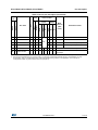
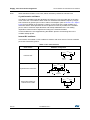
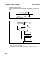
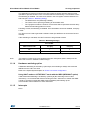
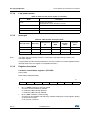
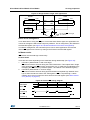
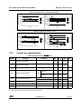
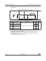
1
ST7LITE20F2 ST7LITE25F2
ST7LITE29F2
8-bit microcontroller with single voltage Flash memory, data
EEPROM, ADC, Timers, SPI
Datasheet - production data
Features
• Memories
– 8 Kbytes single voltage Flash Program
memory with Read-out protection
– In-circuit programming and in-application
programming (ICP and IAP)
– 10K write/erase cycles guaranteed
– Data retention: 20 years at 55 °C
– Temperature ranges:
–
-40 °C to +85 °C
–
-40 °C to +105 °C
– 384 bytes RAM
DIP20
SO20 300”
• 1 communication interface
– SPI synchronous serial interface.
• Interrupt management
– 10 interrupt vectors plus TRAP and RESET
– 15 external interrupt lines (on 4 vectors)
• Clock, reset and supply management
– Enhanced reset system
– Enhanced low voltage supervisor (LVD) for
main supply and an auxiliary voltage
detector (AVD) with interrupt capability for
implementing safe power-down procedures
– Clock sources: internal 1% RC oscillator,
crystal/ceramic resonator or external clock
– Internal 32-MHz input clock for auto-reload
timer
– Optional x4 or x8 PLL for 4 or 8 MHz
internal clock
– Five power saving modes: Halt, Active-halt,
Wait and Slow, Auto-wakeup from Halt
• Instruction set
– 8-bit data manipulation
– 63 basic instructions with illegal opcode
detection
– 17 main addressing modes
– 8 x 8 unsigned multiply instructions
• I/O ports
– Up to 15 multifunctional bidirectional I/O
lines
– 7 high sink outputs
• Development tools
– Full hardware/software development
package
– DM (debug module)
• A/D converter
– 7 input channels
– Fixed gain op-amp
– 13-bit resolution for 0 to 430 mV
(@ 5 V VDD)
– 10-bit resolution for 430 mV to 5 V (@ 5 V
VDD)
• 4 timers
– Configurable watchdog timer
– Two 8-bit Lite timers with prescaler
– 1 real-time base and 1 input capture
– One 12-bit auto-reload timer with 4 PWM
outputs, input capture and output compare
functions
January 2014
This is information on a product in full production.
DocID8349 Rev 7
1/170
www.st.com
Contents
ST7LITE20F2 ST7LITE25F2 ST7LITE29F2
Contents
1
Description . . . . . . . . . . . . . . . . . . . . . . . . . . . . . . . . . . . . . . . . . . . . . . . . 13
2
Pin description . . . . . . . . . . . . . . . . . . . . . . . . . . . . . . . . . . . . . . . . . . . . 15
3
Register & memory map . . . . . . . . . . . . . . . . . . . . . . . . . . . . . . . . . . . . . 18
4
Flash program memory . . . . . . . . . . . . . . . . . . . . . . . . . . . . . . . . . . . . . 21
5
6
2/170
4.1
Introduction . . . . . . . . . . . . . . . . . . . . . . . . . . . . . . . . . . . . . . . . . . . . . . . 21
4.2
Main features . . . . . . . . . . . . . . . . . . . . . . . . . . . . . . . . . . . . . . . . . . . . . . 21
4.3
Programming modes . . . . . . . . . . . . . . . . . . . . . . . . . . . . . . . . . . . . . . . . 21
4.3.1
In-circuit programming (ICP) . . . . . . . . . . . . . . . . . . . . . . . . . . . . . . . . . 21
4.3.2
In-application programming (IAP) . . . . . . . . . . . . . . . . . . . . . . . . . . . . . 22
4.4
ICC interface . . . . . . . . . . . . . . . . . . . . . . . . . . . . . . . . . . . . . . . . . . . . . . 22
4.5
Memory protection . . . . . . . . . . . . . . . . . . . . . . . . . . . . . . . . . . . . . . . . . . 23
4.5.1
Read-out protection . . . . . . . . . . . . . . . . . . . . . . . . . . . . . . . . . . . . . . . . 23
4.5.2
Flash write/erase protection . . . . . . . . . . . . . . . . . . . . . . . . . . . . . . . . . . 23
4.6
Related documentation . . . . . . . . . . . . . . . . . . . . . . . . . . . . . . . . . . . . . . 24
4.7
Register description . . . . . . . . . . . . . . . . . . . . . . . . . . . . . . . . . . . . . . . . . 24
Data EEPROM . . . . . . . . . . . . . . . . . . . . . . . . . . . . . . . . . . . . . . . . . . . . . 25
5.1
Introduction . . . . . . . . . . . . . . . . . . . . . . . . . . . . . . . . . . . . . . . . . . . . . . . 25
5.2
Main features . . . . . . . . . . . . . . . . . . . . . . . . . . . . . . . . . . . . . . . . . . . . . . 25
5.3
Memory access . . . . . . . . . . . . . . . . . . . . . . . . . . . . . . . . . . . . . . . . . . . . 25
5.4
Power saving modes . . . . . . . . . . . . . . . . . . . . . . . . . . . . . . . . . . . . . . . . 27
5.5
Access error handling . . . . . . . . . . . . . . . . . . . . . . . . . . . . . . . . . . . . . . . . 27
5.6
Data EEPROM Read-out protection . . . . . . . . . . . . . . . . . . . . . . . . . . . . . 28
5.7
Register description . . . . . . . . . . . . . . . . . . . . . . . . . . . . . . . . . . . . . . . . . 28
Central processing unit . . . . . . . . . . . . . . . . . . . . . . . . . . . . . . . . . . . . . 30
6.1
Introduction . . . . . . . . . . . . . . . . . . . . . . . . . . . . . . . . . . . . . . . . . . . . . . . 30
6.2
Main features . . . . . . . . . . . . . . . . . . . . . . . . . . . . . . . . . . . . . . . . . . . . . . 30
6.3
CPU registers . . . . . . . . . . . . . . . . . . . . . . . . . . . . . . . . . . . . . . . . . . . . . . 30
DocID8349 Rev 7
ST7LITE20F2 ST7LITE25F2 ST7LITE29F2
7
Supply, reset and clock management . . . . . . . . . . . . . . . . . . . . . . . . . . 34
7.1
Internal RC oscillator adjustment . . . . . . . . . . . . . . . . . . . . . . . . . . . . . . . 34
7.2
Phase locked loop (PLL) . . . . . . . . . . . . . . . . . . . . . . . . . . . . . . . . . . . . . 35
7.3
Register description . . . . . . . . . . . . . . . . . . . . . . . . . . . . . . . . . . . . . . . . . 36
7.4
Multi-oscillator (MO) . . . . . . . . . . . . . . . . . . . . . . . . . . . . . . . . . . . . . . . . . 37
7.5
Reset sequence manager (RSM) . . . . . . . . . . . . . . . . . . . . . . . . . . . . . . . 39
7.6
8
9
7.5.1
Introduction . . . . . . . . . . . . . . . . . . . . . . . . . . . . . . . . . . . . . . . . . . . . . . 39
7.5.2
Asynchronous external RESET pin . . . . . . . . . . . . . . . . . . . . . . . . . . . . 40
7.5.3
External power-on RESET . . . . . . . . . . . . . . . . . . . . . . . . . . . . . . . . . . . 40
7.5.4
Internal low voltage detector (LVD) RESET . . . . . . . . . . . . . . . . . . . . . . 40
7.5.5
Internal watchdog RESET . . . . . . . . . . . . . . . . . . . . . . . . . . . . . . . . . . . 41
System integrity management (SI) . . . . . . . . . . . . . . . . . . . . . . . . . . . . . . 41
7.6.1
Low voltage detector (LVD) . . . . . . . . . . . . . . . . . . . . . . . . . . . . . . . . . . 41
7.6.2
Auxiliary Voltage Detector (AVD) . . . . . . . . . . . . . . . . . . . . . . . . . . . . . . 43
7.6.3
Low power modes . . . . . . . . . . . . . . . . . . . . . . . . . . . . . . . . . . . . . . . . . 44
7.6.4
Register description . . . . . . . . . . . . . . . . . . . . . . . . . . . . . . . . . . . . . . . . 45
Interrupts . . . . . . . . . . . . . . . . . . . . . . . . . . . . . . . . . . . . . . . . . . . . . . . . . 47
8.1
Non maskable software interrupt . . . . . . . . . . . . . . . . . . . . . . . . . . . . . . . 47
8.2
External interrupts . . . . . . . . . . . . . . . . . . . . . . . . . . . . . . . . . . . . . . . . . . 47
8.3
Peripheral interrupts . . . . . . . . . . . . . . . . . . . . . . . . . . . . . . . . . . . . . . . . . 48
Power saving modes . . . . . . . . . . . . . . . . . . . . . . . . . . . . . . . . . . . . . . . . 53
9.1
Introduction . . . . . . . . . . . . . . . . . . . . . . . . . . . . . . . . . . . . . . . . . . . . . . . 53
9.2
SLOW mode . . . . . . . . . . . . . . . . . . . . . . . . . . . . . . . . . . . . . . . . . . . . . . . 53
9.3
WAIT mode . . . . . . . . . . . . . . . . . . . . . . . . . . . . . . . . . . . . . . . . . . . . . . . 54
9.4
HALT mode . . . . . . . . . . . . . . . . . . . . . . . . . . . . . . . . . . . . . . . . . . . . . . . 55
9.4.1
HALT mode recommendations . . . . . . . . . . . . . . . . . . . . . . . . . . . . . . . 57
9.5
ACTIVE-HALT mode . . . . . . . . . . . . . . . . . . . . . . . . . . . . . . . . . . . . . . . . 58
9.6
Auto-wakeup from HALT mode . . . . . . . . . . . . . . . . . . . . . . . . . . . . . . . . 60
9.6.1
10
Contents
Register description . . . . . . . . . . . . . . . . . . . . . . . . . . . . . . . . . . . . . . . . 62
I/O ports . . . . . . . . . . . . . . . . . . . . . . . . . . . . . . . . . . . . . . . . . . . . . . . . . . 64
10.1
Introduction . . . . . . . . . . . . . . . . . . . . . . . . . . . . . . . . . . . . . . . . . . . . . . . 64
10.2
Functional description . . . . . . . . . . . . . . . . . . . . . . . . . . . . . . . . . . . . . . . 64
DocID8349 Rev 7
3/170
7
Contents
11
ST7LITE20F2 ST7LITE25F2 ST7LITE29F2
Input modes . . . . . . . . . . . . . . . . . . . . . . . . . . . . . . . . . . . . . . . . . . . . . . 64
10.2.2
Output modes . . . . . . . . . . . . . . . . . . . . . . . . . . . . . . . . . . . . . . . . . . . . 65
10.2.3
Alternate functions . . . . . . . . . . . . . . . . . . . . . . . . . . . . . . . . . . . . . . . . . 66
10.3
I/O port implementation . . . . . . . . . . . . . . . . . . . . . . . . . . . . . . . . . . . . . . 68
10.4
Unused I/O pins . . . . . . . . . . . . . . . . . . . . . . . . . . . . . . . . . . . . . . . . . . . . 69
10.5
Low power modes . . . . . . . . . . . . . . . . . . . . . . . . . . . . . . . . . . . . . . . . . . 69
10.6
Interrupts . . . . . . . . . . . . . . . . . . . . . . . . . . . . . . . . . . . . . . . . . . . . . . . . . 69
10.7
Device-specific I/O port configuration . . . . . . . . . . . . . . . . . . . . . . . . . . . . 69
On-chip peripherals . . . . . . . . . . . . . . . . . . . . . . . . . . . . . . . . . . . . . . . . 72
11.1
11.2
11.3
11.4
4/170
10.2.1
Watchdog timer (WDG) . . . . . . . . . . . . . . . . . . . . . . . . . . . . . . . . . . . . . . 72
11.1.1
Introduction . . . . . . . . . . . . . . . . . . . . . . . . . . . . . . . . . . . . . . . . . . . . . . 72
11.1.2
Main features . . . . . . . . . . . . . . . . . . . . . . . . . . . . . . . . . . . . . . . . . . . . . 72
11.1.3
Functional description . . . . . . . . . . . . . . . . . . . . . . . . . . . . . . . . . . . . . . 72
11.1.4
Hardware watchdog option . . . . . . . . . . . . . . . . . . . . . . . . . . . . . . . . . . 73
11.1.5
Interrupts . . . . . . . . . . . . . . . . . . . . . . . . . . . . . . . . . . . . . . . . . . . . . . . . 73
11.1.6
Register description . . . . . . . . . . . . . . . . . . . . . . . . . . . . . . . . . . . . . . . . 74
12-bit autoreload timer 2 (AT2) . . . . . . . . . . . . . . . . . . . . . . . . . . . . . . . . . 74
11.2.1
Introduction . . . . . . . . . . . . . . . . . . . . . . . . . . . . . . . . . . . . . . . . . . . . . . 74
11.2.2
Main features . . . . . . . . . . . . . . . . . . . . . . . . . . . . . . . . . . . . . . . . . . . . . 75
11.2.3
Functional description . . . . . . . . . . . . . . . . . . . . . . . . . . . . . . . . . . . . . . 75
11.2.4
Low power modes . . . . . . . . . . . . . . . . . . . . . . . . . . . . . . . . . . . . . . . . . 79
11.2.5
Interrupts . . . . . . . . . . . . . . . . . . . . . . . . . . . . . . . . . . . . . . . . . . . . . . . . 79
11.2.6
Register description . . . . . . . . . . . . . . . . . . . . . . . . . . . . . . . . . . . . . . . . 80
Lite timer 2 (LT2) . . . . . . . . . . . . . . . . . . . . . . . . . . . . . . . . . . . . . . . . . . . 86
11.3.1
Introduction . . . . . . . . . . . . . . . . . . . . . . . . . . . . . . . . . . . . . . . . . . . . . . 86
11.3.2
Main features . . . . . . . . . . . . . . . . . . . . . . . . . . . . . . . . . . . . . . . . . . . . . 86
11.3.3
Functional description . . . . . . . . . . . . . . . . . . . . . . . . . . . . . . . . . . . . . . 87
11.3.4
Low power modes . . . . . . . . . . . . . . . . . . . . . . . . . . . . . . . . . . . . . . . . . 88
11.3.5
Interrupts . . . . . . . . . . . . . . . . . . . . . . . . . . . . . . . . . . . . . . . . . . . . . . . . 88
11.3.6
Register description . . . . . . . . . . . . . . . . . . . . . . . . . . . . . . . . . . . . . . . . 88
Serial peripheral interface (SPI) . . . . . . . . . . . . . . . . . . . . . . . . . . . . . . . . 91
11.4.1
Introduction . . . . . . . . . . . . . . . . . . . . . . . . . . . . . . . . . . . . . . . . . . . . . . 91
11.4.2
Main features . . . . . . . . . . . . . . . . . . . . . . . . . . . . . . . . . . . . . . . . . . . . . 91
11.4.3
General description . . . . . . . . . . . . . . . . . . . . . . . . . . . . . . . . . . . . . . . . 91
11.4.4
Clock phase and clock polarity . . . . . . . . . . . . . . . . . . . . . . . . . . . . . . . 95
DocID8349 Rev 7
ST7LITE20F2 ST7LITE25F2 ST7LITE29F2
11.5
12
11.4.5
Error Flags . . . . . . . . . . . . . . . . . . . . . . . . . . . . . . . . . . . . . . . . . . . . . . . 96
11.4.6
Low power modes . . . . . . . . . . . . . . . . . . . . . . . . . . . . . . . . . . . . . . . . . 99
11.4.7
Interrupts . . . . . . . . . . . . . . . . . . . . . . . . . . . . . . . . . . . . . . . . . . . . . . . 100
11.4.8
Register description . . . . . . . . . . . . . . . . . . . . . . . . . . . . . . . . . . . . . . . 100
10-bit A/D converter (ADC) . . . . . . . . . . . . . . . . . . . . . . . . . . . . . . . . . . 103
11.5.1
Introduction . . . . . . . . . . . . . . . . . . . . . . . . . . . . . . . . . . . . . . . . . . . . . 103
11.5.2
Main features . . . . . . . . . . . . . . . . . . . . . . . . . . . . . . . . . . . . . . . . . . . . 104
11.5.3
Functional description . . . . . . . . . . . . . . . . . . . . . . . . . . . . . . . . . . . . . 104
11.5.4
Low power modes . . . . . . . . . . . . . . . . . . . . . . . . . . . . . . . . . . . . . . . . 106
11.5.5
Interrupts . . . . . . . . . . . . . . . . . . . . . . . . . . . . . . . . . . . . . . . . . . . . . . . 106
11.5.6
Register Description . . . . . . . . . . . . . . . . . . . . . . . . . . . . . . . . . . . . . . 106
Instruction set . . . . . . . . . . . . . . . . . . . . . . . . . . . . . . . . . . . . . . . . . . . . 110
12.1
12.2
ST7 addressing modes . . . . . . . . . . . . . . . . . . . . . . . . . . . . . . . . . . . . . .110
12.1.1
Inherent . . . . . . . . . . . . . . . . . . . . . . . . . . . . . . . . . . . . . . . . . . . . . . . . 111
12.1.2
Immediate . . . . . . . . . . . . . . . . . . . . . . . . . . . . . . . . . . . . . . . . . . . . . . 112
12.1.3
Direct . . . . . . . . . . . . . . . . . . . . . . . . . . . . . . . . . . . . . . . . . . . . . . . . . . 112
12.1.4
Indexed (no offset, short, long) . . . . . . . . . . . . . . . . . . . . . . . . . . . . . . 112
12.1.5
Indirect (short, long) . . . . . . . . . . . . . . . . . . . . . . . . . . . . . . . . . . . . . . . 113
12.1.6
Indirect indexed (short, long) . . . . . . . . . . . . . . . . . . . . . . . . . . . . . . . . 113
12.1.7
Relative mode (direct, indirect) . . . . . . . . . . . . . . . . . . . . . . . . . . . . . . 114
Instruction groups . . . . . . . . . . . . . . . . . . . . . . . . . . . . . . . . . . . . . . . . . . .114
12.2.1
13
Contents
Illegal opcode reset . . . . . . . . . . . . . . . . . . . . . . . . . . . . . . . . . . . . . . . 115
Electrical characteristics . . . . . . . . . . . . . . . . . . . . . . . . . . . . . . . . . . . 118
13.1
Parameter conditions . . . . . . . . . . . . . . . . . . . . . . . . . . . . . . . . . . . . . . . .118
13.1.1
Minimum and maximum values . . . . . . . . . . . . . . . . . . . . . . . . . . . . . . 118
13.1.2
Typical values . . . . . . . . . . . . . . . . . . . . . . . . . . . . . . . . . . . . . . . . . . . 118
13.1.3
Typical curves . . . . . . . . . . . . . . . . . . . . . . . . . . . . . . . . . . . . . . . . . . . 118
13.1.4
Loading capacitor . . . . . . . . . . . . . . . . . . . . . . . . . . . . . . . . . . . . . . . . 118
13.1.5
Pin input voltage . . . . . . . . . . . . . . . . . . . . . . . . . . . . . . . . . . . . . . . . . 118
13.2
Absolute maximum ratings . . . . . . . . . . . . . . . . . . . . . . . . . . . . . . . . . . . .119
13.3
Operating conditions . . . . . . . . . . . . . . . . . . . . . . . . . . . . . . . . . . . . . . . 121
13.3.1
General operating conditions . . . . . . . . . . . . . . . . . . . . . . . . . . . . . . . . 121
13.3.2
Operating conditions with low voltage detector (LVD) . . . . . . . . . . . . . 121
13.3.3
Auxiliary voltage detector (AVD) thresholds . . . . . . . . . . . . . . . . . . . . . 123
13.3.4
Internal RC oscillator and PLL . . . . . . . . . . . . . . . . . . . . . . . . . . . . . . . 123
DocID8349 Rev 7
5/170
7
Contents
ST7LITE20F2 ST7LITE25F2 ST7LITE29F2
13.4
Supply current characteristics . . . . . . . . . . . . . . . . . . . . . . . . . . . . . . . . 127
13.5
Clock and timing characteristics . . . . . . . . . . . . . . . . . . . . . . . . . . . . . . . 130
13.5.1
Crystal and ceramic resonator oscillators . . . . . . . . . . . . . . . . . . . . . . 131
13.6
Memory characteristics . . . . . . . . . . . . . . . . . . . . . . . . . . . . . . . . . . . . . 133
13.7
EMC characteristics . . . . . . . . . . . . . . . . . . . . . . . . . . . . . . . . . . . . . . . . 134
13.7.1
Functional EMS (Electro Magnetic Susceptibility) . . . . . . . . . . . . . . . . 134
13.7.2
Electro Magnetic Interference (EMI) . . . . . . . . . . . . . . . . . . . . . . . . . . 135
13.7.3
Absolute maximum ratings (Electrical sensitivity) . . . . . . . . . . . . . . . . 136
13.8
I/O port pin characteristics . . . . . . . . . . . . . . . . . . . . . . . . . . . . . . . . . . . 137
13.9
Control pin characteristics . . . . . . . . . . . . . . . . . . . . . . . . . . . . . . . . . . . 143
13.10 Communication interface characteristics . . . . . . . . . . . . . . . . . . . . . . . . 145
13.10.1 Serial peripheral interface (SPI) . . . . . . . . . . . . . . . . . . . . . . . . . . . . . . 145
13.11 10-Bit ADC characteristics . . . . . . . . . . . . . . . . . . . . . . . . . . . . . . . . . . . 147
13.11.1 Amplifier output offset variation . . . . . . . . . . . . . . . . . . . . . . . . . . . . . . 150
14
15
Package characteristics . . . . . . . . . . . . . . . . . . . . . . . . . . . . . . . . . . . . 151
14.1
Package mechanical data . . . . . . . . . . . . . . . . . . . . . . . . . . . . . . . . . . . 151
14.2
Soldering information . . . . . . . . . . . . . . . . . . . . . . . . . . . . . . . . . . . . . . . 153
Device configuration . . . . . . . . . . . . . . . . . . . . . . . . . . . . . . . . . . . . . . . 154
15.1
16
6/170
Option bytes . . . . . . . . . . . . . . . . . . . . . . . . . . . . . . . . . . . . . . . . . . . . . . 154
15.1.1
Option byte 0 . . . . . . . . . . . . . . . . . . . . . . . . . . . . . . . . . . . . . . . . . . . . 154
15.1.2
Option byte 1 . . . . . . . . . . . . . . . . . . . . . . . . . . . . . . . . . . . . . . . . . . . . 156
15.2
Device ordering information and transfer of customer code . . . . . . . . . . 157
15.3
Development tools . . . . . . . . . . . . . . . . . . . . . . . . . . . . . . . . . . . . . . . . . 160
15.4
Application notes . . . . . . . . . . . . . . . . . . . . . . . . . . . . . . . . . . . . . . . . . . 161
Important notes . . . . . . . . . . . . . . . . . . . . . . . . . . . . . . . . . . . . . . . . . . . 165
16.1
Execution of BTJX instruction . . . . . . . . . . . . . . . . . . . . . . . . . . . . . . . . 165
16.2
ADC conversion spurious results . . . . . . . . . . . . . . . . . . . . . . . . . . . . . . 165
16.3
A/D converter accuracy for first conversion . . . . . . . . . . . . . . . . . . . . . . 165
16.4
Negative injection impact on ADC accuracy . . . . . . . . . . . . . . . . . . . . . 165
16.5
Clearing active interrupts outside interrupt routine . . . . . . . . . . . . . . . . . 165
16.6
Using PB4 as external interrupt . . . . . . . . . . . . . . . . . . . . . . . . . . . . . . . 166
16.7
Timebase 2 interrupt in slow mode . . . . . . . . . . . . . . . . . . . . . . . . . . . . 166
DocID8349 Rev 7
ST7LITE20F2 ST7LITE25F2 ST7LITE29F2
17
Contents
Revision history . . . . . . . . . . . . . . . . . . . . . . . . . . . . . . . . . . . . . . . . . . 167
DocID8349 Rev 7
7/170
7
List of tables
ST7LITE20F2 ST7LITE25F2 ST7LITE29F2
List of tables
Table 1.
Table 2.
Table 3.
Table 4.
Table 5.
Table 6.
Table 7.
Table 8.
Table 9.
Table 10.
Table 11.
Table 12.
Table 13.
Table 14.
Table 15.
Table 16.
Table 17.
Table 18.
Table 19.
Table 20.
Table 21.
Table 22.
Table 23.
Table 24.
Table 25.
Table 26.
Table 27.
Table 28.
Table 29.
Table 30.
Table 31.
Table 32.
Table 33.
Table 34.
Table 35.
Table 36.
Table 37.
Table 38.
Table 39.
Table 40.
Table 41.
Table 42.
Table 43.
Table 44.
Table 45.
Table 46.
Table 47.
Table 48.
8/170
Device summary . . . . . . . . . . . . . . . . . . . . . . . . . . . . . . . . . . . . . . . . . . . . . . . . . . . . . . . . . 13
Device pin description. . . . . . . . . . . . . . . . . . . . . . . . . . . . . . . . . . . . . . . . . . . . . . . . . . . . . 16
Hardware register map . . . . . . . . . . . . . . . . . . . . . . . . . . . . . . . . . . . . . . . . . . . . . . . . . . . . 19
Row definition . . . . . . . . . . . . . . . . . . . . . . . . . . . . . . . . . . . . . . . . . . . . . . . . . . . . . . . . . . . 27
DATA EEPROM register map and reset values . . . . . . . . . . . . . . . . . . . . . . . . . . . . . . . . . 29
Predefined calibration values . . . . . . . . . . . . . . . . . . . . . . . . . . . . . . . . . . . . . . . . . . . . . . . 34
ST7 clock sources . . . . . . . . . . . . . . . . . . . . . . . . . . . . . . . . . . . . . . . . . . . . . . . . . . . . . . . 38
CPU clock cycle delay . . . . . . . . . . . . . . . . . . . . . . . . . . . . . . . . . . . . . . . . . . . . . . . . . . . . 39
Effect of low power modes on SI . . . . . . . . . . . . . . . . . . . . . . . . . . . . . . . . . . . . . . . . . . . . 44
Interrupt control bits . . . . . . . . . . . . . . . . . . . . . . . . . . . . . . . . . . . . . . . . . . . . . . . . . . . . . . 44
Flag description . . . . . . . . . . . . . . . . . . . . . . . . . . . . . . . . . . . . . . . . . . . . . . . . . . . . . . . . . 45
Interrupt mapping . . . . . . . . . . . . . . . . . . . . . . . . . . . . . . . . . . . . . . . . . . . . . . . . . . . . . . . . 49
Interrupt sensitivity bits . . . . . . . . . . . . . . . . . . . . . . . . . . . . . . . . . . . . . . . . . . . . . . . . . . . . 50
External interrupt I/O pin ei3[1:0] selection . . . . . . . . . . . . . . . . . . . . . . . . . . . . . . . . . . . . . 51
External interrupt I/O pin ei2[1:0] selection . . . . . . . . . . . . . . . . . . . . . . . . . . . . . . . . . . . . . 51
External interrupt I/O pin ei1[1:0] selection . . . . . . . . . . . . . . . . . . . . . . . . . . . . . . . . . . . . . 52
External interrupt I/O pin ei0[1:0] selection . . . . . . . . . . . . . . . . . . . . . . . . . . . . . . . . . . . . . 52
ACTIVE-HALT mode . . . . . . . . . . . . . . . . . . . . . . . . . . . . . . . . . . . . . . . . . . . . . . . . . . . . . 58
AWU prescaler . . . . . . . . . . . . . . . . . . . . . . . . . . . . . . . . . . . . . . . . . . . . . . . . . . . . . . . . . . 63
AWU register map and reset values . . . . . . . . . . . . . . . . . . . . . . . . . . . . . . . . . . . . . . . . . . 63
DR value and output pin status. . . . . . . . . . . . . . . . . . . . . . . . . . . . . . . . . . . . . . . . . . . . . . 65
I/O port mode options . . . . . . . . . . . . . . . . . . . . . . . . . . . . . . . . . . . . . . . . . . . . . . . . . . . . . 67
I/O configurations . . . . . . . . . . . . . . . . . . . . . . . . . . . . . . . . . . . . . . . . . . . . . . . . . . . . . . . . 67
Effect of low power modes on I/O ports . . . . . . . . . . . . . . . . . . . . . . . . . . . . . . . . . . . . . . . 69
I/O port interrupt control/wake-up capability . . . . . . . . . . . . . . . . . . . . . . . . . . . . . . . . . . . . 69
Ports PA7:0, PB6:0 . . . . . . . . . . . . . . . . . . . . . . . . . . . . . . . . . . . . . . . . . . . . . . . . . . . . . . . 69
Port configuration (standard ports) . . . . . . . . . . . . . . . . . . . . . . . . . . . . . . . . . . . . . . . . . . . 70
Port configuration (Interrupt ports) . . . . . . . . . . . . . . . . . . . . . . . . . . . . . . . . . . . . . . . . . . . 70
Ports where the external interrupt capability selected using the EISR register . . . . . . . . . 70
I/O port register map and reset values . . . . . . . . . . . . . . . . . . . . . . . . . . . . . . . . . . . . . . . . 70
Watchdog timing . . . . . . . . . . . . . . . . . . . . . . . . . . . . . . . . . . . . . . . . . . . . . . . . . . . . . . . . . 73
Watchdog timer register map and reset values . . . . . . . . . . . . . . . . . . . . . . . . . . . . . . . . . 74
Effect of low power modes . . . . . . . . . . . . . . . . . . . . . . . . . . . . . . . . . . . . . . . . . . . . . . . . . 79
Interrupts events . . . . . . . . . . . . . . . . . . . . . . . . . . . . . . . . . . . . . . . . . . . . . . . . . . . . . . . . . 79
Counter clock selection. . . . . . . . . . . . . . . . . . . . . . . . . . . . . . . . . . . . . . . . . . . . . . . . . . . . 80
Register map and reset values . . . . . . . . . . . . . . . . . . . . . . . . . . . . . . . . . . . . . . . . . . . . . . 84
Effect of low power modes on Lite timer . . . . . . . . . . . . . . . . . . . . . . . . . . . . . . . . . . . . . . . 88
TBxF and ICF interrupt events . . . . . . . . . . . . . . . . . . . . . . . . . . . . . . . . . . . . . . . . . . . . . . 88
Lite timer register map and reset values. . . . . . . . . . . . . . . . . . . . . . . . . . . . . . . . . . . . . . . 90
WAIT and HALT mode description . . . . . . . . . . . . . . . . . . . . . . . . . . . . . . . . . . . . . . . . . . . 99
Interrupt events . . . . . . . . . . . . . . . . . . . . . . . . . . . . . . . . . . . . . . . . . . . . . . . . . . . . . . . . . 100
SPI master mode SCK frequency . . . . . . . . . . . . . . . . . . . . . . . . . . . . . . . . . . . . . . . . . . . 101
SPI register map and reset values . . . . . . . . . . . . . . . . . . . . . . . . . . . . . . . . . . . . . . . . . . 103
Low power modes effects . . . . . . . . . . . . . . . . . . . . . . . . . . . . . . . . . . . . . . . . . . . . . . . . . 106
Channel selection bits. . . . . . . . . . . . . . . . . . . . . . . . . . . . . . . . . . . . . . . . . . . . . . . . . . . . 106
ADC clock speed selection . . . . . . . . . . . . . . . . . . . . . . . . . . . . . . . . . . . . . . . . . . . . . . . . 108
ADC register map and reset values . . . . . . . . . . . . . . . . . . . . . . . . . . . . . . . . . . . . . . . . . 109
Addressing mode groups . . . . . . . . . . . . . . . . . . . . . . . . . . . . . . . . . . . . . . . . . . . . . . . . . 110
DocID8349 Rev 1
ST7LITE20F2 ST7LITE25F2 ST7LITE29F2
Table 49.
Table 50.
Table 51.
Table 52.
Table 53.
Table 54.
Table 55.
Table 56.
Table 57.
Table 58.
Table 59.
Table 60.
Table 61.
Table 62.
Table 63.
Table 64.
Table 65.
Table 66.
Table 67.
Table 68.
Table 69.
Table 70.
Table 72.
Table 73.
Table 74.
Table 75.
Table 76.
Table 77.
Table 78.
Table 79.
Table 80.
Table 81.
Table 82.
Table 83.
Table 84.
Table 85.
Table 86.
Table 87.
Table 88.
Table 89.
Table 90.
Table 91.
Table 92.
Table 93.
Table 94.
Table 95.
Table 96.
Table 97.
Table 98.
List of tables
ST7 addressing mode overview . . . . . . . . . . . . . . . . . . . . . . . . . . . . . . . . . . . . . . . . . . . . 110
Inherent instructions . . . . . . . . . . . . . . . . . . . . . . . . . . . . . . . . . . . . . . . . . . . . . . . . . . . . . 111
Immediate instructions . . . . . . . . . . . . . . . . . . . . . . . . . . . . . . . . . . . . . . . . . . . . . . . . . . . 112
Long and short instructions supporting direct, indexed,
indirect and indirect indexed addressing modes. . . . . . . . . . . . . . . . . . . . . . . . . . . . . . . . 113
Short instructions supporting direct, indexed, indirect and indirect
indexed addressing modes . . . . . . . . . . . . . . . . . . . . . . . . . . . . . . . . . . . . . . . . . . . . . . . . 114
Relative direct and indirect instructions and functions . . . . . . . . . . . . . . . . . . . . . . . . . . . 114
Instruction groups . . . . . . . . . . . . . . . . . . . . . . . . . . . . . . . . . . . . . . . . . . . . . . . . . . . . . . . 114
Instruction set overview . . . . . . . . . . . . . . . . . . . . . . . . . . . . . . . . . . . . . . . . . . . . . . . . . . 116
Voltage characteristics . . . . . . . . . . . . . . . . . . . . . . . . . . . . . . . . . . . . . . . . . . . . . . . . . . . 119
Current characteristics . . . . . . . . . . . . . . . . . . . . . . . . . . . . . . . . . . . . . . . . . . . . . . . . . . . 119
Thermal characteristics. . . . . . . . . . . . . . . . . . . . . . . . . . . . . . . . . . . . . . . . . . . . . . . . . . . 120
General operating conditions . . . . . . . . . . . . . . . . . . . . . . . . . . . . . . . . . . . . . . . . . . . . . . 121
Power on/power down operating conditions . . . . . . . . . . . . . . . . . . . . . . . . . . . . . . . . . . . 121
AVD thresholds . . . . . . . . . . . . . . . . . . . . . . . . . . . . . . . . . . . . . . . . . . . . . . . . . . . . . . . . . 123
Internal RC oscillator and PLL . . . . . . . . . . . . . . . . . . . . . . . . . . . . . . . . . . . . . . . . . . . . . 123
RC oscillator and PLL characteristics
(tested for TA = -40 to +85°C) @ VDD = 4.5 to 5.5 V. . . . . . . . . . . . . . . . . . . . . . . . . . . . 124
32 MHz PLL . . . . . . . . . . . . . . . . . . . . . . . . . . . . . . . . . . . . . . . . . . . . . . . . . . . . . . . . . . . 127
Supply current. . . . . . . . . . . . . . . . . . . . . . . . . . . . . . . . . . . . . . . . . . . . . . . . . . . . . . . . . . 128
On-chip peripherals . . . . . . . . . . . . . . . . . . . . . . . . . . . . . . . . . . . . . . . . . . . . . . . . . . . . . 130
General timings. . . . . . . . . . . . . . . . . . . . . . . . . . . . . . . . . . . . . . . . . . . . . . . . . . . . . . . . . 130
Auto Wakeup from Halt Oscillator (AWU) . . . . . . . . . . . . . . . . . . . . . . . . . . . . . . . . . . . . . 131
Resonator characteristics . . . . . . . . . . . . . . . . . . . . . . . . . . . . . . . . . . . . . . . . . . . . . . . . . 132
Resonator performances . . . . . . . . . . . . . . . . . . . . . . . . . . . . . . . . . . . . . . . . . . . . . . . . . 133
RAM and hardware registers . . . . . . . . . . . . . . . . . . . . . . . . . . . . . . . . . . . . . . . . . . . . . . 133
Flash program memory. . . . . . . . . . . . . . . . . . . . . . . . . . . . . . . . . . . . . . . . . . . . . . . . . . . 133
EEPROM data memory . . . . . . . . . . . . . . . . . . . . . . . . . . . . . . . . . . . . . . . . . . . . . . . . . . 134
Test results . . . . . . . . . . . . . . . . . . . . . . . . . . . . . . . . . . . . . . . . . . . . . . . . . . . . . . . . . . . . 135
Emission test . . . . . . . . . . . . . . . . . . . . . . . . . . . . . . . . . . . . . . . . . . . . . . . . . . . . . . . . . . 136
Absolute maximum ratings . . . . . . . . . . . . . . . . . . . . . . . . . . . . . . . . . . . . . . . . . . . . . . . . 136
Electrical sensitivities . . . . . . . . . . . . . . . . . . . . . . . . . . . . . . . . . . . . . . . . . . . . . . . . . . . . 137
General characteristics . . . . . . . . . . . . . . . . . . . . . . . . . . . . . . . . . . . . . . . . . . . . . . . . . . . 137
Output driving current . . . . . . . . . . . . . . . . . . . . . . . . . . . . . . . . . . . . . . . . . . . . . . . . . . . . 139
Asynchronous RESET Pin . . . . . . . . . . . . . . . . . . . . . . . . . . . . . . . . . . . . . . . . . . . . . . . . 143
Serial peripheral interface (SPI) . . . . . . . . . . . . . . . . . . . . . . . . . . . . . . . . . . . . . . . . . . . . 145
10-bit ADC characteristics . . . . . . . . . . . . . . . . . . . . . . . . . . . . . . . . . . . . . . . . . . . . . . . . 147
ADC accuracy with VDD = 5.0V. . . . . . . . . . . . . . . . . . . . . . . . . . . . . . . . . . . . . . . . . . . . . 148
ADC characteristics . . . . . . . . . . . . . . . . . . . . . . . . . . . . . . . . . . . . . . . . . . . . . . . . . . . . . 150
Typical offset variation over temperature . . . . . . . . . . . . . . . . . . . . . . . . . . . . . . . . . . . . . 150
Small outline package characteristics. . . . . . . . . . . . . . . . . . . . . . . . . . . . . . . . . . . . . . . . 151
Dual in-line package characteristics . . . . . . . . . . . . . . . . . . . . . . . . . . . . . . . . . . . . . . . . . 152
Thermal characteristics. . . . . . . . . . . . . . . . . . . . . . . . . . . . . . . . . . . . . . . . . . . . . . . . . . . 153
Soldering compatibility (wave and reflow soldering process) . . . . . . . . . . . . . . . . . . . . . . 153
Option bytes values . . . . . . . . . . . . . . . . . . . . . . . . . . . . . . . . . . . . . . . . . . . . . . . . . . . . . 154
Size definition . . . . . . . . . . . . . . . . . . . . . . . . . . . . . . . . . . . . . . . . . . . . . . . . . . . . . . . . . . 155
Option byte default values . . . . . . . . . . . . . . . . . . . . . . . . . . . . . . . . . . . . . . . . . . . . . . . . 155
LVD threshold configuration . . . . . . . . . . . . . . . . . . . . . . . . . . . . . . . . . . . . . . . . . . . . . . . 156
List of valid option combinations . . . . . . . . . . . . . . . . . . . . . . . . . . . . . . . . . . . . . . . . . . . . 157
Supported part numbers . . . . . . . . . . . . . . . . . . . . . . . . . . . . . . . . . . . . . . . . . . . . . . . . . . 158
ST7LITE2 FASTROM microcontroller option list . . . . . . . . . . . . . . . . . . . . . . . . . . . . . . . 159
DocID8349 Rev 1
9/170
10
List of tables
ST7LITE20F2 ST7LITE25F2 ST7LITE29F2
Table 99.
STMicroelectronics development tools . . . . . . . . . . . . . . . . . . . . . . . . . . . . . . . . . . . . . . . 161
Table 100. ST7 application notes . . . . . . . . . . . . . . . . . . . . . . . . . . . . . . . . . . . . . . . . . . . . . . . . . . . . 161
Table 101. Revision history . . . . . . . . . . . . . . . . . . . . . . . . . . . . . . . . . . . . . . . . . . . . . . . . . . . . . . . . 167
10/170
DocID8349 Rev 1
ST7LITE20F2 ST7LITE25F2 ST7LITE29F2
List of figures
List of figures
Figure 1.
Figure 2.
Figure 3.
Figure 4.
Figure 5.
Figure 6.
Figure 7.
Figure 8.
Figure 9.
Figure 10.
Figure 11.
Figure 12.
Figure 13.
Figure 14.
Figure 15.
Figure 16.
Figure 17.
Figure 18.
Figure 19.
Figure 20.
Figure 21.
Figure 22.
Figure 23.
Figure 24.
Figure 25.
Figure 26.
Figure 27.
Figure 28.
Figure 29.
Figure 30.
Figure 31.
Figure 32.
Figure 33.
Figure 34.
Figure 35.
Figure 36.
Figure 37.
Figure 38.
Figure 39.
Figure 40.
Figure 41.
Figure 42.
Figure 43.
Figure 44.
Figure 45.
Figure 46.
Figure 47.
Figure 48.
General block diagram . . . . . . . . . . . . . . . . . . . . . . . . . . . . . . . . . . . . . . . . . . . . . . . . . . . . 14
20-pin SO package pinout . . . . . . . . . . . . . . . . . . . . . . . . . . . . . . . . . . . . . . . . . . . . . . . . . 15
20-pin DIP package pinout . . . . . . . . . . . . . . . . . . . . . . . . . . . . . . . . . . . . . . . . . . . . . . . . . 15
Memory map . . . . . . . . . . . . . . . . . . . . . . . . . . . . . . . . . . . . . . . . . . . . . . . . . . . . . . . . . . . . 18
Typical ICC interface . . . . . . . . . . . . . . . . . . . . . . . . . . . . . . . . . . . . . . . . . . . . . . . . . . . . . 23
EEPROM block diagram . . . . . . . . . . . . . . . . . . . . . . . . . . . . . . . . . . . . . . . . . . . . . . . . . . . 25
Data EEPROM programming flowchart . . . . . . . . . . . . . . . . . . . . . . . . . . . . . . . . . . . . . . . 26
Data EEPROM Write operation . . . . . . . . . . . . . . . . . . . . . . . . . . . . . . . . . . . . . . . . . . . . . 27
Data EEPROM programming cycle . . . . . . . . . . . . . . . . . . . . . . . . . . . . . . . . . . . . . . . . . . 28
CPU registers . . . . . . . . . . . . . . . . . . . . . . . . . . . . . . . . . . . . . . . . . . . . . . . . . . . . . . . . . . . 30
Stack manipulation example . . . . . . . . . . . . . . . . . . . . . . . . . . . . . . . . . . . . . . . . . . . . . . . . 33
PLL output frequency timing diagram . . . . . . . . . . . . . . . . . . . . . . . . . . . . . . . . . . . . . . . . . 35
Clock management block diagram . . . . . . . . . . . . . . . . . . . . . . . . . . . . . . . . . . . . . . . . . . . 37
RESET sequence phases. . . . . . . . . . . . . . . . . . . . . . . . . . . . . . . . . . . . . . . . . . . . . . . . . . 39
Reset block diagram . . . . . . . . . . . . . . . . . . . . . . . . . . . . . . . . . . . . . . . . . . . . . . . . . . . . . . 40
RESET sequences . . . . . . . . . . . . . . . . . . . . . . . . . . . . . . . . . . . . . . . . . . . . . . . . . . . . . . 41
Low voltage detector vs. Reset. . . . . . . . . . . . . . . . . . . . . . . . . . . . . . . . . . . . . . . . . . . . . . 42
Reset and supply management block diagram. . . . . . . . . . . . . . . . . . . . . . . . . . . . . . . . . . 43
Using the AVD to monitor VDD . . . . . . . . . . . . . . . . . . . . . . . . . . . . . . . . . . . . . . . . . . . . . 44
Interrupt processing flowchart. . . . . . . . . . . . . . . . . . . . . . . . . . . . . . . . . . . . . . . . . . . . . . . 48
Power saving mode transitions . . . . . . . . . . . . . . . . . . . . . . . . . . . . . . . . . . . . . . . . . . . . . . 53
SLOW mode clock transition . . . . . . . . . . . . . . . . . . . . . . . . . . . . . . . . . . . . . . . . . . . . . . . 54
WAIT mode flowchart . . . . . . . . . . . . . . . . . . . . . . . . . . . . . . . . . . . . . . . . . . . . . . . . . . . . . 55
HALT timing overview . . . . . . . . . . . . . . . . . . . . . . . . . . . . . . . . . . . . . . . . . . . . . . . . . . . . . 56
HALT mode flowchart . . . . . . . . . . . . . . . . . . . . . . . . . . . . . . . . . . . . . . . . . . . . . . . . . . . . . 57
ACTIVE-HALT timing overview. . . . . . . . . . . . . . . . . . . . . . . . . . . . . . . . . . . . . . . . . . . . . . 59
ACTIVE-HALT mode Flow-chart. . . . . . . . . . . . . . . . . . . . . . . . . . . . . . . . . . . . . . . . . . . . . 59
AWUF mode block diagram . . . . . . . . . . . . . . . . . . . . . . . . . . . . . . . . . . . . . . . . . . . . . . . . 60
AWUF halt timing diagram . . . . . . . . . . . . . . . . . . . . . . . . . . . . . . . . . . . . . . . . . . . . . . . . . 61
AWUF mode flowchart . . . . . . . . . . . . . . . . . . . . . . . . . . . . . . . . . . . . . . . . . . . . . . . . . . . . 61
I/O port general block diagram . . . . . . . . . . . . . . . . . . . . . . . . . . . . . . . . . . . . . . . . . . . . . . 66
Interrupt I/O port state transitions . . . . . . . . . . . . . . . . . . . . . . . . . . . . . . . . . . . . . . . . . . . . 69
Watchdog block diagram . . . . . . . . . . . . . . . . . . . . . . . . . . . . . . . . . . . . . . . . . . . . . . . . . . 72
Block diagram . . . . . . . . . . . . . . . . . . . . . . . . . . . . . . . . . . . . . . . . . . . . . . . . . . . . . . . . . . . 75
PWM inversion diagram . . . . . . . . . . . . . . . . . . . . . . . . . . . . . . . . . . . . . . . . . . . . . . . . . . . 76
PWM function . . . . . . . . . . . . . . . . . . . . . . . . . . . . . . . . . . . . . . . . . . . . . . . . . . . . . . . . . . 77
PWM signal from 0% to 100% duty cycle . . . . . . . . . . . . . . . . . . . . . . . . . . . . . . . . . . . . . . 77
Block diagram of break function . . . . . . . . . . . . . . . . . . . . . . . . . . . . . . . . . . . . . . . . . . . . . 78
Input capture timing diagram . . . . . . . . . . . . . . . . . . . . . . . . . . . . . . . . . . . . . . . . . . . . . . . 79
Lite timer 2 block diagram . . . . . . . . . . . . . . . . . . . . . . . . . . . . . . . . . . . . . . . . . . . . . . . . . 86
Input capture timing diagram . . . . . . . . . . . . . . . . . . . . . . . . . . . . . . . . . . . . . . . . . . . . . . . 87
Serial peripheral interface block diagram . . . . . . . . . . . . . . . . . . . . . . . . . . . . . . . . . . . . . . 92
Single master/ single slave application . . . . . . . . . . . . . . . . . . . . . . . . . . . . . . . . . . . . . . . . 93
Generic SS timing diagram . . . . . . . . . . . . . . . . . . . . . . . . . . . . . . . . . . . . . . . . . . . . . . . . . 93
Hardware/software slave select management . . . . . . . . . . . . . . . . . . . . . . . . . . . . . . . . . . 94
Data clock timing diagram . . . . . . . . . . . . . . . . . . . . . . . . . . . . . . . . . . . . . . . . . . . . . . . . . 96
Clearing the WCOL bit (write collision flag) software sequence . . . . . . . . . . . . . . . . . . . . . 98
Single master / multiple slave configuration . . . . . . . . . . . . . . . . . . . . . . . . . . . . . . . . . . . . 99
DocID8349 Rev 7
11/170
12
List of figures
Figure 49.
Figure 50.
Figure 51.
Figure 52.
Figure 53.
Figure 54.
Figure 55.
Figure 56.
Figure 57.
Figure 58.
Figure 59.
Figure 60.
Figure 61.
Figure 62.
Figure 63.
Figure 64.
Figure 65.
Figure 66.
Figure 67.
Figure 68.
Figure 69.
Figure 70.
Figure 71.
Figure 72.
Figure 73.
Figure 74.
Figure 75.
Figure 76.
Figure 77.
Figure 78.
Figure 79.
Figure 80.
Figure 81.
Figure 82.
Figure 83.
Figure 84.
Figure 85.
Figure 86.
Figure 87.
Figure 88.
Figure 89.
Figure 90.
Figure 91.
Figure 92.
Figure 93.
Figure 94.
12/170
ST7LITE20F2 ST7LITE25F2 ST7LITE29F2
ADC block diagram . . . . . . . . . . . . . . . . . . . . . . . . . . . . . . . . . . . . . . . . . . . . . . . . . . . . . . 104
Pin loading conditions . . . . . . . . . . . . . . . . . . . . . . . . . . . . . . . . . . . . . . . . . . . . . . . . . . . . 118
Pin input voltage . . . . . . . . . . . . . . . . . . . . . . . . . . . . . . . . . . . . . . . . . . . . . . . . . . . . . . . . 119
fCPU maximum operating frequency versus VDD supply voltage . . . . . . . . . . . . . . . . . . . 121
RC Osc Freq vs VDD @ TA= 25°C (calibrated with RCCR1: 3V @ 25°C) . . . . . . . . . . . 125
RC Osc Freq vs VDD (calibrated with RCCR0: 5V@ 25°C). . . . . . . . . . . . . . . . . . . . . . . 126
Typical RC oscillator Accuracy vs temperature @ VDD=5V
(calibrated with RCCR0: 5V @ 25°C) . . . . . . . . . . . . . . . . . . . . . . . . . . . . . . . . . . . . . . . . 126
RC Osc Freq vs VDD and RCCR Value . . . . . . . . . . . . . . . . . . . . . . . . . . . . . . . . . . . . . . 126
PLL DfCPU/fCPU versus time . . . . . . . . . . . . . . . . . . . . . . . . . . . . . . . . . . . . . . . . . . . . . 126
PLLx4 Output vs CLKIN frequency . . . . . . . . . . . . . . . . . . . . . . . . . . . . . . . . . . . . . . . . . . 127
PLLx8 Output vs CLKIN frequency . . . . . . . . . . . . . . . . . . . . . . . . . . . . . . . . . . . . . . . . . . 127
Tipical IDD in RUN vs. fCPU . . . . . . . . . . . . . . . . . . . . . . . . . . . . . . . . . . . . . . . . . . . . . . 128
Typical IDD in SLOW vs. fCPU. . . . . . . . . . . . . . . . . . . . . . . . . . . . . . . . . . . . . . . . . . . . . 129
Typical IDD in WAIT vs. fCPU . . . . . . . . . . . . . . . . . . . . . . . . . . . . . . . . . . . . . . . . . . . . . 129
Typical IDD in SLOW-WAIT vs. fCPU. . . . . . . . . . . . . . . . . . . . . . . . . . . . . . . . . . . . . . . . 129
Typical IDD in AWUF mode at TA = 25°C . . . . . . . . . . . . . . . . . . . . . . . . . . . . . . . . . . . . 129
Typical IDD vs. temperature at VDD = 5V and fCPU = 8MHz . . . . . . . . . . . . . . . . . . . . . 130
Typical application with a crystal or ceramic resonator. . . . . . . . . . . . . . . . . . . . . . . . . . . 133
Two typical applications with unused I/O Pin . . . . . . . . . . . . . . . . . . . . . . . . . . . . . . . . . . 138
Typical IPU vs. VDD with VIN =VSS . . . . . . . . . . . . . . . . . . . . . . . . . . . . . . . . . . . . . . . . . . 138
Typical VOL at VDD = 2.4V (standard). . . . . . . . . . . . . . . . . . . . . . . . . . . . . . . . . . . . . . . 139
Typical VOL at VDD = 2.7V (standard). . . . . . . . . . . . . . . . . . . . . . . . . . . . . . . . . . . . . . . . 140
Typical VOL at VDD = 3.3V (standard). . . . . . . . . . . . . . . . . . . . . . . . . . . . . . . . . . . . . . . 140
Typical VOL at VDD = 5V (standard) . . . . . . . . . . . . . . . . . . . . . . . . . . . . . . . . . . . . . . . . 140
Typical VOL at VDD = 2.4V (high-sink) . . . . . . . . . . . . . . . . . . . . . . . . . . . . . . . . . . . . . . 140
Typical VOL at VDD = 5V (high-sink) . . . . . . . . . . . . . . . . . . . . . . . . . . . . . . . . . . . . . . . . 141
Typical VOL at VDD = 3V (high-sink) . . . . . . . . . . . . . . . . . . . . . . . . . . . . . . . . . . . . . . . . 141
Typical VDD-VOH at VDD = 2.4V. . . . . . . . . . . . . . . . . . . . . . . . . . . . . . . . . . . . . . . . . . . 141
Typical VDD-VOH at VDD = 2.7V. . . . . . . . . . . . . . . . . . . . . . . . . . . . . . . . . . . . . . . . . . . 141
Typical VDD-VOH at VDD = 3V . . . . . . . . . . . . . . . . . . . . . . . . . . . . . . . . . . . . . . . . . . . . 142
Typical VDD-VOH at VDD = 4V . . . . . . . . . . . . . . . . . . . . . . . . . . . . . . . . . . . . . . . . . . . . 142
Typical VDD-VOH at VDD = 5V . . . . . . . . . . . . . . . . . . . . . . . . . . . . . . . . . . . . . . . . . . . . 142
VOL vs. VDD (standard I/Os) . . . . . . . . . . . . . . . . . . . . . . . . . . . . . . . . . . . . . . . . . . . . . . 142
Typical VOL vs. VDD (high-sink I/Os). . . . . . . . . . . . . . . . . . . . . . . . . . . . . . . . . . . . . . . . 143
Typical VDD-VOH vs. VDD. . . . . . . . . . . . . . . . . . . . . . . . . . . . . . . . . . . . . . . . . . . . . . . . 143
RESET pin protection when LVD is enabled . . . . . . . . . . . . . . . . . . . . . . . . . . . . . . . . . . 144
RESET pin protection when LVD is disabled . . . . . . . . . . . . . . . . . . . . . . . . . . . . . . . . . . 144
SPI slave timing diagram with CPHA = 0(1) . . . . . . . . . . . . . . . . . . . . . . . . . . . . . . . . . . . 146
SPI slave timing diagram with CPHA = 1(1) . . . . . . . . . . . . . . . . . . . . . . . . . . . . . . . . . . . 146
SPI master timing diagram(1). . . . . . . . . . . . . . . . . . . . . . . . . . . . . . . . . . . . . . . . . . . . . . . 147
Typical application with ADC . . . . . . . . . . . . . . . . . . . . . . . . . . . . . . . . . . . . . . . . . . . . . . 148
ADC accuracy characteristics with amplifier disabled. . . . . . . . . . . . . . . . . . . . . . . . . . . . 149
ADC accuracy characteristics with amplifier enabled . . . . . . . . . . . . . . . . . . . . . . . . . . . . 149
Amplifier noise vs voltage . . . . . . . . . . . . . . . . . . . . . . . . . . . . . . . . . . . . . . . . . . . . . . . . . 150
20-pin plastic small outline package, 300-mil width . . . . . . . . . . . . . . . . . . . . . . . . . . . . . 151
20-pin plastic dual in-line package, 300-mil width . . . . . . . . . . . . . . . . . . . . . . . . . . . . . . 152
DocID8349 Rev 7
ST7LITE20F2 ST7LITE25F2 ST7LITE29F2
1
Description
Description
ST7LITE20F2, ST7LITE25F2 and ST7LITE29F2 are referred to as ST7LITE2. The
ST7LITE2 is a member of the ST7 microcontroller family. All ST7 devices are based on a
common industry-standard 8-bit core, featuring an enhanced instruction set.
The ST7LITE2 features FLASH memory with byte-by-byte In-Circuit Programming (ICP)
and In-Application Programming (IAP) capability.
Under software control, the ST7LITE2 device can be placed in WAIT, SLOW, or HALT
mode, reducing power consumption when the application is in idle or standby state.
The enhanced instruction set and addressing modes of the ST7 offer both power and
flexibility to software developers, enabling the design of highly efficient and compact
application code. In addition to standard 8-bit data management, all ST7 microcontrollers
feature true bit manipulation, 8x8 unsigned multiplication and indirect addressing modes.
For easy reference, all parametric data are located in Section 15: Device configuration.
The devices feature an on-chip Debug Module (DM) to support in-circuit debugging (ICD).
For a description of the DM registers, refer to the ST7 ICC Protocol Reference Manual.
Table 1. Device summary
Features
ST7LITE20F2
ST7LITE25F2
Program memory bytes
8 Kbyte
RAM (stack) - bytes
384 (128)
Data EEPROM - bytes
Peripherals
−
Lite timer with Watchdog,
autoreload timer, SPI,
10-bit ADC with Op-Amp
Operating supply
CPU frequency
Operating temperature
−
ST7LITE29F2
256
Lite timer with watchdog,
autoreload timer with 32-MHz input clock, SPI,
10-bit ADC with op-amp
2.4V to 5.5 V
Up to 8 MHz
(w/ ext OSC up to 16 MHz)
–40 °C to +85 °C
Packages
Up to 8 MHz (w/ ext OSC up to 16 MHz
and int 1MHz RC 1% PLLx8/4 MHz)
–40 °C to +85 °C
–40 °C to +85 °C
–40 °C to +105 °C
SO20 300”, DIP20
DocID8349 Rev 7
13/170
169
Description
ST7LITE20F2 ST7LITE25F2 ST7LITE29F2
Figure 1. General block diagram
PLL
8 MHz -> 32 MHz
Int.
1% RC
1MHz
PLL x 8
or PLL X4
12-bit
Auto-reload
Timer 2
CLKIN
8-bit
Lite timer 2
/2
OSC1
OSC2
Ext.
OSC
1 MHz
to
16 MHz
Internal
clock
VDD
VSS
RESET
Power
supply
Control
8-bit core
ALU
14/170
Port B
ADDRESS AND DATA BUS
LVD
Port A
ADC
+ Op-amp
SPI
Debug module
Program
memory
(8 Kbytes)
Data EEPROM
(256 bytes)
RAM
(384 bytes)
Watchdog
DocID8349 Rev 7
PA7:0
(8 bits)
PB6:0
(7 bits)
ST7LITE20F2 ST7LITE25F2 ST7LITE29F2
2
Pin description
Pin description
Figure 2. 20-pin SO package pinout
VSS
VDD
RESET
1
20
2
19
3
18
SS/AIN0/PB0
4
SCK/AIN1/PB1
MISO/AIN2/PB2
MOSI/AIN3/PB3
CLKIN/AIN4/PB4
AIN5/PB5
IN/AIN6/PB6
5
ei3
17
ei0
16
6
15
7
14
8
ei2
13
ei1
9
12
10
11
OSC1/CLKIN
OSC2
PA0 (HS)/LTIC
PA1 (HS)/ATIC
PA2 (HS)/ATPWM0
PA3 (HS)/ATPWM1
PA4 (HS)/ATPWM2
PA5 (HS)/ATPWM3/ICCDATA
PA6/MCO/ICCCLK/BREAK
PA7(HS)
(HS) 20mA high sink capability
eix associated external interrupt vector
Figure 3. 20-pin DIP package pinout
MISO/AIN2/PB2
MOSI/AIN3/PB3
CLKIN/AIN4/PB4
1
ei3
ei3
2
3
20
19
18
ei2
AIN5/PB5
4
17
AIN6/PB6
PA7(HS)
MCO/ICCCLK/BREAK/PA6
ATPWM3/ICCDATA/PA5(HS)
ATPWM2/PA4(HS)
ATPWM1/PA3(HS)
5
16
6
15
7
14
ei1
13
8
9
10
ei0
ei0
12
11
SCK/AIN1/PB1
SS/AIN0/PB0
RESET
VDD
VSS
OSC1/CLKIN
OSC2
PA0(HS)/LTIC
PA1(HS)/ATIC
PA2(HS)/ATPWM0
(HS) 20mA high sink capability
eix associated external interrupt vector
Legend and abbreviations for device pin description (seeTable 2 below):
•
•
Type:
–
I = input
–
O = output
–
S = supply
In/Output level:
–
•
CT= CMOS 0.3VDD/0.7VDD with input trigger
Output level:
–
HS = 20mA high sink (on N-buffer only)
DocID8349 Rev 7
15/170
169
Pin description
ST7LITE20F2 ST7LITE25F2 ST7LITE29F2
Port and control configuration:
•
Input:
–
•
float = floating, wpu = weak pull-up, int = interrupt, ana = analog
Output:
–
OD = open drain
–
PP = push-pull
The RESET configuration of each pin is shown in bold which is valid as long as the device is
in reset state.
Table 2. Device pin description
Pin
No.
Level
Port / Control
Main
function
(after
reset)
Input
Output
float
wpu
int
ana
Alternate function
DIP20
Output
SO20
Pin name
Type
Input
1
16 VSS
S
-
-
-
-
-
-
-
-
Ground
2
17 VDD
S
-
-
-
-
-
-
-
-
Main power supply
3
18 RESET
I/O CT
-
-
X
-
-
X
-
Top priority non maskable interrupt (active
low)
4
19 PB0/AIN0/SS
I/O
CT
X
X
X
X
Port B0
ADC analog input 0 or SPI Slave
Select (active low)(1)
5
20 PB1/AIN1/SCK
I/O
CT
X
X
X
X
Port B1
ADC analog input 1 or SPI Serial
Clock(1)
6
1
PB2/AIN2/MISO
I/O
CT
X
X
X
X
Port B2
ADC analog input 2 or SPI Master
in/ Slave out data
7
2
PB3/AIN3/MOSI
I/O
CT
X
X
X
X
Port B3
ADC analog input 3 or SPI Master
out / Slave in data
8
3
PB4/AIN4/CLKIN I/O
CT
X
X
X
X
Port B4
ADC analog input 4 or external
clock input
9
4
PB5/AIN5
I/O
CT
X
X
X
X
Port B5
ADC analog input 5
10 5
PB6/AIN6
I/O
CT
X
X
X
X
Port B6
ADC analog input 6
11 6
PA7
I/O CT HS
X
ei1
-
X
X
Port A7
12 7
PA6 /MCO/
ICCCLK/BREAK
I/O
X
ei1
-
X
X
Port A6
Main clock output or in circuit
communication clock or external
BREAK(2)
13 8
PA5 /ATPWM3/
ICCDATA
I/O CT HS
X
-
X
X
Port A5
Auto-reload timer PWM3 or In
circuit communication data
14 9
PA4/ATPWM2
I/O CT HS
X
-
X
X
Port A4
Auto-reload timer PWM2
16/170
CT
ei3
ei2
ei1
OD PP
DocID8349 Rev 7
-
ST7LITE20F2 ST7LITE25F2 ST7LITE29F2
Pin description
Table 2. Device pin description (continued)
Pin
No.
Level
Port / Control
15 10 PA3/ATPWM1
I/O CT HS
X
16 11 PA2/ATPWM0
I/O CT HS
X
17 12 PA1/ATIC
I/O CT HS
X
18 13 PA0/LTIC
I/O CT HS
X
19 14 OSC2
O
−
−
-
-
20 15 OSC1/CLKIN
I
−
−
-
-
Output
ana
int
wpu
float
Output
Input
Pin name
Type
DIP20
SO20
Input
OD PP
Main
function
(after
reset)
Alternate function
-
X
X
Port A3
Auto-reload timer PWM1
-
X
X
Port A2
Auto-reload timer PWM0
-
X
X
Port A1
Auto-reload timer input capture
-
X
X
Port A0
Lite timer input capture
-
-
-
-
Resonator oscillator inverter output
-
-
-
-
Resonator oscillator inverter input or external
clock input
ei0
1. No negative current injection allowed on this pin. For details (refer toTable 58: Current characteristics).
2. During normal operation this pin must be pulled- up, internally or externally (external pull-up of 10k mandatory in noisy
environment). This is to avoid entering ICC mode unexpectedly during a reset. In the application, even if the pin is
configured as output, any reset will put it back in input pull-up.
DocID8349 Rev 7
17/170
169
Register & memory map
3
ST7LITE20F2 ST7LITE25F2 ST7LITE29F2
Register & memory map
As shown in Figure 4, the MCU is able of addressing 64K bytes of memories and I/O
registers.
The available memory locations consist of 128 bytes of register locations, 384 bytes of
RAM, 256 bytes of data EEPROM and 8 Kbytes of user program memory. The RAM space
includes up to 128 bytes for the stack from 180h to 1FFh.
The highest address bytes contain the user reset and interrupt vectors.
The Flash memory contains two sectors (see Figure 4) mapped in the upper part of the ST7
addressing space so the reset and interrupt vectors are located in Sector 0 (F000h-FFFFh).
The size of Flash Sector 0 and other device options are configurable by Option byte (refer to
Section 15: Device configuration).
Note:
Memory locations marked as “Reserved” must never be accessed. Accessing a reserved
area can have unpredictable effects on the device.
Figure 4. Memory map
0080h
Short Addressing
RAM (zero page)
0000h
007Fh
0080h
00FFh
0100h
HW
registers(1)
16-bit Addressing
RAM
RAM
(384 Bytes)
017Fh
0180h
Reserved
01FFh
01FFh
20h
128 Bytes Stack
0FFFh
1000h
10FFh
1100h
1000h
Data EEPROM
(256 Bytes)
1001h
Reserved
E000h
Flash memory
(8K)
FBFFh
FC00h
FFFFh
7 Kbytes
SECTOR 1
1 Kbyte
SECTOR 0
FFDEh
Interrupt
& reset vectors(2)
FFFFh
FFDFh
1. SeeTable 3: Hardware register map
2. See Table 12: Interrupt mapping
3. See Section 7.1: Internal RC oscillator adjustment
18/170
(3)
RCCR1
8K Flash
PROGRAM MEMORY
DFFFh
E000h
FFDFh
FFE0h
RCCR0
DocID8349 Rev 7
RCCR0
RCCR1
(3)
ST7LITE20F2 ST7LITE25F2 ST7LITE29F2
Register & memory map
Table 3. Hardware register map(1)
Address
0000h
0001h
0002h
0003h
0004h
0005h
Register name
Reset
status
Port A
PADR
PADDR
PAOR
Port A Data Register
Port A Data Direction Register
Port A Option Register
FFh(2)
00h
40h
R/W
R/W
R/W
Port B
PBDR
PBDDR
PBOR
Port B Data Register
Port B Data Direction Register
Port B Option Register
FFh(2)
00h
00h
R/W
R/W
R/W(3)
Block
Register
label
0006h
0007h
0008h
0009h
000Ah
000Bh
000Ch
000Dh
000Eh
000Fh
0010h
0011h
0012h
0013h
0014h
0015h
0016h
0017h
0018h
0019h
001Ah
001Bh
001Ch
001Dh
001Eh
001Fh
0020h
0021h
0022h
Remarks
Reserved area (2 bytes)
Lite
TIMER 2
LTCSR2
LTARR
LTCNTR
LTCSR1
LTICR
Lite Timer Control/Status Register 2
Lite Timer Auto-reload Register
Lite Timer Counter Register
Lite Timer Control/Status Register 1
Lite Timer Input Capture Register
00h
00h
00h
0X00 0000h
00h
R/W
R/W
Read only
R/W
Read only
Autoreload
TIMER 2
ATCSR
CNTRH
CNTRL
ATRH
ATRL
PWMCR
PWM0CSR
PWM1CSR
PWM2CSR
PWM3CSR
DCR0H
DCR0L
DCR1H
DCR1L
DCR2H
DCR2L
DCR3H
DCR3L
ATICRH
ATICRL
TRANCR
BREAKCR
Timer Control/Status Register
Counter Register High
Counter Register Low
Auto-Reload Register High
Auto-Reload Register Low
PWM Output Control Register
PWM 0 Control/Status Register
PWM 1 Control/Status Register
PWM 2 Control/Status Register
PWM 3 Control/Status Register
PWM 0 Duty Cycle Register High
PWM 0 Duty Cycle Register Low
PWM 1 Duty Cycle Register High
PWM 1 Duty Cycle Register Low
PWM 2 Duty Cycle Register High
PWM 2 Duty Cycle Register Low
PWM 3 Duty Cycle Register High
PWM 3 Duty Cycle Register Low
Input Capture Register High
Input Capture Register Low
Transfer Control Register
Break Control Register
0X00 0000h
00h
00h
00h
00h
00h
00h
00h
00h
00h
00h
00h
00h
00h
00h
00h
00h
00h
00h
00h
01h
00h
R/W
Read only
Read only
R/W
R/W
R/W
R/W
R/W
R/W
R/W
R/W
R/W
R/W
R/W
R/W
R/W
R/W
R/W
Read only
Read only
R/W
R/W
0023h to
002Dh
Reserved area (11 bytes)
002Eh
WDG
WDGCR
Watchdog Control Register
7Fh
R/W
0002Fh
Flash
FCSR
Flash Control/Status Register
00h
R/W
00030h
EEPROM
EECSR
Data EEPROM Control/Status Register
00h
R/W
0031h
0032h
0033h
SPI
SPIDR
SPICR
SPICSR
SPI Data I/O Register
SPI Control Register
SPI Control Status Register
xxh
0xh
00h
R/W
R/W
R/W
0034h
0035h
0036h
ADC
ADCCSR
ADCDRH
ADCDRL
A/D Control Status Register
A/D Data Register High
A/D Amplifier Control/Data Low Register
00h
xxh
0xh
R/W
Read Only
R/W
DocID8349 Rev 7
19/170
169
Register & memory map
ST7LITE20F2 ST7LITE25F2 ST7LITE29F2
Table 3. Hardware register map(1) (continued)
Address
Block
0037h
ITC
0038h
MCC
0039h
003Ah
Clock and
Reset
Register
label
004Bh
004Ch
004Dh
004Eh
004Fh
0050h
Remarks
External Interrupt Control Register
00h
R/W
MCCSR
Main Clock Control/Status Register
00h
R/W
RCCR
SICSR
RC oscillator Control Register
System Integrity Control/Status Register
FFh
R/W
0000 0XX0h R/W
Reserved area (1 byte)
ITC
EISR
003Dh to
0048h
0049h
004Ah
Reset
status
EICR
003Bh
003Ch
Register name
External Interrupt Selection Register
0Ch
R/W
Reserved area (12 bytes)
AWU
AWUPR
AWUCSR
AWU Prescaler Register
AWU Control/Status Register
FFh
00h
R/W
R/W
DM(4)
DMCR
DMSR
DMBK1H
DMBK1L
DMBK2H
DMBK2L
DM Control Register
DM Status Register
DM Breakpoint Register 1 High
DM Breakpoint Register 1 Low
DM Breakpoint Register 2 High
DM Breakpoint Register 2 Low
00h
00h
00h
00h
00h
00h
R/W
R/W
R/W
R/W
R/W
R/W
0051h to
007Fh
Reserved area (47 bytes)
1. Legend: x = undefined, R/W = read/write.
2. The contents of the I/O port DR registers are readable only in output configuration. In input configuration, the values of the
I/O pins are returned instead of the DR register contents.
3. The bits associated with unavailable pins must always keep their reset value.
4. For a description of the Debug Module registers, see ICC reference manual.
20/170
DocID8349 Rev 7
ST7LITE20F2 ST7LITE25F2 ST7LITE29F2
Flash program memory
4
Flash program memory
4.1
Introduction
The ST7 single voltage extended Flash (XFlash) is a non-volatile memory that can be
electrically erased and programmed either on a byte-by-byte basis or up to 32 bytes in
parallel.
The XFlash devices can be programmed off-board (plugged in a programming tool) or onboard using in-circuit programming or in-application programming.
The array matrix organization allows each sector to be erased and reprogrammed without
affecting other sectors.
4.2
4.3
Main features
•
ICP (in-circuit programming)
•
IAP (in-application programming)
•
ICT (in-circuit testing) for downloading and executing user application test patterns in
RAM
•
Sector 0 size configurable by option byte
•
Read-out and write protection
Programming modes
The ST7 can be programmed in three different ways:
4.3.1
•
Insertion in a programming tool. In this mode, Flash sectors 0 and 1, option byte row
and data EEPROM (if present) can be programmed or erased.
•
In-circuit programming. In this mode, Flash sectors 0 and 1, option byte row and data
EEPROM (if present) can be programmed or erased without removing the device from
the application board.
•
In-application programming. In this mode, sector 1 and data EEPROM (if present) can
be programmed or erased without removing the device from the application board and
while the application is running.
In-circuit programming (ICP)
ICP uses a protocol called ICC (in-circuit communication) which allows an ST7 plugged on a
printed circuit board (PCB) to communicate with an external programming device connected
via cable. ICP is performed in three steps:
1.
Switch the ST7 to ICC mode (in-circuit communications). This is done by driving a
specific signal sequence on the ICCCLK/DATA pins while the RESET pin is pulled low.
When the ST7 enters ICC mode, it fetches a specific RESET vector which points to the
ST7 System Memory containing the ICC protocol routine. This routine enables the ST7
to receive bytes from the ICC interface.
2.
Download ICP driver code in RAM from the ICCDATA pin.
3.
Execute ICP driver code in RAM to program the Flash memory.
DocID8349 Rev 7
21/170
169
Flash program memory
ST7LITE20F2 ST7LITE25F2 ST7LITE29F2
Depending on the ICP driver code downloaded in RAM, Flash memory programming can be
fully customized (number of bytes to program, program locations, or selection of the serial
communication interface for downloading).
4.3.2
In-application programming (IAP)
This mode uses an IAP driver program previously programmed in Sector 0 by the user (in
ICP mode).
This mode is fully controlled by user software. This allows it to be adapted to the user
application, (user-defined strategy for entering programming mode, choice of
communications protocol used to fetch the data to be stored etc.).
IAP mode can be used to program any memory areas except Sector 0, which is write/erase
protected to allow recovery in case errors occur during the programming operation.
4.4
ICC interface
ICP needs a minimum of 4 and up to 6 pins to be connected to the programming tool. These
pins are:
•
RESET: device reset
•
VSS: device power supply ground
•
ICCCLK: ICC output serial clock pin
•
ICCDATA: ICC input serial data pin
•
CLKIN/PB4: main clock input for external source
•
VDD: application board power supply (optional).
If the ICCCLK or ICCDATA pins are only used as outputs in the application, no signal
isolation is necessary. As soon as the Programming Tool is plugged to the board, even if an
ICC session is not in progress, the ICCCLK and ICCDATA pins are not available for the
application. If they are used as inputs by the application, isolation such as a serial resistor
has to be implemented in case another device forces the signal. Refer to the Programming
Tool documentation for recommended resistor values.
During the ICP session, the programming tool must control the RESET pin. This can lead to
conflicts between the programming tool and the application reset circuit if it drives more than
5mA at high level (push pull output or pull-up resistor<1K). A schottky diode can be used to
isolate the application RESET circuit in this case. When using a classical RC network with
R>1 kΩ or a reset management IC with open drain output and pull-up resistor > 1 kΩ, no
additional components are needed. In all cases the user must ensure that no external reset
is generated by the application during the ICC session.
The use of Pin 7 of the ICC connector depends on the Programming Tool architecture. This
pin must be connected when using most ST Programming Tools (it is used to monitor the
application power supply). Please refer to the Programming Tool manual.
Pin 9 has to be connected to the CLKIN/PB4 pin of the ST7 when the clock is not available
in the application or if the selected clock option is not programmed in the option byte. ST7
devices with multi-oscillator capability need to have OSC1 and OSC2 grounded in this case.
With any programming tool, while the ICP option is disabled, the external clock has to be
provided on PB4.
22/170
DocID8349 Rev 7
ST7LITE20F2 ST7LITE25F2 ST7LITE29F2
Caution:
Flash program memory
During normal operation the ICCCLK pin must be pulled up, internally or externally (external
pull-up of 10k mandatory in noisy environment). This is to avoid entering ICC mode
unexpectedly during a reset. In the application, even if the pin is configured as output, any
reset will put it back in input pull-up.
Figure 5. Typical ICC interface
Programming tool
ICC connector
ICC Cable
ICC connector
HE10 connector type
Optional
9
7
5
3
1
10
8
6
4
2
Application board
Application
reset source
Application
power supply
4.5
ICCDATA
RESET
ST7
ICCCLK
CLKIN/PB4
(See Note 5)
VDD
Application
I/O
Memory protection
There are two different types of memory protection: Read-Out Protection and Write/Erase
Protection which can be applied individually.
4.5.1
Read-out protection
Read-out protection, when selected provides a protection against program memory content
extraction and against write access to Flash memory. Even if no protection can be
considered as totally unbreakable, the feature provides a very high level of protection for a
general purpose microcontroller. Both program and data E2 memory are protected.
In flash devices, this protection is removed by reprogramming the option. In this case, both
program and data E2 memory are automatically erased and the device can be
reprogrammed.
Read-out protection selection depends on the device type:
4.5.2
•
In Flash devices it is enabled and removed through the FMP_R bit in the option byte.
•
In ROM devices it is enabled by mask option specified in the Option List.
Flash write/erase protection
Write/erase protection, when set, makes it impossible to both overwrite and erase program
memory. It does not apply to E2 data. Its purpose is to provide advanced security to
applications and prevent any change being made to the memory content.
Caution:
Once set, Write/erase protection can never be removed. A write-protected flash device is no
longer reprogrammable.
DocID8349 Rev 7
23/170
169
Flash program memory
ST7LITE20F2 ST7LITE25F2 ST7LITE29F2
Write/erase protection is enabled through the FMP_W bit in the option byte.
4.6
Related documentation
For details on Flash programming and ICC protocol, refer to the ST7 Flash Programming
Reference Manual and to the ST7 ICC Protocol Reference Manual.
4.7
Register description
Flash control/status register (FCSR)
Read / Write
Reset value: 0000 0000 (00h)
1st RASS Key: 0101 0110 (56h)
2nd RASS Key: 1010 1110 (AEh)
7
0
Note:
0
0
0
0
0
OPT
LAT
PGM
This register is reserved for programming using ICP, IAP or other programming methods. It
controls the XFlash programming and erasing operations.
When an EPB or another programming tool is used (in socket or ICP mode), the RASS keys
are sent automatically.
24/170
DocID8349 Rev 7
ST7LITE20F2 ST7LITE25F2 ST7LITE29F2
5
Data EEPROM
5.1
Introduction
Data EEPROM
The Electrically Erasable Programmable Read Only Memory can be used as a non-volatile
backup for storing data. Using the EEPROM requires a basic access protocol described in
this chapter.
5.2
Main features
•
Up to 32 bytes programmed in the same cycle
•
EEPROM mono-voltage (charge pump)
•
Chained erase and programming cycles
•
Internal control of the global programming cycle duration
•
WAIT mode management
•
Read-out protection
Figure 6. EEPROM block diagram
High voltage
pump
EECSR
0
0
0
Address
decoder
0
0
4
0
E2LAT E2PGM
EEPROM
Row
memory matrix
decoder
(1 ROW = 32 x 8 BITS)
128
4
128
Data
32 x 8 bits
multiplexer
data latches
4
Address bus
5.3
DATA BUS
Memory access
The Data EEPROM memory read/write access modes are controlled by the E2LAT bit of the
EEPROM Control/Status register (EECSR). The flowchart in Figure 7 describes these
different memory access modes.
DocID8349 Rev 7
25/170
169
Data EEPROM
ST7LITE20F2 ST7LITE25F2 ST7LITE29F2
Read operation (E2LAT=0)
The EEPROM can be read as a normal ROM location when the E2LAT bit of the EECSR
register is cleared.
On this device, Data EEPROM can also be used to execute machine code. Take care not to
write to the Data EEPROM while executing from it. This would result in an unexpected code
being executed.
Write operation (E2LAT=1)
To access the write mode, the E2LAT bit has to be set by software (the E2PGM bit remains
cleared). When a write access to the EEPROM area occurs, the value is latched inside the
32 data latches according to its address.
When PGM bit is set by the software, all the previous bytes written in the data latches (up to
32) are programmed in the EEPROM cells. The effective high address (row) is determined
by the last EEPROM write sequence. To avoid wrong programming, the user must take care
that all the bytes written between two programming sequences have the same high
address: only the five Least Significant Bits of the address can change.
At the end of the programming cycle, the PGM and LAT bits are cleared simultaneously.
Note:
Care should be taken during the programming cycle. Writing to the same memory location
will over-program the memory (logical AND between the two write access data result)
because the data latches are only cleared at the end of the programming cycle and by the
falling edge of the E2LAT bit.
It is not possible to read the latched data.
This note is illustrated by the Figure 9: Data EEPROM programming cycle.
Figure 7. Data EEPROM programming flowchart
Read mode
E2LAT=0
E2PGM=0
Write mode
E2LAT=1
E2PGM=0
Read bytes
in EEPROM area
Write up to 32 bytes
in EEPROM area
(with the same 11 MSB of the address)
Start programming cycle
E2LAT=1
E2PGM=1 (set by software)
0
Cleared by hardware
26/170
DocID8349 Rev 7
E2LAT
1
ST7LITE20F2 ST7LITE25F2 ST7LITE29F2
Data EEPROM
Table 4. Row definition
⇓ Row / Byte ⇒
0
1
2
3
...
30
31
Physical address
0
00h...1Fh
1
20h...3Fh
...
N
Nx20h...Nx20h+1Fh
Figure 8. Data EEPROM Write operation
Read operation impossible
Byte 1
Byte 2
Byte 32
Read operation possible
Programming cycle
PHASE 1
PHASE 2
Writing data latches
Waiting E2PGM and E2LAT to fall
E2LAT bit
Set by USER application
Cleared by hardware
E2PGM bit
Note:
If a programming cycle is interrupted (by a reset action), the integrity of the data in memory
is not guaranteed.
5.4
Power saving modes
WAIT mode
The DATA EEPROM can enter WAIT mode on execution of the WFI instruction of the
microcontroller or when the microcontroller enters ACTIVE-HALT mode.The DATA
EEPROM will immediately enter this mode if there is no programming in progress, otherwise
the DATA EEPROM will finish the cycle and then enter WAIT mode.
ACTIVE-HALT mode
Refer to WAIT mode.
HALT mode
The DATA EEPROM immediately enters HALT mode if the microcontroller executes the
HALT instruction. Therefore the EEPROM will stop the function in progress, and data may
be corrupted.
5.5
Access error handling
If a read access occurs while E2LAT=1, then the data bus will not be driven.
If a write access occurs while E2LAT=0, then the data on the bus will not be latched.
If a programming cycle is interrupted (by a RESET action), the memory data will not be
guaranteed.
DocID8349 Rev 7
27/170
169
Data EEPROM
5.6
ST7LITE20F2 ST7LITE25F2 ST7LITE29F2
Data EEPROM Read-out protection
The Read-out protection is enabled through an option bit (see Section 15.1: Option bytes).
When this option is selected, the programs and data stored in the EEPROM memory are
protected against Read-out (including a re-write protection). In Flash devices, when this
protection is removed by reprogramming the Option Byte, the entire Program memory and
EEPROM is first automatically erased.
Note:
Both Program Memory and DATA EEPROM are protected using the same option bit.
Figure 9. Data EEPROM programming cycle
Read operation not possible
Read operation possible
Internal
programming
voltage
Erase cycle
Write cycle
Write of
data latches
tPROG
LAT
PGM
5.7
Register description
EEPROM Control/Status register (EECSR)
Read / Write
Reset Value: 0000 0000 (00h)
7
0
Note:
28/170
0
0
0
0
0
0
E2LAT
E2PGM
•
Bits 7:2 = Reserved, forced by hardware to 0.
•
Bit 1 = E2LAT Latch Access Transfer
This bit is set by software. It is cleared by hardware at the end of the programming
cycle. It can only be cleared by software if the E2PGM bit is cleared.
0: Read mode
1: Write mode
•
Bit 0 = E2PGM Programming control and status
This bit is set by software to begin the programming cycle. At the end of the
programming cycle, this bit is cleared by hardware.
0: Programming finished or not yet started
1: Programming cycle is in progress
If the E2PGM bit is cleared during the programming cycle, the memory data is not
guaranteed.
DocID8349 Rev 7
ST7LITE20F2 ST7LITE25F2 ST7LITE29F2
Data EEPROM
Table 5. DATA EEPROM register map and reset values
Address
(Hex.)
0030h
Register
label
EECSR
Reset
Value
7
6
5
4
3
2
1
0
0
0
0
0
0
0
E2LAT
0
E2PGM
0
DocID8349 Rev 7
29/170
169
Central processing unit
ST7LITE20F2 ST7LITE25F2 ST7LITE29F2
6
Central processing unit
6.1
Introduction
This CPU has a full 8-bit architecture and contains six internal registers allowing efficient
8-bit data manipulation.
6.2
6.3
Main features
•
63 basic instructions
•
Fast 8-bit by 8-bit multiply
•
17 main addressing modes
•
Two 8-bit index registers
•
16-bit stack pointer
•
Low power modes
•
Maskable hardware interrupts
•
Non-maskable software interrupt
CPU registers
The 6 CPU registers shown in Figure 10 are not present in the memory mapping and are
accessed by specific instructions.
Figure 10. CPU registers
7
0
Accumulator
Reset value = XXh
7
0
X index register
Reset value = XXh
7
0
Y index register
Reset value = XXh
15
PCH
PCL
8 7
0
Program counter
Reset value = reset vector @ FFFEh-FFFFh
7
0
1 1 1 H I
Reset value =
15
N Z C
Condition code register
1 1 1 X 1 X X X
8 7
0
Stack pointer
Reset value = stack higher address
X = Undefined value
30/170
DocID8349 Rev 7
ST7LITE20F2 ST7LITE25F2 ST7LITE29F2
Central processing unit
Accumulator (A)
The Accumulator is an 8-bit general purpose register used to hold operands and the results
of the arithmetic and logic calculations and to manipulate data.
Index registers (X and Y)
In indexed addressing modes, these 8-bit registers are used to create either effective
addresses or temporary storage areas for data manipulation. The cross-assembler
generates a precede instruction (PRE) to indicate that the following instruction refers to the
Y register.
The Y register is not affected by the interrupt automatic procedures (not pushed to and
popped from the stack).
Program counter (PC)
The program counter is a 16-bit register containing the address of the next instruction to be
executed by the CPU. It is made of two 8-bit registers PCL (Program Counter Low which is
the LSB) and PCH (program counter high which is the MSB).
Condition code register (CC)
Read / Write
Reset value: 111x1xxx
7
1
0
1
1
H
I
N
Z
C
The 8-bit Condition Code register contains the interrupt masks and four flags representative
of the result of the instruction just executed. This register can also be handled by the PUSH
and POP instructions.
These bits can be individually tested and/or controlled by specific instructions.
•
Bit 4 = H Half carry
•
This bit is set by hardware when a carry occurs between bits 3 and 4 of the ALU during
an ADD or ADC instruction. It is reset by hardware during the same instructions.
0: No half carry has occurred
1: A half carry has occurred
This bit is tested using the JRH or JRNH instruction. The H bit is useful in BCD
arithmetic subroutines.
Bit 3 = I Interrupt mask
This bit is set by hardware when entering in interrupt or by software to disable all
interrupts except the TRAP software interrupt. This bit is cleared by software.
0: Interrupts are enabled
1: Interrupts are disabled
This bit is controlled by the RIM, SIM and IRET instructions and is tested by the JRM
and JRNM instructions.
Note:
Interrupts requested while I is set are latched and can be processed when I is cleared. By
default an interrupt routine is not interruptible because the I bit is set by hardware at the start
of the routine and reset by the IRET instruction at the end of the routine. If the I bit is cleared
DocID8349 Rev 7
31/170
169
Central processing unit
ST7LITE20F2 ST7LITE25F2 ST7LITE29F2
by software in the interrupt routine, pending interrupts are serviced regardless of the priority
level of the current interrupt routine.
•
Bit 2 = N Negative
This bit is set and cleared by hardware. It is representative of the result sign of the last
arithmetic, logical or data manipulation. It is a copy of the 7th bit of the result.
0: The result of the last operation is positive or null
1: The result of the last operation is negative
(i.e. the most significant bit is a logic 1)
This bit is accessed by the JRMI and JRPL instructions.
•
Bit 1 = Z Zero
This bit is set and cleared by hardware. This bit indicates that the result of the last
arithmetic, logical or data manipulation is zero.
0: The result of the last operation is different from zero
1: The result of the last operation is zero
This bit is accessed by the JREQ and JRNE test instructions.
•
Bit 0 = C Carry/borrow
This bit is set and cleared by hardware and software. It indicates an overflow or an
underflow has occurred during the last arithmetic operation.
0: No overflow or underflow has occurred
1: An overflow or underflow has occurred
This bit is driven by the SCF and RCF instructions and tested by the JRC and JRNC
instructions. It is also affected by the “bit test and branch”, shift and rotate instructions.
Stack pointer register (SP)
Read / Write
Reset value: 01FFh
15
0
8
0
0
0
0
0
0
7
1
1
0
SP6
SP5
SP4
SP3
SP2
SP1
SP0
The Stack Pointer is a 16-bit register which is always pointing to the next free location in the
stack. It is then decremented after data has been pushed onto the stack and incremented
before data is popped from the stack (see Figure 11).
Since the stack is 128 bytes deep, the 9 most significant bits are forced by hardware.
Following an MCU Reset, or after a Reset Stack Pointer instruction (RSP), the Stack Pointer
contains its reset value (the SP6 to SP0 bits are set) which is the stack higher address.
The least significant byte of the Stack Pointer (called S) can be directly accessed by a LD
instruction.
Note:
When the lower limit is exceeded, the Stack Pointer wraps around to the stack upper limit,
without indicating the stack overflow. The previously stored information is then overwritten
and therefore lost. The stack also wraps in case of an underflow.
The stack is used to save the return address during a subroutine call and the CPU context
during an interrupt. The user may also directly manipulate the stack by means of the PUSH
and POP instructions. In the case of an interrupt, the PCL is stored at the first location
32/170
DocID8349 Rev 7
ST7LITE20F2 ST7LITE25F2 ST7LITE29F2
Central processing unit
pointed to by the SP. Then the other registers are stored in the next locations as shown in
Figure 11:
•
When an interrupt is received, the SP is decremented and the context is pushed on the
stack.
•
On return from interrupt, the SP is incremented and the context is popped from the
stack.
A subroutine call occupies two locations and an interrupt five locations in the stack area.
Figure 11. Stack manipulation example
CALL
Subroutine
PUSH Y
Interrupt
Event
POP Y
RET
or RSP
IRET
@ 0180h
SP
SP
Y
CC
A
CC
A
CC
A
X
X
X
PCH
PCH
PCH
PCL
PCL
PCL
PCH
PCH
PCH
PCH
PCH
PCL
PCL
PCL
PCL
PCL
SP
@ 01FFh
SP
SP
SP
Stack higher address = 01FFh
Stack lower address = 0180h
DocID8349 Rev 7
33/170
169
Supply, reset and clock management
7
ST7LITE20F2 ST7LITE25F2 ST7LITE29F2
Supply, reset and clock management
The device includes a range of utility features for securing the application in critical
situations (for example in case of a power brown-out), and reducing the number of external
components.
Main features
•
7.1
Clock management
–
1 MHz internal RC oscillator (enabled by option byte, available on ST7LITE25 and
ST7LITE29 devices only)
–
1 to 16 MHz or 32kHz External crystal/ceramic resonator (selected by option byte)
–
External Clock Input (enabled by option byte)
–
PLL for multiplying the frequency by 8 or 4 (enabled by option byte)
–
For clock ART counter only: PLL32 for multiplying the 8 MHz frequency by 4
(enabled by option byte). The 8 MHz input frequency is mandatory and can be
obtained in the following ways:
. 1 MHz RC + PLLx8
. 16 MHz external clock (internally divided by 2)
. 2 MHz external clock (internally divided by 2) + PLLx8
. Crystal oscillator with 16 MHz output frequency (internally divided by 2).
•
Reset Sequence Manager (RSM)
•
System Integrity Management (SI)
–
Main supply Low Voltage Detection (LVD) with reset generation (enabled by option
byte)
–
Auxiliary Voltage Detector (AVD) with interrupt capability for monitoring the main
supply (enabled by option byte).
Internal RC oscillator adjustment
The device contains an internal RC oscillator with an accuracy of 1% for a given device,
temperature and voltage range (4.5 V - 5.5 V). It must be calibrated to obtain the frequency
required in the application. This is done by software writing a calibration value in the RCCR
(RC Control Register).
Whenever the microcontroller is reset, the RCCR returns to its default value (FFh), i.e. each
time the device is reset, the calibration value must be loaded in the RCCR. Predefined
calibration values are stored in EEPROM for 3 and 5 V VDD supply voltages at 25 °C, as
shown in Table 6.
Table 6. Predefined calibration values
RCCR
34/170
Conditions
ST7LITE29
address
ST7LITE25
address
RCCR0
VDD = 5 V, TA = 25 °C, fRC = 1 MHz
1000h and FFDEh
FFDEh
RCCR1
VDD = 3 V, TA = 25 °C, fRC = 700 kHz
1001h and FFDFh
FFDFh
DocID8349 Rev 7
ST7LITE20F2 ST7LITE25F2 ST7LITE29F2
Note:
Supply, reset and clock management
See Section 13: Electrical characteristics for more information on the frequency and
accuracy of the RC oscillator.
To improve clock stability and frequency accuracy, it is recommended to place a decoupling
capacitor, typically 100nF, between the VDD and VSS pins as close as possible to the ST7
device.
These two bytes are systematically programmed by ST, including on FASTROM devices.
Consequently, customers intending to use FASTROM service must not use these two bytes.
RCCR0 and RCCR1 calibration values will be erased if the Read-out protection bit is reset
after it has been set. See Section 4.5.1: Read-out protection.
Caution:
If the voltage or temperature conditions change in the application, the frequency may need
to be recalibrated.
Refer to application note AN1324 for information on how to calibrate the RC frequency using
an external reference signal.
7.2
Phase locked loop (PLL)
The PLL can be used to multiply a 1 MHz frequency from the RC oscillator or the external
clock by 4 or 8 to obtain fOSC of 4 or 8 MHz. The PLL is enabled and the multiplication factor
of 4 or 8 is selected by 2 option bits.
The x4 PLL is intended for operation with VDD in the 2.4 V to 3.3 V range
•
The x8 PLL is intended for operation with VDD in the 3.3 V to 5.5 V range
Refer to Section 15.1: Option bytes for the option byte description.
If the PLL is disabled and the RC oscillator is enabled, then fOSC = 1 MHz.
If both the RC oscillator and the PLL are disabled, fOSC is driven by the external clock.
Figure 12. PLL output frequency timing diagram
LOCKED bit set
4/8 x
input
freq.
tSTAB
Output freq.
Note:
•
tLOCK
tSTARTUP
t
When the PLL is started, after reset or wakeup from HALT mode or AWUF mode, it outputs
the clock after a delay of tSTARTUP.
When the PLL output signal reaches the operating frequency, the LOCKED bit in the
SICSCR register is set. Full PLL accuracy (ACCPLL) is reached after a stabilization time of
tSTAB (see Figure 12 below and Figure 64: RC oscillator and PLL characteristics (tested
DocID8349 Rev 7
35/170
169
Supply, reset and clock management
ST7LITE20F2 ST7LITE25F2 ST7LITE29F2
for TA = -40 to +85°C) @ VDD = 4.5 to 5.5 V).
Refer to Section 7.6.4: Register description for a description of the LOCKED bit in the
SICSR register.
7.3
Register description
Main clock control/status register (MCCSR)
Read / Write
Reset value: 0000 0000 (00h)
7
0
0
0
0
0
0
0
MCO
SMS
•
Bits 7:2 = Reserved, must be kept cleared
•
Bit 1 = MCO Main Clock Out enable
This bit is read/write by software and cleared by hardware after a reset. This bit allows
to enable the MCO output clock.
0: MCO clock disabled, I/O port free for general purpose I/O.
1: MCO clock enabled.
•
Bit 0 = SMS Slow Mode select
This bit is read/write by software and cleared by hardware after a reset. This bit selects
the input clock fOSC2 or fOSC2/32.
0: Normal mode (fCPU = fOSC2
1: Slow mode (fCPU = fOSC2/32)
RC control register (RCCR)
Read / Write
Reset value: 1111 1111 (FFh)
7
CR70
•
Note:
36/170
0
CR60
CR50
CR40
CR30
CR20
CR10
CR0
Bits 7:0 = CR[7:0] RC oscillator frequency adjustment bits
These bits must be written immediately after reset to adjust the RC oscillator frequency
and to obtain an accuracy of 1%. The application can store the correct value for each
voltage range in EEPROM and write it to this register at startup.
00h = maximum available frequency
FFh = lowest available frequency
To tune the oscillator, write a serie of different values in the register until the correct
frequency is reached. The fastest method is to use a dichotomy starting with 80h.
DocID8349 Rev 7
ST7LITE20F2 ST7LITE25F2 ST7LITE29F2
Supply, reset and clock management
Figure 13. Clock management block diagram
CR7
CR6
CR5
CR4
CR3
CR2
CR1
RCCR
CR0
PLL
8 MHz -> 32 MHz
fCPU
Tunable
1% RC oscillator
Osc,PLLoff,
OSCRANGE[2:0]
Option bits
12-bit
at TIMER 2
RC OSC
PLLx4x8
CLKIN
CLKIN
CLKIN
CLKIN
/OSC1
OSC2
OSC
1-16 MHZ
or 32 kHz
PLL 1 MHz -> 8 MHz
PLL 1 MHz -> 4 MHz
/2
divider
OSC
fOSC
CLKIN/2
CLKIN/2
OSC/2
/2
divider
Osc,PLLoff,
OSCRANGE[2:0]
Option bits
8-bit
Lite timer 2 counter
fOSC
/32 divider
fOSC/32
fOSC
fLTIMER
(1ms timebase @ 8 MHz fOSC)
1
0
fCPU
To CPU and
peripherals
MCO SMS MCCSR
fCPU
7.4
MCO
Multi-oscillator (MO)
The main clock of the ST7 can be generated by four different source types coming from the
multioscillator block (1 to 16MHz or 32kHz):
•
an external source
•
5 crystal or ceramic resonator oscillators
•
an internal high frequency RC oscillator.
Each oscillator is optimized for a given frequency range in terms of consumption and is
selectable through the option byte. The associated hardware configurations are shown in
Table 7.
Note:
Refer to Section 13: Electrical characteristics for more details.
External clock source
In this external clock mode, a clock signal (square, sinus or triangle) with ~50% duty cycle
has to drive the OSC1 pin while the OSC2 pin is tied to ground.
DocID8349 Rev 7
37/170
169
Supply, reset and clock management
Note:
ST7LITE20F2 ST7LITE25F2 ST7LITE29F2
When the Multi-oscillator is not used, PB4 is selected by default as external clock.
Crystal/ceramic oscillators
This family of oscillators has the advantage of producing a very accurate rate on the main
clock of the ST7. The selection within a list of 4 oscillators with different frequency ranges
has to be done by option byte in order to reduce consumption (refer to Section 15.1: Option
bytes for more details on the frequency ranges). In this mode of the multi-oscillator, the
resonator and the load capacitors have to be placed as close as possible to the oscillator
pins in order to minimize output distortion and startup stabilization time. The loading
capacitance values must be adjusted according to the selected oscillator.
These oscillators are not stopped during the RESET phase to avoid losing time in the
oscillator startup phase.
Internal RC oscillator
In this mode, the tunable 1% RC oscillator is used as main clock source. The two oscillator
pins have to be tied to ground.
Table 7. ST7 clock sources
Clock source
Hardware configuration
ST7
OSC1
OSC2
External clock
External
source
ST7
OSC1
OSC2
Crystal/ceramic resonators
CL1
Load
capacitors
CL2
ST7
OSC1
Internal RC oscillator or
external clock on PB4
38/170
DocID8349 Rev 7
OSC2
ST7LITE20F2 ST7LITE25F2 ST7LITE29F2
Supply, reset and clock management
7.5
Reset sequence manager (RSM)
7.5.1
Introduction
The reset sequence manager includes three RESET sources as shown in Figure 15: Reset
block diagram:
Note:
•
External RESET source pulse
•
Internal LVD RESET (low voltage detection)
•
Internal WATCHDOG RESET
A reset can also be triggered following the detection of an illegal opcode or prebyte code.
Refer to Section 12.2.1: Illegal opcode reset for further details.
These sources act on the RESET pin and it is always kept low during the delay phase.
The RESET service routine vector is fixed at addresses FFFEh-FFFFh in the ST7 memory
map.
The basic RESET sequence consists of 3 phases as shown in Figure 14:
•
Active Phase depending on the RESET source
•
256 or 4096 CPU clock cycle delay (see table below)
•
RESET vector fetch.
The 256 or 4096 CPU clock cycle delay allows the oscillator to stabilise and ensures that
recovery has taken place from the Reset state. The shorter or longer clock cycle delay is
automatically selected depending on the clock source chosen by option byte:
Table 8. CPU clock cycle delay
CPU clock
cycle delay
Clock source
Internal RC oscillator
256
External clock (connected to CLKIN pin)
256
External crystal/ceramic oscillator
(connected to OSC1/OSC2 pins)
4096
The RESET vector fetch phase duration is 2 clock cycles.
If the PLL is enabled by option byte, it outputs the clock after an additional delay of tSTARTUP
(see Figure 12: PLL output frequency timing diagram).
Figure 14. RESET sequence phases
RESET
Active phase
Internal reset
256 or 4096 clock cycles
DocID8349 Rev 7
Fetch
vector
39/170
169
Supply, reset and clock management
7.5.2
ST7LITE20F2 ST7LITE25F2 ST7LITE29F2
Asynchronous external RESET pin
The RESET pin is both an input and an open-drain output with integrated RON weak pull-up
resistor. This pull-up has no fixed value but varies in accordance with the input voltage. It
can be pulled low by external circuitry to reset the device.
Note:
See Section 13: Electrical characteristics for more details.
A RESET signal originating from an external source must have a duration of at least
th(RSTL)in in order to be recognized (see Figure 16: RESET sequences). This detection is
asynchronous and therefore the MCU can enter reset state even in HALT mode.
Figure 15. Reset block diagram
VDD
RON
RESET
Internal
reset
Filter
Pulse
generator
Note:
WATCHDOG RESET
Illegal OPCODE RESET
LVD RESET
See Section 12.2.1: Illegal opcode reset for more details on illegal opcode reset conditions.
The RESET pin is an asynchronous signal which plays a major role in EMS performance. In
a noisy environment, it is recommended to follow the guidelines mentioned in Section 13:
Electrical characteristics.
7.5.3
External power-on RESET
If the LVD is disabled by option byte, to start up the microcontroller correctly, the user must
ensure by means of an external reset circuit that the reset signal is held low until VDD is over
the minimum level specified for the selected fOSC frequency.
A proper reset signal for a slow rising VDD supply can generally be provided by an external
RC network connected to the RESET pin.
7.5.4
Internal low voltage detector (LVD) RESET
Two different RESET sequences caused by the internal LVD circuitry can be distinguished:
•
Power-on RESET
•
Voltage drop RESET.
The device RESET pin acts as an output that is pulled low when VDD<VIT+ (rising edge) or
VDD<VIT- (falling edge) as shown in Figure 16: RESET sequences.
The LVD filters spikes on VDD larger than tg(VDD) to avoid parasitic resets.
40/170
DocID8349 Rev 7
ST7LITE20F2 ST7LITE25F2 ST7LITE29F2
7.5.5
Supply, reset and clock management
Internal watchdog RESET
The RESET sequence generated by a internal Watchdog counter overflow is shown in
Figure 16.
Starting from the Watchdog counter underflow, the device RESET pin acts as an output that
is pulled low during at least tw(RSTL)out.
Figure 16. RESET sequences
VDD
VIT+(LVD)
VIT-(LVD)
LVD
RESET
Run
External
RESET
Run
Active phase
Active
phase
Watchdog
RESET
Run
Active
phase
Run
tw(RSTL)out
th(RSTL)in
External
RESET
SOURCE
RESET PIN
Watchdog
RESET
Watchdog underflow
Internal RESET (256 or 4096 TCPU)
Vector fetch
7.6
System integrity management (SI)
The system integrity management block contains the low voltage detector (LVD) and
auxiliary voltage detector (AVD) functions. It is managed by the SICSR register.
Note:
A reset can also be triggered following the detection of an illegal opcode or prebyte code.
Refer to Section 12.2.1: Illegal opcode reset for further details.
7.6.1
Low voltage detector (LVD)
The low voltage detector function (LVD) generates a static reset when the VDD supply
voltage is below a VIT-(LVD) reference value. This means that it secures the power-up as well
as the power-down keeping the ST7 in reset.
The VIT-(LVD) reference value for a voltage drop is lower than the VIT+(LVD) reference value
for power-on in order to avoid a parasitic reset when the MCU starts running and sinks
current on the supply (hysteresis).
DocID8349 Rev 7
41/170
169
Supply, reset and clock management
ST7LITE20F2 ST7LITE25F2 ST7LITE29F2
The LVD Reset circuitry generates a reset when VDD is below:
•
VIT+(LVD)when VDD is rising
•
VIT-(LVD) when VDD is falling.
The LVD function is illustrated in Figure 17.
The voltage threshold can be configured by option byte to be low, medium or high.
Provided the minimum VDD value (guaranteed for the oscillator frequency) is above
VIT-(LVD), the MCU can only be in two modes:
•
under full software control
•
in static safe reset.
In these conditions, secure operation is always ensured for the application without the need
for external reset hardware.
During a Low Voltage Detector Reset, the RESET pin is held low, thus permitting the MCU
to reset other devices.
Note:
The LVD allows the device to be used without any external RESET circuitry.
The LVD is an optional function which can be selected by option byte.
Use of LVD with capacitive power supply: with this type of power supply, if power cuts occur
in the application, it is recommended to pull VDD down to 0V to ensure optimum restart
conditions. Refer to circuit example in Figure 84: RESET pin protection when LVD is
enabled
It is recommended to make sure that the VDD supply voltage rises monotonously when the
device is exiting from Reset, to ensure the application functions properly.
Figure 17. Low voltage detector vs. Reset
VDD
Vhys
VIT+(LVD)
VIT-(LVD)
RESET
42/170
DocID8349 Rev 7
ST7LITE20F2 ST7LITE25F2 ST7LITE29F2
Supply, reset and clock management
Figure 18. Reset and supply management block diagram
Watchdog
STATUS FLAG
timer (WDG)
System integrity management
Reset sequence
RESET
AVD interrupt request
manager
SICSR
(RSM)
0
0
0
WDGRF LOCKED LVDRF AVDF AVDIE
Low voltage
VSS
detector
VDD
(LVD)
Auxiliary voltage
detector
(AVD)
7.6.2
Auxiliary Voltage Detector (AVD)
The voltage detector function (AVD) is based on an analog comparison between a VIT-(AVD)
and VIT+(AVD) reference value and the VDD main supply voltage (VAVD). The VIT-(AVD)
reference value for falling voltage is lower than the VIT+(AVD) reference value for rising
voltage in order to avoid parasitic detection (hysteresis).
The output of the AVD comparator is directly readable by the application software through a
real time status bit (AVDF) in the SICSR register. This bit is read only.
Note:
The AVD functions only if the LVD is enabled through the option byte.
Monitoring the VDD main supply
The AVD voltage threshold value is relative to the selected LVD threshold configured by
option byte (see Section 15.1: Option bytes).
If the AVD interrupt is enabled, an interrupt is generated when the voltage crosses the
VIT+(LVD) or VIT-(AVD) threshold (AVDF bit is set).
In the case of a drop in voltage, the AVD interrupt acts as an early warning, allowing
software to shut down safely before the LVD resets the microcontroller (See Figure 19:
Using the AVD to monitor VDD).
DocID8349 Rev 7
43/170
169
Supply, reset and clock management
ST7LITE20F2 ST7LITE25F2 ST7LITE29F2
Figure 19. Using the AVD to monitor VDD
VDD
Early warning interrupt
(Power has dropped, MCU not
not yet in reset)
Vhyst
VIT+(AVD)
VIT-(AVD)
VIT+(LVD)
VIT-(LVD)
AVDF bit
0
1
RESET
1
0
AVD interrupt
request
if AVDIE bit = 1
Interrupt cleared by
reset
Interrupt cleared by
hardware
LVD RESET
7.6.3
Low power modes
Table 9. Effect of low power modes on SI
Mode
Description
WAIT
No effect on SI. AVD interrupts cause the device to exit from WAIT mode.
HALT
The SICSR register is frozen. The AVD remains active.
Interrupts
The AVD interrupt event generates an interrupt if the corresponding enable control bit
(AVDIE) is set and the interrupt mask in the CC register is reset (RIM instruction).
Table 10. Interrupt control bits
44/170
Interrupt event
Event flag
Enable control bit
Exit from Wait
Exit from Halt
AVD event
AVDF
AVDIE
Yes
No
DocID8349 Rev 7
ST7LITE20F2 ST7LITE25F2 ST7LITE29F2
7.6.4
Supply, reset and clock management
Register description
System integrity (SI) control/status register (SICSR)
Read / Write
Reset Value: 0000 0xx0 (0xh)
7
0
0
0
0
WDGRF
LOCKED
LVDRF
AVDF
AVDIE
•
Bit 7:5 = Reserved, must be kept cleared.
•
Bit 4 = WDGRF Watchdog reset flag
This bit indicates that the last Reset was generated by the Watchdog peripheral. It is
set by hardware (watchdog reset) and cleared by software (writing zero) or an LVD
Reset (to ensure a stable cleared state of the WDGRF flag when CPU starts).
Combined with the LVDRF flag information, the flag description is given by the
following table:
Table 11. Flag description
RESET sources
Note:
LVDRF
WDGRF
External RESET pin
0
0
Watchdog
0
1
LVD
1
X
•
Bit 3 = LOCKED PLL Locked Flag
This bit is set and cleared by hardware. It is set automatically when the PLL reaches its
operating frequency.
0: PLL not locked
1: PLL locked
•
Bit 2 = LVDRF LVD reset flag
This bit indicates that the last Reset was generated by the LVD block. It is set by
hardware (LVD reset) and cleared by software (by reading). When the LVD is disabled
by OPTION BYTE, the LVDRF bit value is undefined.
•
Bit 1 = AVDF Voltage Detector flag
This read-only bit is set and cleared by hardware. If the AVDIE bit is set, an interrupt
request is generated when the AVDF bit is set.
0: VDD over AVD threshold
1: VDD under AVD threshold
Refer to Monitoring the VDD main supply on page 43 and to Figure 19: Using the AVD to
monitor VDD for additional details.
•
Bit 0 = AVDIE Voltage detector interrupt enable
This bit is set and cleared by software. It enables an interrupt to be generated when the
AVDF flag is set. The pending interrupt information is automatically cleared when
software enters the AVD interrupt routine.
0: AVD interrupt disabled
1: AVD interrupt enabled
DocID8349 Rev 7
45/170
169
Supply, reset and clock management
Note:
46/170
ST7LITE20F2 ST7LITE25F2 ST7LITE29F2
The LVDRF flag is not cleared when another RESET type occurs (external or watchdog),
the LVDRF flag remains set to keep trace of the original failure.
In this case, a watchdog reset can be detected by software while an external reset can not.
DocID8349 Rev 7
ST7LITE20F2 ST7LITE25F2 ST7LITE29F2
8
Interrupts
Interrupts
The ST7 core may be interrupted by one of two different methods: maskable hardware
interrupts as listed in the Interrupt Mapping Table and a nonmaskable software interrupt
(TRAP). The Interrupt processing flowchart is shown in Figure 20: Interrupt processing
flowchart.
The maskable interrupts must be enabled by clearing the I bit in order to be serviced.
However, disabled interrupts may be latched and processed when they are enabled (see
External interrupt function on page 64).
Note:
After reset, all interrupts are disabled.
When an interrupt has to be serviced:
•
Normal processing is suspended at the end of the current instruction execution.
•
The PC, X, A and CC registers are saved onto the stack.
•
The I bit of the CC register is set to prevent additional interrupts.
•
The PC is then loaded with the interrupt vector of the interrupt to service and the first
instruction of the interrupt service routine is fetched (refer to Table 12: Interrupt
mapping for vector addresses).
The interrupt service routine should finish with the IRET instruction which causes the
contents of the saved registers to be recovered from the stack.
Note:
As a consequence of the IRET instruction, the I bit will be cleared and the main program will
resume.
Priority management
By default, a servicing interrupt cannot be interrupted because the I bit is set by hardware
entering in interrupt routine.
In the case when several interrupts are simultaneously pending, an hardware priority
defines which one will be serviced first (see Table 12: Interrupt mapping).
Interrupts and low power mode
All interrupts allow the processor to leave the WAIT low power mode. Only external and
specifically mentioned interrupts allow the processor to leave the HALT low power mode
(refer to the “Exit from HALT“ column in Table 12: Interrupt mapping).
8.1
Non maskable software interrupt
This interrupt is entered when the TRAP instruction is executed regardless of the state of
the I bit. It will be serviced according to the flowchart on Figure 20: Interrupt processing
flowchart.
8.2
External interrupts
External interrupt vectors can be loaded into the PC register if the corresponding external
interrupt occurred and if the I bit is cleared. These interrupts allow the processor to leave the
Halt low power mode.
DocID8349 Rev 7
47/170
169
Interrupts
ST7LITE20F2 ST7LITE25F2 ST7LITE29F2
The external interrupt polarity is selected through the miscellaneous register or interrupt
register (if available).
An external interrupt triggered on edge will be latched and the interrupt request
automatically cleared upon entering the interrupt service routine.
Note:
The type of sensitivity defined in the Miscellaneous or Interrupt register (if available) applies
to the ei source. In case of a NANDed source (as described in Section 10: I/O ports), a low
level on an I/O pin configured as input with interrupt, masks the interrupt request even in
case of rising edge sensitivity.
8.3
Peripheral interrupts
Different peripheral interrupt flags in the status register are able to cause an interrupt when
they are active if both:
•
The I bit of the CC register is cleared.
•
The corresponding enable bit is set in the control register.
If any of these two conditions is false, the interrupt is latched and thus remains pending.
Clearing an interrupt request is done by:
Note:
•
writing “0” to the corresponding bit in the status register or
•
access to the status register while the flag is set followed by a read or write of an
associated register.
The clearing sequence resets the internal latch. A pending interrupt (i.e. waiting for being
enabled) will therefore be lost if the clear sequence is executed.
Figure 20. Interrupt processing flowchart
FROM RESET
I BIT SET?
N
N
Y
Y
FETCH NEXT INSTRUCTION
N
IRET?
Y
STACK PC, X, A, CC
SET I BIT
LOAD PC FROM INTERRUPT VECTOR
EXECUTE INSTRUCTION
RESTORE PC, X, A, CC FROM STACK
THIS CLEARS I BIT BY DEFAULT
48/170
DocID8349 Rev 7
INTERRUPT
PENDING?
ST7LITE20F2 ST7LITE25F2 ST7LITE29F2
Interrupts
Table 12. Interrupt mapping
No.
Source
block
RESET
TRAP
Description
Reset
Software interrupt
0
AWU
1
ei0
External interrupt 0
2
ei1
External interrupt 1
3
ei2
External interrupt 2
4
ei3
External interrupt 3
5
Lite timer
6
7
8
Auto-wakeup interrupt
LITE TIMER RTC2 interrupt
Register
label
N/A
N/A
Exit
from
ACTIVEHALT
Address
vector
yes
yes
FFFEh-FFFFh
yes
Highest
priority
FFFCh-FFFDh
(1)
FFFAh-FFFBh
FFF8h-FFF9h
yes
no
FFF4h-FFF5h
LTCSR2
no
FFF0h-FFF1h
Not used
SI
AT timer
AVD interrupt
AT TIMER output compare
interrupt or input capture
interrupt
FFEEh-FFEFh
SICSR
10
LITE TIMER input capture
interrupt
LTCSR
LITE TIMER RTC1 interrupt
LTCSR
SPI peripheral interrupts
SPICSR
11
SPI
FFECh-FFEDh
no
PWMxCSR
or ATCSR
ATCSR
Lite timer
FFF6h-FFF7h
FFF2h-FFF3h
AT TIMER overflow interrupt
13
Exit from
HALT or
AWUF
no
AWUCSR
9
12
Priority
order
no
Lowest
priority
Not used
yes
FFEAh-FFEBh
yes
FFE8h-FFE9h
no
FFE6h-FFE7h
yes
FFE4h-FFE5h
no
FFE2h-FFE3h
FFE0h-FFE1h
1. This interrupt exits the MCU from “Auto-wakeup from HALT” mode only.
DocID8349 Rev 7
49/170
169
Interrupts
ST7LITE20F2 ST7LITE25F2 ST7LITE29F2
External interrupt control register (EICR)
Read/Write
Reset Value: 0000 0000 (00h)
7
IS31
Note:
0
IS30
IS21
IS20
IS11
IS10
IS01
IS00
•
Bit 7:6 = IS3[1:0] ei3 sensitivity
These bits define the interrupt sensitivity for ei3 (Port B0) according to Table 13:
Interrupt sensitivity bits.
•
Bit 5:4 = IS2[1:0] ei2 sensitivity
These bits define the interrupt sensitivity for ei2 (Port B3) according to Table 13:
Interrupt sensitivity bits.
•
Bit 3:2 = IS1[1:0] ei1 sensitivity
These bits define the interrupt sensitivity for ei1 (Port A7) according to Table 13:
Interrupt sensitivity bits.
•
Bit 1:0 = IS0[1:0] ei0 sensitivity
These bits define the interrupt sensitivity for ei0 (Port A0) according to Table 13:
Interrupt sensitivity bits.
These 8 bits can be written only when the I bit in the CC register is set.
Changing the sensitivity of a particular external interrupt clears this pending interrupt. This
can be used to clear unwanted pending interrupts. Refer to External interrupt function on
page 64.
Table 13. Interrupt sensitivity bits
50/170
ISx1
ISx0
External interrupt sensitivity
0
0
Falling edge & low level
0
1
Rising edge only
1
0
Falling edge only
1
1
Rising and falling edge
DocID8349 Rev 7
ST7LITE20F2 ST7LITE25F2 ST7LITE29F2
Interrupts
External interrupt selection register (EISR)
Read/Write
Reset Value: 0000 1100 (0Ch)
7
0
IS31
•
IS30
IS21
IS20
IS11
IS10
IS01
IS00
Bits 7:6 = ei3[1:0] ei3 pin selection
These bits are written by software. They select the Port B I/O pin used for the ei3
external interrupt according to the table below.
Table 14. External interrupt I/O pin ei3[1:0] selection
ei31
ei30
I/O pin
0
0
PB0 (1)
0
1
PB1
1
0
PB2
1. Reset state
•
Bits 5:4 = ei2[1:0] ei2 pin selection
These bits are written by software. They select the Port B I/O pin used for the ei2
external interrupt according to the table below.
Table 15. External interrupt I/O pin ei2[1:0] selection
ei21
ei20
I/O pin
0
0
PB3 (1)
0
1
PB4 (2)
1
0
PB5
1
1
PB6
1. Reset state
2. PB4 cannot be used as an external interrupt in HALT mode.
•
Bit 3:2 = ei1[1:0] ei1 pin selection
These bits are written by software. They select the Port A I/O pin used for the ei1
external interrupt according to the table below.
DocID8349 Rev 7
51/170
169
Interrupts
ST7LITE20F2 ST7LITE25F2 ST7LITE29F2
Table 16. External interrupt I/O pin ei1[1:0] selection
ei11
ei10
I/O pin
0
0
PA4
0
1
PA5
1
0
PA6
1
1
PA7(1)
1. Reset state
•
Bits 1:0 = ei0[1:0] ei0 pin selection
These bits are written by software. They select the Port A I/O pin used for the ei0
external interrupt according to the table below.
Table 17. External interrupt I/O pin ei0[1:0] selection
ei01
ei00
I/O pin
0
0
PA0 (1)
0
1
PA1
1
0
PA2
1
1
PA3
1. Reset state
52/170
DocID8349 Rev 7
ST7LITE20F2 ST7LITE25F2 ST7LITE29F2
Power saving modes
9
Power saving modes
9.1
Introduction
To give a large measure of flexibility to the application in terms of power consumption, five
main power saving modes are implemented in the ST7 (see Figure 21):
•
Slow
•
Wait (and Slow-Wait)
•
Active Halt
•
Auto Wake up From Halt (AWUF)
•
Halt
After a RESET the normal operating mode is selected by default (Run mode). This mode
drives the device (CPU and embedded peripherals) by means of a master clock which is
based on the main oscillator frequency divided or multiplied by 2 (fOSC2).
From RUN mode, the different power saving modes may be selected by setting the relevant
register bits or by calling the specific ST7 software instruction whose action depends on the
oscillator status.
Figure 21. Power saving mode transitions
HIGH
RUN
SLOW
WAIT
SLOW-WAIT
ACTIVE-HALT
AUTO-WAKEUP FROM HALT
HALT
LOW
POWER CONSUMPTION
9.2
SLOW mode
This mode has two targets:
•
To reduce power consumption by decreasing the internal clock in the device,
•
To adapt the internal clock frequency (fCPU) to the available supply voltage.
DocID8349 Rev 7
53/170
169
Power saving modes
ST7LITE20F2 ST7LITE25F2 ST7LITE29F2
SLOW mode is controlled by the SMS bit in the MCCSR register which enables or disables
SLOW mode.
In this mode, the oscillator frequency is divided by 32. The CPU and peripherals are clocked
at this lower frequency.
Note:
SLOW-WAIT mode is activated when entering WAIT mode while the device is already in
SLOW mode.
Figure 22. SLOW mode clock transition
fOSC/32
fOSC
fCPU
fOSC
SMS
Normal Run mode
request
9.3
WAIT mode
WAIT mode places the MCU in a low power consumption mode by stopping the CPU.
This power saving mode is selected by calling the “WFI” instruction.
All peripherals remain active. During WAIT mode, the I bit of the CC register is cleared, to
enable all interrupts. All other registers and memory remain unchanged. The MCU remains
in WAIT mode until an interrupt or RESET occurs, whereupon the Program Counter
branches to the starting address of the interrupt or Reset service routine.
The MCU will remain in WAIT mode until a RESET or an Interrupt occurs, causing it to wake
up.
Refer to Figure 23.
54/170
DocID8349 Rev 7
ST7LITE20F2 ST7LITE25F2 ST7LITE29F2
Power saving modes
Figure 23. WAIT mode flowchart
WFI INSTRUCTION
OSCILLATOR
PERIPHERALS
CPU
I BIT
ON
ON
OFF
0
N
RESET
Y
N
INTERRUPT
Y
OSCILLATOR
PERIPHERALS
CPU
I BIT
ON
OFF
ON
0
256 or 4096 CPU clock
cycle delay
OSCILLATOR
PERIPHERALS
CPU
I BIT
ON
ON
ON
X(1)
Fetch reset vector
or service interrupt
1. Before servicing an interrupt, the CC register is pushed on the stack. The I bit of the CC register is set
during the interrupt routine and cleared when the CC register is popped.
9.4
HALT mode
The HALT mode is the lowest power consumption mode of the MCU. It is entered by
executing the "HALT” instruction when ACTIVVE-HALT is disabled (see Section 9.5:
ACTIVE-HALT mode for more details) and when the AWUEN bit in the AWUCSR register is
cleared.
The MCU can exit HALT mode on reception of either a specific interrupt (see Table 12:
Interrupt mapping) or a reset. When exiting HALT mode by means of a reset or an interrupt,
the oscillator is immediately turned on and the 256 or 4096 CPU cycle delay is used to
stabilize the oscillator. After the startup delay, the CPU resumes operation by servicing the
interrupt or by fetching the reset vector which woke it up (see Figure 25: HALT mode
flowchart).
When entering HALT mode, the I bit in the CC register is forced to 0 to enable interrupts.
Therefore, if an interrupt is pending, the MCU wakes up immediately.
In HALT mode, the main oscillator is turned off causing all internal processing to be stopped,
including the operation of the on-chip peripherals. All peripherals are not clocked except the
DocID8349 Rev 7
55/170
169
Power saving modes
ST7LITE20F2 ST7LITE25F2 ST7LITE29F2
ones which get their clock supply from another clock generator (such as an external or
auxiliary oscillator).
The compatibility of Watchdog operation with HALT mode is configured by the “WDGHALT”
option bit of the option byte. The HALT instruction when executed while the Watchdog
system is enabled, can generate a Watchdog RESET (see Section 15.1: Option bytes for
more details).
Figure 24. HALT timing overview
Run
HALT
256 or 4096 CPU
cycle delay
HALT
instruction
[ACTIVE-HALT disabled]
56/170
Run
Reset
or
interrupt
DocID8349 Rev 7
Fetch
vector
ST7LITE20F2 ST7LITE25F2 ST7LITE29F2
Power saving modes
Figure 25. HALT mode flowchart
HALT instruction
(ACTIVE-HALT disabled)
(AWUCSR.AWUEN=0)
Watchdog
ENABLE
WDGHALT (1)
DISABLE
0
1
Watchdog
reset
Oscillator
Peripherals (2)
CPU
I bit
N
N
OFF
OFF
OFF
0
Reset
Y
Interrupt (3)
Y
Oscillator
Peripherals
CPU
I bit
ON
OFF
ON
X 4)
256 or 4096 CPU clock
cycle delay(5)
Oscillator
Peripherals
CPU
I bit
ON
ON
ON
X 4)
Fetch reset vector
or service interrupt
1. WDGHALT is an option bit (see Section 15.1: Option bytes for more details).
2. Peripheral clocked with an external clock source can still be active.
3. Only some specific interrupts can exit the MCU from HALT mode (such as external interrupt). Refer to
Table 12: Interrupt mapping for more details.
4. Before servicing an interrupt, the CC register is pushed on the stack. The I bit of the CC register is set
during the interrupt routine and cleared when the CC register is popped.
5. If the PLL is enabled by option byte, it outputs the clock after a delay of tSTARTUP (see Figure 12: PLL
output frequency timing diagram).
9.4.1
HALT mode recommendations
•
Make sure that an external event is available to wake up the microcontroller from Halt
mode.
•
When using an external interrupt to wake up the microcontroller, reinitialize the
corresponding I/O as “Input Pull-up with Interrupt” before executing the HALT
DocID8349 Rev 7
57/170
169
Power saving modes
ST7LITE20F2 ST7LITE25F2 ST7LITE29F2
instruction. The main reason for this is that the I/O may be wrongly configured due to
external interference or by an unforeseen logical condition.
9.5
•
For the same reason, reinitialize the level sensitiveness of each external interrupt as a
precautionary measure.
•
The opcode for the HALT instruction is 0x8E. To avoid an unexpected HALT instruction
due to a program counter failure, it is advised to clear all occurrences of the data value
0x8E from memory. For example, avoid defining a constant in program memory with
the value 0x8E.
•
As the HALT instruction clears the interrupt mask in the CC register to allow interrupts,
the user may choose to clear all pending interrupt bits before executing the HALT
instruction. This avoids entering other peripheral interrupt routines after executing the
external interrupt routine corresponding to the wake-up event (reset or external
interrupt).
ACTIVE-HALT mode
ACTIVE-HALT mode is the lowest power consumption mode of the MCU with a real time
clock available. It is entered by executing the ‘HALT’ instruction.
The decision to enter either in ACTIVEHALT or HALT mode is given by the LTCSR/ATCSR
register status as shown in the following table:
Table 18. ACTIVE-HALT mode
LTCSR1 TB1IE bit
ATCSR OVFIE
bit
0
x
x
0
0
0
x
x
1
x
x
x
x
1
0
1
ATCSRCK1 bit ATCSRCK0 bit
Meaning
ACTIVE-HALT
mode disabled
ACTIVE-HALT
mode enabled
The MCU can exit ACTIVE-HALT mode on reception of a specific interrupt (see Table 12:
Interrupt mapping) or a RESET:
•
When exiting ACTIVE-HALT mode by means of a RESET, a 256 or 4096 CPU cycle
delay occurs. After the start up delay, the CPU resumes operation by fetching the reset
vector which woke it up (see Figure 27: ACTIVE-HALT mode Flow-chart).
•
When exiting ACTIVE-HALT mode by means of an interrupt, the CPU immediately
resumes operation by servicing the interrupt vector which woke it up (see Figure 27:
ACTIVE-HALT mode Flow-chart).
When entering ACTIVE-HALT mode, the I bit in the CC register is cleared to enable
interrupts.
Therefore, if an interrupt is pending, the MCU wakes up immediately.
In ACTIVE-HALT mode, only the main oscillator and the selected timer counter (LT/AT) are
running to keep a wake-up time base. All other peripherals are not clocked except those
which get their clock supply from another clock generator (such as external or auxiliary
oscillator).
58/170
DocID8349 Rev 7
ST7LITE20F2 ST7LITE25F2 ST7LITE29F2
Note:
Power saving modes
As soon as ACTIVE-HALT is enabled, executing a HALT instruction while the Watchdog is
active does not generate a RESET.
This means that the device cannot spend more than a defined delay in this power saving
mode.
Figure 26. ACTIVE-HALT timing overview
Run
Activehalt
256 or 4096 CPU
cycle delay (1)
HALT
instruction
[ACTIVE-HALT enabled]
Reset
or
interrupt
Run
Fetch
vector
1. This delay occurs only if the MCU exits ACTIVE-HALT mode by means of a RESET.
Figure 27. ACTIVE-HALT mode Flow-chart
HALT instruction
(ACTIVE-HALT enabled)
(AWUCSR.AWUEN=0)
Oscillator
Peripherals (1)
CPU
I bit
ON
OFF
OFF
0
N
Reset
N
Y
Interrupt (2)
Y
Oscillator
Peripherals (1)
CPU
I bit
ON
OFF
ON
X (3)
256 or 4096 CPU clock
cycle delay
Oscillator
Peripherals
CPU
I bit
ON
ON
ON
X (3)
Fetch reset vector
or service interrupt
1. Peripherals clocked with an external clock source can still be active.
2. Only the RTC1 interrupt and some specific interrupts can exit the MCU from ACTIVE-HALT mode. Refer to
Table 12: Interrupt mapping for more details.
3. Before servicing an interrupt, the CC register is pushed on the stack. The I bit of the CC register is set
during the interrupt routine and cleared when the CC register is popped.
DocID8349 Rev 7
59/170
169
Power saving modes
9.6
ST7LITE20F2 ST7LITE25F2 ST7LITE29F2
Auto-wakeup from HALT mode
Auto Wake Up From Halt (AWUF) mode is similar to Halt mode with the addition of a specific
internal RC oscillator for wake-up (Auto Wake Up from Halt Oscillator). Compared to
ACTIVE-HALT mode, AWUF has lower power consumption (the main clock is not kept
running, but there is no accurate realtime clock available. It is entered by executing the
HALT instruction when the AWUEN bit in the AWUCSR register has been set.
Figure 28. AWUF mode block diagram
AWU RC
oscillator
fAWU_RC
/64
divider
to Timer input capture
AWUFH
prescaler/1 .. 255
AWUFH interrupt
(ei0 source)
As soon as HALT mode is entered, and if the AWUEN bit has been set in the AWUCSR
register, the AWU RC oscillator provides a clock signal (fAWU_RC). Its frequency is divided by
a fixed divider and a programmable prescaler controlled by the AWUPR register. The output
of this prescaler provides the delay time. When the delay has elapsed the AWUF flag is set
by hardware and an interrupt wakes-up the MCU from Halt mode. At the same time the main
oscillator is immediately turned on and a 256 or 4096 cycle delay is used to stabilize it. After
this start-up delay, the CPU resumes operation by servicing the AWUF interrupt. The AWU
flag and its associated interrupt are cleared by software reading the AWUCSR register.
To compensate for any frequency dispersion of the AWU RC oscillator, it can be calibrated
by measuring the clock frequency fAWU_RC and then calculating the right prescaler value.
Measurement mode is enabled by setting the AWUM bit in the AWUCSR register in Run
mode. This connects fAWU_RC to the input capture of the 12-bit Auto-Reload timer, allowing
the fAWU_RC to be measured using the main oscillator clock as a reference timebase.
Similarities with HALT mode:
The following AWUF mode behavior is the same as normal Halt mode:
60/170
•
The MCU can exit AWUF mode by means of any interrupt with exit from Halt capability
or a reset (see Section 9.4: HALT mode).
•
When entering AWUF mode, the I bit in the CC register is forced to 0 to enable
interrupts. Therefore, if an interrupt is pending, the MCU wakes up immediately.
•
In AWUF mode, the main oscillator is turned off causing all internal processing to be
stopped, including the operation of the on-chip peripherals. None of the peripherals are
clocked except those which get their clock supply from another clock generator (such
as an external or auxiliary oscillator like the AWU oscillator).
•
The compatibility of Watchdog operation with AWUF mode is configured by the
WDGHALT option bit in the option byte. Depending on this setting, the HALT instruction
when executed while the Watchdog system is enabled, can generate a Watchdog
RESET.
DocID8349 Rev 7
ST7LITE20F2 ST7LITE25F2 ST7LITE29F2
Power saving modes
Figure 29. AWUF halt timing diagram
tAWU
Run mode
HALT mode
256 or 4096 tCPU
Run mode
fCPU
fAWU_RC
Clear
by software
AWUF interrupt
Figure 30. AWUF mode flowchart
HALT instruction
(Active-halt disabled)
(AWUCSR.AWUEN=1)
ENABLE
WDGHALT (1)
Watchdog
DISABLE
0
1
Watchdog
reset
AWU RC osc
Main osc
Peripherals (2)
CPU
I[1:0] bits
ON
OFF
OFF
OFF
10
N
Reset
N
Y
Interrupt (3)
Y
AWU RC osc
Main osc
Peripherals
CPU
I[1:0] bits
OFF
ON
OFF
ON
XX (4)
256 or 4096 CPU clock
cycle delay (5)
AWU RC osc
Main osc
Peripherals
CPU
I[1:0] bits
OFF
ON
ON
ON
XX (4)
Fetch RESET vector
or service interrupt
1. WDGHALT is an option bit (see Section 15.1: Option bytes for more details).
2. Peripheral clocked with an external clock source can still be active.
3. Only an AWUF interrupt and some specific interrupts can exit the MCU from HALT mode (such as external
DocID8349 Rev 7
61/170
169
Power saving modes
ST7LITE20F2 ST7LITE25F2 ST7LITE29F2
interrupt). Refer to Table 12: Interrupt mapping for more details.
4. Before servicing an interrupt, the CC register is pushed on the stack. The I[1:0] bits of the CC register are
set to the current software priority level of the interrupt routine and recovered when the CC register is
popped.
5. If the PLL is enabled by option byte, it outputs the clock after an additional delay of tSTARTUP (see
Figure 12: PLL output frequency timing diagram).
9.6.1
Register description
AWUF control/status register (CR)
Read / Write
Reset value: 0000 0000 (0Ch)
7
0
62/170
0
0
0
0
0
AWUF
AWUM
AWUEN
•
Bits 7:3 = Reserved
•
Bit 2 = AWUF Auto-Wakeup Flag
This bit is set by hardware when the AWU module generates an interrupt and cleared
by software on reading AWUCSR. Writing to this bit does not change its value.
0: No AWU interrupt occurred
1: AWU interrupt occurred
•
Bit 1= AWUM Auto-Wakeup Measurement
This bit enables the AWU RC oscillator and connects its output to the input capture of
the 12-bit Auto-Reload timer. This allows the timer to be used to measure the AWU RC
oscillator dispersion and then compensate this dispersion by providing the right value
in the AWUPRE register.
0: Measurement disabled
1: Measurement enabled
•
Bit 0 = AWUEN Auto Wake Up From Halt Enabled
This bit enables the Auto Wake Up From Halt feature:
once HALT mode is entered, the AWUF wakes up the microcontroller after a time delay
dependent on the AWU prescaler value. It is set and cleared by software.
0: AWUF (Auto Wake Up From Halt) mode disabled
1: AWUF (Auto Wake Up From Halt) mode enabled
DocID8349 Rev 7
ST7LITE20F2 ST7LITE25F2 ST7LITE29F2
Power saving modes
AWUF prescaler register list (AWUPR)
Read / Write
Reset value: 1111 1111 (FFh)
7
0
AWUPR7
•
AWUPR6
AWUPR5
AWUPR4
AWUPR3
AWUPR2
AWUPR1
AWUPR0
Bits 7:0= AWUPR[7:0] Auto-wakeup prescaler
These 8 bits define the AWUPR dividing factor (as explained in Table 19: AWU
prescaler below):
Table 19. AWU prescaler
AWUPR[7:0]
Dividing factor
00h
Forbidden
01h
1
−
−
FEh
254
FFh
255
In AWU mode, the period that the MCU stays in HALT mode (tAWU in Figure 29: AWUF halt
timing diagram) is defined by:
1
t AWU = 64 × AWUPR × -------------------- + t RCSTRT
f AWURC
This prescaler register can be programmed to modify the time that the MCU stays in HALT
mode before waking up automatically.
Note:
If 00h is written to AWUPR, depending on the product, an interrupt is generated immediately
after a HALT instruction, or the AWUPR remains unchanged.
Table 20. AWU register map and reset values
Addres
s
(Hex.)
Register
label
0049h
AWUPR
Reset
value
004Ah
AWUCSR
Reset
value
7
6
5
4
3
2
1
0
AWUPR
1
AWUPR
1
AWUPR
1
AWUPR
1
AWUPR
1
AWUPR
1
AWUPR
1
AWUPR
1
0
0
0
0
0
AWUF
AWUM
AWUEN
DocID8349 Rev 7
63/170
169
I/O ports
ST7LITE20F2 ST7LITE25F2 ST7LITE29F2
10
I/O ports
10.1
Introduction
The I/O ports allow data transfer. An I/O port can contain up to 8 pins. Each pin can be
programmed independently either as a digital input or digital output. In addition, specific pins
may have several other functions. These functions can include external interrupt, alternate
signal input/output for on chip peripherals or analog input.
10.2
Functional description
A Data Register (DR) and a Data Direction Register (DDR) are always associated with each
port.
The Option Register (OR), which allows input/output options, may or may not be
implemented. The following description takes into account the OR register. Refer to
Section 10.7: Device-specific I/O port configuration for device specific information.
An I/O pin is programmed using the corresponding bits in the DDR, DR and OR registers: bit
x corresponding to pin x of the port.
Figure 31 shows the generic I/O block diagram.
10.2.1
Input modes
Clearing the DDRx bit selects input mode. In this mode, reading its DR bit returns the digital
value from that I/O pin.
If an OR bit is available, different input modes can be configured by software: floating or
pull-up. Refer to I/O Port Implementation section for configuration.
Note:
Writing to the DR modifies the latch value but does not change the state of the input pin.
Do not use read/modify/write instructions (BSET/BRES) to modify the DR register.
External interrupt function
Depending on the device, setting the ORx bit while in input mode can configure an I/O as an
input with interrupt. In this configuration, a signal edge or level input on the I/O generates an
interrupt request via the corresponding interrupt vector (eix).
Falling or rising edge sensitivity is programmed independently for each interrupt vector. The
External Interrupt Control Register (EICR) or the Miscellaneous Register controls this
sensitivity, depending on the device.
Each external interrupt vector is linked to a dedicated group of I/O port pins (see pinout
description in Section 2: Pin description and Interrupts on page 44.
If several I/O interrupt pins on the same interrupt vector are selected simultaneously, they
are logically combined. For this reason if one of the interrupt pins is tied low, it may mask the
others.
External interrupts are hardware interrupts. Fetching the corresponding interrupt vector
automatically clears the request latch. Changing the sensitivity of a particular external
interrupt clears this pending interrupt. This can be used to clear unwanted pending
interrupts.
64/170
DocID8349 Rev 7
ST7LITE20F2 ST7LITE25F2 ST7LITE29F2
I/O ports
Spurious interrupts
When enabling/disabling an external interrupt by setting/resetting the related OR register
bit, a spurious interrupt is generated if the pin level is low and its edge sensitivity includes
falling/rising edge. This is due to the edge detector input which is switched to '1' when the
external interrupt is disabled by the OR register.
To avoid this unwanted interrupt, a "safe" edge sensitivity (rising edge for enabling and
falling edge for disabling) has to be selected before changing the OR register bit and
configuring the appropriate sensitivity again.
Caution:
In case a pin level change occurs during these operations (asynchronous signal input), as
interrupts are generated according to the current sensitivity, it is advised to disable all
interrupts before and to reenable them after the complete previous sequence in order to
avoid an external interrupt occurring on the unwanted edge.
This corresponds to the following steps:
1.
2.
10.2.2
To enable an external interrupt:
–
set the interrupt mask with the SIM instruction (in cases where a pin level change
could occur)
–
select rising edge
–
enable the external interrupt through the OR register
–
select the desired sensitivity if different from rising edge
–
reset the interrupt mask with the RIM instruction (in cases where a pin level
change could occur).
To disable an external interrupt:
–
set the interrupt mask with the SIM instruction SIM (in cases where a pin level
change could occur)
–
select falling edge
–
disable the external interrupt through the OR register
–
select rising edge
–
reset the interrupt mask with the RIM instruction (in cases where a pin level
change could occur).
Output modes
Setting the DDRx bit selects output mode. Writing to the DR bits applies a digital value to the
I/O through the latch. Reading the DR bits returns the previously stored value.
If an OR bit is available, different output modes can be selected by software: push-pull or
opendrain. Refer to I/O Port Implementation section for configuration.
Table 21. DR value and output pin status
DR
Push-pull
Open-drain
0
VOL
VOL
1
VOH
Floating
DocID8349 Rev 7
65/170
169
I/O ports
10.2.3
ST7LITE20F2 ST7LITE25F2 ST7LITE29F2
Alternate functions
Many ST7s I/Os have one or more alternate functions. These may include output signals
from, or input signals to, on-chip peripherals. The Device Pin Description table describes
which peripheral signals can be input/output to which ports.
A signal coming from an on-chip peripheral can be output on an I/O. To do this, enable the
on-chip peripheral as an output (enable bit in the peripheral’s control register). The
peripheral configures the I/O as an output and takes priority over standard I/O programming.
The I/O’s state is readable by addressing the corresponding I/O data register.
Configuring an I/O as floating enables alternate function input. It is not recommended to
configure an I/O as pull-up as this will increase current consumption.
Before using an I/O as an alternate input, configure it without interrupt. Otherwise spurious
interrupts can occur.
Configure an I/O as input floating for an on-chip peripheral signal which can be input and
output.
Caution:
I/Os which can be configured as both an analog and digital alternate function need special
attention.
The user must control the peripherals so that the signals do not arrive at the same time on
the same pin. If an external clock is used, only the clock alternate function should be
employed on that I/O pin and not the other alternate function.
Figure 31. I/O port general block diagram
Alternate
output
Register
access
1
From on-chip peripheral
VDD
0
Alternate
enable
bit
P-buffer
(see table below)
PULL-UP
(see table below)
DR
VDD
DDR
Pull-up
condition
Data bus
OR
PAD
If implemented
OR SEL
N-buffer
Diodes
(see table below)
DDR SEL
DR SEL
CMOS
Schmitt
trigger
1
0
External
interrupt
request (eix)
66/170
Alternate
input
Combinational
Logic
Sensitivity
selection
Analog
input
To on-chip peripheral
From
other
bits
.
DocID8349 Rev 7
ST7LITE20F2 ST7LITE25F2 ST7LITE29F2
Note:
I/O ports
Refer to the Section 10.7: Device-specific I/O port configuration for device specific
information.
Table 22. I/O port mode options(1)
Diodes
Configuration mode
Pull-up
P-buffer
to VDD
Input
Floating with/without interrupt
Off
Pull-up with/without interrupt
On
Push-pull
Output
Off
True open drain
On
On
Off
Open drain (logic level)
to VSS
On
Off
NI
NI(2)
NI
1. Legend:
NI - not implemented
Off - implemented not activated
On - implemented and activated.
2. The diode to VDD is not implemented in the true open drain pads. A local protection between the pad and
VOL is implemented to protect the device against positive stress.
Table 23. I/O configurations
I/O port
Hardware configuration
VDD
RPU
DR register access
NOTE 3
Pull-up
condition
DR
register
Pad
W
Databus
R
Input(1)
Alternate input
To on-chip peripheral
From
other
pins
Interrupt
condition
External interrupt
source (eix)
Combinational
logic
Polarity
selection
Analog input
DocID8349 Rev 7
67/170
169
I/O ports
ST7LITE20F2 ST7LITE25F2 ST7LITE29F2
Table 23. I/O configurations (continued)
I/O port
Hardware configuration
VDD
NOTE 3
DR register access
RPU
Open-drain
output(2)
PAD
DR
register
VDD
R/W
Databus
DR register access
NOTE 3
RPU
Push-pull
output(3)
DR
register
PAD
Alternate
Enable
bit
R/W
Databus
Alternate
output
From on-chip peripheral
1. When the I/O port is in input configuration and the associated alternate function is enabled as an output,
reading the DR register will read the alternate function output status.
2. When the I/O port is in output configuration and the associated alternate function is enabled as an input,
the alternate function reads the pin status given by the DR register content.
3. For true open drain, these elements are not implemented.
Analog alternate function
Configure the I/O as floating input to use an ADC input. The analog multiplexer (controlled
by the ADC registers) switches the analog voltage present on the selected pin to the
common analog rail, connected to the ADC input.
Analog recommendations
Do not change the voltage level or loading on any I/O while conversion is in progress. Do
not have clocking pins located close to a selected analog pin.
Warning:
10.3
The analog input voltage level must be within the limits
stated in the absolute maximum ratings.
I/O port implementation
The hardware implementation on each I/O port depends on the settings in the DDR and OR
registers and specific I/O port features such as ADC input or open drain.
Switching these I/O ports from one state to another should be done in a sequence that
prevents unwanted side effects. Recommended safe transitions are illustrated in Figure 32.
Other transitions are potentially risky and should be avoided, since they may present
unwanted side-effects such as spurious interrupt generation.
68/170
DocID8349 Rev 7
ST7LITE20F2 ST7LITE25F2 ST7LITE29F2
I/O ports
Figure 32. Interrupt I/O port state transitions
01
00
10
11
INPUT
floating/pull-up
interrupt
INPUT
floating
(reset state)
OUTPUT
open-drain
OUTPUT
push-pull
XX
10.4
= DDR, OR
Unused I/O pins
Unused I/O pins must be connected to fixed voltage levels. Refer to Section 13.8: I/O port
pin characteristics.
10.5
Low power modes
Table 24. Effect of low power modes on I/O ports
10.6
Mode
Description
WAIT
No effect on I/O ports. External interrupts cause the device to exit from WAIT mode.
HALT
No effect on I/O ports. External interrupts cause the device to exit from HALT mode.
Interrupts
The external interrupt event generates an interrupt if the corresponding configuration is
selected with DDR and OR registers and if the I bit in the CC register is cleared (RIM
instruction).
Table 25. I/O port interrupt control/wake-up capability
Interrupt event
External interrupt on selected
external event
10.7
Event flag
Enable
control bit
Exit from
WAIT
Exit from
HALT
-
DDRx
ORx
Yes
Yes
Device-specific I/O port configuration
The I/O port register configurations are summarized as follows:
Standard ports
Table 26. Ports PA7:0, PB6:0
Mode
DDR
OR
Floating input
0
0
Pull-up input
0
1
DocID8349 Rev 7
69/170
169
I/O ports
ST7LITE20F2 ST7LITE25F2 ST7LITE29F2
Table 26. Ports PA7:0, PB6:0 (continued)
Mode
DDR
OR
Open drain output
1
0
Push-pull output
1
1
Table 27. Port configuration (standard ports)
Input
Port
Note:
Output
Pin name
OR = 0
OR = 1
OR = 0
OR = 1
Port A
PA7:0
Floating
Pull-up
Open drain
Push-pull
Port B
PB6:0
Floating
Pull-up
Open drain
Push-pull
On ports where the external interrupt capability is selected using the EISR register, the
configuration will be as follows:
Table 28. Port configuration (Interrupt ports)
Input
Port
Output
Pin name
OR = 0
OR = 1
OR = 0
OR = 1
Port A
PA7:0
Floating
Pull-up interrupt
Open drain
Push-pull
Port B
PB6:0
Floating
Pull-up interrupt
Open drain
Push-pull
Interrupt ports
Table 29. Ports where the external interrupt capability selected using the EISR
register
Mode
DDR
OR
Floating input
0
0
Pull-up interrupt input
0
1
Open drain output
1
0
Push-pull output
1
1
Table 30. I/O port register map and reset values
Address
(Hex.)
70/170
Register
label
7
6
5
4
3
2
1
0
0000h
PADR
Reset value
MSB
1
1
1
1
1
1
1
LSB
1
0001h
PADDR
Reset value
MSB
0
0
0
0
0
0
0
LSB
0
0002h
PAOR
Reset value
MSB
0
0
LSB
0
1
0
DocID8349 Rev 7
0
0
0
ST7LITE20F2 ST7LITE25F2 ST7LITE29F2
I/O ports
Table 30. I/O port register map and reset values (continued)
Address
(Hex.)
Register
label
7
6
5
4
3
2
1
0
0003h
PBDR
Reset value
MSB
1
1
1
1
1
1
1
LSB
1
0004h
PBDDR
Reset value
MSB
0
0
0
0
0
0
0
LSB
0
0005h
PBOR
Reset value
MSB
0
0
0
0
0
0
0
LSB
0
DocID8349 Rev 7
71/170
169
On-chip peripherals
ST7LITE20F2 ST7LITE25F2 ST7LITE29F2
11
On-chip peripherals
11.1
Watchdog timer (WDG)
11.1.1
Introduction
The Watchdog timer is used to detect the occurrence of a software fault, usually generated
by external interference or by unforeseen logical conditions, which causes the application
program to abandon its normal sequence. The Watchdog circuit generates an MCU reset on
expiry of a programmed time period, unless the program refreshes the counter’s contents
before the T6 bit becomes cleared.
11.1.2
11.1.3
Main features
•
Programmable free-running downcounter (64 increments of 16000 CPU cycles)
•
Programmable reset
•
Reset (if watchdog activated) when the T6 bit reaches zero
•
Optional reset on HALT instruction (configurable by option byte)
•
Hardware Watchdog selectable by option byte.
Functional description
The counter value stored in the CR register (bits T[6:0]), is decremented every 16000
machine cycles, and the length of the time-out period can be programmed by the user in 64
increments.
If the watchdog is activated (the WDGA bit is set) and when the 7-bit timer (bits T[6:0]) rolls
over from 40h to 3Fh (T6 becomes cleared), it initiates a reset cycle pulling low the reset pin
for typically 30μs.
Figure 33. Watchdog block diagram
Reset
Watchdog control register (CR)
WDGA
T6
T5
T4
T3
7-bit downcounter
fCPU
72/170
Clock divider
÷16000
DocID8349 Rev 7
T2
T1
T0
ST7LITE20F2 ST7LITE25F2 ST7LITE29F2
On-chip peripherals
The application program must write in the CR register at regular intervals during normal
operation to prevent an MCU reset. This downcounter is freerunning: it counts down even if
the watchdog is disabled. The value to be stored in the CR register must be between FFh
and C0h (see Table 31: Watchdog timing):
–
The WDGA bit is set (watchdog enabled)
–
The T6 bit is set to prevent generating an immediate reset
–
The T[5:0] bits contain the number of increments which represents the time delay
before the watchdog produces a reset.
Following a reset, the watchdog is disabled. Once activated it cannot be disabled, except by
a reset.
The T6 bit can be used to generate a software reset (the WDGA bit is set and the T6 bit is
cleared).
If the watchdog is activated, the HALT instruction will generate a Reset.
Table 31. Watchdog timing(1)
fCPU = 8 MHz
WDG counter code
min [ms]
max [ms]
C0h
1
2
FFh
127
128
1. The timing variation is due to the unknown status of the prescaler when writing to the CR register.
Note:
The number of CPU clock cycles applied during the reset phase (256 or 4096) must be
taken into account in addition to these timings.
11.1.4
Hardware watchdog option
If Hardware Watchdog is selected by option byte, the watchdog is always active and the
WDGA bit in the CR is not used.
Refer to the Option Byte description in Section 15: Device configuration.
Using HALT mode or ACTIVE-HALT mode with the WDG (WDGHALT option)
If Halt mode with Watchdog is enabled by option byte (No watchdog reset on HALT
instruction), it is recommended before executing the HALT instruction to refresh the WDG
counter, to avoid an unexpected WDG reset immediately after waking up the
microcontroller. Same behavior in active-halt mode.
11.1.5
Interrupts
None.
DocID8349 Rev 7
73/170
169
On-chip peripherals
11.1.6
ST7LITE20F2 ST7LITE25F2 ST7LITE29F2
Register description
Control register (CR)
Read / Write
Reset value: 0111 1111 (7F h)
7
0
WDGA
•
Note:
T6
T5
T4
T3
T2
T1
T0
Bit 7 = WDGA Activation bit.
This bit is set by software and only cleared by hardware after a reset.
When WDGA = 1, the watchdog can generate a reset.
0: Watchdog disabled
1: Watchdog enabled
This bit is not used if the hardware watchdog option is enabled by option byte.
•
Bits 6:0 = T[6:0] 7-bit timer (MSB to LSB).
These bits contain the decremented value. A reset is produced when it rolls over from
40h to 3Fh (T6 becomes cleared).
Table 32. Watchdog timer register map and reset values
Address
(Hex.)
002Eh
Register
label
WDGCR
Reset value
7
6
5
4
3
2
1
0
WDGA
0
T6
1
T5
1
T4
1
T3
1
T2
1
T1
1
T0
1
11.2
12-bit autoreload timer 2 (AT2)
11.2.1
Introduction
The 12-bit Autoreload Timer can be used for general-purpose timing functions. It is based
on a free-running 12-bit upcounter with an input capture register and four PWM output
channels. There are 6 external pins:
74/170
–
Four PWM outputs
–
ATIC pin for the Input Capture function
–
BREAK pin for forcing a break condition on the PWM outputs.
DocID8349 Rev 7
ST7LITE20F2 ST7LITE25F2 ST7LITE29F2
11.2.2
On-chip peripherals
Main features
•
12-bit upcounter with 12-bit autoreload register (ATR)
•
Maskable overflow interrupt
•
Generation of four independent PWMx signals
•
Frequency 2 kHz-4 MHz (@ 8 MHz fCPU)
•
–
programmable duty-cycles
–
polarity control
–
programmable output modes
–
maskable Compare interrupt
Input capture
–
12-bit input capture register (ATICR)
–
triggered by rising and falling edges
–
maskable IC interrupt.
Figure 34. Block diagram
ATIC
12-bit input capture register
IC interrupt
ATICR
request
OVF interrupt
request
ATCSR
0
ICF
fLTIMER
(1 ms
timebase
@ 8MHz)
ICIE
CK1
CK0
OVF OVFIE CMPIE
CMP
interrupt
request
CMPF0
CMPF1
CMPF2
CMPF3
fCOUNTER
fCPU
12-bit upcounter
CNTR
32 MHz
12-bit autoreload register
ATR
OEx bit
Preload
Preload
CMPFx bit
on OVF Event
if TRAN=1
12-bit duty cycle value (shadow)
Comppare
OPx bit
fPWM polarity
Output control
DCR0L
PWM generation
DCR0H
PWMx
4 PWM channels
11.2.3
Functional description
PWM mode
This mode allows up to four Pulse Width Modulated signals to be generated on the PWMx
output pins. The PWMx output signals can be enabled or disabled using the OEx bits in the
PWMCR register.
DocID8349 Rev 7
75/170
169
On-chip peripherals
ST7LITE20F2 ST7LITE25F2 ST7LITE29F2
PWM frequency and duty cycle
The four PWM signals have the same frequency (fPWM) which is controlled by the counter
period and the ATR register value.
fPWM = fCOUNTER / (4096 - ATR)
Following the above formula,
Note:
–
If fCOUNTER is 32 MHz, the maximum value of fPWM is 8 MHz (ATR register value =
4092), the minimum value is 8 KHz (ATR register value = 0)
–
If fCOUNTER is 4 Mhz, the maximum value of fPWM is 2 MHz (ATR register value =
4094),the minimum value is 1 KHz (ATR register value = 0).
The maximum value of ATR is 4094 because it must be lower than the DCR value which
must be 4095 in this case.
At reset, the counter starts counting from 0.
When a upcounter overflow occurs (OVF event), the preloaded Duty cycle values are
transferred to the Duty Cycle registers and the PWMx signals are set to a high level. When
the upcounter matches the DCRx value the PWMx signals are set to a low level. To obtain a
signal on a PWMx pin, the contents of the corresponding DCRx register must be greater
than the contents of the ATR register.
The polarity bits can be used to invert any of the four output signals. The inversion is
synchronized with the counter overflow if the TRAN bit in the TRANCR register is set (reset
value). See Figure 35.
Figure 35. PWM inversion diagram
inverter
PWMx
PWMx
pin
PWMxCSR register
OPx
DFF
TRAN
TRANCR register
counter
overflow
The maximum available resolution for the PWMx duty cycle is:
Resolution = 1 / (4096 – ATR)
Note:
76/170
To get the maximum resolution (1/4096), the ATR register must be 0. With this maximum
resolution, 0% and 100% can be obtained by changing the polarity.
DocID8349 Rev 7
ST7LITE20F2 ST7LITE25F2 ST7LITE29F2
On-chip peripherals
Figure 36. PWM function
4095
Counter
Duty cycle
register
(DCRx)
Auto-reload
register
(ATR)
PWMx output
000
t
With OE=1
and OPx=0
With OE=1
and OPx=1
Figure 37. PWM signal from 0% to 100% duty cycle
fCOUNTER
ATR= FFDh
PWMx output
with OEx=1
and OPx=1
PWMx output
with OEx=1
and OPx=0
COUNTER
FFDh
FFEh
FFFh
FFDh
FFEh
FFFh
FFDh
FFEh
DCRx=000h
DCRx=FFDh
DCRx=FFEh
DCRx=000h
t
Output compare mode
To use this function, load a 12-bit value in the DCRxH and DCRxL registers.
When the 12-bit upcounter (CNTR) reaches the value stored in the DCRxH and DCRxL
registers, the CMPF bit in the PWMxCSR register is set and an interrupt request is
generated if the CMPIE bit is set.
Note:
The output compare function is only available for DCRx values other than 0 (reset value).
Break function
The break function is used to perform an emergency shutdown of the power converter.
The break function is activated by the external BREAK pin (active low). In order to use the
BREAK pin it must be previously enabled by software setting the BPEN bit in the BREAKCR
register.
When a low level is detected on the BREAK pin, the BA bit is set and the break function is
activated.
DocID8349 Rev 7
77/170
169
On-chip peripherals
ST7LITE20F2 ST7LITE25F2 ST7LITE29F2
Software can set the BA bit to activate the break function without using the BREAK pin.
•
•
When the break function is activated (BA bit =1):
–
the break pattern (PWM[3:0] bits in the BREAKCR) is forced directly on the PWMx
output pins (after the inverter),
–
the 12-bit PWM counter is set to its reset value,
–
the ARR, DCRx and the corresponding shadow registers are set to their reset
values,
–
the PWMCR register is reset.
When the break function is deactivated after applying the break (BA bit goes from 1 to
0 by software):
–
the control of PWM outputs is transferred to the port registers.
Figure 38. Block diagram of break function
BREAK pin (Active low)
BREAKCR register
BA
BPEN
PWM3 PWM2 PWM1 PWM0
1
PWM0
PWM1
PWM2
PWM0
PWM1
PWM3
PWM2
0
PWM3
(Inverters)
When BA is set:
PWM counter -> Reset value
ARR & DCRx -> Reset value
PWM Mode -> Reset value
Note:
The BREAK pin value is latched by the BA bit.
Input capture
The 12-bit ATICR register is used to latch the value of the 12-bit free running upcounter after
a rising or falling edge is detected on the ATIC pin.
When an input capture occurs, the ICF bit is set and the ATICR register contains the value
of the free running upcounter. An IC interrupt is generated if the ICIE bit is set. The ICF bit is
reset by reading the ATICR register when the ICF bit is set. The ATICR is a read only
register and always contains the free running upcounter value which corresponds to the
most recent input capture. Any further input capture is inhibited while the ICF bit is set.
78/170
DocID8349 Rev 7
ST7LITE20F2 ST7LITE25F2 ST7LITE29F2
On-chip peripherals
Figure 39. Input capture timing diagram
fCOUNTER
COUNTER
01h
02h
03h
04h
05h
06h
07h
08h
09h
0Ah
ATIC PIN
INTERRUPT
ATICR READ
INTERRUPT
ICF FLAG
ICR REGISTER
xxh
09h
04h
t
11.2.4
Low power modes
Table 33. Effect of low power modes
Mode
11.2.5
Description
SLOW
The input frequency is divided by 32
WAIT
No effect on AT timer
ACTIVE-HALT
AT timer halted except if CK0=1, CK1=0 and OVFIE=1
HALT
AT timer halted
Interrupts
Table 34. Interrupts events
Event
flag
Enable
Control bit
Exit from
WAIT
Exit from
HALT
Exit from
ACTIVE-HALT
Overflow event
OVF
OVIE
Yes
No
Yes(2)
IC event
ICF
ICIE
Yes
No
No
CMPF0
CMPIE
Yes
No
No
Interrupt event(1)
CMP event
1. The CMP and IC events are connected to the same interrupt vector. The OVF event is mapped on a
separate vector (see Interrupts chapter). They generate an interrupt if the enable bit is set in the ATCSR
register and the interrupt mask in the CC register is reset (RIM instruction).
2. Only if CK0=1 and CK1=0 (fCOUNTER = fLTIMER)
DocID8349 Rev 7
79/170
169
On-chip peripherals
11.2.6
ST7LITE20F2 ST7LITE25F2 ST7LITE29F2
Register description
Timer control status register (ATCSR)
Read / Write
Reset value: 0x00 0000 (x0h)
7
0
0
ICF
ICIE
CK1
CK0
OVF
OVFIE
CMPIE
•
Bit 7 = Reserved.
•
Bit 6 = ICF Input capture flag
This bit is set by hardware and cleared by software by reading the ATICR register (a
read access to ATICRH or ATICRL will clear this flag). Writing to this bit does not
change the bit value.
0: No input capture
1: An input capture has occurred
•
Bit 5 = ICIE IC interrupt enable
This bit is set and cleared by software.
0: Input capture interrupt disabled
1: Input capture interrupt enabled
•
Bits 4:3 = CK[1:0] Counter clock selection
These bits are set and cleared by software and cleared by hardware after a reset. They
select the clock frequency of the counter.
Table 35. Counter clock selection
Counter clock selection
OFF
fLTIMER (1 ms timebase @ 8 MHz)
(1)
fCPU
32 MHz
(2)
CK1
CK0
0
0
0
1
1
0
1
1
1. PWM mode and Output Compare modes are not available at this frequency.
2. ATICR counter may return inaccurate results when read. It is therefore not recommended to use Input
Capture mode at this frequency.
80/170
•
Bit 2 = OVF Overflow flag
This bit is set by hardware and cleared by software by reading the TCSR register. It
indicates the transition of the counter from FFFh to ATR value.
0: No counter overflow occurred
1: Counter overflow occurred
•
Bit 1 = OVFIE Overflow interrupt enable
This bit is read/write by software and cleared by hardware after a reset.
0: OVF interrupt disabled.
1: OVF interrupt enabled.
•
Bit 0 = CMPIE Compare interrupt enable
This bit is read/write by software and cleared by hardware after a reset. It can be used
to mask the interrupt generated when the CMPF bit is set.
DocID8349 Rev 7
ST7LITE20F2 ST7LITE25F2 ST7LITE29F2
On-chip peripherals
0: CMPF interrupt disabled.
1: CMPF interrupt enabled.
Counter register high (CNTRH)
Read only
Reset value: 0000 0000 (000h)
15
0
8
0
0
0
CNTR11
CNTR10
CNTR9
CNTR8
Counter register low (CNTRL)
Read only
Reset value: 0000 0000 (000h)
7
CNTR7
0
CNTR6
CNTR5
CNTR4
CNTR3
CNTR2
CNTR1
CNTR0
•
Bits 15:12 = Reserved
•
Bits 11:0 = CNTR[11:0] Counter value
This 12-bit register is read by software and cleared by hardware after a reset. The
counter is incremented continuously as soon as a counter clock is selected. To obtain
the 12-bit value, software should read the counter value in two consecutive read
operations, LSB first. When a counter overflow occurs, the counter restarts from the
value specified in the ATR register.
Autoreload register (ATRH)
Read / Write
Reset Value: 0000 0000 (00h)
15
0
8
0
0
0
ATR11
ATR10
ATR9
ATR8
•
Bits 15:12 = Reserved
•
Bits 11:0 = ATR[11:0] Counter value
This 12-bit register is read by software and cleared by hardware after a reset. The
counter is incremented continuously as soon as a counter clock is selected. To obtain
the 12-bit value, software should read the counter value in two consecutive read
operations, LSB first. When a counter overflow occurs, the counter restarts from the
value specified in the ATR register.
DocID8349 Rev 7
81/170
169
On-chip peripherals
ST7LITE20F2 ST7LITE25F2 ST7LITE29F2
Autoreload register (ATRL)
Read / Write
Reset Value: 0000 0000 (00h)
7
ATR7
0
ATR6
ATR5
ATR4
ATR3
ATR2
ATR1
ATR0
i
PWM output control register (PWMCR)
Read/Write
Reset Value: 0000 0000 (00h)
7
0
•
0
OE3
0
OE2
0
OE1
0
OE0
Bits 7:0 = OE[3:0] PWMx output enable
These bits are set and cleared by software and cleared by hardware after a reset.
0: PWM mode disabled. PWMx output alternate function disabled: I/O pin free for
general purpose I/O after an overflow event.
1: PWM mode enabled
PWMx control status register (PWMxCSR)
Read / Write
Reset Value: 0000 0000 (00h)
7
0
82/170
0
0
0
0
0
0
OPx
OE0
•
Bits 7:2 = Reserved, must be kept cleared
•
Bit 1 = OPx PWMx Output Polarity
This bit is read/write by software and cleared by hardware after a reset. This bit selects
the polarity of the PWM signal.
0: The PWM signal is not inverted
1: The PWM signal is inverted
•
Bit 0 = CMPFx PWMx Compare Flag
This bit is set by hardware and cleared by software by reading the PWMxCSR register.
It indicates that the upcounter value matches the DCRx register value.
0: Upcounter value does not match DCR value.
1: Upcounter value matches DCR value
DocID8349 Rev 7
ST7LITE20F2 ST7LITE25F2 ST7LITE29F2
On-chip peripherals
Break control register (BREAKCR)
Read/Write
Reset Value: 0000 0000 (00h)
7
0
0
0
BA
BPEN
PWM3
PWM2
PWM1
PWM0
•
Bits 7:6 = Reserved. Forced by hardware to 0.
•
Bit 5 = BA Break Active
This bit is read/write by software, cleared by hardware after reset and set by hardware
when the BREAK pin is low. It activates/deactivates the Break function.
0: Break not active
1: Break active
•
Bit 4 = BPEN Break pin enable
This bit is read/write by software and cleared by hardware after Reset.
0: Break pin disabled
1: Break pin enabled
•
Bits 3:0 = PWM[3:0] Break pattern
These bits are read/write by software and cleared by hardware after a reset. They are
used to force the four PWMx output signals into a stable state when the Break function
is active.
PWMx duty cycle register high (DCRxH)
Read / Write
Reset Value: 0000 0000 (00h)
15
0
8
0
0
0
DCR11
DCR10
DCR9
DCR8
PWMx duty cycle register low (DCRxL)
Read / Write
Reset value: 0000 0000 (00h)
7
DCR7
0
DCR6
DCR5
DCR4
DCR3
DCR2
DCR1
DCR0
•
Bits 15:12 = Reserved
•
Bits 11:0 = DCR[11:0] PWMx duty cycle value
This 12-bit value is written by software. It defines the duty cycle of the corresponding
PWM output signal (see Figure 36).
In PWM mode (OEx=1 in the PWMCR register) the DCR[11:0] bits define the duty cycle
of the PWMx output signal (see Figure 36). In Output Compare mode, they define the
value to be compared with the 12-bit upcounter value.
DocID8349 Rev 7
83/170
169
On-chip peripherals
ST7LITE20F2 ST7LITE25F2 ST7LITE29F2
Input capture register high (ATICRH)
Read only
Reset Value: 0000 0000 (00h)
15
8
0
0
0
0
ICR11
ICR10
ICR9
ICR8
Input capture register low (ATICRL)
Read only
Reset Value: 0000 0000 (00h)
7
0
ICR7
ICR6
ICR5
ICR4
ICR3
ICR2
ICR1
ICR0
•
Bits 15:12 = Reserved.
•
Bits 11:0 = ICR[11:0] Input capture data.
This is a 12-bit register which is readable by software and cleared by hardware after a
reset. The ATICR register contains captured the value of the 12-bit CNTR register
when a rising or falling edge occurs on the ATIC pin. Capture will only be performed
when the ICF flag is cleared.
Transfer control register (TRANCR)
Read/Write
Reset Value: 0000 0001 (01h)
7
0
0
0
0
0
0
0
0
TRAN
•
Bits 7:1 Reserved. Forced by hardware to 0.
•
Bit 0 = TRAN Transfer enable
This bit is read/write by software, cleared by hardware after each completed transfer
and set by hardware after reset.
It allows the value of the DCRx registers to be transferred to the DCRx shadow
registers after the next overflow event.
The OPx bits are transferred to the shadow OPx bits in the same way.
Table 36. Register map and reset values
84/170
Address
(Hex.)
Register
label
0D
0E
7
6
5
4
3
2
1
0
ATCSR
Reset value
0
ICF
0
ICIE
0
CK1
0
CK0
0
OVF
0
OVFIE
0
CMPIE
0
CNTRH
Reset value
0
0
0
0
DocID8349 Rev 7
CNTR11 CNTR10 CNTR9 CNTR8
0
0
0
0
ST7LITE20F2 ST7LITE25F2 ST7LITE29F2
On-chip peripherals
Table 36. Register map and reset values (continued)
Address
(Hex.)
Register
label
0F
CNTRL
Reset value
10
ATRH
Reset value
0
0
0
11
ATRL
Reset value
ATR7
0
ATR6
0
12
PWMCR
Reset value
0
13
PWM0CSR
Reset value
14
7
6
5
4
3
2
CNTR3
0
CNTR2
0
0
ATR11
0
ATR10
0
ATR9
0
ATR8
0
ATR5
0
ATR4
0
ATR3
0
ATR2
0
ATR1
0
ATR0
0
OE3
0
0
OE2
0
0
OE1
0
0
OE0
0
0
0
0
0
0
0
OP0
0
CMPF0
0
PWM1CSR
Reset value
0
0
0
0
0
0
OP1
0
CMPF1
0
15
PWM2CSR
Reset value
0
0
0
0
0
0
OP2
0
CMPF2
0
16
PWM3CSR
Reset value
0
0
0
0
0
0
OP3
0
CMPF3
0
17
DCR0H
Reset value
0
0
0
0
DCR11
0
DCR10
0
DCR9
0
DCR8
0
18
DCR0L
Reset value
DCR7
0
DCR6
0
DCR5
0
DCR4
0
DCR3
0
DCR2
0
DCR1
0
DCR0
0
19
DCR1H
Reset value
0
0
0
0
DCR11
0
DCR10
0
DCR9
0
DCR8
0
1A
DCR1L
Reset value
DCR7
0
DCR6
0
DCR5
0
DCR4
0
DCR3
0
DCR2
0
DCR1
0
DCR0
0
1B
DCR2H
Reset value
0
0
0
0
DCR11
0
DCR10
0
DCR9
0
DCR8
0
1C
DCR2L
Reset value
DCR7
0
DCR6
0
DCR5
0
DCR4
0
DCR3
0
DCR2
0
DCR1
0
DCR0
0
1D
DCR3H
Reset value
0
0
0
0
DCR11
0
DCR10
0
DCR9
0
DCR8
0
1E
DCR3L
Reset value
DCR7
0
DCR6
0
DCR5
0
DCR4
0
DCR3
0
DCR2
0
DCR1
0
DCR0
0
1F
ATICRH
Reset value
0
0
0
0
ICR11
0
ICR10
0
ICR9
0
ICR8
0
20
ATICRL
Reset value
ICR7
0
ICR6
0
ICR5
0
ICR4
0
ICR3
0
ICR2
0
ICR1
0
ICR0
0
21
TRANCR
Reset value
0
0
0
0
0
0
0
TRAN
1
22
BREAKCR
Reset value
0
0
BA
0
BPEN
0
PWM3
0
PWM2
0
PWM1
0
PWM0
0
CNTR7 CNTR8 CNTR7 CNTR6
0
0
0
0
DocID8349 Rev 7
1
0
CNTR1 CNTR0
0
0
85/170
169
On-chip peripherals
ST7LITE20F2 ST7LITE25F2 ST7LITE29F2
11.3
Lite timer 2 (LT2)
11.3.1
Introduction
The Lite timer can be used for general-purpose timing functions. It is based on two freerunning 8-bit upcounters, an 8-bit input capture register.
11.3.2
Main features
•
•
Real-time clock
–
One 8-bit upcounter 1 ms or 2 ms timebase period (@ 8 MHz fOSC)
–
One 8-bit upcounter with autoreload and programmable timebase period from 4µs
to 1.024 ms in 4 µs increments (@ 8 MHz fOSC)
–
2 Maskable timebase interrupts.
Input capture
–
8-bit input capture register (LTICR)
–
Maskable interrupt with wakeup from HALT mode capability.
Figure 40. Lite timer 2 block diagram
fOSC/32
LTTB2
LTCNTR
Interrupt request
LTCSR2
8-bit timebase
counter 2
0
0
0
0
0
0
TB2IE TB2F
8
LTARR
fLTIMER
8-bit autoreload
register
/2
8-bit timebase
counter 1
fLTIMER
8
To 12-bit AT TImer
1
0 Timebase
1 or 2 ms
(@ 8MHz
fOSC)
LTICR
LTIC
8-bit
Input capture
register
LTCSR1
ICIE
ICF
TB
TB1IE TB1F
LTTB1 interrupt request
LTIC interrupt request
86/170
DocID8349 Rev 7
ST7LITE20F2 ST7LITE25F2 ST7LITE29F2
11.3.3
On-chip peripherals
Functional description
Timebase counter 1
The 8-bit value of Counter 1 cannot be read or written by software. After an MCU reset, it
starts incrementing from 0 at a frequency of fOSC/32. An overflow event occurs when the
counter rolls over from F9h to 00h. If fOSC = 8 MHz, then the time period between two
counter overflow events is 1 ms. This period can be doubled by setting the TB bit in the
LTCSR1 register.
When Counter 1 overflows, the TB1F bit is set by hardware and an interrupt request is
generated if the TB1IE bit is set. The TB1F bit is cleared by software reading the LTCSR1
register.
Input capture
The 8-bit input capture register is used to latch the free-running upcounter (Counter 1) 1
after a rising or falling edge is detected on the LTIC pin. When an input capture occurs, the
ICF bit is set and the LTICR1 register contains the MSB of Counter 1. An interrupt is
generated if the ICIE bit is set. The ICF bit is cleared by reading the LTICR register.
The LTICR is a read-only register and always contains the data from the last input capture.
Input capture is inhibited if the ICF bit is set.
Timebase counter 2
Counter 2 is an 8-bit autoreload upcounter. It can be read by accessing the LTCNTR
register. After an MCU reset, it increments at a frequency of fOSC/32 starting from the value
stored in the LTARR register. A counter overflow event occurs when the counter rolls over
from FFh to the LTARR reload value. Software can write a new value at anytime in the
LTARR register, this value will be automatically loaded in the counter when the next overflow
occurs.
When Counter 2 overflows, the TB2F bit in the LTCSR2 register is set by hardware and an
interrupt request is generated if the TB2IE bit is set. The TB2F bit is cleared by software
reading the LTCSR2 register.
Figure 41. Input capture timing diagram
4µs
(@ 8MHz fOSC)
fCPU
fOSC/32
8-bit COUNTER 1
01h
02h
03h
04h
05h
06h
07h
CLEARED
BY S/W
READING
LTIC REGISTER
LTIC PIN
ICF FLAG
LTICR REGISTER
xxh
04h
07h
t
DocID8349 Rev 7
87/170
169
On-chip peripherals
11.3.4
ST7LITE20F2 ST7LITE25F2 ST7LITE29F2
Low power modes
Table 37. Effect of low power modes on Lite timer
Mode
11.3.5
Description
SLOW
No effect on Lite timer
(this peripheral is driven directly by fOSC/32)
WAIT
No effect on Lite timer
ACTIVE-HALT
No effect on Lite timer
HALT
Lite timer stops counting
Interrupts
Table 38. TBxF and ICF interrupt events
Interrupt event
Event flag
Enable Control
bit
Exit from
WAIT
Exit from
ACTIVEHALT
Exit from
HALT
Timebase 1 event
TB1F
TB1IE
Yes
Yes
No
Timebase 2 event
TB2F
TB2IE
Yes
No
No
ICF
ICIE
Yes
No
No
IC event
Note:
The TBxF and ICF interrupt events are connected to separate interrupt vectors (see
Interrupts chapter).
They generate an interrupt if the enable bit is set in the LTCSR1 or LTCSR2 register and the
interrupt mask in the CC register is reset (RIM instruction).
11.3.6
Register description
Lite timer control/status register 2 (LTCSR2)
Read / Write
Reset Value: 0000 0000 (00h)
7
0
88/170
0
0
0
0
0
0
TB2IE
TB2F
•
Bits 7:2 = Reserved, must be kept cleared.
•
Bit 1 = TB2IE Timebase 2 Interrupt enable
This bit is set and cleared by software.
0: Timebase (TB2) interrupt disabled
1: Timebase (TB2) interrupt enabled
•
Bit 0 = TB2F Timebase 2 Interrupt Flag
This bit is set by hardware and cleared by software reading the LTCSR register. Writing
to this bit has no effect.
0: No Counter 2 overflow
DocID8349 Rev 7
ST7LITE20F2 ST7LITE25F2 ST7LITE29F2
On-chip peripherals
1: A Counter 2 overflow has occurred.
Lite timer autoreload register (LTARR)
Read / Write
Reset Value: 0000 0000 (00h)
7
AR7
•
0
AR7
AR7
AR7
AR3
AR2
AR1
AR0
Bits 7:0 = AR[7:0] Counter 2 Reload Value
These bits register is read/write by software. The LTARR value is automatically loaded
into Counter 2 (LTCNTR) when an overflow occurs.
Lite timer counter 2 (LTCNTR)
Read only
Reset Value: 0000 0000 (00h)
7
CNT7
•
0
CNT6
CNT5
CNT4
CNT3
CNT2
CNT1
CNT0
Bits 7:0 = CNT[7:0] Counter 2 Reload Value
This register is read by software. The LTARR value is automatically loaded into Counter
2 (LTCNTR) when an overflow occurs.
Lite timer control/status register (LTCSR1)
Read / Write
Reset Value: 0x00 0000 (x0h)
7
ICIE
Note:
0
ICF
TB
TB1IE
TB1F
−
−
−
•
Bit 7 = ICIE Interrupt Enable
This bit is set and cleared by software.
0: Input Capture (IC) interrupt disabled
1: Input Capture (IC) interrupt enabled
•
Bit 6 = ICF Input Capture Flag
This bit is set by hardware and cleared by software by reading the LTICR register.
Writing to this bit does not change the bit value.
0: No input capture
1: An input capture has occurred
After an MCU reset, software must initialise the ICF bit by reading the LTICR register
•
Bit 5 = TB Timebase period selection
This bit is set and cleared by software.
DocID8349 Rev 7
89/170
169
On-chip peripherals
ST7LITE20F2 ST7LITE25F2 ST7LITE29F2
0: Timebase period = tOSC * 8000 (1 ms @ 8 MHz)
1: Timebase period = tOSC * 16000 (2 ms @ 8 MHz)
•
Bit 4 = TB1IE Timebase interrupt enable
This bit is set and cleared by software.
0: Timebase (TB1) interrupt disabled
1: Timebase (TB1) interrupt enabled
•
Bit 3 = TB1F Timebase interrupt flag
This bit is set by hardware and cleared by software reading the LTCSR register. Writing
to this bit has no effect.
0: No counter overflow
1: A counter overflow has occurred
•
Bit 2:0 = reserved.
Lite timer input capture register (LTICR)
Read only
Reset Value: 0000 0000 (00h)
7
ICR7
•
0
ICR6
ICR5
ICR4
ICR3
ICR2
ICR1
ICR0
Bits 7:0 = ICR[7:0] Input capture value
These bits are read by software and cleared by hardware after a reset. If the ICF bit in
the LTCSR is cleared, the value of the 8-bit up-counter will be captured when a rising or
falling edge occurs on the LTIC pin.
Table 39. Lite timer register map and reset values
Address
(Hex.)
90/170
Register
Label
7
6
5
4
3
2
1
0
TB2F
0
08
LTCSR2
Reset Value
0
0
0
0
0
0
TB2IE
0
09
LTARR
Reset Value
AR7
0
AR6
0
AR5
0
AR4
0
AR3
0
AR2
0
AR1
0
AR0
0
0A
LTCNTR
Reset Value
CNT7
0
CNT6
0
CNT5
0
CNT4
0
CNT3
0
CNT2
0
CNT1
0
CNT0
0
0B
LTCSR1
Reset Value
ICIE
0
ICF
x
TB
0
TB1IE
0
TB1F
0
0
0
0
0C
LTICR
Reset Value
ICR7
0
ICR6
0
ICR5
0
ICR4
0
ICR3
0
ICR2
0
ICR1
0
ICR0
0
DocID8349 Rev 7
ST7LITE20F2 ST7LITE25F2 ST7LITE29F2
On-chip peripherals
11.4
Serial peripheral interface (SPI)
11.4.1
Introduction
The serial peripheral interface (SPI) allows full-duplex, synchronous, serial communication
with external devices. An SPI system may consist of a master and one or more slaves or a
system in which devices may be either masters or slaves.
11.4.2
Main features
•
Full duplex synchronous transfers (on 3 lines)
•
Simplex synchronous transfers (on 2 lines)
•
Master or slave operation
•
Six master mode frequencies (fCPU/4 max.)
•
fCPU/2 max. slave mode frequency (see note)
•
SS Management by software or hardware
•
Programmable clock polarity and phase
•
End of transfer interrupt flag
•
Write collision, Master mode Fault and Overrun flags.
Note:
In slave mode, continuous transmission is not possible at maximum frequency due to the
software overhead for clearing status flags and to initiate the next transmission sequence.
11.4.3
General description
Figure 42 shows the serial peripheral interface (SPI) block diagram. There are 3 registers:
•
SPI Control Register (SPICR)
•
SPI Control/Status Register (SPICSR)
•
SPI Data Register (SPIDR)
The SPI is connected to external devices through 3 pins:
•
MISO: Master In / Slave Out data
•
MOSI: Master Out / Slave In data
•
SCK: Serial Clock out by SPI masters and input by SPI slaves
•
SS: Slave select:
This input signal acts as a "chip select” to let the SPI master communicate with slaves
individually and to avoid contention on the data lines. Slave SS inputs can be driven by
standard I/O ports on the master device.
DocID8349 Rev 7
91/170
169
On-chip peripherals
ST7LITE20F2 ST7LITE25F2 ST7LITE29F2
Figure 42. Serial peripheral interface block diagram
Data/Address Bus
Read
SPIDR
Interrupt
request
Read Buffer
MOSI
MISO
8-Bit Shift Register
SPICSR
7
SPIF WCOL OVR MODF
0
SOD SSM
0
SSI
Write
SOD
bit
SS
SPI
STATE
CONTROL
SCK
7
SPIE
1
0
SPICR
0
SPE SPR2 MSTR CPOL CPHA SPR1 SPR0
MASTER
CONTROL
SERIAL CLOCK
GENERATOR
SS
Functional description
A basic example of interconnections between a single master and a single slave is
illustrated in Figure 43: Single master/ single slave application.
The MOSI pins are connected together and the MISO pins are connected together. In this
way data is transferred serially between master and slave (most significant bit first).
The communication is always initiated by the master. When the master device transmits
data to a slave device via MOSI pin, the slave device responds by sending data to the
master device via the MISO pin. This implies full duplex communication with both data out
and data in synchronized with the same clock signal (which is provided by the master device
via the SCK pin).
To use a single data line, the MISO and MOSI pins must be connected at each node (in this
case only simplex communication is possible).
Four possible data/clock timing relationships may be chosen (see Figure 46: Data clock
timing diagram) but master and slave must be programmed with the same timing mode.
92/170
DocID8349 Rev 7
ST7LITE20F2 ST7LITE25F2 ST7LITE29F2
On-chip peripherals
Figure 43. Single master/ single slave application
SLAVE
MASTER
MSBit
LSBit
8-BIT SHIFT REGISTER
SPI
CLOCK
GENERATOR
MSBit
MISO
MISO
MOSI
MOSI
SCK
SS
LSBit
8-BIT SHIFT REGISTER
SCK
+5V
SS
Not used if SS is managed
by software
Slave select management
As an alternative to using the SS pin to control the Slave Select signal, the application can
choose to manage the Slave Select signal by software. This is configured by the SSM bit in
the SPICSR register (see Figure 45: Hardware/software slave select management).
In software management, the external SS pin is free for other application uses and the
internal SS signal level is driven by writing to the SSI bit in the SPICSR register.
In Master mode:
SS internal must be held high continuously.
In Slave mode:
There are two cases depending on the data/clock timing relationship (see Figure 44):
1.
If CPHA=1 (data latched on 2nd clock edge):
SS internal must be held low during the entire transmission. This implies that in single
slave applications the SS pin either can be tied to VSS, or made free for standard I/O by
managing the SS function by software (SSM= 1 and SSI=0 in the SPICSR register),
2.
If CPHA=0 (data latched on 1st clock edge):
SS internal must be held low during byte transmission and pulled high between each
byte to allow the slave to write to the shift register. If SS is not pulled high, a Write
Collision error will occur when the slave writes to the shift register (see Write collision
error (WCOL) on page 97).
Figure 44. Generic SS timing diagram
MOSI/MISO
Byte 1
Byte 2
Byte 3
Master SS
Slave SS
(if CPHA=0)
Slave SS
(if CPHA=1)
DocID8349 Rev 7
93/170
169
On-chip peripherals
ST7LITE20F2 ST7LITE25F2 ST7LITE29F2
Figure 45. Hardware/software slave select management
SSM bit
SSI bit
1
SS external pin
0
SS internal
Master mode operation
In master mode, the serial clock is output on the SCK pin. The clock frequency, polarity and
phase are configured by software (refer to the description of the SPICSR register).
Note:
The idle state of SCK must correspond to the polarity selected in the SPICSR register (by
pulling up SCK if CPOL=1 or pulling down SCK if CPOL=0).
How to operate the SPI in master mode
To operate the SPI in master mode, perform the following steps in order (if the SPICSR
register is not written first, the SPICR register setting (MSTR bit) may be not taken into
account):
1.
Note:
Write to the SPICR register:
–
Select the clock frequency by configuring the SPR[2:0] bits.
–
Select the clock polarity and clock phase by configuring the CPOL and CPHA bits.
Figure 46 shows the four possible configurations.
The slave must have the same CPOL and CPHA settings as the master.
2.
Write to the SPICSR register:
–
3.
Write to the SPICR register:
–
Note:
Either set the SSM bit and set the SSI bit or clear the SSM bit and tie the SS pin
high for the complete byte transmit sequence.
Set the MSTR and SPE bits.
MSTR and SPE bits remain set only if SS is high.
If the SPICSR register is not written first, the SPICR register setting (MSTR bit) may be not
taken into account.
The transmit sequence begins when software writes a byte in the SPIDR register.
Master mode transmit sequence
When software writes to the SPIDR register, the data byte is loaded into the 8-bit shift
register and then shifted out serially to the MOSI pin most significant bit first.
When data transfer is complete:
1.
The SPIF bit is set by hardware.
2.
An interrupt request is generated if the SPIE bit is set and the interrupt mask in the
CCR register is cleared.
Clearing the SPIF bit is performed by the following software sequence:
94/170
1.
An access to the SPICSR register while the SPIF bit is set
2.
A read to the SPIDR register.
DocID8349 Rev 7
ST7LITE20F2 ST7LITE25F2 ST7LITE29F2
Note:
On-chip peripherals
While the SPIF bit is set, all writes to the SPIDR register are inhibited until the SPICSR
register is read.
Slave mode operation
In slave mode, the serial clock is received on the SCK pin from the master device.
To operate the SPI in slave mode:
1.
Write to the SPICSR register to perform the following actions:
–
Note:
Select the clock polarity and clock phase by configuring the CPOL and CPHA bits
(see Figure 46: Data clock timing diagram).
The slave must have the same CPOL and CPHA settings as the master.
–
2.
Manage the SS pin as described in Slave select management on page 93 and
Figure 44: Generic SS timing diagram. If CPHA=1 SS must be held low
continuously. If CPHA=0 SS must be held low during byte transmission and pulled
up between each byte to let the slave write in the shift register.
Write to the SPICR register to clear the MSTR bit and set the SPE bit to enable the SPI
I/O functions.
Slave mode transmit sequence
When software writes to the SPIDR register, the data byte is loaded into the 8-bit shift
register and then shifted out serially to the MISO pin most significant bit first.
The transmit sequence begins when the slave device receives the clock signal and the most
significant bit of the data on its MOSI pin.
When data transfer is complete:
–
The SPIF bit is set by hardware.
–
An interrupt request is generated if SPIE bit is set and interrupt mask in the CCR
register is cleared.
Clearing the SPIF bit is performed by the following software sequence:
Note:
1.
An access to the SPICSR register while the SPIF bit is set.
2.
A write or a read to the SPIDR register.
While the SPIF bit is set, all writes to the SPIDR register are inhibited until the SPICSR
register is read.
The SPIF bit can be cleared during a second transmission; however, it must be cleared
before the second SPIF bit in order to prevent an Overrun condition (see Overrun condition
(OVR) on page 97).
11.4.4
Clock phase and clock polarity
Four possible timing relationships may be chosen by software, using the CPOL and CPHA
bits (See Figure 46: Data clock timing diagram).
Note:
The idle state of SCK must correspond to the polarity selected in the SPICSR register (by
pulling up SCK if CPOL=1 or pulling down SCK if CPOL=0).
The combination of the CPOL clock polarity and CPHA (clock phase) bits selects the data
capture clock edge.
DocID8349 Rev 7
95/170
169
On-chip peripherals
ST7LITE20F2 ST7LITE25F2 ST7LITE29F2
Figure 46 shows an SPI transfer with the four combinations of the CPHA and CPOL bits.
The diagram may be interpreted as a master or slave timing diagram where the SCK pin,
the MISO pin, the MOSI pin are directly connected between the master and the slave
device.
Note:
If CPOL is changed at the communication byte boundaries, the SPI must be disabled by
resetting the SPE bit.
Figure 46. Data clock timing diagram
CPHA =1
SCK
(CPOL = 1)
SCK
(CPOL = 0)
MISO
(from master)
MOSI
(from slave)
MSBit
Bit 6
Bit 5
Bit 4
Bit3
Bit 2
Bit 1
LSBit
MSBit
Bit 6
Bit 5
Bit 4
Bit3
Bit 2
Bit 1
LSBit
SS
(to slave)
CAPTURE STROBE
CPHA =0
SCK
(CPOL = 1)
SCK
(CPOL = 0)
MISO
(from master)
MOSI
(from slave)
MSBit
MSBit
Bit 6
Bit 5
Bit 4
Bit3
Bit 2
Bit 1
LSBit
Bit 6
Bit 5
Bit 4
Bit3
Bit 2
Bit 1
LSBit
SS
(to slave)
CAPTURE STROBE
Note:
This figure should not be used as a replacement for parametric information. Refer to the
Section 13: Electrical characteristics.
11.4.5
Error Flags
Master mode fault (MODF)
Master mode fault occurs when the master device has its SS pin pulled low.
When a Master mode fault occurs:
96/170
DocID8349 Rev 7
ST7LITE20F2 ST7LITE25F2 ST7LITE29F2
On-chip peripherals
1.
The MODF bit is set and an SPI interrupt request is generated if the SPIE bit is set.
2.
The SPE bit is reset. This blocks all output from the Device and disables the SPI
peripheral.
3.
The MSTR bit is reset, thus forcing the Device into slave mode.
Clearing the MODF bit is done through a software sequence:
Note:
1.
A read access to the SPICSR register while the MODF bit is set.
2.
A write to the SPICR register.
To avoid any conflicts in an application with multiple slaves, the SS pin must be pulled high
during the MODF bit clearing sequence. The SPE and MSTR bits may be restored to their
original state during or after this clearing sequence.
Hardware does not allow the user to set the SPE and MSTR bits while the MODF bit is set
except in the MODF bit clearing sequence.
In a slave device, the MODF bit can not be set, but in a multi master configuration the Device
can be in slave mode with the MODF bit set.
The MODF bit indicates that there might have been a multi-master conflict and allows
software to handle this using an interrupt routine and either perform to a reset or return to an
application default state.
Overrun condition (OVR)
An overrun condition occurs, when the master device has sent a data byte and the slave
device has not cleared the SPIF bit issued from the previously transmitted byte.
When an overrun occurs:
–
The OVR bit is set and an interrupt request is generated if the SPIE bit is set.
In this case, the receiver buffer contains the byte sent after the SPIF bit was last cleared. A
read to the SPIDR register returns this byte. All other bytes are lost.
The OVR bit is cleared by reading the SPICSR register.
Write collision error (WCOL)
A write collision occurs when the software tries to write to the SPIDR register while a data
transfer is taking place with an external device. When this happens, the transfer continues
uninterrupted; and the software write will be unsuccessful.
Write collisions can occur both in master and slave mode. See also Slave select
management on page 93.
Note:
A "read collision" will never occur since the received data byte is placed in a buffer in which
access is always synchronous with the CPU operation.
The WCOL bit in the SPICSR register is set if a write collision occurs. No SPI interrupt is
generated when the WCOL bit is set (the WCOL bit is a status flag only).
Clearing the WCOL bit is done through a software sequence (see Figure 47: Clearing the
WCOL bit (write collision flag) software sequence).
DocID8349 Rev 7
97/170
169
On-chip peripherals
ST7LITE20F2 ST7LITE25F2 ST7LITE29F2
Figure 47. Clearing the WCOL bit (write collision flag) software sequence
Clearing sequence after SPIF = 1 (end of a data byte transfer)
1st Step
Read SPICSR
RESULT
2nd Step
Read SPIDR
SPIF =0
WCOL=0
Clearing sequence before SPIF = 1 (during a data byte transfer)
Read SPICSR
1st Step
RESULT
2nd Step
Read SPIDR
WCOL=0
1. Writing to the SPIDR register instead of reading it does not reset the WCOL bit
Single master and multimaster configurations
There are two types of SPI systems:
1.
Single master system
2.
Multimaster system.
Single master system
A typical single master system may be configured, using a device as the master and four
devices as slaves (see Figure 48).
The master device selects the individual slave devices by using four pins of a parallel port to
control the four SS pins of the slave devices.
The SS pins are pulled high during reset since the master device ports will be forced to be
inputs at that time, thus disabling the slave devices.
Note:
To prevent a bus conflict on the MISO line the master allows only one active slave device
during a transmission.
For more security, the slave device may respond to the master with the received data byte.
Then the master will receive the previous byte back from the slave device if all MISO and
MOSI pins are connected and the slave has not written to its SPIDR register.
Other transmission security methods can use ports for handshake lines or data bytes with
command fields.
Multi-master system
A multi-master system may also be configured by the user. Transfer of master control could
be implemented using a handshake method through the I/O ports or by an exchange of
code messages through the serial peripheral interface system.
The multi-master system is principally handled by the MSTR bit in the SPICR register and
the MODF bit in the SPICSR register.
98/170
DocID8349 Rev 7
ST7LITE20F2 ST7LITE25F2 ST7LITE29F2
On-chip peripherals
Figure 48. Single master / multiple slave configuration
SS
SCK
Slave
Device
SS
SCK
Slave
Device
SS
SCK
Slave
Device
SS
SCK
Slave
Device
MOSI MISO
MOSI MISO
MOSI MISO
MOSI MISO
SCK
Master
Device
5V
11.4.6
Ports
MOSI MISO
SS
Low power modes
Table 40. WAIT and HALT mode description
Mode
Description
WAIT
No effect on SPI.
SPI interrupt events cause the device to exit from WAIT mode.
HALT
SPI registers are frozen.
In HALT mode, the SPI is inactive. SPI operation resumes when the Device is
woken up by an interrupt with “exit from HALT mode” capability. The data
received is subsequently read from the SPIDR register when the software is
running (interrupt vector fetching). If several data are received before the
wakeup event, then an overrun error is generated. This error can be detected
after the fetch of the interrupt routine that woke up the Device.
Using the SPI to wake up the device from HALT mode
In slave configuration, the SPI is able to wake up the Device from HALT mode through a
SPIF interrupt. The data received is subsequently read from the SPIDR register when the
software is running (interrupt vector fetch). If multiple data transfers have been performed
before software clears the SPIF bit, then the OVR bit is set by hardware.
Note:
When waking up from HALT mode, if the SPI remains in Slave mode, it is recommended to
perform an extra communications cycle to bring the SPI from HALT mode state to normal
state. If the SPI exits from Slave mode, it returns to normal state immediately.
Caution:
The SPI can wake up the Device from HALT mode only if the Slave Select signal (external
SS pin or the SSI bit in the SPICSR register) is low when the Device enters HALT mode. So if
Slave selection is configured as external (see Slave select management on page 93), make
sure the master drives a low level on the SS pin when the slave enters HALT mode.
DocID8349 Rev 7
99/170
169
On-chip peripherals
11.4.7
ST7LITE20F2 ST7LITE25F2 ST7LITE29F2
Interrupts
Table 41. Interrupt events
Event
flag
Interrupt Event
SPI end of transfer event
SPIF
Master mode fault event
MODF
Overrun error
Enable
control
bit
SPIE
OVR
Exit
from
WAIT
Exit
from
HALT
Yes
Yes
Yes
No
Yes
No
Note:
The SPI interrupt events are connected to the same interrupt vector (see Section 8:
Interrupts).
They generate an interrupt if the corresponding Enable Control bit is set and the interrupt
mask in the CC register is reset (RIM instruction).
11.4.8
Register description
Control register (SPICR)
Read/Write
Reset Value: 0000 xxxx (0xh)
7
SPIE
Note:
SPE
SPR2
MSTR
CPOL
CPHA
SPR1
SPR0
•
Bit 7 = SPIE Serial peripheral interrupt enable
This bit is set and cleared by software.
0: Interrupt is inhibited
1: An SPI interrupt is generated whenever an End of Transfer event, Master mode
Fault or Overrun error occurs (SPIF=1, MODF=1 or OVR=1 in the SPICSR register).
•
Bit 6 = SPE Serial Peripheral Output Enable
This bit is set and cleared by software. It is also cleared by hardware when, in master
mode, SS=0 (see Master mode fault (MODF) on page 96). The SPE bit is cleared by
reset, so the SPI peripheral is not initially connected to the external pins.
0: I/O pins free for general purpose I/O
1: SPI I/O pin alternate functions enabled.
•
Bit 5 = SPR2 Divider enable
This bit is set and cleared by software and is cleared by reset. It is used with the
SPR[1:0] bits to set the baud rate. Refer to Table 42: SPI master mode SCK frequency.
0: Divider by 2 enabled
1: Divider by 2 disabled
This bit has no effect in slave mode.
•
100/170
0
Bit 4 = MSTR Master mode
This bit is set and cleared by software. It is also cleared by hardware when, in master
mode, SS=0 (see Master mode fault (MODF) on page 96).
0: Slave mode
DocID8349 Rev 7
ST7LITE20F2 ST7LITE25F2 ST7LITE29F2
On-chip peripherals
1: Master mode. The function of the SCK pin changes from an input to an output and
the functions of the MISO and MOSI pins are reversed.
•
Note:
If CPOL is changed at the communication byte boundaries, the SPI must be disabled by
resetting the SPE bit.
•
Note:
Bit 2 = CPHA Clock Phase
This bit is set and cleared by software.
0: The first clock transition is the first data capture edge.
1: The second clock transition is the first capture edge.
The slave must have the same CPOL and CPHA settings as the master.
•
Note:
Bit 3 = CPOL Clock polarity
This bit is set and cleared by software. This bit determines the idle state of the serial
Clock. The CPOL bit affects both the master and slave modes.
0: SCK pin has a low level idle state
1: SCK pin has a high level idle state
Bits 1:0 = SPR[1:0] Serial Clock Frequency
These bits are set and cleared by software. Used with the SPR2 bit, they select the
baud rate of the SPI serial clock SCK output by the SPI in master mode.
These 2 bits have no effect in slave mode.
Table 42. SPI master mode SCK frequency
Serial Clock
SPR2
SPR1
SPR0
fCPU/4
1
0
0
fCPU/8
0
0
0
fCPU/16
0
0
1
fCPU/32
1
1
0
fCPU/64
0
1
0
fCPU/128
0
1
1
Control/status register (SPICSR)
Read/Write (some bits are Read Only)
Reset Value: 0000 0000 (00h)
7
SPIF
•
0
WCOL
OVR
MODF
-
SOD
SSM
SSI
Bit 7 = SPIF Serial peripheral data transfer flag (Read only)
This bit is set by hardware when a transfer has been completed. An interrupt is
generated if SPIE=1 in the SPICR register. It is cleared by a software sequence (an
access to the SPICSR register followed by a write or a read to the SPIDR register).
0: Data transfer is in progress or the flag has been cleared.
1: Data transfer between the Device and an external device has been completed.
DocID8349 Rev 7
101/170
169
On-chip peripherals
Note:
102/170
ST7LITE20F2 ST7LITE25F2 ST7LITE29F2
While the SPIF bit is set, all writes to the SPIDR register are inhibited until the SPICSR
register is read.
•
Bit 6 = WCOL Write collision status (Read only)
This bit is set by hardware when a write to the SPIDR register is done during a transmit
sequence. It is cleared by a software sequence (see Figure 47: Clearing the WCOL bit
(write collision flag) software sequence).
0: No write collision occurred
1: A write collision has been detected.
•
Bit 5 = OVR SPI Overrun error (Read only)
This bit is set by hardware when the byte currently being received in the shift register is
ready to be transferred into the SPIDR register while SPIF = 1 (See Section : Overrun
condition (OVR)). An interrupt is generated if SPIE = 1 in the SPICR register. The OVR
bit is cleared by software reading the SPICSR register.
0: No overrun error
1: Overrun error detected
•
Bit 4 = MODF Mode fault flag (Read only).
This bit is set by hardware when the SS pin is pulled low in master mode (see Section :
Master mode fault (MODF)). An SPI interrupt can be generated if SPIE=1 in the SPICR
register. This bit is cleared by a software sequence (An access to the SPICSR register
while MODF=1 followed by a write to the SPICR register).
0: No master mode fault detected
1: A fault in master mode has been detected
•
Bit 3 = Reserved, must be kept cleared.
•
Bit 2 = SOD SPI output disable
This bit is set and cleared by software. When set, it disables the alternate function of
the SPI output (MOSI in master mode / MISO in slave mode).
0: SPI output enabled (if SPE=1)
1: SPI output disabled.
•
Bit 1 = SSM SS Management.
This bit is set and cleared by software. When set, it disables the alternate function of
the SPI SS pin and uses the SSI bit value instead. See Slave select management on
page 93.
0: Hardware management (SS managed by external pin)
1: Software management (internal SS signal controlled by SSI bit. External SS pin free
for general-purpose I/O).
•
Bit 0 = SSI SS Internal Mode.
This bit is set and cleared by software. It acts as a “chip select” by controlling the level
of the SS slave select signal when the SSM bit is set.
0: Slave selected
1: Slave deselected.
DocID8349 Rev 7
ST7LITE20F2 ST7LITE25F2 ST7LITE29F2
On-chip peripherals
Data I/O register (SPIDR)
Read/Write
Reset Value: Undefined
7
0
D7
D6
D5
D4
D3
D2
D1
D0
The SPIDR register is used to transmit and receive data on the serial bus. In a master
device, a write to this register will initiate transmission/reception of another byte.
Note:
During the last clock cycle the SPIF bit is set, a copy of the received data byte in the shift
register is moved to a buffer. When the user reads the serial peripheral data I/O register, the
buffer is actually being read.
While the SPIF bit is set, all writes to the SPIDR register are inhibited until the SPICSR
register is read.
Caution:
A write to the SPIDR register places data directly into the shift register for transmission.
A read to the SPIDR register returns the value located in the buffer and not the content of
the shift register (see Figure 42: Serial peripheral interface block diagram).
Table 43. SPI register map and reset values
Address
Register
label
7
6
5
4
3
2
1
0
0031h
SPIDR
Reset value
MSB
x
x
x
x
x
x
x
LSB
x
0032h
SPICR
Reset value
SPIE
0
SPE
0
SPR2
0
MSTR
0
CPOL
x
CPHA
x
SPR1
x
SPR0
x
0033h
SPICSR
Reset value
SPIF
0
WCOL
0
OVR
0
MODF
0
0
SOD
0
SSM
0
SSI
0
(Hex.)
11.5
10-bit A/D converter (ADC)
11.5.1
Introduction
The analog to digital converter (ADC) peripheral is a 10-bit, successive approximation
converter with internal sample and hold circuitry. This peripheral has up to 7 multiplexed
analog input channels (refer to Table 2: Device pin description) that allow the peripheral to
convert the analog voltage levels from up to 7 different sources.
The result of the conversion is stored in a 10-bit Data Register. The A/D converter is
controlled through a Control/Status Register.
DocID8349 Rev 7
103/170
169
On-chip peripherals
11.5.2
ST7LITE20F2 ST7LITE25F2 ST7LITE29F2
Main features
•
10-bit conversion
•
Up to 7 channels with multiplexed input
•
Linear successive approximation
•
Data register (DR) which contains the results
•
Conversion complete status flag
•
On/off bit (to reduce consumption)
The block diagram is shown in Figure 49.
11.5.3
Functional description
Analog power supply
VDDA and VSSA are the high and low level reference voltage pins. In some devices (refer to
device pin out description) they are internally connected to the VDD and VSS pins.
Conversion accuracy may therefore be impacted by voltage drops and noise in the event of
heavily loaded or badly decoupled power supply lines.
Figure 49. ADC block diagram
fCPU
DIV 4
DIV 2
1
fADC
0
0
1
SLOW
bit
EOC SPEED ADON
0
0
CH2
CH1
ADCCSR
CH0
3
AIN0
HOLD CONTROL
AIN1
ANALOG
MUX
x 1 or
x8
RADC
ANALOG TO DIGITAL
CONVERTER
CADC
AINx
AMPSEL
bit
ADCDRH
D9
D8
ADCDRL
D7
D6
0
D5
0
D4
0
D3
D2
AMP
AMP
SLOW
CAL
SEL
D1
D0
Input voltage amplifier
The input voltage can be amplified by a factor of 8 by enabling the AMPSEL bit in the
ADCDRL register.
When the amplifier is enabled, the input range is 0 V to VDD/8.
104/170
DocID8349 Rev 7
ST7LITE20F2 ST7LITE25F2 ST7LITE29F2
On-chip peripherals
For example, if VDD = 5 V, then the ADC can convert voltages in the range 0 V to 430 mV
with an ideal resolution of 0.6 mV (equivalent to 13-bit resolution with reference to a VSS to
VDD range).
Note:
For more details, refer to Section 13: Electrical characteristics.
The amplifier is switched on by the ADON bit in the ADCCSR register, so no additional
startup time is required when the amplifier is selected by the AMPSEL bit.
Digital A/D conversion result
The conversion is monotonic, meaning that the result never decreases if the analog input
does not and never increases if the analog input does not.
If the input voltage (VAIN) is greater than VDDA (high-level voltage reference) then the
conversion result is FFh in the ADCDRH register and 03h in the ADCDRL register (without
overflow indication).
If the input voltage (VAIN) is lower than VSSA (low-level voltage reference) then the
conversion result in the ADCDRH and ADCDRL registers is 00 00h.
The A/D converter is linear and the digital result of the conversion is stored in the ADCDRH
and ADCDRL registers. The accuracy of the conversion is described in Section 13:
Electrical characteristics.
RAIN is the maximum recommended impedance for an analog input signal. If the impedance
is too high, this will result in a loss of accuracy due to leakage and sampling not being
completed in the allowed time.
A/D Conversion
The analog input ports must be configured as input, no pull-up, no interrupt. Section 10: I/O
ports. Using these pins as analog inputs does not affect the ability of the port to be read as a
logic input.
In the ADCCSR register, select the CS[2:0] bits to assign the analog channel to convert.
ADC Conversion mode
•
In the ADCCSR register:
–
•
set the ADON bit to enable the A/D converter and to start the conversion. From
this time on, the ADC performs a continuous conversion of the selected channel.
When a conversion is complete:
–
the EOC bit is set by hardware.
–
the result is in the ADCDR registers.
A read to the ADCDRH resets the EOC bit.
To read the 10 bits, perform the following steps:
1.
Poll EOC bit
2.
Read ADCDRL
3.
Read ADCDRH. This clears EOC automatically.
To read only 8 bits, perform the following steps:
1.
Poll EOC bit
2.
Read ADCDRH. This clears EOC automatically.
DocID8349 Rev 7
105/170
169
On-chip peripherals
11.5.4
ST7LITE20F2 ST7LITE25F2 ST7LITE29F2
Low power modes
Table 44. Low power modes effects
Mode
Description
WAIT
No effect on A/D Converter
HALT
A/D Converter disabled.
After wakeup from HALT mode, the A/D Converter requires a stabilization time
tSTAB (see Electrical Characteristics) before accurate conversions can be
performed.
Note:
The A/D converter may be disabled by resetting the ADON bit. This feature allows reduced
power consumption when no conversion is needed and between single shot conversions.
11.5.5
Interrupts
None.
11.5.6
Register Description
Control/status register (ADCCSR)
Read / Write (Except Bit 7 read only)
Reset Value: 0000 0000 (00h)
7
EOC
0
SPEED
ADON
0
CH3
CH2
CH1
CH0
•
Bit 7 = EOC End of Conversion
This bit is set by hardware. It is cleared by software reading the ADCDRH register.
0: Conversion is not complete
1: Conversion complete.
•
Bit 6 = SPEED ADC clock selection
This bit is set and cleared by software. It is used together with the SLOW bit to
configure the ADC clock speed. Refer to the table in the SLOW bit description.
•
Bit 5 = ADON A/D Converter on
This bit is set and cleared by software.
0: A/D converter and amplifier are switched off
1: A/D converter and amplifier are switched on.
•
Bits 4:3 = Reserved. Must be kept cleared.
•
Bits 2:0 = CH[2:0] Channel Selection
These bits are set and cleared by software. They select the analog input to convert.
Table 45. Channel selection bits
106/170
Channel pin(1)
CH2
CH1
CH0
AIN0
0
0
0
AIN1
0
0
1
AIN2
0
1
0
DocID8349 Rev 7
ST7LITE20F2 ST7LITE25F2 ST7LITE29F2
On-chip peripherals
Table 45. Channel selection bits (continued)
Channel pin(1)
CH2
CH1
CH0
AIN3
0
1
1
AIN4
1
0
0
AIN5
1
0
1
AIN6
1
1
0
1. The number of channels is device dependent. Refer to Table
DocID8349 Rev 7
2: Device pin description.
107/170
169
On-chip peripherals
ST7LITE20F2 ST7LITE25F2 ST7LITE29F2
Data register high (ADCDRH)
Read only
Reset value: xxxx xxxx (xxh)
7
D9
•
0
D8
D7
D6
D5
D4
D3
D2
Bits 7:0 = D[9:2] MSB of analog converted value.
AMP control/data register low (ADCDRL)
Read / Write
Reset Value: 0000 00xx (0xh)
7
0
Note:
0
0
0
AMP CAL
SLOW
AMPSEL
D1
D0
•
Bits 7:5 = Reserved. Forced by hardware to 0.
•
Bit 4 = AMPCAL Amplifier Calibration Bit
This bit is set and cleared by software. User is suggested to use this bit to calibrate the
ADC when amplifier is ON. Setting this bit internally connects amplifier input to 0v.
Hence, corresponding ADC output can be used in software to eliminate amplifier-offset
error.
0: Calibration off
1: Calibration on (The input voltage of the amp is set to 0V).
It is advised to use this bit to calibrate the ADC when the amplifier is ON. Setting this bit
internally connects the amplifier input to 0v. Hence, the corresponding ADC output can be
used in software to eliminate an amplifier-offset error.
•
Bit 3 = SLOW SLOW mode
This bit is set and cleared by software. It is used together with the SPEED bit to
configure the ADC clock speed as shown Table 46.
This bit is set and cleared by software.
Table 46. ADC clock speed selection
Note:
108/170
fADC
SLOW
SPEED
fCPU/2
0
0
fCPU
0
1
fCPU/4
1
x
•
Bit 2 = AMPSEL Amplifier selection bit
0: Amplifier is not selected
1: Amplifier is selected
•
Bits 1:0 = D[1:0] LSB of analog converted value
When AMPSEL=1 it is mandatory that fADC be less than or equal to 2 MHz.
DocID8349 Rev 7
ST7LITE20F2 ST7LITE25F2 ST7LITE29F2
On-chip peripherals
Table 47. ADC register map and reset values
Address
(Hex.)
Register
label
7
6
5
4
3
2
1
0
0034h
ADCCSR
Reset Value
EOC
0
SPEED
0
ADON
0
0
0
0
0
CH2
0
CH1
0
CH0
0
0035h
ADCDRH
Reset Value
D9
x
D8
x
D7
x
D6
x
D5
x
D4
x
D3
x
D2
x
0036h
ADCDRL
Reset Value
0
0
0
0
0
0
AMPCAL
0
SLOW
0
AMPSEL
0
D1
x
D0
x
DocID8349 Rev 7
109/170
169
Instruction set
ST7LITE20F2 ST7LITE25F2 ST7LITE29F2
12
Instruction set
12.1
ST7 addressing modes
The ST7 Core features 17 different addressing modes which can be classified in seven
main groups:
:
Table 48. Addressing mode groups
Addressing mode
Example
Inherent
nop
Immediate
ld A,#$55
Direct
ld A,$55
Indexed
ld A,($55,X)
Indirect
ld A,([$55],X)
Relative
jrne loop
Bit operation
bset byte,#5
The ST7 Instruction set is designed to minimize the number of bytes required per
instruction: To do so, most of the addressing modes may be subdivided in two submodes
called long and short:
•
Long addressing mode is more powerful because it can use the full 64 Kbyte address
space, however it uses more bytes and more CPU cycles.
•
Short addressing mode is less powerful because it can generally only access page
zero (0000h00FFh range), but the instruction size is more compact, and faster. All
memory to memory instructions use short addressing modes only (CLR, CPL, NEG,
BSET, BRES, BTJT, BTJF, INC, DEC, RLC, RRC, SLL, SRL, SRA, SWAP).
The ST7 Assembler optimizes the use of long and short addressing modes.
Table 49. ST7 addressing mode overview
Mode
Syntax
Destination/
source
Pointer
address
(Hex.)
Pointer size
(Hex.)
Length
(bytes)
Inherent
−
−
nop
−
−
−
+0
Immediat
e
−
−
ld A,#$55
−
−
−
+1
Short
Direct
−
ld A,$10
00..FF
−
−
+1
Long
Direct
−
ld A,$1000
0000..FFFF
−
−
+2
No offset
Direct
Indexed
ld A,(X)
00..FF
−
−
+ 0 (with x
register)
+ 1 (with Y
register)
Short
Direct
Indexed
ld A,($10,X)
00..1FE
−
−
+1
110/170
DocID8349 Rev 7
ST7LITE20F2 ST7LITE25F2 ST7LITE29F2
Instruction set
Table 49. ST7 addressing mode overview
Mode
Indexed
Syntax
Destination/
source
Pointer
address
(Hex.)
Pointer size
(Hex.)
Length
(bytes)
ld A,($1000,X)
0000..FFFF
−
−
+2
Long
Direct
Short
Indirect
−
ld A,[$10]
00..FF
00..FF
byte
+2
Long
Indirect
−
ld A,[$10.w]
0000..FFFF
00..FF
word
+2
Short
Indirect
Indexed
ld A,([$10],X)
00..1FE
00..FF
byte
+2
Long
Indirect
Indexed
ld
A,([$10.w],X)
0000..FFFF
00..FF
word
+2
Relative
Direct
−
jrne loop
PC-128/
PC+127(1)
−
−
+1
Relative
Indirect
−
jrne [$10]
PC-128/
PC+127(1)
00..FF
byte
+2
Bit
Direct
−
bset $10,#7
00..FF
−
−
+1
Bit
Indirect
−
bset [$10],#7
00..FF
00..FF
byte
+2
Bit
Direct
Relative
btjt $10,#7,skip 00..FF
−
−
+2
Bit
Indirect
Relative
btjt
[$10],#7,skip
00..FF
byte
+3
00..FF
1. At the time the instruction is executed, the Program Counter (PC) points to the instruction following JRxx.
12.1.1
Inherent
All Inherent instructions consist of a single byte. The opcode fully specifies all the required
information for the CPU to process the operation.
Table 50. Inherent instructions
Instruction
Function
NOP
No Operation
TRAP
S/W Interrupt
WFI
WAIT for Interrupt (low power mode)
HALT
HALT oscillator (lowest power mode)
RET
Sub-routine Return
IRET
Interrupt sub-routine Return
SIM
Set Interrupt Mask (level 3)
RIM
Reset Interrupt Mask (level 0)
SCF
Set Carry Flag
RCF
Reset Carry Flag
RSP
Reset Stack Pointer
LD
Load
CLR
Clear
DocID8349 Rev 7
111/170
169
Instruction set
ST7LITE20F2 ST7LITE25F2 ST7LITE29F2
Table 50. Inherent instructions (continued)
Instruction
Function
PUSH/POP
Push/Pop to/from the stack
INC/DEC
Increment/Decrement
TNZ
Test Negative or Zero
CPL, NEG
1 or 2 Complement
MUL
Byte Multiplication
SLL, SRL, SRA, RLC, RRC
Shift and Rotate operations
SWAP
Swap nibbles
12.1.2
Immediate
Immediate instructions have two bytes: The first byte contains the opcode and the second
byte contains the operand value.
.
Table 51. Immediate instructions
Instruction
Function
LD
Load
CP
Compare
BCP
Bit Compare
AND, OR, XOR
Logical operations
ADC, ADD, SUB, SBC
Arithmetic operations
12.1.3
Direct
In Direct instructions, the operands are referenced by their memory address. The direct
addressing mode consists of two submodes:
12.1.4
•
Direct (short)
The address is a byte, thus requiring only one byte after the opcode, but only allows
00 - FF addressing space.
•
Direct (long)
The address is a word, thus allowing 64 Kbyte addressing space, but requires 2 bytes
after the opcode.
Indexed (no offset, short, long)
In this mode, the operand is referenced by its memory address, which is defined by the
unsigned addition of an index register (X or Y) with an offset.
112/170
DocID8349 Rev 7
ST7LITE20F2 ST7LITE25F2 ST7LITE29F2
Instruction set
The indexed addressing mode consists of three submodes:
12.1.5
•
Indexed (no offset)
There is no offset, (no extra byte after the opcode), and it allows 00 - FF addressing
space.
•
Indexed (short)
The offset is a byte, thus requiring only one byte after the opcode and allows
00 - 1FE addressing space.
•
Indexed (long)
The offset is a word, thus allowing 64 Kbyte addressing space and requires 2 bytes
after the opcode.
Indirect (short, long)
The required data byte to do the operation is found by its memory address, located in
memory (pointer).
The pointer address follows the opcode. The indirect addressing mode consists of two
submodes:
12.1.6
•
Indirect (short)
The pointer address is a byte, the pointer size is a byte, thus allowing 00 - FF
addressing space, and requires 1 byte after the opcode.
•
Indirect (long)
The pointer address is a byte, the pointer size is a word, thus allowing 64 Kbyte
addressing space, and requires 1 byte after the opcode.
Indirect indexed (short, long)
This is a combination of indirect and short indexed addressing modes. The operand is
referenced by its memory address, which is defined by the unsigned addition of an index
register value (X or Y) with a pointer value located in memory. The pointer address follows
the opcode.
The indirect indexed addressing mode consists of two submodes:
•
Indirect indexed (short)
The pointer address is a byte, the pointer size is a byte, thus allowing 00 - 1FE
addressing space, and requires 1 byte after the opcode.
•
Indirect indexed (long)
The pointer address is a byte, the pointer size is a word, thus allowing 64 Kbyte
addressing space, and requires 1 byte after the opcode.
I
Table 52. Long and short instructions supporting direct, indexed,
indirect and indirect indexed addressing modes
Long and short instructions
Function
LD
Load
CP
Compare
AND, OR, XOR
Logical operations
ADC, ADD, SUB, SBC
Arithmetic Additions/Subtractions operations
BCP
Bit Compare
DocID8349 Rev 7
113/170
169
Instruction set
I
ST7LITE20F2 ST7LITE25F2 ST7LITE29F2
Table 53. Short instructions supporting direct, indexed, indirect and indirect
indexed addressing modes
Short instructions only
12.1.7
Function
CLR
Clear
INC, DEC
Increment/Decrement
TNZ
Test Negative or Zero
CPL, NEG
1 or 2 Complement
BSET, BRES
Bit operations
BTJT, BTJF
Bit Test and Jump operations
SLL, SRL, SRA, RLC, RRC
Shift and Rotate operations
SWAP
Swap nibbles
CALL, JP
Call or Jump sub-routine
Relative mode (direct, indirect)
This addressing mode is used to modify the PC register value, by adding an 8-bit signed
offset to it.
.
Table 54. Relative direct and indirect instructions and functions
Available relative direct/indirect instructions
Function
JRxx
Conditional Jump
CALLR
Call Relative
The relative addressing mode consists of two submodes:
12.2
•
Relative (direct)
The offset follows the opcode.
•
Relative (indirect)
The offset is defined in the memory, the address of which follows the opcode.
Instruction groups
The ST 7 family devices use an Instruction Set consisting of 63 instructions. The instructions
may be subdivided into 13 main groups as illustrated in Table 55:
Table 55. Instruction groups
Group
114/170
Instructions
Load and Transfer
LD
CLR
−
−
−
−
−
−
Stack operation
PUSH
POP
RSP
−
−
−
−
−
Increment/Decrement
INC
DEC
−
−
−
−
−
−
Compare and Tests
CP
TNZ
BCP
−
−
−
−
−
Logical operations
AND
OR
XOR
CPL
DocID8349 Rev 7
NEG
−
−
−
ST7LITE20F2 ST7LITE25F2 ST7LITE29F2
Instruction set
Table 55. Instruction groups (continued)
Group
Instructions
Bit operation
BSET
BRES
−
−
−
−
−
−
Conditional Bit Test and Branch
BTJT
BTJF
−
−
−
−
−
−
Arithmetic operations
ADC
ADD
SUB
SBC
MUL
−
−
−
Shift and Rotates
SLL
SRL
SRA
RLC
RRC
SWAP
SLA
−
Unconditional Jump or Call
JRA
JRT
JRF
JP
CALL
CALLR
NOP
Conditional Branch
JRxx
−
−
Interruption management
TRAP
WFI
HALT
Condition Code Flag modification
SIM
RIM
SCF
−
RET
−
−
−
−
IRET
−
−
−
−
RCF
−
−
−
−
Using a prebyte
The instructions are described with 1 to 4 bytes.
In order to extend the number of available opcodes for an 8-bit CPU (256 opcodes), three
different prebyte opcodes are defined. These prebytes modify the meaning of the instruction
they precede.
The whole instruction becomes:
•
PC-2: End of previous instruction
•
PC-1: Prebyte
•
PC: Opcode
•
PC+1: Additional word (0 to 2) according to the number of bytes required to compute
the effective address.
These prebytes enable instruction in Y as well as indirect addressing modes to be
implemented.
They precede the opcode of the instruction in X or the instruction using direct addressing
mode. The prebytes are:
12.2.1
•
PDY 90: Replace an X based instruction using immediate, direct, indexed, or inherent
addressing mode by a Y one.
•
PIX 92: Replace an instruction using direct, direct bit or direct relative addressing mode
to an instruction using the corresponding indirect addressing mode.
It also changes an instruction using X indexed addressing mode to an instruction using
indirect X indexed addressing mode.
•
PIY 91: Replace an instruction using X indirect indexed addressing mode by a Y one.
Illegal opcode reset
In order to provide enhanced robustness to the device against unexpected behavior, a
system of illegal opcode detection is implemented. If a code to be executed does not
correspond to any opcode or prebyte value, a reset is generated. This, combined with the
Watchdog, allows the detection and recovery from an unexpected fault or interference.
Note:
A valid prebyte associated with a valid opcode forming an unauthorized combination does
not generate a reset.
DocID8349 Rev 7
115/170
169
Instruction set
ST7LITE20F2 ST7LITE25F2 ST7LITE29F2
Table 56. Instruction set overview
Mnemo
Description
Function/example
Dst
Src
H
I
N
Z
C
ADC
Add with Carry
A=A+M+C
A
M
H
−
N
Z
C
ADD
Addition
A=A+M
A
M
H
−
N
Z
C
AND
Logical And
A=A.M
A
M
−
−
N
Z
−
BCP
Bit compare A, memory
tst (A . M)
A
M
−
−
N
Z
−
BRES
Bit reset
bres Byte, #3
M
−
−
−
−
−
−
BSET
Bit set
bset Byte, #3
M
−
−
−
−
−
−
BTJF
Jump if bit is false (0)
btjf Byte, #3, Jmp1
M
−
−
−
−
−
C
BTJT
Jump if bit is true (1)
btjt Byte, #3, Jmp1
M
−
−
−
−
−
C
CALL
Call sub-routine
−
−
−
−
−
−
−
−
CALLR
Call sub-routine relative
−
−
−
−
−
−
−
−
CLR
Clear
−
reg, M
−
−
−
0
1
−
CP
Arithmetic Compare
−
reg
M
−
−
N
Z
C
CPL
One Complement
A = FFH-A
reg, M
−
−
−
N
Z
1
DEC
Decrement
dec Y
reg, M
−
−
−
N
Z
−
HALT
HALT
−
−
−
0
−
−
−
IRET
Interrupt routine return
Pop CC, A, X, PC
−
−
H
I
N
Z
C
INC
Increment
inc X
−
−
−
N
Z
−
JP
Absolute Jump
jp [TBL.w]
−
−
−
−
−
−
−
JRA
Jump relative always
−
−
−
−
−
−
−
−
JRT
Jump relative
−
−
−
−
−
−
−
−
JRF
Never jump
−
−
−
−
−
−
−
JRIH
Jump if ext. interrupt = 1
−
−
−
−
−
−
−
−
JRIL
Jump if ext. interrupt = 0
−
−
−
−
−
−
−
−
JRH
Jump if H = 1
H=1?
−
−
−
−
−
−
−
JRNH
Jump if H = 0
H=0?
−
−
−
−
−
−
−
JRM
Jump if I1:0 = 11
I=1?
−
−
−
−
−
−
−
JRNM
Jump if I1:0 <> 11
I=0?
−
−
−
−
−
−
−
JRMI
Jump if N = 1 (minus)
N=1?
−
−
−
−
−
−
−
JRPL
Jump if N = 0 (plus)
N=0?
−
−
−
−
−
−
−
JREQ
Jump if Z = 1 (equal)
Z=1?
−
−
−
−
−
−
−
JRNE
Jump if Z = 0 (not equal)
Z=0?
−
−
−
−
−
−
−
JRC
Jump if C = 1
C=1?
−
−
−
−
−
−
−
JRNC
Jump if C = 0
C=0?
−
−
−
−
−
−
−
JRULT
Jump if C = 1
Unsigned <
−
−
−
−
−
−
−
JRUGE
Jump if C = 0
Jmp if unsigned >=
−
−
−
−
−
−
−
116/170
−
reg, M
jrf *
DocID8349 Rev 7
ST7LITE20F2 ST7LITE25F2 ST7LITE29F2
Instruction set
Table 56. Instruction set overview (continued)
Mnemo
Description
Function/example
Dst
Src
H
I
N
Z
C
JRUGT
Jump if (C + Z = 0)
Unsigned >
−
−
−
−
−
−
−
JRULE
Jump if (C + Z = 1)
Unsigned <=
−
−
−
−
−
−
−
LD
Load
dst <= src
reg, M
M, reg
−
−
N
Z
−
MUL
Multiply
X,A = X * A
A, X, Y
X, Y, A
0
−
−
−
0
NEG
Negate (2's compl)
neg $10
reg, M
−
−
−
N
Z
C
NOP
No Operation
−
−
−
−
−
−
OR
OR operation
A=A+M
A
M
−
−
N
Z
−
POP
Pop from the Stack
pop reg
pop CC
reg
CC
M
M
−
−
−
−
−
H
I
N
Z
C
PUSH
Push onto the Stack
push Y
M
reg, CC
−
−
−
−
−
RCF
Reset carry flag
C=0
−
−
−
−
−
−
0
RET
Subroutine return
−
−
−
−
−
−
−
RIM
Enable Interrupts
I=0
−
−
−
0
−
−
−
RLC
Rotate Left true C
C <= Dst <= C
reg, M
−
−
−
N
Z
C
RRC
Rotate Right true C
C => Dst => C
reg, M
−
−
−
N
Z
C
RSP
Reset Stack Pointer
S = Max allowed
−
−
−
−
−
−
SBC
Subtract with Carry
A=A-M-C
−
−
N
Z
C
SCF
Set carry flag
C=1
−
−
−
−
−
−
1
SIM
Disable Interrupts
I=1
−
−
−
1
−
−
−
SLA
Shift Left Arithmetic
C <= Dst <= 0
reg, M
−
−
−
N
Z
C
SLL
Shift Left Logic
C <= Dst <= 0
reg, M
−
−
−
N
Z
C
SRL
Shift Right Logic
0 => Dst => C
reg, M
−
−
−
0
Z
C
SRA
Shift Right Arithmetic
Dst7 => Dst => C
reg, M
−
−
−
N
Z
C
SUB
Subtraction
A=A-M
A
−
−
N
Z
C
SWAP
SWAP nibbles
Dst[7..4] <=> Dst[3..0]
reg, M
−
−
−
N
Z
−
TNZ
Test for Neg and Zero
tnz lbl1
−
−
−
−
N
Z
−
TRAP
S/W TRAP
S/W interrupt
−
−
−
1
−
−
−
WFI
WAIT for Interrupt
−
−
−
−
0
−
−
−
XOR
Exclusive OR
−
−
N
Z
−
−
−
−
A = A XOR M
DocID8349 Rev 7
−
A
A
M
M
M
117/170
169
Electrical characteristics
ST7LITE20F2 ST7LITE25F2 ST7LITE29F2
13
Electrical characteristics
13.1
Parameter conditions
Unless otherwise specified, all voltages are referred to VSS.
13.1.1
Minimum and maximum values
Unless otherwise specified the minimum and maximum values are guaranteed in the worst
conditions of ambient temperature, supply voltage and frequencies by tests in production on
100% of the devices with an ambient temperature at TA=25°C and TA=TAmax (given by the
selected temperature range).
Data based on characterization results, design simulation and/or technology characteristics
are indicated in the table footnotes and are not tested in production. Based on
characterization, the minimum and maximum values refer to sample tests and represent the
mean value plus or minus three times the standard deviation (mean±3Σ).
13.1.2
Typical values
Unless otherwise specified, typical data are based on TA=25 °C, VDD=5 V (for the
4.5V≤VDD≤ 5.5 V voltage range) and VDD=3.3 V (for the 3 V≤VDD≤4 V voltage range). They
are given only as design guidelines and are not tested.
13.1.3
Typical curves
Unless otherwise specified, all typical curves are given only as design guidelines and are
not tested.
13.1.4
Loading capacitor
The loading conditions used for pin parameter measurement are shown in Figure 50.
Figure 50. Pin loading conditions
ST7 PIN
CL
13.1.5
Pin input voltage
The input voltage measurement on a pin of the device is described in Figure 51.
118/170
DocID8349 Rev 7
ST7LITE20F2 ST7LITE25F2 ST7LITE29F2
Electrical characteristics
Figure 51. Pin input voltage
ST7 PIN
VIN
13.2
Absolute maximum ratings
Stresses above those listed as “absolute maximum ratings” may cause permanent damage
to the device. This is a stress rating only and functional operation of the device under these
conditions is not implied. Exposure to maximum rating conditions for extended periods may
affect device reliability.
Table 57. Voltage characteristics
Symbol
VDD - VSS
VIN
VESD(HBM)
Ratings
Maximum value
Supply voltage
7.0
Input voltage on any pin
(1)
VSS- 0.3 to VDD+ 0.3
Electrostatic discharge voltage (Human Body Model)
see Section 13.7.3:
Absolute maximum
ratings (Electrical
sensitivity)
Unit
V
V
1. Directly connecting the I/O pins to VDD or VSS could damage the device if an unexpected change of the I/O configuration
occurs (for example, due to a corrupted program counter). To guarantee safe operation, this connection has to be done
through a pull-up or pull-down resistor (typical: 10 kΩ for I/Os). Unused I/O pins must be tied in the same way to VDD or VSS
according to their reset configuration.
IINJ(PIN) must never be exceeded. This is implicitly insured if VIN maximum is respected. If VIN maximum cannot be
respected, the injection current must be limited externally to the IINJ(PIN) value. A positive injection is induced by VIN>VDD
while a negative injection is induced by VIN<VSS. For true open-drain pads, there is no positive injection current, and the
corresponding VIN maximum must always be respected.
Table 58. Current characteristics
Symbol
Ratings
Maximum value
IVDD
Total current into VDD power lines
(source)(1)
100
IVSS
Total current out of VSS ground lines (sink) (1)
100
Output current sunk by any standard I/O and control pin
25
Output current sunk by any high sink I/O pin
50
IIO
IINJ(PIN) (2) & (3)
Output current source by any I/Os and control pin
- 25
Injected current on RESET pin
±5
Injected current on OSC1 and OSC2 pins
Injected current on PB0 and PB1 pins
Injected current on any other pin
ΣIINJ(PIN) (1)
(4)
(5)
Total injected current (sum of all I/O and control pins)(5)
DocID8349 Rev 7
Unit
mA
±5
+5
±5
± 20
119/170
169
Electrical characteristics
ST7LITE20F2 ST7LITE25F2 ST7LITE29F2
1. All power (VDD) and ground (VSS) lines must always be connected to the external supply.
2.
IINJ(PIN) must never be exceeded. This is implicitly insured if VIN maximum is respected. If VIN maximum cannot be
respected, the injection current must be limited externally to the IINJ(PIN) value. A positive injection is induced by VIN>VDD
while a negative injection is induced by VIN<VSS. For true open-drain pads, there is no positive injection current, and the
corresponding VIN maximum must always be respected.
3. Negative injection disturbs the analog performance of the device. In particular, it induces leakage currents throughout the
device including the analog inputs. To avoid undesirable effects on the analog functions, care must be taken:
- Analog input pins must have a negative injection less than 0.8 mA (assuming that the impedance of the analog voltage is
lower than the specified limits)
- Pure digital pins must have a negative injection less than 1.6mA. In addition, it is recommended to inject the current as far
as possible from the analog input pins.
4. No negative current injection allowed on PB0 and PB1 pins.
5. When several inputs are submitted to a current injection, the maximum ΣIINJ(PIN) is the absolute sum of the positive and
negative injected currents (instantaneous values). These results are based on characterization with ΣIINJ(PIN) maximum
current injection on four I/O port pins of the device.
Table 59. Thermal characteristics
Symbol
TSTG
TJ
Ratings
Storage temperature range
Maximum junction temperature(1)
1. (seeTable 90: Thermal characteristics)
120/170
DocID8349 Rev 7
Value
Unit
-65 to +150
°C
−
−
ST7LITE20F2 ST7LITE25F2 ST7LITE29F2
Electrical characteristics
13.3
Operating conditions
13.3.1
General operating conditions
TA = -40 to +85 °C unless otherwise specified.
Table 60. General operating conditions
Symbol
Parameter
VDD
Supply voltage
fCPU
CPU clock frequency
Conditions
Min
Max
fCPU = 4 MHz. max.
2.4
5.5
fCPU = 8 MHz. max.
3.3
5.5
3.3 V≤VDD≤5.5 V
up to 8
2.4 V≤VDD<3.3 V
up to 4
Unit
V
MHz
Figure 52. fCPU maximum operating frequency versus VDD supply voltage
FUNCTIONALITY
GUARANTEED
IN THIS AREA
(UNLESS OTHERWISE
STATED IN THE
TABLES OF
PARAMETRIC DATA)
fCPU [MHz]
8
FUNCTIONALITY
NOT GUARANTEED
IN THIS AREA
4
2
SUPPLY VOLTAGE [V]
0
2.0
13.3.2
2.4 2.7
3.3
3.5
4.0
4.5
5.0
5.5
Operating conditions with low voltage detector (LVD)
TA = -40 to 85°C, unless otherwise specified
Table 61. Power on/power down operating conditions
Symbol
Parameter
Conditions
Min
Typ
Max
Unit
Reset release threshold
(VDD rise)
High Threshold
Med. Threshold
Low Threshold
4.00(1)
3.40(1)
2.65(1)
4.25
3.60
2.90
4.50
3.80
3.15
VIT-(LVD)
Reset generation threshold
(VDD fall)
High Threshold
Med. Threshold
Low Threshold
3.80
3.20
2.40
4.05
3.40
2.70
4.30(1)
3.65(1)
2.90(1)
Vhys
LVD voltage threshold
hysteresis
VIT+(LVD)-VIT-(LVD)
−
200
−
mV
VtPOR
VDD rise time rate (2)
20000
μs/V
tg(VDD)
Filtered glitch delay on VDD
IDD(LVD)
LVD/AVD current consumption
VIT+(LVD)
−
Not detected by the
LVD
DocID8349 Rev 7
−
20
V
−
−
150
ns
−
220
−
μA
121/170
169
Electrical characteristics
ST7LITE20F2 ST7LITE25F2 ST7LITE29F2
1. Not tested in production.
2. Not tested in production. The VDD rise time rate condition is needed to insure a correct device power-on
and LVD reset. When the VDD slope is outside these values, the LVD may not ensure a proper reset of the
MCU.
Use of LVD with capacitive power supply: with this type of power supply, if power cuts occur in the
application, it is recommended to pull VDD down to 0 V to ensure optimum restart conditions. Refer to
circuit example in Figure 84: RESET pin protection when LVD is enabled
122/170
DocID8349 Rev 7
ST7LITE20F2 ST7LITE25F2 ST7LITE29F2
13.3.3
Electrical characteristics
Auxiliary voltage detector (AVD) thresholds
TA = -40 to 85°C, unless otherwise specified.
Table 62. AVD thresholds
Symbol
Parameter
Conditions
Min
Typ
Max
Unit
1=>0 AVDF flag toggle threshold
(VDD rise)
High Threshold
Med. Threshold
Low Threshold
4.40(1)
3.90(1)
3.20(1)
4.70
4.10
3.40
5.00
4.30
3.60
VIT-(AVD)
0=>1 AVDF flag toggle threshold
(VDD fall)
High Threshold
Med. Threshold
Low Threshold
4.30
3.70
2.90
4.60
3.90
3.20
4.90(1)
4.10(1)
3.40(1)
Vhys
AVD voltage threshold hysteresis
VIT+(AVD)-VIT-(AVD)
−
150
−
mV
ΔVIT-
Voltage drop between AVD flag
set and LVD reset activation
VDD fall
−
0.45
−
V
VIT+(AVD)
V
1. Not tested in production.
13.3.4
Internal RC oscillator and PLL
The ST7 internal clock can be supplied by an internal RC oscillator and PLL (selectable by
option byte).
Table 63. Internal RC oscillator and PLL
Symbol
Min
Typ
Internal RC Oscillator operating voltage
2.4
−
5.5
VDD(x4PLL)
x4 PLL operating voltage
2.4
−
3.3
VDD(x8PLL)
x8 PLL operating voltage
3.3
−
5.5
VDD(RC)
tSTARTUP
Parameter
−
PLL Startup time
60
Max
Unit
V
−
PLL
input
clock
(fPLL)
cycles
The RC oscillator and PLL characteristics are temperature-dependent and are grouped in
four tables.
DocID8349 Rev 7
123/170
169
Electrical characteristics
ST7LITE20F2 ST7LITE25F2 ST7LITE29F2
Table 64. RC oscillator and PLL characteristics
(tested for TA = -40 to +85°C) @ VDD = 4.5 to 5.5 V
Symbol
fRC (1)
Parameter
Internal RC oscillator
frequency (1)
Conditions
Min
Typ
Max
RCCR = FF (reset value), TA=25 °C,
VDD=5 V
−
760
−
(2)
−
1000
−
RCCR = RCCR0 , TA=25 °C, VDD=5 V
Unit
kHz
Accuracy of Internal RC
oscillator with
RCCR=RCCR0(2)
TA=25° C, VDD=4.5 to 5.5 V
-1
−
+1
%
TA=-40 to +85 °C, VDD=5 V
-5
−
+2
%
-2 (3)
−
+2(3)
%
IDD(RC)
RC oscillator current
consumption
TA=25° C, VDD=5 V
−
970(3)
−
μA
tsu(RC)
RC oscillator setup time
TA=25° C, VDD=5 V
−
−
10(2)
μs
−
−
1(3)
−
MHz
−
−
2
−
ms
−
−
4
−
ms
−
0.1(5)
−
%
−
0.1(5)
−
%
−
125(6)
−
µs
−
1(6)
−
%
−
600(3)
−
μA
ACCRC
fPLL
x8 PLL input clock
time(4)
tLOCK
PLL Lock
tSTAB
PLL Stabilization time(4)
ACCPLL
TA=0 to +85° C, VDD=4.5 to 5.5 V
x8 PLL Accuracy
tw(JIT)
PLL jitter period
JITPLL
PLL jitter (ΔfCPU/fCPU)
fRC = 1 MHz@TA=25° C, VDD=4.5 to 5.5 V
fRC = 1 MHz@TA=-40 to +85° C, VDD=5 V
fRC = 1 MHz
−
IDD(PLL) PLL current consumption TA=25° C
1.
If the RC oscillator clock is selected, to improve clock stability and frequency accuracy, it is recommended to place a
decoupling capacitor, typically 100nF, between the VDD and VSS pins as close as possible to the ST7 device.
2. See Section 7.1: Internal RC oscillator adjustment.
3. Data based on characterization results, not tested in production.
4. After the LOCKED bit is set ACCPLL is max. 10% until tSTAB has elapsed. See Figure 12: PLL output frequency timing
diagram.
5. Averaged over a 4ms period. After the LOCKED bit is set, a period of tSTAB is required to reach ACCPLL accuracy.
6. Guaranteed by design.
124/170
DocID8349 Rev 7
ST7LITE20F2 ST7LITE25F2 ST7LITE29F2
Electrical characteristics
RC oscillator and PLL characteristics
(tested for TA = -40 to +85°C) @ VDD = 2.7 to 3.3V
Symbol
fRC(1)
ACCRC
Parameter
Internal RC oscillator
frequency(1)
Accuracy of Internal RC
oscillator when calibrated
with RCCR=RCCR1(2)(3)
Conditions
Min
Typ
Max
−
560
−
−
700
−
TA=25°C,VDD=3V
-2
−
+2
%
TA=25°C,VDD=2.7 t 3.3V
-25
−
+25
%
TA=-40 to +85°C,VDD=3V
-15
−
15
%
RCCR = FF (reset value), TA=25 °C, VDD=
3.0V
(3)
RCCR=RCCR1
,TA=25°C, VDD= 3 V
Unit
kHz
IDD(RC)
RC oscillator current
consumption
TA=25°C,VDD=3V
−
700(2)
−
μA
tsu(RC)
RC oscillator setup time
TA=25°C,VDD=3V
−
−
10(3)
μs
−
−
0.7(2)
−
MHz
−
−
2
−
ms
−
−
4
−
ms
−
0.1(5)
−
%
−
0.1(5)
−
%
−
125(6)
−
µs
−
1(6)
−
%
−
190(2)
−
μA
fPLL
x4 PLL input clock
time(4)
tLOCK
PLL Lock
tSTAB
PLL Stabilization time(4)
ACCPLL x4 PLL Accuracy
tw(JIT)
PLL jitter period
JITPLL
PLL jitter (ΔfCPU/fCPU)
IDD(PLL) PLL current consumption
fRC = 1MHz@TA=25°C,VDD=2.7 to 3.3V
fRC = 1MHz@TA=40 to +85°C,VDD= 3V
fRC = 1MHz
−
TA=25°C
1. If the RC oscillator clock is selected, to improve clock stability and frequency accuracy, it is recommended to place a
decoupling capacitor, typically 100nF, between the VDD and VSS pins as close as possible to the ST7 device.
2. Data based on characterization results, not tested in production.
3. See Section 7.1: Internal RC oscillator adjustment.
4. After the LOCKED bit is set ACCPLL is max. 10% until tSTAB has elapsed. See Figure 12: PLL output frequency timing
diagram.
5. Averaged over a 4ms period. After the LOCKED bit is set, a period of tSTAB is required to reach ACCPLL accuracy.
6. Guaranteed by design.
Figure 53. RC Osc Freq vs VDD @ TA= 25°C (calibrated with RCCR1: 3V @ 25°C)
Output Freq (MHz)
1.00
0.90
0.80
0.70
0.60
0.50
2.4
2.6
2.8
3
3.2
3.4
3.6
3.8
4
VDD (V)
DocID8349 Rev 7
125/170
169
Electrical characteristics
ST7LITE20F2 ST7LITE25F2 ST7LITE29F2
Output Freq. (MHz)
Figure 54. RC Osc Freq vs VDD (calibrated with RCCR0: 5V@ 25°C)
1.10
1.00
0.90
0.80
0.70
0.60
0.50
0.40
0.30
0.20
0.10
0.00
-45°
0°
25°
90°
105°
130°
2.5
3
3.5
4
4.5
5
5.5
6
Vdd (V)
Figure 55. Typical RC oscillator Accuracy vs temperature @ VDD=5V
(calibrated with RCCR0: 5V @ 25°C)
2
(*)
RC Accuracy
1
0
(*)
-1
-2
-3
-4
-5
( )
*
-45
0
25
85
125
Temperature (°C)
(*) tested in production
Figure 56. RC Osc Freq vs VDD and RCCR Value
1.80
Output Freq. (MHz)
1.60
1.40
1.20
1.00
rccr=00h
0.80
rccr=64h
0.60
rccr=80h
0.40
rccr=C0h
0.20
rccr=FFh
0.00
2.4
2.7
3
3.3 3.75
4
4.5
5
5.5
6
Vdd (V)
Figure 57. PLL ΔfCPU/fCPU versus time
ΔfCPU/fCPU
Max
t
0
Min
tw(JIT)
126/170
DocID8349 Rev 7
tw(JIT)
ST7LITE20F2 ST7LITE25F2 ST7LITE29F2
Electrical characteristics
Figure 58. PLLx4 Output vs CLKIN frequency
Output Frequency (MHz)
7.00
6.00
5.00
3.3
4.00
3
2.7
3.00
2.00
1.00
1
1.5
2
2.5
3
External Input Clock Frequency (MHz)
1. fOSC = fCLKIN/2*PLL4
Figure 59. PLLx8 Output vs CLKIN frequency
Output Frequency (MHz)
11.00
9.00
7.00
5.5
5
5.00
4.5
4
3.00
1.00
0.85
0.9
1
1.5
2
2.5
External Input Clock Frequency (MHz)
1. fOSC = fCLKIN/2*PLL8
Table 65. 32 MHz PLL
Symbol
VDD
Parameter
Voltage (1)
(1)
fPLL32
Frequency
fINPUT
Input Frequency
Min
Typ
Max
Unit
4.5
5
5.5
V
−
32
−
MHz
7
8
9
MHz
1. 32 MHz is guaranteed within this voltage range.
Note:
TA = -40 to 85°C, unless otherwise specified.
13.4
Supply current characteristics
The following current consumption specified for the ST7 functional operating modes over
temperature range does not take into account the clock source current consumption. To get
the total device consumption, the two current values must be added (except for HALT mode
for which the clock is stopped).
DocID8349 Rev 7
127/170
169
Electrical characteristics
ST7LITE20F2 ST7LITE25F2 ST7LITE29F2
Table 66. Supply current
Symbol
Parameter
Conditions
Typ
Max
1
−
2.2
−
fCPU=8MHz
7.5
12
External Clock, fCPU=1MHz(2)
0.8
−
Internal RC, fCPU=1MHz
1.8
−
fCPU = 8MHz(2)
External Clock, fCPU = 1MHz(1)
Supply current in Run mode
Internal RC, fCPU=1MHz
(1)
Supply current in WAIT mode
IDD
3.7
6
Supply current in SLOW mode
fCPU = 250kHz
(3)
1.6
2.5
Supply current in SLOW-wait mode
fCPU = 250kHz(4)
1.6
2.5
-40°C≤TA≤+85°C
1
10
TA = +125°C
15
50
TA = +25°C
20
30
Supply current in HALT mode(5)
(6)
Supply current in AWUF mode
Unit
mA
μA
1. CPU running with memory access, all I/O pins in input mode with a static value at VDD or VSS (no load), all peripherals in
reset state; clock input (CLKIN) driven by external square wave, LVD disabled.
2. All I/O pins in input mode with a static value at VDD or VSS (no load), all peripherals in reset state; clock input (CLKIN)
driven by external square wave, LVD disabled.
3. SLOW mode selected with fCPU based on fOSC divided by 32. All I/O pins in input mode with a static value at VDD or VSS
(no load), all peripherals in reset state; clock input (CLKIN) driven by external square wave, LVD disabled.
4. SLOW-WAIT mode selected with fCPU based on fOSC divided by 32. All I/O pins in input mode with a static value at VDD or
VSS (no load), all peripherals in reset state; clock input (CLKIN) driven by external square wave, LVD disabled.
5. All I/O pins in output mode with a static value at VSS (no load), LVD disabled. Data based on characterization results,
tested in production at VDD max and fCPU max.
6. All I/O pins in input mode with a static value at VDD or VSS (no load). Data tested in production at VDD max. and fCPU
max.
This consumption refers to the Halt period only and not the associated run period which is software dependent.
Note:
TA = -40 to +85°C unless otherwise specified, VDD=5.5V.
Figure 60. Tipical IDD in RUN vs. fCPU
9.0
8Mhz
4Mhz
1Mhz
8.0
Idd (mA)
7.0
6.0
5.0
4.0
3.0
2.0
1.0
0.0
2.0
2.5
3.0
3.5
4.0
Vdd (V)
128/170
DocID8349 Rev 7
4.5
5.0
5.5
6.0
ST7LITE20F2 ST7LITE25F2 ST7LITE29F2
Electrical characteristics
Figure 61. Typical IDD in SLOW vs. fCPU
1.6
1.4
250Khz
125Khz
62.5Hz
Idd (mA)
1.2
1.0
0.8
0.6
0.4
0.2
0.0
2
2.5
3
3.5
4
4.5
5
5.5
6
Vdd (V)
Figure 62. Typical IDD in WAIT vs. fCPU
1.6
1.4
250Khz
125Khz
62.5Hz
Idd (mA)
1.2
1.0
0.8
0.6
0.4
0.2
0.0
2
2.5
3
3.5
4
4.5
5
5.5
6
Vdd (V)
Figure 63. Typical IDD in SLOW-WAIT vs. fCPU
1.4
250KHz
1.2
125KHz
Idd (mA)
1.0
62.5Khz
0.8
0.6
0.4
0.2
0.0
2.0
2.5
3.0
3.5
4.0
4.5
5.0
5.5
6.0
Vdd (V)
Figure 64. Typical IDD in AWUF mode at TA = 25°C
0.035
fawu_rc ~125 KHz
0.030
Idd(mA)
0.025
0.020
0.015
0.010
0.005
0.000
2.0
2.5
3.0
3.5
4.0
4.5
5.0
5.5
6.0
Vdd(V)
DocID8349 Rev 7
129/170
169
Electrical characteristics
ST7LITE20F2 ST7LITE25F2 ST7LITE29F2
Figure 65. Typical IDD vs. temperature at VDD = 5V and fCPU = 8MHz
8.0
25°
-45°
90°
130°
7.0
Idd (mA)
6.0
5.0
4.0
3.0
2.0
2.4
2.8
3.2
3.6
4
4.4
Vdd (V)
4.8
5.2
5.6
Table 67. On-chip peripherals
Symbol
IDD(AT)
Parameter
Conditions
12-bit Auto-Reload Timer supply current(1)
IDD(SPI) SPI supply current(2)
IDD(ADC) ADC supply current when converting(3)
Typ
fCPU=4MHz
VDD=3.0V
300
fCPU=8MHz
VDD=5.0V
1000
fCPU=4MHz
VDD=3.0V
50
fCPU=8MHz
VDD=5.0V
300
VDD=3.0V
250
VDD=5.0V
1100
fADC=4MHz
Unit
μA
1. Data based on a differential IDD measurement between reset configuration (timer stopped) and a timer
running in PWM mode at fcpu= 8MHz.
2. Data based on a differential IDD measurement between reset configuration and a permanent SPI master
communication (data sent equal to 55h).
3. Data based on a differential IDD measurement between reset configuration and continuous A/D
conversions with amplifier off.
13.5
Clock and timing characteristics
Subject to general operating conditions for VDD, fOSC, and TA.
Table 68. General timings
Symbol
tc(INST)
tv(IT)
Parameter(1)
Conditions
Instruction cycle time
fCPU=8MHz
Interrupt reaction time(3)
tv(IT) = Δtc(INST) + 10
fCPU=8MHz
Min
Typ(2)
Max
Unit
2
3
12
tCPU
250
375
1500
ns
10
−
22
tCPU
1.25
−
2.75
μs
1. Guaranteed by design. Not tested in production.
2. Data based on typical application software.
3. Time measured between interrupt event and interrupt vector fetch. Dtc(INST) is the number of tCPU cycles
needed to finish the current instruction execution.
130/170
DocID8349 Rev 7
ST7LITE20F2 ST7LITE25F2 ST7LITE29F2
Electrical characteristics
Table 69. Auto Wakeup from Halt Oscillator (AWU)
Symbol
Parameter(1)
Conditions
Min
Typ
Max
Unit
fAWU
AWU Oscillator Frequency
−
50
125
250
kHz
tRCSRT
AWU Oscillator startup time
−
−
−
50
µs
1. Guaranteed by design.
13.5.1
Crystal and ceramic resonator oscillators
The ST7 internal clock can be supplied with eight different Crystal/Ceramic resonator
oscillators. All the information given in this paragraph are based on characterization results
with specified typical external components. In the application, the resonator and the load
capacitors have to be placed as close as possible to the oscillator pins in order to minimize
output distortion and start-up stabilization time. Refer to the crystal/ceramic resonator
manufacturer for more details (frequency, package, accuracy...).
DocID8349 Rev 7
131/170
169
Electrical characteristics
ST7LITE20F2 ST7LITE25F2 ST7LITE29F2
Table 70. Resonator characteristics
Symbol
Parameter
Conditions
Min
Typ
Max
Unit
2
−
16
MHz
fCrOSC
Crystal Oscillator Frequency(1)
−
CL1
CL2
Recommended load capacitance
versus equivalent serial
resistance of the crystal or
ceramic resonator (RS)
−
See Table 72:
Resonator
performances
pF
1. When PLL is used, please refer to the Section 13.3.4: Internal RC oscillator and PLL and Section 7:
Supply, reset and clock management (fCrOSC min. is 8 Mhz with PLL).
Table 71: Resonator performances
Supplier
Typical ceramic
resonators(1)
fCrOSC
[MHz]
Type
(3)
2
Murata
4
8
16
CL1(2) CL2(2)
[pF]
[pF]
Rd
[Ω]
Reference
Supply
voltage
range [V]
SMD
CSTCC2M00G56-R0
(47)
(47)
0
SMD
CSTCR4M00G53-R0
(15)
(15)
0
LEAD CSTLS4M00G53-B0
(15)
(15)
0
SMD
CSTCE8M00G52-R0
(10)
(10)
0
LEAD CSTLS8M00G53-B0
(15)
(15)
0
SMD
CSTCE16M0V51-R0
(5)
(5)
0
3.3V to 5.5V
LEAD CSTLS16M0X53-B0
(15)
(15)
0
4.5V to 5.5V
LEAD CSALS16M0X55-B0
7
7
Temperature
range [°C]
2.4V to 5.5V
-40 to 85
1.5k 3.8V to 5.5V
1. Resonator characteristics given by the ceramic resonator manufacturer. For more information on these
resonators, please consult www.murata.com
2. () means load capacitor built in resonator.
3. SMD = -R0: Plastic tape package (∅=180mm).
LEAD = -B0: Bulk
132/170
DocID8349 Rev 7
ST7LITE20F2 ST7LITE25F2 ST7LITE29F2
Electrical characteristics
Table 72. Resonator performances
Supplier
(1)
fCrOSC Typical ceramic resonators
CL2(2)
[pF]
Rd
[Ω]
Supply
voltage
range [V]
[MHz]
Type
2
SMD
CSTCC2M00G56-R0
(47)
(47)
0
SMD
CSTCR4M00G53-R0
(15)
(15)
0
LEAD
CSTLS4M00G53-B0
(15)
(15)
0
SMD
CSTCE8M00G52-R0
(10)
(10)
0
LEAD
CSTLS8M00G53-B0
(15)
(15)
0
SMD
CSTCE16M0V51-R0
(5)
(5)
0
3.3V to 5.5V
LEAD
CSTLS16M0X53-B0
(15)
(15)
0
4.5V to 5.5V
LEAD
CSALS16M0X55-B0
7
7
1.5k
3.8V to 5.5V
4
Murata
CL1(2)
[pF]
8
16
(3)
Reference
Temperature
range [°C]
2.4V to 5.5V
-40 to 85
1. Resonator characteristics given by the ceramic resonator manufacturer. For more information on these resonators,
please consult www.murata.com
2. () means load capacitor built in resonator.
3. SMD = -R0: Plastic tape package (∅=180mm).
LEAD = -B0: Bulk
Figure 66. Typical application with a crystal or ceramic resonator
WHEN RESONATOR WITH
INTEGRATED CAPACITORS
i2
fOSC
CL1
OSC1
RESONATOR
CL2
ST7LITE2
OSC2
Rd
13.6
Memory characteristics
TA = -40°C to 85°C, unless otherwise specified.
Table 73. RAM and hardware registers
Symbol
VRM
Parameter
Data retention mode(1)
Conditions
HALT mode (or RESET)
Min
Typ
Max
Unit
1.6
−
−
V
1. Minimum VDD supply voltage without losing data stored in RAM (in HALT mode or under RESET) or in hardware registers
(only in HALT mode). Guaranteed by construction, not tested in production.
Table 74. Flash program memory
Symbol
Parameter
Conditions
Min
Typ
Max
Unit
VDD
Operating voltage for Flash write/erase
−
2.4
−
5.5
V
DocID8349 Rev 7
133/170
169
Electrical characteristics
ST7LITE20F2 ST7LITE25F2 ST7LITE29F2
Table 74. Flash program memory
Symbol
Parameter
Conditions
(1)
tprog
tRET
NRW
IDD
Min
Typ
Max
Unit
−
5
10
ms
0.24
0.48
s
−
−
years
10K
−
−
cycles
Read / Write / Erase modes
fCPU = 8MHz, VDD = 5.5V
−
−
2.6(5)
mA
No Read/No Write mode
−
−
100
μA
Power down mode / HALT
−
0
0.1
μA
Programming time for 1~32 bytes
TA=−40 to +85°C
Programming time for 1.5 kBytes
TA=+25°C
Data retention
(2)
(3)
TA=+55°C
20
(4)
TA=+25°C
Write erase cycles
Supply current
1. Up to 32 bytes can be programmed at a time.
2. Data based on reliability test results and monitored in production.
3. The data retention time increases when the TA decreases.
4. Design target value pending full product characterization.
5. Guaranteed by Design. Not tested in production.
Table 75. EEPROM data memory
Symbol
Parameter
Conditions
Min
Typ
Max
Unit
−
2.4
−
5.5
V
−
5
10
ms
20
−
−
years
300K(3)
−
−
cycles
VDD
Operating voltage for EEPROM
write/erase
tprog
Programming time for 1~32 bytes
TA=−40 to +85°C
Data retention(1)
TA=+55°C(2)
tret
NRW
TA=+25°C
Write erase cycles
1. Data based on reliability test results and monitored in production.
2. The data retention time increases when the TA decreases.
3. Design target value pending full product characterization.
13.7
EMC characteristics
Susceptibility tests are performed on a sample basis during product characterization.
13.7.1
Functional EMS (Electro Magnetic Susceptibility)
Based on a simple running application on the product (toggling 2 LEDs through I/O ports),
the product is stressed by two electro magnetic events until a failure occurs (indicated by
the LEDs).
134/170
•
ESD: Electro-Static Discharge (positive and negative) is applied on all pins of the
device until a functional disturbance occurs. This test conforms with the IEC 1000-4-2
standard.
•
FTB: A Burst of Fast Transient voltage (positive and negative) is applied to VDD and
VSS through a 100pF capacitor, until a functional disturbance occurs. This test
conforms with the IEC 1000-4-4 standard.
DocID8349 Rev 7
ST7LITE20F2 ST7LITE25F2 ST7LITE29F2
Electrical characteristics
A device reset allows normal operations to be resumed. The test results are given in the
Table 76 based on the EMS levels and classes defined in application note AN1709.
Designing hardened software to avoid noise problems
EMC characterization and optimization are performed at component level with a typical
application environment and simplified MCU software. It should be noted that good EMC
performance is highly dependent on the user application and the software in particular.
Therefore it is recommended that the user applies EMC software optimization and
prequalification tests in relation with the EMC level requested for his application.
Software recommendations
The software flowchart must include the management of runaway conditions such as:
•
Corrupted program counter
•
Unexpected reset
•
Critical data corruption (control registers...)
Prequalification trials
Most of the common failures (unexpected reset and program counter corruption) can be
reproduced by manually forcing a low state on the RESET pin or the Oscillator pins for 1
second.
To complete these trials, ESD stress can be applied directly on the device, over the range of
specification values. When unexpected behavior is detected, the software can be hardened
to prevent unrecoverable errors occurring.
Note:
For more details, refer to the application note AN1015.
Table 76. Test results
Symbol
Parameter
Conditions
Level/Class
VFESD
Voltage limits to be applied on any I/O pin to
induce a functional disturbance
VDD=5V, TA=+25°C, fOSC=8MHz
conforms to IEC 1000-4-2
3B
VFFTB
Fast transient voltage burst limits to be applied
VDD=5V, TA=+25°C, fOSC=8MHz
through 100pF on VDD and VDD pins to induce a
conforms to IEC 1000-4-4
functional disturbance
3B
13.7.2
Electro Magnetic Interference (EMI)
Based on a simple application running on the product (toggling 2 LEDs through the I/O
ports), the product is monitored in terms of emission. This emission test is in line with the
norm SAE J 1752/3 which specifies the board and the loading of each pin.
DocID8349 Rev 7
135/170
169
Electrical characteristics
ST7LITE20F2 ST7LITE25F2 ST7LITE29F2
Table 77. Emission test
Symbol Parameter
SEMI
Peak level
Monitored
Frequency Band
Conditions
VDD=5V, TA=+25°C,
SO20 package,
conforming to SAE J 1752/3
Max vs. [fOSC/fCPU]
8/4MHz
16/8MHz
0.1 MHz to 30 MHz
9
17
30 MHz to 130 MHz
31
36
130 MHz to 1 GHz
25
27
SAE EMI Level
3.5
4
Note:
Data based on characterization results, not tested in production.
13.7.3
Absolute maximum ratings (Electrical sensitivity)
Unit
−
dBμV
−
Based on three different tests (ESD, LU and DLU) using specific measurement methods,
the product is stressed in order to determine its performance in terms of electrical sensitivity.
Note:
For more details, refer to the application note AN1181.
Electro-Static Discharge (ESD)
Electro-Static Discharges (a positive then a negative pulse separated by 1 second) are
applied to the pins of each sample according to each pin combination. The sample size
depends on the number of supply pins in the device (3 parts*(n+1) supply pin). This test
conforms to the JESD22-A114A/A115A standard.
Table 78. Absolute maximum ratings
Symbol
VESD(HBM)
Ratings
Electro-static discharge voltage
(Human body model)
Conditions
TA=+25°C
Maximum value(1)
Unit
4000
V
1. Data based on characterization results, not tested in production.
Static and dynamic latch-up
Note:
136/170
•
LU: 3 complementary static tests are required on 10 parts to assess the latch-up
performance. A supply overvoltage (applied to each power supply pin) and a current
injection (applied to each input, output and configurable I/O pin) are performed on each
sample. This test conforms to the EIA/JESD 78 IC latch-up standard.
•
DLU: Electro-Static Discharges (one positive then one negative test) are applied to
each pin of 3 samples when the micro is running to assess the latch-up performance in
dynamic mode. Power supplies are set to the typical values, the oscillator is connected
as near as possible to the pins of the micro and the component is put in reset mode.
This test conforms to the IEC1000-4-2 and SAEJ1752/3 standards.
For more details, refer to the application note AN1181.
DocID8349 Rev 7
ST7LITE20F2 ST7LITE25F2 ST7LITE29F2
Electrical characteristics
Table 79. Electrical sensitivities
Symbol
LU
DLU
Parameter
Class(1)
Conditions
A
Static latch-up class
TA=+25°C
Dynamic latch-up class
VDD=5.5V, fOSC=4MHz, TA=+25°C
A
1. Class description: A Class is an STMicroelectronics internal specification. All its limits are higher than the
JEDEC specifications, that means when a device belongs to Class A it exceeds the JEDEC standard. B
Class strictly covers all the JEDEC criteria (international standard).
13.8
I/O port pin characteristics
Table 80. General characteristics(1)
Symbol
Parameter
Conditions
Min
Typ
Max
VIL
Input low level voltage
−
VSS - 0.3
−
0.3 x VDD
VIH
Input high level voltage
−
0.7 x
VDD
−
VDD + 0.3
Vhys
Schmitt trigger voltage
hysteresis(2)
−
−
400
−
IL
Input leakage current
VSS≤VIN≤VDD
−
−
±1
IS
Static current consumption
induced by each floating input
pin(3)
Floating input mode
−
400
−
RPU
Weak pull-up equivalent
resistor(4)
VIN= VDD=5V
VSS V =3V
DD
50
120
250
−
160
−
CIO
I/O pin capacitance
−
5
−
−
25
−
−
25
−
1
−
−
−
tf(IO)out
Output high to low level fall
time(2)
tr(IO)out
Output low to high level rise
time(2)
tw(IT)in
External interrupt pulse time(5)
CL=50pF
Between 10% and
90%
−
Unit
V
mV
μA
kΩ
pF
ns
tCPU
1. Subject to general operating conditions for VDD, fOSC, and TA unless otherwise specified.
2. Data based on characterization results, not tested in production.
3. Configuration not recommended, all unused pins must be kept at a fixed voltage: using the output mode of
the I/O for example or an external pull-up or pull-down resistor (seeFigure 67). Static peak current value
taken at a fixed VIN value, based on design simulation and technology characteristics, not tested in
production. This value depends on VDD and temperature values.
4. The RPU pull-up equivalent resistor is based on a resistive transistor (corresponding IPU current
characteristics described in Figure 68).
5. To generate an external interrupt, a minimum pulse width has to be applied on an I/O port pin configured as
an external interrupt source.
DocID8349 Rev 7
137/170
169
Electrical characteristics
ST7LITE20F2 ST7LITE25F2 ST7LITE29F2
Figure 67. Two typical applications with unused I/O Pin
VDD
ST7XXX
10kΩ
10kΩ
UNUSED I/O PORT
UNUSED I/O PORT
ST7XXX
Caution:
To avoid entering ICC mode unexpectedly during a reset, the ICCCLK pin must be pulled-up
internally or externally during normal operation (external pull-up of 10k mandatory in noisy
environment).
Note:
I/O can be left unconnected if it is configured as output (0 or 1) by the software. This has the
advantage of greater EMC robustness and lower cost.
Figure 68. Typical IPU vs. VDD with VIN =VSS
90
Ta=1 40°C
80
Ta=9 5°C
70
Ta=2 5°C
Ta=-45°C
Ipu(uA)
60
50
40
30
20
10
0
2
138/170
2.5
3
3.5
4
4.5
Vdd(V)
DocID8349 Rev 7
5
5.5
6
ST7LITE20F2 ST7LITE25F2 ST7LITE29F2
Electrical characteristics
Table 81. Output driving current(1)
Symbol
Parameter
Conditions
Output low level voltage for a standard I/O
pin when 8 pins are sunk at same time
(see Figure 72)
Output low level voltage for a high sink I/O
pin when 4 pins are sunk at same time
(see Figure 74)
VOH(3)
Max
IIO=+5mATA≤85°C
TA≥85°C
1.0
1.2
IIO=+2mATA≤85°C
TA≥85°C
0.4
0.5
IIO=+20mATA≤85°C
TA≥85°C
1.3
1.5
IIO=+8mATA≤85°C
TA≥85°C
0.75
0.85
IIO=-5mATA≤85°C
TA≥85°C
VDD-1.5
VDD-1.6
IIO=-2mATA≤85°C
TA≥85°C
VDD-0.8
VDD-1.0
IIO=+2mATA≤85°C
TA≥85°C
0.5
0.6
Output low level voltage for a high sink I/O
pin when 4 pins are sunk at same time
IIO=+8mATA≤85°C
TA≥85°C
0.5
0.6
Output high level voltage for an I/O pin
when 4 pins are sourced at same time
VDD=3.3V
Output low level voltage for a standard I/O
pin when 8 pins are sunk at same time
(2)(4) (see Figure 71)
VOH(3)(4)
VOL
Output high level voltage for an I/O pin
when 4 pins are sourced at same time
(see Figure 80)
IIO=-2mATA≤85°C
TA≥85°C
IIO=+2mATA≤85°C
TA≥85°C
0.6
0.7
Output low level voltage for a high sink I/O
pin when 4 pins are sunk at same time
IIO=+8mATA≤85°C
TA≥85°C
0.6
0.7
Output high level voltage for an I/O pin
VOH(3)(4) when 4 pins are sourced at same time
(see Figure 77)
Unit
V
VDD-0.8
VDD-1.0
Output low level voltage for a standard I/O
pin when 8 pins are sunk at same time
(2)(4) (see Figure 69)
VDD=2.7V
VOL
VDD=5V
VOL(2)
Min
IIO=-2mATA≤85°C
TA≥85°C
VDD-0.9
VDD-1.0
1. Subject to general operating conditions for VDD, fOSC, and TA unless otherwise specified.
2. The IIO current sunk must always respect the absolute maximum rating specified in Table 58: Current characteristics and
the sum of IIO (I/O ports and control pins) must not exceed IVSS.
3. The IIO current sourced must always respect the absolute maximum rating specified in Table 58: Current characteristics
and the sum of IIO (I/O ports and control pins) must not exceed IVDD.
4. Not tested in production, based on characterization results.
Figure 69. Typical VOL at VDD = 2.4V (standard)
0.70
VOL at VDD=2.4V
0.60
0.50
-45
0°C
0.40
25°C
0.30
90°C
130°C
0.20
0.10
0.00
0.01
1
2
lio (mA)
DocID8349 Rev 7
139/170
169
Electrical characteristics
ST7LITE20F2 ST7LITE25F2 ST7LITE29F2
Figure 70. Typical VOL at VDD = 2.7V (standard)
0.60
VOL at VDD=2.7V
0.50
0.40
-45°C
0°C
25°C
90°C
130°C
0.30
0.20
0.10
0.00
0.01
1
2
lio (mA)
Figure 71. Typical VOL at VDD = 3.3V (standard)
0.70
VOL at VDD=3.3V
0.60
0.50
-45°C
0°C
25°C
90°C
130°C
0.40
0.30
0.20
0.10
0.00
0.01
1
2
3
lio (mA)
Figure 72. Typical VOL at VDD = 5V (standard)
0.80
VOL at VDD=5V
0.70
0.60
-45°C
0°C
25°C
90°C
130°C
0.50
0.40
0.30
0.20
0.10
0.00
0.01
1
2
3
4
5
lio (mA)
Figure 73. Typical VOL at VDD = 2.4V (high-sink)
1.00
0.90
VOL at VDD=2.4V (HS)
0.80
0.70
-45
0°C
25°C
90°C
130°C
0.60
0.50
0.40
0.30
0.20
0.10
0.00
6
7
8
lio (mA)
140/170
DocID8349 Rev 7
9
10
ST7LITE20F2 ST7LITE25F2 ST7LITE29F2
Electrical characteristics
Figure 74. Typical VOL at VDD = 5V (high-sink)
2. 50
2. 00
-45
0°C
1. 50
25°C
1. 00
90°C
130°C
0. 50
0. 00
6
7
8
9
10
15
20
25
30
35
40
l i o (mA )
Figure 75. Typical VOL at VDD = 3V (high-sink)
1.20
Vol (V) at VDD=3V (HS)
1.00
0.80
-45
0°C
0.60
25°C
90°C
0.40
130°C
0.20
0.00
6
7
8
9
10
15
lio (mA)
Figure 76. Typical VDD-VOH at VDD = 2.4V
1.60
VDD-VOH at VDD=2.4V
1.40
1.20
-45°C
0°C
25°C
90°C
130°C
1.00
0.80
0.60
0.40
0.20
0.00
-0.01
-1
-2
lio (mA)
Figure 77. Typical VDD-VOH at VDD = 2.7V
1.20
VDD-VOH at VDD=2.7V
1.00
0.80
-45°C
0°C
25°C
90°C
130°C
0.60
0.40
0.20
0.00
-0.01
-1
-2
lio(mA)
DocID8349 Rev 7
141/170
169
Electrical characteristics
ST7LITE20F2 ST7LITE25F2 ST7LITE29F2
Figure 78. Typical VDD-VOH at VDD = 3V
1.60
VDD-VOH at VDD=3V
1.40
1.20
-45°C
0°C
25°C
90°C
130°C
1.00
0.80
0.60
0.40
0.20
0.00
-0.01
-1
-2
-3
lio (mA)
Figure 79. Typical VDD-VOH at VDD = 4V
2.50
VDD-VOH at VDD=4V
2.00
-45°C
0°C
25°C
90°C
130°C
1.50
1.00
0.50
0.00
-0.01
-1
-2
-3
-4
-5
lio (mA)
Figure 80. Typical VDD-VOH at VDD = 5V
2.00
VDD-VOH at VDD=5V
1.80
1.60
1.40
-45°C
0°C
25°C
90°C
130°C
1.20
1.00
0.80
0.60
0.40
0.20
0.00
-0.01
-1
-2
-3
-4
-5
lio (mA)
Figure 81. VOL vs. VDD (standard I/Os)
0.70
0.06
0.50
-45
0.40
0°C
25°C
0.30
90°C
130°C
0.20
0.10
0.00
0.05
-45
0.04
0°C
25°C
0.03
90°C
0.02
130°C
0.01
0.00
2.4
2.7
3.3
5
VDD (V)
142/170
Vol (V) at lio=0.01mA
Vol (V) at lio=2mA
0.60
2.4
2.7
3.3
VDD (V)
DocID8349 Rev 7
5
ST7LITE20F2 ST7LITE25F2 ST7LITE29F2
Electrical characteristics
Figure 82. Typical VOL vs. VDD (high-sink I/Os)
1.00
VOL vs VDD (HS) at lio=20mA
VOL vs VDD (HS) at lio=8mA
0.70
0.60
0.50
-45
0.40
0°C
25°C
0.30
90°C
130°C
0.20
0.10
0.00
2.4
3
0.90
0.80
0.70
-45
0.60
0°C
0.50
25°C
0.40
90°C
0.30
0.20
130°C
0.10
0.00
2.4
5
3
5
VDD (V)
VDD (V)
Figure 83. Typical VDD-VOH vs. VDD
1.80
1.10
VDD-VOH (V) at lio=-2mA
1.70
VDD-VOH at lio=-5mA
1.60
1.50
-45°C
0°C
25°C
90°C
130°C
1.40
1.30
1.20
1.10
1.00
1.00
0.90
-45°C
0.80
0°C
25°C
0.70
90°C
130°C
0.60
0.50
0.90
0.40
0.80
4
2.4
5
2.7
3
13.9
4
5
VDD (V)
VDD
Control pin characteristics
Table 82. Asynchronous RESET Pin(1)
Symbol
VIL
Parameter
Conditions
Min
Typ
Max
−
VSS 0.3
−
0.3xVDD
−
VDD +
0.3
−
2
−
IIO=+5mATA≤85°C
TA≥85°C
−
0.5
1.0
1.2
IIO=+2mATA≤85°C
TA≥85°C
−
0.2
0.4
0.5
VDD=5V
20
40
80
VDD=3V
40
70
120
−
30
−
μs
Input low level voltage
VIH
Input high level voltage
−
Vhys
Schmitt trigger voltage hysteresis(2)
−
VOL
RON
Output low level voltage(3)
Pull-up equivalent resistor(2)(4)
tw(RSTL)out Generated reset pulse duration
VDD=5V
Internal reset sources
0.7xVD
D
Unit
V
V
V
kΩ
th(RSTL)in
External reset pulse hold time(5)
−
20
−
−
μs
tg(RSTL)in
Filtered glitch duration
−
−
200
−
ns
1. TA = -40°C to 85°C, unless otherwise specified.
2. Data based on characterization results, not tested in production.
DocID8349 Rev 7
143/170
169
Electrical characteristics
ST7LITE20F2 ST7LITE25F2 ST7LITE29F2
3. The IIO current sunk must always respect the absolute maximum rating and the sum of IIO (I/O ports and control pins) must
not exceed IVSS.
4. The RON pull-up equivalent resistor is based on a resistive transistor. Specified for voltages on RESET pin between VILmax
and VDD.
5. To guarantee the reset of the device, a minimum pulse has to be applied to the RESET pin. All short pulses applied on
RESET pin with a duration below th(RSTL)in can be ignored.
Figure 84. RESET pin protection when LVD is enabled
VDD
Required
Optional
(note 3)
ST72XXX
RON
EXTERNAL
RESET
INTERNAL
RESET
Filter
0.01μF
1MΩ
PULSE
GENERATOR
WATCHDOG
ILLEGAL OPCODE
LVD RESET
Figure 85. RESET pin protection when LVD is disabled
VDD
ST72XXX
RON
USER
EXTERNAL
RESET
CIRCUIT
INTERNAL
RESET
Filter
0.01μF
PULSE
GENERATOR
WATCHDOG
ILLEGAL OPCODE
Required
The reset network protects the device against parasitic resets.
The output of the external reset circuit must have an open-drain output to drive the ST7
reset pad. Otherwise the device can be damaged when the ST7 generates an internal reset
(LVD or watchdog).
Whatever the reset source is (internal or external), the user must ensure that the level on
the RESET pin can go below the VIL max. level specified in Table 82: Asynchronous RESET
Pin. Otherwise the reset will not be taken into account internally.
Because the reset circuit is designed to allow the internal RESET to be output in the RESET
pin, the user must ensure that the current sunk on the RESET pin is less than the absolute
maximum value specified for IINJ(RESET) in Table 58: Current characteristics.
When the LVD is enabled, it is recommended not to connect a pull-up resistor or capacitor.
A 10nF pull-down capacitor is required to filter noise on the reset line.
In case a capacitive power supply is used, it is recommended to connect a 1MΩ pull-down
resistor to the RESET pin to discharge any residual voltage induced by the capacitive effect
of the power supply (this will add 5µA to the power consumption of the MCU).
Tips when using the LVD:
144/170
DocID8349 Rev 7
ST7LITE20F2 ST7LITE25F2 ST7LITE29F2
Electrical characteristics
1.
Check that all recommendations related to ICCCLK and reset circuit have been applied
(seeTable 2: Device pin description)
2.
Check that the power supply is properly decoupled (100nF + 10µF close to the MCU).
Refer to AN1709 and AN2017. If this cannot be done, it is recommended to put a
100nF + 1MΩ pull-down on the RESET pin.
3.
The capacitors connected on the RESET pin and also the power supply are key to
avoid any startup marginality. In most cases, steps 1 and 2 above are sufficient for a
robust solution. Otherwise: replace 10nF pull-down on the RESET pin with a 5µF to
20µF capacitor.”
Note:
Please refer to Section 12.2.1: Illegal opcode reset for more details.
13.10
Communication interface characteristics
13.10.1
Serial peripheral interface (SPI)
Subject to general operating conditions for VDD, fOSC, and TA unless otherwise specified.
Refer to I/O port characteristics for more details on the input/output alternate function
characteristics (SS, SCK, MOSI, MISO).
Table 83. Serial peripheral interface (SPI)(1)
Symbol
fSCK =
1/tc(SCK)
tr(SCK)
tf(SCK)
Parameter
Conditions
SPI clock frequency
Min
Max
Master
/128 = 0.0625
f
fCPU = 8MHz CPU
fCPU/4 = 2
Slave
fCPU = 8MHz
fCPU/2 = 4
−
SPI clock rise and fall time
MHz
0
see I/O port pin description
SS setup time(3)
Slave
(4 x TCPU) +150
−
SS hold time
Slave
120
−
SCK high and low time
Master
Slave
100
90
−
tsu(MI)
tsu(SI)
Data input setup time
Master
Slave
100
100
−
th(MI)
th(SI)
Data input hold time
Master
Slave
100
100
−
ta(SO)
Data output access time
Slave
0
120
tdis(SO)
Data output disable time
Slave
−
240
tv(SO)
Data output valid time
−
120
th(SO)
Data output hold time
Slave (after
enable edge)
0
−
tv(MO)
Data output valid time
−
120
th(MO)
Data output hold time
0
−
tsu(SS)(2)
th(SS)
(2)
tw(SCKH)
tw(SCKL)
Master (after
enable edge)
Unit
ns
1. Subject to general operating conditions for VDD, fOSC, and TA unless otherwise specified.
2. Data based on design simulation and/or characterization results, not tested in production.
DocID8349 Rev 7
145/170
169
Electrical characteristics
ST7LITE20F2 ST7LITE25F2 ST7LITE29F2
3. Depends on fCPU. For example, if fCPU = 8MHz, then TCPU = 1/ fCPU = 125ns and tSU(SS) = 550ns
Figure 86. SPI slave timing diagram with CPHA = 0(1)
SS INPUT
SCK INPUT
tsu(SS)
tc(SCK)
th(SS)
CPHA=0
CPOL=0
CPHA=0
CPOL=1
ta(SO)
MISO OUTPUT
(2)
tw(SCKH)
tw(SCKL)
tv(SO)
MSB OUT
tsu(SI)
th(SO)
BIT6 OUT
(2)
LSB OUT
th(SI)
MSB IN
MOSI INPUT
tdis(SO)
tr(SCK)
tf(SCK)
LSB IN
BIT1 IN
1. Measurement points are done at CMOS levels: 0.3xVDD and 0.7xVDD.
2. When no communication is on-going the data output line of the SPI (MOSI in master mode, MISO in slave
mode) has its alternate function capability released. In this case, the pin status depends on the I/O port
configuration.
Figure 87. SPI slave timing diagram with CPHA = 1(1)
SS INPUT
SCK INPUT
tsu(SS)
tc(SCK)
th(SS)
CPHA=0
CPOL=0
CPHA=0
CPOL=1
tw(SCKH)
tw(SCKL)
ta(SO)
MISO OUTPUT
(2)
tv(SO)
MSB OUT
HZ
tsu(SI)
MOSI INPUT
th(SO)
BIT6 OUT
tr(SCK)
tf(SCK)
LSB OUT
tdis(SO)
(2)
th(SI)
MSB IN
BIT1 IN
LSB IN
1. Measurement points are done at CMOS levels: 0.3xVDD and 0.7xVDD.
2. When no communication is on-going the data output line of the SPI (MOSI in master mode, MISO in slave
mode) has its alternate function capability released. In this case, the pin status depends on the I/O port
configuration.
146/170
DocID8349 Rev 7
ST7LITE20F2 ST7LITE25F2 ST7LITE29F2
Electrical characteristics
Figure 88. SPI master timing diagram(1).
SS INPUT
tc(SCK)
SCK INPUT
CPHA=0
CPOL=0
CPHA=0
CPOL=1
CPHA=1
CPOL=0
CPHA=1
CPOL=1
tw(SCKH)
tw(SCKL)
th(MI)
tsu(MI)
MISO INPUT
MSB IN
tv(MO)
MOSI OUTPUT
tr(SCK)
tf(SCK)
BIT6 IN
LSB IN
th(MO)
MSB OUT
(2)
LSB OUT
BIT6 OUT
(2)
1. Measurement points are done at CMOS levels: 0.3xVDD and 0.7xVDD.
2. When no communication is on-going the data output line of the SPI (MOSI in master mode, MISO in slave
mode) has its alternate function capability released. In this case, the pin status depends on the I/O port
configuration.
13.11
10-Bit ADC characteristics
Table 84. 10-bit ADC characteristics(1)
Symbol
fADC
Parameter
Conditions
Min
Typ(2)
Max
Unit
−
−
−
4
MHz
−
VSSA
−
VDDA
V
ADC clock frequency
range(3)
VAIN
Conversion voltage
RAIN
External input resistor
−
−
−
10(4)
kΩ
CADC
Internal sample and hold
capacitor
−
−
6
−
pF
tSTAB
Stabilization time after ADC
enable
tADC
IADC
0(5)
μs
fCPU=8MHz,
fADC=4MHz
Conversion time
(Sample+Hold)
3.5
- Sample capacitor loading time
- Hold conversion time
4
10
1/fADC
Analog Part
−
−
−
1
Digital Part
−
−
−
0.2
mA
1. Subject to general operating condition for VDD, fOSC, and TA unless otherwise specified.
2. Unless otherwise specified, typical data are based on TA=25°C and VDD-VSS=5V. They are given only as
design guidelines and are not tested.
3. When VDDA and VSSA pins are not available on the pinout, the ADC refers to VDD and VSS.
4. Any added external serial resistor will downgrade the ADC accuracy (especially for resistance greater than
10kΩ) . Data based on characterization results, not tested in production.
DocID8349 Rev 7
147/170
169
Electrical characteristics
ST7LITE20F2 ST7LITE25F2 ST7LITE29F2
5. The stabilization time of the AD converter is masked by the first tLOAD. The first conversion after the enable
is then always valid.
Figure 89. Typical application with ADC
VDD
VT
0.6V
RAIN
AINx
10-Bit A/D
Conversion
VAIN
CAIN
VT
0.6V
IL
±1μA
CADC
6pF
ST72XXX
Table 85. ADC accuracy with VDD = 5.0V
Symbol
Parameter
Conditions
|ET|
Total unadjusted error(2)
error (2)
|EO|
Offset
|EG|
Gain Error (2)
|ED|
Differential linearity
error(2)
|EL|
Integral linearity error(2)
fCPU=8MHz, fADC=4MHz(1), VDD=5.0V
Typ
Max(1)
3
6
1.5
5
2
4.5
2.5
4.5
2.5
4.5
Unit
LSB
1. Data based on characterization results over the whole temperature range, not tested in production.
2. Injecting negative current on any of the analog input pins significantly reduces the accuracy of any
conversion being performed on any analog input.
Analog pins can be protected against negative injection by adding a Schottky diode (pin to ground).
Injecting negative current on digital input pins degrades ADC accuracy especially if performed on a pin
close to the analog input pins.
Any positive injection current within the limits specified for IINJ(PIN) and ΣIINJ(PIN) in Section 13.8: I/O port
pin characteristics does not affect the ADC accuracy.
148/170
DocID8349 Rev 7
ST7LITE20F2 ST7LITE25F2 ST7LITE29F2
Electrical characteristics
Figure 90. ADC accuracy characteristics with amplifier disabled
Digital result ADCDR
EG
1023
1022
1LSB
1021
IDEAL
(1) Example of an actual
transfer curve
V
–V
DD
SS
= --------------------------------
1024
(2) The ideal transfer curve
(2)
ET
7
(3) End point correlation line
(3)
(1)
6
5
EO
4
EL
3
ED
2
1 LSBIDEAL
1
0
VSS
1
2
3
4
5
6
7
Vin (LSBIDEAL)
1021 1022 1023 1024
VDD
•
ET=Total Unadjusted Error: maximum deviation between the actual and the ideal
transfer curves.
•
EO=Offset Error: deviation between the first actual transition and the first ideal one.
•
EG=Gain Error: deviation between the last ideal transition and the last actual one.
•
ED=Differential Linearity Error: maximum deviation between actual steps and the ideal
one.
•
EL=Integral Linearity Error: maximum deviation between any actual transition and the
end point correlation line.
Figure 91. ADC accuracy characteristics with amplifier enabled
EG
Digital Result ADCDR
(1) Example of an actual
V
–V
transfer curve
DD
SS
704
1LSB
IDEAL
= --------------------------------
1024
(2) The ideal transfer curve
(2)
ET
(3) End point correlation line
(3)
(1)
EO
EL
ED
1 LSBIDEAL
108
Vin (LSBIDEAL)
0
VSS
Note:
1
2
3
4
5
6
7
701 702 703 704
62.5mV
430mV
Vin (OPAMP)
When the AMPSEL bit in the ADCDRL register is set, it is mandatory that fADC be less than
or equal to 2 MHz (if fCPU=8MHz, then SPEED=0, SLOW=1).
•
ET=Total Unadjusted Error: maximum deviation between the actual and the ideal
transfer curves.
•
EO=Offset Error: deviation between the first actual transition and the first ideal one.
•
EG=Gain Error: deviation between the last ideal transition and the last actual one.
•
ED=Differential Linearity Error: maximum deviation between actual steps and the ideal
one.
•
EL=Integral Linearity Error: maximum deviation between any actual transition and the
end point correlation line.
DocID8349 Rev 7
149/170
169
Electrical characteristics
ST7LITE20F2 ST7LITE25F2 ST7LITE29F2
Figure 92. Amplifier noise vs voltage
Vout (ADC input)
Vmax
Noise
Vmin
0V
430mV
Vin
(OPAMP input)
Table 86. ADC characteristics(1)
Symbol
Parameter
VDD(AMP)
Amplifier operating voltage
VIN
Amplifier input voltage(2)
VOFFSET
Amplifier output offset
voltage(3)
VSTEP
Step size for monotonicity(4)
Linearity
Output voltage response
Gain factor Amplified analog input
Conditions
Min
Typ
−
3.6
−
5.5
VDD=3.6V
0
−
350
VDD=5V
0
−
500
VDD=5V
−
200
−
VDD=3.6V
3.5
−
−
VDD=5V
4.89
−
−
−
gain(5)
Vmax
Output linearity max voltage
Vmin
Output linearity min voltage
−
VINmax = 430mV,
VDD=5V
Max
Unit
V
mV
mV
mV
Linear
−
8
−
−
−
3.65
3.94
V
−
200
−
mV
1. Data based on characterization results over the whole temperature range, not tested in production.
2. Please refer to the application note AN1830 for details of TE% vs Vin.
3. Refer to the offset variation in temperature below.
4. Monotonicity guaranteed if VIN increases or decreases in steps of min. 5mV.
5. For precise conversion results, it is recommended to calibrate the amplifier at the following two points:
−offset at VINmin = 0V
−gain at full scale (for example VIN=430mV).
13.11.1
Amplifier output offset variation
The offset is quite sensitive to temperature variations. In order to ensure a good reliability in
measurements, the offset must be recalibrated periodically i.e. during power on or whenever
the device is reset depending on the customer application and during temperature variation.
Table 87 gives the typical offset variation over temperature.
Table 87. Typical offset variation over temperature
Typical offset variation (LSB)
150/170
Unit
-45
-20
+25
+90
°C
-12
-7
−
+13
LSB
DocID8349 Rev 7
ST7LITE20F2 ST7LITE25F2 ST7LITE29F2
Package characteristics
14
Package characteristics
14.1
Package mechanical data
Figure 93. 20-pin plastic small outline package, 300-mil width
D
h x 45×
L
A1
A
c
a
B
e
E H
Table 88. Small outline package characteristics
mm
inches
Dim.
Min
Typ
Max
Min
Typ
Max
A
2.35
−
2.65
0.093
−
0.104
A1
0.10
−
0.30
0.004
−
0.012
B
0.33
−
0.51
0.013
−
0.020
C
0.23
−
0.32
0.009
−
0.013
D(1)
12.60
−
13.00
0.496
−
0.512
E
7.40
−
7.60
0.291
−
0.299
e
−
1.27
−
−
0.050
−
H
10.00
−
10.65
0.394
−
0.419
h
0.25
−
0.75
0.010
−
0.030
α
0°
−
8°
0°
−
8°
L
0.40
−
1.27
0.016
−
0.050
Number of Pins
N
1.
20
Dimension "D" does not include mold flash, protrusions or gate burrs. Mold flash,
protrusions or gate burrs shall not exceed 0.15mm per side
DocID8349 Rev 7
151/170
169
Package characteristics
ST7LITE20F2 ST7LITE25F2 ST7LITE29F2
Figure 94. 20-pin plastic dual in-line package, 300-mil width
A2
A
A1
L
c
b
eB
D1
e
b2
D
20
11
1
10
E1
Table 89. Dual in-line package characteristics
mm
inches
Dim.
Min
Typ
Max
Min
Typ
Max
A
−
−
5.33
−
−
0.210
A1
0.38
−
−
0.015
−
−
A2
2.92
3.30
4.95
0.115
0.130
0.195
b
0.36
0.46
0.56
0.014
0.018
0.022
b2
1.14
1.52
1.78
0.045
0.060
0.070
c
0.20
0.25
0.36
0.008
0.010
0.014
D
24.89
26.16
26.92
0.980
1.030
1.060
D1
0.13
−
−
0.005
−
−
e
−
2.54
−
−
0.100
−
eB
−
−
10.92
−
−
0.430
E1
6.10
6.35
7.11
0.240
0.250
0.280
L
2.92
3.30
3.81
0.115
0.130
0.150
Number of Pins
N
152/170
20
DocID8349 Rev 7
ST7LITE20F2 ST7LITE25F2 ST7LITE29F2
Package characteristics
Table 90. Thermal characteristics
Symbol
Ratings
SO20
DIP20
Value
Unit
125
63
°C/W
RthJA
Package thermal resistance
(junction to ambient)
TJmax
Maximum junction temperature(1)
150
°C
PDmax
Power dissipation(2)
500
mW
1. The maximum chip-junction temperature is based on technology characteristics.
2. The maximum power dissipation is obtained from the formula PD = (TJ -TA) / RthJA.
The power dissipation of an application can be defined by the user with the formula: PD=PINT+PPORT
where PINT is the chip internal power (IDDxVDD) and PPORT is the port power dissipation depending on the
ports used in the application.
14.2
Soldering information
In accordance with the RoHS European directive, all STMicroelectronics packages have
been converted to lead-free technology, named ECOPACKTM.
•
ECOPACKTM packages are qualified according to the JEDEC STD-020C compliant
soldering profile.
•
Detailed information on the STMicroelectronics ECOPACKTM transition program is
available on www.st.com/stonline/leadfree/, with specific technical Application notes
covering the main technical aspects related to lead-free conversion (AN2033, AN2034,
AN2035, AN2036).
Backward and forward compatibility
The main difference between Pb and Pb-free soldering process is the temperature range.
•
ECOPACKTM TQFP, SDIP and SO packages are fully compatible with Lead (Pb)
containing soldering process (see application note AN2034)
•
TQFP, SDIP and SO Pb-packages are compatible with Lead-free soldering process,
nevertheless it's the customer's duty to verify that the Pb packages maximum
temperature (mentioned on the Inner box label) is compatible with their Leadfree
soldering temperature.
Table 91. Soldering compatibility (wave and reflow soldering process)
Package
Plating material devices
Pb solder paste
Pb-free solder paste
SDIP & PDIP
Sn (pure Tin)
Yes
Yes(1)
TQFP and SO
NiPdAu (Nickel-palladium-Gold)
Yes
Yes(1)
1. Assemblers must verify that the Pb-package maximum temperature (mentioned on the Inner box label) is
compatible with their Lead-free soldering process.
DocID8349 Rev 7
153/170
169
Device configuration
15
ST7LITE20F2 ST7LITE25F2 ST7LITE29F2
Device configuration
Each device is available for production in user programmable versions (FLASH) as well as
in factory coded versions (FASTROM).
ST7FLITE2 devices are FLASH versions. ST7PLITE2 devices are Factory Advanced
Service Technique ROM (FASTROM) versions: they are factory programmed FLASH
devices.
ST7FLITE2 devices are shipped to customers with a default program memory content
(FFh), while FASTROM factory coded parts contain the code supplied by the customer. This
implies that FLASH devices have to be configured by the customer using the Option Bytes
while the FASTROM devices are factory configured.
15.1
Option bytes
The two option bytes allow the hardware configuration of the microcontroller to be selected.
The option bytes can be accessed only in programming mode (for example using a standard
ST7 programming tool).
15.1.1
Option byte 0
•
OPT7 = Reserved, must always be 1
•
OPT6:4 = OSCRANGE[2:0] Oscillator range
When the internal RC oscillator is not selected (Option OSC=1), these option bits select
the range of the resonator oscillator current source or the external clock source.
Table 92. Option bytes values
OSCRANGE
Typ.
frequency range with
Resonator
External
Clock source:
CLKIN
Note:
1
0
LP
1~2MHz
0
0
0
MP
2~4MHz
0
0
1
MS
4~8MHz
0
1
0
HS
8~16MHz
0
1
1
VLP
32.768kHz
1
0
0
on OSC1
1
0
1
on PB4
1
1
1
Reserved
1
1
0
When the internal RC oscillator is selected, the OSCRANGE option bits must be kept at
their default value in order to select the 256 clock cycle delay (see Section 7.5: Reset
sequence manager (RSM)).
•
154/170
2
OPT3:2 = SEC[1:0] Sector 0 size definition
These option bits indicate the size of sector 0 according to Table 93.
DocID8349 Rev 7
ST7LITE20F2 ST7LITE25F2 ST7LITE29F2
Device configuration
Table 93. Size definition
Sector 0 size
SEC1
SEC0
0.5k
0
0
1k
0
1
2k
1
0
4k
1
1
•
OPT1 = FMP_R Read-out protection
Read-out protection, when selected provides a protection against program memory
content extraction and against write access to Flash memory. Erasing the option bytes
when the FMP_R option is selected will cause the whole memory to be erased first and
the device can be reprogrammed. Refer to the ST7 Flash Programming Reference
Manual and Section 4.5: Memory protection for more details
0: Read-out protection off
1: Read-out protection on
•
OPT0 = FMP_W Flash write protection
This option indicates if the Flash program memory is write protected.
0: Write protection off
1: Write protection on
Warning:
When this option is selected, the program memory (and the
option bit itself) can never be erased or programmed again.
Table 94. Option byte default values
Option byte 0
Option byte 1
7
0
Res.
Default
Value
1
OSCRANGE
2:0
1
1
1
7
0
SEC SEC FMP FMP PLL PLL PLL32
LVD
OSC
1
0
R
W x4x8 OFF OFF
1
1
1
0
0
1
DocID8349 Rev 7
1
1
0
1
WDG
LVD WDG
HAL
0
SW
T
1
1
1
155/170
169
Device configuration
15.1.2
Note:
ST7LITE20F2 ST7LITE25F2 ST7LITE29F2
Option byte 1
•
OPT7 = PLLx4x8 PLL Factor selection.
0: PLLx4
1: PLLx8
•
OPT6 = PLLOFF PLL disable
0: PLL enabled
1: PLL disabled (by-passed)
•
OPT5 = PLL32OFF 32MHz PLL disable
0: PLL32 enabled
1: PLL32 disabled (by-passed)
•
OPT4 = OSC RC Oscillator selection
0: RC oscillator on
1: RC oscillator off
1% RC oscillator available on ST7LITE25 and ST7LITE29 devices only
If the RC oscillator is selected, then to improve clock stability and frequency accuracy, it is
recommended to place a decoupling capacitor, typically 100nF, between the VDD and VSS
pins as close as possible to the ST7 device.
•
OPT3:2 = LVD[1:0] Low voltage detection selection
These option bits enable the LVD block with a selected threshold as shown in Table 95.
Table 95. LVD threshold configuration
Configuration
156/170
LVD1
LVD0
LVD Off
1
1
Highest Voltage Threshold (∼4.1V)
1
0
Medium Voltage Threshold (∼3.5V)
0
1
Lowest Voltage Threshold (∼2.8V)
0
0
•
OPT1 = WDG SW Hardware or Software Watchdog
This option bit selects the watchdog type.
0: Hardware (watchdog always enabled)
1: Software (watchdog to be enabled by software)
•
OPT0 = WDG HALT Watchdog Reset on HALT
This option bit determines if a RESET is generated when entering HALT mode while
the Watchdog is active.
0: No Reset generation when entering HALT mode
1: Reset generation when entering HALT mode
DocID8349 Rev 7
ST7LITE20F2 ST7LITE25F2 ST7LITE29F2
Device configuration
Table 96. List of valid option combinations
Operating conditions
VDD range
Option bits
Clock Source
Internal RC 1%
PLL
(1)
2.4V - 3.3V
External clock or oscillator
(depending on OPT6:4
selection)
Internal RC 1%
External clock or oscillator
(depending on OPT6:4
selection)
PLLOFF PLLx4x8
0.7MHz @3V
0
1
1
x4
2.8MHz @3V
0
0
0
x8
−
−
−
−
off
0-4MHz
1
1
1
x4
4MHz
1
0
0
−
−
−
0
1
1
−
−
−
−
x8
1MHz @5V
−
x4
3.3V - 5.5V
OSC
off
off
(1)
Typ fCPU
x8
8MHz @5V
0
0
1
off
0-8MHz
1
1
1
x4
−
−
−
−
1
0
1
x8
8 MHz
1. Configuration available on ST7LITE25 and ST7LITE29 devices only
Note:
For further information, see clock management block diagram in Figure 13.
15.2
Device ordering information and transfer of customer code
Customer code is made up of the FASTROM contents and the list of the selected options (if
any).
The FASTROM contents are to be sent on diskette, or by electronic means, with the S19
hexadecimal file generated by the development tool. All unused bytes must be set to FFh.
The selected options are communicated to STMicroelectronics using the correctly
completed Option list appended on Table 98: ST7LITE2 FASTROM microcontroller option
list.
Refer to application note AN1635 for information on the counter listing returned by ST after
code has been transferred.
The STMicroelectronics Sales Organization will be pleased to provide detailed information
on contractual points.
DocID8349 Rev 7
157/170
169
Device configuration
ST7LITE20F2 ST7LITE25F2 ST7LITE29F2
Table 97. Supported part numbers
Part number
Program
memory
(Bytes)
RAM
(Bytes)
Data
EEPROM
(Bytes)
ST7FLITE20F2B6
ST7FLITE25F2B6
8K Flash
−
384
SO20
-40 °C to +85 °C
ST7FLITE29F2B6
256
ST7FLITE29F2M7
8K
FASTROM
ST7PLITE29F2B6
256
ST7PLITE29F2M6
158/170
−
384
Contact ST sales office for product availability.
DocID8349 Rev 7
SO20
DIP20
−
ST7PLITE20F2M6
Note:
SO20
SO20
-40 °C to +105 °C
ST7PLITE20F2B6
ST7PLITE25F2M6
DIP20
DIP20
ST7FLITE29F2M6
ST7PLITE25F2B6
Package
DIP20
−
ST7FLITE20F2M6
ST7FLITE25F2M6
Temp.
range
SO20
-40 °C to +85 °C
DIP20
SO20
DIP20
SO20
ST7LITE20F2 ST7LITE25F2 ST7LITE29F2
Device configuration
Table 98. ST7LITE2 FASTROM microcontroller option list
Customer
Address
Contact
Phone No
Reference/FASTROM code (assigned by STMicroelectronics)
FASTROM code must be sent in .S19 format. .Hex extension cannot be processed.
Device Type/Memory Size/Package (check only one option):
FASTROM device
SO20:
8K
[ ] ST7PLITE20F2M6
[ ] ST7PLITE25F2M6
[ ] ST7PLITE29F2M6
[ ] ST7FLITE29F2M7
DIP20:
[ ] ST7PLITE20F2B6
[ ] ST7PLITE25F2B6
[ ] ST7PLITE29F2B6
Note:
Addresses 1000h, 1001h, FFDEh and FFDFh are reserved areas for ST to program
RCCR0 and RCCR1 (see Section 7.1: Internal RC oscillator adjustment).
Conditioning (do not specify for DIP package)
[ ] Tape & Reel[ ] Tube
Special marking: [ ] No [ ] Yes "_ _ _ _ _ _ _ _ "
Authorized characters are letters, digits, '.', '-', '/' and spaces only.
Maximum character count:
DIP20/S020 (8 char. max) : _ _ _ _ _ _ _ _
Watchdog Selection:[ ] Software Activation[ ] Hardware Activation
Watchdog Reset on HALT:[ ] Reset[ ] No Reset
LVD Reset[ ] Disabled[ ] Enabled
[ ] Highest threshold
[ ] Medium threshold
[ ] Lowest threshold
Sector 0 size:[ ] 0.5K[ ] 1K [ ] 2K[ ] 4K
Read-out Protection:[ ] Disabled[ ] Enabled
FLASH write Protection:[ ] Disabled[ ] Enabled
Clock Source Selection:[ ] Resonator:
[ ] VLP: Very Low power resonator (32 to 100 kHz)
[ ] LP: Low power resonator (1 to 2 MHz)
[ ] MP: Medium power resonator (2 to 4 MHz)
[ ] MS: Medium speed resonator (4 to 8 MHz)
[ ] HS: High speed resonator (8 to 16 MHz)
[ ] External Clock:
[ ] On OSC1
Note:
Not all configurations are available. See Table 96 for authorized option byte combinations.
DocID8349 Rev 7
159/170
169
Device configuration
15.3
ST7LITE20F2 ST7LITE25F2 ST7LITE29F2
Development tools
STMicroelectronics offers a range of hardware and software development tools for the ST7
microcontroller family. Full details of tools available for the ST7 from third party
manufacturers can be obtained from the STMicroelectronics Internet site: http//www.st.com.
Tools from these manufacturers include C compliers, evaluation tools, emulators and
programmers.
Emulators
Two types of emulators are available from ST for the ST7LITE2 family (refer to Table 99):
•
ST7 DVP3 entry-level emulator offers a flexible and modular debugging and
programming solution. SO20 packages need a specific connection kit.
•
ST7 EMU3 high-end emulator is delivered with everything (probes, TEB, adapters etc.)
needed to start emulating the ST7LITE2. To configure it to emulate other ST7 subfamily
devices, the active probe for the ST7EMU3 can be changed and the ST7EMU3 probe
is designed for easy interchange of TEBs (Target Emulation Board).
In-circuit debugging kit
Two configurations are available from ST:
•
ST7FLIT2-IND/USB: Low-cost In-Circuit Debugging kit from Softec Microsystems.
Includes STX-InDART/USB board (USB port) and a specific demo board for
ST7FLITE29 (DIP16) (a promotion package of 15 STFLIT2-IND/USB can be ordered
with the following order code: STFLIT2-IND/15)
•
STxF-INDART/USB (a promotion package of 15 STxF-INDART/USB can be ordered
with the following order code: STxF-INDART)
Flash programming tools
•
ST7-STICK ST7 In-circuit Communication Kit, a complete software/hardware package
for programming ST7 Flash devices. It connects to a host PC parallel port and to the
target board or socket board via ST7 ICC connector.
•
ICC Socket Boards provide an easy to use and flexible means of programming ST7
Flash devices. They can be connected to any tool that supports the ST7 ICC interface,
such as ST7 EMU3, ST7-DVP3, inDART, ST7-STICK, or many third-party development
tools.
Evaluation boards
One evaluation tool is available from ST:
•
160/170
ST7FLIT2-COS/COM: STReal time starter kit from Cosmic software.
DocID8349 Rev 7
ST7LITE20F2 ST7LITE25F2 ST7LITE29F2
Device configuration
Table 99. STMicroelectronics development tools
Emulation
Supported
Products
ST7FLITE20
ST7FLITE25
ST7FLITE29
ST7 DVP3 Series
Programming
ST7 EMU3 series
Emulator
Connection kit
Emulator
Active Probe &
T.E.B.
ST7MDT10-DVP3
ST7MDT10-20/
DVP
ST7MDT10-EMU3
ST7MDT10-TEB
ICC Socket
Board
ST7SB10/123(1)
1. Add suffix /EU, /UK, /US for the power supply of your region.
15.4
Application notes
Table 100. ST7 application notes
Identification
Description
Application examples
AN1658
Serial Numbering Implementation
AN1720
Managing the Read-out Protection in Flash Microcontrollers
AN1755
A High Resolution/Precision thermometer using ST7 and NE555
AN1756
Choosing a DALI Implementation Strategy with ST7DALI
AN1812
A High Precision, Low Cost, Single Supply ADC for Positive and Negative Input Voltages
Example drivers
AN 969
SCI Communication Between ST7 and PC
AN 970
SPI Communication Between ST7 and EEPROM
AN 971
I²C Communication Between ST7 and M24Cxx EEPROM
AN 972
ST7 Software SPI Master Communication
AN 973
SCI Software Communication with a PC Using ST72251 16-Bit Timer
AN 974
Real Time Clock with ST7 Timer Output Compare
AN 976
Driving a Buzzer Through ST7 Timer PWM Function
AN 979
Driving An Analog Keyboard with the ST7 ADC
AN 980
ST7 Keypad Decoding Techniques, Implementing wakeup on Keystroke
AN1017
Using the ST7 Universal Serial Bus Microcontroller
AN1041
Using ST7 PWM Signal to Generate Analog Output (Sinusoïd)
AN1042
ST7 Routine for I²C Slave Mode Management
AN1044
Multiple Interrupt Sources Management for ST7 MCUs
AN1045
ST7 S/W Implementation of I²C Bus Master
AN1046
UART Emulation Software
AN1047
Managing Reception Errors with the ST7 SCI Peripherals
DocID8349 Rev 7
161/170
169
Device configuration
ST7LITE20F2 ST7LITE25F2 ST7LITE29F2
Table 100. ST7 application notes (continued)
Identification
Description
AN1048
ST7 Software LCD Driver
AN1078
PWM Duty Cycle Switch Implementing True 0% & 100% Duty Cycle
AN1082
Description of the ST72141 Motor Control Peripherals Registers
AN1083
ST72141 BLDC Motor Control Software and Flowchart Example
AN1105
ST7 pCAN Peripheral Driver
AN1129
PWM Management for BLDC Motor Drives Using the ST72141
AN1130
An Introduction to Sensorless Brushless DC Motor Drive applications with the ST72141
AN1148
Using the ST7263 for Designing a USB Mouse
AN1149
Handling Suspend Mode on a USB Mouse
AN1180
Using the ST7263 Kit to Implement a USB Game Pad
AN1276
BLDC Motor Start Routine for the ST72141 Microcontroller
AN1321
Using the ST72141 Motor Control MCU in Sensor Mode
AN1325
Using the ST7 USB LOW-SPEED Firmware V4.x
AN1445
Emulated 16 bit slave SPI
AN1475
Developing an ST7265X Mass Storage Application
AN1504
Starting a PWM Signal Directly at High Level using the ST7 16-Bit timer
AN1602
16-bit timing operations using ST7262 or ST7263B ST7 USB MCUs
AN1633
Device Firmware Upgrade (DFU) implementation in ST7 non-USB applications
AN1712
Generating a high resolution sinewave using ST7 PWMART
AN1713
SMBus Slave Driver for ST7 I2C Peripherals
AN1753
Software UART using 12-bit ART
AN1947
ST7MC PMAC Sine Wave Motor Control Software Library
General purpose
AN1476
Low Cost Power Supply for Home Appliances
AN1526
ST7FLITE0 Quick Reference Note
AN1709
EMC Design for ST Microcontrollers
AN1752
ST72324 Quick Reference Note
Product evaluation
AN 910
Performance Benchmarking
AN 990
ST7 Benefits Versus Industry Standard
AN1077
Overview of Enhanced CAN Controllers for ST7 and ST9 MCUs
AN1086
U435 Can-Do Solutions for Car Multiplexing
AN1103
Improved B-EMF detection for Low Speed, Low Voltage with ST72141
AN1150
Benchmark ST72 Vs PC16
162/170
DocID8349 Rev 7
ST7LITE20F2 ST7LITE25F2 ST7LITE29F2
Device configuration
Table 100. ST7 application notes (continued)
Identification
Description
AN1151
Performance Comparison Between ST72254 & PC16F876
AN1278
LIN (Local Interconnect Network) Solutions
Product Migration
AN1131
Migrating applications from ST72511/311/214/124 to ST72521/321/324
AN1322
Migrating an application from ST7263 Rev.B to ST7263B
AN1365
Guidelines for migrating ST72C254 applications to ST72F264
AN1604
How to use ST7MDT1-TRAIN with ST72F264
AN2200
guidelines for migrating st7lite1x applications to st7flite1xb
Product Optimization
AN 982
Using ST7 with Ceramic Resonator
AN1014
How to Minimize the ST7 Power Consumption
AN1015
SOFTWARE TECHNIQUES FOR IMPROVING MICROCONTROLLER EMC
PERFORMANCE
AN1040
Monitoring the Vbus Signal for USB Self-Powered Devices
AN1070
ST7 Checksum Self-Checking Capability
AN1181
Electrostatic Discharge Sensitive Measurement
AN1324
Calibrating the RC Oscillator of the ST7FLITE0 MCU using the MAINS
AN1502
Emulated Data EEPROM with ST7 HDFlash Memory
AN1529
Extending the current & voltage capability on the ST7265 VDDF Supply
AN1530
Accurate timebase for low-cost ST7 applications with internal RC oscillator
AN1605
Using an active RC to wakeup the ST7LITE0 from power saving mode
AN1636
UNDERSTANDING AND MINIMIZING ADC CONVERSION ERRORS
AN1828
PIR (Passive Infrared) Detector using the ST7FLITE05/09/SUPERLITE
AN1946
SENSORLESS BLDC MOTOR CONTROL AND BEMF SAMPLING METHODS WITH
ST7MC
AN1953
PFC FOR ST7MC STARTER KIT
AN1971
ST7LITE0 MICROCONTROLLED BALLAST
Programming and Tools
AN 978
ST7 Visual DeVELOP Software Key Debugging Features
AN 983
Key Features of the Cosmic ST7 C-Compiler Package
AN 985
Executing Code In ST7 RAM
AN 986
Using the Indirect Addressing Mode with ST7
AN 987
ST7 Serial Test Controller Programming
AN 988
Starting with ST7 Assembly Tool Chain
AN 989
Getting Started with the ST7 Hiware C Toolchain
DocID8349 Rev 7
163/170
169
Device configuration
ST7LITE20F2 ST7LITE25F2 ST7LITE29F2
Table 100. ST7 application notes (continued)
Identification
Description
AN1039
ST7 Math Utility Routines
AN1064
Writing Optimized Hiware C Language for ST7
AN1071
Half duplex USB-to-Serial Bridge using the ST72611 USB Microcontroller
AN1106
Translating Assembly Code From HC05 to ST7
AN1179
Programming ST7 Flash Microcontrollers In Remote ISP Mode (In-Situ Programming)
AN1446
Using the ST72521 Emulator to Debug a ST72324 Target Application
AN1477
Emulated Data EEPROM with Xflash Memory
AN1478
Porting an ST7 Panta Project to Codewarrior IDE
AN1527
Developing a USB Smartcard Reader with ST7SCR
AN1575
On-Board Programming Methods for XFLASH and HDFLASH ST7 MCUs
AN1576
In-Application Programming (IAP) drivers for ST7 HDFlash or XFlash MCUs
AN1577
Device Firmware Upgrade (DFU) implementation for ST7 USB applications
AN1601
Software Implementation for ST7DALI-EVAL
AN1603
Using the ST7 USB Device Firmware Upgrade Development Kit (DFU-DK)
AN1635
ST7 Customer ROM Code Release Information
AN1754
Data Logging Program for Testing ST7 Applications via ICC
AN1796
Field updates for Flash Based ST7 Applications using a PC COMM Port
AN1900
HARDWARE IMPLEMENTATION FOR ST7DALI-EVAL
AN1904
ST7MC three-phase AC Induction Motor Control Software Library
AN1905
ST7MC three-phase BLDC Motor Control Software Library
System Optimization
AN1711
software techniques for compensating st7 adc errors
AN1827
Implementation of SIGMA-DELTA ADC with ST7FLITE05/09
AN2009
PWM Management for 3-Phase BLDC Motor Drives using the ST7FMC
AN2030
Back EMF Detection during PWM on time by ST7MC
164/170
DocID8349 Rev 7
ST7LITE20F2 ST7LITE25F2 ST7LITE29F2
Important notes
16
Important notes
16.1
Execution of BTJX instruction
When testing the address $FF with the "BTJT" or "BTJF" instructions, the CPU may perform
an incorrect operation when the relative jump is negative and performs an address page
change.
To avoid this issue, including when using a C compiler, it is recommended to never use
address $00FF as a variable (using the linker parameter for example).
16.2
ADC conversion spurious results
Spurious conversions occur with a rate lower than 50 per million. Such conversions happen
when the measured voltage is just between 2 consecutive digital values.
Workaround
A software filter should be implemented to remove erratic conversion results whenever they
may cause unwanted consequences.
16.3
A/D converter accuracy for first conversion
When the ADC is enabled after being powered down (for example when waking up from
HALT, ACTIVE-HALT or setting the ADON bit in the ADCCSR register), the first conversion
(8-bit or 10-bit) accuracy does not meet the accuracy specified in the datasheet.
Workaround
In order to have the accuracy specified in the datasheet, the first conversion after a ADC
switch-on has to be ignored.
16.4
Negative injection impact on ADC accuracy
Injecting a negative current on an analog input pins significantly reduces the accuracy of the
AD Converter. Whenever necessary, the negative injection should be prevented by the
addition of a Schottky diode between the concerned I/Os and ground.
Injecting a negative current on digital input pins degrades ADC accuracy especially if
performed on a pin close to ADC channel in use.
16.5
Clearing active interrupts outside interrupt routine
When an active interrupt request occurs at the same time as the related flag or interrupt
mask is being cleared, the CC register may be corrupted.
DocID8349 Rev 7
165/170
169
Important notes
ST7LITE20F2 ST7LITE25F2 ST7LITE29F2
Concurrent interrupt context
The symptom does not occur when the interrupts are handled normally, i.e. when:
•
The interrupt request is cleared (flag reset or interrupt mask) within its own interrupt
routine.
•
The interrupt request is cleared (flag reset or interrupt mask) within any interrupt
routine.
•
The interrupt request is cleared (flag reset or interrupt mask) in any part of the code
while this interrupt is disabled.
If these conditions are not met, the symptom can be avoided by implementing the following
sequence:
Perform SIM and RIM operation before and after resetting an active interrupt request
Ex:
SIM
reset flag or interrupt mask
RIM
16.6
Using PB4 as external interrupt
PB4 cannot be used as an external interrupt in HALT mode because the port pin PB4 is not
active in this mode.
16.7
Timebase 2 interrupt in slow mode
Timebase 2 interrupt is not available in slow mode.
166/170
DocID8349 Rev 7
ST7LITE20F2 ST7LITE25F2 ST7LITE29F2
17
Revision history
Revision history
Table 101. Revision history
Date
30-Aug-2004
Revision
3
Description of changes
Updated Figure 62. Typical IDD in WAIT vs. fCPU with correct data
Added data for Fcpu @ 1MHz into Section 13.4.1 Supply Current
table.
EnabledProgramming Capability for EMU3, Table 26
Reset delay in section 11.1.3 on page 53 changed to 30µs
Altered note 1 for section 13.2.3 on page 94 removing references to
RESET
Removed sentence relating to an effective change only after overflow
for CK[1:0], page 61
MOD00 replaced by 0Ex in Figure 37 on page 58
Added Note 2 related to Exit from Active Halt, section 11.2.5 on page
60
Changed section 11.4.2 on page 71
Changed section 11.4.3.3 on page 74
Added illegal opcode detection to page 1, section 7.6 on page 30,
section 12 on page 87
Clarification of Flash Readout protection, section 4.5.1 on page 14
Added note 4 and description relating to Total Percentage in Error and
Amplifier Output Offset Variation to the ADC Characteristics
subsection and table, page 120
Added note 5 and description relating to Offset Variation in
Temperature to ADC Characteristics subsection and table, page 120
fPLL value of 1MHz quoted as Typical instead of a Minimum in section
13.3.4.1 on page 97
Updated fSCK in section 13.10.1 on page 115 to fCPU/4 and fCPU/2
CorrectedfCPU in SLOW and SLOW WAIT modes in section 13.4.1 on
page 101
Max values updated for ADC Accuracy, page 118
Socket Board development kit details added in Table 27 on page 126
Notes indicating that PB4 cannot be used as an external interrupt in
HALT mode, section 16.6 on page 132 and Section 8.3 PERIPHERAL
INTERRUPTS
-Removed “optional” referring to VDD in Figure 5 on page 13
-Changed FMP_R option bit description in section 15.1 on page 124
-Added “CLEARING ACTIVE INTERRUPTS OUTSIDE INTERRUPT
ROUTINE” on page 132
DocID8349 Rev 7
167/170
169
Revision history
ST7LITE20F2 ST7LITE25F2 ST7LITE29F2
Table 101. Revision history (continued)
Date
07-Jul-2006
168/170
Revision
Description of changes
4
Added 300K read/write cycles for EEPROM on first page
Updated Section 4.4 on page 22 and modified note 5 and Figure 5
Added note 2 in External interrupt control register (EICR) on page 41
and changed External interrupt function on page 64
Modified read operation section in Memory access on page 25
Added note to Section 7.1 on page 34
Modified one note in Section 7.1 on page 34
Modified Table on page 38
Added note on illegal opcode reset to Section 7.5.1 on page 39
Added note to Section 7.6.1 on page 41
Changed note below Figure 8 on page 27 and the last paragraph of
Access error handling on page 27
In Section 11.2.6 on page 80, modified description of OE bits in the
PWMCR register (added “after an overflow event”).
Added important note to Section on page 94
Changed Section 13.2.1 on page 117 (fOSC or fCLKIN replaced by fCPU
and frequency values changed accordingly)
Added note 1 and modified note 3 in Section on page 113 and
Section on page 122 and changed table titles
Added Crystal and Ceramic Resonator Oscillators on page 120
Changed IS value and note 2 in Section 12.7.1 on page 127
Updated Section 14.2 on page 153
Added note to Figure 67 on page 138
Changed notes 1 and 2 to Table 89 on page 152 and added RthJA
value for DIP20 package
Changed Figure 84, Figure 85 on page 144 (and notes) and removed
EMC protection circuitry in Figure 85 on page 144 (device works
correctly without these components)
Added note 2 to opt 4 (option byte 2) in Section 15.1 on page 154
Modified Section 14.2 on page 153
Changed Section 15.3 on page 160
Added Section 16.7 on page 166
Changed LTICR reset value in Table 3 on page 19
Modified “caution” in Section 8.2 on page 47
Replaced bit1 by bit2 for AWUF bit in AWUCSR description in
Section 9.6.1 on page 62
Modified Section on page 64
Changed order of Section and Section on page 87 and removed two
paragraphs before Section 11.3.4 on page 88
Added note 3 to Section 13.3.2 on page 121
Modified Section 12.9 on page 137: changed th(MO) and tv(MO), as well
as tsu(SS) and th (SS) values and added note 4. The change made to
tsu(SS) and th (SS) values applies from silicon rev B of this product.
Changed tw(JIT) value in Section on page 113 and Section on page
122
Added note to Section 12.4.2 on page 120
Changed LTCSR2 reset value in Section 11.3.6 on page 88
Modified Figure 84 and Figure 85 on page 144
Added note 1 to the max column in table on page 148 and modified
the content of this note.
DocID8349 Rev 7
ST7LITE20F2 ST7LITE25F2 ST7LITE29F2
Revision history
Table 101. Revision history (continued)
Date
Revision
Description of changes
25-Jun-2013
5
Added Temperature range in Features.
Added ST7FLITE29F2M toTable 97: Supported part numbers and
Table 98: ST7LITE2 FASTROM microcontroller option list.
31-Jul-2013
6
Added a second Temperature range in Features.
Updated the Operating temperature row in Table 1: Device summary.
Updated the Temp. range column in front of ST7FLITE29F2M in
Table 97: Supported part numbers.
07-Jan-2014
7
Added note (1) on Table 88: Small outline package characteristics
DocID8349 Rev 7
169/170
169
ST7LITE20F2 ST7LITE25F2 ST7LITE29F2
Please Read Carefully:
Information in this document is provided solely in connection with ST products. STMicroelectronics NV and its subsidiaries (“ST”) reserve the
right to make changes, corrections, modifications or improvements, to this document, and the products and services described herein at any
time, without notice.
All ST products are sold pursuant to ST’s terms and conditions of sale.
Purchasers are solely responsible for the choice, selection and use of the ST products and services described herein, and ST assumes no
liability whatsoever relating to the choice, selection or use of the ST products and services described herein.
No license, express or implied, by estoppel or otherwise, to any intellectual property rights is granted under this document. If any part of this
document refers to any third party products or services it shall not be deemed a license grant by ST for the use of such third party products
or services, or any intellectual property contained therein or considered as a warranty covering the use in any manner whatsoever of such
third party products or services or any intellectual property contained therein.
UNLESS OTHERWISE SET FORTH IN ST’S TERMS AND CONDITIONS OF SALE ST DISCLAIMS ANY EXPRESS OR IMPLIED
WARRANTY WITH RESPECT TO THE USE AND/OR SALE OF ST PRODUCTS INCLUDING WITHOUT LIMITATION IMPLIED
WARRANTIES OF MERCHANTABILITY, FITNESS FOR A PARTICULAR PURPOSE (AND THEIR EQUIVALENTS UNDER THE LAWS
OF ANY JURISDICTION), OR INFRINGEMENT OF ANY PATENT, COPYRIGHT OR OTHER INTELLECTUAL PROPERTY RIGHT.
ST PRODUCTS ARE NOT DESIGNED OR AUTHORIZED FOR USE IN: (A) SAFETY CRITICAL APPLICATIONS SUCH AS LIFE
SUPPORTING, ACTIVE IMPLANTED DEVICES OR SYSTEMS WITH PRODUCT FUNCTIONAL SAFETY REQUIREMENTS; (B)
AERONAUTIC APPLICATIONS; (C) AUTOMOTIVE APPLICATIONS OR ENVIRONMENTS, AND/OR (D) AEROSPACE APPLICATIONS
OR ENVIRONMENTS. WHERE ST PRODUCTS ARE NOT DESIGNED FOR SUCH USE, THE PURCHASER SHALL USE PRODUCTS AT
PURCHASER’S SOLE RISK, EVEN IF ST HAS BEEN INFORMED IN WRITING OF SUCH USAGE, UNLESS A PRODUCT IS
EXPRESSLY DESIGNATED BY ST AS BEING INTENDED FOR “AUTOMOTIVE, AUTOMOTIVE SAFETY OR MEDICAL” INDUSTRY
DOMAINS ACCORDING TO ST PRODUCT DESIGN SPECIFICATIONS. PRODUCTS FORMALLY ESCC, QML OR JAN QUALIFIED ARE
DEEMED SUITABLE FOR USE IN AEROSPACE BY THE CORRESPONDING GOVERNMENTAL AGENCY.
Resale of ST products with provisions different from the statements and/or technical features set forth in this document shall immediately void
any warranty granted by ST for the ST product or service described herein and shall not create or extend in any manner whatsoever, any
liability of ST.
ST and the ST logo are trademarks or registered trademarks of ST in various countries.
Information in this document supersedes and replaces all information previously supplied.
The ST logo is a registered trademark of STMicroelectronics. All other names are the property of their respective owners.
© 2014 STMicroelectronics - All rights reserved
STMicroelectronics group of companies
Australia - Belgium - Brazil - Canada - China - Czech Republic - Finland - France - Germany - Hong Kong - India - Israel - Italy - Japan Malaysia - Malta - Morocco - Philippines - Singapore - Spain - Sweden - Switzerland - United Kingdom - United States of America
www.st.com
170/170
DocID8349 Rev 7