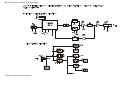
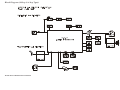
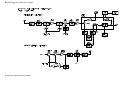
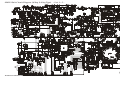
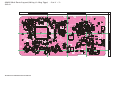
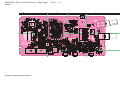
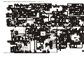
1
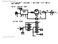
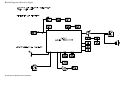
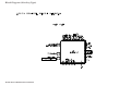
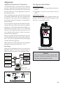
VERTEX STANDARD CO., LTD. 4-8-8 Nakameguro, Meguro-Ku, Tokyo 153-8644, Japan VERTEX STANDARD US Headquarters 10900 Walker Street, Cypress, CA 90630, U.S.A. VX-450 Series YAESU UK LTD. Unit 12, Sun Valley Business Park, Winnall Close Winchester, Hampshire, SO23 0LB, U.K. VHF Band Service Manual VERTEX STANDARD HK LTD. Unit 1306-1308, 13F., Millennium City 2, 378 Kwun Tong Road, Kwun Tong, Kowloon, Hong Kong VERTEX STANDARD (AUSTRALIA) PTY., LTD. Tally Ho Business Park, 10 Wesley Court, East Burwood, VIC, 3151 ©2011 VERTEX STANDARD CO., LTD. EC094N90E Introduction This manual provides the technical information necessary for servicing the VX-450 Series Transceiver. Servicing this equipment requires expertise in handing surface-mount chip components. Attempts by non-qualified persons to service this equipment may result in permanent damage not covered by the warranty, and may be illegal in some countries. Two PCB layout diagrams are provided for each double-sided board in this transceiver. Each side of the board is referred to by the type of the majority of components installed on that side (“Side A” or “Side B”). In most cases one side has only chip components (surface-mount devices), and the other has either a mixture of both chip and leaded components (trimmers, coils, electrolytic capacitors, ICs, etc.), or leaded components only. As described in the pages to follow, the advanced microprocessor design of the VX-450 Series 16 key Type 4 key Type Non-key Type Transceiver allows a complete alignment of this transceiver to be performed without opening the case of the radio; all adjustments can be performed from the front panel, using the “Alignment Mode” menu. While we believe the information in this manual to be correct, VERTEX STANDARD assumes no liability for damage that may occur as a result of typographical or other errors that may be present. Your cooperation in pointing out any inconsistencies in the technical information would be appreciated. Important Note This transceiver was assembled using Pb (lead) free solder, based on the RoHS specification. Only lead-free solder (Alloy Composition: Sn-3.0Ag-0.5Cu) should be used for repairs performed on this apparatus. The solder stated above utilizes the alloy composition required for compliance with the lead-free specification, and any solder with the above alloy composition may be used. Contents Specifications........................................................... 2 Exploded View & Miscellaneous Parts ................. 4 16 key & 4 key Type ...........................................4 Non-key Type ......................................................5 Parts List ................................................................. 6 Block Diagram ........................................................ 7 16 key & 4 key Type ...........................................7 Non-key Type ....................................................11 VX-450 Series VHF Band Service Manual Circuit Description .............................................. 15 Alignment .............................................................. 18 Board Units (Schematics & Layouts) MAIN Unit (16 key & 4 key Type) ................. 32 MAIN Unit (Non-key Type) ............................ 41 Display Unit (16 key & 4 key Type) ............... 47 1 Specifications (USA, EXP) General Frequency range: Channel / Group: Power Supply Voltage: Current Consumption: Channel Spacing: PLL Steps: Battery Life (5-5-90 duty): 2400 mAh FNB-V113LI 1170 mAh FNB-V112LI IP Rating: Operating Temperature Range: Charging Temperature Range: Frequency Stability: RF Input-Output: Dimension (H x W x D): Weight (Approx.): 134-174 MHz 512 CH / 32 Groups (VX-459, VX-454) 32 CH / 2 Group (VX-451) 7.4 V DC ± 10 % 1.7 A (5 W TX) 12.5 / 20 / 25 kHz 12.5 / 2.5 / 5 / 6.25 kHz 18.5 hours (w/saver) / 16 hours 9.5 hours (w/saver) / 8.6 hours IP57 –22 °F to +140 °F (–30 °C to +60 °C) +32 °F to +113 °F (0 °C to +45 °C) ±2.5 ppm 50 Ohms 4.29 x 2.3 x 1.34 inches (109 x 58.5 x 34 mm) (w/FNB-V112LI) 4.29 x 2.3 x 1.69 inches (109 x 58.5 x 43 mm) (w/FNB-V113LI) 10.44 oz (296 g) (w/FNB-V112LI, Antenna, Belt Clip) 11.99 oz (340 g) (w/FNB-V113LI, Antenna, Belt Clip) Receiver (Measurement per TIA/EIA-603) Circuit Type: Sensitivity (12dB SINAD): Adjacent Channel Selectivity: Hum and Noise: Intermodulation: Spurious Image Rejection: Audio output: Double Conversion Super-heterodyne 0.25 μV 70/65 dB (W/N) 45/40 dB (W/N) 70/65 dB (W/N) 70 dB 700 mW (intemal @ 16 Ohms 5% THD) 500 mW (extemal @ 4 Ohms 5% THD) Transmitter (Measurement per TIA/EIA-603) Output Power: 5 / 2.5 / 1 / 0.25 W Modulation: 16K0F3E/11K0F3E) Maximum Deviation: ±5.0 kHz / ±2.5 kHz Conducted Spurious Emissions: 70 dB below carrier FM Hum & Noise: 45 dB / 40 dB Audio Distortion: < 3% @ 1kHz Specifications subject to change without notice or obligation. VX-450 Series VHF Band Service Manual 2 Specifications (EU) General Frequency range: Channel / Group: Power Supply Voltage: Current Consumption: Channel Spacing: PLL Steps: Battery Life (5-5-90 duty): 2400 mAh FNB-V113LI 1170 mAh FNB-V112LI IP Rating: Operating Temperature Range: Charging Temperature Range: Frequency Stability: RF Input-Output: Dimension (H x W x D): Weight (Approx.): 134-174 MHz 512 CH / 32 Groups (VX-459, VX-454) 32 CH / 2 Group (VX-451) 7.4 V DC ± 10 % 1.7 A (5 W TX) 12.5 / 20 / 25 kHz 12.5 / 2.5 / 5 / 6.25 kHz 18.5 hours (w/saver) / 16 hours 9.5 hours (w/saver) / 8.6 hours IP57 –20 °C to +55 °C +5 °C to +35 °C ±2.5 ppm 50 Ohms 4.29 x 2.3 x 1.34 inches (109 x 58.5 x 34 mm) (w/FNB-V112LI) 4.29 x 2.3 x 1.69 inches (109 x 58.5 x 43 mm) (w/FNB-V113LI) 10.44 oz (296 g) (w/FNB-V112LI, Antenna, Belt Clip) 11.99 oz (340 g) (w/FNB-V113LI, Antenna, Belt Clip) Receiver (Measurement per EN300 086) Circuit Type: Sensitivity (20 dB SINAD): Adjacent Channel Selectivity: Hum and Noise: Intermodulation: Spurious Image Rejection: Audio output: Double Conversion Super-heterodyne –4 dBμV / –2 dBμV (W/N) 70/65 dB (W/N) 45/40 dB (W/N) 70/65 dB (W/N) 70 dB 700 mW (intemal @ 16 Ohms 5% THD) 500 mW (extemal @ 4 Ohms 5% THD) Transmitter (Measurement per EN300 086) Output Power: 5 / 2.5 / 1 / 0.25 W Modulation: 16K0F3E/11K0F3E) Maximum Deviation: ±5.0 kHz / ±2.5 kHz Spurious Emissions: –36 dBm (< 1 GHz), –30 dBm (> 1 GHz) FM Hum & Noise: 45 dB / 40 dB Audio Distortion: < 3% @ 1kHz Specifications subject to change without notice or obligation. VX-450 Series VHF Band Service Manual 3 Exploded View & Miscellaneous Parts (16 key & 4 key Type) CP9788001 FRONT CASE ASSY(16KEY) RA1252100 CAP (MIC/SP) RA1250900 BUSH (2 pcs) RA1251000 KNOB (VOL) CP9788002 FRONT CASE ASSY(4KEY) RA1251100 KNOB (FREQ) WINDOW, DOUBLE FACE TAPE, SPONGE RUBBER (LCD), LIGHT GUIDE, O RING, RUBBER (TOP-SEL), RUBBER (SIDE), RUBBER (PTT), FRAME (PTT), KEY PAD (4KEY), LATCH PLATE, COIL SPRING (2 pcs), ESCUTCHEON (DOT), DOUBLE FACE TAPE (ESC), SP NET, SPEAKER, PLATE, WIRE ASSY, BIND HEAD TAPTITE-B M2X5 (2 pcs) RA1250800 RING NUT RA1250900 BUSH (2 pcs) RA1243200 HOLDER (LCD) G6090208 LCD RA1243400 INTER CONNECTOR RA1243300 LIGHT GUIDE (LCD) RA1246600 RUBBER BOOTS(MIC) RA0323800 SHEET M3290032 MIC. ELEMENT P0091542 SP-CONNECTOR RA1243700 REFLECTOR SHEET Please remove the speaker connector from DISPLAY Unit when you remove a FRONT Case of the transceiver. SP-Connector Unmating Operation DISPLAY UNIT RA1247400 PAD(PWB) 1. Hook the lever. MAIN UNIT 2. Pull up friction lock is released. RA1250800 RING NUT RA1277900 LEAF SPRING (TOP-SEL) RA1316200 RUBBER BOOTS (CONT) RA1314300 BLIND SHEET RA124730A O RING 3. Positive lock is released and removal completes. RA037690B SHEET (6X6) CP9787001 CHASSIS (W/ CONNECTOR) SP-Connector Mating Operation RA1313900 PACKING PAD 1.Insert the cable side first. RA1247800 INSULATOR RA124760A LID RA0292100 SHEET (M TEX(010)) 2.Press down at the lever side. Optional Accessories VXSTD P/N AAH12X101 AAH07X001 AAH08X001 AAH73X002 AAH73X003 AAH73X004 Ref. Description Belte Clip CLIP-20 Li-Ion BATTERY PACK FNB-V112LI Li-Ion BATTERY PACK FNB-V113LI Antenna ATV-16A (136 MHz~149 MHz) Antenna ATV-16B (158 MHz~161 MHz) Antenna ATV-16C (162 MHz~174 MHz) VXSTD P/N U24110001 U44105001 U32230001 U20206007 Description BIND HEAD TAPTITE-B M2X10N PAN HEAD TAPTITE-B M2X5NI PAN HEAD SCREW M2X3(3) BINDING HEAD SCREW M2.6X6B RA1278400 CAUTION LABEL Positive lock Friction lock NOTE: H o r i z o n t a l m a t i n g c o u l d damage the connector. Qty. 6 6 2 2 Non-designated parts are available only as part of a designated assembly. VX-450 Series VHF Band Service Manual Li-Ion BATTERY PACK FNB-V112LI or FNB-V113LI Belte Clip CLIP-20 4 Exploded View & Miscellaneous Parts (Non-key Type) RA1252100 CAP (MIC/SP) RA1250800 RING NUT (2pcs) CP9813001 FRONT CASE ASSY RA1250900 BUSH (2pcs) LIGHT GUIDE, RUBBER (TOP-SEL), LATCH PLATE, SP NET, NAME PLATE, FRAME (PTT), COIL SPRING, ESCUTCHEON (16CH), PLATE (FREQ),RUBBER (SIDE), DOUBLE FACE TAPE (ESC), FRONT CASE (NON-KEY), SHEET (M-TEX9_4.5), RUBBER (PTT), PORON SHEET (50X6), BLIND SHEET (SP_WIRE), PLATE, SPEAKER (16OHM-1W), WIRE ASSY (65MM2P2F), BIND HEAD TAPTITE-B M2X5 (2 pcs) RA1251000 KNOB (VOL) RA1251200 WASHER (FREQ) RA1251100 KNOB (FREQ) M3290045 MIC. ELEMENT RA011020A HOLDER RUBBER (MIC) RA1331600 MYLAR SHEET (MIC) (2pcs) RA1331800 BLIND SHEET (SP_WIRE) MAIN Unit RA1332100 SPACER P0091542 SP-CONNECTOR Please remove the speaker connector from DISPLAY Unit when you remove a FRONT Case of the transceiver. SP-Connector Unmating Operation RA1277900 LEAF SPRING (TOP-SEL) RA124730A O RING (CHASSIS) 1. Hook the lever. RA1316200 RUBBER BOOTS (CONT) RA037690B SHEET (6X6) 2. Pull up friction lock is released. CP9812001 CHASSIS ASSY (W/ CONNECTOR) RA1313900 PACKING PAD (OPTION) RA1247800 INSULATOR (OPTN) RA124760A LID (OPTION) 3. Positive lock is released and removal completes. RA0292100 SHEET (MICROTEX C010) RA1278400 CAUTION LABEL SP-Connector Mating Operation 1.Insert the cable side first. Li-Ion BATTERY PACK FNB-V112LI or FNB-V113LI 2.Press down at the lever side. Positive lock Belte Clip CLIP-20 Friction lock NOTE: H o r i z o n t a l m a t i n g c o u l d damage the connector. Ref. VXSTD P/N U24110001 U44105001 U32230001 U20206007 U44110002 Description BIND HEAD TAPTITE-B M2X10N PAN HEAD TAPTITE-B M2X5NI FLAT HEAD SCREW M2X3(3) BINDING HEAD SCREW M2.6X6B PAN HEAD TAPTITE-B M2X10NI Qty. 2 9 2 2 1 Non-designated parts are available only as part of a designated assembly. VX-450 Series VHF Band Service Manual Optional Accessories VXSTD P/N AAH12X101 AAH07X001 AAH08X001 Q3000243 Q3000244 Q3000245 Description Belte Clip CLIP-20 Li-Ion BATTERY PACK FNB-V112LI Li-Ion BATTERY PACK FNB-V113LI Antenna ATV-16A (136 MHz~149 MHz) Antenna ATV-16B (158 MHz~161 MHz) Antenna ATV-16C (162 MHz~174 MHz) 5 Parts List REF. DESCRIPTION VALUE V/W TOL. MAIN PCB with Components MAIN PCB with Components MAIN PCB with Components DISPLAY PCB with Components MAIN Unit Printed Circuit Board MAIN Unit Printed Circuit Board DISPLAY Unit Printed Circuit Board FRONT CASE ASSY FRONT CASE ASSY FRONT CASE ASSY KNOB KNOB SPEAKER HOLDER LIGHT GUIDE INTER CONNECTOR SPONGE RUBBER REFLECTOR SHEET CAP BINDING HEAD SCREW 2 pcs BIND HEAD TAPTITE-B 6 pcs BIND HEAD TAPTITE-B 2 pcs BIND HEAD TAPTITE-B 2 pcs PAN HEAD TAPTITE-B 6 pcs PAN HEAD TAPTITE-B 9 pcs FLAT HEAD SCREW PAN HEAD TAPTITE-B F 1001 CHIP FUSE 3.15A Q 1006 FET S 1001 TACT SWITCH S 1002 TACT SWITCH S 1003 TACT SWITCH S 1004 TACT SWITCH S 1005 ROTARY SWITCH SC1001 SHIELD CASE TH1001 THERMISTOR VR1001 POT. X 1001 TCXO 16.8MHz X 1002 XTAL 32.768kHz XF1001 XTAL FILTER DS2001 LCD J 2002 CONNECTOR J 1008 CONNECTOR MC2001 MIC. ELEMENT MC1001 MIC. ELEMENT VX-450 Series VHF Band Service Manual MFR’S DESIG VXSTD P/N CS2095701 CS2095702 CS2097701 CB5471001 FR021580G FR021670D FR021560E (16KEY) CP9788001 (4KEY) CP9788002 (NON-KEY) CP9813001 (VOL) RA1251000 (FREQ) RA1251100 AC094U 36MM16OHM1W M4090204 (LCD) RA1243200 (LCD) RA1243300 RA1243400 (LCD) RA1243500 RA1243700 (MIC/SP) RA1252100 M2.6X6B U20206007 2X10N U24110001 2X10N U24110001 M2X5 (SPEAKER) U24105001 M2X5 U44105001 M2X5 U44105001 M2X3(3) U32230001 M2X10NI U44110002 FHC16 322ADTP Q0000118 RQA0011DNS G3070392 EVQPUB02K N5090167 EVQPUB02K N5090167 EVQPUB02K N5090167 EVQPUB02K N5090167 TP70GF4161 14.7F RY-10031 N0190196 (VCO) RA1250300 TH05 4B473FR G9090150 TP76N975N13.5FB503RY10034 J60800314 TTS14VSB-A3 16.80MHZ H9501100 4809995L18 32.768KHZ H0103407 1D50811GQ2 50.85M H1102462 GS-35719-TFZWH G6090208 DF57-2P-1.2V(21) P0091542 DF57-2P-1.2V(21) P0091542 EM-140 M3290032 PF0-1055P M3290045 VERS. LOT. SIDE LAY ADR 16 KEY 4 KEY NON-KEY 16 KEY & 4 KEY 16 KEY & 4 KEY NON-KEY 16 KEY & 4 KEY 16 KEY 14 KEY 1NON-KEY 111116 KEY & 4 KEY 116 KEY & 4 KEY 116 KEY & 4 KEY 116 KEY & 4 KEY 116 KEY & 4 KEY 11116 KEY & 4 KEY 1NON-KEY 1116 KEY & 4 KEY 1NON-KEY 11NON-KEY 1111111111111116 KEY & 4 KEY 116 KEY & 4 KEY 1NON-KEY 116 KEY & 4 KEY 1NON-KEY 1- A A B B B A B B A B B A B A A A A A B1 B2 c1 c2 c3 A1 b1 a3 A5 a1 b4 B4 c3 B1 A4 C2 C4 C3 6 Block Diagram (16 key & 4 key Type) VX-450 Series VHF Band Service Manual 7 Block Diagram (16 key & 4 key Type) VX-450 Series VHF Band Service Manual 8 Block Diagram (16 key & 4 key Type) VX-450 Series VHF Band Service Manual 9 Block Diagram (16 key & 4 key Type) VX-450 Series VHF Band Service Manual 10 Block Diagram (Non-key Type) VX-450 Series VHF Band Service Manual 11 Block Diagram (Non-key Type) VX-450 Series VHF Band Service Manual 12 Block Diagram (Non-key Type) VX-450 Series VHF Band Service Manual 13 Block Diagram (Non-key Type) VX-450 Series VHF Band Service Manual 14 Circuit Description 1. Circuit Configuration by Frequency The receiver is a Double-conversion Super-heterodyne with a first intermediate frequency (IF) of 50.85MHz and a second IF of 450KHz. Incoming signal from the antenna is mixed with the local signal from the VCO/PLL to produce the first IF of 50.85 MHz. This is then mixed with the 50.4 MHz second local oscillator output to produce the 450kHz second IF. This is detected to give the demodulated signal. The transmit signal frequency is generated by the PLL VCO, and modulated by the signal from the microphone. It is then amplified and sent to the antenna. 2. Receiver System 2-1. Front-end RF amplifier Incoming RF signal from the antenna is delivered to the RF Unit and passes through Low-pass filer, antenna switching diode, high pass filter and removed undesired frequencies by varactor diode D1006, D1007 and D1009, D1010 (tuned band-pass filer). The passed signal is amplified in Q1007 (2SK293) and moreover cuts an image frequency with the tuned band pass filter and comes into the 1st mixer. 2-2. First Mixer The 1st mixer consists of the Q1015 (3SK293). Buffered output from the VCO is amplified by Q1014 (2SC5005) to provide a pure first local signal between 184.85 and 224.85 MHz for injection to the first mixer. The IF signal then passes through monolithic crystal filters XF1001 (± 7.5 kHz BW) to strip away all but the desired signal. 2-3. IF Amplifier The first IF signal is amplified by Q1025 (2SC5526). The amplified first IF signal is applied to FM IF subsystem IC Q1033 (NJM2591V) which contains the second mixer, second local oscillator, limiter amplifier, noise amplifier, and RSSI amplifier. The signal from reference oscillator X1001 becomes 4 times of frequencies in Q1033, it is mixed with the IF signal and becomes 450 kHz. The second IF then passes through the ceramic filter CF1001 or CF1002 to strip away unwanted mixer VX-450 Series VHF Band Service Manual products, and is applied to the limiter amplifier in Q1033, which removes amplitude variations in the 450kHz IF, before detection of the speech by the ceramic discriminator CD1001 (ECDA450C24). 2-4. Audio amplifier Detected signal from Q1033 (NJM2591V) is inputted to Audio Processor IC Q1013. The signal which appeared from Q1001 is in high pass filter Q1041 (NJM12902V). The signal which passed Q1041 goes to AF volume (VR1001). And then the signal goes to audio amplifier Q1048 (TDA2822L-50B).The output signal from J1006 is in audio speaker. 2-5. Squelch Circuit There are 16 levels of squelch setting from 0 to 15. The level 0 means open the squelch. The level 1 means the threshold setting level and level 14 means tight squelch. From 2 to 13 is established in the middle of threshold and tight. The bigger figure is nearer the tight setting. The level 15 becomes setting of carrier squelch. 2-5-1. Noise Squelch Noise squelch circuit is composed of the band path filter and noise detector of Q1033. When a carrier isn't received, the noise ingredient which goes out of the demodulator Q1033 is amplified in Q1037 through the band path filter, is detected to DC voltage with D1031 and is inputted to 15 pin (the A/D port) of the Q1035 (CPU). When a carrier is received, the DC voltage becomes low because the noise is compressed. When the detected voltage to CPU is high, the CPU stops AF output with Q1049 "OFF" by making the 90 pin (CPU) "L" level. When the detection voltage is low, the CPU makes Q1049 ON with making 90 pin "H" and the AF signal is output. 2-5-2. Carrier Squelch The CPU (14pin: A/D port) detect RSSI voltage output from Q1033 12 pin, and controls AF output. The RSSI output voltage changes according to the signal strength of carrier. The stronger signal makes the RSSI voltage to be higher voltage. 15 Circuit Description The process of the AF signal control is same as Noise Squelch. The shipping data is adjusted -1dBu (EMF) higher than squelch tight sensitivity. 3. Transmitter System 3-1. MIC Amplifier The AF signal from internal microphone MC2001 or external microphone J1004 in to Audio processor IC Q1013. (selected 34pin or 35pin) Q1013 is which contains the microphone amplifier, compandor, Preemphasis, limiter and splatter filter, the processed signal to made FM modulation to transmit carrier by the modulator D1014 (HVC383B) of VCO. Q1013 is DTMF Receiver, and Inversion Type Encryption. 3-2. Drive and Final Amplifier Stages The modulated signal from the VCO Q1023 (2SC4227) is buffered by Q1017 (2SC5005) . Then the signal is buffered by Q1010 (2SC3356) for the final amplifier driver Q1015 (RQA0004PXDQS). The low-level transmit signal is then applied to Q1006 (RQA0011DNS) for final amplification up to 5watts output power. The transmit signal then passes through the antenna switch D1005 (HVU131) and is low pass filtered to suppress away harmonic spurious radiation before delivery to the antenna. 3-3. Automatic Transmit Power Control The current detector Q1040-1 (NJM12904V) detects the current of Q1006 and Q1008, and converts the current difference to the voltage difference. The output from the current detector Q1040-1 is compared with the reference voltage and amplified by the power control amplifier Q1040-2. The output from Q1040-2 controls the gate bias of the final amplifiers Q1006 and the final amplifier driver Q1008. The reference voltage changes into four values (Transmit Power High and Low) controlled by Q1040 (NJM12904V). 3-4. PLL Frequency Synthesizer The frequency synthesizer consists of PLL IC, Q1036 (AK1541), VCO, TCXO (X1001). VX-450 Series VHF Band Service Manual The output frequency from TCXO is 16.8 MHz and the tolerance is +/- 2.5 ppm (in the temperature range -30 to +60 degrees). 3-4-1. VCO (TX Voltage-Controlled Oscillator) While the radio is receiving, the RX oscillator Q1019 (2SK508) in VCO generates a programmed frequency between 201.65 and 241.65MHz as 1st local signal. While the radio is transmitting, the TX oscillator Q1023 (2SC4227) in VCO generates a frequency between 134 and 174 MHz. The output from oscillator is amplified by buffer amplifier Q1017 (2SC5005) and becomes output of VCO. The output from VCO is divided, one is amplified by Q1022 and feed back to the PLL IC 17 pin. The other is amplified in Q1014 and in case of the reception, it is put into the mixer as the 1st local signal through D1011, in transmission, it is buffered Q1010, and more amplified in Q1008 and it is put into the final amplifier Q1008. 3-4-2. VCV (Varactor Control Voltage) Control Tuning voltage of VCO is expanding the lock range of VCO by controlling the cathode of varactor diode at the voltage and the control voltage from PLL IC. 3-4-3. PLL The PLL IC consists of reference divider, main divider, phase detector, charge pumps and pulse swallow operation. The reference frequency from TCXO is inputted to 10 pin of PLL IC and is divided by reference divider. The other hand, inputted feed back signal to 17 pin of PLL IC from VCO is divided with the dividing ratio which becomes same frequency as the output of reference divider. These two signals are compared by phase detector, the phase difference pulse is generated. The phase difference pulse and the pulse from through the charge pumps and LPF. It becomes the DC voltage to control the VCO. The oscillation frequency of VCO is locked by the control of this DC voltage. The PLL serial data from CPU is sent with three lines of SDO (40pin), SCK (36pin) and PSTB (30pin). The lock condition of PLL is output from the UL 16 Circuit Description (18Pin) terminal and UL becomes "H" at the time of the lock condition and becomes "L" at the time of the unlocked condition. The CPU always watches over the UL condition, and when it becomes "L" unlocked condition, the CPU prohibits transmitting and receiving. VX-450 Series VHF Band Service Manual 17 Alignment Introduction The VX-450 series is carefully aligned at the factory for the specified performance across the frequency range specified for each version. Realignment should therefore not be necessary except in the event of a component failure, or altering version type. All component replacement and service should be performed only by an authorized Vertex Standard representative, or the warranty policy may be void. The following procedures cover the sometimes critical and tedious adjustments that are not normally required once the transceiver has left the factory. However, if damage occurs and some parts subsequently are replaced, realignment may be required. If a sudden problem occurs during normal operation, it is likely due to component failure; realignment should not be done until after the faulty component has been replaced. We recommend that servicing be performed only by authorized Vertex Standard service technicians who are experienced with the circuitry and fully equipped for repair and alignment. Therefore, if a fault is suspected, contact the dealer from whom the transceiver was purchased for instructions regarding repair. Authorized Vertex Standard service technicians realign all circuits and make complete performance checks to ensure compliance with factory specifications after replacing any faulty components. Those who do undertake any of the following alignments are cautioned to proceed at their own risk. Problems caused by unauthorized attempts at realignment are not covered by the warranty policy. Also, Vertex Standard reserves the right to change circuits and alignment procedures in the interest of improved performance, without notifying owners. Under no circumstances should any alignment be attempted unless the normal function and operation of the transceiver are clearly understood, the cause of the malfunction has been clearly pinpointed and any faulty components replaced, and realignment determined to be absolutely necessary. VX-450 Series VHF Band Service Manual The following test equipment (and thorough familiarity with its correct use) is necessary for complete realignment. Correction of problems caused by misalignment resulting from use of improper test equipment is not covered under the warranty policy. While most steps do not require all of the equipment listed, the interactions of some adjustments may require that more complex adjustments be performed afterwards. Do not attempt to perform only a single step unless it is clearly isolated electrically from all other steps. Have all test equipment ready before beginning, and follow all of the steps in a section in the order presented. Required Test Equipment RF Signal Generator with calibrated output level at 200 MHz Oscilloscope Deviation Meter (linear detector) In-line Wattmeter with 5 % accuracy at 200 MHz 50 Ohm RF Dummy Load with power rating 10 W at 200 MHz 4 Ohm/1W AF Dummy Load (Attention : Audio output is BTL output) Regulated DC Power Supply (standard 7.5 V DC, 3 A) Frequency Counter with 0.2 ppm accuracy at 200 MHz Audio Signal Generator AC Voltmeter DC Voltmeter VHF Sampling Coupler Microsoft® Windows ® 2000, XP, Vista or Windows7 Vertex Standard CE115 PC Programming Software CT-42 Connection Cable or FIF-10A USB Programming Interface and CT-106 PC Programming Cable. CN-2A (P/N: A08420002) Antenna Connector 18 Alignment Alignment Preparation & Precautions The Alignment Tool Outline A 50-Ohm RF Dummy Load and in-line wattmeter must be connected to the main antenna jack in all procedures that call for transmission, except where specified otherwise. Correct alignment is not possible with an antenna. Installation the tool Install the CE115 (PC Programming Software) to your PC. “Alignment“ function in the “Radio“ menu of CE115. After completing one step, read the following step to determine whether the same test equipment will be required. If not, remove the test equipment (except dummy load and wattmeter, if connected) before proceeding. Action of the switches When the transceiver is in the “Alignment mode,“ the action of the PTT and all PF KEYS are ignored. All of the action is controlled by the PC. Correct alignment requires that the ambient temperature be the same as that of the transceiver and test equipment, and that this temperature be held constant between 68 and 86 °F (20 ~ 30 °C). When the transceiver is brought into the shop from hot or cold air, it should be allowed time to come to room temperature before alignment. Whenever possible, alignments should be made with oscillator shields and circuit boards firmly affixed in place. Also, the test equipment must be thoroughly warmed up before beginning. Note: Signal levels in dB referred to in the alignment procedure are based on 0 dBμ EMF = 1 μV. Test Setup Setup the test equipment as shown for transceiver alignment, apply 7.5 V DC power to the transceiver. Refer to the drawings above for Alignment Points. 50-ohm Dummy Load RF Signal Generator Antenna Connector (CN-2A) RF Sampling Coupler Inline Wattmeter ANT Transceiver MIC/SP Deviation Meter BATTERY TERMINAL POLARITY Caution! Please never turn off a power supply while alignment. If the power supply turn off while alignment, the setting data is failed. BATTERY TERMINAL Power Supply 7.5 VDC CT-42 or FIF10A + CT-106 Frequency Counter COM Port (for CT-42) or USB Port (for FIF10A + CT-106) CLONE GND SP MIC SP MIC CLONE GND AF TEST ADAPTER SCHEMATIC VX-450 Series VHF Band Service Manual 19 Alignment Alignment Mode The Alignment mode allows you to align the entire radio. The value of each parameter can be changed to the desired value by use of the “” / “” and up/ down arrow keys, along with direct number input and dragging of the PC mouse. To enter the Alignment Mode, select “Alignment” in the main “Radio” menu. It will start to “Upload” the alignment data from the radio to the PC. Pressing the “OK” button will then "Download" the alignment data to the radio and exit the Alignment Mode. Note: when all items are to be aligned, it is strongly recommended to align them according to the following sequence. Detailed information for each step may be found in the “Help” file within CE115 (PC Programming Software). 1. VCO (Please do not adjust it) 2. PLL Reference Frequency (Frequency) 3. RX Sensitivity (RX Tune) 4. Squelch (SQL/RSSI) 5. TX Power <High/Low3/Low2/Low1> 6. Maximum Deviation <Wide/Narrow> Please adjust the following items when needed. Modulation Balance <Wide/Narrow> CTCSS Deviation <Wide/Narrow> DCS Deviation <Wide/Narrow> DTMF Alignment Seq Tone VOX ON Level TX MSK Battery Unit During alignment, you may select the value among dBμV,μV (EMF or PD), or dBm. When performing the “RX Tune” and “SQL” alignment, the RF level shows this unit according to this setting. VX-450 Series VHF Band Service Manual 20 Alignment 1. VCO (RX VCO/TX VCO) - Normally there is no need to adjust this parameter This parameter is to align the VCO Voltage adjustment. 2. PLL REFERENCE FREQUENCY (FREQUENCY) This parameter is to align the reference frequency for PLL. VX-450 Series VHF Band Service Manual 1. Press the “Frequency” button to start the alignment. The Frequency Alignment window will appear. 2. Click the “PTT” button or press the “SPACE” bar, and the radio will start to transmit on the center frequency channel. 3. Set the value to get the desired frequency by dragging the slide bar, clicking the up-down button, pressing the left or right arrow key, or entering the value in the entry box. 4. After getting the desired frequency click the “PTT” button or press the “SPACE” bar to stop transmitting. 5. Click the “OK” button to finish the frequency alignment and save the data. 21 Alignment 3. RX SENSITIVITY (RX TUNE) This parameter is to align the RX BPF (Band Pass Filter) for Receive (RX) sensitivity. The PLL Reference Frequency (Frequency) alignment must be done before this alignment is performed. 1. Press the “RX Tune” button to start the alignment. The RX Sensitivity Alignment window will appear. 2. Click the left mouse button on the slide bar or press Up / Down arrow key, to switch to the selected channel. 3. Set the Signal Generator according to the indication at the top of the screen (Setting Your SG as followings). 4. Drag the slide bar, click the up-down buttons, press the left or right arrow key, or enter the value in the entry box to get the best RX sensitivity (Highest RSSI value). 5. Click the “OK” button to finish the RX Sensitivity alignment and save the data. ADJ Type Basic: “Low-edge / band center / high-edge“ and select the channel for alignment (Default). Single : Alignment value changes only on the selected channel. All Freq : Alignment value changes on all channels. VX-450 Series VHF Band Service Manual 22 Alignment 4. SQUELCH (SQL) This parameter is to align the SQL (Squelch) Sensitivity. There are several alignments as follows in the Squelch Sensitivity. Tight SQL Level (TI NSQ W/N) The Alignment for the Noise SQL Tight level at Wide (5k/4k) or Narrow (2.5k). Threshold SQL Level (TH NSQ W/N) The Alignment for the Noise SQL Threshold level at Wide (5k/4k) or Narrow (2.5k). Tight SQL RSSI Level (TI RSSI W/N) The Alignment for the “level 14” of the RSSI SQL level at Wide (5k/4k) or Narrow (2.5k). TX Save RSSI Level (TX SAVE W/N) The Alignment for the TX Save RSSI level at Wide (5k/4k) or Narrow (2.5k). VX-450 Series VHF Band Service Manual The procedure for all the alignments is as follows. 1. Click the “Start” button to open the alignment window in the SQL/RSSI Alignment menu. 2. The Alignment window will appear, Set the Signal Generator according to the indication, then click the “Start” button. 3. The automatic alignment will start to get the SQL or RSSI level. 4. It will show the alignment result in the “New” box. 5. Click the “OK” button, then the data will be saved and the alignment is finished. 23 Alignment 5. TX POWER This parameter is to align the “Power High”, “Power Low3”, “Power Low2” or “Power Low1” for the selected channel. VX-450 Series VHF Band Service Manual 1. Press the “TX Pwr(H / L3 / L2 / L1)” button to start the alignment. The TX Power Alignment window will appear. 2. Click the left mouse button on the slide bar or press the Up / Down arrow key, to select the desired channel. 3. Click the “PTT” button or press the “SPACE” bar at the desired channel, then the radio starts to transmit on the selected channel. 4. Set the value to get desired output power (High: 5 W, Low3: 2.5 W, Low2: 1 W, Low1: 250 mW) on the Power Meter by dragging the slide bar, clicking the up-down button, pressing the left or right arrow key, or entering the value in the entry box on the selected channel. 5. After getting the desired output power click the “PTT” button or press the “SPACE” bar to stop transmitting. 6. Click the “OK” button to finish the TX Power alignment and save the data. ADJ Type Basic: “Low-edge / band center / high-edge“ and select the channel for alignment (Default). Single : Alignment value changes only on the selected channel. All Freq : Alignment value changes on all channels. 24 Alignment 6. MAXIMUM DEVIATION <WIDE> / <NARROW> This parameter is to align the “Maximum Deviation” (Wide/Narrow). It requires the appropriate JIG (Tuning Interface BOX). Connect the JIG and Test Equipment to the radio before the alignment is started. VX-450 Series VHF Band Service Manual 1. Press the “Max Dev (W /N)” button to start the alignment. 2. The Max Deviation alignment window will appear. 3. Connect the Generator, Inject a1 kHz tone / Sine Wave / -10 dBm to the MIC jack. 4. Click the left mouse button on the slide bar or press the Up / Down arrow key, to select the desired channel. 5. Click the “PTT” button or press the “SPACE” bar the radio starts to transmit on the selected channel. 6. Set the value to get desired deviation (Wide: 4.2kHz, Narrow: 2.1kHz) on the deviation meter by dragging the slide bar, clicking the up-down button, pressing the left or right arrow key, or entering the value in the entry box on the selected channel. 7. After getting the desired deviation click the “PTT” button or press the “SPACE” bar to stop transmitting. 8. Click the “OK” button to finish the Max Deviation alignment and save the data. ADJ Type Basic: “Low-edge / band center / high-edge“ and select the channel for alignment (Default). Single : Alignment value changes only on the selected channel. All Freq : Alignment value changes on all channels. 25 Alignment Please adjust the following items when needed. MODULATION BALANCE <WIDE> / <NARROW> (THIS ALIGNMENT IS DIFFICULT.) This parameter is to align the “Modulation Balance” (Wide/Narrow). It needs the appropriate JIG (Tuning Interface BOX). Connect the JIG and Test Equipment to the radio before the alignment is started. VX-450 Series VHF Band Service Manual 1. Press the “Mod Bal (W / N)” button to start the alignment. 2. The Modulation Balance Alignment window will appear. 3. Connect the Generator, Inject a 400Hz tone / Sine Wave / -10 dBm to the MIC jack. 4. Click the left mouse button on the slide bar or press the Up / Down arrow key, to select the desired channel. 5. Click the “PTT” button or press the “SPACE” bar the radio starts to transmit on the selected channel. 6. Set the value to get “the best square wave” on the Oscilloscope by dragging the slide bar, clicking the up-down button, pressing the left or right arrow key, or entering the value in the entry box on the selected channel. 7. After getting the “the best square wave” click the “PTT” button or press the “SPACE” bar to stop transmitting. 8. Click the “OK” button to finish the Modulation Balance alignment and save the data. ADJ Type Basic: “Low-edge / band center / high-edge“ and select the channel for alignment (Default). Single : Alignment value changes only on the selected channel. All Freq : Alignment value changes on all channels. 26 Alignment CTCSS DEVIATION <WIDE> / <NARROW> This parameter is to align CTCSS Deviation of the selected channel. VX-450 Series VHF Band Service Manual 1. Press the “CTC Dev (W / N)” button to start the alignment. The CTCSS Deviation Alignment window will appear. 2. Click the left mouse button on the slide bar or press the Up / Down arrow key, to select the desired channel. 3. Click the “PTT” button or press the “SPACE” bar the radio starts to transmit with CTCSS tone on the selected channel. 4. Set the value to get desired deviation on the deviation meter by dragging the slide bar, clicking the up-down button, pressing the left or right arrow key, or entering the value in the entry box on the selected channel.. 5. After getting the desired deviation (Wide: 0.6 kHz, Narrow: 0.3 kHz) click the “PTT” button or press “SPACE” bar to stop transmitting. 6. Click the “OK” button to finish the CTCSS Deviation alignment and save the data. ADJ Type Basic: “Low-edge / band center / high-edge“ and select the channel for alignment (Default). Single : Alignment value changes only on the selected channel. All Freq : Alignment value changes on all channels. 27 Alignment DCS DEVIATION <WIDE> / <NARROW> This parameter is to align “DCS Deviation” of the selected channel. VX-450 Series VHF Band Service Manual 1. Press the “DCS Dev (W / N)” button to start the alignment. The DCS Deviation Alignment window will appear. 2. Click the left mouse button on the slide bar or press the Up / Down arrow key, to select the desired channel. 3. Click the “PTT” button or press the “SPACE” bar the radio starts to transmit with DCS Code on the selected channel. 4. Set the value to get desired deviation (Wide: 0.6 kHz, Narrow: 0.3 kHz) on the deviation meter by dragging the slide bar, clicking the up-down button, pressing the left or right arrow key, or entering the value in the entry box on the selected channel. 5. After getting the desired deviation click “PTT” button or press “SPACE” bar to stop transmitting. 6. Click the “OK” button to finish the DCS Deviation alignment and save the data. ADJ Type Basic: “Low-edge / band center / high-edge“ and select the channel for alignment (Default). Single : Alignment value changes only on the selected channel. All Freq : Alignment value changes on all channels. 28 Alignment DTMF DEVIATION This parameter is to align “DTMF Deviation”. 1. Press the “DTMF” button to start the alignment. The DTMF Alignment window will appear. 2. Click the “PTT” button or press the “SPACE” bar the radio starts to transmit on the Center frequency channel. 3. Set the value to get desired deviation (3.0 kHz) on the deviation meter by dragging the slide bar, clicking the up-down button, pressing the left or right arrow key, or entering the value in the entry box. 4. After getting the desired deviation click the “PTT” button or press the “SPACE” bar to stop transmitting.. 5. Click the “OK” button to finish the DTMF Deviation alignment and save the data. SEQUENTIAL TONE DEVIATION This parameter is to align “Sequential Tone Deviation”. VX-450 Series VHF Band Service Manual 1. Press the “Seq Tone” button to start the alignment. The Sequential Tone Deviation Alignment window will appear. 2. Click the “PTT” button or press the “SPACE” bar the radio starts to transmit on the Center frequency channel. 3. Set the value to get desired deviation (3.0 kHz) on the deviation meter by dragging the slide bar, clicking the up-down button, pressing the left or right arrow key, or entering the value in the entry box. 4. After getting the desired deviation click the “PTT” button or press the “SPACE” bar to stop transmitting. 5. Click the “OK” button to finish the Sequential Tone Deviation alignment and save the data. 29 Alignment VOX ON LEVEL This parameter is to align the “VOX On Level”. Set the Sensitivity of the VOX circuitry's input audio detector. 1. Press the “VOX ON Level” button to start the alignment. The VOX ON Level window will appear. 2. Then input the alignment value in the “New” box. Default: 80 Input Range: 0 (Level Down) ~ 255 (Level Up) 3. Click the “OK” button, the data will be saved and the alignment is complete. TX MSK LEVEL This parameter is to align the modulation level of the ANI function. 1. Press the “TX MSK” button to start the alignment. The TX MSK Level window will appear. 2. Then input the alignment value in the “New” box. Default: 9 Input Range: 0 (Level Down) ~ 15 (Level Up) 3. Click the “OK” button, the data will be saved and the alignment is complete. VX-450 Series VHF Band Service Manual 30 Alignment BATTERY This parameter is to align the “Low Battery Alert Level” and “EEPROM Protect Level” voltage. When the DC power source voltage drops below the “EEPROM Protect Level” voltage, the radio will stop writing data to the EEPROM to prevent erroneous writing. VX-450 Series VHF Band Service Manual 1. Set the value of the DC Power source to 6.5V (according to the indication) and click the “Start” button. The new alignment value will show in the “New” box. 2. Set the value of the DC Power source to 5.5V (according to the indication) and click the “Start” button. The new alignment value will show in the "New” box. 3. Click the “OK” button, the data will be saved and the alignment is complete. 4. Set the value of the DC Power source to 7.5V (according to the indication). 31 MAIN Unit Circuit Diagram (16 key & 4 key Type) VX-450 Series VHF Band Service Manual - Lot. 1 ~ 3 - 32 MAIN Unit Parts Layout (16 key & 4 key Type) Side A 5 4 - Lot. 1 ~ 3 - 3 2 1 A B C VX-450 Series VHF Band Service Manual 33 MAIN Unit Parts Layout (16 key & 4 key Type) Side B 5 4 - Lot. 1 ~ 3 - 3 2 1 a b c VX-450 Series VHF Band Service Manual 34 MAIN Unit Circuit Diagram (16 key & 4 key Type) VX-450 Series VHF Band Service Manual - Lot. 4 ~ 6 - 35 MAIN Unit Parts Layout (16 key & 4 key Type) - Lot. 4 ~ 6 Side A 5 4 3 2 1 A B C VX-450 Series VHF Band Service Manual 36 MAIN Unit Parts Layout (16 key & 4 key Type) - Lot. 4 ~ 6 Side B 5 4 3 2 1 a b c VX-450 Series VHF Band Service Manual 37 MAIN Unit Circuit Diagram (16 key & 4 key Type) VX-450 Series VHF Band Service Manual - Lot. 7 ~ - 38 MAIN Unit Parts Layout (16 key & 4 key Type) Side A 5 4 - Lot. 7 ~ - 3 2 1 A B C VX-450 Series VHF Band Service Manual 39 MAIN Unit Parts Layout (16 key & 4 key Type) Side B 5 4 - Lot. 7 ~ - 3 2 1 a b c VX-450 Series VHF Band Service Manual 40 MAIN Unit Circuit Diagram (Non-key Type) VX-450 Series VHF Band Service Manual - Lot. 1 ~ 5 - 41 MAIN Unit Parts Layout (Non-key Type) Side A 5 4 - Lot. 1 ~ 5 - 3 2 1 A B C VX-450 Series VHF Band Service Manual 42 MAIN Unit Parts Layout (Non-key Type) Side B 5 4 - Lot. 1 ~ 5 - 3 2 1 a b c VX-450 Series VHF Band Service Manual 43 MAIN Unit Circuit Diagram (Non-key Type) VX-450 Series VHF Band Service Manual - Lot. 6 ~ - 44 MAIN Unit Parts Layout (Non-key Type) Side A 5 4 - Lot. 6 ~ - 3 2 1 A B C VX-450 Series VHF Band Service Manual 45 MAIN Unit Parts Layout (Non-key Type) Side B 5 4 - Lot. 6 ~ - 3 2 1 a b c VX-450 Series VHF Band Service Manual 46 DISPLAY Unit Circuit Diagram (16 key & 4 key Type) - Lot. 1 ~ 3 - VX-450 Series VHF Band Service Manual 47 DISPLAY Unit Parts Layout (16 key & 4 key Type) - Lot. 1 ~ 3 Side A 4 3 2 1 A B C VX-450 Series VHF Band Service Manual 48 DISPLAY Unit Parts Layout (16 key & 4 key Type) Side B 4 - Lot. 1 ~ 3 - 3 2 1 a b c VX-450 Series VHF Band Service Manual 49 DISPLAY Unit Circuit Diagram (16 key & 4 key Type) VX-450 Series VHF Band Service Manual - Lot. 4 ~ - 50 DISPLAY Unit Parts Layout (16 key & 4 key Type) Side A 4 3 - Lot. 4 ~ - 2 1 A B C VX-450 Series VHF Band Service Manual 51 DISPLAY Unit Parts Layout (16 key & 4 key Type) Side B 4 - Lot. 4 ~ - 3 2 1 a b c VX-450 Series VHF Band Service Manual 52 Copyright 2011 VERTEX STANDARD CO., LTD. All rights reserved No portion of this manual may be reproduced without the permission of VERTEX STANDARD CO., LTD. VX-450 Series VHF Band Service Manual 53