1
RabbitCore RCM3400
C-Programmable Analog Core Module
with 10/100Base-T Reference Design
User’s Manual
019–0122_N
RabbitCore RCM3400 User’s Manual
©2011 Digi International® Inc.
All rights reserved.
Rabbit, Dynamic C, Rabbit 4000, Digi, Digi International, Digi International Company, and the Digi and Rabbit logos are trademarks or registered trademarks of Digi
International, Inc. in the United States and other countries worldwide. All other trademarks are the property of their respective owners.
Information in this document is subject to change without notice and does not represent a commitment on the part of Digi International.
Digi provides this document "as is," without warranty of any kind, expressed or
implied, including, but not limited to, the implied warranties of fitness or merchantability for a particular purpose. Digi may make improvements and/or changes in this
manual or in the product(s) and/or the program(s) described in this manual at any
time.
This product could include technical inaccuracies or typographical errors. Changes
are periodically made to the information herein; these changes may be incorporated in
new editions of the publication.
The latest revision of this manual is available at www.digi.com.
RabbitCore RCM3400
TABLE OF CONTENTS
Chapter 1. Introduction
1
1.1 RCM3400 Features ...............................................................................................................................1
1.2 Advantages of the RCM3400 ...............................................................................................................3
1.3 Development and Evaluation Tools......................................................................................................4
1.3.1 RCM3400 Development Kit .........................................................................................................4
1.3.2 Software ........................................................................................................................................5
1.3.3 Connectivity Interface Kits ...........................................................................................................5
1.3.4 Online Documentation ..................................................................................................................5
Chapter 2. Getting Started
7
2.1 Install Dynamic C .................................................................................................................................7
2.2 Hardware Connections..........................................................................................................................8
2.2.1 Attach Module to Prototyping Board............................................................................................8
2.2.2 Connect Programming Cable ........................................................................................................9
2.2.3 Connect Power ............................................................................................................................10
2.2.3.1 Overseas Development Kits ............................................................................................... 10
2.3 Run a Sample Program .......................................................................................................................11
2.3.1 Troubleshooting ..........................................................................................................................11
2.4 Where Do I Go From Here? ...............................................................................................................12
2.4.1 Technical Support .......................................................................................................................12
Chapter 3. Running Sample Programs
13
3.1 Introduction.........................................................................................................................................13
3.2 Sample Programs ................................................................................................................................14
3.2.1 Serial Communication.................................................................................................................15
3.2.2 A/D Converter Inputs..................................................................................................................17
3.2.3 Real-Time Clock .........................................................................................................................18
3.2.4 TCP/IP Sample Programs ...........................................................................................................18
3.2.5 LCD/Keypad Module Sample Programs ....................................................................................18
Chapter 4. Hardware Reference
19
4.1 RCM3400 Digital Inputs and Outputs ................................................................................................20
4.1.1 Memory I/O Interface .................................................................................................................26
4.1.2 Other Inputs and Outputs ............................................................................................................26
4.2 Serial Communication ........................................................................................................................27
4.2.1 Serial Ports ..................................................................................................................................27
4.2.2 Programming Port .......................................................................................................................27
4.3 Serial Programming Cable..................................................................................................................29
4.3.1 Changing Between Program Mode and Run Mode ....................................................................29
4.3.2 Standalone Operation of the RCM3400......................................................................................30
User’s Manual
4.4 A/D Converter .................................................................................................................................... 31
4.4.1 A/D Converter Calibration ......................................................................................................... 33
4.4.2 A/D Converter Power Supply..................................................................................................... 33
4.5 Other Hardware .................................................................................................................................. 34
4.5.1 Clock Doubler ............................................................................................................................ 34
4.5.2 Spectrum Spreader...................................................................................................................... 34
4.6 Memory .............................................................................................................................................. 35
4.6.1 SRAM......................................................................................................................................... 35
4.6.2 Flash EPROM............................................................................................................................. 35
4.6.3 Dynamic C BIOS Source Files................................................................................................... 35
Chapter 5. Software Reference
37
5.1 More About Dynamic C..................................................................................................................... 37
5.2 Dynamic C Function Calls ................................................................................................................. 39
5.2.1 Digital I/O................................................................................................................................... 39
5.2.2 Serial Communication Drivers ................................................................................................... 39
5.2.3 TCP/IP Drivers ........................................................................................................................... 39
5.2.4 Prototyping Board Function Calls .............................................................................................. 40
5.2.5 Board Initialization..................................................................................................................... 40
5.2.6 Analog Inputs ............................................................................................................................. 41
5.3 Upgrading Dynamic C ....................................................................................................................... 55
5.3.1 Upgrades..................................................................................................................................... 55
Appendix A. RCM3400 Specifications
57
A.1 Electrical and Mechanical Characteristics ........................................................................................ 58
A.1.1 Headers ...................................................................................................................................... 62
A.2 Bus Loading ...................................................................................................................................... 63
A.3 Rabbit 3000 DC Characteristics ........................................................................................................ 66
A.4 I/O Buffer Sourcing and Sinking Limit............................................................................................. 67
A.5 Conformal Coating ............................................................................................................................ 68
A.6 Jumper Configurations ...................................................................................................................... 69
Appendix B. Prototyping Board
71
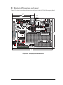
B.1 Introduction ....................................................................................................................................... 72
B.1.1 Prototyping Board Features ....................................................................................................... 73
B.2 Mechanical Dimensions and Layout ................................................................................................. 75
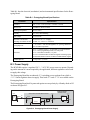
B.3 Power Supply..................................................................................................................................... 76
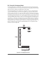
B.4 Using the Prototyping Board ............................................................................................................. 77
B.4.1 Adding Other Components ........................................................................................................ 79
B.4.2 Measuring Current Draw ........................................................................................................... 79
B.4.3 Analog Features ......................................................................................................................... 80
B.4.3.1 A/D Converter Inputs........................................................................................................ 80
B.4.3.2 Thermistor Input ............................................................................................................... 82
B.4.3.3 A/D Converter Calibration................................................................................................ 83
B.4.4 Serial Communication ............................................................................................................... 84
B.4.4.1 RS-232 .............................................................................................................................. 85
B.4.4.2 RS-485 .............................................................................................................................. 86
B.4.4.3 Ethernet Port ..................................................................................................................... 88
B.4.5 Other Prototyping Board Modules............................................................................................. 89
B.5 RCM3400 Prototyping Board Jumper Configurations...................................................................... 90
Appendix C. Using the TCP/IP Features
93
C.1 TCP/IP Connections .......................................................................................................................... 93
C.2 TCP/IP Primer on IP Addresses ........................................................................................................ 95
C.2.1 IP Addresses Explained ............................................................................................................. 97
C.2.2 How IP Addresses are Used....................................................................................................... 98
C.2.3 Dynamically Assigned Internet Addresses ................................................................................ 99
RabbitCore RCM3400
C.3 Placing Your Device on the Network ..............................................................................................100
C.4 Running TCP/IP Sample Programs..................................................................................................101
C.4.1 How to Set IP Addresses in the Sample Programs...................................................................102
C.4.2 How to Set Up your Computer’s IP Address for Direct Connect ............................................103
C.5 Run the PINGME.C Sample Program .............................................................................................104
C.6 Running Additional Sample Programs With Direct Connect ..........................................................104
C.7 Where Do I Go From Here?.............................................................................................................105
Appendix D. LCD/Keypad Module
107
D.1 Specifications ...................................................................................................................................107
D.2 Contrast Adjustments for All Boards...............................................................................................109
D.3 Keypad Labeling ..............................................................................................................................110
D.4 Header Pinouts .................................................................................................................................111
D.4.1 I/O Address Assignments.........................................................................................................111
D.5 Mounting LCD/Keypad Module on the Prototyping Board ............................................................112
D.6 Bezel-Mount Installation .................................................................................................................113
D.6.1 Connect the LCD/Keypad Module to Your Prototyping Board...............................................115
D.7 Sample Programs .............................................................................................................................116
D.8 LCD/Keypad Module Function Calls ..............................................................................................117
D.8.1 LCD/Keypad Module Initialization .........................................................................................117
D.8.2 LEDs ........................................................................................................................................117
D.8.3 LCD Display ............................................................................................................................118
D.8.4 Keypad .....................................................................................................................................138
Appendix E. Power Supply
141
E.1 Power Supplies .................................................................................................................................141
E.1.1 Battery-Backup Circuits ...........................................................................................................141
E.1.2 Reset Generator ........................................................................................................................142
Index
User’s Manual
143
RabbitCore RCM3400
1. INTRODUCTION
The RCM3400 is a compact module that incorporates the powerful Rabbit® 3000 microprocessor, flash memory, static RAM,
digital I/O ports, analog inputs, and PWM outputs.
The Development Kit has the essentials that you need to design
your own microprocessor-based system, and includes a complete Dynamic C software development system. This Development Kit also contains a Prototyping Board that will allow you
to evaluate the RCM3400 and to prototype circuits that interface
to the RCM3400 module. You will also be able to write and test
software for the RCM3400 modules, including Ethernet or
TCP/IP applications.
Throughout this manual, the term RCM3400 refers to the complete series of RCM3400
RabbitCore modules unless other production models are referred to specifically.
The RCM3400 has a Rabbit 3000 microprocessor operating at up to 29.4 MHz, static
RAM, flash memory, an 8-channel A/D converter, two clocks (main oscillator and timekeeping), and the circuitry necessary for reset and management of battery backup of the
Rabbit 3000’s internal real-time clock and the static RAM. Two 34-pin headers bring out
the Rabbit 3000 I/O bus lines, parallel ports, A/D converter channels, and serial ports.
The RCM3400 receives its +3.3 V power from the customer-supplied motherboard on
which it is mounted. The RCM3400 can interface with all kinds of CMOS-compatible
digital devices through the motherboard.
1.1 RCM3400 Features
• Small size: 1.16" × 1.37" × 0.31"
(29 mm × 34 mm × 8 mm)
• Microprocessor: Rabbit 3000 running at up to 29.4 MHz
• 47 parallel 5 V tolerant I/O lines: 41 configurable for I/O, 3 fixed inputs, 3 fixed outputs
• Two additional digital inputs, one additional digital output
• Combinations of up to eight single-ended or four differential analog inputs
User’s Manual
1
• One additional analog input (CONVERT)
• External reset input
• Alternate I/O bus can be configured for 8 data lines and 6 address lines (shared with
parallel I/O lines), I/O read/write
• Ten 8-bit timers (six cascadable) and one 10-bit timer with two match registers
• 512K flash memory, 512K SRAM, (options for 256K flash memory and 256K SRAM)
• Real-time clock
• Watchdog supervisor
• Provision for customer-supplied backup battery via connections on header J2
• 10-bit free-running PWM counter and four width registers
• Two-channel Input Capture can be used to time input signals from various port pins
• Two-channel Quadrature Decoder accepts inputs from external incremental encoder
modules
• Five CMOS-compatible serial ports: maximum asynchronous baud rate of 5.5 Mbps.
Four ports are configurable as a clocked serial port (SPI), and two ports are configurable as SDLC/HDLC serial ports.
• Supports 1.15 Mbps IrDA transceiver
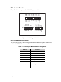
There are two RCM3400 production models. Table 1 summarizes their main features.
Table 1. RCM3400 Features
Feature
RCM3400
Microprocessor
RCM3410
Rabbit 3000 at 29.4 MHz
Flash Memory
512K
256K
SRAM
512K
256K
A/D Converter
Serial Ports
12 bits
5 shared high-speed, CMOS-compatible ports:
5 are configurable as asynchronous serial ports;
4 are configurable as clocked serial ports (SPI);
2 are configurable as SDLC/HDLC serial ports;
1 asynchronous serial port is used during programming
The RCM3400 can be programmed through connections on the motherboard supporting
RS-232, USB with an RS-232/USB converter, or over an Ethernet connection.
Appendix A provides detailed specifications for the RCM3400.
2
RabbitCore RCM3400
1.2 Advantages of the RCM3400
• Fast time to market using a fully engineered, “ready-to-run/ready-to-program” microprocessor core.
• Competitive pricing when compared with the alternative of purchasing and assembling
individual components.
• Easy C-language program development and debugging
• Rabbit Field Utility to download compiled Dynamic C .bin files, and cloning board
options for rapid production loading of programs.
• Generous memory size allows large programs with tens of thousands of lines of code,
and substantial data storage.
• Reference design allows integrated Ethernet port for network connectivity, with
royalty-free TCP/IP software.
User’s Manual
3
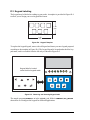
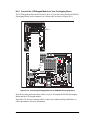
1.3 Development and Evaluation Tools
1.3.1 RCM3400 Development Kit
The RCM3400 Development Kit contains the hardware essentials you will need to use
your RCM3400 module. The items in the Development Kit and their use are as follows.
• RCM3400 module.
• Prototyping Board.
• AC adapter, 12 V DC, 1 A. (Included only with Development Kits sold for the North
American market. A header plug leading to bare leads is provided to allow overseas
users to connect their own power supply with a DC output of 8–24 V at 8 W.)
• 10-pin header to DB9 programming cable with integrated level-matching circuitry.
• Dynamic C CD-ROM, with complete product documentation on disk.
• Getting Started instructions.
• A bag of accessory parts for use on the Prototyping Board.
• Rabbit 3000 Processor Easy Reference poster.
• Registration card.
Programming
Cable
AC Adapter
(North American
kits only)
Accessory Parts for
Prototyping Board
J8
DS4
CUR
MEARENT
OPT SUREME
ION NT
D2
D1
J9
JP10
RS-23
R60
R61
TxD
RxD
GND
2
C24
C27
R46
C57
C61
R58C44
C48
U10
GND
C54
C55
C47
DCIN
C58
R55
R52
R56
Y1
C52
HOT
+5 V
+3.3 V
U12
+5 V
C56
C59
C60
U13
R64
GND
D7
5
3
1
LT
LED
+BK
LCD1JA
+3.3
GND
+5 V
GND
V
R25
R28
R19
LED
+3.3 V
LED
JP6
JP7
/CS
+3.3
V
D6
D2
D5
6
D0
D4
A1
2
A3
4
LED
GND
A0
LED
A2
D3
LED
GND
D1
0
LED
+V
/RESE
T
C50
+5 V
RC
L1
J7
R50
R51
R53
R48 C49
C39
C38
U6
C45
R6
R7
TxC
RxE
GND
2
C29
RS-23
TxF
R22
R16
U2 C13
RxC
J2
R21
BT1
Battery
TxE
PROGRAM
33
RxF
485
JP3
1
C46
R59
C51
U7
S1
R54
C42
C49
C40
GND
RS-485
JUMPER
DEFAULT (12, 56)
J6
M1JB
DS3
+485
J4
J5
M1JA
AIN2
AIN3
AIN4
AIN5
AIN6 THERM GND CNVRT VREF
D6
D4
D2
D0
A3
A1
A2
D7
D5
D3
D1
GND
GND
LCD1JC
A1
T
6
2
0
4
LED
GND
LED
LED
/RESE
LDE
+V
5
3
1
GND
/CS
GND
LED
LCD1JB
DS2
R47
R57
PD7
+3.3 V
2
1
PD5
LED
+BK
LT
R43
R44
R38
R35
R27
R32
R12
R15
R18
PD6
S2
AIN1
LED
R34
mA
420
R37
C20
R33
C17
R30
C16
R24
C8
C15
R20
C14
R17
C12
+5 V
DS1
R11
C10
GND
JP9
JP2
JP1
R23
J3
R36 34
RC
2
R31
R29
C9
R9
C6
R13
R14
C11
U1
JP5
C2
St
LINK ACT
C3
C4
R8
RCM3400
PROTOTYPING
BOARD
GND AIN0
tti
C41
C31
C32
R45
C33
C34
C35
C36
C37
RESET
1
POWER
59
60
R2
R39
R40
R41
R42
R62
R65
R67
PF1
PF5
PF7
PG1
C1
R4
R5
R3
amic C are registered trademarks of Rabbit Semiconductor Inc.
C30
C53
C43
RN1
RN2
IR1
R1
C25
U5
C23
CX9
CX10
CX11
GND
PG5
+3.3 V
GND
GND
00 Processor Easy Reference poster.
on card.
C22
C26
CX7
PG7
RESET IN
GND
+3.3 V
VBAT
C CD-ROM, with complete product documentation on disk.
tarted instructions.
C28
C18
JP8
JP4
CX8
CX6
2
PG3
PG2
PG4
PG6
/RES OUT
ader to DB9 programming cable with integrated level-matching circuitry.
U3
PE7
PE6
PF4
PF6
PG0
er, 12 V DC, 1 A. (Included only with Development Kits sold for the North American market.
plug leading to bare leads is provided to allow overseas users to connect their own power
th a DC output of 8–24 V.)
accessory parts for use on the Prototyping Board.
R26
PD6
PE0
PE2
PE5
PF0
0 module.
ng Board.
PG6
PG7
CX3
CX4
CX5
PD4
PD0
PD7
PE1
PE4
00 Development Kit contains the following items:
R10
C7
CX2
UX2
CX1
UX1
/IORD
STAT
SMD2
PD5
ment Kit Contents
C21
C19
J1
PA3
PA5
PA7
PB2
PB4
PB6
PC0
PC2
PC6
U4
C5
PA1
PA0
PA2
PA4
PA6
PB1
PB3
PB5
PB7
PC1
PC3
PC7
/IOWR
SMODE1
DS5
ng Dynamic C®
CD from the Development Kit in your PC’s CD-ROM drive. If the instalnot auto-start, run the setup.exe program in the root directory of the
C CD. Install any Dynamic C modules after you install Dynamic C.
bbitCore RCM3400
S3
1
PD4
2
GND
+5 V
+3.3 V
GND
+5 V
t d
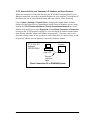
Figure 1. RCM3400 Development Kit
4
RabbitCore RCM3400
1.3.2 Software
The RCM3400 is programmed using version 7.32 or later of Dynamic C. A compatible
version is included on the Development Kit CD-ROM.
Digi also offers add-on Dynamic C modules containing the popular C/OS-II real-time
operating system, as well as PPP, Advanced Encryption Standard (AES), and other select
libraries. In addition to the Web-based technical support included at no extra charge, a
one-year telephone-based technical support module is also available for purchase. Visit
our Web site at www.digi.com or contact your Digi sales representative or authorized distributor for further information.
1.3.3 Connectivity Interface Kits
Digi has available additional interface kits to allow you to provide a wireless interface to
the RCM3400 and to use the RCM3400 with header sockets that have a 0.1" pitch.
• 802.11b Wi-Fi Add-On Kit (Part No. 101-0998)—The Wi-Fi Add-On Kit for the
RCM3400 footprint consists of an RCM3400 Interposer Board, a Wi-Fi CompactFlash
card with a CompactFlash Wi-Fi Board, a ribbon interconnecting cable, and the software drivers and sample programs to help you enable your RCM3400 module with
Wi-Fi capabilities. The RCM3400 Interposer Board is placed between the RCM3400
module and the RCM3400 Prototyping Board so that the CompactFlash Wi-Fi Board,
which holds the Wi-Fi CompactFlash card, can be connected to the RCM3400-based
system via the ribbon cable provided.
• Connector Adapter Board (Part No. 151-0114)—allows you to plug the RCM3400
whose headers have a 1.27 mm pitch into header sockets with a 0.1" pitch.
Visit our Web site at www.digi.com or contact your Digi sales representative or authorized
distributor for further information.
1.3.4 Online Documentation
The online documentation is installed along with Dynamic C, and an icon for the documentation menu is placed on the workstation’s desktop. Double-click this icon to reach the
menu. If the icon is missing, use your browser to find and load default.htm in the docs
folder, found in the Dynamic C installation folder.
The latest versions of all documents are always available for free, unregistered download
from our Web sites as well.
User’s Manual
5
6
RabbitCore RCM3400
2. GETTING STARTED
This chapter describes the RCM3400 hardware in more detail, and
explains how to set up and use the accompanying Prototyping Board.
NOTE: This chapter (and this manual) assume that you have the RCM3400 Development
Kit. If you purchased an RCM3400 module by itself, you will have to adapt the information in this chapter and elsewhere to your test and development setup.
2.1 Install Dynamic C
To develop and debug programs for the RCM3400 (and for all other Rabbit Semiconductor
hardware), you must install and use Dynamic C.
If you have not yet installed Dynamic C version 7.32 (or a later version), do so now by
inserting the Dynamic C CD from the RCM3400 Development Kit in your PC’s CD-ROM
drive. If autorun is enabled, the CD installation will begin automatically.
If autorun is disabled or the installation does not start, use the Windows Start | Run menu
or Windows Disk Explorer to launch setup.exe from the root folder of the CD-ROM.
The installation program will guide you through the installation process. Most steps of the
process are self-explanatory.
Dynamic C uses a COM (serial) port to communicate with the target development system.
The installation allows you to choose the COM port that will be used. The default selection is COM1. You may select any available port for Dynamic C’s use. If you are not certain which port is available, select COM1. This selection can be changed later within
Dynamic C.
NOTE: The installation utility does not check the selected COM port in any way. Specifying a port in use by another device (mouse, modem, etc.) may lead to a message such
as "could not open serial port" when Dynamic C is started.
Once your installation is complete, you will have up to three new icons on your PC desktop. One icon is for Dynamic C, one opens the documentation menu, and the third is for
the Rabbit Field Utility, a tool used to download precompiled software to a target system.
If you have purchased any of the optional Dynamic C modules, install them after installing
Dynamic C. The modules may be installed in any order. You must install the modules in
the same directory where Dynamic C was installed.
User’s Manual
7
2.2 Hardware Connections
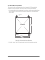
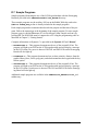
2.2.1 Attach Module to Prototyping Board
Turn the RCM3400 module so that the Rabbit 3000 chip is facing up and the Rabbit logo is
facing the direction shown in Figure 2 below. Align the pins from headers J1 and J2 on the
bottom side of the module into header sockets RCM1JA and RCM1JB on the Prototyping
Board. The shaded corner notch at the top left corner of the RCM3400 module should face the
same direction as the corresponding notch below it on the Prototyping Board.
LINK ACT
J8
J9
JP10
CURRENT
MEASUREMENT
OPTION
DS3
DS4
R60
C57
C58
C44
R58 C48
R50
R56 R55
R51
R53 R52
C38
C49
C39
R48
C47
+5 V
C56
C49
C59
C60
U13
D2
D4
D3
D5
GND
D0
+3.3 V
A1
D6
A3
GND
D1
LED4
LED5
LED6
LED2
A0
LED0
/RESET
+V
GND
A2
R64
C50
LED3
U6
LED1
C45
U7
+5 V
+BKLT
/CS
LDE0
LED2
LED4
LED6
GND
LED5
GND
GND
LCD1J1
C20
R33
C17
R30
C16
R24
C15
R20
C14
R17
C12
C10
C8
+3.3 V
R35
R32
R27
R23
R18
RCM3400
PROTOTYPING
BOARD
PD6
D6
D4
D7
D5
D0
GND
A1
A1
D2
A3
A2
DS2
R47
2
1
S2
GND AIN0 AIN1 AIN2 AIN3 AIN4 AIN5 AIN6 THERM GND CNVRT VREF
GND
+5 V
DS1
R15
R12
C2
J3
/RESET
+V
GND
LCD1J3
D3
JP2
JP1
R11
C4
R8
R1
LCD1J2
D1
JP5
JP9 420
C11
mA
R13
R14
U1
R4
R5
R3
/CS
R34
R31
R29
C3
C9
R9
C6
C1
IR1
R43
R44
GND
2
+3.3 V
+BKLT
GND
GND
60
LED3
GND GND
RCM1JA
RCM1J1
RESET IN
VBAT
59
LED1
+3.3 V
D7
JP7
+5 V
PG7
+3.3 V
HOT
C51
C37
S1
GND
PG6
/RES OUT
C52
34
PG5
GND
+3.3 V
U12
+5 V
C55
R36
PG3
PG4
DCIN
C54
C34
R62
2
U10
R59
C33
R42
C61
Y1
JP6
PG1
PG2
R46
RS-232
R41
R38
PF7
D2
D1
J7
TxE
R45
R37
PF6
R61
TxD
GND
RS-232
TxC
RxC
RxE
C29
33
1
R67
L1
R25
R28
R19
C9
PF5
R2
C32
R40
1
RCM1JB
RCM1J2
Y1
C24
C25
PE7
PF4
C1
PG0 R1
Do not
press down
here.
C24
C27
GND
R6
R7
R22
R16
CX11
C31
R39
C36
PF1
PF0
C8
U1
CX10
CX6
C46
C35
PE5
PE6
R4
C2
C3
C4
C5
CX8
CX5
R54
C41 C42
C40
R25
C62
D1
R18
U7
C31 R11
C33
U3 C34
C22
U2
C32 R13 U5 R20
R17
R3
CX4
CX9
RESET
U3
PE2
PE4
C19
C14
CX7
PD4
PE0
PD7
PE1
C13
C26
CX3
SMD0
RN1
RN2
C28
C53
PD6
PD5
Battery
C23
C35
C61
JP1
JP2
C48
C40
PD0
C39
JP8
JP4
PG7
STAT
SMODE1
R21
CX1
UX1
/IORD
PC7
C55
C50 /IOWR
R24
C53
C51
C13
PC6
U2
JP3
PC3
U5
PG6
R21
PC2
C30
J6
PC1
C25
JP3
PC0
C22
TxF
J2
PB6
PB7
RS-485
JUMPER
DEFAULT (12, 56)
PB4
PB5
C18
RxF
PROGRAM
PB3
C7
CX2
UX2
J5
GND 485
PB2
RxD
+485
J4
PA7
POWER
PA5
PA6
C28
C43
RP4
PA4
R10
R26
RP3
PA3
R65
J1
Shaded
notch
RP2
PA1
PA2
PB1
RCM3400
C59
C56
PA0
BT1
DS5
C19 C21
U4
C5
PD5
PD7
R57
2
S3
1
PD4
+3.3 V
+3.3 V
GND
GND
+5 V
+5 V
Figure 2. Install the RCM3400 Module on the Prototyping Board
NOTE: It is important that you line up the pins on headers J1 and J2 of the RCM3400
module exactly with the corresponding pins of header sockets RCM1JA and RCM1JB
on the Prototyping Board. The header pins may become bent or damaged if the pin
alignment is offset, and the module will not work. Permanent electrical damage to the
module may also result if a misaligned module is powered up.
Press the module’s pins firmly into the Prototyping Board header sockets—press down in the
area above the header pins using your thumbs or fingers over the connectors as shown in
Figure 2. Do not press down on the middle of the RCM3400 module to avoid flexing the module, which could damage the module or the components on the module.
Should you need to remove the RCM3400 module, grasp it with your fingers along the top and
bottom by the connectors and gently work the module up to pull the pins away from the sockets where they are installed. Do not remove the module by grasping it at the sides.
8
RabbitCore RCM3400
2.2.2 Connect Programming Cable
The programming cable connects the RCM3400 to the PC running Dynamic C to download
programs and to monitor the RCM3400 module during debugging.
Connect the 10-pin connector of the programming cable labeled PROG to header J2 on the
RCM3400 Prototyping Board as shown in Figure 3. Be sure to orient the marked (usually red)
edge of the cable towards pin 1 of the connector. (Do not use the DIAG connector, which is
used for a normal serial connection.)
Blue
shrink wrap
To
PC COM port
Programming
Cable
PROG
Colored
edge
J2
LINK ACT
C20
R33
C17
R30
C16
R24
C15
R20
C14
R17
J8
CURRENT
MEASUREMENT
OPTION
DS3
DS4
R60
R61
JP10
TxC
J9
R48
C57
C58
C44
R58 C48
R50
R56 R55
C38
C49
C39
RS-232
R51
R53 R52
J7
TxE
D2
D4
D3
D5
GND
D0
+3.3 V
A1
D6
A3
GND
A0
LED6
A2
D1
LED4
LED5
+V
/CS
LED2
LED4
LED6
GND
LED5
GND
GND
D7
+BKLT
LDE0
LED3
R35
R32
R27
R23
R18
RCM3400
PROTOTYPING
BOARD
D6
D4
D7
D5
D0
GND
GND
A1
A1
D2
A3
A2
D3
LCD1JC
D1
/RESET
LCD1JB
+5 V
PD6
DS2
R47
2
1
S2
GND AIN0 AIN1 AIN2 AIN3 AIN4 AIN5 AIN6 THERM GND CNVRT VREF
/CS
+V
GND
R11
C12
C8
C10
LED1
JP2
JP1
DS1
R15
R12
C2
J3
LCD1JA
+3.3 V
mA
JP9 420
C11
JP5
U1
C4
R8
R1
LED2
33
R25
C62
D1
U7
R34
R31
R29
R13
R14
R4
R5
R3
GND GND
R1
2
C3
C9
R9
C6
60
59
C1
IR1
R2
C35
R18
C32 R13 U5 R20
C31 R11
Y1
U1
C1
GND
GND
+5 V
C61
1
R3
+BKLT
+3.3 V
GND
JP1
RCM1JA
GND
C24
C25
C19
C14
C13
RESET IN
VBAT
+3.3 V
C9
PG7
+3.3 V
R64
C50
C8
PG6
/RES OUT
R4
PG5
C60
U13
34
PG4
JP7
C39
C28
U6
R36
PG3
U7
+5 V
R37
PG1
C37
C59
GND
JP6
3-pin
power connector
+5 V
C56
C51
S1
R38
PF7
R67
R21
HOT
C49
1
2
C52
C34
R62
R24
R25
R28
R19
PF5
PF6
JP3
C55
C50
C3
C4
C5
PF1
PF4
PG2
C53
C51
C2
PF0
PG0
JP2
C48
PE7
RCM1JB
PE6
RP4
RP3
RP2
C59
C56
GND
C55
R59
C33
R42
RESET
U3
C40
PE5
C33
PE2
PE4
U3 C34
PE0
PE1
C22
PD6
PD7
R45
R41
C36
U2
PD5
R40
DCIN
+3.3 V
U12
+5 V
LED0
CX11
C32
C54
/RESET
CX10
CX6
C31
R39
U10
LED3
CX8
CX5
D2
D1
C61
Y1
LED1
CX4
R17
PD4
TxD
RS-232
GND
CX9
C46
C47
CX7
R54
C41 C42
C35
RN1
RN2
PD0
RxC
C27
GND
C29
C13
R21
CX3
C26
SMD0
SMODE1
RxE
R22
R6
R7
R16
U2
C53
PG7
STAT
/IOWR
C23
C45
/IORD
JP8
JP4
C40
PC7
PG6
CX1
UX1
R43
R44
PC6
U5
L1
R46
C30
JP3
PC3
C25
J6
PC2
C24
J2
PC0
C22
TxF
PROGRAM
PROG
PB6
PB7
C18
RxF
485
PB5
PC1
C7
CX2
UX2
J5
GND
PB4
RxD
+485
J4
PB2
C43
PA7
RS-485
JUMPER
DEFAULT (12, 56)
PA5
PA6
PB3
POWER
DIAG
PA4
PB1
R10
BT1
Battery
R65
PA3
R26
PA2
C28
DS5
J1
PA1
C21
C19
U4
C5
PA0
PD5
PD7
R57
2
S3
1
PD4
+3.3 V
+3.3 V
GND
GND
+5 V
+5 V
Figure 3. Connect Programming Cable and Power Supply
NOTE: Be sure to use the programming cable (part number 101-0542) supplied with this
Development Kit—the programming cable has blue shrink wrap around the RS-232
converter section located in the middle of the cable. Programming cables with clear or
red shrink wrap from other Rabbit Semiconductor kits are not designed to work with
RCM3400 modules.
Connect the other end of the programming cable to a COM port on your PC.
NOTE: Some PCs now come equipped only with a USB port. It may be possible to use
an RS-232/USB converter (Part No. 540-0070) with the programming cable supplied
with the RCM3400 Development Kit. Note that not all RS-232/USB converters work
with Dynamic C.
User’s Manual
9
2.2.3 Connect Power
When all other connections have been made, you can connect power to the Prototyping Board.
Connect the wall transformer to jack J8 on the Prototyping Board as shown in Figure 3.
Plug in the wall transformer. The power LED on the Prototyping Board should light up. The
RCM3400 and the Prototyping Board are now ready to be used.
NOTE: A RESET button is provided on the Prototyping Board to allow a hardware reset
without disconnecting power.
2.2.3.1 Overseas Development Kits
Development kits sold outside North America include a header connector that may be connected to 3-pin header J9 on the Prototyping Board. The connector may be attached either way
as long as it is not offset to one side. The red and black wires from the connector can then be
connected to the positive and negative connections on your power supply. The power supply
should deliver 8 V–24 V DC at 8 W.
10
RabbitCore RCM3400
2.3 Run a Sample Program
If you already have Dynamic C installed, you are now ready to test your programming
connections by running a sample program. Start Dynamic C by double-clicking on the
Dynamic C icon or by double-clicking on dcrab_XXXX.exe in the Dynamic C root
directory, where XXXX are version-specific characters. Dynamic C uses the serial port
specified during installation.
If you are using a USB port to connect your computer to the RCM3400 module, choose
Options > Project Options and select “Use USB to Serial Converter” under the
Communications tab.
Find the file PONG.C, which is in the Dynamic C SAMPLES folder. To run the program,
open it with the File menu, compile it using the Compile menu, and then run it by selecting
Run in the Run menu. The STDIO window will open on your PC and will display a small
square bouncing around in a box.
2.3.1 Troubleshooting
If you receive the message No Rabbit Processor Detected, the programming
cable may be connected to the wrong COM port, a connection may be faulty, or the target
system may not be powered up. First, check to see that the power LED on the Prototyping
Board is lit and that the jumper across pins 5–6 of header JP10 on the Prototyping Board is
installed. If the LED is lit, check both ends of the programming cable to ensure that it is
firmly plugged into the PC and the programming port on the Prototyping Board. Ensure
that the module is firmly and correctly installed in its connectors on the Prototyping
Board.
If Dynamic C appears to compile the BIOS successfully, but you then receive a communication error message when you compile and load a sample program, it is possible that your
PC cannot handle the higher program-loading baud rate. Try changing the maximum
download rate to a slower baud rate as follows.
• Locate the Serial Options dialog in the Dynamic C Options > Project Options >
Communications menu. Select a slower Max download baud rate.
If a program compiles and loads, but then loses target communication before you can
begin debugging, it is possible that your PC cannot handle the default debugging baud
rate. Try lowering the debugging baud rate as follows.
• Locate the Serial Options dialog in the Dynamic C Options > Project Options >
Communications menu. Choose a lower debug baud rate.
If there are no faults with the hardware, select a different COM port within Dynamic C.
From the Options menu, select Project Options, then select Communications. Select
another COM port from the list, then click OK. Press <Ctrl-Y> to force Dynamic C to
recompile the BIOS. If Dynamic C still reports it is unable to locate the target system, repeat
the above steps until you locate the active COM port.You should receive a message Bios
compiled successfully once this step is completed successfully.
User’s Manual
11
2.4 Where Do I Go From Here?
If the sample program ran fine, you are now ready to go on to the sample programs in the
RCM3400 User’s Manual (click the documentation icon on your PC) and to develop your
own applications. The sample programs can be easily modified for your own use. The user's
manual also provides complete hardware reference information and software function calls for
the RCM3400, the Prototyping Board, the Ethernet reference design, and the optional
LCD/Keypad module.
For advanced development topics, refer to the Dynamic C User’s Manual and the
Dynamic C TCP/IP User’s Manual, also in the online documentation set.
2.4.1 Technical Support
NOTE: If you purchased your RCM3400 through a distributor or through a Rabbit Semiconductor partner, contact the distributor or partner first for technical support.
If there are any problems at this point:
• Use the Dynamic C Help menu to get further assistance with Dynamic C.
• Check the Rabbit Semiconductor Technical Bulletin Board at
http://forums.digi.com/support/formum/index.
• Use the Technical Support e-mail form at http://www.digi.com/support.
12
RabbitCore RCM3400
3. RUNNING SAMPLE PROGRAMS
To develop and debug programs for the RCM3400 (and for all
other Digi hardware), you must install and use Dynamic C. This
chapter provides a tour of its major features with respect to the
RCM3400.
3.1 Introduction
To help familiarize you with the RCM3400 modules, Dynamic C includes several sample
programs. Loading, executing and studying these programs will give you a solid hands-on
overview of the RCM3400’s capabilities, as well as a quick start with Dynamic C as an
application development tool.
NOTE: The sample programs assume that you have at least an elementary grasp of ANSI
C. If you do not, see the introductory pages of the Dynamic C User’s Manual for a suggested reading list.
In order to run the sample programs discussed in this chapter and elsewhere in this manual,
1. Your RCM3400 must be plugged in to the Prototyping Board as described in Chapter 2,
“Getting Started.”
2. Dynamic C must be installed and running on your PC.
3. The programming cable must connect the programming header on the Prototyping
Board to your PC.
4. Power must be applied to the RCM3400 through the Prototyping Board.
Refer to Chapter 2, “Getting Started,” if you need further information on these steps.
To run a sample program, open it with the File menu (if it is not still open), compile it
using the Compile menu (or press F5), and then run it by selecting Run in the Run menu
(or press F9). The RCM3400 must be in Program Mode (see Figure 7) and must be connected to a PC using the programming cable.
More complete information on Dynamic C is provided in the Dynamic C User’s Manual.
User’s Manual
13
3.2 Sample Programs
Of the many sample programs included with Dynamic C, several are specific to the
RCM3400. These programs will be found in the SAMPLES\RCM3400 folder.
Each sample program has comments that describe the purpose and function of the program. Follow the instructions at the beginning of the sample program.
• CONTROLLED.c—Demonstrates use of the digital inputs by having you turn LEDs
DS1 and DS2 on the Prototyping Board on or off from the STDIO window on your PC.
Parallel Port D bit 6 = LED DS1
Parallel Port D bit 7 = LED DS2
Once you compile and run CONTROLLED.C, the following display will appear in the
Dynamic C STDIO window.
Press “1” or “2” on your keyboard to select LED DS1 or DS2 on the Prototyping
Board. Then follow the prompt in the Dynamic C STDIO window to turn the LED ON
or OFF. A logic low will light up the LED you selected.
14
RabbitCore RCM3400
• FLASHLED1.c—demonstrates the use of assembly language to flash LEDs DS1 and
DS2 on the Prototyping Board at different rates. Once you have compiled and run this
program, LEDs DS1 and DS2 will flash on/off at different rates.
• FLASHLED2.c—demonstrates the use of cofunctions and costatements to flash LEDs
DS1 and DS2 on the Prototyping Board at different rates. Once you have compiled and
run this program, LEDs DS1 and DS2 will flash on/off at different rates.
• TOGGLESWITCH.c—demonstrates the use of costatements to detect switches using the
press-and-release method of debouncing. LEDs DS1 and DS2 on the Prototyping
Board are turned on and off when you press switches S2 and S3. S2 and S3 are controlled by PD5 and PD4 respectively.
• IR_DEMO.c—Demonstrates sending Modbus ASCII packets between two Prototyping
Board assemblies via the IrDA transceivers with the IrDA transceivers facing each other.
Note that this sample program requires a second Prototyping Board or Digi singleboard computer that has an IrDA chip and is running the IR_DEMO.C sample program
associated with it.
First, compile and run the IR_DEMO.C sample program from the SAMPLES folder specific to the other system on the second system, then remove the programming cable and
press the RESET button so that the first assembly is operating in the Run mode. Then
connect the programming cable to the RCM3400 Prototyping Board, and compile and
run the IR_DEMO.C sample program from the SAMPLES\RCM3400 folder on the
RCM3400 system. With the IrDA transceivers on the two Prototyping Boards facing
each other, press switch S2 on the RCM3400 Prototyping Board to transmit a packet.
The other system will return a response packet that will then appear in the Dynamic C
STDIO window. The test packets and response packets have different codes.
Once you have loaded and executed these five programs and have an understanding of
how Dynamic C and the RCM3400 modules interact, you can move on and try the other
sample programs, or begin building your own.
3.2.1 Serial Communication
The following sample programs are found in the SERIAL subdirectory in
SAMPLES\RCM3400.
• FLOWCONTROL.C—This program demonstrates how to configure Serial Port C for
CTS/RTS with serial data coming from Serial Port D (TxD) at 115,200 bps. The serial
data received are displayed in the STDIO window.
To set up the Prototyping Board, you will need to tie TxD and RxD
together on the RS-232 header at J5, and you will also tie TxC and
RxC together using the jumpers supplied in the Development Kit as
shown in the diagram.
RxC TxC
J5
TxD RxD GND
A repeating triangular pattern should print out in the STDIO window.
The program will periodically switch flow control on or off to demonstrate the effect of
no flow control.
User’s Manual
15
• PARITY.C—This program demonstrates the use of parity modes by
repeatedly sending byte values 0–127 from Serial Port D to Serial Port
C. The program will switch between generating parity or not on Serial
Port D. Serial Port C will always be checking parity, so parity errors
should occur during every other sequence.
RxC TxC
J5
TxD RxD GND
To set up the Prototyping Board, you will need to tie TxD and RxC together on the
RS-232 header at J5 using one of the jumpers supplied in the Development Kit as
shown in the diagram.
The Dynamic C STDIO window will display the error sequence.
• SIMPLE3WIRE.C—This program demonstrates basic RS-232 serial
communication. Lower case characters are sent by TxC, and are
received by RxD. The characters are converted to upper case and are
sent out by TxD, are received by RxC, and are displayed in the
Dynamic C STDIO window.
RxC TxC
J5
TxD RxD GND
To set up the Prototyping Board, you will need to tie TxD and RxC together on the
RS-232 header at J5, and you will also tie RxD and TxC together using the jumpers
supplied in the Development Kit as shown in the diagram.
• SIMPLE5WIRE.C—This program demonstrates 5-wire RS-232 serial communication
with flow control on Serial Port C and data flow on Serial Port D.
To set up the Prototyping Board, you will need to tie TxD and RxD
together on the RS-232 header at J5, and you will also tie TxC and
RxC together using the jumpers supplied in the Development Kit as
shown in the diagram.
RxC TxC
J5
TxD RxD GND
Once you have compiled and run this program, you can test flow control by disconnecting TxC from RxC while the program is running. Characters will no
longer appear in the STDIO window, and will display again once TxC is connected
back to RxC.
• SWITCHCHAR.C—This program demonstrates transmitting and then receiving an
ASCII string on Serial Ports D and C. It also displays the serial data received from both
ports in the STDIO window.
To set up the Prototyping Board, you will need to tie TxD and RxC
together on the RS-232 header at J5, and you will also tie RxD and
TxC together using the jumpers supplied in the Development Kit as
shown in the diagram.
RxC TxC
J5
TxD RxD GND
Once you have compiled and run this program, press and release S2
and S3 on the Prototyping Board. The data sent between the serial ports will be displayed in the STDIO window.
Two sample programs, SIMPLE485MASTER.C and SIMPLE485SLAVE.C, are available to
illustrate RS-485 master/slave communication. To run these sample programs, you will
need a second Rabbit-based system with RS-485.
16
RabbitCore RCM3400
The RS-485 connections between the slave and master devices are as follows.
•
RS485+ to RS485+
•
RS485– to RS485–
•
GND to GND
• SIMPLE485MASTER.C—This program demonstrates a simple RS-485 transmission of
lower case letters to a slave. The slave will send back converted upper case letters back
to the master RCM3400 and display them in the STDIO window. Use
SIMPLE485SLAVE.C to program the slave.
• SIMPLE485SLAVE.C—This program demonstrates a simple RS-485 transmission of
lower case letters to a master RCM3400. The slave will send back converted upper case
letters back to the master RCM3400 and display them in the STDIO window. Use
SIMPLE485MASTER.C to program the master RCM3400.
3.2.2 A/D Converter Inputs
The following sample programs are found in the ADC subdirectory in SAMPLES\RCM3400.
• AD_CAL_ALL.C—Demonstrates how to recalibrate all single-ended analog input channels for one gain, using two known voltages to generate the calibration constants for
each channel. Constants will be rewritten into the user block data area.
• AD_CAL_CHAN.C—Demonstrates how to recalibrate one single-ended analog input
channel with one gain using two known voltages to generate the calibration constants
for that channel. Constants will be rewritten into user block data area.
• AD_CAL_DIFF.C—Demonstrates how to recalibrate one differential analog input
channel using two known voltages to generate the calibration constants for that channel.
Constants will be rewritten into user block data area.
• AD_CALMA_CH.C—Demonstrates how to recalibrate an A/D input channel being used to
convert analog current measurements to generate the calibration constants for that channel.
NOTE: The above sample programs will overwrite any existing calibration constants.
• AD_RDDIFF_CH.C—Demonstrates how to read an A/D input channel being used for a
differential input using previously defined calibration constants.
• AD_RDMA_CH.C—Demonstrates how to read an A/D input channel being used to convert analog current measurements using previously defined calibration constants for
that channel.
• AD_RDVOLT_ALL.C—Demonstrates how to read all single-ended A/D input channels
using previously defined calibration constants.
• AD_SAMPLE.C—Demonstrates how to use a low-level driver on single-ended inputs.
The program will continuously display the voltage (average of 10 samples) that is present on the A/D channels.
• ANAINCONFIG.C—Demonstrates how to use the Register Mode method to read singleended analog input values for display as voltages. The sample program uses the function call anaInConfig() and the ADS7870 CONVERT line to accomplish this task.
User’s Manual
17
• THERMISTOR.C—Demonstrates how to use analog input THERM_IN7 to calculate
temperature for display to the STDIO window. This sample program assumes that the
thermistor is the one included in the Development Kit whose values for beta, series
resistance, and resistance at standard temperature are given in the part specification.
• DNLOADCALIB.C—Demonstrates how to retrieve analog calibration data to rewrite it
back to simulated EEPROM in flash with using a serial utility such as Tera Term.
• UPLOADCALIB.C—Demonstrates how to read calibrations constants from the user
block in flash memory and then transmitting the file using a serial port and a PC serial
utility such as Tera Term. Use DNLOADCALIB.C to download the calibration constants
created by this program.
3.2.3 Real-Time Clock
If you plan to use the real-time clock functionality in your application, you will need to set
the real-time clock. Set the real-time clock using the SETRTCKB.C sample program from
the Dynamic C SAMPLES\RTCLOCK folder, using the onscreen prompts. The
RTC_TEST.C sample program in the Dynamic C SAMPLES\RTCLOCK folder provides
additional examples of how to read and set the real-time clock.
3.2.4 TCP/IP Sample Programs
Sample programs demonstrating the TCP/IP associated with the Prototyping Board are
described in Appendix C.
3.2.5 LCD/Keypad Module Sample Programs
Sample programs for the optional LCD/keypad module are described in Appendix D.
18
RabbitCore RCM3400
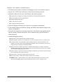
4. HARDWARE REFERENCE
Chapter 4 describes the hardware components and principal hardware
subsystems of the RCM3400. Appendix A, “RCM3400 Specifications,” provides complete physical and electrical specifications.
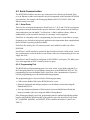
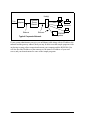
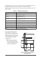
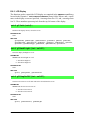
Figure 4 shows the Rabbit-based subsystems designed into the RCM3400.
A/D Converter
SRAM
Flash
RABBIT®
3000
External
scaling
circuitry
logic-level serial signal
Level
converter
32 kHz
osc
29.4 MHz
osc
RabbitCore Module
RS-232, RS-485,
IrDA and Ethernet
drivers on motherboard
Figure 4. RCM3400 Subsystems
User’s Manual
19
4.1 RCM3400 Digital Inputs and Outputs
Figure 5 shows the RCM3400 pinouts for headers J1 and J2.
J1
J2
GND
PB6
PB5
PB3
PB1
PA6
PA4
PA2
PC2
PC0
PC6-TxA
PC7-RxA
PG2
PG0
PD4
PD6
PD7
PF1
PF0
PB4
PB2
PA7
PA5
PA3
PA1
PA0
PC3
PC1
PG3
PG1
PD0
PD5
/RESET_IN
VBAT_EXT
LN3
LN2
LN1
LN0
VREF
PF6
PF4
PB7
PE6
PE4
PE1
GND
PG7
PG5
/IORD
SMODE1
/RES
LN7
LN6
LN5
LN4
CONVERT
PF7
PF5
PE7
PE5
PE2
PE0
+3.3 V_IN
PG6
PG4
STATUS
/IOWR
SMODE0
n.c. = not connected
Note: These pinouts are as seen on
the Bottom Side of the module.
Figure 5. RCM3400 Pinouts
Headers J1 and J2 are standard 2 × 34 headers with a nominal 1.27 mm pitch.
20
RabbitCore RCM3400
Figure 6 shows the use of the Rabbit 3000 microprocessor ports in the RCM3400 modules.
PC0, PC2
PC1, PC3
PG2, PG6
PA0PA7
PB1PB7
PD0
PD4PD7
Port A
Port B
Port D
Port C
RABBIT®
Port E
PE0PE2
PE4PE7
Port F
PF0PF1
PF4PF7
(Serial Ports C & D)
Port G
PG3, PG7
(Serial Ports E & F)
PB1, PC6
Programming
Port
PC7, /RES
PC4*
PC5*
* PC4 and PC5 are
not available on
RCM3400 I/O pins.
(Serial Port A)
A/D Converter
(Serial Port B)
RAM
3000
Real-Time Clock
Watchdog
11 Timers
Slave Port
Clock Doubler
Port G
(+Serial Ports)
Misc. I/O
Backup Battery
Support
Flash
PG0PG7
/RES_IN
/IORD
/RESET,
/IOWR,
STATUS
SMODE0
SMODE1
Figure 6. Use of Rabbit 3000 Ports
The ports on the Rabbit 3000 microprocessor used in the RCM3400 are configurable, and
so the factory defaults can be reconfigured. Table 2 lists the Rabbit 3000 factory defaults
and the alternate configurations.
User’s Manual
21
Table 2. RCM3400 Pinout Configurations
Pin
Pin Name
Default Use
Alternate Use
Notes
1
LN3
Analog Input
2
LN7
Analog Input
3
LN2
Analog Input
4
LN6
Analog Input
5
LN1
Analog Input
6
LN5
Analog Input
7
LN0
Analog Input
8
LN4
Analog Input
9
VREF
Analog Output
1.15 V/2.048 V/2.500 V
on-chip ref. voltage
10
CONVERT
Analog Input
A/D converter
11
PF6
Input/Output
AQD2B
PWM2
12
PF7
Input/Output
AQD2A
PWM3
13
PF4
Input/Output
AQD1B
PWM0
14
PF5
Input/Output
AQD1A
PWM1
15
PB7
Input/Output
IA5
/SLAVEATTN
External Address 5
Slave Attention
16
PE7
Input/Output
I7
/SCS
I/O Strobe 7
Slave Port Chip Select
17
PE6
Input/Output
I6
I/O Strobe 6
18
PE5
Input/Output
I5
INT1B
I/O Strobe 5
Interrupt 1B
19
PE4
Input/Output
I4
INT0B
I/O Strobe 4
Interrupt 0B
20
PE2
Input/Output
I2
I/O Strobe 2
21
PE1
Input/Output
I1
INT1A
I/O Strobe 1
Interrupt 1A
22
PE0
Input/Output
I0
INT0A
I/O Strobe 0
Interrupt 0A
Header J1
A/D converter
22
RabbitCore RCM3400
Table 2. RCM3400 Pinout Configurations (continued)
Pin
Pin Name
Default Use
Alternate Use
Notes
23
GND
24
+3.3 V_IN
25
PG7
Input/Output
RXE
26
PG6
Input/Output
TXE
27
PG5
Input/Output
RCLKE
Serial Clock E input
28
PG4
Input/Output
TCLKE
Serial Clock E output
29
/IORD
Input
30
STATUS
Output (Status)
Header J1
Serial Port E
31
SMODE1
External read strobe
Output
(SMODE1, SMODE0)
(0,0)—start executing at address zero
(0,1)—cold boot from slave port
(1,0)—cold boot from clocked Serial Port A
Programming port
SMODE0 =1, SMODE1 = 1
Cold boot from asynchronous Serial Port A at
2400 bps (programming cable connected)
32
/IOWR
Output
33
/RES
Reset output
34
SMODE0
External write strobe
Reset input
(SMODE1, SMODE0)
(0,0)—start executing at address zero
(0,1)—cold boot from slave port
(1,0)—cold boot from clocked Serial Port A
Reset output from Reset
Generator
Programming port
SMODE0 =1, SMODE1 = 1
Cold boot from asynchronous Serial Port A at
2400 bps (programming cable connected)
User’s Manual
23
Table 2. RCM3400 Pinout Configurations (continued)
Header J2
Pin
Pin Name
Default Use
Alternate Use
Notes
1
GND
2
PF1
Input/Output
QD1A
CLKC
3
PB6
Input/Output
IA4
4
PF0
Input/Output
QD1B
CLKD
5
PB5
Input/Output
IA3
SA1
External Address 3
Slave port Address 1
6
PB4
Input/Output
IA2
SA0
External Address 2
Slave port Address 0
7
PB3
Input/Output
IA1
/SRD
External Address 1
Slave port read
8
PB2
Input/Output
IA0
/SWR
External Address 0
Slave port write
9
PB1
Input/Output
CLKA
External Address 4
10–16
PA[7:1]
Parallel I/O
External data bus
(ID7–ID1)
Slave port data bus
(SD7–SD1)
17
PC2
Output
TXC
18
PA0
Parallel I/O
External data bus (ID0)
High
Slave port data bus (SD0)
19
PC0
Output
TXD
Serial Port D
20
PC3
Input
RXC
Serial Port C
21
PC6
Output
TXA
Programming port
22
PC1
Input
RXD
Serial Port D
23
PC7
Input
RXA
Programming port
24
PG3
Input/Output
RXF
25
PG2
Input/Output
TXF
26
PG1
Input/Output
RCLKF
Serial Clock F input
27
PG0
Input/Output
TCLKF
Serial Clock F output
28
PD0
Input/Output
29
PD4
Input/Output
ATXB
30
PD5
Input/Output
ARXB
Serial Port C
Serial Port F
24
RabbitCore RCM3400
Table 2. RCM3400 Pinout Configurations (continued)
Header J2
Pin
Pin Name
Default Use
31
PD6
Input/Output
32
/RESET_IN
Input
33
PD7
Input/Output
34
VBAT_EXT
User’s Manual
Alternate Use
Notes
ATXA
Input to Reset Generator
ARXA
25
4.1.1 Memory I/O Interface
The Rabbit 3000 address lines (A0–A19) and all the data lines (D0–D7) are routed internally to the onboard flash memory and SRAM chips. I/0 write (/IOWR) and I/0 read
(/IORD) are available for interfacing to external devices.
Parallel Port A can also be used as an external I/O data bus to isolate external I/O from the
main data bus. Parallel Port B pins PB2–PB7 can also be used as an auxiliary address bus.
When using the auxiliary I/O bus for either Ethernet or the LCD/keypad module on the
Prototyping Board or for any other reason, you must add the following line at the beginning of your program.
#define PORTA_AUX_IO
// required to enable auxiliary I/O bus
4.1.2 Other Inputs and Outputs
The status, /RESET_IN, SMODE0, and SMODE1 I/O are normally associated with the
programming port. Since the status pin is not used by the system once a program has been
downloaded and is running, the status pin can then be used as a general-purpose CMOS
output. The programming port is described in more detail in Section 4.2.2.
/RESET_IN is an external input used to reset the Rabbit 3000 microprocessor and the
RCM3400 memory. /RES is an output from the reset circuitry that can be used to reset
other peripheral devices.
The two SMODE pins, SMODE0 and SMODE1, are available as inputs. The logic state of
these two pins determines the startup procedure after a reset.
26
RabbitCore RCM3400
4.2 Serial Communication
The RCM3400 board does not have any serial transceivers directly on the board. However, an Ethernet or other serial interface may be incorporated on the board the RCM3400
is mounted on. For example, the Prototyping Board has RS-232, RS-485, IrDA, and
Ethernet transceiver chips.
4.2.1 Serial Ports
There are five serial ports designated as Serial Ports A, C, D, E, and F. All five serial ports
can operate in an asynchronous mode up to the baud rate of the system clock divided by 8.
An asynchronous port can handle 7 or 8 data bits. A 9th bit address scheme, where an
additional bit is sent to mark the first byte of a message, is also supported.
Serial Port A is normally used as a programming port, but may be used either as an asynchronous or as a clocked serial port once application development has been completed and
the RCM3400 is operating in the Run Mode.
Serial Port B is used by the A/D converter, and is not available for other use off the
RCM3400.
Serial Ports C and D can also be operated in the clocked serial mode. In this mode, a clock
line synchronously clocks the data in or out. Either of the two communicating devices can
supply the clock.
Serial Ports E and F can also be configured as SDLC/HDLC serial ports. The IrDA protocol is also supported in SDLC format by these two ports.
4.2.2 Programming Port
The RCM3400 serial programming port is accessed via the 10-pin header labeled J2 on
the Prototyping Board or over an Ethernet connection via the RabbitLink EG2110. The
programming port uses the Rabbit 3000’s Serial Port A for communication. Dynamic C
uses the programming port to download and debug programs.
The programming port is also used for the following operations.
• Cold-boot the Rabbit 3000 on the RCM3400 after a reset.
• Remotely download and debug a program over an Ethernet connection using the
RabbitLink EG2110.
• Fast copy designated portions of flash memory from one Rabbit-based board (the
master) to another (the slave) using the Rabbit Cloning Board.
If the Prototyping Board is not used, programming must be initiated through the motherboard to which the RCM3400 module is plugged in to since the Serial Port A (PC6 and
PC7), SMODE0, SMODE1, and /RESET_IN are available on headers J1 and J2 (see
Table 2).
User’s Manual
27
Alternate Uses of the Programming Port
All three clocked Serial Port A signals are available as
• a synchronous serial port
• an asynchronous serial port, with the clock line usable as a general CMOS I/O pin
The programming port may also be used as a serial port via the DIAG connector on the
programming cable.
In addition to Serial Port A, the Rabbit 3000 startup-mode (SMODE0, SMODE1), status,
and reset pins are available on the programming port.
The two startup mode pins determine what happens after a reset—the Rabbit 3000 is
either cold-booted or the program begins executing at address 0x0000.
The status pin is used by Dynamic C to determine whether a Rabbit microprocessor is
present. The status output has three different programmable functions:
1. It can be driven low on the first op code fetch cycle.
2. It can be driven low during an interrupt acknowledge cycle.
3. It can also serve as a general-purpose output.
The /RESET_IN pin is an external input that is used to reset the Rabbit 3000 and the
RCM3400 onboard peripheral circuits. The serial programming port can be used to force a
hard reset on the RCM3400 by asserting the /RESET_IN signal.
Refer to the Rabbit 3000 Microprocessor User’s Manual for more information.
28
RabbitCore RCM3400
4.3 Serial Programming Cable
The programming cable is used to connect the serial programming port of the RCM3400
to a PC serial COM port. The programming cable converts the RS-232 voltage levels used
by the PC serial port to the CMOS voltage levels used by the Rabbit 3000.
When the PROG connector on the programming cable is connected to the programming
header on the RCM3400 Prototyping Board, programs can be downloaded and debugged
over the serial interface.
The DIAG connector of the programming cable may be used on header J2 of the RCM3400
Prototyping Board with the RCM3400 operating in the Run Mode. This allows the programming port to be used as a regular serial port.
4.3.1 Changing Between Program Mode and Run Mode
The RCM3400 is automatically in Program Mode when the PROG connector on the programming cable is attached, and is automatically in Run Mode when no programming
cable is attached. When the Rabbit 3000 is reset, the operating mode is determined by the
status of the SMODE pins. When the programming cable’s PROG connector is attached,
the SMODE pins are pulled high, placing the Rabbit 3000 in the Program Mode. When the
programming cable’s PROG connector is not attached, the SMODE pins are pulled low,
causing the Rabbit 3000 to operate in the Run Mode.
Blue
shrink wrap
To
PC COM port
Programming
Cable
PROG
Colored
edge
J2
LINK ACT
RCM3400
PROTOTYPING
BOARD
C20
R33
C17
R30
C16
R24
C15
R20
C14
R17
C12
C10
C8
JP10
J8
CURRENT
MEASUREMENT
OPTION
DS3
DS4
R61
R60
J9
R48
C57
R56 R55
C58
R50
R51
R53 R52
C39
J7
D2
D4
D3
D5
GND
D0
D1
+3.3 V
A1
D6
A3
GND
A0
LED6
A2
LED4
LED5
C45
+V
/CS
LED6
D7
+BKLT
LED4
GND
+3.3 V
D6
D4
D2
D0
A1
A3
GND
LED2
LDE0
/RESET
+V
LCD1JC
GND
D7
D5
GND
A1
A2
D3
D1
GND
GND
LED5
/CS
LED3
+5 V
PD6
DS2
R47
2
1
S2
GND AIN0 AIN1 AIN2 AIN3 AIN4 AIN5 AIN6 THERM GND CNVRT VREF
LED1
+BKLT
GND
R43
R44
R35
R32
R27
R23
R18
LCD1JB
RESET RCM3400 when changing mode:
Short out pins 132 on header J2, OR
Press RESET button (if using Prototyping Board), OR
Cycle power off/on
after removing or attaching programming cable.
DS1
R15
J3
R12
C2
R11
C4
R8
R1
C40
33
R25
C62
D1
JP2
JP1
R37
JP5
U1
R4
R5
R3
JP9 420
C11
mA
R13
R14
IR1
R2
C35
R18
Y1
C9
C8
R36
R34
R31
R29
C3
LCD1JA
RESET
C9
R9
C6
60
59
C1
GND GND
R1
2
GND
GND
C32 R13 U5 R20
R25
R28
R19
C1
C60
U13
R64
+3.3 V
R38
+3.3 V
R3
+5 V
JP2
C48
RCM1JA
GND
VBAT
C19
C14
C13
RESET IN
U7
PG7
C31 R11
PG5
PG6
+3.3 V
C24
C25
PG4
/RES OUT
U1
PG3
C59
C50
GND
JP7
C3
C4
C5
PG2
U6
+5 V
R24
JP6
C39
C28
U7
S1
R4
PG1
C55
C50
R67
+5 V
C56
34
PF7
C53
C51
R21
C2
PF6
PG0
C61
1
PF5
JP1
PF1
PF4
RCM1JB
PE7
PF0
HOT
C51
C37
1
2
C40
PE5
PE6
C33
PE4
C59
C56
U3 C34
PE2
C52
C49
C36
JP3
GND
C34
R62
C35
RP4
RP3
RP2
C22
PE1
C33
R42
RESET
U3
U2
PE0
C38
C49
RS-232
R41
R59
LED2
CX11
R45
+3.3 V
U12
+5 V
C55
LED0
CX10
CX6
C32
R40
DCIN
C54
/RESET
CX8
CX5
C31
R39
U10
LED3
CX4
CX9
D2
D1
C61
Y1
LED1
CX7
C46
R54
C41 C42
C47
C26
CX3
R17
PD6
PD7
TxC
C53
PG7
RN1
RN2
PD4
PD5
RxC
C23
C44
R58 C48
JP8
JP4
SMD0
PD0
TxE
C29
CX1
UX1
STAT
SMODE1
TxD
RS-232
GND
C24
C27
GND
R16
U5
/IORD
PC7
/IOWR
RxE
R22
R6
R7
C13
PC6
U2
PC3
C30
PG6
R21
PC2
C25
JP3
PC1
C22
J6
J2
PC0
RS-485
JUMPER
DEFAULT (12, 56)
PB6
PB7
C18
TxF
PROGRAM
PROG
PB5
CX2
UX2
L1
R46
RxF
485
PB4
J5
GND
PB2
RxD
+485
J4
PA7
PB3
C28
C43
PA6
PB1
R10
C7
POWER
DIAG
PA5
R65
PA3
PA4
R26
PA2
BT1
Battery
DS5
J1
PA1
C21
C19
U4
C5
PA0
PD5
PD7
R57
2
S3
1
PD4
+3.3 V
+3.3 V
GND
GND
+5 V
+5 V
Figure 7. Switching Between Program Mode and Run Mode
User’s Manual
29
A program “runs” in either mode, but can only be downloaded and debugged when the
RCM3400 is in the program mode.
Refer to the Rabbit 3000 Microprocessor User’s Manual for more information on the programming port and the programming cable.
4.3.2 Standalone Operation of the RCM3400
The RCM3400 must be programmed via the RCM3400 Prototyping Board or via a similar
arrangement on a customer-supplied board. Once the RCM3400 has been programmed
successfully, remove the programming cable from the programming connector and reset
the RCM3400. The RCM3400 may be reset by cycling power off/on or by pressing the
RESET button on the Prototyping Board. The RCM3400 module may now be removed
from the Prototyping Board for end-use installation.
CAUTION: Power to the Prototyping Board or other boards should be disconnected
when removing or installing your RCM3400 module to protect against inadvertent
shorts across the pins or damage to the RCM3400 if the pins are not plugged in correctly. Do not reapply power until you have verified that the RCM3400 module is
plugged in correctly.
30
RabbitCore RCM3400
4.4 A/D Converter
The RCM3400 has an onboard ADS7870 A/D converter whose scaling and filtering are
done via the motherboard on which the RCM3400 module is mounted. The A/D converter
multiplexes converted signals from eight single-ended or four differential inputs to Serial
Port B on the Rabbit 3000.
The eight analog input pins, LN0–LN7, each have an input impedance of 6–7 M,
depending on whether they are used as single-ended or differential inputs. The input signal
can range from -2 V to +2 V (differential mode) or from 0 V to +2 V (single-ended mode).
Use a resistor divider such as the one shown in Figure 8 for the analog inputs.
+V
RCM3400
R10
R11
C
AGND
C
R0
LN0
ADC
LN1
ADC
R1
BVREF
Figure 8. Resistor Divider Network for Analog Inputs
R0 and R1 are typically 20 k to 100 k, with a lower resistance leading to more accuracy, but at the expense of a higher current draw. R10 and R11 would then be 180 k to
900 k for a 10:1 attenuator. The capacitor filters noise pulses on the A/D converter input.
The actual voltage range for a signal going to the A/D converter input is also affected by
the 1, 2, 4, 5. 8, 10, 16, and 20 V/V software-programmable gains available on each channel of the ADS7870 A/D converter. Thus, you must scale the analog signal with an attenuator circuit and a software-programmable gain so that the actual input presented to the
A/D converter is within the range limits of the ADS7870 A/D converter chip (-2 V to + 2 V
or 0 V to + 2 V).
The A/D converter chip can only accept positive voltages. With resistors R0 and R1 connected to ground, your analog circuit is well-suited to perform positive A/D conversions.
When R0 and R1 are tied to ground for differential measurements, both differential inputs
must be referenced to analog ground, and both inputs must be positive with respect to analog ground.
User’s Manual
31
If a device such as a battery is
connected across two channels
R10
AIN0
for a differential measurement,
LN0 ADC
and it is not referenced to
1 nF
R0
Device +
analog ground, then the current
I
+
from the device will flow
1 nF
R1
through both sets of attenuator
R11
AIN1
resistors as shown in Figure 9.
LN1
This will generate a negative
voltage at one of the inputs,
Figure 9. Current Flow from Ungrounded
LN1, which will almost ceror Floating Source
tainly lead to inaccurate A/D
conversions. To make such differential measurements, connect R0 and R1 to the A/D converter’s internal reference voltage, which is software-configurable for 1.15 V, 2.048 V, or 2.5 V. This internal reference
voltage is available on pin 9 of header J1 as VREF, and allows you to convert analog input
voltages that are negative with respect to analog ground.
NOTE: The amplifier inside the A/D converter’s internal voltage reference circuit has a
very limited output-current capability. The internal buffer can source up to 20 mA and
sink only up to 20 µA. Use a separate buffer amplifier if you need to supply any load
current.
The A/D converter’s CONVERT pin is available on pin 10 of header J1 and can be used as
a hardware means of forcing the A/D converter to start a conversion cycle. The CONVERT
signal is an edge-triggered event and has a hold time of two CCLK periods for debounce.
A conversion is started by an active (rising) edge on the CONVERT pin. The CONVERT
pin must stay low for at least two CCLK periods before going high for at least two CCLK
periods. Figure 10 shows the timing of a conversion start. The double falling arrow on
CCLK indicates the actual start of the conversion cycle.
Conversion starts
CCLK
BUSY
CONV
Figure 10. Timing Diagram for Conversion Start Using CONVERT Pin
Appendix B explains the implementation examples of these features on the Prototyping
Board.
32
RabbitCore RCM3400
4.4.1 A/D Converter Calibration
All single-ended inputs are factory-calibrated with actual voltages at a gain code of 0.
Typical values for the other gain codes and for other calibration constants for current and
differential measurements are used to populate the table to allow A/D conversions to be
done “out of the box.” See Appendix B.4.3.3 for information on performing your own calibrations in situations where you require enhanced accuracy.
4.4.2 A/D Converter Power Supply
The analog section is isolated from digital noise generated by other components by way of a
low-pass filter composed of L1, C10, and C15 on the RCM3400 as shown in Figure 11. The
+V analog power supply powers the A/D converter chip.
Vcc
+V
L1
C15
2.2 nF
C10
100 nF
Figure 11. Analog Supply Circuit
User’s Manual
33
4.5 Other Hardware
4.5.1 Clock Doubler
The RCM3400 takes advantage of the Rabbit 3000 microprocessor’s internal clock doubler. A built-in clock doubler allows half-frequency crystals to be used to reduce radiated
emissions. The 29.4 MHz frequency specified for the RCM3400 is generated using a
14.7 MHz resonator.
The clock doubler may be disabled if 29.4 MHz clock speeds are not required. Disabling
the Rabbit 3000 microprocessor’s internal clock doubler will reduce power consumption
and further reduce radiated emissions. The clock doubler is disabled with a simple configuration macro as shown below.
1. Select the “Defines” tab from the Dynamic C Options > Project Options menu.
2. Add the line CLOCK_DOUBLED=0 to always disable the clock doubler.
The clock doubler is enabled by default, and usually no entry is needed. If you need to
specify that the clock doubler is always enabled, add the line CLOCK_DOUBLED=1 to
always enable the clock doubler.
3. Click OK to save the macro. The clock doubler will now remain off whenever you are
in the project file where you defined the macro.
The clock doubler must be disabled for low-voltage operation (2.8 V–3.0 V).
4.5.2 Spectrum Spreader
The Rabbit 3000 features a spectrum spreader, which helps to mitigate EMI problems. The
spectrum spreader is on by default, but it may also be turned off or set to a stronger setting.
The means for doing so is through a simple configuration macro as shown below.
1. Select the “Defines” tab from the Dynamic C Options > Project Options menu.
2. Normal spreading is the default, and usually no entry is needed. If you need to specify
normal spreading, add the line
ENABLE_SPREADER=1
For strong spreading, add the line
ENABLE_SPREADER=2
To disable the spectrum spreader, add the line
ENABLE_SPREADER=0
NOTE: The strong spectrum-spreading setting is unnecessary for the BL2000.
3. Click OK to save the macro. The spectrum spreader will now remain off whenever you
are in the project file where you defined the macro.
NOTE: Refer to the Rabbit 3000 Microprocessor User’s Manual for more information
on the spectrum-spreading setting and the maximum clock speed.
34
RabbitCore RCM3400
4.6 Memory
4.6.1 SRAM
RCM3400 boards have 256K–512K of SRAM installed at U6.
4.6.2 Flash EPROM
RCM3400 boards also have 256K–512K of flash EPROM installed at U4.
NOTE: Digi recommends that any customer applications should not be constrained by
the sector size of the flash EPROM since it may be necessary to change the sector size
in the future.
Writing to arbitrary flash memory addresses at run time is also discouraged. Instead,
define a “user block” area to store persistent data. The functions writeUserBlock and
readUserBlock are provided for this. Refer to the Rabbit 3000 Microprocessor
Designer’s Handbook for additional information.
A Flash Memory Bank Select jumper configuration option based on 0 surface-mounted
resistors exists at header JP2 on the RCM3400 modules. This option is reserved for future
use.
4.6.3 Dynamic C BIOS Source Files
The Dynamic C BIOS source files handle different standard RAM and flash EPROM sizes
automatically.
User’s Manual
35
36
RabbitCore RCM3400
5. SOFTWARE REFERENCE
Dynamic C is an integrated development system for writing
embedded software. It runs on an IBM-compatible PC and is
designed for use with Rabbit Semiconductor controllers and
other controllers based on the Rabbit microprocessor. Chapter 5
provides the libraries, function calls, and sample programs
related to the RCM3400.
5.1 More About Dynamic C
Dynamic C has been in use worldwide since 1989. It is specially designed for programming embedded systems, and features quick compile and interactive debugging in the real
environment. A complete reference guide to Dynamic C is contained in the Dynamic C
User’s Manual.
You have the choice of doing your software development in the flash memory or in the
static SRAM included on the RCM3400. The flash memory and SRAM options are
selected with the Options > Compiler menu.
The advantage of working in RAM is to save wear on the flash memory, which is limited
to about 100,000 write cycles. The disadvantage is that the code and data might not both
fit in RAM.
NOTE: An application can be developed in RAM, but cannot run standalone from RAM
after the programming cable is disconnected. All standalone applications can only run
from flash memory.
NOTE: Do not depend on the flash memory sector size or type. Due to the volatility of
the flash memory market, the RCM3400 and Dynamic C were designed to accommodate flash devices with various sector sizes.
Developing software with Dynamic C is simple. Users can write, compile, and test C and
assembly code without leaving the Dynamic C development environment. Debugging
occurs while the application runs on the target. Alternatively, users can compile a program
to an image file for later loading. Dynamic C runs on PCs under Windows 95, 98, 2000,
NT, Me, and XP. Programs can be downloaded at baud rates of up to 460,800 bps after the
program compiles.
User’s Manual
37
Dynamic C has a number of standard features:
• Full-feature source and/or assembly-level debugger, no in-circuit emulator required.
• Royalty-free TCP/IP stack with source code and most common protocols.
• Hundreds of functions in source-code libraries and sample programs:
Exceptionally fast support for floating-point arithmetic and transcendental functions.
RS-232 and RS-485 serial communication.
Analog and digital I/O drivers.
I2C, SPI, GPS, file system.
LCD display and keypad drivers.
• Powerful language extensions for cooperative or preemptive multitasking
• Loader utility program to load binary images into Rabbit Semiconductor targets in the
absence of Dynamic C.
• Provision for customers to create their own source code libraries and augment on-line
help by creating “function description” block comments using a special format for
library functions.
• Standard debugging features:
Breakpoints—Set breakpoints that can disable interrupts.
Single-stepping—Step into or over functions at a source or machine code level, µC/OS-II aware.
Code disassembly—The disassembly window displays addresses, opcodes, mnemonics, and
machine cycle times. Switch between debugging at machine-code level and source-code level by
simply opening or closing the disassembly window.
Watch expressions—Watch expressions are compiled when defined, so complex expressions
including function calls may be placed into watch expressions. Watch expressions can be updated
with or without stopping program execution.
Register window—All processor registers and flags are displayed. The contents of general registers
may be modified in the window by the user.
Stack window—shows the contents of the top of the stack.
Hex memory dump—displays the contents of memory at any address.
STDIO window—printf outputs to this window and keyboard input on the host PC can be
detected for debugging purposes. printf output may also be sent to a serial port or file.
38
RabbitCore RCM3400
5.2 Dynamic C Function Calls
5.2.1 Digital I/O
The RCM3400 was designed to interface with other systems, and so there are no drivers
written specifically for the I/O. The general Dynamic C read and write functions allow
you to customize the parallel I/O to meet your specific needs. For example, use
WrPortI(PEDDR, &PEDDRShadow, 0x00);
to set all the Port E bits as inputs, or use
WrPortI(PEDDR, &PEDDRShadow, 0xFF);
to set all the Port E bits as outputs.
When using the auxiliary I/O bus on the Rabbit 3000 chip, add the line
#define PORTA_AUX_IO
// required to enable auxiliary I/O bus
to the beginning of any programs using the auxiliary I/O bus.
The sample programs in the Dynamic C SAMPLES/RCM3400 directory provide further
examples.
5.2.2 Serial Communication Drivers
Library files included with Dynamic C provide a full range of serial communications support. The RS232.LIB library provides a set of circular-buffer-based serial functions. The
PACKET.LIB library provides packet-based serial functions where packets can be delimited by the 9th bit, by transmission gaps, or with user-defined special characters. Both
libraries provide blocking functions, which do not return until they are finished transmitting or receiving, and nonblocking functions, which must be called repeatedly until they
are finished. For more information, see the Dynamic C Function Reference Manual and
Technical Note 213, Rabbit 2000 Serial Port Software.
5.2.3 TCP/IP Drivers
The TCP/IP drivers are located in the TCPIP directory.
Complete information on these libraries and the TCP/IP functions is provided in the
Dynamic C TCP/IP User’s Manual.
User’s Manual
39
5.2.4 Prototyping Board Function Calls
The functions described in this section are for use with the Prototyping Board features.
The source code is in the RCM34xx.LIB library in the Dynamic C LIB\RCM3400 folder if
you need to modify it for your own board design.
Other generic functions applicable to all devices based on Rabbit microprocessors are
described in the Dynamic C Function Reference Manual.
5.2.5 Board Initialization
void brdInit (void);
Call this function at the beginning of your program. This function initializes Parallel Ports A through G
for use with the RCM3400 Prototyping Board.
Summary of Initialization
1. Display/keypad select is disabled.
2. Ethernet select is disabled.
3. RS-485 is not enabled.
4. RS-232 is not enabled.
5. Unused configurable I/O are tied inputs or outputs set low.
6. A/D converter is reset and SCLKB is set to 57,600 bps.
7.A/D converter calibration constants are read, so this function cannot run in RAM.
RETURN VALUE
None.
40
RabbitCore RCM3400
5.2.6 Analog Inputs
unsigned int anaInConfig(unsigned int
instructionbyte, unsigned int cmd, long baud);
Use this function to configure the A/D converter. This function will address the A/D converter in
Register Mode only, and will return an error if you try the Direct Mode. Appendix B.4.3 provides
additional addressing and command information.
ADS7870 Signal
ADS7870 State
LN0
Input
AIN0
LN1
Input
AIN1
LN2
Input
AIN2
LN3
Input
AIN3
LN4
Input
AIN4
LN5
Input
AIN5
LN6
Input
AIN6
LN7
Input
AIN7
/RESET
Input
Board reset device
RISE/FALL
Input
Pulled up for SCLK active on rising edge
PIO0
Input
Pulled down
PIO1
Input
Pulled down
PIO2
Input
Pulled down
PIO3
Input
Pulled down
CONVERT
Input
Pulled down
BUSY
Output
CCLKCNTRL
Input
Pulled down; 0 state sets CCLK as input
CCLK
Input
Pulled down; external conversion clock
SCLK
Input
PB0; serial data transfer clock
SDI
Input
PC4; 3-wire mode for serial data input
SDO
Output
/CS
Input
PD2 pulled up; active-low enables serial interface
BUFIN
Input
Pulled down; reference buffer amplifier
VREF
Output
Connected to BUFIN
BUFOUT
Output
Pulled down
User’s Manual
RCM3400 Function/State
PD1 pulled down; logic high state converter is busy
PC5; serial data output /CS driven
41
PARAMETERS
instructionbyte is the instruction byte that will initiate a read or write operation at 8 or 16 bits on
the designated register address. For example,
checkid = anaInConfig(0x5F, 0, 9600);
// read ID and set baud rate
cmd are the command data that configure the registers addressed by the instruction byte. Enter 0 if you
are performing a read operation. For example,
i = anaInConfig(0x07, 0x3b, 0);
// write ref/osc reg and enable
baud is the serial clock transfer rate of 9600 to 57,600 bps. baud must be set the first time this function
is called. Enter 0 for this parameter thereafter, for example,
anaInConfig(0x00, 0x00, 9600);
// resets device and sets baud
RETURN VALUE
0 on write operations,
data value on read operations
SEE ALSO
anaInDriver, anaIn, brdInit
42
RabbitCore RCM3400
unsigned int anaInDriver(unsigned int cmd,
unsigned int len);
Reads the voltage of an analog input channel by serial-clocking an 8-bit command to the A/D converter
by its Direct Mode method. This function assumes that Mode1 (most significant byte first) and the A/D
converter oscillator have been enabled. See anaInConfig() for the setup.
The conversion begins immediately after the last data bit has been transferred. An exception error will
occur if Direct Mode bit D7 is not set.
PARAMETERS
cmd contains a gain code and a channel code as follows.
D7—1; D6–D4—Gain Code; D3–D0—Channel Code
Use the following calculation and the tables below to determine cmd:
cmd = 0x80 | (gain_code*16) + channel_code
Gain Code
Multiplier
0
×1
1
×2
2
×4
3
×5
4
×8
5
×10
6
×16
7
×20
Channel Code
Differential Input
Lines
Channel Code
Single-Ended
Input Lines*
4–20 mA
Lines
0
+AIN0 -AIN1
8
AIN0
AIN0*
1
+AIN2 -AIN3
9
AIN1
AIN1*
2
+AIN4 -AIN5
10
AIN2
AIN2*
3†
+AIN6 -AIN7
11
AIN3
AIN3
4
-AIN0 +AIN1
12
AIN4
AIN4
5
-AIN2 +AIN3
13
AIN5
AIN5
6
-AIN4 +AIN5
14
AIN6
AIN6
7*
-AIN6 +AIN7
15
AIN7
AIN7*
* Negative input is ground.
† Not accessible on Prototyping Board
len, the output bit length, is always 12 for 11-bit conversions
User’s Manual
43
RETURN VALUE
A value corresponding to the voltage on the analog input channel:
0–2047 for 11-bit conversions (bit 12 for sign)
-1 overflow or out of range
-2 conversion incomplete, busy bit timeout
SEE ALSO
anaInConfig, anaIn, brdInit
44
RabbitCore RCM3400
unsigned int anaIn(unsigned int channel,
int opmode, int gaincode);
Reads the value of an analog input channel using the direct method of addressing the A/D converter.
Note that it takes about 1 second to ensure an internal capacitor on the A/D converter is charged when the
function is called the first time.
PARAMETERS
channel is the channel number (0 to 7) corresponding to ADC_IN0 to ADC_IN7
opmode is the mode of operation:
SINGLE—single-ended input
DIFF—differential input
mAMP—4–20 mA input
channel
SINGLE
DIFF
mAMP
0
+AIN0
+AIN0 -AIN1
+AIN0*
1
+AIN1
+AIN1 -AIN0*
+AIN1*
2
+AIN2
+AIN2 -AIN3
+AIN2*
3
+AIN3
+AIN3 -AIN2*
+AIN3
4
+AIN4
+AIN4 -AIN5
+AIN4
5
+AIN5
+AIN5 -AIN4*
+AIN5
6
+AIN6
+AIN6 -AIN7*
+AIN6
7
+AIN7
+AIN7 -AIN6*
+AIN7*
* Not accessible on Prototyping Board.
gaincode is the gain code of 0 to 7 (applies only to Prototyping Board):
Gain Code
Multiplier
Voltage Range
(V)
0
×1
0–20
1
×2
0–10
2
×4
0–5
3
×5
0–4
4
×8
0–2.5
5
×10
0–2
6
×16
0–1.25
7
×20
0–1
RETURN VALUE
A value corresponding to the voltage on the analog input channel:
0–2047 for 11-bit A/D conversions (bit 12 for sign)
ADOVERFLOW (defined macro = -4096) if overflow or out of range
ADTIMEOUT (defined macro = -4095) if conversion is incomplete or busy-bit timeout
SEE ALSO
anaIn, anaInConfig, anaInDriver
User’s Manual
45
int anaInCalib(int channel, int opmode,
int gaincode, int value1, float volts1,
int value2, float volts2);
Calibrates the response of the desired A/D converter channel as a linear function using the two conversion points provided. Four values are calculated and placed into global tables _adcCalibS,
_adcCalibD, and adcCalibM to be later stored into simulated EEPROM using the function
anaInEEWr(). Each channel will have a linear constant and a voltage offset.
PARAMETERS
channel is the analog input channel number (0 to 7) corresponding to ADC_IN0 to ADC_IN7
opmode is the mode of operation:
SINGLE—single-ended input
DIFF—differential input
mAMP—milliamp input
channel
SINGLE
DIFF
mAMP
0
+AIN0
+AIN0 -AIN1
+AIN0*
1
+AIN1
+AIN1 -AIN0*
+AIN1*
2
+AIN2
+AIN2 -AIN3
+AIN2*
3
+AIN3
+AIN3 -AIN2*
+AIN3
4
+AIN4
+AIN4 -AIN5
+AIN4
5
+AIN5
+AIN5 -AIN4*
+AIN5
6
+AIN6
+AIN6 -AIN7*
+AIN6
7
+AIN7
+AIN7 -AIN6*
+AIN7*
* Not accessible on Prototyping Board.
gaincode is the gain code of 0 to 7:
Gain Code
Multiplier
Voltage Range*
(V)
0
×1
0–20
1
×2
0–10
2
×4
0–5
3
×5
0–4
4
×8
0–2.5
5
×10
0–2
6
×16
0–1.25
7
×20
0–1
* Applies to Prototyping Board.
46
RabbitCore RCM3400
value1 is the first A/D converter channel raw count value
volts1 is the voltage or current corresponding to the first A/D converter channel value (0 to +20 V or
4 to 20 mA)
value2 is the second A/D converter channel raw count value
volts2 is the voltage or current corresponding to the first A/D converter channel value (0 to +20 V or
4 to 20 mA)
RETURN VALUE
0 if successful.
-1 if not able to make calibration constants.
SEE ALSO
anaIn, anaInVolts, anaInmAmps, anaInDiff, anaInCalib, brdInit
User’s Manual
47
float anaInVolts(unsigned int channel,
unsigned int gaincode);
Reads the state of a single-ended analog input channel and uses the previously set calibration constants to
convert it to volts.
PARAMETERS
channel is the channel number (0 to 7) corresponding to ADC_IN0 to ADC_IN7
Channel Code
Single-Ended
Input Lines*
Voltage Range†
(V)
0
+AIN0
0–20
1
+AIN1
0–20
2
+AIN2
0–20
3
+AIN3
0–20
4
+AIN4
0–20
5
+AIN5
0–20
6
+AIN6
0–20
7
+AIN7
0–2‡
* Negative input is ground.
† Applies to Prototyping Board.
‡ Used for thermistor in sample program.
gaincode is the gain code of 0 to 7.
Gain Code
Multiplier
Voltage Range*
(V)
0
×1
0–20
1
×2
0–10
2
×4
0–5
3
×5
0–4
4
×8
0–2.5
5
×10
0–2
6
×16
0–1.25
7
×20
0–1
* Applies to RCM3400 Prototyping Board.
RETURN VALUE
A voltage value corresponding to the voltage on the analog input channel.
ADOVERFLOW (defined macro = -4096) if overflow or out of range.
ADTIMEOUT (defined macro = -4095) if conversion is incomplete or busy-bit timeout.
SEE ALSO
anaInCalib, anaIn, anaInmAmps, brdInit
48
RabbitCore RCM3400
float anaInDiff(unsigned int channel,
unsigned int gaincode);
Reads the state of differential analog input channels and uses the previously set calibration constants to
convert it to volts.
PARAMETERS
channel is the analog input channel number (0 to 7) corresponding to ADC_IN0 to ADC_IN7
channel
DIFF
Voltage Range
(V)
0
+AIN0 -AIN1
-20 to +20*
1
+AIN1 -AIN1
—
2
+AIN2 -AIN3
-20 to +20*
3
+AIN3 -AIN3
—
4
+AIN4 -AIN5
-20 to +20*
5
+AIN5 -AIN5
—
6
+AIN6 -AIN7
—
7
+AIN7 -AIN7
—
* Accessible on Prototyping Board.
gaincode is the gain code of 0 to 7.
Gain Code
Multiplier
Voltage Range*
(V)
0
×1
-20 – +20
1
×2
-10 – +10
2
×4
-5 – +5
3
×5
-4 – +4
4
×8
-2.5 – +2.5
5
×10
-2 – +2
6
×16
-1.25 – +1.25
7
×20
-1 – +1
* Applies to Prototyping Board.
RETURN VALUE
A voltage value corresponding to the voltage differential on the analog input channel.
ADOVERFLOW (defined macro = -4096) if overflow or out of range.
ADTIMEOUT (defined macro = -4095) if conversion is incomplete or busy-bit timeout.
SEE ALSO
anaInCalib, anaIn, anaInmAmps, brdInit
User’s Manual
49
float anaInmAmps(unsigned int channel);
Reads the state of an analog input channel and uses the previously set calibration constants to convert it
to current.
PARAMETERS
channel is the channel number (0–7):
Channel Code
4–20 mA
Input Lines*
0
+AIN0
1
+AIN1
2
+AIN2
3
+AIN3†
4
+AIN4*
5
+AIN5*
6
+AIN6*
7
+AIN7
* Negative input is ground.
† Applies to Prototyping Board.
RETURN VALUE
A current value between 4.00 and 20.00 mA corresponding to the current on the analog input channel.
ADOVERFLOW (defined macro = -4096) if overflow or out of range.
ADTIMEOUT (defined macro = -4095) if conversion is incomplete or busy-bit timeout.
SEE ALSO
anaInCalib, anaIn, anaInVolts
50
RabbitCore RCM3400
root int anaInEERd(unsigned int channel,
unsigned int opmode, unsigned int gaincode);
Reads the calibration constants, gain, and offset for an input based on their designated position in the
simulated EEPROM area of the flash memory, and places them into global tables _adcCalibS,
_adcCalibD, and _adcCalibM for analog inputs. The constants are stored in the top 2K of the user
block in a reserved memory area. Depending on the flash size, the following macros can be used to
identify the starting address for these locations.
ADC_CALIB_ADDRS, address start of single-ended analog input channels
ADC_CALIB_ADDRD, address start of differential analog input channels
ADC_CALIB_ADDRM, address start of milliamp analog input channels
NOTE: This function cannot be run in RAM.
PARAMETER
channel is the analog input channel number (0 to 7) corresponding to ADC_IN0 to ADC_IN7.
opmode is the mode of operation:
SINGLE—single-ended input line
DIFF—differential input line
mAMP—milliamp input line
channel
SINGLE
DIFF
mAMP
0
+AIN0
+AIN0 -AIN1
+AIN0*
1
+AIN1
+AIN1 -AIN0*
+AIN1*
2
+AIN2
+AIN2 -AIN3
+AIN2*
3
+AIN3
+AIN3 -AIN2*
+AIN3
4
+AIN4
+AIN4 -AIN5
+AIN4
5
+AIN5
+AIN5 -AIN4*
+AIN5
6
+AIN6
+AIN6 -AIN7*
+AIN6
7
+AIN7
+AIN7 -AIN6*
+AIN7*
ALLCHAN
read all channels for selected opmode
* Not accessible on Prototyping Board.
User’s Manual
51
gaincode is the gain code of 0 to 7. The gaincode parameter is ignored when channel is ALLCHAN.
Gain Code
Voltage Range*
(V)
0
0–20
1
0–10
2
0–5
3
0–4
4
0–2.5
5
0–2
6
0–1.25
7
0–1
* Applies to Prototyping Board.
RETURN VALUE
0 if successful.
-1 if address is invalid or out of range.
SEE ALSO
anaInEEWr, anaInCalib
52
RabbitCore RCM3400
int anaInEEWr(unsigned int channel, int opmode
unsigned int gaincode);
Writes the calibration constants, gain, and offset for an input based from global tables _adcCalibS,
_adcCalibD, and _adcCalibM to designated positions in the simulated EEPROM area of the flash
memory. The constants are stored in the top 2K of the user block in a reserved memory area. Depending
on the flash size, the following macros can be used to identify the starting address for these locations.
ADC_CALIB_ADDRS, address start of single-ended analog input channels
ADC_CALIB_ADDRD, address start of differential analog input channels
ADC_CALIB_ADDRM, address start of milliamp analog input channels
NOTE: This function cannot be run in RAM.
PARAMETER
channel is the analog input channel number (0 to 7) corresponding to ADC_IN0 to ADC_IN7.
opmode is the mode of operation:
SINGLE—single-ended input line
DIFF—differential input line
mAMP—milliamp input line
channel
SINGLE
DIFF
mAMP
0
+AIN0
+AIN0 -AIN1
+AIN0*
1
+AIN1
+AIN1 -AIN0*
+AIN1*
2
+AIN2
+AIN2 -AIN3
+AIN2*
3
+AIN3
+AIN3 -AIN2*
+AIN3
4
+AIN4
+AIN4 -AIN5
+AIN4
5
+AIN5
+AIN5 -AIN4*
+AIN5
6
+AIN6
+AIN6 -AIN7*
+AIN6
7
+AIN7
+AIN7 -AIN6*
+AIN7*
ALLCHAN
read all channels for selected opmode
* Not accessible on Prototyping Board.
User’s Manual
53
gaincode is the gain code of 0 to 7. The gaincode parameter is ignored when channel is ALLCHAN.
Gain Code
Voltage Range*
(V)
0
0–20
1
0–10
2
0–5
3
0–4
4
0–2.5
5
0–2
6
0–1.25
7
0–1
* Applies to Prototyping Board.
RETURN VALUE
0 if successful
-1 if address is invalid or out of range.
SEE ALSO
anaInEEWr, anaInCalib
54
RabbitCore RCM3400
5.3 Upgrading Dynamic C
Dynamic C patches that focus on bug fixes are available from time to time. Check the Web
site http://www.digi.com/support for the latest patches, workarounds, and bug fixes.
The default installation of a patch or bug fix is to install the file in a directory (folder) different from that of the original Dynamic C installation. Digi recommends using a different
directory so that you can verify the operation of the patch without overwriting the existing
Dynamic C installation. If you have made any changes to the BIOS or to libraries, or if
you have programs in the old directory (folder), make these same changes to the BIOS or
libraries in the new directory containing the patch. Do not simply copy over an entire file
since you may overwrite a bug fix. Once you are sure the new patch works entirely to your
satisfaction, you may retire the existing installation, but keep it available to handle legacy
applications.
5.3.1 Upgrades
Dynamic C installations are designed for use with the board they are included with, and
are included at no charge as part of our low-cost kits. Dynamic C is a complete software
development system, but does not include all the Dynamic C features. Digi also offers
add-on Dynamic C modules containing the popular C/OS-II real-time operating system,
as well as PPP, Advanced Encryption Standard (AES), and other select libraries. In addition to the Web-based technical support included at no extra charge, a one-year telephonebased technical support module is also available for purchase.
User’s Manual
55
56
RabbitCore RCM3400
APPENDIX A. RCM3400 SPECIFICATIONS
Appendix A provides the specifications for the RCM3400, and
describes the conformal coating.
User’s Manual
57
A.1 Electrical and Mechanical Characteristics
RP4
JP3
C55
C50
R24
C9
U1
C8
R4
C2
C3
C4
C5
R3
C24
C25
C19
C14
C13
Y1
U7
C31 R11
C33
U3 C34
C22
U2
C28
Please refer to the RCM3400
footprint diagram later in this
appendix for precise header
locations.
(34.9)
D1
R17
C39
1.375
C40
R18
R21
C35
RP3
C32 R13 U5 R20
RP2
C53
C51
C62
JP2
C48
JP1
C59
C56
R25
C61
Figure A-1 shows the mechanical dimensions for the RCM3400.
C1
R1
1.160
(4.4)
(2.5)
(4.4)
0.17
(2.5)
0.098
(29.5)
(1.3)
1.160
0.052
(7.9)
0.31
(2.2)
0.086
(34.9)
0.17
J1
(1.3)
1.375
0.052
J2
0.098
(7.9)
0.31
(2.2)
0.086
(29.5)
Figure A-1. RCM3400 Dimensions
58
RabbitCore RCM3400
(2.2)
0.086
(2)
0.08
(1)
0.04
It is recommended that you allow for an “exclusion zone” of 0.04" (1 mm) around the
RCM3400 in all directions when the RCM3400 is incorporated into an assembly that
includes other printed circuit boards. This “exclusion zone” that you keep free of other
components and boards will allow for sufficient air flow, and will help to minimize any
electrical or electromagnetic interference between adjacent boards. An “exclusion zone”
of 0.08" (2 mm) is recommended below the RCM3400 when the RCM3400 is plugged
into another assembly using the shortest connectors for headers J1 and J2. Figure A-2
shows this “exclusion zone.”
J2
0.04
1.375
(34.9)
(1)
J1
0.04
(1)
(2.2)
0.086
(2)
0.08
(1)
0.04
Exclusion
Zone
0.04
(1)
1.160
(29.5)
0.04
(1)
Figure A-2. RCM3400 “Exclusion Zone”
User’s Manual
59
Table A-1 lists the electrical, mechanical, and environmental specifications for the RCM3400.
Table A-1. RabbitCore RCM3400 Specifications
Parameter
Microprocessor
RCM3400
RCM3410
Low-EMI Rabbit® 3000 at 29.4 MHz
Flash Memory
512K
256K
SRAM
512K
256K
Backup Battery
Connection for user-supplied backup battery
(to support RTC and SRAM)
Analog Inputs
8 channels single-ended or 4 channels differential
Programmable gain 1, 2, 4, 5, 8, 10, 16, and 20 V/V
• A/D Converter
12 bits (11 bits single-ended)
Resolution
• A/D Conversion Time
180 µs
(including 120 µs raw
count and Dynamic C)
• A/D Input Voltage
0 - 2 VDC
Range:
47 parallel digital I/0 lines:
• 41 configurable I/O
• 3 fixed inputs
• 3 fixed outputs
General-Purpose I/O
Additional Inputs
Startup mode (2), reset in, CONVERT
Additional Outputs
Status, reset out, VREF
Auxiliary I/O Bus
Can be configured for 8 data lines and
6 address lines (shared with parallel I/O lines), plus I/O read/write
5 shared high-speed, CMOS-compatible ports:
• all 5 configurable as asynchronous, 3 as clocked serial (SPI), and 2
Serial Ports
as SDLC/HDLC
• 1 asynchronous serial port dedicated for programming
• Support for MIR/SIR IrDA transceiver
Serial Rate
Slave Interface
Real-Time Clock
Timers
60
Maximum asynchronous baud rate = CLK/8
A slave port allows the RCM3400 to be used as an intelligent
peripheral device slaved to a master processor, which may either be
another Rabbit 3000 or any other type of processor
Yes
Ten 8-bit timers (6 cascadable), one 10-bit timer with 2 match
registers
RabbitCore RCM3400
Table A-1. RabbitCore RCM3400 Specifications (continued)
Parameter
Watchdog/Supervisor
Pulse-Width Modulators
RCM3400
RCM3410
Yes
10-bit free-running counter and four pulse-width registers
Input Capture
2-channel input capture can be used to time input signals from various
port pins
Quadrature Decoder
2-channel quadrature decoder accepts inputs from external
incremental encoder modules
Power
Operating Temperature
3.0–3.45 V DC @ 29.4 MHz, 2.8–3.45 V DC @ 14.7 MHz
97 mA @ 3.3 V, 29.4 MHz; 57 mA @ 3.0 V, 14.7 MHz
–40°C to +85°C
Humidity
5% to 95%, noncondensing
Connectors
Two 2 × 17, 1.27 mm pitch
Board Size
1.160" × 1.375" × 0.31"
(29.5 mm ×34.9 mm × 7.9 mm)
User’s Manual
61
A.1.1 Headers
The RCM3400 uses headers at J1 and J2 for physical connection to other boards. J1 and J2
are 2 × 17 SMT headers with a 1.27 mm pin spacing.
Figure A-3 shows the layout of another board for the RCM3400 to be plugged into. These
values are relative to the designated fiducial.
RCM3400 Footprint
J1
J2
0.900
(1.3)
0.050
(22.9)
0.046
(1.2)
0.163
(4.1)
1.193
(30.3)
Figure A-3. User Board Footprint for RCM3400
62
RabbitCore RCM3400
A.2 Bus Loading
You must pay careful attention to bus loading when designing an interface to the
RCM3400. This section provides bus loading information for external devices.
Table A-2 lists the capacitance for the various RCM3400 I/O ports.
Table A-2. Capacitance of Rabbit 3000 I/O Ports
I/O Ports
Input
Capacitance
(pF)
Output
Capacitance
(pF)
12
14
Parallel Ports A to G
Table A-3 lists the external capacitive bus loading for the various RCM3400 output ports.
Be sure to add the loads for the devices you are using in your custom system and verify
that they do not exceed the values in Table A-3.
Table A-3. External Capacitive Bus Loading -40°C to +85°C
Clock Speed
(MHz)
Maximum External
Capacitive Loading (pF)
All I/O lines with clock
doubler enabled
29.4
70
All I/O lines with clock
doubler disabled
14.7456
100
Output Port
Table A-4 lists the loadings for the A/D converter inputs.
Table A-4. A/D Converter Inputs
User’s Manual
Parameter
Value
Input Capacitance
4–9.7 pF
Input Impedance
Common-Mode 6 M
Differential 7 M
63
Figure A-4 shows a typical timing diagram for the Rabbit 3000 microprocessor external
I/O read and write cycles.
External I/O Read (one programmed wait state)
T1
Tw
T2
CLK
A[15:0]
valid
Tadr
/CSx
/IOCSx
TCSx
TCSx
TIOCSx
TIOCSx
/IORD
TIORD
TIORD
/BUFEN
TBUFEN
Tsetup
TBUFEN
D[7:0]
valid
Thold
External I/O Write (one programmed wait state)
T1
Tw
T2
CLK
A[15:0]
valid
Tadr
/CSx
/IOCSx
/IOWR
/BUFEN
D[7:0]
TCSx
TCSx
TIOCSx
TIOCSx
TIOWR
TIOWR
TBUFEN
TBUFEN
valid
TDHZV
TDVHZ
Figure A-4. External I/O Read and Write Cycles—No Extra Wait States
NOTE: /IOCSx can be programmed to be active low (default) or active high.
64
RabbitCore RCM3400
Table A-5 lists the delays in gross memory access time for several values of VDD.
Table A-5. Data and Clock Delays VDD ±10%, Temp, -40°C–+85°C (maximum)
Clock to Address Output Delay
(ns)
30 pF
60 pF
90 pF
Data Setup
Time Delay
(ns)
3.3
6
8
11
2.8
7
10
13
VDD
Spectrum Spreader Delay
(ns)
Normal
Strong
dbl/no dbl
dbl/no dbl
1
3/4.5
4.5/9
1.5
3.5/5.5
5.5/11
The measurements are taken at the 50% points under the following conditions.
• T = -40°C to 85°C, V = VDD ±10%
• Internal clock to nonloaded CLK pin delay 1 ns @ 85°C/3.0 V
The clock to address output delays are similar, and apply to the following delays.
• Tadr, the clock to address delay
• TCSx, the clock to memory chip select delay
• TIOCSx, the clock to I/O chip select delay
• TIORD, the clock to I/O read strobe delay
• TIOWR, the clock to I/O write strobe delay
• TBUFEN, the clock to I/O buffer enable delay
The data setup time delays are similar for both Tsetup and Thold.
When the spectrum spreader is enabled with the clock doubler, every other clock cycle is
shortened (sometimes lengthened) by a maximum amount given in the table above. The
shortening takes place by shortening the high part of the clock. If the doubler is not
enabled, then every clock is shortened during the low part of the clock period. The maximum shortening for a pair of clocks combined is shown in the table.
Technical Note TN227, Interfacing External I/O with Rabbit 2000/3000 Designs, contains suggestions for interfacing I/O devices to the Rabbit 3000 microprocessors.
User’s Manual
65
A.3 Rabbit 3000 DC Characteristics
Table A-6. Rabbit 3000 Absolute Maximum Ratings
Symbol
Parameter
Maximum Rating
TA
Operating Temperature
-55° to +85°C
TS
Storage Temperature
-65° to +150°C
Maximum Input Voltage:
• Oscillator Buffer Input
• 5-V-tolerant I/O
VDD
Maximum Operating Voltage
VDD + 0.5 V
5.5 V
3.6 V
Stresses beyond those listed in Table A-6 may cause permanent damage. The ratings are
stress ratings only, and functional operation of the Rabbit 3000 chip at these or any other
conditions beyond those indicated in this section is not implied. Exposure to the absolute
maximum rating conditions for extended periods may affect the reliability of the Rabbit
3000 chip.
Table A-7 outlines the DC characteristics for the Rabbit 3000 at 3.3 V over the recommended operating temperature range from TA = –55°C to +85°C, VDD = 3.0 V to 3.6 V.
Table A-7. 3.3 Volt DC Characteristics
Symbol
Parameter
Min
Typ
Max
Units
3.3
3.6
V
VDD
Supply Voltage
3.0
VIH
High-Level Input Voltage
2.0
VIL
Low-Level Input Voltage
VOH
High-Level Output Voltage
IOH = 6.8 mA,
VDD = VDD (min)
VOL
Low-Level Output Voltage
IOL = 6.8 mA,
VDD = VDD (min)
0.4
V
IIH
High-Level Input Current
VIN = VDD,
(absolute worst case, all buffers) VDD = VDD (max)
10
µA
IIL
Low-Level Input Current
IOZ
High-Impedance State
Output Current
V
0.8
VIN = VSS,
(absolute worst case, all buffers) VDD = VDD (max)
(absolute worst case, all buffers)
66
Test Conditions
VIN = VDD or VSS,
VDD = VDD (max), no pull-up
0.7 ×
VDD
V
-10
-10
V
µA
10
µA
RabbitCore RCM3400
A.4 I/O Buffer Sourcing and Sinking Limit
Unless otherwise specified, the Rabbit I/O buffers are capable of sourcing and sinking
6.8 mA of current per pin at full AC switching speed. Full AC switching assumes a
29.4 MHz CPU clock and capacitive loading on address and data lines of less than 70 pF
per pin. The absolute maximum operating voltage on all I/O is 5.5 V.
Table A-8 shows the AC and DC output drive limits of the parallel I/O buffers when the
Rabbit 3000 is used in the RCM3400.
Table A-8. I/O Buffer Sourcing and Sinking Capability
Output Drive (Full AC Switching)
Pin Name
All data, address, and I/O
lines with clock doubler
enabled
Sourcing/Sinking Limits
(mA)
Sourcing
Sinking
6.8
6.8
Under certain conditions, the maximum instantaneous AC/DC sourcing or sinking current
may be greater than the limits outlined in Table A-8. The maximum AC/DC sourcing current can be as high as 12.5 mA per buffer as long as the number of sourcing buffers does
not exceed three per VDD or VSS pad, or up to six outputs between pads. Similarly, the
maximum AC/DC sinking current can be as high as 8.5 mA per buffer as long as the number of sinking buffers does not exceed three per VDD or VSS pad, or up to six outputs
between pads. The VDD bus can handle up to 35 mA, and the VSS bus can handle up to
28 mA. All these analyses were measured at 100°C.
User’s Manual
67
A.5 Conformal Coating
C53
C51
RP4
JP3
C55
C50
R24
C40
D1
R18
R21
R17
C24
C25
C9
C8
C3
C4
C5
C2
R3
U1
C19
C14
C13
R4
C22
U2
C28
Conformally coated
area
Y1
U7
C31 R11
C33
U3 C34
C39
C35
RP3
C32 R13 U5 R20
RP2
C62
JP2
C48
JP1
C59
C56
R25
C61
The areas around the 32 kHz real-time clock crystal oscillator have had the Dow Corning
silicone-based 1-2620 conformal coating applied. The conformally coated area is shown
in Figure A-5. The conformal coating protects these high-impedance circuits from the
effects of moisture and contaminants over time.
C1
R1
Figure A-5. RCM3400 Areas Receiving Conformal Coating
Any components in the conformally coated area may be replaced using standard soldering
procedures for surface-mounted components. A new conformal coating should then be
applied to offer continuing protection against the effects of moisture and contaminants.
NOTE: For more information on conformal coatings, refer to Technical Note 303, Conformal Coatings.
68
RabbitCore RCM3400
A.6 Jumper Configurations
JP1
JP2
Figure A-6 shows the header locations used to configure the various RCM3400 options
via jumpers.
Top Side
JP3
Figure A-6. Location of RCM3400 Configurable Positions
Table A-9 lists the configuration options.
Table A-9. RCM3400 Jumper Configurations
Header
JP1
JP2
JP3
Description
Pins Connected
Factory
Default
1–2
128K/256K
RCM3410
2–3
512K
RCM3400
1–2
Normal Mode
2–3
Bank Mode
1–2
128K/256K
RCM3410
2–3
512K
RCM3400
Flash Memory Size
×
Flash Memory Bank Select
SRAM Size
NOTE: The jumper connections are made using 0 surface-mounted resistors.
User’s Manual
69
70
RabbitCore RCM3400
APPENDIX B. PROTOTYPING BOARD
Appendix B describes the features and accessories of the Prototyping Board, and explains the use of the Prototyping Board to
demonstrate the RCM3400 and to build prototypes of your own
circuits. The RCM3400 Prototyping Board has power-supply
connections and also provides some basic I/O peripherals
(RS-232, RS-485, A/D converter screw-terminal header, IrDA
transceiver, LEDs, and switches), as well as a prototyping area
for more advanced hardware development.
User’s Manual
71
B.1 Introduction
The Prototyping Board included in the Development Kit makes it easy to connect an
RCM3400 module to a power supply and a PC workstation for development. It also provides some basic I/O peripherals (RS-232, RS-485, an IrDA transceiver, an Ethernet port,
LEDs, and switches), as well as a prototyping area for more advanced hardware development.
For the most basic level of evaluation and development, the Prototyping Board can be
used without modification.
As you progress to more sophisticated experimentation and hardware development,
modifications and additions can be made to the board without modifying the RCM3400
module.
The Prototyping Board is shown below in Figure B-1, with its main features identified.
LINK ACT
JP10
CURRENT
MEASUREMENT
OPTION
DS3
DS4
R60
R61
TxD
J9
R48
C57
C58
C44
R58 C48
C38
C49
C39
RS-232
R50
TxE
R56 R55
RxE
J7
C59
C60
U13
C47
D2
D4
D3
D5
GND
D0
+3.3 V
A1
D6
A3
GND
LED4
LED5
D1
LED2
LED6
LED0
/RESET
+V
LED3
GND
A0
R64
C50
LED1
GND
RS-232
TxC
RxC
C27
GND
C29
C13
U2
/CS
LED2
LED4
LED6
GND
GND
D7
+BKLT
LDE0
GND
GND GND
LCD1JA
C20
R33
C17
R30
C16
R24
C15
R20
C14
R17
C12
C10
C8
R35
R32
R27
R23
R18
RCM3400
PROTOTYPING
BOARD
PD6
GND AIN0 AIN1 AIN2 AIN3 AIN4 AIN5 AIN6 THERM GND CNVRT VREF
User
LEDs
R47
2
1
S2
Analog
Inputs
D4
D6
D5
D7
D0
GND
GND
A1
A1
D2
A3
A2
LCD1JC
DS2
DS1
R15
R12
C2
J3
LCD1JB
+5 V
R11
C4
R8
GND
D3
JP2
JP1
D1
JP5
JP9 420
C11
mA
R13
R14
U1
R4
R5
R3
/RESET
R34
R29
C3
IR1
R1
Through-Hole
Prototyping Area
C9
R9
C6
60
C1
R31
2
GND
59
LED5
+3.3 V
+V
+3.3 V
R2
U6
JP6
RCM1JA
GND
GND
U7
+5 V
JP7
RESET IN
VBAT
C51
C37
/CS
PG7
+3.3 V
+5 V
C56
LED3
PG6
/RES OUT
HOT
LED1
PG5
C55
C52
+BKLT
PG4
C36
1
C45
PG3
GND
+3.3 V
U12
+5 V
C49
S1
R67
DCIN
C54
C34
R62
2
U10
R59
C33
R42
C40
PG1
PG2
R45
R41
R43
R44
PG0
C32
R40
+5 V, 3.3 V, and
GND Buses
C61
Y1
+3.3 V
PF7
C31
R39
RESET
U3
33
PF5
PF6
C46
C35
+5 V
PF1
PF4
CX9
GND
PE7
PF0
CX11
R37
PE6
CX10
CX6
R38
PE5
CX8
CX5
D2
D1
R25
R28
R19
PE4
CX7
CX4
34
PE2
C26
CX3
R54
C41 C42
R36
PE0
C53
RCM1JB
PD6
PE1
C23
PG7
RN1
PD4
PD7
JP8
JP4
SMT Prototyping
Area
SMD0
PD5
R22
R6
R7
CX1
UX1
STAT
PD0
R16
PG6
R21
/IORD
C30
U5
1
PC6
PC7
C25
JP3
PC3
/IOWR
C22
J6
PC2
C24
J2
PC0
RS-485
JUMPER
DEFAULT (12, 56)
PB7
PC1
CX2
UX2
TxF
PROGRAM
PB6
L1
R46
RxF
485
PB4
J5
GND
PB2
PB5
RxD
+485
J4
PA7
PB3
C28
C18
C43
PA6
PB1
R10
C7
R65
PA5
R26
PA3
PA4
SMODE1
RN2
IRDA
Transceiver
PA2
BT1
Battery
DS5
J1
RCM3400
Module
Connectors
PA1
C21
C19
U4
C5
PA0
J8
Extension Header
Power
Input
A2
RS-485
CurrentMeasurement
RJ-45
Header
Ethernet Ethernet
Power
Jack
LEDs
LED
RS-232
Headers
R51
R53 R52
RCM3400
Programming
Header
RCM3400 Module
POWER
Reset
Switch
PD5
PD7
R57
2
S3
1
PD4
+3.3 V
+3.3 V
GND
GND
+5 V
+5 V
User
Switches
LCD/Keypad
Module
Connections
Figure B-1. Prototyping Board
72
RabbitCore RCM3400
B.1.1 Prototyping Board Features
• Power Connection—A power-supply jack and a 3-pin header are provided for connection to the power supply. Note that the 3-pin header is symmetrical, with both outer
pins connected to ground and the center pin connected to the raw V+ input. The cable
of the AC adapter provided with the North American version of the Development Kit is
terminated with a 5.5 mm plug that connects to the power-supply jack. The header plug
leading to bare leads provided for overseas customers can be connected to the 3-pin
header in either orientation.
Users providing their own power supply should ensure that it delivers 8–24 V DC at
8 W. The voltage regulators will get warm while in use.
• Regulated Power Supply—The raw DC voltage provided at the POWER IN jack is
routed to a 5 V switching voltage regulator, then to a separate 3.3 V linear regulator.
The regulators provide stable power to the RCM3400 module and the Prototyping
Board.
• Power LED—The power LED lights whenever power is connected to the Prototyping
Board.
• Reset Switch—A momentary-contact, normally open switch is connected directly to the
RCM3400’s /RESET_IN pin. Pressing the switch forces a hardware reset of the system.
• Programming Header—The programming cable is used to connect the RCM3400 via
the programming header on the Prototyping Board to your PC to enable you to program
your RCM3400 module.
• I/O Switches and LEDs—Two momentary-contact, normally open switches are connected to the PD4 and PD5 pins of the RCM3400 module and may be read as inputs by
sample applications.
Two LEDs are connected to the PD6 and PD7 pins of the RCM3400 module, and may
be driven as output indicators by sample applications.
• Prototyping Area—A generous prototyping area has been provided for the installation
of through-hole components. +3.3 V, +5 V, and Ground buses run around the edge of
this area. Several areas for surface-mount devices are also available. (Note that there
are SMT device pads on both top and bottom of the Prototyping Board.) Each SMT pad
is connected to a hole designed to accept a 30 AWG solid wire.
• Module Extension Headers—The complete non-analog pin set of the RCM3400
module is duplicated at header J1. Developers can solder wires directly into the appropriate holes, or, for more flexible development, a 2 × 30 header strip with a 0.1" pitch
can be soldered into place. See Figure B-4 for the header pinouts.
• Analog Inputs Screw-Terminal Header—The complete analog pin set of the
RCM3400 module is duplicated at screw-terminal header J3. See Figure B-4 for the
header pinouts.
• Ethernet—One 10/100Base-T Ethernet port is available on the Prototyping Board with
an RJ-45 jack at J7. LNK and ACT LEDs indicate a live Ethernet link and Ethernet
activity.
User’s Manual
73
• RS-232—Two 3-wire or one 5-wire RS-232 serial ports are available on the Prototyping Board at header J5 and another two 3-wire or one 5-wire RS-232 serial ports are
available at header J6.
A 10-pin 0.1-inch spacing header strip is installed at J5 allows you to connect a ribbon
cable that leads to a standard DE-9 serial connector.
NOTE: An RS-232 driver chip needs to be installed at U5 along with a header at J6 and
filtering capacitors in order to use header J6.
• RS-485—One RS-485 serial port is available on the Prototyping Board at screw-terminal header J4. Jumpers on header JP3 configure the termination and bias resistors.
• Current Measurement Option—Jumpers across pins 1–2 and 5–6 on header JP10 can
be removed and replaced with an ammeter across the pins to measure the current drawn
from the +5 V or the +3.3 V supplies, respectively.
• LCD/Keypad Module—Digi’s LCD/keypad module may be plugged in directly to
headers LCD1JA, LCD1JB, and LCD1JC. Appendix D provides complete information
for mounting and using the LCD/keypad module.
• IrDA—An infrared transceiver on the Prototyping Board is capable of handling link
distances up to 1.5 m. The infrared transceiver uses Serial Port F.
• Backup Battery—A 2032 lithium-ion battery rated at 3.0 V, 220 mA·h, provides
battery backup for the RCM3400 SRAM and real-time clock.
74
RabbitCore RCM3400
B.2 Mechanical Dimensions and Layout
Figure B-2 shows the mechanical dimensions and layout for the RCM3400 Prototyping Board.
3.75
(2.5)
0.10
(95)
LINK ACT
JP10
CURRENT
MEASUREMENT
OPTION
DS3
DS4
R61
R60
RxC
J9
J7
C57
C58
C44
R58 C48
R50
R56 R55
R51
R53 R52
C38
C49
C39
RxF
GND
GND
D7
/CS
4.80
D4
D5
+BKLT
(122)
D2
D3
GND
D0
D1
+3.3 V
A1
D6
A3
GND
A0
LED6
LED4
LED5
A2
LED2
+V
LED0
33
LCD1JA
C20
R33
C17
R30
C16
R24
C15
R20
C14
R17
C12
C10
C8
R35
R32
R27
R23
R18
RCM3400
PROTOTYPING
BOARD
PD6
D2
D4
D6
D7
GND
D0
D5
A1
DS2
R47
2
1
S2
GND AIN0 AIN1 AIN2 AIN3 AIN4 AIN5 AIN6 THERM GND CNVRT VREF
A3
+5 V
DS1
R15
R12
C2
J3
GND
D3
GND
LCD1JC
A1
JP2
JP1
R11
C4
R8
R1
LCD1JB
A2
JP5
U1
R4
R5
R3
JP9 420
C11
mA
R13
R14
IR1
D1
R34
R29
C3
C9
R9
C6
60
C1
R31
2
GND
59
LED6
+3.3 V
R2
LED4
GND
GND
GND GND
RCM1JA
RESET IN
VBAT
LED2
PG7
+3.3 V
GND
PG5
PG6
/RES OUT
+3.3 V
LDE0
PG4
JP7
LED5
PG3
JP6
/RESET
PG2
+5 V
GND
R67
C60
U13
R64
/CS
PG1
C59
C50
LED3
PG0
2
U6
LED1
PF7
U7
S1
+V
PF5
PF6
1
+BKLT
PF1
PF4
C51
C37
+3.3 V
PF0
C49
C36
GND
PE7
C35
+5 V
PE5
PE6
+5 V
C56
34
PE2
PE4
HOT
C34
R62
RESET
U3
C52
LED3
CX11
R59
C33
R42
C55
R36
PE1
R45
R41
R37
PE0
C32
R40
R38
PD7
R39
GND
+3.3 V
U12
+5 V
R25
R28
R19
PD6
1
PD5
C31
DCIN
C54
/RESET
CX6
CX5
RS-232
CX9
CX10
U10
LED1
C26
C41 C42
C61
Y1
C47
CX8
D2
D1
TxE
C29
CX7
CX4
RCM1JB
PD4
RN1
RN2
PD0
TxD
RS-232
GND
C27
GND
R16
C13
U2
CX3
SMD0
SMODE1
TxC
R22
R6
R7
PG7
STAT
/IOWR
C53
C46
C45
/IORD
C23
R48
PC6
PC7
JP8
JP4
R54
C40
PC3
CX1
UX1
R43
R44
PC2
U5
L1
R46
C30
PG6
R21
PC0
C25
J6
PB7
PC1
C22
JP3
PB6
RS-485
JUMPER
DEFAULT (12, 56)
PB4
PB5
C24
J2
PB3
C18
TxF
PROGRAM
PB2
RxE
485
PB1
R10
C7
CX2
UX2
J5
GND
PA7
RxD
+485
J4
PA5
PA6
Battery
R65
PA3
PA4
C28
C43
PA2
R26
PA1
BT1
DS5
J1
PA0
C21
C19
U4
C5
J8
(78)
POWER
3.07
PD7
1
PD4
PD5
R57
2
S3
+3.3 V
+3.3 V
GND
GND
+5 V
+5 V
6.70
(170)
Figure B-2. Prototyping Board Dimensions
User’s Manual
75
Table B-1 lists the electrical, mechanical, and environmental specifications for the Prototyping Board.
Table B-1. Prototyping Board Specifications
Parameter
Specification
Board Size
4.80" × 6.70" × 0.98" (122 mm × 170 mm × 25 mm)
Ethernet Port
10/100Base-T, RJ-45, 2 LEDs
Operating Temperature
–20°C to +60°C
Humidity
5% to 95%, noncondensing
Input Voltage
8 V to 24 V DC
Maximum Current Draw
800 mA max. for +3.3 V supply,
(including user-added circuits) 1 A total +3.3 V and +5 V combined
Prototyping Area
2" × 4" (50 mm × 100 mm) throughhole, 0.1" spacing, additional
space for SMT components
Connectors
Two 2 × 17 header sockets, 1.27 mm pitch, to accept RCM3400
One 2 × 5 IDC programming header, 1.27 mm pitch
One 2 × 5 IDC RS-232 header, 0.1" pitch
Two screw-terminal headers for RS-485 signals and analog inputs
Two unstuffed header locations for RS-232 and RCM3400 signals
Standoffs/Spacers
6, accept 4-40 × ½ screws
B.3 Power Supply
The RCM3400 requires a regulated 2.8 V – 3.45 V DC power source to operate. Depending on the amount of current required by the application, different regulators can be used
to supply this voltage.
The Prototyping Board has an onboard +5 V switching power regulator from which a
+3.3 V linear regulator draws its supply. Thus both +5 V and +3.3 V are available on the
Prototyping Board.
The Prototyping Board itself is protected against reverse polarity by a Shottky diode at D2
as shown in Figure B-3.
SWITCHING POWER REGULATOR
POWER
IN
J8/J9
1
2
3
D2
DCIN
DL4003
C61
47 µF
+RAW
+5 V
LINEAR POWER
REGULATOR +3.3 V
3
U12
330 µH
LM2575
10 µF
LM1117
U10
1
2
10 µF
L1
D1
1N5819
Figure B-3. Prototyping Board Power Supply
76
RabbitCore RCM3400
B.4 Using the Prototyping Board
The Prototyping Board is actually both a demonstration board and a prototyping board.
As a demonstration board, it can be used to demonstrate the functionality of the RCM3400
right out of the box without any modifications to either board.
The Prototyping Board comes with the basic components necessary to demonstrate the
operation of the RCM3400. Two LEDs (DS1 and DS2) are connected to PD6 and PD7,
and two switches (S2 and S3) are connected to PD4 and PD5 to demonstrate the interface
to the Rabbit 3000 microprocessor. Reset switch S1 is the hardware reset for the RCM3400.
The Prototyping Board provides the user with RCM3400 connection points brought out conveniently to labeled points at header J1 and J3 on the Prototyping Board. Although header J1
is unstuffed, a 2 × 30 header is included in the bag of parts. RS-485 signals are available on
header J4, and RS-232 signals are available on header J5 (Serial Ports C and D) and header
J6 (Serial Ports E and F). A header strip at J5 allows you to connect a ribbon cable, and a 2 × 5
header is included in the bag of parts for optional installation at J6. The pinouts for these
locations are shown in Figure B-4.
PA5
PA6
PA7
PB1
PB2
PB3
PB4
PB5
PB6
PB7
PC0
PC1
PC2
PC3
PC6
PC7
/IORD
RCM3400
Non-Analog
Signals
PD4
PD6
PD7
PE0
PE1
PE2
PE4
PE5
PE6
PE7
PF0
PF1
PF4
PF5
PF6
PF7
PG0
PG1
PG2
PG3
PG4
PG5
PG6
PG7
VBAT
GND
RxD
TxD
GND
RS-232
SMODE0
PD5
+3.3 V
J6
STAT
PD0
/RES OUT
TxC
RxC
PA3
PA4
RxE
TxE
PA2
RS-232
J5
GND
PA1
TxF
RxF
PA0
SMODE1
RS-485+
J4
J1
/IOWR
GND
RS-485
RS-485
RESET IN
GND
+3.3 V
GND
VREF
CONVERT
ANALOG_GND
ADC_IN6
THERM_IN7
ADC_IN5
ADC_IN4
ADC_IN3
ADC_IN2
ADC_IN1
ADC_IN0
ANALOG_GND
J3
Analog
Inputs
Figure B-4. Prototyping Board Pinout
User’s Manual
77
Selected signals from the Rabbit 3000 microprocessor are available on header J1 of the
Prototyping Board. The remaining ports on the Rabbit 3000 microprocessor are used for
RS-232, RS-485, and Ethernet serial communication. Table B-2 lists the signals on header
J1 and explains how they are used on the Prototyping Board.
Table B-2. Use of Rabbit 3000 Signals on RCM3400 Prototyping Board
78
Pin
Pin Name
Prototyping Board Use
1–8
9
10–15
16–17
PA0–PA7
PB1
PB2–PB7
PC0–PC1
External I/O data, ID0–ID7
Programming port CLKA
External I/O address, IA0–IA5
Serial Port D (RS-232, header J5)
18–19
20–21
22
PC2–PC3
PC6–PC7
/IORD
Serial Port C (RS-232, header J5)
Serial Port A (programming port)
External read strobe
23
24
25
26
27
28
29
30
31
/IOWR
STATUS
SMODE1
SMODE0
PD0
PD4
PD5
PD6
PD7
External write strobe
Output
32
33
34
35
36
37
38
39–40
41–44
45
46
47–48
49–50
51–52
53
54
55
56
57
58
59–60
PE0
PE1
PE2
PE4
PE5
PE6
PE7
PF0–PF1
PF4–PF7
PG0
PG1
PG2–PG3
PG4–PG5
PG6–PG7
/RES_OUT
/RESET_IN
+3.3 V
GND
VBAT
+3.3 V
GND
Programming port
RS-485 transmit enable
Switch S3 (normally open/pulled up)
Switch S2 (normally open/pulled up)
LED DS1 (normally high/off)
LED DS2 (normally high/off)
Ethernet
Input (pulled up)
Ethernet
IrDA
Input (pulled up)
External I/O strobe, LCD/keypad module
Input (pulled up)
Input (pulled up)
Input (pulled up)
Input (pulled up)
Ethernet
Serial Port F (RS-232/IrDA)
IrDA inputs
Serial Port E (RS-485/RS-232)
Reset output from Reset Generator
Input to Reset Generator
RabbitCore RCM3400
There is a 2" × 4" through-hole prototyping space available on the Prototyping Board. The
holes in the prototyping area are spaced at 0.1" (2.5 mm). +3.3 V, +5 V, and GND traces run
along the edge of the Prototyping Board for easy access. Small to medium circuits can be
prototyped using point-to-point wiring with 20 to 30 AWG wire between the prototyping
area, the +3.3 V, +5 V, and GND traces, and the surrounding area where surface-mount
components may be installed. Small holes are provided around the surface-mounted components that may be installed around the prototyping area.
B.4.1 Adding Other Components
There are two sets of pads for 28-pin devices that can be used for surface-mount prototyping involving SOIC devices.There are also pads that can be used for SMT resistors and
capacitors in an 0805 SMT package. Each component has every one of its pin pads connected to a hole in which a 30 AWG wire can be soldered (standard wire wrap wire can be
soldered in for point-to-point wiring on the Prototyping Board). Because the traces are
very thin, carefully determine which set of holes is connected to which surface-mount pad.
B.4.2 Measuring Current Draw
JP0
CURRENT
MEASUREMENT
OPTION
The Prototyping Board has a current-measurement feature available on header JP10. Normally, a jumper connects pins 1–2 and pins 5–6 on header JP10, which provide jumper
connections for the +5 V and the +3.3 V regulated voltages respectively. You may remove
a jumper and place an ammeter across the pins instead, as shown in the example in
Figure B-5, to measure the current being drawn.
+3.3V
+5V
0
A
Figure B-5. Prototyping Board Current-Measurement Option
User’s Manual
79
B.4.3 Analog Features
The Prototyping Board has typical support circuitry installed to complement the ADS7870
A/D converter on the RCM3400 module.
B.4.3.1 A/D Converter Inputs
Figure B-6 shows a pair of A/D converter input circuits. The resistors form an approx.
10:1 attenuator, and the capacitor filters noise pulses from the A/D converter input.
+V
ADC_IN0
178 kW
ADC
ADC_IN1
ADC
20 kW
1 nF 1 nF
20 kW
178 kW
JP1
BVREF =
2.048 V
0W
Factory
Default
AGND
Figure B-6. A/D Converter Inputs
The A/D converter chip can make either single-ended or differential measurements
depending on the value of the opmode parameter in the software function call. Adjacent
A/D converter inputs are paired to make differential measurements. The default setup on
the Prototyping Board is to measure only positive voltages for the ranges listed in Table B-3.
Table B-3. Positive A/D Converter Input Voltage Ranges
80
Min. Voltage
(V)
Max. Voltage
(V)
Amplifier
0.0
+20.0
1
10
0.0
+10.0
2
5
0.0
+5.0
4
2.5
0.0
+4.0
5
2.0
0.0
+2.5
8
1.25
0.0
+2.0
10
1.0
0.0
+1.25
16
0.625
0.0
+1.0
20
0.500
Gain
mV per Tick
RabbitCore RCM3400
Many other possible ranges are possible by physically changing the resistor values that
make up the attenuator circuit.
It is also possible to read a negative voltage on ADC_IN0–ADC_IN5 by moving the 0
jumper (see Figure B-6) on header JP1, JP2, or JP9 associated with the A/D converter
input from analog ground to the reference voltage generated and buffered by the A/D converter. Adjacent input channels are paired so that moving a particular jumper changes both
of the paired channels. At the present time Digi does not offer the software drivers to work
with single-ended negative voltages, but the differential mode described below may be
used to measure negative voltages.
NOTE: THERM_IN7 was configured to illustrate the use of a thermistor with the sample
program, and so is not available for use as a differential input. There is also no resistor
attenuator for THERM_IN7, so its input voltage range is limited.
Differential measurements require two channels. As the name differential implies, the difference in voltage between the two adjacent channels is measured rather than the difference between the input and analog ground. Voltage measurements taken in differential
mode have a resolution of 12 bits, with the 12th bit indicating whether the difference is
positive or negative.
The A/D converter chip can only accept positive voltages, as explained in Section 4.4. Both
differential inputs must be referenced to analog ground, and both inputs must be positive
with respect to analog ground. Table B-4 provides the differential voltage ranges for this
setup.
Table B-4. Differential Voltage Ranges
Min. Differential
Voltage
(V)
Max. Differential
Voltage
(V)
Amplifier
0
±20.0
×1
10
0
±10.0
×2
5
0
±5.0
×4
2.5
0
±4.0
×5
2.0
0
±2.5
×8
1.25
0
±2.0
×10
1.00
0
±1.25
×16
0.625
0
±1.0
×20
0.500
Gain
mV per Tick
The A/D converter inputs can also be used with 4–20 mA current sources by measuring the
resulting analog voltage drop across 249 1% precision resistors placed between the analog input and analog ground for ADC_IN3 to ADC_IN6. Be sure to reconfigure the
jumper positions on header JP5 as shown in Section B.5 using the slip-on jumpers
included with the spare parts in the Development Kit.
User’s Manual
81
B.4.3.2 Thermistor Input
Analog input THERM_IN7 on the Prototyping Board was designed specifically for use
with a thermistor in conjunction with the THERMISTOR.C sample program, which demonstrates how to use analog input THERM_IN7 to calculate temperature for display to the
Dynamic C STDIO window. The sample program is targeted specifically for the thermistor
included with the Development Kit with R0 @ 25°C = 3 k and 25/85 = 3965. Be sure
to use the applicable R0 and values for your thermistor if you use another thermistor.
BVREF
1 kW
J3
Thermistor
9
10
THERM_IN7
ANALOG_GND
ADC
ADC
Figure B-7. Prototyping Board Thermistor Input
82
RabbitCore RCM3400
B.4.3.3 A/D Converter Calibration
All single-ended inputs are factory-calibrated with actual voltages at a gain code of 0.
Typical values for the other gain codes and for other calibration constants for current and
differential measurements are used to populate the table to allow A/D conversions to be
done “out of the box.” To get the best results form the A/D converter, it is necessary to
calibrate each mode (single-ended, differential, and current) for each of its gains. It is
imperative that you calibrate each of the A/D converter inputs in the same manner as they
are to be used in the application. For example, if you will be performing floating differential measurements or differential measurements using a common analog ground, then calibrate the A/D converter in the corresponding manner. The calibration must be done with
the attenuator reference selection jumper in the desired position (see Figure B-6). If a calibration is performed and the jumper is subsequently moved, the corresponding input(s)
must be recalibrated. The calibration table in software only holds calibration constants
based on mode, channel, and gain. Other factors affecting the calibration must be taken
into account by calibrating using the same mode and gain setup as in the intended use.
Sample programs are provided to illustrate how to read and calibrate the various A/D
inputs for the three operating modes.
Mode
Single-Ended, one channel
Read
—
Calibrate
AD_CAL_CHAN.C
Single-Ended, all channels
AD_RDVOLT_ALL.C
AD_CAL_ALL.C
Milli-Amp, one channel
AD_RDMA_CH.C
AD_CALMA_CH.C
Differential, analog ground
AD_RDDIFF_CH.C
AD_CALDIFF_CH.C
These sample programs are found in the SAMPLES\RCM3400\ADC subdirectory. See
Section 3.2.2 for more information on these sample programs and how to use them.
User’s Manual
83
B.4.4 Serial Communication
The RCM3400 Prototyping Board allows you to access five of the serial ports from the
RCM3400 module. Table B-5 summarizes the configuration options. Note that Serial
Ports E and F can be used only with the RCM3400 Prototyping Board.
Table B-5. Prototyping Board Serial Port Configurations
Serial Port
Header
Default Use
Alternate Use
A
J2
Programming Port
RS-232
C
J5
RS-232
—
D
J5
RS-232
—
E
J4, J6
RS-485 (J4)
RS-232 (J6)
F
IrDA, J6
IrDA Transceiver
RS-232 (J6)
Serial Port E is configured in hardware for RS-232 or RS-485 via jumpers on headers JP4
and JP8 as shown in Section B.5. Serial Port F is configured in hardware for the IrDA
transceiver or RS-232 via jumpers on headers JP6 and JP7 as shown in Section B.5.
84
RabbitCore RCM3400
B.4.4.1 RS-232
RS-232 serial communication on header J5 on both Prototyping Boards is supported by an
RS-232 transceiver installed at U4. This transceiver provides the voltage output, slew rate,
and input voltage immunity required to meet the RS-232 serial communication protocol.
Basically, the chip translates the Rabbit 3000’s signals to RS-232 signal levels. Note that
the polarity is reversed in an RS-232 circuit so that a +5 V output becomes approximately
-10 V and 0 V is output as +10 V. The RS-232 transceiver also provides the proper line
loading for reliable communication.
A customer-supplied RS-232 transceiver may be installed at U5 on the RCM3400 Prototyping Board, and a 2 × 5 header from the bag of parts in the RCM3400 Development Kit
may be installed at J6 to access Serial Ports E and F, which are by default configured for
RS-485 and IrDA support on the RCM3400 Prototyping Board. Be sure to configure the
0 jumpers as explained in Section B.5 to be able to access Serial Ports E and F on
header J6.
RS-232 can be used effectively at the RCM3400 module’s maximum baud rate for distances
of up to 15 m.
RS-232 flow control on an RS-232 port is initiated in software using the serXflowcontrolOn function call from RS232.LIB, where X is the serial port (C or D). The locations
of the flow control lines are specified using a set of five macros.
SERX_RTS_PORT—Data register for the parallel port that the RTS line is on (e.g., PCDR).
SERA_RTS_SHADOW—Shadow register for the RTS line's parallel port (e.g., PCDRShadow).
SERA_RTS_BIT—The bit number for the RTS line.
SERA_CTS_PORT—Data register for the parallel port that the CTS line is on (e.g., PCDRShadow).
SERA_CTS_BIT—The bit number for the CTS line.
Standard 3-wire RS-232 communication using Serial Ports C and D is illustrated in the
following sample code.
#define CINBUFSIZE 15
#define COUTBUFSIZE 15
#define DINBUFSIZE 15
#define DOUTBUFSIZE 15
#ifndef _232BAUD
#define _232BAUD 115200
#endif
main(){
serCopen(_232BAUD);
serDopen(_232BAUD);
serCwrFlush();
serCrdFlush();
serDwrFlush();
serDrdFlush();
}
User’s Manual
85
B.4.4.2 RS-485
The RCM3400 Prototyping Board has one RS-485 serial channel, which is connected to
the Rabbit 3000 Serial Port E through an RS-485 transceiver. The half-duplex communication uses an output from PD0 on the Rabbit 3000 to control the transmit enable on the
communication line. Using this scheme a strict master/slave relationship must exist
between devices to insure that no two devices attempt to drive the bus simultaneously.
Serial Port E is configured in software for RS-485 as follows.
#define
#define
#define
#define
#define
#define
ser485open serEopen
ser485close serEclose
ser485wrFlush serEwrFlush
ser485rdFlush serErdFlush
ser485putc serEputc
ser485getc serEgetc
#define EINBUFSIZE 15
#define EOUTBUFSIZE 15
#ifndef _485BAUD
#define _485BAUD 115200
#endif
The configuration shown above is based on circular buffers. RS-485 configuration may
also be done using functions from the PACKET.LIB library.
GND
RS485+
RS-485
GND
RS485+
RS-485
GND
RS485+
RS-485
The RCM3400 Prototyping Boards with RCM3400 modules installed can be used in an
RS-485 multidrop network spanning up to 1200 m (4000 ft), and there can be as many as
32 attached devices. Connect the 485+ to 485+ and 485– to 485– using single twisted-pair
wires as shown in Figure B-8. Note that a common ground is recommended.
Figure B-8. RCM3400 Multidrop Network
86
RabbitCore RCM3400
The RCM3400 Prototyping Board comes with a 220 termination resistor and two 681
bias resistors installed and enabled with jumpers across pins 1–2 and 5–6 on header JP3,
as shown in Figure B-9.
LINK ACT
C20
R33
C17
R30
C16
R24
C15
R20
C14
R17
C12
C10
C8
JP10
J8
CURRENT
MEASUREMENT
OPTION
DS3
J9
C58
R50
R56 R55
R51
R53 R52
C57
C44
R58 C48
C47
D2
D4
D3
D5
GND
D0
D1
+3.3 V
A1
D6
A3
GND
A0
LED4
LED5
LED6
LED2
LED3
A2
LED0
+V
/CS
LED2
LED4
LED6
GND
LED5
GND
GND
D7
+BKLT
LDE0
LED3
LCD1JA
GND
RCM3400
PROTOTYPING
BOARD
D2
D4
D6
D7
GND
D0
D1
D5
A1
GND
D3
A3
A1
/RESET
LCD1JC
A2
+BKLT
/CS
+V
PD6
DS2
R47
2
S2
GND AIN0 AIN1 AIN2 AIN3 AIN4 AIN5 AIN6 THERM GND CNVRT VREF
LCD1JB
+5 V
R43
R44
R35
R32
R27
R23
R18
GND GND
+3.3 V
GND
DS1
R15
/RESET
33
R25
DS4
J7
R48
+3.3 V
R11
R12
C2
J3
C38
C49
C39
TxF
RxF
+5 V
mA
JP2
JP1
C60
U13
R64
GND
JP9 420
JP5
U1
C4
R8
C59
C50
LED1
R31
R29
C11
IR1
R1
U6
R1
R13
R14
R4
R5
R3
U7
S1
C35
Y1
C1
2
C3
C51
C37
C9
R9
C6
60
59
C1
D1
C62
R3
GND
GND
C32 R13 U5 R20
+5 V
C31 R11
C33
485
RCM1JA
+3.3 V
VBAT
R18
C40
U2
GND
+3.3 V
+5 V
C56
R16
681 W
bias
C19
C14
C13
RESET IN
HOT
C9
PG7
C52
C8
PG5
PG6
C28
R4
PG4
/RES OUT
5
C55
34
PG3
JP7
6
GND
+3.3 V
U12
+5 V
C49
C36
R22
220 W
termination
C39
7
R25
R28
R19
PG2
C35
2
R24
JP6
U7
PG1
C55
C50
1
R67
C24
C25
PF7
C53
C51
R21
DCIN
C54
C34
R62
R26
681 W
U1
PF5
PF6
JP3
2
JP3
U10
R59
C33
1
bias
C2
PF4
6
PG0
CX11
C3
C4
C5
PF1
C61
1
PE7
PF0
JP2
C48
PE5
PE6
RCM1JB
PE4
RP4
RP3
RP2
C59
C56
U3 C34
U2
PE2
C22
PE0
PE1
R45
R42
RESET
U3
RN1
RN2
PD7
C32
R40
R41
+3.3 V
485+
R39
C61
Y1
LED1
CX6
CX5
JP1
PD6
CX9
CX10
R17
PD4
PD5
C26
C31
C45
CX8
C46
C41 C42
C40
CX7
CX4
SMD0
PD0
R60
RxC
RS-232
C29
CX3
R61
TxD
RS-232
GND
C27
GND
R16
C13
U2
STAT
SMODE1
C53
PG7
R54
R36
/IORD
C23
R34
PC6
PC7
/IOWR
JP8
JP4
R37
PC3
CX1
UX1
R38
PC2
R21
PC0
J6
PB7
U5
PG6
D2
D1
R46
C30
JP3
PB6
L1
TxE
R22
R6
R7
RS-485
JUMPER
DEFAULT (12, 56)
C25
PB4
PC1
R2
C24
J2
PB5
C22
BT1
Battery
C43
2
4
PB3
C18
TxC
PROGRAM
PB2
RxE
485
PB1
R10
C7
CX2
UX2
C28
J5
GND
PA7
RxD
+485
J4
PA5
PA6
R26
JP3
PA3
PA4
POWER
PA1
PA2
6
U4
C5
R65
J1
PA0
C21
C19
1
3
5
DS5
Factory
Default
1
PD5
PD7
R57
2
S3
1
PD4
+3.3 V
+3.3 V
GND
GND
+5 V
+5 V
Figure B-9. RS-485 Termination and Bias Resistors
For best performance, the termination resistors in a multidrop network should be enabled
only on the end nodes of the network, but not on the intervening nodes. Jumpers on boards
whose termination resistors are not enabled may be stored across pins 1–3 and 4–6 of
header JP3.
User’s Manual
87
B.4.4.3 Ethernet Port
Figure B-10 shows the pinout for the Ethernet port (header J7). Note that there are two standards for numbering the pins on this connector—the convention used here, and numbering
in reverse to that shown. Regardless of the numbering convention followed, the pin positions relative to the spring tab position (located at the bottom of the RJ-45 jack in
Figure B-10) are always absolute, and the RJ-45 connector will work properly with offthe-shelf Ethernet cables.
ETHERNET
1
8
1.
2.
3.
6.
RJ-45 Plug
E_Tx+
E_Tx
E_Rx+
E_Rx
RJ-45 Jack
Figure B-10. RJ-45 Ethernet Port Pinout
RJ-45 pinouts are sometimes numbered opposite to the way shown in Figure B-10.
Two LEDs are placed next to the RJ-45 Ethernet jack, one to indicate a live Ethernet link
(LNK) and one to indicate Ethernet activity (ACT).
The transformer/connector assembly ground is connected to the RCM3400 Prototyping
Board printed circuit board digital ground via a 0 resistor “jumper,” R46, as shown in
Figure B-11.
RJ-45 Ethernet Plug
R46
Board
Ground
Chassis
Ground
Figure B-11. Isolation Resistor R46
The factory default is for the 0 resistor “jumper” at R46 to be installed. In high-noise
environments, remove R46 and ground the transformer/connector assembly directly to
ground by soldering a wire between the RJ-45 transformer/connector assembly and
ground. This will be especially helpful to minimize ESD and/or EMI problems.
88
RabbitCore RCM3400
B.4.5 Other Prototyping Board Modules
An optional LCD/keypad module is available that can be mounted on the RCM3400
Prototyping Board. Refer to Appendix D, “LCD/Keypad Module,” for complete
information.
User’s Manual
89
B.5 RCM3400 Prototyping Board Jumper Configurations
Figure B-12 shows the header locations used to configure the various RCM3400 Prototyping Board options via jumpers.
Battery
JP3
JP10
JP8
JP4
JP6
JP7
Note
JP6 and JP7 are located
under the RCM3400
(if the RCM3400 module
is plugged in)
JP5
JP1 JP2 JP9
Figure B-12. Location of Configurable Jumpers on RCM3400 Prototyping Board
Table B-6 lists the configuration options using either jumpers or 0 surface-mount resistors.
Table B-6. RCM3400 Prototyping Board Jumper Configurations
Header
JP1
JP2
90
Description
Pins Connected
1–2
Tied to VREF
2–3
Tied to analog ground
1–2
Tied to VREF
2–3
Tied to analog ground
ADC_IN0–ADC_IN1
ADC_IN2–ADC_IN3
Factory
Default
×
×
RabbitCore RCM3400
Table B-6. RCM3400 Prototyping Board Jumper Configurations (continued)
Header
JP9
JP10
JP3
JP4*
JP6*
JP7*
JP8*
Analog Voltage/4–20 mA
Options
Pins Connected
Factory
Default
1–2
Connect for 4–20 mA option on ADC_IN3
n.c.
3–4
Connect for 4–20 mA option on ADC_IN4
n.c.
5–6
Connect for 4–20 mA option on ADC_IN5
n.c.
7–8
Connect for 4–20 mA option on ADC_IN6
n.c.
1–2
Tied to VREF
2–3
Tied to analog ground
1–2
+5 V
Connected
5–6
+ 3.3 V
Connected
1–2
5–6
Bias and termination resistors
connected
1–3
4–6
Bias and termination resistors not
connected (parking position for
jumpers)
1–2
RS-485
2–3
RS-232 (RxE)
1–2
IrDA
2–3
RS-232 (RxF)
1–2
IrDA
2–3
RS-232 (TxF)
1–2
RS-485
2–3
RS-232 (TxE)
ADC_IN4–ADC_IN5
×
Current Measurement Option
RS-485 Bias and Termination
Resistors
PG7 RS-232/RS-485 Select
PG3 IrDA/RS-232 Select
PG2 IrDA/RS-232 Select
PG6 RS-232/RS-485 Select
×
×
×
×
×
Available only on RCM3400 Prototyping Board
JP5
Description
* These jumper connections are made using 0 surface-mounted resistors.
User’s Manual
91
92
RabbitCore RCM3400
APPENDIX C. USING THE TCP/IP
FEATURES
C.1 TCP/IP Connections
Programming and development can be done with the RCM3400 modules without connecting the Ethernet port on the RCM3400 Prototyping Board to a network. However, if you
will be running the sample programs that use the Ethernet capability or will be doing
Ethernet-enabled development, you should connect the RCM3400 Prototyping Board’s
Ethernet port at this time.
Before proceeding you will need to have the following items.
• If you don’t have Ethernet access, you will need at least a 10Base-T Ethernet card
(available from your favorite computer supplier) installed in a PC.
• Two RJ-45 straight through Ethernet cables and a hub, or an RJ-45 crossover Ethernet
cable.
The Ethernet cables and a 10Base-T Ethernet hub are available from Rabbit Semiconductor in a TCP/IP tool kit. More information is available at http://www.digi.com/support.
1. Connect the AC adapter and the programming cable as shown in Chapter 2, “Getting
Started.”
2. Ethernet Connections
There are four options for connecting the RCM3400 Prototyping Board to a network
for development and runtime purposes. The first two options permit total freedom of
action in selecting network addresses and use of the “network,” as no action can interfere with other users. We recommend one of these options for initial development.
• No LAN — The simplest alternative for desktop development. Connect the RCM3400
Prototyping Board’s Ethernet port directly to the PC’s network interface card using an
RJ-45 crossover cable. A crossover cable is a special cable that flips some connections
between the two connectors and permits direct connection of two client systems. A
standard RJ-45 network cable will not work for this purpose.
• Micro-LAN — Another simple alternative for desktop development. Use a small
Ethernet 10Base-T hub and connect both the PC’s network interface card and the
RCM3400 Prototyping Board’s Ethernet port to it using standard network cables.
User’s Manual
93
The following options require more care in address selection and testing actions, as
conflicts with other users, servers and systems can occur:
• LAN — Connect the RCM3400 Prototyping Board’s Ethernet port to an existing LAN,
preferably one to which the development PC is already connected. You will need to
obtain IP addressing information from your network administrator.
• WAN — The RCM3400 is capable of direct connection to the Internet and other Wide
Area Networks through the Prototyping Board, but exceptional care should be used
with IP address settings and all network-related programming and development. We
recommend that development and debugging be done on a local network before connecting a RabbitCore system to the Internet.
TIP: Checking and debugging the initial setup on a micro-LAN is recommended before
connecting the system to a LAN or WAN.
The PC running Dynamic C through the serial port on the RCM3400 Prototyping Board
does not need to be the PC with the Ethernet card.
3. Apply Power
Plug in the AC adapter. The RCM3400 module and Prototyping Board are now ready to
be used.
94
RabbitCore RCM3400
C.2 TCP/IP Primer on IP Addresses
Obtaining IP addresses to interact over an existing, operating, network can involve a number of complications, and must usually be done with cooperation from your ISP and/or
network systems administrator. For this reason, it is suggested that the user begin instead
by using a direct connection between a PC and the RCM3400 using an Ethernet crossover
cable or a simple arrangement with a hub. (A crossover cable should not be confused with
regular straight through cables.)
In order to set up this direct connection, the user will have to use a PC without networking,
or disconnect a PC from the corporate network, or install a second Ethernet adapter and set
up a separate private network attached to the second Ethernet adapter. Disconnecting your
PC from the corporate network may be easy or nearly impossible, depending on how it is
set up. If your PC boots from the network or is dependent on the network for some or all
of its disks, then it probably should not be disconnected. If a second Ethernet adapter is
used, be aware that Windows TCP/IP will send messages to one adapter or the other,
depending on the IP address and the binding order in Microsoft products. Thus you should
have different ranges of IP addresses on your private network from those used on the corporate network. If both networks service the same IP address, then Windows may send a
packet intended for your private network to the corporate network. A similar situation will
take place if you use a dial-up line to send a packet to the Internet. Windows may try to
send it via the local Ethernet network if it is also valid for that network.
The following IP addresses are set aside for local networks and are not allowed on the
Internet: 10.0.0.0 to 10.255.255.255, 172.16.0.0 to 172.31.255.255, and 192.168.0.0 to
192.168.255.255.
The RCM3400 Prototyping Board uses a 10Base-T type of Ethernet connection, which is
the most common scheme. The RJ-45 connectors are similar to U.S. style telephone connectors, except they are larger and have 8 contacts.
An alternative to the direct connection using a crossover cable is a direct connection using
a hub. The hub relays packets received on any port to all of the ports on the hub. Hubs are
low in cost and are readily available. The RCM3400 Prototyping Board uses 10 Mbps
Ethernet, so the hub or Ethernet adapter must be either a 10 Mbps unit or a 10/100 unit that
adapts to 10 Mbps.
In a corporate setting where the Internet is brought in via a high-speed line, there are typically machines between the outside Internet and the internal network. These machines
include a combination of proxy servers and firewalls that filter and multiplex Internet traffic. In the configuration below, the RCM3400 Prototyping Board could be given a fixed
address so any of the computers on the local network would be able to contact it. It may be
possible to configure the firewall or proxy server to allow hosts on the Internet to directly
contact the controller, but it would probably be easier to place the controller directly on
the external network outside of the firewall. This avoids some configuration complications
by sacrificing some security.
User’s Manual
95
Hub(s)
T1 in
Adapter
Ethernet
Firewall
Proxy
Server
Network
Ethernet
Typical Corporate Network
RCM3400
System
If your system administrator can give you an Ethernet cable along with its IP address, the
netmask and the gateway address, then you may be able to run the sample programs without having to setup a direct connection between your computer and the RCM3400. You
will also need the IP address of the nameserver, the name or IP address of your mail
server, and your domain name for some of the sample programs.
96
RabbitCore RCM3400
C.2.1 IP Addresses Explained
IP (Internet Protocol) addresses are expressed as 4 decimal numbers separated by periods,
for example:
216.103.126.155
10.1.1.6
Each decimal number must be between 0 and 255. The total IP address is a 32-bit number
consisting of the 4 bytes expressed as shown above. A local network uses a group of adjacent IP addresses. There are always 2N IP addresses in a local network. The netmask (also
called subnet mask) determines how many IP addresses belong to the local network. The
netmask is also a 32-bit address expressed in the same form as the IP address. An example
netmask is:
255.255.255.0
This netmask has 8 zero bits in the least significant portion, and this means that 28
addresses are a part of the local network. Applied to the IP address above
(216.103.126.155), this netmask would indicate that the following IP addresses belong to
the local network:
216.103.126.0
216.103.126.1
216.103.126.2
etc.
216.103.126.254
216.103.126.255
The lowest and highest address are reserved for special purposes. The lowest address
(216.103.126.0) is used to identify the local network. The highest address
(216.103.126.255) is used as a broadcast address. Usually one other address is used for the
address of the gateway out of the network. This leaves 256 - 3 = 253 available IP
addresses for the example given.
User’s Manual
97
C.2.2 How IP Addresses are Used
The actual hardware connection via an Ethernet uses Ethernet adapter addresses (also
called MAC addresses). These are 48-bit addresses and are unique for every Ethernet
adapter manufactured. In order to send a packet to another computer, given the IP address
of the other computer, it is first determined if the packet needs to be sent directly to the
other computer or to the gateway. In either case, there is an IP address on the local network to which the packet must be sent. A table is maintained to allow the protocol driver
to determine the MAC address corresponding to a particular IP address. If the table is
empty, the MAC address is determined by sending an Ethernet broadcast packet to all
devices on the local network asking the device with the desired IP address to answer with
its MAC address. In this way, the table entry can be filled in. If no device answers, then
the device is nonexistent or inoperative, and the packet cannot be sent.
IP addresses are arbitrary and can be allocated as desired provided that they don’t conflict
with other IP addresses. However, if they are to be used with the Internet, then they must
be numbers that are assigned to your connection by proper authorities, generally by delegation via your service provider.
Each RCM3400 RabbitCore module has its own unique MAC address, which consists of
the prefix 0090C2 followed by a code that is unique to each RCM3400 module. For example, a MAC address might be 0090C2C002C0.
TIP: You can always obtain the MAC address on your board by running the sample program DISPLAY_MAC.C from the SAMPLES\TCPIP folder.
98
RabbitCore RCM3400
C.2.3 Dynamically Assigned Internet Addresses
In many instances, there are no fixed IP addresses. This is the case when, for example, you
are assigned an IP address dynamically by your dial-up Internet service provider (ISP) or
when you have a device that provides your IP addresses using the Dynamic Host Configuration Protocol (DHCP). The RCM3400 modules can use such IP addresses to send and
receive packets on the Internet, but you must take into account that this IP address may
only be valid for the duration of the call or for a period of time, and could be a private IP
address that is not directly accessible to others on the Internet. These private address can
be used to perform some Internet tasks such as sending e-mail or browsing the Web, but
usually cannot be used to participate in conversations that originate elsewhere on the
Internet. If you want to find out this dynamically assigned IP address, under Windows 98
you can run the winipcfg program while you are connected and look at the interface
used to connect to the Internet.
Many networks use private IP addresses that are assigned using DHCP. When your computer comes up, and periodically after that, it requests its networking information from a
DHCP server. The DHCP server may try to give you the same address each time, but a
fixed IP address is usually not guaranteed.
If you are not concerned about accessing the RCM3400 from the Internet, you can place
the RCM3400 on the internal network using a private address assigned either statically or
through DHCP.
User’s Manual
99
C.3 Placing Your Device on the Network
In many corporate settings, users are isolated from the Internet by a firewall and/or a
proxy server. These devices attempt to secure the company from unauthorized network
traffic, and usually work by disallowing traffic that did not originate from inside the network. If you want users on the Internet to communicate with your RCM3400, you have
several options. You can either place the RCM3400 directly on the Internet with a real
Internet address or place it behind the firewall. If you place the RCM3400 behind the firewall, you need to configure the firewall to translate and forward packets from the Internet
to the RCM3400.
100
RabbitCore RCM3400
C.4 Running TCP/IP Sample Programs
We have provided a number of sample programs demonstrating various uses of TCP/IP for
networking embedded systems. These programs require you to connect your PC and the
RCM3400 board together on the same network. This network can be a local private network (preferred for initial experimentation and debugging), or a connection via the Internet.
RCM3400
System
User’s PC
Ethernet
crossover
cable
Direct Connection
(network of 2 computers)
User’s Manual
RCM3400
System
Ethernet
cables
Hub
To additional
network
elements
Direct Connection Using a Hub
101
C.4.1 How to Set IP Addresses in the Sample Programs
With the introduction of Dynamic C 7.30 we have taken steps to make it easier to run
many of our sample programs. You will see a TCPCONFIG macro. This macro tells
Dynamic C to select your configuration from a list of default configurations. You will
have three choices when you encounter a sample program with the TCPCONFIG macro.
1. You can replace the TCPCONFIG macro with individual MY_IP_ADDRESS,
MY_NETMASK, MY_GATEWAY, and MY_NAMESERVER macros in each program.
2. You can leave TCPCONFIG at the usual default of 1, which will set the IP configurations
to 10.10.6.100, the netmask to 255.255.255.0, and the nameserver and gateway
to 10.10.6.1. If you would like to change the default values, for example, to use an IP
address of 10.1.1.2 for the RCM3400 board, and 10.1.1.1 for your PC, you can edit
the values in the section that directly follows the “General Configuration” comment in
the TCP_CONFIG.LIB library. You will find this library in the LIB\TCPIP directory.
3. You can create a CUSTOM_CONFIG.LIB library and use a TCPCONFIG value greater
than 100. Instructions for doing this are at the beginning of the TCP_CONFIG.LIB
library in the LIB\TCPIP directory.
There are some other “standard” configurations for TCPCONFIG that let you select different features such as DHCP. Their values are documented at the top of the
TCP_CONFIG.LIB library in the LIB\TCPIP directory. More information is available in
the Dynamic C TCP/IP User’s Manual.
IP Addresses Before Dynamic C 7.30
Most of the sample programs use macros to define the IP address assigned to the board and
the IP address of the gateway, if there is a gateway. Instead of the TCPCONFIG macro, you
will see a MY_IP_ADDRESS macro and other macros.
#define
#define
#define
#define
MY_IP_ADDRESS "10.10.6.170"
MY_NETMASK "255.255.255.0"
MY_GATEWAY "10.10.6.1"
MY_NAMESERVER "10.10.6.1"
In order to do a direct connection, the following IP addresses can be used for the RCM3400:
#define MY_IP_ADDRESS "10.1.1.2"
#define MY_NETMASK "255.255.255.0"
// #define MY_GATEWAY "10.10.6.1"
// #define MY_NAMESERVER "10.10.6.1"
In this case, the gateway and nameserver are not used, and are commented out. The IP
address of the board is defined to be 10.1.1.2. The IP address of your PC can be defined
as 10.1.1.1.
102
RabbitCore RCM3400
C.4.2 How to Set Up your Computer’s IP Address for Direct Connect
When your computer is connected directly to the RCM3400 Prototyping Board via an
Ethernet connection, you need to assign an IP address to your computer. To assign the PC
the address 10.10.6.101 with the netmask 255.255.255.0, do the following.
Click on Start > Settings > Control Panel to bring up the Control Panel, and then
double-click the Network icon. Depending on which version of Windows you are using,
look for the TCP/IP Protocol/Network > Dial-Up Connections/Network line or tab.
Double-click on this line or select Properties or Local Area Connection > Properties
to bring up the TCP/IP properties dialog box. You can edit the IP address and the subnet
mask directly. (Disable “obtain an IP address automatically”.) You may want to write
down the existing values in case you have to restore them later. It is not necessary to edit
the gateway address since the gateway is not used with direct connect.
RCM3400
System
IP 10.10.6.101
Netmask
255.255.255.0
User’s PC
Ethernet
crossover
cable
Direct Connection PC to RCM3400 System
User’s Manual
103
C.5 Run the PINGME.C Sample Program
Connect the crossover cable from your computer’s Ethernet port to the RJ-45 Ethernet
connector on the RCM3400 Prototyping Board. Open this sample program from the
SAMPLES\TCPIP\ICMP folder, compile the program, and start it running under Dynamic C.
When the program starts running, the green LNK light on the RCM3400 Prototyping
Board should be on to indicate an Ethernet connection is made. (Note: If the LNK light
does not light, you may not have a crossover cable, or if you are using a hub perhaps the
power is off on the hub.)
The next step is to ping the board from your PC. This can be done by bringing up the MSDOS window and running the pingme program:
ping 10.10.6.100
or by Start > Run
and typing the entry
ping 10.10.6.100
Notice that the red ACT light flashes on the RCM3400 Prototyping Board while the ping
is taking place, and indicates the transfer of data. The ping routine will ping the board four
times and write a summary message on the screen describing the operation.
C.6 Running Additional Sample Programs With Direct Connect
The sample programs discussed here are in the Dynamic C SAMPLES\RCM3400\TCPIP\
folder.
• BROWSELED.C—This program demonstrates a basic controller running a Web page.
Two “LEDs” are created on the Web page, and two buttons on the Prototyping Board
then toggle them. Users can change the status of the lights from the Web browser. The
LEDs on the Prototyping Board match the ones on the Web page. As long as you have
not modified the TCPCONFIG 1 macro in the sample program, enter the following
server address in your Web browser to bring up the Web page served by the sample program.
http://10.10.6.100
Otherwise use the TCP/IP settings you entered in the TCP_CONFIG.LIB library.
• MBOXDEMO.C—Implements a Web server that allows e-mail messages to be entered
and then shown on the LCD/keypad module.
• PINGLED.C—This program demonstrates ICMP by pinging a remote host. It will flash
LEDs DS1 and DS2 on the Prototyping Board when a ping is sent and received.
• SMTP.C—This program allows you to send an E-mail when a switch on the Prototyping Board is pressed. Follow the instructions included with the sample program.
104
RabbitCore RCM3400
C.7 Where Do I Go From Here?
NOTE: If you purchased your RCM3400 through a distributor or through a Rabbit Semiconductor partner, contact the distributor or partner first for technical support.
If there are any problems at this point:
• Use the Dynamic C Help menu to get further assistance with Dynamic C.
• Check the Rabbit Semiconductor Technical Bulletin Board at
http://forums.digi.com/support/formum/index..
• Use the Technical Support e-mail form at http://www.digi.com/support.
If the sample programs ran fine, you are now ready to go on.
Additional sample programs are described in the Dynamic C TCP/IP User’s Manual.
Please refer to the Dynamic C TCP/IP User’s Manual to develop your own applications.
An Introduction to TCP/IP provides background information on TCP/IP, and is available
on the CD and on our Web site.
User’s Manual
105
106
RabbitCore RCM3400
APPENDIX D. LCD/KEYPAD MODULE
An optional LCD/keypad is available for the Prototyping Board.
Appendix D describes the LCD/keypad and provides the software function calls to make full use of the LCD/keypad.
D.1 Specifications
Two optional LCD/keypad modules—with or without a panel-mounted NEMA 4 waterresistant bezel—are available for use with the RCM3400 Prototyping Board. They are
shown in Figure D-1.
LCD/Keypad Modules
Figure D-1. LCD/Keypad Module Versions
Only the version without the bezel can mount directly on the Prototyping Board; if you
have the version with a bezel, you will have to remove the bezel to be able to mount the
LCD/keypad module on the Prototyping Board. Either version of the LCD/keypad module
can be installed at a remote location up to 60 cm (24") away. Contact your sales representative or your authorized Digi distributor for further assistance in purchasing an LCD/keypad
module.
User’s Manual
107
Mounting hardware and a 60 cm (24") extension cable are also available for the LCD/
keypad module through your sales representative or authorized distributor.
Table D-1 lists the electrical, mechanical, and environmental specifications for the LCD/
keypad module.
Table D-1. LCD/Keypad Specifications
Parameter
Specification
Board Size
2.60" × 3.00" × 0.75"
(66 mm × 76 mm × 19 mm)
Bezel Size
4.50" × 3.60" × 0.30"
(114 mm × 91 mm × 7.6 mm)
Temperature
Operating Range: 0°C to +50°C
Storage Range: –40°C to +85°C
Humidity
5% to 95%, noncondensing
Power Consumption
1.5 W maximum*
Connections
Connects to high-rise header sockets on the Prototyping Board
LCD Panel Size
122 × 32 graphic display
Keypad
7-key keypad
LEDs
Seven user-programmable LEDs
* The backlight adds approximately 650 mW to the power consumption.
The LCD/keypad module has 0.1"
IDC headers at J1, J2, and J3 for
physical connection to other boards or
ribbon cables. Figure D-2 shows the
LCD/keypad module footprint. These
values are relative to one of the
mounting holes.
(2.5)
(19.5)
0.768
(15.4)
0.607
J1
(40.6)
0.200
(5.1)
J3
J2
1.600
NOTE: All measurements are in
inches followed by millimeters
enclosed in parentheses. All dimensions have a manufacturing tolerance of ±0.01" (0.25 mm).
0.100
0.500
(12.7)
1.450
(36.8)
2.200
(55.9)
Figure D-2. Mother Board Footprint for
LCD/Keypad Module
108
RabbitCore RCM3400
D.2 Contrast Adjustments for All Boards
Starting in 2005, LCD/keypad modules were factory-configured to optimize their contrast
based on the voltage of the system they would be used in. Be sure to select a KDU3V
LCD/keypad module for use with the RCM3400 Prototyping Board — these modules
operate at 3.3 V. You may adjust the contrast using the potentiometer at R2 as shown in
Figure D-3. LCD/keypad modules configured for 5 V may be used with the 3.3 V
RCM3400 Prototyping Board, but the backlight will be dim.
LCD/Keypad Module Jumper Configurations
Description
Pins
Connected
Factory
Default
2.8 V
12
×
3.3 V
34
5V
n.c.
U3
D1
C7
JP1
R3
U2
C4
U1
R4
R5
C11
C13
U4
J5
CR1
C12
R7
LCD1
R6
D2 C1
C6
C9
C10
R2
C5
C2
Contrast
Adjustment
C3
J5
R1
Header
Q1
J5
Part No. 101-0541
R8
R26
R14
2
R20
1
4
R17
3
R10
Q4
Q6
OTHER LP3500
3.3 V 2.8 V
n.c. = 5 V
R12
R9
Q7
Q2
U6
U5
Q5
R15
R18
R13
R16
R11
J5
R21
2
Q3
R19
4
R23
1
R22
3
J1
R25
Q8
J2
U7 C14
C16 R24
C15
KP1
C17
RN1
DISPLAY
BOARD
J4
Figure D-3. LCD/Keypad Module Voltage Settings
You can set the contrast on the LCD display of pre-2005 LCD/keypad modules by adjusting the potentiometer at R2 or by setting the voltage for 3.3 V by connecting the jumper
across pins 3–4 on header J5 as shown in Figure D-3. Only one of these two options is
available on these LCD/keypad modules.
NOTE: Older LCD/keypad modules that do not have a header at J5 or a contrast adjustment potentiometer at R2 are limited to operate only at 5 V, and will not work with the
RCM3400 Prototyping Board. The older LCD/keypad modules are no longer being sold.
User’s Manual
109
D.3 Keypad Labeling
The keypad may be labeled according to your needs. A template is provided in Figure D-4
to allow you to design your own keypad label insert.
1.10
(28)
2.35
(60)
Figure D-4. Keypad Template
To replace the keypad legend, remove the old legend and insert your new legend prepared
according to the template in Figure D-4. The keypad legend is located under the blue keypad matte, and is accessible from the left only as shown in Figure D-5.
Keypad label is located
under the blue keypad matte.
Figure D-5. Removing and Inserting Keypad Label
The sample program KEYBASIC.C in the 122x32_1x7 folder in SAMPLES\LCD_KEYPAD
shows how to reconfigure the keypad for different applications.
110
RabbitCore RCM3400
D.4 Header Pinouts
DB6B
DB4B
DB2B
DB0B
A1B
A3B
GND
LED7
LED5
LED3
LED1
/RES
VCC
Figure D-6 shows the pinouts for the LCD/keypad module.
J3
GND
LED7
LED5
LED3
LED1
/RES
VCC
GND
DB6B
DB4B
DB2B
DB0B
A1B
A3B
DB7B
DB5B
DB3B
DB1B
A0B
A2B
GND
GND
LED6
LED4
LED2
PE7
+5BKLT
J1
GND
GND
LED6
LED4
LED2
PE7
+5BKLT
GND
DB7B
DB5B
DB3B
DB1B
A0B
A2B
J2
Figure D-6. LCD/Keypad Module Pinouts
D.4.1 I/O Address Assignments
The LCD and keypad on the LCD/keypad module are addressed by the /CS strobe as
explained in Table D-2.
Table D-2. LCD/Keypad Module Address Assignment
Address
User’s Manual
Function
0xE000
Device select base address (/CS)
0xExx0–0xExx7
LCD control
0xExx8
LED enable
0xExx9
Not used
0xExxA
7-key keypad
0xExxB (bits 0–6)
7-LED driver
0xExxB (bit 7)
LCD backlight on/off
0xExxC–ExxF
Not used
111
D.5 Mounting LCD/Keypad Module on the Prototyping Board
Install the LCD/keypad module on header sockets LCD1JA, LCD1JB, and LCD1JC of the
Prototyping Board as shown in Figure D-7. Be careful to align the pins over the headers,
and do not bend them as you press down to mate the LCD/keypad module with the Prototyping Board.
LINK ACT
C20
R33
C17
R30
C16
R24
C15
R20
C14
R17
C12
C10
C8
JP10
J8
J9
C58
R56 R55
C57
GND
D4
D5
+3.3 V
D2
D3
D6
D0
D1
A1
A3
GND
LED6
LED4
C45
+V
D7
A0
A2
LED5
/CS
LED3
LED6
LED1
+BKLT
LED4
GND
LCD1JA
+3.3 V
D6
D4
D2
D0
A1
D7
D5
D3
GND
A3
GND
LCD1JC
A1
A2
GND
GND
LED5
LED3
/CS
LCD1JC
D1
GND
LED2
LDE0
/RESET
+V
PD6
DS2
R47
2
1
S2
GND AIN0 AIN1 AIN2 AIN3 AIN4 AIN5 AIN6 THERM GND CNVRT VREF
LCD1JB
+5 V
R43
R44
R38
R35
R32
R27
R23
R18
RCM3400
PROTOTYPING
BOARD
LED1
LCD1JB
GND
DS1
R15
CURRENT
MEASUREMENT
OPTION
DS3
DS4
R61
R60
C44
R58 C48
R51
R53 R52
J7
C40
33
R25
C62
D1
JP2
JP1
R11
J3
R12
C2
R2
+5 V
U7
mA
JP9 420
JP5
U1
C4
R8
GND GND
C9
R34
R31
R29
C11
IR1
R1
LCD1JA
R1
R13
R14
R4
R5
R3
+3.3 V
C32 R13 U5 R20
C31 R11
Y1
C24
C25
C1
2
C3
C60
U13
R64
C9
R9
C6
60
59
C1
C59
C50
C35
R18
R3
GND
GND
U6
+BKLT
+3.3 V
VBAT
U7
+5 V
C8
RCM1JA
GND
+3.3 V
C19
C14
C13
RESET IN
U1
PG7
C49
R36
PG5
PG6
+5 V
C56
C51
C37
R37
PG4
/RES OUT
C3
C4
C5
PG3
HOT
GND
C39
R4
PG2
R50
R48
R62
1
JP7
C28
C52
34
PG1
GND
+3.3 V
U12
+5 V
C34
S1
JP6
DCIN
C54
C55
R59
C33
R42
R24
R67
R21
R25
R28
R19
PF7
C38
C49
C39
RS-232
R41
2
C55
C50
C2
PF6
PG0
C61
1
PF5
JP2
C48
PF1
PF4
C53
C51
C22
PE7
PF0
JP1
PE5
PE6
RCM1JB
PE4
C59
C56
JP3
C40
PE2
R45
C36
RP4
RP3
RP2
C33
U3 C34
PE0
PE1
C32
R40
C35
RN1
RN2
PD7
C31
R39
U10
LED2
CX11
D2
D1
C61
Y1
LED0
CX10
CX6
C46
/RESET
CX8
CX5
R54
C41 C42
C47
CX4
CX9
RESET
U3
U2
PD6
TxD
RS-232
GND
CX7
R17
PD4
PD5
TxC
C53
C26
CX3
SMD0
PD0
TxE
C29
C23
PG7
STAT
SMODE1
RxC
C27
GND
R16
C13
CX1
UX1
/IORD
PC7
/IOWR
RxE
R22
R6
R7
U2
PC6
JP8
JP4
R21
PC3
U5
PG6
L1
R46
C30
JP3
PC2
C25
J6
PC1
C24
J2
PC0
RS-485
JUMPER
DEFAULT (12, 56)
PB6
PB7
C22
TxF
PROGRAM
PB4
PB5
C18
RxF
485
PB3
C7
CX2
UX2
J5
GND
PB2
C28
C43
PA7
RxD
+485
J4
PA5
PA6
POWER
PA4
PB1
R10
R65
PA3
R26
PA2
BT1
Battery
DS5
J1
PA1
C21
C19
U4
C5
PA0
PD5
PD7
R57
2
S3
1
PD4
+3.3 V
+3.3 V
GND
GND
+5 V
+5 V
Figure D-7. Install LCD/Keypad Module on Prototyping Board
112
RabbitCore RCM3400
D.6 Bezel-Mount Installation
This section describes and illustrates how to bezel-mount the LCD/keypad module
designed for remote installation. Follow these steps for bezel-mount installation.
1. Cut mounting holes in the mounting panel in accordance with the recommended dimensions in Figure D-8, then use the bezel faceplate to mount the LCD/keypad module
onto the panel.
0.125 D, 4x
0.230
(5.8)
2.870
(86.4)
0.130
(3.3)
CUTOUT
3.400
(3)
(72.9)
3.100
(78.8)
Figure D-8. Recommended Cutout Dimensions
2. Carefully “drop in” the LCD/keypad module with the bezel and gasket attached.
User’s Manual
113
3. Fasten the unit with the four 4-40 screws and washers included with the LCD/keypad
module. If your panel is thick, use a 4-40 screw that is approximately 3/16" (5 mm) longer than the thickness of the panel.
Bezel/Gasket
DISPLAY BOARD
U1
C1
U2
C4
U3
C3
C2
Q1
R17
D1
J1
R1
R2
R4
R3
R5
R7
R6
R8
R15
R14
R13
R12
R11
R9
R10
Panel
R18
Q2
Q3
Q4
Q5
Q6
Q8
Q7
C5
R16
KP1
J3
RN1
U4
C6
C7
C8
J2
Figure D-9. LCD/Keypad Module Mounted in Panel (rear view)
Carefully tighten the screws until the gasket is compressed and the plastic bezel faceplate is touching the panel.
Do not tighten each screw fully before moving on to the next screw. Apply only one or
two turns to each screw in sequence until all are tightened manually as far as they can
be so that the gasket is compressed and the plastic bezel faceplate is touching the panel.
114
RabbitCore RCM3400
D.6.1 Connect the LCD/Keypad Module to Your Prototyping Board
The LCD/keypad module can be located as far as 2 ft. (60 cm) away from the RCM3400
Prototyping Board, and is connected via a ribbon cable as shown in Figure D-10.
C5
D1
C7
JP1
R3
U2
C4
U1
C10
C9
R4
R5
C11
Pin 1
CR1
C13
C12
R7
LCD1
R6
D2 C1
C6
C3
R1
C2
R2
U3
U4
Q1
J5
J1
R25
R8
Q4
Q6
3.3 V 2.8 V
n.c. = 5 V
Q3
R19
2
OTHER LP3500
R12
R9
Q7
Q2
U6
U5
R15
R18
R10
R20
4
R17
1
R16
R14
J5
3
R21
R13
R23
R11
R22
R26
Q5
Q8
J2
U7 C14
C16 R24
C15
KP1
RN1
C17
DISPLAY
BOARD
J4
GND AIN0 AIN1 AIN2 AIN3 AIN4 AIN5 AIN6 THERM GND CNVRT VREF
PD5
RCM3400
PROTOTYPING
BOARD
JP1
JP5
JP2
C2
R13
R14
IR1
59
C1
GND
VBAT
+3.3 V
+3.3 V
GND
PG5
PG4
PG3
PG2
PG1
PG0
PF7
PF6
PF5
PF4
PF1
PF0
PE7
PE5
PE4
PE2
PE1
PE0
PD7
PD6
PD5
PD4
PD0
SMODE1
C28
C19
C14
C39
JP7
R21
U3
JP6
R67
C59
C56
RP2
RP3
+3.3 V
GND
+5 V
2
JP3
RP4
S1
1
CX11
CX6
CX5
STAT
PC0
PB7
PB6
PB5
PB4
PB3
PB2
PB1
PA7
PA6
PA5
PA4
PA3
PA2
PA1
PA0
CX4
CX3
CX10
CX8
CX9
CX7
C26
R62
C7
R10
R45
R40
C31
C23
C22
C5
C30
C25
C28
C19
C21
C60
C41 C42
R54
HOT
C52
C56
+5 V
U12
+5 V
C55
+3.3 V
C54
U10
GND
Y1
DCIN
C46
C61
R46
RxD
GND
Battery
DS3
DS4
TxD
C24
U4
R64
U13
C59
R59
C32
R39
U5
C18
LCD1JA
GND GND
C49
C33
R41
C53
JP8
JP4
PG6
CX2
UX2
GND
LCD1JC
C34
R42
PG7
CX1
UX1
J1
PC2
R26
PC6
R6
R7
R22
/IORD
R16
PC1
LCD1JB
C50
C51
C35
SMD0
C13
C27
RS-232
PC3
U6
C37
C36
U2
GND
TxC
RxC
PC7
U7
RESET
R21
C29
J7
J5
/IOWR
R57
DS2
GND
R24
C55
C50
C53
C51
C61
1
PE6
PD7
R47
+5 V
R1
C1
R3
C13
JP1
RCM1JB
JP2
C48
R25
33
RN1
PG7
C40
C62
D1
C35
R18
RxE
JP3
RS-485
JUMPER
DEFAULT (12, 56)
RN2
RESET IN
C33
U3 C34
R25
R28
R19
U7
C32 R13 U5 R20
C31 R11
PG6
C22
U2
C24
C25
+5 V
GND
Y1
R17
/RES OUT
U1
C2
C3
C4
C5
C9
RCM1JA
R4
C8
TxF
C43
60
C3
GND
2
34
RxF
TxE
J6
RS-232
R50
R56 R55
R51
R53 R52
C38
C49
C39
R61
R60
BT1
CURRENT
MEASUREMENT
OPTION
JP10
L1
R65
U1
+3.3 V
+3.3 V
PD6
DS1
R4
R5
R3
GND
GND
2
C9
R9
C6
R29
R31
R34
R36
R48
C44
R58 C48
C57
D1
J8
D2
DS5
J3
C4
R8
C8
C11
mA
C40
C45
C47
C58
J9
LINK ACT
R1
C10
JP9 420
+3.3 V
+V
/RESET
LED6
GND
GND
POWER
R2
1
S3
+5 V
+5 V
PD4
2
1
S2
R11
C12
R17
C14
R20
R24
C15
C16
R30
C17
R33
C20
R37
+V
/RESET
LDE0
A3
/CS
A1
LED1
D0
+BKLT
A2
D2
LED0
A0
D4
LED2
D1
D6
LED4
D3
LED3
D5
LED5
D7
+3.3 V
LCD1JA
R12
R15
R18
R23
R27
R32
R35
R38
R43
R44
/CS
A3
LED1
A1
+BKLT
D0
LED2
D2
LED4
A2
LED6
A1
D4
GND
D1
GND
D3
GND
D5
D6
LED3
D7
LED5
GND
Pin 1
J2
J4
+485
GND
485
PROGRAM
Figure D-10. Connecting LCD/Keypad Module to RCM3400 Prototyping Board
Note the locations and connections relative to pin 1 on both the RCM3400 Prototyping
Board and the LCD/keypad module.
Digi offers 2 ft. (60 cm) extension cables. Contact your authorized Digi distributor or a
sales representative for more information.
User’s Manual
115
D.7 Sample Programs
Sample programs illustrating the use of the LCD/keypad module with the Prototyping
Board are provided in the SAMPLES\RCM3400\LCD_KEYPAD directory.
These sample programs use the auxiliary I/O bus on the Rabbit 3000 chip, and so the
#define PORTA_AUX_IO line is already included in the sample programs.
Each sample program has comments that describe the purpose and function of the program. Follow the instructions at the beginning of the sample program. To run a sample
program, open it with the File menu (if it is not still open), then compile and run it by
pressing F9. The RCM3400 must be connected to a PC using the programming cable as
described in Chapter 2, “Getting Started.”.
Complete information on Dynamic C is provided in the Dynamic C User’s Manual.
• KEYPADTOLED.C—This program demonstrates the use of the external I/O bus. The
program will light up an LED on the LCD/keypad module and will display a message
on the LCD when a key press is detected. The DS1 and DS2 LEDs on the Prototyping
Board will also light up.
• LCDKEYFUN.C—This program demonstrates how to draw primitive features from the
graphic library (lines, circles, polygons), and also demonstrates the keypad with the key
release option.
• SWITCHTOLED.C—This program demonstrates the use of the external I/O bus. The
program will light up an LED on the LCD/keypad module and will display a message
on the LCD when a switch press is detected. The DS1 and DS2 LEDs on the Prototyping Board will also light up.
Additional sample programs are available in the SAMPLES\LCD_KEYPAD\122×32_1×7
subdirectory.
116
RabbitCore RCM3400
D.8 LCD/Keypad Module Function Calls
When mounted on the Prototyping Board, the LCD/keypad module uses the auxiliary I/O
bus on the Rabbit 3000 chip. Remember to add the line
#define PORTA_AUX_IO
to the beginning of any programs using the auxiliary I/O bus.
D.8.1 LCD/Keypad Module Initialization
The function used to initialize the LCD/keypad module can be found in the Dynamic C
LIB\DISPLAYS\LCD122KEY7_LIB library.
void dispInit();
Initializes the LCD/keypad module. The keypad is set up using keypadDef() or keyConfig() after
this function call.
RETURN VALUE
None.
D.8.2 LEDs
When power is applied to the LCD/keypad module for the first time, the red LED (DS1)
will come on, indicating that power is being applied to the LCD/keypad module. The red
LED is turned off when the brdInit function executes.
One function is available to control the LEDs, and can be found in the Dynamic C
LIB\DISPLAYS\LCD122KEY7_LIB library.
void displedOut(int led, int value);
LED on/off control. This function will only work when the LCD/keypad module is installed on the
Prototyping Board.
PARAMETERS
led is the LED to control.
0 = LED DS1
1 = LED DS2
2 = LED DS3
3 = LED DS4
4 = LED DS5
5 = LED DS6
6 = LED DS7
value is the value used to control whether the LED is on or off (0 or 1).
0 = off
1 = on
RETURN VALUE
None.
SEE ALSO
brdInit
User’s Manual
117
D.8.3 LCD Display
The functions used to control the LCD display are contained in the GRAPHIC.LIB library
located in the Dynamic C LIB\DISPLAYS\GRAPHIC library folder. When x and y coordinates on the display screen are specified, x can range from 0 to 121, and y can range from
0 to 31. These numbers represent pixels from the top left corner of the display.
void glInit(void);
Initializes the display devices, clears the screen.
RETURN VALUE
None.
SEE ALSO
glDispOnOFF, glBacklight, glSetContrast, glPlotDot, glBlock, glPlotDot,
glPlotPolygon, glPlotCircle, glHScroll, glVScroll, glXFontInit, glPrintf,
glPutChar, glSetBrushType, glBuffLock, glBuffUnlock, glPlotLine
void glBackLight(int onOff);
Turns the display backlight on or off.
PARAMETER
onOff turns the backlight on or off
1—turn the backlight on
0—turn the backlight off
RETURN VALUE
None.
SEE ALSO
glInit, glDispOnoff, glSetContrast
void glDispOnOff(int onOff);
Sets the LCD screen on or off. Data will not be cleared from the screen.
PARAMETER
onOff turns the LCD screen on or off
1—turn the LCD screen on
0—turn the LCD screen off
RETURN VALUE
None.
SEE ALSO
glInit, glSetContrast, glBackLight
118
RabbitCore RCM3400
void glSetContrast(unsigned level);
Sets display contrast.
NOTE: This function is not used with the LCD/keypad module since the support circuits
are not available on the LCD/keypad module.
void glFillScreen(char pattern);
Fills the LCD display screen with a pattern.
PARAMETER
The screen will be set to all black if pattern is 0xFF, all white if pattern is 0x00, and vertical stripes
for any other pattern.
RETURN VALUE
None.
SEE ALSO
glBlock, glBlankScreen, glPlotPolygon, glPlotCircle
void glBlankScreen(void);
Blanks the LCD display screen (sets LCD display screen to white).
RETURN VALUE
None.
SEE ALSO
glFillScreen, glBlock, glPlotPolygon, glPlotCircle
void glFillRegion(int left, int top, int width,
int height, char pattern);
Fills a rectangular block in the LCD buffer with the pattern specified. Any portion of the block that is
outside the LCD display area will be clipped.
PARAMETERS
left is the x coordinate of the top left corner of the block.
top is the y coordinate of the top left corner of the block.
width is the width of the block.
height is the height of the block.
pattern is the bit pattern to display (all black if pattern is 0xFF, all white if pattern is 0x00, and
vertical stripes for any other pattern).
RETURN VALUE
None.
SEE ALSO
glFillScreen, glBlankScreen, glBlock, glBlankRegion
User’s Manual
119
void glFastFillRegion(int left, int top, int width,
int height, char pattern);
Fills a rectangular block in the LCD buffer with the pattern specified. The block left and width parameters must be byte-aligned. Any portion of the block that is outside the LCD display area will be clipped.
PARAMETERS
left is the x coordinate of the top left corner of the block.
top is the y coordinate of the top left corner of the block.
width is the width of the block.
height is the height of the block.
pattern is the bit pattern to display (all black if pattern is 0xFF, all white if pattern is 0x00, and
vertical stripes for any other pattern).
RETURN VALUE
None.
SEE ALSO
glFillScreen, glBlankScreen, glBlock, glBlankRegion
void glBlankRegion(int left, int top, int width,
int height);
Clears a region on the LCD display. The block left and width parameters must be byte-aligned. Any portion of the block that is outside the LCD display area will be clipped.
PARAMETERS
left is the x coordinate of the top left corner of the block (x must be evenly divisible by 8).
top is the y coordinate of the top left corner of the block.
width is the width of the block (must be evenly divisible by 8).
height is the height of the block.
RETURN VALUE
None.
SEE ALSO
glFillScreen, glBlankScreen, glBlock
120
RabbitCore RCM3400
void glBlock(int left, int top, int width,
int height);
Draws a rectangular block in the page buffer and on the LCD if the buffer is unlocked. Any portion of the
block that is outside the LCD display area will be clipped.
PARAMETERS
left is the x coordinate of the top left corner of the block.
top is the y coordinate of the top left corner of the block.
width is the width of the block.
height is the height of the block.
RETURN VALUE
None.
SEE ALSO
glFillScreen, glBlankScreen, glPlotPolygon, glPlotCircle
void glPlotVPolygon(int n, int *pFirstCoord);
Plots the outline of a polygon in the LCD page buffer, and on the LCD if the buffer is unlocked. Any
portion of the polygon that is outside the LCD display area will be clipped. If fewer than 3 vertices are
specified, the function will return without doing anything.
PARAMETERS
n is the number of vertices.
pFirstCoord is a pointer to array of vertex coordinates: x1,y1, x2,y2, x3,y3, ...
RETURN VALUE
None.
SEE ALSO
glPlotPolygon, glFillPolygon, glFillVPolygon
User’s Manual
121
void glPlotPolygon(int n, int y1, int x1, int y2,
int x2, ...);
Plots the outline of a polygon in the LCD page buffer and on the LCD if the buffer is unlocked. Any
portion of the polygon that is outside the LCD display area will be clipped. If fewer than 3 vertices are
specified, the function will return without doing anything.
PARAMETERS
n is the number of vertices.
y1 is the y coordinate of the first vertex.
x1 is the x coordinate of the first vertex.
y2 is the y coordinate of the second vertex.
x2 is the x coordinate of the second vertex.
... are the coordinates of additional vertices.
RETURN VALUE
None.
SEE ALSO
glPlotVPolygon, glFillPolygon, glFillVPolygon
void glFillVPolygon(int n, int *pFirstCoord);
Fills a polygon in the LCD page buffer and on the LCD screen if the buffer is unlocked. Any portion of
the polygon that is outside the LCD display area will be clipped. If fewer than 3 vertices are specified,
the function will return without doing anything.
PARAMETERS
n is the number of vertices.
pFirstCoord is a pointer to array of vertex coordinates: x1,y1, x2,y2, x3,y3, ...
RETURN VALUE
None.
SEE ALSO
glFillPolygon, glPlotPolygon, glPlotVPolygon
122
RabbitCore RCM3400
void glFillPolygon(int n, int x1, int y1, int x2,
int y2, ...);
Fills a polygon in the LCD page buffer and on the LCD if the buffer is unlocked. Any portion of the
polygon that is outside the LCD display area will be clipped. If fewer than 3 vertices are specified, the
function will return without doing anything.
PARAMETERS
n is the number of vertices.
x1 is the x coordinate of the first vertex.
y1 is the y coordinate of the first vertex.
x2 is the x coordinate of the second vertex.
y2 is the y coordinate of the second vertex.
... are the coordinates of additional vertices.
RETURN VALUE
None.
SEE ALSO
glFillVPolygon, glPlotPolygon, glPlotVPolygon
void glPlotCircle(int xc, int yc, int rad);
Draws the outline of a circle in the LCD page buffer and on the LCD if the buffer is unlocked. Any portion of the circle that is outside the LCD display area will be clipped.
PARAMETERS
xc is the x coordinate of the center of the circle.
yc is the y coordinate of the center of the circle.
rad is the radius of the center of the circle (in pixels).
RETURN VALUE
None.
SEE ALSO
glFillCircle, glPlotPolygon, glFillPolygon
void glFillCircle(int xc, int yc, int rad);
Draws a filled circle in the LCD page buffer and on the LCD if the buffer is unlocked. Any portion of the
circle that is outside the LCD display area will be clipped.
PARAMETERS
xc is the x coordinate of the center of the circle.
yc is the y coordinate of the center of the circle.
rad is the radius of the center of the circle (in pixels).
RETURN VALUE
None.
SEE ALSO
glPlotCircle, glPlotPolygon, glFillPolygon
User’s Manual
123
void glXFontInit(fontInfo *pInfo, char pixWidth,
char pixHeight, unsigned startChar,
unsigned endChar, unsigned long xmemBuffer);
Initializes the font descriptor structure, where the font is stored in xmem. Each font character's bitmap is
column major and byte-aligned.
PARAMETERS
pInfo is a pointer to the font descriptor to be initialized.
pixWidth is the width (in pixels) of each font item.
pixHeight is the height (in pixels) of each font item.
startChar is the value of the first printable character in the font character set.
endChar is the value of the last printable character in the font character set.
xmemBuffer is the xmem pointer to a linear array of font bitmaps.
RETURN VALUE
None.
SEE ALSO
glPrinf
unsigned long glFontCharAddr(fontInfo *pInfo,
char letter);
Returns the xmem address of the character from the specified font set.
PARAMETERS
*pInfo is the xmem address of the bitmap font set.
letter is an ASCII character.
RETURN VALUE
xmem address of bitmap character font, column major and byte-aligned.
SEE ALSO
glPutFont, glPrintf
124
RabbitCore RCM3400
void glPutFont(int x, int y, fontInfo *pInfo,
char code);
Puts an entry from the font table to the page buffer and on the LCD if the buffer is unlocked. Each font
character's bitmap is column major and byte-aligned. Any portion of the bitmap character that is outside
the LCD display area will be clipped.
PARAMETERS
x is the x coordinate (column) of the top left corner of the text.
y is the y coordinate (row) of the top left corner of the text.
pInfo is a pointer to the font descriptor.
code is the ASCII character to display.
RETURN VALUE
None.
SEE ALSO
glFontCharAddr, glPrintf
void glSetPfStep(int stepX, int stepY);
Sets the glPrintf() printing step direction. The x and y step directions are independent signed values.
The actual step increments depend on the height and width of the font being displayed, which are multiplied by the step values.
PARAMETERS
stepX is the glPrintf x step value
stepY is the glPrintf y step value
RETURN VALUE
None.
SEE ALSO
Use glGetPfStep() to examine the current x and y printing step direction.
int glGetPfStep(void);
Gets the current glPrintf() printing step direction. Each step direction is independent of the other,
and is treated as an 8-bit signed value. The actual step increments depends on the height and width of the
font being displayed, which are multiplied by the step values.
RETURN VALUE
The x step is returned in the MSB, and the y step is returned in the LSB of the integer result.
SEE ALSO
Use glGetPfStep() to control the x and y printing step direction.
User’s Manual
125
void glPutChar(char ch, char *ptr, int *cnt,
glPutCharInst *pInst)
Provides an interface between the STDIO string-handling functions and the graphic library. The
STDIO string-formatting function will call this function, one character at a time, until the entire formatted string has been parsed. Any portion of the bitmap character that is outside the LCD display area will
be clipped.
PARAMETERS
ch is the character to be displayed on the LCD.
*ptr is not used, but is a place holder for STDIO string functions.
*cnt is not used, is a place holder for STDIO string functions.
pInst is a pointer to the font descriptor.
RETURN VALUE
None.
SEE ALSO
glPrintf, glPutFont, doprnt
void glPrintf(int x, int y, fontInfo *pInfo,
char *fmt, ...);
Prints a formatted string (much like printf) on the LCD screen. Only the character codes that exist in
the font set are printed, all others are skipped. For example, '\b', '\t', '\n' and '\r' (ASCII backspace, tab,
new line, and carriage return, respectively) will be printed if they exist in the font set, but will not have
any effect as control characters. Any portion of the bitmap character that is outside the LCD display area
will be clipped.
PARAMETERS
x is the x coordinate (column) of the upper left corner of the text.
y is the y coordinate (row) of the upper left corner of the text.
pInfo is a pointer to the font descriptor.
*fmt is a formatted string.
... are formatted string conversion parameter(s).
EXAMPLE
glprintf(0,0, &fi12x16, "Test %d\n", count);
RETURN VALUE
None.
SEE ALSO
glXFontInit
126
RabbitCore RCM3400
void glBuffLock(void);
Increments LCD screen locking counter. Graphic calls are recorded in the LCD memory buffer and are
not transferred to the LCD if the counter is non-zero.
NOTE: glBuffLock() and glBuffUnlock() can be nested up to a level of 255, but be
sure to balance the calls. It is not a requirement to use these procedures, but a set of
glBuffLock() and glBuffUnlock() bracketing a set of related graphic calls speeds
up the rendering significantly.
RETURN VALUE
None.
SEE ALSO
glBuffUnlock, glSwap
void glBuffUnlock(void);
Decrements the LCD screen locking counter. The contents of the LCD buffer are transferred to the LCD
if the counter goes to zero.
RETURN VALUE
None.
SEE ALSO
glBuffLock, glSwap
void glSwap(void);
Checks the LCD screen locking counter. The contents of the LCD buffer are transferred to the LCD if the
counter is zero.
RETURN VALUE
None.
SEE ALSO
glBuffUnlock, glBuffLock, _glSwapData (located in the library specifically for the LCD
that you are using)
void glSetBrushType(int type);
Sets the drawing method (or color) of pixels drawn by subsequent graphic calls.
PARAMETER
type value can be one of the following macros.
PIXBLACK draws black pixels (turns pixel on).
PIXWHITE draws white pixels (turns pixel off).
PIXXOR draws old pixel XOR'ed with the new pixel.
RETURN VALUE
None.
SEE ALSO
glGetBrushType
User’s Manual
127
int glGetBrushType(void);
Gets the current method (or color) of pixels drawn by subsequent graphic calls.
RETURN VALUE
The current brush type.
SEE ALSO
glSetBrushType
void glXGetBitmap(int x, int y, int bmWidth,
int bmHeight, unsigned long xBm);
Gets a bitmap from the LCD page buffer and stores it in xmem RAM. This function automatically calls
glXGetFastmap if the left edge of the bitmap is byte-aligned and the left edge and width are each
evenly divisible by 8.
This function call is intended for use only when a graphic engine is used to interface with the LCD/keypad
module.
PARAMETERS
x is the x coordinate in pixels of the top left corner of the bitmap (x must be evenly divisible by 8).
y is the y coordinate in pixels of the top left corner of the bitmap.
bmWidth is the width in pixels of the bitmap (must be evenly divisible by 8).
bmHeight is the height in pixels of the bitmap.
xBm is the xmem RAM storage address of the bitmap.
RETURN VALUE
None.
void glXGetFastmap(int left, int top, int width,
int height, unsigned long xmemptr);
Draws bitmap in the specified space. The data for the bitmap are stored in xmem. This function is similar
to glXPutBitmap, except that it's faster. The bitmap must be byte-aligned. Any portion of a bitmap
image or character that is outside the LCD display area will be clipped.
This function call is intended for use only when a graphic engine is used to interface with the LCD/keypad
module.
PARAMETERS
left is the x coordinate of the top left corner of the bitmap (x must be evenly divisible by 8).
top is the y coordinate in pixels of the top left corner of the bitmap.
width is the width of the bitmap (must be evenly divisible by 8).
height is the height of the bitmap.
xmemptr is the xmem RAM storage address of the bitmap.
RETURN VALUE
None.
SEE ALSO
glXPutBitmap, glPrintf
128
RabbitCore RCM3400
void glPlotDot(int x, int y);
Draws a single pixel in the LCD buffer, and on the LCD if the buffer is unlocked. If the coordinates are
outside the LCD display area, the dot will not be plotted.
PARAMETERS
x is the x coordinate of the dot.
y is the y coordinate of the dot.
RETURN VALUE
None.
SEE ALSO
glPlotline, glPlotPolygon, glPlotCircle
void glPlotLine(int x0, int y0, int x1, int y1);
Draws a line in the LCD buffer, and on the LCD if the buffer is unlocked. Any portion of the line that is
beyond the LCD display area will be clipped.
PARAMETERS
x0 is the x coordinate of one endpoint of the line.
y0 is the y coordinate of one endpoint of the line.
x1 is the x coordinate of the other endpoint of the line.
y1 is the y coordinate of the other endpoint of the line.
RETURN VALUE
None.
SEE ALSO
glPlotDot, glPlotPolygon, glPlotCircle
void glLeft1(int left, int top, int cols, int rows);
Scrolls byte-aligned window left one pixel, right column is filled by current pixel type (color).
PARAMETERS
left is the top left corner of bitmap, must be evenly divisible by 8, otherwise truncates.
top is the top left corner of the bitmap.
cols is the number of columns in the window, must be evenly divisible by 8, otherwise truncates.
rows is the number of rows in the window.
RETURN VALUE
None.
SEE ALSO
glHScroll, glRight1
User’s Manual
129
void glRight1(int left, int top, int cols, int rows);
Scrolls byte-aligned window right one pixel, left column is filled by current pixel type (color).
PARAMETERS
left is the top left corner of bitmap, must be evenly divisible by 8, otherwise truncates.
top is the top left corner of the bitmap.
cols is the number of columns in the window, must be evenly divisible by 8, otherwise truncates.
rows is the number of rows in the window.
RETURN VALUE
None.
SEE ALSO
glHScroll, glLeft1
void glUp1(int left, int top, int cols, int rows);
Scrolls byte-aligned window up one pixel, bottom column is filled by current pixel type (color).
PARAMETERS
left is the top left corner of bitmap, must be evenly divisible by 8, otherwise truncates.
top is the top left corner of the bitmap.
cols is the number of columns in the window, must be evenly divisible by 8, otherwise truncates.
rows is the number of rows in the window.
RETURN VALUE
None.
SEE ALSO
glVScroll, glDown1
void glDown1(int left, int top, int cols, int rows);
Scrolls byte-aligned window down one pixel, top column is filled by current pixel type (color).
PARAMETERS
left is the top left corner of bitmap, must be evenly divisible by 8, otherwise truncates.
top is the top left corner of the bitmap.
cols is the number of columns in the window, must be evenly divisible by 8, otherwise truncates.
rows is the number of rows in the window.
RETURN VALUE
None.
SEE ALSO
glVScroll, glUp1
130
RabbitCore RCM3400
void glHScroll(int left, int top, int cols,
int rows, int nPix);
Scrolls right or left, within the defined window by x number of pixels. The opposite edge of the scrolled
window will be filled in with white pixels. The window must be byte-aligned.
Parameters will be verified for the following:
1. The left and cols parameters will be verified that they are evenly divisible by 8. If not, they will
be truncated to a value that is a multiple of 8.
2. Parameters will be checked to verify that the scrolling area is valid. The minimum scrolling area is
a width of 8 pixels and a height of one row.
PARAMETERS
left is the top left corner of bitmap, must be evenly divisible by 8.
top is the top left corner of the bitmap.
cols is the number of columns in the window, must be evenly divisible by 8.
rows is the number of rows in the window.
nPix is the number of pixels to scroll within the defined window (a negative value will produce a scroll
to the left).
RETURN VALUE
None.
SEE ALSO
glVScroll
User’s Manual
131
void glVScroll(int left, int top, int cols,
int rows, int nPix);
Scrolls up or down, within the defined window by x number of pixels. The opposite edge of the scrolled
window will be filled in with white pixels. The window must be byte-aligned.
Parameters will be verified for the following:
1. The left and cols parameters will be verified that they are evenly divisible by 8. If not, they will
be truncated to a value that is a multiple of 8.
2. Parameters will be checked to verify that the scrolling area is valid. The minimum scrolling area is
a width of 8 pixels and a height of one row.
PARAMETERS
left is the top left corner of bitmap, must be evenly divisible by 8.
top is the top left corner of the bitmap.
cols is the number of columns in the window, must be evenly divisible by 8.
rows is the number of rows in the window.
nPix is the number of pixels to scroll within the defined window (a negative value will produce a scroll
up).
RETURN VALUE
None.
SEE ALSO
glHScroll
void glXPutBitmap(int left, int top, int width,
int height, unsigned long bitmap);
Draws bitmap in the specified space. The data for the bitmap are stored in xmem. This function calls
glXPutFastmap automatically if the bitmap is byte-aligned (the left edge and the width are each
evenly divisible by 8).
Any portion of a bitmap image or character that is outside the LCD display area will be clipped.
PARAMETERS
left is the top left corner of the bitmap.
top is the top left corner of the bitmap.
width is the width of the bitmap.
height is the height of the bitmap.
bitmap is the address of the bitmap in xmem.
RETURN VALUE
None.
SEE ALSO
glXPutFastmap, glPrintf
132
RabbitCore RCM3400
void glXPutFastmap(int left, int top, int width,
int height, unsigned long bitmap);
Draws bitmap in the specified space. The data for the bitmap are stored in xmem. This function is like
glXPutBitmap, except that it is faster. The restriction is that the bitmap must be byte-aligned.
Any portion of a bitmap image or character that is outside the LCD display area will be clipped.
PARAMETERS
left is the top left corner of the bitmap, must be evenly divisible by 8, otherwise truncates.
top is the top left corner of the bitmap.
width is the width of the bitmap, must be evenly divisible by 8, otherwise truncates.
height is the height of the bitmap.
bitmap is the address of the bitmap in xmem.
RETURN VALUE
None.
SEE ALSO
glXPutBitmap, glPrintf
int TextWindowFrame(windowFrame *window,
fontInfo *pFont, int x, int y, int winWidth,
int winHeight)
Defines a text-only display window. This function provides a way to display characters within the text
window using only character row and column coordinates. The text window feature provides end-of-line
wrapping and clipping after the character in the last column and row is displayed.
NOTE: Execute the TextWindowFrame function before other Text... functions.
PARAMETERS
window is a pointer to the window frame descriptor.
pFont is a pointer to the font descriptor.
x is the x coordinate of the top left corner of the text window frame.
y is the y coordinate of the top left corner of the text window frame.
winWidth is the width of the text window frame.
winHeight is the height of the text window frame.
RETURN VALUE
0—window frame was successfully created.
-1—x coordinate + width has exceeded the display boundary.
-2—y coordinate + height has exceeded the display boundary.
-3—Invalid winHeight and/or winWidth parameter value.
User’s Manual
133
void TextBorderInit(windowFrame *wPtr, int border,
char *title);
This function initializes the window frame structure with the border and title information.
NOTE: Execute the TextWindowFrame function before using this function.
PARAMETERS
wPtr is a pointer to the window frame descriptor.
border is the border style:
SINGLE_LINE—The function will draw a single-line border around the text window.
DOUBLE_LINE—The function will draw a double-line border around the text window.
title is a pointer to the title information:
If a NULL string is detected, then no title is written to the text menu.
If a string is detected, then it will be written center-aligned to the top of the text menu box.
RETURN VALUE
None.
SEE ALSO
TextBorder, TextGotoXY, TextPutChar, TextWindowFrame, TextCursorLocation
void TextBorder(windowFrame *wPtr);
This function displays the border for a given window frame. This function will automatically adjust the
text window parameters to accommodate the space taken by the text border. This adjustment will only
occur once after the TextBorderInit function executes.
NOTE: Execute the TextWindowFrame function before using this function.
PARAMETERS
wPtr is a pointer to the window frame descriptor.
RETURN VALUE
None.
SEE ALSO
TextBorderInit, TextGotoXY, TextPutChar, TextWindowFrame,
TextCursorLocation
134
RabbitCore RCM3400
void TextGotoXY(windowFrame *window, int col,
int row);
Sets the cursor location to display the next character. The display location is based on the height and
width of the character to be displayed.
NOTE: Execute the TextWindowFrame function before using this function.
PARAMETERS
window is a pointer to a font descriptor.
col is a character column location.
row is a character row location.
RETURN VALUE
None.
SEE ALSO
TextPutChar, TextPrintf, TextWindowFrame
void TextCursorLocation(windowFrame *window,
int *col, int *row);
Gets the current cursor location that was set by a Graphic Text... function.
NOTE: Execute the TextWindowFrame function before using this function.
PARAMETERS
window is a pointer to a font descriptor.
col is a pointer to cursor column variable.
row is a pointer to cursor row variable.
RETURN VALUE
Lower word = Cursor Row location
Upper word = Cursor Column location
SEE ALSO
TextGotoXY, TextPrintf, TextWindowFrame, TextCursorLocation
User’s Manual
135
void TextPutChar(struct windowFrame *window, char ch);
Displays a character on the display where the cursor is currently pointing. Once a character is displayed,
the cursor will be incremented to the next character position. If any portion of a bitmap character is outside the LCD display area, the character will not be displayed.
NOTE: Execute the TextWindowFrame function before using this function.
PARAMETERS
*window is a pointer to a font descriptor.
ch is a character to be displayed on the LCD.
RETURN VALUE
None.
SEE ALSO
TextGotoXY, TextPrintf, TextWindowFrame, TextCursorLocation
void TextPrintf(struct windowFrame *window,
char *fmt, ...);
Prints a formatted string (much like printf) on the LCD screen. Only printable characters in the font
set are printed; escape sequences '\r' and '\n' are also recognized. All other escape sequences will be
skipped over; for example, '\b' and \'t' will cause nothing to be displayed.
The text window feature provides end-of-line wrapping and clipping after the character in the last column and row is displayed. The cursor then remains at the end of the string.
NOTE: Execute the TextWindowFrame function before using this function.
PARAMETERS
window is a pointer to a font descriptor.
*fmt is a formatted string.
... are formatted string conversion parameter(s).
EXAMPLE
TextPrintf(&TextWindow, "Test %d\n", count);
RETURN VALUE
None.
SEE ALSO
TextGotoXY, TextPutChar, TextWindowFrame, TextCursorLocation
136
RabbitCore RCM3400
int TextMaxChars(windowFrame *wPtr);
This function returns the maximum number of characters that can be displayed within the text window.
NOTE: Execute the TextWindowFrame function before using this function.
PARAMETERS
wPtr is a pointer to the window frame descriptor.
RETURN VALUE
The maximum number of characters that can be displayed within the text window.
SEE ALSO
TextGotoXY, TextPrintf, TextWindowFrame, TextCursorLocation
void TextWinClear(windowFrame *wPtr);
This functions clears the entire area within the specified text window.
NOTE: Execute the TextWindowFrame function before using this function.
PARAMETERS
wPtr is a pointer to the window frame descriptor.
RETURN VALUE
None.
SEE ALSO
TextGotoXY, TextPrintf, TextWindowFrame, TextCursorLocation
User’s Manual
137
D.8.4 Keypad
The functions used to control the keypad are contained in the Dynamic C LIB\KEYPADS\KEYPAD7.LIB library.
void keyInit(void);
Initializes keypad process
RETURN VALUE
None.
SEE ALSO
brdInit
void keyConfig(char cRaw, char cPress,
char cRelease, char cCntHold, char cSpdLo,
char cCntLo, char cSpdHi);
Assigns each key with key press and release codes, and hold and repeat ticks for auto repeat and
debouncing.
PARAMETERS
cRaw is a raw key code index.
1 × 7 keypad matrix with raw key code index assignments (in brackets):
[0]
[1]
[4]
[2]
[5]
[3]
[6]
User Keypad Interface
cPress is a key press code
An 8-bit value is returned when a key is pressed.
0 = Unused.
See keypadDef() for default press codes.
cRelease is a key release code.
An 8-bit value is returned when a key is pressed.
0 = Unused.
cCntHold is a hold tick, which is approximately one debounce period or 5 µs.
How long to hold before repeating.
0 = No Repeat.
cSpdLo is a low-speed repeat tick, which is approximately one debounce period or 5 µs.
How many times to repeat.
0 = None.
cCntLo is a low-speed hold tick, which is approximately one debounce period or 5 µs.
How long to hold before going to high-speed repeat.
0 = Slow Only.
138
RabbitCore RCM3400
cSpdHi is a high-speed repeat tick, which is approximately one debounce period or 5 µs.
How many times to repeat after low speed repeat.
0 = None.
RETURN VALUE
None.
SEE ALSO
keyProcess, keyGet, keypadDef
void keyProcess(void);
Scans and processes keypad data for key assignment, debouncing, press and release, and repeat.
NOTE: This function is also able to process an 8 × 8 matrix keypad.
RETURN VALUE
None
SEE ALSO
keyConfig, keyGet, keypadDef
char keyGet(void);
Get next keypress
RETURN VALUE
The next keypress, or 0 if none
SEE ALSO
keyConfig, keyProcess, keypadDef
int keyUnget(char cKey);
Pushes the value of cKey to the top of the input queue, which is 16 bytes deep.
PARAMETER
cKey
RETURN VALUE
None.
SEE ALSO
keyGet
User’s Manual
139
void keypadDef();
Configures the physical layout of the keypad with the desired ASCII return key codes.
Keypad physical mapping 1 × 7
0
4
1
['L']
5
2
['U']
['–']
6
['D']
3
['R']
['+']
['E']
where
'L' represents Left Scroll
'U' represents Up Scroll
'D' represents Down Scroll
'R' represents Right Scroll
'–' represents Page Down
'+' represents Page Up
'E' represents the ENTER key
Example: Do the following for the above physical vs. ASCII return key codes.
keyConfig
keyConfig
keyConfig
keyConfig
keyConfig
keyConfig
keyConfig
(
(
(
(
(
(
(
3,'R',0,
6,'E',0,
2,'D',0,
4,'-',0,
1,'U',0,
5,'+',0,
0,'L',0,
0,
0,
0,
0,
0,
0,
0,
0,
0,
0,
0,
0,
0,
0,
0,
0,
0,
0,
0,
0,
0,
0
0
0
0
0
0
0
);
);
);
);
);
);
);
Characters are returned upon keypress with no repeat.
RETURN VALUE
None.
SEE ALSO
keyConfig, keyGet, keyProcess
void keyScan(char *pcKeys);
Writes "1" to each row and reads the value. The position of a keypress is indicated by a zero value in a bit
position.
PARAMETER
pcKeys is a pointer to the address of the value read.
RETURN VALUE
None.
SEE ALSO
keyConfig, keyGet, keypadDef, keyProcess
140
RabbitCore RCM3400
APPENDIX E. POWER SUPPLY
Appendix D provides information on the current requirements
of the RCM3400, and includes some background on the chip
select circuit used in power management.
E.1 Power Supplies
The RCM3400 requires a regulated 2.8 V – 3.45 V DC power source. The RabbitCore
design presumes that the voltage regulator is on the user board, and that the power is made
available to the RCM3400 board through header J1.
An RCM3400 with no loading at the outputs operating at 29.4 MHz typically draws 97 mA.
E.1.1 Battery-Backup Circuits
The RCM3400 does not have a battery, but there is provision for a customer-supplied battery to back up the data SRAM and keep the internal Rabbit 3000 real-time clock running.
Header J2, shown in Figure E-1, allows access to the external battery. This header makes
it possible to connect an external 3 V power supply. This allows the SRAM and the internal Rabbit 3000 real-time clock to retain data with the RCM3400 powered down.
J2
GND
1
33
2
34
External
Battery
VBAT_EXT
Figure E-1. External Battery Connections
at Header J5
A lithium battery with a nominal voltage of 3 V and a minimum capacity of 165 mA·h is
recommended. A lithium battery is strongly recommended because of its nearly constant
nominal voltage over most of its life.
User’s Manual
141
The drain on the battery by the RCM3400 is typically 7.5 µA when no other power is supplied. If a 165 mA·h battery is used, the battery can last about 2.5 years:
165 mA·h
------------------------ = 2.5 years.
7.5 µA
The actual life in your application will depend on the current drawn by components not on
the RCM3400 and on the storage capacity of the battery. The RCM3400 does not drain the
battery while it is powered up normally.
Cycle the main power off/on on the RCM3400 after you install a backup battery for the
first time, and whenever you replace the battery. This step will minimize the current drawn
by the real-time clock oscillator circuit from the backup battery should the RCM3400
experience a loss of main power.
NOTE: Remember to cycle the main power off/on any time the RCM3400 is removed
from the Protoyping Board or motherboard since that is where the backup battery
would be located.
E.1.2 Reset Generator
The RCM3400 uses a reset generator to reset the Rabbit 3000 microprocessor when the voltage drops below the voltage necessary for reliable operation. The reset occurs between
2.85 V and 3.00 V, typically 2.93 V. The RCM3400 has a reset output, pin 33 on header J1.
142
RabbitCore RCM3400
INDEX
A
A/D converter
calibration ................... 33, 83
function calls
anaIn .............................. 45
anaInCalib ..................... 46
anaInConfig ................... 41
anaInDiff ....................... 49
anaInDriver ................... 43
anaInEERd .................... 51
anaInEEWr .................... 53
anaInmAmps ................. 50
anaInVolts ..................... 48
inputs
current measurements ... 82
differential measurements .
81
negative voltages ........... 81
single-ended measurements
80
additional information
online documentation .......... 5
analog inputs See A/D converter
auxiliary I/O bus ................... 26
software ..................... 26, 117
B
battery backup
battery life ....................... 142
external battery connections .
141
reset generator ................. 142
board initialization
function calls ..................... 40
brdInit ............................ 40
bus loading ............................ 63
C
clock doubler ........................ 34
conformal coating ................. 68
connectivity interface kits
Connector Adpater Board ... 5
User’s Manual
Wi-Fi Add-On Kit ............... 5
Connector Adapter Board ....... 5
D
Development Kits ................... 4
RCM3400 Development Kit 4
AC adapter ...................... 4
DC power supply ............ 4
Getting Started instructions
4
programming cable ......... 4
digital I/O .............................. 20
I/O buffer sourcing and sinking limits ....................... 67
memory interface .............. 26
SMODE0 .................... 26, 28
SMODE1 .................... 26, 28
dimensions
LCD/keypad module ....... 107
LCD/keypad template ..... 110
Prototyping Board ............. 75
RCM3400 .......................... 58
Dynamic C .............. 5, 7, 11, 37
add-on modules ................... 7
installation ....................... 7
COM port .......................... 11
libraries ............................. 39
sample programs ............... 14
standard features ............... 38
debugging ...................... 38
telephone-based technical support ............................ 5, 55
upgrades and patches ........ 55
USB port settings .............. 11
E
Ethernet cables ...................... 93
Ethernet connections ....... 93, 95
10Base-T ........................... 95
10Base-T Ethernet card .... 93
additional resources ........ 105
direct connection ............... 95
Ethernet cables .................. 95
Ethernet hub ...................... 93
IP addresses ................ 95, 97
MAC addresses ................. 98
steps ............................ 93, 94
exclusion zone ...................... 59
F
features .................................... 1
Prototyping Boards ..... 72, 73
flash memory addresses
user blocks ........................ 35
H
hardware connections
install RCM3400 on Prototyping Board ........................ 8
power supply ..................... 10
programming cable ............. 9
hardware reset ....................... 10
headers
Prototyping Board
JP3 ................................. 87
I
I/O address assignments
LCD/keypad module ....... 111
I/O buffer sourcing and sinking
limits ............................. 67
IP addresses .......................... 97
how to set in sample programs
102
how to set PC IP address 103
J
jumper configurations
Prototyping Board ............. 90
JP1 (analog inputs reference) ........................... 90
JP10 (current measurement
option) ........................ 91
JP2 (analog inputs reference) ........................... 90
143
JP3 (RS-485 bias and termination resistors) ....87, 91
JP4 (PG7 RS-232/RS-485
select) ..........................91
JP5 (analog voltage/4–20
mA measurement options)
91
JP6 (PG3 IrDA/RS-232 select) .............................91
JP7 (PG2 IrDA/RS-232 select) .............................91
JP8 (PG6 RS-232/RS-485
select) ..........................91
JP9 (analog inputs reference) ...........................91
RCM3400 ..........................69
JP1 (flash memory size) 69
JP2 (flash memory bank select) .......................35, 69
JP3 (SRAM size) ...........69
jumper locations ............69
K
keypad template ..................110
removing and inserting label .
110
L
LCD/keypad module
bezel-mount installation ..113
dimensions .......................107
function calls
dispInit .........................117
displedOut ...................117
keypad
keyConfig ................138
keyGet ......................139
keyInit ......................138
keypadDef ................140
keyProcess ...............139
keyScan ....................140
keyUnget ..................139
LCD display
glBackLight .............118
glBlankRegion .........120
glBlankScreen ..........119
glBlock .....................121
glBuffLock ...............127
glBuffUnlock ...........127
glDispOnOff ............118
glDown1 ..................130
glFastFillRegion ......120
glFillCircle ...............123
glFillPolygon ...........123
144
glFillRegion .............119
glFillScreen ..............119
glFillVPolygon ........122
glFontCharAddr .......124
glGetBrushType ......128
glGetPfStep ..............125
glHScroll ..................131
glInit ........................118
glLeft1 .....................129
glPlotCircle ..............123
glPlotDot ..................129
glPlotLine ................129
glPlotPolygon ..........122
glPlotVPolygon .......121
glPrintf .....................126
glPutChar .................126
glPutFont .................125
glRight1 ...................130
glSetBrushType .......127
glSetContrast ...........119
glSetPfStep ..............125
glSwap .....................127
glUp1 .......................130
glVScroll ..................132
glXFontInit ..............124
glXGetBitmap ..........128
glXGetFastmap ........128
glXPutBitmap ..........132
glXPutFastmap ........133
TextBorder ...............134
TextBorderInit .........134
TextCursorLocation .135
TextGotoXY ............135
TextMaxChars .........137
TextPrintf .................136
TextPutChar .............136
TextWinClear ..........137
TextWindowFrame ..133
LEDs ............................117
header pinout ...................111
I/O address assignments ..111
keypad template ..............110
mounting instructions ......112
reconfigure keypad ..........110
remote cable connection ..115
removing and inserting keypad
label .............................110
sample programs .............116
specifications ...................108
versions ...........................107
voltage settings ................109
M
MAC addresses .....................98
mounting instructions
LCD/keypad module .......112
P
pinout
LCD/keypad module .......111
Prototyping Board .............77
Ethernet port ..................88
RCM3400
alternate configurations .22
RCM3400 headers .............20
power supplies
+3.3 V ..............................141
battery backup .................141
Program Mode .......................29
switching modes ................29
programming cable
PROG connector ...............29
RCM3400 connections ........9
programming port .................27
Prototyping Board .................72
access to RCM3400 analog inputs ................................73
adding components ............79
dimensions .........................75
Ethernet port ......................88
handling EMI and noise 88
pinout .............................88
expansion area ...................73
features ........................72, 73
jumper configurations .......90
jumper locations ................90
mounting RCM3400 ............8
pinout .................................77
power supply .....................76
prototyping area ................79
RS-485 network ................86
specifications .....................76
use of Rabbit 3000 signals 78
R
Rabbit 3000
data and clock delays ........65
spectrum spreader time delays
65
Rabbit subsystems .................21
RCM3400
mounting on Prototyping
Board ...............................8
reset .......................................10
RS-485 network
termination and bias resistors
87
Run Mode ..............................29
RabbitCore RCM3400
switching modes ............... 29
S
sample programs ................... 14
A/D converter inputs
AD_CAL_ALL.C ... 17, 83
AD_CAL_CHAN.C ...... 17
AD_CAL_DIFF.C ........ 17
AD_CALDIFF_CH.C ... 83
AD_CALMA_CH.C 17, 83
AD_RDDIFF_CH.C 17, 83
AD_RDMA_CH.C .. 17, 83
AD_RDVOLT_ALL.C 17,
83
AD_SAMPLE.C ........... 17
ANAINCONFIG.C ....... 17
D_CAL_CHAN.C ......... 83
DNLOADCALIB.C ...... 18
THERMISTOR.C ... 18, 82
UPLOADCALIB.C ....... 18
getting to know the RCM3400
CONTROLLED.C ........ 14
FLASHLED1.C ............ 15
FLASHLED2.C ............ 15
IR_DEMO.C ................. 15
TOGGLESWITCH.C .... 15
how to run TCP/IP sample
programs ............. 101, 102
how to set IP address ...... 102
LCD/keypad module ....... 116
KEYBASIC.C ............. 110
KEYPADTOLED.C .... 116
LCDKEYFUN.C ......... 116
reconfigure keypad ...... 110
SWITCHTOLED.C ..... 116
PONG.C ............................ 11
real-time clock
RTC_TEST.C ................ 18
SETRTCKB.C .............. 18
serial communication
FLOWCONTROL.C ..... 15
PARITY.C .................... 16
SIMPLE3WIRE.C ........ 16
SIMPLE485MASTER.C 17
SIMPLE485SLAVE.C .. 17
SIMPLE5WIRE.C ........ 16
SWITCHCHAR.C ........ 16
TCP/IP
BROWSELED.C ........ 104
DISPLAY_MAC.C ....... 98
MBOXDEMO.C ......... 104
PINGLED.C ................ 104
PINGME.C .................. 104
SMTP.C ...................... 104
User’s Manual
serial communication ............ 27
Prototyping Board
RS-232 .......................... 85
RS-485 network ............ 86
RS-485 termination and bias
resistors ...................... 87
serial ports ............................. 27
Ethernet port ..................... 88
programming port ............. 27
software .................................. 5
auxiliary I/O bus ............... 39
I/O drivers ......................... 39
libraries ............................. 39
KEYPAD7.LIB ........... 138
LCD/keypad module ... 117
PACKET.LIB ................ 39
RCM34xx.LIB .............. 40
RS232.LIB .................... 39
TCP/IP ........................... 39
sample programs ............... 14
serial communication drivers
39
TCP/IP drivers .................. 39
upgrading Dynamic C ....... 55
specifications ........................ 57
bus loading ........................ 63
digital I/O buffer sourcing and
sinking limits ................ 67
dimensions ........................ 58
electrical, mechanical, and environmental ................... 60
exclusion zone ................... 59
header footprint ................. 62
headers .............................. 62
LCD/keypad module
dimensions .................. 107
electrical ...................... 108
header footprint ........... 108
mechanical .................. 108
relative pin 1 locations 108
temperature ................. 108
Prototyping Board ............. 76
Rabbit 3000 DC characteristics ................................. 66
Rabbit 3000 timing diagram .
64
relative pin 1 locations ...... 62
spectrum spreader ................. 65
settings .............................. 34
subsystems
digital inputs and outputs .. 20
switching modes ................... 29
T
TCP/IP primer ....................... 95
technical support ................... 12
U
USB/serial port converter
Dynamic C settings ........... 11
user block
function calls
readUserBlock ............... 35
writeUserBlock ............. 35
W
Wi-Fi Add-On Kit .................. 5
145
146
RabbitCore RCM3400