1
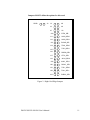
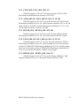
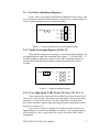
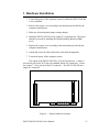
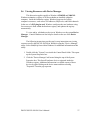
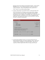
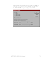
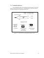
DSCLP/SSCLP-200/300 Two and One Channel RS-422/485 Low Profile Asynchronous Communications Adapter for PCI bus User's Manual QUATECH, INC. 5675 Hudson Industrial Parkway Hudson, Ohio 44236 TEL: (330) 655-9000 FAX: (330) 655-9010 http://www.quatech.com WARRANTY INFORMATION Quatech, Inc. warrants the DSCLP-200/300 or SSCLP-200/300 to be free of defects for five (5) years from the date of purchase. Quatech, Inc. will repair or replace any board that fails to perform under normal operating conditions and in accordance with the procedures outlined in this document during the warranty period. Any damage that results from improper installation, operation, or general misuse voids all warranty rights. Please complete the following information and retain for your records. Have this information available when requesting warranty service. DATE OF PURCHASE: MODEL NUMBER: DSCLP-200/300 or SSCLP-200/300 PRODUCT DESCRIPTION: DSCLP: Two Channel RS-422/485 Asynchronous PCI Bus Communications Adapter SSCLP: One Channel RS-422/485 Asynchronous PCI Bus Communications Adapter SERIAL NUMBER: DSCLP/SSCLP-200/300 User's Manual ii 2006 Quatech, Inc. NOTICE The information contained in this document cannot be reproduced in any form without the written consent of Quatech, Inc. Likewise, any software programs that might accompany this document can be used only in accordance with any license agreement(s) between the purchaser and Quatech, Inc. Quatech, Inc. reserves the right to change this documentation or the product to which it refers at any time and without notice. The authors have taken due care in the preparation of this document and every attempt has been made to ensure its accuracy and completeness. In no event will Quatech, Inc. be liable for damages of any kind, incidental or consequential, in regard to or arising out of the performance or form of the materials presented in this document or any software programs that might accompany this document. Quatech, Inc. encourages feedback about this document. Please send any written comments to the Technical Support department at the address listed on the cover page of this document. DOS, Windows 95, Windows NT are trademarks or registered trademarks of Microsoft Corporation. OS/2 is a registered trademark of IBM Corporation. All other trademarks or registered trademarks are property of their respective owners. DSCLP/SSCLP-200/300 User's Manual iii Declaration of Conformity Manufacturer's Name: Quatech Inc. Manufacturer's Address: 5675 Hudson Industrial Parkway Hudson, Ohio 44236 (USA) Application of Council Directive: 89/336/EEC Standards to which Conformity is Declared: * EN50081-1 (EN55022, EN60555-2, EN60555-3) * EN50082-1 (IEC 801-2, IEC 801-3, & IEC 801-4) Type of Equipment: Information Technology Equipment Equipment Class: Commercial, Residential, & Light Industrial Product Name: PCI Two Port or One Port Serial Communications Card Model Number : DSCLP-200/300 / SSCLP-200/300 DSCLP/SSCLP-200/300 User's Manual iv Table of Contents 1 General Information . . . . . . . . . . . . . . . . . . . . . . . . . . . . . . 2 Hardware Configuration . . . . . . . . . . . . . . . . . . . . . . . . . 8 9 2.1 RS-422 or RS-485 Signal Line Termination . . . . . . . . . . . 9 2.2 Signal Connections . . . . . . . . . . . . . . . . . . . . . . . . . . . . . . . . . 10 2.3 Full-duplex/Half-duplex Operation . . . . . . . . . . . . . . . . . . 10 2.3.1 CTS0_SEL, CTS1_SEL (J10, 17) . . . . . . . . . . . . . . . . . 12 2.3.2 AUX0_SEL1,0, AUX1_SEL1,0 (J12, 11, 19, 18) . . . 12 2.3.3 RCLK0_SEL, RCLK1_SEL (J13, 20) . . . . . . . . . . . . 12 2.3.4 TGL0_SEL1,0, TGL1_SEL1,0 (J15, 14, 22, 21) . . . . 12 2.3.5 RXEN0_SEL, RXEN1_SEL (J16, 23) . . . . . . . . . . . . 12 2.4 Clock Rate and Optional Registers . . . . . . . . . . . . . . . . . . 13 2.4.1 Enable Scratchpad Register (SPAD, J2) . . . . . . . . . . 13 2.4.2 Force High-Speed UART Clock (X2, X4, or X8; J3, 4, 5) . . . . . . . . . . . . . . . . . . . . . . . . . . . . . . . . . . . . . . . . . . . . . . . 13 3 Hardware Installation . . . . . . . . . . . . . . . . . . . . . . . . . . . 4 Address Map and Special Registers . . . . . . . . . . . 4.1 Base Address and Interrupt Level (IRQ) . . . . . . . . . . . . . 4.2 Enabling the Special Registers . . . . . . . . . . . . . . . . . . . . . . 4.3 Interrupt Status Register . . . . . . . . . . . . . . . . . . . . . . . . . . . . 4.4 Quatech Modem Control Register . . . . . . . . . . . . . . . . . . . 4.5 Options Register . . . . . . . . . . . . . . . . . . . . . . . . . . . . . . . . . . . . 4.5.1 Enhanced Serial Adapter Identification . . . . . . . . . . . 4.5.2 Clock Rate Multiplier . . . . . . . . . . . . . . . . . . . . . . . . . . . . 5 Windows Configurations ........................ 5.1 Windows Millennium . . . . . . . . . . . . . . . . . . . . . . . . . . . . . . . 5.2 Windows 2000 . . . . . . . . . . . . . . . . . . . . . . . . . . . . . . . . . . . . . . 5.3 Windows 98 . . . . . . . . . . . . . . . . . . . . . . . . . . . . . . . . . . . . . . . . 5.4 Windows 95 . . . . . . . . . . . . . . . . . . . . . . . . . . . . . . . . . . . . . . . . 5.5 Windows NT . . . . . . . . . . . . . . . . . . . . . . . . . . . . . . . . . . . . . . . 5.6 Viewing Resources with Device Manager . . . . . . . . . . . . 5.6.1 Changing Resource Settings with Device Manager . 6 Other Operating Systems v 15 16 16 17 17 18 19 19 20 21 21 22 23 25 26 27 30 . . . . . . . . . . . . . . . . . . . . . . . 35 DSCLP/SSCLP-200/300 User's Manual 6.1 OS/2 . . . . . . . . . . . . . . . . . . . . . . . . . . . . . . . . . . . . . . . . . . . . . . . 35 6.2 DOS and other operating systems . . . . . . . . . . . . . . . . . . . 35 6.2.1 QTPCI.EXE . . . . . . . . . . . . . . . . . . . . . . . . . . . . . . . . . . . . . 36 7 External Connections ............................ 7.1 RTS/cts Handshake . . . . . . . . . . . . . . . . . . . . . . . . . . . . . . . . . 7.2 RCLK . . . . . . . . . . . . . . . . . . . . . . . . . . . . . . . . . . . . . . . . . . . . . . 7.3 TCLK . . . . . . . . . . . . . . . . . . . . . . . . . . . . . . . . . . . . . . . . . . . . . . 7.4 AUXIN/AUXOUT Loopback . . . . . . . . . . . . . . . . . . . . . . . . 7.5 Half-Duplex/Full-Duplex/Auto-Toggle Selection . . . . . 7.6 Termination Resistors . . . . . . . . . . . . . . . . . . . . . . . . . . . . . . 7.7 RS-422/485 Peripheral Connection . . . . . . . . . . . . . . . . . . 8 PCI Resource Map . . . . . . . . . . . . . . . . . . . . . . . . . . . . . . . 9 Specifications . . . . . . . . . . . . . . . . . . . . . . . . . . . . . . . . . . . . . . 10 Troubleshooting . . . . . . . . . . . . . . . . . . . . . . . . . . . . . . . . vi 38 39 39 40 40 41 43 44 45 46 47 DSCLP/SSCLP-200/300 User's Manual DSCLP/SSCLP-200/300 User's Manual 7 1 General Information The Quatech, Inc. DSCLP-200/300 (two-port) and SSCLP-200/300 (one-port) provide RS-422 or RS-485 asynchronous serial communication interfaces for IBM-compatible personal computer systems using the PCI expansion bus. For general purposes, this manual usually makes reference only to the DSCLP-200/300. All information pertains equally to the SSCLP-200/300, with the exception that with the SSCLP there is just one port instead of two. The DSCLP-200/300 uses Quatech's new Enhanced Serial Adapter design. Legacy serial port data rates are limited to a maximum of 115,200 bits per second. Quatech Enhanced Serial Adapters can achieve data rates as high as 921,600 bits per second. As a PCI device, the DSCLP-200/300 requires no hardware configuration. The card is automatically configured by the computer's BIOS or operating system. The two serial ports share a single interrupt line and are addressed in a contiguous block of 16 bytes. A special interrupt status register is provided to help software to manage the shared interrupt. The DSCLP-200/300's serial ports are implemented using 16550 Universal Asynchronous Receiver/Transmitters (UARTs). These UARTs contain hardware buffers (FIFOs) which reduce processing overhead and allow higher data rates to be achieved. The 16550 contains a 16-byte FIFO and can transmit and receive data at a rate of up to 921,000 bits per second. The DSCLP-200/300 is supported under several popular operating systems and environments. Contact the sales department for details on current software offerings. Most device drivers are available for download from the Quatech world wide web site at http://www.quatech.com. DSCLP/SSCLP-200/300 User's Manual 8 2 Hardware Configuration The DSCLP-200/300 is automatically configured at boot time by the computer's BIOS or operating system. There are no required switches or jumpers to set for installation. This chapter lists a number of optional jumper settings that control various hardware features. Jumpers J1-J4, located in a column near the D-type connector (D-25 for DSCLP, D-9 for SSCLP), control the RS-422 or RS-485 signal line termination. Jumpers J5-J8, located in a column just to the right of J1-J4, control how signals are routed from the UARTs to the connector, as well as full- or halfduplex operation. Jumpers J10-J22, grouped together at the end of the board opposite the D-type connector (D-25 for DSCLP, D-9 for SSCLP), control special options. Any changes from the factory default should be made before installing the DSCLP-200/300 in the computer. These settings can also be changed in Device Manager under Windows operating systems. 2.1 RS-422 or RS-485 Signal Line Termination Jumpers J6-J9 allow the selection of 100-ohm RS-422 termination, 120-ohm RS-485 termination, or no termination at all. The factory default, shown in Figure 1, is RS-422 termination. For full details, see section 7.6. Jumpers J6-J9 2 4 1 3 RS-422 termination (100 ohms) (factory default) Figure 1 --- Factory default signal termination settings DSCLP/SSCLP-200/300 User's Manual 9 2.2 Signal Connections The DSCLP-200/300 provides each of two serial ports with four differential signal pairs: TxD, RxD, AUXOUT, and AUXIN. TxD and RxD are always present at the connector. The AUXOUT and AUXIN signals can be used to support RTS/CTS handshaking, external clocking, or external signal loopback. The factory default configuration, as shown in Figure 2, is a loopback of AUXOUT to AUXIN at the connector, with RTS and CTS looped back on the board. There is an extensive discussion of this topic in section 7. 2.3 Full-duplex/Half-duplex Operation The DTR or RTS modem control output of the UART can be used to enable and disable the transmit drivers. The inverse of these signals can also be used to enable and disable the receivers. These options are selectable per channel. The factory default, as shown in Figure 2, is for both the drivers and receivers of both channels to be continuously enabled. Two spare jumpers are installed in neutral positions. For details, refer to section 7.5. The DSCLP-200/300 is shipped from the factory with each channel configured with No jumpers on J10-23. The following conditions occur: CTS=AUXIN, AUXOUT=RTS, RCLK=TCLK, TXEN=1 AND RXEN=1. DSCLP/SSCLP-200/300 User's Manual 10 Jumpers J10-J23 define the options for this card: SPAD J2 J3 X8 J4 X4 J5 X2 J10 CTS0_SEL J11 AUX0_SEL0 J12 AUX0_SEL1 J13 RCLK0_SEL J14 TGL0_SEL0 J15 TGL0_SEL1 J16 RXEN0_SEL J17 CTS1_SEL J18 AUX1_SEL0 J19 AUX1_SEL1 J20 RCLK1_SEL J21 TGL1_SEL0 J22 TGL1_SEL1 J23 RXEN1_SEL Figure 2 - Right Card Edge Jumpers DSCLP/SSCLP-200/300 User's Manual 11 2.3.1 CTS0_SEL, CTS1_SEL (J10, 17) With NO jumpers on J10 or J17 the mode selection is CTS=AUXIN. With Jumpers installed the mode selection is CTS=RTS. 2.3.2 AUX0_SEL1,0, AUX1_SEL1,0 (J12, 11, 19, 18) With NO jumpers on J12 or J19 the mode selection is AUXOUT=RTS. With Jumpers installed on J12 or J19 and NO jumpers installed on J11 or J18, the mode selection is AUXOUT=TCLK. With Jumpers installed on J12, J11 or J19, J18, the mode selection is AUXOUT=AUXIN. 2.3.3 RCLK0_SEL, RCLK1_SEL (J13, 20) With NO jumpers on J13 or J20 the mode selection is RCLK=TCLK. With Jumpers installed on J13 or J20 the mode selection is RCLK=AUXIN. 2.3.4 TGL0_SEL1,0, TGL1_SEL1,0 (J15, 14, 22, 21) With NO jumpers on J15,14, or J22,21 the mode selection is TXEN=1. With Jumpers installed on J14 or J21 and NO jumpers on J15 or J22, the mode selection is TXEN=DTR. With Jumpers installed on J15 or J22 and NO jumpers on J14 or J21, the mode selection is TXEN=RTS. With Jumpers installed on J15, J14 or J22, J21, the mode selection is TXEN=”Auto Toggle”. 2.3.5 RXEN0_SEL, RXEN1_SEL (J16, 23) With NO jumpers on J16 or J23 the mode selection is RXEN=1. With Jumpers installed on J16 or J23 the mode selection is RCLK=!TXEN. DSCLP/SSCLP-200/300 User's Manual 12 2.4 Clock Rate and Optional Registers Figure 3 shows the jumper configuration as shipped from the factory, with two spare jumpers applied in neutral positions. Remove one or both and apply as shown in following subsections to set optional features. SPAD J2 J3 X8 J4 X4 J5 X2 Figure 3 --- Factory default clock rate and options settings 2.4.1 Enable Scratchpad Register (SPAD, J2) In the default configuration (see page 11), an Interrupt Status Register and an Options Register replace the scratchpad (base address + 7) of each UART. If the SPAD jumper is applied as in Figure 4, the UART scratchpad registers are enabled, and the Interrupt Status Register and the Options Register are not available. SPAD J2 J3 X8 J4 X4 J5 X2 Figure 4 --- Enable scratchpad registers 2.4.2 Force High-Speed UART Clock (X2, X4, or X8; J3, 4, 5) These jumpers force an increase of the UART input clock frequency by a factor of two, four, or eight. This feature can allow legacy software to use baud rates above 115,200 bits per second. It is also useful if the serial port device driver does not directly support setting the higher baud rates through the Options Register (see section 4.5). If one of these jumpers is applied, it overrides any value written to the Options Register to set the clock multiplier by software. The effective baud rate will be either two, four, or eight times the value for which the UART itself is programmed. DSCLP/SSCLP-200/300 User's Manual 13 The factory default is none of these jumpers applied, which allows for software control of the clock multiplier via the Options Register. The Options Register powerup default is for a standard times-1 clock of 1.8432 MHz for compatibility with standard serial ports. Figure 5 --- Clock multiplier jumper options SPAD J2 J3 X8 J4 X4 J5 X2 factory default SPAD J2 J3 X8 J4 X4 J5 X2 X8 mode SPAD J2 J3 X8 J4 X4 J5 X2 X4 mode SPAD J2 J3 X8 J4 X4 J5 X2 X2 mode DSCLP/SSCLP-200/300 User's Manual 14 3 Hardware Installation 1. Turn off the power of the computer system in which the DSCLP-200/300 is to be installed. 2. Remove the system cover according to the instructions provided by the computer manufacturer. 3. Make any desired optional jumper setting changes. 4. Install the DSCLP-200/300 in any empty PCI expansion slot. The board should be secured by installing the Option Retaining Bracket (ORB) screw. 5. Replace the system cover according to the instructions provided by the computer manufacturer. 6. Attach and secure the cable connectors to the desired equipment. 7. Turn on the power of the computer system. The output of the DSCLP-200/300 is a 25-pin D-connector. A cable is provided to convert the D-25 into two standard female D-9 connectors. Please see section 7.7 for a pin-out of the D-9 connector. The SSCLP-200/300 has a single D-9 connector. Figure 6 --- Jumper/connector locations DSCLP/SSCLP-200/300 User's Manual 15 4 Address Map and Special Registers This chapter explains how the two UARTs and special registers are addressed, as well as the layout of those registers. This material will be of interest to programmers writing driver software for the DSCLP-200/300. 4.1 Base Address and Interrupt Level (IRQ) The base address and IRQ used by the DSCLP-200/300 are determined by the BIOS or operating system. Each serial port uses 8 consecutive I/O locations. The two ports reside in a single block of I/O space in eight byte increments, for a total of 16 contiguous bytes, as shown in Figure 7. Channel I/O Address Range Port 1 Base Address + 0 to Base Address + 7 Port 2 Base Address + 8 to Base Address + 15 Figure 7 --- Port Address Map All serial ports share the same IRQ. The DSCLP-200/300 signals a hardware interrupt when any port requires service. The interrupt signal is maintained until no port requires service. Interrupts are level-sensitive on the PCI bus. The base address and IRQ are automatically detected by the device drivers Quatech supplies for various operating systems. For cases where no device driver is available, such as for operation under DOS, Quatech supplies the "QTPCI" DOS software utility for manually determining the resources used. See section 6.2.1 for details. DSCLP/SSCLP-200/300 User's Manual 16 4.2 Enabling the Special Registers The DSCLP-200/300 contains two unique registers, an Interrupt Status Register and an Options Register. These registers are enabled when the SPAD jumper (J13) is removed (factory default). They replace the UART Scratchpad Register on accesses to register address 7. The Interrupt Status Register and Options Register are accessed through the scratchpad location of any UART. The DLAB bit of the UART (Line Control Register, bit 7) is used to select between the two registers. The most recent write of a DLAB bit in any UART selects between the two registers as shown in Figure 8. DLAB Bit SPAD Jumper 0 1 X removed removed applied Register selected for address 7 accesses Interrupt Status Register Options Register Scratchpad Registers Figure 8 --- DLAB bit selects between special registers 4.3 Interrupt Status Register The read-only Interrupt Status Register can be used to quickly identify which serial ports require servicing after an interrupt. Reading the Interrupt Status Register will return the interrupt status of the entire DSCLP-200/300, as shown in Figure 9. The individual bits are cleared as the interrupting ports are serviced. The interrupt service routine should ensure that the interrupt status register reads zero before exiting. Bit Description 7 (MSB) 0 (not used) 6 0 (not used) 5 0 (not used) 4 0 (not used) 3 0 (not used) 2 0 (not used) 1 Port 2 --- 1 if interrupt pending 0 Port 1 --- 1 if interrupt pending Figure 9 --- Interrupt Status Register DSCLP/SSCLP-200/300 User's Manual 17 4.4 Quatech Modem Control Register The Quatech Modem Control Register can be used to set up each port. To access the QMCR write a 0xBF to the LCR (base + 3) and a 0x10 to the Options Register (base+7). This will allow the user read/write access to the QMCR. The QMCR of the entire DSCLP-200/300 is shown in Figure 9a. Bit Description 7 (MSB) 0 (always 0) 6 0 (always 0) 5 0 - RXEN=1 1 - RXEN=!TXEN 4 0 - Bits 2 and 3 are used 1 - RCLK=TCLK,CTS=RTS, AUXOUT=AUXIN 3 0 - RCLK=TCLK,CTS=AUXIN 1 - RCLK=AUXIN, CTS=RTS 2 0 - AUXOUT=RTS 1- AUXOUT=TCLK 1-0 00 - TXEN “Auto” 01 - TXEN=DTR 10 - TXEN=RTS 11 - TXEN TOGGLES DURING X-MIT Figure 9a --- Quatech Modem Control Register DSCLP/SSCLP-200/300 User's Manual 18 4.5 Options Register The Options Register allows software to identify the DSCLP-200/300 as a Quatech Enhanced Serial Adapter. It also allows software to set the UART clock rate multiplier. Figure 10 shows the structure of the Options Register. The powerup default of the Options Register is all bits zero. Bit Name Description 7 (MSB) ID1 ID bit 1 6 ID0 ID bit 0 5 - (reserved, 0) 4 - (reserved, 0) 3 - (reserved, 0) 2 - (reserved, 0) 1 RR1 Clock rate multiplier bit 1 0 RR0 Clock rate multiplier bit 0 Figure 10--- Options Register bit definitions 4.5.1 Enhanced Serial Adapter Identification The ID bits are used to identify the DSCLP-200/300 as a Quatech Enhanced Serial Adapter. Logic operations are performed such that the values read back from these bits will not necessarily be the values that were written to them. Bit ID1 will return the logical-AND of the values written to ID[1:0], while bit ID0 will return their exclusive-OR. Software can thus identify a Quatech Enhanced Serial Adapter by writing the ID bits with the patterns shown in the "write" column of Figure 11, then reading the bits and comparing the result with the patterns in the "read" column. Matching read patterns verify the presence of the Options Register. Write Read ID1 ID0 ID1 ID0 0 0 0 0 0 1 0 1 1 0 0 1 1 1 1 0 Figure 11 --- ID bit write/read table DSCLP/SSCLP-200/300 User's Manual 19 4.5.2 Clock Rate Multiplier A standard serial port operates at a clock speed of 1.8432 MHz. In order to achieve higher data rates, Quatech Enhanced Serial Adapters can operate at two, four, or eight times this standard clock speed. This is controlled by the clock rate multiplier bits in the Options Register. Software can determine the UART clock frequency by reading the clock rate multiplier bits RR1 and RR0 in the Options Register as shown in Figure 12. RR1 and RR0 can be set by writing to the Options Register if the X2 and X4 jumpers (J4-J5) are all removed. If one of these jumpers is applied, the RR1 and RR0 bits are forced to the appropriate value. Reading the Options Register will always return the clock rate multiplier at which the board is operating. RR1 RR0 0 0 0 1 1 1 0 1 Clock Rate Multiplier X1 (default) X2 X4 X8 UART Clock Frequency Maximum Data Rate 1.8432 MHz 115.2 kbaud 3.6864 MHz 7.3728 MHz 14.7456 MHz 230.4 kbaud 460.8 kbaud 921.6 kbaud Figure 12 --- Rate Register bit definition At powerup and reset, the Options Register is initialized to 0. The DSCLP-200/300 will thus powerup in the x1 mode with software control of the clock rate multiplier enabled as long as the X2 or X4 or X8 jumpers are not installed. Software can control high baud rates through a combination of changing the clock rate multiplier and the UART baud rate divisor. For example, a baud rate of 230.4 kbps could be achieved by setting the clock rate multiplier to X2 mode (or by applying the X2 jumper) and setting a software application for 115.2 kbps. DSCLP/SSCLP-200/300 User's Manual 20 5 Windows Configurations 5.1 Windows Millennium 1. After inserting the DSCLP-200/300 for the first time the "Add New Hardware Wizard" will begin. Select "Search for the best driver for your device.". Check the "Removable media" and "Specify location" box. Click the "Next" button. 2. 3. Window will locate the proper INF file and copy the file from the CD. Click the "Next" button. The final dialog screen will verify the file copy from the CD. Click the "Finish" button. DSCLP/SSCLP-200/300 User's Manual 21 5.2 Windows 2000 1. After inserting a DSCLP-200/300 for the first time, the "Add New Hardware Wizard will appear at start up. Click the "OK" button. 2. The following dialog box insert the Quatech COM CD (shipped with the device). Click the "OK" button. 3. The following dialog box will display the appropriate INF file from the CD in the drive. Click the "OK" button. 4. Window will copy the INF file from the CD and display a final dialog indication that the process is complete. Click the "Finish" button. DSCLP/SSCLP-200/300 User's Manual 22 5.3 Windows 98 1. After inserting a DSCLP-200/300 for the first time, the "Add New Hardware Wizard will appear at start up. Click the "Next" button. 2. Select "Search for the best driver for you device". Click the "Next" button. 3. On the next dialog, select the "CD-ROM DRIVE" check box. Insert the Quatech COM CD (shipped with the device) into the CD-ROM drive. Click the "Next" button. DSCLP/SSCLP-200/300 User's Manual 23 4. The following dialog box will display the appropriate INF file on the diskette in the drive. Click the "Next" button. 5. Window will copy the INF file from the diskette and display a final dialog indication that the process is complete. Click the "Finish" button. DSCLP/SSCLP-200/300 User's Manual 24 5.4 Windows 95 Windows 95 maintains a registry of all known hardware installed in your computer. Inside this hardware registry Windows 95 keeps track of all of your system resources, such as I/O locations, IRQ levels, and DMA channels. The "Add New Hardware Wizard" utility in Windows 95 was designed to add new hardware and update this registry. An "INF" configuration file is included with the DSCLP-200/300 to allow easy configuration in the Windows 95 environment. Also a custom Windows 95 serial device driver is included with the DSCLP-200/300 to support the use of the 16550 UART's 64 byte FIFO. Windows 95 uses the "INF" file to determine the system resources required by the DSCLP-200/300, searches for available resources to fill the boards requirements, and then updates the hardware registry with an entry that allocates these resources The following instructions provide step-by-step instructions on installing the DSCLP-200/300 in Windows 95 using the "New Hardware Found" wizard. 1. After booting the computer with a newly-installed DSCLP-200/300, the "New Hardware Found" dialog box will appear. If you have never installed a Quatech PCI communications adapter before, the dialog box may simply indicate that it has found a "PCI Card." 2. Select the radio button for "Driver from disk provided by hardware manufacturer." Click the "OK" button to continue. 3. An "Install From Disk" dialog box should pop up. Insert the diskette with the Quatech INF files on it, select the correct drive letter, and click the "OK" button. Windows 95 automatically browses the root directory for an INF file that defines configurations for Multi-function Adapters. If no INF files are found, click the "Browse" button and search the Win95 sub directory on the installation diskette. You are not required to select the file name. After finding the directory containing the INF files, Windows 95 will choose the correct file. 4. The "New Hardware Found" dialog box will appear again, this time for an "Unknown Device." 5. Again select the radio button for "Driver from disk provided by hardware manufacturer." Click the "OK" button to continue. 6. Another "Install From Disk" dialog box will pop up. The path should already be pointing to the Quatech diskette. Click the "OK" button to continue. 7. You should now see the "Copying Files" dialog box as Windows 95 copies the driver files from the diskette. DSCLP/SSCLP-200/300 User's Manual 25 8. The installation utility will ask for your Windows 95 installation disks. Serial communication ports require two drivers supplied by Microsoft to function: SERIAL.VXD and SERIALUI.DLL. Insert the disk or CD and click "OK". NOTE: You may be able to skip this step if you are certain that your system has the latest version of these files installed. If you do not have your Windows 95 install disks immediately available, click "OK" anyway. A dialog box appears with an option to Skip the files. Click the Skip button and the files will not be installed. This is all right if the latest version of these drivers are currently in the \WINDOWS\SYSTEM directory. 9. The "New Hardware Found" dialog will repeat for each of the serial ports on the DSCLP-200/300 as each port is registered with Windows 95. 10. Installation is complete. 5.5 Windows NT The Windows NT device driver is installed by running the SETUP program. Up to 256 serial ports are supported. There is a command line-based configuration utility which is used for adding PCI bus and ISA bus serial ports. Please refer to the documentation included with the device driver for full installation and configuration details. DSCLP/SSCLP-200/300 User's Manual 26 5.6 Viewing Resources with Device Manager This discussion applies equally to Windows 95/98/ME and 2000/XP. Windows maintains a registry of all known hardware installed within the computer. Inside this hardware registry Windows keeps track of all the computer's resources, such as base I/O addresses, IRQ levels, and DMA channels. In the case of a PCI plug-in card, Windows configures the new hardware using free resources it finds within the hardware registry, and updates the registry automatically. To view and/or edit hardware devices in Windows use the system Device Manager. Consult Windows on-line help for details on the use of the Device Manager. The following instructions provide step-by-step instructions on viewing resources used by the DSCLP-200/300 in Windows using the "Device Manager" utility. Select Start|Help from within Windows for additional information on this utility. 1. Double click the "System" icon inside the Control Panel folder. This opens up the System Properties box. 2. Click the "Device Manager" tab located along the top of the System Properties box. This lists all hardware devices registered inside the Windows registry. Additional information is available on any of these devices by right-clicking on the device name and then selecting "Properties" from the pop-up menu. DSCLP/SSCLP-200/300 User's Manual 27 3. Double click the device group "Multi-function Adapters". The DSCLP-200/300 “parent device” belongs to this hardware class. The full device name for the DSCLP-200/300 is Quatech DSCLP-200/300 PCI Two-Port RS-422/RS485 Serial Adapter. 4. Double click the DSCLP-200/300 name and a properties dialog should open for the hardware adapter. 5. Click the "Resources" tab located along the top of the properties box to view the resources Windows has allocated for Input/Output Range and Interrupt Request. Because PCI is a true plug-and-play bus, do not attempt to modify the configuration values listed. Click "Cancel" to exit without making changes. 6. Double click the hardware class Ports (Com and LPT). Each Quatech PCI Serial Port listed in this class is a “child device” of the DSCLP-200/300 “parent device.” Windows 95 does not assign COM1-COM4 to ports addressed at nonstandard locations. So in Windows 95, the DSCLP-200/300 ports will be enumerated starting with COM5 (or higher) even if lower logical numbers are available. 7. Select any of the Quatech Serial Ports listed under the group Port (COM and LPT) and click the "Properties" button. This action opens a properties DSCLP/SSCLP-200/300 User's Manual 28 dialog for the specific COM port on the DSCLP-200/300. Then click the Resources tab to view the Input/Output Range and Interrupt Request resource allocations. These will match those of the “parent device.” Click "Cancel" to exit without making changes. 8. Click the "Port Settings" tab and then click the "Advanced" button. The DSCLP-200/300 driver will display a custom Advanced Port Settings control, which allows the ports UART compatibility mode and FIFO threshold levels to be configured. The threshold values of full-scale for the transmit buffer and ¾-scale for the receive buffer are optimal for most applications. Note that the FIFO option for each of the DSCLP-200/300's two ports is configured independently. 9. Use the Logical COM Port names to access the serial ports on your DSCLP-200/300 through your software applications. Note: The Logical COM Port name is assigned to your ports by Windows. This name is required by Windows applications when accessing a particular port. DSCLP/SSCLP-200/300 User's Manual 29 5.6.1 Changing Resource Settings with Device Manager 1. Start the Windows 95/98/ME Device Manager. 2. Double click on the hardware class Multi-Port Serial Adapters to list hardware devices in the class. 3. The DSCLP-200/300 “parent device” belongs to this hardware class. The full device name for the DSCLP-200/300 is Quatech DSCLP-200/300: Two-Port RS-422/485 Serial Adapter. 4. Open the Properties dialog for the DSCLP-200/300 device, then click the Resources tab to view the Input/Output Range and Interrupt Request resource allocations. 5. Open the Properties dialog for the DSCLP-200/300 device, then click the Advanced tab to view the clock rate settings. DSCLP/SSCLP-200/300 User's Manual 30 Clock Mode Auto X1 X2 X4 X8 Data Rate Multiplier Max bps Description Auto clock mode enables applications to request any baud rate up to 921,600. 921,600 The hardware drivers will select the correct clock multiplier based on the baud rate requested The X1 clock mode mimics a standard COM port. The hardware drivers lock 115,200 the clock to the standard rate. The port will run at the baud rate requested by the application. The X2 clock mode locks the ports hardware clock at double the standard rate. The baud rate the port runs at will 230,400 always be double the rate requested by the applications. This mode is useful for legacy applicattions which cannot request baud rates over 115,200 The X4 clock mode locks the ports hardware clock at four times the standard rate. The baud rate the port 460,800 runs at will always be four times the rate requested by the application. This mode is useful for legacy applications which cannot request baud rates over 115.200. The X8 clock mode locks the ports hardware clock at eight times the standard rate. The baud rate the port runs at will always be eight times the 921,600 rate requested by the application. This mode is useful for legacy applications which cannot request baud rates over 115.200. 6. Double click the hardware class Ports (Com and LPT). Each Quatech PCI Serial Port listed in this class is a “child device” of the DSCLP-200/300 “parent device.” 7. Open the Properties dialog for a COM port, then click the RS-422/485 tab to view the settings for that port. DSCLP/SSCLP-200/300 User's Manual 31 RS-422/485 Connector Setup RTS routed to CTS, AUXIN routed to AUXOUT, and TCLK Loopback All routed to RCLK. Used when external handshaking or clocking signals are not available. RTS routed to AUXOUT, AUXIN routed to CTS, and Modem Control TCLK routed to RCLK. Used when RTS/CTS handshaking is required. RTS routed to CTS, AUXIN routed to RCLK, and TCLK routed to AUXOUT. Used to Clocks connect ports transmitting at different baud rates. In order to function, all ports must have and use this feature. DSCLP/SSCLP-200/300 User's Manual 32 Receive Control Receivers are always enabled. In a Half Duplex mode, you will Always Receive receive what you transmit (sometimes called echo). Receivers are only enabled when not transmitting. In a Half When NOT Tranmitting Duplex mode, you will not receive what you transmit. RS-422/485 Duplex Mode Transmitters and receivers are always enabled; ports can send Full Duplex and receive simultaneously. Used in four-wire communication. RTS is set to enable the Half Duplex using RTS transmitters. Used in two-wire communication. DTR is set to enable the Half Duplex using DTR transmitters. Used in two-wire communication Hardware automatically enables the transmitters when transmitting. Transmitters will Auto Toggle turn off three bit-times after the last stop bit of the last character, regardless of baud rate. Used in two-wire communication. 8. To summarize the RS-422/485 output drivers enable options: The DSCLP-200/300’s ports may be configured for either full duplex or half duplex operation with this option. The default setting is the RS-422/485 ports are configured for full duplex operation with the RS-422/485 output drivers always enabled. In half duplex mode, the RS-422/485 transmitter may be enabled and disabled via the RTS (request to send) or DTR (data terminal ready) signals, or in auto-toggle mode, set to enable only when data is being transmitted. Both RTS and DTR are controlled through the Modem Control Register of the 16550. 9. Click the "Port Settings" tab and then click the "Advanced" button. The DSCLP-200/300 driver will display a custom Advanced Port Settings control, which allows the ports UART compatibility mode and FIFO threshold levels to be configured. The threshold values of DSCLP/SSCLP-200/300 User's Manual 33 full-scale for the transmit buffer and ¾-scale for the receive buffer are optimal for most applications. Note that the FIFO option for each of the DSCLP-200/300's two ports is configured independently. DSCLP/SSCLP-200/300 User's Manual 34 6 Other Operating Systems Device drivers for Windows NT and OS/2 are also available for the DSCLP-200/300. The board can be used under DOS and other operating systems as well in many circumstances. The software described below can be obtained from the Quatech web site if it did not come with the board. 6.1 OS/2 The OS/2 device driver supports up to 32 serial ports in a system. Installation is a manual, but simple, process. Please refer to the documentation included with the device driver for full installation and configuration details. 6.2 DOS and other operating systems The DSCLP-200/300 is not a direct drop-in replacement for a legacy serial port because its base address and IRQ cannot be fixed at values such as 3F8 hex, IRQ 4 (COM1) or 2F8 hex, IRQ 3 (COM2), etc. Rather, the system BIOS assigns the address and the IRQ in a plug-and-play fashion at boot time. Software which is to use the DSCLP-200/300 must be able to accommodate any valid assignments of these resources. For Windows 95, Windows NT and OS/2, the Quatech device drivers determine what the resource assignments are and proceed accordingly. In other cases, however, the user must intervene. The discussion below will center on DOS, but the concepts can be applied to other operating systems as well. Many DOS applications support user configuration of the base address and IRQ of a serial port. Such applications can generally make use of the DSCLP-200/300. Older applications, as well as some custom software, may use hard-coded standard legacy serial port addresses. These applications will require modifications to support PCI devices. Custom applications for which the customer has source code can be modified to make just a few PCI BIOS function calls to obtain all the necessary configuration information. The PCI BIOS specification can be obtained from the PCI Special Interest Group. Contact Quatech technical support for more information. DSCLP/SSCLP-200/300 User's Manual 35 6.2.1 QTPCI.EXE Quatech's "QTPCI" utility supplies the information required when modifying the serial port settings of the application. This program should be run from real DOS, not in a Windows DOS box. Figure 13 shows the Basic Mode display for the DSCLP-200/300 after the "Q" key has been pressed. In this example, the DSCLP-200/300 uses I/O base address FFA0 hex and IRQ 3. The hardware revision of the DSCLP-200/300 is also displayed. Pressing the "N" key will show similar information for all non-Quatech PCI devices in the system, including those devices integrated on the motherboard. The QTPCI program is capable only of displaying the PCI configuration. It cannot be used to make changes. Figure 13 --- QTPCI.EXE Basic Mode display DSCLP/SSCLP-200/300 User's Manual 36 Figure 14 shows the Expert Mode display for the DSCLP-200/300 after the "Q" key has been pressed. The information from the Basic Mode display is presented along with more details such as the Vendor and Device IDs, PCI Class Code, size of memory and I/O regions, etc. Pressing the "N" key will show similar information for all non-Quatech PCI devices in the system, including those devices integrated on the motherboard. In this example, the "Base addr 0" resource is reserved. For users interested in even more details, PCI BIOS information can be displayed by pressing the "B" key. Pressing the "I" key displays thePCI interrupt routing table. Figure 14 --- QTPCI.EXE Expert Mode display DSCLP/SSCLP-200/300 User's Manual 37 7 External Connections The DSCLP-200/300 provides four differential communication signals per channel. The two output signals are Transmit Data (TxD) and Auxiliary Output (AUXOUT). The two input signals are Receive Data (RxD) and Auxiliary Input (AUXIN). A ground signal is also provided. The available input signals for AUXIN are Clear To Send (CTS) and the Receive Clock (RCLK). The available output signals for AUXOUT are Request To Send (RTS), the Transmit Clock (TCLK), and the AUXIN signal (for loopback). Either half-duplex or full-duplex operation can be selected for each communications channel. Auto-Toggle is also jumper selectable .If half-duplex operation is selected, one of the UART's signals (either DTR or RTS) is used to enable the transmitter drivers. The inverse of the transmitter enable can be used to enable the receiver drivers. Factory-installed resistors allow for signal line termination in compliance with the RS-422 and RS-485 standards. The desired termination can be selected or removed per port by applying a jumper. Configuration is done using jumpers J6 through J9 for termination selection, and jumpers J10 through J23 for interface signal routing. Each jumper block provides the same functions for its particular channel. All below examples are for Channel 1. Channel 2 is the same but different sets of jumpers. See Figure 15 for Channel 2 jumpers. Channel Termination Signal routing Port 1 J6, J7 J10-16 Port 2 J8, J9 J17-23 Figure 15 --- Jumper/Channel correspondence DSCLP/SSCLP-200/300 User's Manual 38 7.1 RTS/CTS Handshake Transmission of RTS, combined with reception of CTS, allows for hardware handshaking (data flow control) between the UART and the external device. RTS is transmitted on AUXOUT by not connecting pins 1 and 2 of the jumper blocks J11-12. CTS is received on AUXIN by not connecting pins 1 and 2 of the jumper block J10. If RTS/CTS handshaking is not desired, the RTS output can be looped back to the CTS input by connecting pins 1 and 2 of the jumper block J10. Figure 16 shows how to select the RTS/CTS mode. Jumpers J10-12 J10 CTS0_SEL J10 CTS0_SEL J11 AUX0_SEL0 J11 AUX0_SEL0 J12 AUX0_SEL1 J12 AUX0_SEL1 Transmit RTS on AUXOUT Receive CTS on AUXIN Loopback RTS to CTS Figure 16 --- RTS/CTS selection 7.2 RCLK This is the clock signal used by the receiver portion of the UART. It is generally provided by connecting it to the UART's own transmit clock output (TCLK). This is done by not connecting pins 1 and 2 of the jumper block J13. If desired, RCLK can be received from an external source over the AUXIN line by connecting pins 1 and 2 of the jumper block J13. Figure 17 shows how to select the RCLK mode. Jumper J13 J13 RCLK0_SEL Loopback TCLK to RCLK J13 RCLK0_SEL Receive RCLK on AUXIN Figure 17 --- RCLK selection DSCLP/SSCLP-200/300 User's Manual 39 7.3 TCLK This is the output clock signal used by the transmitter portion of the UART. It is generally connected to the UART's own receive clock input (RCLK). This is done by not connecting pins 1 and 2 of the jumper block J13. If desired, TCLK can be transmitted to an external source over the AUXOUT line by connecting pins 1 and 2 of the jumper block J12. Figure 18 shows how to select the TCLK mode. Jumpers J11-13 J13 J11 AUX0_SEL0 J12 AUX0_SEL1 J13 RCLK0_SEL RCLK0_SEL Loopback TCLK to RCLK Transmit TCLK on AUXOUT Figure 18 --- TCLK selection 7.4 AUXIN/AUXOUT Loopback The AUXIN signal is an input from the external device, and connecting it to the AUXOUT signal provides for a loopback mode of operation. In other words, whatever signal is transmitted by the external device over the AUXIN line will be fed back to the external device over the AUXOUT line. This mode is accomplished by connecting pins 1 and 2 of the jumper blocks J11 and J12. Figure 19 shows how to select this loopback mode. Jumpers J11-13 J11 AUX0_SEL0 J12 AUX0_SEL1 J13 RCLK0_SEL Loopback AUXOUT to AUXIN Figure 19 --- AUXIN/AUXOUT loopback DSCLP/SSCLP-200/300 User's Manual 40 7.5 Half-Duplex/Full-Duplex/Auto-Toggle Selection Using jumper blocks J14 thru J16, the transmitters and receivers of each channel can be enabled and disabled by modem control signals. This allows operation in both half-duplex, full-duplex or Auto-Toggle modes. The transmit drivers can be controlled by either the Data Terminal Ready (DTR) or the Request to Send (RTS) output from the UART. If a jumper is applied between pins 1 and 2 of jumper block J14, the drivers are enabled for TxD and AUXOUT when the UART's DTR signal is asserted. If a jumper is applied between pins 1 and 2 of jumper block J15, the drivers are enabled for TxD and AUXOUT when the UART's RTS signal is asserted. If neither of these jumpers is applied, the drivers remain enabled at all times. When disabled, the transmit drivers enter a high-impedance state. The receivers can be controlled by the inverse of the transmit enable. If a jumper is applied between pins 1 and 2 of jumper block J16, the receivers for RxD and AUXIN will be disabled when the transmit drivers are enabled and vice-versa (based on the DTR or RTS connections on pins 1-2 of J14 and J15. To operate in half-duplex DTR mode, apply jumpers between pins 1 and 2 of jumper blocks J14 and J16. To operate in half-duplex RTS mode, apply jumpers between pins 1 and 2 .of jumper blocks J15 and J16 To operate in full-duplex mode, leave the jumpers in their factory default locations, installed in the spare locations of J14-16 only. The drivers and receivers are always enabled in full-duplex mode. For Auto-Toggle, apply jumpers between pins 1 and 2 of jumper blocks J14 and J15. Figure 20 shows how to select half-, full-duplex or Auto-Toggle operation. WARNING: When operating in half-duplex mode, the transmitter drivers must be disabled before receiving any data. Failure to do so may result in multiple active output drivers being connected together, which may cause damage to the board, the computer, and the external device. DSCLP/SSCLP-200/300 User's Manual 41 Jumpers J14-16 J14 TGL0_SEL0 J15 TGL0_SEL1 J16 RXEN0_SEL J14 TGL0_SEL0 J15 TGL0_SEL1 J16 RXEN0_SEL J14 TGL0_SEL0 J15 TGL0_SEL1 J16 RXEN0_SEL J14 TGL0_SEL0 J15 TGL0_SEL1 J16 RXEN0_SEL Half-Duplex(DTR) Operation Half-Duplex(RTS) Operation Full-Duplex Operation Auto-Toggle Operation Figure 20 --- Half/full-duplex and Auto-Toggle selection DSCLP/SSCLP-200/300 User's Manual 42 7.6 Termination Resistors Line termination resistors are provided for the input signals of each of the DSCLP-200/300's RS-422/485 ports. Termination may be selected or removed for individual signal lines using jumper blocks J6-J9. RS-422/485 Receiver RS-422 RS-485 Rt = 100 ohm 1/2W Rt = 120 ohm 1/2W RXD+ + Rt - AUXIN+ or RXD- AUXIN- Jumpers J6-J9 2 4 2 4 2 4 1 3 1 3 1 3 no termination RS-422 termination (100 ohms) (factory default) RS-485 termination (120 omhs) Figure 21 --- RS-422/485 Line termination resistance values DSCLP/SSCLP-200/300 User's Manual 43 7.7 RS-422/485 Peripheral Connection The DSCLP-200/300 connects to peripheral equipment through a 25-pin D-connector. A cable is provided to convert the D-25 into two standard female D-9 connectors. The SSCLP-200-300 has a single D-9 connector. The serial port connector definitions are listed in Figure 22. SignalDescription D-9 Connector Pin TxD+ 2 TxD- 7 RxD+ 4 RxD- 8 AUXOUT+ 1 AUXOUT- 6 AUXIN+ 5 AUXIN- 9 GND 3 Figure 22 --- DSCLP-200/300 connector definitions 5 9 4 8 3 7 2 6 1 D-9 connector Figure 23 --- DSCLP-200/300 output connectors DSCLP/SSCLP-200/300 User's Manual 44 8 PCI Resource Map Listed below are the PCI resources used by the DSCLP-200/300. Such information may be of use to customers writing their own device drivers or other custom software. A detailed description of the DSCLP-200/300's UARTs is available on the Quatech web site. (all numbers in hex) PCI Vendor ID: 0x135C Quatech, Inc. PCI Device ID: 0x01B0 0x01C0 DSCLP-200/300 SSCLP-200/300 PCI Class Code Base class: Subclass: Interface: 0x07 0x02 0x00 Simple communications controller Multiport serial controller IRQ sourced by: INTA# Base address 0: 0x80 bytes I/O Reserved region Base address 1: 0x10 bytes I/O Serial ports Port 1 at offset 0x00 Port 2 at offset 0x08 DSCLP/SSCLP-200/300 User's Manual 45 9 Specifications Bus interface: PCI, 32-bit bus, Universal Voltage Signaling IBM-compatible computers Dimensions: approx. 4.725" x 2.5" Serial ports Controller: Interface: 16550 with 16-byte FIFOs (16550 with 64-byte FIFOs optional) DSCLP: one male D-25 connector (Two female D-9 connectors using adapter cable) SSCLP: one female D-9 connector Transceivers: Differential output: Output rise/fall time: Differential input threshold: Input resistance: Input current: Power requirements +5 volts: MAX-3076E or compatible 2V min. with 50-ohm load (RS-422) 1.5V min. with 27-ohm load (RS-485) 3ns min., 40ns max., 15ns typ. -0.2V min., +0.2V max. 12k ohm min., 15k ohm typ. +/- 1.0mA max. approx. 320 mA Temperature: operating 0° to 70° storage -50° to 80° Humidity: 10% to 90% DSCLP/SSCLP-200/300 User's Manual 46 10 Troubleshooting Listed here are some common problems and frequent causes of those problems. If the information here does not provide a solution, contact Quatech technical support. Any unauthorized repairs or modifications will void the DSCLP-200/300's warranty. Computer will not boot up. 1. Is the DSCLP-200/300 properly inserted? Remove the card and try again. Perhaps try a different expansion slot. 2. Ensure that an ISA-bus card is not using the same IRQ that the PCI BIOS tries to assign to the DSCLP-200/300. Most computers have BIOS setup options to reserve IRQs for either ISA or PCI use. Try reserving the IRQ for the ISA card. The BIOS will automatically choose a different IRQ for the DSCLP-200/300. An address conflict is unlikely because most PCI-based computers will assign I/O addresses in such a way that they cannot conflict with ISA-bus devices. 3. The DSCLP-200/300 may be defective. Contact technical support for instructions. Cannot communicate with other equipment. 1. Are the cable connections correct? Are the cables securely attached? 2. Is the software configured with the correct base address and IRQ information for the DSCLP-200/300? (This is mainly a DOS issue.) 3. Is the device driver installed? 4. If you are trying to communicate with another DTE, a null-modem cable will be required. 5. If possible, use a loopback connector to test the port. Loop-back TxD+ and RxD+ (pins 2 and 4) Loop-back TxD- and RxD- (pins 7 and 8) Loop-back AuxOut+ and AuxIn+ (pins 1 and 5) Loop-back AuxOut- and AuxIn- (pins 6 and 9) DSCLP/SSCLP-200/300 User's Manual 47 DSCLP/SSCLP-200/300 User's Manual Revision 1.23 November 2006 P/N: 940-0182-123 i DSCLP/SSCLP-200/300 User's Manual