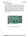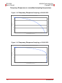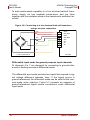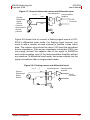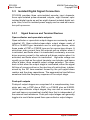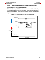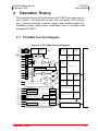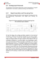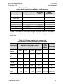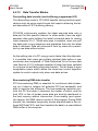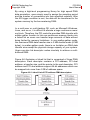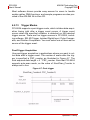
1
PCI-9524
24-Bit Precision Load Cell Input Card
User’s Manual
Manual Revision: 2.00
Revision Date:
April 09, 2008
Part No:
50-11236-1000
Advance Technologies; Automate the World.
PCI-9524
User’s Manual
ADLINK Technology, Inc.
Copyright 2008
Revision History
ii
Revision
Release Date
2.00
2008/04/09
Description of Change(s)
Document Created
Initial Release
ADLINK Technology Inc.
Copyright 2008
PCI-9524
User’s Manual
Preface
Copyright 2008 ADLINK TECHNOLOGY INC.
This document contains proprietary information protected by copyright. All rights are reserved. No part of this manual may be reproduced by any mechanical, electronic, or other means in any form
without prior written permission of the manufacturer.
Disclaimer
The information in this document is subject to change without prior
notice in order to improve reliability, design, and function and does
not represent a commitment on the part of the manufacturer.
In no event will the manufacturer be liable for direct, indirect,
special, incidental, or consequential damages arising out of the
use or inability to use the product or documentation, even if
advised of the possibility of such damages.
Environmental Responsibility
ADLINK is committed to fulfill its social responsibility to global
environmental preservation through compliance with the European Union's Restriction of Hazardous Substances (RoHS) directive and Waste Electrical and Electronic Equipment (WEEE)
directive. Environmental protection is a top priority for ADLINK.
We have enforced measures to ensure that our products, manufacturing processes, components, and raw materials have as little
impact on the environment as possible. When products are at their
end of life, our customers are encouraged to dispose of them in
accordance with the product disposal and/or recovery programs
prescribed by their nation or company.
Trademarks
PC, PS/2, and VGA are registered trademarks of International
Business Machines Corp. Borland®, Borland® C, C++ Builder®,
and Delphi® are registered trademarks of the Borland Software
Corporation. LabVIEW™ is a trademark of National Instruments
Corporation. Microsoft®, Visual Basic®, Visual C++®, Windows®
Preface
iii
PCI-9524
User’s Manual
ADLINK Technology Inc.
Copyright 2008
98, Windows® NT, Windows® 2000, Windows® XP, and Windows®
Vista® are registered trademarks of Microsoft® Corporation.
PCI™, is a registered trademark of the Peripheral Component
Interconnect Special Interest Group (PCI-SIG).
Product names mentioned herein are used for identification purposes only and may be trademarks and/or registered trademarks
of their respective companies.
iv
Preface
ADLINK Technology Inc.
Copyright 2008
PCI-9524
User’s Manual
Using this Manual
Audience and Scope
The PCI-9524 User’s Manual is intended for hardware technicians
and systems operators with knowledge of installing, configuring
and operating industrial grade PCI cards.
Manual Organization
This manual is organized as follows:
Preface:
Presents
important
copyright
notifications,
disclaimers, trademarks, and associated information on the
proper understanding and usage of this document and its
associated product(s).
Chapter 1, Introduction: Introduces the PCI-9524, its
features, applications, specifications and operating software
environment.
Chapter 2, Installation: Describes how to install the PCI-9524
into your chassis and basic PCI configuration settings.
Chapter 3, Signal Connections: Describes
connections between PCI-9524 and external devices.
signal
Chapter 4, Operation Theory: Describes A/D and D/A
conversions, pulse-commands, encoder inputs and isolated
digital I/O signals to assist users in understanding how to
configure and program the cPCI-9524.
Chapter 5, Calibration: Presents the calibration process to
minimize measurement and output errors.
Important Safety Instructions: Presents safety instructions
all users must follow for the proper setup, installation and
usage of equipment and/or software.
Warranty Information: Presents important warranty
information for users/manufacturers rights and responsibilities
regarding ADLINK products and services.
Preface
v
PCI-9524
User’s Manual
ADLINK Technology Inc.
Copyright 2008
Conventions
Take note of the following conventions used throughout this
manual to make sure that users perform certain tasks and
instructions properly.
Additional information, aids, and tips that help users perform tasks.
NOTE:
vi
CAUTION:
Information to prevent minor physical injury, component
damage, data loss, and/or program corruption when trying to complete a task.
WARNING:
Information to prevent serious physical injury, component damage, data loss, and/or program corruption
when trying to complete a specific task.
Preface
ADLINK Technology Inc.
Copyright 2008
PCI-9524
User’s Manual
Acronyms & Terminology
The following terms are used throughout this document. This list is
prepared in alphabetical order for clarity.
A/mA - (Ampere/amp/milliampere) a unit of electric current, or
amount of electric charge per second
AGND - Analog Ground
AI - Analog Input
AO - Analog Output
BIOS - Basic Input/Output System
bit - Binary digit, the basic unit of information storage in computing
byte - An 8-bit binary digit standard unit of information in
computing
CD - Compact Disk
ch (CH) - Channel
CLK/DIR - Clock Direction
CMRR - Common-mode rejection ratio
CW/CCW - Clock Wise, Counter Clock Wise
DAQ - Data Acquisition
dB - Decibel, a logarithmic unit of measurement in acoustics and
electronics
DC - Direct Current
DI - Differential Input
DLL (.dll) - Dynamic-link libraries, a library subroutine file type and
common filename extension in Microsoft Windows.
DMA (UDMA) - Direct Memory Access / Ultra DMA
DO - Digital Output
DSP - Digital Signal Processor
EEPROM (E2PROM) - Electrically Erasable Programmable ReadOnly Memory
Preface
vii
PCI-9524
User’s Manual
ADLINK Technology Inc.
Copyright 2008
EMI - Electromagnetic Interference
ENOB - Effective Number of Bits
FIFO - First In, First Out
FPGA - Field-Programmable Gate Array
GB - Gigabyte (1,073,741,824 bytes)
Hz/KHz/MHz - hertz / Kilo hertz / Mega hertz, standard unit of
frequency
I/O (IO) - Input / Output
IIH - Input current at logic high
IIL - Input current at logic low
IIR - Infinite impulse response
IOL - Output current at logic low
IRQ / SERIRQ - Interrupt Request / Serial Interrupt Request
ITU - International Telecommunications Union
LabVIEW - Laboratory Virtual Instrumentation Engineering
Workbench, a visual programming
LBS - Least significant bit
LED - Light Emitting Diode
MB - Megabyte (1,048,576 bytes)
MOSFET - Metal-Oxide Semiconducgtor Field Effect
ohm - a standard unit of electrical resistance “Ω“
OS - Operating System
PC - Personal Computer
PCI - Peripheral Component Interconnect
RMS - Root Mean Square
RSV - Reserved
SNR - Singnal to Noise Ratio
SPS - Samples per Second
SSI - Synchronization System Interface
viii
Preface
ADLINK Technology Inc.
Copyright 2008
PCI-9524
User’s Manual
TBD - To Be Determined
TTL - Transistor-Transistor Logic, digital circuits built from bipolar
junction transistors and resistors.
V/mV/µV - Volt / milli Volt / micro Volt, a derived unit of electrical
potential difference
VHDCI - Very high density cable interconnect
VIH - Input voltage at logic high
VIL - Input voltage at logic low
VOH - Output volage at logic high
VOL - Output voltage at logic low
W - Watt
Preface
ix
PCI-9524
User’s Manual
ADLINK Technology Inc.
Copyright 2008
Reference Documentation
The following list of documents may be used as reference materials to support installation, configuration and/or the operation of the
PCI-9524. This list is prepared in alphabetical order (by vendor/
organization name, then by document title) for clarity.
Vendor(s)
Title
Rev.
American National
Standards Institute
TIA-422 Electrical Characteristics of
Balanced Voltage Differential Interface
Circuits
B
Telecommunications
Industry Association
ITU-T Recommendation V.11
11
x
Preface
ADLINK Technology Inc.
Copyright 2008
PCI-9524
User’s Manual
Getting Service
Contact us should you require any service or assistance.
ADLINK TECHNOLOGY INC. (HEADQUARTERS)
Web Site:
Sales & Service:
Telephone No.:
Fax No.:
Mailing Address:
http://www.adlinktech.com
[email protected]
+886-2-8226-5877
+886-2-8226-5717
9F No. 166 Jian Yi Road, Chungho City,
Taipei 235, Taiwan, ROC
ADLINK TECHNOLOGY AMERICA INC.
Sales & Service:
Toll-Free:
Fax No.:
Mailing Address:
[email protected]
+1-866-4 ADLINK
+1-949-727-2099
8900 Research Drive, Irvine,
CA 92618, USA
ADLINK TECHNOLOGY CO. LTD. (BEIJING)
Sales & Service:
Telephone No.:
Fax No.:
Mailing Address:
[email protected]
+86-10-5885-8666
+86-10-5885-8625
Rm. 801, Power Creative E, No. 1, B/D
Shang Di East Rd.
Beijing, 100085 China
ADLINK TECHNOLOGY CO. LTD. (SHANGHAI)
Sales & Service:
Telephone No.:
Fax No.:
Mailing Address:
[email protected]
+86-21-6495-5210
+86-21-5450-0414
4F, Bldg. 39, No.333 Qinjiang Road,
Cao He Jing High-Tech Park
Shanghai, 200233 China
ADLINK TECHNOLOGY CO. LTD. (SHENZHEN)
Sales & Service:
Telephone No.:
Fax No.:
Mailing Address:
Preface
[email protected]
+86-755-2643-4858
+86-755-2664-6353
2F, C Block, Bld. A1,
Cyber-Tech Zone, Gao Xin Ave. Sec. 7,
High-Tech Industrial Park S.,
Shenzhen, 518054 China
xi
PCI-9524
User’s Manual
ADLINK Technology Inc.
Copyright 2008
ADLINK TECHNOLOGY INC. (EUROPEAN Liaison Office)
Sales & Service:
Telephone No.:
Fax No.:
Mailing Address:
[email protected]
+49-211-495-5552
+49-211-495-5557
Nord Carree 3, 40477
Düsseldorf, Germany
ADLINK TECHNOLOGY JAPAN CORP.
Sales & Service
Telephone No.
Fax No.
Mailing Address
[email protected]
+81-3-4455-3722
+81-3-5333-6040
Asahiseimei Hatagaya Bld. 8Fl. 1-1-2
Hatagaya Shibuya-ku, Tokyo, Japan
ADLINK TECHNOLOGY INC. (SOUTH KOREA Liaison Office)
Sales & Service:
Telephone No.:
Fax No.:
Mailing Address:
[email protected]
+82-2-2057-0565
+82-2-2057-0563
#402, Dongsung B/D, 60-12,
Nonhyeon-dong Gangnam-gu,
Seoul, 135-010, South Korea
ADLINK TECHNOLOGY SINGAPORE PTE. LTD.
Sales & Service:
Telephone No.:
Fax No.:
Mailing Address:
[email protected]
+65-6844-2261
+65-6844-2263
84 Genting Lane #07-02A,
Cityneon Design Center,
Singapore 349584
ADLINK TECHNOLOGY SINGAPORE PTE. LTD. (INDIA Liaison Office)
Sales & Service:
Telephone No.:
Fax No.:
Mailing Address:
xii
[email protected]
+91-80-6560-5817
+91-80-2244-3548
No. 1357, Ground Floor, "Anupama",
Aurobindo Marg JP Nagar (Ph-1)
Bangalor, Karnataka 560078, India
Preface
ADLINK Technology Inc.
Copyright 2008
PCI-9524
User’s Manual
Table of Contents
PCI-9524..................................................................................... i
Revision History...................................................................... ii
Preface .................................................................................... iii
Copyright 2008 ADLINK TECHNOLOGY INC. ...............iii
Disclaimer .......................................................................iii
Environmental Responsibility ..........................................iii
Trademarks .....................................................................iii
Using this Manual ........................................................... v
Conventions ....................................................................vi
Acronyms & Terminology ...............................................vii
Reference Documentation .............................................. x
Getting Service ...............................................................xi
Table of Contents................................................................. xiii
List of Figures ..................................................................... xvii
List of Tables........................................................................ xix
1 Introduction ........................................................................ 1
1.1
Features............................................................................... 2
1.2
Applications ......................................................................... 2
1.3
Specifications....................................................................... 3
1.4
Software Support ............................................................... 19
2 Getting Started ................................................................. 21
2.1
2.2
2.3
2.4
2.5
Installation Environment ....................................................
Package Contents .............................................................
PCI-9524 Layout................................................................
Installing the Card..............................................................
PCI Configuration ..............................................................
Table of Contents
21
22
23
24
25
xiii
PCI-9524
User’s Manual
ADLINK Technology Inc.
Copyright 2008
3 Signal Connections .......................................................... 27
3.1
Connectors & Pin Assignments ......................................... 27
3.2
Analog Input Signal Connections....................................... 33
3.2.1 Signal Sources.................................................................... 33
3.2.2 Input Configurations............................................................ 34
3.3
Isolated Digital Signal Connection ..................................... 38
3.3.1 Signal Sources and Terminal Devices ................................ 38
3.3.2 Connecting to/from External Encoders ............................... 40
3.3.3 Connecting to External Servo Amplifiers ............................ 42
3.3.4 Interfacing Isolated DO with External Loads....................... 43
3.3.5 Interfacing Isolated DI with External Devices...................... 45
4 Operation Theory .............................................................. 47
4.1
PCI-9524 Function Diagram .............................................. 47
4.2
Analog Input Channels....................................................... 48
4.2.1 Signal Acquisition and Processing Flow ............................. 48
4.2.2 How to Define a 1 in 200,000 Count Resolution ................. 49
4.2.3 Data Rate versus Sampling Rate........................................ 51
4.2.4 Auto-scan, Multiplexing and Settling Time.......................... 51
4.2.5 Power Line Noise Rejection................................................ 53
4.2.6 Excitation and Remote-sensing .......................................... 54
4.2.7 Thermal EMF, 1/f Noise and Auto-zero .............................. 55
4.2.8 Warm-up Requirement........................................................ 58
4.2.9 Post-processing IIR Digital Filter......................................... 58
4.2.10RAW Data Format............................................................... 61
4.2.11AD Data Format .................................................................. 62
4.2.12Data Transfer Modes .......................................................... 64
4.2.13Trigger Modes..................................................................... 66
xiv
4.3
D/A Conversion.................................................................. 67
4.4
Isolated Encoder Input Channels....................................... 67
4.5
Isolated Pulse-Command Generator ................................. 69
4.6
Isolated Digital I/O.............................................................. 69
Table of Contents
ADLINK Technology Inc.
Copyright 2008
PCI-9524
User’s Manual
4.6.1 Isolated Digital Inputs ......................................................... 70
4.6.2 Isolated Digital Outputs....................................................... 70
4.7
Trigger Sources ................................................................. 70
4.7.1 Software-Trigger ................................................................. 70
4.7.2 External Digital Trigger ....................................................... 70
4.7.3 Pulse Comparator Trigger .................................................. 71
4.7.4 Position Comparator Trigger............................................... 72
5 Calibration......................................................................... 73
5.1
Loading Calibration Constants........................................... 73
5.2
Auto-calibration.................................................................. 74
5.3
Saving Calibration Constants ............................................ 74
Important Safety Instructions .............................................. 75
Warranty Policy..................................................................... 77
Table of Contents
xv
PCI-9524
User’s Manual
ADLINK Technology Inc.
Copyright 2008
This page intentionally left blank.
xvi
Table of Contents
ADLINK Technology Inc.
Copyright 2008
PCI-9524
User’s Manual
List of Figures
Figure 1-1:
Figure 1-2:
Figure 1-3:
Figure 1-4:
PCI-9524 Product Image ................................................. 1
Effective-number-of-bits vs. Gain .................................... 9
RMS Noise in µV vs. Gain ............................................... 9
Spectral Response ±10V range,
0.996094 Hz sine wave, -1 dB FS ................................. 10
Figure 1-5: Spectral Response ±5V range,
0.996094 Hz sine wave, -1 dB FS ................................. 10
Figure 1-6: Spectral Response ±2.5V range,
0.996094 Hz sine wave, -1 dB FS ................................. 11
Figure 1-7: Spectral Response ±1.25V range,
0.996094 Hz sine wave, -1 dB FS ................................. 11
Figure 1-8: Frequency Response Sampling at 30,000 SPS ............ 12
Figure 1-9: Frequency Response Sampling at 15,000 SPS ............ 12
Figure 1-10: Frequency Response Sampling below 15,000 SPS ...... 13
Figure 2-1: PCI-9524 PCB Layout and Mechanical Drawing ........... 23
Figure 3-1: CN1 Connector & Pin Assignments............................... 27
Figure 3-2: CN2 Connector & Pin Assignments............................... 29
Figure 3-3: SSI Connector & Pin Assignments ................................ 31
Figure 3-4: Connecting to a four-terminal load-cell transducer
using a four-wire connection.......................................... 34
Figure 3-5: Connecting to a six-terminal load-cell transducer
using a six-wire connection............................................ 35
Figure 3-6: Connecting to a four-terminal load-cell transducer
using a six-wire connection............................................ 36
Figure 3-7: Ground-referenced source and differential input ........... 37
Figure 3-8: Floating source and differential input............................. 37
Figure 3-9: Connecting to an external encoder
with NPN sink drivers..................................................... 40
Figure 3-10: Connecting to an external encoder
with PNP source drivers ................................................ 40
Figure 3-11: Connecting to an external encoder
with push-pull source drivers ......................................... 41
Figure 3-12: Connecting to an external encoder
with differential line-drivers ............................................ 41
Figure 3-13: Connecting to an external servo-amplifier
with opto-coupler inputs................................................. 42
Figure 3-14: Connecting to an external servo-amplifier
with differential line-receivers ........................................ 42
List of Figures
xvii
PCI-9524
User’s Manual
ADLINK Technology Inc.
Copyright 2008
Figure 3-15: Connecting to an external resistive load
from the isolated DO sink driver .................................... 43
Figure 3-16: Connecting to an external inductive load
from an isolated DO sink driver ..................................... 44
Figure 3-17: Connecting to a low-side push button............................ 45
Figure 3-18: Connecting to an external sink driver ............................ 46
Figure 4-1: PCI-9524 Function Diagram .......................................... 47
Figure 4-2: Signal acquisition and data processing flow
for transducer input channels ........................................ 48
Figure 4-3: SINC Filter Power Line Noise Rejection
at 60 Hz Multiples .......................................................... 54
Figure 4-4: The Effect of Auto-zero on Thermal Noise and
1/f Noise, ADC running at 60 SPS................................. 57
Figure 4-5: Digital Filter Tap Length Effects
on Signal Frequency Responses................................... 59
Figure 4-6: Linked List of PCI address DMA descriptors ................. 65
Figure 4-7: Post trigger .................................................................... 66
Figure 4-8: X4 Encoder mode .......................................................... 68
Figure 4-9: External digital trigger .................................................... 71
xviii
List of Figures
ADLINK Technology Inc.
Copyright 2008
PCI-9524
User’s Manual
List of Tables
Table
Table
Table
Table
Table
Table
Table
Table
1-1:
1-2:
1-3:
1-4:
1-5:
1-6:
1-7:
1-8:
Table
Table
Table
Table
Table
1-9:
1-10:
1-11:
3-1:
4-1:
Table 4-2:
Table 4-3:
Table 4-4:
Table 4-5:
Table 4-6:
Table 4-7:
List of Tables
-3dB small signal bandwidth: (Typical, 25°C) .................. 4
System Noise (including Quantization, Typical, 25°C) .... 4
Transducer Input Impedance........................................... 5
Transducer CMRR (DC to 60 Hz, Typical 25°C) ............. 5
Settling Error: (Typical, 25°C) .......................................... 6
Programmable input range and gain ............................... 7
-3dB small signal bandwidth vs. input range ................... 7
-3dB small signal bandwidth vs. sampling rates,
in ±10V range .................................................................. 8
General Purpose Input Impedance................................ 13
General Purpose CMRR (DC to 60 Hz, Typical, 25°C) . 13
Settling Error: (Typical, 25ºC) ........................................ 14
I/O Signal Descriptions .................................................. 32
Data Rates vs. Multiplexing, Auto-zero &
ADC Sampling Rates, in Samples-per-second (SPS) ... 53
Temperature Coefficient of different metal junctions ..... 56
Default Threshold Values (ADC counts)
vs. ADC Sampling Rates ............................................... 61
RAW Data Format ......................................................... 61
Bipolar analog input ranges and
output digital codes for transducer input channels ........ 63
Bipolar analog input ranges and
AD codes for general purpose input channels............... 63
Bipolar output code table ............................................... 67
xix
PCI-9524
User’s Manual
ADLINK Technology Inc.
Copyright 2008
This page intentionally left blank.
xx
List of Tables
ADLINK Technology Inc.
Copyright 2008
1
PCI-9524
User’s Manual
Introduction
The ADLINK PCI-9524 is a 24-bit high-resolution multifunction
DAQ card capable of up to 30 kS/s sampling rate, providing 4-CH
load-cell transducer input channels, and 4-CH general purpose
analog input. In addition, the PCI-9524 comes with a 2-CH 16-bit
analog output, isolated motion I/O and digital I/O. The highly integrated function makes the PCI-9524 the ideal solution for combined data acquisition and motion control functionalities. Ideal for
manufacturing, laboratory research, and factory automation, the
PCI-9524 comes with all the features and performance you need
at an affordable price.
Figure 1-1: PCI-9524 Product Image
Introduction
1
PCI-9524
User’s Manual
ADLINK Technology Inc.
Copyright 2008
1.1 Features
PCI-9524 24-bit multifunction DAQ card provides the following
advanced features:
X
Supports 32-bit 3.3V or 5V PCI bus
X
Load-cell transducer input channels
X
Z
4-CH differential analog input with remote-sense
Z
4-CH transducer excitation, 10V or 2.5V selectable
Z
Auto-zero capability
Z
Up to 30 kS/s sampling rate without auto-zero
Z
IIR digital filter for post-processing
General purpose analog input channels
Z
4-CH differential analog input
Z
Programmable gains: x1, x2, x4, x8
Z
Up to 30 kS/s sampling rate
X
2-CH 16-bit analog output
X
3-CH opto-isolated pulse-command output, supporting AB
phase, CW/CCW, CLK/DIR modes
X
3-CH opto-isolated encoder input, supports AB phase
inputs in quadrature mode
X
8-CH opto-isolated digital inputs
X
8-CH opto-isolated digital outputs with N-MOS sink drivers
X
Auto-calibration
1.2 Applications
2
X
Materials Testing Systems
X
Precision Weighting Systems
X
Automotive Testing
X
Process Control
X
Laboratory Automation
X
Biotech Measurements
Introduction
ADLINK Technology Inc.
Copyright 2008
PCI-9524
User’s Manual
1.3 Specifications
Analog Input (AI) for Transducers
X
Number of channels: (programmable)
Z
X
A/D converter:
Z
X
X
4 differential inputs (DI)
ADS1255
Maximum sampling rate:
Z
Without Auto-zero
Z
30,000 samples/s (single channel)
Z
1,638 samples/s (multiplexed/scanning)
Z
With Auto-zero
Z
819 samples/s (single channel or multiplexed/scanning)
Resolution:
Z
24-bit
X
Input coupling: DC
X
Input range and gain:
X
Z
±200mV relative to a common-mode input voltage
Z
A fixed gain of 25x
Operational common-mode input range:
Z
X
X
X
-2V to +6V
Transducer Excitation Voltage Sources:
Z
4-CH differential output
Z
10V or 2.5V selectable (all 4-CH share same settings)
Z
Driving up to four 120-ohm load-cells
Z
Short-circuit protection
Remote-sense input:
Z
4-CH differential input
Z
0V to 10V operating input range
Overvoltage protection:
Z
Transducer inputs
Z
Power on: +28.7V to -35.7V (continuous)
Z
Power off: ±15V (continuous)
Introduction
3
PCI-9524
User’s Manual
ADLINK Technology Inc.
Copyright 2008
Z
Remote-sense inputs:
Z
Power on: -40V to +55V (continuous)
Z
Power off: -40V to +55V (continuous)
X
FIFO buffer size: 1024 samples (1024 x 32 bits)
X
Data transfers:
Z
Programmed I/O
Z
Bus-mastering DMA with scatter/gather
Table 1-1: -3dB small signal bandwidth: (Typical, 25°C)
Input Range
Bandwidth (-3dB)
±200 mV
2,730 Hz
Table 1-2: System Noise (including Quantization, Typical, 25°C)
Input
Range
±200 mV
4
Data
Rate in
SPS
System
Noise in
LSBrms
RMS
Res. in
Bits
(ENOB)
Peak
Res. in
Bits
RMS Res
in µV
Peak
Res. in
µV
1.25
0.5
23.0
21.0
0.013
0.053
2.5
0.6
22.8
20.4
0.014
-0.079
5.0
0.6
22.7
20.4
0.016
0.079
7.5
0.7
22.6
20.0
0.017
0.079
12
0.9
22.2
19.7
0.023
0.159
15
0.8
22.3
19.7
0.020
0.132
24
1.2
21.8
19.2
0.031
0.212
29
1.1
21.9
19.0
0.030
0.185
47
1.9
21.1
18.6
0.037
0.291
194
2.9
20.5
17.7
0.078
0.583
Introduction
ADLINK Technology Inc.
Copyright 2008
Input
Range
±200 mV
PCI-9524
User’s Manual
Data
Rate in
SPS
System
Noise in
LSBrms
RMS
Res. in
Bits
(ENOB)
Peak
Res. in
Bits
RMS Res
in µV
Peak
Res. in
µV
316
3.7
20.1
17.1
0.101
0.742
463
5.5
19.6
16.4
0.146
1.113
595
6.9
19.2
16.4
0.185
1.351
704
8.9
18.9
15.9
0.243
1.748
768
10.9
18.6
15.5
0.306
2.305
819
12.6
18.4
15.4
0.328
2.331
Test conditions: Rice Lake Load-cell Simulator IV set at 0mV/V
output, 10V excitation and six-wire remote-sense connection,
auto-zero enabled. The RMS resolution and peak resolution are
calculated relative to full-scale input range of ±200mV.
Table 1-3: Transducer Input Impedance
Normal Power On
Power Off
Overload
1GΩ || 3pF
1K Ω
1K Ω
Table 1-4: Transducer CMRR (DC to 60 Hz, Typical 25°C)
Input Range
±200mV
Introduction
CMRR
90 dB (Auto-zero Disabled)
102 dB (Auto-zero Enabled)
5
PCI-9524
User’s Manual
ADLINK Technology Inc.
Copyright 2008
Table 1-5: Settling Error: (Typical, 25°C)
Input Range
Condition
Settling Error
±200mV
Scanning 200mV step
max 0.01%
X
Time-base source: Internal 40 MHz
X
Trigger mode: post-trigger
X
Offset error:
X
Z
Before calibration: ±0.5mV typical
Z
After calibration: ±0.001mV typical (auto-zero disabled),
< ±0.001mV typical (auto-zero enabled)
Transfer Linearity:
Z
X
Better than: ±0.0035% over full-scale input range
Gain error:
Z
Before calibration: ±1% typical
Z
After calibration: ±0.5% typical
Analog Input (AI) for General Purpose
X
Number of channels: (programmable)
Z
X
A/D converter:
Z
X
X
6
ADS1255
Maximum sampling rate:
Z
30,000 samples/s (single channel)
Z
1.638 samples/s (multiplexed/scanning)
Resolution:
Z
X
4 differential input (DI)
24-bit
Input coupling: DC
Introduction
ADLINK Technology Inc.
Copyright 2008
PCI-9524
User’s Manual
Table 1-6: Programmable input range and gain
Bipolar Input Range
Gain
±10V
1
±5V
2
±2.5V
4
±1.25V
8
X
Operational common-mode input range: ±13V
X
Overvoltage protection:
Z
Power on: ±30V (continuous)
Z
Power off: ±15V (continuous)
X
FIFO buffer size: 1024 samples (1024 x 32 bits)
X
Data transfers:
X
Z
Programmed I/O
Z
Bus-mastering DMA with scatter/gather
-3dB small signal bandwidth (Typical, 25º)
Table 1-7: -3dB small signal bandwidth vs. input range
Introduction
Input Range
Bandwidth (-3dB)
±10V
5,800 Hz
±5V
5,900 Hz
±2.5V
5,900 Hz
±1.25V
5,900 Hz
7
PCI-9524
User’s Manual
ADLINK Technology Inc.
Copyright 2008
Table 1-8: -3dB small signal bandwidth vs. sampling rates,
in ±10V range
8
Sampling Rate
In Samples-per-second
(SPS)
Bandwidth (-3 dB)
2.5
1.1 Hz
5
2.2 Hz
10
4.4 Hz
15
6.6 Hz
25
11 Hz
30
13 Hz
50
22 Hz
60
26 Hz
100
44 Hz
500
220 Hz
1,000
440 Hz
2,000
880 Hz
3,750
1,600 Hz
7,500
3,000 Hz
15,000
4,800 Hz
30,000
5,800 Hz
Introduction
ADLINK Technology Inc.
Copyright 2008
PCI-9524
User’s Manual
System Noise (LSBrms, including Quantization, Typical, 25ºC)
Figure 1-2: Effective-number-of-bits vs. Gain
ENOB vs PGA Gain
[Input = AGND]
25
24
23
ENOB [bits]
22
21
20
19
18
17
16
15
14
2
5
10
15
25
30
50
60
100
500
1000
2000
3750
7500
15000
30000
7500
15000
30000
Sam pling Rate [Sam ples per Second]
Gain = 1
Gain = 2
Gain = 4
Gain = 8
Figure 1-3: RMS Noise in µV vs. Gain
RMS Noise vs PGA Gain
[Input = AGND]
1000
Noise [uV]
100
10
1
0.1
2
5
10
15
25
30
50
60
100
500
1000
2000
3750
Sam pling Rate [Sam ples per Second]
Gain = 1
Gain = 2
Gain = 4
Gain = 8
Test conditions: RMS resolution and peak resolution are calculated relative to the full-scale range of their gain settings, using
internal calibration voltage references.
Introduction
9
PCI-9524
User’s Manual
ADLINK Technology Inc.
Copyright 2008
Spectral Response (At 30,000-SPS, Typical, 25ºC)
Figure 1-4: Spectral Response ±10V range,
0.996094 Hz sine wave, -1 dB FS
Input Signal = 996.094 Hz @ -1 dBFS, Sampling rate = 30 KHz
0
SINAD = 99.5171 dB
SNR = 101.0395 dB
-20
THD = -104.8086
Magnitude (dB)
-40
ENOB = 16.2387 bit
SFDR = 105.8299
-60
-80
-100
-120
-140
0
2000
4000
6000
8000
10000
Frequency (Hz)
12000
14000
Figure 1-5: Spectral Response ±5V range,
0.996094 Hz sine wave, -1 dB FS
Input Signal = 996.094 Hz @ -1 dBFS, Sampling rate = 30 KHz
0
SINAD = 98.6425 dB
SNR = 99.4779 dB
-20
THD = -106.2125
ENOB = 16.0934 bit
-40
Magnitude (dB)
SFDR = 106.8945
-60
-80
-100
-120
-140
-160
10
0
2000
4000
6000
8000
10000
Frequency (Hz)
12000
14000
Introduction
ADLINK Technology Inc.
Copyright 2008
PCI-9524
User’s Manual
Figure 1-6: Spectral Response ±2.5V range,
0.996094 Hz sine wave, -1 dB FS
Input Signal = 996.094 Hz @ -1 dBFS, Sampling rate = 30 KHz
0
SINAD = 97.5555 dB
SNR = 98.0951 dB
-20
THD = -106.8792
ENOB = 15.9129 bit
-40
Magnitude (dB)
SFDR = 106.1694
-60
-80
-100
-120
-140
-160
0
2000
4000
6000
8000
10000
Frequency (Hz)
12000
14000
Figure 1-7: Spectral Response ±1.25V range,
0.996094 Hz sine wave, -1 dB FS
Input Signal = 996.094 Hz @ -1 dBFS, Sampling rate = 30 KHz
0
SINAD = 98.1582 dB
SNR = 98.6841 dB
-20
THD = -107.5872
ENOB = 16.013 bit
-40
Magnitude (dB)
SFDR = 99.1709
-60
-80
-100
-120
-140
-160
Introduction
0
2000
4000
6000
8000
10000
Frequency (Hz)
12000
14000
11
PCI-9524
User’s Manual
ADLINK Technology Inc.
Copyright 2008
Frequency Response (vs. normalized sampling frequencies):
Figure 1-8: Frequency Response Sampling at 30,000 SPS
Frequency Response versus Norm. Sampling Frequency
0
-20
Attenuation (dB)
-40
-60
-80
-100
-120
0.00
0.17
0.33
0.50
0.67
0.83
1.00
Normalized Sampling Frequency (Fs)
Figure 1-9: Frequency Response Sampling at 15,000 SPS
Frequency Response versus Norm. Sampling Frequency
0
-20
Attenuation (dB)
-40
-60
-80
-100
-120
0.00
0.17
0.33
0.50
0.67
0.83
1.00
Normalized Sampling Frequency (Fs)
12
Introduction
ADLINK Technology Inc.
Copyright 2008
PCI-9524
User’s Manual
Figure 1-10: Frequency Response Sampling below 15,000 SPS
Frequency Response versus Norm. Sampling Frequency
0
-20
Attenuation (dB)
-40
-60
-80
-100
-120
0.00
0.17
0.33
0.50
0.67
0.83
1.00
Normalized Sampling Frequency (Fs)
Table 1-9: General Purpose Input Impedance
Normal Power On
Power Off
Overload
1GΩ || 3pF
1K Ω
1K Ω
Table 1-10: General Purpose CMRR (DC to 60 Hz, Typical, 25°C)
Introduction
Input Range
CMRR
±10V
80 dB
±5V
86 dB
±2.5V
94 dB
±1.25V
98 dB
13
PCI-9524
User’s Manual
ADLINK Technology Inc.
Copyright 2008
Table 1-11: Settling Error: (Typical, 25ºC)
Condition
Settling Error
±10V
Scanning 20Vpp
<0.0005%
±5V
Scanning 10Vpp
<0.0005%
±2.5V
Scanning 5Vpp
<0.0005%
±1.25V
Scanning 2.5Vpp
<0.0005%
X
Time-base source: Internal 40 MHz
X
Trigger mode: post-trigger
X
Offset error:
X
14
Input Range
Z
Before calibration: ±2 mV typical 25ºC
Z
After calibration: ±0.1 mV typical 25ºC
Gain error:
Z
Before calibration: ±0.5% typical 25ºC
Z
After calibration: ±0.01% typical 25ºC
Introduction
ADLINK Technology Inc.
Copyright 2008
PCI-9524
User’s Manual
Analog Output (AO)
X
Number of channels: 2 analog voltage outputs
X
D/A converter: DAC8812
X
Maximum update rate: 10K sample/s
X
Resolution: 16-bit
X
Data transfers: Programmed I/O
X
Output range: ±10V (after software calibration)
X
Settling time (0.1% of full scale): 2 µs
X
Slew rate: 15V/µS
X
Output coupling: DC
X
Protection: Short-circuit to ground, indefinitely
X
Output impedance: 0.1Ω max
X
Output driving: ±5mA max.
X
Stability: Any passive load, up to 1500pF
X
Power-on state: Around 0V steady-state
X
Offset error:
X
Z
Before calibration: ±4mV typical 25ºC
Z
After calibration: ±1mV typical 25ºC
Gain error:
Z
Before calibration: ±0.8% of output max.
Z
After calibration: ±0.015% of output max.
Introduction
15
PCI-9524
User’s Manual
ADLINK Technology Inc.
Copyright 2008
Isolated Pulse Command Outputs
X
Number of channels: 3
X
Output type: AM26LS31 differential line-driver
X
Compliant to ANSI TIA/EIA-422-B and ITU Recommendation V.11 standards
X
Logic Compatibility: 5V TTL with complementary output
X
Output voltage:
Z
Logic low: VOL = 0.5V max.; IOL = 20mA max.
Z
Logic high: VOH = 2.4V min.; IIH = -20mA max.
X
Programmable duty cycle: 1% to 99%
X
Maximum pulse frequency: 1 MHz
X
Direction control modes: CLK/DIR & CW/CCW
X
Pulse counter: 1 to 16777215
X
Pulse Comparator Trigger to initiate AI acquisition once
condition is met
X
Data transfers: Programmed I/O
Isolated Quadrature Encoder Inputs
16
X
Number of channels: 3
X
Input type: AB-Phase differential inputs
X
Input impedance: 249-Ω || 220-pF
X
Input voltage:
Z
Logic low: VIL = 0.8V max.
Z
Logic high: VIH = 3.8V min.
Z
Logic high: VIH = 9V max.
X
Maximum Encoder frequency: 1 MHz
X
Decoder type: Quadrature, 4X resolution
X
Decoder counts: -8388608 to +8388607
X
Positional Comparator Trigger to initiate AI acquisition once
condition is met
X
Data transfers: Programmed I/O
Introduction
ADLINK Technology Inc.
Copyright 2008
PCI-9524
User’s Manual
Isolated Digital Inputs
X
Number of channels: 8
X
Input type: Bipolar, resistive differential
X
Input impedance: 2.7K-Ω || 250-pF
X
Input voltage:
Z
Logic low: VIL = 0.7V max.
Z
Logic high: VIH = 4.8V min.
Z
Logic high: VIH = 24V max.
X
Maximum input frequency: 5 KHz
X
Data transfers: Programmed I/O
X
Digital Trigger to initiate AD conversion on DI channel 0,
with programmable detection polarity
Isolated Digital Outputs
X
Number of channels: 8
X
Output type: N-Type MOSFET current sinker with a command ground
X
Maximum external power-supply voltage: 60V DC
X
Drain-off leakage current: 10 µA
X
Drain-on resistance: 75 mΩ
X
Maximum drain current: 5A DC
X
Maximum toggling frequency: 5 KHz
X
Data transfers: Programmed I/O
Introduction
17
PCI-9524
User’s Manual
ADLINK Technology Inc.
Copyright 2008
Isolated Power Supplies
X
Number of channels: 2
X
Nominal output voltage
X
X
Z
ISO5VDD: 5V ±0.05V
Z
ISOPWR: 5V ±0.15V
Output current (Pulse Command channels are unused)
Z
ISO5VDD: 160mA max.
Z
ISOPWR: 16mA max.
Maximum output current (nth channel of Pulse Command
channel is used)
Z
ISO5VDD: 160 - (20 x n) mA max.
Z
ISOPWR:16mA max.
X
Physical
X
Dimensions: 156 mm x 116 mm
X
I/O connectors: two 68-pin SCSI-VHDCI connectors
Power Requirement (typical, 25ºC)
X
+5VDC: 2A
Operating Environment
X
Ambient temperature: 0ºC to 45ºC
X
Relative humidity: 10% to 90% non-condensing
Storage Environment
18
X
Ambient temperature: -20ºC to 80ºC
X
Relative humidity: 5% to 95% non-condensing
Introduction
ADLINK Technology Inc.
Copyright 2008
PCI-9524
User’s Manual
1.4 Software Support
Software Support
ADLINK provides versatile software drivers and packages to suit
various user approach to building a system. Aside from programming libraries, such as DLLs, for most Windows-based systems,
ADLINK also provides drivers for other application environment
such as LabVIEW®.
All software options are included in the ADLINK All-in-One CD.
Commercial software drivers are protected with licensing codes.
Without the code, you may install and run the demo version for
trial/demonstration purposes only up to two hours. Contact your
ADLINK dealers if you want to purchase the software license.
Programming Library
For customers who want to write their own programs, ADLINK provides the PCIS-DASK function library that is compatible with various operating systems.
PCIS-DASK
The PCIS-DASK includes device drivers and DLL for Windows 98/
NT/2000/XP/Vista. DLL is binary compatible across Windows 98/
NT/2000/XP/Vista. This means all applications developed with
PCIS-DASK are compatible with these Windows operating systems. The developing environment may be VB, VC++, Delphi,
BC5, or any Windows programming language that allows calls to a
DLL. The PCIS-DASK user's and function reference manuals are
in the ADLINK All-in-One CD. (\\Manual\Software Package\PCISDASK).
Introduction
19
PCI-9524
User’s Manual
ADLINK Technology Inc.
Copyright 2008
This page intentionally left blank.
20
Introduction
ADLINK Technology Inc.
Copyright 2008
2
PCI-9524
User’s Manual
Getting Started
This chapter further describes the PCI-9524; a proper installation
environment, its package contents and basic information users
should be aware of.
2.1 Installation Environment
Whenever unpacking and preparing to install any equipment
described in this manual, please refer to the Important Safety
Instructions chapter of this manual.
Only install equipment in well lit areas on flat, sturdy surfaces with
access to basic tools such as flat and cross head screwdrivers,
preferably with magnetic heads as screws and standoffs are small
and easily misplaced.
Recommended Installation Tools
X
Phillips (cross-head) screwdriver
X
Flat-head screwdriver
X
Anti-static Wrist Strap
X
Anti-static mat
ADLINK PCI-9524 DAQ cards are electro-static sensitive equipment that can be easily damaged by static electricity. The equipment must be handled on a grounded anti-static mat. The operator
must wear an anti-static wristband, grounded at the same point as
the anti-static mat.
Inspect the carton and packaging for damage. Shipping and handling could cause damage to the equipment inside. Make sure that
Getting Started
21
PCI-9524
User’s Manual
ADLINK Technology Inc.
Copyright 2008
the equipment and its associated components have no damage
before installing.
CAUTION:
The equipment must be protected from static discharge and
physical shock. Never remove any of the socketed parts
except at a static-free workstation. Use the anti-static bag
shipped with the product to handle the equipment and wear a
grounded wrist strap when servicing.
2.2 Package Contents
Before continuing, check the package contents for any damage
and check if the following items are included in the packaging:
X
PCI-9524 Multi-function Data Acquisition Card
X
ADLINK All-in-one Compact Disc
X
Software Installation Guide
X
PCI-9524 User’s Manual
If any of these items are missing or damaged, contact the dealer
from whom you purchased the product. Save the shipping materials and carton in case you want to ship or store the product in the
future.
WARNING:
22
DO NOT install or apply power to equipment that is damaged or if there is missing/incomplete equipment. Retain
the shipping carton and packing materials for inspection.
Please contact your ADLINK dealer/vendor immediately
for assistance. Obtain authorization from your dealer
before returning any product to ADLINK.
Getting Started
ADLINK Technology Inc.
Copyright 2008
PCI-9524
User’s Manual
2.3 PCI-9524 Layout
Figure 2-1: PCI-9524 PCB Layout and Mechanical Drawing
Controller
Getting Started
23
PCI-9524
User’s Manual
ADLINK Technology Inc.
Copyright 2008
2.4 Installing the Card
To install the card:
1. Turn off the system/chassis and disconnect the power
plug from the power source.
2. Remove the system/chassis cover.
3. Select the PCI slot that you intend to use, then remove
the bracket opposite the slot, if any.
4. Align the card connectors (golden fingers) with the slot,
then press the card firmly until the card is completely
seated on the slot.
5. Secure the card to the chassis with a screw.
6. Replace the system/chassis cover.
7. Connect the power plug to a power source, then turn on
the system/chassis.
24
Getting Started
ADLINK Technology Inc.
Copyright 2008
PCI-9524
User’s Manual
2.5 PCI Configuration
1. Plug and Play:
As a plug and play component, the card requests an interrupt
number via its PCI controller. The system BIOS responds with
an interrupt assignment based on the card information and on
known system parameters. These system parameters are
determined by the installed drivers and the hardware load recognized by the system. Users can use the PCI_SCAN software
utility on the ADLINK All-in-One CD to read/check the system
configuration.
2. Configuration:
The board configuration is done on a board-by-board basis for
all PCI boards on your system. Because configuration is controlled by the system and software, there is no jumper setting
required for base-address, DMA, and interrupt IRQ.
The configuration is subject to change with every boot of the
system as new boards are added or removed.
3. Trouble shooting:
If your system doesn't boot or if you experience erratic operation with your PCI board in place, it's likely caused by an interrupt conflict (perhaps the BIOS Setup is incorrectly configured).
In general, the solution, once you determine it is not a simple
oversight, is to consult the BIOS documentation that comes
with your system.
Getting Started
25
PCI-9524
User’s Manual
ADLINK Technology Inc.
Copyright 2008
This page intentionally left blank.
26
Getting Started
ADLINK Technology Inc.
Copyright 2008
3
PCI-9524
User’s Manual
Signal Connections
This chapter describes the connectors of PCI-9524, and the signal
connections between PCI-9524 and external devices. Please see
Figure 3-1, Figure 3-2 and Figure 3-3 for details.
X
CN1/CN2 - 68-pin VHDCI Connector
X
SSI - SSI Connector
3.1 Connectors & Pin Assignments
PCI-9524 is equipped with two 68-pin VHDCI connectors. They
are used for digital input/output, analog input/output, etc. The SSI
connector is used for system synchronization.
Figure 3-1: CN1 Connector & Pin Assignments
35
68
1
34
Signal Connections
Pin #
34
33
Pin #
68
67
VEX_SEN0+
NC
32
31
66
65
VEX_SEN0NC
AI1+
VEX1+
30
29
64
63
AI1VEX1-
VEX_SEN1+
28
62
VEX_SEN1-
NC
AI2+
27
26
61
60
NC
AI2-
VEX2+
VEX_SEN2+
25
24
59
58
VEX2VEX_SEN2-
NC
AI3+
23
22
57
56
NC
AI3-
VEX3+
21
55
VEX3-
VEX_SEN3+
NC
20
19
54
53
VEX_SEN3NC
AGND
18
52
AGND
AI0+
VEX0+
AI0VEX0-
27
PCI-9524
User’s Manual
ADLINK Technology Inc.
Copyright 2008
AIH4
AIH5
AIH6
AIH7
AGND
AGND
AGND
AGND
AGND
AGND
AGND
AGND
AGND
AO0
AGND
AO1
AGND
28
Pin #
17
16
15
14
13
12
11
10
9
8
7
6
5
4
3
2
1
Pin #
51
50
49
48
47
46
45
44
43
42
41
40
39
38
37
36
35
AIL4
AIL5
AIL6
AIL7
AGND
AGND
AGND
AGND
AGND
AGND
AGND
AGND
AGND
AGND
AGND
AGND
AGND
Signal Connections
ADLINK Technology Inc.
Copyright 2008
PCI-9524
User’s Manual
Figure 3-2: CN2 Connector & Pin Assignments
35
68
1
34
Signal Connections
Pin #
34
33
Pin #
68
67
VEX_SEN0+
NC
32
31
66
65
VEX_SEN0NC
AI1+
VEX1+
30
29
64
63
AI1VEX1-
VEX_SEN1+
NC
AI2+
28
27
26
62
61
60
VEX_SEN1NC
AI2-
VEX2+
VEX_SEN2+
25
24
59
58
VEX2VEX_SEN2-
NC
AI3+
VEX3+
23
22
21
57
56
55
NC
AI3VEX3-
VEX_SEN3+
NC
20
19
54
53
VEX_SEN3NC
AGND
18
52
AGND
AI0+
VEX0+
AI0VEX0-
29
PCI-9524
User’s Manual
ADLINK Technology Inc.
Copyright 2008
Pin #
17
Pin #
51
IDI0+
16
50
IDI0-
IDI1+
15
49
IDI1-
IDI2+
14
48
IDI2-
IDI3+
13
47
IDI3-
ISOPWR
12
46
ISOGND
IDI4+
11
45
IDI4-
IDI5+
44
43
IDI5-
IDI6+
10
9
IDI6-
IDI7+
8
42
IDI7-
ISOPWR
IDO0
7
41
6
40
IDO2
5
39
ISOGND
IDO1
IDO3
EXT_ISOPWR
4
38
ISOGND
ISOPWR
3
37
ISOGND
IDO4
2
36
IDO5
IDO6
1
35
IDO7
ISOPWR
30
ISOGND
Signal Connections
ADLINK Technology Inc.
Copyright 2008
PCI-9524
User’s Manual
Figure 3-3: SSI Connector & Pin Assignments
1
19
Signal Connections
2
PIN
Signal Name
11
SSI_AD_TRIG_IN
1, 3, 5, 7, 9, 13, 15
RSV
17
NC
19
NC
2, 4, 6,…, 20
DGND
20
31
PCI-9524
User’s Manual
ADLINK Technology Inc.
Copyright 2008
Table 3-1: I/O Signal Descriptions
Signal Name
AIn+
VEXn+
VEX_SENn+
Reference
AIn-
VEXn-
VEX_SENn+
AGND
--
AOn
AGND
PULSEn_A+
PULSEn_A-
Direction
Description
Input
Differential analog input channels.
Channels 0 to 3 are for load-cell
transducer inputs (1) (2), and channels 4 to 7
are for general purpose analog inputs.
Output
Analog outputs for transducer voltage
excitation, in selectable ranges of 2.5V or
10V.
Connect one excitation source to only one
load-cell transducer; sharing a common
wiring between transducers will degrade
gain accuracy.
Up to four 120-ohm load-cells can be
connected to one PCI-9524. Load-cells
with larger impedance can also be used.
Input
Remote-sense
analog
inputs
for
transducer excitation sensing.
Always connect VEX_SENn+ to VEXn+,
VEX_SENn- to VEXn-, and as close as
possible
to
transducers
excitation
terminals.
--
Analog ground.
Output
Single-ended analog output channel.
Output
Pulse-command differential voltage
outputs.
As Clock signal in single phase mode.
As Clock signal in CLK/DIR mode.
As CW signal in CW/CCW mode.
Output
Pulse-command differential voltage
outputs.
Unused in single phase mode.
As DIR signal in CLK/DIR mode.
As CWW signal in CW/CCW mode.
PULSEn_B+
PULSEn_B-
ENCn_A+
ENCn_A-
Input
Encoder phase A inputs.
ENCn_B+
ENCn_B-
Input
Encoder phase B inputs.
IDIn+
IDIn-
Input
Isolated digital inputs.
Accepts bipolar input signal.
IDOn+
IDOn-
Output
32
Isolated digital outputs.
current sinker.
Using N-MOS as
Signal Connections
ADLINK Technology Inc.
Copyright 2008
PCI-9524
User’s Manual
ISO5VDD
ISOGND
Output
Isolated 5V output from internal regulator.
Note 3
ISOPWR
ISOGND
Output
Isolated 5V output from internal regulator.
Note 3
Input
Use in conjunction with IDOn and external
power supply, to provide current return
path for fly-wheel diodes.
Note 3
EXT_ISOPWR
ISOGND
ISOGND
--
NC
--------
NOTE:
---------
Isolated digital ground.
Shall be left unconnected.
1) Short AIn+ and AIn- to AGND for unused transducer input
channels
2) Exceeding the maximum input voltage range may permanently degrade performance, or damage the input amplifier.
3) Please refer to section 1.3 for driving capacity information.
3.2 Analog Input Signal Connections
PCI-9524 provides eight differential analog input channels. To
avoid ground loops and to achieve accurate low-level-signal measurements the PCI-9524 provides only differential input mode.
3.2.1
Signal Sources
Ground-Referenced Signal Sources
A ground-referenced signal is connected in some way to the buildings power system. That is, the signal source is already connected
to a common ground point with respect to PCI-9524, assuming
that the computer is plugged into the same power system. Nonisolated outputs of instruments and devices that plug into the
buildings power system are ground-referenced signal sources.
Signal Connections
33
PCI-9524
User’s Manual
ADLINK Technology Inc.
Copyright 2008
Floating Signal Sources
A floating signal source is not connected in any way to the buildings ground system. A device with an isolated output is a floating
signal source, such as optical isolator outputs, batteries, transformer outputs, load-cells and thermocouples.
3.2.2
Input Configurations
Differential input mode for transducer input channels
AI channels 0 to 3 are dedicated to connecting to load-cell transducers in differential mode.
A load-cell is comprised of four resistive strain-gauges connected
in Wheatstone bridge form, and is inherently a floating differential
output device. Since a load-cell transducer is a passive device, it
requires voltage excitation in order to transform the resistive
change into electrical signals. A typical four-wire connection is
shown on Figure 3-4.
Figure 3-4: Connecting to a four-terminal load-cell transducer
using a four-wire connection
+Vex
VEXn+
VEX_SENn+
VEXn-
-Vex
VEX_SENnAIn+
AIn-
+Vo
NC
NC
-Vo
Load-cell Transducer
PCI-9524
It is recommended to enable the remote-sense function, and loopback the VEXn+/- to VEX_SENn+/- on the terminal board you're
34
Signal Connections
ADLINK Technology Inc.
Copyright 2008
PCI-9524
User’s Manual
using when connecting to the transducer. A lengthy extension
cable between PCI-9524 and the terminal board inevitably has
some lead resistance that results in voltage drop; looping-back the
excitation on the terminal board creates a six-wire connection and
compensates for voltage drop.
A better approach is to use specially designed load-cell transducers having two additional SENSE terminals. The voltage difference
across the bridge excitation junctions is fed back to the voltage
excitation circuitry by two separate 'sense-wires', to further correct
the voltage drops due to the resistance in the excitation wiring. Be
sure to enable the remote-sense function to take full advantage of
a six-wire connection. A typical six-wire connection is shown in
Figure 3-5.
Figure 3-5: Connecting to a six-terminal load-cell transducer
using a six-wire connection
+Vex
+Sense
VEXn+
VEX_SENn+
VEXn-
-Vex
VEX_SENnAIn+
-Sense
AInNC
+Vo
NC
-Vo
Load-cell Transducer
Whether to use a six-wire connection is dependent on the impedance of the load-cell transducers you are using, length of the wiring cable, wire-gauge inside the cable, and the required
measurement accuracy. We recommend you to use a six-wire
connection as the default connection method for high-accuracy
load-cell transducers.
Signal Connections
35
PCI-9524
User’s Manual
ADLINK Technology Inc.
Copyright 2008
To add remote-sense capability to a four-terminal load-cell transducer, simply run two separate sense-wires, and join them
together with the excitation wires at the transducer's excitation terminals.
Figure 3-6: Connecting to a four-terminal load-cell transducer
using a six-wire connection
+Vex
VEXn+
VEX_SENn+
VEXn-
-Vex
VEX_SENnAIn+
AIn-
+Vo
NC
NC
-Vo
Load-cell Transducer
PCI-9524
Differential input mode for general purpose input channels
AI channels 4 to 7 are designed for connecting to ground-referenced or floating sources in differential mode.
The differential input mode provides two inputs that respond to signal voltage difference between them. If the signal source is
ground-referenced, the differential mode can be used for the common-mode noise rejection. Figure 3-7 presents an example of
ground-referenced signal source connections under differential
input mode.
36
Signal Connections
ADLINK Technology Inc.
Copyright 2008
PCI-9524
User’s Manual
Figure 3-7: Ground-referenced source and differential input
Input Multipexer
n = 4, ..., 7
AIn+
Ground
Referenced
Signal
Source
Commonmode noise &
Ground
potential
+
-
AIn-
Instrumentation
Amplifier
+ To A/D
Converter
-
Vcm
AIGND
Figure 3-8 shows how to connect a floating signal source to PCI9524 in differential input mode. For floating signal sources, you
need to add a resistor at each channel to provide a bias return
path. The resistor value should be about 100 times the equivalent
source impedance. If the source impedance is less than 100Ω, you
can simply connect the negative side of the signal to AIGND as
well as the negative input of the Instrumentation Amplifier without
any resistors. In differential input mode, less noise couples into the
signal connections than in single-ended mode.
Figure 3-8: Floating source and differential input
Input Multipexer
n = 4, ..., 7
Ground
Referenced
Signal
Source
AIn+
+
-
AIn-
Instrumentation
Amplifier
+ To A/D
Converter
-
AIGND
Signal Connections
37
PCI-9524
User’s Manual
ADLINK Technology Inc.
Copyright 2008
3.3 Isolated Digital Signal Connection
PCI-9524 provides three opto-isolated encoder input channels,
three opto-isolated pulse-command outputs, eight channel optoisolated digital inputs as well as eight channel isolated digital outputs. Also, a built-in isolated power supply can be used as a resistors pull-up source.
3.3.1
Signal Sources and Terminal Devices
Open-collector and open-drain outputs
Open-collector or open-drain output stages are commonly used in
industrial I/O. Open-collector/open-drain output stages made of
NPN or N-MOS type transistors are for sink-type drivers, while
those made of PNP or P-MOS type are for source-type drivers. A
sink-driver sinks current from the external pull-up resistor when it
is activated, and floats when it is inactivated; conversely, a sourcedriver sources current to the external pull-down resistor when it is
activated, and floats when it is inactivated. High-side voltage can
usually go as high as the output transistor can tolerate, and hence
offers a wider, more versatile output voltage selection. The drawback is that when the output stage is inactivated, either the signal
fall-time of a source-driver or the rise-time of a sink-driver, is determined by the RC time-constant formed by the pull-up/pull-down
resistor and the stray capacitance. The asymmetrical rise/fall-time
somehow limits the frequency response of the output stage.
Push-pull outputs
Push-pull output stages are comprised of a complementary transistor pair, say, a PNP plus a PNP, or a P-MOS plus an N-MOS.
Unlike open-collector output stages, they can sink or source current and hence a symmetrical rise/fall-time that is independent of
the external load resistance. Push-pull output stages can generally
toggle at a much faster speed than open-collector output stages.
38
Signal Connections
ADLINK Technology Inc.
Copyright 2008
PCI-9524
User’s Manual
Line-driver outputs
A Line-driver output stage is of differential output type, providing a
normal output and a complementary output for each signal port. A
Line-driver usually works at a much lower supply voltage and can
toggle quickly. By utilizing differential transmission topology, the
transmission distance can be extended considerably and with relatively low EMI.
The line-driver used on PCI-9524 is of voltage-driving type
AM26LS31, compliant with ANSI TIA/EIA-422-B requirements.
Either one of the two complementary outputs can be regarded as
a single-ended push-pull output, and can be connected to an optoisolated input or a TTL input.
Opto-coupler Inputs
Opto-coupler inputs are of current input type devices, made of a
light-emitting-diode (LED) and an integrated light-sensitive transistor. They accept wide input voltage ranges, provided that the input
current is limited by a series external resistor in order to protect
the integrated LED device.
Line-receiver inputs
The line-receiver, as its name implies, is used to accept signals
from line-drivers. It's of differential input type, providing a normal
input and a complementary input for each signal port.
NOTE:
1) The isolated ground (ISOGND) is shared between all isolated functions in PCI-9524. Make sure the ISOGND is connected to a known ground potential, only at one point in the
system.
2) Do not let the ISOGND float, nor connect it directly to a
chassis, as it may cause EMI and/or accumulate a charge that
lead to safety hazards.
3) Shield the exposed ISOGND pins, connectors, and wiring, if
possible to run a ground potential that is greater then 30-VDC.
4) Do not connect the ISOGND to analog ground (AGND), the
noise on ISOGND will ruin analog performance.
Signal Connections
39
PCI-9524
User’s Manual
3.3.2
ADLINK Technology Inc.
Copyright 2008
Connecting to/from External Encoders
Figure 3-9: Connecting to an external encoder
with NPN sink drivers
Vcc
Phase A
+ISOPWR
ENCn_A+
249O
ENCn_A-
Phase B
ENCn_B+
249O
GND
ENCn_B-
ISOGND
Encoder
PCI-9524
Figure 3-10: Connecting to an external encoder
with PNP source drivers
Vcc
+ISOPWR
ENCn_A+
Phase A
249O
ENCn_AENCn_B+
Phase B
GND
249O
ENCn_B-
ISOGND
Encoder
40
PCI-9524
Signal Connections
ADLINK Technology Inc.
Copyright 2008
PCI-9524
User’s Manual
Figure 3-11: Connecting to an external encoder
with push-pull source drivers
Vcc
+ISOPWR
ENCn_A+
Phase A
249O
ENCn_AENCn_B+
Phase B
249O
ENCn_B-
GND
ISOGND
Encoder
PCI-9524
Figure 3-12: Connecting to an external encoder
with differential line-drivers
Vcc
Phase A
+ISOPWR
ENCn_A+
249O
Phase A'
ENCn_AENCn_B+
Phase B
249O
ENCn_B-
Phase B'
GND
Encoder
Signal Connections
ISOGND
PCI-9524
41
PCI-9524
User’s Manual
3.3.3
ADLINK Technology Inc.
Copyright 2008
Connecting to External Servo Amplifiers
Figure 3-13: Connecting to an external servo-amplifier
with opto-coupler inputs
ISO5VDD
PULSEn_A+
VDD
CLK/CW
470O
PULSEn_A-
COM0
DIR/CCW
PULSEn_B+
470O
COM1
PULSEn_BISOGND
ISOGND
PCI-9524
Servo Amplifier
Figure 3-14: Connecting to an external servo-amplifier
with differential line-receivers
ISO5VDD
PULSEn_A+
PULSEn_A-
PULSEn_B+
PULSEn_BISOGND
PCI-9524
42
VDD
CLK+/CW+
CLK-/CW-
DIR+/CCW+
DIR-/CCWISOGND
Servo Amplifier
Signal Connections
ADLINK Technology Inc.
Copyright 2008
3.3.4
PCI-9524
User’s Manual
Interfacing Isolated DO with External Loads
Connecting to external resistive loads
Figure 3-15 presents connecting to external resistive loads. The
left side illustrates driving an external LED using the internal
ISOPWR source; the right side illustrates driving an external 5W,
24-VDC Bulb using an external power supply.
Figure 3-15: Connecting to an external resistive load
from the isolated DO sink driver
5 VDC
5 VDC
ISOPWR
EXT_ISOPWR
330 O
EXT_ISOPWR
ISOPWR
LED
Bulb
IDOn
IDOn
24 VDC
ISOGND
PCI-9524
ISOGND
PCI-9524
Connecting to external inductive loads
Figure 3-16 presents connecting to external resistive loads. The
left side illustrates driving a 5-VDC relay coil using the internal
ISOPWR source; the right side illustrates driving an external 12VDC relay coil using an external power supply.
Signal Connections
43
PCI-9524
User’s Manual
ADLINK Technology Inc.
Copyright 2008
24 VDC
Figure 3-16: Connecting to an external inductive load
from an isolated DO sink driver
ISOGND
ISOGND
PCI-9524
IDOn
IDOn
EXT_ISOPWR
5 VDC
ISOPWR
Coil
44
PCI-9524
5 VDC
EXT_ISOPWR
ISOPWR
Coil
Signal Connections
ADLINK Technology Inc.
Copyright 2008
3.3.5
PCI-9524
User’s Manual
Interfacing Isolated DI with External Devices
Connecting to a low-side push button
Alternatively, the push button can be connected at the high-side,
i.e. between the ISOVDD and IDn+ pins. Also, the IDIn+ and IDIncan be interchanged, since the opto-coupler accepts bipolar input
signals.
Figure 3-17: Connecting to a low-side push button
5 VDC
ISO5VDD
IDIn+
2.7KO
IDInPush Button
ISOGND
PCI-9524
Signal Connections
45
PCI-9524
User’s Manual
ADLINK Technology Inc.
Copyright 2008
Connecting to an external sink driver
The sink driver can also be replaced by a mechanical switch, a
proximity-sensor, etc. An external power-supply can be used
instead of the internal isolated power source.
Figure 3-18: Connecting to an external sink driver
5 VDC
ISO5VDD
IDIn+
2.7KO
IDIn24 VDC
Open Collector /
Open Drain
GND
ISOGND
PCI-9524
46
Signal Connections
ADLINK Technology Inc.
Copyright 2008
4
PCI-9524
User’s Manual
Operation Theory
The operation theory of the functions of PCI-9524 are described in
this chapter. The functions include A/D conversion, D/A conversion, pulse-commands, encoder inputs, and isolated digital I/O.
Operation theory helps users understand how to configure and
program PCI-9524.
4.1 PCI-9524 Function Diagram
Figure 4-1: PCI-9524 Function Diagram
VEX0
VEX1
2
VEX2
2
VEX3
2
Voltage
Regulator
SOA Protection
PCI 12V
Auto-zero
Controller
Fast Polling
Port Control
2
VEX_SEN0
VEX_SEN1
VEX_SEN2
VEX_SEN3
M
U
X
AI0
2
AI1
2
AI2
2
AI3
2
OPAMP
IIR Filter
Block
2
2
M
U
X
ADC
INA
2
2
4
SPI BUS
2
2
Reference Bridge
AI Timing Control
Reference Voltage
Generator
Calibration Sources
SPI BUS
AI4
2
AI5
AI6
2
AI7
2
2
2
M
U
X
ADC
PGA
2
2
4
2
2
OPAMP
SPI BUS
AD FIFO #0
Interrupt
Controller
SPI BUS
AD FIFO #1
DMA
DAC
4
Input Filter
AO0
AO1
OPAMP
PCI Bus Controller
2
DAC
4
PULSE0
2
PULSE1
Diff Pulse Driver #0
2
Diff Pulse Driver #2
PULSE2
2
Pulse Command Generator
Isolated
Barrier
6
Isolated
Barrier
6
Diff Pulse Driver #1
Quadrature Decoder
ENC0
ENC1
2
ENC2
2
ISO5VDD
2
ISO5VDD
DC-DC
ISOPWR
IDI[7..0]
8
ID0[7..0]
8
Isolated DO MOSFET
Trigger
Isolated
Power
PCI 5V
Isolated
Barrier
8
Isolated
Barrier
8
Isolated DIO
ISOGND
Isolated Plane
Operation Theory
47
PCI-9524
User’s Manual
ADLINK Technology Inc.
Copyright 2008
4.2 Analog Input Channels
The following sub-sections depict the internal operations of signal
amplification, conversion, post-processing, and calibration.
4.2.1
Signal Acquisition and Processing Flow
PCI-9524 was designed to detect weak signals through proper signal conditioning, amplification and digital post filtering, as
depicted.
Figure 4-2: Signal acquisition and data processing flow
for transducer input channels
At the first stage, the voltage excitation applied to the load-cell
transducer transforms the resistive change into an electric signal,
in the range of tens of milli-volts. Before entering amplification
stage, the signal passes through a passive filter stage to filter out
unwanted interference. A custom-made, low temperature coefficient instrumentation amplifier provides a fixed gain of 25, and the
necessary level-shift (1). The amplified signal is fed into a sigmadelta modulator running at 1.92 MHz, pushing the in-band quantization noise to a higher frequency, and filtering most of which out
using a 5-order SINC filter. The filtered digital data passes through
an averager to tune down the data rate to a specific sampling rate.
A built-in correction algorithm automatically calibrates the output
data, which can then be pushed into the on-board FIFO for data
transfer to PC memory, or sent to the next DSP stage described
below.
48
Operation Theory
ADLINK Technology Inc.
Copyright 2008
PCI-9524
User’s Manual
There are four programmable post-processing IIR digital filter
banks (2), one for each load-cell transducer input channel. Each
bank is a fixed-coefficient, variable-length IIR digital filter, and can
be instructed to flush itself once a large input-step is observed.
The processed data are pushed into the on-board FIFO for DMA
data transfer to PC memory; otherwise, they are read by user
applications directly, without buffering, through fast-polling data
transfers.
The software driver utilizes a look-up-table to correct the null offset
and gain error of the analog front-end, using a built-in 1.25kΩ
bridge, to provide adequate absolute accuracy for applications
that do not calibrate load-cell transducers in the field. For applications that always perform null and gain calibrations in the field,
users can manipulate the 2's complementary binary code directly.
Throughout the acquisition and processing flow, remote-sensing
(3) and auto-zeroing (4) are working simultaneously to compensate voltage drops over excitation wires, and to remove thermal
drift and 1/f noise in signal paths. The dynamic error compensation
is essential to achieve high-stability measurements; otherwise the
output will drift at a very low frequency that is difficult to be reconstructed using any other post-filtering method.
NOTE:
4.2.2
1) For general purpose analog input channels, i.e. channels 4
to 7, the available gain ranges are 1, 2, 4, and 8.
2), 3), 4) The general purpose analog input channels, i.e. channel 4 to 7, do not support the remote-sensing and auto-zeroing
functions.
How to Define a 1 in 200,000 Count Resolution
It is common in the weight-scaling or material-testing industries to
specify the resolution capability of a measurement device such as
PCI-9524, in Counts or Digits, rather than in bits.
Operation Theory
49
PCI-9524
User’s Manual
ADLINK Technology Inc.
Copyright 2008
For example, a measurement device that is capable of resolving 1
in 1000 counts, can successfully register a 1-gram change on a 1kg capacity load-cell transducer. Consequently, a measurement
device that is capable of resolving 1 in 200,000 counts, can successfully register a 1-gram change on a 200-kg capacity load-cell
transducer.
In practical applications, the sensitivity of load-cell transducers
vary from model to model (typically form 1 to 4mV/V), and the fullscale output range of a transducer is usually only a fraction of the
full-scale input range of a measurement device. The convenience
of using Counts rather than Bits, is that the specified Count
achievable by a measurement device, is relative to the transducers full-scale output, rather than the full-scale input range of the
analog input amplifier. Thus, theoretically, no matter what the sensitivity of the 200-kg capacity load-cell transducer you are using, a
200,000 count measurement device can always resolve a 1-gram
measurement.
Please also note, as a weight/force indicator, the displayed Counts
or Digits shall be flicker-free while the applied force is in steady
state. Therefore, a measurement device specified to have a
200,000 count resolution, must guarantee peak-to-peak system
noise and short-term drift to below 1 / 200,000, or 5-ppm of the
full-scale output range of the transducer.
The specified 200,000 count resolution capacity of PCI-9524 is
verified by a precision load-cell simulator utilizing 3mV/V sensitivity, under 10-V excitation and using a six-wire remote-sense connection. The auto-zero function is enabled throughout acquisition,
while the ADC sampling rate is set to 60 samples-per-second (the
equivalent data rate is 29 samples-per-second, see Section 4.2.3
for details), and using an IIR post digital filter of 32-taps (see
Section 4.2.9 for details). Under these conditions, the peak-topeak system noise and drift are well below 150-nano-Volts, the
limit of 1 in 200,000 count resolution. The recording duration is 30
50
Operation Theory
ADLINK Technology Inc.
Copyright 2008
PCI-9524
User’s Manual
minutes, and the ambient temperature fluctuation is within ± 1ºC
throughout.
4.2.3
Data Rate versus Sampling Rate
Due to the internal delay time and manipulations required for autozeroing and remote-sensing functions, the 'Sampling Rate' that
the ADC is actually running at can be different from the actual
'Data Rate'.
In the following sections, the term 'Sampling Rate' and 'Data Rate'
are of different meaning. The 'Sampling Rate' stands for the ADC's
internal conversion speed set by users, whereas the 'Data Rate'
stands for the output rate of the processed data.
See Table 4-1 for equivalent data rates versus ADC actual sampling rates, under different operating modes. When programming
through a software API, users must set the desired ADC sampling
rate, and the actual 'Data Rate' will be looked-up and returned by
the software API for your reference.
4.2.4
Auto-scan, Multiplexing and Settling Time
PCI-9524 uses multiplexing for transducer input channels, and up
to four transducers can be attached. When the Auto-scan feature
is enabled, the hardware multiplexes and scans the four transducers in sequence; AI0, AI1, AI2, AI3, and AI0…etc.
Multiplexing increases the number of transducers that a single
amplifier can deal with, it does however require additional time for
the signal to rise/fall and propagate through the circuit stages.
The time delay therefore required is called 'Settling Time'. Besides
the propagation delay within PCI-9524, the parasitic in the cabling,
the impedance of the transducers, and the amplitude difference
between channels, affect final settling time figures.
Operation Theory
51
PCI-9524
User’s Manual
ADLINK Technology Inc.
Copyright 2008
PCI-9524 is programmed to have 400-µs default settling time, and
this works best with low impedance transducers, such as 120 or
350-ohm load-cells. Insufficient settling time may causes interchannel crosstalk; the new signal will not be able to fully settle to
its final value, and some 'residual' signals in the previous measurement will be present in the current measurement. Users may
increase the hardware settling time, to check if a lesser inter-channel crosstalk is perceived. See Table 4-1 for the equivalent Data
Rates versus ADC actual Sampling Rates, under different operating modes.
52
Operation Theory
ADLINK Technology Inc.
Copyright 2008
PCI-9524
User’s Manual
Table 4-1: Data Rates vs. Multiplexing, Auto-zero &
ADC Sampling Rates, in Samples-per-second (SPS)
ADC
Sampling
Rate
30,000
15,000
7,500
3,750
2,000
1,000
500
100
60*
50**
30*
25**
15*
10***
5***
2.5***
NOTE:
4.2.5
Non-multiplexed
Auto-zero
Auto-zero
Disabled
Enabled
818.73
30,000
768.40
15,000
703.53
7,500
594.74
3,750
462.66
2,000
316.32
1,000
193.75
500
47.26**
100
29.00
60
24.29
50
14.74
30
12.32
25
7.44
15
4.97
10
2.49
5
1.25
2.5
Multiplexed
Auto-zero
Auto-zero
Disabled
Enabled
1637.47
818.73
1536.81
768.40
1407.06
703.53
1189.48
594.74
925.33
462.66
632.63
316.32
387.49
193.75
94.51
47.26**
58.00
29.00
48.59
24.29
29.49
14.74
24.64
12.32
14.87
7.44
9.94
4.97
4.99
2.49
2.5
1.25
1) For the equivalent data rate per channel, divide the multiplexed data rate figures by four.
2) *60 Hz Rejection, **50 Hz Rejection, ***Simultaneous 50
and 60 Hz Rejection.
3) Auto-zero function is always disabled for general purpose
input channels, i.e. channels 4 to 7.
Power Line Noise Rejection
The SINC filter built into the PCI-9524 works best for suppressing
power line noise, if the ADC sampling rate is set to match power
line frequency. The harmonics of the power line noise can also be
suppressed as well, see Table 4-3 for illustration. For applications
demanding high-stability, low-drifting measurements, selecting a
sampling rate that provides inherent power line noise rejection is
recommended.
Operation Theory
53
PCI-9524
User’s Manual
ADLINK Technology Inc.
Copyright 2008
Figure 4-3: SINC Filter Power Line Noise Rejection
at 60 Hz Multiples
Sinc Response
0
Attenuation (dB)
-20
-40
-60
Sinc Response
-80
-100
-120
0.00
30.00
60.00
90.00
120.00
150.00
180.00
Frequency (Hz)
The power line frequency is either 50 or 60-HZ in most countries.
For sampling rates supporting power line noise rejection, please
refer to the notes after Table 4-1 for your reference.
The SINC filter cannot suppress power line noise for a sampling
rate above 60 SPS (or 100 SPS with auto-zero). Under such conditions, power line noise rejection relies on the inherent commonmode rejection ability of the input amplifier. Under this circumstance, using the post-processing IIR digital filter can attenuate
power line noise somewhat, at the cost of increased signal settling
time. See Section 4.2.9 for details.
4.2.6
Excitation and Remote-sensing
Users can select excitation voltages from either 2.5V or 10V
sources. For most load-cell transducers, 10V is recommended.
The higher the excitation, the higher the resolution will generally
be; since the signal is larger at the beginning of the signal chain
and hence a better overall 'signal-to-noise ratio' (SNR).
The remote-sensing function requires users to connect all the
excitation voltage driving pins to the corresponding remote-sens-
54
Operation Theory
ADLINK Technology Inc.
Copyright 2008
PCI-9524
User’s Manual
ing pins. For channels that are not connected to a transducer,
feedback the excitation voltage to the corresponding remote-sensing pins directly on the terminal board. Please refer to section 3.2
for details.
PCI-9524 applies simulated AC excitation to the load-cell transducers and must respond quickly toward the excitation voltage
change, otherwise amplitude attenuation will occur. In general,
calibrating your system and working at a fixed sampling rate not
exceeding 100-SPS is preferred for most high accuracy applications. Also, using a lower impedance transducer, shortening the
connecting cable, and increasing the wiring gauge will help to
improve the response time.
Load-cell transducers with inductive properties are not recommended to be used with PCI-9524.
4.2.7
Thermal EMF, 1/f Noise and Auto-zero
Thermal electromotive force (Thermal EMF) is the most common
error in a low-level signal measurement system. A junction made
of dissimilar metals develops some voltage difference across it.
Working like a tiny thermal-couple, this phenomenon is also
known as the Seebeck effect. Common lead-tin solder junctions
can have 1 to 3µV/ºC temperature coefficients, and even tight connected cooper-cooper junctions without oxidation will have as
much as 0.3µV/ºC temperature coefficients. For high-resolution
load-cell applications calling for a voltage resolution higher than
100 nano-Volts, obviously, a 1ºC fluctuation in temperature will
bury the signal of interest.
Operation Theory
55
PCI-9524
User’s Manual
ADLINK Technology Inc.
Copyright 2008
Table 4-2: Temperature Coefficient of different metal junctions
Junction Type
Temperature Coefficient ( µV/ºC )
Copper–Copper
< 0.3
Copper–Gold
0.5
Copper–Silver
0.5
Copper–Lead-Tin Solder
1 to 3
Copper–Brass
3
Copper–Aluminum
5
Copper–Nickel
10
Copper–Copper Oxide
> 500
Wiring made to connect the load-cell and PCI-9524, inevitably creates multiple metal junctions. When there are temperature differences between these junctions, the thermal EMF will not be able
to cancel out each other, and generates an offset error that fluctuates with ambient temperature change. The worst problem of thermal EMF is that it creeps slowly in a very low frequency range,
typically below 1Hz, rendering any post digital filtering impractical
due to the extremely long settling time therefore required.
Besides thermal EMF, they are other noise sources that reside in
semiconductor devices, exhibiting 1/f noise properties; i.e. noise
density increases as frequency of interest decreases.
The auto-zeroing technique used on PCI-9524 helps to remove
systematic offset errors in the signal chain, including thermal EMF
drift and 1/f noise from the transducers, cabling, wiring, signal conditioning and amplifiers.
For noise rejection response when auto-zero is enabled, please
refer to Figure 4-4. The solid line denotes SINC responses of ADC
signal gain running at 60 SPS; the dotted line denotes the simultaneous noise attenuation at both near-DC (0Hz) and near ADC's
56
Operation Theory
ADLINK Technology Inc.
Copyright 2008
PCI-9524
User’s Manual
sampling rate. Also note that the output data rate is 29.5 SPS
rather than 60 SPS, due to auto-zeroing. As the sampling rate
changes, the notches' frequency change accordingly.
Figure 4-4: The Effect of Auto-zero on Thermal Noise and
1/f Noise, ADC running at 60 SPS
Effect of Auto-zero on Thermal noise and 1/f Noise
0
-20
Attenuation (dB)
-40
-60
-80
-100
-120
0.00
10.00
20.00
30.00
40.00
50.00
60.00
Frequency (Hz)
As many bipolar-input low-noise amplifiers, those used in PCI9524 start to assert their 1/f noise below 10 Hz, the gradually
increasing noise attenuation from below 20 Hz is a nice feature.
This also implies that a too-low sampling rate will not improve the
stability performance significantly, since noise attenuation may
start at a frequency much lower than where the amplifier's 1/f
noise emerges.
To successfully resolve low-level signals, always enable the autozero and remote-sense function, keeping transducers and installation of PCI-9524 away from heat radiating sources, EMI radiating
sources, and free of mechanical vibration. Also, shield transducers
from airflow, and make sure all the connecting junctions are fastened tight and free of oxidation.
Operation Theory
57
PCI-9524
User’s Manual
4.2.8
ADLINK Technology Inc.
Copyright 2008
Warm-up Requirement
PCI-9524 requires sufficient warm-up time before operation to
achieve its specified accuracy. Typically a 25-minute warm-up
time is required. Specifications are tested after 2-hour warm-up.
4.2.9
Post-processing IIR Digital Filter
Digital filter banks are provided to improve visual stability of displayed numbers in digital weighting or metering systems, without
the need for software-based averaging algorithms in user applications. The tap length can be programmed in ranges of 1, 2, 4, 8,
16, 32, 64, 128, 256, 512, and 1024.
Figure 4-5 illustrates several frequency response curves versus
different filter tap lengths and normalized sampling rate. Rows
from top to bottom are of tap length of 2, 16, 128 and 512. The figures in the left column have their auto-zeros disabled; those in
right column have their auto-zeros enabled, with the noise attenuation response shown in dotted lines. Note the figures with autozero disabled have Nyquist rates of 0.5 * fs, while those with autozero enabled have Nyquist rates of 0.25 * fs. As sampling theorem
implies, keeping a source bandwidth only as large as it is necessary, is a good practice to optimize noise performance.
58
Operation Theory
ADLINK Technology Inc.
Copyright 2008
PCI-9524
User’s Manual
Figure 4-5: Digital Filter Tap Length Effects
on Signal Frequency Responses
0
0
-20
-20
-40
-40
-60
-60
-80
-80
-100
-100
0.00
0.25
0.50
0.75
1.00
0
0
-20
-20
-40
-40
-60
-60
-80
-80
-100
-100
0.00
0.25
0.50
0.75
1.00
0
0
-20
-20
-40
-40
-60
-60
-80
-80
-100
0.00
0.25
0.50
0.75
1.00
0.00
0.25
0.50
0.75
1.00
0.00
0.25
0.50
0.75
1.00
0.00
0.25
0.50
0.75
1.00
-100
0.00
0.25
0.50
0.75
1.00
0
0
-20
-20
-40
-40
-60
-60
-80
-80
-100
-100
0.00
0.25
Operation Theory
0.50
0.75
1.00
59
PCI-9524
User’s Manual
ADLINK Technology Inc.
Copyright 2008
In order to improve filter settling time, a threshold detection block
was added in front of each digital filter bank. The threshold detection block continuously compares the previous output from the digital filter, to the current conversion results from the ADC. Once the
difference exceeds a predefined threshold, the filter is commanded to flush its internal data with the new data. Please note
that the threshold counts mentioned hereafter are in terms of ADC
binary counts, not voltage level.
To select an appropriate threshold value, however, is a complex
process. First, a too-low settling will falsely flush the digital filter
due to system noise; whereas a too-high settling will not improve
the filter's settling time. Second, system noise grows proportionally
to ADC sampling rates.
PCI-9524 is shipped with a set of predefined threshold values as
listed in Table 4-3, one for each given sampling rate, as listed in
Table 4-1. The listed figures are a good starting point to top up
threshold counts if your transducer or environment is too noisy.
The predefined thresholds are actually two times the peak-to-peak
noise code deviation of the given sampling rate, as compared to a
350Ω, 3mV/V bridge simulator in our lab experiments.
60
Operation Theory
ADLINK Technology Inc.
Copyright 2008
PCI-9524
User’s Manual
Table 4-3: Default Threshold Values (ADC counts) vs. ADC Sampling Rates
ADC Sampling Rate
4.2.10
30,000
Threshold Counts
268
15,000
176
7,500
188
3,750
104
2,000
90
1,000
56
500
46
100
22
60
16
50
14
30
12
25
10
15
8
10
8
5
8
2.5
8
RAW Data Format
To maximize data processing flexibility, it is possible for users to
deal with raw data directly, rather than scaled data. The data format of the acquired 32-bit raw AI is shown in Table 4-4.
Table 4-4: RAW Data Format
BIT[31..8]
BIT[7..4]
BIT[3..2]
BIT[1]
BIT[0]
AD Data
Channel No.
RSV
DSP Flushed
Data Refreshed
The 'AD Data' field contains a 2's complement coded AD data, to
manually scale them to physical units; please refer to
Section 4.2.11. To convert the AD data to a decimal count, first
convert it to a signed decimal integer, and divide it by 256; bit 7 to
0 are automatically eliminated during the conversion process.
Operation Theory
61
PCI-9524
User’s Manual
ADLINK Technology Inc.
Copyright 2008
Bypassing the API's internal software calibrating mechanism may,
however, invalidate the specified absolute accuracy.
The 'Channel No.' ranges from 0 to 3, indicating which of the input
channels of that analog input group is converted during auto-scan
mode. This represents channels 0 to 3 for transducer input channels, and channels 4 to 7 for general purpose input channels. If
auto-scan is disabled, the Channel No. will remain at zero.
The 'RSV' field is reversed.
The 'DSP Flushed' field denotes whether the current AD Data is a
large input step that has been recognized, and validated to flush
the post-processing IIR digital filter contents.
The 'Data Refreshed' bit is valid only in Fast-polling Data Transfer
mode (see Section 4.2.12 for Data Transfer Modes), a '1' indicates
that the AD data for that specific channel has been updated, and it
is the first time it is being read.
4.2.11
AD Data Format
The data format of the acquired 24-bit AD data is in 2's Complement coding. Table 4-5 illustrates valid input ranges and the ideal
transfer characteristics for transducer input channels, i.e. analog
input channels 0 to 3.
62
Operation Theory
ADLINK Technology Inc.
Copyright 2008
PCI-9524
User’s Manual
Table 4-5: Bipolar analog input ranges and
output digital codes for transducer input channels
AD Code
(Hex)
Count
(Decimal)
7FFFFF
8388607
Description
Analog Input Range
Full-scale Range
±200,000 µV
Least significant
bit (LSB)
0.0238 µV
FSR-1LSB
199,999 µV
Midscale +1LSB
0.0238 µV
000001
1
Midscale
0 µV
000000
0
Midscale -1LSB
-0.0238 µV
FFFFFF
-1
-FSR
-200,000 µV
800000
-8388608
Table 4-6 presents valid input ranges and ideal transfer characteristics for general purpose input channels, i.e. analog input channels 4 to 7.
Table 4-6: Bipolar analog input ranges and
AD codes for general purpose input channels
Description
Full-scale
Range
Bipolar Analog Input Range
±10V
±5V
±2.5V
AD
Code
(Hex)
±1.25V
Least
significant
bit
1.325µV 0.662µV 0.331µV 0.1656µV
FSR-1LSB
9.9999V 4.9999V 2.49999V 1.249999V 733332
Midscale
+1LSB
1.32µV 0.662µV 0.331µV
Midscale
Midscale
-1LSB
-FSR
0V
0V
0V
Operation Theory
-5V
-2.5V
7549746
0.116µV
000001
1
0V
0
0
-1.32µV -0.662µV -0.331µV -0.116µV FFFFFF
-10V
Count
(Decimal)
-1.25V
-1
8CCCCD -7549747
63
PCI-9524
User’s Manual
4.2.12
ADLINK Technology Inc.
Copyright 2008
Data Transfer Modes
Fast-polling data transfer (non-buffering programmed I/O)
The fast-polling mode in PCI-9524 benefits timing sensitive applications such as servo-control-loops that require retrieving the latest data without FIFO buffering latency.
PCI-9524 continuously updates the latest acquired data onto a
data port for that specific channel. In other words, there are eight
separate data ports holding the latest converted data for analog
input channels 0 to 7. When auto-scan is enabled, users can poll
the data ports in any sequence and guarantee that only the latest
data is retrieved. Data not retrieved in time by users are overwritten by new data without notice.
As the polling rate of a PC may go much faster than the data rate,
it is possible that users get multiple identical data before a new
conversion has completed. A 'Data Refreshed' bit in the raw data
(see Section 4.2.10) indicates whether AI data has been updated
or not since its last fast-polling data transfer. This bit helps to save
computation power which allows the close-loop control algorithm
update to control outputs only when new data arrives.
Bus-mastering DMA data transfer
PCI bus-mastering DMA is essential for continuous data streaming, as it helps to achieve full potential PCI bus bandwidth, and
also to improve bus efficiency. The bus-mastering controller controls the PCI bus when it becomes the master of which, and the
host CPU is free of burden since data are directly transferred to
the host memory without intervention. Once analog input operation begins, the DMA returns control of the program. During DMA
transfer, the hardware temporarily stores acquired data in the onboard AD Data FIFO, and then transfers the data to a user-defined
DMA buffer in the computer.
64
Operation Theory
ADLINK Technology Inc.
Copyright 2008
PCI-9524
User’s Manual
By using a high-level programming library for high speed DMA
data acquisition, users simply need to assign the sampling period
and the number of conversions into their specified counters. After
the AD trigger condition is met, the data will be transferred to the
system memory by the bus-mastering DMA.
In a multi-user or multi-tasking OS, such as Microsoft Windows,
Linux, and so on, it is difficult to allocate a large continuous memory block. Therefore, the PCI controller provides DMA transfer with
scatter-gather function to link non-continuous memory blocks into
a linked list so users can transfer large amounts of data without
being limited by memory limitations. In non-scatter-gather mode,
the maximum DMA data transfer size is 2 MB double words (8 MB
bytes); in scatter-gather mode, there is no limitation on DMA data
transfer size except the physical storage capacity of your system.
Users can also link descriptor nodes circularly to achieve a multibuffered DMA.
Figure 4-6 illustrates a linked list that is comprised of three DMA
descriptors. Each descriptor contains a PCI address, PCI dual
address, a transfer size, and the pointer to the next descriptor. PCI
address and PCI dual address support 64-bit addresses which can
be mapped into more than 4 GB of address space.
Figure 4-6: Linked List of PCI address DMA descriptors
Operation Theory
65
PCI-9524
User’s Manual
ADLINK Technology Inc.
Copyright 2008
Most software drivers provide easy access for users to handle
scatter-gather DMA functions, and sample programs are also provided in the ADLINK All-in-One CD.
4.2.13
Trigger Modes
PCI-9524 supports a post-trigger mode, which initiates data acquisition timing right after a trigger event occurs. A trigger event
occurs when the specified condition is detected on the selected
trigger source. There are five trigger sources in PCI-9524, including software, SSI AD Trigger, Isolated Digital Input, Pulse Comparator, and Position Comparator. You must select one of them as the
source of the trigger event.
Post-Trigger Acquisition
Use post-trigger acquisition in applications where you want to collect data after a trigger event. The number of scans after the trigger is specified is PSC_counter, as illustrated in Figure 4-7. The
total acquired data length = 4 * PSC_counter. Note that PCI-9524
supports auto-scan mode, so the value of NumChan_Counter is
always set to four.
Figure 4-7: Post trigger
66
Operation Theory
ADLINK Technology Inc.
Copyright 2008
PCI-9524
User’s Manual
4.3 D/A Conversion
There are two single-ended channels of 16-bit analog outputs
available on PCI-9524. They support software polling to update
the output status. Therefore, the update rate is fully controlled by
software timing.
PCI-9524 supports a maximum ±10V voltage output. Table 4-7
illustrates the relationship between 2's Complement coded binary
and output voltage.
Table 4-7: Bipolar output code table
Binary Code (Hex)
Analog Output
0x7FFF
10V * (65535/65536)
0x0001
10V * (1/65536)
0x0000
0V
0xFFFF
-10V * (1/65536)
0x8000
-10V
The D/A is designed to have 0.5% over-range used for internal
digital calibration. Therefore, there are approximately 327 codes
being traded at the extreme ends of the D/A transfer function.
While the transfer function remains linear after calibration, code
mapping is required to have calibrated output voltages. Using the
supplied API and software routines will do the required mapping
for you; the valid input binary code range remains unchanged,
from 0x0000 to 0xFFFF.
4.4 Isolated Encoder Input Channels
There are three opto-isolated differential encoder input channels
in PCI-924 accepting both single-end and differential encoder signals, including NPN sink drivers, PNP source drivers, push-pull
drivers, and differential line drivers.
Operation Theory
67
PCI-9524
User’s Manual
ADLINK Technology Inc.
Copyright 2008
Encoders using open-drain/open-collector output stages can generally go as high as 500-kHz pulses per second. For higher speed
applications, use encoders with differential line-driver output
stages. To ensure low EMI leakage, use twisted pair cabling for
high-speed differential signal transmissions.
PCI-9524 uses quadrature decoding logic, or X4 encoder mode,
that increments/decrements the counter value on every edge of
either Phase A or Phase B waveform. This provides four times the
resolution of angular/linear displacement, as shown in Figure 4-8.
Figure 4-8: X4 Encoder mode
The decoder has a built-in position comparator that generates an
AD trigger signal whenever the count value matches the user
specified one.
The PCI-9524 has an internal power supply for powering the
external encoders and their output stages. The default output voltage is 5V. For applications requiring 12V output, please consult
ADLINK technical support or Field Application Engineers (FAE).
For encoders that require currents exceeding the capacity of the
internal power supply, an external power supply is required. If
needed, connect its power ground to isolated ground (ISOGND)
on PCI-9524.
68
Operation Theory
ADLINK Technology Inc.
Copyright 2008
PCI-9524
User’s Manual
4.5 Isolated Pulse-Command Generator
There are three opto-isolated differential pulse output channels in
PCI-9524, supporting typical servo amplifiers equipped with optoisolated inputs and/or differential line-receivers. Each pulse-command channel can be programmed to support single phase or dual
phase operations, including DIR/CLK and CW/CCW direction control.
The pulse-command generator has two operating modes, Burst
mode and Infinite Mode. The former generates user specified
pulses, while the later generates pulses continuously until a stop
command is issued by user's application.
The pulse frequency, and duty-cycle can be programmed through
a windows API, although most servo amplifiers accept a 50% duty
cycle as default.
Servo amplifiers using opto-coupler input stages generally accept
as high as 500-kHz pulses per second. For higher speed pulsecommand applications, use servo amplifiers with differential linereceivers. Use twisted pair wiring for high-speed differential signal
transmissions to ensure low EMI leakage.
The pulse-command generator has a built-in pulse comparator
that generates an AD trigger signal when the number of pulses
generated has reached a user specified threshold.
4.6 Isolated Digital I/O
PCI-9524 supports eight channels of opto-coupler isolated digital
inputs, and eight channels of N-MOS sink drivers. Users can use
these I/O functions to control relays, actuators, bulbs, etc...
Operation Theory
69
PCI-9524
User’s Manual
4.6.1
ADLINK Technology Inc.
Copyright 2008
Isolated Digital Inputs
PCI-9524 has isolated digital inputs based on non-polarity optocoupler devices, and accepts input signals in either direction. Each
isolated digital input can be connected to external devices with different common-mode voltages, without interfering with each other.
4.6.2
Isolated Digital Outputs
PCI-9524 offers isolated digital outputs based on N-MOS sink drivers; they handle larger power and are sturdier than conventional
Darlington output stages. However, when connecting to inductive
loads, be sure to utilize the built-in fly-wheel diodes to prevent sink
drivers from being destroyed by kick-back voltage. Follow the signal connection illustrated in Figure 3-15 when connecting to inductive loads.
4.7 Trigger Sources
PCI-9524 supports four trigger sources, including software trigger,
external digital trigger, pulse comparator trigger, and position comparator trigger.
4.7.1
Software-Trigger
The trigger asserts immediately after users execute the specified
API function calls to begin data acquisition.
4.7.2
External Digital Trigger
An external digital trigger occurs when a rising edge or a falling
edge is detected on the digital signal connected to PCI-9524's isolated digital input channel #0.
70
Operation Theory
ADLINK Technology Inc.
Copyright 2008
PCI-9524
User’s Manual
This trigger source can work together with an external opticalapproximation-sensor and starts AI acquisition when the target
test device is placed in an appropriate position.
Users can program the trigger polarity through ADLINK's software
drivers easily. Note that the level of the external digital trigger signal shall be compliant with the transition thresholds of the isolated
digital input, with a minimum pulse width of 1ms.
If re-trigger is enabled, the AI acquisition accepts a new trigger
after the specified number of samples has been readily acquired;
else the trigger signal is ignored.
Figure 4-9: External digital trigger
4.7.3
Pulse Comparator Trigger
The pulse-command generator has a built-in pulse comparator
that generates an AD trigger signal when the number of pulses
generated has reached a user specified threshold.
This trigger can be used whenever user applications require that
AI acquisition begins after the external servo motor/stepper is
actuated and positioned accordingly. For example, a destructive
material-testing-system, that finding the maximum tension/stress a
specimen-under-test can tolerate, will shut down before the specimen is broken down. It is common for such a system to pre-press
Operation Theory
71
PCI-9524
User’s Manual
ADLINK Technology Inc.
Copyright 2008
the specimen-under-test to a certain level before the AI acquisition
starts.
For applications that do not need pulse-command channel #0, this
trigger source can be used to turn post-trigger mode to delay-trigger mode; by specifying the pulse frequency and pulse count, and
starting the pulse-command generator, the AI acquisition starts
immediately after the duration pulse_counts x ( 1 /
pulse_frequency) has expired.
If re-trigger is enabled, users may re-start the pulse-command
generator and generate a new trigger, without first stopping the AI
acquisition. The AI acquisition accepts a new trigger and restarts, after the specified number of samples has been readily
acquired; else the trigger signal is ignored.
4.7.4
Position Comparator Trigger
The quadrate decoder has a built-in position comparator that generates an AD trigger signal whenever the counter value matches
the user specified one; that is, when the movement/displacement
crosses a physical point set by user. This trigger can be useful if it
is desired to start AI acquisition after the expected displacement is
reached.
Due to the nature of reversed rotation the decoder accepts, it is
possible to generate multiple AD triggers if the movement/displacement is moving forth and back near the specified physical
point. If re-trigger is enabled, the AI acquisition re-starts after the
specified number of samples has been acquired; else the trigger
signal is ignored.
72
Operation Theory
ADLINK Technology Inc.
Copyright 2008
5
PCI-9524
User’s Manual
Calibration
This chapter introduces the calibration process to minimize AD
measurement errors and DA output errors.
5.1 Loading Calibration Constants
The PCI-9524 is factory calibrated before shipment by writing the
associated calibration constants of TrimDACs firmware to the onboard EEPROM. TrimDACs firmware is the algorithm in the
FPGA. Loading calibration constants is the process of loading the
values of TrimDACs firmware stored in the on-board EEPROM.
ADKLINK provides a software utility for reading the calibration
constants automatically if necessary.
There is a dedicated space for storing calibration constants in the
EEPROM. In addition to the default bank of factory calibration constants, there are three more user-utilization banks. That means
users can load TrimDAC firmware values either from the original
factory calibration or from a calibration that is subsequently performed.
Because errors in measurements and outputs will vary with time
and temperature, it is recommended to re-calibrate when the card
is installed in the user's environment. The auto-calibration function
used to minimize errors will be introduced in the next sub-section.
Calibration
73
PCI-9524
User’s Manual
ADLINK Technology Inc.
Copyright 2008
5.2 Auto-calibration
By using the auto-calibration feature of PCI-9524, the calibration
software can measure and minimize measurement errors without
external signal connections, reference voltages, or measurement
devices.
PCI-9524 has an on-board calibration reference to ensure the
accuracy of auto-calibration. The reference voltage is measured
on the production line through a digital potentiometer and compensated in the software. The calibration constant is memorized after
this measurement.
5.3 Saving Calibration Constants
Factory calibrated constants are permanently stored in a onboard
EEPROM data bank and cannot be modified. When you re-calibrate the device, software stores new constants in a user-modifiable section of the EEPROM. To return a device to its initial factory
calibration settings, software copies the factory calibrated constants to the user-modifiable section of the EEPROM. After an
auto-calibration is completed, users can save the new calibration
constants into the user-modifiable banks in the EEPROM. The
date, temperature and calibration constants of the auto-calibration
will be saved. Therefore users can store three sets of calibration
constants according to three different environments and re-load
the calibration constants later.
NOTE:
74
1) Before auto-calibration starts, it is recommended to warm up
the card for at least 25 minutes.
2) Please remove cables before an auto-calibration procedure
is initiated because the DA outputs will change in the calibration process.
Calibration
ADLINK Technology Inc.
Copyright 2008
PCI-9524
User’s Manual
Important Safety Instructions
For user safety, please read and follow all instructions,
WARNINGS, CAUTIONS, and NOTES marked in this manual and
on the associated equipment before handling/operating the
equipment.
X
Read these safety instructions carefully.
X
Keep this user’s manual for future reference.
X
Read the specifications section of this manual for detailed
information on the operating environment of this equipment.
X
When installing/mounting or uninstalling/removing
equipment:
Z
X
Turn off power and unplug any power cords/cables.
To avoid electrical shock and/or damage to equipment:
Z
Keep equipment away from water or liquid sources;
Z
Keep equipment away from high heat or high humidity;
Z
Keep equipment properly ventilated (do not block or
cover ventilation openings);
Z
Make sure to use recommended voltage and power
source settings;
Z
Always install and operate equipment near an easily
accessible electrical socket-outlet;
Z
Secure the power cord (do not place any object on/over
the power cord);
Z
Only install/attach and operate equipment on stable
surfaces and/or recommended mountings; and,
Z
If the equipment will not be used for long periods of time,
turn off and unplug the equipment from its power source.
Important Safety Instructions
75
PCI-9524
User’s Manual
X
Never attempt to fix the equipment. Equipment should only
be serviced by qualified personnel.
X
A Lithium-type battery may be provided for uninterrupted,
backup or emergency power.
CAUTION:
X
76
ADLINK Technology Inc.
Copyright 2008
RISK OF EXPLOSION IF BATTERY IS REPLACED BY AN
INCORECT TYPE. DISPOSE OF USED BATTERIES
ACCORDING TO THEIR INSTRUCTIONS.
Equipment must be serviced by authorized technicians
when:
Z
The power cord or plug is damaged;
Z
Liquid has penetrated the equipment;
Z
It has been exposed to high humidity/moisture;
Z
It is not functioning or does not function according to the
user’s manual;
Z
It has been dropped and/or damaged; and/or,
Z
It has an obvious sign of breakage.
Important Safety Instructions
ADLINK Technology Inc.
Copyright 2008
PCI-9524
User’s Manual
Warranty Policy
Thank you for choosing ADLINK. To understand your rights and
enjoy all the after-sales services we offer, please read the following carefully.
1. Before using ADLINK’s products please read the user
manual and follow the instructions exactly. When sending in damaged products for repair, please attach an
RMA application form which can be downloaded from:
http://rma.adlinktech.com/policy/
2. All ADLINK products come with a limited two-year warranty, one year for products bought in China:
X
The warranty period starts on the day the product is shipped
from ADLINK’s factory.
X
Peripherals and third-party products not manufactured by
ADLINK will be covered by the original manufacturers' warranty.
X
For products containing storage devices (hard drives, flash
cards, etc.), please back up your data before sending them
for repair. ADLINK is not responsible for any loss of data.
X
Please ensure the use of properly licensed software with
our systems. ADLINK does not condone the use of pirated
software and will not service systems using such software.
ADLINK will not be held legally responsible for products
shipped with unlicensed software installed by the user.
X
For general repairs, please do not include peripheral accessories. If peripherals need to be included, be certain to
specify which items you sent on the RMA Request & Confirmation Form. ADLINK is not responsible for items not listed
on the RMA Request & Confirmation Form.
Warranty Policy
77
PCI-9524
User’s Manual
ADLINK Technology Inc.
Copyright 2008
3. Repair service is not covered by ADLINK's two-year
guarantee in the following situations:
X
Damage caused by not following instructions in the User's
Manual.
X
Damage caused by carelessness on the user's part during
product transportation.
X
Damage caused by fire, earthquakes, floods, lightening,
pollution, other acts of God, and/or incorrect usage of voltage transformers.
X
Damage caused by inappropriate storage environments
such as high temperatures, high humidity, or volatile chemicals.
X
Damage caused by leakage of battery fluid during or after
change of batteries by customer/user.
X
Damage from improper repair by unauthorized technicians.
X
Products with altered and/or damaged serial numbers are
not entitled to our service.
X
This warranty is not transferable or extendable.
X
Other categories not protected under our warranty.
4. Customers are responsible for all fees necessary to
transport damaged products to ADLINK.
5. To ensure the speed and quality of product repair, please
download an RMA application form from our company
website: http://rma.adlinktech.com/policy/ Products with
attached RMA forms receive priority.
For further questions, please e-mail our FAE staff:
[email protected].
78
Warranty Policy