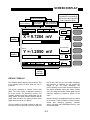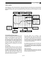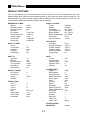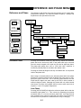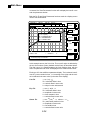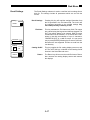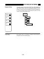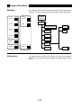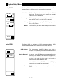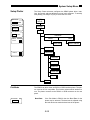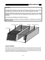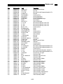
1
MODEL SR850
DSP Lock-In Amplifier
Stanford Research Systems
1290-D Reamwood Avenue
Sunnyvale, California 94089
Phone: (408) 744-9040 • Fax: (408) 744-9049
email: [email protected] • www.thinkSRS.com
Copyright © 1992 by SRS, Inc.
All Rights Reserved.
Revision 2.0 (01/2009)
TABLE OF CONTENTS
GENERAL INFORMATION
Safety and Preparation for Use
Specifications
Abridged Command List
1-3
1-5
1-7
GETTING STARTED
Your First Measurements
The Basic Lock-in
Displays and Traces
Outputs, Offsets and Expands
Scans and Sweeps
Using the Disk Drive
Aux Outputs and Inputs
Trace Math
2-1
2-3
2-7
2-13
2-17
2-23
2-31
2-35
SR850 BASICS
What is a Lock-in Amplifier?
What Does a Lock-in Measure?
The SR850 Functional Diagram
Reference Channel
Phase Sensitive Detectors
Time Constants and DC Gain
DC Outputs and Scaling
Dynamic Reserve
Signal Input Amplifier and Filters
Input Connections
Intrinsic (Random) Noise Sources
External Noise Sources
Noise Measurements
3-1
3-3
3-5
3-7
3-9
3-11
3-13
3-17
3-19
3-21
3-23
3-25
3-27
OPERATION
FRONT PANEL
Power On/Off and Power On Tests
Video Display
Soft Keys
Keypad
Spin Knob
Disk Drive
Front Panel BNC Connectors
4-1
4-1
4-1
4-2
4-2
4-2
4-2
4-2
SCREEN DISPLAY
Default Display
Data Traces
Single/Dual Trace Displays
Bar Graphs
Polar Graphs
Strip Charts
Trace Scans, Sweeps and Aliasing
Settings and Input/Output Monitor
Menu Display
Status Indicators
4-5
4-5
4-6
4-7
4-9
4-10
4-11
4-13
4-15
4-15
4-16
KEYPAD
Normal and Alternate Keys
Menu Keys
4-19
4-19
4-19
Additional Menus
Entry Keys
START/CONT and PAUSE/RESET
CURSOR
ACTIVE DISPLAY
MARK
CURSOR MAX/MIN
AUTO RESERVE
AUTO GAIN
AUTO PHASE
AUTO SETUP
AUTOSCALE
PRINT to a PRINTER
PRINT to a FILE
HELP
LOCAL
4-20
4-20
4-20
4-21
4-21
4-21
4-22
4-22
4-22
4-22
4-22
4-22
4-23
4-23
4-23
4-23
REAR PANEL
Power Entry Module
IEEE-488 Connector
RS232 Connector
Parallel Printer Connector
PC Keyboard Connector
Rear Panel BNC Connectors
Aux Inputs (A/D Inputs)
Aux Outputs (D/A Outputs)
X and Y Outputs
Signal Monitor Output
Trigger Input
TTL Sync Output
Preamp Connector
4-25
4-25
4-25
4-25
4-25
4-25
4-26
4-26
4-26
4-26
4-26
4-27
4-27
4-27
USING SRS PREAMPS
4-27
MENUS
Menu Guide
Default Settings
Reference and Phase Menu
Input and Filters Menu
Gain and Time Constant Menu
Output and Offset Menu
Trace and Scan Menu
Display and Scale Menu
Aux Outputs Menu
Cursor Setup Menu
Edit Mark Menu
Math Menu
Disk Menu
System Setup Menu
5-1
5-2
5-3
5-7
5-9
5-15
5-17
5-21
5-25
5-29
5-31
5-33
5-41
5-49
PROGRAMMING
GPIB Communications
RS232 Communications
Status Indicators and Queues
Command Syntax
1-1
6-1
6-1
6-1
6-1
Table of Contents
Interface Ready and Status
GET (Group Execute Trigger)
6-2
6-2
DETAILED COMMAND LIST
Reference and Phase
Input and Filter
Gain and Time Constant
Output and Offset
Trace and Scan
Display and Scale
Cursor
Mark
Aux Input and Output
Math
Store and Recall
Setup
Print and Plot
Front Panel and Auto Functions
Data Transfer
Interface
Status Reporting
6-3
6-4
6-6
6-7
6-9
6-10
6-11
6-13
6-14
6-15
6-16
6-18
6-19
6-21
6-22
6-23
6-28
6-29
STATUS BYTE DEFINITIONS
Serial Poll Status Byte
Service Requests
Standard Event Status Byte
LIA Status Byte
Error Status Byte
6-30
6-30
6-31
6-31
6-32
6-32
PROGRAM EXAMPLES
Microsoft C, Nationall Instr GPIB
QUICKBASIC, Nationall Instr GPIB
6-33
6-39
SERVICE
Circuit Boards
Adjusting DC Offset and CMRR
Adjusting Notch Filters
CIRCUITRY
Circuit Boards
Video Driver and CRT
CPU Board
Power Supply Board
DSP Logic Board
Analog Input Board
PARTS LISTS
Power Supply Board
DSP Logic Board
Analog Input Board
CPU Board
Chassis Assembly
Miscellaneous
SCHEMATIC DIAGRAMS
CPU Board
Power Supply Board
DSP Logic Board
Analog Input Board
TESTING
Introduction
Preset
Serial Number
Firmware Revision
General Installation
Necessary Equipment
If A Test Fails
7-1
7-1
7-1
7-1
7-2
7-3
7-3
PERFORMANCE TESTS
Self Tests
DC Offset
Common Mode Rejection
Amplitude Accuracy and Flatness
Amplitude Linearity
Frequency Accuracy
Phase Accuracy
Sine Output Amplitude
DC Outputs and Inputs
Input Noise
7-5
7-7
7-9
7-11
7-13
7-15
7-17
7-19
7-21
7-23
PERFORMANCE TEST RECORD
7-25
8-1
8-3
8-6
1-2
9-1
9-1
9-3
9-5
9-7
9-9
9-11
9-13
9-20
9-27
9-32
9-35
SAFETY AND PREPARATION FOR USE
WARNING
Dangerous voltages, capable of causing injury or death, are present in
this instrument. Use extreme caution whenever the instrument covers
are removed. Do not remove the covers while the unit is plugged into a
live outlet.
CAUTION
outlet which has a properly connected protective
ground.
This instrument may be damaged if operated
with the LINE VOLTAGE SELECTOR set for the
wrong AC line voltage or if the wrong fuse is
installed.
SERVICE
Do not attempt to service or adjust this instrument
unless another person, capable of providing first
aid or resuscitation, is present.
LINE VOLTAGE SELECTION
The SR850 operates from a 100V, 120V, 220V, or
240V nominal AC power source having a line frequency of 50 or 60 Hz. Before connecting the power cord to a power source, verify that the LINE
VOLTAGE SELECTOR card, located in the rear
panel fuse holder, is set so that the correct AC input voltage value is visible.
Do not install substitute parts or perform any unauthorized modifications to this instrument. Contact
the factory for instructions on how to return the instrument for authorized service and adjustment.
FURNISHED ACCESSORIES
- Power Cord
- Operating Manual
Conversion to other AC input voltages requires a
change in the fuse holder voltage card position
and fuse value. Disconnect the power cord, open
the fuse holder cover door and rotate the fuse-pull
lever to remove the fuse. Remove the small printed circuit board and select the operating voltage
by orienting the printed circuit board so that the
desired voltage is visible when pushed firmly into
its slot. Rotate the fuse-pull lever back into its normal position and insert the correct fuse into the
fuse holder.
ENVIRONMENTAL CONDITIONS
OPERATING
Temerpature: +10° C to +40° C
(Specifications apply over +18° C to +28° C)
Relative Humidity: <90% Non-condensing
NON-OPERATING
Temperature: -25° C to 65° C
Humidity: <95% Non-condensing
LINE FUSE
WARNING REGARDING USE WITH PHOTOMULTIPLIERS AND OTHER DETECTORS
Verify that the correct line fuse is installed before
connecting the line cord. For 100V/120V, use a 1
Amp fuse and for 220V/240V, use a 1/2 Amp fuse.
The front end amplifier of this instrument is easily
damaged if a photomultiplier is used improperly
with the amplifier. When left completely unterminated, a cable connected to a PMT can charge to
several hundred volts in a relatively short time. If
this cable is connected to the inputs of the SR850
the stored charge may damage the front-end op
amps. To avoid this problem, always discharge the
cable and connect the PMT output to the SR850
input before turning the PMT on.
LINE CORD
The SR850 has a detachable, three-wire power
cord for connection to the power source and to a
protective ground. The exposed metal parts of the
instrument are connected to the outlet ground to
protect against electrical shock. Always use an
1-3
1-4
SR850 DSP LOCK-IN AMPLIFIER
SPECIFICATIONS
SIGNAL CHANNEL
Voltage Inputs
Current Input
Full Scale Sensitivity
Input Impedance
Gain Accuracy
Input Noise
Signal Filters
CMRR
Dynamic Reserve
Harmonic Distortion
REFERENCE CHANNEL
Frequency Range
Reference Input
Phase Resolution
Absolute Phase Error
Relative Phase Error
Orthogonality
Phase Noise
Phase Drift
Harmonic Detect
Acquisition Time
DEMODULATOR
Zero Stability
Time Constants
Harmonic Rejection
INTERNAL OSCILLATOR
Frequency
Frequency Accuracy
Frequency Resolution
Frequency Sweeps
Distortion
Output Impedance
Amplitude
Amplitude Accuracy
Amplitude Stability
Outputs
Single-ended (A) or differential (A-B).
106 or 10 8 Volts/Amp.
2 nV to 1 V in a 1-2-5-10 sequence (expand off).
Voltage: 10 MΩ+25 pF, AC or DC coupled.
Current: 1 kΩ to virtual ground.
±1% from 20°C to 30°C (notch filters off), ±0.2% typical.
6 nV/√Hz at 1 kHz (typical).
60 (50) Hz and 120(100) Hz notch filters (Q=4).
100 dB at 10 kHz (DC Coupled), decreasing by 6 db/octave above 10 kHz
Greater than 100 dB (with no signal filters).
<-90 dB to 10 kHz, <-80 dB to 100 kHz.
1 mHz to 102 kHz
TTL (rising or falling edge) or Sine.
Sine input is1 MΩ, AC coupled (>1 Hz). 400 mV pk-pk minimum signal.
0.001°
<1°
<0.001°
90° ± 0.001°
External synthesized reference: 0.005° rms at 1 kHz, 100 ms, 12 dB/oct.
Internal reference: crystal synthesized, <0.0001° rms at 1 kHz.
<0.01°/°C below 10 kHz
<0.1°/°C to 100 kHz
Detect at Nxf where N<32767 and Nxf<102 kHz.
(2 cycles + 5 ms) or 40 ms, whichever is greater.
Digital displays have no zero drift on all dynamic reserves.
Analog outputs: <5 ppm/°C for all dynamic reserves.
10 µs to 30 s (reference > 200 Hz). 6, 12, 18, 24 dB/oct rolloff.
up to 30000 s (reference < 200 Hz). 6, 12, 18, 24 dB/oct rolloff.
Synchronous filtering available below 200 Hz.
-90 dB
1 mHz to 102 kHz.
25 ppm + 30 µHz
5 digits or 0.1 mHz, whichever is greater.
Linear and Log.
f<10 kHz, below -80 dBc. f>10 kHz, below -70 dBc.1 Vrms amplitude.
50 Ω
4 mVrms to 5 Vrms (into a high impedance load) with 2 mV resolution.
(2 mVrms to 2.5 Vrms into 50Ω load).
1%
50 ppm/°C
Sine output on front panel. TTL sync output on rear panel.
When using an external reference, both outputs are phase locked to the
external reference.
1-5
SR850 DSP Lock-In Amplifier
INPUTS AND OUTPUTS
Channel 1 Output
Channel 2 Output
X and Y Outputs
Aux. Outputs
Aux. Inputs
Trigger Input
Monitor Output
DISPLAYS
Screen Format
Displayed Quantities
Display Types
Chart Data Buffer
ANALYSIS FUNCTIONS
Smoothing
Curve Fits
Calculator
Statistics
GENERAL
Monitor
Interfaces
Preamp Power
Hardcopy
Disk
Power
Dimensions
Weight
Warranty
X, R, θ, or Trace 1-4. Traces are defined as A•B/C or A•B/C2 where A, B,
and C are selected from the quantities Unity, X, Y, R, θ, Xnoise, Ynoise,
Rnoise, Aux Inputs 1 through 4, or Frequency.
Output Voltage: ±10 V full scale. 10 mA max output current.
Y, R, θ, or Trace 1-4. Traces are defined as A•B/C or A•B/C2 where A, B,
and C are selected from the quantities Unity, X, Y, R, θ, Xnoise, Ynoise,
Rnoise, Aux Inputs 1 through 4, or Frequency.
Output Voltage: ±10 V full scale. 10 mA max output current.
Rear panel outputs of cosine (X) and sine (Y) components.
Output Voltage: ±10 V. 10 mA max output current.
4 BNC Digital to Analog outputs.
±10 V full scale, 1 mV resolution. May be set to a fixed voltage or swept in
amplitude (linear or log). 10 mA max output current.
4 BNC Analog to Digital inputs.
Differential inputs with1 MΩ input impedance on both shield and center
conductor. ±10 V full scale, 1 mV resolution.
TTL trigger input triggers each data sample and/or start of scan.
Analog output of signal amplifiers (before the demodulator).
Single or dual display.
Each display may show one of the traces.
Traces are defined as A•B/C or A•B/C 2 where A, B and C are selected from
the quantities Unity, X, Y, R, θ, Xnoise, Ynoise, Rnoise, Aux Inputs 1
through 4, or Frequency.
Large numeric readout with bar graph, polar graph, and strip chart.
64k data points may be stored and displayed on strip charts. The buffer can
be configured as a single trace with 64k points, 2 traces with 32k points
each, or 4 traces with16k points each. The internal data sample rate ranges
from 512 Hz down to 1 point every 16 seconds. Samples can also be
triggered.
5 - 25 point Savitsky-Golay smoothing of trace regions.
Line, Exponential, and Gaussian fits of trace regions.
Arithmetic, trigonometric, and logarithmic calculations on trace regions.
Mean and standard deviation of trace regions.
Monochrome CRT. 640H by 480V resolution.
Adjustable brightness and screen position.
IEEE-488, RS232 and Printer interfaces standard.
All instrument functions can be controlled through the IEEE-488 and RS232
interfaces. A PC keyboard input is provided for additional flexibility.
Power connector for SR550 and SR552 preamplifiers.
Screen dumps to dot matrix and HP LaserJet compatible printers. Data
plots to HP-GL compatible plotters (via RS232 or IEEE-488). Screens can
also be saved to disk as PCX image files.
3.5 inch DOS compatible format, 720 kbyte capacity.
Storage of data and setups.
60 Watts, 100/120/220/240 VAC, 50/60 Hz.
17"W x 6.25"H x 19.5"D
40 lbs.
One year parts and labor on materials and workmanship.
1-6
SR850 DSP Lock-In Amplifier
COMMAND LIST
VARIABLES
i,j,k,l,m
f
x,y,z
s
REFERENCE and PHASE
PHAS (?) {x}
FMOD (?) {i}
FREQ (?) {f}
SWPT (?) {i}
SLLM (?) {f}
SULM (?) {f}
RSLP (?) {i}
HARM (?) {i}
SLVL (?) {x}
page
6-4
6-4
6-4
6-4
6-4
6-4
6-4
6-5
6-5
description
Set (Query) the Phase Shift to x degrees.
Set (Query) the Reference Source to Internal (0), Sweep (1) , or External (2).
Set (Query) the Reference Frequency to f Hz.Set only in Internal reference mode.
Set (Query) the Internal Sweep Type to Linear (0) or logarithmic (1).
Set (Query) the Start Frequency to f Hz.Set only in Internal Sweep mode.
Set (Query) the Stop Frequency to f Hz.Set only in Internal Sweep mode.
Set (Query) the External Reference Slope to Sine(0), TTL Rising (1), or TTL Falling (2).
Set (Query) the Detection Harmonic to 1 ≤ i ≤ 32767 and i•f ≤ 102 kHz.
Set (Query) the Sine Output Amplitude to x Vrms. 0.004 ≤ x ≤5.000.
INPUT and FILTER
ISRC (?) {i}
IGAN (?) {i}
IGND (?) {i}
ICPL (?) {i}
ILIN (?) {i}
page
6-6
6-6
6-6
6-6
6-6
description
Set (Query) the Input Configuration to A (0), A-B (1) , or I (2).
Set (Query) the Current Conversion Gain to 1 MΩ (0) or 100 MΩ (1).
Set (Query) the Input Shield Groungind to Float (0) or Ground (1).
Set (Query) the Input Coupling to AC (0) or DC (1).
Set (Query) the Line Notch Filters to Out (0), Line In (1) , 2xLine In (2), or Both In (3).
GAIN and TIME CONSTANT
SENS (?) {i}
RMOD (?) {i}
RSRV (?) {i}
OFLT (?) {i}
OFSL (?) {i}
SYNC (?) {i}
page
6-7
6-7
6-7
6-7
6-8
6-8
description
Set (Query) the Sensitivity to 2 nV (0) through 1 V (26) rms full scale.
Set (Query) the Dynamic Reserve Mode to Max (0), Manual (1), or Min (2).
Set (Query) the Dynamic Reserve to i th reserve. Set will switch to Manual Reserve Mode.
Set (Query) the Time Constant to 10 µs (0) through 30 ks (19).
Set (Query) the Low Pass Filter Slope to 6 (0), 12 (1), 18 (2) or 24 (3) dB/oct.
Set (Query) the Synchronous Filter to Off (0) or On below 200 Hz (1).
OUTPUT and OFFSET
FOUT (?) i {, j}
OEXP (?) i {, x, j}
page description
6-9
Set (Query) the CH1 (i=1) or CH2 (2) Output Source to XY,R,θ,Trace 1, 2, 3, 4 (j=0...6).
6-9
Set (Query) the X, Y, R (i=1,2,3) Offset to x percent and Expand to j. -105.00 ≤ x ≤ 105.00 and
1 ≤ j ≤ 256.
6-9
Auto Offset X, Y, R (i=1,2,3).
AOFF i
TRACE and SCAN
TRCD (?) i {, j, k, l, m}
Integers
Frequency (real)
Real Numbers
String
SRAT (?) {i}
SLEN (?) {x}
SEND (?) {i}
TRIG
page description
6-10 Set (Query) the Definition of Trace i (1-4) to j•k/l and Store (m=1) or Not Store (0). j, k, l select
1, X, Y, R, q, Xn, Yn, Rn, Aux 1, Aux 2, Aux 3, Aux4, or F (j,k,l = 0...12). l=13-24 selects X2
through F2 .
6-10 Set (Query) the Sample Rate to 62.5 mHz (0) through 512 Hz (13) or Trigger (14).
6-10 Set (Query) the Scan Length to x seconds.
6-10 Set (Query) the Scan Mode to 1 Shot (0) or Loop (1).
6-10 Software trigger command. Same as trigger input.
DISPLAY and SCALE
ASCL
ADSP (?) {i}
SMOD (?) {i}
MNTR (?) {i}
DTYP (?) i {, j}
page
6-11
6-11
6-11
6-11
6-11
description
Auto Scale the active display.
Set (Query) the active display to Full (0), Top (1) or Bottom (2). Full screen is always active.
Set (Query) the Screen Format to Single (0) or Up/Down dual (1) display mode.
Set (Query) the Monitor Display to settings (0) or Input/Output (1).
Set (Query) theFull (i=0), Top (i=1) or Bottom (i=2) Display Type to Polar (j=0), Blank (j=1),
Bar (j=2) or Chart (j=3).
1-7
SR850 DSP Lock-In Amplifier
DTRC (?) i {, j}
DSCL (?) {x}
DOFF (?) {x}
DHZS (?) {i}
6-11
6-11
6-11
6-12
RBIN? i
6-12
Set (Query) theFull (i=0), Top (i=1) or Bottom (i=2) Display Trace to trace j (1,2,3,4).
Set (Query) theFull (i=0), Top (i=1) or Bottom (i=2) Display Range to x.
Set (Query) theFull (i=0), Top (i=1) or Bottom (i=2) Display Center value to x.
Set (Query) theFull (i=0), Top (i=1) or Bottom (i=2) Display Horizontal Scale to 2 ms (0) through
200 ks (32) per div.
Query the bin number at the right edge of the Full (i=0), Top (i=1) or Bottom (i=2) chart display.
CURSOR
CSEK (?) {i}
CWID (?) {i}
CDIV (?) {i}
CLNK (?) {i}
CDSP (?) {i}
CMAX
CURS? i
CBIN (?) {i}
page
6-13
6-13
6-13
6-13
6-13
6-13
6-13
6-13
description
Set (Query) the active display Cursor Seek mode to Max (0), Min (1) or Mean (2).
Set (Query) the active display Cursor Width to Off (0), Narrow (1), Wide (2) or Spot (3).
Set (Query) the active display Chart Divisions to 8 (0), 10 (1) or None (2).
Set (Query) the Cursor Control Mode to Linked (0) or Separate (1).
Set (Query) the active display Cursor Readout to Delay (0), Bin (1), Fsweep (2) or Time (3).
Move active chart cursor to max or min. Same as pressing [CURSOR MAX/MIN] key.
Query the cursor horz,vert position of Full (0), Top (1) or Bottom (2) chart display.
Set (Query) the center of the cursor region in the active chart display. i is the bin number.
MARK
MARK
MDEL
CNXT
CPRV
MACT?
MBIN? i
MTXT (?) i {,s}
page
6-14
6-14
6-14
6-14
6-14
6-14
6-14
description
Places a mark in the data buffer. Same as pressing [MARK] key.
Delete the nearest mark to the left of the cursor. Same as pressing <Marker Delete> softkey.
Move active chart cursor to next mark to the right.
Move active chart cursor to next mark to the left.
Query the number of active marks. Also returns the active mark numbers.
Query the bin number of mark #i.
Set (Query) the label text for mark #i.
AUX INPUT/OUTPUT
OAUX ? i
AUXM(?) i{, j}
AUXV (?) i {, x}
page
6-15
6-15
6-15
SAUX (?) i {, x, y, z}
6-15
TSTR (?) {i}
6-15
description
Query the value of Aux Input i (1,2,3,4).
Set (Query) the Output Mode of Aux Output i (1,2,3,4). j selects Fixed (0), Log (1) or Linear (2).
Set (Query) voltage of Aux Output i (1,2,3,4) to x Volts. -10.500 ≤ x ≤ 10.500. Fixed Output
Mode only.
Set (Query) the Aux Output i (1,2,3,4) Sweep Limits to Start (x), Stop (y) and Offset (z) voltages. 0.001 ≤ x,y ≤ 21.000 and -10.500 ≤ z ≤ 10.500.
Set (Query) the Trigger Starts Scan? mode to No (0) or Yes (1).
MATH
SMTH i
COPR (?) {i}
CALC
CAGT (?) {i}
CTRC (?) {i}
CARG (?) {x}
FTYP (?) {i}
FITT i, j
PARS ? i
STAT i, j
page
6-16
6-16
6-17
6-17
6-17
6-17
6-17
6-17
6-17
6-17
SPAR ? i
6-17
description
Smooth the data within the active chart using 5 (0), 11 (1), 17 (2), 21 (3), 25 (4) point width.
Set (Query) the Calculator Operation to +, -, x, /, sin, cos, tan, √x, x 2 , log, 10x (i=0...10).
Do the Calculation selected by COPR with the argument set by CTRC or CARG.
Set (Query) the Calculation Argument Type to Trace (0) or Constant (1).
Set (Query) the Trace Argument to Trace i (1,2,3,4).
Set (Query) the Constant Argument value to x.
Set (Query) the Fit Type to Linear (0), Exponential (1) or Gaussian (2).
Fit the data within the chart region between i% and j% from the left edge. 0 ≤ i,j ≤ 100.
Query the fit parameters a (0), b (1), c (2) or t0 (3).
Statistically analyze the data within the chart region between i% and j% from the left edge.
0 ≤ i,j ≤ 100.
Query the Statistical results mean (0), standard dev (1), total (2) or delta time (3).
STORE AND RECALL FILE
FNAM (?) {s}
SDAT
SASC
SSET
page
6-18
6-18
6-18
6-18
description
Set (Query) the current File Name to string s.
Save the Active Display's Trace Data to the file specified by FNAM.
Save the Active Display's Trace Data in ASCII format to the file specified by FNAM.
Save the Settings to the file specified by FNAM.
1-8
SR850 DSP Lock-In Amplifier
RDAT
RSET
6-18
6-18
Recall the Trace Data from the file specified by FNAM to the active display's trace buffer.
Recall the Settings from the file specified by FNAM.
SETUP
OUTX (?) {i}
OVRM (?) {i}
KCLK (?) {i}
ALRM (?) {i}
THRS (?) {i}
TMIN (?) {i}
TSEC (?) {i}
DMTH (?) {i}
DDAY (?) {i}
DYRS (?) {i}
PLTM (?) {i}
PLTB (?) {i}
PLTA (?) {i}
PLTS (?) {i}
PNTR (?) {i}
PNGD (?) {i}
PNAL (?) {i}
PNCR (?) {i}
PRNT (?) {i}
page
6-19
6-19
6-19
6-19
6-19
6-19
6-19
6-19
6-19
6-19
6-19
6-19
6-19
6-19
6-19
6-20
6-20
6-20
6-20
description
Set (Query) the Output Interface to RS232 (0) or GPIB (1).
Set (Query) the GPIB Overide Remote state to Off (0) or On (1).
Set (Query) the Key Click to Off (0) or On (1).
Set (Query) the Alarms to Off (0) or On (1).
Set (Query) the Hours to 0≤ i ≤ 23.
Set (Query) the Minutes to 0 ≤ i ≤ 59.
Set (Query) the Seconds to 0 ≤ i ≤ 59.
Set (Query) the Month to 1 ≤ 1 ≤ 12.
Set (Query) the Day to 1 ≤ 1 ≤ 31.
Set (Query) the Year to 0 ≤ 1 ≤ 99.
Set (Query) the Plotter Mode to RS232 (0) or GPIB (1).
Set (Query) the Plotter Baud Rate to 300 (0), 1200 (1), 2400 (2), 4800 (3), 9600 (4).
Set (Query) the Plotter GPIB Address to 0 ≤ i ≤ 30.
Set (Query) the Plot Speed to Fast (0) or Slow (1).
Set (Query) the Trace Pen Number to 1 ≤ i ≤ 6.
Set (Query) the Grid Pen Number to 1 ≤ i ≤ 6.
Set (Query) the Alphanumeric Pen Number to 1 ≤ i ≤ 6.
Set (Query) the Cursor Pen Number to 1 ≤ i ≤ 6.
Set (Query) the Printer Type to Epson (0), HP (1) or File (2).
PRINT AND PLOT
PRSC
PALL
PTRC
PCUR
page
6-21
6-21
6-21
6-21
description
Print the screen. Same as the [PRINT] key.
Plot the display(s).
Plot the trace(s) only.
Plot the cursor(s) only.
FRONT PANEL CONTROLS
AUTO FUNCTIONS
STRT
PAUS
REST
ASCL
ATRC (?) {i}
AGAN
ARSV
APHS
AOFF i
CMAX
page
6-22
6-22
6-22
6-11
6-22
6-22
6-22
6-22
6-22
6-22
description
Start or continue a scan. Same as [START/CONT] key.
Pause a scan. Does not reset a paused or done scan.
Reset the scan. All stored data is lost.
Auto Scale the active display.
Set (Query) the active display to Top (0) or Bottom (1). Full screen is always active.
Auto Gain function. Same as pressing the [AUTO GAIN] key.
Auto Reserve function. Same as pressing the [AUTO RESERVE] key.
Auto Phase function. Same as pressing the [AUTO PHASE] key.
Auto Offset X,Y or R (i=1,2,3).
Move Cursor to Max or Min. Same as pressing the [CURSOR MAX/MIN] key.
DATA TRANSFER
OUTP? i
OUTR? i
OAUX? i
SPTS? i
TRCA? i,j,k
TRCB? i,j,k
TRCL? i,j,k
FAST (?) {i}
page
6-23
6-23
6-23
6-23
6-23
6-23
6-24
6-25
STRD
6-25
description
Query the value of X (1), Y (2), R (3) or θ (4). Returns ASCII floating point value.
Query the value of Trace i (1,2,3,4). Returns ASCII floating point value.
Query the value of Aux Input i (1,2,3,4). Returns ASCII floating point value.
Query the number of points stored in Trace i (1,2,3,4).
Read k≥1 points starting at bin j≥0 from trace i (1,2,3,4) in ASCII floating point.
Read k≥1 points starting at bin j≥0 from trace i (1,2,3,4) in IEEE binary floating point.
Read k≥1 points starting at bin j≥0 from trace i (1,2,3,4) in non-normalized binary floating point.
Set (Query) Fast Data Transfer Mode On (1 or 2) or Off (0).On will transfer binary X and Y every sample during a scan over the GPIB interface.
Start a scan after 0.5sec delay. Use with Fast Data Transfer Mode.
1-9
SR850 DSP Lock-In Amplifier
INTERFACE
*RST
*IDN?
LOCL(?) {i}
OVRM (?) {i}
TRIG
page
6-26
6-26
6-26
6-26
6-26
STATUS
*CLS
*ESE (?) {i} {,j}
page description
6-27 Clear all status bytes.
6-27 Set (Query) the Standard Event Status Byte Enable Register to the decimal value i (0-255).
*ESE i,j sets bit i (0-7) to j (0 or 1). *ESE? queries the byte. *ESE?i queries only bit i.
6-27 Query the Standard Event Status Byte. If i is included, only bit i is queried.
6-27 Set (Query) the Serial Poll Enable Register to the decimal value i (0-255). *SRE i,j sets bit i (07) to j (0 or 1). *SRE? queries the byte, *SRE?i queries only bit i.
6-27 Query the Serial Poll Status Byte. If i is included, only bit i is queried.
6-27 Set (Query) the Power On Status Clear bit to Set (1) or Clear (0).
6-27 Set (Query) the Error Status Enable Register to the decimal value i (0-255). ERRE i,j sets bit i
(0-7) to j (0 or 1). ERRE? queries the byte, ERRE?i queries only bit i.
6-27 Query the Error Status Byte. If i is included, only bit i is queried.
6-27 Set (Query) the LIA Status Enable Register to the decimal value i (0-255). LIAE i,j sets
bit i (0-7) to j (0 or 1). LIAE? queries the byte, LIAE?i queries only bit i.
6-27 Query the LIA Status Byte. If i is included, only bit i is queried.
*ESR? {i}
*SRE (?) {i} {,j}
*STB? {i}
*PSC (?) {i}
ERRE (?) {i} {,j}
ERRS? {i}
LIAE (?) {i} {,j}
LIAS? {i}
description
Reset the unit to its default configurations.
Read the SR850 device identification string.
Set (Query) the Local/Remote state to LOCAL (0), REMOTE (1), or LOCAL LOCKOUT (2).
Set (Query) the GPIB Overide Remote state to Off (0) or On (1).
Software trigger command. Same as trigger input.
STATUS BYTE DEFINITIONS
SERIAL POLL STATUS BYTE
bit
0
1
2
3
4
5
6
7
name
SCN
IFC
ERR
LIA
MAV
ESB
SRQ
Unused
(6-28)
usage
No data is being acquired
No command execution in progress
Unmasked bit in error status byte set
Unmasked bit in LIA status byte set
The interface output buffer is non-empty
Unmasked bit in standard status byte set
SRQ (service request) has occurred
STANDARD EVENT STATUS BYTE
bit
0
1
2
3
4
5
6
7
name
INP
Unused
QRY
Unused
EXE
CMD
URQ
PON
LIA STATUS BYTE (6-29)
bit
0
1
2
3
4
5
6
7
(6-29)
name
RESRV
FILTR
OUTPT
UNLK
RANGE
TC
TRIG
PLOT
usage
Set when a RESRV overload is detected
Set when a FILTR overload is detected
Set when a OUTPT overload is detected
Set when reference unlock is detected
Set when detection freq crosses 200 Hz
Set when time constant is changed
Set when unit is triggered
Set when a plot is completed
ERROR STATUS BYTE (6-30)
usage
Set on input queue overflow
Set on output queue overflow
Set when command execution error occurs
Set when an illegal command is received
Set by any key press or knob rotation
Set by power-on
bit
0
1
2
3
4
5
6
7
1-10
name
Prn/Plt Err
Backup Error
RAM Error
Disk Error
ROM Error
GPIB Error
DSP Error
Math Error
usage
Set when an printing or plotting error occurs
Set when battery backup fails
Set when RAM Memory test finds an error
Set when a disk error occurs
Set when ROM Memory test finds an error
Set when GPIB binary data transfer aborts
Set when DSP test finds an error
Set when an internal math error occurs
GETTING STARTED
YOUR FIRST MEASUREMENTS
The sample measurements described in this section are designed to acquaint the first time user with the
SR850 DSP Lock-In Amplifier. Do not be concerned that your measurements do not exactly agree with these
exercises. The focus of these measurement exercises is to learn how to use the instrument.
It is highly recommended that the first time user step through some or all of these exercises before attempting
to perform an actual experiment.
The experimental procedures are detailed in two columns. The left column lists the actual steps in the experiment. The right column is an explanation of each step.
Key Types
There are two types of front panel keys which will be referred to in this
manual. Hardkeys are those keys with labels printed on them. Their function is determined by the label and does not change. Hardkeys are referenced by brackets like this - [HARDKEY]. The softkeys are the six gray
keys along the right edge of the screen. Their function is labelled by a
menu box displayed on the screen next to the key. Softkey functions
change depending upon the situation. Softkeys will be referred to as the
<Soft Key> or simply the Soft Key.
Hardkeys
The keypad consists of five groups of hardkeys. The ENTRY keys are
used to enter numeric parameters which have been highlighted by a softkey. The MENU keys select a menu of softkeys. Pressing a menu key
will change the menu boxes which are displayed next to the softkeys.
Each menu groups together similar parameters and functions. The
CONTROL keys start and stop actual data acquisition, select the cursor
and toggle the active display. These keys are not in a menu since they
are used frequently and while displaying any menu. The SYSTEM keys
output the screen to a printer and display help messages. These keys
can also be accessed from any menu. The AUTO keys perform auto
functions such as Auto Gain and Auto Phase.
Softkeys
The SR850 has a menu driven user interface. The 6 softkeys to the right
of the video display have different functions depending upon the information displayed in the menu boxes at the right of the video display. In general, the softkeys have two uses. The first is to toggle a feature on and
off or to choose between settings. The second is to highlight a parameter
which is then changed using the knob or numeric keypad. In both cases,
the softkey selects the parameter which is displayed adjacent to it.
Knob
The knob is used to adjust parameters which have been highlighted by a
softkey. Many numeric entry fields may be adjusted with the knob. In
addition, many parameters are adjusted only with the knob. These are
typically parameters with a limited set of values, such as sensitivity or
time constant. In these cases, the parameter is selected by a softkey.
The [CURSOR] key will set the knob function to scrolling the cursor
within the active chart display.
2-1
Getting Started
2-2
The Basic Lock-in
THE BASIC LOCK-IN
This measurement is designed to use the internal oscillator to explore some of the basic lock-in functions.
You will need BNC cables.
Specifically, you will measure the amplitude of the Sine Out at various frequencies, sensitivities, time constants and phase shifts. The "normal" lock-in display will be used throughout this exercise.
1. Disconnect all cables from the lock-in. Turn
the power on while holding down the [←]
(backspace) key. Wait until the power-on tests
are completed.
When the power is turned on with the backspace
key depressed, the lock-in returns to its default
settings. See the Default Settings list in the Menu
section for a complete listing of the settings.
The display is the "normal" lock-in display. The
lock-in setup is displayed across the top of the
screen. The sensitivity, reserve, time constant,
prefilters and input configuration are all easily visible. Watch how these indicators change as you
change parameters. The upper numeric readout
and bar graph shows the value of X (Rcosθ) and
the lower graph shows the the value of Y (Rsinθ).
2. Connect the Sine Out on the front panel to the
A input using a BNC cable.
The input impedance of the lock-in is 10 MΩ. The
Sine Out has an output impedance of 50Ω. Since
the Sine Output amplitude is specified into a high
impedance load, the output impedance does not
affect the amplitude.
The lock-in defaults to the internal oscillator reference set at 1.000 kHz. The reference mode (Intrnl)
and frequency are displayed at the bottom of the
screen. In this mode, the lock-in generates a synchronous sine output at the internal reference
frequency.
The sine amplitude is 1.000 Vrms and the
sensitivity is 1 V(rms). Since the phase shift of the
sine output is very close to zero, the upper display
(X) should read close to 1.000 V and the lower display (Y) should read close to 0.000 V.
3. Press [AUTO PHASE]
Automatically adjust the reference phase shift to
eliminate any residual phase error. This should set
the value of Y to zero.
4. Press [REF/PHASE]
Display the Reference and Phase menu. The
phase shift (displayed in the top menu box) should
be close to zero.
2-3
The Basic Lock-in
5. Press the <Rotate 90 deg> softkey.
This adds 90° to the reference phase shift. The
value of X drops to zero and Y becomes minus the
magnitude (-1.000 V).
Press the <deg.> softkey.
Highlight the phase shift.
Use the knob to adjust the phase shift until Y
is zero and X is equal to the positive
amplitude.
The knob can be used to adjust parameters which
are continuous, such as phase, amplitude and frequency. The final phase value should be close to
zero again.
Press [9] [0] [ENTER]
Phase shifts can also be entered numerically.
The knob is useful for small adjustments while
numeric entry is easier when changing to a precise value or by a large amount.
Press [AUTO PHASE]
Use the Auto Phase function to return Y to zero
and X to the amplitude.
6. Press <Ref. Frequency>
Highlight the internal reference frequency menu.
Press [1] [2] [.] [3] [4] [5] [EXP] [3] [ENTER]
Enter 12.345 kHz in exponential form. The measured signal amplitude should stay within 1% of 1 V
and the phase shift should stay close to zero (the
value of Y should stay close to zero).
Press [1] [0] [0] [0] [ENTER]
Parameters can be entered in real or integer form
as well. In this case, the frequency is changed to
1.000 kHz.
The internal oscillator is crystal synthesized with
25 ppm of frequency error. The frequency can be
set with 5 digit or 0.1 mHz resolution, whichever is
greater.
7. Press <Sine Output>
Highlight the sine output amplitude.
Use the knob to adjust the amplitude.
As the amplitude is changed, the measured value
of X should equal the sine output amplitude.
Press [.] [0] [1] [ENTER]
The amplitude may be entered numerically also.
The sine amplitude can be set from 4 mV to 5 V
rms into high impedance (half the amplitude into a
50 Ω load).
8. Press [GAIN/TC]
Display the Gain and Time Constant menu.
Press [AUTO GAIN]
The Auto Gain function will adjust the sensitivity so
2-4
The Basic Lock-in
that the measured magnitude (R) is a sizable percentage of full scale.
9. Press <Sensitivity>
Highlight the full scale sensitivity.
Use the knob to change the sensitivity to
50 mV.
Parameters which are discrete values, such as
sensitivity and time constant, can only be changed
with the knob. Numeric entry is not allowed for
these parameters.
Change the sensitivity back to 20 mV.
10. Press <Time Constant>
Highlight the time constant.
Use the knob to change the time constant to
300 µs.
The values of X and Y become noisy. This is
because the 2f component of the output (at 2 kHz)
is no longer attenuated completely by the low pass
filters.
Change the time constant to 3 ms.
Let's leave the time constant short and change the
filter slope.
11. Press the <Filter db/oct.> softkey until 6 dB/oct
is selected.
Parameters which have their available options displayed within the menu box are selected by pressing the corresponding softkey until the desired
option is chosen.
The X and Y outputs are somewhat noisy at this
short time constant and only 1 pole of low pass
filtering.
Press <Filter db/oct.> again to select
12 dB/oct.
The outputs are less noisy with 2 poles of filtering.
Press <Filter db/oct.> twice to select
24 db/oct.
With 4 poles of low pass filtering, even this short
time constant attenuates the 2f component reasonably well and provides steady readings.
Press <Filter db/oct> again to select 6 db/oct.
Let's leave the filtering short and the outputs noisy
for now.
12. Press [REF/PHASE]
Display the Reference and Phase menu.
Press <Ref. Frequency>
Highlight the internal reference frequency.
Press [5] [0] [ENTER]
Enter 50 Hz for the reference frequency. With a
3 ms time constant and only 6 db/oct of filtering,
the output is totally dominated by the 2f component at 50 Hz.
2-5
The Basic Lock-in
13. Press [GAIN/TC]
Press <Synchronous> to select <200 Hz.
Display the Gain and Time Constant menu again.
This turns on synchronous filtering whenever the
detection frequency is below 200 Hz.
Synchronous filtering effectively removes output
components at multiples of the detection frequency. At low frequencies, this filter is a very effective
way to remove 2f without requiring extremely long
time constants.
The outputs are now very quiet and steady, even
though the time constant is very short. The
response time of the synchronous filter is equal to
the period of the detection frequency (20 ms in this
case).
This concludes this measurement example. You
should have a feeling for the basic operation of the
menus, knob and numeric entry. Basic lock-in
parameters have been introduced and you should
be able to perform simple measurements.
2-6
Displays and Traces
DISPLAYS and TRACES
This measurement is designed to use the internal oscillator and an external signal source to explore some of
the display types. You will need a synthesized function generator capable of providing a 100 mVrms sine
wave at 1.000 kHz (the DS345 from SRS will suffice), BNC cables and a terminator appropriate for the generator function output.
Specifically, you will display the lock-in outputs when measuring a signal close to, but not equal to, the internal reference frequency. This setup ensures changing outputs which are more illustrative than steady outputs.
The displays will be configured to show X, Y, R and θ in bar graph and polar formats. The example Scans and
Sweeps demonstrates the use of the chart graph.
1. Disconnect all cables from the lock-in. Turn
the power on while holding down the [←]
(backspace) key. Wait until the power-on tests
are completed.
When the power is turned on with the backspace
key depressed, the lock-in returns to its default
settings. See the Default Settings list in the Menu
section for a complete listing of the settings.
The display is the "normal" lock-in display. The
lock-in setup is displayed across the top of the
screen. The sensitivity, reserve, time constant,
prefilters and input configuration are all easily visible. Watch how these indicators change as you
change parameters. The upper numeric readout
and bar graph shows the value of X (Rcosθ) and
the lower graph shows the the value of Y (Rsinθ).
2. Turn on the function generator, set the frequency to 1.0000 kHz (exactly) and the amplitude to 500 mVrms.
The input impedance of the lock-in is 10 MΩ. The
generator may require a terminator. Many generators have either a 50Ω or 600Ω output impedance.
Use the appropriate feedthrough or T termination if
necessary. In general, not using a terminator
means that the function output amplitude will not
agree with the generator setting.
Connect the function output (sine wave) from
the synthesized function generator to the A
input using a BNC cable and appropriate
terminator.
The lock-in defaults to the internal oscillator reference set at 1.000 kHz. The reference mode (Intrnl)
and frequency are displayed at the bottom of the
screen. In this mode, the internal oscillator sets
the detection frequency.
The internal oscillator is crystal synthesized so
that the actual reference frequency should be very
close to the actual generator frequency. The X and
Y displays should read values which change very
slowly. The lock-in and the generator are not
phase locked but they are at the same frequency
with some slowly changing phase.
3. Press [REF/PHASE]
Display the Reference and Phase menu.
2-7
Displays and Traces
Press <Ref. Frequency>
Highlight the internal oscillator frequency.
Use the knob to change the frequency to
999.80 Hz.
By setting the lock-in reference 0.2 Hz away from
the signal frequency, the X and Y outputs are
0.2 Hz sine waves (difference between reference
and signal frequency). The X and Y output displays should now oscillate at about 0.2 Hz (the
accuracy is determined by the crystals of the generator and the lock-in).
4. Press [DISPLAY/SCALE]
Display the Display and Scale menu.
The SR850 collects data in the form of traces.
There are 4 definable traces and only these trace
quantities may be displayed. The default definition
of these traces is X, Y, R and θ for traces 1, 2, 3
and 4.
The Display Scale menu box shows the display
parameters for the Full (screen), Top or Bottom
(split screen) displays. In this case, the Top display parameters are shown.
Press <Type/Trace> twice to highlight the displayed trace number.
Each display shows one of the data traces. The
Top display defaults to showing trace 1 which has
a default definition of X. Thus the top bar graph
shows the X output.
Use the knob to change the trace number to 3.
Trace 3 has a default definition of R so showing
trace 3 on the top graph will display the quantity R.
R is phase independent so it shows a steady value
(close to 0.500 V).
Press [AUTO SCALE]
[AUTO SCALE] automatically scales the active
display. The top display is the active display (as
indicated by the inverse trace identifier at the
upper left of the display).
5. Press <Full, Top or Bottom> to select Bottom.
To modify the bottom graph, you must display the
bottom graph's parameters in the Display Scale
menu box. This also makes the bottom display the
active display (for autoscaling). The trace indicator
(at the upper left of each display) is highlighted on
the active display.
Press <Type/Trace> twice to highlight the displayed trace number.
The bottom display defaults to trace 2 (Y).
Use the knob to change the trace number to 4.
Trace 4 is θ. The phase between the reference
and the signal changes by 360° every 5 sec
(0.2 Hz difference frequency).
2-8
Displays and Traces
Press [AUTO SCALE]
[AUTO SCALE] automatically scales the active
display. In this case, the trace data is moving and
autoscaling may not do a very satisfactory job.
Press the <± Range> softkey. This is the fifth
softkey from the top.
To manually set the graph scale, you set the range
(±) and center value (@). The graph displays a
scale equal to the center value plus and minus the
range.
Press [1] [8] [0] [ENTER]
In this case, set the bar graph to ±180°. The bar
graph should be a linear phase ramp at 0.2 Hz.
6. Press <Monitor> to select Input/Output.
The monitor display at the top of the screen monitors either the lock-in settings (sensitivity, time
constant, etc.) or the measured lock-in inputs and
outputs (X, Y, R, θ and Aux In 1-4).
The Input/Output monitor allows you to see all of
the measured quantities, even if they are not
shown on the larger displays.
7. Press <Format> to select Single.
The screen is now setup for a single display. The
default display type for the full screen display is a
polar graph.
The polar graph plots the quantities X and Y on an
X-Y axis. The resulting vector has a length equal
to the magnitude R and has a phase angle relative
to the positive X axis equal to θ. In this case, since
the phase is rotating at the difference frequency,
the vector rotates at 0.2 Hz.
8. Press [REF/PHASE]
Display the Reference and Phase menu.
Press <Ref. Frequency>
Highlight the internal oscillator frequency.
Use the knob to adjust the frequency slowly to
try to stop the rotation of the signal vector.
As the internal reference frequency gets closer to
the signal frequency, the rotation gets slower and
slower. If the frequencies are EXACTLY equal,
then the phase is constant.
9. Use a BNC cable to connect the TTL SYNC
output from the generator to the Reference
Input of the lock-in.
By using the signal source as the external reference, the lock-in will phase lock its internal oscillator to the signal frequency and the phase will be a
constant.
Press <Ref. Source>
Highlight the reference source.
Use the knob to select External.
Select external reference mode. The lock-in will
phase lock to the signal at the Reference Input.
2-9
Displays and Traces
Press <Ref. Slope> to select Rising Edge.
With a TTL reference signal, the slope needs to be
set to either rising or falling edge.
The signal vector on the polar graph will not rotate
since the phase is a constant. The actual phase
depends upon the phase difference between the
function output and the sync output from the
generator.
The external reference frequency (as measured by
the lock-in) is displayed at the bottom of the
screen. The reference mode is shown as Ext+ for
external TTL rising edge. The LOCK indicator
should be on (successfully locked to the external
reference).
10. Press [DISPLAY/SCALE]
Display the Display and Scale menu.
Press <Format> to select Up/Down.
Change the screen to dual display mode again.
11. Press [TRACE/SCAN]
Display the Trace and Scan menu.
Press <1 / 2 / 3 / 4> to select trace 3.
Trace 3 is defined as R and is displayed on the top
graph. Let's change the definition of trace 3 to
something else.
Press the second softkey, next to the trace
definition, to highlight the R.
Traces are defined as A•B/C. The quantities A, B,
and C are selected from the various quantities
measured by the lock-in.
Use the knob to change the A parameter from
R to X.
Trace 3 has now been redefined to be X. The top
graph now displays X. The trace definition is
shown at the upper left of each graph.
Press the second softkey to highlight the
denominator (C) of the trace definition.
Traces may be defined to be ratios and products
of 2 or 3 quantities.
Use the knob to change the C parameter from
1 to R.
Trace 3 is now defined as X/R and is equal to
cosθ, independent of the signal amplitude. The
traces can be defined to display the most useful
quantities for a given experiment. Trace data may
be stored in the data buffers. Scans and chart
graphs will be discussed in a later example.
12. Press [REF/PHASE]
Change the reference phase shift to check that
trace 3 displays cosθ.
Press [AUTO PHASE]
Automatically adjust the measured phase shift to
zero. The top display should show cos0° or 1.
Press <deg.>
Highlight the phase shift.
2-10
Displays and Traces
Using the keypad, enter a phase shift which is
45° greater than the displayed phase shift.
At a measured phase shift of 45°, trace 3 should
equal cos45° or 0.707.
This concludes this measurement example. You
should have a feeling for the basic operation of the
display types and trace definitions.
2-11
Displays and Traces
2-12
Outputs, Offsets and Expands
OUTPUTS, OFFSETS and EXPANDS
This measurement is designed to use the internal oscillator to explore some of the basic lock-in outputs. You
will need BNC cables and a digital voltmeter (DVM).
Specifically, you will measure the amplitude of the Sine Out and provide analog outputs proportional to the
measurement. The effect of offsets and expands on the displayed values and the analog outputs will be
explored.
1. Disconnect all cables from the lock-in. Turn
the power on while holding down the [←]
(backspace) key. Wait until the power-on tests
are completed.
When the power is turned on with the backspace
key depressed, the lock-in returns to its default
settings. See the Default Settings list in the Menu
section for a complete listing of the settings.
The display is the "normal" lock-in display. The
lock-in setup is displayed across the top of the
screen. The sensitivity, reserve, time constant,
prefilters and input configuration are all easily visible. Watch how these indicators change as you
change parameters. The upper numeric readout
and bar graph shows the value of X (Rcosθ) and
the lower graph shows the the value of Y (Rsinθ).
2. Connect the Sine Out on the front panel to the
A input using a BNC cable.
The input impedance of the lock-in is 10 MΩ. The
Sine Out has an output impedance of 50Ω. Since
the Sine Output amplitude is specified into a high
impedance load, the output impedance does not
affect the amplitude.
The lock-in defaults to the internal oscillator reference set at 1.000 kHz. The reference mode (Intrnl)
and frequency are displayed at the bottom of the
screen. In this mode, the lock-in generates a synchronous sine output at the internal reference
frequency.
The sine amplitude is 1.000 Vrms and the
sensitivity is 1 V(rms). Since the phase shift of the
sine output is very close to zero, the upper display
(X) should read close to 1.000 V and the lower display (Y) should read close to 0.000 V.
3. Connect the CH1 output on the front panel to
the DVM. Set the DVM to read DC Volts.
The CH1 output defaults to X. The output voltage
is simply (X/Sensitivity - Offset)xExpandx10V. In
this case, X = 1.000 V, the sensitivity = 1 V, the
offset is zero percent and the expand is 1. The
output should thus be 10 V or 100% of full scale.
2-13
Outputs, Offsets and Expands
4. Press [REF/PHASE]
Display the Reference and Phase menu.
Press <Sine Output>
Highlight the sine output amplitude.
Press [.] [5] [ENTER]
Enter an amplitude of 0.5 V. The top display
should show X=0.5 V and the CH1 output should
be 5 V on the DVM.
5. Press [OUTPUT/OFFSET]
Display the Output and Offset menu. This menu
chooses which measured parameters or traces
are output on CH1 and CH2. In addition, the X, Y
and R offsets and expands are programmed in this
menu.
The Offset & Expand menu box displays the offset
and expand of either X, Y or R. In this case, the X
offset and expand is displayed. The <X,Y,R> softkey selects the which offset and expand is
displayed.
Press <Auto Offset>
Auto Offset automatically adjusts the Xoffset (or Y
or R) such that X (or Y or R) becomes zero. The
offset should be about 50% in this case. Offsets
are useful for making relative measurements. In
analog lock-ins, offsets were generally used to
remove DC output errors from the lock-in itself.
The SR850 has no DC output errors and the offset
is not required for most measurements.
The offset affects both the displayed value of X
and any analog output proportional to X. The CH1
output should be zero in this case.
The highlighted OFFST indicator turns on at the
bottom left of the top display to indicate that the
displayed trace is affected by an offset.
Press <Offset>
Highlight the X offset.
Press [4] [0] [ENTER]
Enter an offset of 40% of full scale. The output offsets are a percentage of full scale. The percentage does not change with the sensitivity. The displayed value of X should be 0.100 V (0.5 V - 40%
of full scale). The CH1 output voltage is
(X/Sensitivity - Offset)xExpandx10V.
CH1 Out = (0.5/1.0 - 0.4)x1x10V = 1 V
Press <Expand>
Highlight the X expand.
Set the expand to 10 using the knob or the
numeric entry keys.
With an expand of 10, the display has one more
digit of resolution (100.XX mV).
2-14
Outputs, Offsets and Expands
The highlighted EXPD indicator turns on at the
bottom left of the top display to indicate that the
displayed trace is affected by an expand.
The CH1 output is
(X/Sensitivity - Offset)xExpandx10V. In this case,
the output voltage is
CH1 Out = (0.5/1.0 - 0.4)x10x10V = 10V
The expand allows the output gain to be increased
by up to 256. The output voltage is limited to
10.9 V and any output which tries to be greater will
turn on the OUTPT overload indicator at the
bottom left of the screen.
With offset and expand, the output voltage gain
and offset can be programmed to provide control
of feedback signals with the proper bias and gain
for a variety of situations.
Offsets do add and subtract from the displayed
values while expand increases the resolution of
the display.
6. Connect the DVM to the X output on the rear
panel.
The X and Y outputs on the rear panel always provide voltages proportional to X and Y (with offset
and expand). The X output voltage should be
10 V, just like the CH1 output.
The front panel outputs can be configured to
output different traces quantities while the rear
panel outputs always output X and Y.
Outputs proportional to X and Y (rear panel, CH1
or CH2) have 100 kHz of bandwidth. The CH1 and
CH2 outputs, when configured to be proportional
to R, θ, or a trace (even a trace defined as X or Y)
are updated at 512 Hz and have a 200 Hz bandwidth. It is important to keep this in mind if you use
very short time constants.
7. Connect the DVM to the CH1 output on the
front panel again.
Let's change CH1 to a trace.
Press <Expand>
First, set the X expand back to 1.
Press [1] [ENTER]
Press <Offset>
Set the X offset back to 0.0%.
Press [0] [ENTER]
X Should be 0.500 V again and the CH1 output
2-15
Outputs, Offsets and Expands
should be 5.0 V.
Press <Source>
Highlight the CH1 source. The CH1 output is proportional to this source.
Use the knob to select Trace1.
CH1 can be proportional to X, R, θ, or Trace 1-4.
Choose Trace 1. Trace 1 has a default definition of
X so the CH1 output should remain 5.0 V (but its
bandwidth is only 200 Hz instead of 100 kHz).
8. Press [TRACE/SCAN]
Display the Trace and Scan menu.
Traces are defined as A•B/C. The quantities A, B,
and C are selected from the various quantities
measured by the lock-in.
Press the second softkey, next to the trace
definition, to highlight the X.
Trace 1 is defined as X by default. Let's change it
to 1/X.
Use the knob to change the numerator from X
to 1.
Trace 1 is now 1•1/1 and the top display shows
1.000
Press the second softkey twice to highlight the
denominator (C) of the trace definition.
Change the denominator.
Use the knob to change the denominator from
1 to X.
Trace 1 is now defined as 1/X. The top display
shows Trace 1. The trace definition is shown at
the upper left of the top display. The trace units
are shown at the bottom center of the top display
(1/V).
Remember, X was 0.5V. Thus, 1/X is 1/0.5 = 2.0
(1/V). The display should show 2.0 (or very close).
Displays use the actual measured quantities to
calculate the value of a trace. If X was 5 mV, the
value of Trace 1 would be 1/5 mV or 200 (1/V).
Traces are calculated using Volts, degrees, and
Hz for the units of A, B and C.
The CH1 output voltage is 0.2V. This is because
trace output voltages are calculated using the
output voltages of the A, B and C quantities rather
than their displayed values. In this case, X=0.5V.
As an analog output voltage, this would be 5.0 V
(1/2 scale of 1V full scale sensitivity). The 1/X
output voltage is 1/5.0V or 0.2 V.
See the DC Outputs and Scaling discussion in the
Lock-In Basics section for more detailed
information.
2-16
Scans and Sweeps
SCANS and SWEEPS
This measurement is designed to use the internal oscillator to explore some of the basic lock-in functions.
You will need BNC cables.
Specifically, you will measure the response of the line notch filters by sweeping the internal reference frequency and measuring the sine output. Traces and strip chart displays will be used to record X, Y, R and θ as the
signal is swept through the input notch filters.
1. Disconnect all cables from the lock-in. Turn
the power on while holding down the [←]
(backspace) key. Wait until the power-on tests
are completed.
When the power is turned on with the backspace
key depressed, the lock-in returns to its default
settings. See the Default Settings list in the Menu
section for a complete listing of the settings.
The display is the "normal" lock-in display. The
lock-in setup is displayed across the top of the
screen. The sensitivity, reserve, time constant,
prefilters and input configuration are all easily visible. Watch how these indicators change as you
change parameters. The upper numeric readout
and bar graph shows the value of X (Rcosθ) and
the lower graph shows the the value of Y (Rsinθ).
2. Connect the Sine Out on the front panel to the
A input using a BNC cable.
The input impedance of the lock-in is 10 MΩ. The
Sine Out has an output impedance of 50Ω. Since
the Sine Output amplitude is specified into a high
impedance load, the output impedance does not
affect the amplitude.
The lock-in defaults to the internal oscillator reference set at 1.000 kHz. The reference mode (Intrnl)
and frequency are displayed at the bottom of the
screen. In this mode, the lock-in generates a synchronous sine output at the internal reference
frequency.
The sine amplitude is 1.000 Vrms and the
sensitivity is 1 V(rms). Since the phase shift of the
sine output is very close to zero, the upper display
(X) should read close to 1.000 V and the lower display (Y) should read close to 0.000 V.
3. Press [INPUT/FILTERS]
Display the Input and Filters menu. This menu
allows the input configuration to be changed.
Press the <Line Notches> softkey until Both filters are selected.
With the line notch filters engaged, signal inputs at
60 (50) Hz and 120 (100) Hz are removed. Note
that the line filter indicators at the top of the screen
are both on.
2-17
Scans and Sweeps
4. Press [DISPLAY/SCALE]
Display the Display and Scale menu. This menu
configures and scales the different screen displays
and graphs.
Press the <Type/Trace> softkey to select the
Trace number.
Highlight the trace number for the Top Bar graph.
The SR850 acquires and displays data in the form
of traces. The default definitions for the 4 traces
are X, Y, R and θ. These definitions may be
changed.
Use the knob to select Trace 3.
Display the magnitude R (Trace 3) on the top
graph.
5. Press [REF/PHASE]
Display the Reference and Phase menu.
Press <Ref. Source>
Choose internal reference frequency sweep. In
this mode, the SR850 will sweep the internal oscillator from a start to a stop frequency.
Use the knob to select Internal Sweep.
6. Press <Sweep Menu>
Set the sweep start and stop frequencies in this
submenu. Sweeps may be linear or logarithmic. In
this case, let's use a linear sweep.
Press <Start>
Highlight the start frequency.
Press [4] [0] [ENTER].
Set the start frequency to 40 Hz. The reference
changes to 40.000 Hz as shown in the frequency
readout at the bottom center of the screen.
Press <Stop>
Highlight the stop frequency.
Press [1] [6] [0] [ENTER].
Set the stop frequency to 160 Hz.
7. Press [GAIN/TC]
Display the Gain and Time Constant menu.
Press <Time Constant> and use the knob to
select 10 ms.
Choose a short time constant so that the frequency can be swept in a reasonably short time.
Press <Synchronous> to select <200 Hz.
Since the sweep frequencies are below 200 Hz,
you can take advantage of the synchronous filter
to remove the 2f component of the output without
using a long time constant.
8. Press [TRACE/SCAN]
Display the Trace and Scan menu. This menu
allows the trace definitions to be changed and the
scan (sweep) to be configured. Trace data is sampled and stored in the buffers at the sample rate.
Swept parameters (reference frequency in this
case) are also updated at the sample rate (immediately after the data is sampled). The scan time
2-18
Scans and Sweeps
sets the amount of time the buffer will store and
the length of any sweep.
In this measurement, let's leave the trace definitions equal to the defaults and just change the
sample rate and scan time.
Press <Sample Rate>
Highlight the sample rate.
Use the knob to select 32 Hz.
The trace data will be sampled at 32 Hz and
stored in the buffer. After each data point is
recorded, the reference frequency will be updated.
This determines the resolution of our data along
the time axis.
Press <Scan Length>
Highlight the scan length.
Press [1] [0] [0] [ENTER]
Set the scan length to 100 seconds (1:40). This
configures the data buffer to hold 3200 data points
(32 Hz sample rate x 100 second scan length).
The scan length is also the sweep time for the
internal frequency sweep. Sweeps are always
coordinated with the data acquisition. In this case,
the sweep range is 120 Hz (40 Hz to 160 Hz) and
will take 100 seconds and be updated 3200 times.
Each stored data point will represent a frequency
increment of 0.0375 Hz (120/3200).
Press <1 Shot/Loop> to select 1 Shot.
Scans can repeat (Loop) or stop when finished (1
Shot). Let's take a single scan of data.
Now you're finally ready to start the scan.
9. Press [START/CONT]
The [START/CONT] key starts the scan and
sweep. The scan indicator at the bottom left corner
of the screen switches from STOP to Run 1 (single
scan in progress). The reference frequency readout at the bottom center displays the frequency
while sweeping.
As the frequency passes through 60 (50) Hz and
120 (100) Hz, the value of R should drop close to
zero as the signal sweeps through each input
notch filter.
When the scan is complete, the scan indicator
switches to DONE and the frequency should be
160 Hz.
Now let's try displaying the data in a more meaningful way.
2-19
Scans and Sweeps
10. Press [DISPLAY/SCALE]
Display the Display and Scale menu.
Press <Format> to select Single.
Choose a full screen display.
Press <Type>
Highlight the display type (the default is polar).
Use the knob to select Chart.
Let's view the stored data on a chart graph.
Press <Type> again to highlight the Trace
number. Use the knob to select Trace 3.
To view R on the chart, you need to display Trace
3. The chart now displays R vs time (frequency).
Press [AUTO SCALE]
Auto Scale the graph.
11. Press the <± Range> softkey. This is the fifth
softkey from the top.
To manually adjust the graph scale, you change
the center value and range. Highlight the range
(±).
Use the knob to select 1.000 e0 (1 V) for the
range.
The graph displays a vertical scale equal to the
center value plus and minus the range. The range
can also be entered numerically to any value. The
knob adjusts the range in a 1-2-5 sequence.
Press the <± Range> softkey again to highlight the center value (@).
Highlight the center value.
Press [0] [ENTER]
Set the center to zero.
The graph always displays the center and range
below the chart in the units of the trace being displayed. The default horizontal scale is 10 seconds
per division. This can be changed but let's leave it
since the entire scan fits perfectly on the screen.
12. Press [CURSOR]
This key activates the cursor. The knob now controls the cursor. The cursor coordinates are displayed at the top right of the chart. When the
cursor coordinates are surrounded by a box, the
cursor is active and the knob will move the cursor.
Use the knob to read specific data points from
the graph.
The cursor horizontal position is displayed in units
of seconds (time from the end of the scan) and the
vertical position is in the trace units. Since this is
an internal frequency sweep, let's read the frequency as the horizontal position.
Press [CURSOR SETUP]
Display the Cursor Setup menu. The cursor can
be configured in many different modes. The cursor
can be defined as a region where the marker
seeks the max or min within the region. Cursors
on split screen charts can also be linked together.
Press <Cursor Readout> twice to select
Fsweep.
Set the cursor display to show the frequency and
trace value of each data point. The reference fre-
2-20
Scans and Sweeps
quency of each point is displayed in the cursor
coordinate display.
The graph shows all 3200 data points at once.
Since the screen resolution only has 640 pixels
across, each X-axis value must represent multiple
data points. The cursor reads the Max, Min or
Mean of the data points graphed at each X-axis
position.
Press <Cursor Seek> to select Min.
To read the notch filter minimum frequencies,
select Min.
Use the knob to read the frequencies of the
notch filter zeroes or minimums.
The cursor displays the frequency and trace value
of the smallest data point graphed at each horizontal X-axis position.
13. Press [DISPLAY/SCALE]
Show the Display and Scale menu again.
Press <Type/Trace> to highlight the Trace
number again.
The SR850 can store up to 4 traces simultaneously. In the default configuration, all 4 traces are
stored. Let's take a look at the other traces.
Use the knob to select Trace 1.
Trace 1 is X. This corresponds to the real part of
the filter response.
Use the knob to select Trace 2.
Trace 2 is Y. This corresponds to the quadrature
part of the filter response (or derivative of X).
Use the knob to select Trace 4.
Press [AUTO SCALE].
Trace 4 is θ. This is the phase response of the filters. The phase approaches 180° at the exact filter
notch frequencies and approaches zero at frequencies far from the notches. In many experiments, the phase (or quadrature) measurements
yield a far more exact measure of the actual resonant or peak frequency than R.
14. Press [PAUSE/RESET]
Pressing the [PAUSE/RESET] key while DONE
will reset the scan and sweep. The stored data is
lost and the scan indicator shows STOP again.
Swept parameters (frequency in this case) return
to their start values and the graph is blanked.
15. Press {START/CONT]
Let's take the data again, this time while displaying
the chart to show the scan data in progress.
The data scrolls in from the right. New points are
added at the right edge and the old points move to
the left. This is a strip chart type of graph.
The buffers can be configured for a single scan
(1 Shot) as in this measurement, or continuous
2-21
Scans and Sweeps
looping (Loop). In the loop mode, scans repeat
indefinitely and the entire data buffer is filled at the
sample rate. When the end is reached, new points
are added at the beginning again, overwriting the
oldest data. This mode is convenient for always
storing the last buffer full of data. If something
worth saving occurs, simply pause the scan and
save, print or plot the data.
16. When the scan is complete, press
[TRACE/SCAN].
Display the Trace and Scan menu.
Press <1 Shot/Loop> to select Loop.
Choose the loop buffer.
Press [PAUSE/RESET]
Reset the scan and data buffer.
Press [START/CONT] to start the scan again.
This time, the scan and sweep will repeat at the
end. The buffer is capable of storing 16000 points
(for 4 traces). Each scan is 3200 points so 5 complete sweeps can be stored in the buffer.
17. Press [PAUSE/RESET] ONCE.
Pause the scan by pressing the [PAUSE/RESET]
key once while the scan is in progress. The scan
indicator shows PAUSE. Pressing this key again
will reset the data!!!
Press [START/CONT]
Resume the scan with [START/CONT] key.
Let the scan run for more than 100 seconds so
data scrolls past the left edge of the graph.
18. Press [DISPLAY/SCALE]
Show the Display and Scale menu.
Press <sec/div> (the last softkey).
Highlight the horizontal chart scale.
Use the knob to select 20 S/div.
Twice as much data will now be shown on the
graph. 2 complete sweeps can now be displayed
on the graph.
2-22
The Disk Drive
USING THE DISK DRIVE
The disk drive on the SR850 may be used to store 3 types of files.
1. Data File
This includes the data in the active display trace. In addition to the data, the instrument state (sensitivity,
input configuration, time constant, reference, scan parameters, aux outputs) and the trace definition of
the stored trace are saved. Data files are recalled into the trace buffer of the active display. If the
present trace buffer is configured to hold less points than the stored trace, then points are recalled starting with the oldest point in the stored trace until the trace buffer is filled. The stored instrument state and
the trace definition of the recalled trace are recalled as well. When data is recalled from disk, the instrument state is changed to the state in effect when the data was stored!
2. ASCII Data File
This file saves the data in the active display trace in ASCII format. These files may not be recalled to the
display. This format is convenient when transferring data to a PC application. ASCII files are much
larger than the binary data file for the same trace.
3. Settings File
This files stores the lock-in settings. This includes the instrument state (see Data file) as well as the
system setup (printer, plotter, etc.) Recalling this file will change the lock-in setup to that stored in the
file.
The disk drive uses double-sided, double density (DS/DD) 3.5" disks. The disk capacity is 720k. The SR850
uses the DOS format. A disk which was formatted on a PC or PS2 (for 720k) may be used. Files written by
the SR850 may be copied or read on a DOS computer.
This measurement is designed to familiarize the user with the disk drive. We will use the internal oscillator to
provide a signal so that there is some data to save and recall. Specifically, you will save and recall a data file
and a settings file.
STORING AND RECALLING DATA
1. Disconnect all cables from the lock-in. Turn
the power on while holding down the [←]
(backspace) key. Wait until the power-on tests
are completed.
When the power is turned on with the backspace
key depressed, the lock-in returns to its default
settings. See the Default Settings list in the Menu
section for a complete listing of the settings.
The display is the "normal" lock-in display. The
lock-in setup is displayed across the top of the
screen. The upper numeric readout and bar graph
shows the value of X (Rcosθ) and the lower graph
shows the the value of Y (Rsinθ).
2. Connect the Sine Out on the front panel to the
A input using a BNC.
The input impedance of the lock-in is 10 MΩ. The
Sine Out has an output impedance of 50Ω. Since
the Sine Output amplitude is specified into a high
impedance load, the output impedance does not
affect the amplitude.
The lock-in defaults to the internal oscillator refer-
2-23
The Disk Drive
ence set at 1.000 kHz. The reference mode (Intrnl)
and frequency are displayed at the bottom of the
screen. In this mode, the lock-in generates a synchronous sine output at the internal reference
frequency.
The sine amplitude is 1.000 Vrms and the
sensitivity is 1 V(rms). Since the phase shift of the
sine output is very close to zero, the upper display
(X) should read close to 1.000 V and the lower display (Y) should read close to 0.000 V.
3. Press [AUTO PHASE]
Automatically adjust the phase shift so that Y is
zero and X is equal to the magnitude.
4. Press [DISPLAY/SCALE]
Show the Display and Scale menu.
Press <Format> to select Single display.
Change the screen to a full screen display.
Press <Type>
Highlight the display type.
Use the knob to adjust the display type to
Chart.
With the chart display, we can see the data stored
in the trace buffers.
5. Press [TRACE/SCAN]
Display the Trace and Scan menu.
Press <Scan Length>
Highlight the scan length.
Press [1] [0] [0] [ENTER]
Set the scan length to 100 seconds. At the default
sample rate of 1 Hz, this represents 100 points in
the scan.
Press <1 Shot/Loop> to select 1 Shot.
Take one scan and then stop.
6. Press [REF/PHASE]
Display the Reference and Phase menu.
Press [START/CONT]
Start the scan. The quantity X is sampled and
stored at a rate of 1 Hz. The trace buffer is
graphed on the chart display as the data is taken.
Press <Rotate 90 deg.> a few times during the
scan to generate some changes in the data.
Each time the phase is shifted by 90°, the value of
X changes from (plus or minus) the signal amplitude to zero and back.
After 100 seconds, the scan will finish and we can
save the graph on disk.
7. Put a blank double-sided, double density
(DS/DD)3.5" disk into the drive.
Use a blank if disk if possible, otherwise any disk
that you don't mind formatting will do. Make sure
the write protect tab is off.
2-24
The Disk Drive
8. Press [DISK]
Display the Disk menu.
Press <Disk Utils>
Choose Disk Utilities.
Press <Disk Format>
Make sure that the disk does not contain any information that you want. Formatting the disk takes
about a minute.
Press <Return>
Go back to the main Store and Recall menu.
Press <Data Save>
Display the Data Save menu.
Press <File Name>
Now we need a file name.
Press [ALT]
[ALT] lets you enter the letter characters printed
below each key. The numbers function as normal.
Press [D] [A] [T] [A] [1] [ALT]
Type a file name such as DATA1 (or any legal
DOS file name) and turn off the ALT mode.
Press <Data Save>
This saves the trace data which is displayed on
the active display to disk using the file name specified above. If the entered file name has no extension, then the extension .85T is appended to the
file name.
All stored data points in the selected trace are
saved. Only the trace in the active display is
saved. In this case, only trace 1 (X) is saved, even
though the other traces have data stored.
In addition to the data, the instrument state (most
lock-in parameters, scan parameters, and the
active trace definition) is stored.
9. Press [DISPLAY/SCALE]
Let's change the display to show another trace.
Press <Type/Trace> twice to highlight the
trace number.
The other traces are stored in the buffer and can
be displayed at any time.
Use the knob to change the trace number to 2.
This displays trace 2 (Y) on the chart so we can
save it also.
10. Press [DISK]
Display the Disk menu.
Press <Data Save>
Choose the Data Save menu.
Press <File Name>
Save trace 2 (Y) using a new file name. This way
you can have multiple files in the disk catalog.
Press [ALT] [D] [A] [T] [A] [2] [ALT]
Use the file name DATA2 (or any legal DOS file
name) and turn off the ALT mode.
2-25
The Disk Drive
Press <Data Save>
Save Trace 2.
11. Press <Catalog> to select On.
Display the disk catalog. This display lists all of the
files on the disk. The files which you just saved
should appear in the catalog. Each file has a
name, extension, and type. The file type for binary
trace data is TRC.
Press <Return>
Go back to the main Store and Recall menu.
12. Press [PAUSE RESET]
Reset the scan. This clears the data buffers within
the lock-in.
13. Press <Data Recall>
Display the Data Recall menu.
Press <Catalog> to select On.
Display the disk catalog. The 2 files which you just
saved should be listed.
Use the knob to select the first file.
The knob chooses a file in the catalog display.
Let's recall the X data (the file made by saving
Trace 1).
Press <Data Recall>
This recalls the data file from disk and stores it in
the active display trace. The active display trace is
redefined to agree with the recalled data trace definition. In this case, the data is recalled into Trace
2 (since it is currently being shown on the active
display). Trace 2 becomes defined as X since that
is the trace definition of the recalled data.
Data acquisition is paused so no new data will be
taken.
If the active display is not a chart, the data is still
recalled into the trace which is shown by the active
display. For example, if the active display is a bar
graph showing Trace 2, then the recalled data fills
Trace 2. The trace is redefined to agree with the
recalled data and the bar graph will show the
present value of the redefined trace.
Data files may not be recalled into traces which
are not presently being stored.
14. Press [DISPLAY/SCALE]
Show the Display and Scale menu.
Press <Format> to select Up/Down
Choose the dual display format.
Press<Type>
Highlight the Top display type.
2-26
The Disk Drive
Use the knob to select the Chart display.
Display two charts.
Press <Full, Top or Bottom> to select Bottom.
Select the bottom display. The bottom display type
should be highlighted.
Use the knob to select the Chart display for
the bottom display.
Both displays should be charts.
Press [AUTO SCALE]
Auto scale the bottom display. The [AUTO
SCALE] will scale the active display. In this case,
the bottom display is active since we just changed
it. The active display shows its trace number in
inverse at the upper left of the display.
Note that both Trace 1 (top) and Trace 2 (bottom)
are defined as X. Trace 2 is the recalled X data.
Trace 1, which was empty before the data was
recalled, has been filled with zeroes so that its
length agrees with the recalled trace.
All stored traces must have the same length. If the
recalled data trace has less points than existing
traces in memory, then the recalled trace is
padded with zeroes until it is the same length. If
the recalled data has more points than the existing
traces in memory (as was the case here), the
existing traces are padded with zeroes until they
are the same length as the recalled trace. Data is
never destroyed in the recall process.
If the recalled trace has more points than the existing trace buffer allocation (16k points for 4 stored
traces, 32k points for 2 stored traces, or 64k points
for 1 stored trace), then as many points are
recalled as will fit in the existing trace buffer. The
other existing traces are either padded with zeroes
or left alone, depending upon how many points are
presently stored.
Press [ACTIVE DISPLAY]
Make the top display active. The top display trace
number should be highlighted at the upper left of
the top display. This makes Trace 1 the active display trace.
15. Press [DISK]
Let's recall the stored Y trace into Trace 1.
Press <Data Recall>
Display the Data Recall menu.
Press <Catalog> to select On.
Display the disk catalog.
Use the knob to select the second file.
The knob chooses a file in the catalog display.
Let's recall the Y data (the file made by saving
Trace 2).
2-27
The Disk Drive
Press <Data Recall>
This recalls the data file from disk and stores it in
the active display trace. The active display trace is
redefined to agree with the recalled data trace definition. In this case, the data is recalled into Trace
1 (since it is currently being shown on the active
display). Trace 1 becomes defined as Y since that
is the trace definition of the recalled data.
The existing data in Trace 2 (bottom display) is not
changed.
Press [AUTO SCALE]
Auto Scale the top display.
In general, the existing lock-in state may not agree
with the state stored in the recalled data file. In this
case, the lock-in state is also recalled along with
the data. Existing data in other traces is not
destroyed but may lose their meaning given the
new lock-in state. For example, if the existing data
sample rate is 1 Hz and data is stored in the
traces, recalling a data file whose data was stored
at 2 Hz will change the sample rate to 2 Hz. The
existing data is not destroyed but will be displayed
as if the data was sampled at 2 Hz. If the state
was not recalled with the data, then the recalled
data would have no meaning. This way, the
recalled data is meaningful. Existing data is presumably more easily recaptured and can also be
saved if important.
2-28
The Disk Drive
STORING AND RECALLING SETTINGS
1. Turn the lock-in on while holding down the [←]
(backspace) key. Wait until the power-on tests
are completed. Disconnect any cables from
the lock-in.
When the power is turned on with the backspace
key depressed, the lock-in returns to its default
settings. See the Default Settings list in the Menu
section for a complete listing of the settings.
Change the lock-in setup so that we have a nondefault setup to save.
2. Press [GAIN/TC]
Show the Gain and Time Constant menu.
Press <Sensitivity>
Highlight the full scale sensitivity.
Use the knob to change the sensitivity to
100 mV.
Select 100 mV.
Press <Time Constant>
Highlight the time constant.
Use the knob to select 1 S.
Select 1 second.
3. Press [DISK]
Display the Disk menu.
Press <Settings Save>
Choose the Settings Save menu.
Press <File Name>
Now we need a file name.
Press [ALT]
[ALT] lets you enter the letters printed below each
key. The numbers function as normal.
Press [T] [E] [S] [T] [1] [ALT]
Type a file name such as TEST1 (or any legal
DOS file name) and turn off the ALT mode.
Press <Settings Save>
This saves the setup to disk using the file name
specified above. If the entered file name has no
extension, then the extension .85S is appended to
the file name.
4. Turn the lock-in off and on while holding down
the [←] (backspace) key. Wait until the poweron tests are complete.
Change the lock-in setup back to the default
setup. Now let's recall the lock-in setup that we
just saved.
Press [GAIN/TC]
Check that the sensitivity and time constant are 1V
and 100 ms (default values).
5. Press [DISK]
Display the Disk menu.
Press <Settings Recall>
Choose the Settings Recall menu.
2-29
The Disk Drive
Press <Catalog>
Display the disk catalog listing. Note that settings
files have the file type SET.
Use the knob to select the settings file which
you just saved.
When the disk catalog is displayed, the knob highlights a file. Use the knob to choose the file TEST1
to recall.
6. Press <Settings Recall>
This recalls the settings from the file TEST1. The
lock-in settings are changed to those stored in
TEST1.
Press [GAIN/TC]
The sensitivity and time constant should be the
same as those in effect when you created the file.
Settings files store the lock-in state (sensitivity,
time constant, reference, etc.), the display setup
(display format, type, trace parameters, etc.) as
well as the system setup (plotter, printer, interface
settings, etc.).
2-30
Aux Outputs and Inputs
AUX OUTPUTS and INPUTS
This measurement is designed to illustrate the use of the Aux Outputs and Inputs on the rear panel. You will
need BNC cables and a digital voltmeter (DVM).
Specifically, you will set the Aux Output voltages and measure them with the DVM. These outputs will then be
connected to the Aux Inputs to simulate external DC voltages which the lock-in can measure.
1. Disconnect all cables from the lock-in. Turn
the power on while holding down the [←]
(backspace) key. Wait until the power-on tests
are completed.
When the power is turned on with the backspace
key depressed, the lock-in returns to its default
settings. See the Default Settings list in the Menu
section for a complete listing of the settings.
2. Connect Aux Out 1 on the rear panel to the
DVM. Set the DVM to read DC volts.
The 4 Aux Outputs can provide programmable
voltages between -10 and +10 volts. The outputs
can be a fixed voltage or they can sweep with the
scan.
3. Press [AUX OUTPUTS]
Display the Aux Output menu.
Press <Voltage>
Highlight the output voltage of Aux Out 1.
Press [1] [0] [ENTER]
Change the output to 10V. The DVM should display 10.0 V. The knob can also be used to adjust
the voltages.
Press [-] [5] [ENTER]
Change the output to -5V. The DVM should display -5.0 V.
The 4 outputs are useful for controlling other
parameters in an experiment, such as pressure,
temperature, wavelength, etc.
4. Press [DISPLAY/SCALE]
Show the Display and Scale menu.
Press <Monitor> to select Input/Output.
Change the monitor display at the top of the
screen to show the Aux Inputs (A1, A2, A3 and
A4).
The Aux Inputs can read 4 analog voltages. These
inputs are useful for monitoring and measuring
other parameters in an experiment, such as pressure, temperature, position, etc.
We'll use Aux Out 1 to provide an analog voltage
to measure.
2-31
Aux Outputs and Inputs
5. Disconnect the DVM from Aux Out 1. Connect
Aux Out 1 to Aux In 1 on the rear panel.
The A1 monitor should now display -5 V. The monitor display shows all 4 Aux Inputs. To display and
save the Aux Input values, a trace needs to be
defined to measure an Aux Input.
6. Press [TRACE/SCAN]
Display the Trace and Scan menu.
Press the second softkey, next to the trace
definition, to highlight the X.
Trace 1 is defined as X. Let's change it to Aux
Input 1.
Use the knob to change the A parameter from
X to AI1.
The Aux Inputs are abbreviated AI1, AI2, AI3 and
AI4. Trace 1 is now defined as AI1. The top graph
shows trace 1 and should display -5.0 V.
The traces can measure Aux Inputs directly. In
addition, these inputs can be used to multiply or
divide other quantities (such as X, Y or R) for ratio
normalization or gain modulation.
Press [AUTO SCALE]
Auto Scale the top bar graph.
Now let's setup a voltage sweep on Aux Output 1.
7. Press <Scan Length>
Highlight the scan length.
Press [1] [0] [0] [ENTER]
Set the scan time to 100 seconds. The sample
rate is 1 Hz so the scan is 100 samples long.
8. Press [AUX OUTPUTS]
Display the Aux Output menu again.
Press <Fixed / Log / Linear> twice to select
Linear.
Choose a linear sweep for Aux Output 1. Each
Aux Output may be swept in voltage in either log
or linear fashion.
Press <Start>
Highlight the start voltage.
Press [1] [ENTER]
Enter 1 V for the start voltage. The Aux 1 output
changes to 1 V since data acquisition is stopped
right now. All swept parameters return to their start
values when a scan is stopped.
Press <Stop>
Highlight the stop voltage.
Press [5] [ENTER]
Enter 5 V for the stop voltage.
The offset voltage is used to offset the sweep without changing the start and stop. For log (exponential) sweeps, the offset allows much more flexibility
in defining the range and acceleration of a sweep.
9. Press [START/CONT]
Start the scan. Aux Out 1 will linearly ramp from
2-32
Aux Outputs and Inputs
1 V to 5 V in 100 seconds updating every second.
The output voltage is measured on Aux In 1,
recorded in Trace 1 and displayed on the top
graph.
10. Press [DISPLAY/SCALE]
Show the Display and Scale menu.
Press <Type / Trace> to highlight the type of
the top display.
The top display is a bar graph. Let's change it to a
chart to show the history of Aux In 1.
Use the knob to change the display type to
Chart.
The chart display shows the history of the sweep.
The SR850 can be used as a general purpose 4
channel digital chart recorder. The displays can be
scaled vertically and horizontally with full cursor
readouts. Data can be stored on disk and output to
a printer or plotter.
2-33
Aux Outputs and Inputs
2-34
Trace Math
TRACE MATH
This example is designed to familiarize the user with the trace math functions in the lock-in. You will need
BNC cables and a 50Ω terminator.
Specifically, you will record the input noise in a trace and perform various calculations with the trace. The
internal oscillator will also be used to provide signal data for curve fits.
There are a few points to remember about the trace math functions.
Math functions may only be performed on trace data which is stored in a trace buffer and displayed in
the active chart display. Data which are not within the time window of the chart are not operated upon. Use
the horizontal chart scale to select the size of the time window and move the cursor to pan the window to the
desired portion of the trace buffer. Data which exceeds the upper or lower display range of the graph are, of
course, operated upon.
The amount of time a math function takes to complete depends upon its complexity and the number of data
points which are operated on. For example, 25-point smoothing takes longer than 5-point smoothing while
each type of smoothing takes longer the more points there are. Do not operate on more points than
necessary.
Math functions can only be performed while data acquisition is stopped, either by pausing or finishing a scan.
Some math operations change the stored trace data. Resuming a scan after smoothing, for example, will
result in a trace where a region of the trace is smoothed and other regions are not.
1. Disconnect all cables from the lock-in. Turn
the power on while holding down the [←]
(backspace) key. Wait until the power-on tests
are completed.
When the power is turned on with the backspace
key depressed, the lock-in returns to its default
settings. See the Default Settings list in the Menu
section for a complete listing of the settings.
The display is the "normal" lock-in display. The
lock-in setup is displayed across the top of the
screen. The upper numeric readout and bar graph
shows the value of X (Rcosθ) and the lower graph
shows the the value of Y (Rsinθ).
2. Connect a 50Ω terminator to the A input.
The input impedance of the lock-in is 10 MΩ. The
terminator effectively provides a short at the input
so that the input noise is predominantly the voltage noise of the input transistors.
The lock-in defaults to the internal oscillator reference set at 1.000 kHz. All measurements will be
made at 1 kHz in this example.
3. Press [GAIN/TC]
Display the Gain and Time Constant menu.
Press <Sensitivity>
Highlight the sensitivity.
2-35
Trace Math
Use the knob to select 50 nV.
To measure the input noise, we need to use an
appropriate sensitivity.
4. Press [TRACE/SCAN]
Display the Trace and Scan menu.
Press <Sample Rate>
Since the time constant is 100 ms, we need a
sample rate greater than 1 Hz to record the output.
Use the knob to change the sample rate to
16 Hz.
Choose 16 Hz as the sample rate.
Leave the scan mode on Loop. Data will be
recorded indefinitely with the trace buffer storing
the last 16k (1000 seconds) of data.
5. Press [DISPLAY/SCALE]
Show the Display and Scale menu.
Press <Format> to select Single.
Use a full screen display.
Press <Type>
Highlight the display type.
Use the knob to select Chart.
Math functions require a chart display.
Press <± Range>
Highlight the chart range.
Press [5] [0] [EXP] [-] [9] [ENTER]
Enter 50 nV for the chart range.
Press <sec/Div> (the last softkey).
Highlight the horizontal time scale.
Use the knob to select 5.0 S/Div.
Change the scale to 5.0 S/Div so 50 seconds of
data will fill the graph.
6. Press [START/CONT]
Start the scan. The X output is recorded on the
chart display. The chart shows the last 50 seconds
of data. The graph should be a noisy trace about 2
divisions peak to peak.
Wait until the data fills the graph (50 sec) and
data starts scrolling past the left edge.
Press [PAUSE/CONT]
Pause the data acquisition. No new data is recorded and the graph stops scrolling to the left.
7. Press [MATH]
Display the Math menu.
Press <Stats>
Choose the Statistics menu.
Press <Do Stats>
The mean, standard deviation, total and time
span are calculated for the data between the left
and right limits. The limits are shown as vertical
heavy dashed lines. The limits default to the left
2-36
Trace Math
and right edge of the graph display. In this case,
50 seconds of data (800 data points at 16 Hz
sample rate).
The results are displayed at the bottom of the
screen. The standard deviation (σ)should be about
6 nV or so. This is the rms noise of the input in a
noise equivalent bandwidth of 1.2 Hz (100 ms, 12
dB/oct time constant). The input noise (in Volts/
√Hz) is thus the standard deviation divided by the
square root of 1.2 Hz.
The lock-in can measure noise directly in V/√Hz,
this measurement is meant to illustrate the statistical functions.
Press <Return> twice.
Return to the main Math menu.
8. Press <Smooth>
Choose the Smoothing menu.
Press <17 point>
Perform 17 point smoothing on the noisy data. The
data should become less noisy and smoother.
Smoothing reduces narrow variations in the data.
Press [CURSOR]
Let the knob move the cursor.
Use the knob to move the cursor past the left
edge of the graph. The data will scroll to the
right to display unsmoothed portions of the
trace.
The smoothing operation changed the data within
the time window of the graph. Data which was not
displayed was not smoothed. This trace now contains a region which has been smoothed and a
region which is untouched.
Smoothing changes the data in the buffer and the
original unsmoothed points are lost.
Press <Return>
Return to the main Math menu.
8. Press <Calc>
Choose the Calculator menu.
Press <Operation>
Highlight the operation.
Use the knob to select x2.
Let's square the data.
Press <Do Calc.>
Calculations are performed on all of the data
within the time window of the graph. Let the calculation finish.
Press [AUTO SCALE]
X squared is a positive quantity. The magnitude of
the data is now 10-18 so auto scale is required to
view the data.
Use the knob to select √.
Select square root.
2-37
Trace Math
Press <Do Calc.>
The net effect is to take the absolute value of X.
Let the calculation finish.
Press [AUTO SCALE]
The magnitude of the data is back to 10 -9.
Use the knob to select log10.
Take the log of |X|.
Press <Do Calc.>
Let the calculation finish.
Use the knob to select ❊.
Let's multiply the data by something.
Press <Argument Type> to select Constant.
Multiply the data by a constant.
Press <Constant Value>
Highlight the constant value.
Press [2] [0] [ENTER]
Enter 20.
Press <Do Calc.>
The final data is 20log|X| which results in a graph
of X scaled in dBV. Let the calculation finish.
Press [AUTO SCALE]
Auto scale the graph.
Press [CURSOR]
Activate the cursor.
Use the knob to read points from the graph.
The values of the data should be in the range
below -160 dBV and below.
9. Press [PAUSE/RESET]
Clear the data buffers for the next measurement.
10. Press [DISPLAY/SCALE]
Show the Display and Scale menu.
Press <Format> to select Up/Down.
Display the bar graphs.
11. Press [GAIN/TC]
Display the Gain and Time Constant menu.
Press <Sensitivity>
Highlight the sensitivity.
Use the knob to change the sensitivity to 1V.
Change the sensitivity to measure the Sine Out.
Press <Time Constant>
Highlight the time constant.
Use the knob to change the time constant to
3S.
Use a long time constant.
Press <Filter db/oct.> until 6 db is selected.
Choose the simplest filter response.
12. Press [TRACE/SCAN]
Show the Trace and Scan menu.
Press <Scan Length>
Highlight the scan length.
Press [5] [0] [ENTER]
Enter a scan length of 50 seconds.
2-38
Trace Math
Press <1 Shot/Loop> to select 1 Shot.
Stop data acquisition after the scan is complete.
13. Connect the Sine Out to the A input using a
BNC cable.
The input impedance of the lock-in is 10 MΩ. The
Sine Out has an output impedance of 50Ω. Since
the Sine Output amplitude is specified into a high
impedance load, the output impedance does not
affect the amplitude.
Wait until the value of X reaches 1 V.
The sine amplitude is 1.000 Vrms and the
sensitivity is 1 V(rms). Since the phase shift of the
sine output is very close to zero, the upper display
(X) should read close to 1.000 V and the lower display (Y) should read close to 0.000 V.
14. Press [DISPLAY/SCALE]
Show the Display and Scale menu.
Press <Format> to select Single.
Display the full screen chart again.
Press the <± Range> softkey. This is the fifth
softkey from the top.
Set the chart scale.
Press [1] [ENTER]
Set the range to ±1 V.
Press the <± Range> softkey again to highlight the center (@) value.
Set the chart center.
Press [0] [ENTER]
Set the chart center to zero.
15. Press [START/CONT] and after about 10 seconds, remove the cable from the A input.
Start the scan. When the cable is removed, the
value of X should decrease to zero over the next
15 seconds or so.
Wait until the scan finishes. When the scan is finished, the DONE indictor at the bottom left of the
screen will switch on.
The graph should be an exponential decay starting
when the cable was removed from the input. Let's
fit a curve to this data.
16. Press [MATH]
Display the Math menu.
Press <Fit>
Choose the Fit menu.
Press <Fit Type> to select Exp.
Choose exponential fit.
Press [CURSOR]
Activate the cursor.
Use the knob to position the cursor at the point
where the signal starts to decay.
Use the cursor to determine the graph region over
which the curve fit will be calculated.
2-39
Trace Math
Press <Left Limit>
Set the left limit of the region at the start of the
signal decay.
Use the knob to position the cursor 3 divisions
to the right of the left limit.
Select the smallest region which covers the signal
decay.
Press <Right Limit>
Set the right limit.
Move the cursor farther to the right.
The fit region is between the two limit marks (vertical heavy dashed lines). Only the data between
the limits is used to calculate the fit.
Press <Do Fit>
Curve fit calculations can take a long time if the fit
region encompasses a lot of data points. Try to
use the smallest region possible when performing
fits.
The curve fit uses a multi-iteration chi-squared
minimization technique. After each iteration, the
value of chi 2 is displayed at the bottom of the
screen. Pressing the last softkey during the fit will
terminate the calculation after the current iteration.
The fit parameters are displayed in a window in
the center of the screen. The decay parameter b
should be 3 seconds (6 db time constant).
17. Press any key to continue.
The first time a key is pressed, the parameter
window is removed. The curve fit is plotted over
the data on the graph.
Press any key to continue.
The next key removes the curve fit from the graph.
18. Press <Fit Type> twice to select Line.
Try fitting a line to this region.
Press <Do Fit>
Fit a line to this region.
Press any key to continue.
Remove the parameter window. The calculated fit
is terrible of course.
Press any key to continue.
Remove the curve fit.
19. Press [DISPLAY/SCALE]
Show the Display and Scale menu.
Press <S/Div>
Highlight the horizontal scale.
Use the knob to change the horizontal time
scale to 1 S/Div.
Zoom in on the graph.
Press [CURSOR]
Activate the cursor.
2-40
Trace Math
Move the cursor past the left edge of the
graph to pan the data window until the signal
decay becomes visible again.
Scroll the data to show the signal decay region.
20. Press [MATH]
Go back to the Math menu.
Press <Fit>
Choose the Fit menu.
Press <View Params>
View the most recent fit. The most recent fit is
stored in memory and can be viewed again.
Press any key to continue.
Remove the parameter window so that the plotted
fit can be seen. The fit is now being displayed at a
different graph scale than before. Details on the
quality of the fit can be examined up close.
Press any key to continue.
Remove the fit from the graph.
The math functions are very powerful data analysis tools. Together with the flexible trace definitions, the SR850 can perform complex data acquisition and analysis tasks.
2-41
Trace Math
2-42
SR850 BASICS
WHAT IS A LOCK-IN AMPLIFIER?
Lock-in amplifiers are used to detect and measure
very small AC signals - all the way down to a few
nanovolts! Accurate measurements may be made
even when the small signal is obscured by noise
sources many thousands of times larger.
experiment at the reference frequency. In the diagram below, the reference signal is a square wave
at frequency ωr. This might be the sync output
from a function generator. If the sine output from
the function generator is used to excite the experiment, the response might be the signal waveform
shown below. The signal is Vsig sin(ωrt + θsig )
where V sig is the signal amplitude.
Lock-in amplifiers use a technique known as
phase-sensitive detection to single out the component of the signal at a specific reference frequency
AND phase. Noise signals at frequencies other
than the reference frequency are rejected and do
not affect the measurement.
The SR850 generates its own sine wave, shown
as the lock-in reference below. The lock-in reference is VLsin(ωLt + θref).
Why use a lock-in?
Reference
Let's consider an example. Suppose the signal is a
10 nV sine wave at 10 kHz. Clearly some amplification is required. A good low noise amplifier will
have about 5 nV/√Hz of input noise. If the amplifier
bandwidth is 100 kHz and the gain is 1000, then
we can expect our output to be 10 µV of signal
(10 nV x 1000) and 1.6 mV of broadband noise
(5 nV/√Hz x √100 kHz x 1000). We won't have
much luck measuring the output signal unless we
single out the frequency of interest.
θ sig
Signal
θ ref
Lock-in Reference
If we follow the amplifier with a band pass filter
with a Q=100 (a VERY good filter) centered at
10 kHz, any signal in a 100 Hz bandwidth will be
detected (10 kHz/Q). The noise in the filter pass
band will be 50 µV (5 nV/√Hz x √100 Hz x 1000)
and the signal will still be 10 µV. The output noise
is much greater than the signal and an accurate
measurement can not be made. Further gain will
not help the signal to noise problem.
The SR850 amplifies the signal and then multiplies
it by the lock-in reference using a phase-sensitive
detector or multiplier. The output of the PSD is
simply the product of two sine waves.
V psd = V sig VLsin(ωrt + θsig )sin(ωLt + θref)
= 1/2 Vsig V Lcos([ω r - ωL]t + θsig - θref) 1/2 Vsig V Lcos([ω r + ωL]t + θsig + θref)
Now try following the amplifier with a phasesensitive detector (PSD). The PSD can detect the
signal at 10 kHz with a bandwidth as narrow as
0.01 Hz! In this case, the noise in the detection
bandwidth will be only 0.5 µV (5 nV/√Hz x √.01 Hz
x 1000) while the signal is still 10 µV. The signal to
noise ratio is now 20 and an accurate measurement of the signal is possible.
The PSD output is two AC signals, one at the difference frequency (ω r - ωL) and the other at the
sum frequency (ω r + ωL).
If the PSD output is passed through a low pass
filter, the AC signals are removed. What will be
left? In the general case, nothing. However, if ω r
equals ω L, the difference frequency component
will be a DC signal. In this case, the filtered PSD
output will be
What is phase-sensitive detection?
Lock-in measurements require a frequency reference. Typically an experiment is excited at a fixed
frequency (from an oscillator or function generator)
and the lock-in detects the response from the
V psd = 1/2 Vsig V Lcos(θsig - θref)
3-1
SR850 Basics
This is a very nice signal - it is a DC signal proportional to the signal amplitude.
sync) which is always phase-locked to the reference oscillator.
Narrow band detection
Magnitude and phase
Now suppose the input is made up of signal plus
noise. The PSD and low pass filter only detect signals whose frequencies are very close to the lockin reference frequency. Noise signals at frequencies far from the reference are attenuated at the
PSD output by the low pass filter (neither ωnoise ωref nor ωnoise +ωref are close to DC). Noise at frequencies very close to the reference frequency will
result in very low frequency AC outputs from the
PSD (|ωnoise -ωref| is small). Their attenuation
depends upon the low pass filter bandwidth and
roll-off. A narrower bandwidth will remove noise
sources very close to the reference frequency, a
wider bandwidth allows these signals to pass. The
low pass filter bandwidth determines the bandwidth of detection. Only the signal at the reference
frequency will result in a true DC output and be
unaffected by the low pass filter. This is the signal
we want to measure.
Remember that the PSD output is proportional
to Vsig cosθ where θ = (θsig - θref). θ is the phase
difference between the signal and the lock-in reference oscillator. By adjusting θref we can make θ
equal to zero, in which case we can measure Vsig
(cosθ=1). Conversely, if θ is 90°, there will be no
output at all. A lock-in with a single PSD is called a
single-phase lock-in and its output is V sig cosθ.
This phase dependency can be eliminated by
adding a second PSD. If the second PSD multiplies the signal with the reference oscillator shifted
by 90°, i.e. VLsin(ωLt + θref + 90°), its low pass filtered output will be
V psd2 =
1/2 Vsig V Lsin(θsig - θref)
V psd2 ~
V sig sinθ
Now we have two outputs, one proportional to
cosθ and the other proportional to sinθ. If we call
the first output X and the second Y,
Where does the
lock-in reference come from?
We need to make the lock-in reference the same
as the signal frequency, i.e. ωr = ωL. Not only do
the frequencies have to be the same, the phase
between the signals can not change with time, otherwise cos(θsig - θref) will change and V psd will not
be a DC signal. In other words, the lock-in reference needs to be phase-locked to the signal
reference.
X = Vsig cosθ
Y = Vsig sinθ
these two quantities represent the signal as a
vector relative to the lock-in reference oscillator. X
is called the 'in-phase' component and Y the
'quadrature' component. This is because when
θ=0, X measures the signal while Y is zero.
Lock-in amplifiers use a phase-locked-loop (PLL)
to generate the reference signal. An external reference signal (in this case, the reference square
wave) is provided to the lock-in. The PLL in the
lock-in locks the internal reference oscillator to this
external reference, resulting in a reference sine
wave at ωr with a fixed phase shift of θref. Since
the PLL actively tracks the external reference,
changes in the external reference frequency do
not affect the measurement.
By computing the magnitude (R) of the signal
vector, the phase dependency is removed.
R = (X 2 + Y2)1/2 = Vsig
R measures the signal amplitude and does not
depend upon the phase between the signal and
lock-in reference.
A dual-phase lock-in, such as the SR850, has two
PSD's, with reference oscillators 90° apart, and
can measure X, Y and R directly. In addition, the
phase θ between the signal and lock-in reference,
can be measured according to
All lock-in measurements
require a reference signal.
In this case, the reference is provided by the excitation source (the function generator). This is
called an external reference source. In many situations, the SR850's internal oscillator may be used
instead. The internal oscillator is just like a function generator (with variable sine output and a TTL
θ = tan -1 (Y/X)
3-2
SR850 Basics
WHAT DOES A LOCK-IN MEASURE?
So what exactly does the SR850 measure?Fourier's theorem basically states that any
input signal can be represented as the sum of
many, many sine waves of differing amplitudes,
frequencies and phases. This is generally considered as representing the signal in the "frequency
domain". Normal oscilloscopes display the signal
in the "time domain". Except in the case of clean
sine waves, the time domain representation does
not convey very much information about the various frequencies which make up the signal.
lowing the multiplier. This "bandwidth narrowing" is
the primary advantage that a lock-in amplifier provides. Only inputs at frequencies at the reference
frequency result in an output.
RMS or Peak?
Lock-in amplifiers as a general rule display the
input signal in Volts RMS. When the SR850 displays a magnitude of 1V (rms), the component of
the input signal at the reference frequency is a
sine wave with an amplitude of 1 Vrms or
2.8 V pk-pk.
What does the SR850 measure?
The SR850 multiplies the signal by a pure sine
wave at the reference frequency. All components
of the input signal are multiplied by the reference
simultaneously. Mathematically speaking, sine
waves of differing frequencies are orthogonal, i.e.
the average of the product of two sine waves is
zero unless the frequencies are EXACTLY the
same. In the SR850, the product of this multiplication yields a DC output signal proportional to the
component of the signal whose frequency is exactly locked to the reference frequency. The low pass
filter which follows the multiplier provides the averaging which removes the products of the reference
with components at all other frequencies.
Thus, in the previous example with a2 V pk-pk
square wave input, the SR850 would detect the
first sine component, 1.273sin(ωt). The measured
and displayed magnitude would be 0.90 V (rms)
(1/√2 x 1.273).
Degrees or Radians?
In this discussion, frequencies have been referred
to as f (Hz) and ω (2πf radians/sec). This is
because people measure frequencies in cycles
per second and math works best in radians. For
purposes of measurement, frequencies as measured in a lock-in amplifier are in Hz. The equations
used to explain the actual calculations are sometimes written using ω to simplify the expressions.
The SR850, because it multiplies the signal with a
pure sine wave, measures the single Fourier (sine)
component of the signal at the reference frequency. Let's take a look at an example. Suppose the
input signal is a simple square wave at frequency
f. The square wave is actually composed of many
sine waves at multiples of f with carefully related
amplitudes and phases. A 2V pk-pk square wave
can be expressed as
Phase is always reported in degrees. Once again,
this is more by custom than by choice. Equations
written as sin(ωt + θ) are written as if θ is in
radians mostly for simplicity. Lock-in amplifiers
always manipulate and measure phase in
degrees.
S(t) = 1.273sin(ωt) + 0.4244sin(3ωt) +
0.2546sin(5ωt) + ...
where ω = 2πf. The SR850, locked to f will single
out the first component. The measured signal will
be 1.273sin(ωt), not the 2V pk-pk that you'd measure on a scope.
In the general case, the input consists of signal
plus noise. Noise is represented as varying signals
at all frequencies. The ideal lock-in only responds
to noise at the reference frequency. Noise at other
frequencies is removed by the low pass filter fol-
3-3
SR850 Basics
3-4
SR850 Basics
THE FUNCTIONAL SR850
The functional block diagram of the SR850 DSP
Lock-In Amplifier is shown below. The functions in
the gray area are handled by the digital signal processor (DSP). We'll discuss the DSP aspects of
the SR850 as they come up in each functional
block description.
Low Noise
Differential
Amp
50/60 Hz
Notch
Filter
100/120 Hz
Notch
Filter
Gain
A
Voltage
B
Current I
DC Gain
Offset
Expand
90°
Phase
Shift
Low
Pass
Filter
Phase
Sensitive
Detector
Reference In
Sine or TTL
Discriminator
Phase
Locked
Loop
Internal
Oscillator
R and
Ø Calc
Low
Pass
Filter
Phase
Shifter
PLL
Y Out
Phase
Sensitive
Detector
R
Ø
X Out
DC Gain
Offset
Expand
Sine Out
TTL Out
SR850 FUNCTIONAL BLOCK DIAGRAM
3-5
Discriminator
SR850 Basics
3-6
SR850 Basics
REFERENCE CHANNEL
A lock-in amplifier requires a reference oscillator
phase-locked to the signal frequency. In general,
this is accomplished by phase-locking an internal
oscillator to an externally provided reference
signal. This reference signal usually comes from
the signal source which is providing the excitation
to the experiment.
oscillator sine wave is phase-locked to the reference. The rising zero crossing is locked to the
detected reference zero crossing or edge. In this
mode, the SINE OUT provides a sine wave phaselocked to the external reference. At low frequencies (below 10 Hz), the phase locking is accomplished digitally by the DSP. At higher frequencies,
a discrete phase comparator is used.
Reference Input
The SR850 reference input can accept an analog
signal (like a sine wave) or a TTL logic signal. The
first case is called External Sine. The input is AC
coupled (above 1 Hz) and the input impedance is
1 MΩ. A sine wave input greater than 200 mV pk
will trigger the input discriminator. Positive zero
crossings are detected and considered to be the
zero for the reference phase shift.
The internal oscillator may be used without an
external reference. In the Internal Reference
mode, the SINE OUT provides the excitation for
the experiment. The phase-locked-loop is not used
in this mode since the lock-in reference is providing the excitation signal.
The TTL OUT on the rear panel provides a TTL
sync output. The internal oscillator's rising zero
crossings are detected and translated to TTL
levels. This output is a square wave.
TTL reference signals can be used at all frequencies up to 102 kHz. For frequencies below 1 Hz,
a TTL reference signal is required. Many function generators provide a TTL SYNC output which
can be used as the reference. This is convenient
since the generator's sine output might be smaller
than 200 mV or be varied in amplitude. The SYNC
signal will provide a stable reference regardless of
the sine amplitude.
Reference Oscillators and Phase
The internal oscillator sine wave is not the reference signal to the phase sensitive detectors. The
DSP computes a second sine wave, phase shifted
by θref from the internal oscillator (and thus from
an external reference), as the reference input to
the X phase sensitive detector. This waveform is
sin(ωrt + θref). The reference phase shift is adjustable in .001° increments.
When using a TTL reference, the reference input
can be set to External Rising (detect rising edges)
or External Falling (detect falling edges). In each
case, the internal oscillator is locked (at zero
phase) to the detected edge.
The input to the Y PSD is a third sine wave, computed by the DSP, shifted by 90° from the second
sine wave. This waveform is sin(ωrt + θref + 90°).
Internal Oscillator
The internal oscillator in the SR850 is basically a
100 kHz function generator with sine and TTL
sync outputs. The oscillator can be phase-locked
to the external reference.
Both reference sine waves are calculated to 20
bits of accuracy and a new point is calculated
every 4 µs (256 kHz). The phase shifts (θ ref and
the 90° shift) are also exact numbers and accurate
to better than .001°. Neither waveform is actually
output in analog form since the phase sensitive
detectors are actually multiply instructions inside
the DSP.
The oscillator generates a digitally synthesized
sine wave. The digital signal processor, or DSP,
sends computed sine values to a 16 bit digital-toanalog converter every 4 µs (256 kHz). An antialiasing filter converts this sampled signal into a
low distortion sine wave. The internal oscillator
sine wave is output at the SINE OUT BNC on the
front panel. The amplitude of this output may be
set from 4 mV to 5 V.
Phase Jitter
When an external reference is used, the phaselocked loop adds a little phase jitter. The internal
oscillator is supposed to be locked with zero
phase shift relative the external reference. Phase
jitter means that the average phase shift is zero
but the instantaneous phase shift has a few milli-
When an external reference is used, this internal
3-7
SR850 Basics
Harmonic Detection
degrees of noise. This shows up at the output as
noise in phase or quadrature measurements.
It is possible to compute the two PSD reference
sine waves at a multiple of the internal oscillator
frequency. In this case, the lock-in detects signals
at Nxfref which are synchronous with the reference. The SINE OUT frequency is not affected.
The SR850 can detect at any harmonic up to
N=32767 as long as Nxfref does not exceed
102 kHz.
Phase noise can also cause noise to appear at the
X and Y outputs. This is because a reference
oscillator with a lot of phase noise is the same as
a reference whose frequency spectrum is spread
out. That is, the reference is not a single frequency, but a distribution of frequencies about the true
reference frequency. These spurious frequencies
are attenuated quite a bit but still cause problems.
The spurious reference frequencies result in signals close to the reference being detected. Noise
at nearby frequencies now appears near DC and
affects the lock-in output.
Phase noise in the SR850 is very low and generally causes no problems. In applications requiring no
phase jitter, the internal reference mode should be
used. Since there is no PLL, the internal oscillator
and the reference sine waves are directly linked
and there is no jitter in the measured phase.
(Actually, the phase jitter is the phase noise of a
crystal oscillator and is very, very small).
3-8
SR850 Basics
THE PHASE SENSITIVE DETECTORS (PSD's)
The SR850 multiplies the signal with the reference
sine waves digitally. The amplified signal is converted to digital form using a 16 bit A/D converter
sampling at 256 kHz. The A/D converter is preceded by a 102 kHz anti-aliasing filter to prevent
higher frequency inputs from aliasing below
102 kHz. The signal amplifier and filters will be discussed later.
scale signal, the analog PSD measures the signal
with an error. The error is caused by non-linearity
in the multiplication (the error at the output
depends upon the amplitude of the input). This
error can be quite large (10% of full scale) and
depends upon the noise amplitude, frequency, and
waveform. Since noise generally varies quite a bit
in these parameters, the PSD error causes quite a
bit of output uncertainty.
This input data stream is multiplied, a point at a
time, with the computed reference sine waves
described previously. Every 4 µs, the input signal
is sampled and the result is multiplied by the two
reference sine waves (90° apart).
In the digital lock-in, the dynamic reserve is limited
by the quality of the A/D conversion. Once the
input signal is digitized, no further errors are introduced. Certainly the accuracy of the multiplication
does not depend on the size of the numbers. The
A/D converter used in the SR850 is extremely
linear, meaning that the presence of large noise
signals does not impair its ability to correctly digitize a small signal. In fact, the dynamic reserve of
the SR850 can exceed 100 dB without any problems. We'll talk more about dynamic reserve a little
later.
Digital PSD vs Analog PSD
The phase sensitive detectors (PSD's) in the
SR850 act as linear multipliers, that is, they multiply the signal with a reference sine wave. Analog
PSD's (both square wave and linear) have many
problems associated with them. The main problems are harmonic rejection, output offsets, limited
dynamic reserve and gain error.
An analog linear PSD multiplies the signal by an
analog reference sine wave. Any amplitude variation in the reference amplitude shows up directly
as a variation in the overall gain. Analog sine wave
generators are susceptible to amplitude drift, especially as a function of temperature. The digital reference sine wave has a precise amplitude and
never changes. This eliminates a major source of
gain error in a linear analog lock-in.
The digital PSD multiplies the digitized signal with
a digitally computed reference sine wave.
Because the reference sine waves are computed
to 20 bits of accuracy, they have very low harmonic content. In fact, the harmonics are at the
-120 dB level! This means that the signal is multiplied by a single reference sine wave (instead of a
reference and its many harmonics) and only the
signal at this single reference frequency is detected. The SR850 is completely insensitive to signals
at harmonics of the reference. In contrast, a
square wave multiplying lock-in will detect at all of
the odd harmonics of the reference (a square
wave contains many large odd harmonics).
The overall performance of a lock-in amplifier is
largely determined by the performance of its
phase sensitive detectors. In virtually all respects,
the digital PSD outperforms its analog
counterparts.
Output offset is a problem because the signal of
interest is a DC output from the PSD and an
output offset contributes to error and zero drift.
The offset problems of analog PSD's are eliminated using the digital multiplier. There are no erroneous DC output offsets from the digital
multiplication of the signal and reference. In fact,
the actual multiplication is totally free from errors.
We've discussed how the digital signal processor
in the SR850 computes the internal oscillator and
two reference sine waves and handles both phase
sensitive detectors. In the next section, we'll see
the same DSP perform the low pass filtering and
DC amplification required at the output of the
PSD's. Here again, the digital technique eliminates
many of the problems associated with analog lockin amplifiers.
The dynamic reserve of an analog PSD is limited
to about 60 dB. When there is a large noise signal
present, 1000 times or 60 dB greater than the full
3-9
SR850 Basics
3-10
SR850 Basics
TIME CONSTANTS and DC GAIN
Remember, the output of the PSD contains many
signals. Most of the output signals have frequencies which are either the sum or difference
between an input signal frequency and the reference frequency. Only the component of the input
signal whose frequency is exactly equal to the reference frequency will result in a DC output.
12 dB/oct. This limitation is usually due to space
and expense. Each filter needs to have many different time constant settings. The different settings
require different components and switches to
select them, all of which is costly and space
consuming.
The digital signal processor in the SR850 handles
all of the low pass filtering. Each PSD can be followed by up to four filter stages for up to 24 dB/oct
of roll off. Since the filters are digital, the SR850 is
not limited to just two stages of filtering.
The low pass filter at the PSD output removes all
of the unwanted AC signals, both the 2F (sum of
the signal and the reference) and the noise components. This filter is what makes the lock-in such
a narrow band detector.
Why is the increased roll off desirable? Consider
an example where the reference is at 1 kHz and a
large noise signal is at 1.05 kHz. The PSD noise
outputs are at 50 Hz (difference) and 2.05 kHz
(sum). Clearly the 50 Hz component is the more
difficult to low pass filter. If the noise signal is
80 dB above the full scale signal and we would
like to measure the signal to 1% (-40 dB), then the
50 Hz component needs to be reduced by 120 dB.
To do this in two stages would require a time constant of at least 3 seconds. To accomplish the
same attenuation in four stages only requires
100 ms of time constant. In the second case, the
output will respond 30 times faster and the experiment will take less time.
Time Constants
Lock-in amplifiers have traditionally set the low
pass filter bandwidth by setting the time constant.
The time constant is simply 1/2πf where f is the
-3 dB frequency of the filter. The low pass filters
are simple 6 dB/oct roll off, RC type filters. A 1
second time constant referred to a filter whose
-3 dB point occurred at 0.16 Hz and rolled off at
6 dB/oct beyond 0.16 Hz. Typically, there are two
successive filters so that the overall filter can roll
off at either 6 dB or 12 dB per octave. The time
constant referred to the -3 dB point of each filter
alone (not the combined filter).
The notion of time constant arises from the fact
that the actual output is supposed to be a DC
signal. In fact, when there is noise at the input,
there is noise on the output. By increasing the time
constant, the output becomes more steady and
easier to measure reliably. The trade off comes
when real changes in the input signal take many
time constants to be reflected at the output. This is
because a single RC filter requires about 5 time
constants to settle to its final value. The time
constant reflects how slowly the output responds,
and thus the degree of output smoothing.
Synchronous Filters
Another advantage of digital filtering is the ability
to do synchronous filtering. Even if the input signal
has no noise, the PSD output always contains a
component at 2F (sum frequency of signal and reference) whose amplitude equals or exceeds the
desired DC output depending upon the phase. At
low frequencies, the time constant required to
attenuate the 2F component can be quite long. For
example, at 1 Hz, the 2F output is at 2 Hz and to
attenuate the 2 Hz by 60 dB in two stages requires
a time constant of 3 seconds.
Note that the SR850 displays the time constant
and the equivalent noise bandwidth (ENBW) in the
time constant menu. The ENBW is NOT the filter
-3 dB pole, it is the effective bandwidth for
Gaussian noise. More about this later.
A synchronous filter, on the other hand, operates
totally differently. The PSD output is averaged
over a complete cycle of the reference frequency.
The result is that all components at multiples of
the reference (2F included) are notched out completely. In the case of a clean signal, almost no
additional filtering would be required. This is
increasingly useful the lower the reference frequency. Imagine what the time constant would
Digital Filters vs Analog Filters
The SR850 improves on analog filters in many
ways. First, analog lock-ins provide at most, two
stages of filtering with a maximum roll off of
3-11
SR850 Basics
need to be at 0.001 Hz!
is one of the reasons why analog lock-ins do not
perform well at very high dynamic reserve.
In the SR850, synchronous filters are available at
detection frequencies below 200 Hz. At higher frequencies, the filters are not required (2F is easily
removed without using long time constants).
Below 200 Hz, the synchronous filter follows either
one or two stages of normal filters. The output of
the synchronous filter is followed by two more
stages of normal filters. This combination of filters
notches all multiples of the reference frequency
and provides overall noise attenuation as well.
The digital lock-in does not have an analog DC
amplifier. The output gain is yet another function
handled by the digital signal processor. We
already know that the digital PSD has no DC
output offset. Likewise, the digital DC amplifier has
no input offset. Amplification is simply taking input
numbers and multiplying by the gain. This allows
the SR850 to operate with 100 dB of dynamic
reserve without any output offset or zero drift.
Long Time Constants
What about resolution?
Time constants above 100 seconds are difficult to
accomplish using analog filters. This is simply
because the capacitor required for the RC filter is
prohibitively large (in value and in size!). Why
would you use such a long time constant?
Sometimes you have no choice. If the reference is
well below 1 Hz and there is a lot of low frequency
noise, then the PSD output contains many very
low frequency components. The synchronous filter
only notches multiples of the reference frequency,
the noise is filtered by the normal filters.
Just like the analog lock-in where the noise can
not exceed the input range of the PSD, in the digital lock-in, the noise can not exceed the input
range of the A/D converter. With a 16 bit A/D converter, a dynamic reserve of 60 dB means that
while the noise has a range of the full 16 bits, the
full scale signal only uses 6 bits. With a dynamic
reserve of 80 dB, the full scale signal uses only
2.5 bits. And with 100 dB dynamic reserve, the
signal is below a single bit! Clearly multiplying
these numbers by a large gain is not going to
result in a sensible output. Where does the output
resolution come from?
The SR850 can provide time constants as long as
30000 seconds at reference frequencies below
200 Hz. Obviously you don't use long time constants unless absolutely necessary, but they're
available.
The answer is filtering. The low pass filters effectively combine many data samples together. For
example, at a 1 second time constant, the output
is the result of averaging data over the previous 4
or 5 seconds. At a sample rate of 256 kHz, this
means each output point is the exponential average of over a million data points. (A new output
point is computed every 4 µs and is a moving
exponential average). What happens when you
average a million points? To first order, the resulting average has more resolution than the incoming
data points by a factor of million . This represents
a gain of 20 bits in resolution over the raw data. A
1 bit input data stream is converted to 20 bits of
output resolution from 1 out of a million all the way
up to a million out of a million or 1.
DC Output Gain
How big is the DC output from the PSD? It
depends on the dynamic reserve. With 60 dB of
dynamic reserve, a noise signal can be 1000 times
(60 dB) greater than a full scale signal. At the
PSD, the noise can not exceed the PSD's input
range. In an analog lock-in, the PSD input range
might be 5V. With 60 dB of dynamic reserve, the
signal will be only 5 mV at the PSD input. The
PSD typically has no gain so the DC output from
the PSD will only be a few millivolts! Even if the
PSD had no DC output errors, amplifying this millivolt signal up to 10 V is error prone. The DC
output gain needs to be about the same as the
dynamic reserve (1000 in this case) to provide a
10 V output for a full scale input signal. An offset
as small as 1 mV will appear as 1 V at the output!
In fact, the PSD output offset plus the input offset
of the DC amplifier needs to be on the order of
10 µV in order to not affect the measurement. If
the dynamic reserve is increased to 80dB, then
this offset needs to be 10 times smaller still. This
The compromise here is that with high dynamic
reserve (large DC gains), some filtering is
required. The shortest time constants are not
available when the dynamic reserve is very high.
This is not really a limitation since presumably
there is noise which is requiring the high dynamic
reserve and thus substantial output filtering will
also be required.
3-12
SR850 Basics
DC OUTPUTS and SCALING
The SR850 has X and Y outputs on the rear panel
and Channel 1 and 2 (CH1 and CH2) outputs on
the front panel.
output proportional to simply X, Y or R. This is the
output scale for the X and Y rear panel outputs as
well as the CH1 and CH2 outputs when configured
to output X, Y or R. When the CH1 or CH2 outputs
are proportional to a data trace which is simply
defined as X, Y or R, the output scale is also 10 V
full scale.
X and Y
The X and Y rear panel outputs are the outputs
from the two phase sensitive detectors with low
pass filtering, offset and expand. These outputs
are the traditional outputs of an analog lock-in.
The X and Y outputs have an output bandwidth of
100 kHz.
Lock-in amplifiers are designed to measure the
RMS value of the AC input signal. All sensitivities
and X, Y and R outputs and displays are RMS
values.
CH1 and CH2
The two front panel outputs can be configured to
output voltages proportional to X, Y, R, θ, or
Traces 1-4.
Phase is a quantity which ranges from -180° to
+180° regardless of the sensitivity. When the CH1
or CH2 outputs a voltage proportional to θ, the
output scale is 18°/Volt or 180°=10V.
If the outputs are set to X or Y, these outputs
duplicate the rear panel outputs.
X, Y and R Output Offset and Expand
The SR850 has the ability to offset the X, Y and R
outputs. This is useful when measuring deviations
in the signal around some nominal value. The
offset can be set so that the output is offset to
zero. Changes in the output can then be read
directly from the display or output voltages. The
offset is specified as a percentage of full scale and
the percentage does not change when the sensitivity is changed. Offsets up to ±105% can be
programmed.
If they are set to R or θ the output voltages are
proportional to the calculated values of R and θ.
These calculations are performed at a rate of 512
Hz and the R and θ outputs are updated at the
512 Hz rate.
If the outputs are proportional to a data trace, then
the output is also updated at 512 Hz. The traces
are defined in the TRACE menu as A•B/C where
A,B,C can be X, Y, R, θ, Xnoise, Ynoise, Rnoise,
Frequency, Aux Inputs 1-4, or unity (C may also
be any quantity squared). If a trace is defined as
simply X, this trace, when output through CH1 or
CH2, will only update at 512 Hz. It is better in this
case to set CH1 to output X directly, rather than
the trace defined as X. The output scale of a data
trace is discussed later in this section.
X, Y, R and
The X, Y and R outputs may also be expanded.
This simply takes the output (minus its offset) and
multiplies by an expansion factor. Thus, a signal
which is only 10% of full scale can be expanded to
provide 10 V of output rather than only 1 V. The
normal use for expand is to expand the measurement resolution around some value which is not
zero. For example, suppose a signal has a nominal value of 0.9 mV and we want to measure small
deviations, say 10 µV or so, in the signal. The sensitivity of the lock-in needs to be 1 mV to accommodate the nominal signal. If the offset is set so to
90% of full scale, then the nominal 0.9 mV signal
will result in a zero output. The 10 µV deviations in
the signal only provide 100 mV of DC output. If the
output is expanded by 10, these small deviations
are magnified by 10 and provide outputs of 1 VDC.
Output scales
The sensitivity of the lock-in is the rms amplitude
of an input sine (at the reference frequency) which
results in a full scale DC output. Traditionally, full
scale means 10 VDC at the X, Y or R BNC output.
The overall gain (input to output) of the amplifier is
then 10 V/sensitivity. This gain is distributed
between AC gain before the PSD and DC gain following the PSD. Changing the dynamic reserve at
a given sensitivity changes the gain distribution
while keeping the overall gain constant.
The SR850 can expand the output by a factor from
1 to 256 provided the expanded output does not
exceed full scale. In the above example, the 10 µV
The SR850 considers 10 V to be full scale for any
3-13
SR850 Basics
deviations can be expanded up to 100 times
before they exceed full scale (at 1 mV sensitivity).
example, if a trace is defined as X•θ/Aux 1 and
X=1 mV, θ=37°, and Aux 1= 2.34 V, then the
trace value is 0.001 x 37/2.34 Volt•degrees per
Volt or 0.01581 Vdeg/V. This value is not changed
by the sensitivity (X is the input signal, not the
output voltage) or by X expand. An X offset will,
however, change the value of this trace.
The analog output with offset and expand is
Output = (signal/sensitivity - offset) x Expand x10V
where offset is a fraction of 1 (50%=0.5), expand
is an integer from 1 to 256 and the output can not
exceed 10 V. In the above example,
Trace output scaling
What about CH1 or CH2 outputs proportional to
data traces which are not simply X, Y, R or θ? If a
trace is defined as A•B/C, then the trace output
voltage depends upon the values of each parameter. Trace output voltages are calculated by determining the output voltages for the individual
quantities, A, B and C. The individual output voltages (-10 V to +10 V) are then combined using the
trace definition to determine the trace output
voltage.
Output = (0.91mV/1mV - 0.9) x 10 x 10V = 1V
for a signal which is 10 µV greater than the 0.9 mV
nominal. (Offset = 0.9 and expand =10).
The X and Y offset and expand functions in the
SR850 are output functions, they do NOT affect
the calculation of R or θ. R has its own output
offset and expand.
For example, suppose a trace is defined as X/R.
The parameters X and R scale as 10 V for a full
scale input signal. If the sensitivity is 1 V and the
measured values are X=500 mV and R=1 V, the
X output would be 5 V and the R output would be
10 V. The trace output voltage is simply
(X=5 V)/(R=10 V)=0.5 V.
Trace displays
Only data traces may be displayed on the screen.
In order to display the quantity X, it is necessary to
define a trace to be X and then choose to display
that trace.
Output offsets ARE reflected in data trace displays
which depend upon X, Y or R. For example, a
trace which is defined as X is affected by the X
offset. When the X output is offset to zero, the displayed trace value on the screen will drop to zero
also. Any display which is showing a trace which is
affected by a non-zero offset will display a highlighted Offst indicator at the lower left of the
display.
Output voltages for traces which are defined as A,
B, A/C, B/C or A•B/C are calculated using the
output voltages for A, B and C. Traces defined as
A•B (A,B≠1, C=1) have output voltages which are
the product of the A and B output voltages divided
by 10.
For example, suppose a trace is defined as X•θ.
The parameter X scales as 10 V for a full scale
input signal and θ scales as 10 V for 180° of phase
shift. If the measured X is 1 V on the 1 V sensitivity, X would be 100% of full scale or 10 V. If the
phase is 180°, then θ is also 10 V. The trace
output voltage is thus, (X=10 V)•(θ=10 V)/10=10 V.
The extra factor of 10 allows products of two full
scale quantities to be output.
Output expands do NOT increase the displayed
values of X, Y or R in data traces. Expand increases the resolution of the X, Y or R value used to
calculate the trace value. For example, a trace
which is defined as X does not increase its displayed value when X is expanded. This is because
the expand function increases the resolution with
which the signal is measured, not the size of the
input signal. The displayed value will show an
increased resolution but will continue to display
the original value of X minus the X offset. Any display which is showing a trace which is affected by
a non-unity expand will display a highlighted Expd
indicator at the lower left of the display.
X, Y and R output offsets ARE reflected in trace
outputs which depend upon X, Y or R. For example, a trace which is defined as X and output
through CH1 or CH2 is affected by the X offset.
When the X output is offset to zero, the trace
output voltage will drop to zero also.
Complex data traces are displayed and stored in
the actual units of the computed quantity. For
Output expands DO increase the output voltage of
X, Y or R in trace outputs. Expand increases the
3-14
SR850 Basics
output voltages of X, Y or R in trace output calculations. For example, a trace which is defined as X
and output through CH1 or CH2 increases its
output voltage by the expand factor when X is
expanded. This is because the output voltage of X
is expanded.
The output voltage scales for the individual quantities are listed below.
X,Y,R
θ
Xn,Yn,Rn
Aux In 1-4
1
F
(signal/sensitivity-offset)xExpandx10V
10V/180°
(noise signal/sensitivity)xExpandx10V
output voltage = Aux input voltage
1V
5V - 10V for each octave in frequency.
For example,
1000 Hz = 5V
1200 Hz = 6V
1600 Hz = 8V
1800 Hz = 9V
1990 Hz = 9.95V
2000 Hz = 5V (next octave)
The octaves are defined as follows,
...
62.5 Hz - 125 Hz
125 Hz - 250 Hz
250 Hz - 500 Hz
500 Hz - 1000 Hz
1 kHz - 2 kHz
4 kHz - 8 kHz
8 kHz - 16 kHz
...
3-15
SR850 Basics
3-16
SR850 Basics
DYNAMIC RESERVE
We've mentioned dynamic reserve quite a bit in
the preceding discussions. It's time to clarify
dynamic reserve a bit.
high gain and low frequency noise and offset drift
at the PSD output or the DC amplifier input will be
amplified and appear large at the output. The
noise is more tolerable than the DC drift errors
since increasing the time constant will attenuate
the noise. The DC drift in an analog lock-in is usually on the order of 1000ppm/°C when using 60 dB
of dynamic reserve. This means that the zero point
moves 1% of full scale over 10°C temperature
change. This is generally considered the limit of
tolerable.
What is dynamic reserve really?
Suppose the lock-in input consists of a full scale
signal at fref plus noise at some other frequency.
The traditional definition of dynamic reserve is the
ratio of the largest tolerable noise signal to the full
scale signal, expressed in dB. For example, if full
scale is 1 µV, then a dynamic reserve of 60 dB
means noise as large as 1 mV (60 dB greater than
full scale) can be tolerated at the input without
overload.
Lastly, dynamic reserve depends on the noise frequency. Clearly noise at the reference frequency
will make its way to the output without attenuation.
So the dynamic reserve at fref is 0dB. As the noise
frequency moves away from the reference frequency, the dynamic reserve increases. Why?
Because the low pass filter after the PSD attenuates the noise components. Remember, the PSD
outputs are at a frequency of |fnoise -fref|. The rate
at which the reserve increases depends upon the
low pass filter time constant and roll off. The
reserve increases at the rate at which the filter
rolls off. This is why 24 dB/oct filters are better
than 6 or 12 dB/oct filters. When the noise frequency is far away, the reserve is limited by the
gain distribution and overload level of each gain
element. This reserve level is the dynamic reserve
referred to in the specifications.
The problem with this definition is the word 'tolerable'. Clearly the noise at the dynamic reserve limit
should not cause an overload anywhere in the
instrument - not in the input signal amplifier, PSD,
low pass filter or DC amplifier. This is accomplished by adjusting the distribution of the gain. To
achieve high reserve, the input signal gain is set
very low so the noise is not likely to overload. This
means that the signal at the PSD is also very
small. The low pass filter then removes the large
noise components from the PSD output which
allows the remaining DC component to be amplified (a lot) to reach 10 V full scale. There is no
problem running the input amplifier at low gain.
However, as we have discussed previously,
analog lock-ins have a problem with high reserve
because of the linearity of the PSD and the DC offsets of the PSD and DC amplifier. In an analog
lock-in, large noise signals almost always disturb
the measurement in some way.
actual reserve
60 dB
60 dB specified reserve
40 dB
The most common problem is a DC output error
caused by the noise signal. This can appear as an
offset or as a gain error. Since both effects are
dependent upon the noise amplitude and frequency, they can not be offset to zero in all cases and
will limit the measurement accuracy. Because the
errors are DC in nature, increasing the time constant does not help. Most lock-ins define tolerable
noise as noise levels which do not affect the
output more than a few percent of full scale. This
is more severe than simply not overloading.
20 dB
low pass filter
bandwidth
0 dB
fref
fnoise
The above graph shows the actual reserve vs the
frequency of the noise. In some instruments, the
signal input attenuates frequencies far outside the
lock-in's operating range (fnoise>>100 kHz). In
these cases, the reserve can be higher at these
Another effect of high dynamic reserve is to generate noise and drift at the output. This comes about
because the DC output amplifier is running at very
3-17
SR850 Basics
frequencies than within the operating range. While
this may be a nice specification, removing noise at
frequencies very far from the reference does not
require a lock-in amplifier. Lock-ins are used when
there is noise at frequencies near the signal. Thus,
the dynamic reserve for noise within the operating
range is more important.
decrease and the output noise will decrease also.
In general, do not run with more reserve than necessary. Certainly don't use ultra high reserve when
there is virtually no noise at all.
The frequency dependence of dynamic reserve is
inherent in the lock-in detection technique. The
SR850, by providing more low pass filter stages,
can increase the dynamic reserve close to the reference frequency. The specified reserve applies to
noise signals within the operating range of the
lock-in, i.e. frequencies below 100 kHz. The
reserve at higher frequencies is actually higher but
is generally not that useful.
Dynamic reserve in the SR850
The SR850, with its digital phase sensitive detectors, does not suffer from DC output errors caused
by large noise signals. The dynamic reserve can
be increased to above 100 dB without measurement error. Large noise signals do not cause
output errors from the PSD. The large DC gain
does not result in increased output drift.
Minimum dynamic reserve
The SR850 always has a minimum amount of
dynamic reserve. This minimum reserve changes
with the sensitivity (gain) of the instrument. At high
gains (full scale sensitivity of 50 µV and below),
the minimum dynamic reserve increases from
37 dB at the same rate as the sensitivity increases. For example, the minimum reserve at 5 µV
sensitivity is 57 dB. In many analog lock-ins, the
reserve can be lower. Why can't the SR850 run
with lower reserve at this sensitivity?
In fact, the only drawback to using ultra high
dynamic reserves (>60 dB) is the increased output
noise due to the noise of the A/D converter. This
increase in output noise is only present when the
dynamic reserve is increased above 60 dB AND
above the minimum reserve. (If the minimum
reserve is 80 dB, then increasing to 90 dB may
increase the noise. As we'll discuss next, the minimum reserve does not have increased output
noise no matter how large it is.)
The answer to this question is - Why would you
want lower reserve? In an analog lock-in, lower
reserve means less output error and drift. In the
SR850, more reserve does not increase the output
error or drift. More reserve can increase the output
noise though. However, if the analog signal gain
before the A/D converter is high enough, the
5 nV/√Hz noise of the signal input will be amplified
to a level greater than the input noise of the A/D
converter. At this point, the detected noise will
reflect the actual noise at the signal input and not
the A/D converter's noise. Increasing the analog
gain (decreasing the reserve) will not decrease the
output noise. Thus, there is no reason to decrease
the reserve. At a sensitivity of 5 µV, the analog
gain is sufficiently high so that A/D converter noise
is not a problem. Sensitivities below 5 µV do not
require any more gain since the signal to noise
ratio will not be improved (the front end noise dominates). The SR850 does not increase the gain
below the 5 µV sensitivity, instead, the minimum
reserve increases. Of course, the input gain can
be decreased and the reserve increased, in which
case the A/D converter noise might be detected in
the absence of any signal input.
To set a scale, the SR850's output noise at 100 dB
dynamic reserve is only measurable when the
signal input is grounded. Let's do a simple experiment. If the lock-in reference is at 1 kHz and a
large signal is applied at 9.5 kHz, what will the
lock-in output be? If the signal is increased to the
dynamic reserve limit (100 dB greater than full
scale), the output will reflect the noise of the signal
at 1 kHz. The spectrum of any pure sine generator
always has a noise floor, i.e. there is some noise
at all frequencies. So even though the applied
signal is at 9.5 kHz, there will be noise at all other
frequencies, including the 1 kHz lock-in reference.
This noise will be detected by the lock-in and
appear as noise at the output. This output noise
will typically be greater than the SR850's own
output noise. In fact, virtually all signal sources will
have a noise floor which will dominate the lock-in
output noise. Of course, noise signals are generally much noisier than pure sine generators and will
have much higher broadband noise floors.
If the noise does not reach the reserve limit, the
SR850's own output noise may become detectable
at ultra high reserves. In this case, simply lower
the dynamic reserve and the DC gain will
3-18
SR850 Basics
SIGNAL INPUT AMPLIFIER and FILTERS
A lock-in can measure signals as small as a few
nanovolts. A low noise signal amplifier is required
to boost the signal to a level where the A/D converter can digitize the signal without degrading the
signal to noise. The analog gain in the SR850
ranges from roughly 7 to 1000. As discussed previously, higher gains do not improve signal to
noise and are not necessary.
lock-in will measure the input noise with an ENBW
of 2.5 Hz. This translates to 7.9 nVrms at the
input. At the output, this represents about 0.16%
of full scale (7.9 nV/5 µV). The peak to peak noise
will be about 0.8% of full scale.
All of this assumes that the signal input is being
driven from a low impedance source. Remember
resistors have Johnson noise equal to
0.13x√R nVrms/√Hz. Even a 50Ω resistor has
almost 1 nVrms/√Hz of noise! A signal source
impedance of 2kΩ will have a Johnson noise
greater than the SR850's input noise. To determine the overall noise of multiple noise sources,
take the square root of the sum of the squares of
the individual noise figures. For example, if a 2kΩ
source impedance is used, the Johnson noise will
be 5.8 nVrms/√Hz. The overall noise at the SR850
input will be [52 + 5.82]1/2 or 7.7 nVrms/√Hz.
The overall gain (AC plus DC) is determined by
the sensitivity. The distribution of the gain (AC
versus DC) is set by the dynamic reserve.
Input noise
The input noise of the SR850 signal amplifier is
about 5 nVrms/√Hz. What does this noise figure
mean? Let's set up an experiment. If an amplifier
has 5 nVrms/√Hz of input noise and a gain of
1000, then the output will have 5 µVrms/√Hz of
noise. Suppose the amplifier output is low pass filtered with a single RC filter (6 dB/oct roll off) with a
time constant of 100 ms. What will be the noise at
the filter output?
We'll talk more about noise sources later in this
section.
At lower gains (sensitivities above 50 µV), there is
not enough gain at high reserve to amplify the
input noise to a level greater than the noise of the
A/D converter. In these cases, the output noise is
determined by the A/D noise. Fortunately, at these
sensitivities, the DC gain is low and the noise at
the output is negligible.
Amplifier input noise and Johnson noise of resistors are Gaussian in nature. That is, the amount of
noise is proportional to the square root of the
bandwidth in which the noise is measured. A
single stage RC filter has an equivalent noise
bandwidth (ENBW) of 1/4T where T is the time
constant (RxC). This means that Gaussian noise
at the filter input is filtered with an effective bandwidth equal to the ENBW. In this example, the
filter sees 5 µVrms/√Hz of noise at its input. It has
an ENBW of 1/(4x100ms) or 2.5 Hz. The voltage
noise
at
the
filter
output
will
be
5 µVrms/√Hz x√2.5Hz
or
7.9µVrms.
For
Gaussian noise, the peak to peak noise is about 5
times the rms noise. Thus, the output will have
about 40 µV pk-pk of noise.
Notch filters
The SR850 has two notch filters in the signal
amplifier chain. These are pre-tuned to the line frequency (50 or 60 Hz) and twice the line frequency
(100 or 120 Hz). In circumstances where the largest noise signals are at the power line frequencies,
these filters can be engaged to remove noise signals at these frequencies. Removing the largest
noise signals before the final gain stage can
reduce the amount of dynamic reserve required to
perform a measurement. To the extent that these
filters reduce the required reserve to either 60 dB
or the minimum reserve (whichever is higher), then
some improvement might be gained. If the
required reserve without these notch filters is
below 60 dB or if the minimum reserve is sufficient, then these filters do not significantly improve
the measurement.
Input noise for a lock-in works the same way. For
sensitivities below about 5 µV full scale, the input
noise will determine the output noise (at minimum
reserve). The amount of noise at the output is
determined by the ENBW of the low pass filter.
The SR850 displays the ENBW in the Time
Constant menu. The ENBW depends upon the
time constant and filter roll off. For example, suppose the SR850 is set to 5 µV full scale with a 100
ms time constant and 6 dB/oct of filter roll off. The
Using either of these filters precludes making
3-19
SR850 Basics
measurements in the vicinity of the notch frequencies. These filters have a finite range of attenuation, generally 10 Hz or so. Thus, if the lock-in is
making measurements at 70 Hz, do not use the
60 Hz notch filter! The signal will be attenuated
and the measurement will be in error. When measuring phase shifts, these filters can affect phase
measurements up to an octave away.
Anti-aliasing filter
After all of the signal filtering and amplification,
there is an anti-aliasing filter. This filter is required
by the signal digitization process. According to the
Nyquist criterion, signals must be sampled at a frequency at least twice the highest signal frequency.
In this case, the highest signal frequency is
100 kHz and the sampling frequency is 256 kHz
so things are ok. However, no signals above 128
kHz can be allowed to reach the A/D converter.
These signals would violate the Nyquist criterion
and be undersampled. The result of this undersampling is to make these higher frequency signals appear as lower frequencies in the digital
data stream. Thus a signal at 175 kHz would
appear below 100 kHz in the digital data stream
and be detectable by the digital PSD. This would
be a problem.
To avoid this undersampling, the analog signal is
filtered to remove any signals above 154 kHz
(when sampling at 256 kHz, signals above
154 kHz will appear below 102 kHz). This filter has
a flat pass band from DC to 102 kHz so as not to
affect measurements in the operating range of the
lock-in. The filter rolls off from 102 kHz to 154 kHz
and achieves an attenuation above 154 kHz of at
least 100 dB. Amplitude variations and phase
shifts due to this filter are calibrated out at the factory and do not affect measurements. This filter is
transparent to the user.
Input Impedance
The input impedance of the SR850 is 10 MΩ. If a
higher input impedance is desired, then the SR550
remote preamplifier must be used. The SR550 has
an input impedance of 100 MΩ and is AC coupled
from 1 Hz to 100 kHz.
3-20
SR850 Basics
INPUT CONNECTIONS
Differential Voltage Connection (A-B)
In order to achieve the best accuracy for a given
measurement, care must be taken to minimize the
various noise sources which can be found in the
laboratory. With intrinsic noise (Johnson noise, 1/f
noise or input noise), the experiment or detector
must be designed with these noise sources in
mind. These noise sources are present regardless
of the input connections. The effect of noise sources in the laboratory (such as motors, signal generators, etc.) and the problem of differential grounds
between the detector and the lock-in can be minimized by careful input connections.
The second method of connection is the differential mode. The lock-in measures the voltage difference between the center conductors of the A and
B inputs. Both of the signal connections are shielded from spurious pick-up. Noise pickup on the
shields does not translate into signal noise since
the shields are ignored.
When using two cables, it is important that both
cables travel the same path between the experiment and the lock-in. Specifically, there should not
be a large loop area enclosed by the two cables.
Large loop areas are susceptible to magnetic
pickup.
There are two basic methods for connecting a voltage signal to the lock-in - the single-ended connection is more convenient while the differential
connection eliminates spurious pick-up more
effectively.
Experiment
Signal
Source
SR850 Lock-In
A
+
-
Single-Ended Voltage Connection (A)
In the first method, the lock-in uses the A input in a
single-ended mode. The lock-in detects the signal
as the voltage between the center and outer conductors of the A input only. The lock-in does not
force the shield of the A cable to ground, rather it
is internally connected to the lock-in's ground via a
resistor. The value of this resistor is chosen in the
INPUT menu. Float uses 1 kΩ and Ground uses
10Ω. This avoids ground loop problems between
the experiment and the lock-in due to differing
ground potentials. The lock-in lets the shield
'quasi-float' in order to sense the experiment
ground. However, noise pickup on the shield will
appear as noise to the lock-in. This is bad since
the lock-in cannot reject this noise. Common mode
noise, which appears on both the center and
shield, is rejected by the 100 dB CMRR of the
lock-in input, but noise on only the shield is not
rejected at all.
Experiment
Signal
Source
Loop
Area
B
R
Grounds may be at different potentials
Common Mode Signals
Common mode signals are those signals which
appear equally on both center and shield (A) or
both A and B (A-B). With either connection
scheme, it is important to minimize both the
common mode noise and the common mode
signal. Notice that the signal source is held near
ground potential in both illustrations above. If the
signal source floats at a nonzero potential, the
signal which appears on both the A and B inputs
will not be perfectly cancelled. The common mode
rejection ratio (CMRR) specifies the degree of cancellation. For low frequencies, the CMRR of 100
dB indicates that the common mode signal is canceled to 1 part in 105. Even with a CMRR of
100 dB, a 100 mV common mode signal behaves
like a 1 µV differential signal! This is especially
bad if the common mode signal is at the reference
frequency (this happens a lot due to ground
loops). The CMRR decreases by about 6 dB/
octave (20 dB/decade) starting at around 1 kHz.
SR850 Lock-In
A
+
R
Grounds may be at different potentials
3-21
SR850 Basics
Current Input (I)
AC vs DC Coupling
The current input on the SR850 uses the A input
BNC. Voltage or current input is chosen in the
INPUT menu. The current input has a 1 kΩ input
impedance and a current gain of either 106 or
108 Volts/Amp. Currents from 1 µA down to 2 fA
full scale can be measured.
The signal input can be either AC or DC coupled.
The AC coupling high pass filter passes signals
above 160 mHz (0.16 Hz) and attenuates signals
at lower frequencies. AC coupling should be used
at frequencies above 50 mHz whenever possible.
At lower frequencies, DC coupling is required.
The impedance of the signal source is the most
important factor to consider in deciding between
voltage and current measurements.
A DC signal, if not removed by the AC coupling
filter, will multiply with the reference sine wave and
produce an output at the reference frequency. This
signal is not normally present and needs to be
removed by the low pass filter. If the DC component of the signal is large, then this output will be
large and require a long time constant to remove.
AC coupling removes the DC component of the
signal without any sacrifice in signal as long as the
frequency is above 160 mHz.
For high source impedances, greater than 1 MΩ
(106 gain) or 100 MΩ (108 gain), and small currents, use the current input. Its relatively low impedance greatly reduces the amplitude and phase
errors caused by the cable capacitance-source
impedance time constant. The cable capacitance
should still be kept small to minimize the high frequency noise gain of the current preamplifier.
The current input current to voltage preamplifier is
always DC coupled. AC coupling can be selected
following the current preamplifier to remove any
DC current signal.
For moderate to low source impedances, or larger
currents, the voltage input is preferred. A small
value resistor may be used to shunt the signal current and generate a voltage signal. The lock-in
then measures the voltage across the shunt resistor. Select the resistor value to keep the shunt voltage small (so it does not affect the source current)
while providing enough signal for the lock-in to
measure.
Which current gain should you use? The current
gain determines the input current noise of the lockin as well as its measurement bandwidth. Signals
far above the input bandwidth are attenuated by
6 dB/oct. The noise and bandwidth are listed
below.
Gain
Noise
Bandwidth
106
108
130 fA/√Hz
13 fA/√Hz
70 kHz
700 Hz
The current gain is selected in the INPUT menu
when the I input is in use.
3-22
SR850 Basics
INTRINSIC (RANDOM) NOISE SOURCES
Random noise finds its way into experiments in a
variety of ways. Good experimental design can
reduce these noise sources and improve the
measurement stability and accuracy.
amount of broadband noise that will be amplified.
This affects the dynamic reserve. The time constant sets the amount of noise which will be measured at the reference frequency. See the SIGNAL
INPUT AMPLIFIER discussion for more information about Johnson noise.
There are a variety of intrinsic noise sources which
are present in all electronic signals. These sources
are physical in origin.
Shot noise
Electric current has noise due to the finite nature
of the charge carriers. There is always some nonuniformity in the electron flow which generates
noise in the current. This noise is called shot
noise. This can appear as voltage noise when current is passed through a resistor, or as noise in a
current measurement. The shot noise or current
noise is given by
Johnson noise
Every resistor generates a noise voltage across its
terminals due to thermal fluctuations in the electron density within the resistor itself. These fluctuations give rise to an open-circuit noise voltage,
1/2
V noise (rms) = ( 4k TR∆f)
Inoise (rms) = (2q I∆f)
where k=Boltzmann's constant (1.38x10⁻²³ J/°K),
T is the temperature in °Kelvin (typically 300°K), R
is the resistance in Ohms, and ∆f is the bandwidth
in Hz. ∆f is the bandwidth of the measurement.
where q is the electron charge (1.6x10 -19
Coulomb), I is the RMS AC current or DC current
depending upon the circuit, and ∆f is the
bandwidth.
Since the input signal amplifier in the SR850 has a
bandwidth of approximately 300 kHz, the effective
noise at the amplifier input is Vnoise = 70√R nVrms
or 350√R nV pk-pk. This noise is broadband and if
the source impedance of the signal is large, can
determine the amount of dynamic reserve
required.
When the current input of a lock-in is used to
measure an AC signal current, the bandwidth is
typically so small that shot noise is not important.
1/f noise
Every 10 Ω resistor, no matter what it is made of,
has the same Johnson noise. However, there is
excess noise in addition to Johnson noise which
arises from fluctuations in resistance due to the
current flowing through the resistor. For carbon
composition resistors, this is typically 0.1 µV-3 µV
of rms noise per Volt of applied across the resistor. Metal film and wire-wound resistors have
about 10 times less noise. This noise has a 1/f
spectrum and makes measurements at low frequencies more difficult.
The amount of noise measured by the lock-in is
determined by the measurement bandwidth.
Remember, the lock-in does not narrow its detection bandwidth until after the phase sensitive
detectors. In a lock-in, the equivalent noise bandwidth (ENBW) of the low pass filter (time constant)
sets the detection bandwidth. In this case, the
measured noise of a resistor at the lock-in input,
typically the source impedance of the signal, is
simply
V noise (rms) = 0.13
R
1/2
ENBW nV
Other sources of 1/f noise include noise found in
vacuum tubes and semiconductors.
The SR850 displays the ENBW in the TIME
CONSTANT menu. This is the correct noise bandwidth for the time constant and the number of
poles and should be used to calculate the detected Johnson noise. The displayed ENBW does not
take the synchronous filter into account.
Total noise
All of these noise sources are incoherent. The
total random noise is the square root of the sum of
the squares of all the incoherent noise sources.
The signal amplifier bandwidth determines the
3-23
SR850 Basics
3-24
SR850 Basics
EXTERNAL NOISE SOURCES
In addition to the intrinsic noise sources discussed
in the previously, there are a variety of external
noise sources within the laboratory.
For example, if the noise source is a power circuit,
then f = 60 Hz and V noise = 120 V. Cstray can be
estimated using a parallel plate equivalent capacitor. If the capacitance is roughly an area of 1 cm2
at a separated by 10 cm, then Cstray is 0.009 pF.
The resulting noise current will be 400 pA (at
60 Hz). This small noise current can be thousands
of times larger than the signal current. If the noise
source is at a higher frequency, the coupled noise
will be even greater.
Most of these noise sources are asynchronous,
i.e. they are not related to the reference and do
not occur at the reference frequency or its harmonics. Examples include lighting fixtures, motors,
cooling units, radios, computer screens, etc.
These noise sources affect the measurement by
increasing the required dynamic reserve or lengthening the time constant.
If the noise source is at the reference frequency,
then the problem is much worse. The lock-in
rejects noise at other frequencies, but pick-up at
the reference frequency appears as signal!
Some noise sources, however, are related to the
reference and, if picked up in the signal, will add or
subtract from the actual signal and cause errors in
the measurement. Typical sources of synchronous
noise are ground loops between the experiment,
detector and lock-in, and electronic pick up from
the reference oscillator or experimental apparatus.
Cures for capacitive noise coupling include:
1) Removing or turning off the noise source.
2) Keeping the noise source far from the
experiment (reducing Cstray). Do not bring
the signal cables close to the noise
source.
Many of these noise sources can be minimized
with good laboratory practice and experiment
design. There are several ways in which noise
sources are coupled into the signal path.
3) Designing the experiment to measure voltages with low impedance (noise current
generates very little voltage).
Capacitive coupling
An AC voltage from a nearby piece of apparatus
can couple to a detector via a stray capacitance.
Although Cstray may be very small, the coupled
noise may still be larger than a weak experimental
signal. This is especially damaging if the coupled
noise is synchronous (at the reference frequency).
4) Installing capacitive shielding by placing
both the experiment and detector in a
metal box.
Inductive coupling
Stray Capacitance
Experiment
An AC current in a nearby piece of apparatus can
couple to the experiment via a magnetic field. A
changing current in a nearby circuit gives rise to a
changing magnetic field which induces an emf
(dØ B/dt) in the loop connecting the detector to the
experiment. This is like a transformer with the
experiment-detector loop as the secondary
winding.
Noise
Source
Detector
We can estimate the noise current caused by a
stray capacitance by,
B(t)
Experiment
i = C stray dV = ωC stray V noise
dt
Detector
where ω is 2π times the noise frequency, Vnoise is
the noise amplitude, and Cstray is the stray
capacitance.
3-25
Noise
Source
SR850 Basics
Microphonics
Cures for inductively coupled noise include:
Not all sources of noise are electrical in origin.
Mechanical noise can be translated into electrical
noise by microphonic effects. Physical changes in
the experiment or cables (due to vibrations for
example) can result in electrical noise over the
entire frequency range of the lock-in.
1) Removing or turning off the interfering
noise source.
2) Reduce the area of the pick-up loop by
using twisted pairs or coaxial cables, or
even twisting the 2 coaxial cables used in
differential connections.
For example, consider a coaxial cable connecting
a detector to a lock-in. The capacitance of the
cable is a function of its geometry. Mechanical
vibrations in the cable translate into a capacitance
that varies in time, typically at the vibration frequency. Since the cable is governed by Q=CV,
taking the derivative, we have
3) Using magnetic shielding to prevent the
magnetic field from crossing the area of
the experiment.
4) Measuring currents, not voltages, from
high impedance detectors.
C dV + V dC = dQ = i
dt
dt
dt
Resistive coupling or ground loops
Currents flowing through the ground connections
can give rise to noise voltages. This is especially a
problem with reference frequency ground currents.
Experiment
Mechanical vibrations in the cable which cause a
dC/dt will give rise to a current in the cable. This
current affects the detector and the measured
signal.
Detector
Some ways to minimize microphonic signals are:
1) Eliminate mechanical vibrations near the
experiment.
I(t)
2) Tie down cables carrying sensitive signals
so they do not move.
Noise Source
3) Use a low noise cable that is designed to
reduce microphonic effects.
In this illustration, the detector is measuring the
signal relative to a ground far from the rest of the
experiment. The experiment senses the detector
signal plus the voltage due to the noise source's
ground return current passing through the finite
resistance of the ground between the experiment
and the detector. The detector and the experiment
are grounded at different places which, in this
case, are at different potentials.
Thermocouple effects
The emf created by junctions between dissimilar
metals can give rise to many microvolts of slowly
varying potentials. This source of noise is typically
at very low frequency since the temperature of the
detector and experiment generally changes slowly.
This effect is large on the scale of many detector
outputs and can be a problem for low frequency
measurements, especially in the mHz range.
Cures for ground loop problems include:
1) Grounding everything to the same physical point.
Some ways to minimize thermocouple effects are:
1) Hold the temperature of the experiment or
detector constant.
2) Using a heavy ground bus to reduce the
resistance of ground connections.
2) Use a compensation junction, i.e. a
second junction in reverse polarity which
generates an emf to cancel the thermal
potential of the first junction. This second
junction should be held at the same temperature as the first junction.
3) Removing sources of large ground currents from the ground bus used for small
signals.
3-26
SR850 Basics
NOISE MEASUREMENTS
Lock-in amplifiers can be used to measure noise.
Noise measurements are generally used to characterize components and detectors.
moving average of X is computed. This is the
mean value of X over some past history. The
present mean value of X is subtracted from the
present value of X to find the deviation of X from
the mean. Finally, the moving average of the absolute value of the deviations is calculated. This calculation is called the mean average deviation or
MAD. This is not the same as an RMS calculation.
However, if the noise is Gaussian in nature, then
the RMS noise and the MAD noise are related by
a constant factor.
The SR850 measures input signal noise AT the
reference frequency. Many noise sources have a
frequency dependence which the lock-in can
measure.
How does a lock-in measure noise?
Remember that the lock-in detects signals close to
the reference frequency. How close? Input signals
within the detection bandwidth set by the low pass
filter time constant and roll-off appear at the output
at a frequency f=fsig -fref. Input noise near fref
appears as noise at the output with a bandwidth of
DC to the detection bandwidth.
The SR850 uses the MAD method to estimate the
RMS noise quantities Xn, Yn and Rn. The advantage of this technique is its numerical simplicity
and speed.
The noise calculations for X, Y and R occur at
512 Hz. At each sample, the mean and moving
average of the absolute value of the deviations is
calculated. The averaging time (for the mean and
average deviation) depends upon the time constant. The averaging time is selected by the
SR850 and ranges from 10 to 80 times the time
constant. Shorter averaging times yield a very
poor estimate of the noise (the mean varies rapidly
and the deviations are not averaged well). Longer
averaging times, while yielding better results, take
a long time to settle to a steady answer.
The noise is simply the standard deviation (root of
the mean of the squared deviations)of the measured X, Y or R . The SR850 can measure this
noise exactly by recording the output quantity on a
chart display and then calculating the standard
deviation using the trace math functions. The
noise, in Volts/√Hz, is simply the standard deviation divided by the square root of the equivalent
noise bandwidth of the time constant.
For Gaussian noise, the equivalent noise bandwidth (ENBW) of a low pass filter is the bandwidth
of the perfect rectangular filter which passes the
same amount of noise as the real filter. The
ENBW is displayed along with the time constant in
the GAIN/TC menu.
To change the settling time, change the time constant. Remember, shorter settling times use smaller time constants (higher noise bandwidths) and
yield noisier noise estimates.
Noise estimation
The quantities Xn, Yn and Rn are displayed in
units of Volts/√Hz. The ENBW of the time constant
is already factored into the calculation. Thus, the
mean value of Xn should not depend upon the
time constant.
The above technique, while mathematically sound,
can not provide a real time output or an analog
output proportional to the measured noise. For
these measurements, the SR850 can estimate the
X, Y or R noise directly.
To display or record the noise of X, for example,
simply define a trace as Xn (in the Trace/Scan
menu). The quantity Xn is computed in real time
and is an estimate of the noise of X. The quantities
Yn and Rn are estimations of the Y noise and R
noise.
The SR850 performs the noise calculations all of
the time, whether or not Xn, Yn or Rn are being
recorded or displayed. Thus, as soon as Xn is displayed, the value shown is up to date and no settling time is required. If the sensitivity is changed,
then the noise estimate will need to settle to the
correct value.
The quantity Xn is computed from the measured
values of X using the following algorithm. The
For most applications, noise estimation and standard deviation calculations yield the same answer.
3-27
SR850 Basics
Which method you use depends upon the requirements of the experiment.
R noise
The quantity Rn can be somewhat hard to understand. For example, suppose X and Y are equally
noisy and centered about zero. The values of R
are always positive (magnitude) and thus average
to a nonzero value. In this case, X and Y noise
result in an average R which can be interpreted as
the minimum detectable value of R. Increasing the
time constant reduces the X and Y output noise
and reduces this average value of R. The calculation of R noise by either method will typically yield
a value smaller than either Xn or Yn. This is
because X and Y have both positive and negative
values with a zero center yielding large deviations
while R is always positive with a non zero mean
and has smaller deviations. In this case, R noise is
mathematically defined but not indicative of the
Gaussian noise typically measured.
If there is a nonzero steady state value of R such
that the noise excursions of R are small compared
with the mean R, then R noise is meaningful. This
is the case when measuring noise in the presence
of real detectable signal. In this case, the value Rn
approaches Xn and Yn.
3-28
FRONT PANEL
Brightness Control
Soft Keys
Spin Knob
Key Pad
CONTROL
MODEL SR850 DSP LOCK-IN AMPLIFIER
START
CONT
PAUSE
RESET
A
SYSTEM
CURSOR
B
Disk Drive
ACTIVE
DISPLAY
C
PRINT
E
8
9
MARK
6
EDIT
MARK
REF
PHASE
G
5
4
1
AUTO
RESERVE
AUTO
GAIN
P
AUTO
PHASE
2
_
ALT
Power Button
Video Display
50 Ω
X
MATH
T
SYSTEM
SETUP
Y
Z
SIGNAL IN
CH2
<20mA
O
S
DISK
OUTPUT
SINE OUT
L
DISPLAY
SCALE
N
AUX
OUTPUTS
ENTER
W
CH1
1M Ω
CURSOR
MAX/MIN
EXP
V
REFERENCE IN
STANFORD RESEARCH SYSTEMS
TRACE
SCAN
R
AUTO
SCALE
I
OUTPUT
OFFSET
K
M
Q
U
SRS
CURSOR
SETUP
3
.
0
F
INPUT
FILTERS
H
GAIN
TC
J
AUTO
LOCAL
MENU
ENTRY
7
HELP
D
A-I
B
100M Ω/15pF
Front Panel BNC Connectors
POWER BUTTON
The SR850 is turned on by pushing in the power
button. The video display may take a few seconds
to warm up and become visible. Adjust the brightness until the screen is easily readable.The model,
firmware version and serial number of the unit are
displayed when the power is turned on.
backspace [←] key while the power is
turned on. The unit will use the default settings. The default setup is listed in a later
chapter.
CLK
This test checks the CMOS clock and calendar for a valid date and time. If the there
is an error, the time will be reset to a default
time. Change the clock settings using the
SYSTEM SETUP menu.
DSP
This test checks the digital signal processor
(DSP).
A series of internal tests are performed at this
point. Each test is displayed as it is performed and
the results are represented graphically as OK or
NOT OK. The tests are described below.
RAM This test performs a read/write test to the
processor RAM. In addition, the nonvolatile
backup memory is tested. All instrument
settings are stored in nonvolatile memory
and are retained when the power is turned
off. If the memory check passes, then the
instrument returns to the settings in effect
when the power was last turned off. If there
is a memory error, then the stored settings
are lost and the default settings are used.
VIDEO DISPLAY
The monochrome video display is the user interface for data display and front panel programming
operations. The resolution of the display is 640H
by 480V. The brightness is adjusted using the
brightness control knob located at the upper left
corner. As with most video displays, do not set the
brightness higher than necessary. The display
may be adjusted left/right and up/down in the
Screen Settings function in the SYSTEM SETUP
menu.
ROM This test checks the processor ROM.
CLR
This test indicates whether the unit is being
reset. To reset the unit, hold down the
4-1
Front Panel
The main area of the display is occupied by the
output display(s). Both single and dual trace displays are available. In addition, each display can
be formatted as a large numeric readout with bar
graph, a polar graph, or a strip chart.
In these cases, the knob function is selected by
the soft keys. The [CURSOR] key, which can be
pressed at any time, will set the knob function to
scrolling the cursor if there is a strip chart displayed.
A complete description of the screen display
options follows in the next section.
DISK DRIVE
The 3.5" disk drive is used to store data and instrument settings. Double sided, double density disks
should be used. The disk capacity is 720k bytes
formatted. The disk format is DOS compatible.
Disks written by the SR850 may be read by PC
compatible computers equipped with a 3.5" drive
and DOS 3.0 or higher.
SOFT KEYS
The SR850 has a menu driven user interface. The
6 soft keys to the right of the video display have
different functions depending upon the information
displayed in the menu boxes at the right of the
screen. In general, the soft keys have two uses.
The first is to toggle a feature on and off or to
choose between various options. The second is to
highlight a parameter which is then changed using
the spin knob or numeric keypad. In both cases,
the soft keys select the parameters which are displayed adjacent to them.
Only use double sided double density (DS/DD)
disks. Do not use high density (DS/HD) disks.
FRONT PANEL BNC CONNECTORS
Refer to the previous section, SR850 Basics, for
detailed information about each input or output.
KEYPAD
Reference Input
The reference input can be a sine wave (rising
zero crossing detected) or a TTL pulse or square
wave (rising or falling edge). The input impedance
is 1 MΩ AC coupled (>1 Hz) for the sine input. For
low frequencies (<1 Hz), it is necessary to use a
TTL reference signal. The TTL input provides the
best overall performance and should be used
whenever possible.
The keypad consists of five groups of keys. The
ENTRY keys are used to enter numeric parameters which have been highlighted by a soft key.
The MENU keys select a menu of soft keys.
Pressing a menu key will change the menu boxes
which are displayed next to the soft keys. Each
menu presents a group of related parameters and
functions. The CONTROL keys start and stop
actual data acquisition, select the cursor and
toggle the active display. These keys are not in a
menu since they are used frequently and while displaying any menu. The SYSTEM keys print the
screen to a printer and display help messages.
Once again, these keys can be accessed from any
menu. The AUTO keys perform auto functions and
are accessible from any menu.
Sine Out
The internal oscillator output has a 50Ω output
impedance and varies in amplitude from 4 mVrms
to 5 Vrms. The output level is specified into a high
impedance load. If the output is terminated in a
low impedance, such as 50Ω, the amplitude will be
less than the programmed amplitude (half for a
50Ω load).
A complete description of the keys follows in the
next section.
This output is active even when an external reference is used. In this case, the sine wave is phase
locked to the reference and its amplitude is programmable.
SPIN KNOB
The spin knob is used to adjust parameters which
have been highlighted using the soft keys. Most
numeric entry fields may be adjusted using the
knob. Some parameters with many options, sensitivity for example, use the knob to select the
desired option. In addition, functions such as display zooming and scrolling use the knob as well.
A TTL sync output is provided on the rear panel.
This output is useful for triggering scopes and
other equipment at the reference frequency. The
TTL sync output is a square wave derived from the
zero crossings of the sine output.
4-2
Front Panel
Ch1 & Ch2 Outputs
The Channel 1 and Channel 2 outputs can be configured to output a voltage from -10 V to +10 V
proportional to X, Y, R, θ, or Traces 1 through 4.
±10 V is full scale. The outputs can source 10 mA
maximum.
Signal Inputs
The input mode may be single-ended, A, or differential, A-B. The A and B inputs are voltage inputs
with 10 MΩ, 25 pF input impedance. Their connector shields are isolated from the chassis by 10 Ω
(Ground) or 1 kΩ (Float). Do not apply more than
50 V to either input. The shields should never
exceed 1 V. The I (current) input is 1 kΩ to a virtual ground.
4-3
Front Panel
4-4
SCREEN DISPLAY
Soft Key Definitions.
Pressing the corresponding
soft key will either highlight a
field or select an option.
Lock-in Parameters
Sensitivity and
Dynamic Reserve
Time Constant
and Slope
Full Scale = 10 mV
Dyn Reserve = 0 dB
X
Trace 1
Top
Display
100 mS Syncro
12 dB/oct Line 2xLin AC A
X = 9.7284 mV
± 10.000 e-3
Trace 2
Bottom
Display
Input configuration
and signal filters
0.0
Y
Stop
0.0
Sensitivity
10 mV f.s.
60 dB gain
Reserve
Min
Max
Manual
V
Y =-1.2050 mV
± 10.000 e-3
Soft Keys
V
Intrnl Fr= 100.00 Hz
LOCK Harmonic= 1
LOC
Time Constant
100 mS
1.2 Hz
Filter dB/oct.
6
12
18
24
Synchronous
Off
< 200Hz
Status and
activity
indicators
DEFAULT DISPLAY
The SR850's default display is shown above. This
is the display format in effect when the unit is
turned on.
This screen resembles a "normal" lock-in front
panel. The lock-in setup is displayed across the
top of the screen. The sensitivity, reserve, time
constant, prefilters and input configuration are all
easily visible. The upper numeric readout and bar
graph show the value of X (Rcosθ) and the lower
graph shows the value of Y (Rsinθ).
The bar graphs are normally scaled so that plus
full scale is at the right end, minus full scale is at
the left end, and zero is in the middle. Whenever
the sensitivity is changed, the bar graphs are
scaled to the full scale sensitivity. The
[AUTO SCALE] key will scale the active display to
the actual measured signal (the center remains
zero). The range and center of a bar graph may be
manually adjusted to expand a portion of the
scale.
Status indicators are displayed across the bottom
of the screen. These include the reference mode,
unlock alert, reference frequency, harmonic
detect, overloads, and GPIB/RS232 activity, error
and remote status.
4-5
Screen Display
DATA TRACES
In most cases, the default trace definitions will suffice. For specialized situations, the traces may be
redefined to fit the experiment. Some examples:
The SR850 collects and displays data in the form
of traces. There are four data traces which may be
defined. Each trace is defined as A•B/C where the
parameters A, B, and C are chosen from X, Y, R,
θ, Xnoise, Ynoise, Rnoise, Aux Inputs 1-4,
Frequency, and unity (1). C can also be any quantity squared. The traces are defined in the TRACE/
SCAN menu.
Trace 3
Only data traces may be displayed. In order to
display the quantity X, it is necessary to define a
trace to be X and then choose to display that
trace.
Trace 4
Trace 3
When the unit is reset, the traces are defined as
follows:
Trace 1 X
Trace 2 Y
Trace 3 R
Trace 4
where B and C are set to unity in each case.
Trace 4
4-6
R/AI1 Magnitude/Aux Input 1. This
normalizes the magnitude to
an external slowly varying
signal. (detector output normalized to laser power for
instance.)
Xn
Xnoise. The SR850 calculates
the rms noise of X in the bandwidth determined by the time
constant.
AI3
Aux Input 3. Store and display
the value of Aux Input 3. The
SR850 can monitor an external voltage while recording
normal lock-in quantities such
as X, Y, R or θ.
F
Frequency. Store the reference frequency along with the
X, Y, R or θ.
Screen Display
SINGLE and DUAL TRACE DISPLAYS
Remember, only data traces may be displayed.
The traces are defined in the TRACE/SCAN
menu. The choices of which traces are displayed,
and in which formats, are selected in the
DISPLAY/SCALE menu.
The screen can be formatted as a single trace
(Single) display or a dual trace (Up/Down) display.
The screen format is selected in the DISPLAY/
SCALE menu. There are three displays which may
be configured, the Single screen display and the
Top and Bottom displays for the split screen. Each
display can show a different trace using a separate display type.
A dual trace screen showing both Bar and Chart
displays is shown below. Each display is labelled
with a trace identifier indicating which trace is
being displayed. The trace definition is also
shown. In the screen below, the top display is
showing Trace 1 which is defined to be X.
There are three different display types - Bar (with
large numbers), Polar, and Chart (of stored traces
only). The Bar graph resembles a "normal" lock-in
display. The Polar graph plots X and Y on a circular graph to illustrate the signal as a vector relative
to the reference. The Chart displays stored data in
a strip chart form, complete with zooming, panning
and cursor. In order to use the analysis functions
such as curve fitting, the data must be stored in
the buffer and displayed in a strip chart.
One of the displays is the active display. The
active display is denoted by displaying the trace
identifier in inverse video (bottom display below).
Certain functions, such Auto Scale and cursor
movement, affect the active display only. The
[ACTIVE DISPLAY] key is used to switch the
active display between the top and bottom displays. A full screen display is always the active
display.
The default screen (pg. 4-5) is a dual trace display
where the top display shows Trace 1 (X) and the
bottom display shows Trace 2 (Y). Both displays
are bar graphs.
Top display trace
identifier and trace
definition.
Bottom display trace
identifier and trace
definition. Shown in
inverse to indicate the
active display.
Full Scale = 10 mV
Dyn Reserve = 0 dB
Trace 1
100 mS Syncro
12 dB/oct Line 2xLin AC A
X
Up/Down
X = 9.7284 mV
± 10.000 e-3
Trace
Trace 22
Format
Single
0.0
Y
Monitor
Settings
Input/Output
Display Scale
Full
Top
Bottom
V
36.000 S
58.332 e-3
Type:
Chart
Trace:
2
±
10 S /div
± 50.00 e-3
center = 0.0
Stop
Stop
Intrnl Fr= 100.00 Hz
LOCK Harmonic= 1
4-7
V
LOC
0.000 S
@
10 S
50.0 e-3
0.0
/div
Screen Display
4-8
Screen Display
BAR GRAPHS
The most commonly used display type is the Bar graph with large numeric readout. This display most closely
resembles a "normal" lock-in. The bar graph display is shown below. The bar graph only occupies half of the
screen, even when the screen format is full height. Thus, it generally makes sense to use the bar graph in
split screen mode and show two bar graphs.
Trace Identifier
Trace 1
Trace Definition
X
X = 9.7284 mV
Full scale range
± 10.000 e-3
Offst
0.0
V
Expd
Trace Offset
and Expand
Indicators
Center value and Trace Units
Trace Identifier and Active Display
The bar graph is labelled with a trace identifier
above it. This indicates which trace is being displayed. The trace definition is shown next to the
identifier. If this display is the active display, the
trace identifier will be in inverse. When a bar graph
is the active display, the [AUTO SCALE] key will
scale the bar graph. There is no cursor function for
this display. Pressing the [CURSOR] key will not
activate a cursor.
graph to expand a portion of the full scale range
around a nominal value. The bar will always be
drawn from the center (nominal value).
When the trace definition is simple (X, Y, R, θ or F)
the trace definition is displayed in the large numeric readout (X=). If the trace is defined as Xn, Yn,
Rn, AI1, AI2, AI3 or AI4, or involves a product or
ratio (A•B/C where either B or C or both are nonunity), then the large readout simply shows 'T1='
(for Trace 1) instead of the actual parameter(s)
being monitored. The trace definition above the
readout is always displayed fully however.
Using [AUTO SCALE] will adjust the range to
make the measured output greater than 40% of
the new range. [AUTO SCALE] always returns the
center to zero.
For the simple traces, X, Y, and R, changing the
sensitivity will automatically scale the bar graphs
so the range is equal to the sensitivity and zero is
at the center. For other trace definitions, the bar
scaling is not changed when the sensitivity is
changed.
Rate
The bar graph is updated at a rate of about 7 Hz
while the numeric readout changes at about 2 Hz.
When the data is noisy, the bar graph more accurately shows the "noisiness" while with steady
readings, the numeric display is an accurate
measure of the signal.
Bar Range and Center
The graph range and center value are displayed
below the graph. These values are in the units of
the displayed trace.
Offset and Expand
If the trace being shown is affected by a non-zero
offset or a non-unity expand, then the Offst and
Expd alert indicators are turned on.
Bar Scaling
The bar graph scaling can be changed in the
DISPLAY/SCALE menu. Both the center value
and the range can be changed. This allows the bar
4-9
POLAR GRAPHS
The polar graph is a convenient way to view magnitude and phase. The signal is represented as a vector on
an X-Y coordinate axes. The full screen polar display is shown below. The split screen polar graph is half as
big.
Y Axis (90°)
Signal Vector
X Axis (0°)
Trace Offset
and Expand
Indicators
Offst
Expd
Signal Vector
Coherent signals have a steady phase and the
signal vector will have a steady direction. Signals
which are noisy will move around in direction as
well as magnitude. The polar display can quickly
give a feeling for whether a signal is coherent or
not. Signals whose frequencies are close to, but
not synchronous with the reference frequency will
to rotate at the difference frequency between the
signal and reference.
Plot of X and Y
The polar graph is not labelled - there is no trace
identifier above it. This is because the polar graph
always plots X and Y as a vector. This display
cannot be changed to display any other traces.
Changes made to X and Y, such as offsets, will
change the vector on the polar graph. Changes
made to R, such as offset, will not.
The [ACTIVE DISPLAY] key will not select this display since there is no cursor associated with it and
it cannot be autoscaled.
Offset and Expand
If the either X or Y has a non-zero offset or a nonunity expand, then the Offst and Expd alert indicators are turned on. The vector is plots the offset
and expanded quantities X and Y. If X and Y have
unequal expands (differing gains), the signal
vector is generally not meaningful.
Scale
The graph is oriented like a normal X-Y axes.
Positive X is to the right and positive Y is up, and
zero is in the center. The four circles indicate 25%,
50%, 75% and 100% of full scale. The polar graph
is always scaled to the full scale sensitivity. Note
that X and Y can both be full scale in amplitude
and the resultant vector exceed full scale by √2 (at
45°).
4-10
Screen Display
STRIP CHARTS
Chart displays are used to view stored traces. Only stored traces have a time history, thus, only stored traces
may be displayed on a chart. The full screen chart display is shown below. If the split screen format is used,
the chart will display half as many vertical divisions but will be the same as the full size display in all other
aspects.
Trace Identifier
Trace Definition
Y
Trace 2
Cursor Readout
36.000 S
58.332 e-3
Cursor region is
defined by heavy
dashed lines
Cursor is located at
the Min, Max, or
Mean of the data
within the cursor
region
Trace Offset
and Expand
Indicators
Offst
Expd
center = 0.0
Vertical
center value
10 S /div
± 50.00 e-3
Vertical range
Trace Identifier and Active Display
The chart is labelled with a trace identifier at the
upper left. This indicates which trace is being displayed. The trace definition is shown next to the
identifier. If this display is the active display, the
trace identifier will be in inverse. When a chart is
the active display, the [AUTO SCALE] key will
scale the chart so all of the displayed data is on
the graph. In addition, when a chart is the active
display, pressing the [CURSOR] key will activate
the cursor.
0.000 S
V
Time value of
right most point
Horizontal scale
The chart scaling can be changed in the
DISPLAY/SCALE menu. Both the vertical scale
(center value and range) and horizontal scale can
be changed. [AUTO SCALE] will automatically
adjust the vertical center and range to display all
of the data within the graph. [AUTO SCALE] will
not change the horizontal scale.
By changing the horizontal scale, the entire trace
buffer can be displayed at once or a small portion
may be expanded. If only a portion of the buffer is
being displayed, use the cursor to pan right and
left within the buffer.
Chart Scaling
The graph vertical range is the center value plus
and minus the range. The center value is the value
of a data point located at the vertical midpoint of
the graph. The horizontal scale is the number of
seconds per division across the graph. The time
value of the right most point is shown at the
bottom right. When the most recent point is at the
right, the time shown will be 0.000 S.
Offset and Expand
If the trace being shown is affected by a non-zero
offset or a non-unity expand, then the Offst and
Expd alert indicators are turned on.
4-11
Screen Display
Data Scrolling
The chart display acts like a strip chart recorder
where the pen is drawing the most recent data.
For example, if the sample rate is 1 Hz (1 point
taken per second) and the horizontal scale is
10 S/div, then the graph displays 100 data points
(10 divisions x 10 points per division). As new data
is taken, the old data scrolls to the left at the rate
of 10 S/div. This is because new points are added
at a fixed location (right edge of the graph) just like
a strip recorder. In this case, the time value of the
right most point is 0.000 S meaning the most
recent data point.
desired display (top or bottom). When the cursor
readout is surrounded by this box, the knob
adjusts the position of the cursor region. Moving
the cursor beyond the edge of the graph pans the
display left (showing older data points) and right
(showing more recent data points). Remember,
the time window shown in the graph does not
change with time. As the data points get older, the
data will scroll to the left as new points are taken.
Cursor Display
The cursor readout displays the horizontal position
and the trace data at the cursor. The horizontal
position is displayed as time (from the beginning of
the trace), delay (time from the most recent point),
bin (number of data points since the start), and frequency (if the reference is internally swept). In this
illustration, the cursor point was taken 36 seconds
before the most recent point.
The chart displays a fixed window in time which is
10 divisions wide (100 seconds in this case) starting Tright seconds ago (where Tright is the time
value of the right most point). Since the data is
always getting older, it scrolls left continuously
(whenever data is being taken).
Cursor
The cursor region is the graph region between the
two heavy vertical dashed lines. The cursor region
may be set to 1 division (wide), 1/2 division
(norm), or a single vertical line (spot). The cursor
region does not change with horizontal scaling.
The cursor is the small square which seeks the
minimum, maximum, or mean of the data within
the cursor region. When seeking min or max, the
cursor is located at the position of the data point
which is the min or max. This allows peaks and
valleys in the data to be easily specified. When
seeking the mean, the X position of the cursor is at
the center of the cursor region and the Y position
is the mean of the data within the region. The
cursor type is defined in the CURSOR SETUP
menu.
Marks
While data is being added to the data buffer,
events may be marked using the [MARK] key.
Pressing [MARK] will tag the next trace buffer
location. A mark will appear on the chart and will
scroll with the data. This is analogous to marking a
real strip chart while it is recording. Marks are
useful for marking when an external event
occurred or when the experimental conditions
changed.
Often the display is scaled such that there are
many more data points than can be resolved on
the display. The chart display is 496 pixels wide. If
more than that number of data points are being
displayed, then each horizontal position represents multiple data points. In this case, a vertical
line is drawn between the minimum and maximum
data points represented by a single horizontal
location. In this case, even the spot cursor region
represents multiple data points. The cursor will
seek the max, min or mean of these data points.
A mark is always placed at the buffer start to mark
the oldest (first) data point at the start of a scan.
A maximum of eight marks may be placed in the
data buffer. A mark will appear on ALL stored
traces at the same buffer location. The different
mark symbols are shown below.
The [EDIT MARK] key allows the mark data to be
viewed. The value of each stored trace and the
time the mark was placed is displayed. The user
can add comments to the mark data to label a specific event.
When trace data is saved to disk, the marks are
saved as well. When a trace is recalled from disk,
the marks are recalled as well. Existing marks are
replaced with the recalled marks.
Pressing the [CURSOR] key will draw a box
around the cursor readout of the active chart display. Use the [ACTIVE DISPLAY] key to select the
4-12
Screen Display
TRACE SCANS, SWEEPS & ALIASING
Trace and Scan parameters are selected in the
TRACE/SCAN menu.
imum scan length is 125 seconds at 512 Hz or 12
days at 62.5 mHz (64000 points). Changing the
sample rate will only change the scan length if the
maximum number of data points is already being
used. Otherwise, the number of data points in the
scan is changed to keep the scan length constant.
The number of points in the buffer can vary from 1
to a maximum of 16000, 32000, or 64000 depending upon the number of traces being stored.
Trace Storage
Having defined up to four data traces for an experiment, the issue of data storage needs to be
addressed. Only traces that are stored may be
displayed in strip chart form. If a graph or
record of a trace over time is desired, then that
trace's data must be stored. The SR850 can
record up to 64000 data points in memory. The
data buffer can store 64000 points of a single
trace, 32000 points of two traces, or 16000 points
of all four traces. When defining the traces, the
Store or Do Not Store option needs to be decided.
The default is all four traces stored.
There is only one Scan Length, i.e. the number of
points stored will be the same for all traces being
stored.
Sweep Time
The scan length is the sweep time for frequency
sweeps and Aux Output sweeps. Swept parameters are synchronized with the data acquisition.
For example, if the internal reference is programmed to sweep from 1 kHz to 2 kHz, the
sweep will take a scan length to finish. The frequency will change once per stored point. Thus, if
the sample rate is 1 Hz and the scan length is 100
seconds, the frequency will change 100 times and
move from 1 kHz to 2 kHz in 100 seconds. At each
sample, the trace data is stored before the swept
parameter is changed. The next data point is
taken after one sample interval to allow the outputs to settle as long as possible.
Data Points and Bins
Data points stored in a trace are sometimes
referred to by their bin position within the trace
buffer. The oldest data point is bin0, the next point
is bin1, etc. A trace with N points numbers them
from 0 to N-1.
Sample Rate
The Sample Rate can be varied from 512 Hz down
to 62.5 mHz (1 point every 16 sec). The sample
rate sets how often points are added to the storage buffers. All stored traces are sampled at the
same rate (and at the same times).
End of Scan
When the scan is complete, data storage can stop
or continue.
In addition to the internal sample rates, samples
can be triggered by an external TTL trigger. This
mode is selected by increasing the sample rate
past 512 Hz. In this mode, a sample is recorded
within 2 ms of a rising edge trigger on the rear
panel Trigger input. Triggers which occur faster
than 512 Hz are ignored. When viewing an externally triggered data trace on a chart graph, set the
cursor readout to Bin (in the CURSOR SETUP
menu). This displays the horizontal position of the
cursor as bin or data point number rather than
time (for scaling purposes, the time scale of the
graph is based upon a 1 Hz sample rate - bins and
seconds are equivalent).
The first case is called 1 Shot (data points are
stored for a single Scan Length). At the end of the
scan, data acquisition stops and swept parameters
are held at their final stop values.
The second case is called Loop. In this case, a
new scan is started at the end of each scan.
Scans repeat indefinitely until halted by the user.
The data buffer will store as many points as possible (16000, 32000 or 64000 depending upon the
number of stored traces). The buffer will start filling
at the start and will hold as many scans as will fit.
The buffer always holds at least one complete
scan. If the scan is short, then the buffer will hold
multiple scans of data. When the buffer end is
reached, the buffer starts filling at the beginning
again. The oldest data will be overwritten and lost.
This looping continues indefinitely. In this mode,
Scan Length
The Scan Length is the time duration of a single
scan expressed in seconds. The maximum scan
length is determined by the number of stored
traces (maximum storage buffer length) and the
sample rate. When storing a single trace, the max-
4-13
Screen Display
the scan length is only meaningful is parameters
are being swept. Once the trace buffer has looped
around, the oldest point (at any time) is at bin#0
and the most recent point is at bin#k where k is
the buffer length (minus 1).
The samples represent a sine wave much slower
than 2 Hz that isn't actually present in the output!
The chart display of this trace will show a sine
wave at a very low frequency and will be rather
misleading. In this case, a much higher sampling
rate will solve the problem.
The default mode is Loop.
Aliasing occurs whenever the output signal
being sampled contains signals at frequencies
greater than 1/2 the sample rate. The effect is
most noticeable when trying to sample an output
frequency at an integer multiple of the sample rate
(as above). The above aliasing problem will be the
same for a 1 kHz output (500 times the sample
rate) as for the 2 Hz output.
Default Scan
Upon reset, all four traces are stored for a maximum of 16000 points. The sample rate is 1 Hz, the
scan length is 16000 seconds and the scan mode
is Loop. The trace definitions are X, Y, R and θ for
Traces 1-4.
Starting and Stopping a Scan
The [START/CONT] and [PAUSE/RESET] keys
are used to control data acquisition. Basically, the
[START/CONT] key starts a scan or continues a
paused scan and the [PAUSE/RESET] key pauses
a scan or resets a finished scan. See the discussion of keypad operation later in this section for
details. Scans can also be controlled via the computer interfaces. See the programming section for
an explanation.
Generally, the highest possible sample rate should
be used given the desired scan length and number
of stored traces. The lock-in time constant and
filter slope should be chosen to attenuate signals
at frequencies higher than 1/2 the sample rate as
much as possible.
Aliasing can occur with the polar and bar graph
displays as well. These displays sample the output
signal at a fixed rate.
In addition, the rear panel Trigger input can be
used to start a scan. To select this mode, set the
Trigger Starts option in the AUX menu. In this
mode, a rising TTL trigger will act the same as the
[START/CONT] key. The sample rate can be
either internal or Triggered. In the first case, the
trigger starts the scan and data is sampled at the
programmed sample rate (up to 512 Hz). In the
latter case, the first trigger will start the scan and
data will be sampled at every subsequent trigger.
Aliasing Effects
In any sampled data stream, it is possible to
sample a high frequency signal such that it will
appear to be a much lower frequency. This is
called aliasing.
For example, suppose the lock-in is detecting a
signal near 1 Hz with a relatively short time constant. The X output will have a DC component and
a 2 Hz component (2xf). If the sample rate is 2 Hz,
then the samples may be taken as illustrated
below.
1 second
4-14
Screen Display
SETTINGS & INPUT/OUTPUT MONITOR
MENU DISPLAY
The upper two lines of the screen are the monitor
display (see the screen on pg. 4-5). The lock-in
settings (sensitivity, time constant, etc.) or the
lock-in signal measurements (X, Y, R, θ, and the
Aux Inputs) may be monitored. Use the DISPLAY
menu to select the type of monitor (Settings or
Input/Output).
The Soft Key menu boxes define the functions of
the 6 soft keys to the right of the screen. The menu
boxes are grouped into menus. Pressing each of
the ten Menu keys will display a different menu of
boxes. Related functions are grouped into a single
menu.
Full Scale = 10 mV
Dyn Reserve = 40 dB
In general, pressing a soft key does one of two
things. One is to toggle between 2 or 3 specific
options. An example is the Filter Slope box illustrated on page 4-5. Pressing the fourth soft key
toggles the slope from 6 to 12 to 18 to 24 and back
to 6 dB/oct.
100 mS Syncro DigPll
12 dB/oct Line 2xLin AC A
The Settings Monitor is shown above. The sensitivity, dynamic reserve, time constant and roll-off
are always displayed. When the synchronous
output filter is selected AND the detection frequency is below 200 Hz, then Syncro will be displayed.
If the detection frequency is above 200 Hz, synchronous filtering is not active and Syncro is not
displayed. When the external reference is below
10 Hz, the digital phase lock loop is active and
DigPll is displayed.
The second soft key mode is to highlight an entry
field and knob function. An example would be the
Phase Adjust. Pressing this soft key will highlight
the phase setting. The phase may then be adjusted with the knob or entered as a value using the
numeric entry keys. Each menu is described at
length in a following section.
The input filters are shown when they are in, their
display boxes are empty when the corresponding
filter is out. The input coupling and type (A, A-B, or
I) are always shown.
X= 135.23 mV R= 137.14 mV
Y= 22.78 mV θ = 9.56 °
A1= 0.000 V A3= 0.000 V
A2= 0.000 V A4= 0.000 V
The Input/Output Monitor is shown above. The
values of X, Y, R and θ are shown, regardless of
the trace definitions or displays chosen. In addition, the readings of the rear panel Aux Inputs are
displayed. These readings are updated a few
times a second.
4-15
STATUS INDICATORS
Run
FILTR Ext S Fr= 100.00 Hz GPIB ERR SRQ TRIG
RESRV OUTPT UNLOCK Harmonic= 1
LOC ALT
OUTPT
If the output (either X, Y, R or a trace output voltage) is greater than 1.09 times full scale, then
OUTPT is displayed. This can occur if the sensitivity is too low or if the output is expanded such that
the output voltage exceeds 10 V. Note that a trace
output can overload even if it is not being displayed on the screen or output to CH1 or CH2.
There are a number of status indicators which are
displayed at the bottom of the screen. These
include the scan, unlock, and overload indicators,
the reference frequency and source, and interface
status.
Stop • Run 1 • Run • Pause • Done
When the data buffers are reset (pressing
[PAUSE RESET] while paused or done), then
Stop will be indicated.
Intrnl • Sweep • Ext S • Ext + • Ext If the internal reference is being used, then Intrnl is
displayed. If the internal reference frequency is
being swept, then Sweep is displayed. When
using an external reference source, the reference
mode may be set to Sine (Ext S), Rising TTL edge
(Ext +), or Falling TTL edge (Ext -).
When a scan is in progress in the 1 Shot mode,
Run 1 is indicated. The storage of trace data in the
buffer continues until the scan is complete at
which time Done is displayed.
If a Loop scan is in progress, Run is displayed.
The storage of trace data in the buffer may continues indefinitely. When the buffer fills, the oldest
data is written over.
LOCK • UNLOCK
The UNLOCK indicator turns on if the SR850 can
not lock to the external reference. LOCK is displayed when the SR850 is successfully locked to
the reference. LOCK is always on when in internal
reference mode.
If the scan is paused (with the [PAUSE/RESET]
key for instance), then the Pause indicator will be
on. Pressing [START/CONT] will continue the
scan from a paused state.
Fr= XX.YYY Hz
The reference frequency (internal or external) is
displayed continuously.
RESRV • INPUT
If the analog signal amplifier overloads before the
phase sensitive detector, then RESRV or INPUT is
displayed.
Harmonic = N
The SR850 can detect synchronous signals at N
times the reference frequency. Generally, N is
equal to 1.
RESRV indicates that the signal amplifier is overloaded. Change the sensitivity or increase the
dynamic reserve.
GPIB • RS232
Flashes when there is activity on the computer
interfaces. This does not flash for printer or plotter
activity.
INPUT indicates that the actual signal input is
overloaded. This occurs for voltage inputs greater
than 1.4Vpk (unless removed by AC coupling) or
current inputs greater than 10 µA DC or 1.4 µA AC
(1MΩ gain) or 100 nA DC or 14 nA AC (100MΩ
gain). Reduce the input signal level.
ERR
Flashes whenever there is a computer interface
error such as an illegal command or out of range
parameter is received. This does not flash for a
printer or plotter error.
FILTR
If an overload occurs in the low pass filters after
the PSD's, then FILTR is displayed. Increase the
time constant or filter roll-off or decrease the
dynamic reserve.
LOC • REM
REM is on when the front panel is locked out by a
computer interface. No front panel adjustments
may be made. To return the unit to local control (if
4-16
Screen Display
allowed), press the [HELP] key. LOC is on whenever local front panel control is allowed (usually
on).
SRQ
This indicator is on whenever a GPIB Service
Request is generated by the SR850. SRQ stays
on until a serial poll is completed.
ALT
Indicates that the ALTERNATE keypad is in use.
The ALTERNATE keypad uses the alphabetic legends printed below each key. To enter the ALT
mode, press the [ALT] key once. Pressing the
keys will now enter letters into the active entry
field. The [0]...[9], [.], [-], [←] and [ALT] have the
same function in the ALTERNATE keypad. To
return to the normal keypad, press the [ALT] key
again.
4-17
Screen Display
4-18
KEYPAD
CONTROL
START
CONT
PAUSE
RESET
A
SYSTEM
CURSOR
B
C
D
E
8
9
MARK
5
6
EDIT
MARK
CURSOR
SETUP
H
AUTO
RESERVE
AUTO
GAIN
P
AUTO
PHASE
2
3
0
.
_
K
M
N
EXP
W
V
REFERENCE IN
SINE OUT
NORMAL
AND ALTERNATE
KEYS
CH1
The normal key definitions are printed on each
key. In addition,
each key also
has an alternate
50 Ω
1M Ω
definition printed below it. The [ALT] key toggles
the keypad between the two definitions. The ALT
screen indicator is on when the alternate definitions are in use. The [0]...[9], [.], [-], [←] and [ALT]
keys have the same definition in both modes. The
alternate keys should only be used when accessing files on the disk drive or entering labels.
ENTER
OUTPUT
<20mA
S
T
SYSTEM
SETUP
DISK
X
O
MATH
AUX
OUTPUTS
R
ALT
L
DISPLAY
SCALE
TRACE
SCAN
CURSOR
MAX/MIN
Q
AUTO
SCALE
U
1
I
OUTPUT
OFFSET
GAIN
TC
J
AUTO
F
INPUT
FILTERS
REF
PHASE
G
4
LOCAL
MENU
ENTRY
7
HELP
PRINT
ACTIVE
DISPLAY
Y
Z
SIGNAL IN
[REF/PHASE]
CH2
A-I
Sets the reference source and phase shift. Also
sets the internal oscillator frequency, sweep limits
and output level.
100M Ω/15pF
[INPUT/FILTERS]
Configures the signal inputs and selects the notch
prefilters.
[GAIN/TC]
Select the full scale sensitivity, dynamic reserve,
time constant and roll-off.
MENU KEYS
[OUTPUT/OFFSET]
Configures the Channel 1 and 2 front panel outputs and sets the X, Y and R output offsets and
output expands.
All operating parameters of the SR850 are
grouped into function menus. The ten menu keys
select which menu of parameters is displayed next
to the six soft keys. The soft keys then either
toggle a parameter, highlight a parameter entry
field (for numeric entry or knob adjustment), or display a submenu. These menus are listed below.
[TRACE/SCAN]
Define the four data traces, the scan length and
sample rate.
4-19
B
A new phase shift may now be
Phase Adjust
entered using the numeric
0.000
deg.
keys. For example, to set the
phase shift to 12.34 degrees,
press [1] [2] [.] [3] [4] and then
Rotate
the [ENTER] key. Entries may
90 deg.
be made in exponential form
using the [EXP] key. The entry
above may be made by pressing [1] [.] [2] [3] [4]
[EXP] [1] and then the [ENTER] key.
[DISPLAY/SCALE]
Select full screen or split screen display, settings
or input/output monitor, and display scaling.
[AUX OUTPUTS]
Program the four Aux Output voltages and sweep
limits. Also select scan starts with trigger.
[MATH]
Provides data smoothing, curve fitting, statistical
analysis, and calculator functions for operating on
stored data traces.
The backspace [←] key may be used to correct
any entry errors made before pressing [ENTER].
To cancel the entry before pressing [ENTER],
press the same soft key which highlighted the
field. The entry will revert to its original value.
[DISK]
This menu stores and recalls data and settings to
and from the disk. Also contains a disk utilities
submenu.
In general, whenever a numeric entry field is highlighted, the knob may also be used to adjust the
value. In this case, the knob will adjust the phase
in 0.001° increments for fine adjustments. If the
knob is turned while making a numeric entry but
before the [ENTER] key has been pressed, the
knob will adjust the original value (the numeric
entry is cancelled).
[SYSTEM SETUP]
The SETTINGS submenu configures the computer
interfaces, sound, real time clock, plotter, printer,
and screen location. The PLOT submenu plots
trace data on a plotter. The TEST submenu tests
the keypad, external keyboard, knob, RS232 interface, printer interface, disk drive, video screen,
and memory. The INFO submenu displays various
information screens.
Some entry fields allow only knob adjustment or
only numeric entry.
ADDITIONAL MENUS
[START/CONT] and [PAUSE/RESET]
In addition to the menus described above, there
are two other menus. These are accessed by the
[CURSOR SETUP] and [EDIT MARK] keys.
The [START/CONT] and [PAUSE/RESET] keys
are used to start, pause, continue, and reset data
acquisition scans. The [START/CONT] key starts
a scan (and any programmed sweep). Stored
traces are sampled at the sample rate and stored
in the data buffer. If charts are displayed, the displayed data will scroll across the graph. Swept
parameters such as internal reference frequency
and Aux Outputs start changing at the sample
rate. The scan indicator at the bottom left of the
screen will show Run (Loop) or Run 1 (1 Shot
scan) to indicate that data is being acquired in the
loop buffer or single shot scan mode.
[CURSOR SETUP]
Sets the cursor type, width and readout.
[EDIT MARK]
This menu is used to edit marks and move the
cursor to the next mark.
Detailed descriptions of each menu are provided
in the next chapter.
ENTRY KEYS
If the unit is acquiring and displaying data, then
pressing the [PAUSE/RESET] key will pause data
acquisition. The scan indicator switches to Pause
and no new data points will be stored and the
chart display will not scroll. Any sweeps in
progress will also pause. Bar and polar graphs are
not affected. Pressing [PAUSE/RESET] again will
erase the data buffer and reset sweeps. Pressing
[START/CONT] will resume data acquisition.
The numeric entry keys can be used to directly
enter parameter values. Parameters may be
entered only if their menu box is displayed and
their entry field is highlighted. For example, if the
REF/PHASE menu is displayed, the first soft key
is next to the Phase Shift box. Pressing this soft
key will highlight the entry field displaying the
phase shift. The menu box will appear as below.
4-20
Keypad
[PAUSE/RESET] will erase the data buffer
whenever data acquisition is Paused or Done.
To clear a buffer while a scan is in progress, two
presses of the [PAUSE/RESET] key are required.
However, at the end of a single shot scan, the
data acquisition will be Done. This state is equivalent to a paused state and a single press of the
[PAUSE/RESET] key will destroy the data!
lighted trace identification at the upper left of each
Trace 2
Y
36.000 S
58.332 e-3
display as illustrated below.
Whenever the scan is reset and the data buffers
are empty, Stop is displayed.
The active display determines which display the
[AUTO SCALE], [CURSOR] and [CURSOR
MAX/MIN] keys will affect. [AUTO SCALE] autoscales the active display. If the active display is a
chart, the [CURSOR] key selects the cursor for
knob movement and the [CURSOR MAX/MIN] key
finds the max or min of the graph. Polar graphs
are never the active display since they can not be
scaled and have no cursor.
[CURSOR]
Pressing the [CURSOR] key will draw a box
around the cursor readout of the active chart display as illustrated below.
Trace 2
Y
36.000 S
58.332 e-3
[MARK]
While data is being added to the data buffer,
events may be marked using the [MARK] key.
Pressing the [MARK] key will tag the next buffer
location. A mark will appear on the chart and will
scroll with the data. This is analogous to marking a
real strip chart while it is recording. Marks are
useful for marking when an external event
occurred or when the experimental conditions
changed.
Use the [ACTIVE DISPLAY] key to select the
desired (top or bottom) display. When the cursor
readout is surrounded by this box, the knob
adjusts the position of the cursor region. Moving
the cursor beyond the edge of the graph will pan
the display left (showing older data points) and
right (showing more recent data points).
Remember, the time window shown in the graph
does not change. As the data points get older,
data will scroll off the left as new points are taken.
A maximum of eight marks may be placed in the
data buffer. A mark will appear on all stored traces
When the [CURSOR] key is pressed, any previously highlighted parameter field (in a menu box)
will become non-highlighted. Pressing a soft key to
again highlight a new parameter field will let the
knob adjust the new parameter while the cursor
becomes unselected.
at the same buffer location. The different mark
symbols are shown below.
This key has no affect unless the active display is
a chart graph. Bar and polar graphs have no
cursor.
A mark is always placed at the buffer start to mark
the first and oldest data point in the scan.
The [EDIT MARK] menu allows the mark data to
be viewed. The value of each stored trace and the
time the mark was placed is displayed. The user
can add comments to the mark data to label a specific event.
[ACTIVE DISPLAY]
Pressing [ACTIVE DISPLAY] toggles the active
display. In the single full height display format, this
key does nothing (the displayed graph is always
the active one). In the dual screen display,
[ACTIVE DISPLAY] switches which display is
active (top or bottom), as indicated by the high-
When trace data is saved to disk, the marks are
4-21
[AUTO PHASE]
saved as well. When a trace is recalled from disk,
the marks are recalled as well. Existing marks are
replaced with the recalled marks.
[AUTO PHASE] adjusts the reference phase shift
so that the measured signal phase is 0°. This is
done by subtracting the measured value of θ from
the programmed reference phase shift. It will take
several time constants for the outputs to reach
their new values during which time θ will move
towards 0°. Do not press [AUTO PHASE] again
until the outputs have stabilized. When the measurement is noisy or if the outputs are changing,
Auto Phase may not result in a zero phase.
[CURSOR MAX/MIN]
Pressing [CURSOR MAX/MIN] will center the
cursor region around the maximum or minimum
data value on the active chart display. The Cursor
Seek mode in the CURSOR SETUP menu chooses whether this key finds the max or min. If the
cursor seeks the mean, then the [CURSOR
MAX/MIN] key finds the maximum on-screen
point. The cursor will be positioned at the Min,
Max, or Mean of the data within the region,
depending upon the cursor seek mode. The
[CURSOR MAX/MIN] key only searches the data
which is on the screen. If the max/min value
occurs at more than one location, then the one
closest to the left edge is found.
AUTO SETUP
There is no truly reliable way to automatically
setup a lock-in amplifier for all possible input signals. In most cases, the following procedure
should setup the SR850 to measure the input
signal.
[AUTO RESERVE]
1. Press [AUTO GAIN] to set the sensitivity.
Pressing [AUTO RESERVE] will adjust the dynamic reserve to the minimum reserve required. To do
this, the reserve is decreased until a RESRV overload is detected, indicating that the analog input
amplifier is overloaded. The reserve is then
increased to remove the overload.
2. Press [AUTO RESERVE].
Auto Reserve will work only if the overloading
noise source has a frequency greater than a few
Hz. Lower frequency noise sources may overload
so infrequently that Auto Reserve can not detect it.
5. Repeat if necessary.
3. Adjust the time constant and roll-off until
there is no FILTR overload.
4. Press [AUTO PHASE] if desired.
At very low frequencies, the auto functions may
not function properly. This is because very low frequency signals overload very infrequently and the
time constants used tend to be very long.
[AUTO RESERVE] does not change the notch prefilter settings.
[AUTOSCALE]
[AUTO GAIN]
Chart displays and bar graphs may be Auto
Scaled. Auto Scaling only affects the displays - the
data values and the front and rear panel analog
outputs are not affected.
[AUTO GAIN] will adjust the sensitivity so that the
detected signal magnitude is a sizable percentage
of full scale. If the present value of R is a very
small percentage of full scale when [AUTO GAIN]
is pressed, then Auto Gain will respond very quickly. If R is very much greater than full scale, then
Auto Gain may take several time constants to
reach the optimum gain setting. Auto Gain will
stop before reaching the optimum sensitivity if a
RESRV overload is detected.
Pressing [AUTOSCALE] when a bar graph is the
active display sets the range of the graph so that
the present reading will be a major percentage of
the range. The center will always be set to zero. If
the data is rapidly changing, then Auto Scaling
may not result in the optimum scaling. Both the
range and center may be manually adjusted in the
DISPLAY/SCALE menu.
[AUTO GAIN] does not adjust the time constant or
roll-off.
4-22
Keypad
where XXXX is a file number. PCX files can be
imported directly into many PC draw and paint programs and easily incorporated into word processing documents.
Pressing [AUTO SCALE] when a chart graph is
the active display will automatically set the vertical
range and center value to display the entire range
of the data. [AUTOSCALE] does not affect the horizontal scaling. [AUTOSCALE] only operates on
the data which is presently displayed on the graph.
Data which has scrolled past the left edge of the
graph does not affect the scaling.
[HELP]
[HELP] provides on screen help with any key or
soft key. Pressing [HELP] followed by any key will
display information about the function or use of
that key. [HELP] with a soft key will describe the
menu item next to the soft key. Pressing another
key will exit the help screen.
[AUTOSCALE] may be pressed at any time during
or after data acquisition.
[AUTOSCALE] does not affect a polar graph.
[PRINT] TO A PRINTER
The [PRINT] key is the one key for which no help
is available. Pressing [PRINT] at any time will print
the screen, including the help screens.
[PRINT] will print the screen display to a printer
attached to the rear panel parallel printer port. The
entire screen, including text and menus, is printed.
The time and date will also be printed. The printer
type needs to be configured in the SYSTEM
SETUP menu before using [PRINT]. A "Printing in
Progress" message will appear on the screen
while printing occurs. No other front panel operations may be performed until printing is completed.
If no printer is attached or there is a printer error,
then the print operation is aborted after about 10
seconds. A "Print Aborted!" message will appear
briefly on the screen.
[LOCAL]
When a host computer places the unit in the
REMOTE state, no keypad input or knob adjustment is allowed. The REM indicator is on in the
status bar at the bottom of the screen. To return to
front panel operation, press the [HELP] key.
Pressing the backspace [←] key will abort the
printout.
[PRINT] TO A DISK FILE
If File is chosen as the printer type (in the
SYSTEM SETUP menu), then [PRINT] will save
the screen image as a PCX format file on the disk.
Files are automatically named SCRNXXXX.PCX
4-23
Keypad
4-24
REAR PANEL
WARNING!:
NO USER SERVICEABLE PARTS INSIDE.
REFER TO USER MANUAL FOR SAFETY NOTICE.
FOR USE BY QUALIFIED PERSONNEL ONLY.
AUX IN
AUX OUT
X
Y
STANFORD RESEARCH SYSTEMS - MADE IN U.S.A.
1
1
2
2
MONITOR OUT
Fuse : 1A @100/120V & 1/2A @ 220/240V
FUSE
PULL
3
3
PRINTER PORT
PREAMP
TRIG IN
TTL OUT
PC KEYBOARD (8088)
IEEE-488 STD PORT
4
Power
Entry
Module
4
RS232 (DCE)
PC Keyboard Connector
Rear Panel BNC Connectors
Preamp Connector
RS232 Connector
IEEE-488 (GPIB) Connector
Parallel Printer Connector
POWER ENTRY MODULE
connect the SR850 to a PC serial adapter, which
is usually a DTE, use a straight thru serial cable.
The power entry module is used to fuse the AC
line voltage input, select the line voltage, and
block high frequency noise from entering or exiting
the instrument. Refer to the first page of this
manual for instructions on selecting the correct
line voltage and fuse.
Also, a serial plotter with HPGL compatible graphics may be connected to the RS232 port. The
SR850 will drive the plotter to generate plots of the
screen graph. Use the SYSTEM SETUP menu to
configure the SR850 for use with a serial plotter.
IEEE-488 CONNECTOR
PARALLEL PRINTER CONNECTOR
The 24 pin IEEE-488 connector allows a computer
to control the SR850 via the IEEE-488 (GPIB)
instrument bus. The address of the instrument is
set in the SETUP GPIB menu.
The [PRINT] key will print the screen to an Epson
compatible graphics printer or an HP LaserJet
compatible laser printer. Use a standard printer
cable to attach the printer to the printer port. Use
the SYSTEM SETUP menu to choose the printer.
Also, a GPIB plotter with HPGL compatible graphics may be connected to the IEEE-488 port. In this
case, the SR850 will control the plotter to generate
plots of the screen graph. Use the SYSTEM
SETUP menu to configure the SR850 for use with
a GPIB plotter.
RS232 CONNECTOR
The RS232 interface connector is configured as a
DCE (transmit on pin 3, receive on pin 2). The
baud rate, parity, and word length are programmed from the SYSTEM SETUP menu. To
PC KEYBOARD CONNECTOR
An IBM PC compatible keyboard may be attached
to the keyboard connector. An AT keyboard must
be in its PC or 8088 mode. Pressing ALT with a
letter on the keyboard is equivalent to pressing the
front panel key associated with that letter. (The letters are shown under each key.) For example,
ALT-A is [START] and ALT-Q is [AUTO GAIN].
The function keys F1-F6 are equivalent to the six
soft keys. The right and left arrow keys function as
the knob. Keyboard number, letter and Enter keys
function normally.
4-25
NSIDE.
AFETY NOTICE.
NEL ONLY.
REAR PANEL BNC CONNECTORS
AUX IN
AUX OUT
X
time is the scan length. Output voltage sweeps are
coordinated with the data acquisition. Sweeps
start and stop with the [START/CONT] and
[PAUSE/RESET] keys. Pausing data acquisition
will pause an Aux Out sweep. Resetting the data
buffer will reset a sweeping Aux Out to its starting
value.
Y
DE IN U.S.A.
1
1
X and Y
2
The X and Y lock-in outputs are always available
at these connectors. The bandwidth of these outputs is 100 kHz. A full scale input signal will generate ±10V at these outputs. The output impedance
is <1Ω and the output current is limited to 10 mA.
MONITOR OUT
2
Fuse : 1A @100/120
These outputs are affected by the X and Y offsets
and expands. The actual outputs are
3
3
REAMP
TRIG IN
4
X Output = (X/sensitivity - offset)xExpandx10V
PRINTER PORT
Y Output = (Y/sensitivity - offset)xExpandx10V
TTL OUT
STD PORT
whereIEEE-488
the offset
is a percentage of full scale and
the expand is an integer from 1 to 256. The offsets
and expand are set in the OUTPUT/OFFSET
menu.
4
RS232 (DCE)
AUX IN 1-4 (A/D Inputs)
MONITOR OUT
These are auxiliary analog inputs which can be
digitized by the SR850. The range is -10V to +10V
and the resolution is 16 bits (1/3 mV). The input
impedance is 1 MΩ.
This BNC provides a buffered output from the
signal amplifiers and prefilters. This is the signal
just before the A/D converter and PSD. The output
impedance is <1Ω and the output current is limited
to 10 mA.
These inputs may be displayed and stored as
traces on the displays. The inputs are sampled at
the scan sample rate, which may be as fast as
512 Hz. These inputs allow signals other than the
lock-in outputs to be acquired and stored.
Furthermore, complex quantities such as X/Aux1
(ratio) may be acquired and stored directly as
trace quantities.
The gain from the signal input to the monitor
output is the overall gain minus the dynamic
reserve minus 3dB. The overall gain is specified in
dB in the Sensivitiy menu box (in the Gain menu).
The actual dynamic reserve is shown in the monitor settings display. For example, if the sensitivity
is 10 mV, the gain is 60dB. If the dynamic reserve
is 21dB, then the gain from the input to the monitor
output is 60-21-3=36dB or a gain of 63. A 10 mV
(rms) input will result in a .63 Vrms or.9 Vpk
output. The gain is only accurate to about 1.5dB or
20%.
AUX OUT 1-4 (D/A Outputs)
These are auxiliary analog outputs. The range is
-10V to +10V and the resolution is 1 mV. The
output impedance is <1Ω and the output current is
limited to 10 mA.
This output is useful for determining the cause of
input overloads and the effects of prefiltering.
However, because the analog gain never exceeds
2000, very small signals may not be amplified
enough to viewed at the monitor output.
These outputs may be programmed from the front
panel or via the computer interfaces. They may be
set to fixed voltages or they may be programmed
to sweep between two voltages. Sweeps may be
either linear or logarithmic. When sweeping, the
outputs change at the sample rate and the sweep
4-26
PC KEYBOA
Rear Panel
TRIG IN
PREAMP CONNECTOR
This TTL input may be used to trigger data samples and/or to start data acquisition. When the
sample rate is set to Trigger, samples are recorded whenever there is a rising edge at the Trigger
input. The maximum sample rate is 512 Hz. If the
Trigger Starts is selected (in the AUX menu), then
a rising edge will have the same effect as pressing
the [START/CONT] key. Frequency and Aux
Output sweeps will also start with this trigger. If the
sample rate is internally set, then samples are
recorded at the programmed sample rate. If the
sample rate is Trigger, then samples are recorded
at every subsequent trigger. (The first trigger starts
the scan and takes the first data point, subsequent
triggers record the rest of the data points.)
This 9 pin "D" connector provides power and control signals to external preamplifiers such as the
SR550 and SR552. The power connections are
described below.
Pin
1
2
6
7
8
Voltage
+20V
+5V
-20V
Signal Ground
Ground
USING SRS PREAMPS
TTL OUT
When using either the SR550 or SR552, connect
the power cable (standard 9 pin D connectors)
from the preamp to the rear panel preamp connector on the SR850. Use BNC cables to connect the
A output from the preamp to the A input of the
SR850. The B output from the preamp (preamp
ground) may be connected to the B input of the
SR850. In this case, use A-B as the input configuration. Be sure to twist the A and B cables so that
there is no differential noise pickup between the
cables.
This output is the TTL sync output for the internal
oscillator. The output is a square wave whose
edges are linked to the sine wave zero crossings.
This is useful when the sine output amplitude is
small and a synchronous trigger is required (to a
scope for example). This output is active even
when locked to an external reference.
The SR550 and SR552 are AC coupled from
1 Hz to 100 kHz. The SR550 has an input
impedance of 100 MΩ, the SR552 has 100 kΩ.
Set the SR850 to AC coupled since the signal
must be above 1 Hz.
The SR850 does NOT compensate for
the gain of the preamp. The SR850 sets
both preamps to their maximum gains.
Measurements made by the SR850 with a preamp
need to be divided by the gain of the preamp. The
SR550 has a gain of 10 and the SR552 has a gain
of 100.
Make sure that the preamp is at least 3
feet from the SR850 to avoid excess
interference from the video display. Do
not bring the preamp cables near the
CRT.
4-27
Rear Panel
4-28
SR850 MENUS
Default Settings
Reference and Phase
5-2
Edit Mark
5-3
Internal/External Reference
Internal Osc Frequency and Amplitude
Internal Sweeps
External Reference Modes
Harmonic Detect
Input and Filters
Math
5-7
Disk
5-41
Save and Recall Data
Save and Recall Settings
Disk Utilities
5-9
System Setup
Settings
Sensitivity
Dynamic Reserve
Time Constant
Filter Slope
Synchronous Filtering
Output and Offset
5-33
Smooth
Fit Line, Exponential or Gaussian
Calculator
Stats
Input Configuration
Coupling and Grounding
Line Notch Filters
Gain and Time Constant
5-15
Plot
5-17
5-21
Test
Single or Dual Display Format
Monitor
Display Scales
Keypad
Keyboard
Knob
Disk drive
RS232
Memory
Screen
Printer
5-25
Fixed or Swept Outputs
Output Voltage and Sweep Limits
Cursor Setup
5-63
Specifications
SRS
Operation
Commands
Status bytes
Trace Definitions
Sample Rate
Scan Length and Mode
Aux Outputs
5-61
Plot All, Trace, Marker
Info
Display and Scale
5-49
Com
Sound
Plotter
Printer
Screen
Time
Front Panel CH1 and CH2
X, Y and R Offset and Expand
Auto Offset
Trace and Scan
5-31
Marker Labels
Cursor To Next Mark
5-29
Max, Min or Mean Seeking
Cursor Region Width
Vertical Grid
Linked Cursors
Cursor Readout
5-1
5-65
SR850 Menus
DEFAULT SETTINGS
If the [←] (backspace) key is held down when the power is turned on, the lock-in settings will be set to the
defaults shown below rather than the settings that were in effect when the power was last turned off. The
default settings may also be recalled using the ❊RST command over the computer interface. In this case, the
communications parameters and status registers are not changed.
REFERENCE / PHASE
Phase
Reference Source
Reference Slope
Harmonic
Sine Output
Internal Frequency
Internal Sweep
Sweep Start
Sweep Stop
0.000°
Internal
Sine
1
1.000 Vrms
1.000 kHz
Linear
1.0000 kHz
2.0000 kHz
INPUT / FILTERS
Source
Current Gain
Grounding
Coupling
Line Notches
A
1M
Float
AC
Out
GAIN / TC
Sensitivity
Reserve
Manual Reserve
Time Constant
Filter dB/oct.
Synchronous
1V
Min
3 dB
100 ms
12 dB
Off
OUTPUT / OFFSET
CH1 Source
CH2 Source
Offsets
Expands
X
Y
0.00%
1
TRACE / SCAN
Trace 1
Trace 2
Trace 3
Trace 4
Store
Sample Rate
Scan Length
Scan Mode
X
Y
R
θ
All Traces
1 Hz
16000
Loop
5-2
DISPLAY / SCALE
Format
Monitor
Top Display
Top Display Scale
Bottom Display
Bottom Display Scale
Full Display
Horizontal Scales
Up/Down
Settings
Bar, Trace 1
0±1.000e0
Bar, Trace 2
0±1.000e0
Polar
10 s/div
AUX OUTPUT
All Outputs
All Output Voltages
All Start Voltages
All Stop Voltages
All Offset Voltages
Trigger Starts
Fixed
0.000 V
1.000 V
2.000 V
0.000 V
No
MATH
Fit Type
Calc Operation
Argument Type
Argument Trace
Constant
Line
x
Trace
4
0.0
SYSTEM SETUP
Output To
GPIB Address
Overide Remote
RS232 Baud Rate
Word Length
Parity
Key Click
Alarms
Plot Mode
Plotter Baud Rate
Plotter GPIB Address
Plot Speed
Trace Pen
Grid Pen
Alpha Pen
Cursor Pen
Printer Type
GPIB
8
Yes
9600
8 bits
None
On
On
RS232
9600
1
Fast
1
1
1
1
Epson
STATUS ENABLE
REGISTERS
Cleared
REFERENCE AND PHASE MENU
Reference and Phase
Ref. Phase
12.345
deg.
The Reference and Phase menu sets the reference source, phase shift,
and detection harmonic. The internal oscillator frequency , sweeps, and
amplitude are also specified in this menu.
REFERENCE
PHASE
Phase Shift
Rotate
90 deg.
Ref. Source
90° Shift
Internal
Ref Frequency
Reference Source
Internal
Internal Sweep
External
50.000 Hz
Reference
Frequency
Harmonic
#
Sweep Menu
Reference
Slope
1
Sine Output
Sweep Type
Harmonic
0.100 V rms
Sine Output
Sweep Limits
Return
Reference Phase
Pressing the Reference Phase key (top soft key) selects the reference
phase shift as the active entry field. A new phase shift may be entered
from the numeric keypad or the knob may be used to adjust the phase.
The phase shift ranges from -180° to +180° with 0.001° resolution. A
numerically entered phase is rounded to the nearest 0.001°.
Pressing the Rotate 90 Degrees soft key will add 90.000° to the present
value of the phase shift.
When using an external reference, the reference phase shift is the phase
between the external reference and the digital sine wave which is multiplying the signal in the PSD. This is also the phase between the sine
output and the digital sine wave used by the PSD in either internal or
external reference mode. Changing this phase shift only shifts internal
sine waves. The effect of this phase shift can only be seen at the lock-in
outputs X, Y and θ. R is phase independent.
Auto Phase
Pressing [AUTO PHASE] will adjust the reference phase shift so that the
measured signal phase is 0°. This is done by subtracting the present
measured value of θ from the reference phase shift. It will take several
time constants for the outputs to reach their new values. Auto Phase may
not result in a zero phase if the measurement is noisy or changing.
5-3
Reference and Phase Menu
Reference Source
Ref. Source
External
Ref Slope
Sine
The Reference Source key selects the source of the lock-in reference.
Turn the knob to select the desired source, either Internal , Internal
Sweep, or External. Keypad entry is not allowed for this entry field.
External When the reference source is External, the SR850 will
phase lock to the external reference provided at the Reference Input BNC. The SR850 will lock to frequencies
between 0.001 Hz and 102.0 kHz. The upper limit is
reduced to 102 kHz/N where N is the harmonic number if
N is greater than 1.
Ref Slope This key selects the reference input discriminator mode.
This selection is only available when the reference source
is external.
When either TTL Rising Edge or TTL Falling Edge is
selected, the SR850 locks to the selected edge of a TTL
square wave or pulse train. For reliable operation, the TTL
signal should exceed 3.5 V when high and be less then 0.5
V when low. The input is directed past the analog discriminator and is DC coupled into a TTL input gate. This input
mode should be used whenever possible since it is less
noise prone than the sine wave discriminator. For very
low frequencies (<1 Hz), a TTL reference MUST be
used.
Sine input mode locks the SR850 to the rising zero crossings of an analog signal at the Reference Input BNC. This
signal should be a clean sine wave at least 200 mVpk in
amplitude. In this input mode, the Reference Input is AC
coupled (above 1 Hz) with an input impedance of 1 MΩ.
This mode can not be used at frequencies far below 1 Hz.
At very low frequencies, the TTL input modes must be
used.
Ref. Source
Internal
Ref Frequency
50.000 Hz
Internal When the reference source is Internal, the SR850's synthesized internal reference is used as the reference. The
Reference Input BNC is ignored in this case. In this mode,
the Sine Out or TTL Sync Out provides the excitation for
the measurement.
Reference Frequency Pressing this key selects the internal oscillator frequency
as the active entry field. This field is only available when
the reference source is internal. The frequency may adjusted with the knob or directly entered from the keypad. The
frequency has 5 digits or 0.1 mHz resolution, whichever is
larger.
The frequency can range from 0.001 Hz to 102.00 kHz.
The upper limit is decreased if the harmonic number is
greater than 1. In this case, the upper limit is 102 kHz/N
where N is the harmonic number.
5-4
Reference and Phase Menu
Ref. Source
Internal Sweep
Sweep
Menu:
Internal Sweep When the reference source is Internal Sweep, the SR850's
synthesized internal reference is used as the reference
and swept in frequency. Internal frequency sweeps are
linked to the data acquisition scan. The frequency is
changed once per sample (after the trace data is recorded)
and sweeps from the start to stop frequency in one scan
length amount of time. Pausing a scan with the [PAUSE
RESET] key will pause a sweep. Resetting a scan will
reset the frequency to the start frequency.
When using a sweep, it is useful to set the cursor readout
to Fsweep (in the CURSOR SETUP menu). In this mode,
the cursor will read the frequency as the horizontal
coordinate.
Sweep Menu This key displays the internal reference sweep menu
described below. This menu is only available when the reference source is Internal Sweep.
Sweep Type
linear
log
Sweep Limits
Start:
1.0000 kHz
Stop:
2.0000 kHz
Sweep Type The frequency sweep can be linear or logarithmic (actually
exponential). Remember, the resolution of the sweep is
determined by the number of samples in the scan, i.e. the
scan length times the sample rate. If the number of samples is small, the sweep will be very coarse.
Sweep Limits The upper field is the sweep start frequency and the lower
field is the sweep stop frequency. Pressing either key will
select an active entry field. The frequencies may be adjusted using the knob or entered directly with the keypad. The
frequency can be swept in either direction.
Return This key returns to the main Reference Phase menu.
Return:
5-5
Reference and Phase Menu
Harmonic
The SR850 can detect signals at harmonics of the reference frequency.
The SR850 multiplies the input signal with digital sine waves at a multiple
of the reference. Only signals at this harmonic will be detected. Signals
at the original reference frequency are not detected and are attenuated
as if they were noise.
Pressing this key selects the harmonic number field as the active entry
field. The harmonic number may be adjusted using the knob or entered
directly with the keypad. Harmonics up to 32767 times the reference can
be detected as long as the harmonic frequency does not exceed
102 kHz.
If the harmonic number is set to N then the reference frequency is limited
to 102 kHz/N.
The harmonic number is always displayed in the status bar at the bottom
of the screen.
Sine Output
Pressing this key selects the Sine Output Amplitude as the active entry
field. The sine amplitude may be set from 4 mVrms to 5 Vrms. The
output impedance of the Sine Out is 50Ω. If the signal is terminated in
50Ω, the amplitude will be half of the programmed value.
When the reference mode is internal, this is the excitation source provided by the SR850. When an external reference is used, this sine output
provides a sine wave phase locked to the external reference. The SR850
provides a synchronous sinusoidal excitation signal even when an external TTL reference is used.
The rear panel TTL Output provides a TTL square wave at the reference
frequency. This square wave is generated by discriminating the zero
crossings of the sine output. This signal can provide a trigger or sync
signal to the experiment when the internal reference source is used. This
signal is also available when the reference is externally provided. In this
case, the TTL Output is phase locked to the external reference.
5-6
INPUT AND FILTERS MENU
Input and Filters
The Input and Filters menu sets the input signal source and configuration. The input notch filters are also selected in this menu. See the
SR850 Basics section for a discussion of the different input configurations and the signal filters.
Source
A A-B
I
INPUT
FILTERS
Current Gain
1M
Source
100M
A
A-B
I
Grounding
Float
Current Gain
Ground
Coupling
AC
Grounding
DC
Coupling
Line Notches
Out
Line
Both 2xLine
Source
Line Notch Filters
The Input Source key selects the front end signal input configuration. The
input amplifier can be either a single-ended (A) or differential (A-B) voltage or a current (I).
The voltage inputs have a 10 MΩ, 25 pF input impedance. Their connector shields are isolated from the chassis by either 10 Ω (Ground) or
10 kΩ (Float). Do not apply more than 50 V to either input. The shields
should never exceed 1 V.
The current input uses the A connector. The input is 1 kΩ to a virtual
ground. The largest allowable DC current before overload is 10 µA (1 M
gain) or 100 nA (100 M gain). No current larger than 10 mA should ever
be applied to this input.
Current Gain
This key selects the current gain when using the current input as the
signal source. This menu box is only available if the current input is
selected above.
5-7
Input and Filters Menu
The current gain determines the input current noise as well as the input
bandwidth. The 100 MΩ gain has 10 times lower noise but 100 times
lower bandwidth. Make sure that the signal frequency is below the input
bandwidth. The noise and bandwidth are listed below.
Gain
1M
100M
Noise
130 fA/√Hz
13 fA/√Hz
Bandwidth
70 kHz
700 Hz
The impedance of the signal source should be greater than 1 MΩ when
using the 1M gain or 100 MΩ when using the 100M gain.
Changing the current gain does not change the instrument sensitivity.
Sensitivities above 10 nA require a current gain of 1 MΩ. Sensitivities
between 20 nA and 1 µA automatically select the 1 MΩ current gain. At
sensitivities below 20 nA, changing the sensitivity does not change the
current gain.
Grounding
This key chooses the shield grounding configuration. The shields of the
input connectors (A and B) are not connected directly to the lock-in chassis ground. In Float mode, the shields are connected by 10 kΩ to the
chassis ground. In Ground mode, the shields are connected by 10 Ω to
ground. Typically, the shields should be grounded if the signal source is
floating and floating if the signal source is grounded. Do not exceed 1 V
on the shields.
Coupling
This key selects the input coupling. The signal input can be either AC or
DC coupled. The current input is coupled after the current to voltage conversion. The current input itself is always DC coupled (1 kΩ to virtual
ground).
The AC coupling high pass filter passes signals above 160 mHz and
attenuates signals at lower frequencies. AC coupling should be used at
frequencies above 160 mHz whenever possible. At lower frequencies,
DC coupling is required. AC coupling results in gain and phase errors at
low frequencies. Remember, the Reference Input is AC coupled when
a sine reference is used. This also results in phase errors at low
frequencies.
Line Notches
This key selects no line notch filters engaged (Out), either the line frequency (Line) or twice line frequency (2xLine) notch engaged, or Both filters engaged. The line notch filters are pre-tuned to the line frequency
(50 or 60 Hz) and twice the line frequency (100 or 120 Hz).
These filters have an attenuation depth of at least 30 dB. These filters
have a finite range of attenuation, generally 10 Hz or so. If the reference
frequency is 70 Hz, do not use the 60 Hz notch filter! The signal will be
attenuated and the phase shifted. See the SR850 Basics section for a
discussion of when these filters improve a measurement.
5-8
GAIN AND TIME CONSTANT MENU
Gain and Time Cons
The Gain and Time Constant menu sets the full scale sensitivity and
dynamic reserve. The low pass filter time constant and slope are also
selected in this menu. See the SR850 Basics section for a discussion of
gain, time constants and dynamic reserve.
Sensitivity
10 mV f.s.
60 dB gain
GAIN
TIME CONSTANT
Reserve
Max
Min
Manual
Sensitivity
Reserve
Manual Reserve
Max Min Manual
41 dB
Time Constant
100 mS
1.2 Hz
Manual Reserve
Time Constant
Filter dB/oct.
6
12
18
24
Filter dB/oct
Synchronous
Off
< 200Hz
Sensitivity
Synchronous
The Sensitivity key selects the full scale sensitivity as the active entry
field. Use the knob to adjust the sensitivity. Keypad entry is not allowed
for this parameter. The gain displayed below the sensitivity is the overall
instrument gain, output divided by input. This is simply 10 V (full scale
DC output of X, Y, or R) divided by the sensitivity expressed in dB.
The full scale sensitivity can range from 2 nV to 1 V (rms) or 2 fA to 1 µA
(rms). The sensitivity indication is not changed by the X, Y, or R output
expand. The expand functions increase the output scale as well as the
resolution of the trace data. Whenever the sensitivity is changed, any displayed bar graph will change its range to full scale with zero at the
center.
Changing the sensitivity may change the dynamic reserve. Sensitivity
takes precedence over dynamic reserve. See the next page for more
details.
Auto Gain
Pressing the [AUTO GAIN] key will automatically adjust the sensitivity
based upon the detected signal magnitude (R). Auto Gain may take a
long time if the time constant is very long.
5-9
Gain and Time Constant Menu
Reserve
This key selects either maximum, minimum or manual dynamic reserve.
When the reserve is maximum, the SR850 automatically selects the maximum reserve available at the present full scale sensitivity. When the
reserve is minimum, the minimum available reserve is selected. The
dynamic reserve is displayed in the settings display at the top of the
screen (if selected in the DISPLAY/SCALE menu).
When the reserve is manual, the reserve is set by the user to a value
between the min and max reserve. The reserve is set in 10 dB
increments.
Changing the sensitivity may change the reserve. With max or min
reserve, the max or min reserve of the new sensitivity is used. With
manual reserve, the reserve is kept the same relative to the minimum reserve. For example, if the sensivity is 10 mV and the reserve is
21 dB (20 dB above the minimum for this sensivity), changing the sensivity to 5 mV will change the reserve to 27 dB (20 dB above the 7 dB minimum). If the new sensivity does not have a reserve high enough to satisfy this rule, then the max sensitivity will be used instead.
The minimum and maximum reserve limits for each sensitivity are listed
below.
Sensitivity
1V
500 mV
200 mV
100 mV
50 mV
20 mV
10 mV
5 mV
2 mV
1 mV
500 µV
200 µV
100 µV
50 µV
20 µV
10 µV
5 µV
2 µV
1 µV
500 nV
200 nV
100 nV
50 nV
20 nV
10 nV
5 nV
2 nV
Min Reserve (dB)
0
6
4
0
6
4
0
6
4
10
16
24
30
36
44
50
56
64
70
76
84
90
96
104
110
116
124
Max Reserve (dB)
0
6
14
20
26
34
40
46
54
60
66
74
80
86
94
100
106
114
120
126
134
140
146
154
160
166
174
Do not use ultra high dynamic reserves above 120 dB unless absolutely
necessary. It will be very likely that the noise floor of any interfering
5-10
Gain and Time Constant Menu
signal will obscure the signal at the reference and make detection difficult
if not impossible. See the SR850 Basics section for more information.
Man Reserve
This key selects the Manual Reserve entry field for knob adjustment.
Keypad entry is not allowed for this parameter. This menu box is available only if manual reserve is selected above. The reserve may be set
between the minimum and maximum values in 10 dB increments. The
min and max reserve limits change with sensitivity (see the table on the
previous page). If the sensitivity is changed, the manual reserve may
also be changed as described above.
Auto Reserve
Pressing [AUTO RESERVE] will change the reserve to manual and
adjust the dynamic reserve to the minimum reserve required. Auto
Reserve will not work if there are low frequency noise sources which
overload infrequently.
Time Constant
This key selects the Time Constant as the active field. Use the knob to
adjust the time constant. Keypad entry is not allowed for this parameter.
The time constant may be set from 10 µs to 30 s (det. freq.>200 Hz) or
30 ks (det. freq. <200 Hz).
The maximum time constant is 30 s if the detection frequency is above
200 Hz and 30 ks if the frequency is below 200 Hz. The actual range
switches at 203.12 Hz when the frequency is increasing and at
199.21 Hz when the frequency is decreasing. The time constant may not
be adjusted beyond the maximum for the present detection frequency. If
the frequency is below 200 Hz and 100 s is the time constant and the frequency increases above 200 Hz, the time constant WILL change to 30 s.
Decreasing the frequency back below 200 Hz will NOT change the time
constant back to 100 s.
The absolute minimum time constant is 10 µs. The actual minimum time
constant depends upon the filter slope and the DC gain in the low pass
filter (dynamic reserve plus expand). The minimum time constant is only
restricted if the dynamic reserve plus expand is high and the filter slope
is low - not a normal operating situation. The tables below list the minimum time constants for the different filter slopes and gains.
6 dB/oct
DC gain (dB)
<45
<55
<65
<75
<85
<95
<105
<115
<125
<135
<145
<155
5-11
min time constant
10 µs
30 µs
100 µs
300 µs
1 ms
3 ms
10 ms
30 ms
100 ms
300 ms
1s
3s
Gain and Time Constant Menu
<165
<175
10 s
30 s
12 dB/oct
DC gain (dB)
<55
<75
<95
<115
<135
<155
<175
min time constant
10 µs
30 µs
100 µs
300 µs
1 ms
3 ms
10 ms
18 dB/oct
DC gain (dB)
<62
<92
<122
<152
<182
min time constant
10 µs
30 µs
100 µs
300 µs
1 ms
24 dB/oct
DC gain (dB)
<72
<112
<152
<182
min time constant
10 µs
30 µs
100 µs
300 µs
To use these tables, choose the correct table for the filter slope in use.
Calculate the DC gain by adding the reserve to the expand (expressed in
dB). Find the smallest DC gain entry which is larger than the gain in use.
Read the minimum time constant for this entry. For example, if the slope
is 12 dB/oct, the reserve is 65 dB, and the X expand is 10 (20 dB), then
the DC gain is 85 dB and the min time constant is 100 µs.
Time constant is a low priority parameter. If the sensitivity, dynamic
reserve, or filter slope change, and the present time constant is below
the new minimum, the time constant WILL change to the new minimum.
Remember, changing the sensitivity may change the reserve and thus
change the time constant.
Choosing a short time constant limits the amount of expand available.
The X and Y expands may not be increased such that the present time
constant will be shorter than the minimum time constant for the reserve
plus expand. Changing the expand does NOT change the time constant.
Displayed below the time constant in the menu is the equivalent noise
bandwidth (ENBW) of the low pass filter. This is the measurement bandwidth for Gaussian noise and depends upon the time constant and filter
slope. (See the Noise discussion in the SR850 Basics section.)
Analog Outputs with Short Time Constants
When using short time constants below 10 ms, the X and Y analog outputs from the rear panel or the CH1 and CH2 outputs configured to
output X or Y should be used. These outputs have a 100 kHz bandwidth
and are accurate even with short time constants. Trace outputs are
updated at a 512 Hz rate, as are the R and θ outputs. These outputs do
not accurately reflect high frequency outputs.
5-12
Gain and Time Constant Menu
Filter dB/oct
This key selects the low pass filter slope (number of poles). Each pole
contributes 6 dB/oct of roll off. Using a higher slope can decrease the
required time constant and make a measurement faster. The filter slope
affects the minimum time constant (see above). Changing the slope may
change the time constant if the present time constant is shorter than the
minimum time constant at the new filter slope.
Synchronous
Pressing this key selects no synchronous filtering (Off) or synchronous
filtering on below 200 Hz (<200 Hz). In the second case, the synchronous filter is switched on when the detection frequency decreases below
199.21 Hz and switched off when the detection frequency increases
above 203.12 Hz. The detection frequency is the reference frequency
times the harmonic detect number. The Syncro indicator in the Settings
monitor (at the top of the screen) is turned on whenever synchronous filtering is on.
When the synchronous filter is on, the phase sensitive detectors (PSD's)
are followed by 2 poles of low pass filtering, the synchronous filter, then 2
more poles of low pass filtering. The low pass filters are set by the time
constant and filter slope. If the filter slope requires less then 4 poles
(<24 dB/oct), then the unused poles are set to a minimum time constant.
The poles which are set by the time constant are the ones closest to the
PSD's. For example, if the time constant is 100 ms with 12 dB/oct slope
and synchronous filtering is on, then the PSD's are followed by two poles
of low pass filtering with 100 ms time constant, the synchronous filter,
then two poles of minimum time constant.
Synchronous filtering removes outputs at harmonics of the reference frequency, most commonly 2xf. This is very effective at low reference frequencies since 2xf outputs would require very long time constants to
remove. The synchronous filter does NOT attenuate broadband noise
(except at the harmonic frequencies). The low pass filters remove outputs due to noise and interfering signals. See the SR850 Basics section
for a discussion of time constants and filtering.
Note :
The synchronous filter averages the outputs over a complete period.
Each period is divided into 128 equal time slots. At each slot, the average over the previous 128 slots is computed and output. This results in
an output rate of 128xf. This output is then smoothed by the two poles of
filtering which follow the synchronous filter.
The settling time of the synchronous filter is one period of the detection
frequency. If the amplitude, frequency, phase, time constant or slope is
changed, then the outputs will settle for one period. These transients are
because the synchronous filter provides a steady output only if the input
is repetitive from period to period. The transient response also depends
upon the time constants of the regular filters. Very short time constants
(<<period) have little effect on the transient response. Longer time constants (<period) can magnify the amplitude of a transient. Much longer
time constants (≥ period) will increase the settling time far beyond a
period.
5-13
Gain and Time Constant Menu
Use of the synchronous filter results in a reduction in amplitude
resolution.
5-14
OUTPUT AND OFFSET MENU
Output and Offset
Front Panel
CH1
The Output and Offset menu selects the CH1 and CH2 outputs and sets
the X, Y and R offsets and expands. See the SR850 Basics section for a
discussion of the DC outputs and scaling.
OUTPUT
OFFSET
CH2
Source:
CH1 or CH2 Output
X
Source
Offset & Expand
X
Y
R
X, Y or R Output
Offset:
Offset
0.00%
Auto:
Auto Offset
Expand:
Expand
1
Front Panel CH1 and CH2
The SR850 has two front panel output BNC connectors called Channel 1
(CH1) and Channel 2 (CH2). These outputs can provide voltages proportional to X, Y, R, θ, or traces 1-4. Outputs proportional to X or Y have a
bandwidth of 100 kHz (the outputs are updated at 256 kHz). These outputs are the traditional outputs of a lock-in. Outputs proportional to R, θ,
or a data trace (even if the trace is simply X or Y) have a bandwidth of
200 Hz (updated at 512 Hz).
CH1 or CH2
The Source entry field displays the quantity being output from either CH1
or CH2. The first soft key selects whether CH1 or CH2's output source
quantity is being displayed. Pressing this key toggles between CH1 and
CH2.
Source
Pressing this key selects the output source quantity for either CH1 or
CH2 as the active entry field. Use the knob to select the desired output
parameter. Keypad entry is not allowed.
CH1 can be proportional to X, R, θ, Trace1, Trace2, Trace3, or Trace 4.
CH2 can be proportional to Y, R, θ, Trace1, Trace2, Trace3, or Trace 4.
Remember, outputs proportional X or Y have 100 kHz of bandwidth. The
other output quantities should only be used if the time constant is sufficiently long so there are no high frequency outputs.
See the SR850 Basics section for output scaling information.
5-15
Output and Offset Menu
Output Offset and Expand
The X, Y and R outputs may be offset and expanded. See the SR850
Basics section for a complete discussion of scaling, offsets and expands.
Briefly, X, Y and R analog outputs (either the rear panel X and Y or the
front panel CH1 or CH2 proportional to X, Y or R) are determined by
Output = (signal/sensitivity - offset) x Expand x 10 V
The output is normally 10 V for a full scale signal. The offset subtracts a
percentage of full scale from the output. Expand multiplies the remainder
by a factor from 1 to 256 (output limited to 10 V).
Output offsets ARE reflected in data trace displays which depend upon
X, Y or R.
X and Y offsets do NOT affect the calculation of R or θ. X and Y offsets
WILL affect a polar graph since a polar graph plots X and Y. The R offset
does NOT affect a polar graph.
Output expands do NOT increase the displayed values of X, Y or R in
data traces. Expand increases the resolution of the X, Y or R value in a
trace.
Displays which are showing a trace which is affected by a non-zero offset
or a non-unity expand have their Offst and Expd indicators turned on (at
the lower left of each display).
X, Y or R
This key selects which output quantity's offset and expand will be displayed and adjusted in this menu box. Only X, Y and R have offsets and
expands. θ can be offset by adjusting the reference phase shift.
Offset
Pressing this key selects the Offset as the active entry field. This is the
offset of the output quantity selected above. The offset ranges from
-105.00% to 105.00% of full scale. This offset percentage does not
change with sensitivity - it is an output function. The offset may be
entered numerically or adjusted with the knob.
Auto Offset
Pressing this key automatically sets the offset percentage to offset the
selected output quantity to zero.
Expand
Pressing this key selects the Expand as the active entry field. This is the
output expand for the output quantity selected above (X, Y or R). The
expand ranges from 1 to 256. The output can never exceed full scale
when expanded. For example, if an output is 20% of full scale, the
largest expand (with no offset) which does not overload is 5. An output
expanded beyond full scale will OUTPT overload.
Short Time Constant Limitations
The maximum expand is also limited by short time constants. A short
time constant places a limit on the total amount of DC gain (reserve plus
expand) available. If the time constant is short, the filter slope low and
the dynamic reserve high, then the maximum expand may be less than
256. See the table of time constants and DC gains in the Gain and Time
Constant menu section.
5-16
TRACE AND SCAN MENU
Trace and Scan
Trace
1
2
3
❊
X
The Trace and Scan menu defines the four data traces and the data
buffer usage. The sample rate and scan time for data storage and
sweeps are set in this menu. See the Data Traces and Trace Scans and
Sweeps discussion in the Screen Display Operation section for more
information.
TRACE
SCAN
4
Trace 1, 2, 3 or 4
1
1
Define A•B/C
Do Not Store
Store
Store/Do Not Store
Sample Rate
Sample Rate
1 Hz
Scan Length
Scan Length
16000.0
4:26:40.0
Single Shot/Loop
1 Shot
Loop
Trace
The SR850 collects and displays data in the form of traces. There are
four data traces which may be defined. Each trace is defined as A•B/C
where the parameters A, B and C are chosen from X, Y, R, θ, Xnoise,
Ynoise, Rnoise, Aux Inputs 1-4 (rear panel), Frequency, and unity (1). C
can also be any quantity squared.
Only data traces may be displayed. In order to display the quantity X, a
trace must be defined to be X and then displayed (see the DISPLAY/
SCALE menu).
When the unit is reset, the traces are defined as
Trace 1 = X, Trace 2 = Y, Trace 3 = R, Trace 4 = θ.
Trace 1, 2, 3 or 4
Pressing this key selects Trace 1, 2, 3 or 4. The selected trace's definition and storage mode is displayed below the trace selection. Only the
selected trace's definition and storage mode may be changed.
A❊B/C
Pressing this key highlights the boxed parameter (either A, B or C in the
equation A•B/C). The highlighted parameter may be changed using the
knob. Pressing the key again highlights the next parameter and so on. In
the illustration above, the A parameter is boxed and is set to X. The
parameters B and C are both unity.
5-17
Trace and Scan Menu
The A, B and C parameters may be set to the quantities X, Y, R, θ,
Xnoise, Ynoise, Rnoise, Aux Inputs 1-4 (on the rear panel), Frequency,
and unity. C may also be any quantity squared. X, Y, R and θ are the
normal lock-in output quantities. Frequency is useful when the reference
is unknown or changing (as in an external sweep). The rear panel aux
inputs can digitize a slowly varying signal with16 bits of resolution to
monitor external parameters which affect the lock-in measurement. The
noise values are calculated by the SR850 and represent the noise of the
signal in the equivalent noise bandwidth of the low pass filter time constant. See the SR850 Basics section for more about noise
measurements.
Normal measurements rarely require a trace other than simply X, Y, R or
θ. Ratio normalization to an external voltage requires a trace defined as
R/Aux Input 1 for example. Noise or frequency may be displayed by
defining a trace as Xnoise or Frequency.
Store/Do Not Store
Pressing this key selects whether the trace selected above will be stored
in the data buffer or not. If store is chosen, when the scan begins, trace
data will be stored in the data buffer at the sample rate. The data buffer
can record up to 64000 data points in memory. This buffer can be 64000
points of a single trace, 32000 points of two traces, or 16000 points of all
four traces.
Data is stored only while data acquisition is in progress. The [START/
CONT] key starts a data scan. The Run or Run 1 scan indicators are
turned on in the status bar at the bottom of the screen.
Only traces that are stored may be displayed in strip chart form.
See the SR850 Operation section for more about trace scans.
Sample Rate
This key selects the Sample Rate as the active field. Use the knob to
adjust the sample rate. The sample rate can be varied from 62.5 mHz (1
point every 16 sec.) up to 512 Hz. Increasing the sample rate past
512 Hz will select Triggered samples. In this mode, a sample is recorded
within 2 ms of a rising edge trigger on the rear panel Trigger input. Triggers which occur faster than 512 Hz are ignored. When the sample rate
is set to Triggered, the chart displays assume a sample rate of 1 per
second for scaling purposes. Simply read the graphs as triggers per division instead of seconds per division.
The sample rate sets how often points are added to the storage buffers.
All stored traces are sampled at the same rate (and at the same times).
Swept parameters (internal oscillator frequency or Aux Outputs) are synchronized with the data acquisition. Swept parameters change once per
sample (even if no traces are being stored). The parameter is updated
after the data points for each sample are taken. The settling time for
each point is thus 1/(sample rate).
5-18
Trace and Scan Menu
Aliasing effects can occur whenever the trace being sampled contains
signals at frequencies greater than twice the sample rate. The effect is
most noticeable when trying to sample an output whose frequency is a
multiple of the sample rate. Generally, the highest possible sample rate
should be used given the desired scan length and the buffer size. The
time constant and filter slope should be chosen to eliminate output signals at frequencies higher than twice the sample rate.
See the Trace Scan discussion in the Operation section for more details.
Scan Length
The scan length is the length of the data acquisition scan (and sweeps)
in seconds. The minimum scan length is 1 second and the maximum
scan length is the maximum number of points in the data buffer (16000,
32000, or 64000) divided by the sample rate. Changing the sample rate
will only change the scan length if the present scan length is greater than
the new maximum scan length. Otherwise, the number of points in the
scan is changed to keep the scan length constant.
When the sample rate is triggered, the sample rate is assumed to be
1 Hz for display scaling and scan length purposes. The time (in seconds)
is equal to the sample number.
The sample rate sets how often points are added to the storage buffers.
All stored traces are sampled at the same rate (and at the same times).
See the Trace Scan and Sweep discussion in the Operation section for
more details.
Scan Length
1 Shot or Loop
This key selects the Scan Length as the active entry field. Enter the scan
length numerically from the keypad or use the knob to adjust it. The scan
length is entered in seconds. The scan length is displayed in
hours:minutes:seconds format below the entry field.
Pressing this key selects 1 Shot or Loop scan mode.
When the scan (or sweep) is complete, data storage (or sweeping) can
stop or continue.
1 Shot scan mode means that data points are stored for a single scan. At
the end of the scan, data acquisition stops and swept parameters are
held at their final stop values.
Loop scan mode means that a new scan (or sweep) is started at the end
of each scan. Scans (and sweeps) repeat indefinitely until halted by the
user. The data buffer will store as many scans as possible. The buffer
always holds at least one complete scan. If the scan does not fill the
entire buffer, then multiple scans of data are stored. When the buffer is
full, new data is added at the beginning of the buffer, overwriting the
oldest data.
5-19
Trace and Scan Menu
5-20
DISPLAY AND SCALE MENU
Display and Scale
Format
Single
Up/Down
The Display and Scale menu selects the screen format, the displayed
traces, and the display types. The bar graph and chart display scales
may be adjusted in this menu. See the Operation section for more information about the different displays.
DISPLAY
SCALE
Monitor
Settings
Input/Output
Format
Monitor
Display Scale
Full
Top
Bottom
Type:
Full, Top or Bottom Display
Chart
Trace: 1
Type
±
1.000 e0
Range
@
0.0
Trace
Center
Seconds/div
10 S
/div
Format
The Format key toggles between single and dual display screen formats.
In dual display format, the [ACTIVE DISPLAY] key selects the active display for Auto Scale and Cursor functions.
Monitor
The Monitor key toggles the monitor display between displaying the lockin settings and the lock-in inputs and outputs. The monitor display is the
upper two lines of the screen.
The settings monitor displays the sensitivity, dynamic reserve, time constant and rolloff, signal filters, and input configuration.
The Input/Output monitor displays the values of X, Y, R and θ as well as
the rear panel Aux Inputs.
Display Scale
Each of the displays (full screen, top and bottom) has a Type (bar, chart
or polar). Bars and charts display one of the four data traces. Polar
graphs always plot X and Y. Bars and charts have a range and center
trace value. Charts have a horizontal scale as well.
See the Operation section for a complete description of each type of
display.
5-21
Display and Scale Menu
Full, Top or Bottom Display
Pressing this key selects which display's type, trace and scaling will be
adjusted and displayed in this menu box. If the format is full screen, the
top and bottom displays can not be selected. If the format is dual display,
then only top or bottom can be selected.
Type and Trace
Pressing this key highlights the boxed parameter (either Type or Trace).
The highlighted parameter may be changed using the knob. Pressing the
key again highlights the other parameter (either Type or Trace). In the
illustration above, the Trace parameter is boxed and is set to 1. Pressing
this key will highlight the trace number and allow the knob to change it.
Pressing this key again will highlight the type, Chart in this case.
The display type may be set to Polar, Bar, Chart or Blank.
The blank display clears the display area of the screen.
The polar graph has no trace or scale information since it always displays X and Y and the graph is scaled to the sensitivity. If the display is
polar, the trace and scale may not be selected or changed.
The bar graph has trace and range and center parameters displayed.
The bar graph has no horizontal (time) scale.
The chart graph has trace, range and center as well as horizontal scale
information.
The trace parameter selects which data trace will be displayed in the
selected display. Only data traces may be displayed. Only bar and
chart displays have a selectable trace. The trace number and definition is
shown in the screen display.
Range and Center
Bar graph and chart vertical scales are represented as a center value
plus and minus a range. The range is the upper (±) parameter, the center
is the lower (@). Pressing this key highlights the boxed parameter (either
range or center). The highlighted parameter may be changed with the
knob or entered numerically. Pressing the key again highlights the other
parameter (either range or center). In the illustration above, the range is
boxed and set to 1.000 V and the center value is zero.
Both the center and range may be changed for a bar graph. This allows
the bar graph to expand a portion of the full scale range around a nominal value. The bar is always drawn from the center (nominal) value.
Pressing [AUTO SCALE] while a bar graph is the active display will set
the center to zero and adjust the range so that the bar is at least 40% of
the new range.
The vertical chart scale places the center value at the vertical midpoint of
the graph. The top of the graph is the center plus the range and the
bottom is the center minus the range. Pressing [AUTO SCALE] while a
chart graph is the active display will change both the center and range to
display all of the data within the graph. Data which has scrolled off the
graph edge is not taken into account when auto scaling.
5-22
Display and Scale Menu
Seconds/div
Chart graphs have a horizontal scale which determines how much of the
data buffer will be displayed. The horizontal scale is the number of seconds per division across the graph. By changing the horizontal scale, the
entire trace buffer can be displayed at once or a small portion may be
expanded. If only a portion of the buffer is displayed, use the cursor to
pan right and left within the buffer. To activate the cursor, select the chart
as the active display and press [CURSOR].
The horizontal scale may be set from 2 ms/div to 100 ks/div. If the scale
is such that the amount of time across the graph is less than 1/sample
rate, there may not be any data points on the graph.
5-23
Display and Scale Menu
5-24
AUX OUTPUTS MENU
Aux Outputs
Aux. Output
1
2
Fixed
3
4
Log
The Aux Outputs menu programs the rear panel auxiliary D/A outputs.
The outputs may be set to fixed voltages or programmed to sweep. In
addition, the Trigger input can be configured to start scans.
AUX
OUTPUTS
Aux Output 1, 2, 3 or 4
Linear
Fixed
Voltage
Log or Linear
2.000 V
Voltage
Start
Stop
Offset
Trigger Starts?
No
Trigger Starts?
Yes
Aux Outputs
The four aux outputs on the rear panel are general purpose analog outputs which may be programmed by the user. They may be set to fixed
voltages or swept between two voltages. Sweeps may be either linear or
logarithmic (actually exponential).
When sweeping, the outputs change at the sample rate and the sweep
time is the scan length. Sweeps may be 1 Shot (single sweep) or Loop
(repeat) as set by the scan mode. Scan and sample parameters are set
in the Trace Scan menu. Sweeps start and stop with the [START/CONT]
and [PAUSE/RESET] keys. Pausing data acquisition will pause a sweeping output. Resetting the scan will reset a swept output to its start voltage. At the end of a single shot sweep, a swept output is held at its stop
value.
Aux Out 1, 2, 3 or 4
Pressing this key selects which aux output's mode, voltage, limits and
offset are adjusted and displayed in this menu. Pressing this key toggles
from 1 through 4 and back to 1.
Fixed, Log or Linear
Pressing this key selects the mode for the selected aux output. Each
output may be set to a fixed voltage or swept in log or linear fashion.
Choosing a sweep while a scan is in progress is not allowed.
5-25
Aux Outputs Menu
Voltage
This menu box displays the fixed voltage at the selected aux output. This
menu box is only displayed if the output is Fixed.
If the output is Fixed, pressing this key will select the voltage as the
active entry field. The fixed voltage level can be adjusted with the knob or
entered from the keypad. The voltage can range from -10 V to +10 V with
1 mV resolution.
Sweep Limits
An output which is in linear or log sweep mode has its sweep limits and
offset value displayed.
A swept output is a linear or logarithmic progression from the start value
to the stop value, plus the offset value. Sweeps are computed based
upon the start and stop values and then offset by the offset value. This
allows a single definition to work for both linear and log sweeps. For
example, a linear sweep with a start of 1 V and a stop of 5 V and an
offset of -4 V will sweep linearly from -3 V to 1 V. A log sweep with the
same parameters will be computed as a sweep from 1 V to 5 V (a factor
of 5) and then be offset by -4 V. This allows log sweeps to provide negative outputs (for which log is not defined).
The sweep limits can range from 0.001 V to 21 V and the offset can
range from -10.5 V to +10.5 V. Outputs cannot be programmed to be outside the -10.5 V to 10.5 V range. Adjusting the limits such that an output
voltage would be outside this range will change the offset in the opposite
direction to pin the outputs to -10.5 V or 10.5 V. The same is true when
adjusting the offset - the limits will change to pin the outputs.
To number of points in the scan and the limits determine the actual
sweep progression. The number of points is the scan (sweep) length
multiplied by the sample rate. A 100 second scan with a 4 Hz sample
rate has 400 points. This is how many data points will be recorded in this
scan as well as the number of points in the sweep.
A linear sweep divides the sweep range (stop-start) into N equal increments where N is the number of points in the sweep. If the increment is
less than 1 mV, then two or more successive points may have the same
output value.
A log progression is one where the ratio of each point to the previous
point is a constant.
V i = Vi-1 x k
If N points are required to progress from the start to the stop, then k is
determined by
V stop = Vstart x k N
The start and stop voltages are restricted to positive values from 0.001 V
to 21 V.
5-26
Aux Outputs Menu
A log sweep from a higher voltage to a lower voltage is just the reverse
progression as the sweep from lower to higher. More time will be spent at
lower voltages.
Sweep Limits
Start:
1.000 V
Stop:
2.000 V
Start
If the selected aux output is in a sweep mode, then pressing this key will
select the start voltage as the active entry field. The value may be adjusted with the knob or entered with the keypad. The start voltage can range
from 0.001 V to 21 V.
Stop
If the selected aux output is in a sweep mode, then pressing this key will
select the stop voltage as the active entry field. The value may be adjusted with the knob or entered with the keypad. The stop voltage can range
from 0.001 V to 21 V.
Offset
If the selected aux output is in a sweep mode, then pressing this key will
select the offset voltage as the active entry field. The value may be
adjusted with the knob or entered with the keypad. The offset voltage can
range from -10.5 V to 10.5 V.
Offset:
0.000 V
Trigger Starts?
This key selects the scan start mode. Choosing Yes allows the rear
panel trigger input to start a data scan and frequency or aux output
sweep. If the sample rate is internally set, then samples are taken at the
sample rate and further triggers are ignored. If the sample rate is triggered, then the first trigger starts the scan and data is sampled at every
subsequent trigger. Swept parameters are also changed at every trigger.
Choosing No requires that scans be started with the [START/CONT] key
or via an interface command.
5-27
Aux Outputs Menu
5-28
CURSOR SETUP MENU
Cursor Setup
Cursor Seek
Max
Min
Mean
The Cursor Setup menu is activated with the [CURSOR SETUP] key in
the Entry area of the keypad. This menu is used to set the cursor modes.
Each display (full, top or bottom) has its own cursor (which is active only
if the display is a chart). The cursor information displayed in this menu is
for the active display.
CURSOR
SETUP
Cursor Width
Off
Narrow
Spot
Wide
Cursor Seek
Cursor Width
Vert Grid Divs
8
10
None
Vert Grid Divs
Cursor Control
Linked
Separate
Cursor Control
Cursor Readout
Delay
Bin
Time Fsweep
Cursor Seek
Cursor Readout
The cursor marker searches the data points within the cursor region for
the maximum or minimum data value, or calculates the mean of the
region. This key toggles between Max, Min, and Mean. Cursors are available only for chart displays. Each display (full, top or bottom) has its own
cursor seek type.
When seeking minimum or maximum, the cursor marker is located at the
minimum or maximum data point. This allows peaks and valleys in the
data to be read easily. When seeking mean, the horizontal position of the
cursor marker is the center of the cursor region and the vertical position
is the mean of the data within the region. When a spot cursor region is
used, the cursor marker is confined to a single horizontal screen location.
However, depending upon the horizontal scaling, each horizontal screen
location may represent multiple data points. The cursor marker can still
seek the minimum, maximum, or mean of the data at a single horizontal
screen location.
5-29
Cursor Setup Menu
Cursor Width
This function selects the width of the cursor region defined by the vertical
dashed lines on the chart display. Cursors are available only for chart
displays. Each display (full, top or bottom) has its own cursor width.
Narrow is 1/2 of a division, Wide is 1 division, and Spot is a single horizontal position on the graph (the cursor is a single dashed line).
Off removes the cursor from the graph.
Vert Grid Divs
This key selects the number of vertical divisions on the chart graph. The
full screen chart may have 8 or 10 divisions while the top and bottom
dual display charts may have 4 or 5 divisions. None selects no grid
marks on the graph at all. Depending upon the graph scaling, either 4 or
5 divisions should yield an even scale per division.
Cursor Control
This function links the cursors in the dual chart display mode together.
Adjusting the position of the active chart cursor will move the other cursor
to the same horizontal position.
Cursor Readout
This function sets the cursor horizontal position readout.
Delay displays the cursor position as time from the most recent point in
the buffer. Time increases to the left.
Time displays the cursor position as time from the first point in the buffer.
Time increases to the right.
Bin displays the cursor position as point number within the buffer with bin
0 being the first point.
Fsweep displays the cursor position as frequency based upon the internal reference sweep limits and sweep type. This readout uses the reference frequency sweep parameters even if the reference is not sweeping.
5-30
EDIT MARK MENU
Edit Mark
The Edit Mark menu is activated with the [EDIT MARK] key in the Entry
area of the keypad. This menu is used to label marks in the data buffer.
See the discussion on chart graphs in the Operation section for more
information about marks. The cursors may also be moved to the mark
locations.
Marks may only be inserted, edited or deleted if the active display is
a chart display.
Marks are saved with the trace data when data is saved to disk. When
data is recalled from disk, the existing marks are replaced with the
recalled marks.
Marker
Insert:
EDIT
MARK
Insert Mark
Entry Mode
Edit Mark
Space
Delete Mark
Delete
Cursor to Next Mark
Backspace
Cursor to Previous Mark
Abandon
Edit:
Delete:
Cursor to
Next:
Previous:
Save
Insert Mark
Marks are normally added to the data buffer by pressing the [MARK] key
while a scan is in progress. When a scan is paused or completed, marks
may added to the existing buffer by using the Insert Mark function. This
key will add a mark at the cursor location. This mark will behave exactly
the same as a mark added during the scan.
5-31
Edit Mark Menu
Edit Mark
Entry Mode
Overstrike
Insert
Character
Space:
Delete:
This key activates a submenu which allows marks to be labelled and
viewed. This key will select the nearest mark to the left of the cursor
(towards older points) and display the trace values and mark time and
label on the screen. The mark label may be entered or edited with the
submenu.
The square entry cursor indicates where text will be entered in the label.
Use the knob to move the square back and forth. To enter letters, press
the [ALT] key to switch to the alternate keypad.
Entry Mode Characters may be entered in the label by writing over the
existing characters (Overstrike) or by moving the existing
characters to the right (Insert).
Space Press this key to enter a space in the mark label.
Delete Press this key to delete a character from the mark label.
Backspace:
Marker Changes
Abandon:
Save:
Backspace Press this key to backspace the entry cursor to the left,
deleting existing characters to the left.
Abandon Changes Press this key to abandon any changes made to the mark
label. This key will return to the main Edit Mark menu.
Changes made to the mark label are ignored.
Save Changes Press this key to save the changes made to the mark
label. This key will return to the main Edit Mark menu.
Delete Mark
This key will delete the nearest mark to the left of the cursor (towards
older points). Pressing this key successively will continue to delete marks
until no marks remain to the left of the cursor position!
Cursor to Next
This key moves the cursor of the active chart display to the next mark to
the right. If the mark is off the right edge of the graph, then the display is
panned to the right until the next mark is on the graph.
Cursor to Previous
This key moves the cursor of the active chart display to the next mark to
the left. If the mark is off the left edge of the graph, then the display is
panned to the left until the previous mark is on the graph.
5-32
MATH MENU
Math
The Math menu is used to smooth, fit, change and analyze trace data.
Math functions only operate on the data which is displayed within the
active display.
Math
MATH
Smooth:
Smooth
Fit:
Fit
Calc:
Calc
Stats:
Math Keys
Stats
Each Math key activates a sub menu. Each sub menu is described in
detail in the following pages.
Math functions may only be performed on trace data which is
stored in a trace buffer and displayed in the active chart display.
Data which are not within the time window of the chart are not operated
upon. Use the horizontal chart scale to select the size of the time window
and move the cursor to pan the window to the correct portion of the trace
buffer. Data which exceeds the upper or lower bounds of the graph are,
of course, operated upon.
The amount of time a math function takes to complete depends upon its
complexity and the number of data points which are operated on. For
example, 25-point smoothing takes longer than 5-point smoothing while
each type of smoothing takes longer the more points there are. Do not
operate on more points than necessary.
Math functions can only be performed while data acquisition is stopped,
either by pausing or finishing a scan. Some math operations change the
stored trace data. Resuming a scan after smoothing, for example, will
result in a trace where a region of the trace is smoothed and other
regions are not.
5-33
Math Menu
Smooth
The Smooth sub menu will smooth the data within the active chart display using the Savitsky-Golay algorithm. For details on the SavitskyGolay smoothing technique, see Abraham Savitsky and Marcel J. E.
Golay, "Smoothing and Differentiation of Data by Simplified Least
Squares Procedures", Analytical Chemistry, (36) 8, July 1964. In
essence, smoothing removes features which are narrower than the
number of smoothing points.
Smoothing is performed only on the data which is stored in a trace buffer
and displayed on a chart. The chart must be the active display. Data
which are outside the time window of the chart are not smoothed.
Smoothing alters the data in the trace memory. Original unsmoothed
data is replaced with new smoothed values. Once smoothed, the data
can not be restored to its original values. To avoid accidentally losing
original data, save the trace to a disk file before performing Smooth
menu operations.
MATH
25 point:
Smooth
21 point:
25 point
17 point:
21 point
17 point
11 point:
11 point
5 point:
5 point
Return:
Return
25 point
21 point
17 point
11 point
5 point
Pressing a smoothing key will smooth the data within the active chart display with the corresponding width. A width of 25 points means that features which span less than 25 points will be smoothed out. The smoothing width in time is simply the number of points divided by the sample
rate.
While calculations are in progress, the "Smoothing..." message is displayed at the bottom of the screen. Smoothing may be repeated until the
desired noise reduction is attained.
Return
The Return key will return to the main Math menu.
5-34
Math Menu
Fit
The Fit sub menu allows the user to fit one of three curves to the data
within the active chart display - lines, exponentials, and Gaussians. Fitting is done using the Marquardt 'Gradient-expansion' algorithm to minimize chi-squared.
MATH
Do Fit:
Type of Fit
Line Exp
Gauss
Fit
Do Fit
View
Params:
Fit Type
Limits
View Parameters
Left:
Left Limit
Right:
Right Limit
Return:
Return
Do Fit
Abort
Pressing this key starts the actual fit calculations. While calculations are
in progress, the "Calculating fit..." message is displayed at the bottom of
the screen. The algorithm is designed to iterate until the change in chisquared falls below 0.1%, although the fit may be terminated at any time
by pressing the Abort (Return) softkey. The value of chi-squared is
shown after each iteration.
When the fit terminates, the best fit curve is plotted and the parameters
of the fit are displayed in a window at the center of the screen. Pressing
any key to continue will remove the parameter window while leaving the
best fit curve on the display. Pressing another key to continue will
remove the curve and restore the graph to normal. See View Parameters
below for a description of each fit.
Type of Fit
This function toggles the Type of Fit between line, exponential, and
Gaussian. The fit takes place only within the fit region defined by the Left
and Right Limits (see below) on the active chart graph.
View Parameters
The View Parameters function displays the most recent curve fit and
parameter window. For example, if a fit was performed and then the Fit
menu exited, the fit will be erased from the screen. If the graph is then
scaled differently using the Display Scale menu and then the Fit menu
5-35
Math Menu
re-entered, the View Parameters function will re-display the best fit curve
and the parameter window.
Both the Do Fit and View Parameters functions result in a display screen
like the one shown below.
Full Scale = 100 mV
Dyn Reserve = 23 dB
Trace 2
Y
100 mS Syncro
12 dB/oct Line 2xLin AC A
7.000 S
36.100 e-3
Do Fit:
Type of Fit
Line Exp
Gauss
y = a + b•(t-t0)
t0 = 9.600000e+001 s
a = -2.875882e-003
b = 1.136381e-003
View
Params:
Limits
Left:
Right:
center = 0.0
10 S /div
± 50.00 e-3
0.000 S
V
Return:
Press Any Key To Continue...
In this example screen, the fit is a line. The curve fit region is delimited by
the two limit markers (heavy dashed vertical lines) as described below.
The final curve fit is plotted between the limit markers along with the
data. The parameters of the fit are displayed in the window at the center.
Each type of fit has a different parameter display. The horizontal coordinate is t (cursor readout in time, i.e. increasing to the right) and the vertical coordinate is the trace value (in the units of the display).
Line Fit:
Exp. Fit:
Gauss. Fit:
y = a + b•(t - t0)
t0 = horizontal offset in time
a = vertical offset in trace units
b = slope in trace units/second
)/b + c
y = ae -(t - t0
t0 = horizontal offset in time
a = amplitude in trace units
b = time constant in time
c = vertical offset in trace units
1/2( t/b) 2
+ c where t = t - t 0
y = ae t0 = peak center position in time
a = amplitude in trace units
b = line width in time
c = vertical offset in trace units
5-36
Math Menu
Full Scale = 100 mV
Dyn Reserve = 23 dB
Trace 2
Y
100 mS Syncro
12 dB/oct Line 2xLin AC A
7.000 S
36.100 e-3
Do Fit:
Type of Fit
Line Exp
Gauss
View
Limit Markers
Params:
Limits
Left:
Right:
center = 0.0
Done
Return
10 S /div
± 50.00 e-3
Intrnl Fr= 100.00 Hz
LOCK Harmonic= 1
0.000 S
V
Return:
LOC
The Return key will return to the main Math menu. Re-entering the Fit
menu and using the View Parameters function will re-display the most
recent fit.
5-37
Math Menu
Calc
The Calculation sub menu allows the user perform simple arithmetic calculations with data displayed in the active chart. Operations are performed only on the data within the chart, not the entire trace buffer.
An operation which overflows (such as divide by zero) will display an
error message and abort.
Performing a calculation on the data will change the data. Once
changed, the data can not be restored to its original values. To avoid
accidentally losing original data, save the trace data to a disk file
before performing Calc menu operations.
MATH
Do Calc:
Operation
Calc
+
Argument Type
Trace
Constant
Do Calc
Operation
Constant Value
Argument Type
0
Trace
Constant
Cursor Value
to Arg:
Constant Value
Trace Number
Cursor to Arg
Return:
Return
Do Calc
Pressing this key starts the actual calculation. While calculations are in
progress, the "Calculating..." message is displayed at the bottom of the
screen. The calculation uses the operation specified by the Operation
menu box below and uses the argument chosen by the Argument keys.
Note that many operations will require an AutoScale to display the result
on the graph.
Operation
The Operation key highlights the operator as the active field for knob
selection. Turn the knob to select +, -, x, /, sin, cos, tan, √, x2, log 10,
10x . The add, subtract, multiply, and divide functions require a second
argument (entered below) which may be a constant or another trace.
5-38
Math Menu
Argument Type
The +, -, x, / operations require a second argument. The Argument Type
function selects between a constant argument and another trace. A constant argument adds or subtracts a constant to the trace or multiplies or
divides the trace by a constant. A trace argument uses a data trace as
the argument. In this case, calculations are performed on a point by point
basis. The trace which is in the active chart display is where the results
are stored. The active chart determines the time window over which
these operations are performed. In the case of divide, the trace in the
active display is divided by the argument trace.
In all cases, the arguments are not corrected for units. Constants should
be entered in the trace units. Adding two traces adds their values, even if
their units are not the same. The units of the resulting trace are not
changed. A trace may be scaled before being used as an argument
using x or / with a constant conversion factor.
Argument Type
Trace
Constant
If the Argument type is a constant, then the Argument and Cursor functions are displayed.
Constant Value
Constant Value Pressing the Constant Value key activates the constant
argument entry field. Use the keypad to enter a numerical
argument. Integer (-3), real (-3.0), or floating point (0.3E+1) formats are all allowed.
0
Cursor Value
to Arg:
Argument Type
Trace
Constant
Trace
1
Return
Cursor Value to Arg. The Cursor Value to Arg key will copy the trace value of
the cursor marker to the constant argument field above.
This is convenient when subtracting a baseline or normalizing to a data point.
If the Argument type is a trace, then the trace selection function is
displayed.
Trace Pressing the Trace key activates the trace number entry
field. Use the knob to select trace 1, 2, 3 or 4. A trace must
be stored in order to be used as an argument.
The Return key will return to the main Math menu.
5-39
Math Menu
Stats
The Stats sub menu calculates a variety of statistical information about a
chart display calculation region defined by the Left and Right Limits.
MATH
Do Stats:
Stats
Do Stats
Limits
Left:
Left Limit
Right:
Right Limit
Return:
Return
Do Stats
Pressing this key starts the actual calculation. While calculations are in
progress, the "Calculating Statistics..." message is displayed at the
bottom of the screen. For the display region defined by the Left and Right
Limits, the mean, standard deviation, total, and delta time defined by the
region endpoints are calculated and displayed below the graph. The total
is the sum of all the data points within the region. The delta time is the
time difference between the limits.
Total = -4.799722e+000
Mean = -7.163765e-002
σ
= 1.139963e-001
Delta t = 4.288000e+000 s
Left and Right Limit
The Left and Right Limit functions set the left and right limits of the calculation region. The default positions of the limits are the the left and right
edges of the graph. To move a limit, use the knob to move the cursor to
the desired location of the limit (press [CURSOR] to activate the cursor).
Pressing the Left or Right Limit key will set the limit to the cursor position.
The Limits are set each time a limit key is pressed. The limits are shown
as heavy dashed vertical lines on the graph. See the description of Limits
under the Fit sub menu.
Return
The Return key will return to the main Math menu.
5-40
DISK MENU
Disk
The Disk menu is used to save and recall data and settings to and from
disk. The Disk Utilities submenu can erase files and format blank disks.
Files are saved as DOS files and can be read by a DOS compatible computer with a 3.5" disk drive.
The SR850 uses double sided, double density disks (DS/DD). Do not use
high density (DS/HD) disks.
The maximum number of files allowed on a disk is 114. This is the DOS
limitation on the number of directory entries in the root directory.
Data
Save:
DISK
Save Data
Recall:
Settings
Save:
File Name
Recall Data
Catalog On/Off
Save Settings
Return
Recall:
Disk
Recall Settings
Disk Utilities
Utils:
Format Disk
Erase File
Return
Disk Keys
Each softkey in this menu activates a submenu. The submenus are
described in detail on the following pages.
5-41
Disk Menu
Save Data
The Save Data submenu is used to save the trace data which is on the
active chart display to the disk.
Save Data
Data
Save:
ASCII
Save:
Pressing this key will save the trace which is displayed
by the active chart display to the file specified in the File
Name field. Only a single trace is saved in a file, even if
more traces are stored in the buffer. If the active display
is not a chart, no action is taken.
The ENTIRE trace is saved, including data which is currently not within the chart time window. Data is stored in
binary form and requires 4 bytes per data point. The
number of data points is the scan length times the
sample rate. Be aware that long scans at high sample
rates take up large amounts of disk space and take
longer to save and recall. Try to define the scans so that
the files are a manageable size.
File Name
TEST
Catalog
On
Marks are saved with the trace data.
Off
In addition, the instrument state (sensitivity, input configuration, time constant, reference, scan parameters, aux
outputs) and the trace definition of the stored trace are
saved.
Return:
Save ASCII Data
Pressing this key will save the trace in the active chart
display to disk in ASCII format. Only the trace data is
saved. The data is saved as "1.236774e-002<cr>
<lf>4.564522e-002<cr><lf>7.890034e-002<cr><lf>..."
where "1.236774e-002" is the first (bin 0) data point,
"4.564522e-002" is the next data point, etc. The data is
exactly as if read from the cursor display.
The ENTIRE trace is saved, including data which is currently not within the chart time window. Ascii storage
requires about 15 bytes per point. The number of data
points is the scan length times the sample rate. The
required file size may exceed the disk capacity! Try to
define the scan so that the files are a manageable size.
The ASCII format is a convenient way to transfer data to
other programs on a PC. The file is a simple DOS text
file. ASCII files may not be recalled on the SR850!
File Name
This key activates the File Name entry field. File names
are entered using the alternate keypad. The [ALT] key
allows letters to be entered. DOS file name conventions
must be followed, i.e. file names are 8 characters or less
with an extension of up to 3 characters. "ABCDEFGH.XYZ" is a valid file name. It is not necessary to
press [ENTER] following the file name. DOS subdirectories are not supported.
5-42
Disk Menu
Full Scale = 10 mV
Dyn Reserve = 3 dB
100 mS Syncro
12 dB/oct Line 2xLin AC A
Name
Ext Type
Size
Date
ABCD
DAT TRC
1894
02/07/91
22:53:10
450
16384
16384
02/22/91
03/13/91
04/11/91
14:47:28
09:21:41
11:21:01
TEST
85S SET
SPECT1 85T TRC
MYDATA 85T TRC
Data
Save:
Time
ASCII
Save:
File Name
ABCD.DAT
Catalog
On
Stop
Free = 720280 bytes
Intrnl Fr= 100.00 Hz
LOCK Harmonic= 1
5-43
Return:
LOC
Off
Disk Menu
Recall Data
The Recall Data submenu is used to recall data from a binary disk file
into the trace which is displayed by the active display. For example, if the
full screen display is a chart showing Trace 2, then recalling a trace from
disk will read the file into Trace 2. The stored trace definition is recalled
with the data and changes the definition of Trace 2.
All stored traces must have the same length. If the recalled data trace
has less points than existing traces in memory, then the recalled trace is
padded with zeroes until it is the same length. If the recalled data has
more points than the existing traces in memory, the existing traces are
padded with zeroes until they are the same length as the recalled trace.
Data is never destroyed in the recall process.
If the recalled trace has more points than the existing trace buffer allocation (16k points for 4 stored traces, 32k for 2 stored traces, or 64k for 1
stored trace), then as many points are recalled as will fit in the existing
trace buffer (starting with the most recent data). The other existing traces
are either padded with zeroes or left alone, depending upon how many
points are presently stored.
Data files may not be recalled into traces which are not presently being
stored.
The existing marks are replaced with the marks recalled with the data.
In general, the existing lock-in state may not agree with the state stored
in the recalled data file. In this case, the lock-in state is also recalled
along with the data. Existing data in other traces is not destroyed but
may lose their meaning given the new lock-in state. For example, if the
existing data sample rate is 1 Hz and data is stored in the traces, recalling a data file whose data was stored at 2 Hz will change the sample rate
to 2 Hz. The existing data is not destroyed but will be displayed as if the
data was sampled at 2 Hz. If the state was not recalled with the data,
then the recalled data would have no meaning. This way, the recalled
data is meaningful. Existing data is presumably more easily recaptured
and can also be saved if important.
5-44
Disk Menu
Data
Recall Data
Recall:
Pressing this key will recall the trace data and instrument
state from the file specified in the File Name field.
If the file specified is not on the disk or is not a data file,
then an error message will appear. Ascii files may not be
recalled.
File Name
This key activates the File Name entry field. File names
are entered using the keypad and alternate keypad. The
[ALT] key allows letters to be entered. DOS file name
conventions must be followed, i.e. file names are 8 characters or less with an extension of up to 3 characters.
"ABCDEFGH.XYZ" is a valid file name. It is not necessary to press [ENTER] following the file name. DOS subdirectories are not supported. All files are read from the
root directory.
Catalog On/Off
This key toggles the file catalog display screen on and
off. The use of this key is identical to the Catalog On/Off
function in the Save Data submenu described
previously.
Return
The Return key will return to the main Disk menu. Return
also removes the catalog display screen and restores
the displays.
File Name
TEST
Catalog
On
Return:
Off
5-45
Disk Menu
Save Settings
Setting
The Save Settings submenu is used to save the lock-in settings to a disk
file. The settings include all parameters which are set with the menus.
Save Settings
Pressing this key will save the current lock-in settings to
the file specified in the File Name field.
File Name
This key activates the File Name entry field. File names
are entered using the keypad and alternate keypad. The
[ALT] key allows letters to be entered. DOS file name
conventions must be followed, i.e. file names are 8 characters or less with an extension of up to 3 characters.
"ABCDEFGH.XYZ" is a valid file name. It is not necessary to press [ENTER] following the file name. DOS subdirectories are not supported. All files are saved to the
root directory.
Catalog On/Off
This key toggles the file catalog display screen on and
off. The use of this key is identical to the Catalog On/Off
function in the Save Data submenu describe previously.
Return
The Return key will return to the main Disk menu. Return
also removes the catalog display screen and restores
the displays.
Save:
File Name
TEST
Catalog
On
Return:
Off
5-46
Disk Menu
Recall Settings
Setting
The Recall Settings submenu is used to recall the lock-in settings from a
disk file. The settings include all parameters which are set with the
menus.
Recall Settings
Pressing this key will read the settings information from
the file specified in the File Name field. The lock-in will
be configured according to the recalled settings. Any
trace data presently in memory is lost.
File Name
This key activates the File Name entry field. File names
are entered using the keypad and alternate keypad. The
[ALT] key allows letters to be entered. DOS file name
conventions must be followed, i.e. file names are 8 characters or less with an extension of up to 3 characters.
"ABCDEFGH.XYZ" is a valid file name. It is not necessary to press [ENTER] following the file name. DOS subdirectories are not supported. All files are read from the
root directory.
Catalog On/Off
This key toggles the file catalog display screen on and
off. The use of this key is identical to the Catalog On/Off
function in the Save Data sub menu.
Return
The Return key will return to the main Disk menu. Return
also removes the catalog display screen and restores
the displays.
Recall:
File Name
TEST
Catalog
On
Return:
Off
5-47
Disk Menu
Disk Utilities
File
The Disk Utilities submenu contains the Format Disk and Erase File functions. These functions should be used with care since disk data will
be erased. The catalog screen may be displayed with this submenu if a
formatted disk is in the drive.
Erase File
This function will erase the file specified in the File Name
field. Make sure the selected file is the correct file before
pressing this key.
Format Disk
Pressing this key will format the disk. Formatting a disk
involves erasing all information on the disk and rewriting
the directory. Formatting a disk destroys all data
presently on the disk. Use caution when choosing this
function.
Erase:
Disk
Format:
Disk capacity is 720k formatted. The maximum number
of directory entries is 114. This is the DOS limitation on
the number of files allowed in the root directory.
File Name
TEST
Catalog
On
File Name
This key activates the File Name entry field. File names
are entered using the keypad and alternate keypad. The
[ALT] key allows letters to be entered. DOS file name
conventions must be followed, i.e. file names are 8 characters or less with an extension of up to 3 characters.
"ABCDEFGH.XYZ" is a valid file name. It is not necessary to press [ENTER] following the file name. DOS subdirectories are not supported. All files are read from the
root directory.
Catalog On/Off
This key toggles the file catalog display screen on and
off. The use of this key is identical to the Catalog On/Off
function in the Save Data sub menu.
Return
The Return key will return to the main Disk menu. Return
also removes the catalog display screen and restores
the displays.
Off
Return:
5-48
SYSTEM SETUP MENU
System Setup
Settings:
The System Setup menu is used to configure the system parameters.
The Settings submenu configures the printer, plotter and computer interfaces, and the screen, sound and clock/calendar parameters. The Plot
submenu is used to plot the screen display to an HPGL compatible plotter. The Info submenu displays various information screens. The Test
submenu selects various hardware tests.
SYSTEM
SETUP
Settings
Plot:
Plot
Info:
Info
Hardware
Test:
Setup Keys
Hardware Test
Each System Setup key activates a submenu. Each submenu is
described in detail in the following pages.
5-49
System Setup Menu
Settings
Settings
Com:
The Settings menu is used to configure the printer, plotter and computer
interfaces, and to set the screen, sound and clock/calendar parameters.
Settings
Screen:
SYSTEM
SETUP
Settings
Sound:
Time:
Plotter:
Communications
Screen
Sound
Time
Plotter
Printer:
Printer
More:
More
Return:
Return:
Return
Settings Keys
Return
The Settings menu consists of two menus, with each key activating a
submenu. Use the More and Return softkeys to toggle between the two
menus.
5-50
System Setup Menu
Setup Communications
Output To
RS-232 GPIB
Setup
Communication parameters in this submenu should not be altered while
the computer interface is active.
SYSTEM
SETUP
Settings
RS232:
Communications
Setup
GPIB:
Output To RS232/GPIB
View
Queues:
Setup RS232
Return:
Setup GPIB
Baud Rate
GPIB Address
Word Length
Overide Remote ?
Parity
Return
Return
View Queues
Return
Output to RS232/GPIB
The SR850 only outputs data to one interface at a time. Commands may
be received over both interfaces but responses are directed only to the
interface selected by this key. Make sure that the Output interface is set
correctly before attempting to program the SR850 from a computer. The
first command sent by any program should be to set the output to the
correct interface.
5-51
System Setup Menu
Setup RS232
Baud Rate
The Setup RS232 key activates the RS232 parameters submenu. Baud
rate, word length, and parity may be configured in this submenu.
Baud Rate
The Baud Rate key allows the knob to adjust the RS232
baud rate. The baud rate can be set to any standard
value from 300 to 19200 baud.
Word Length
This key toggles the character length. The RS232 character length can be 7 or 8 bits. 8 bits is standard.
Parity
This key toggles the parity. The RS232 parity can be
Even, Odd, or None.
Return
The Return key will return to the Setup Communications
menu.
9600 bd
Word Length
7 bits
8 bits
Parity
Even
Odd None
Return:
Setup GPIB
GPIB Address
The Setup GPIB key activates the GPIB parameters submenu. GPIB
instrument address and Remote Overide are set in this submenu.
GPIB Address
This key activates the GPIB Address entry field for
numeric and knob entry. The instrument address can be
set from 0 to 30.
Overide Remote ?
In general, every GPIB interface command will put the
SR850 into the REMOTE state with the front panel inactivated. To defeat this feature, set the Overide Remote ?
to Yes. In this mode, the front panel is not locked out
when the unit is in the REMOTE state.
8
Overide Remote?
No
Yes
If the SR850 is in the REMOTE state, the [HELP] key
returns the unit to local front panel control.
Return
The Return key will return to the Setup Communications
menu.
Return:
5-52
System Setup Menu
View Queues
The last 256 characters received or transmitted by the SR850 may be
displayed to help find programming errors. The View Queues key will display the interface buffers at the time the key is pressed. This screen is
updated regularly to display new interface activity. The View Queues
screen may slow down the communications between the SR850 and a
host computer. In general, the View Queues screen should be displayed
only when testing or debugging a host program.
The most recent data is displayed at the right of the upper line of each
queue display. For example, in the screen below, the ❊IDN?[lf] string
was the most recently received command. The [lf] character is a line-feed
and is the string delimiter. The most recently transmitted string is
"Stanford_Research_Systems,SR850,s/n00001,ver001"[lf] in response to
the ❊IDN? command. Unrecognized characters are ignored and not displayed. The terminator character on the output queue is always shown
as a [lf]. When the output is directed to the RS232 interface, a carriage
return [cr] is actually sent in place of the [lf].
Press any key (except [PRINT]) to restore the screen to the graph mode.
Full Scale = 10 mV
Dyn Reserve = 3 dB
100 mS Syncro
12 dB/oct Line 2xLin AC A
Output To
RS-232 GPIB
Setup
Receive Queue:
*IDN?
RS232:
Setup
RS232:
Transmit Queue:
Stanford_Research_Systems,SR850,s/n00001,ver001
Setup
GPIB:
Press Any Key to Continue
Stop
Return
Intrnl Fr= 100.00 Hz
LOCK Harmonic= 1
Return:
LOC
The Return key will return to the main Settings menu.
5-53
System Setup Menu
Setup Sound
Key Click
On
Off
Alarms
On
The Setup Sound key activates the sound submenu. Key click and
alarms are enabled and disabled in this menu.
SYSTEM
SETUP
Settings
Off
Sound
Key Click On/Off
Alarms On/Off
Return
Return:
Key Click
This key turns the key click on and off.
Alarms
This key enables and disables the audible alarms. Alarms will sound
whenever a front panel programming error or interface error occurs.
Alarms are also used to draw the user's attention to a message.
Return
The Return key will return to the main Settings menu.
5-54
System Setup Menu
Setup Plotter
Plot Mode
RS232 GPIB
Baud Rate
The Setup Plotter submenu configures the SR850 plotter driver. Interface, plot speed, and pen definitions are set in this submenu. To actually
start plotting, use the [PLOT] key to select the Plot menu.
SYSTEM
SETUP
Settings
9600 bd
Plot Speed
Fast
Plotter
Slow
Plot Mode
Define
RS232
GPIB
Pens:
Baud Rate
Plotter Address
Plot Speed
Define Pens
Return:
Trace Pen
Grid Pen
Alpha Pen
Cursor Pen
Return
Return
Plot Mode
Baud Rate
9600 bd
The SR850 can drive either an RS232 or GPIB interface plotter. The plotter must be HP-GL compatible. This function selects which interface to
use. The plotter connects to the RS232 or GPIB connector on the rear
panel.
Baud Rate
If the Plot Mode is RS232, then the Baud Rate for the
plotter may be selected. The baud rate is adjusted using
the knob and must match the baud rate of the plotter.
5-55
System Setup Menu
Plotter Addr.
Plotter Addr.
1
If the Plot Mode is GPIB, then the Plotter Address must
be set. The Plotter Address may be entered from the
keypad or by using the knob. The Plotter Address must
agree with the address of the plotter in use.
In this mode, the plotter must be the only device
attached to the SR850 GPIB interface.
Plot Speed
This key toggles the Plot Speed. Normally, when plotting on paper, the
Fast Plot Speed is used. When plotting on transparencies or other nonstandard media, the Slow plot speed may be better.
Define Pens
Many plotters have a multipen carousel. In this case, each part of the
screen may be plotted using a different color pen. The Define Pens key
activates a submenu in which each feature of the screen may be
assigned a pen number. The allowable pen numbers are from 1 to 6.
When using a single pen plotter, all features are plotted using the one
pen regardless of the pen definitions.
Trace Pen
Trace Pen
1
Grid Pen
1
Grid Pen
This field assigns a pen number to the data traces on the
screen.
This field assigns a pen number to the graph grids.
Alpha Pen
This field assigns a pen number to all of the alphanumeric labels on the screen.
Cursor Pen
This field assigns a pen number to the dashed cursor
region lines and marker.
Alpha Pen
1
Cursor Pen
Return
This key returns to the Setup Plotter menu.
1
Return:
Return
The Return key will return to the main Settings menu.
5-56
System Setup Menu
Setup Printer
Printer Type
Epson
HP
File
The Setup Printer menu is used to select the type of printer attached to
the parallel printer port. The [PRINT] key prints the screen to the printer.
If File is chosen as the printer type, then [PRINT] will save the screen
image as a PCX file on the disk.
SYSTEM
SETUP
Settings
Printer
Printer Type
Return
Return:
Printer Type
This function toggles the Printer Type between Epson, HP and File.
Epson is used for any Epson compatible graphics dot matrix printer and
HP is used for an HP LaserJet laser printer or compatible. File is used to
save the screen image as a PCX file on the disk. The files are automatically named SCRNXXXX.PCX. PCX files can be imported directly into
many paint and draw programs on a PC. This allows SR850 charts and
graphs to be easily incorporated into documents on a PC. Press the
[PRINT] key to print the screen on the printer or to a file.
Return
The Return key will return to the main Settings menu.
5-57
System Setup Menu
Setup Screen
The Setup Screen submenu is used to adjust the position of the display
on the screen. The display area may be moved left, right, up and down.
Move
SYSTEM
SETUP
Right:
Settings
Left:
Screen
Up:
Move Right
Move Left
Down:
Move Up
Move Down
Return:
Return
The screen position is stored in non-volatile memory and is retained
when the power is turned off. To restore the screen to the default position, power the unit on with the [←] (backspace) key pressed.
Move Right
This function moves the display to the right on the screen.
Move Left
This function moves the display to the left on the screen.
Move Up
This function moves the display up on the screen.
Move Down
This function moves the display down on the screen.
Return
The Return key will return to the main Settings menu.
5-58
System Setup Menu
Setup Time
The Setup Time key activates the clock/calendar submenu. The time and
date are used to label all screen prints and plots as well as disk files.
This menu is used to check or change the time and date.
Time
SYSTEM
SETUP
03 : 45 : 12
Date
Settings
03 / 15 / 91
Time
Time
Date
Return
Return:
Time
The time is displayed as hours:minutes:seconds. A 24 hour format is
used. This key toggles the entry field from hours to minutes to seconds.
A new entry may be made using the knob. The clock is set whenever the
highlighted value is changed.
Date
The date is displayed as month:day:year. This key toggles the entry field
from months to days to years. A new entry may be made using the knob.
The calendar is set whenever the highlighted value is changed.
Return
The Return key will return to the main Settings menu.
5-59
System Setup Menu
5-60
System Setup Menu
Plot
Plot
All:
The Plot submenu is used to plot the screen display to an HPGL compatible plotter. Use the Plotter Settings menu to configure the plotter
interface.
SYSTEM
SETUP
Plot
Trace:
Plot All
Cursor:
Plot Trace
Plot Cursor
Abort
Plot:
Abort Plot
Return:
Return
Plot All
The Plot All key generates a plot of the entire display, including the scale
and marker information. In single display format only the full screen
graph is plotted. In dual trace mode both displays are plotted. Each feature uses the pen assigned in the Plotter Settings submenu in the
System Setup menu. The marker is plotted only if it is presently
displayed.
Plot Trace
The Plot Trace key plots only the data trace(s). This allows multiple data
traces to be plotted on a single sheet. Traces may be plotted in different
colors by changing pen definitions or pens between plots. In single display format, the full screen graph is plotted. In dual trace mode, both displays are plotted.
Plot Cursor
The Plot Cursor key plots the cursor if the cursor is presently displayed
on the screen. Use the Cursor Setup menu to turn the cursor display on
and off. The cursor information is plotted next to the cursor. This is useful
when a trace has multiple peaks which need to be marked on the plot.
First Plot All with the cursor at one location, then move the cursor and
Plot Cursor.
Plot Abort
Pressing this key aborts the plot.
Return
The Return key will return to the main System Setup menu.
5-61
System Setup Menu
5-62
System Setup Menu
Info
About the
SR850:
The Info submenu displays various information screens which may be
helpful to the user.
SYSTEM
SETUP
Info
About
SRS:
About the SR850
Operating
Hints:
About SRS
Command
List:
Operating Hints
Status
Bytes:
Command List
Status Bytes
Return:
Return
About the SR850
This key displays the SR850 specifications.
About SRS
This key displays information about Stanford Research Systems, Inc.
Operating Hints
This key displays information about the use of the SR850.
Command List
This key displays a list of the remote commands available.
Status Bytes
This key displays an explanation of the remote programming status
bytes.
Return
The Return key will return to the main System Setup menu.
5-63
System Setup Menu
5-64
System Setup Menu
Test Hardware
The Test submenu allows the user to test various features of the SR850
such as the keypad, knob, screen, memory, etc. Use the More softkey to
select the second test menu screen.
Test
Test
Keypad:
RS-232:
Keyboard:
Memory:
SYSTEM
SETUP
Test Hardware
Knob:
Disk Drive:
Keypad Test
RS-232 Test
Keyboard Test
Memory Test
Knob Test
Screen Test
Disk Drive Test
Printer Test
Screen:
Printer:
More
More
More
Return:
Return:
Return
Return
Keypad Test
This key activates the keypad test screen. The keypad test screen displays a map of the keypad with each key represented by a small square.
Pressing each key will highlight the corresponding square. When all
squares are highlighted, the test is complete.
Keyboard Test
This key activates the keyboard test screen. Characters typed on an
attached PC keyboard (in PC or 8088 mode) will be displayed on the test
screen. If the displayed characters are accurate, then the keyboard interface is functioning and the keyboard is configured correctly. If not, check
that the keyboard is in the correct mode. Many keyboards have a switch
on the bottom to select PC (8088) or AT (80286) mode.
Knob Test
This key activates the knob test screen. A circle with a marker is displayed. Select one of the 4 speeds displayed in the menu. Turning the
knob will cause the marker to move around the circle verifying knob
action and direction. Using speed 1 or 2 is best when checking direction
of movement.
5-65
System Setup Menu
Disk Drive Test
Pressing this key activates the disk drive test screen. Continuing with
this test will destroy any data on the disk currently in the drive.
Therefore remove any disk containing data from the drive and insert a
scratch disk. This test will check the controller, format the disk, and read
and write data to the disk. The entire test takes approximately 2 minutes.
Use the Return function to skip this test and return to the previous menu.
RS-232 Test
Pressing this key activates the RS232 test screen. A special loop back
adapter is required to complete this test. The loop back adapter is simply
a mating connector with pins 2 and 3 connected so characters transmitted by the SR850 will be received by the SR850.
Memory Test
The Memory Test key activates a memory test submenu. Select the
desired memory test.
Main Mem
Main Memory
Pressing this key tests the program ROM and data RAM
on the CPU board.
Video Mem
Video Memory
Pressing this key tests the video display RAM. A video
pattern will scroll through the display while the test is
done.
Return
The Return key will return to the Test submenu.
Screen Test
This key displays a test pattern on the screen.
Printer Test
The Printer Test key activates a submenu.
Printer
Printer Type
The Printer Type key selects the type of printer attached
to the parallel printer port. Any Epson compatible graphics printer or HP LaserJet compatible printer is
supported.
Screen Dump
Pressing this key will print the screen on the printer. This
action is the same as using the [PRINT] key.
Print String
Pressing this key prints a text string to the printer. If the
Print String test works but the Screen Dump test fails,
then the printer probably does not support the Epson or
HP LaserJet graphics mode.
HP EPSON
Screen Dump
Print String
Return
Return
The Return key will return to the Test submenu.
Pressing this key returns to the first Test submenu. Pressing Return
again displays the System Setup menu.
5-66
REMOTE PROGRAMMING
INTRODUCTION
The SR850 DSP Lock-in Amplifier may be remotely programmed via either the RS232 or GPIB
(IEEE-488) interfaces. Any computer supporting
one of these interfaces may be used to program
the SR850. Both interfaces are receiving at all
times, however, the SR850 will send responses
only to the interface specified in the System
Setup menu (Output To RS232/GPIB function).
Use the OUTX command at the beginning of
every program to direct the responses to the
correct interface. All front panel features (except
power) may be controlled.
SR850 is in a remote state (front panel locked
out). The LOC indicator is on when the front panel
is active (Local Mode). The SRQ indicator is on
when the SR850 generates a service request.
SRQ stays on until a serial poll is completed.
COMMUNICATING WITH GPIB
COMMAND SYNTAX
The SR850 supports the IEEE-488.1 (1978) interface standard. It also supports the required
common commands of the IEEE-488.2 (1987)
standard. Before attempting to communicate with
the SR850 over the GPIB interface, the SR850's
device address must be set. The address is set in
the Setup GPIB menu and may be set between 0
and 30.
Communications with the SR850 uses ASCII characters. Commands may be in either UPPER or
lower case and may contain any number of
embedded space characters. A command to the
SR850 consists of a four character command
mnemonic, arguments if necessary, and a command terminator. The terminator must be a linefeed <lf> or carriage return <cr> on RS232, or a
linefeed <lf> or EOI on GPIB. No command processing occurs until a command terminator is
received. Commands function identically on GPIB
and RS232 whenever possible. Command mnemonics beginning with an asterisk "❊" are IEEE488.2 (1987) defined common commands. These
commands also function identically on RS232.
Commands may require one or more parameters.
Multiple parameters are separated by commas (,).
To help find program errors, the SR850 can display the interface buffers on the screen. This
screen is activated by the View Queue function in
the Setup Communications menu. The last 256
characters received and transmitted by the SR850
are displayed.
COMMUNICATING WITH RS232
The SR850 is configured as a DCE ( transmit on
pin 3, receive on pin 2) device and supports CTS/
DTR hardware handshaking. The CTS signal (pin
5) is an output indicating that the SR850 is ready,
while the DTR signal (pin 20) is an input that is
used to control the SR850's data transmission. If
desired, the handshake pins may be ignored and a
simple 3 wire interface (pins 2,3 and 7) may be
used. The RS232 interface baud rate, number of
data bits, and parity must be set. These are set in
the Setup RS232 menu.
Multiple commands may be sent on one command
line by separating them with semicolons (;). The
difference between sending several commands on
the same line and sending several independent
commands is that when a command line is parsed
and executed, the entire line is executed before
any other device action proceeds.
STATUS INDICATORS AND QUEUES
To assist in programming, the SR850 has 5 interface status indicators which are displayed at the
bottom of the screen. The RS232/GPIB Activity
indicator flashes whenever a character is received
or transmitted over either interface. The ERR indicator flashes when an error, such as an illegal
command, or parameter out of range, has been
detected. The REM indicator is on whenever the
There is no need to wait between commands. The
SR850 has a 256 character input buffer and processes commands in the order received. If the
buffer fills up, the SR850 will hold off handshaking
on the GPIB and attempt to hold off handshaking
on RS232. Similarly, the SR850 has a 256 character output buffer to store outputs until the host
6-1
Remote Programming
computer is ready to receive. If either buffer overflows, both buffers are cleared and an error
reported.
sent, the Status Bytes should be queried.
When using the GPIB interface, serial polling may
be used to check the Interface Ready bit in the
Serial Poll Byte while an operation is in progress.
After the Interface Ready bit becomes set, signalling the completion of the command, then the ERR
or ESB bit may be checked to verify successful
completion of the command.
The present value of a particular parameter may
be determined by querying the SR850 for its
value. A query is formed by appending a question
mark "?" to the command mnemonic and omitting
the desired parameter from the command. Values
returned by the SR850 are sent as a string of
ASCII characters terminated by a carriage return
<cr> on RS232 and by a line-feed <lf> on GPIB. If
multiple queries are sent on one command line
(separated by semicolons, of course) the answers
will be returned individually, each with a
terminator.
If the RS232 interface is used, or serial polling is
not available, then the ❊STB?, ❊ESR?, ERRS?,
and LIAS? status query commands may be used
to query the Status Bytes. Since the SR850 processes one command at a time, the status query
will not be processed until the previous operation
is finished. Thus a response to the status query in
itself signals that the previous command is finished. The query response may then be checked
for various errors.
Examples of Command Formats
FMOD 0<lf>
FREQ 10E3 <lf>
❊IDN? <lf>
STRT <lf>
OUTP? 1 <lf>
Set reference source to
internal
Set the internal reference frequency to 10000 Hz (10 kHz)
Queries the device
identification
Starts data acquisition (same
as [START] key)
Queries the value of X
For example, the command line SDAT;ERRS?
<lf> will save the data to disk and return the Error
Status Byte when finished. The Disk Error bit (bit
3) may be checked to make sure that the Save
Data (SDAT) command terminated without error.
Since the Save Data command may take a long
time to execute, it is important that the host computer interface does not time out while waiting for
the response to the ERRS? query. In the case
where the host interface times out before the
ERRS? response, the host program must wait
before sending the ERRS? query.
INTERFACE READY AND STATUS
The Interface Ready bit (bit 1) in the Serial Poll
Status Byte signals that the SR850 is ready to
receive and execute a command. When a command is received, this bit is cleared indicating that
an operation is in progress. While the operation is
in progress, no other commands will be processed. Commands received during this time are
stored in the buffer to be processed later. Only
GPIB serial polling will generate a response while
a command is in progress. When the command
execution terminates, the Interface Ready bit is set
again and new commands will be processed.
Since most commands execute very quickly, the
host computer does not need to continually check
the Interface Ready bit. Commands may be sent
one after another and they will be processed
immediately.
GET (GROUP EXECUTE TRIGGER)
The GPIB interface command GET is the same as
the TRIG command. GET is the same as a trigger
input. GET only has an effect if the sampling rate
is triggered or if triggers start a scan.
However, some commands, such as file commands and math operations, may require a long
time to execute. In addition, the host program may
need to check that these operations executed
without error. In these cases, after the command is
6-2
Remote Programming
DETAILED COMMAND LIST
The four letter mnemonic in each command sequence specifies the command. The rest of the sequence consists of parameters. Multiple parameters are separated by commas. Parameters shown in { } are optional or
may be queried while those not in { } are required. Commands that may be queried have a question mark in
parentheses (?) after the mnemonic. Commands that may ONLY be queried have a ? after the mnemonic.
Commands that MAY NOT be queried have no ?. Do not send ( ) or { } as part of the command.
The variables are defined as follows.
i, j, k, l, m
integers
x, y, z
real numbers
f
frequency
s
string
All numeric variables may be expressed in integer, floating point or exponential formats ( i.e., the number five
can be either 5, 5.0, or .5E1). Strings are sent as a sequence of ASCII characters.
Remember!
All responses are directed to the interface selected in the Setup Communications Output To RS232/GPIB
function, regardless of which interface received the query. Use the OUTX command to select the
correct interface at the beginning of every program.
6-3
Remote Programming
REFERENCE and PHASE COMMANDS
PHAS (?) {x}
The PHAS command sets or queries the reference phase shift. The
parameter x is the phase (real number of degrees). The PHAS x command will set the phase shift to x. The value of x will be rounded to
0.001°. The phase may be programmed from -360.000 ≤ x ≤ 719.999
and will be wrapped around at ±180°. For example, the PHAS 541.0
command will set the phase to -179.000° (541-360=181=-179). The
PHAS? queries the phase shift.
FMOD (?) {i}
The FMOD command sets or queries the reference source. The parameter i selects internal (i=0), internal sweep (i=1) or external (i=2).
FREQ (?) {f}
The FREQ command sets or queries the reference frequency. The
FREQ? query command will return the reference frequency (in internal or
external mode). The FREQ? query reads the frequency displayed at the
bottom of the screen.
The FREQ f command sets the frequency of the internal oscillator. This
command is allowed only if the reference source is internal. The parameter f is a frequency (real number of Hz). The value of f will be rounded to
5 digits or 0.0001 Hz, whichever is greater. The value of f is limited to
0.001 ≤ f ≤ 102000. If the harmonic number is greater than 1, then the
frequency is limited to nxf ≤ 102 kHz where n is the harmonic number.
SWPT (?) {i}
The SWPT command sets or queries the type of frequency sweep when
the reference source in internal sweep. The parameter i=0 selects linear
and i=1 selects logarithmic. The sweep type may not be changed while a
scan (sweep) is in progress.
SLLM (?) {f}
The SLLM command sets or queries the start frequency of the internal
frequency sweep. This parameter may be set in any reference mode.
The sweep limit may not be changed while a scan (sweep) is in progress.
The parameter f is a frequency (real number of Hz). The value of f will be
rounded to 5 digits or 0.0001 Hz, whichever is greater. The value of f is
limited to 0.001 ≤ f ≤ 102000. If the harmonic number is greater than 1,
then the frequency is limited to nxf ≤ 102 kHz where n is the harmonic
number.
SULM (?) {f}
The SULM command sets or queries the stop frequency of the internal
frequency sweep. This parameter may be set in any reference mode.
The sweep limit may not be changed while a scan (sweep) is in progress.
The parameter f is a frequency (real number of Hz). The value of f will be
rounded to 5 digits or 0.0001 Hz, whichever is greater. The value of f is
limited to 0.001 ≤ f ≤ 102000. If the harmonic number is greater than 1,
then the frequency is limited to nxf ≤ 102 kHz where n is the harmonic
number.
RSLP (?) {i}
The RSLP command sets or queries the reference slope when using the
external reference mode. The parameter i selects sine zero crossing
(i=0), TTL rising edge (i=1), , or TTL falling edge (i=2). At frequencies
below 1 Hz, the a TTL reference must be used.
6-4
Remote Programming
HARM (?) {i}
The HARM command sets or queries the detection harmonic. This
parameter is an integer from 1 to 32767. The HARM i command will set
the lock-in to detect at the ith harmonic of the reference frequency. The
value of i is limited by ixf ≤ 102 kHz. If the value of i requires a detection
frequency greater than 102 kHz, then the harmonic number will be set to
the largest value of i such that ixf ≤ 102 kHz.
SLVL (?) {x}
The SLVL command sets or queries the amplitude of the sine output.
The parameter x is a voltage (real number of Volts). The value of x will
be rounded to 0.002V. The value of x is limited to 0.004 ≤ x ≤ 5.000.
6-5
Remote Programming
INPUT and FILTER COMMANDS
ISRC (?) {i}
The ISRC command sets or queries the input configuration. The parameter i selects A (i=0), A-B (i=1) or I (i=2).
IGAN (?) {i}
The IGAN command sets or queries the conversion gain of the current
input. The parameter i selects 1 MΩ (i=0), 100 MΩ (i=1). This parameter
has no effect unless the input is configured to measure current.
Changing the current gain does not change the instrument sensitivity.
Sensitivities above 10 nA require a current gain of 1 MΩ. Sensitivities
between 20 nA and 1 µA automatically select the 1 MΩ current gain. At
sensitivities below 20 nA, changing the sensitivity does not change the
current gain.
IGND (?) {i}
The IGND command sets or queries the input shield grounding. The
parameter i selects Float (i=0) or Ground (i=1).
ICPL (?) {i}
The ICPL command sets or queries the input coupling. The parameter i
selects AC (i=0) or DC (i=1).
ILIN (?) {i}
The ILIN command sets or queries the input line notch filter status. The
parameter i selects Out or no filters (i=0), Line notch in (i=1), 2xLine
notch in (i=2) or Both notch filters in (i=3).
6-6
Remote Programming
GAIN and TIME CONSTANT COMMANDS
SENS (?) {i}
The SENS command sets or queries the sensitivity. The parameter i
selects a sensitivity below.
i
0
1
2
3
4
5
6
7
8
9
10
11
12
sensitivity
2 nV/fA
5 nV/fA
10 nV/fA
20 nV/fA
50 nV/fA
100 nV/fA
200 nV/fA
500 nV/fA
1 µV/pA
2 µV/pA
5 µV/pA
10 µV/pA
20 µV/pA
i
13
14
15
16
17
18
19
20
21
22
23
24
25
26
sensitivity
50 µV/pA
100 µV/pA
200 µV/pA
500 µV/pA
1 mV/nA
2 mV/nA
5 mV/nA
10 mV/nA
20 mV/nA
50 mV/nA
100 mV/nA
200 mV/nA
500 mV/nA
1 V/µA
RMOD (?) {i}
The RMOD command sets or queries the reserve mode. The parameter i
selects Max (i=0), Manual (i=1) or Min (i=2).
RSRV (?) {i}
The RSRV command sets or queries the dynamic reserve. The RSRV i
command sets the manual reserve to the ith available reserve (0≤i≤5).
RSRV 0 selects the minimum reserve for the present sensitivity and time
constant. RSRV 1 selects the next highest reserve and so on. The
reserve increases by 10 dB for each successive value of i. If the RSRVi
command requests a reserve greater than the max available at the
present sensitivity, the max reserve will be used. RSRV5 always sets the
reserve to the max. The reserve can be set only if Manual reserve mode
is selected.The RSRV? query returns the reserve index i (0≤i≤5).
See the Reserve section in the Gain and Time Constant menu section for
a listing of the available reserves.
OFLT (?) {i}
The OFLT command sets or queries the time constant. The parameter i
selects a time constant below.
i
0
1
2
3
4
5
6
7
8
9
time constant
10 µs
30 µs
100 µs
300 µs
1 ms
3 ms
10 ms
30 ms
100 ms
300 ms
6-7
i
10
11
12
13
14
15
16
17
18
19
time constant
1s
3s
10 s
30 s
100 s
300 s
1 ks
3 ks
10 ks
30 ks
Remote Programming
Time constants greater than 30s may NOT be set if the
harmonic x ref. frequency (detection frequency) exceeds 200 Hz. Time
constants shorter than the minimum time constant (based upon the filter
slope and dynamic reserve) will set the time constant to the minimum
allowed time constant. See the GAIN/TC menu section.
OFSL (?) {i}
The OFSL command sets or queries the low pass filter slope. The
parameter i selects 6 dB/oct (i=0), 12 dB/oct (i=1), 18 dB/oct (i=2) or
24 dB/oct (i=3).
SYNC (?) {i}
The SYNC command sets or queries the synchronous filter status. The
parameter i selects Off (i=0) or synchronous filtering below 200 Hz (i=1).
Synchronous filtering is turned on only if the detection frequency (reference x harmonic number) is less than 200 Hz.
6-8
Remote Programming
OUTPUT and OFFSET COMMANDS
FOUT (?) i {, j}
The FOUT command sets or queries the front panel (CH1 and CH2)
output sources. The parameter i selects CH1 (i=1) or CH2 (i=2) and is
required. The FOUT i, j command sets output i to quantity j where j is
listed below. The definition of j is different for the two outputs.
j
0
1
2
3
4
5
6
CH1 (i=1)
output quantity
X
R
θ
Trace 1
Trace 2
Trace 3
Trace 4
j
0
1
2
3
4
5
6
CH2 (i=2)
output quantity
Y
R
θ
Trace 1
Trace 2
Trace 3
Trace 4
OEXP (?) i {, x, j}
The OEXP command sets or queries the output offsets and expands.
The parameter i selects X (i=1), Y (i=2) or R (i=3) and is required. The
parameter x is the offset in percent (-105.00 ≤ x ≤ 105.00) and j is the
expand (1 ≤ j ≤ 256). The OEXP i, x, j command will set the offset and
expand for quantity i. This command requires BOTH x and j. The OEXP?
i command queries the offset and expand of quantity i. The returned
string contains both the offset and expand separated by a comma. For
example, if the OEXP? 2 command returns "50.00,10" then the Y offset
is 50.00% and Y expand is 10.
AOFF i
The AOFF i command automatically offsets X (i=1), Y (i=2) or R (i=3) to
zero. The parameter i is required. This command is equivalent to pressing the Auto softkey in the Offset & Expand menu box.
6-9
Remote Programming
TRACE and SCAN COMMANDS
TRCD (?) i {, j, k, l, m}
The TRCD command sets or queries the trace definitions. The parameter
i selects the trace number (1, 2, 3 or 4) and is required. The
TRCD i, j, k, l, m command defines trace i to quantity j times quantity k
divided by quantity l and the trace will be stored (m=1) or not stored
(m=0). This command requires all of the parameters. The parameters j, k
and l select the quantities listed below. Only l can be greater than 12.
j, k, l
0
1
2
3
4
5
6
quantity
1
X
Y
R
θ
Xn
Yn
j, k, l
7
8
9
10
11
12
quantity
Rn
AI1
AI2
AI3
AI4
F
l
13
14
15
16
17
18
quantity
X2
Y2
R2
θ2
Xn2
Yn2
l
19
20
21
22
23
24
quantity
Rn2
AI12
AI22
AI32
AI42
F2
For example, the TRCD 1,1,2,3,1 command defines trace 1 as X•Y/R
and stores trace 1.
The TRCD? i command queries the trace definition of trace i. The
returned string contains j, k, l and m separated by commas. For example,
if the TRCD? 1 command returns "1,2,3,1" then trace 1 is defined as
X•Y/R and is stored.
SRAT (?) {i}
The SRAT command sets or queries the scan sample rate. The parameter i selects the sample rate listed below.
i
0
1
2
3
4
5
6
quantity
62.5 mHz
125 mHz
250 mHz
500 mHz
1 Hz
2 Hz
4 Hz
i
7
8
9
10
11
12
13
14
quantity
8 Hz
16 Hz
32 Hz
64 Hz
128 Hz
256 Hz
512 Hz
Trigger
SLEN (?) {x}
The SLEN command sets or queries the scan length. The parameter x is
the scan length (real number of seconds). The scan length will be set to
the closest allowed time given the sample rate and the number of stored
traces. The buffer holds 16000 points for 4 stored traces, 32000 points
for 2 traces and 64000 points of 1 trace. The maximum scan length is the
buffer size divided by the sample rate. The minimum is 1.0 sec.
SEND (?) {i}
The SEND command sets or queries the scan mode. The parameter i
selects 1 Shot (i=0) or Loop (i=1).
TRIG
The TRIG command is the software trigger command. This command
has the same effect as a trigger at the rear panel trigger input.
6-10
Remote Programming
DISPLAY and SCALE COMMANDS
ASCL
The ASCL command auto scales the active display. This command is
just like pressing the [AUTO SCALE] key. Only Bar and Chart displays
are affected.
ADSP (?) {i}
The ADSP command selects the active display. The parameter i selects
Full (i=0), Top (i=1) or Bottom (i=2). The selected display must be presently displayed on the screen otherwise an error will result.
SMOD (?) {i}
The SMOD command sets or queries the screen format. The parameter i
selects Single or full screen display (i=0), or Up/Down dual display (i=1).
MNTR (?) {i}
The MNTR command sets or queries the monitor display mode. The
parameter i selects Settings monitor (i=0), or Input/Output monitor (i=1).
DTYP (?) i {, j}
The DTYP command sets or queries the display type. The parameter i
selects the Full (i=0), Top (i=1) or Bottom (i=2) display and is required.
The parameter j selects Polar (i=0), Blank (i=1), Bar (i=2) or Chart (i=3).
An error is generated if the DTYP command tries to set the display type
of a display which is not on the screen. The DTYP?i query can check any
display's type.
DTRC (?) i {, j}
The DTRC command sets or queries the displayed trace number. The
parameter i selects the Full (i=0), Top (i=1) or Bottom (i=2) display and is
required. The parameter j is the trace number (1, 2, 3 or 4). An error is
generated if the DTRC command tries to set the trace number of a display which is not on the screen. The DTRC?i query can check any display's trace.
DSCL (?) i {, x}
The DSCL command sets or queries the display range. The parameter i
selects the Full (i=0), Top (i=1) or Bottom (i=2) display and is required.
The parameter x is the range (real number with the units of the displayed
trace). The value of x is limited to 10-18 < x < 1018. An error is generated
if the DSCL command tries to set the range of a display which is not on
the screen. The range only affects bar and chart display types.
DOFF (?) i {, x}
The DOFF command sets or queries the display center value or offset.
The parameter i selects the Full (i=0), Top (i=1) or Bottom (i=2) display
and is required. The parameter x is the center value (real number with
the units of the display trace). The value of x is limited to 10-12 < x <
1012. An error is generated if the DOFF command tries to set the center
of a display which is not on the screen. The center only affects bar and
chart display types.
6-11
Remote Programming
DHZS (?) i {, j}
The DHZS command sets or queries the display horizontal scale. The
parameter i selects the Full (i=0), Top (i=1) or Bottom (i=2) display and is
required. The parameter j selects a scale listed below. An error is generated if the DHZS command tries to set the horizontal scale of a display
which is not on the screen. The horizontal scale only affects chart display
types.
i
0
1
2
3
4
5
6
7
8
9
10
11
12
13
14
15
16
time/div
2 mS
5 mS
10 mS
20 mS
50 mS
0.1 S
0.2 S
0.5 S
1.0 S
2.0 S
5.0 S
10 S
20 S
50 S
1 min
100 S
2 min
i
17
18
19
20
21
22
23
24
25
26
27
28
29
30
31
32
time/div
200 S
5 min
500 S
10 min
1 kS
20 min
2 kS
1 hour
5 kS
2 hour
10 kS
3 hour
20 kS
50 kS
100 kS
200 kS
The minimum scale is related to the sample rate. The minimum scales is
(1/sample rate) per division. This displays a minimum of 10 points on the
chart. The maximum scale is also related to the sample rate. The scale
cannot exceed that which would display the entire buffer on the chart at
once.
RBIN? i
The RBIN?i command queries the bin number at the right edge of the
Full (i=0), Top (i=1) or Bottom (i=2) chart display. The selected display
must be a chart display. RBIN? along with CBIN can be used to position
the time window of the active chart display over a specific trace region.
6-12
Remote Programming
CURSOR COMMANDS
CSEK (?) {i}
The CSEK command sets or queries the cursor seek mode of the active
display. The parameter i selects Max (i=0), Min (i=1) or Mean (i=2). Each
display has its own cursor seek mode. Use the ATRC and SMOD commands to select the desired display. Only chart displays have a cursor.
CWID (?) {i}
The CWID command sets or queries the cursor width of the active display. The parameter i selects Off (i=0), Narrow (i=1), Wide (i=2) or Spot
(i=3). Each display has its own cursor width. Use the ATRC and SMOD
commands to select the desired display. Only chart displays have a
cursor.
CDIV (?) {i}
The CDIV command sets or queries the vertical divisions of the active
display. The parameter i selects 8 (i=0), 10 (i=1) or None (i=2). Each display has its own vertical division mode. Use the ATRC and SMOD commands to select the desired display. This only affects chart displays.
CLNK (?) {i}
The CLNK command sets or queries the cursor control mode. The
parameter i selects Linked (i=0) or Separate (i=1). Only chart displays
have a cursor.
CDSP (?) {i}
The CDSP command sets or queries the cursor readout mode of the
active display. The parameter i selects Delay (i=0), Bin (i=1), Fsweep
(i=2) or Time (i=3). Only chart displays have a cursor.
CMAX
The CMAX command is just like pressing the [CURSOR MAX/MIN] key.
The cursor will move to the max or min of the data (as set by the CSEK
command) on the active chart display . Only effective if the active display
is a chart display.
CURS? i
The CURS? command queries the cursor position of the full (i=0), top
(i=1) or bottom (i=2) chart display. The selected display must be a chart
display. The result is returned as an X,Y pair of numbers separated by a
comma. The first number is the horizontal position (in bin, delay, time or
sweep frequency) and the second is the vertical position. The returned
values are those displayed in the cursor readout above the selected
chart display.
CBIN (?) {i}
The CBIN command sets or queries the cursor bin position of the active
chart display. The active display must be a chart display. CBIN? returns
the bin number of the cursor. This is the bin at the center of the cursor
region, not the cursor readout position (which selects the min, max or
mean of the data within the cursor region). Remember, even a spot
cursor can span multiple data bins depending upon the scaling. The
CBIN i command moves the cursor to bin i. If bin i is outside the time
window of the chart, then the chart is panned left or right until bin i is at
either the left edge (bin i to the left of the window) or right edge (bin i to
the right of the window).
Remember, CBIN references the center of the cursor region. The
CURS? query reads the actual cursor location (as displayed in the cursor
readout) which is the max, min or mean of the data bins within the cursor
region.
6-13
Remote Programming
MARK COMMANDS
MARK
The MARK command is just like pressing the [MARK] key. A mark will be
placed in the data buffer at the next sample. This command has an effect
only when a scan is in progress.
CNXT
The CNXT command moves the cursor of the active chart display to the
next mark to the right. If the mark is off the right edge of the graph, then
the display is panned to the right until the next mark is found.
CPRV
The CPRV command moves the cursor of the active chart display to the
next mark to the left. If the mark is off the left edge of the graph, then the
display is panned to the left until the next mark is found.
MDEL
The MDEL command is just like pressing the Marker Delete softkey. This
command will delete the nearest mark to the left of the cursor.
MACT?
The MACT? command queries the number of active marks (0-8). If the
number of active marks is greater than 0, then the number of marks is
followed by the active mark numbers, separated by commas. For example, if MACT? returns 3,0,2,6 then there are 3 active marks - mark #0, #2
and #6.
MBIN? i
The MBIN?i command queries the bin number of mark #i. Remember, all
displays use the same marks. If mark #i is not active, then -1 is returned.
With the mark bin number, use TRCA? to read the trace data at mark #i.
MTXT (?) i {,s}
The MTXT command sets or queries the label field for mark #i.
Remember, all displays use the same marks. The parameter i must
select an active mark (0-7). Use MACT? to determine which marks are
active. MTXT?i reads the label field for mark #i. The default label is the
date and time. The MTXT i,s sets the mark label to string s. Spaces are
not recognized, use '_' (underbar) instead.
6-14
Remote Programming
AUX INPUT and OUTPUT COMMANDS
OAUX? i
The OAUX? command queries the Aux Input values. The parameter i
selects an Aux Input (1, 2, 3 or 4) and is required. The Aux Input voltages
are returned as ASCII strings with units of Volts. The resolution is
1/3 mV. This command is a query only command.
AUXM (?) i {, j}
The AUXM command sets or queries the Aux Output mode. The parameter i selects an Aux Output (1, 2, 3 or 4) and is required. The parameter j
selects Fixed (j=0), Log sweep (j=1) or Linear sweep (j=2).
AUXV (?) i {, x}
The AUXV command sets or queries the Aux Output voltage when the
output is in fixed voltage mode. The parameter i selects an Aux Output
(1, 2, 3 or 4) and is required. If i selects an output which is set to sweep,
then the AUXV command will generate an error. The parameter x is the
output voltage (real number of Volts) and is limited to
-10.500 ≤ x ≤ 10.500. The output voltage will be set to the nearest mV.
SAUX (?) i {, x, y, z}
The SAUX command sets or queries the Aux Output sweep limits and
offsets. The parameter i selects an Aux Output (1, 2, 3 or 4) and is
required. If i selects an output which is set to fixed voltage mode, then
the SAUX command will generate an error. The parameter x is the
sweep start voltage. The parameter y is the sweep stop voltage. The
parameter z is the sweep offset voltage. The parameters x, y and z are
real numbers of Volts. The values of x and y are limited to
0.001 ≤ x,y ≤ 21.000. The value of z is limited to -10.500 ≤ z ≤ 10.500.
The voltages will be set to the nearest mV.
The SAUX? i query will return x,y,z if the output is in a sweep mode. The
return string is in ASCII and multiple parameters are separated by
commas.
For
example,
the
SAUX?1
command
returns
"3.456,7.890,0.000" if output 1 is sweeping from 3.456V to 7.890V with
0.000V offset.
Any set of sweep parameters which would result in an output voltage outside of the -10.5V≤V≤10.5V range results in an error.
TSTR (?) {i}
The TSTR command sets or queries the trigger start scan mode. The
parameter i selects No (i=0) or Yes (i=1).
6-15
Remote Programming
MATH COMMANDS
The math functions operate on the trace which is graphed in the active display. If the display type is polar,
then the trace most recently displayed (in a bar or chart) will be used. If the active display trace is not stored,
then the math functions will generate an error and have no effect.
The Smooth and Calculator functions CHANGE the stored data. Only the data which is within the time window
of the chart graph is operated upon. If the display type is not a chart, then the most recent horizontal chart
scale and position will be used to determine the region of the trace which is operated upon.
The Fit and Statistics functions do NOT change the stored data. However, these functions only analyze a portion of the data within the time window of the active chart display. If the display type is not a chart, then the
most recent horizontal chart scale and position will be used to determine the time window. The region of interest within the window is determined by the left and right limits. These limits are specified in percent where 0%
is at the left edge, 10% is at the first division from the left, and 100% is at the right edge of the chart graph.
When using the math commands SMTH, FITT, STAT and CALC, the status bytes should be queried after the
command is sent to check if the command generated an error. Common sources of errors are divide by zero
and math overflow. For example, the command line CALC;❊ESR?<lf> will perform a calculation and then
return the Standard Event Status Byte when finished. This allows the host program to determine when the
CALC command is finished and whether an error occurred. The Execution Error bit (bit 4) may be checked to
make sure that the CALC command terminated without an error.
SMTH i
The SMTH i command smooths the data trace of the active display. The
parameter i selects a smoothing width.
i
0
1
2
3
4
smoothing width
5 points
11 points
17 points
21 points
25 points
The SMTH i command may take some time to complete. Use a status
byte query to detect when the smoothing operation is done. If a scan is in
progress, the SMTH command will Pause the scan.
COPR (?) {i}
The COPR i command sets or queries the type of math operation selected. The parameter i selects the operation.
i
0
1
2
3
4
5
6
7
8
9
10
operation
+
❊
/
sin
cos
tan
√x
x2
log
10x
6-16
Remote Programming
CALC
The CALC command starts the calculation selected by the COPR command. This may take some time. Use a status query command to detect
when the calculation is done. Make sure that CTRC or CARG have been
used to set the argument (if required by the operation) before using the
CALC command. If a scan is in progress, the CALC command will Pause
the scan.
CAGT (?) {i}
The CAGT command sets or queries the argument type. The parameter i
selects Trace (i=0) or Constant (i=1).
CTRC (?) {i}
The CTRC command sets or queries the trace argument number. The
parameter i selects Trace 1, 2, 3 or 4 (i=1, 2, 3, 4). The selected trace
must be stored.
CARG (?) {x}
The CARG command sets or queries the constant argument value. The
parameter x is a real number.
FTYP (?) {i}
The FTYP i command sets or queries the type of fit. The parameter i
selects the Line (i=0), Exponential (i=1) or Gaussian (i=2).
FITT i, j
The FITT i,j command starts the fitting calculations. The fit takes place
only within the chart region defined as i% and j% from the left edge. The
parameters i and j are integers from 0 to 100 and j must be greater than
i.
The fit may take some time. Use a status query command to detect when
the fir operation is done. If a scan is in progress, the FITT command will
Pause the scan.
PARS ? i
The PARS? i command queries the fit parameters after a curve fit has
been performed. If no fit has been done or the selected parameter is
unused in the fit, the PARS? command returns invalid data. The curve fit
parameters are a, b, c and t0 (see the Math menu section of this
manual). The parameter i selects a fit parameter to read. The value of i
from 0 to 3 selects a, b, c or t0.
STAT i, j
The STAT i,j command starts the statistics calculations. Only the data
within the chart region defined as i% and j% from the left edge are analyzed. The parameters i and j are integers from 0 to 100 and j must be
greater than i.
The analysis may take some time. Use a status query command to
detect when the calculation is done.
SPAR ? i
The SPAR? i command queries the results of a statistical calculation. If
no analysis has been done, the SPAR? command returns invalid data.
The STAT command calculates the mean, standard deviation, total data,
and delta time (see the Math menu section of this manual). The parameter i selects the parameter to read. The value of i from 0 to 3 selects
mean, standard deviation, total data, and delta time.
6-17
Remote Programming
STORE AND RECALL FILE COMMANDS
When using file commands, the status byte should be queried after the command is sent to check if the command generated an error. Common sources of errors are file not on disk, no space on disk, and no disk in
drive. For example, the command line SDAT;ERRS? <lf> will save the data to disk and return the Error Status
Byte when finished. The Disk Error bit may be checked to make sure that the Save Trace command terminated without error.
FNAM (?) {s}
The FNAM command sets or queries the active file name. All file operations use the name specified by the FNAM command. Be sure to use
the FNAM s command before any file operation commands. For
example, "FNAM MYDATA.DAT" will set the active file name to
MYDATA.DAT. DOS file name conventions must be followed, i.e. file
names are 8 characters or less with an optional extension of up to 3
characters. Subdirectories are not supported. All file access is to the root
directory.
SDAT
The SDAT command saves the active display's data trace, trace definition and the instrument state to the file specified by the FNAM command.
See the Disk menu section for more details. This command is the same
as the Data Save softkey.
SASC
The SASC command saves the active display's data trace in ascii format
to the file specified by the FNAM command. See the Disk menu section
for more details. This command is the same as the Ascii Save softkey.
SSET
The SSET command saves the instrument setup to the file specified by
the FNAM command. See the Disk menu section for more details. This
command is the same as the Setting Save softkey.
RDAT
The RDAT command recalls the trace data, trace definition and instrument state from the file specified by the FNAM command. The data is
stored in the active display's trace. See the Disk menu section for more
details. This command is the same as the Data Recall softkey.
RSET
The RSET command recalls the instrument setup from the file specified
by the FNAM command. See the Disk menu section for more details.
This command is the same as the Setting Recall softkey.
6-18
Remote Programming
SETUP COMMANDS
OUTX (?) {i}
The OUTX command sets the output interface to RS232 (i=0) or GPIB
(i=1). The OUTX i command should be sent before any query commands to direct the responses to the interface in use.
OVRM (?) {i}
The OVRM command sets or queries the GPIB Overide Remote Yes/No
condition. The parameter i selects No (i=0) or Yes (i=1).
KCLK (?) {i}
The KCLK command sets or queries the key click On (i=1) or Off (i=0)
state.
ALRM (?) {i}
The ALRM command sets or queries the alarm On (i=1) or Off (i=0)
state.
THRS (?) {i}
The THRS command sets or queries the hours setting of the clock. The
value of i is in the range 0 ≤ i ≤23.
TMIN (?) {i}
The TMIN command sets or queries the minutes setting of the clock. The
value of i is in the range 0 ≤ i ≤59.
TSEC (?) {i}
The TSEC command sets or queries the seconds setting of the clock.
The value of i is in the range 0 ≤ i ≤59.
DMTH (?) {i}
The DMTH command sets or queries the months setting of the calendar.
The value of i is in the range 1 ≤ i ≤12.
DDAY (?) {i}
The DDAY command sets or queries the days setting of the calendar.
The value of i is in the range 1 ≤ i ≤31.
DYRS (?) {i}
The DYRS command sets or queries the years setting of the calendar.
The value of i is in the range 0 ≤ i ≤99.
PLTM (?) {i}
The PLTM command sets or queries the plotter mode. If i=0 plotting is
directed to the RS232 interface, if i=1 plotting is to the GPIB interface.
PLTB (?) {i}
The PLTB command sets or queries the RS232 plotter baud rate. The
parameter i ranges from 0 to 4 and selects baud rates of 300 (0),1200
(1), 2400 (2), 4800 (3), and 9600 (4). This baud rate should match the
baud rate of the plotter in use.
PLTA (?) {i}
The PLTA command sets or queries the GPIB plotter address. The
parameter i ranges from 0 to 30 and should agree with the address of the
plotter in use.
PLTS (?) {i}
The PLTS command sets or queries the plot speed. If i=0 fast plot speed
is used, if i=1 slow plot speed is used.
PNTR (?) {i}
The PNTR command sets or queries the trace pen number. The pen
number is in the range of 1 to 6.
6-19
Remote Programming
PNGD (?) {i}
The PNGD command sets or queries the grid pen number. The pen
number is in the range of 1 to 6.
PNAL (?) {i}
The PNAL command sets or queries the alphanumeric pen number. The
pen number is in the range of 1 to 6.
PNCR (?) {i}
The PNCR command sets or queries the cursor pen number. The pen
number is in the range of 1 to 6.
PRNT (?) {i}
The PRNT command sets or queries the printer type. The printer type
may be EPSON (i=0), HP (i=1) or File (i=2).
6-20
Remote Programming
PRINT and PLOT COMMANDS
PRSC
The PRSC command will print the screen display to a printer attached to
the rear panel parallel printer port. This function is the same as the
[PRINT] key. The printer type needs to be selected before using the
PRSC command.
PALL
The PALL command generates a plot of the data displays. Each feature
uses the pen assigned in the Setup Plotter menu.
PTRC
The PTRC command plots only the data trace(s).
PCUR
The PCUR command plots only the cursor(s) if they are on.
6-21
Remote Programming
FRONT PANEL CONTROLS and AUTO FUNCTIONS
STRT
The STRT command starts or resumes a scan (and sweep). This function is the same as pressing the [START/CONT] key. STRT is ignored if
a scan is already in progress.
PAUS
The PAUS command pauses a scan. All sweeps in progress also pause.
If a scan is already paused, stopped or done, then this command is
ignored (the scan is not reset).
REST
The REST command resets a scan. The REST command can be sent at
any time - any scan in progress, paused or not, will be reset. This command will erase the data buffer. All swept parameters are reset to their
start values.
ATRC (?) {i}
The ATRC command selects the active display. The parameter i selects
Top (i=0) or Bottom (i=1). If the display is full screen, then it is always the
active display.
ASCL
The ASCL command auto scales the active display. This command is
just like pressing the [AUTO SCALE] key. Only Bar and Chart displays
are affected.
AGAN
The AGAN command performs the Auto Gain function. This command is
the same as pressing the [AUTO GAIN] key. Auto Gain may take some
time if the time constant is long. Check the command execution in
progress bit in the Serial Poll Status Byte (bit 1) to determine when the
function is finished.
ARSV
The ARSV command performs the Auto Reserve function. This command is the same as pressing the [AUTO RESERVE] key. Auto Reserve
may take some time. Check the command execution in progress bit in
the Serial Poll Status Byte (bit 1) to determine when the function is
finished.
APHS
The APHS command performs the Auto Phase function. This command
is the same as pressing the [AUTO PHASE] key. The outputs will take
many time constants to reach their new values. Do not send the APHS
command again without waiting the appropriate amount of time.
AOFF i
The AOFF i command automatically offsets X (i=1), Y (i=2) or R (i=3) to
zero. The parameter i is required. This command is equivalent to pressing the Auto softkey in the Offset & Expand menu box.
CMAX
The CMAX command is just like pressing the [CURSOR MAX/MIN] key.
The cursor will move to the max or min of the data (as set by the CSEK
command) on the active chart display . Only effective if the active display
is a chart display.
6-22
Remote Programming
DATA TRANSFER COMMANDS
OUTP ? i
The OUTP? i command reads the value of X, Y, R or . The parameter
i selects X (i=1), Y (i=2), R (i=3) or θ (i=4). Values are returned as ASCII
floating point numbers with units of Volts or degrees. For example, the
response might be "-1.01026". This command is a query only command.
OUTR ? i
The OUTR? i command reads the value of trace 1, 2, 3 or 4. The
parameter i selects the trace (i=1, 2, 3 or 4). Values are returned as
ASCII floating point numbers with units of the trace (as displayed on the
bar graph). For example, the response might be "-1.01026". This command is a query only command.
OAUX? i
The OAUX? command reads the Aux Input values. The parameter i
selects an Aux Input (1, 2, 3 or 4) and is required. The Aux Input voltages
are returned as ASCII strings with units of Volts. The resolution is
1/3 mV. This command is a query only command.
SNAP ? i,j {,k,l,m,n}
The SNAP? command records the values of either 2, 3, 4, 5 or 6 parameters at a single instant. For example, SNAP? is a way to query values of
X and Y (or R and θ) which are taken at the same time. This is important
when the time constant is very short. Using the OUTP? or OUTR? commands will result in time delays, which may be greater than the time constant, between reading X and Y (or R and θ).
The SNAP? command requires at least two parameters and at most six
parameters. The parameters i, j, k, l, m, n select the parameters below.
i,j,k,l,m,n
1
2
3
4
5
6
7
8
9
10
11
12
13
parameter
X
Y
R
θ
Aux In 1
Aux In 2
Aux In 3
Aux In 4
Reference Frequency
Trace 1
Trace 2
Trace 3
Trace 4
The requested values are returned in a single string with the values separated by commas and in the order in which they were requested. For
example, the SNAP?1,2,9,5 will return the values of X, Y, Freq and
Aux In 1. These values will be returned in a single string such as
"0.951359,0.0253297,1000.00,1.234".
The first value is X, the second is Y, the third is f, and the fourth is
Aux In 1.
The values of X and Y are recorded at a single instant. The values of R
6-23
Remote Programming
and θ are also recorded at a single instant. Thus reading X,Y OR R,θ
yields a coherent snapshot of the output signal. If X,Y,R and θ are all
read, then the values of X,Y are recorded approximately 10µs apart from
R,θ. Thus, the values of X and Y may not yield the exact values of R and
θ from a single SNAP? query.
The values of the Aux Inputs may have an uncertainty of up to 32µs. The
frequency is computed only every other period or 40 ms, whichever is
longer.
The SNAP? command is a query only command. The SNAP? command
is used to record various parameters simultaneously, not to transfer data
quickly.
SPTS ? i
The SPTS? command queries the number of points stored in Trace i.
The parameter i selects a trace (1, 2, 3 or 4) and is required. If Trace i is
not stored, then 0 is returned. If the scan is reset, then 0 is returned.
Remember, SPTS? returns N where N is the number of points - the
points are numbered from 0 (oldest) to N-1 (most recent). The SPTS?i
command can be sent at any time, even during a scan. This command is
a query only command.
TRCA ? i, j, k
The TRCA? command queries the points stored in Trace i. The values
are returned as ASCII floating point numbers with the units of the trace.
Multiple points are separated by commas and the final point is followed
by a terminator. For example, the response with two points might be
"-1.234567e-009,+7.654321e-009,".
The parameter i selects a trace (1, 2, 3 or 4) and is required. If Trace i is
not stored, then an error occurs. Points are read from the buffer starting
at bin j (j≥0). A total of k bins are read (k≥1). To read a single point, set
k=1. Both j and k are required. If j+k exceeds the number of stored points
(as returned by the SPTS? query), then an error occurs. Remember,
SPTS? returns N where N is the total number of bins - the TRCA? command numbers the bins from 0 (oldest) to N-1 (most recent).
TRCB ? i, j, k
The TRCB? command queries the points stored in Trace i. The values
are returned as IEEE format binary floating point numbers (with the units
of the trace). There are 4 bytes per point. Multiple points are not separated by any delimiter. The bytes can be read directly into a floating point
array (in most languages).
Do not query the IFC (no command in progress) status bit after sending
the TRCB command. This bit will not be set until the transfer is complete.
When using the GPIB interface, EOI is sent with the final byte. The points
must be read using a binary transfer (see your GPIB interface card software manual). Make sure that the software is configured to NOT terminate reading upon receipt of a CR or LF.
When using the RS232 interface, the word length must be 8 bits. The
points must be read as binary bytes (no checking for linefeeds, carriage
returns or other control characters). Most serial interface drivers are
designed for ASCII text only and will not work here. In addition, the data
6-24
Remote Programming
transfer does not pause between bytes. The receiving interface must
always be ready to receive the next byte. In general, using binary transfers on the RS232 interface is not recommended.
The parameter i selects a trace (1, 2, 3 or 4) and is required. If Trace i is
not stored, then an error occurs. Points are read from the buffer starting
at bin j (j≥0). A total of k bins are read (k≥1) for a total transfer of k*4
bytes. To read a single point, set k=1. Both j and k are required. If j+k
exceeds the number of stored points (as returned by the SPTS? query),
then an error occurs. Remember, SPTS? returns N where N is the total
number of bins - the TRCB? command numbers the bins from 0 (oldest)
to N-1 (most recent).
TRCL ? i, j, k
The TRCL? command queries the points stored in Trace i. The values
are returned in a non-normalized floating point format (with the units of
the trace). There are 4 bytes per point. Multiple points are not separated
by any delimiter. The bytes CANNOT be read directly into a floating point
array.
Each point consists of four bytes. Byte 0 is the LSB and Byte 3 is the
MSB. The format is illustrated below.
0
16 bits
exp
byte3
byte2
16 bits
mantissa
byte1
byte0
The mantissa is a signed 16 bit integer (-32768 to 32767). The exponent
is a signed integer whose value ranges from 0 to 248 (thus byte 3 is
always zero). The value of a data point is simply,
value = m x 2 (exp-124)
where m is the mantissa and exp is the exponent.
The trace data within the SR850 is stored in this format. Data transfers
using this format are faster than IEEE floating point format. If data transfer speed is important, the TRCL? command should be used.
Do not query the IFC (no command in progress) status bit after sending
the TRCL command. This bit will not be set until the transfer is complete.
When using the GPIB interface, EOI is sent with the final byte. The points
must be read using a binary transfer (see your GPIB interface card software manual). Make sure that the software is configured to NOT terminate reading upon receipt of a CR or LF.
When using the RS232 interface, the word length must be 8 bits. The
points must be read as binary bytes (no checking for linefeeds, carriage
returns or other control characters). Most serial interface drivers are
designed for ASCII text only and will not work here. In addition, the data
transfer does not pause between bytes. The receiving interface must
always be ready to receive the next byte. In general, using binary transfers on the RS232 interface is not recommended.
6-25
Remote Programming
The parameter i selects a trace (1, 2, 3 or 4) and is required. If Trace i is
not stored, then an error occurs. Points are read from the buffer starting
at bin j (j≥0). A total of k bins are read (k≥1) for a total transfer of k*4
bytes. To read a single point, set k=1. Both j and k are required. If j+k
exceeds the number of stored points (as returned by the SPTS? query),
then an error occurs. Remember, SPTS? returns N where N is the total
number of bins - the TRCB? command numbers the bins from 0 (oldest)
to N-1 (most recent).
FAST (?) {i}
The FAST command sets the fast data transfer mode on and off. The
parameter i selects:
i=0: Off
i=1: On (DOS programs or other dedicated data collection computers)
i=2: On (Windows Operating System Programs)
When the fast transfer mode is on, whenever data is sampled (during a
scan), the values of X and Y are automatically transmitted over the GPIB
interface (this mode is not available over RS232). The sample rate sets
the frequency of the data transfers. It is important that the receiving interface be able to keep up with the transfers.
To use the FAST2 mode, a ROM version of 1.08 or higher is required in
the SR850. The FAST2 version uses the lock-in transmit queue to buffer
the GPIB data being sent to the host. Since the transmit queue can
buffer a maximum of 63 X and Y data pairs, the host can only be diverted
for short periods of time (e.g. 120mS at 512Hz sample rate) without
causing the lock-in to "time out" and abort the FAST mode data transfer.
The values of X and Y are transferred as signed integers, 2 bytes long
(16 bits). X is sent first followed by Y for a total of 4 bytes per sample.
The values range from -32768 to 32767. The value ±30000 represents
±full scale (i.e. the sensitivity).
Offsets and expands are included in the values of X and Y. The transferred values are (raw data - offset) x expand. The resulting value must
still be a 16 bit integer. The value ±30000 now represents ±full scale
divided by the expand factor.
At fast sample rates, it is important that the receiving interface be able to
keep up. If the SR850 finds that the interface is not ready to receive a
point, then the fast transfer mode is turned off.
The fast transfer mode may be turned off with the FAST0 command.
The transfer mode should be turned on (using FAST1 or FAST 2) before
a scan is started. Then use the STRD command (see below) to start a
scan. After sending the STRD command, immediately make the SR850 a
6-26
Remote Programming
talker and the controlling interface a listener. Remember, the first transfer
will occur with the very first point in the scan. If the scan is started from
the front panel or from the trigger input, then make sure that the SR850
is a talker and the controlling interface a listener BEFORE the scan actually starts.
STRD
After using FAST1 or FAST 2 to turn on fast data transfer, use the STRD
command to start the scan. STRD starts a scan after a delay of 0.5 sec.
This delay allows the controlling interface to place itself in the read mode
before the first data points are transmitted. Do not use the STRT command to start the scan. See the programming examples at the end of
this section.
6-27
Remote Programming
INTERFACE COMMANDS
❊RST
The ❊RST command resets the SR850 to its default configurations. The
communications setup is not changed. All other modes and settings are
set to their default conditions and values. This command takes some
time to complete.
❊IDN?
The ❊IDN? query returns the SR850's device identification string. This
string is in the format "Stanford_Research_Systems,SR850,s/
n00111,ver1.000". In this example, the serial number is 00111 and the
firmware version is 1.000.
LOCL (?) {i}
The LOCL command sets the local/remote function. If i=0 the SR850 is
LOCAL, if i=1 the SR850 will go REMOTE, and if i=2 the SR850 will go
into LOCAL LOCKOUT state. The states duplicate the GPIB local/remote
states. In the LOCAL state both command execution and keyboard input
are allowed. In the REMOTE state command execution is allowed but the
keyboard and knob are locked out except for the [HELP] key which
returns the SR850 to the LOCAL state. In the LOCAL LOCKOUT state all
front panel operation is locked out, including the [HELP] key.
The LOC/REM indicator is in the status bar at the bottom of the screen.
OVRM (?) {i}
The OVRM command sets or queries the GPIB Overide Remote Yes/No
condition. The parameter i selects No (i=0) or Yes (i=1). When Overide
Remote is set to Yes, then the front panel is not locked out when the unit
is in the REMOTE state. The REM indicator will still be on and the
[HELP] key will still return the unit to the Local state.
TRIG
The TRIG command is the software trigger command. This command
has the same effect as a trigger at the rear panel trigger input.
6-28
Remote Programming
STATUS REPORTING COMMANDS
The Status Byte definitions follow this section.
❊CLS
The ❊CLS command clears all status registers. The status enable registers are NOT cleared.
❊ESE (?) {i} {,j}
The ❊ESE i command sets the standard event enable register to the
decimal value i (0-255). The ❊ESE i,j command sets bit i (0-7) to j (0 or
1). The ❊ESE? command queries the value (0-255) of the status byte
enable register. The ❊ESE? i command queries the value (0 or 1) of bit i.
❊ESR? {i}
The ❊ESR? command queries the value of the standard event status
byte. The value is returned as a decimal number from 0 to 255. The
❊ESR? i command queries the value (0 or 1) of bit i (0-7). Reading the
entire byte will clear it while reading bit i will clear just bit i.
❊SRE (?) {i} {,j}
The ❊SRE i command sets the serial poll enable register to the decimal value i (0-255). The ❊SRE i,j command sets bit i (0-7) to j (0 or
1).The ❊SRE? command queries the value (0-255) of the serial poll
enable register. The ❊SRE? i command queries the value (0 or 1) of bit i.
❊STB? {i}
The ❊STB? command queries the value of the serial poll status byte.
The value is returned as a decimal number from 0 to 255. The ❊STB? i
command queries the value (0 or 1) of bit i (0-7). Reading this byte has
no effect on its value.
❊PSC (?) {i}
The ❊PSC command sets the value of the power-on status clear bit. If
i=1 the power-on status clear bit is set and all status registers and enable
registers are cleared on power up. If i=0 the bit is cleared and the status
enable registers maintain their values at power down. This allows a service request to be generated at power up.
ERRE (?) {i} {,j}
The ERRE i command sets the error status enable register to the decimal value i (0-255). The ERRE i,j command sets bit i (0-7) to j (0 or 1).
The ERRE? command queries the value (0-255) of the error status
enable register. The ERRE? i command queries the value (0 or 1) of bit i.
ERRS? {i}
The ERRS? command queries the value of the error status byte. The
value is returned as a decimal number from 0 to 255. The ERRS? i command queries the value (0 or 1) of bit i (0-7). Reading the entire byte will
clear it while reading bit i will clear just bit i.
LIAE (?) {i} {,j}
The LIAE command sets the lock-in (LIA) status enable register to the
decimal value i (0-255). The LIAE i,j command sets bit i (0-7) to j (0 or 1).
The LIAE? command queries the value of the LIA status enable register.
The LIAE? i command queries the value (0 or 1) of bit i.
LIAS? {i}
The LIAS? command queries the value of the lock-in (LIA) status byte.
The value is returned as a decimal number from 0 to 255. The LIAS? i
command queries the value (0 or 1) of bit i (0-7). Reading the entire byte
will clear it while reading bit i will clear just bit i.
6-29
Remote Programming
STATUS BYTE DEFINITIONS
The SR850 reports on its status by means of four status bytes: the Serial Poll Status byte, the Standard Event
Status byte, the LIA Status byte, and the Error Status byte.
The status bits are set to 1 when the event or state described in the tables below has occurred or is present.
SERIAL POLL
STATUS BYTE
bit
name
usage
0
SCN
No scan in progress (Stop or Done). A Paused
scan is considered to be in progress.
1
IFC
No command execution in progress.
2
ERR
An enabled bit in the error status byte has been
set.
3
LIA
An enabled bit in the LIA status byte has been
set.
4
MAV
The interface output buffer is non-empty.
5
ESB
An enabled bit in the standard status byte has
been set.
6
SRQ
SRQ (service request) has occurred.
7
Unused
The ERR, LIA, and ESB bits are set whenever any bit in both their respective status bytes AND enable registers is set. Use the ✳SRE, ✳ESE, ERRE and LIAE commands to set enable register bits. The ERR, LIA and
ESB bits are not cleared until ALL enabled status bits in the Error, LIA and Standard Event status bytes are
cleared (by reading the status bytes or using ✳CLS).
Using ✳STB? to read the Serial Poll Status Byte
A bit in the Serial Poll status byte is NOT cleared by reading the status byte using ✳STB?. The bit stays set
as long as the status condition exists. This is true even for SRQ. SRQ will be set whenever the same bit in the
serial poll status byte AND enable register is set. This is independent of whether a serial poll has occurred to
clear the service request.
Using SERIAL POLL
Except for SRQ, a bit in the Serial Poll status byte is NOT cleared by polling the status byte. When reading
the status byte using a serial poll, the SRQ bit signals that the SR850 is requesting service. The SRQ bit will
be set (1) the first time the SR850 is polled following a service request. The serial poll automatically clears the
service request. Subsequent serial polls will return SRQ cleared (0) until another service request occurs.
Polling the status byte and reading it with ✳STB? can return different values for SRQ. When polled, SRQ indicates a service request has occurred. When read, SRQ indicates that an enabled status bit is set.
6-30
Remote Programming
SERVICE REQUESTS (SRQ)
A GPIB service request (SRQ) will be generated whenever a bit in both the Serial Poll Status byte AND Serial
Poll Enable register is set. Use ✳SRE to set bits in the Serial Poll Enable register. A service request is only
generated when an enabled Serial Poll Status bit becomes set (changes from 0 to 1). An enabled status bit
which becomes set and remains set will generate a single SRQ. If another service request from the same
status bit is desired, the requesting status bit must first be cleared. In the case of the ERR, LIA and ESB bits,
this means clearing the enabled bits in the ERR, LIA and ESB status bytes (by reading them). Multiple enabled bits in these status bytes will generate a single SRQ. Another SRQ (from ERR, LIA or ESB) can only be
generated after clearing the ERR, LIA or ESB bits in the Serial Poll status byte. To clear these bits, ALL enabled bits in the ERR, LIA or ESB status bytes must be cleared.
The controller should respond to the SRQ by performing a serial poll to read the Serial Poll status byte to
determine the requesting status bit. Bit 6 (SRQ) will be reset by the serial poll.
For example, to generate a service request when a RESRV overload occurs, bit 0 in the LIA Status Enable
register needs to be set (LIAE 0,1 command) and bit 3 in the Serial Poll Enable register must be set (✳SRE
3,1 command). When a reserve overload occurs, bit 0 in the LIA Status byte is set. Since bit 0 in the LIA
Status byte AND Enable register is set, this ALSO sets bit 3 (LIA) in the Serial Poll Status byte. SInce bit 3 in
the Serial Poll Status byte AND Enable register is set, an SRQ is generated. Bit 6 (SRQ) in the Serial Poll
Status byte is set. Further RESRV overloads will not generate another SRQ until the RESRV overload status
bit is cleared. The RESRV status bit is cleared by reading the LIA Status byte (with LIAS?). Presumably, the
controller is alerted to the overload via the SRQ, performs a serial poll to clear the SRQ, does something to
try to remedy the situation (change gain, experimental parameters, etc.) and then clears the RESRV status bit
by reading the LIA status register. A subsequent RESRV overload will then generate another SRQ.
STANDARD EVENT
STATUS BYTE
bit
name
usage
0
INP
Set on input queue overflow (too many commands received at once, queues cleared).
1
Unused
2
QRY
3
Unused
4
EXE
Set when a command can not execute correctly
or a parameter is out of range.
5
CMD
Set when an illegal command is received.
6
URQ
Set by any key press or knob rotation.
7
PON
Set by power-on.
Set on output queue overflow (too many
responses waiting to be transmitted, queues
cleared).
The bits in this register remain set until cleared by reading them or by the ❊CLS command.
6-31
Remote Programming
LIA STATUS BYTE
bit
name
usage
0
INPUT/RESRV
Set when an INPUT or RESRV overload is
detected.
1
FILTR
Set when a FILTR overload is detected.
2
OUTPT
Set when an OUTPT overload is detected.
3
UNLK
Set when a reference unlock is detected.
4
RANGE
Set when the detection frequency switches
ranges (harmonic x ref. frequency decreases
below 199.21 Hz or increases above
203.12 Hz). Time constants above 30 s and
Synchronous filtering are turned off in the upper
frequency range.
5
TC
Set when the time constant is changed indirectly, either by changing frequency range, dynamic
reserve or filter slope.
6
TRIG
Set when unit is triggered. Only if samples or
scans are triggered.
7
PLOT
Set when a plot is completed.
The LIA Status bits stay set until cleared by reading or by the ❊CLS command.
ERROR STATUS BYTE
bit
name
usage
0
Prn/Plt Error
Set when an error occurs during printing or
plotting.
1
Backup Error
Set at power up when the battery backup has
failed.
2
RAM Error
Set when the RAM Memory test finds an error.
3
Disk Error
Set when an error occurs during a disk or file
operation.
4
ROM Error
Set when the ROM Memory test finds an error.
5
GPIB Error
Set when GPIB fast data transfer mode aborted.
6
DSP Error
Set when the DSP test finds an error.
7
Math Error
Set when an internal math error occurs.
The Error Status bits stay set until cleared by reading or by the ❊CLS command.
6-32
Remote Programming
EXAMPLE PROGRAM 1
Using Microsoft C (v5.1) with the National Instruments GPIB card
on the IBM PC.
To successfully interface the SR850 to a PC via the GPIB interface, the instrument, interface card, and interface drivers must all be configured properly. To configure the SR850, the GPIB address must be set in the
SYSTEM SETUP menu. The default GPIB address is 8; use this address unless a conflict occurs with other
instruments in your system. The SR850 will be set to GPIB address 8 whenever a reset is performed (power
on with the [<-] key down).
Make sure that you follow all the instructions for installing the GPIB card. The National Instruments card
cannot be simply unpacked and put into your computer. To configure the card you must set jumpers and
switches on the card to set the I/O address and interrupt levels. You must run the program "IBCONF" to configure the resident GPIB driver for you GPIB card. Please refer to the National Instruments manual for information. In this example, the following options must be set with IBCONF:
Device name:
Device address:
Terminate Read on EOS:
LIA
8
No (for binary transfers)
Once all the hardware and GPIB drivers are configured, use "IBIC". This terminal emulation program allows
you to send commands to the SR850 directly from your computer's keyboard. If you cannot talk to the SR850
via "IBIC", then your programs will not run. Use the simple commands provided by National Instruments. Use
"IBWRT" and "IBRD" to write and read from the SR850. After you are familiar with these simple commands,
you can explore more complex programming commands.
/*******************************************************************************************************/
/*
Example program using Microsoft C V5.1 and the National Instruments GPIB card.
Connect the Sine Out to the A Input with a BNC cable.
Run this program by typing the program name followed by a space and the device name.
The device name is the name used in IBCONF to configure the National Instruments driver.
For example, if the program is called LIATEST and the above configuration is used,
then type LIATEST LIA.
The program will configure the SR850 to sweep the internal oscillator from 10 to 100 Hz in 100 seconds. The line notch (50/60 Hz) filter will be engaged. As the frequency is swept, the response of the
notch filter is graphed.
Binary X and Y data will be transferred to the PC during the sweep using the FAST transfer command.
After the sweep is complete, the existing magnitude (R) data in the data buffer will be transferred in
IEEE floating point format as well as the LIA non-normalized floating point format (faster transfer) */
#include <stdio.h>
#include <stdlib.h>
#include <string.h>
#include <math.h>
#include "decl.h"
#define SR850 argv[1]
6-33
Remote Programming
/* function prototypes */
void
void
void
void
void
void
void
main(int, char *[]);
txLia(char *);
initGpib(char *);
setupLiaForSweep(void);
printOutBinaryResults();
printOutIEEEResults();
printOutLIAResults();
/* National Instruments Interface Function Prototypes (488.1 Calls - see the National software manual).*/
int
void
void
void
void
void
ibfind(char*);
ibwrt(int,char *,int);
ibrd(int,char *,unsigned long);
ibrsp(int,char *);
ibeos(int,int);
ibtmo(int,int);
/* global variables */
int
lia;
int
rxBuf[6600*2];
float rfBuf[6600];
/* SR850 handle */
/* FAST mode data buffer */
/* Floating point data buffer */
void main(int argc, char *argv[])
{
int i,x,y,nPts;
int *ptr;
char tstr[20];
if (argc<2) {
printf("\nUsage: liatest <devName>\n");
exit(1);
}
else
initGpib(SR850);
txLia("OUTX1");
setupLiaForSweep();
/* Set the SR850 to output responses to the GPIB port */
/* Setup the SR850 sweep */
printf("\nAcquiring Data\n");
ibtmo(lia,0);
/* turn off timeout for lia or set the timeout longer than the scan. The timeout
measures the time to transfer the full number of bytes, not the time since the
most recent byte is received.*/
txLia("FAST2;STRD"); /* Turn FAST mode data transfer ON, then start scan using the STRD start
after delay command. The STRD command MUST be used if the scan is to be
started by this program! Do NOT use STRT. */
ibrd(lia,(char *)rxBuf,6401L*4L);
/* get FAST mode data.
The 100 sec sweep at 64 Hz has 64*100 + 1 points, each point
consists of X (2 bytes) and Y (2 bytes) for a total of 4 bytes. */
6-34
Remote Programming
printOutBinaryResults();
/* format and print the results */
printf("\n%d bytes received.\nPress <Enter> to continue.",ibcnt);
getch(); printf("\n");
printf("Reading Results in IEEE Binary Format\n");
txLia("SPTS?3");
/* how many points in trace 3 (R) ?*/
ibrd(lia,tstr,20L);
/* get the answer */
sscanf(tstr,"%d",&nPts); /* convert from a string to an int */
sprintf(tstr,"TRCB?3,0,%d",nPts);
ibwrt(lia,tstr,strlen(tstr));
/* use TRCB to read the points in IEEE floating point format */
/* note that we cannot use txLia here because the IFC RDY bit will
not be set until the transfer is complete! */
ibrd(lia,(char *)rfBuf,(long)nPts*4L); /* read directly into a FLOAT array, 4 bytes per point */
printf ("\nReceived %d bytes in IEEE binary format\n",ibcnt);
printOutIEEEResults();
/* format and print results */
printf ("Press <Enter> to continue");
getch(); printf("\n");
printf("Reading Reults in LIA Binary Format\n");
sprintf(tstr,"TRCL?3,0,%d",nPts);
/* use TRCL to read the points in LIA floating point format */
ibwrt(lia,tstr,strlen(tstr));
/* note that we cannot use txLia here because the IFC RDY bit will
not be set until the transfer is complete! */
ibrd(lia,(char *)rfBuf,(long)nPts*4L); /* read into FLOAT array but the values are NOT floats! */
printf ("\nReceived %d bytes in LIA binary format\n",ibcnt);
printOutLIAResults();
/* format and print results */
printf ("End of Program");
}
void printOutBinaryResults(void)
{
/* calculates the first 10 values of R based on the X and Y values takes in FAST mode by the SR850 */
int i;
float x,y,r;
int *ptr;
printf("\n\n");
ptr = rxBuf;
/* ptr points to the first X,Y pair of values. X and Y are each integers. */
for (i=0;i<10;i++) {
x = (float) (*ptr++) /(float) 30.000;
/* 30000 is full scale which is 1 V in this case */
y = (float) (*ptr++) /(float) 30.000;
/* for other scales, multiply by the full scale voltage */
r = (float) sqrt(x*x + y*y);
/* compute R from X and Y */
printf("%d %e\n",i,r);
}
}
void printOutIEEEResults(void)
{
/* prints the first 10 values of R transferred in IEEE floating point format by the SR850 */
int i;
6-35
Remote Programming
printf("\n\n");
for (i=0;i<10;i++)
printf("%d %e\n",i,rfBuf[i]);
/* this is simple since the values are already floats */
}
void printOutLIAResults(void)
{
/* calculates the first 10 values of R transferred in LIA float format by the SR850 */
int i,mant,exp;
int *ptr;
float val;
printf("\n\n");
ptr =(int *) rfBuf;
/* ptr points to integers in rfBuf, not floats! */
for (i=0;i<10;i++) {
mant = *ptr++;
/* first comes the mantissa (16 bits) */
exp = *ptr++ - 124;
/* then the binary exponent (16 bits) offset by 124 */
val = (float) mant * (float) pow(2.0,(double) exp);
printf("%d %e\n",i,val);
}
}
void initGpib(char *devName)
{
if ((lia=ibfind(devName))<0) {
printf("\nCannot Find SR850 \n\a");
exit(1);
}
}
void txLia(char *str)
{
char serPol;
ibwrt(lia,str,strlen(str));
do {
ibrsp(lia,&serPol);
/* now poll for IFC RDY */
}
while ((serPol&2)==0); /* until the command finishes executing */
}
void setupLiaForSweep(void)
{
txLia("*RST");
/* initialize the lock-in */
txLia("FMOD1;SLLM10.;SULM100.");
txLia("ILIN1");
txLia("SRAT10;SEND0;SLEN100");
txLia("SMOD0");
txLia("DTYP0,3;DTRC0,3");
/* set sweep mode and sweep limits */
/* put in the line notch filter */
/* set 64 Hz sample rate, stop at end of scan, 100 second
scan length */
/* set single screen */
/* set chart display, 'R' display */
6-36
Remote Programming
txLia("DSCL0,.5;DOFF0,.5");
txLia("DHZS0,11");
/* set scale from 0 to 1 V */
/* set 10s/div horizontal */
printf("Scan is Initialized, Press <Enter> to Begin Scan...");
getch();
}
6-37
Remote Programming
6-38
Remote Programming
EXAMPLE PROGRAM 2
Using Microsoft QUICKBASIC (v4.5) with the National Instruments GPIB
card on the IBM PC.
To successfully interface the SR850 to a PC via the GPIB interface, the instrument, interface card, and interface drivers must all be configured properly. To configure the SR850, the GPIB address must be set in the
SYSTEM SETUP menu. The default GPIB address is 8; use this address unless a conflict occurs with other
instruments in your system. The SR850 will be set to GPIB address 8 whenever a reset is performed (power
on with the [<-] key down).
Make sure that you follow all the instructions for installing the GPIB card. The National Instruments card
cannot be simply unpacked and put into your computer. To configure the card you must set jumpers and
switches on the card to set the I/O address and interrupt levels. You must run the program "IBCONF" to configure the resident GPIB driver for you GPIB card. Please refer to the National Instruments manual for information. In this example, the following options must be set with IBCONF:
Device name:
Device address:
Terminate Read on EOS:
LIA
8
No (For binary transfers)
Once all the hardware and GPIB drivers are configured, use "IBIC". This terminal emulation program allows
you to send commands to the SR850 directly from your computer's keyboard. If you cannot talk to the SR850
via "IBIC", then your programs will not run. Use the simple commands provided by National Instruments. Use
"IBWRT" and "IBRD" to write and read from the SR850. After you are familiar with these simple commands,
you can explore more complex programming commands.
Link with the National Basic Library (see the National software manual for more information on making
QuickBasic libraries.)
'
'
'
'
'
***********************************************************************************************************************
QuickBASIC 4.0/4.5 SR850 Example Program
'
Connect the Sine Out to the A Input with a BNC cable.
'
'
'
The program will configure the SR850 to sweep the internal oscillator from 10 to 100 Hz in 100 seconds.
The line notch (50/60 Hz) filter will be engaged. As the frequency is swept, the response of the notch filter
is graphed.
'
'
'
'
Binary X and Y data will be transferred to the PC during the sweep using the FAST transfer command.
After the sweep is complete, the existing magnitude (R) data in the data buffer will be transferred in ASCII
format as well as the LIA non-normalized floating point format (faster transfer).
IEEE floating point format can not be used in BASIC since BASIC does not use this format.
The program assumes that a device has been initialized with the device name "LIA"
The device name is the name used in IBCONF to configure the National Instruments driver.
'
use the National Instruments include file
REM $INCLUDE: 'qbdecl4.bas'
DECLARE SUB TXLIA (LIA%, SND$)
DECLARE SUB FINDERR ()
6-39
Remote Programming
'
'
Look for device named "LIA". Use IBCONF to configure the device "LIA" as above.
Assign the device handle to variable LIA%.
BDNAME$ = "LIA"
CALL IBFIND(BDNAME$, LIA%)
'
Check for error on IBFIND call.
IF LIA% < 0 THEN CALL FINDERR
'
Reset the device.
WRT$ = "*RST"
CALL TXLIA(LIA%, WRT$)
CALL IBCLR(LIA%)
PRINT "The SR850 is reset. Now initialize the scan"
PRINT "Press <Enter> to continue."
INPUT a
'
Set the SR850 to output responses to the GPIB port
WRT$="OUTX1"
CALL TXLIA(LIA%, WRT$)
'
Set Internal sweep from 10 to 100 Hz
WRT$ = "FMOD1;SLLM10.;SULM100."
CALL TXLIA(LIA%, WRT$)
'
Turn line notch filter on
WRT$ = "ILIN1"
CALL TXLIA(LIA%, WRT$)
'
Set sample rate to 64 Hz, stop at end, 100 second scan length
WRT$ = "SRAT10;SEND0;SLEN100"
CALL TXLIA(LIA%, WRT$)
'
Set single screen, chart, display R
WRT$ = "SMOD0;DTYP0,3;DTRC0,3"
CALL TXLIA(LIA%, WRT$)
'
Set scale to 0 to 1 V, 10 sec per division
WRT$ = "DSCL0,.5;DOFF0,.5;DHZS0,11"
CALL TXLIA(LIA%, WRT$)
PRINT "The scan is ready. Now acquire data."
PRINT "Press <Enter> to continue."
INPUT a
DIM RXBUF%(13000)
'
Turn off GPIB timeout or set the timeout longer than the scan. The timeout measures the time to transfer
the full number of bytes, not the time since the most recent byte is received.
CALL IBTMO(LIA%, 16)
'
'
'
Turn FAST mode data transfer ON, then start scan using the STRD start after delay command.
The STRD command must be used if the the scan is to be started by this program!
Do NOT use STRT.
6-40
Remote Programming
WRT$ = "FAST2;STRD"
CALL TXLIA(LIA%, WRT$)
'
Get FAST mode data.
'
The 100 sec sweep at 64 Hz has 64*100 + 1 points, each point consists of X (2 bytes) and Y (2 bytes)
'
for a total of 4 bytes per sample. 6401*4=25604 bytes.
CALL IBRDI(LIA%, RXBUF%(), 25604)
PRINT "Scan Finished."; IBCNT%; "Bytes Received"
'
Now print out the first 10 values of R based on the X and Y values
FOR I% = 0 TO 9
'
the buffer contains X,Y pairs so move by 2*I% to find the next point.
X = RXBUF%(2 * I%) / 30000!
Y = RXBUF%(2 * I% + 1) / 30000!
'
30000 is full scale (1V in this case). For other scales, multiply by the full scale voltage.
R = SQR((X * X) + (Y * Y))
PRINT "I ="; I%; "
R ="; R
NEXT I%
PRINT "Now dump the scan as ASCII values"
PRINT "Press <Enter> to continue"
INPUT a
DIM RFBUF(10)
FOR I% = 1 TO 10
RD$ = SPACE$(20)
'
Read 1 value of R from buffer position I%-1
WRT$ = "TRCA?3," + STR$(I% - 1) + ",1"
CALL TXLIA(LIA%, WRT$)
CALL IBRD(LIA%, RD$)
'
Convert to number and store
RFBUF(I%) = VAL(RD$)
PRINT "I ="; I%; "
R ="; RFBUF(I%)
NEXT I%
PRINT "Now dump the scan as LIA floating point values"
PRINT "Press <Enter> to continue"
INPUT a
'
Read from buffer position 0 a total of 10 points
WRT$ = "TRCL?3,0,10"
'
Do not use TXLIA here since the IFC RDY bit will not be cleared until the binary transfer is complete.
CALL IBWRT(LIA%, WRT$)
'
Each point is a 4 byte value made up of 2 integers
CALL IBRDI(LIA%, RXBUF%(), 40)
FOR I% = 0 TO 9
'
the first integer of each pair is the mantissa
MANTISSA% = RXBUF%(2 * I%)
'
the second integer is the exponent offset by 124
6-41
Remote Programming
EXPONENT% = RXBUF%(2 * I% + 1) - 124
'
compute the floating point value
R = MANTISSA% * 2! ^ EXPONENT%
PRINT "I ="; I%; "
R ="; R
NEXT I%
END
SUB FINDERR STATIC
PRINT "IBFIND ERROR"
END SUB
SUB TXLIA (LIA%, SND$)
CALL IBWRT(LIA%, SND$)
'
wait until the command is finished executing
DO
CALL IBRSP(LIA%, SPR%)
LOOP WHILE (SPR% AND 2) <> 2
END SUB
6-42
PERFORMANCE TESTS
Introduction
Knob
The performance tests described in this section
are designed to verify with a high degree of confidence that the unit is performing within the
specifications.
The knob is used to adjust parameters which have
been highlighted using the softkeys. Most numeric
entry fields may be adjusted using the knob. In
addition, parameters such as sensitivity and time
constant use the knob as well. In these cases, the
knob function is selected by the softkeys. The
[CURSOR] key, which can be pressed at any time,
will set the knob function to scrolling the cursor.
The results of each test may be recorded on the
test sheet at the end of this section.
[HARDKEYS]
Preset
The keypad consists of five groups of hardkeys.
The ENTRY keys are used to enter numeric
parameters which have been highlighted by a softkey. The MENU keys select a menu of softkeys.
Pressing a menu key will change the menu boxes
which are displayed next to the softkeys. Each
menu groups together similar parameters and
functions. The CONTROL keys start and stop
actual data acquisition, select the cursor and
toggle the active display. These keys are not in a
menu since they are used frequently and while displaying any menu. The SYSTEM keys print the
screen to a printer and display help messages.
Once again, these keys can be accessed from any
menu. The AUTO keys are perform various auto
functions and can be accessed from any menu.
Throughout this section, it will be necessary to
preset the lock-in into a known default state. To do
this, turn the power off. Turn the power back on
while holding down the [←] (backspace) key. The
unit will perform power up tests and then assume
the default settings. Each test generally starts with
a preset. This procedure will be referred to as
{PRESET}.
Serial Number
If you need to contact Stanford Research
Systems, please have the serial number of your
unit available. The serial number is printed on a
label affixed to the rear panel. The serial number
is also displayed on the screen when the unit is
powered on.
Hardkeys are referenced in braces like [HELP].
<Softkeys>
The serial number can also be displayed by
pressing
[SYSTEM SETUP]
<Hardware Test >
<More>
<Screen Test>
The SR850 has a menu driven user interface. The
6 softkeys to the right of the video display have different functions depending upon the information
displayed in the menu boxes along the right edge
of the screen. In general, the softkeys have two
uses. The first is to toggle a feature on and off or
to choose between settings. The second is to highlight a parameter which is then changed using the
knob or numeric keypad. In both cases, the softkeys affect the parameters which are displayed
adjacent to them.
Softkeys are referenced
<Ref. Frequency>.
in
brackets
Firmware Revision
The firmware revision code is displayed on the
screen when the unit is powered on. The revision
code is also displayed with the serial number in
the Screen Test described above.
like
7-1
Performance Tests
General Installation
POWER
Make sure that the power entry module on the rear
panel is set for the AC line voltage in your area
and that the correct fuse is installed. The selected
AC voltage may be seen through the window on
the power entry module. Verify that the line cord is
plugged all the way into the power entry module
and that the power button on the front panel is
pressed in.
SCREEN BRIGHTNESS
If the screen is too dark or too bright, adjust the
brightness using the knob at the upper left of the
screen. Do not set the brightness higher than
necessary.
DISPLAY POSITION
Use the Setup Screen function in the SYSTEM
SETUP menu to position the display in the center
of the screen.
FAN
The fan in the SR850 is required to cool the unit.
Do not block the vents in the chassis or the unit
may not operate properly.
7-2
Performance Tests
Necessary Equipment
Warm Up
The following equipment is necessary to complete
the performance tests. The suggested equipment
or its equivalent should be used.
The lock-in should be turned on and allowed to
warm up for at least an hour before any tests are
performed. The self test does not require any
warm up period.
1. Frequency Synthesizer
Freq Range
1 Hz to 1 MHz
Freq Accuracy
better than 5 ppm
Amplitude Accuracy 0.2 dB from 1 Hz to
100 kHz
Harmonic Distortion ≤ -65 dBc
Spurious
≤ -55 dBc
TTL SYNC
available
Recommended
It is necessary to turn the unit off and on to preset
it. As long as the unit is powered on immediately,
this will not affect the test results.
The Test Record
Make a copy of the SR850 Performance Test
Record at the end of this section. Fill in the results
of the tests on this record. This record will allow
you to determine whether the tests pass or fail and
also to preserve a record of the tests.
SRS DS345
2. AC Calibrator
Freq Range
10 Hz to 100 kHz
Amplitude
1 mV to 10 V
Accuracy
0.1%
External phase locking capability
Recommended
3. DC Voltmeter
Range
Accuracy
Recommended
If A Test Fails
If a test fails, you should check the settings and
connections of any external equipment and, if possible, verify its operation using a DVM, scope or
some other piece of test equipment.
Fluke 5200A
19.999 V, 4 1/2 digits
0.005%
After checking the setup, repeat the test from the
beginning to make sure that the test was performed correctly.
Fluke 8840A
If the test continues to fail, contact Stanford
Research Systems for further instructions. Make
sure that you have the unit's serial number and
firmware revision code handy. Have the test
record on hand as well.
4. Feedthrough Terminations
Impedance
50 Ω
7-3
Performance Tests
7-4
Performance Tests
1. Self Tests
The self tests check the lock-in hardware. These are functional tests and do not relate to the specifications.
These tests should be run before any of the performance tests.
Note that the Hardware Test menu offers more tests than are required here. Only those tests which require no
additional equipment are discussed in this section. The computer interface and disk drive tests are not
required but should be periodically checked. See the System Setup menu for more information about those
tests.
Setup
No external setup is required for this test.
Procedure
1) {PRESET} (Turn on the lock-in with the [←] key pressed)
At power up, the RAM, ROM, CLK and DSP tests should all be OK.
2) Press the keys in the following sequence:
[SYSTEM SETUP]
<Hardware Test>
<Keypad Test>
Press all of the front panel keys until all of the boxes on the screen are filled in.
Then press any key to exit this screen.
<Knob Test>
<Speed 2>
Rotate the knob to verify rotation and direction.
<Return>
<More>
<Memory Test>
<Main Mem>
<Begin Test>
All of the main memory chips should Pass.
<Return>
<Video Mem>
<Begin Test>
All of the video memory chips should Pass.
<Return>
<Return>
3) This completes the functional hardware tests. Enter the results of this test in the test record at the end
of this section.
7-5
Performance Tests
7-6
Performance Tests
2. DC Offset
This test measures the DC offset of the input.
Setup
Connect a 50Ω terminator to the A input. This shorts the input so the lock-in's own DC offset will be
measured.
Procedure
1) {PRESET} (Turn the lock-in off and on with the [←] key pressed)
2) Press the keys in the following sequence:
[REF/PHASE]
<Ref. Frequency>
[1] [ENTER]
[GAIN/TC]
<Sensitivity>
Use the knob to select 1 mV.
[DISPLAY/SCALE]
<Type and Trace>
Highlight the trace number.
Use the knob to select trace 3 (R) for the top display.
3) Wait at least 10 seconds, then record the reading of R.
4) Press
[INPUT]
<Coupling>
Select DC coupling.
5) Wait 10 secONDS, then record the reading of R.
6) This completes the DC offset test. Enter the results of this test in the test record at the end of this
section.
7-7
Performance Tests
7-8
Performance Tests
3. Common Mode Rejection
This test measures the common mode rejection of the lock-in.
Setup
We will use the internal oscillator sine output to provide the signal.
Connect the Sine Out to both the A and B inputs of the lock-in. Use equal length cables from A and B to a
BNC TEE. Connect the cable from the Sine Out to the TEE. Do not use any termination.
Procedure
1) {PRESET} (Turn the lock-in off and on with the [←] key pressed)
2) Press the keys in the following sequence:
[REF/PHASE]
<Ref. Frequency>
[1] [0] [0] [ENTER]
[DISPLAY/SCALE]
<Type and Trace>
Highlight the trace number.
Use the knob to select trace 3 (R) for the top display.
[INPUT/FILTER]
<Coupling>
Select DC.
3) The value of R should be 1.000 V (within 2%).
4) Press
[INPUT/FILTER]
<Source>
Select A-B.
[GAIN/PHASE]
<Sensitivity>
Use the knob to select 200 µV.
5) Record the value of R.
6) This completes the CMRR measurement test. The common mode rejection is 20log(1.0/R) where R is
in Volts. Enter the results of this test in the test record at the end of this section.
7-9
Performance Tests
7-10
Performance Tests
4. Amplitude Accuracy and Flatness
This test measures the amplitude accuracy and frequency response.
Setup
We will use the frequency synthesizer to provide an accurate frequency and the AC calibrator to provide a
sine wave with an exact amplitude.
Connect the output of the frequency synthesizer to the phase lock input of the calibrator. Connect the output
of the AC calibrator to the A input of the lock-in. Be sure to use the appropriate terminations where required.
Connect the TTL SYNC output of the synthesizer to the Reference Input of the lock-in.
Set the Synthesizer to:
Function
Sine
Frequency
1 kHz
Amplitude
0.5 Vrms
Offset
off or 0V
Sweep
off
Modulation
none
Set the AC Calibrator to:
Frequency
1 kHz
Amplitude
1.000 Vrms
Voltage
Off
Phase Lock
On
Sense
Internal
Procedure
1) {PRESET} (Turn the lock-in off and on with the [←] key pressed)
2) Press the keys in the following sequence:
[REF/PHASE]
<Ref. Source>
Use the knob to select External.
<Ref. Slope>
Select Rising edge.
[DISPLAY/SCALE]
<Type and Trace>
Highlight the trace number.
Use the knob to select trace 3 (R) for the top display.
[GAIN/TC]
<Filter db/oct>
Select 24 dB/oct.
3) Amplitude accuracy is verified at 1 kHz and various sensitivities. For each sensitivity setting in the
table below, perform steps 3a through 3c.
Sensitivity
1V
200 mV
100 mV
20 mV
10 mV
AC Calibrator Amplitude
1.0000 Vrms
200.00 mVrms
100.000 mVrms
20.000 mVrms
10.000 mVrms
7-11
Performance Tests
a) Set the AC calibrator to the amplitude shown in the table.
b) Press
<Sensitivity>
Use the knob to select the sensitivity from the table.
c) Wait for the R reading to stabilize. Record the value of R for each sensitivity.
4) Frequency response is checked at frequencies above 1 kHz. The test frequencies are listed below.
Test Frequencies
24 kHz
48 kHz
72 kHz
96 kHz
a) Set the AC calibrator to 1 kHz and an amplitude of 200.00 mVrms.
b) Set the frequency synthesizer to 1 kHz.
c) Press
[GAIN/TC]
<Sensitivity>
Use the knob to select 200 mV.
d) Set the AC calibrator and frequency synthesizer to the frequency in the table.
e) Wait for the R reading to stabilize. Record the value of R.
f) Repeat steps 4d and 4e for all of the frequencies listed.
5) This completes the amplitude accuracy and frequency response test. Enter the results of this test in
the test record at the end of this section.
7-12
Performance Tests
5. Amplitude Linearity
This test measures the amplitude linearity. This tests how accurately the lock-in measures a signal smaller
than full scale.
Setup
We will use the frequency synthesizer to provide an accurate frequency and the AC calibrator to provide a
sine wave with an exact amplitude.
Connect the output of the frequency synthesizer to the phase lock input of the calibrator. Connect the output
of the AC calibrator to the A input of the lock-in. Be sure to use the appropriate terminations where required.
Connect the TTL SYNC output of the synthesizer to the Reference Input of the lock-in.
Set the Synthesizer to:
Function
Sine
Frequency
1 kHz
Amplitude
0.5 Vrms
Offset
off or 0V
Sweep
off
Modulation
none
Set the AC Calibrator to:
Frequency
1 kHz
Amplitude
1.0000 Vrms
Voltage
Off
Phase Lock
On
Sense
Internal
Procedure
1) {PRESET} (Turn the lock-in off and on with the [←] key pressed)
2) Press the keys in the following sequence:
[REF/PHASE]
<Ref. Source>
Use the knob to select External.
<Ref. Slope>
Select Rising edge.
[DISPLAY/SCALE]
<Type and Trace>
Highlight the trace number.
Use the knob to select trace 3 (R) for the top display.
[GAIN/TC]
<Filter db/oct>
Select 24 dB/oct.
[OUTPUT/OFFSET]
<X, Y or R>
Select R offset and expand.
7-13
Performance Tests
3) For each of the amplitudes listed below, perform steps 3a through 3c.
AC Calibrator Amplitudes
1.0000 Vrms
100.00 mVrms
10.000 mVrms
4.000 mVrms
R Output Expand
1
10
100
250
a) Set the AC calibrator to the amplitude in the table.
b) Press the keys in the following sequence:
<Expand>
Highlight the R expand.
Enter the R Output Expand from the table.
c) Wait for the R reading to stabilize. Record the value of R.
4) This completes the amplitude linearity test. Enter the results of this test in the test record at the end of
this section.
7-14
Performance Tests
6. Frequency Accuracy
This test measures the frequency accuracy of the lock-in. This tests the accuracy of the frequency counter
inside the unit. The counter is used only in external reference mode. The internal oscillator frequency is set by
a crystal and has 25 ppm frequency accuracy.
Setup
We will use the frequency synthesizer to provide the reference signal.
Connect the TTL SYNC output of the frequency synthesizer to the Reference input of the lock-in.
Procedure
1) {PRESET} (Turn the lock-in off and on with the [←] key pressed)
2) Set the frequency synthesizer to a frequency of 10 kHz.
3) Press the keys in the following sequence:
[REF/PHASE]
<Ref. Source>
Use the knob to select External.
<Ref. Slope>
Select Rising edge.
4) The lock-in should be locked to the external reference. The frequency is displayed at the bottom of
the screen. Record the frequency reading.
5) This completes the frequency accuracy test. Enter the results of this test in the test record at the end
of this section.
7-15
Performance Tests
7-16
Performance Tests
7. Phase Accuracy
This test measures the phase accuracy of the lock-in. Due to the design of the lock-in, the phase accuracy
can be determined by measuring the phase of the internal oscillator Sine Out.
Setup
Connect the Sine Out to the A input of the lock-in using a 1 meter BNC cable. Do not use any termination.
Procedure
1) {PRESET} (Turn the lock-in off and on with the [←] key pressed)
2) Press the keys in the following sequence:
[GAIN/TC]
<Filter db/oct>
Select 24 dB/oct.
[INPUT/FILTERS]
<Coupling>
Select DC coupling.
[DISPLAY/SCALE]
<Type and Trace>
Highlight the trace number.
Use the knob to select trace 3 (R) for the top display.
<Top and Bottom>
Select the Bottom display.
Use the knob to select trace 4 (θ) for the bottom display.
3) The value of R should be 1.000 V (±2%) and the value of θ should 0° (±1°).
4) Phase accuracy is checked at various frequencies. The test frequencies are listed below.
Test Frequencies
10 Hz
100 Hz
1 kHz
10 kHz
a) Press
[REF/PHASE]
<Ref. Frequency>
Enter the frequency from the table.
b) Wait for the readings to stabilize. Record the value of θ.
c) Repeat steps 4a and 4b for all frequencies in the table.
5) This completes the phase accuracy test. Enter the results of this test in the test record at the end of
this section.
7-17
Performance Tests
7-18
Performance Tests
8. Sine Output Amplitude Accuracy and Flatness
This test measures the amplitude accuracy and frequency response of the internal oscillator Sine Out.
Setup
We will use the lock-in to measure the Sine Out. Connect the Sine Out to the A input of the lock-in.
Procedure
1) {PRESET} (Turn the lock-in off and on with the [←] key pressed)
2) Press the keys in the following sequence:
[DISPLAY/SCALE]
<Type and Trace>
Highlight the trace number.
Use the knob to select trace 3 (R) for the top display.
3) Amplitude accuracy is verified at 1 kHz using various sensitivities. For each sine amplitude and sensitivity setting in the table below, perform steps 3a through 3b.
Sensitivity
1V
200 mV
50 mV
10 mV
Sine Output Amplitude
1.000 Vrms
0.200 Vrms
0.050 Vrms
0.010 Vrms
a) Press
[REF/PHASE]
<Sine Output>
Enter the sine amplitude from the table.
[GAIN/TC]
<Sensitivity>
Use the knob to select the sensitivity from the table.
b) Wait for the R reading to stabilize. Record the value of R.
c) Repeat 3a and 3b for each amplitude in the table.
4) Frequency response is checked at frequencies above 1 kHz. The sine amplitude is set to 1 Vrms for
all frequencies. The test frequencies are listed below.
Test Frequencies
24 kHz
48 kHz
72 kHz
96 kHz
7-19
Performance Tests
c) Press
[GAIN/TC]
<Sensitivity>
Use the knob to select 1 V.
[REF/PHASE]
<Sine Output>
[1] [ENTER]
d) Press
<Ref. Frequency>
Enter the frequency from the table.
e) Wait for the R reading to stabilize. Record the value of R.
f) Repeat steps 4d and 4e for all of the frequencies listed.
5) This completes the sine output amplitude accuracy and frequency response test. Enter the results of
this test in the test record at the end of this section.
7-20
Performance Tests
9. DC Outputs and Inputs
This test measures the DC accuracy of the DC outputs and inputs of the lock-in.
Setup
We will use the digital voltmeter (DVM) to measure the DC outputs of the lock-in. Then we will use one of the
outputs to generate a voltage to measure on the DC inputs.
Connect a 50Ω termination to the A input.
Procedure
1) {PRESET} (Turn the lock-in off and on with the [←] key pressed)
2) Press
[OUTPUT/OFFSET]
3) For the CH1 and CH2 outputs, repeat steps 3a through 3e.
a) Connect the CH1 (or CH2) output to the DVM. Set the DVM to 19.999 V range.
b) Press
<Offset & Expand X, Y, or R>
Select X for CH1 and Y for CH2.
c) For each of the offsets in the table below, repeat steps 3d and 3e.
Offsets (%)
-100.00
-50.00
0.00
50.00
100.00
d) Press
<Offset>
Enter the offset from the table.
e) Record the DVM reading.
4) Press
[AUX OUTPUTS]
5) For each output (1, 2, 3 and 4), repeat steps 5a through 5e.
a) Press
<1,2,3,4>
Select the output.
b) Connect the selected Aux Output to the DVM.
7-21
Performance Tests
c) For each output voltage in the table below, repeat steps 5d and 5e.
Output Voltages
-10.000
-5.000
0.000
5.000
10.000
d) Press
<Voltage>
Enter the voltage from the table.
e) Record the DVM reading.
6) Press
[DISPLAY/SCALE]
<Monitor>
Select Input/Output.
[AUX OUTPUTS]
<1,2,3,4>
Select Aux Out 1.
7) For each Aux Input (1,2,3 and 4), repeat steps 7a through 7d.
a) Connect Aux Out 1 to Aux Input 1,2,3 or 4.
b) For each output voltage in the table above, repeat steps 7c and 7d.
c) Press
<Voltage>
Enter the voltage from the table.
d) Record the Aux Input value from the monitor display at the top of the screen.
8) This completes the DC outputs and inputs test. Enter the results of this test in the test record at the
end of this section.
7-22
Performance Tests
10. Input Noise
This test measures the lock-in input noise.
Setup
Connect a 50Ω termination to the A input. This grounds the input so the lock-in's own noise is measured.
Procedure
1) {PRESET} (Turn the lock-in off and on with the [←] key pressed)
2) Press the keys in the following sequence:
[GAIN/TC]
<Sensitivity>
Use the knob to select 100 nV.
[TRACE/SCAN]
<Trace definition> (second soft key)
Highlight X.
Use the knob to select Xn.
3) Wait until the reading of T1 (top display) stabilizes. Record the value of T1.
8) This completes the noise test. Enter the results of this test in the test record at the end of this section.
7-23
Performance Tests
7-24
Page 1 of 4
SR850 Performance Test Record
Serial Number
Firmware Revision
Tested By
Date
Equipment Used
1. Self Tests
Test
Power On Tests
Keypad
Knob
Main Memory
Video Memory
Pass
____
____
____
____
____
Fail
____
____
____
____
____
2. DC Offset
Input Coupling
AC
DC
Reading
_______
_______
Upper Limit
0.500 mV
0.500 mV
Reading
_______
Upper Limit
30 µV
3. Common Mode Rejection
Frequency
100 Hz
4. Amplitude Accuracy and Flatness
Sensitivity
1V
200 mV
100 mV
20 mV
10 mV
Calibrator Ampl.
1.0000 Vrms
200.00 mVrms
100.000 mVrms
20.000 mVrms
10.000 mVrms
Lower Limit
0.9900 V
198.00 mV
99.00 mV
19.800 mV
9.900 mV
Reading
_______
_______
_______
_______
_______
Upper Limit
1.0100 V
202.00 mV
101.00 mV
20.200 mV
10.100 mV
Sensitivity
200 mV
200 mV
200 mV
200 mV
Frequency
24 kHz
48 kHz
72 kHz
96 kHz
Lower Limit
198.00 mV
198.00 mV
198.00 mV
198.00 mV
Reading
_______
_______
_______
_______
Upper Limit
202.00 mV
202.00 mV
202.00 mV
202.00 mV
7-25
Page 2 of 4
SR850 Performance Test Record
5. Amplitude Linearity
Sensitivity
1V
Calibrator Ampl.
1.0000 Vrms
100.00 mVrms
10.000 mVrms
4.000 mVrms
Lower Limit
0.9900 V
0.0990 V
0.0098 V
0.0038 V
Reading
_______
_______
_______
_______
Upper Limit
1.0100 V
0.1010 V
0.0102 V
0.0042 V
6. Frequency Accuracy
Input Frequency
10 kHz
Lower Limit
9.990 kHz
Reading
_______
Upper Limit
10.010 kHz
Lower Limit
-1.0 deg
-1.0 deg
-1.0 deg
-1.0 deg
Reading
_______
_______
_______
_______
Upper Limit
+1.0 deg
+1.0 deg
+1.0 deg
+1.0 deg
7. Phase Accuracy
Frequency
10 Hz
100 Hz
1 kHz
10 kHz
8. Sine Output Amplitude and Flatness
Sensitivity
1V
200 mV
50 mV
10 mV
Sine Output Ampl.
1.000 Vrms
0.200 Vrms
0.050 Vrms
0.010 Vrms
Lower Limit
0.9800 V
196.00 mV
49.000 mV
9.800 mV
Reading
_______
_______
_______
_______
Upper Limit
1.0200 V
204.00 mV
51.000 mV
10.200 mV
Sine Ampl.
1.000 Vrms
Frequency
24 kHz
48 kHz
72 kHz
96 kHz
Lower Limit
0.9800 V
0.9800 V
0.9800 V
0.9800 V
Reading
_______
_______
_______
_______
Upper Limit
1.0200 V
1.0200 V
1.0200 V
1.0200 V
Lower Limit
9.960 V
4.960 V
-0.020 V
-5.040 V
-10.040 V
Reading
_______
_______
_______
_______
_______
Upper Limit
10.040 V
5.040 V
0.020 V
-4.960 V
-9.960 V
9. DC Outputs and Inputs
Output
CH1
Offset
-100.00
-50.00
0.00
50.00
100.00
7-26
Page 3 of 4
SR850 Performance Test Record
9. DC Outputs and Inputs (continued)
Output
CH2
Offset
-100.00
-50.00
0.00
50.00
100.00
Lower Limit
9.960 V
4.960 V
-0.020 V
-5.040 V
-10.040 V
Reading
_______
_______
_______
_______
_______
Upper Limit
10.040 V
5.040 V
0.020 V
-4.960 V
-9.960 V
Output
AUX1
Voltage
-10.000
-5.000
0.000
5.000
10.000
Lower Limit
-10.040 V
-5.040 V
-0.020 V
4.960 V
9.960 V
Reading
_______
_______
_______
_______
_______
Upper Limit
-9.960 V
-4.960 V
0.020 V
5.040 V
10.040 V
Output
AUX2
Voltage
-10.000
-5.000
0.000
5.000
10.000
Lower Limit
-10.040 V
-5.040 V
-0.020 V
4.960 V
9.960 V
Reading
_______
_______
_______
_______
_______
Upper Limit
-9.960 V
-4.960 V
0.020 V
5.040 V
10.040 V
Output
AUX3
Voltage
-10.000
-5.000
0.000
5.000
10.000
Lower Limit
-10.040 V
-5.040 V
-0.020 V
4.960 V
9.960 V
Reading
_______
_______
_______
_______
_______
Upper Limit
-9.960 V
-4.960 V
0.020 V
5.040 V
10.040 V
Output
AUX4
Voltage
-10.000
-5.000
0.000
5.000
10.000
Lower Limit
-10.040 V
-5.040 V
-0.020 V
4.960 V
9.960 V
Reading
_______
_______
_______
_______
_______
Upper Limit
-9.960 V
-4.960 V
0.020 V
5.040 V
10.040 V
7-27
Page 4 of 4
SR850 Performance Test Record
9. DC Outputs and Inputs (continued)
Input
AUX1
Voltage
-10.000
-5.000
0.000
5.000
10.000
Lower Limit
-10.040 V
-5.040 V
-0.020 V
4.960 V
9.960 V
Reading
_______
_______
_______
_______
_______
Upper Limit
-9.960 V
-4.960 V
0.020 V
5.040 V
10.040 V
Input
AUX2
Voltage
-10.000
-5.000
0.000
5.000
10.000
Lower Limit
-10.040 V
-5.040 V
-0.020 V
4.960 V
9.960 V
Reading
_______
_______
_______
_______
_______
Upper Limit
-9.960 V
-4.960 V
0.020 V
5.040 V
10.040 V
Input
AUX3
Voltage
-10.000
-5.000
0.000
5.000
10.000
Lower Limit
-10.040 V
-5.040 V
-0.020 V
4.960 V
9.960 V
Reading
_______
_______
_______
_______
_______
Upper Limit
-9.960 V
-4.960 V
0.020 V
5.040 V
10.040 V
Input
AUX4
Voltage
-10.000
-5.000
0.000
5.000
10.000
Lower Limit
-10.040 V
-5.040 V
-0.020 V
4.960 V
9.960 V
Reading
_______
_______
_______
_______
_______
Upper Limit
-9.960 V
-4.960 V
0.020 V
5.040 V
10.040 V
10. Input Noise
Frequency
1 kHz
Sensitivity
100 nV
Min Reserve
Reading
_______
7-28
Upper Limit
8 nV/√Hz
SR850 SERVICE
CAUTION
Potentially lethal voltages are present in this instrument. This unit is to be serviced
by qualified service personnel only. There are no user serviceable parts inside.
Check the LED at the front edge of the power supply board. The unit is safe only if
the LED is OFF. If the LED is ON, then voltages are present within the unit - USE
CAUTION.
Use caution when checking circuits with the power on.
Always disconnect the power cord before replacing or servicing any component
inside the chassis.
Power Supply Board
CPU Board
DSP Board
Analog Input Board
CRT Assembly
Disk Drive
CIRCUIT BOARDS
The SR850 has four main printed circuit board assemblies. The four boards shown above contain most of the
active circuitry of the unit. The CRT and video driver circuits are mounted inside the CRT shield assembly.
This assembly is replaced as a unit. The front panel circuit board only has keypad contacts printed on it and
holds no active components. The DSP and Analog boards are cards mounted in a shielded card cage behind
the keypad. The disk drive is mounted on the right hand side panel.
8-1
SR850 Service
8-2
SR850 Service
Adjusting the DC Offset and Common Mode Rejection
1. The DC Offset and CMRR adjustments affect each other and must be done together. This procedure requires a 50Ω terminator, a BNC Tee and a few BNC cables. A small slotted screwdriver is
also required to adjust the potentiometers.
2. Turn the unit ON while holding the [<-] key down. This resets the unit. Let it warm up for at least
an hour.
3. Remove the four black screws which secure the top lid. There are two screws on each side. Slide
the top lid back about 1/4". Remove the lid by pulling the lid towards the back and upwards.
Remove the card cage cover by loosening the two screws at the center edge of the cover.
4. The adjustment pots are on the Analog board on right hand side of the card cage. Remove the
magnetic shield cover at the front of the Analog board. Simply pull the shield up using the finger
hole.
5. The adjustment pots are shown in the figure.
The Offset and Common Mode adjustment pots
are inside the shield which is mounted on the
analog board.
DSP
Board
Analog
Board
2xLine Notch Depth
Line Notch Depth
2xLine Notch Freq
Common Mode
Line Notch Freq
Voltage Input Offset
Current Input Offset
Front
6. Press the following keys to set the frequency and display.
[REF/PHASE]
<Ref. Frequency> Select Reference Frequency
[1] [ENTER] Enter 1 Hz
[DISPLAY/SCALE]
<Type/Trace> Select Trace Number for Top display
[3] [ENTER] Enter 3 to display R
7. Connect a 50Ω termination to the A input. This shorts the input so the lock-in's own DC offset will
be measured.
Press
[GAIN/TC]
<Filter dB/oct> twice to select 24 dB/oct
<Sensitivity>
Rotate the knob to select 100 mV full scale
8-3
SR850 Service
If the R reading (top display) is less than 1 mV, then proceed to the next step. If the reading is
greater than 1 mV, adjust the Voltage Input Offset pot until R is less than 1 mV.
8. Press
<Sensitivity>
Rotate the knob to select 1 mV full scale
If the R reading is less than 0.02 mV then proceed to the next step. If the reading is greater than
0.02 mV, adjust the Voltage Input Offset pot until R is less than 0.02 mV.
9. Connect the SINE OUT output to both the A and B inputs. Use equal length cables from A and B
to a BNC TEE. Connect the cable from SINE OUT to the TEE.
Press
[GAIN/TC]
<Sensitivity>
Rotate the knob to select 1 V full scale
[REF/PHASE]
<Ref. Frequency> Select Reference Frequency
[1] [0] [0] [ENTER] Enter 100 Hz
[INPUT/FILTERS]
<Coupling> Select DC coupling
The R reading (top display) should read 1.00 V (±2%).
Press
<Source> to select A-B
If the R reading is less than 0.001 V, then proceed to the next step. If the reading is greater than
0.001 V, adjust the Common Mode pot until R is less than 0.001 V.
Press
[GAIN/TC]
<Sensitivity>
Rotate the knob to select 2 mV full scale
If the R reading is less than 0.2 mV, then proceed to the next step. If the reading is greater than
0.2 mV, adjust the Common Mode pot until R is less than 0.02 mV.
Press
[GAIN/TC]
<Sensitivity>
Rotate the knob to select 200 µV full scale
If the R reading is less than 2 µV, then proceed to the next step. If the reading is greater than
2 µV, adjust the Common Mode pot until R is less than 2 µV.
10. The offset needs to be readjusted after adjusting the common mode. Connect a 50Ω termination
to the A input.
Press
[INPUT/FILTERS]
<Source> twice to select A
<Coupling> to select AC
[REF/PHASE]
<Ref. Frequency> Select Reference Frequency
[1] [ENTER] Enter 1 Hz
8-4
SR850 Service
[GAIN/TC]
<Sensitivity>
Rotate the knob to select 100 mV full scale
If the R reading (top display) is less than 1 mV, then proceed to the next step. If the reading is
greater than 1 mV, adjust the Voltage Input Offset pot until R is less than 1 mV.
11. Press
<Sensitivity>
Rotate the knob to select 1 mV full scale
If the R reading is less than 0.02 mV then proceed to the next step. If the reading is greater than
0.02 mV, adjust the Voltage Input Offset pot until R is less than 0.02 mV.
12. Remove the terminator from the A input. Leave the inputs open to adjust the current input offset.
Press
[INPUT]
<Input Source> Twice to select I
<Grounding> select Ground
<Coupling> select DC
[GAIN/TC]
<Sensitivity>
Rotate the knob to select 100 nA full scale
If the R reading (top display) is less than 1 nA, then proceed to the next step. If the reading is
greater than 1 nA, adjust the Current Input Offset pot until R is less than 1 nA.
13. Press
<Sensitivity>
Rotate the knob to select 1 nA full scale
If the R reading is less than 0.02 nA then proceed to the next step. If the reading is greater than
0.02 nA, adjust the Current Input Offset pot until R is less than 0.02 nA.
14. This completes the offset and common mode adjustment procedure.
15. Turn the unit OFF. Replace the magnetic shield at the front of the Analog board and replace the
card cage cover. Tighten the two cover screws. Replace the top lid. The lid slides forward and
down to engage the clip at the center front. Replace the four black screws to secure the lid.
8-5
SR850 Service
Adjusting the Notch Filters
1. The Notch filter frequency and depth adjustments must be done together. This procedure requires
a BNC cables. A small slotted screwdriver is also required to adjust the potentiometers.
2. Turn the unit ON while holding the [<-] key down. This resets the unit. Let it warm up for at least
an hour.
3. Remove the four black screws which secure the top lid. There are two screws on each side. Slide
the top lid back about 1/4". Remove the lid by pulling the lid towards the back and upwards.
4. The adjustment pots are on the Analog board on right hand side of the card cage. The notch filter
adjustments are accessible through the card cage vent holes. Do not remove the card cage
cover.
5. The adjustment pots are shown in the figure.
The Notch Frequency and Notch Depth adjustment
pots are outside the shield which is mounted on the
analog board.
DSP
Board
Analog
Board
2xLine Notch Depth
Line Notch Depth
2xLine Notch Freq
Common Mode
Line Notch Freq
Voltage Input Offset
Current Input Offset
Front
6. Connect the SINE OUT output to the A input with a BNC cable.
Press the following keys to set the frequency, display and time constant.
[REF/PHASE]
<Ref. Frequency> Select Reference Frequency
[6] [0] [ENTER] Enter 60 Hz OR
[5] [0] [ENTER] Enter 50 Hz
[DISPLAY/SCALE]
<Type/Trace> Select Trace Number for Top display
[3] [ENTER] Enter 3 to display R on the top
<Full/Top/Bottom> to select Bottom display
[4] [ENTER] Enter 4 to display θ on the bottom
[GAIN/TC]
<Filter dB/oct> twice to select 24 dB/oct
<Synchronous> to select <200 Hz
After the readings are stable, the top display should read 1.00 V (±2%).
8-6
SR850 Service
Press
[AUTO PHASE]
The bottom display should read 0.0°.
7. Press
[INPUT/FILTERS]
<Line Notches> to select Line
[GAIN/TC]
<Sensitivity>
Rotate the knob to select 50 mV full scale
Adjust the Line Notch Depth pot until R (top display) is between 20.0 and 25.0 mV.
Then adjust the Line Notch Freq pot to minimize the reading of R AND until θ (bottom display) is
EITHER 0° or 180° (within 1°).
8. Now adjust the Line Notch Depth pot until R is less than 1.0 mV
9. Press
[INPUT/FILTERS]
<Line Notches> three times to select Out
[GAIN/TC]
<Sensitivity>
Rotate the knob to select 1V full scale
[REF/PHASE]
<Ref. Frequency> Select Reference Frequency
[1] [2] [0] [ENTER] Enter 120 Hz OR
[1] [0] [0] [ENTER] Enter 100 Hz
After the readings are stable, the top display should read 1.00 V (±2%).
Press
[AUTO PHASE]
The bottom display should read 0.0°.
10. Press
[INPUT/FILTERS]
<Line Notches> twice to select 2xLine
[GAIN/TC]
<Sensitivity>
Rotate the knob to select 50 mV full scale
Adjust the 2xLine Notch Depth pot until R (top display) is between 20.0 and 25.0 mV.
Then adjust the 2xLine Notch Freq pot to minimize the reading of R AND until θ (bottom display)
is EITHER 0° or 180° (within 1°).
11. Now adjust the 2xLine Notch Depth pot until R is less than 1.0 mV
12. This completes the notch filter adjustment procedure.
13. Turn the unit OFF. Replace the top lid. The lid slides forward and down to engage the clip at the
center front. Replace the four black screws to secure the lid.
8-7
SR850 Service
8-8
CIRCUIT DESCRIPTION
Power Supply Board
CPU Board
Analog Input Board
DSP Logic Board
CAUTION
VIDEO DRIVER AND CRT
Always disconnect the power cord and
wait at least one minute before opening the unit. Dangerous power supply
voltages may be present even after the
unit has been unplugged.
Potentially lethal voltages are present
in this circuit. Do not attempt to service the CRT and Video Driver Board.
Refer any service problems to the
factory.
Check the LED at the front edge of the
power supply board. The unit is safe
only if the LED is OFF. If the LED is
ON, then DO NOT attempt any service
on the unit.
CIRCUIT BOARDS
The SR850 has four main printed circuit boards.
The four boards shown contain most of the active
circuitry of the unit. The CRT and video driver
board are mounted inside the CRT shield assembly. The front panel circuit board only has keypad
contacts printed on it and holds no active components. The rear panel circuit board only provides
connections to the BNC connectors on the rear
panel.
This unit is to be serviced by qualified
service personnel only. There are no
user serviceable parts inside.
9-1
Circuit Description
9-2
Circuit Description
CPU BOARD
de-asserted (U805A and U815D) and the processor moves on to the next instruction.
The CPU board contains the microprocessor
system. All display, front panel, disk, and computer interfaces are on this board.
Interrupts generated by peripherals on the CPU
board are combined in U505 into a single prioritized interrupt. The highest priority pending interrupt will be encoded on U505's outputs and read
via the status port, U608. The UART directly interrupts the processor since it can never be masked.
MICROPROCESSOR SYSTEM
The microprocessor, U101, is an 80C186 microcontroller which integrates a fast 16 bit processor,
counter-timers, interrupt controller, DMA controller,
and I/O decoding into a single component.
KEYPAD INTERFACE
The 80C186 uses a 24.00 MHz crystal, X101, as
its oscillator. The instruction clock cycle is 2 oscillator cycles or 12.0 MHz. The data and lower 16
bits of address are multiplexed on AD0-AD15.
U201, U202, U203 latch the address A0-A19 at
the beginning of each memory or I/O cycle. U204
and U205 are bidirectional data bus drivers which
are active during the data read/write portion of
each memory or I/O cycle.
The keypad is organized as 8 columns and 8 rows
of switch closures. The conductive rubber keys
provide the switch closures. U607 strobes the columns and U606 detects the switch closure. The
diodes D601 - D608 prevent one column from
affecting another. All of the outputs from U607 are
set high and U606 is read periodically by the processor. As long as 00H is read, no key is pressed
and the strobes are left on. When a non-zero byte
is read, then the key strobes are activated individually in order to decode which key is down.
The 80C186 can address 1 Mbyte of memory and
64k of I/O space. The memory is mapped into 4
256kbyte blocks. Each block has 2 sockets, one
for the low byte and one for the high byte of data.
KEYBOARD INTERFACE
The PC keyboard interface uses U603 to convert
serial data from the keyboard into a parallel byte
for the processor to read. The data format from the
keyboard is a leading start bit followed by 8 data
bits. U603 is reset by a processor read. When a
key is pressed, the bits are shifted into U603.
When the start bit appears at the QH output, 7 bits
of the data byte are in U603. U601 is the 9th bit of
the shift register. When U601 clocks in the start
bit, U601 must have the 8 bits of the data. U601
then latches the serial data in U601 and interrupts
the processor.
U301 and U302 are 128kbyte EPROMS holding
the program boot firmware. This memory is
mapped at C0000H to FFFFFH (256k). U303 and
U304 are 128kbyte data ROMS mapped at
80000H to BFFFFH (256k).
U401-403 are 128kbyte CMOS static RAMs
mapped at 00000H to 7FFFFH (512k). U401 and
U402 are backed up by the battery. Q401 provides
power down RAM protection. This memory is
system memory.
4 of the 7 80C186's peripheral chip select strobes
are used by peripherals on the CPU board. -PCS0
is decoded into 16 I/O strobes which access the
clock, keypad, keyboard, knob, printer port, etc. PCS1 decodes the disk controller, the GPIB controller, and DMA acknowledge strobes. -PCS2
selects the UART and -PCS3 selects the video
graphics controller. Whenever the video controller
is accessed, the ARDY line is asserted (U504A)
which puts the processor into a wait state. When
the video controller acknowledges the data transfer by pulling -Video_Rdy low, the ARDY line is
Only keyboards which operate in the PC or 8088
mode will function with this interface.
SPIN KNOB
The knob is an optical encoder buffered by U612.
Each transition of its outputs is clocked into U610
or U611 and generates an interrupt at the output
of U602A. The processor keeps track of the knob's
position continuously.
9-3
Circuit Description
address may be read or written. This allows drawing to take place as fast as possible.
SPEAKER
The speaker is driven by a timer on the 80C186.
The timer outputs a square wave which is enabled
by U602B and drives the speaker through Q705.
Commands and data are sent from the 80C186 to
the HD63484 using a DMA channel. This allows
the HD63484 to process commands without
having to wait for the 80C186 to send them.
CLOCK/CALENDAR
DISK CONTROLLER
U702 is an MC146818 real time clock chip which
keeps track of time and date. The time base is a
32.768 kHz oscillator made by U706. Both U702
and U706 are battery backed up.
U907 is a DP8473 disk controller which integrates
all of the functions of the PC interface into a single
IC. All motor controls, read and write signals, and
data are all controlled by the DP8473. A DMA
channel is used to send and receive data from the
controller in order to satisfy the disk drive timing.
PRINTER INTERFACE
The printer interface allows screen displays to be
printed to Epson compatible printers. Output data
is buffered by U703, an LS octal latch. Output control bits are buffered by the open collector driver
U704, and input control bits are discriminated by
U705C and U705D.
GPIB INTERFACE
The GPIB (IEEE-488) interface is provided by
U902, a TMS9914A controller. U903 and U904
buffer data I/O to the GPIB connector. U902 is programmed to provide an interrupt to the processor
whenever there is bus activity addressed to the
unit.
VIDEO GRAPHICS INTERFACE
The video graphics interface is centered around
U810, an HD63484 graphics controller. The
HD63484 generates the video sync signals, controls the video memory, and draws graphic primitives such as lines, circles, polygons,etc., and
other high level functions. The HD63484 relieves
the 80C186 from having to calculate each video
image and greatly increases display speed.
RS232 INTERFACE
The SCN2641 UART, U905, provides all of the
UART functions as well as baud rate generation.
Standard baud rates up to 19.2k can be generated
from the 3.6864 MHz clock. U906 buffers the outgoing data and control signals. Incoming signals
are received by U705A and U705B. If the host
computer asserts DTR, RS232 data output from
the unit will cease.
U813 and U814 are 32kbyte RAMs which make up
the 64k video memory. The video screen is 640H
by 480V and requires 38,400 bytes of memory.
The remaining memory is used to store patterns,
fonts, and other graphic objects. The data and
address are multiplexed and U811 and U182 are
the address latches.
The RS232 port is a DCE and may be connected
to a PC using a standard serial cable (not a "null
modem" cable).
EXPANSION CONNECTOR
Data is read 16 bits at a time. When data is
required for the display, the 16 bits of data are
latched into U804 and U809 which are parallel to
serial converters. The video data is then shifted
out at 13.5 MHz and synchronized by U806B.
U803C blanks the video data except during active
display times.
All control of the data acquisition hardware is
through the signals on the 30 pin expansion
connector.
Memory is accessed twice during each display
cycle. The first access reads the 16 bits of video
data for the current display cycle. The second
access is used by the controller for drawing purposes. During the drawing access, data at any
9-4
Circuit Description
POWER SUPPLY BOARD
CAUTION: Dangerous voltages are present on
this circuit board whenever the instrument is
attached to an AC power source and the front
panel power switch is "on".
The following description refers to the +5V_P
supply but describes the +5V_I supply as well.
The main pass transistor is Q5. The base of this
transistor is controlled so that the emitter will provide a low impedance source of 5 VDC. The current gain of Q5 remains large until the collectoremitter voltage drops to about 0.4 VDC, hence the
low drop-out voltage of the regulator. The base of
Q5 is driven by the emitter of Q6 which is driven
by the output of the op amp, U3B. By comparing
the output of the regulator to the 5.00V reference,
the op amp maintains the regulator's output at
5.00 VDC. The current output from the regulator is
measured by the 0.1 Ω resistor R10. If the current
exceeds about 2 Amps, then the output of U3A
turns on, pulling the sense input of U3B high,
thereby turning off the regulator's output.
Always disconnect the power cord and wait at
least one minute before opening the unit.
Check the LED at the front edge of the power
supply board. The unit is safe only if the LED is
OFF. If the LED is ON, then DO NOT attempt
any service on the unit.
UNREGULATED POWER SUPPLIES
A power entry module, with RF line filter, is used
to configure the unit for 100, 120, 220, or 240
VAC. The line filter reduces noise from the instrument and reduces the unit's susceptibility to line
voltage noise. R1 is an inrush limiter to limit the
turn on current and TS1 is a thermal switch which
will interrupt the AC line if the heat sink temperature rises to 50°C.
U6, U7 and U18 are the ±12V regulators. U5 is the
-5V regulator. Since these supplies do not need to
be accurate, output sensing is not used.
Bridge rectifiers are used to provide unregulated
DC at ±22V, ±20V and ±8V. Schottky diodes are
used for all supplies to reduce rectifier losses.
U9 and U10 provide ±20V sources which are not
referenced to the digital ground (as are all of the
supplies mentioned above). This allows the analog
input board to establish a ground at the signal
input without digital ground noise.
Resistors provide a bleed current on all of the
unregulated supply filter capacitors. Because of
the large capacitances in this circuit, the time for
the voltages to bleed to zero is about a minute
after the power is turned off.
U1 provides power-up and power-down reset.
The 24 VDC brushless fan speed which cools the
heat sink and removes the hot air from the box.
POWER SUPPLY REGULATORS
The voltage regulators provide outputs at +5V,
-5V, ±15V, and ±12V. The +5V regulators are
designed to operate with a very low drop-out
voltage.
U2 is a precision 5.00V reference which is used to
set +5V output voltages. This provides very accurate digital power supply outputs.
There are 2 +5V supplies, one to power the CPU
board and disk drive (+5V_P), and one to power
the DSP Logic Board (+5V_I).
9-5
Circuit Description
9-6
Circuit Description
DSP LOGIC BOARD
also sets
accuracy.
OVERVIEW
The DSP LOGIC BOARD takes a digital input from
the A/D Converter on the Analog Input Board and
performs all of the computations related to the
measurement before it is displayed on the screen.
This includes generating the digital reference sine
wave, demodulating the signal, low-pass filtering
the results, and offset and expanding the outputs.
The internal oscillator sine output and Aux D/A
outputs are generated on this board as well. The
reference phase lock loop controls the clock of this
board whenever the reference mode is external.
These functions are implemented within a system
comprised of five functional blocks: the Digital
Signal Processor (DSP), the DAC Outputs, the
Timing Signal Generator, the Reference Clock
Generator and the I/O Interface. Through the use
of highly efficient algorithms, the system is capable of real-time lock-in operation to 100 kHz with
24 dB/oct filtering on both X and Y as well as providing a synthesized analog sine output.
the
internal
reference
frequency
When the reference mode is external, the VCO
(voltage controlled oscillator, U110) is used as the
system clock. The VCO nominally runs at 30 MHz
as well. U105 is a phase comparator. The external
reference input, discriminated by U103 (or TTL
buffered through U104D) is one of the inputs to
the phase comparator. The other input is the internal reference. The DSP always synthesizes a sine
wave at the reference frequency. This is the Sine
Output. This sine output is discriminated by U209
into a TTL square wave (TTL Sync Out) and is the
other input to the phase comparator. The phase
lock loop then controls the VCO which is the clock
to the DSP. This in turn changes the sine output
frequency to maintain frequency lock with the
external reference. The DSP is constantly getting
external frequency information from the host
(based upon counter U622) which allows the DSP
to synthesize nearly the correct reference frequency assuming a 30 MHz clock. This keeps the VCO
within range at all frequencies.
DSP PROCESSOR
TIMING GENERATOR
The SR850 utilizes a Motorola 24-bit DSP56001
digital signal processor (U501). The DSP is configured without external memory. The lock-in algorithms run entirely within the internal program and
data memory of the DSP itself. The Host processor bus is connected to the main CPU Board via
the I/O Interface on the DSP Logic Board. The
80C186 processor on the CPU Board acts as the
"host" processor to the DSP. DSP firmware and
commands are downloaded from the CPU Board
to invoke different operating modes. The DSP also
has two dedicated serial ports: one for receiving,
and one for transmitting.
All timing signals for the DSP and Analog boards
are derived from the system clock by PALs (U601604). These PALs generate the clocks for the
DACs and A/D converter, the multiplexing signals
for the Aux inputs and outputs, etc.
SERIAL CHANNELS
There are two serial data streams from the A/D
converter on the Analog Input board which need to
be received by the DSP. The digitized input signal
is received directly via the DSP's serial input port.
The Aux A/D input data is shifted into a pair of
serial-to-parallel registers (U502 and U503) and is
read via the DSP data bus. Each A/D input channel provides a new sample every 4 µs.
REFERENCE CLOCK SOURCE
The clock to the DSP is derived from the timing
generator. U120, U121 and U122 are gates which
select the clock source for the entire digital board.
There are two dual-channel D/A converters on this
board for a total of four D/A output channels. Each
output channel provides a new output every 4 µs.
This means that 4 output values must be written
by the DSP each 4 µs cycle. The DSP writes to
one channel of each D/A converter via its serial
When the reference mode is internal, the
30.208 MHz crystal (U111) is used. The A/D
inputs and D/A outputs run with a 256 kHz cycle
and the DSP performs 59 instructions each cycle
(each instruction takes two clocks). The crystal
9-7
Circuit Description
±15V for the op amps. ±5.6V for analog switches
and op amps is generated from the ±15V supplies.
The reference and sine discriminators use separate ±5V supplies regulated from the ±15V supplies
as well.
transmit port each cycle. The transmit port operates at twice the frequency of the receive port. The
DSP writes to the other channel of each DAC via a
pair of parallel-to-serial registers (U504 and
U505).
DAC OUTPUTS
Three of the DAC output channels provide Sine
Out, X and Y. The fourth channel is multiplexed
into eight slow outputs. Two of these are the front
panel CH1 and CH2 outputs when the outputs are
proportional to a trace. Four of these are the Aux
D/A outputs. The last two are used to provide
internal offset trims to the reference and sine
discriminators.
The DSP generates sine waves using direct digital
synthesis. At each 4 µs cycle, the DSP calculates
the next sine output value based upon the desired
reference frequency. This value is output via a
DAC and converted to an analog output. This
output is a sampled sine wave. To convert this to a
smooth, low distortion analog sine wave, the
output is filtered to remove frequency components
above 100 kHz (U201-203). The filter output is
scaled by DAC U206 and output by driver U207.
U209 discriminates the zero crossings to provide a
TTL square wave at the reference frequency. This
is the TTL SYNC out as well as the feedback to
the phase lock loop in external reference mode.
I/O INTERFACE TO CPU BOARD
The I/O interface provides the communication
pathway between the DSP Logic Board and the
main CPU Board. U610 and U613 are buffers for
the address and data bus connections. Both buffer
chips are enabled only when the CPU Board is
writing to the DSP Logic Board. This helps isolate
the activity on the CPU Board from affecting circuitry on the DSP Logic Board. U608 and U609
are simple D-type latches used to hold configuration data for the DSP Logic Board. U606 is the
main decoder PAL and generates all of the chip
selects and strobes needed by the DSP Logic
Board.
POWER
The bulk of the digital circuitry, the DSP and the
timing PALs and the interface circuits are all powered by +5V from the power supply board. The
±22V from the power supply is used to generate
9-8
Circuit Description
ANALOG INPUT BOARD
and frequency adjustment. (60 Hz - depth:P222
and freq:P221
120 Hz - depth:P202 and
freq:P201). The 120 Hz notch filter has a configurable gain of either 1 or 3.17.
OVERVIEW
The Analog Input Board provides the very important link between the user's input signal and the
DSP processor. From the front panel BNC, the
user's signal passes through a low distortion frontend amplifier, gain stages, notch filters, antialiasing filter, and finally an A/D Converter. Once
converted to digital form, the input signal is ready
to be processed by the Digital Signal Processor.
The notch filters are followed by two gain stages,
each configurable up to a gain of 10.
Overloads are sensed at the input amplifier and
the final amplifier outputs. Since there is no attenuation in the amplifier chain, this is sufficient.
INPUT AMPLIFIER
ANTI-ALIASING FILTER
The goal of any measurement instrument is to perform some given measurement while affecting the
quantities to be measured as little as possible. As
such, the input amplifier is often the most critical
stage in the entire signal path. The design of the
front end input amplifier in the SR850 was driven
by an effort to provide optimum performance in the
following areas: input voltage noise, input current
noise, input capacitance, harmonic distortion, and
common mode rejection (CMR). To provide such
performance, a FET input differential amplifier with
common-mode feedback architecture was chosen.
The input signal is first passed through a series of
relays to select input mode and input coupling.
The input FETs U100A and U100B are extremely
low-noise matched FETs. To improve distortion
performance, the input FETs are cascoded to
maintain a constant drain-source voltage across
each FET. This prevents modulation of the drainsource voltage by the input voltage. U109 senses
the source voltages and maintains the same voltage at the drains (via FETs U108A and B) with
some DC offset determined by resistors N102 and
N103. U105 provides common-mode feedback
and maintains a constant drain current in each
FET. The gain of the front end is fixed. U103 provides the output. The DC offset is adjusted by
P101 and the CMR by P102.
To prevent aliasing, the input signal passes
through a low-pass filter so that all frequency components greater than half the sampling frequency
are attenuated by at least 96 dB. This is accomplished with an 8-zero 9-pole elliptical low pass
filter. The pass band of this filter is DC to 102kHz.
The stopband begins at 154 kHz. Stopband attenuation is nominally 100 dB.
The architecture of the filter is based on a singly
terminated passive LC ladder filter. L's are simulated with active gyrators formed by op-amp pairs
(U311, U321, U331, U341). Passive LC ladder filters have the special characteristic of being very
tolerant of variations in component values.
Because no section of the ladder is completely isolated from the other, a change in value of any
single component affects the entire ladder. The
design of the LC ladder however, is such that the
characteristics of the rest of the ladder will shift to
account for the change in such a way as to minimize its effect on the ladder. Not only does this
loosen the requirement for extremely high accuracy resistors and capacitors, but it also makes the
filter extremely stable despite wide temperature
variations. As such, the anti-aliasing filter used in
the SR850 does not ever require calibration to
meets its specifications.
GAIN STAGES AND NOTCH FILTERS
Following the anti-aliasing filter is the signal monitor buffer (U386) and A/D driver stage (U301).
Collectively, the front end amplifier and following
gain stages provide gain up to about 2000.
A/D CONVERTER
The notch filters are simple single stage, inverting
band pass filters summing with their inputs to
remove 60 Hz or 120 Hz. Each filter has a depth
The SR850 uses a dual channel A/D converter
(U407). Each channel samples simultaneously at
9-9
Circuit Description
a rate of 256 kHz. One channel is dedicated to the
input signal. The other channel reads one of the
Aux A/D inputs. The Aux inputs are multiplexed so
that each input is read every four cycles. The two
digital output streams are buffered by U406 and
sent to the DSP board.
I/O INTERFACE
The Analog Input Board communicates with the
CPU Board via its I/O Interface. U504 and U506
are simple latches which hold configuration data
for the analog board. They are written via the isolated data bus from the DSP board. This data bus
is active only when the Analog board is
addressed. This prevents noise from the CPU and
DSP boards from entering the Analog Board.
Timing signals for the A/D Converter are buffered
by U406.
POWER
Several voltages are generated on the Analog
Input Board locally. ±15V is generated for most of
the analog IC's. A dedicated ±15V supply is also
generated for the front-end amplifier. ±5.6V is generated for the digital circuitry as well as some of
the drivers. The A/D Converter has its own ±5V
supply.
9-10
PARTS LIST
Power Supply Board Parts List
Ref.
C1
C2
C3
C4
C5
C6
C7
C8
C9
C 10
C 11
C 12
C 13
C 16
C 17
C 18
C 19
C 20
C 21
C 23
C 24
C 26
C 27
C 28
C 29
C 30
C 31
C 32
C 33
C 34
D2
D3
D4
D5
D6
D7
D8
D9
D 12
D 13
D 15
D 16
D 17
D 18
D 19
D 20
SRS Part No.
5-00124-526
5-00124-526
5-00228-526
5-00228-526
5-00230-550
5-00229-521
5-00023-529
5-00127-524
5-00038-509
5-00027-503
5-00002-501
5-00027-503
5-00002-501
5-00127-524
5-00127-524
5-00127-524
5-00192-542
5-00127-524
5-00127-524
5-00192-542
5-00127-524
5-00192-542
5-00127-524
5-00192-542
5-00127-524
5-00192-542
5-00127-524
5-00192-542
5-00127-524
5-00127-524
3-00391-301
3-00391-301
3-00391-301
3-00391-301
3-00391-301
3-00391-301
3-00391-301
3-00391-301
3-00004-301
3-00004-301
3-00391-301
3-00001-301
3-00001-301
3-00001-301
3-00001-301
3-00001-301
Value
5600U
5600U
15000U
15000U
47000U
15000U
.1U
2.2U
10U
.01U
100P
.01U
100P
2.2U
2.2U
2.2U
22U MIN
2.2U
2.2U
22U MIN
2.2U
22U MIN
2.2U
22U MIN
2.2U
22U MIN
2.2U
22U MIN
2.2U
2.2U
MBR360
MBR360
MBR360
MBR360
MBR360
MBR360
MBR360
MBR360
1N4148
1N4148
MBR360
1N4001
1N4001
1N4001
1N4001
1N4001
Description
Capacitor, Electrolytic, 35V, 20%, Rad
Capacitor, Electrolytic, 35V, 20%, Rad
Capacitor, Electrolytic, 35V, 20%, Rad
Capacitor, Electrolytic, 35V, 20%, Rad
Capacitor, Electrolytic, 10V, 20%, Rad
Capacitor, Electrolytic, 25V, 20%, Rad
Cap, Monolythic Ceramic, 50V, 20%, Z5U
Capacitor, Tantalum, 50V, 20%, Rad
Capacitor, Electrolytic, 50V, 20%, Rad
Capacitor, Ceramic Disc, 50V, 20%, Z5U
Capacitor, Ceramic Disc, 50V, 10%, SL
Capacitor, Ceramic Disc, 50V, 20%, Z5U
Capacitor, Ceramic Disc, 50V, 10%, SL
Capacitor, Tantalum, 50V, 20%, Rad
Capacitor, Tantalum, 50V, 20%, Rad
Capacitor, Tantalum, 50V, 20%, Rad
Cap, Mini Electrolytic, 50V, 20% Radial
Capacitor, Tantalum, 50V, 20%, Rad
Capacitor, Tantalum, 50V, 20%, Rad
Cap, Mini Electrolytic, 50V, 20% Radial
Capacitor, Tantalum, 50V, 20%, Rad
Cap, Mini Electrolytic, 50V, 20% Radial
Capacitor, Tantalum, 50V, 20%, Rad
Cap, Mini Electrolytic, 50V, 20% Radial
Capacitor, Tantalum, 50V, 20%, Rad
Cap, Mini Electrolytic, 50V, 20% Radial
Capacitor, Tantalum, 50V, 20%, Rad
Cap, Mini Electrolytic, 50V, 20% Radial
Capacitor, Tantalum, 50V, 20%, Rad
Capacitor, Tantalum, 50V, 20%, Rad
Diode
Diode
Diode
Diode
Diode
Diode
Diode
Diode
Diode
Diode
Diode
Diode
Diode
Diode
Diode
Diode
9-11
Parts List
Ref.
D 30
D 31
D 32
D 33
D 34
D 35
D 36
D 37
D 38
DS1
JP1
JP2
JP3
JP4
JP5
JP6
PC1
Q3
Q4
Q5
Q6
Q7
Q8
R3
R4
R5
R6
R7
R8
R9
R 10
R 11
R 12
R 13
R 14
R 15
R 16
R 17
R 18
R 19
R 20
R 21
R 30
R 31
R 32
R 33
R 34
R 35
R 36
SRS Part No.
3-00479-301
3-00479-301
3-00479-301
3-00479-301
3-00391-301
3-00391-301
3-00391-301
3-00391-301
3-00001-301
3-00011-303
1-00039-116
1-00116-130
1-00119-116
1-00171-130
1-00086-130
1-00086-130
7-00354-701
3-00021-325
3-00021-325
3-00257-329
3-00378-329
3-00378-329
3-00257-329
4-00034-401
4-00032-401
4-00034-401
4-00046-401
4-00065-401
4-00021-401
4-00021-401
4-00436-409
4-00446-407
4-00054-401
4-00034-401
4-00034-401
4-00021-401
4-00021-401
4-00436-409
4-00770-407
4-00054-401
4-00034-401
4-00034-401
4-00360-401
4-00048-401
4-00360-401
4-00027-401
4-00027-401
4-00185-407
4-00185-407
Value
MUR410
MUR410
MUR410
MUR410
MBR360
MBR360
MBR360
MBR360
1N4001
RED
5 PIN, WHITE
4 PIN DI DISK
3 PIN, WHITE
34 PIN ELH
3 PIN SI
3 PIN SI
4
2N3904
2N3904
TIP41B
TIP102
TIP102
TIP41B
10K
100K
10K
2.0M
3.3K
1.0K
1.0K
0.1
47.5K
200K
10K
10K
1.0K
1.0K
0.1
38.3K
200K
10K
10K
430
2.2K
430
1.5K
1.5K
4.02K
4.02K
Description
Diode
Diode
Diode
Diode
Diode
Diode
Diode
Diode
Diode
LED, T1 Package
Header, Amp, MTA-156
Connector, Male
Header, Amp, MTA-156
Connector, Male
Connector, Male
Connector, Male
Printed Circuit Board
Transistor, TO-92 Package
Transistor, TO-92 Package
Voltage Reg., TO-220 (TAB) Package
Voltage Reg., TO-220 (TAB) Package
Voltage Reg., TO-220 (TAB) Package
Voltage Reg., TO-220 (TAB) Package
Resistor, Carbon Film, 1/4W, 5%
Resistor, Carbon Film, 1/4W, 5%
Resistor, Carbon Film, 1/4W, 5%
Resistor, Carbon Film, 1/4W, 5%
Resistor, Carbon Film, 1/4W, 5%
Resistor, Carbon Film, 1/4W, 5%
Resistor, Carbon Film, 1/4W, 5%
Resistor, Wire Wound
Resistor, Metal Film, 1/8W, 1%, 50PPM
Resistor, Carbon Film, 1/4W, 5%
Resistor, Carbon Film, 1/4W, 5%
Resistor, Carbon Film, 1/4W, 5%
Resistor, Carbon Film, 1/4W, 5%
Resistor, Carbon Film, 1/4W, 5%
Resistor, Wire Wound
Resistor, Metal Film, 1/8W, 1%, 50PPM
Resistor, Carbon Film, 1/4W, 5%
Resistor, Carbon Film, 1/4W, 5%
Resistor, Carbon Film, 1/4W, 5%
Resistor, Carbon Film, 1/4W, 5%
Resistor, Carbon Film, 1/4W, 5%
Resistor, Carbon Film, 1/4W, 5%
Resistor, Carbon Film, 1/4W, 5%
Resistor, Carbon Film, 1/4W, 5%
Resistor, Metal Film, 1/8W, 1%, 50PPM
Resistor, Metal Film, 1/8W, 1%, 50PPM
9-12
Parts List
Ref.
R 37
R 38
R 39
R 40
T1
U1
U2
U3
U4
U5
U6
U7
U8
U9
U 10
U 11
U 12
Z0
Z0
Z0
Z0
Z0
Z0
Z0
Z0
Z0
Z1
SRS Part No.
4-00522-407
4-00517-407
4-00522-407
4-00517-407
1-00152-116
3-00039-340
3-00319-340
3-00088-340
3-00088-340
3-00119-329
3-00346-329
3-00346-329
3-00330-329
3-00149-329
3-00141-329
3-00114-329
3-00120-329
0-00089-033
0-00186-021
0-00187-021
0-00231-043
0-00246-043
0-00309-021
0-00316-003
1-00087-131
7-00285-721
0-00158-070
Value
243
3.57K
243
3.57K
11 PIN, WHITE
74HC14
AD586JN
LF353
LF353
7905
7812
7812
7912
LM317T
LM337T
7815
7915
4"
6-32X1-3/8PP
4-40X1/4PP
1-32, #4 SHOULD
#8 X 1/16
8-32X1/4PP
PLTFM-28
2 PIN JUMPER
PLTFM-21
60MM 24V
Description
Resistor, Metal Film, 1/8W, 1%, 50PPM
Resistor, Metal Film, 1/8W, 1%, 50PPM
Resistor, Metal Film, 1/8W, 1%, 50PPM
Resistor, Metal Film, 1/8W, 1%, 50PPM
Header, Amp, MTA-156
Integrated Circuit (Thru-hole Pkg)
Integrated Circuit (Thru-hole Pkg)
Integrated Circuit (Thru-hole Pkg)
Integrated Circuit (Thru-hole Pkg)
Voltage Reg., TO-220 (TAB) Package
Voltage Reg., TO-220 (TAB) Package
Voltage Reg., TO-220 (TAB) Package
Voltage Reg., TO-220 (TAB) Package
Voltage Reg., TO-220 (TAB) Package
Voltage Reg., TO-220 (TAB) Package
Voltage Reg., TO-220 (TAB) Package
Voltage Reg., TO-220 (TAB) Package
Tie
Screw, Panhead Phillips
Screw, Panhead Phillips
Washer, nylon
Washer, nylon
Screw, Panhead Phillips
Insulators
Connector, Female
Machined Part
Fans, & Hardware
DSP Logic Board Parts List
Ref.
C 101
C 114
C 117
C 119
C 120
C 121
C 130
C 135
C 136
C 137
C 140
C 141
C 142
C 143
C 144
C 150
C 151
C 152
SRS Part No.
5-00060-512
5-00100-517
5-00100-517
5-00259-501
5-00092-523
5-00023-529
5-00023-529
5-00002-501
5-00002-501
5-00017-501
5-00053-512
5-00053-512
5-00051-512
5-00121-566
5-00056-512
5-00023-529
5-00023-529
5-00023-529
Value
1.0U
2.2U
2.2U
.002U
1P
.1U
.1U
100P
100P
47P
.033U
.033U
.015U
.0047U
.1U
.1U
.1U
.1U
Description
Cap, Stacked Metal Film 50V 5% -40/+85c
Capacitor, Tantalum, 35V, 20%, Rad
Capacitor, Tantalum, 35V, 20%, Rad
Capacitor, Ceramic Disc, 50V, 10%, SL
Capacitor, Silver Mica, Miniature
Cap, Monolythic Ceramic, 50V, 20%, Z5U
Cap, Monolythic Ceramic, 50V, 20%, Z5U
Capacitor, Ceramic Disc, 50V, 10%, SL
Capacitor, Ceramic Disc, 50V, 10%, SL
Capacitor, Ceramic Disc, 50V, 10%, SL
Cap, Stacked Metal Film 50V 5% -40/+85c
Cap, Stacked Metal Film 50V 5% -40/+85c
Cap, Stacked Metal Film 50V 5% -40/+85c
Cap, Polyester Film 50V 5% -40/+85c Rad
Cap, Stacked Metal Film 50V 5% -40/+85c
Cap, Monolythic Ceramic, 50V, 20%, Z5U
Cap, Monolythic Ceramic, 50V, 20%, Z5U
Cap, Monolythic Ceramic, 50V, 20%, Z5U
9-13
Parts List
Ref.
C 153
C 154
C 155
C 156
C 157
C 171
C 173
C 180
C 181
C 182
C 183
C 202
C 203
C 204
C 205
C 206
C 207
C 210
C 211
C 235
C 236
C 237
C 238
C 254
C 255
C 260
C 261
C 264
C 265
C 280
C 281
C 282
C 283
C 290
C 301
C 302
C 303
C 305
C 307
C 308
C 309
C 310
C 350
C 351
C 352
C 353
C 381
C 382
C 383
SRS Part No.
5-00023-529
5-00023-529
5-00023-529
5-00023-529
5-00023-529
5-00002-501
5-00002-501
5-00038-509
5-00038-509
5-00100-517
5-00100-517
5-00148-545
5-00148-545
5-00148-545
5-00148-545
5-00148-545
5-00148-545
5-00148-545
5-00003-501
5-00002-501
5-00002-501
5-00016-501
5-00002-501
5-00023-529
5-00023-529
5-00023-529
5-00023-529
5-00023-529
5-00023-529
5-00038-509
5-00038-509
5-00100-517
5-00100-517
5-00023-529
5-00002-501
5-00002-501
5-00002-501
5-00002-501
5-00002-501
5-00002-501
5-00002-501
5-00002-501
5-00023-529
5-00023-529
5-00023-529
5-00023-529
5-00100-517
5-00100-517
5-00100-517
Value
.1U
.1U
.1U
.1U
.1U
100P
100P
10U
10U
2.2U
2.2U
1000P - 50V
1000P - 50V
1000P - 50V
1000P - 50V
1000P - 50V
1000P - 50V
1000P - 50V
10P
100P
100P
470P
100P
.1U
.1U
.1U
.1U
.1U
.1U
10U
10U
2.2U
2.2U
.1U
100P
100P
100P
100P
100P
100P
100P
100P
.1U
.1U
.1U
.1U
2.2U
2.2U
2.2U
Description
Cap, Monolythic Ceramic, 50V, 20%, Z5U
Cap, Monolythic Ceramic, 50V, 20%, Z5U
Cap, Monolythic Ceramic, 50V, 20%, Z5U
Cap, Monolythic Ceramic, 50V, 20%, Z5U
Cap, Monolythic Ceramic, 50V, 20%, Z5U
Capacitor, Ceramic Disc, 50V, 10%, SL
Capacitor, Ceramic Disc, 50V, 10%, SL
Capacitor, Electrolytic, 50V, 20%, Rad
Capacitor, Electrolytic, 50V, 20%, Rad
Capacitor, Tantalum, 35V, 20%, Rad
Capacitor, Tantalum, 35V, 20%, Rad
Capacitor, Monolythic Ceramic, COG, 1%
Capacitor, Monolythic Ceramic, COG, 1%
Capacitor, Monolythic Ceramic, COG, 1%
Capacitor, Monolythic Ceramic, COG, 1%
Capacitor, Monolythic Ceramic, COG, 1%
Capacitor, Monolythic Ceramic, COG, 1%
Capacitor, Monolythic Ceramic, COG, 1%
Capacitor, Ceramic Disc, 50V, 10%, SL
Capacitor, Ceramic Disc, 50V, 10%, SL
Capacitor, Ceramic Disc, 50V, 10%, SL
Capacitor, Ceramic Disc, 50V, 10%, SL
Capacitor, Ceramic Disc, 50V, 10%, SL
Cap, Monolythic Ceramic, 50V, 20%, Z5U
Cap, Monolythic Ceramic, 50V, 20%, Z5U
Cap, Monolythic Ceramic, 50V, 20%, Z5U
Cap, Monolythic Ceramic, 50V, 20%, Z5U
Cap, Monolythic Ceramic, 50V, 20%, Z5U
Cap, Monolythic Ceramic, 50V, 20%, Z5U
Capacitor, Electrolytic, 50V, 20%, Rad
Capacitor, Electrolytic, 50V, 20%, Rad
Capacitor, Tantalum, 35V, 20%, Rad
Capacitor, Tantalum, 35V, 20%, Rad
Cap, Monolythic Ceramic, 50V, 20%, Z5U
Capacitor, Ceramic Disc, 50V, 10%, SL
Capacitor, Ceramic Disc, 50V, 10%, SL
Capacitor, Ceramic Disc, 50V, 10%, SL
Capacitor, Ceramic Disc, 50V, 10%, SL
Capacitor, Ceramic Disc, 50V, 10%, SL
Capacitor, Ceramic Disc, 50V, 10%, SL
Capacitor, Ceramic Disc, 50V, 10%, SL
Capacitor, Ceramic Disc, 50V, 10%, SL
Cap, Monolythic Ceramic, 50V, 20%, Z5U
Cap, Monolythic Ceramic, 50V, 20%, Z5U
Cap, Monolythic Ceramic, 50V, 20%, Z5U
Cap, Monolythic Ceramic, 50V, 20%, Z5U
Capacitor, Tantalum, 35V, 20%, Rad
Capacitor, Tantalum, 35V, 20%, Rad
Capacitor, Tantalum, 35V, 20%, Rad
9-14
Parts List
Ref.
C 384
C 385
C 386
C 387
C 388
C 389
C 390
C 401
C 402
C 403
C 404
C 406
C 407
C 408
C 409
C 410
C 420
C 421
C 422
C 423
C 424
C 425
C 426
C 427
C 428
C 429
C 430
C 431
C 432
C 433
C 434
C 435
C 450
C 453
C 456
C 459
C 470
C 471
C 601
C 602
C 603
C 604
C 630
C 631
C 650
C 651
C 652
C 653
C 654
SRS Part No.
5-00100-517
5-00100-517
5-00100-517
5-00100-517
5-00100-517
5-00038-509
5-00038-509
5-00023-529
5-00023-529
5-00023-529
5-00023-529
5-00023-529
5-00023-529
5-00023-529
5-00023-529
5-00021-501
5-00023-529
5-00219-529
5-00023-529
5-00219-529
5-00023-529
5-00219-529
5-00023-529
5-00219-529
5-00023-529
5-00219-529
5-00023-529
5-00219-529
5-00023-529
5-00219-529
5-00023-529
5-00219-529
5-00098-517
5-00098-517
5-00098-517
5-00098-517
5-00100-517
5-00100-517
5-00027-503
5-00023-529
5-00038-509
5-00239-562
5-00033-520
5-00033-520
5-00225-548
5-00225-548
5-00225-548
5-00225-548
5-00225-548
Value
2.2U
2.2U
2.2U
2.2U
2.2U
10U
10U
.1U
.1U
.1U
.1U
.1U
.1U
.1U
.1U
82P
.1U
.01U
.1U
.01U
.1U
.01U
.1U
.01U
.1U
.01U
.1U
.01U
.1U
.01U
.1U
.01U
10U
10U
10U
10U
2.2U
2.2U
.01U
.1U
10U
680P
47U
47U
.1U AXIAL
.1U AXIAL
.1U AXIAL
.1U AXIAL
.1U AXIAL
Description
Capacitor, Tantalum, 35V, 20%, Rad
Capacitor, Tantalum, 35V, 20%, Rad
Capacitor, Tantalum, 35V, 20%, Rad
Capacitor, Tantalum, 35V, 20%, Rad
Capacitor, Tantalum, 35V, 20%, Rad
Capacitor, Electrolytic, 50V, 20%, Rad
Capacitor, Electrolytic, 50V, 20%, Rad
Cap, Monolythic Ceramic, 50V, 20%, Z5U
Cap, Monolythic Ceramic, 50V, 20%, Z5U
Cap, Monolythic Ceramic, 50V, 20%, Z5U
Cap, Monolythic Ceramic, 50V, 20%, Z5U
Cap, Monolythic Ceramic, 50V, 20%, Z5U
Cap, Monolythic Ceramic, 50V, 20%, Z5U
Cap, Monolythic Ceramic, 50V, 20%, Z5U
Cap, Monolythic Ceramic, 50V, 20%, Z5U
Capacitor, Ceramic Disc, 50V, 10%, SL
Cap, Monolythic Ceramic, 50V, 20%, Z5U
Cap, Monolythic Ceramic, 50V, 20%, Z5U
Cap, Monolythic Ceramic, 50V, 20%, Z5U
Cap, Monolythic Ceramic, 50V, 20%, Z5U
Cap, Monolythic Ceramic, 50V, 20%, Z5U
Cap, Monolythic Ceramic, 50V, 20%, Z5U
Cap, Monolythic Ceramic, 50V, 20%, Z5U
Cap, Monolythic Ceramic, 50V, 20%, Z5U
Cap, Monolythic Ceramic, 50V, 20%, Z5U
Cap, Monolythic Ceramic, 50V, 20%, Z5U
Cap, Monolythic Ceramic, 50V, 20%, Z5U
Cap, Monolythic Ceramic, 50V, 20%, Z5U
Cap, Monolythic Ceramic, 50V, 20%, Z5U
Cap, Monolythic Ceramic, 50V, 20%, Z5U
Cap, Monolythic Ceramic, 50V, 20%, Z5U
Cap, Monolythic Ceramic, 50V, 20%, Z5U
Capacitor, Tantalum, 35V, 20%, Rad
Capacitor, Tantalum, 35V, 20%, Rad
Capacitor, Tantalum, 35V, 20%, Rad
Capacitor, Tantalum, 35V, 20%, Rad
Capacitor, Tantalum, 35V, 20%, Rad
Capacitor, Tantalum, 35V, 20%, Rad
Capacitor, Ceramic Disc, 50V, 20%, Z5U
Cap, Monolythic Ceramic, 50V, 20%, Z5U
Capacitor, Electrolytic, 50V, 20%, Rad
Cap., NPO Monolitic Ceramic, 50v, 5% Ra
Capacitor, Electrolytic, 16V, 20%, Rad
Capacitor, Electrolytic, 16V, 20%, Rad
Capacitor, Ceramic, 50V,+80/-20% Z5U AX
Capacitor, Ceramic, 50V,+80/-20% Z5U AX
Capacitor, Ceramic, 50V,+80/-20% Z5U AX
Capacitor, Ceramic, 50V,+80/-20% Z5U AX
Capacitor, Ceramic, 50V,+80/-20% Z5U AX
9-15
Parts List
Ref.
C 655
C 656
C 657
C 658
C 659
C 660
C 661
C 662
C 663
C 664
C 665
C 666
C 667
C 668
C 669
C 670
C 671
CU401
CU402
CX623
D 103
D 104
D 105
D 180
D 181
D 280
D 281
JP301
K 101
K 201
L 101
L 601
N 101
N 102
N 201
N 202
N 301
N 302
N 303
N 304
N 305
N 306
N 420
N 421
N 501
N 502
N 503
N 601
N 602
SRS Part No.
5-00225-548
5-00225-548
5-00225-548
5-00225-548
5-00225-548
5-00225-548
5-00225-548
5-00225-548
5-00225-548
5-00225-548
5-00225-548
5-00225-548
5-00225-548
5-00225-548
5-00225-548
5-00225-548
5-00225-548
5-00002-501
5-00002-501
5-00225-548
3-00465-301
3-00004-301
3-00004-301
3-00004-301
3-00004-301
3-00004-301
3-00004-301
1-00035-130
3-00196-335
3-00444-335
6-00107-606
6-00006-602
4-00693-421
4-00690-421
4-00693-421
4-00690-421
4-00497-421
4-00692-421
4-00265-421
4-00497-421
4-00692-421
4-00265-421
4-00244-421
4-00244-421
4-00463-421
4-00334-425
4-00333-421
4-00767-420
4-00334-425
Value
.1U AXIAL
.1U AXIAL
.1U AXIAL
.1U AXIAL
.1U AXIAL
.1U AXIAL
.1U AXIAL
.1U AXIAL
.1U AXIAL
.1U AXIAL
.1U AXIAL
.1U AXIAL
.1U AXIAL
.1U AXIAL
.1U AXIAL
.1U AXIAL
.1U AXIAL
100P
100P
.1U AXIAL
MV209
1N4148
1N4148
1N4148
1N4148
1N4148
1N4148
20 PIN DIL
HS-212S-5
BS-211-DC5 GF
.8UH
33U
270X5
3.3KX4
270X5
3.3KX4
1.5KX4
5.6KX4
100X4
1.5KX4
5.6KX4
100X4
10KX4
10KX4
82X4
10KX5
10KX5
270X8
10KX5
Description
Capacitor, Ceramic, 50V,+80/-20% Z5U AX
Capacitor, Ceramic, 50V,+80/-20% Z5U AX
Capacitor, Ceramic, 50V,+80/-20% Z5U AX
Capacitor, Ceramic, 50V,+80/-20% Z5U AX
Capacitor, Ceramic, 50V,+80/-20% Z5U AX
Capacitor, Ceramic, 50V,+80/-20% Z5U AX
Capacitor, Ceramic, 50V,+80/-20% Z5U AX
Capacitor, Ceramic, 50V,+80/-20% Z5U AX
Capacitor, Ceramic, 50V,+80/-20% Z5U AX
Capacitor, Ceramic, 50V,+80/-20% Z5U AX
Capacitor, Ceramic, 50V,+80/-20% Z5U AX
Capacitor, Ceramic, 50V,+80/-20% Z5U AX
Capacitor, Ceramic, 50V,+80/-20% Z5U AX
Capacitor, Ceramic, 50V,+80/-20% Z5U AX
Capacitor, Ceramic, 50V,+80/-20% Z5U AX
Capacitor, Ceramic, 50V,+80/-20% Z5U AX
Capacitor, Ceramic, 50V,+80/-20% Z5U AX
Capacitor, Ceramic Disc, 50V, 10%, SL
Capacitor, Ceramic Disc, 50V, 10%, SL
Capacitor, Ceramic, 50V,+80/-20% Z5U AX
Diode
Diode
Diode
Diode
Diode
Diode
Diode
Connector, Male
Relay
Relay
Inductor, Variable
Inductor, Radial
Res. Network, SIP, 1/4W,2% (Isolated)
Res. Network, SIP, 1/4W,2% (Isolated)
Res. Network, SIP, 1/4W,2% (Isolated)
Res. Network, SIP, 1/4W,2% (Isolated)
Res. Network, SIP, 1/4W,2% (Isolated)
Res. Network, SIP, 1/4W,2% (Isolated)
Res. Network, SIP, 1/4W,2% (Isolated)
Res. Network, SIP, 1/4W,2% (Isolated)
Res. Network, SIP, 1/4W,2% (Isolated)
Res. Network, SIP, 1/4W,2% (Isolated)
Res. Network, SIP, 1/4W,2% (Isolated)
Res. Network, SIP, 1/4W,2% (Isolated)
Res. Network, SIP, 1/4W,2% (Isolated)
Resistor Network SIP 1/4W 2% (Common)
Res. Network, SIP, 1/4W,2% (Isolated)
Resistor Network, DIP, 1/4W,2%,8 Ind
Resistor Network SIP 1/4W 2% (Common)
9-16
Parts List
Ref.
N 603
N 604
PC1
Q 101
Q 102
Q 201
R 102
R 103
R 114
R 115
R 116
R 117
R 118
R 119
R 120
R 121
R 130
R 131
R 132
R 133
R 140
R 141
R 142
R 143
R 156
R 157
R 170
R 171
R 172
R 173
R 174
R 175
R 176
R 177
R 178
R 180
R 181
R 201
R 202
R 203
R 204
R 205
R 206
R 207
R 208
R 209
R 210
R 211
R 212
SRS Part No.
4-00463-421
4-00463-421
7-00356-701
3-00021-325
3-00022-325
3-00021-325
4-00022-401
4-00130-407
4-00056-401
4-00142-407
4-00192-407
4-00192-407
4-00193-407
4-00522-407
4-00074-401
4-00034-401
4-00598-407
4-00383-407
4-00768-407
4-00204-407
4-00025-401
4-00598-407
4-00383-407
4-00768-407
4-00030-401
4-00030-401
4-00062-401
4-00142-407
4-00105-401
4-00292-401
4-00021-401
4-00398-407
4-00130-407
4-00193-407
4-00130-407
4-00781-402
4-00781-402
4-00177-407
4-00177-407
4-00771-407
4-00163-407
4-00409-408
4-00409-408
4-00467-407
4-00193-407
4-00158-407
4-00409-408
4-00409-408
4-00746-407
Value
82X4
82X4
L/I DIGITAL
2N3904
2N3906
2N3904
1.0M
1.00K
22
100K
49.9K
49.9K
499
243
33K
10K
127K
12.7K
1.27K
750
1.2M
127K
12.7K
1.27K
10
10
270
100K
910K
1.1K
1.0K
499K
1.00K
499
1.00K
56
56
3.48K
3.48K
66.5
2.80K
1.210K
1.210K
2.43K
499
2.00K
1.210K
1.210K
2.05K
Description
Res. Network, SIP, 1/4W,2% (Isolated)
Res. Network, SIP, 1/4W,2% (Isolated)
Printed Circuit Board
Transistor, TO-92 Package
Transistor, TO-92 Package
Transistor, TO-92 Package
Resistor, Carbon Film, 1/4W, 5%
Resistor, Metal Film, 1/8W, 1%, 50PPM
Resistor, Carbon Film, 1/4W, 5%
Resistor, Metal Film, 1/8W, 1%, 50PPM
Resistor, Metal Film, 1/8W, 1%, 50PPM
Resistor, Metal Film, 1/8W, 1%, 50PPM
Resistor, Metal Film, 1/8W, 1%, 50PPM
Resistor, Metal Film, 1/8W, 1%, 50PPM
Resistor, Carbon Film, 1/4W, 5%
Resistor, Carbon Film, 1/4W, 5%
Resistor, Metal Film, 1/8W, 1%, 50PPM
Resistor, Metal Film, 1/8W, 1%, 50PPM
Resistor, Metal Film, 1/8W, 1%, 50PPM
Resistor, Metal Film, 1/8W, 1%, 50PPM
Resistor, Carbon Film, 1/4W, 5%
Resistor, Metal Film, 1/8W, 1%, 50PPM
Resistor, Metal Film, 1/8W, 1%, 50PPM
Resistor, Metal Film, 1/8W, 1%, 50PPM
Resistor, Carbon Film, 1/4W, 5%
Resistor, Carbon Film, 1/4W, 5%
Resistor, Carbon Film, 1/4W, 5%
Resistor, Metal Film, 1/8W, 1%, 50PPM
Resistor, Carbon Film, 1/4W, 5%
Resistor, Carbon Film, 1/4W, 5%
Resistor, Carbon Film, 1/4W, 5%
Resistor, Metal Film, 1/8W, 1%, 50PPM
Resistor, Metal Film, 1/8W, 1%, 50PPM
Resistor, Metal Film, 1/8W, 1%, 50PPM
Resistor, Metal Film, 1/8W, 1%, 50PPM
Resistor, Carbon Comp, 1/2W, 5%
Resistor, Carbon Comp, 1/2W, 5%
Resistor, Metal Film, 1/8W, 1%, 50PPM
Resistor, Metal Film, 1/8W, 1%, 50PPM
Resistor, Metal Film, 1/8W, 1%, 50PPM
Resistor, Metal Film, 1/8W, 1%, 50PPM
Resistor, Metal Film, 1/8W, 0.1%, 25ppm
Resistor, Metal Film, 1/8W, 0.1%, 25ppm
Resistor, Metal Film, 1/8W, 1%, 50PPM
Resistor, Metal Film, 1/8W, 1%, 50PPM
Resistor, Metal Film, 1/8W, 1%, 50PPM
Resistor, Metal Film, 1/8W, 0.1%, 25ppm
Resistor, Metal Film, 1/8W, 0.1%, 25ppm
Resistor, Metal Film, 1/8W, 1%, 50PPM
9-17
Parts List
Ref.
R 213
R 214
R 215
R 216
R 217
R 221
R 222
R 226
R 227
R 228
R 231
R 232
R 237
R 238
R 239
R 240
R 250
R 251
R 280
R 281
R 290
R 301
R 302
R 303
R 304
R 381
R 382
R 383
R 384
R 385
R 386
R 387
R 388
R 389
R 390
R 401
R 402
R 450
R 451
R 452
R 453
R 470
R 471
R 503
R 601
R 602
R 603
R 604
R 611
SRS Part No.
4-00317-407
4-00652-407
4-00409-408
4-00409-408
4-00523-407
4-00130-407
4-00188-407
4-00782-448
4-00193-407
4-00704-407
4-00519-407
4-00467-407
4-00787-407
4-00031-401
4-00062-401
4-00022-401
4-00772-402
4-00772-402
4-00781-402
4-00781-402
4-00071-401
4-00027-401
4-00273-401
4-00027-401
4-00273-401
4-00475-407
4-00475-407
4-00706-407
4-00706-407
4-00795-412
4-00795-412
4-00215-407
4-00215-407
4-00706-407
4-00706-407
4-00234-407
4-00174-407
4-00056-401
4-00030-401
4-00056-401
4-00030-401
4-00031-401
4-00031-401
4-00034-401
4-00034-401
4-00062-401
4-00021-401
4-00034-401
4-00062-401
Value
422
1.58K
1.210K
1.210K
649
1.00K
4.99K
54.9
499
54.9
4.75K
2.43K
768
100
270
1.0M
33
33
56
56
33
1.5K
5.6K
1.5K
5.6K
2.61K
2.61K
237
237
24
24
909
909
237
237
10
280
22
10
22
10
100
100
10K
10K
270
1.0K
10K
270
Description
Resistor, Metal Film, 1/8W, 1%, 50PPM
Resistor, Metal Film, 1/8W, 1%, 50PPM
Resistor, Metal Film, 1/8W, 0.1%, 25ppm
Resistor, Metal Film, 1/8W, 0.1%, 25ppm
Resistor, Metal Film, 1/8W, 1%, 50PPM
Resistor, Metal Film, 1/8W, 1%, 50PPM
Resistor, Metal Film, 1/8W, 1%, 50PPM
Resistor, Metal Film, 1W, 1%,
Resistor, Metal Film, 1/8W, 1%, 50PPM
Resistor, Metal Film, 1/8W, 1%, 50PPM
Resistor, Metal Film, 1/8W, 1%, 50PPM
Resistor, Metal Film, 1/8W, 1%, 50PPM
Resistor, Metal Film, 1/8W, 1%, 50PPM
Resistor, Carbon Film, 1/4W, 5%
Resistor, Carbon Film, 1/4W, 5%
Resistor, Carbon Film, 1/4W, 5%
Resistor, Carbon Comp, 1/2W, 5%
Resistor, Carbon Comp, 1/2W, 5%
Resistor, Carbon Comp, 1/2W, 5%
Resistor, Carbon Comp, 1/2W, 5%
Resistor, Carbon Film, 1/4W, 5%
Resistor, Carbon Film, 1/4W, 5%
Resistor, Carbon Film, 1/4W, 5%
Resistor, Carbon Film, 1/4W, 5%
Resistor, Carbon Film, 1/4W, 5%
Resistor, Metal Film, 1/8W, 1%, 50PPM
Resistor, Metal Film, 1/8W, 1%, 50PPM
Resistor, Metal Film, 1/8W, 1%, 50PPM
Resistor, Metal Film, 1/8W, 1%, 50PPM
Resistor, Carbon Film 1/2W 5%
Resistor, Carbon Film 1/2W 5%
Resistor, Metal Film, 1/8W, 1%, 50PPM
Resistor, Metal Film, 1/8W, 1%, 50PPM
Resistor, Metal Film, 1/8W, 1%, 50PPM
Resistor, Metal Film, 1/8W, 1%, 50PPM
Resistor, Metal Film, 1/8W, 1%, 50PPM
Resistor, Metal Film, 1/8W, 1%, 50PPM
Resistor, Carbon Film, 1/4W, 5%
Resistor, Carbon Film, 1/4W, 5%
Resistor, Carbon Film, 1/4W, 5%
Resistor, Carbon Film, 1/4W, 5%
Resistor, Carbon Film, 1/4W, 5%
Resistor, Carbon Film, 1/4W, 5%
Resistor, Carbon Film, 1/4W, 5%
Resistor, Carbon Film, 1/4W, 5%
Resistor, Carbon Film, 1/4W, 5%
Resistor, Carbon Film, 1/4W, 5%
Resistor, Carbon Film, 1/4W, 5%
Resistor, Carbon Film, 1/4W, 5%
9-18
Parts List
Ref.
RX623
T 201
TP101
TP102
TP103
TP104
TP105
TP106
TP107
TP108
TP201
TP202
TP203
TP204
TP301
TP302
TP303
TP304
TP401
TP402
TP403
TP404
TP501
TP502
U 101
U 102
U 103
U 104
U 105
U 106
U 107
U 110
U 111
U 120
U 121
U 122
U 180
U 181
U 201
U 202
U 203
U 205
U 206
U 207
U 208
U 209
U 210
U 280
U 281
SRS Part No.
4-00053-401
6-00137-601
1-00143-101
1-00143-101
1-00143-101
1-00143-101
1-00143-101
1-00143-101
1-00143-101
1-00143-101
1-00143-101
1-00143-101
1-00143-101
1-00143-101
1-00143-101
1-00143-101
1-00143-101
1-00143-101
1-00143-101
1-00143-101
1-00143-101
1-00143-101
1-00143-101
1-00143-101
3-00461-340
3-00461-340
3-00211-340
3-00262-340
3-00160-340
3-00402-340
3-00461-340
3-00437-340
6-00110-621
3-00238-340
3-00238-340
3-00182-340
3-00116-325
3-00122-325
3-00130-340
3-00130-340
3-00130-340
3-00130-340
3-00058-340
3-00383-340
3-00461-340
3-00211-340
3-00262-340
3-00116-325
3-00122-325
Value
200
15MH
TEST JACK
TEST JACK
TEST JACK
TEST JACK
TEST JACK
TEST JACK
TEST JACK
TEST JACK
TEST JACK
TEST JACK
TEST JACK
TEST JACK
TEST JACK
TEST JACK
TEST JACK
TEST JACK
TEST JACK
TEST JACK
TEST JACK
TEST JACK
TEST JACK
TEST JACK
OPA2604
OPA2604
LT1016
74HC86
74HC4046
74HC4052
OPA2604
AD9696KN
30.208 MHZ
74F74
74F74
74HC02
78L05
79L05
5532A
5532A
5532A
5532A
AD7524
LM6321
OPA2604
LT1016
74HC86
78L05
79L05
Description
Resistor, Carbon Film, 1/4W, 5%
Inductor
Vertical Test Jack
Vertical Test Jack
Vertical Test Jack
Vertical Test Jack
Vertical Test Jack
Vertical Test Jack
Vertical Test Jack
Vertical Test Jack
Vertical Test Jack
Vertical Test Jack
Vertical Test Jack
Vertical Test Jack
Vertical Test Jack
Vertical Test Jack
Vertical Test Jack
Vertical Test Jack
Vertical Test Jack
Vertical Test Jack
Vertical Test Jack
Vertical Test Jack
Vertical Test Jack
Vertical Test Jack
Integrated Circuit (Thru-hole Pkg)
Integrated Circuit (Thru-hole Pkg)
Integrated Circuit (Thru-hole Pkg)
Integrated Circuit (Thru-hole Pkg)
Integrated Circuit (Thru-hole Pkg)
Integrated Circuit (Thru-hole Pkg)
Integrated Circuit (Thru-hole Pkg)
Integrated Circuit (Thru-hole Pkg)
Crystal Oscillator
Integrated Circuit (Thru-hole Pkg)
Integrated Circuit (Thru-hole Pkg)
Integrated Circuit (Thru-hole Pkg)
Transistor, TO-92 Package
Transistor, TO-92 Package
Integrated Circuit (Thru-hole Pkg)
Integrated Circuit (Thru-hole Pkg)
Integrated Circuit (Thru-hole Pkg)
Integrated Circuit (Thru-hole Pkg)
Integrated Circuit (Thru-hole Pkg)
Integrated Circuit (Thru-hole Pkg)
Integrated Circuit (Thru-hole Pkg)
Integrated Circuit (Thru-hole Pkg)
Integrated Circuit (Thru-hole Pkg)
Transistor, TO-92 Package
Transistor, TO-92 Package
9-19
Parts List
Ref.
U 301
U 302
U 303
U 380
U 381
U 382
U 383
U 401
U 402
U 403
U 404
U 501
U 502
U 503
U 504
U 505
U 601
U 602
U 603
U 604
U 606
U 608
U 609
U 610
U 611
U 612
U 613
U 614
U 621
U 622
U 623
U 630
Z0
Z0
Z0
Z0
Z0
SRS Part No.
3-00087-340
3-00087-340
3-00088-340
3-00149-329
3-00141-329
3-00149-329
3-00141-329
3-00328-340
3-00328-340
3-00270-340
3-00385-340
3-00611-360
3-00265-340
3-00265-340
3-00488-340
3-00488-340
3-00495-343
3-00496-343
3-00497-343
3-00498-343
3-00499-343
3-00411-340
3-00411-340
3-00387-340
3-00440-340
3-00440-340
3-00440-340
3-00038-340
3-00441-340
3-00491-340
3-00036-340
3-00049-340
0-00012-007
0-00043-011
0-00373-000
0-00388-000
0-00438-021
Value
LF347
LF347
LF353
LM317T
LM337T
LM317T
LM337T
PCM1700P
PCM1700P
74HC4051
74HC4053
DSP56002FC-40
74HC595
74HC595
74HC597
74HC597
SR850 U601
SR850 U602
SR850 U603
SR850 U604
SR850 U606
74HC273
74HC273
74HC245
74HC573
74HC573
74HC573
74HC139
74HC113
UPD71054C
74HC00
74HC74
TO-220
4-40 KEP
CARD EJECTOR
RCA PHONO
4-40X5/16PP
Description
Integrated Circuit (Thru-hole Pkg)
Integrated Circuit (Thru-hole Pkg)
Integrated Circuit (Thru-hole Pkg)
Voltage Reg., TO-220 (TAB) Package
Voltage Reg., TO-220 (TAB) Package
Voltage Reg., TO-220 (TAB) Package
Voltage Reg., TO-220 (TAB) Package
Integrated Circuit (Thru-hole Pkg)
Integrated Circuit (Thru-hole Pkg)
Integrated Circuit (Thru-hole Pkg)
Integrated Circuit (Thru-hole Pkg)
Integrated Circuit (Surface Mount Pkg)
Integrated Circuit (Thru-hole Pkg)
Integrated Circuit (Thru-hole Pkg)
Integrated Circuit (Thru-hole Pkg)
Integrated Circuit (Thru-hole Pkg)
GAL/PAL, I.C.
GAL/PAL, I.C.
GAL/PAL, I.C.
GAL/PAL, I.C.
GAL/PAL, I.C.
Integrated Circuit (Thru-hole Pkg)
Integrated Circuit (Thru-hole Pkg)
Integrated Circuit (Thru-hole Pkg)
Integrated Circuit (Thru-hole Pkg)
Integrated Circuit (Thru-hole Pkg)
Integrated Circuit (Thru-hole Pkg)
Integrated Circuit (Thru-hole Pkg)
Integrated Circuit (Thru-hole Pkg)
Integrated Circuit (Thru-hole Pkg)
Integrated Circuit (Thru-hole Pkg)
Integrated Circuit (Thru-hole Pkg)
Heat Sinks
Nut, Kep
Hardware, Misc.
Hardware, Misc.
Screw, Panhead Phillips
Analog Input Board Parts List
Ref.
C 102
C 103
C 104
C 106
C 111
C 150
C 151
C 152
SRS Part No.
5-00183-535
5-00183-535
5-00159-501
5-00100-517
5-00023-529
5-00098-517
5-00098-517
5-00023-529
Value
.1U - 2%
.1U - 2%
6.8P
2.2U
.1U
10U
10U
.1U
Description
Capacitor, Polypropylene
Capacitor, Polypropylene
Capacitor, Ceramic Disc, 50V, 10%, SL
Capacitor, Tantalum, 35V, 20%, Rad
Cap, Monolythic Ceramic, 50V, 20%, Z5U
Capacitor, Tantalum, 35V, 20%, Rad
Capacitor, Tantalum, 35V, 20%, Rad
Cap, Monolythic Ceramic, 50V, 20%, Z5U
9-20
Parts List
Ref.
C 153
C 180
C 181
C 182
C 183
C 201
C 202
C 221
C 222
C 225
C 261
C 281
C 282
C 303
C 311
C 312
C 321
C 322
C 331
C 332
C 341
C 342
C 351
C 361
C 362
C 363
C 371
C 372
C 381
C 382
C 386
C 390
C 391
C 392
C 393
C 394
C 395
C 396
C 397
C 398
C 410
C 411
C 414
C 430
C 431
C 456
C 460
C 461
C 462
SRS Part No.
5-00023-529
5-00038-509
5-00038-509
5-00100-517
5-00100-517
5-00060-512
5-00060-512
5-00060-512
5-00060-512
5-00007-501
5-00023-529
5-00023-529
5-00023-529
5-00002-501
5-00148-545
5-00148-545
5-00148-545
5-00148-545
5-00148-545
5-00148-545
5-00148-545
5-00148-545
5-00148-545
5-00219-529
0-00772-000
5-00022-501
5-00148-545
5-00148-545
5-00148-545
5-00148-545
5-00013-501
5-00148-545
5-00023-529
5-00023-529
5-00023-529
5-00023-529
5-00023-529
5-00023-529
5-00023-529
5-00023-529
5-00023-529
5-00098-517
5-00098-517
5-00100-517
5-00100-517
5-00023-529
5-00023-529
5-00023-529
5-00023-529
Value
.1U
10U
10U
2.2U
2.2U
1.0U
1.0U
1.0U
1.0U
220P
.1U
.1U
.1U
100P
1000P - 50V
1000P - 50V
1000P - 50V
1000P - 50V
1000P - 50V
1000P - 50V
1000P - 50V
1000P - 50V
1000P - 50V
.01U
1.5" WIRE
.001U
1000P - 50V
1000P - 50V
1000P - 50V
1000P - 50V
33P
1000P - 50V
.1U
.1U
.1U
.1U
.1U
.1U
.1U
.1U
.1U
10U
10U
2.2U
2.2U
.1U
.1U
.1U
.1U
Description
Cap, Monolythic Ceramic, 50V, 20%, Z5U
Capacitor, Electrolytic, 50V, 20%, Rad
Capacitor, Electrolytic, 50V, 20%, Rad
Capacitor, Tantalum, 35V, 20%, Rad
Capacitor, Tantalum, 35V, 20%, Rad
Cap, Stacked Metal Film 50V 5% -40/+85c
Cap, Stacked Metal Film 50V 5% -40/+85c
Cap, Stacked Metal Film 50V 5% -40/+85c
Cap, Stacked Metal Film 50V 5% -40/+85c
Capacitor, Ceramic Disc, 50V, 10%, SL
Cap, Monolythic Ceramic, 50V, 20%, Z5U
Cap, Monolythic Ceramic, 50V, 20%, Z5U
Cap, Monolythic Ceramic, 50V, 20%, Z5U
Capacitor, Ceramic Disc, 50V, 10%, SL
Capacitor, Monolythic Ceramic, COG, 1%
Capacitor, Monolythic Ceramic, COG, 1%
Capacitor, Monolythic Ceramic, COG, 1%
Capacitor, Monolythic Ceramic, COG, 1%
Capacitor, Monolythic Ceramic, COG, 1%
Capacitor, Monolythic Ceramic, COG, 1%
Capacitor, Monolythic Ceramic, COG, 1%
Capacitor, Monolythic Ceramic, COG, 1%
Capacitor, Monolythic Ceramic, COG, 1%
Cap, Monolythic Ceramic, 50V, 20%, Z5U
Hardware, Misc.
Capacitor, Ceramic Disc, 50V, 10%, SL
Capacitor, Monolythic Ceramic, COG, 1%
Capacitor, Monolythic Ceramic, COG, 1%
Capacitor, Monolythic Ceramic, COG, 1%
Capacitor, Monolythic Ceramic, COG, 1%
Capacitor, Ceramic Disc, 50V, 10%, SL
Capacitor, Monolythic Ceramic, COG, 1%
Cap, Monolythic Ceramic, 50V, 20%, Z5U
Cap, Monolythic Ceramic, 50V, 20%, Z5U
Cap, Monolythic Ceramic, 50V, 20%, Z5U
Cap, Monolythic Ceramic, 50V, 20%, Z5U
Cap, Monolythic Ceramic, 50V, 20%, Z5U
Cap, Monolythic Ceramic, 50V, 20%, Z5U
Cap, Monolythic Ceramic, 50V, 20%, Z5U
Cap, Monolythic Ceramic, 50V, 20%, Z5U
Cap, Monolythic Ceramic, 50V, 20%, Z5U
Capacitor, Tantalum, 35V, 20%, Rad
Capacitor, Tantalum, 35V, 20%, Rad
Capacitor, Tantalum, 35V, 20%, Rad
Capacitor, Tantalum, 35V, 20%, Rad
Cap, Monolythic Ceramic, 50V, 20%, Z5U
Cap, Monolythic Ceramic, 50V, 20%, Z5U
Cap, Monolythic Ceramic, 50V, 20%, Z5U
Cap, Monolythic Ceramic, 50V, 20%, Z5U
9-21
Parts List
Ref.
C 463
C 480
C 481
C 482
C 483
C 511
C 512
C 513
C 514
C 515
C 516
C 517
C 520
C 521
C 523
C 524
C 530
C 531
C 540
C 560
C 561
C 562
D 101
D 180
D 181
D 480
D 481
J 101
J 102
JP201
JP221
JP401
K 101
K 102
K 103
K 104
K 105
L 501
N 101
N 102
N 103
N 261
N 401
N 402
N 403
N 404
N 405
N 406
N 501
SRS Part No.
5-00023-529
5-00098-517
5-00098-517
5-00098-517
5-00098-517
5-00100-517
5-00100-517
5-00100-517
5-00100-517
5-00098-517
5-00023-529
5-00023-529
5-00100-517
5-00100-517
5-00100-517
5-00100-517
5-00100-517
5-00100-517
5-00100-517
5-00100-517
5-00100-517
5-00100-517
3-00489-301
3-00004-301
3-00004-301
3-00004-301
3-00004-301
0-00388-000
0-00388-000
1-00006-130
1-00006-130
1-00184-130
3-00196-335
3-00444-335
3-00444-335
3-00196-335
3-00444-335
6-00006-602
4-00560-421
4-00244-421
4-00497-421
4-00560-421
4-00756-421
4-00757-421
4-00756-421
4-00757-421
4-00694-421
4-00694-421
4-00758-425
Value
.1U
10U
10U
10U
10U
2.2U
2.2U
2.2U
2.2U
10U
.1U
.1U
2.2U
2.2U
2.2U
2.2U
2.2U
2.2U
2.2U
2.2U
2.2U
2.2U
1N5232
1N4148
1N4148
1N4148
1N4148
RCA PHONO
RCA PHONO
2 PIN DI
2 PIN DI
32 PIN DIL
HS-212S-5
BS-211-DC5 GF
BS-211-DC5 GF
HS-212S-5
BS-211-DC5 GF
33U
47KX3
10KX4
1.5KX4
47KX3
1.0MX4
220KX4
1.0MX4
220KX4
270X4
270X4
15KX5
Description
Cap, Monolythic Ceramic, 50V, 20%, Z5U
Capacitor, Tantalum, 35V, 20%, Rad
Capacitor, Tantalum, 35V, 20%, Rad
Capacitor, Tantalum, 35V, 20%, Rad
Capacitor, Tantalum, 35V, 20%, Rad
Capacitor, Tantalum, 35V, 20%, Rad
Capacitor, Tantalum, 35V, 20%, Rad
Capacitor, Tantalum, 35V, 20%, Rad
Capacitor, Tantalum, 35V, 20%, Rad
Capacitor, Tantalum, 35V, 20%, Rad
Cap, Monolythic Ceramic, 50V, 20%, Z5U
Cap, Monolythic Ceramic, 50V, 20%, Z5U
Capacitor, Tantalum, 35V, 20%, Rad
Capacitor, Tantalum, 35V, 20%, Rad
Capacitor, Tantalum, 35V, 20%, Rad
Capacitor, Tantalum, 35V, 20%, Rad
Capacitor, Tantalum, 35V, 20%, Rad
Capacitor, Tantalum, 35V, 20%, Rad
Capacitor, Tantalum, 35V, 20%, Rad
Capacitor, Tantalum, 35V, 20%, Rad
Capacitor, Tantalum, 35V, 20%, Rad
Capacitor, Tantalum, 35V, 20%, Rad
Diode
Diode
Diode
Diode
Diode
Hardware, Misc.
Hardware, Misc.
Connector, Male
Connector, Male
Connector, Male
Relay
Relay
Relay
Relay
Relay
Inductor, Radial
Res. Network, SIP, 1/4W,2% (Isolated)
Res. Network, SIP, 1/4W,2% (Isolated)
Res. Network, SIP, 1/4W,2% (Isolated)
Res. Network, SIP, 1/4W,2% (Isolated)
Res. Network, SIP, 1/4W,2% (Isolated)
Res. Network, SIP, 1/4W,2% (Isolated)
Res. Network, SIP, 1/4W,2% (Isolated)
Res. Network, SIP, 1/4W,2% (Isolated)
Res. Network, SIP, 1/4W,2% (Isolated)
Res. Network, SIP, 1/4W,2% (Isolated)
Resistor Network SIP 1/4W 2% (Common)
9-22
Parts List
Ref.
P 101
P 102
P 103
P 201
P 202
P 221
P 222
PC1
R 101
R 102
R 103
R 104
R 106
R 107
R 108
R 109
R 110
R 111
R 114
R 115
R 119
R 120
R 123
R 124
R 125
R 126
R 127
R 129
R 130
R 131
R 132
R 133
R 140
R 141
R 150
R 151
R 180
R 181
R 201
R 202
R 203
R 204
R 205
R 207
R 208
R 221
R 222
R 223
R 224
SRS Part No.
4-00015-445
4-00354-445
4-00015-445
4-00759-445
4-00760-445
4-00730-445
4-00760-445
7-00355-701
4-00021-401
4-00131-407
4-00306-407
4-00034-401
4-00191-407
4-00191-407
4-00139-407
4-00139-407
4-00143-407
4-00689-408
4-00217-408
4-00735-408
4-00217-408
4-00735-408
4-00143-407
4-00689-408
4-00030-401
4-00142-407
4-00142-407
4-00130-407
4-00192-407
4-00034-401
4-00396-407
4-00059-401
4-00030-401
4-00059-401
4-00089-401
4-00089-401
4-00030-401
4-00030-401
4-00198-407
4-00761-407
4-00762-407
4-00763-407
4-00321-407
4-00380-407
4-00556-407
4-00595-407
4-00663-407
4-00322-407
4-00732-407
Value
100K
20
100K
50
500
100
500
L/I ANALOG
1.0K
1.00M
100M
10K
49.9
49.9
10.0M
10.0M
102K
2.150K
1.000K
357
1.000K
357
102K
2.150K
10
100K
100K
1.00K
49.9K
10K
374K
22K
10
22K
56
56
10
10
6.65K
287
158
14.0K
1.74K
6.34K
2.94K
13.3K
576
316
28.0K
Description
Pot, Multi-Turn, Side Adjust
Pot, Multi-Turn, Side Adjust
Pot, Multi-Turn, Side Adjust
Pot, Multi-Turn, Side Adjust
Pot, Multi-Turn, Side Adjust
Pot, Multi-Turn, Side Adjust
Pot, Multi-Turn, Side Adjust
Printed Circuit Board
Resistor, Carbon Film, 1/4W, 5%
Resistor, Metal Film, 1/8W, 1%, 50PPM
Resistor, Metal Film, 1/8W, 1%, 50PPM
Resistor, Carbon Film, 1/4W, 5%
Resistor, Metal Film, 1/8W, 1%, 50PPM
Resistor, Metal Film, 1/8W, 1%, 50PPM
Resistor, Metal Film, 1/8W, 1%, 50PPM
Resistor, Metal Film, 1/8W, 1%, 50PPM
Resistor, Metal Film, 1/8W, 1%, 50PPM
Resistor, Metal Film, 1/8W, 0.1%, 25ppm
Resistor, Metal Film, 1/8W, 0.1%, 25ppm
Resistor, Metal Film, 1/8W, 0.1%, 25ppm
Resistor, Metal Film, 1/8W, 0.1%, 25ppm
Resistor, Metal Film, 1/8W, 0.1%, 25ppm
Resistor, Metal Film, 1/8W, 1%, 50PPM
Resistor, Metal Film, 1/8W, 0.1%, 25ppm
Resistor, Carbon Film, 1/4W, 5%
Resistor, Metal Film, 1/8W, 1%, 50PPM
Resistor, Metal Film, 1/8W, 1%, 50PPM
Resistor, Metal Film, 1/8W, 1%, 50PPM
Resistor, Metal Film, 1/8W, 1%, 50PPM
Resistor, Carbon Film, 1/4W, 5%
Resistor, Metal Film, 1/8W, 1%, 50PPM
Resistor, Carbon Film, 1/4W, 5%
Resistor, Carbon Film, 1/4W, 5%
Resistor, Carbon Film, 1/4W, 5%
Resistor, Carbon Film, 1/4W, 5%
Resistor, Carbon Film, 1/4W, 5%
Resistor, Carbon Film, 1/4W, 5%
Resistor, Carbon Film, 1/4W, 5%
Resistor, Metal Film, 1/8W, 1%, 50PPM
Resistor, Metal Film, 1/8W, 1%, 50PPM
Resistor, Metal Film, 1/8W, 1%, 50PPM
Resistor, Metal Film, 1/8W, 1%, 50PPM
Resistor, Metal Film, 1/8W, 1%, 50PPM
Resistor, Metal Film, 1/8W, 1%, 50PPM
Resistor, Metal Film, 1/8W, 1%, 50PPM
Resistor, Metal Film, 1/8W, 1%, 50PPM
Resistor, Metal Film, 1/8W, 1%, 50PPM
Resistor, Metal Film, 1/8W, 1%, 50PPM
Resistor, Metal Film, 1/8W, 1%, 50PPM
9-23
Parts List
Ref.
R 225
R 226
R 227
R 228
R 241
R 242
R 244
R 245
R 246
R 247
R 249
R 252
R 261
R 262
R 299
R 301
R 302
R 303
R 304
R 305
R 306
R 307
R 308
R 309
R 311
R 312
R 313
R 314
R 315
R 321
R 322
R 323
R 324
R 325
R 331
R 332
R 333
R 334
R 335
R 341
R 342
R 343
R 344
R 345
R 351
R 361
R 363
R 364
R 365
SRS Part No.
4-00321-407
4-00158-407
4-00158-407
4-00158-407
4-00380-407
4-00556-407
4-00380-407
4-00556-407
4-00380-407
4-00556-407
4-00380-407
4-00556-407
4-00138-407
4-00138-407
4-00059-401
4-00066-401
4-00130-407
4-00130-407
4-00158-407
4-00164-407
4-00158-407
4-00217-408
4-00217-408
4-00130-407
4-00348-407
4-00765-407
4-00475-407
4-00748-408
4-00748-408
4-00467-407
4-00698-407
4-00582-407
4-00748-408
4-00748-408
4-00159-407
4-00429-407
4-00136-407
4-00748-408
4-00748-408
4-00137-407
4-00583-407
4-00699-407
4-00748-408
4-00748-408
4-00200-407
4-00234-407
4-00188-407
4-00164-407
4-00139-407
Value
1.74K
2.00K
2.00K
2.00K
6.34K
2.94K
6.34K
2.94K
6.34K
2.94K
6.34K
2.94K
10.0K
10.0K
22K
3.3M
1.00K
1.00K
2.00K
20.0K
2.00K
1.000K
1.000K
1.00K
2.21K
56.2
2.61K
2.000K
2.000K
2.43K
357
2.15K
2.000K
2.000K
2.10K
511
1.82K
2.000K
2.000K
1.91K
309
1.54K
2.000K
2.000K
619
10
4.99K
20.0K
10.0M
Description
Resistor, Metal Film, 1/8W, 1%, 50PPM
Resistor, Metal Film, 1/8W, 1%, 50PPM
Resistor, Metal Film, 1/8W, 1%, 50PPM
Resistor, Metal Film, 1/8W, 1%, 50PPM
Resistor, Metal Film, 1/8W, 1%, 50PPM
Resistor, Metal Film, 1/8W, 1%, 50PPM
Resistor, Metal Film, 1/8W, 1%, 50PPM
Resistor, Metal Film, 1/8W, 1%, 50PPM
Resistor, Metal Film, 1/8W, 1%, 50PPM
Resistor, Metal Film, 1/8W, 1%, 50PPM
Resistor, Metal Film, 1/8W, 1%, 50PPM
Resistor, Metal Film, 1/8W, 1%, 50PPM
Resistor, Metal Film, 1/8W, 1%, 50PPM
Resistor, Metal Film, 1/8W, 1%, 50PPM
Resistor, Carbon Film, 1/4W, 5%
Resistor, Carbon Film, 1/4W, 5%
Resistor, Metal Film, 1/8W, 1%, 50PPM
Resistor, Metal Film, 1/8W, 1%, 50PPM
Resistor, Metal Film, 1/8W, 1%, 50PPM
Resistor, Metal Film, 1/8W, 1%, 50PPM
Resistor, Metal Film, 1/8W, 1%, 50PPM
Resistor, Metal Film, 1/8W, 0.1%, 25ppm
Resistor, Metal Film, 1/8W, 0.1%, 25ppm
Resistor, Metal Film, 1/8W, 1%, 50PPM
Resistor, Metal Film, 1/8W, 1%, 50PPM
Resistor, Metal Film, 1/8W, 1%, 50PPM
Resistor, Metal Film, 1/8W, 1%, 50PPM
Resistor, Metal Film, 1/8W, 0.1%, 25ppm
Resistor, Metal Film, 1/8W, 0.1%, 25ppm
Resistor, Metal Film, 1/8W, 1%, 50PPM
Resistor, Metal Film, 1/8W, 1%, 50PPM
Resistor, Metal Film, 1/8W, 1%, 50PPM
Resistor, Metal Film, 1/8W, 0.1%, 25ppm
Resistor, Metal Film, 1/8W, 0.1%, 25ppm
Resistor, Metal Film, 1/8W, 1%, 50PPM
Resistor, Metal Film, 1/8W, 1%, 50PPM
Resistor, Metal Film, 1/8W, 1%, 50PPM
Resistor, Metal Film, 1/8W, 0.1%, 25ppm
Resistor, Metal Film, 1/8W, 0.1%, 25ppm
Resistor, Metal Film, 1/8W, 1%, 50PPM
Resistor, Metal Film, 1/8W, 1%, 50PPM
Resistor, Metal Film, 1/8W, 1%, 50PPM
Resistor, Metal Film, 1/8W, 0.1%, 25ppm
Resistor, Metal Film, 1/8W, 0.1%, 25ppm
Resistor, Metal Film, 1/8W, 1%, 50PPM
Resistor, Metal Film, 1/8W, 1%, 50PPM
Resistor, Metal Film, 1/8W, 1%, 50PPM
Resistor, Metal Film, 1/8W, 1%, 50PPM
Resistor, Metal Film, 1/8W, 1%, 50PPM
9-24
Parts List
Ref.
R 371
R 372
R 373
R 374
R 375
R 379
R 381
R 382
R 383
R 384
R 385
R 386
R 387
R 388
R 389
R 391
R 392
R 393
R 394
R 395
R 396
R 397
R 398
R 430
R 431
R 452
R 460
R 461
R 462
R 463
R 480
R 481
R 511
R 512
R 513
R 514
R 515
R 516
R 517
R 518
R 519
R 520
R 540
R 560
SO101
SO102
SO108
SO361
TP101
SRS Part No.
4-00763-407
4-00700-407
4-00763-407
4-00158-407
4-00158-407
4-00303-407
4-00156-407
4-00202-407
4-00595-407
4-00158-407
4-00158-407
4-00185-407
4-00141-407
4-00021-401
4-00130-407
4-00030-401
4-00030-401
4-00030-401
4-00030-401
4-00130-407
4-00138-407
4-00138-407
4-00059-401
4-00021-401
4-00021-401
4-00141-407
4-00030-401
4-00030-401
4-00030-401
4-00030-401
4-00108-402
4-00108-402
4-00475-407
4-00706-407
4-00475-407
4-00706-407
4-00359-402
4-00359-402
4-00215-407
4-00706-407
4-00215-407
4-00706-407
4-00141-407
4-00056-401
1-00173-150
1-00173-150
1-00173-150
1-00173-150
1-00143-101
Value
14.0K
1.62K
14.0K
2.00K
2.00K
7.87K
16.2K
698
13.3K
2.00K
2.00K
4.02K
100
1.0K
1.00K
10
10
10
10
1.00K
10.0K
10.0K
22K
1.0K
1.0K
100
10
10
10
10
150
150
2.61K
237
2.61K
237
51
51
909
237
909
237
100
22
8 PIN MACH
8 PIN MACH
8 PIN MACH
8 PIN MACH
TEST JACK
Description
Resistor, Metal Film, 1/8W, 1%, 50PPM
Resistor, Metal Film, 1/8W, 1%, 50PPM
Resistor, Metal Film, 1/8W, 1%, 50PPM
Resistor, Metal Film, 1/8W, 1%, 50PPM
Resistor, Metal Film, 1/8W, 1%, 50PPM
Resistor, Metal Film, 1/8W, 1%, 50PPM
Resistor, Metal Film, 1/8W, 1%, 50PPM
Resistor, Metal Film, 1/8W, 1%, 50PPM
Resistor, Metal Film, 1/8W, 1%, 50PPM
Resistor, Metal Film, 1/8W, 1%, 50PPM
Resistor, Metal Film, 1/8W, 1%, 50PPM
Resistor, Metal Film, 1/8W, 1%, 50PPM
Resistor, Metal Film, 1/8W, 1%, 50PPM
Resistor, Carbon Film, 1/4W, 5%
Resistor, Metal Film, 1/8W, 1%, 50PPM
Resistor, Carbon Film, 1/4W, 5%
Resistor, Carbon Film, 1/4W, 5%
Resistor, Carbon Film, 1/4W, 5%
Resistor, Carbon Film, 1/4W, 5%
Resistor, Metal Film, 1/8W, 1%, 50PPM
Resistor, Metal Film, 1/8W, 1%, 50PPM
Resistor, Metal Film, 1/8W, 1%, 50PPM
Resistor, Carbon Film, 1/4W, 5%
Resistor, Carbon Film, 1/4W, 5%
Resistor, Carbon Film, 1/4W, 5%
Resistor, Metal Film, 1/8W, 1%, 50PPM
Resistor, Carbon Film, 1/4W, 5%
Resistor, Carbon Film, 1/4W, 5%
Resistor, Carbon Film, 1/4W, 5%
Resistor, Carbon Film, 1/4W, 5%
Resistor, Carbon Comp, 1/2W, 5%
Resistor, Carbon Comp, 1/2W, 5%
Resistor, Metal Film, 1/8W, 1%, 50PPM
Resistor, Metal Film, 1/8W, 1%, 50PPM
Resistor, Metal Film, 1/8W, 1%, 50PPM
Resistor, Metal Film, 1/8W, 1%, 50PPM
Resistor, Carbon Comp, 1/2W, 5%
Resistor, Carbon Comp, 1/2W, 5%
Resistor, Metal Film, 1/8W, 1%, 50PPM
Resistor, Metal Film, 1/8W, 1%, 50PPM
Resistor, Metal Film, 1/8W, 1%, 50PPM
Resistor, Metal Film, 1/8W, 1%, 50PPM
Resistor, Metal Film, 1/8W, 1%, 50PPM
Resistor, Carbon Film, 1/4W, 5%
Socket, THRU-HOLE
Socket, THRU-HOLE
Socket, THRU-HOLE
Socket, THRU-HOLE
Vertical Test Jack
9-25
Parts List
Ref.
TP102
TP103
TP104
TP201
TP301
TP302
TP303
TP405
TP406
TP407
TP408
TP501
TP502
TP503
TP504
TP505
TP506
TP507
U 101
U 102
U 103
U 104
U 105
U 106
U 108
U 109
U 180
U 181
U 201
U 202
U 203
U 204
U 241
U 242
U 243
U 244
U 261
U 301
U 302
U 303
U 304
U 305
U 311
U 321
U 331
U 341
U 361
U 362
U 371
SRS Part No.
1-00143-101
1-00143-101
1-00143-101
1-00143-101
1-00143-101
1-00143-101
1-00143-101
1-00143-101
1-00143-101
1-00143-101
1-00143-101
1-00143-101
1-00143-101
1-00143-101
1-00143-101
1-00143-101
1-00143-101
1-00143-101
3-00494-340
3-00246-340
3-00423-340
3-00143-340
3-00461-340
3-00143-340
3-00817-340
3-00461-340
3-00118-325
3-00124-325
3-00461-340
3-00385-340
3-00423-340
3-00423-340
3-00385-340
3-00423-340
3-00385-340
3-00423-340
3-00143-340
3-00130-340
3-00385-340
3-00130-340
3-00130-340
3-00143-340
3-00130-340
3-00130-340
3-00130-340
3-00130-340
3-00089-340
3-00089-340
3-00130-340
Value
TEST JACK
TEST JACK
TEST JACK
TEST JACK
TEST JACK
TEST JACK
TEST JACK
TEST JACK
TEST JACK
TEST JACK
TEST JACK
TEST JACK
TEST JACK
TEST JACK
TEST JACK
TEST JACK
TEST JACK
TEST JACK
AD645JN
NPD5564
5534
LM393
OPA2604
LM393
NPD5566
OPA2604
78L15
79L15
OPA2604
74HC4053
5534
5534
74HC4053
5534
74HC4053
5534
LM393
5532A
74HC4053
5532A
5532A
LM393
5532A
5532A
5532A
5532A
LF357
LF357
5532A
Description
Vertical Test Jack
Vertical Test Jack
Vertical Test Jack
Vertical Test Jack
Vertical Test Jack
Vertical Test Jack
Vertical Test Jack
Vertical Test Jack
Vertical Test Jack
Vertical Test Jack
Vertical Test Jack
Vertical Test Jack
Vertical Test Jack
Vertical Test Jack
Vertical Test Jack
Vertical Test Jack
Vertical Test Jack
Vertical Test Jack
Integrated Circuit (Thru-hole Pkg)
Integrated Circuit (Thru-hole Pkg)
Integrated Circuit (Thru-hole Pkg)
Integrated Circuit (Thru-hole Pkg)
Integrated Circuit (Thru-hole Pkg)
Integrated Circuit (Thru-hole Pkg)
Integrated Circuit (Thru-hole Pkg)
Integrated Circuit (Thru-hole Pkg)
Transistor, TO-92 Package
Transistor, TO-92 Package
Integrated Circuit (Thru-hole Pkg)
Integrated Circuit (Thru-hole Pkg)
Integrated Circuit (Thru-hole Pkg)
Integrated Circuit (Thru-hole Pkg)
Integrated Circuit (Thru-hole Pkg)
Integrated Circuit (Thru-hole Pkg)
Integrated Circuit (Thru-hole Pkg)
Integrated Circuit (Thru-hole Pkg)
Integrated Circuit (Thru-hole Pkg)
Integrated Circuit (Thru-hole Pkg)
Integrated Circuit (Thru-hole Pkg)
Integrated Circuit (Thru-hole Pkg)
Integrated Circuit (Thru-hole Pkg)
Integrated Circuit (Thru-hole Pkg)
Integrated Circuit (Thru-hole Pkg)
Integrated Circuit (Thru-hole Pkg)
Integrated Circuit (Thru-hole Pkg)
Integrated Circuit (Thru-hole Pkg)
Integrated Circuit (Thru-hole Pkg)
Integrated Circuit (Thru-hole Pkg)
Integrated Circuit (Thru-hole Pkg)
9-26
Parts List
Ref.
U 381
U 386
U 391
U 401
U 402
U 403
U 406
U 407
U 480
U 481
U 504
U 506
U 508
U 509
U 510
U 511
U 530
Z0
Z0
Z0
Z0
Z0
SRS Part No.
3-00130-340
3-00423-340
3-00088-340
3-00087-340
3-00402-340
3-00423-340
3-00155-340
3-00392-340
3-00116-325
3-00122-325
3-00411-340
3-00411-340
3-00149-329
3-00141-329
3-00149-329
3-00141-329
3-00195-340
0-00043-011
0-00187-021
0-00243-003
0-00373-000
1-00087-131
Value
5532A
5534
LF353
LF347
74HC4052
5534
74HC04
PCM1750P
78L05
79L05
74HC273
74HC273
LM317T
LM337T
LM317T
LM337T
CA3082
4-40 KEP
4-40X1/4PP
TO-220
CARD EJECTOR
2 PIN JUMPER
Description
Integrated Circuit (Thru-hole Pkg)
Integrated Circuit (Thru-hole Pkg)
Integrated Circuit (Thru-hole Pkg)
Integrated Circuit (Thru-hole Pkg)
Integrated Circuit (Thru-hole Pkg)
Integrated Circuit (Thru-hole Pkg)
Integrated Circuit (Thru-hole Pkg)
Integrated Circuit (Thru-hole Pkg)
Transistor, TO-92 Package
Transistor, TO-92 Package
Integrated Circuit (Thru-hole Pkg)
Integrated Circuit (Thru-hole Pkg)
Voltage Reg., TO-220 (TAB) Package
Voltage Reg., TO-220 (TAB) Package
Voltage Reg., TO-220 (TAB) Package
Voltage Reg., TO-220 (TAB) Package
Integrated Circuit (Thru-hole Pkg)
Nut, Kep
Screw, Panhead Phillips
Insulators
Hardware, Misc.
Connector, Female
CPU Board Parts List
Ref.
BT701
C 101
C 102
C 103
C 501
C 601
C 602
C 603
C 701
C 704
C 705
C 706
C 801
C 802
C 803
C 804
C 805
C 806
C 807
C 808
C 810
C 811
C 901
SRS Part No.
6-00001-612
5-00177-501
5-00215-501
0-00772-000
5-00215-501
5-00033-520
5-00012-501
5-00012-501
5-00064-513
5-00012-501
5-00012-501
5-00061-513
5-00178-501
5-00178-501
5-00100-517
5-00225-548
5-00100-517
5-00100-517
5-00100-517
5-00100-517
5-00023-529
5-00232-520
5-00003-501
Value
BR-2/3A 2PIN PC
30P
20P
1.5" WIRE
20P
47U
330P
330P
.0047U
330P
330P
.001U
62P
62P
2.2U
.1U AXIAL
2.2U
2.2U
2.2U
2.2U
.1U
470U
10P
Description
Battery
Capacitor, Ceramic Disc, 50V, 10%, SL
Capacitor, Ceramic Disc, 50V, 10%, SL
Hardware, Misc.
Capacitor, Ceramic Disc, 50V, 10%, SL
Capacitor, Electrolytic, 16V, 20%, Rad
Capacitor, Ceramic Disc, 50V, 10%, SL
Capacitor, Ceramic Disc, 50V, 10%, SL
Capacitor, Mylar/Poly, 50V, 5%, Rad
Capacitor, Ceramic Disc, 50V, 10%, SL
Capacitor, Ceramic Disc, 50V, 10%, SL
Capacitor, Mylar/Poly, 50V, 5%, Rad
Capacitor, Ceramic Disc, 50V, 10%, SL
Capacitor, Ceramic Disc, 50V, 10%, SL
Capacitor, Tantalum, 35V, 20%, Rad
Capacitor, Ceramic, 50V,+80/-20% Z5U AX
Capacitor, Tantalum, 35V, 20%, Rad
Capacitor, Tantalum, 35V, 20%, Rad
Capacitor, Tantalum, 35V, 20%, Rad
Capacitor, Tantalum, 35V, 20%, Rad
Cap, Monolythic Ceramic, 50V, 20%, Z5U
Capacitor, Electrolytic, 16V, 20%, Rad
Capacitor, Ceramic Disc, 50V, 10%, SL
9-27
Parts List
Ref.
C 902
C 903
C 904
C 905
C 906
C 907
C 908
C 909
C 910
C 1001
C 1002
C 1003
C 1004
C 1005
C 1006
C 1007
C 1008
C 1009
C 1010
C 1011
C 1012
C 1013
C 1014
C 1015
C 1016
C 1017
C 1018
C 1019
C 1020
C 1021
C 1022
C 1023
C 1024
C 1025
C 1026
C 1027
C 1028
C 1029
C 1030
C 1031
C 1032
C 1033
C 1034
C 1035
C 1036
C 1037
C 1038
C 1039
C 1040
SRS Part No.
5-00003-501
5-00061-513
5-00223-513
5-00068-513
5-00061-513
5-00012-501
5-00012-501
5-00178-501
5-00178-501
5-00225-548
5-00225-548
5-00225-548
5-00225-548
5-00100-517
5-00225-548
5-00225-548
5-00225-548
5-00225-548
5-00225-548
5-00225-548
5-00225-548
5-00225-548
5-00100-517
5-00225-548
5-00225-548
5-00225-548
5-00225-548
5-00225-548
5-00225-548
5-00225-548
5-00225-548
5-00100-517
5-00225-548
5-00225-548
5-00100-517
5-00225-548
5-00225-548
5-00225-548
5-00225-548
5-00225-548
5-00225-548
5-00225-548
5-00225-548
5-00225-548
5-00225-548
5-00225-548
5-00100-517
5-00225-548
5-00225-548
Value
10P
.001U
.027U
.047U
.001U
330P
330P
62P
62P
.1U AXIAL
.1U AXIAL
.1U AXIAL
.1U AXIAL
2.2U
.1U AXIAL
.1U AXIAL
.1U AXIAL
.1U AXIAL
.1U AXIAL
.1U AXIAL
.1U AXIAL
.1U AXIAL
2.2U
.1U AXIAL
.1U AXIAL
.1U AXIAL
.1U AXIAL
.1U AXIAL
.1U AXIAL
.1U AXIAL
.1U AXIAL
2.2U
.1U AXIAL
.1U AXIAL
2.2U
.1U AXIAL
.1U AXIAL
.1U AXIAL
.1U AXIAL
.1U AXIAL
.1U AXIAL
.1U AXIAL
.1U AXIAL
.1U AXIAL
.1U AXIAL
.1U AXIAL
2.2U
.1U AXIAL
.1U AXIAL
Description
Capacitor, Ceramic Disc, 50V, 10%, SL
Capacitor, Mylar/Poly, 50V, 5%, Rad
Capacitor, Mylar/Poly, 50V, 5%, Rad
Capacitor, Mylar/Poly, 50V, 5%, Rad
Capacitor, Mylar/Poly, 50V, 5%, Rad
Capacitor, Ceramic Disc, 50V, 10%, SL
Capacitor, Ceramic Disc, 50V, 10%, SL
Capacitor, Ceramic Disc, 50V, 10%, SL
Capacitor, Ceramic Disc, 50V, 10%, SL
Capacitor, Ceramic, 50V,+80/-20% Z5U AX
Capacitor, Ceramic, 50V,+80/-20% Z5U AX
Capacitor, Ceramic, 50V,+80/-20% Z5U AX
Capacitor, Ceramic, 50V,+80/-20% Z5U AX
Capacitor, Tantalum, 35V, 20%, Rad
Capacitor, Ceramic, 50V,+80/-20% Z5U AX
Capacitor, Ceramic, 50V,+80/-20% Z5U AX
Capacitor, Ceramic, 50V,+80/-20% Z5U AX
Capacitor, Ceramic, 50V,+80/-20% Z5U AX
Capacitor, Ceramic, 50V,+80/-20% Z5U AX
Capacitor, Ceramic, 50V,+80/-20% Z5U AX
Capacitor, Ceramic, 50V,+80/-20% Z5U AX
Capacitor, Ceramic, 50V,+80/-20% Z5U AX
Capacitor, Tantalum, 35V, 20%, Rad
Capacitor, Ceramic, 50V,+80/-20% Z5U AX
Capacitor, Ceramic, 50V,+80/-20% Z5U AX
Capacitor, Tantalum, 35V, 20%, Rad
Capacitor, Ceramic, 50V,+80/-20% Z5U AX
Capacitor, Ceramic, 50V,+80/-20% Z5U AX
Capacitor, Ceramic, 50V,+80/-20% Z5U AX
Capacitor, Ceramic, 50V,+80/-20% Z5U AX
Capacitor, Ceramic, 50V,+80/-20% Z5U AX
Capacitor, Ceramic, 50V,+80/-20% Z5U AX
Capacitor, Ceramic, 50V,+80/-20% Z5U AX
Capacitor, Ceramic, 50V,+80/-20% Z5U AX
Capacitor, Ceramic, 50V,+80/-20% Z5U AX
Capacitor, Ceramic, 50V,+80/-20% Z5U AX
Capacitor, Ceramic, 50V,+80/-20% Z5U AX
Capacitor, Tantalum, 35V, 20%, Rad
Capacitor, Ceramic, 50V,+80/-20% Z5U AX
Capacitor, Ceramic, 50V,+80/-20% Z5U AX
9-28
Parts List
Ref.
C 1041
C 1042
C 1043
C 1044
CU901
D 100
D 401
D 601
D 602
D 603
D 604
D 605
D 606
D 607
D 608
D 701
D 702
D 703
D 704
D 705
D 810
JP201
JP301
JP302
JP303
JP601
JP602
JP603
JP702
JP801
JP802
JP803
JP901B
JP902
JP903
JP1000
JP1002
N 101
N 102
N 501
N 601
N 701
N 801
N 901
N 902
PC1
Q 401
Q 701
Q 702
SRS Part No.
5-00225-548
5-00100-517
5-00225-548
5-00225-548
5-00114-501
3-00391-301
3-00004-301
3-00004-301
3-00004-301
3-00004-301
3-00004-301
3-00004-301
3-00004-301
3-00004-301
3-00004-301
3-00203-301
3-00004-301
3-00004-301
3-00004-301
3-00004-301
3-00820-301
0-00772-000
0-00772-000
0-00772-000
0-00772-000
1-00113-100
1-00207-133
0-00772-000
1-00083-130
1-00035-130
0-00772-000
1-00086-130
1-00209-133
1-00238-161
1-00016-160
1-00170-130
1-00039-116
4-00587-425
4-00334-425
4-00334-425
4-00227-425
4-00270-425
4-00334-425
4-00221-425
4-00244-421
7-00809-701
3-00026-325
3-00022-325
3-00021-325
Value
.1U AXIAL
2.2U
.1U AXIAL
.1U AXIAL
200P
MBR360
1N4148
1N4148
1N4148
1N4148
1N4148
1N4148
1N4148
1N4148
1N4148
1N5711
1N4148
1N4148
1N4148
1N4148
1N5228B
1.5" WIRE
1.5" WIRE
1.5" WIRE
1.5" WIRE
DIN 5
30 PIN DRA
1.5" WIRE
26 PIN DIL
20 PIN DIL
1.5" WIRE
3 PIN SI
34 PIN DRA
GPIB SHIELDED
RS232 25 PIN D
26 PIN ELH
5 PIN, WHITE
10KX7
10KX5
10KX5
22KX9
1.0KX5
10KX5
150X5
10KX4
003/015 CONTRLR
2N5210
2N3906
2N3904
Description
Capacitor, Ceramic, 50V,+80/-20% Z5U AX
Capacitor, Tantalum, 35V, 20%, Rad
Capacitor, Ceramic, 50V,+80/-20% Z5U AX
Capacitor, Ceramic, 50V,+80/-20% Z5U AX
Capacitor, Ceramic Disc, 50V, 10%, SL
Diode
Diode
Diode
Diode
Diode
Diode
Diode
Diode
Diode
Diode
Diode
Diode
Diode
Diode
Diode
Diode
Hardware, Misc.
Hardware, Misc.
Hardware, Misc.
Hardware, Misc.
Connector, Misc.
Connector, Male, Right Angle
Hardware, Misc.
Connector, Male
Connector, Male
Hardware, Misc.
Connector, Male
Connector, Male, Right Angle
Connector, IEEE488, Reverse, R/A, Female
Connector, D-Sub, Right Angle PC, Female
Connector, Male
Header, Amp, MTA-156
Resistor Network SIP 1/4W 2% (Common)
Resistor Network SIP 1/4W 2% (Common)
Resistor Network SIP 1/4W 2% (Common)
Resistor Network SIP 1/4W 2% (Common)
Resistor Network SIP 1/4W 2% (Common)
Resistor Network SIP 1/4W 2% (Common)
Resistor Network SIP 1/4W 2% (Common)
Res. Network, SIP, 1/4W,2% (Isolated)
Printed Circuit Board
Transistor, TO-92 Package
Transistor, TO-92 Package
Transistor, TO-92 Package
9-29
Parts List
Ref.
Q 703
Q 705
Q 810
Q 811
R 401
R 402
R 502
R 601
R 602
R 701
R 702
R 703
R 704
R 705
R 706
R 707
R 710
R 711
R 712
R 713
R 714
R 801
R 802
R 808
R 809
R 810
R 811
R 812
R 813
R 814
R 901
R 904
R 905
R 911
R 912
R 913
SO101
SO301
SO302
SO303
SO304
SO907
U 101
U 201
U 202
U 203
U 204
U 205
U 206
SRS Part No.
3-00021-325
3-00022-325
3-00022-325
3-00021-325
4-00034-401
4-00079-401
4-00034-401
4-00034-401
4-00034-401
4-00088-401
4-00021-401
4-00034-401
4-00034-401
4-00034-401
4-00034-401
4-00063-401
4-00080-401
4-00080-401
4-00021-401
4-00056-401
4-00079-401
4-00022-401
4-00062-401
4-00060-401
4-00081-401
4-00031-401
4-00021-401
4-00021-401
4-00053-401
4-00038-401
4-00273-401
4-00090-401
4-00090-401
4-00022-401
4-00062-401
4-00021-401
1-00108-150
1-00156-150
1-00156-150
1-00156-150
1-00156-150
1-00232-150
3-00354-360
3-00340-340
3-00340-340
3-00340-340
3-00341-340
3-00341-340
3-00342-340
Value
2N3904
2N3906
2N3906
2N3904
10K
4.7K
10K
10K
10K
51K
1.0K
10K
10K
10K
10K
3.0K
47
47
1.0K
22
4.7K
1.0M
270
240
470
100
1.0K
1.0K
200
120
5.6K
560
560
1.0M
270
1.0K
PLCC 68 TH
32 PIN 600 MIL
32 PIN 600 MIL
32 PIN 600 MIL
32 PIN 600 MIL
52 PLCC TH
80C186-12
74ALS373
74ALS373
74ALS373
74ALS245
74ALS245
74ALS138
Description
Transistor, TO-92 Package
Transistor, TO-92 Package
Transistor, TO-92 Package
Transistor, TO-92 Package
Resistor, Carbon Film, 1/4W, 5%
Resistor, Carbon Film, 1/4W, 5%
Resistor, Carbon Film, 1/4W, 5%
Resistor, Carbon Film, 1/4W, 5%
Resistor, Carbon Film, 1/4W, 5%
Resistor, Carbon Film, 1/4W, 5%
Resistor, Carbon Film, 1/4W, 5%
Resistor, Carbon Film, 1/4W, 5%
Resistor, Carbon Film, 1/4W, 5%
Resistor, Carbon Film, 1/4W, 5%
Resistor, Carbon Film, 1/4W, 5%
Resistor, Carbon Film, 1/4W, 5%
Resistor, Carbon Film, 1/4W, 5%
Resistor, Carbon Film, 1/4W, 5%
Resistor, Carbon Film, 1/4W, 5%
Resistor, Carbon Film, 1/4W, 5%
Resistor, Carbon Film, 1/4W, 5%
Resistor, Carbon Film, 1/4W, 5%
Resistor, Carbon Film, 1/4W, 5%
Resistor, Carbon Film, 1/4W, 5%
Resistor, Carbon Film, 1/4W, 5%
Resistor, Carbon Film, 1/4W, 5%
Resistor, Carbon Film, 1/4W, 5%
Resistor, Carbon Film, 1/4W, 5%
Resistor, Carbon Film, 1/4W, 5%
Resistor, Carbon Film, 1/4W, 5%
Resistor, Carbon Film, 1/4W, 5%
Resistor, Carbon Film, 1/4W, 5%
Resistor, Carbon Film, 1/4W, 5%
Resistor, Carbon Film, 1/4W, 5%
Resistor, Carbon Film, 1/4W, 5%
Resistor, Carbon Film, 1/4W, 5%
Socket, THRU-HOLE
Socket, THRU-HOLE
Socket, THRU-HOLE
Socket, THRU-HOLE
Socket, THRU-HOLE
Socket, THRU-HOLE
Integrated Circuit (Surface Mount Pkg)
Integrated Circuit (Thru-hole Pkg)
Integrated Circuit (Thru-hole Pkg)
Integrated Circuit (Thru-hole Pkg)
Integrated Circuit (Thru-hole Pkg)
Integrated Circuit (Thru-hole Pkg)
Integrated Circuit (Thru-hole Pkg)
9-30
Parts List
Ref.
U 207
U 208
U 401
U 402
U 403
U 404
U 501
U 502
U 503
U 504
U 505
U 506
U 601
U 602
U 603
U 606
U 607
U 608
U 609
U 610
U 611
U 612
U 701
U 702
U 703
U 704
U 705
U 801
U 802
U 803
U 804
U 805
U 806
U 807
U 808
U 809
U 810
U 811
U 812
U 813
U 814
U 815
U 901
U 902
U 903
U 904
U 905
U 906
U 907
SRS Part No.
3-00343-340
3-00344-340
3-00551-341
3-00551-341
3-00551-341
3-00551-341
3-00342-340
3-00342-340
3-00342-340
3-00049-340
3-00347-340
3-00259-340
3-00049-340
3-00348-340
3-00265-340
3-00044-340
3-00046-340
3-00044-340
3-00046-340
3-00049-340
3-00049-340
3-00039-340
3-00051-340
3-00900-340
3-00300-340
3-00263-340
3-00110-340
3-00051-340
3-00171-340
3-00277-340
3-00351-340
3-00280-340
3-00049-340
3-00274-340
3-00303-340
3-00351-340
3-00598-340
3-00046-340
3-00046-340
3-00299-341
3-00299-341
3-00262-340
3-00350-340
3-00645-340
3-00078-340
3-00079-340
3-00247-340
3-00109-340
3-00596-360
Value
74ALS32
74ALS08
128KX8-70
128KX8-70
128KX8-70
128KX8-70
74ALS138
74ALS138
74ALS138
74HC74
74LS148
74HCT373
74HC74
74HC20
74HC595
74HC244
74HC374
74HC244
74HC374
74HC74
74HC74
74HC14
74HCU04
DS12C887
74LS374
DS75451N
MC1489
74HCU04
74HC191
74HC11
74HCT299
74HC10
74HC74
74AC74
74HC164
74HCT299
63484P-98
74HC374
74HC374
32KX8-70L
32KX8-70L
74HC86
74ALS04
NAT9914BPD
DS75160A
DS75161A
SCN2641
MC1488
DP8473AV
Description
Integrated Circuit (Thru-hole Pkg)
Integrated Circuit (Thru-hole Pkg)
STATIC RAM, I.C.
STATIC RAM, I.C.
STATIC RAM, I.C.
STATIC RAM, I.C.
Integrated Circuit (Thru-hole Pkg)
Integrated Circuit (Thru-hole Pkg)
Integrated Circuit (Thru-hole Pkg)
Integrated Circuit (Thru-hole Pkg)
Integrated Circuit (Thru-hole Pkg)
Integrated Circuit (Thru-hole Pkg)
Integrated Circuit (Thru-hole Pkg)
Integrated Circuit (Thru-hole Pkg)
Integrated Circuit (Thru-hole Pkg)
Integrated Circuit (Thru-hole Pkg)
Integrated Circuit (Thru-hole Pkg)
Integrated Circuit (Thru-hole Pkg)
Integrated Circuit (Thru-hole Pkg)
Integrated Circuit (Thru-hole Pkg)
Integrated Circuit (Thru-hole Pkg)
Integrated Circuit (Thru-hole Pkg)
Integrated Circuit (Thru-hole Pkg)
Integrated Circuit (Thru-hole Pkg)
Integrated Circuit (Thru-hole Pkg)
Integrated Circuit (Thru-hole Pkg)
Integrated Circuit (Thru-hole Pkg)
Integrated Circuit (Thru-hole Pkg)
Integrated Circuit (Thru-hole Pkg)
Integrated Circuit (Thru-hole Pkg)
Integrated Circuit (Thru-hole Pkg)
Integrated Circuit (Thru-hole Pkg)
Integrated Circuit (Thru-hole Pkg)
Integrated Circuit (Thru-hole Pkg)
Integrated Circuit (Thru-hole Pkg)
Integrated Circuit (Thru-hole Pkg)
Integrated Circuit (Thru-hole Pkg)
Integrated Circuit (Thru-hole Pkg)
Integrated Circuit (Thru-hole Pkg)
STATIC RAM, I.C.
STATIC RAM, I.C.
Integrated Circuit (Thru-hole Pkg)
Integrated Circuit (Thru-hole Pkg)
Integrated Circuit (Thru-hole Pkg)
Integrated Circuit (Thru-hole Pkg)
Integrated Circuit (Thru-hole Pkg)
Integrated Circuit (Thru-hole Pkg)
Integrated Circuit (Thru-hole Pkg)
Integrated Circuit (Surface Mount Pkg)
9-31
Parts List
Ref.
U 908
X 101
X 801
X 901
X 902
Z0
Z0
Z0
Z0
SRS Part No.
3-00040-340
6-00068-620
6-00069-620
6-00068-620
6-00037-620
0-00126-053
0-00479-055
1-00136-171
1-00137-165
Value
74HC157
24.000 MHZ
13.5168 MHZ
24.000 MHZ
3.6864 MHZ
3-1/2" #24
1.5"X#30 ORA
26 COND
25 PIN IDC
Description
Integrated Circuit (Thru-hole Pkg)
Crystal
Crystal
Crystal
Crystal
Wire #24 UL1007 Strip 1/4x1/4 Tin
Wire, Other
Cable Assembly, Ribbon
Connector, D-Sub, Female
Chassis Assembly Parts List
Ref.
C1
C2
C3
C4
C5
C6
C7
C8
C 20
C 21
Z0
Z0
Z0
Z0
Z0
Z0
Z0
Z0
Z0
Z0
Z0
Z0
Z0
Z0
Z0
Z0
Z0
Z0
Z0
Z0
Z0
Z0
Z0
Z0
Z0
Z0
SRS Part No.
5-00219-529
5-00134-529
5-00219-529
5-00134-529
5-00219-529
5-00134-529
5-00219-529
5-00134-529
5-00219-529
5-00219-529
0-00014-002
0-00025-005
0-00043-011
0-00048-011
0-00079-031
0-00084-032
0-00089-033
0-00098-042
0-00108-054
0-00111-053
0-00112-053
0-00116-050
0-00122-053
0-00123-053
0-00149-020
0-00168-023
0-00187-021
0-00190-030
0-00209-021
0-00210-020
0-00212-021
0-00231-043
0-00241-021
0-00248-026
0-00256-043
0-00257-000
Value
.01U
100P
.01U
100P
.01U
100P
.01U
100P
.01U
.01U
6J4
3/8"
4-40 KEP
6-32 KEP
4-40X3/16 M/F
36154
4"
#6 LOCK
1" #26
1-3/4"#24B
1-3/4"#24R
11-3/4"#18
2-1/4" #24
21" #24
4-40X1/4PF
6-32X5/16R
4-40X1/4PP
#8X1"
4-40X3/8PP
4-40X5/16PF
6-32X2PP
1-32, #4 SHOULD
4-40X3/16PP
10-32X3/8TRUSSP
#6 SHOULDER
HANDLE3
Description
Cap, Monolythic Ceramic, 50V, 20%, Z5U
Cap, Monolythic Ceramic, 50V, 20%, Z5U
Cap, Monolythic Ceramic, 50V, 20%, Z5U
Cap, Monolythic Ceramic, 50V, 20%, Z5U
Cap, Monolythic Ceramic, 50V, 20%, Z5U
Cap, Monolythic Ceramic, 50V, 20%, Z5U
Cap, Monolythic Ceramic, 50V, 20%, Z5U
Cap, Monolythic Ceramic, 50V, 20%, Z5U
Cap, Monolythic Ceramic, 50V, 20%, Z5U
Cap, Monolythic Ceramic, 50V, 20%, Z5U
Power Entry Hardware
Lugs
Nut, Kep
Nut, Kep
Standoff
Termination
Tie
Washer, lock
Wire #26 UL1061
Wire #24 UL1007 Strip 1/4x1/4 Tin
Wire #24 UL1007 Strip 1/4x1/4 Tin
Wire #18 UL1007 Stripped 3/8x3/8 No Tin
Wire #24 UL1007 Strip 1/4x1/4 Tin
Wire #24 UL1007 Strip 1/4x1/4 Tin
Screw, Flathead Phillips
Screw, Roundhead Phillips
Screw, Panhead Phillips
Spacer
Screw, Panhead Phillips
Screw, Flathead Phillips
Screw, Panhead Phillips
Washer, nylon
Screw, Panhead Phillips
Screw, Black, All Types
Washer, nylon
Hardware, Misc.
9-32
Parts List
Ref.
Z0
Z0
Z0
Z0
Z0
Z0
Z0
Z0
Z0
Z0
Z0
Z0
Z0
Z0
Z0
Z0
Z0
Z0
Z0
Z0
Z0
Z0
Z0
Z0
Z0
Z0
Z0
Z0
Z0
Z0
Z0
Z0
Z0
Z0
Z0
Z0
Z0
Z0
Z0
Z0
Z0
Z0
Z0
Z0
Z0
Z0
Z0
Z0
Z0
SRS Part No.
0-00259-021
0-00310-010
0-00330-050
0-00331-031
0-00335-000
0-00336-027
0-00337-027
0-00338-023
0-00340-016
0-00343-027
0-00350-053
0-00368-053
0-00369-053
0-00372-000
0-00377-004
0-00378-004
0-00382-000
0-00389-000
0-00390-024
0-00391-010
0-00394-031
0-00407-032
0-00415-031
0-00416-020
0-00417-057
0-00418-000
0-00443-000
0-00466-050
0-00467-050
0-00500-000
0-00521-048
0-00527-050
0-00893-026
1-00003-120
1-00033-113
1-00073-120
1-00076-171
1-00110-130
1-00120-113
1-00131-171
1-00132-171
1-00138-130
1-00141-171
1-00153-113
1-00167-169
1-00168-169
1-00180-170
1-00181-165
1-00183-171
Value
4-40X1/2"PP
HEX 3/8-32
5-1/2" #18
4-40X5/8 F/F
FAN GUARD 2
#4X1/4PP-B
#4X3/8PP-B
2-56X1/4RP
F0204
#4X1/4PF-B
2-1/4" #24
21" #24
21" #24
BE CU / FFT
SR760/830/780
CAP 760/830/780
CARD GUIDE 4.5"
PHONO PLUG
1-72X1/4
1-72X5/32X3/64
6-32X13/16
SOLDR SLV RG174
4-40X1/2 M/F
8-32X1/4PF
GROMMET STRIP
CLIP, CABLE
SWITCH
23" #18 BLACK
23" #18 RED
554808-1
3" #18
13" #18
8-32X3/8PF
BNC
5 PIN, 18AWG/OR
INSL
4 PIN SIL
30 PIN DIL
3 PIN, 18AWG/OR
30 COND DIL
34 COND
5 PIN SI
5 PIN SIL
11 PIN,18AWG/OR
14/26 IDC-40 CE
34/60 CE TO IDC
9418
9 PIN STRAIGHT
20 COND
Description
Screw, Panhead Phillips
Nut, Hex
Wire #18 UL1007 Stripped 3/8x3/8 No Tin
Standoff
Hardware, Misc.
Screw, Sheet Metal
Screw, Sheet Metal
Screw, Roundhead Phillips
Power Button
Screw, Sheet Metal
Wire #24 UL1007 Strip 1/4x1/4 Tin
Wire #24 UL1007 Strip 1/4x1/4 Tin
Wire #24 UL1007 Strip 1/4x1/4 Tin
Hardware, Misc.
Knobs
Knobs
Hardware, Misc.
Hardware, Misc.
Screw, Slotted
Nut, Hex
Standoff
Termination
Standoff
Screw, Flathead Phillips
Grommet
Hardware, Misc.
Hardware, Misc.
Wire #18 UL1007 Stripped 3/8x3/8 No Tin
Wire #18 UL1007 Stripped 3/8x3/8 No Tin
Hardware, Misc.
Wire, #18 UL1015 Strip 3/8 x 3/8 No Tin
Wire #18 UL1007 Stripped 3/8x3/8 No Tin
Screw, Black, All Types
Connector, BNC
Connector, Amp, MTA-156
Connector, BNC
Cable Assembly, Ribbon
Connector, Male
Connector, Amp, MTA-156
Cable Assembly, Ribbon
Cable Assembly, Ribbon
Connector, Male
Cable Assembly, Ribbon
Connector, Amp, MTA-156
Cable Assembly, Custom
Cable Assembly, Custom
Cable Assembly, Multiconductor
Connector, D-Sub, Female
Cable Assembly, Ribbon
9-33
Parts List
Ref.
Z0
Z0
Z0
Z0
Z0
Z0
Z0
Z0
Z0
Z0
Z0
Z0
Z0
Z0
Z0
Z0
Z0
Z0
Z0
Z0
Z0
Z0
Z0
Z0
Z0
Z0
Z0
Z0
Z0
Z0
Z0
Z0
Z0
Z0
Z0
Z0
Z0
Z0
Z0
Z0
Z0
Z0
Z0
Z0
Z0
Z0
Z0
Z0
Z0
SRS Part No.
1-00206-133
1-00208-133
2-00023-218
2-00034-220
2-00035-222
4-00541-435
4-00649-455
4-00681-436
5-00134-529
6-00004-611
6-00076-600
6-00089-610
6-00213-630
7-00124-720
7-00254-721
7-00270-735
7-00281-720
7-00284-720
7-00286-720
7-00287-721
7-00289-720
7-00292-720
7-00350-720
7-00392-720
7-00396-701
7-00403-720
7-00404-720
7-00406-720
7-00407-720
7-00409-720
7-00414-720
7-00420-740
7-00421-735
7-00427-711
7-00431-720
7-00432-720
7-00433-720
7-00434-721
7-00435-720
7-00436-701
7-00437-701
7-00438-701
7-00458-720
7-00459-720
7-00473-720
7-00520-709
7-00718-720
8-00034-850
8-00040-840
Value
20 PIN DRA
32 PIN DRA
DPDT
ENA1J-B20
SAS50B
130V/1200A
100K
SG240
100P
1A 3AG
2" SPKR
PLTFM II
2-HOLE
TRANSCOVER2-MOD
PLTFM-4
PLTFM-7
PLTFM-18
PLTFM-20
7" CRT SCREEN
PLTFM-23
PLTFM-26
PLTFM-27
PLTFM-29
SR770-4
PLTFM FP
SR770-9
SR770-10
SR770-12
SR770-13
SR770-15 & 16
SR770-17
SR850
PLTFM-9 THRU 13
SR850-5
SR770-21/22
SR770-23
SR770-24
SR770-25
SR770-26
FFT/DSP LI
FFT/DSP LI
SR850 RP
SR850-6
SR850-7
SR770-27/28/29
SR850-12
SR770-33
FLOPPY
7" Z-AXIS
Description
Connector, Male, Right Angle
Connector, Male, Right Angle
Switch, Panel Mount, Power, Rocker
SOFTPOT
Thermostat
Varistor, Zinc Oxide Nonlinear Resistor
Trim Pot, Cond. Plastic, PC Mount
Thermistor, ICL (Inrush Current Limiter)
Cap, Monolythic Ceramic, 50V, 20%, Z5U
Fuse
Misc. Components
Transformer
Ferrite Beads
Fabricated Part
Machined Part
Injection Molded Plastic
Fabricated Part
Fabricated Part
Fabricated Part
Machined Part
Fabricated Part
Fabricated Part
Fabricated Part
Fabricated Part
Printed Circuit Board
Fabricated Part
Fabricated Part
Fabricated Part
Fabricated Part
Fabricated Part
Fabricated Part
Keypad, Conductive Rubber
Injection Molded Plastic
Rear Panel
Fabricated Part
Fabricated Part
Fabricated Part
Machined Part
Fabricated Part
Printed Circuit Board
Printed Circuit Board
Printed Circuit Board
Fabricated Part
Fabricated Part
Fabricated Part
Lexan Overlay
Fabricated Part
Disk Drive
CRT Display
9-34
Parts List
Ref.
Z0
SRS Part No.
9-00267-917
Value
GENERIC
Description
Product Labels
Miscellaneous Parts List
Ref.
U 301
U 302
U 303
U 304
Z0
Z0
Z0
Z0
Z0
Z0
Z0
Z0
Z0
Z0
Z0
Z0
Z0
Z0
Z0
Z0
Z0
Z0
Z0
SRS Part No.
3-00450-342
3-00450-342
3-00450-342
3-00450-342
0-00089-033
0-00159-000
0-00179-000
0-00180-000
0-00185-021
0-00187-021
0-00204-000
0-00223-029
0-00248-026
0-00259-021
0-00315-021
1-00182-171
1-00183-171
7-00147-720
7-00394-720
7-00395-720
7-00402-720
7-00405-720
7-00408-720
Value
27C010-120
27C010-120
27C010-120
27C010-120
4"
FAN GUARD
RIGHT FOOT
LEFT FOOT
6-32X3/8PP
4-40X1/4PP
REAR FOOT
6-32X3/8TR PH
10-32X3/8TRUSSP
4-40X1/2"PP
6-32X7/16 PP
32 COND
20 COND
BAIL
SR770-6
SR770-7
SR770-8
SR770-11
SR770-14
Description
EPROM/PROM, I.C.
EPROM/PROM, I.C.
EPROM/PROM, I.C.
EPROM/PROM, I.C.
Tie
Hardware, Misc.
Hardware, Misc.
Hardware, Misc.
Screw, Panhead Phillips
Screw, Panhead Phillips
Hardware, Misc.
Screw, Truss Phillips
Screw, Black, All Types
Screw, Panhead Phillips
Screw, Panhead Phillips
Cable Assembly, Ribbon
Cable Assembly, Ribbon
Fabricated Part
Fabricated Part
Fabricated Part
Fabricated Part
Fabricated Part
Fabricated Part
9-35
Parts List
NOTICE: Schematics may not show current part numbers or values. Refer to parts
list for current part numbers or values.
9-36