1
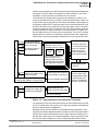
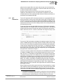
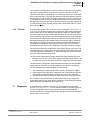
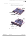
DNx-AI-217 — User Manual 16-Channel, 24-bit, Simultaneously Sampling, Differential Analog Input Board with Cold-Junction Compensation for the PowerDNA Cube and PowerDNR RACKtangle Release 4.6 April 2013 PN Man-DNx-AI-217-413 © Copyright 1998-2013 United Electronic Industries, Inc. All rights reserved. No part of this publication may be reproduced, stored in a retrieval system, or transmitted, in any form by any means, electronic, mechanical, by photocopying, recording, or otherwise without prior written permission. Information furnished in this manual is believed to be accurate and reliable. However, no responsibility is assumed for its use, or for any infringement of patents or other rights of third parties that may result from its use. All product names listed are trademarks or trade names of their respective companies. See the UEI website for complete terms and conditions of sale: http://www.ueidaq.com/cms/terms-and-conditions/ Contacting United Electronic Industries Mailing Address: 27 Renmar Avenue Walpole, MA 02081 U.S.A. For a list of our distributors and partners in the US and around the world, please see http://www.ueidaq.com/partners/ Support: Telephone: Fax: (508) 921-4600 (508) 668-2350 Also see the FAQs and online “Live Help” feature on our web site. Internet Support: Support: Web-Site: FTP Site: [email protected] www.ueidaq.com ftp://ftp.ueidaq.com Product Disclaimer: WARNING! DO NOT USE PRODUCTS SOLD BY UNITED ELECTRONIC INDUSTRIES, INC. AS CRITICAL COMPONENTS IN LIFE SUPPORT DEVICES OR SYSTEMS. Products sold by United Electronic Industries, Inc. are not authorized for use as critical components in life support devices or systems. A critical component is any component of a life support device or system whose failure to perform can be reasonably expected to cause the failure of the life support device or system, or to affect its safety or effectiveness. Any attempt to purchase any United Electronic Industries, Inc. product for that purpose is null and void and United Electronic Industries Inc. accepts no liability whatsoever in contract, tort, or otherwise whether or not resulting from our or our employees' negligence or failure to detect an improper purchase. Specifications in this document are subject to change without notice. Check with UEI for current status. DNA/DNR-AI-217 Simultaneous Sampling Differential Analog Input Board Contents Table of Contents Chapter 1 Introduction .................................................... 1 1.1 Organization of Manual. . . . . . . . . . . . . . . . . . . . . . . . . . . . . . . . . . . . . . . . . . . . . . . . 1 1.2 The AI-217 Interface Board. . . . . . . . . . . . . . . . . . . . . . . . . . . . . . . . . . . . . . . . . . . . . 3 1.3 Features . . . . . . . . . . . . . . . . . . . . . . . . . . . . . . . . . . . . . . . . . . . . . . . . . . . . . . . . . . . 4 1.4 Specification . . . . . . . . . . . . . . . . . . . . . . . . . . . . . . . . . . . . . . . . . . . . . . . . . . . . . . . . 5 1.5 Comparison between AI-217 and AI-207 Layers . . . . . . . . . . . . . . . . . . . . . . . . . . . . 6 1.6 Device Architecture. . . . . . . . . . . . . . . . . . . . . . . . . . . . . . . . . . . . . . . . . . . . . . . . . . . 8 1.7 Diagnostics . . . . . . . . . . . . . . . . . . . . . . . . . . . . . . . . . . . . . . . . . . . . . . . . . . . . . . . . 11 1.8 Indicators . . . . . . . . . . . . . . . . . . . . . . . . . . . . . . . . . . . . . . . . . . . . . . . . . . . . . . . . . 12 1.9 Layer Connectors and Wiring . . . . . . . . . . . . . . . . . . . . . . . . . . . . . . . . . . . . . . . . . . 13 1.10 CJC Data . . . . . . . . . . . . . . . . . . . . . . . . . . . . . . . . . . . . . . . . . . . . . . . . . . . . . . . . . 14 Chapter 2 Programming with the High Level API . . . . . . . . . . . . . . . . . . . . . . . . . . . . . . 15 2.1 Creating a Session . . . . . . . . . . . . . . . . . . . . . . . . . . . . . . . . . . . . . . . . . . . . . . . . . . 15 2.2 Configuring the Resource String. . . . . . . . . . . . . . . . . . . . . . . . . . . . . . . . . . . . . . . . 15 2.3 Configuring the Input. . . . . . . . . . . . . . . . . . . . . . . . . . . . . . . . . . . . . . . . . . . . . . . . . 15 2.4 Configuring the Timing . . . . . . . . . . . . . . . . . . . . . . . . . . . . . . . . . . . . . . . . . . . . . . . 17 2.5 Open Circuit Detection . . . . . . . . . . . . . . . . . . . . . . . . . . . . . . . . . . . . . . . . . . . . . . . 17 2.6 Read Data. . . . . . . . . . . . . . . . . . . . . . . . . . . . . . . . . . . . . . . . . . . . . . . . . . . . . . . . . 18 2.7 Cleaning-up the Session. . . . . . . . . . . . . . . . . . . . . . . . . . . . . . . . . . . . . . . . . . . . . . 18 Chapter 3 Programming with the Low-level API . . . . . . . . . . . . . . . . . . . . . . . . . . . . . . . 19 © Copyright 2013 United Electronic Industries, Inc. Tel: 508-921-4600 Date: April 2013 www.ueidaq.com Vers: 4.5 DNx-AI-217-ManualTOC.fm i DNA/DNR-AI-217 Simultaneous Sampling Differential Analog Input Board Figures List of Figures 1-1 1-2 1-3 1-4 1-5 1-6 Block Diagram of the AI-217 Layer ............................................................................... 8 Logical Modules of the DNx-AI-217 Controller.............................................................. 9 The DNA-AI-217 Analog-Input Layer .......................................................................... 12 The DNR-AI-217 Analog-Input Layer.......................................................................... 12 Pinout Diagram of the AI-217 Layer............................................................................ 13 Recommended Ground Connections for Analog Inputs ............................................. 14 © Copyright 2013 United Electronic Industries, Inc. Tel: 508-921-4600 Date: April 2013 www.ueidaq.com Vers: 4.5 DNx-AI-217-ManualLOF.fm ii DNA/DNR-AI-217 Simultaneous Sampling Differential Analog Input Board Chapter 1 Introduction Chapter 1 Introduction This document outlines the feature set and use of the DNx-AI-217 board. The AI-217 is a 16-channel analog input module for the PowerDNA I/O Cube (DNAAI-217) and the DNR-1G HalfRACK and RACKtangle chassis (DNR-AI-217). 1.1 Organization of Manual © Copyright 2013 United Electronic Industries, Inc. This AI-217 User Manual is organized as follows: • Introduction This chapter provides an overview of DNx-AI-217 Analog Input Board features, device architecture, connectivity, and logic. • Programming with the High-Level API This chapter provides an overview of the how to create a session, configure the session, and interpret results with the Framework API. • Programming with the Low-Level API This chapter is an overview of low-level API commands for configuring and using the AI-217 series layer. • Appendix A - Accessories This appendix provides a list of accessories available for use with the DNx-AI-217 board. • Index This is an alphabetical listing of the topics covered in this manual. Tel: 508-921-4600 Date: April 2013 www.ueidaq.com Vers: 4.5 DNx-AI-217 Chap1x.fm 1 DNA/DNR-AI-217 Simultaneous Sampling Differential Analog Input Board Chapter 1 Introduction Manual Conventions To help you get the most out of this manual and our products, please note that we use the following conventions: Tips are designed to highlight quick ways to get the job done or to reveal good ideas you might not discover on your own. NOTE: Notes alert you to important information. CAUTION! Caution advises you of precautions to take to avoid injury, data loss, and damage to your boards or a system crash. Text formatted in bold typeface generally represents text that should be entered verbatim. For instance, it can represent a command, as in the following example: “You can instruct users how to run setup using a command such as setup.exe.” Text formatted in fixed typeface generally represents source code or other text that should be entered verbadim into the source code, initialization, or other file. Examples of Manual Conventions Before plugging any I/O connector into the Cube or RACKtangle, be sure to remove power from all field wiring. Failure to do so may cause severe damage to the equipment. Usage of Terms Throughout this manual, the term “Cube” refers to either a PowerDNA Cube product or to a PowerDNR RACKtangle rack mounted system, whichever is applicable. The term DNR is a specific reference to the RACKtangle, DNA to the PowerDNA I/O Cube, and DNx to refer to both. © Copyright 2013 United Electronic Industries, Inc. Tel: 508-921-4600 Date: April 2013 www.ueidaq.com Vers: 4.5 DNx-AI-217 Chap1x.fm 2 DNA/DNR-AI-217 Simultaneous Sampling Differential Analog Input Board Chapter 1 Introduction 1.2 The AI-217 Interface Board The DNA-AI-217 and DNR-AI-217 are 16-channel simultaneously sampling A/D boards compatible with UEI’s popular Cube and RACKtangle chassis respectively. The DNA/DNR versions are electronically identical and feature 24bit resolution with 7 software selectable input ranges. The DNx-AI-217 is pin compatible with the popular DNx-AI-207 board and offers an easy upgrade path for those looking for more resolution, higher sample rates or simultaneously sampling inputs. An A/D per channel configuration allows channels to be sampled simultaneously at rates up to 120000kS/s each for AI-217-1 or 30kS/s each for AI-217-803 (up to 480 kS/s max aggregate rate per board). The A/D per channel configuration virtually eliminates input cross talk and channel settling time issues even when connected to high impedance signal sources. The DNx-AI-217 is fully isolated from the Cube/RACKtangle and is overvoltage protected up to ±40 V (power on or off). The inputs go into a high impedance mode when power is removed making the AI-217 ideal for use in redundant measurement/control applications. Additionally, the DNx-AI-217 provides a dedicated CJC channel that can be used for reading from the built-in CJC sensor on the DNA-STP-AI-U or AI207TC terminal panels. The DNx-AI-217 is a member of UEI’s popular Guardian series, which provide high levels of user diagnostics. The AI-217 board provides both open input detection functionality as well as the ability to detect input overvoltage conditions. As with all UEI PowerDNA boards, the DNx-AI-217 can be operated in harsh environments and has been tested at 5g vibration, 50g shock, -40 to +85°C temperature. Each board provides 350 Vrms isolation between the board and its enclosure, or any other installed boards. Software included with the DNx-AI-217 provides a comprehensive yet easy to use API that supports all popular operating systems including Windows, Linux, real-time operating systems such as QNX, RTX, VXworks and more. Finally, the UEIDAQ Framework supplies complete support for those creating applications in Windows based data acquisition software packages such as LabVIEW, MATLAB, DASYLab or any application which supports ActiveX or OPC servers. © Copyright 2013 United Electronic Industries, Inc. Tel: 508-921-4600 Date: April 2013 www.ueidaq.com Vers: 4.5 DNx-AI-217 Chap1x.fm 3 DNA/DNR-AI-217 Simultaneous Sampling Differential Analog Input Board Chapter 1 Introduction 1.3 Features © Copyright 2013 United Electronic Industries, Inc. The AI-217 layer has the following features: • 16 differential analog input channels (+ one CJC channel) • Simultaneous sampling (one A/D converter per channel) • Maximum sampling rate 120 kHz per channel for the AI-217, 30kHz per channel for the AI-217-803 (480 kHz max per board) • 24-bit resolution • “Open” input wiring detection • Input over-range detection • Over-voltage protection -40V to +40V (power on or off) • ±10V input range • Gains - 1, 2, 4, 8, 16, 32 and 64 • Pin compatible with DNx-AI-207 • Built-in Diagnostic Feature • Power consumption 2.2W max • Weight of 120 g or 4.24 oz for DNA-AI-217; 630 g or 22.2 oz with PPC5 • Tested to withstand 5g Vibration, 50g Shock, -40 to +85°C Temperature • UEI Framework Software API may be used with all popular Windows programming languages and most real time operating systems such as RT Linux, RTX, or QNX and graphical applications such as LabVIEW, MATLAB, DASYLab and any application supporting ActiveX or OPC Tel: 508-921-4600 Date: April 2013 www.ueidaq.com Vers: 4.5 DNx-AI-217 Chap1x.fm 4 DNA/DNR-AI-217 Simultaneous Sampling Differential Analog Input Board Chapter 1 Introduction 1.4 Specification The technical specification for the DNx-AI-217 board are listed in Table 1-1. Table 1-1. DNx-AI-217-1 Technical Specifications Number of channels: 16 fully differential plus 1 single-ended dedicated CJC channel ADC resolution / type 24 bits / SAR. (AD7766) Sampling rate 120 kS/s per channel (max); 480 kS/s max aggregate for entire board Input bias current < 2 nA typical Input offset <4 μV; G=1, <2μV; G=2, <1 μV; G>2 (@ 25°C) (-40°C to +85°C spec is 2.5 times 25°C offset) Input INL error < 0.00004 % (40 ppm) max Input impedance 100 MΩ (min) Input range ±10 Volt (gain = 1) Input resolution 1.19 μV (gain = 1), 18.6 nV (gain = 64) Gains 1, 2, 4, 8, 16, 32, 64 Common mode rejection 110 dB typical Chan to Chan crosstalk < 1 μVrms Open input detection current 100 μA Isolation 350 Vrms Overvoltage protection -40V to +40V (power on or off ) Power off leakage current < 10 μA (-40V to + 40V) Power consumption 2.2W max Operating temp. (tested) -40°C to +85°C Operating humidity 95%, non-condensing Vibration IEC 60068-2-6 5 g, 10-500 Hz, sinusoidal IEC 60068-2-64 5 g (rms), 10-500Hz, broadband random 50 g, 3 ms half sine, 18 shocks @ 6 orientations Shock IEC 60068-2-27 30 g, 11 ms half sine, 18 shocks @ 6 orientations MTBF 500,000 hours Table 1-2. DNx-AI-217-803 Technical Specifications Number of channels: 16 fully differential plus 1 single-ended dedicated CJC channel ADC resolution / type 24 bits / SAR. (AD7766) Sampling rate 0 kS/s per channel (max); 480 kS/s max aggregate for entire board Input bias current < 2 nA typical Input offset <4 μV; G=1, <2μV; G=2, <1 μV; G>2 (@ 25°C) (-40°C to +85°C spec is 2.5 times 25°C offset) Input INL error < 0.00004 % (40 ppm) max Input impedance 100 MΩ (min) Input range ±10 Volt (gain = 1) Input resolution 1.19 μV (gain = 1), 18.6 nV (gain = 64) Gains 1, 2, 4, 8, 16, 32, 64 Common mode rejection 110 dB typical Chan to Chan crosstalk < 1 μVrms Open input detection current 100 μA Isolation 350 Vrms Overvoltage protection -40V to +40V (power on or off ) Power off leakage current < 10 μA (-40V to + 40V) Power consumption 2.2W max Operating temp. (tested) -40°C to +85°C Operating humidity 95%, non-condensing Vibration IEC 60068-2-6 5 g, 10-500 Hz, sinusoidal IEC 60068-2-64 5 g (rms), 10-500Hz, broadband random 50 g, 3 ms half sine, 18 shocks @ 6 orientations Shock IEC 60068-2-27 30 g, 11 ms half sine, 18 shocks @ 6 orientations MTBF © Copyright 2013 United Electronic Industries, Inc. Tel: 508-921-4600 Date: April 2013 500,000 hours www.ueidaq.com Vers: 4.5 DNx-AI-217 Chap1x.fm 5 DNA/DNR-AI-217 Simultaneous Sampling Differential Analog Input Board Chapter 1 Introduction 1.5 Comparison The following table is a side-by-side comparison of specification items for the AI207 and the AI-217 analog input layers: between AI-217 and AI- Table 1-3. AI-207 vs.AI-217 207 Layers Item AI-207 AI-217 No. and Type of 16 differential analog voltage 16 differential analog Channels plus 1 CJC voltage plus 1 CJC Input Range ±10V ±10V A/D Converters One 17 (one per analog input channel plus one for CJC) Simultaneous Sampling No Yes Sampling Rate 16 kHz aggregate max (1 kHz for 16 channels, 2 kHz for 8 channels, or 16 kHz for one channel) 1 Hz to 120kHz per channel, 480 kHz aggregate max. (30kHz/channel for 217-803) CJC Selection Channel 33, (adjustable gain) Channel 33 or Channel 16, 0 to 5 V, Fixed Gain) Available Gains 1, 2, 4, 8, 10, 20, 40, 80, 100, 200, 400, 800 Source Impedance Compatibility Resolution Isolation © Copyright 2013 United Electronic Industries, Inc. Tel: 508-921-4600 Date: April 2013 Best with low impedance sources 18-bit AI-207: 350Vrms between inputs and chassis. Common ground for input channels. www.ueidaq.com 1, 2, 4, 8, 16, 32, 64 Performs well with either low or high impedance sources 24-bit AI-217: 350Vrms between inputs and chassis. Common ground for input channels. Vers: 4.5 DNx-AI-217 Chap1x.fm 6 DNA/DNR-AI-217 Simultaneous Sampling Differential Analog Input Board Chapter 1 Introduction Table 1-3. AI-207 vs.AI-217 (Forts.) Item Pinout Noise Filtering AI-207 AI-217 Same for both models Averaging engine that averages multiple samples to improve resolution. AI-217 has a simple analog low-pass RC filter on the front-end for anti-aliasing designed for 60k-120kS/s. Digital FIR filter for all channels with user-configurable coefficients on back-end. AI-217-1 has 128-tap FIR, AI-217-803 has 512-tap. Channel List Specifies the channels that are to be read and the order in which to read them. Thus, the returned data is in the order that the channel list shows. If a channel needs to be sampled more often than other channels, the AI-207 allows the channel to be entered more than once in the channel list. Specifies the channels that are to be read, but because they are simultaneously sampled, the sequential order concept does not apply. The AI-217 always returns data with the channels in numerical order regardless of what order they were in the channel list. A channel may only appear once in the channel list. For a 8-channel analog input board with per-channel isolation, also see AI-218. © Copyright 2013 United Electronic Industries, Inc. Tel: 508-921-4600 Date: April 2013 www.ueidaq.com Vers: 4.5 DNx-AI-217 Chap1x.fm 7 DNA/DNR-AI-217 Simultaneous Sampling Differential Analog Input Board Chapter 1 Introduction Figure 1-1 is a block diagram of the architecture of the AI-217 layer. Channel 1 of 16 Reference Calibration 4ch ±40V Protection IC + + 1ch PGA – PGA 280 Analog Voltages DB-37 Analog Input Connector ±10V ±10V FPGA 24-bit FIR (4x4ch) 24-bit 1ch ADC (8x O/S) Control Logic Channels 2 to 4 Channels 5 to 8 Channels 9 to 12 Channels 13 to 16 Channel 17 CJC+ 1kΩ EEPROM 24-bit ADC 32-bit 66MHz Bus Device Architecture Isolation 1.6 Ext_Trig AGnd 2x +5V DC/DC (sw controlled) +13V 50mA Figure 1-1. Block Diagram of the AI-217 Layer Each AI-217 has sixteen differential input channels designed for high-speed, high-resolution analog voltage signal measurement. Each channel has 24-bit sampling resolution over a ±10V input range and and maximum sampling rate of 120000 samples per second (one sample every 8.3µsec) for the AI-217-1 or 30000 samples per second (one sample every 33.3µsec) for the AI-217-803. Each AI-217 is capable of up to 480000 max samples per second maximum. The DNx-AI-217 is fully isolated from the Cube or RACKtangle chassis and is overvoltage protected up to ±40V with power on or off. When power is removed, the inputs go into a high impedance mode, making the AI-217 an ideal choice for redundant measurement/control applications. Each channel’s input consists of two pins: a pair of analog input lines that carry the voltage to be sampled. The analog input lines (Ain+ and Ain- in Figure 1-1) enter through the DB-37 connector pins into a protection, then into a simple R-C low-pass filter circuit on the front end used for anti-aliasing, then into a PGA to be amplified by 1, 2, 4, 8, 16, 32, 64x and then into an A/D to be sampled. There is one 24-bit over-sampled successive approximation A/D converter per input channel plus one for a dedicated CJC input. Using a single ADC for each input channel virtually eliminates input crosstalk and channel settling time issues even when connected to high impedance signal sources. All sixteen analog © Copyright 2013 United Electronic Industries, Inc. Tel: 508-921-4600 Date: April 2013 www.ueidaq.com Vers: 4.5 DNx-AI-217 Chap1x.fm 8 DNA/DNR-AI-217 Simultaneous Sampling Differential Analog Input Board Chapter 1 Introduction inputs are first sampled by the ADC simultaneously and gain/offset adjustments are applied. The CJC channel is sampled once each decimation cycle. More information on A/D conversion is provided in the next section. The dedicated CJC channel that can be used for reading from a built-in CJC sensor on the DNA-STP-AI-U or AI-207TC accessory terminal panel. Static CJC compensation may be used when no CJC sensor is available, such as when it is connected to a DNA-STP-37 accessory panel. When used with DNA-STP-AI-U Universal Terminal Panel, the DNx-AI-217 layer also offers a direct connection for thermocouples and open TC detection. The STP-AI-U accessory panel also provides excitation for 2-wire and 4-wire RTD measurements. For details, see the User Manual for the STP-AI-U screw terminal panel. The AI-217’s versatile design allows it to achieve an exceptional cost/performance ratio, making it an ideal solution for precise temperature measurement over a long period of time. to AD7766 ADC and CJC adc-rdy ADC Reader Module Simultaneous read from adc-sdo all 16+1 channels. adc-sync Per-channel offset & adc-sclk gain adjustments. 4-channel FIR Module [128-taps max for 217-1; 512-taps max for 217-803] 24-bit FIR Coeff. 24-bit Data Each channel has its own data storage, but all 4 channels share the same coefficients and decimation ratio. Software-configured. Output conversion clock adc-mclk Used as 8x master clock source for ADCs. Input Clock Source 21.12M, 25.6M, 66MHz, or custom freq. to PGA280s FIR Sync Module pga-d PGA280 Access Module Configure two master and pga-clk fourteen slave PGA280s. Clock Divider Divides input clock source to use as 8x ADC clock source. Source is software-selectable. Receives data from four 4-chan FIR units plus CJC. Streams data into Input CL. Output sample and their channel number. Input Channel List for AI-217 Standard DNA Logic found on every layer. Provides DMA access to ADC Reader, FIR Module, PGA Module, and other components. Output Channel List Only conversion clock used. PGA Error Interrupts Figure 1-2. Logical Modules of the DNx-AI-217 Controller The samples from A/D converters travel across an opto-isolated barrier into the AI-217’s controller chip. The structure of on-chip logical modules is illustrated in the block diagram shown in Figure 1-2. Samples from the A/D are passed to a FIR Module that provides both a finiteinput-response filter and data decimation, and then into the FIR Synchronization module, which streams data/samples into the input Channel List buffer; this is the data that is retrieved to your computer application when using function calls like the ones listed in Chapter 3. It does not guarantee that channels will be © Copyright 2013 United Electronic Industries, Inc. Tel: 508-921-4600 Date: April 2013 www.ueidaq.com Vers: 4.5 DNx-AI-217 Chap1x.fm 9 DNA/DNR-AI-217 Simultaneous Sampling Differential Analog Input Board Chapter 1 Introduction placed into the output buffer in the same order as they are in the channel list, however each data sample incorporates a channel number that can be used to re-order the output buffer in software. Using the output channel list, the PGA Access Module manages PGA operations, stores data from each, and generates error IRQs for any error conditions that occur. Error interrupts output from the PGA access module are processed in the standard DNA logic. 1.6.1 A/D Conversion The AI-217 implements ADC converters that utilize an oversampled SAR architecture and require a clock source (mclk) that is 8x the ADC’s output data rate. The input clock source for the ADCs is kept between 480KHz to 960KHz for the AI-217-1; meaning that the actual data rate from the AD7766 is always 60k-120k samples/second, which is free from aliasing because of the analog anti-alias filter mentioned previously. To get output data rates less than 60kHz the layer’s FIR module’s decimation unit will only keep 1 in n samples, where n is the decimation factor. The following pseudocode shows how to calculate the master clock frequency and the decimation ratio for the AI-217-1, which is useful when not using the on-layer clock: // calculate decimation factor and sample rate decratio = 1; while (mclkrate <= (480000/8)){ mclkrate *= 2; decratio *= 2; } // start at 60000Hz For the AI-217-803, decimation is disabled; the maximum master clock source (mclk) is 240kHz which gives an output data rate of 30kHz. With the AI-217-803 the user may need to supply an appropriate input anti-aliasing (low-pass) filter on the front-end, similar to the R-C filter of the AI-217-1, if aliasing below 56kHz is to be expected. Finally, the CJC channel is read once per decimation cycle. Both sample rate and decimation factor are configured by your user application through function calls listed in Chapter 3. The AI-217 provides a special clock divider that can use 66MHz as well as fixed 21.12MHz or 25.6MHz clocks to create different frequencies used to run the ADC; the AI-2171 incorporates a programmable PLL that allows the generation of the base frequency with 0.1% or better accuracy. Alternatively the UEI DNxIRIG-650 layer’s 100MHz base clock and PLL can also be used to generate a very precise master clock signal of 480-960KHz and route it into the AI-217 ADCs. The “master” clock shall be constantly running even when conversion results are not used because it has a long FIR filter that should stay settled (see AD7766/AD7767 datasheet for details about the ADC). Thus, samples are always produced, but are not stored in the output buffer until a start command or start trigger is issued. When multiple layers should be synchronized, the clock generated by a master layer should be routed to the SYNC bus (e.g. SYNC1 line) and from there back to the clock of the slave layers (CVOUT). Keeping all AI-217 layers synchronized using an 8x ADC clock and hardware trigger would provide fully synchro1. This feature is supported on logic revision 02.10.D3 (2013). UEI Technical Support can provide you with a field programmable update package if your logic is older. Use PowerDNA Explorer’s Hardware Report to show logic versions for your AI-217. © Copyright 2013 United Electronic Industries, Inc. Tel: 508-921-4600 Date: April 2013 www.ueidaq.com Vers: 4.5 DNx-AI-217 Chap1x.fm 10 DNA/DNR-AI-217 Simultaneous Sampling Differential Analog Input Board Chapter 1 Introduction nous operation of multiple layers; however if there are other layers in the system that require synchronization using the scan clock then there are two other options that should be considered. One is to divide the master 8x clock by eight clock cycles using the CT-601 layer and distribute it across the system. However if an extra layer is not an option then each individual layer can be configured to run the ADC at maximum rate of 120KHz and the scan clock is used as a gate that grabs one last scan received from the converters; thus synchronizing the AI217 using the scan clock. This way all layers are synchronized within ±1 conversion cycle (8.33µsec). 1.6.2 FIR Filter A unique feature of the AI-217 is the use of four 4-channel (i.e. 0 to 3, 4 to 7, 8 to 11, 12 to 15) FIR filters implemented on-chip in the FIR module logical block. Each channel uses its own storage for the data and each four channels share the same coefficients and decimation ratio. By default, all channels are set to the same coefficients and decimation ratio by the software function call for simplicity, and thus have the same output data rate. Coefficients and decimation ratio are automatically selected by the software calls to an optimum value to match the throughput. The FIR filter can either be disabled or enabled with automatic or user-configured coefficients using software function calls. The FIR module’s decimation ratio can also be user-configured to 0 (keep all samples) or higher. This section discusses the configuration of the digital FIR filter found in the FIR module logical block. This should not be confused with the FIR filters also found in the AD7766 (as per its datasheet), or the anti-aliasing filter circuit on the frontend of the PGA discussed much earlier. The FIR module implements an integer-based finite-input-response filter with: • • 128-taps on the AI-217-1, for a faster response and lower group delay, or as 512-taps on the AI-217-803, which provides a sharper filter with less ripple. The default filter is configured to suppress harmonics above one half of the ADC output data rate, however, you can generate/use your own filter coefficients. The filter operates as per standard digital FIR filter theory: 1. The newest input sample from the ADC is put into the delay line register. 2. Each sample in the delay line is multipled by the corresponding coefficient. Accumulate all multiplied values to provide the result to the output line. 3. Shift the delay line by one sample to make room for the next input sample. The caveats of using the FIR filter are that rippling may occur in response to sharp edges and there is a group delay of 128/2=64 or 512/2=256 ADC samples before the output is provided into the output buffer. 1.7 Diagnostics © Copyright 2013 United Electronic Industries, Inc. A standard feature available with the AI-217 is a diagnostic function called DqAdv217GetPgaStatus(). You can call this function at any time to perform a series of diagnostic tests of board operation. Refer the PowerDNA API Reference Manual for a detailed description of how the function works and to the sample code on how to use it. Tel: 508-921-4600 Date: April 2013 www.ueidaq.com Vers: 4.5 DNx-AI-217 Chap1x.fm 11 DNA/DNR-AI-217 Simultaneous Sampling Differential Analog Input Board Chapter 1 Introduction 1.8 Indicators A photo of the DNx-AI-217 unit is illustrated below. The front panel has two LED indicators: • RDY: indicates that the layer is receiving power and operational. • STS: can be set by the user using the low-level framework. DNA bus connector RDY LED STS LED DB-37 (female) 37-pin I/O connector Figure 1-3. The DNA-AI-217 Analog-Input Layer DNR bus connector RDY LED STS LED DB-37 (female) 37-pin I/O connector Figure 1-4. The DNR-AI-217 Analog-Input Layer © Copyright 2013 United Electronic Industries, Inc. Tel: 508-921-4600 Date: April 2013 www.ueidaq.com Vers: 4.5 DNx-AI-217 Chap1x.fm 12 DNA/DNR-AI-217 Simultaneous Sampling Differential Analog Input Board Chapter 1 Introduction 1.9 Layer Connectors and Wiring Figure 1-5 below illustrates the pinout of the AI-217. The AI-217 layer uses a Bsize 37-pin D-sub connector. The following signals are located at the connector: • AIN0+ – AIN15+ — input channel, differential mode. Use AIN0 to –AIN15 as signal returns. • +13V 50mA — provides power for CJC circuitry on the optional DNA-STP-AU accessory panel • CJC+ — cold junction compensation return line from DNA-STP-AI-U. • AGND — layer analog ground, isolated from system ground. • EXT_TRIG — accepts an external trigger signal to the layer. Ext_Trig AIn 15+ AIn 14+ AIn 13AIn 12AIn 11AIn 10Gnd AIn 9+ AIn 8+ AIn 7+ AIn 6+ AIn 5AIn 4AIn 3AIn 2Gnd AIn 1+ AIn 0+ 1 2 3 4 5 6 7 8 9 10 11 12 13 14 15 16 17 18 19 20 21 22 23 24 25 26 27 28 29 30 31 32 33 34 35 36 37 AIn 15AIn 14+13V, 50 mA AIn 13+ AIn 12+ AIn 11+ AIn 10+ AIn 9AIn 8AIn 7AIn 6CJC+ AIn 5+ AIn 4+ AIn 3+ AIn 2+ AIn 1AIn 0- Figure 1-5. Pinout Diagram of the AI-217 Layer NOTE: If you are using a accessory panel with the AI-217, please refer to the Appendix for a description of the panel. © Copyright 2013 United Electronic Industries, Inc. Tel: 508-921-4600 Date: April 2013 www.ueidaq.com Vers: 4.5 DNx-AI-217 Chap1x.fm 13 DNA/DNR-AI-217 Simultaneous Sampling Differential Analog Input Board Chapter 1 Introduction 1.9.1 Analog Input Ground Connections To avoid errors caused by common mode voltages on analog inputs, follow the recommended grounding guidelines in Figure 1-6 below. Because all analog input channels in AI-201/202/207/208/217/225 layers are isolated as a group, you can connect layer AGND to the ground of the signal source and eliminate the resistors shown in Figure 1-6 for floating differential input signals. Type of Input Floating Grounded Typical Signal Sources: Instruments or sensors with non-isolated outputs DNA-STP-37, DNA-STP-AI-U Sig Vin _ Differential Ret Sig + AInX + DNA-STP-AI-U AInX Typical Signal Sources: Input Thermocouples Configuration DC Voltage Sources Instruments or sensors with isolated outputs Vin _ Ret AGnd Two resistors (10k <R< 100k) provide return paths to ground for bias currents. AGnd Add this connection to ensure that both grounds are at the same potential. NOT RECOMMENDED DNA-STP-AI-U _ Ret Sig AInX Vin + AInX Single-Ended, Ground Referenced DNA-STP-AI-U Sig + Vin AGnd _ Ret AGnd Figure 1-6. Recommended Ground Connections for Analog Inputs 1.10 CJC Data Raw CJC Voltage from the AI-217 may be represented as: CJCVoltage T Kelvin = -------------------------------0.00295 For example, if the voltage read from Channel 33 (the CJC channel) is 0.87, the CJC Temperature is: © Copyright 2013 United Electronic Industries, Inc. Temp. Scale Calculation CJC Temperature Kelvin 0.87/0.00295 294.9 °K Celsius 294.9 – 273.15 21.75 °C Fahrenheit 1.8 x 21.75 + 32 71.75 °F Tel: 508-921-4600 Date: April 2013 www.ueidaq.com Vers: 4.5 DNx-AI-217 Chap1x.fm 14 DNA/DNR-AI-217 Simultaneous Sampling Differential Analog Input Board Chapter 2 Programming with the High Level API Chapter 2 Programming with the High Level API This section describes how to control the DNx-AI-217 using the UeiDaq Framework High Level API. UeiDaq Framework is object oriented and its objects can be manipulated in the same manner from different development environments such as Visual C++, Visual Basic or LabVIEW. The following section focuses on the C++ API, but the concept is the same no matter what programming language you use. Please refer to the “UeiDaq Framework User Manual” for more information on use of other programming languages. 2.1 Creating a Session The Session object controls all operations on your PowerDNx device. Therefore, the first task is to create a session object: // create a session object for input CUeiSession aiSession; 2.2 Configuring UeiDaq Framework uses resource strings to select which device, subsystem the Resource and channels to use within a session. The resource string syntax is similar to a web URL: String <device class>://<IP address>/<Device Id>/<Subsystem><Channel list> For PowerDNA and RACKtangle, the device class is pdna. For example, the following resource string selects analog input lines 0,1,2,3 on device 1 at IP address 192.168.100.2: “pdna://192.168.100.2/Dev1/Ai0:3” as a range, or as a list “pdna://192.168.100.2/Dev1/Ai0,1,2,3”. 2.3 2.3.1 Configuring the Input Voltage Measurement This section will show you how to configure your input for voltage measurement, thermocouple measurement, or RTD measurement. The gain applied on each channel is specified by using low and high input limits. For example, the AI-217 available gains are 1, 2, 4, 8, 16, 32, 64 and the maximum input range is [-10V, +10V (gain = 1)]. To select the gain of 1, you need to specify input limits of [-10V, +10V]: // Configure channels 0,1 to use a gain of 1 in differential mode aiSession.CreateAIChannel(“pdna://192.168.100.2/Dev0/Ai0,1”, -10.0, 10.0, UeiAIChannelInputModeDifferential); © Copyright 2013 United Electronic Industries, Inc. Tel: 508-921-4600 Date: April 2013 www.ueidaq.com Vers: 4.5 DNx-AI-217 Chap2x.fm 15 DNA/DNR-AI-217 Simultaneous Sampling Differential Analog Input Board Chapter 2 Programming with the High Level API 2.3.2 Thermocouple For thermocouples, use the object method CreateTCChannel which automatMeasurement ically handles temperature calculations, as follows: // Configure channel 0 to 2, scaling for thermocouples; // thermocouple Type K, degrees F°, using CJC built-in // compensation from the STP-AI-U board, in differential mode. mySs.CreateTCChannel("pdna://192.168.100.2/Dev0/Ai0:2", -10.0, 10.0, ThermocoupleType.TypeK, TemperatureScale.Fahrenheit, ColdJunctionCompensationType.BuiltIn, 0, "", AIChannelInputMode.Differential); 2.3.3 RTD Measurement RTD measurements are configured using the Session object method “CreateRTDChannel”. RTD sensors are resistive sensors whose resistance varies with temperature. Knowing the resistance of an RTD, we can calculate the temperature using the “Callendar Van-Dusen” equations. RTD sensors are specified using the "alpha" (α) constant. It is also known as the temperature coefficient of resistance, which defines the resistance change factor per degree of temperature change. The RTD type is used to select the proper coefficients A, B and C for the Callendar Van-Dusen equation, which is used to convert resistance measurements to temperature. To measure the RTD resistance, we need to know the amount of current flowing through it. We can then calculate the resistance by dividing the measured voltage by the known excitation current. To measure the excitation current, we measure the voltage from a high precision reference resistor whose resistance is known. The reference resistor is built-into the terminal block if you are using a DNASTP-AI-U, but you can provide your own external reference resistor, if prefered. In addition, you must configure the RTD type and its nominal resistance at 0° Celsius, as shown in the following example: // // // // // // // Add 4 channels (0 to 3) to the channel list and configure them to measure a temperature between 0.0 and 200.0 deg. C. The RTD sensor is connected to the DAQ device using two wires, the excitation voltage is 5V, and the reference resistor is the 20kOhm resistor built-into the DNA-STP-AI-U. The RTD alpha coefficient is 0.00385, the nominal resistance at 0° C is 100 Ohms, and the measured temperature will be returned in °C. MySession.CreateRTDChannel(“pdna://192.168.100.2/dev0/Ai0:3”, 0, 1000.0, UeiTwoWires, 5.0, UeiRefResistorBuiltIn, 20000.0, UeiRTDType3850, 100.0, UeiTemperatureScaleCelsius, UeiAIChannelInputModeDifferential); © Copyright 2013 United Electronic Industries, Inc. Tel: 508-921-4600 Date: April 2013 www.ueidaq.com Vers: 4.5 DNx-AI-217 Chap2x.fm 16 DNA/DNR-AI-217 Simultaneous Sampling Differential Analog Input Board Chapter 2 Programming with the High Level API 2.4 Configuring the Timing You can configure the AI-217 to run in simple mode (point by point) or highthroughput buffered mode (ACB mode), or high-responsiveness (DMAP) mode. In simple mode, the delay between samples is determined by software on the host computer. In buffered mode, the delay between samples is determined by the AI-217 on-board clock and data is transferred in blocks between PowerDNA and the host PC. The following sample shows how to configure the simple mode. Please refer to the “UeiDaq Framework User’s Manual” to learn how to use other timing modes. // configure timing of input for point-by-point (simple mode) aiSession.ConfigureTimingForSimpleIO(); 2.5 Open Circuit Detection The AI-217 can source a 100mA current through each input channel to detect whether the circuit is close or open. This can be enabled on a per channel basis. Use the AI channel object method "EnableOpenCircuitDetection()" to turn on the feature on any input channel (0 to 15). The example below shows how to turn on open circuit detection on all channels: // turn on open circuit detection on all channels for(int ch=0; ch<session.GetNumberOfChannels(); ch++) { CUeiAIChannel* pChan = dynamic_cast<CUeiAIChannel*>(session.GetChannel(ch)); pChan->EnableOpenCircuitTest(true); } Once the session is started, you can retrieve the result of the open cicuit detection with the channel object method "IsCircuitOpen()": // return if circuit is open for(int ch=0; ch<session.GetNumberOfChannels(); ch++) { CUeiAIChannel* pChan = dynamic_cast<CUeiAIChannel*>(session.GetChannel(ch)); if(pChan->IsCircuitOpen()) { std::cout << "Open circuit detected on channel " << pChan->GetIndex() << std::endl; } } © Copyright 2013 United Electronic Industries, Inc. Tel: 508-921-4600 Date: April 2013 www.ueidaq.com Vers: 4.5 DNx-AI-217 Chap2x.fm 17 DNA/DNR-AI-217 Simultaneous Sampling Differential Analog Input Board Chapter 2 Programming with the High Level API 2.6 Read Data Reading data is done using reader object(s). There is a reader object to read raw data coming straight from the A/D converter. There is also a reader object to read data already scaled to volts or mV/V. The following sample code shows how to create a scaled reader object and read samples. // create a reader and link it to the analog-input session’s stream CUeiAnalogScaledReader aiReader(aiSession.GetDataStream()); // the buffer must be big enough to contain one value per channel double data[2]; // read one scan, where the buffer will contain one value per channel aiReader.ReadSingleScan(data); 2.7 Cleaning-up the Session The session object will clean itself up when it goes out of scope or when it is destroyed. To reuse the object with a different set of channels or parameters, you can manually clean up the session as follows: // clean up the session aiSession.CleanUp(); © Copyright 2013 United Electronic Industries, Inc. Tel: 508-921-4600 Date: April 2013 www.ueidaq.com Vers: 4.5 DNx-AI-217 Chap2x.fm 18 DNA/DNR-AI-217 Simultaneous Sampling Differential Analog Input Board Chapter 3 Programming with the Low-level API Chapter 3 Programming with the Low-level API The PowerDNA cube and PowerDNR RACKtangle and HalfRACK can be programmed using the low-level API. The low-level API offers direct access to PowerDNA DAQBios protocol and also allows you to access device registers directly. However, we recommend that, when possible, you use the UeiDaq Framework High-Level API (see Chapter 2), because it is easier to use. You should need to use the low-level API only if you are using an operating system other than Windows. For additional information about low-level programming of the AI-217, please refer to the PowerDNA API Reference Manual document under: Start » Programs » UEI » PowerDNA » Documentation Refer to the PowerDNA API Reference Manual on how to use the following lowlevel functions of AI-217, as well as others related to cube operation: Function Description DqAdv217Read Returns continously sampled data from input channel. DqAdv217GetPgaStatus Returns the PGA status of the AI-217. DqAdv217SetCfgLayer DqAdv217SetCjcAvg Set advanced layer configuration parameters for the AI-217. Overrides/restores the default averaging factor used by CJC channel. DqAdv217SetFIR Convenience function to configure the FIR and decimation factor. DqAdv217SetPll Configures custom sampling rates for DACs. © Copyright 2013 United Electronic Industries, Inc. Tel: 508-921-4600 Date: April 2013 www.ueidaq.com Vers: 4.5 DNx-AI-217 Chap3.fm 19 DNA/DNR-AI-217 Simultaneous Sampling Differential Analog Input Board Appendix A Appendix A A. Accessories The following cables and STP boards are available for the AI-217 layer. DNA-CBL-37 This is a 37-conductor flat ribbon cable with 37-pin male D-sub connectors on both ends. The length is 3ft and the weight is 3.4 ounces or 98 grams. DNA-CBL-37S This is a 37-conductor round shielded cable with 37-pin male D-sub connectors on both ends. It is made with round, heavy-shielded cable; 3 ft (90 cm) long, weight of 10 ounces or 282 grams; also available in 10ft and 20ft lengths. DNA-STP-37 The DNA-STP-37 provides easy screw terminal connections for all DNA and DNR series I/O boards which utilize the 37-pin connector scheme. The DNASTP-37 is connected to the I/O board via either DNA-CBL-37 or DNA-CBL-37S series cables. The dimensions of the STP-37 board are 4.2w x 2.8d x1.0h inch or 10.6 x 7.1 x 7.6 cm (with standoffs). The weight of the STP-37 board is 2.4 ounces or 69 grams. JP1 — DB-37 (male) 37-pin connector: UP+1 UP+1 UP+1 UP+1 UP+1 UP+1 UP+1 UP+1 UP+1 UP+1 UP+1 UP+1 UP+1 UP+1 UP+1 UP+1 UP+1 UP+1 20 21 22 23 24 25 26 27 28 29 30 31 32 33 34 35 36 37 1 2 3 4 5 6 7 8 9 10 11 12 13 14 15 16 17 18 19 JP2 — 20-position terminal block: UP+1 UP+1 UP+1 UP+1 UP+1 UP+1 UP+1 UP+1 UP+1 UP+1 UP+1 UP+1 UP+1 UP+1 UP+1 UP+1 UP+1 UP+1 UP+1 JP3 — 20-position terminal block: 4 2 CABLE SHIELD N/C N/C 24 22 20 to JP2 to JP3 DNA-STP-AI-U Universal screw-terminal panel with embedded CJC. DNA-STP-AI-207TC Screw terminal panel for use with the DNx-AI-217 and thermocouples. The panel provides open thermocouple detection as well as the cold-junction compensation measurement. © Copyright 2013 United Electronic Industries, Inc. Tel: 508-921-4600 Date: April 2013 www.ueidaq.com Vers: 4.5 DNx-AI-217 AppxA.fm 20 DNA/DNR-AI-217 Simultaneous Sampling Differential Analog Input Board 21 Index B J Block Diagram Jumper Settings 8 C L Cable(s) 20 CJC Sensor 9 Configuring the Resource String Connectors and Wiring 13 Conventions 2 Creating a Session 15 Low-level API 15 H High Level API 15 5 19 O Organization 1 S Screw Terminal Panels 20 Setting Operating Parameters 4 Specifications 5 Support ii I Isolation 3 © Copyright © 2013 Copyright 2013 United Electronic United Electronic Industries,Industries, Inc. Inc. Tel: 508-921-4600 Date: April 2013 www.ueidaq.com Vers: 4.5 DNx-AI-217-ManualIX.fm